A BIST Architecture for Testing LUTs in a Virtex-4 ... - OhioLINK ETD
134
A Thesis entitled A BIST Architecture for Testing LUTs in a Virtex-4 FPGA by Priyanka Gadde Submitted to the Graduate Faculty as partial fulfillment of the requirements for the Master of Science Degree in Electrical Engineering _______________________________________ Dr. Mohammad Niamat, Committee Chair _______________________________________ Dr. Mansoor Alam, Committee Member _______________________________________ Dr. Weiqing Sun, Committee Member _______________________________________ Dr. Patricia R. Komuniecki, Dean College of Graduate Studies The University of Toledo December 2013
-
Upload
khangminh22 -
Category
Documents
-
view
2 -
download
0
Transcript of A BIST Architecture for Testing LUTs in a Virtex-4 ... - OhioLINK ETD

A Thesis
entitled
A BIST Architecture for Testing LUTs in a Virtex-4 FPGA
by
Priyanka Gadde
Submitted to the Graduate Faculty as partial fulfillment of the requirements for the
Master of Science Degree in Electrical Engineering
_______________________________________
Dr. Mohammad Niamat, Committee Chair
_______________________________________
Dr. Mansoor Alam, Committee Member
_______________________________________
Dr. Weiqing Sun, Committee Member
_______________________________________
Dr. Patricia R. Komuniecki, Dean
College of Graduate Studies
The University of Toledo
December 2013

Copyright 2013, Priyanka Gadde
This document is copyrighted material. Under copyright law, no parts of this document
may be reproduced without the expressed permission of the author.
iii
An Abstract of
A BIST Architecture for Testing LUTs in a Virtex-4 FPGA
by
Priyanka Gadde
Submitted to the Graduate Faculty as partial fulfillment of the requirements for the
Master of Science Degree in Electrical Engineering
The University of Toledo
December 2013
Field Programmable Gate Arrays (FPGAs) are programmable logic devices that
can be used to implement a given digital design. Built-In Self-Test (BIST) is a testing
technique that enables the device to test itself without the need for any external test
equipment. The re-programmability feature of the FPGAs makes BIST a favorable
approach for testing FPGAs because it eliminates any area or performance degradation
associated with BIST.
In order to ensure proper operation of Look up Tables in Xilinx Virtex-4 Field-
Programmable Gate Arrays (FPGAs), a dependable and resource efficient test technique
is needed so that the functional operation of the memory can be tested. Traditional BIST
techniques for FPGAs suffer from a large number of logic resource requirements and
long test times in the implementation and testing of the circuit.
The work presented in this research simplifies the BIST architecture and reduces
the test time required to test the Look up Tables in a Virtex-4 FPGA. The proposed

iv
technique is capable of testing the following types of memory faults: stuck-at fault,
transition fault, address decoder fault, incorrect read fault, read destructive fault,
deceptive read destructive fault, data retention fault, state coupling fault, transition
coupling fault, incorrect read coupling fault, read destructive coupling fault, and
deceptive read destructive coupling fault in a SRAM based FPGA.

This Thesis is dedicated to my Grandparents, for all their Love and Support.

vi
Acknowledgements
I would like to thank Dr. Mohammed Niamat for giving me an opportunity to
work under his leadership and guiding me with his valuable advice. I would also like to
thank Dr. Mansoor Alam and Dr. Weiqing Sun for serving in my thesis committee. I
would also like to thank the Department of Electrical Engineering and Computer
Sciences, for partially funding my Master’s degree
I would like to thank my grandparents Mr. Adinarayana and Mrs. Jayasri and my
parents, Mr. Ramprasad and Mrs. Karuna for their constant love, support, understanding,
encouragement and for always being my source of motivation. I am very grateful to them
for their sacrifices and efforts that made this thesis possible. I would love to thank my
sister Hema Prasanthi for being there to share my happiness, cheer me up in tough times
and being my best friend always.
My acknowledgments would be incomplete without thanking my friends. Primarily, I
would like to thank Pradyuma Thayi for being my best companion to help and guide me
throughout my Masters. I would like to thank my friends Aditya, Ahmad, Anu, Jayaram,
Karthik, Prem, Sandeep, Swetha, and Teja for all their encouragement at every step and I
would like to thank my Uncle Madhusudan and Aunt Padmaja for all their love and
support.

vii
Contents
Abstract ............................................................................................................................. iii
Acknowledgements .......................................................................................................... vi
Table of Contents ............................................................................................................ vii
List of Tables .................................................................................................................. xii
List of Figures ............................................................................................................... xiii
1 Introduction ........................................................................................................... 1
1.1 Field Programmable Gate Arrays .................................................................... 1
1.2 Built in Self-Test (BIST) ................................................................................. 2
1.3 Advantages of BIST ......................................................................................... 3
1.4 Disadvantages of BIST .................................................................................... 4
1.5 Literature Survey .............................................................................................. 5
1.6 Organization of Thesis ..................................................................................... 8
2 Fault Types and Algorithms ................................................................................ 9
2.1 Introduction ...................................................................................................... 9
2.2 SRAM Cell ..................................................................................................... 11
2.3 Functional Model ........................................................................................... 11
2.4 Electrical Structure for SRAMs ..................................................................... 12

viii
2.5 SRAM Read and Write Circuitries................................................................. 14
2.6 Faults .............................................................................................................. 15
2.6.1 SRAM Memory Faults .................................................................... 16
2.7 Analysis of Faults in SRAM Cell ................................................................... 29
2.8 Advanced Memory Test ................................................................................. 32
2.9 MATS and MATS+ Algorithms .................................................................... 32
2.10 MARCH C-Algorithm.................................................................................. 33
2.11 Extended MarchC- Algorithm ...................................................................... 33
2.12 March Tests .................................................................................................. 34
2.13 Selection of the Testing Algorithm .............................................................. 35
3 SRAM Based FPGA ............................................................................................ 36
3.1 Introduction .................................................................................................... 36
3.2 Anatomy of the FPGA.................................................................................... 36
3.3 Benefits and Drawbacks of FPGAs ................................................................ 37
3.4 FPGA Applications ........................................................................................ 38
3.5 FPGA Device Manufactures .......................................................................... 39
3.6 SRAM Programmable Virtex-4 FPGA .......................................................... 39
3.6.1 I/O Blocks ....................................................................................... 40
3.6.2 Block RAM Modules (BRAMs) ..................................................... 40
3.6.3 Cascadable Embedded Xtreme DSPSlices ...................................... 41

ix
3.6.4 Digital Clock Managers (DCMs) .................................................... 41
3.6.5 Configurable Logic Block (CLBs) .................................................. 41
3.7 Need for Testing FPGAs ................................................................................ 49
4 Proposed Architecture for Testing Look up Tables in a Virtex-4 FPGA ...... 50
4.1 Test Pattern Generator (TPG) ........................................................................ 53
4.2 Circuit Under Test (CUT) and Output Response Analyzer (ORA) ............... 57
4.3 BISTArchitecture ........................................................................................... 59
4.4 Fault Modeling and Detection using Extended MarchC- Algorithm............. 62
4.5 Pseudo Code ................................................................................................... 63
4.6 Fault Modeling and Detection ........................................................................ 64
4.6.1 Stuck-at Fault .................................................................................. 64
4.6.2 Transition Fault ............................................................................... 65
4.6.3 Address Decoder Fault .................................................................... 67
4.6.4 Incorrect Read Fault ........................................................................ 69
4.6.5 Read Destructive Fault .................................................................... 70
4.6.6 Deceptive Read Destructive Fault ................................................... 71
4.6.7 Data Retention Fault........................................................................ 72
4.6.8 Coupling Faults ............................................................................... 72
5 Simulation Results and Performance Analysis ................................................ 74
5.1 Introduction .................................................................................................... 74

x
5.2 Simulation Results.......................................................................................... 74
5.3 Simulations without Faults ............................................................................. 75
5.4 Stuck-at 1 Fault .............................................................................................. 80
5.5 Stuck-at 0 Fault .............................................................................................. 82
5.6 Up-Transient Fault ......................................................................................... 83
5.7 Down-Transient Fault .................................................................................... 85
5.8 Address Decoder Fault ................................................................................... 86
5.9 Incorrect Read Fault ....................................................................................... 87
5.10 Read Destructive Fault ................................................................................. 88
5.11 Deceptive Read Destructive Fault ................................................................ 89
5.12 Data Retention Fault..................................................................................... 90
5.13 State Coupling Fault ..................................................................................... 91
5.14 Up-Transient Coupling Fault ....................................................................... 94
5.15 Down-Transient Coupling Fault................................................................... 94
5.16 Incorrect Read Coupling Fault ..................................................................... 95
5.17 Read Destructive Coupling Fault ................................................................. 97
5.18 Deceptive Read Destructive Coupling Fault ................................................ 99
5.19 Analysis of Results ..................................................................................... 100
6 Conclusion ......................................................................................................... 108
6.1 Contributions ................................................................................................ 110
6.2 Future work .................................................................................................. 111

xi
References ...................................................................................................................... 112

xii
List of Tables
Table 2.1. Characteristics of different Memory Architectures ......................................... 10
Table 2.2. List of other March Tests ................................................................................ 34
Table 3.1. Logic Resources in a CLB ............................................................................... 43
Table 3.2. ROM Configurations. ...................................................................................... 46
Table 4.1. The Test Patterns Generated by the TPG. ........................................................ 56
Table 5.1. ORA outputs .................................................................................................... 79
Table 5.2. Fault Coverage ............................................................................................... 101

xiii
List of Figures
Simple BIST scheme. ....................................................................................... 3 Figure 1-1:
Huang's Interconnection scheme. ..................................................................... 6 Figure 1-2:
Lalla’s proposed Interconnection Scheme. ...................................................... 7 Figure 1-3:
SRAM Memory Model. ................................................................................. 11 Figure 2-1:
6T SRAM Cell. .............................................................................................. 13 Figure 2-2:
Read Circuitry. ............................................................................................... 14 Figure 2-3:
Single-ended Voltage Sense Amplifier. ......................................................... 15 Figure 2-4:
State Diagram of a Fault Free Cell. ................................................................ 17 Figure 2-5:
State Diagram of (a) SA0 Fault and (b) SA1 Fault. ....................................... 18 Figure 2-6:
Up-Transient Fault. ........................................................................................ 19 Figure 2-7:
State Diagram of Down-Transient Fault. ....................................................... 19 Figure 2-8:
Address Decoder Faults. ................................................................................ 20 Figure 2-9:
State diagram for Incorrect Read Fault. ....................................................... 21 Figure 2-10:
State Diagram for Read Destructive Fault. .................................................. 22 Figure 2-11:
State diagram for Deceptive Read Destructive Fault. .................................. 23 Figure 2-12:
State diagram for Data Retention Fault. ....................................................... 24 Figure 2-13:
State Diagram for State Coupling Fault. ...................................................... 25 Figure 2-14:
State Diagram for Transient Coupling Fault. ............................................... 26 Figure 2-15:
State Diagram for Incorrect Read Coupling Fault. ...................................... 27 Figure 2-16:

xiv
State Diagram for Read Destructive Coupling Fault. .................................. 28 Figure 2-17:
State Diagram for Deceptive Read Destructive Coupling Fault. ................. 29 Figure 2-18:
Defects Injected into SRAM Core cell. ........................................................ 30 Figure 2-19:
MATS+ Algorithm. ...................................................................................... 32 Figure 2-20:
March C- Algorithm. .................................................................................... 33 Figure 2-21:
Extended March C- Algorithm. .................................................................... 33 Figure 2-22:
Figure 3-1: Basic FPGA Architecture. .............................................................................. 37
Figure 3-2: CLB Architecture. .......................................................................................... 42
Figure 3-3: Distributed RAM. ........................................................................................... 44
Figure 3-4: Representation of a Shift Register. ................................................................. 47
Figure 3-5: Representation of MUX F5 and MUX FX Multiplexers. .............................. 48
Figure 4-1: Slice L [42] ..................................................................................................... 51
Figure 4-2: Slice M [42]. .................................................................................................. 52
Figure 4-3: Detailed Diagram for a UP Counter. .............................................................. 54
Figure 4-4: Detailed Diagram for a Down Counter. ......................................................... 55
Figure 4-5: XOR operation of a Down Counter. .............................................................. 55
Figure 4-6: Extended March Algorithm. ........................................................................... 56
Figure 4-7: Comparator Based ORA Architecture. .......................................................... 58
Figure 4-8: Comparator Operation. ................................................................................... 59
Figure 4-9: Proposed Architecture. ................................................................................... 60
Figure 4-10: Interconnection Scheme of the Proposed Architecture. ............................... 61
Figure 4-11: Circular Comparison BIST Architecture. .................................................... 62
Figure 4-12: Model of Stuck-at Fault. .............................................................................. 65

xv
Figure 4-13: Model of Transition Fault. ........................................................................... 66
Figure 4-14: Address Decoder with Stuck-at Faults. ........................................................ 67
Figure 4-15: Model of Address Decoder Fault. ................................................................ 68
Figure 4-16: Model of Incorrect Read Fault. .................................................................... 69
Figure 4-17: Model of Read Destructive Fault. ................................................................ 70
Figure 4-18: Model of Deceptive Read Destructive Fault. ............................................... 71
Figure 4-19: Model of Coupling Fault. ............................................................................. 73
Fault free simulation of M0 Operation. ......................................................... 75 Figure 5-1:
Fault free simulation of M1 operation. .......................................................... 76 Figure 5-2:
Fault free simulation of M2 operation. .......................................................... 77 Figure 5-3:
Fault free simulation of M3 Operation. .......................................................... 78 Figure 5-4:
Fault free simulation of M4 Operation. .......................................................... 79 Figure 5-5:
Fault free simulation of M5 Operation. .......................................................... 79 Figure 5-6:
Stuck-at 1 Fault at CLB#3 during M1 operation. .......................................... 81 Figure 5-7:
Stuck-at 1 Fault at CLB #3 during M3 operation. ......................................... 81 Figure 5-8:
Stuck-at 1 Fault CLB#3 during M5 operation. .............................................. 82 Figure 5-9:
Stuck-at 0 Fault at CLB#3 during M2 operation. ........................................ 83 Figure 5-10:
Up-Transient fault at CLB#2 during M2 operation. .................................... 84 Figure 5-11:
Down-Transient fault at CLB#2 during M3 operation. ............................... 85 Figure 5-12:
Address Decoder fault at CLB#2 during M3 operation. .............................. 86 Figure 5-13:
Address Decoder fault at CLB#3 during M1 operation. .............................. 87 Figure 5-14:
Incorrect Read Fault at CLB#1 during M1 operation. ................................. 88 Figure 5-15:
Read Destructive Fault at CLB#1 during M1 operation. ............................. 89 Figure 5-16:

xvi
Deceptive Read Destructive Fault at CLB#3 during M4 operation. ............ 90 Figure 5-17:
Data Retention Fault at CLB#3 during M4 operation. ................................. 91 Figure 5-18:
State Coupling Fault at CLB#3 during M1 operation. ................................. 92 Figure 5-19:
State Coupling Fault at CLB#3 during M1 operation. ................................. 93 Figure 5-20:
Up-Transient Coupling Fault at CLB#4 during M1 operation. .................... 94 Figure 5-21:
Down-Transient Coupling Fault at CLB#1 during M3 operation. ............... 95 Figure 5-22:
Incorrect Read Coupling Fault at CLB#1 during M1 operation. ................. 96 Figure 5-23:
Incorrect Coupling Fault at CLB#1 during M2 operation. .......................... 97 Figure 5-24:
Read Destructive Coupling Fault at CLB#3 during M1 operation. ............. 98 Figure 5-25:
Read Destructive Coupling Fault at CLB#1 during M2 operation. ............. 99 Figure 5-26:
Figure 5-27: Deceptive Read Destructive Coupling Fault at CLB#4 during M4 operation.
................................................................................................................................. 100

1
Chapter 1
1 Introduction
1.1 Field Programmable Gate Arrays
A Field Programmable Gate Array (FPGA) is an integrated circuit that can be
configured by the user in the field unlike devices such as Application Specific Integrated
Circuits (ASICs) which are configured by the manufacturer [1]. FPGAs contain
Configurable Logic Blocks (CLBs) and Random Access Memories (RAMs) that allow
the user to implement combinational or sequential logic functions. Also, some FPGAs
can be partially reprogrammed during run time, thereby making it possible to implement
reconfigurable hardware circuits. Due to these versatile features, FPGAs are in great
demand for military and space applications. However the operations of FPGAs may be
prone to errors when they are subjected to severe environmental conditions such as
exposure to gamma radiations. With the advent of the FPGA and its proliferation in
system critical applications, testing FPGAs before programming them is becoming a
necessity.
Testing an FPGA is a complex task since it involves testing logic functions and
interconnections. New testing schemes are being developed to decrease the overhead

2
circuitry cost and test time; and at the same time increasing the fault coverage. In general,
testing is carried out by applying a test vector to the circuit, and its output is compared
with the expected output. With the decrease in feature size and the increase in device
complexity, large test vectors are required to test a circuit. Also, an external circuitry
might be used to store all the test configurations. A Built in Self-Test (BIST) can
overcome the problems of using large test vectors and external circuitry by testing the
circuit with components on board with the FPGA.
1.2 Built in Self-Test (BIST)
The need for an efficient and economical testing method such as the Built-In Self-
Test (BIST) increases with the increase in complexity of Very Large Scale Integration
(VLSI) devices [2]. The idea behind BIST is to design a circuit that is capable of
verifying itself as being either faulty or fault-free and then continue its operation when
the testing is not being carried out.
As shown in Figure 1-1, a simple BIST scheme contains three major components [3] [4]:
Test Pattern Generator (TPG)
Circuit Under Test (CUT)
Output Response Analyzer (ORA)

3
Simple BIST scheme. Figure 1-1:
The TPG serves as a stimulus to the CUT, producing a sequence of patterns that
will cause the CUT to generate an expected output. The result from the CUT is analyzed
by an ORA. Depending on whether an ORA receives the expected output or an erroneous
one, it generates some sort of pass/fail indication [1] [3]. For the system level
implementation, components such as an Isolation Circuitry and a Test Controller are
needed. The isolation circuit can be a 2:1 multiplexer which switches between normal
operation and BIST. The test controller ensures that all the components in the BIST
circuit are initialized to prevent any unknown data from entering into an ORA. The BIST
scheme contains an output bit to indicate the status (pass/fail) of the system to an external
device. Optionally, BIST start and done flags are used to indicate the start and end of a
test sequence. The effectiveness of a BIST test is determined by the number of faults that
are detected compared to the total number of faults possible in a system (fault coverage)
and the test time [5] [6].
1.3 Advantages of BIST
Given that BIST enables a circuit to test itself, the main advantages of BIST are:
ORATPG
Test Controller
CUT
BIST Start BIST End
IsolationCircuitry
Pass/Fail
System Input System
Output
ORATPG
Test Controller
CUT
BIST Start BIST End
IsolationCircuitry
Pass/Fail
System Input System
Output
4
A device can be validated in any stage of production which is known as Vertical
Testability.
BIST is a lower cost technique compared to external testing using an Automatic
Test Pattern Generator (ATPG).
BIST uses the system’s internal clock for at-speed testing which enables it to
detect components which cause excessive delay in an otherwise working circuit.
It is possible to test at a high speed, which helps in reducing the test time.
It is possible to test the circuit in the field by a user using BIST.
Using pseudorandom patterns helps in detecting unmodeled defects in a circuit.
1.4 Disadvantages of BIST
Disadvantages of implementing BIST include
Additional design time.
Applying pseudorandom patterns results in sending illegal patterns to some
signals that have constraints on the set of logic values they can have.
An experienced BIST design engineer is required.
Additional circuitry increases the overall cost of the chip.
Despite these drawbacks, studies [7] [8] have shown that the benefits incurred
from using a BIST are more than the implementation costs. Using an FPGA, a BIST can
be programmed, and the circuit can be tested. Implementing BIST using FPGA is

5
beneficial because of the re-programmable nature of an FPGA. Due to the availability of
enormous logic resources in a FPGA, BIST structures can be easily implemented. After
the circuit has been tested for the required function, the chip can be reprogrammed to its
original function. In this research, a Virtex-4 FPGA is used for implementation.
1.5 Literature Survey
BIST technique has been implemented for testing embedded memory [9] [10].
Using external test equipment techniques increases the area overhead on the chip [11].
Therefore, it is advantageous to use the reprogrammability feature inherent in the FPGAs.
An additional advantage of utilizing the re-programmable feature of an FPGA is, after
testing, the circuit BIST logic can be removed and the circuit can be configured to its
normal operation. Using this technique, permanent area overhead problem can be solved.
Due to these advantages BIST techniques have been implemented widely to test various
ICs including System-on-Chips and FPGAs [7] [12-15]. There has been considerable
research on developing BIST techniques for programmable logic resources in an FPGA
including CLBs [16] and interconnect matrix of routing resources [17]. Testing
embedded SRAM modules of FPGA has been done in [18-22]. Each study has come up
with a different testing scheme.
Abramovici and Stroud [16] presented a BIST architecture to test CLBs in an
FPGA. In the proposed scheme, a group of CLBs are configured to generate pseudo-
exhaustive test patterns to test the circuit and a group of CLBs are configured to compare
the outputs. Each testing session covers only half of the CLBs in an FPGA and another
session is required to test the other half.

6
In [18], Huang proposes to use the output of the first module to the input of the
second module using N test configurations. This method achieves full controllabilty but it
is very time consuming. Figure 1-2 shows the proposed scheme. This scheme uses a
single chain of connected CLBs which increases the time taken to detect the faults. The
fault needs to traverse n-1 arrays on a row before it can be observed. This is the main
drawback of this system.
Huang’s Interconnection scheme. Figure 1-2:
In [20], Renovell proposes an pseudo register inteconnection scheme to test a 4-
input RAM module using single test configuration. This method guarantees full
controllabilty and observabilty on all the SRAM modules. In this method, the output of
the LUT/RAM module is connected to the data input of the next SRAM in the chain. In
this scheme, to propagate data from a memory location X to Y, it is first read and then
written to the same address location in the RAM module of the next CLB. If there are ‘n’
CLBs in a chain, it takes ‘n’ read operations to read a particular memory address.
Similarly, it requires ‘n’ write operations to write in all SRAM modules at a particular
memory address. Although it has the above mentioned advantages, the main
disadvantage of this system is that it cannot locate the faulty CLB in the chain.

7
In [21], a new Split Array Technique(SAT) was introduced by Nemade and later
developed by Lalla in [22]. The SAT scheme is proposed to reduce time of detection of
faults and make efficient use of I/O pins. The entire FPGA is divided into two halves
and tested for various faults. Figure 1-3 shows the proposed interconnection scheme. In
this scheme, TPG provides the test vectors which are then sent to test the circuit and the
outputs are later analysed by a resopnse analyser. The drawback of this scheme is that it
uses almost two complete CLBs to test a portion of a CLB.
Lalla’s proposed Interconnection Scheme. Figure 1-3:
Most of the research in [5-8] focuses on testing embedded RAM modules for the
presence of classic faults. The current research proposes a new BIST scheme which
overcomes the drawbacks of the above mentioned schemes and tests SRAM memories
for the presence of single-cell and coupling fault models (namely, Stuck-at Fault;
Transition Fault; Address Decoder Fault; Incorrect Read Fault; Read Destructive Fault;
Deceptive Read Destructive Fault; Data Retention Fault; Transition Coupling Fault; State
Coupling Fault; Incorrect Read Coupling Fault ; Read Destructive Coupling Fault and
Deceptive Read Destructive Coupling Fault). An optimized March C- algorithm is

8
applied to detect the faults. The reason for the selection of the algorithm is justified in
Section 2.13. The Xilinx Virtex-4 Series FPGA is used as a model for implementing the
algorithm to detect the above mentioned faults. VHDL is used to model the FPGA, and
simulations results are presented to verify the system.
1.6 Organization of Thesis
The organization of this thesis is as follows:
Chapter 2 describes various memory faults and the different testing algorithms used to
test them. Chapter 3 gives an overview of Virtex-4 series FPGA Architecture. Chapter 4
discusses the proposed BIST Architecture as well as the implementation of BIST using
an Extended March C- algorithm. Chapter 5 shows the simulation results. Chapter 6
presents the conclusion and suggestions for future work.

9
Chapter 2
2 Fault Types and Algorithms
2.1 Introduction
For the last decade, semiconductor memory devices have shown to have the
highest performance and versatility among all types of memories (Floppy Discs, CDs,
etc.) [23]. These memories are classified as Read Only Memories (ROMs) and Random
Access Memories (RAMs). ROMs are the programmed memory devices which are set to
give the same output all the time while RAMs are memory devices in which any cell can
be accessed for Read and Write operations. ROMs have two variants, Erasable
Programmable ROMs (EPROMs) which are erasable with ultra violet light and
Electronically Erasable Programmable ROMs (EEPROMs) which are erasable
electronically. RAMs have been classified into Dynamic RAMs (DRAMs) and Static
RAMs (SRAMs). DRAMs store their information as a charge on a capacitor and they
have the high density and slow access time. Inherently, DRAMs suffer from leakage
currents, which cause its cell to loose energy over a period of time. In order to maintain
the data in a cell, DRAMs need to be refreshed from time to time (typically every 64ns).

10
The word ‘dynamic’ refers to the fact that the data stored in the DRAM cell has to be
refreshed after a given period of time [24].
SRAMs are constructed out of a bistable multi-vibrator circuit, which means
circuits that have two different stable states. Each state represents a given logical level ‘1’
or ‘0’. The word ‘static’ refers to the fact that when the cell is forced into a certain state,
it will stay in it as long as the memory is kept in contact with the power supply. SRAMs
have the fastest possible speed (typically 2ns).
Hybrid memories combine the feature of both RAMs and ROMs. Table 2.1 shows
the characteristic of various elements that are being used widely in the industry [25]. This
research is focused on testing SRAMs.
Table 2.1. Characteristics of different Memory Architectures
Memory
Type Volatile Writeable Speed
Erase
Size
PROM No Yes, Once with a device
Programmer Fast N/A
EPROM No Yes, Multiple times with a
device Programmer Fast
Entire
chip
EEPROM No Yes Fast to read, slow
to write Byte
DRAM Yes Yes Fast Byte
SRAM Yes Yes Fast Byte
Flash No Yes Fast to read, slow
to write Sector
The most popular hybrid memories are Flash Memories and Phase Change
Memories (PCMs). Flash Memories are low cost and non-volatile memory devices. They
are used extensively in embedded systems. PCM is a type of non-volatile random-access
memory. It has high storage capacity and is small in size, but the greatest challenge for

11
PCM has been the requirement of high programming current density. Also, this memory
is still in the research phase.
2.2 SRAM Cell
SRAM has excellent read and write speeds, integrates readily into the process
technology of embedded applications, requires little power for data retention, and does
not need to refresh logic to maintain the data at all times.
2.3 Functional Model
A SRAM memory consists of a memory cell array, two address decoders
read/write circuits, data flow, and control circuits as shown in Figure 2-1.
SRAM Memory Model. Figure 2-1:
The memory cell array is the basic part of the memory. It consists of ‘n’ cells,
which are organized as an array of R rows and C columns. The memory cell capacity is
determined by the number of rows and columns (RxC bits). The number of rows is not
restricted and it can be any integer whereas the number of columns is restricted. There is
always an integer number of words in one row.

12
The address is provided by an Address Decoder which is divided into high and
low order bits. The higher order bits are connected to the row decoder, while the lower
order bits are connected to the column decoder and these decoders select the appropriate
rows and columns respectively. The number of columns determines the number of bits
that can be accessed during a read/write operation.
To read the memory cells, appropriate row and column select lines must be
selected. The content of the selected memory cells are amplified by the read circuits,
loaded on to the data registers, and presented on the output lines. Conversely, during a
write operation, the data on the data lines is loaded into the data registers and written into
the selected cells through the write circuits.
2.4 Electrical Structure for SRAMs
A memory cell is the basic part of the memory whose design depends on various
factors including the memory application and the implementation style. A standard
SRAM memory cell is a bi-stable circuit being driven into one of two states ‘0’ and ‘1’.
After removing the trigger, the circuit remains in its state. A standard SRAM cell with 6
transistors is shown in the Figure 2-2. The 6T SRAM cell consists of two load elements
LT1 and LT2, two storage elements ST1 and ST2, and two pass transistors PT1 and PT2.
Transistor ST1 forms an inverter with LT1 and transistor ST2 forms an inverter with LT2.
These two inverters are cross coupled forming a latch. This latch can be access for read
and write operations.

13
6T SRAM Cell. Figure 2-2:
Data can be written into the cell by driving the bit line BL with the data given by
the Data-in and bitline BL with its complementary value. Also, to perform a write
operation the Word Line (WL) should be driven high. Since the two bitlines are driven
with more force than the force with which the cell retains its information, the memory
cell will be maintained at a state presented by these lines.
To read data from a cell, the bitlines needs to be pre-charged to a high voltage
level, after which the desired WL is driven high. At this time the data in the cell will
discharge one of the bitlines. This creates a difference in voltage levels between the two
bitlines which is amplified by the read circuitry and read out through the data register.

14
2.5 SRAM Read and Write Circuitries
Once a particular cell has been selected by the Address Decoder, the circuitry is
required to write and read the cell. A typical write circuitry is shown in Figure 2-3 (a) and
(b), Figure 2-3 (a) consists of a pair of inverters and a pass gate with a write enable
control, while Figure 2-3 (b) consists of a pair of NAND gates. The data to be written
‘Data In’ is presented on BL and BL.
Read Circuitry. Figure 2-3:
The read circuitry is more complex than the write circuitry and depends on the
type of memory cell and the technique to transmit the signal. A memory cell can be
single ended or differential and it can use a voltage node or a current node transmitting
technique to transmit the signal. Figure 2-4 shows a sample voltage mode single ended
sense amplifier.
In the figure, when the data on BL is ‘1’, the transistor N1 turns on, and the
transistor P2 gives an output ‘1’ at the ‘out’ line. Similarly, when the data on BL is ‘0’,
the transistor N2 turns on, and gives an output ‘0’. Using these circuitries, the data can
(a) (b)

15
read from a cell. If there is any delay in reading data there may be a read fault. Also, the
resistive effects between transistors may lead to different faults [26].
Single-ended Voltage Sense Amplifier. Figure 2-4:
2.6 Faults
A defect is an imperfection in a circuit that, depending on the abstraction level,
can be modeled as a fault. A fault is identified when a difference is observed between the
observed and expected response in the circuit. Fault detection means discovering the
existence of the fault.
A simple way to categorize the faults is according to the way they manifest
themselves in time. For example, faults can be categorized as permanent and temporary
faults. Permanent faults affect the functionality of the system permanently; these faults
usually occur during the manufacturing process or in the early life cycle of FPGAs. For
example, the presence of broken components or design errors could cause such faults.

16
Temporary faults can be caused by transient or intermittent disturbances that are present
only for a short period of time. For example, exposure to cosmic rays, high temperature
conditions, aging components, wear out failures, or power supply fluctuations can result
in temporary faults. Detecting either type of faults is not a trivial task, as the feature size
of the semi-conductor devices are shrinking day by day.
Fault detection in a logic circuit is carried out by applying a series of test patterns
and observing the resulting outputs [27]. When the number of the test sequences and the
number of components used to implement the testing circuit increases, the cost of testing
the circuit increases. One of the main objectives of testing the circuit is to minimize the
length of the test sequence so as to reduce cost. For example, a combinational circuit with
‘n’ inputs, can be tested by applying 2n test vectors to it. The size of the test patterns
increases exponentially as the value of ‘n’ increases. Hence, to reduce the size of the test
patterns, optimization of the test pattern is required; that is, the input pattern that detects
most of the faults in the circuit needs to be identified [28].
2.6.1 SRAM Memory Faults
Faults in SRAM memories are classified into two categories:
1. Simple Faults: Faults that involve one cell are simple faults. These faults cannot
influence the behavior of each other such that masking cannot occur. Some
examples of single cell faults are stuck-at faults and transition faults.
2. Coupling Faults: Faults that involve neighboring cells are called coupling faults.
These faults influence the behavior of the other cells such that masking can occur.
These faults have the property that the cell which sensitizes the fault is different

17
from the cell in which the fault appears. Some examples are state coupling faults
and transition coupling faults.
If the actual output from a circuit is the same as the expected output, then the cell
is considered fault free. Figure 2-5 shows the state diagram of a fault free memory cell.
S0 is the state when the cell contains logic ‘0’ and S1 is the state when the cell contains
logic ‘1’ [29].
State Diagram of a Fault Free Cell. Figure 2-5:
During the normal fault free operation,
When the cell is in state S0, a write 0 operation (denoted by w0) causes the cell to
remain in the same state, while the write 1 operation (denoted by w1 ) causes the
cell to undergo a transition from ‘0’ to ‘1’.
When the cell is in state S1, a w1 operation causes the cell to remain in the same
state and a w0 operation causes the cell to undergo a transition from ‘1’ to ‘0’.

18
2.6.1.1 Simple Faults
There are various fault modes that need to be considered in the SRAM memories. In this
research faults that may occur in the address decoder, read/write circuitry, and memory
cell array of the SRAM core faults are considered [30] [31].
2.6.1.1.1 Stuck-at Fault (SF)
A stuck-at fault occurs when the logic value of the cell is always ‘0’ or ‘1’. If the
value of the cell is always ‘0’ then it is a stuck-at 0 fault (SF0), and if the value of the cell
is always ‘1’ then it is a stuck-at 1 fault (SF1). Figure 2-6 shows the state diagram for
SF0 and SF1 faults.
In case of a SF0 as shown Figure2-6, a w1 operation on the cell in state S0 does
not change the content of the cell. Similarly, in case of SF1, a w0 operation on the cell in
state S1 does not change the content of the cell. A SF0 is detected by a r1 operation
followed by a w1 operation, while a SF1 is detected by a r0 operation followed by a w0
operation.
State Diagram of (a) SA0 Fault and (b) SA1 Fault. Figure 2-6:
(a) (b)

19
2.6.1.1.2 Transition Faults (TFs)
A transition fault is a special case of stuck-at fault in which a cell fails to undergo
a transition from ‘0’ to ‘1’ (up transition) or a transition from ‘1’ to ‘0’ (down transition).
When the cell fails to transit from ‘1’ to ‘0’ it cannot be mistaken as a stuck-at fault
because the cell can take and store the value 1 if a 0 has not yet been written to the cell.
Figure 2-7 and Figure 2-8 show the state diagram for up-transient and down-transient
faults.
Up-Transient Fault. Figure 2-7:
State Diagram of Down-Transient Fault. Figure 2-8:

20
A test that detects transient faults must undergo an up transition and a down
transition and must be read after each transition before undergoing any further operations.
2.6.1.1.3 Address Decoder Fault
Address Decoder Faults are critical as a wrong address generated can result in
addressing a completely different set of data in a memory cell. Faulty address decoders
can result in the following:
No cell is accessed with a certain address.
A cell cannot be accessed with any address.
More than one cell can be accessed simultaneously.
Address Decoder Faults. Figure 2-9:
To detect an ADF (shown in Figure 2-9), a cell has to be written and read with a
‘0’ and ‘1’ in increasing and decreasing address order.

21
2.6.1.1.4 Incorrect Read Faults (IRFs)
Incorrect Read Faults are hard to detect, as the content of the cell is not changed
by the fault. IRF faults are explained using the example provided in Figure 2-10.
State diagram for Incorrect Read Fault. Figure 2-10:
In Figure 2-10, when cell 2 is being read for logic value ‘1’, the read operation
sensitizes the fault and returns a ‘0’, while retaining ‘1’ in the cell. This fault is identified
by reading a ‘1’ and ‘0’ from each cell.
2.6.1.1.5 Read Destructive Faults (RDFs):
A cell is said to have a read destructive fault if the read operation performed on
the memory cell returns an incorrect logic value while changing the content in the cell.
The state diagram for RDF is depicted in Figure 2-11. In the figure, when cell 2 is read
for a logic value ‘1’, the read operation sensitizes the fault and changes the content stored
in the cell, returning an incorrect logic value at the output. This is shown by a blue circle
in the figure. To detect a RDF, a ‘1’ and ‘0’ should be read from each cell.

22
State Diagram for Read Destructive Fault. Figure 2-11:
2.6.1.1.6 Deceptive Read Destructive Fault (DRDFs):
A cell is said to have a deceptive read destructive fault when a read operation
followed by a write operation is performed on the cell and the read operation returns the
correct logic value, while changing the content of the cell. The state diagram for this fault
is shown in Figure 2-12.
In the figure, the value stored in the cell is ‘1’. After the first read operation it
returns the correct logic value ‘1’, while inverting the content on the cell to ‘0’. When the
cell is being read for the second time, it returns a ‘0’ (marked by a blue circle in the
figure), indicating the presence of a DRDF. To identify this fault, two simultaneous read
operations are required.

23
State diagram for Deceptive Read Destructive Fault. Figure 2-12:
2.6.1.1.7 Data Retention Faults (DRFs)
A memory cell is said to have a data retention fault when the cell loose its stored
logic value after a certain period during which it is not accessed. The state diagram for
this fault is as shown in Figure 2-13.
In the figure, the value stored in the cell is ‘0’. After an immediate read operation,
the output of the read operation shows the exact value written into the cell. However,
when the cell is kept on hold for a certain amount of time and read for the expected value,
it shows the complement value stored in the cell indicating the presence of a DRF [32].

24
State diagram for Data Retention Fault. Figure 2-13:
2.6.1.2 Coupling Faults
A coupling fault is said to exist if transition in the coupling cell forces the
contents in the coupled cell to change.
2.6.1.2.1 State Coupling Fault (CFst)
A cell is said to have a state coupling fault when the coupled cell is forced to
change. This could happen when the coupling cell is in a given logical state. State
coupling fault is not sensitized by a transition write operation; it is sensitized by the
logical state of the coupling cell. The state diagram for this fault is as shown in Figure 2-
14.

25
State Diagram for State Coupling Fault. Figure 2-14:
In the figure, the state of the coupling cell (marked by a blue circle) and coupled
cell (marked by a green square) is shown. Initially the state of the coupled cell shows the
exact data, but when the coupling cell is at a given state ‘1’, the content of the coupled
cell is inverted (marked by a red square), which proves the existence of a state coupling
fault. This fault is detected when the coupling cell is read for a ‘0’ and ‘1’ when the
coupled cell is in a given state.
2.6.1.2.2 Transient Coupling Fault
A cell is said to have a transient coupling fault when the state of the coupling cell
causes the failure of a write operation performed on the coupled cell. This fault is
sensitized by a transition write operation on the coupled cell when the coupling cell is in
a given state. Depending on the transition, it is categorized as an up-transient or down-
transient coupling fault. The state diagram for this fault is as shown in Figure 2-15.

26
State Diagram for Transient Coupling Fault. Figure 2-15:
In the figure, the coupling cell in a given state ‘0’, the transition in the coupled
cell failed. This confirms the existence of a transient coupling fault.
2.6.1.2.3 Incorrect Read Coupling Fault (CFir)
A cell is said to have an incorrect read coupling fault, if a read operation
performed on the coupling cell, which is in a given state, returns an incorrect value from
the coupled cell. During this operation, the content of the coupled cell will not be
changed, only the output changes. The state diagram for this fault is as shown in Figure
2-16.
In the figure, the initial state of the coupling cell (denoted by a blue circle) and
coupled cell (denoted by a green square) after write operation is shown. When a read
operation is performed on the coupling cell, it affects the coupled cell and changes its
output leaving the content of the cell unchanged.

27
State Diagram for Incorrect Read Coupling Fault. Figure 2-16:
2.6.1.2.4 Read Destructive Coupling Fault (CFrd)
A cell is said to have a read destructive coupling fault if a read operation
performed on the coupling cell that is in a given state changes the content of the coupled
cell and returns an incorrect value at the output. In this research, to detect this fault, the
content of the cell is stored in a buffer and compared with expected output. The state
diagram for this fault is as shown in Figure 2-17. The change in the content of the cell
after the read operation is shown in the figure.

28
State Diagram for Read Destructive Coupling Fault. Figure 2-17:
2.6.1.2.5 Deceptive Read Destructive Coupling Fault (CFdr)
A deceptive read coupling fault is a special case of read fault. To detect this fault
two read operations are required. A read operation performed on the coupling cell which
is in a given state returns the correct logic value while changing the content of the
coupled cell. The state diagram for this fault is shown in Figure 2-18.
In the figure, after performing a read operation on the coupling cell that is in a
given state, it results in change in the content of the coupled cell. However, the output of
the coupled cell (denoted by a red square) will be same as the expected output which
might mask the fault. Hence, it is difficult to detect these faults. In order to detect these
faults, before the content of the coupled changes, a second read operation needs to be
operated on the coupling cell. The change in the content of the coupled cell when a read
operation is performed on the coupling cell is shown in the figure.

29
State Diagram for Deceptive Read Destructive Coupling Fault. Figure 2-18:
2.7 Analysis of Faults in a SRAM Cell
To analyze the faults described in Section 2.6, the defects need to be injected onto
the SRAM cell. Each injected defect induces a faulty behavior during the memory
operation as well as in HOLD mode [33] [34]. The defect injection in the SRAM core
cell is depicted in Figure 2-19.
Defect RDF1: This defect is responsible for the delay of charge or discharge of the bit
line BL through transistor tn4 during write operations. This defect leads to a transition
fault. Also, RDF1 is on the path which is responsible for read operation and may lead to
a read destructive fault.

30
Defects Injected into SRAM Core cell. Figure 2-19:
Defect RDF2: This defect induces a delay in the output of INV1, which leads to RDFs .
During r1 operation, the bit line BL is pre-charged to VDD. After it is pre-charged, it
tries to pull up the INV2 which is at logic ‘0’. This pull up is not well counterbalanced by
the pull down of INV2 which may lead to the change of state at INV2 and swap of the
core cell content. In some cases, data loss does not involve incorrect read immediately;
thus a further read operation is required. This leads to a DRDF.
Defect RDF3: This defect also produces similar effects to those of RDF2. This defect
also leads to RDF and DRDF.
Defect RDF4: This defect is placed in the pull up of INV1 and delay in this operation
might lead to RDF and RDFs for large values of resistance. For very large values of
resistance, this might lead to spontaneous data loss, resulting in DRF.
Defect RDF5: This defect represents the resistance of long interconnects as word lines.
This defect affects the switching activity of the pass transistors, reducing the operating
time of the read or write operations leading to IRFs and TFs.

31
Defect RDF6: This defect is placed at the gates of two transistors of INV2 and for high
value of resistance no bias current enters into the MOS transistor gate. This defect might
cause a delay in pull up and pull down operations of INV2. This may result in TFs.
There are many traditional memory test algorithms such as zero-one,
checkerboard, and walking I/O tests. These algorithms are very well known and simple to
implement. A zero-one test pattern is also referred as blanket pattern or MSCAN
(Adams). In a zero-one test a ‘0’ is written and read back similarly a ‘1’ is written and
read back. This test has a limited coverage. It would be able to find stuck-at faults, but
not transition or coupling faults. Also, it has a long test length of 4*2N
operations, where
N stands for the number of bits and 2N
is the common notation used for the number of
addresses in memory [35].
The checkerboard test is another simple test, in which the cells in memory are
written with alternating values; each cell is surrounded by a cell whose value is different.
This test has the same test strength as the zero-one test and also takes the same length of
4*2N operations or O(n) [35].
The walking I/O test is not as simple as the other tests,but it can detect transifition
faults and coupling faults. In this test, the memory is written with all 0s (or 1s) except for
a "base" cell, which contains the opposite logic value and the cell is "walked" or stepped
through the memory. All cells are read for each step. This test test fails to cover all
coupling faults and takes an enormous test time. The test time is 2*(2N + 2*n + n
2), which
is an O(n2) test (Goor.). The GALPAT (GALloping PATtern) test is like the Walking 1/0
test except that, in GALPAT, after each read the base cell is also read.

32
2.8 Advanced Memory Test
With processor memory size growing exponentially, new efficient test pattems
with larger test coverage are needed. March test algorithms are superior to detect faults
and have reduced test time [36]. The test 'marches' through the memory and hence the
name. March tests consist of March elements which are applied to every cell either in
increasing or decreasing address order. There are four operations in a March test and they
are:
Write ‘0’ in all cells (w0).
Read ‘0’ from all cells (r0).
Write ‘1’ in all cells (w1).
Read ‘1’ from all cells (r1).
2.9 MATS and MATS+ Algorithms
MATS, which stands for Modified Algorithmic Test Sequnce, is the shortest
March test for detecting stuck-at faults. The Algorithmic Test Sequence was proposed by
KInaizuk and Hartman and later improved by Nair as MATS+. MATS+ consists of 4N
operations [37]. Figure 2-20 shows the MATS+ algorithm which consists of three March
elements M0-M2. The MATS+ Algorithm has a complexity of 4n with a better fault
coverage compared to equivalent zero-one and checkerboard tests.
MATS+ Algorithm. Figure 2-20:
{↕(w0); ↕(r0,w1); ↕(r1,w0)}
M0 M1 M2

33
2.10 MARCH C- Algorithm
March C- is a popular testing algorithm used in the industry [35] [38] and it
detects SAF, TF, IRF and RDF. Figure 2-21 shows the algorithms which consists of six
March elements: M0-M5. The March C- Algorithm has a complexity of 10n. It has better
fault coverage than MATS+ but it is not able to detect DRDF and data retention faults.
March C- Algorithm. Figure 2-21:
2.11 Extended March C- Algorithm
This test detects all the faults detected by March C- and also detects DRDFs, data
retention faults, and read coupling faults. The algorithm has 4n operations and is shown
in Figure 2-22 [39].
Extended March C- Algorithm. Figure 2-22:
Stuck-at faults are detected because each cell is read with expected value ‘0’ (by
M1) or ‘1’ (by M2). Up-Tranisent faults are detected by M1 followed by M2 and down
transient faults are detected by M2 followed by M3; all address decoder faults are
detected by this algorithm. The incorrect read and read destructive faults are detected
when the cell is read with ‘0’ or ‘1’ and then compared with the expected value and with
the value stored in the buffer. If the actual output and the value stored in the buffer are
{↕ (w0); ↑ (r0,w1); ↑ (r1,w0); ↓ (r0,w1); ↓(r1,w0); ↕(r0)}
M0 M1 M2 M3 M4 M5
{↕ (w0); ↑ (r0, w1); ↑ (r1, w0); ↓ (r0, w1) HOLD; ↓ (r1, r1, w0) HOLD; ↕ (r0, r0)}
M0 M1 M2 M3 M4 M5
34
different then its is an incorrect read fault and if it is the same then it’s a read destructive
fault. Deceptive read destructive and data retention faults are detected by M4 and M5.
State coupling faults are detected by the March elements M1 and M2 and these
faults are useful to differentiate other coupling faults with simple faults. A transition fault
is differntiated with a transient coupling fault by introducing a state coupling fault at the
coupling cell. After introducing the fault, if the transient fault still exists, then it is a
simple fault or else it can be concluded as a transient coupling fault. Transient coupling
faults are detected by the March elements M2 and M3. Incorrect read and read
destructive copling faults are detected by March elements M1 and M2 where deceptive
read destructive and data retention coupling faults are detected by the March elements
M4 and M5.
2.12 March Tests
There are other March tests avaiable. Table 2.2 covers the list of March tests available
and their fault coverage .
Table 2.2. List of other March Tests
March Test
Algorithm
No.of
operatios Algorithm Fault Coverage
March SR 14n
{ ↓ (w0); ↑ (r0,w1,r1,w0); ↓(r0,r0,);
↑(w1); ↓(r1,w0,r0,w1); ↑(r1,r1) }
SF, TF, RDF, IRF,
DRDF, DRF, CFst,
CFtf, CFir, CFrd

35
March B 17n
{↕ (w0); ↑(r0,w1,r1,w0,r0,w1);
↑(r1,w0,w1); ↓ (r1,w0,w1,w0);
↓(r0,w1,w0)}
SF, ADF, TF, RDF,
IRF, CFst
March C- 10n
{↕ (w0); ↑(r0,w1); ↑(r1,w0);
↓(r0,w1); ↓(r1,w0); ↕ (r0) }
SF, ADF, TF, RDF,
IRF, CFst, CFtf, CFir
2.13 Selection of the Testing Algorithm
One of the important steps in testing any circuit is the selection of the testing
algorithm. The time taken and the fault coverage are important factors to be considered
while testing the algorithm. In this research, the focus is on testing Look up Tables in a
SRAM FPGA for the presence of address decoder, stuck-at, transient, incorrect read, read
destructive, deceptive read destructive, data retentnion, state coupling, transient coupling,
incorrect read coupling, read destructive coupling, and deceptive read destructive
coupling faults. There are many March tests available to detect these faults and the most
efficent is selected after analysing the avaiable algorithms. Extended March C- algorithm
proposed in [39] was choosen for this research because it covers all the simple and
coupling faults within the scope of this research with less test time.

36
Chapter 3
3 SRAM Based FPGA
3.1 Introduction
FPGAs are programmable logic devices that are programmed to perform tasks
specific to any digital application. FPGAs have gained popularity because of their
flexibility, portability, and short time-to-market, making them ideal for prototyping
systems. Also, these devices allow “in-the-field” reconfiguration which makes them
suitable for a wide variety of applications including, military and airborne applications.
3.2 Anatomy of the FPGA
A FPGA consists of an array of Configurable Logic Blocks (CLBs),
Programmable Interconnects, Input/Output Buffers (IOBs), and RAM cores. Newer
FPGAs have additional embedded cores like DSP cores, embedded microprocessors, and
high-speed I/O interface for better system performance. The CLBs are comprised of Look
up Tables (LUTs) and the Flip-flops form the logic resource of an FPGA. A
programmable interconnect network is comprised of wire segments and programmable
switches that either connect or disconnect the wire segments. The CLBs are surrounded

37
by these programmable interconnect networks that allows CLB blocks to be
interconnected. The CLBs are surrounded by the IOBs, which in turn connect the chip to
the outside world. The basic FPGA architecture is shown in Figure 3-1.
Figure 3-1: Basic FPGA Architecture.
3.3 Benefits and Drawbacks of FPGAs
The main advantages of the FPGA are:
Programmability and re-programmability.
Short development time.
ASICs are microchips specifically designed for a given application. The
implementation of ASIC consumes a lot of time and money. On the other hand, FPGA

38
eliminates the need for customization during manufacturing which reduces the need for a
custom made package and customized testing. Programming a FPGA is easy and they can
be reprogrammed even after the design has been manufactured allowing engineers to
reconfigure the hardware for the design enhancements. It also allows the designer to test
the design extensively without any additional manufacturing costs. Once the design is
validated and approved, it can then be sent for fabrication, which saves a lot of time and
money.
There are also some disadvantages of using FPGAs compared to ASCIs. FPGAs
have an on-chip programming circuitry that enables the programming of the FPGA that
helps in efficient programming and re-programming of the devices; it adds an overhead
to the circuit. The additional circuitry also slows down the inter-connect paths in the
FPGA due to additional resistance and capacitance in the connection paths causing signal
delay.
3.4 FPGA Applications
Due to their programmable nature and flexibility, FPGAs are an ideal fit for a lot
of industries [40]:
In the fields of Aerospace & Defense, radiation-tolerant FPGAs are used for
image processing, waveform generation, and partial reconfiguration for SDRs.
ASIC prototyping of FPGAs enables a fast and accurate SoC modeling and
verification of the embedded software.

39
In the fields of Multimedia and Teleprocessing, FPGAs are used to design
platforms which enable higher degrees of flexibility and lower overall non-
recurring engineering costs (NRE).
FPGAs are used in cost-effective, full-featured consumer applications such as
converged handsets, digital flat panel displays, information appliances, home
networking, and residential set top boxes.
3.5 FPGA Device Manufactures
A List of FPGA product manufactures is shown below:
Xilinx
Altera
Actel
Cypress Semiconductor
i-Cube
Motorola
Quicklogic
Gatefield
A Virtex-4 FPGA from Xilinx was chosen as a hardware platform for this research.
3.6 SRAM Programmable Virtex-4 FPGA
The Virtex-4 family of FPGAs combines traditional FPGAs with embedded
processors, multipliers, and high speed I/O interfaces into a single package [41]. The
architectural and operational features of these FPGAs can be exploited in the

40
implementation of BIST in order to speed-up the test time. Virtex-4 devices implement
the following functionality:
I/O blocks
Configurable Logic Blocks (CLBs)
Block RAM
Cascadable embedded XtremeDSP slices
Digital Clock Manager (DCM)
3.6.1 I/O Blocks
I/O Blocks control the data flow between package pins and the internal
configurable logic blocks. All the popular and leading-edge I/O standards are supported
by programmable I/O Blocks (IOBs). The IOBs are enhanced for source-synchronous
applications including per-bit deskew, data serializer/deserializer, clock dividers, and
dedicated local clocking resources.
3.6.2 Block RAM Modules (BRAMs)
BRAMs provide flexible 18Kbit dual-port RAM that are cascadable to form
larger memory blocks. In addition, BRAMs in Virtex-4 FPGAs contain optional
programmable FIFO logic for increased device utilization.

41
3.6.3 Cascadable Embedded Xtreme DSP Slices
The DSP slices contain an 18-bit dedicated multiplier, an Integrated Adder, and a
48-bit accumulator. These blocks are designed in order to implement high-speed DSP
applications.
3.6.4 Digital Clock Managers (DCMs)
Digital Clock Manager (DCMs) blocks and Global Clock Multiplexers (GCMs)
provide self-calibration and complete digital solutions for clock distribution delay
compensation, clock multiplication or division, and coarse or fine-grained clock phase
shifting.
3.6.5 Configurable Logic Blocks (CLBs)
CLBs provide the basic logic elements for Xilinx FPGAs. In addition to this they
provide combinatorial and synchronous logic, as well as distributed memory and SRL16
shift register capability. CLBs are the main logic resources for realizing sequential and
combinatorial circuits. In order to access the general routing matrix, each CLB element is
connected to a switch matrix as shown in Figure 3-2. A CLB element contains four slices
[42]. These slices are grouped in pairs and organized as a column. In the figure, a
SLICEM indicates the pair of slices in the left column, and SLICEL designates the pair of
slices in the right column. Each pair in a column has an independent carry chain.
However, only the slices in SLICEM have a common shift chain. CLBs provide the basic
logic elements for Xilinx FPGAs. They provide combinatorial and synchronous logic as
well as distributed memory and SRL16 shift register capability.

42
In the figure,
The letter “X” followed by a number identifies the position of a slice in a pair as
well as in the column.
The letter “Y” followed by a number identifies the position of each slice in a pair
as well as in the CLB row.
The number followed by “X” counts up in the sequence from left to right. The
number followed by “Y” counts the slices from bottom to up. Figure 3-2 shows the CLB
located in the bottom left corner. The elements common to both slice pairs (SLICEM and
SLICEL) are function generators (or look-up tables), storage elements, wide-function
multiplexers, carry logic, and arithmetic gates.
Figure 3-2: CLB Architecture.

43
Table 3.1 details the logic resources in one CLB. These elements are used by both
SLICEM and SLICEL to provide logic, arithmetic, and ROM functions. Besides these,
SLICEM supports two additional functions including storing data using distributed RAM
and shifting data with 16-bit registers.
Table 3.1. Logic Resources in a CLB
Slices LUTs
Flip-
Flops MULT_ANDs
Arithmetic
and Carry
Chains
Distributed
RAMs
Shift
Registers
4 8 8 8 2 64bits 64bits
3.6.5.1 Look Up Table (LUT)
The function generators in Virtex-4 FPGAs are implemented as 4-input Look up
Tables (LUTs) and there are four inputs for each of the two function generators (F and G)
in a slice. The LUTs can implement any arbitrarily defined four-input Boolean function
and the propagation delay is independent of the function implemented. Signals
originating from the LUTs exit the slice through the output lines X or Y, can enter the
XOR dedicated gate and enter the select line of the carry-logic multiplexer. The output is
then feed to the D input of the storage element, or to MUXF5.
In addition to the basic LUTs, the Virtex-4 FPGA slices contain multiplexers
(MUXF5 and MUXFX) which can effectively combine LUTs within the same CLB or
across different CLBs making logic functions with even more input variables. As

44
mentioned earlier, Slice L does not have any memory so all the functional generators act
as LUTs. On the other hand Slice M LUTs can be configured as 16 bit SRAM memories.
3.6.5.2 Distributed RAM and Memory (Available in SLICEM only)
Multiple LUTs in a SLICEM can be grouped in pairs to store larger amounts of
data. This is possible since each function generator (LUTs) available in SLICEM can be
implemented as a 16x1 bit synchronous RAM resource called a distributed RAM element
(Figure 3-3). Distributed RAM modules are by default synchronous write and read
resources and they can be implemented with a storage element in the same slice. The
distributed RAM and the storage element share the same control signals (CLK, CE, and
Set/Reset). To perform a write operation, the write enable signal must be set high.
Figure 3-3: Distributed RAM.

45
3.6.5.3 Storage Elements
The storage elements in a Virtex-4 FPGA slice can be configured in two ways :
Edge-triggered D-type flip-flops or
Level-sensitive latches.
The input of each flip-flop can be driven directly by a LUT output or by the slice
inputs bypassing the function generators. The control signals clock (CLK), clock enable
(CE) and set/reset (SR) are common to both storage elements in a slice. All of the control
signals have independent polarity and the clock-enable signal (CE) is active High by
default. If left unconnected, the clock enable defaults to the active state.
3.6.5.4 Read Only Memory (ROM)
Each function generator in SLICEM and SLICEL can implement a 16 x 1-bit
ROM, with contents being loaded at device configuration. Four device configurations are
available: ROM16x1, ROM32x1, ROM64x1, and ROM128x1. The ROM elements are
cascadable to implement wider and deeper ROM. The number of LUTs occupied by each
configuration is shown in Table 3.2.

46
Table 3.2. ROM Configurations.
Number of LUTs ROM
1 16x1
2 32x1
4 64x1
8 128x1
16(2CLBs) 256x1
3.6.5.5 Shift Registers (SLICEM only)
A function generator in a SLICEM can also be configured as a 16-bit shift register
without using the flip-flops available in a slice. This way, each LUT can delay serial data
from one to 16 clock cycles. The SHIFTIN and SHIFTOUT lines are cascaded to other
LUTs to form larger shift registers. The four LUTs in a SLICEM of a single CLB can be
cascaded to produce delays from one to 64 clock cycles. It is also possible to combine
shift registers across different CLBs to produce longer delays. The resulting
programmable delays can be used to balance the timing of data pipelines as well as
implement the synchronous FIFO designs and Content Addressable Memory (CAM)
designs.
The write operation with a clock input (CLK) and a Clock Enable (CE) is shown
in Figure 3-4. The write operation is synchronous and the read operation is asynchronous
by default. However, a storage element or flip-flop is provided to implement synchronous
reads.

47
Figure 3-4: Representation of a Shift Register.
3.6.5.6 Multiplexers
Each Virtex-4 FPGA slice has one MUXF5 and one MUXFX multiplexer. The
MUXFX multiplexer implements the MUXF6, MUXF7, or MUXF8 depending on the
slice position in the CLB as shown in Figure 3-5. Each CLB element has two MUXF6,
one MUXF7, and one MUXF8 multiplexer. These Multiplexers are used to design
different LUT combinations up to 16 LUTs. Any LUT can be implemented by the
following configurations [42]:
4x1 multiplexer in one slice.
8x1 multiplexer in two slices.

48
16x1 multiplexer in one CLB element (4 slices).
32x1 multiplexer in two CLB elements (8 slices - 2 adjacent CLBs).
Figure 3-5: Representation of MUX F5 and MUX FX Multiplexers.
Each Multiplexer shown in the figure has a defined function:
MUXF5 combines the outputs of two LUTs
MUXF6 combines the outputs of MUXF5 from all the four slices S0- S3
MUXF7 combines the outputs of MUXF6 from slices S0 and S1
MUXF8 combines the outputs of MUXF7
After the detailed analysis of slice architecture, the next section describes the need
for testing FPGAs.

49
3.7 Need for Testing FPGAs
Field Programmable Gate Arrays (FPGAs) have the ability to be configured in the
field to implement an arbitrary desired function according to the user demands. The
ability of FPGAs can help users achieve a faster design cycle, lower development costs,
and a reduced time-to market compared to conventional Application Specific Integrated
Circuits (ASICs). ASICs are widely used in many system critical applications including
military, airborne, and adaptive computing. However, these applications can cause many
defects in FPGA due to exposure to gamma radiation. Hence, testing methods are
required to efficiently detect the faults with minimum test time and maximum fault
coverage.

50
Chapter 4
4 Proposed Architecture for Testing Look up Tables in a
Virtex-4 FPGA
BIST architecture consists of a Test Pattern Generator (TPG), a Circuit Under
Test (CUT), and an Output Response Analyzer (ORA). For testing Look up Tables
(LUTs) in a SRAM based FPGA, a 4 bit up/down counter which generates addresses to
access various memory cells is used as a TPG. March test algorithms used for testing
memories requires sequential access to memory cells in both up and down directions.
Hence, an up/down counter is used. The ORA used for analyzing the outputs is a XOR
comparator. ORA compares the outputs of two identically configured CUTs and
generates a pass/fail indication.
Based on the slice mode being tested, the CLB BIST architecture is divided into
two categories. The first set of configurations tests every CLB in the FPGA in Slice M
(memory) mode of operation and the second set tests every Slice L (Logic). The set of
BIST configurations is repeated twice with the roles of the CLBs reversed such that every
CLB is tested. Figure 4-1 and 4-2 (reproduced from [42]) show the elements in Slice L
and M, respectively.

51
Figure 4-1: Slice L [42]

52
Figure 4-2: Slice M [42].
53
4.1 Test Pattern Generator (TPG)
The test pattern generator used to generate the addresses for testing the circuit is
an important part of the BIST architecture. It is designed using four LUTs: two LUTs
from Slice L and two LUTs from Slice M. The method proposed in [22] uses an entire
CLB; it takes eight LUTs to implement the TPG which adds a lot of area overhead to the
test circuitry and is not optimal. The method implemented in this research improves the
architectures proposed in [22] by building the TPG using four LUTs instead of eight. The
method implemented in [43] uses a DSP to implement the TPG and a CLB as a CUT.
Hence, reversing the roles of a CUT and TPG to detect a faulty TPG can be difficult with
this approach.
TPG is divided into two modules: module 1 is used as an up counter and module 2
is used as a down counter. Module 1 generates addresses from “0000” to “1111” and
module 2 counts from “1111” to “0000”. The detailed diagram for the up counter is
shown in Figure 4-3. As shown in the figure, the initial address for all LUTs is “0000”
and then it increments or decrements based on the up/down signal. The current cell being
accessed contains the address of the next cell. For example, if the contents of all the
LUTs read as “0000”, then the outputs from the TPG would be “0000”, and as a result,
the value of signal changes from “0000” to 0001”. This is feedback to the LUTs and the
cell 1 of all LUTs is read and the process continues until the address “1111” is reached.
At this point, a check for the up/down signal is done and if the up counter signal does not
change, then the TPG is initialized to “0000” and the counting continues until the address
“1111” is reached. If the up/down counter signal is changed, then the rollover takes place
and it forms a down counter, which forms the second module of TPG.

54
Figure 4-3: Detailed Diagram for a UP Counter.
The detailed diagram of down counter is shown in Figure 4-4. Unlike the method
implemented in [22] which uses a complete set of different LUTs for a down counter, this
method utilizes the same circuitry used by an up counter thus reducing a significant area
overhead.

55
Figure 4-4: Detailed Diagram for a Down Counter.
A down counter generates addresses from “1111” to “0000” and the addresses are
feedback to LUT inputs to access the next address. This is achieved by using an XOR
logic as shown in Figure 4-5.
Figure 4-5: XOR operation of a Down Counter.

56
The extended March algorithm used in this research is shown in Figure 4-6.
During M0, M1, and M2 operations, the addresses are generated in increasing order from
“0000” to “1111”. During this period, the up/down signal is kept low. During operations
M3, M4, and M5, the addresses are generated in reverse order. Hence, the up/down signal
is kept high. The pattern for an up/down counter is shown in Table 4.1.
Figure 4-6: Extended March Algorithm.
Table 4.1. The Test Patterns Generated by the TPG.
Bit Signal Up/Down
Signal
Output for
the Up
counter
Up/Down
Signal
Output for
the Down
counter
0000 0 0000 1 1111
0001 0 0001 1 1110
0010 0 0010 1 1101
0011 0 0011 1 1100
0100 0 0100 1 1011
0101 0 0101 1 1010
0110 0 0110 1 1001
0111 0 0111 1 1000
1000 0 1000 1 0111
1001 0 1001 1 0110
{↑ (w0); ↑ (r0, w1); ↑ (r1, w0); ↓ (r0, w1) HOLD; ↓ (r1, r1, w0) HOLD; ↓ (r0, r0)}
M0 M1 M2 M3 M4 M5

57
1010 0 1010 1 0101
1011 0 1011 1 0100
1100 0 1100 1 0011
1101 0 1101 1 0010
1110 0 1110 1 0001
1111 0 1111 1 0000
4.2 Circuit Under Test (CUT) and Output Response Analyzer (ORA)
Circuit Under Test is the actual test object being tested. Initially, Slice M, which
has the memory test resources, is tested and then the set of BIST configurations are
repeated twice with the roles of the TPGs and ORAs reversed such that every Slice serves
as a CUT. The outputs of each CUT are compared by an ORA with the outputs of two
adjacent identically configured CUTs in the same row.
The ORA is used to compare the actual output with the expected output. In the
proposed architecture, signals are compared using a XOR comparator implemented in a
LUT. The output of a circuit is compared with the adjacent identically configured
memory in the same row, as shown in Figure 4-7. Any deviation from the expected
output latches a logic 1 in the ORA flip-flop. Otherwise, a logic 0 is stored, which
indicates the circuit is fault free.
ORA is implemented using Slice L, which contains no embedded SRAM
memories. Hence, no external resources are used in mapping ORA, which reduces the
cost of testing and the area overhead. The output of the memory under test is XORed
with the output of the adjacent memory and displayed at the ORA output. The

58
implementation of a comparator based ORA is shown in Figure 4-8. The ORA
implemented identifies the faults at the LUT level and it receives the following inputs:
Output of F LUT for the memory under test
Output of F LUT of the adjacent memory
Output of G LUT for the memory under test
Output of G LUT of the adjacent memory
When the output of the current memory under test doesn’t match the adjacent
memory, the faulty signal for the LUT goes high.
Figure 4-7: Comparator Based ORA Architecture.
59
Figure 4-8: Comparator Operation.
4.3 BIST Architecture
The basic concept of the BIST architecture, illustrated in Figure 4-9, is to
configure the TPG, CUT, and ORA into one CLB thereby reducing the effects of
interconnects. This also helps to reduce the test time taken to send the test patterns to the
circuit being tested. After applying the test patterns, the output response of the circuit
under test is compared with the responses of other identically configured CUTs by
circular comparison-based ORAs to detect faults. All the CLBs in one row are connected
through a scan chain mechanism. Each CUT receives an address from a different TPG.
This reduces the chance of a faulty TPG sending the wrong addresses to all the CLBs
[44-45].

60
Figure 4-9: Proposed Architecture.
Figure 4-10 shows the interconnection scheme of the proposed architecture. It
illustrates the interconnects between four CLBs that have all the three BIST components
embedded in them. The TPG generates the address for both F and G LUTs and sends it to
the CUT for testing. Subsequently, the response of CUT is analyzed by an ORA. Each
ORA compares the output of the current memory under test with the memories once
within the same row and with the next row to prevent masking of faults.

61
Figure 4-10: Interconnection Scheme of the Proposed Architecture.
For example, if the third and fourth memories are faulty, comparing the third with
the fourth memory will not result in a faulty signal. However, a fault results when the
third memory is compared with the memory in the next row. Each ORA compares the F
LUT and G LUT modules separately and gives out two faulty signals, F1 and G1
respectively. The circular comparison of BIST architecture is shown in Figure 4-11.

62
Figure 4-11: Circular Comparison BIST Architecture.
Detection of the faulty LUT/ RAM (F or G) is possible through the ORA outputs
which have two faulty signals, one for each LUT. If all the ORA outputs (FO1-FO4 or
G1-G4) show “0000” then it can be concluded that no fault exists in the row. When a
fault exists, the corresponding signal goes high. For example, when the ORA output
shows F2 “0010”, then it can be determined that the fault exists at CLB#2 of F LUT.
Similarly, “0100” (CLB#3) and “1000” (CLB#4) identify the fault. The exact address at
which the fault is present can be found from the TPG.
4.4 Fault Modeling and Detection using Extended March C- Algorithm
In this research, the Extended March C- Algorithm was applied to test the LUTs
in a CLB. The set of BIST configurations is repeated twice to ensure the entire CLB is
tested. In order to detect the faults, faults are inserted using VHDL before applying the
March algorithm. The pseudo code for the algorithm is shown below.
A March test consists of a finite sequence of March elements, while a March
element is a finite sequence of operations applied to every cell in the memory array
before proceeding to the next cell.

63
4.5 Pseudo Code
Initialize the memory cells
Inject faults
--March Element M0
for i= 0 to 15 do
Ram[i]= write 0
end for
-March Element M1
for i= 0 to 15 do
read values from the cell then
update the cell value to 1
end for
-March Element M2
for i= 0 to 15 do
read values from the cell then
update the cell value to 0
end for
-March Element M3
for i= 15 to 0 do
read values from the cell then
update the cell value to 1
wait for 5 ns;

64
end for
March Element M4
for i= 15 to 0 do
read values from the cell twice and then
update the cell value to 0
wait for 5 ns;
end for
March Element M5
for i= 15 to 0 do
read values from the cell twice
end for
4.6 Fault Modeling and Detection
4.6.1 Stuck-at Fault
A fault free behavior of the write driver will write the value specified by the
‘Data’ pin, and a faulty free read driver will read the data written into the memory cell. In
the presence of stuck-at faults, the data in the cell is always stuck at a logic value despite
the changes in the input.
To model a SF1, logic ‘0’ needs to be written into all the memory cells and a logic
‘1’ needs to be inserted at the SF address as shown in Figure 4-12.

65
Figure 4-12: Model of Stuck-at Fault.
The fault is inserted at “0010” of G LUT at CLB#2. This fault is detected in read
‘0’ operation of M1 element of Extended March algorithm. This detection of fault implies
that a ‘0’ is not written in all the cells by the write ‘0’ operation. Similarly, a SF1 can be
detected by read 1 operation of M2 element.
4.6.2 Transition Fault
A successful operation on a fault free circuit will undergo an up or down
transition when there is an up or down write operation. With transient faults, the cell fails
to undergo a ‘0’ to ‘1’ or ‘1’ to ‘0’ operation.
To model a transient fault, the cell needs to be checked for any possible
transitions from its previously stored value. As shown in Figure 4-13, the modeling of

66
transition fault can be achieved by using an AND gate and ANDing the output of the
memory cell with its previous output. For example, if the memory output is ‘1’ and if the
faulty address previously contains ‘0’, the output of the AND gate is replaced in the cell
thus preventing the up transition.
Figure 4-13: Model of Transition Fault.
The up-transient fault is detected by March element M2. The results appear
similar to a stuck-at fault. Hence, to distinguish them, a state coupling fault should be
added at the same location. If the value of the cell changes, then it is concluded that the
fault is a transient fault. Similarly, the down transient fault can be modeled and detected
by the March element M3.

67
4.6.3 Address Decoder Fault
Address decoder faults are caused by shorts and/or opens between the gates of the
decoder. Due to this fault, the cell might not be accessed or it might be accessed with two
addresses.
A typical LUT consists of a 4:16 decoder and the fault can occur if any of the
input line is stuck-at ‘0’ or ‘1’. Figure 4-14 shows a detailed diagram of an address
decoder with stuck-at faults.
Figure 4-14: Address Decoder with Stuck-at Faults.
It is observed that if an entire input line is stuck-at ‘1’ or ‘0’ the cells are
accessed at the wrong time due to faulty addresses and if the and gate input is stuck-at ‘1’
or ‘0’, multiple cells are being accessed at the same time. Also, if an input gate is open,
the particular cell is undefined and the cell can never be accessed.

68
To model the fault, a bit signal is used to determine which AND gate is stuck.
Figure 4-15 shows when the AND gate input is stuck and it also shows when the cell is
never accessed.
Figure 4-15: Model of Address Decoder Fault.
To detect these faults, faults are introduced in the LUT at 0010 and 1110. Initially
the memory is assumed to contain unknown or garbage values. During a fault free
operation, March element writes ‘0’ in all memory locations. Due to the address decoder
fault at “0010”, the cell is never accessed and shows an output ‘X’ during M2 operation.
This detects the address decoder fault at “0010”.
When the AND gate input is stuck at ‘1’ and when the address is “1110”, cell 14
and 15 are accessed simultaneously. During M3 operation, when cell 15 is accessed it

69
writes a ‘1’ on cell 14 as well as itself. So, when cell 14 is read for a ‘0’ the operation
fails, confirming the existence of an address decoder fault.
4.6.4 Incorrect Read Fault
During no fault operation, the read circuit should be able to read the value stored
in the cell. With incorrect read faults, the read operation fails to read the value stored in
the cell.
To model an IRF, the cell needs to be checked for any read operation. If there is a
read operation at the faulty address, the output value is changed according to the logic
implemented in the MUX as shown in Figure 4-16.
Figure 4-16: Model of Incorrect Read Fault.
The IRF is inserted at “0010” of G LUT at CLB#3. This fault is detected in read
‘0’ operation of M1 element of Extended March algorithm. This detection of fault implies
that a ‘0’ is written in all the cells by the write ‘0’ operation, However, a defect in read
circuitry results in the faulty output.

70
4.6.5 Read Destructive Fault
During no fault operation, the read circuit should be able to read the value stored
in the cell. With read destructive fault, the read operation changes the value stored in the
cell and results in a faulty output.
To model an RDF, the cell needs to be checked for any read operation. If there is
a read operation at the faulty address, the value stored in the cell is changed according to
the logic implemented in the MUX. This is shown in Figure 4-17.
Figure 4-17: Model of Read Destructive Fault.
RDF is detected by March element M1. The results appear similar to IRF. Hence
to distinguish the two faults, the value of the cell is stored in a buffer. If the output
obtained is different from the value of cell stored in the cell, it is concluded that an RDF
exists.

71
4.6.6 Deceptive Read Destructive Fault
During a no fault operation, the read circuit should be able to read the value stored
in the cell. With deceptive read destructive fault, the read operation returns the correct
logic value, while changing the content of the cell.
To model a DRDF, the cell needs to be checked for any read operation. If there is
a read operation at the faulty address, the value stored in the cell is changed after the
value is sent to the output. This is achieved by changing the value at the falling edge of
the clock cycle as shown in Figure 4-18.
Figure 4-18: Model of Deceptive Read Destructive Fault.
A deceptive read fault is a special case of read fault. To detect this fault, two read
operations are required. A read operation performed on the cell which is in a given state,
returns the correct logic value while changing the content of the cell. The DRDF is
inserted at “0110” of F LUT at CLB#1. This fault is detected in second read operation of
M4 element of Extended March algorithm. This detection of fault implies that a read
operation has changed the content of the cell.
72
4.6.7 Data Retention Fault
During a no fault operation, memory will write and read the value specified by the
Data input. In the case of a data retention fault, the delayed read operation followed by
write operation fails to read the data as the cell fails to retain the data after a specific
time. This is achieved by introducing a delay in the process of reading and writing data.
To model a data retention fault, a delayed read operation followed by a write
operation is required. The DRF is inserted at “1010” of F LUT at CLB#4. This fault is
detected by the read operation of M4 element of Extended March algorithm. The
detection of fault, only by the read operation of M4 element, indicates that the fault is a
data retention fault.
4.6.8 Coupling Faults
During a no fault operation, the logical state of one cell will not change the data
stored in the coupled cell. With state coupling fault, the data stored in the coupled cell is
affected by the value stored in the coupling cell.
To model the state coupling fault, the logical value stored in the coupling cell is
checked and if it matches with the given state, the value of the coupled cell is inverted
using an inverter as shown in Figure 4-19.
The CFst is inserted at “0110” of F LUT at CLB#1. This fault is detected by
March element M1 of Extended March algorithm. This fault is used to differentiate
between single cell faults and coupling faults. For example, if CFst is introduced at the
faulty cell and if the value of the cell changes, then it is concluded as a single cell fault. If
it’s not, it can be concluded as coupling fault.

73
Figure 4-19: Model of Coupling Fault.
Similarly, using the approach described in the above figure, the remaining
coupling faults, including CFir, CFrd, and CFdrdf are modeled and detected and the results
are shown in Chapter 5.

74
Chapter 5
5 Simulation Results and Performance Analysis
5.1 Introduction
The functional model of a Virtex-4 series FPGA is modeled using VHDL. To
increase the accuracy and prevent masking of faults, a chain of 4 CLBs is used to test the
system. An optimized March C- algorithm is used to test the embedded SRAM memories
of Virtex-4 FPGA. The simulation results and performance analysis is discussed below.
5.2 Simulation Results
Preliminary simulations are done without any faults. Subsequently, various faults
described in Section 2.6 are introduced into the memory. The unlatched outputs of RAM
modules are used for comparing the outputs. Due to this, the final fault signal output is
available instantaneously and there is no delay due to the scan chain. However, the
detection of fault using optimized March C- algorithm takes a certain amount of time.
This is the only timing constraint observed, and is listed in terms of number of clock
cycles taken in each subsection.

75
5.3 Simulations without Faults
Figure 5-1 to Figure 5-6 show the simulation results when no fault is introduced
in the system for March elements M0, M1, M2, M3, M4, and M5. M0 is a write operation
and during M0, the write enable signal must be held high. Data input is sampled and a ‘0’
is written in all memory locations. During the write cycle, the memory outputs are in high
impedance (blue lines), and the faulty outputs FO1- FO4 are in undefined state (red lines)
as shown in Figure 5-1.
Fault free simulation of M0 Operation. Figure 5-1:
M1 is a read ‘0’ and write ‘1’ operation. During this operation, the data written by
M1 operation will be read from each address and a ‘1’ is written to each address. During
read operation, the write enable signal is held low, indicating a read operation. The data
read is propagated through the ORA and the ORA compares the output with the fault free

76
output and enables the PASS/FAIL signal instantaneously. In this case, the ORA outputs
FO1-FO4 and G1-G4 show “0000” indicating a fault free operation. During the write
operation, the write enable signal is held high indicating a write operation. The process
continues in increasing order. Figure 5-2 shows the simulation results.
Fault free simulation of M1 operation. Figure 5-2:
March element M2 operation is performed on the memory cells in the similar way
as explained above. During this operation a read ‘1’ and a write ‘0’ is performed. The
ORA outputs show “00000000”, indicating a fault free simulation. During the write
operation ORA outputs remain in a high impedance state because, the output cannot be
determined during a write operation. Figure 5-3 presents the simulations results.
M3 is applied in the reverse order on the memory cells. After the read and write
operations, a HOLD command is applied on the memory cells. During this period, the

77
cells will remain in a saturation state and the value of the cell remains the same. This
operation is used as a test for many faults. Simulations results are presented in Figure 5-4.
Fault free simulation of M2 operation. Figure 5-3:

78
Fault free simulation of M3 Operation. Figure 5-4:
M4 operation occurs after the HOLD command is performed. During this
operation each memory cell is read twice from the address and then the new data ‘0’ is
written on the cells. The multiple reads avoid masking of the faults and this helps in
detecting deceptive read faults. M4 operation is performed in the decreasing order and
after the operation there is a Hold command, during which a ‘0’ is written in the memory
cell and held for a time ‘T’. Simulation result is shown in Figure 5-5.
M5 operation starts in the decreasing order and during the operation each cell is
read for the value ‘0’. During this operation, ORA output reads a “00000000”, indicating
a fault free circuit. Simulation results are shown in Figure 5-6. Table 5.1 shows the ORA
outputs.

79
Fault free simulation of M4 Operation. Figure 5-5:
Fault free simulation of M5 Operation. Figure 5-6:
Table 5.1. ORA outputs

80
Fault inserted in CLB# ORA outputs
F1/G1 F2/G2 F3/G3 F4/G4
No CLB is Faulty 0 0 0 0
CLB 1 is Faulty 0 0 0 1
CLB 2 is Faulty 0 0 1 0
CLB 3 is Faulty 0 1 0 0
CLB 4 is Faulty 1 0 0 0
5.4 Stuck-at 1 Fault
A stuck-at 1 fault is introduced at G LUT of CLB#3 at address “0101”. The
simulation result is shown in Figure 5-7. When the output of CUT #3 is compared with
adjacent identically configured CUT, the faulty signals show an output “00000100”,
indicating the presence of fault at CLB #3.

81
Stuck-at 1 Fault at CLB#3 during M1 operation. Figure 5-7:
The exact location can be obtained from the TPG address. Stuck-at 0 faults are
detected during M1 operation and the detection of the fault takes 22 clock cycles.
Assuming a clock period of 10ns (100 MHZ frequency), it takes 0.22 µs to detect and
locate the fault.
As shown in Figure 5-7, when the Memory cell “0101” is read for an expected value ‘0’
during March element M1, it reads a ‘1’. After the value is read, ORA receives the
output, and compares the value with the adjacent LUT signal. As there is a mismatch in
the value the ORA pass/fail signal goes high. This is shown by the yellow circle. And the
pattern “00000100” indicates a fault in the G LUT of CLB #3.
Stuck-at 1 Fault at CLB #3 during M3 operation. Figure 5-8:

82
The same fault can be identified by March element M3 and M5. Figures 5-8 and
5-9 show the simulations results.
Stuck-at 1 Fault CLB#3 during M5 operation. Figure 5-9:
5.5 Stuck-at 0 Fault
Stuck-at 0 fault is introduced in G RAM Module of CLB#3 at address “0101”.
Initially, during M1 operation, the memory cell is read with an expected ‘0’ and results in
the expected output. At the end a ‘1’ is written into the cell and during M2, when the cell
is read for an expected ‘1’ it returns a ‘0’. This ensures the presence of a stuck-at 0 fault
and ORA Signals show a “00001000” indicating a fault at address “0101”. Figure 5-10
shows the Stuck-at fault detection at address “0101” (marked by a yellow circle). The
exact location of the fault can be found with the TPG Address and the detection of the
fault takes 33 clock cycles. Assuming a clock period of 10 ns (100 MHZ), it takes 0.33 µs
to detect and locate the fault. SAF0 can also be detected by March element M4.

83
Stuck-at 0 Fault at CLB#3 during M2 operation. Figure 5-10:
5.6 Up-Transient Fault
An Up- Transient fault is introduced in the memory cell of F RAM module of
CLB#2 at address “0100”. Figure 5-11 shows the detection of up-transient fault at
address “0100”. The fault can be detected by March element M2 and M4. The ORA
output shows “00100000” indicating a fault (yellow circle). This occurs at the same time
when the cell “0100” is read for a ‘1’. The up-transient fault is detected and it takes 37
clock cycles to detect the fault and assuming a clock period of 10 ns, it takes 0.37 µs to
detect the fault.

84
Up-Transient fault at CLB#2 during M2 operation. Figure 5-11:
When the F RAM module is read for an expected value ‘1’, it reads a ‘0’. The
existence of this fault is confirmed with the ORA signal going high (yellow circle in the
figure). Yet the up-transient fault seems like a stuck-at fault. These two faults can be
distinguished by introducing the state coupling fault at the same location. The output of
the stuck-at fault is not affected by the coupling faults, whereas the output affects the
state transition fault.

85
5.7 Down-Transient Fault
Down-Transient fault is introduced in the F LUT of CLB #2 at address “1100”.
Initially, during M1 operation, the memory cell at address “1100” is read for the expected
value ‘0’. The output returns the expected value and the circuit appears to be fault free.
However, during M3 operation, when the cell is read for a ‘0’ it returns a ‘1’, confirming
a down-transient fault. This fault is detected only by March element M3. The ORA
returns an output “001000000” indicating a fault in the F LUT of CLB#2 (yellow circle),
and the exact fault location is obtained from the TPG address. Figure 5-12 shows the
simulation result for down-transient fault. It takes 51 clock cycles to detect the fault and,
assuming a clock period of 10 ns, the down- transient fault is detected in 0.51 µs.
Down-Transient fault at CLB#2 during M3 operation. Figure 5-12:

86
5.8 Address Decoder Fault
Address Decoder fault is inserted at address “0100” in the G RAM module of
CLB #2. Stuck-at 1 fault is introduced to detect the faults when the input lines are stuck-
at1. Figure 5-13 shows the detection of address decoder fault at “0100”.
When the input of the AND gate is stuck-at ‘1’ and address is “0100”, cell 4 and
cell 5 are accessed. During M3 operation, write ‘1’ is performed on cell 5. As more than
one cell is accessed with same address, a ‘1’ is also written on cell 4. Thus, when a read
operation on cell 4 is performed, it fails and reads a ‘1’ instead. . It takes 59 clock cycles
to detect the fault and assuming a clock period of 10 ns, the address decoder fault is
detected in 0.59 µs.
Address Decoder fault at CLB#2 during M3 operation. Figure 5-13:
A second type of address decoder fault can occur when the cell “0100” is never
accessed due to an open gate line. As the cell is never accessed, it shows an ‘X’

87
(undefined value). This fault is detected by March element M1 and Figure 5-14 shows
the simulation result. It takes 22 clock cycles to detect the fault, and assuming a clock
period of 10 ns, the address decoder fault is detected in 0.22 µs.
Address Decoder fault at CLB#3 during M1 operation. Figure 5-14:
5.9 Incorrect Read Fault
An Incorrect Read fault is introduced in the memory cell of F RAM module of
CLB#1 at address “1010”. The simulation result is shown in Figure 5-15 and the fault can
be detected by March element M1. The ORA output shows “10000000”, indicating a
fault. This fault is detected when the cell “1010” is read for a ‘0’ and it takes 27 clock

88
cycles to detect the fault. Assuming a clock period of 10 ns, the incorrect read fault is
detected in 0.27 µs.
Incorrect Read Fault at CLB#1 during M1 operation. Figure 5-15:
5.10 Read Destructive Fault
A Read Destructive fault is introduced in the memory cell of F RAM module of
CLB#1 at address “1010”. To detect a read destructive fault a ‘0’ and ‘1’ should be read
from each cell. The fault can be detected by March element M1 and M2. The value of the
cell is affected by RDF changes during the read operation (M1), whereas the value of cell
affected by IRF does not change. This helps in differentiating the two faults as shown in
Figure 5-15 and Figure 5-16 (identified by the “value of cell 1010”) .The simulation

89
results are shown in Figure 5-16. The ORA output shows “10000000”, indicating a fault.
It takes 27 clock cycles to detect the fault and, assuming a clock period of 10 ns the read
destructive fault is detected in 0.27 µs.
Read Destructive Fault at CLB#1 during M1 operation. Figure 5-16:
5.11 Deceptive Read Destructive Fault
A Deceptive Read Destructive fault is introduced in the memory cell of G RAM
module of CLB#4 at address “0110”. To detect the fault, two successive read operations
are applied to each cell, the first operation will sensitize the fault and the second will
detect it. The fault can be detected by M4 and M5. The simulation result is shown in
Figure 5-17 and the ORA output shows “00000010”, indicating a fault. It takes 100 clock
cycles to detect the fault and, assuming a clock period of 10 ns, the deceptive read fault is
detected in 1 µs.

90
Deceptive Read Destructive Fault at CLB#3 during M4 operation. Figure 5-17:
As shown in the figure, the fault is sensitized by the first read operation and detected
by the second read operation (marked by yellow circle).
5.12 Data Retention Fault
Data Retention fault is introduced in the memory cell of F RAM module of
CLB#3 at address “0100”. To detect the fault, the memory cell needs to be set at a
certain state, this is achieved by the HOLD command in the March algorithm. The fault is
sensitized by the HOLD command and detected by the read operation followed by it. The
fault can be detected by the March element M4, and the simulation results are shown in
Figure 5-18. The ORA output shows “000010000” indicating a fault. It takes 89 clock
cycles to detect the fault and assuming a clock period of 10 ns, it takes 0.89 µs to detect
the fault.

91
Data Retention Fault at CLB#3 during M4 operation. Figure 5-18:
5.13 State Coupling Fault
State Coupling fault is introduced in the memory cell of F RAM module of
CLB#3 at address “1000” and is coupled to a cell at address “0111” of F RAM as shown
in the figure. State coupling fault occurs when a coupled cell is forced to a complement
state when the coupling cell is in a given state. The simulation results are shown in the
figures Figure 5-19 and Figure 5-20.

92
State Coupling Fault at CLB#3 during M1 operation. Figure 5-19:
Figure 5-19 shows the coupling cell in a ‘0’ state (given state) and the coupled
cell forced to ‘0’. The ORA detects the change and shows “00001000” at the output,
indicating a fault in the F RAM module of CLB#3. The fault can be detected by the
March element M1 and the exact location of the faulty cell can be obtained from the TPG
address. It takes approximately 25 clock cycles to detect the fault and, assuming a clock
period of 10 ns, it takes 0.25 µs to detect the fault.

93
State Coupling Fault at CLB#3 during M1 operation. Figure 5-20:
Figure 5-20 shows the condition when the coupling cell is in a ‘1’ state (given
state), and the coupled cell is forced to “0”. This can be detected by the March Element
M2 and the ORA output shows “00000100” indicating a fault in the G RAM module of
CLB#3. The simulation results are shown in Figure 5-20 and the exact location of the
faulty cell can be obtained from the TPG address. It takes approximately 37 clock cycles
to detect the fault and, assuming a clock period of 10 ns, it takes 0.37 µs to detect the
fault.

94
5.14 Up-Transient Coupling Fault
Transient Coupling Fault is introduced in the memory cell of G RAM module of
CLB#4 at address “1001”. It is coupled to a cell at address “1000” of F RAM. The fault
can be detected by M1 and M2. The simulation result is shown in Figure 5-21. The ORA
output shows “00000001”, indicating a fault, and this fault can be differentiated from the
up transient fault by introducing a state coupling fault on the aggressor cell.
Up-Transient Coupling Fault at CLB#4 during M1 operation. Figure 5-21:
5.15 Down-Transient Coupling Fault
Transient Coupling Fault is introduced in the memory cell of G RAM module of
CLB#1 at address “1010”. It is coupled to a cell at address “1011” of F RAM. The fault
can be detected by M3. Figure 5-22 shows the simulation result and the ORA output
shows “01000000” indicating a fault. It takes approximately 67 clock cycles to detect the
fault and, assuming a clock period of 10 ns (100 MHZ), it takes 0.67 µs to detect and
locate the fault.

95
Down-Transient Coupling Fault at CLB#1 during M3 operation. Figure 5-22:
The exact location of the faulty cell can be obtained from the TPG address. It
takes approximately 26 clock cycles to detect the fault and, assuming a clock period of 10
ns (100 MHZ), it takes 0.26 µs to detect and locate the fault. Down-transient coupling
fault and down-transient fault can be distinguished by introducing a coupling fault and
the aggressor location. The output of the down-transient will not be affected by a
coupling fault.
5.16 Incorrect Read Coupling Fault
Incorrect Read Coupling Fault is introduced in the memory cell of F RAM
module of CLB#3 at address “1000”. It is coupled to a cell at address “0111” of F RAM.
The state of coupling cell can result in two types of incorrect read coupling faults, i.e. if

96
the coupling cell is at ‘0’ state and ‘1’ state. Figure 5-23 describes when the coupling cell
is at ‘0’ and Figure 5-24 describes when the coupling cell is at’1’. The fault can be
detected by March elements M1 and M2. The ORA output shows “00000010” indicating
a fault. The exact location of the faulty cell can be obtained from the TPG address. It
takes approximately 24 clock cycles to detect the fault and, assuming a clock period of 10
ns (100 MHZ), it takes 0.24 µs to detect and locate the fault.
Incorrect Read Coupling Fault at CLB#1 during M1 operation. Figure 5-23:
Figure 5-24 shows when the coupling cell is in a ‘1’ state (given state) the
coupled cell is forced to “0”. This can be detected by the March Element M2 and the
ORA output shows “00001000”, indicating a fault in the G RAM module of CLB#3. The
fault can be detected by M1 and the exact location of the faulty cell can be obtained from

97
the TPG address. It takes approximately 41 clock cycles to detect the fault and, assuming
a clock period of 10 ns, it takes 0.41 µs to detect the fault.
Incorrect Coupling Fault at CLB#1 during M2 operation. Figure 5-24:
5.17 Read Destructive Coupling Fault
Read Destructive Coupling Fault is introduced in the memory cell of F RAM
module of CLB#4 at address “1000”. It is coupled to a cell at address “0111” of F RAM.
Read destructive coupling fault is also classified into two types based on the coupling cell
state. The fault can be detected by the March elements M1 and M2, respectively. The

98
simulation results are shown in the figures Figure 5-25 and Figure 5-26. Figure 5-25
shows the coupling cell in a ‘1’ state (given state). The ORA output shows “00000010”,
indicating a fault. It takes approximately 24 clock cycles to detect the fault and, assuming
a clock period of 10 ns, it takes 0.24 µs to detect the fault.
Read Destructive Coupling Fault at CLB#3 during M1 operation. Figure 5-25:
Figure 5-26 shows the coupling cell in a ‘0’ state (given state). This can be
detected by the March Element M2 and the ORA output shows “00001000”, indicating a
fault in the G RAM module of CLB#3. The fault can be detected by M1 and the exact
location of the faulty cell can be obtained from the TPG address. It takes approximately
41 clock cycles to detect the fault and, assuming a clock period of 10 ns, it takes 0.41 µs
to detect the fault.

99
Read Destructive Coupling Fault at CLB#1 during M2 operation. Figure 5-26:
5.18 Deceptive Read Destructive Coupling Fault
Deceptive Read Destructive Coupling Fault is introduced in the memory cell of F
RAM module of CLB#4 at address “1000”. It is coupled to a cell at address “0111” of F
RAM. The fault can be detected by M4 and M5 and the simulation results are shown in
Figure 5-27. The ORA output shows “00000010”, indicating a fault. The exact location
of the faulty cell can be obtained from the TPG address. It takes approximately 82 clock
cycles to detect the fault and, assuming a clock period of 10 ns, it takes 0.82 µs to detect
the fault.

100
Figure 5-27: Deceptive Read Destructive Coupling Fault at CLB#4 during M4
operation.
5.19 Analysis of Results
Observing the simulation results, the presence of a fault can be identified when
the ORA output goes high. The detection of fault is, however, dependent on the type of
fault and each fault can be differentiated by the methods explained above and can be
uniquely identified. The algorithm used requires 12n operations to completely identify
the faults. For the 4-input LUT, it requires 128 operations to completely detect the fault
and read and write operations are performed in a single clock cycle using both rising and
falling edges. Table 5.2 summarizes the time taken to detect a particular fault based on
the cell addresses.
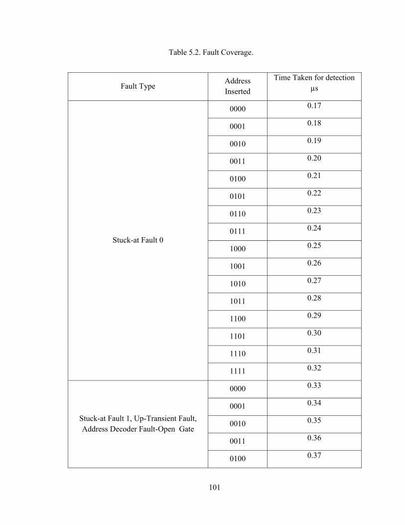
101
Table 5.2. Fault Coverage.
Fault Type Address
Inserted
Time Taken for detection
µs
Stuck-at Fault 0
0000 0.17
0001 0.18
0010 0.19
0011 0.20
0100 0.21
0101 0.22
0110 0.23
0111 0.24
1000 0.25
1001 0.26
1010 0.27
1011 0.28
1100 0.29
1101 0.30
1110 0.31
1111 0.32
Stuck-at Fault 1, Up-Transient Fault,
Address Decoder Fault-Open Gate
0000 0.33
0001 0.34
0010 0.35
0011 0.36
0100 0.37

102
0101 0.38
0110 0.39
0111 0.40
1000 0.41
1001 0.42
1010 0.43
1011 0.44
1100 0.45
1101 0.46
1110 0.47
1111 0.48
Down-Transient Fault,
Address Decoder Fault Stuck-at input
lines
0000 0.50
0001 0.52
0010 0.54
0011 0.56
0100 0.58
0101 0.60
0110 0.62
0111 0.64
1000 0.66
1001 0.68
1010 0.70
1011 0.72
1100 0.74

103
1101 0.76
1110 0.78
1111 0.80
Incorrect Read Fault,
Read Destructive Fault
0000 0.17
0001 0.18
0010 0.19
0011 0.20
0100 0.21
0101 0.22
0110 0.23
0111 0.24
1000 0.25
1001 0.26
1010 0.27
1011 0.28
1100 0.29
1101 0.30
1110 0.31
1111 0.32
Deceptive Read Destructive Fault ,
Data Retention Fault
0000 0.82
0001 0.84
0010 0.86
0011 0.88
0100 0.90

104
0101 0.92
0110 0.94
0111 0.96
1000 0.98
1001 1.00
1010 1.02
1011 1.04
1100 1.06
1101 1.08
1110 1.10
1111 1.12
State Coupling Fault
0000 0.17
0001 0.18
0010 0.19
0011 0.20
0100 0.21
0101 0.22
0110 0.23
0111 0.24
1000 0.25
1001 0.26
1010 0.27
1011 0.28
1100 0.29

105
1101 0.30
1110 0.31
1111 0.32
Up- Transient Coupling Fault
0000 0.33
0001 0.34
0010 0.35
0011 0.36
0100 0.37
0101 0.38
0110 0.39
0111 0.40
1000 0.41
1001 0.42
1010 0.43
1011 0.44
1100 0.45
1101 0.46
1110 0.47
1111 0.48
Down-Transient Coupling Fault
0000 0.50
0001 0.52
0010 0.54
0011 0.56
0100 0.58

106
0101 0.60
0110 0.62
0111 0.64
1000 0.66
1001 0.68
1010 0.70
1011 0.72
1100 0.74
1101 0.76
1110 0.78
1111 0.80
Incorrect Read Coupling Fault
Read Destructive Coupling Fault
0000 0.17
0001 0.18
0010 0.19
0011 0.20
0100 0.21
0101 0.22
0110 0.23
0111 0.24
1000 0.25
1001 0.26
1010 0.27
1011 0.28
1100 0.29

107
1101 0.30
1110 0.31
1111 0.32
Deceptive Read Destructive Coupling
Fault
0000 1.13
0001 1.14
0010 1.15
0011 1.16
0100 1.17
0101 1.18
0110 1.19
0111 1.20
1000 1.21
1001 1.22
1010 1.23
1011 1.24
1100 1.25
1101 1.26
1110 1.27
1111 1.28

108
Chapter 6
6 Conclusion
This thesis presents the development and verification of a BIST architecture for
testing the LUTs in Virtex-4 FPGAs. The primary aim is to test the LUTs within the
SRAM Virtex-4 FPGAs for the presence of stuck-at, transient, address decoder, incorrect
read, read destructive, deceptive read destructive, data retention, transient coupling,
incorrect read coupling, read destructive coupling, and deceptive read destructive
coupling faults with minimum test time and also to design a diagnostic scheme to locate
the faulty LUT in the FPGA.
With increasing FPGA applications and their wide usage in critical applications,
testing FPGAs for correct operations is very important. Prior research in the area of
testing memory modules has been done in [16], [20-22]. The method presented in [16]
takes a long time to test the entire FPGA as it coveres only half of the FPGA in one test
session . The method proposed in [21] requires external logic resources to implement the
scheme and the scheme proposed in [22] consumes an entire CLB for designing a TPG
and is time consuming. The method proposed in [20] cannot locate the faulty CLB.
Hence, to overcome these disadvantages a novel BIST scheme is proposed,
designed and mapped on the Virtex-4 FPGA. The proposed scheme can not only test the

109
faults but also has the capability of locating the faults. An extended March C- algorithm
is used for testing the LUTs and it takes 14n operations and can detect all the faults. In
Table 5.3, the exact number of clock cycles taken by the proposed method is calculated
and comapred with [22].
Table 5.3. Fault Coverage Comparison
#
Fault Models with
faults at address
0001
No of clock
Cycles taken by
the proposed
technique
No of clock
Cycles
[22]
Time taken by
the proposed
technique (µs)
Time
taken
(µs)
[22]
1 Stuck-at 0 Fault
18 17 0.18 0.17
2 Stuck-at 1 Fault
34 77 0.34 0.77
3
Address Decoder
Fault
34 77 0.34 0.77
4
Up-Transient
Fault
34 77 0.34 0.77
5
Down-Transient
Fault
78 83 0.78 0.83
6
Incorrect Read
Fault
18 NA 0.18 NA
7
Read Destructive
Fault
18 NA 0.18 NA
8
Data Retention
Fault
108 NA 1.08 NA
9
Deceptive Read
Destructive Fault
109 NA 1.09 NA
10
State Coupling
Fault
18 NA 0.18 NA
11 Up-Transient
Coupling Fault 34 NA 0.34 NA

110
12
Down-Transient
Coupling Fault
78 NA 0.78 NA
13
Incorrect Read
Coupling Fault
18 NA 0.18 NA
14
Read Destructive
Coupling Fault
18 NA 0.18 NA
15
Deceptive Read
Destructive
Coupling Fault 128 NA 1.28 NA
6.1 Contributions
The following are the main contributions in this research:
Developing a new interconnection scheme which eliminates the drawbacks
presented in earlier works.
Testing stuck-at, transient, address decoder, incorrect read, read destructive,
deceptive read destructive, data retention, state coupling, transient coupling,
incorrect read coupling, read destructive coupling, and deceptive read destructive
coupling faults.
Detecting and locating the exact address of multiple faults in the LUTs of an
SRAM based FPGA.
Performing simulations in ModelSim.
Reducing the fault detection time.
It was observed that the time taken for detection of the fault is dependent on the
type of the fault and the address at which the fault is present. Based on the address of the
memory cell (0000-1111), to detect stuck-at1 and 0 faults it takes 17 to 32 and 33 to 48

111
clock cycles, respectively. Up-transient and down-transient faults are detected in 33 to 48
and 50 to 80 clock cycles respectively. To detect incorrect read and read destructive
faults, 17 to 32 clock cycles are needed, and for deceptive read destructive and data
retention faults, 82 to 112 clock cycles are required. For detecting address decoder faults
with stuck-at input lines takes 50 to 80 clock cycles, and with open lines, it takes 17 to 32
clock cycles. Similarly, for incorrect read coupling and read destructive coupling faults,
17 to 32 clock cycles are needed and to detect deceptive read destructive coupling faults,
82 to 112 clock cycles are required.
6.2 Future work
The following ideas can be considered for extending this work:
SRAM BIST design could be applied to other families of FPGAs including the
Virtex-5 and Spartan-3. Additionally, the improvements made with this BIST
approach can be applied to the previous families of the Virtex-4 device.
The techniques used for test time speed-up and better fault coverage can be
explored for other programmable resources in FPGAs.
Multiple faults located in the same address in a LUT may not be detected in this
research which can be achieved by further modifying the architecture.
The fault detection approach can be applied to future memories including flash
and phase change memories.

112
References
[1] C. Stroud, N. A. Touba, and L. Wang, "System-on-Chip Test Architectures:
Nanometer Design for Testability," Morgan Kaufmann, 2008.
[2] P. Prinetto, M. S. Reorda, S. Barbagallo, A. Burri, D. Medina, and P. Camurati,
"Industrial BIST of Embedded RAMs," in Proceedings of IEEE Design and Test, pp.
86-95.
[3] C. R. Kime, K. K. Saluja, and V. D. Agrawal, "A Tutorial on Built-in Self-Test. I.
Principles," IEEE Design and Test of Computers, vol. 10, no. 1, pp. 73-82, 1993.
[4] Charles Stroud, "A Designer's Guide to Built-in Self-test", Springer, 2002.
[5] J. L. Dailey, "Analysis and Implementation of Built-In Self-Test for Block Random
Access Memories in Virtex-5 Field Programmable Gate Arrays," Dissertation,
Auburn University, 2011.
[6] D. Niggemeyer, E. M. Rudnick, and T. J. Bergfeld, "Diagnostic Testing of
Embedded Memories using BIST," in Proceedings of IEEE Design, Automation and
Test in Europe Conference and Exhibition, 2000, pp. 305-309.
[7] F. Tony, T. Nagesh, K. Mark, H. Abu, R. Janusz, and H. Graham, "Logic BIST for
Large Industrial Designs: Real Issues and Case Studies," in International Test

113
Conference, 1999, pp. 358-367.
[8] E. J. McCluskey, "Built-In Self Test Techniques," IEEE Design and Test of
Computers, vol. 2, 1985, pp. 21-28.
[9] V. D. Agrawal and T. J. Chakraborty, "High-Performance Circuit Testing with
Slow-Speed Testers," in Proceedings of International Test Conference, vol. 21-25 ,
1995, pp. 302-310.
[10] A. J. van de Goor, I. Schanstra, and Y. Zorian, "An effective BIST scheme for ring-
address type FIFOs," in Proceedings of International Test Conference, 1994, pp.
378-387.
[11] T. Arnaout, H. J. Wunderlich, and O. Heron, "On the Reliability Evaluation of
SRAM- based FPGA designs," International Conference of Field Programmable
Logic Applications, 2005, pp. 403–408.
[12] Y. Zorian, "A Distributed BIST Control Scheme for Complex VLSI Devices,"
Proceedings of VLSI Test Syposium, 1993, pp. 4-9.
[13] T. Inoue, H. Fujiwara, H. Michinishi, T. Yokohira, and T. Okamoto, "Universal Test
Complexity of Field-Programmable Gate Arrays," in Proceedings of the 4th Asian
Test Symposium, 1995, pp. 259-265.
[14] Riaz Naseer and Jeff Draper, "Improve Memory Reliability in Sub-100nm
Technologies," in Proceedings of the IEEE International conference on

114
Elecctroinics, Circuits and Systems, 2008, pp. 586-589.
[15] B. Dixon, C. Stroud, V. Nelson, and Jia Yao, "System-level Built-in Self-Test of
Global Routing Resources in Virtex-4 FPGAs," in 41st Southeastern Symposium on
System Theory(SSST), 2009.
[16] M. Abramovici and C. Stroud, "BIST-Based Test and Diagnosis of FPGA Logic
Blocks," in IEEE Transactions on Very Large Scale Integration (VLSI) Systems, vol.
9(10), 2001, pp. 159-172.
[17] T. Xia, C. Stroud, and J. Smith, "An Automated BIST Architecture for Testing and
Diagnosing FPGA Interconnect Faults," in Journal of Electronic Testing, vol. 22,
2006, pp. 239-253.
[18] W. K. Huang, F. J. Meyer, N. Park, and F. Lombardi, "Testing Memory Modules in
SRAM-Based Configurable FPGAs," in IEEE International Workshop on Memory
Technology, Design and Test, 1997, pp. 79-86.
[19] J. Jenicek, O. Novak, and M. Rozkovec, "An Evaluation of the Application
Dependent FPGA Test Method," in 2012, IEEE 15th International Symposium on
Design and Diagnostics of Electronic Circuits & Systems (DDECS).
[20] J. M. Portal, J. Figueras, Y. Zorian, and M. Renovell, "SRAM-Based FPGAs:
Testing the Embedded SRAM Modules," in Journal of Electronic Testing, vol. 14,
1998.

115
[21] M. Y. Niamat and D. M. Nemade, "Test, Diagnosis and Fault simulation of
Embedded RAM Modules in SRAM-Based FPGAs," in Microelectronic
Engineering, vol. 84, 2007, pp. 194-203.
[22] M. Lalla, K. Junghwan, and M. Niamat, "Testing Faults in SRAM Memory of
Virtex-4 FPGA," in 52nd IEEE International Midwest Symposium on Circuits and
Systems, 2009.
[23] Said Hamidioui, Testing Static Random Access Memories: Defects, Fault Models
and Test Patterns.: Kluwer academic Publishers, 2004.
[24] M. Grosso, M. S. Reorda, Y. Zhang, and P. Bernardi, "A Programmable BIST for
DRAM Testing and Diagnosis," in International Test Conference (ITC), 2010, pp. 1-
10.
[25] Barr Michael, Memory Types Embedded Systems Programming., 2001.
[26] M. H. Abu-Rahma and M. Anis, "Variation-Tolerant SRAM Write and Read Assist
Techniques in Nanometer Variation-Tolerant SRAM," in Springer New York, 2013,
pp. 49-95.
[27] P. K. Lala, "Digital Circuit Testing and Testability", Academic Press, 1997.
[28] A. J. van de Goor amd S. Hamdioui, "Advanced Embedded Memory Testing:
Reducing the Defect per Million Level at Lower Test Cost," in IEEE 13th
International Symposium on Design and Diagnostics of Electronic Circuits and

116
Systems (DDECS), 2010, pp. 7-7.
[29] Siti Aisah Mat Junos, A. Razak, M. Idris, and N. Haron, "Modeling and Simulation
of Finite State Machine Memory Built-in Self Test Architecture for Embedded
Memories," in Asia-Pacific Conference on Applied Electromagnetics, 2007, pp. 1-5.
[30] D. T. Milton, C. E. Stroud, and B. R. Garrison, "Built-in Self-Test for Memory
Resources in Virtex-4 Field Programmable Gate Arrays," in International
Conference on Computers and Their Applications(CATA), 2009, pp. 63-68.
[31] Jian-Hua Su, You-Ren Wang, and C. Ze-Wang, "An Effective Test Algorithm and
Diiagnostic Implementation for Embedded Static Random Access Memories," in
Journal of Circuits, Systems, and Computers, vol. 07, 2011, pp. 1389-1402.
[32] E. Karl, M. Meterelliyoz, F. Hamzaoglu, Ng. Yong-Gee, S. Ghosh, and K. Zhang Y.
Wang, "Dynamic Behavior of SRAM Data Retention and a Novel Transient Voltage
Collapse," in IEEE International In Electron Devices Meeting, 2011, pp. 32-1.
[33] P. Girard , S. Pravossoudovitch, A. Virazel, S. Borri, and M. Hage-Hassan L. Dilillo,
"Resistive-Open Defects in Embedded-SRAM core cells:Analysis and March Test
Solution," in Asian Test Symposium, 2004.
[34] A. Bosio, L. Dilillo, P. Girard, S. Pravossoudovitch, A. Virazel, N. Badereddine, and
L. B. Zordan, "Optimized March Test Flow for Detecting Memory Faults in SRAM
Devices under Bit Line Coupling," in IEEE 14th International Symposium on Design
and Diagnostics of Electronic Circuits & Systems (DDECS), 2011, pp. 353-358.

117
[35] A. J. Van de Goor, Testing Semiconductor Memories, Theory and Practice.: John
Wiley and Sons, Inc, 1991.
[36] A. J. Van De Goor, "Using March Tests to Test SRAMs," in IEEE Design and Test
of Computers Conference, 1993, pp. 8-14.
[37] S. M. Thatte, J. A. Abraham, and R. Nair, "Efficient Algorithms for Testing
Semiconductor Random-Access Memories," in IEEE Transactions on Computers,
vol. 6, 1978, pp. 572-576.
[38] Z. Navabi, S. M. Fakhraie, and M. H. Tehranipour, "An Efficient BIST Method for
Testing of Embedded SRAMs," in IEEE International Symposium on Circuits and
Systems (ISCAS), vol. 5, 2001, pp. 73-76.
[39] M. Hamid, B. Swarup, K. Roy, and Q. Chen, "Efficient Testing of SRAM With
Optimized March Sequences and a Novel DFT Technique for Emerging Failures due
to Process Variations," in IEEE Transactions on Very Large Scale Integration
(VLSI) Systems, vol. 13, 2005.
[40] [Online]. http://www.xilinx.com/training/fpga/fpga-field-programmable-gate-
array.htm
[41] Xilinx Inc. (2005) Virtex-4 Family Overview Product Specification DS-112.
[42] "Virtex-4 FPGA Userguide," in Xilinx Inc., 2008.
[43] B. F. Dutton, "Embedded Soft-Core Processor-Based Built-in Self-Test of Field

118
Programmable Gate Arrays", Dissertation Auburn University, 2010.
[44] Priyanka Gadde and Mohammed Niamat, "FPGA Memory Testing Technique using
BIST," in IEEE 56th International Midwest Symposium on Circuits and Systems
(MWSCAS), 2013.