Evaluating BIST
39
Please get some pizza and BBQ
Transcript of Evaluating BIST

Please get some pizza and BBQ
Evaluating the Digital Fault Coverage of a Mixed-Signal BIST
Alex Lusco

Thesis StatementA set of test procedures is evaluated which test the digital portion of a mixed-signal BIST approach using the digital loopback path. To provide context for evaluation, the test procedures are used to create and simulate a set of measurements which test a Selective Signal Analysis (SSA) BIST implementation. In addition to an analysis of the resulting fault coverage, the measurement set is also used to test actual manufactured chips and the results discussed.
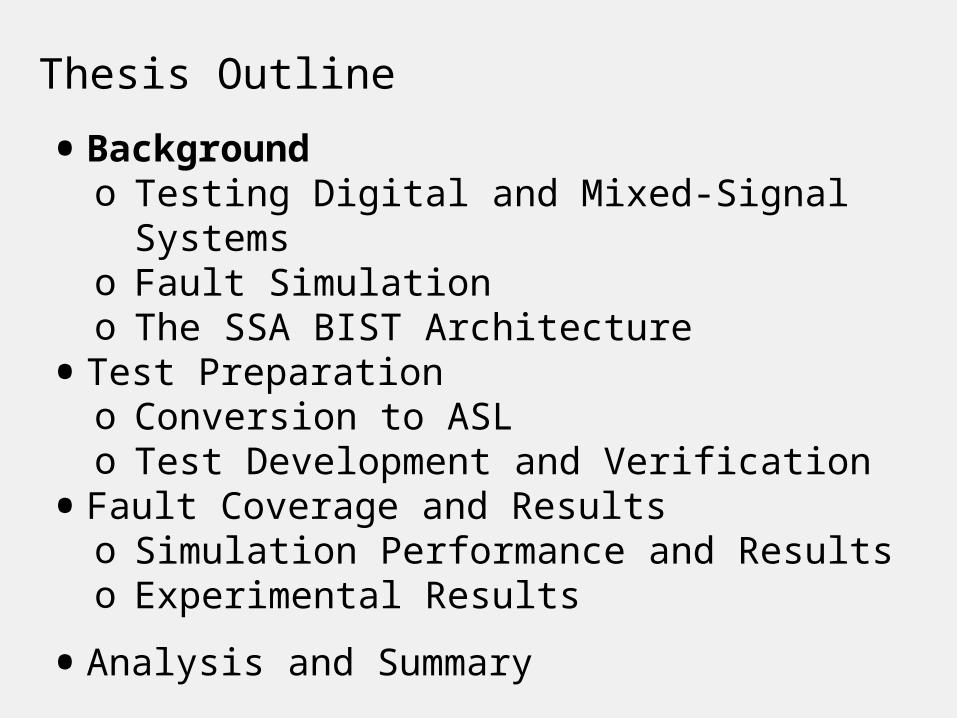
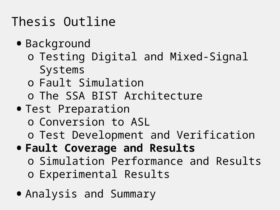
Thesis Outline•Background
o Testing Digital and Mixed-Signal Systems
o Fault Simulationo The SSA BIST Architecture
•Test Preparationo Conversion to ASLo Test Development and Verification
•Fault Coverage and Resultso Simulation Performance and Resultso Experimental Results
•Analysis and Summary

• Given a set of test vectors, a circuit can be simulated to determine the fault coverage or percentage of faults detected.o The fault-free circuit is simulated with a
set of test vectors.o A list of faults is generated based on the
circuit design and fault model.o A fault is emulated in the circuit and
then resimulated.o The output of the faulty circuit is
compared to the fault-free output to determine if the fault was detected.
• Faults can be detected (D), potentially detected (P), or undetected. They can also be undetectable (X).o P faults are caused by uninitialized logic
values and are typically assumed to be detected 50% of the time (Y=.5).
Fault Simulation
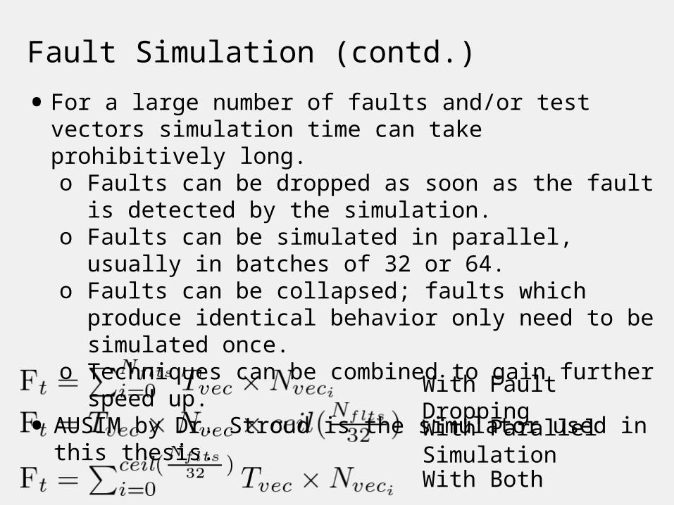
Fault Simulation (contd.)•For a large number of faults and/or test vectors simulation time can take prohibitively long.o Faults can be dropped as soon as the fault
is detected by the simulation.o Faults can be simulated in parallel,
usually in batches of 32 or 64.o Faults can be collapsed; faults which
produce identical behavior only need to be simulated once.
o Techniques can be combined to gain further speed up.
• AUSIM by Dr. Stroud is the simulator used in this thesis.
With Fault DroppingWith Parallel SimulationWith Both
Testing of Digital Systems• Digital systems operate at a discrete logic
level of '1' or '0'.• There are many different models for
describing faults in a digital system. Each having it's own advantages and disadvantages.
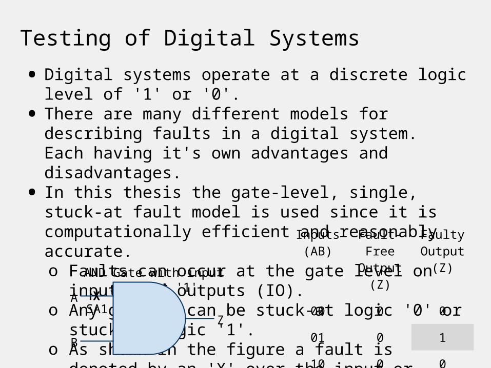
• In this thesis the gate-level, single, stuck-at fault model is used since it is computationally efficient and reasonably accurate.o Faults can occur at the gate level on
inputs and outputs (IO).o Any gate IO can be stuck-at logic '0' or
stuck-at logic '1'.o As shown in the figure a fault is
denoted by an 'X' over the input or output with the SA abbreviation denoting the fault.
Inputs(AB)
Fault-Free Output (Z)
Faulty Output (Z)
00 0 0
01 0 1
10 0 0
11 1 1
AND Gate with input stuck-at '1'X
SA1A
BZ

Testing of Mixed-Signal Systems• Includes both digital and analog components
in the same system.o Signals are usually converted back and
forth from the analog to digital domain using both analog-to-digital (ADC) and digital-to-analog (DAC) converters.
o Unlike digital devices, analog components operate in range of acceptable values complicating testing. This prevents the exact circuit
response from being known during testing.
• Traditionally the digital and analog portions of the device are tested separately using different techniques.o Allows for the use of testing techniques
best suited for each sub-system.• Effectively testing the digital components
requires them to be isolated from the analog system.

Typical Mixed-Signal System
DigitalSystem
AnalogSystem
AnalogSystem
DigitalSystem
Digital Inputs
Digital Outputs
Analog Inputs
Analog Outputs
ADC
DAC
Analog Loopback
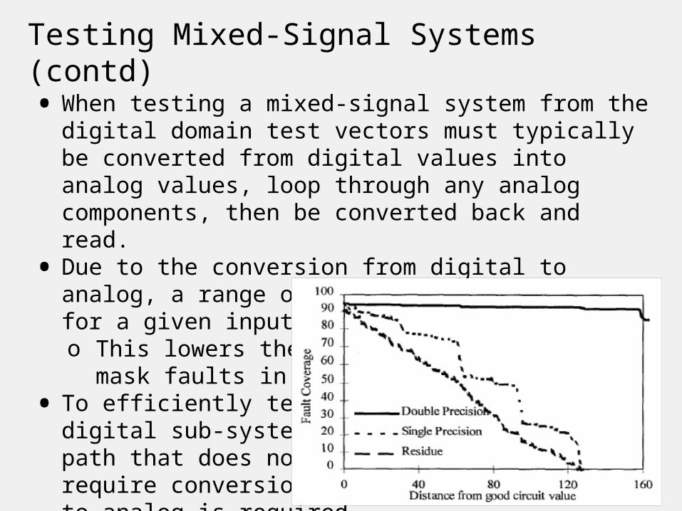
Testing Mixed-Signal Systems (contd)• When testing a mixed-signal system from the
digital domain test vectors must typically be converted from digital values into analog values, loop through any analog components, then be converted back and read.
• Due to the conversion from digital to analog, a range of outputs are acceptable for a given input.o This lowers the fault coverage as it may
mask faults in the digital system.• To efficiently test the
digital sub-system a path that does not require conversion to analog is required.

Testing via the Digital Loopback Path
DigitalSystem
AnalogSystem
AnalogSystem
DigitalSystem
Digital Inputs
Digital Outputs
Analog Inputs
Analog Outputs
ADC
DAC
Analog Loopback
Digital Loopback
Analog Bypass
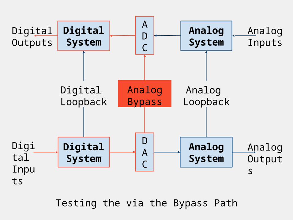
Testing the via the Bypass Path
DigitalSystem
AnalogSystem
AnalogSystem
DigitalSystem
Digital Inputs
Digital Outputs
Analog Inputs
Analog Outputs
ADC
DAC
Analog Loopback
Digital Loopback
Analog Bypass
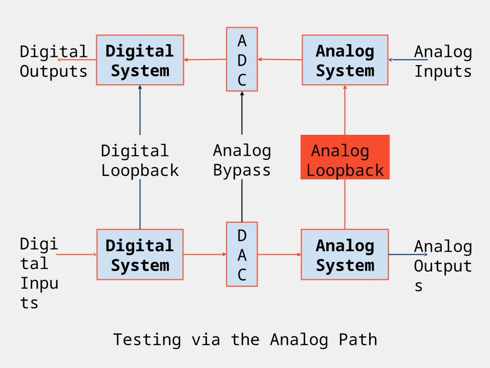
Testing via the Analog Path
DigitalSystem
AnalogSystem
AnalogSystem
DigitalSystem
Digital Inputs
Digital Outputs
Analog Inputs
Analog Outputs
ADC
DAC
Analog Loopback
Digital Loopback
Analog Bypass
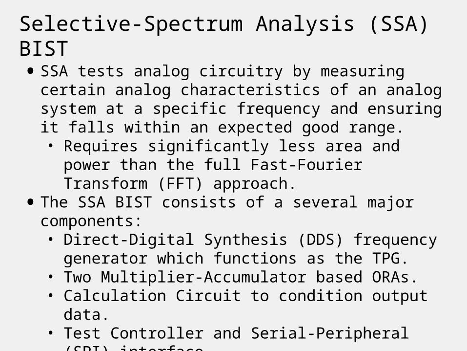
Selective-Spectrum Analysis (SSA) BIST•SSA tests analog circuitry by measuring certain analog characteristics of an analog system at a specific frequency and ensuring it falls within an expected good range.• Requires significantly less area and power than the full Fast-Fourier Transform (FFT) approach.
•The SSA BIST consists of a several major components:• Direct-Digital Synthesis (DDS) frequency generator which functions as the TPG.
• Two Multiplier-Accumulator based ORAs.• Calculation Circuit to condition output data.
• Test Controller and Serial-Peripheral (SPI) interface.
•Accuracy of SSA is a function of accumulation time:• More time spent accumulating, the better the accuracy.
• If accumulation is stopped at certain points in time then the accuracy v. time trade off can be minimized.
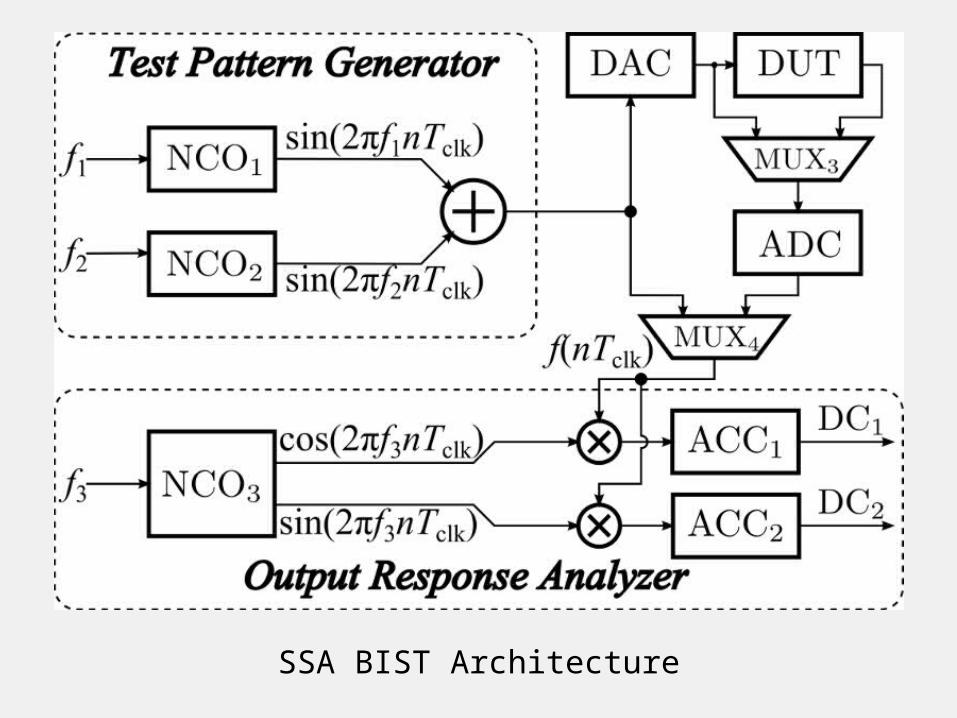
SSA BIST Architecture

• Generates sine and cosine signals used to stimulate the analog components as well as reference tones used in the ORA.
• Tones are generated based on frequency words and the formula below where n=16 for 16-bit frequency words (FW).
• The frequency resolution of the DDS is dependent on the number of bits in the frequency words and the clock speed.
• As an example when using 16-bit frequency words at 50MHz. FW 0x100 produces a frequency of ~19.5Khz and the system frequency resolution is ~760Hz.
Direct-Digital Synthesis (DDS)
Phase Accumula
tor
Phase Truncato
rSin/CosLUT DAC
n n p dFw
Fout
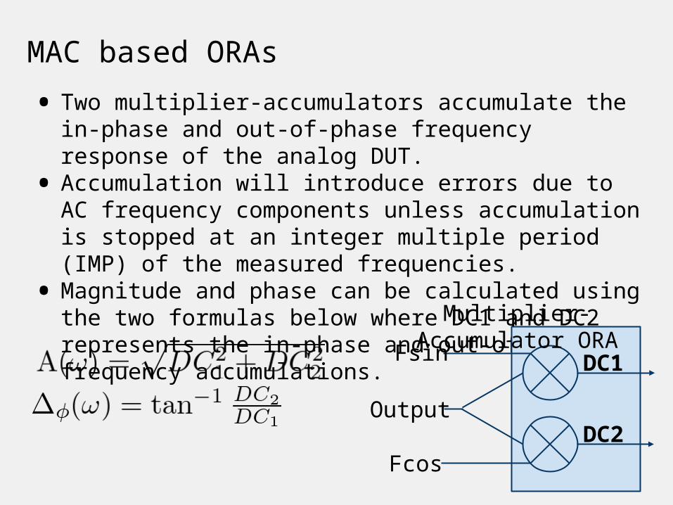
MAC based ORAs• Two multiplier-accumulators accumulate the
in-phase and out-of-phase frequency response of the analog DUT.
• Accumulation will introduce errors due to AC frequency components unless accumulation is stopped at an integer multiple period (IMP) of the measured frequencies.
• Magnitude and phase can be calculated using the two formulas below where DC1 and DC2 represents the in-phase and out-of-phase frequency accumulations. DC1
DC2Output
Fsin
Fcos
Multiplier-Accumulator ORA
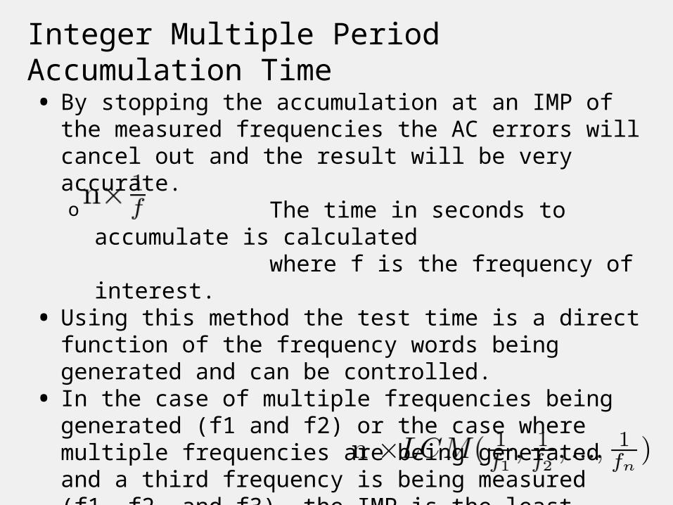
Integer Multiple Period Accumulation Time• By stopping the accumulation at an IMP of the measured frequencies the AC errors will cancel out and the result will be very accurate.o The time in seconds to accumulate is calculated where f is the frequency of interest.
• Using this method the test time is a direct function of the frequency words being generated and can be controlled.
• In the case of multiple frequencies being generated (f1 and f2) or the case where multiple frequencies are being generated and a third frequency is being measured (f1, f2, and f3), the IMP is the least common multiple of all frequency periods.

Calculation Circuitry• Uses CORDIC algorithm to convert DC1 and
DC2 accumulator values to magnitude and phase values.
• In conjunction with the test controller the SSA BIST can measure important analog characteristics which require multiple individual measurements to be performed.o Linearity of the system.o Multi-point frequency sweep.o Signal-to-Noise (SNR) ratio of the
system.o Noise-Figure (NF) of the system.
• All calculations are performed in the logarithmic domain to simplify the calculation circuitry and results are in decibels (dB).
• Calculations are not performed using floating point and results are expected to be within a dB of the real result.
• All output (and input) must be read and written through the SPI.
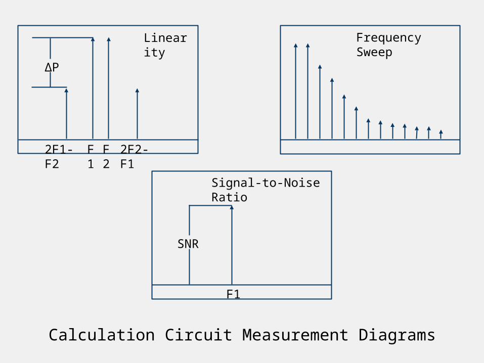
Signal-to-Noise Ratio
F1
SNR
Frequency Sweep
2F1-F2
F1
F2
2F2-F1
Linearity
ΔP
Calculation Circuit Measurement Diagrams
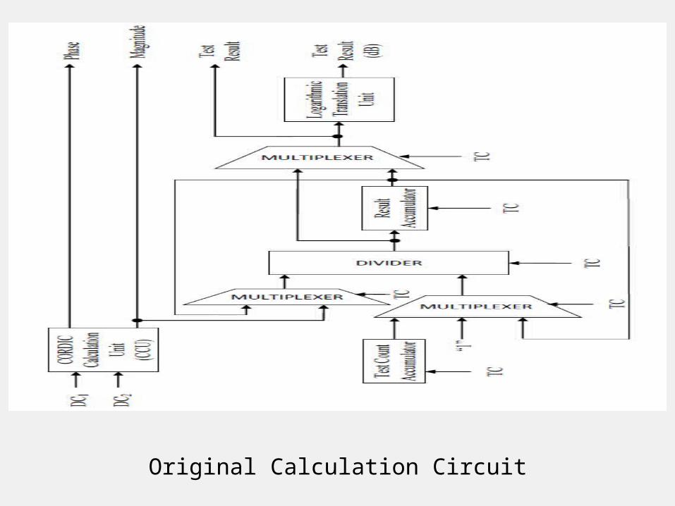
Original Calculation Circuit
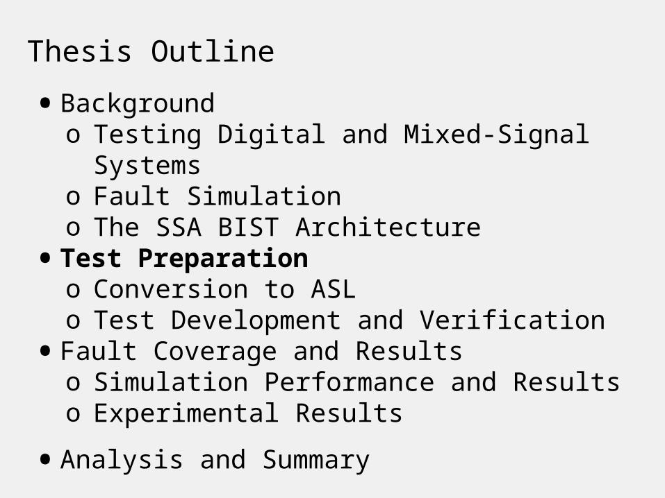
Thesis Outline•Background
o Testing Digital and Mixed-Signal Systems
o Fault Simulationo The SSA BIST Architecture
•Test Preparationo Conversion to ASLo Test Development and Verification
•Fault Coverage and Resultso Simulation Performance and Resultso Experimental Results
•Analysis and Summary

Conversion to ASL from Verilog• Production circuits are often written in a
high level design language such as Verilog or VHDL.
• AUSIM fault simulator requires an ASL netlist.
• To simplify simulation of complex circuits a converter was written which converts a Verilog netlist to ASL.o Conversion can be performed at any stage
of development: pre or post-layout.o Has been used to successfully convert
and simulate ISCAS'89 for bridging faults (faults which occur between wires).
• Written in C#, ~800 lines of (poorly written) code. Took approximately 1 week to develop, and an additional 1 week to verify and fix several edge cases.
• Converted circuits can be behaviorally verified against ModelSIM simulations.

ASL Conversion

The Test Procedures• Goal is to determine how high of a fault
coverage can be achieved by using the SSA BIST to test itself via the digital loopback path.o Convert the SSA BIST to the ASL format
for simulation.o Verify the correctness of the converted
circuit.o Develop an initial set of measurements
to function as test vectors.o Simulate circuit to determine fault
coverage.o Analyze results and determine if changes
to test vector set need to be made.o Re-simulate new test vectors until fault
coverage is sufficient.o Verify experimentally.
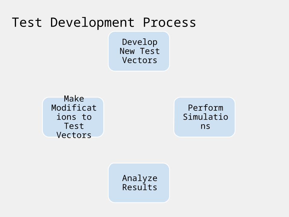
Test Development ProcessDevelop New Test Vectors
Perform Simulatio
ns
Analyze Results
Make Modifications to Test
Vectors
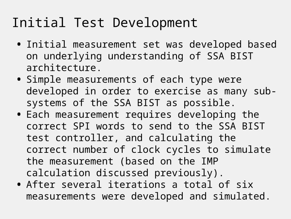
Initial Test Development• Initial measurement set was developed based on underlying understanding of SSA BIST architecture.
• Simple measurements of each type were developed in order to exercise as many sub-systems of the SSA BIST as possible.
• Each measurement requires developing the correct SPI words to send to the SSA BIST test controller, and calculating the correct number of clock cycles to simulate the measurement (based on the IMP calculation discussed previously).
• After several iterations a total of six measurements were developed and simulated.
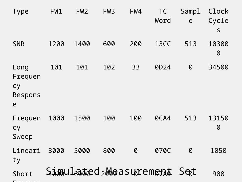
Type FW1 FW2 FW3 FW4 TC Word
Sample
Clock Cycles
SNR 1200 1400 600 200 13CC 513 103000
Long Frequency Response
101 101 102 33 0D24 0 34500
Frequency Sweep
1000 1500 100 100 0CA4 513 131500
Linearity
3000 5000 800 0 070C 0 1050
Short Frequency Response
4000 6000 2000 0 07A0 0 900
Noise Figure
0CFC 0AFC 10FC 7CCC 1B60 2 91601
Total Test Vectors: 725,102
Total Clock Cycles: 362,501
Simulated Measurement Set
Thesis Outline•Background
o Testing Digital and Mixed-Signal Systems
o Fault Simulationo The SSA BIST Architecture
•Test Preparationo Conversion to ASLo Test Development and Verification
•Fault Coverage and Resultso Simulation Performance and Resultso Experimental Results
•Analysis and Summary

• Due to the number of faults in the SSA BIST (approximately 40K collapsed faults), the simulation time required would be too long to facilitate rapid simulation of some of the longer measurements.o The longest simulation (a combined
simulation of all measurements) would take 6400 hours or ~9 months!
• To greatly decrease the simulation time the Auburn University High-Performance Computing Cluster (HPCC) was used to perform a large number of simulations in parallel.o Each parallel simulation simulated a
much lower number of faults, approximately 350 faults each.
• The graph on the next slide shows the approximate CPU time required in hours compared to the actual time required for simulation (Wall Time).
Simulation Time

Simulation Time in Hours vs CPU Time Required
Combined SNR FR Sweep IP3 FR NF1
10
100
1000
10000 6422
2018
12.5
3450
8.5
609
2544
74
20
1
28
1
921.7
CPU Time vs Wall Time
CPU Time Wall Time
Time
(Hr
s)
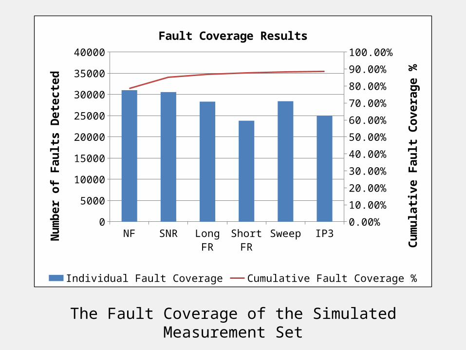
The Fault Coverage of the Simulated Measurement Set
NF SNR Long FR
Short FR
Sweep IP30
5000
10000
15000
20000
25000
30000
35000
40000
0.00%10.00%20.00%30.00%40.00%50.00%60.00%70.00%80.00%90.00%100.00%
Fault Coverage Results
Individual Fault Coverage Cumulative Fault Coverage %
Number of Faults Detected
Cumulative Fault Coverage %
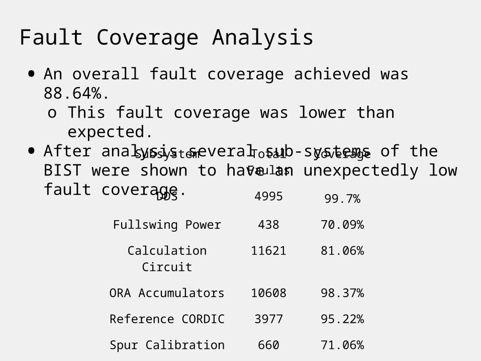
• An overall fault coverage achieved was 88.64%. o This fault coverage was lower than
expected.• After analysis several sub-systems of the
BIST were shown to have an unexpectedly low fault coverage.
Fault Coverage Analysis
Subsystem Total Faults
Coverage
DDS 4995 99.7%
Fullswing Power 438 70.09%
Calculation Circuit
11621 81.06%
ORA Accumulators 10608 98.37%
Reference CORDIC 3977 95.22%
Spur Calibration 660 71.06%
Test Controller 1829 85.27%
SPI Interface 4259 81.71%

Coverage Improvements• In an effort to improve the fault coverage,
modifications we're made to the SSA BIST to increase the testability of the circuit.
• Modifications made include:o Ability to disable certain output
normalization circuitry.o Ability to attenuate the magnitude of
the DDS generated signal.o Ability to clip the DDS signal so that
noise can be introduced into the digital loopback path.
o Allow the testing of included preset circuitry.
o Expose internal registers to the SPI for increased testability.
• Four additional measurements were developed to take advantage of the newly implement circuitry.

Fault Coverage Results and Analysis• A new measurement set consisting of 10
measurements was re-simulated resulting in an increase in fault coverage to 89.5%.o Unfortunately this is a less than a 1%
increase, and not very significant.• One factor contributing to the low fault
coverage is the inability to test certain portions of the BIST circuitry while using the digital loopback path.
• It is likely that with additional iterations on the measurement set some improvement in fault coverage could be achieved.
• Lastly some components of the SSA BIST may need to be redesigned for improved testability.o When the SPI circuitry is removed the
fault coverage of the BIST improves to 91.5%
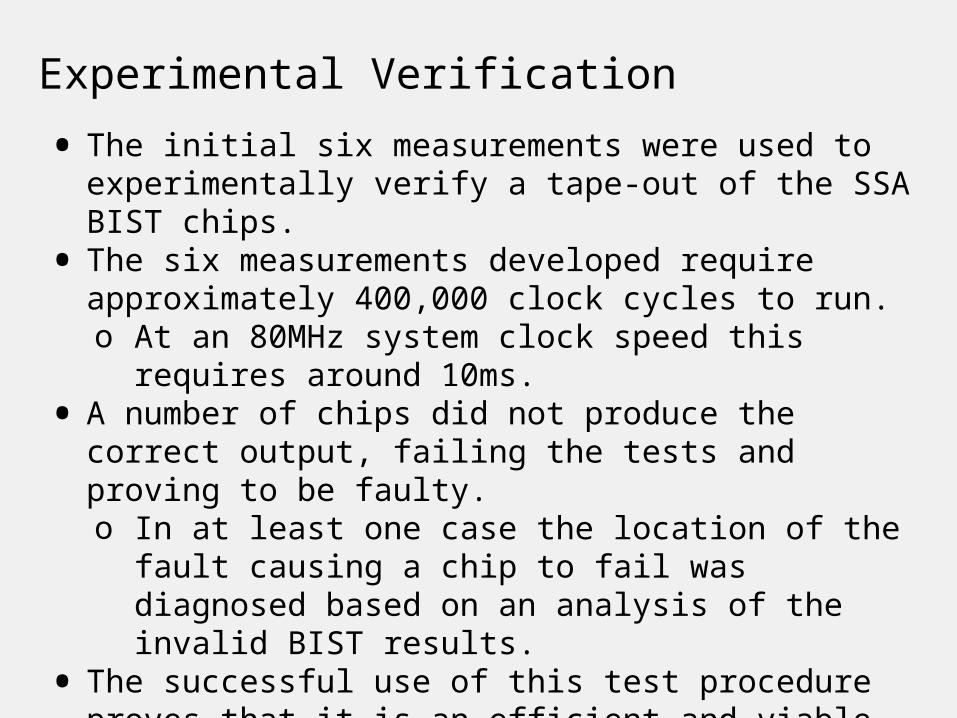
Experimental Verification• The initial six measurements were used to
experimentally verify a tape-out of the SSA BIST chips.
• The six measurements developed require approximately 400,000 clock cycles to run.o At an 80MHz system clock speed this
requires around 10ms.• A number of chips did not produce the
correct output, failing the tests and proving to be faulty.o In at least one case the location of the
fault causing a chip to fail was diagnosed based on an analysis of the invalid BIST results.
• The successful use of this test procedure proves that it is an efficient and viable method for chip verification and in some cases fault diagnosis.
Thesis Outline•Background
o Testing Digital and Mixed-Signal Systems
o Fault Simulationo The SSA BIST Architecture
•Test Preparationo Conversion to ASLo Test Development and Verification
•Fault Coverage and Resultso Simulation Performance and Resultso Experimental Results
•Analysis and Summary

Analysis and Summary• Some difficulties were encountered when
using this approach to a mixed-signal BIST approach.
• There is no automated tool to develop the test vector set. Development requires some level of trial and error and time to iterate so that a sufficiently high fault coverage can be achieved.
• Can be difficult to achieve the highest levels of fault coverage (>95%) without the addition of some dedicated testing hardware.
• Certain portions of the BIST circuitry will be untestable.o External paths and components, such as
the bypass and analog loopback paths may prove especially difficult.
o Due to untestable components, additional test techniques may be required to fully test the circuit.
Analysis and Summary (contd.)•Even though a fault coverage of 88.6% was lower than expected -- a fault coverage of almost 90% still was achieved.o Compared to partial scan (900 FFs) which
increased the chip area by almost 11% area and achieved only 62% coverage using pseudo-random vectors.
• Test procedure is circuit agnostic and can be used to test a number of similar mixed-signal approaches.o It requires only a Verilog netlist and a
digital loopback path.o It reuses test circuitry already meant
to test the analog components keeping area down.
• Since no dedicated circuitry is required, testing can occur at system speed and without costly area increases.
• Furthermore it can also be performed at any stage of the circuit's lifetime including design, manufacturing, and during system operation.