
a-3492_277729_fr.pdf - SMARTech
136
OPERATIONS MANUAL FOR POWER SUPPLY/MODULATOR T. V. Wallace Submitted to: Philips Elektronikindustrier.AB S-175 88 JARFALLA, Sweden Under Purchase Order D21-247145 Submitted by: GEORGIA INSTITUTE OF TECHNOLOGY ENGINEERING EXPERIMENT STATION Atlanta, Georgia 30332 23 February 19814
-
Upload
khangminh22 -
Category
Documents
-
view
3 -
download
0
Transcript of a-3492_277729_fr.pdf - SMARTech

OPERATIONS MANUAL FOR POWER SUPPLY/MODULATOR
T. V. Wallace
Submitted to:
Philips Elektronikindustrier.AB S-175 88
JARFALLA, Sweden
Under Purchase Order D21-247145
Submitted by:
GEORGIA INSTITUTE OF TECHNOLOGY ENGINEERING EXPERIMENT STATION
Atlanta, Georgia 30332
23 February 19814

TABLE OF CONTENTS
Section Title 1220. 1 INTRODUCTION 1
2 MAINTENANCE AND OPERATION 4
2.1 Introduction 4
2.2 Maintenance and Setup Procedure 4
2.3 Operation 7
2.3.1 Front Panel Controls and Indicators 7 2.3.2 Summary of Power Up Procedure 11
3 THEORY OF OPERATION 14
3.1 Generation of Optically Coupled Pulses 14
3.2 Floating Deck Modulator Operation 16
3.2.1 Formation of the Pulse 18
3.3 Protection Circuitry 20
3.4 Control Circuitry 21
3.5 High Voltage Isolated Power Supplies 22
3.6 High Voltage Power Supplies 24
3.6.1 Beam Supply 24
3.6.2 Bias and Pulser Supply 24
3.7 Low Voltage Power Supply 24
3.8 Interconnecting Cables 26
3.9 Troubleshooting 26
3.9.1 Excessive PRF 26
3.9.2 EIO Heater Undervoltage 27
3.9.3 Total EIO and Body Overcurrent 27
4 SUMMARY 28
Appendix A Schematics and Parts Location Diagrams A-1
Appendix B Parts Lists B-1
Appendix C Manufacturer's Specification Sheets C-1
Appendix D Instruction Manual for High Voltage
Power Supply D-1

LIST OF FIGURES
Figure Title Page
1 Block diagram of modulator/power supply assembly 2
2 Modulator enclosure 5
3 Interior of modulator assembly 6
4 Power supply front panel 8
5 Timing diagram for pulse driver circuit 15
6 Simplified diagram of a floating deck modulator 17
7 EIO grid-to-cathode voltage during pulse 17
8 Illustration of trailing edge distortion of received optical pulses 19
9 Shape of pulse at cathode of planar triodes 19
10 Location of added components to high voltage power supply 25
ii
SECTION 1
INTRODUCTION
Under Purchase Order D21-247145, the Georgia Institute of Technology/
Engineering Experiment Station (GIT/EES) of Atlanta, Georgia (USA), develop-
ed a radar modulator/high voltage power supply for the Philips Elektronik-
industrier AB of Jarfalla, Sweden. The modulator/power supply was original-
ly built for integration with Philips 9LV200MK2 series of radars and is
intented for use with a Varian Canada Bridded Extended Interaction Oscil-
lator (EIO). This manual describes the maintenance and operation of the
modulator/power supply assembly and also includes an engineering discussion
on its theory of operation. Appendices are included that contain sche-
matics, parts location drawings, parts lists, and manufacturers' data sheets
for selected parts.
* DANGER - HIGH VOLTAGE - USE EXTREME CAUTION *
Figure 1 is a block diagram of the modulator/power supply assembly.
Caution must be taken at all times when working near the modulator/power
supply assembly due to the presence of high voltage. A TTL circuit receives
the synchronization signal and generates three pulses that are optically
coupled to the floating-deck modulator. Optical coupling is used to isolate
the low-level digital circuitry from the modulator deck which floats at
about -21 kV. These three optically-coupled pulses define the length of the
high voltage pulse. The control and protection circuits are solid state
circuits that control and monitor the status of the modulator. The forma-
tion of the optically-coupled pulses and the high-voltage pulse, the opera-
tion of the control and protection circuits, and the low-voltage and high-
voltage power supplies are discussed in more detail in Section 3.
The modulator accepts an input synchronization signal and generates a
high voltage pulse relative to each rising edge of the synchronization sig-
nal. Therefore, the pulse repetition frequency (PRF) of the synchronization
1

Floating Deck —>›— Modulator --->>---
Pulsewidth Select
V
TTL Pulse Driver A
Optically Coupled Pulses
Start A —<—> Start B
Stop
Synchronization Pulse
Control and
Protection
H› 230 50
Vac Hz --41---
Low Voltage Power Supply
High-Voltage Isolation
Power Supplies
High-Voltage Power Supply
Figure 1. Block diagram of modulator/power supply assembly.

signal equals that of the high voltage pulse train. The necessary charac-
teristics of the synchronization signal and the characteristics and power
requirements of the modulator/power supply assembly are listed in Table 1.
TABLE 1. MODULATOR/POWER SUPPLY SPECIFICATIONS
Input Synchronization Signal:
Amplitude +6 i 2 V
Pulse Length 0.7 t 0.3 1.13
Rise Time < 100 ns
Load Impedance 50 -75 ohm
Pulse Repetition Frequency 1-20 kHz
Pulse Width
35-200 ns
Power Requirements 230 VAC, 50 Hz
Size Modulator 42 cm x 15.6 cm x 25.4 cm
Power Supply 141.3 cm x 13.3 cm x 143.2 cm
Weight Modulator 14.5 kg
Power Supply 20 kg
3
SECTION 2
MAINTENANCE AND OPERATION
2.1 INTRODUCTION
This section discusses the maintenance and operation procedures neces-
sary for safe and proper utilization of the modulator/power supply. This
discussion can be used to train operators how to USE the assembly; however,
only qualified engineering personnel should be allowed to disassemble or
modify the modulator or power supply. A detailed discussion of the theory
of operation of the assembly is included in_Section 3 to aid engineering
personnel and should be referenced before performing maintenance or making
modifications.
2.2 MAINTENANCE AND SETUP PROCEDURE
The modulator/power supply assembly consists of the following items:
modulator enclosure, power supply enclosure with front panel, multiconductor
cable, coaxial cable, and high-voltage cable. To set up the system for
operation, all three cables must be connected between the two enclosures,
the AC line cord from the power supply enclosure must be connected to a
grounded 230 VAC outlet, and the high voltage power supply must be connected
to a good chassis ground.
Figure 2 is an illustration of the modulator enclosure. The left side
plate must be removed to service the interior of the enclosure. Figure 3 is
a view of the interior of the modulator asembly with the side plate removed
and shows the location of various major components and circuits. The ex-
posed plexiglass plate must be removed to work on the floating deck modu-
lator. Because of the high voltage, care must be taken when working inside
the modulator enclosure; THE INTERIOR OF THE PLEXIGLASS MODULATOR ENCLOSURE
FLOATS AT THE BEAM POTENTIAL (-21 kV). The bottom of the enclosure is
surrounded by potting material. If any of this material is cut away it must
be replaced before application of high voltage to the modulator. The bottom
4

Multi-pin Connector
High Voltage Connector
Sync Output
Sync Input
Figure 2. Modulator enclosure. (Left side plate is underneath in this view)

PAW.
Figure 3. Interior of modulator assembly.
JI
0 ir." A26
O • 3KV, R.
1,R4 0
,
e
, --t
,
I
CU CI
VR2
C) itloMEA' 430140 -117
Vq .924

plate of the modulator enclosure is made of aluminum; special care must be
taken when working with this plate since it floats at the beam potential of
-21 kV.
Care must be taken when mounting the modulator assembly so as not to
interfere with any interior components, especially the high voltage
section. Mounting screws placed on the side plates opposite the high
voltage section should not penetrate the potting material; they can pene-
trate only the depth of the outer aluminum plate (.25 inches). Care must
also be taken not to interfere with the location of any other interior com-
ponents, such as the fan and the four circuit cards, when inserting mounting
screws into the side plates, that are not adjacent to the high voltage
section.
Figure 4 is an illustration of the front panel of the power supply as-
sembly. The power supply enclosure is designed . for rack mounting in a
standard 19 inch (48.3 cm) rack. The top cover of the supply can be removed
for servicing.
2.3 OPERATION
'DANGER - HIGH VOLTAGE - USE EXTREME CAUTION*
When the assembly is fully set up, it is ready for operation. The
front panel of the high voltage power supply, illustrated in Figure 4, con-
tains all operator controls and indicators. Each control and indicator lamp
is discussed individually, and then a standard power-up procedure is sum-
marized to aid in the training of operators.
2.3.1 FRONT PANEL CONTROLS AND INDICATORS
The following is a discussion of the function of each control and in-
dicator on the front panel of the power supply.
1) ON/OFF SWITCH - Applies prime power (230 VAC) when in the ON posi-
tion.
2) ON/OFF LAMP - Is lit when prime power is applied.
7

Pulse Beam Width Voltage
0 0 ()Heater Undervoltage LED
On Lamp 0' Current Meter
Beam Voltage Meter
On/Off Switch
(9\ Body Overcurrent LED
EIO Over- current
LED Excessive PRF
Fault LED Lamp
Heater Radiate/ Delay Standby Lamp Standby Switch
Lamp Radiate Lamp
Pse )97 / I
CO
Figure 4. Power supply front panel.

3) HEATER DELAY LAMP - Stays lit for approximately two minutes after
application of prime power. This delay allows the heaters of the
RF tube and the planar triodes in the modulator to warm up so that
the tubes operate properly when high voltage is applied. During
the heater delay period, the system is automatically prevented
from radiating in order to protect the tubes. After the heater
delay the system automatically goes to STANDBY.
4) RADIATE/STANDBY SWITCH - Selects status of modulator. If the
Heater Delay has timed out, switching to RADIATE applies high
voltage to the modulator. If an attempt is made to go to RADIATE
while in Heater Delay, the system will automatically ignore the
attempt. After the Heater Delay, the system will go to STANDBY
even though the switch remains in the RADIATE position. Switching
to STANDBY cuts off the high voltage and also clears faults (see
Fault Lamp for further explanation).
5) RADIATE/STANDBY LAMP - Indicates the status of the modulator, re-
gardless of the RADIATE/STANDBY switch position.
6) FAULT LAMP - Lights up when a fault condition is detected by the
protection circuit in the modulator. Four conditions are tested
and faults are indicated by light emitting diodes (LEDs) (Fault
LEDS are described next). When a fault is detected, the Fault
lamp is lit along with the LED corresponding to that fault, and
the system automatically reverts to STANDBY, shutting off high
voltage to the modulator. When the fault condition is removed or
corrected, the fault can be cleared by toggling the RADIATE/
STANDBY switch to STANDBY (if the fault is encountered while in
STANDBY, the switch must be moved to RADIATE and then back to
STANDBY in order to clear the fault. Since a fault condition
exists, toggling the switch to RADIATE first will not cause the
system to go to RADIATE). If a fault is encountered at power on,
it will automatically clear itself after 6 seconds unless the
fault still exists.
9

7) FAULT LED'S
a) Excessive PRF - The system will fault if the frequency of the
synchronization signal is greater than the maximum design
specification of 20 kHz. To clear this fault, decrease the
frequency of the input synchronization signal and toggle the
RADIATE/STANDBY switch as described above.
b) Heater Undervoltage - This indicates a low heater voltage in
the RF tube. Operating an RF tube at high voltage with a low
heater voltage can damage its cathode. If toggling the
RADIATE/STANDBY switch does not clear the fault, the modu-
lator must be inspected by qualified engineering personnel to
determine the cause of undervoltage.
c) EIO Overcurrent - This indicates an excessive current drain
on the high voltage power suply. -If toggling the RADIATE/
STANDBY switch does not clear the fault, the modulator/power
supply must be inspected by qualified engineering personnel
to determine the cause of the excessive current drain.
d) Body Overcurrent - This indicates an excessive absorption of
power by the body of the RF tube, which can lead to its
destruction. If toggling the RADIATE/STANDBY switch does not
clear the fault, the modulator must be inspected by qualified
engineering personnel to determine the cause of the fault
(possibly a defocused beam).
8) PULSE WIDTH DIAL - This dial controls a multiturn potentiometer
which sets the output pulsewidth. Table 2 correlates the dial
setting with the actual output pulse width.
9) BEAM VOLTAGE DIAL - This dial controls the output of the high vol-
tage power supply (0-25 KVdc) and sets the beam voltage of the RF
tube.
10) BEAM VOLTAGE METER - Indicates the level of negative beam voltage
applied.
10

11) CURRENT METER - Indicates the total amount of current drawn from
the high voltage power supply (beam current plus body current).
2.3.2 SUMMARY OF POWER UP PROCEDURE
Table 3 summarizes the operating procedures for the modulator/power
supply.
TABLE 2. PULSE WIDTH SETTINGS
(beam voltage set at 18.5 kV)
Setting on Pulse Width Dial Output Pulse Width
00 (minimum) 35 ns
045 50 ns
332 100 ns
646 150 ns
975 200 ns
1000 (maximum) 205 ns
11

TABLE 3. SUMMARY OF OPERATION
*CAUTION - HIGH VOLTAGE - USE EXTREME CAUTION*
Modulator/Power Operator Action
Supply Status
Operator Response
Turn Power Switch ON Power lamp lit
Heater Delay Lamp Lit for 2 Minutes
Fault lamp and an LED possibly on - will auto-matically clear after 6 seconds unless fault still exists
After 2 minute delay Heater Delay lamp goes out, Standby lamp comes on
Modulator now ready to Radiate
If fault does not auto-matically clear, attempt to clear it manually by toggling the Radiate/Standby switch. If the fault can not be cleared,
shut off power and have engineering personnel determine cause of fault
Switch to RADIATE
Set Beam Voltge to Desired Level
Standby lamp goes out Radiate lamp comes on High voltage is applied
to modulator
12

TABLE 3. SUMMARY OF OPERATION (CONTINUED)
Modulator/Power Operator Action
Supply Status Operator Response
Set Pulse Width to Desired Level
A fault occurs
If no faults occur, the modulator can be switched to and from Radiate with the Radiate/Standby switch
Switch to Standby Radiate lamp goes out Standby lamp comes on
Turn Power OFF
Attempt to clear fault by toggling Radiate/ Standby switch to Standby. If this does not clear fault have engineering personnel determine cause of fault
13

SECTION 3
THEORY OF OPERATION
This section is intended to aid the engineering personnel whose task is
to make repairs or modifications to the modulator/power supply assembly.
The paragraphs that follow discuss the theory of operation of the various
individual circuits in the modulator. References are made to the schematic
diagrams located in Appendix A to clarify the discussion. The basics of
operation and the system block diagram, both in Section 1.2, should be re-
viewed before reading further in this section.
3.1 GENERATION OF OPTICALLY COUPLED PULSES
The high voltage pulse generated by the floating deck modulator is de-
fined by the three optically coupled logic pulses generated by the Pulse
Driver. Optical coupling is used to isolate the high voltage at the modu-
lator deck from the ground referenced logic circuits used to form the
pulses. Optical coupling provides better noise immunity and better isola-
tion than commonly used pulse transformers.
The schematic diagram of the Pulse Driver is shown in Figure A-1 in
Appendix A. The inputs to the circuit are the external synchronization
signal and the pulsewidth adjust level from the front panel. A timing
diagram is included in Figure 5 to illustrate the following discussion.
Integrated circuit (IC) one-shot U1a forms a positive pulse on the
rising edge of the synchronization input defined by .7C 1 multiplied by the
sum of the resistances R3 and the Pulsewidth Adjust potentiometer. This
pulse is inverted in U2, a DS0026 MOS clock driver chip. The manufacturer's
data sheets for the DS0026 are included in Appendix C. The high output
current capability of the DS0026 is used to drive delay line U3, since
normal TTL circuits can not supply enough current to drive these delay
lines. The manufacturers data sheets on these delay lines are also included
in Apendix C. NOR gate U4b combines the inverted pulse with its delayed
version, producing a shorter positive level pulse than that produced by one-
14
Synchronization Pulse
50 ns Delay Line —*I
Pulsewidth Limit
< >
Output of Ula
Output of U3
Output of U4b
Output of Ulb
Output of U5
40 ns Delay Line
40 ns Propagation
Delay
I i<-4
—>1
I I
I I
i 4-
Start A Pulse (at TP6)
Output of U7a
Start B Pulse (at TP7)
1--- Output of U7b
1--- Stop Pulse (at TP8)
Figure 5. Timing diagram for pulse driver circuit.
15

shot Ula. This pulse is inverted with NOR gate Ultc and combined with the
output of one-shot Ulb via NOR gate Mts.. The output of Ulb is a low level
pulse which limits the pulsewidth set by Ula to a maximum value set by R2
and C3. The output of Ulla is a positive pulse which is inverted in U5,
another DS0026 driver, at TP5. The output of U5 drives delay lines U6 and
U8 and is the input to one-shot U7a.
The output of U5 is delayed through U6; when the output of U6 goes low,
the open collector output transistor of U9 conducts and allows current to
flow through the LED in optical transmitter Ull. This current flow produces
the low level pulse START A (which can be viewed at TP6) that is optically
coupled to the modulator deck.
The end of the pulse at TP5, i.e., its rising edge, causes one-shot U7a
to form a positive pulse which triggers the START B pulse in the same manner
as START A was formed. The leading edges of these two start pulses define
the width of the pulse applied to the gates of the power FET's in the modu-
lator. The two pulses are necessary because there is a 30 ns distortion at
the receiver end of the optical link that prohibits receiving very short
pulses. The logic used to combine the START A and START B pulses in the
modulator is discussed in Section 3.2.
The rising edge of the delayed output of U8 triggers one-shot U7b,
which forms the STOP pulse for the modulator in the same manner as START A
and START B were formed. The use and significance of all three of these
optically coupled pulses are discussed in the operation of the high voltage
floating section of the modulator assembly.
3.2 FLOATING DECK MODULATOR OPERATION
Figure 6 is a simplified diagram of a floating deck modulator. Planar
triode V 1 is referred to as the ON tube, while triode V2 is called the OFF
tube. Subsequently, the two circuit boards are referred to as the START
deck and the STOP deck, respectively. As illustrated in Figure 7, when V 1
turns on, the grid-cathode voltage of the EIO rises from its cutoff bias of
-3 kV to near 0 V with a rise time, t r , set by the plate-to-cathode resis-
16

Vgk
-3 Kv
V1 Turns On
Fall Time Without V2 N
..... ......
V Turns Off
R
Figure 6. Simplified diagram of a floating deck modulator.
V2 Turns On
Figure 7. EIO grid to cathode voltage during pulse.
17

tance of V 1 and the sum of the EIO grid-cathode capacitance plus any stray
circuit capacitance, or
tr •-•-• 2.2 x rpki x (Cgk + Cstray ). (1)
The adjustable focus voltage compensates for the voltage drop across V 1
during the pulse, allowing the focus grid potential to be set very close to
the cathode potential for proper operation. The focus grid of the EIO
focuses the electron beam formed by the electron gun structure in much the
same way as an optical lens focuses a light source into a narrow beam. When
the grid is driven out of cutoff, the beam is defocused. Energy in the
defocused beam is absorbed by he body, causing undesirable body current
which can damage the EIO. The focus grid will properly focus the electron
beam when the focus grid potential equals the cathode potential. Therefore,
proper setting of the focus voltage and minimizing the rise and fall times
of the grid pulse will minimize body dissipation.
The high voltage pulse is terminated when V 1 cuts off and V2 turns
on. The OFF or "tailbiter" tube forms a low impedance ( rpk2 << R) discharge
path for the EIO and stray capacitances which results in a good fall, time
for the pulse. If V2 were not present, the fall time of the pulse would be
extremely long, set by R and C gk instead of rpk2 and Cgk . The output
synchronization pulse is a sample of the collector current of the EIO; this
pulse will be present only when the system is in radiate. Monitoring this
signal will give an indication of proper modulator operation.
3.2.1 FORMATION OF THE PULSE
The schematic for the entire high voltage referenced section of the
modulator is given in Figure A-3. Optically coupled pulses START A and
START B are received and combined with digital logic to form a pulse with a
width determined by the difference between the leading edges of the two
pulses. This is necessary because the optical transmit-receive system in-
troduces a trailing edge distortion, illustrated in Figure 8, that prohibits
receiving very short pulses. Figure 8 also illustrates the form of the
18

/
\ 1 -----\ ----
Trailing Edge Distortion
Received START A Pulse
Received START B Pulse
Output of A2B
Figure 8. Illustration of trailing edge distortion of received optical pulses.
60V - -
OV
-100V
Figure 9. Shape of pulse at cathode of planar triodes.
19
output of circuit board A2B, which is mounted on the upper deck circuit
board A2A.
The output of circuit board A2B forms the input to a set of three open
collector drivers which drive a set of three DS0026 MOS clock drivers. The
MOS drivers turn on three IVN6000CNT power MOSFETs, which pull down the
cathode of the 8847A planar triode, thereby turning it on. The R-C network
which connects the drains of the MOSFETs to the cathode of the planar triode
sets the pulse shape at the cathode of the triode. Figure 9 illustrates the
correct shape of the pulse at the cathode of the planar triode. The initial
spike allows the triode to conduct a large surge of current that quickly
charges up the EIO grid-cathode capacitance in order to obtain a good rise
time. After the spike, the cathode settles to a level that keeps the tube
in saturation for the flattest possible pulse. After the START pulse is
finished, the cathode rises to a bias level set by the zener diode CR3.
The optically coupled STOP pulse forms the input to a MOS driver. No
digital logic is needed here since the duration of the STOP pulse is not
very critical. The operation of the STOP deck parallels that of the START
deck and will not be repeated here. The formation of the high voltage pulse
resulting from switching the planar triodes was discussed in Section 3.2.
3.3 PROTECTION CIRCUITRY
Due to the high cost of high power RF tubes, tube protection is an im-
portant aspect of modulator operation. The schematic of the protection cir-
cuitry is given in Figure A-7. The basic theory of operation of this
circuit is to compare the monitored signals to a stable reference voltage
using comparators. When the monitored signals reach critical levels, a
comparator will change state, toggle and latch a flip-flop, and send a low
level logic signal to the control circuitry indicating that a fault condi-
tion exists. Four signals are monitored: the synchronization signal pulse
repetition frequency (PRF), the center tap voltage of the isolation trans-
former (T 1 ) that supplies the EIO heater voltage, the total EIO current, and
the EIO body current.
20

The specification for the maximum operating PRF is 20 kHz. The protec-
tion circuitry will indicate a fault condition if the synchronization signal
PRF exceeds 20 kHz. The synchronization signal triggers one-shot Ul which
forms a fixed-width pulse which is then inverted and integrated. Therefore,
the DC level obtained from the integration is a function of frequency only.
If the EIO heater voltage gets too low, the cathode of the EIO can be
damaged when high voltage is applied to the tube. The center tap voltage
that supplies the EIO heater voltage is monitored to give an indication if
the EIO heater voltage drops below its minimum value. The center tap
voltage is divided down with precision resistors, and this level is compared
with a stable reference voltage.
The high voltage power supply has a floating ground terminal which
allows for insertion of current monitoring circuitry between it and ground.
The total EIO current flows from the floating ground terminal and through
R10. The collector or beam current flows out through pin J4-3, leaving the
body current to flow through R 11 . If the total current or body current of
the EIO gets too high, one of the comparators will trigger and a fault will
be declared.
The use of the Fault signal and the method used to reset a fault will
be discussed next in a discussion of the control circuitry.
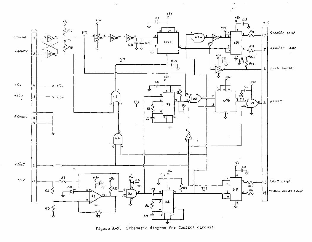
3.4 CONTROL CIRCUITRY
The schematic of the control circuitry is given in Figure A-9. The
circuit operates as follows. Application of prime power at the front panel
causes a rising edge at pin 2 of U3, a precision timer IC, which causes it
to trigger a two minute (heater delay) low level logic pulse at its output
pin 9. This logic "0" pulse causes flip-flop U7a to stay cleared which
allows the circuit to prevent the modulator from going to the radiate mode
while in heater delay.
Inverters U6a and U6b debounce the Radiate/Standby switch. Toggling
this switch to Radiate causes a low to high transition at the clock input,
pin 3, of flip-flop U7a. This sets the flip-flop unless the clear input,
21

pin 1, is low. In other words, the system can not go to radiate during
heater delay, if a fault is preent, or if the switch is in the Standby posi-
tion. Switching to Standby automatically clears the flip-flop, taking the
system out of the radiate mode.
The HVPS Enable signal is sent to the high voltage power supply. In
the Radiate mode, this signal is a 15 V level that turns on the high
voltage. When the system reverts to Standby or is in Heater Delay, this
signal is approximately 0 V and disables the high voltage power supply.
Application of prime power also causes another precision timer U4 to
trigger a six second logic "1" pulse. The purpose of this pulse is to auto-
matically reset the protection circuitry after power-up, since the modulator
will probably come on in a fault condition. This six second pulse is ex-
clusive-ORed with the debounced setting of the Radiate/Standby switch. If
this switch is in the Standby position at power up, as it should be, the
circuit will automatically clear faults after the six seconds. If the
switch is left in the Radiate position, the faults will not automatically be
cleared; however, to go to Radiate would require switching to Standby first,
which would clear the fault anyway. After the six second pulse ends,
switching to Standby will clear any faults, as long as they are not still
present at the time the attempt to reset is made.
When a fault is encountered, the Fault signal from the protection cir-
cuitry goes low and causes the Reset Command to go low and latch up the
flip-flops within the protection circitry. Switching to Standby clocks
flip-flop U7b and sets it, causing the Reset Command to go high, unlatches
the flip-flops in the protection circuitry, and therefore clears the fault
if it is no longer present. If the fault is still present it will not be
cleared; the cause of the fault should then be determined.
3.5 HIGH VOLTAGE ISOLATED POWER SUPPLIES
Several voltages are necessary for operation of the floating deck modu-
lator. These include heater voltages for the planar triodes and RF tube,
+28 V for the - 3 kV bias supply, the focus voltage, +5 V, +18 V, and +300 V
22

for the various circuits used to form and amplify the pulse. since the
entire START deck follows the 3 kV swing of the grid pulse, the operating
voltages for the START and STOP decks must be isolated from each other. Four
isolation transformers supply the necessary operating voltages to the
floating deck modulator. Table 4 lists how the various voltages are dis-
tributed among the four isolation transformers.
TABLE 4. DISTRIBUTION OF HIGH VOLTAGE
ISOLATION TRANSFORMER VOLTAGES
Transformer Secondary Voltages
T1
Operating voltages for STOP deck;
+300 V, +18 V, +5 V
Heater voltages for planar triode
and RF tube
T2 +28 V for - 3 kV bias supply
T3
Operating voltages for START deck;
+300 V, +18 V, +5 V
Heater voltage for planar triode
T4 Focus voltage
The secondary voltages of the four transformers are supplied by the
center-tapped primaries of four driven push-pull power converters. The
schematic for the push-pull converters is given in Figure A-11 in Appendix
A. The schematics of the four transformers are given in Figures A-13 and A-
14. In Figure A-11, U1 is a SG1525A complementary output square wave
generator, and U3 is a DS0026 MOS driver which drives the gates of all eight
switching FET's. The FET's used are the IRF520, and manufacturers' data
23

sheets for them and for the SG1525A and DS0026 are included in Appendix C.
The center-taps of T1, T3, and T4 are adjustable via voltage regulators in
the low voltge power supply; the center-tap of T2 is +24 V, since additional
regulation is supplied by the input of the - 3 kV supply itself.
3.6 HIGH VOLTAGE POWER SUPPLIES
3.6.1 BEAM SUPPLY
The high voltage power supply used to supply the beam voltage (-21 kV)
was manufactured by the Spellman High Voltage Electronics Corporation. The
manufacturer's instruction manual for this high voltage power supply is
given in Appendix D and includes the specifications and schematics for the
power supply.
Several modifications have been made to the beam supply. One modifica-
tion was the inclusion of the low voltage power supply within the high
voltage power supply enclosure. The additional connector was added to the
back of the supply to allow for a cable that carries voltages from the low
voltage supply and commands from the front panel switches to the modulator
and carries status and control signals from the modulator back to the front
panel. Figure 10 is a sketch of the location of the additional components
within the Spellman supply.
3.6.2 BIAS AND PULSER SUPPLY
The bias and pulser supply is a - 3 kV supply made by the Advanced High
Voltage Corporation. The manufacturer's specifications for this power
supply are given in Appendix C. This supply provides the - 3 kV grid bias
necesary to keep the EIO cutoff. Formation of the 3 kV pulse is described
in Section 3.2. The -3 kV supply is located within the modulator assembly.
3.7 LOW VOLTAGE POWER SUPPLY
The low voltage power supply assembly is located within the high
voltage power supply. The schematic for the low voltage power supply is
24

,•■■••••
Terminal Strip
Multi-pin
Transformer Connector
T6
LI
Power Supply Filter Caps
Transformer T7 1
Low Voltage Power Supply Board
Front Panel
Figure 10. Location of added components to high voltage power supply (top view).
25
given in Figure A-19. The power supply consists of two 230 V to 24 V trans-
formers followed by appropriate filtering and regulating circuits. Trans-
former T6 supplies power for the center taps of the isolation transformers
and also for the fan within the modulator and the lamps on the front panel
of the high voltage power supply. Transformer T7 supplies power for the
control, protection, pulse driver, and push-pull converter circuits.
3.8 INTERCONNECTING CABLES
Three cables connect the modulator and the high voltage power supply.
A multiconductor cable carries DC power supply voltages and control and
status commands to and from the modulator and beam supply front panel. A
BNC cable carries the HVPS Enable command from the control circuitry in the
modulator to the beam supply. The high voltage cable connects the beam
supply to the floating deck modulator. A diagram for the interconnection
board is given in Figure A-21. Note that input and output synchronization
signal BNC jacks are located on the modulator assembly.
3.9 TROUBLESHOOTING
This section deals with the four fault conditions that result in auto-
matic shutdown of the modulator. The majority of service required for the
system should deal with these four conditions. Each fault is discussed in-
dividually along with possible causes for the fault. This should help mini-
mize repair time.
3.9.1 EXCESSIVE PRF
This fault occurs when a synchronization signal with a frequency
greater than 20 kHz is applied to the modulator. Decreasing the frequency
of the input signal should clear this fault. If it does not, refer to the
discussion in Section 3.3 dealing with this condition. A possible circuit
failure might be a faulty one-shot setting; adjust potentiometer R 1 (see
Figure A-7), for a 26.5 us pulse at TP2. If this does not correct the
circuit, check for failure of the integrated circuits used.
26

3.9.2 EIO HEATER UNDERVOLTAGE
This fault occurs when the center tap voltage of isolation transformer
T1 gets too low indicating that the secondary voltage that supplies the
heater voltage for the EIO has also dropped. Possible causes for this fault
are excessive power drain by the other secondaries of T1, or maladjustment
or failure of the voltage regulator Q6 that supplies the center tap voltage
(see Figure A-21).
3.9.3 TOTAL EIO AND BODY OVERCURRENT
The protection circuitry (Figure A-7), samples the total current
flowing from the high voltage power supply. This current flows through R 10 ,
and the collector current flows back out of the circuit, leaving the body
current to flow to ground through R 11 . Total EIO overcurrent can result
from an arc within the EIO. Body overcurrent results from an improperly
focused beam. Adjusting the focus voltage via the voltage regulator Q5 that
feeds the center tap of isolation transform T4 should correct any beam
defocusing.
27
SECTION 4
SUMMARY
This operations manual was written with the following as goals:
1) To provide sufficient explanation of the operation of the modu-
lator/ power supply assembly so that operators can be easily
trained; and
2) To provide detailed explanation, including diagrams and schematics
of the individual circuits within the modulator. This discussion
should aid Philips' engineers who wish to modify or repair the
assembly.
All circuit schematics and parts location drawings for each circuit
board are given in Appendix A. Parts lists for the various circuits are
given in Appendix B. Manufacturers' specification sheets for selected com-
ponents are given in Appendix C. The instruction manual for the -21 kV beam
supply is given in Appendix D.
28

APPENDIX A
SCHEMATICS AND PARTS LOCATION DIAGRAMS

STA RT A To m 4,141.r
STAtqT tea
t 5v.irs S
Gra, 4 7
RASe. 0;4111‘.
SYNC
Ri
STA hT e
70 illocioloter
`..7/11',7 A. c k
.5 -ro f-
TO MJA.7or
`7_70
Figure A-1. Schematic diagram for Pulse Driver Circuit.

R 6
T
C C C
0 7 3
C11 R8 I-- —I R3 I— —I R4 I--
IC11
R 9 I--
n n
I R 7
R 1 3 T
H RIO F— ETI --I RS I--
I CS
U10
R12 F
C
2
U3 U 8
U 7 U2 U S
R2 RI
J3
UI U G
U4
C
s
09 R11
TP6 TP7 TP8 TPS TP9 TP3 TP2 TP4 TPI ©
Figure A-2. Parts location diagram for Pulse Driver Circuit.

• 3a U3' 7 ) 3 e
/3
tEJ 0
R Rio 7
4444
T z
lY
uz
=
C5
ES
•AE3
lL
E7
(1,
T. 14
• CR 3
N -3
CZ
6o4k0
Va.
cs
R10
56.1
G7` cR3
C 0:7
A 1 _ _ _ ES
Sk y
5144
>i›El
%Q1Y
—1 0 ) 2CI
(sTAAT) <f
,
_es (srAprr)
V syr4c
c I yl
L5
SZD1 R15 VVe
1
1
1
Figure A-3. Schematic diagram for modulator circuitry.

R R 7
TT
OTP6 I
G
E3 © R3 1 TPS
R UI U3
5
T C 6 ) R2 h- ©TP3
L 2 I--
LI
J2
Figure A-4. Parts location diagram for modulator Start Deck A2A.
TPIO
Q3
©TP7
TP8
CR2 I TP9
CRI
RI 4
02
C11
C14
El
E2 U2
11 R R II 12
TPI R4 © RIO I--
=1) TP2 --I R 9 H TP4
U4
U3
U4 .
C2
CI OTPI OTP2
C 3
©E2
E3©
TP3 O
--I RI 1-
C4
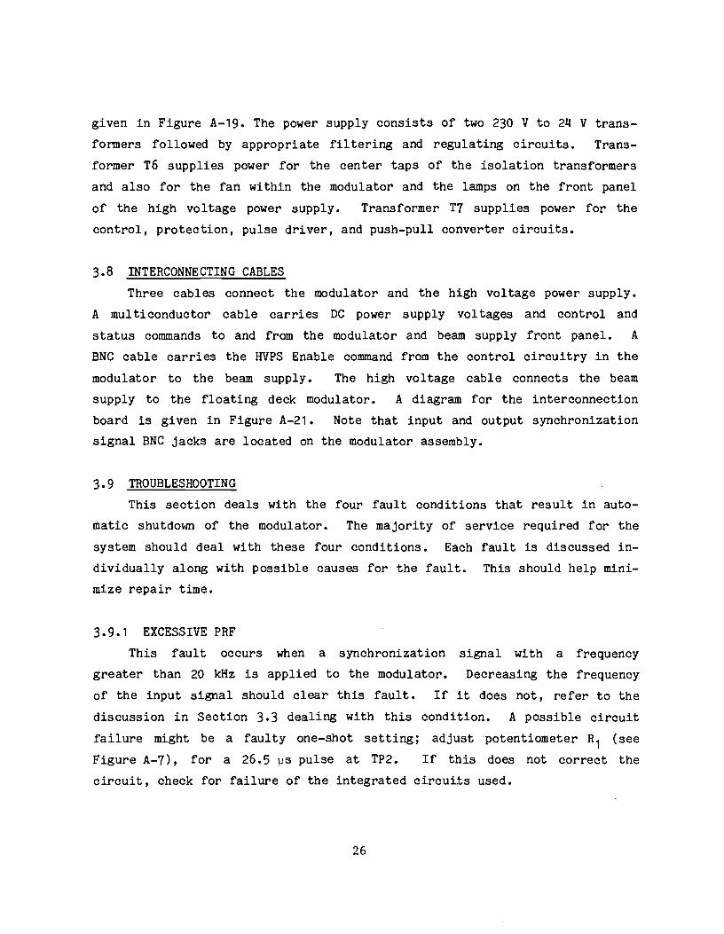
Figure A-5. Parts location diagram for modulator Start Deck A2B.

TP2
O -d R2 F-
(CL2) TPLH R3 H
(LD T193 ( C4 --I RI I--
LI
--I L2 I-
0
0 Q2
QI
TP6 © R8
C9 CB
R9
JI
SG I
E3 RII
El
I R 5
I TP4
R 7
I I © TP5
Ul
—I RIO I— --(of 1)--
© TP7
TP8
E2
ES
R 4
6
CG
Figure A-6. Parts location diagram for modulator Stop Deck.

IlvP Ft o47
Er° CoLLecTOR
REsE -r
3 6o0y OVER cuRREHT
LE 0
+15 v
4- 5v
STOP acK c # .PpeR C e AMR r4P VOL
o RI 41.
010
U 0
fez.
811
EXcEsssve PRF (EL)
FAULT
3
z1
Low HEAT VOLTA&E LEO
L
o OVERCuRnElpr
LED
fr2.3 "Or-- //
-45v
Rzz Iz
/3
Rzo
;C.47
Figure A-7. Schematic diagram of Protection circuit.
R7
US
R
7 T
CRI CS
C 6
R4 R5 R6
U I
I cio I zr
U6
I C3
U4
l cl 1
R3
TP8 TP7 TP6 TP5 TP4 33 . 16 is © © © © ©
I C9
I 03) cg1D-D-2
CR3 - RI2
- RI4
CR2 M
1 Cifb,1 1:1T)DI LI I i
0 1 4 --I R9 -rT TT
R8
- R23I--
- -I R22 1—
—4 R21 1—
- R201—
I R R R I I I 6 8 9 T 1 T
RI
R2
T
C2
—r
J4
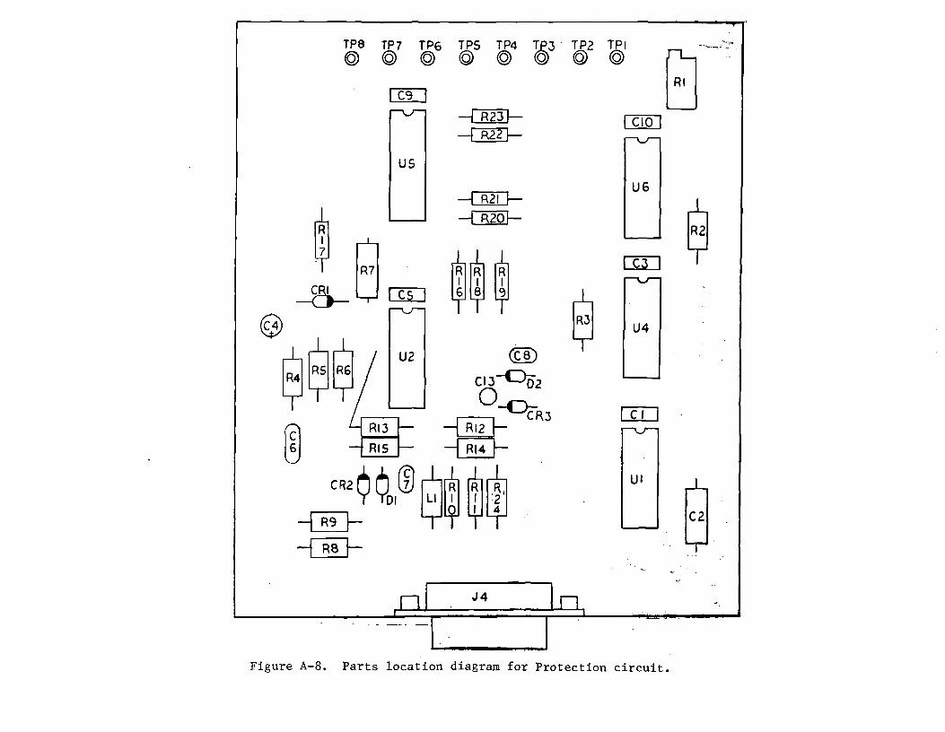
Figure A-8. Parts location diagram for Protection circuit.
Cis CI
TN, Ulf
he/ a ly
IZ.
)3 3 TP1
5 R s3
TPZ 644 HEATER DELAy LA,v1/3 lo
F451L7 LAMP
5 Ail R7
9
45,./ 0 CZ —I FT
''l'V"
U2)8 7
3 C.13 C.
0 4- 5v
0
53
o
1 1
/2.
UL
/3 R I +5v
cR I
A3 it 10
4tSv
C.Touo lp
FAULT
0- /5 ✓ +1Sv
C I
tA l
+5v
TP8
57A41).W v
7
RI5 tr ilDiA75"
.+Sv
CS
Nurs 6A/ACLE
C5
4-5V 0
0
R8
liEsET
116
r5v C/0
+5v 0
+55/
U-71
0 c7
T5
T4 L/04Y LArAf/
IAta
1a
l̂A OIATE LAMP X16
1 1_c. c.
-rInt
LIS.
TP5 Ul 6 All
L7.
4 5V
Figure A-9. Schematic diagram for Control circuit.

-4 R8
--I R9 I--
I R 7
1 TP2
61PG.
CRI I
R R R S 4 3
I I I
TPI
U2
Us
U5 RI I RI3
I 2
RI
TP8
C) Ul
C) QCI) uG TP7 U7 TPS
TP3 TP4
C) U9 (cl) CCTzl)
CII
E0
RIO U10
R 12
IS I 16
1 T
0 CIS
RI4
n
JS n
Figure A-10. Parts location diagram for Control circuit.

IS
cq
° R TP1 2. U34
3
R1 TKI -1
U3b
R5
To le QI CR 1
To EV
SF
Q2- E1 caL
O ro Ef
3 0133
1 To E
CF-1
5 5 rs E4
CRle
3 ra Eiz
-t 5,
+15v 6 Cll
C10
3 rp3 outa 0 5-
7 /2
Int ► E3
Q8 cRg
a
l
t.. E7
on coArtet.r
6e.rd-
Figure A-11. Schematic diagram of push-pull power converter (chopper) circuit.

CRI
—1 CR2 I-
-1 CR3
CR4 I-
TPI () —I R2 I--
_
3 9 U3
—I R4 I-- ©
R TP2 TP3
() I TP4
(C 3 )
RI
--1 CRS I--
CR6 I-
--I CR7
—1 CR8 k (C 7) (C8)
(C5)
U2 (C2)
(C 4)
(C I ) C6
UI
_XL
0 0 0 0 0 0 O 0I
02
03
04
08
07
Q6
Q5
J6
Figure A-12. Parts location diagram for push-pull power converter (chopper) circuit.

1)2
ri JI 4- loo V
+300V RET
4 17V
SV
CZ CRI
RI
(SET
Y2 CATH00E
HEATEi3
Elo CAM-loor
EX() HEATFR
E/
EZ
C I (7 C7T C3T
E3
7 13
IS
On) -10TE fic 0JeJecT 4::QA 3. Ks, Zorter-L
+2.8v t° -3 k„
R-ET
2.
DI
CI
C1 3 1 1
CIOT 1-C6•
Eil
E/z.
k— 'I 3o Kg InTertu.e.
Figure A-13. Schematic diagram for isolation transformer supplies Tl and T2.

ES
3oo N./
+30DV RCS"
-) V
-1- 5 V
Re'r
VI CATHo 0 r
VI N eATE
7 )3 /5
C a Cy
T3
D z.
RI C7_ CR1
H30 Kw Inter-c.c.
Tit E7
1'1 Kv Inter-gate,
+ FocuS
TO START pecK.
- Focus
I T" Cs
Es7
El
J2
op./ jrJTERCorJN EcT oARD
Figure A-14. Schematic diagram of isolation transformer supplies T3 and T4.

R I
D2 o co TI
—(CR 11--
C
JI
Figure A-15. Parts location diagram for isolation transformer supply Tl.
0
o° 00
cc
T2
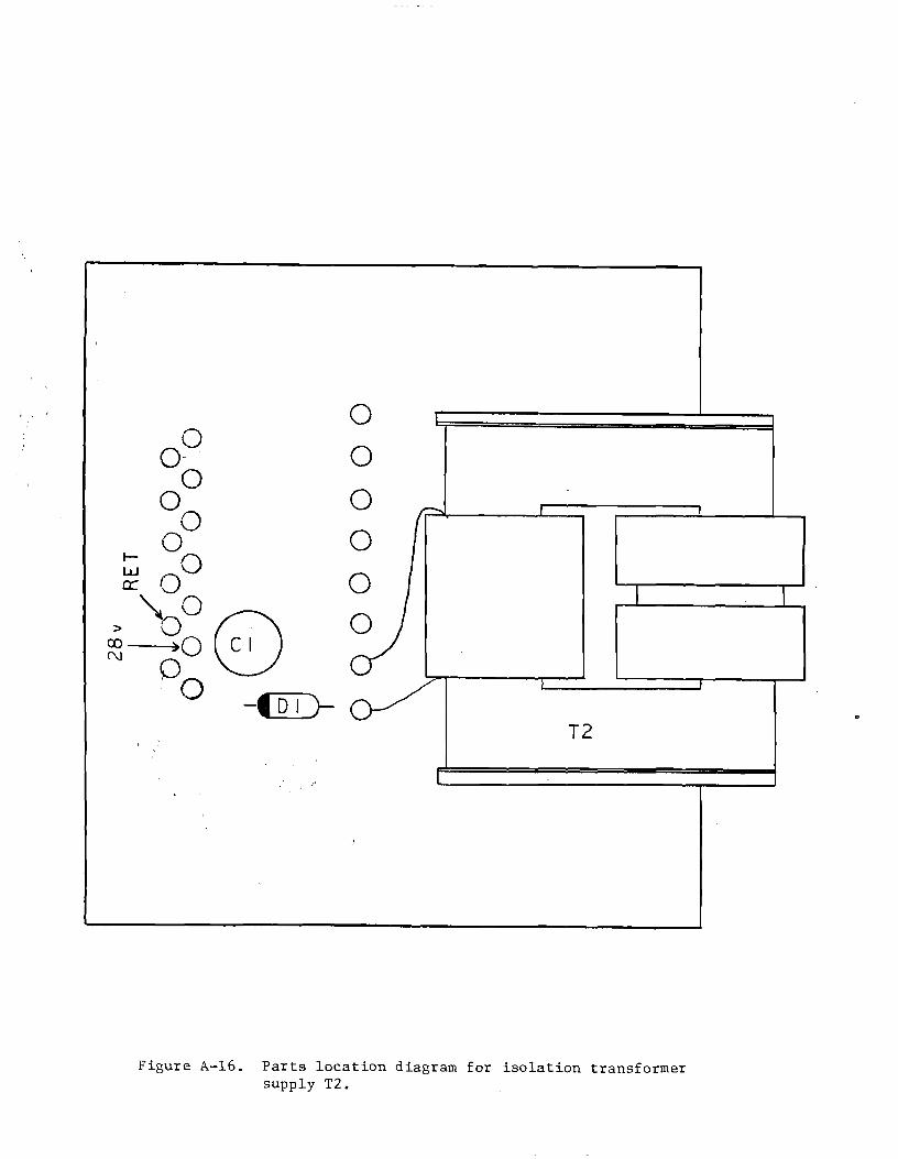
Figure A-16. Parts location diagram for isolation transformer supply T2.

--(CR I IIP---
CI 4 f
0
J2
T3
RI
Figure A-17. Parts location diagram for isolation transformer supply T3.

0
0
0
0 T4
Figure A-18. Parts location diagram for isolation transformer supply T4.

Q5 )2 fac ✓ 5 ✓oi-TACTE GETTER 74e
Figure A-19. Schematic diagram of Low Voltage_Power Supply.
15
TCe RP R7
TC7
040
Ro RI
euZ R
Q3
Tcg
fif R3
Q't
85 T C5
+5 ✓
07
3
5
7
STotc. °ECK CENTE R TAP
I/
START O&-C? R TAP
lo
4 /.5v
GN O
;3o Ye.c.
T7
Ti )
CRI
QI
4- 11 v
CI
TC.2.
T'''

JII
O+ C 3
0
Figure A-20. Parts location diagram of Low Voltage Power Supply.

Figure A-21. Schematic diagram of Interconnect Board.
E 31 r_.•
112.
E zi o 7 E
E33 6 ray 14
EJ5 ;
En .1
G NO 1'3 Ei7 1,
38
5G N 0
pvtc,
g 7o 116, o A s. kJ
E!11 To E2O co,L107oe_ e. e @ e e 8 0 8 TI
C 1 561
Py 13
C C6
-N17
41.57
co
9
ca
r
il--.4 1 •
RI CIS
C
•---I Gf
ow WARD,
7.1
E45
E.0
tq3
Ezi
E30
Fly
En
Ett
EIS
eft
PiNc. our
1-1\A-s
Sy NC
IN
70 rAn1
P707
+24v
1.1 Ex.vs Rev1.1...r
LI START DECK lietvIsler
V STOP OEcK Retvlo,Tor
o v
3. +15v
b
a. ST6v ResiT
F4J IT Lome
•
Neu-tar
F G.( 04frcorreAT LGO
G- Eso over,urr.or LEO
✓ Led NeAter V.1t....0, LED
• G•tr. PRF LC 0
C1.3 ( v or
5
7
7
10
1 7
15
‘cl 31,

E14 E13
OO @
R2
SGI
C2
0 . 00000000 ,1 0 0000000 PF
0000000 00000000
PS ro- 0EIS
E27()
E260
E250
E 2243:
E23©
El E2 E3 E4 ES EG ©00 000
E7 E8 E9 EIO EH E12 000 ©00
@ —I I— RI (Do
E17
E42
0 0000000 00000000
E4I E38 0 ©E43
E40 E3 0
©E44
0 0E45.
E34 QE39()
E30 E3G
E29© E31 E32 E35 9 0 0 0 0
E26©
0E16
EIB E21 E E19
E33 0
0 [ 0000000 00000
P3 E20 E22
Figure A-22. Parts location diagram for Interconnect Board.

-I-Z4 v -+5i
7- 11 I I 1-
_57-4"10 6y tame
RADIATE LAMP
R EATEIQ orogY 141P
FA Vi-T LAMP
Erc-EsSive- r°,9
4e-'W HEATER VOLTAGE
Eio ovErecuRrie wr -
Booy ovER curmEar
7-7
RADIA -re-
sTANI) ay R Es Er
PULSE war r
re%
Figure A-23. Schematic diagram of wiring modifications made to Spellman Power Supply front panel.

0 High Voltage Lead
(ThChassis \-/Ground
„.., HVPS U Enable
0
Multi-pin Cable Connector 0
230v AC Line Cord
Figure 24. View of back panel of power supply showing connector designations.

TABLE A-1. CABLE PIN ASSIGNMENTS FOR CABLE BETWEEN MODULATOR AND POWER SUPPLY
Pin #
A
B
C,D
E
F
G
H
K
L
P
R
M,N
S
T
U
V
X
Destination Signal
in Power Supply
Excessive PRF
Cathode of Excessive PRF LED
GND
+5 V
LVPS: J11-4 Front Panel LED's
Pulsewidth Potentiometer
Cathode of Low Low Heater Voltage
Heater Voltage LED
Body Overcurrent
Cathode of Body Overcurrent LED
EIO Overcurrent
Cathode of EIO Overcurrent LED
GND
+15 V
STBY LAMP
Low Side of STANDBY LAMP
RADIATE LAMP
Low Side of RADIATE LAMP
N/C
N/C
+24 V
LVPS: J11-1 Front Panel Lamps
Heater Delay Lamp
Low Side of Heater Delay Lamp
Fault Lamp
Low Side of Fault Lamp
Focus Regulator Voltage LVPS: J11-12
Stop Deck Regulator Voltage LVPS: J11-11
Start Deck Regulator Voltage LVPS: J11-10
N/C
N/C
Destination in Modulator
Protection: J4-11
Pulse Driver J3-5,9 Control: J5-9
Protection: J4-14 Chopper: J6-4
Protection: J4-12
Protection: J4-4
Protection: J4-13
Control: J5-13 Protection: J4-10 Chopper: J6-6
Control: J5-7
Control: J5-8
Interconnect: E-29
Control: J5-14
Control: J5-15
Interconnect: E45
Protection: J4-1 Interconnect: E43
Interconnect: E44

TABLE A-1. CABLE PIN ASSIGNMENTS FOR CABLE BETWEEN MODULATOR AND POWER SUPPLY (CONTINUED)
Destination Destination Pin # Signal in Power Supply in Modulator
a STBY/RESET Command Front Panel Switch Control: J5-4
b Radiate Command Front Panel Switch Control: J5-5
c Spare
d Spare
e GND
f GND
g N/C
h GND
j GND
k Shield GND GND
m Pulsewidth Setting Front Panel Potentiometer Pulse Driver: J3-3
n Floating Ground Back Panel Protection: J4-2
p Shield GND GND.
✓ Spare
s Spare

APPENDIX B
PARTS LISTS

PA R TS LIST LIST TITLE: ^
Pulse Driver
CONTRACT NO: r DATE: 1/10/84
FIN D NO. PART NUMBER QTY
ROD DESCRIPTION REF DESIG,
? AGE OF NOTES
49.952 1% R1
7.5kQ 1% R2
• 2 1(2 1% R3
3.9k2 R4,R5
1002 1/8w 1% R6,R7
2.61U 1% R8
10052 1/8w 1% R9
4.99U 1% R10
47.50 1% R11-R13
39 pf Cl
.22 of C2
47 pf C3
.001 of C4
.22 if
. 001 of
.22 of
C5
C6
C7
47 pf C8
190 _pf C9
- 22 lif C10-C13
10 pf 25v tantalum C14
.22 pf C15
270 pf C16
. .01 of C17
1N4733A 5.1 v zener CR1
DM74IS921 Dual one-shot Ul U7
DS0026 MOS Clock Driver U2 U5
PE9825 Delay 'Mae U3 U6 U8
74S02 Quad NOR Gate - U4
75451 NAND Driver U9
75452 AND Driver U10
HFBR-0500 Optical Transmitter Ull-U13
DAE15PA ____ 15 pin .D connector J3
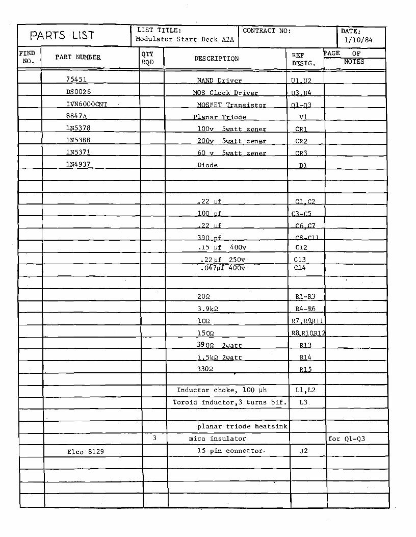
PARTS LIST LIST TITLE: Modulator Start Deck A2A
CONTRACT NO: DATE: 1/10/84
FIND NO. PART NUMBER QTY
ROD DESCRIPTION REF PAGE OF DESIG. NOTES
75451 NAND Driver U1,U2
DS0026 MOS Clock Driver U3,U4
IVN6000CNT • MOSFET Transistor Q1-(1 3 8847A Planar Triode V1
1N5378 100v 5watt zener CR1
1N5388 200v 5watt zener CR2
1N5371 60 v 5watt zener CR3
1N4937 Diode D1
.22 of C1,C2
100 pf C3-05
.22 iif C6, C7
WI pf (-11-C11.
.15 pf 400v C12
.22pf 250v C13
.047pf 400v C14
2052 R1-R3
3.9k52 R4-R6
1052 R7,R9a11
150Q R8,1110,R.12
3900 2watt R13
1.5k0 2watt R14
. 33052 R15
Inductor choke, 100 ph Ll,L2
Toroid inductor,3 turns bif. L3
planar triode heatsink f
3 mica insulator for Ql-Q3
Elco 8129 15 pin connector- J2
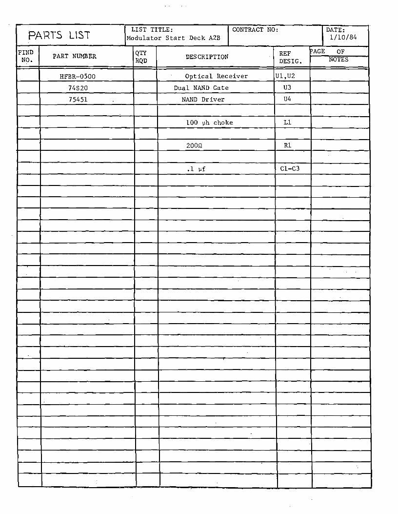
PARTS LIST LIST TITLE:
Modulator Start Deck A2B CONTRACT NO: DATE:
1/10/84
FINDNO. PART NUMBER QTY
RQD DESCRIPTION REF PAGE OF
DESIG. NOTES
HFBR-0500 Optical Receiver Ul,U2
74S20 Dual NAND Gate U3
75451 NAND Driver U4
100 ph choke Ll
2000 R1
.1 pf Cl-C3

PA RTS L I ST LIST TITLE: Modulator Stop Deck
CONTRACT NO: DATE: 1/10/84
FIND NO. PART NUMBER QTY
RQD DESCRIPTION REF AGE OF DESIG. NOTES
DS0026 MOS Clock Driver Ul
HFBR-0500 Optical Receiver U2
IVN6000CNT . MOSFET Transistor Q1,Q2
8847A Planar Triode V2
100 ph choke Ll,L2
Toroid inductor,16 turns bif. L3
1 1(.0 R1
3.9k0 R2,R3
100 R4,R6
116/ R5,R7
4300 R8
4.31a2 R9
116/ Ilwatt R10
301a2 10 watt Rll Caddock
1N5378 100v 5watt zener CR1 . 1N5388 200v 5watt zener CR2
1N5371 60 v 5watt zener CR3
1N4937 Diode Rectifier D1
.22 pf C1,C4
• ..
I
1000 pf
.005 of 1kv
C2,C3
C5
. 15 of 400v C6,C7
.022 pf C8
. .01 pf C9
UBT4.0 Spark Gap 4kv SG1
planar triode heatsink
mica insulator - for Q1,Q2
Elco 8129 _ 15 pin connector Jl
. ,

P RTS LIST LIST TITLE:
Protection Circuit CONTRACT NO: DATE:
4/1/84
FIND NO. PART NUMBER QTY
RQD DESCRIPTION REF DESIG.
AGE OF NOTES
10 k2 pot R1
2.0 k2 1% R2
. 4992 1% R3
5.11 k2 1% R4
17.4 k2 1% R5
10.0 k2 1% R6
202 1/2- watt R7
15k2 1% R8
5.6k2 R9
3002 1% R10
9532 1% Rll
27.4k2 1% R12 ...
280k2 1% R13
18.2k2 1% R14
40.2k2 1% R15
4 3.9162 R16-R19
4 512 R20-R23
30102 1% R24
100 Ph Ll ... 1N914 diode D1,D2
1N4730 3.9 volt zener CR1
1N4733 2 5.1 volt zener CR2,CR3
5 .22 of C1,C3,C5,C9,C10
1200 pf polystyrene C2
22 of 25 v tantalum C4
2 1 of 50 v tantalum C6,C13
2 4.7 of 25v tantalum C7,C8
2 .01 of C11,C12
• 4 .1 of C14-C17
74121 One-shot Ul
LM339 Quad Comparator U2
7406 Hex Inverter - U4
7475 Quad D Latch U5
7421 Dual 4-input AND Gate U6
DAE15PA 15 pin D connector J4

PASTS LIST TITLE:
Control Circuit --
CONTRACT NO: DATE: 1/10/84
FIND NO. PART NUMBER
RQD
,
DESCRIPTION DESIG.
PAGE OF NOTES
27052 1 watt R1
511(Q R2
18kQ R3
6201(0 R4
3.91(0 R5
10MQ R6
1162 R7,R9
510k0 R8
4 6852 1 watt R10,R11, R13,R14
3 2.21(0 R12.R15, R16
1N4733A 5.1 volt lwatt zener CR1
.1 of C1,C2
.001 of C3
10 of 25v tantalum C4,C6
8 .1 of :5,C7-C13
.01 of C14
.22pf C15 - 1 pf C16
LM339 Quad Comparator Ul
7408 Quad AND Gate I.J2
LM122H Precision Timer U3,U4
7486 Quad XOR Gate US
. 7404 HEX Inveter U6
74S74 Dual D Flip-Flop U7
DS3611N Dual Peripheral Driver U8,U9
7406 Hex Inverter/Open Coll. outpu U10
DAE15PA 15 pin D connector J5

PARTS LIST LIST TITLE: Chopper Circuit
CONTRACT NO: DATE: 1/10/84
FIND NO. PART NUMBER QTY
RQD DESCRIPTION REF DESIG.
PAGE OF NOTES
10162 R1
15S-2 R2,R4
. 101d-2 R3,R5
.1 pf Cl, C2
2200 pf C3
.1 pf C4,C5
.22 pf C6,C9
.1 pf C7,C8
22 pf 25volt tantalum C10,C11
1N5375 8 82 volt 5watt zener CR1-CR8
IRF 520 8 100volt,5amp HEXFET Ql -Q8
__ SG1525A _ Pulse-width Modulator Ul
DS0026 MOS Clock Driver U2,U3
DAE15PA 15 pin D connector J6
L

.
PARTS LIST LIST TITLE: Stop Deck Floating Power Supply
,
CONTRACT NO: DATE: 1/10/84
FIND NO. PART NUMBER QTY
RQD DESCRIPTION
..1„._
REF AGE OF
DESIG. NOTES
Transformer T1
F740-1-05 Ferramic "U" core
• Primary: 14 turns of #25awg
Bif liar winding
Secondaries:
(300v) 310 turns, ift30awg
(18v) 18 turns, #28awg
2 (6.3v) 7 turns, #24awg
Primary on plexiglass spindl? I
MR818 Diode Rectifier D1
1N4937 Diode Rectifier D2
1N4733 5.1v lwatt zener CR1
2700 1 watt R1
.047 of 400volt Cl
15 of 35 volt C2
Elco 8129 15 pin connector Jl
. _.
•

PARTS UST LIST TITLE: 28v to -3kv
Floating power supply DATE:
CONTRACT NO:
1/10/84
FINDNO. PART NUMBER QTY
RQD DESCRIPTION REF DESIG.
'AGE OF NOTES
Transformer T2
F740-1-05 Ferramic "U" core
. Primary: 16 turns of #22awg
bifilar on plexiglass
spindle
Secondary: 22 turns of #25
awg [
MR856 Diode Rectifier Dl
'22 ;if, 35volt tantalum Cl
PARTS LIST LIST TITLE: Start Deck
Floating Power Supply CONTRACT NO: DATE:
1/10/84
FIND NO. PART NUMBER QTY
RQD DESCRIPTION REF DESIG.
'AGE OF NOTES
Transformer T3
F740-1-05 Ferramic "U" Core
• Primary: 16 turns of #25awg
bifilar on plexiglass
spindle
Secondaries:
(300v) 290 turns, #30awg
(18v) 18 turns, #30awg
(6.0v) 6 turns,#25awg
MR818 Diode Rectifier D1
1N4937 Diode Rectifier D2
1N4733 5.lvolt 1 watt zener CR1
15052 2 watt R1
.047 pf 400volt Cl . 15 of 35 volt tantalum C2
Rico 8199 15 pin connector J2
, .
• ,
,-....—.

PARTS LIST LIST TITLE: Floating
Focus Volt. Power Supply
CONTRACT NO: DATE: 1/10/84
FIND NO. PART NUMBER QTY
RQD DESCRIPTION REF
DESIG.
?AGE OF NOTES
Transformer T4
F740-1-05 Ferramic "U" Core
• Primary: 14 turns of #25awg
bifilar on plexiglass
spindle
Secondary: 200 turns of
#28 awg
MR818 Diode Rectifier D1
.22 of 250 volt Cl
_ .
L.----..

PARTS LIST LIST TITLE: Low Voltage Power Supply -
CONTRACT NO: DATE: 1/10/84
FIND NO. PART NUMBER
-■
QTY RQD
DESCRIPTIQN REF WAGE OF
DESIG. NOTES
453052 1% R1
6 24352 1% R2,R4,R6,k8,R10,R12
274052 1% R3
73252 1% R5
3 10kQ pot R7,R9,R11
2 2400 pf, 50 volt C1,C3
5 15 pf, 35 volt C2,C6-C8,r10
22 pf, 25 volt C4,C5
22 pf, 35 volt C9
6. MDA970A1 4 amp,50 v bridge rectifierCRl,CR2
LM317K 3 1.5amp Voltage Reg. Q1,Q3,Q4
2N6338 Power NPN Transistor Q2
LM350K 3 3 amp Voltage Reg. 0,0,Q7
47-1115S 15 pin D connector Jil
Triad F-214U 230v to 24v 4amp transformer T6
Triad F-107Z 230v to 24v tamp transformer T7 i
•
_ -

PARTS LIST LIST TITLE: Interconnect Board
c.
CONTRACT NO: DATE: 1/10/84
FINDNO. PART NUMBER QTY
RQD DESCRIPTION REF ?AGE OF
DESIG. NOTES
120 R1
100k 2 watt R2
lkv spark gap SG1
27 pf Cl
.1 uf C2
11 22 uf, 35 volt C3-C14
22 uf, 25 volt C15
25 turns on BBR7725 toroid Tl
DEE9SU 9 pin D connector P3
DAE15SU 3 15 pin D connector P4-P6
•
i —

APPENDIX C
MANUFACTURER'S SPECIFICATION SHEETS

TECHNICAL DATA
8 847 8 8 4Th HIGH-MU
PLANAR TRIODES
The 8847 and 8847A are miniature, ceramic/metal, rugged planar triodes for advanced airborne and space applications up to 3.5 GHz.
The 8847A is identical to the 8847 in all respects except that the re-quired heater power is reduced by 25%. The tube should be used where input power consumption and heat dissipation are of major concern.
Either tube may be used as an amplifier, oscillator, or frequency multi-plier in the CW, grid- or plate-pulsed mode, as well as a modulator or regulator tube. In addition to low interelectrode capacitances, high trans-conductance and amplification factor, the 8847 and 8847A have an anode designed to enhance frequency stability and an arc-resistant cathode, both assuring stable, reliable and long-life operation under adverse conditions.
The 8847 and 8847A are supplied without radiator and may be conduc-tion, convection, heat sink, or liquid cooled. Radiators for forced-air cool-ing permitting an anode dissipation up to 150 watts, can be furnished on separate order.
GENERAL CHARACTERISTICS 1
ELECTRICAL
Cathode:Oxide Coated, Unipotential Heater: Voltage 6.3 -± 0.3 V 8847 Current, at 6.3 volts 1.30 A 8847A Current, at 6.0 volts 0.95 A
Transconductance (Average): Ib = 160 mA (200 mA/cm2) 38 mmhos
Amplification Factor (Average): 75 Direct Interelectrode Capacitances (Grounded Cathode) 2
Grid-Cathode 9.5 - pF Plate-Cathode 0.06 pF Grid-Plate 1.40 pF
Cut-off Bias 3 -30 V max.
1. Characteristics and operating values are based upon performance tests. These figures may change without notice as the result of additional data or product refinement. EIMAC Division of Varian should be consulted before using this information for final equipment.
2. Capacitance values for a cold tube as measured in a special shielded fixture. When the cathode is heated to the
proper temperature, the grid-cathode capacitance will increase from the cold value by approximately 1 pF due to thermal expansion of the cathode.
3. Measured with one milliampere plate current and a plate voltage of 1 kVdc.
(Effective 6-1-70) © 1970 by Varian Printed- in U.S.A.
EIMAC division of varian / 301 industrial way / san carlos / california 94070

8847/8847A
MECHANICAL
Maximum Overall Dimensions: - Length
1 370 in; 34.75 mm Diameter
0 785 in; 19.94 mm Net Weight 0.56 oz; 16.0 gm Operating Position
Any
Maximum Operating Temperature: Ceramic/Metal Seals 250°C Anode Core 250°C
Cooling Conduction, convection, forced-airl or liquid
Terminals Coaxial, special
ENVIRONMENTAL
Shock, 11 ms, non-operating 60 G Vibration, operating, all axes 55 to 500 Hz 10 G Altitude, max (in suitable designed circuit) 70,000 ft.
CW RF POWER AMPLIFIER OR OSCILLATOR
GRID PULSED OR PLATE PULSED AMPLIFIER OR OSCILLATOR
MAXIMUM RATINGS/ABSOLUTE VALUES
DC PLATE VOLTAGE
DC GRID VOLTAGE
INSTANTANEOUS PEAK
GRID-CATHODE VOLTAGE
Grid negative to cathode
Grid positive to cathode
DC PLATE CURRENT
DC GRID CURRENT
PLATE DI SSI PATI ON 1
GRID DISSIPATION
FREQUENCY
2500 VOLTS
-150 VOLTS
-400 VOLTS
30 VOLTS
250 MILLIAMPERES
45 MILLIAMPERES
150 WATTS
1.5 WATTS
3.0 GIGAHERTZ
MAXIMUM RATINGS/ABSOLUTE VALUES DC PLATE VOLTAGE(GRID PULSED) ... PEAK PULSE PLATE VOLTAGE (PLATE PULSED) DC GRID VOLTAGE . INSTANTANEOUS PEAK GRID-CATHODE VOLTAGE
Grid negative to cathode
Grid positive to cathode PULSE PLATE CURRENT PUSLE GRID CURRENT PLATE DISSIPATION 1 GRID DISSIPATION FREQUENCY PULSE DURATION2 DUTY FACTOR2
3000 VOLTS
3500 VOLTS -150 VOLTS
-700 VOLTS 175 VOLTS 5.0 AMPERES 2.5 AMPERES 150 WATTS 1.5 WATTS 3.5 GIGAHERTZ
6 psec 0033
1. Using one of the EIMAC radiators shown on the cooling curves.
2. For application requiring longer pulse duration and/or higher duty cycle consult the nearest Varian Electron Tube and Devices Field Office, or the Product Manager, Eimac-Division of Varian, Salt Lake City, Utah.
REPRESENTATIVE OPERATION
Grid-Pulsed rf Power Oscillator (1.6 GHz)
DC Plate Voltage 3000 Vdc Peak Plate Current 3.0 a DC Grid Voltage (Approx I -9Q V Peak Grid Current 1.0 a Filament Voltage 6.3 V Useful Power Output (Approx.) 3000 w Bandwidth (1db) 40 MHz Plate Efficiency 33%
2

8847/8847A
PULSE MODULATOR OR PULSE AMPLIFIER SERVICE
MAXIMUM RATINGS/ABSOLUTE VALUES
DC PLATE VOLTAGE 3500 VOLTS PEAK PLATE VOLTAGE 4000 VOLTS DC GRID VOLTAGE -150 VOLTS INSTANTANEOUS PEAK GRID-CATHODE VOLTAGE
Grid negative to cathode -750 VOLTS Grid positive to cathode 150 VOLTS
PULSE CATHODE CURRENT 7.5 AMPERES 1. Using one of the EIMAC radiators shown on the cooling DC PLATE CURRENT 150 MILLIAMPERES curves. PLATE DI SSI PATI ON 1 150 WATTS GRID DISSIPATION 1.5 WATTS 2. For application requiring longer pulse duration and/or PULSE DURATION 6 ILS higher duty cycle consult the nearest Varian Electron DUTY FACTOR 0033 Tube and Device Field Office, or the Product Manager CUT-OFF MU 60 Eimac-Division of Varian. Salt Lake City. Utah.
RANGE VALUES FOR EQUIPMENT DESIGN
Heater current at 6.3 volts (8847) Heater current at 6.0 volts (8847A) Cathode Heating Time Interelectrode Capacitances1(grounded cathode connection)
Grid-Cathode Plate-Cathode Grid-Plate
Min. Max.
1.20 1.40 A 0.85 1.05 A
60 --- sec.
8.5 10.5 pF --- 0.06 pF 1.2 1.6 pF
1. Capacitance values for a cold tube as measured in a special shielded fixture. When the cathode is heated to the proper temperature, the grid-cathode capacitance will increase from the cold value by approximately 1 pF due to
thermal expansion of the cathode.
APPLICATION
COOLING - The 8847 and 8847A can be cooled by conduction, convection, forced-air or liquid cooling. The tubes are designed to permit high- . temperature operation up to the limit indicated. However, if long life is the prime objective, tube terminal and seal temperatures should be kept well below 250° C. If forced-air cooling is pro-vided, auxiliary air flow, apart from the air flowing through the radiator, should be provided to cool the tube envelope and other tube terminals. Some conduction cooling is always provided
through the contact terminals. However, these terminals usually exhibit poor heat transfer, often having a temperature gradient across them as high as 50°C. Cooling curves are given for the three radiators which are suitable for use with the 8847 and 8847A.
For further details on cooling or other aspects of tube operation, refer to the "Application Notes for Planar Triodes" bulletin which can be ob-tained on request.
3

8847/8847A
DIM.
_ INCHES
_____ MILLIMETERS
MIN. MAX REF MIN. MAX. REF A -- 1.020 --
D 0.740 0.800 -- 18.80 20.32 - -
F -- 0.570 -- G 0.150 0.170 -- 3.81 4.32 - - H -- 0.040 -- -- 1.02 - -
--
L - - 0.260 - - M 0.545 0.570 -- 13.84 14.48 --
P 0.775 0.785 -- 19.69 19.94 --
II 0.650 0.670 -- 16.51 17.02 - -
T 0.210 0.225 -- 5.33 5.72 - - U 0.310 0.330 -- 7.87 8.38 - -
AB 0.590 0.740 -- 14.99 18.80 - - AC 0.760 0 885 -- 19.30 22.48 -- AD 0.800 0.975 - - 20.32 24.77 - -
NOTES: ARE FOR INFO I. REF DIMENSIONS
ONLY Et ARE NOT REQUIRED FOR MJCOCI. ,(11111 CM 100,CCG
NOTES:
1. ANODE FLANGE IS ELECTRICAL CONTACT. STUD IS FOR HEAT TRANSFER.
2. (*) DISTANCE FROM REFERENCE SURFACE TO THE CENTER OF CONTACT AREA.
3. METRIC EQUIVALENTS ARE TO THE NEAREST .01 mm, ARE GIVEN FOR GENERAL
INFORMATION ONLY, AND ARE BASED ON 1 INCH = 25.4 mm.
4. CONCENTRICITY BETWEEN GRID TERMINAL AND CATHOOE/HEATER TERMINAL RESPECTIVELY TO THE ANOOE STUD TO
BE 0.020 TIR MAX. MEASUREMENT TO
BE MADE WITH EIMAC GAGE JA-21685G
WHICH MUST SEAT AGAINST THE ANODE FLANGE.
0
0 3/8-24UNF-2A
ANODE CONTACT AREA
REFERENCE LINE
HEATER
CATH./HEATER
GRID 4

8847/8847A
•
-
. . . 1
: _1 1 _ I
„ . - - -
_ - ( . _____ . , .- , ,
.- . , .. .
. .
. . : . TYPICAL .. .
CONSTANT GRID VOLTAGE
- t-__:______ __. ._ . ,_- - --
.. -
. . - , . ■ -
-- CHARACTERISTICS ,-- - 4 : ; : : - * ; . . .
- - !
- ----- -- • -- - ,- :-
=
FOR PULSE OPERATION ----, ---- : --::1 -, - 7 - - ' • - c f = S. 311 ; -: - f -. -- ---'
_, -rt
._ -I -4-•
; ..;
_ _ . _ — - • -.
- -------=----- --, t - _PLATE CURRENT
. i ._ --- -.-` - -GRID CURRENT .. =
— . ._._ -- ._. r i ; ;
■ i
1 +
• i
1 '
4 1
-- . =
1 , = . (-- . - - I --
I -2-GRID t------e VOLTAGEE -IN
250 VOLTS .
201J. - . - . - - - __.___i
__ _
i 1. •-• I- t
t- .... _. 4- 1
_ ...... _
,_
r r
, - • 1 .
---i
.._
---
• - • -
- r - - , 150
_ _ . . - -• - t , r----
4 -i-- - • -- r-- -t-- t ._____ • - -- - ----
_ r -
. ._ . • _ _ _ _ ..,
' • l- t - - 4 .
i :7--t - i
-- t - -,
. t__ _ t i . - , • ' • -- - -- - - 71 t
•:------1 --1 ,
100 .__ .
-- - , + — i - 4--...---
• - - • . •
_ - I
---- - -'---
4, __ 4_,,_ =--
• - - - -1.. -
; I. • •- — -
. i •■ • •.- - . ____ 4_ _ , + 1 , • .,- , - ■ - - - t---_ ----__[ :it _ , _____ - __,_ ._1 ,_-. ___ ._f . _ ____ h ... ' ...
. , ... • , , ..... \
, , •••■
1, t---._ - l _. -. ---
•••• -.- •
.
- _- --
. . . . %. .
..,„ ..... 1, ; ■ •
i ••■••••••■ • ....
■
I ••••■ -. -__
. • • • •- —I. .... .,.. . ,.... . .. 7250V , :-.:
18
16
14
12
10
8
6
• • •
----
---------
•- . • ----
0 200 400 600 800 1000 1500 2000 2500 3000
PLATE VOLTAGE (Vdc) CURVE #MA-2375
-100 •50
0
•••• •••• • •••• •■••■ •••• •••
- --- -- ---
------ • ' " • " • ----200
-- --- --- --- ------ -150
••••• •...

300 t
280
FOR PULSE OPERATION E t =:6.3V - —1
10kirt-URREN17-TAMPERES -GRID CURRENT; ;= AMPERES
- - f ----- - • -
18.0 0..0." • •••
4.4• 4.4•
or.
260
240
220
200
180
160 —.—
r •
GRID
VO
LTAG
E (V
)
14.0
--------- 2.0
12.0
140
120 -
80
60
20
0
—20
t 8847/88474
TYPICAL CONSTANT- CURRENT = -,CRARACTERISTECS
•
16 0
10.0 - 1 t-
t.0 8 .0 ---- -------.
— t--- t- 7 L 1
-4 t - [ ._._-_-__ ,4__ i
6.0 • =::14=7;_
100
— — -----------
n.5 _ 4.0
40
1.0 0.5
—40
—60
—80 200 400 600
1000
1500
2000
2500
3000
PLATE VOLTAGE (Vdc)
CURVE #MA-2374
S

CURVE #MA-2380 PLATE VOLTAGE (Vdc)
200 400 600 800 1000 1200 1400 1600 1800 2000
GRI
D V
OLT
AG
E (
V)
''CONSTANT, {CURRENT 4-:TYPI All,,
- 1 -- ; _ , i . CTERISTIC
, , CHARA S
i . *.;_ 6 nii t_._
PLATE !CUR .ENT .: .i AMPERES: .: .". '',ti L
GRIP :CURRENT 1 2-7AMPERE6F; 7

500
400
300 7 --
200 —
8847/8847A
800 400 600 200 1200 1000
CURVE #MA-2379 PLATE VOLTAGE (Vdc)
. . . _ = GRID VOLTAGE IN -VOLTS -
20- - - •
1000 ' 14
•-•
900
800
700
• _ I
600 ,
•
CURR
ENT
(mA)
— 1-
--10
-12 :
• •
100
12 --- • • •
• ; •
I ' -TYPICAL-' . •- CONSTANT GRID VOLTAGE
-• t • CHARACTERISTICS = 6 3V
PLATE CURRENT GRID CURRENT .
: • ;
10

12.7 (.5001
3.811.S0E,
•HFBR-150XJ250X • . MODULE 4 .280}
•
2.3 COVE • —
IN II 5.31.2101
LOW
.-19.1 (.75/
_ 25.4 11.001
• CONNECTORS DIFFER ONLY IN COLOR E101
ALL DIMENSIONS IN mm IINCHESI ALL DIMENSIONS .0.211 Jam UNLESS OTHERWISE SPECICIED. L1201 -;
.43001
HFBR -4501/4511 CONNECTOR• 7.6E30010
E3 HEWLETT PACKARD
SNAP-IN FIBER OPTIC LINK
HFBR-0500 TO
HFBR-4595
TECHNICAL DATA JANUARY 1983
Features • LOW COST PLASTIC DUAL-IN-LINE PACKAGE
• SNAP-IN CONNECTOR
• 665 nm EMITTER OPTIMIZED FOR PLASTIC CABLE
• EASY FIELD TERMINATIONS
• SHIELDED RECEIVER FOR HIGH NOISE IMMUNITY
• OPERATION TO 22 METRES — GUARANTEED OVER TEMPERATURE
• DC TO 5 MBaud DATA RATE
• LSTTL/TTL COMPATIBLE OUTPUT LEVEL
• CHOICE OF INTERNAL PULL-UP OR OPEN COLLECTOR OUTPUT
• STANDARD OR SPECIAL LENGTH CABLES
• SINGLE +5V RECEIVER POWER SUPPLY
• COLOR CODED TRANSMITTER AND RECEIVER
• SIMPLEX AND ZIP CORD STYLE DUPLEX CABLE
Applications • EMC REGULATED SYSTEMS (FCC, VDE)
• INTER/INTRA-SYSTEM DATA LINK
• STATIC PROTECTION
• HIGH VOLTAGE ISOLATION
• MEDICAL EQUIPMENT
• SECURE DATA COMMUNICATIONS
Mechanical Dimensions
Description The HFBR-0500 series is a complete family of fiber optic link
components for configuring low-cost, short distance digital data transmission links. These components are designed to
mate with plastic snap-in connectors and low-cost plastic
fiber cable. Link design is simplified by the logic compatible receivers and the ease of terminating the plastic fiber cable. The key parameters of links configured with the HFBR-0500 family are fully guaranteed. The HFBR-0500 evaluation kit
contains all the components and literature necessary to
evaluate a working link.

Ordering Guide Connectored Plastic Fiber Optic Cable
Single Dual
Length* Channel Channel
(metres)
HF BR-3500** HFBR-3600'• Customer Specified
HFBR-3501 0.1 HFBR-3502 HFBR-3602 0.5 HFBR-3503 HFBR-3603 1
HFBR-3504 HFBR-3604 5 HFBR-3505 HFBR-3605 10 HFBR-3506 HFBR-3606 15
HFBR-3507 HFBR-3607 20 HFBR-3508 HFBR-3608 25
'Ail cable lengths are +10%, -0% tolerance.
– HFBR-3500. HFBR-3600 Ordering information
These cable assemblies of customer specified length, have factory installed connectors. The length must be specified in 1 metre increments. The mandatory OPT 001, specifies the number of assemblies of equal length ordered.
EXAMPLE: To order 3 Duplex cable assemblies, 21 metres each, specify
HFBR-3600 Quantity 63 OPT 001 Quantity 3
Modules/Connectors HFBR-1501/1502 Transmitters HFBR-2501/2502 Receivers
HFBR-4501 Gray Connector/Crimp Ring HFBR-4511 Blue Connector/Crimp Ring
Unconnectored Plastic Fiber Optic Cable
Single
Dual
Length* Channel
Channel
(metres)
HFBR-3589
HFBR-3689
25 HFBR-3590
HFBR-3690
100 HFBR-3591
HFBR-3691
500
HFBR-4595 Polishing Kit Polishing Fixture — Abrasive Paper
HFBR-0500 Evaluation Kit HFBR-1501 Transmitter (Gray) HFBR-2501 Receiver ( Blue) HFBR-3504 5m Connectored Cable HFBR-4501 Connector/Crimp Ring (Gray) HFBR-4511 Connector/Crimp Ring (Blue) )
HFBR-4595 Polishing Kit Technical Literature
Link Design Considerations The first step in designing the link is to choose either the HFBR-1501/2501 or the HFBR-1502/2502 Transmitter/ Receiver pair based on the data-rate and distance require-ments. The value of the transmitter drive current, IF, must be determined next from Figure 2. For the HFBR-1501/2501
pair ( Figure 2A), note that there is an upper as well as a lower
limit on the value of IF for any given distance. The dotted lines in Figure 2A and Figure 2B represent pulsed operation.
When operating in the pulsed mode, the conditions in Note 1 must be met.
After selecting a value for the transmitter drive current IF, the value of 111 in Figure 1 can be calculated as follows:
VCC VF R1 =
IF
For the HFBR-1502/2502 pair, the value o the capacitor, 'Ci (Figure 18), must be chosen such that RI Ci > 75 ns.
0.1pF
A. HFBR-1501/HFBR-2501 Link (5 MBaud, S 10m)
0.1pF
B. HFBR-1502/HFBR-2502 Link (1 MBaud, S 22m)
Figure 1. Typical Circuit Configuration -

Parameter Min. Symbol
mm
Max. Units
AMBIENT TEMPERATURE
Peak Forward Current 0 . Note
Avg. Forward Current IF AV
, RECEIVER Supply Voltage
Fan-Out (TTL
CABLE' Long Term Bend Radius
' Long Term Tensile Load
4.75
50 10 20 30 40
e - CABLE LENGTH - METERS
System Performance with NH:IR-1502 and HAM-2502
IF - F
OR
WA
RD
CU
RR
EN
T -
mit
1000 800 600
300
200
100 so 60
40 30
20
10 0
Figure 28.
Recommended Operating Conditions
System Performance - Parameter Symbol Min. Typ. (17) Max. Units 1 Conditions
fiFBR-1501/H F B R-2501
Data Rate " MBd BER 10-9
Transmission Distance 10 IFpx= 60 mA, 0-70°C
17 I•px = 60 mA,25°C
Propagation Delay tput 140 ns RL = 56012, Ct. = 30 pF -21.6 5 Pa 5 -9.5 dBm
Fig. 5.3
Note 4 tPHL 140 ns
Pulse Width Distortion ns -15 dBm Fig. 4 Note 5
HFBR-1504/HFB R-2502
Data Rate dc MBd BER 10-9
Transmission Distance 16 1FPK =.60 rnA, 0-70°C
iFPK = 60 MA, 25°C
Transmission Distance
■ SO% Duty Factor Max.I
22 • IFPK = ,120 rnA, 0-70°C
l•pg =120 mA, 25°C
Propagation Delay 250 ns
ns
56011. Cti PF
Pa = -24 dBm
Fig. 5, 3
Note 4 ' tPHL 140
Pulse Width Distortion PR = -24 dBm Fig. 4 Note 5
HFBR-150X/250X
EMI immunity Vim BER
1000 800
soo 400
300 •••
200
O 100 80 60
O 40 30
10 20 30 40
e -CABLE LENGTH - METERS
Figure 2A. System Performance with HMI-1501 and 10814-2501
10
O'c b 70'C

Transmitters The gray plastic HFBR-1501/1502 Transmitter modules
incorporate a 665nm LED targeted at the low attenuation
window for the FIFBR-3500/3600 plastic fiber optic cable. The transmitters can be easily interfaced to standard TTL
logic. The optical power output of the HFBR-1501/1502 is
specified at the end of 0.5m of cable.
HFBR-1501/1502 Transmitter
N.C.
ANOOE
CATHOD
CATHODE
N.C.
N.C.
Absolute Maximum Ratings Parameter Symbol Min. Max. Units Ref.
Storage Temperature Ts +75 °C
Operating Temperature TA 0 +70 , °C
Lead Soldering Cycle Temp 260 C Note 6
Time 10 SeC Peak Forward Input Current IF PK 1000 mA ::Note 7
Average Forward Input Current IF AV ti 80 • mA
Reverse Input Voltage VA
Electrical/Optical Characteristics (Cont.) 0°C to +70°C Unless Otherwise Specified
Parameter Symbol Min. Typ. on Max. Units Conditions Ref.
Transmitter Output
Optical Power
HFBR-1501 -14.8 -8.4 dBm IF = 60mA, 0-70°C Note 8
Note 9 -11.7 -9.3 dBm IF =90mA, 25°C
HFBR-1502 -13.6 -5.5 dBm IF= 60mA, 0-70° C
-10.4 -6.4 dBm • IF = 60mA, 25°C
Output Optical Power Temperature Coefficient
APT
pT -0.026 dB/°0
Peak Emission Wavelength Mix 665 nm
Forward Voltage VF 1.45 1.67 2.02 V IF = 60 mA
Forward Voltage Temperature Coefficient
AVF AT
-1.37 mV/° C
Effective Diameter , DT 1 mm Numerical Aperture N.A. .0.5 •,..
Reverse Input Breakdown Voltage WWI 5.0 12.4 V IF = -10 pA, TA = 25°C
Diode Capacitance Co 86 pF VF = 0,1=1 MHz
WARNING: When viewed under some conditions, the optical port of the Transmitter may expose the eye beyond the Maximum Permissible Exposure recommended in ANSI Z-136-1, 1981. Under most viewing conditions there is no eye hazard.

Receivers HFBR-2501/2502 Receiver
Vo The blue HFBR-2501/2502 Receiver feature a plastic modules a shielded integrated photodetector and wide bandwidth NC
DC amplifier for high EMI immunity. A Schottky clamped 2 GROUND
open-collector output transistor allows interfacing to corn-
mon logic families and enables "wired-OR" circuit designs. GROUND 3
The open collector output is specified up to 18V. An inte- 4 Vcc
grated 1000 ohm resistor internally connected to Vcc may
i i I.
4 Z: 10:1011
iniriAA.,
5 be externally jumpered to provide a pull-up for ease-of-use raL with +5V logic. The combination of high optical power levels
and fast transitions falling edge could result in distortion of the output signal (HFBR-2502 only), that could lead to multiple triggering of following circuitry. Optical power
waveshaping circuitry as in Figure 1B may be required for proper link operation.
Absolute Maximum Ratings Parameter ' ': Symbol MI6. Max. - Units Ref.
Storage Temperature Ts. ' :. +75 . 0
Operating Temperature TA 0 • +70 .°O
Lead Soldering Cycle . Temp 260 °C Note 6
Time 10 • sec
Supply Voltage Vcc -0.5 - -•
Output Collector Current to • 25 mA
Output Collector Power Dissipation -.. Pop •
Output Voltage Vo • •-0.5 • 18
Pullup Voltage VRL -0.5 Vcc .;,. . .V
Electrical/Optical Characteristics (Cont.) 0°C to +70°C Unless Otherwise Specified
Parameter Symbol Mln. Typ.(17) Max. Units Conditions Ref..
Receiver Input Optical Power Level for Logic "0"
HFBR-2501 PA 04 -21.6 -9.5 dBm , 0-70°C, Va .= 0.5V • • • 'la = 8 mA
Note 9,10 -
-21.6 -8/ dBm 25°C.Vot. = 0.5V lot.= 8 mA •••
• . tiFBR-2502 • PR (L) -24 dBm 0-70°C, Vol.= 0.5V . .• .tot_.= 8 mA
-24 dBm 25°C, Vot. = 0.5V • ,' • lot.= 8 mA• •
Input Optical Power Level for Logic "1" PR (H) -43 dBm VOH = 5.25V. tom 5 250 pA
Note 9
High Level Output Current loH 250 pA Vo =18V. PR Note 16
Low Level Output Voltage VOL 0.4 • 0.5 V lot. = 8 mA, . Pa = PRL MIN
Note 16
High Level Supply Current ICCH 3.5 6.3 mA Vcc = 525V, On = 0 Note 16
Low Level Supply Current Ica: ' •. 62 • 10 mA Vcc = 5.25V, .. .Prt = -12.5 dBm
Note 16
Effective Diameter DR 1 mm
Numerical Aperture N.A.R 0.5
Internal Pull-Up Resistor Pk 1000 Ohms

Parameter Max. Mln. Units Symbol
Installation Temperature `'4-70 Tt
Bend Radius 10 Note 12
Flexing Note 13 1000 Cycles
Storage Temperature IS +75
Tensile Force (Single Channel)
(Dual Channel)
Cable/COnnector
, ,100
kg Impact Note 14
15
FT
FT
Plastic Fiber Cable The HFBR-3500/3600 series cables contain 1mm diameter
plastic fibers. These cables are extremely easy to connector. Simplex ( HFBR-3500 I and Duplex (HFBR-3600( cables are available with or without factory installed connectors.
Absolute Maximum Ratings
Electrical/Optical Characteristics 0°C to +70°C Unless Otherwise Specified
Parameter Symbol Min. Typ. On Max. Units Conditions Ref.
Link Coupling Variation AaLc 0.9 2.0 dB Note 15
Cable Attenuation ao 0.3 0.45 0.63 dB/m @665 nm Source NA = 0.5
Numerical Aperture N.A. 0.5 . 2> 2 m
Diameter, Core DC 1.0 mm
Diameter, Jacket Dt 2.2 mm Simplex Cable
Delay tvdc 5.0 nsec/m
Mass per Unit Length/Channel rrig 4.6 g/m Without Connectors
Cable Leakage Current IL 10 kV, 2 = 0.1m
CABLE TERMINATIONS
Connectoring the cable is accomplished with the Hewlett-Packard HFBR-4595 Polishing Kit consisting of a Polishing Fixture and 600 grit abrasive paper. No adhesive material is needed to secure the cable in the connector, and the con-
nector can be used immediately after polishing.
Connectors may be easily installed on the cable ends with readily available tools. Materials needed for the terminating
procedure are:
1) HFBR-3500/3600 Fiber Optic Cable 21 HFBR-4595 Polishing Fixture, 600 grit sand paper 3) HFBR-4501 Connector crimp ring (gray) ) 4) HFBR-4511 Connector crimp ring (blue)
5) Industrial Razor Blade 61 16 gauge latching wire strippers
7) Crimp Tool, AMP 90364-2
The zip cord structure of the HFBR-3600 duplex cable per-
mits easy separation of the channels. The channels should be separated approximately 50 mm back from the ends to permit connectoring and polishing.
After cutting the cable to the desired length, strip off
approximately 7 mm (0.275 in( of the outer jacket with the 16
guage wire strippers.
Place the crimp ring and connector over the end of the cable;
the fiber should protrude about 3 mm (0.120 in ( through the
end of the connector. Carefully position the ring so that it is entirely on the connector and then crimp the ring in place
with the crimping tool.
NOTE: Place the gray connector on the cable end to be connected to the transmitter and the blue connector on the cable end to be connected to the receiver to maintain the color coding (both connectors are the same mechanically).
Any excess fiber protruding from the connector end may be trimmed with the razor blade: however, the trimmed fiber
should extend at least 1.5 mm (0.060 in) from the connector end.
Insert the connector fully into the polishing fixture with the connector end protruding from the bottom of the fixture.
NOTE: The four dots on the bottom of the polishing fixture are wear indicators. Replace the polishing fixture when any dot is no longer visible.
Using a figure-eight motion of the polishing fixture on the 600 grit abrasive, trim the fiber and the connector until the connector is flush with the end of the polishing fixture. The
fiber end should be flat and smooth with no large irregularities.
The cable can now be used.

HFBR-1501 HFBR-2501/2502
. HP 80078 PULSE
GENERATOR
INPUT MONITORING
NODE VI OUTPUT
MONITORING NODE stn Vo
VI
IT
Vo
V05
— - 1.5V - - VOL
H F BR -1502
son VLED
IN 00075 PULSE
GENERATOR
L'ILT52 - -
INPUT MONITORING NODE
tg, -
PU
LS
E W
IDT
H D
IST
OR
TIO
N -
ns
IF -
FO
RW
AR
D C
UR
RE
NT
- m
A
1000 800
600 500 400
300
200
100 80
60 50 40
20
30
10 16 1 5 20 2 2 10 20 30 40 60 80100 200 300 600 1000
+10 dB g
N Tv
Zt 0 dB
Fo O
Z e, -10 dB
• ;i9'4' ■ 7
I 1,
/ 70.0 / 25. 0 10°G
I 7
I I I It 1 I I III I 1 11111
Figure 3. AC Test Circuit
tp -
PR
OP
AG
AT
ION
DE
LA
Y -
ns
Pm — INPUT OPTICAL POWER —dBm
Figure 4. Pulse Width Distortion vs. Optical Power
500
400
300
200
100
0 -25 -20 -15 -10 -5 0
PR — INPUT OPTICAL POWER — dBm
Figure 5. Propagation Delay vs. Optical Power
vF - FORWARD VOLTAGE - V
Ir ImA)
Figure 6. Forward Current vs. Forward Voltage Figure 7. Normalized Transmitter Output Optical Power vs. Input Current

B
7
2
30.
DATA OUT I.-- 4.5p.
DATA IN
150 nt
A
5.0V 0--4 5 .Wo--.31.1 - - - - - -
LtAl\'-5." 15=i ";: 1 Ar 747.0T - 1 [
UnPl .9-81671
T 4.7., , „3_ ..,- ,,
!lF0 b 500 mA 1000 pf 9.66kft
-__LLDBI____ 2 ''-- a io 1 1 ,, • 146E1R-1502
1 I r - - - - - -- I L I 6
51
0 6
I) 7 CD I
9556.2j
6.1 Too■Toi-ri 74.Vd1-1 •
I I 5 -LL.-a 50V ! 8,51
10
L HFBR-2502
SS 96S02 1,
5.0V 0
r 1K
I
L
75451 J
DATA OUT
Optic Power Measurement The optical power at the end of the HFBR-3500 series Fiber
Optic Cable can be easily measured using a large area Radiometer such as the EG&G-550, Photodyne 88XL, or United Detector Technology S550, that has been calibrated at 665 nm.
The output optical power for the Transmitter has been specified at the end of 0.5 metres of HFBR-3500 Fiber Optic Cable and can therefore be easily measured using one of the above instruments.
Extended Distance Operation Distances greater than 22m (0 - 70°C), are achievable by using high peak current pulses to drive the Transmitter. IFAV must be limited to 80 mA and IFPK to 1000 mA. The pulse width must be controlled. (Note 1 I.
Figure 8 shows a simple circuit suitable for RS-232 applica-tions using the HFBR-1502 Transmitter and HFBR-2502 Receiver for 30 metre operation.
IFpK = 500 mA ( From Figure 2B, Q = 31m ); IF4v = 25 mA at a Data Rate of 55 Kbd or less, Pulse Width Distortion < 25% (4.5 As max.)
NOTE: IFPK up to 1000 mA may be used for distances up to 35m.
An MOS clock driver may be used to provide transient current sinking capability up to 1000 mA.
Even longer distances can be achieved using specially selected components - contact your local Hewlett-Packard Sales Representative.
Figure 8. Pulsed Operation
NOTES: 1. For IFPK> 00 MA, the duty factor must be such as to keep IFAvS. 80 mA. In addition, for IFpk > 80 mA, the following rules for pulse width apply:
IFPK 5 160 mA : Pulse width 5_ 1 ms IFPK > 160 mA : Pulse width 5 1 As
2. It is essential that a bypass capacitor (0.01µF to 0.1 AF ceramic ) be connected from pin 3 to pin 4 of the receiver. Total lead length between both ends of the capacitor and the pins should not exceed 20 mm.
3. See cable absolute maximum ratings for short-term bend radius and tensile load. 4. The propagation delay of lm of cable (4.5 nsi is included. 5. tsK = tPLH - 11:-11_; RL = 5600, CL = 30 pF. 6. 1.6 mm below seating plane. 7.1 As pulse, 20 As period. 8. Measured at the end of 0.5m HFBR-3502 Fiber Optic Cable with a large area detector. 9. Optical flux. P IdBml = 10 Log P (AW)/1000
10. Measured at the end of HFBR-3500 Fiber Optic Cable with large area detector. 11. Less than 30 minutes. 12. Less than 1 hour, non-operating. 13. 90° bend on 10 mm radius mandrel. 14.1 Kg weight dropped from 15 mm height on 2.5 mm radius mandrel laid on cable. 15. Included in PT and PR. 16. PL is open. 17. Typical data at 25° C, Vcc = 5 WIC.

PIN CONFIGURATION
CN Series 10.220 TN Series 10.39
SCHEMATIC DIAGRAM ()HAIN
0
GATE
(Note 3)
sol 4CE
Body internally connected to source. Drain common to case.
ORDERING INFORMATION
IVN6000 C N S
Breakdown voltage S = 400V T = 450V U = 500V No Zener
Package C = TO-220 T = TO-39
Basic part number
See 6000 Geometry.
IVN6000 CN Series IVN6000 TN Series
500V n-Channel Enhancement-mode
Vertical Power MOSFETs
2-19
FEATURES
• High speed, high current switching
• Inherent current sharing capability when paralleled
• Directly interfaces to CMOS logic
• Extended safe operating area
• inherently temperature stable
ABSOLUTE MAXIMUM RATINGS (TA = 25° C unless otherwise noted)
Drain-source Voltage IVN6000 CNR, TNR 395V IVN6000 CNS, TNS 400V IVN6000 CNT, TNT 450V IVN6000 CNU, TNU 500V
Drain-gate Voltage VN6000 CNS, TNS 400V IVN6000 CNT, TNT 450V IVN6000 CNU, TNU 500V
Continuous Drain Current (Note 1) IVN6000 CNS, CNT 2A IVN6000 CNU, CNR 1 75A I VN6000 TNS, TNT 1 OA IVN6000 TNU 0 9A
Peak Drain Current (see note 2) CN devices 6A TN devices 5A
Gate-source Voltage + 30V Thermal Resistance, Junction to Case
CN devices 3 13 °C/W TN devices 10 °CM/
Continuous Device Dissipation at (or below) • 25°C Case Temperature, CN devices 30W TN devices 12.5W
Linear Derating Factor CN devices 320mW/°C TN devices 100mW/°C
Operating Junction Temperature Range — 55°C to + 150°C
Storage Temperature Range — 55°C to + 150°C Lead Temperature
(1/16" in. from case for 10 sec) + 300°C Reverse Diode Continuous Forward Current
ON devices 2A TN devices 1A
Reverse Diode Peak Forward Current CN devices 6A TN devices 5A
Note 1. Tc = 25°C; limited by rDs(on) and maximum power dissipation.
Note 2. Maximum pulse width 80A sec maximum duty cycle 1.0%.
Note 3. The Drain-source diode is an integral part of the MOSFET structure.
APPLICATIONS • Switching power supplies
• DC to DC inverters
• Motor controllers
• Power amplifiers
• RF amplifiers

IVN6000 CN Series
ELECTRICAL. CHARACTERISTICS (25°C unless otherwise noted)
PARAMETER SYMBOL TEST CONDITIONS
LIMITS
UNIT MIN. TYP. MAX.
Drain-Source Breakdown Voltage
IVN6000 CNR, TNR
BVDSS VGS = OV
ID = 100 µA
395
V
IVN6000 CNS, TNS 400
IVN6000 CNT, TNT 450
IVN6000 CNU, TNU 500
Gate-Threshold Voltage VGS(th) VDS = VGS. lo = 10mA 2 5
Gate-Body Leakage Current IGSS VGS = 30V 10 100 nA
Zero Gate Voltage
Drain Current loss VDS = Maximum Rating, VGS = OV
TJ = 125°C (Note 2)
0.2 2 mA
ON Drain Currentltl 'Colon) VDS = 50V, VGS = 15V CN devices 4
A TN devices 3
Static-Drain Source ON Resistance111
IVN6000 CNR rDS(on)
rDS(on)
• VGS = 15V, ID = 1A
VGS = 15V, ID = 1A
5.0
ft IVN6000 CNS. CNT 3.5
IVN6000 CNU 4.0
Forward TransconductanceIll gis VDS = 200V, ID = 1.5A 0.8 1.1 mho
Input Capacitance Ciss
VDS = 100V, f = 1.0 MHz, (Note 2)
VGS = OV
220 275
pF Output Capacitance Coss 22 30
Reverse Transfer Capacitance Crss 6 10
Rise Time tr VDS = 200V, ID = 1.0A, See Switching TimesTest
VGs = 15V, R9en = 6f1 circuit
VGS = 0V, VDS = 80% of rating
10 ns
Fall Time ti
100
10 its
Wits Slew Rate SR
Note 1: Pulse test MIAs, 1%duty cycle. Note 2: Sample test only.
REVERSE DIODE CHARACTERISTICS
PARAMETER SYMBOL TEST CONDITIONS
LIMITS
UNIT MIN. TYP. MAX.
Forward Voltage Drop V, Forward Current = 2A 0.85 1.1 V
Reverse Recovery Time t„ liwri(oi) = irev(pk) Recovery to 50% 200 ns
Recovered Charge Orr Tj = 150°C, liwd(pk) = 2A 400 nC
Note 3: See 6000 family characteristic curves.

National
MOS Clock Drivers Semiconductor
DS0026, DS0056 5 MHz Two-Phase MOS Clock Drivers General Description DS0026/DS0056 are low cost monolithic high speed
t•O phase MOS clock drivers and interface circuits.
Unique Circuit design provides both very high speed
operation and the ability to drive large capacitive loads. The device accepts standard TTL/DTL outputs and
converts them to MOS logic levels. They may be driven
from standard 54/74 series and 54S/74S series gates .,nd flip-flops or from drivers such as the DS8830 or
"In,17440. The DS0026 and DS0056 are intended for
aoplications in which the output pulse width is logically
ontrolled; i.e., the output pulse width is equal to the input pulse width.
The DS0026/DS0056 are designed to fulfill a wide
variety of MOS interface requirements, As a MOS clock driver for long silicon-gate shift registers, a single device
(ran drive over 10k bits at 5 MHz. Six devices provide
rout address and precharge drive for a Bk by 16-bit
1103 RAM memory system. Information on the correct
,iage of the DS0026 in these as well as other systems is
included in the application note AN-76A.
The DS0026 and DS0056 are identical except each
criver in the DS0056 is provided with a V88 connection
to supply a higher voltage to the output stage. This aids
in pulling up the output when it is in the high state. An
external resistor tied between these extra pins and a
supply higher than V + will cause the output to pull up
to (V+ — 0.1V) in the off state.
For DS0056 applications, it is required that an external
resistor be used to prevent damage to the device when
the driver switches low. A typical V88 connection is
shown on the next page.
These devices . are available in 8-lead TO-5, one watt
copper lead frame 8-pin mini-DIP, and one and a half
watt ceramic DIP, and TO-8 packages.
Features ■ Fast rise and fall times-20 ns with 1000 pF load
■ High output swing-20V
• High output current drive—±1.5 amps
■ TTL/DTL compatible inputs
■ High rep rate-5 to 10 MHz depending on power
. dissipation
• Low power consumption in MOS "0" state-2 mW
• Drives to 0.4V of GND for RAM address drive
Connection Diagrams (Top Views)
TO.5 Package
Now 11,n r coon441.11 Ie ue
Order Number DS0026H or DS0026CH
See NS Package HO8C
TO-5 Package
1 I 2 11
Ir NC IN A V - IN
Order Number DS0026C-1-8, DS0026CN-8 or DS0026J-8
See NS Package .108A or NO8A
Dual-In-Line Package
OUT A V V, , OUT S
TO-8 Package
IN A
IN
Order Number DS0026H or 0S0026CH
See NS Package H126
TO -8 Package
IN A
v -
IN
Na„ Pm 4 connoctod to taw
Order Number DS0056H or DS0056CH
See NS Package HO8C
LI
V.,, IN A V IN II
Order Number DS0056J-8, DS0056CJ-8
or DS0056CN-8 See NS Package J08A or MBA
OUT A
V'
OUT B
IN
Order Number DS0056H or DS0056CH
See NS Package H128
Flat Package
V NC OUTI NC IN S NC NC
4 In 12 II 10
12 3 • 14
NC OUT A MC IN A NC VT
Orde Number DS0026VV See NS Package IN 14A
I r I2
Dual-In-Line Package
NC OUT A V OUT B
It 7 1 6 5
Nom
`szo
osa

CD L11
0 CD csi O O
0
Absolute Maximum Ratings ( Note 1)
V + — V - Differential Voltage 22V Operating Temperature Range Input Current 100 mA DS0026, DS0056 —55° C to +125 ° C
Input Voltage (V IN — V - ) 5.5V DS0026C, DS0056C 0° C to +70° C
Peak Output Current 1.5A Storage Temperature Range —65° C to +150`C
Lead Temperature (Soldering, 10 seconds) 300° C
Electrical Characteristics (Notes 2 and 3)
PARAMETER CONDITIONS MIN TNT MAX UNITS
V,,, Logic "1" Input Voltage V - = OV 2 1.5 V
1 1H Logic "1" Input Current V,, - V- --. 2.4V 10 15 mA
Vp. Logic "0" Input Voltage V - = OV 0.6 0.4 V
111.. Logic "0" Input Current V IN - V - = OV -3 HO PA
VOL Logic ''1" Output Voltage V I N — \r"- = 2.4V V -+0.7 V -+1.0 V
V o ,, Logic "0" Output Voltage — V — V = 0.4V, V 00 > V + 1.0V
v+-1.0 0-0.7 V
DS0056 V+-0.3 0-0.1 V
ICC(0.4) "ON" Supply Current V + - V - = 20V VIN — V - = 2.4V
(Note 6) (one side on)
DS0026 30 40 mA
DS0056 12 30 mA
ICCIOFFI "OFF" Supply Current V + - V - = 20V,
V, — V- = OV
70° C 10 100 PA
125° C 10 500 pA
Switching Characteristics (TA = 25°C) (Notes 5 and 7)
PARAMETER CONDITIONS MIN TYP MAX UNITS
tor.' Turn-on Delay (Figure 11 5 7.5 12 nr
(Figure 21 11 ns
torn Turn-off Delay (Figure 11 12 15 115
(Figure 21 13 ns
Rise Time (Figure 11,
(Note 5)
C L = 500 pF 15 18 n ,
C L = 1000 PF 20 35 515
(Figure 2),
(Note 5)
C L = 500 pF 30 40 ns
C L = 1000 pF 36 50 ns
ti Fall Time (Figure 1),
(Note 5)
C L = 500 pF 12 16 ns
C L = 1000 pF 17 25 ns
(Figure 21,
(Note 5)
C L = 500 pF 28 35 i,
C L = 1000 pF 31 40
Note 1: "Absolute Maximum Ratings" are those values beyond which the safety of the device cannot be guaranteed. Except for ' Operatir i
Temperature Range" they are not meant to imply that the devices should be operated at these limits. The table of "Electrical Characteristic,' provides conditions for actual device operation.
Note 2: These specifications apply for V + - V = 10V to 20V, CL = 1000 pF, over the temperature range of -55"C to +125 ° C for the DS0028
DS0056 and 0"C to +70"C for the DS0026C, DS0056C.
Note 3: All currents into device pins shown as positive, out of device pins as negative, all voltages referenced to ground unless otherwise note.:. All values shown as max or min on absolute value basis.
Note 4: All typical values for the TA = 25"C.
Note 5: Rise and fail time ara given for MOS logic levels; i.e., rise time is transition from logic "0" to logic "1" which is voltage fall.
Note 6: 166 for DS0056 is approximately (V88 - V1/1 1452 (for one side) when output is low.
Note 7: The high current transient (as high as 1.5A1 through the resistance of the external interconnecting V lead during the output transition
from the high state to the low state can appear as negative feedback to the input. If the external interconnecting lead from the driving circuit to V is electrically long, or has significant dc resistance, it can subtract from the switching response.
Typical Vim Connection DS0056
',as ; •IV
' • • •
• • •
V 7 UV

T A • 25'C C, •0
V' - V - • 20V
V. - V - • 17V ...... V'-V- 12V
Pvc IV' -
DC) 0 61(
Typical Performance Characteristics
14
12
10
Input Current vs Input Voltage
-1.0-0.5 0 05 10 15 20 25
INPUT VOLTAGE (V)
10
8
6
4
2
INN
! t C
UR
0
-2
4
6
Supply Current vs Temperature
DUTY CYCLE • 20%
1. 1 MHz
CL • 0
V . -V - • 304
V' -V - • 11V
6.0 -75 -50 -25 0 25 50 75 100 125
TEMPERATURE I"C)
ION
i0Fi
V“ • 20V C.A • C L • 1000 pF -
WOO ON INPUT -
(FIGURE 21 - I I 1 1
-50 -25 0 25 50 75 100 125
TEMPERATURE 1 CI
TUR
N.O
N, T
UR
N.D
FF D
ELAY
bui
Turn-On and Turn-Off Delay vs Temperature
24
22
20
18
16
SUPP
LY
CUR
REN
T (
TA)
fly
80
7.5
7.0
6.5 fi
0
Rise Time vs Load Capacitance
10
0 200 400 600 800 1000 1200
LOAD CAPACITANCE (pF)
Fall Time vs Load Capacitance
40
30
AC TEST CIRCUIT (FIGURE 2)
10 1191"11 AC TEST CIRCUIT__ (FIGURE II
0 200 400 600 800 1000 • 1200
LOAO CAPACITANCE (pP)
40
30
20
III AC TEST CIRCUIT
„
(FIGURE
Di
piPCIGTUERSTE 1) CIRCUIT (FIGURE
Recommended Input Coupling Capacitance
1111/112' i..- RANSISTOR
WITH 50 OHMS TO +5V DRIVING 050026
- • 20V
TA .25'C
, • 1000 pF
LOGICALLY CONTROLLED
PULSE (FIGURE 2) 0M745130 DRIVING
000026
j 2400
d 2200
2000
IE. 1800
g. 1600
41 1400
‘,5 1200
s 1000
E saa
t;," 400
W 200
100 200 300 400 500 600 700 800
OUTPUT PULSE WIDTH Ins/
DC Power (PDcl vs Duty Cycle
0 10 20 30 40 50 60 70 80
DUTY CYCLE 1511
400
360
320
200
240
200
160
120
00
40
0
Non
a V
ona

PD-9.313
INTERNATIONAL RECTIFIER
HEXFET® TRANSISTORS I RF520
IRF521
N-Channel IR F522
IRF523
100 Volt, 0.3 Ohm HEXFET TO-220AB Plastic Package
The HEXFET ® technology is the key to International Recti-fier's advanced line of power MOSFET transistors. The effi-cient geometry and unique processing of the HEXFET design achieve very low on-state resistance combined with high transconductance and great device ruggedness.
The HEXFET transistors also feature all of the well estab-lished advantages of MOSFETs such as voltage control, free-dom from second breakdown, very fast switching, ease of paralleling, and temperature stability of the electrical param-eters.
They are well suited for applications such as switching power supplies, motor controls, inverters, choppers, audio amplifi-ers, and high energy pulse circuits.
Features: ■Compact Plastic Package ■Fast Switching ■Low Drive Current ■Ease of Paralleling ■No Second Breakdown ■Excellent Temperature Stability
Product Summary
Part Number VDS R DSIon) ID
IRF520 100V 0.302 8.0A
IRF521 60V 0.302 8.0A
IRF522 100V 0.40S1 7.0A
IRF523 60V 0.402 7.0A
CASE STYLE AND DIMENSIONS
10.66 (0.420) MAX.
16.51 (0.650) MAX.
14.73 (0.580) MAX.
ACTUAL SIZE
5.33 10_2101 4.83 10.1901 14.73 01801
12.70 0.500)
6. 5 10250/ MAX.
T
0.51 101201 1.77 100701 1.15 11045/ 2. 10.1151
2.04 1011101
h- 3.42 10.1351 14 (660604 6.110 a9 .3: 3.5 81031 2.54 10.100) 4.08 10.1611 0 , A.
19.51 10.6501 14.23 10.5601
1.15 10.0451 MIN.
TERM 4 -DRAIN
6.65 10.2701 5.85 102301
0.51 10.0201 1 39 10 0551
TERM 3 - SOURCE
TERM 2 - ORAIN
TERM 1 - GATE
LSECT1OR X-X 1.14 10.0451 I-I 031 101121
1.1410 6451
Case Style TO.220AB Dimensions in Millimeters and (Inches)

IRF520, IRF521, IRF522, IRF523 Devices
Absolute Maximum Ratings Parameter IRF520 IRF521 IRF522 IRF523 Units
VDS Drain - Source Voltage 0 100 60 100 60 V
VDGR Drain - Gate Voltage (Ros = 1 MR) 0 100 60 100 60 V
ID @ TC = 25 ° C Continuous Drain Current 8.0 8.0 7.0 7.0 A
ID @ TC = 100°C Continuous Drain Current 5.0 5.0 4.0 4.0 A
IDM Pulsed Drain Current 0 32 32 28 28 A
VGS Gate - Source Voltage t 20 V
RD @ TC .. 25 ° C Max. Power Dissipation 40 (See Fig. 141 W
Linear Derating Factor 0.32 (See Fig. 14) W/K
(LM Inductive Current, Clamped 32
(See fig. 15 and 16) L = 100sH
I 32 I 28 I 28 A
T j
Tstg
Operating Junction and Storage Temperature Range
-55 to 150 ° C
Lead Temperature 300 (0.063 in. 11 .6mm) from case for 10s) ° C
Electrical Characteristics @TC = 25°C (Unless Otherwise Specified) Parameter Type Min. Typ. Max. Units Test Conditions
BVDSS Drain - Source Breakdown Voltage IRF520 IRF522
100 - - V "-' VGS = OV
ID = 250sA IRF521 IRF523
60 - - V
VGS(th) Gate Threshold Voltage ALL 2.0 - 4.0 V VDS = VGS , ID = 2500A
IGSS Gate-Source Leakage Forward ALL - - 500 nA VGS = 20V
IGSS Gate-Source Leakage Reverse ALL - - -500 nA VGS .= -20V
IDSS Zero Gate Voltage Drain Current ALL
- - 250 sA VDS = Max. Rating, VGS = OV
- - 1000 sA VDS = Max. Rating x 0.8, VGS = OV, TC r-r 125°C
Imgh On-State Drain Current 0 IRF520 IRF521
8.0 - - A
V DS > I Dlon) x R DSIon) max.• VGS = 10V IRF522 IRF523
7.0 - - A
RDshsro Static Drain-Source On-State Resistance 0
IRF520 IRF521 -
0.25 0.30 0
VGS = 10V, ID = 4.0A '
IRF522 IRF523 -
0.30 0.40 0
Clfs Forward Transconductance (2) ALL 1.5 2.9 - S MI ' 'Dion) x R DSlonI max.• ID = 4.OA VDS )
Ciss Input Capacitance ALL - 450 600 pF VGS = OV, VDS = 25V, f = 1.0 MHz
See Fig. 10 Coss Output Capacitance ALL - 200 _ 400 pF
Crss Reverse Transfer Capacitance ALL - 50 100 pF
td(on) Turn-On Delay Time ALL - 20 40 ns VOD • 0.5 BVoss , l o = 4.OA, Zo • 500
See Fig. 17
IMOSFET switching times are essentially independent of operating temperature.)
tr Rise Time ALL - 35 70 ns
td(off) Turn-Off Delay Time ALL - 50 100 ns
ti Fall Time ALL - 35 70 ns
Qg Total Gate Charge (Gate-Source Plus Gate-Drain)
ALL - 10 15 nC V GS = 15V, I D = 10A, V DS = 0.8 Max. Rating.
See Fig. 18 for test circuit. (Gate charge is essentially independent of operating temperature.)
Qgs Gate-Source Charge ALL nC
Ogd Gate-Drain (•Miller") Charge ALL - 4.0 - nC
LD Internal Drain Inductance
, ALL
nH Measured from the contact screw on tab to center of die.
Modified MOSFET symbol showing the internal device inductances.
- - 4,5 - nH Measured from the drain lead, 6mm 10.25 in.) from package to center of die.
LS Internal Source Inductance ALL - 7.5 - nH Measured from the source lead, 6mm 10.25 in.) from package to source bonding pad.
Thermal Resistance RthJC Junction-to-Case ALL - - 3.12 K/W
RthCS Case-to-Sink ALL - 1.0 - K/W Mounting surface flat, smooth, and greased.
RthJA Junction-to-Ambient ALL - - 80 K/W Free Air Operation

16
_Bo,. PULSE TEST
VOS > 'Mon) x 11 05(on) max
10 2 4 6 8
VG5. BATE TO SOURCE VOLTAGE (VOLTS/
10 20 30 40
Vos, DRAIN-TO-SOURCE VOLTAGE IVOLTSI 50
20
16
12
cc
cc 0 0
4
SO ,e PULSE TEST
9V I
V
VGS (V
6V
1 V
4V
20
12
8
IV
2 3 4
10VV
—SUM PULSE TEST
9V
By
8
6
4
ID, D
RAIN
CURR
EN
T (A
MPE
RES)
2
45
IRF520, IRF521, IRF522, IRF523 Devices
Source-Drain Diode Ratings and Characteristics IS Continuous Source Current
(Body Diode) IRF520 IRF521
— — 8.0 A Modified MOSFET symbol showing the integral reverse P-N junction rectifier.
41 IRF522 IRF523 --
— 7.0 A
Ism Pulse Source Current (Body Diode) 0
IRF520 IRF521
— — 32 A
IRF522 IRF523 --
— 28 A
VSD Diode Forward Voltage 0 IRF520 IRF521
— — 2.5 V TC = 25°C, Is = 8.0A, V05 = OV
IRF522 IRF523 —
— 2.3 V TC = 25°C, IS = 7.0A, V05 = OV
trr Reverse Recovery Time ALL — 280 — ns T j = 1 50°C, I F = 8.0A, dI F/dt = 100A/os
QRR Reverse Recovered Charge ALL — 1.6 — AC T j = 150°C, I F = 8.0A, dI F/dt = 100A/As
ton Forward Turn-on Time ALL Intrinsic turn-on time is negligible. Turn-on speed is substantially controlled by Ls + L.
T = 25°C to 150°C. Pulse Test: Pulse width < 300us, Duty Cycle < 2%.
(3) Repetitive Rating: Pulse width limited
by max. junction temperature.
See Transient Thermal Impedance Curve (Fig. 51.
Fig. 1 — Typical Output Characteristics
Fig. 2 — Typical Transfer Characteristics
Vos, DRAIN-TO-SOURCE VOLTAGE (VOLTS/
Fig. 3 — Typical Saturation Characteristics
■■.■■■■11.auto ====2:::18. OPERATION IN THIS ====:::::
am■m..........
AREA IS LIMITED 2-2111:11 1RF520 illr.11V4:::1
1 2195,111 --!.-
BY R OS( 0,1 ) – - -
I° As
■1
M=MINIMIIII M=111111111
1111111
IRF520
SIMPLIIIIMOMMOI - 1 1111!1 =.....
Mill1011•01111
■1101111:111
–1
1111 MIMI ■M111111
ramp= momi■••••••■•■• ME •••,==111■•■■■••■ •
MOO •IMMIIIIMINOWMIN •II•1 too us
,- NOIWIMIPM11•
Mbliiega■NMEMMAIMin =CIN all ∎ ■∎ ••■•••••
IMMiMMMEMEMI Ininkrahrefillin
111111111301111111 ■11■300,111
MENENIIInaloamnieggiosiumm
MIIIIIIIIIMIIIIIMMOISIIIIMIIIIIIIMIIIII
!II 111111m•ulli
NW 1111111 ■111111
1 1 11111 ==— =======ala
EILUSIVII; 10 ms WHIM
TC ' 25°C T .,. 150°C MAX. o thjo - 112 K/W
SINGLE PULSE
100- :NMI .........no IIIMMIIIIMINIII •••IIIIIIIIIM••MIIIII
Nil Ill 111 ■1 1111111
nun in I ■uu unim. IRF521 3 IRF520 2
111111 0 2 5 10 20 50 100 200 500
Vos, DRAIN TO-SOURCE VO TAGE (VOLTS)
Fig. 4 — Maximum Safe Operating Area
100
50
20
z
2
0.2
01

0.1 III
1. DUTY FACTOR, 0 • .
2 PER UNIT BASE • R thjc • 3.12 DEG. CAN. III 3. TJ3 TC ZOIJC(0 .
III
55°C Tj
T - 125.0
8 12 15
10, DRAIN-CURRENT )AMPERES)
Fig. 6 - Typical Transconductance Vs. Drain Current
20
5
T J
VOS > 1 0(cm). °Mon) max.
BOA PULSE TEST
T J • 1 50°C
2 O
102 LLI CC YJ
m
•
5 Tj • 2 5°C
- Tj • 150°C CC
2 3
V50. SOURCE TO DRAIN VOLTAGE (VOLTS)
Fig. 7 - Typical Source-Drain Diode Forward Voltage
1.0 Tj - 25°C
CC CC
▪
2
< 10 cr
▪ 5
25°C
2.2
• 1.8
z
col 471 u.■
1.4 ti CC n
<
O = 1.0
O
o 0.6
0.2
IRF520, IRF521, IRF522, IRF523 Devices
0
0.5
0.2
III 111111111111111•111111111MIIIIIIM_
-...40111111111311 111 111111111111
rat
IsmonionsiN
ul
=========-------- ====::: ====r-=-"--r-=---
.......---. - -. w----------- m...■••••••••••• -Imilm•-•••••=w--- ---
monsummommuum."--....oam ullan!Mmosom01111■-•1"---- .... ,......!-_,:/1111111 alraffiliiinolow--.....isamormin • 111.0"710 1- _,... NM
mm...-7.-.......---......■n....... ■■71=1. T.-.;.........r.do.r... .... mom
-....002:- .1.11=m■mmommo PM- NM AIM -.Mal
SINGLE PULSE (TRANSIENT 1111 THERMAL IMPEDANCE) ■■ IR
• 11111111111111111 NEM! 0 = 0.5
0.2
NOTES:
-1- PDM
• I1
10-0 2 5 104 2 5 104 2 5 o-2 2 5 10-1
1.0 II, SQUARE WAVE PULSE DURATION (SECONDS)
Fig. 5 - Maximum Effective Transient Thermal Impedance, Junction-to-Case Vs. Pulse Duration
MEMIIIIM nil 111111111.1ii
M1111111111111•1111M•11111111 IIIIIIIIII
OS
10
1.25
of 1.15
O
.1 ES 1.05 L0 10 CC IV O3 Z.-
,
fL
• s 0.95 O
z
0.85 /.1
0.75 -40 0 40 80 120
160
T j, JUNCTION TEMPERATURE 1°C)
Fig. 8 - Breakdown Voltage Vs. Temperature
VGS = 10V ID • 3A
-40 0 40 80
120
Tj, JUNCTION TEMPERATURE 1°C)
Fig. 9 - Normalized On-Resistance Vs. Temperature

50 O 10 20 30 40 Voc, DRAIN-TO-SOURCE VOLTAGE (VOLTS)
Fig. 10 — Typical Capacitance Vs. Drain-to-Source Voltage
0 4 8 12 00 , TOTAL GATE CHARGE 14C)
Fig. 11 — Typical Gate Charge Vs. Gate-to-Source Voltage
16 20
V05 = 20V
VOS 50V
VOS 80V, RF520 522:•.00
lo . 10A
FOR TEST CIRCUIT SEE FIGURE 18
uu I
V GS 1
' ° - 1 MHz
Colo
Coo Cod
Cod, C. - Cod C.
C..
- Coo + f
SHORTED 800
Colo
"C.
+
Cod
ip .c, id
600
400
I„
H ISS li Co.
111111 200 =
Mil C td
C, C
APA
CIT
AN
CE
WI
O 15
20
cm
>
O 1. 1 O
1;■
cm 5 (.07
0
et 0.4
0
z
.1 0.2
cc
0, 521
IR F522, 5 23
35
30
• 25
.4 7
▪
20 col
15 O
10
5
IRF520, IRF521, IRF522, IRF523 Devices
10 0.8
8
2 ▪ 6 ca,
z
•
4
2
Vcc = 10V
V65 = 20V
Roc(on) MEASURED WITH CURRENT PULSE OF 2.0 As DURATION. INITIAL To . 25°C. (HEATING EFFECT OF 2.0 As PULSE IS MINIMAL.)
0 0 10 20 30
10 DRAIN CURRENT (AMPERES)
Fig. 12 — Typical On-Resistance Vs. Drain Current
40
40 25 50 75 100 125
150 Tc, CASE TEMPERATURE (°C)
Fig. 13 — Maximum Drain Current Vs. Case Temperature
0 20 40 60 80 100 120 140
Tc, CASE TEMPERATURE 1°C)
Fig. 14 — Power Vs. Temperature Derating Curve

Regulating Pulse. Width': Modulators-,-
SG1525A/2525A/3525A SG 1527A/2527A/3527A
ADVANCED DATA Performance data described herein represent design goals.
Final device specifications are subject to change.
DESCRIPTION
The SG1525A11527A series of pulse width modulator integrated cir- cu its are designed to offer improved performance and lowered exter- nal parts count when used to implement all types of switching power supplies. The on-chip +5.1 volt reference is trimmed to ±1% initial accuracy and the input common-mode range of the error amplifier includes the reference voltage, eliminating external potentiometers and divider resistors. A Sync input to the oscillator allows multiple units to be slaved together, or a single unit to be synchronized to an • external system clock. A single resistor between the CT pin and the Discharge pin provides a wide range of deadtime adjustment. These devices also feature built-in soft-start circuitry with only a timing ca- pacitor required externally. A Shutdown pin controls both the soft-start circuitry and the output stages, providing instantanious turn-off with soft-start recycle for slow turn-on. These functions are also controlled by an undervoltage lockout which keeps the outputs off and the soft-start capacitor discharged for input voltages less than that required for normal operation. Another unique feature of these PWM circuits is a latch following the comparator. Once a PWM pulse has been termi- nated for any reason, the outputs will remain off for the duration of the period. The latch is reset with each clock pulse. The output stages are totem-pole designs capable of sourcing or sinking 100 mA. The SG1525A output stage features NOR logic, giving a LOW output for an OFF state. The SG1527 utilizes OR logic which results in a HIGH output level when OFF.
FEATURES
• 8 to 35 volt operation
• 5.1 volt reference trimmed to ± 1%
• 100 Hz to 500 kHz oscillator range
• Separate oscillator sync terminal
• Adjustable deadtime control
• Internal soft-start
• Input undervoltage lockout
- • Latching P.W.M. to prevent multiple pulses
• Dual 100 mA source/sink output drivers
.
- CHIP LAYOUT
.088
I I l , 3 ;al i
li -mi
1
la-:,..--'` -.J.-•-ra
,pici.412.-rdi
_,(27F2--__;1-44 1-111 51/
I
111111Trniii(x
-1:1-'-'--r"L
Fr p -c1,-- C
-1117...1, Ji;t::1111
BLOCK DIAGRAM
r
Fact---- .095
CONNECTION
INV INPUT El
N I INPUT a
SYNC El
OSC OUTPUT a
CT a RT a
DISCHARGE iii
SOFT.START a
TOP VIEW DIAGRAM
SCI VREF
al • VIN
o OUTPUT B It] El VC
GROUND
OUTPUT A
SHUTDOWN
COMPENSATION
. i.,,,, I ‘..
' I
al
I
"
011C••10
ASOULATat TO Loca otrt OfTERMAL GlICAIII71, 3■41 o,
rissEn
roc
o FIT 0
OSC Minor o 460SCILLATom
o ,
a wlle0i :, OUTPUT • I If ,
I F SOISZIA OUTPUT STAGE
CT
ONCNARGE 0
GOGIFENSATION 0
M. AVM 0
...wow 0
soFT-sTART 0
.
lit
Sp LATIMII all VG
11030441 I
I
al I
I I
J-PACKAGE TO-116
S. E.
1.3°1
,'
OUTPUT •
SO 11 S Ig I.,
I sa152,4 OUTPUT STAGE ,

Approximately 100 PPM/°C 50 volts
3 4
1112 OUT EM CASE SCHEMATICS
I. PE-20410-
20419 Gi ITU v.
7
2
3 4 12 6. 8 9 io IA e
0
T I -I-
T UT
PE-9821- 9829
• RATING RANGE—Temperature Coefficient
Peak Pulse Voltage
EM CASE
INCHES 1,11U.114 ETERS
.300 MAX 7,62MAX
.140 MIN 3,55 MIN
60041 1001. 010 •
010 w .020 SOLDER- 7,62!,
010
ABLE LEADS PLANE 14 PLS
15240 2.542,25•
• ACCUMULATNE TOLERANCE
D-I-P DELAY LINES
• FAST RISE TIME all delay lines feature fast rise time and low distortion.
• DESIGNED FOR AUTOMATIC HANDLING—this series of delay lines is fully compat-ible with automatic handling and insertion equipment.
• PACKAGING — all units are transfer molded and will meet applicable sections of MIL-D-23859 and MIL-STD-202C.
16

ELECTRICAL SPECIFICATIONS*
Catalog Number
Impedance Zo
(ohms -±10%)
Total Delay
(ns ±5%)
No. of
Taps
Delay Per Tap
(ns ±3 ns)
Rise Time
(ns max.)
Total Delay/ Rise Time
Ratio (min.)
Distortion (% max.)
Attenuation (% max.)
9821 50 50 10 5(±2 ns) 8.5 6 10 1.6
9822 50 100 10 10 17 6 10 3.8
9823 50 125 10 12.5 21 6 10 6.5
9824 100 50 10 5( -±- 2 ns) 8.5 6 10 2.0
9825 100 100 10 10 17 6 10 4.0
9826 100 125 10 12.5 21 6 10 7.0
9827 100 150 10 15 25 6 10 8.0
9828 100 200 10 20 34 6 10 10.0
9829 100 250 10 25 42 6 10 12.0
20410 100 10 4 2.5(t-- 1 ns) 4 3 15 5
20411 100 20 4 5.0(±2 ns) 7 3 15 5
20412 100 30 4 7.5(±2 ns) 10 3 15 5
20413 100 40 4 10 14 3 15 5
20414 100 50 4 12.5 17 3 15 5
20415 100 60 4 15 20 3 15 5
20416 100 70 4 17.5 24 3 15 5
20417 100 80 4 20 27 3 15 5
20418 100 90 4 22.5 30 3 15 5
20419 100 100 4 25 34 3 15 5
•Electrical Specifications Per E.I.A. Standard (RS.242)
17

ADVANCED HIGH VOLTAGE CO., INC. 14532 ARMINTA AVE. • VAN NUYS, CALIF. 91402 • PHONE: (213) 997-7222
APPLICATIONS
CRT displays, image converters & similar photo-tube
applications. General high voltage uses where close
regulation, low ripple and small size are important.
FEATURES
Module type high voltage supply.
All solid state silicon.
Features line and load regulation.
Low ripple.
Short-circuit proof, output will recover upon removal of short.
Floating HV return. May be floated up to 500V from
case or input.
Magnetically shielded. Serviceable low voltage section.
Encapsulated high voltage section.
SPECIFICATIONS
Input: 28 VDC nominal. Ripple: < 0.1% rms
Output: 800 V to 22 KV Adjustable ± 10%. Operating temperature: —20°C to +65°C
Regulation — Line: < 0.1%. Load: < 0.1%. Package: MIL-T-27 case. Combined L/ L: < 0.1%.
oap
MODIFICATIONS AND SPECIALS
Special DRM can be factory adjusted to any output voltage not listed, 200 V to 22 KV. Other specifica-
tions apply. Other input voltages. Very low ripple figures. Wider adjustment range.
Output externally programmable, voltage or resistance. Negative output polarity.
Units can be supplied with reverse input voltage protection or automatic selection of proper input
polarity.
Units can be supplied foamed or epoxy-filled to withstand extreme environmental shock conditions.
REV 3/73

OPERATING INSTRUCTIONS FOR DRM & DUM SERIES
1. The High Voltage output is on the top of the unit either a wire (high voltage lead) or a connector. The color of the lead has no bearing on the output polarity. The nameplate states the voltage and the polarity.
2. Other connections are on the bottom of the unit: Pin 1 = Program input, 0 to 6.2 volts, the same
polarity as the high voltage. Pin 2 = Input return (negative DC). Pin 3 = Positive DC input (+28 VDC) Pin 4 = High voltage return. Pin 5 = Program return.
3. To facilitate initial testing, unit is shipped with the output voltage adjusted to the nameplate voltage under a "no load" condition. Only the DC input (pin 3 & 2) need be connected to the unit for an operational check. Unit is designed for inttallation into systems and therefore does not contain reverse polarity protection.
4. The remote program capability is activated by connec-ting a low impedance drive voltage to the program input (pin 1). The program return lead goes to pin 5. Program voltage is approximately 6 volts for the nameplate out-put voltage, and of the same polarity. Program input im-pedance is approximately 100 Kohm. A low impedance program voltage automatically overrides the voltage set-in by trimpot RP 1.
5. Input return, high voltage return and program return are common and internally connected together. In the installation, they must be run separately in order to avoid ground loops. (During a high voltage short circuit, large amplitudes are present on the high voltage return and could damage the semiconductors used in the low-voltage section of the unit).
6. The case of the unit should normally be connected to the HV return, but may be floated within 500 volts of the input leads.
7. The bottom plate of the unit carries heat-generating -components and should be installed on a flat metal surface. Heat-conducting paste should be used to insure good heat transfer. Heatsinking must limit the bottom plate tempe-rature to 65°C, even during short circuits, where as much as 50 watts could be dissipated. (Only some units).

8. The 8-32 mounting screws must not penetrate more than one quarter of an inch (1/4") into the bottom plate.
9. The internal current limiting is set by Rl. A lower-than-standard value of current limiting can be obtained by increasing Rl. (Roughly .47 ohm for 1 Ampere input current). Smaller values of R1 can also be used on the units with -19 option. (This option supplies a 30 watt output on the DRM & DUM series of supplies).
10. Unit should be fused with 1.5 A, slo-blo, except the -19 units, which need a 3 A fuse. The purpose of the fuse is to protect external wiring and other equipment.
11. Unit is shielded and the connections contain some RFI decoupling. If RFI is a problem, choke/capacitor filters should be installed at the input and output connections. The unit's switching frequency is also adjustable with trimpot RP 2. A synch pulse can also be introduced at pin 5 of IC 1, now bypassed, to keep the oscillator locked to an external clock.
153 B

RP.1
IC3
(. C15
P.I6
RI
4 8
IC 1 7
3
2 6 5
CAI
R20
C.16 RP2
RI7
+ C13 TI CRi
ZS
123 / 0 XI
R21
C18 +
SZ.T ZR22 a2 CRn
0 XI C2
C 17
C 14
RII
R12.
+ REG
R_I4 IC9
0.
INPUT RETURN 0
IC 2
CR
RS .0o5
R
PROGRAM INPUT
Rl5
0 PKOGRM. 0.E7 URN
R7 Cl RP4
R9 CR S
RIO
. o0.5
C R
I 2
O. SAMPLE SAMPLE INPUT RETURN H V RETURN
5/D DRM/DUM SERIES 13R 5-10-11


Item Qty
PARTSLIST DRM/DUM BOARDS
Description Part Number
(-050 &-051)
Manufacturer Ref #
1 2 Cap. Elyt, 100/40 Siemens Cl, 2
2 6 Cap. Tant 1/35 T368 A105M035 AS Kemet C3,4,8, C12,13,15
3 7 Cap. Ceram. .01/100 AE C5,6,7,9 C11,14,17
4 1 Cap. Mica .001/200 CD C10
5 1 Cap. Ceram. .0022/100 AE C16
6 1 Cap. Elyt. 22/16 Siemens C18
7 1 Zener, Ref. 1N825A Transitron CR2
8 5 Diode, signal 1N914 CR5,6,7,8,
9 2 Rectifier 1N4003 Mot CR10, 11
10 1 Zener, JOV, 400mW 1N5240 Mot CR13
11 1 Oscillator IC NE555V Signetics IC1
12 '1 Op-Amp 741 HC • Fairchild IC2
13 1 Regulator 78M15UC Fairchild IC3
14 2 Transistor, Power 2N5192 Mot Q1,2
15 2 Transistor, signal 2N4002 Mot Q3, 5
16 1 Transistor, power MJE 3055 Mot Q4
17 1 Transistor, signal - 2N2222 Mot Q6

18
19
20
21
1
1
1
1
Trimpot, 10K
Trimpot, 100K
Trimpot, 2 K
Trimpot, 50K
Piher
Piher
Piher
Piher
RP1
RP2
RP3
RP4
22 1 Resistor, WW .47 ohm, 10% BWH Ohmite R1
23 1 Resistor CC, 2.2 K, 1/4 W,10% AB R2
24 2 Resistor CC 22 ohm. 1/4W, 10% AB R3,16
25 2 Resistor CC 1 K, 1/4 W, 10% AB R5, 20
26 1 Resistor MF, 483 ohm, 1% MK-2 R6
27 2 Resistor, CC, 100 ohm, 1/4W, 10% AB R7,8
28 3 Resistor, CC, 10K, 1/4W, 10% AB R9,10,17
29 1 Resistor, CC, 18K, 1/4W, 10% AB R11
30 1 Resistor, CC, 6.2K, 1/4W, 10% AB R12
31 1 Resistor, MF, 1.31 K, 1%, RN55C Mepco R13
32 1 Resistor, MF, 13.7K, 1%, RN55C Mepco R14
33 1 Resistor, CC, 82K, 1/4W, 10% AB R15
34 1 Resistor, CC, 270 ohm, 1/4W, 10% AB R18
35 2 Resistor, CC, 1K, 1/2W, 10% AB R21,22
36 1 Resistor, CC, 330 ohm, 1/2W, 10% SIT AB R23

37
38
39
40
1
2
2
1
Transformer bobbin 120:20:20
Core-halves, transformer 1408 UG41408F
Switch, DPDT
Heatsink 4800-000-017
AHV T1
Mag Inc T1
S 1
AHV
41 1 P.C. Board, complt. -050/051 AHV
42 1 Insulator, heatsink -071 AHV
43 1 Insulating washer, transformer -072 AHV
44 2 Insulator, Mica B08853A001 MOT
45 2 Insulator, Mica MOT
46 2 Insulator, Nylon B51547F015 MOT
47 4 Screw, 4-40X5/8 BH
48 1 Screw, 4-40X1/2 BH
49 5 Nut, 4-40, sml pattern
50 1 Washer, flat, #4, sml pattern
51 1 Washer, flat, #4, regular
52 2 Washer, compression, #4 B52200F003 MOT
53 2 Washer, compression, #6 MOT

APPENDIX D
INSTRUCTION MANUAL FOR HIGH VOLTAGE POWER SUPPLY

J
SPELLMAN HIGH VOLTAGE ELECTRONICS CORPORATION
7 FAIRCHILD AVENUE, PLAINVIEW, NEW YORK 11803 • 516-349-8686
INSTRUCTION
MANUAL
MODEL RHR
High Voltage Power Sup ly
SERIAL NO.: SP e_ zg77 DATE PRODUCED:
OUR FOURTH DECADE OF LEADERSHIP IN HIGH-VOLTAGE TECHNOLOGY.
• TWX: 510-221-2155 • Cable address: SPELLTRON, PLVW.

WARNING
THIS EQUIPMENT EMPLOYS VOLTAGES MAT ARE DANGEROUS
AND MAY BF FATAL. EXTREK. CAUTION MUST BF EXERCISED
WHEN WORKING WITH nIrs EQUIPMENT.
Corres•ondence and orderin: are Parts
1. Each Spellman Power Supply has an identification label on the rear of the chassis (or on one surface of the housing, in modular supplies) that bears its model and serial number.
2. When requesting engineering or applications information, reference should be made to this model and serial number, as well as to the component symbol number(s) shown on the applicable schematic diagram, if specific components or circuit sections are involved in,the inquiry.
3. When ordering spare parts, the information described in paragraph 2 should be given in addition to the 6 digit Spellman part number that appears on the schematic.
Examples: 1. When requesting engineering data:
"...voltage across Capacitor C2, for serial No. 56584 of Model RHR30P60 per supply."
2. When ordering that component:
... one (1) Spellman Part No: 105423-1, Capacitor C2 for Serial No. S6584 of Model RHR30P60 power supply."

CONTENTS
Subsection TITLE !M.
SECTION I DESCRIPTION, INSTALLATION AND OPERATION
I.1 General 1-1 1.2 RHR Line Options
Current Limiting (CL) 1-2 Overload Tripout (OL) 1-3 Remote Voltage Programming (PVC) 1-4 Bench Cabinet (C) 1-4 Current Regulation (CR) 1-5 220 Volt Input(50-60 Hz) (220) 1-6 100 Volt Input(50-60 Hz) (100) 1-6 Focus Tap (F) 1-6 BCD Digital Remote Programming (BCD) 1-7 Remote Resistance Programming (RC) 1-8 Remote Monitor Terminals (TP) 1-8 Remote Control Panel (RCP) 1-9 Parallel Operation (PM) 1-9 Slaved Bi-Polar (t) Operation (BPM) and (BPS) 1-10 Floating Ground (FG) 1-10
1.3 Description 1-11 1.4 Packing and Inspection 1-13 1.5 Installation and Operation 1-14 1.6 Specification 1-16

CO
uJ
I . 1 GENERAL
The Spellman RHR line high-voltage power supplies described herein
provide continuously adjustable, well-regulated high-voltage DC for
use in the industrial, aerospace, coeputer, research, and instrumenta-
tion fields. The units feature 0.012 regulation, 0.022 ripple, and
are available with a choice of positive, negative or reversible high
voltage output polarity. Numerous configurations and options are
available; the model-number explanation below covers the standard
variations, as well as custom modifications.
RHR Series —I Per Specifications
KV Max—
RHR 30 P ;20( ,/X(
LCustom Designation
Polarity Symbol (P, N, or PN, for Positive, Negative,or Reversible Resp.)
—Standard Options See List Following
— Max Watts Output

1.2 RHR LINE OPTIONS
The MIR line is available with any combination of the options listed below. The appropriate code letters are suffixed to the model number, which is given on the title page as well as the name plate on the unit for this specific power supply.
CURRENT LIMITINC OVERLOAD TRIP-OUT REMOTE VOLTAGE. PROGRAMMINC BENCH CABINET CURRENT REGULATION 220 VOLT INPUT (50-60 Hz) 100 VOLT INPUT (50-60 Hz) FOCUS TAP BCD DIGITAL REMOTE PROGRAMMING REMOTE RESISTANCE PROCRAtIMINC: REMOTE MONITOR TERMINALS REMOTE CONTROL PANEL PARALLFL OPERATION SLAVED BIPOLAR (+) OPERATION FLOATING GROUND
(CL) (00 (RVC) (C) (CR) (220) (100) (F) (BCD) (RC) (TT) (RCP) (PM) (BPM) (Fr)
CURRENT LIMITING (CL)
DESCRIPTION:
This option automatically limits the load current to approximately 110% of rated load regardless of the overload imposed upon the power supply. The power supply continues to operate at any overload condition including a short circuit by auto-matically reducing the output voltage as required to maintain the current limit. The unit is self-restoring to its normal operating level when the overload condi-tion is removed. The voltage cut-off characteristic is quite sharp and approaches the ideal characteristic of a voltage-current regulator with automatic crossover.
The CURRENT LIMITING option is supplied as standard on all models. No suffix letters are required in the model number.
APPLICATION NOTES:
The CURRENT LIMITING option should be selected when the load is erratic and can exceed the power supply rating frequently. In such situations, the reset require-ment of the OVERLOAD TRIP-OUT option, described below, can be an annoyance. A typical example of this situation is a CRT which experiences occasional arc-ovens. When the arc occurs, the CURRENT LIMITING circuit forces the output voltage to drop rapidly (depending on the load impedance). This helps the arc to extinguish and permits the power supply to regain its normal operating level.
continued . . .

1.2 RHR LINE OPTIONS (continued)
CURRENT LIMITING is also desirable for capacitive load conditions. Frequently referred to as a "capacitor charger" type application, the CURRENT LIMITING option provides essentially a constant current charge. The standard OVERLOAD TRIP-OUT option, on the other hand, would cut-off in most cases due to excessive initial inrush current.
SPECIFICATION INFORMATION:
The CURRENT LIMITING option is provided as standard on all RHR models. Suffix letters are not required in the model number. Note that when the OVERLOAD TRIPOUT(OL) option is provided, it replaces the standard CURRENT LIMITING option. If a current limit level less than the power supply rated current is desired, this limit, in
milliamperes is specified in parenthesis following the CL; i.e. CL(4) 4 milliampere limit. NOTE: Values as low as 0.25 milliampere may be selected as standard.
OVERLOAD TRIPOUT (OL)
DESCRIPTION:
The OVERLOAD TRIPOUT protection feature rapidly "crowbars" the power supply when the load current exceeds approximately 110% of the rated load. A fast acting, latching circuit, removes power to the oscillator, thereby turning off the high voltage. The power supply must be reset by OFF-ON activation of the main AC power switch.
When the OVERLOAD TRIPOUT (OL) option is provided, it replaces the normally standard CURRENT LIMITING feature. See CURRENT LIMITING section above for additional informa-tion.
APPLICATION NOTE:
This protection arrangement provides the utmost in safety for personnel, load, and power supply. The trip-out is extremely sensitive and rapid, and will turn off the supply even for short-duration arcs in the load. This option should be selected in any situation where the inconvenience of having to "reset" the supply when occasional load arc-ovens occur is acceptable.
SPECIFICATION INFORMATION:
Suffix letters (OL) appear at the end of the basic model number when this option has been provided.
If an overload trip-out level less than the power supply rated current is desired, this limit, in milliamperes, is specified in parenthesis following OL; i.e. OL(4) -4 milliamperes trip-out. NOTE: Values as low as 0.25 milliampere may be selected as standard.
continued

1.2 RHR LINE OPTIONS (continued)
REMOTE VOLTAGE PROGRAMMING (RVC)
DESCRIPTION:
This option enables the power supply to be controlled by an external low voltage DC source. The output voltage is directly proportional to the input voltage with linearity and proportionality of 1% of full scale. The programming vbltage polarity is always positive, regardless of the output polarity of the power supply.
The physical arrangement of this option is that a barrier type terminal board is provided on the rear of the chassis. Schematic information covering this option is provided at the back of this instruction manual and details the necessary inter-connection wiring changes to permit normal operation using the front panel control, or disabling this control to allow for application of the programming voltage. Note that the programming voltage polarity should always be positive, regardless of power supply output voltage polarity. Shielded cable should be used for the programming voltage to prevent pick-up.
SPECIFICATION INFORMATION:
Suffix letters RVC appear at the end of the basic model number when this option ( has been provided.
Unless otherwise specified, the ratio of input to output is such that 0 to +6VDC controls the output from 0 to rated kilovolts. If a control voltage other than 6 volts is desired, any value desired between 10 and 250 volts DC may be specified in parenthesis after the option letters; i.e. RVC(10) specifies a 0 to 10 volt programming signal.
BENCH CABINET (C)
DESCRIPTION:
A deluxe styled rack cabinet is available for all models. The base dimensions are 22" wide x 18" deep. Height is selected to fit individual unit height. Two- tone blue-gray color scheme is standard. Carrying handles are located conveniently on the sides of the cabinet for easy handling.
SPECIFICATION INFORMATION:
Suffix letter (C) appears at the end of the basic model number when this option has been provided.
continued

1.2 RHR LINE OPTIONS (continued)
CURRENT REGULATION (CR)
Same as corresponding standard RHR model. Output current is adjustable from zero to rated current over the full voltage compliance range from zero to rated voltage. A front panel mounted 10-turn potentiometer provides resolution of 250 ppm for the current control.
±0.1% for any current setting between 25% and 100% of rated value for a load variation from 10% to 100% of full voltage compliance.
The power sunply output voltage is limited to a maximum of 110% of rated voltage in the event of an open circuited load.
0.1% RMS of output voltage
DESCRIPTION:
OUTPUT CURRENT AND VOLTAGE:
CURRENT REGULATION:
PROTECTION:
L RIPPLE:
Other characteristics are similar to standard RHR voltage regulation specifications.
APPLICATION NOTE:
This type of unit is particularly suitable for gas laser excitation since the supply can provide a relatively high open circuit voltage for starting the plasma discharge. Once the arc has formed, the supply automatically operates in a constant current mode at any preset level.
SPECIFICATION INFORMATION:
Suffix letters (CR) appear at the end of the bast model number when this option is provided.
continued

1.2 RHR LINE OPTIONS (continued)
220 VOLT INPUT (50-60 Hz) (220)
DESCRIPTION:
Nominal input voltage between 220 and 250 volts RMS, 50-60 Hz, single phase can be accommodated with this option. Input current is approximately 1.0, 1.5 and 2 amperes RMS for 30, 60 and 120 watt models respectively.
SPECIFICATION INFORMATION:
Suffix (220) appears at the end of basic model number-when this option is provided.
100 VOLT INPUT (50-60 Hz) (100)
DESCRIPTION:
Nominal input voltage between 100 and 130 volts RMS, 50-60 Hz, single phase can be accommodated with this option. Input current is approximately 1.5, 3 and 5 amperes RMS for 30, 60 and 120 watt models respectively.
SPECIFICATION INFORMATION:
Suffix (100) appears at the end of basic model number when this option is provided.
FOCUS TAP (F)
DESCRIPTION:
This option provides for a separate, supplementary output. The auxiliary voltage is obtained by including a DC to DC supply selected from the Spellman RM line of modules. Any 1.5 watt unit with voltage rating to 24KVDC may be selected. Specifi-cations for this supplementary output are in accordance with RM line data.
Voltage control is provided on the front panel by means of a single turn potentio-meter. If the RC, Remote Control, option is ordered for the main output, then provision is made for remote control of the auxiliary output also.
SPECIFICATION INFORMATION:
Suffix letter F(max KV) appears at the end of the basic model number when this option is provided. The number in the parenthesis is the rated maximum output voltage of the RM module. The polarity of the module is POSITIVE unless otherwise
continued

1.2 RHR LINE OPTIONS (continued)
FOCUS TAP (F)
specified.
EXAMPLE: RHR30P120F(6). This model number indicates that module RM6P1500D (4-6KV at 250 microamperes) is included within standard Model RHR30P120.
BCD DIGITAL REMOTE PROGRAMMING (BCD)
DESCRIPTION:
This option is supplied in the form of a separate programmer adaptor with all necessary connectors and cables for interconnection to the basic high voltage power supply. The programmer module is designed for rack mounting in standard 19" wide cabinetry. It is 3- 1/2" high and 6- 1/2" deep and may be mounted either above or below the basic power supply, or at any convenient remote location.
SPECIFICATIONS,:
All standard RHR characteristics for regulation, ripple, etc. are not affected by the addition of the programmer module.
OUTPUT VOLTAGE:
PROTECTION:
Digitally programmable by contact closures at a rear mounted terminal board on the programmer module. Four decades using BCD, 1-2-4-8 code are provided. Contact closures are made to the 16 terminal positions of BCD coding (with respect to common) in any desired combina-tion. The output voltaee is then the sum of all the selected terminals. Increments are based on the particular voltage rating of the supply. For 10KV models, the decades cover 1,2,4,8/ 10,20,40,80/ 100,200,400,800/ 1000,2000,4000,8000 volts. For 5KV models, the same increments are available except that the 8000 volt position is deleted. For models above 10KV, the decades have a minimum increment of 10 volts. For example, a 30KV model would have selectable values of 10,20,40,80/ 100,200,400,800/ 1000,2000,4000,8000/ 10,000, 20,000 volts. Accuracy of output voltage is 0.25% of setting from 10% to 100% of rated voltage.
Current limiting is provided on all units to permit opera-tion on capacitive loading. The standard front panel 10-turn potentiometer functions as an over-voltage limiter selector when the BCD module is connected. When the module is disconnected, the basic supply reverts to standard con-trol from the front panel.

1.2 MIR LINE OPTIONS (continued)
BCD DIGITAL REMOTE PROGRAMMING (BCD)
APPLICATION NOTE:
This model has been used successfully in conjunction with a punch-card programmer. The punched holes correspond to the required output voltage.
SPECIFICATION INFORMATION:
Suffix (BCD) appears at the end of basic model number when this option is provided.
REMOTE RESISTANCE PROGRAMMING (RC)
DESCRIPTION:
This option permits the output voltage to be controlled by either an external potentiometer (3 terminals) or the front panel 10-turn control potentiometer. A barrier type terminal board is mounted on the rear of the chassis ior connection to an external potentiometer. When wired in accordance with the appropriate schematic, the front panel control is switched out, and the remote potentiometer assumes control. A 5000 ohm potentiometer is required, although fixed resistor dividers of equivalent value may be used. A shielded, insulated cable with a twisted pair should be used, with the shield connected to common. Up to 100 feet of cable is permitted.
SPECIFICATION INFORMATION:
Suffix (RC) appears at the end of the basic model number when this option has been provided.
REMOTE MONITOR TERMINALS (TP)
DESCRIPTION:
BNC connectors are provided on the rear of the chassis for remote monitoring of voltage and current. The voltage monitor circuit provides a 1 volt signal corres-ponding to maximum rated voltage accurate to 1%. The current monitor circuit is taken across a 100 ohm resistor (100mV/mA)
SPECIFICATION INFORMATION:
Suffix letters (TP) appear at the end of the basic model number when this option has been provided.
continued

1.2 MIR LINE OPTIONS (continued)
REMOTE CONTROL PANEL (RCP)
DESCRIPTION:
Any standard model may be supplied with the control panel removed from the basic supply. Terminal boards are added to the basic supply on the rear of the chassis and to the control panel so that the two parts are readily interconnected. 15 feet of appropriately shielded interconnection cable is provided. The control panel contains an AC power switch, fuse, and pilot light, kilovoltmeter, milliam-meter, and 10-turn control potentiometer.
SPECIFICATION INFORMATION:
Suffix letters (RCP) appear at the end of basic model number when this option has been provided. NOTE that all models with output voltage of 150KVDC or greater are supplied with the REMOTE CONTROL PANEL as standard.
PARALLEL OPERATION (PM)
DESCRIPTION:
Any model in the R}IR line can be used as a "master" controller for parallel operation of up to three "slave" units of the same rating from either the RHR or UHR line. Whether the "slave" units are from the MIR or UHR units, the overall characteristics of the parallel system are governed by the specifications of the RHR "master" supply and are the same as standard specifications except for ripple which will deteriorate to the 1111R levels. Current unbalance between units is less than 10% and no derating is required for total current capability of the parallel system.
Each power supply unit may be used independently, if desired, by simple rearrangement of terminal board connections.
SPECIFICATION INFORMATION:
Suffix (PM) appears after. the standard model number for the "naster supply". Suffix (PS) appears after the standard model number for the "slave" supplies. Up to three"slaves" can be controlled by one "master".
continued
1.2 PTIR LINE OPTIONS (continued)
SLAVED BI-POLAP (±) OPERATIM ([TPA') and (RPS)
DESCRIPTION:
Any positive polarity model in the MIR line can be used as a "master" for "tracking" control of the negative polarity equivalent RiiR model. Thus, nne control provides adjustment of both supplies from zero to rated output voltage. The negative polarity output "tracks" the positive output within + 1% from 10Z to rated output voltage. All specifications for regulation, ripple, etc. are governed by individual unit characteristics.
SPECIFICATION INFORMATION:
Suffix (RPM) and (BPS) appear after standard model number for positive and negative polarity units respectively.
FLOATINC CROUND (Fr)
DESCRIPTION:
The ELOATINC rROUND feature isolates the "low end" return of the power supply with respect to ground. Nominal insulation of at least 100 volts Rt.!S is provided for the "floating" terminal. The terminal is also bypassed to chassis ground by a • one megohm resistance, a 0.1mfd. capacitance, and a neon glow lamp whose breakdown voltage is nominally 85 volts (type NE2).
The purpose and application of the FLOATINr CROUND option is to permit the user to "ground" or return" the low end of the power supply at a point within his system which will suppress undesirable ground loop currents.
In some instances, the user may desire to monitor the load current with accurate instrumentation. For this situation, the user can insert his own current monitoring circuitry between the "FI.OATINC GROUND" terminal and "system" ground. This may consist simply of an appropriate milliammeter or microammeter, or alternatively, a current sensing resistor which can be calibrated with a sensitive digital or different tial voltmeter, as desired. It should be understood, however, that a low impedance return to ground must be provided by the user for proper operation of the power supply One thousand ohms or less is quite appropriate, and ten thousand ohms would be an acceptable value, if necessary. Check with our Engineering Department for further information.
SPECIFICATION INFORMATION:
Suffix (FC) after the standard model number indicates that the FLOATINr CROUMD option is provided.
continued
1 — 10

r. ■
I. 3 DESCRIPTION
Spellman RHR line of high voltage per supplies provide a continuously adiust-able source of well-regulated DC voltage. The DC output voltage is continuously adjustable from near zero to its rated maximum by means of a 10-turn front panel OUTPUT VOLTAGE control. The supplies operate from a standard 115 Volt AC line, are regulated, blower cooled and have excellent ripple filtering. The rack mounted RHR can be provided in a cabinet ("C" Option) for bench use.
These power supplies employ a sophisticated, modern, solid-state RF high-voltage circuit to provide an optimum combination of electrical performance, reliability and economy. The AC input is rectified, filtered, and fed to a Class C RF oscillator circuit employing silicon power transistors. A feedback loop that controls the driver - and, hence, the amplitude of the output voltage - consists of a wideband RF amplifier with variable gain controlled by the output of a differential operational amplifier. The input signal to the operational amplifier is the difference between a stabilized, temperature-compensated, zener-diode reference voltage and an accurately determined sample of the DC output voltage. The output of the RF oscillator is recti-fied and filtered in a solid-state multiplier - a doubler, quadruples, etc., depending on the output voltage rating.
The RHR rack mounting models have front panels notched for mounting in a standard relay rack or cabinet. The "C" option models are RHR/s mounted in steel rack cabinets. The AC line per enters the power supply by means of a standard line cord, the line
■ end of which is equipped with a 3-prong grounded plug.
On Models rated up to and including 10UKV DC, the DC output is available at a high-voltage connector on the rear of the unit, and a matching output cable is provided. The DC output of models rated over 100KV is provided on a toroidal, anti-corona, high-voltage termination. A separate ground binding post is always provided, and should always be used.
The RHR line per supplies are furnished with either positive, negative, or revers-ible output polarity with respect to ground. A simple procedure is described in Section 1.5 for reversing the output polarity on units with this feature ("PN" style).
continued

1-11° AC
INPUT
LOW VOLTAGE POWER
TRANSFORMER, RECTIFIER,
FILTER
POWER RF
OSCILLATOR
RECTIFIER/ MULTIPLIER
FILTER
HV O0
UTPUT DC - HV
GROUND
SERIES CONTROL
HIGH GAIN AMPLIFIER RESISTOR
DIVIDER
REFERENCE/ CONTROL/ METERING
1.3 DESCRIPTION (continued)
If desired, the power supply may be interlocked by breaking one or both sides of the incoming AC line. AC transients resulting from interlock switching will not damage the equipment.
Simplified Mock Diagram

1.4 UNPACKING AND INSPECTION
First inspect package exterior for evidence of rough handling in transit. If none, proceed to unpack ... CAREFULLY. After removing the supply from its shipping container, remove the top dust cover and inspect thoroughly for evidence of damage. (In cabinet models, remove the supply from its cabinet in order to inspect it.) Remove the jumper connections from the meter terminals. These are installed prior to shipment to "damp" the meters against vibrations which may occur in transit. If the units are reshipped at a later date, a similar process should be used.
IMPORTANT
In cases of damage due to rough handling in transit, notify the carrier imnediately, if damage is evident from appearance of package.
Under any circumstances, do not destroy or remove any of the packing material used in a damaged shipment. Carrier companies will usually not accept claims for damaged
L
material unless they can inspect the damaged item and its associated packing material. Claims must be made promptly — certainly within five days of receipt of shipment.
Check out the power supply as outlined as paragraph 1.5 and fill out the Warranty Registration card accompanying the unit. Mail the Warranty Registration card promptly.
Co

I.5 INSTALLATION AND OPERATION
After the equipment has been nlaced or mounted in position, the following procedure should he followed to connect and operate the equipment.
WARNING
THIS EQUIPMENT EMPLOYS VOLTAGES THAT ARE DANGEROUS AND MAY RE FATAL. EXTREME CAUTION MUST RE EXERCISED WHEN WORKING WITH THIS EQUIPMENT.
A 3-PRONG GROUND PLUG IS PROVIDED FOR CONNECTION TO AC LINE. IF A GROUNDED RECEPTACLE IS NOT AVAILABLE, USE AN ADAPTER AND CONNECT THE THIRD '.DIRE TO A coon GROUND - PREFERABLY A WATER SYSTEM GROUND.
ALWAYS MAKE CERTAIN THAT THE RETURN LINE FROM THE LOAD IS CONNECTED TO THE rwvIn BINDING POST AT THE REAR or THF UNIT. A ('non EXTEI)NAL 'LATER SYSTEM GROUND SHOULD ALSO RE CONNECTED TO THIS BINDING POST.
A) For reversible polarity models (PN, in model number), open the top cover to set the output polarity as desired. In models up to 30KV .DC, the high voltage assembly is fastened to the chassis in heavy duty retainer clips. For shinping purposes, the assembly is strapped to the clips by plastic cable ties. For fixed polarity models it is not necessary to remove the ties. For reversible polarity models, it is necessary to remove these ties to reverse the polarity.
Operating polarity is identified by apnropriate labels on the high voltage assembly. To change the polarity, unsnap the leads from the two ends of the assembly, lift the assembly out of the lower retainer clip, and finally pull it away from the upper clip. The assembly should now be free. Rotate it through 180' and replace the assembly in the retainer clips, reversing the above step-by-step procedure. Snap the high voltage leads back on to the assembly, and finally screw the cover back down on to the unit.
For higher voltage models, the polarity reversal is effected by the interchange of leads in a plug/receptacle configuration - two plus's and two jack/receptacles are located at the high voltage assembly. The nlugs are identified so that polarity is easily determined. Interchanging the plugs in the two jacks reverses the polarity.
B)• Set the "POWER" switch to the OFF position.
C) Check the input voltage rating on the name-plate of the supply and make certain that this is the rating of the available power source.
D) Connect the high-voltage output cable and rround return lead to the load.
E) Connect the input cable to the power source.
continued

r-
1.5 INSTALLATION AND OPERATION (continued)
F) If this supply has a focus output, connect the focus voltage cable from the load to the FOCUS output connector at the rear of the unit.
0 Rotate OUTPUT VOLTAGE control to fully counter-clockwise position. (This is optional, but desirable to prevent damage to external equipment caused by inadvertent overvoltage setting. Not required if correct setting has already been determined.)
H) Apply input power to the supply by setting POWER switch to ON (up) position.
I) Rotate OUTPUT VOLTAGE control clock-wise until voltmeter indicates desired output voltage (Monitor output current, to be sure maximum rating is not exceeded).
J. (For supplies with Focus outputs only.) Adjust FOCUS VOLTAGE control clock-wise, until desired focus voltage is obtained.
) To shut down supply, set POWER switch to OFF (down) position.
WARNING! DO NOT HANDLE THE LOAD UNTIL IT HAS BEEN DISCHARGED CHECK KILOVOLTMETER!
(NOTE: FOCUS TAP IS NOT METERED IN STANDARD DESIGNS. USE EXTERNAL METER TO CHECK FOR SAFE CONDITIONS BEFORE HANDLING HIGH VOLTAGE . WIRING!)

1.6 SPECIFICATIONS
INPUT:
OUTPUT - MAX. RATINGS Voltage and Current
Ranges:
REGULATION -
STATIC LOAD:
STATIC LINE:
WORST CASE:
RIPPLE:
STABILITY:
ENVIRONMENTAL DATA
Ambient Temperature: Relative Humidity: Temperature Stability:
METERS:
CONTROLS:
PROTECTION!
SIZE:
WEIGHT:
to volts, 50/60 Hertz, 1 phase. The full load input current is approximately amperes at full load, 0.8 power factor.
0 - kilovolts DC at 0 - milliamperes; Output polarity is with respect to ground.
_0.01% +1V, whichever is greater; NL to FL, at nominal line voltage.
+0.01% +1V, whichever is greater; 105 to 125V input at fixed load within rating.
2:0.02% +2V, whichever is greater; for any combination of above.
0.02% RMS +2V RMS whichever is greater. RMS - p-p/2.82
0.02%/hour, 0.05%/8 hrs., at rated output voltage.
OPERATING STORAGE
-10 to +60 . 0 -25 to +71 . 0
0 to 70% 0 to 90% Maximum change in output voltage is O.01%/'Cat rated voltage from 0 to 60 ° C.
3-1/2" rectangular; 4'2% fs accuracy for current, +3% fs combined meter and multiplier accuracy for voltage.
AC power switch, fuse, pilot light, 10-turn high voltage control -0.02% resolution.
Current limiting is provided as standard on all models. Refer to OPTIONS, Section 1.2 for full description of the CURRENT LIMITING protection system, as well as other optional protection arrangements.
19" wide standard rack panel with standard notching 16-1/2" deep, " high.
lbs. net, lbs. shipping

Tk I E
-
i ICti
kcv ■ - , -= 1 - E v..t.i
— • .
-
- 1 R "
▪
-
VAZOi: , EC.dv c2/ 9.F, , CR7
CR21 ,,N52B5
)s---1 CR19
R23 c 2
• Vcc R6 10K
Ul 741,
4 + RI
EE tot<
RIO 41K RA-z
2
d10
Vcc
CR1 192. 1 k1 5 235 10K
R33 101(
,v%",
10u R27 •
100K
<RIG Rss 45.
I 'v■A‘
Ri9 10K
T.01 1 C9
R20 10K
e4 .11,;.01' CR4 )1-- 1144143
R28
CR10 1 A.1 5235 (5ELEi ll(°61-0-15 5 t ea
R172
3
Ri8 1014 VEE
NHS R21 10K .
Vcc
R3 v 410
2W
. CR? INV R22 -
61.9K. iVo —05
Rt...155E .02z • - (01 ,32 6Bov
ICR5 CR6
R31 R30 500 *
105003-2
•
13
r R22w
\INI, 7.7
5 7 G 5 2 1
'(YrrY \./
19 20
17 16 21 14 12 13 .
.YY Y YY Y NOTES: UNLESS OTHERWISE SPECIFIED
L RESISTOR VALUES ARE IN OHMS 1/4 W±I0%. 2.CAPACITOR VALUES ARE IN mICROFARADS. 3.D1ODES ARE TYPE 1N4 002 4.1-INDICATES FACTORY SELECTED COMPONENT. 5_ ALL 6 DIGIT NUMBERS ARE SPELLMAN STANDARD PARTS
AND ARE RECOMMENDED AS SPARE PARTS. 6. OVERLOAD (OL)-FOR OL OPTION: LI IS USED,
J2 PIN 23 IS CONNECTED TO J2 PIN 24 J2 PIN 18 IS CONNECTED TO J2 PIN 22
7_ CURRENT LIMIT (CL)-FOR CL OPTION:LI MAY BE REPLACED BY JUMPER. REMOVE CONNEcTIONJ2PiN23 TOJ2PIN24 8J2 PIN t8 TOJ2F9422. J2 PIN 23 IS CONNECTED TO J2 PIN 25.
4
-r
1 C
4..% a ∎ c, o 1
■ 5 0.5 •...5 IP5C56” acts
▪ •0* ■ CD C MO • I, • - - 2
•••■■...
071.[Pnws,
ID 5
OPI• ,T 5,
15:r
L•11
&Cali
SCI-4 EMATI C
AMPLI PI ER RIAR /U-1R
SrELLY.;h: HIGH vC.•..1•0•C•1 E11: -
CCR1, CvA11 :014 • •••
.5 10 • • I aw,a, e•
rsr ) u5E.D c ■..!

SYM
1 -TI
I CR1 171 <-
1
P (320C/cg coz) C IT1
[
5 KV(I-IALF WAVE)
10 KV(DouBLER)
NOTES *.(aISS 0Tvitawsc.
1.T 1 IS ELECTROKAAGML 11CALLY COUPLED TO T2. SEE MAIM ASSY 1-1, v. Asst' SCHEUATIC. TITLE 1,-/L)K.ABTR
2. ALL CR'S ARE 105402-008 A LL C I S ARE 10 5Z0 .C/Rw.SE S•CCifiE 0
ALL / ARE 30(590-ooh osmENSiONS •PC INCH( 6ClAq3, 1\1_1_ CoDcCitT LluMBERS PRE SPELLVA I"/"-""
saArtrto.i.
r•rJr(-
REVISIONS
40I 710-TAB
51AkiD,,RD PAP,Ts t\ ■ 1D AFE P; 3,
tat.JE
SCHEMATIC FILCH -VOLTAGE ELECTRONICS CORPORATION
FA ■ o:H.L.0 , Pt 1131';
SPELLMAN
/
A T2-8 `NpS T SEE E.c.t.i C Tv -z0 ) 2g f 3 0 K ✓ kv,q 2 0 si 3 02,1V A pc,..€
O S EE EGl! 3 E SEE ECK'. 493 F SEE EcK11452_
TOLIERA■ NCES On 0(sru-r+CR OCC..ALS
CRel-
CR3
UNLESS. OT
4-0 0 P-r a 0KV
(105204 - COS)
24_00Pc aoKNI
(105204-005)
15 KV(T1:11PLER) CR
2())25 30KV(QUADRUPLER)
mi„ 1-1 I GH VOLTAGE Nro.fi- 1- ASSY
Cn
Ln
• "r"

- 7-- C7 f.
,C2 1052°3 .0,741AF
p/0 T
rr— 105•:04
100 PIV m , z"
254 —0 CRI 215
Y:2
105 00Z-1 R3
5K 2w 2
1).--1 25 24 23 22 1E3
T
1_)13) 1F7
SCHEU AT1C-301090
a<-1 A55Y-401 0E31
1-)14;i1-
1)15)1 1
5 6 20 19 3 4 21 / ‘,C
I I - p.4 (T,- -
1K
10560E3
4-
i o 5G37
AI AMPLIFIER
1.-11
cG -Jaamr
is 1-1.V. ASSY I - -
. ASSY EUATIC2000G7 -
c14
ASSY 106164 - - 1 -
L` _ _pi- t.+-tt tl Cd
I1MF =100V
- - 4- +tt tt? — .
bi- A3
-•===wi .000 J1 PI
!FILTER 4 1-EIDe.6/1:K i [ ASSY U0.106167I
ssse oc.t661
c I I ic‘ 1 2 6
- zoo.,
C5 TAMP
100y
R7
( 2 I L, ;7- p-E
•
Zw3oss

h.
IMO
•
A
OR AFTSM
DESIGNER
LHECKER
MIN= pR •111,111
REVISIONS r A
SYM DESCRIPTION DATE APPRC4AL ..11■7••■•,
J3 131.1C
0-1 VOLT uV ?.57-69V 14V
UNLESS OTHERWISE SPECIFIED
DIMENSIONS ARE IN INCHES TOLERANCES ON • FRACTIONS DECIMALS ANGLES
MAT ERIAL
PR OTECTIVE FINISH
TITLE
I C. OPT
ICOi • %moo • • t
SPELLMAN HIGH-VOLTAGE ELECTRONICS CORPORATION
1930 AM! AVE , BRONX, N y 10469
DATE 400- ULI
-1 5
4. ,
DWG SIZE
A •
0 NO SCALE
-.7 - - ' • .:141,;(1"• 7.t., • A4t1144..e 46tts-i

APPLICATION --
REVISION •
NEXT ASSY USED ON LTR DESCRIPTION DATE APPROVED
____ _ g E-1//550e,'ecr.-.0e,4441/(1 EGA/ i Z 70 5-15-80 -M
- • .
• .
• . . ,
_ 7-f /040/7-035 . - .
/25
.
CPI El 5/ • • I's i • .
. • ios • 5 - • ..
• /40
, . • ,
• •
e/ . • (,,c- USED .
0 . •
220 V.-250. L A ,41/
_
. /2.5 • 1/5
/3
. • 65 •
•
: - /05
•
B . /00
CR I
D5/
x FL/ • • O
•blIF UNLESS OTHERWISE SPECIFIED DIMENSIONS ARE IN INCHES TOLERANCES ARE
FRACTIONS DECIMALS ANGLES
4- —1---.xx ±-÷-± --1--- .x ± ---/— xx
CONTRACT NO. 1-0 SPELLMAN
HIGH VOLTAGE ELECTRONICS CORPORATION APPROVALS DATE 7FAIRCHILD.AVENUE, PLAINVIEW, NEW YORK 11803
DRAWN/1 A,i4//0,0Ey 86) 5_45_ - 220 V OPT/0/V
RHR , Cpl-7/,P 2N5-,P RIAL CHECKED 4-1mi chrje,
!DESIGN'
PROD. ENG. ra...e., SIZE
A CODE IDENT NO. DRAWING NO.
/00098 -00/ FINISH
• I N788 DO NOT SCALE DRAWING
.........,. PROPRIETARY INFORMATION SCALE: -71— PART CODE: OCO SHEET / OF /

psi, NIE2'
TITLE
FLOATIKIG.GROUI\\11 0 kl
SPELLMAN' HIGH-VOLTACE ELECTRONICS CORPORATION
1930 ADEE AVE., BRONX, N Y 1040 C
DESIGNER
ATE ZZ, ^^ o ll
73
DWG
1 . 1 1 1 00 101(1:-00 SIZE
A SH I OF
''"'a' r. Do t'l i(fkklitflIDIttiO• i'21,;' ii:,;;i7 ScALg .4,
REVISIONS
SYM DES , . 141P1 ION DATE I APPROVAL
IPP/o 19> \MPL.
2 1 e4i1.41
1 _ .1
7 P/o TZ F.G_'F,,ZS•(,, 100 BBG -g- 0 0-- 3- G
A A is 1.4— L..) I k ‘..) zy w) 74-
5 Yli\-,Y,11.1500Y,'N:D... Bik1D)K1G Poca .1
61.1d,c-_-.DNArn-Idte7)
FRO TERMNM. O
-rE. I R.E.MOVED 121(0/175
C 14M41\5 1729bi,
MOTE 1 -,- TERKA1KIAL 4<< REMOVED
._PROM _
r...1110ONO.
UNLESS OTHERWISE SPECIFIED
DimLlioNS ARE IN INCHES TDLEr,ANCES ON FRACTIONS DECIMALS ANGLES ±
MAT ERIAL..
FliOrECTivE FINISH
1.■■■■■■ le N ^ 41040 '" /017:
0.1.0r