A-28 4.0 Using IGBT Modules Powerex IGBT modules ... - Galco
27
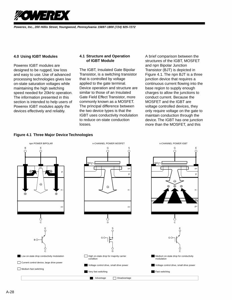
Powerex, Inc., 200 Hillis Street, Youngwood, Pennsylvania 15697-1800 (724) 925-7272 A-28 4.0 Using IGBT Modules Powerex IGBT modules are designed to be rugged, low loss and easy to use. Use of advanced processing technologies gives low on-state saturation voltages while maintaining the high switching speed needed for 20kHz operation. The information presented in this section is intended to help users of Powerex IGBT modules apply the devices effectively and reliably. 4.1 Structure and Operation of IGBT Module The IGBT, Insulated Gate Bipolar Transistor, is a switching transistor that is controlled by voltage applied to the gate terminal. Device operation and structure are similar to those of an Insulated Gate Field Effect Transistor, more commonly known as a MOSFET. The principal difference between the two device types is that the IGBT uses conductivity modulation to reduce on-state conduction losses. A brief comparison between the structures of the IGBT, MOSFET and npn Bipolar Junction Transistor (BJT) is depicted in Figure 4.1. The npn BJT is a three junction device that requires a continuous current flowing into the base region to supply enough charges to allow the junctions to conduct current. Because the MOSFET and the IGBT are voltage controlled devices, they only require voltage on the gate to maintain conduction through the device. The IGBT has one junction more than the MOSFET, and this B E n+ p n– n+ C S G p n– n+ D n+ SiO 2 E G p n– n+ C n+ SiO 2 p+ npn POWER BIPOLAR n-CHANNEL POWER MOSFET n-CHANNEL POWER IGBT E C B S D G E C G Low on-state drop conductivity modulation Current control device, large drive power Medium fast switching High on-state drop for majority carrier condition Voltage control drive, small drive power Very fast switching Medium on-state drop for conductivity modulation Voltage control drive, small drive power Fast switching Advantage Disadvantage Figure 4.1 Three Major Device Technologies
-
Upload
khangminh22 -
Category
Documents
-
view
0 -
download
0
Transcript of A-28 4.0 Using IGBT Modules Powerex IGBT modules ... - Galco
Powerex, Inc., 200 Hillis Street, Youngwood, Pennsylvania 15697-1800 (724) 925-7272
A-28
4.0 Using IGBT Modules
Powerex IGBT modules aredesigned to be rugged, low lossand easy to use. Use of advancedprocessing technologies gives lowon-state saturation voltages whilemaintaining the high switchingspeed needed for 20kHz operation.The information presented in thissection is intended to help users ofPowerex IGBT modules apply thedevices effectively and reliably.
4.1 Structure and Operationof IGBT Module
The IGBT, Insulated Gate BipolarTransistor, is a switching transistorthat is controlled by voltageapplied to the gate terminal.Device operation and structure aresimilar to those of an InsulatedGate Field Effect Transistor, morecommonly known as a MOSFET.The principal difference betweenthe two device types is that theIGBT uses conductivity modulationto reduce on-state conductionlosses.
A brief comparison between thestructures of the IGBT, MOSFETand npn Bipolar JunctionTransistor (BJT) is depicted inFigure 4.1. The npn BJT is a threejunction device that requires acontinuous current flowing into thebase region to supply enoughcharges to allow the junctions toconduct current. Because theMOSFET and the IGBT arevoltage controlled devices, theyonly require voltage on the gate tomaintain conduction through thedevice. The IGBT has one junctionmore than the MOSFET, and this
B E
n+
p
n–
n+
C
SG
p
n–
n+
D
n+
SiO2
EG
p
n–
n+
C
n+
SiO2
p+
npn POWER BIPOLAR n-CHANNEL POWER MOSFET n-CHANNEL POWER IGBT
E
C
B
S
D
G
E
C
G
Low on-state drop conductivity modulation
Current control device, large drive power
Medium fast switching
High on-state drop for majority carrier condition
Voltage control drive, small drive power
Very fast switching
Medium on-state drop for conductivity modulation
Voltage control drive, small drive power
Fast switching
Advantage Disadvantage
Figure 4.1 Three Major Device Technologies
Powerex, Inc., 200 Hillis Street, Youngwood, Pennsylvania 15697-1800 (724) 925-7272
A-29
junction allows higher blockingvoltage and conductivitymodulation, as described below,during conduction. This additionaljunction in the IGBT does limitswitching frequency however.
4.1.1 Silicon Structure
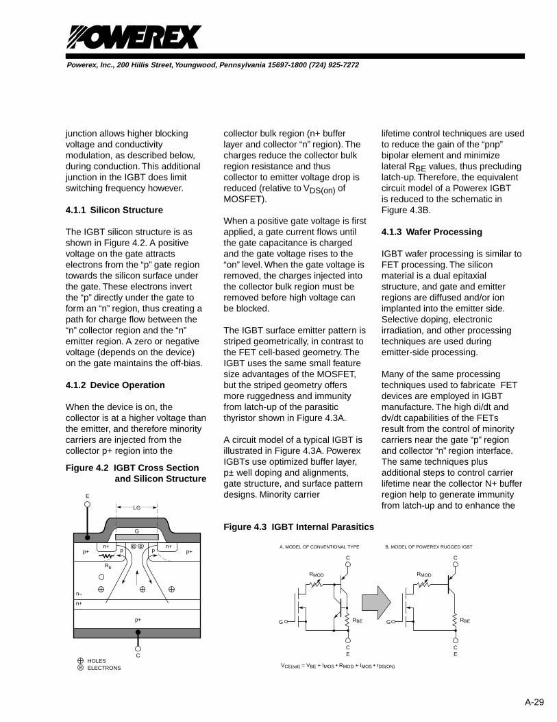
The IGBT silicon structure is asshown in Figure 4.2. A positivevoltage on the gate attractselectrons from the “p” gate regiontowards the silicon surface underthe gate. These electrons invertthe “p” directly under the gate toform an “n” region, thus creating apath for charge flow between the“n” collector region and the “n”emitter region. A zero or negativevoltage (depends on the device)on the gate maintains the off-bias.
4.1.2 Device Operation
When the device is on, thecollector is at a higher voltage thanthe emitter, and therefore minoritycarriers are injected from thecollector p+ region into the
collector bulk region (n+ bufferlayer and collector “n” region). Thecharges reduce the collector bulkregion resistance and thuscollector to emitter voltage drop isreduced (relative to VDS(on) ofMOSFET).
When a positive gate voltage is firstapplied, a gate current flows untilthe gate capacitance is chargedand the gate voltage rises to the“on” level. When the gate voltage isremoved, the charges injected intothe collector bulk region must beremoved before high voltage canbe blocked.
The IGBT surface emitter pattern isstriped geometrically, in contrast tothe FET cell-based geometry. TheIGBT uses the same small featuresize advantages of the MOSFET,but the striped geometry offersmore ruggedness and immunityfrom latch-up of the parasiticthyristor shown in Figure 4.3A.
A circuit model of a typical IGBT isillustrated in Figure 4.3A. PowerexIGBTs use optimized buffer layer,p± well doping and alignments,gate structure, and surface patterndesigns. Minority carrier
lifetime control techniques are usedto reduce the gain of the “pnp”bipolar element and minimizelateral RBE values, thus precludinglatch-up. Therefore, the equivalentcircuit model of a Powerex IGBTis reduced to the schematic inFigure 4.3B.
4.1.3 Wafer Processing
IGBT wafer processing is similar toFET processing. The siliconmaterial is a dual epitaxialstructure, and gate and emitterregions are diffused and/or ionimplanted into the emitter side.Selective doping, electronicirradiation, and other processingtechniques are used duringemitter-side processing.
Many of the same processingtechniques used to fabricate FETdevices are employed in IGBTmanufacture. The high di/dt anddv/dt capabilities of the FETsresult from the control of minoritycarriers near the gate “p” regionand collector “n” region interface.The same techniques plusadditional steps to control carrierlifetime near the collector N+ bufferregion help to generate immunityfrom latch-up and to enhance the
n+
p+
E
p+p+n+ n+
p pe
G
LG
n–
CHOLES
Rb
e
e ELECTRONS
Figure 4.2 IGBT Cross Sectionand Silicon Structure
RMOD
C
CE
G RBE
RMOD
C
CE
G RBE
A. MODEL OF CONVENTIONAL TYPE B. MODEL OF POWEREX RUGGED IGBT
VCE(sat) = VBE + IMOS • RMOD + IMOS • rDS(ON)
Figure 4.3 IGBT Internal Parasitics
Powerex, Inc., 200 Hillis Street, Youngwood, Pennsylvania 15697-1800 (724) 925-7272
A-30
switching ruggedness of PowerexIGBTs. Ultra clean facilities andin-line wafer testing promoteconsistent processing, thusensuring chips of the highestquality and reliability.
4.1.4 Module PackagingConstruction and Layout
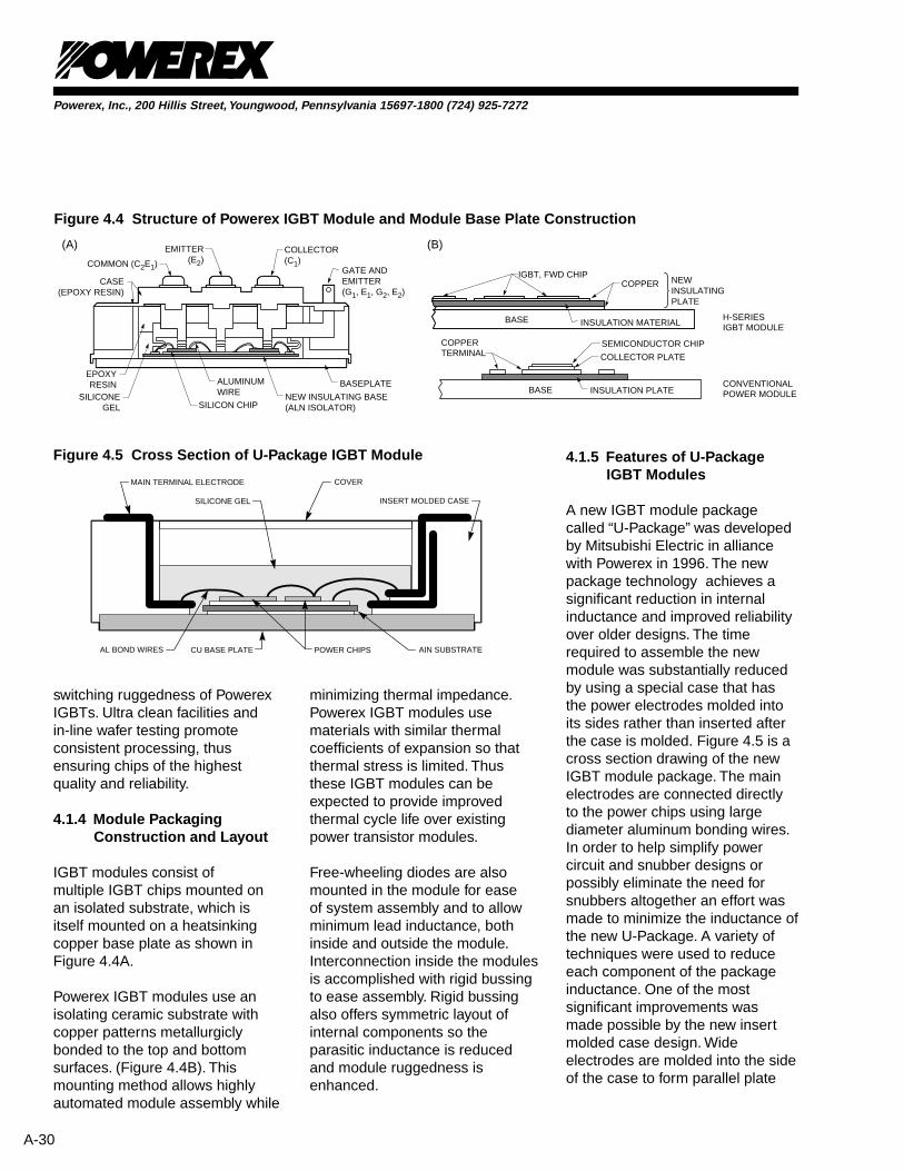
IGBT modules consist ofmultiple IGBT chips mounted onan isolated substrate, which isitself mounted on a heatsinkingcopper base plate as shown inFigure 4.4A.
Powerex IGBT modules use anisolating ceramic substrate withcopper patterns metallurgiclybonded to the top and bottomsurfaces. (Figure 4.4B). Thismounting method allows highlyautomated module assembly while
minimizing thermal impedance.Powerex IGBT modules usematerials with similar thermalcoefficients of expansion so thatthermal stress is limited. Thusthese IGBT modules can beexpected to provide improvedthermal cycle life over existingpower transistor modules.
Free-wheeling diodes are alsomounted in the module for easeof system assembly and to allowminimum lead inductance, bothinside and outside the module.Interconnection inside the modulesis accomplished with rigid bussingto ease assembly. Rigid bussingalso offers symmetric layout ofinternal components so theparasitic inductance is reducedand module ruggedness isenhanced.
4.1.5 Features of U-PackageIGBT Modules
A new IGBT module packagecalled “U-Package” was developedby Mitsubishi Electric in alliancewith Powerex in 1996. The newpackage technology achieves asignificant reduction in internalinductance and improved reliabilityover older designs. The timerequired to assemble the newmodule was substantially reducedby using a special case that hasthe power electrodes molded intoits sides rather than inserted afterthe case is molded. Figure 4.5 is across section drawing of the newIGBT module package. The mainelectrodes are connected directlyto the power chips using largediameter aluminum bonding wires.In order to help simplify powercircuit and snubber designs orpossibly eliminate the need forsnubbers altogether an effort wasmade to minimize the inductance ofthe new U-Package. A variety oftechniques were used to reduceeach component of the packageinductance. One of the mostsignificant improvements wasmade possible by the new insertmolded case design. Wideelectrodes are molded into the sideof the case to form parallel plate
Figure 4.5 Cross Section of U-Package IGBT Module
MAIN TERMINAL ELECTRODE
SILICONE GEL
COVER
INSERT MOLDED CASE
AIN SUBSTRATEPOWER CHIPSCU BASE PLATEAL BOND WIRES
CASE(EPOXY RESIN)
COMMON (C2E1)
EMITTER(E2)
COLLECTOR(C1)
GATE ANDEMITTER(G1, E1, G2, E2)
EPOXYRESIN
SILICONEGEL
ALUMINUMWIRE
SILICON CHIPNEW INSULATING BASE(ALN ISOLATOR)
BASEPLATE
BASE
IGBT, FWD CHIPNEWINSULATING PLATE
INSULATION MATERIAL
COPPER
BASE
COLLECTOR PLATE
INSULATION PLATE
COPPERTERMINAL
SEMICONDUCTOR CHIP
(A) (B)
H-SERIESIGBT MODULE
CONVENTIONALPOWER MODULE
Figure 4.4 Structure of Powerex IGBT Module and Module Base Plate Construction
Powerex, Inc., 200 Hillis Street, Youngwood, Pennsylvania 15697-1800 (724) 925-7272
A-31
structures that have considerablyless inductance than conventionalelectrodes. In addition, the strainrelieving “S” bends that wereneeded in the electrodes ofconventional modules are notneeded in the U-Package becausethe aluminum bond wires performthe strain relieving function.Elimination of these “S” bendshelped to further reduce theelectrode inductance. Overall, as aresult of these inductance reducingfeatures the U-Package modulestypically have about one third theinductance of conventionalmodules. A further reduction inassembly time was achieved byreducing the number of solderingsteps during manufacturing. With
the conventional module the chip tosubstrate and substrate to baseplate soldering is done first withhigh temperature solder. Then thecase is attached to the base plateand a second low temperaturesoldering step is used to connectthe power electrodes. In the newmodule the second step is notneeded because the connectionsto the power electrodes are madeusing the aluminum bond wires.The soldering temperature of thechip and substrate attachment canbe reduced. The lower solderingtemperature minimizes the effectsof the mismatched coefficients ofexpansion between the base plateand the AlN DBC substrate. Theresult is a reduction in thermal
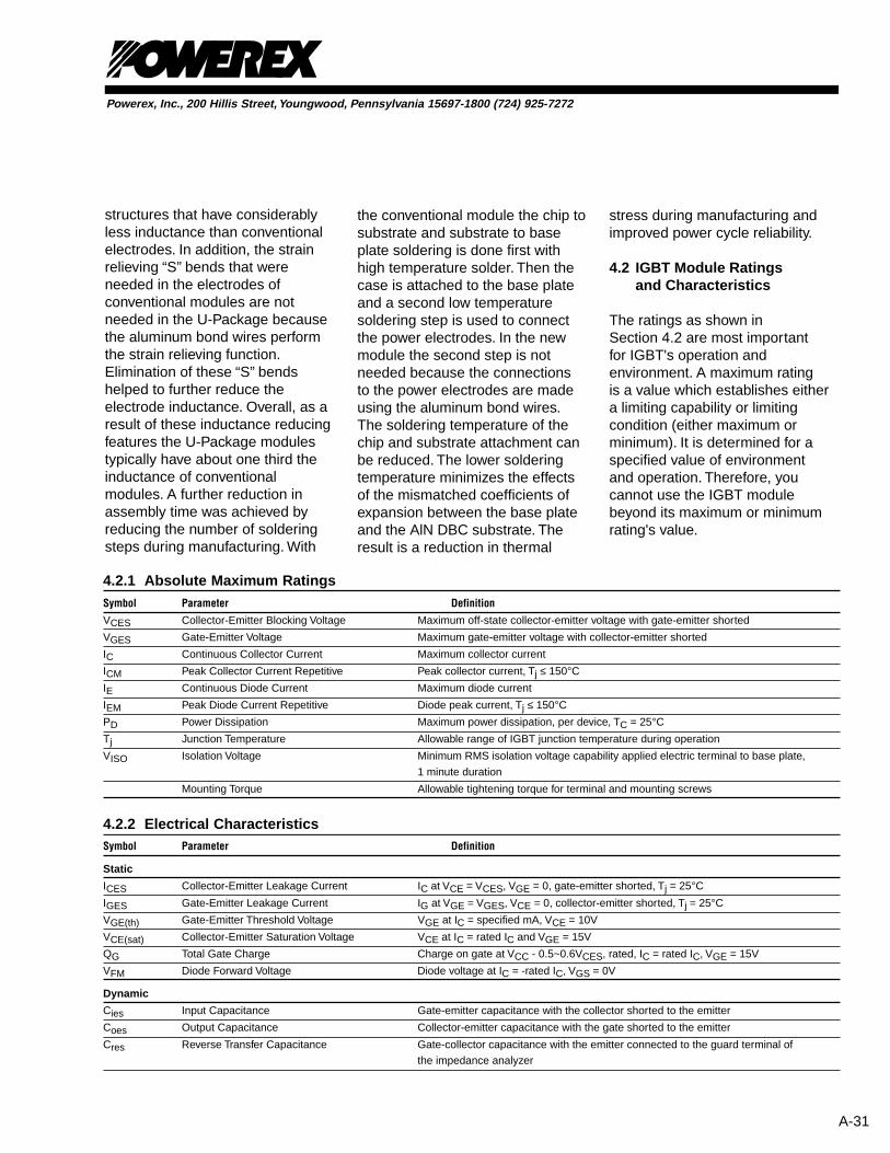
4.2.1 Absolute Maximum RatingsSymbol Parameter Definition
VCES Collector-Emitter Blocking Voltage Maximum off-state collector-emitter voltage with gate-emitter shorted
VGES Gate-Emitter Voltage Maximum gate-emitter voltage with collector-emitter shorted
IC Continuous Collector Current Maximum collector current
ICM Peak Collector Current Repetitive Peak collector current, Tj ≤ 150°CIE Continuous Diode Current Maximum diode current
IEM Peak Diode Current Repetitive Diode peak current, Tj ≤ 150°CPD Power Dissipation Maximum power dissipation, per device, TC = 25°CTj Junction Temperature Allowable range of IGBT junction temperature during operation
VISO Isolation Voltage Minimum RMS isolation voltage capability applied electric terminal to base plate,
1 minute duration
Mounting Torque Allowable tightening torque for terminal and mounting screws
4.2.2 Electrical CharacteristicsSymbol Parameter Definition
Static
ICES Collector-Emitter Leakage Current IC at VCE = VCES, VGE = 0, gate-emitter shorted, Tj = 25°CIGES Gate-Emitter Leakage Current IG at VGE = VGES, VCE = 0, collector-emitter shorted, Tj = 25°CVGE(th) Gate-Emitter Threshold Voltage VGE at IC = specified mA, VCE = 10V
VCE(sat) Collector-Emitter Saturation Voltage VCE at IC = rated IC and VGE = 15V
QG Total Gate Charge Charge on gate at VCC - 0.5~0.6VCES, rated, IC = rated IC, VGE = 15V
VFM Diode Forward Voltage Diode voltage at IC = -rated IC, VGS = 0V
Dynamic
Cies Input Capacitance Gate-emitter capacitance with the collector shorted to the emitter
Coes Output Capacitance Collector-emitter capacitance with the gate shorted to the emitter
Cres Reverse Transfer Capacitance Gate-collector capacitance with the emitter connected to the guard terminal of
the impedance analyzer
stress during manufacturing andimproved power cycle reliability.
4.2 IGBT Module Ratingsand Characteristics
The ratings as shown inSection 4.2 are most importantfor IGBT's operation andenvironment. A maximum ratingis a value which establishes eithera limiting capability or limitingcondition (either maximum orminimum). It is determined for aspecified value of environmentand operation. Therefore, youcannot use the IGBT modulebeyond its maximum or minimumrating's value.

Powerex, Inc., 200 Hillis Street, Youngwood, Pennsylvania 15697-1800 (724) 925-7272
A-32
4.2.4 Test Circuits andConditions
The following test circuits are usedto evaluate IGBT characteristics.
1. VCE(SAT) and VECTo ensure specified junctiontemperature, Tj,measurements of VCE (SAT)and VEC must be performed
VCC
CURRENTMONITOR
L
D.U.T.
Irr
t
IC
t
IF
IF
Irr
trr
IF
0.5 IrrQrr = 1/2 Irr trr
E
C
V ICVCE
RG
E
C
V IC
Figure 4.6 Reverse Recovery Measurement Circuit and Waveform Figure 4.7 VCE (SAT) Test
Figure 4.8 VCE Test
Figure 4.9 Resistive LoadSwitching Test Circuit
4.2.2 Electrical Characteristics (Continued)Symbol Parameter Definition
Dynamic (Continued)
Itd(on) Turn-on Delay Time Time from VGE = 0V to IC = 10% of final value
tr Rise Time Time from IC = 10% of final value to IC = 90% of final value
td(off) Turn-off Delay Time Time from VGE = 90% of initial value to IC = 90% of initial value
tf Fall Time Time from IC = 90% of initial value to IC = 10% of initial value
trr Diode Reverse Recovery Time Time from IC = 0A to projection of zero IC from Irr and 0.5 Irr points with
IC = -rated IC and at specified di/dt (Refer to Figure 4.6)
Qrr Diode Reverse Recovery Charge Area under Irr curve from IC = 0A to projection of zero IC from Irr and
0.5x Irr points with IC = rated IC and at specified di/dt (Refer to Figure 4.6)
4.2.3 Thermal Characteristics
Symbol Parameter Definition
Rth(j-c) Thermal Resistance, Junction to Case (Tj - TC)/(IC-X VCE), IC conducting to establish thermal equilibrium
Rth(c-f) Thermal Resistance, Case to fin (TC - Tf)/(IC X VCE), IC conducting to establish thermal equilibrium lubricated
as low duty factor pulsed tests.(See Figures 4.7 and 4.8)
2. Resistive Load Switching TestCircuit. (See Figure 4.9)
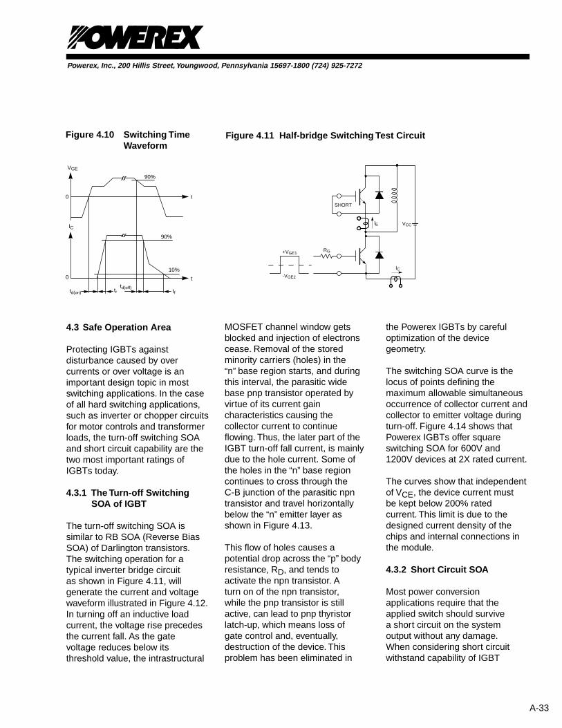
3. Half-Bridge Switching TestCircuit (See Figure 4.10)
+VGE1
-VGE2
RG
lC
RLOAD
VCC
Powerex, Inc., 200 Hillis Street, Youngwood, Pennsylvania 15697-1800 (724) 925-7272
A-33
4.3 Safe Operation Area
Protecting IGBTs againstdisturbance caused by overcurrents or over voltage is animportant design topic in mostswitching applications. In the caseof all hard switching applications,such as inverter or chopper circuitsfor motor controls and transformerloads, the turn-off switching SOAand short circuit capability are thetwo most important ratings ofIGBTs today.
4.3.1 The Turn-off SwitchingSOA of IGBT
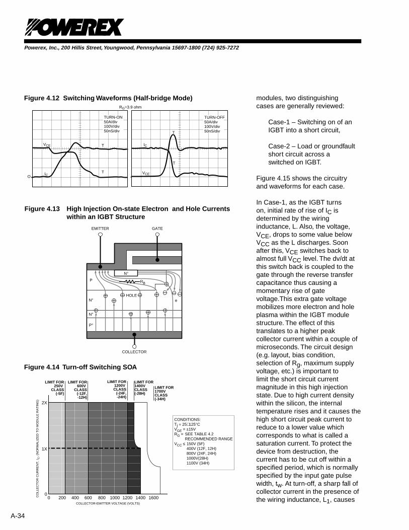
The turn-off switching SOA issimilar to RB SOA (Reverse BiasSOA) of Darlington transistors.The switching operation for atypical inverter bridge circuitas shown in Figure 4.11, willgenerate the current and voltagewaveform illustrated in Figure 4.12.In turning off an inductive loadcurrent, the voltage rise precedesthe current fall. As the gatevoltage reduces below itsthreshold value, the intrastructural
MOSFET channel window getsblocked and injection of electronscease. Removal of the storedminority carriers (holes) in the“n” base region starts, and duringthis interval, the parasitic widebase pnp transistor operated byvirtue of its current gaincharacteristics causing thecollector current to continueflowing. Thus, the later part of theIGBT turn-off fall current, is mainlydue to the hole current. Some ofthe holes in the “n” base regioncontinues to cross through theC-B junction of the parasitic npntransistor and travel horizontallybelow the “n” emitter layer asshown in Figure 4.13.
This flow of holes causes apotential drop across the “p” bodyresistance, RD, and tends toactivate the npn transistor. Aturn on of the npn transistor,while the pnp transistor is stillactive, can lead to pnp thyristorlatch-up, which means loss ofgate control and, eventually,destruction of the device. Thisproblem has been eliminated in
the Powerex IGBTs by carefuloptimization of the devicegeometry.
The switching SOA curve is thelocus of points defining themaximum allowable simultaneousoccurrence of collector current andcollector to emitter voltage duringturn-off. Figure 4.14 shows thatPowerex IGBTs offer squareswitching SOA for 600V and1200V devices at 2X rated current.
The curves show that independentof VCE, the device current mustbe kept below 200% ratedcurrent. This limit is due to thedesigned current density of thechips and internal connections inthe module.
4.3.2 Short Circuit SOA
Most power conversionapplications require that theapplied switch should survivea short circuit on the systemoutput without any damage.When considering short circuitwithstand capability of IGBT
VGE
0
lC
0
90%
90%
10%
t
t
td(on) trtd(off)
tf
Figure 4.10 Switching TimeWaveform
+VGE1
-VGE2
RG
VCClE
lC
SHORT
Figure 4.11 Half-bridge Switching Test Circuit
Powerex, Inc., 200 Hillis Street, Youngwood, Pennsylvania 15697-1800 (724) 925-7272
A-34
modules, two distinguishingcases are generally reviewed:
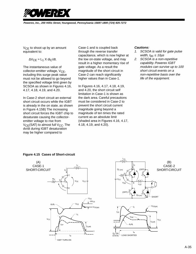
Case-1 – Switching on of anIGBT into a short circuit,
Case-2 – Load or groundfaultshort circuit across aswitched on IGBT.
Figure 4.15 shows the circuitryand waveforms for each case.
In Case-1, as the IGBT turnson, initial rate of rise of IC isdetermined by the wiringinductance, L. Also, the voltage,VCE, drops to some value belowVCC as the L discharges. Soonafter this, VCE switches back toalmost full VCC level. The dv/dt atthis switch back is coupled to thegate through the reverse transfercapacitance thus causing amomentary rise of gatevoltage.This extra gate voltagemobilizes more electron and holeplasma within the IGBT modulestructure. The effect of thistranslates to a higher peakcollector current within a couple ofmicroseconds. The circuit design(e.g. layout, bias condition,selection of Rg, maximum supplyvoltage, etc.) is important tolimit the short circuit currentmagnitude in this high injectionstate. Due to high current densitywithin the silicon, the internaltemperature rises and it causes thehigh short circuit peak current toreduce to a lower value whichcorresponds to what is called asaturation current. To protect thedevice from destruction, thecurrent has to be cut off within aspecified period, which is normallyspecified by the input gate pulsewidth, tw. At turn-off, a sharp fall ofcollector current in the presence ofthe wiring inductance, L1, causes
Figure 4.12 Switching Waveforms (Half-bridge Mode)
TURN-ON50A/div100V/div50nS/div
TVCE IC
VCEICO
RG=3.9 ohm
T
T
T
TURN-OFF50A/div100V/div50nS/div
EMITTER GATE
COLLECTOR
RB
HOLEN°
N°
P°
P
e
N°
Figure 4.14 Turn-off Switching SOA
COLLECTOR-EMITTER VOLTAGE (VOLTS)
0 200 400 600 800 1000 CO
LLE
CT
OR
CU
RR
EN
T, I
C, (
NO
RM
ALI
ZE
D T
O M
OD
ULE
RA
TIN
G)
1X
01400
LIMIT FOR600V
CLASS(-12F, -12H)
LIMIT FOR250V
CLASS(-5F)
CONDITIONS:Tj = 25∼ 125°CVGE = ±15V RG =
VCC ≤
2X
1200
LIMIT FOR1200V CLASS
(-24F, -24H)
LIMIT FOR1700V CLASS(-34H)
SEE TABLE 4.2RECOMMENDED RANGE150V (5F)400V (12F, 12H)800V (24F, 24H)1000V(28H)1100V (34H)
1600
LIMIT FOR1400V CLASS(-28H)
Figure 4.13 High Injection On-state Electron and Hole Currentswithin an IGBT Structure
Powerex, Inc., 200 Hillis Street, Youngwood, Pennsylvania 15697-1800 (724) 925-7272
A-35
VCE to shoot up by an amountequivalent to:
∆VCE ≈ L1 X diC/dt.
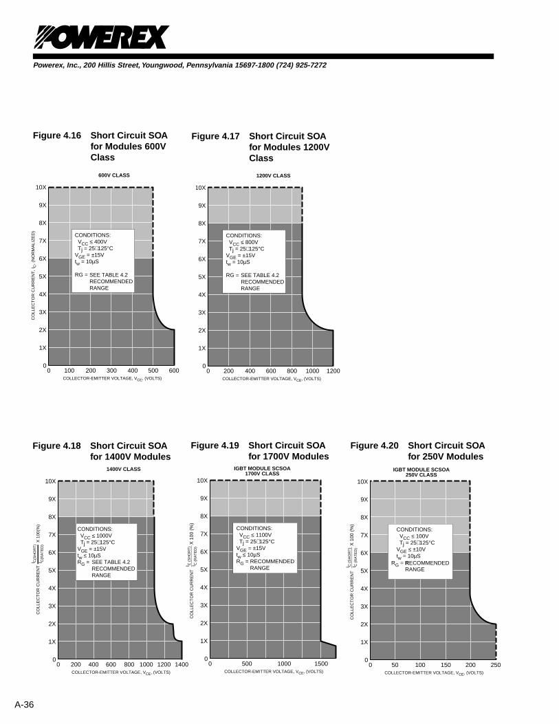
The instantaneous value ofcollector-emitter voltage, VCE,including this surge peak valuemust not be allowed to go beyondthe specified voltage limit given bySCSOA as shown in Figures 4.16,4.17, 4.18, 4.19, and 4.20.
In Case-2 short circuit an externalshort circuit occurs while the IGBTis already in the on state. as shownin Figure 4.15B) The increasingshort circuit forces the IGBT chip todesaturate causing the collector-emitter voltage to rise fromVCE(SAT) to almost full VCC. Thedv/dt during IGBT desaturationmay be higher compared to
Case-1 and is coupled backthrough the reverse transfercapacitance, which is now higher atthe low on-state voltage, and mayresult in a higher momentary rise ofgate voltage. As a result themagnitude of the short circuit inCase-2 can reach significantlyhigher values than in Case-1.
In Figures 4.16, 4.17, 4.18, 4.19,and 4.20, the short circuit selflimitation in Case-1 is shown asthe dark area. Careful precautionsmust be considered in Case-2 toprevent the short circuit currentmagnitude going beyond amagnitude of ten times the ratedcurrent as an absolute limit(shaded area in Figures 4.16, 4.17,4.18, 4.19, and 4.20).
Cautions:1. SCSOA is valid for gate pulse
width, tW, ≤ 10µs2. SCSOA is a non-repetitive
capability. Powerex IGBTmodules can survive up to 100short circuit events on anon-repetitive basis over thelife of the equipment.
Figure 4.15 Cases of Short-circuit
lC
VCC
RG
LI
VCE
C
E
G
VCC
VCE
VCE(pk)
VCE
IC
ICP
IGBT TURN-ON
tw
IC(off)
t
dv/dt
lC
Q1 (on)
L11
C
E
G
VCC
VGE
(OFF)
Q4 (on)SHORT
L12
(OFF)
VCC
IC
ICP
LOAD SHORTED
tw
IC(off)
VGE
VCE(pk)
dv/dt
Q1 ONSTATE
∆VCE
(A)CASE-1
SHORT-CIRCUIT
(B)CASE-2
SHORT-CIRCUIT
Powerex, Inc., 200 Hillis Street, Youngwood, Pennsylvania 15697-1800 (724) 925-7272
A-36
COLLECTOR-EMITTER VOLTAGE, VCE, (VOLTS)
0 100 200 300 400 500
CO
LLE
CT
OR
CU
RR
EN
T, I
C, (
NO
RM
ALI
ZE
D)
10X
9X
8X
7X
6X
5X
4X
3X
2X
1X
0600
600V CLASS
CONDITIONS: VCC ≤ 400V Tj = 25∼ 125°CVGE = ±15V tw = 10µS
RG = SEE TABLE 4.2RECOMMENDEDRANGE
Figure 4.16 Short Circuit SOAfor Modules 600VClass
COLLECTOR-EMITTER VOLTAGE, VCE, (VOLTS)
0 200 400 600 800 1000
10X
9X
8X
7X
6X
5X
4X
3X
2X
1X
01200
1200V CLASS
CONDITIONS: VCC ≤ 800V Tj = 25∼ 125°CVGE = ±15V tw = 10µS
RG = SEE TABLE 4.2RECOMMENDEDRANGE
Figure 4.17 Short Circuit SOAfor Modules 1200VClass
COLLECTOR-EMITTER VOLTAGE, VCE, (VOLTS)
0 200 400 600 800 1000
CO
LLE
CT
OR
CU
RR
EN
T
X
100
(%)
10X
9X
8X
7X
6X
5X
4X
3X
2X
1X
01200 1400
1400V CLASS
CONDITIONS: VCC ≤ 1000V Tj = 25∼ 125°CVGE = ±15V tw ≤ 10µSRG = SEE TABLE 4.2
RECOMMENDEDRANGE
I C(S
HO
RT
)
I C(R
AT
ED
)
Figure 4.18 Short Circuit SOAfor 1400V Modules
Figure 4.19 Short Circuit SOAfor 1700V Modules
COLLECTOR-EMITTER VOLTAGE, VCE, (VOLTS)
0 500 1000 1500
CO
LLE
CT
OR
CU
RR
EN
T
X 1
00 (
%)
10X
9X
8X
7X
6X
5X
4X
3X
2X
1X
0
IGBT MODULE SCSOA1700V CLASS
I C (
SH
OR
T)
I C (
RA
TE
D)
CONDITIONS: VCC ≤ 1100V Tj = 25∼ 125°CVGE = ±15V tw ≤ 10µSRG = RECOMMENDED
RANGE
CO
LLE
CT
OR
CU
RR
EN
T
X 1
00 (
%)
IGBT MODULE SCSOA250V CLASS
I C (
SH
OR
T)
I C (
RA
TE
D)
COLLECTOR-EMITTER VOLTAGE, VCE, (VOLTS)
0 50 100 150 200
10X
9X
8X
7X
6X
5X
4X
3X
2X
1X
0250
CONDITIONS: VCC ≤ 100V Tj = 25∼ 125°CVGE ≤ ±10V tw = 10µS
RECOMMENDEDRANGE
RG = R
Figure 4.20 Short Circuit SOAfor 250V Modules
Powerex, Inc., 200 Hillis Street, Youngwood, Pennsylvania 15697-1800 (724) 925-7272
A-37
During a short circuit, the highcurrent from the current mirroractivates the RTC which reducesthe gate driving voltage on theIGBT, thereby clamping the shortcircuit current to a safe level. TheRTC circuit restores the shortwithstanding capability of theF-Series IGBT module.
4.4 Performance Curves
The characteristic curves showtypical electrical characteristics andmaximum transient thermalimpedance characteristics of theIGBT and FWDi.
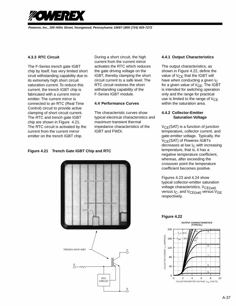
Figure 4.21 Trench Gate IGBT Chip and RTC
GATEGATE
CURRENT MIRROR EMITTEROR EMITTERCURRENT MIRROR EMITTER
MAIN EMITTER AREAMAIN EMITTER AREAMAIN EMITTER AREA
E
C
G
RTCCIRCUIT
TRENCH GATE IGBT
4.3.3 RTC Circuit
The F-Series trench gate IGBTchip by itself, has very limited shortciruit withstanding capability due toits extremely high short circuitsaturation current. To reduce thiscurrent, the trench IGBT chip isfabricated with a current mirroremitter. The current mirror isconnected to an RTC (Real TimeControl) circuit to provide activeclamping of short circuit current.The RTC and trench gate IGBTchip are shown in Figure 4.21.The RTC circuit is activated by thecurrent from the current mirroremitter on the trench IGBT chip.
4.4.1 Output Characteristics
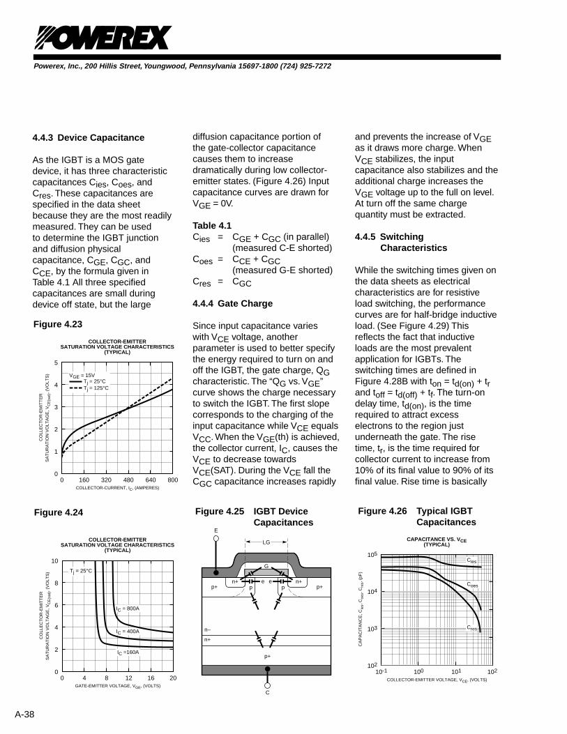
The output characteristics, asshown in Figure 4.22, define thevalue of VCE that the IGBT willhave when conducting a given ICfor a given value of VGE. The IGBTis intended for switching operationonly and the range for practicaluse is limited to the range of VCEwithin the saturation area.
4.4.2 Collector-Emitter Saturation Voltage
VCE(SAT) is a function of junctiontemperature, collector current, andgate-emitter voltage. Typically, theVCE(SAT) of Powerex IGBTsdecreases at low IC with increasingtemperature, that is, it has anegative temperature coefficient,whereas, after exceeding thecrossover point the temperaturecoefficient becomes positive.
Figures 4.23 and 4.24 showtypical collector-emitter saturationvoltage characteristics, VCE(sat)versus IC, and VCE(sat) versus VGErespectively.
COLLECTOR-EMITTER VOLTAGE, VCE, (VOLTS)
CO
LLE
CT
OR
CU
RR
EN
T, I
C, (
AM
PE
RE
S)
OUTPUT CHARACTERISTICS(TYPICAL)
200
0 2 4 6 8 10
160
120
80
40
0
Tj = 25°C
12
10 9
7
6
5
8
15VGE = 20V
Figure 4.22
Powerex, Inc., 200 Hillis Street, Youngwood, Pennsylvania 15697-1800 (724) 925-7272
A-38
COLLECTOR-CURRENT, IC, (AMPERES)
CO
LLE
CT
OR
-EM
ITT
ER
SA
TU
RA
TIO
N V
OLT
AG
E, V
CE
(sat
), (V
OLT
S)
COLLECTOR-EMITTERSATURATION VOLTAGE CHARACTERISTICS
(TYPICAL)
5
0 160 320 480 640 800
4
3
2
1
0
VGE = 15VTj = 25°CTj = 125°C
GATE-EMITTER VOLTAGE, VGE, (VOLTS)
CO
LLE
CT
OR
-EM
ITT
ER
SA
TU
RA
TIO
N V
OLT
AG
E, V
CE
(sat
), (V
OLT
S)
COLLECTOR-EMITTERSATURATION VOLTAGE CHARACTERISTICS
(TYPICAL)
10
0 4 8 12 16 20
8
6
4
2
0
Tj = 25°C
IC =160A
IC = 800A
IC = 400A
Figure 4.23
Figure 4.24
diffusion capacitance portion ofthe gate-collector capacitancecauses them to increasedramatically during low collector-emitter states. (Figure 4.26) Inputcapacitance curves are drawn forVGE = 0V.
Table 4.1Cies = CGE + CGC (in parallel)
(measured C-E shorted)Coes = CCE + CGC
(measured G-E shorted)Cres = CGC
4.4.4 Gate Charge
Since input capacitance varieswith VCE voltage, anotherparameter is used to better specifythe energy required to turn on andoff the IGBT, the gate charge, QGcharacteristic. The “QG vs. VGE”curve shows the charge necessaryto switch the IGBT. The first slopecorresponds to the charging of theinput capacitance while VCE equalsVCC. When the VGE(th) is achieved,the collector current, IC, causes theVCE to decrease towardsVCE(SAT). During the VCE fall theCGC capacitance increases rapidly
RB
n+
p+
E
p+p+n+ n+
p pe e
G
LG
n–
C
Figure 4.25 IGBT DeviceCapacitances
COLLECTOR-EMITTER VOLTAGE, VCE, (VOLTS)
CA
PA
CIT
AN
CE
, Cie
s, C
oes,
Cre
s, (
pF)
CAPACITANCE VS. VCE(TYPICAL)
10-1 100 102
105
104
103
102101
Cies
Coes
Cres
Figure 4.26 Typical IGBTCapacitances
4.4.3 Device Capacitance
As the IGBT is a MOS gatedevice, it has three characteristiccapacitances Cies, Coes, andCres. These capacitances arespecified in the data sheetbecause they are the most readilymeasured. They can be usedto determine the IGBT junctionand diffusion physicalcapacitance, CGE, CGC, andCCE, by the formula given inTable 4.1 All three specifiedcapacitances are small duringdevice off state, but the large
and prevents the increase of VGEas it draws more charge. WhenVCE stabilizes, the inputcapacitance also stabilizes and theadditional charge increases theVGE voltage up to the full on level.At turn off the same chargequantity must be extracted.
4.4.5 SwitchingCharacteristics
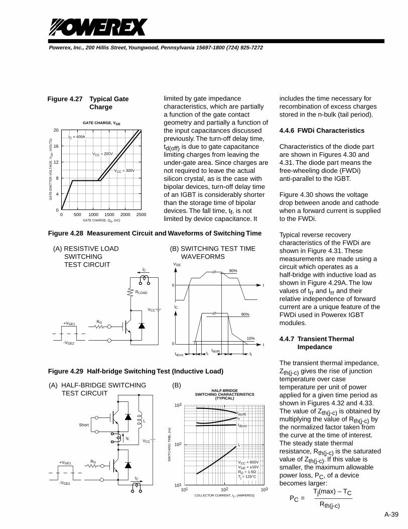
While the switching times given onthe data sheets as electricalcharacteristics are for resistiveload switching, the performancecurves are for half-bridge inductiveload. (See Figure 4.29) Thisreflects the fact that inductiveloads are the most prevalentapplication for IGBTs. Theswitching times are defined inFigure 4.28B with ton = td(on) + trand toff = td(off) + tf. The turn-ondelay time, td(on), is the timerequired to attract excesselectrons to the region justunderneath the gate. The risetime, tr, is the time required forcollector current to increase from10% of its final value to 90% of itsfinal value. Rise time is basically
Powerex, Inc., 200 Hillis Street, Youngwood, Pennsylvania 15697-1800 (724) 925-7272
A-39
limited by gate impedancecharacteristics, which are partiallya function of the gate contactgeometry and partially a function ofthe input capacitances discussedpreviously. The turn-off delay time,td(off) is due to gate capacitancelimiting charges from leaving theunder-gate area. Since charges arenot required to leave the actualsilicon crystal, as is the case withbipolar devices, turn-off delay timeof an IGBT is considerably shorterthan the storage time of bipolardevices. The fall time, tf, is notlimited by device capacitance. It
Figure 4.28 Measurement Circuit and Waveforms of Switching Time
Figure 4.29 Half-bridge Switching Test (Inductive Load)
+VGE1
-VGE2
RG
VCClE
lC
LShort
COLLECTOR CURRENT, IC, (AMPERES)
SW
ITC
HIN
G T
IME
, (ns
)
HALF-BRIDGESWITCHING CHARACTERISTICS
(TYPICAL)
103
101 102 103
102
101
td(off)tf
td(on)
tr
VCC = 600VVGE = ±15VRG = 1.6ΩTj = 125°C
(A) HALF-BRIDGE SWITCHING TEST CIRCUIT
(B)
GATE CHARGE, QG, (nC)
GA
TE
-EM
ITT
ER
VO
LTA
GE
, VG
E, (
VO
LTS
)
GATE CHARGE, VGE
20
0 500 1000 1500 2000 2500
16
12
8
4
0
IC = 400A
VCC = 300V
VCC = 200V
Figure 4.27 Typical GateCharge
+VGE1
-VGE2
RG
lC
RLOAD
VCC
VGE
0
lC
0
90%
90%
10%
t
t
td(on) trtd(off)
tf
(A) RESISTIVE LOAD SWITCHING TEST CIRCUIT
(B) SWITCHING TEST TIME WAVEFORMS
includes the time necessary forrecombination of excess chargesstored in the n-bulk (tail period).
4.4.6 FWDi Characteristics
Characteristics of the diode partare shown in Figures 4.30 and4.31. The diode part means thefree-wheeling diode (FWDi)anti-parallel to the IGBT.
Figure 4.30 shows the voltagedrop between anode and cathodewhen a forward current is suppliedto the FWDi.
Typical reverse recoverycharacteristics of the FWDi areshown in Figure 4.31. Thesemeasurements are made using acircuit which operates as ahalf-bridge with inductive load asshown in Figure 4.29A. The lowvalues of trr and Irr and theirrelative independence of forwardcurrent are a unique feature of theFWDi used in Powerex IGBTmodules.
4.4.7 Transient ThermalImpedance
The transient thermal impedance,Zth(j-c) gives the rise of junctiontemperature over casetemperature per unit of powerapplied for a given time period asshown in Figures 4.32 and 4.33.The value of Zth(j-c) is obtained bymultiplying the value of Rth(j-c) bythe normalized factor taken fromthe curve at the time of interest.The steady state thermalresistance, Rth(j-c) is the saturatedvalue of Zth(j-c). If this value issmaller, the maximum allowablepower loss, PC, of a devicebecomes larger:
Tj(max) – TCPC =
Rth(j-c)
Powerex, Inc., 200 Hillis Street, Youngwood, Pennsylvania 15697-1800 (724) 925-7272
A-40
4.4.8 Switching EnergyCharacteristics
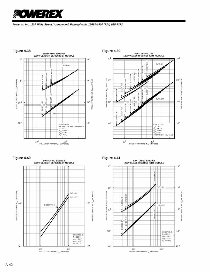
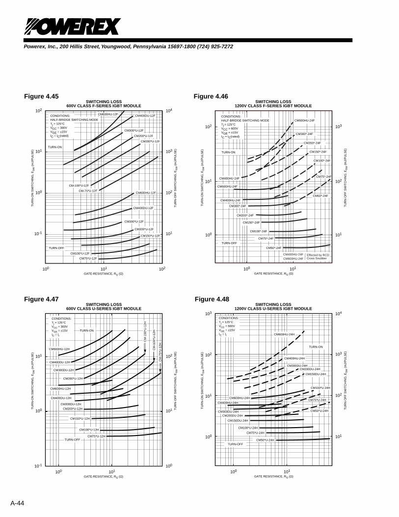
Switching energy curves areprovided in order to simplifyestimation of switching losses.Use of these curves is describedin more detail in Section 3.4.1 ofthis application data. Figures 4.34through 4.44 show turn-on andturn-off switching energy as afunction of collector current forPowerex 250V, 600V, 1200V,1700V H-Series and U-Series andF-Series IGBT modules. Figures4.45 and 4.48 show switching lossversus series gate resistance for U-Series and F-Series IGBTmodules.
4.5 IGBT Selection
Proper selection of an IGBTinvolves two key points. Both arerelated to keeping the IGBTwithin its maximum ratings duringoperation. The first criterion is thatthe peak collector current duringoperation including any requiredoverload current must be within theSWSOA (this means < 2 x Irated or2 x nameplate current). Thesuggested IGBT selections inSections 2.3, 2.4, and 2.5 arebased on a 200% overloadrequirement and allow 20% forripple current factors indetermining the peak IGBT current
requirement for the inverter. Thesecond criterion is that the IGBToperating junction temperaturemust always be kept below Tj(max)(150°C) in all normal operationincluding expected motor overload.Power dissipation and thermaldesign considerations arediscussed in detail in Section 3.4.Modules selected for listing inSections 2.3, 2.4, and 2.5 willmeet these requirements withnormal environmental andheatsink considerations. It maybe possible (or required) to use alower (higher) current rated ifmore (or less) efficient coolingis employed.
4.6 IGBT Module Gate Drive
IGBTs require gate voltage toestablish collector to emitterconduction. This gate voltage canbe applied by a variety of drivecircuits. The parameters to beconsidered in selecting a drivecircuit include device off biasingrequirements, gate chargerequirements, ruggednessrequirements and power supplyavailability.
A recommended drive circuitincludes substantial on biasingand off biasing. Such a circuit isshown in Figure 4.49. The IGBTgate-emitter impedance is largeenough that turn-on can beaccomplished with MOSFET drivetechniques, but as the IGBT inputcapacitance is larger than for aMOSFET the IGBT turn-off biasshould be stronger than manyMOSFET drives offer.
TIME, (s)
NO
RM
ALI
ZE
D T
RA
NS
IEN
T T
HE
RM
AL
IMP
ED
AN
CE
, Zth
(j-c
)Z
th =
Rth
• (
NO
RM
ALI
ZE
D V
ALU
E)
TRANSIENT THERMALIMPEDANCE CHARACTERISTICS
(IGBT)
101
10-5 10-4 10-3
100
10-1
10-2
10-3
10-3 10-2 10-1 100 101
Single PulseTC = 25°CPer Unit Base = Rth(j-c) = 0.08°C/W
10-1
10-2
10-3
TIME, (s)
NO
RM
ALI
ZE
D T
RA
NS
IEN
T T
HE
RM
AL
IMP
ED
AN
CE
, Zth
(j-c
)Z
th =
Rth
• (
NO
RM
ALI
ZE
D V
ALU
E)
TRANSIENT THERMALIMPEDANCE CHARACTERISTICS
(FWDi)
101
10-5 10-4 10-3
100
10-1
10-2
10-3
10-3 10-2 10-1 100 101
Single PulseTC = 25°CPer Unit Base = Rth(j-c) = 0.18°C/W
10-1
10-2
10-3
Figure 4.32 Figure 4.33
0.8 1.2 1.6 2.0 2.4 2.8101
EMITTER-COLLECTOR VOLTAGE, VEC, (VOLTS)
FREE-WHEEL DIODEFORWARD CHARACTERISTICS
(TYPICAL)
102
103
NE
GA
TIV
E C
OLL
EC
TO
R-C
UR
RE
NT
, -I C
, (A
MP
ER
ES
)
Tj = 25°C
Figure 4.30
EMITTER CURRENT, IE, (AMPERES)
RE
VE
RS
E R
EC
OV
ER
Y T
IME
, trr
, (ns
)
REVERSE RECOVERY CHARACTERISTICS(TYPICAL)
103
101 102 103
102
101
trr
Irr
di/dt = -800A/µsec
102
101
100 RE
VE
RS
E R
EC
OV
ER
Y C
UR
RE
NT
, Irr
, (A
MP
ER
ES
)
Figure 4.31

Powerex, Inc., 200 Hillis Street, Youngwood, Pennsylvania 15697-1800 (724) 925-7272
A-41
10-2
COLLECTOR CURRENT, IC (AMPERES)
SWITCHING LOSS600V CLASS H-SERIES IGBT MODULE
TU
RN
-ON
SW
ITC
HIN
G, E
SW
(m
J/P
ULS
E)
10-1
100
101
101 102
CM50-600**-12HIC = Ir/10~Ir FOREACH MODULE
CM
-50*
*-12
H
CM
-150
**-1
2H
CM
-200
**-1
2H
CM
-300
**-1
2H
CONDITIONS:HALF-BRIDGE SWITCHING MODETj = 125°CVCC = 300VVGE = ±15VRG = 625/Ir
TURN-ON
CM
-400
**-1
2H
TURN-OFF
CM
-75*
*-12
H
CM
-100
**-1
2H
10-1
100
101
102
TU
RN
-OF
F S
WIT
CH
ING
, ES
W (
mJ/
PU
LSE
)
CM
-600
**-1
2H
Figure 4.34 Figure 4.35
Figure 4.36 Figure 4.37
10-3
COLLECTOR CURRENT, IC (AMPERES)
SWITCHING LOSS600V CLASS H-SERIES IGBT MODULE
TU
RN
-ON
SW
ITC
HIN
G, E
SW
(m
J/P
ULS
E)
10-2
10-1
100
100 101
CM15/20/30TF*-12HIC = Ir/10~Ir FOR EACH MODULE
CM
15T
F*-
12H
TURN-ON
CM
20T
F*-
12H
TURN-OFF
10-2
10-1
100
101
TU
RN
-OF
F S
WIT
CH
ING
, ES
W (
mJ/
PU
LSE
)
CM
30T
F*-
12H
CONDITIONS:HALF-BRIDGE SWITCHING MODETj = 125°CVCC = 300VVGE = ±15VRG = 625/Ir
10-1
COLLECTOR CURRENT, IC (AMPERES)
TU
RN
-ON
SW
ITC
HIN
G ,
ES
W (
mJ/
PU
LSE
)
100
101
102101
CONDITIONS:HALF-BRIDGE SWITCHING MODETj = 125°CVCC = 300VVGE = ±15V
RG =
SWITCHING ENERGY600V CLASS F-SERIES IGBT MODULE
CM
150*
U-1
2F
CM
200*
U-1
2F
CM
300*
U-1
2F
CM
400D
U-1
2F
CM
600H
U-1
2F
CM
150*
U-1
2F
CM
200*
U-1
2F
CM
300*
U-1
2F
CM
400D
U-1
2F
CM600HU-12F
CM
100*
U-1
2F
CM
75*U
-12F
CM
75*U
-12F
CM
100*
U-1
2F
TURN-OFF
TURN-ON
101
102
100
TU
RN
-OF
F S
WIT
CH
ING
, ES
W (
mJ/
PU
LSE
)
: CM75 ~ 300*U-12F
3.1Ω : CM400DU-12F, CM600HU-12F
625 (A • Ω)IC (rated) (A)
COLLECTOR CURRENT, IC (AMPERES)
TU
RN
-ON
SW
ITC
HIN
G, E
SW
(m
J/P
ULS
E)
10-1
100
101
101 102
SWITCHING ENERGY1200V CLASS F-SERIES IGBT MODULE
TURN-OFF
TURN-ON
CM50*-24F
CM75*-24F
CM100*-24F
CM150*-24F
CM200*-24F
CM300*-24F
CM
400*
-24F
CM
600*
-24F
CM400*-24F
CM600*-24F
100
101
102
TU
RN
-OF
F S
WIT
CH
ING
, ES
W (
mJ/
PU
LSE
)
CONDITIONS:HALF-BRIDGE SWITCHING MODETj = 125°CVCC = 600VVGE = ±15V
RG = 313 (A • Ω)IC (rated) (A) : CM50 ~ 400*U-24F
1Ω : CM600HU-24F
CM400HU-24F CM600HU-24F Cross Snubber
Effected by RCD
CM50*-24F
CM100*-24F
CM75*-24F
CM150*-24F
CM200*-24F
CM300*-24F
Powerex, Inc., 200 Hillis Street, Youngwood, Pennsylvania 15697-1800 (724) 925-7272
A-42
Figure 4.38 Figure 4.39
COLLECTOR CURRENT, IC (AMPERES)
SWITCHING LOSS1200V CLASS H-SERIES IGBT MODULE
TU
RN
-ON
SW
ITC
HIN
G, E
SW
(m
J/P
ULS
E)
10-1
100
101
102
101 102
CM
50**
-24H
CM
75**
-24H C
M15
0**-
24H
CM
200*
*-24
H
CM
300*
*-24
H
CONDITIONS:Tj = 125°CVCC = 600VVGE = ±15VRG = 313/IrCM600HA-24H : RG = 2.1
TURN-ON
TURN-OFF
103
100
101
102
TU
RN
-OF
F S
WIT
CH
ING
, ES
W (
mJ/
PU
LSE
)
CM
100*
*-24
H
CM
400*
*-24
H
CM
600*
*-24
H
CM
50**
-24H
CM
75**
-24H
CM
150*
*-24
H
CM
200*
*-24
H
CM
300*
*-24
H
CM
100*
*-24
H
CM
400*
*-24
H
CM
600*
*-24
H
COLLECTOR CURRENT, IC (AMPERES)
SWITCHING ENERGY1200V CLASS H-SERIES IGBT MODULE
TU
RN
-ON
SW
ITC
HIN
G, E
SW
(m
J/P
ULS
E)
10-2
10-1
100
101
100 101
CM
15T
F-2
4H CM
30T
F-2
4H
CONDITIONS:HALF-BRIDGE SWITCHING MODETj = 125°CVCC = 600VVGE = ±15VRG = 313/Ir
TURN-ON
TURN-OFF
102
10-1
100
101
TU
RN
-OF
F S
WIT
CH
ING
, ES
W (
mJ/
PU
LSE
)
CM
20T
F-2
4H
CM
15T
F-2
4H
CM
30T
F-2
4H
CM
20T
F-2
4H
Figure 4.40 Figure 4.41
101
COLLECTOR CURRENT, IC (AMPERES)
SWITCHING ENERGY1200V CLASS H-SERIES IGBT MODULE
TU
RN
-ON
SW
ITC
HIN
G, E
SW
(m
J/P
ULS
E)
TU
RN
-OF
F S
WIT
CH
ING
, ES
W (
mJ/
PU
LSE
)
102
102 103
CONDITIONS:Tj = 125°CVCC = 600VVGE = ±15VRG = 3.3
TURN-ON
TURN-OFF
CM1000HA-24H
101
102
10-2
COLLECTOR CURRENT, IC (AMPERES)
TU
RN
-ON
SW
ITC
HIN
G, E
SW
(m
J/P
ULS
E)
10-1
100
101
102
102 103
CONDITIONS:Tj = 125°CVCC = 100VVGE = ±10VRG = 2500/Ir
TURN-ON
TURN-OFF
103
10-1
100
101
102
TU
RN
-OF
F S
WIT
CH
ING
, ES
W (
mJ/
PU
LSE
)
CM
350D
U-5
F
CM
450H
A-5
F
CM
600H
A-5
F
CM
350D
U-5
F
CM
450H
A-5
F
CM
600H
A-5
F
SWITCHING ENERGY250V CLASS H-SERIES IGBT MODULE

Powerex, Inc., 200 Hillis Street, Youngwood, Pennsylvania 15697-1800 (724) 925-7272
A-43
Figure 4.42
100100
COLLECTOR CURRENT, IC (AMPERES)
TU
RN
-ON
SW
ITC
HIN
G, E
SW
(m
J/P
ULS
E)
101
102
101 102 103
CONDITIONS:Tj = 125°CVCC = 800VVGE = ±15VRG = 312/IrCM600HA-28H: RG = 2.1 CM1000HA-28H: RG = 3.3
TURN-ON
TURN-OFF
CM
50**
-28H
CM
75**
-28H
CM
100T
F-2
8H CM
200D
Y-2
8H
CM
300D
Y-2
8H
CM
400H
A-2
8H
CM
600H
A-2
8H
CM
1000
HA
-28H
CM50~1000-28H(IC = Ir /10~Ir)
SWITCHING ENERGY1400V CLASS H-SERIES IGBT MODULE
101
102
100
TU
RN
-OF
F S
WIT
CH
ING
, ES
W (
mJ/
PU
LSE
)
Figure 4.43 Figure 4.44
10-1
COLLECTOR CURRENT, IC (AMPERES)
TU
RN
-ON
SW
ITC
HIN
G ,
ES
W (
mJ/
PU
LSE
)
100
101
101 102
CONDITIONS:HALF-BRIDGE SWITCHING MODETj = 125°CVCC = 300VVGE = ±15VRG = 625/Ir
SWITCHING ENERGY600V CLASS U-SERIES IGBT MODULE
CM
150T
U-1
2H
CM
200T
U-1
2H
CM
300D
U-1
2H
CM
400D
U-1
2H
CM
600H
U-1
2H
CM
150T
U-1
2H
CM
200T
U-1
2H
CM
300D
U-1
2H
CM
400D
U-1
2H
CM
600H
U-1
2H
CM
100T
U/B
U-1
2H
CM
75T
U/B
U-1
2H
CM
100T
U/B
U-1
2H
TURN-ON
TURN-OFF
100
101
10-1
TU
RN
-OF
F S
WIT
CH
ING
, ES
W (
mJ/
PU
LSE
)
COLLECTOR CURRENT, IC (AMPERES)
TU
RN
-ON
SW
ITC
HIN
G, E
SW
(m
J/P
ULS
E)
100
101
102
101 102
CONDITIONS:HALF-BRIDGE SWITCHING MODETj = 125°CVCC = 600VVGE = ±15VRG = 312.5/IrCM600HU-24H: RG = 2.1
SWITCHING ENERGY1200V CLASS U-SERIES IGBT MODULE
TURN-ON
TURN-OFF
CM
50T
U-2
4H
CM
75T
U-2
4H
CM
100T
U-2
4H
CM
150D
U-2
4H
CM
200D
U-2
4H
CM
300D
U-2
4H
CM
50T
U-2
4H
CM
75T
U-2
4H
CM
100T
U-2
4H
CM
150D
U-2
4H
CM
200D
U-2
4H
CM
300D
U-2
4H
CM
400H
U-2
4H
CM
600H
U-2
4H
CM400HU-24H
CM600HU-24H
100
101
102
TU
RN
-OF
F S
WIT
CH
ING
, ES
W (
mJ/
PU
LSE
)
Powerex, Inc., 200 Hillis Street, Youngwood, Pennsylvania 15697-1800 (724) 925-7272
A-44
Figure 4.45
Figure 4.47 Figure 4.48
10-1
GATE-RESISTANCE, RG (Ω)
TU
RN
-ON
SW
ITC
HIN
G, E
SW
(m
J/P
ULS
E)
100
101
101
102
100 101
CONDITIONS:Tj = 125°CVCC = 300VVGE = ±15VIC = Ir
CM
-75*
U-1
2H
CM
-100
*U-1
2H
CM
-150
*U-1
2H
100
TU
RN
-OF
F S
WIT
CH
ING
, ES
W (
mJ/
PU
LSE
)
TURN-ON
TURN-OFF
CM600HU-12H
CM600HU-12H
CM400DU-12H
CM400DU-12H
CM300DU-12H
CM300DU-12H
CM200*U-12H
CM200*U-12H
CM150*U-12H
CM100*U-12H
CM75*U-12H
SWITCHING LOSS600V CLASS U-SERIES IGBT MODULE
GATE RESISTANCE, RG (Ω)
SWITCHING LOSS1200V CLASS U-SERIES IGBT MODULE
TU
RN
-ON
SW
ITC
HIN
G, E
SW
(m
J/P
ULS
E)
100
101
102
103
100 101
CONDITIONS:Tj = 125°CVCC = 600VVGE = ±15VIC = Ir
104
101
102
103
TU
RN
-OF
F S
WIT
CH
ING
, ES
W (
mJ/
PU
LSE
)
CM600HU-24H
CM600HU-24H
CM400HU-24H
CM400HU-24H
CM300DU-24H
CM300DU-24H
CM200DU-24H
CM200DU-24H
CM150DU-24H
CM150DU-24H
CM50*U-24H
CM50*U-24H
CM75*U-24H
CM75*U-24H
CM100*U-24H
CM100*U-24H
TURN-OFF
TURN-ON
Figure 4.46
GATE-RESISTANCE, RG (Ω)
TU
RN
-ON
SW
ITC
HIN
G, E
SW
(m
J/P
ULS
E)
10-1
100
101
102
101
103
102
104
100 101 102
CONDITIONS:HALF-BRIDGE SWITCHING MODETj = 125°CVCC = 300VVGE = ±15VIC = IC(rated)
CM-75*U-12F
CM-100*U-12F
CM200*U-12F
TU
RN
-OF
F S
WIT
CH
ING
, ES
W (
mJ/
PU
LSE
)
TURN-ON
TURN-OFF
CM600HU-12F
CM600HU-12F
CM400DU-12F
CM400DU-12F
CM300*U-12F
CM300*U-12F
CM200*U-12F
CM200*U-12F
CM150*U-12F
CM100*U-12F
CM75*U-12F
SWITCHING LOSS600V CLASS F-SERIES IGBT MODULE
GATE RESISTANCE, RG (Ω)
SWITCHING LOSS1200V CLASS F-SERIES IGBT MODULE
TU
RN
-ON
SW
ITC
HIN
G, E
SW
(m
J/P
ULS
E)
100
101
102
100 101
101
102
103
TU
RN
-OF
F S
WIT
CH
ING
, ES
W (
mJ/
PU
LSE
)
CM600HU-24F
CM600HU-24F
CM400HU-24F
CM400HU-24F
CM300*-24F
CM300*-24F
CM200*-24F
CM200*-24F
CM150*-24F
CM150*-24F
CM50*-24F
CM50*-24F
CM75*-24F
CM75*-24F
CM100*-24F
CM100*-24F
TURN-OFF
TURN-ON
CONDITIONS:HALF-BRIDGE SWITCHING MODETj = 125°CVCC = 600VVGE = ±15VIC = IC(rated)
CM400HU-24F CM600HU-24F Cross Snubber
Effected by RCD

Powerex, Inc., 200 Hillis Street, Youngwood, Pennsylvania 15697-1800 (724) 925-7272
A-45
4.6.1 Gate Drive Voltage
For turn-on a positive gatevoltage of 15V ±10% isrecommended. This value issufficiently high to fully saturate theIGBT at rated current and minimizeon-state losses while it issufficiently low to limit short circuitcurrent and its resulting powerstress. In no case should a gatedrive outside of the range of 12 to20V be used for turn-on.
An IGBT will be off when its gatevoltage is zero. However, in orderto ensure that the IGBT stays inits off state when dv/dt noise ispresent in the collector-emittervoltage an off bias must be used.Use of reverse bias also decreasesturn off losses. The relationshipbetween reverse bias voltage andswitching losses is shown inFigure 4.50. For Powerex IGBTsan off bias of -5 to -15V isrecommended.
Powerex IGBT modules are notsuitable for linear operation. Gatevoltages in the 3 to 11V rangeshould only appear on the IGBT’sgate during rapid switchingtransitions.
4.6.2 Rg - Series Gate Resistance
Selecting the proper series gateresistor for IGBT gate drive is veryimportant. The value of the gateresistor has a significant impact onthe dynamic performance of theIGBT. The IGBT is turned on andoff by charging and discharging thegate capacitance. A smaller gateresistor will charge/discharge thegate capacitance faster, reducingthe switching times and switchinglosses. Figures 4.51 and 4.52depict the typical dependence of
switching times and losses on thevalue of the series gate resistor.
Under short circuit or during turnoff of the free-wheeling diodeacross an IGBT, the dv/dt appliedto the IGBT and its collector to gatecapacitance can cause acurrent to flow in the gate circuit. Ifthis current is large enough thevoltage developed across thegate resistor can cause the IGBT toturn on. So, while smaller gateresistances offer enhancedruggedness (rejection of dv/dtturn on), they also provide lessmargin for noise and can lead tooscillation problems in conjunctionwith the gate-emitter capacitanceand any parasitic inductance in thegate drive wiring.
In addition, smaller gate resistorsallow faster turn-on di/dt of theIGBT. This may cause high dv/dtand increased surge voltage atFWDi recovery.
Giving consideration to all of theabove effects, Table 4.2 gives therecommended values of seriesgate resistance. The value given forthe minimum series gate resistor isthe standard resistor that is usedfor determining all data sheetparameters and characteristics.The maximum value given allowsfor flexibility in slowing down theswitching speed and avoidingpotential oscillation problemswithout risking linear operation. Italso provides for slower switchingin lower frequency applicationswhere switching losses are not ascritical and reduced transientvoltages and gate drive currentrequirements may be a factor.
Table 4.2 was generatedconsidering hard switchedinductive load applications which
VG
+VGE
–VGE
Q1
Q2
RG
18V
Q1, Q2: VCEO ≥50V
IC, Max. ≥
RG: See Table 4.2 or data sheet for suggested value
RG
VGE + + VGE
-
Figure 4.49 Typical IGBT GateDrive Circuit
0101
GATE REVERSE BIAS VOLTAGE, -VGE, (VOLTS)
SW
ITC
HIN
TG
LO
SS
, ES
W (
mJ/
PU
LSE
)
102
103
Esw(on)
4 8 12 16 20
Esw(off)
CONDITIONS:HALF-BRIDGE INDUCTIVE LOADSWITCHING OPERATIONTj = 125oCVCC = 300VVGE = ±15VIC = 300A
Figure 4.50 Switching Energyas a Function ofReverse-BiasVoltage
Figure 4.51 TypicalDependence ofSwitching Time onGate Resistance
100 101 102102
GATE RESISTANCE, RG, (Ω)
t d(o
n), t
r, t d
(off)
, tf,
(ns)
t d(on)
t f
t r
103
104
td(off)
CONDITIONS:HALF-BRIDGE INDUCTIVE LOADSWITCHING OPERATIONTj = 125oCVCC = 300VVGE = ±15V

Powerex, Inc., 200 Hillis Street, Youngwood, Pennsylvania 15697-1800 (724) 925-7272
A-46
represent the majority of IGBTapplications. There are some lowfrequency, chopper, and resonantmode applications for which valuesof series gate resistance outside ofthe limits in the table may be used.Consult the factory for specificrecommendations in these cases.
4.6.3 Gate Drive PowerRequirements
IGBT switching consumes powerfrom the gate drive power supplyas a function of the transition fromnegative to positive bias, ∆GE, thetotal gate charge, QG, and thefrequency of operation, f. Theminimum peak current capability,IG(pk) of the supply is:
VGEIG(pk) = ±
Rg
The average power, PAVG,required of the supply is:
PAVG = ∆VGE * QG * f
where
VGE = VGE(on) + | VGE(off) | QG = Total Gate Charge
(See Figure 4.53) f = Switching
Frequency
100 101 102101
GATE RESISTANCE, RG, (Ω)
SW
ITC
HIN
TG
LO
SS
, ES
W (
mJ/
PU
LSE
)
102
103
CONDITIONS:HALF-BRIDGE INDUCTIVE LOADSWITCHING OPERATIONTj = 125oCVCC = 300VVGE = ±15V
Esw(on)
Esw(off)
Figure 4.52 TypicalDependence ofSwitching Loss onGate Resistance
Table 4.2 Values of Gate Resistance
Recommended Series Gate Resistance, RG, (ohms)
Voltage Turn-on(Volts) Type Number Min. Max
CM15**-12H 42 420
CM20**-12H 31 310
CM30**-12H 21 210
CM50**-12H 13 130
CM75**-12H & F 8.3 83
600 CM100**-12H & F 6.3 63
CM150**-12H & F 4.2 42
CM200**-12H & F 3.1 31
CM300**-12H & F 2.1 21
CM400**-12H 1.6 16
CM400DU-12F 3.1 31
CM600**-12H 1.0 10
CM600HU-12F 3.1 31
CM15**-24H 21 210
CM20**-24H 16 160
CM30**-24H 10 100
CM50**-24H & F 6.3 63
CM75**-24H & F 4.2 42
1200 CM100**-24H & F 3.1 31
CM150**-24H & F 2.1 21
CM200**-24H & F 1.6 16
CM300**-24H & F 1.0 10
CM400**-24H 0.78 8
CM-400HU-24F 0.78 7.8
CM600**-24H 2.1 22
CM600HU-24F 1.0 10
CM1000**-24H 3.3 33
CM50**-28H 6.3 63
CM75**-28H 4.2 42
CM100**-28H 3.1 31
CM200DY-28H 1.6 16
1400 CM300DY-28H 1.0 10
CM400HA-28H 0.78 8
CM600HA-28H 2.1 22
CM1000HA-28H 3.3 33
1700 CM400HA-34H 10 50
Powerex, Inc., 200 Hillis Street, Youngwood, Pennsylvania 15697-1800 (724) 925-7272
A-47
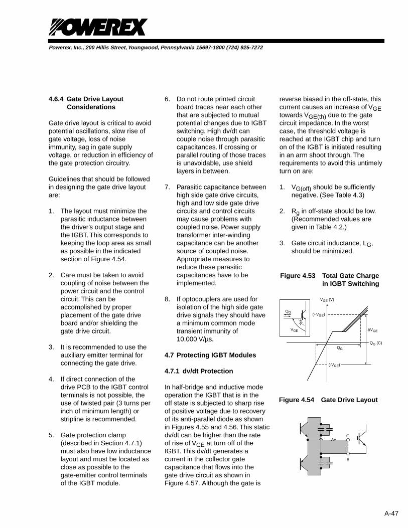
4.6.4 Gate Drive LayoutConsiderations
Gate drive layout is critical to avoidpotential oscillations, slow rise ofgate voltage, loss of noiseimmunity, sag in gate supplyvoltage, or reduction in efficiency ofthe gate protection circuitry.
Guidelines that should be followedin designing the gate drive layoutare:
1. The layout must minimize theparasitic inductance betweenthe driver’s output stage andthe IGBT. This corresponds tokeeping the loop area as smallas possible in the indicatedsection of Figure 4.54.
2. Care must be taken to avoidcoupling of noise between thepower circuit and the controlcircuit. This can beaccomplished by properplacement of the gate driveboard and/or shielding thegate drive circuit.
3. It is recommended to use theauxiliary emitter terminal forconnecting the gate drive.
4. If direct connection of thedrive PCB to the IGBT controlterminals is not possible, theuse of twisted pair (3 turns perinch of minimum length) orstripline is recommended.
5. Gate protection clamp(described in Section 4.7.1)must also have low inductancelayout and must be located asclose as possible to thegate-emitter control terminalsof the IGBT module.
6. Do not route printed circuitboard traces near each otherthat are subjected to mutualpotential changes due to IGBTswitching. High dv/dt cancouple noise through parasiticcapacitances. If crossing orparallel routing of those tracesis unavoidable, use shieldlayers in between.
7. Parasitic capacitance betweenhigh side gate drive circuits,high and low side gate drivecircuits and control circuitsmay cause problems withcoupled noise. Power supplytransformer inter-windingcapacitance can be anothersource of coupled noise.Appropriate measures toreduce these parasiticcapacitances have to beimplemented.
8. If optocouplers are used forisolation of the high side gatedrive signals they should havea minimum common modetransient immunity of10,000 V/µs.
4.7 Protecting IGBT Modules
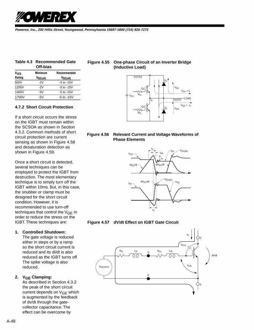
4.7.1 dv/dt Protection
In half-bridge and inductive modeoperation the IGBT that is in theoff state is subjected to sharp riseof positive voltage due to recoveryof its anti-parallel diode as shownin Figures 4.55 and 4.56. This staticdv/dt can be higher than the rateof rise of VCE at turn off of theIGBT. This dv/dt generates acurrent in the collector gatecapacitance that flows into thegate drive circuit as shown inFigure 4.57. Although the gate is
reverse biased in the off-state, thiscurrent causes an increase of VGEtowards VGE(th) due to the gatecircuit impedance. In the worstcase, the threshold voltage isreached at the IGBT chip and turnon of the IGBT is initiated resultingin an arm shoot through. Therequirements to avoid this untimelyturn on are:
1. VG(off) should be sufficientlynegative. (See Table 4.3)
2. Rg in off-state should be low.(Recommended values aregiven in Table 4.2.)
3. Gate circuit inductance, LG,should be minimized.
QG
VGE (V)
(+VGE)
QG
(-VGE)
VGE
QG (C)
∆VGE
Figure 4.53 Total Gate Chargein IGBT Switching
E
G
Figure 4.54 Gate Drive Layout
Powerex, Inc., 200 Hillis Street, Youngwood, Pennsylvania 15697-1800 (724) 925-7272
A-48
Table 4.3 Recommended GateOff-bias
VCES Minimum RecommendedRating VGE(off) VGE(off)600V -2V -5 to -15V
1200V -2V -5 to -15V
1400V -5V -5 to -15V
1700V -5V -5 to -15V
4.7.2 Short Circuit Protection
If a short circuit occurs the stresson the IGBT must remain withinthe SCSOA as shown in Section4.3.2. Common methods of shortcircuit protection are currentsensing as shown in Figure 4.58and desaturation detection asshown in Figure 4.59.
Once a short circuit is detected,several techniques can beemployed to protect the IGBT fromdestruction. The most elementarytechnique is to simply turn off theIGBT within 10ms. But, in this case,the snubber or clamp must bedesigned for the short circuitcondition. However, it isrecommended to use turn-offtechniques that control the VGE inorder to reduce the stress on theIGBT. These techniques are:
1. Controlled Shutdown:The gate voltage is reducedeither in steps or by a rampso the short circuit current isreduced and its di/dt is alsoreduced as the IGBT turns off.The spike voltage is alsoreduced.
2. VGE Clamping:As described in Section 4.3.2the peak of the short circuitcurrent depends on VGE whichis augmented by the feedbackof dv/dt through the gate-collector capacitance. Theeffect can be overcome by
RGVCC
RG
Q1
Q2
Irr
D1
D2
VQ1
VQ2
LOAD
VQ1 = IL
VQ2 = –IL
VQ2
trr
trrb
Irr
IQ2
dIQ1/dt
dVQ1/dtID1
VQ2(pk)
dVQ1/dt
VQ1(pk)VQ1
trr
iD
GCG
RG LG
dv/dt
C
E
VGEVGE(OFF)
RGi LGiG
E
Figure 4.55 One-phase Circuit of an Inverter Bridge(Inductive Load)
Figure 4.56 Relevant Current and Voltage Waveforms ofPhase Elements
Figure 4.57 dV/dt Effect on IGBT Gate Circuit
Powerex, Inc., 200 Hillis Street, Youngwood, Pennsylvania 15697-1800 (724) 925-7272
A-49
clamping the VGE safely below18 Volts. An effective clampingcircuit is shown in Figure 4.60.The clamping diode, DCL, andclamping capacitor, CCL,should be connected directly tothe control signal terminals ofthe IGBT module. A fastforward recovery is required forDCL. For low current IGBTs azener clamp between gate andemitter may also be effective.
3. Reducing tw:For reducing the thermal stressin short circuit operation it isbeneficial to reduce the time inshort circuit, tw. However, thiswill increase the magnitude ofthe current at turn off as shownin Figure 4.61, and di/dt will beincreased. This undesirableeffect may be overcome byusing the techniques in Steps 1and 2 above.
Caution:The above techniques reduce thestress at short circuit turn-off.However, they do not release thedesigner from considering worstcase turn off in snubber design.
4.7.3 Handling Precautions
Since IGBT gates are insulatedfrom any other conducting region,care should be taken to preventstatic build up which could possibledamage gate oxides. All ESDsensitive IGBT modules areshipped from the factory withconductive foam contacting thegate and emitter control terminals.Never touch the gate terminalsduring assembly and keep theconducting foam in place untilpermanent connections are madeto the gate and emitter controlterminals. Always ground parts
Figure 4.58 Short Circuit Protection Scheme (Example)
M
A. SYSTEM BLOCK DIAGRAM
BUSCURRENT
SENSE
COMPARATOR
LATCH DISABLE
DRIVER
<SIGNAL GATE>
UNDER PROTECTION
6
PWM SIGNALS
<PWM SIGNAL GENERATOR>
CLEAR PROTECTION
CLEAR
B. LOGIC DIAGRAM FOR OVER CURRENT PROTECTION
+
–R
S
Q
<F.F.> UNDER PROTECTION PWM SIGNALS
<PWM SIGNAL GENERATOR>
CLEAR PROTECTION
CURRENTSENSOR
OUT OF SATURATION SHORT CIRCUIT DIAGRAM
FAULTLATCHCLEAR
FROMDRIVELOGIC
GATEDRIVE
DISABLE
AND
COMPARATOR
Vref
Figure 4.59 Out of Saturation Short Circuit Protection
Powerex, Inc., 200 Hillis Street, Youngwood, Pennsylvania 15697-1800 (724) 925-7272
A-50
0 0.2 0.4 0.6 0.80
VCE(sat) (V) Tj = 25°C
I C
/I C
100
%
10
20
30
600V H&U SERIES1200V H&U SERIES250V TRENCH GATE SERIES
Figure 4.62 Maximum CurrentImbalance vs.DVCE(sat)
and dynamic current balanceamong the paralleled devices.With proper attention to circuitdesign and device selection severalmodules can be reliably operatedin parallel. The followingsub-sections outline the basicrequirements and considerationsfor parallel operation of single IGBTmodules with ratings of 200A ormore.
4.8.1 Static Current Balance
Table 4.4 outlines the factorsinfluencing parallel operation ofIGBT modules. Under staticon-state or DC operating conditionsthe collector to emitter saturationvoltage and junction temperaturehave the biggest influence oncurrent sharing. To achieve reliableand consistent static currentbalance devices should bemounted on the heat sink near toeach other with cooling arranged tomaintain uniform base platetemperatures between paralleledmodules. A good general designguideline is to maintain a baseplate temperature differencebetween paralleled devices of 15°Cor less. Parallel connected devicesshould be selected with matchedsaturation voltages. The maximumstatic current imbalance as afunction of saturation voltage atTj = 25°C is shown in Figure 4.62.Experimental analysis has
demonstrated that the currentbalance becomes considerablybetter at elevated junctiontemperatures. For example, in thecase of 1200V H-series the worstcase imbalance drops from 15%at 25°C to about 5% at 125°C.Figure 4.63 shows how theimbalance shown in Figure 4.62 isdefined. To facilitate the matchingof devices for parallel operationPowerex provides IGBT modulesmarked with a saturation voltagerank letter. All devices to beoperated in parallel should havethe same saturation voltage rank.Devices can also be supplied inmatched sets for parallelapplications. Contact the factoryfor ordering information. Table 4.5shows the standard saturationvoltage letter rankings for PowerexIGBT modules. Column 1 of thistable is applicable to all voltageclasses of U-Series and H-Seriesmodules, column 2 applies to 250Vtrench gate IGBT modules, andcolumn 3 applies to 600V and1200V F-Series modules. Note thatall ranks do not exist for a givenvoltage class. For example, 600VH-Series modules have amaximum data sheet saturationvoltage of 2.8V and therefore ranks
touching gate terminals duringinstallation. In general, standardESD precautions applicable toMOSFETs shouldbe followed.
Other handling precautions thatshould be observed are:
1. Use grounded work stationwith grounded floors andgrounded wrist straps whenhandling devices.
2. Use a 100Ω resistor in serieswith the gate when performingcurve tracer tests.
3. Never install devices intosystems with power connectedto the system.
4. Use soldering irons withgrounded tips when solderingto gate terminals.
4.8 Parallel Operation
Powerex IGBT modules can beconnected in parallel forapplications requiring very highcurrents. In such applicationsparallel operation should only beconsidered when the highestcurrent module available is notlarge enough. Use of a single largemodule rather than smaller parallelmodules is recommended becauseit eliminates concerns about static
ON
OFF
RG
+
-
-
+
DCL
VGE (ON)
VGE (OFF)
CCL
IC
tw2
tw1
Figure 4.60 VGE ClampingCircuit
Figure 4.61 Short Circuit atReduced tw

Powerex, Inc., 200 Hillis Street, Youngwood, Pennsylvania 15697-1800 (724) 925-7272
A-51
IC - IC IC + IC
IL = 2IC
Figure 4.63 Circuit Showing theDefinition ofCurrent Imbalance
H through M do not exist for thesedevices. Saturation voltage ranksare intended for matching sets ofdevices for parallel applications.Orders specifying a specific rankwill not normally be accepted. Thesaturation voltage rank will beeither marked with white ink on thetop of the module or indicated onthe label. Saturation voltageranking is available for singlemodules rated 200A or more.
Table 4.4 IGBT Module Parallel Operation, Current Sharing
Factors related to current sharing and their effect.
Categories of Current SharingIGBT Switching Steady State
Factors Effecting Current Sharing Turn-on Turn-off di/dt = 0 di/dt ≠ 0 Device VCE(SAT) X X X
Characterization Temperature X
Main L (Supply to ∂ X X Circuit Device)
Wiring L (Total Loop X X X
Inductance Including Load)
Driver to Device X X Driver Wiring Length Diff.
Wiring Output Impedance X Xof Driver
- Relation Exists X - No Relation ∂ - Relation Ambiguous or Weak
Saturation voltage ranking is notnormally available for dual or sixpack types. Modules of differentsaturation voltage ranks may beused in the same inverter providedthat devices connected in parallelare of the same rank.
When modules of the samesaturation voltage rank areparalleled the static currentimbalance will be minimized so
that the following recommendedderatings can be applied:
For 250V Trench Gate derateIC by 10%
For 600V Class H-Series,U-Series and F-Series derateIC by 10%
For 1200V and 1400V ClassH-Series, U-Series andF-Series derate IC by 15%
For 1700V Class H-Seriesderate IC by 20%
Table 4.5 Saturation Voltage Ranks for Parallel Applications
Saturation Voltage Ranks for H-Series Saturation Voltage Ranks for 250V Saturation Voltage Ranks for 600Vand U-Series IGBT Modules Trench Gate IGBT Modules and 1200V F-Series Modules
(CM**-12F / CM**-24F)
Saturation Voltage VCE(sat) (V) Saturation Voltage VCE(sat) (V) Saturation Voltage VCE(sat) (V)Rank IC = Rated Current Rank IC = Rated Current Rank IC = Rated Current
VGE = 15V VGE = 15V VGE = 15VTj = 25°C Tj = 25°C Tj = 25°C
C 1.70 ~ 1.95 Q 1.15 ~ 1.30 E 1.5 ~ 1.6
D 1.90 ~ 2.15 R 1.25 ~ 1.40 F 1.55 ~ 1.65
E 2.10 ~ 2.35 S 1.35 ~ 1.50 G 1.6 ~ 1.7
F 2.30 ~ 2.55 H 1.65 ~ 1.75
G 2.50 ~ 2.80 J 1.7 ~ 1.8
H 2.75 ~ 3.05 K 1.75 ~ 1.85
J 3.00 ~ 3.30 L 1.8 ~ 1.95
K 3.25 ~ 3.55 M 1.9 ~ 2.05
L 3.50 ~ 3.80 N 2.0 ~ 2.2
M 3.75 ~ 4.05 P 2.15 ~ 2.4

Powerex, Inc., 200 Hillis Street, Youngwood, Pennsylvania 15697-1800 (724) 925-7272
A-52
ASYMMETRICLOADCONNECTION
SYMMETRICLOADCONNECTION
IC1 IC2
Figure 4.64 Circuit Diagram Showing Symmetric and AsymmetricLoad Connections
When more than two modules areparalleled the derating can becomputed using the followingformula:
Where:
x = 0.1 for 250V devicesx = 0.1 for 600V devicesx = 0.15 for 1200V/
1400V devicesx = 0.20 for 1700V devicesn = number parallel
Example:
In the case of four IGBT modulesof 600V class connected inparallel, the formula is:
So the derated current with 4parallel 300A modules is:
300A(1 - 0.136) x 4 = 1037A
4.8.2 Dynamic Current Balance
Matching VCE(sat) is effective formaintaining good static steadystate current balance. Thismatching also helps some with turnoff current balance because of thefundamental inverse relationship offall time and saturation voltage.However, as indicated in Table 4.4,gate drive conditions and powercircuit layout have by far thegreatest impact on dynamic currentbalance between paralleleddevices. Temperature differencesbetween paralleled modules is also
[1–
(n – 1) (1 – x)___________(1 + x)
( + 1)______________
n] X 100
% Derating =
[1–
(4 – 1) (1 – .1)___________(1 + .1)
( + 1)______________
4] = 13.6%
% Derating =
a factor because of the resultingeffect on delay time and thereforethe design guidelines given inSection 4.8.1 should be observedfor dynamic current balance aswell. To understand the circuitlayout factors affecting dynamiccurrent balance it is necessary toconsider two cases:
The first case is when the device isin the static on-state and the loadcurrent is changing. As indicatedin Table 4.4 the main cause ofimbalance in this case isdifferences in inductance to theload connection. In practicalapplications this is most oftenthe result of an asymmetricconnection of the load as shownin Figure 4.64. A typical currentimbalance waveform resulting froman asymmetric load connection isshown in Figure 4.65. Experimentalanalysis has shown that this type ofimbalance can also be caused bythe orientation of the main circuitbus bars. For example, if the loadconnection causes the load current
to run in parallel with the current inone of the paralleled modulesmutual inductance effects cancause the inductance of thatpath to be effectively reduced orincreased even though themechanical connection point issymmetric.
The second case that must beconsidered is current imbalancethat occurs at the moment ofturn-on or turn-off switching.Table 4.4 indicates that the mostimportant factors influencingcurrent balance are the gate circuitdesign and module temperature.The recommended gate driveconfiguration for paralleledmodules is shown in Figure 4.66.The recommended approach is touse a single drive stage with aseparate Rg for each paralleledmodule. The small kelvin emitterconnections on the paralleleddevices should be connected witha short, low impedance symmetricconnection in order to preventground loop currents from

Powerex, Inc., 200 Hillis Street, Youngwood, Pennsylvania 15697-1800 (724) 925-7272
A-53
disrupting the gate drive. In somepower circuit layouts it may becomenecessary to put some part of theRg impedance in the ground pathto impede the flow of ground loopcurrents. However, in this caseimprovements in the power circuitlayout should be investigated first.In order to maintain uniformswitching it is recommended to userelatively small values of seriesgate resistance. Series gateresistors should never be largerthan ten times the valuerecommended on the data sheet ofthe module being used. Care mustbe exercised to make the gatewiring symmetric. In general, thebest practice is to minimize the
inductance in the gate drive wiring.Use of a printed circuit boardmounted directly to the module orshort tightly twisted wires of equallength is recommended. Careshould be exercised to avoidinductive coupling to the gate driveby keeping the wiring from runningparallel to the main circuit current.Figure 4.67 shows a typical turn-offcurrent waveform with imbalancecaused by an improper gate drive.In addition to the influences oftemperature and gate drive thecurrent balance at turn-on isinfluenced by the symmetry of theinductance in the power circuitbetween the main supplycapacitors and devices.Figure 4.68 is a circuit showingsymmetric versus asymmetric maincircuit connections. Figure 4.69shows a typical turn on waveformwith current imbalance caused byasymmetric main circuitinductance. An effective approachto balance the main circuitinductance is minimize theinductance by using laminated busstructures. The current imbalancewaveform at turn-on due toimproper gate drive also looks likeFigure 4.69.
lC
lC1
lC2
t
Figure 4.65 Typical CurrentImbalance Causedby AssymetricLoad Connection
NOTE:It may be observed that PowerexIGBTs have a negativetemperature coefficient ofsaturation voltage over a widerange of collector currents. This isnot a deterrent to parallel operationand, in fact, is an advantage as ityields lower conduction loss at highjunction temperature. Thehomogeneous processcharacteristics of Powerex IGBTsproduce VCE(SAT) characteristicsthat track as a function of currentand temperature such that, once aVCE(SAT) rank is chosen, theparallel devices will share withinthe given derating factor.
GATEDRIVER
USE SHORT LOWIMPEDANCE
CONNECTION
RG
RG
USE SAME RG
GATE AND EMITTERCONNECTIONS LOW
INDUCTANCE ANDSYMMETRIC
Figure 4.66 Gate Drive Configuration for Paralleled Modules
lC
lC1
lC2
t
Figure 4.67 Typical CurrentWaveform ShowingImbalance atTurn-off Due toImproper GateDrive

Powerex, Inc., 200 Hillis Street, Youngwood, Pennsylvania 15697-1800 (724) 925-7272
A-54
Figure 4.68 Symmetric and Asymmetric Main Circuit Connections
ASYMMETRICMAIN BUS
CONNECTION SYMMETRICMAIN BUSCONNECTION
IC1 IC2
Figure 4.69 Typical Turn-onWaveform withCurrent ImbalanceCaused byAsymmetric MainCircuit Inductance
lC
lC1
lC2
t