82559 LAN on Motherboard (LOM) Design Guide
31
82559 LAN on Motherboard (LOM) Design Guide Application Note (AP-392) Revision 1.4 January 1999 Document Number: 718213-004
-
Upload
khangminh22 -
Category
Documents
-
view
0 -
download
0
Transcript of 82559 LAN on Motherboard (LOM) Design Guide

82559 LAN on Motherboard (LOM) Design GuideApplication Note (AP-392)
Revision 1.4
January 1999
Document Number: 718213-004

ii Application Note (AP-392)
Information in this document is provided in connection with Intel products. No license, express or implied, by estoppel or otherwise, to any intellectual property rights is granted by this document. Except as provided in Intel's Terms and Conditions of Sale for such products, Intel assumes no liability whatsoever, and Intel disclaims any express or implied warranty, relating to sale and/or use of Intel products including liability or warranties relating to fitness for a particular purpose, merchantability, or infringement of any patent, copyright or other intellectual property right. Intel products are not intended for use in medical, life saving, or life sustaining applications.
Intel may make changes to specifications and product descriptions at any time, without notice.
Designers must not rely on the absence or characteristics of any features or instructions marked “reserved” or “undefined.” Intel reserves these for future definition and shall have no responsibility whatsoever for conflicts or incompatibilities arising from future changes to them.
The 82559 may contain design defects or errors known as errata which may cause the product to deviate from published specifications. Current characterized errata are available on request.
Contact your local Intel sales office or your distributor to obtain the latest specifications and before placing your product order.
Copies of documents which have an ordering number and are referenced in this document, or other Intel literature, may be obtained from:
Intel Corporation P.O. Box 7641 Mt. Prospect IL 60056-7641
or call 1-800-879-4683.
Many documents are available for download from Intel’s website at http://www.intel.com.
Copyright © Intel Corporation, 1997
*Third-party brands and names are the property of their respective owners.
Revision History
Revision Date Revision Description
June 1998 1.0 First release.
July 1998 1.1Added Section 8.0, "Signal Descriptions" on page 12, Section 9.0, "Package and Pinout Information" on page 18, and Section 10.0, "Bill of Materials" on page 22.
November 1998 1.2 Incorporated new schematics.
December 1998 1.3 Final B5-Step Schematics Added
January 1999 1.4 Initial Public Release - removed references to AP-393
Contents
1.0 INTRODUCTION ............................................................................................................................... 11.1 Scope ..............................................................................................................................11.2 Reference Documents.....................................................................................................1
2.0 PCI INTERFACE..............................................................................................................................2
2.1 PCI Mode ........................................................................................................................22.2 Clockrun Operations........................................................................................................22.3 Reset Considerations ......................................................................................................2
2.3.1 PCI Reset ...........................................................................................................22.3.2 ALTRST#............................................................................................................32.3.3 ISOLATE# ..........................................................................................................3
2.4 Setting PCI Signal Levels................................................................................................3
3.0 WAKE-UP EVENTS..........................................................................................................................4
3.1 ACPI Designs ..................................................................................................................43.2 Advanced Power Management Designs .........................................................................4
4.0 LOCAL MEMORY PORTS .................................................................................................................5
4.1 Serial EEPROM............................................................................................................... 54.2 Flash Interface.................................................................................................................5
5.0 TEST PORT ....................................................................................................................................6
6.0 82559 BOARD DESIGN CONSIDERATIONS .......................................................................................7
6.1 Clock Source ...................................................................................................................76.2 LED Indicators.................................................................................................................76.3 Magnetics Selection ........................................................................................................76.4 Trace Routing..................................................................................................................86.5 Signal Terminations.........................................................................................................8
6.5.1 Termination Plane ..............................................................................................86.5.2 Termination Plane Capacitance .........................................................................9
6.6 Critical Dimensions..........................................................................................................96.6.1 Distance A: Magnetics to RJ45 (Priority 1).........................................................96.6.2 Distance B: PHY to Magnetics (Priority 2)........................................................10
7.0 POWER SUPPLY REQUIREMENTS ..................................................................................................11
7.1 +3.3VSB Power Requirement .......................................................................................117.2 +3.3VSB Power Recommendation................................................................................11
8.0 SIGNAL DESCRIPTIONS .................................................................................................................12
8.1 Signal Type Definitions..................................................................................................128.2 PCI Bus and CardBus Interface Signals .......................................................................12
8.2.1 Address and Data Signals ................................................................................128.2.2 Interface Control Signals ..................................................................................138.2.3 System and Power Management Signals.........................................................14
8.3 Local Memory Interface Signals ....................................................................................148.4 System Management Bus (SMB) Interface Signals ......................................................168.5 Testability Port Signals..................................................................................................168.6 PHY Signals ..................................................................................................................16
Application Note (AP-392) iii

9.0 PACKAGE AND PINOUT INFORMATION ........................................................................................... 18
9.1 Package Information ..................................................................................................... 189.2 Pinout Information .........................................................................................................19
9.2.1 82559 Pin Assignments ................................................................................... 199.2.2 82559 Ball Grid Array Diagram ....................................................................... 21
10.0 BILL OF MATERIALS ..................................................................................................................... 22
11.0 APPENDIX A: 82559/PIIX4 LOM D ESIGNS ................................................................................... 23
iv Application Note (AP-392)

lerate
SA/ On l
ign and
and
.
1.0 Introduction
The 82559 provides: a higher level of integration, enhanced features set, reduced power consumption, and small footprint (15 mm by 15 mm). The 82559 has been optimized to accethe integration of LAN into desktop, server, PC cards, docking stations (port replicators), andmobile platforms.
1.1 Scope
This application note covers the design of the 82559 into a platform based on Intel’s PCI to IIDE Xcelerator 4 (PIIX4). The 82559 will reduce cost, power, and real estate in existing LANMotherboard (LOM) designs. Platform designs for other chipsets are available from your Interepresentative.
1.2 Reference Documents
This application note assumes that the designer has a working knowledge of high-speed deslayout issues. A knowledge of the Advanced Configuration and Power Interface (ACPI) Specification and power management industry initiatives is valuable prior to beginning the integration of the 82559 into any platform. The following reference list provides sufficient background material.
• PCI Specification, PCI Special Interest Group.
• Network Device Class Reference, Revision 1.0, Intel Corporation, Microsoft Corporation,Toshiba.
• Advanced Configuration and Power Interface (ACPI) Specification, Intel Corporation, Microsoft Corporation, Toshiba.
• Advanced Power Management (APM) Specification, Intel Corporation and Microsoft Corporation.
• 82559 Fast Ethernet Multifunction PCI/CardBus Controller Datasheet, Intel Corporation.
• LAN On Motherboard (LOM) Design Guide Application Note (AP-391), Intel Corporation
• WOL Header Recommendations, Intel Corporation.
Application Note (AP-392) 1

82559 LOM Design Guide
the actions
e fined in L,
E# r e as a en be
by the lock. If vided
value
the rating e. The ts.
istent s the
PCI 9
2.0 PCI Interface
The 82559 provides a direct (glueless) 32-bit interface to the PCI bus. Prior to configuration,82559 operates as a simple slave device. After the device has been configured all data transwith the device are through memory structures in system memory. The PCI interface must benabled for bus mastering for normal operation. Address, data, and control signals are as dethe PCI Specification. Additional clarification of the PCIMODE, CLKRUN#, RST#, PME#, WOISOLATE#, ALTRST#, and VIO pins are provided in the following sections.
2.1 PCI Mode
Flash Address[0] (FLA0) doubles as the bus mode select pin during PCI reset. The PCIMODinput signal (sampled during PCI RST#) determines whether the 82559 operates as a PCI oCardBus device. If this signal is sampled low when the RST# is active, the 82559 will operatPCI device; if sampled high, then a CardBus device. In a LOM design the pin is either left op(internal pull-down), pulled low (through a resistor), or connected to a Flash device. It shouldpulled high only in a CardBus design.
2.2 Clockrun Operations
The CLKRUN# signal is used by the system to pause or slow down the PCI Clock signal and 82559 to enable and disable PCI Clock signal suspension or to request a restart of the PCI cclockrun is not used, this pin should be pulled low through a resistor (the reference design proin Section 11.0, “Appendix A: 82559/PIIX4 LOM Designs” on page 23 uses a value of 62 KΩ). Pull-down resistor values were selected based on the requirements of Intel’s Nand-tree test equipment. If the Nand-tree test capabilities of the 82559 are not used then any reasonable will be adequate, i.e. 1- 10 KΩ.
2.3 Reset Considerations
The 82559 can maintain a virtual connection to the network regardless of the power state ofsystem. Therefore, the state of the PCI bus signals can be undefined when the 82559 is opefrom auxiliary power. The 82559 response to a reset event varies based on operational mod82559 provides three signals that enable the device to operate correctly in these environmenConnections to these signals vary based on system implementation.
2.3.1 PCI Reset
The PCI Reset (RST#) signal is used to put PCI registers, sequencers, and signals in a consstate. When the RST# signal is asserted, all PCI output signals are tri-stated. In LOM design82559’s RST# pin would normally be connected to the PCI Reset pin.
Note: In designs where an signal to drive the ISOLATE# pin on the 82559 is not available, thereset signal may be routed to the ISOLATE# pin. In these designs the RST# pin on the 8255would be pulled-up to the 82559’s power rail through a 3.3 KΩ resistor.
2 Application Note (AP-392)
82559 LOM Design Guide
ed to
). In 559’s
D tely
erted, and
ch as
nal bus is . The
PCI 9
The pin
2.3.2 ALTRST#
ALTRST# is the power-on reset signal to the 82559. This signal is required due to the uniquefunctionality provided by the 82559 when the system is in a low power state. ALTRST# is usprovide a complete reset to the 82559 on power-up. In systems that support VAUX, ALTRST# should be connected to a power-up detection circuit (i.e. 3.3V_standby powergood indicationsystems that do not have an auxiliary power source, the ALTRST# pin should be tied to the 82VCC (3.3V) power-rail. The reference design in Section 11.0, “Appendix A: 82559/PIIX4 LOM Designs” on page 23 shows the ALTRST# pin connected to a signal called AUX_GOOD. This signal should be asserted low whenever the auxiliary power is not available. The AUX_GOOsignal can be generated by a power supply supervisory circuit, and the 82559 will be complereset anytime the signal is asserted low.
2.3.3 ISOLATE#
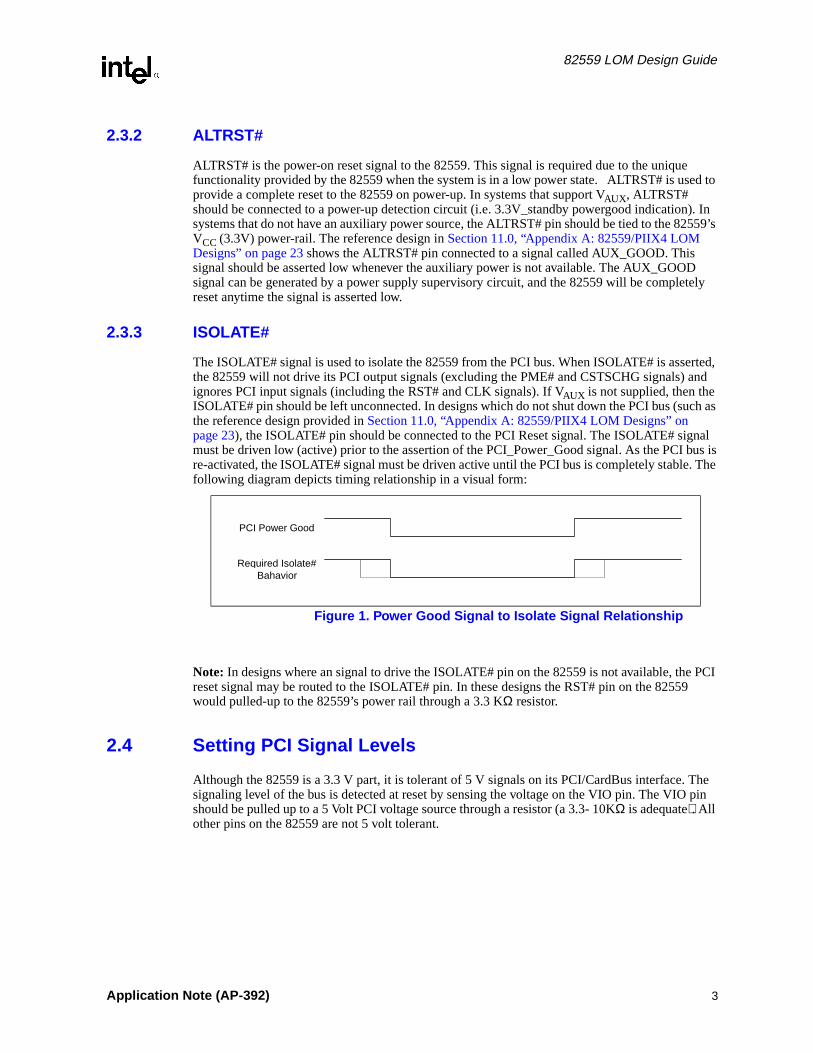
The ISOLATE# signal is used to isolate the 82559 from the PCI bus. When ISOLATE# is assthe 82559 will not drive its PCI output signals (excluding the PME# and CSTSCHG signals) ignores PCI input signals (including the RST# and CLK signals). If VAUX is not supplied, then the ISOLATE# pin should be left unconnected. In designs which do not shut down the PCI bus (suthe reference design provided in Section 11.0, “Appendix A: 82559/PIIX4 LOM Designs” on page 23), the ISOLATE# pin should be connected to the PCI Reset signal. The ISOLATE# sigmust be driven low (active) prior to the assertion of the PCI_Power_Good signal. As the PCI re-activated, the ISOLATE# signal must be driven active until the PCI bus is completely stablefollowing diagram depicts timing relationship in a visual form:
Note: In designs where an signal to drive the ISOLATE# pin on the 82559 is not available, thereset signal may be routed to the ISOLATE# pin. In these designs the RST# pin on the 8255would pulled-up to the 82559’s power rail through a 3.3 KΩ resistor.
2.4 Setting PCI Signal Levels
Although the 82559 is a 3.3 V part, it is tolerant of 5 V signals on its PCI/CardBus interface. signaling level of the bus is detected at reset by sensing the voltage on the VIO pin. The VIOshould be pulled up to a 5 Volt PCI voltage source through a resistor (a 3.3- 10KΩ is adequate). All other pins on the 82559 are not 5 volt tolerant.
Figure 1. Power Good Signal to Isolate Signal Relationship
PCI Power Good
Required Isolate#Bahavior
Application Note (AP-392) 3

82559 LOM Design Guide
ing AN te the ts l/
ent in IO1) mon to the ds to
nts this l ble of
APM rpose
on
. This he
PME# vides pin ry
ut on e the 4 is .
3.0 Wake-up Events
The 82559 provides two output signals to alert the system of a wake-up event, PME# and CSTSCHG (WOL). In ACPI compliant designs, the PME# pin alerts the system of any incomevent; and CSTSCHG, in CardBus systems. The WOL pin acts as an active high Wake on L(WOL) signal when used in PCI systems. This alleviates the need for external circuitry to creaWOL signal in Advanced Power Management (APM) designs. The WOL header requiremendocument is available from the wired for management website at http://developer.intel.com/iaWfM/index.htm.
3.1 ACPI Designs
The Power Management Event signal is an active low, open drain signal that indicates an evACPI compliant systems. It is usually connected to the General Purpose Input/Output 1 (GPsignal of the PIIX. In an ACPI compliant system, the Power Management Event signal is comto all PCI devices. Since the signal is driven from open drain sources, a single pull-up resistor3.3 VAUX must be provided. If configured, the 82559 will assert PME# anytime the system neebe woken up.
The 82559 was designed to be fully ACPI Specification compliant. The ACPI specification requires that PCI devices implement a power management event signal. The 82559 implemethrough its PME# pin. For the 82559 to function properly in an ACPI context, the PME# signashould be connected to a pin on the PIIX4 device that resides in the resume well and is capagenerating a System Control Interrupt (SCI). In a PIIX4 design, which is intended to be both and ACPI compliant, it is recommended that the PME# signal is connected to the General PuInput 1 (GPI1) PIIX4 pin. The GPI1 signal is capable of generating both a SCI and System Management Interrupt (SMI) making it the ideal pin to use.
Note: As per the ACPI specification, the 82559 will not generate a follow-on wake-up indicatiuntil the device is re-armed. The re-arming is accomplished by clearing the PME bit
3.2 Advanced Power Management Designs
The Wake on LAN pin provides the active high signal that wakes the system in APM designssignal is distributed via a 3-pin header in network interface card (adapter) implementations. TWOL signal is not necessary in LOM designs because it provides the same indication as thesignal (albeit active high). However, in adapter designs it can be used to build a card that proboth signal levels. If APM support is desired, then the PME# or WOL pin must be routed to aon the chipset capable of generating a SMI while the chipset is powered only from an auxiliapower source.
It is recommended that the incoming signal from the WOL header is routed to a separate inpthe PIIX4. The use of separate inputs provides the ability to interrogate the PIIX4 device oncsystem has powered up and discern the source of the wake event. The LID input of the PIIXrecommended since it resides in the resume well and is capable of generating a SMI or SCI
4 Application Note (AP-392)

82559 LOM Design Guide
for
OM
data
data
k
evice. e
sh.
ils
4.0 Local Memory Ports
The 82559 supports both a serial EEPROM for configuration information and a parallel Flashuser data. In most designs, the Flash interface is used for expansion ROM, such as PrebootExecution Environment (PXE) code.
4.1 Serial EEPROM
The serial EEPROM of the 82559 provides storage for initialization, the heartbeat packet in managed designs, and the Card Information Structure (CIS) in CardBus designs. The EEPRinterface consists of the following signals:
• EEPROM Data Input (EEDO)
The EEDO pin is multiplexed with the Flash Address[14] pin and acts as the serial input pin to the EEPROM Data Output signal.
• EEPROM Data Output (EEDI)
The EEDI pin is multiplexed with the Flash Address[13] pin and acts as the serial outputpin to the EEPROM Data Input signal.
• EEPROM Serial Clock (EESK)
The EESK pin is a multiplexed with the Flash Address[15] pin and acts as the serial clocoutput to the EEPROM.
• EEPROM Chip Select (EECS)
The EECS pin is used to assert chip select to the serial EEPROM.
In unmanaged (TCO controllerless) PCI designs (such as the reference design provided in Section 11.0, “Appendix A: 82559/PIIX4 LOM Designs” on page 23), a 64-word device is required. The EEPROM must be 3.3 V powered in order to operate with the 82559.
4.2 Flash Interface
The 82559 support a glueless interface to an 8-bit wide (128 Kbyte), 3.3 V parallel memory dThis port can be used for a 128 Kbyte Flash or any other parallel 8-bit device which meets th82559’s AC timing. The reference design provided in Section 11.0, “Appendix A: 82559/PIIX4 LOM Designs” on page 23 depicts a Flash socket, which may not be required if there is no requirement for the system to boot from the LAN or if the PXE code will be stored in main fla
The 82559 uses a number of the Flash address pins for auxiliary functions based on the configuration or the state of the device reset. The 82559 Datasheet contains additional detaregarding these secondary pin functions.
Application Note (AP-392) 5

82559 LOM Design Guide
K
5.0 Test Port
The 82559 uses an internal NAND tree configuration for test purposes. The Test Port is not normally accessed in LOM designs. The Test pin (pin A13) must be pulled low through a 4.7Ω resistor to place the device in normal operational mode.
6 Application Note (AP-392)

82559 LOM Design Guide
al the X1 input, 559 d t.
ice
meet
thin the
p
“Does
6.0 82559 Board Design Considerations
6.1 Clock Source
The 82559 can operate from either its internal oscillator using a 25 MHz crystal or an externoscillator as a 25 MHz clock source. If a crystal is used, then it should be connected across and X2 input pins. If an external oscillator is used, then it can be connected directly to the X1 with X2 left unconnected. In both cases the clock should be accurate within 50ppm. The 82can also provide its internal clock as an output on the CLK25 pin (pin N9, which is multiplexewith FLA[16]). The clock out function is enabled by asserting the CLKEN pin during PCI reseThe CLKEN pin is multiplexed with FLA[7].
A sampling of crystals that meet the specifications outlined is listed below:
6.2 LED Indicators
The 82559 provide three indication LED outputs:
• Link (LILED)
• Activity (ACTLED)
• Speed (SPEEDLED)
The 82559 can sink up to 10 mA of current for each LED.
6.3 Magnetics Selection
One of the most critical component choices in a 100 Mbps Ethernet design is the magneticsmodule. The module has a critical effect on overall IEEE and emissions compliance. The devselected should meet the performance required for a design. Occasionally, components thatbasic specifications may cause the system (LOM, adapter, repeater, etc.) to fail because of unintentional interactions with board effects. Examples of these phenomena could be an unexpected series or parallel capacitance values or unexpected series inductance values wimagnetics module. This could cause the overall design to fail certain IEEE specifications. Qualifying a new magnetics module can help to alleviate these sorts of issues. The three-steprocess outlined below is recommended when evaluating suppliers:
1. Verify vendor’s specification.
The component should have more margins than the system specification. For example, the module have a minimum of 400 µH of open circuit inductance (OCL) with 8 mA of DCBias?”.
2. Check module’s electrical qualifications.
The electrical specifications of the module should be verified by performing stand-alone electrical qualification. Several modules should be tested (not in circuit) with two goals inmind:
Manufacturer Manufacturer’s Part Number
Raltron TT-SMDC-25.00-20-T
Epson-Seiko MA-406-25.000M-20PF
Application Note (AP-392) 7
82559 LOM Design Guide
rd nd ues short
ignals, aused m sepa- the
the
esigner
d the e) is d path
a. Does the component meet the published specifications?
b. Does the vendor's published data correlate to the measured data?
3. Perform IEEE conformance tests
System level IEEE PHY conformance and EMC (FCC and EN) testing should be done toverify that the system meets all electrical requirements with the new component.
A sampling of modules that meet the specifications outlined is listed below:
6.4 Trace Routing
Generic Trace routing considerations for final layout are described in the LAN On Motherboa(LOM) Design guide Application Note (AP-391). 82559 specific layout information can be fouin the 82559 Printed Circuit Board (PCB) Design Application Note (AP-399). Critical layout issare covered in the following section for completeness. Critical signal traces should be kept asas possible to decrease the likelihood of being affected by high frequency noise from other sincluding those propagated through power and ground planes. Capacitive loading, which is cby the signal trace, can also be reduced by keeping the traces as short as possible. Maximuration between differential pairs should be no more than one tenth of an inch as illustrated infigure below.
6.5 Signal Terminations
A single 100 Ω (1%) resistor is used to terminate the transmit differential (TDP/TDN) pair. Forreceive differential (RDP/RDN) pairs, a 120 Ω (1%) resistor was utilized. The 120 Ω resistor was used in the layout of this design because of the improvements in receive performance, the dmay want to experiment with values from 100 Ω to 120 Ω on the receive side. They should be placed as close to the 82559 as possible.
6.5.1 Termination Plane
Resistors are used to terminate noise from the unused inputs of both the RJ45 connector anmagnetics module to the termination plane. The netname TERMPLANE (for termination planprovided as a guide to the termination plane. A termplane is a plane fabricated into the printecircuit board (PCB) substrate. This plane, which has no DC termination, acts like a capacitivefor the coupled noise.
Manufacturer Manufacturer’s Part Number
Pulse Engineering H1012T
Pulse Engineering H1088
Pulse Engineering H1138
Bel Fuse S558-5999-46
Bel Fuse S558-5999-K7
8 Application Note (AP-392)

82559 LOM Design Guide
. This the
uired acitor
59
one :
tent th).
oise. the
ce B
6.5.2 Termination Plane Capacitance
It is recommended that the termination plane capacitance equal a minimum value of 1500 pFhelps reduce the amount of cross-talk on the differential pairs (TDP/TDN and RDP/RDN) fromunused pairs of the RJ45. Pads may be placed for additional capacitance, which may be reqdue to failure of electrical fast transient testing. If 1500pf is not achievable, then the series capmay need to be populated.
6.6 Critical Dimensions
There are two critical dimensions that must be considered during the layout phase of an 825LOM implementation. These dimensions are identified in Figure 2 as A and B:
6.6.1 Distance A: Magnetics to RJ45 (Priority 1)
The distance labeled “A” in Figure 2 should be given the highest priority in board layout. The distance between the magnetics module and the RJ45 connector should be kept to less thaninch of separation. The following trace characteristics are important and should be observed
1. Differential Impedance: The differential impedance should be 100 Ω. The single ended trace impedance will be approximately 50 Ω; however, the differential impedance can also be affected by the spacing between the traces.
2. Trace Symmetry: Differential pairs (such as TDP and TDN) should be routed with consisseparation and with exactly the same lengths and physical dimensions (for example, wid
Caution: Asymmetrical and unequal length traces in the differential pairs contribute to common mode nThis can degrade the receive circuit’s performance and contribute to radiated emissions fromtransmit circuit.
If the 82559 must be placed further than a couple of inches from the RJ45 connector, distancan be sacrificed. Keeping distance A as short as possible should be a priority.
Figure 2. Critical Dimensions for Component Placement
82559 Fast EthernetContoller
Magnet ics
RJ45
Flash(optional)
EEPROM
B A
Application Note (AP-392) 9

82559 LOM Design Guide
es. ance tended
een ay signed
6.6.2 Distance B: PHY to Magnetics (Priority 2)
Distance B from Figure 2 should also be designed to extend less than one inch between devicThe high speed nature of the signals propagating through these traces requires that the distbetween these components are closely observed. In general, any section of traces that is infor use with high speed signals should observe proper termination practices.
Proper termination of signals can reduce reflections caused by impedance mismatches betwdevices and traces. The reflections of a signal may have a high frequency component that mcontribute more EMI than the original signal itself. For this reason, these traces should be deto a 100 Ω differential value.
10 Application Note (AP-392)

82559 LOM Design Guide
ed to
s. ments
s OOD
559.
7.0 Power Supply Requirements
WOL designs require a segmented power supply. The auxiliary power supply (+3.3VSB) is usprovide the trickle power necessary to keep key components operational in WOL mode.
7.1 +3.3VSB Power Requirement
In designs that utilize 3.3VSB, the 82559 will operate from this supply in all operational stateTherefore, the +3.3VSB must be capable of supplying 175 mA of current (worst case requirefor the 82559).
7.2 +3.3VSB Power Recommendation
Ideally the power supply will provide an AUX_GOOD signal. The AUX_GOOD signal indicatethat the auxiliary power supply is ready to provide stable power and is similar to the PWR_Gsignal on many of today’s common power supplies.
Note: The AUX_GOOD signal from the power supply is the same as the ALTRST# signal of the 82
Application Note (AP-392) 11

82559 LOM Design Guide
8.0 Signal Descriptions
8.1 Signal Type Definitions
8.2 PCI Bus and CardBus Interface Signals
8.2.1 Address and Data Signals
Type Name Description
IN Input The input pin is a standard input only signal.
OUT Output The output pin is a Totem Pole Output pin and is a standard active driver.
T/S Tri-State The tri-state pin is a bidirectional, input/output pin.
S/T/S Sustained Tri-State
The sustained tri-state pin is an active low tri-state signal owned and driven by one agent at a time. The agent asserting the S/T/S pin low must drive it high at least one clock cycle before floating the pin. A new agent can only assert an S/T/S signal low one clock cycle after it has been tri-stated by the previous owner.
O/D Open Drain The open drain pin allows multiple devices to share this signal as a wired-OR.
A/I Analog Input The analog input pin is used for analog input signals.
A/O Analog Output The analog output pin is used for analog output signals.
B Bias The bias pin is an input bias.
Symbol Type Name and Function
AD[31:0] T/S
Address and Data. The address and data lines are multiplexed on the same PCI pins. A bus transaction consists of an address phase followed by one or more data phases. During the address phase, the address and data lines contain the 32-bit physical address. For I/O, this is a byte address; for configuration and memory, it is a Dword address. The 82559 uses little-endian byte ordering (in other words, AD[31:24] contain the most significant byte and AD[7:0] contain the least significant byte). During the data phases, the address and data lines contain data.
C/BE[3:0]# T/S
Command and Byte Enable. The bus command and byte enable signals are multiplexed on the same PCI pins. During the address phase, the C/BE# lines define the bus command. During the data phase, the C/BE# lines are used as Byte Enables. The Byte Enables are valid for the entire data phase and determine which byte lanes carry meaningful data.
PAR T/S
Parity. Parity is even across AD[31:0] and C/BE[3:0]# lines. It is stable and valid one clock after the address phase. For data phases, PAR is stable and valid one clock after either IRDY# is asserted on a write transaction or TRDY# is asserted on a read transaction.Once PAR is valid, it remains valid until one clock after the completion of the current data phase. The master drives PAR for address and write data phases; and the target, for read data phases.
12 Application Note (AP-392)

82559 LOM Design Guide
8.2.2 Interface Control Signals
Symbol Type Name and Function
FRAME# S/T/S
Cycle Frame. The cycle frame signal is driven by the current master to indicate the beginning and duration of a transaction. FRAME# is asserted to indicate the start of a transaction and de-asserted during the final data phase.
IRDY# S/T/S
Initiator Ready. The initiator ready signal indicates the bus master’s ability to complete the current data phase and is used in conjunction with the target ready (TRDY#) signal. A data phase is completed on any clock cycle where both IRDY# and TRDY# are sampled asserted (low) simultaneously.
TRDY# S/T/S
Target Ready. The target ready signal indicates the selected device’s ability to complete the current data phase and is used in conjunction with the initiator ready (IRDY#) signal. A data phase is completed on any clock cycle where both IRDY# and TRDY# are sampled asserted (low) simultaneously.
STOP# S/T/S
Stop. The stop signal is driven by the target to indicate to the initiator that it wishes to stop the current transaction. As a bus slave, STOP# is driven by the 82559 to inform the bus master to stop the current transaction. As a bus master, STOP# is received by the 82559 to stop the current transaction.
IDSEL IN
Initialization Device Select. The initialization device select signal is used by the 82559 as a chip select during PCI configuration read and write transactions. This signal is provided by the host in PCI systems. In a CardBus system, this pin should not be connected.
DEVSEL# S/T/S
Device Select. The device select signal is asserted by the target once it has detected its address. As a bus master, the DEVSEL# is an input signal to the 82559 indicating whether any device on the bus has been selected. As a bus slave, the 82559 asserts DEVSEL# to indicate that it has decoded its address as the target of the current transaction.
REQ# T/SRequest. The request signal indicates to the bus arbiter that the 82559 desires use of the bus. This is a point-to-point signal and every bus master has its own REQ#.
GNT# INGrant. The grant signal is asserted by the bus arbiter and indicates to the 82559 that access to the bus has been granted. This is a point-to-point signal and every master has its own GNT#.
INTA# O/D Interrupt A. The interrupt A signal is used to request an interrupt by the 82559. This is an active low, level triggered interrupt signal.
SERR# O/DSystem Error. The system error signal is used to report address parity errors. When an error is detected, SERR# is driven low for a single PCI clock.
PERR# S/T/S
Parity Error. The parity error signal is used to report data parity errors during all PCI transactions except a Special Cycle. The parity error pin is asserted two clock cycles after the error was detected by the device receiving data. The minimum duration of PERR# is one clock for each data phase where an error is detected. A device cannot report a parity error until it has claimed the access by asserting DEVSEL# and completed a data phase.
Application Note (AP-392) 13
82559 LOM Design Guide
8.2.3 System and Power Management Signals
8.3 Local Memory Interface Signals
Symbol Type Name and Function
CLK IN
Clock. The Clock signal provides the timing for all PCI transactions and is an input signal to every PCI device. The 82559 requires a PCI Clock signal (frequency greater than or equal to 16 MHz) for nominal operation. The 82559 supports Clock signal suspension using the Clockrun protocol.
CLKRUN#IN/OUT
O/D
Clockrun. The Clockrun signal is used by the system to pause or slow down the PCI Clock signal. It is used by the 82559 to enable or disable suspension of the PCI Clock signal or restart of the PCI clock. When the Clockrun signal is not used, this pin should be connected to an external pull-down resistor.
RST# INReset. The PCI Reset signal is used to place PCI registers, sequencers, and signals into a consistent state. When RST# is asserted, all PCI output signals will be tri-stated.
PME#
(PCI)O/D
Power Management Event. The Power Management Event signal indicates that a power management event has occurred in a PCI bus system.
CSTSCHG
(CardBus)/WOL (PCI)
OUT
Card Status Change/Wake on LAN. This pin is multiplexed to provide Card Status Change or Wake on LAN signals. In a CardBus system, it is used as the Card Status Change output signal and is an asynchronous signal to the Clock signal. It indicates that a power management event has occurred in a CardBus system. In a PCI system, it is used as the WOL pin and provides a positive pulse of approximately 52 ms upon detection of an incoming Magic Packet*.
ISOLATE# IN
Isolate. The Isolate signal is used to isolate the 82559 from the PCI bus. When Isolate is active (low), the 82559 does not drive its PCI outputs (except PME# and CSTSCHG) or sample its PCI inputs (including CLK and RST#). If the 82559 is not powered by an auxiliary power source, The ISOLATE# pin should not be connected.
ALTRST# IN
Alternate Reset. The Alternate Reset signal is used to reset the 82559 on power-up. In systems that support an auxiliary power supply, ALTRST# should be connected to a power-up detection circuit. Otherwise, ALTRST# should be tied to Vcc.
VIOB
INVoltage Input/Output. The VIO pin is a voltage bias pin and should be 5 V ± 5% in a PCI bus system and VCC in a CardBus system.
Symbol Type Name and Function
FLD[7:0] T/S Flash/Modem Data Input/Output. These pins are used for Flash/Modem data interface.
FLA[16]/CLK25 OUT
Flash Address[16]/25 MHz Clock. This multiplexed pin is controlled by the status of the Flash Address[7] (FLA[7]) pin. If FLA[7] is left floating, this pin is used as FLA[16]; otherwise, if FLA[7] is connected to a pull-up resistor, this pin is used as a 25 MHz clock.
FLA[15]/EESK OUT
Flash Address[15]/EEPROM Data Output. During Flash accesses, this multiplexed pin acts as the Flash Address [15] output signal. During EEPROM accesses, it acts as the serial shift clock output to the EEPROM.
14 Application Note (AP-392)

82559 LOM Design Guide
FLA[14]/EEDO IN/OUT
Flash Address[14]/EEPROM Data Output. During Flash accesses, this multiplexed pin acts as the Flash Address [14] output signal. During EEPROM accesses, it acts as serial input data to the EEPROM Data Output signal.
FLA[13]/EEDI OUT
Flash Address[13]/EEPROM Data Input. During Flash accesses, this multiplexed pin acts as the Flash Address [13] output signal. During EEPROM accesses, it acts as serial output data to the EEPROM Data Input signal.
FLA[12]/MCNTSM#
OUT
O/D
Flash Address[12]/Modem Central Site Mode. This multiplexed pin acts as the Flash Address[12] output signal in a non-modem card. If modem is enabled, it is used as an output signal to the modem. It is either floated by default or driven low by the Modem System Control Registers.
FLA[11]/MINT IN/OUT
Flash Address[11]/Modem Interrupt. This multiplexed pin acts as the Flash Address[11] output signal in a non-modem card. If modem is enabled, it is used as the Modem Interrupt input signal.
FLA[10]/MRING# IN/OUT
Flash Address[10]/Modem Ring. This multiplexed pin acts as the Flash Address[10] output signal in a non-modem card. If modem is enabled, it is used as the Modem Ring input signal.
FLA[9]/MRST OUT
Flash Address[9]/Modem Reset. This multiplexed pin acts as the Flash Address[9] output signal in a non-modem card. If modem is enabled, it acts as the Modem Reset signal with an active high output.
FLA[8]/IOCHRDY IN/OUT
Flash Address[8]/ISA Input/Output Channel Ready. This multiplexed pin acts as the Flash Address[8] output signal in a non-modem card. If modem is enabled, it is used as the ISA IOCHRDY input signal.
FLA[7]/CLKEN T/S
Flash Address[7]/Clock Enable. This is a multiplexed pin and acts as the Flash Address[7] output signal during nominal operation. When the PCI RST# signal is active, this pin acts as input control over the FLA[16]/CLK25 output signal. If the FLA[7]/CLKEN pin is connected to a pull-up resistor (3.3 KΩ), a 25 MHz clock signal is provided on the FLA[16]/CLK25 output; otherwise, it is used as FLA[16] output.
FLA[6:2] OUT Flash Address[6:2]. These pins are used as Flash/modem address outputs to support 128 Kbyte Flash addressing.
FLA[1]/AUXPWR T/S
Flash Address[1]/Auxiliary Power. This multiplexed pin acts as the Flash Address[1] output signal during nominal operation. When RST is active (low), it acts as the power supply indicator. If the 82559 is fed PCI power, this pin should be connected to a pull-down resistor; if fed by auxiliary power, a pull-up resistor.
FLA[0]/PCIMODE# T/S
Flash Address [0]/PCI Mode. This multiplexed pin acts as the Flash Address[0] output signal during nominal operation. When RST# is active (low), it acts as the input system type. If the 82559 is used in a CardBus system, this pin should be connected to a pull-up resistor (3.3 KΩ); otherwise, the 82559 considers the host as a PCI system.
EECS OUT EEPROM Chip Select. The EEPROM Chip Select signal is used to assert chip select to the serial EEPROM.
FLCS#/AEN OUTFlash Chip Select/Address Enable. The Flash Chip Select signal is active during Flash. In modem mode, it acts as an ISA-like Address Enable signal (modem chip select).
FLOE# OUT Flash Output Enable. This pin provides an active low output enable control to the Flash or modem.
FLWE# OUT Flash Write Enable. This pin provides an active low write enable control to the Flash or modem.
Symbol Type Name and Function
Application Note (AP-392) 15

82559 LOM Design Guide
for
8.4 System Management Bus (SMB) Interface Signals
Note: Do not connect the SMBus signals to the PIIX4, unless the PIIX4’s pins are configuredSMBus support. This is especially critical for the SMB ALert signal.
8.5 Testability Port Signals
8.6 PHY Signals
Symbol Type Name and Function
SMBDIN
O/DSMB Data. This signal is stable when the SMB Clock signal is high.
SMBCLKIN
O/DSMB Clock. This pin is used as the SMB Clock signal. One clock pulse is generated for each data bit transferred.
SMBALRT# O/DSMB Alert. This pin is used as an interrupt signal for a slave device on the SMB.
Symbol Type Name and Function
TEST INTest. If this input pin is high, the 82559 will enable the test port. During nominal operation this pin should be connected to a pull-down resistor.
TCK INTestability Port Clock. This pin is used for the Testability Port Clock signal.
TI INTestability Port Data Input. This pin is used for the Testability Port Data Input signal.
TEXEC INTestability Port Execute Enable. This pin is used for the Testability Port Execute Enable signal.
TO OUTTestability Port Data Output. This pin is used for the Testability Port Data Output signal.
Symbol Type Name and Function
X1 A/ICrystal Input One. X1 and X2 can be driven by an external 3.3 V 25 MHz crystal. Otherwise, X1 may be driven by an external metal-oxide semiconductor (MOS) level 25 MHz oscillator when X2 is left floating.
X2 A/OCrystal Input Two. X1 and X2 can be driven by an external 3.3 V 25 MHz crystal. Otherwise, X1 may be driven by an external MOS level 25 MHz oscillator when X2 is left floating.
TDP
TDNA/O
Analog Twisted Pair Ethernet Transmit Differential Pair. These pins transmit the serial bit stream for transmission on the Unshielded Twisted Pair (UTP) cable. The current-driven differential driver can be two-level (10BASE-T) or three-level (100BASE-TX) signals depending on the mode of operation. These signals interface directly with an isolation transformer.
16 Application Note (AP-392)

82559 LOM Design Guide
NOTE: 619 Ω and 549 Ω for the RBIAS100 and RBIAS10, respectively, are only a recommended values and should be fine tuned for various designs.
RDP
RDNA/I
Analog Twisted Pair Ethernet Receive Differential Pair. These pins receive the serial bit stream from the isolation transformer. The bit stream can be two-level (10BASE-T) or three-level (100BASE-TX) signals depending on the mode of operation.
ACTLED# OUT
Activity LED. The Activity LED pin indicates either transmit or receive activity. When activity is present, the activity LED is on; when no activity is present, the activity LED is off.
In Wake on LAN mode, the ACTLED# signal is used to indicate that the received frame passed MAC address filtering.
LILED# OUTLink Integrity LED. The Link Integrity LED pin indicates link integrity. If the link is valid in either 10 or 100 Mbps, the LED is on; if link is invalid, the LED is off.
SPEEDLED# OUT Speed LED. The Speed LED pin indicates the speed. The speed LED will be on at 100 Mbps and off at 10 Mbps.
RBIAS100 B Reference Bias Resistor (100 Mbps). This pin should be connected to a 619 Ω (1%) pull-down resistor.
RBIAS10 B Reference Bias Resistor (10 Mbps). This pin should be connected to a 549 Ω (1%) pull-down resistor.
VREF BVoltage Reference. This pin is connected to a 1.25 V ± 1% external voltage reference generator. To use the internal voltage reference source, this pin should be left floating.
Symbol Type Name and Function
Application Note (AP-392) 17
82559 LOM Design Guide
9.0 Package and Pinout Information
9.1 Package Information
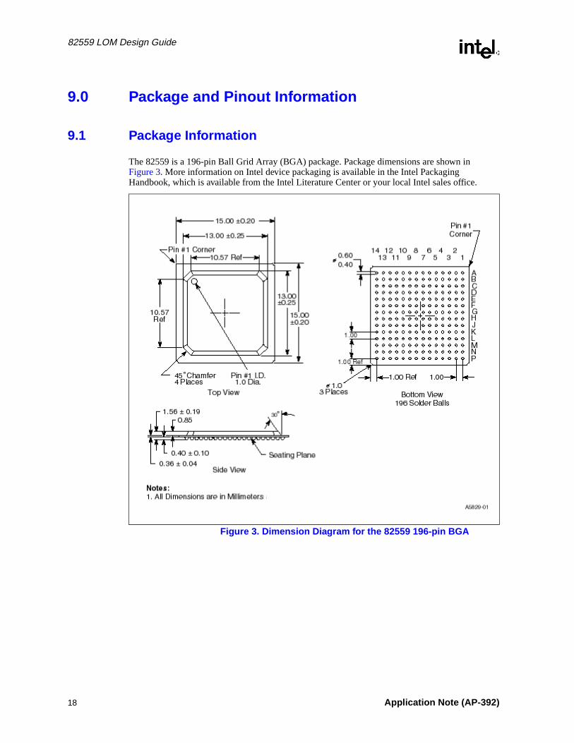
The 82559 is a 196-pin Ball Grid Array (BGA) package. Package dimensions are shown in Figure 3. More information on Intel device packaging is available in the Intel Packaging Handbook, which is available from the Intel Literature Center or your local Intel sales office.
Figure 3. Dimension Diagram for the 82559 196-pin BGA
18 Application Note (AP-392)

82559 LOM Design Guide
9.2 Pinout Information
9.2.1 82559 Pin Assignments
Table 1. 82559 Pin Assignments
Pin Name Pin Name Pin Name
A1 NC A2 SERR# A3 VCCPP
A4 IDSEL A5 AD25 A6 PME#
A7 VCCPP A8 AD30 A9 ALTRST#
A10 SMBCLK A11 VCCPT A12 LILED
A13 TEST A14 NC
B1 AD22 B2 AD23 B3 VSSPP
B4 AD24 B5 AD26 B6 AD27
B7 VSSPP B8 AD31 B9 ISOLATE#
B10 SMBALRT# B11 SPEEDLED B12 TO
B13 RBIAS100 B14 RBIAS10
C1 AD21 C2 RST# C3 REQ#
C4 C/BE3# C5 CSTSCHG C6 AD28
C7 AD29 C8 CLKRUN# C9 SMBD
C10 VSSPT C11 ACTLED C12 VREF
C13 TDP C14 TDN
D1 AD18 D2 AD19 D3 AD20
D4 VSS D5 VSS D6 VSS
D7 VSS D8 VSS D9 NC
D10 NC D11 VSS D12 TI
D13 TEXEC D14 TCK
E1 VCCPP E2 VSSPP E3 AD17
E4 VSS E5 VSS E6 VSS
E7 VSS E8 VSS E9 VSS
E10 VSS E11 VSS E12 VCC
E13 RDP E14 RDN
F1 IRDY# F2 FRAME# F3 C/BE2#
F4 VSS F5 VSS F6 VSS
F7 VSS F8 VSS F9 VSS
F10 VSS F11 VSS F12 FLD2
F13 FLD1 F14 FLD0
G1 CLK G2 VIO G3 TRDY#
G4 NC G5 VCC G6 VCC
G7 VSS G8 VSS G9 VSS
G10 VSS G11 VSS G12 FLD3
G13 VCCPL G14 VSSPL
Application Note (AP-392) 19

82559 LOM Design Guide
H1 STOP# H2 INTA# H3 DEVSEL#
H4 NC H5 VCC H6 VCC
H7 VCC H8 VCC H9 VSS
H10 VSS H11 VSS H12 FLD6
H13 FLD5 H14 FLD4
J1 PAR J2 PERR# J3 GNT#
J4 NC J5 VCC J6 VCC
J7 VCC J8 VCC J9 VCC
J10 VCC J11 VCC J12 FLA1
J13 FLA0 J14 FLD7
K1 AD16 K2 VSSPP K3 VCCPP
K4 VCC K5 VCC K6 VCC
K7 VCC K8 VCC K9 VCC
K10 VCC K11 VCC K12 VSSPL
K13 VCCPL K14 FLA2
L1 AD14 L2 AD15 L3 C/BE#1
L4 VCC L5 VCC L6 VSS
L7 NC L8 NC L9 VCC
L10 VCC L11 VSS L12 FLA5
L13 FLA4 L14 FLA3
M1 AD11 M2 AD12 M3 AD13
M4 C/BE0# M5 AD5 M6 VSSPP
M7 AD1 M8 FLOE# M9 FLWE#
M10 FLA15/EESK M11 FLA12 M12 FLA11
M13 FLA7 M14 FLA6
N1 VSSPP N2 AD10 N3 AD9
N4 AD7 N5 AD4 N6 VCCPP
N7 AD0 N8 VCCPL N9 FLCS#
N10 FLA14/EEDO N11 X1 N12 VSSPL
N13 FLA10 N14 FLA8/IOCHRDY
P1 NC P2 VCCPP P3 AD8
P4 AD6 P5 AD3 P6 AD2
P7 EECS P8 VSSPL P9 FLA16
P10 FLA13/EEDI P11 X2 P12 VCCPL
P13 FLA9 P14 NC
Table 1. 82559 Pin Assignments
Pin Name Pin Name Pin Name
20 Application Note (AP-392)
82559 LOM Design Guide
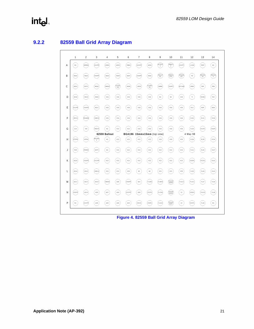
9.2.2 82559 Ball Grid Array Diagram
Figure 4. 82559 Ball Grid Array Diagram
N CF L A 9V C C P LX 2F L A 1 3 /E E D IF L A 1 6V S S P LE E C SA D 2A D 3A D 6A D 8V C C P PN C
F L A 8F L A 1 0V S S P LX 1F L A 1 4 /E E D OF L C S #V C C P LA D 0V C C P PA D 4A D 7A D 9A D 1 0V S S P P
F L A 6F L A 7F L A 1 1F L A 1 2F L A 1 5 /E E S K
F L W E #F L O E #A D 1V S S P PA D 5C B E 0 #A D 1 3A D 1 2A D 1 1
F L A 3F L A 4F L A 5V S SV C CV C CN CN CV S SV C CV C CC B E 1 #A D 1 5A D 1 4
F L A 2V C C P LV S S P LV C CV C CV C CV C CV C CV C CV C CV C CV C C P PV S S P PA D 1 6
F L D 7F L A 0F L A 1V C CV C CV C CV C CV C CV C CV C CN CG N T #P E R R #P A R
F L D 4F L D 5F L D 6V S SV S SV S SV C CV C CV C CV C CN CD E V S E L
#I N T A #S T O P #
V S S P LV C C P LF L D 3V S SV S SV S SV S SV S SV C CV C CN CT R D Y #V I OC L K
F L D 0F L D 1F L D 2V S SV S SV S SV S SV S SV S SV S SV S SC B E 2 #F R A M E #I R D Y #
R D NR D PV C CV S SV S SV S SV S SV S SV S SV S SV S SA D 1 7V S S P PV C C P P
T C KT E X E CTIV S SN CN CV S SV S SV S SV S SV S SA D 2 0A D 1 9A D 1 8
T D NT D PV R E FA C T L E DV S S P TS M B DC L K R U
N #A D 2 9A D 2 8
C S T S CH G
C B E 3 #R E Q #R S T #A D 2 1
R B I A S 10
R B I A S 10 0
T OS P E E D LE D
S M B A LR T #
I S O L A TE #
A D 3 1V S S P PA D 2 7A D 2 6A D 2 4V S S P PA D 2 3A D 2 2
N CT E S TL I L E DV C C P TS M B C L
KA L T R S T
#A D 3 0V C C P PP M E #A D 2 5I D S E LV C C P PS E R R #N CA
B
C
D
E
F
G
H
J
K
L
M
N
P
1 2 3 4 5 6 7 8 9 10 11 12 13 14
82559 Ballout BGA196 15mmx15mm ( top view) 4 May 98
Application Note (AP-392) 21

82559 LOM Design Guide
10.0 Bill of Materials
Part Part Number Quantity Reference Designator
22 pF Capacitor C603C220J5GAC-T/R Kemet 2 C1, C2
0.1 uF Capacitor 0603YC104KAT$A AVX 3 C3, C5, C7
8.2 pF Capacitor 1 C4
1500 pF Capacitor 1 C6
LED 2 D1, D2
RJ45 connector 78186-003 Berg 1 J1
62 KΩ Resistor 3 R1, R2, R8
330 Ω Resistor MCR03EZ$J#331 Rohm 2 R3, R4
549 Ω Resistor ERJ3EKF5490FT Panasonic 1 R7
619 Ω Resistor ERJ3EKF6190V Panasonic 1 R8
100 Ω Resistor ERJ3EKF1000V Panasonic 2 R9, R14
75 Ω Resistor EXB38V750JV Panasonic 4 R10, R11, R12, R13
1:1 Magnetics H1012T Pulse Engineering 1 T1
82559 Intel 1 U1
93C46 EEPROM AT92C46A-10SC2.7 Atmel 1 U2
PLCC Socket 821977-1 AMP 1 U3
25 MHz Crystal TT-SMDC-25.000-20T Raltron 1 Y1
22 Application Note (AP-392)
82559 LOM Design Guide
notes
ME# te in
well
ed to
11.0 Appendix A: 82559/PIIX4 LOM Designs
The Intel 82559 is fully compatible with the Intel PCI to ISA/IDE Xcelerator 4 (PIIX4). The following pages provide a complete reference design for a 82559/PIIX4 solution. Schematic are also provided below.
Schematic Notes
• GPI1 of the PIIX4 is used for the PME# input from the 82559. It should also be used for Pinputs from PCI slots. GPI1 can cause SMI, SCI, and Resume events allowing it to operaAdvanced Configuration and Power Interface (ACPI) and Advanced Power Management(APM) applications.
• The PWR_GOOD signal feeds into the Power Good (PWROK) input pin of the PIIX4 as as discrete logic for the ISOLATE# signal
• LAN_WAKE is a 50 ms pulse used in APM WOL cases to wake the system. It is connectthe LID input of the PIIX4 which allows for resume events (no SMI and no SCI).
Information on the PIIX4 can be obtained from the Intel 82371AB PCI-to-ISA/IDE Xcelerator(PIIX4) Datasheet.
Application Note (AP-392) 23

82559 LOM Design Guide
24 Application Note (AP-392)

A
A
B
B
C
C
D
D
E
E
4 4
3 3
2 2
1 1
REVISION 0.5
** PLEASE NOTE THESE SCHEMATICS ARE SUBJECT TO CHANGE
THESE SCHEMATICS ARE PROVIDED AS IS WITH NO WARRANTIESWHATSOEVER, INCLUDING ANY WARRANTY OF MERCHANTABILITY,FITNESS FOR ANY PARTICULAR PURPOSE, OR ANY WARRANTYOTHERWISE ARISING OUT OF PROPOSAL, SPECIFICATION ORSAMPLES.
Information in this document is provided in connectionwith Intel products. No license, express or implied, byestoppel or otherwise, to any intellectual propertyrights is granted by this document. Except as providedin Intel's Terms and Conditions of Sale for such products, Intel assumes no liability whatsoever, andIntel disclaims any express or implied warranty,relating to sale and/ or use of Intel products includingliability or warranties relating to fitness for aparticular purpose, merchantability, or infringement ofany patent, copyright or other intellectual propertyright. Intel products are not intended for use inmedical, life saving, or life sustaining applications.
Intel may make changes to specifications and productDescriptions at any time, without notice. The Intel82559 10/100Mbit LAN may contain design defects orerrors known as errata, which may cause the product todeviate from published specifications. Currentcharacterized errata are available on request.
Copyright © Intel Corporation 1998.
*Third- party brands and names are the property of theirrespective owners.
Cover Sheet
2
3Physical Interface
1
82559
REV Descrip tion Date
01 Initial A1 Step Sch ematic Release
02 Initial B-Step Sch ematic Release
03 Updated Phy Passive Values and a dded Connection to pin P2
04Corrected improper connection on pin P2 and added clarifying
notes to VIO pin connections 11/29/98
10/30/98
07/06/98
04/29/98
Revisions
05
05 Final B-5 Step Sch ematic Release 12/18/98
3of 3of 3of 3of
Doc
82559 Pi ix4 LOM Reference Design
NPD-NIOJF3-4142111 N.E. 25th Ave.Hillsboro, OR 97124-5961
B
1 3Tuesday, December 22, 1998
Title
Size Documen t Number Rev
Date: Sheet of
t leni

A
A
B
B
C
C
D
D
E
E
4 4
3 3
2 2
1 1
RBIAS10 AND RBI AS100
SHOULD BE "TUNED" FOR
YOUR APPLICATION. THE
VALUES SHOWN ARE A
GOOD STARTING VALUE
TO
PC
I B
US
TO PIIX4
The SMBus conne ction
provides access to the
TCO features of the
82559. Connect the
SMBCLK and SMBD p ins to
the systems TCO
controller, or pull them
up to the 3.3 volt rail
through 100K resi stors
if not used. These
signals should not be
connected in emb edded
designs.
The 82559 can drive three
LEDs with the cath ode of
each device connec ted to
the 82559 as shown with
the SPEEDLED, or a two LED
configuration can be
employed, as shown. In
the two LED config uration
the Link and and A ctivity
functions would s hare a
indicator. In this scheme
the LINK LED would flash
LOW whenever activ ity was
detected.
The ISOLATE signal should be a signal that is driven LOW
just prior to the PCI bus shutting down, and it should be
driven HIGH imediately following the PCI reactivating.
VREF: EXTERNAL VREF MAYBE APPLIED HERE IF THE INTERNAL REFERENCE
IS NOT USED. THE INTERNAL REFERNCE IS RECOM MENDED, BUT IF AN
EXTERNAL REFERENCE IS IMPLEMENTED, THEN THIS WILL CAUSE THE RBIAS
VALUES TO CHANGE
1) The decoup ling
capacitor should be
added to VIO pin.
2) The voltage on VIO determines the slope of the si gnals on the bus. So
although the device will communicate if VIO is conne cted to 3.3V in 3.3V
PCI systems, optimal performance will be acheived if this signal is
connected to +5V in PCI bus systems regardless of Bus voltage.
All Vcc Pins are connected together on the boardlevel. The power on the symbol is broken downbetween Core power (Vcc), Local Bus Power (Vccpl),Transmit Power (Vcct), and PCI power (Vccpp) justfor clarity. See enclosed table for Vcc pins.
All Vss Pins are connected together on the boardlevel. The power on the symbol is broken downbetween Core power (Vss), Local Bus Power (Vsspl),Transmit Power (Vsst), and PCI power (Vsspp) justfor clarity. See enclosed table for a listing ofVss pins.
Pulldown resistors are
utilized on strapped pins
to enable the NA NDtree
test mode to work. The
value of 62K was chosen
Strictly on the ba sis of
Intel's test fix turing
requirements. Other
values can be used, but it
is recommended that
resistors be used other
that hard strapping the
pins.
Doc 05
82559 Reference Design
B
2 3Tuesday, December 22, 1998
Title
Size Documen t Number Rev
Date: Sh eet of
S E R R #
C/BE1
A D 27
ISOLATE#
A D 18
IDSEL
C/BE2
A D 26
A D 23A D 22A D 21
C L K R U N #
E E CS
A D 10
EESK
PME#AUX_GOOD
INTA
A D 4
RST#
A D 12
A D 0
C L K
A D 29
EEDI
A D 19
A D 17
GNT#
P E R R #
A D 31
A D 7
C/BE3
A D 13
A D 6
A D 1
A D 28
A D 25A D 24
A D 3
C/BE0
A D 30
A D 20
A D 16A D 15A D 14
E E D O
A D 5
A D 2
R E Q#
A D 11
A D 9A D 8
AD[31:0]
C/BE[3:0]
3VSB
PCI_5V
3VSB
3VSB
Y1
25MHz
12
R 3
330
12
C 1
0.1uF
12
R 4
3.3K
12
R 5
62K
12
R 862K
12
R 1
62K
12
R 6
549
1 2
R 7
619
1 2
C 2
22pF
12
C 3
22pF
12
D 2
L E D
12
R 2
330
1 2
D 1
L E D
12
U 2
93C46
1
2
3
4
8
C S
S K
DI
D O
VC
C
82559 B-5
196 PIN BGA
U1
N 7M 7P6P5N 5M 5P4N 4P3N 3N 2M 1M 2M 3L1L2K1E3D 1D 2D 3C 1B1B2B4A5B5B6C 6C 7A8B8
M 4L3F3C 4F2F1G 3H 3H 1J1H 2J2A2A4C 3J3C 2G 1B9A9
A10C 9
B10N 1 1P11
G 2 A12C 1 1B11
C 1 3
C 1 4
E13
E14
C 5A6
P9M 1 0N 1 0P10M 1 1M 1 2N 1 3P13N 1 4M 1 3M 1 4L12L13L14K14J12J13J14H 1 2H 1 3
F14F13F12G 1 2H 1 4
P7N 9
M 8M 9
C 8
A13D 1 3D 1 4D 1 2
B14
B13
C 1 2
B12
A D 0A D 1A D 2A D 3A D 4A D 5A D 6A D 7A D 8A D 9A D 1 0A D 1 1A D 1 2A D 1 3A D 1 4A D 1 5A D 1 6A D 1 7A D 1 8A D 1 9A D 2 0A D 2 1A D 2 2A D 2 3A D 2 4A D 2 5A D 2 6A D 2 7A D 2 8A D 2 9A D 3 0A D 3 1
C/BE0#C/BE1#C/BE2#C/BE3#F R A M E #IRDY#TRDY#D E V S E L #STOP#P A RINTA#P E R R #S E R R #IDSELR E Q #GNT#RST#C L KISOLATE#ALTRSt#
S M B C L KS M B D
S M B A L R T #X1X2
VIO LILEDA C T L E D
S P E E D L E D
TDP
TDN
R D P
R D N
C S T S C H G / W O LP M E #
FLA16 /CLK25FLA15 /EESKFLA14 /EEDO
FLA13/EEDIF L A 1 2 / M C N T S M #
FLA11/MINTFLA10 /MRING#
FLA9 /MRSTFLA8/ IOCHRDY
FLA7 /CLKENFLA6FLA5FLA4FLA3FLA2
F L A 1 / A U X P W RFLA0 /PCIMODE#
F L D 7F L D 6F L D 5
F L D 0F L D 1F L D 2F L D 3F L D 4
E E C SFLCS# /AEN
F L O E #F L W E #
C L K R U N #
TESTTEXEC
TCKTI
RBIAS10
RBIAS100
V R E F
TO
PME#
FRAME#IRDY#TRDY#D E VSEL#STOP#P A R
TDN
TDP
R D P
R D N

A
A
B
B
C
C
D
D
E
E
4 4
3 3
2 2
1 1
TERMPLANE
CHASSIS GROUND
USE PLANE FOR
THIS SIGNAL
OPTIONAL CAP
TO HELP WITH
EFT
CONFORMANCE
CREATE TERMINATION PLANE IN PWB. THIS
PLANE WILL ACT A PATH FOR LO W-FREQUENCY
NOISE THAT MAYBE COUPLED TO UNUSED PINS.
THE PLANE SHOULD NOT HAVE ANY DIRECT
COMNECTION.
KEEP TRACE LENGTH FROM MAGNETICS TO RJ-45 CONNECTOR UNDER 1 INCH.
KEEP ALL TERMI NATION
RESISTORS AS CLOSE TO
THE 82559 AS PO SSIBLE
USE SYMETRICAL 100
OHM DIFFERENTIAL
TRACES FOR RDP/RDN
AND TDP/TDN
This capicitor is not normally ins talled, but a
placement location can be provi ded. It may
need to be placed based on the r esults of FCC
conformance testing. If it is req uired, values
in the pico farad range would be used. Large
capicitance values installed in this location
will have a negative effect on long cable
performance. so care must be taken in
selecting values used.
Place decoupling capacitiors as close to the 82559 as
possible. If component placements are utilized on the
bottom side of the board than place de coupling under
the 82559.
Doc 05
82559 Reference Design
B
3 3Tuesday, December 22, 1998
Title
Size Documen t Number Rev
Date: Sh eet of
TDN
TDP
3VSB
R 91001%
12
R 1 4
1201%
12
C 6
1500pF
1 2
T1
1 :1 MAGNETICS
14
16
15
1
2
3
10
11
7
12
5
6
TDC
TD+
TD-
R D +
RD-
R D C
TX+
TX-
RX+
C M T
R X C
RX-
R 1 0
75
12
J1
RJ45
1
2
3
4
5
6
7
8
9 10
1
2
3
4
5
6
7
8 9 10
C 4
12
C 5
0.1uF
12
R 1 1
75
12
R 1 2
75
12
R 1 3
75
12
C 7
0.1uF
12
C 1 0
0.1uF
12
C 1 1
0.1uF
12
C 1 2
0.1uF
12
C 1 3
0.1uF
12
C 1 4
0.1uF
12
C 1 5
0.1uF
12
C 1 6
0.1uF
12
C 1 7
0.1uF
12
C 1 8
0.1uF
12
C 1 9
0.1uF
12
C 9
4.7uF
12
C 8
4.7uF
12