
Reliability and Characteristics for Wafer Level Chip Scale ...
Upload
independentCategory
view
2download
0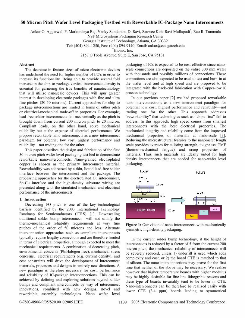
0-7803-8906-9/05/$20.00 ©2005 IEEE 2005 Electronic Components and Technology Conference
50 Micron Pitch Wafer Level Packaging Testbed with Reworkable IC-Package Nano Interconnects
Ankur O. Aggarwal, P. Markondeya Raj, Venky Sundaram, D. Ravi, Sauwee Koh, Ravi Mullapudi*, Rao R. Tummala NSF Microsystems Packaging Research Center
Georgia Institute of Technology, Atlanta, GA 30332 Tel: (404) 894-1250, Fax: (404) 894-9140, Email: [email protected]
*Hionix, Inc. 2157 O'Toole Avenue, Suite E, San Jose, CA 95131
Abstract
The decrease in feature sizes of micro-electronic devices has underlined the need for higher number of I/O's in order to increase its functionality. Being able to provide several fold increase in the chip-to-package vertical interconnect density is essential for garnering the true benefits of nanotechnology that will utilize nanoscale devices. This will spur greater interest in developing electronic packages with fine and ultra fine pitches (20-50 microns). Current approaches for chip to package interconnections are limited in terms of either pitch or electrical-mechanical trade-off in properties. For example, lead free solder interconnects fail mechanically as the pitch is brought down from current 200 micron pitch to 20 micron. Compliant leads, on the other hand, solve mechanical reliability but at the expense of electrical performance. We propose reworkable nano interconnects as a new interconnect paradigm for potential low cost, highest performance and reliability—not trading one for the other.
This paper describes the design and fabrication of the first 50 micron pitch wafer level packaging test bed to demonstrate reworkable nano-interconnects. Nano-grained electroplated copper is chosen as the primary interconnect material. Reworkability was addressed by a thin, liquid lead-free solder interface between the interconnect and the package. The processing approaches for the electroplated Cu interconnect, Sn-Cu interface and the high-density substrate wiring are presented along with the simulated mechanical and electrical performance of the interconnects.
1. Introduction Decreasing I/O pitch is one of the key technological
barriers identified by the 2003 International Technology Roadmap for Semiconductors (ITRS) [1]. Downscaling traditional solder bump interconnect will not satisfy the thermo-mechanical reliability requirements at very fine pitches of the order of 50 microns and less. Alternate interconnection approaches such as compliant interconnects typically require lengthy connections and are therefore limited in terms of electrical properties, although expected to meet the mechanical requirements. A combination of decreasing pitch, environmental concerns (Pb/Halogen free), mechanical stress concerns, electrical requirements (e.g. current density), and cost constraints will drive the development of interconnect materials, processes and designs in entirely new directions. A new paradigm is therefore necessary for cost, performance and reliability of IC-package interconnections. This can be achieved by defining and exploring solutions beyond solder bumps and compliant interconnects by way of interconnect innovations, combined with new designs, novel and reworkable assembly technologies. Nano wafer level
packaging of ICs is expected to be cost effective since nano-scale connections are deposited on the entire 300 mm wafer with thousands and possibly millions of connections. These connections are also expected to be used to test and burn-in at the wafer level and at high speed and are proposed to be integrated with the back-end fabrication with Copper-low K process technology.
In our previous paper [2] we had proposed reworkable nano interconnections as a new interconnect paradigm for potential low cost, highest performance and reliability—not trading one for the other. This approach addresses “reworkability” that technologies such as “chips first” fail to address. In this approach, high speed comes from smallest interconnects with the best electrical properties. The mechanical integrity and relability come from the improved mechanical properties of materials at nano-scale [3]. Reducing the microstructural features to the nanometer length scale provides avenues for tailoring strength, toughness, TMF (thermo-mechanical fatigue) and creep properties of materials. Thus, such materials are ideally suited for high density interconnects that are needed for nano-wafer level packaging.
Figure 1: Our vision of nano-interconnects with mechanically symmetric high-density packaging.
In the current solder bump technology, if the height of interconnects is reduced by a factor of 5 from the current 200 micron pitch, the mechanical reliability of interconnects will be severely reduced, unless 1) underfill is used which adds complexity and cost, or 2) the board CTE is matched to that of silicon. The nano interconnections may prove for the first time that neither of the above may be necessary. We realize however that higher temperature boards with higher modulus may be highly desirable for fine line lithogrphic reasons and these type of boards invariably tend to be lower in CTE. Nano-interconnects can be therefore be realized easily with lower CTE (2-4 ppm) boards leading to symmetrical
1139
2005 Electronic Components and Technology Conference
structures on both sides of the joint as is shown in Figure 1. [4]
Low cost comes from thin film or self assembly deposition of nano structures on the entire 300 mm wafer. Nano-scale interconnects can offer these benefits as well as lower the pitch along with improved electrical and mechanical performance to accommodate any future system demands; thus realizing the goal of unlimited I/Os. Reworkability is needed to be able to replace bad chips with good chips, particularly with MCM, SIP or SOP approaches. We propose thin liquid interfaces to accomplish this on the package side. In this paper, the new nano-interconnect concept is demonstrated through a 50 micron pitch testbed. The height of the interconnect is reduced from the current industry standard of 200 microns to 50 microns.
2. Electrical Modeling of Nano Interconnects Interconnects have parasitic inductance, resistance and
capacitance associated with them. Typically, small length of interconnects is desired for faster signal propagation and low losses particularly at higher frequency. Parasitics increase RC delays and reduces the speed of operation of the circuits. The fine pitch of the interconnects increases cross talk between adjacent connections which could result in signal distortion and spurious data transfer. Future ICs operating at high frequencies of 30-60 GHz, signal bandwidths of Tbps and lower supply voltages require minimal R, L and C for the interconnects. Current fine pitch WLP approaches such as compliant interconnects cannot meet the R, L, C requirements of future. The mechanical requirements on the other hand dictates a lengthier interconnect design which comes at a price of higher inductance and resistance. Therefore electrical modeling of interconnects is an important step in design and analysis of interconnect performance.
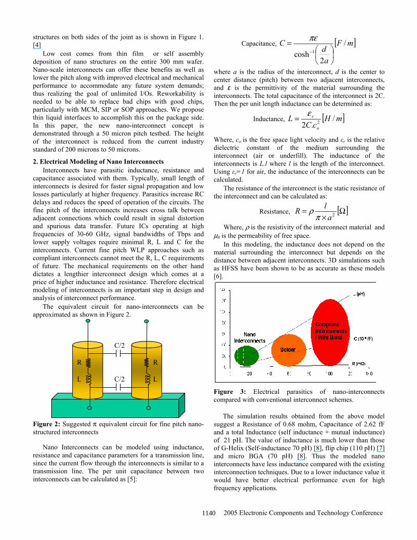
The equivalent circuit for nano-interconnects can be approximated as shown in Figure 2.
R
L C/2 L
R
C/2
Figure 2: Suggested π equivalent circuit for fine pitch nano-structured interconnects
Nano Interconnects can be modeled using inductance, resistance and capacitance parameters for a transmission line, since the current flow through the interconnects is similar to a transmission line. The per unit capacitance between two interconnects can be calculated as [5]:
Capacitance, [ ]mF
ad
C /
2cosh 1
=−
πε
where a is the radius of the interconnect, d is the center to center distance (pitch) between two adjacent interconnects, and ε is the permittivity of the material surrounding the interconnects. The total capacitance of the interconnect is 2C. Then the per unit length inductance can be determined as:
Inductance, [ ]mHcC
Lo
r /.2 2
ε=
Where, co is the free space light velocity and εr is the relative dielectric constant of the medium surrounding the interconnect (air or underfill). The inductance of the interconnects is L.l where l is the length of the interconnect. Using εr=1 for air, the inductance of the interconnects can be calculated.
The resistance of the interconnect is the static resistance of the interconnect and can be calculated as:
Resistance, [ ]Ω×
= 2alR
πρ
Where, ρ is the resistivity of the interconnect material and µ0 is the permeability of free space.
In this modeling, the inductance does not depend on the material surrounding the interconnect but depends on the distance between adjacent interconnects. 3D simulations such as HFSS have been shown to be as accurate as these models [6].
Figure 3: Electrical parasitics of nano-interconnects compared with conventional interconnect schemes.
The simulation results obtained from the above model suggest a Resistance of 0.68 mohm, Capacitance of 2.62 fF and a total Inductance (self inductance + mutual inductance) of 21 pH. The value of inductance is much lower than those of G-Helix (Self-inductance 70 pH) [8], flip chip (110 pH) [7] and micro BGA (70 pH) [8]. Thus the modeled nano interconnects have less inductance compared with the existing interconnection techniques. Due to a lower inductance value it would have better electrical performance even for high frequency applications.
1140
2005 Electronic Components and Technology Conference
3. Thermo-mechanical Reliability Analysis of Nano Interconnects
Thermo-mechanical loads on the interconnects arise from the global and local CTE mismatch between the package and IC. The stresses in turn are determined by the geometry of the interconnects and the the load. Thermal cycling hence results in failure from fatigue, typically estimated from the following equation.
2
)(
∆∆ TLhFailureforCyclesLifeFatifueα
α
Where, L is the length of the die and h is the height of the interconnect. The stresses and plastic strain increase with shorter interconnections thereby lowering the fatigue life. Current solders cannot meet the fatigue resistance because of their inferior mechanical properties. By employing underfills, thermal stresses at the solder bumps can be effectively reduced to improve package reliability. Nevertheless, underfill technology is costly and underfill dispensing becomes increasingly complicated with the shorter gaps required for future interconnects. Usage of underfill is also known to cause the package to deform, leading to large peeling stresses at the die-underfill and die-solder interfaces which significantly impact copper-low-K and package reliability.
50 µm
25 µm
Interconnect Pitch = 50 Microns
50 µm
25 µm
50 µm
25 µm
Interconnect Pitch = 50 Microns
Silicon (thickness = 500 µm)
Titanium (thickness = 0.5 µm)
Copper (thickness = 1.0 µm)
Nano Copper (thickness = 25.0 µm)
Gold (thickness = 0.5 µm)
Solder (Sn- 0.5Cu) (thickness = 1.0 µm)
Solder Mask (thickness = 1.0 µm)
Substrate (thickness = 1.0 mm
28 µm
25 µm
Silicon (thickness = 500 µm)
Titanium (thickness = 0.5 µm)
Copper (thickness = 1.0 µm)
Nano Copper (thickness = 25.0 µm)
Gold (thickness = 0.5 µm)
Solder (Sn- 0.5Cu) (thickness = 1.0 µm)
Solder Mask (thickness = 1.0 µm)
Substrate (thickness = 1.0 mm
28 µm
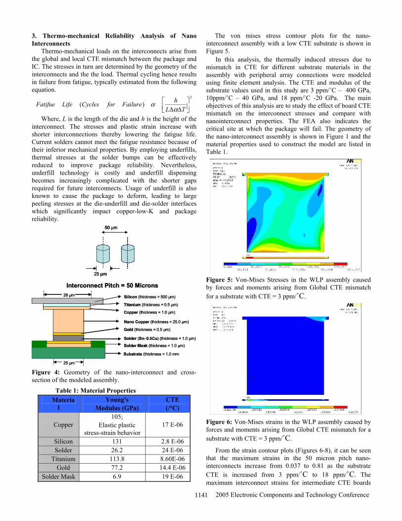
25 µm Figure 4: Geometry of the nano-interconnect and cross-section of the modeled assembly.
Table 1: Material Properties Materia
l Young's
Modulus (GPa) CTE (/°C)
Copper 105;
Elastic plastic stress-strain behavior
17 E-06
Silicon 131 2.8 E-06 Solder 26.2 24 E-06
Titanium 113.8 8.60E-06 Gold 77.2 14.4 E-06
Solder Mask 6.9 19 E-06
The von mises stress contour plots for the nano-interconnect assembly with a low CTE substrate is shown in Figure 5.
In this analysis, the thermally induced stresses due to mismatch in CTE for different substrate materials in the assembly with peripheral array connections were modeled using finite element analysis. The CTE and modulus of the substrate values used in this study are 3 ppm/˚C – 400 GPa, 10ppm/˚C – 40 GPa, and 18 ppm/˚C -20 GPa. The main objectives of this analysis are to study the effect of board CTE mismatch on the interconnect stresses and compare with nanointerconnect properties. The FEA also indicates the critical site at which the package will fail. The geometry of the nano-interconnect assembly is shown in Figure 1 and the material properties used to construct the model are listed in Table 1.
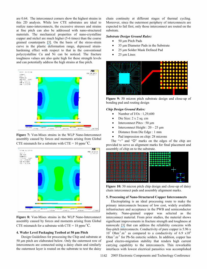
Figure 5: Von-Mises Stresses in the WLP assembly caused by forces and moments arising from Global CTE mismatch for a substrate with CTE = 3 ppm/˚C.
Figure 6: Von-Mises strains in the WLP assembly caused by forces and moments arising from Global CTE mismatch for a substrate with CTE = 3 ppm/˚C.
From the strain contour plots (Figures 6-8), it can be seen that the maximum strains in the 50 micron pitch nano-interconnects increase from 0.037 to 0.81 as the substrate CTE is increased from 3 ppm/˚C to 18 ppm/˚C. The maximum interconnect strains for intermediate CTE boards
1141
2005 Electronic Components and Technology Conference
are 0.64. The interconnect corners show the highest strains in this 2D analysis. While low CTE substrates are ideal to realize nano-interconnects, the excessive stresses and strains at fine pitch can also be addressed with nano-structured materials. The mechanical properties of nano-crystalline copper and nickel are much higher (5-6 times) than the coarse grained counterparts [3]. On the basis of the stress-strain curve in the plastic deformation range, depressed strain-hardening effect with respect to that in the conventional polycrystalline Cu and Ni can be noticed. The fracture toughness values are also quite high for these strength levels and can potentially address the high strains at fine pitch.
Figure 7: Von-Mises strains in the WLP Nano-Interconnect assembly caused by forces and moments arising from Global CTE mismatch for a substrate with CTE = 10 ppm/˚C.
Figure 8: Von-Mises strains in the WLP Nano-Interconnect assembly caused by forces and moments arising from Global CTE mismatch for a substrate with CTE = 18 ppm/˚C.
4. Wafer Level Packaging Testbed at 50 µm Pitch Design Guidelines for processing the Chip and substrate at
50 µm pitch are elaborated below. Only the outermost row of interconnects are connected using a daisy chain and similarly the outermost layer is routed on the substrate to test the daisy
chain continuity at different stages of thermal cycling. Moreover, since the outermost periphery of interconnects are expected to fail first, only those interconnect are routed on the substrate.
Substrate Design Ground Rules: • 50 µm Pitch Pads • 35 µm Diameter Pads in the Substrate • 25 µm Solder Mask Defined Pad • 25 µm Lines
Figure 9: 50 micron pitch substrate design and close-up of bonding pad and routing design
Chip Design Ground Rules: • Number of I/Os : 1,29,600 • Die Size: 2 x 2 sq. cm • Interconnect Pitcs : 50 µm • Interconnect Height : 20 – 25 µm • Distance from Die Edge : 1 mm • Pad impression on chip: 28 microns
The “+” and “О” marks on the edges of the chip are provided to serve as alignment marks for final placement and assembly of chip on to the substrate.
Figure 10: 50 micron pitch chip design and close-up of daisy chain interconnect pads and assembly alignment marks.
5. Processing of Nano-Structured Copper Interconnects Electroplating is an ideal processing route to make the
primary interconnects because of low cost, widely available infrastructure and acceptance in the PWB and semiconductor industry. Nano-grained copper was selected as the interconnect material. From prior studies, the material shows significant improvements in fracture strength and toughness at nanoscale [3] that can address the reliability concerns with fine-pitch interconnects. Conductivity of pure copper is 5.96 x 10⁷ Ohm-1.m-1 as compared to a conductivity of 6.9 x10⁶ Ohm-1.m-1 for Pb-Sn eutectic solders. In addition, copper has good electro-migration stability that renders high current carrying capability to the interconnects. Thin reworkable interfaces with lowest electrical parasitics was accomplished
1142
2005 Electronic Components and Technology Conference
on the wafer side by a co-sputtering process developed by Hionix Inc.
Interconnect Pads Copper Pads were first fabricated on a silicon substrate. A
0.5 micron titanium layer was first sputtered as a adhesion layer between copper and silicon. Thereafter, a 1.0 micron copper film was sputtered followed by etching of titanim and copper to provide the interconnect pads on the silicon wafer. Once again, a thin copper layer of 400 nm was sputtered as the seed layer for electroplating.
Nano-Structured Copper Interconnect Nano-structured copper interconnects were then fabricated
using the SU-8 Series 2000TM (MicroChem Corp.) photoresist. SU-8 has very high optical transparency which makes it ideally suited for imaging near vertical sidewalls in very thick films, and is near UV (350-400nm) and e-beam imageable. It has superb chemical resistance that makes it suitable for a variety of electrolytic plating bath chemistries. Other advantage includes faster drying of the film.
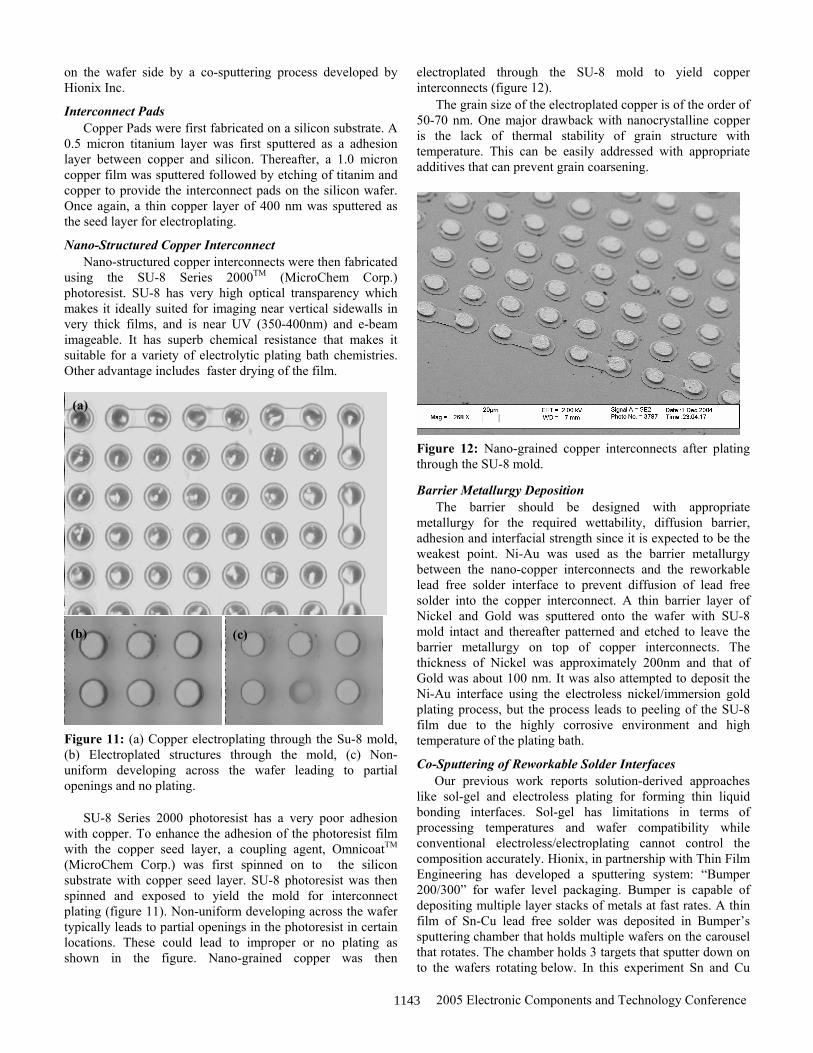
Figure 11: (a) Copper electroplating through the Su-8 mold, (b) Electroplated structures through the mold, (c) Non-uniform developing across the wafer leading to partial openings and no plating.
SU-8 Series 2000 photoresist has a very poor adhesion with copper. To enhance the adhesion of the photoresist film with the copper seed layer, a coupling agent, OmnicoatTM
(MicroChem Corp.) was first spinned on to the silicon substrate with copper seed layer. SU-8 photoresist was then spinned and exposed to yield the mold for interconnect plating (figure 11). Non-uniform developing across the wafer typically leads to partial openings in the photoresist in certain locations. These could lead to improper or no plating as shown in the figure. Nano-grained copper was then
electroplated through the SU-8 mold to yield copper interconnects (figure 12).
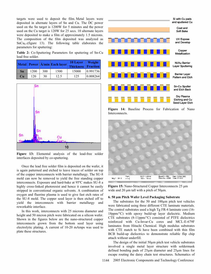
The grain size of the electroplated copper is of the order of 50-70 nm. One major drawback with nanocrystalline copper is the lack of thermal stability of grain structure with temperature. This can be easily addressed with appropriate additives that can prevent grain coarsening.
Figure 12: Nano-grained copper interconnects after plating through the SU-8 mold.
Barrier Metallurgy Deposition The barrier should be designed with appropriate
metallurgy for the required wettability, diffusion barrier, adhesion and interfacial strength since it is expected to be the weakest point. Ni-Au was used as the barrier metallurgy between the nano-copper interconnects and the reworkable lead free solder interface to prevent diffusion of lead free solder into the copper interconnect. A thin barrier layer of Nickel and Gold was sputtered onto the wafer with SU-8 mold intact and thereafter patterned and etched to leave the barrier metallurgy on top of copper interconnects. The thickness of Nickel was approximately 200nm and that of Gold was about 100 nm. It was also attempted to deposit the Ni-Au interface using the electroless nickel/immersion gold plating process, but the process leads to peeling of the SU-8 film due to the highly corrosive environment and high temperature of the plating bath.
Co-Sputtering of Reworkable Solder Interfaces Our previous work reports solution-derived approaches
like sol-gel and electroless plating for forming thin liquid bonding interfaces. Sol-gel has limitations in terms of processing temperatures and wafer compatibility while conventional electroless/electroplating cannot control the composition accurately. Hionix, in partnership with Thin Film Engineering has developed a sputtering system: “Bumper 200/300” for wafer level packaging. Bumper is capable of depositing multiple layer stacks of metals at fast rates. A thin film of Sn-Cu lead free solder was deposited in Bumper’s sputtering chamber that holds multiple wafers on the carousel that rotates. The chamber holds 3 targets that sputter down on to the wafers rotating below. In this experiment Sn and Cu
(a)
(b) (c)
1143
2005 Electronic Components and Technology Conference
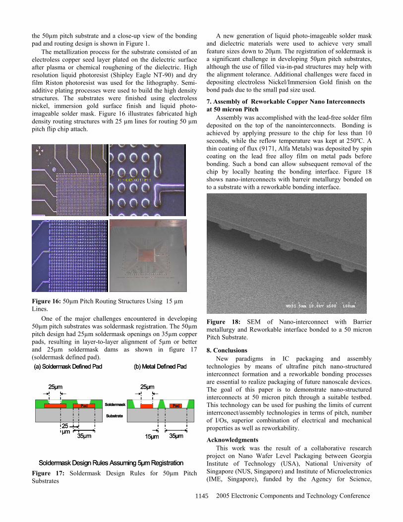
targets were used to deposit the film. Metal layers were deposited in alternate layers of Sn and Cu. The DC power used on the Sn target is 1200W for 5 minutes and the power used on the Cu target is 120W for 25 secs. 10 alternate layers were deposited to make a film of approximately 1.5 microns. The composition of the film deposited was analyzed as SnCu0.7(figure 13). The following table elaborates the parameters for sputtering: Table 2: Co-Sputtering Parameters for sputtering of Sn-Cu lead free solder.
Metal Power Å/min Each layer 10 Layer Thickness
Weight Fraction
Sn 1200 300 1500 15000 0.991736Cu 120 30 12.5 125 0.008264
Figure 13: Elemental analysis of the lead-free solder interfaces deposited by co-sputtering.
Once the lead free solder film is deposited on the wafer, it is again patterned and etched to leave traces of solder on top of the copper interconnects with barrier metallurgy. The SU-8 mold can now be removed to yield the free standing copper interconnects. Exposure and hard-bake at 95ºC makes SU-8 a highly cross-linked photoresist and hence it cannot be easily stripped in conventional organic solvents. A combination of oxygen and fluorine plasma is used to give fast etch rates of the SU-8 mold. The copper seed layer is then etched off to yield the interconnects with barrier metallurgy and reworkable interface.
In this work, interconnects with 25 microns diameter and height and 50 micron pitch were fabricated on a silicon wafer. Shown in the figures below are the nano-structured copper interconnects grown from the bottom seed layer using electrolytic plating. A current of 10-20 mAmps was used to plate these structures.
Si with Cu pads and sputtered Cu
Coat and Soft Bake
UV Expose and Develop
Copper Metallization
Dry Plasma Etching and Cu
Seed Layer Etch
Ni/Au Barrier Layer Sputtering
Barrier Layer Pattern and Etch
Sn-Cu Sputter and Etch Back
Si with Cu pads and sputtered Cu
Coat and Soft Bake
UV Expose and Develop
Copper Metallization
Dry Plasma Etching and Cu
Seed Layer Etch
Ni/Au Barrier Layer Sputtering
Barrier Layer Pattern and Etch
Sn-Cu Sputter and Etch Back
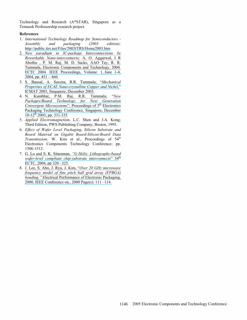
Figure 14: Baseline Process for Fabrication of Nano Interconnects.
Figure 15: Nano-Structured Copper Interconnects 25 µm wide and 20 µm tall with a pitch of 50µm.
6. 50 µm Pitch Wafer Level Packaging Substrate The substrates for the 50 and 100µm pitch test vehicles
were fabricated using three different CTE laminate materials. The control substrates used a high Tg FR-4 laminate core (16-18ppm/°C) with epoxy build-up layer dielectric. Medium CTE substrates (8-11ppm/°C) consisted of PTFE dielectrics reinforced with Cu-Invar-Cu cores and MCL-E-679F laminates from Hitachi Chemical. High modulus substrates with CTE match to Si have been combined with thin film BCB build-up dielectrics to demonstrate reliable flip chip attach without underfill.
The design of the initial 50µm pitch test vehicle substrates involved a single metal layer structure with soldermask defined bonding pads of 25µm diameter and 25µm lines for escape routing the daisy chain test structures. Schematics of
1144
2005 Electronic Components and Technology Conference
the 50µm pitch substrate and a close-up view of the bonding pad and routing design is shown in Figure 1.
The metallization process for the substrate consisted of an electroless copper seed layer plated on the dielectric surface after plasma or chemical roughening of the dielectric. High resolution liquid photoresist (Shipley Eagle NT-90) and dry film Riston photoresist was used for the lithography. Semi-additive plating processes were used to build the high density structures. The substrates were finished using electroless nickel, immersion gold surface finish and liquid photo-imageable solder mask. Figure 16 illustrates fabricated high density routing structures with 25 µm lines for routing 50 µm pitch flip chip attach.
Figure 16: 50µm Pitch Routing Structures Using 15 µm Lines.
One of the major challenges encountered in developing 50µm pitch substrates was soldermask registration. The 50µm pitch design had 25µm soldermask openings on 35µm copper pads, resulting in layer-to-layer alignment of 5µm or better and 25µm soldermask dams as shown in figure 17 (soldermask defined pad).
25µm
25µm
35µm
Substrate
SoldermaskPad
25µm
15µm 35µm
Pad
Soldermask Design Rules Assuming 5µm Registration
(a) Soldermask Defined Pad (b) Metal Defined Pad
25µm
25µm
35µm
Substrate
SoldermaskPad
25µm
15µm 35µm
Pad
Soldermask Design Rules Assuming 5µm Registration
(a) Soldermask Defined Pad (b) Metal Defined Pad
Figure 17: Soldermask Design Rules for 50µm Pitch Substrates
A new generation of liquid photo-imageable solder mask and dielectric materials were used to achieve very small feature sizes down to 20µm. The registration of soldermask is a significant challenge in developing 50µm pitch substrates, although the use of filled via-in-pad structures may help with the alignment tolerance. Additional challenges were faced in depositing electroless Nickel/Immersion Gold finish on the bond pads due to the small pad size used.
7. Assembly of Reworkable Copper Nano Interconnects at 50 micron Pitch
Assembly was accomplished with the lead-free solder film deposited on the top of the nanointerconnects. Bonding is achieved by applying pressure to the chip for less than 10 seconds, while the reflow temperature was kept at 250ºC. A thin coating of flux (9171, Alfa Metals) was deposited by spin coating on the lead free alloy film on metal pads before bonding. Such a bond can allow subsequent removal of the chip by locally heating the bonding interface. Figure 18 shows nano-interconnects with barreir metallurgy bonded on to a substrate with a reworkable bonding interface.
Figure 18: SEM of Nano-interconnect with Barrier metallurgy and Reworkable interface bonded to a 50 micron Pitch Substrate.
8. Conclusions New paradigms in IC packaging and assembly
technologies by means of ultrafine pitch nano-structured interconnect formation and a reworkable bonding processes are essential to realize packaging of future nanoscale devices. The goal of this paper is to demonstrate nano-structured interconnects at 50 micron pitch through a suitable testbed. This technology can be used for pushing the limits of current interrconect/assembly technologies in terms of pitch, number of I/Os, superior combination of electrical and mechanical properties as well as reworkability.
Acknowledgments This work was the result of a collaborative research
project on Nano Wafer Level Packaging between Georgia Institute of Technology (USA), National University of Singapore (NUS, Singapore) and Institute of Microelectronics (IME, Singapore), funded by the Agency for Science,
1145
2005 Electronic Components and Technology Conference
Technology and Research (A*STAR), Singapore as a Temasek Professorship research project.
References 1. International Technology Roadmap for Semiconductors -
Assembly and packaging (2003 edition); http://public.itrs.net/Files/2003ITRS/Home2003.htm
2. New paradigm in IC-package Interconnections by Reworkable Nano-interconnects; A. O. Aggarwal, I R Abothu , P. M. Raj, M. D. Sacks, AAO Tay, R. R. Tummala, Electronic Components and Technology, 2004. ECTC 2004. IEEE Proceedings, Volume: 1, June 1-4, 2004, pp. 451 – 460.
3. S. Bansal, A. Saxena, R.R. Tummala; “Mechanical Properties of ECAE Nano-crystalline Copper and Nickel,” ICMAT 2003, Singapore, December 2003.
4. N. Kumbhat, P.M. Raj, R.R. Tummala; “New Packagre/Board Technology for Next Generation Convergent Microsystems”; Proceedings of 5th Electronics Packaging Technology Conference, Singapore, December 10-12th 2003; pp. 331-335
5. Applied Electromagnetism, L.C. Shen and J.A. Kong; Third Edition, PWS Publishing Company; Boston, 1995.
6. Effect of Wafer Level Packaging, Silicon Substrate and Board Material on Gigabit Board-Silicon-Board Data Transmission; W. Kim et al., Proceedings of 54th Electronics Components Technology Conference; pp. 1506-1512.
7. G. Lo and S. K. Sitaraman, “G-Helix: Lithography-based wafer-level compliant chip-substrate interconnects” 54th ECTC, 2004, pp 320 –325.
8. J. Lee, S. Ahn, J. Ryu, J. Kim, “Over 20 GHz microwave frequency model of fine pitch ball grid array (FPBGA) bonding,” Electrical Performance of Electronic Packaging, 2000, IEEE Conference on., 2000 Page(s): 111 –114.
1146
Copyright © 2022 FDOKUMEN