
480-W, Thin-Profile, 94% Efficiency, Fast Transient Response ...
21
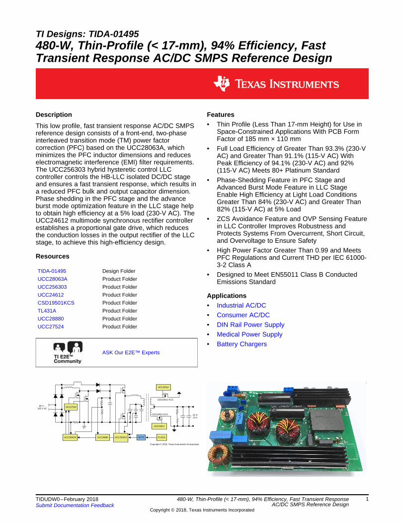
TL431A OPTO UCC256303 UCC24612 UCC28880 UCC24612 24 V/ 20 A CDS19501 KCS CDS19501 KCS UCC27524 UCC28063A 85 V – 265 V AC Copyright © 2018, Texas Instruments Incorporated 1 TIDUDW0 – February 2018 Submit Documentation Feedback Copyright © 2018, Texas Instruments Incorporated 480-W, Thin-Profile (< 17-mm), 94% Efficiency, Fast Transient Response AC/DC SMPS Reference Design TI Designs: TIDA-01495 480-W, Thin-Profile (< 17-mm), 94% Efficiency, Fast Transient Response AC/DC SMPS Reference Design Description This low profile, fast transient response AC/DC SMPS reference design consists of a front-end, two-phase interleaved transition mode (TM) power factor correction (PFC) based on the UCC28063A, which minimizes the PFC inductor dimensions and reduces electromagnetic interference (EMI) filter requirements. The UCC256303 hybrid hysteretic control LLC controller controls the HB-LLC isolated DC/DC stage and ensures a fast transient response, which results in a reduced PFC bulk and output capacitor dimension. Phase shedding in the PFC stage and the advance burst mode optimization feature in the LLC stage help to obtain high efficiency at a 5% load (230-V AC). The UCC24612 multimode synchronous rectifier controller establishes a proportional gate drive, which reduces the conduction losses in the output rectifier of the LLC stage, to achieve this high-efficiency design. Resources TIDA-01495 Design Folder UCC28063A Product Folder UCC256303 Product Folder UCC24612 Product Folder CSD19501KCS Product Folder TL431A Product Folder UCC28880 Product Folder UCC27524 Product Folder ASK Our E2E™ Experts Features • Thin Profile (Less Than 17-mm Height) for Use in Space-Constrained Applications With PCB Form Factor of 185 mm × 110 mm • Full Load Efficiency of Greater Than 93.3% (230-V AC) and Greater Than 91.1% (115-V AC) With Peak Efficiency of 94.1% (230-V AC) and 92% (115-V AC) Meets 80+ Platinum Standard • Phase-Shedding Feature in PFC Stage and Advanced Burst Mode Feature in LLC Stage Enable High Efficiency at Light Load Conditions Greater Than 84% (230-V AC) and Greater Than 82% (115-V AC) at 5% Load • ZCS Avoidance Feature and OVP Sensing Feature in LLC Controller Improves Robustness and Protects Systems From Overcurrent, Short Circuit, and Overvoltage to Ensure Safety • High Power Factor Greater Than 0.99 and Meets PFC Regulations and Current THD per IEC 61000- 3-2 Class A • Designed to Meet EN55011 Class B Conducted Emissions Standard Applications • Industrial AC/DC • Consumer AC/DC • DIN Rail Power Supply • Medical Power Supply • Battery Chargers
-
Upload
khangminh22 -
Category
Documents
-
view
3 -
download
0
Transcript of 480-W, Thin-Profile, 94% Efficiency, Fast Transient Response ...
TL431AOPTOUCC256303
UCC24612
UCC28880
UCC24612
24 V/ 20 A
CDS19501 KCS
CDS19501 KCS
UCC27524
UCC28063A
85 V ±265 V AC
Copyright © 2018, Texas Instruments Incorporated
1TIDUDW0–February 2018Submit Documentation Feedback
Copyright © 2018, Texas Instruments Incorporated
480-W, Thin-Profile (< 17-mm), 94% Efficiency, Fast Transient ResponseAC/DC SMPS Reference Design
TI Designs: TIDA-01495480-W, Thin-Profile (< 17-mm), 94% Efficiency, FastTransient Response AC/DC SMPS Reference Design
DescriptionThis low profile, fast transient response AC/DC SMPSreference design consists of a front-end, two-phaseinterleaved transition mode (TM) power factorcorrection (PFC) based on the UCC28063A, whichminimizes the PFC inductor dimensions and reduceselectromagnetic interference (EMI) filter requirements.The UCC256303 hybrid hysteretic control LLCcontroller controls the HB-LLC isolated DC/DC stageand ensures a fast transient response, which results ina reduced PFC bulk and output capacitor dimension.Phase shedding in the PFC stage and the advanceburst mode optimization feature in the LLC stage helpto obtain high efficiency at a 5% load (230-V AC). TheUCC24612 multimode synchronous rectifier controllerestablishes a proportional gate drive, which reducesthe conduction losses in the output rectifier of the LLCstage, to achieve this high-efficiency design.
Resources
TIDA-01495 Design FolderUCC28063A Product FolderUCC256303 Product FolderUCC24612 Product FolderCSD19501KCS Product FolderTL431A Product FolderUCC28880 Product FolderUCC27524 Product Folder
ASK Our E2E™ Experts
Features• Thin Profile (Less Than 17-mm Height) for Use in
Space-Constrained Applications With PCB FormFactor of 185 mm × 110 mm
• Full Load Efficiency of Greater Than 93.3% (230-VAC) and Greater Than 91.1% (115-V AC) WithPeak Efficiency of 94.1% (230-V AC) and 92%(115-V AC) Meets 80+ Platinum Standard
• Phase-Shedding Feature in PFC Stage andAdvanced Burst Mode Feature in LLC StageEnable High Efficiency at Light Load ConditionsGreater Than 84% (230-V AC) and Greater Than82% (115-V AC) at 5% Load
• ZCS Avoidance Feature and OVP Sensing Featurein LLC Controller Improves Robustness andProtects Systems From Overcurrent, Short Circuit,and Overvoltage to Ensure Safety
• High Power Factor Greater Than 0.99 and MeetsPFC Regulations and Current THD per IEC 61000-3-2 Class A
• Designed to Meet EN55011 Class B ConductedEmissions Standard
Applications• Industrial AC/DC• Consumer AC/DC• DIN Rail Power Supply• Medical Power Supply• Battery Chargers
System Description www.ti.com
2 TIDUDW0–February 2018Submit Documentation Feedback
Copyright © 2018, Texas Instruments Incorporated
480-W, Thin-Profile (< 17-mm), 94% Efficiency, Fast Transient ResponseAC/DC SMPS Reference Design
An IMPORTANT NOTICE at the end of this TI reference design addresses authorized use, intellectual property matters and otherimportant disclaimers and information.
1 System DescriptionThis reference design is a thin-profile, 480-W, high-efficiency AC/DC power supply for use in space-constrained, high-power-density applications. The design consists of a two-phase-interleaved, criticalconduction mode (CrCM) PFC converter, which operates from an input voltage range of 85-V to 265-VACRMS and generates a 390-V DC bus. The second stage comprises an isolated half-bridge (HB) LLCstage, which generates a 24-V, 20-A nominal output. This design demonstrates high-efficiency operationin a small form factor (185 × 110 × 17 mm) and delivers a continuous 480 W of power over the entire inputoperating voltage range from 85-V to 265-V AC. The design shows an efficiency greater than 93% for 230-V AC nominal operation and 91% for 115-V AC nominal operation.
The UCC28063A PFC integrated circuit (IC) controls the interleaved CrCM PFC stage. Interleaved criticalconduction mode (CrCM) and continuous conduction mode (CCM) are the two popular topologies for PFCapplications with greater than 300-W output power. CrCM PFC has the advantage of minimizing theturnon losses on the PFC MOSFET and eliminates the reverse recovery on the boost diode to reducelosses. CrCM PFC also has a much smaller inductor value than the CCM PFC. The reduced boostinductor value helps to develop the low-profile magnetics necessary for meeting the thin-profilerequirement in the design. By interleaving two CrCM power stages, the effective input ripple current isreduced and helps to minimize the EMI filter requirement. The HB-LLC power stage is controlled throughthe stage of the art UCC256303 resonant controller which implements current mode control for increasedcontrol bandwidth. This increased control bandwidth reduces the PFC bulk and output capacitors requiredto suppress the AC ripple on the output. To achieve high efficiency, the output of the LLC stage usessynchronous rectification based on the UCC24612 device and the CSD19501KCS MOSFET.
The design has low standby power of < 400 mW and meets ENERGY STAR rating requirements as wellas 2013 EU eco-design directive ErP Lot 6. The EMI filter is designed to meet EN55011 class-Bconducted emission levels. The design is fully tested and validated for various parameters such asregulation, efficiency, EMI signature, output ripple, start-up, and switching stresses. Overall, the designmeets the key challenges of industrial power supplies to provide safe and reliable power with allprotections built-in, while delivering high performance with low power consumption and low bill-of-material(BOM) cost.
www.ti.com System Description
3TIDUDW0–February 2018Submit Documentation Feedback
Copyright © 2018, Texas Instruments Incorporated
480-W, Thin-Profile (< 17-mm), 94% Efficiency, Fast Transient ResponseAC/DC SMPS Reference Design
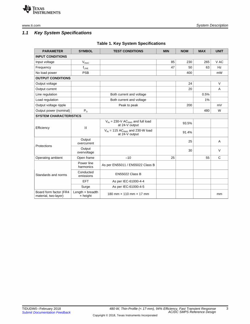
1.1 Key System Specifications
Table 1. Key System Specifications
PARAMETER SYMBOL TEST CONDITIONS MIN NOM MAX UNITINPUT CONDITIONSInput voltage VINAC 85 230 265 V ACFrequency fLINE 47 50 63 HzNo load power PSB 400 mWOUTPUT CONDITIONSOutput voltage 24 VOutput current 20 ALine regulation Both current and voltage 0.5%Load regulation Both current and voltage 1%Output voltage ripple Peak to peak 200 mVOutput power (nominal) PO 480 WSYSTEM CHARACTERISTICS
Efficiency Η
VIN = 230-V ACRMS and full loadat 24-V output 93.5%
VIN = 115 ACRMS and 230-W loadat 24-V output 91.4%
Protections
Outputovercurrent 25 A
Outputovervoltage 30 V
Operating ambient Open frame –10 25 55 C
Standards and norms
Power lineharmonics As per EN55011 / EN55022 Class B
Conductedemissions EN55022 Class B
EFT As per IEC-61000-4-4Surge As per IEC-61000-4-5
Board form factor (FR4material, two-layer)
Length × breadth× height 180 mm × 110 mm × 17 mm mm
TL431AOPTOUCC256303
UCC24612
UCC28880
UCC24612
24 V/ 20 A
CDS19501 KCS
CDS19501 KCS
UCC27524
UCC28063A
85 V ±265 V AC
Copyright © 2018, Texas Instruments Incorporated
System Overview www.ti.com
4 TIDUDW0–February 2018Submit Documentation Feedback
Copyright © 2018, Texas Instruments Incorporated
480-W, Thin-Profile (< 17-mm), 94% Efficiency, Fast Transient ResponseAC/DC SMPS Reference Design
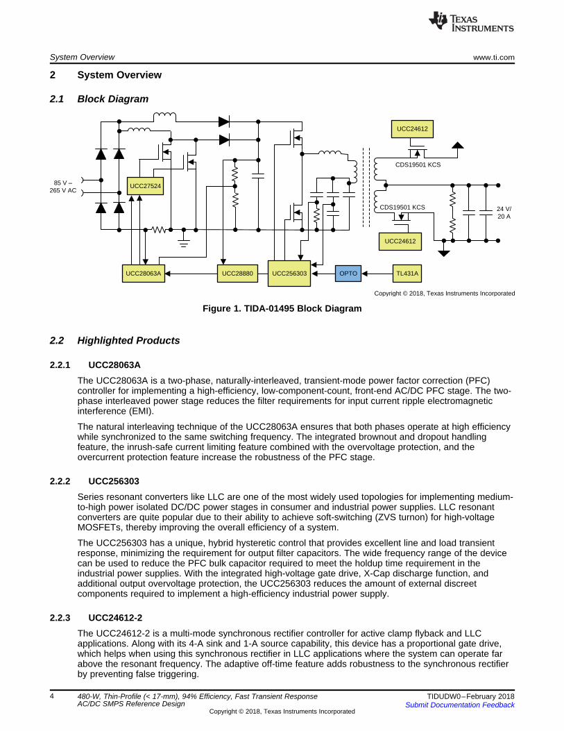
2 System Overview
2.1 Block Diagram
Figure 1. TIDA-01495 Block Diagram
2.2 Highlighted Products
2.2.1 UCC28063AThe UCC28063A is a two-phase, naturally-interleaved, transient-mode power factor correction (PFC)controller for implementing a high-efficiency, low-component-count, front-end AC/DC PFC stage. The two-phase interleaved power stage reduces the filter requirements for input current ripple electromagneticinterference (EMI).
The natural interleaving technique of the UCC28063A ensures that both phases operate at high efficiencywhile synchronized to the same switching frequency. The integrated brownout and dropout handlingfeature, the inrush-safe current limiting feature combined with the overvoltage protection, and theovercurrent protection feature increase the robustness of the PFC stage.
2.2.2 UCC256303Series resonant converters like LLC are one of the most widely used topologies for implementing medium-to-high power isolated DC/DC power stages in consumer and industrial power supplies. LLC resonantconverters are quite popular due to their ability to achieve soft-switching (ZVS turnon) for high-voltageMOSFETs, thereby improving the overall efficiency of a system.
The UCC256303 has a unique, hybrid hysteretic control that provides excellent line and load transientresponse, minimizing the requirement for output filter capacitors. The wide frequency range of the devicecan be used to reduce the PFC bulk capacitor required to meet the holdup time requirement in theindustrial power supplies. With the integrated high-voltage gate drive, X-Cap discharge function, andadditional output overvoltage protection, the UCC256303 reduces the amount of external discreetcomponents required to implement a high-efficiency industrial power supply.
2.2.3 UCC24612-2The UCC24612-2 is a multi-mode synchronous rectifier controller for active clamp flyback and LLCapplications. Along with its 4-A sink and 1-A source capability, this device has a proportional gate drive,which helps when using this synchronous rectifier in LLC applications where the system can operate farabove the resonant frequency. The adaptive off-time feature adds robustness to the synchronous rectifierby preventing false triggering.
� �� �
� �
OUT maxINrms max
IN min
PI
V PF K u u
� �OUT max500
I 1.28 A390
� �� �
� �
OUT maxOUT max
OUT max
PI
V
www.ti.com System Overview
5TIDUDW0–February 2018Submit Documentation Feedback
Copyright © 2018, Texas Instruments Incorporated
480-W, Thin-Profile (< 17-mm), 94% Efficiency, Fast Transient ResponseAC/DC SMPS Reference Design
2.2.4 CSD19501KCSThe CSD19501KCS is an 80-V NexFET™ power MOSFET, with 5.5-mΩ resistance and 38-nC gatecharge. In this reference design, the CSD19501KCS is used as the synchronous field-effect transistor(FET) to lower the losses in the output stage of the LLC converter.
2.3 System Design TheoryThis reference design provides a universal AC mains-powered, 480-W nominal output at 24 V and 20 A.This design comprises a front-end AC/DC PFC power stage followed by an isolated DC/DC LLC powerstage.
2.3.1 PFC Regulator Stage DesignFor high power levels such as 500 W, either the single-phase CCM PFC or interleaved CrCM PFC is thepreferred topology for implementing PFC. Interleaved CrCM PFC offers certain advantages at these powerlevels because it ensures valley switching for the PFC MOSFET and ZCS turnoff diode, which reduces thelosses in the PFC stage. Cheaper diodes can be used because the PFC diode does not have a hardturnoff. CrCM PFC requires a smaller PFC inductor. By interleaving two CrCM power stages, the overallinput ripple current is also reduced. Alternatively, CCM PFC requires a larger inductor and is not veryeffective in low-profile designs.
This reference design uses the UCC28063A-based interleaved CrCM PFC. The following subsectionsdetail the design process and component selection.
2.3.1.1 Design Parameters
Table 2. Design Parameters for PFC Power Stage Design
SYMBOL PARAMETER MIN TYP MAX UNITINPUT
VIN Input voltage 85 265 V ACfLINE Input frequency 47 63 Hz
OUTPUTVOUT Output voltage 397 V DC
POUT(nom) Output power 500 WLine regulation 5%Load regulation 5%
PF Targeted power factor 0.99η Targeted efficiency 97.3%
iTHD Targeted input current THD 5%
2.3.1.2 Input Current CalculationsThe input fuse, bridge rectifier, and input capacitor are selected based on the input current calculations.First, determine the maximum average output current, IOUT(max):
(1)
(2)
Calculate the maximum input root mean square (RMS) for the line current, IINrms(max), using the parametersfrom the Key System Specifications and the initial assumptions of the efficiency and power factor:
(3)
200 mVRcs 9 m
21 A # :
CSPEAK2 2 500 1.25
I 21A0.95 85
u u u
u
� �
� �CS
OUT maxPEAK
INrms min
2 2 P 1.25I
V
u u u
Ku
OUT1
C 2 500 182.4 F390 4 47 25
t u u Pu u S u u
� �OUT OUT maxOUT LINE PFCRipple
1C 2 P
V 4 F Vt u u
u u S u u
� �� �
� �
OUT maxL max
INrms min
PI 2 8.3 A
V
§ ·¨ ¸ u ¨ ¸© ¹
20.95 85 0.69L1 L2 195 H
500 50000u u
Pu
� �� � � �
� �� �
2
INrms min max
MINOUT max
V DUTYL1 L2
P F
§ ·K u u¨ ¸© ¹
u
� �� �
max390 1.414 85
DUTY 0.691390
� u
� �� � � �� �
� �
OUT nom INrms minmax
OUT nom
V V 2DUTY
V
� u
� �INrms max500
I 6.32 A0.94 85 0.99
u u
System Overview www.ti.com
6 TIDUDW0–February 2018Submit Documentation Feedback
Copyright © 2018, Texas Instruments Incorporated
480-W, Thin-Profile (< 17-mm), 94% Efficiency, Fast Transient ResponseAC/DC SMPS Reference Design
(4)
2.3.1.3 Boost InductorCalculate the boost inductor using the minimum input voltage and the minimum desired frequency ofoperation. First calculate the duty cycle, DUTY(max), at the peak of the minimum input voltage:
(5)
(6)
Equation 7 calculates the boost inductor value.
(7)
(8)
The actual value of the boost inductor used is 210 µH. Calculate the required saturation current for theboost inductor is calculated using Equation 9 for the minimum input voltage and under the assumption thatboth phases equally share the load.
(9)
2.3.1.4 Output CapacitorFor this application, choose the output capacitor such that the output ripple is kept below 25 VPK-PK.Equation 10 calculates the output capacitor.
(10)
(11)
In this reference design, two low-profile 100-µF capacitors are connected in parallel to form the PFC bulkcapacitor.
2.3.1.5 Current Sense ResistorThe current sense resistor detects the sum of the inductor currents through both phases. The overcurrentprotection limit in UCC28063A is 200 mV. The required value of the current sense resistor is calculated forthe lowest input voltage and a 25% overload condition. Estimate the peak current first (Equation 12)before calculating the current sense resistor:
(12)
(13)
This result gives the value of the current sense resistor as:
(14)
1C65 1.06 nF
2 20000 7500
S u u
1C63 2.12 F
2 10 7500 P
S u u
AB
1.4 RR 123.5 K
70 2 1.414
u
�
A 6BOHYS
1.414 17R 12 8.5 M
I 2 10� u :
u
( )( )CS
PFC
INrms minPEAK
rms
OUT
4 2 VIID 2.26 A
2 9 V
´æ ö= ´ =ç ÷ç ÷ p ´è ø
rmsIDS 3.715 A
� �� �CS
PFC
INrms minPEAKrms
OUT
14 2 VI 6IDS
2 9 V
� u§ · u¨ ¸¨ ¸ S u© ¹
www.ti.com System Overview
7TIDUDW0–February 2018Submit Documentation Feedback
Copyright © 2018, Texas Instruments Incorporated
480-W, Thin-Profile (< 17-mm), 94% Efficiency, Fast Transient ResponseAC/DC SMPS Reference Design
This reference design uses two 18-mΩ resistors in parallel.
2.3.1.6 PFC MOSFETEquation 15 calculates the RMS current through the PFC MOSFET.
(15)
(16)
Select a MOSFET with a low figure of merit for this application. To maintain the overall height of thedesign to less than 17 mm, the PFC stage has been designed to switch at high frequency. The keyMOSFET specifications that are important for minimizing losses in this design are:• Low RDSon, for reducing the conduction losses in the MOSFET• Low QG, for fast turnoff
2.3.1.7 PFC DiodeEquation 17 calculates the RMS current through the boost diode.
(17)
2.3.1.8 Brownout Protection ConfigurationThe brownout voltage in UCC28063A can be set through the potential divider on the VINAC pin. In thisreference design, the brownout voltage is set to 70 V with a hysteresis of 12 V. The following equationsdetermine the value of the resistors in the potential divider network. RA refers to the top three resistors inthe potential divider (Equation 18) and RB refers to the bottom resistor in the potential divider(Equation 19).
(18)
Three resistors of 2.87 MΩ are connected in series to form RA, with the bottom resistor using Equation 19.
(19)
A standard value of 123 k is chosen for RB.
2.3.1.9 Control Loop CompensationThis design uses a type-2 compensator for the voltage loop compensation. Resistor R67 and capacitorsC63 and C65 form the compensator. Start with a value of 7.5 K for R67. Place a zero close to 10 Hz togive a phase boost close to the gain crossover frequency. This zero is formed by R67 and C63.
(20)
Choose a 2.2-µF capacitor for the C63 capacitor.
Place a pole at a frequency much lower than the lowest switching frequency, around 20 KHz, to attenuatethe switching noise. This pole is formed by R67 and C65.
(21)
Choose a 1-nF capacitor for C65.
� �
6E
FOUT pk
4.87 R 4.87 9 10R 98.46 k
V 4.87 450 4.87
u u u :
� �
� �
6C
D REFREFOUT nom
R 6 9 10R V 140.6 k
V V 390 6u u
u :� �
System Overview www.ti.com
8 TIDUDW0–February 2018Submit Documentation Feedback
Copyright © 2018, Texas Instruments Incorporated
480-W, Thin-Profile (< 17-mm), 94% Efficiency, Fast Transient ResponseAC/DC SMPS Reference Design
2.3.1.10 Programming VOUT and HVSENThe VOUT pin sets the output voltage regulation point. To minimize the no-load losses, use high-valueresistances to construct this potential divider network. Use three 3.01-MΩ resistors to form the top resistor(RC) in the potential divider. Calculate the bottom resistor (RD) using Equation 22.
(22)
Use a value of 142 kΩ for RD.
This reference design uses the HVSEN pin to set the fail-safe output overvoltage protection (OVP). Three3.01-MΩ resistors form the top resistor (RE) in the potential divider. Calculate the bottom resistor (RF)using Equation 23.
(23)
Use a value of 97.6 kΩ for RF.
2.3.2 LLC Converter Stage DesignIncreased demands for high-power-density power supplies have resulted in the increase in switchingfrequency of the converters designed. While component sizes tend to decrease with an increase in theswitching frequency, device switching losses (which are proportional to frequency) have significantlyincreased contributing to resulting in significant efficiency loss. Resonant converters use soft-switchingtechniques to alleviate switching loss problems and attain high efficiencies. Further, soft-switching helpsattain low losses during light load conditions, very-low device stress, and reduced EMI.
The LLC resonant converter is based on the series resonant converter (SRC). By utilizing the transformermagnetizing inductor, zero-voltage switching can be achieved over a wide range of input voltage and load.As a result of multiple resonances, zero-voltage switching can be maintained even when the switchingfrequency is higher or lower than the resonant frequency.
In this design, the LLC converter operates at a high nominal switching frequency of around 180 kHz. Thisallows to minimize the dimension of the LLC transformer to meet the low profile requirements. Theconverter achieves the best efficiency when operated close to its resonant frequency at a nominal inputvoltage. As the switching frequency is lowered, the voltage gain is significantly increased. This allows theconverter to maintain regulation when the input voltage falls low. These features make the converterideally suited to operate from the output of a high-voltage boost PFC pre-regulator, allowing it to hold upthrough brief periods of AC line-voltage dropout.
With its hybrid hysteretic control and ZCS avoidance feature, the UCC256303 LLC controller enables safeoperation of the LLC power stage while minimizing the dimension of the output capacitors. In addition, thecontroller delivers complete system protection functions including overcurrent, undervoltage lockout(UVLO), and overvoltage protection (OVP).
Table 3 lists the design parameters for the LLC power stage design.
Table 3. Design Parameters for LLC Power Stage Design
SYMBOL PARAMETER MIN TYP MAX UNITINPUT
VINDC Input voltage 250 397 410 V DCOUTPUT
VOUT Output voltage 24 V DCPOUT Max output power 480 W
fSW_nom Nominal switching frequency 180 kHzLine regulation 1 %Load regulation 1 %
η Targeted efficiency 0.965
2
e _nom 2
8 8 24R 62.31
20
´ æ ö= ´ = Wç ÷
p è ø
2O_nom
e 2O_nom
V8 nR
I
§ ·u u ¨ ¸
¨ ¸S © ¹
g_max
24.1VM 8.0 1.285
310 V
2
æ öç ÷
= ´ =ç ÷ç ÷è ø
( )
( )
F0 nom
g_maxDCIN min
V VM n
V
2
æ öç ÷+ç ÷= ´ç ÷ç ÷è ø
g_min24.1V
M 8.0 0.94410 V
2
§ ·¨ ¸
u ¨ ¸¨ ¸© ¹
� �
� �
O Fg_min
DCIN max
V VM n
V
2
� u
390n 1 8.07
24 0.1§ ·
u ¨ ¸�© ¹
� �DCIN nom
g gO F
V
2n M M 1V V
u �
.
.
.
www.ti.com System Overview
9TIDUDW0–February 2018Submit Documentation Feedback
Copyright © 2018, Texas Instruments Incorporated
480-W, Thin-Profile (< 17-mm), 94% Efficiency, Fast Transient ResponseAC/DC SMPS Reference Design
2.3.2.1 Determine LLC Transformer Turns Ratio NThe LLC tank is designed to have a nominal gain, Mg, of 1 at the resonant frequency. Use Equation 24 toestimate the required turns ratio.
(24)
where• Mg is the voltage gain,• VDCIN(nom) is the nominal PFC output,• VO is the output voltage,• VF is the voltage drop across the synchronous rectifier.
From the specifications, the nominal values for input voltage and output voltage are 390 V and 24 V,respectively. Assuming an average drop of 100 mV on the synchronous rectifier, the turns-ratio can becalculated as:
(25)
The transformer turns ratio is set to 8.
2.3.2.2 Determine Mg_min and Mg_max
Determine Mg_min and Mg_max using Equation 26 and Equation 27, respectively.
(26)
(27)
The dimensioned Mg_max is increased to 1.1 times the required value to have some margin = Mg_max = 1.1 ×1.28543 ≈ 1.426.
2.3.2.3 Determine Equivalent Load Resistance (Re) of Resonant NetworkEquation 28 calculates the equivalent load resistance at nominal and peak load under nominal outputvoltage and peak output voltage.
(28)
(29)
2 2rI 2.775 1.84 3.373 A �
2 2r m priI I I �
m2 2 8.0 24
I 1.84 A2 100kHz 150 H
§ · § ·u u ¨ ¸ ¨ ¸¨ ¸S u S u u P© ¹© ¹
� � fO nomm
SW _min M
V V2 2I n
2 f L
�§ ·§ ·¨ ¸ u u¨ ¸¨ ¸ ¨ ¸S u S u u© ¹ © ¹
pri20
I 1.11 2.775 A8.0
§ · u ¨ ¸
© ¹
� �O nompri
II
n2 2
§ ·S ¨ ¸ u¨ ¸© ¹
Frequency (KHz)
Gai
n
0 100 200 300 4000
0.2
0.4
0.6
0.8
1
1.2
1.4
1.6
D005
� �
1Fr 176 kHz
2 Lr Cr
uS u u
System Overview www.ti.com
10 TIDUDW0–February 2018Submit Documentation Feedback
Copyright © 2018, Texas Instruments Incorporated
480-W, Thin-Profile (< 17-mm), 94% Efficiency, Fast Transient ResponseAC/DC SMPS Reference Design
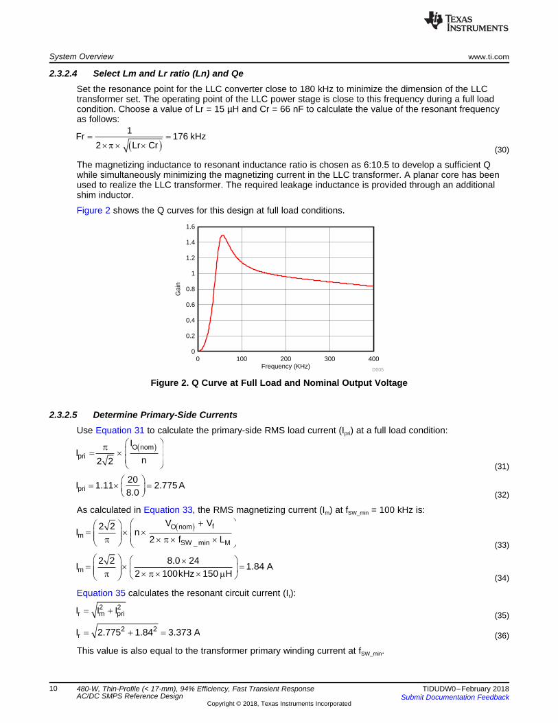
2.3.2.4 Select Lm and Lr ratio (Ln) and QeSet the resonance point for the LLC converter close to 180 kHz to minimize the dimension of the LLCtransformer set. The operating point of the LLC power stage is close to this frequency during a full loadcondition. Choose a value of Lr = 15 µH and Cr = 66 nF to calculate the value of the resonant frequencyas follows:
(30)
The magnetizing inductance to resonant inductance ratio is chosen as 6:10.5 to develop a sufficient Qwhile simultaneously minimizing the magnetizing current in the LLC transformer. A planar core has beenused to realize the LLC transformer. The required leakage inductance is provided through an additionalshim inductor.
Figure 2 shows the Q curves for this design at full load conditions.
Figure 2. Q Curve at Full Load and Nominal Output Voltage
2.3.2.5 Determine Primary-Side CurrentsUse Equation 31 to calculate the primary-side RMS load current (Ipri) at a full load condition:
(31)
(32)
As calculated in Equation 33, the RMS magnetizing current (Im) at fSW_min = 100 kHz is:
(33)
(34)
Equation 35 calculates the resonant circuit current (Ir):
(35)
(36)
This value is also equal to the transformer primary winding current at fSW_min.
9r
ISNS ISNS 12ISNS
C 66 10R R14 K 0.39 171
C 150 10
�
�
u u u :
u
� �
� �
� �ISNSFullload
ISNSOUT max
DCIN nom
V 0.5K 0.39
1P 1 500390V
:§ · § ·§ · u ¨ ¸¨ ¸¨ ¸ u © ¹¨ ¸K ¨ ¸© ¹ © ¹
ISNSFullloadOCP3 0.6
V 0.5 V1.2 1.2
SS
25 AC C31 400 mS 1.5 F
7 V
m= = ´ = m
( )DSmax_ sec O nomV 1.2 2 V 57.6 V= ´ ´ =
sec_rms secI I 15.7 A4S
u
www.ti.com System Overview
11TIDUDW0–February 2018Submit Documentation Feedback
Copyright © 2018, Texas Instruments Incorporated
480-W, Thin-Profile (< 17-mm), 94% Efficiency, Fast Transient ResponseAC/DC SMPS Reference Design
2.3.2.6 Determine Secondary-Side CurrentsThe secondary-side RMS currents can be calculated from the average load current. Assuming the LLCpower stage is operating close to its second resonant frequency, the RMS current through each rectifier inthe secondary-side push-pull output is calculated in Equation 37:
(37)
where,• Isec is the full-load, secondary-side output current (equal to 20 A).
2.3.2.7 Primary Side MOSFETsConsider each MOSFET to have an input voltage equal to its maximum applied voltage. A MOSFET witha maximum drain source voltage greater than 500 V is feasible for this design. The turnon losses can beneglected for an LLC power stage working in ZVS. Choose the MOSFET based on the values for RDSonand COSS. Optimizing the COSS helps to minimize the dead time required for achieving ZVS, therebyminimizing the duty cycle loss. This reference design uses the STP24N60M2 MOSFET. The adaptivedead-time optimization feature of the UCC256303 helps to maximize the duty cycle, which improves theefficiency.
2.3.2.8 Secondary-Side Synchronous MOSFETsEquation 38 calculates the synchronous rectifier maximum voltage rating.
(38)
The current rating of the MOSFET is determined as Isec_M rms = 15.7 A.
This reference design uses TI's CSD19501KCS with its low RDSon (< 5.5 mΩ) and Qg (< 38 nC). The very-low RDSon of the device helps to reduces the overall loss in the synchronous rectifier.
2.3.2.9 Soft Start—UCC256303The UCC256303 is configured to provide a maximum 400-ms soft-start period. During start-up the soft-start capacitor charges using the internal 25-µA current source. The UCC256303 exits soft start when theclosed-loop control takes over or when the voltage on the soft-start capacitor reaches 7 V. Select thevalue of the soft-start capacitor using Equation 39.
(39)
2.3.2.10 Current Sense Circuit (ISNS Pin)—UCC256303The overcurrent limit OCP3 is set to trigger at 1.2 times the peak overload capability of the system.
(40)
The current sense ratio is then calculated as:
(41)
Select the current sense capacitor CISNS = C39 = 150 pF. Equation 42 calculates the current sense resistorRISNS.
(42)
Use a 169-Ω resistor for R14.
BWUPPER32 V 4 V
R R20 R18 70 k4 V�
u
System Overview www.ti.com
12 TIDUDW0–February 2018Submit Documentation Feedback
Copyright © 2018, Texas Instruments Incorporated
480-W, Thin-Profile (< 17-mm), 94% Efficiency, Fast Transient ResponseAC/DC SMPS Reference Design
2.3.2.11 Overvoltage Protection (BW Pin)—UCC256303The BW pin senses the output voltage through the bias winding mounted on the LLC transformer. This pincan be used to provide an additional OVP in the system. In this reference design, the bias winding has thesame number of turns as the secondary winding. When the OVP voltage is set to 32 V, the bias windingvoltage will be 32 V. After implementing this setting, the BW pin potential divider is configured in such away that it acknowledges the 4 V at the 32-V output.
Select RBWLOWER = R18 = 10 kΩ. Equation 43 then calculates the RBWUPPER as follows.
(43)
Use a 69.8-kΩ resistor for R18.
www.ti.com Hardware, Testing Requirements, and Test Results
13TIDUDW0–February 2018Submit Documentation Feedback
Copyright © 2018, Texas Instruments Incorporated
480-W, Thin-Profile (< 17-mm), 94% Efficiency, Fast Transient ResponseAC/DC SMPS Reference Design
3 Hardware, Testing Requirements, and Test Results
3.1 Requirement for Testing
3.1.1 Test Conditions• Input conditions:
– VIN: 85-V to 265-V AC– IIN: Current limit to 8 A
• Output conditions:– VOUT: 24 V– IOUT: 0 A to 20 A
3.1.2 Required Equipment• Isolated AC source• Single-phase power analyzer• Digital oscilloscope• Multimeters• Electronic load• 12-V DC fan
3.1.3 Procedure1. Turn on the 12-V DC fan and set the current to obtain approximately 200 LFM airflow on the board.2. Connect the input terminals (connector J3) of the reference board to the AC power source.3. Connect the output terminals (connector J2) to the electronic load, maintaining correct polarity.4. Set a minimum load of approximately 50 mA.5. Gradually increase the input voltage from 0 V to turn on a voltage of 85-V AC. As the voltage across
the PFC bulk capacitor crosses 90 V, the LLC section begins working and supplies the auxiliary powerto the PFC controller. At this point, the PFC starts and boosts the PFC stage output voltage to 390-VDC.
6. Observe the start-up conditions for smooth switching waveforms.7. Apply a load and perform tests to determine the efficiency, obtain regulation data, and observe steady-
state operating conditions.

Output Power (W)
PF
0 100 200 300 400 5000.6
0.65
0.7
0.75
0.8
0.85
0.9
0.95
1
D003
230-V AC115-V AC
Output Power (W)
TH
D
0 100 200 300 400 5000
5
10
15
20
25
30
35
D004D004
230 V-AC115 V-AC
D001_TIDUDW0.grf
Output Power (W)
Effi
cien
cy (
%)
0 100 200 300 400 50080
82
84
86
88
90
92
94
96
D001
230-V AC115-V AC
Output Power (W)
Effi
cien
cy (
%)
0 100 200 300 400 500-0.6
-0.4
-0.2
0
0.2
0.4
0.6
0.8
D002
230 V-AC115 V-AC
Hardware, Testing Requirements, and Test Results www.ti.com
14 TIDUDW0–February 2018Submit Documentation Feedback
Copyright © 2018, Texas Instruments Incorporated
480-W, Thin-Profile (< 17-mm), 94% Efficiency, Fast Transient ResponseAC/DC SMPS Reference Design
3.2 Test Results
3.2.1 Efficiency, Regulation, PF, and iTHDThis section shows the efficiency, power factor, regulation, and iTHD results at 115-V AC and 230-V ACinput. Table 4 gives the test data.
Table 4. Test Results for 115-V AC and 230-V AC Input
POUT (W) EFFICIENCY (%)AT 115-V AC
EFFICIENCY (%)AT 230-V AC
PF AT115-V AC
PF AT230-V AC
iTHD (%) AT115-V AC
iTHD (%) AT230-V AC
% REGULATIONAT 115-V AC
% REGULATIONAT 230-V AC
25 82.51507128 81.29950053 0.9481 0.7 23.09 33 0.57 0.62
50 83.9242486 84.81680385 0.9727 0.866 17.2 27.2 0.54 0.55
100 89.52061765 90.22170067 0.9884 0.964 11.19 16.8 0.05 0.38
150 90.97905138 92.31231215 0.992 0.9755 8.7 15.7 0 –0.05
200 91.65701754 93.15128193 0.995 0.981 7.27 14.06 –0.08 –0.1
250 92.07668415 93.92470822 0.996 0.985 6.37 12.5 –0.1 –0.06
300 92.04876775 94.11389092 0.997 0.988 5.75 11.3 –0.14 –0.12
350 91.87753864 94.01469237 0.997 0.9899 5.53 10.88 –0.25 –0.22
400 91.55421377 93.74407263 0.997 0.991 5.39 9.67 –0.39 –0.35
450 91.35421377 93.45708653 0.998 0.992 5.42 9.06 –0.44 –0.4
480 91.12785237 93.34447384 0.998 0.992 5.31 8.97 –0.44 –0.42
Figure 3. Efficiency Data Figure 4. Load Regulation Data
Figure 5. Power Factor Data Figure 6. iTHD Data
www.ti.com Hardware, Testing Requirements, and Test Results
15TIDUDW0–February 2018Submit Documentation Feedback
Copyright © 2018, Texas Instruments Incorporated
480-W, Thin-Profile (< 17-mm), 94% Efficiency, Fast Transient ResponseAC/DC SMPS Reference Design
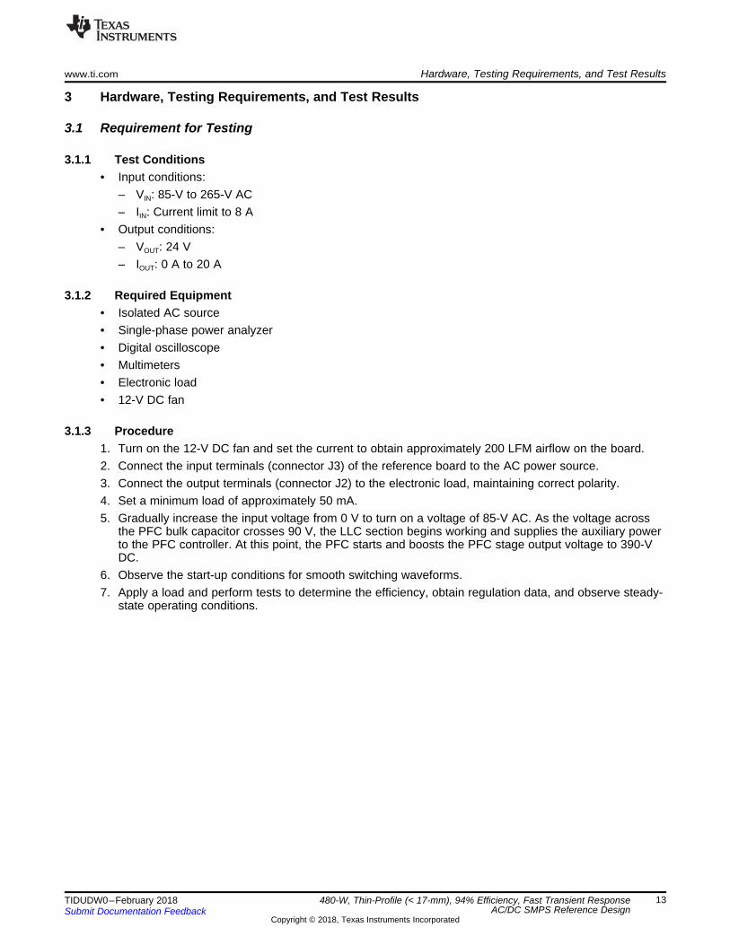
3.2.2 Inrush Current Limiting at Start-UpFigure 7 shows the inrush current at start-up. The inrush current is limited through an active inrush limitercircuit in series with the bulk capacitor.
Figure 7. Inrush Current Limiting at Start-Up
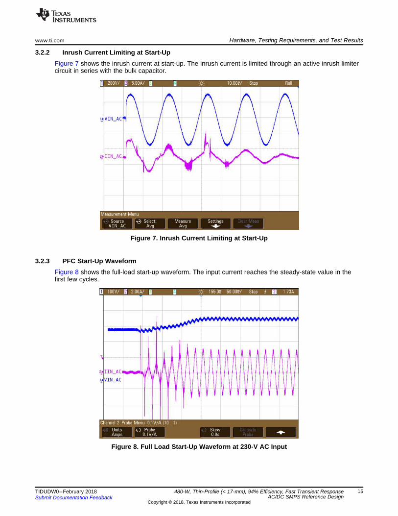
3.2.3 PFC Start-Up WaveformFigure 8 shows the full-load start-up waveform. The input current reaches the steady-state value in thefirst few cycles.
Figure 8. Full Load Start-Up Waveform at 230-V AC Input
Hardware, Testing Requirements, and Test Results www.ti.com
16 TIDUDW0–February 2018Submit Documentation Feedback
Copyright © 2018, Texas Instruments Incorporated
480-W, Thin-Profile (< 17-mm), 94% Efficiency, Fast Transient ResponseAC/DC SMPS Reference Design
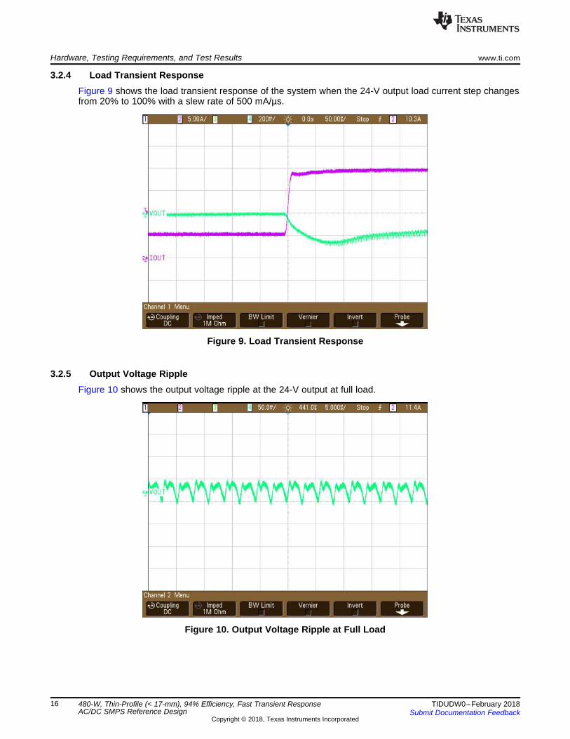
3.2.4 Load Transient ResponseFigure 9 shows the load transient response of the system when the 24-V output load current step changesfrom 20% to 100% with a slew rate of 500 mA/µs.
Figure 9. Load Transient Response
3.2.5 Output Voltage RippleFigure 10 shows the output voltage ripple at the 24-V output at full load.
Figure 10. Output Voltage Ripple at Full Load

www.ti.com Hardware, Testing Requirements, and Test Results
17TIDUDW0–February 2018Submit Documentation Feedback
Copyright © 2018, Texas Instruments Incorporated
480-W, Thin-Profile (< 17-mm), 94% Efficiency, Fast Transient ResponseAC/DC SMPS Reference Design
3.2.6 PFC Working WaveformsThis subsection shows the PFC input and switching waveforms. Figure 11 shows the input voltage andinput current at a 230-V AC input and full-load output.
Figure 11. PFC Input Voltage and Current Waveform
Figure 12 shows the PFC switching waveform for phase 1. The MOSFET drain source voltage, gatesource voltage, and the ZCD winding voltage has been captured. Note how the PFC MOSFET turns at thevalley point, thus ensuring the lowest turnon loss.
Figure 12. PFC MOSFET Switching Waveform
Hardware, Testing Requirements, and Test Results www.ti.com
18 TIDUDW0–February 2018Submit Documentation Feedback
Copyright © 2018, Texas Instruments Incorporated
480-W, Thin-Profile (< 17-mm), 94% Efficiency, Fast Transient ResponseAC/DC SMPS Reference Design
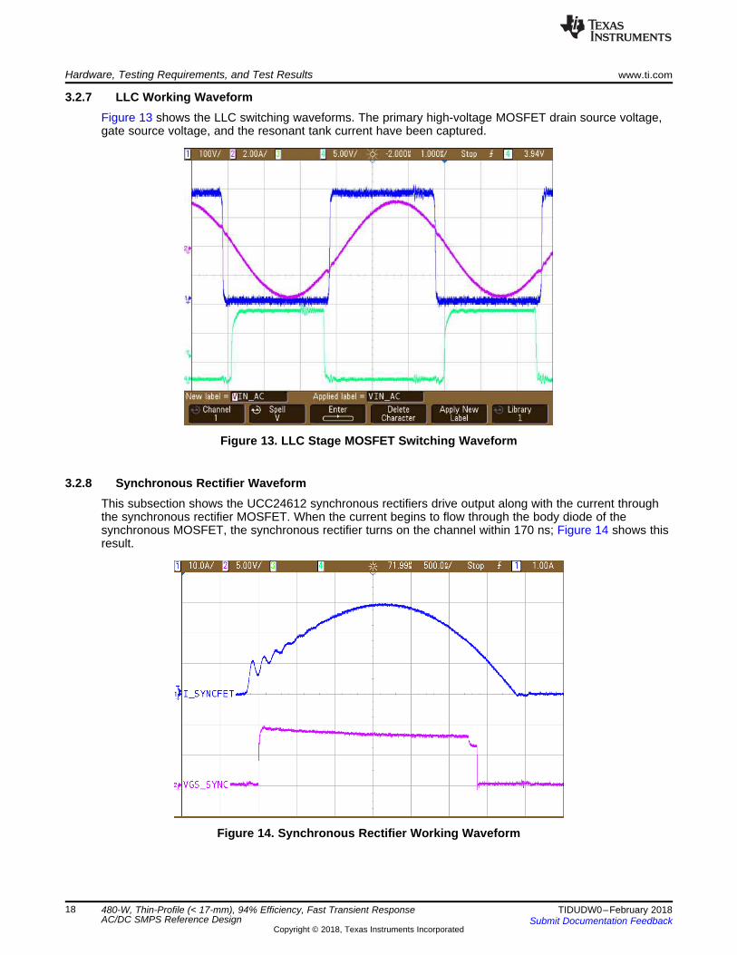
3.2.7 LLC Working WaveformFigure 13 shows the LLC switching waveforms. The primary high-voltage MOSFET drain source voltage,gate source voltage, and the resonant tank current have been captured.
Figure 13. LLC Stage MOSFET Switching Waveform
3.2.8 Synchronous Rectifier WaveformThis subsection shows the UCC24612 synchronous rectifiers drive output along with the current throughthe synchronous rectifier MOSFET. When the current begins to flow through the body diode of thesynchronous MOSFET, the synchronous rectifier turns on the channel within 170 ns; Figure 14 shows thisresult.
Figure 14. Synchronous Rectifier Working Waveform
www.ti.com Hardware, Testing Requirements, and Test Results
19TIDUDW0–February 2018Submit Documentation Feedback
Copyright © 2018, Texas Instruments Incorporated
480-W, Thin-Profile (< 17-mm), 94% Efficiency, Fast Transient ResponseAC/DC SMPS Reference Design
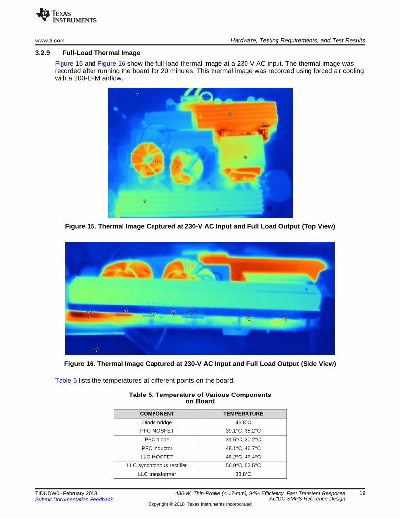
3.2.9 Full-Load Thermal ImageFigure 15 and Figure 16 show the full-load thermal image at a 230-V AC input. The thermal image wasrecorded after running the board for 20 minutes. This thermal image was recorded using forced air coolingwith a 200-LFM airflow.
Figure 15. Thermal Image Captured at 230-V AC Input and Full Load Output (Top View)
Figure 16. Thermal Image Captured at 230-V AC Input and Full Load Output (Side View)
Table 5 lists the temperatures at different points on the board.
Table 5. Temperature of Various Componentson Board
COMPONENT TEMPERATUREDiode bridge 46.8°C
PFC MOSFET 39.1°C, 35.2°CPFC diode 31.5°C, 30.2°C
PFC inductor 48.1°C, 46.7°CLLC MOSFET 46.2°C, 46.4°C
LLC synchronous rectifier 56.9°C, 52.5°CLLC transformer 38.8°C
Design Files www.ti.com
20 TIDUDW0–February 2018Submit Documentation Feedback
Copyright © 2018, Texas Instruments Incorporated
480-W, Thin-Profile (< 17-mm), 94% Efficiency, Fast Transient ResponseAC/DC SMPS Reference Design
4 Design Files
4.1 SchematicsTo download the schematics, see the design files at TIDA-01495.
4.2 Bill of MaterialsTo download the bill of materials (BOM), see the design files at TIDA-01495.
4.3 PCB Layout RecommendationsRefer to the UCC256303, UCC28063A, and UCC24612-2 data sheets for detailed layoutrecommendations.
4.3.1 Layout PrintsTo download the layer plots, see the design files at TIDA-01495.
4.4 Altium ProjectTo download the Altium project files, see the design files at TIDA-01495.
4.5 Gerber FilesTo download the Gerber files, see the design files at TIDA-01495.
4.6 Assembly DrawingsTo download the assembly drawings, see the design files at TIDA-01495.
5 TrademarksE2E, NexFET are trademarks of Texas Instruments.All other trademarks are the property of their respective owners.
6 About the AuthorRAMKUMAR S is a systems engineer at Texas Instruments, where he is responsible for developingreference design solutions for the industrial segment. Ramkumar brings his diverse experience in analogand digital power supplies design to this role. Ramkumar earned his master of technology (M.Tech) fromthe Indian Institute of Technology in Delhi.

IMPORTANT NOTICE FOR TI DESIGN INFORMATION AND RESOURCES
Texas Instruments Incorporated (‘TI”) technical, application or other design advice, services or information, including, but not limited to,reference designs and materials relating to evaluation modules, (collectively, “TI Resources”) are intended to assist designers who aredeveloping applications that incorporate TI products; by downloading, accessing or using any particular TI Resource in any way, you(individually or, if you are acting on behalf of a company, your company) agree to use it solely for this purpose and subject to the terms ofthis Notice.TI’s provision of TI Resources does not expand or otherwise alter TI’s applicable published warranties or warranty disclaimers for TIproducts, and no additional obligations or liabilities arise from TI providing such TI Resources. TI reserves the right to make corrections,enhancements, improvements and other changes to its TI Resources.You understand and agree that you remain responsible for using your independent analysis, evaluation and judgment in designing yourapplications and that you have full and exclusive responsibility to assure the safety of your applications and compliance of your applications(and of all TI products used in or for your applications) with all applicable regulations, laws and other applicable requirements. Yourepresent that, with respect to your applications, you have all the necessary expertise to create and implement safeguards that (1)anticipate dangerous consequences of failures, (2) monitor failures and their consequences, and (3) lessen the likelihood of failures thatmight cause harm and take appropriate actions. You agree that prior to using or distributing any applications that include TI products, youwill thoroughly test such applications and the functionality of such TI products as used in such applications. TI has not conducted anytesting other than that specifically described in the published documentation for a particular TI Resource.You are authorized to use, copy and modify any individual TI Resource only in connection with the development of applications that includethe TI product(s) identified in such TI Resource. NO OTHER LICENSE, EXPRESS OR IMPLIED, BY ESTOPPEL OR OTHERWISE TOANY OTHER TI INTELLECTUAL PROPERTY RIGHT, AND NO LICENSE TO ANY TECHNOLOGY OR INTELLECTUAL PROPERTYRIGHT OF TI OR ANY THIRD PARTY IS GRANTED HEREIN, including but not limited to any patent right, copyright, mask work right, orother intellectual property right relating to any combination, machine, or process in which TI products or services are used. Informationregarding or referencing third-party products or services does not constitute a license to use such products or services, or a warranty orendorsement thereof. Use of TI Resources may require a license from a third party under the patents or other intellectual property of thethird party, or a license from TI under the patents or other intellectual property of TI.TI RESOURCES ARE PROVIDED “AS IS” AND WITH ALL FAULTS. TI DISCLAIMS ALL OTHER WARRANTIES ORREPRESENTATIONS, EXPRESS OR IMPLIED, REGARDING TI RESOURCES OR USE THEREOF, INCLUDING BUT NOT LIMITED TOACCURACY OR COMPLETENESS, TITLE, ANY EPIDEMIC FAILURE WARRANTY AND ANY IMPLIED WARRANTIES OFMERCHANTABILITY, FITNESS FOR A PARTICULAR PURPOSE, AND NON-INFRINGEMENT OF ANY THIRD PARTY INTELLECTUALPROPERTY RIGHTS.TI SHALL NOT BE LIABLE FOR AND SHALL NOT DEFEND OR INDEMNIFY YOU AGAINST ANY CLAIM, INCLUDING BUT NOTLIMITED TO ANY INFRINGEMENT CLAIM THAT RELATES TO OR IS BASED ON ANY COMBINATION OF PRODUCTS EVEN IFDESCRIBED IN TI RESOURCES OR OTHERWISE. IN NO EVENT SHALL TI BE LIABLE FOR ANY ACTUAL, DIRECT, SPECIAL,COLLATERAL, INDIRECT, PUNITIVE, INCIDENTAL, CONSEQUENTIAL OR EXEMPLARY DAMAGES IN CONNECTION WITH ORARISING OUT OF TI RESOURCES OR USE THEREOF, AND REGARDLESS OF WHETHER TI HAS BEEN ADVISED OF THEPOSSIBILITY OF SUCH DAMAGES.You agree to fully indemnify TI and its representatives against any damages, costs, losses, and/or liabilities arising out of your non-compliance with the terms and provisions of this Notice.This Notice applies to TI Resources. Additional terms apply to the use and purchase of certain types of materials, TI products and services.These include; without limitation, TI’s standard terms for semiconductor products http://www.ti.com/sc/docs/stdterms.htm), evaluationmodules, and samples (http://www.ti.com/sc/docs/sampterms.htm).
Mailing Address: Texas Instruments, Post Office Box 655303, Dallas, Texas 75265Copyright © 2018, Texas Instruments Incorporated