
354399-1.pdf - Eindhoven University of Technology research ...
109
Eindhoven University of Technology MASTER Evaluation of an offset-compensated comparator and design of a self-calibrating 12-bit A/D convertor in CMOS Gerritsen, R.M.W. Award date: 1991 Link to publication Disclaimer This document contains a student thesis (bachelor's or master's), as authored by a student at Eindhoven University of Technology. Student theses are made available in the TU/e repository upon obtaining the required degree. The grade received is not published on the document as presented in the repository. The required complexity or quality of research of student theses may vary by program, and the required minimum study period may vary in duration. General rights Copyright and moral rights for the publications made accessible in the public portal are retained by the authors and/or other copyright owners and it is a condition of accessing publications that users recognise and abide by the legal requirements associated with these rights. • Users may download and print one copy of any publication from the public portal for the purpose of private study or research. • You may not further distribute the material or use it for any profit-making activity or commercial gain
-
Upload
khangminh22 -
Category
Documents
-
view
0 -
download
0
Transcript of 354399-1.pdf - Eindhoven University of Technology research ...
Eindhoven University of Technology
MASTER
Evaluation of an offset-compensated comparator and design of a self-calibrating 12-bit A/Dconvertor in CMOS
Gerritsen, R.M.W.
Award date:1991
Link to publication
DisclaimerThis document contains a student thesis (bachelor's or master's), as authored by a student at Eindhoven University of Technology. Studenttheses are made available in the TU/e repository upon obtaining the required degree. The grade received is not published on the documentas presented in the repository. The required complexity or quality of research of student theses may vary by program, and the requiredminimum study period may vary in duration.
General rightsCopyright and moral rights for the publications made accessible in the public portal are retained by the authors and/or other copyright ownersand it is a condition of accessing publications that users recognise and abide by the legal requirements associated with these rights.
• Users may download and print one copy of any publication from the public portal for the purpose of private study or research. • You may not further distribute the material or use it for any profit-making activity or commercial gain

Eindhoven University of Technology Department of Electrical Engineering Digital Systems EB
Evaluation of an offset-compensated comparator and design of a self-calibrating 12-bit AID converter in CMOS.
RM.W. Gerritsen
coaches:
Prof.dr.ir. RJ. van de Plassche Philips Reseach Laboratories, Eindhoven University of Technology
Dr.ir. M.J.M. Pelgrom Philips Reseach Laboratories
Graduation work: Sept.1990 May 1991 Philips Research Laboratories, Eindhoven
The Eindhoven University of Technology accepts no responsibility for the contents of this report.
£7) 311
Abstract
In this report a new offset-compensated comparator for use in high-speed 8-bit CMOS AID converters is evaluated. Fundamental operation, analysis of the offset sources, measurements and an improved design will be shown. Measurements showed an always-positive offset voltage. An unmatched parasitic cross-capacitance in the layout has been found responsible for this behaviour. An improved design results in a comparator that could be used at 30 MHz clock with 1 mV (standard deviation) offset voltage. The comparator's power consumption is 0.75-1 mW and its size is approximately 150 x 150 J.lm2 in a 1.2 J.lm feature size process.
The second topic is the design of a 12-bit AID converter. The redesigned comparator can be used in this 12-bit ADC. The ADC is based on a resistor string generating 4095 reference voltages. A 4-step subranging architecture is used to find the reference voltage that matches the input voltage. This results in the digital representation of the analog input. Special attention has been paid to the resistor ladder. It consists of a fine and a coarse part. The ladder is monotonic by design.
To increase the integral linearity of the ladder, a self-calibration technique was developed. With this technique the coarse resistor ladder can be calibrated. This reduces the demands for the fine ladder to only 6-bit accuracy.
1

Preface
I want to thank prof.dr.ir. R.J. van de Plassche and dr.ir. M.J.M. Pelgrom for giving me the opportunity to do my graduation work at Philips Research Laboratories. I appreciate the support and coaching by them and the members of the group Wouda. Although my education was focused on digital circuits, this work showed me the beauty of analog integrated CMOS circuits.
Reinier Gerritsen, Eindhoven, May 1991.
2
Contents
1 Introduction 1.1 Conversion principles. 1.2 Parallel converter . . 1.3 Two-step converter . . 1.4 Multi-step converter 1.5 Sigma delta converter 1.6 Comparison.. 1.7 CMOS process 1.8 Software tools .
2 Comparator 2.1 Introduction. 2.2 Component values ..... . 2.3 Mismatch in the comparator.
2.3.1 Some calculations 2.3.2 Computer analysis
2.4 Measurements ...... . 2.5 Circuit extraction. . . . . 2.6 Redesign of the comparator
2.6.1 Switches .... 2.6.2 Level-shifter..... 2.6.3 Gain and offset ... 2.6.4 Optimizing the differential pair 2.6.5 Buffers and Capacitors . 2.6.6 AC simulation ..... 2.6.7 Recovery after latching 2.6.8 Timing ....... . 2.6.9 Large input difference 2.6.10 Bias ......... . 2.6.11 Digital output ... . 2.6.12 Component values and some final notes
2.7 Conclusions ................... .
3
5 6 6 7 8 9
10 10 11
12 12 15 18 18 19 23 28 31 31 33 34 34 37 40 40 43 44 47 48 48 50

3 12-bit CMOS AID converter 52 3.1 Introduction. . . . . . . . . ........... 52 3.2 Resistor reference ladder . . ........... 55
3.2.1 Selection of taps in the ladder . .56 3.2.2 Matching properties ...... 60
3.3 Requirements for the comparators 61 3.4 Calibration of the coarse ladder . 63
3.4.1 The calibration cell . 66 3.5 Calibration amplifier . . . 71
3.5.1 Fixed offset . . . . . 71 3.5.2 Offset due to noise . 72 3.5.3 Common mode dependent offset 72 3.5.4 Measuring methods 73 3.5.5 Computer simulation . 77 3.5.6 Panacea simulation . 79 3.5.7 The amplifier 80
3.6 Fast latch .... " ............ 88
4 Conclusions 90
A MOS formulae 97
B Pinning diagram of the comparator 98
C C program for ladder calibration 99
D Optimization of the comparator 105
4

Chapter 1
Introduction
In the past years we have seen an increase in the use of digital circuits in electronic equipment. For many applications in the field of high-quality storage and signal transmission a realization in the digital domain is much easier than in the analog domain. Many application require computer control, a digital operation. However, the world we live in is strictly analog. Therefore there is a need to convert analog signals to a digital representation. Well known applications are digital audio (CD, DAT, DCC), telecommunication (ISDN), video digitizing (HDTV), measurement (e.g. temperature, weight, voltage, current), digital servo systems, medical electronics (MRI scanners), radar echo processing and so on.
Analog to digital converters (ADCs) can be classified by many properties. Some of them are listed below:
• Technology: CMOS (cheap, digital circuits on same chip), bipolar (high speed, digital circuits on same chip), BiCMOS (high speed, expensive) or GaAs (very high speed, expensive).
• Accuracy: number of bits (usually in the range 6-16 bit)
• Speed: number of samples per second and effective (analog) bandwidth.
• Power: generally high speed needs more power.
• Conversion principle: various circuit designs.
This report will concentrate on high-speed converters in CMOS technology. The basic part of a high-speed AID converter is the comparator. This circuit compares the analog input voltage or a voltage related to the input - with a reference voltage. The comparator must decide whether the input is smaller or larger then a reference voltage. The basic problem for medium and high-accuracy CMOS comparators (> 8 bit) is the offset voltage of the comparator due to the limited component matching properties.
A few years ago a new offset-compensated comparator and a test circuit were made, but there has never been a serious measurement and study of the capabilities of the comparator.
5

This report contains an evaluation of this comparator: fundamental operation, analysis of the offset sources, measurements and an improved design (chapter 2). the second topic discussed in this report is the design of a multi-step 12-bit A/D converter. The new comparator can be used in the 12-bit ADC. To increase integral linearity a self-calibration technique was developed. With this technique a resistor reference ladder can be calibrated. The 12-bit ADC and the calibration will be treated in chapter 3. It should be noted that the design of the AID converter is far from ready. Only a part of the design is presented in this report. The main omissions are the 12-bit accurate comparator, the sample and hold, timing generation and an analysis of the behaviour of the ladder at dynamic loading. Chapter 4 gives some conclusions and recommendations for further work. The four appendices give some practical information.
1.1 Conversion principles
The number of comparators depends highly on the architecture of the converter and ranges from 1 to 2n where n is the number of bits. Several high-speed conversion principles can be discerned. The choice which principle is to be used depends on the demands for the converter. The number of bits, conversion speed, chip area and power consumption are some of the most important design specifications. We will have a closer look at the following converter types in the next paragraphs:
• Parallel ("flash") converter.
• Two-step converter.
• Multi-step converter.
• Sigma-Delta converter.
1.2 Parallel converter
In figure 1.1 the architecture of a parallel converter is shown. For an n-bit converter, 2n - 1 comparators operate simultaneously. A resistor ladder is used to generate the 2n - 1 reference levels. The analog input signal is assumed not to exceed the reference values at the extremes of the. ladder. Sometimes extra comparators are added to indicate overflow or underflow of the input.
The comparators generate a thermometer code. All comparators with Yin > v;.ef; generate a logic 1, the others generate a logic O. The digital output is equal to the ordinal number of the comparator that is the last one with a logic 1 decision. A simple AND gate checks the neighbouring comparator(s) to detect the 1/0 transition in the thermometer code. Now only one of the 2n - 1 outputs is a logic 1. A simple ROM can be used to convert it to the final code, e.g. binary.
The main application of CMOS flash converters is for the accuracy range 7-8-bit running at video rates. Due to the large number of comparators required (255 for 8-bit) the input capacitance (several tens of pF), chip area and power dissipation
6

Vref Vin Vdd
b2 bl bO
Figure 1.1: Full flash converter (3-bit).
are large. The most important advantages of a flash converter are its high-speed conversion ability and the fact that there is no need for a sample and hold (SjH) circuit because of the simultaneous operation. However, a S/H can boost the analog (bandwidth) performance.
Small parallel converters (3-5 bit) are often used as building blocks in other types of ADCs as we will see. Some examples of full-flash converters are references [2] and [21].
1.3 Two-step converter
To avoid the large number of comparators necessary for a parallel converter, a twostep method is used frequently. A general circuit diagram is shown in figure 1.2. For an 8-bit converter, in the first step we make a 4-bit coarse quantization. Then the digitized value is fed to a D j A converter making a coarse representation of the input voltage. It is important that the 4-bit D I A converter has an 8-bit linearity. In the second step the difference signal of input and coarse D I A voltage is applied to a 4-bit flash converter. Now the fine information is digitized. The results of both operations are combined to form the 8-bit output code.
In a practical design several building blocks can be combined or are implicit in the circuit. An example of such a circuit is the resistor based AID converter shown in figure 1.3. Here a string of resistors is used to generate the reference voltages. For the first step a small number of taps is used to divide the ladder into segments. After
7

Vin
coarse
4 bit flash
MSB
Figure 1.2: General two-step AID converter.
fine
4 bit flash
LSB
quantization by a small flash converter the most significant bits are determined. In the second step the taps in the segment just found are switched to a second flash converter. We can see the first step as an estimation where to look for in the "real" conversion step. It is a waist of power and area to search the whole range of reference voltages in one step since only one comparator (at the 110 boundary) determines the digital representation.
The big advantage of a 2-step converter over a flash converter is the reduction in the number of comparators (2 x 15 compared to 255). Less comparators means less area, capacitance and power consumption. Of coarse there are disadvantages: it takes two cycles thus halving the throughput and a S/H is necessary to hold the signal during the second step. Special attention has to be paid to avoid nonmonotonicity of the converter due to the segmentation of the conversion. There is also a problem with the PSRR because there are two sampling moments. But with the use of a pipelining architecture, integrated S/H circuitry and error correction these drawbacks can be circumvented. Because of the reduced number of comparators, more power can be spent per comparator making it faster.
As we study the publications over the last few years, we notice that almost all high-speed 8-bit CMOS AID converters use a 2-step architecture. Some authors call it a subranging architecture. An important example is the A/D converter published by Dingwall et. al. [3], some other publications are references [6,7,9,12,13,52]
1.4 Multi-step converter
The 2-step architecture is just a special case of the multi-step architecture. If we need more than 8 bits (e.g. ID-12) the 2-step converter becomes quite large and has the same disadvantages as a parallel converter. The solution is to use more steps where each step resolves a small number of bits (usually 3-4). Of coarse, this reduces the conversion speed. Special attention must be paid to avoid range errors. If in a previous step an error is made, it must be possible to correct this error. Many designs of this kind of converter have been published lately [15,24,37,54]. There is a variation in the number of steps, the number of bits per step and the way the D/ A
8
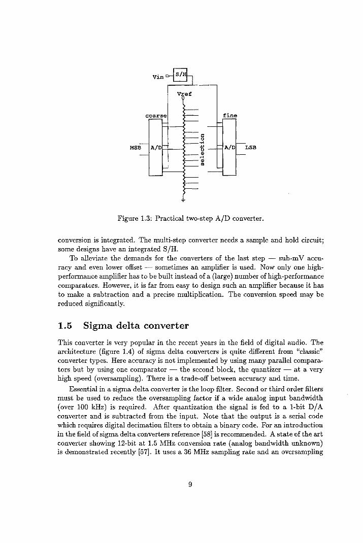
Vin
Vref
coar8e fine
MSB A/DH---< A/D LSB
Figure 1.3: Practical two-step AID converter.
conversion is integrated. The multi-step converter needs a sample and hold circuit; some designs have an integrated S fH.
To alleviate the demands for the converters of the last step - sub-m V accuracy and even lower offset sometimes an amplifier is used. Now only one highperformance amplifier has to be built instead of a (large) number of high-performance comparators. However, it is far from easy to design such an amplifier because it has to mal{e a subtraction and a precise multiplication. The conversion speed may be reduced significantly.
1.5 Sigma delta converter
This converter is very popular in the recent years in the field of digital audio. The architecture (figure 1.4) of sigma delta converters is quite different from "classic" converter types. Here accuracy is not implemented by using many parallel comparators but by using one comparator - the second block, the quantizer at a very high speed (oversampling). There is a trade-off between accuracy and time.
Essential in a sigma delta converter is the loop filter. Second or third order filters must be used to reduce the oversampling factor if a wide analog input bandwidth (over 100 kHz) is required. After quantization the signal is fed to a I-bit D I A converter and is subtracted from the input. Note that the output is a serial code which requires digital decimation filters to obtain a binary code. For an introduction in the field of sigma delta converters reference [58] is recommended. A state of the art converter showing 12-bit at 1.5 MHz conversion rate (analog bandwidth unknown) is demonstrated recently [57]. It uses a 36 MHz sampling rate and an oversampling
9

Vin + fil- l-b
- ter AID out
l-b DIA
Figure 1.4: Sigma Delta converter.
ratio of 24.
1.6 Comparison
In table 1.6 a comparison is made of the properties of the conversion principles discussed in the previous paragraphs. This table is based on CMOS converters.
property flash 2-step multi-step Ell accuracy 4-8 8-10 10-12 12-16
bandwidth 20 MHz 10 MHz 1 MHz 44 KHz power high medium medium ? area large medium medium ? SIH no yes yes no
capacitance large medium medium small application video data transmission audio
Table 1.1: Comparison of different ADC types.
1.7 CMOS process
The CMOS process (C250) to be used is optimized for 5-Volt digital circuits. The minimum (effective) channel length is 1.1 j.Lm. NMOS and PMOS (in N-well) transistors are available. Bipolar transistors and junction diodes are available as parasitic components but should not be used if possible because of their side-effects.
There are three interconnection layers: one poly-silicon and two metal layers. The poly layer can be used to make small resistors (sheet resistance is approximately 25 0/0). Resistor of several KO can be realized by using a transistor biased in the linear region. This resistor is highly non-linear. Capacitors can be made by stacking
10

the three interconnection layers, separated by an oxide layer. Capacitance of a such a triple plate capacitor is approximately 0.1 f F / Jlm2. Unfortunately it is not possible in this technology to make a capacitor using thin-oxide dielectric as we can in the MOS transistor (1.4 fF / Jlm2).
For an NMOS transistor the threshold voltage V T is a function of the sourcebulk voltage and it ranges from 0.7 to 1.3 Volt. The PMOS transistor shows a comparable effect but the designer can choose to connect the N-well to the source to have a fixed VT (approximately 1.1 V). The main disadvantage of this connection is the much larger chip area needed. Some simple formulae for the MOS model are in appendix A.
1.8 Software tools
There are several design tools available for the Apollo workstation. The most important tool is the circuit simulator, panacea. It is a program like the well-knovlll spice simulator but panacea has many extra features. Its output can be displayed and processed by cgap. The input can be hand-written or can be generated automatically by neted, a circuit drawing program.
Several programs exist for layout generation but no layout was made by the author. The circuit-extractor local can be used to convert a layout to a circuit description suitable for the simulator. With mplot4 it is possible to make a graphical presentation of e.g. measurement data.
11

Chapter 2
Comparator
2.1 Introduction
For high-speed CMOS AID converters high-speed comparators are needed. To achieve fast comparators, short-channel transistors are necessary and their input capacitance - gate area must be small. So transistors should be sized very small. Unfortunately this implies large mismatch between "equal" transistors which results in a comparator offset voltage, not known in advance. Accuracy of high-speed comparators based on matching is limited to 7 bit. To achieve fast and small comparators and higher resolutions we need to compensate the inherent offset voltage. There are several compensation methods, all relying on offset storage in capacitors. Generally offset-compensated comparators need several steps to obtain the result:
• Calibration or offset storage.
• Generating a (compensated) difference signal, Vin - v;.ef.
• Amplification of the difference to obtain digital output levels.
These 3 steps take at least 2 cycles, some can be combined, depending on the design. An inverter based comparator is used in many 8-bit ADCs [2]. The basic circuit
is shown in figure 2.1. Usually a small number of stages is cascaded to achieve sufficient gain. For aIm V resolution and 5 V output, the total gain must be 5000 so the gain per stage is moderate (e.g. 17x with 3 stages). First the input capacitor is switched to the input and the inverters are bypassed by switches, so the inverters are set to the take-over point. The capacitor stores the input Vin and the offset voltage. Next the inverter switches are opened and the capacitor is connected to the reference voltage v;.ef. If v;.ef > Vin the voltage at the input of the inverter will rise and the output will fall (negative gain). The offset does not play any role because it is sampled when Vin is applied but the same offset is also present when v;.e! is applied to the circuit.
This comparator is restricted to low or medium resolution high-speed converters due to its limited accuracy and its intrinsic low PSRR.l The PSRR is low because
1 power supply rejection ratio.
12
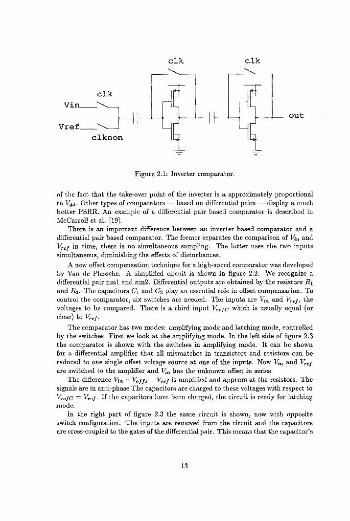
elk
elk
Vin_'1 I
Vref __ ~ 11f--+---+ out
elknon
Figure 2.1: Inverter comparator.
of the fact that the take-over point of the inverter is a approximately proportional to Vdd. Other types of comparators - based on differential pairs - display a much better PSRR. An example of a differential pair based comparator is described in McCarroll et al. [19].
There is an important difference between an inverter based comparator and a differential pair based comparator. The former separates the comparison of Yin and Vre! in time, there is no simultaneous sampling. The latter uses the two inputs simultaneous, diminishing the effects of disturbances.
A new offset compensation technique for a high-speed comparator was developed by Van de Plassche. A simplified circuit is shown in figure 2.2. We recognize a differential pair nml and nm2. Differential outputs are obtained by the resistors Rl and R2. The capacitors C1 and C2 play an essential role in offset compensation. To control the comparator, six switches are needed. The inputs are Yin and y"e!, the voltages to be compared. There is a third input Vre!G which is usually equal (or close) to y"e!'
The comparator has two modes: amplifying mode and latching mode, controlled by the switches. First we look at the amplifying mode. In the left side of figure 2.3 the comparator is shown with the switches in amplifying mode. It can be shown for a differential amplifier that all mismatches in transistors and resistors can be reduced to one single offset voltage source at one of the inputs. Now Yin and y"e! are switched to the amplifier and Yin has the unknowll offset in series.
The difference 'Yin - VO!ls - Y,.e/ is amplified and appears at the resistors. The signals are in anti-phase The capacitors are charged to these voltages with respect to y"e/C = Vre!. If the capacitors have been charged, the circuit is ready for latching mode.
In the right part of figure 2.3 the same circuit is shown, now with opposite switch configuration. The inputs are removed from the circuit and the capacitors are cross-coupled to the gates of the differential pair. This means that the capacitor's
13

Vdd
Rl ;\OfC R2
~ 1J\l nm2
vind 6 vref
Itail
Figure 2.2: Simplified circuit of new comparator.
bottom-plate voltage v;.e/ is applied to both inputs. Note that the same Va/Js is still present. Three different cases can be discerned:
• Vin = v;.e/ Now, cross-coupling has no effect since both inputs will not change. The comparator was in a stable position and since nothing has changed, it cannot make a decision despite the presence of an offset voltage. In practice noise and the previous comparator decision wi! determine the decision
• Yin> Vre/ Now, cross-coupling does have effect. The gate voltage of nml falls from Vin to v;.e/' For the gate of nm2 nothing has changed (if v;.e/C = v;.e/)' Because of the voltage drop at nml 's gate, the drain current will drop too. This implies an increase in output voltage. Because the capacitors cannot be charged or discharged, they are just DC level-shifters so the voltage at the gate of nm2 will rise too. This means more current through nm2, less voltage at its drain and therefore less voltage at nml 's gate. This is an avalanche effect due to the positive feedback. A stable position is reached if nml is completely off and nm2 conducts the whole current Itail.
• Yin < v;.ef This is the opposite situation, now the same latching occurs but with the outputs interchanged.
In figure 2.4 the circuit of the comparator is shown. We see a slightly more complicated circuit but the parts of the simplified circuit are easy to detect. The
14

vdd Vdd
Rl
rtfC R2 Rl R2
Cl C2
Voffs
nml
~ Cf nm.2
l!,tail -
Figure 2.3: Amplification mode and latching mode.
differential pair is formed by nmi and nm2 and the resistors are replaced by pml and pm2. These PMOS transistors are biased in their linear region by connecting the gates to Vss. The switches are replaced by nm5-nmlO.
The capacitors are not connected to the resistive outputs but via buffers nm3 and nm4. This enhances high-speed operation because the charging can now be done from a low-impedance transistor instead of a (medium) impedance resistor. The buffers also buffer the output, making the comparator less sensitive for the load, a fast latch to produce 0/5 V outputs. The circuit is biased by the transistors nmll-nmI6. The bias for the differential pair and the buffers are separated to allow for some experimental variations.
Simple NMOS transistors will do for the switching because the input interval of interest is 1.5-3.5 V. NMOS switches will work up to approximately 3.8-4.0 V if switched on with a 5 V gate voltage. The differential pair will start working for input voltages above 1.5 V because there has to be a minimum tail voltage (approximately 300 mY) to allow the current source to operate (in saturation).
2.2 Component values
The comparator of figure 2.4 has been processed in the C3DM technology. This is a technology with almost the same specifications as the C250 technology described in section 1.7. The major difference is the minimum layout value for a transistor: 2.4/1.6 /-Lm. The 1.6 /-Lm channel length is 1.2 /-Lm effective. C250 dimensions are 0.75 times C3DM dimensions.
For the prototype no optimalization was done (lack of time). To have a low
15
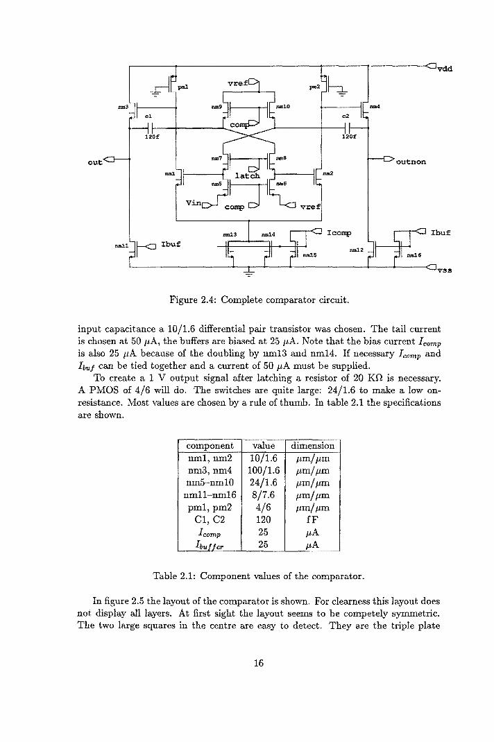
vdd
_4
01
120£ 120£
out outnon
Icomp
=11 r Ibuf "",12
Figure 2.4: Complete comparator circuit.
input capacitance a 10/1.6 differential pair transistor was chosen. The tail current is chosen at 50 J-tA, the buffers are biased at 25 J-tA. Note that the bias current Icamp
is also 25 J-tA because of the doubling by nm13 and nm14. If necessary lcomp and Ibu.f can be tied together and a current of 50 J-tA must be supplied.
To create a 1 V output signal after latching a resistor of 20 KO is necessary. A PMOS of 4/6 will do. The s'witches are quite large: 24/1.6 to make a low onresistance. Most values are chosen by a rule of thumb. In table 2.1 the specifications are shown.
component value dimension nm1, nm2 10/1.6 J-tm/ J-tm nm3, nm4 100/1.6 J-tm/ Jim nm5-nmlO 24/1.6 J-tm/ J-tm nm11-nm16 8/7.6 J-tm/ J-tm pm1, pm2 4/6 J-tm/ J-tm
C1, C2 120 fF Icamp 25 J-tA
Ibuffer 25 J-tA -
Table 2.1: Component values of the comparator.
In figure 2.5 the layout of the comparator is shown. For clearness this layout does not display all layers. At first sight the layout seems to be competely symmetric. The two large squares in the centre are easy to detect. They are the triple plate
16

capacitors Cl (right) and C2 (left). Above them are the six switches. The outer switches nm5/nm7 and nm6/nm8 share one diffusion area, it is the selector of the change-over switch. The differential pair can be found at the left (nm1) and at the right (nm2) of the switches. The large folded transistors at the bottom are the output buffers. Between the buffers and the capacitors we see the almost square current sources nmll to nm16. Finally the small transistors at the bottom corners are the PMOS resistors, pm1 at the left corner, pm2 at the right corner.
< 1'-15 Uri )
Figure 2.5: Layout of the comparator
17

2.3 Mismatch in the comparator
Because of the symmetry in architecture and layout of the comparator, no systematic offsets are expected. Random mismatch of the components is expected as a source of overall offset voltage. The main problems are caused by transistor mismatch and capacitor mismatch. We ignore parasitic capacitors and resistors since they are assumed to be small and if they are not, their effects will be canceled by symmetry.
In this section first some hand calculated results are presented. Second, extensive computer analysis has been carried out to extract the offset errors of each pair of transistors. To do so, transistor parameters are changed by a small amount and an offset voltage is included at the comparator's input. The voltage of this source is adjusted to eliminate the effect of the disturbance. By doing this one parameter at a time, an expression of the overall offset voltage can be obtained.
Mismatch can be modeled mainly by two parameters: mismatch O"(VT) in threshold voltage VT and mismatch 0"(f3) in current factor f3 = 1f J.LCo;r,. From Pelgrom [26] we have learned:
0"2(f3) f32 -
0"(13) _ f3
O"(VT) -
2% v'WL 16mV
v'WL
2.3.1 Some calculations
(2.1)
(2.2)
(2.3)
The comparator can be seen as two different parts, an amplifier and some switches to change the circuit dynamically. Mismatch in the amplifier itself can be reduced to an input-referred offset voltage and will be compensated. Compensation relies on the fact that the same circuit including its offset - is used both in sampling and in latching mode. This is not true for the switches so the main source of offset is mismatch in the switches. A few calculations give an idea of the offset to be expected in the computer analysis.
According to eqn. 2.3, for a matched pair of switches with dimensions W / L = 24/1.6 we have:
16mV O"(VT) = v'WE = 2.6 m V
WL We will assume that there exists a difference ~VT = O"(VT) This means that the charge in the switches in the channel - is not equal, there is a difference ~Q:
~Q = W LCo;r,~ VT
If a switch is turned on or off, this charge mismatch results in a voltage mismatch due to the capacitance at the node where the switch is connected. For an estimated capacitance of C = 120 fF, this results in a voltage mismatch of
6.Q WLCo;r, ~VVT = C = C ~VT= 1.2 mV
18

This mismatch is compensated by the amplified offset voltage source at the comparator's input. The (differential) gain is 7.2, so the offset voltage will be:
.6.VvT V Voffset V:;T = -G' = 0.17 m , aln
This offset voltage is the offset referred to the Yin - 'Vre! value. Because this difference is amplified in the comparator, we must divide the offset by the gain factor.
For the switches connected to 'Vre! or Yin this value can differ because part of the charge difference approximately 50 % - goes into these sources and does not contribute to the offset voltage. Mismatch in W and L is treated similar to mismatch in VT. Suppose there is a mismatch .6.W. Because of this mismatch there will be a proportional mismatch in capacitance. Now the charge in the "mismatch" -capacitor (aW)LCo:v is:
.6.Q = (.6.W)LCo:v(VGS - VT)
For VGS = 5 V, VT = 1 V and .6.W/W = 0.7% we find:
.6.Vw = .6.Q = (.6.W)LCo:v (VGS - VT) = 0.01 mV C C
This seems to be no problem. But there are more effects caused by .6. W. There will be a difference in resistance of the switch - RC-time mismatch, decreases with increasing time - and there will be a difference in gate-drain and gate-source overlap capacitors. Especially these overlap capacitors introduce errors if they are not matched. For our switch (24/1.6), the gate-drain overlap capacitor is CGD = 8 fF. A 0.7 % mismatch2 of CGD and a 5 Volt dock pulse results in a voltage mismatch VCGD on the storage capacitors:
0.7%CGD .6.VCGD = C Vclock 2.33 mV
One way to get around with this error is to use limited amplitude clock signals, however this may reduce the operating limits of the switches, or to use a bootstrapping technique.
One source of offset in not discussed yet, it is the mismatch of the impedances of'Vrej and Yin. For a switch we used a simple model: half of the charge goes to the drain and the other half goes to the source. But the division is not 50% if the impedance is not equal at the drain and the source [25,32,35]. The impedance of comparator is equal for the switches but at the side of the inputs they will differ. 'Vre! is usually derived from a resistor ladder and Yin is an external pin of the comparator with a larger capacitive load than 'Vre!.
2.3.2 Computer analysis
For the C3DM process, u~) 2 %/ V(w L) and it is assumed to be dominated by spread of Pi spread of W, L or Call: is a minor cause.
2To be discussed later.
19

Since /3 or f.L cannot be varied without modifying the transistor model, a small change of W is used, which has the same effect as modifying /3. A severe problem is that this method also affects gate and overlap capacitances. In the first analysis, only a deviation in W was applied; later, a new model was created with a different /3, see table 2.2.
parameter circuit analysis area WL small difference of W or L
VT 10 m V source in series with the gate /3 new MOS model with /3 1 % higher
... ~
Table 2.2: Modeling of mismatch.
In table 2.3 the results of the analysis are given. These values are valid for Vre! = 2.5 Volt. Please note that the offset denoted in the table is the value of the input (offset) voltage source that has to be applied to have the comparator make the right decision; it is not the VT offset of an individual transistor! The effect of mismatches in the capacitors is shown in table 2.4. The mismatch in capacitors has not yet been studied for C3DM. The use of (parasitic) capacitors in fact is forbidden for digital circuits. For large capacitors (C > 1 pF) a 0.1 % mismatch has been observed, so 1 % is a good choice for worst case.
transistor WIllY test value offset test value offset offset offset Llay
pm/pm W pm W mV L pm L mV /3 mV VT mV nm1 10/1.6 10.1 0.15 1.616 0.17 0.05 0.15 pm1 3.5/6 3.6 -0.04 6.171 -0.03 0.00 0.06 nm3 100/1.6 101.0 0.06 1.616 -0.01 0.02 0.01 nm11 8/7.5 8.1 0.53 7.594 -0.60 -0.32 0.93 nm9 24/1.6 24.2 2.13 1.613 1.29 -0.32 0.35 nm7 24/1.6 24.2 -6.44 1.613 -2.30 0.00 -2.22 nm5 24/1.6 24.2 -3.69 1.613 -2.81 0.76 -0.79
Table 2.3: Effects on offset by variation of W, L, /3 (1%) and VT (10 mV).
Capacitor nominal test value offset fF fF mV
C1 115 116 0.448
Table 2.4: Effects on offset by variation of capacitance.
Analysis shows that mismatch in W has more effect than mismatch in /3. There
20

seems to be no correlation between them so we may come to the conclusion that the side-effects of using W as a method of analysing spread in f3 are to large to ignore, especially for the switches. The main effect of geometrical mismatch of a pair of switches is not a different f3, but a different overlap capacitance and charge storage. Changes in f3 have less influence according to table 2.3. Therefore the - arbitrary - division of contributions to mismatch in f3 is made based on:
This yields the following values to be used in equation 2.1:
O"(W) = 0.71% W
O"(L) _ 0.71% L
0"(1£) = 1.73% j.t
Note that simulations with a different f3 in fact simulate a different j.t only. From the tables - assuming linearity of the variations of W, L, VT, f3 and
C - the standard deviation of the total offset can be calculated. In table 2.5 the individual contributions to the offset voltage are displayed. In this table for property x, 0"1,; means the input referred offset due to mismatch in X, O"(x). Total offset can be calculated using:
2 '" (2 2 2 2) O"total = ~ O"w + O"L + 0"" + O"vT (2.4)
transistors
Including mismatch in the capacitor, an overall offset voltage with 0" = 7.2 mV is to be expected. Notice that the differential pair itself has a sigma of
16mV =4mV J10 x 1.6
If we use a non-compensated comparator we will have to add approximately the same 4 m V due to mismatch in the rest of the circuit making offset compensation comparable to no compensation at all, not quite what it should be!
21

transistor Wlay Uw UL u!3 uVT Utotal Llay
pm/ pm mV mV mV mV mV urn 1 iO/1.6 0.11 0.08 0.09 0.07 0.18 pm1 3.5/6 0.01 0.01 0.00 0.03 0.03 nm3 100/1.6 0.04 0.00 0.03 0.00 0.05
nm11 8/7.5 0.30 0.47 0.55 0.20 0.81 urn9 24/1.6 1.81 0.76 0.55 0.11 2.04 nm7 24/1.6 5.49 1.35 0.00 0.69 5.70 nm5 24/1.6 3.14 1.65 1.31 0.25 3.79 total 6.59 2.31 1.53 0.77 7.19
Table 2.5: Standard deviations of offset voltages.
22
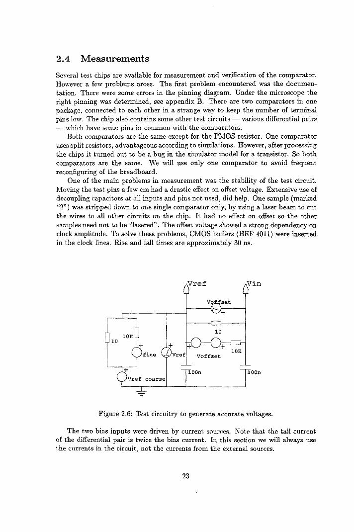
2.4 Measurements
Several test chips are available for measurement and verification of the comparator. However a few problems arose. The first problem encountered was the documentation. There were some errors in the pinning diagram. Under the microscope the right pinning was determined, see appendix B. There are two comparators in one package, connected to each other in a strange way to keep the number of terminal pins low. The chip also contains some other test circuits - various differential pairs - which have some pins in common with the comparators.
Both comparators are the same except for the PMOS resistor. One comparator uses split resistors, advantageous according to simulations. However, after processing the chips it turned out to be a bug in the simulator model for a transistor. So both comparators are the same. We will use only one comparator to avoid frequent reconfiguring of the breadboard.
One of the main problems in measurement was the stability of the test circuit. Moving the test pins a few cm had a drastic effect on offset voltage. Extensive use of decoupling capacitors at all inputs and pins not used, did help. One sample (marked "2") was stripped down to one single comparator only, by using a laser beam to cut the wires to all other circuits on the chip. It had no effect on offset so the other samples need not to be "lasered". The offset voltage showed a strong dependency on clock amplitude. To solve these problems, CMOS buffers (HEF 4011) were inserted in the clock lines. Rise and fall times are approximately 30 ns.
Vref Vin
Va set
+
10
10K
Figure 2.6: Test circuitry to generate accurate voltages.
The two bias inputs were driven by current sources. Note that the tail current of the differential pair is twice the bias current. In this section we will always use the currents in the circuit, not the currents from the external sources.
23

Because the output buffers of the comparator were not capable of driving large capacitances, high-speed testing was not possible at alL For clock frequencies above 1 MHz the comparator ceased operation.
Despite all decoupling and other measures, the offset voltage still didn't behave as was expected. The offset was always positive. All working samples showed the same behaviour and the measurements were reproducable. In figure 2.6 the test circuit is shown. Several voltage sources are used to make coarse and fine tuning voltages for Vre! and Yin. The outputs are displayed on an oscilloscope. An example of the output is shown in figure 2.7
3.8 V Ibuffer' 25 J-tA =
out 3.3 V I tail 50 J-tA
out 3.3 V v;.ej = 2.5 V
Vin = v;.ej + 40 mV
Jclock = 100 KHz I I 2.6 V 1 :
-+-- ~ Vdd = 5V I.
Temp 20°C = 0.4 J-tS 0.4 J-ts
5V compare
OV
5V latch
OV
F.igure 2.7: Output and clock signals on the oscilloscope.
At a specific offset voltage the outputs change their logic levels. The oscilloscope shows a noisy picture (eye pattern) because the outputs go up one time and go down the other time. The accuracy in determining the offset voltage this way is approximately ±300 J-t V. The offset has a positive sign if at the threshold Yin > Vre!'
The offset voltage is a function of the reference voltage as can be seen in figure 2.8. As standard current values are used: Itail = 50 J-tA and Ibu! = 25 J-tA. We see that all samples (except one) have the same behaviour. The standard deviation of the offset is approximately 3.0 to 3.8 mY. Note that the number of samples is very low (10) so the calculation of the standard deviation may be inaccurate. The formula to predict the standard deviation of a population by a sample of N values Xi with mean value x is:
L~l(Xi - x)2 N-l
(2.5)
The simulations predict an offset of approximately 7 m V. In section 2.5 we will investigate the causes of the strange behaviour of the offset voltage.
24

::0-E
80.0
70.0
60.0
SO.O
10.0
30.0
20.0
10.0
0.0 0.0 0.5 1.0 1.5 2.0 2.5 3.0 3.5 1.0 1.5 5.0
Vref V
Figure 2.8: Offset voltage as a function of VreJ for 10 different samples.
The offset is not a function of frequency. This is concluded after measurements at 1 KHz, 10 KHz, 100 KHz and 1 MHz. Also the pulse-width of the clock signals has no influence. For all these measurements the same clock fall and rise times are used. Frequencies above 1 MHz cannot be measured because the parasitic capacitance cannot be driven by the 100/1.2 output transistors (biased at 25 J-tA). The offset voltage is a function of the capacitive load. Without load the offset is small; adding a load (10 pF) increases the offset a few « 10) percent.
The value of the parasitic capacitance can be determined by the time necessary to discharge the output (high to low transition). The discharging current is supplied totally by the output buffer's bias transistor. The output voltage is a straight line. The voltage changes approximately 1.3 V in 325 ns. The discharge time is measured using a 1 pF capacitor in series with the probe. This reduces the capacitive load to approximately 1 pF. The total capacitance is:
c = 25 J-tA X 325 ns ~ 6 F 1.3 V P
One pF is due to loading by the probe, so 5 pF remains. This capacitance is due to packaging, IC-socket, breadboard and the on-chip bonding pads. If we use the 11 pF //10 MS1 probe without the 1 pF series capacitor, we observed:
C = 25 J-tA x 950 ns ~ 18 F 1.3 V P
25
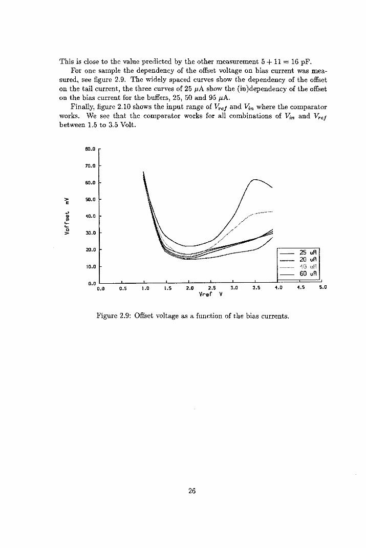
This is close to the value predicted by the other measurement 5 + 11 = 16 pF. For one sample the dependency of the offset voltage on bias current was mea
sured, see figure 2.9. The widely spaced curves show the dependency of the offset on the tail current, the three curves of 25 f-tA show the (in)dependency of the offset on the bias current for the buffers, 25, 50 and 95 f-tA.
Finally, figure 2.10 shows the input range of v;.e! and V'in where the comparator works. We see that the comparator works for all combinations of V'in and v;.e! between 1.5 to 3.5 Volt.
> e
.... Q) (/) ....
co >
80.0
70.0
60.0
50.0
'10.0
30.0
20.0
10.0
0.0
2S vA 20 vA "10 uA 60 vA
0.0 0.5 1.0 1.5 2.0 2.5 3.0 3.5 1.0 1.5 5.0
Vref V
Figure 2.9: Offset voltage as a function of the bias currents.
26

>
c .~ >
5.0
4.5
1.0
3.5
3.0
2.5
2.0
1.5
1.0
0.5
0.0 0.0 0.5 1.0 1.5 2.0 2.5 3.0 3.5
Vref V
Figure 2.10: The input range of Vre/ and Yin.
27
1.0
Vi.n, max Vi.n, mi.n
1.5 S.O

2.5 Circuit extraction
From the measurements of different comparators we found that the offsets do not spread around zero as was expected. All comparators show a positive offset. Clearly, there must be some mismatch or crosstalk in the chip-layout or the breadboard. In figure 2.5 the chip-layout is displayed. At a glance, symmetry seems to be perfect except for the current mirrors. To study the offset due to mismatch in the chiplayout, the circuit was extracted from the total test chip (name: YO).
This extraction has to be done carefully to include all parasitic capacitors and (poly)resistors. If a resistor is defined, only its capacitance to substrate is computed. But a resistor may cross an interconnect line and their cross-capacitance is not to be neglected. In the first extraction such an error was made and the simulations showed a negative offset. In the second attempt, the resistors were divided into two parts so the cross-capacitance was computed. After extraction, the resistor values were adapted manualy to their correct values. Now the capacitor that was responsible for negative offset is (partially) cancelled by a new capacitor, but another crosscapacitance is introduced that causes the comparator to have an offset of about +15 m V. Now measurements agree with simulations.
Vdd
out 119f
J~ comp=.d L.avin Vref
Figure 2.11: Most important parasitics after circuit-extraction.
28

In figure 2.11 the most important parasitics for offset are shown. By far the most important one is the cross capacitance ( 0.58 fF) between the gate of the differential pair's V'in side and the latch clock. We can find this cross capacitance in figure 2.5 at the gate of the left transistor of the differential pair. We see a line crossing the gate connection. The gate is connected to the switches (at the right side of the dif.pair transitor) and one of these switches is controled by the crossing clock line.
During input sampling and offset storage this parasitic capacitor is harmless, but if the comparator is switched on for latching, a capacitive divider is created and some charge is injected into the total capacitance seen at the gate. This results in an error voltage between the gates when the regenerative latching begins. The offset is therefore a function of the latch pulse amplitude, as has been noticed during measurements. In order to cancel the effects of clock pulses on offset, buffers were inserted on the breadboard. These buffers (two nands HEF4011) have an outputrange of 0 .. 5 V. Fall- and risetimes are 30 ns.
Simulating an extracted circuit is not an easy thing to do. The simulator fails to converge and consumes lots of cpu time. After some manual processing on the input file it is able to simulate the circuit. The simulations are carried out with two different rise- and falltimes: 2 ns and 30 ns to see the effect on the offset voltage. In figure 2.12 the simulated and the measured data are plotted. For Vre/ > 1.5 V simulation and measurement agree but for Vre/ < 1.5 V they disagree.
SO.O
15.0
10.0
35.0 r"<
> 30.0 e
..> 25.0 Gl III ... ... 20.0 0 >
(1.... .0---------- -- ...... " ............ 6 ..... · .... ·· ....
A •••• "tt\ ,/ ......... .& ..... +---+ measuremenl, 30 ns •••• \ ",,' •••••••••••••• (to - - E) s~muLol~on, 30 ns
•.....• ~& - - _ -0'" .. ,,6 .. ···••····· 6-· ...... 6 e~muLolLon, 2 ns 0.0 L_~'6i..:·:.:.:· .. :.:.:. .. ·:.:.: .. ·:.;J. .. \.:.: .. 1.:.:".:.:.: ... .::.:" • .:.:.:."::.... --L __ --L __ -L.~==::J:====::J:=========::!.J
15.0
10.0
5.0
0.75 1.00 1.25 I.SO 1.75 2.00 2.25 2.50 2.75 3.00 Vref IV)
Figure 2.12: Simulation compared to measurement.
What happens below 1.5 V for reference and input voltage? Due to the low
29
input voltage, the voltage at the tail of the differential pair is only a few hundred m V. The current source is driven into its linear region and the current falls. Also the output impedance of the current source becomes very low (equal to channel resistance Vds/1d) These effects cause a decreasing gain and therefore an increasing offset. No exact reason has been found that explains the disagreement between simulation and measurement.
In this region the infuence of VT is important. A large VT means that the minimum input voltage to keep the current source in saturation is higher. It looks like the simulated circuit has transistors with a lower VT than in the samples. All curves show a high offset for v;.e! near VT. Another possibility is that the modeling of low voltage behaviour is not accurate in Panacea3.
The normal area were the comparator is used, is the interval of 1.5-3.5 V. At voltages above 3.9 V the comparator stops working correctly. Now the switches cause problems because at Vs = 3.9 V the effective gate voltage approaches zero and the on-resistance increases quickly.
We can conclude that before processing a layout it is important to extract the parasitics and include these in the simulation to prevent malfunction of the circuit due to these parasitics.
3 Model 7 was used, not (the more accurate) model 9. Sub-threshold is not implemented correctly in model 7
30

2.6 Redesign of the comparator
In order to study the capabilities of the comparator a redesign is necessary. For use in an 8-bit application (1 LSB = 8 m V) the goals are:
• 2 mV offset (standard deviation).
• Input range 0-2 Volt.
• Low input capacitance
• 33 ns cycle time (30 MHz clock).
• 1 m W power consumption.
• C250 technology (1.1 ILm effective channel length, double metal, single poly).
It would be nice to design a comparator with aIm V offset so it can be used in the third-step sub converter of the 12-bit ADC.
The current design needs some modifications to shift the input range from 1.5-3.5 V to 0-2 V. This can be realized by using a PMOS source follower as a levelshifter. By choosing appropriate W /L and bias current the shift can be made 1.5 V. Because the level-shifters are inserted between the differential pair and the switches, their offset is compensated automatically when latching is turned on. In figure 2.13 the circuit is shown.
Another modification is the use of cascode transistors for the current sources. For the differential pair a high-swing cascode [31] is necessary because the tail voltage can be as low as 0.7 V. The last main modification is the addition of a reset clock. This enables fast recovery from latching. This clock is turned off before the compare clock is turned off, so this clock has no effect on offset. In the following paragraphs a detailed view is presented on the new design.
2.6.1 Switches
The main error in the previous design was the size of the switches (24/1.6). Errors in matched switches cannot be compensated by this comparator so these errors should be kept as small as possible. In the new design these switches have minimal dimensions, W / L = 1.5/1.2. This implies a higher on-resistance but this is partly compensated because the input is shifted to 0-2 V. The switches are turned on with a higher VGS, decreasing the resistance. The resistance ranges from Ron = 3.5 KO at VGS = 5 V to Ron = 7 KO at VGS = 3 V. Because capacitors in the circuit have the order of 100 fF, the RC constant is below 1 ns, sufficient for high-speed operation. For the old design, Ron = 360 n at VGS = 3.5 V to Ron 2.2 KO at VGS = 1.5 V. A plot of R versus VGS for the 1.5/1.2 switch is shown in figure 2.14.
Note that scaling the width of the switches with a factor a does not scale offset with the same factor. See what happens to the mismatch in charge 6.Q due to a
31

Vdd
bias49
nrese~ pm40
out outnon
nm16
nm15
Figure 2.13: Redesign offset-compensated comparator/latch.
32
Resistance (Vds/Ids) fur nmos lI'allSistor as a function ofVgs. Vs=SV-Vgs; WIL-1.S/l.2; for large Vds lI'allSistor in saturation.
Resistance SO.Ok:
I I I \ \ ,
i , \ , \ , \
\ 1 \ ,
\ \ I
\ \ : \
\\ \ \ \
\~ \ \
" ,-" \-\ '\
\ \
VdsclOmV !S.,l00mV \ " IV
"
~, "~ .... ~ ........ ~ .. " '.
~
45.Ok:
4O,Ok:
3S.Ok:
3O.Ok:
2S.Ok
2O.Ok
lS.Ok
10.Ok
" " " " ,3V ....
..... .... ....
......................
S.Ok: r-- ...................... ~ ........ ~----- .. -~ ....
0.0 1.0 2.0 3.0 4.0
1.5 2.S 3.5 4.5
Figure 2.14: Resistance (VDs/IDs) of a 1.5/1.2 NMOST.
mismatch in VT:
2.6.2 Level-shifter
The PMOS level-shifters (pm3, pm4) in fact have a double function:
• Shifting 0-2 V to 1.5-3.5 V
• Providing a low input capacitance.
----~ .. -..... -....
S.O
Vgs
The differential pair (nm1, nm2) can have a large input capacitance (for obtaining sufficient transconductance), isolated from the real input by the level-shifters. The N-well is connected to the source to prevent VT becoming too large. The shift can
33

be found by:
In
VGS
~(VGS - VT )2 2
= VT+ J2~D If we choose W/ L = 10/1.2 small input capacitance we find In = 25J..tA for a 1.5 V shift. If the current source does not have a high output impedance, the levelshifter's output is attenuated with respect to the input. Using a casco de greatly increases the output impedance. An example of cascoding is shown in figure 3.22, section 3.5.7
The small signal output impedance of the level-shifter (pm3) is 1/ gm = 10 KO. The load is capacitive only and is determined by gate, diffusion and overlap capacitors of nml, pm7 and pm3 itself.
2.6.3 Gain and offset
The gain of the differential pair is:
A=gmR
The latch decision is based on the (offset-compensated) difference 6. after the latching pulse:
6. = A(Vin v;.e/ ) + Voffs switch , So, to compensate the switch-introduced offset, we must apply
V. Voffs, switch re/- A
It is not easy to compute Voffs switch' It consists of two different parts: mismatch in clock feedthrough due to differences in GGD and GGS overlap capacitors and second, mismatch in charge-dump from the channel, which is a complex function of rise/fall time, impedance mismatch at the switches and threshold voltage mismatch. From simulations it is known that a gain of 10 is sufficient to reduce to effects of mismatch for an overall offset voltage of 1 m V.
2.6.4 Optimizing the differential pair
Simulations show that the main limit in speed is the RC time produced by the PMOS resistor and the total capacitance at the node pm1/nml (see figure 2.13) We have to satisfy the condition:
gmR= 10
We are free to choose W and L of the differential pair, W and L of the resistor and the tail current. Best high-frequency performance is expected with a minimal length
1.2J..tm - differential pair. If R has a small value, 9m needs to be large and vice
34

versa. Both R and gm have corresponding capacitors. It is likely that there exists an optimal situation where the product of total capacitance and R is minimal.
If nml (nm2) is constructed with 2 transistors in parallel (simulator: mult=2), the drain diffusion area can be shared, effectively halving GDB compared to a single (twice as wide) transistor. Increasing Itail increases gm but also increases the ampli~ tude after latching. A large amplitude means a large time to settle and a large time to recover. Things get even worse for large amplitudes because of the highly voltage (or current) dependent R. If the voltage across the resistor is 1 V for 1/2 Itail then the voltage will be not 2 V but approximately 3 V when the whole Itail goes into the resistor.
In order to make the right choices, a computer model was developed to calculate the RC product and the dimensions of the resistor and the differential pair. The input is gain, (tail) current and W of the resistor. The channel length of the differential pair is fixed to 1.1 pm (the program uses effective values). Some non~ideal effects are taken into account for the resistor because without them, there was a severe discrepancy between simulations and the simple model used. The simulated voltage after latching was much larger than predicted.
A voltage Viatch :::; 2 V is desirable, more would slow down the settling of the comparator, although the associated time constant is smaller. A voltage above 2 V may force transistors out if their saturation area. The program can be found in appendix D.
The program generates several curves. All the curves assume a gain of 10 and a buffer (nm3, nm4) of 40/1.2. In figure 2.15 the RC time is shown as a function of Lres for several tail currents. For the Wres given, there is a distinct minimum in the RC time. Unfortunately this minimum cannot be used because the voltage after latching becomes very large and requires a long time to settle and a long time to discharge after latching. Also, a large difference - e.g. Yin - Vrel = 2 V -generates a maximum output amplitude. When latching is turned on the difference Vout - Voutnon has to change its sign so the output has to make a 5 V swing. This takes so much time that high~speed operation is impossible. Notice that the sign change is inherent to this comparator. In the 12~bit ADC application this problem does not occur because the input and the reference differ at most 64 m V in the third step.
In figure 2.16 we see that the voltage after latching4 rises quickly with increasing Lres • A simple approximation explains: R"" Lres • For a large Itail we have to choose a resistor that corresponds to an RC time far from optimal. The resistance must be lowered to limit the voltage after latching, but a lower resistance means a resistor with a larger area and therefore more parasitic capacitance. A lower resistor means that the gm of the differential pair has to be enhanced so a Wnm08 must be larger and again, we add capacitance to the drain node. Increasing the tail current yields only a moderate decrease of RC time, part of the gain is lost by the increased capacitance.
4V;"lch is the voltage across the resistor, not the output buffer voltage.
35

RC time of dU.pair output for resistor 1.5/I..res for several Itail RC time vertical if PMOST out of resistor area.
RC 8.On
\ II I I I
~ I I I I
"- I
, , ~ , , , ,
~ , , , i'--,?SuA , ,
........ , ,
1.On
6,On
5.On
4.On
" ---....... --- I "' .... ,. .. lOOuA --'-J, -~""'" -- ... -
" .......... I ~ .............
" ....... "' ...... ~ .. --.. -...... ...c ___ ..... _
3.On
125uA -- - ,--I- -
2.On 1.2 1.8 2.4
t--
" "
"
1.5 2.1 2.1
I
i : r--- , :
I , ! , , --,-
---",
3.0 3.6 3.3
Figure 2.15: RC time constant as a function of L re8 and ltai/'
,
, , , I , , ,
3.9
Lres
The unity gain bandwidth is determined by 9m and total load capacitance C:
UGB= 9m 21f-G
In figure 2.17 W nmo8 is plotted as a function of L re8 . Because of the limited capability of the level-shifter to drive the gate capacitance, W nmo8 < 40 has to be chosen. Another restriction is Wnmos > 1.5, according to the minimum design rule.
The curves shown so far correspond to a Wres = 1.5. This minimum value is gives the smallest capacitance of course, but because L res must be chosen at discrete values (steps of 0.15 pm) it may be that an intermediate value would be better. Increasing Wres slightly often solves this problem. Also, for large currents Lres cannot be made small enough for Wre8 = 1.5. This means that we have to increase Wres , but we also increase the parasitic capacitance.
The curves are repeated for other values. They all look the same except for the numbers so it is not so useful to include all of them. Analyzing the data of these curves with the restriction of Viatch < 2.2 V yields figure 2.18. Here the optimal RC
36

Latch voltage for resistor 1.5/Ltes for several ltaiL Vlatch-SV if PMOST out of resistor area.
Vlatch 5.0
I
4.5 / , 'l2SuA f I i I ! I
4.0
3.5 i I i / I'
lOOuA ! 7SuA :
~l/~~ , , ,
I , , , /~~~~ , ,
.~"'~~ , -,.,,..,;
3.0
2.5
2.0
1.5 ,-
I I I
I I I I
I , I I
~ ... .1" ... '
~ , --l.0 ------SOO.Om
1.2 1.8 1.5 2.1
I I I I I
~ ~
2.4 3.0 2.7
Figure 2.16: Latch voltage as a function of Lresistor and Itail.
3.3 Ln:s
time and the corresponding (effective) dimensions of the differential pair and the resistor are plotted as a function of Itail. The final selection can be based upon the value of Wnmo8 and the tail current. It makes sense to select Itail :5 75 f..tA because in this interval the differential pair has reasonable dimensions (the level-shifter can drive the capacitance) and for larger currents the decrease in RC time is not so much.
2.6.5 Buffers and Capacitors
Another way to diminish the offset is to use larger storage capacitors C1 and C2. Now the effect of mismatch in the switches is dumped into a large capacitor, so the voltage change will be small. One serious problem is the increased area needed. The penalty in speed can be compensated by using a larger buffer transistor (nm3, nm4) or increasing its bias current. Compared to the old design, the buffers are even smaller (100 f..tm, now 40 f..tm). The load consists of the capacitors and a (full
37

W of dif.pair output for resistor 1.5/Lres for sevend Itall. W<l.S makes no sense; W>4() makes levelshlfter slow.
Wdif.pair
100.0 ,
\ , , , , , ,
\
\
\ , , \
80.0
,
1\ \
... \ , ... \
\\ ~ ...
"\ \ , , \
\ ,
~ \ , \~\\ \
\
\ \ \
\ '. , "-\ ·• •• 100uA ',?5uA , '. " ,
60.0
40.0
, , "..''''''
, , '. , ,
20.0 , , , , ,
.....
~ ~ I
" .............. ,,"- r---.... ................. - ---..... 125uA ................. - ._----.-.•..•. ---'" '"
~~ ....... ~"' .......... ~ -- ............... -...... ~ - -0.0 1.2 1.8 2.4 3.0
1.5 2.1 2.7
'" '" ..
3.3
----- , ------3.6
3.9
~s
Figure 2.17: Wnmos as a function of Lresistor and Itail for 9mR 10.
swing) latch. The output impedance is low enough compared to the switches.
1 1 1 Rout = - = = = 1.9 KO
9m . 12Idf3D W . 12 x 50 . 10-6 X 80 . 10-6 40 V L V 1.1
There is a limit to increasing C1 and C2 because of the RC time - R is the on-resistance of a switch - becoming the dominant factor in speed. A second limit is imposed by the current source of the buffer. The capacitor discharge current is limited by this source.
If the voltage drop across a capacitor is guaranteed to be one Volt or more, an NMOS transistor can be used as a capacitor. The gate is one terminal (the positive one) and the drain and source together are the other terminaL There has to be a voltage of at least Va,SD > VT ~ IV because the existence of an inversion layer is essential in this capacitor: it forms one plate.
Technology prohibits the use of a capacitor with a thin oxide dielectric on a diffusion area (instead of the channel). Also a triple plate sandwich capacitor with thin oxide is not available. For a thin oxide (dual plate) capacitor the capacitance is
38

Best case RC time and corresponding W(diff.pair) for several ltail Selection is based on Vlatch<2.2V.
Wdif.pair
4.1n
4.011
3.9n
3.8n
3.7n
3.6n
3.5n
'\
~c \
\ ~
~~r. .1 ............ .., "
1.8/1. 5
-W ,,' " / ,
1.812. !S .''' '" r------" ", , , ,
3An ... _--_ ....
1.5 (. .. 85 " --........ ""
" 3.3n
SO.Ou 100.011 75.011
The numbers shown in the picture are W/L of the PMOS resistor.
All dimensions are effective values, not layout values.
.........
125.011
-, /' -, ,
100.011
90.011
SO.Ou
2.25/13: 5 70.011
", -,
60.011
SO.Ou
40.011
3O.Ou
-20.011
lSO.Ou
ltail
Figure 2.18: Best case dimensions and RC time as a function of [tail.
approximately 1.4 f F / p,m2 - as is known for the gate capacitance -, for a normal triple plate we have 0.1 fF / p,m2 •
Unfortunately the existence of a channel cannot be guaranteed for Vre/ > 1 V. The threshold voltage VT itself will also be larger because of the substrate effect.
If we insist on using an NMOS capacitor, the resistor values and the tail current would need to be adjusted far from the optimum to satisfy the channel existence condition. Also, VT can be 200 m V above or below the nominal value caused by process variation. If VT is maximal, the NMOS capacitor will need 200 m V more and the output will be 200 m V lower so the capacitor will malfunction at 400 m V below the nominal value.
This problem could be circumvented by disconnnecting the capacitors from Yre/ and using a new - lower - reference Vre/ G • This could be a fixed reference or a reference depending on the "real" Vre/. A disadvantage of this technique is the voltage jump (Yre/ - Yre/G) at the gates of the comparator's inputs at the time latching is switch on. Both inputs have the same jump - a common mode effect but the offset may be a function of the common mode level. We did the compensation
39

for the offset at v;.e!, but we use it at v;.e!C. It is likely that the overall offset will nse.
An advantage is the fact that the charging and discharging current of the capacitors does not flow through the ladder and second, the resistance of the switches pulling the capacitor to the new reference is lower (Vre!C is lower so Vas is higher).
In the current design "normal" triple plate capacitors are used. The area needed is approximately ~o; JF 2 = 3000 f1.m2 , a square of 55 by 55 f1.m. If more offset
0.1 f1.m is allowed, the capacitors can be made smaller, they take approximately half of the comparator's area.
2.6.6 AC simulation
An AC-run of the comparator - in the amplifying mode - shows the poles of the comparator, see figure 2.19. The frequency plots are calculated for the three stages in the comparator. We can see that the differential pair determines the dominant pole. The solid lines are for v;.e! = 0 V, the dashed line for v;.e! = 2 V. For large v;.ej the level-shifters are slow.
2.6.7 Recovery after latching
Due to the large resistors required to achieve adequate gain - giving a large latch voltage there is major problem of recovery after latching. To speed up this process, a third clock reset has been introduced, implemented with a PMOS switch. This switch shortens the "problem"-nodes (gates of nm3 and nm4, see figure 2.13). There is no need for a complementary NMOS transistor because of the high voltage (> 4 V) at these nodes prohibits NMOS conductance .. The switch in fact discharges one node and charges the other, canceling the charge inequality.
Comparison is started by switching the inputs to the amplifier. The reset clock is (still) on to discharge the outputs, the comparator's previous decision, quickly. If the input difference is large, it will settle, although attenuated. If the difference is close to zero, the switch will help to set the output difference close to zero too.
Then the reset switch is turned off to enable proper settling of the amplified signal, diminishing the influence of the reset switch. Therefore it needs not to be a minimal switch and its timing is not critical. A small switch would take more time to do its job because of the large resistance, a larger switch would take more time to settle after the switch is turned off. 5
We assume that the amplifier has settled now and goes into the latching mode. During the first nano seconds of latching the amplifier has a high gain and the outputs will diverge quickly. It will stop when one resistor is without current and the other has Itail. This is a pleasant situation for the second stage latch but it is unpleasant for the next comparison phase. The reset switch is turned on a few nano seconds before latching is turned off. The timing requirement is that is must leave
SThe switch introduces a COIIllnon mode error (100 mY) which is harmless. If the impedances at both sides of the switch do not match, a. differential mode error will occur, proportional to the size of the switch.
40

AC analysis for COIllparator in amplifying mode. Solid !iDe: Vref-OV; dashed line: Vref=2V.
dB
15.0
12.0
zoom active
----- --. -- - - ------ ......
9.0
6.0
3.0
0.0 --3.0
-6.0
-9.0 I
-12.0
-15.0
1.0M 1O.OM
- t--
-'. f' "
--. --
:-.. 0- '~~ , ,
,\ ,t', \. dif.Pail
, \ ,
'[\ \ r\
-C"" -, ~, ~ \ '<'~ I': -::- '\ ,\,
~ , , f\ " I\. overall , , ,
'\ , ,
Ish
'1\ loo.OM
Figure 2.19: An AC simulation of the comparator.
R
+ Rs V2 sv R
Vs=Vl-V2 Itail
~ ftc \
,
1.00
Vs
R
Figure 2.20: Equivalent circuit when reset switch is on in latch mode.
41

the latch enough time to produce a large difference, possibly it has even finished latching. The latch clock is still on.
Now the PMOS resistors and the reset switch form a three resistor network that can be simplified to the left circuit in figure 2.20. The latch is assumed to be in the final position: Itail in one resistor, none in the other resistor. The PMOS resistor pml and pm2 are represented by R and the reset switch is represented by Rs Because we are only interested in the difference Vs, we can make a further simplification as shown in the right part of figure 2.20. In reality the simplification that pml and pm2 have the same resistance is not true because of the high voltage dependency.
We would like the voltage across Rs to be limited to about 250 mY. Now a fast second latch can be used to store the result of the comparator. When reset is active, the amplification (in latching mode) is low, so we must not apply reset before the output difference has reached 250 mY. However, the timing is not very critical.
Rtot R(Rs + R)
-2R+Rs
V1 - ItailRtot
V2 R - Vi R+RII
Vs = V; (R) RRs Vi - 2 = ItailRtot 1 - R + Rs = Itail 2R + Rs
Rs 2RVs
= ItailR - Vs
Substituting estimated values R = 30 KO, Vs 250 m V, Itail = 75 fLA results in Rs = 7.5 KO or a switch of W/L = 3/1.2 A larger switch has a smaller resistance so the amplitude Vs is smaller, a smaller switch has more resistance but this means a slower discharging.
Without this extra switch, the comparator is much slower because of the large swing the outputs have to make. As we have seen before, a small output swing is not easy to make because it requires small resistor values and therefore a large differential pair to achieve a sufficient gain (10 times). A large differential pair has a large capacitance and is hard to drive by the level-shifter. The dimensions of the level-shifter are determined by the input capacitance so the only way to increase its 9m is by using a larger bias current. But there is only 1 m W available The voltage swing chosen seems to be optimal.
The extra clock has no critical timing as we have seen. An example of the comparator with and without this reset switch is shown in figure 2.21. The input offset is fixed to 1 LSB= 8 mY. The large amplitude signals are out and outnon without the use of a reset pulse. We see the outputs alternate each cycle due to the fact that the comparator did not have time to settle correctly in amplifying mode. The previous latch decision influences the new decision. The small amplitude signals (inside the eye-pattern) are again out and outnon but with the use of the reset switch. We see that the amplitUde in latching mode is limited. After latching (every
42

Operation with and without 11:Set pulse. Vm-V ref>=8m V; without teset the OUlputs toggle.
outputs
4.0
3.5
3.0
2.5
.. ""_..f.~.W1 ..... ~ . ' , I
• I
" .' I'
I I
I I I
2.0
1.5
1.0 0.0
I \ I \ , \
, I \ I \ I \ I I,
outn04 I
" , ~\I
33.On
I I ,
, , ,
66.Gn
\ I \ I \ \
I I \ , , , '- ..... }
99.On
T
Figure 2.21: Operation with and without reset pulse. Yin - v;.ef = 8 mY.
33 ns) the comparator is in amplifying mode and it settles very fast. Therefore the comparator takes the right decision every cycle.
2.6.8 Timing
For full-speed operation - 30 MHz -correct timing is important. The timing is shown in figure 2.22.
The rise and fall time are 1 ns and there is no overlap between compare and latch clock. The reset clock overlaps both latch and compare clock. If reset is still active in amplifying mode, input sampling is attenuated, but if reset is off, the final sampling can take place. This phase doesn't take much time. Notice that the reset pulse applied to the PMOS switch is an active low signal. Figure 2.22 shows the logic signals, "high" means active, "low" means inactive so the real reset clock is inverted with respect to the figure. As stated before, timing is not critical, it may have a deviation of a few (1-4) nano seconds.
In figure 2.23 a simulated output is shown for a comparator running at 30 MHz.
43

16ns
compare
4ns 12ns
reset
latch
IE------- 33ns -----~
rise and fall times lns
Figure 2.22: Timing diagram for comparator/latch.
The input signal steps 1/2 LSB (4 mY) from -8 mV to +4 mVat a DC level of 2 V. A 2 V level is the maximum level to be used and it is the worst operating case of the comparator. This is because the switches have a much higher on-resistance. In the third cycle the input difference is zero. In this case the decision of the comparator is based on the previous decision. Notice the inversion of the output due to the memory effect of the previous decision. The effect of the reset clock is visible when out and Gutnon suddenly "fall back" from their extremes. An approximately 150 m V difference remains until the compare clock is switched on (every 33 ns).
2.6.9 Large input difference
So far we have concentrated on the operation for a small difference Vin - v;.e/' If the difference is large for most of the comparators in a flash converter - a new problem arises. The output buffer is not capable to follow a large drop on its input. The capacitive load of the buffer - the 300 fF storage capacitor and an additional capacitor of 30 fF to account for the load of the subsequent circuitry - can only be discharged by the current source. This means that the buffer transistor is almost completely without current. Suppose there is a 1 V drop at the gate of the buffer. If the bias current Ibu/ Jer = 25ft A then we have:
C6.V Tdischarge = 1 = 14 ns
buffer
If latching is turned on, the outputs out and outnon should not change because of the low impedance at these nodes, the input to the level-shifter should jump from Vin and v;.e/ to VrefC. 6 But if the capacitor is still being discharged and the buffer is out of action, the impedance at the output of the buffer is high, unable to keep the output at the same voltage at the time latching is turned on. This means that the comparator will not work, the input difference does not change. The solution to this
6Usually both reference voltages are the same.
44

Comparator at full speed (30 MHz) for small input differences. Vref\=2V. Vin-Vref\=..SroV, -"roV, 0, 4roV.
latch outputs
3.2 i
--------.-------.--------, 20.0
3.0
2.8
2.6
2.4
2.2 0.0
OU~ II : : f i : 1
i i .. .J i ! i \ . V '
out
,--- -- ... , , , , I , • • • •
33.On
The output difference after latching is 150 roV.
:------, , , , : latch ~ • I I I I I I I I I I I
M.On
For Vin=Vref this difference is small (based on previous decision).
I------~ I I I I , I , , I I I I I I , ,
\ \ \
15.0
\ ./~ 10.0 \ 1
~ -------, 5.0 , ,
I I
/ ..... J.l-----'----t- 0.0 132.On
99.On T
Figure 2.23: 30 MHz operation of comparator for small signals.
problem is to choose a smaller latch voltage - operating far from optimal or to increase the output buffer bias current. More power in the buffers means less power in the differential pair, making it slower but closer to the optimum. A compromise was found: Itail = !QuJ Jer = 50 /LA. If we are sure that large input differences do not occur (as in subranging ADCs), we do not have the problem of slow buffers and could do with a 25 /LA bias for the buffers.
If we adapt the architecture of the flash converter, we could use a low current version too. The comparators are logically divided into a number of segments. For the segment of interest, all comparators have small input differences so we can use a small bias current for the buffers. A limited number of fast, not-compensated comparators is used in parallel with the normal comparators, to detect the valid segment where to look for the 1/0 change in the thermometer code. So the possibly wrong outputs of comparators with large input differences are ignored. Perhaps it can even simplify the digital circuitry.
An example of the operation with a large input difference is shown in figure 2.24. The most critical situation is VreJ = 2 V because in this case the switches have
45
Comparator at full speed 00 MHz) for large input differences. Vref,.,2V, Vm=l.S, 1.0,0.5,0 Volt.
latch outputa
4.0 -,--------r------,,--------.---------r 20.0
3.5
3.0
2.5
2.0
1.5
1.0
The decision is the small eye (6ns width) at the end of the latch pu~
The diffen:nce is 200 mV.
Figure 2.24: Operating the comparator at a large input difference.
maximum on-resistance (slowest operation). In the figure we see an increasing input difference (0.5 V per cycle). The big "eye" is caused by the high gain in amplifying mode. The out signal clips at 3.6 V but the outnon signal is still falling due to the discharging of the capacitor. The input of the Gutnon buffer settles much faster. Above 1.7 V the outnon curve is approximately a straight line. Studying the curve we find a 0.93 V decrease of out non in 7 ns. If we assume the discharge current to be equal to the current source we can calculate the total capacitance to be discharged.
Ibuller = 50 J1.A D.t = 7 ns
D.V = 0.93 V
C ItailD.t
= 375 fF = D.V
An estimated load capacitor of 30 fF had been added to the 300 fF storage capacitor in the simulation so the the remaining 45 fF is due to diffusion area and overlap capacitors of the buffer and the current source.
46

For a 1 Volt input difference (or more) the comparator still does not latch immediately as can be seen in figure 2.24. At the time the reset pulse is activated (not shown in the figure, it starts halfway the latch pulse) the real latching begins. The small eye at the end of the latch pulse is the correct decision of the comparator. The difference is about 200 m V and the duration is 6 ns, enough for the second stage latch to settle.
2.6.10 Bias
In figure 2.25 the bias circuit is shown. The bias is applied to the differential pair and the output buffers. Different currents in comparator and buffers can be made by scaling the mirrors.
J2 25u
1/4 W/L
nm22
Figure 2.25: Bias circuit for comparator.
Note that nm20, nm21, nm23 have the same W/L but nm22 has (1/4)W/L. It can be shown [31, page 715} that by taking WI L (nm22) four times smaller, a cascode biased by this circuit can have an output voltage as low as 2VGT - VGT = VGS - VT
- with both transistors still operating in saturation. Simulations show that the expected output voltage7 is at least 0.7 V, so we can choose the dimensions of the transistor to have a VGT ~ 0.3 V. This yields a 20/1.2 transistor for a 50 JiA current. The bias for pm5 pm8 can be obtained by a similar circuit or simply by two stacked PMOS "diodes" (pm20, pm21) as shown in figure 2.25.
7 Output of the current source.
47

2.6.11 Digital output
The comparator can be used in combination with a fast latch to obtain full-swing logic levels. It also holds the result of the comparison when the comparator is in the amplifying mode. The latch must clock a few nano seconds before the comparator is reset. The latch can be set in sampling mode if the reset switch is turned on. Final latching can be done when the comparator's latch pulse falls. In section 3.6 a small and fast latch is described. This latch reaches 0 and 5 V within a few nano seconds and needs a differential input voltage of some 100 m V to overcome the (possibly large) offset voltage and to speed up latching.
2.6.12 Component values and some final notes
In table 2.6 the final design values are shown. With these parameters a 1 mW
element value differential pair 22/1.2
resistor 1.5/2.85 output buffer 40/1.2 level-shifter 10/1.2
latch switches 1.5/1.2 sample switches 1.5/1.2
reset switch 3/1.2 nmos current sources 20/1.2 pmos current sources 10/1.2
capacitors 300 fF Itail 50 J.lA
Ibuffer 50 J.lA Ishifter 25 J.lA
Table 2.6: Final dimensioning of the comparator.
comparator can be built for a 33 ns cycle time. As stated in paragraph 2.6.9, the bias currents can be decreased if the comparator cannot be overloaded in amplifying mode by a large input difference, as is the case in a subranging converter. The offset voltage is computed for several types of mismatch, indicating an overall (input referred) offset voltage of 1 mY. This is appropriate for 9-bit accuracy. In 8-bit applications the gain and the storage capacitors can be reduced. In that case, a 25 ns cycle time may be possible but further research is necessary.
Exact information about the origin of f3 mismatch (2 %) is not available. If the variation in geometry is neglectable « 0.1%) then the offset will be much lower; if it is more than 1 %, the offset is likely to be larger. For a reasonable approximation we can use the values used in section 2.3. Good characterization of the geometry
48

mismatch of the C250 process would be very desirable. 8
8Recent measurements on a :flash AID converter indicate that the mismatch predicted by simulations agree with measurements.
49
2.7 Conclusions
The compaxators examined in this chapter have their pros and cons. For the compaxator in the test circuit we have the following list:
+ small area (135 x 145 /Lm2)
+ low power (0.5 mW)
+ 20 MHz clock frequency
+ good PSRR due to differential axchitecture
+ only 2 clock signals
o 8-bit accuracy if smaller switches
floating input range 1.5-3.5 V.
sensitive for impedance mismatch of v;.e! and 'Vin
layout-error and switches too large
no digital output (extra latch necessaxy)
v;.e! is loaded by 2 capacitors and 1 gate9
In the redesign some of the drawbacks have been eliminated in order to make it suitable for a 9-bit application (third step in a 12-bit multi-step AID converter). Here is a list of the advantages and disadvantages:
+ small area (estimated 150 x 150 /Lm2)
+ low power (0.75 mW)
+ 30 MHz clock frequency
+ 9-bit accuracy (1 m V offset)
+ good PSRR due to differential axchitecture
+ 0-2 V input range
sensitive for impedance mismatch of v;.e! and 'Vin
no digital output (extra latch necessaxy)
v;.ef is loaded by 2 capacitors and 1 gate
laxge input difference slows down amplifier mode (increasing power in levelshifter helps)
9This may be circumvented by using a separate V.e/c ladder to supply the charging and discharging currents of the sampling capacitors.
50

In general this comparator architecture is suited for 7-9-bit applications at 30 MHz clock frequency. Accuracy is limited by the mismatch of the switches, the value of the capacitors and the gain in amplification mode. A lO-bit performance is not easy to be realized, it would need a gain of approximately 20, not easy for a single stage amplifier without loss of speed.
The use of level-shifters at the input stage reduces the input capacitance because only part of the gate capacitance is seen and there is no Miller-capacitance between drain and gate as is the case for a differential pair input.
51

Chapter 3
12-bit CMOS AjD converter
3.1 Introduction
One of the most interesting areas of A/D conversion is the high-speed 12-bit area. It is an area between the 8-bit video rate ADCs - :£lash and two-step architectures
and the 16-bit audio ADCs - sigma-delta and noise shaping architectures. As we investigate the recent publications for 12-13-bit CMOS A/D converters we see a wide range of architectures. Some examples are two-step [52], sigma-delta [57], pipelined [55,53] algorithmic [34] and multi-step [54]1 architectures.
For low-speed, various counter based solutions exist, e.g. the dual slope converter. The digital value is proportional to the time necessary to discharge a capacitor using a precise current source. Since we are interested in high-speed (~ 1 J.Ls) A/D conversion we will pay no attentention to these converter types.
For 8-bit ADCs a string of resistors is often used to generate the reference voltages as we have seen in the introduction. A lO-bit resistor ladder has been used in a D/ A converter by Pelgrom [27]. The ladder can be used up to 50 MHz clock frequencies and the integral and differential non-linearities satisfy the demands for a "good" converter. Because of the nice behaviour of the lO-bit resistor string it was decided to see if a 12-bit string can be used for an A/D converter.
A f:l.ash architecture is impossible because of the large number of comparators required. Also a 2-step architecture is too large. If both steps resolve 6 bit, each subconverter needs 63 comparators. At least the comparators for the fine step need to be 12-bit accurate, this requires too much area. The converter proposed here is a 4-step subranging converter. Its operation is an extension of the 2-step subranging converter as shown in section 1.3, figure 1.3. Because of the topology of the ladder, a square, folded array of resistors, a 4-step architecture is advantageous as we will see. Each step resolves 3 bits to make a total of 12 bits.
The conversion can be seen as a stepwise refinement. The first step is a very coarse quantization using only 7 taps from the ladder. The second step is the quantization of the segment found by the first step, the 7 taps between the taps of the first step where the 1/0 change in the thermometer code was detected. Similarly
52

the third and fourth step use the taps of the segment found by th~ir previous steps. To avoid range errors in the first three steps, error correction will be necessary. The final decision is based on the comparators of the fourth step. This can be accomplished by implementing overrange. How this is actually implemented in the ladder will be shown in the next section.
It is important that the input value does not change too much to avoid the situation that the input value if not within the range of the last step. Therefore a sample and hold should be used during conversion to hold the input value during the last three steps.
One advantage of the error correction capability is that the settling requirements for this S IH can be relaxed. Small errors can be tolerated because each step has the ability to correct its predecessor. The design of the S/H is outside the scope of this report. It is a difficult but challenging task to design a fast, 12-bit accurate S/H.
The goal is to design a converter with the following specifications:
• 12-bit
• monotone
• < 1 ItS conversion time
• 3 to 4 steps
• based on resistor array
• ~ LSB linearity
The main requirement for the 12-bit ADC is monotonicity. A resistor ladder is monotonic by design. So the monotonicity requirement is accomplished automatically if the comparators have an offset below 1 LSB.
Unfortunately, a 12-bit integral linearity is not to be expected using a resistor ladder due to limited resistor matching properties. The lO-bit DAC mentioned before showed that 10-bit is the limit. Although not a requirement, it would be nice to have a integral non-linearity specification below ±1/2 LSB. An interesting calibration technique was developed which could be used to calibrate only 63 (or even less) resistors to make the whole ladder linear within 12-bit specifications. In figure 3.1 the architecture of the proposed 12-bit converter is shown.
53

(external)
~alOg _ I SIH I - Vin
~nput -, ~
15
Resistor Reference Ladder
4095
yin
4-b flash
4-b flash
step 3 step 4
4 4
Yin
7
3
select
yin
3-b step 1
flash 3
step 2
4
Digital Error Correction
Figure 3.1: Architecture of the 12-bit AID converter.
54
output
12-bit

3.2 Resistor reference ladder
The hart of the converter is the resistor ladder. For 12-bit we need 212 = 4096 resistors. Such a large ladder cannot be realized as one long linear ladder. It would be impossible to select taps in the ladder for the subconverters. Therefore the ladder is folded into 64 rows of 64 resistors each, see figure 3.2.
Vref vref~ R4096
R64
Figure 3.2: Folding the ladder.
The row endpoints form the coarse taps to be used in the first and second step. In the third and fourth step the tap voltages of one row are used Since only one row is selected at a time, the interconnection line between the tap in the row and the comparator can be shared for all taps in the same column. Every tap has a switch to put the tap voltage onto the line.
One problem is the high impedance of a 4096 elements ladder. To reduce the impedance a second ladder is connected at the row endpoints as shown in figure 3.3. This ladder, the coarse ladder, is the main signal path for a tap somewhere in the middle of the ladder. If both ladders are perfect, no current will flow through the connections between the coarse and the fine ladder. One second advantage of a coarse ladder is the fact that this ladder is small (64 resistors) and that it sets the integral linearity. So we can concentrate on the coarse ladder to make the whole ladder linear.
If the coarse ladder is assumed to be perfectly linear (all resistors equal valued) and the impedance of a coarse resistor is much lower than the resistance of the parallel ladder section, then the fine ladder needs to be 6-bit accurate only to have a 12-bit overall performance. The coarse ladder can be made less sensitive for resistance gradients by using an anti-parallel connection of a second coarse ladder. Each coarse resistor consists of two electrically parallel resistors, but in the layout
55
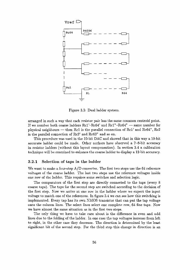
Vref
Re64 R4096
ReI
RI R64
Figure 3.3: Dual ladder system.
arranged in such a way that each resistor pair has the same common centroid point. If we number both coarse ladders Rc1'-Rc64' and Rcl"-Rc64" same number for physical neighbours - then Rc1 is the parallel connection of ReI' and Rc64" , Re2 is the parallel connection of Rc2' and Rc63" and so on.
This procedure was used in the lO-bit DAC and showed that in this way a lO-bit accurate ladder could be made. Other authors have observed a 7-8-bit accuracy in resistor ladders (without this layout compensation). In section 3.4 a calibration technique will be examined to enhance the coarse ladder to display a 12-bit accuracy.
3.2.1 Selection of taps in the ladder
We want to make a four-step AID converter. The first two steps use the 64 reference voltages of the coarse ladder. The last two steps use the reference voltages inside one row of the ladder. This requires some switches and selection logic.
The comparators of the first step are directly connected to the taps (every 8 coarse taps). The taps for the second step are switched according to the decision of the first step. Now we arrive at one row in the ladder where we expect the input voltage to match one of the references. In figure 3.4 we can see how this switching is implemented. Every tap has its own NMOS transistor that can put the tap voltage onto the column lines. The select lines select one complete row, 64 fine taps. Now we have almost the same situation as in the first two steps.
The only thing we have to take care about is the difference in even and odd lines due to the folding of the ladder. In one case the tap voltages increase from left to right, in the other case they decrease. The direction is determined by the least significant bit of the second step. For the third step this change in direction is an
56
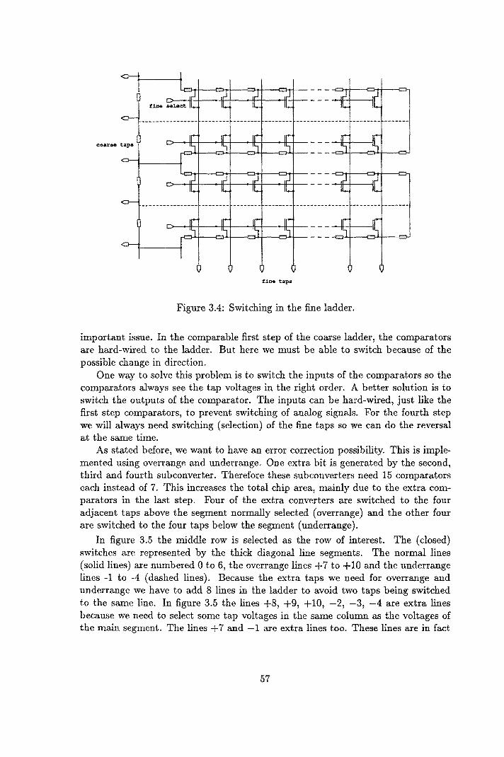
Figure 3.4: Switching in the fine ladder.
important issue. In the comparable first step of the coarse ladder, the comparators are hard-wired to the ladder. But here we must be able to switch because of the possible change in direction.
One way to solve this problem is to switch the inputs of the comparators so the comparators always see the tap voltages in the right order. A better solution is to switch the outputs of the comparator. The inputs can be hard-wired, just like the first step comparators, to prevent switching of analog signals. For the fourth step we will always need switching (selection) of the fine taps so we can do the reversal at the same time.
As stated before, we want to have an error correction possibility. This is implemented using overrange and underrange. One extra bit is generated by the second, third and fourth sub converter. Therefore these sub converters need 15 comparators each instead of 7. This increases the total chip area, mainly due to the extra comparators in the last step. Four of the extra converters are switched to the four adjacent taps above the segment normally selected (overrange) and the other four are switched to the four taps below the segment (underrange).
In figure 3.5 the middle row is selected as the row of interest. The (closed) switches are represented by the thick diagonal line segments. The normal lines (solid lines) are numbered 0 to 6, the overrange lines +7 to +10 and the underrange lines -1 to -4 (dashed lines). Because the extra taps we need for overrange and underrange we have to add 8 lines in the ladder to avoid two taps being switched to the same line. In figure 3.5 the lines +8, +9, +10, -2, -3, -4 are extra lines because we need to select some tap voltages in the same column as the voltages of the main segment. The lines +7 and -1 are extra lines too. These lines are in fact
57
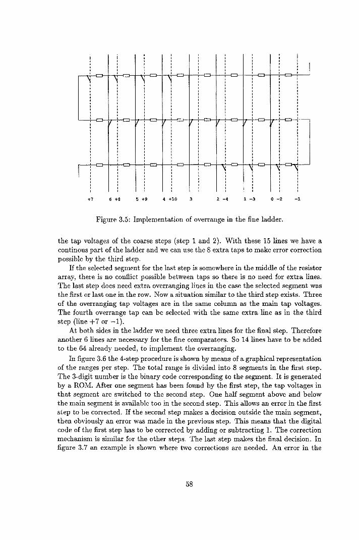
I i , , , , , , i , , , , , , , , , , , , , , ,
I , , , , , , , , , , , , , , , , , , , , , , , , , , , , , , I , , , I ,
~ ~ '1 '1 ; , , , , , , , , , , , I , I , , , , , , , • , , , , , , , , , I , , , , , , , , , , • , , , , , , , , I I I , , , , , , , , , , , , I , , , , , , , , , , , • : • , , , , , • , - • !f !f
, 1/ I
I , I I , , • , , , , , I I I , I I I I r I , , I I r I I • , , , I , , , • , , , , , , , • , , , , , , , , , , , , , , I , , , , , , , , , , , , , , , , , , I , , , , , , , , , , , , , , , , , , 1 !
, , , , ,
I , , , : ~ ~ ~ , I , , , , , , , , , , , , , , , , , , I , , , , , , , , , , , , , I I , , , , , , , , I , , , I I , I ,
+7 6 +8 5 +9 4 +10 2 -4 1 -3 o -2 -1
Figure 3.5: Implementation of overrange in the fine ladder.
the tap voltages of the coarse steps (step 1 and 2). With these 15 lines we have a continous part of the ladder and we can use the 8 extra taps to make error correction possible by the third step.
If the selected segment for the last step is somewhere in the middle of the resistor array, there is no conflict possible between taps so there is no need for extra lines. The last step does need extra overranging lines in the case the selected segment was the first or last one in the row. Now a situation similar to the third step exists. Three of the overranging tap voltages are in the same column as the main tap voltages. The fourth overrange tap can be selected with the same extra line as in the third step (line +7 or -1).
At both sides in the ladder we need three extra lines for the final step. Therefore another 6 lines are necessary for the fine comparators. So 14 lines have to be added to the 64 already needed, to implement the overranging.
In figure 3.6 the 4-step procedure is shown by means of a graphical representation of the ranges per step. The total range is divided into 8 segments in the first step. The 3-digit number is the binary code corresponding to the segment. It is generated by a ROM. After one segment has been found by the first step, the tap voltages in that segment are switched to the second step. One half segment above and below the main segment is available too in the second step. This allows an error in the first step to be corrected. If the second step makes a decision outside the main segment, then obviously an error was made in the previous step. This means that the digital code of the first step has to be corrected by adding or subtracting 1. The correction mechanism is similar for the other steps. The last step makes the final decision. In figure 3.7 an example is shown where two corrections are needed. An error in the
58
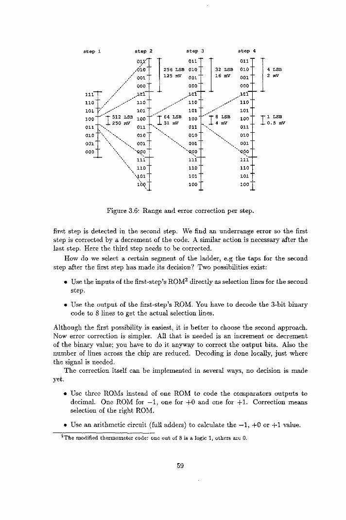
step 1
111
110
101
100
011
010
001
000
" ,./'
,-
~/"
step :1
o~).'
,.<lio /
/ 001
000
011
010
step 3
1 011
256 LSB 010
125 mV 001
000
,Hi
.' .. , ....... " "", .... "
--'1- 64 LSB 31 mV
'" " "" ......
'. """""000
", 111
110
101
100
132 LSB 16 mV
"
step 4
011
010
001
000
.Hi
__ .----'-. 110
-- 101 ---I' a LSB 100
4 mV """ 011
" 010
"""" 001
"""000 ",
111
110
101
100
Figure 3.6: Range and error correction per step.
14 LSB 2 mV
11 LSB 0.5 mV
first step is detected in the second step. We find an underrange error so the first step is corrected by a decrement of the code. A similar action is necessary after the last step. Here the third step needs to be corrected.
How do we select a certain segment of the ladder, e.g the taps for the second step after the first step has made its decision? Two possibilities exist:
• Use the inputs of the first-step's ROM2 directly as selection lines for the second step.
• Use the output of the first-step's ROM. You have to decode the 3-bit binary code to 8 lines to get the actual selection lines.
Although the first possibility is easiest, it is better to choose the second approach. Now error correction is simpler. All that is needed is an increment or decrement of the binary value; you have to do it anyway to correct the output bits. Also the number of lines across the chip are reduced. Decoding is done locally, just where the signal is needed.
The correction itself can be implemented in several ways, no decision is made yet.
• Use three ROMs instead of one ROM to code the comparators outputs to decimal. One ROM for -1, one for +0 and one for +1. Correction means selection of the right ROM.
• Use an arithmetic circuit (full adders) to calculate the -1, +0 or +1 value.
2The modified thermometer code: one out of 8 is a logic 1, others are O.
59

step 1
111
110
101
100
011
010
001
000
step 2
all 010
001
000
111
110
101
100
all 010
001
101
100
step 3
all 010
001
110
101
100
before correction, 100 110 010 010 after oorrection : all 110 011 010
Figure 3.7: Error correction .
step 4
all
010
110
101
100
011
010
001
000
• Use an arithmetic circuit that is able to calculate +0, +1 or +2. Now the ROM generates the -1 code and if no correction is necessary, the circuit adds 1. If it has to make a subtraction, it does nothing because the ROM generated that code. An advantage of this circuit over the regular ±1 circuit is that it requires less gates.
3.2.2 Matching properties
Now a calculation will show the matching properties of an n-bit ladder (2n resistors). The ladder has a reference voltage v;.eJ. The accuracy of the n-bit ladder must be lV-bit. this means that:
1 LSB = ~;; Each resistor is assumed to display a Gaussian distribution with a mean value R and a standard deviation 0":
Ri = R±O"R
The maximum deviation of a tap voltage is expected at the middle tap. This is shown for a similar situation in section 3.5.3. We'll call this tap voltage VM. The 2n - 1 resistors below (above) tap M can be replaced by one resistor Rl (R2):
2,.-1
Rl - E Ri = 2n- 1R± J2n-10"~ (3.1) i=l
= 2n - 1 R ± 2 ";-1 O"R (3.2)
R2 - 2n - 1 R ± 2 ";1 erR (3.3)
60

The error is maximized if we take the plus sign for one resistor (Rt) and the minus sign for the other resistor (R2 ). Now we can easily express VM:
Rl 2 n - 1 R + 2 "21
<7R Vre/ R R = Vre/ .. -1 ,,-1
1 + 2 2 n - 1R+ 2-2-<7R + 2 n - 1R - 2-2-<7R VM =
1 ,,-1 2n - R+2-2-<7R 1 ( 1-n<7R )
VreJ 2n R = 2" Vrej 1 + 2 2 Ii
The maximum error allowed at the middle tap is 1/2 LSB. This gives:
1 ! LSB VM - 2"VreJ = 2
1 !=1!:. <7R 1 Vre! 2" Vrej2 2 R - 2" 2N
From equation 3.7 we find the maximum allowed relative deviation of R:
<7R
R ,,-1 N = 2-2--
= 2-9.5 ~ 0.14% , for n = 6 and N = 12
(3.4)
(3.5)
(3.6)
(3.7)
(3.8)
(3.9)
If we look at the case n 5 and N = 10 - as is the case of the 10-bit DAC then we find a good estimation for the relative deviation to be expected:
R = 2-8 = 0.39% (3.10)
It is clear that 12-bit performance is not possible with these resistors. The current in the coarse ladder is chosen to be 1 mAo For Vre! = 2 V we find
that the voltage across each coarse resistor is 2/64 = 31.25 m V so R = 31.25 n. Because the current is identical for all resistors, the voltages have the same matching properties as the resistors themselves:
<7(V) = 0.14% x 31.25 mV = 44 p.V
This is approximately 1/11 LSB (12-bit LSB).
3.3 Requirements for the comparators
(3.11)
The requirements for the resolution of the comparators can be extracted from figure 3.6. We see that the first step has to resolve a large voltage of 250 m V. This is easy to do with a fast uncompensated latch. In the second step we have a resolution of 31 m V and we are able to correct a 125 m V error in the previous step. For the third and fourth step we must use offset-compensated comparators. In the final step the comparator should be very accurate because it has to resolve a voltage as low as 0.488 mY. So an offset with <7 ~ 0.15 mV is allowed. This requires a very accurate design.
61

item step number dimension 1 2 3 4
number of bits 3 4 4 4 bit number of comparators 7 15 15 15
accuracy 3 6 9 12 bit resolution 250 31 4 0.5 mV
(J offset 80 10 1.3 0.15 mV conversion time 10 20 40 150 ? ns compensation no no yes yes
Table 3.1: Demands for the comparators.
In table 3.1 the specifications of the comparators are shown. The comparator for the first step is a simple latch, the comparator for the second step is an amplifier followed by a latch. The comparator for the third step can be the redesigned comparator of chapter 2. The conversion time for a 12-bit accurate comparator is estimated 150 ns. It is a good idea to make this comparator in such a way that it can calibrate its offset voltage during the first three steps. Such comparators are based on a differential pair for Yin and Vre! and a secondary differential input pair to cancel the offset of the primary inputs. \\Then the final decision has to be made, the comparator is compensated. One should avoid a comparator that has capacitors that are charged from the inputs. This would change the tap voltages due to the charge currents supplied by the ladder.
To speed up settling of the fine tap voltages on the connection lines, a precharging with the input voltage can be used. We know that the voltages at the final taps are close to the input voltage so if they are already charged to the input voltage, the correction to charge them to the tap voltages is much faster. To reduce the load of the input, a buffer can be used. The lines (64 fine + 16 overrange) need not to be charged exactly, it is used only to have a good value to start from so the buffer does not have to be very precise. Only a low output impedance is required. Precharging takes place during the first two steps.
Perhaps it is wise to modify the architecture of the converter a little bit to combine the first two steps into one 6-bit flash converter. This would simplify the generation of the timing and control signals. The penalty in area is probably not so serious because small, not-compensated comparators can be used. It is not a real option to combine other steps because this would result in many more, large, offset-compensated comparators.
62
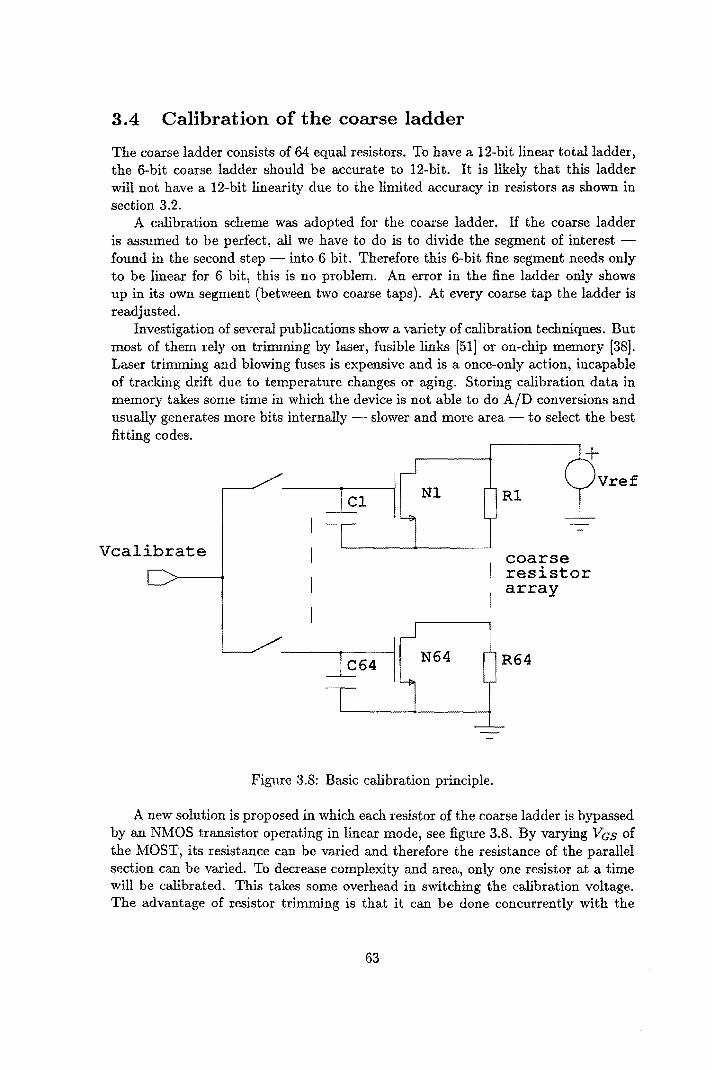
3.4 Calibration of the coarse ladder
The coarse ladder consists of 64 equal resistors. To have a 12-bit linear total ladder, the 6-bit coarse ladder should be accurate to 12-bit. It is likely that this ladder will not have a 12-bit linearity due to the limited accuracy in resistors as shown in section 3.2.
A calibration scheme was adopted for the coarse ladder. If the coarse ladder is assumed to be perfect, all we have to do is to divide the segment of interest found in the second step - into 6 bit. Therefore this 6-bit fine segment needs only to be linear for 6 bit, this is no problem. An error in the fine ladder only shows up in its own segment (between two coarse taps). At every coarse tap the ladder is readjusted.
Investigation of several publications show a variety of calibration techniques. But most of them rely on trimming by laser, fusible links [51] or on-chip memory [38]. Laser trimming and blowing fuses is expensive and is a once-only action, incapable of tracking drift due to temperature changes or aging. Storing calibration data in memory takes some time in which the device is not able to do AID conversions and usually generates more bits internally - slower and more area - to select the best fitting codes.
lel Nl
Vcalibrate
~64 N64
Figure 3.8: Basic calibration principle.
Rl
coarse resistor array
R64
Vref
A new solution is proposed in which each resistor of the coarse ladder is bypassed by an NMOS transistor operating in linear mode, see figure 3.8. By varying VGS of the MOST, its resistance can be varied and therefore the resistance of the parallel section can be varied. To decrease complexity and area, only one resistor at a time will be calibrated. This takes some overhead in switching the calibration voltage. The advantage of resistor trimming is that it can be done concurrently with the
63
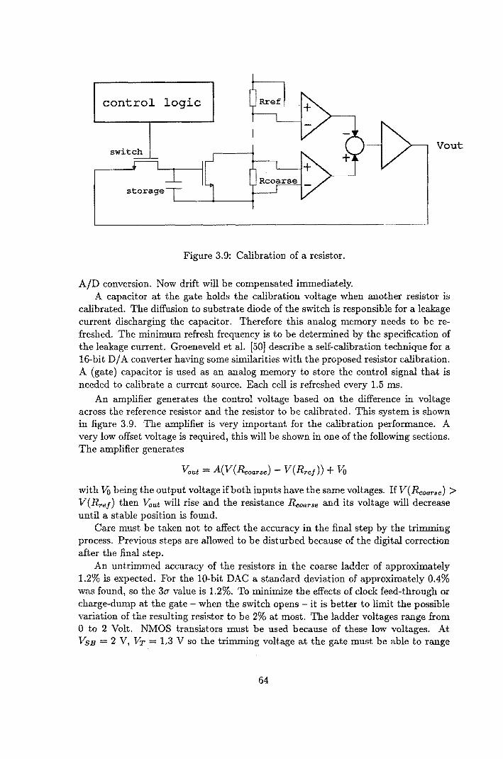
control logic
Vout
Figure 3.9: Calibration of a resistor.
AID conversion. Now drift will be compensated immediately. A capacitor at the gate holds the calibration voltage when another resistor is
calibrated. The diffusion to substrate diode of the switch is responsible for a leakage current discharging the capacitor. Therefore this analog memory needs to be refreshed. The minimum refresh frequency is to be determined by the specification of the leakage current. Groeneveld et al. [50] describe a self-calibration technique for a 16-bit D / A converter having some similarities with the proposed resistor calibration. A (gate) capacitor is used as an analog memory to store the control signal that is needed to calibrate a current source. Each cell is refreshed every 1.5 illS.
An amplifier generates the control voltage based on the difference in voltage across the reference resistor and the resistor to be calibrated. This system is shown in figure 3.9. The amplifier is very important for the calibration performance. A very low offset voltage is required, this will be shown in one of the following sections. The amplifier generates
Vout = A(V(Rcoarse) - V(Rret ) + Vo
with Vo being the output voltage if both inputs have the same voltages. If V(Rcoarse) > VeRret) then Vaut will rise and the resistance Rcoarse and its voltage will decrease until a stable position is found.
Care must be taken not to affect the accuracy in the final step by the trimming process. Previous steps are allowed to be disturbed because of the digital correction after the final step.
An untrimmed accuracy of the resistors in the coarse ladder of approximately 1.2% is expected. For the lO-bit DAC a standard deviation of approximately 0.4% was found, so the 30' value is 1.2%. To minimize the effects of clock feed-through or charge-dump at the gate - when the switch opens it is better to limit the possible variation of the resulting resistor to be 2% at most. The ladder voltages range from o to 2 Volt. NMOS transistors must be used because of these low voltages. At VSB = 2 V, VT = 1.3 V so the trimming voltage at the gate must be able to range
64

control logic
switches
n branches
tri'"wning resistors
Rn
Figure 3.10: Digitally controlled calibration.
from VSB + VT = 3.3 V to Vdd = 5 V. For VSB = 0, VT 0.7 V so below 0.5 V the transistor is guaranteed to be off. In order not to waist a part of the possibly small working area (5 - 3.3 = 1.7 V), it is necessary to design an output stage with a capability to swing from 0.5 V to (near) Vdd. We will into detail in the following sections
A somewhat different approach is to use a digitally controlled trimming scheme. In figure 3.10 this method is shown. The resistor of the coarse ladder is trimmed by switching on one or more parallel branches. The accuracy is limited by the number of different combinations. There are two main options for the bypass-resistor values:
• Binary weighted: n resistors (Ro, 2Ro, 2n - 1 Ro) give 2n combinations. The switches are assumed to have a low on-resistance and if not, it should be compensated by the resistors. Attention must be paid to avoid non-monotonicity and switching noise. It can be shown that for the binary code c, 0 ::; c :$ 2n -1, a unity transistor Ro and a ladder resistor RI, we can "program" the parallel resistor:
R __ Rl total -- 1 _c_.&
+ 2n - 1 Ro
• Equal valued: n resistors Ro give n combinations. This is a thermometer-like operation and is monotonic by design. If c is the number of closed switches (0 ::; c ::; n) we find:
RI Rtotal = R
1 + ci{; This option needs more area and probably more control signals.
The amplifier measures the difference in voltage across the reference resistor and the resistor to be trimmed. The amplified difference signal must be digitized: difference too low or too high. A successive approximation algorithm could be used to change the settings of the switches until both resistor voltages are as close as possible.
65

Both digital and analog versions need the same amplifier but the number of control lines for the calibration cell is small for the analog version and is large for the digital version. The analog calibration technique is preferred because of its simplicity and its high (theoretical) accuracy. We will concentrate on the analog version only.
In general, it is necessary to connect one gate to a fixed voltage or to leave out one MOST completely in order to obtain a fixed reference. This reference should have a resistance slightly below the minimum resistor expected (without calibration) because the calibration process can only decrease a resistance, not increase. If all resistors can be adjusted, global drifting of all gate voltages is likely to happen. At a certain moment some of them will reach a limit (Vas or Vdd) and then further trimming will fail.
Several control algorithms and sequences have been examined, none of them is without any problems. Here is a list of some (im)possibilities:
• Select one of the resistors as reference and sequentially calibrate the other resistors. The reference is part of the ladder.
• Use a separate reference, i.e. a reference with no relation to the ladder's voltage or current. This is ahnost impossible because this reference has to be exactly equal to V'reJl64 = 31.25 mV. Suppose that it is only 30 mY, then the already calibrated resistors have a voltage of 30 m V but the remaining resistors must "consume" all the missing 1.25 m V's in order to have a total voltage equal to V'reJ.
• Do not use the same reference resistor for calibration but use the one just calibrated. For example: use Ro to calibrate R1, then use Rl to calibrate R2 and so on. Various swapping methods can be used but errors in calibration accumulate this way and may degrade the linearity in the last (in time) resistors. This swapping method might be used if the accumulation of all errors due to adjacent comparisons is smaller then one error due to a "far away" comparison, e.g. if the common mode dependent offset of the amplifier is non-linear (extra high offset for large common mode differences between the two resistor voltages).
• Calibrate a resistor in several steps (opening and closing the switch), thereby measuring and compensating the error due to opening of the switches. This can be seen as a kind of a delta-modulator. This is an interesting idea, but it needs other switches which may introduce neW problems. It is more complicated than the straightforward analog calibration.
The control algorithm chosen is the first option in the list above.
3.4.1 The calibration cell
Now we will have a closer look at the basic calibration cell. What are the main problems and what values should be taken for the transistors and the capacitor.
66

Switch introduced errors are not the main problem. The switch can have minimal dimensions because there is no dc current, only a small current to charge and discharge the storage capacitor The switch consists of a parallel circuit of a PMOST and an NMOST (figure 3.11). Both transistors are necessary because of the large swing the control voltage can have. The overlap capacitors of the switches are approximately equal. Due to the fact that complementary clock signals are needed, the errors cancel approximately.
I
d Vcalibrate
coarse ladder
Figure 3.11: Three calibration cells.
The charge dump will not cancel because the charge in the switches is dependent on the applied calibration voltage. A low voltage means all charge is accumulated in the NMOS switch and the PMOS switch is out of action; for a high voltage the charge is accumulated in the PMOS switch and the NMOS switch is out of action.
The hold capacitor must be dimensioned to limit the voltage jump to a value that results in a resistor deviation below the 12-bit linearity specification. If this voltage jump correlates with the position of the calibration cell we have to be sure that it does not result in an integral nonlinearity error beyond 1/2 LSB. A second requirement is that the capacitor must hold the voltage during calibration of the other 62 resistors.
As stated before, we want a 2% control by the parallel NMOS transistor. The ladder resistor is denoted by Rl = 31.25 0, the transistor by Rn and the total resistance of the parallel section is R. Then we can calculate the resistor Rn to find the W /L dimensions of the transistor. Rn is minimal if the control voltage is maximal, a maximum VGT = 1.5 V is assumed; {3D ~ 60 x 10-6 A/V2 effective.
R = Rn II RI = (1 - 2%)Rl = 30.625 0 (3.12)
67

1 1 1 (3.13) = -+-R Rn Rl
Rn 1
=1.5Kn (3.14) - 1 1 Il- R/
14. 1 1
(3.15) ,BVGT ~ :r 60 x 10-6 X 1.5
W 1 (3.16) = 7.4
L -
60 X 10-6 X 1.5 X 1500
A 20/3 transistor is chosen. Next we will calculate the sensitivity of the voltage VR across the resistor to
changes in control voltage. The ladder current I is constant in this calculation:
R 1
(3.17) -,BVGT + k
VR - IR (3.18) aVR
(3.19) aVGT
-
(3.20)
Maximal sensitivity is at VGT = 0; using equation 3.19 and constants used before, we find:
-430~ (3.21)
So a 1 V change in control voltage results in maximal 430 JL V change in resistor voltage. This is a 67 dB attenuation. In figure 3.12 a simulation is shown that shows the voltage across the resistor as a function of the applied control voltage. We see that for the resistor at 0 V in the ladder, the control starts at a much lower value compared to a resistor at 2 V. We see that the resistor voltage decreased nearly linear with the calibration voltage.
We can use the result of equation 3.21 to determine the maximum error due to charge dump of the switch and to determine the stability of the control amplifier in active calibration (feedback) mode.
The (channel) charge in a switch is given by the equation:
(3.22)
The total (storage) capacitance C will show a voltage jump due to the charge dump when the switch (W / L) is turned off. Approximately half of the charge is responsible for this jump. So for the voltage jump .6. V we find:
AV = !Q = WLCo:cV; C 2C GT (3.23)
The capacitance C is determined by the gate capacitance Cn of the calibration transistor - Cn ~ 20 X 3 X 1.4 = 84 fF - and the "real" storage capacitor Cs , so
68

Voltage across calibratioo cell as a function of applied caJibratioo voltage for three positions in the ladder.
Vxesistor
31.6m
31.4m
31.2m I~ , , , , . , , , . , , , , .
31.Om OVolt~
3O.&m
30.6m
3O.4m
3O.2m
3O.Om 0.0 2.0
1.0
, . . ,,1 Volt
,
-~
3.0
. . . . , , . ,
, ,
4.0 5.0
Vcalibrate
Figure 3.12: Resistor voltage as a function of the calibration voltage.
C = Cn + CS. If we allow a jump of 10 mV using VaT = 1.5 V we find for Cs :
8V WLCo:c
- 2(Cn + Cs) VaT
Cn+Cs 1 VaT
= 2'WLCo:c 8V
4.3 p,V jump in the ladder - then
(3.24)
(3.25)
Cs - ~1.5 x 1.2 x 1.4;;1 - 84:::::: 100 fF (3.26)
The switch has a reverse-biased p-n junction (substrate to n-difIusion) that is responsible for a leakage current.3 This current is approximately 10-14 AI p,m2• The drain area is 1.5 x 3 = 4.5 p,m2 so the leakage current Ileak = 4.5 X 10⁻¹⁴ A. If we allow a 10 mV change in control voltage - 4.3 p,V in the ladder - then we find
the NMOS switch is considered, the PMOS switch has a much lower leakage current.
69
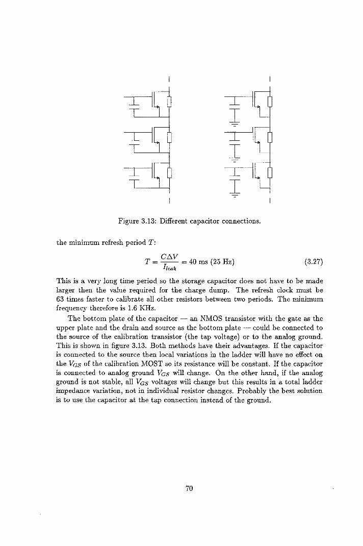
Figure 3.13: Different capacitor connections.
the minimum refresh period T;
CLlV T = -- = 40 ms (25 Hz)
I/eak (3.27)
This is a very long time period so the storage capacitor does not have to be made larger then the value required for the charge dump. The refresh clock must be 63 times faster to calibrate all other resistors between two periods. The minimum frequency therefore is 1.6 KHz.
The bottom plate of the capacitor - an NMOS transistor with the gate as the upper plate and the drain and source as the bottom plate could be connected to the source of the calibration transistor (the tap voltage) or to the analog ground. This is shown in figure 3.13. Both methods have their advantages. If the capacitor is connected to the source then local variations in the ladder will have no effect on the Vas of the calibration MOST so its resistance will be constant. If the capacitor is connected to analog ground Vas will change. On the other hand, if the analog ground is not stable, all Vas voltages will change but this results in a total ladder impedance variation, not in individual resistor changes. Probably the best solution is to use the capacitor at the tap connection instead of the ground.
70

3.5 Calibration amplifier
The calibration amplifier is the main problem in the design of the resistor calibration technique. In this section we will have a look at the demands and see that offset voltages should be very low.
Offset in the amplifier can be divided into three categories.
• Fixed offset. If the circuit is not completely symmetric od if there is a layout mismatch - as observed in the comparator in chapter 2 - a structural offset will exist .. This offset can be compensated if the source is known.
• Random offset due to noise. Because we must use a sampling amplifier to be discussed later - noise will be sampled too and will playa role in the calibration process. Various types of noise occur: l/f noise, kT/C (thermal) noise and noise due to other circuits.
• Common mode dependent offset. Because the resistors have a common mode level ranging from 0 to 2 V, the CMRR4 must be high to avoid the common mode level to introduce a differential mode signal which introduces an offset voltage. Also the overall gain of the amplifier must be very high as we will see.
So offset may be characterized by the following simple approximation:
V - T7 + T7 • + Vcommon mode offset - v fixed v nOIse eM RR
he effects of these three factors are examined in the next paragraphs.
3.5.1 Fixed offset
The effect of a fixed offset is that all resistors except the reference have the same value after calibration and their differences in voltage to the reference voltage equals the offset. So, if we want an integral and differential nonlinearity of 1/2 LSB, the offset must be below 1/2 LSB = 0.24 mY. One solution to get around with the fixed offset is using a reference outside the active part of the ladder. We may add a 65th resistor and use it as reference.
One must notice that this has a disadvantage too: the Vrej does not correspond to the maximum input voltage of the ADC, it will be Vrej/65 = 30.8 mV lower. This is not a serious problem, you might see it as a small gain error (1.5%) of the converter because the input signal must have a smaller amplitude. The impact on the size of the LSB and therefore on the accuracy needed for the comparators is also minor. A careful layout of the amplifier reduces fixed offsets and the amplifier principle will cancel this error as we will see.
'common mode rejection ratio
71

3.5.2 Offset due to noise
Another problem arises if the differential amplifier has a random (noise) offset. The effect of this offset is the same as a non-calibrated ladder. Because of the offset, each resistor is calibrated but a random value will be superimposed. Using the results of section 3.2 we know that a noise of 43 p, V (one (7) is allowed per resistor. This means that in the comparison an offset due to noise of 43 J.t V may occur. A lower value would be preferred because the same noise is likely to occur in both measurements (reference resistor and resistor to be calibrated).
3.5.3 Common mode dependent offset
More problems are caused by a common mode dependent offset. Suppose there is neither a fixed nor a noise part of the offset. Then the differential nonlinearity will be equal to the common mode offset difference between two adjacent resistors. But because the offset difference has the same sign over the whole ladder, it severely degrades the integral nonlinearity (INL). Suppose we have an increase in common mode voltage of {j for each resistor. For V(Rd = V we find:
VeRi) = V + (i -1)8 , with 1 :::; i :::; N = 64 (3.28)
The sum of all these voltages must be VreJ of course, so we arrive at:
N N-l N-1 VreJ = 2)V + (i -1)8) = NV + 8 L i = N(V +8--)
i=l i=O 2
The average voltage per resistor should be:
At a certain node k, the error voltage E is maximal and this equals the integral nonlinearity.
k
€k = Vk,ideal - Vk,real = kYo - L(V + (i - 1 )8) (3.29) i==l
= k(V + N - 18 _ (V + k -1»8 = keN - k) 8 (3.30) 2 2 2
dEk {j = -(N - 2k) 0 (3.31)
dk 2
k N
(3.32) = 2 N8 N N2
EN/2 - -(N--)=-8 (3.33) 4 2 8
As a result of equation 3.31, the maximum deviation is halfway the ladder, as would be expected for reasons of symmetry. Given 1 LSB = 0.488 m V and N = 64 we can
72
calculate 6 and the total allowed offset variation VCM for the resistor ladder from top to bottom resistor:
VCM
= ! LSB 2
~2 LSB 1;24 LSB = 0.5 j.t V
4 1 - No = N LSB = 16 LSB = 30.5 j.tV
(3.34)
(3.35)
(3.36)
So the CMRR must be v"e! /VCM = 6.6 X 104 = 96 dB. Please compare the values of common mode increase per resistor and the noise per resistor, 0.5 j.tV and 43 j.tV.
There are two main sources that could introduce a common mode dependent error voltage across the resistors in the ladder.
• Common mode dependent offset in the measurement. A differential pair has a limited CMRR because of the fact that VDS changes with the common mode. A larger VDS results in a larger current. If the tail current is assumed to be constant, this means that the Gm of the differential pair increases. Another problem is keeping the tail current constant (same problem of VDS). Simulations showed that a simple cascode does not solve this problem .
• Limited gain of the calibration amplifier. Because the average calibration voltage Vcal is proportional to the common mode voltage of the calibration cell operation starts at Vsource + VT - there will be an error due to the feedback. With an amplifier gain A and Vdif the difference in voltages across both resistors we find:
Vcal
As we have seen in equation 3.36, 30.5 j.t V is allowed for Vdi/ in the case of a 2 V common mode difference. The 2 V in the ladder (source voltages) will result in an approximately 2.6 V change in calibration voltage because VT increases approximately 0.6 V in a 2 V change of VsB . This means that the
~ . " . mInImum gam 1S:
2.6 V 4 A = 30.5 j.tV = 8.5 x 10 ~ 100 dB
3.5.4 Measuring methods
We have to design an amplifier that has to satisfy the requirements found in the last paragraphs. A first attempt was based on a so called differential difference amplifier (DDA) [49J. In figure 3.14 a DDA based on a folded casco de amplifier is shown. One pair of inputs is s·witched to the reference and the other pair of inputs is switched to the calibration cell. The differential pairs are cross-coupled to make a (current) subtraction. The difference i is fed to the folded cascode (impedance TO) to create a high-gain output (voltage). The output voltage is the calibration voltage.
73

vb3
GmI Gm2 nI pI n2
SigmaMinus
SigmaPlus
Figure 3.14: Basic differential difference amplifier.
The output is determined by the following equations:
~ - (ipml + i pm3) - (ipm2 + ipm4 ) (3.37)
= (ipml - ipm2 ) + (ipm3 - ipm4) (3.38)
= Gm1 (Vpl - Vnl) + Gm 2(Vp2 - Vn2) (3.39)
Vout = GmrO {(Vpl - Vnl) + (Vp2 - Vn2)} (3.40)
In equation 3.40 one and the same Gm is used. We see that the amplifier is able to make a differential difference if we interchange p2 and n2.
This type of amplifier suffices from bad matching of input pairs. First there is a direct mismatch in threshold voltage (between two differential pairs) and second there is a gain difference due to differences in f3 and in tail current. Another problem is the CMRR of an input pair. Especially this common mode problem is a severe problem. It is hard to compensate as opposed to an ordinary offset voltage. Several attempts have been made to change the design to have a constant VDS of an input pair but none of them was successfuL
An other idea was to swap two inputs, figure 3.15. Now both input pairs have almost the same common mode voltage 31.25 m V difference - but now one of the problems is that the input range of a differential pair must be at least 2 V wide. This means that a low Gm must be used so the problems to achieve high gain increase. Also, the operating point of the input pair changes completely with different resistor positions in the ladder. Neighbouring resistors yield in a 62 mV difference for each differential pair, far-away resistors means a 2 V difference for each pair. To calibrate the last case, differences of several It V have to be detected between two 2 V signals, quite difficult. Offset due to mismatch still has to be compensated.
74
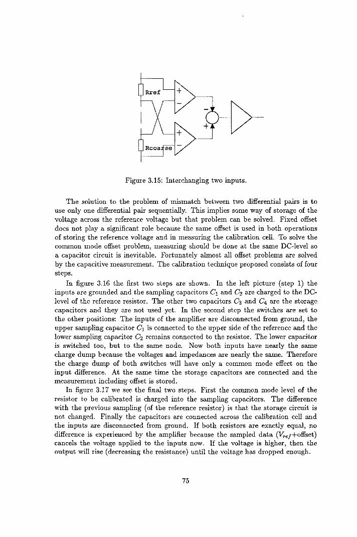
Figure 3.15: Interchanging two inputs.
The solution to the problem of mismatch between two differential pairs is to use only one differential pair sequentially. This implies some way of storage of the voltage across the reference voltage but that problem can be solved. Fixed offset does not playa significant role because the same offset is used in both operations of storing the reference voltage and in measuring the calibration cell. To solve the common mode offset problem, measuring should be done at the same DC-level so a capacitor circuit is inevitable. Fortunately almost all offset problems are solved by the capacitive measurement. The calibration technique proposed consists of four steps.
In figure 3.16 the first two steps are shown. In the left picture (step 1) the inputs are grounded and the sampling capacitors C1 and C2 are charged to the DClevel of the reference resistor. The other two capacitors C3 and C4 are the storage capacitors and they are not used yet. In the second step the switches are set to the other positions: The inputs of the amplifier are disconnected from ground, the upper sampling capacitor C1 is connected to the upper side of the reference and the lower sampling capacitor C2 remains connected to the resistor. The lower capacitor is switched too, but to the same node. Now both inputs have nearly the same charge dump because the voltages and impedances are nearly the same. Therefore the charge dump of both switches will have only a common mode effect on the input difference. At the same time the storage capacitors are connected and the measurement including offset is stored.
In figure 3.17 we see the final two steps. First the common mode level of the resistor to be calibrated is charged into the sampling capacitors. The difference with the previous sampling (of the reference resistor) is that the storage circuit is not changed. Finally the capacitors are connected across the calibration cell and the inputs are disconnected from ground. If both resistors are exactly equal, no difference is experienced by the amplifier because the sampled data CV;.ef+offset) cancels the voltage applied to the inputs now. If the voltage is higher, then the output will rise (decreasing the resistance) until the voltage has dropped enough.
75
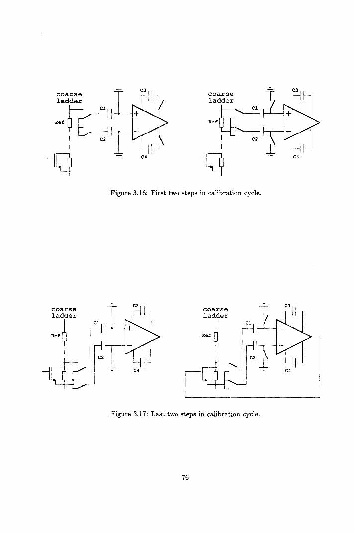
-coarse coarse ladder ladder
~ ~ Ref Ref
I C2 I C2
I I
-lq - C4 -lq - C4
Figure 3.16: First two steps in calibration cycle.
- -coarse coarse ladder ladder
~,~ ~,~
Figure 3.17: Last two steps in calibration cycle.
76
It is likely that the charge dump of a switch is not equal for different positions in the ladder, but the two switches in the plus and minus inputs of the amplifier will have (nearly) the same error: the impedance and voltage does not differ very much. Therefore this common mode dependent switch charge dump is canceled too.
Before we look at the actual implementation of the amplifier we will study some simulation steps of the calibration procedure with an "ideal" amplifier.
3.5.5 Computer simulation
To study the behaviour of the calibration process in case of any offset, a C program was written. This program uses an uniform distribution (random number generator) instead of a Gaussian distribution for generating a mismatched ladder to be trimmed and for generating the noise part of the offset. This is not the case in practical circuits but it will give an insight on the effects of noise and offset. The input of the program is:
• tolerance of the resistors (uncalibrated)
• noise in the sampling, not Gaussian but equal probability on the interval [-Vnoise, +Vnoise]
• fixed offset
• common mode offset factor (total variation of offset voltage for input range 0-2 V)
Note that common mode errors due to the limited gain as discussed in section 3.5.3 are not included in the program. They can be accounted for in the common mode offset factor.
The program uses the lowest resistor (R1) in the ladder as the reference and 'simulates a sampled differential amplifier. The sequence is as follows:
1. Sample the voltage at RI .
2. Adjust R2 to have the same voltage.
3. Sample the voltage at Rl (is changed due to R2).
4. Adjust R3 to have the same voltage.
5. Sample the voltage at RI.
6. Adjust R4 to have the same voltage.
7. Do so for all resistors. After R64 , start all over again.
Because an error is introduced each step, several iterations must be done to bring the error down to (almost) zero. Simulation shows that after 2-3 iterations the error is neglect able. The program generates an mplot4 output to display the INL and DNL before and after calibration of the ladder. The program does not include errors due
77

2.0
I.S
1.0
o.S
~ 0.0
-o.S
-1.0
· Inle9ra~ nonlLnea~Ll9'. 6b ladder wLth 12b occurocy w~lh ond w~lhout cot~brol~on, Rref ~s oulsLde lhe lodder
Rref-31.2S0 11.0%), Voffsel-O.lOO+O.02SITopNr/ToloLTops)+rndI0.OI00) mV
""",_ ... ",. ~--,------~-----~~-
uncoLi..broted colLbroted
-I.S .7---::-:--~~----1.----'----~=====::X:===~ 0.0 10.0 20.0 30.0 10.0 SO.O 60.0 70.0
resLstor-top l6bl
uncol~broled: INL - 1.76 LSB, ONL - 0.61 LSB several runs: INl - 0.63 LSB, ONl - 0.05 LSB
Figure 3.18: Simulated integral nonlinearity of 6-bit coarse ladder.
to charge dumping of the switches. This can be modeled as an offset error in the amplifier. An example of the results is shown in figure 3.18 and figure 3.19.
We see that calibration greatly enhances the differential and integral linearity. Note that a very small value of common mode offset results in quite a large linearity error.
One of the credits of this program is that it showed that sequential sampling does converge and does not result in instabilities. One could think that it does not converge because the resistor under calibration will not be calibrated to the same value as the reference. The current changes if the resistance is varied. In the ideal case the reference voltage changes proportional to the current so the final result is that the voltages across the reference resistor is equal to the voltage across the calibration cell. If a resistor is calibrated, the voltages across other resistors change
78

O.B
0.6
0.1
0.2 .c N
0.0 (D en ...J
-0.2
-0.1
O~rrerenl~aL nonl~neor~l~. 6b Lodder vLlh 12b accuracy wLlh and vLlhoul coLLbralLan, Rrer ~s oul.~de the ladder
Rrer-31.2S0 [I.OXI, Voffset-0.lOO+0.02SITapNr/TotalTopsl+rndlO.0100I mV
~ t I
A ~ , - II .... " ........ f- r~ , .....
'"
~ \ li'J ...
\ ~ -0.6
I uncoLU:roled I =-: coL ~broled -0.8
0.0 10.0
. 20.0 30.0 10.0 SO.O
res~SLor-Lop (6bl
uncQL~brQled: INL - 1.76 LSB, ONL - 0.64 LSB several runs! INL - 0.63 LSB, ONL - 0.05 LSB
60.0
Figure 3.19: Simulated differential nonlinearity of 6-bit coarse ladder.
only a fraction. This attenuation prohibits oscillation.
3.5.6 Panacea simulation
70.0
To have a more exact simulation that includes the effect of charge dump due to the switches a more realistic circuit was simulated with Panacea. Only the amplifier and its associated capacitors and switches are simulated by a controlled voltage source. The ladder, the calibration transistors (20/3), the storage capacitors (200 fF) and the switches (1.5/1.2) are "real".
Seven of the resistors were supplied with a calibration cell, the others were assumed to be ideal (30 0). The resistors to be calibrated had a random value ranging from 30.2 to 30.6 n. The bottom resistor is used as the reference resistor. The
79

Ref
Vctrl = lOE5*(V(Ri)-V(Ref»
clipping: 0 < Vctrl < 5
Figure 3.20: Circuit to simulate the calibration process.
circuit is shown in figure 3.20. Also note that the "amplifier" has one pole due to the R-C combination at the voltage source. This is necessary to make the feedback loop stable. It is not used to simulate the transient behaviour of a real amplifier.
Due to the limited possibilities of Panacea, the "amplifier" does not sample the reference but it uses the reference at the same time as it uses the voltage across the resistor under calibration. This is the ideal case but as the previous (C-language) simulations showed, a sampled amplifier gives the same results after some iterations.
In figure 3.21 we can see the calibration in action. The almost straight line at 31.3 m V is the reference voltage. Shown is the calibration of four resistors. At T = 0 we see the voltages of an uncalibrated ladder, they differ almost 1 mY. At T = 100 J1.s the four resistors are calibrated and their deviation from the reference is determined by the calibration voltage divided by the amplifier's gain (100 dB). This results in a difference of approximately 35 J1. V maximal. The spike at T = 80 fLS is due to the low calibration voltage that was applied to calibrate the previous resistor. The large capacitor at the output of the amplifier prohibits fast changes. In reality we must be sure not to introduce this switching noise when the AID converter is in its final step. This is a point of interest for further research.
3.5.7 The amplifier
So far now, we have not used a "real" amplifier. The design of figure 3.14 does not please us because it has two major problems:
80
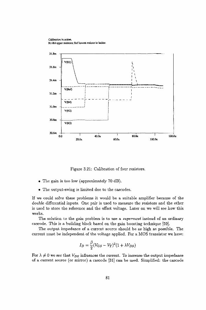
Calibration in action. Rl-R4 upper resistors; Ref lowest resistor in ladder.
31.8m
31.6m
31.4m
\ '\ '\ I \ I \ , \
-V~----:=r~---------f~=--~::~-~:::· __ ::R: ___ :~ : I 31.2m
31.Om
30.8m
30.6m
I ! I ;
- - - - - :-- - - - - -:-V(R4} I I
I ! I , ------------- :
V(R2) 1 ! l .. _~~~ __ .. ____ .. ~_ .... _________ ...... _______ .. ,. ............ __ .. ___ J
V(R3)
0.0 40.00 20.00
SO.Oo 60.00
Figure 3.21: Calibration of four resistors .
• The gain is too low (approximately 70 dB) .
• The output-swing is limited due to the casco des.
100.00 120.00
If we could solve these problems it would be a suitable amplifier because of the double differential inputs. One pair is used to measure the resistors and the other is used to store the reference and the offset voltage. Later on we will see how this works.
The solution to the gain problem is to use a supermost instead of an ordinary cascode. This is a building block based on the gain boosting technique [59].
The output impedance of a current source should be as high as possible. The current must be independent of the voltage applied. For a MOS transistor we have:
For ,\ :f= 0 we see that VDS influences the current. To increase the output impedance of a current source (or mirror) a casco de [31] can be used. Simplified: the cascode
81
transistor limits the swing on the drain voltage of the current source so the current variation is limited too.
H a simple casco de is not enough, casco ding once more could help. Unfortunately casco ding limits the output swing of the current source.
A supermost is simply a casco de with additional circuitry that regulates the bias voltage of the casco de (ordinary casco de has a fixed gate voltage). The advantages of supermost are [59]:
• no speed penalty
• self-biasing
• very large output impedance
• large output swing
• simplifying high-spec design
• transistor-like buiding-block
There is of course a price to pay: increased area and power, but it is not fair to see these as disadvantages. Supermost makes a second high-gain stage superfluous and therefore makes frequency compensation stability for feedback much easier. The supermost is also capable of a large output swing.
Three different current mirrors are shown in figure 3.22. A simple transistor mirror, a cascoded mirror and a supermost mirror. The associated figure shows the V-I relation of the output. We see that the normal mirror has a low output impedance, 330 KO. It works above 250 mY. The cascode mirror has a much better performance, 17 MO, but there is a region between 250 m V and 1.2 V equal to a normal mirror because here the upper transistor is in its linear region. Finally the supermost, this one looks perfect. The output impedance is 350 MO and it starts working from 250 mY. All transistor are equal - 10/1.2 - to make a reasonable comparison. For all current mirrors, the channel length could be increased to get a higher output impedance.
In figure 3.23 the supermost amplifier is shown. It is instructive to compare this amplifier with figure 3.14. The cascoded current sources are replaced by a supermost. Note that the supermost has a drain, gate, source and a folded casco de terminal. Not shown are the power supply connections. The folded casco de terminal is a lowimpedance input. The input current is subtracted from the output current (drain). There is IlO difference in operation for the supermost amplifier and the cascode version. The only difference is the increased DC-gain and therefore an increased accuracy in feedback mode.
Because of the fact that measurement is always at 0 V DC level capacitor cir(;uit- the current sources smpl and smp2 could be replaced by a simple PMOS cascode, or even simpler, by a single transistor only.
The Ilew amplifier has a better output swing capability compared with the "classic" folded cascode amplifier, but not enough. Therefore a CMOS inverter is used
82

Vout Iout
~ 25uA 25uA
Iout
10/1.2
- 250my.OV Vout -
Vout Iout
~ 25uA
r=17M Ohm Iout
10/1.2
10/1.2
- 250mY.2V vout -
Vout Iout
~ 25uA r=350M Ohm 25uA -Iout
D D 10/1.2 F N GN
s s
- 250mV Vout -
Figure 3.22: Comparison of three different current mirrors.
83

S S
vb3 G P vb3 G P F -
D D smp3 smp4
r 1 r 1 out
Gml Gm2 nl pl n2 p2 smnl
0
SigmaMinus F N
s 0 vbl
FN SigmaPlus S smn2
-
Figure 3.23: Supermost amplifier with two input stages.
as a final stage. Now the output has a full 0-5 V swing. Of course we should take care with voltages around 1/2 Vdd = 2.5 V because then both transistors in the inverter are "on" and a large current will flow. To limit dissipation a minimal PMOS, transistor (1.5/1.2) is chosen and a longer (not wider) NMOS (1.5/3.6). The longer channel also compensates for the difference in mobility. The take-over point is at approximately 1/2 Vdd.
In figure 3.24 the DC curve of the amplifier is shown. We see that a very small input voltage is sufficient to change the output voltage significant. The second stage - inverter - makes a full 0 to 5 V swing possible. It also enhances the gain. We see that for a 1 to 5 V output - the swing we may need to calibrate - the input voltage changes a few J-tV. The DC-gain (approximately 125 dB) is more than necessary to prevent the problems discussed in section 3.5.3. In that section we found a 100 dB requirement.
One thing not yet discussed is the storage of the measured reference voltage. In figure 3.25 a simplified amplifier is shown. It is an amplifier with one main input and a secondary, reduced sensitivity input. The corresponding circuit of the amplifier (using supermost) is shown in figure 3.23. To store the measurement data, the secondary input Gm2 is configured to make a feedback circuit. Suppose we have an input voltage Yin at the main input Gm1 , it generates a current difference il. The secondary input has its plus input connected to Vern, the common mode voltage we want at the output (to decrease common mode errors in the ladder). The output is fed back to the minus input. The output currents of the transconductance inputs are summed in the casco de. The folded cascode with the supermost technique is represented by TO, a very high output resistance. The voltage amplifier A is the
84

DC curve of supennost amplifier. dlf.pair: W/L-loo/l.2, supermost: W/L-50/3
Vout
5.0
----- ------- - If '" -, foldedca ;code output -,
invert! OUlpUt -" 4.0 , , , , , , , , ,
3.0 \
\ \ , ,
\
, 2.0 ,
\ , \
\ \
\ \
\
1.0 \
\ \ ,
\ , ~ ,----- --------0.0
-loo.Ou -SO.OU 0.0 so'Ou -75.Ou -25.Ou 25.Ou 7S.Ou
Figure 3.24: DC curve of supermost amplifier (primary input).
inverter, its presence is not essential as we will see. The following equations describe the operation of the feedback circuit:
i 1 = Gm1'Vin ~2 = Gm2(Vcm - 'VcJtst)
Vout - Aro(il + i2)
loo.Ou
Vin
(3.41)
(3.42) (3.43)
Substituting equations 3.41 and 3.42 into 3.43 and using AroGm2 ~ 1 we find:
(3.44)
(3.45)
To reduce the effects of disturbances at the secondary input, a low Gm2 is chosen, 1/10 of Gm1 by using a ten times smaller channel width and tail current. So we see that the output becomes Vern + IOVin. This means that at the input of the secondary stage we have a difference of -lOVin ~ -0.31 V in feedback mode.
85
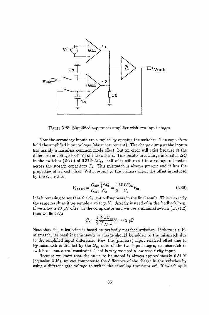
csI Vout
Figure 3.25: Simplified supermost amplifier with two input stages.
Now the secondary inputs are sampled by opening the switches. The capacitors hold the amplified input voltage (the measurement). The charge dump at the inputs has mainly a harmless common mode effect, but an error will exist because of the difference in voltage (0.31 V) of the switches. This results in a charge mismatch b..Q in the switches (W/L) of 0.31WLCo;v; half of it will result in a voltage mismatch across the storage capacitors Cs. This mismatch is always present and it has the properties of a fixed offset. With respect to the primary input the offset is reduced by the Gm ratio:
(3.46)
It is interesting to see that the Gm ratio disappears in the final result. This is exactly the same result as if we sample a voltage 'Vin directly instead of in the feedback loop. If we allow a 20 ""V offset in the comparator and we use a minimal switch (1.5/1.2) then we find Cs:
C - ~ WLCo:ll Tl: '" 2 F s - Yin'" P
2 Voffset
Note that this calculation is based on perfectly matched switches. If there is a VT mismatch, its resulting mismatch in charge should be added to the mismatch due to the amplified input difference. Now the (primary) input referred offset due to VT mismatch is divided by the Gm ratio of the two input stages, so mismatch in switches is not a real constraint. That is why we used a low sensitivity input.
Because we know that the value to be stored is always approximately 0.31 V (equation 3.45), we can compensate the difference of the charge in the switches by using a different gate voltage to switch the sampling transistor off. If switching is
86

done with the same effective gate-source voltage, then the offset error is canceled and only an error due to mismatch remains. So the switch at the (secondary) plus input is switched on with 4.69 V and the switch at the minus input with 5 V.
Because of the feedback, frequency compensation has to be used to make sure that the circuit is stable in feedback mode. We have to consider two cases:
• Feedback of the main input when a resistor is calibrated .
• Feedback of the secondary input when the amplifier stores the voltage of the reference resistor.
Cc Rz
coarse ladder
Vin~
Cl
Figure 3.26: Frequency compensation.
dummy load
Vout
The circuit of figure 3.26 shows the compensation method for the primary input. The folded cascade has an output impedance TO and a parasitic capacitance (loaded by the inverter) Ci. To study the gain and phase margins, we must have a single input and a single output. We cannot use the input of the amplifier directly because it is a differential input. Therefore the calibration cell is the input. To include its load at the output in an open loop configuration, it is repeated as a dummy element at the output of the inverter.
For stability, the phase margin must be approximately 50° at 0 dB gain (complete feedback). Because of the high attenuation of the calibration ceil, the circuit is probably stable in calibration-feedback mode. But this is not the case for storagefeedback mode. Now a compensation must be used. The capacitor Cc is used to create a new pole. It also introduces an unwanted (right half plane) zero, but with a nulling resistor Rz this zero can be shifted into the left half plane, enhancing the phase margin [31]. The position of Cc across an amplifier is known as Millercompensation. The effective value of Cc as seen by the folded cascode amplifier is (A + l)Cc. At this moment the compensation has not yet been tested.
87

3.6 Fast latch
A fast latch can be used to store the result of a comparator or it can be used as a (coarse) comparator itself. A latch using minimal transistors (1.5/1.2) has been simulated. The circuit is shown in figure 3.27. These kind of latches are often used in dynamic RAMs to restore the digital value of a memory cell. The latch needs approximately 100 m V to overcome offset voltages. First the input is sampled by opening the switches. NMOS switches work up to 3.5 V input voltages. H voltages above 3.5 V are expected, PMOS switches must be used. H both NMOS and PMOS switches are used (parallel) then the input voltages may be in the range 0 to 5 V. The other two switches, the switch to 5 V and the switch to 0 V are not yet activated and therefore there is no current in the cross-coupled inverter. If the voltages have settled, the input switches are opened. Due to the capacitance at the outputs out and outnon the voltage will not change after the sampling switches are opened.
Yin out +---1-_---..
Vref
I sample
\1...---------11 latch-----il L outputs I / L ¥
'" \ decision
I I
Vin":Vref
Figure 3.27: Fast latch with minimal dimensions.
Now the latching switches are turned on by pulling the inverters to the power supply rails. Because of the positive feedback, a small difference is amplified very fast until the outputs have reached 0 V and 5 V. In figure 3.28 a simulation is shown for a ±100 m V input difference. The whole cycle of sampling and latching takes 10 ns. This simulation is without load, a load will slow down the operation. The W /L dimensions may be adjusted to speed up the latching in the case of a large ( capacitive) load. The latch does not dissipate power when it has reached its final values.
88

Fast latch with + lOOmV and -lOOmV input difference. Common mode input level is 1 V.
V
6.0
5.0
4.0
3.0
2.0
1.0
0.0
-1.0
VI
" 1 I
I
4O.On
zoom active
, -I I out
I I , ,
I I , ,
I I
, , , I I
I
+lOOmV : ~ \:.---- .9
I ~
~ outnon
45.On
I, "
, , , I I , , I I I I , \
, I I , I
, , , I I I ;-
50.On
( /
II ·l00mV J , , --~~ I
I , \ , , --
55.On
~ ~
I 1 I I I I
I
6O.On
... -
.'~ / ''''-'/ -
65.On
T
Figure 3.28: Simulation of latching for a 100 m V overdrive.
89
Chapter 4
Conclusions
A new offset-compensated comparator architecture has been evaluated. It is suitable for high-speed medium-resolution AID converters. The comparator that has been processed has an always-positive offset voltage caused by a parasitic crosscapacitance. We can conclude that before processing a layout it is important to extract the parasitics and include these in the simulation to prevent malfunction of the circuit due to these parasitics.
With a few modifications this comparator is suited for 7 to 9 bit (1 mVoffset) applications with a 33 ns conversion time. A lO-bit performance is more difficult to be realized, it would need a gain of approximately 20. The conversion time will be larger, but further research is required. The comparator's power consumption is 0.75-1 mW and its size is approximately 150 x 150 pm2 (in the C250 process). The main modification is the addition of a third clock pulse to speed up recovery after latching. This clock has no critical timing. A second modification is the use of level-shifters at the input stage to obtain a 0 to 2 V input range and to reduce the input capacitance.
The redesign is comparable with a design that is used (and under development) at the moment. No fundamental advantages or drawbacks have been found. If speed is not the main goal, the comparator can be simplified by the omission of the third clock.
A second topic is the design of a 12-bit AID converter. The new comparator can be used in the 12-bit ADC. The ADC is based on a resistor string generating 4095 reference voltages. A low ohmic coarse ladder of 64 resistors is used to lower the impedance of the 12-bit ladder. A 4-step subranging architecture is used to find the reference voltage that matches the input voltage. Digital error correction allows errors due to offset of comparators and inaccurate sample and hold settling, to be corrected.
To increase the integral linearity of the ladder, a self-calibration technique was developed. With this technique the coarse resistor ladder is calibrated. This reduces the demands for the fine ladder to only 6-bit accuracy. This technique is very promising. It can be used in high resolution AID converters but also in Dj A converters. It is probably limited to 12-bit accuracy due to the very high requirements on common mode rejection in the control amplifier. It is recommended to implement
90

the new calibration technique in a D I A converter to study its effect. The following items are objects of further research:
• Behaviour of the ladder during conversion (charge injection due to loading and unloading) .
• Calibration of the coarse ladder (stability of the amplifier in feedback, common mode errors, noise).
• All digital parts, error correction, timing logic etc.
• 12-bit accurate comparator.
91

Bibliography
[1] T. Matsuura, H. Kojima, E. Imaizumi, K. Usui, S. Ueda, An 8-b 50-MHz 225-m W submicron CMOS ADC using saturation eliminated comparators, IEEE 1990 Custom Integrated Circuits Conference, pp. 6.4.1-6.4.4.
[2] A.F. Dingwall, Monolitic expandable 6 bit 20 MHz CMOS/SOS A/D converter, J. Solid-State Circuits, VoL SC-14, pp. 926-932, No.6, Dec. 1979.
[3] A.G.F. Dingwall, V. Zazzu, An 8-MHz CMOS subranging 8-bit A/D converter, J. Solid-State Circuits, Vol. SC-20, pp. 1138-1143, No.6, Dec. 1985.
[4] A.G.F. Dingwall, An 8MHz 8b CMOS subranging ADC, ISSCC Digest of technical papers, pp. 72-73, Feb. 1985.
[5] N. Fukushima, et al., A CMOS 8-bit 20MHz two-step parallel ADC with 95m W power consumption, ISSCC Digest of technical papers, pp. 238-239, June 1988.
(6J N. Fukushima, T. Yamada, N. Kumazawa, Y. Hasewaga, M. Soneda, A CMOS 40MHz 8b t05m W two-step ADC, IEEE International Solid-State Circuits Conference, pp. 14-15, Feb. 1989.
[7] T. Shimizu, M. Hotta, K. Maio, S. Ueda, A to-bit 20-MHz two-step parallel A/D converter with internal S/H, J. Solid-State Circuits, Vol. 24, No.1, pp. 13-20, Feb. 1989.
[8] S. Hosotani et al., An 8-bit 20-MS/s CMOS A/D converter with 50m W power consumption, VLSI Circuit Symposium 89, pp. 55-56, May 1989.
[9] S. Hosotani, T. Miki, A. Maeda, N. Yazawa, An 8-bit 20-MS/s CMOS A/D converter with 50-m W power consumption, J. Solid-State Circuits, Vol. 25, No.1, pp. 167-172, Feb. 1990.
[10] T. Tsukahara et al., CMOS comparator suitable for mixed analog-digital LSI's, The transactions of the institute of electronics, information and communication engineers, VoL J71-C, No.3, March 1988.
[11] M. Ishikawa, T. Tsukahara, An 8b 40MHz CMOS subranging ADC with pipe lined wide band S/H, ISSCC89, pp. 12-13, Feb. 1989.
92

[12] M. Ishikawa, T. Tsukahara, An 8-bit 50-MHz CMOS sub ranging AID converter with pipe lined wide-band SIH, J. Solid-State Ciruits, Vol. 24, pp. 1485-1491, No.6, Dec. 1989.
[13] T. Matsuura, T. Tsukada, et al., An 8b 20MHz CMOS half-flash AID converter, ISSCC88, pp 220-221, Feb. 1988.
[14] H. Haas, D. Draxelmayr, F. Kuttner, R Zojer, A monolitic triple 8 bit CMOS video coder, ISSCC 90, pp. 250-251, 1990.
[15] S. Chin, M.K. Mayes, R. Filippi, A multistep ADC family with efficient architecture, ISSCC89, pp. 16-17, Feb. 1989.
[16] Chu Phoon Chong, K. C. Smith, A high-resolution CMOS comparator, Int. J. Electronics, VoL 64, No.3, pp. 409-415, 1988.
[17] J. Yuan, C. Svensson, K. Chen, High speed pipelined CMOS encoder for flash AID converters, IEEE ISCAS '89, pp. 2088-2091, 1989.
[18J W.T. Ng, C.A.T. Salama, High-speed high-resolution CMOS voltage comparator, Electronics Letters, Vol. 22, pp. 338-339, 1986.
[19J RJ. McCarroll, C.G. Sodini, Hae-Seung Lee, A high-speed CMOS comparator for use in an ADC, J. Solid-State Circuits, Vol. SC-23, pp. 159-165, Feb. 1988.
[20] A. Yukawa, A CMOS 8-bit high-speed AID converter IC, J. Solid-State Circuits, Vol. SC-20, pp. 775-779, June 1985.
[21] T. Tsukada, Y. Nakatani, E. Imaizumi, Y. Toba, S. Deda, CMOS 8b 25MHz flash ADC, ISSCC Dig. Tech. Papers, pp. 89--99, Feb. 1985.
[22J K. Tsuji, S. Saitoh, S. Morinaga, T. Iida, A new pipelined-subranging 8 bit 20 MHz CMOS AD converter, Proc. Symp. VLSI Circuits, pp. 127-128, Aug. 1988.
[23] A.K. Joy, R.J. Killips, P.H. Saul, An inherently monotonic 1-bit CMOS ADC for video application, J. Solid-State Circuits, VoL SC-21, pp. 436-440, June 1986.
[24] M.K. Mayes, S.W. Chin, A multistep AID converter family with efficient architecture, J. Solid-State Circuits, Vol. SC-24, No.6, pp. 1492-1497, Dec. 1989.
[25] G. Wegman, E.A. Vittoz, F. Rahili, Charge injection in analog MOS switches, J. Solid-State Circuits, Vol. SC-22, No.6, pp. 1091-1097, Dec. 1987.
[26] M.J.M. Pelgrom, A.C.J. Duinmaijer, A.P.G. Welbers, Matching properties of MOS transistors, J. Solid-State Circuits, VoL SC-24, No.5, pp. 1433-1440, Oct. 1989.
127] M.J.M. Pelgrom, A 50-MHz 10-bit CMOS digital-to-analog converter with 150 buffer, ISSCC 1990, Digest of Technical Papers, pp. 200-201, Feb. 1990.
93

[28] K.R Lakshmikumar, R.A. Hadaway, M.A. Copeland, Characterization and modeling of mismatch in MOS transistors for precision analog design, J. SolidState Circuits, Vol. SC-21, No.6, pp. 1057-1066, Dec. 1986.
[29] J.W. Scott, W.L. Lee, C.H. Giancarlo, C.G. Sodini, CMOS inplementation of an immediately adaptive delta modulator, J. Solid-State Circuits, Vol. SC-21, No.6, pp. 1088-1095, Dec. 1986.
[30] C. Toumazou, F.J. Lidgey, D.G. Haigh (editors), Analogue IC design: the current-mode approach, lEE Circuit and systems series 2, ISBN 0 86341 215 7, Peter Peregrinus Ltd., London, 1990.
[31] P.R Gray, RG. Meyer, Analysis and design of analog integrated circuits, second edition 1984, John Wiley & Sons, Inc.
[32} W.B. Wilson, H.Z. Massoud, E.J. Swanson, RT. George, RB. Fair, Measurement and modeling of charge feedthrough in n-channel MOS analog switches, J. Solid-State Circuits, Vol. SC-20, No.6, pp. 1206-1212, Dec. 1985.
[33] E.A. Vittoz, The design of high-performance analog circuits on digital CMOS chips, J. Solid-State Circuits, Vol. SC-20, No.3, pp. 657-665, June 1985.
[34] H. Ohara, H.X. Ngo, M.J. Armstrong, C.F. Rahim, P.R Gray, A CMOS programmable self-calibrating 13-bit eight-channel data acquisition peripheral, J. Solid-State Circuits, Vol. SC-22, No.6, pp. 930-938, Dec. 1987.
[35] Je-Hurn Shieh, M. Patil, B.J. Sheu, Measurement and analysis of charge injection in MOS analog switches, J. Solid-State Circuits, Vol. SC-22, No.6, pp. 277-281, April 1987.
[36J S.H. Lewis, P.R Gray, A pipe lined 5-Msample/s 9-bit analog-to-digital converter, J. Solid-State Circuits, Vol. SC-22, No.6, pp. 954-961, Dec. 1987.
[37] S.M. Bhandari, S. Aggarwal, A successive double-bit approximation technique for analog/digital conversion, IEEE Transactions on circuits and systems, Vol. 37, No.6, pp. 856-858, June 1990.
[38] A.C. Dent, Colin F.N. Cowan, Linearization of analog-to-digital converters, IEEE Transactions on circuits and systems, Vol. 37, No.6, pp. 729-737, June 1990.
[39J P.R Gray, RG. Meyer, MOS operational amplifier design - a tutorial overview, J. Solid-State Circuits, Vol. SC-17, No.6, pp. 969-982, Dec. 1982.
[40] A.W. Swager, S/H and T/H amplifiers, EDN May 10, pp. 72-84, 1990.
[41] Y.S. Vee, L.G. Heller, L.M. Terman, A 1m V MOS comparator, J. Solid-State Circuits, Vol. SC-13, pp. 294-297, June 1978.
94

[42] T. Sekino, A monolithic 8b two-step parallel ADC without DAC and subtractor circuit, ISSCC Digest of Technical Papers, pp. 46-47, Feb. 198!.
[43] J.D. Favoretto Jr., A precision CMOS comparator, PH report, Philips Research Laboratories, 1984.
[44] P.S. Grant, KF. Smith, Monotonic dual-ladder A/D conversion, J. Solid-State Circuits, Vol. SC-22, No.2, pp. 295-297, April 1987.
[45] P.R. Gray, MOS sample/hold amplifiers, Voltage comparator design, Summercourse.
[46] C.A. Leme, J .E. Franca, High performance CMOS comparator for analoguedigital convertors, Electronics Letters, Vol. 26, No. 20, pp. 1725-1726, Sept. 1990.
[47] T. Kumamoto, M. Nakaya, H. Honda, S. Asai, Y. Akasaka, Y. Horiba, An 8-bit high-speed CMOS A/D converter, J. Solid-State Circuits, Vol. SC-21, No.6, pp. 976-982, Dec. 1986.
[48] K Bacrania, An I2-bit successive-approximation-type ADC with digital error correction, J. Solid-State Circuits, Vol. SC-21, No.6, pp. 1016-1025, Dec. 1986.
[49] E. Sackinger, W. Guggenbiihl, A Versatile building block: the CMOS differential difference amplifier, J. Solid-State Circuits, Vol. SC-22, No.2, pp. 287-294, April 1987.
[50] D.J.W. Groeneveld, H.J. Schouwenaars, H.A.H. Termeer, C.A.A. Bastiaansen, A Self-Calibration Technique for Monolithic High-Resolution D/ A Converters, J. Solid-State Circuits, Vol. SC-24, No.6, pp. 1517-1522, Dec. 1989.
[51] M.P.V. Kolluri, A I2-bit 500-ns subranging ADC, J. Solid-State Circuits, Vol. SC-24, No.6, pp. 1498-1506, Dec. 1989.
[52] D.A. Kerth, I2-bit I-MHz two-step flash A/D converter implemented in a standard 3-f-lm CMOS technology, J. Solid-State Circuits, Vol. SC-24, No.2, pp. 250-255, April 1989.
[53] B.S. Song, M.F. Tompsett, KR. Lakshmikumar, A I2-bit I-Msample/s capacitor Error-Averaging Pipelined A/D Converter, J. Solid-State Circuits, Vol. SC-23, No.6, pp. 1324-1333, Dec. 1988.
[54] J. Fernandes, S.R. Lewis, A.M. Mallinson, G.A. Miller, A I4-bit 10-f-ls Subranging A/D Converter with S/H, J. Solid-State Circuits, Vol. SC-23, No.6, pp. 1309-1315, Dec. 1988.
[55] S. Sutarja, P.R. Gray, A Pipe lined I3-bit 250-Ks/s, 5- V Analog-to-Digital Converter, J. Solid-State Circuits, Vol. SC-23, No.6, pp. 1316-1323, Dec. 1988.
95

[56J E. Sackinger, W. Guggenbiihl, A high-swing, high-impedance MOS cascode circuit, J. Solid-State Circuits, Vol. SC-25, No.1, pp. 289-298, Feb. 1990.
[57] B.P. Brandt, RA. Wooley, A CMOS Oversampling AID converter with 12-bit resolution at conversion rates above 1 MHz, ISSCC 1991.
[58] RE. Boser, B.A. Wooley, The design of sigma-delta modulation analog-to-digital converters J. Solid-State Circuits, VoL SC-23, No.6, pp. 1289--1308, Dec. 1988.
[59] K. Bult, G. Geelen, The gain-boosting technique, Seminar on CMOS analogue circuits, Philips Research Laboratories, Oct. 24, 1990.
96

Appendix A
MOS formulae
Simple approximations of MOS transistor curves. Linear region (Vns < Vas - VT):
(3
In,lin
gm,lin
Rchannel
saturation region:
charge in switch:
W - yjJCom
= (3(Vas - VT) Vns
- (3Vns 1
= (3(Vas - VT)
= ~(VGS - VT)2 2
= (3(Vas - VT)
Q = WLCom(Vas - VT)
VT and (3 mismatch between two equal transistor:
constants:
o-(VT) = 16mV . vIWI' area m Ilm2
WL 2%
- y'WL
Com = 1.4 fF j Ilm2
(3pmo8 - 20 ... 30 jJA/y2
(3nmos = 60 ... 80 jJAjy2
(A.I)
(A.2) (A.3)
(A.4)
(A.S)
(A.6)
(A.7)
(A.S)
(A.9)
(A.lO) (A.ll) (A.12)
The (3 in the equations of this appendix is the effective (3, it includes reduction by several effect, e.g. mobility reduction due to a large gate-source voltage. Therefore no exact value can be given for (3.
97

Appendix B
Pinning diagram of the comparator
Two comparators are integrated on one chip together with other test structures. The chip is mounted in a ceramic 28-pin DIL package. The pin layout is shown in table B. It is recommended to use comparator 1. Comparator 2 has a split PMOS resistor but should behave exactly as comparator 1.
1 Vdd 28 2 27 3 26 Vaut 1 4 v;.e! 1,2 25 bias dif.pair 1,2
5 24 latch 1 6 23 bias buffers 1)2
7 22 Vout 1
8 21 Vaut 2 9 20 'Vin 2
10 ~8 19 Vout 2 11 18 12 17 13 16 latch 2) 'Vin 1 14 15 compare 1,2
.... -
98

Appendix C
C program for ladder calibration
In this appendix the listing of a small C program is presented. The program has been commented in the source code itself. It simulates a calibration method with first sampling the reference and then using this value to calculate the new value of the resistor to be calibrated. This is in fact the sequential sampling as proposed in this report. The only source of offset is the calibration amplifier.
total offset = offset + (tap...nr/totaLtaps)*cm + random(-rod, rod) The program asks for:
• "Resistor accuracy (in %)?"
• "Should calculation of (int, diff) linearity include Rref? (yin)"
• "offset static offset" "offset (in m V)? "
• "common mode factor (0 <= (tap...nr/total_taps) < 1)" "em (in mY)? "
• "rnd maximal amplitude of random disturbance" "rod (in m V)? "
A static offset has the same effect for all resistor except Rref. Therefore we could also say, it has only effect for Rref. The calculation of the integral and differential non-linearity can be with or without Rref, so with or without the effect of a fixed offset. This corresponds to a reference resistor inside or outside the ladder. The output of the program is file (in fact two files) that satisfies the mplot4 syntax.
99
J.adder.c
/* ladder.c simulation of calibration of resistor-ladder * RMW Gerritsen * V1.0 29-11-90 * V1.3 04-12-90 */
f:include <stdio.h> f:include <math.h> linclude <time.h>
f:define VERSION Idefine V f:define LEN f:define STEPS f:define LSB tdefine REF f:define R 'define MAX ITER 'define RND-
fdefine FN INL f:define FN-DNL fdefine rnd 0 1.0)
"Ladder V1.3 n
2.0 64 4096 (V/STEPS) o 31.25 20 OxFFFFFFFL
1* only this one needs updating */ /* 2 volt reference */ /* coarse ladder 64 resistors */ /* 12b */ /* linearity for 12b required */ /* index reference resistor */ /* ideal resistor value *1 /* maximum number of iterations */ /* just a long number */
"in1.mplot" /* filename for output to mplot4 */ " dn1.mplot" /* filename for output to mplot4 */ (2.0* (double) (random() % RND) / (double) RND -
/* -1 <= rnd < 1 */ 'define MAX LINE 5 /* 5 different linestyles */
/* status of calls to mplot4 enum {INIT,-PRE, RON, POST}; generator */
char structure[MAX LINE] [15] /* mplot4 linestyles */ { -
} ;
"straight n ,
"dash" , "dot IT ,
"cdot" , "cdash" ,
double resistor[LEN]i double ii double r total; double offset; double devi double var; double cmi int ref=REF; FILE *fp if *fp d; int stable = 0;int include_ref=1;
/* values of resistors */ /* current */ /* sum of all resistors */ /* fixed offset */ /* max resistor deviations in % */ /* random variation of offset */ /* common mode factor */ /* reference resistor */ /* output filepointers for INL and DNL */ /* flag to see if circuit doesn't change */ 1* should resistor[REF] be included in output? */ /* 0 means a resistor outside the ladder */ /* minimum and maximum resistors */ double r min, r max;
double inl=O.O,-dnl, inl~re=O.O, inl_max=O.O, dnl~re=O.Ot dnl_max=O.Oi
void init () {
int j; double step = dev * R/100.0;
r total 0.0; for (j=O; j<LEN; j++)
{
/* max + and - % spread in R's */
resistor [ J - R + step* rnd(); /* random(-1,1) */ r total resistor[j];
} resistor [refJ = Ri /* this is our reference */
}
double compute_current() /* compute total r first */
100

ladder.c
{
}
int j;
r total-OJ fOr (j=Oi j<LEN; j++)
{ r_total += resistor[j];
} return(v/r_total);
void adjust resistor(int j, int *stable) /* adjust resistor[j), status in 'stable' */
{ double delta, alpha;
if (j == ref) return; /* don't calibrate reference */ alpha = (offset + cm*j/LEN + var*rnd() ) / Vi
* fixed + common mode + random offset */ /* delta is the correction in resistance we need to calibrate.
* the reference value is used to compute delta. * after correction the reference will be changed due to the * fact that the current has changed (==> sampled measurement) */
delta = r total * (resistor [ref] - resistor[j] + alpha*r total) / - (r total * (l-alpha) - resistor[ref]); -
resistor(j] +=-delta; r total += delta; /* keep track of total resistance too */ if (fabs(delta) > le-12) *stable=O; /* delta too big -> not yet
stable */ }
double compute_linearity(double *min, double *max, double *inl, double *dnl)
{ double delta, v_node=O.O, ideal_v=O.O, v_old-O.O, v_r; int j;
*dnl = *inl = 0.0; *min= *max=resistor[O]i for (j=O; j<LEN; j++)
{ if (resistor[j] < *min) *min resistor(j]; /* keep track of
minimum */ if (resistor[j] > *max) *max resistor[j]; /* and maximum values
*/
*/
*/
v node += i * resistor[j]; /* this is the actual voltage at
ideal_v += V/LENi /* this is the ideal voltage at
delta = fabs(ideal_v - v_node); /* so this is the error at j */ if «delta> *inl) && «j!=ref) I I include ref» *inl = delta;
j
j
/* maximal deviation (delta) is integral non-linearity */ delta = fabs(v_node-v_old-V/LEN); /* differential non-linearity */ if «delta> *dnl) && «j !=ref) II include ref» *dnl .,. delta; v old v_node; /* store old voltage for DNL */
} }
void mplot de} /* differential nonlinearity */ { -
static int colour=O; int k; double v_r=O.O, v_old=O.O;
if (colour < MAX_LINE) /* maximal 5 runs */ {
101
1add.er.c:
fprintf(fp_d, "structure %s\n", structure[colour])i fprintf(fp d, "colour %d\nplot label ", colour+l)i fprintf(fp-d, (colour ...... O) ? "'uncalibrated'\n" : "'calibrated'\n"); for (k"'O; k<LENi k++)
{ v r + ... i*resistor[k]; if «k! =ref) I I include ref)
fprintf(fp_d, "%d %2.3f\n", k, (v_r-v_old)/LSB-STEPS/LEN) ;
} }
} colour++i
void mplot it) /* integral nonlinearity */ { -
}
static int colour=Oi double v r=O.O, v ideal=O.O; int ki - -
if (colour < MAX LINE) /* maximal 5 runs * / { -
}
fprintf(fp i, "structure %s\n", structure[colour]); fprintf(fp-i, "colour %d\nplot label ", colour+l}i fprintf(fp-i, (colour=-O) ? "'uncalibrated'\n" : "'calibrated'\n")i for (k=O; k<LENi k++)
{
}
v ideal += V/LENi v-r += i*resistor[k]; if «k! =ref) I I include ref)
fprintf(fp_i, "%d %2.3f\n", k,
colour++i
void mplot(int status)
{ /* some dirty work */
switch (status) {
case INIT: /* open file for writing */
output */ fp_d == fopen(FN_DNL, "w")i /* differential nonlinearity
*/
if (fp d == NULL) { -
}
perror(FN DNL)i exit (1); -
fp_i == fopen(FN_INL, "w"};
if (fp i === NULL) { -
perror(FN INL)i exit(l); -
} break;
/* integral nonlinearity output
case PRE: /* some mplot4 header info */ fprintf(fp d, "picture A4 portrait\n"); fprintf (fp - d, "< %s DNL output>\n", VERSION); fprintf(fp-d, "title 'Differential nonlinearity, 6b ladder with
12b accuracy' \n") ; -fprintf(fp d T "'with and without calibration, "); if (include_ref) fprintf(fp_d, "Rref is part of the ladder'\n"); else fprintf (fp d, "Rref is outside the ladder' \nff) ; fprintf(fp_d, ff'Rref=%2.3f-(%2.1f%%},
102
ladd.er.c
Vo££set-%l. 3£+%1. 3£ (TapNr/TotalTaps) +rnd (%1.4£) mV' \n" , resistor[re£], dev, o££set*1000.0, cm*1000.0, var*1000.0);
£print£(£p d, "xaxis 'resistor-tap (6b)'\nyaxis 'LSB (12b)'\n"); £print£(£p-i, "picture A4 portrait\n"); £print£(£p-i, ,,< %13 INL output>\n", VERSION); £print£(fpi, "title 'Integral nonlinearity, 6b ladder with 12b
accuracy'\n")i -fprintf (fp i, '''with and without calibration, "); if (include ref) fprintf(fp i, "Rref is part of the ladder'\n"); else - fprintf (fp i, "Rref is outside the ladder' \n") ; fprintf(fp i, "'Rref-%2.3f-(%2.1f%%},
Vo££set=%1.3£+%1.3£ (TapNr/TotalTaps) +rnd(%l.4f) mV'\n", resistor[re£], dev, offset*1000.0, cm*1000.0, var*1000.0);
£printf(£p i, "xaxis 'resistor-tap (6b)'\nyaxis 'LSB (12b)'\n"); break; -
case RUN: mplot dO; mplot -i (); break;
case POST: £printf(fp d, "colour l\nstructure straight\nkey bottom
right\n"); -fprintf(fp d, "colour l\ntitle boxed bottom right \n"); £printf(£P:d, "'uncalibrated: INL - %2.2£ LSB, DNL = %2.2f
LSB'\n", inl-pre/LSB, dnl-pre/LSB);
£print£(fp_d, "'several runs: INL %2.2f LSB, DNL = %2.2£ LSB'\n",
inl max/LSB, dnl max/LSB); fprint£(fp d, ,,< Rtotal = %f Ohm, I = %f mA, V - %f V >\n",
r total, i*1000.0, V); fclose (fp d); printf("DNL output written to file:'%s'\n", FN DNL); fprintf(fp i, "colour 1\nstructure straight\nkey bottom
right\n"); -fprintf (fp i, "title boxed bottom right \n"); fprintf(fp:i, '''uncalibrated: INL %2.2f LSB, DNL = %2.2f
LSB'\n",
LSB'\n",
inl-pre/LSB, dnl-pre/LSB); fprintf(fp_i, "'several runs: INL
inl max/LSB, dnl max/LSB};
%2.2£ LSB, DNL %2.2f
fprintf(fp i, ,,< Rtotal = %f Ohm, I == %f mA, V ... %f V >\n", r total, i*1000.0, V);
fclose (fp i);
} }
printf("INL output written to file:'%s'\n", FN_INL); break;
void questions() {
char 5[100];
printf("%s 03-12-90 RMW Gerritsen\n\n", VERSION); printf("resistor accuracy (in %%)? "); scanfC"%lf", &dev}; print£("Should calculation of (int & diff) linearity include Rref?
(yIn) "); scanf("%s", 13); if (*s=='N' I I *s=='n') include ref-O; else include ref-1; -printf("\ntotal-offset = offset + (tap nr/total taps)*cm + random(-rnd,
rnd) \n\n"); - -printf("offset\t: static offset\ncm\t: common mode factor (0 <
(tap nr/total taps) < 1) \n"} ; printf("rnd\t: maximal amplitude of random disturbance\n\n");
103

1adder.CI
}
printf("offset (in mV)? "): scanf("%lf", &offset); offset /= 1000.0; /* make it mV */ printf("cm (in mV)? "); scanf("%lf", &cm); cm /- 1000.0; printf("rnd (in mV)? "); scanf("%lf", &var); var /= 1000.0;
void main() {
int j=O, k;
questions(); srandom«int)time(NULL»; mplot(INIT); /* open outputfiles */ init(); /* create random resistors */ i-compute current(); mplot (PRE) ;-printf(n'Rref=%2.3f +/-%2.3f %%, Voffset=%1.4f +
%1.5f(tap nr/total taps) +/- rnd(%2.5f) mV'\n", - resistor[ref], dev, offset*1000.0, cm*1000.0, var*lOOO.O);
while «!stable) && (j < MAX ITER» { -
compute linearity(&r min, &r max, &inl, &dnl); printf("INL .. %2.3£ LSB, DNL-" %2.3£ LSB, Rmin = %2.3£, Rmax ..
%2.4£, delta R .. %2.5£\n",
*/
}
}
inl/LSB, dnl/LSB, r min, r max, r max-r min ): i£ (j==O) /* uncalibrated *;-
{
}
inlyre dnlyre
inl; dnl;
if (j > 4) {
/* after settling: search for maximum errors */
}
if (inl > inl max) inl max = inl; if (dnl > dnl:max) dnl:max = dnl;
if (j == 0) mplot(RUN); /* plot first sample */ stable=l; for (k=O; k<LEN; k++)
{ adjust_resistor(k, &stable); /* i£ adjustment done -> stable-O
i .. compute_current(): }
if (++j =- MAX_ITER) printf("stop - maximum iterations.\n lf):
mplot(RUN); /* plot last sample */ mplot(POST); /* finish it */ for (k=O; k<LEN: k++)
{
}
print£(nR(%2d)=%f ", k, resistor[k]); if (k % 4 == 3) printf("\n");
printf(lfuncalibrated: INL" %2.2£ LSB, DNL %2.2£ LSB\n", inlyre/LSB, dnlyre/LSB);
printf("several runs: INL .. %2.2f LSB, DNL %2.2f LSB\n", inl max/LSB, dnl max/LSB);
printf ("< Rtotal .. %f Ohm, I-= %f rnA, V .. %f V >\n", r_tota1, i*1000.0, V);
104

Appendix D
Optimization of the comparator
To calculate the optimal dimensions of a differential pair a program has been written. It uses (abuses) Panacea for its capability to generate sdif files for graphic postprocessing by cgap. The program is documented, although most numerical constants are the result of some hand calculations with the blue book specifications (especially capacitance parameters). The model book is used to find more accurate expression for a transistor in linear mode (model 7). A very simple approximation did not satisfy.
105

opti.mal. pan
/* Optimalisatie van verschilpaar met PMOS weerstand. * voor bepaalde Gain: * - R groot, nmos klein -> grote Cres, kleine Cnmos, grote slag na latch * - R klein, nmos groot -> kleine Cres, grote Cnmos, kleine Vlatch * ergens ligt een optimum (minimaal RC-produkt of minimale ontladingstijd). * Meegenomen wordt: * - stroom- of spanningsafhankelijkheid van R en mobiliteitsreductie * via thetal, theta2, theta3 * - parasitaire capaciteiten van: * R drain diffusie, 0.5*gate, gate-drain overlap * nmos drain diff. (incl.mult), gain*(gate-drain ovl) (miller) * buffer (1-0.95) * (gate-source cap. + gate-source ovl) + GD ovl * IN bedradingscapaciteit * switch drain diffusie en gate-drain overlap * Output: * - Res (klein * - Ctot
signaal) weerstand totale capaciteit op de uitgang produkt van deze Res en Ctot * - RC
* - Vres spanning over de weerstand bij Itail/2 (als Vin=Vref) spanning over de weerstand bij volle staartstroom Itail ontlading na latch tot 335uV uitgaande van RC en Vlatch (helaas verandert R voordurend ala Vres verandert, dus
* - Vlatch * - Tdischarge * * */
niet zo betrouwbaar •.. )
circuit; el (1, 0) 1; betaR=31e-6*Wres/Lres; betan=75e-6: Ln=l.l; Vgt=3.85; mult=2:
/* misbruik panacea */ /* beta of the Pmost */
/* beta of the Nmost */ /* effective channel length */
/* Vgt for the pmost */ /* differential pair has mult=2 */
/* model to calculate DC characteristics of P-resistor */ /* see modelbook, model 7 */ auxL=1/Lres-l/l.2i auxW=l/Wres-l/20; thetal 0.2 + 0.06*auxL - 0.08*auxW; theta2 0.1 - 0.26*auxL + 0.13*auxW; theta3 = 0.02 + O.02*auxL + O.Ol*auxW; al = 1 + thetal*Vgt + theta2*0.81; a2 = Vgt - theta3*al*0.5*Itail/betaR; root a2*a2 - 2.44*a1*0.5*Itail/betaR; error=if(root<O, 1, 0); /* error indien buiten lineair gehied (VDsat) */
Vres=if(error=O, (a2-sqrt(root»/1.22, 5): /* spanning over weerstand */ Res=if(error=O, 1/(betaR*(Vgt-1.22*Vres)/al),10Mg); /* klein signaal R */ Wnmos=Gain*Gain*Ln/(Itail*betan*Res*Res); /* W van dif.pair */
/* numbers are based on blue book specifications */ Cres=2.7f*Wres + 1.4f*Wres*Lres/2.0 + 0.18f*Lres; /* cap. weerstand */ Cnmos=O.94f*Wnmos/mult + O.31f*Gain*Wnmos; /* cap. dif.pair */ Cbuf=0.076f*Wbuf + 0.344f*(Wbuf+l.l); /* idem output buffer */
c: CMOS switch met Wswitch/l.2 schakelaars: Cswitch=3.78f*Ws; Cswitch=2.53f*Wswitch; c: PMOS switch met Wswitch/l.2; Cin=0.1346f*IN*le6; /* interconnect capaciteit per micron */ Ctot=Cres+Cnmos+Cbuf+Cswitch+Cin; /* totale capaciteit */ RC=Res*Ctot;
a3 = Vgt - theta3*al*Itail/betaR; latchroot = a3*a3 - 2.44*al*Itail/betaR; latcherror=if(latchroot<O, 1, 0); Vlatch=if(latcherror=O, (a3-sqrt(latchroot»/1.22, 5); Tdischarge=RC*(8+ln(Vlatch»;
end:
dc; Lres=as(1.2, 6, 0.15);
106

opt::.imal • pan
Wres=as(1.5, 2.7, 0.15); wswitch=3; Wbuf=40i Gain=lO; Itailc 50u, 75u, 100u, 125u, 150Ui c: staartstroom!, Id=Itail/2; IN=O; c:75u; file: RC, Wnmos, Vlatch, Vres, Tdischargei
end; run; finish;
107