2 XII December 2014 - IJRASET
6
2 XII December 2014
-
Upload
khangminh22 -
Category
Documents
-
view
2 -
download
0
Transcript of 2 XII December 2014 - IJRASET

2 XII December 2014
www.ijraset.com Volume 2 Issue XII, December 2014 ISSN: 2321-9653
International Journal for Research in Applied Science & Engineering Technology (IJRASET)
©IJRASET 2014: All Rights are Reserved 344
Design and Simulation of I2C Protocol Tripti Singh 1
M.Tech in VLSI and Microelectronics, Shobhit University, Meerut
Abstract — Inter-Integrated circuit (I2C), is a bus protocol was proposed by Phillips semiconductor to enable faster device to communicate with slower devices without any data loss. The components of the I2C bus controller is consist of only a bidirectional two wire and standard protocol which communicates between two integrated circuit or device. First one is serial data (SDA) line and second is serial clock (SCL) line. I2C protocol provides easy communication without data loss. It also gives excellent speed compared to other protocol. In this paper, the design method is developed in Verilog hardware description language (HDL), simulated on MODELSIM 6.4a . The object of this paper is the design and simulation of an I2C (Inter-Integrated Circuit) serial interface. Keywords— I2C, SDA, SCL, SIMULATION.
I. INTRODUCTION Philips originally developed I2C for communication between devices inside of a TV set. Examples of simple I2C-compatible devices found in embedded systems include EEPROMs, thermal sensors, and real-time clocks. I2C is also used as a control interface to signal processing devices that have separate, application-specific data interfaces. For instance, it's commonly used in multimedia applications, where typical devices include RF tuners, video decoders and encoders, and audio processors. In all, Philips and other manufacturers offer hundreds of I2C-compatible devices. I2C provides good support for communication with various slow, on-board peripheral devices that are accessed intermittently, while being extremely modest in its hardware resource needs. It is a simple, low-bandwidth, short-distance protocol. Most available I2C devices operate at speeds up to 400Kbps, with some venturing up into the low megahertz range. I2C is easy to use to link multiple devices together since it has a built-in addressing scheme.
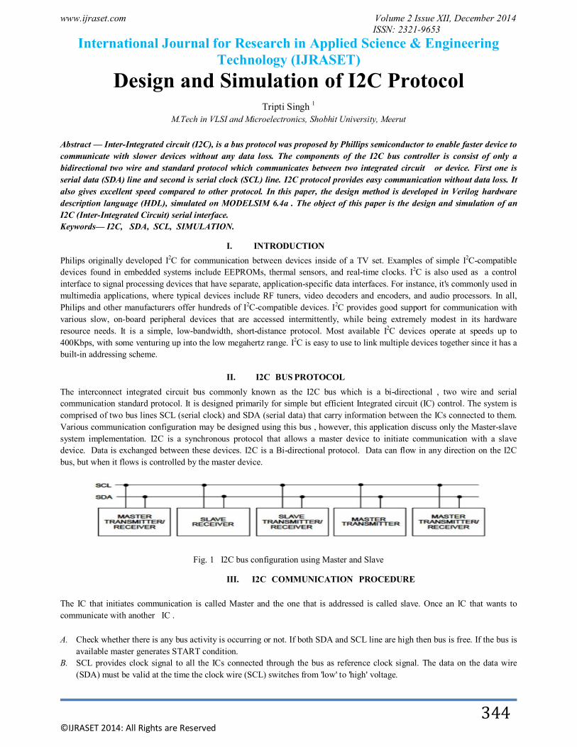
II. I2C BUS PROTOCOL The interconnect integrated circuit bus commonly known as the I2C bus which is a bi-directional , two wire and serial communication standard protocol. It is designed primarily for simple but efficient Integrated circuit (IC) control. The system is comprised of two bus lines SCL (serial clock) and SDA (serial data) that carry information between the ICs connected to them. Various communication configuration may be designed using this bus , however, this application discuss only the Master-slave system implementation. I2C is a synchronous protocol that allows a master device to initiate communication with a slave device. Data is exchanged between these devices. I2C is a Bi-directional protocol. Data can flow in any direction on the I2C bus, but when it flows is controlled by the master device.
Fig. 1 I2C bus configuration using Master and Slave
III. I2C COMMUNICATION PROCEDURE
The IC that initiates communication is called Master and the one that is addressed is called slave. Once an IC that wants to communicate with another IC .
A. Check whether there is any bus activity is occurring or not. If both SDA and SCL line are high then bus is free. If the bus is available master generates START condition.
B. SCL provides clock signal to all the ICs connected through the bus as reference clock signal. The data on the data wire (SDA) must be valid at the time the clock wire (SCL) switches from 'low' to 'high' voltage.
www.ijraset.com Volume 2 Issue XII, December 2014 ISSN: 2321-9653
International Journal for Research in Applied Science & Engineering Technology (IJRASET)
©IJRASET 2014: All Rights are Reserved 345
C. Address of each device is put on serial form on the SDA line. D. One bit signal is put on the SDA line to know whether data is to be transmitted or received from the slave. E. One bit represents acknowledgement bit to inform the master that slave is ready to receive or transmit data. F. After the acknowledgement bit is received by the master it puts data serially on the SDA line. G. The first IC sends or receives as many 8- bit words of data as it wants. After every 8- bit data word the sending IC expects
the receiving IC to acknowledge that the data is received. H. When all data is received STOP condition is generated and the bus is free again.
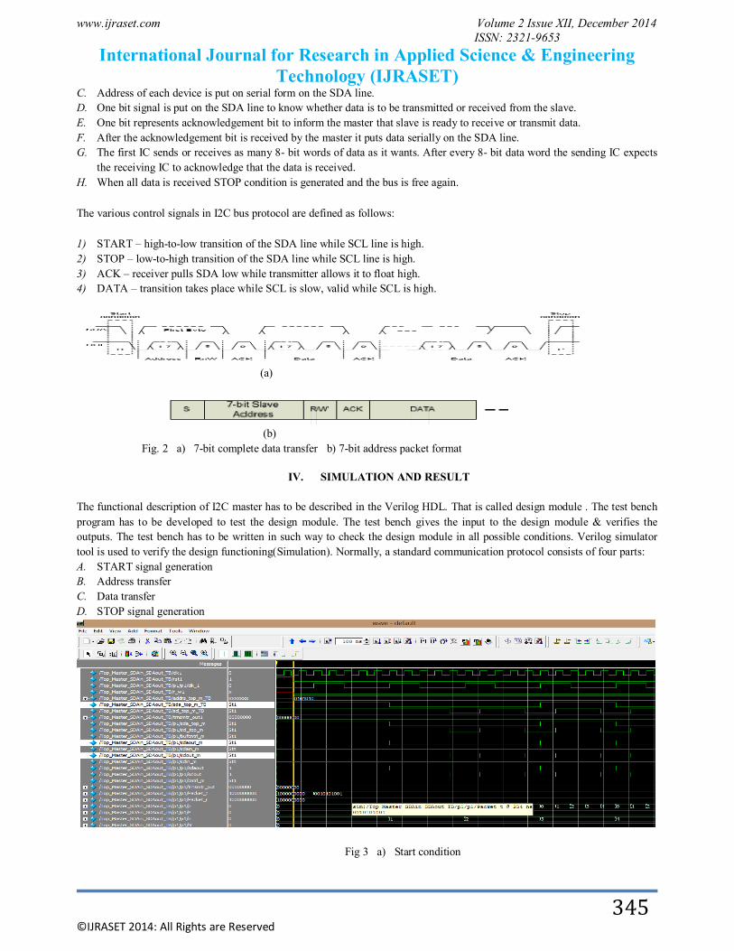
The various control signals in I2C bus protocol are defined as follows:
1) START – high-to-low transition of the SDA line while SCL line is high. 2) STOP – low-to-high transition of the SDA line while SCL line is high. 3) ACK – receiver pulls SDA low while transmitter allows it to float high. 4) DATA – transition takes place while SCL is slow, valid while SCL is high.
(a)
(b) Fig. 2 a) 7-bit complete data transfer b) 7-bit address packet format
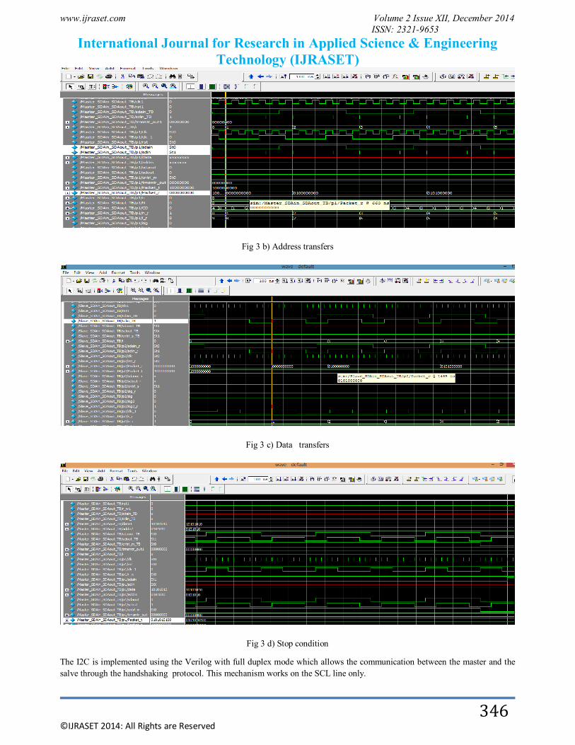
IV. SIMULATION AND RESULT The functional description of I2C master has to be described in the Verilog HDL. That is called design module . The test bench program has to be developed to test the design module. The test bench gives the input to the design module & verifies the outputs. The test bench has to be written in such way to check the design module in all possible conditions. Verilog simulator tool is used to verify the design functioning(Simulation). Normally, a standard communication protocol consists of four parts: A. START signal generation B. Address transfer C. Data transfer D. STOP signal generation
Fig 3 a) Start condition
www.ijraset.com Volume 2 Issue XII, December 2014 ISSN: 2321-9653
International Journal for Research in Applied Science & Engineering Technology (IJRASET)
©IJRASET 2014: All Rights are Reserved 346
Fig 3 b) Address transfers
Fig 3 c) Data transfers
Fig 3 d) Stop condition
The I2C is implemented using the Verilog with full duplex mode which allows the communication between the master and the salve through the handshaking protocol. This mechanism works on the SCL line only.
www.ijraset.com Volume 2 Issue XII, December 2014 ISSN: 2321-9653
International Journal for Research in Applied Science & Engineering Technology (IJRASET)
©IJRASET 2014: All Rights are Reserved 347
V. CONCLUSIONS This paper presents the design and simulation of I2C protocol. The Software simulator is typically used to run Verilog HDL- based designs. The Software simulator sprint on a generic computer. I load the Verilog HDL code and simulate the behavior. Software simulation work done on Modelsim. Coding or design work is done in Verilog HDL language.
VI. ACKNOWLEDGMENT
I would like to thank my mentor Prof. R.P AGGRWAL for his constant support, encouragement, and guidance throughout this project. I would also like to thank the faculty members of department of Electronics & Communication, Shobhit University, Meerut, India for continuous support and encouragement.
REFERENCES [1] Implementation of the communication protocols SPI and I2C using a FPGA by the HDL-Verilog languagDesign of I2C Interface for Custom ASICS
Used in the Detection of Ionizing Radiation [2] http://www.microchip.co. [3] The I2C -Bus specifications version 2.1 January 2000 http://www.semiconductors.philips.com/buses/i2c . [4] UM10204 I2C -bus specification and user manual Rev. 03 — 19 June 2007 [5] A Verilog HDL Primer, by J. Bhaskar, second Edition, BSP. [8] www.latticesemi.com, I 2C Master Controller reference design, [6] I2C bus Inter Integrated Circuits bus by Philips Semiconductors [7] http://en.wikipedia.org/wiki/I%C2%B2C [8] http://www.robot-electronics.co.uk/acatalog/I2C_Tutorial.html [9] http://www.i2c-bus.org/ [10] IEEE Computer Society. IEEE Standard Verilog® Hardware Description Language, IEEE Std 1364-2001, The Institute of Electrical and Electronics
Engineers, Inc,28 September 2001