
1.1 Transmission line basic concepts: - UPCommons
29
1 Design and Analysis of RF and Microwave Systems European Master of Research on Information Technology European Master of Research on Information Technology 1.1 Transmission line basic concepts: Introduction to narrow-band matching networks March 2010 Francesc Torres, Lluís Pradell, Jorge Miranda Design and Analysis of RF and Microwave Systems European Master of Research on Information Technology European Master of Research on Information Technology For any lossless transmission line: ) ( ) ( ) ( z V z V z V 1 Voltage and current in the transmission line V(z I(z) Z L ≠ Z 0 Z 0 V L I L V + (z) V - (z) z j e V z V 0 ) ( z j e V z V 0 ) ( ) ( ) ( 1 ) ( 0 z V z V Z z I where L V V V V 0 0 ) 0 ( L I V V Z I 0 1 ) 0 ( At z=0 n n z n z n z z z 2 2 , 2 ) ( Periodicity of V(z) and I(z): wavelength I(z) z=0 -z V (z) Reflection coefficient: load 0 0 Z Z Z Z V V L L L Impedance: load L L L L L L L Z V V V V Z V V V V Z I V Z 1 1 0 0 0
-
Upload
khangminh22 -
Category
Documents
-
view
0 -
download
0
Transcript of 1.1 Transmission line basic concepts: - UPCommons

1
Design and Analysis of RF and Microwave SystemsEuropean Master of Researchon Information TechnologyEuropean Master of Researchon Information Technology
1.1 Transmission line basic concepts:Introduction to narrow-band matching networks
March 2010
Francesc Torres, Lluís Pradell, Jorge Miranda
Design and Analysis of RF and Microwave SystemsEuropean Master of Researchon Information TechnologyEuropean Master of Researchon Information Technology
For any lossless transmission line:
)()()( zVzVzV
1
Voltage and current in the transmission line
V(z I(z) ZL≠ Z0 Z0
VL IL
V+(z)V-(z)
zjeVzV 0)(
zjeVzV 0)(
)()(1
)(0
zVzVZ
zI
where
LVVVV 00)0(
LIVVZ
I
0
1)0(
At z=0
nnz
nznzzz
2
2,2)(Periodicity of V(z) and I(z): wavelength
I(z)
z=0 -z
V (z)
Reflection coefficient: load
0
0
ZZ
ZZ
V
V
L
LL
Impedance: load
L
L
L
L
L
LL Z
VV
VVZ
VV
VVZ
I
VZ
1
1000

2
Design and Analysis of RF and Microwave SystemsEuropean Master of Researchon Information TechnologyEuropean Master of Researchon Information Technology
At any point z of the transmission line the impedance is computed as:
Reflection coefficient in the transmission line
)(1
)(1
)(
)()( 0
zZ
zVzZ
0
0 )(
)()(
ZzZZz
Modulus
)(1)()( 0 zzI 0
0 )()(
ZzZ
zjL
zjzj eeeV
V
zV
zVz 222 )0(
)(
)()(
At any point z of the transmission line the reflection coefficient is:
Lzj
Lez 2)( Constant in z
LinearIncreasing with +z (towards load)Periodicity: half a wavelength
Phase radz2 degº180
2
z
22
22,2)(22
nnn
z
nznzzz
Design and Analysis of RF and Microwave SystemsEuropean Master of Researchon Information TechnologyEuropean Master of Researchon Information Technology
The transmission line as impedance transformer
zjz L 2)( jL 2)(
ZL≠ Z0 Z0, β
z=0
|Γ(z) |=|ΓL|
z
jL )(
)( i
Example: Compute the input impedance Zi of a circuit formed by a transmission line of length is λ/8 and loaded with ZL=0 (sc).
10
0
ZZ
ZZ
L
LL
jeeejj
jLi
28
22
2)(
00 1
1jZZZ
i
ii

3
Design and Analysis of RF and Microwave SystemsEuropean Master of Researchon Information TechnologyEuropean Master of Researchon Information Technology
Standing waves in the transmission line (i)
zjjL
zjjL
zj
zjjL
zjjL
zj
eeZ
Veee
Z
VzI
eeVeeeVzV
LL
LL
22
22
11)(
11)(
LL ZZ 00
)(
At any point z where the term (1+ΓL) is real, voltage and current are real an their magnitude is either maximum or minimum:
radzL 22 max
L
L
Z
VzII
VzVV
1)(
1)(
0minmin
maxmax
zz Z0
L
L
Z
VzII
VzVV
1)(
1)(
0maxmax
minmin radzL min2
4minmax zz
Design and Analysis of RF and Microwave SystemsEuropean Master of Researchon Information TechnologyEuropean Master of Researchon Information Technology
Standing waves in the transmission line (ii)At any point z where the voltage is maximum the impedance is real an maximum, if the voltage is minimum the impedance is real and minimum:
11)( eVzV zj
max0
0
max
maxmax 1
1
1
1
)(
)()( ZZ
eZV
eV
zI
zVzZ
L
L
Lzj
L
min0
0
min
minmin 1
1
1
1
)(
)()( ZZ
eZV
eV
zI
zVzZ
L
L
Lzj
Lzj
)(
)(
minmaxmin
maxminmax
zIV
zIV
The voltage standing wave ratio (VSWR or S) is defined as
1
1,
1
1
min
max
S
S
V
VS L
L
L
SL
1
10
Matched load: Z=Z0, Γ=0, SWR=1

4
Design and Analysis of RF and Microwave SystemsEuropean Master of Researchon Information TechnologyEuropean Master of Researchon Information Technology
Standing waves in the transmission line (iii)Maximum and minimum impedances at in the transmission line:
)(zVλ/4 λ/4
Vmax
Vmin
z=0 zmin zmax zmin
VSWR is easy to measure and it is widely used to specify mismatch
SZZI
VZ
L
L00
min
maxmax 1
1
S
Z
ZI
VZ
L
L 0
0max
minmin 1
11
Design and Analysis of RF and Microwave SystemsEuropean Master of Researchon Information TechnologyEuropean Master of Researchon Information Technology
At any point z of the transmission line the net power is computed as:Power in the transmission line (i)
**
0
* )(11
)(1)()·()( zeVZ
zeVezIzVezP zjzj
222
0
)(1)(1 zPzZ
V
o
Since the modulus of the reflection coefficient is constant in z, the net transmitted power is constant at any z and equals the power delivered to the load:
LL PPPPzPzP 221)(1)(
jxraaaae ,1112*
LL PPPPzPzP 1)(1)(
PPZ
VP
Z
VP L
2
0
2
0
2
,,
Where the power associated to the “positive” (incident) and “negative” (reflected) waves is:

5
Design and Analysis of RF and Microwave SystemsEuropean Master of Researchon Information TechnologyEuropean Master of Researchon Information Technology
Example: P+ =1 Watt in transmission line of impedance Z0=50Ω
Power in the transmission line (ii)
WPPj
jjZ LLL 5.0
2
1,
2
1,
1,10050
2
)()()(),(·log20, 10
2dBRLdBWPdBWPRL
P
PRL LL
j 221
Return loss definition:
In this case
dddd dBWdBdBWPdBRL 330,3
8.51
1
L
LS
The standing wave ratio (SWR) in the transmission line
Design and Analysis of RF and Microwave SystemsEuropean Master of Researchon Information TechnologyEuropean Master of Researchon Information Technology
If we have a mismatched load
Matching networks
PPP LL2
1
ZL≠ Z0Z0
P+
• A fraction of the incident power P+
is not delivered to the load• A fraction of the incident power
returns to the generator
A matching network must be•Simple (passive)
L≠ 0 Z0
ΓL≠ 0
ZL≠ Z0
Z0 Matching Network
P-≠0
P+
P-=0
2
LPP
Simple (passive)•Lossless (L, C, Transformer, transmission line, waveguide,…)
PPP iLIf lossless: All power is delivered to the load
Zi= Z0 Γi= 0
P 0

6
Design and Analysis of RF and Microwave SystemsEuropean Master of Researchon Information TechnologyEuropean Master of Researchon Information Technology
An impedance can be normalized to a reference impedance Z0
Normalized impedances and admittances
LLL
LL YY
YZ
Z
ZZ
1; 0
0
ZP+
ZL≠ 1
In this case, the reflection coefficient:
LL YYZ0
L
L
L
L
L
LL Y
Y
Z
Z
ZZ
ZZ
1
1
1
1
0
0
Z0
ΓL≠ 0
ZL≠ 1
Z0=1 Matching Network
P-≠0
P+
P-=0
ZL≠ 1
Working with normalized impedances is equivalent to work with reference transmission lines of Z0=1
LLL 0
Zi= 1 Γi= 0
Design and Analysis of RF and Microwave SystemsEuropean Master of Researchon Information TechnologyEuropean Master of Researchon Information Technology
Example: lossless narrowband matching network (i)
Z 4 j2Z 1Z 1P+
Zx =jX
YB =jB
In this case, the reflection coefficient:
jXZ 11
ZL=4-j2 Z0=1
Z1
Z0=1
Zi= 1
P-=0 YB =jB
YL=0.2+j0.1
)1.0(2.0
1111 BjjBY
jXZL
By equalling the real parts By equalling the imaginary parts
5.0
3.0
)1.0(2.0
2.01
2
122 B
B
B
3
2
)1.0(2.0
)1.0(
2
122 X
X
B
BX

7
Design and Analysis of RF and Microwave SystemsEuropean Master of Researchon Information TechnologyEuropean Master of Researchon Information Technology
Example: lossless narrowband matching network (ii)Solution 1
Zx =-j2 Zx =j2
Solution 2
Sometimes a shunt-series solution does not exist and a series-shunt network must be used:
ZL=4-j2 Z0=1
Zi= 1
YB =-j0.5 ZL=4-j2 Z0=1
Zi= 1
YB =j0.3
Z0=1
Zi= 1
ZL Z0=1
Zi= 1
Design and Analysis of RF and Microwave SystemsEuropean Master of Researchon Information TechnologyEuropean Master of Researchon Information Technology
The Smith ChartThe Smith ChartZ(z)→ Impedance at any point z of the transmission line
Re 0,
Im ,
Z z
Z z
P.H. Smith, in 1939, developed a chart to represent any impedance Z(z) as a function of its related reflection coefficient ρ(z). This graphic tool is based in the fact that |ρ|≤1 which allows to represent all impedances in a finite area. The Smith chart is currently used as a universal tool to represent impedances.
P.H. SMITH

8
Design and Analysis of RF and Microwave SystemsEuropean Master of Researchon Information TechnologyEuropean Master of Researchon Information Technology
Relation Relation Z(z) -- ρ(z)
An impedance can be normalized in relation to a reference impedance Zo as
1ZZ r j x
1 jZe j
Mathematically, this correspond to a bilinear transformation which translates a circle in the impedance domain into a circle in the reflection coefficient domain.
0 1Z r j x
Z
1 r ie jZ
ixr≥0
r
≤1
rZ
Design and Analysis of RF and Microwave SystemsEuropean Master of Researchon Information TechnologyEuropean Master of Researchon Information Technology
Relation Relation Z(z) -- ρ(z)Now, if ρ=ρr+jρi is substituted in the expression of the normalized impedance, the equations that relate the loci r and x constants as a function of the components ρr and ρi are obtained. This is a
set of circumferences in the complex domain :
2 2 2
222
1 1 1; 1
1 1r i r i
r
r r x x
11,
1Constant reactance circle: CENTRE RADIUS
,01
r
r
1
1r Constant resistance circle: CENTRE RADIUS
r
x r=const
r
i
r
x
x=const.
r
ix
x

9
Design and Analysis of RF and Microwave SystemsEuropean Master of Researchon Information TechnologyEuropean Master of Researchon Information Technology
The reflection coefficient in the complex domainThe reflection coefficient in the complex domain
i90ºz=-ℓ z=0
ZLℓ= 360º ℓ= 180º ℓ= 90º
r
|=1
0º180º
LeZe
L
L|
ℓℓ
L
4( )Lj z
Towardsload
Rationale
ZL L Zee
L e
270º4
( ( ))2( )Ljj
e L Lz e e
0 1L|
e
L|( )2( )Lj zj z
L Lz e e
( 0) LjL Lz e
Towardsgenerator
Design and Analysis of RF and Microwave SystemsEuropean Master of Researchon Information TechnologyEuropean Master of Researchon Information Technology
x = ∞
x = 0.5
x = 2
x = 1
Chart of impedances
r = 0 r = 0.5 r = 1 r = 2 r = ∞
x = 0
x = - 2
x = - 1
Circles of constant reactance
Circles of constant resistance
x = - 0.5

10
Design and Analysis of RF and Microwave SystemsEuropean Master of Researchon Information TechnologyEuropean Master of Researchon Information Technology
At a point placed in thetransmission line of Z0 = 50Ω we measure animpedance 100+j·150 ΩWhat is the value of ρ atthis point? | ρ | = 0.75
x = +3
p
100 1502 3
50
jZ j
0.75 26º
| ρ | 0.75
r = 2
φ = 26º
Design and Analysis of RF and Microwave SystemsEuropean Master of Researchon Information TechnologyEuropean Master of Researchon Information Technology
If , what is itsrelated normalizedimpedance ? How doesthis impedance changeif the point is moved alongthe transmission line?
1 3 90º
ZZ φ = 90º
r = 0.8
x = +0.620.33j
e
0.8 0.6Z j
As we move along atransmission line, themodulus of the reflection
| ρ | = 0.33
modulus of the reflectioncoefficient is constant:
The normalized impedance varies as given by this circle.
0.33
Z

11
Design and Analysis of RF and Microwave SystemsEuropean Master of Researchon Information TechnologyEuropean Master of Researchon Information Technology
transformation: transformation: ρρ ↔ Z↔ Z
SWR = S (standing wave ratio)
RET’N LOSS dB =x| ρ |
Z
26º
¯
2 3Z j
20 log RET N LOSS, dB =
REFL. COEFF. P =
REFL.COEFF, E OR I =
φ
0.75 26º
20 log 2
0.75
7S
2.6 dBretL
72.6
Design and Analysis of RF and Microwave SystemsEuropean Master of Researchon Information TechnologyEuropean Master of Researchon Information Technology
Input impedanceInput impedance
0.45·λ
VZL= 60 – j·90
S 3 6
0.8 1.2LZ j
2 1.6Z j ZL
Ze
mín
máx
mín 0.28
V
I
Z
máx
mín
máx 3.6
V
I
Z x
x
ZLZe
l = 0.45·λ
Z0 = 75 Ω
S=3.61/S=0.28
2 1.6eZ j
150 120eZ j
270máxmáxZ R
21mínmínZ R
S=3.6

12
Design and Analysis of RF and Microwave SystemsEuropean Master of Researchon Information TechnologyEuropean Master of Researchon Information Technology
AdmittanceAdmittance
Z R j X
Y G j B
1
ZLx
1
1
cL
cCX
BL
X
C
L
B C
1 1 1
1 1 1
Z Y Y
Z Y Y
50Z x
Rotation: 180º
0 500.2 0.5
10 25 LL
ZZ j
Z j
00
0.7 1.7
0.014 0.034
LL L L
L
L
YY Y Y Y
Y j
Y j
Z
YL
Design and Analysis of RF and Microwave SystemsEuropean Master of Researchon Information TechnologyEuropean Master of Researchon Information Technology
Input admitanceInput admitance
ZL= 10 + j·15ZL
x
Zex
0.1·λ
Ye Z0 = 50 Ω
l = 0.1·λ
ZL
0 2 0 3Z j YL
x
x
0
10 15
50LZ j
Z
0.2 0.3LZ j
0.3 0.7eY j
0.006 0.0145eY j
0
10.02
50Y
Ye
x
0.1·λ

13
Design and Analysis of RF and Microwave SystemsEuropean Master of Researchon Information TechnologyEuropean Master of Researchon Information Technology
ShortShort--circuited linecircuited line
Ze, Ye s.c.
0.1·λ
Open circuit lineOpen circuit line
0.73
1.4e
e
Z j
Y j
l = 0.1·λ
Short circuit Open circuit xx
Ze, Ye o.c
l = 0.15·λ
0.73
1.4e
e
Z j
Y j
0.15·λ
Design and Analysis of RF and Microwave SystemsEuropean Master of Researchon Information TechnologyEuropean Master of Researchon Information Technology
Change of reference Change of reference impedanceimpedance
11’2’ 2
Z1x
0.1·λ
0.15·λ
Ze 50 Ω
0.15·λ
ZL100 Ω 150 Ω
0.1·λ 0.15·λ Z1’
x
Change of referenceimpedance
1
1 1
750.5
1501 0.7
150 150 105
LZ
Z j
Z Z j
1'
150 1051.5
1001 8 0 9
jZ j
Z j
ZL
x
Ze
Z2
xx
Z2’
x
2
2 2
1.8 0.9
100 180 90
Z j
Z Z j
2'
3
3
180 903.6 1.8
500.28 0.52
50 14 26e
j
j
Z j
Z
j
Z
Z
0.15·λ

14
Design and Analysis of RF and Microwave SystemsEuropean Master of Researchon Information TechnologyEuropean Master of Researchon Information Technology
Z
MATCHING. Transmission MATCHING. Transmission line plus reactance in line plus reactance in
seriesseries
l
ZL
j·XSZL
xx
0.114·λ
MATCHING. Transmission line plus reactance inseries
Z’
¿ l ?
1 2.1Z j
0.2 0.5LZ j
Ze=1 Z=1+j·XXS = -X
2.1Sj X j 1
Ze=1
x
0
12.1 Z
C
' 1 2.1Z j ' 2.1Sj X j
02.1L Z
0.234·λ
Design and Analysis of RF and Microwave SystemsEuropean Master of Researchon Information TechnologyEuropean Master of Researchon Information Technology
MATCHING. MATCHING. Transmission line plus Transmission line plus reactance in parallelreactance in parallel
YL
¿ l ?
ZLj·BPY
0.289·λ
ZLx
x
MATCHING. Transmission line plus reactance inparallel
1 2.4Y j
0.4 1.4LZ j
2.4Pj B j
¿ l ?
Y=1+j·BBP = -B
Ye=1
0.2 0.65LY j
Y’
Ye=1
x
0
12.4 Y
L
' 1 2.4Y j ' 2.4Pj B j
02.4C Y
0.402·λYL
x
15
Design and Analysis of RF and Microwave SystemsEuropean Master of Researchon Information TechnologyEuropean Master of Researchon Information Technology
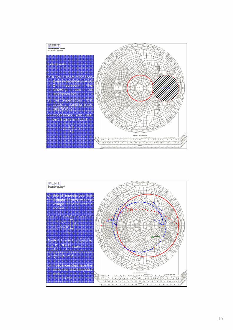
Example A)
In a Smith chart referencedto an impedance Z0 = 50Ω, represent thefollowing sets ofimpedance loci:
a) The impedances thatcause a standing waveratio SWR=2
)
x
ROE=2
R>100
b) Impedances with realpart larger than 100
1002
50r
Design and Analysis of RF and Microwave SystemsEuropean Master of Researchon Information TechnologyEuropean Master of Researchon Information Technology
c) Set of impedances thatdisipate 20 mW when avoltage of 2 V rms isapplied
+
xx
LY
ZL
+
-
VL=2 V
PL=20 mW
2* * *
3
2
Re Re
20 100.005
4
L L L L L L L L
LL
L
P V I V V Y V G
PG
V
x
gL=0.25
x
rL=4
xx
ZL
d) Impedances that have thesame real and imaginaryparts
00
0.25LL L
Gg G Z
Y
r=x

16
Design and Analysis of RF and Microwave SystemsEuropean Master of Researchon Information TechnologyEuropean Master of Researchon Information Technology
Example B) A generator at f=300 MHz feeds an unknown load ZL by menas of atransmission line of impedance Z0=70 . In the line it is measured |Vmax|=5.2 V and |Vmin|=1.1V. Furthermore when the load is substituted by a short circuit the positions of all minimumvoltages move 15 cm towards the load. ¿What is the impedance ZL?
maxmin
14.72, 0.212, 300 1pvV
ROE Z f MHz mV ROE f
SS
ZL
0
ZLZLZL
2
3
2
Z iZ i
VminVmin
z=0z=-ℓ z(- 0.5- 1-1.5
|V|min
|V|max
0
|V(z)|0.15
0.15
minV ROE fS
22 ZminZmin
c.c.
z=0z=-ℓ
c.cc.cc.c
Vmin Vmin
0
- 0.5- 1-1.5 0
|V(z)|
z(
|V|max
Design and Analysis of RF and Microwave SystemsEuropean Master of Researchon Information TechnologyEuropean Master of Researchon Information Technology
Example B)
min 0.212
0.15
Z
z
0.52 1.2LZ j
minZ
x
Z 1 2j
0.15z
0.52
0.15
LZ 1.2j
0· 36.4 84L LZ Z Z j

17
Design and Analysis of RF and Microwave SystemsEuropean Master of Researchon Information TechnologyEuropean Master of Researchon Information Technology
Example B) The same result is obtained if the position Vmin moves 35 cmtowards the generatormax
min
14.72, 0.212, 300 1pvV
ROE Z f MHz mV ROE f
SS
ZLZLZLZL
2
3
2
Z iZ i
VminVmin
z=0z=-ℓ 0.15 0.35
0.35 0.15
- 0.5- 1-1.50
|V|min
|V|max
|V(z)|
z(
minV ROE fS
22 ZminZmin
c.c.
z=0z=-ℓ
c.cc.cc.c
Vmin Vmin
0
- 0.5- 1-1.5 0
|V(z)|
z(
|V|max
Design and Analysis of RF and Microwave SystemsEuropean Master of Researchon Information TechnologyEuropean Master of Researchon Information Technology
Example B
min 0.212
0.35
Z
z
0.52 1.2LZ j
minZ
x
Z 1 2j
0.35z
0.52
0.15
LZ 1.2j
0· 36.4 84L LZ Z Z j
0.35

18
Design and Analysis of RF and Microwave SystemsEuropean Master of Researchon Information TechnologyEuropean Master of Researchon Information Technology
Example C
An antenna has and input impedance of 75 at 400 MHz. It is fed by means of a parallel wirestransmission line with an impedance Z0=150 .
a) Design a matching network compounded of transmission line plus a shunt capacitor. The dielectric) g g p p pconstant of the transmission line is εr=2.2.
YL
ℓ
ZLj·Bc
Y=1+j·BB = BY =1 B = -Bc
Bc>0Ye=1
¿ ℓ, C ?
Design and Analysis of RF and Microwave SystemsEuropean Master of Researchon Information TechnologyEuropean Master of Researchon Information Technology
YL
ℓ
ZLj·Bc
Y=1+j·BB BY 1
x
1 0.7Y j
75 10.5 2
150L LL
Z YZ
B = -Bc
Bc>0Ye=1
x
xLY
1 0.7Y j
Solution with capacitor1 0.7Y j
0.25 1eY
ℓ=0.088
8
6
/ 3 10 / 2.20.506
400 10rc
mf
0.348
ℓ=0.088
0.7CB ℓ=4.45 cm
00.7 /1.85
2
ZC pF
f

19
Design and Analysis of RF and Microwave SystemsEuropean Master of Researchon Information TechnologyEuropean Master of Researchon Information Technology
Compute the length of atransmission line, ended inshort-circuit, that cansubstitute the capactior.
x
0.7cY j
YL
ZLYc=j·0.7
x
CC
ℓ
Y=1-j·0.7Ye=1 ℓ=0.347
ℓ=0.347 =cm
Design and Analysis of RF and Microwave SystemsEuropean Master of Researchon Information TechnologyEuropean Master of Researchon Information Technology
b) Matching network formed by a quarter wavelength transformer .
ZLZ0’
ℓ=
ZL
Ze= Z0
0
20' 0'e
e L e
Z Z ZZ Y Z
Z Z Z
In the case of a quarter wavelength transformer
0'e e
L LZ Z Z
0'
0 150e L
e
Z Z Z
Z Z
0' 106.07
12.654
Z
cm

20
Design and Analysis of RF and Microwave SystemsEuropean Master of Researchon Information TechnologyEuropean Master of Researchon Information Technology
Matching networks utilities and examples
Lecturer: Francesc Torres ([email protected])
Design and Analysis of RF and Microwave SystemsEuropean Master of Researchon Information TechnologyEuropean Master of Researchon Information Technology
There are a number of on-line tools for RF design and/or educational purpose

21
Design and Analysis of RF and Microwave SystemsEuropean Master of Researchon Information TechnologyEuropean Master of Researchon Information Technology
Design and Analysis of RF and Microwave SystemsEuropean Master of Researchon Information TechnologyEuropean Master of Researchon Information Technology

22
Design and Analysis of RF and Microwave SystemsEuropean Master of Researchon Information TechnologyEuropean Master of Researchon Information Technology
Design and Analysis of RF and Microwave SystemsEuropean Master of Researchon Information TechnologyEuropean Master of Researchon Information Technology

23
Design and Analysis of RF and Microwave SystemsEuropean Master of Researchon Information TechnologyEuropean Master of Researchon Information Technology
Design and Analysis of RF and Microwave SystemsEuropean Master of Researchon Information TechnologyEuropean Master of Researchon Information Technology

24
Design and Analysis of RF and Microwave SystemsEuropean Master of Researchon Information TechnologyEuropean Master of Researchon Information Technology
Design and Analysis of RF and Microwave SystemsEuropean Master of Researchon Information TechnologyEuropean Master of Researchon Information Technology

25
Design and Analysis of RF and Microwave SystemsEuropean Master of Researchon Information TechnologyEuropean Master of Researchon Information Technology
Design and Analysis of RF and Microwave SystemsEuropean Master of Researchon Information TechnologyEuropean Master of Researchon Information Technology

26
Design and Analysis of RF and Microwave SystemsEuropean Master of Researchon Information TechnologyEuropean Master of Researchon Information Technology
Design and Analysis of RF and Microwave SystemsEuropean Master of Researchon Information TechnologyEuropean Master of Researchon Information Technology

27
Design and Analysis of RF and Microwave SystemsEuropean Master of Researchon Information TechnologyEuropean Master of Researchon Information Technology
Design and Analysis of RF and Microwave SystemsEuropean Master of Researchon Information TechnologyEuropean Master of Researchon Information Technology
EXERCISES: www.amanogawa.com:
1) Microstrip impedance computation: GlassSubstrate thickness: 1.59 mm Dielectric permittivity: 4.15Strip thickness: 0.1 mm Copper conductivity: 5.8 107 S/mSubstrate conductivity: 2.3 10-4 S/m
a) Calculate the substrate width W (mm) in order to have Zo=50 Ω at f=2.5 GHz
b) In the previous case, compute the return loss (RL) referred to Zo=50 Ω at f=1 GHz and f=5 GHz: RL degradation due to frequency dependence Zo(f)
c) Compute the return loss (RL) referred to Zo=50 Ω at f=2.5 Ghz if the strip thickness is neglected (t=0)
2) Narrowband matching networks
Select the narrow band matching structure that provides the best bandwidth Select the narrow band matching structure that provides the best bandwidth (VSWR<1.5) to adapt an impedance ZL=100+j120 Ω, referred to Zo=50 Ω at f=10 GHz, εr=2.4.
• Quarter wavelength adapter• Double stub adapter• Single stub (short/open) adapter
Gives line length in mm.

28
Design and Analysis of RF and Microwave SystemsEuropean Master of Researchon Information TechnologyEuropean Master of Researchon Information Technology
Layout and picture of a microstrip two-stage amplifier
GNDOuput matching network
Interstage matching network: coupled lines (DC block)
INTRT1
TRT2
IN OUT
o.c.
s.c.
λ/4
λ/4
λ/4
GNDBias resistor
Bias network
Input matching network
Gate bias voltage Drain bias voltage
Low frequency s.c.
Design and Analysis of RF and Microwave SystemsEuropean Master of Researchon Information TechnologyEuropean Master of Researchon Information Technology
Other utilities: http://www.hp.woodshot.com/•Simple tool for transmission line calculations, bias circuits, smith chart,..

29
Design and Analysis of RF and Microwave SystemsEuropean Master of Researchon Information TechnologyEuropean Master of Researchon Information Technology
Exercises1) Derive the expression of the input impedance of a transmission line of
impedance Zo, length λ/4 and loaded with an impedance ZL.2) Demonstrate that |Γ|≤1 for any load Z=R+jX if R≥03) What is the return loss of a load ZL=75Ω when connected to a L
transmission line of Z0=50Ω ? What fraction (%) of the incident power is delivered to the load?
4) What is the tolerance (±x Ω) of a resistor of nominal impedance R=50Ω when connected to a transmission line of impedance Z0=50Ω if VSWR ≤1.1?