
1-kW, 80 Plus Titanium, GaN CCM Totem Pole Bridgeless ...
62
Design Guide: TIDA-010062 1-kW, 80 Plus Titanium, GaN CCM Totem Pole Bridgeless PFC and Half-Bridge LLC Reference Design Description This reference design is a digitally controlled, compact 1-kW AC/DC power supply design for server power supply unit (PSU) and telecom rectifier applications. The highly-efficient design supports two main power stages, including a front-end continuous conduction mode (CCM) totem-pole bridgeless power factor correction (PFC) stage. The PFC stage features TI’s LMG341x GaN FET with integrated driver to provide enhanced efficiency across a wide load range and meet 80 Plus Titanium requirements. The design also supports a half-bridge LLC isolated DC/DC stage to achieve a +12-V DC output at 1 kW. Two control cards use C2000 ™ Piccolo ™ microcontrollers to control both power stages. Resources TIDA-010062 Design Folder TMS320F280049, TMS320F280025 TMS320F280039 Product Folder TMDSFSIADAPEVM, LMG3410, TMCS1100 Product Folder UCC21540, UCC27524, ISO7742, INA180 Product Folder OPA2376, TPS560430, UCC28911 Product Folder Ask our TI E2E ™ support experts Features • 80 Plus Titanium efficiency, η = > 95% at 20%– 100% load • CCM GaN based totem-pole bridgeless PFC stage with > 99% peak efficiency, enabled by LMG341x GaN FET with integrated driver • Half-bridge Si MOSFET LLC stage with > 98% peak efficiency • Fast load transient, V o change within 300 mV at 2.5-A/µs slew rate • Low iTHD, < 10% at 10% load, < 5% at 20% load, < 2% at > 50% load • Power density 41 W/in 3 , 38-mm × 66-mm × 160- mm • Fast serial interface (FSI) based PFC, DC/DC communication Applications • Merchant network and server PSU • Merchant telecom rectifiers • Industrial AC/DC LMG3410-HB- EVM TMDSCNCD280049C UCC27714 UCC27524 ISO7742FDW INA180 UCC28911 TPS560430 TPS560430 TMPP6131LPGM TMP6131LPGM OPA2376 + SN74LVC1G3157 TLV713 EMI Filter Vlink-s OVP 2 2 Vdrv-pri UCC21540 CTS Vlink Ires TMDSCNCD280049C 2 2 Vresv-sec Vc-sec Vdrv-sec Temp Vout-s Iout-s 12 Vout 0 Vout CSD18510Q5B *4 CSD18510Q5B *4 AC lin VL-s Vn-s Temp TMCS1100 Vc-3v3 Vc-pri VLink + www.ti.com Description TIDUET7E – JANUARY 2022 – REVISED MARCH 2022 Submit Document Feedback 1-kW, 80 Plus Titanium, GaN CCM Totem Pole Bridgeless PFC and Half- Bridge LLC Reference Design 1 Copyright © 2022 Texas Instruments Incorporated
-
Upload
khangminh22 -
Category
Documents
-
view
0 -
download
0
Transcript of 1-kW, 80 Plus Titanium, GaN CCM Totem Pole Bridgeless ...

Design Guide: TIDA-0100621-kW, 80 Plus Titanium, GaN CCM Totem Pole Bridgeless PFC and Half-Bridge LLC Reference Design
DescriptionThis reference design is a digitally controlled, compact 1-kW AC/DC power supply design for server power supply unit (PSU) and telecom rectifier applications. The highly-efficient design supports two main power stages, including a front-end continuous conduction mode (CCM) totem-pole bridgeless power factor correction (PFC) stage. The PFC stage features TI’s LMG341x GaN FET with integrated driver to provide enhanced efficiency across a wide load range and meet 80 Plus Titanium requirements. The design also supports a half-bridge LLC isolated DC/DC stage to achieve a +12-V DC output at 1 kW. Two control cards use C2000™ Piccolo™ microcontrollers to control both power stages.
ResourcesTIDA-010062 Design FolderTMS320F280049, TMS320F280025 TMS320F280039 Product Folder
TMDSFSIADAPEVM, LMG3410, TMCS1100 Product FolderUCC21540, UCC27524, ISO7742, INA180 Product FolderOPA2376, TPS560430, UCC28911 Product Folder
Ask our TI E2E™ support experts
Features• 80 Plus Titanium efficiency, η = > 95% at 20%–
100% load• CCM GaN based totem-pole bridgeless PFC stage
with > 99% peak efficiency, enabled by LMG341x GaN FET with integrated driver
• Half-bridge Si MOSFET LLC stage with > 98% peak efficiency
• Fast load transient, Vo change within 300 mV at 2.5-A/µs slew rate
• Low iTHD, < 10% at 10% load, < 5% at 20% load, < 2% at > 50% load
• Power density 41 W/in3, 38-mm × 66-mm × 160-mm
• Fast serial interface (FSI) based PFC, DC/DC communication
Applications• Merchant network and server PSU• Merchant telecom rectifiers• Industrial AC/DC
LMG3410-HB-
EVM
TMDSCNCD280049C
UCC27714UCC27524
ISO7742FDWINA180
UCC28911
TPS560430
TPS560430
TMPP6131LPGMTMP6131LPGM
OPA2376 +
SN74LVC1G3157
TLV713
EMI
Filter
Vlink-s
OVP
2
2
Vdrv-pri
UCC21540 CTS
Vlink
Ires
TMDSCNCD280049C
2
2
Vresv-sec
Vc-secVdrv-sec
Temp
Vout-s
Iout-s
12 Vout
0 Vout
CSD18510Q5B *4
CSD18510Q5B *4
AC
lin
VL-s
Vn-s
Temp
TMCS1100
Vc-3v3
Vc-pri
VLink
+
www.ti.com Description
TIDUET7E – JANUARY 2022 – REVISED MARCH 2022Submit Document Feedback
1-kW, 80 Plus Titanium, GaN CCM Totem Pole Bridgeless PFC and Half-Bridge LLC Reference Design
1
Copyright © 2022 Texas Instruments Incorporated
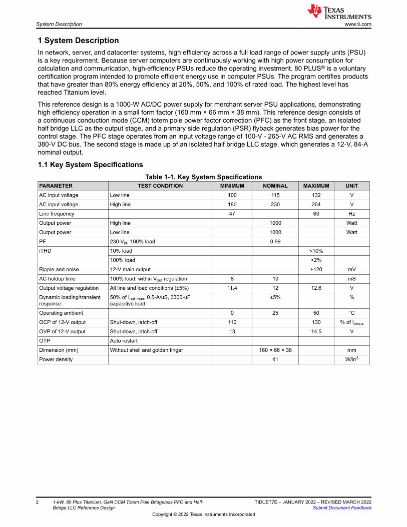
1 System DescriptionIn network, server, and datacenter systems, high efficiency across a full load range of power supply units (PSU) is a key requirement. Because server computers are continuously working with high power consumption for calculation and communication, high-efficiency PSUs reduce the operating investment. 80 PLUS® is a voluntary certification program intended to promote efficient energy use in computer PSUs. The program certifies products that have greater than 80% energy efficiency at 20%, 50%, and 100% of rated load. The highest level has reached Titanium level.
This reference design is a 1000-W AC/DC power supply for merchant server PSU applications, demonstrating high efficiency operation in a small form factor (160 mm × 66 mm × 38 mm). This reference design consists of a continuous conduction mode (CCM) totem pole power factor correction (PFC) as the front stage, an isolated half bridge LLC as the output stage, and a primary side regulation (PSR) flyback generates bias power for the control stage. The PFC stage operates from an input voltage range of 100-V - 265-V AC RMS and generates a 380-V DC bus. The second stage is made up of an isolated half bridge LLC stage, which generates a 12-V, 84-A nominal output.
1.1 Key System SpecificationsTable 1-1. Key System Specifications
PARAMETER TEST CONDITION MINIMUM NOMINAL MAXIMUM UNITAC input voltage Low line 100 115 132 V
AC input voltage High line 180 230 264 V
Line frequency 47 63 Hz
Output power High line 1000 Watt
Output power Low line 1000 Watt
PF 230 Vin, 100% load 0.99
iTHD 10% load <10%
100% load <2%
Ripple and noise 12-V main output ±120 mV
AC holdup time 100% load, within Vout regulation 8 10 mS
Output voltage regulation All line and load conditions (±5%) 11.4 12 12.6 V
Dynamic loading/transient response
50% of Iout-max, 0.5-A/uS, 3300-uF capacitive load
±5% %
Operating ambient 0 25 50 °C
OCP of 12-V output Shut-down, latch-off 110 130 % of Iomax
OVP of 12-V output Shut-down, latch-off 13 14.5 V
OTP Auto restart
Dimension (mm) Without shell and golden finger 160 × 66 × 38 mm
Power density 41 W/in3
System Description www.ti.com
2 1-kW, 80 Plus Titanium, GaN CCM Totem Pole Bridgeless PFC and Half-Bridge LLC Reference Design
TIDUET7E – JANUARY 2022 – REVISED MARCH 2022Submit Document Feedback
Copyright © 2022 Texas Instruments Incorporated
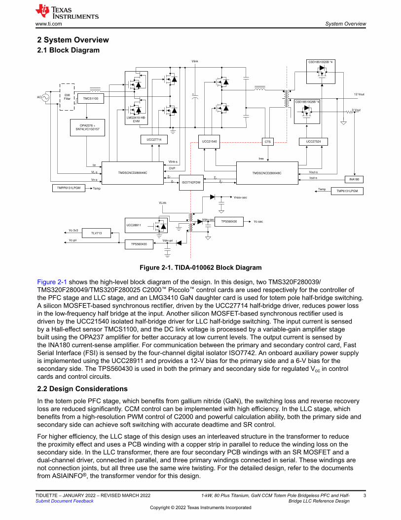
2 System Overview2.1 Block Diagram
LMG3410-HB-
EVM
TMDSCNCD280049C
UCC27714UCC27524
ISO7742FDWINA180
UCC28911
TPS560430
TPS560430
TMPP6131LPGMTMP6131LPGM
OPA2376 +
SN74LVC1G3157
TLV713
EMI
Filter
Vlink-s
OVP
2
2
Vdrv-pri
UCC21540 CTS
Vlink
Ires
TMDSCNCD280049C
2
2
Vresv-sec
Vc-secVdrv-sec
Temp
Vout-s
Iout-s
12 Vout
0 Vout
CSD18510Q5B *4
CSD18510Q5B *4
AC
lin
VL-s
Vn-s
Temp
TMCS1100
Vc-3v3
Vc-pri
VLink
+
Figure 2-1. TIDA-010062 Block Diagram
Figure 2-1 shows the high-level block diagram of the design. In this design, two TMS320F280039/TMS320F280049/TMS320F280025 C2000™ Piccolo™ control cards are used respectively for the controller of the PFC stage and LLC stage, and an LMG3410 GaN daughter card is used for totem pole half-bridge switching. A silicon MOSFET-based synchronous rectifier, driven by the UCC27714 half-bridge driver, reduces power loss in the low-frequency half bridge at the input. Another silicon MOSFET-based synchronous rectifier used is driven by the UCC21540 isolated half-bridge driver for LLC half-bridge switching. The input current is sensed by a Hall-effect sensor TMCS1100, and the DC link voltage is processed by a variable-gain amplifier stage built using the OPA237 amplifier for better accuracy at low current levels. The output current is sensed by the INA180 current-sense amplifier. For communication between the primary and secondary control card, Fast Serial Interface (FSI) is sensed by the four-channel digital isolator ISO7742. An onboard auxiliary power supply is implemented using the UCC28911 and provides a 12-V bias for the primary side and a 6-V bias for the secondary side. The TPS560430 is used in both the primary and secondary side for regulated Vcc in control cards and control circuits.
2.2 Design ConsiderationsIn the totem pole PFC stage, which benefits from gallium nitride (GaN), the switching loss and reverse recovery loss are reduced significantly. CCM control can be implemented with high efficiency. In the LLC stage, which benefits from a high-resolution PWM control of C2000 and powerful calculation ability, both the primary side and secondary side can achieve soft switching with accurate deadtime and SR control.
For higher efficiency, the LLC stage of this design uses an interleaved structure in the transformer to reduce the proximity effect and uses a PCB winding with a copper strip in parallel to reduce the winding loss on the secondary side. In the LLC transformer, there are four secondary PCB windings with an SR MOSFET and a dual-channel driver, connected in parallel, and three primary windings connected in serial. These windings are not connection joints, but all three use the same wire twisting. For the detailed design, refer to the documents from ASIAINFO®, the transformer vendor for this design.
www.ti.com System Overview
TIDUET7E – JANUARY 2022 – REVISED MARCH 2022Submit Document Feedback
1-kW, 80 Plus Titanium, GaN CCM Totem Pole Bridgeless PFC and Half-Bridge LLC Reference Design
3
Copyright © 2022 Texas Instruments Incorporated

2.3 Highlighted ProductsThe following highlighted products are used in this reference design. Key features for selecting the devices for this reference design are explained in the following sections. Complete details of the highlighted devices is referred to in the respective product data sheets.
2.3.1 LMG3410 — 600-V GaN With Integrated Driver and Protection
The LMG3410 single-channel GaN power stage contains a 70mR (/50mR/150mR), 600-V GaN power transistor and specialized driver in an 8-mm x 8-mm QFN package. Direct drive architecture is used to create a normally-off device while providing the native switching performance of the GaN power transistor. When the LMG3410 is unpowered, an integrated low-voltage silicon MOSFET turns the GaN device off through its source. In normal operation, the low-voltage silicon MOSFET is held on continuously while the GaN device is gated directly from an internally-generated negative voltage supply. The integrated driver provides additional protection and convenience features. Fast overcurrent, overtemperature, and undervoltage lockout (UVLO) protections help create a fail-safe system. The device’s status is indicated by the FAULT output. An internal 5-V low-dropout regulator can provide up to 5 mA to supply external signal isolators. Finally, externally-adjustable slew rate and a low-inductance QFN package minimize switching loss, drain ringing, and electrical noise generation.
2.3.2 TMCS1100 — Precision Isolated Current Sense Monitor
The TMCS1100 is an isolated bidirectional Hall-effect current sensor, with high accuracy, excellent linearity, and stability across temperature.
A low-drift, temperature-compensated signal chain provides <1% full-scale error across the entire device temperature range. The output voltage is proportional to input current with four sensitivity options: 50 mV/A, 100 mV/A, 200 mV/A, and 400 mV/A.
The TMCS1100 operates from a single 3-V to 5.5-V power supply, drawing a maximum supply current of 5 mA. All versions are specified over an extended operating temperature range of 40°C to +125°C and are offered in an 8-pin SOIC package.
2.3.3 UCC27524 — Dual, 5-A, High-Speed Low-Side Power MOSFET Driver
The UCC2752x family of devices are dual-channel, high-speed, low-side gate-driver devices capable of effectively driving MOSFET and IGBT power switches. Using a design that inherently minimizes shoot-through current, UCC2752x can deliver high peak current pulses of up to 5-A source and 5-A sink into capacitive loads along with rail-to-rail drive capability and extremely small propagation delay (typically 13 ns). In addition, the drivers feature matched internal propagation delays between the two channels. These delays are very well suited for applications requiring dual-gate drives with critical timing, such as synchronous rectifiers. This also enables connecting two channels in parallel to effectively increase current-drive capability or driving two switches in parallel with one input signal. The input pin thresholds are based on TTL and CMOS compatible low-voltage logic, which is fixed and independent of the VDD supply voltage. Wide hysteresis between the high and low thresholds offers excellent noise immunity.
2.3.4 UCC27714 — 620-V, 1.8-A, 2.8-A High-Side Low-Side Gate Driver
The UCC27714 is a 600-V high-side, low-side gate driver with 4-A source and 4-A sink current capability that is targeted to drive power MOSFETs or IGBTs. The device comprises of one ground-referenced channel (LO) and one floating channel (HO), which is designed for operating with bootstrap supplies. The device features excellent robustness and noise immunity with capability to maintain operational logic at negative voltages of up to -8 VDC on HS pin (at VDD = 12 V).
2.3.5 UCC21540 — Reinforced Isolation Dual-Channel Gate Driver With 3.3-mm Channel-to-Channel Spacing Option
The UCC2154x is an isolated dual channel gate driver family designed with up to 4-A/6-A peak source/sink current to drive power MOSFET, IGBT, and GaN transistors, and UCC21540 in DWK package also offers 3.3-mm minimum channel-to-channel spacing which facilitates higher bus voltage. The UCC2154x family can be configured as two low-side drivers, two high-side drivers, or a half-bridge driver. The input side is isolated from the two output drivers by a 5.7-kVRMS isolation barrier, with a minimum of 100-V/ns common-mode transient immunity (CMTI). Protection features include: resistor programmable dead time, disable feature to shut down
System Overview www.ti.com
4 1-kW, 80 Plus Titanium, GaN CCM Totem Pole Bridgeless PFC and Half-Bridge LLC Reference Design
TIDUET7E – JANUARY 2022 – REVISED MARCH 2022Submit Document Feedback
Copyright © 2022 Texas Instruments Incorporated

both outputs simultaneously, integrated de-glitch filter that rejects input transients shorter than 5 ns, and negative voltage handling for up to –2-V spikes for 200-ns on input and output pins. All supplies have UVLO protection.
2.3.6 ISO7740 and ISO7720 — High-Speed, Low-Power, Robust EMC Digital Isolators
The ISO774x devices are high-performance, quad channel digital isolators with 5000 VRMS (DW package) and 3000 VRMS (DBQ package) isolation ratings per UL1577. This family of devices has reinforced insulation ratings according to VDE, CSA, TUV and CQC. The ISO774x devices provide high electromagnetic immunity and low emissions at low power consumption, while isolating CMOS or LV CMOS digital I/Os. Each isolation channel has a logic input and output buffer separated by a double capacitive silicon diodes (SiO2 ) insulation barrier. This device comes with enable pins which can be used to put the respective outputs in high impedance for multi-master driving applications and to reduce power consumption. The ISO7740 device has all four channels in the same direction, the ISO7741 device has three forward and one reverse-direction channels, and the ISO7742 device has two forward and two reverse-direction channels. If the input power or signal is lost, default output is high for devices without suffix F and low for devices with suffix F.
2.3.7 OPA237 — Single-Supply Operational Amplifier
The OPA237 operational amplifier (op amp) family is one of TI's micro amplifiers in a series of miniature products. In addition to small size, these devices feature low offset voltage, low quiescent current, low bias current, and a wide supply range. They are ideal for single-supply applications. When operated from a single supply, the input common-mode range extends below ground, and the output can swing to within 10 mV of ground.
2.3.8 INAx180 — Low- and High-Side Voltage Output, Current-Sense Amplifiers
The INA180, INA2180, and INA4180 (INAx180) current sense amplifiers are designed for cost optimized applications. These devices are part of a family of current-sense amplifiers (also called current shunt monitors) that sense voltage drops across current-sense resistors at common-mode voltages from –0.2 V to +26 V, independent of the supply voltage. The INAx180 integrate a matched resistor gain network in four, fixed-gain device options: 20 V/V, 50 V/V, 100 V/V, or 200 V/V. This matched gain resistor network minimizes gain error and reduces the temperature drift.
All of these devices operate from a single 2.7-V to 5.5-V power supply. The single-channel INA180 draws a maximum supply current of 260 µA; whereas, the dual-channel INA2180 draws a maximum supply current of 500 µA, and the quad channel draws a maximum supply current of 900 µA.
The INA180 is available in a 5-pin, SOT-23 package with two different pin configurations. The INA2180 is available in an 8-pin, VSSOP package. The INA4180 is available in a 14-pin, TSSOP package. All device options are specified over the extended operating temperature range of –40°C to +125°C.
2.3.9 TPS560430 — SIMPLE SWITCHER® 4-V to 36-V, 600-mA Synchronous Step-Down Converter
The TPS560430 is an easy-to-use synchronous step-down DC-DC converter capable of driving up to 600-mA load current. With a wide input range of 4 V to 36 V, the device is suitable for a wide range of applications from industrial to automotive for power conditioning from an unregulated source.
The TPS560430 has 1.1-MHz and 2.1-MHz operating frequency versions for either high efficiency or small solution size. The TPS560430 also has a FPWM (forced PWM) version to achieve constant frequency and small output voltage ripple over the full load range. Soft-start and compensation circuits are implemented internally which allows the device to be used with minimum external components.
The device has built-in protection features, such as cycle-by-cycle current limit, hiccup mode short-circuit protection, and thermal shutdown in case of excessive power dissipation. The TPS560430 is available in SOT-23-6 package.
2.3.10 TLV713 — 150-mA Low-Dropout (LDO) Regulator With Foldback Current Limit for Portable Devices
The TLV713 series of low-dropout (LDO) linear regulators are low quiescent current LDOs with excellent line and load transient performance and are designed for power-sensitive applications. These devices provide a typical accuracy of 1%.
www.ti.com System Overview
TIDUET7E – JANUARY 2022 – REVISED MARCH 2022Submit Document Feedback
1-kW, 80 Plus Titanium, GaN CCM Totem Pole Bridgeless PFC and Half-Bridge LLC Reference Design
5
Copyright © 2022 Texas Instruments Incorporated

The TLV713 series of devices is designed to be stable without an output capacitor. The removal of the output capacitor allows for a very small solution size. However, the TLV713 series is also stable with any output capacitor if an output capacitor is used.
The TLV713 also provides inrush current control during device power up and enabling. The TLV713 limits the input current to the defined current limit to avoid large currents from flowing from the input power source. This functionality is especially important in battery-operated devices.
The TLV713 series is available in standard DQN and DBV packages. The TLV713P provides an active pulldown circuit to quickly discharge output loads.
2.3.11 TMP61 — Small Silicon-Based Linear Thermistor for Temperature Sensing
The TMP61 series of small silicon linear thermistors are designed for temperature measurement, protection, compensation, and control systems. Compared to traditional NTC thermistors, the TMP61 device offers enhanced linearity and consistent sensitivity across the full temperature range. The TMP61 offers robust performance due to device immunity to environmental variation and built-in fail-safe behaviors at high temperatures. This device is currently available in a 2-pin, surface-mount, 0402 footprint-compatible X1SON package.
2.3.12 CSD18510Q5B — 40-V, N-Channel NexFET™ MOSFET, Single SON5x6, 0.96 mOhm
This 40-V, 0.79-mΩ, SON 5-mm × 6-mm NexFET™ power MOSFET has been designed to minimize losses in power conversion applications.
2.3.13 UCC28911 — 700-V Flyback Switcher With Constant-Voltage, Constant-Current, and Primary-Side Regulation
The UCC28910 and UCC28911 are high-voltage flyback switchers that provide output voltage and current regulation without the use of an optical coupler. Both devices incorporate a 700-V power FET and a controller that process operating information from the flyback auxiliary winding and power FET to provide a precise output voltage and current control. The integrated high-voltage current source for startup that is switched off during device operation, and the controller current consumption is dynamically adjusted with load. Both enable the very low stand-by power consumption.
Control algorithms in the UCC28910 and UCC28911, combining switching frequency and peak primary current modulation, allow operating efficiencies to meet or exceed applicable standards. Discontinuous conduction mode (DCM) with valley switching is used to reduce switching losses. Built-in protection features help to keep secondary and primary component stress levels in check across the operating range. The frequency jitter helps to reduce EMI filter cost.
2.3.14 SN74LVC1G3157DRYR — Single-Pole Double-Throw Analog Switch
This single channel single-pole double-throw (SPDT) analog switch is designed for 1.65-V to 5.5-V VCC operation. The SN74LVC1G3157 device can handle both analog and digital signals. The SN74LVC1G3157 device permits signals with amplitudes of up to VCC (peak) to be transmitted in either direction. Applications include signal gating, chopping, modulation or demodulation (modem), and signal multiplexing for analog-to-digital and digital-to-analog conversion systems.
System Overview www.ti.com
6 1-kW, 80 Plus Titanium, GaN CCM Totem Pole Bridgeless PFC and Half-Bridge LLC Reference Design
TIDUET7E – JANUARY 2022 – REVISED MARCH 2022Submit Document Feedback
Copyright © 2022 Texas Instruments Incorporated
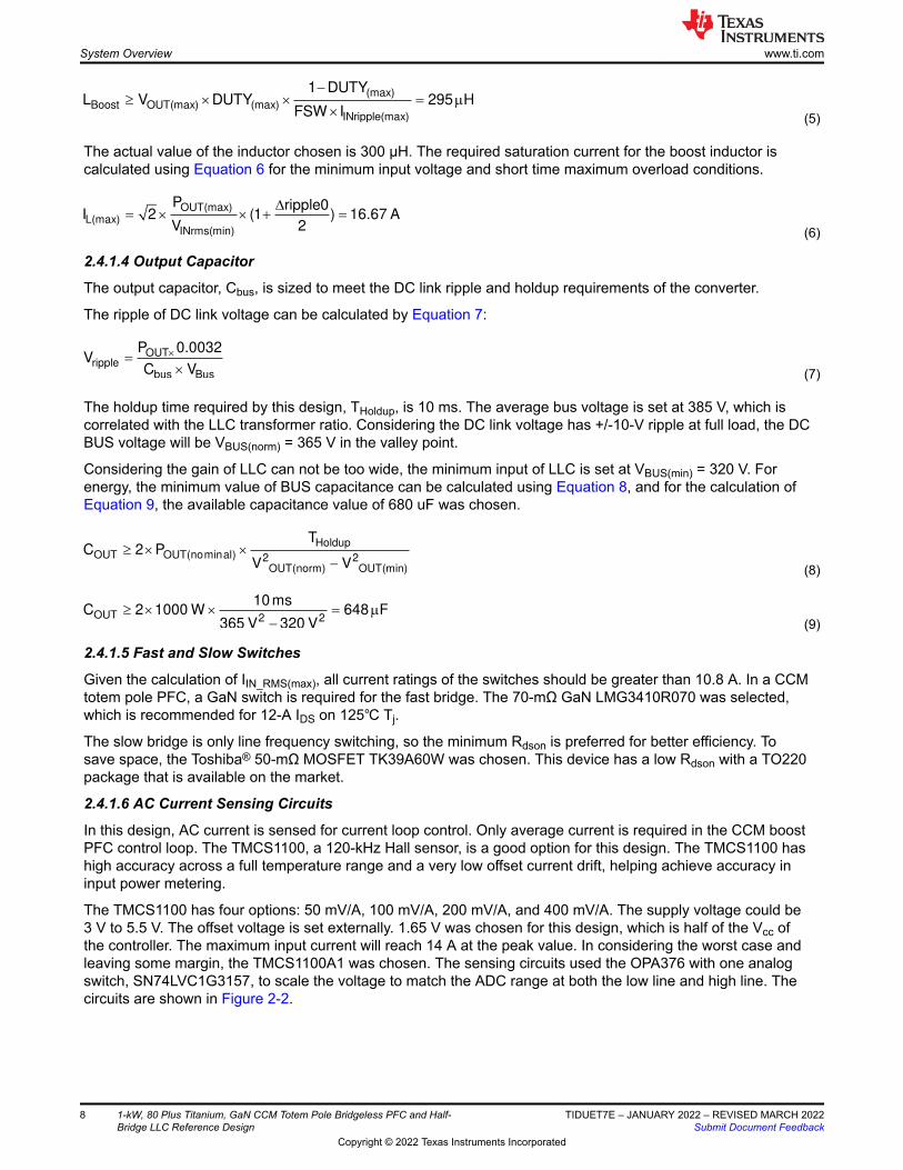
2.4 System Design TheoryThis reference design provides a universal AC mains-powered, 1000-W nominal output at 12 V and 84 A. This design comprises a front-end totem pole PFC power stage followed by an isolated DC/DC LLC power stage.
2.4.1 Totem Pole PFC Stage Design
The totem pole bridgeless PFC is an old structure that has been presented for many years, but it has not been applied in products because of the poor reverse recovery performance of the MOSFET's body diode. However, in recent years, benefitting from GaN HEMT's no reverse recovery feature, the totem pole PFC is now being applied and and has become a simple structure. Generally, the totem pole PFC has one fast-switching leg and one slow-switching leg. The slow-switching leg can use both a rectifier diode or MOSFET. When using a MOSFET as a slow-switching leg, the totem pole PFC can achieve higher efficiency and bidirectional power conversion between the AC side and the DC side.
2.4.1.1 Design Parameters of the PFC Stage
Table 2-1. Design Parameters of the PFC StageSYMBOL PARAMETER MINIMUM NOMINAL MAXIMUM UNITVIN AC input voltage 100 230 264 V AC
fline Line frequency 47 63
Vout Output voltage 385 V DC
Pout (nom) Output power 1050 Watt
η Targeted efficiency 99%
iTHD Targeted input current THD < 5% at >30% Load
PF Targeted power factor 0.98
Fsw Switching frequency 100 kHz
2.4.1.2 Current Calculations
The input fuse, bridge rectifier, and input capacitor are selected based on the input current calculations. First, determine the maximum average output current, IOUT(max) as per Equation 1:
� �
�
OUT(max)OUT(max)
dc _ link
P 1050 WI 2.73 A
V 385 V (1)
The maximum input RMS line current, IIN_RMS(max), is calculated using the parameters from Table 2-1, and the efficiency and power factor initial assumptions are calculated as follows:
OUT(max)INrms(max)
PFC IN(min)
P 1050 WI 10.8 A
V PF 98% 100 V 0.99
� �K u u u � u (2)
2.4.1.3 PFC Boost Inductor
To determine the boost inductor, the maximum-allowed ripple current is calculated first. The maximum ripple current is observed at the lowest input voltage and maximum load. Assuming a maximum 40% ripple in the inductor current, the ripple current would be calculated as follows:
' u u u �INripple(max) INrms(max)I ripple I 0.2 2 10.7A 6.06 A (3)
The duty cycle, DUTY(max), at the peak of the minimum input voltage can be calculated as:
OUT(max) INmin 2(max)
dc _ link
V V 385 V 100 V 2DUTY 0.63
V 385 V
u� � � � � u �
� (4)
The minimum value of the boost inductor is calculated based on the acceptable ripple current, at a worst-case duty cycle of 0.63:
www.ti.com System Overview
TIDUET7E – JANUARY 2022 – REVISED MARCH 2022Submit Document Feedback
1-kW, 80 Plus Titanium, GaN CCM Totem Pole Bridgeless PFC and Half-Bridge LLC Reference Design
7
Copyright © 2022 Texas Instruments Incorporated
�t u u �P
u
(max)Boost OUT(max) (max)
INripple(max)
1 DUTYL V DUTY 295 H
FSW I (5)
The actual value of the inductor chosen is 300 μH. The required saturation current for the boost inductor is calculated using Equation 6 for the minimum input voltage and short time maximum overload conditions.
' u u � �
OUT(max)L(max)
INrms(min)
P ripple0I 2 (1 ) 16.67 A
V 2 (6)
2.4.1.4 Output Capacitor
The output capacitor, Cbus, is sized to meet the DC link ripple and holdup requirements of the converter.
The ripple of DC link voltage can be calculated by Equation 7:
u
u
OUTripple
bus Bus
P 0.0032V
C V (7)
The holdup time required by this design, THoldup, is 10 ms. The average bus voltage is set at 385 V, which is correlated with the LLC transformer ratio. Considering the DC link voltage has +/-10-V ripple at full load, the DC BUS voltage will be VBUS(norm) = 365 V in the valley point.
Considering the gain of LLC can not be too wide, the minimum input of LLC is set at VBUS(min) = 320 V. For energy, the minimum value of BUS capacitance can be calculated using Equation 8, and for the calculation of Equation 9, the available capacitance value of 680 uF was chosen.
t u u
�
HoldupOUT OUT(nominal) 2 2
OUT(norm) OUT(min)
TC 2 P
V V (8)
OUT 2 2
10 msC 2 1000 W 648 F
365 V 320 V
�t u � u �P
� � � (9)
2.4.1.5 Fast and Slow Switches
Given the calculation of IIN_RMS(max), all current ratings of the switches should be greater than 10.8 A. In a CCM totem pole PFC, a GaN switch is required for the fast bridge. The 70-mΩ GaN LMG3410R070 was selected, which is recommended for 12-A IDS on 125℃ Tj.
The slow bridge is only line frequency switching, so the minimum Rdson is preferred for better efficiency. To save space, the Toshiba® 50-mΩ MOSFET TK39A60W was chosen. This device has a low Rdson with a TO220 package that is available on the market.
2.4.1.6 AC Current Sensing Circuits
In this design, AC current is sensed for current loop control. Only average current is required in the CCM boost PFC control loop. The TMCS1100, a 120-kHz Hall sensor, is a good option for this design. The TMCS1100 has high accuracy across a full temperature range and a very low offset current drift, helping achieve accuracy in input power metering.
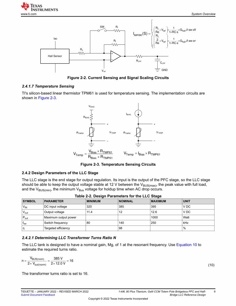
The TMCS1100 has four options: 50 mV/A, 100 mV/A, 200 mV/A, and 400 mV/A. The supply voltage could be 3 V to 5.5 V. The offset voltage is set externally. 1.65 V was chosen for this design, which is half of the Vcc of the controller. The maximum input current will reach 14 A at the peak value. In considering the worst case and leaving some margin, the TMCS1100A1 was chosen. The sensing circuits used the OPA376 with one analog switch, SN74LVC1G3157, to scale the voltage to match the ADC range at both the low line and high line. The circuits are shown in Figure 2-2.
System Overview www.ti.com
8 1-kW, 80 Plus Titanium, GaN CCM Totem Pole Bridgeless PFC and Half-Bridge LLC Reference Design
TIDUET7E – JANUARY 2022 – REVISED MARCH 2022Submit Document Feedback
Copyright © 2022 Texas Instruments Incorporated
Hall Sensor+
GND
CLPF
Re
SW Rf
Rf
Vref
RLPF±
Iac
fref hall
f
ref hall
R 1V G ,if sw off
Re 1 RC ssense R
12 V G ,if sw onRe 1 RC s
I (S)
§ ·� u u � �¨ ¸ � �© ¹
§ ·¨ ¸
� u u � �¨ ¸� �¨ ¸¨ ¸
© ¹
°°°
®°°°̄
Figure 2-2. Current Sensing and Signal Scaling Circuits
2.4.1.7 Temperature Sensing
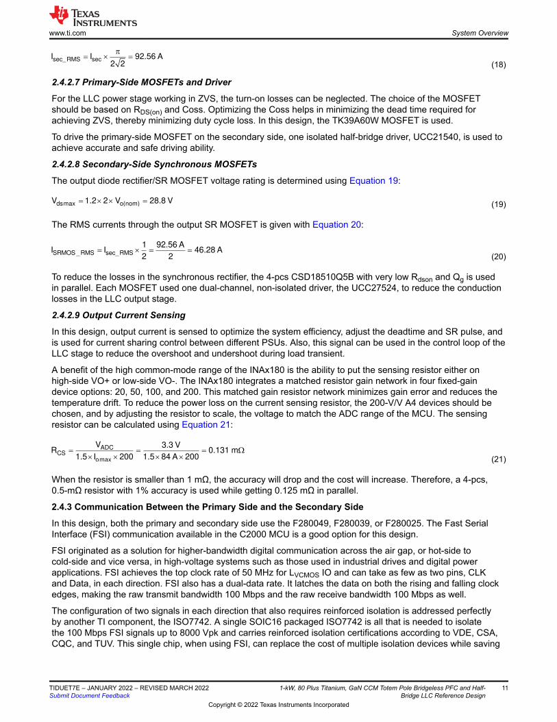
TI's silicon-based linear thermistor TPM61 is used for temperature sensing. The implementation circuits are shown in Figure 2-3.
RBIAS
VBIAS
VTEMPRTMP61
IBIAS
VTEMPRTMP61
+
±�
+
±�
u
�
Bias TMP61Temp
Bias TMP61
V RV
R R uTemp Bias TMP61V I R
Figure 2-3. Temperature Sensing Circuits
2.4.2 Design Parameters of the LLC Stage
The LLC stage is the end stage for output regulation. Its input is the output of the PFC stage, so the LLC stage should be able to keep the output voltage stable at 12 V between the VBUS(max), the peak value with full load, and the VBUS(min), the minimum VBus voltage for holdup time when AC drop occurs.
Table 2-2. Design Parameters for the LLC StageSYMBOL PARAMETER MINIMUM NOMINAL MAXIMUM UNITVIN DC input voltage 320 385 395 V DC
Vout Output voltage 11.4 12 12.6 V DC
Pout Maximum output power 1000 Watt
fsw Switch frequency 80 140 250 kHz
η Targeted efficiency 98 %
2.4.2.1 Determining LLC Transformer Turns Ratio N
The LLC tank is designed to have a nominal gain, Mg, of 1 at the resonant frequency. Use Equation 10 to estimate the required turns ratio.
�
u u �
BUS(nom)
out(norm)
V 385 Vn 16
2 V 2 12.0 V (10)
The transformer turns ratio is set to 16.
www.ti.com System Overview
TIDUET7E – JANUARY 2022 – REVISED MARCH 2022Submit Document Feedback
1-kW, 80 Plus Titanium, GaN CCM Totem Pole Bridgeless PFC and Half-Bridge LLC Reference Design
9
Copyright © 2022 Texas Instruments Incorporated

2.4.2.2 Determining Mg_min and Mg_max
Determine Mg_min and Mg_max using Equation 11 and Equation 12, respectively.
� � � � u u
�
O Fg _ min
bus(max)
V V 12 V 0.01VM n 16 0.972
V / 2 395 V / 2 (11)
O Fg_max
bus(min)
V V 12 V 0.01VM n 16 1.2
V / 2 320 V / 2
� � � � u u
� (12)
The dimensioned Mg_max is increased to one. One times the required value to have some margin is Mg_max = 1.1 × 1.2 ≈ 1.3.
2.4.2.3 Determining Equivalent Load Resistance (Re) of Resonant Network
Equation 13 calculates the equivalent load resistance at nominal and peak load under nominal output voltage and peak output voltage.
u u u u �:
S S
2 2O
e 2 2O
V8 n 8 16 12R 29.64
I 84 (13)
2.4.2.4 Selecting Lm and Lr Ratio (Ln) and Qe
Set the resonance point for the LLC converter close to 140 kHz to minimize the dimension of the LLC transformer set. The operating point of the LLC power stage is close to this frequency during a full load condition. Choose a value of Lr = 19 μH and Cr = 66 nF to calculate the value of the resonant frequency as follows:
�
Sr
r r
1f 140 kHz
2 L C (14)
A PQ 32/30 core has been used to realize the LLC transformer. The resonant inductance is provided through an additional shim inductor built on a 20/16 PQ core.
2.4.2.5 Determining Primary-Side Currents
Use Equation 15 to calculate the primary-side RMS load current (Ipri) at a full load condition:
o(nom)pri
I 84I 1.11 5.83 A
n 162 2
S u u �
(15)
As calculated in Equation 16, the RMS magnetizing current (Im) at fSW_min = 140 kHz is:
O(norm) Fm
sw(min) m
V V2 2I n 0.66 A
2 f L
§ ·� u �¨ ¸
¨ ¸S Su � u© ¹ (16)
Equation 17 calculates the resonant circuit current (Ir):
� �2 2
r pri mI I I 5.86 A (17)
This value is also equal to the transformer primary winding current at fSW_min.
2.4.2.6 Determining Secondary-Side Currents
The secondary-side RMS currents can be calculated from the average load current. Assuming that the LLC power stage is operating close to its second resonant frequency, the RMS current through each rectifier in the secondary-side push-pull output is calculated in Equation 18:
System Overview www.ti.com
10 1-kW, 80 Plus Titanium, GaN CCM Totem Pole Bridgeless PFC and Half-Bridge LLC Reference Design
TIDUET7E – JANUARY 2022 – REVISED MARCH 2022Submit Document Feedback
Copyright © 2022 Texas Instruments Incorporated
S u �sec_RMS secI I 92.56 A
2 2 (18)
2.4.2.7 Primary-Side MOSFETs and Driver
For the LLC power stage working in ZVS, the turn-on losses can be neglected. The choice of the MOSFET should be based on RDS(on) and Coss. Optimizing the Coss helps in minimizing the dead time required for achieving ZVS, thereby minimizing duty cycle loss. In this design, the TK39A60W MOSFET is used.
To drive the primary-side MOSFET on the secondary side, one isolated half-bridge driver, UCC21540, is used to achieve accurate and safe driving ability.
2.4.2.8 Secondary-Side Synchronous MOSFETs
The output diode rectifier/SR MOSFET voltage rating is determined using Equation 19:
u u �dsmax o(nom)V 1.2 2 V 28.8 V (19)
The RMS currents through the output SR MOSFET is given with Equation 20:
� u �SRMOS _RMS sec_RMS
1 92.56 AI I 46.28 A
2 2 (20)
To reduce the losses in the synchronous rectifier, the 4-pcs CSD18510Q5B with very low Rdson and Qg is used in parallel. Each MOSFET used one dual-channel, non-isolated driver, the UCC27524, to reduce the conduction losses in the LLC output stage.
2.4.2.9 Output Current Sensing
In this design, output current is sensed to optimize the system efficiency, adjust the deadtime and SR pulse, and is used for current sharing control between different PSUs. Also, this signal can be used in the control loop of the LLC stage to reduce the overshoot and undershoot during load transient.
A benefit of the high common-mode range of the INAx180 is the ability to put the sensing resistor either on high-side VO+ or low-side VO-. The INAx180 integrates a matched resistor gain network in four fixed-gain device options: 20, 50, 100, and 200. This matched gain resistor network minimizes gain error and reduces the temperature drift. To reduce the power loss on the current sensing resistor, the 200-V/V A4 devices should be chosen, and by adjusting the resistor to scale, the voltage to match the ADC range of the MCU. The sensing resistor can be calculated using Equation 21:
� �� :
u u u � u
ADCCS
omax
V 3.3 VR 0.131 m
1.5 I 200 1.5 84 A 200 (21)
When the resistor is smaller than 1 mΩ, the accuracy will drop and the cost will increase. Therefore, a 4-pcs, 0.5-mΩ resistor with 1% accuracy is used while getting 0.125 mΩ in parallel.
2.4.3 Communication Between the Primary Side and the Secondary Side
In this design, both the primary and secondary side use the F280049, F280039, or F280025. The Fast Serial Interface (FSI) communication available in the C2000 MCU is a good option for this design.
FSI originated as a solution for higher-bandwidth digital communication across the air gap, or hot-side to cold-side and vice versa, in high-voltage systems such as those used in industrial drives and digital power applications. FSI achieves the top clock rate of 50 MHz for LVCMOS IO and can take as few as two pins, CLK and Data, in each direction. FSI also has a dual-data rate. It latches the data on both the rising and falling clock edges, making the raw transmit bandwidth 100 Mbps and the raw receive bandwidth 100 Mbps as well.
The configuration of two signals in each direction that also requires reinforced isolation is addressed perfectly by another TI component, the ISO7742. A single SOIC16 packaged ISO7742 is all that is needed to isolate the 100 Mbps FSI signals up to 8000 Vpk and carries reinforced isolation certifications according to VDE, CSA, CQC, and TUV. This single chip, when using FSI, can replace the cost of multiple isolation devices while saving
www.ti.com System Overview
TIDUET7E – JANUARY 2022 – REVISED MARCH 2022Submit Document Feedback
1-kW, 80 Plus Titanium, GaN CCM Totem Pole Bridgeless PFC and Half-Bridge LLC Reference Design
11
Copyright © 2022 Texas Instruments Incorporated

significant board space and also reducing the PCB routing and voltage plane definition challenges associated with mixed-plane, high-voltage PCB designs.
System Overview www.ti.com
12 1-kW, 80 Plus Titanium, GaN CCM Totem Pole Bridgeless PFC and Half-Bridge LLC Reference Design
TIDUET7E – JANUARY 2022 – REVISED MARCH 2022Submit Document Feedback
Copyright © 2022 Texas Instruments Incorporated
3 Hardware, Software, Testing Requirements, and Test Results3.1 Required Hardware and Software3.1.1 Hardware
This section details the necessary equipment, test setup, and procedure instructions for the TIDA-010062 board testing and validation.
3.1.1.1 Test Conditions
For input, the power supply source (VIN) must range from 100-V to 265-V AC. Set the input current limit of the input AC source to 15 A. For output, use an electronic variable load or a variable resistive load, which must be rated for ≥ 15 V and must vary the load current from 0 A to 90 A.
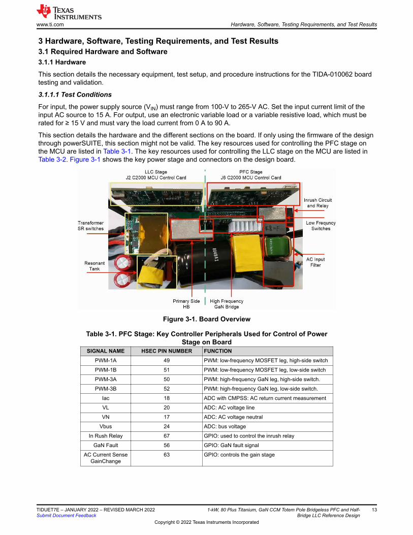
This section details the hardware and the different sections on the board. If only using the firmware of the design through powerSUITE, this section might not be valid. The key resources used for controlling the PFC stage on the MCU are listed in Table 3-1. The key resources used for controlling the LLC stage on the MCU are listed in Table 3-2. Figure 3-1 shows the key power stage and connectors on the design board.
Figure 3-1. Board Overview
Table 3-1. PFC Stage: Key Controller Peripherals Used for Control of Power Stage on Board
SIGNAL NAME HSEC PIN NUMBER FUNCTIONPWM-1A 49 PWM: low-frequency MOSFET leg, high-side switch
PWM-1B 51 PWM: low-frequency MOSFET leg, low-side switch
PWM-3A 50 PWM: high-frequency GaN leg, high-side switch.
PWM-3B 52 PWM: high-frequency GaN leg, low-side switch.
Iac 18 ADC with CMPSS: AC return current measurement
VL 20 ADC: AC voltage line
VN 17 ADC: AC voltage neutral
Vbus 24 ADC: bus voltage
In Rush Relay 67 GPIO: used to control the inrush relay
GaN Fault 56 GPIO: GaN fault signal
AC Current Sense GainChange
63 GPIO: controls the gain stage
www.ti.com Hardware, Software, Testing Requirements, and Test Results
TIDUET7E – JANUARY 2022 – REVISED MARCH 2022Submit Document Feedback
1-kW, 80 Plus Titanium, GaN CCM Totem Pole Bridgeless PFC and Half-Bridge LLC Reference Design
13
Copyright © 2022 Texas Instruments Incorporated
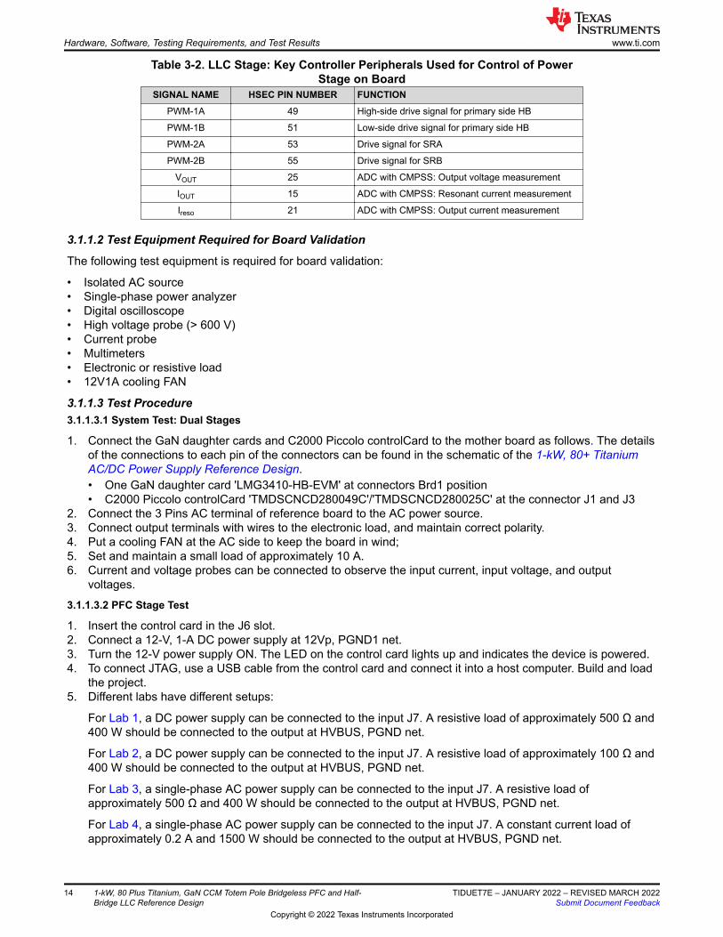
Table 3-2. LLC Stage: Key Controller Peripherals Used for Control of Power Stage on Board
SIGNAL NAME HSEC PIN NUMBER FUNCTIONPWM-1A 49 High-side drive signal for primary side HB
PWM-1B 51 Low-side drive signal for primary side HB
PWM-2A 53 Drive signal for SRA
PWM-2B 55 Drive signal for SRB
VOUT 25 ADC with CMPSS: Output voltage measurement
IOUT 15 ADC with CMPSS: Resonant current measurement
Ireso 21 ADC with CMPSS: Output current measurement
3.1.1.2 Test Equipment Required for Board Validation
The following test equipment is required for board validation:
• Isolated AC source• Single-phase power analyzer• Digital oscilloscope• High voltage probe (> 600 V)• Current probe• Multimeters• Electronic or resistive load• 12V1A cooling FAN
3.1.1.3 Test Procedure3.1.1.3.1 System Test: Dual Stages
1. Connect the GaN daughter cards and C2000 Piccolo controlCard to the mother board as follows. The details of the connections to each pin of the connectors can be found in the schematic of the 1-kW, 80+ Titanium AC/DC Power Supply Reference Design.• One GaN daughter card 'LMG3410-HB-EVM' at connectors Brd1 position• C2000 Piccolo controlCard 'TMDSCNCD280049C'/'TMDSCNCD280025C' at the connector J1 and J3
2. Connect the 3 Pins AC terminal of reference board to the AC power source.3. Connect output terminals with wires to the electronic load, and maintain correct polarity.4. Put a cooling FAN at the AC side to keep the board in wind;5. Set and maintain a small load of approximately 10 A.6. Current and voltage probes can be connected to observe the input current, input voltage, and output
voltages.
3.1.1.3.2 PFC Stage Test
1. Insert the control card in the J6 slot.2. Connect a 12-V, 1-A DC power supply at 12Vp, PGND1 net.3. Turn the 12-V power supply ON. The LED on the control card lights up and indicates the device is powered.4. To connect JTAG, use a USB cable from the control card and connect it into a host computer. Build and load
the project.5. Different labs have different setups:
For Lab 1, a DC power supply can be connected to the input J7. A resistive load of approximately 500 Ω and 400 W should be connected to the output at HVBUS, PGND net.
For Lab 2, a DC power supply can be connected to the input J7. A resistive load of approximately 100 Ω and 400 W should be connected to the output at HVBUS, PGND net.
For Lab 3, a single-phase AC power supply can be connected to the input J7. A resistive load of approximately 500 Ω and 400 W should be connected to the output at HVBUS, PGND net.
For Lab 4, a single-phase AC power supply can be connected to the input J7. A constant current load of approximately 0.2 A and 1500 W should be connected to the output at HVBUS, PGND net.
Hardware, Software, Testing Requirements, and Test Results www.ti.com
14 1-kW, 80 Plus Titanium, GaN CCM Totem Pole Bridgeless PFC and Half-Bridge LLC Reference Design
TIDUET7E – JANUARY 2022 – REVISED MARCH 2022Submit Document Feedback
Copyright © 2022 Texas Instruments Incorporated

6. Current and voltage probes can be connected to observe the input current, input voltage, and output voltages, as shown in Figure 3-1.
3.1.1.3.3 LLC Stage Test
1. Insert the control card in the J2 slot.2. Connect a 12-V, 1-A DC power supply at 12Vp, PGND1 net.3. Connect a 6-V, 1-A DC power supply at 6Vcc, V0 net.4. Turn the 12-V and 6-V power supply ON. The LED on the control card lights up and indicates the device is
powered.5. To connect JTAG, use a USB cable from the control card and connect it into a host computer. Build and load
the project.6. Different labs have different setups:
For Lab 1, a DC power supply can be connected to the HVBUS, PGND net. A constant current load of approximately 10 A should be connected to the output at the 12Vout, V0-out net.
For Lab 2, a DC power supply can be connected to the HVBUS, PGND net. A constant current load of approximately 10 A should be connected to the output at the 12Vout, V0-out net.
7. Current and voltage probes can be connected to observe the resonant current, switching node voltage, SR drive signal and output voltages, as Figure 3-1 shows.
3.1.2 PFC Stage Software
The software of this design is available inside C2000Ware Digital Power SDK and is supported inside the powerSUITE framework.
3.1.2.1 Opening Project Inside CCS
To start:
1. Install CCS from the Code Composer Studio (CCS) Integrated Development Environment (IDE) tools folder, CCSV10.1 or above is recommended.
2. Install C2000Ware DigitalPower SDK at the C2000Ware Digital Power SDK tools folder.• Note: powerSUITE is installed with the SDK in the default install.
3. Go to View → Resource Explorer. Below the TI Resource Explorer, go to C2000Ware DigitalPower SDK.
To open the reference design software as it is (opens firmware as it was run on this design and hardware, requires the board to be exactly the same as this reference design).
4. Under C2000Ware DigitalPower SDK, select Development Kits → CCM Totem Pole PFC TIDA-010062, and click on Run <Import> Project.
5. These steps import the project, and the development kit or designs page show up. This page can be used to browse all the information on the design including this user guide, test reports, hardware design files, and so forth.
6. Click Import <device_name> Project.7. This action imports the project into the workspace environment, and a main.syscfg page with a GUI similar to
Figure 3-3 shows up.
www.ti.com Hardware, Software, Testing Requirements, and Test Results
TIDUET7E – JANUARY 2022 – REVISED MARCH 2022Submit Document Feedback
1-kW, 80 Plus Titanium, GaN CCM Totem Pole Bridgeless PFC and Half-Bridge LLC Reference Design
15
Copyright © 2022 Texas Instruments Incorporated
3.1.2.2 Project Structure
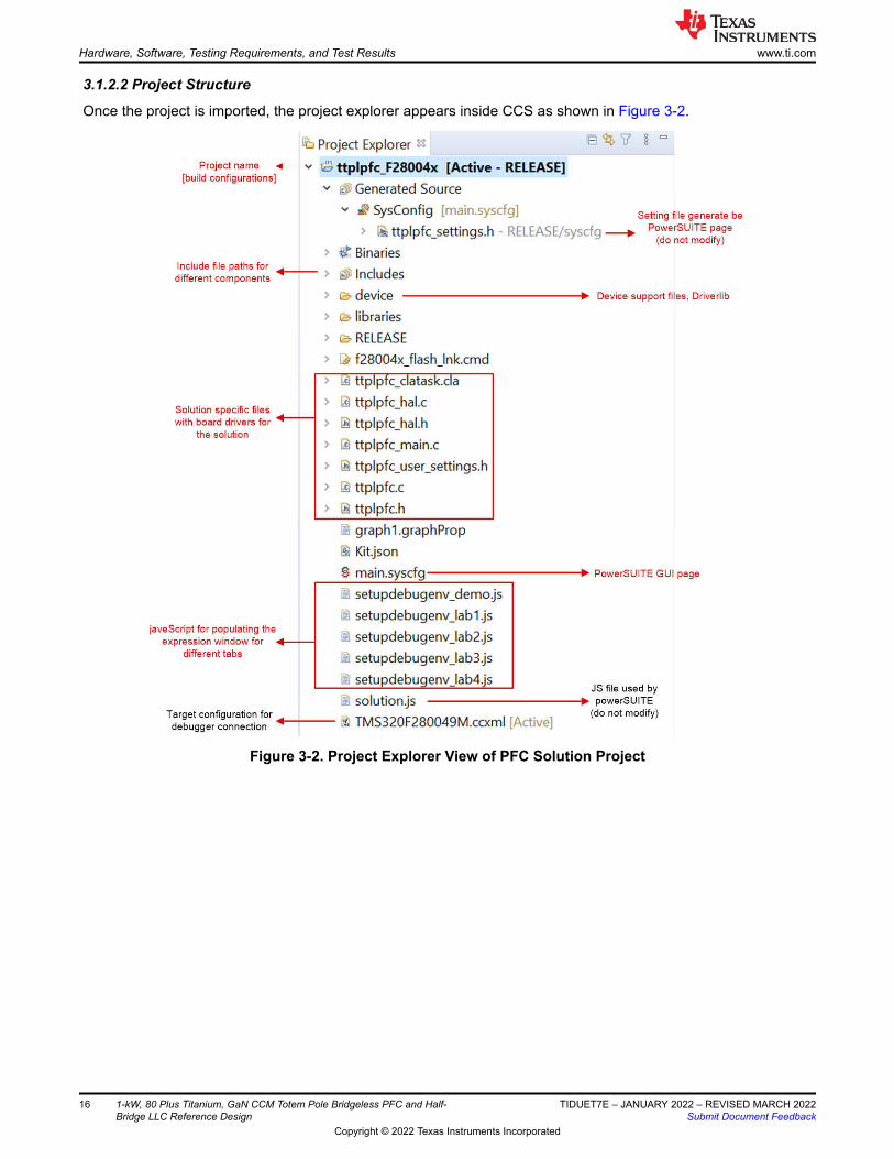
Once the project is imported, the project explorer appears inside CCS as shown in Figure 3-2.
Figure 3-2. Project Explorer View of PFC Solution Project
Hardware, Software, Testing Requirements, and Test Results www.ti.com
16 1-kW, 80 Plus Titanium, GaN CCM Totem Pole Bridgeless PFC and Half-Bridge LLC Reference Design
TIDUET7E – JANUARY 2022 – REVISED MARCH 2022Submit Document Feedback
Copyright © 2022 Texas Instruments Incorporated
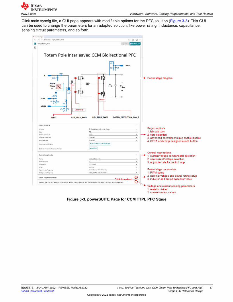
Click main.syscfg file, a GUI page appears with modifiable options for the PFC solution (Figure 3-3). This GUI can be used to change the parameters for an adapted solution, like power rating, inductance, capacitance, sensing circuit parameters, and so forth.
Figure 3-3. powerSUITE Page for CCM TTPL PFC Stage
www.ti.com Hardware, Software, Testing Requirements, and Test Results
TIDUET7E – JANUARY 2022 – REVISED MARCH 2022Submit Document Feedback
1-kW, 80 Plus Titanium, GaN CCM Totem Pole Bridgeless PFC and Half-Bridge LLC Reference Design
17
Copyright © 2022 Texas Instruments Incorporated
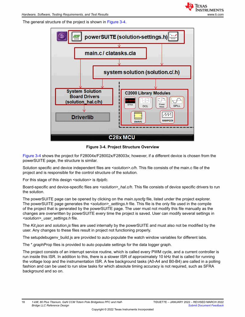
The general structure of the project is shown in Figure 3-4.
Figure 3-4. Project Structure Overview
Figure 3-4 shows the project for F28004x/F28002x/F28003x; however, if a different device is chosen from the powerSUITE page, the structure is similar.
Solution specific and device independent files are <solution>.c/h. This file consists of the main.c file of the project and is responsible for the control structure of the solution.
For this stage of this design <solution> is ttplpfc.
Board-specific and device-specific files are <solution>_hal.c/h. This file consists of device specific drivers to run the solution.
The powerSUITE page can be opened by clicking on the main.syscfg file, listed under the project explorer. The powerSUITE page generates the <solution>_settings.h file. This file is the only file used in the compile of the project that is generated by the powerSUITE page. The user must not modify this file manually as the changes are overwritten by powerSUITE every time the project is saved. User can modify several settings in <solution>_user_settings.h file.
The Kit.json and solution.js files are used internally by the powerSUITE and must also not be modified by the user. Any changes to these files result in project not functioning properly.
The setupdebugenv_build.js are provided to auto-populate the watch window variables for different labs.
The *.graphProp files is provided to auto populate settings for the data logger graph.
The project consists of an interrupt service routine, which is called every PWM cycle, and a current controller is run inside this ISR. In addition to this, there is a slower ISR of approximately 10 kHz that is called for running the voltage loop and the instrumentation ISR. A few background tasks (A0-A4 and B0-B4) are called in a polling fashion and can be used to run slow tasks for which absolute timing accuracy is not required, such as SFRA background and so on.
Hardware, Software, Testing Requirements, and Test Results www.ti.com
18 1-kW, 80 Plus Titanium, GaN CCM Totem Pole Bridgeless PFC and Half-Bridge LLC Reference Design
TIDUET7E – JANUARY 2022 – REVISED MARCH 2022Submit Document Feedback
Copyright © 2022 Texas Instruments Incorporated
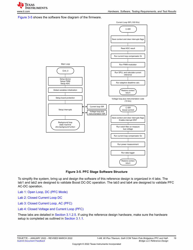
Figure 3-5 shows the software flow diagram of the firmware.
Save context and clear interrupts flags
C-ISR
Read ADC result
Run current loop compensator Gi
Run PWM modulator
Run SPLL and calculate current
reference
Run adaptive deadtime calc.
Restore context
return
Save context and clear interrupts flags
Enable interrupt EINT
C-ISR
(boost control)
Run notch filter on measure
bus voltage
Run current loop compensator Gv
Run power measurement
Run data logger
Restore context
return
Setup device
Setup PWM
Setup ADC
Cinit_0
Global variables initialization
Setup board protection
Setup interrupts
Background loop
state machine
sfra background funtion
Current loop ISR
Voltage loop plus
instrumentation ISR
Main Loop
Current Loop ISR (100 Khz)
Voltage loop plus instrumentation code
(10 khz)
Figure 3-5. PFC Stage Software Structure
To simplify the system, bring up and design the software of this reference design is organized in 4 labs. The lab1 and lab2 are designed to validate Boost DC-DC operation. The lab3 and lab4 are designed to validate PFC AC-DC operation.
Lab 1: Open Loop, DC (PFC Mode)
Lab 2: Closed Current Loop DC
Lab 3: Closed Current Loop, AC (PFC)
Lab 4: Closed Voltage and Current Loop (PFC)
These labs are detailed in Section 3.1.2.5. If using the reference design hardware, make sure the hardware setup is completed as outlined in Section 3.1.1.
www.ti.com Hardware, Software, Testing Requirements, and Test Results
TIDUET7E – JANUARY 2022 – REVISED MARCH 2022Submit Document Feedback
1-kW, 80 Plus Titanium, GaN CCM Totem Pole Bridgeless PFC and Half-Bridge LLC Reference Design
19
Copyright © 2022 Texas Instruments Incorporated
3.1.2.3 Using CLA on C2000 MCU to Alleviate CPU Burden
The control law accelerator (CLA) is a co-processor available on the C2000 MCU family of devices. This coprocessor enables offloading the control-ISR functions from the main C28x CPU core.
To run the control ISR on the CLA for solutions supported in powerSUITE, selection is achieved through a drop-down menu on the powerSUITE CFG page. The software structure of the powerSUITE solution is designed such that offloading the task to the CLA is simply a drop-down menu selection. The code is not duplicated and a single source for the solution algorithm is maintained even when code is run on the CLA or the C28x. This configuration enables flexible debugging of the solution.
The CLA features of each device varies slightly. For example, on the F2837xD, F2837xS, and F2807x, the CLA can support only one task at a given time, and there is no nesting capability. This configuration means that the task cannot be interrupted. Only one ISR can be offloaded to the CLA. On the F28004x, the CLA supports a background task from which a regular CLA task can nest. This configuration enables offloading two ISRs on the CLA.
The CLA supports a background task from which it can nest into a CLA task. This configuration allows offloading two ISR functions to the CLA. For the F28003x/F28004x, both the control ISR (100 kHz) for the current loop and the voltage loop and instrumentation ISR (10 kHz) are offloaded to the CLA. For the F28002x which do not have CLA, both the ISRs can only run on C28x.
For more information on the CLA, visit the CLA Hands-On Workshop and the respective device technical reference manuals.
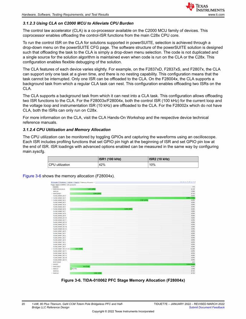
3.1.2.4 CPU Utilization and Memory Allocation
The CPU utilization can be monitored by toggling GPIOs and capturing the waveforms using an oscilloscope. Each ISR includes profiling functions that set GPIO pin high at the beginning of ISR and set GPIO pin low at the end of ISR. ISR loadings with advanced options enabled can be measured in the same way by configuring main.syscfg.
ISR1 (100 kHz) ISR2 (10 kHz)CPU utilization 42% 10%
Figure 3-6 shows the memory allocation (F28004x).
Figure 3-6. TIDA-010062 PFC Stage Memory Allocation (F28004x)
Hardware, Software, Testing Requirements, and Test Results www.ti.com
20 1-kW, 80 Plus Titanium, GaN CCM Totem Pole Bridgeless PFC and Half-Bridge LLC Reference Design
TIDUET7E – JANUARY 2022 – REVISED MARCH 2022Submit Document Feedback
Copyright © 2022 Texas Instruments Incorporated
3.1.2.5 Running the Project
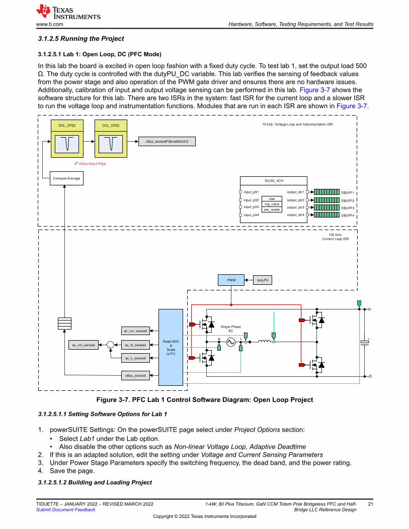
3.1.2.5.1 Lab 1: Open Loop, DC (PFC Mode)
In this lab the board is excited in open loop fashion with a fixed duty cycle. To test lab 1, set the output load 500 Ω. The duty cycle is controlled with the dutyPU_DC variable. This lab verifies the sensing of feedback values from the power stage and also operation of the PWM gate driver and ensures there are no hardware issues. Additionally, calibration of input and output voltage sensing can be performed in this lab. Figure 3-7 shows the software structure for this lab. There are two ISRs in the system: fast ISR for the current loop and a slower ISR to run the voltage loop and instrumentation functions. Modules that are run in each ISR are shown in Figure 3-7.
Single Phase
AC
LN +
PWM dutyPU
+-ac_vol_sensed
DCL_DF22 DCL_DF22
4th
Order Notch Filter
Compute Average
vBus_sensedFilteredNotch2
10 kHz, Voltage Loop and Instrumentation ISR
100 kHz,
Current Loop ISR
DBUFF1
DBUFF2
DBUFF3
DBUFF4
vBus_sensed
ac_L_sensed
ac_N_sensed
ac_cur_sensed
Read ADC
&
Scale
to PU
DLOG_4CH
input_ptr1 output_ptr1
size
trig_value
pre_scalar
output_ptr2
output_ptr3
output_ptr4
input_ptr2
input_ptr3
input_ptr4
Figure 3-7. PFC Lab 1 Control Software Diagram: Open Loop Project
3.1.2.5.1.1 Setting Software Options for Lab 1
1. powerSUITE Settings: On the powerSUITE page select under Project Options section:• Select Lab1 under the Lab option.• Also disable the other options such as Non-linear Voltage Loop, Adaptive Deadtime
2. If this is an adapted solution, edit the setting under Voltage and Current Sensing Parameters3. Under Power Stage Parameters specify the switching frequency, the dead band, and the power rating.4. Save the page.
3.1.2.5.1.2 Building and Loading Project
www.ti.com Hardware, Software, Testing Requirements, and Test Results
TIDUET7E – JANUARY 2022 – REVISED MARCH 2022Submit Document Feedback
1-kW, 80 Plus Titanium, GaN CCM Totem Pole Bridgeless PFC and Half-Bridge LLC Reference Design
21
Copyright © 2022 Texas Instruments Incorporated
1. Right click on the project name, and click Rebuild Project.2. The project builds successfully.3. In the Project Explorer make sure the correct target configuration file is set as Active under targetconfigs
(Figure 3-2).
4. Then click Run → Debug or debug button . This action launches a debugging session. In the case of dual CPU devices, a window may appear to select the CPU that the debug must be performed. In this case, select CPU1.
5. The project then loads on the device, and CCS debug view becomes active. The code halts at the start of the main routine.
3.1.2.5.1.3 Setup Debug Environment Windows
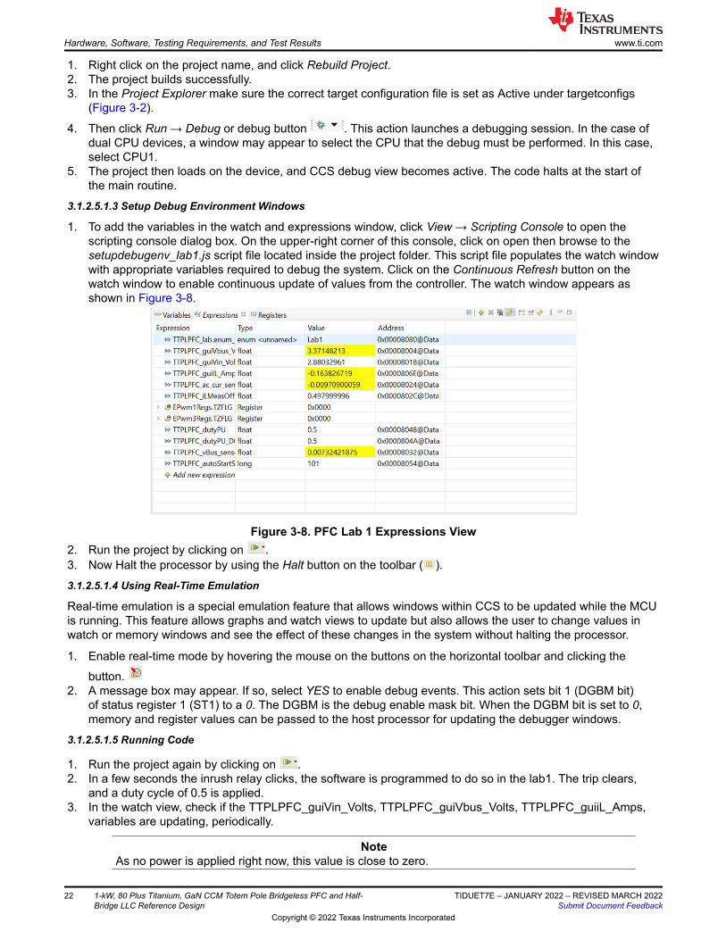
1. To add the variables in the watch and expressions window, click View → Scripting Console to open the scripting console dialog box. On the upper-right corner of this console, click on open then browse to the setupdebugenv_lab1.js script file located inside the project folder. This script file populates the watch window with appropriate variables required to debug the system. Click on the Continuous Refresh button on the watch window to enable continuous update of values from the controller. The watch window appears as shown in Figure 3-8.
Figure 3-8. PFC Lab 1 Expressions View2. Run the project by clicking on .3. Now Halt the processor by using the Halt button on the toolbar ( ).
3.1.2.5.1.4 Using Real-Time Emulation
Real-time emulation is a special emulation feature that allows windows within CCS to be updated while the MCU is running. This feature allows graphs and watch views to update but also allows the user to change values in watch or memory windows and see the effect of these changes in the system without halting the processor.
1. Enable real-time mode by hovering the mouse on the buttons on the horizontal toolbar and clicking the
button. 2. A message box may appear. If so, select YES to enable debug events. This action sets bit 1 (DGBM bit)
of status register 1 (ST1) to a 0. The DGBM is the debug enable mask bit. When the DGBM bit is set to 0, memory and register values can be passed to the host processor for updating the debugger windows.
3.1.2.5.1.5 Running Code
1. Run the project again by clicking on .2. In a few seconds the inrush relay clicks, the software is programmed to do so in the lab1. The trip clears,
and a duty cycle of 0.5 is applied.3. In the watch view, check if the TTPLPFC_guiVin_Volts, TTPLPFC_guiVbus_Volts, TTPLPFC_guiiL_Amps,
variables are updating, periodically.
NoteAs no power is applied right now, this value is close to zero.
Hardware, Software, Testing Requirements, and Test Results www.ti.com
22 1-kW, 80 Plus Titanium, GaN CCM Totem Pole Bridgeless PFC and Half-Bridge LLC Reference Design
TIDUET7E – JANUARY 2022 – REVISED MARCH 2022Submit Document Feedback
Copyright © 2022 Texas Instruments Incorporated

4. Slowly increase the input DC voltage from zero to 120 V. The output voltage shows a boosted voltage as a steady duty cycle of 0.5 PU is applied as default setting. If a high current is drawn, verify if the voltage terminals are swapped. If true, reduce the voltage to zero first and correct the issue before resuming the test.
5. Verifying the voltage sensing: Make sure TTPLPFC_guiVin_Volts and TTPLPFC_guiVbus_Volts display the correct values. This verifies the voltage sensing of the board in some manner.
6. Verifying the current sensing: Notice the TTPLPFC_guiiL_Amps for the given test condition.
Figure 3-9. PFC Lab 1: Watch Expression Showing Measured Voltage and Currents7. This verifies at a basic level the PWM driver and connection of hardware, the user can change the
dutyPU_DC variable to see operation under various boost conditions.8. Once finished, reduce the input voltage to zero and watch for the bus voltages to reduce down to zero.9. This completes the check for this build, the following items are verified on successful completion of this build:
• Sensing of voltages and currents and scaling to be correct• Interrupt generation and execution of the Lab 1 code in the current loop ISR and Voltage Loop
Instrumentation ISR• PWM driver and switching
If any issue is observed a careful inspection of the hardware may be required to eliminate any build issues, and so forth.
10. The controller can now be halted, and the debug connection terminated.11. Fully halting the MCU when in real-time mode is a two-step process. First halt the processor by using the
Halt button on the toolbar ( ) or by using Target → Halt. Then take the MCU out of real-time mode by
clicking on . Finally, reset the MCU by clicking on .12. Close CCS debug session by clicking on Terminate Debug Session (Target → Terminate all) .
3.1.2.5.2 Lab 2: Closed Current Loop DC
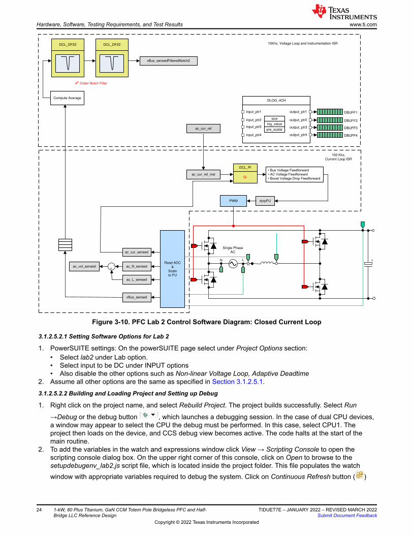
In this build, Lab 2, the inner current loop is closed; that is, the inductor current is controlled using a current compensator Gi. To test lab 2, set the output load 100 Ω. Both DC bus and output voltage feed forward are applied to the output of this current compensator to generate the duty cycle of the inverter, Equation 22.
� �� u �
ac _ cur _meas ac _ cur _ ref _ inst Gi ac _ vol_ sensedduty1PU
vBus _ sensed (22)
The complete software diagram for this lab is illustrated in Figure 3-10.
www.ti.com Hardware, Software, Testing Requirements, and Test Results
TIDUET7E – JANUARY 2022 – REVISED MARCH 2022Submit Document Feedback
1-kW, 80 Plus Titanium, GaN CCM Totem Pole Bridgeless PFC and Half-Bridge LLC Reference Design
23
Copyright © 2022 Texas Instruments Incorporated
Single Phase
AC
LN +
PWM dutyPU
+-ac_vol_sensed
DCL_DF22 DCL_DF22
4th Order Notch Filter
Compute Average
vBus_sensedFilteredNotch2
ac_cur_ref
ac_cur_ref_inst
DCL_PI
Gi
��%XV�9ROWDJH�)HHGIRUZDUG
��$&�9ROWDJH�)HHGIRUZDUG
��%RRVW�9ROWDJH�'URS�)HHGIRUZDUG
10Khz, Voltage Loop and Instrumentation ISR
100 Khz,
Current Loop ISR
DBUFF1
DBUFF2
DBUFF3
DBUFF4
vBus_sensed
ac_L_sensed
ac_N_sensed
ac_cur_sensed
Read ADC
&
Scale
to PU
DLOG_4CH
input_ptr1 output_ptr1
size
trig_value
pre_scalar
output_ptr2
output_ptr3
output_ptr4
input_ptr2
input_ptr3
input_ptr4
Figure 3-10. PFC Lab 2 Control Software Diagram: Closed Current Loop
3.1.2.5.2.1 Setting Software Options for Lab 2
1. PowerSUITE settings: On the powerSUITE page select under Project Options section:• Select lab2 under Lab option.• Select input to be DC under INPUT options• Also disable the other options such as Non-linear Voltage Loop, Adaptive Deadtime
2. Assume all other options are the same as specified in Section 3.1.2.5.1.
3.1.2.5.2.2 Building and Loading Project and Setting up Debug
1. Right click on the project name, and select Rebuild Project. The project builds successfully. Select Run
→Debug or the debug button , which launches a debugging session. In the case of dual CPU devices, a window may appear to select the CPU the debug must be performed. In this case, select CPU1. The project then loads on the device, and CCS debug view becomes active. The code halts at the start of the main routine.
2. To add the variables in the watch and expressions window click View → Scripting Console to open the scripting console dialog box. On the upper right corner of this console, click on Open to browse to the setupdebugenv_lab2.js script file, which is located inside the project folder. This file populates the watch window with appropriate variables required to debug the system. Click on Continuous Refresh button ( )
Hardware, Software, Testing Requirements, and Test Results www.ti.com
24 1-kW, 80 Plus Titanium, GaN CCM Totem Pole Bridgeless PFC and Half-Bridge LLC Reference Design
TIDUET7E – JANUARY 2022 – REVISED MARCH 2022Submit Document Feedback
Copyright © 2022 Texas Instruments Incorporated
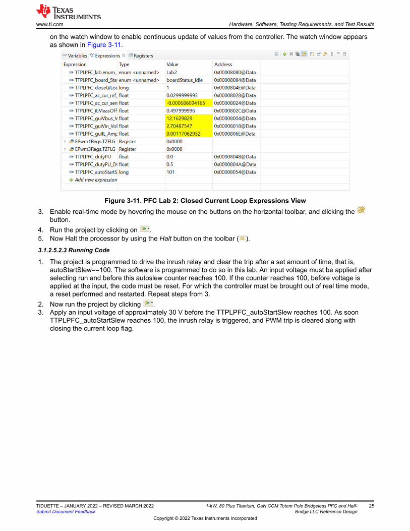
on the watch window to enable continuous update of values from the controller. The watch window appears as shown in Figure 3-11.
Figure 3-11. PFC Lab 2: Closed Current Loop Expressions View3. Enable real-time mode by hovering the mouse on the buttons on the horizontal toolbar, and clicking the
button.4. Run the project by clicking on .5. Now Halt the processor by using the Halt button on the toolbar ( ).
3.1.2.5.2.3 Running Code
1. The project is programmed to drive the inrush relay and clear the trip after a set amount of time, that is, autoStartSlew==100. The software is programmed to do so in this lab. An input voltage must be applied after selecting run and before this autoslew counter reaches 100. If the counter reaches 100, before voltage is applied at the input, the code must be reset. For which the controller must be brought out of real time mode, a reset performed and restarted. Repeat steps from 3.
2. Now run the project by clicking .3. Apply an input voltage of approximately 30 V before the TTPLPFC_autoStartSlew reaches 100. As soon
TTPLPFC_autoStartSlew reaches 100, the inrush relay is triggered, and PWM trip is cleared along with closing the current loop flag.
www.ti.com Hardware, Software, Testing Requirements, and Test Results
TIDUET7E – JANUARY 2022 – REVISED MARCH 2022Submit Document Feedback
1-kW, 80 Plus Titanium, GaN CCM Totem Pole Bridgeless PFC and Half-Bridge LLC Reference Design
25
Copyright © 2022 Texas Instruments Incorporated
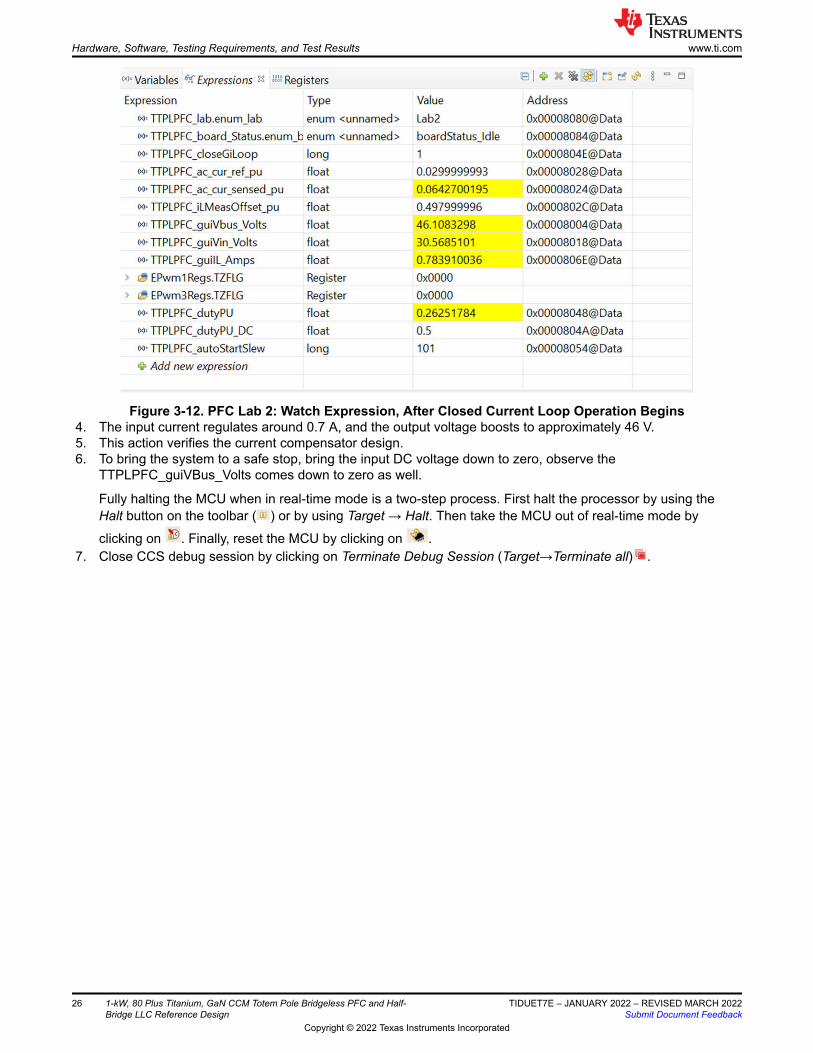
Figure 3-12. PFC Lab 2: Watch Expression, After Closed Current Loop Operation Begins4. The input current regulates around 0.7 A, and the output voltage boosts to approximately 46 V.5. This action verifies the current compensator design.6. To bring the system to a safe stop, bring the input DC voltage down to zero, observe the
TTPLPFC_guiVBus_Volts comes down to zero as well.
Fully halting the MCU when in real-time mode is a two-step process. First halt the processor by using the Halt button on the toolbar ( ) or by using Target → Halt. Then take the MCU out of real-time mode by
clicking on . Finally, reset the MCU by clicking on .7. Close CCS debug session by clicking on Terminate Debug Session (Target→Terminate all) .
Hardware, Software, Testing Requirements, and Test Results www.ti.com
26 1-kW, 80 Plus Titanium, GaN CCM Totem Pole Bridgeless PFC and Half-Bridge LLC Reference Design
TIDUET7E – JANUARY 2022 – REVISED MARCH 2022Submit Document Feedback
Copyright © 2022 Texas Instruments Incorporated
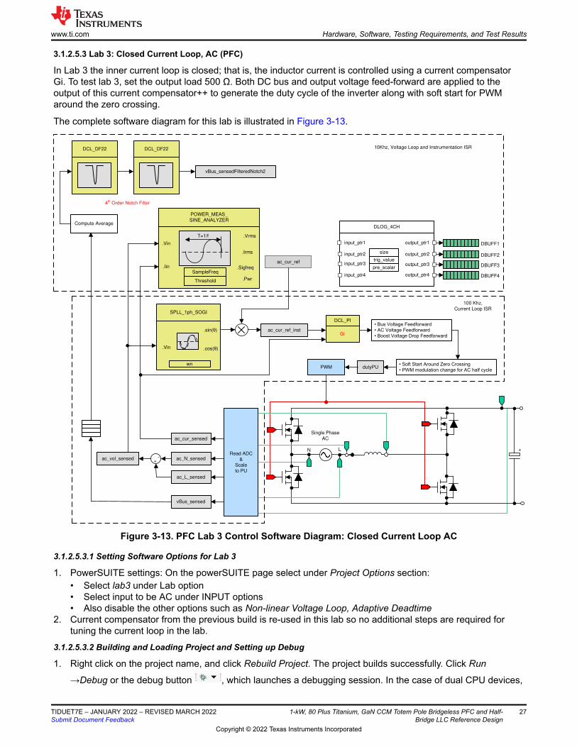
3.1.2.5.3 Lab 3: Closed Current Loop, AC (PFC)
In Lab 3 the inner current loop is closed; that is, the inductor current is controlled using a current compensator Gi. To test lab 3, set the output load 500 Ω. Both DC bus and output voltage feed-forward are applied to the output of this current compensator++ to generate the duty cycle of the inverter along with soft start for PWM around the zero crossing.
The complete software diagram for this lab is illustrated in Figure 3-13.
Single Phase
AC
LN +
PWM dutyPU
+-ac_vol_sensed
DCL_DF22 DCL_DF22
4th Order Notch Filter
.cos(�).Vin
SPLL_1ph_SOGI
wn
.sin(�)
.Vrms
.Vin
POWER_MEAS_
SINE_ANALYZER
SampleFreq
Threshold
.Sigfreq
T=1/f
.Iin
.Pwr
.Irms
Compute Average
vBus_sensedFilteredNotch2
ac_cur_ref
ac_cur_ref_inst
DCL_PI
Gi
��%XV�9ROWDJH�)HHGIRUZDUG
��$&�9ROWDJH�)HHGIRUZDUG
��%RRVW�9ROWDJH�'URS�)HHGIRUZDUG
��6RIW�6WDUW�$URXQG�=HUR�&URVVLQJ
��3:0�PRGXODWLRQ�FKDQJH�IRU�$&�KDOI�F\FOH
10Khz, Voltage Loop and Instrumentation ISR
100 Khz,
Current Loop ISR
DLOG_4CH
input_ptr1 output_ptr1
size
trig_value
pre_scalar
DBUFF1
output_ptr2 DBUFF2
output_ptr3 DBUFF3
output_ptr4 DBUFF4
input_ptr2
input_ptr3
input_ptr4
vBus_sensed
ac_L_sensed
ac_N_sensed
ac_cur_sensed
Read ADC
&
Scale
to PU
Figure 3-13. PFC Lab 3 Control Software Diagram: Closed Current Loop AC
3.1.2.5.3.1 Setting Software Options for Lab 3
1. PowerSUITE settings: On the powerSUITE page select under Project Options section:• Select lab3 under Lab option• Select input to be AC under INPUT options• Also disable the other options such as Non-linear Voltage Loop, Adaptive Deadtime
2. Current compensator from the previous build is re-used in this lab so no additional steps are required for tuning the current loop in the lab.
3.1.2.5.3.2 Building and Loading Project and Setting up Debug
1. Right click on the project name, and click Rebuild Project. The project builds successfully. Click Run
→Debug or the debug button , which launches a debugging session. In the case of dual CPU devices,
www.ti.com Hardware, Software, Testing Requirements, and Test Results
TIDUET7E – JANUARY 2022 – REVISED MARCH 2022Submit Document Feedback
1-kW, 80 Plus Titanium, GaN CCM Totem Pole Bridgeless PFC and Half-Bridge LLC Reference Design
27
Copyright © 2022 Texas Instruments Incorporated
a window may appear to select the CPU the debug must be performed. In this case, select CPU1. The project then loads on the device, and CCS debug view becomes active. The code halts at the start of the main routine.
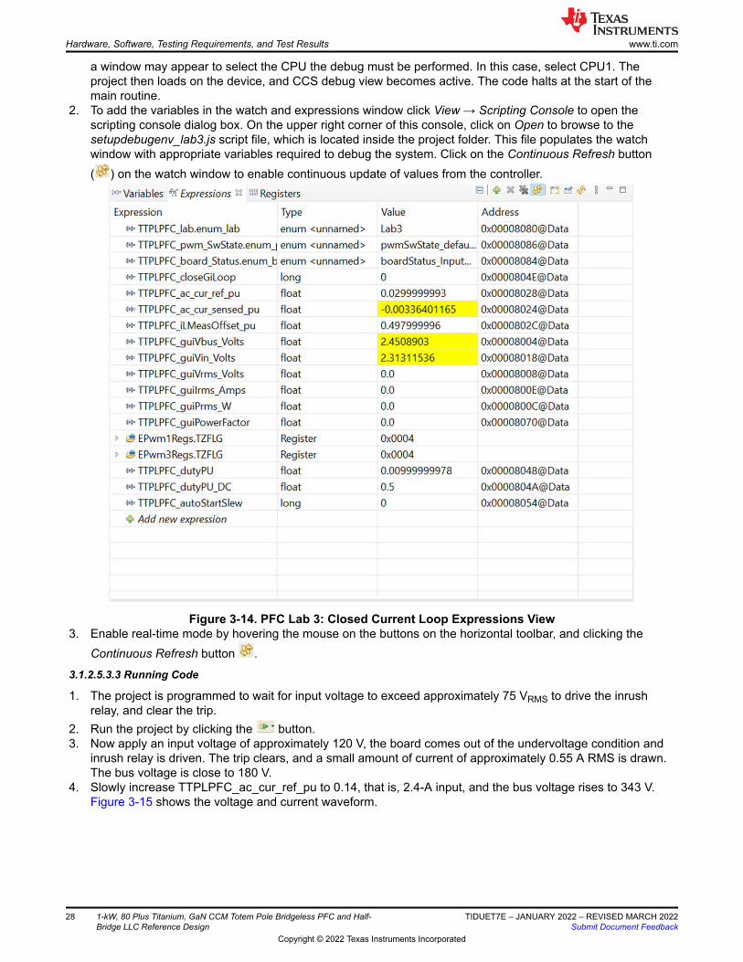
2. To add the variables in the watch and expressions window click View → Scripting Console to open the scripting console dialog box. On the upper right corner of this console, click on Open to browse to the setupdebugenv_lab3.js script file, which is located inside the project folder. This file populates the watch window with appropriate variables required to debug the system. Click on the Continuous Refresh button ( ) on the watch window to enable continuous update of values from the controller.
Figure 3-14. PFC Lab 3: Closed Current Loop Expressions View3. Enable real-time mode by hovering the mouse on the buttons on the horizontal toolbar, and clicking the
Continuous Refresh button .
3.1.2.5.3.3 Running Code
1. The project is programmed to wait for input voltage to exceed approximately 75 VRMS to drive the inrush relay, and clear the trip.
2. Run the project by clicking the button.3. Now apply an input voltage of approximately 120 V, the board comes out of the undervoltage condition and
inrush relay is driven. The trip clears, and a small amount of current of approximately 0.55 A RMS is drawn. The bus voltage is close to 180 V.
4. Slowly increase TTPLPFC_ac_cur_ref_pu to 0.14, that is, 2.4-A input, and the bus voltage rises to 343 V. Figure 3-15 shows the voltage and current waveform.
Hardware, Software, Testing Requirements, and Test Results www.ti.com
28 1-kW, 80 Plus Titanium, GaN CCM Totem Pole Bridgeless PFC and Half-Bridge LLC Reference Design
TIDUET7E – JANUARY 2022 – REVISED MARCH 2022Submit Document Feedback
Copyright © 2022 Texas Instruments Incorporated
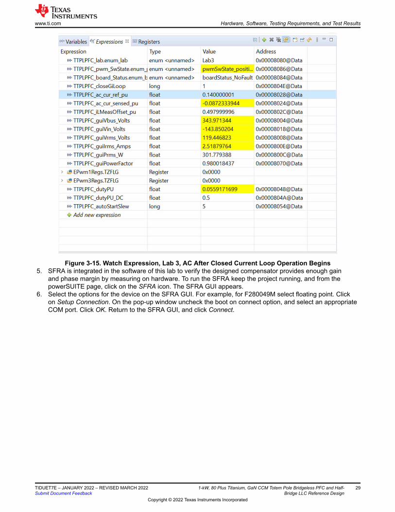
Figure 3-15. Watch Expression, Lab 3, AC After Closed Current Loop Operation Begins5. SFRA is integrated in the software of this lab to verify the designed compensator provides enough gain
and phase margin by measuring on hardware. To run the SFRA keep the project running, and from the powerSUITE page, click on the SFRA icon. The SFRA GUI appears.
6. Select the options for the device on the SFRA GUI. For example, for F280049M select floating point. Click on Setup Connection. On the pop-up window uncheck the boot on connect option, and select an appropriate COM port. Click OK. Return to the SFRA GUI, and click Connect.
www.ti.com Hardware, Software, Testing Requirements, and Test Results
TIDUET7E – JANUARY 2022 – REVISED MARCH 2022Submit Document Feedback
1-kW, 80 Plus Titanium, GaN CCM Totem Pole Bridgeless PFC and Half-Bridge LLC Reference Design
29
Copyright © 2022 Texas Instruments Incorporated
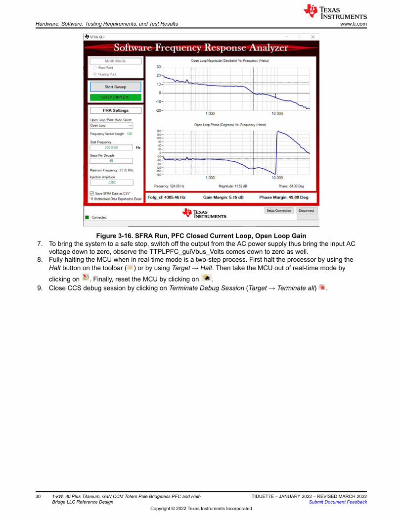
Figure 3-16. SFRA Run, PFC Closed Current Loop, Open Loop Gain7. To bring the system to a safe stop, switch off the output from the AC power supply thus bring the input AC
voltage down to zero, observe the TTPLPFC_guiVbus_Volts comes down to zero as well.8. Fully halting the MCU when in real-time mode is a two-step process. First halt the processor by using the
Halt button on the toolbar ( ) or by using Target → Halt. Then take the MCU out of real-time mode by
clicking on . Finally, reset the MCU by clicking on .9. Close CCS debug session by clicking on Terminate Debug Session (Target → Terminate all) .
Hardware, Software, Testing Requirements, and Test Results www.ti.com
30 1-kW, 80 Plus Titanium, GaN CCM Totem Pole Bridgeless PFC and Half-Bridge LLC Reference Design
TIDUET7E – JANUARY 2022 – REVISED MARCH 2022Submit Document Feedback
Copyright © 2022 Texas Instruments Incorporated
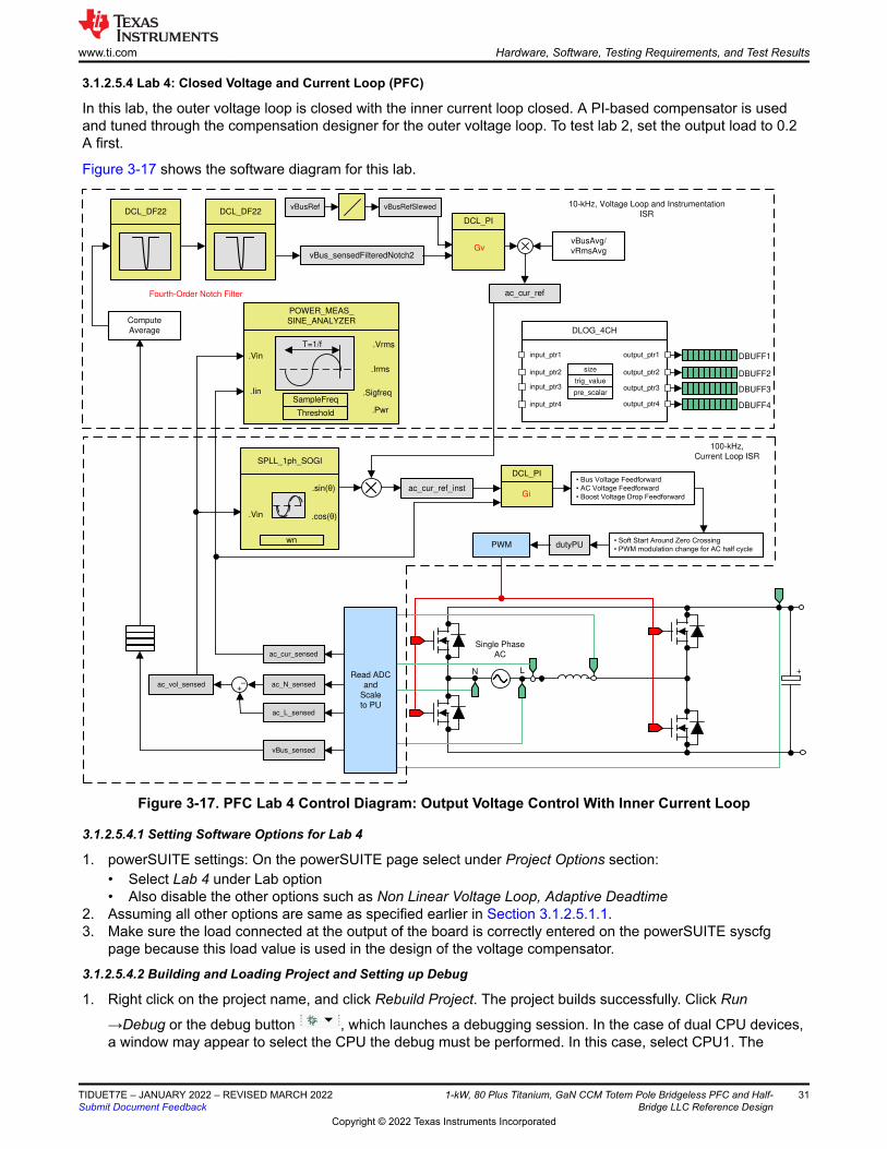
3.1.2.5.4 Lab 4: Closed Voltage and Current Loop (PFC)
In this lab, the outer voltage loop is closed with the inner current loop closed. A PI-based compensator is used and tuned through the compensation designer for the outer voltage loop. To test lab 2, set the output load to 0.2 A first.
Figure 3-17 shows the software diagram for this lab.
Single Phase
AC
LN +
PWM dutyPU
+±ac_vol_sensed
DCL_DF22 DCL_DF22
Fourth-Order Notch Filter
.cos(�).Vin
SPLL_1ph_SOGI
wn
.sin(�)
.Vrms
.Vin
POWER_MEAS_
SINE_ANALYZER
SampleFreq
Threshold
.Sigfreq
T=1/f
.Iin
.Pwr
.Irms
Compute
Average
vBus_sensedFilteredNotch2
ac_cur_ref
ac_cur_ref_inst
DCL_PI
Gi
��%XV�9ROWDJH�)HHGIRUZDUG
��$&�9ROWDJH�)HHGIRUZDUG
��%RRVW�9ROWDJH�'URS�)HHGIRUZDUG
DCL_PI
GvvBusAvg/
vRmsAvg
��6RIW�6WDUW�$URXQG�=HUR�&URVVLQJ
��3:0�PRGXODWLRQ�FKDQJH�IRU�$&�KDOI�F\FOH
10-kHz, Voltage Loop and Instrumentation
ISR
100-kHz,
Current Loop ISR
DLOG_4CH
input_ptr1 output_ptr1
size
trig_value
pre_scalar
DBUFF1
output_ptr2 DBUFF2
output_ptr3 DBUFF3
output_ptr4 DBUFF4
input_ptr2
input_ptr3
input_ptr4
vBus_sensed
ac_L_sensed
ac_N_sensed
ac_cur_sensed
Read ADC
and
Scale
to PU
vBusRef vBusRefSlewed
Figure 3-17. PFC Lab 4 Control Diagram: Output Voltage Control With Inner Current Loop
3.1.2.5.4.1 Setting Software Options for Lab 4
1. powerSUITE settings: On the powerSUITE page select under Project Options section:• Select Lab 4 under Lab option• Also disable the other options such as Non Linear Voltage Loop, Adaptive Deadtime
2. Assuming all other options are same as specified earlier in Section 3.1.2.5.1.1.3. Make sure the load connected at the output of the board is correctly entered on the powerSUITE syscfg
page because this load value is used in the design of the voltage compensator.
3.1.2.5.4.2 Building and Loading Project and Setting up Debug
1. Right click on the project name, and click Rebuild Project. The project builds successfully. Click Run
→Debug or the debug button , which launches a debugging session. In the case of dual CPU devices, a window may appear to select the CPU the debug must be performed. In this case, select CPU1. The
www.ti.com Hardware, Software, Testing Requirements, and Test Results
TIDUET7E – JANUARY 2022 – REVISED MARCH 2022Submit Document Feedback
1-kW, 80 Plus Titanium, GaN CCM Totem Pole Bridgeless PFC and Half-Bridge LLC Reference Design
31
Copyright © 2022 Texas Instruments Incorporated
project then loads on the device, and CCS debug view becomes active. The code halts at the start of the main routine.
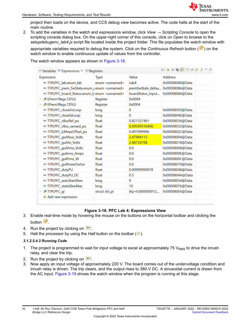
2. To add the variables in the watch and expressions window, click View → Scripting Console to open the scripting console dialog box. On the upper-right corner of this console, click on Open to browse to the setupdebugenv_lab4.js script file located inside the project folder. This file populates the watch window with appropriate variables required to debug the system. Click on the Continuous Refresh button ( ) on the watch window to enable continuous update of values from the controller.
The watch window appears as shown in Figure 3-18.
Figure 3-18. PFC Lab 4: Expressions View3. Enable real-time mode by hovering the mouse on the buttons on the horizontal toolbar and clicking the
button .4. Run the project by clicking on .5. Halt the processor by using the Halt button on the toolbar ( ).
3.1.2.5.4.3 Running Code
1. The project is programmed to wait for input voltage to excel at approximately 75 VRMS to drive the inrush relay, and clear the trip.
2. Run the project by clicking on .3. Now apply an input voltage of approximately 220 V. The board comes out of the undervoltage condition and
inrush relay is driven. The trip clears, and the output rises to 380-V DC. A sinusoidal current is drawn from the AC input. Figure 3-19 shows the watch window when the program is running at this stage.
Hardware, Software, Testing Requirements, and Test Results www.ti.com
32 1-kW, 80 Plus Titanium, GaN CCM Totem Pole Bridgeless PFC and Half-Bridge LLC Reference Design
TIDUET7E – JANUARY 2022 – REVISED MARCH 2022Submit Document Feedback
Copyright © 2022 Texas Instruments Incorporated
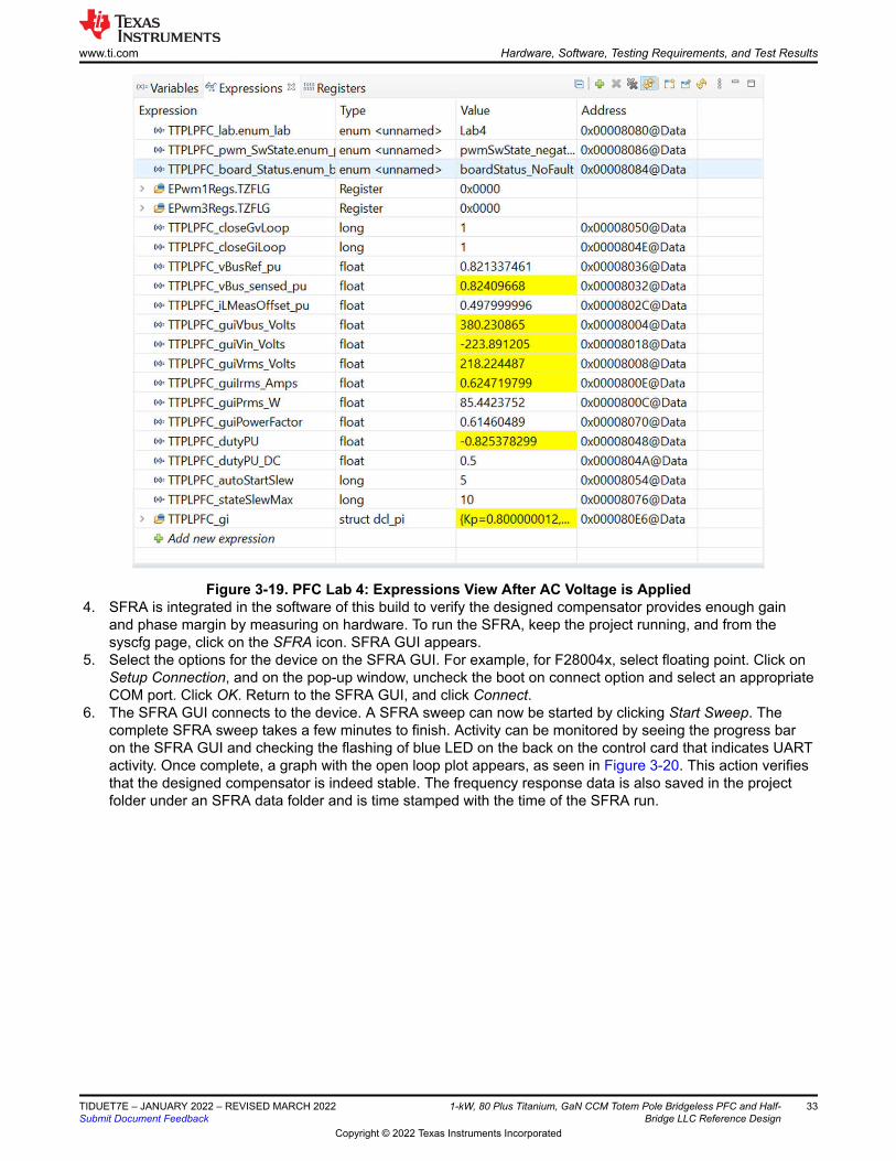
Figure 3-19. PFC Lab 4: Expressions View After AC Voltage is Applied4. SFRA is integrated in the software of this build to verify the designed compensator provides enough gain
and phase margin by measuring on hardware. To run the SFRA, keep the project running, and from the syscfg page, click on the SFRA icon. SFRA GUI appears.
5. Select the options for the device on the SFRA GUI. For example, for F28004x, select floating point. Click on Setup Connection, and on the pop-up window, uncheck the boot on connect option and select an appropriate COM port. Click OK. Return to the SFRA GUI, and click Connect.
6. The SFRA GUI connects to the device. A SFRA sweep can now be started by clicking Start Sweep. The complete SFRA sweep takes a few minutes to finish. Activity can be monitored by seeing the progress bar on the SFRA GUI and checking the flashing of blue LED on the back on the control card that indicates UART activity. Once complete, a graph with the open loop plot appears, as seen in Figure 3-20. This action verifies that the designed compensator is indeed stable. The frequency response data is also saved in the project folder under an SFRA data folder and is time stamped with the time of the SFRA run.
www.ti.com Hardware, Software, Testing Requirements, and Test Results
TIDUET7E – JANUARY 2022 – REVISED MARCH 2022Submit Document Feedback
1-kW, 80 Plus Titanium, GaN CCM Totem Pole Bridgeless PFC and Half-Bridge LLC Reference Design
33
Copyright © 2022 Texas Instruments Incorporated
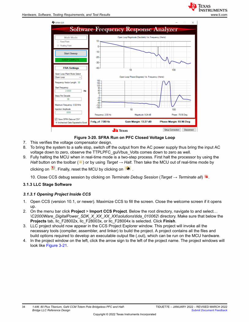
Figure 3-20. SFRA Run on PFC Closed Voltage Loop7. This verifies the voltage compensator design.8. To bring the system to a safe stop, switch off the output from the AC power supply thus bring the input AC
voltage down to zero, observe the TTPLPFC_guiVbus_Volts comes down to zero as well.9. Fully halting the MCU when in real-time mode is a two-step process. First halt the processor by using the
Halt button on the toolbar ( ) or by using Target → Halt. Then take the MCU out of real-time mode by
clicking on . Finally, reset the MCU by clicking on .
10. Close CCS debug session by clicking on Terminate Debug Session (Target → Terminate all) .
3.1.3 LLC Stage Software
3.1.3.1 Opening Project Inside CCS
1. Open CCS (version 10.1, or newer). Maximize CCS to fill the screen. Close the welcome screen if it opens up.
2. On the menu bar click Project > Import CCS Project. Below the root directory, navigate to and select…\C2000Ware_DigitalPower_SDK_X_XX_XX_XX\solutions\tida_010062\ directory. Make sure that below the Projects tab, llc_F28002x, llc_F28003x, or llc_F28004x is selected. Click Finish.
3. LLC project should now appear in the CCS Project Explorer window. This project will invoke all the necessary tools (compiler, assembler, and linker) to build the project. A project contains all the files and build options required to develop an executable output file (.out), which can be run on the MCU hardware.
4. In the project window on the left, click the arrow sign to the left of the project name. The project windows will look like Figure 3-21.
Hardware, Software, Testing Requirements, and Test Results www.ti.com
34 1-kW, 80 Plus Titanium, GaN CCM Totem Pole Bridgeless PFC and Half-Bridge LLC Reference Design
TIDUET7E – JANUARY 2022 – REVISED MARCH 2022Submit Document Feedback
Copyright © 2022 Texas Instruments Incorporated
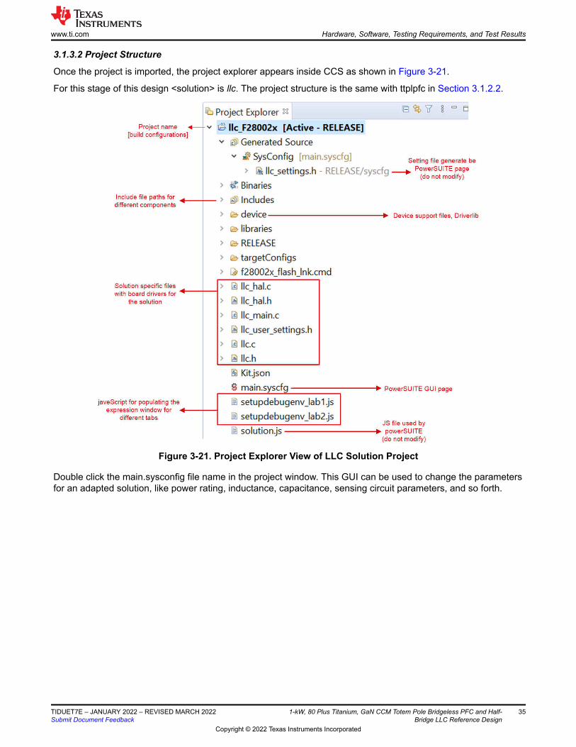
3.1.3.2 Project Structure
Once the project is imported, the project explorer appears inside CCS as shown in Figure 3-21.
For this stage of this design <solution> is llc. The project structure is the same with ttplpfc in Section 3.1.2.2.
Figure 3-21. Project Explorer View of LLC Solution Project
Double click the main.sysconfig file name in the project window. This GUI can be used to change the parameters for an adapted solution, like power rating, inductance, capacitance, sensing circuit parameters, and so forth.
www.ti.com Hardware, Software, Testing Requirements, and Test Results
TIDUET7E – JANUARY 2022 – REVISED MARCH 2022Submit Document Feedback
1-kW, 80 Plus Titanium, GaN CCM Totem Pole Bridgeless PFC and Half-Bridge LLC Reference Design
35
Copyright © 2022 Texas Instruments Incorporated

Figure 3-22. powerSUITE Page for LLC Stage
3.1.3.3 Software Flow
The software project makes use of the C-background and C-ISR framework. The project uses C background code as the main supporting program for the application, which is responsible for all system management tasks, decision making, intelligence, and host interaction. The C-ISR code is executed inside a time critical interrupt service routine (ISR), and runs all the critical control code. This code includes ADC reading, control calculations, and PWM updates. The Control ISR portion of the C-ISR is executed at a fixed rate of 50 kHz using a spare PWM module timer. Figure 3-23 shows the software flow diagram of the firmware.
Hardware, Software, Testing Requirements, and Test Results www.ti.com
36 1-kW, 80 Plus Titanium, GaN CCM Totem Pole Bridgeless PFC and Half-Bridge LLC Reference Design
TIDUET7E – JANUARY 2022 – REVISED MARCH 2022Submit Document Feedback
Copyright © 2022 Texas Instruments Incorporated
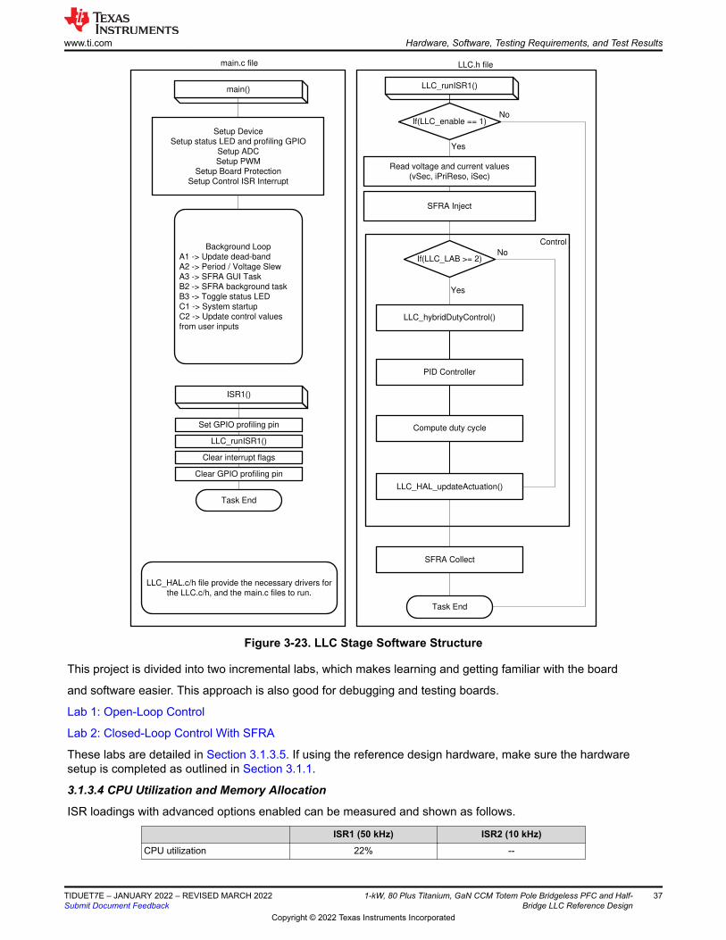
Setup Device
Setup status LED and profiling GPIO
Setup ADC
Setup PWM
Setup Board Protection
Setup Control ISR Interrupt
Background Loop
A1 -> Update dead-band
A2 -> Period / Voltage Slew
A3 -> SFRA GUI Task
B2 -> SFRA background task
B3 -> Toggle status LED
C1 -> System startup
C2 -> Update control values
from user inputs
ISR1()
Read voltage and current values
(vSec, iPriReso, iSec)
main.c file
Task End
LLC.h file
LLC_HAL.c/h file provide the necessary drivers for
the LLC.c/h, and the main.c files to run.
Task End
Set GPIO profiling pin
LLC_runISR1()
Clear interrupt flags
Clear GPIO profiling pin
LLC_runISR1()
SFRA Inject
LLC_hybridDutyControl()
If(LLC_LAB >= 2)
PID Controller
Yes
Compute duty cycle
LLC_HAL_updateActuation()
SFRA Collect
If(LLC_enable == 1)
Yes
No
No
main()
Control
Figure 3-23. LLC Stage Software Structure
This project is divided into two incremental labs, which makes learning and getting familiar with the board
and software easier. This approach is also good for debugging and testing boards.
Lab 1: Open-Loop Control
Lab 2: Closed-Loop Control With SFRA
These labs are detailed in Section 3.1.3.5. If using the reference design hardware, make sure the hardware setup is completed as outlined in Section 3.1.1.
3.1.3.4 CPU Utilization and Memory Allocation
ISR loadings with advanced options enabled can be measured and shown as follows.
ISR1 (50 kHz) ISR2 (10 kHz)CPU utilization 22% --
www.ti.com Hardware, Software, Testing Requirements, and Test Results
TIDUET7E – JANUARY 2022 – REVISED MARCH 2022Submit Document Feedback
1-kW, 80 Plus Titanium, GaN CCM Totem Pole Bridgeless PFC and Half-Bridge LLC Reference Design
37
Copyright © 2022 Texas Instruments Incorporated
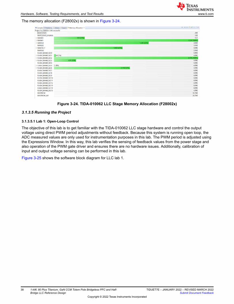
The memory allocation (F28002x) is shown in Figure 3-24.
Figure 3-24. TIDA-010062 LLC Stage Memory Allocation (F28002x)
3.1.3.5 Running the Project
3.1.3.5.1 Lab 1: Open-Loop Control
The objective of this lab is to get familiar with the TIDA-010062 LLC stage hardware and control the output voltage using direct PWM period adjustments without feedback. Because this system is running open loop, the ADC measured values are only used for instrumentation purposes in this lab. The PWM period is adjusted using the Expressions Window. In this way, this lab verifies the sensing of feedback values from the power stage and also operation of the PWM gate driver and ensures there are no hardware issues. Additionally, calibration of input and output voltage sensing can be performed in this lab.
Figure 3-25 shows the software block diagram for LLC lab 1.
Hardware, Software, Testing Requirements, and Test Results www.ti.com
38 1-kW, 80 Plus Titanium, GaN CCM Totem Pole Bridgeless PFC and Half-Bridge LLC Reference Design
TIDUET7E – JANUARY 2022 – REVISED MARCH 2022Submit Document Feedback
Copyright © 2022 Texas Instruments Incorporated
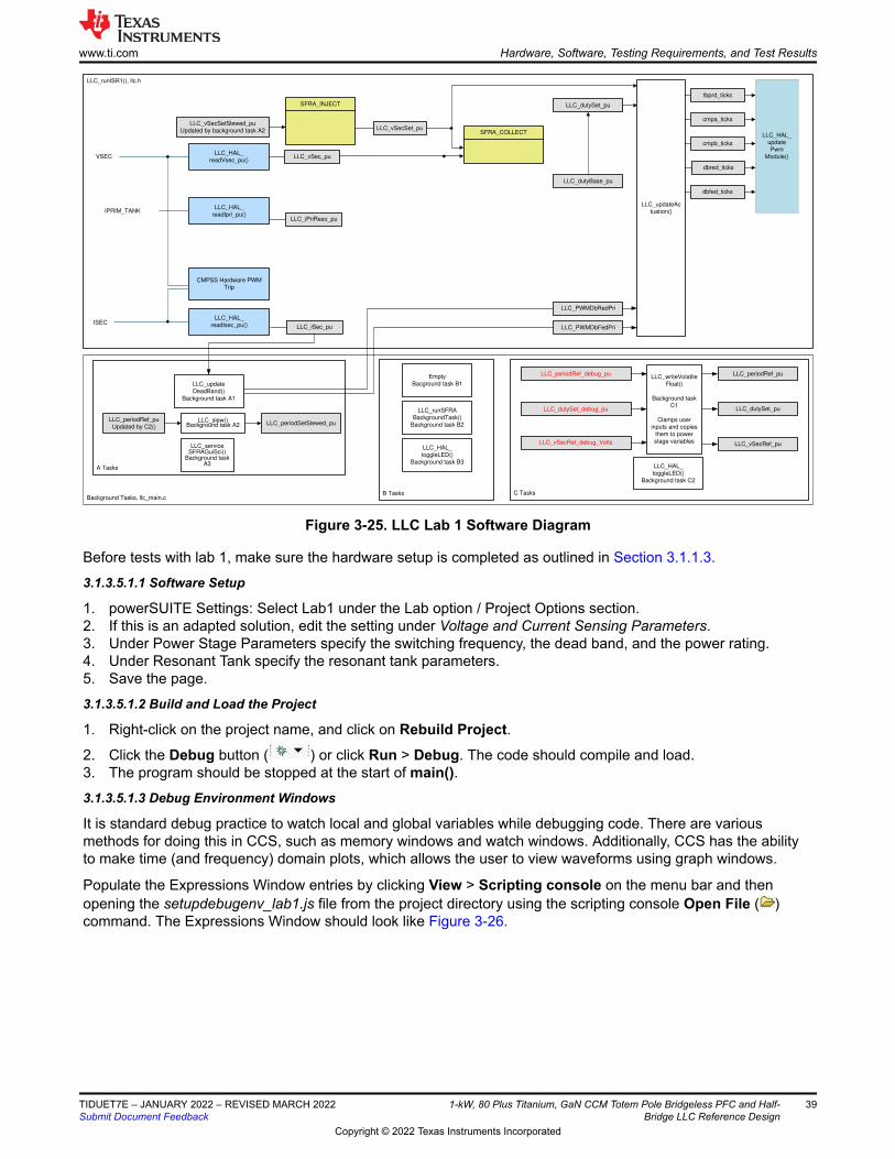
Background Tasks, llc_main.cC TasksB Tasks
A Tasks
LLC_runISR1(), llc.h
LLC_vSec_pu
SFRA_COLLECT
SFRA_INJECT
LLC_vSecSetSlewed_pu
Updated by background task A2
LLC_HAL_
readVsec_pu()
LLC_HAL_
readIsec_pu()
LLC_HAL_
readIpri_pu()IPRIM_TANK
VSEC
ISECLLC_iSec_pu
LLC_iPriReso_pu
LLC_vSecSet_puLLC_HAL_
update
Pwm
Module()
LLC_dutySet_pu
LLC_PWMDbRedPri
LLC_PWMDbFedPri
tbprd_ticks
cmpa_ticks
cmpb_ticks
dbred_ticks
dbfed_ticks
LLC_update
DeadBand()
Background task A1
LLC_periodRef_pu
Updated by C2()
CMPSS Hardware PWM
Trip
LLC_periodRef_debug_pu LLC_periodRef_pu
LLC_dutySet_debug_pu
LLC_vSecRef_debug_Volts
LLC_writeVolatile
Float()
Background task
C1
Clamps user
inputs and copies
them to power
stage variables
LLC_dutyBase_pu
LLC_updateAc
tuation()
LLC_slew()Background task A2 LLC_periodSetSlewed_pu
LLC_runSFRA
BackgroundTask()
Background task B2
LLC_HAL_
toggleLED()
Background task B3
LLC_serviceSFRAGuiSci()
Background task A3 LLC_HAL_
toggleLED()
Background task C2
Empty
Bacground task B1
LLC_dutySet_pu
LLC_vSecRef_pu
Figure 3-25. LLC Lab 1 Software Diagram
Before tests with lab 1, make sure the hardware setup is completed as outlined in Section 3.1.1.3.
3.1.3.5.1.1 Software Setup
1. powerSUITE Settings: Select Lab1 under the Lab option / Project Options section.2. If this is an adapted solution, edit the setting under Voltage and Current Sensing Parameters.3. Under Power Stage Parameters specify the switching frequency, the dead band, and the power rating.4. Under Resonant Tank specify the resonant tank parameters.5. Save the page.
3.1.3.5.1.2 Build and Load the Project
1. Right-click on the project name, and click on Rebuild Project.2. Click the Debug button ( ) or click Run > Debug. The code should compile and load.3. The program should be stopped at the start of main().3.1.3.5.1.3 Debug Environment Windows
It is standard debug practice to watch local and global variables while debugging code. There are various methods for doing this in CCS, such as memory windows and watch windows. Additionally, CCS has the ability to make time (and frequency) domain plots, which allows the user to view waveforms using graph windows.
Populate the Expressions Window entries by clicking View > Scripting console on the menu bar and then opening the setupdebugenv_lab1.js file from the project directory using the scripting console Open File ( ) command. The Expressions Window should look like Figure 3-26.
www.ti.com Hardware, Software, Testing Requirements, and Test Results
TIDUET7E – JANUARY 2022 – REVISED MARCH 2022Submit Document Feedback
1-kW, 80 Plus Titanium, GaN CCM Totem Pole Bridgeless PFC and Half-Bridge LLC Reference Design
39
Copyright © 2022 Texas Instruments Incorporated

Figure 3-26. LLC Lab 1 Expressions View
Table 3-3. LLC Lab 1 Description of Expressions Window EntriesVARIABLE DESCRIPTIONLLC_buildLevel Shows which lab is loaded.
LLC_board_Status Show the board status: Fault types or normal operation
LLC_startFlag Set this variable to 1 to start the powerstage.
LLC_vSec_Volts Output voltage in Volts.
LLC_iPriReso_Amps The primary tank current in Amps.
LLC_iSec_Amps Secondary (output) current in Amps.
LLC_periodRef_debug_pu The variable used to control the switching period in lab 1. It is in per unit format.
LLC_dutySet_debug_pu The variable used to control the switching duty It is in per unit format.
EPwm1Regs.CMPA.CMPA Compare A register in ePWM1.
EPwm1Regs.CMPB.CMPB Compare B register in ePWM1.
EPwm1Regs.TBPRD Time-based period register in ePWM1.
EPwm2Regs.CMPA.CMPA Compare A register in ePWM2.
EPwm2Regs.CMPB.CMPB Compare B register in ePWM2.
EPwm2Regs.TBPRD Time-based period register in ePWM2.
EPwm1Regs.TZFLG TZ flag of ePWM1. For debugging protection use.
EPwm2Regs.TZFLG TZ flag of ePWM2. For debugging protection use.
3.1.3.5.1.4 Run the Code
1. Run the code by using the <F8> key or the Run button ( ) on the toolbar2. As this is an open-loop test (no voltage loop), care must be taken not to use too small a load to avoid
accidental high output voltages. Use a load of 10 A at the 12-V output.3. In the Expressions Window set LLC_startFlag = 1. The converter operation should start with the default
LLC_periodSet_pu value resulting in approximately 250-kHz switching frequency.4. The LLC_periodRef_debug_pu value may be changed between 0.55 and 0.65. As this value is increased
the switching frequency decreases, which results in a higher energy delivered to the load. In open loop this results in an increase in output voltage, which should not be allowed to exceed board capabilities.
5. Set input voltage: increase DC source output from 0 V to 380 V. Verify that all of the sensed values are updating in the expressions window: LLC_vSec_Volts, LLC_iPriReso_Amps, LLC_iSec_Amps.
Hardware, Software, Testing Requirements, and Test Results www.ti.com
40 1-kW, 80 Plus Titanium, GaN CCM Totem Pole Bridgeless PFC and Half-Bridge LLC Reference Design
TIDUET7E – JANUARY 2022 – REVISED MARCH 2022Submit Document Feedback
Copyright © 2022 Texas Instruments Incorporated
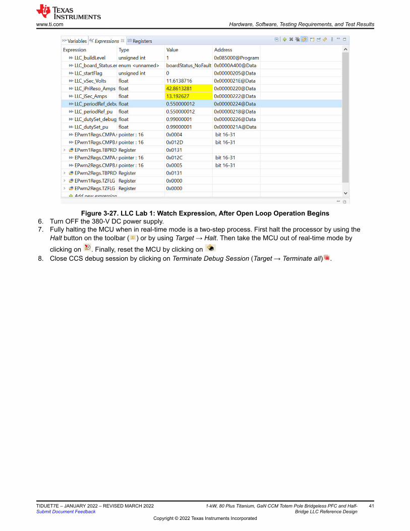
Figure 3-27. LLC Lab 1: Watch Expression, After Open Loop Operation Begins6. Turn OFF the 380-V DC power supply.7. Fully halting the MCU when in real-time mode is a two-step process. First halt the processor by using the
Halt button on the toolbar ( ) or by using Target → Halt. Then take the MCU out of real-time mode by
clicking on . Finally, reset the MCU by clicking on 8. Close CCS debug session by clicking on Terminate Debug Session (Target → Terminate all) .
www.ti.com Hardware, Software, Testing Requirements, and Test Results
TIDUET7E – JANUARY 2022 – REVISED MARCH 2022Submit Document Feedback
1-kW, 80 Plus Titanium, GaN CCM Totem Pole Bridgeless PFC and Half-Bridge LLC Reference Design
41
Copyright © 2022 Texas Instruments Incorporated
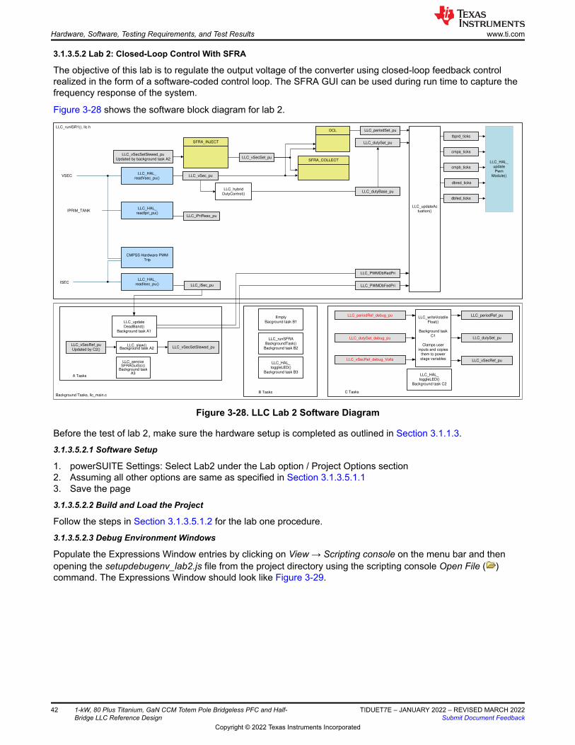
3.1.3.5.2 Lab 2: Closed-Loop Control With SFRA
The objective of this lab is to regulate the output voltage of the converter using closed-loop feedback control realized in the form of a software-coded control loop. The SFRA GUI can be used during run time to capture the frequency response of the system.
Figure 3-28 shows the software block diagram for lab 2.
Background Tasks, llc_main.c C Tasks B Tasks
A Tasks
LLC_runISR1(), llc.h
LLC_vSec_pu
SFRA_COLLECT
SFRA_INJECT
LLC_vSecSetSlewed_pu
Updated by background task A2
LLC_HAL_
readVsec_pu()
LLC_HAL_
readIsec_pu()
LLC_HAL_
readIpri_pu()IPRIM_TANK
VSEC
ISECLLC_iSec_pu
LLC_iPriReso_pu
LLC_vSecSet_puLLC_HAL_
update
Pwm
Module()
LLC_dutySet_pu
LLC_PWMDbRedPri
LLC_PWMDbFedPri
tbprd_ticks
cmpa_ticks
cmpb_ticks
dbred_ticks
dbfed_ticks
LLC_update
DeadBand()
Background task A1
LLC_vSecRef_pu
Updated by C2()
CMPSS Hardware PWM
Trip
LLC_periodRef_debug_pu LLC_periodRef_pu
LLC_dutySet_debug_pu
LLC_vSecRef_debug_Volts
LLC_writeVolatile
Float()
Background task
C1
Clamps user
inputs and copies
them to power
stage variables
DCL LLC_periodSet_pu
LLC_hybrid
DutyControl()LLC_dutyBase_pu
LLC_updateAc
tuation()
LLC_slew()Background task A2 LLC_vSecSetSlewed_pu
LLC_runSFRA
BackgroundTask()
Background task B2
LLC_HAL_
toggleLED()
Background task B3
LLC_serviceSFRAGuiSci()
Background task A3 LLC_HAL_
toggleLED()
Background task C2
Empty
Bacground task B1
LLC_dutySet_pu
LLC_vSecRef_pu
Figure 3-28. LLC Lab 2 Software Diagram
Before the test of lab 2, make sure the hardware setup is completed as outlined in Section 3.1.1.3.
3.1.3.5.2.1 Software Setup
1. powerSUITE Settings: Select Lab2 under the Lab option / Project Options section2. Assuming all other options are same as specified in Section 3.1.3.5.1.13. Save the page
3.1.3.5.2.2 Build and Load the Project
Follow the steps in Section 3.1.3.5.1.2 for the lab one procedure.
3.1.3.5.2.3 Debug Environment Windows
Populate the Expressions Window entries by clicking on View → Scripting console on the menu bar and then opening the setupdebugenv_lab2.js file from the project directory using the scripting console Open File ( ) command. The Expressions Window should look like Figure 3-29.
Hardware, Software, Testing Requirements, and Test Results www.ti.com
42 1-kW, 80 Plus Titanium, GaN CCM Totem Pole Bridgeless PFC and Half-Bridge LLC Reference Design
TIDUET7E – JANUARY 2022 – REVISED MARCH 2022Submit Document Feedback
Copyright © 2022 Texas Instruments Incorporated
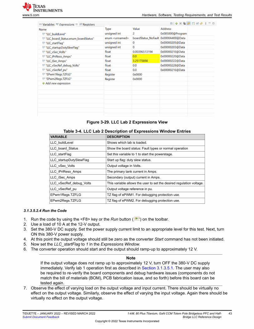
Figure 3-29. LLC Lab 2 Expressions View
Table 3-4. LLC Lab 2 Description of Expressions Window EntriesVARIABLE DESCRIPTIONLLC_buildLevel Shows which lab is loaded.
LLC_board_Status Show the board status: Fault types or normal operation
LLC_startFlag Set this variable to 1 to start the powerstage.
LLC_startupDutySlewFlag Start up flag: duty slew status.
LLC_vSec_Volts Output voltage in Volts.
LLC_iPriReso_Amps The primary tank current in Amps.
LLC_iSec_Amps Secondary (output) current in Amps.
LLC_vSecRef_debug_Volts This variable allows the user to set the desired regulation voltage.
LLC_vSecRef_pu Output voltage reference in pu.
EPwm1Regs.TZFLG TZ flag of ePWM1. For debugging protection use.
EPwm2Regs.TZFLG TZ flag of ePWM2. For debugging protection use.
3.1.3.5.2.4 Run the Code
1. Run the code by using the <F8> key or the Run button ( ) on the toolbar.2. Use a load of 10 A at the 12-V output.3. Set the 380-V DC supply. Set the power supply current limit to an appropriate level for this test. Next, turn
ON this 380-V power supply.4. At this point the output voltage should still be zero as the converter Start command has not been initiated.5. Now set the LLC_startFlag to 1 in the Expressions Window.6. The converter operation should start and the output should ramp-up to approximately 12 V.
NoteIf the output voltage does not ramp up to approximately 12 V, turn OFF the 380-V DC supply immediately. Verify lab 1 operation first as described in Section 3.1.3.5.1. The user may also be required to re-verify the board components and debug hardware issues (components do not match the bill of materials (BOM), PCB fabrication issue, and so forth) before this board can be tested again.
7. Observe the effect of varying load on the output voltage and input current. There should be virtually no effect on the output voltage. Similarly, observe the effect of varying the input voltage. Again there should be virtually no effect on the output voltage.
www.ti.com Hardware, Software, Testing Requirements, and Test Results
TIDUET7E – JANUARY 2022 – REVISED MARCH 2022Submit Document Feedback
1-kW, 80 Plus Titanium, GaN CCM Totem Pole Bridgeless PFC and Half-Bridge LLC Reference Design
43
Copyright © 2022 Texas Instruments Incorporated
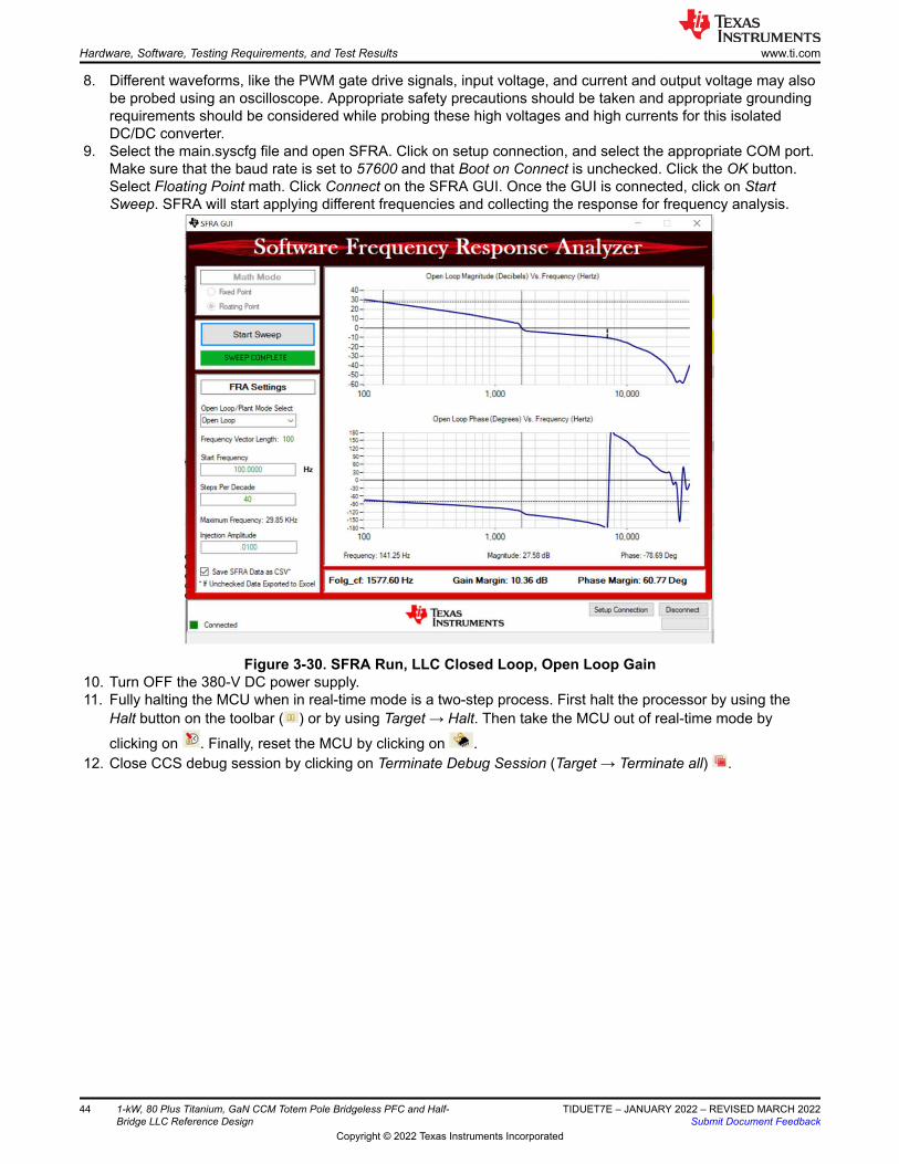
8. Different waveforms, like the PWM gate drive signals, input voltage, and current and output voltage may also be probed using an oscilloscope. Appropriate safety precautions should be taken and appropriate grounding requirements should be considered while probing these high voltages and high currents for this isolated DC/DC converter.
9. Select the main.syscfg file and open SFRA. Click on setup connection, and select the appropriate COM port. Make sure that the baud rate is set to 57600 and that Boot on Connect is unchecked. Click the OK button. Select Floating Point math. Click Connect on the SFRA GUI. Once the GUI is connected, click on Start Sweep. SFRA will start applying different frequencies and collecting the response for frequency analysis.
Figure 3-30. SFRA Run, LLC Closed Loop, Open Loop Gain10. Turn OFF the 380-V DC power supply.11. Fully halting the MCU when in real-time mode is a two-step process. First halt the processor by using the
Halt button on the toolbar ( ) or by using Target → Halt. Then take the MCU out of real-time mode by
clicking on . Finally, reset the MCU by clicking on .12. Close CCS debug session by clicking on Terminate Debug Session (Target → Terminate all) .
Hardware, Software, Testing Requirements, and Test Results www.ti.com
44 1-kW, 80 Plus Titanium, GaN CCM Totem Pole Bridgeless PFC and Half-Bridge LLC Reference Design
TIDUET7E – JANUARY 2022 – REVISED MARCH 2022Submit Document Feedback
Copyright © 2022 Texas Instruments Incorporated
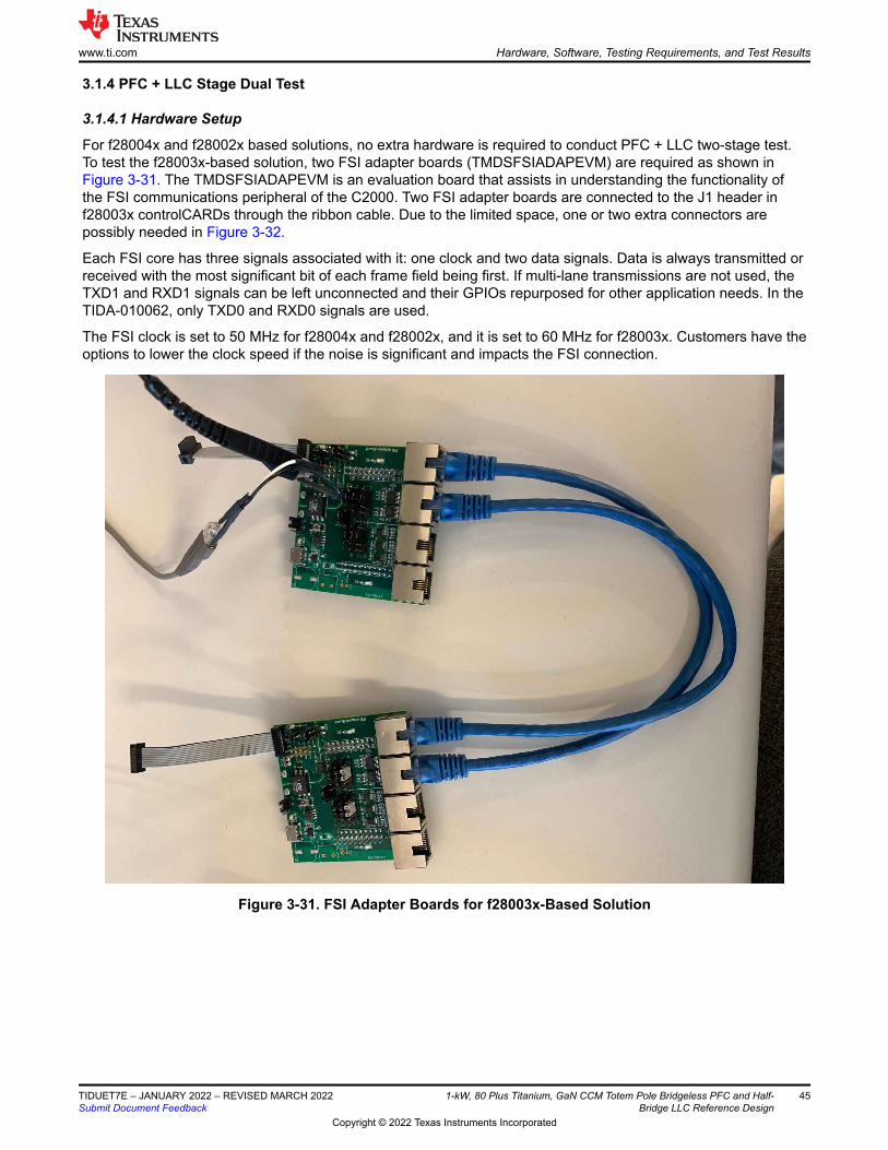
3.1.4 PFC + LLC Stage Dual Test
3.1.4.1 Hardware Setup
For f28004x and f28002x based solutions, no extra hardware is required to conduct PFC + LLC two-stage test. To test the f28003x-based solution, two FSI adapter boards (TMDSFSIADAPEVM) are required as shown in Figure 3-31. The TMDSFSIADAPEVM is an evaluation board that assists in understanding the functionality of the FSI communications peripheral of the C2000. Two FSI adapter boards are connected to the J1 header in f28003x controlCARDs through the ribbon cable. Due to the limited space, one or two extra connectors are possibly needed in Figure 3-32.
Each FSI core has three signals associated with it: one clock and two data signals. Data is always transmitted or received with the most significant bit of each frame field being first. If multi-lane transmissions are not used, the TXD1 and RXD1 signals can be left unconnected and their GPIOs repurposed for other application needs. In the TIDA-010062, only TXD0 and RXD0 signals are used.
The FSI clock is set to 50 MHz for f28004x and f28002x, and it is set to 60 MHz for f28003x. Customers have the options to lower the clock speed if the noise is significant and impacts the FSI connection.
Figure 3-31. FSI Adapter Boards for f28003x-Based Solution
www.ti.com Hardware, Software, Testing Requirements, and Test Results
TIDUET7E – JANUARY 2022 – REVISED MARCH 2022Submit Document Feedback
1-kW, 80 Plus Titanium, GaN CCM Totem Pole Bridgeless PFC and Half-Bridge LLC Reference Design
45
Copyright © 2022 Texas Instruments Incorporated
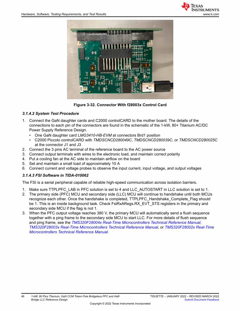
Figure 3-32. Connector With f28003x Control Card
3.1.4.2 System Test Procedure
1. Connect the GaN daughter cards and C2000 controlCARD to the mother board. The details of the connections to each pin of the connectors are found in the schematic of the 1-kW, 80+ Titanium AC/DC Power Supply Reference Design.• One GaN daughter card LMG3410-HB-EVM at connectors Brd1 position• C2000 Piccolo controlCARD with TMDSCNCD280049C, TMDSCNCD280039C, or TMDSCNCD280025C
at the connector J1 and J32. Connect the 3 pins AC terminal of the reference board to the AC power source3. Connect output terminals with wires to the electronic load, and maintain correct polarity4. Put a cooling fan at the AC side to maintain airflow on the board5. Set and maintain a small load of approximately 10 A6. Connect current and voltage probes to observe the input current, input voltage, and output voltages
3.1.4.3 FSI Software in TIDA-010062
The FSI is a serial peripheral capable of reliable high-speed communication across isolation barriers.
1. Make sure TTPLPFC_LAB in PFC solution is set to 4 and LLC_AUTOSTART in LLC solution is set to 1.2. The primary side (PFC) MCU and secondary side (LLC) MCU will continue to handshake until both MCUs
recognize each other. Once the handshake is completed, TTPLPFC_Handshake_Complete_Flag should be 1. This is an inside background task. Check FsiRxARegs.RX_EVT_STS registers in the primary and secondary side MCU if the flag is not 1.
3. When the PFC output voltage reaches 380 V, the primary MCU will automatically send a flush sequence together with a ping frame to the secondary side MCU to start LLC. For more details of flush sequence and ping frame, see the TMS320F28004x Real-Time Microcontrollers Technical Reference Manual, TMS320F28003x Real-Time Microcontrollers Technical Reference Manual, or TMS320F28002x Real-Time Microcontrollers Technical Reference Manual.
Hardware, Software, Testing Requirements, and Test Results www.ti.com
46 1-kW, 80 Plus Titanium, GaN CCM Totem Pole Bridgeless PFC and Half-Bridge LLC Reference Design
TIDUET7E – JANUARY 2022 – REVISED MARCH 2022Submit Document Feedback
Copyright © 2022 Texas Instruments Incorporated
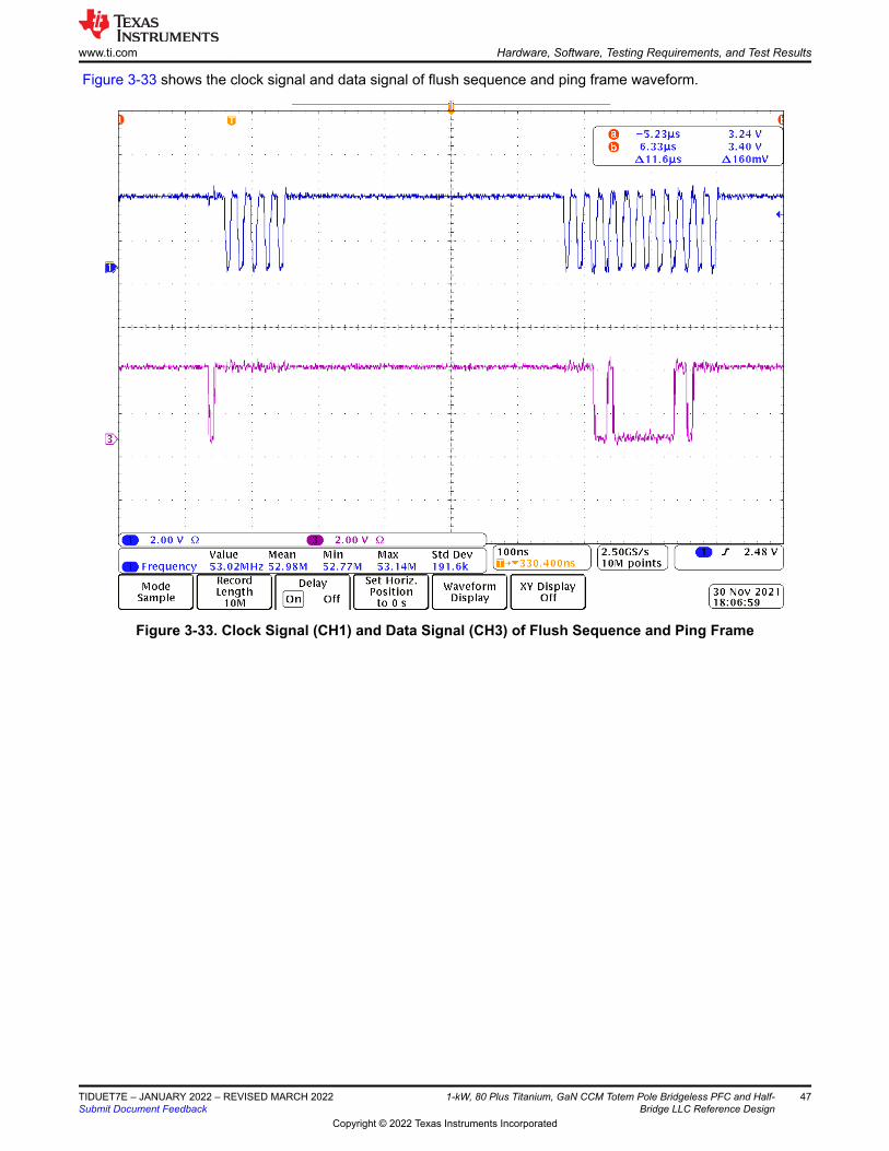
Figure 3-33 shows the clock signal and data signal of flush sequence and ping frame waveform.
Figure 3-33. Clock Signal (CH1) and Data Signal (CH3) of Flush Sequence and Ping Frame
www.ti.com Hardware, Software, Testing Requirements, and Test Results
TIDUET7E – JANUARY 2022 – REVISED MARCH 2022Submit Document Feedback
1-kW, 80 Plus Titanium, GaN CCM Totem Pole Bridgeless PFC and Half-Bridge LLC Reference Design
47
Copyright © 2022 Texas Instruments Incorporated
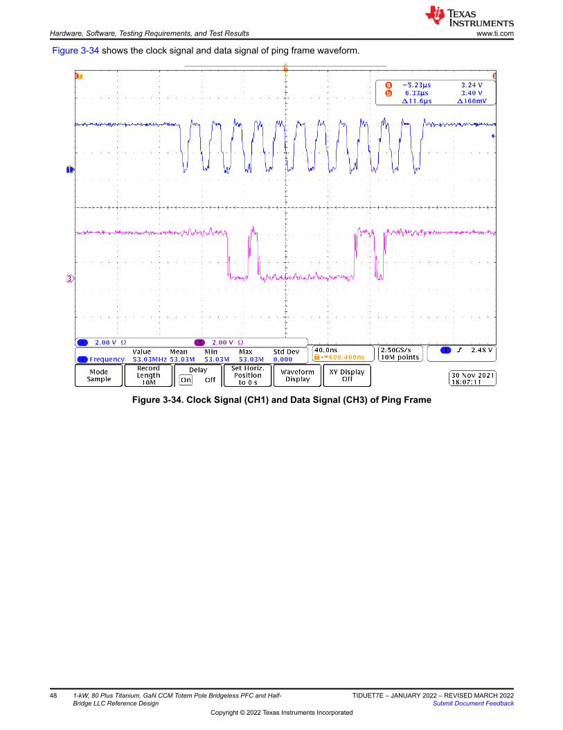
Figure 3-34 shows the clock signal and data signal of ping frame waveform.
Figure 3-34. Clock Signal (CH1) and Data Signal (CH3) of Ping Frame
Hardware, Software, Testing Requirements, and Test Results www.ti.com
48 1-kW, 80 Plus Titanium, GaN CCM Totem Pole Bridgeless PFC and Half-Bridge LLC Reference Design
TIDUET7E – JANUARY 2022 – REVISED MARCH 2022Submit Document Feedback
Copyright © 2022 Texas Instruments Incorporated
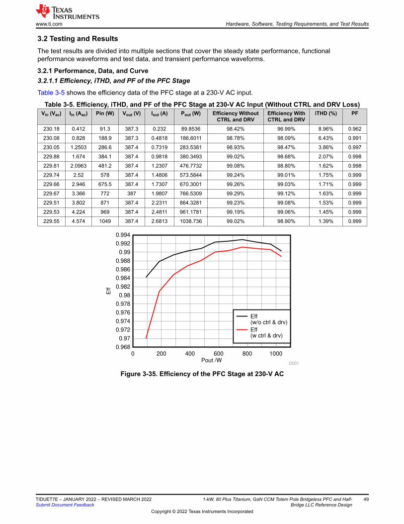
3.2 Testing and ResultsThe test results are divided into multiple sections that cover the steady state performance, functional performance waveforms and test data, and transient performance waveforms.
3.2.1 Performance, Data, and Curve3.2.1.1 Efficiency, iTHD, and PF of the PFC Stage
Table 3-5 shows the efficiency data of the PFC stage at a 230-V AC input.
Table 3-5. Efficiency, iTHD, and PF of the PFC Stage at 230-V AC Input (Without CTRL and DRV Loss)Vin (Vac) Iin (Aac) Pin (W) Vout (V) Iout (A) Pout (W) Efficiency Without
CTRL and DRVEfficiency With CTRL and DRV
iTHD (%) PF
230.18 0.412 91.3 387.3 0.232 89.8536 98.42% 96.99% 8.96% 0.962
230.08 0.828 188.9 387.3 0.4818 186.6011 98.78% 98.09% 6.43% 0.991
230.05 1.2503 286.6 387.4 0.7319 283.5381 98.93% 98.47% 3.86% 0.997
229.88 1.674 384.1 387.4 0.9818 380.3493 99.02% 98.68% 2.07% 0.998
229.81 2.0963 481.2 387.4 1.2307 476.7732 99.08% 98.80% 1.62% 0.998
229.74 2.52 578 387.4 1.4806 573.5844 99.24% 99.01% 1.75% 0.999
229.66 2.946 675.5 387.4 1.7307 670.3001 99.26% 99.03% 1.71% 0.999
229.67 3.366 772 387 1.9807 766.5309 99.29% 99.12% 1.63% 0.999
229.51 3.802 871 387.4 2.2311 864.3281 99.23% 99.08% 1.53% 0.999
229.53 4.224 969 387.4 2.4811 961.1781 99.19% 99.06% 1.45% 0.999
229.55 4.574 1049 387.4 2.6813 1038.736 99.02% 98.90% 1.39% 0.999
Pout /W
Eff
0 200 400 600 800 10000.968
0.97
0.972
0.974
0.976
0.978
0.98
0.982
0.984
0.986
0.988
0.99
0.992
0.994
D001
Eff (w/o ctrl & drv)
Eff (w ctrl & drv)
Figure 3-35. Efficiency of the PFC Stage at 230-V AC
www.ti.com Hardware, Software, Testing Requirements, and Test Results
TIDUET7E – JANUARY 2022 – REVISED MARCH 2022Submit Document Feedback
1-kW, 80 Plus Titanium, GaN CCM Totem Pole Bridgeless PFC and Half-Bridge LLC Reference Design
49
Copyright © 2022 Texas Instruments Incorporated
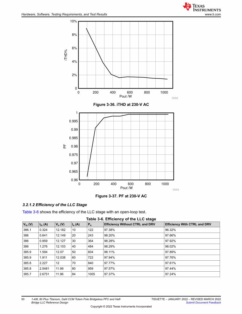
Pout /W
iTH
D%
0 200 400 600 800 1000
0
2%
4%
6%
8%
10%
D002
Figure 3-36. iTHD at 230-V AC
Pout /W
PF
0 200 400 600 800 1000
0.96
0.965
0.97
0.975
0.98
0.985
0.99
0.995
1
D003
Figure 3-37. PF at 230-V AC
3.2.1.2 Efficiency of the LLC Stage
Table 3-6 shows the efficiency of the LLC stage with an open-loop test.
Table 3-6. Efficiency of the LLC stageVin (V) Iin (A) Vo (V) Io (A) Po Efficiency Without CTRL and DRV Efficiency With CTRL and DRV386.1 0.324 12.182 10 122 97.38% 96.32%
386 0.641 12.149 20 243 98.20% 97.66%
386 0.959 12.127 30 364 98.28% 97.92%
386 1.276 12.103 40 484 98.29% 98.02%
385.9 1.594 12.07 50 604 98.11% 97.89%
385.9 1.911 12.038 60 722 97.94% 97.76%
385.8 2.227 12 70 840 97.77% 97.61%
385.8 2.5481 11.99 80 959 97.57% 97.44%
385.7 2.6751 11.96 84 1005 97.37% 97.24%
Hardware, Software, Testing Requirements, and Test Results www.ti.com
50 1-kW, 80 Plus Titanium, GaN CCM Totem Pole Bridgeless PFC and Half-Bridge LLC Reference Design
TIDUET7E – JANUARY 2022 – REVISED MARCH 2022Submit Document Feedback
Copyright © 2022 Texas Instruments Incorporated
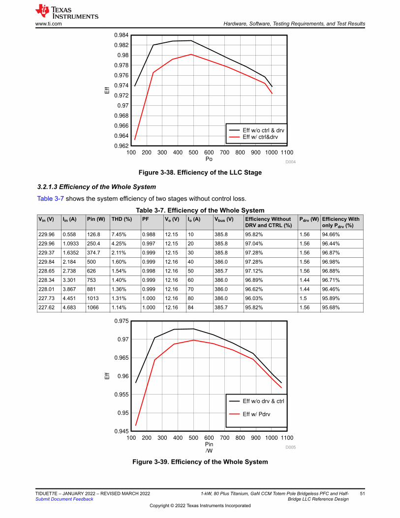
Po
Eff
100 200 300 400 500 600 700 800 900 1000 1100
0.962
0.964
0.966
0.968
0.97
0.972
0.974
0.976
0.978
0.98
0.982
0.984
D004
Eff w/o ctrl & drv
Eff w/ ctrl&drv
Figure 3-38. Efficiency of the LLC Stage
3.2.1.3 Efficiency of the Whole System
Table 3-7 shows the system efficiency of two stages without control loss.
Table 3-7. Efficiency of the Whole SystemVin (V) Iin (A) Pin (W) THD (%) PF Vo (V) Io (A) Vbus (V) Efficiency Without
DRV and CTRL (%)Pdrv (W) Efficiency With
only Pdrv (%)229.96 0.558 126.8 7.45% 0.988 12.15 10 385.8 95.82% 1.56 94.66%
229.96 1.0933 250.4 4.25% 0.997 12.15 20 385.8 97.04% 1.56 96.44%
229.37 1.6352 374.7 2.11% 0.999 12.15 30 385.8 97.28% 1.56 96.87%
229.84 2.184 500 1.60% 0.999 12.16 40 386.0 97.28% 1.56 96.98%
228.65 2.738 626 1.54% 0.998 12.16 50 385.7 97.12% 1.56 96.88%
228.34 3.301 753 1.40% 0.999 12.16 60 386.0 96.89% 1.44 96.71%
228.01 3.867 881 1.36% 0.999 12.16 70 386.0 96.62% 1.44 96.46%
227.73 4.451 1013 1.31% 1.000 12.16 80 386.0 96.03% 1.5 95.89%
227.62 4.683 1066 1.14% 1.000 12.16 84 385.7 95.82% 1.56 95.68%
Pin
/W
Eff
100 200 300 400 500 600 700 800 900 1000 1100
0.945
0.95
0.955
0.96
0.965
0.97
0.975
D005
Eff w/o drv & ctrl
Eff w/ Pdrv
Figure 3-39. Efficiency of the Whole System
www.ti.com Hardware, Software, Testing Requirements, and Test Results
TIDUET7E – JANUARY 2022 – REVISED MARCH 2022Submit Document Feedback
1-kW, 80 Plus Titanium, GaN CCM Totem Pole Bridgeless PFC and Half-Bridge LLC Reference Design
51
Copyright © 2022 Texas Instruments Incorporated
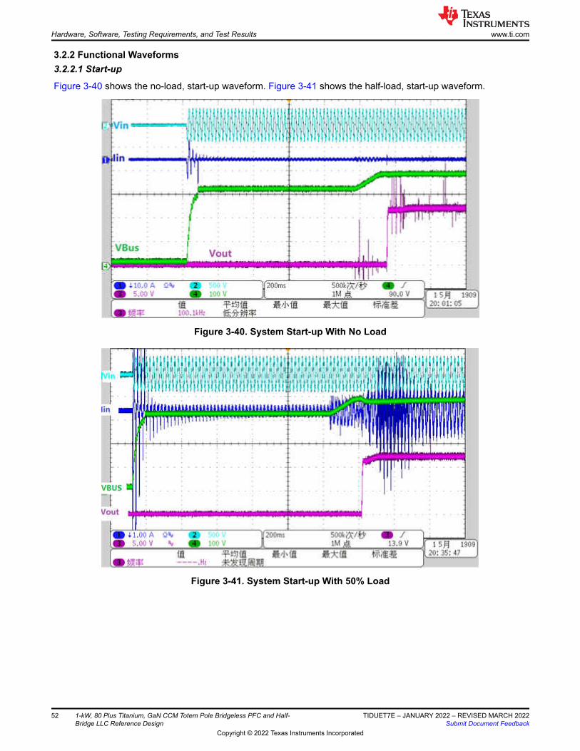
3.2.2 Functional Waveforms3.2.2.1 Start-up
Figure 3-40 shows the no-load, start-up waveform. Figure 3-41 shows the half-load, start-up waveform.
Figure 3-40. System Start-up With No Load
Figure 3-41. System Start-up With 50% Load
Hardware, Software, Testing Requirements, and Test Results www.ti.com
52 1-kW, 80 Plus Titanium, GaN CCM Totem Pole Bridgeless PFC and Half-Bridge LLC Reference Design
TIDUET7E – JANUARY 2022 – REVISED MARCH 2022Submit Document Feedback
Copyright © 2022 Texas Instruments Incorporated
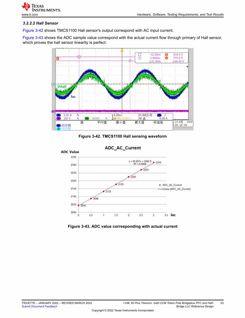
3.2.2.2 Hall Sensor
Figure 3-42 shows TMCS1100 Hall sensor's output correspond with AC input current.
Figure 3-43 shows the ADC sample value correspond with the actual current flow through primary of Hall sensor, which proves the hall sensor linearity is perfect.
Figure 3-42. TMCS1100 Hall sensing waveform
Figure 3-43. ADC value corresponding with actual current
www.ti.com Hardware, Software, Testing Requirements, and Test Results
TIDUET7E – JANUARY 2022 – REVISED MARCH 2022Submit Document Feedback
1-kW, 80 Plus Titanium, GaN CCM Totem Pole Bridgeless PFC and Half-Bridge LLC Reference Design
53
Copyright © 2022 Texas Instruments Incorporated
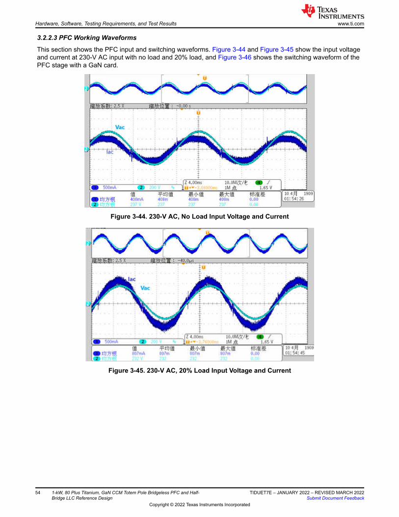
3.2.2.3 PFC Working Waveforms
This section shows the PFC input and switching waveforms. Figure 3-44 and Figure 3-45 show the input voltage and current at 230-V AC input with no load and 20% load, and Figure 3-46 shows the switching waveform of the PFC stage with a GaN card.
Figure 3-44. 230-V AC, No Load Input Voltage and Current
Figure 3-45. 230-V AC, 20% Load Input Voltage and Current
Hardware, Software, Testing Requirements, and Test Results www.ti.com
54 1-kW, 80 Plus Titanium, GaN CCM Totem Pole Bridgeless PFC and Half-Bridge LLC Reference Design
TIDUET7E – JANUARY 2022 – REVISED MARCH 2022Submit Document Feedback
Copyright © 2022 Texas Instruments Incorporated
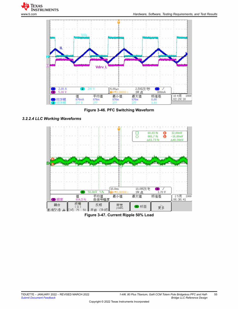
Figure 3-46. PFC Switching Waveform
3.2.2.4 LLC Working Waveforms
Figure 3-47. Current Ripple 50% Load
www.ti.com Hardware, Software, Testing Requirements, and Test Results
TIDUET7E – JANUARY 2022 – REVISED MARCH 2022Submit Document Feedback
1-kW, 80 Plus Titanium, GaN CCM Totem Pole Bridgeless PFC and Half-Bridge LLC Reference Design
55
Copyright © 2022 Texas Instruments Incorporated
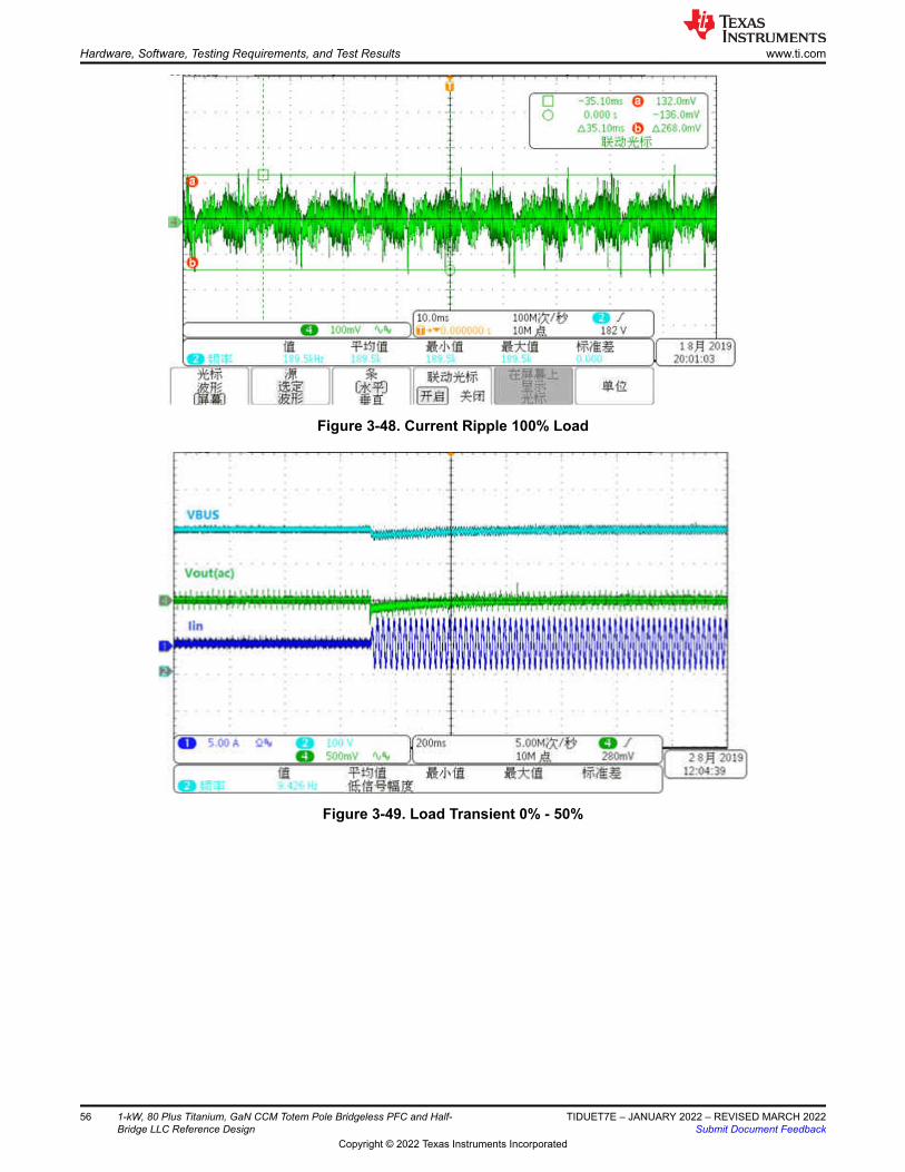
Figure 3-48. Current Ripple 100% Load
Figure 3-49. Load Transient 0% - 50%
Hardware, Software, Testing Requirements, and Test Results www.ti.com
56 1-kW, 80 Plus Titanium, GaN CCM Totem Pole Bridgeless PFC and Half-Bridge LLC Reference Design
TIDUET7E – JANUARY 2022 – REVISED MARCH 2022Submit Document Feedback
Copyright © 2022 Texas Instruments Incorporated
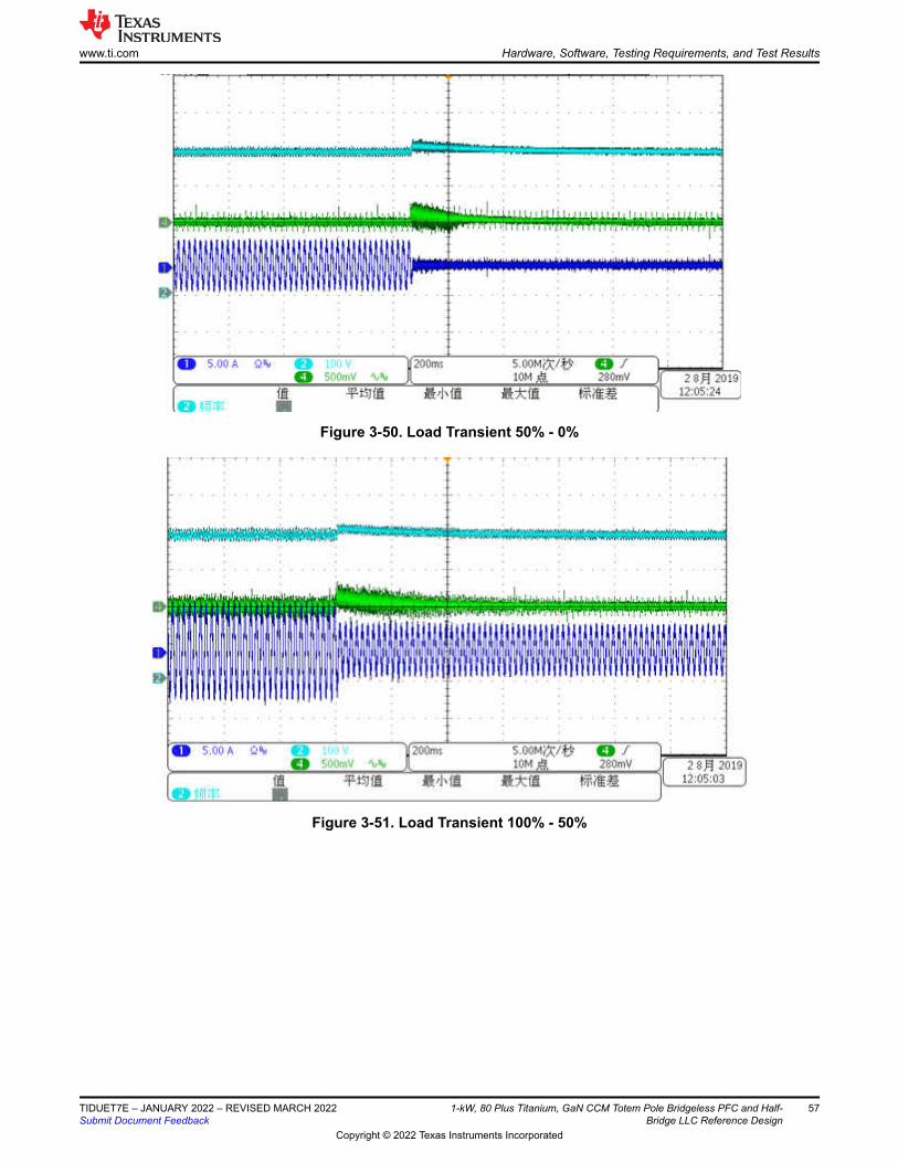
Figure 3-50. Load Transient 50% - 0%
Figure 3-51. Load Transient 100% - 50%
www.ti.com Hardware, Software, Testing Requirements, and Test Results
TIDUET7E – JANUARY 2022 – REVISED MARCH 2022Submit Document Feedback
1-kW, 80 Plus Titanium, GaN CCM Totem Pole Bridgeless PFC and Half-Bridge LLC Reference Design
57
Copyright © 2022 Texas Instruments Incorporated
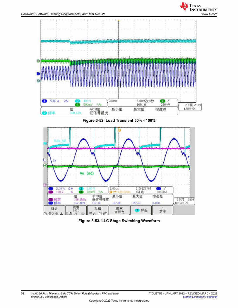
Figure 3-52. Load Transient 50% - 100%
Figure 3-53. LLC Stage Switching Waveform
Hardware, Software, Testing Requirements, and Test Results www.ti.com
58 1-kW, 80 Plus Titanium, GaN CCM Totem Pole Bridgeless PFC and Half-Bridge LLC Reference Design
TIDUET7E – JANUARY 2022 – REVISED MARCH 2022Submit Document Feedback
Copyright © 2022 Texas Instruments Incorporated

4 Design Files4.1 SchematicsTo download the schematics, see the design files at TIDA-010062.
4.2 Bill of MaterialsTo download the bill of materials (BOM), see the design files at TIDA-010062.
4.3 PCB Layout RecommendationsA careful PCB layout is critical in a high-current, fast-switching circuit to provide appropriate device operation and design robustness. As with all switching power supplies, pay attention to detail in the layout to save time in troubleshooting.
4.3.1 Power Stage Specific Guidelines
Follow these key guidelines to route the power stage components:
• Minimize the loop area and trace length of the power path circuits, which contain high-frequency switching currents. This will help reduce EMI and improve the converter's overall performance.
• Keep the switch node as short as possible. A short and optimal trace width helps reduce induced ringing caused by parasitic inductance.
• Keep traces with high dV/dt potential and high di/dt capability away from or shielded from sensitive signal traces with adequate clearance and ground shielding.
• Keep the power ground and control ground separate for each power supply stage. Tie them together (if they are electrically connected) in one point near the DC input return or output return of the given stage.
• When multiple capacitors are used in parallel for current sharing, the layout should be symmetrical across both capacitor leads. If the layout is not identical, the capacitor with the lower series trace impedance will see higher peak currents, and become hotter (I2R).
• Tie the heat sinks of all of the power switching components to their respective power grounds.• Place protection devices such as TVS, snubbers, capacitors, or diodes physically close to the device that
they are intended to protect, and route with short traces to reduce inductance.• Choose the width of PCB traces based on an acceptable temperature rise at the rated current as per
IPC2152, as well as acceptable DC and AC impedances. The traces should withstand the fault currents (such as short circuit current) before electronic protection devices, such as fuses or circuit breakers, are activated.
• Determine the distances between various traces of the circuit, according to the requirements of applicable standards. For this design, the UL 60950-1 safety standard is followed to maintain the creepage and clearance from live line, to neutral line, and to safety ground.
• Adapt the thermal management to fit the end equipment.
4.3.2 Gate Driver Specific Guidelines
Follow these key guidelines to route the high-frequency, high-current gate driver:
• Place the driver device as close as possible to the power device to minimize the length of high current traces between the output pins of gate drive and the gate of the power device.
• Locate the VDD bypass capacitors between VDD and GND as close as possible to the driver with minimal trace length to improve the noise filtering. These capacitors support high-peak current being drawn from VDD.
• Minimize the turn-on and turn-off current-loop paths (driver device, power MOSFET, and VDD bypass capacitor) as much as possible to keep the stray inductance to a minimum.
• Minimize noise coupling with star point grounding from one current loop to another. Connect the driver GND to the other circuit nodes, such as the power switch source or the PWM controller ground, at one single point. The connected paths must be as short as possible to reduce inductance and be as wide as possible to reduce resistance.
4.3.3 Layout Prints
To download the layer plots, see the design files at TIDA-010062.
www.ti.com Design Files
TIDUET7E – JANUARY 2022 – REVISED MARCH 2022Submit Document Feedback
1-kW, 80 Plus Titanium, GaN CCM Totem Pole Bridgeless PFC and Half-Bridge LLC Reference Design
59
Copyright © 2022 Texas Instruments Incorporated
4.4 Altium ProjectTo download the Altium Designer® project files, see the design files at TIDA-010062.
4.5 Gerber FilesTo download the Gerber files, see the design files at TIDA-010062.
4.6 Assembly DrawingsTo download the assembly drawings, see the design files at TIDA-010062.
5 Software FilesTo download the software files, see the design files at TIDA-010062.
6 Related Documentation1. Texas Instruments, Interleaved CCM Totem Pole Bridgeless PFC Reference Design Using C2000™ MCU2. Texas Instruments, Designing an LLC Resonant Half-Bridge Power Converter Seminar3. Texas Instruments, Resonant LLC Half-Bridge DC/DC Converter Software Design Guide4. Texas Instruments, Resonant LLC Half-Bridge DC/DC Converter Hardware Design Guide5. Texas Instruments, LMG341xR070 600-V 70-mΩ GaN with Integrated Driver and Protection Data Sheet6. Texas Instruments, TMS320F28004x Piccolo™ Microcontrollers Data Manual7. Texas Instruments, TMS320F28004x Real-Time Microcontrollers Technical Reference Manual8. Texas Instruments, TMS320F28003x Real-Time Microcontrollers Technical Reference Manual9. Texas Instruments, TMS320F28002x Real-Time Microcontrollers Technical Reference Manual
6.1 TrademarksC2000™, Piccolo™, and TI E2E™NexFET™ are trademarks of Texas Instruments.80 PLUS® is a registered trademark of Ecos Consulting, Inc.ASIAINFO® is a registered trademark of AsiaInfo Holdings, Inc.SIMPLE SWITCHER® is a registered trademark of Texas Instruments.Toshiba® is a registered trademark of Kabushiki Kaisha Toshiba.Altium Designer® is a registered trademark of Altium LLC or its affiliated companies.All trademarks are the property of their respective owners.
7 About the AuthorDESHENG GUO is a System Application Engineer at Texas Instruments, where he is responsible for developing customized power solutions as part of the power delivery, industrial segment. Desheng brings to this role his extensive experience in power electronics, power conversion, EMI/EMC, power and signal integrity, and analog circuits design spanning many high-profile organizations. He got his master degree from Harbin Institute of Technology with Power electronics in 2007, and has been working in DPEC of DELTA for many years, focusing on the high efficiency power supply's research and design.
MINGHAN DONG is a Systems Engineer at Texas Instruments where he is responsible for developing digital reference design solutions for the power design service, industrial segment. Minghan focus on C2000 firmware design and analog power circuit design. Minghan earned his master degree of electrical and electronics engineering from the Zhejiang University, Hangzhou.
Design Files www.ti.com
60 1-kW, 80 Plus Titanium, GaN CCM Totem Pole Bridgeless PFC and Half-Bridge LLC Reference Design
TIDUET7E – JANUARY 2022 – REVISED MARCH 2022Submit Document Feedback
Copyright © 2022 Texas Instruments Incorporated
8 Revision HistoryNOTE: Page numbers for previous revisions may differ from page numbers in the current version.
Changes from Revision D (January 2022) to Revision E (March 2022) Page• Added TMS320F280039 product folder to the Resources section..................................................................... 1• Added TMS320F280039 ....................................................................................................................................3• Added F28003x................................................................................................................................................ 16• Added F28003x................................................................................................................................................ 20• Added llc_F28003x .......................................................................................................................................... 34
Changes from Revision C (March 2021) to Revision D (January 2022) Page• Added TMDSFSIADAPEVM product folder to the Resources section............................................................... 1• Added FSI feature in the Features section......................................................................................................... 1• Added F280039 to the Communication Between the Primary Side and the Secondary Side section.............. 11• Removed the System Test: Dual Stages section from Section 3.1.1.3.............................................................14• Added PFC + LLC Stage Dual Test section......................................................................................................45
Changes from Revision B (September 2019) to Revision C (March 2021) Page• Updated the numbering format for tables, figures, and cross-references throughout the document. ................1• Required Hardware and Software section completely reworked...................................................................... 13
Changes from Revision A (September 2019) to Revision B (September 2019) Page• Changed title.......................................................................................................................................................1• Changed description...........................................................................................................................................1• Changed features............................................................................................................................................... 1
Changes from Revision * (September 2019) to Revision A (September 2019) Page• Changed description...........................................................................................................................................1
www.ti.com Revision History
TIDUET7E – JANUARY 2022 – REVISED MARCH 2022Submit Document Feedback
1-kW, 80 Plus Titanium, GaN CCM Totem Pole Bridgeless PFC and Half-Bridge LLC Reference Design
61
Copyright © 2022 Texas Instruments Incorporated

IMPORTANT NOTICE AND DISCLAIMERTI PROVIDES TECHNICAL AND RELIABILITY DATA (INCLUDING DATA SHEETS), DESIGN RESOURCES (INCLUDING REFERENCE DESIGNS), APPLICATION OR OTHER DESIGN ADVICE, WEB TOOLS, SAFETY INFORMATION, AND OTHER RESOURCES “AS IS” AND WITH ALL FAULTS, AND DISCLAIMS ALL WARRANTIES, EXPRESS AND IMPLIED, INCLUDING WITHOUT LIMITATION ANY IMPLIED WARRANTIES OF MERCHANTABILITY, FITNESS FOR A PARTICULAR PURPOSE OR NON-INFRINGEMENT OF THIRD PARTY INTELLECTUAL PROPERTY RIGHTS.These resources are intended for skilled developers designing with TI products. You are solely responsible for (1) selecting the appropriate TI products for your application, (2) designing, validating and testing your application, and (3) ensuring your application meets applicable standards, and any other safety, security, regulatory or other requirements.These resources are subject to change without notice. TI grants you permission to use these resources only for development of an application that uses the TI products described in the resource. Other reproduction and display of these resources is prohibited. No license is granted to any other TI intellectual property right or to any third party intellectual property right. TI disclaims responsibility for, and you will fully indemnify TI and its representatives against, any claims, damages, costs, losses, and liabilities arising out of your use of these resources.TI’s products are provided subject to TI’s Terms of Sale or other applicable terms available either on ti.com or provided in conjunction with such TI products. TI’s provision of these resources does not expand or otherwise alter TI’s applicable warranties or warranty disclaimers for TI products.TI objects to and rejects any additional or different terms you may have proposed. IMPORTANT NOTICE
Mailing Address: Texas Instruments, Post Office Box 655303, Dallas, Texas 75265Copyright © 2022, Texas Instruments Incorporated