"1 - CiteSeerX
310
-jp (I La C\ : LUI-2 DCo. C.33 H 33 o~ "1 U, I) C) ((3i A-)d 3 C)C ý5
-
Upload
khangminh22 -
Category
Documents
-
view
3 -
download
0
Transcript of "1 - CiteSeerX
-jp
(I La
C\ :
LUI-2
DCo.
C.33
H 33
o~ "1
U, I)
C)
((3i
A-)d 3
C)C ý5

Office of Naval Research
Contract R00014-67-A-0298-0012 NR-017-308
ARPA Contract DAHC-15-67-C-0219
,- PREPARATION AND OPTICAL PROPERTIES OF"4, •CRYSTALS AND FILMS OF VANADIUM OXIDES-A Lx
-4
I
s By
John C.C. Far
May 1972 D D CJUL 071"l
Technical Report No. ,P-28 U•J"Technical Report No. ARPA-43
Reproduction in whole or in part is permitted by the U. S.1
Government. Distribution of this document is unlimited.
Division of Engineering and Applied PhysicsHarvard Univerity * Cambridge, Massachusetts
-- 5
UnclassifiedSectiritv Cla~otification
-DOCUMENT COtI" OL DATA-R &D-Sto'lit, fY lAJS Icatsc'itn Of fitli.. ho~d) to I, &I) frac I.,ic l sid cex i a - os, .rut., It. fn rin,t er I I earlerd 0tt n h e coverall reportt ss cI., %it, cd
IORIGINA TING AC TIVI TY dCorporate Zolthor) 20. REPORt SECURITY CLASSIFICATlION
"'~Division of Engineering and Applied PhyscHarva~rd University fscs21 GROUP
Cambridge, Massachusetts3 REPORT TITLE
PREPARATION AND OPTICAL PROPERTIES OF CRYSTALS AND FILMS OFVANADIUM OXIDES
4. DESCRIPTIVE NOTES (Type af report ""ndsinclusive dates)
Interim technical report5 AU THOR($) (First name, middle ,n;tial. last flame)
SJohn C. C. Fan
6. REPORT DATE 7a1. TOTAL NO OF P.AGES 7b. NO. OF REPS
May 1972 __ ___ 303 2218a. CONTRACT OR GRANT NO. 90. ORIGINATOR'S REPORT NUMBERt'
N00014-67.-A-0298-001Z and ARPA TcnclRpr o P2b. PROJECT NO. DAHC 15-67--C-0219 Technical Report No. ARPA48
C. 9b. OTHER REPORT NO(S) (Any oather numbers that may be assignedthis report)
d.
10. DISTRIBUTION STATEMENT
Reproduction in whole or in part is permitted by the U. S. Government.Distribution of this document is unlimited.
11 SUPPLEMENTARY NOTrs 12 SPONSORING MILITARY ACTIVITY
Office of Naval Research
'13 ABSTRACT
T'dis nmanuscript dlescribe, man~ily the preparation and optica) prop-rtie ot crystals aidfilms of sonse of the vanadiunm ooides. In addition, different anieoods of determ..ngt the opticalconstant of solids are discussed and compared
The compleo vanoadiumi-oxygen system contains several ooides v'chio exhibit first orderinsilatcor-metaol phase Iransition sas funtion of lemperature There a-e differeot models thathave been suggested to explain the nature of these transitions In peactice, it is often adtficoltto choose an appropriate model or modelo to eoplain the meachnism of each of the pohasetransitions. In our wourk, we concentrated on ihe VOL, V 2 03 and V.10 3 -CrZ0 3 sysiems, whichexhibit isany featuires of the phase transitions.
Single crystals of V203 asd (VI.,Cr,,1203 were growno by the tri-aec Coochralsh, technique.Using a vapor transport technique, %e also peepared single crystals of VZ0 3 and filmsn of V2.03asd V0 2 . Spouttered V203 films, as geown, were found to exhihit no phase transition around 1500rC upon an lainf, tho phase teansition occourred, suggesting that if there -a no change inchemical c iposition on annealing. critical grain sizes might be necessary for the phasetriansition to peo~pugate.
Optical reflretivity nmeanurements were made on sniigle cryntas of VZ0 3 The opticalpro~perties Of VZ0 3 exhihited a fr"ee lectroo absorption in itsnmetallic state, which %an replacedby an Optical absorption edge in its low temperature insulating stole The optical constants ofV 203 were evaluated front the reflectivity spentra by nsing both the lKramers-lKronig analysisand the Oscillator fit techniqoe
Similarly, the optical constants of VO,, both is its insolatieg state and inetallic state wereevaluated. In addition, the optical constants of a single crystal of JVOe 98ZCee 0184503 at roomtemperature %ere reported. At room temperature. the optical properties of (V0 1g2Cr 0 18)203and V Z0 3 were found tc be similar, indicating that at room temperature, the band structures ofthese two nmaterials miight nut be too different.
The structural and eleclecicl eharacterintlcs of oar films of V 2 03 or' V0 2 indicated thatthe films -er of poorer quality than the siegle crystals Optical norasur, cots on the films,though complementing oar optical reflectivity, tncsoeuremtnts on the single nt~ystals,. were not usedto evaloate the Optical constansn of these mnaterWal The optical teAnsmlusion measurement. onthese films did,* however, confirm the existence of absorption edges in V Z03 and VO, an their Io-temperature insultating $taten..
Front the optic.) data, order of moagnitude values of optical effective mass and Opticalmobility were obt'inedt for the conduction electrons in the metallic states of both Vz01 aed V0 2 .Our optical data were, however, not capable of ii.dicatlcg which mtechacisto, or mechanism wereresponsible for the phase transition in these materials The optical properties were not unusual,and could be explained in teems of a one-celctron, band model The mean free paths of the conductionelectrons were, howeer, short and thus electron correlation and/er electron phoren Interaction,were probably preosent.
The 4V,-,Cr,)ZO, s)oteri was investigated mainly lee Optical reflectivity useasiuremeets an afunction of temperature 11e -caonetrated On the phase transition between the paramiagnetic metallicstate and lb. paramagnetic inoatulog stte Our measurements shbowed that this phase transitioncoud be either a first order or a 11 '-r order transition. idepending on the chromium doping level
L ~Duringr nur investigation, different methods of determining optical constanits were dintcoassdWe founod that the angular dependencenieasurements. thoogh Often linmited too a few waeegths,offered dirc..t and accurate meo-uremete et n sndhk The KrameoesKronganyssi ileiio extraopolaotion uncertainties, and the oscillato fit techniqoe tn ftiting uncertainties lBy cosutrainingat some wavelotigth., the optical constants caleiulatrd from either the Kramer-lKronig aralysis orthe o-scllaotor fit technique too upproach those obtained from the angular dependence measuremsentsat the sante wavelengths, the above unicertainties can he greatly reduced
FORM (PAGE I)DD NO.61473 Unclas sifiedS/N 0102-014-6700 SeCUrity CIlSSifiCation
UnclassifiedSecurity Classification ,,_,
I LINK A LINK 0 LINK C
4 ROLE WT ROLE WT ROLF WT -
Transition Metal Oxides
Semiconductor-Metal Transitions
Preparation of Vanadium Oxides
Optical Properties of Vanadium Oxides
Mott Transitions
FORM BACK) Unclassified
S/N 0102-014-6800 - -, Security Classification A-31409

ACKNOWLEDGMENT
The preparation of this report was made possible by the support
and cooperation of many colleagues and friends. I would like to mention
some of their contributions here. First and foremost, I would like to
thank my thesis advisor Professor William Paul for his advice and
guidance throughout my research, from choosing the research topic to
critically reviewing and helping with this final manuscript.
Professor Paul Raccah, formerly of MIT Lincoln Laboratory and
n6w of Yeshiva University, proved to be of invaluable assistance and
guidance in helping with those parts of my research that were conducted
at Lincoln Laboratory. I am greatly indebted to him.
For their experienced advice, I am grateful to Doctors Larry
Ladd, John Goodenough and, particularly, Tom Reed, who aided me
in growing the V2 0 3 -Cr 2 0 3 crystals. My colleagues at Harvard, Mr.
Wesley Akutagawa, who helped in growing vapor transport films and
crystals, Mr. William Rosevear and Mr. Nigel Shevchik, are also
gratefully acknowledged for their helpful suggestions and cooperation.
M- . Albert Manning and the late Mr. James Inglis provided
expertise in machining, and Mr. David McLeod in sample preparation.
Mr. Edward Owens of Lincoln Laboratory was very helpful with the
analysis of some of the samples and the discussion of analytical
problems connected with this work. Mr. Carl Anderson, also of
Lincoln Laboratory helped in setting up some of the optical equipment
used there. My sincere thanks to them all.

-S
Office of Naval Research
Contract N00014-67-A-0Z98-001Z
NR - 017 - 308
PREPARATION AND OPTICAL PROPERTIES OF
CRYSTALS AND FILMS OF VANADIUM OXIDES
By
John C. C. Fan
May 197Z
-u. Technical Report No. HP-28
Technical Report No. ARPA-43
Reproduction in whole or in part is permitted by the U. S.|Government. Distribution of this document is unlimited. I
The research reported in this document was made possible throughsupport extended the Division of Engineering and Applied Physics,Harvard University, by the Office of Naval Research, under Contract
N00014-67-A-0298-0012 and by the Advanced Research ProjectsAgency under Contract DAHC-15-67-C-0219.
Division of Engineering and Applied Physics
Harvard University Cambridge, Massachusetts
'Ui

PREPARATION AND OPTICAL PROPERTIES OF
CRYSTALS AND FILMS OF VANADIUM OXIDES
By
John C. C. Fan
Division of Engineering and Applied Physics
Harvard University Cambridge, Massachusetts
m'
ABSTRACT
Th)•6 manuscript describes mainly the preparation and optical
properties of crystals and films of some of the vanadium oxides. In
addition, different methods of determining the optical constants of solids
are discussed and compared.
The complex vanadium-oxygen system contains several oxides
which exhibit first order insulator-metal phase transition as a function of
temperature. There are different models that have been suggested to ex-
plain the nature of these transitions. In practice, it is often difficult to
choose an appropriate model or models to explain the mechanism of each
of the phase transitions. In our work, we concentrated on the VOZ, V2 03
* and V 2 0 3 -Cr 2 O 3 systems, which exhibit many features of the phase
transitions.
Single crystals of V 203 and (V1 xCrx)2 0 3 were grown by the tri-
arc Czochralski technique. Using a vapor transport technique, we also
prepared single crystals of V203 and films of V 203 and VO 2. Sputtered
V2 0 3 films, as grown, were found to exhibit no phase transition around
150 0K. Upon annealing, the phase transition occurred, suggesting that
2
iv
if there was no change in chemical composition on annealing, critical
grain sizes might be necessary for the phase transition to propagate.
Optical eeflectivity measurements were made on single crystals ofV0O The optical properties of V 0 exhibited a free electron absorption
in its metallic state, which was replaced by an optical absorption edge in
its ?ow temperature insulating state. The optical constants of V Z03 were
evaluated from the reflectivity spectra by using both the Kramers-Kronig
analysis and the oscillator fit technique.
Similarly, the optical constants of VOz, both in its insulating state
and metallic state were evaluated. In addition, the optical constants of asingle crystal of (V 0.982Cr0. 018203 at room temperature were reported.
At room temperature, the optical properties of (V0. 9 8 2 Cr 0 .18)203 and
V ZO3 were found to be similar, indicating that at room temperature, the
band structures of these two materials might not be too different.
The structural and electrical characteristics of our films of V 20 3
and VO 2 indicated that the films were of poorer quality than the single
crystals. Optical measurements on the films, though complementing our
optical reflectivity measurements on the single crystals, were not used
to evaluate the optical constants of these materials. The optical trans-
mission measurements on these films did, however, confix m the existence
of absorption edges in V 203 and VO 2 in their low temperature insulating
states.
From the optical data, order of magnitude values of optical effective
mass and optical mobility were obtained for the conduction electrons in the
metallic states of both V Z03 and VO 2 . Our optical data were, however,
not capable of indicating which mechanism or mechanism were responsible
3

rvV
for the phase transitions in these materials. The optical prope-rties
were not unusual, and could be explained in terms of a one-electron band
model. The mean free paths of the conduction electrons were, however,
short and thus electron correlation and/or electron phonon interaction
were probably present.
-The (Vlx Crx)20 3 system was investigated mainly by optical re-
flectivity measurements as a function of temperature. We concentrated
on the phase transition between the paramagnetic metallic state and the
paramagnetic insulating state. Our measurements showed that this
phase transition could be either a first order or a higher order transition,
depending on the chromium doping level.
During our investigation, different methods of determining optical
constants were discussed. We found that the angular dependence measure-
ments, though often limited to a few wavelengths, offered direct and
accurate measurements of n and k. The Kramers-Kronig analysis is
subject to extrapolation uncertainties, and the oscillatoi fit technique to
fitting uncertainties. By constraining, at some wavelengths, the optical
constants calculated from either the Kramers-Kronig analysis or the
oscillator fit technique to approach those obtained from the angular
dependence measurements at the same wavelengths, the above uncertainties
can be greatly reduced.
b4

TABLE OF CONTENTSPage
ABSTRACT iii
TABLE OF CONTENTS vii
LIST OF FIGURES x
LIST OF TABLES xvii
.. HAI-TER I. IN'I ,kODUCTION I-I
Tran•-:ior Metal Compounds I-I
T."; Discussion of Some Transition Metal Oxides 1-2
C. Exp,' .,---ntal Results on Some Transition Metal Oxides 1-16
D. Research Objectives 1-26
REPERENCES 1-28
CHAPTER II. PREPARATION OF FILMS AND CRYSTALS II-i
A. Earlier Methods of Preparation 11-2
i. VO 2 Crystals 11-2
2. V2 0 3 Crystals 11-4
3. VO2 Films 11-7
4. V2 0 3 Films 11-9
5. (V 1 xCrx)2 0 3 Crystals 11-10
B. Preparation of Films and Crystals of VO 2 and V 2 03 andCrystals of (V 1 _xCrx)2 O 3 11-11
1. Radio-Frequency Sputtering 11-12
2. Film Preparation in a Reactive Atmosphere 11-21
3. Vapor Transport Technique 11-23
4. Tri-Arc Czochralski Crystal Growth Technique 11-28
C. Summary I-i25
REFERENCES 11-37
Vii
S~5

.4
viii
Page
CHAPTER III. DESIGN OF OPTICAL APPARATUS AND METHODSOF DETERMINING OPTICAL CONSTANTS I11-I
A. Theories and Methods of Determining the Optical Constants
of Solids
1. Optical Constants 111-2
Z. Dispersion Relations 111-6
3. "-ramers-Kronig Analysis 111-8
4. Oscillator Fit Method 111-11
5. Angular Dependence and Other Techniques ofDetermining Optical Constants HI-19
6. Discussion 111-21
B. Numerical and Programming Techniques 111-24
1. Kramers-Kronig Analysis 111-24
2. Oscillator Fit Method 111-25
3. Angular Dependence Method 111-34
C. Experimental Optical Apparatus Design and Operation 111-35
1. Single Beam Spectrometer for both Reflectionand Trans mission Measurements 1l-35
2. Ratio Reflectometer 111-36
3. Optical Setup for Angular Dependence Measurements 111-41
REFERENCES 111-44
CHAPTER IV. OPTICAL RESULTS AND DISCUSSION IV-1
A. Introduction IV-I
B. Angular Dependence Measurements IV-4
C. Optical Results on V 2 0 3 ,(V 0 . 9 8 2 Cr 0 . 018)203, and V0 2
Using the Single Beam Spectrometer IV-8
1. V2 0 3 IV-8
2. (V0. 9 82 Cr0.*0 1 8 )2 0 3 IV-213. VO 2 IV-25
D. Optical Reflectivity Studies of Metal-Insulator Transitionsin (V1 _xCr x)203 IV-28
REFERENCES IV-34
6

ix
Page
CHAPTER V. DISCUSSION AND CONCLUSIONS V-i
A. Discussion V-i
1. Methods of Determining Optical Constants V-i
2. Voa V-4
3. V2 0 3 V-10
4. (V0. 9 8 2 Cr0. 018)203 V-14
5. (V1 xCrx)203 V-16
6. Summary V-17
B. Suggestions for Future Study V-18
REFERENCES V-24
APPENDIX A A-i
APPENDIX B B-i
7

LIST OF FIGURES
CHAPTER I
Figure No.
I-1 Pseudoparticle band structure as a function of the ratioof bandwidth to intra-atomic Coulomb energy U for thecase of a single s band. To is the binding ene-rgy of theatomic level from which the s band arises (48).
1-2 The crystal structure of VO 2 in the high-temperaturerutile phase; space group P 4 /mnm. Distances are inangstroms (41, 52). 2
1-3 Monoclinic P 2 /c structure of the low-temperature VO 2phase and its irelationship to the rutile phase. Onlythe vanadium ions are shown. The displacement of thevanadium ions at the transition is demonstrated. Dis -tances are in angstroms (41, 84).
1-4 The crystal structure of V 0 3 showing both low-temperaturemonoclinic primitive cell (Space group I2/a) and the high-temperature hexagonal cell (space group R3-c). Open andhatched circles refer to cations of different spin orientationin the low-temperature antiferromagnetic phase. Distancesare in angstroms (28, 34).
I-5 Temperature -pres sure -composition phase diagram of(V1 x Cr x)2O3 system (34).
CHAPTER II
11-i Phase diagram of VOx for x = 1.5 to 2.5 (60).
11-2 Schematic diagram of our sputtering system.
11-3 Various parts used in sputtering.
11-4 Various parts used in sputtering.
11-5 Reflection electron diffraction pattern of a V2 0 3 sputteredfilm (Hitachi Electrcn Microscope Model HU-iI).
11-6 Resistivity versus temperature of two annealed sputteredfilms of V2 0 3 .
8
8
xi
Figure No.
11-7 Sample holder for resistance versus temperaturemeasurements.
H1-8 (a) Schematic diagram of vapor transport apparatus.(b) Detail of the crystal reaction crucible in the quartz
reaction chamber.(c) Detail of the film crucible in the chamber.
11-9 Resistivity versus temperature of V2 0 3 crystals measuredby several investigators (3, 19, 25) and of a V 03 crystaland a V2 0 3 film grown by the vapor transport technique.
II-10 (a) Reflection electron diffraction pattern.(b) Optical microscopic picture of a vapor transport V2 O3
film (magnified 150. times by a Universal Rikert
Camera Microscope "MeF").
11-11 (a) Reflection electron diffraction pattern.(b) Optical microscopic picture of a vapor transport
VO film.
11-12 Resistivity versus temperature of VO2 crystals measuredby several investigators (1,3, 15, 53) and of a vapor trans-port VO 2 film.
11-13 Cross-section diagram of the tri-arc Czochralski crystalgrowing furnace.
11-14 Oxygen partial pressure versus oxygen-metal ratio fordifferent elements (56).
11-15 Picture of V2 0 3 crystals from a crystal run in a tri-arcfurnace.
1- 1-16 Lattice constants of V2 0 3 and (V1 Cr x)O 3 crystals as afunction of chromium concentration.
CHAPTER III
111-1 A comparison of different methods of evaluating theoptical constants n and k of germanium (15).
111-2 Flowchart of the simplex method (30).
S~9
4
xii
Figure No.
111-3 The schematic diagram of the sample and detector 3ptinsof the single beam spectrometer (35).
11-4 An optical dewar designed for the single beamspectrometer (35).
111-5 The diagram summary of our detectors and theirassociated electronics (35).
I1-6 The schematic diagram of the ratio reflectometer andits associated electronics.
I1-7 The reflectivity of a VzO3 sample measured in the singlebeam spectrometer and the ratio reflectomneter.
111-8 The schematic diagram of the high temperature opticalsample holder.
111-9 The optical set-up for the angular dependence measure-ments.
CHAPTER IV
IV-1 The reflectivity of two VzD 3 crystals Cl and C2 at 3000K.
IV-2 The reflectivity of a VZO3 crystal (Cl) as a function ofincidence angle q.
IV-3 The reflectivity of a V2 0 3 crystal (C2) as a funttion ofincidence angle q.
IV-4 The reflectivity of a (V1 xCr_ )2 0 crystal where x = 0. 018as a function of incidence angle 0.
IV-5 A theoretical fit to the experimental reflectivity data ofC1 by the oscillator fit method where n and k at1. 96 eV and 2. 54 eV are constrained to approach thoseobtained from the angular dependence measurements.
IV-6 E curve of Cl, obtained from the fit shown in Fig. IV-5.
IV-7 E2 curve of Cl, obtained from the fit shown in Fig. IV-5.
IV-8 a curve of Cl, obtained from the fit show-i in Fig. IV-5.
10
xiii
Figure No.
IV-9 A theoretical fit to the experimental reflectivity data ofCl by the oscillator fit method where n and k at1. 96 eV and 2.54 eV are not constrained.
IV-10 E1 curve of Cl, obtained from the fit shown in Fig. IV-9.
IV-11 E2 curve of CI, obtained from the fit shown in Fig. IV-9.
IV-1Z a curve of Cl, obtained from the fit shown in Fig. IV-9.
IV-13 A theoretical fit to the experimental reflectivity d~ta ofC1 by the oscillator fit method where n and k at1. 96 eV and 2.54eV are not constrained.
IV-14 E curve of Cl, obtained from the fit shown in Fig. IV-13.
IV-15 E curve of Cl, obtained from the fit shown in Fig. IV-13.
SIV-16 a curve of Cl, obtained from the fit shown in Fig. IV-13.
IV-17 E1 curve of Cl, obtained from the Kramers-Kroniganalysis of the reflectivity spectrum of C1.
IV-18 %2 curve of Cl, obtained from the Kramers-Kroniganalysis of the reflectivity spectrum of Cl.
IV-19 a curve of Cl, obtained frcm the Kramers-Kroniganalysis of the reflectivity spectrum of Ci.
IV-20 A theoretical fit to the experimental data of Cl by theoscillator fit method (at 120 0 K).
IV-21 E curve of Cl, obtained from the fit shown in Fig. IV-20MIV-22 E12 curve of Cl, obtained from the fit shown in Fig. IV-0.
IV-23 a curve of CI, obtained from the fit shown in Fig. IV-Z0.
IV-24 Predicted transmission of a single V2 0 3 crystal of 0. 5ý±thickness at 1200 K.
IV-25 Low temperature transmission of a V2 0 3 film grown byvapor transport and of an annealed V2 O3 sputteredfilm, compared with that of a single crystal measuredby Feinleib and Paul (3).
•11
xiv
Figure No.
IV-26 A theoretical fit to the experimental reflectivity dataof a (V 0 982 Cr0 018)203 crystal, where the values ofn and k at 1. 96 eV and 2. 54eV are constrained toapproach those obtained from the angular dependencemeasurements.
IV-27 E curve of the (V 0 9 8 2 Cr 0 crystal, obtained fromthe fit shown in Fig. IV-20.
IV-28 Ecurve of the (V0 9 2 Cr 018) 03 crystal, obtained fromthe fit shown in Fig. V-2
IV-9 a curve of the (V0 0982 Cr 0 018)203 crystal, obtained fromthe fit shown in Fi'g. IV-26.
IV-30 A theoretical fit to the experimental data of the (V 0. Cr^ 018)203crystal, where the values of n and k at 1. 96eVU£n 2 0.Z. 54 eV are not constrained.
IV-31 E1 curve of the (V0. 9 8 2 Cr 0 018)203 crystal, obtained from
the fit shown in Fig. IV-30.
IV-32 E2 curve of the (V0. 982Cr0. 018)203 crystal, obtained from
the fit shown in Fig. IV-30.
IV-33 a curve of the (V0.982 Cr 0 .018)203 crystal, obtained from
the fit shown in Fig. IV-30.
IV-34 A theoretical fit to the axpc -imental data of the(V 0 9 8 2 Cr 0. 018)2 03 crystal by the oscillator fit method,wher'e the values of n and k at 1.96eV and 2.54eV arenot constrained. This is a poorer fit than the one shownin Fig. IV-30.
IV-35 E curve of the (V0 982Cr^ 18)203 crystal, obtained fromthe fit shown in Fig. -V-34.
IV-36 C2 curve of the (V0. 982Cr0. 018)203 crystal, obtained from
the fit shown in Fig. IV-34.
IV-37 a curve of the (V 0. 9 8 2 Cr 0 018)z03 crystal, obtained from
the fit shown in Fig. IV-34.
12

xv
Figure No.
IV-38 E curve,obtained from the Kramers-Kronig analysis ofthe reflectivity spectrum of (V0. 9 8 2 Cr 0 018)203.
IV-39 E cturve,obtained from the Kramers-Kronig analysis ofthe reflectivity spectrum of (V0. 9 8 2 Cr 0 . 018)Z03*
IV-40 a curve, obtained from the Kramers-Kronig analysis ofthe reflectivity spectrum of (V0. 9 8 ZCr0. 018)203.
IV-41 A theoretical fit to the experimental data of a VO2 crystal(at 360 0 K) by the oscillator fit method.
IV-42 E curve of the VO2 crystal, obtained from the fit shownin Fig. IV-41.
IV-43 E curve of the V0 2 crystal, obtained from the fit shownin Fig. IV-41.
IV-44 a curve of the VO? crystal, obtained from the fit shownin Fig. IV-41.
IV-45 A theoretical fit to the experimental data of the V0 2crystal (at 300 0 K) by the oscillator fit method.
IV-46 El curve of the VO2 crystal obtained from the fit shownin Fig. IV-45.
IV-47 E curve of the VO 2 crystal obtained from the fit shownin Fig. IV- 45.
IV-48 a curve of the VO crystal obtained from the fit shownin Fig. IV-45.
IV-49 A comparison of the values of a obtained by fitting Ladd'sdata (2) with those reported by Barker et al. (10).
IV-50 Apparent reflectivity and transmission of a VO filmgrown by the vapor transport method, above (350OK) andbelow (300 0 K) the transition temperature.
IV-51 The reflectivity of a V2 0 3 crystal at 0. 65 eV as a functionof temperature.
IV-52 The reflectivity of a (V 1 x Crx) 2 0 3 crystal (where x = 0. 0022)
at 0.65 eV as a function of temperature.
13

xvi
Figure No.
IV-53 The reflectivity of a V2 0 3 crystal at different temperaturesas a function of photon energy.
IV-54 The reflectivity of a (V IxCrx)2 O 3 crystal (where x = 0. 0022)
at different temperatures as a function of photon energy.
IV-55 The reflectivity of a (V1 xCrx) 203 crystal (where x = 0. 0047)
at 0.65 eV as a function of temperature.
IV-56 The reflectivity of a (V1 xCrx)2 0 3 crystal (where x = 0. 010)
at 0.65 eV as a function of temperature.
IV-57 The reflectivity of a (V1 xCrx) 203 crystal (where x =0. 014)
at 0. 65 eV as a function of temperature.
IV-58 The reflectivity of a (V 1 _xCrx)2 O 3 crystal (where x = 0. 0047)at different temperatures as a function of photon energy.
IV-59 The reflectivity of a (V 1 _xCrx) 2 0 3 crystal (wherex = 0. 010)at different temperatures as a function of photon energy.
IV-60 The reflectivity of a (V .Cr ) 0 crystal (wherex= 0.014)at different temperatures as a unction of photon energy.
IV-61 Transition temperatures observed in reflectivity measure-ments on (V1 x Crx)203
14
A

LIST OV' TABLES
Table No. Page
Il-i Melting points of vanadium andsome vanadium oxides (38). Il-li
11-2 Comparison of lattice spacings of a V 20 3sputtered film obtained from reflectionelectron microscopy with the spacingslisted in ASTM index. 11-17
11-3 List of crystal runs and measurementson the crystals. 11-30
IV-1 Optical constants n and k of a V 203crystal (Cl) at room temperature,23obtained by different methods. IV- 10
IV-2 Optical constants n and k of a(V 0 9 8 2 )Cr crystal (R1) at roomtemperature, o bained by different methods IV-22
IV-3 Transition temperatures obtained in re-flectivity measurements on (V 1 -xCr x) 2 0
3 IV-33
15w xvii

CHAPTER I
INTRODUCTION
Ever since F.J. Morin (1) reported, in 1959, that single crystals
of VO, V0 2 , V ZO3 and Ti 2 O 3 all exhibited sharp changes of electrical
conductivity from metallic to semiconducting behavior at certain transi-
tion temperatures, intense efforts have been made to understand this
class of materials, both experimentally and theoretically. The object
of this thesis is to investigate these compounds, especially in the areas
of preparation and optical properties.
First, however, a brief survey of the experimental and theoretical
studies in this area is necessary to put this investigation into its proper
perspective.
A. Transition Metal Compounds
The transition metals possess one to nine d electrons on each
atom, in addition to the s and p electrons found on the atoms of
ordinary metals. In a solid, the d orbitals overlap to form a relatively
narrow d band. The next higher s band is usually wide and overlaps
the entire d band. Thus, the s band is always partially full and metal-
lic conductivity prevails in all the transition metals.
When compounds of transition metals are formed, their electrical
properties vary widely from insulating to metallic behaviour. If we re-
strict ourselves to oxides and sulphides of the transition metals, many
compounds can be classified by their electrical conductivity characteristics
into three distinct classes:
16

I-2
(a) Insulators (resistivity of the order of 103- I07-cm and decreasing
with increasing temperature): NiO (2), CoO (3. 9), MnO (4), FeO (5),
Fe20 3 (6), Cr 2 O 3 (7), Mn 3 0 4 (4), Mn O 3 (8), Co 3 0 4 (8), MnS (10),
FeS2 (10), and MnS 2 (10).
(b) Metals (resistivity of the order of 10 -2 10- 6 a-cm at room
temperature, and linearly increasing with increasing temperature):
TiO (11), VO (11), CrO2 (12), NbO (13), ReO 2 (14), ReO 3 (15), TiS (16),
CoS 2 (10), and CuS 2 (10).
(c) Materials with insulator-metal transitions: V2 0 3 (1, 16), VO (1, 17),
V6 0 1 3 (18), V4 0 7 (19), V5 0 9 (20), V8 0 1 5 (21), Ti 2 03 (1), Ti 4 0 7 (22),
Ti 3 0 5 (22), Ti 5 0 9 (22), Ti 6 0 1 1 (22), NbO 2 (23), Fe 3 0 4 (24), NiS (25),
CrS (26), and FeS (27).
Two striking features of these compounds emerge from this clas-
sification: (1) failure of the Bloch-Wilson one electron band theory in
explaining the electrical conductivities of some of the insulating transition
metal compounds, and (2) frequent occurrence of insulator-metal transi-
tions in a large number of materials, especially in the oxides of vanadium
and titanium.
In the next section, we will elaborate on these two points as they
pertain to some of the transition metal oxides.
B. Theoretical Discussion on Transition Metal Oxides
One of the classical examples of the failure of the Bloch-Wilson
theory is NiO. In NiO, as well as in many transition metal oxides, the
17_ _ _ _ _ _ _ _

1-3
bonding of Ni++ cations with 0-- anions is partially ionic. The 0-- 2p
states are the bonding orbitals and form a band - 6 eV below the anti-
bonding orbitals of Ni++ 4s states (28). The 3d band is generally as-
sumed to be somewhere between the 2p and 4s bands (28). In the
ground state, the s band is completely empty and the p band is com-
pletely full. Therefore, only the d band is near the Fermi level and
should be responsible for both the electrical and magnetic properties of
NiO.
NiO has a cubic NaCI structure, and the ten-fold degenerate 3d
states are split by the ;rvstalline field into a lower six-fold degenerate
t2g band and an upper four-fold degenerate e band. Since NiO con-
tains eight 3d electrons per unit cell, the e band should be partiallyg
filled and NiO should be metallic. NiO however, is a good insulator.
Since NiO is antiferromagnetic below the Neel temperature TN, its
ground state can be insulating if the antiferromagnetism, which leads to
doubling of the primitive cell, actually opens up a gap in the density of
states in the e band. At temperatures above TN, this band splittirg
should disappear and NiO should be metallic. This, however, is not the
case. Thus, the one el,:ctron Bloch-Wilson band theory fails to explain
the insulating property of NiO above TN.
In order to modify the Bloch-Wilson band theory, one must under-
stand the assumptions on which the theory is based, namely, the Hartree-
Fock hypothesis, which reduces a many-electron problem to the description
of a single electron moving in a periodic field. But this hypothesis fails
18
1-4
to treat adequately electron correlations and electron-pbonon interactions,
which, for reasons outlined below, could be important in transition metal
compounds.
The properties of outer electrons in crystals can often be described
by either of two theories, one the crystal field theory, and the other the
one-electron band theory. Crystal field theory is adequate to describe
the properties of the outer Aectrons in a crystal if the interaction between
the neighboring atoms is so weak that each electron is essentially localized
near its nucleus. On the other hand, one electron band theory is most
appropriate for explaining outer electrons if they are essentially itiner-
ant and are equally likely to be found at any site in the solid. There are,
however, outer electrons which are neither sufficiently itinerant nor
localized to be adequately described by either of the two above theories.
The outer d-electrons in some transition metal compounds fall into this
category. The following justification applies, strictly speaking, to the
atomic limit only, though quantitatively, it is usually applicable even in
crystals.
Outer s and p electronic wave functions usually spread far from
their atomic nuclei and their properties are usually adequately described
by one electron b -d theory. The outer 4f electrons, on the other hand,
are more L. calized to .hei..7 nuclei, and are szreened from their neighboring
atoirs by the 5s2 arid 5r6 electrons (28, 29). These electrons are then
considý.:.e-l to be localized and their behavior can be described by the
crystal field theory. The outer d electrons are, however, generally
1-5
intermediate in nature. In many transition metal compounds, such as
NiO and MnO, the outer d electrons cannot be described by either of
the two theories and the theories have to be modified. Here, we are
interested only in modification of the one electron band theory, which
then should include consideration of electron correlations and electron-
phonon interactions.
Besides the failure of the one electron band theory in explaining
the electrical insulating behavior of some transition metal oxides, another
striking feature of the transition metal compounds is the frequent occur-
rence of first order phase transitions.
In 1949, Mott (30) provided an argument which not only showed the
limitation of the one electron band theory, but also demonstrated how a
first order phase transition could occur. Briefly, suppose we have a crystal
made of atoms whose outer shell has only one s electron, and which has only
one atom per unit cell. One electron band theory will predict the crystal
to be metallic. If, however, the atoms are very far apart, the overlap
between the orbitals from the neighboring atoms will be small, and the
electronic energy levels will not be too different from the atomic energy
levels. Now, if we consider a particular atomic site at which there is
already an electron, a second electron of the opposite spin placed at the
same site will have to have an additional energy U since a Coulomb re-
pulsion force will have to be overcome in order to place two electrons
at the same site. Thus migration of electrons in this crystal will neces-
sitate an activation energy U. The electrons are essentially localized
20

1-6
to their respective atomic sites, and we have an insulator; however,
as the atoms are brought together, the kinetic energy of the electrons
increases as they are confined to their respective atomic sites. Eventually,
the energy of the repulsion of two electrons on one atomic site becomes
less than the energy required to localize the electrons in their atomic
sites. The electronic wave function then spreads out reducing the kinetic
energy of the electrons. The electrons become delocalized and metallic
conductivity results.
In such a crystal, according to the Mott theory, the interatomic
distances are crucial in determining the electrical conductivity. If the
interatomic distances in the crystal are so large that its outer s electrons
are essentially localized, then the crystal is an insulator, although the one
electron band theory predicts that it should be a metal. If the inter-
atomic distances are so small that the outer s electrons are delocalized,
the crystal is a metal. If the interatomic distance is in between these
two limits, then the properties of the s electrons are not clear. If,
say, the crystal has interatomic distances sufficiently large that the outer
s electrons are essentially localized, out yet small enough that the
application of hydrostatic pressure on this crystal may well reduce the
interatomic distances until the outer s electrons become essentially free,
then the conductivity of such a crystal will increase under hydrostatic
pressure. Such a transition could conceivably be either gradual or sharp.
Mott further suggested that when the interatomic distances in the crystal
are near the critical value, free electrons and holes may be produced.
21

1-7
If only one free eiectron and one free hole are present in the crybtal,
then they would attract each other by a Coulomb interaction:
2
V(r) -eKr
where e = electron charge, K = dielectric constant of the crystal and
r = distance between the electron and hole. They form an exciton and
therefore are bound. If the exciton concentration increases, for instance
with increasing pressure, then the Coulomb interaction will be screened
by the electrons and holes associated with the excitons, until, at a cer-
tain exciton concentration, the effective Coulomb interaction will be too
weak to bind the electrons and holes together, and there will be an ab-
rupt transition from a small number to a large number of free carriers.
Such a transition - often referred to as the Mott transition- is then
first order. One prediction of the Mott theory is the possible existence
of a Mott transition in some solids under pressure, especially in transition
metal compounds where the outer d electrons are in the intermediate
region between being localized and iLinerant. The transition should ap-
pear as a sudden drop in resistivity at a given pressure, whereas a
transition due to band overlap should lead to a gradual change in resistivity.
In fact, the Mott transition is hard to demonstrate unambiguously, since
in practice, where abrupt insulator-metal transitions are found, other
phenomena such as magnetic ordering and crystalline distortion, which
can also cause first order transitions, are found simultaneously. Many
attempts however, have been made to observe such a transition.
22
1-8
NiO had been subjected to a quasi-hydrcstatic pressure of
500 kilobars (31) without a resistivity transition occurring. Recently,
however, Kawai and Mochizuki (32) did observe a sharp drop in re-
sistivity when NiO was subjected to a very high quasi-hydrostatic pres-
su~re. At a pressure larger than 2 megabars (no exact value was re-
ported because the calibration of pressure in this range is difficult), a
sharp drop in resistivity of a factor of - 106 was observed. No conclusion,
however, can be drawn as to whether this sharp transition is indeed the
Mott transition because the physical properties of NiO, such as the
crystal structure, magnetic properties, etc., before and after it under-
goes the transition have not been investigated.
McWhan, Rice et al. (33, 34) investigated the (Vx1 - 'xr)2 O 3 system
and observed a first order insulator to metal transition with a resistivity
change as large as a factor of 10 under hydrostatic pressure. There
is no change in crystal symmetry although there is a change in the crystal
volume at the transition. They suggested that this transition might be a
Mott transition, but the evidence is not conclusive because other mechanisms
may be involved. A more detailed discussion of the (V1 .x CrX)2 O 3 system
will be presented in the latter part of this chapter.
VO, as will be discussed later, is insulating at room temperature.
At 340 K, VO 2 undergoes a first order insulator-metal transition with a
resistivity change as large as a factor of 105 and becomes a metal.
Roach and Balberg argued that if VO 2 had interatomic distances near the
critical interatomic distance such that its insulating state was caused by
the form.-iation of excitons, as in the Mott theory, then the generation of
( p.

1-9
free carriers - for example, by a ruby laser - would increase the
screening effect on the Coulomb interaction that binds the holes and
electrons together. If a certain critical free electron concentration
were reached, the Coulomb interaction would no longer be able to bind
the holes and electrons together, and the Mott transition would occur.
They were, indeed, able to switch the films from an insulating state into
a metallic state. In practice, however, the ruby laser used not only
generates free carriers in VO films, but also heats up the films during
the process. They are, therefore, unable to distinguish whether the
observed insulator-metal transition is a Mott transition, or is caused by
thermally heating the VO2 films through the transition temperature at
340 K.
The investigations cited above fail to demonstrate unambiguously
the existence of the Mott transition. As we have discussed earlier, the
main difficulty is finding a material whose insulator-metal transition
property can be explained only by the Mott theory, and wherein no other
mechanisms which can cause a first order phase transition, such as
crystalline distortion, are present. Detailed analyses of other such
mechanisms can be found in Adler's review paper (36) and Goodenough's
summer lecture in Poland (37).
Here, we will discuss only some of th? more important models,
namely the Adler-Brooks crystalline distortion model, the homopolar
bond model, and the Lubbard model, and will briefly mention some of the
effects of electron-phonon interactions on the insulator-metal transition.
2

I-10.
Only a qualitative discussion of the Adler-Brooks crystalline
distortion model will be presented here since detailed quantitative
analysis has been put forth by Adler and Brooks (38). This model makes
use of the fact that in the narrow band limit, a metallic state can be
unstable at T = 0 K and a crystalline distortion towards a lower sym-
metry can be favored. This arises because, for any metal, a crystal-
line distortion can always be envisioned which will reduce the electronic
energy of just the number of states that are filled, but will raise the
energy of just those states that are empty. Such a distortion always
minimizes the electronic energy of the system. An insulating state will
result if a real energy gap in the density of states is produced. This is
more likely if the energy bands are narrow. This distortion, however,
will not occur unless the free energy of the insulating state is lower than
that of the metallic state. Since at T = 0 0 K, there are no entropy contri-
butions to the free energy, we have only to consider the total energy of
the system in both states. The distortion will occur if the decrease in
the electronic energy outweighs the increase in the strain energy caused
by the crystalline distortion. This, again, has been shown to be the case
only if the energy bands are narrow (38). As the temperature of such a
narrow band insulating material is increased from 0 K, electrons are
excited thermally across the energy gap into the conduction band. The
thermal excitation of carriers will increase the electronic energy of the
insulating state. In addition, as the temperature is increased, the en-
tropy contribution to the free energy also becomes important. Since the
_ _ "A
I-li
electronic entropy of the metallic state is usually greater than that of
the insulating state, as the temperature increases, the free energy of
the insulating state becomes closer to that of the metallic state, until at
a certain critical temperature, the free energy of the metallic state be-
comes lower than that of the insulating state, and a first order insulator
to metal transition occurs.
The Adler-Brooks theory has an important drawback in that it
neglects electron correlation effects and electron-phonon interaction in
its hypothesis. In fact, it assumes that one electron band theory is still
appropriate. However, if we have a narrow band material, so that we
can try to apply the Adler-Brooks theory, we should also take into ac-
count electron correlation effects and the electron-phonon interaction.
If the electron-phonon interaction in a crystal is sufficiently large,
an electron can polarize and, thereby distort, the lattice in its neighbor-
hood. The polarization, in turn, acts on the electron and lowers its
energy. As the electron moves through the crystal, it takes along the
distortion of the lattice. The electron together with the accompanying
self-consistent polarization field can be thought of as a quasi-particle,
and is usually called a polaron. Its effective mass is larger than that of
the Bloch electron. Polaron effects might thus explain the low conductivity
of some of the transition metal oxides.
Within the limits of small polaron theory (small polarons occur if
the dimension -_ the polaron, that is, of the electronic wave function and
the self-consistent polarization field, is smaller than the lattice constant),
26

1-12
Holstein (39) reported that at low temperatures, polaron conductivity
was due to polaron bands, and conductivity was low. Above a critical
temperature (approximately at half of the Debye temperature), con-
duction took place by means of thermally activated polaron hopping of
very low mobility. Therefore, we have a transition from a state '. -th
low conductivity to a state with even lower conductivity as temperature
increases, and this is the reverse of what we observe in many transition
metal oxides and sulphides except in the (V1 xCrx)2 0 3 system. Ac-
cordingly, polaron effects are generally not applicable in explaining the
insulator-metal transition. This is not, however, to imply that the
electron-phonon interaction is not important, as its effect may be present
in other forms.
Berglund and Guggenheim (40) calculated that the latent heat of VO0
at the phase transition could not be accounted for by the change in the
electronic entropy at the phase transition alone. They then suggested
that most of the latent heat should be supplied by the lattice. Ladd (41)
suggested that the latent heat could be supplied by, lattice-vibrational
mode-softening in the metallic state in VO.
Paul (42) and Hearn (43) suggest that since the 3d electrons in
transition metal. compounds, and particularly in VOZ are intermediate
in character between localized and itinerant electrons, they can be easily
excited by changing the temperature or stress into higher energy states.
They are, however, still sufficiently localized that these excitations may
produce considerable local charge fluctuation. If the distribution of
G r7

1-13
d-electron charges near the vanadium ions is such that the lattice
phonon spectrum is critically dependent on it, this local charge fluctua-
tion may induce a strong electron-phonon interaction and lead to the
softening of the phonon spectrum in the metallic phase where, by second
order perturbation theory, the effect of the electron-phonon interaction
is greater than in the insulating state because of the larger number of
degenerate states at the Fermi level. The softening of phonon modes
in the metallic state decreases its lattice free energy and eventually the
total free energy becomes lower for the metallic phase than for the
insulating phase, causing the insulator-metal transition.
Hearn did a one dimensional calculation for atoms along the c-axis
in VO, using this idea, and obtained reasonable quantitative agreement
with known experimental data. Mattis and Langer (44) obtained some
quantitative results of the effects of phonons and band structure on the
metal-insulator transition. Depending on the electron-phonon coupling
coefficients and the band structures of the materials, either first order
or second order phase transitions may occur. Insulator-metal transitions,
therefore, should depend strongly on the crystal structures of the solids
if they are driven by electron-phonon interactions. In contrast, the
crystal structures may not be important in the Mott transition. The
interatomic distances and the nature of valence electrons in the solid
determine the possible existence of the Mott transition. In fact, in a
solid, if the interatomic distances are in the critical region where the
electrons can either be itinerant or localized, the Mott transition may
be possible even in amorphous materials.
28

1-14
In 1960, Goodenough (45) suggested the possibility that for some
transition metal ion arrangements, it might be favorable for some of
the d orbitals of the cations to form covalent-bonded molecular orbitals,
where electrons are localized. These molecular orbitals, often referred
to as homopolar bonds, may be formed at a certair. critical temperature.
At temperatures above this critical temperature, these homopolar bonds
break apart, and the electrons become delocalized (28), leading to an
insulator-metal transition.
As Mott has pointed out, electron correlation can play an important
role in the properties of some transition metal compounds. Hubbard in a
series of papers (46, 47, 48, 49)incorporated correlation effects into band
theory by introducing the Hamiltonian
H= Z £(k)nk,.±UnZ n 1 n - )n 2 U
k,o i
where 8 (k) are the Bloch energies.
nk, (r are the number operators for the Bloch states,
n. are the number operators for the Wannier states centered
at the lattice site R.1
a represents spin
U is the intra-atomic Coulomb repulsion,
n is the number of electrons per atom,
N is the number of atoms in the crystal.
The first term in the Hamiltonian is the normal Hartree-Fock
term, and the second term represents the correlation effects between
C!

1-15
two electrons of opposite spin in the same atomic site. These cor-
relation effects were included by an important approximation where
only the intra-atomic Coulomb interaction was considered.
Hubbard applied this Hamiltonian to a half-filled s band and ob-
tained some quantitative results. In the atomic limit, that is, when the
bandwidth is zero, the above Hamiltonian can be solved exactly by means
of retarded and advanced Green's function (46). The s band is found to
be split into two subbands, separated by an energy gap U at T = 0. In
this case, the lower band is completely filled and the upper band is empty
at T = 0 0 K. As the ratio of the bandwidth A to U is increased, the
energy gap decreases until it disappears at - (see Fig. I-1).
Since the gap decreases slowly to zero, we have only a gradual change in
conductivity. A sudden first order transition cannc' be predicted by the
Hubbard model. However, this does not imply that the electron cor-
relation effects cannot give rise to a first order phase transition. If we
include long range Coulomb interactions, a first order insulator-metal
transition might be possible. A theoretical approach to this problem is
difficult and so far no solution has been presented.
Other models have also been offered which exhibit a gradual change
(such as the band overlap model (50)) and sharp change (such as antifer-
romagnetism (51)) in the electrical conductivity.
As we have discussed before, it is usually difficult to choose the
appropriate model or models to explain the mechanisms of the phase
30
1-16
transitions in many transition metal oxides. Many experimental ob-
-ervations are still incomplete, and in some compounds, more than
one mechanism seems to be operating. In the next section we shall
present some experimental results on the VO 2 , V 2 0 3 , V 2 0 3 -Cr 2 0 3
systems, which exhibit many features of the models mentioned above.
C. Experimental Results on Some Transition Metal Oxides
1. VO 2
For T > Tt = 340 0 K, VO 2 has z. structure which is a minor
modification of that of rutile. There are two vanadium ions in each
unit cell, and the vanadium ions, after having given electrons to satisfy
the bonding requirement of the oxygen ions, have one valence electron
per ion remaining in the vanadium d bands. For T < 340 0 K, VO 2 under-
goes a crystalline distortion into a monoclinic symmetry, and has its
unit cell doubled. Figures 1-2 and 1-3 show the crystal structures above
and below TV and the relationship between the two states.
The electrical conductivity has been measured by many investigators
(1, 17, 40, 53, 54, 55), all of whom observed a sharp insulator-metal
transition at - 340 0 K, with a conductivity discontinuity of a factor as
5large as 10 . If one defines activation energy Ea by the following
equation,
(r = % exp (-Ea/kT)
where u = conductivity at a temperature T
k = Boltzmannds constant
T = Temperature in OK1
= conductivity at O(T /°K).0
31

1-17
then in the insulating state, E is not constant as in most semiconductors,a
but varies slightly with temperature (17).
Hall measurements have been reported by several workers (56, 57,
58, 59) on ceramic samples, films and single crystals, the most recent
of which were done on single crystals at Harvard by Rosevear and Paul
(60). Their results showed a Hall mobility of - 0. 5 cm /V sec at
T < TV and "0.4 cm 2 /V sec at T > Tt with weak temperature de-
pendence in both phases.
Magnetic susceptibility measurements, nuclear magnetic resonance
measurements, and the Mossbauer effect have revealed a small temperature-
independent susceptibility of - 10-6 emu/g at T < Tt (40). At Tt, the
susceptibility jumps by a factor of approximately 8, and remains
temperature-independent for T > Tt (40). There is no evidence of any
long-range magnetic ordering.
Optical measurements have been performed on single crystals of
VO 2 in several laboratories (17, 58, 61, 62). All have found that the
reflectivity spectrum at T > Tt manifests a free electron absorption
region with a reflectivity minimum at - 1. 5 eV. At T < Tt, the free
electron absorption disappears, and an absorption edge appears at - 0.7eV.
Ladd and Paul (17) determined the temperature dependence of the ab-
sorption edge by optical transmission measurements on thin single
crystals. The absorption edge shifts from 0. 74eV at 100°K to 0.61 eV
at a temperature just below Tt. The size of the change of absorption
edge is not inconsistent with that of the change of absorption edge in
ordinary semiconductors with high Debye temperatures.
32

1-18
From optical reflectivity data (61), the possible bandwidths forVO are- 1 eV wide. Photoemission measurements (63) also suggest
that the 3d band is not very narrow and an energy gap in excess of
0. 6 eV exists at the semiconducting state.
Although many experimental and theoretical efforts have been con-
centrated on VO 2 , the mechanisms or mechamisms that provide the
driving force for this transition are still uncertain. It is definitely not
due to antiferromagnetism as no long-range magnetic ordering has
ever been detected. Goodenough (28) suggested that at T < Tt, the single
d electron associated with each V4+ ion forms a homopolar bond with
the one associated with its nearest neighbor. This cation-cation inter-
action, together with an antiferroelectric distortion (caused by the tilt-
ing of the c-axis cation pairs forming more stable cation-anion bonds)
permits the opening of a finite energy gap. If the Fermi energy is in
the energy gap, VO 2 would become insulating. Above the transition
temperature, these bonds break, causing the energy gap to disappear, and
VO to become metallic.
As mentioned earlier, in 1970, Paul (42) and Ladd (41) suggested
that the insulator-metal transition in VO 2 might be due to phonon mode-
softening as temperature increased above Tt. Paul (42) and Hearn (43)
further proposed such phonon mode-softening in the metallic state could
be caused by the strong electron-phonon interaction in the crystal.
Theoretical calculations incorporating the electron -phonon interactions were
made by Hearn (43) and Mattis and Langer (44) and their results tended to favor
this hypothesis. Experimentally, Raman scattering on VO 2 crystals was
33_ _
1-19
performed by Chase and Srivastava (64) which suggested strong electron
phonon coupling at T > Tt. They also suggested a possible optical
phonon mode softening at T > T . Their experiment was, however, not
entirely conclusive, and more definitive experiments in this area have
yet to be done.
2. v20o3
At room temperature, V2 03 has the corundum structure, which
has a slightly distorted hexagonal lattice. Below -150 K, there is a
first order phase transition to monoclinic symmetry. The relationship
of the monoclinic unit cell to the hexagonal cell is shown in Fig. 1-4.
The volume of the crystal increases about 3. 5% through the transition to
the low-temperature phase (65). Therefore, the Clausius-Clapeyron equation
implies that hydrostatic pressure will reduce the transition temperature Tt.
Feinleib and Paul found
( dTt3
p-f-- = -(3.78 + 0.15) x 10- 3K/bar
under hydrostatic pressure (16), while McWhan and Rice managed to
suppress the low temperature phase entirely for hydrostatic pressure
greater than 26 kbar (66).
Electrical measurements have also been made (1, 16, 67). At low
temperatures, the conductivity increased exponentially with increasing
temperature with an activation energy of approximately 0. 15 eV. At
o 7 o150 K, the conductivity jumped by a factor of 10 . Above 150 K, the
conductivity decreased linearly with temperature. A second anomaly
44

1-20
occurred near 550 0 K where the conductivity decreased by a factor of
2 over a 1000 range (16).
Specific-heat data (68, 69) showed a first order phase transition
near 150 0 K on cooling, 168 0 K on heating and a higher order phase
change in the interval between 383 K and 533 0K.
Magnetic susceptibility measurcments (70) revealed an anomaly
near 150 0 K where the susceptibility dropped by a factor of - 2 when
V2 0 3 went from the metallic state to the antiferromagnetic insulator
state. There was also another anomaly near 380 0 K < T < 550 0 K where
the susceptibility vs temperature curve exhibited a shallow maximum.
Mossbauer results (71) showed that V2 0 3 becomes antiferromagnetic
below 150 0 K. This was confirmed by Moon using the neutron diffraction
technique; he found an ordered magnetic moment of 1. 2 •B per vanadium
atom (72).
An optical transmission measurement was done on a thin 3ingle
crystal (2 25 microns thick) of V2 O3 by Feinleib and Paul (16). No
transmission was observed in the metallic state between 0. 1 and 6 eV.
In the insulating state, transmission was observed between 0. 1 and 0.4 eV.
At 0.4 eV, the transmission was less than 0. 1%, and increased gradualiy
to about 10% at about 0. 2 eV. Since there is no sharp rise in transmission
as in Ge and Si, it is difficult to decide an exact value for the energy gap.
Optical reflectivity at room temperature has been reported by Barker
et al. (73) from 0. 04 eV to 3 eV, and by Feinleib (74) from photon energy
close to 0. 0 eV to about 6 eV. All have found that the reflectivity

1-21
spectra show a free electron absorption region with a reflectivity
minimum at - 3. 0 eV.
Hall effect data on single crystals were taken in the metallic state
(75), showing that the charge carriers were holes with a concentration
22 30of -4x 10 /cm . The Hall mobility varied from 0. 55 at 200 Kto
0. 40 cm2/V sec at 300°K. Since the crystals cracked when going through
the transition, no Hall data were obtained in the insulating state.
Hall effect measurements were also done on single crystals of
V2 0 3 by Rosevear and Paul (60), and they obtained a Hall mobility of
S0.9 cm 2/V sec with a hole concentration of - 1.5 x 10 22/cm /V sec
in the metallic state.
Austin and Turner (76), likewise, reported a Hall mobility of
2S0.6 cm /V sec in the metallic state of single crystals of V2 0 3 . How-
ever, they interpreted the charge carriers as electrons with a con-
22 3centration of - 3 x 10 /cm . In the insulating state, no Hall signal
was detected. They, then, inferred the Hall mobility should be less
than 3 x 10 4cm /V sec in the insulating state.
Adler-Brooks crystalline distortion theory has been applied to
V2 0 3 (77). Using a transition temperature of 150 K and a semiconducting
gap of 0. 1 eV, their model predicted a first order insulator-metal
transition. The model also predicted that
din T dnEgo
dx
where T0 = the transition temperature in 0 K, Ego = energy gap at T = 00 K,
x = either hydrostatic pressure or stress. The above relationship was
36

1-22
verified to within experimental error by Feinleib and Paul (16) by their
measurements of the variation of the activation energy in the insulating
state and of the transition temperature with hydrostatic pressure and
with uniaxial stress in V 2 0 3 . However, the jump in carrier density pre-
dicted by the theory was only about two orders of magnitude, much less
than the 107 discontinuity in the conductivity. The remaining factor of
105 was therefore supposed tc be caused by the very much increased
mobility in the metallic state resulting from the increased screening.
The Austin and Turner Hall measurement, if reliable, could indeed de-
note a large change of mobility at Tt. Another point which should be
mentioned is that the assumed semiconducting gap of 0. 1 eV may also be
on the low side, judging from the optical transmission spectrum re-
ported by Feinleib and Paul (16).
In 1963, Goodenough (8) suggested that in the low temperature
monoclinic phase, the atoms in the basal plane moved together to form
homopolar bonds, leading to its insulating properties. At T > Tt,
when the atoms in the basal plane moved apart, the homopolar bonds
broke up, and metallic conductivity resulted. Recent x-ray measure-
ments (34) showed that the atoms in the basal plane actually moved to-
gether as the temperature increased through Tt. Goodenough revised
his hypothesis and proposed that in V O3 the interaction between the
neighboring cations in the basal. plane was critical so that the 3d electrons
could be either described as itinerant or localized. depending on the inter-
atomic distance between the neighboring cations in the basal plane. In
37

1-23
the metallic phase, the interatomic distance between the cations was
close enough so that the 3d electrons were essentially itinerant. At
T > Tt, the cations in the basal plane moved apart, and the interatomic
distance between neighboring cations was then large enough so that the d
electrons became localized.
Goodenough suggested a possible energy band picture for V 203
both in the insulating and metallic phases using this idea of critical
cation-cation interaction with due consideration for both symmetry
changes and ionicity of the crystal, A detailed discussion of his model
can be found in his paper (78).
3. (Vx Cr x)2O3
In 1969, McWhan, Rice and Remeika (33) reported the existence
of a first order insulator-metal transition, with a change in crystal vol-
ume but without any change in crystal symnmetry in the (V1 x Crx) 2 0 3 sys-
tem. They were able to induce this transition by va.ying temperature, pres-
sure and chromium concentration. They then suggested that the transition
had all the qualitative features of a Mott transition, and that it was difficult
to explain the transition on other grounds. Since then, many papers have
been published on this system (34, 79, 80, 81, 82, 83). Figure 1-5 shows a
phase diagram of the system as a function of chromium concent-ration
and pressure. There are three different phases present: a low temperature
antiferromagnetic insulating phase, and two high temperature phases.
The high temperature phases are separated into a paramagnetic insulating
38

1-24
phase and a paramagnetic metallic phase that differ in resistivities
3by a factor of about 10 . They have the same corundum crystal
structure, but with different lattice constants. The antiferromagnetic
insulating phase has monoclinic symmetry.
McWhan et al. found that the high temperature first order phase
tranasition changed into a higher order transition for x < 0. 005
(V IxCrx)2 O 3 , from x-ray, magnetic susceptibility, and electrical
measurements (33, 79, 80). For x approximately between 0. 005 and
0. 016, there was a first order phase transition from a paramagnetic
metallic phase into a paramagnetic insulating phase at atmospheric pres-
sure with increasing temperature. In addition, when - 10 kilobar of
hydrostatic pressure was applied to a (V 0 . 9 6 Cr 0 . 0 4 ) 2 0 3 sample at room
temperature, an abrupt decrease of the resistivity of a factor of - 10z
was observed (33). There was no long-range magnetic order in either
phase. In acdition, magnetic susceptibility measurements as a function
of temperature (80) showed anomalies in the samples where x is ap-
proximately between -. 005 and 0. 016. These anomalies, which usually
appeared as a shallow maximum in the temperature range near the high
temperature transition, were interpreted as being caused by a possible
onset of elec in correlation as the crystals went from the paramagnetic
metallic phase into the paramagnetic insulating phase (80). Optical
reflectivity measurements as a function of temperature were done on
o-ne (V 9 8 8 r 01Z~2O3 sample and no sharp optical reflectivity change
was observed between the two phases. Instead, the reflectivity of the
;ample at 8p. wavelength was found to increase slightly over a broad
I-Z5
temperature interval where the insulator to metal transition was to
take place. X-ray measurement (34) distinctly showed an abrupt
change of volume at the phase transition. Between 0. 005 < x < 0. 016,
in (V. Crx)2 0 3 , x-ray measurements also indicated that both the metal-
lic and insulating phases coexisted at room temperature aid atmospheric
pressure. Rubinstein (83) made nuclear magnetic resonance measure-
ments on sintered samples of (V1 Cr ) 0 and confirmed the phase1-x xZ2 3
diagram and the coexistence of both insulating and metallic phases for
the appropriate chromium concentration. The interpretation that this
transition is of the nature of a Mott transition is, .,owever, not conclusive,
although it does possess some features of a Mott transition, viz., it can
be induced by pressure and the electrons in the paramagnetic insulating
state may be highly correlated. Experimental evidence is not definitive,
and theoretically, there are still no quantitative results to demonstrate
that a Mott transition can be a first order phase transition.
Some other mechanisms may well give rise to a transition with
similar characteristics, or other mechanisms may be present together
with the mechanism that causes the Mott transition. Nonetheless, the
discovery is of great interest, since, if the transition is a Mott transition,
then it may be induced by lasers in the same manner as we have discussed
for VO. Changes in the electrical conductivity in a Mott transition in-
duced by this method could very well occur in a much shorter time than
conductivity changes in phase transitions that are induced by thermal
heating. Faster electrical conductivity switching times could have wide
device applicability.
40

1-26
D. Research Objectives
Although the experimental and theoretical studies on the transition
metal oxides that exhibit insulator-metal transition have been extensive,
we feel some of the measurements on these materials are either in-
complete or not very conclusive. In addition, the preparation of these
materials has been difficult, and often not very satisfactory. Our research
objectives, therefore, were focused on the preparation of thin films and
single crystals of these materials by various means. From our ex-
perience, we then attempted to draw a few conclusions about some of
the features and difficulties of the various methods of film and crystal
growth. We concentrated only on three systems, VO2 , V20 3 , and
(V1 XCr x)203, as their transition mechanisms are probably character-
istic of the various models that have been proposed.
Besides some structural analysis and electrical measurements on
these films and crystals, our measurements were mainly optical trans-
mission and reflectivity. From these measurements, we obtained
some optical constants for these materials in their metallic and insulating
states by both Kramers-Kronig analysis and the oscillator fit method,
which are presently the two frequently used methods of deriving optical
constants from reflectivity spectra. Advantages and disadvantages of
these two approaches were examined.
The V2 0 -Cr O3 alloy systems were investigated with emphasis
on the transition between the paramagnetic metallic state and the para-
magnetic insulating state, and especially on the optical reflectivity
changes between these two states.
41

1-27
From the optical constants, w- tere able to obtain some under-
standing of the band structures of these materials, if indeed it is ap-
propriate to describe them by a band approach. In the process of our
research, we increased our knowledge of some of the properties
of the various phases on both sides of the insulator-metal transition
in these materials, and hence of the mechanisms responsible for these
transitions.
42

1-28
CHAPTER I
REFERENCES
1. F. J. Morin, Phys. Rev. Lett. 3, 34 (1959).
2. Ya. M. Ksendzov, L. N. Ansel'rn, L. L. Vasil'eva and V. M.Latysheva, Soviet Phys. - Solid State (English Transl. ) 5,1116 (1963).
3. M. Roilos and P. Nagels, Solid State Comm. 2, 285 (1964).
4. V.G. Bhide and R.H. Dani, Physica 27, 832 (1961).
5. D.S. Tannhauser, J. Phys. Chem. Solids 23, 25 (1962).
6. R.F.G. Gardner, F. Swett and D.W. Tanner, J. Phys. Chem.Solids 24, 1183 (1963).
7. W.C. Hagel, J. Appl. Phys. 36, Z586 (1965).
8. J. B. Goodenough, "Magnetism and the Chemical Bond, " Wiley(Interscience), New York, 1963.
9. F.J. Morin, Bell System Tech. J. 37, 1047 (1958).
10. D. Adler, Rev. Mod. Phys. 40, 714 (1968).
11. M. D. Banus and T. B. Reed, "The Chemistry of Extended Defectsin Non-Metallic Solids, " North-Holland Publishing Company,Amsterdam (1970).
12. D.S. Chapin, J.A. Kafalas and J.M. Honig, J. Phys. Chem. 69,140Z (1965).
13. W. Meissner, H. Franz and H. Westerhoff, Ann. Physik 17,593 (1933).
14. J. B. Goodenough, P. Gibart and J. Brenet, Compt. Rend. 261,233 (1965).
15. A. Ferretti, D.B. Rogers and J.B. Goodenough, J. Phys. Chem.Solids 26, 2007 (1965).
16. J. Feinleib and W. Paul, Phys. Rev. 155, 841 (1967).
__ A
1-29
17. L. Ladd and W. Paul, Solid State Comm. 7, 425 (1969).
18. K.K. Kanazawa, Bull. Am. Phys. Soc. 12, 1120 (1967).
19. S. Kachi and T. Takada, J. Phys. Soc. Japan 28, 798 (1970).
20. H. Okinaka, K. Nagasawa, K. Kosuge, Y. Bando, S. Kachiand T. Takada, J. Phys. Soc. Japan 28, 803 (1970).
21. K. Nagasawa, Y. Bando and T. Takada, Japan J. Appl. Phys. 9,841 (1970).
22. R.F. Bartholomew and D.R. Frankl, Phys. Rev. 187, 828 (1969).
23. R.F. Janninck and D.H. Whitmore, J. Phys. Chem. Solids 27,1183 (1966).
24. P.A. Miles, ",'.B. Westphal and A. Von Hippel, Rev. Mod. Phys.29, 279 (1957). '
25. J. T. Sparks and T. Komoto, Phys. Lett. 25A, 398 (1967).
26. T. Kamigaichi, K. Masumoto and T. Hihara, J. Phys. Soc. Japan15, 1355 (1960).
27. M. Murakami, J. Phys. Soc. Japan 16, 187 (1961).
28. J. B. Goodenough, "Progress in Solid State Chemistry, " H. Reissed. (Pergamon), 1971 (Chapter 4).
29. A. H. Morrish, "The Physical Principles of Mag" -tism, " p. 36,Wiley, New York (1966).
30. N. F. Mott, Proc. Phys. Soc. (London) A62, 416 (1949).
31. S. Minomura and H.G. Drickamer, J. Appl. Phys. 34, 3043 (1963).
32. N. Kawai and S.S. Mochizuki, Solid State Comm. 9, 1393 (1971).
33. D.B. McWhan and T.M. Rice, Phys. Rev. Lett. 23, 1384 (1969).
34. D.B. McWhan and J.P. Remeika, Phys, Rev. B2, 3734 (1970).
39. W. R. Roach and I. Balberg, Solid State Comm. 9, 551 (1971).
36. D. Adler, Solid State Phys. 21, 1 (1968).
37. J. B. Gooden,...gh, Summer Lectures on "The Theory of Magnetismin Metals, " Zakopane, Poland (1970).

1-30
38. D. Adler and H. Brooks, Phys. Rev. 155, 826 (1967).
39. T. Holstein, Ann. Phys. 8, 325 (1959).
40. C.N. Berglund and H. J. Guggenheim, Phys. Rev. 185, 1022 (1969).
41. L. Ladd, Tech. Report No. HP-26, Gordon McKay Laboratory,Harvard University, 1971 (unpublished).
42. W. Paul, Matl. Res. Bull. 5, 691 (1970).
43. C. J. Hearn, to be published.
44. D.C. Mattis and W.D. Langer, Phys. Rev. Lett. 25, 376 (1970).
45. J.B. Goodenough, Phys. Rev. 117, 1942 (1960).
46. J. Hubbard, Proc. Roy. Soc. (London) A276, 238 (1963).
47. J. Hubbard, Proc. Roy. Soc. (London) A277, 238 (1964).
48. J. Hubbard, Proc. Roy. Soc. (London) A281, 401 (1964).
49. J. Hubbard, Proc. Roy. Soc. (London) A285, 542 (1965).
50. B.I. Halperin and T.M. Rice, Rev. Mod. Phys. 40, 755 (1948).
51. J.C. Slater, Phys. Rev. 82, 538 (1950).
52. S. Westman, Acta. Chem. Scand. 15, 217 (1961).
53. H. Sasaki and A. Watanabe, J. Phys. Soc. Japan 19, 1748 (1964).
54. P. F. Bongers, Solid State Comm. 3, 275 (1965).
55. H. Takei and S. Kiode, J. Phys. Soc. Japan, 21, 1010 (1966).
56. I. Kitahiro, T. Ohashi and A. Watanabe, J. Phys. Soc. Japan21, 2422 (1966).
57. D.H. Hensler, J. Appl. Phys. 39, 235 (1968).
58. A.S. Barker, H.W. Verleur and H. J. Guggenheim, Phys. Rev.Lett. 17, 1286 (1966).
59. W. Rosevear and W. Paul, Bull. Am. Phys. Soc., Series II, 15,316 (1970).

1-31
60. W. Rosevear and W. Paul, to be published.
61. H.W. Verleur, A.S. Barker, Jr. and C.N. Berglund, Phys.Rev. 172, 788 (1968).
62. V.G. Mokerov and A. V. Rakov, FiZ. Tverd. Tela 11, 197 (1969)(Soc. Phys. - Solid State 11, 150 (1969)).
63. R.J. Powell, C.N. Berglund and W.E. Spicer, Phys. Rev.178, 1410 (1969).
64. L. L. Chase and Ramakant Sri,,astava, Phys. Rev. LIett. 27,727 (1971).
65. S. Minomura and H. Nagasaki, J. Phys. Soc. Japan 19, 131 (1964).
66. D.B. McWhan and T.M. Rice, Phys. Rev. Lett. 22, 887 (1969).
67. M. Foex, Compt. Rend. 227, 193 (1948).
68. C.T. Anderson, J. Am. Chem. Soc. 58, 564 (1936).
69. J. Jaffrey and R. Lyand, J. des Recherches du C. N. R. S. Labs.Bellevue (Paris) 4, 249 (1952).
70. P.H. Carr and S. Foner, J. Appl. Phys. Suppl. 31, 344S (1960).
71. T. Shingo and K. Kosuge, J. Phys. Soc. Japan 21, 2622 (1966).
72. R.M. Moon, Phys. Rev. Lett. 25, 527 (1970).
73. A. S. Barker, Jr. and J. P. Remeika, Solid State Comm. 8, 1521(1970).
74. J. Feinleib, "Electronic Structures in Solids, " E. Haidemenakised., p. 239, Pergamon Press, New York, 1969.
75. V. P. Zhuze, A. A. Andreev and A. I. Shelykh, Soviet Phys. - Solid
State 10, 2914 (1969).
76. I.G. Austin and C.E. Turner, Phil. Mag. 19, 939 (1969).
77. D. Adler, J. Feinleib, H. Brooks and W. Paul, Phys. Rev. 155,851 (1967).
78. J. B. Goodenough, Proc. of the 10th Intl. Conf. of the Phys. ofSemiconductors, 304 (1970).
46

[-32
79. A. Jayaraman, D.B. McWhan, J.P. Remeika and P.D. Dernier,Phys. Rev. B2, 3751 (1970).
80. A. Menth and J.P. Remeika, Phys. Rev. BZ, 3756 (1970).
81. P.D. Dernier and M. Marezio, Phys. Rev. B2, 3771 (1970).
82. W.F. Brinkman and T.M. Rice, Phys. Rev. B2, 1324(1970).
83. M. Rubinstein, Phys. Rev. BZ, 4731 (1970).
84. A. Magneli and G. Andersson, Acta. Chem. Scand. 9, 1378 (1955).
47
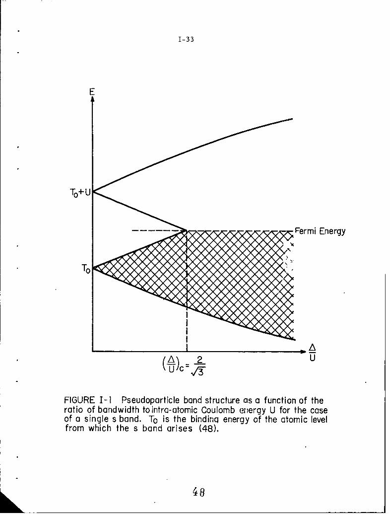
1-33
E
To+U'
Fermi Energy
(A 2 U
ToT
U C 3U
FIGURE I-I Pseudoparticle bond structure as a function of theratio of bandwidth tointra-atomic Coulomb eriergy U for the caseof a single s band. To is the bindincj energy of the atomic levelfrom which the s band arises (48).
48
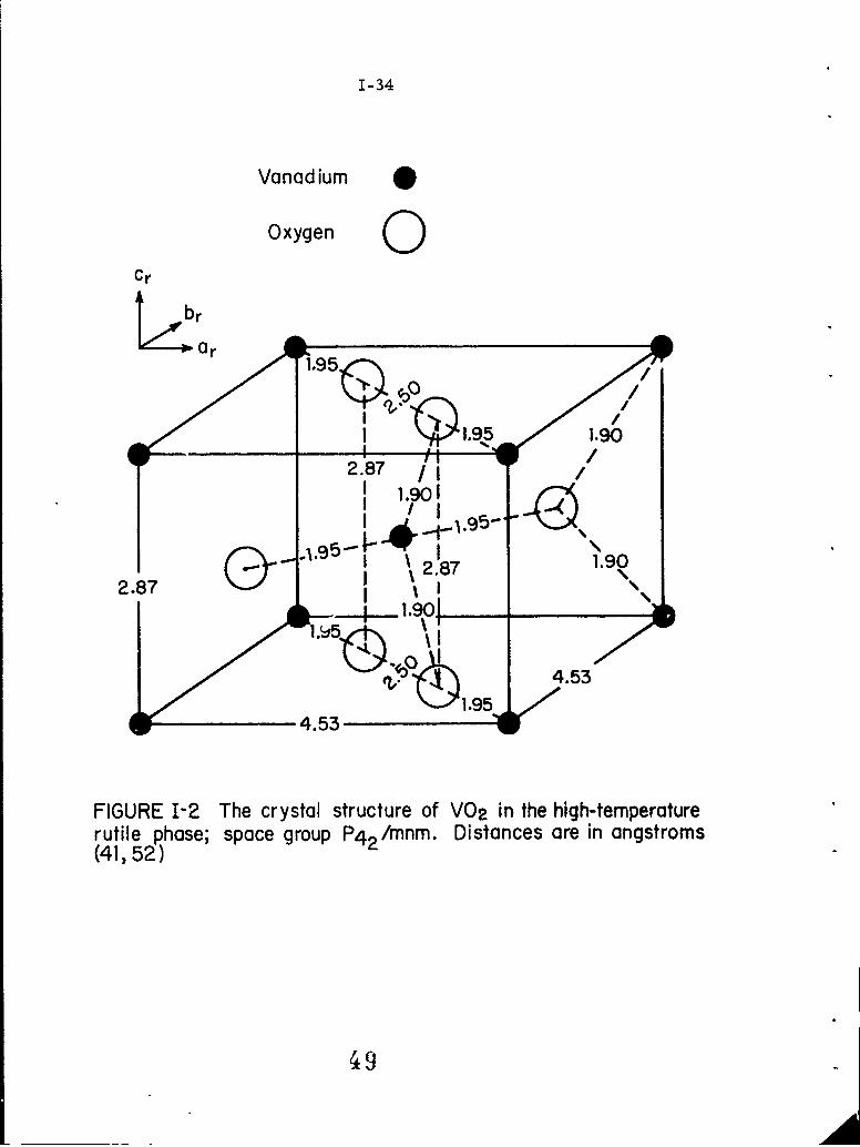
1-34
VanadiumOxygen 0
Cr
Or " '1.95?f•
1.95 ./1.90
2.87 /1.901
1.8 I 2. 1 8712 .8 1.900
",.- 1.951z 4.53,
FIGURE 1-2 The crystal structure of V02 in the high-temperaturerutile phase; space group P4 2 /mnm. Distances are in angstroms(41,52)
49
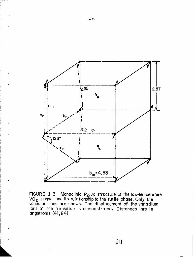
1-35
;;.65 2.87
''jIam
gI~~ 3.12 ar
IZ~12C / m___ ____
b.=.5
FIGURE 1-3 Monoclinic P21 /c structure of the low-temperatureV0 2 phase and its relationship to the rutile phase. Only thevanadium ions are shown. The displacement of the vanadiumions at the transition is demonstrated. Distances are inangstroms (41,84)
50

5sj 1-36
4.95
I I
I ,
I
96.8' /
14.00I/// . ' CCHM
FIGURE 1-4 The crystal structure of V203 showing both low-temperaturemonoclinic primitive cell (space group I2/) and the high- temperaturehexagonal cell (space group R~c). Open and hatched circles refer tocations of different spin orientation in the low-temperature antiferromagneticphase. Distances are in angstroms (28, 34)

1-37 5
600-
(VI-x Crx)z 03
400-
Cl PARAMAGNETIC
:: ................... ULTO...... ... ..... .
RO MAGNTAIL
FIGU~ ~F RE20Tmeatr-pesrecmoiin0hs igaof (V1~Crx) ...systm.(34)

CHAPTER II
PREPARATION OF FILMS AND CRYSTALS
In Chapter I we discussed the fact that one of the major experi-
mental problems in studying the transition metal oxides is the prepara-
tion of high quality single crystals and films. In this chapter we will
discuss some of the methods of growing films and crystals of V2 0 3 and
VO2 .
Since the vanadium-oxygen system is very complex (see Fig. II-1),
the growth of V2 0 3 and VO 2 crystals and films is complicated. We will
begin by briefly discussing methods used by other investigators to grow
single crystals and films of vanad;.um oxides. (Methods of obtaining
sintered samples of these oxides will not be mentioned since sintered
samples are usually poor substitutes for single crystals for physical
measurements.) Then, we will describe the methods we used in the
preparation of crystals and films of some of these oxides. We should
point out that our purpose is not to investigate in detail the different
growth processes in films and crystals of these vanadium oxides. Rather,
we want to obtain some experience in growing good quality single crystals
and films that will show a first order phase transition with a large resis-
tivity change at the transition. There has been no exhaustive attemvt,
in our investigation, to explore the various conditions of growth nor to
obtain the optimal growth parameters.
53
l1-2
A. Earlier Methods of Preparation
1. VO 2 Crystals
VO2 single crystals were fir3t grown by Guggenheim (1) by the
hydrothermal growth technique (2) and measured by Morin (1). These
crystals showed a first order phase transition with a resistivity change
of only a factor of "-10 at - 350°K.
Single crystals of VO 2 have also been grown by flowing oxygen-
free nitrogen gas past a platinum crucible containing both VO2 and V2 05
powder heated to 1000 0 C. The partial oxygen pressure was low enoughso that V205 was reduced to VO This method was first used by Sasaki
and Watanabe (3), who obtained crystals with resistivity changes up to a
4factor of 10 . MacChesney et al. (4) and Everhart et al. (5) used the
same method as Sasaki and Watanabe, but with different growth param-
eters, and were able to grow crystals as large as I cm in width. Their
crystals had a resistance change at the transition of a factor of as large
as 105 and a hysteresis on temperature cycling of 1 0 C.
Various vapor transport techniques of growing VO single crystals
were used by Kitahiro, Watanabe and Sasaki (6). They managed to giowcrystals of VO 2 by reacting V2O5 with titanium in a heated sealed quartz
tube. The crystals were small ( "- 0. imrn x 0. 2mm x 8rmm) and showed
a resistivity change of a factor of 3 x 10⁴ within 1 C at 65. 50 C.
Takei and Koide (7, 8) presented a new technique which was based
on the chemical decomposition of VOCI 3 vapor with moisture in an inert
or reducing atmosphere. They managed to obtain single cryst.als of
541

11-3
V2 0 5, VO 2 , V3 0 5 , and V2 0 3 . The largest VO crystals grown by this
method were '0.8mm x 0.8rmm x 15 mm. There was a resistivity
change of a factor of -104 at - 65 0 C. Using this same technique,
epitaxial films of VO and VO 2 on appropriate substrates were also ob-
tained. Growth of epitaxial films of V 2O3 was not successful. This
technique will be discussed in more detail later as we have adopted it
in our preparation of these vanadium oxides.
In 1969, Bando, Nagasawa, Kato and Takada (9) adopted a technique
used by Niemyski and Piekarczyk (14) for TiO to produce single crystals
of the vanadium oxides. This method proved to be very successful as
they have managed to grow single crystals of V2 0 4 (9), V3 0 5 (10),
V6OI1 (10), V407 (11), V7013 (11), V509 (12), and V8015 (13). This
vapor transport method involved the use of tellurium tetracholoride
(TeGI 4 ) as a transport agent. In all cases, the powders of each vanadium
oxide of which single crystals were to be prepared was sealed in a heated
and evacuated quartz tube with an appropriate amount of TeCl The
resultant single crystals in every case possessed the same chemical
composition. This technique proved to be a very flexible method to ob-
tain single crystals of many vanadium oxides, especially in the Magneli
phase system (Vn 0 2n for n=4, . . .n) where the chemical composition
is very difficult to control. The quality and size of these crystals are
reasonable. For instV.nce, in VO2, there was a resistivity change of a
factor of '- 10 within 1 C at 67°C. The crystal size was - 2-3mm in
width and - 1.6 cm in length (9). The only drawback in the method is
55
11-4
the toxic nature of TeCI 4; however, this is but a minor problem re-
quiring only careful handling. Growth of epitaxial films of these oxides
by this method has not yet been reported, but there is no apparant reason
that it cannot be done.
The technique of growing crystals by slow cooling of VO 2 in a
V2 0 5 flux, first used by Sobon and Greene (17), was adopted by Ladd
and Paul (15, 16) to obtain high quality crystals of VO,. An appropriate
mixture of powders of VO 2 and V 205 was sealed in an evacuated quartz
tube, and heated to about I1000C. Though the melting point of VO2 is
"- 2000°C, it will dissolve readily in an appropriate amount of V 2O5
when the temperature is - 800 C (see Fig. 11-1). The temperature of
the flux was then slowly reduced to room temperature (about 3 0 C/hour).
Single crystals of VO 2 were subsequently obtained in a solidified V2 0 5
flux, which was dissolved. The crystals in each run ranged from largeI
ones of ' 1 mm x 1 mm x 10 mm to smaller but mechanically strongcr
ones. Resistivity measurements as a function of temperature were done
on a few of these crystals (15, 16), and the insulator-metal transition
was found to occur often within one degree of 65°0 with a hysteresis on
temperature cycling of 1 °00. The resistivity change was typically by
a factor of 105.
2. V0 3 Crystals
Single crystals of V203 have usually been prepared by the flame
fusion technique, one of many variations of the Verneuil method (18).
In the flame fusion technique, material in the form of a fine powder, in
56
II-5
this case V2 0 3 powder, is continuously added to the molten top of a seed
crystal with heat usually being provided by an oxy-hydrogen flame. The
chief advantage of this method is that no crucible is required to hold the
melt. It thus permits the growth of crystals from materials having very
high melting points, and for which no non-reactive crucible materials can
be found. The disadvantages are that the high thermal gradients present
usually give rise to thermal strains in the crystals and taiat with the use
of an oxy-hydrogen flame it is not always possible to adjust the ratio of
oxygen to hydrogen freely to provide the correct oxygen partial pressure
for the growth of stoichiometric oxides. In fact, this latter point most
likely explains why VO 2 cannot be grown by the flame fusion technique (17).
Feinleib and Paul (19, 20) did their measurements on single crystals
grown by Linde Co. (21) by the flame fusion technique. They found that
the crystals exhibited a resistivity change of a factor of - 10 7 at - 1400K
on cooling and ' 150°K on heating. Goodman (22) also measured V2 0 3
crystals provided by Linde Co. and obtained a resistivity change of a
factor of 108 at "-160 K on cooling. Austin and Turner's (23) Hall effect
measurements on V2 03 crystals from Linde Co. were discussed earlier
in Chapter I. The flame fusion technique was also used by Sobon and
Greene (17) to grow V2 0 3 single crystals; no electrical data were re-
ported by th.•m a- these crystaIs all cracked at - 170 0 K on cooling.
Single crystals of V 203 were also produced by the flame fusion
method at the Institute of Crystallography of the Academy of Sciences of
the USSR (24). These crystals showed an electrical discontinuity of a
factor of 106 at a transition temperature of - 145 K on cooling. On
heating, the transition temperature was at - 165 0 K.
57

11-6
Single crystals of V2 0 3 were prepared at Bell Telephone Labora-
tories by a flux method (25) similar to the method we used in growing
VO 2 crystals, except that in preparing the V2 0 3 crystals, the choice
of a suitable solvent for V2 0 3 was difficult. Potassium fluoride (KF)
was finally chosen and gave satisfactory results. In brief, the growth
procedure involves mixing VN with V2O5 in a platinum crucible and
heating the mixture to 950 C. The mixture reacted to form V 03 and
was then transported through the molten KF to grow as single crystals
in the cooler part of the crucible, which was placed in an argon control-
led furnace. The resultant V203 crystals were quite soluble in boiling
water, were ' 5 mm across and ' 1 mm thick in size, and were found
to contain some VN (chemical analysis showed 1% nitrogen in the
crystals). An electrical measurement of one of these crystals as a
function of temperature has been reported (25) which showed a con-
ductivity discontinuity of a factor of ' 106 at ^150 0 K on cooling. There
was a hysteresis in temperature cycling of 10° 0 C.
Single crystals of V2 0 3 were also grown by the vanadium oxy-
chloride decomposition method discussed above. The crystals were thin
platelets of about 1 mm wide. The resistivity discontinuity at 153 K on
4cooling of one of the crystals was about a factor of 10
In reviewing various methods that many investigators have used to
obtain single crystals of VO 2 and V2 0 3 , we note that they all obtained
single crystals with large conductivity changes at the phase transition.
There were, however, variations in the magnitude of the disco.ntinuity
and the transition temperature, even in crystals prepared by similar

11-7
methods. These discrepancies can be explained by the sensitivity
of the electrical characteristics of these oxides to the chemical
composition and the impurity content. Since there are variations in
the properties of single crystals of V2 0 3 and VO, we can expect that
films of these oxides will fare much worse. In Sections 3 and 4, we
will discuss some methods of preparation and some of the properties
of the films of VO 2 and V2 0 3 that have been reported in the literature.
3. VO2 Films
In 194 7. Steensel, Burg and Kooy (26) reported that they had been
able to grow VO2 films by evaporating vanadium on glass substrates in
an oxygen atmosphere of 5 x 10⁻⁵ torr and then heat-treating the films
in oxygen after the deposition. The resultant films varied in thickness
from 0. *.- il. The electrical characteristics usually varied from film
to film. The resistivity discontinuity was not sharp, varying from a
very small anomaly at the transition temperature to a maximum change
of a factor of - 103 over a temperature interval of 10 C. The hysteresis
on temperature cycling also varied from 5°0 to 150C. Nor was the
transition temperature on heating constant, varying from 650C to 700C.
Structural analyses were not reported on these films.
Koide and Takei (27) used the oxychloride decomposition technique
described earlier, and obtained epitaxial films of VO2 on single crystal
TiO2 and GeO2 substrates. A typical film was 3 11 - 20ý thick, although
the growth conditions could be varied to give films as thick as Z00t.
Resistivity measurements as a factor of temperature showed wide
variations between samples. The best sample they reported showed a
resistivity discontinuity of a factor of -'103 at - 65 C.
59

11-8
MacChesney et al. (28) managed to grow VO2 films by a
technique involving the vapor deposition of V205 filnms on single crystal
sapphire substrates by the reaction of VOCI3 with CO The V 05
films were then reduced to VO2 films by a mixture of CO and CO2 gases.
The resulting films (0. 1 - 101±) showed a sharp drop in resistance
(103 ohms) at - 67 C. The hysteresis on temperature cycling was
about 1 0°C.
Rczgonyi and Polito (29) first prepared V20 5 films of - J. Z1
thickness on single crystal sapphire substrates by oxidizing vanadium
films deposited by DC sputtering of vanadium targets. The V2 0 5 films
were then reduced to VO 2 films. The resistivity change of one of the
films was a factor of - 103 at - 680C. The films prepared by the above
two methods were all polycrystalline.
The best VO 2 films reported were ,rown by reactive sputtering of
vanadium targets (30, 31, 32). The VO 2 films were deposited on various
kinds of substrates, for example single crystal sapphire, single crystal
TiO2 (rutile), amorphous glass and glassy ceramic. On single crystal
rutile and sapphire substrates, epitaxial films of VO2 were obtained
with resistivity discontinuities as large as a factor of - 4 x 10³ at the
transition temperature. Epitaxial films on sapphire substrates showed
a transition temperature - 68 0 C, while those on rutile substrates had
a transition temperature at - 58 C. In both cases, the hysteresis was
less than 10 C. The films grown on glass and ceramic substrates were
polycrystalline with a resistivity change of a factor of only 102 at
about 680C.
60
11-9
Since then, VO, films have been prepared by other authors using
the same or similar techniques (33, 34, 35) leading to similar results.
A significant experiment on amorphous VO2 films was done by
Kennedy and Mackenzie in 1969 (36). The amorphous films were
grown by radio-frequency sputtering of VO 2 powder target on cold sub-
strates of single crystals of MgO, Al203, and SiO 2 , and on glass.
Kennedy and Mackenzie, using x-rays, found the films to be amorphous.
The interesting feature of their experiment is the absence of the in-
sulator-metal transition in these amorphous films. When annealed in
argon for 24 hours at 6000C, the films became crystalline and a
resistivity change of a factor of - 102 at - 68 0 C appeared.
Mackenzie (37) later reported that amorphous VO 2 films grown
at "apparent" substrate temperatures above 65 0 C had relatively high
conductivity ( p- 5x 10⁻³ acm), while those grown at "apparent" sub-
strate temperatures below 6b"C had low conductivity (P- 10 2- 103-cm).
He, however, did not clarify what he meant b; "apparent" substrate
temperature. From the experiments on the amorphous films, Mackenzie
suggested that the electrical conductivities of these films were governed
primarily by the short-range structure of the films, but that the
insulator-metal transition in VO 2 depended on their long-range order.
4. V 2 0 3 Films
There have been few reported attempts to grow V2 03 films. In
one of these, Rozgonyi and Polito (29) managed to grow thin polycrystal-
line films of V203 using the same technique discussed on p. 11-8. The
2 3I
I-10
electrical characteristics of their films were poor when compared with
those of the bulk crystals. The electrical conductivity as a function of
temperature showed a change of a factor of "106 at "125°K on cooling
over a temperature interval of 250C. There was also a hysteresis of
about 300C.
Hensler, Ross and Fuls (32) tried to grow V 2 03 films by reactive
sputtering of a vanadium target, but managed to obtain only a mixture
of VOl. and V2 0 3 . Takei (8) also tried to grow V O3 films on single
crystal sapphire substratesby the vapor transport method discussed on
p. 11-2, with no success. Kennedy and Mackenzie (36, 37) reported
that they had grown amorphous films on VZ0 3 by radio frequency sput-
tering of powdered V 03 targets. As in the case of amorphous VO 2 film,
these amorphous VZO3 films failed to show any insulator-metal transition.
After annealing, the films became crystalline, and a large resistivity
change of a factor of 108 occurred between room temperature and 77 K.
However, since they provide no plot of resistivity as a function of
temperature, the existence of a sharp insulator-metal transition in the
crystall'zed film can only be inferred.
5. (V 1 x1Crx)2O3 Crystals
We have discussed in Chapter I that, in addition to the low
0temperature phase transition at 150 K, there is a second first order
phase transition in V203 crystals doped with an appropriate chromium
concentration and grown by the flux method described on p. 11-6 . By
adding Cr 2 0 3 to the mixture of VN, KF, and V2 0 5 , Remeika obtained
62

II-ll
crystals of V203 with different chromium concentrations. Pure V 03
crystals grown by this method were 5 mm across and 1 mm thick. The
size of the crystal in the mixed oxides decreased rapidly with increasing
chromium content, and at x 0. 12, the crystals were less than 0. 1 mm
wide. The doped crystals, like the V2 0 3 , had a considerable amount
of nitrogen (probably %- 1'0) in them, and were quite soluble in boiling
water.
B. Preparation of Films and Crystals of VO2 and V2 0 3 , and
Crystals of (V1 Cr)O3
Films and crystals of vanadium oxides are difficult to grow, not
only because of the complex vanadium-oxygen system, but also because
of the high melting points of most of these materials. Table II-1 lists
the melting points of vanadium metal and some of the cxides in which
we are interested.
Material Melting Points ( C)
Vanadium V 1890 + 10
Vanadium Dioxide (VO 2 ) 1967
Vanadium Sesquioxide 1970(V 2 0 3 )
Vanadium Pentoxide 690(V 2 0 5 )
t: Melting Points of Vanadium and SomeM . xides (38).
63

11-12
Since VO 2 and V O3 both have melting points of 20000 C, the
preparation of films of these oxides by the evaporation of these oxides
from tungsten and tantalum boats is not recommended. In addition, the
oxygen partial pressure from the oxides tends to oxidize the boats at
these high temperatures and the oxides of tungsten and tantalun aC-1
volatile. Nor is evaporation of vanadium metal from these boats suc-
cessful, as the vanadium alloys with the tungsten and tantalum. In ad-
dition to the above difficulties, at high temperatures, VO decomposes to
lower o-ýides of vanadium and oxygen (26). Therefore, in the preparation
of films and single crystals of VO 2 and V2 0 3 , special care mist be
given to the selection of the appropriate growth techniques.
1. Radio Frequency Sputtering
Sputtering occurs when a target is bombarded by energetic ions
causing some surface atoms to be ejected from the target. The surface
atoms then collect on any surfaces which may be close to the target.
(A detailed exposition of theories of sputtering may be found in the fol-
lowing references: 40, 41, 42, 43, 44, 45, 46.)
In our sputtering apparatus (see Fig. 11-2), the energetic ions
are provided in the manner described below. Electrons produced by
thermionic emission from a tungsten filament are attracted towards an
anode and during the process acquire energy from the electric field pro-
vided by the anode. When sufficient energy is attained, these emitted
electro,,s will ionize the sputtering gas atoms. The ionization of these
atoms will in t-rn provide secondary electrons, which can then participate
II- 13
in further ionization of the gas atoms. Under proper operating conditions
the resultant plasma of energetic ions and electrons can be sustained.
Then, when a negative dc potential is applied to the target, the positive
ions in the plasma will be attracted to the target and DC sputtering begin3.
In our experiments, radio frequency sputtering (RF sputtering)
was used to sputter pressed targets of V2 0 3 and VO. The difference
between RF sputtering and DC sputtering is that in the former, a radio
frequency alternating potential is applied to the target instead of the
negative DC potential used in the DC sputtering. DC sputtering is adequate
for sputtering metallic targets. On the other hand, if an insulating tar-
get is used in DC sputtering, the positive charges from the bombarding
energetic ic -s will build up on the surface of the target and repel all
further ions from bombarding the target. If an alternating potential is
applied to this insulating target, the surface of the target --ill be period-
ically neutralized by the electrons in the plasma attracted to the target
by the positive potential in every half cycle of the alternating potential.
Therefore, the RF sputtering technique can be used for both metallic
and insulating targets.
At room temperature, V203 is quite a poor metal (P - 10-3 G-cm)
while VO 2 is insulating (P - 100 61-cm). When powders of V2 0 3 and VO 2
are pressed into targets, their resistivity is usually higher (e.g., the
resistivity of a pressed V2 0 3 target was fouLLl to be P - 0. 2 6ý-cm at
lo--n temperature). Although it might be possible to sputter V 03
(but not VO2 ) targets by the DC techr.ique, we decided to use RF sputterir,
to sputter both V2 0 3 and VO 2 targets.
65

U-14
Our sputtering apparatus is based on a RD Mathis model SPZIOA
triode sputtering unit for both the RF and DC sputtering. A turbo-
molecular pump (Welch model 310A, made by the Welch Company,
Illinois) enables us to reach a vacuum of 3x10⁻⁶ torr. A turbomolecular
pump was chosen over a diffusion pump because of its high pumping speed,
and its minimal oil contamination. Furthermore, the turbomolecular
pump can be used to pump all non-corrosive gases and will not be
damaged by an accidental exposure to atmospheric pressure.
This sputtering apparatus was originally assembled by Rossi (39)
to grow NiO films by DC reactive sputtering. During our research work,
further improven ents have been made. Figure 11-2 is a schematic dia-
gram of our sputtering system, and Fig. 11-3 and Fig. U1-4 show some of
the equipment that has been used during our film preparation. We will
identify each individual part later in the text.
The targets were made by pressing VO3 or VO * powders in a
1 ,, diamcter die. Figure II-3a shows the die that we used. It was2
made of Lehigh H stainless steel (47) which can withstand abrasions from
the powders when under a uniaxial stress of about 5x 10⁴ Ci. Generally,
an eight gram load of V O., or VOZ powder would give us a disc of ' 112 . 2
diameter and 1, thick. The target to be sputtered was then mounted on
an oxygen-free copper block with a diameter slightly smaller than that
of the target by a solder of high thermal and electrical cornd'ictivity
(Eccobond Solder 56c (48)). Figure II-3b shows the copper block with
V2 0 3 powder obtained commercially from United Mineral and ChemicalCorp., New York.
VO2 powder obtained commercially from Alfa Inorganics, Beverly, Mass.
66

11-15
a pressed target of V2O3 mounted on it. Finally, the copper block
with the target was mounted on the water-cooled electrode shown in
Fig. 11-2.
The substrates used were polished single crystals of sapphire of
< 0001 >orientation obtained commercially from the Adolf Miller Go.,
Rhode Island. We further polished the sapphire substrates using first
4. diamond paste and then 0. 03p. syton to reduce the surface damage.
The cleaning procedure for the substrates involved a five-minute scrub
with Alconox and a rinse in hot water, followed by a rinse in distilled
water. After they were boiled in HI 0 solution for ten minutes, they2 2
were rinsed in doubly distilled water and dried by blowing dry nitrogen
gas over them. During the whole process (right after they were scrubbed
in Alconox), they were placed in a specially built teflon basket (see Fig.
1I-3c) and never allowed to be dried in air. This elaborate cleaning pro-
cess was used by Hensler et al. in cleaning their sapphire substrates
before the deposition of VO 2 films (49).
The construction of the substrate heater is illustrated in Fig. II-4a,
which also shows the substrate holder (the slot in the holder is designed
to receive a standard size sapphire substrate, i. e. , 0. 310" square x
0. 010" thick). A platinum-platinum 10% rhodium thermocouple was
mounted next to the substrate.
During the presputtering process, a mechanical shutter (see Fig.
II-4b) was usually placed just above the substrate and between the ta;-
get and the substrate. Hence any film deposition would be on the shutter
67

11-16
and not on the substrate. When the operating sputtering conditions were
stabilized, the shutter was removed and the actual film deposition began.
Argon gas was chosen as the sputtering gas, partly because of its
inertness and partly because of its relatively large molecular weight
when compared with other inert gases such as nitrogen; it thus pro-
vided a large sputtering rate. The argon gas, obtained commercially
from the Igos Co., Massachusetts, with a stated purity of 99. 995%
was further purified by passing it through calcium turnings heated to 400 °C.
_V203 Films. The above sputtering system was used to grow V 0
films by radio frequency sputtering of pressed V2 0 3 targets. Four
polycrystalline films grown on sapphire substrates under very similar
conditions. Typical operating conditions were: argon pressure at
"1i. 616 , radio frequency at 0. 1IMz, target voltage of -" 1700 v, target
current at - i10 ma, and substrate temperature at -. 400 0C. The sput-
tering lasted about five hours with a deposition rate of 1100 A/hour, as
measured by an interferometer (Hilger and Watts Model 130). Three
of the films grown had no post-deposition annealing, and one film, VSZ,
was annealed after deposition in the sputtering system (vacuum - 7 x 10"5 torr)
at 300 C for two hours.
Reflection electron diffraction measurements on the films verified
that these films possessed most of the rings expected for V2 0 3 . Figure
11-5 shows the reflection electron diffraction pattern of VS3. By as-0
surning that the first ring corresponded to 3. 65 A of V 203 from ASTM0 o o
index, then the other rings corresponded to 2. 70 A, 2. 46 A, 2. 32 A0 0 0 0 0 0
2.17A, 1.83 A, 1. 68A, 1.46 A, 1.42 A, and 1.32 A, with an

11-17
ASTM INDEX
d (measured) V2 0 3
0 0(A) d (A) 1/10
3.65 3.65 60
2.70 2.70 80
2.46 2.47 60
2.32 2.32 z
2, L7 2.18 202. 03 2
1.83 1.83 25
1.68 1.69 100
1.61 2
1.57 3
1.46 1.47 25
1.42 i.43 30
1.32 I. 33 10
TABLE 11-2. Comparison of lattice spacingsof a V2 0 3 sputtered film obtained from re-flection electron microscopy with the spacingslisted in ASTM Index.
experimental uncertainty of about + i1% on each peak. When compared
with the ASTM Index of V 03 (see Table 11-2), wve noticed thai only threeo 0 0
rings were missing: at 2.03 A. 1.61 A and 1.57 A. Since these lines
are the w.akest in the series, their absence is not very surprising.
The reflection electron diffraction patterns on other films were very
similar and in all cases missing lines in th6 patterns corresponded to
the weak lines in the ASTM series. T1'orefoze, reflection electron micro-
scopy measureme-ts showed these films to be polycrystalline V 23films.
269ims

II- 18
These films, however, did not show a distinct metal-insulator
transition on cooling; their electrical resistivity at room temperature
-4 -3varied from - 5 x 10- to 10 R3-cm, and typically showed a slight de-
crease from 2 to 8 times when the temperature was reduced from room
temperature to that of liquid nitrogen.
These four films were then annealed at 600 0 C for 24 hours in a
sealed quartz tube which had been flushed repeatedly with argon and
evacuated to 10-5 torr. After the annealing, they all showed a large
resistance increase (all had more than a factor of 10 3) when cooled from
room temperature to that of liquid nitrogen. The electrical resistivity
as a function of temperature of two of the films is shown in Fig. 11-6.
Despite the difference in the room temperature resistivity and the
breadth of the structure, the resistivity change is about a factor of 102
at -150 0 K, which is close to the transition temperature of the bulk V2 0 3
crystal. The elec...ical measurements were done by the four probe
method. Silver contacts were evaporated on a film which had been placed
in a brass block and covered by a brass mask (see Fig. II-4c). Elec-
trical leads were then attached to the silver contacts by silver epoxy.
For VS2, the electrical measurement was made in a Janis Super Vari-
Temp. Control Dewar Model 10-DT described in detail by Callendar (50)
in his thesis. The electrical measurement on VS4 was done in a dewar
designed by Ladd (16). Figure 11-7 shows the copper block on which the
film was mounted and the associated electrical and heater arrang.ements.
The block was then placed in a stainless dewar and evacuated to 10-5 torr.
11-19
A cooling rate of 5 0 C/min could be obtained by immersing the dewar
in liquid nitrogen and adjusting the heater current. Our temperature
reading was accurate to within 11 " . Such low accuracy was quite suf-
ficient ) establish the alteration of the resistivity versus temperature
relation caused by annealing.
Although the electrical characteristics, of these films were different
before and after annealing, the reflection electron diffraction measure-
ments showed that the films remained polycrystalline V203 films after
the annealing.
The effect of the annealing is not certain. One possibility is that
the size of the crystallites increased. If this is the case, it may imply
a minimum crystallite size or a minimum degree of order for a phase
transition to propagate. As discussed earlier, Kennedy and Mackenzie
(36) had already noted that amorphous films of V 203 grown at temperature
- 130 0 C were metallic both above and below the transition temperature.
When annealed, a large change of resistance occurred between room
temperature and 77 0 K. In VO 2, in addition to the absence of the phase
transition, Mackenzie (37) also reported that the amorphous films de-
posited below the transition temperature were semiconducting while
similar films deposited above the transition temperature remained metallic.
If this is the case, one can deduce that the substrate temperature de-
termines the local order, which, in turn, determines the transport
mechanism, and that the insulator-metal transition is inhibited because
the lattice cannot transform. The present measurements may suggest
71

II-20
the amorphicity is not necessary fo. the inhibition of the phase
transition, only the greater disorder of a polycrystalline film.
Another plausible possibility is that annealing, even in a sealed
quartz ampoule, changes the V-O balance, which might be important
in view of the complex V-O system. Reflection electron microscopy
identified the films to be of V2 0 3 structure, but it could not inform us
of their exact chemical composition.
VO2 Films. As an extension of our efforts in growing V2 O3
films by the RF sputtering of V 2 0 3 targets, a pressed target of VO0
powder was prepared and sputtered under similar conditions as in
V 2 0 3. Two polycrystalline films were grown on single crystal sapphire
substrates <0001 > orientation, but reflection electron microscopy showed
that the films were not VO. In fact, if we assume that the first ring
corresponded to the first x-ray powder diffraction peak of V0 1 . 0 (51),
then the rest of the rings matched with the diffraction peak of VO 1 0 to
within 1o%. The reason why VO decomposed to VO is not known for sure.
It might be due to the fact that the VO 2 target decomposed at the surface
where the surface temperature could have been very high, or that if
VOZ film had indeed been grown, it might have been decomposed by the
substrate temperature of 600 0 C. We may still be able to grow VO 2
films by this method, however, if a mixture of argon and oxygen gases,
rather than argon gas alone, is used as the sputtering gas. The mixture
might maintain an appropriate oxygen partial pressure in the system to
allow growth of stoichiometric VO2 films. A possible drawback to this
72
1I-2I
technique is that the reactive sputtering is not very suitable for our
existing apparatus; the reasons for this are explained in the next
section. In any event, our success in growing VO2 films by the vapor
transport technique to be discussed later led us to drop experimentation
on the sputtering of this material.
2. Film Preparation in a Reactive Atmosphere
In our attempts to prepare VO 2 films in a reactive atmosphere, we
used both electron beam gun evaporation and DC sputtering. In the
former, vanadium metal in a water-cooled graphite crucible was eva-
Lorated in an oxygen atmosphere using a Veeco electron beam gun (Model
VeB-6G). By adjusting the power of the gun - and thus the rate of
evaporation - and the oxygen partial pressure, we should have been able
to vary the vanadium-oxygen ratio in the films. Nevertheless, of the 20
or so films ve grew, on BaF 2 and sapphire substrates, none showed a
sharp resistance change near 67 0 G. Most of the films were grown with
fixed oxygen partial pressure ("10-4 torr) and with varying electron gun
power. There were marked differences in the electrical resistance in
films grown under apparently similar conditions. The difficulties could
be attributed to the many valence states of vanadium which permit it to
combine with oxygen in various proportions. Therefore, the ratio of
vanadium and oxygen present in the vacuum system has to be exactly
right and very well controlled in order to grow good reproducible films.
Since our electron beam system is a model without a fine regulation of the
beam power, which was found to vary as much as 20% during runs that
73

11-22
typically lasted about 20 minutes, it is not surprising that the pre-
paration of VO 2 film by this method in our system was unsatisfactory.
A very well controlled electron beam system and a good regulator for
the oxygen partial pressure in the vacuum system might very well allow
growth of VO 2 .
The same difficulties in using electron beam gun evaporation were
encountered in the DC reactive sputtering of a vanadium target. The
sputtering system we used was the same as the one described above,
operated in the DC mode with the argon sputtering gas replaced by dif-
ferent mixtures of oxygen and argon gases as the sputtering gas. The
gas mixtures we used were Ar 80%o, 02 20%o; Ar 90%6, 02 10%o; Ar 95%,
02 5%; Ar 99%, 02 1% and Ar 99.5%, Oz 0.5%. There were many
variables in the sputtering process, among them, gas mixtures, sput-
tering pressure, substrate material, substrate temperature, and target
current. Most films were grown on glass, A 2 0 3 and TiO2 substrates
with two gas mixtures (Ar 90%6, 02 10%; and Ar 99%, 02 17%) by varying
the sputtering pressure and/or the target voltage. None of the films
that were grown - about 40 of them - showed any sharp resistivity
change near 670C. Again, we think that VO 2 films could have been
grown if very well controlled operating conditions were possible.
No detailed reflection electron microscopy studies have been done
on films grown either by electron beam gun evaporation or by DC reactive
sputtering. Reflection electron diffraction measurements showed, in
many cases, very faint rings and, in other cases, no clearly visible
riJ

11-23
structures at all. Hence, though the films are probably polycrystalline,
the identification of these phases by reflection electron microscopy has
been difficult.
3. Vapor Transport Technique
The vapor transport method used by Takei and Koide (7, 8) is con-
sidered to be a very flexible method of preparing high melting point
materials. We therefore attempted to investigate the preparation of
crystals and films by using their technique.
Figure 11-8 shows a schematic of the apparatus and the reaction
crucibles for both crystal and film growth. The quartz reaction chamber
was heated by a resistance furnace controlled by a Barber-Colman elec-
tronic controller which regulated the temperature in the reaction crucible
to -.bout + 50C, as indicated by a Platinum-Platinum 13%6 Rhodium thermo-
couple placed next to the reaction chamber. Chemical vapors were passed
into the reaction chamber through temperature baths controlled to with-
in + 5 0 C, and the flow rates of these vapors were regulated by flow-
meters to better than + 10%6 of their values. The chemical equations
used in this method are:
ZVOCI 3 + 3H 2O -0 V20 5 + 6HCI
VOC1 + H0 +1H-H VO + 3HCI3 2 Z 2 ~ 2
ZVOCI 3 + H2 0 + 2H2 -' V0 3 + 6HCI
VOCl 3 solution was obtained commercially from Howe & FrenchCompany, Boston, Mass.
75

11-24
Vz0 3 Crystals. A few runs were made to produce crystals of
V*0 2 . The best run yielded a reasonable number - about 50 - of
2 03 crystals roughly 2mm in diameter by 0.5 mm long. The actual
operating conditions can be explained by reference to Fig. 11-8, with
the parameters taking the following values: T1 = 8000C; T = 60CC;
T3 = 300C; V 1 = 3. 8cc/min; V. = 0. 3 6 U/min; V 3 = 0.3 J/min; and
reaction time 160 hours. The parameters used here, as well as those
used in the growth of V 2 0 3 and VO 2 films by this method were chosen
with reference to thrcse used by Takei (8). Some adjustments of his
parameters were necessary for our system, and our parameters were
arrived at empirically after several trial runs. X-ray Debye Scherrer
analysis showed the crystals were V 2 0 3 , and x-ray Laue back reflection
using tungsten radiation showed them to be single crystals with the
c-axis of V2 0 3 perpendicular to the plane of the platelet. Chemical
analysis (52) showed them to be 68. 0 + 0. 5% by weight of vanadium,
while stoichiometric V2 0 3 should be 67. 98% by weight of vanadium.
Spectrographic analysis (52) established that the impurities which are
observable by this analysis, were about 1 part per million. Optical and
optical microscopy examination showed one natural surface of each
crystal to be usually very flat and shiny with no visible structure, making
the crystals suitable for optical reflectivity measurement.
Figure 11-9 shows the resistivity versus the temperature of oue of
the crystals, together with a comparison with previous investigations.
*EL )nents such as nitrogen, carbon, oxygen, and hydrogen, however,are not detectable by this method.

II-25
The data were obtained by a four point probe measurement done in the
same apparatus as discussed earlier in this chapter. The actual resis-
tivity value was estimated to within a factor of about 2 or 3 because of
the irregular shape of the crystal.
Two additional crystal runs were made to try to reproduce the
most successful run discussed above. In both of thest runs, we ob-
tained crystals about half the size of those grown in the best run. They
were also identified to be V203 by the x-ray Debye Scher.-er measure-
ments. However, these crystals did not have the natural shiny optical
surfaces that those grown in the best run possessed, and, therefore,
were not used for optical measurements.
V2_03 Films. Because of our success in obtaining V203 crystals,
we tried to grow epitaxial films of V 2 0 3 on single crystal sapphire sub-
strates with <0001> orientation. Several films were grown that showed
large resistance changes (a factor of larger than 10 2) as the temperature
was decreased from room temperature to 77 K. One of the films grown
was scraped off the substrate and was checked by x-ray Debye-Scherrer
measurements. The measurements showed faint rings whose positions
corresponded to V2 0 3 x-ray lines from the ASTM index. But since
the amount of scraped powder was very minute, there is a possibility
of other phases existing in the film in smaller proportions. Reflection
electron microscopy determined that these films were essentially epit-
axial though it is possible that there were some small angle bound&.rie';
between the crystallites. By optical microscope examination, tl is
77

11-26
surfaces were rough compared with those of the ciystals, with needle-
like protuberances on occasion. The thickness of these films were us-
ually uneven, often thinner on the edge than in the middle. Measure-
ment of their thickness was, therefore, difficult. We used a Pratt and
1Whitney electrolimit gauge (accurate to - micron) to estimate the
thickness of the films.
Figure II-10a shows the reflection electron diffraction pattern of
one of the films which was grown on a sapphire substrate cut with the
c-axis perpendicular to the plane of the substrate. The film has a
reasonably smooth surface, as can be seen in Fig. U-10b. Though we
did not try to determine the orientation of the film on the substrate,
some of the crystallites on the surface had a hexagonal shape, indi-
cating that the film might have grown with the c-axis perpendicular to
the plane of the substrate. The electrical resistivity measurements on
the film as a function of temperature were done in the dewar discussed
earlier in the chapter. Only a two probe measurement was done on this
film because of its small physical size (see Fig. 11-7). The resistivity
value reported in the above figure is an approximate one, partly be-
cause of the uneven-ness of the film thickness, and partly because of
the inaccuracy of a two probe measurement on an irregular-shaped film.
Nevertheless, the film showed a resistance change of - 102 in the same
region where the phase transition occurs in crystals of V203 (see
Fig. 11-9). This film was grown under the following conditions: TI = 8000G;
T2 = 60 0 C; T3= 30 0 C; V1 = 3. 8cc/min; V 2 = 0. 361/min; V3= 0. 15 e/min;
reaction time = 42 hours; with film thickness = 2+.
78

11-27
Reproducibility of the vapor transport film was not good. Under
similar conditions, we tried twice to reproduce the above film; once
we did get a film that showed a large resistance increase of a factor of
S103 from room tem perature , the tem perature of liquid nitrogen, but
another time a thin discontinuous grey film was obtained.
VO2 Films. Attempts were made to grow VO2 films cn single
crystal sapphire substrates with <0001> orientation. Severalfilms grown indi-
cated resistance changes of more than a factor of 102 for the tempera-
ture interval from room temperature to " 80°0. Figure II-1l shows
the reflection electron diffraction pattern (indicated the film to be
epitaxial) and the optical microscope picture of one of the films gro-,n,
under the following conditions; TI= 8000C; T2 = 600C; T3= 30°C;
VI = 5.7 cc/mim.; V = 0. 36 irrin; V3= C.32 U/min; reaction time = 42
hours; with film thickne 3s = L.5p.
Figure 11-12 shows the resistivity versus -temperature plot of
"*he film. The measurement was done in the dewar discussed earlier in
this chapter. The resistivity value of the film as reported in the above
figure, is only an approximate one, again because cf the irregular
shape of the film and the inaccuracy of the two probe measurement. A
sh..rp resistance change o- a factor of - 102 was indeed observed z !ound
670C, which is close to that of bulk crystals as demonstrated in Fig. II '2.
VO2 Cr7'stals. Several attempts were made to grow VO crystals
with no apparent suLzess. Most ol the runs produced crystals that had
mixtures oi different vanadiam oxides, including VO 2. Since
79

11-28
high quality VO crystals had already been successfully grown by Ladd
and Paul (15), and since considerable time would have to be spent to ob-
tain the proper growth conditions, we decided to proceed no further.
4. Tri-Arc Czochralski Crystal Growth Technique
(V 1 x _Cr x)2O3 Crystals. Single crystals of V2 0 3 and V203 doped
with chromium were grown in a tri-arc furnace in Linc,.i Laboratory.
Three electric arcs were used to heat a melt in a graphite crucible sur-
rounded by a water-cooled copper block. The crystal was pulled from
th- center of the melt with a water-cooled seed rod. Use of this experi-
mental setup eliminated the difficulty of finding crucible materials suit-
able for high temperature growth, since the melt was contained by a
solid shell of the same substance in contact with the cooled crucible.
Figure 11-13 shows'a cross-section drawing cf the tri-arc Czochralski
crystal growing furnace. (A detailed discussion of this technique of
crystal growth can be found by referring to Reed and Pollard's paper (55)).
V2 0 and (V, _Cr) 2 3 can be grc.wn easily by this method be-
cause of their partial oxygen vapor prassure. Figure -1-14 shows a
plot of oxygen partial pressure versus oxygen-metal ratio for different
elements (56). This was obtained from theoretical calculation of the
free energy of formation of the.,- materials at 1000 0 K. It is noted from
the chart that the oxygen partin' pressures of V 2 0 3 and Cr 2 O 3 are both
very low and have approximately the same value. Therefore, if V 03
crystals can be grown in the apparatus, growth of Cr 2 O 3 crystals, and
the alloys of Cr2 0 3 - V2 0 3 should not be difficult. In addition, because
*In collaboration, with Dr. T. B. Reed.
80

I1-29
of the very low oxygen partial pressure of both Cr 2 0 3 and V2 0 3,
negligible amounts of oxygen should be lost in the growth process, and
the resulting crystals should be stoichiometric.
To grow crystals of V2 0 3 , the graphite crucible wai first charged
with 10-30 grams of V2 0 3 powder. The furnace chamber was then flushed
by argon for several minutes and then maintained just above atmospheric
p•-essure by a steady flow of argon gas ( - 1000cc/min). The first arc
was started by touching its tungsten cathode to the side of the graphite
crucible. The cathode was then moved in to strike the charge. The
other two arcs were started the same way, or by touching their cathodes
to the first arc. The heat was then increased until a melt was formed.
The seed, a molybdenum stud in our particular case, was then dipped
into the melt and raised rapidly to form a small neck in the growing
crystal in order to eliminate polycrystallinity. The crystal was then
raised typically at 4 in/hr, and its diameter was increased either by
decreasing the arc current or by moving the cathodes out toward the
edge of the melt. During the pulling process, the melt and pull rod
were both rotating at a speed of 50-100 cycles/min for better mixingV
and distribution of heat. When the crystal reached a reasonable size,
the pulling rod was raised much faster so that the crystal would break
away from the melt. The melt was then cooled slowly. Single crystals
of V2 0 3 of reasonable sizes were usually also found in the c oled melt.
Figure 11-15 shows the crystals grown by this techniq'ie. Tb - largest
one obtained by pulling from the -,elt, and ttie others were grown in
the melt.
831

11-30
Chromiumns X-Ray
Run Concentration Mass Optical * Diffraction **(average over Spectroscopic Measurements Measurenents
number of crystals) Analysis A
1 0 x
2 0 X X
3 0.0022 X
4 0. 0O?0 X X
5 0.0045 X X
6 0.0083
7 0.010 X X
8 0.014 X X
9 0.018 X X X
A Results of mass spectroscopic analysis are listed on pp. 11-33, 34.
* Results of optical neasurements will be presented in Chapter IV.
Results of x-ray diffraction measurements are shc "- in Fig. - 16.
TABLE 11-3. List of Crystal Runs andMeasurements on the Crystals
To grow single crystals of (V,_x1 Crx)2103, an appropriate mix-
ture >f V 2O3 and Cr20 3 powders was used. Though similar operating
procedares were followed, we found that it was much harder to pull a
large crystal from t e melt since the crystal would tend to crack easily.

11-31
Therefore, our doped crystals were usually grown by melting the mixed
powders with the arcs, then cooling the melt to room temperature. They
were usually-, 2-3mm across and 3-4 mm long. Table 11-3 lists our
crystal runs and some of the measurements that have been made on
the cry-Ctals.
Chemical spectrophotometric analysis on one of the V203 crystals
(Run #2) showed that it contained 68.0 0 0. 1% by weight of vanadium,
while the stoichimetric V2 0 would contain 67. 98% by weight of vanadium.
The experimental uncertainty in the chemical spectrophotometr. '
analysis for the chromium concentration in the crystals obviously de-
pends on the amf of chromium present in the test, and in our cases,
it was within + 4% for x = 0. 002, and decreased to within + 1% for
x = 0. 02. The chemical analysis of the doped crystals showed that the
average doping concentrations (averaged over a number of crystals) in
each run was ususally within 10% of the initial doping concentration in
the powders. This was partially due to the fact that when the powders
were heated up by the arcs, the trapped air in the powders often scat-
tered the powders around, some of it often getting away from the crucible.
Furthermore, some segregation (i. e., the ratio of two components in
the solid phase usually is differeat frc• .hat in the liquid phase, and
usually this ratio itself varies along the length of solid) inevitably must have
occurred. When a two-component liquid solidifies, segregation often
occurs (57).
83

11-32
To check the effects of segregation in our system, the chemical
analysis was done on a number of crystals and on the grains from the
melt obtained on the same crystal run (Run #6). It was found that the
average chromium doping level of the crystals was x = 0. 0083 and was
only - 6% lower than that of the grains. Therefore, the segregation
in (Vl xCrx)2 03 was small when compared with the segregation of
many two-component systems, such as indium or antimony in germanium
(58). These small segregation effects were further demonstrated by a
series of analyses on four doped single crystals (each about 3mm across
and 2mm long). They were broken into two parts and chemical analyses
were performed on the separate parts. The analyses showed that the
chromium doping level, x, in one of the crystals grown in Run #5 was
0. 0047 and that there was no variation in the doping level between the two
parts of the crystal. A crystal obtained from each of Runs #8 and #9
evidenced only - 616 differenc•. in the doping level between the two parts
of the same crystal; the average chromium doping level, x, was found
to be respectively 0. 014 and 0. 019. The analysis was also done on a
second crystal from Run #9, and a difference of 10%o in the doping level
between the two parts of the same crystal was observed; the average
doping level in this crystal was found to be 0. 018.
Thus, the variation of chromium concentration within the crystals,
as indicated by the chemical analyses, was small when the uncertainty
of the chemical analyses themselves is taken into consideration. The
slight variation in chromium concentration within these crystals was
84

11-33
probably due to the fact that the crystals were grown by a relatively
rapid solidification from the melt. A detailed explanation of the effect
of the rate of solidification on the segregation of a two-corn onent sys-
tem can be found in reference 57. It is sufficient to point out that in
solidifica-..on, the two homogeneously-mixed components in the liquid
phase are essentially quenched into the solid phase, resulting in very
little segregation.
In the above-mentioned analyses of the four crystals, At can be
seen that the segregation effects also cause slight variations of doping
levels in different crystals from the same growth run. Therefore,
chemical analyses, whenever possible, were done individually on
crystals whose physical properties were measured, and particularly
those whose optical~properties were measured. The doping level re-
ported for such a crystal was the average chromium concentration in
the crystal. For a crystal which was not individually analyze 1, its
doping level was approximated by taking the doping level as determined
from analyses of a number of crystals grown at the same time, sub-
jected to an uncertainty level of + 5% of its value.
Mass spectrographic analysis on a single crystal of V2 03 from
Run #2 showed that the impurity contents were 130 p.p.m. of carbon;
300 p.p.m. of aluminum, 70 p.p.m. of iron; and less than 50 p.p.m.
of nitrogen, titanium, molybdenum, potassium, and sodium each. In
(V1 x Cr x)203 crystals, mass spectrographic analysis on a cryztal
from Run #4 showed impurity contents to be 360 p. p.m. of carbon,
85

11-34
100 p. p.m. of sodium; and less than 50 p. p.m. of nitrogen, silicon,
potassium, and titanium each. On a crystal f:om Run #9, we found
impurity contents to be 80 p.p.m. of carbon and less than 50 p.p.m.
of sodium, nitrogen, aluminutm, silicon, potassium and molybdenum
each.
X-ray Laue back reflection measurements on V203 and doped
V2 0 3 crystIs all showed sharp diffraction spots indicating that they
were single crystals. From x-ray diffraction measurements, we ob-
tained lattice constants, aH and cH (as defined in a hexagonal lattice)
of V2 0 3 and (V 1 x Cz )203 crystals as a function of doping concentrations
(see Fig. 11-16). We also noted that when x was between - 0. 010 and
"- 0. 015, there were two phases coexisting at room temperature. This
co-Pxistence of two phases was also observed by McWhan and
R emeika (Z5).
VCr crystals grown by the flux methodV203 crystals and (VI1 xGr•2 0 3
have been reported to be quite soluble in boiling water (25), though the
exact solubility is not known. The solubility of a V 2 0 3 crystal from
Run #2, however, was examined by boiling it in water for twelve hours.
Its weight was found to decrease only by - 0./6%. Even this small
weight decrease could have been caused by having some chips broken
away from the crystal during boiling. A doped crystal from Run #9
which was boiled in water for five days, showed a weight decrease of
only 0.2%6. Therefore, in contrast to what has been reported, these
crystals have very low, if any, solubility in water.
86

11-33
probably due to the fact that the crystals were grown by a relatively
rapid solidification from the melt. A detailed explanation of the effect
r , rate of solidification on the segr-gation of a two-component sys-
tem can be found in reference 57. It is sufficient to point out that in
solidification, the two homogeneously-mixed components in the liquid
phase are essentially quenched into the solid phase, resulting in -rery
little segregation.
In the ab'ove-mentioned analyses of the four crystals, it can be
seen that the segregation effects also cause slight variations of doping
levels in different crystals from the same growth run. Therefore,
chemical analyses, whenever poss'ble, were done individually on
crystals whose physical properties were measured, and particularly
those whose optical~properties were measu'ed. The doping level re-
ported for such a crystal was the average chromium concentration in
the crystal. For a crystal which was not individually analyzed, its
doping level was approximated by taking the doping level as determined
from analyses of a number of crystals grown at the same time, sub-
jected to an uncertainty level of r 5%6 of its value.
Mass spectrographic analysis on a single crystal of V203 from
Run #Z showed that the impurity contents were 130 p.p.m. of carbun;
300 p.p.m. of aluminum, 70 p.p.m. of iron; and less than 50 p.p.m.
of nitrogen, titanium, molybdenum, potassium, and sodium each. In
(V1 xCr x)203 crystals, mass spectrographic analysis on a crystal
from Run #4 showed impurity contents to be 360 p. p.m. of carboa,
87

11-34
100 p.p.m. of sodium; and less than 50 p.p.m. of nitrogen, silicon,
potassium, and titanium eact,. On a crystal from Run #9, we found
impurity contents to be 80 p. p.m. of carbon and less than 50 p.p.m.
of sodium, nitrogen, aluminum, silicon, potassium and molybdenum
each.
X-ray Laue back reflection measurements on V203 and doped
22 3V2 C3 crystals all showed sharp diffraction s•pots indicating that they
were single crystals. From x-ray diffraction measurements, we ob-
tained lattice constants, aH and c (as defined in a hexagonal lattice)H H
of V2 O3 and (V Gr )2 0 3 crystals as a function of doping concentrations
(s'ee Fig. U1-16). We also noted that when x was between - 0.010 and
0. 015, there were two phases coexisting at room temperature. This
co-existence c• two phases was also observed by McWhan and
R era.' .ka (25).
V2 3 crystals and (V1 xGrx)20
3 crystals grown by the flux method
have been reported to be quite soluble in boiling water (25), though the
exact solubility is not known. The solubility of a V 2 O3 crystal from
Run #2, however, was examined by boiling it in water for twelve hours.
Its weight was found to decrease only by - 0. 6%. Even this small
weight decrease could have been caused by having some chips broken
away from the crystal during boiling. A doped crystal from Run #9
which was boiled in water for five days, showed a weight decrease of
c-.ly 0. 2%. Therefore, in contrast to what has been reported, these
crystals have very low, if any, solubility in water.
11-35
Electrical conductivity as a function of temperature was
measured by Honig (59) on one of the V2 0 3 crystals grown by the tri-
arc technique, and he o&servedl a resistivity change of a fac-
tor of - 107 at 157 K on cooling and 168 0 K on heating (59). No elec-
trica.l data have been collected on our doped crystals.
In this chapter, we have investigated various techniques of pre-
paring films and crystals of VO 2 and V2 03) and the tri-arc technique
of growing single crystals of (V OCrx)'0 We have also reported
on some of their structural and electrical properties. We now turn to
an examination of their optical properties.
C. Summary
Single crystals of V2 0 3 , and crystalline films of V2 0 3 and VO 2 ,
have been successfully grown by the vapor transport technique. RF
sputtering of V2 0 3 targets was found to be suitable for the growth of
crystalline films of V2 0 The tri-arc furnace was successfully used
to produce single crystals of V0 3 and of (V1 xCrx) 2 0 3 alloys. On
the other hand, for diverse reasons elaborated in the main text, single
crystal VO 2 was not produced by us by vapor transport, films of VO
rather than VO 2 were grown by sputtering of VO 2 targets, and films
grown in a reactive atmosphere, whether using electron beam evaporation
or DC sputtering did not appear to be VO 2 or V2 0.
The single crystals grown by these methods appear to be at least
comparable in quality with those grown by the other techniques dis( ussed
in Section A. Indeed, the vapor-grown V203 may be freer of defects,
and the tri-arc material more easily and more controllably reproduced.
89

11-36
Duplication of the success of Takei and Koide and of Bando et al. in
growing VO 2 single crystals by vapor transport would appear to be a
matter of adjustment of growth parameters only.
While the vapor transport method served us best for the pro-
duction of crystalline films of VO 2 and V 2 0 3 , our success in sputtering
crystalline V 203 films, and earlier successe.. of other workers in
growing crystalline VO 2 films in a reactive atmosphere, suggest that
all of the methods cited will serve, provided care and patience are
exercised in varying,controlling and regulating the deposition param-
eters. (Note here the experience of Sosn'ck (54) and Fuls et al. (30)
in sputtering V0 2 films reproducibly.) Thus, for deposition in a re-
active atmosphere, the partial pressure of oxygen must be well-regulated,
and the vanadium deposition rate must be finely adjustable and - ntrol-
lable. For RF sputtering of targets of the desired material, the tar-
get and substrate temperatures and the sputtering rates must be opti-
mized. Our success with the vapor transport technique probably stems
from the fact that we spent considerable effort in varying and control-
ling the parameters there, and we had the advantage of knowledge of a
combination of parameters found to be successful by the Japanese group.
In spite of the difficulties of reproducibility, tur films of VO2 and V 203
did clearly exhibit sharp transitions in resistivity (see
Fig. 11-12 for VO 2 and Fig. 11-6 for V 2 0 3 ). These films therefore
appear to be suitable to obtain optical data in order to complement
those of thin bulk single crystals, which was our primary purpose in
growing them in the first place.
90

11-37
REFERENCES
1, F.J. Morin, Phys. Rev. Letters 3, 34 (1959).
2. "The Art and Science of Growing Crystals, " J.J. Gilman, ed.,p. 231, Wiley, 1963.
3. H. Sasaki and A. Watanabe, J. Phys. Soc. Japan 19, 1748 (1964).
4. J.B. MacChesney and H.J. Guggenheim, J. Phys. Chem. Solids30, 225 (1969).
5. C.R. Everhart and J.B. MacChesney, J. Appl. Phys. 39, 2872(1968).
6. I. Kitahiro, A. Watanabe and H. Sasaki, J. Phys. Soc. Japan21, 196 (1966).
7. H. Takei and S. Koide, J. Phys. Soc. Japan 2I, 1010 (1966).
8. H. Takei, Japan J. Appl. Phys. 7, 827 (1968).
9. Y. Bando, K. Nagasawa, Y. Kato and T. Takada, Japan J. Appl.Phys. 8, 633 (1969).
10. K. Nagasawa, Y. Bando and T. Takada, Japan J. Appl. Phys.8, 1267 (1969).
11. K. Nagasawa, Y. Bando and T. Takada, Japan J. Appl. Phys.8, 1262 (1969).
12. K. Nagasawa, Y. Bando and T. Takada, Japan J. ý'.ppl. Phys.9, 407 (1970).
13. K. Nagasawa, Y. Bando and T. Takada, Japan J. Appi. Phys.9, 841 (-1970).
14. T. Niemyski and W. Piekarczyk, J. Crystal Growth, 1, 177(1967).
15. L. Ladd and W. Paul, Solid State Comm. 7, 425 (1969).
16. L. Ladd, Tech. Rept. No. HP-26, Gordon McKay Laboratory,Harvard University, 1971 (unpublished).
17. L.E. Sobon and P.E. Greene, J. Am. Ceram. Soc. 49, 106(!966)and private communication.
91

11-38
18. "The Art and Science of Growing Crystals, " J. J. Gilman, ed.,p. 398, Wiley, 1963.
19. J. Feinleib and W. Paul, Phys. Rev. 155, 841 (1967).
20. J. Feinleib, Tech. Rept. No. HP-Il, Gordon McKay Laboratory,Harvard University, 1963 (unpublished).
21. Linde Company, Speedway Laboratory, Speedway, Indiana.
22. G. Goodman, Phys. Rev. Lett. 9, 305 (1962).
23. I.G. Austin and C.E. Turner, Phil. Mag. 19, 939 (1969).
24. V.P. Zhuze, A.A. Andreev and A.I. Shelykh, Sov. Phys. -Solid State 10, 2914 (1969).
25. D.B. McWhan and J.P. Remeika, Phys. Rev. B2, 3734 (1970).
26. K. van Steensel, F. Vande Burg and C. Kooy, Phillips Res.Rept. 22, 170 (1967).
27. S. Koide and H. Takei, J. Phys. Soc. 3ayar 22, 946 (1967).
28. J.B. MacChesney, J.F. Potter and J.J. Guggenheim, J.Electrochem. Soc. 115, 52 (196$).
29. G.A. Rozgonyi and W.J. Polito, J. Electrochem. S -c. 115,56 (1968).
30. E. N. Fuls, D. H. Hensler and A. R. Ross, Appl. Phys. Lett.10, 199 (1967).
31. G.A. Rozgonyi and D.H. Hensle-. J. Vacuum Sci. and T.-h.5, 194 (1968).
32. D. H. Hensler, A.R. Ross and E. N. Fuls, J. Electrochem. Soc.116, 887 (1969).
33. C.N. Berglund, IEEE Trans. Electron Devices ED-16, 432 (1969).
34. C.N. Berglund and R.H. vtalden, IEEE Trans. Electron DevicesED-17, 137 (1970).
35. R.G. Cope and A.W. Penn, Brit. J. Appl. Phys. (J. Phys. D.)SER 2, 161 (1968).
C,

11-39
36. T. N. Kennedy and J. D. Mackenzie, J. Non-Crystalline Solids1, 326 (1969).
37. J.D. Mackenzie, "Congres. International Sur les Couches Minces,"Cannes, France, p. 275, 1970.
38. "Handbook of Chemistry and Physics, " R. C. Weast, ed., 52ndEdition, Chemical Rubber Co., p. B-152, 1971.
39. C. E. Rossi, Tech. Rept. No. HP-18, Gordon McKay Laboratory,Harvard University, 1968 (unpublished).
40. W. Crookes, Proc. Roy. Soc. London 50, 88 (1891).
41. F. Stark, Z. Electrochem. 15, 509 (1909).
42. G.K. Wehner, Phys. Rev. 108, 35 (1957).
43. G.K Wehner, J. Appl. Phys. 34, 3492 (1963).
44. F. Keywell, Phys. Rev. 97, 1611 (1955).
45. D.E. Harrison, Jr., J. Chem. Phys. 32, 1336 (1960).
46. R.S. Pease, Nuovo Cimento, Suppl. 13 (1960).
47. Austin-Hastings Co., Inc., Woburn, Mass.
48. Emerson & Cummings, Inc., Canton, Mass.
49. D. H. Hensler, Bell Telephone Lab., private communication.
50. R. H. Callender, Ph.D. Thesis, Gordon McKay Laboratory,Harvard University, p. 3-6, 1969 (unpublished).
51. Klemm von Wilholm and Ludwig Grimm, Zeit. alleg. Chem.250, 42 (1942).
52. MIT Central Analytical Lab., M. I. T., Cambridge, Mass.
53. P. F. Bongers, Solid State Comm. 3, 275 (1965).
54. J. Sosnick, Bell Telephone Laboratories, private communication.
55. T. B. Reed and E. R. Pollard, J. Crystal Growth 2, 243 (1968).
"93
11-40
56. T. B. Reed, "Free Energy of Binary Crystals, " M. I. T. UniversityPress, Cambridge, 1971.
57. "The Att and Science of Growing Crystals, " J.J. Gilman, ed.,pp. 278.-279, Wiley, 1963.
58. "Semiconductors," N. B. Hannay, ed., p. 156, Reinhold Publ.
Corp., New York, 1959.
59. J. M. Honig, Purdue University, Indiana, private communication.
60. K. Kosuge, J. Phys. Chem. Solids 28, 1613 (1967).
N1
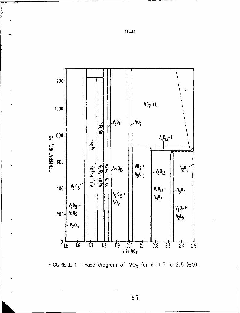
11-41
II
1200-,
OL
1000. V02 0+ L
0I
LAII
"-
"I 600S 701 V02+ V205j
SV60 60
400 V305 1- v
v0+6 + -V307
V203 + V02
200- V305 V205
"V203
1.5 1.6 1.7 1.8 1.9 2.0 2.1 2.2 2.3 24 2.5x in VOx
FIGURE 11-1 Phase diagram of VOx for x =1.5 to 2.5 (60).
95
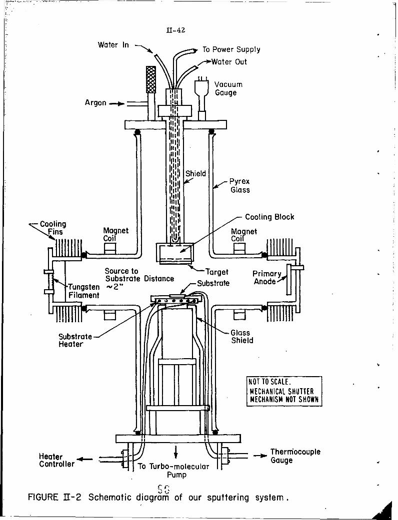
11-42
Water In To Power Supply,--3*Water Out
IVacuum~Gouge
Cooling Block
Fins agnetMa net
Substratetane rly
Heater
NOT TO SCALE.MECHANICAL SHUTTERMECHANISM NOT SHOWN
Heate ThermhocoupleController -To Turbo-molecular Gaug
Pump
FIGURE 11-2 Schematic d i ag rari of our sputtering system.

(b)
Die
FIGURE 11-3 VoriOLuS pGOrS USOd in spuffer-1111.
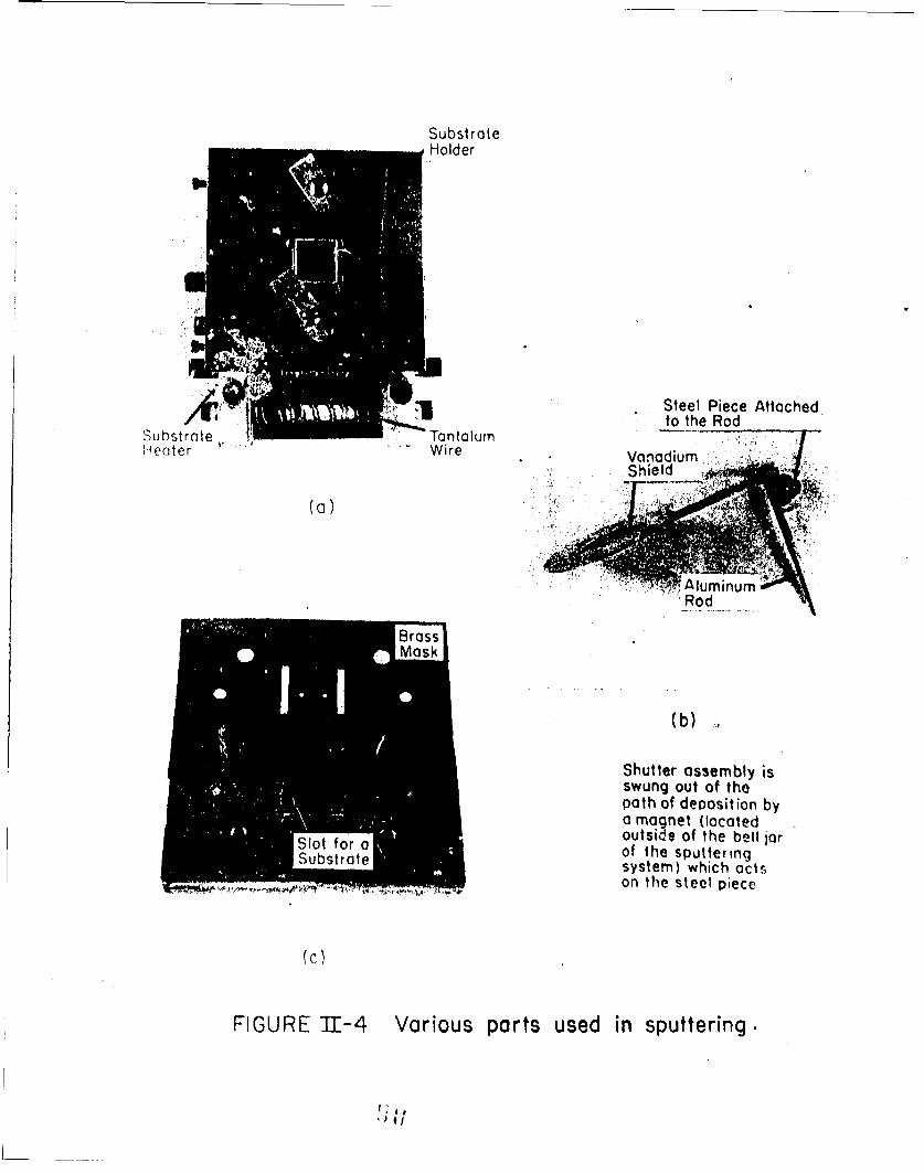
Substrate,Holder
Steel Piece Attached'-,.,..to the RodSubstrnte TantalumrnHeater Wire Vanadium
' AluminuS"Rod......
(b) ,
Shutter assembly isswung out of thepath of deposition by
oa a magnet (locatedSoutsi e of the bell jarSlotfr ai of the sputteringSubstrate system) which acts
on the steel piece
(c)
FIGURE TL-4 Various parts used in sputtering.
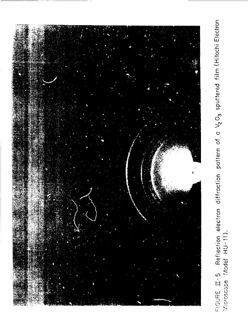
0.4-
0ci�
UA -z
00
I
E4-
�0�2)
ci).4-.4-
C-(I)
r�)0
N
04-
0
C
a).4--4-
1� i�i�' t
C0
� U
4-.4-
C0
.4-
(-)0)0)
C-
0�
�3D
4-
0) -
Qua)C)
iC)�
C)La.J �0D(2�2'-I

11-46
- I
//
0
105 0/
I
0I
4 V2O3 sputtered films104 --
-
E 0
0I
i VS4 (Annealed)-0
I
10--
010
3
• ,,I
0 /O
FI UR - - Re i t vt versu te pe at r nnet oa nned)ed
m03
//
//
0 -X
IK
1010/•00 T(°K
FIGUE I-6 Rsisivit vesus empratue o twoannale
sputeredfilm of zO /
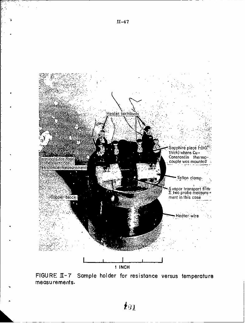
U1-47
ýSapphwie piece'ýho-thick) where, Cu -
6'T6 ~Con'stan' tin thermo-;K- ~~~--couple was ~mounted'
- ~- Teflon clamp.
- '~.4vapor transport fMImtiwo probemeasure-
* -opper blok * ment in this case
Hdierý'-wre-
I INCH
FIGURE 11-7 Sample holder for resistance versus temperaturemeasurements.

L1-48
Out Thermocouplet
Elctric FurnaceITI H2 In
iG Glass NQuartz Wool
Reaction Chamber Wl -N 2 In
N2 InVVI)
V2 Flowmeters
V3)
[ H20 ® Toggle Valve
ZConstant Temperature Baths
(a)
Crystal Substrate Holder
VOCt 3/N2 --J (H2+ H20)/N 2
(b) (C)FIGURE T1:-8 (a) Schematic diagram of vapor transport apparatus.(b) Detail of the crystal reaction crucible ;n the quartz reaction
chamber.(c) Detail of the film crucible in the chamber.
___ ___ __1

11-49
50
Feinleib and Paul10[4
McWhan andRemeika
102_
01 2FnadPu
E
00
101-
V2 03
.- 2ICF
10-
10
3 4 5 6 7 8 9 10
103T(OK)
FIGURE T1-9 Resistivity versus temperature of V20 3 crystalsmeasured by several investigators (3, 19, 25) and of a V2 03crystal and a V203 film grown by the vapor transport technique.
103

" 104 11-50
a
b
FIGURE 11-10 (a) Reflection electron diffraction pattern.(b) Optical microscopic picture of a vapor transport V2 03film (magnified 1500 times by a Universal Rikert CameraMicroscope "MeF").
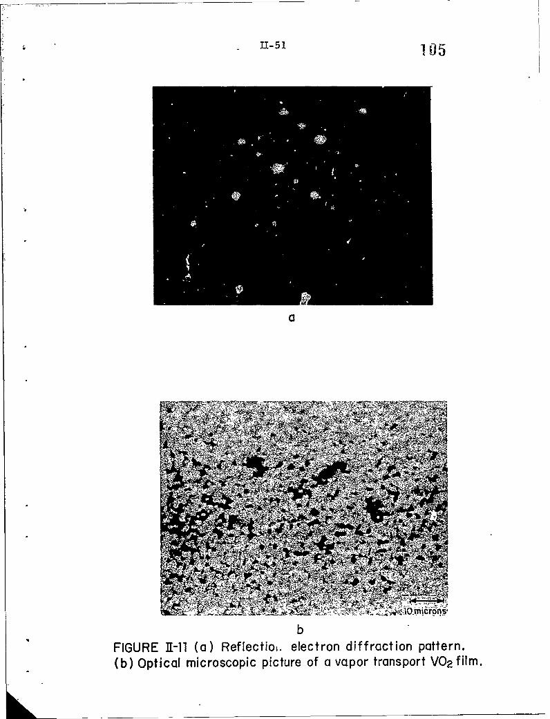
- •11-51 105
w0
-, - 13"1
b
FIGURE IL-11 (a) Reflectio,. electron diffraction pattern.(b) Optical microscopic picture of a vapor transport V02 film.

106
I I I I *.I
Sasaki and Watanabe- -Ladd and Paul
101 , Bongers ~+....
VO, filmMori+
I
1
0 +
10
+
10"1 I L-E IIIc II
I .II
102 _ 03+
+
3 :0 3 4
T(OK)FIGURE 11-12 Resistivity versus temperature of V0 2 crystalsmeaswred by several investigators (1,3,115, 53) and of a vaportransport. V09 film.
_ _ _ _ _

11-531.07
* CATHODE () PULLING ROD
CYTL WINDOW
ECATHODE
SPYREX•CRYSTAL WINDOW
AND HEARTH
BODY •+) -COOLING
GRAPHITESTN
CRUCIBLE
FIGURE 11-13 Cross-section diagram of the tri-arc Czochralskicrystal growing furnace.

11-54
60 TWO-PHASE REGIONSINGLE-PHASE REGION
Sc50-
k'SC203ji i..TiO 200
L.I"Ti200
40-
V .Mn t-, 20 .c
0 t~0S30"- -
S n-MnO E0C o • ZnO IV--2 0S2Fe 100
2,Ni C0
N10.iC Fe203
oCCu20 Mn3o 4I r 11•Mn 2 03
SC0304
0 0
I-_Cu0 ~ 1 C r02Mn02 11
-101 Cr00 0.5 1.0 1.5 2.0 2.5
OXYGEN. TO METAL RATIO Wx)
FIGURE ]1-14 Oxygen partial pressure versus oxygen-metalratio for different elements.- (56).
A

0C:
:3
C)
LO
Ld
-5
(D)FT

11-56
14 .0 2 1 --
14.00 x
•- 13.98-
Io• 13.96-
13.94
13.92-
5.01-
5.00-
4.99
o< 4.98-
4.97-
4.96-
4.95k A x
I I0 0.005 0.010 0.015 0.020
x IN (Vl_xCrx) 20 3
aH obtained from the (300) peakCH obtained from the (226) peak
x is accurate to L 5 % of its value
FIGURE 11-16 Lattice constants of V2 0 3 and (VI-X CrX) 203crystals as a function of chromium concentration.
__110 ___

CHAPTER III
DESIGN OF OPTICAL APPARATUS AND METHODS
OF DETERMINING OPTICAL CONSTANTS
The electrical properties of materials which show the insulator-
metal phase transition have been the object of considerable attention for
quite some time, so that by comparison the work on optical properties
has been much less extensive and detailed. In many of these materials
the nature of the absorption and reflectivity spectra changes noticeably
at the phase transition.
An examination of the optical properties and their changes at the
transition may therefore increase our understanding of the properties
of the insulating and metallic phases on both sides of the phase transition.
In this chapter and in Chapter IV we will concentrate on the optical
properties of the crystals and films of vanadium oxides and (V 1 x Crx) 2 0 3
whose preparation was described in Chapter II.
A. Theories and Methods of Determining the Optical Constants
of Solids
The theory of the optical properties of single crystals and films of
ordinary metals and semiconductors is well known and has been ex-
tensively reviewed (1, 2, 3, 4, 5). Hence, rather than discuss the deriva-
tion of the theory in detail, we will instead simply define theoretical
constants, their inter-relationship, and how they appear in expressions
for experimentally measurable quantities such as transmission and re-
flectivity.
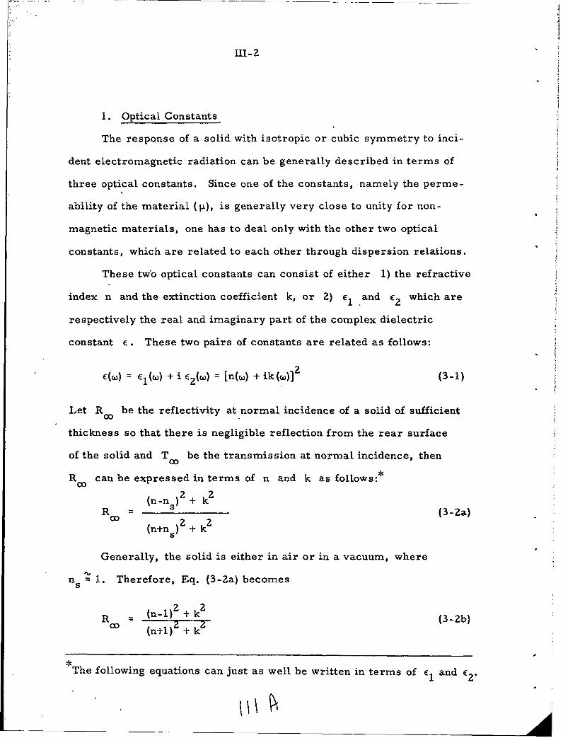
III- 2
1. Optical Constants
The response of a solid with isotropic or cubic symmetry to inci-
dent electromagnetic radiation can be generally described in terms of
three optical constants. Since one of the constants, namely the perme-
ability of the material (pi), is generally very close to unity for non-
magnetic materials, one has to deal only with the other two optical
constants, which are related to each other through dispersion relations.
These two optical constants can consist of either 1) the refractive
index n and the extinction coefficient k, or 2) E and E2 which are
respectively the real and imaginary part of the complex dielectric
constant E. These two pairs of constants are related as follows:
(= EI(w) + i E((co) = [n(cw) + ik(wo)] (3-1)
Let R be the reflectivity at normal incidence of a solid of sufficient
thickness so that there is negligible reflection from the rear surface
of the solid and T be the transmission at normal incidence, thenCO
R can be expressed in terms of n and k as follows:*
(n-n2 + k2
R = (3-Za)2 2
(n+ns) + k
Generally, the solid is either in air or in a vacuum, where
ns= 1. Therefore, Eq. (3-Za) becomes
R (n-i) + k (3-2b)(n+1) + k
The following equations can just as well be written in terms of EI and E "
A

11-3
Similarly, To0 can be expressed as
Too {(I-R 0)2 + 4R sin2 e-at (3-Zc)
where
a = absorption coefficient = 47k
X = wavelength of incident radiation
t = thickness of the sample
= ai-1 2k
n +k -1
If n > > k, Eq. (3-Zc) becomes
T 'ý (1-R ) eat (3-Zd)
As we mentioned earlier, the above equations, Eqs. (3-Za, b, c, d)
are valid only if the reflection from the rear surface of the solid is
negligible, that is when eat > > 4. For thin samples, where the re-
flection from the rear surface can no longer be neglected, then Eqs.
(3-Za, b, c, d) have to be modified:
R ([- e-at]Z + 4 e-at sin(-atz -to.(3 -3a)
(l-R 0-e ) at 4R e-at sin (P +•y)
This criterion can be easily verified from Eqs. (3-3a,b) to be
described later).

111-4
and
e-at([ QR o] 0+ 4R2 0 sin 2 (3-3b)
(1-Ro0 e-at)Z + 4Roo e-'t sinZ(qj +-)
where
Y =ZTrnt (n is any integer)
t = thickness of a thin sample
R = reflected intensity of the thin sample at normal incidence
T = transmitted intensity of the thin sample at normal incidence.
The second term in the denominator in both Eq. (3-3a) and (3-3b)
is an interference term. If no interference fringes are observed, say,
because of thickness variation, we then average over y and obtain:
R OD -Zt (3 -4a)1-RZ e
([l-RDO] 2 + 4Rc0 sin2 ) e- at
T =- -Zat (3-4b)
1-RZ e
For thin films deposited on different substrate materials, the ef-
fects of substrates 3n R and T must be considered, and the formulae
for R and T become much more complicated (4, 42). It will not be
necessary for us to summarize them here, since we do not analyse
our reflectivity and transmission measurements on thin films in order
to obtain the optical constants.
112
A

I1I-5
When the angle of incidence of the incident radiation is not nor-
rmal to the surface of a solid, where e at > > 4, then Eqs. (3-2a, b, c, d)
again have to be modified. We will consider only the reflected intensity
at oblique incidence (6):
R (a-cos) + b (3-a)(a+cos ) +b
(a -sin tan )2 + b2Rp =Rn (a+sin tan ) +b (3-5b)
where
R n the reflected intensity of the solid when then polarization of the incident radiation is per-
pendicular to the plane of incidence;
R = the reflected intensity of the solid when theP polarization of the incident radiation is in the
plane of incidence;
the angle between the incident radiation and thenormal to the surface of the solid;
a 1 1[(n 2 -k 2 -sin2$) 2 +4n 2 k 2 1 2 +(n 2 n2
2 1[2 k2-sin 22+ 4n 1 k 2 1/2 2 2 sinbz 1[2 n/
b ~.{[(n -kZ-sin $) +i4n k ] -(n -k -sin •) }
In all the above equations, n and k are used to relate to experi-
mentallv measurable optical quantities, but it is actually the imaginary
pn :t of the dielec:tric constant, E 2(w), that comes out most directly from the
derivation of the optical properties of the solid from its band structure
(,' i.." ij) can then be obtained from E2 (w) by the dispersion relations.
"113
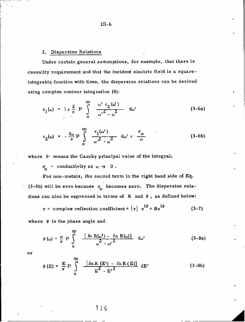
M11-6
2. Dispersion Relations
Under certain general assumptions, for example, that there is
causality requirement and that the incident electric field is a square-
integrablq function with time, the dispersion relations can be derived
using complex contour integration (8):
) II .
o
E2 (co) _ OD p -- dc + a 0 (3-6b)
0
where IP means the Cauchy principal value of the integral;
a = conductivity as u, -4 00
For non-metals, the second term in the right hand side of Eq.
(3-6b) will be zero because a becomes zero. The dispersion rela-0
tions can also be expressed in terms of R and 0 , as defined below:
r = complex reflection coefficient = I re io= Reio (3-7)
where 0 is the phase angle and
0:,
0 P iR ,z-InRw] w (3-8a)
or
0 (E)= -p [AnR(E') - 2nR(.E)] dE' (3-8b)IT E2 ,
0
o ~
tA

111- 7
where
E =•W
2Ah = Planck's constant.
Constants n and k can be obtained from R and 0 by the following
relations:l-R
n = I(3-9a)l+R-2 VW-cos O
k = 2/R-- sin 0 (3-9b)
1+R-2 rRR-cos 0
If the function R(E) is known over the entire spectral region,
then from Eq. (3-8b) 0 (E) can be calculated for all energies. With R
and 0 , Eqs. (3-9a) and (3-9b) will give us n and k, and ultimately
E and 4E The above method of obtaining the optical constants is
frequently referred to as the Kramers-Kronig analysis.
We should point out that Eqs. (3-9a) and (3-9b) are derived for
solids of sufficient thickness such that reflection from the rear surface
is negligible (i. e., for eat> > 4). * For a sample where the above
condition is not valid, the expressions for R and T in terms of the
optical constants n and k become too complicated to be inverted in
closed forms (refer to Eqs. (3-3a) and (3-3b)). It will, then, no longer
be feasible to obtain the optical constants of the sample by Kramers-
Kronig analysis. In the next section, we will present a detailed dis-
cussion of this analysis.
* Thus R(E) should actually be labelled as R 0(E); however, it is
clear from the context.
" _1115
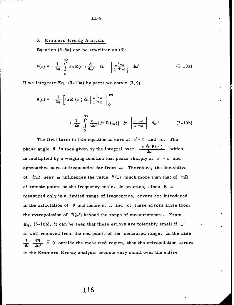
111-8
3. Kramers-Kronig Analysis
Equation (3-8a) can be rewritten as (3):
0o
0(W) =4- ' )2nR(w')4d in [•-- dw' (S 10a)
0
If we integrate Eq. (3-10a) by parts.we obtain (3, 9)
1 C•i , • o o0 (W) = - nR (0) inI w ow
Co
00
The first term in this equation is zero at w'= 0 and co. The
phase angle 0 is then given by the integral over d nR(w') which
is multiplied by a weighing function that peaks sharply at w' = W and
approaches zero at frequencies far from w. Therefore, thn derivative
of InR near w influences the value 0 (w) much more than that of inR
at remote points on the frequency scale. In practice, since R is
measured only in 'a limited range of frequencies, errors are introduced
in the calculation of 0 and hence in n and k; these errors arise from
the extrapolation of R(w') beyond the range of measurements. From
Eq. (3-10b), it can be seen that these errors are tolerably small if U'
is well removed from the end points of the measured range. In the case1 dR 2
"1- dR = 0 outside the measured region, then the cxtrapolation errors
in the Kramers-Kronig analysis become very small over the entire
11113

111-9
rneawltecl region. In most optical spectra, however, the reflectivity
is rnetiy still varying at the highest frequencies used in the measure-
rment. We, therefore, have to extrapolate the measured reflectivity in
a sengible way which will minimize errors.
Ji e:xtrapolation, the chief difficulty is extzapolation on the high
enelgy ead of the reflectivity spectrum. This is due to the fact that,
iri Met;41., the reflectivity at low energies can be assumed to go to 1.0
as .c-- 0. Similarly in the case of a semiconductor, the reflectivity
at o.- 0 can generally be calculated using the static dielectric constant
of th- rnterial.
'there are a few extrapolation procedures that are commonly used.
One a9roach is to extrapolate R(w) to higher frequencies using the
fo~rrhu.l (10)
whe•
C4 = upper frequency limit of measurement, and
iý 1 - reflectivity at w * = wI.
The paj-snreter p is varied in order to obtain values of n and k that
agPe best with the experimental n and k at low energies in the range
of nieOsurernent. Another method of extrapolating R(w) to higher
energjes is to assume:
= R1 (3-12)
.11-10
where t is taken to fit the measured derivative of R(w) at CO (01 (11).
Here, the integration raage must be cut off at = certain frequency, W.,
in order to avoid divergence of the integral in Eq. (3-8a). w? is again
chosen so that Kramers-Kronig analysis gives the constants n and k
which will fit some experimental n and k at low energies. There
are other methods, such as the one that uses damped harmonic oscil-
lators, to extrapolate the reflectivity spectrum in the high energy
region. The parameters of these oscillators are adjusted to give values
of n and k which are comparable to experimental n and k at cer-
tain energies.
In addition to the errors introduced by the extrapolation, we can
have large errors in the optical constants from the inaccuracies of
experimental measurements. From Eq. (3-8a), the value of 0 (w) de-
pends on the natural logarithm of R(w). The natural logarithm of a
function whose values are equal to or smaller than one is a rapidly
varying function. The logarithm of R((w) is such a function. In fact,
the smaller the value of R(w) gets, the more sensitive 0 (w) becomes
to the experimental errors in R(w).
Furthermore, judging from Eq. (3-Za), when k is small, and
especially when k << n, then R is nearly independent of k. Therefore, in
such a region, reflectivity data cannot yield accurate values of k, and
the values of k depend on the reflectivity spectrum outside the region
where k is small. The extrapolation of the reflectivity spectrum then
becomes critical.
*1,1

4. Oscillator Fit Method
To comprehend the oscillator fit method, 'we need first to under-
stand why it is reasonable to express the dielectric constant of a solid
in terms of oscillators. In general, the complex dielectric constant
of a solid' can be divided into four terms, three of which are expressed
as sums of damped harmonic oscillator terms and the fourth is a Drude
term. At this point, we are interested only in the first three terms.
Two of the three terms represent contributions from the excitations of
transverse optical phonons, and from the electronic transitions from
bands below the valence band to the conduction bands. These contri-
butions to the dielectric constant have been shown to be adequately re-
presented by sums of oscillators (12, 13). The third term represents
the contribution from electronic transitions from the valence band to
the conduction bands. The contribution from these transitions to the
dielectric constant is often expressed as follows (13):
S() t 4,e 2 f(w ) N (c)dw3'F a(3-13)
where
N (o') = the density of valence band states separated byan energy hw from conduction band states.
f(w') = oscillator strength, and
T (') = relaxation time.
But if the transitions are between narrow bands, or in the limit
between atomic levels, than N (c') can be approximated by a sum of
delta functions, and Eq. (3-13) is reduced to a sum of oscillators, with
1119

111-12
each transition from the valence band to a conduction band approximated
by a damped harmonic oscillator.
When the bands involved in the transitions are no longer narrow,
then the contribution to the complex dielectric constant from each
transition from the valence band to a conduction band usually cannot be
expressed in terms of a single damped oscillator; but a sum of oscil-
lators has to be used. The reason for using a sum of oscillators can
be explained by referring to Eq. (3-13). The integrand in the second
term of that equation is in the form of a damped harmonic oscillator term.
From calculus, this integral can be approximated by a sum of oscil-
lators at discrete frequencies.
It must be remembered, however, that when the bands are narrow,
the oscillator used has a one to one correspondence with the transition
between the bands, but when the bands are not narrow, it is no longer
correct to identify one oscillator with a particular transition; in fact,
several oscillators may together represent a single transition.
Since different sets of oscillators can be chosen to give rise to the
same contribution to the complex dielectric constant, the loss of physical
significance of the parameters of these oscillators .s obvious. In an
oscillator fit method, the complex dielectric constant of a solid where
the free electron contribution is negligible can be adequately represented
as follows:
S.E(M) = + iE2 (c) = M (3 -14a)I -ir
i 1--- ~i' (--

M III- 13
where
Si = parameter associated with the oscillator strength of theith oscillator
r = linewidth of the ith oscillatorI
Wi = resonance frequency of the ith oscillator.
If we are interested in an optical spectrum within a limited spectral
range, as is usually the case, the contribution of the oscillators whose
resonance frequencies are far from the range of frequency under examina-
tion is then reduced to a sum of their respective oscillator strengths -
this is evident by inspecting the form of Eq. (3-14a). Equation (3-14a)
can then be reduced to
N S.
E( IE = + Si 2 (3-14b)
11 r
where
E = 1 + contributions to E(w) from oscillators far from thespectral range of interest in the frequency scale, and
N = the number of oscillators required to given an adequaterepresentation of the dielectric constant in the spectralrange of interest.
The reflectivity of the solid can then be derived from the dielectric
constant. For a solid of sufficient thickness such that et > >4, Eq.
(3-2b) can be rewritten as follows:
R __ TWj-l 2 (3-15)
121-hL _
111- 14
Though we have shown that, in theory, we can always express
the complex dielectric constant of a solid in terms of a sum of oscil-
lators, in practice, we find that we cannot use an unlimited number of
oscillators in our oscillator fit method because of computational limita-
tions. The computational time required to get a good fit to a reflectivity
spectrum using a large number of oscillators (say, 10) is very long
(after more than 30 minutes); this proves to be a drawback of the
method. Further discussion of this point will be presented in Chapter
IV when we discuss the cptical results.
We will, now, consider a special case where the reflectivity
spectrum of a solid is in the spectral range where the optical phonon
excitations are important. As we have discussed earlier, the re-
presentation of the complex dielectric constant of such a solid can be
adequately expressed as a sum of damped harmonic oscillators. The
parameters of the fitted oscillators usually provide us with some idea
of the strength, frequency and relaxation time of each transverse optical
phonon mode which is excited by the incident radiation. This technique
has been used successfully by several authors to obtain the parametersof optical phonon modes in various solids (14).
Verleur (15), using Eq. (3-14b), fitted a reflectivity spectrum of
silicon from 0.5 to 10 eV with six oscillators. He, then, used the derived
parameters of the oscillators that gave a good fit to the measured spectrum
to calculate optical constants n and k and found them in good agree-
ment with those values obtained by Phillipp and Taft who used a Kramers-
Kronig analysis (16).
41`22

111-15
Where a crystal becomes transparent, that is when eat < 4, or
when thin transparent films are involved, Eqs. (3-9a) and (3-9b) are no
longer valid, and the expressions for R and T in terms of n and k
become too complicated to be inverted in closed forms. Kramers-Kronig
analysis is no longer feasible. To obtain the optical constants in these
cases, two quantities, such as the transmission of two films (TT) of dif-
ferent thickness or the reflectivity and transmission of the same film
(RT), are measured at each frequency. In all cases, the thickness is
determined by other means. The RT method has its disadvantages;
Grant and Paul (17) have shown that small experimental errors in some
wavelength regions, especially where n - k 1 can lead to large in-
accuracies in the calculated optical constants.
Grant (42) and Nillson (18) found that the TT method would not run2- k2 ý
into the same trouble as the RT method when n- k= 1. However, they
found that considerable errors in the values of the optical constants
could result from the TT method, unless the thicknesses of the two films
were carefully chosen. For example, Grant (42) showed that for germanium
films in the spectral range between 0. Z. and 0. 6p. reasonably accurate
values of the optical constants could be obtained if the thicknesses of the0 0
two films were 100 A and 300/400 A . For some other combinations, say,0 0
50 A and 100 A, large errors in the optical constants would result,
Verleur (15) adopted the oscillator fit method to obtain optical con-
stants from the transmission and reflectivity spectra of thin films.
Equation (3-15) is, of course, not applicable for thin films. Verleur
then used the appropriate formulae for R and T (15) which contain the
`r•3
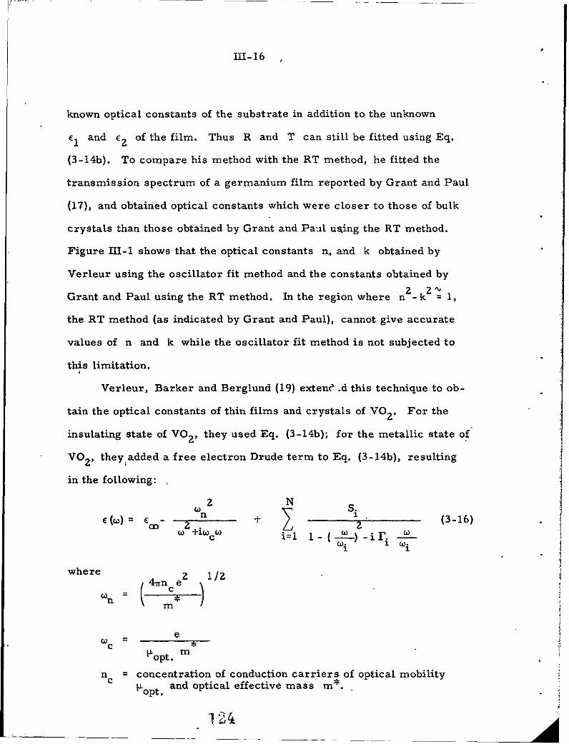
M1-16
known optical constants of the substrate in addition to the unknown
E1 and E2 of the film. Thus R and T can still be fitted using Eq.
(3-14b). To compare his method with the RT method, he fitted the
transmission spectrum of a germanium film reported by Grant and Paul
(17), and obtained optical constants which were closer to those of bulk
crystals than those obtained by Grant and Paul uqing the RT method.
Figure III-I shows that the optical constants n. and k obtained by
Verleur using the oscillator fit method and the constants obtained by
Grant and Paul using the RT method. In the region where n - k 1,
the RT method (as indicated by Grant and Paul), cannot give accurate
values of n and k while the oscillator fit method is not subjected to
this limitation.
Verleur, Barker and Berglund (19) extene .d this technique to ob-
tain the optical constants of thin films and crystals of VO For the
insulating state of VO, they used Eq. (3-14b); for the metallic state of
VO2 , they added a free electron Drude term to Eq. (3-14b), resulting
in the following:
2 N S.SlW) E n '3+ (3_16)
- W 1 2 W() c i--I1 -( ) -i i i
where z 1/Z4-r e
~nk•nton m
ec oopt. m
nc = concentration of conduction carriers of optical mobility
c p and optical effective mass mopt.

M11-17
The method has since been used by others to obtain the optical
constants of bulk crystals and thin films of various kind of material
in the spectral region where interband electronic transitions are im-
portant (20, 21, 22, 23).
In summary, let us list, and amplify on where necessary,. the
advantages and disadvantages of the oscillator fit method as compared
to the Kramers-Kronig analsis.
Advantages. 1) In Kramers-Kronig analysis, extrapolation is
often needed and different methods of extrapolation have been used in
earlier studies (10, 11). The values of the optical constants in the
spectral range of interest usually depend on the parameters used in the
extrapolation procedures. In practice, the extrapolation parameters
have to be adjusted so that the calculated optical constants, at some
frequencies inside the spectral region, will fit some known optical con-
stants obtained by other means. In the oscillator fit method, however,.
extrapolation (strictly speaking, it is not extrapolation in the sense used
in Kramers-Kronig analysis) is usually not required unless it is neces-
sary to give a reasonable fit to an optical spectrum in the spectral range
of interest. Extrapolation, if needed, is achieved by assigning oscil-
lators outside the spectral range of interest, and the parameters of the
assigned oscillators are automatically adjusted in the oscillator fit
method so that an adequate fit is obtained in the range of interest. Thus,
in the oscillator fit method, no prior knowledge of the values of optical
constants in the spectral range of interest is needed. The resultant
L4
MI-18
optical constants are, however, still subject to some uncertainties.
We will discuss them on p. 111-19, and again in Chapter IV.
2) As mentioned earlier, the oscillator fit method enables us to
obtain the optical constants of the transparent crystals and films; this
is not feasible using the Kramers-Kronig analysis. And the RT and TT
techniques, which are frequently used in evaluating the optical constants
of thin films, may, in some instances, fail to give accurate values of
optical constants. The oscillator fit method, in these instances, may
well be superior to the RT and TT method.
3) In regions where Reststrahlen effects are dominant, or where
electronic excitations are between narrow bands or atomic levels, this
method will give us directly their frequency, oscillator strength and
relaxation time.
4) Referring to Eq. (3-16), the oscillator fit method will provide
us with the parameters of the free electron absorption. From these
parameters, the optical -effective mass and optical mobility of the con-
duction electrons can be obtained, provided that the concentration of the
conduction electrons is known. In Kramers-Kronig analysis, this is,
not directly possible.
Disadvantages. 1) The oscillator fit method usually requires more
computational time than does the Kramers-Kronig analysis. Numerical
analysis and programming procedures are much nrore complicated.
Z)When an absorption spectrum of a solid is very assymetrical,
as in the case of an absorption edge, or is due to electronic transitions
_ __ _

UI-19
between broad bands, it may require a substantial number of oscillators
to adequately fit the absorption spectrum, and the length of computational
time required becomes a serious factor.
3) In the oscillator fit method, the curve fitting procedure is usually
provided by a nonlinear minimization technique, which has one problem,
viz., convergence often occurs at a point other than the absolute mini-
mum. Though this problem is not serious since we are interested only
in the resultant- dielectric constant and not in the parameters of the
oscillators, sometimes a convergence may occur that leads to a poor
fit and, in some cases, small structures in the optical reflectivity or
transmission spectrum may not be fitted well during the fitting procedure.
As long as an adequate fit is obtained, however, reasonable optical con-
stants can be obtained.
5. Angular Dependence and Other Techniques of Determining
Optical Constants
There are other techniques for obtaining optical constants* of opaque
solids where eat > > 4. In this section, we are interested only in crystals
that satisfy this condition. When a light- beam, whose electric field is
polarized either perpendicular or parallel to the plane of incidence, is
incident on a solid at different angles of incidence, the reflected in-
tensity of the beam is described by either Eq. (3-Sa) or (3-5b). Since
we have two unknowns, n and k, we need only two independent measure-
ments to determine them; and judging from Eqs. (3-5a) and (3-5b),
several choices of these measurements are possible. One way - some-
times called the angular dependence technique - is to measure the

II- 20
reflected intensity, Rn or Rp, of the solid at two different angles of inci-
dence (6, 24). Another way is to measure both R and R at onen p
angle of incidence (25). Yet a third way is to determine the ratio of
R n/R for two angles of incidence (26). In still another technique,
ellipsometry, the optical constants of a solid can be obtained by measur-
ing changes in the state of polarization of light upon reflection from the
surface of the solid (27).
The above methods show that it is possible to obtain values of n
and k of an opaque solid directly without resorting to the indirect
techniques of Kramers.-Kronig analysis and oscillator fit. Although
it is not always feasible to use these direct techniques to obtain the
optical constants in a wide spectral range because of the lack of ap-
propriate instruments, it is quite feasible to use them to find values of
n and k at some particular frequencies in the spectral range of interest.
By requiring the measured values of n and k at these particular fre-
quencies to fit the calculated values of n and k obtained by the Kramers-
Kronig analysis or the oscillator fit technique, extrapolation uncertainties
in both techniques can be greatly reduced.
We determined the n and k values of some of our crystals by
measuring the angular dependence of the reflected intensity of these
crystals as a function of the incidence angle • at different frequencies,
which were provided by a helium-neon laser and an argon-ion laser.
Light polarized in the plane of incidence was used because the reflected
intensity of a solid for light polarized perpendicular to the plane of inci-
dence usually did not vary with 4 as much as for light polarized in the
plane of incidence (6).
- ° .4
111-21
Since there were two unknowns, n and k, only two measure-
ments of R at two different angles of incidence were actually requiredp
to determine them (see Eq. (3-5b)). However, in order to minimize the
experimental errors in R which could lead to subotantial errors in np
and k (6), we usually measured the R of each crystal at more than
ten different angles of inci'.nce $ and used an automatic curve fitting
"procedure to obtain values of n and k that would give a calculated Rp
versus 0 curve that would fit well with the experimental curve.
6. Discussion
The theories and methods of determining the optical constants of a
solid are based on several assumptions; aside from those gererally
valid for dispersion relations, they include the following: 1) that the
solid is optically isotropic (a solid which is isotropic or cubic in crystal
symmetry), 2) that the solid is non-optically active (a solid which does
not rotate the polarization of an incident light on passing through it),
3) that the solid possesses no net charges, and 4) that the local field
effects in the solid are negligible. The formulation of the optical
properties of solids for which the latter three assumptions are not ap-
plicable is very complicated and, in general, not necessary for common
solids, and therefore will not be discussed here.
We will, however, briefly describe the optical constants of an
optically non-isotropic solid since the crystals we have investigated are
all non-cubic. The optical constants of such solids az'e usually not
scalars, and the real and imaginary parts of the co'-rplex dielectric
12

III-22
constants become second-rank tensor quantities. It is known that a
second-rank tensor can always be diagonalized by judiciously choosing
three mutually orthogonal principal axes. In a crystal which belongs to
one of the following crystal symmetry classes: tetragonal, hexagonal,
trigonal and orthorhombic -- the principal axes are along the crystal-
lographic axes of the crystal for all wavelengths and the real and
imaginary parts of its complex dielectric constant share the same set
of principal axes. Therefore, if optical reflectivity R or transmission
T measurements are made with the incident electric field polarized
along any one of the principal axes, the values of n and k or E1 and
E2 , obtained from the R or T spectrum using the Kramers-Kronig
analysis or the oscillator fit method, will give us the optical constants
along this particular axis. If these measurements are made along
each of the three principal axes in the solid, we will then obtain the
components of the dielectric constant tensor along those axes, and
hence, the complex dielectric constant tensor for the solid can be de-
termined. If, however, for some reason,. the electric field of the inci-
dent radiation is either unpolarized or not along any of the principal axes,
then the optical constants obtained will be a superposition of those com-
ponents of the dielectric tensor along those principal axes on which the
incident radiation have effects.
When the materials being investigated are either crystal- which
belong to the monoclinic or triclinic crystal symmetry classes, or thin
films which are non-cubic in nature and are not epitaxial, amorphous,
or perfectly polycrystalline, the choice of the principal axes for the
130
111-23
real and imaginary parts of the dielectric constants becomes very dif-
ficult, if not impossible. In monoclinic and triclinic crystals, even
if the principal axes can be found, they will usually vary with the wave-
lengths of the incident radiation and the set of principal axes for the real
part usually will not coincide with that for the imaginary part of the
dielectric constant (3). Therefore, in general practice, when optical
reflectivity and transmission measurements are done on one of these
materials, either with the electric field along one of the crystallographic
axes or with unpolarized light, the optical constants derived from the
Kramers-Kronig analsis or the oscillator fit method should be inter-
preted as constants that will give us the measured values of reflectivity
jr transmission when used in the appropriate equations, and thus this
fact must be given careful consideration, if these derived constants are
used to compare with those calculated from band structures or any such
methods.
In our optical -nvestigations of VO 2 and V 2 0 3, the crystals trans-
formed, respectively, from monoclinic to tetragonal structure at " 3400K,
and from monoclinic to corundum structure (almost hexagonal) at • 150 K,
with increasing temperature. If the electric field polarization of the
incident radiation is aligned along one of the principal axes of these
crystals in its high temperature state (either along c- or a-axis in
crystals with the tetragonal or hexagonal symmetry), then the electric
field will usually not be polarized along any of the principal axes in the
low temperature monoclinic state, thus making polarization studies on

III- Z4
this class of materials difficult and hardly fruitful. Because of this
and the limited availability of crystals with large physical dimensions,
we have not concentrated on studies of polarization effects on the opti-
cal properties of solids. Also, it has turned out that at room tempera-
ture, in V 2 0 3 crystals and V2 0 3 crystals doped with chromium, no
significant optical anisotropy was observed in the spectral range of our
interest, and hence, the polarization effects on their optical properties
are not important.
B. Numerical Analysis and Programming Techniques
In this section, we will describe some of the characteristics of
our computer programs for Kramers-Kronig, oscillator fit, and angular
dependence analyses.
1. Kramers-Kronig Analysis
For the Kramers-Kronig Analysis, Eqs. (3-8b), (3-9a) and (3-9b)
were used. The computer program, similar t the one used by Rossi
(28), computed the integrand in Eq. (3-8b) at each discrete photon
energy for which the measured reflectivity value was available. The
integral was then approximated by multiplying the average value of the
integrand between each adjacent pair of energies by the difference AE
between the energies, and then summing the results (trapezoidal rule).
The integral between the two energies L'djacent to the energy where E = E'
was taken as the average of the integrand at the two adjacent energies
times the energy difference.
Ia?

111-25
Above the energy E where the reflectivity data were notmax
available, the reflectivity spectrum was approximated by R maxE x)
(see Eq. (3-11)) where R max was the value of reflectivity at E max
and p was an adjustable parameter. The integration of the phase inte-
gral from Emax to ao was:
1 n Rn max (En+l)- z E .Zn+Imax max-E E max
n
This sum was computed to 50 terms in the program.
The values of p were varied from 0.0 to 5. 0 by increments of
0. 1, and the usual procedure, where applicable, was to print out and
plot the optical constants n, k, El, E.. and a only when a certain
p gave values of n and k at some energies which were within + 576
of those values obtained by the angular dependence measurements (to
be discussed later).
A complete Fortran listing of the program is given on p. A-i to
A-5.
2. scillator Fit Method
The oscillator expressions we used in our analysis were Eq. (3-14b)
for semiconductors and Eq. (3-16) for metals. They were rewritten in
te. is of the photon energies and expressed as follows:
(for semiconductors)
N S.E (E) = o + )2 (3-17a)
i 1
1 33
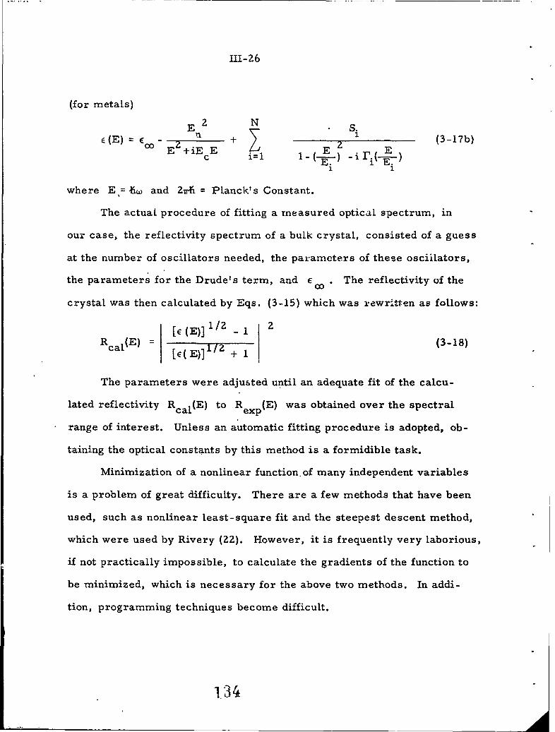
III-Z6
(for metals)
E 2 N S.1(E) (3-17b)
00E+iE EEE1 1
where E 1= f and 2A = Planck's Constant.
The actual procedure of fitting a measured optical spectrum, in
our case, the reflectivity spectrum of a bulk crystal, consisted of a guess
at the number of oscillators needed, the parameters of these osciilators,
the parameters for the Drude's term, and E Co . The reflectivity of the
crystal was then calculated by Eqs. (3-15) which was rewritten as follows:
[E (E)]l/2 -1 2
Rcal(E) = (3-18)
The parameters were adjusted until an adequate fit of the calcu-
lated reflectivi.ty Rcal(E) to R exp(E) was obtained over the spectral
range of interest. Unless an automatic fitting procedure is adopted, ob-
taining the optical constants by this method is a formidible task.
Minimization of a nonlinear function.of many independent variables
is a problem of great difficulty. There are a few methods that have been
used, such as nonlinear least-square fit and the steepest descent method,
which were used by Rivery (22). However, it is frequently very laborious,
if not practically impossible, to calculate the gradients of the function to
be minimized, which is necessary for the above two methods. In addi-
tion, programming techniques become difficult.
III-27
Therefore, there are considerable advantages in using mini-
mization procedures that do not require the derivatives of the function
to be minimized. A few procedures are indeed available and they in-
clude the simplex pattern search method (29, 30), the method proposed
by Powell (31), and the method proposed by Peckham (32). We will
not discuss the advantages and disadvantages of each of these methods.
It is sufficient to point out that Eq. (3-17 a, b) are very complex, and
that the derivatives of these equations are even more so. We chose to
use the simplex method for our fitting procedure since the simplex
method is computationally very compact, and a great majority of its
instructions are additions and subtractions or logical orders. There
are a few multiplications, but no divisions at all except on entering
and leaving the computational routine.. The method may take a little
longer computational time than other methods such as the steepest
descent method, but the easy definition of thc. problem and the program-
ming convenience more than compensate for this possible disadvantage.
We should point out that Scouler and Raccah independently developed
their oscillator fit procedure also using the simplex method (23).
The general concept of the simplex method to minimize a function
of n variables (henceforth referred to as objective function) is to set
up a simplex of (n+l) vertices, that is, to select (n+l) points in the
space of n variables and to calculate the values of the function at
selected points. Then, by comparing the calculated values of the ob-
jective function at those points, the vertex with the highest value (the
1.35

111-28
worst point in minimization) is " Laced by another point with a lower
value of the objective function, which in turn is determined according
to certain systematic operations (to be described later). This method
forces the objective function to approach the minimum by, at each step
of the operation, discarding the worst point of a simplex and adopting
a better point for a new simplex. This procedure is repeated until the
minimum is achieved.
Figure II1-2 shows a flowchart of the simplex method we used (30).
A brief description of the procedure follows: we consider initially,
the minimization of a function of n variables (xi, . . . . . . . . . . Xn) with-
out any constraints. P 0 PI .... Pn are the (n+l) points in the n-dimen-
sional space that define the current simplex. Let Yi be the functional
value at Pi, and h and I be the suffices such that
= max (yi) (h = high)
rain (yi) U=( low)
We then define P as the centroid of the points with i ý h, and (PiP.)
for the distance from P. to P.. At each stage in the minimization.1 3
process, Ph is replaced by a new point; three operations are used -
reflection, contraction and expansion. These operations are defined
as follows: the reflection of Ph is denoted by P', and its coordinate
are defined by the relations:
P* (1 +a)P -a h (3-19a)
where a., the reflection coefficient, is a positive constant.

M1-29
Thus, P* is on the line joining Ph and •, on the far side of P*
from Vh with (P*-5) =a (PhP). If y* lies between Yh and y, , then
Ph is replaced by P* and we start again with the new simplex.
If y* < Yi' that is, if the reflection has produced a minimum, then
we expand P* to P** by
P** P* +(I - ) (3-19b)
where y, the expansion coefficient, is the ratio of the distance (P**F)
to (P*P) and is usually greater than unity. If y*< y,, we replace Ph
by P'* and restart the process. However, if y** > yl, then we have
a "failed" expansion, and we replace Ph by P* before restarting.
If on reflecting P to P* we find that y*> yi for all i 0 h,
that is replacing P by P* leaves y* the maximum, then we define
a new Ph to be either the old P or P*, whichever has the lowerh h
value and form
P = Ph + (i -l )P (3-19c)
where f, the contraction coefficient, is the ratio of the distance (P**p)
to (PP) and lies between 0 to 1. We then accept P for Ph and
restart the process, unless y * > min (Yh' y*), that is, the contracted
point is worse than the better of Ph and P*. For such a "failed" con-
traction, we replace all the Pi's by (Pi + P1)/2 and restart the process.
In Eqs. (3-17a and b), none of the parameters, from physical
arguments, should be zero or negative. This constraint is incorporated
into our minimization procedure by the following method. At d.ny stage
137

I
111-30
during the operation, when one or more of the parameters becomes
zero or negative, the functional value of the objective function is re-
placed by a large positive value. If we investigate the flowchart care-
fully, the designated large positive value effectively forms a barrier
such that any trespassing by the simplex will be followed automatically
by contraction moves which will eventually keep the simplex inside
the confine.
A final point about the general concept of the simplex method con-
cerns the criterion used for halting the procedure. The criterion
chosen is to compare the "standard error" of the y's in the form
SZ (Yi - )n <c 1 (3-ZO)
where
c is a preassigned constant,
y is the average of all yi's, and
n is the number of variables.
When the standard error falls below cl, the fitting procedure stops.
The reasoning behind this criterion is that in the curve fitting problem,
we are not so interested in finding the exact values of x.'s, but in ob-
taining the minimum that gives us a good fit between the calculated and
experimental curves.
118_ _ _ _ __ _ _!
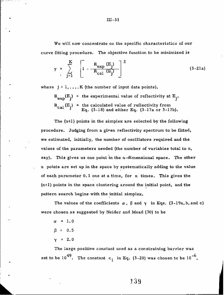
IJI-31
We will now concentrate on the specific characteristics of our
curve fitting procedure. The objective function to be minimized is
K K cIexp|(Ei
_ - R (E.) ( 22
% j=l calj
where j = 1, .... K (the number of input data points),
R (E.) = the experimental value of reflectivity at E.,
Rcal (E.) the calculated value of reflectivity fromEq. (3-18) and either Eq. (3-17a or 3-17b).
The (n+l) points in the simplex are selected by the following
procedure. Judging from a given reflectivity spectrum to be fitted,
we estimated, initially, the number of oscillators required and the
values of the parameters needed (the number of variables total to n,
say). This gives us one point in the n-dimensional space. The other
n points are set up in the space by systematically adding to the value
of each parameter 0. 1 one at a time, for n times. This gives the
(n+l) points in the space clustering around the initial point, and the
pattern search begins with the initial simplex.
The values of the coefficients a, B and y in Eqs. (3-19a, b, and c)
were chosen as suggested by Nelder and Mead (30) to be
a = 1.0
1 = 0.5
y = 2.0
The large positive constant used as a constraining barrier was
set to be 10 The constant c1 in Eq. (3-20) was chosen to be 106
p39

III-3Z
which would give us a reasonable fit. For cases where we have obtained
optical constants n and k by the angular dependence method, the ob-
jective function y in Eq. (3-Z1a) is modified to
y expa(E) )2 + kexp(Emi)R= a Ej 2 k Cal (Em)
j=1 Mica . . .cal
n exp' •i)
where nal (Erai)
E' = photon energy at which n and k values are knownIn.
1.m = number of known k or n values; in our program, m• 2.
e2 = weighing constraint; in our program, we set it at 4. 0,
suffice cal = calculated value from Eq. (3-18) and either Eq.(3-17a) or (3-17b),
suffix exp experimental value.
Typically from a given reflectivity spectrum, we guessed the num-
ber of oscillators required, and the values of the parameters. The
initial guess can be quite poor. If the initial guess is very poor, Eq.
(3-Z0) usually will not be satisfactory after - 25 minutes on the SDS
Sigma 7 computer. An adjustment of the parameters will generally pro-
vide us with a reasonable fit that will satisfy Eq. (3-20) within 25 min-
utes, unless the number of oscillators chosen was too few. If the num-
ber of oscillators chosen are too few, then even if Eq. (3-20) is satis-
field within 25 minutes, we will obtain a theoretical reflectivity curve
that does not have all the fine structures of the experimental curve.
____

111-33
However, when too many oscillators are assigned, one of the oscillators
will have its parameters approaching zero, and we will then discard
the oscillator. In general, the final values of these adjustable oscil-
lators parameters are dependent on their initial values. The final
optical constants are, however, quite independent of the initial set,
and this is not too surprising in view of the discussions we presented
earlier. Some initial sets give better fits than others, and we usually
selected a set that gave the best fit -that is, the set of parameters that
gave us the smallest value of the objective function y - to the experi-
mental values from a number of runs using different initial values. We,
however, noticed that the parameters of the Drude's term was not very
sensitive to their initial guesses and that the resu .ant, let. .re usually
within 20%6 of each other from runs that give good f: peri-
mental curve.
Finally, as in most curve fitting problems, the selection of the
points of a spectrum are quite important. Data points should be selected
with proper care to reflect the important features of the reflectivity
spectra.
In conclusion, the oscillator fit method by the simplex pattern
search method is quite straightforward, and after a few trial runs, a
reasonable fit is often obtained.
A complete Fortran listing is given on p. B-6 to B-16, for
fitting a reflectivity curve of V2 0 3 at 300 K (the optical constants are
reported in Chapter IV).
' 141

111-34
3. Angular Dependence Method
The automatic curve fitting computer program was written by
Raccah and Landon (34) at MIT Lincoln Laboratory. The same simplex
pattern search method as the on- we used in the oscillator fit method
was used in the minimization of the objective function.
y =j K e (3-22)
j=l cal
where j = 1, ... K(the number of input data points)
Rp () = the experimental value of the reflectedexp intensity at ..
JR a (. = the value of the reflected intensity a'. 4.
Cal J calculated from Eq. (3-5b).
The parameters used in the simplex pattern m- -'.i re slightly
different from those we used in the oscillator fit mechod, but the basic
operation remains the same.
The coefficients in Eqs. (3-19a, b, c) were:
a = 1.1
B = 0.51
N = 3.0
The criterion used in halting the fitting procedure was in thd form
< 10 (3-23)
where
maxYh i
=min_- mi (yi)
1•2

111-35
which, though slightly different from Eq. (3-20), is basically very
similar. Since there were only two parameters n and k to be ad-
justed, in contrast to the many parameters used in the oscillator fit
method, Eq. (3-23) was usually satisfied in less than half a minute on
an IBM Model 67 computer. The results of the angular dependence
measurements are presented in Chapter IV.
C. Experimental Optical Apparatus Design and Operation
In order to make reflection and transmission measurements on
our crystals and films of V2 03 and VO2, two spectrometers were used.
We will describe them briefly in this section. In addition, .we will pre-
sent the optical setup for our angular dependence measurements.
Single Beam Spectrometer for both Reflection andttansmission Measurements
The single beam spectrometer and associated optics has been
described in detail in Ladd's technical report (35).
The light is chopped at 600 Hz by a Princeton Applied Re'search
(abbreviated (PAR))Model BZ-1 chopper. The sample optics for both
reflectivity and transmission measurements, and the detector optics
are shown in Fig. 111-3. Since this is a single beam design, two
measurements have to be made with each sample - an I° measurement
with the sample out of the optical path, and an I measurement with
the sample in the optical path. The reflection or transmission is then
found by taking the ratio I/I . The drifting of light sources plus focus-0
sing errors are the main sources of uncertainty in transmission and
reflectivity measurements, with an accuracy no better than + 576.
-143
1IHI-36
Measurements at temperatures below room temperature were done
in an optical dewar specially designed for our spectrometer (see Fig. 111-4).
Because of the leaks through the thermocouple wires and heater leads,
the lowest temperature we were able to achieve was about 100 0 K when
liquid nitrogen was used.
Our detection electronics and the various detectors we used have
also been discussed in detail (35). Here, we will show only a diagram
summary of the detectors and their associated electronics (Fig. 111-5).
Generally, a CaFZ prism has been used since it has a very good
operating spectral region from 250 mm to 8pLm. The CaF 2 prism has
been carefully calibrated using the absorption lines of atmospheric water
vapor, carbon dioxide and polystyrene, and emission lines from a
Hg-Zn-Cd arc discharge lamp. There is an uncertainty in the wave-
length calibration of less than 0. Z% which is accurate enough for our
i.•- ee-.- urements.
Z. Ratio Reflectometer
Most of ouf optical measurements were made using the spectro-
meter described above. However, in a series of experiments where we
investigated the changes in the optical reflectivity between the para-
magnetic metallic state and the paramagnetic insulating state in V 03
and chromium doped V203 crystals as a function of temperature, th".-e
was a need for a ratio reflectometer.
A ratio reflectometer has quite a few advantages over the single
beam spectrometer, and a detailed discussion of the superiority of
_ _ _ _ _ _ _ _ _

-II- 37
such a setup. has been presented by McElroy (36). In a single beam
spectrometer, the spectral range of interest is swept twice; once with
the sample in the light beam and once without the sample. The two re-
sultant traces are divided to give the percent of light reflected.
There are a few major disadvantages to this method. Drift in the
optical system, especially the light sources, occurs between the two
sweeps, and limits the resolution of amplitude changes. This problem
is more pronounced in our experiment because the reflected light at a
particular wavelength has to be monitored for as long as several hours
as a function of slowly varying temperature.
A second disadvantage is the delay in time that results from thelaborious process of measuring the intensities of I and I, dividing
0
them, and then plotting the results before the experiment can be
evaluated. This objection is not just a matter of convenience. It is not.
unusual that one experiment suggests another, and if .esults are not
known immediately, it may be difficult or impossible to return to the
original conditions. Changes in experimental conditions, during the
course of the experiment, may be difficult to detect. In our experi-
ments, V 03 samples oxidize when heated to temperatures over - 400 K
unless they are adequately protected by a protective atmosphere. Any
changes in our samples could be rapidly indicated by a ratio reflectometer.
In our single beam spectrometer, reflecti'dty is not measured at
normal incidence, but at an angle within 10°0 from the normal. Al-
through this small deviation from normal incidence usually causes

111-38
negligible changes in the measurement, especially in the case of un-
polarized incident radition (37, 38), it is possible that this might lead to
errors, especially when measurements with polarized radiation are be-
ing used. A normal incidence reflectometer eliminates even this risk.
We, therefore, collaborated with Dr. Paul Raccah of Lincoln
Laboratory in improving the design of a normal incidence ratio reflecto-
meter suitable for our purposes. Figure 111-6 shows a schematic of
the optical apparatus. The quartz prism monochromator, obtained com-
mercially from Oriel Optics (Model F-11-20), has an in-line configuration
of the entrance and exit beams and installation into an optical path with-
out disturbing its direction becomes possible. Its light weight and
miniature size ( Z 3/8" x 711 x 1 7/8") enables easy mounting of the
unit in the system. With a slit width of 0. 1 mm, the monochromater
has a wavelength resolution better than 216 in the spectral range of our
interest which is between 0. 6 eV and 2. 0 eV; this resolution is adequate
for our measurement. The light from the monochromator is chopped by
a PAR Model 125 light chopper at 83 Hz. Then the light beam is divided
into two beams by a quartz beatn splitter. One beam is focussed by a
quartz lens on the sample to be measured ( 1 mm x I mm spot); the
other beam provides the reference channel. Two additional quartz
lenses focus the divided beams onto the center of two matched lead
sulphide (PbS) detectors. The two PbS detectors (obtained from Infra-
red Industries, Walthz.m, Mass.) were selected from ten detectors and
the difference in the spectral response of the two matched ones was less
'4l

111-39
than 0. 2% from 2. 00 eV to 1.20 eV and less than 3% from 1.20 eV to
0. 60 eV. Slight adjustments were made to the reflectivity spectra cor-
responding to the matching characteristics of the two detectors. Since
the signal in a PbS detector depends on its biasing circuits and its physical
characteristics, we calibrate the biasing circuits of the two detectors
by adjusting the readout reflectivity of an aluminum mirror to its cali-
brated value at 1. 96 eV.
The main. sources of experimental uncertainty are from optical
misalignment and electronic noises and drifts, especially in the PAR
230 Divider, where the accuracy of ratio of two signals decreases when
one signal becomes much smaller than the other. For a ratio close to
1.0, the accuracy is found to be better than + 0.5%. For a ratio close
to 0.2, the accuracy is close to + 1.0%.
Therefore, with proper care in optical alignment, the reflectivity
readout should be better than - 1% of the reflectivity for a sample
whose reflectivity ratio is larger than 0.5. The uncertainty increases
when the reflectivity gets smaller and is close to + 2% when the re-
flectivity ratio is - 0. 2. Figure HII-7 shows the reflectivity of a sample
measured by this ratio reflectometer and the single beam spectrometer
described earlier. The reflectivity curve, obtained by the single beam
spectrometer, was normalized at 1.96 eV to 20. 2%, which had been ob-
tained earlier by a near normal incidence reflectivity measurement us-
ing a helium-neon laser. The reflectivity spectra obtained in the two

111-40
systems are similar in the spectral range (within the experimental un-I
certainty of the systems).
For some of our measv:rements, a high temperature optical sample
holder was needed to provide a sample temperature as high as 600 0 K.
Since V2 0 3 crystals oxidize at high temperature, they were protected
by a steady flow of forming gas (argon 85% and hydrogen 15%). An
adequate flow was found to be - 30 cu. ft. /hour. If the flow was lower,
the reflectivity of the sample changed after the heating cycle; in parti-
cular, the reflectivity at low photon energies (around 0. 6 eV) decreased
markedly after the heating cycle. The protection technique works
chiefly because V2 0 3 cannot be reduced by hydrogen gas to lower oxides
in our operating temperature region (39). Figure 111-8 shows a detailed
schematic of this high temperature sample heater. The heating was
provided by a cartridge heater whose current was regulated by a Temples
temperature controller so that the sample temperature was regulated
to + 2°C.
In high temperature measurements, the problem was further com-
plicated because the PbS detectors were ambient-temperature sensitive;
then its signal levelwould change by "-1% for every 0 C change (40).
Thus, in high temperature experiment, the PbS detectors were placed
in heat-insulated chambers with quartz windows for light transmission
and the detectors were in a steady stream of dry nitrogen gas. This
system was calibrated by heating a polished aluminum metal piece to
AR6000K in the forming gas. The change of. reflectivity (--) at 0.65 eV
Sin th 65 e

I1-41
(the photon energy at which the reflectivity was usually monitored in
our experiments) was found to be less than 1%.
Therefore, if we assume that the reflectivity of aluminum mirror
is insensitive to temperature changes - and this is not an unreasonable
assumption -then our setup should be able to see reflectivity changes
as low as 1% in this temperature interval.
For experiments at temperatures below room temperature, the
optical dewar described in Fig. 111-4 was used. Quartz windows were
used in the dewar. To balance the effect of having one quartz window
in the sample channel, we also put a quartz window (double in thickness
of the one in the dewar; that is, light passes the window in the dewar
twice) in the reference channel.
3. Optical Setup for Angular Dependence Measurements*
In order to minimize experimental uncertainties in our angular
dependence measurements on small samples, we need a very narrow
collimated light beam with sufficient intensity and with polarization
in the plane of incidence. This can be easily obtained by the use of
lasers. The helium-neon laser (Spectra Physics Company, Model 119)
emits coherent radiation at 632. 8nm (1. 96 eV) with the polarization in
the plane of incidence. An argon ion laser (Coherent Radiation Co.,
Model 54), however, gives off coherent radiation at five different wave-
lengths, with two principal lines, one at 514. 5nm and one at 488. Onm.
We selected the line at 488. Onm (2. 54eV) since it is not so close to
In collaboration with Dr. Paul Raccah , Lincoln Laboratory.

111-42
1.96 eV as the other principal line at 514. 5nm (2. 41 eV). In the case
of the argon ion laser, the emitted polarization 'is perpendicular to the
plane of incidence, and two polarizers are used to rotate the polarization
into the plane of incidence. The unwanted polarization, that is, the amount
of light sfill polarized perpendicular to the plane of incidence, is less
than 0. 1576 in both the helium-neon laser and the argon ion laser.
Since our crystals are quite small (typically 2-3 mm across), we
used a system of two quartz lenses to obtain a narrow collimated beam
(- 0.2mm diameter and a divergence of - 1/100). A detailed schematic
of the setup using the argon ion laser is shown in Fig. HI-9. Two sili-
con photovoltaic detectors were used as detectors and the two detectors'
signals were fed into two PAR Model 211 amplifiers, and followed by
two PAR Model 220 lock-in amplifiers (the laser light was chopped at
800 Hz to eliminate stray light). The two dc signals from the lock-in
amplifiers were divided by the PAR 230 Divider and fed into a teletype
which was used as a digital voltmeter. Such a ratio system eliminates
the errors from the drifts of laser power during the experiments.
Owing to the particular configuration of the experimental setup,
the outputs of the PAR 230 Divider with the laser beam at different
angles of incidence on the crystal being measured were normalized by
the output of the PAR Z30 Divider obtained by placing the silicon de-
tector B between the crystal and the quartz lens of focal length 2. 5cm
(see Figure 111-9).
Th.o

HI1-43
Careful alignment was needed so that for 0 =0 the light was re-
flected back along the incident light path. Also, since the detector B
(see Fig. I1-9) was not coupled to the rotation of the sample, by geo-
metrical argument, the center of the rotation axis does not have to be on
the main optical light path (PP' in Fig. 111-9). This facilitates the opti-
cal alignment (41). To ensure that the beam will always be incident on
the center of the sample for all angles of incidence, the rotating table
was mounted oni a-moving platform for convenient optical alignment.
We estimated our uncertainty in ý to be about 1/5 degree and the
reflectivity to have an uncertainty of - 1%, mainly because of the slight
nonuniformity of the signal response across the silicon detectors and
the drift in electronics.
In Chapter IV, we will present the optical measurements obtained
using the above experimental setups, and the optical constants derived
from these measurements using the Kramers-Kronig analysis, the
oscillator fit method, and the angular dependence method.
151

UI1-44
REFERENCES
1. F. Stern, Solid State Physics, Vol. 15, F. Seitz and D. Turnbull,ed., p. 299, 1963.
2. H. Ehrenreich, Proc. of Intl. School of Physics, "Enrico Fermi"Course XXXIV, Academic Press, J. Tauc ed., p. 106, 1966.
3. D.L. Greenaway andG. Harbeke, "Ort 4 cal Properties and BandStructure of Semiconductors," Pergamon Press, 1968.
4. 0. S. Heavens, "Optical Properties of Thin Solid Films, " Dover
Publication Co., 1965.
5. W. Paul, J. of Vac. Sci and Tech.6, 483 (1969).
6. W.R. Hunter, J. Opt. Soc. Am. 55, 1197 (1965).
7. W. Heitler, "The Quantum Theory of Radiation, " Oxford Univ.Press, London, 1954.
8. J. S. Toll, Phys. Rev. 104, 1760 (1956).
9. H. J. Bowlden and J. K.Wilmshurst, J. Opt. Soc. Am. 53, 1073(1963).
10. H. R. Phillipp and E.A. Taft, Phys. Rev. 113, 1002 (1959).
11. M.R. Rimmer and D.A. Dexter, J. Appl. Phys. 31, 775 (1960).
12. T. S. Moss, "Optical Properties of Semiconductors, " p. 15,Academic Press, 1959.
13. J. M. Ziman;, "Principles of the Theory of Solids, " p. 229, p. 233,Cambridge Univ. Press, 1965.
14. W.G. Spitzer and D.A. Kleinman, Phys. Rev. 121, 13Z4 (1961);A.S. Barker, Jr., Phys. Rev. 136, 1290 (1964F.
15. H.W. Verleur, J. Opt. Soc. Am. 58, 1356 (1968).
16. H.R. Phillipp and E.A. Taft, Phys. Rev. 120, 37 (1960).
17. P.M. Grant and W. Paul, J. Appl. Phys. 37, 3110 (1966).
18. P. 0. Nilsson, Appl. Opt. 1, 435 (1968).
Th2
111-45
19. H.W. Verleur, A.S. Barker and C.N. Berglund, Phys. Rev.172, 172 (1968).
20. C.J. Powell, J. Opt. Soc. Am. 60, 78 (1970).
21. C.J. Powell, J. Opt. Soc. Am. 60, 214 (1970).
22. J. Rivory, Optics Comm. 1,334 (1970)
Z3. W.J. Scouler and P.M. Raccah, Bull. Am. Phys. Soc. , Ser. 11,15, 289 (1970).
24. R. Tousey, J. Opt. Soc. Am. 29, 235 (1939).
25. I. Simon, J. Opt. Soc. Am. 41, 336 (1951).
26. J.N. Hodgson, Proc. Phys. Soc. (London) B67, 269 (1954).
27. J.A. Faucher, G.M. McManus and H.J. Trurnit, J. Opt. Soc.Am. 48, 51 (1958).
28. C. E. Rossi, Tech. Rept. No. HP-18, Gordon McKay Laboratory,Harvard University, 1968 (unpublished).
29. W. Spendley, G. R. Hext and F. R. Himsworth, Telenometrics4, 441 (1962).
30. j. A. Nelder and R. Mead, The Computer Journal 7, 308 (1964).
31. M.J.D. Powell, The Computer Journal 7, 155 (1964).
32. G. Peckham, The Computer Journal 13, 418 (1970).
33. L. F. Nye, "Physical Properties of Crystals, " p. 23, ClarendonPress, 1957.
34. P. Raccah and S. Landon, MIT Lincoln Laboratory, privatecommunication.
35. L. Ladd, Tech. Rept. N-. HP-26, Gordon McKay Laboratory,Harvard University, 1971 (unpublished).
36. P. T. McElroy, Tech. Rept. No. HP-20, Gordon McKay Laboratory,Harvard University, 1968 (unpublished).
37. R. W. Ditchburn, "Light," Vol. 2, p. 554, Wiley, 1964.
153
111-46
38. D. W. Berreman, Appl. Opt. 6, 1519 (1967).
39. K. Kosuge, J. Phys. Chem. Solids Z8, 1.613 (1967).
40. Infrared Industries, Waltham, Mass., private communication.
41. W.R. Hunter, Appl. Optics 6, 2140 (1967).
42. P.M. Grant, Tech. Rept. HP-14, Gordon McKay Laboratory,Harvard University, 1965.
51

M1T-47
n kby K-K Analysis of bulk Ge crystal (171
* x by RT Method of a 2500A Ge film [171
o by Oscillator Fit Method (fitling thetransmission spectrum of the above film) [15]
6-n
* 000 00
5.
(00
*00
a, 0 00000 00-00
4- 4--
,,
XX
2-
0 X kI xI
.2 .3 4 5 .6Wavelength (microns)
FIGURE ]11-1 A comparison of different methods of evaluating theoptical constants n and k of germanium (15).
155
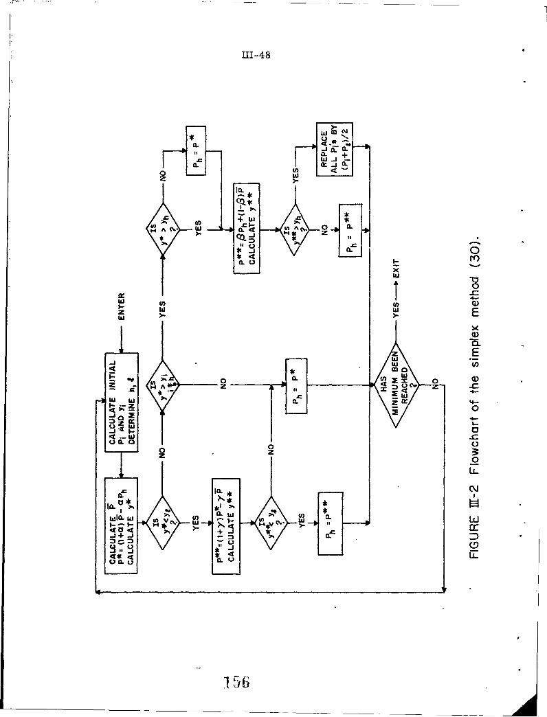
11I-48
a.-w -
00
U))
*w
Ia.0
0
-C
zE
U) E£ HA z
I~l W
0a. 0 (D0 As 3-
'CII.-*
-j z
ICLd
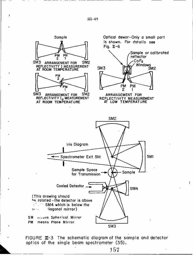
T1I-49
Sample Optical dewar-Only a small partis shown. For details seeFig. 1E-6
ý,Sample or calibratedreflector
SM3 ARRANGEMENT FOR SM2 WindowsREFLECTIVITY I MEASUREMENT ,ndow sAT ROOM TEMPERATURE I1SM
PMP
Pr2 1SM3 ARRANGEMENT FOR SM2 ARRANGEMENT FOR
REFLECTIVITY Io MEASUREMENT REFLECTIVITY MEASUREMENTAT ROOM TEMPERATURE AT LOW TEMPERATURE
SM2
~-*-Spectrometer Exit Slit S~IV
for Transmission"- •- apeapeSae L• ,---•-.
Cooled Detector_.SM
(This drawing shouldh• rotated -the detector is above
," M4 which is below the-•, , •liagonal mirror)
SM ,.JIs Spherical MirrorPM means Plane Mirror
SM3
FIGURE 11-3 The schematic diagram of the sample and detectoroptics of the single beam spectrometer (35).

HI-50
Thermocouple HeaterLeads Leads
DewarHeater - Bottom
CoilHeat Sink
C pL
Thin WallStainless Steel
Vacuum Valve>,
Sm•,j •--Heater CoMl
Light.Aý' •Transmission Sample
CaF 2 WindowsFIGUREU I-4 An- optical dewar designed for the single beamspectrometer (35).
151
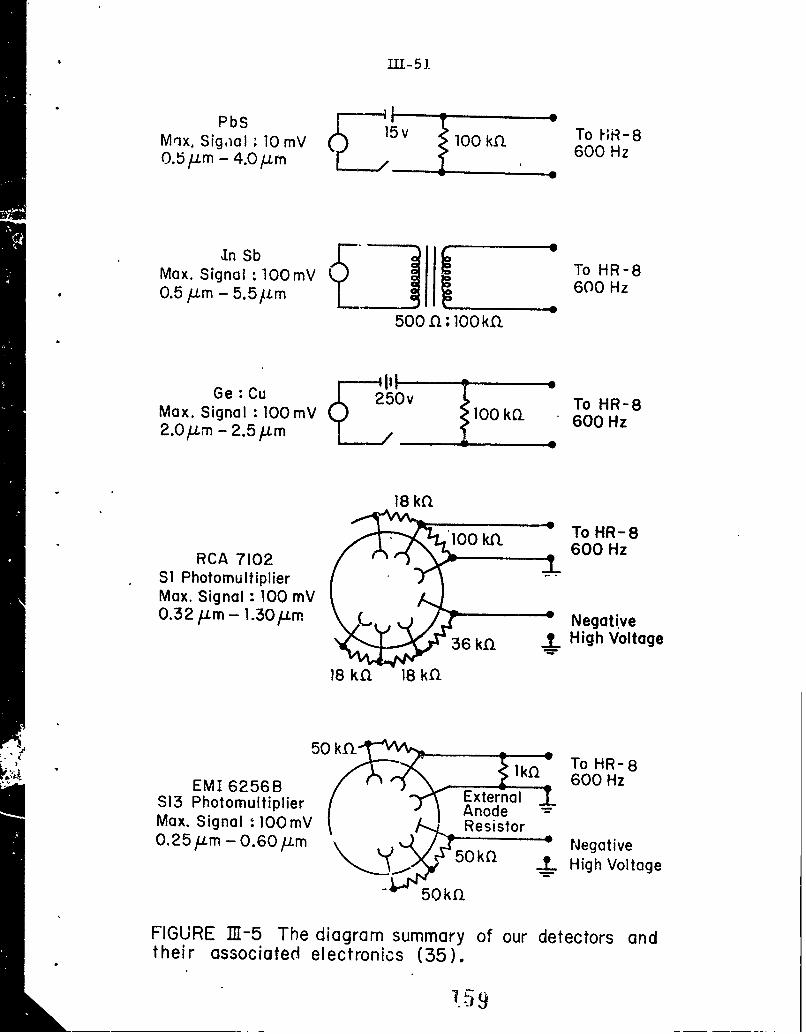
, TTT-5 J
PbS To .'-TMix, Sigl0l l mV 15v 100 kl To HR-8
0.5/.Lm - 4.0)u m 600 Hz
In SbToH-Max. Signal : lOOmV To HR80.5.rm - 5.51.m 600 Hz
500 ..1: lO0k<.
Ge : Cu . 25v To HR-8Max. Signal : 1OOmV 100 k(_ 600 Hz2.0u.Jm - 2.5Mm j 60H
18 k(I
RCA 7102 ,O
' 100 K600
H z-
S1 PhotomultiplierMax. Signal : 100 mV
0.32 /im - 1.30/im Negative333 66 kk 36 k!1 ± High Voltage
18 kB. 18 kn.
I kflTo HR-8
EMI6256B /600 HzS13 PhotomultiplierMax. Signal - IOOmV Reinor0.25 Lrn - 0.60/.Lm 5,k_ Negative
f .. High Voltage
-• 50k.
FIGURE TMT-5 The diagram summary of our detectors andtheir associated electronics (35).

LAJ
_ ~0cin
~ C, 0C.
0 0
'3)CP cym U
E 0
_ n E
C, C.0 . (1C1)-j l L0.0 C=, 4
l
-cc4-
W
C=C
0.2E0
-D
00
- ~ - 4-
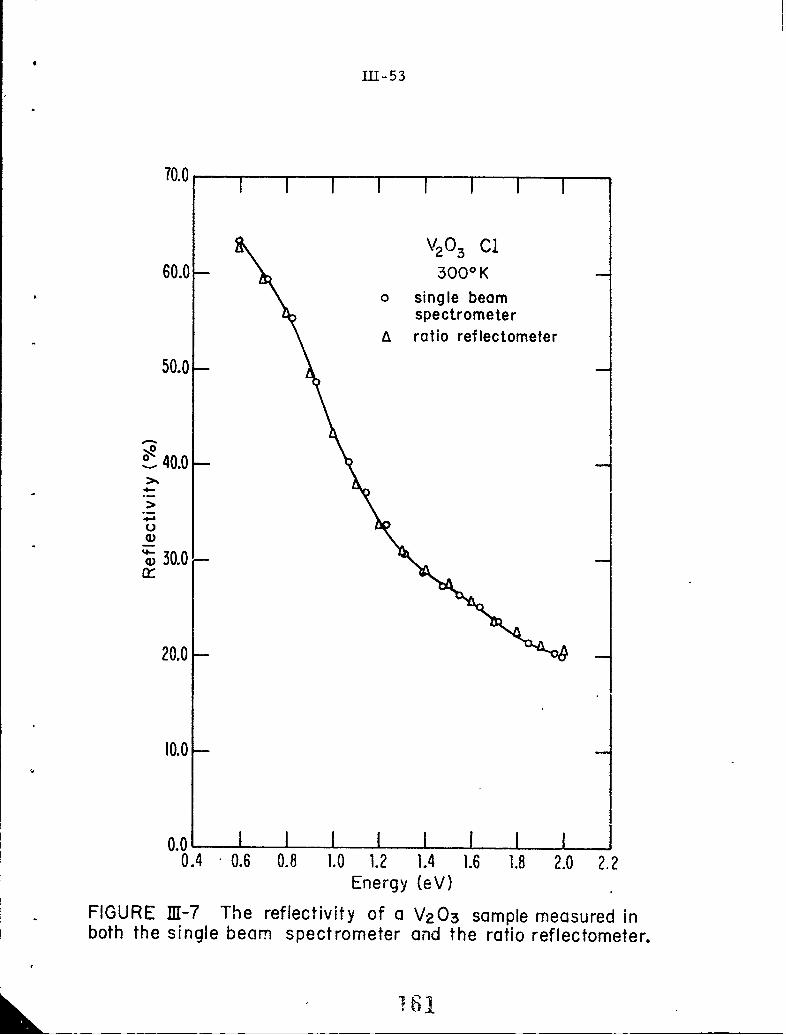
III-53
10.0 1 1
v203 Ci60.0- 3000 K
0o single beamspectrometer
A ratio ref lectometer
50.0
I 40.0
C.)
0)= 30.0-Cr
20.0 -
10.0-
0.0 _-0.4 0.6 0.8 1.0 1.2 1.4 1.6 1.8 2.0 2.2
Energy (eV)
FIGURE Il1-7 The reflectivity of a V2 0 3 sample measured inboth the single beam spectrometer and the ratio reflectometer.
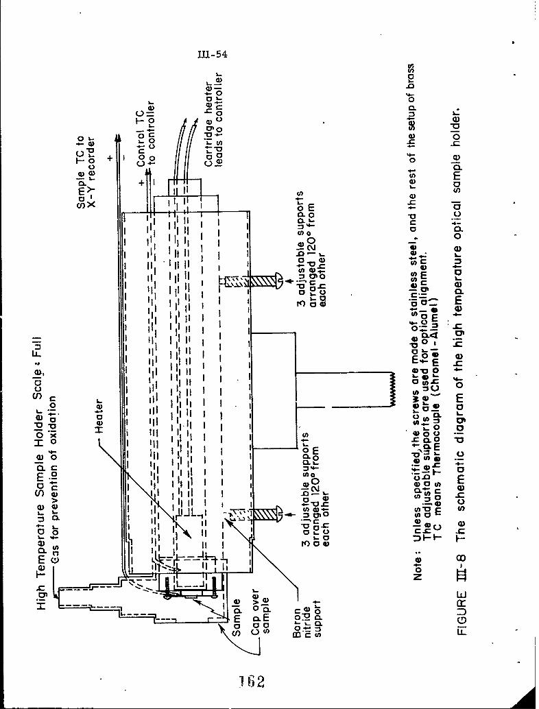
Ul-54
0 L0
O0
0o +I
: CL.
0L 0.
C 0•, I
0
t0 -0 v"-
',OL "' o
0~~ 0~
0.
-Ia
0 0= 0 0
l _iiI II'
C) oE
.II 'li Ir0
° "' Ililo o
IL 0C0
11 II E00"
"• ' •III iI t0 Io
I I
0
-I OLIll ''
a C F
, .F
0" II I
gEo 4II005.M
1,1 1
E• -
000
4-V
=
0M a , 1 ,0
E u )
To oI
li
n o.-W a.
'~~~~*
0. .0
_ I&i-
0. .
E a. _ E00
M r2
I62

II- 55
4=iLLJ
CD /1
C CL
0~0.
0
4 ~L. 0
(I)0-w -0-
0 EuCIo ~ ~ r 0~u~
04))CLC
.N & I-<> 00 a
- NC 0o o
m-. -V000
O.C 0.00
n_0 _ iN 0.36--
a.-
NE 0
L-
0 0(00
N 4)
:300C 4 -
=0
EC
* (I)
163
CHAPTER IV
OPTICAL RESULTS AND DISCUSSION
In thi, chapter, we shall report the results of our optical measure-
ments on VO2, V2 0 3 and (V xCr) 203. Most of our measurements
were done on single crystals of V 03 and (VlIxCrx)203 The optical
properties of VO 2 single crystals have already been reported by Ladd
and Paul (1) and Ladd (2). We shall, however, present the optical con-
stants we have derived from the reflectivity curves of VO 2 reported by
Ladd (2). The optical properties of films will then be presented as a
comparison to those of bulk crystals. Since the films have much smaller
changes in resistivity at the phase transition than those of bulk crystals
(see Chapter III) and since their thickness is usually uneven, and their
surfaces rough, no optical constants were derived from measurements
on the films.
A. Introduction
Most of our optical measurements were made on unoriented cry-
stals, mainly because, in our experimental observation, we had found
no significant optical anisotropy in such crystals at room temperature.
Here, we will elaborate on this question.
In separate studies, it has been found that the dc electrical con-
ductivity of V2 0 3 crystals in the metallic state exhibits no significant
anisotropy (3, 4). Feinleib and Paul (3) reported that the anisotropy
ratio of V 2 0 3 crystals (the ratio of resistivity along the c-axis to re-
sistivity along the a-axis of the crystal) varied from 0.9 at 275°K to

IV-z
1. 1 at 6250 K. While a lack of anisotropy in the dc electrical con-
ductivity of a crystal does not necessarily imply' a lack of anisotropy
in the frequency dependent .tical constants, it is not uncommon to find
'o significant optical anisotropy in uniaxial crystals. For example, in
quartz (SiO 2 ) which is hexagonal in structure, the refractive indices
ne, obtained with the electric field vector along the c-axis, and nor
obtained with the electric field vector perpendicular to the a-axis, were
reported in the.wavelength interval from 0. 19p to 2.18p± and were found
to be within 1%6 of each other over the entire wavelength region (5). In
sapphire (At 0 3 ), which has the corundum structure, ne and no
were measured in the interval from 0. 54ýi to 0. 6 7 11 and they too were
found within 1% of each other (5). And Chandrasekharan and Damany(6),
who investigated the optical constants of At 2O3 in the vacuum ultraviolet
region from 0. 61ýL to 0. 3 2p, reported that the refractive indices n e
and no were within 1.55% of each other over this wavelength region.
To confirm that there is no significant optical anisotropy in our
crystals we performed an experiment on a V2 0 3 crystal from Run #1
(x-ray Laue back reflection pattern showed the front surface - [01T2]which is - 580 from the c-axis), and on a (V0.982Cr0.018)203 crystal
from Run #9 (x-ray Laue back reflection pattern showed the front sur-
face to be - 200 away from the c-axis) at room temperature. These
crystals will henceforth be referred to as B1 and Ri respectively. The
crystals were mounted on a rotating disk so that the axis of rotation was
along the inc'dent optical path of the ratio-reflectometer described in
*In collaboration with Dr. Paul Raccah, Lincoln Laboratory.
___

IV-3
Chapter III. The incident light was polarized by a quartz crystal
polarizer in such a way that the electric field was perpendicular to
the plane of incidence. Since the c-axis was not perpendicular to the
front surface of either of the crystals, the incident polarization should
have different effects on the c-axis and a-axis when the crystals were
rotated about the optical axis. We did the polarization studies at four
photon energies: 2.0eV, 1. 5 eV, 1. 0 eV, and 0.65 eV. As we rotated the
crystals, their, reflectivity remained within + 1% of their values, which
is within the range of experimental uncertainty of the optical setup.
Therefore, the experiment indicated that there was no significant
anisotropy in the crystals between 0. 6 eV and 2. 0 eV; please note that
a lack of optical anisotropy in a crystal between 0. 6 eV and 2. 0 eV does
not necessarily imply that there is no anisotropy over the whole
spectral region.
We then turned to other observations to demonstrate further the
lack of optical anisotropy in these crystals. We found that the optical
constants BI and RI obtained from the angular dependence measure-
ments were very similar to those derived by the oscillator fit method
from the near-normal incidence reflectivity measurements (at the same
energies: 1. 96 eV and 2.54eV respectively). For reasons we will dis-
cus,; later in this chapter, we concluded from the above observation
that the optical anisotropy in these crystals is not significant.
Since we observed no significant optical anisotropy, our measure-
ments could be done on unoriented, mechanically polished crystals -

IV-4
this was fortunate since almost all our crystals were too small
(approximately 2-3 mm across and 3mm long) for crystal orientation
anyway.
The crystals were first polished by 10V Al 2 0 3 paste, followed
by 5V and 2V diamond pastes and finished with IV diamond paste. They
were then rinsed in alcohol and in de-ionized water, and blown dry
with dry nitrogen gas. The samples prepared this way have very simi-
lar optical surfaces, as demonstrated by the close resemblance of the
reflectivity spectra of the two V2 0 3 crystals Cl and C2 (they were cut
from a boule from Run #2 with c-axis perpendicular to the plane of the
crystals, and the reflectivity spectra are shown in Fig. IV-l).
B. Angular Dependence Measurements*
We have discussed earlier in Chapter III that the values of opti-
cal constants evaluated from a reflectivity spectrum by either the
oscillator fit method or the 1'ramers-Kronig analysis could be subject
to errors. To minimize the possibil'ty of errors, we obtained the
values of n and k at two photon energies (1. 96 eV and 2.54eV) by the
aagular dependence measurements, and then required the calculated
values of n and k obtained by the Kramers-Kronig analysis or the
oscillator fit method to fit the measured values at the above mentioned photon
energies (for detailed discussion see Chapter -III). We will present the
results of the angular dependence measurements in this section.
Angular dependence measurements were done on C1 and C2 crystals
at room temperature. Figures IV-2 and IV-3 show the reflectivity Rp
In collaboration with Dr. Paul Raccah, Lincoln Laboratory.
T_7 G

IV-5
of Cl and C2 as a function of incidence angle ý at both 1. 96 eV and
2.54eV. Using the angular dependence curve fitting procedure des-
cribed in Chapter III, we obtained reasonable fits between the theoretical
and the experimental values of R as a function of q. The values ofp
n and k, which provide such fits, are listed as follows:
For Cl:
At 1.96eV, n = 1.77 and k = 1.10
At 2.54eV, n = 1.82 and k = 0.90
For CZ:
At 1.96eV, n = 1.78 and k = 1.10;
At 2.54eV, n = 1.81 and k = 0.90
Angular dependence measurements were also done on RI. The
measured and fitted Rp versus ý values are shown in Fig. IV-4 and
their optical constants are listed as follows:
At 1. 96eV, n = 2. 02 and k = 1. 14;
At 2. 54eV, n = 1. 86 and k= 0. 96.
Error Analysis. Since Eq. (3-5b), used in the angular dependence
method, is very complex, error analyses by mathematical means would
be difficult. Instead, we took a different approach. First, an angular
dependence measurement was done on the V2 0 3 crystal B1 at 2.54eV;
the optical constants obtained were n = 1. 79 and k = 0.89. Then to
investigate the effect of the absolute values of R on the values of np
and k, we multiplied all the R values of BI by a factor of 1. 05. Afterp
fitting the newly generated data using Eq. (3-Sb), we obtained no change

IV-6
in n and an increase of ' 3%6 in k. Similarly, by multiplying the
experimental R values of B1 by 0. 95 and fitting the newly generatedp
data, we again found no change in n, and a decrease of ' 3% in k. By
keeping R values the same as the experimental values but by in-p
creasing each corresponding value of ý by 5 degrees, we found an in-
crease of "8%0 in n and a slight decrease ("' 1%) in k. Obviously,
the above analysis holds true only for this particular set of n and k.
However, since the values of n and k obtained for all our crystals
are in the vicinity of the above values (n = 1. 79, k = 0.89), we should
expect similar dependence of the n and k of Cl, CZ and R1 on the
experimental accuracy of R and ý, In our optical setup, the un-p
certainty in ý from the alignment errors, as stated in Chapter III,
should not exceed 1/5 degree and the accuracy of R should be withinp
+ 1%6. Therefore, the actual experimental uncertainties in 0 and R-- pshould cause very small errors in n and k.
There are, however, other sources of error, namely, surface
scattering and polarization effects. In angular dependence measurement,
surface scattering could become important when the surface of the material
is rough. Strictly speaking, the effects of surface scattering on our
measurements can be considered as two parts; the first part is inde-
pendent of the incidence angle 0 and will affect equally the absolute
values of R at all ý's. Its effects have been shown to be small in ourp
earlier investigation of effects on n and k by the uncertainties in the
absolute values of R p. The second part of the surface scattering effects
p6,
S_ A

* IV-7
is dependent on 4 and the effects usually become important for large
angles of incidence. To demonstrate that this part is also unimportant
to our measurements, we deleted the experimental value of R of C1p
at ý = 70 from the initial set of data points (at 2.54eV), and pro-
ceeded to fit this new set of data points. If the surface scattering were
important, we should expect an appreciable change in n and k; how-
ever, we obtained n = 1. 81 and k = 0.90 which are very similar to those
obtained from the'initial set of data points (n = 1. 82 and k = 0.90), thus
indicating that the surface scattering effects are not important.
Our measurements were done with the electric field of the inci-
dent radiation polarized in the plane of incidence. If in the incident
beam, the electric field were to contain a component which is polarized
perpendicular to the plane of incidei.ce, there is a possibility of error* *
because the Rp and Rn as a function of ý are expressed by different
equations (see Eqs. (3-5a and 5b)).
To incorporate this mixing effect into Eq. (3-5b), we modified it:
R Rp + pRn (4-1)
whereintensity of incident radiation with the electricfield polarized perpendicular to the plane of incidence;P intensity of incident radiation witn the electricfield polarized in the plane of incidence
p was measured and found to be less than 0. 0015 in our system. We
then fitted the experimental values of the reflectivity of CZ as a function
* Rp(Rn), as defined in Chapter III, is the reflectivity of a crystal whenthe electric field of incident radiation is polarized in (perpendicularto) the plane of incidence.
170

IV-s
of ý at 2. 54eV using Eq. (4-1) with p = 0. 0015, and obtained n = 1. 82
and k = 0.89, which again are very close to n = 1.81 and k = 0.90 ob-
tained by fitting the experimental values using Eq. (3-5b).
There was also the indication that any effects of optical anisotropy
on the optical constants at 1. 96 eV and 2. 54eV were negligible. If
there is any significant anisotropy, then a gooL "t of the theoretical
curve to the experimental values of R versus 4 for all ý will bep
difficult to obtain. This was not the case in our experiments. Further-
more, even if the crystals were anisotropic and good fits were obtained
between the theoretical curves and the experimental curves, the optical
constants n and k obtained should be different from those derived
from near-normal incidence reflectivity spectra of those crystals using
the oscillator fit method. We will see later that the constants obtained
from both the angular dependence measurements and the oscillator fit
method are very similar.
From the above discussions of all the possible sources of error,
we feel that our accuracy in determining n and k should be better
than + 5%6 of their values, and we will proceed to use them in our later
analyses.
C. Optical Results on V2O_3 and (V 0.98Cr0.018)2O3 and VO2 Using
the Single Beam Spectrometer
1. V 2o 3
a. T> Tt
The optical reflectivity of the two V 2 0 3 crystals Cl " . . was
measured in the single beam spectrometer described in Chapter III
S'A

IV-9
and in Ladd's work (2). A great part of the uncertainty in the re-
flectivity measurements using the spectrometer is due to re-focussing
errors. To eliminate this source of uncertainty in our experiment, we
normalized the reflectivity values of Cl and CZ at 1. 96 eV to 20.2%6 and
20. 1% respectively; these values were obtained from near-normal inci-
dence reflectivity measurements using a helium-neon laser. Figure IV-l
shows the resulting reflectivity curves of both Cl and C2 at room
temperature.
Since the values of n and k at both 1.96eV and 2.54eV for C1
are close to those for CZ, and since the reflectivity spectra of these
two crystals are also similar, we have only to derive the optical con-
stants for one of the curves, in our case, for the reflectivity spectrum
of the C1 crystal; the other crystal, CZ, should give similar results.
Figure IV-5 shows the theoretical reflectivity curve obtained fr )m
an oscillator fit to the experimental reflectivity data of Cl. in this
particular fit, we used Eq. (3-17b)to express the complex dielectric con-
stant E(w) and used Eq. (3-21b) as the objective function in the fitting
procedure so that the values of n and k at 1.96eV and 2.54eV ob-
tained from the oscillator fit were constrained to approach those values
obtained from the angular dependence measurements. Table IV-1 shows
the values of n and k obtained from this fit.
Figures IV-6, 7, and 8 show respectively E1 (the real part of the
dielectric constant E), c? (the imaginary part of the dielectric cor.stant E)
172

IV-10
At 1. 96 eV At Z. 54eVMethod n I k n k
IAngular Dependeace 1.77 1.10 1.82 0.90
Oscillator Fit using .79 1..0 1.79 0.89Eq. (3-Z2b)
Oscillator Fit using 1.81 1.10 1.81 0.86Eq. (3-Zla)
Kramers-Kronig 1.83 i. 1i.81 0.86p 1.0
Kramers-Kronig 1.081 .9 11.79 0.87
Kramers-Kronig 1.78 1.09 1.76 0.88p = 1.2
Kramers-Kronig .p = 1.3 1.76 1.10 1.73 0.89
TABLE IV-1. Optical constants n and k of a V2O0"crystal -1l) at room temperature, cbtained bydifferent methods.
and the absorption coefficient a as a function of photon energy. We
then used the same initial values of the parameters in Eq.(3-17b), but
changed the objective function from Eq. (3-21b) to Eq. (3-Z2a), so that
.ae opt cal constants at 1. 96 eV and 2.54eV were allowed to take any
values. Judging front che reasonable fit shown in Fig. IV-5, , e would
expect the values of n and k at 1. 96 eV and 2. 54eV should not b
very diff,'ren* from those obtained from the angular dependence method.
If, then, the values of the optical constants at 1. 96 eV and Z. 54eV ob-
tained from a reasonable fit to the experimental data were very much
_ _ __ __ _

IV-1l
different from the values obtained from the angular dependence method,
then it would suggest three possible situations: 1) the oscillator fit
method by itself is not adequate to give accurate values cf n and k at
1.96 eV and 2.54eV; 2) the angular dependence method did not give us
accurate results, probably because of an optical anisotropy; or 3)
the reflectivity spectrum has appreciable errors.
Figure IV-9 shov's the theoretical reflecti'rly curve obtained from
the oscillator fit to the experimental data using Eq. (3-Zla) and Figs.
IV-10, 11, and 12 show Ec, E2 and a, respectively, as a function of
photon energy obtained from this fit. These curves are all similar
to the respective curves in Figs. 111-6, 7, and 8. The values of the
optical constants at 1. 96 eV and 2.54eV are also listed in Table IV-l,
and they, indeed, are close to those obtained from the angular dependence
measurements, indicating that none of the above three possible situa-
tions actually pertains.
One could then ask whether it was actually necessary to obtain the
optical constants at 1. 96 eV and 2. 54 eV using the angular dependence
measurements, since the oscilator fit method using Eq. (3-Zla) did
give us quite accurate values of n and k at 1. 96 eV and 2.54eV (as
demonstrated above); or, to put the question differently, will the oscil-
lator fit always give us t.he correct valae. of the optical constants ? To
answer this question, onr. must re-examine the oscillator fit method
carefully. In this method, the complex dielectric constant E(c,) is ex-
pressed in terms of a series of oscillator terms and, for metals, a
174

S
IV-12
Drude term (see Eq. ( 3 -17a) or Eq. (3-17b)), and the values of the re-
flectivity are calculated using Eq. (3-18). Then, the parameters of the
oscillator terms and the Drude term are automatically adjusted until a
good fit is obtained between the calculated and measured reflectivity
values. If we have only one experimental data point to be fitted, then
judging from Eq. (3. 18). we can select an infinite number of combina-
tions of E, and E2 that will give a calculated reflectivity value close
to the measured one. However, in practice, we always have data points
in a wide spectral range, and hence correct selection of E and E2 is
much easier since the values of c and E2 have to be related to each
other through Eq. (3-17a) or Eq. (3-17bý. There is still no absolute
guarantee, however, that we will obtain the correct set of c and E2 "
A theoretical study of how this uncertainty can influence our results
is very difficult and is dependent on each particular spectrum. To
examine the effects of this uncertainty, or non-uniqueness, we obtained
three different sets of parameters that gave good fits to the reflectivity
spectrum of C1 (by using different sets of initial values of the parameters
in Eq. (3-17b)). A comparison of the values of n and. k obtained from
these fits at 1.96 eV and 2.54eV with those values obtained by the angular
dependence measurements should give us some idea of the seriousness
of the effects of this non-uniqueness. We found that in all these three
fits, the values of n and k at 1.96 eV and 2.54eV we. e still close to
1.75

IV-13
the measured values. Here, we will report the results of the worst
match. Figure IV-13 shows the theoretical fit to the experimental
data obtained from the oscillator fit method using Eq. (3-Z2a). The
values of n and k at 1.96 eV and 2. 54eV are as follows:
at 1.96 eV, n 1. 75
nk= 1.72
at 2.54eV, n = 0.89k= 0.89
The plots of ElI E2 , and a versus photon energy resulting
from tils fit are shown in Figs. IV-14, 15, and 16. Though there are
some differences in the values of these optical constants from those
reported earlier, especially for E > 2. 5 eV, the general features of
these curves are still very similar to their corresponding curves re-
ported above.
"* The criterion for the best match is to choose the particular fit
such that the value of the function f, defined below, is at a minimum:
f =n n a + ca-n m eas (n )nmeas 1.96 eV meas 2..54eV
+(kcal kmeas + k cal kmeas)k kmeas 1.96 eV meas 2.54eV
where
subscript "meas" = measured value, andsubscript " cal"l calculated value.
176

IV-14
Therefore, while our investigation is not very exhaustive, the
oscillator fit method most probably can provide us reasonable values of
optical constants. If we still need more accurate values of the constants,
then we have to obtain the values of the optical constants at some photon
energies in 'he spectral range of our interest,say n and k, by other
methods such as the angular dependence method. The calculated values
of n and k obtained from the oscillator fit method are then constrained
to approach those *obtained from the angular dependence method. By
this approach, correct selection of values of E and E2 can be assured.
We then did a Kramers-Kronig analysis on the reflectivity curve
of Cl (the dat "oints of the reflectivity spectrum were spaced at
photon energy intervals of 0. 05 eV). Equation (3-11) was used in the
extrapolation procedure (discus.sed in Chapter III); p was varied from
0.0 to 5.0 by increments of 0.1. Only four valaes of p, namelyp = 0.0,
p = 1.1, p = 1.2, andp = 1.3, gave values of n and k at 1.96eV and
;.. 54eV that were withinr-+ 5% of the measured values (see Table IV-1).
From the table it can be noted that the Kramers-Kronig analysis using
p = 1.1 and p = 1.2 gave values c. n and k which were very close to
the measured values, though a slightly better match was obtained using
p = 1. 2 than was obtained using p - 1.* Figures IV-17, 18, and 19
The criterion for the best mratch is to choose the particular p such thatthe value of the function f, defined below, is a minimum:
f ncl n meas )+ n n al - n m anmeas / 1.96 eV nmeas 2.54 eVkca -kmes
whr + k ekeas) + ( cal kmas).54eVwhere meas 6eV
subscript "Imeas" = measured value, andsubscript "cal" = calculated value.
,77 tA

'aIV-15
show respectively the plots of El, E2 and a versus photon energy.
In Fig. IV-17 and Fig. IV-18, the curves were obtained using p = 1. 2.
Figure IV-19 shows the plots of a versus photon energy for p r 1.1,
p = 1.2 and p = 1.3; though the curves are quite similar, there are
some di.Zferences among them for photon energies greater than 2. 0 eV,
Therefore, it appears that if we do not have any previous knowledge
of n and k at 1.96eV and 2.54eV, the proper selection of p that
will give us correct values of n and k will be difficult in the Kramers-
Kronig analysis, while in the oscillator fit method, we have a much better
chance to obtain reasonable values of n and k.
In summary, the plots of el E 2 and a versus photon energy)
obtained using the above three different approaches, are similar, ex-
cept for some minor differences that arose from the curve fitting and
from extrapolation uncertainties. Also, in all the E2 curves, we ob-
serve structures at about 0. 6 eV, 1. 5 eV and 4. 3 eV. There is a weak,
broad structure between 2. 0 eV and Z. 4eV. Further discussion of these
structures will be presented in Chapter V.
As mentioned in Chapter III, the oscillator fit method allows us
to extract the free electron contribution directly from the reflectivity
spectrum. The parameters of the free electron contribution can vary
somewhat depending on the initial values of the parameters used (within
20%). Furthermore, in our oscillator fit method, our parameters are
obtained with the assumption that we have a one-band model w;th all the
conduction electrons having the same mobility and effective mass.
This is, of course, a serious approximation, and the values of the
S]7V8

IV-16
optical mobility and the values of the effective mass of the conduction
electrons, obtained from the calculation shown below, are thus only an
order of magnitude calculation, and should be interpr. ed as such.
From the oscillator fit method where the values of n and k at
1. 96 eV and 2. 54eV were constrained to approach the values measured
in the angular dependence measurements, we obtained:
E = 3.54eV,n
E = 0.678eV.c
Where E and E are defined as follows:n c
E 4irn e2
O n n c (4-2)n = m*
Ec e (43)oc - opt m* 7 43
topt c
where
n = concentration of conduction electrons/holes ofoptical mobility "opt' and optical effective mass m*.
T c relaxation time of the conduction electrons/holes.
22 3In V 2 0 3 , there are 3 .92x 10 vanadium ions cm- . As men-
tioned in Chapter I, there are two outer d electrons per vanadium ion
left after all the bonding requirements are fulfilled. If we assume a
one-band model and that these outer electl:z,r.s all become conduction
electrons, then n0 is equal to 7. 84 x 1022 cm- 3 . Using E = 3.54eV
and Ec = 0. 678 eV, and the above value of nc in Eq. (4-2) and Eq. (4-3),
we obtain m* 9.1 me and pt 0.19cm /V-sec, where m free
e opt

IV-17
electron mass. Furthermore from Eq. (4-3), we obtained T-16
9.8 x 10 sec.
Though it might be questionable for us to compare the value of
the optical mobility with that of the Hall mobility, it is nevertheless
interesting to see whether they are within the same order of magnitude.
Hall effect measurements have been done on V203 by several
peo -le (7, 8, 9). The results obtained varied among the studies. Rosevear
and Paul (7) measured a V2 03 crystal grown by us using the vapor trans-
port technique and found RHa = 0.95+ 0.2 cm -3/Vsec, which
would correspond, in a one-band model, to a carrier concentration of122 -32
1.6 x 10 cm .and Hall mobility H = 0.95 +-0.2 cm /V-sec. Austin
and Turner (8) found R14 = 0.4 cm 2 /V-sec, which would correspond,
22 -3in a one-band model, to a Hall carrier concentration of 2. 7 x 10 cm
and •H 0.4 cm /V-sec. Zhuze et al. (9) found RHu = 0.4 cm 2 /V-sec,RH = H
which could compare, in a one-band model, to a carrier concentration
of 3.8 x 10² crri and ýLH = 0.4cm /V-sec. (The above-mentioned workers
all found that the Hall carriers would correspond to holes in a one-band
model.) Hence, in a one-band model, the values of Hall mobility
measured are in the same order of magnitude as that of the optical
mobility.
This is especially true if the one-band model is not valid, and one hasto consider overlapping bands. In the metallic state of V20 3 , the metal-lic conductivity could very well be caused by mixed conduction. The Hallmeasurements, as well as our optical measurements, however, would notbe able to give us the values of prevalent parameters in such cases. Theone-band model, therefore, represents the simplest approximation.

IV-18
Finally, a comparison can be made between the value of the
optical mobility and Hall mobility with that of the mobility obtained
,asing the following equation.
= ne p (4-4)
where
S= conductivity,
S= m obility, and
n number of charge carriers.
22 -3If we assume a one-band model and assume n = 7. 84x 10 cm and
3 -1a = 5 x 10 (62-cm) (the resistivity of a bulk V 0 3 crystal as reported
in Chapter U1) then p. = 0.4cm/ V-sec, which is of the same order of
magnitude as the values of Hall mobility and optical mobility described
above.
In the oscillator fit method where the values of n and k at 1. 96 eV
and 2. 54eV were not constrained to approach the measured values, we
obtained E = 3.50eV and Ec = 0.6E6 eV, similar to those values wenc
used in the above calculation Therefore, similar results can be
expected.
Finally, we should point out that the crystals Cl and C2 were cut
from the same boule gro vn in the tri-arc furnace. V2O3 crystals
grown by the vapor transport technique have also been measured opti-
cally. We found that the optical reflectivity spectrum at room temperature
of the as-grown crystal resembled that of VO 2 (to be shown later). After
IV-19
the crystal was lapped, the spectrum became that of V.03 indicating
that a small layer of VO 2 had very probably been removed. Since these
crystals were very small and often cracked during lapping, they were
not used further for definitive determination of the optical properties.
Because x-ray, chemical analysis, electrical conductivity measure-
ments and Hall effect measurements all showed that the crystals were
V2 0 3 , the VO film must be very thin. The thin film was probably
caused by the oxidation that occured during the shutdown of the vapor
transport apparatus. At the end of each crystal run,, the furnace and
the gas flows were shutdown at the same time. Though the, system was
supposedly a closed system (see Chapter II), inevitably some air would
leak in during the cooling of the furnace causing the surfaces of the
crystai. to oxidize.
b. T<Tt.
Figure IV-20 shows the experimental reflectivity data of a V.0 3
0crystal, Cl, at 120 K together with the theoretical reflectivity curve
obtained from the oscillator fit method. The reflectivity measurements
were done in our single beam spectrometer using the optical dewar
described in Chapter III. Above I eV, the low temperature reflectivity
curve is similar to that at room temperature. Below 1 eV, a peak at
about 0.8 eV and a shoulder around 0.4 eV appeared.
The optical constants El, E., and a obtained from the oscillator
fit are shown in Figs. IV-21, 22, and 23 respectively. The absorption
coefficient a was found to decrease steadily below 1 eV with a shoulder
182

IV-20
around 0.4eV. Using Eq. (3-4b) and the absorption coefficients, the
transmission of a thin 0.5ý± V 0 crystal was calculated and plotted2 3
(see Fig. IV-24). Though the theoretical reflectivity curve does not
match exactly with the experimental data (see Fig. IV-20), the struc-
tures in the predicted transmission spectrum are quite apparent. When
this predicted spectrum is compared with the transmission spectra*
measured in the single beam spectrometer on thin films of V O33
grown by sputtering and vapor transport techniques, the similarity in
shape between them is quite obvious (see Fig, IV-25).
From the transmission spectrum, as well as from the absorption
coefficient a ve-rsus photon energy curve, we notice that there is no
sharp absorption edge as in germanium and silicon. The absence of a
sharp absorption edge was also noted by Feinleib and Paul (3), using a
transmission measurement on a thin ( -,.25ýL thick) V2 O3 crystal (see
Fig. IV-25).
We should point out that the reflectivity spectrum has not been
analyzed by the Kramers-Kronig analysis since we do not have the neces-
sary prior knowledge of any of the optical constants in the spectral range
of our interest to enable us to select the proper extrapolation parameters
for the reflectivity spectrum at both the high and Low7 photon energy regions.
The structural and electrical properties of these films were presentedin Chapter II.
A
* IV-21
In summary, at T > Tt, we have structures in the E2 curve
(Fig. IV-7 or 15 or 18) at around 0.6eV, 1.5eV, 2.0-2.4eV, and
4. 3 eV. At T -, Tt, structures are observed in the E2 curve (Fig.
IV-22) at around 0.4eV, 0.9eV, 1.5eV, 2.0-2.4eV, and 4.3eV.
We will interpret these results in Chapter V.
2. (V0. 9 8 2 Cr0.018)203
As discussed earlier in Chai..,ers I and II (V IxCr x)23 crystals
would undergo a phase transition from a metallic state into an insulating
state at room temperature at a critical chromium concentration x = 0. 010.
However, x-ray diffraction studies in c..; doped crystals showed that for
x = 0. 010 and 0. 014, both the metallic and insulating phases coexisted
at room temperature. Therefore, to study the optical properties of the
insulating state of a doped crystal at room temperatu. -. , we chose a
(V 0 . 9 8 2 Gr0 018)203 crystal, which has the largest shromium concentra-
tion among all our crystals runs, and which has been shown by x-ray dif-
fraction studies to contain no metallic phase (see Chapter U1).
The'reflectivity of the (V0, 9 8 2 Cr 0 018)203 crystal (R1) at room
temperature was measured in the single beam spectrometer. As in the
case of V2 0 3 , the reflectivity at 1. 96 eV was normalized k.o 22. 2%, the
value measured in a near-normal incidence reflectivity measurement
using a helium-neon laser.
Figure IV-26 shows the theoretical reflectivity curve obtained f::om
the oscillator fit to the experimental reflectivity data. The fit was ob-
tained -ising Eq. (3-17a) as the expression foz the dielectric constant
E (o) and using Eq. (3-Zb) as the objective function, that is, the values
1e

IV-z2
of n and k at 1 .96 eV and 2.54eV obtained from the oscillator fit
method were constrained to approach the measured values of n and k
at 1.96eV and 2.54eV. Table IV-2 shows the list of n and k values
At 1. 96 eV At 2.54eV
Method n k nk
Angular Dependence Z. 02 1.14 1.86 0.96
Oscillator Fit using 2.02 1.14 1.85 0.95Eq. (3-21b)
Oscillator Fit using 2 1.13 1.86 0.93Eq. (3-Z2a)
Kramers-Kronig Z.05 1.11 1.86 0.92p = 1. .
Kramers-Kronig 2.02 1.12 1.83 0.94p = 1.3
Kramers-Kronig 1.99 1.14 1.80 0.95p= 1 . 4
Kramers-Kronig 1.95 1.15 1.77 0.96p= 1.5 1 .95 1.15 1.77 0.96
TABLE IV-Z. Optical constant n and K of a(V 0 . 9 8 2 Cr 0.01 ) 0 crystal (Ri) at roomtem'perature, o ,ained by different methods.
obtained by the different methods we used, and, in particular, shows
that by this method, we obtainedn = 2. 02 and k = 1.14 at 1.96eV, and
n = 1.85 and k = 0.96 at Z. 54 eV. These values are very close to those
obtained by the angular dependence method. Figures IV-Z7, 28, and 29
show respectively the plots of Ely Cz, and a versus photon energy ob-
tained from the above fit.
_ AI
IV-23
As in the case of the V2 0 3 crystals (CO), the reflectivity spec-
trum was then fitted using Eq. (3-Z2a) as the objective function. In
this case, the optical constants n and k at 1.96eV and 2 54eV were
allow.:d to take any values. Figure IV-30 shows the theoretical re-
flectivity curve obtained. The plots of El, E2 , and a versus photon
energy are shown in Figs. IV-31, 32, and 33 respectively.
The values of n and k at 1. 96 eV and 2. 54 eV obtained from
this fit are also listed in Table IV-Z. They are again similar to those
obtained by the angular dependence method.
In the oscillator fit method, the values of the optical constants
obtained are obviously depende-"t on how good a fit we can obtain between
the experimental reflectivity data ..nd the theoretical curve. When a
poor fit occurs, some fine structures in the optical constants will be
lost. This can be illustrated well in the follc ing results. Figure
IV-34 shows the th3oretical reflectivity curve )btained from the oscil-
lator fit x,; the experimental data of RI (using Eq. (3-Zla)). Figures
IV-35, 36, ard 37 show the El, EC and a curves as a function of
photon energy. There we- some differences between these curves and
the corresponding curves shown in Figs. IV-31, 32, and 33, especially
at photon energies between 2. 0 eV and 2. 5 eV where the fit was quite
poor. The values of n and k obtained from the fit were as follows:
n = 1. 97 n = 1. 83k = 1.15 at2.54eV, k = 0.94
The inifial values of the parameters in the fitting program were keptthe sa•ne as those used to obtain the fit shown in Fig. IV-26.

IV-24
These values were riot as close to those obtained from the angular
dependence measurements as thos.a values obtained from the fits re-
ported earlier.
Despite some difference, however, when the plots of El, E2 ,
and a versus photon energy obtained from all the fits using either
Eq. (3-Z2a) or Eq. (3-Z2b) were compared with one another, the re-
sultant curves were similar.
Kramers-Kroniag analysis of the reflectivity spectrum yielded re-
sults similar to those obtained from the oscillator fit method and they
are shown in Figs. IV-38, 39, and 40. As in the case of V2 0 3 , the
values of p in Eq. (3-11) were varied from 0.0 to 5. 0 by increments
of 0. 1. Four values of p, namely 1.2, 1.3, 1.4, and 1.5, were ob-
tained which gave n and k values at 1.96eV and 2.54eV that were
within + 5% of the measured values. The values of n and k corres-
ponding to each of the four values of p are listed in Table IV-2, judging
from which, both p = 1. 3 and p = 1. 4 gave very good fits between the
calculated and measured values of n and k. Since for p = 1. 3, we got
a slightly better match (the same criteria as used in V2 0 3), Figs. IV-38
and 39 were plotted with p = 1. 3. In Fig. IV-40, a was plotted as a
function of photon energy for both p = 1. 3 and p = 1. 4; a slight difference
in the curves was observed, indicating uncertainty arising from extra-
polation.
In summary, as in V2 0 3 the optical constants of Ri obtained from
the above three different approaches gave essentially the same results.

IV-2.5
The E2 versus photon energy curve, obtained by any of the three ap-
proaches, shows a strong peak at around 0. 6 tv, and structures at around
1. 5 eV, 2.0-2. 4eV and 4.3 eV. The positions of these structures are
essentially in the same location as those in V2 0 3 at room temperature,
with one marked difference: the absorption coefficient in OV Cr A)20.982 r0 .01820a
decreases more sharply after 1 eV than it does V2 0 3 . In fact, a at 0. 2 eV
in the doped crystal is only 2x 10 4cm-1 while in V2 0 3 at 0. 2 eV, a is
5 -11.5x10 cm-. Furt:--r discussion of these optical results will be pre-
sented in Chapter V.
3. VO 2 . Optical reflectivity and transmission results on VO0
single crystals have bee,, reported by Ladd and Paul (1) and by Ladd (Z).
The reflectivity spectra reported by Ladd (2) on one of the thin samples
used for his transmission measurements were fitted by our oscillator fit
method, and the resultant optical constants are discussed here.
a. T > Tt
Figure IV-41 shows the theoretical reflectivity curve obtained from
an oscillator fit method to the experimental reflectivity data reported (2).
The resultant plots of El, E2 . and a (obtained by using Eq. (3-Z2a)) as
a function of photca energy are shown in Figs. IV-42, 43, and 44. Structures
are observed at - 0.7 eV, 2.9 eV and 3.5 eV in the E2 curve. We also
obtained parameters of the free electron contribution using the oscillator
fit method: En = 3. 63 eV and E = 0. 500 eV. In VO., there are
188
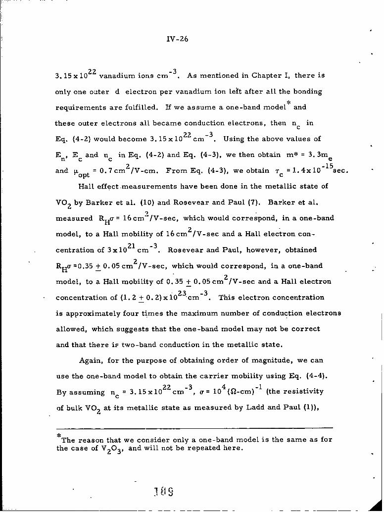
IV-26
3. 15 x 1022 vanadium ions cm -. As mentioned in Chapter I, there is
only one outer d electron per vanadium ion leit after all the bonding
requirements are fulfilled. If we assume a one-band model* and
these outer electrons all became conduction electrons, then nc in
1022 -3Eq. (4-2) would become 3.15 x 10 cm . Using the above values of
En, E and n in Eq. (4-2) and Eq. (4-3), we then obtain m* = 3. 3 mec ce
and topt 0.7 cm /V-cm. From Eq. (4-3), we obtain Tc = 1.4x10 sec.
Hall effect measurements have been done in the metallic state of
VO2 by Barker et al. (10) and Rosevear and Paul (7). Barker et al.
measured RHa = 16 cm"/V-sec, which would correspond, in a one-band
2model, to a Hall mobility of 16 cm /V-sec and a Hall electron con-
21 -3centration of 3x cm . Rosevear and Paul, however, obtained
RHo =0.35 + 0.05 cm /V-sec, which would correspond, in a one-band
model, to a Hall mobility of 0. 35 + 0.05 cm /V-sec and a Hall electron
concentration of (1. 2 + 0. 2) x 10 -3cm- . This electron concentration
is approximately four times the maximum number of conduction electrons
allowed, which suggests that the one-band model may not be correct
and that there is two-band conduction in the metallic state.
Again, for the purpose of obtaining order of magnitude, we can
use the one-band model to obtain the carrier mobility using Eq. (4-4).i22 -3 04 -i
By assuming nc = 3.15x10 cm , a= 10 (a-cm) (the resistivity
of bulk VO 2 at its metallic state as measured by Ladd and Paul (1)),
The reason that we consider only a one-band model is the same as forthe case of V 2 0 3 , and will not be repeated here.

IV-27
we obtained . = 2cm 2/V-sec which is again of the same order of
magnitude as the values of the Hall mobility and the optical mobility
reported above.
b. T<Tt
Figure IV-45 shows the theoretical reflectivity curve obtained
by fitting the experimental reflectivity data reported (2). Plots of E
and c2 versus photon energy are shown in Figs. IV-46 and 47. In the
E2 curve, we .observe structures at - 1. 1 eV, 3.0 eV and 3. 6 eV.
FigureIV-48 shows a plot of an absorption coefficient a as a
function of photon energy. The absorption coefficient shows an absorptionS104 -1
edge at E < "'.leV, with a = 1.2xlO cm at 0.6eV. Ladd (2) re-
ported that from his transmission measurement, a of this crystal
3 -1should be about 5 x 10 cm-. The discrepancy between the calculated
and measured values could be due to several factors; 1) experimental
errors in measuring the reflectivity and transmission curves, 2) the
uncertainties in the oscillator fit method that arise in fitting an ab-
sorption edge (as discussed in Chapter IMI), and/or 3) the uncertainties,
estimated by Ladd (2) to be about + 10%, in the crystal thickness, but
which, alone, would not explain all the discrepancy; one or both of the
first two factors must also have played a part.
Despite the discrepancy in the measured and calculated values of
a at 0. 6 eV, it is still apparent that there is an absorption edge near
0.6 eV though not as sharp as in germanium and silicon (see Fig. IV-49,
where in addition to the values of a derived from Ladd's results, we
4 9

IV-28
also included that a-vs-photon energy curves reported by Verleur
et al. (12)) and this fact confirms the transmission measurement on
single crystals of VO2 by Ladd and Paul (1) and the transmission
measurement of thin films of VO 2 by Verleur et al. (12). This ab-
sorption edge was further demonstrated by our transmission measure-
ment of a VO 2 film grown by the vapor transport technique - the
electrical and the structural properties of the film have been shown
in Chapter IH. Figure IV-50 shows the transmission and the apparent
reflectivity of the film in both the metallic state and the insulating
state. Though the absolute value in reflectivity is different from that
of bulk crystals, because of the surface roughness of the film, the
general shape of the spectra of the film and of the bulk crystals is
very similar (see Figs. IV-41, 45).
D. Optical Reflectivity Studies of Metal-Insulator Transitionsin (V1 _xGrx)203
As we have discussed in Chapter III, McWhan, Remeika et al.
(13, 14, 15) observed a first order metal-to-insulator transition in
(V1 xCrx)zO3 with an increase in temperature in a narrow range of
chromium compositions (x = a value between - 0. 005 and -'0. 016). In
optical measurements on single crystals in this composition range, we
have observed abrupt changes in optical reflectivity as a function of
temperature which are presumably associated with the metal-insulator
transition; such abrupt changes had not been observed in previous re-
flectivity measurements (16). The single crystals were unoriented,
1.91

IV-27
we obtained = 2 cm /V-sec which is again of the same order of
magnitude as the values of the Hall mobility and the optical mobility
reported above.
b. T<Tt
Figure IV-45 shows the theoretical reflectivity curve obtained
by fitting the experimental reflectivity data reported (2). Plots of I
and e2 versus photon energy are shown in Figs. IV-46 and 47. In the
E curve, we observe structures at - 1. 1 eV, 3.0 eV and 3.6 eV.
Figure IV-48 shows a plot of an absorption coefficient a as a
function of photon energy. The absorption coefficient shows an absorption
4 -1edge atE < "i.1eV, with a = i.Zx cm at 0.6 eV. Ladd (2) re-
ported that from his transmission measurement, a of this crystal
3 -1should be about 5 x 10 cm". The discrepancy between the calculated
and measured values could be due to several factors; 1) experimental
errors in measuring the reflectivity and transmission curves, 2) the
uncertainties in the oscillator fit method that arise in fitting an ab-
sorption edge (as discussed in Chapter III), and/or 3) the uncertainties,
estimated by Ladd (2) to be about + 10%, in the crystal thickness, but
which, alone, would not explain all the discrepancy; one or both of the
first two factors must also have played a part.
Despite the discrepancy in the measured and calculated values of
a at 0.6 eV, it is still apparent that there is an absorption edge near
0.6 eV though not as sharp as in germanium and silicon (see Fig. IV-49,
where in addition to the values of a derived from Ladd's results, we
PJ 2

IV-28
also included t,:Lt ce-vs-photon energy curves reported by Verleur
et al. (12)) and this fact confirms the transmission measurement on
single crystals of VO2 by Ladd and Paul (1) and the transmission
measurement of thin films of VO 2 by Verleur et al. (12). This ab-
sorption edge was further demonstrated by our transmission measure-
ment of a VO 2 film grown by the vapor transport technique -- the
electrical and the structural properties of the film have been shown
in Chapter IH. Figure IV-50 shows the transmission and the apparent
reflectivity of the film in both the metallic state and the insulating
state. Though tlhe absolute value in reflectivity is different from that
of bulk crystals, because of the surface roughness of the film, the
general shape of the spectra of the film and of the bulk crystals is
very similar (see Figs. IV-41, 45).
D. Optical Reflectivity Studies of Metal-Insulator Transitionsin (VI _xrx TO3
As we have discussed in Chapter III, McWhan, Remeika et al.
(13, 14, 15) observed a first order metal-to-insulator transition in
(V1 xCr x)03 with an increase in temperature in a narrow range of
chromium compositions (x = a value between - 0. 005 and -0. 016). In
optical measurements on single crystals in this composition range, we
have observed abrupt changes in optical reflectivity as a function of
temperature which are presumably associated with the metal-insulator
transition; such abrupt changes had not been observed in previous re-
flectivity measurements (16). The single crystals were unoriented,
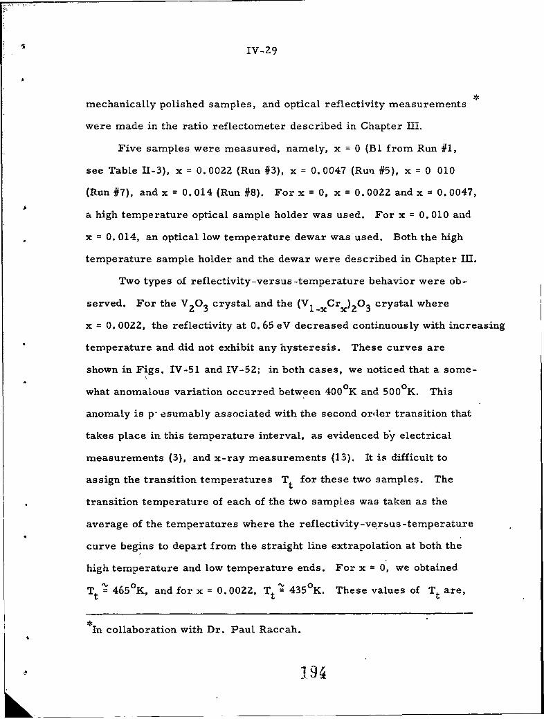
IV-29
mechanically polished samples, and optical reflectivity measurements
were made in the ratio reflectometer described in Chapter III.
Five samples were measured, namely, x = 0 (Bl from Run #1,
see Table H1-3), x = 0.0022 (Run #3), x = 0.0047 (Run #5), x = 0 010
(Run #7), and x = 0.014 (Run #8). For x = 0, x = 0.0022 and x = 0.0047,
a high temperature optical sample holder was used. For x = 0. 010 and
x = 0. 014, an optical low temperature dewar was used. Both the high
temperature sample holder and the dewar were described in Chapter InI.
Two types of reflectivity-versus-temperature behavior were ob-
served. For the V2 0 3 crystal and the (V 1 XCrx)2 0 3 crystal where
x = 0. 0022, the reflectivity at 0. 65 eV decreased continuously with increasing
temperature and did not exhibit any hysteresis. These curves are
shown in Figs. IV-51 and IV-52; in both cases, we noticed that a some-
what anomalous variation occurred between 400°K and 500 0 K. This
anomaly is p- esumably associated with the second ordler transition that
takes place in this temperature interval, as evidenced by electrical
measurements (3), and x-ray measurements (13). It is difficult to
assign the transition temperatures Tt for these two samples. The
transition temperature of each of the two samples was taken as the
average of the temperatures where the reflectivity-versus-temperature
curve begins to depart from the straight line extrapolation at both the
high temperature and low temperature ends. For x = 0, we obtained
T t '465 0 K, and for x = 0.00Z2, Tt 4350 K. These values of Tt are,
*In collaboration with Dr. Paul Raccah.
- 194

IV-30
subject to some uncertainty. Figure IV-53 and Fig. IV-54 show the
reflectivity-versus-photon energy curves of the two samples at dif-
ferent temperatur, s. i-here are a few interesting features in these
curves: 1) the i,#.fectivity-versus-photon energy curves at room
temperature remained the same before and after thu temperature cycle,
ind4l:ating the surfa 7es of the crystals did not oxidize in the protective
atmosphere of the forming gp ; 2) the structure near 1.5 eV is visible
t all ramperat~ire-s, and 3) the reflectivity of the samples at photon
• .rgy abo-, 1 i. 8 eV remained the same at all temperatures (within
e exper:...eit'.. uncertainty of the optical setup).
For za:nples with x = 0.0047, x = 0.010 and x = 0.014, abrupt
changes in reflectivity were observed with large hysteresis on tempera-
ture cycling. Figures IV-55, 56, and 57 show the reflectivity at 0. 65 eV
as a function of temperature of these crystals° Abrupt reflectivity
changes were observed in all these'crystals. Such abrupt changes are
presumably associated w.ith the abrupt changes in the electrical measure-
ments reported by McWhan and Remeika (13), who described this transi-
tion as a first order transition with some characteristics of a Mott
The reflectivity-versus-photon energy curve of B1 did not match verywell with that of C1 or CZ. This is not so surprising since the crystalswere grown in different crystal runs. A slight change in stoichiometrycould cause a change in the number of charge carriers in the crystals(V 2 9 3 crystals were found to have differenit resistivities at roomtemperature (3, 13)). This change in charge carrier density will affectthe optical reflectivity spectrum, especially in the free electron ab-sorption region.

IV-31
transition. For those. crystals that underwent the first order phase
transition, there was evidence that the crystals cracked on going through
the phase transition; the cracking was observed partly from the changes
in reflectivity at room temperature before and after the temperatur;,
cycling, and partly from the cracks visible after the temperature cyc-
line. In fact, the crystal at x = 0. 0047, as grown, already had some
fine cracks. This was due to the fact that the crystal on cooling down
from the melting temperature during the growth process had already
undergone a phase transition. Because of the problem of crystal crack-
ing, slight optical adjustments were done to focus the incident light on
the best spot of each crystal (that is, the reflectivity value is maximum
"* at this spot). In some cases, no apparent improvement was observed,
and in others, noticeable improvements were observed. Though part of
the reflectivity changes observed was indeed due to crystal cracking (for
example, the reflectivity of the doped crystal at room temperature, as
shown in Fig. IV-55, was lower after the temperature cycling), it is
apparent that most of the abrupt reflectivity changes at the phase
transition must have been due to the transition itself. Crystal cracking
could cause only decreases in reflectivity values, and could not explain
the sudden increases observed in reflectivity values.
Figures IV-58, 59, and 60 show the reflectivity-versus-photon
energy curves a:. different temperaturesfor samples with x = 0. 0047,
x = 0. 010 and x = 0. 014. An interesti ng point is that at low photon
energy, the reflectivity of the metallic state of the doped crystals is
not as high as that of undoped V2 0 3 crystals -- this is especially
1.96

IV-32
noticeable at photon energy near 0. 6 eV. It indicates that the so-called
metallic state of the doped crystals is different from that of the undoped
crystal; this fact corresponds to the findings of McWhan et al. (13) who
reported that the resistivity of the metallic state of the doped crystal
(V 0. 9 9 0 Cr 0 010)203 was about two orders of magnitude higher than that
of the undoped crystals.
Other points of interest are: 1) the structure at -" 1. 5 eV is visible
at all temperatures; and 2) the reflectivity of the metallic state of the
doped crystals is lower than that of the insulating state for photon
energy above 1. 2 eV. Though it might not be very appropriate to com-
pare the metallic state of VzO3 with that of a doped crystal, at room
temperature, we found that at 1. 96 eV the reflectivity of V2 0 3 crystals
Cl and CZ (metallic state) is about 20%o. This value is indeed lower
than that of a crystal of (V1 xCr x)zO3, RI, where x = 0.018; at room
temperature the crystal is in its insulating state and its reflectivity
at 1.96 eV is about 22%.
Table IV-3 lists the transition temperature Tt for the crystals
we measured, and Fig. IV-61 is a plot of these temperatures as a
function of chromium concentration, indicating clearly the two types
of phase transition. A discussion of the mechanism or mechanisms of
the transition will be presented in Chapter V.-
In summary, in this chapter, we have presented optical measure-
ments on V 2 0 3 and (V1 x Crx)2 O 3 . Optical constants were obtained
from angular dependence measurements, and from reflectivity spectra
using the oscillator fit method and Kramers-Kronig analysis. In Chapter
V, we will ,urther interpret these optical results and their implications.
197
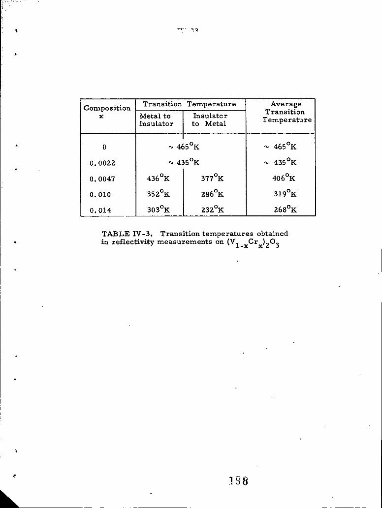
Composition Transition Temperature Average
x Metal to Insulator Transition
Insulator to Metal Temperature
0 - 465 0 K - 465 0 K
0.0022 - 435 0 K - 4350K
0.0047 436 0 K 377 0 K 406 0 K
0.010 35 2°K 286 0 K 319 0 K
0.014 303 0 K 232 0 K 268 0 K
TABLE IV-3. Transition temperatures obtainedin reflectivity measurements on (VI XCrX)2 O 3
198

IV-34
REFERENCES
1. L. Ladd and W. Paul, Solid Statc Comm. 7, 425 (1969).
2. L. Ladd, Tech. Rept. No. HP-26, Gordon McKay Laboratory,Harvard University, 1971 (unpublished).
3. J. Feinlelb and W. Paul, Phys. Rev. 155, 841 (1967).
4. K. Kosuge, J. Phys. Soc. Japan 22, 55 (1967).
5. A. Smakula, "Phys. Properties of Optical Crystals, p. 99,U.S. Dept. of Commerce, 1952.
6. V. Chandrasekharan and H. Damany, Appl. Optics 7, 930 (1968).
7. W. Rosevear and W. Paul, to be published.
8. I.G. Austin and C.E. Turner, Phil. Mag. 19, 939 (1969).
9. V.P. Zhuze, A.A. Andreev and A. I. Shelykh, Soy. Phys. -Solid State 10, 2914 (1969).
10. A. S. Barker, Jr., H. W. Ve'leur, and H. J. Guggenheim, Phys.Rev. Letters 17, 1286 (1966).
11. W. Rosevear, Tech. Rept. ,.Gordon McKay Laboratory, HarvardUniversity (to be published).
12. H.W. Verleur, A.S. Barker, Jr., and C.N. Berglund, Phys.Rev. 172, 172 (1968).
13. D.B. McWhan and J.P. Remeika, Phys. Rev. BZ, 3734 (1970).
14. A. Jayaraman, D.B. McWhan, J.P. Renmeika and P.D. Dernier,Phys. Rev. B2, 3751 (1970).
15. A. Menth and J.P. Remeika, Phys. Rev. BZ, 3756 (1970).
16. A. S. Barker, Jr. and J. P. Remeika, Solid State Comm. 8,1521 (1970).
1.99

IV-35
80.0
5V2070.O-0 3000K
0o C1
60.0
4.0-
30.0 -
20.0-
10.0-
0.01 -0.0 1.0 2.0 3.0 4.0 5.0
Energy (eV)
FIGURE ]D-1 The reflectivity of two V2 0 3 crystals Cl and C2at 300°K

IV-36
24.0 1 I
22.0 V2 0 3 C13000 K
20.0 - x- experimental",A- theoretical fit
18.0 \
14.0 - \ ' 1.96 eV'A 1.77
12.0- k 1.10
Cr10.0- 2. 54 eV A10\
n 1.828.0- 0.90 A
6.0 -
4.0 ,
2.0-
0 . I70 I ! !0 10 20 30 40 50 60 70 80
0 (degrees)
FIGURE TZ-2 The reflectivity of a V2 0 3 crystal (Cl)as a function of incidence angle 4.
2911

"IV-37
24.0 V20 3 C23000 K
A 22.0 x measuredA theoretical fit
20.0-
18.0-
16.0010 1.96 eV
o• 14.0 1.78C. k =1.10
12.0
10.0 2.54 eVA/ \n = 1.81k = 0.90
8.0
6.0-
4.0 \
2.00 I I I I I
0 10 20 30 40 50 60 70 800 (degrees)
FIGURE MZ-3 The reflectivity of a V20 3 crystal (C2)*as a function of incidence angle t/.
,202

IV-38
24.01 1
22.0 - , (Vl-xCrx)2O3x = 0.018
20.0 3000 K
18.0 .
16.0
14.096 eV_ Y n=2.02Se .12.0 -k -1.14
10.0 - 2.54 eV isn=1.86
8.0 k=0.96
6.0-4.0 - x - experimental
a- theoretical fit
2.0-0 I I I i i I
0 10 20 30 40 50 60 70 804 (degrees)
FIGURE IV-4 The reflectivity of a (Vl-xCrx) 2 03crystal where x=O,018 as a function of incidenceangle kb
203

IV-39
80.0
V2 0 3 -c1
70.0 3000 K
GcO= 2.10
60.0 En = 3.54 eVEc 0.678 eV
SL Ei.(eV) r.
50.0 2.86 0.557 0.977- 0.320 4.22 0.247
1.70 2.54 0.801
S1.80 6.0 3 0 .225
"2 0.792 1.56 0.526S40.0 -_.O Oscillator Fit
',-,
Constraints on n andk at 1.96 eV and 2.54 eV
30.0 -
20.0-
10.0-
- theoretical fito experimental
00.0 1.0 2.0 3.0 4.0 5.0
Energy (eV)
FIGURE MZ-5 A theoretical fit to the experimental reflectivitydata of CI by the oscillator fit method where n and k at 1.96eVand 2.54eV are constrained to approach those obtained fromthe angular, dependence measuremento

IV-40
6.0
5.0 V2 0 3 CI
4.0 - 3000 K
Oscillator Fit3.0-
2.0-
1.0-
0.0 ;0,0 1.0 2.0 3.0 4.0 5.0
-1.0- Energy (eV)
-2.0 -El
-3.0- 1
-4.0-
-5.0 -
-6.0 -
-7.0 -
-8.0-
-9.0- Constraints onn and k at1.96 eV and 2.54 eV
-10.0
-12.0
-12.0
FIGURE IV-6 el curve of Cl, obtained from the fit shownin Fig. 17-5.
_ _ _ A

IV-41
II
35.0-V2 03 Cl
T= 300 'K
30.0 -T>Tt
Constraints on n andk at 1.96 eV and 2.54eV
25.0
20.0 -
E?
15.0 -
10.0 -
5.0
0.00.0 1.0 2.0 3.0 4.0 5.0
Energy (eV)
FIGURE I"-7 E2 curve of Cl, obtained from the fit shown inFig. IV-5
206

IV-42
5 I IOI5xICP
E
04-.
0
C
10-0 S05
0
V2 0 3 C'
3000 K
- Constraints on Oscillator Fitn and k at
5 x 10⁴ - 1.96 eV and 2.54 eV
I I I I I0.0 1.0 2.0 3.0 4.0 5.0
Energy (eV)
FIGURE ]&-8 a curve of Cl, obtained from the fit shownin Fig. SZT-5.

IV-43
80.0
V2 03 C1300 OK
10.0- E0= 2.20En= 3.50 eVEc- 0.656 eV
60.0- Si Ei(eV) ri2.80 0.542 1.010.380 4.23 0.2791.86 2.43 0.8541.72 6.02 0.204
50.0- 0.800 1.50 0.564
00
Oscillator Fitt40.0 No constraints on.> optical constants; 00:.0.
30.0-
20.0 -
theoretical fit10.0 - o experimental
0.00.0 1.0 2.0 3.0 4.0 5.0
Energy (eV)FIGURE I]Z-9 A theoretical fit to the experimental reflectivitydata of C1 by, the oscillator fit method where n and k at 1.96eVand 2,54e\ -te not constrained.

IV-44
6.0
5.0-
4.0
3.0 -
2.0
1.0
0.0 0.0 1. 2.0 3.0 4.0 5.0
-1.0- Energy (eV)
-2.0-'E1
-3.0-
-4.0-v2 03 CI
-5.0 -300 0 K
Oscillator Fit-6.0-No constraints onoptical constants
-.0I
-8.0 -
-9.0 --
-10.0-
-11.0 I-12.0
_
FIGURE IV-10 El curve of C1, obtained from the fit shownin Fig. IV-9
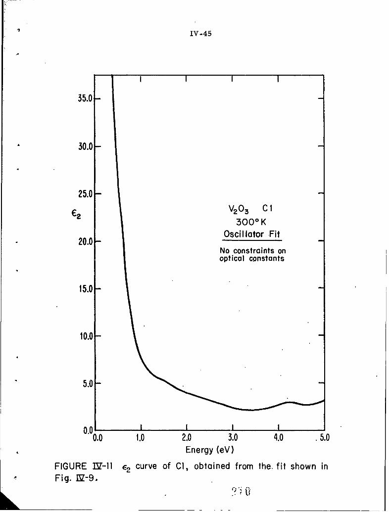
IV-45
I I i I
35.0-
30.0
25.0
V- v0 3 C I3000 K
20.0- Oscillator Fit
No constraints onoptical constants
15.0
10.0
5.0
0.00.0 1.0 2.0 3.0 4.0 .5.0
Energy (eV)
FIGURE ]V-11 E2 curve of Cl, obtained from the. fit shown inFig. IM-9.

IV-46
I
E
0
05x105
I0
v02 03 CV(I) 300 °K'
Oscillator Fit
No constraints onoptical constants
5x 10⁴
I I I
0.0 1.0 2.0 3.0 4.0 5.0Energy (eV)
FIGURE M'-12 a curve of C1, obtained from the fit shown inFig. &Z-9.

IV -47
80.0 1 1 1
3000 K
70.0- ECD -194En= 3.48 eV
Ec=0.664 eV
600-S1 EL(eV) rL6003.23 0.479 1.76
0.490 4.25 0.2962.16 2.45 0.9641.42 5.78 0.445
50.0- Oscillator Fit
No constraints onOle optical constants
> :40.0
C-,
30.0
20.0
* 110.0-theoretical fit
o experimental
FIGUR 1.0 2.0 . 4.0 5.0
FIGURE I-13 A theoretical fit to the experimental reflectivitydata -of C1 by the oscillator fit method where n and k at 1.96eVand 2.54eV are not constrained.
212

IV-48
6.0-
5.0
4.0
3.0
2.0
1.0
0.0 0.0 1.0 2:0 3.0 4'0 5.0
-1.0 Energy (eV)
-2.0
-3.0
-4.0
-5.0
-6.0
-7.0V2 0 3 C1
-8.0 300 0 K
No constraints on- 9.0 optical constants
Oscillator Fit
-10.0
-11.0
-12.0FIGURE. M~-14 e, curve of Cl, obtained from the fit shownin FIG. IV-13.•<:- .... 2 1 3

IV-49
35.0 -
A v2o3 cl30.0 - V2300o
3U.U 300 0K
No constraints onoptical constants
Oscillator Fit25.0-
E?
20.0
15.0-
10.0 -
5.0-
0.0 , I0.0 1.0 2.0 3.0 4.0 5.0
Energy (eV)FIGURE 17-15 E2 curve of Cl, obtained from the fit shownin Figc.I2-13.

IV-50
5 xlO
E
ZC--
0
4.•
00 50
*
U
o
1104-
V2 0 3 Cl- 3000K
. 4 No constraints on5x optical constants
Oscillator FitmI, ,III I
0.0 1.0 2.0 3.0 4.0 5.0Energy (eV)
FIGURE IZ-16 a curve of Cl, obtained from the fit shownin Fig. I7-13.
715
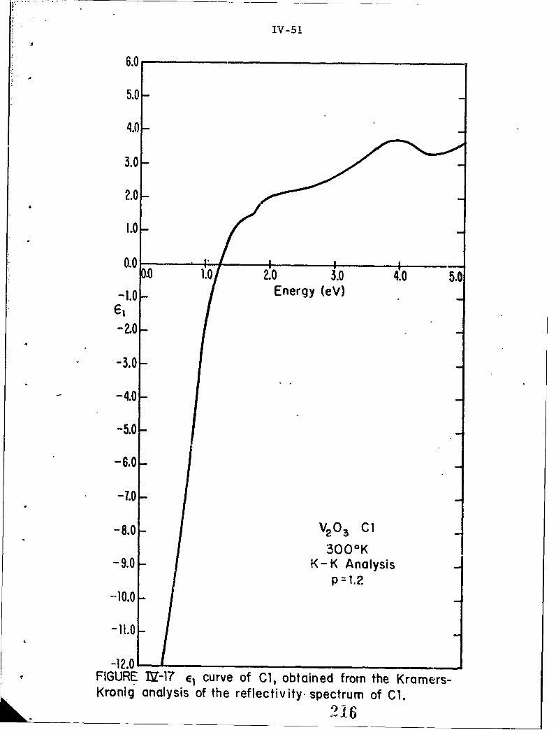
IV-51
6.0
5.0-
4.0
3.0
2.0
1.0
0.0
.0 1.0 2.0 3.0 4.0 5.0-1.0- Energy (eV)
-2.0-
-3.0-
-4.0-
-5.0-
-6.0-
-7.0-
-8.0- V203 Cl
3000 K-9.0 K-K Analysis
p=1.2
-10.0
-11.01
-12.0FIGURE LZ-17 4E curve of C1, obtained from the Kramers-Kronig analysis of the reflectivity spectrum of Cl.
216

IV-5Z
35.0 -V20o C13000K
K- K Analysis
30.0 - P I.2
25.0-
£2
20.0 -
15.0 -
10.0 -
5.0-
0.0I0.0 1.0 2.0 3.0 4.0 5.0
Energy (eV)
FIGURE IV-18 ep curve of CI, obtained from the Kramers-Kronig analysis of the reflectivity spectrum of C1.
9 j F

IV- 53
5X10
p:1
p:1
IE
0 0
0
V23 C
5-' 3000
0. . 2030 . .
Energy (eV)FIGURE 17-19 a curve of C1. obtained from the Kramers-Kroniganalysis of the reflectivity spectrum of C1.
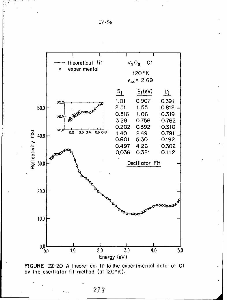
IV-54
I I I I
-theoretical fit V2 0 3 CIo experimental 120 0 K
E00 = 2.69
Si Ei(eV) Fi
35.0 1.01 0.907 0.39150.0 -• 2.51 1.55 0.812 -
32.5 0.516 1.06 0.3193 3.29 0.756 0.762
30.o0 ' _,, 0.202 0.392 0.31040.0- 0.2 0.3 0.4 0.6 0.8 1.40 2.49 0.791
0.601 5.30 0.192. 0.497 4.26 0.302
0.036 0.321 0.112
- 30.0 Oscillator Fit
20.0 -
10.0 _
0.0 I I I I0.0 1.0 2.0 3.0 4.0 5.0
Energy (eV)
FIGURE 1&-20 A theoretical fit to the experimental data of C1by the oscillator fit method (at 120 0 K).
:.. 21 9
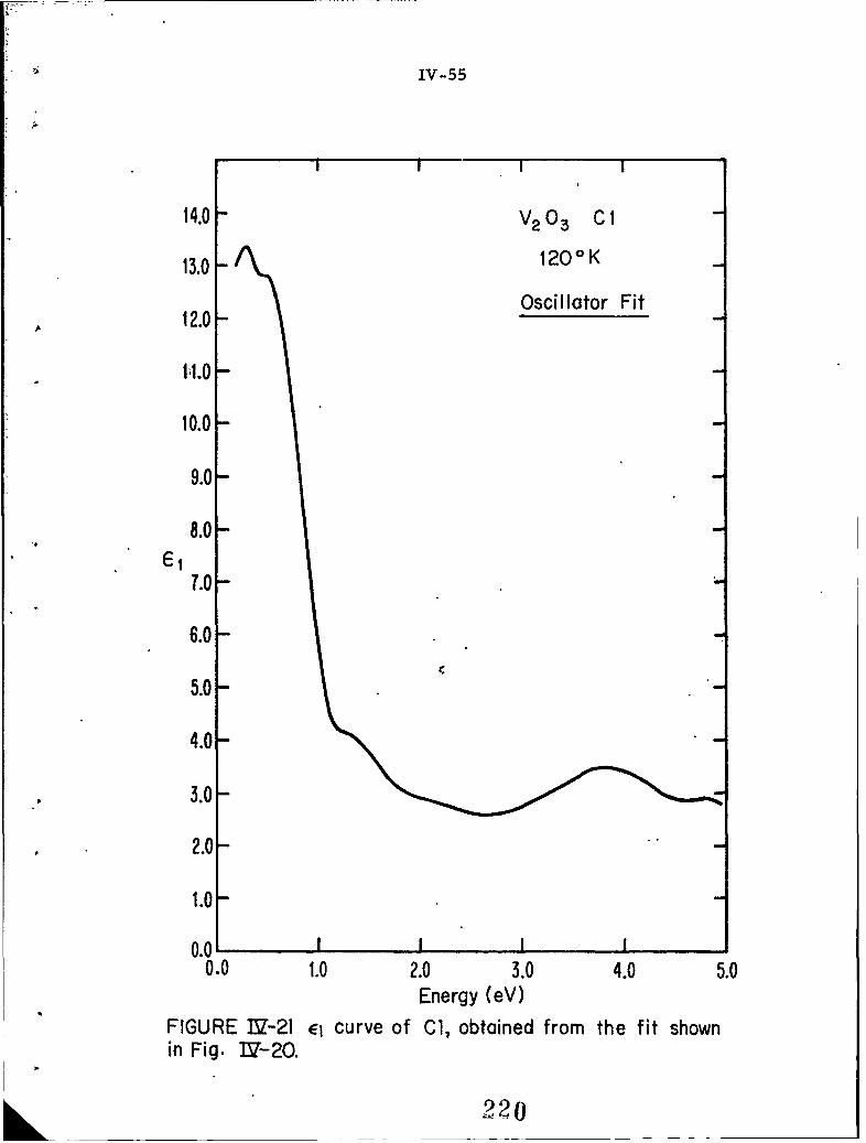
* IV-55
I I I
14.0 V2 0 3 C1
13.0 1200 K
Oscillator Fit12.0•-
.11.0
10.0
9.0
8.0El
1.0-
6.0-
5.0-
4.0-
. 3.0-
2.0-
1.0-
0.0 I I I I0.0 1.0 2.0 3.0 4.0 5.0
Energy (eV)FIGURE M'-21 El curve of Cl, obtained from the fit shownin Fig. IV-20.
220
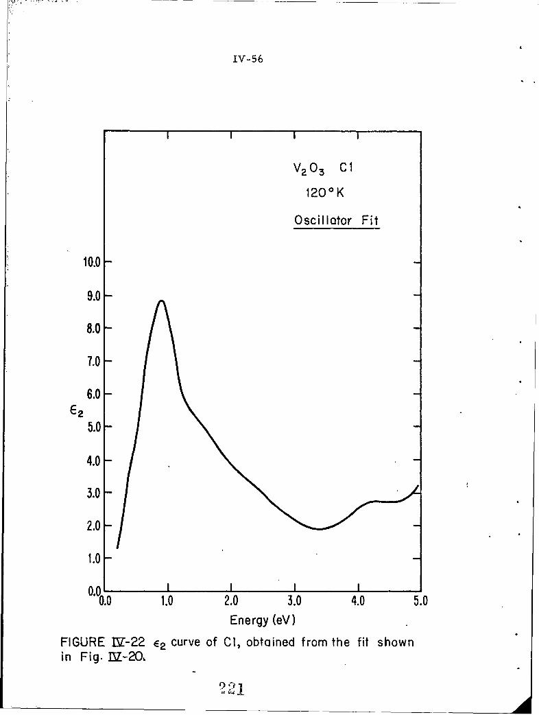
IV-56
V2 0 3 Cl
1200 K
Oscillator Fit
10.0 -
9.0-
8.0-
7.0-
6.0-E2
5.0
4.0
3.0 -
2.0 -
1.0-
0.00.0 1.0 2.0 3.0 4.0 5.0
Energy (eV)
FIGURE 1&-22 E2 curve of Cl, obtained from the fit shownin Fig. M;-20.
?,21

IV-57
*I I II
5x10⁵ -
E-1 x10 5 -
E
o Oscillator Fit
C
0
0
'4--
0.*10 .04..-0 .
C)0
1,04
inFg.].-01.22
1200 K
* 5x 103
0.0 1.0 2.0 3.0 4.0 5.0Energy (eV)
FIGURE I2V-23 a curve of Cl., obtained from the fit shownin Fig. IV-20
222

IV-58
60.0 1 1
v203 Cl
50.0- 1200 K
0.5/. thick
40.0
C-• 30.0
H 20.0
10.0
00'10.0 0.1 0.2 0.3 0.4 0.5 0.6 0.7 0.8 0.9
Energy (eV)
FIGURE 17-24 Predicted transmission of a single Vp_0 3crystal of 0.5/. thickness at 1201K.
__ __ __ _ 143
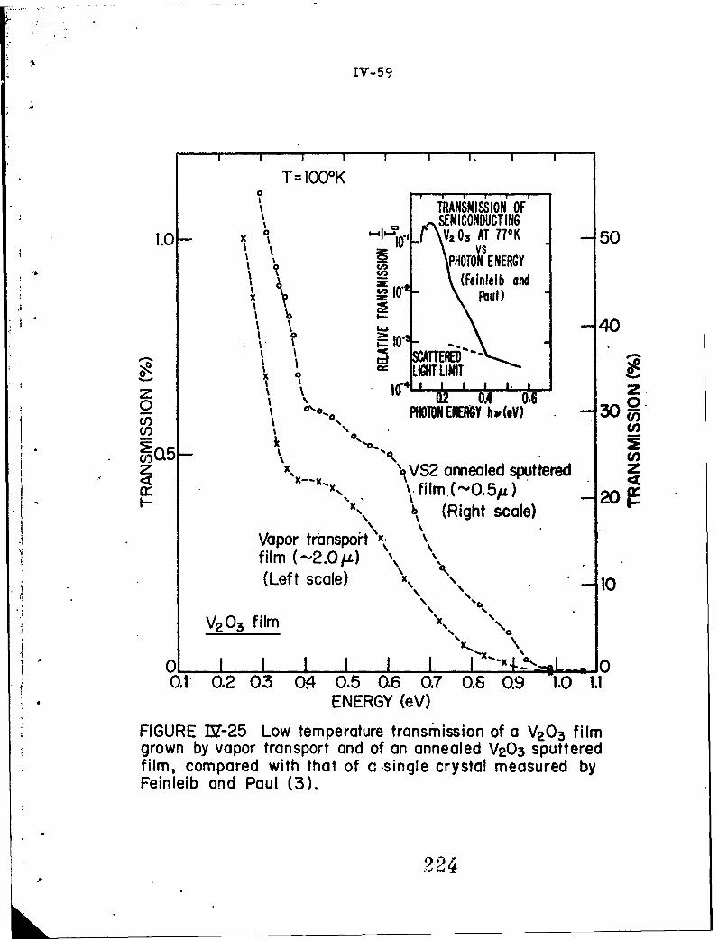
IV-59
I I I I I I I. I I ..
T= 100K
"TRANSMISSION OF'
'' SEMICONDUCTING1.0- x "I V203 AT 770K -50
PHPHOTON ENERGYI UI
T(Feinleib and
x 10-t -Paul)L;• 40
SCA TTERED'Ix LIGHT LIMIT
z z z.__0.' PHOTON ENERGY h (eV) -30Cf) 0- c
0%Q 5 ,
z 'X% '6VS2 annealed sputtered zWr: -X \.film.("-0.5/t) -20
-X, (Right scale)
Vapor transport x.\film (-2.0 u)(Left scale) x• 0
to
V2 0 3 film , \0
0.1 0.2 03 0.4 0.5 0.6 0.7 0.6 0.9 1.0 1.1ENERGY (eV)
FIGURE WV-25 Low temperature transmission of a V20 3 filmgrown by vapor transport and of an annealed V20 3 sputteredfilm, compared with that of c -single crystal measured byFeinleib and Paul (3),
924

IV-60
III I
o= 2.85
SL, E.(eV) ri
60.0 4.73 0.713 0.5964.82 2.29 0.1402.06 1.00 0.5656.69 0.365 1.320.506 5.08 0.217
50.0 5.15 0.518 0.8310.418 4.20 0.2470.124 1.51 0.171
-- 40.0- (Vl.xCrx) 2 0 3 x=0.0187
"> • 300 OK
Oscillator Fit
Cr30.0 Constraints on n and kat 1.96 eV and 2.54 eV
20.0
10.0 - theoretical fit0 experimental
0.0 1.0 2.0 3.0 4.0 5.0Energy (eV)
FIGURE 17-26 A theoretical fit to the experimental reflectivitydata of a (Vo. 9 2zcro.oj 8 )20 3 crystal, where the values of n andk at 1.96eV and 2.54eV are constrained to approach thoseobtained from the angular dependence measurements.
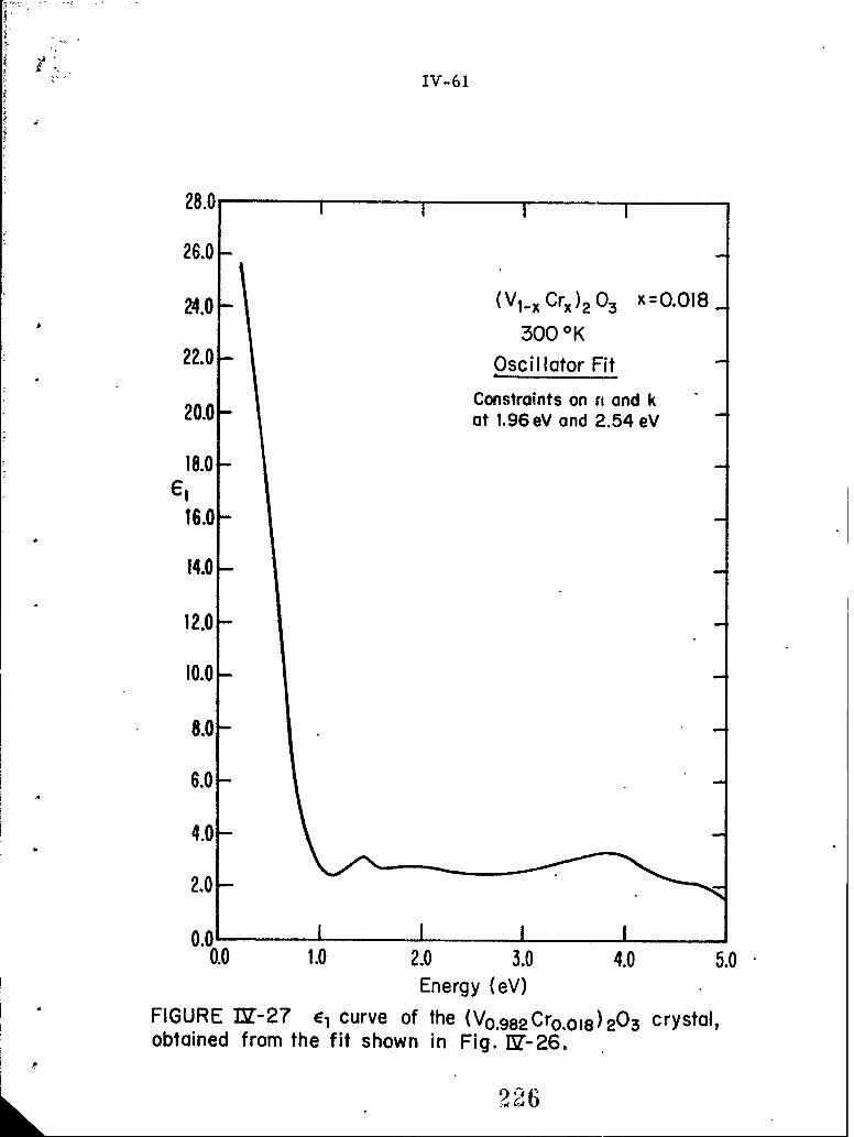
IV-61
28.0
26.0 -
24.0 - (Vli Crx) 2 03 x=0.018300 oK
22.0 - Oscillator Fit
Constraints on rt and k20.0- at 1.96eV and 2.54 eV
18.0 -
16.0-
14.0-
12.0-
10.0-
8.0-
6.0-
4.0-
2.0-
0.0 ! I I I0.0 1.0 2.0 3.0 4.0 5.0
Energy (eV)FIGURE IV-27 e1 curve of the (Vo.9 82 Cro.0 18)e0 3 crystal,obtained from the fit shown in Fig. LV-26.
926

!V-62
I
26.0 -
(V1_xCrx) 2 O-A x=0.01824.0 300 OK
22.0 -Oscillator FitConstraints on n and k
20.0- at 1.96 eV and 2.54 eV
18.0-E2
16.0 -
14.0
12.0 -
10.0
8.0-
6.0-
4.0-
2.0-
0.0 i0.0 1.0 2.0 3.0 4.0 5.0
Energy (eV)
FIGURE I&-28 E2 curve of the (Vo. 98pCro.o 8 ),.03 crystal,obtained from the fit shown in Fig.IV-26.
44

IV-63
5 x10 5
E
1 x10 5
.'-
8U 5x10⁴
04-
0le (Vl-xCrx)203 X=0.018-
300 0 K
Osci Ilator Fit
Constraints on n and kao 1.96 eV and 2.54 eV
I X104
i3
15x 10 0.0 1.0 2.0 3.0 4.0 5.0
Energy (eV)
FIGURE It-29 a curve of the (Vo. 9 8 2 Cro.0 18)2 0 3 crystal,obtained from the fit shown in Fig. ITV-26.
?,8

IV-.64
(VlxCrx)203
300K60.0- x = 0.018 Eco 2.93
S L Ej(eV) 'L4.66 0.726 0.622
50.0 - 4.92 2.30 0.1471.99 1.01 0.6416.81 0.381 1.390.493 5.06 0.2145.16 0.526 0.841
S40.0• 0.406 4.21 0.244v> •0.119 1.52 0.193
"Oscillator Fit
0 No constraints onS30.0 optical constants
20.0
10.0 o experimental-- theoretical fit
0.0.I0.0 1.0 LO 3.0 4.0 5.0
Energy (eV)
FIGURE IZ-30 A theoretical fit to the experimental data oft:;d (Vo. 9 82 Cro.os)2-03 crystal, where the values of n and kat 1.96eV and 2.54eV are not constrained.
___

IV- 65
28.0-T
26.0
x 0.012 4 .0 -(
l x r ) 0
22.0 -300 OKOscillator Fit
20.0- No constraints onoptical conslants
18.0-
16.0-
14.0-
12.0-
10.0-
8.0-
6.0-
4.0-
2.0
0.0 II0.0 1.0 2.0 3.0 4.0 5.0
Energy (eV)
FIGURE M~-31 E, curve of the (VO.9 82Cro.o,8) 203 crystal,obtained from the fit shown in Fig. ISZ-3O,
2.3

IV-66
28.0 1
26.0 -x = 0.018
24.0 (VI-xCrx)203
22.0 300KOscillator Fit
20.0 No constraints onoptical constants
18.0
16.0
14.0
12.0 /
10.0
8.0
6.0
4.0
2.0
0.0 I I I0.0 1.0 2.0 3.0 4.0 5.0
Energy (eV)
FIGURE I-32 e2 curve of the (Vo.9 82 Cro.o08)20 3 crystal,obteined from the fit shown in Fig. iM-30.
231

IV -67
I I I
5x10 5 -
)E 5
410
0)
C0
4--
"00
x =0.018< (VI-xC,.x)203
300°KOscillator Fit
No constraints on4 optical constants
10
0.0 1.0 2.0 3.0 4.0 5.0Energy (eV)
FIGURE IV-33 a curve of the (Vo.9 82 Cro.o18) 2 0 3 crystal,obtained from the fit shown in Fig. BV-30.
232

IV-68
233
70.0
E,,= 2.59
Si E1 (eV) rl60.0- 7.23 0.646 0.747
0.556 0.219 0.3206.35 2.23 1.812.36 0.897 0.5673.15 0.455 0.684
50.0- 0.634 5.15 0.259
1.88 0.305 0.5900.306 4.17 0.2130.073 1.49 0.155
">% 40.0 - (Vl.xCrx) 2 03
x.= 0.018
300 OKS30.0- Oscillator Fit
No constraints onQptical constants
20.0 -
10.0 - theoretical fit
o experimental
0.0 I I I I0.0 1.0 2.0 3.0 4.0 5.0
Energy (eV)
FIGURE TI-34 A theoretical fit to the experimental dataof the (Vo.982 Cro.o 18 )-03 crystal by the oscillator fit method,where the values of n and k at 1.96eV and 2.54eV are notconstrained., This is a poorer fit than the one shown in Fig.-1-30.

IV-69
28.0
24.0- (VI-x Crx) 2 03
x =0.018
300 OK20.0- Oscill Iator Fit
No constraints on- optical constants
16.0
12.0-
8.0
4.0-
0.0 I0.0 t0 2.0 3.0 4.0 5.0
Energy (eV)
FIGURE 131-35 qi curve of the (VO. 982 Cro.o 18 )203 crystal,obtained from the fit shown in Fig. IST-34.
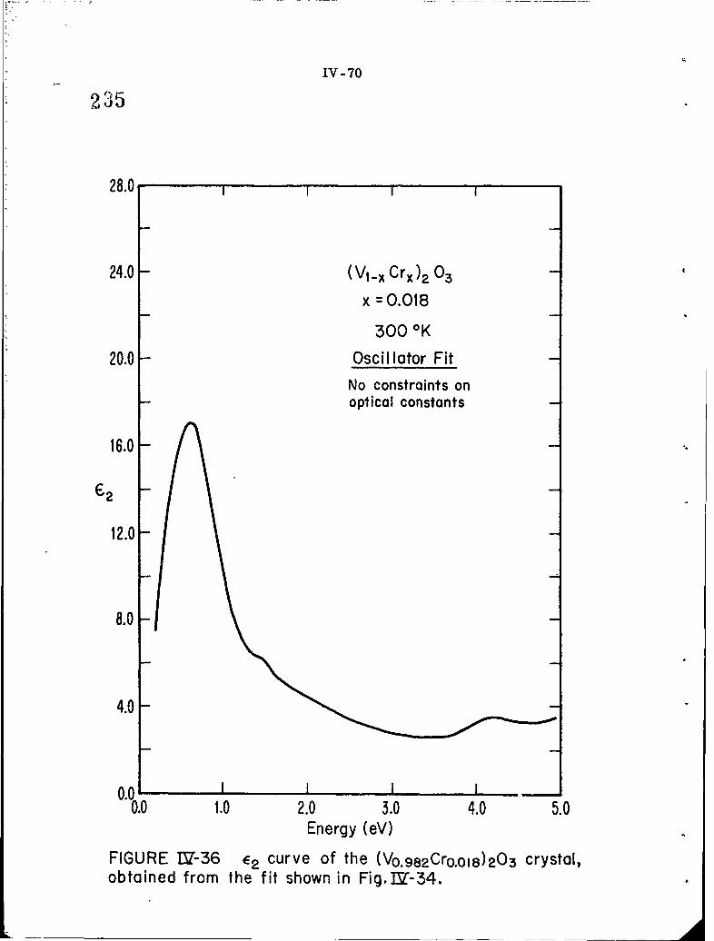
IV-70
235i
28.0
24.0 (VI-x Crx) 2 03
x = 0.018
300 OK
20.0 Oscillator Fit
No constraints onoptical constants
16.0
62
12.0
8.0
4.0
0.0-0.0 1.0 2.0 3.0 4.0 5.0
Energy (eV)
FIGURE IV-36 e2 curve of the (Vo.9 8 2 Cro.o18)203 crystal,obtained from the fit shown in Fig.IZ-34.

"* IV-71
S?236
5x10 5
io 5
1504 -
(V5 1 0Crx)I 03x =O.018
300 OK
Oscillator Fit
No constraints on
104- optical constants
0.0 1.0 2.0 3.0 4.0 5.0Energy (eV)
FIGURE ISI-37 a curve of the (Vo. 9 8 pCro.0 18 )2 0 3 crystal,obtained from the fit shown in Fig. DI-34.
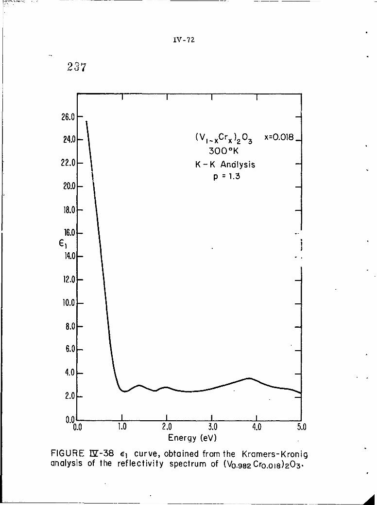
IV-72
23 J
26.0 -
24.0- (VlxCrx) 2 03 x=0.018
300 0K22.0 K - K Andlysis
I p 1.3
20.0-
18.0
16.0 -
14.0 -.
12.0
10.0 -
8.0
6.0
4.0
2.0
0.0 I0.0 1.0 2.0 3.0 4.0 5.0
Energy (eV)
FIGURE IZ-38 E1 curve, obtained from the Kramers-Kroniganalysis of the reflectivity spectrum of (Vo. 98 2 Cro.o 18 ) 20 3 .

IV-73
S9238
26.0
24.0 - (V- xCrx) 2 0 3 x 0.018300 0 K
22.0 - K-K Analysis
p = 1.320.0
18.0E2
16.0
14.0
12.0
10.0
8.0
6.0
4.0
2.0-
0.010.0 1.0 2.0 3.0 4.0 5.0
Energy (eV)
FIGURE IV-39 E2 curve, obtained from the Kramers-Kroniganalysis of the reflectivity spectrum of (Vo. 9 8e Croo0 18 )203,

IV-74
2,39
5
5x1.4
- •p -1.3 -
EUS105 ,
5-
Cx
0
o 5x1C
€-90.I-.
U (VlxCrx) 2 0 3 x=0.018.03000 K
K-K analysis
p 1.3p =1.4
410
3W r
0.0 1.0 2.0 3.0 4.0 5.0Energy (CV)
FIGURE IV-40 a curve, obtained from the Kramers-Kroniganalysis of the reflectivity spectrum of (Vo.9B2Cro.o 18)203.
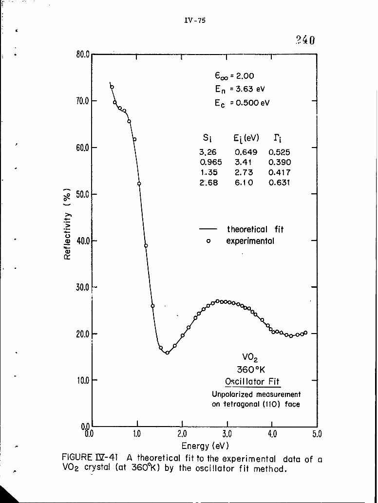
IV -75
80.0
600 = 2.00
En = 3.63 eV70.0 Ec = 0.500 eV
Si EW(eV) ri
3.26 0.649 0.5250.965 3.41 0.3901.35 2.73 0.4172.68 6.10 0.631
S50.0
• -. theoretical fitw 40.0 o experimental
30.0
20.0
V02
360 0 K10.0 Oscillator Fit
Unpolarized measurementon tetragonal (110) face
0.0 I I 1 I0.0 1.0 2.0 3.0 4.0 5.0
Energy (eV)FIGURE IZ-41 A theoretical fit to the experimental data of aV02 crystal (at 3600K) by the oscillator fit method.

IV-76
2 41
8.0
6.0-
4.0-
2.0-
0.00.0 1.0 2.0 3.0 4.0 5.0
-2.0- Energy (eV)
-4.0
-6.0-
- 8.0
-10.0-
-12.0
-14.0 -VO2
-16.0 360 0 K
-18.0 Oscillator Fit
-22.0
FIGURE I'-42 E1 curve of the V02 crystal, obtained from thefit shown in Fig. 1VT-41.

IV-77 242
40.0
35.0 - V02
360 0 K
Oscillator Fit
30.0 -
25.0-
E2
20.0 -
15.0 -
10.0 -
5.0-
0.0
S•I0.0 I I I I
0.0 1.0 2.0 3.0 4.0 5.0Energy (eV)
FIGURE I-43 c2 curve of the V02 crystal, obtained from thel'it shown in Fig. 1Z-41.
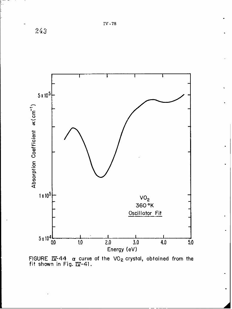
IV-78243
5x 10⁵
E
af)
1 x10⁵ - VOa360 OK
Oscill I for Fit
100.0 1.0 2.0 3.0 4.0 5.0
Energy (eV)
FIGURE IV/-44 a curve of the V02 crystal, obtained from thefit shown in Fig. I3V-4I.

IV-79 ?6
60.0 -C%== 5.05
- theoretical fit Si E1(eV) W)50.0 - experimental 1.16 6.05 0.366
0.663 4.09 0.737
0.455 4.55 0.5221.30 3.63 0.337
0.559 2.97 0.20040.0- 0.923 1.66 0.470
0.153 1.31 0.4291.70 1.06 0.3301.60 1.30 0.358
. 30.0
n4-
20.0
V0 2 300 OK
O.,icillator Fit
10.0 Unpolarized Measurementon Tetragonal (110) Face
0.0 I I I I0.0 1.0 2.0 3.0 4.0 5.0
Energy (eV)
FIGURE IV-45 A theoretical fit to the experimental data ofthe V02 crystal (at 300°K) by the oscillator fit method.
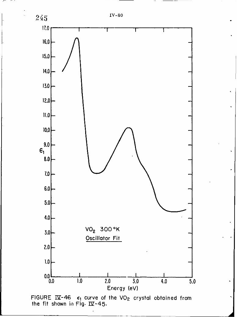
2K~5 IV-80
11.0
16.0[
15.0 -
14.0 L
13.0 -
12.0-
11.0
10.0-
9.0-
8.0-
7.0
6.0-
5.0
4.0-
3.0- VO2 300 OKOscillator Fit
2.0
1.0-
0.0 I I0.0 1.0 2.0 3.0 4.0 5.0
Energy (eV)
FIGURE EZ-46 Ec curve of the V02 crystal obtained fromthe fit shown in Fig. M"-45.
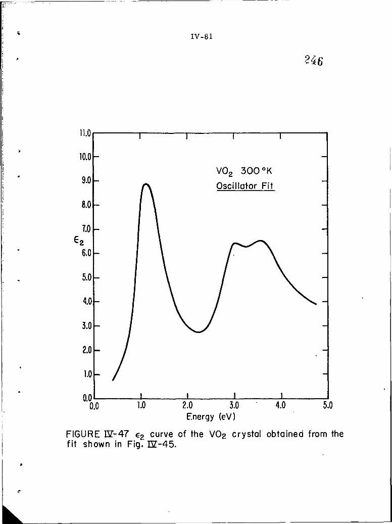
IV-81
11.0
10.0-V0 2 300 0 K9.0- Oscillator Fit
8.0-
7.0-E2
6.0-
5.0-
4.0-
3.0-
2.0-
1.0-
0.0!0.0 1.0 2.0 3.0 4.0 5.0
Energy (eV)
FIGURE IV-47 Ec curve of the VO crystal obtained from thefit shown in Fig. I32-45.
SP

IV-82
24 7
5x1O5 -
1110 5
S5x104 -
*0-
C
0
0 4CA
L..0
V0 2 300 OK
5 X10 3 Oscillator Fit
0.0 10 2D0 3.0 4D0 5D0Energy (eV)
FIGURE I2-48 a curve of the VO crystal obtained from thefit shown in Fig. 1=2-45.
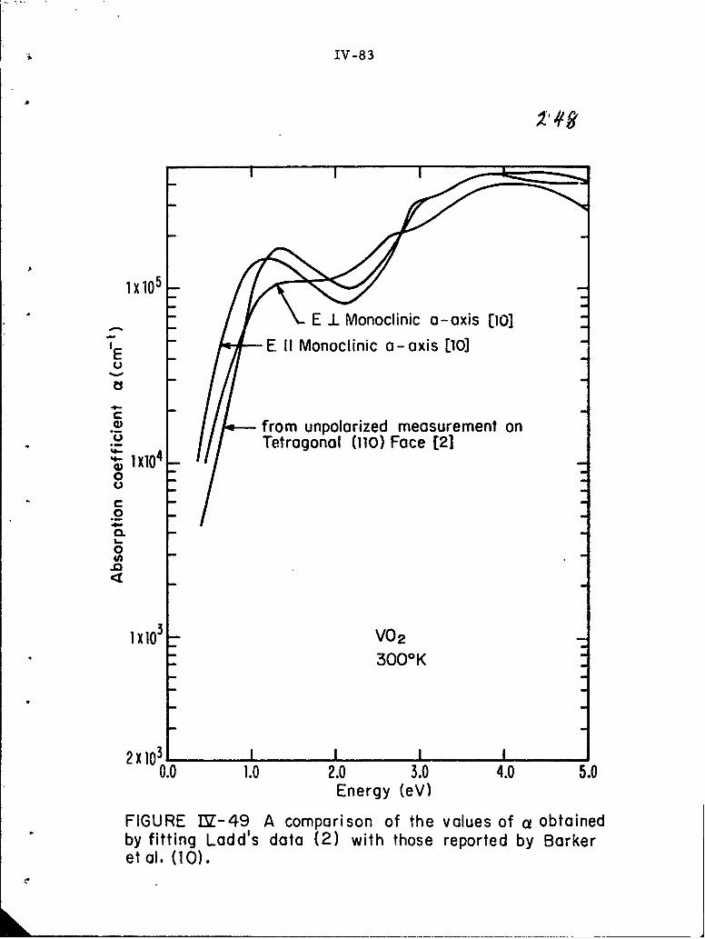
IV-83
1 105-
E I Monoclinic a-axis [10]
E 11 Monoclinic a-axis [10]"4-E --- EIMoolncaaxs[0U
) •from unpolarized measurement on"6 Tetragonal (110) Face [21-I XI04
0
0Q."2C -
I.-00
lXIO3 V0 2
3000OK
2 X10 30.0 1.0 2.0 3.0 4.0 5.0
Energy (eV)
FIGURE IV-49 A comparison of the values of a obtainedby fitting Ladd's data (2) with those reported by Barkeret al. (10).

IV-84
30 - 1 , 1 1 1 ,
, -.--.- Reflectivity T>Tc
S20 -o--o- Reflectivity T<Tc
x -a--A- Transmission T>Tc-x--x- Transmission T<Tc
ai:
V0 2 film
10 000& 0
LiiLL x
a 0 ,,, 'O--O- 0 O,
O0...
x OI " ,.' -• . Oo
0.0 1.0 2.0 3.0 4.0ENERGY (eV)
FIGURE 1IV-50 Apparent reflectivity and transmission ofa VQ2 film grown by the vapor transport method, above(35Cf-) and below (300Cf) the transition temperature.

IV-85 250
60.0- v203
0
0
55.0-
50.0
0
I.-
* 50.0-
45.0-
o coolinga heating
40.0300 400 500 600
Temperature (OK)FIGURE IZ-51 The reflectivity of a V20 3 crystal at 0.65eV as afunction of temperature.-

25 1 IV-86
(V -xCrx) 2 03x= 0.0022
55.0
50.0
0
n~-
45.0
o coolinga heating40.0
300 400 500 600Temperature (OK)
FIGURE IV-52 The reflectivity of a (VlxCrx) 20 3 crystal (where x=O.O022)at 0.65eV as a function of temperature.

IV-87 552
?0.0
60.0 v2 03
x
50.0
- °
0)
"-40.0 -
ox,Q 4
' 30.0-
20.0 -
a 300°K before heating
10.0- x 440OKa 6000 K+ 300OK after heating
00 I I I I I I I0.4 0.6 0.8 1.0 1.2 1.4 1.6 1.8 2.0 2.2
Energy (eV)
FIGURE I&'-53 The reflectivity of a VpO 3 crystal atdifferent temperatures as a function of photon energy.

9,i 3 IV-88
70.0 1
60.0- 2 (Vl-xCrx) 20 3x 0.0022
2
50.0 -
40.0- ao A
•.a 6
30.0 -
20.0
10.0 x 300°K before heatingo 3000 K after heatinga 58OOK
0.0 L...... L_ I ! I I I I0.4 •.. 0.8 1.0 1.2 1.4 1.6 1.8 2.0 2.2
Energy (eV)
FIGURE IZ-54 The reflectivity of a V20 3 crystal (wherex=O.OO22) at different temperatures as a function ofphoton energy.

IV-89
(V1 - Crx)2 03
0.0047
60.0-
"2-0
50.0
40.0
o coolinga heating
30.6 1 1 1 I250 300 350 400 450 500
Temperature (OK)
FIGURE tM-55 The reflectivity of a (VlixCrx) 2 0 3 crystal (wherex=0.0047) at 0.65eV as a function of temperaiture.
L _ _ __ _ _ _ _

IV-90
65.0 (Vl-xCrx) 203x =0.010
60.0 -
55.0 -
50 .
45.0 -
o cooling40.0- A heating45.0 -
300 400Temperature (oK)
FIGURE &Z-56 The reflectiviity of a (VixCrx) 20 3 crystal (wherex=0.OI1) at 0.65eV as a function of temperatures.

IV-91
956
65.0
(V] _x Crx)2 03
x= 0.01460.0
S55.0
o50.00)
45.0
40.0 - o coolinga heating
35.0150 200 250 300 350
Temperature (OK)
FIGURE IIZ-57 The reflectivity of a (Vl-xCrx)2O3crystal (where x=0.014) at 0.65eV as a function oftemperature.

IV-9Z
70.0 1 1 1 1
60.0 xA (VIX xCr203
x x =0.0047A
50.0 X
A
0
S40.0 o
> 0 X0
03.-0.0 A-r 0
G) 0
® 30.0-
20.0-
10.0 x 300 0 K before heatinga 30ooK after heatingo 480*K
0.0 I I I I"0.4 0.6 0.8 1.0 1.2 1.4 1.6 1.8 2.0 2.2
Energy (eV)
FIGURE .LM-58 The reflectivity of a (Vl-xCrx)eO3 crystal(where x=0.0047) at different temperatures as a functionof photon energy.

[ IV-93
70.00
70.0 1 1'"
60.0 x(VI-xGrx) 2O3x =0.010
x
50.0 O
0010n X
-40.0 A4 a
A
30.0 - x A
x )A
30.0 -
10.0 - x A3*
a 3600 K
0.0 I I I i I . I I
0.4 0.6 0.8 1.0 1.2 1.4 1.6 1.8 2.0 2.2Energy (eV)
FIGURE 1Y-59 The reflectivity of o (VlGxCrx)2O3 crystal(where x=O.O10) at different temperc.ures as a functionof photon energy.

259 IV-94
70.0 1 .1
60.0- (V1 x Crx) 2 0 3x 0.014
A
50.0 -x
-40.0 -
30.0-
20.0 A
10.0 x 300 0 K beforecyclinga 200 K
o 310 OK after cycling
0. I I I I !
"0.4 0.6 0.8 1.0 1.2 1.4 1.6 1.8 2.0 2.2Energy (eV)
FIGURE IZ-60 The reflectivity of a (Vl-xCrx) 2 0 3 crystalwhere x=0.O14) at different temperatures as a function ofphoton energy.

IV-95
500
o 03
400 ®
2. First OrderE . TransitionEH 300 - 0
0 Metal -to- Insulatora Insulator-to-Metal0 Average
o No abrupt fransition
200I II
0 0.005 0.010 0.015
x in (VI xCrx) 2 03
x is the average chromiumconcentration in each crystal
FIGURE ]V-61 Transition temperatures observed in reflectivitymeasurements on (Vl-xCrx)2O3.

CHAPTER V
DISCUSSION AND CONCLUSIONS
Our investigation of b,-. -he methods of preparation and the
pro, .rties of films and crystals of VO2 and V 2 03 and crystals of
(V 1 x Cr x)203 has been reported in Chapters II, III and IV. It has
gained us new experimental results which have contributed to our under-
standing of the basic properties of these materials. In this chapter, we
shall present a critical discussion of the implication of these results,*
especially those of our optical measurements.
A. Discussion
1. Methods of Determining Optical Constants. In Chapters II
and IV, we discussed the various methods of determining the optical
constants of solids and presented our values of the constants of VO 2 ,
V2 0 3 and (V0. 9 8 2 Cr0. 018)203 using these methods.
Among the methods used, the angular dependence method is ap-
parently the most direct and accurate one for obtaining the optical con-
stants of solids. It often proved difficult, however, to obtain a narrow
collimated beam of sufficient intensity for our measurements on small
crystals, unless a laser was used. Since we did not have lasers of wide
spectral range at our disposal, this method was necessarily limited to
obtaining optical constants at only a few photon energies, in our case,
at 1. 96 eV and 2.54eV.
*Since detailed discussion on our preparation of these materials has al-
ready been presented in Chapter II, we will not comment further on ithere.
261
V-2
In our attempt to obtain optical constants over a wide spectral
range, we used two indirect methods: Kramers-Kronig analysis and
the oscillator fit method. To obtain accurate optical results using the
former technique, we found that we required an independently accurate
determination of the optical constants at a few wavelengths in the spectral
range of interest which allowed us to choose the appropriate parameters
for our extrapolation procedure. In the latter method, there are two
possible approaches to derive the optical constants from the reflectivity
spectra: 1) Eq. (3-Z1b), which was used where the calculated values of
n and k at 1. 96 eV and 2.54eV were constrained to approach those ob-
tained from the angular dependence measurements; and 2) Eq. (3-21a),
which was used where there were no constraints on n and k at 1.96eV
and 2.54eV.
From the results reported in Chapter IV, we note that the opti-
cal constants derived from these two approaches of the oscillator fit
method, while they did have minor differences, were, in general, quite
similar to each other, provided, of course, that an adequate fit between
the calculated and experimental reflectivity data was obtained, and that
there were no large errors in the near-normal incidence reflectivity
measurements. The fact that the constants were similar suggests that
the oscillator fit method is less sensitive to the extrapolation uncertain-
ties than the Kramers-Kronig analysis. Therefore, in instances where we
have no independent knowledge of some of the values of the optical con-
stants in the spectral range of interest, the oscillator fit method is
preferable to the Kramers-Kronig analysis. On the other hand, there
ZIP,*~

V-3
are some minor differences in the values of the optical constants ob-
tained from the two approaches of the oscillator fit method. The values
of n and k at 1. 96 eV and Z. 54eV obtained using Eq. (3-Zla) are not
as close to those obtained by the angular dependence method as those
obtained using Eq. (3-Z2b). Therefore, to obtain accurate values of
optical constants, it appears the better approach is to use Eq. (3-Z2b),
where the values of the optical constants at certain frequencies are con-
strained to approach those obtained by the- angular dependence method.
We also obtained the parameters of the free electron contribution
.irectly from the oscillator fit analysis, and from these param-
eters, in turn, we obtained a rough notion of the values of the optical
effective mass and the optical mobility of the conduction eleetronc in
the metallic states of both VO 2 and V2 0 3 . These were reported in
Chapter IV.
The oscillator fit method do%.s have a drawback. Judging from
our results, we found that some fine struc.ares in the optical constants
were not so apparent when they were derived by the oscillator fit method
as whea they were derived by the Kramers-Kronig analysis, mainly be-
cause of the difficulties in fitting fine structures in reflectivity spectra
by the oscillator fit method.
Finally, one of the advantages of the oscillator fit method over the
Kramers-Kronig analysis, and in fact one of our main reasons for
studying the oscillator fit method in the first place, is that it can pro-
vide us with the optical constants of thin transparent crystals and films.

V-4
Unfortunately, we concluded from the structural and transport studies
that our films were not of sufficient quality that the data from them
warranted such analysis.
We conclude that the oscillator fit method and the Kramers-
Kronig analysis have their respective advantages and disadvantages,
but they may be used to complement each other in arriving at the opti-
mum description of the optical parameters.
2. VO 2 . The nature of the low temperature insulating and high
temperature metallic states of VO 2 has been discussed in detail by many,
among them Ladd (1), Paul (2), and Hearn (3) of our laboratory. We
will not repeat their arguments here, but simply describe some features
of the insulating and metallic states of VO 2 , which may be derived from
our optical measurements. The optical constants obtained from the re-
flectivity spectra by the oscillator fit method show that in the metallic
state there is free electron absorption in the infrared wavelength region,
and structure in E2 at about 0.7eV, 2. 9eV and 3. 5eV. If we assume
a one-band model and suppose that each vanadium ion contributes one
conduction electron, then from the values of the parameters "E and En c
(see Chapter IV) obtained by the oscillator fit method, an optical ef-
fective mass of the conduction electrons of 3. 3m (where m = freee e
electron mass) and an optical mobility of - 0.7 cm /V-sec is obtained.
The effective mass is not very large, and thus indicates that the band-
width of the conduction band is probably not very narrow. The optical
rr
V-5
mobility is low and this suggests that electron correlation effects and/ur
electron phonon interaction may be present.
In the low temperature insulating state, the free electron ab-
sorption is replaced by the appearance of an absorption edge for photon
energies less than 1 eV. Structures in E2 were observed at about
1.1 eV, 3.0 eV and 3.6 eV. The Hall mobility in the insulating state is
low ( - 0.5 cm 2 /sec) (5, 6) and its value is about the same order of
magnitude as the values of the Hall mobility and optical mobility of the
This can be illustrated by the following order of magnitude calculation.If we were to take a one non-degenerate band model and apply the theoryof a free Fermi Gas, then we would obtain (4):
S(3 2 nc)1/3 3 0
vF = ( )-3-) )1/3= 0.34 x 108cm/sec.
where
vF = carrier velocity at the Fermi surface,n = carrier concentration = 3.15x102 cm-3 (see Chapter IV)
C* effective mass = 3. 3m (carrier effective mass assumede
to be the same as the optical effective mass).
Then the mean free path IF = v F TF' where TF = relaxation time ofthe carriers at the Fermi surface. If we assume TF = Tc = 1. 4x10-15 sec(see Chapter IV), then IF = 4. 40A, which is the same order of magni-tude as the lattice constant of VOZ, indicating that the effects of electroncorrelation and/or electron-phonon interaction are probably important.In the above calculation, we have also made an approximation that allthe electrons at the Fermi surface have the same effective mass andrelaxation time.
265
V-6
conduction electrons in the metallic state (see Chapter IV), indicating
that there is most likely no large change in mobility at the phase transi-
tion and that the abrupt changes of resistivity are probably caused by a
large change in the number of charge carriers.
It is not clear whether the insulating and metallic states can in-
deed be explained in terms of a conventional band model. Even if they
could, unless we have a detailed band calculation of VO, which is still
unavailable, it would be very difficult to assign the structures in E2 to
any particular optical transitions. Nonetheless, we will go ahead and
interpret the structures in a conventional band scheme, keeping in mind
that the interpretation will necessarily be sketchy and tentative.
In SrTiO3 , each titanium is surrounded by an octahedral con-
figuration of six oxygen ions. Kahn and Leyendicker (7) did the energy
band calculation for SrTiO3 and found that the valence bands were
derived primarily from the oxygen Zp orbitals, separated by approximately
3 eV from the conduction bands which arose primarily from the titanium 3d
orbitals. This calculated band structure has been found to be in reasonable
agreement with experimental evidence (Schooley et al. , 8). Furthermore,
Cardona and Harbeke (9) measured the reflectivity of TiO where as in SrTiO3 ,
each titanium ion is surrounded by a similar (though slightly distorted in
TiO2 ) octahedral arrangement of oxygen ions. They found an optical.
transition at around 3 eV which they ascribed to a transition from the
ox.ygen Zp valence band to a 3d conduction band. Since VO2 crystal

V-7
symmetry is tetragonal and is very similar to SrTiO3 and TiO2 , we
would expect the band scheme in VO2 in its metallic state to be very
similar to that of TiO 2 and SrTiO3, that is the valence bands should be
primarily from oxygen Zp orbitals and separated approximately 3 eV from
the conduction bands arising primarily from the vanadium 3d orbitals.
The structures in E2 at 2. 9 eV and 3.5 eV are, th,_ ?fore, probably
due to transitions from the Zp valence bands to the 3d conduction bands.
The structure at 0.7 eV is probably a transition between the d bands.
The metallic conductivity of this high temperature state can be
explained in the following manner. In the VO 2 high temperature state,
each unit cell of the crystal contains two vanadium ions. Since each
vanadium ion has five 3d orbitals, we have ten 3d bands in the solid.
If we assume that the 3d band with the lowest energy is separated from
the other nine d bands, then this band will be completely filled by the
two extra d electrons, one associated with each vanadium ion, and we
should have insulating behavior. Instead, we have metallic properties,
and this suggests that the bottom band probably overlaps with one or
more of the nine remaining bands. The amount of overlap is not known.
Verleur et al. (10) presented arguments similar to ours for the band
model, and suggested that the overlap was probably, small, based on the121 -3)
Hall electron concentration (2x cm ) they obtained using a one-band
model. The Hall data reported by Rosevear (11), where the Hall electron103 -3)
concentration (1. 2x 10 2 3 cm ) is about four times the maximum number
of carriers allowed, also suggests multi-band conduction, and el
* 2137
V-8
of overlapping bands is thus quite reasonable. The amount of overlap is,
however, unknown, and the large differences in the values of Hall elec-
tron concentrations suggest that it would be risky to try to derive the
amount of band overlap from the Hall data.
Below 67 0 C, the crystal structure changes from tetragonal to
monoclinic symmetry, and VO2 becomes insulating. The mechanism or
mechanisms that cause this first order transition are still not clear,
nor are our optical measurements capable of identifying them. How-
ever, in a simple band interpretation, we should expect the band structure
of VO 2 in the monoclinic phase to be similar to that of the tetragonal
phase, since the monoclinic phase is only a slight distortion of the tetra-
gonal phase. Hence, we expect the energy separation between the oxygen
2p bands and the vanadium 3d bands to remain nearly the same, but
doubling the size of a unit cell (in monoclinic symmetry) will double the
number of bands. There are twenty 3d bands (many of them should be
degenerate) made up of the five 3d orbitals of each of the four vanadium
ions per unit cell. Since insulating behavior is observed, two of these
bands must be completely filled and separated from the other eighteen
bands by a finite energy gap. This band scheme is substantiated by our
optical measurements. In the insulating state, the structures in E2
near 3.0 eV remain essentially the same as in the metallic state, as
expected. There is, indeed, an absorption edge for photon energy less
than 1 eV, indicating an energy gap. Assuming that the metallic pro-
perties of VO 2 are caused by band overlap, this energy gap may arise
V-9
in either of two ways: 1) the change in lattice spacings associated with
the monoclinic distortion may change the band structure in such a way
as xo remove the band overlap; and 2) whether or not the band overlap
is removed by the change in latt-ce spacings, the reduced symmetry of
,:he monoclinic crystal will open up new gaps in the energy vs wave vec-
tor curves. It is then conceivable that a discontinuity in the electrical
resistivity can occui if the Fermi level lands in an absolute gap in the
density of states versus energy curve. Whatever the reason, an absorption
edge a.ppears in the insulating state along with a sharp drop in conductivity.
The above band model suggests that the change in conductivity should be
primarily due to changes in the number of carriers with no large change
in mobility across the phase transition, consistent with our finding that
there is probably no large change of m'-bility across the phase transi-
tion. An interesting point about the absorption edge is that it is gradual.
and not as sharp as that in germanium and silicon. The absence of a
definite threshold in 'he absorption coefficient a could be caused by
several factors, such as non-stoichiometry or impurities, In summary,
the optical properties of both the insulating and metallic states of VO2
can be exptained in terms of a conventional band picture, despite the fact
that tie effects of electron correlatio- and/oA! electron-phonon interaction
may be important which may make interpretation in ternis of a band pic
ture not very apprcpriate.

V-10
3. V 2 0 3 . The general features of the optical reflectivity spectra
of both the insulating and metallic states of V 2 0 3 are quite similar to
tnose of VO 2 . Hence, in interpreting the spectra of V2 O3' many oi the
arguments will be parallel to those for VO 2 presented above.
At room temperatur(., the reflectivity spectrum exhibits free
electron absorption behavior. Using the oscillator fit method, we ob-
tained values of the parameters E and - (see Chapter I-1). By as-n c
suming that in a one-band model each vanadium ion contributes two con-
duction electrcns, we obtained an optical effective mass of 9. lime and2
an optical mobility of 0. 2cm /V-sec. The effective mF ss is not very
large, indicating that the bandwidth of the conduction band is probably not
very narrow. The low optical mobility may. suggest that electron cor-
relation and/or electron-phonon interaction effects are present.
In the low temperature insulating state, the free eleciz-on ab-
sorptica is replaced by the appearance of an absorption edge. The ab-
sorption coefficient a does not show any reshold; instead, it gradually
As in VO 2 , we performed the following o:der of magnitude calculation.Assuming a non-degenerate one band rn.idel,
S13 2nc1/37vF = ( )( 3 rr n ) = 1.7x10 7cm/sec
F cwhere
vF = carrier velocity at the Y 1-ni surfa'e, 3nc = carrier concentration 84x10•z con-m* = optical effective mass = 9. lme.
-16If we assume Lhat Tc = TF= 9.8x10 sec, then iF meanfree path ofthe conduction carriers at the Fermi surface, and 4F = v F TF = 1. 7 A.Despite the approximate nature of the calculation, the short mean freepath does suggest that electron correlation effects and/or electron phononinteraction may be important.
?A

V-II
decreases below 1. 0 eV with a structure of - 0. 4eV. The absence
of a sharp absorption edge may be due to non-stoichiometry, sample
impurities, etc. However, the absence of a sharp edge could very well
be intrinsic, since this feature has been observed in films and crystals
of both VO 2 and V2 0 3 , prepared by various growth techniques.
The EZ -vs-photon energy curves show structures at around 0.6 eV,
1.5 eV, Z. 0-2. 4eV and 4.3 eV in the metallic state, and structures at
around 0.4eV, 0.9eV, 1.5eV, 2.0-2.4eV and 4.3eV in the insulating
state. To interpret these structures in terms of band models would be
very difficult since there has been no (detailed band calculation of V2 0 3 .0
Furthermore, our calculation of J. = 1.7 A suggests that effects of
electron correlation and/or electron-phonon interaction may be important,
and conventional band models may not be very appropriate in explaining
the insulating and metallic states. Nevertheless, we will proceed to
interpret the system in a conventional band scheme (a simple scheme,
but the only one available), keeping in mind that such interpretation is
by no means final.
In the metallic state, V2 0 3 has the corundum structure, and thus
has four vanadium ions per unit cell. Since each vanadium ion has five
3d orbitals, wc have twenty 3d bands in the solid. If we assume that
the lowest four d bands are separated from the sixteen higher d bands,
then the solid should be insulating since the four lowest d bands should
be filled by eight extra d electrons, two associated with each vanadium
ion. Instead, we have metallic c luctivity, suggesting that the fourth
271

V-12
lowest band probably overlaps with one or more of the upper d bands.
The amount of overlap is not known, but the fact that the Hall effect in
the metallic state is positive suggests the existence of multi-band con-
duction. As in VOZ, oxygen 2p bands are below the 3d bands. In VO 2 ,
the energy between the Zp bands and the lowest d band has been esti-
mated to be ^, 3 eV. In V2 0 3, the Fermi level should be higher, since
it is the fourth lowest d band that is supposed to overlap with the higher
bands. The energy separation between the oxygen 2p bands and the
Fermi level is therefore likely to be larger, and the structure in the E2
curve at 4. 3 eV is assigned to this transition.
Ti 2 0 3 , like V2 0 3 at room temperature, has a corundum structure.
Since it has only one outer d electron per titanium ion after all the bond-
ing requirements are satisfied, we expect the two lowest d bands to be
filled, and Ti 0.3 should be insulating, which is indeed the case. Scouler
and Raccah (12) measured the optical reflectivity of Ti 2 0 3 , and assigned
the peak at 4.8 eV in the ,2 curve to be from an optical transition from
the oxygen Zp bands to an empty d band. It would, then, -eem that, . ,
V0 3 s the energy separation between the 2p bands and the Fermi level
should be larger than 4. 3 eV. However, since vanadium is oa the right
of titanium ir. the peil odic table, the vanadium ions will have larger
ionic effective charges than the titanium ions; thus the 3d band should
be closer to the 2p bands in V2 0 3 than in Ti 2 0 3 . Hence, we have two
compensating effects in V2 032 and together with the possibility of dif-
ference in bandwidths in the 3d bands in V 03 and Ti2 0 we feel our
assignment is quite reasonabl.e.
172
V-13
In the low temperature insulating state, V z03 becomes insulating,
and its crystal structure changes to monoclinic symmetry. The mechanism
or mechanisms that cause this first order transition are still not clear,
and our optical measurements cannot iden+ify them. However, in a
simple band interpretation, we expect the band structure of V2 0 3 in the
mcu•oclii,;c phase to be similar to that of the corundum phase since the
monoclinic phase is only a slight distortion of the corundum phase. Hence,
we expect the energy separation between the oxygen 2p bands and the
vanadium 3d bands to remain nearly the same. Unlike V0 2 , in the low
temperature monoclinic phase, the number of vanadiun ions per unit
cell remains the same as in the corundum phase (four). Therefore, we
still have twenty bands, many of them degenerate, made up of the 3d
orbitals of each of the four vanadium ions per unit cell. Since insulating
behavior is observed, four of these bands must be completely filled and
separated from the other sixteen bands by a finite energy gap. This
simple band scheme is consistent with our optical measurements. In
the insulating state, the structures in E2 near 4.3 eV remains essentially
the same as in the metallic state. There is, indeed, an absorption edge
for photon energy less then 1 eV, indicating an energy gap. Since this
energy gap is not sharp and there is an additional structure near about
0.4eV, the exact assignment of the ene .', gap is difficult. The cause
of this energy gap is also not clear; as discussed earlier in the case of
VO2 , the energy gap observed in our optical measurements could arise
in several ways: 1) the change in lattice spacings associated with the
"P. 273
V- 14
monoclinic distortion may remove the band overlap, or 2) the reduced
symmetry of the monoclinic crystal (the weak antiferromagnetism in the
insulating states of V 2 U3 further reduces the symmetry) will open up
new energy gaps in the energy vs wavevector curves. If the Fermi level
lands in an absolute zap in the density of states vs energy curve, we can
have a discontinuity in the electrical resistivity and an absorption edge
in our optical measurements. For whatever reason, an absorption edge
appears in the low temperature state along with a sharp drop in con-
ductivity.
4. (V0. 9 8 2 Cr0. 018)203 . The reflectivity spectrum of the
(V0. 982 Cr0. 018)203 crystal at room temperature is very interesting.
The structures in the E2 curve appear at about the same energies as
in the metallic state of V Z03* McWhan, Remeika et al. (11, 12) suggested
that the transition from a metal to an insulator on temperature increase
might be of the Mott type, that is, the paramagnetic insulating state
might be a Mott insulator where the electrons ar.- localized. According
to the phase diagram (13) shown in Chapter I, the (V 0.982Cr0.018)2.O3
crystal should be in the paramagnetic insulating state at the temperature
of our measurement (300 0 K). Thus, although the details of the re-
flectivity spectrum of a Mott insulator have not been worked out, it
would appear that the density-of-states structure and the matrix ele-
ments for the optical transitions would -- if the original assertion of
McWhan et al. is correct, and. in view of our results - have to remain
essentially unaffected by the electronic correlations.
274

V-15
However, judging from the optical data above, it seems that the
metal to insulator transition in a chromium doped crystal with increasing
temperature could well be explained by a conventional band -nodel. The
rationale that, in V2 031 the metallic conductivity is probably the result
of band overlap can also be applied to the explanation of the metallic
state of a doped crystal. At the transition, the crystal becomes in-
sulating and undergoes a volume change - a decrease of - 2% in volume.
Tho -h the symmetry of the crystal remains the same, viz.. corundum,
the change of volume could very well remove the band overlap and result
in the insulating properties. By this argument, we do not have to invoke
the Mott theory. Furthermore, the above argument suggests that the
optical properties of the insulating state are probably similar to those
of the metallic state of V2 0 3 in the visible and ultraviolet regions, and
further suggests that there should be an appearance of an absorption edge.
Our optical measurements, reported earlier, did show, of coirse, that
the optical properties of*(V0.982Cr0. 018)203 in its paramagnetic in-
sulating state were similar to those of the metallic state of V2 0 3 , and
that an absorption edge did appear in the insulating state of (V0. 9 8 2 Cr 0 . 0 1 8 ) 2 0 3
for photon energy less than 1.0 eV. The absorption edge, as in the low
temperature insulating state of V 2 03 and VO, is gradual and not as
sharp as in silicon and germanium. In summary, the optical properties
of (Vo0 9820Cr 018)203 in its insulating state can be explained in terms
of a conventional band model, where the band structure is similar to that
of the metallic state of V2 0 3 , except in the former case, there is an
2 7

V-16
absorption edge in the infrared wavelength region. This absorption
edge may be due to a removal of band overlap at tie prescribed Mott
transition. This is not to say that the insulating state of (V0 9 8 2 Cr. 018)203
is not due to a highly correlated electron gas, only that our optical
measurements do not require that explanation.
5. (V 1 XCrx) 2 0 3 . Our optical reflectivity studies confirmed the
existence of tw( types of phase transition in the (V1 xCrx)2 O 3 system:
a first order transition and a higher order transition. We also noted
sharp changes in reflectivity at the first order phase transition with
large hysteresis (see Chapter IV). It is interesting that the first order
transition from a metallic to an insulating state with increasing tempera-
ture occurs for x between about 0. 005 and 0. 015, the same region where
there is the coexistence of both the metallic and insulating phases at
room temperature. A crystal with a chromium concentration in the
aforesaid region will then have both insulating and metallic phases at
room temperature. If the insulating p1 ase is in the Mott insulating state,
then the electrons in this phase should essentially be localized. The
electrons in the metallic phase should, however, be itinerant, and they
can conceivably go into the insulating phase, effectively screen out the
excitons associated with the Mott insulating phase, and cause the in-
sulating phase to go into the metallic phase. If the chromium doping
concentration is evenly distributed across such a crystal, it would be
difficult to imagine how such a coexistence of two phases could occur.
*This was confirmed by our x-ray diffraction measurements, reported
in Chapter II.
9 O;t
V-17
Actually, if the insulating state is a Mott insulating state, in accordance
with our above arguments, a coexisteace of two phases would still be
hard to explain, even if the chromium concentration is not evenly distri-
-, d. The actual distribution of the metallic and insulating phases and
the local chromium concentration fluctuation, if any, in such a crystal
are, however, not known, and experiments should be done to determine
them. Experiments of this nature, more detailed suggestions of which
will be presented later, can conceivably yield some insight into the nature
of the transition.
6. Summary. Our or-tical studies show that the optical properties
'i VO , V2 O 3 and (V Ixcrx)2 0 3 do not differ in nature from those of
conventional solid state materials, and can be interpreted in terms of
band models. Optical constants have been evaluated for these materials.,
all of which exhibited a gradual absorption edge in their insulating
states. Approximate values of optical effective mass and optical mobil-
ity of the conduction electrons in the metallic states of V2 0 3 and VO 2
were obtained. The mean free paths of these conduction electrons have
also been shown to be of the sam- order of magnitude as the lattice
constants of the materials, indicating that perhaps electron correlation
or polaron effects are important and that conventional band scheme:s
may not be appropriate. Ther:efore, our explanation of the optical data
in terms of a conventional band picture represents a simple, but the
only available approach. Until detailed theoretical studies are done
on these materials where effects of electron correlation and/or electron
277

V-18
phonon interaction may be important, further interpretation of the opti-
cal properties of such materials is difficult. Parallel to the need for
theoretical studies is the need for experimental studies that will further
increase our knowledge and understanding of the mechanism or mechanisms
that cause the first order phase transitions in these materials.
B. Suggestions for Future Study
In our optical reflectivity studies, we noticed that there were no
sharp structures in the optical spectra. Electroreflectance and electro-
absorption in crystals and films of VO., V 2 0 3 and (V1 xCrx)2 0 3 might give
us a better determination of the energy locations of the structures
in the spectra.
Our measurements on the (V0. 9 8 2 Cr 0 0.18)203 in its paramagnetic
insulatinR state in -hcated the optical properties of the state are similar
to those o? the metallic state of V2 0 3 in the visible and ultraviolet regions.
Though we have not measured the optical properties of the metallic state
of this doped crystal, we would expect that its optical properties should
also be similar to those of the metallic state of V 2 0 3 . If the optical
properties of the metallic and insulating states of this doped crystal are
similar in the ivisible and ultraviolet regions, then the band structures
of these two states on both sides of the prescribed Mott transition should
be similar, which is consistent with the Mott theory. A Hall effect
measurement on these two states would be very revealing. Let us as-
sume hat the metallic conductivity of this doped crystal is due to band
overlap such that we have both electrons and holes at the Fermi level.
SV-19
If the band structure does not change at the transition, and if the value
of mobility of the electrons changes by about the same percentage as
that of the mobility of the holes across the transition, then the Hall con-
stant should remain the same across a Mott transition. The change in
the Hall mobility will then be reflected in the change in electrical con-
ductivity. The above argument rests on the fact that in a Mott transition,
the charge carriers are itinerant in the metallic state and localized in
the insulating state. Therefore, at the phase transition, the number of
charge carriers should not change, but there will be a change of mobility,
causing a change in electrical conductivity. Hence, if the Hall effect
measurement shows a constant Hall coefficient across the transition,
this will indicate the transition is consistent with the Mott mechanism.
If, however, there is a change in Hall constant across the transition,
then either of the following situations may have occurred; 1) the value
of the mobility of the electrons changes by a different percentage from
that of the mobility of the holes -- the number of the respective charge
carriers remains constant. In this case, the transition may still be a
Mott transition, or 2) there is a change in the number of charge carriers
at the transition and the phase transition is not a Mott transition. Though
this Hall effect measurement is important, normally it is difficult to
measure the change of mobility across the transition because of crystal
cracking. However, we have a unique opportunity in the chromium
doped crystals to measure the Hall mobility of the crystals in the ir -
sulating state at room temperature, since at a properly selected doping
279
V-20
level, e.g., for x = 0. 018, the crystal as grown is not cracked. A
comparison of the value of the Hall mobility at room temperature -f such
a crystal with that of the Hall mobility at room temperature of VZ0 3.
which should be very similar to that of the metallic state of such . cry -tal,
but which as grown is not cracked at room temperature, should indicate
whether there is a change in the Hall constant across the transition.
It has been suggested that the phase transition in VO2 could be
due to phonon softening in the crystal as it goes from its insulating to
its metallic state (1, 2, 3). Velocity of sound, inelastic neutron diffraction
and Raman scattering measurements on VO 2 might provide us with very
useful information about the suggested effects. In fact Raman scatter-
ing studies on VO 2 have been done which show changes in the Raman
modes across the phase transition (15), but these results are ha t to
interpret and further experiments need to be done. Similarly, Raman
scattering, neutron scattering and velocity cf sound experiments should
be done on V 2 0 3 and (V1 XCrx)2 0 3 as phonon softening effects at the
phase transitions in these materials could be very important.
We have discussed earlier that the metallic and insulating phases
coexist for some chromium doping concentrations in the (V1 -XCrx)2 C 3
system. The coexistence of the two phases could be due to fluctuations
of local chromium concentrations with separate regions of large and
small chromium concentrations in such a crystal. X-ray small angle
scattering experiments may be very useful in determining the the con-
centration and siz,:s of the separate regigns, provided that the sizes ofo *
the separate regions are less than about 100 A
*Small angle scatter4 rig experinie. ts can only pick up fluctuations of sizes
less than about 1i0 A.
2G~i I!_________________________________________

V-z1
There is another experiment that should be done to examine further
the nature of the postulated Mott transition in (V 1 _xCrx) 03 systems.
As we have demonstrated in Chapter IV, crystals of (V0. 9 9 Cr0.01)zO3
and (V 0. 9 8 6 Cr0. 014)203 at room temperature are in their paramagnetic
insulating state. When the temperature is raised above the room
temperature, the reflectivity has been found to decrease slowly with
increasing temperature. When the temperature is lowered from room
temperature, the crystals undergo a phase transition from the insulating
state to the metallic state at 280 0 K (for (V0. 9 9 Cr 0 . 0 1 ) 2 0 3 )and 232 0 K
(for (V0. 9 8 6 Cr 0 . 014)203), with abrupt increases in reflectivity at
0. 65 eV of about 7% (see Chapter IV). We are, therefore, presented with
a unique opportunity to examine whether this particular transition is a
thermal or an electronic one. Suppose at room temperature, an infra-
red laser, with photon energy at say - 0. 65 eV, is incident on a crystal
of chromium concentration x I 0. 010, charge carriers would be excited
in such a crystal, and if the insulating state at room temperature is
indeed a Mott insulator, the newly generated carriers would start re-
ducing the Coulomb attraction in the ex :itons, where the holes and
electrons are bound together by the Coulomb interaction, until at a cer-
tain laser power (that is, at a certain carrier concentration), the exci-
tons would break up and the insulator become metallic. The optical
reflectivity should increase abruptly at the threshold laser power.
N. B. The optical reflectivity can be monitored by another infraredlaser or actually by the same laser that is used to excite thecarriers.
7 281

V-2Z
The particular advantage of this system is that the heating effects of the
laser could only cause the reflectivity to decrease. And a sudden in-
crease in reflectivity of such a crystal with increasing laser power (as
long as the surface of the crystal does not melt) cannot be due to thermal
effects and necessarily has to be of an electronic nature. In contrast,
in VO2 , an induced transition by laser power would not distinguish whether
the transition is thermal or electronic in nature. * If we can indeed in-
duce such an electronic transition in the abovementioned chromium
doped crystal, we would be able to disprove all the theories that rely on
thermal effects to explain the phase transition. It would still, however,
be inadequate in proving that the transition is definitely a Mott transition,
as other mechanisms such as the one suggested b; Adler and Brooks (17),
could have the same effect. Nevertheless, an electronic transition can have
important device implications: the switching time of such ; ;ransition
would be much faster than.a that of a thermal transition.
We have discussed in Chapter I that a Mott transition does not de-
pend on crystal symmetry and thus may presumably occur in amorphous
films. If any of the phase transitions i: - JZ, Vz 3 and (V IxCrx)2 O 3
are Mott transitions, then the amorphous films of such a material could
still show the phase transition. Such an experiment has been done on
amorphous films of VO2 and V2 0 3 by Kennedy and Mackenzie (18) who
found that the phase transitions of VO2 and V 2 0 3 were absent in the
*Such an experiment ha - been done on VO 2 and the phase transition in-duced by laser power (iC).

V-23
amorphous films of these materials. Their experiments, however,
were not very defiritive, and further detailed studies must be done. In
fact, there is yet another important experiment. Our experiments on
sputtered V2 0 3 films showed that the films as grown did not exhibit the
low temperature phase transition. After annealing, the phase transition
occurred. Though this effect could be due to slight chemical changes
that might occur during annealing, the possibility of effects -f grain sizes
on the nature oi these phase transitions cannot be ignored. In fact, an
interesting experiment would be to investigate just how the phase transi-
tions in VO 2 , V2 0 3, and (V IxCrx)2 0 3 are influenced by the grain sizes;
such aa experiment might reveal much information about the details of
the mechanism or mechanisms of the phase transition.
Since Morin (19) focussed attention on the first order phase transi-
tion in crystals of VO and V 0 3 , much intensive effort has been devoted.
both experimentally and theoretically, to the understanding of these
materials. We believe that the present work has contributed to the firm
establishment of some of the optical parameters of these materials, and
has also suggested useful approaches to a final resolution of the interesting
problems involved.
0!3

V-24
REFERENCES
1. L. Ladd, Tech. Rept. No. HP-26, Gordon McKay Laboratory,
Harvard University, 1971 (unpublished).
Z. W. Paul, Mat. Res. Bull. 5, 691 (1970).
3. C.J. Hearn, to be published.
4. C. Kittel, "Introduction to Solid State Physics, " 3rd Ed., p. 208,Wiley & Sons, 1966.
5. W. Rosev-ar and W. Paul, Bull. Am. Phys. Soc., Ser. II, 15,316 (197U,.
6. A.S. Barker, J.:., H.W. Verleur and H.J. Guggenheim, Phys.Rev. Lett. 17, 1286 (1966).
7. A.H. Kahn L- a A.J. Leyendecker, in Proceedings of the SeventhInternational Conference on Semiconductors, Paris, 1964,(Academic Press Inc., New York, 1964), p. 33.
8. J. F. Schooley, W. R. Hosler and M. L. Cohen, Phys. Rev. Lett.1Z, 474 (1964).
9. M. Cardona and G. Harbeke, Phys. Rev. 137, A1467 (1965).
10. H.W. Verleur, A.S. Barker, Jr., and C.N. Berglund, Phys. Rev.17Z, 17Z (1968).
11. W. Rosevear and W. Paul, to be published.
12. W. J. Scouler and P.M. Raccah, Bull. Am. Phys. Soc., Ser. II,15, 289 (1970).
13. D.B. McWhan and J.P. Remeika, Phys. Rev. B2, 3734 (1970).
14. A. Jayaraman, D.B. McWhan, J.P. Remeika and P.D. Dernier,Phys. Rev. B2, 3751 (1970).
15. Ramakant Srivastava and L. L. Chase, Phys. Rev. Lett. 27, 727
(1971).
16. W.R. Roach and 1. Balberg, Solid State Comm. 9, 551 (1971).
17. D. Adler and H. Brooks, Phys. Rev. 155, 826 (1967).

V-25
18. T. N. Kennedy and J. D. Mackenzie, J. Non-Crystalline Solids,1, 326 (1969).
19. R.J. Morin, Phys. Rev. Lett. 3, 34 (1959).
V
APPENDIX A
KRAMERS-KRONIG *ANALYSIS'
* p4
00m0
0 L
= co
-'a
0i e-4C)1;-ju
I. U.0 o
1 - WI-
;c w C 4
'I I .. N~ L C1 .
W-0 X; - W;W0.0 x u . -4
.4 41 >. w
* -4 ; a.4 4 )z -7-x - V0 cc 39:C
14 i o. o1 0. w 1_j 0 mN M- jf a'
CL M ca M I m t n - co C 4 Ca C. o2 I-7a-. mD 3fl C)a 0j t 0 U0 LL -I W Q.
0I 40 ý o - j o N I4 0-" 41t 0 .. .I LOIz ID. 0 0 0L.U i ý ,-. 110-X-4xw - m 4
'a c0 - pa. - *C j: u 0 - ý t- 1
I. I Z 00flf- -q - < ~ -q *l -3 -. a it -1ý . 10111 LML
* Y ; ~ -- xpI~ *-4mWP Y LLJL U uU- U.U *2 -0 LuU& U* W IntM o .- 0 a .-00Q -1 *W UW W a ..U. 0: LL. 0 .w 0CtL L) C LXU- X. JU, 0 Wc
I. 4 0m 14 0N.L~.4 ') - - N-.Il4) ***. 1
cc* 4~If UA- IIr WV! 01-ChI-IAS-4t-UaI' -4.-4Z0 UJCZf CDC C)!~L.-4" 3. Ml---*--VC C IJ r Et- fl C00 C 0 IIz .- -0 '-..-I 4-.u- -4 -ý IWO- N r CIJ N I pjc .4 (\ f nM t .- ".rcn( It C.) .7 It %T 'TW4T4 N'WC.
CC oJW 0. V- . - - O- - - -00 0 0O- o-0 0 0 0 CC0 00 0. o2 ouIIot oo0.4c 40.11 24-411 0.0 0 0 00 0 0 000001I1.L

A- 2
40
A
0xwL
- r4 0 m on a
-Y l- .- 4-4-a
oY Lu W% U% W 1%
N.~~Y x
4 IL a U-
p.. -1 a N0 0 *
cc a*a - 0 LL.
-- in * I aq04 %. 0 :; R4 .4 N t
0- *t -7 I- -'x .J a
49 - a 0 a * L-aj - -.1 -. 0 In- at * *onI CMD m* V m~ 0 :0 z ol no* Zc
cm Im .4 m - 0 0 2 . 220
0- -4 .4 4 "3 NI9v* * 2 't40a0 * :; 24 N: N, -1
1 0~ U -n - ofl CC Y. -. f) -4
O.4 2aV -%- +1 an 24 0 -4 44m M ~ J4 a N4 aUN u -4 - N -4* 4 a ý
A l0 It - a - *n 0- ' I * * pl t-o '
C;4 01 9 0 '2 w0 2,e - J U % n
W ui -* u0 41 - u i2 - 1 1- 11- wJ L) II " -Za T * * . 1 O'r4-- -.- -0
-- 0 0u i 0 0 -0 it~a -7 -1 an -3 10- . 1.- ")-4 1-1 1.- --- -I~ p -4 - Z .1 X'~ CC
.JCZ4< N4 z. 4 nLn<a- 11 =U .. U ** U0.1 4 0'IL U Z U.4 U~ to X4 11p-. 11 x UI; 0'CMDLW W ~ t.o ;-~x uý.( u-)-
N * N I- U'0-.J2 < '.j WUJII)-UJUOI I.41Ig..UJUJ2.3 i on W-4LW4LO N *Q m0 t- w 4+ 1.01%Z
W0 -Cf It LI -0 t-Zo a 0 - m e 4 in4 103 f.- 2o 0U'2 L U -4 N
.'J o' O'-4C'b O O ) C) a O a V 000" 0.4 N0 ('1 .- 4tf 2- 00 00' 4
U.

A-3
x N.
0Y.0 c
I- J - - 0-j-
* C i
cc I-~ Io- LUIZ "n1- Ua- a, 0ýu o
o 0 a 0 0 ý

-A-
LU.
CD-M
CL4
N9
.j x
X m
*. 11 W .
W. ;. ) A4uC
* L 4 - 0 i 0i
in C60.x z w -
Z -x - 6z .C* .4 x %-4 I C*. x14%
a .n . 4 .- )I iCL .N. Q- >Z . - *.V -X O l j W
x4 9-4 r-s I 9 W I. z v . 0 4 = % 0 C 4xel- qC - xXLw + %. I-- uJx~u -z0 j C t0&JI
z z z 1-.. 00 N- .4. oI m m- 4 -4 m> - M - 4 1- Umo).ý0-- U) .- wI x K-1 -.. 1 1- % 1
I. 6" 4 u) Q. z x 9_ )a-00V o --C.) Nilz J .I 0 j
0.X 11 . >-> I sLU1 .4T- UJ W 0 -4 9. 9- . U V--- ý 0 .J Z Z .,
F- z Uo Uý U -a -- zz 00>Z *Z O z z x vcm. 'L' U . XZ )U -)- -**w.LI 0IL 94 0
* )- * fl Xo " -. xO.Z-4Z N ). J J-Z-~o--jjy L'1. o ~ w
w M 4o*- o I--- m. .7 in-u or- 4-.U a 4ynýullr DOV)cqr%ý -0% 09-. -4~ %C- co Wt 4~
1- 0.0 DC -rI00ý d 4 4ýo 4r 04I NX4 .. CM N N- NC C~ CYC 4MM()MMMMM.)II T. t- 4 tUn If% Ua: ~ D .- 9 3 ~ 4~X 4(l2 - D0 0.- DC% * DC -I--I- -- )-Z * +-000 0 ) . x00 Z00- . 1 ILo 4
U.904D I C2JCJ 0 -~O ~ -4 - q O.4p-4) X ~

A-5
*w
* 4 *
N 0.
9z
OD0
*0 1
j- Z
I _
oc OD
+. I- .
CL i b. 'cc u %U zg zx nu1
-. in-p. I-a , L9 4 o0x Ci- 92 I 4 4ý.
x I x 00.-- W .4 x - . 1n x ; ~ x
a ) X-c Z ID0 t-j q Lr% - - -4 m.4IN MN N
C2 ~ ~ ~ ~ .N- W9N-X L q t : 'It I0V 1.zu -1
Na. 0 s"Id j i
0 "x k >e 0 - -Z- Zmmcw.
-4 N % 100-4 N
> 54 v4 4~ -4 ..
ma Ni.L . 0I .1 -w -L to . nf-r- l - P l- . r- t- r-O I
U U.4 .,JA XX L UI
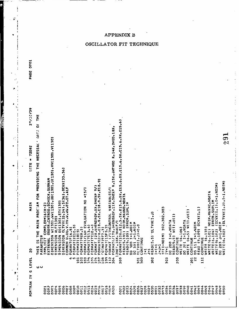
APPENDIX B
OSCILLATOR FIT TECHNIQUE
04
uJjon 1
CY U
ww
> *=
0 n fn 0 sxrW -J0.4 ~ ~ ~ ~ ~ .<I t.4X 04
11A LuD o l1iw W I -414.' 1 V .0
.4 x 4 4 1 . 0-nZC
W nX C 0. nw tZC0 00 In =1cc W -r 39 W -' j 1V
Zý OX a ~ 0
9- V ol 9- .
.. .0o 0 , L - -u
jr 2T X I. x . 0 M - + -
on U-- N fn 4 U' 0 --c 10' o - nýU) 4C c10100.0 0. 0 . O 0 aZ
>. .4 4.4 _4 on M zn -n -
* z 0 c ý,01`-W Iý4I Xi4n l`W MCII inU I(.-U i - i *
0 cz- .0 50a 00 n -~*S*-
U.~4 i *- j

B-Z
N
0. 0
LU _
0i~+ fl
cc
N S.
-C >0 -M
_j M
) ~ 0 fn -
> c..0
i- N 2' -mcý0 NM

B-3
0%
m z
C.
cca
*-f I" n
x n 0
I.- 2UI-r. 3t 0 . k
In z I- 2.4 l-u Lu
; x.. Lu cc
K in > 3 .at In4 0u 04>
N cc- - 1- 8*a'x 0N * - .- w ILIZ
u . uz a. 0 w... In 21. QI -' -4 n Lu0. -. u( x4 -4o Lg .Lu ýo $X Lu w wuD- In j KU z z I
4 OOif ODM x. K x K -
4 X K xC 4 an 0 Xn V-. - .a.ilM W. I- . Z O D- Z .- 0- 2j
ox z .! < O xn j t- cc3I-C2* '.4. - -X Zm < -J a -Cj F
O LJf>40 . IK*"w U0 W Lu U
U. =)O. in ZWWI- X1 4 w . .- O-Z If Lu 1.-. m. F--U -.'-Z---I n 1 - NO -0 3 .1 m3 +4 i .:D =UdZ CU nI WI ZX-'C 3In4 CI 4- 5.- "i Z 11 1101 MC)0 nXýe - 4
D*Z Z o -< u-ino I-1 <W: ) >. Lu - Lu >4 C) 4a~oZww- u~xxzzxo x) w~ X) < . OI - wj0- w mN* ' 1 " I
0 .. i Z .34w A X 0-J 1-x. ' n_ Z I->-42 Iem 0-. U.~
.4 mt 2n 2y fn Z UNZI
w Z Z Z -- 4 I-I 04 0- Oý4 I 4 N -2 0 u> 9 O C 0C ~ .-4 4 '.4 *U . u 5 -. I4a4 . 3 0
at m 4 iK IKKw0,0.ý.~ N M I 'D-K- m a- .. 4 tvt T nI r.J . a.J K01 0 N- In. I
0 a 00 0 00 4U. -444ýý mNIN N NINNN In n eLu0 00 o c 000 00C 00 . 0 o4a0 G.0 0 0 0 0 0 0 0 c o 0 0 0 0 0 -040
0 0-40 cLu.

B-
.9
ON
CM
0e
b.z 0
xx
0 _07 0. 2LC .A
ox -D D .
*. f- I-.* CM .+ I- _j
l' z . 4 fn - t f- Uo -. 'D0t.
- ;0 N! nI be I.- ZC be40 0
-a x 0% c + x MD )
a 4 U. 7- .Z 24TU, x'z .Cf
0 i - -01 O* Ol -- Ou xX : X 0 w - 0 O* wzý 0 0hý x UY
" " o- M 2: + MX+-j t% - -M++- , . DX _ M. 7 =4XS. u U b ) _ 0 -S I 0 04 1 !.CW. I.
11 -4 Z rM -0ý, DO~.
C." 4 l'- 4x -y - x. -* M X 1 C_ 02 jU P -- b >) z >Inj b > cc >-JZ 4
L. cc 00 00 - Do U3 007 - 004 * *N0 cao - -1
j 10 4. 4 LN .9.4 N e~n It M En 04 co NWn-2 -4 r4 em N.. 4i N N- cmf N. 0 Y NM m0 m M m4 m0
-cc I M *01a 4W Z t.- W0 M W* , r-. m C, * 0. I- 4-. P- M C.in- In 2 - tn 0. n4 In LA.. % .-. 0 'D 40 z 2IDz1 01
-0 Ol ---Ol -. ~ 0 00 -- 00 Oh --- 0000 00000--0-00 U2 UZ OnZ . 0 UU..0 ( - 0 )Z - ~ 2 L~

A B-5
CIDc00
tIJ
4 30.U
*x
0
zz4 eeoL C;Uu I n
I.- . -
4 0
ccc il ''- 1 C c14 I- W. -
I.. .. zS. bd )l-
:00
U.0
.00 . 00 0 0 0.0
U. O
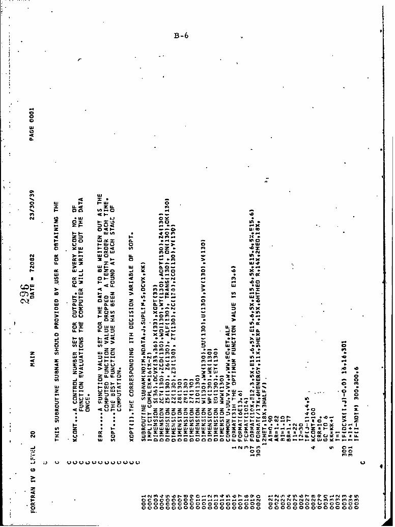
B-6
fq Uf
%%40 C1- ,ro m L -t ML
in W#71o0 w cz m-U CLI
9- 0 U t- 0 .4u 02c U 4- . --A en
I. 0 WW i-a -N of %. IX w n.0 wA.
co 0 c i 041:1- 0- XO
4v :0 2i I- NO)..L.00
at 0 UJ 4 0. *4-N l0 6" > 9-W4) 0 - v4 .1
= 0 1.1 -42 U. C) 0 2 ) us OX.fie . W f0 -M M* n
*0 0 = 0 9- 0j *Wo aup CL M~ IL 9'o- 0 *L Ui .
9- 10 W. 020 CL " 00 0- in X.= 0. X Z 0 V) V) - X-C) ) W%
IS. 1.- -4 09 4 14 M s- N 0. C"9-0 .-. U -. W M .4 0
I.- U. 411 M U3 -02.J- Wn j ewj j x 01 o.4 .. SX
V)IL 1- 441- o o ol X) U)99-9 z 0 U) >9 .> ". __10 Iw C3 4Ww ot .00- Al z e. i
W 0.. . 0 03 MO 02U0 X0 V I.- Us. N. N. 0,'. z .: ;
-4 m0 _j Ou ) U) " X. x- . - - 1 M= U) sz CL) 9- 4 a 0. *0W) X X .3.0 t
w ZWWW 0 -.- U) W ..4-0 -2C- -31 %eV) _. OX xW * 0 a - - - - 0 11.2 -L 4
U.S W- <X M O OO)> -0.n ZU C) in0 W0 Ix. 0 1- )(49 Ln 4.aZW 4 4 >'.'K
. -U b. 4 U- 4- w4 N.- - *- NXW ; 1~ Z I.- .49- 0- 9-U 1 0
O x LU)0 U)4 0 . Z .Wcc 2 0W 0))0 u- -z 0zz z z z z; 4~ .. 0
Z U) -9 -10 - -- -.4 -) - - 0 -ii. -*X- -=. UJ W~- 0 kn IA W W 0W0 0) W Z f. '0ý -
2 4 2.1 4UU 2 Zp04U I- .x U#WI
U) f. 0 0 z _" -. - -. -1 -*0 - ý .0 a .W0 -at-c iI i e1LN02 09-9 4A X , W .0000000)- O)0 DO01ZU. LL N44
* ~~~~~~ ~_ WY en r-U) C" U%.00004W-0)f.4 '2 -4Z~~~0 cc.U-9 '--.4'.)4d * .. NU *. *
29-~~~ fn ZrnU~ .rl-0.4- > ' '.
Oe 00Z0CCJ000WI.0)00 00 OC0000-OUVOCC0 411.00 00 00 00 0 00000000Z2ZZ Z2ZZZ0000000. o
* N90 O O 0 OO O O'.'.% 0- N
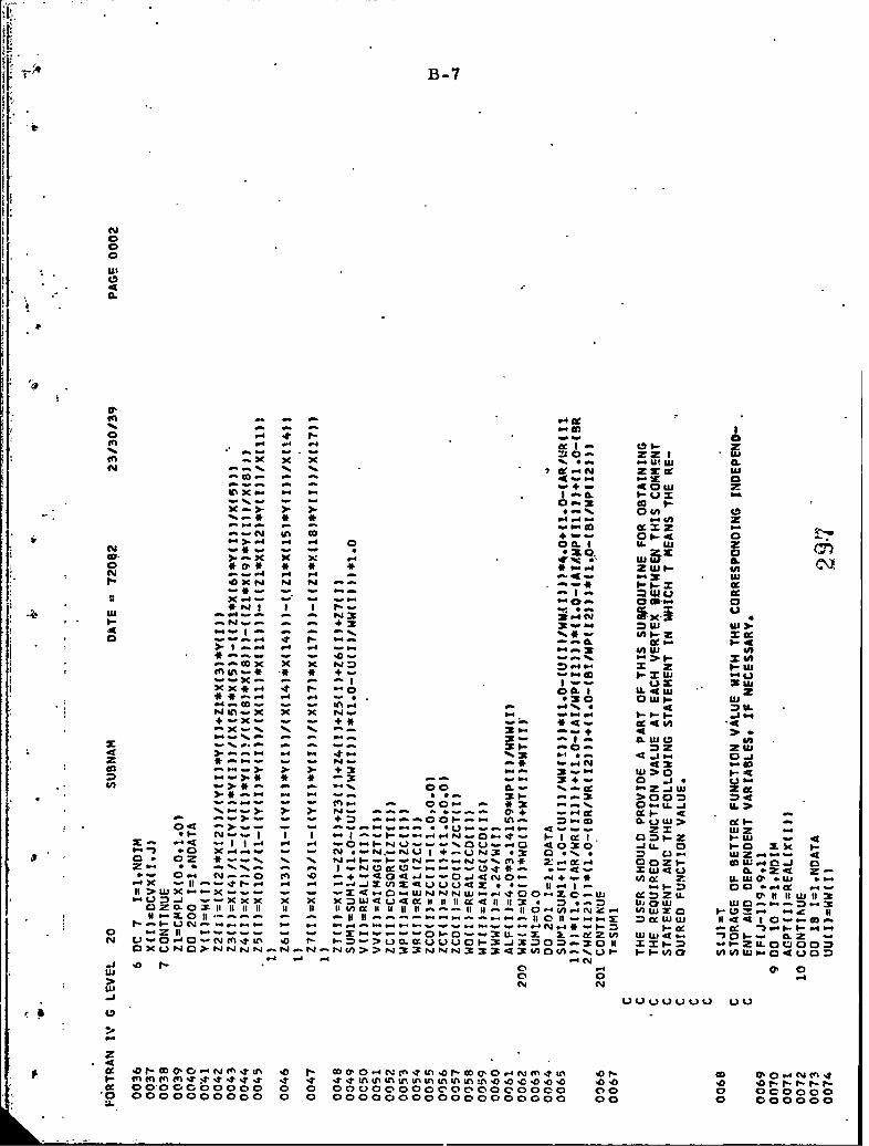
B-7
V4 i
0 u
x -I
Car a -xIL* * *' z JaI
i V -'P .4 wI S* - -, - w0 214 ý c K .-- 1 0.
w 13 . - -4 XI. 3t -i w - -..
inK... .l in. -
~.+ an * 4. b.i
92- - -ý - -~.V4 %. . 0 00- D. IX XXN -*-. 1. 1- 1. 0 ZQ
a-- cc -4 in '..
+- 393w -XXIL CC z' 0i C S w -. 2
4.-K-c -- -i I* -. * - PifK~~N -r m. -. < 5- a a
2~~~t a...- U N.. >*-.N4
0. C* M* 2: aa W. 3 4 0 C) O.*~~~~z! xn .. t-1 -a ;: -C 00- %a -... 4 x X* v1- xa qxU U4 0 cti >Lg. X. a 00- a o3 11-4% 0 . U. ..j1
N a x4 x1- P.4 -0--NJ-- ~ I0-0 Z-. LL 5 0 0~ 0 -o Nr4 N-N - x3 m m X%% a X 0 -4 0w~ w. ww 2" 4* 0 ~ J-- 41 0 - 4 4 J - . 4 0 -4.- in U. O * y
a Of- 47Nva e4m* 4tm .0 1-. 10 1- aOD- .4 Cm 4-'
I- It 5' 101 00 I- I- 0 l t000000 0 0000000000c

B-8
CC
C~
co4
a.%
c~cn
0Y
V) - e o
*l - V) -- -
OW*w aI I--, ,I- . - 11- 1. F I.-
w ww
>~ -4
w U% 101 CP0 4 ntlo-cmm CIO V-.cloo~ao
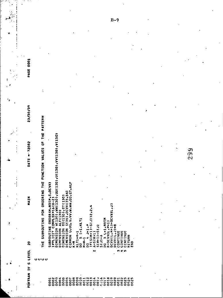
2 B-9
-4
x0
cm Wco 0.:
cu
0 0
cc Q
m z ; -
w U >
to ; -,;
CC C -i M>
t3- t;"I-n 7++114-
2i -M- Iuu o
42- In AaI In8*- O 4
At-

B-10
w
0
Go 0w 3 L
3d x <L)N > 0p4 X U 02DUjf
L; >$- m iu z
x I.- - LD UICjb 0 nC -a
-Z X -cc I . f i
U. I.- z 0ý-c X 404 Z4q XW -
.0 aUU 0-Ou. X fflZ..4u
M0 0 -I--OM41- -1 't r 4X - ) Q
4W m.. mf1 cx -" I. .*J &) J X C U
>- LL-f op a.xw4 l <
w wxvV V L.)u'- a O"-,o11 1 1 011-0-2.0 Z I-X X --- zI-zý
9.4~~~1 tCrIJ W~I
.cc 000 I- 3* -
0 .. Z.0-03 00 0. 00 00 00a o
04 -. Z 3 a

B-11
-4
fn0
CL
0 U
x 0.
I. I..
m m19,.
in -
-4 > 0 L
U. ccto 0
o w W r
-a z D e -4 $-Z
cf w x > C
D4 W M
in Xn -j M
Zui 0 -a Y--w cf -. u 0 U.. x
- Z -ZZ - - 4-
_j 4- 4 -1 2:Z
to I 0 a O "Iz ll.l is0 4 I r
z a =.- -o WO
I-xxmD - - - - *<<O2ZW
Ix0 ~-4 4 3.-3 wlo NM 0 of- o1. w 0* '-c 0 0 - 1--
02 *JOU--.>

K... K-.-.- -- �i* b4.K414K.Mil
Kb..KSK.b..KbPb...K.lK-brn Kb.AKKbK.0�KK.Kfl0�Krn K 'K... P �KKKb� K LK..K4*.b.Kbl b�b*�*rn 4KbK4bl b�Kb.44 0.0*S Kb.4b.4 K***��t W. K.KO........4Klb 4K-b.� K.rn..b...b�?K4S.K
r�. ........ a-o.K.. cob...... 'tin K.e...b..1K..s....o..b.K �... o.i.. K.....b.b.K SKIt KI...ibKS.b.Kl4** K' AlIbI 0 PK - lb4� A�bK. - K..K IS"
rn.AAK.0b.04.b..L.Kbb...rn 4P K.I4b.bIb,, ..?.bK.l.....bbb.i KK0.Kbi OIbb.rn I0.K bIli K LI�a.* K�S IKI.b K.KAK.b..... A. 1.4K'
K.b..b.b -- £4.K .�SK.b. - 1 - -- *rn�rnK�� KKbI4.bKl L�b.K* K�- IA K..A.t-b K...bi?% bb.4b. bib.? 'l..4. b-41eb4 1.4504. Kb.e.KKlKrn41b�ebKbK�b
0Kb... KrnK T�bb 1511 KbA.0145Ke� K.*pKb KIlt III
�t.2?IZta-� ' * a p..... � P.b.Ib.A .. nKb. 1mbIlbIb fb.rn K�blb.Kl4 I.. - rnot.K.K..-4K-. K. b..rnr
4.K..b..bKbKb.9 PKb..l.IK O.hl..bl. bliob KKba1bb�b.�4.Al � b.KKKK I??- K. IlK- �%�bb* 511Kb a-IlK- Kb.b.?4. LI0.4�KbII'tKIK�IAflK'4KSKb.41 P441KK.0*fl� A K- III � K.K.K? K 3 K Kb�rn 4..?KA.4�4flKLK4
KKKbII irn 1O.. Kb...b.K Ib.K411 K*�K�J*l --- "I..- 0K" L.14% KKKKKI0. 44.411*
- 4..0KA 0.K4ISK Kbb-II K.....AKb.Kb4.0.4.14.4K 0' -141111 KKKK44b .. AK..A.I.... A I KK4bllb.KIIA.". 4. IK.KK.b. K A K�-K
Kb.... Kb.KbKK� KK Kill b.b.bb. K' KAd KKII rnK44b.b Kb. .0. KKbbbeClIbbli Obb.4? .0.-. LIt - UK K.0Kb.b4A 4.141 KKI4lb�tb.. Irn.. K-b. tOil
A..- Klb.4ll� *KaKbI-KK� ' - K PKIK.b. 4-4K 5W-
K0.:.4�rnKb4� 0100tK.. .1K. 0.0K. AKt.K� OK.. bK*b K.bAb.K l*414 *K**** p.o. ..
Kbbb.IK..*l.b�� K.bKb p,,� � 0..- 5 K. b.SK.tI.-.' 414411t1 lea .tK.KA.KbIbI � - � a4iil
KKb.aKbi 0K��b -bib - I�IA4 CIKA.Kb 4MK' *.ll.KI. K...b.rnK..K AKaK... 01104.. lIbel. K.bKK
.KI.bKl.l i..�... KeKb� K...b4 K I.b0Kla
Ill OK. 0.1101Kb. K4 ella .1K. K K K..K,.. KKbb.b.KK.lI C.hi.�Sb 441Kb. KrnKb.4Kbb.IC4an.. 'I KIKIK. KK.K.KI. 1..K.e4 lbb.KbIK.Kb.-.KIbK..0K. ��2K0Kb4K
relK.-..K. K..Ib.m Inca o..aeAK.... K...KK�KKK0.KKb Kb.ern* KUJ* KKA IK-KeO..
I �..... . K.I....b KIKIK P KbIKbl�SKI ill ,,* IKe-, KaKJ...IK Mitt Kb.KiK.rnKlK.lKb
OK... K... C..I". alal.a.b.*O bbill0. KIKK.* 4.K-IK..115KbK4. K4..K.bb0-.bi�Kb Ka..IKK..4a.� 40Kb..
- r..a�...... tlKKbbIbl. K.....b.b.KI P111K (43 K.*b.Kb
1e11
K CilIK K K...KIb.U.K.b..I1blbbKbl K A.... ..4KIKKeKKQ
C.KK.IK.I. KbK.� 4�K 0.14 0..el IK� K.KeKIKAb.lKb -- - .4,44KILl..... blIKI K....rnrn .. K.Kib K.lll & K...KKAIK...b.,b K .a.. S.. lb... K.0K.�. flKb K..l.bS IKYIAKK...bb.KK.I.I K.b.K.�K�sb K.. K..K A. C. 1.11
AKbm.Kb. - I.! I K I.e.. - K4..il K.K .KK..K..AK.K..I...It...1e4b.b...b.. 4.4..... K..bl....K.4
baLK A.-KbKeKb.d 11.1 Plb. OK...... K..bOS.l 4... bb l.......?. b....a. LS.b...bK Ka�. K'.. KeK bb.b� CKKK.b.Il. Kb.K 11411blKb.�KKlIbIK..,Kb IK..1.b.b.abt Ptbrn4l ... b.K.... P.K. b....K.K. KIIII.b.KK. hub5�1 K.......l O.K...-. 11144 i*I K...b. K K KI.KIKK K. IK*b**batl
KI..K. lb. 4.1 K.trn.IK.K0 . in.bdK...IK.KKIIKb.K11b.K - A-? -P.... KI II I.K.bA. I.....- *..b..K.K 0.e�A K0�...Kb.b...KL.b .KblIl Kb.Kb KIII' PKKb.K. .0Kb...., ebb.
K.rnb...b. 00. K? P.b.rn K.I..rn .tlb..IK.bbl I P K -K.4.IIKK KKb.bbb b.beb.K4, Ke Keb 11Kb
Kb.lb.A. KO..K.KI 1141 - 3 K 11K'brn
I.-: KIlbe K..eeK 01.1.. KA.KKlbb bbbbb.I 1-4K.....?Ml.. b 0 KOK.4 :.±.21z'z:� III - ,� ,:lildK:r.l:te.K..a. i... 0Kb. a.... K..ne..l.a bO.KI. a-1b.l. - 4b�b ala.. - Keb IMbI A4..��
4ifl*b.�lb.l. A.b.Kl 944Kb IbI 0.' bOb. b.? K..K.0 K.i.lb.K. '4Mb ebb?
K.' rnb.b Kb. Pall lKbb� KK bb�KK lrn.b.KKb.bKb.lKbb �KKKKIP K A. Kb.....K�Kb.blKbb.iK.b....b K....bKC.. bbblbb.....K KKIK.t bOrn.?. K.b..a.a..K bi.4 Ke.4b.lb. alPbtb.K KA.I..ab. P.....K..b.bb.Kbl...b.rn Il..KIMKK..e-*..bb.. Ilb.bb.0K*lb bb*bb :13 OK... b�.1 lb. OKebb.rn PbK. PK....bI.KK IblIb -I
01.KKbl.. K.lbb*.4.. IbiK PK?�b4� K�Kb�ebKbS....,.bon....b t.b..1K..i.. KK.b.b.rn.bbi.b.l KOTA....- Lbl.11 Kb.. I�l4 .0.410 K ' rn iKI K...."� 0.-K. K�b... Mbb. 1.1 KbK4Kb. L.1.b.b..4lrnabIleK11 KK bbbfl �4 LKb.1�bKK*KK4? lb. 4e. 1.0b....K Pill. Kb...?1401. KIKiKIrn.. IC'S
h.o...Krn.10 .t bb.IP.b...b.SAKe, A.b.. 0101.0K 5 K.oe O......l.a.bK..rnKKrnb K. 4..rn05K..IbKII.b.b.4flb.4b.KK K.. T.A LIKKb. *IK4MK.*KelKIKKIIKKP K.rn.bK...K.irnb'4K.
..bKKi.i.l...K bKKbb.IabKb K Kb...bK. K�i�..I? bbib K..Kab.. IKAA&K K...rn.K.4 .bAlb..PKOK. *441..I KKb. P.14K- 4bb�S K .e K..... Pbib.. KKKeK
0K...1.A1.00.- Abok.. *PK.I0..l4
.i.. 1.0b.b.K 1111K K.K.rnM K.b.b. Kbb... Kohl' K 0.1b.AAAK.b.KAKb.b.?KSKKIK Ke.bK.l.rnKK.bK.K.. Kbb.b.4KKKI*K? *KbK
-b. K -- 1.KKbea. Kb�e�KbK.K Sill (KI K.Kell P14*0
4.' Kb.I Kb.?b.I bb.iK IbI F'..... b1.bbi' 0441KWS44 AP...Ib. KA.WAb.?
O.K. 04... K bb.l..b. rnK.K.KKelb.rnibK KK.b.b.ilb1.KKrnO.- P...4 1...sbb 0.4.0... A Pbb.b *K.K.4 1.lKKe 'lb.? rn...a 10'.. K.AllIK� 4db
- Kb.% K.' b..b bKii Ibi K.?KK...b.b. pbbeI Kel Kb.b.K.....bbbrnPi..bbKlK.b. AKb.Kb..Kblb.bK K K
014 I
- bIlIb P0K.. I KKK..ern.l K.Kb. -
� - -- KbKKbII P00.. Sb - OKIKIKK�K4I
.Ke�1.b.l 'c.... K...Kb.K.b40,0.. K K. KbKKK
K K b.K..l K..-.....bKA.4rn4K. UK.KYKb.Pb.b....rn.bb..bb.....b K....rn 1.,bl0� 1.04.1.0 *bK? � oi.os. bOilNb.be.t.rn LK.KK10b11OK..bKI4 0.1.11KK4.K P..b.KIb.KIn... 4..� 444Kb K.... Kl.b.. 0.4.011. ?rn.Kb P K K.. bib
K K�-� KKd�. lKb'Ob bMb L1.4K. Kb
4� �.bKb.A ' A K P.t.
LA 4b.b.-PKII t...el.14.4PK....* AK KolIb 0-I. P-b �.K.K.qa.llK.A.-AIbbAb...elK� K....?bb...a Sib b.l.,4K P.rn..?4..KK b'- bb...rnbbib. � b???b P.c b.Kb.l Al.
�b0rn - -K.Keb.SKI1K.
K...KKb...ab.elle? Kb...bA.4lb.l Ai.rn..K... A.-..y.4iK-.S�lelL.K...e.e. A.b.b..blb....bib.bA..b..KbIa�Kb. 4Kb. ..rn..K.KKC K.l.74.l. K..b.bl.K K4ib� K K bKK4.....b.b.b..KY b -. - - 1111K1b.IKKI
K.bbOlrnKb.? OKKA.b.�.4 KK.1 KiloPb.rnKb 04K. KKlbb.lbbKbb. KbIKrn4.b.l.l rn%?.K. K.lb.b.. K.' 4144
Pb.K.b..b KK�4? O.K 440 rnel4Kr�� LI 4.14., KA.ib.... rnl�bK K 4 K.bb.rnKb...Ul..KIKK....KKKI KC.0., Kb.'btKKb.�lrn MO?
Kb K.14 b.KelK A4b4Ab� KK..K4ibK 0.a.KK LKlKbKbiKIb.?b.?0Kb.b.KI KK.b..K *KI.KK
K..4b� 4.1K. 00.... bK��el A Jel - K.K41.b. b.l..e.K.. Le�e. KIIb..Lb.. Kbb
K.1ab?.lb.bAO.-abb?
4A4K.b. ?KA. 31141 K..b.bb.pb.A.blb.K4 *K4Kt. KK.i.bb44 1P9?i
K 4 C....I K.44.Krn. KbLK...b KIllK...blb K.0.K... - K..bblb 1.14 0. Kb..b..Kbeb Pb.....K Kb�...lb.rn Kb..ll bK 4141 4.1
0.Krn.b..bb.eIKrnK4Kb.KK.bK KKK... PK�ebI�40Kb.? bIb K.Kil.K. Ibbb.Kl4 b.?eK lbbbb
'A K IA? K KKP KLKb..K..K...5b.b.Kb4??b04.014. - blb.b K0.Kbe14.10b.b.bK4?
KKKb.l? JK..441.AK4 .IPK.A..KI-ll.KrnK iK..P*K.K�K�? 014b.KKKb..b.4L.p .brnLb.bK4b.lKbb.144bi ?K....
K...41.b.IA.KK?... b.b..Kb.?bbibb4tl.�lb.. K.... KIll 'b..b.4 K.l...b...b b.K.'4.K4? 0.. n,.o. � ?bll?
K..KbK.IKd.IKKI Kb. K.iPOKlI0b A 0....4 IbIKO
K P Ke..iK K..b.b.4. 0.41.41K ?lbll K. Kl�b bAiK
?..l.l.bib.Kb.. K.b.l...Kb.b..b.....rnlib. K..'..
Kb.KelAiKKKbp KKelIIb.41K1K
rn.4..4K..KK. Kb11 KKbK bb.K. �lKb Ks41 b4K.Kb.?. KbKKb.lbbbbi
Kb...? ?KK* ?b. lb...? .iniK...bPb.blKl....Kbb..b JbK.4KA� b.0.,.JC
0Kb..4
At1. �KbK K.?b.KIIK.10Kb41K.K � a.c...K.eaK4��b�Ki K.0b.4..l 'NIb 0b.4. Kb...... .lb...?KK.Kb.D...??�4i'bOKAMIK K.,.4e.b..brnbKb.
4b.Kb.Kb b.K.b.y 40.1. KILO K0...4AKb... i.. .aPKb.K.Il. A.AI.4K. ?KK IlK 14.?b.KK
K.K4414 KbrnK.K.�b. �bi4l �Zb.KKb.bb.4 O.KKb.4l. Kb.b.AelKI Sib?
0K1.KK. Ke.�I? "0. K 04b.bb.b KO?1140 K 0.141. 1114Kb 0.KbP..4KPKMO.b....4 40.Kb.b K*14b.Kb.b.bbbA-Kb p0
K..4iKb..eb.bK. OKI.. L..KAb.ll. Kb..b.bb..e 41141 iKl�b.K...l0.K. 11411 K A - lib I..1.4K.. K.b.l.be.rnc Sib
b.....l, Kbb40�4 Kbe ?KbK..K.14b. K' 'IlK 144Kb.'.'..b.41,K.rn - I.l.� Kb.b. 0.K..Kb?
K...bKel..b..KPIK..b.KbI...b Kb.�K�b.Kb.0.b.b.b.l LKbK.. P KP..llb.? K...b.b.. lKb� b.Kb Keb. 114 b..K KeiO A.. LIII P..KII..
?.41.KblOlb..4 KKb..bKb.b...bK-.ll. ArnoKb4PK.eKKKK..KI. Kb4K�b Kb.4 KK.K�lb.K. KOKIK
0.e.bb.KIINKb. A 0. bb.4K.b.KKA...b.. Pb.Kb.A KQKIb. PIKp. K.-l.K i40.14KAb.
0.4.4.1K 0Kb.. Ilel KOIK-Kib SI KI4....4. KIPKKK
not 0K4b.b... K.lb.4bb..rn.KKb.A?..K.A.4? .. l Kbt.elK 4K..b�K.lell.b.Kb PK K..?b
I �
43.00n.0.lo.-.o..0oo Coooo ooNýO I=. 31A. "= 1~o~oo 7o. No R,.'..*
No. o. - .0030.404 N.. Yol an00 Wo00g0.o Zoo. OotkoA.Do-.No00 N- o.4 t
Argo...ý NoU:.oo " `nlooy W~. F 3 '0,Wooo. 0404044Am) Ao.oo., toMoo 000. 7
0.oo0,Otooyooo 3071003o000000000A$n-.oo Nn 0.oo.o.......ooo o0.~ d at" AIV.N *
Nog. 0.0, 0oIoo, Optlog, 44
7y0 370No. Dogoto0 Ni~.slo.0 0.4,j.)0 No..o0~44 (ý 0l44l40
0
No.,.,~~~045050. Nl 0ul . ,lDn ,D.I . 00034Col~oo, 0000l 0.0 N.000, Io~.~ooo NoH 040.oot A... No. 40l- F, IllO1000pool5 l~o.. S_ ooo~ tol 40-0.00000 CoT it". oooo ooooo
Noot ~ ~ ~ ~ ~ ~ ~ u OOuoo *,Is$ 130.oo04 h.I. .......00,... 0. Q00.0.'00*.. oo...- 37000 C.... .v ... 0.0.oooo D0 C..0 0 2.0n0.r
Codot- 04o0.yL"oy CZloy.) ..4 Zoooo Qo. 4 04.o olo 0 o .og -oAo 0 0_-1ot O.,oooo o A-l. Tolo0o0l-l0.000y1 T ýilo.~ .o,
ACo T -okooo 11O~. OOollo. N4A0-.. Rl-o0 41- 7 D. Ooooo No.o)N
Mo 07No.O000Wo~o~~7boo lOoooO~y 0000looofOOo~l. N Zo oot. Ao :.a4 0044 10Pobo~~~~~doloo.~'M 0004 0o0.o 0.70 ...... b00 olo0. oon, .o~o ~oO
Obloo~o 0 0.1 ..... Ilk ro 30.0. xoo....y 0.0..0. .4.....o. 0oo.o000All. ~ ~ ~ ~ 11l .-..o.-l. I..O.Ooooo ........ I~g) 00304
N, =NO. St4..... )H. All oooool.oao&-oO...
I00.0.s - -I.. . P. .... ao"olo 00 1 ...oooo N .0.0..Coo..0. Tool 0403 P 14-110.0.. NoolO OAolbo.kooooo0 40014. iY.~. 0000
'0oooIgoo. N,! 0 01C -o-.oo N0 04
144 4o _o.. 4oa.ob xoooo AI,000. I.... ....oo
lot lo.Z. o~o . N. oo N. 7oo.No0 oo
A'0.. 0000.t, 0 ..0 oo.- A.0o Nt .. I00, 10oo40oP40..
004 ~M ZI-o0 03 1004 od....t DIo000.r
-40 0.
toooooo aloo.. .0... Wino.3~ooo W(Ygo. .41,o~~ oo.'000 o1lo 0. l0. l.Do0. Coll4 Aoo..o -. 00 P ill
00 oo o
0.44.o~ N.. ooooo I0.404.00_.0, 40000 O1~ 40400 '0o0o Moo.I.oM .Zo.
C. -_-3A........
401.O0.,0040
N...oo. 0.oo 000.4, L I-.lu tlooYolko. n . F
Noobol 1.0o7oooo 0..O: D0. H.oYooooo 0A.4
7530404.0. o..70400 704 .000 M)Oo oo.oo 0. VN, i,_g 50.ý Nloolo olk lA ll T..I...43.. val0.00.',(Z Iooo.) MoI- USA Al~o-oo.14
NoorO~ ~ ~ ~ ~ ~ ~. 0.40.0. 1.
"ooo 04o.40104*00 04pooflo..ooottoo. Aol.. '0o44 W - ot R ....Il
1..ol.0400 4170S W4 - --l. N _ 0. t 04004 No ... 0OlinAN.7oo~o0..00 5..k. Iola 7.O 1..0.? 0044.00
N00.04.0.o.0 7-l 011 W. o It 1 0.4.,3l~~o~oodO.0.ooCall 0.003 A.. N0oo.o ow .o N0 0..4'.o0 4O 770 Vo.0.. A-, .o.10 007
700 No.bZo....h N.o1.0.0 10 Do.' N Fonoý OoooooogO o,
No lA 0.oo. ...... NASA .otooot .0..? .04o
ftoi .0o... lo0 Pooo. E100 3...ll A0.ooo ok...Oo 00344 knit3A4fN0I.31.0._ -t, 000.40 4 A, CIA~oo ..ooo. t.0,ooooo 400o401Poo.0oo1...
00000,, No- -. " looooy 01304o M0.0.'0 03003ba ~o
Ttl~ot. 00 tl-o.Y o. 04 N..o ob10. o0l-oIoo.lo 0ooo
Pod.., 0 Z'010000.l. 0.-W.o1, N ol 0 ll 00000 A.otI. C.."...0 040
000.o` ., *-41000030.o N.. .
Aloo. Oo fh Cooo.404000 0001 C0 . Io~'oO.'0.Ifro~o, o~o 1100 '0.4 ol.4 Aofo~ N-k. A-0000.4 o 044 00,
Al.. .0113Uoo.O. NS .~ .400 0oo 0400,000.04D0o0. . o. , (00.".0 W lk 0..4400.4 40000o04.04 444Moooo00..
AA4).0344000 00ol.Okts ..u~ lain. 300.oor t 4 ao ll044I Aloo DolZo...o 40-~ 0 0 Nc Too3007
003o.0,000.0005. 000000-%,oooN.00,04 4ooo
A.,ooo 7.00.," S,-0y.03 .40. .... Alto 1o,6, 0000Z 0 00AN.0...l..o.1 -a0P..00N- .. A,.oo 044.1 At.0.0 ,4 C-00 . I00404No 3.'0oi~ 0.4 400.oo.Oy- 44.ool, o '0- - 0 ) Oo. coo. .1.n004 . )t0.4"044ol.o00l 7100 A-oo 000oo Olo..' 000Al 30.00 ., .oo.oI.400
00 1, o 05...4ovoo. C.. 700 40 . I00001 N,.010.0 33 ooo.
'0400% 0.0o.0 0030o No.Agooo!o. 00_k730 400 =. 044 43 0010
Do-. 3. 000.000 N 0. Alloy 0V.4 A.40o-otb 0.00I_0301.1000,0.Oil340o.4 C.4.04,1.000 310 1110o Vito nooott oooo00 0.00
MOS U~ t.oo. o I. ... I 05 N 001.flOot ,oooo,-. 0.in N...t 000.0 .00R0.0
N~ Gobo. W4440..0.o~o .No -010 i4.ooo V000 34 .0.0034037I_.00 0.0o Aonky 4.0.. '0.40.0. 03
00,00004 .1.3031.03000. $30 a001 44....0 Noooo W 4 o.,N.0Soo0 -N.00,5" mo.ot T-A,.. -W,..o -30tol No' lboo
0.No,000 10.. 7433 71 N-4t 0g44 000 00,Oooooo400...0.A'..., 0044.010.000..0. 07a0000 000
0434zplo IM ? Ao.4 000.34C. .
44'll.50 LU oo 0.... o4 . 000000 cu,.. t0 104 3.g0. 40.00 N .0 05N oP -.00 00, N~#W 20 Amt. Mo.poo. 0A.o0, 1..ot 0.40. .0,00
No.030..00,004 L00440t 0-0..04 lolo hlool 000000N o - L o s. 0 .o o ~ 4 4 0 4 1 0 ll . ~ o ~ o O .o o no.. 0 1 4 0 7 N o ' .. o o 0 0 0 , 4 0 0. 4 0
7.. oooo 101001.000.4 No 0.0000 9110.5.