
ECE444 - CiteSeerX
145
ECE444 Theory and Fabrication of Integrated Circuits Lab Supplement Spring 2008 Copyright ©2008 University of Illinois Department of Electrical and Computer Engineering This manual should not be reproduced without permission from the University of Illinois Department of Electrical and Computer Engineering
-
Upload
khangminh22 -
Category
Documents
-
view
7 -
download
0
Transcript of ECE444 - CiteSeerX

ECE444 Theory and Fabrication of
Integrated Circuits
Lab Supplement Spring 2008
Copyright ©2008 University of Illinois Department of Electrical and Computer Engineering
This manual should not be reproduced without permission from the University of Illinois Department of Electrical and Computer
Engineering


ECE444 Laboratory Supplemental Information
Table of Contents Introduction………………………………………………………………………. 3
Lab Grades………………………………………………………………... 4 Final Exam………………………………………………………………... 4
Safety…………………………………………………………………………….... 7 Safety at a Glance………………………………………………………… 9 Laboratory Health and Safety…………………………………………….. 13 Laboratory Chemicals…………………………………………………….. 19 Medical Management of HF Acid Exposure……………………………... 21 Etching (Without Etching Yourself)……………………………………... 27
Appendix A: ICS…………………………………………………………………. 29 Appendix B: Evaporators………………………………………………………… 35
LDS-7211………………………………………………………………….. 35 CVE-301………………………………………………………………….. 44
Appendix C: Wafer Cleaning…………………………………………………….. 53 Simple Degrease…………………………………………………………... 53 RCA Clean………………………………………………………………... 54 Hydrogen Peroxide Solutions for Silicon Wafer Cleaning………………... 57 Keeping the ‘RCA’ in Wet Chemistry Cleaning………………………….. 63 Single-Wafer, Short Cycle Time Wet Clean Technology………………... 67 Wafer Cleaning Processes – A Review…………………………………… 73
Appendix D: Photoresist Processing……………………………………………… 81 PR Process Overview……………………………………………………... 87 Wafer Inspection (Lines and Spaces)……………………………………... 89
Appendix E: Hot Point Probe…………………………………………………….. 93 Appendix F: Four Point Probe…………………………………………………… 95
LDS………………………………………………………………………... 98 Veeco……………………………………………………………………... 100
Appendix G: Furnaces……………………………………………………………. 103 Appendix H: Ultratech 1000WF Stepper………………………………………... 109 Appendix J: Test Stations………………………………………………………… 117 Appendix K: Semiconductor Acronyms………………………………………… 119 Appendix L: Common IC Processing Terms……………………………………... 123 Appendix M: Processing Equations……………………………………………….. 129 Mask Set…………………………………………………………………………... 131 Test Regions………………………………………………………………………. 143

2

Introduction Motivation for the ECE 444 Lab
This laboratory experience is intended to help engineering students who plan either to work within the semiconductor industry or to utilize semiconductors in their designs. The latter purpose is not as obvious as the first, but knowledge of how transistors and ICs are fabricated can help an engineer get the most out of them. Modeling semiconductors as black boxes with certain specifications (SPICE models) is an important engineering technique, but after this laboratory the student will not have to treat semiconductors as mysterious black boxes.
The student will see many of the work horse technologies of the semiconductor industry. The lab follows a cookbook style recipe – this is necessary since the process is not in sequence with the lecture. Later in the process, understanding of what was done previously will come. Although the cookbook nature of the lab manual threatens to trivialize the processing itself, opportunities abound to observe phenomena crucial to the industry. The student is reminded that he or she is here to learn. Observations cannot be made for the student; that part of learning requires active participation.
There has already been so much information discovered in IC processing (as in many others) that it is far more important for an engineer to develop skills in the acquisition of this knowledge rather than to attempt to memorize everything. These skills involve making efficient use of books, libraries, CD-ROM databases, and the wealth of information on the web. This laboratory experience, however, should help provide another valuable resource - personal experience.
The most valuable contributions an engineer can bring to the job are human intuition, creativity and skepticism. As you make your own integrated circuits this semester, take the time to improve your conception of what
is really going on in the semiconductor during the fabrication and operation of the devices by thinking about them at the lowest level. Visualize the nearly perfect three-dimensional array of silicon atoms and their associated electron clouds quivering because the temperature is above absolute zero. Remember to update your image periodically throughout the processing and testing of the devices. This exercise can help you perform mental experiments to test creative new ideas.
Skepticism is hard to program into an algorithm or to learn from reading. Not all published data or conclusions can be trusted. For instance, there are plenty of published values for the work functions for silicon and aluminum that would predict that the schottky diodes you will make would turn out to be resistors instead. There are also contradictory explanations in the literature for why silicon oxidizes faster in steam than in dry oxygen. Sometimes there is no substitute for actually doing something. Try to keep your curiosity high and your eyes wide open as you make your own ICs from scratch and, hopefully, you'll have fun too.
Scheduling details for the ECE 444 Lab
It is imperative for students to attend the orientation session held at the regular meeting time the first week of classes. Laboratory sections are NOT automatically canceled the first week!
This first meeting is designed to organize the following weeks – you will be assigned to one of three groups, each starting at a different point in the process.
If you cannot attend your lab section the first week, attend another section. Make sure you contact your instructor to find out which part of the experiment you will be expected to begin the following week. Consult the timetable on the web to find out when there are lab meetings that you can attend.
It is strongly recommended that you try to stay ahead of the schedule in the Student Preparations Web Page (Main→Lab→Preparations). Human error or equipment failure
can and have knocked people back a period or two in the processing. There are less equipment conflicts if the students in each section are staggered.
The next three weeks are designed to train you in the use of the equipment so that you can process independently. There are three prelabs: oxidation, photolithography, and ICS. There will be a maximum of three students per TA during these training sessions. During the prelabs it is difficult to accommodate students from other sections, so make sure that you attend your scheduled section (requests to make up this portion are seldom granted).
This scheduling is required due to limited time and equipment. It also allows for more direct contact with a TA during this critical learning period.
After the training sessions you will be on your own for processing. Make sure that you are prepared for the processes that you will be performing. Most of the details are in this manual. The TAs have been trained so that they are not a crutch to the students, but rather a resource for unexpected problems. Do not ask questions that can be answered by referencing the lab manual – if you do the TA will tell you to look it up. But do feel free to ask questions about safety or issues not discussed in the lab manual. Remember, you are learning to become an engineer – engineers provide answers.
Keep in mind that this exercise was designed to account for unexpected problems and failures. Do not worry if you are behind other students in your section. This can and will occur for some. Usually all students will finish their wafer in the allotted time. Don’t worry until the TA starts to worry. If it looks as though you will not finish in time, extra labs can be scheduled. Extra lab time can be obtained by: • Attending an open lab. These will be
announced on my.ece.uiuc.edu starting at approximately meeting 11 (depending on the need). Students reserve places in the open lab by replying to the announcement.
• Attending another lab section. Permission must be sought each time from: o your lab instructor and o the instructor of the other section.
Due to space and equipment limitations, the answer may be no, so be prepared!
3

ECE 444 Lab Notebooks A Lab Notebook should be
used to record observations during the execution of the experiment. Your notebook should reflect your progress and note any irregularities you encounter during processing. It does not have to include information which may be found elsewhere. References should be made to steps in this lab manual as they are executed.
An engineer's notebook is an important record when things go wrong. Employers would like the educational system to develop good notebook skills in students because profits occasionally depend on them.
The lab notebook is not a requirement, but a suggestion to help answer questions later in the semester.
ECE 444 Lab Reports The Lab Reports shall consist of the following: 1. Title and dates performed. 2. Data not recorded
electronically. References to electronic data should be made when appropriate. Include sample calculations when necessary.
3. Answers to questions and problems – in an easy to follow, logical progression.
4. State references to your notebook, textbooks, the lab manual, etc. Specify any graphs or tables used. Write out any equations used in calculations.
5. State your assumptions! It is difficult to tell if a student really knows the answer when he or she has not stated all assumptions clearly. For example, state your voltage reference directions when necessary.
6. Brief comments on experimental results. Point out any unusual experimental observations and explain them if you can.
In addition: 1. Everything must be written
in ink, preferably typed on a word processor. Reports
written in pencil are unacceptable.
2. Label all graphs and diagrams. 3. Write on only one side of each
page. All writing should be legible if hand printed.
4. Leave plenty of room for comments by the TA.
5. Each student must write up his/her own lab report independently! We have copies of past reports and do reference them – violators face severe penalties (expulsion is not out of the question.)
6. Any data files are considered part of the lab report.
7. Unless an excuse from a dean is presented, late reports will be de-rated by ten percent per day.
ECE 444 Lab Grades The grades will be based primarily on: • The answering of report
questions in a manner which displays understanding and some thinking on the student's part.
• Obtaining and explaining results which are derived from the experiment performed.
• General neatness. • In-lab technique. • Lab quizzes and final exam.
NOTE: Anyone caught stealing or using another's wafer, lab notebook, or computer files will receive a failing grade for tthe course. Similar treatment will be given to students caught using a lab notebook or files from a previous semester.
A significant percentage (25%) of your lab grade is based on in-lab technique. Good in-lab technique includes proper use of equipment, safety awareness, cleaning up after oneself, and in-lab performance which demonstrates a basic understanding of the procedures being followed. It is expected that the student will become thoroughly familiar with the procedures for each lab period in which he/she subsequently will be involved, even if it may require study in advance of covering a given topic in class. The theory and rationale of the steps are not difficult to understand, and are in fact, quite logical. If, however, questions pertaining to the process persist, do not stumble on blindly - ask the lab instructor. A thorough explanation will usually result.
After meeting 5 and until testing is completed, logsheet files should be filled out within 24 hours of
acquiring the data. The lab depends on quick process feedback so we have made this simple task worth 4 points toward the overall grade. Points will be assigned as follows:
ITEM POINTS Oxidation prelab 1 PR prelab 1 ICS Tutorial prelab 1 Quizzes 20 Tutorial report 7 Processing report 10 Final Lab report 10 Lab Final Exam 25 Lab Performance* 25 Total 100
*Everyone will begin the semester with 15 Performance points. You will have to work hard to increase your performance points. This can be achieved by understanding the processes, mastering the equipment, acting professionally, working efficiently, and contributing to the lab experience. On the other hand, your performance score will be adversely affected by tardiness (deduct 2 points for every 10 minutes), unexcused absence (10 pt deduction), not following safety and cleanroom protocols (variable deduction based on the offense), and jeopardizing the integrity of the equipment.
There are two offenses which will cause immediate expulsion from the lab - careless disregard for safety, and deliberate disrespect for the equipment.
Unless an excuse from a dean is presented, late reports will be de-rated by ten percent per day.
About the Lab Final Exam
The meeting time and place scheduled for the ECE 444 Final Exam will be used for a lab-oriented exam.
The exam should take only about an hour, although you will have 3 hours or until the last of those who arrived on time leave (whichever comes first) in order to complete it.
The knowledge and understanding of what you did in lab and particularly why you did it will be the focus of the exam. What's on the Exam?
The best advice for the exam is: "Know what you did and why you did it." You do not need to memorize the various times and temperatures, etc. for each step, but you should definitely know the order of the steps, have a feel for times and temperatures, and know what would happen if you changed them.
At least one question in each of the following categories will usually be on the Final Exam every semester:
• Photolithography • Diffusion • Vacuum Deposition
4

• Device testing/characterization
• Safety
Tim Dow, veteran lab TA and currently an engineer at Intel, created a list of things you should know by the end of the semester. It will give you a very good idea of the type of information that we want you to know. Look for it on the web (Main→Lab→Schedule: Finals Week).
Often questions will describe some processing mistake or problem and ask what you would do to ensure that you get working devices or that equipment isn't damaged. • At least one question will
require some creative thought.
• Bring a ruler and a simple calculator.
• Notes will not be allowed.
Comments on the ECE 444 Process
Semiconductor processing is a time-consuming business. For example, on a commercial basis it is not unusual for to take up to a month to convert a single wafer into a batch of tested but unpackaged chips. Since you are
to fabricate and test an IC in ~14 lab sessions, compromises must be made in order to save time. For this reason the diffusion intervals you use are much shorter than would be typical in commercial practice. Short diffusion times result in shallow junction depths. The figures shown below give some typical dimensions:
XjE (µm) XjC (µm) ------------ ------------- commercial 2 - 2.5 2.7 - 3.5 our lab 0.2 - 0.5 1.2 - 2
Shallow emitter junctions tend to give higher than normal values of RSE, the emitter sheet resistance. This, in turn, can act to lower the (BJT) transistor beta as may be seen by the approximate equation:
1/β= RSE/RBB + 1/2 (Wb/Lmb)² (1) where
RSE = emitter sheet resistance
RBB = buried base layer (between emitter and collector) sheet resistance
Wb = xjc - xje = base width
Lmb = base minority carrier diffusion length.
For typical numbers in our lab, the first term in Equation (1) will be
dominant; hence a high value of RSE due to a shallow XjE will result in a low β.
Time restrictions also make it unfeasible for you to make true integrated circuits. We cannot afford to carry out the steps involved in isolating the devices from each other. You will, however, make arrays of discrete devices covering nearly all devices that are used in ICs, namely: Single Diffusion Double DiffusionDiodes BJTs diffused resistors NMOSFETs MOS capacitors PMOSFETs
Junction isolation, the simplest form of isolation, requires a very deep isolation diffusion which extends from the wafer surface through the epitaxial layer (epi). Again, time limitations preclude such a long (up to several hours) diffusion. In summation, as you do the work in the laboratory learn the procedures and processes you use. For the most part, they are typical of commercial practice. But remember that diffusion cycles are short and βs are low by normal standards.
Keep in mind as you are processing that this is not a commercial fab, and therefore we expect low yields and mistakes. If something goes wrong, consider it a learning experience that you seldom can afford to make in industry. In fact, it can and should be to your benefit if there is a discrepancy from expected results – you should try to figure out what effects are caused by the variation.
5

6

Safety One bad accident could conceivably bring an end to the ECE 444 lab. Its excellent 30+ year safety history depends largely upon student preparedness, so the best thing you can do in the interest of safety is understand what you will be doing BEFORE you come to lab. Here is some information that should help you stay out of danger.
The Sinks and Fume Hoods The fume hoods are designed for safety. Such materials as HF and trichloroethane give off fumes that are potentially dangerous. Always work with these chemicals at a fume hood. The hoods are checked on a yearly basis to verify correct flow. We have labeled waste containers for the chemicals used in ECE 444. Do not rinse chemicals down the sink! This will keep the plumbers at home. Most drains are either plastic or metallic. Used organic solvents are to be stored beneath the developer hood in bottles labeled with the contents and the word "waste", used acids go in the carboy labeled "waste acids" in the acid hood (the lid must be left a bit lose except during transportation). Avoid pouring anything but water down the drain. Furthermore: • Always wear:
o latex gloves, o glasses, and o face shield when entering
the wet lab. • Make use of the heavy (green
Nitrile) acid gloves when handling acids.
• The instructor will mix all chemicals unless specified in the instructions. If you need something ask.
• Only labeled beakers are allowed under the hoods and only for use with the chemical so intended.
• Do not remove chemical containers from the acid hoods.
• Do not leave chemicals in unlabeled containers!
Furnaces There are certain do's and don'ts associated with working with furnaces. Some are obvious, some are not so obvious. 1. The furnace tubes and
pushrods are made of quartz (fused silica), not glass. This enables them to withstand the high temperatures inside the furnace without melting. It also means that they are not cheap. Always handle the quartz with care. It is extremely fragile, especially the pushrod (~$20/foot). Try not to exert a torque on any quartz part.
2. Never touch the quartz furnace parts with your bare hands. There is the danger of getting yourself burned, and in addition, you will contaminate the furnace. Contaminants on your hands, particularly sodium, can be very detrimental to the experiment. Contamination will result even if you have just washed your hands, so always wear the zetex gloves provided. Remember it is 950° to 1100°C inside the furnace. This contamination applies both to your wafer (alkali ions are very mobile in the gate oxide, thus affecting Vt) and the quartz (alkali compounds will increase the rate of devitrification, negatively affecting the thermal properties of the quartz).
3. Always return the pushrods to the storage tubes provided along side the furnaces. It is essential that the proper rod be used in each furnace.
4. Always store the empty boats in the front end of the furnace tubes. Do not exchange the boats between furnaces. In the case of predeps, the solid sources should be stored in the center of the furnace to
reduce the possibilities of contamination.
5. Not all of the furnace is at the same temperature; only the center is at the desired temperature. So, when putting the boat into the furnace, try to make sure the boat center is within an inch of the furnace center. The center position is reached when the tape on the pushrod is even with the shroud of the furnace.
6. Do not adjust the furnace controls. Do check that the furnace set points are correct for the process that you are doing. If they are not, notify your instructor. They will be set at the temperature needed. The thermocouple used in the control is outside the quartz tube; the temperature pertinent to the experiment is inside the quartz tube. Before the semester began a calibration was performed using a thermocouple placed inside each quartz tube to determine the controller settings. The electrical and gas controls associated with the furnaces are described in Appendix F. However, your instructor must make these adjustments.
A Final Word of Caution Use care at all times (both for your sake and the sake of your wafer). If you move a wafer, carry it in your wafer carrier with the lid on. If you must carry it with tweezers, cup your other hand under the wafer. In the event that it slips from the tweezers, it will fall into your hand rather than onto the floor. Four-inch wafers are fragile! Previous students have broken their wafers by swishing them in a rinse tank or even simply squeezing too hard with their tweezers.
7
THINK SAFETY - Eyes and fingers must be protected. They cannot be (easily) replaced.
Cleanliness is of great importance in the fabrication process. Contaminants introduced during the process can degrade or destroy device performance. Therefore, it is important that processing equipment or chemicals are never touched with the bare hands, (i.e., diffusion furnaces, push rods, boats, etc.). Not only do the bare hands contain dirt and oils, but also sodium, which can easily destroy FETs. Always handle the wafer with clean tweezers. A good rule to remember is to never touch anything with your bare hands that will come in contact with the wafer. Always consult the instructor if any mistakes are made in processing. Always consult your instructor at the beginning of the period for any special processing instructions. Often the instructor will call a short meeting at the beginning to make such announcements to everyone at once.
Photoresist should not be left on wafers overnight. Do not begin a photoresist operation unless you are confident you can
finish it. At the beginning of the semester a PR patterning process will take a little over an hour. Later, it will go more quickly.
Leave most of your stuff outside the cleanroom. Bring only your lab manual, notebook, and a pen into the lab. Use the shoe cleaner before entering the gown room. Wait outside if there are already three persons in the gown room. Don your tyvek coveralls and cap while on the "dirty" side of the bench. If you do not wear glasses, put on a pair of safety glasses or goggles.
Contact lenses are unnecessarily risky because they can hold chemicals against your eye. Please do not use them when you come to lab. Put on the booties as you step onto the "clean" side of the bench. Never step on the dirty side of the gown room with booties on. As you enter the cleanroom, take a couple of steps on the tacky mat to remove lint from the booties. Never ever enter the wet lab without gloves, face shield, and safety glasses.
It is of the utmost importance that processing instructions be performed carefully, step by step, as
outlined. Of equal importance is the requirement of absolute cleanliness. Industrial fabs often spend as much or more on "clean" as on the equipment in the lab. In this laboratory, however, we must be satisfied with observing basic precautions. Always clean tweezers before use. When a rinse with DI water is called for, rinse thoroughly with copious quantities of water. Any strange stains or spots which may develop on the wafer should be called to the attention of the lab instructor for analysis and treatment.
To fight pollution and cost overruns, use all chemicals sparingly; i.e., never scrimp on cleanliness, but avoid excess.
Read instructions carefully, think about what must be done, and then do it with care. It is imperative that you read the instructions through completely before coming to lab. Watch for changes, corrections, or addenda. This manual is revised frequently, but last minute changes may be added during the course of the semester. This is particularly true now that the manual is available on the World Wide Web.
8
Safety At a Glance The University of Illinois, and especially the ECE444 laboratory, has a long standing tradition of safety awareness. There have been no serious accidents in over 30 years of operation of the 444 lab. It's your responsibility to be familiar with this material: you will be tested on it! The first and most important tool for safety available to you is common sense. Be aware that you are working in a potentially dangerous environment where you cannot afford to be careless. Never horse around in the lab or engage in any activity that may be risky to you or other people working in the lab. Be conscious of the safety hazards of the lab: You are working with strong chemicals, with high temperatures, with vacuum pumps and with lasers.
Safety Equipment and procedures
Safety in the lab begins before you get into the lab. Always wear covered shoes (no sandals) and pants (shorts and skirts only mean that you have 1 layer less of clothing between you and the lab). Never wear contact lenses; they may trap chemicals against your eyes. Before you come into the Lab make sure you are properly wearing your Tyvek® suit, cap, booties and safety glasses. As you come into the lab always get a pair of latex gloves (ask for vinyl if you are allergic to latex) this will provide you with the basic safety equipment, and will also protect the equipment, lab and experiments from contamination you may bring into the lab. You should wear these items at all times inside the Lab. Be familiar with MSDS (Material safety data sheets). These are the specifications for all the chemicals we use in the ECE444 lab. In case of an emergency medical personnel will NEED this information. The MSDS for the ECE444 are located in the red binder on the TA desk. Ask your TA to show you one and explain the basics of an MSDS.
The Wet Lab
The Wet Lab deserves special attention due to the potentially dangerous chemicals that are stored there.
• Always wear a closed face shield inside the wet lab (You may take it off when using the microscopes; just remember to put the face shield back on when finished).
• Whenever working with chemicals work under the appropriate fume hood. Most of the chemicals in the lab are volatile.
• Always wear the heavy nitrile gloves (thick green gloves) when working in the acid or RCA hoods. BE ESPECIALLY CAREFUL WITH THESE GLOVES:
Remember: never touch the outside of the gloves. Students are usually careful when getting in and out of the gloves; however some students
tend to be careless while using the gloves. Never touch your face with the gloves, if your face / nose itches don't use your
gloved hands to scratch Always be aware of BOTH hands. Always keep both hands above the counter.
Don't let your left hand (if you are right handed for example) out of your sight, you will tend to put it by your left hip. Remember: TYVEK and LATEX will N O T PROTECT YOU FROM CHEMICALS.
If you see or feel anything wet inside the gloves let one of the TAs know, we have plenty of new gloves
When handling chemicals for the RCA clean be careful when you get them in and out of the cabinets underneath the hoods. When you are done with the bottles and other equipment remember to rinse them before returning them to their storage place. Always open the containers underneath the hood, some of them will give off fumes as you open them.
When using the sulfuric acid on SC-2 remember your jingle "Always do as you oughta add ACID to WATER". When working with acids and water, water always goes first. When you add the sulfuric acid to the solution you will notice a sharp increase in temperature. If you pour too fast, or to a solution that is already too hot (above 60° C) you will reach (at least locally) the boiling point of H2SO4 (sulfuric acid). This will cause bubbling and splashing of acid outside the quartz boat. If this happens stop pouring acid immediately, turn the
9

temperature controller off and wait for the temperature to go below 60° C before continuing to pour the acid.
The Furnaces
• When working with the furnaces make sure you are wearing the appropriate gloves • Make sure there is only 1 person in the furnace area (marked by yellow and black tape on the floor)
when someone is loading / unloading a boat. • Whenever you turn in any of the gases make sure you check the flow and pressure settings. You wan
to make sure that the ball in the flow meter is floating, and that the pressure gauges read ~ 15 psi AFTER you turn the gas on.
• Hydrogen is explosive in high concentrations or below 800°C. If any of these conditions is present on the furnaces a local high-pitched alarm will sound. If this happens:
1. Turn the hydrogen off 2. Turn the alarm off by pressing the AUTO IGNITION button. 3. Check that the furnace is at the right temperature and that oxygen is
flowing 4. Try turning the hydrogen on again; if the LOCAL alarm goes off again
repeat steps 1 and 2 and contact your TA.
The Evaporators
You should always wear a face shield in the vicinity of any vacuum system. An implosion of the chamber will result in thousands of glass pieces flying in the vicinity of the machine.
Emergencies
In case of emergency always call 9-911 and give the following information:
Your name Location - Integrated Circuit Fabrication Laboratory Room 50Q, Basement of Everitt Lab 1406 W. Green St., Urbana Specific information about the emergency
Fire Alarms
In case of a fire students should evacuate (see evacuation routes) the lab as soon as possible and always in an orderly fashion. Activate one of the regular fire alarms on your way out. Regular fire alarms require you to break a small glass to access the handle. The special CO2 fire alarms are smaller and they don't have glass covers.
• Special CO2 fire alarms: There are two handles for these alarms. The first one is outside the Wet Lab on the door by the shower. The second one is on the north wall inside the Wet Lab, by the emergency hatch. These alarms should only be activated in case of a fire in one of the fume hoods (i.e. the solvent, acid, or RCA hoods). This alarm will flood the Wet Lab with CO2. The last person leaving the Wet lab should activate this alarm. If you are using the alarm by the emergency hatch, make sure you do it once you have at least one foot out of the hatch. If this alarm is activated while someone is still inside the Wet Lab the CO2 will asphyxiate him or her.
10

Hydrogen Alarms
Hydrogen is a highly flammable and explosive gas, therefore a hydrogen alarm should be considered just as a fire alarm. There are 2 levels of hydrogen alarms in the Lab.
• The first level of security is a local alarm in the furnaces. See the "safety equipment and procedure section: furnaces" of this document. There is no need to evacuate the building due to this alarm, unless your TA indicates otherwise.
• The second level is the main H2 alarm located outside of the Wet Lab just to the east of the door. You will notice 3 gauges and a sound alarm. This alarm has 2 warning levels. If hydrogen concentration reaches 5%LEL it will sound a local alarm. This is a warning that will give your TA a few minutes to fix the problem. At this point students should get ready to evacuate the Lab. You will hear the siren coming out of the Alarm. If H2 levels reach 10%LEL in any of the sensors, then the main alarm of the Lab will be activated. Evacuate the building immediately.
Evacuation Routes
We have 3 evacuation routes in case of an accident in the ECE444 lab. (See figure 1) All of these routes should end up in front of the Everitt lab. Exit the building and wait for your TA outside the building by the bike path located south of the Everitt Lab. It's important that TAs account for everybody, so don't take your suit off, it makes it easy for them to get a fast count of students.
• Main evacuation Route. Route 1. This route should be used in case of an emergency, if access of this route is impossible due to fire, chemicals, electrical hazard or smoke use either of the other 2 evacuation routes. Go to the main glass door of the lab (in front of the Wet Lab's door), exit the lab, use the stairs to get to the south door of the Everitt Lab, and exit the building.
• Evacuation Route 2. This route should be used when access to the Main evacuation route is not possible. You can access this evacuation route from the Test area, from the furnace area and from the Wet lab. If you are on the Wet lab or on the Furnace area use the emergency hatches located in the north wall. Pull the red handle and exit to the service corridors. TURN LEFT and you will end up in the gown room again. IF YOU TURN TO THE RIGHT YOU WILL FIND AN EMERGENCY EXIT DOOR THAT IS USUALLY LOCKED, YOU CAN NOT EXIT THROUGH THAT DOOR. If you are in the test area, exit to the gown room, then leave the lab through the same path you usually follow. Exit the building and wait for your TA outside the south door of the building.
• Evacuation Route 3. This route is used only for the Steppers room and the storage room. Use the door in the south wall of the Stepper room to exit to the hallway. Exit the building and wait for your TA outside the south door of Everitt Lab.
11

12

•
Laboratory Health and Safety:
Be Aware, Be Prepared, Be Protected
by James. A. Kaufman
As a chemistry student, you probably spend between 3 and 30 hours per week in a laboratory. Your time there should be an education, exciting for what you can learn not for the accidents or injuries you can have. When working in the laboratory, you must be aware of the responsibilities you and your professor have for your health and safety. To do this, you need to understand and practice three important concepts of lab safety: 1. Know the hazards before you do the experiment 2. Answer the questions:
a) What are the worst things that can go wrong? b) What must I do to be prepared? c) What are the proper practices, equipment, and
facilities necessary to minimize exposure to the anticipated hazards?
3. Make health and safety an integral part of your activity.
Health and safety in the laboratory depends on many
factors. Some of these factors have already been discussed in previous articles in the pHilter: “Chemical Health and Safety” (Spring ’83); “Labeling Chemicals: Training Aids for Use” and “Chemical Waste Management in Academic Laboratories” (Fall ’83). This article will deal with four aspects of laboratory health and safety: 1. Responding to emergencies. 2. Safety rules and recommended good practice. 3. Protective equipment, and, 4. Protective facilities. While these topics do not represent all that can be said on laboratory health and safety, they do cover a broad spectrum of issues that relate to your well being and the well being of those who work around you. Assume the responsibility for yourself and others by being AWARE, PREPARED, AND PROTECTED.
Responding to Emergencies
Fires, explosions, chemical exposures and spills, bleeding, unconsciousness, asphyxiation, and thermal burns are all possible in laboratory accidents. How would you respond?
13

Without a doubt, protection comes from being prepared, from having considered your response to “the worst thing that can happen.”
What might your preparation need to be? You should know: (1) the established evacuation routes from your building, (2) the location of the list of phone numbers for assistance, (3) the ways to assist in the temporary care of a variety of injures, (4) the techniques for handling certain types of small fires, and (5) how to clean up and dispose of different types of chemicals you use during your experiments. To do all these properly requires planning and practice. It requires thinking through a variety of problems and having a predetermined course of action. Most importantly, the plans your school has established need to be practiced.
If a fire, explosion, or majo9r toxic chemical spill occurs, it may become necessary to evacuate the building. Preparation for this type of accident means exit routes should have been understood and rehearsed. (Remember, elevators should never be used during emergency evacuations.) Because all good evacuation procedures include a means of accounting for people who may be inside the building, you should always move to your assigned place outside the building.
Obtaining assistance with minimum delay is possible if there is a list of phone numbers of the police and fire department, hospitals, poison center, ambulance service, and campus medical assistance group posted on or next to your laboratory’s telephone. Understanding how to use this list is a valuable aid.
Knowing how to assist in the temporary care of an injured person can be extremely important. Know what you can and cannot do to help a victim. Red Cross standard first-aid and cardiopulmonary resuscitation (CPR) courses are available from local chapters of the Red cross and sometimes through the local fire and police departments. Certainly, both help you provide informed emergency care. The boxed information on page 12 lists several important points that should be remembered when considering temporary emergency care.
Dealing with major fires is a job for trained professionals. If a serious fire occurs, your most important concern should be the prompt evacuation of all persons in the building and then a call to the fire department.
For smaller fires, training and knowledge are the important elements for success. Training will help you know which tyupe of fire extinguisher is the correct one to use for the particular type of fire: paper, oil or grease, electrical, and active metals all require special types of extinguishers. (See the box on page 8.) In addition to using the proper extinguisher, you need to know the correct techniques for extinguishing a fire as well as when and how to use a fire blanket.
If your clothing were to catch fire it is best to drop to the floor and roll around to smother the flames. Running for a shower or fire blanket can fan the fire and increase your chances of inhaling hot vapors that can burn the throat and lungs.
There is some debate concerning the proper use of fire blankets. Traditionally, fire blankets were useful for smothering flames on clothing. Yet, the increased use of synthetics in clothing has raised a new problem. Because synthetics melt when they burn, wrapping the victim with a fire blanket could press the melting material onto the skin and cause severe burns. Therefore, rolling to smother the flames may provide the best alternative for extinguishing fires on clothing.
As with fires, large chemical spills are best handled by professionals. Lab bench spills should be cleaned up immediately and precautions appropriate to the nature of the
spilled materials should be known and used. In cases involving highly toxic, flammable, or noxious compounds, it may be necessary to evacuate the building.
It is important to remember the following points: 1. When flammable liquids are involved, all gas flames,
electrical equipment, and other sources of ignition should be turned off immediately.
2. When someone has been exposed to a large amount of a hazardous chemical, immediately remove all clothing (including socks, shoes, watches, and other easily removed jewelry) and flush the body area with water for at least 15 minutes. Medical assistance should be sought as soon as possible. Make sure the contaminated clothing is not put back on after the shower; it, too, needs to be cleaned.
3. Flushing the body also means giving special attention to the eyes. Eyes should be washed for 15 minutes; both top and bottom lids should be turned inside out and the eye should be constantly rolled.
Safety Rules and Recommended Good Practice
Your day-to-day lab procedures also are important. We occasionally forget to observe such things as personal hygiene; housekeeping ; curtailing eating, drinking, and smoking in the lag; proper attire; general conduct; and the importance of not working alone, and of not leaving operations unattended.
The presence of hazardous substances in the chemistry lab places an extra demand on the chemist to maintain a high standard of personal hygiene. Regular washing of hands and face become particularly important; it is a food practice to wash your hands thoroughly before you leave the lab. Depending on the chemicals being used, a shower after working may be wise. Personal clothing and protective equipment like lab coats should be laundered regularly and immediately after contamination. Clean work surfaces facilitate safe operation. Small spills should be cleaned up immediately. Equipment and chemicals that are not in use should be stored to avoid the buildup of clutter. Promptly placing empty shipping cartons and packing materials in the proper trash receptacles is another way you can avoid laboratory litter.
Dirty glassware should not be allowed to accumulate in the sink. Disposable or broken glassware should be discarded separately from general trash to avoid injury to custodial personnel. In addition, discarded glassware should be as free of chemical contamination as possible.
Eating, drinking, and smoking in the lab should never be permitted. Refrigerators for storing food should be outside the laboratory area. In fact, separate areas should be designated for the consumption of food and beverages and smoking and non-smoking areas should be assigned. Hands should always be washed before food or beverages are consumed and lab coats and other protective clothing should be removed before entering the dining areas. It may seem more convenient and less time consuming to eat, drink, or smoke in the lab area but any of these practices can increase your chances of swallowing or inhaling the chemicals you are working with – a situation that can lead to a reduced life expectancy. Smoking also can act as an ignition source for a major fire or explosion.
Clothing worn in the lab should be comfortable and not restrict motion, yet should not be so loose as to catch on any moving apparatus. Because of their flammability, many synthetic fabrics are more dangerous than cotton. As an added precaution against fire, long hair should be tied back. Sandals and open-toed shoes are dangerous footwear in
14

Extinguishers and Fires – Know the Right Ones for the Job
Every Lab should have fire extinguishers that are rated
in two ways: (1) with a number indicating the approximate number of square feet they cover, and, (2) with a letter indicating the type of materials they are designed to extinguish. Thus, a 2A extinguisher will cover about 2 square feet of a type A fire.
A type A fire is of wood, paper, rubber, or plastic materials. Extinguishers charged with water, water/soda acid, or foam can be used on type A fires. (Type A fires involve items that, when burned, make ash.)
Type B fires include flammable liquids, gases and greases. Extinguishers charged with foam, carbon dioxide, or dry chemicals can be used. (Type B fires involve materials that boil and bubble when burned.)
Type C fires are those involving electrical equipment. Only dry chemical or carbon dioxide extinguishers should be used. Carbon dioxide may be preferred because it leaves no residue in the equipment. (Type C fires involve things that can give an electrical charge.)
Fires caused by active metals are classified as type D. Only sand and special powders should be used on active metal fires. (Type D fires involve metals that burn doggone hot.)
The use of carbon tetrachloride fire extinguishers is not permitted and the extinguishers are not supposed to be in schools. (In some older schools, they may be stored in out-of-the-way places.) The material is toxic and in a fire it can form the even more toxic compound, phosgene.
Extinguishers in the lab should be small enough to be handled easily as well as provide sufficient coverage. If they are too large, they become hard to use. Everyone who might be expected to use a fire extinguisher should be instructed in its proper use. They should be inspected annually and marked with the date and initials of the inspector.
laboratories; they offer no protection from spilled
chemicals or dropped objects. Canvas shoes and sneakers also do not provide the necessary protection from laboratory accidents. Leather shoes or steel-toed work shoes provide the best protection.
Because of the hazards which are present in the lab, a serious working atmosphere needs to be maintained. Horse play, fooling around, or practical jokes can often lead to unintentional injury or accident.
Remember, never work alone. There should always be a person nearby who knows how to lend assistance or summon help in an emergency.
You may at times need to continue operating an experiment without supervising it. Unattended operations need special considerations. Set them up in ways that make them fail-safe; add monitors for temperature, pressure, and fluid levels. Secure hoses and shield the operation as a precaution against accident. It also is handy to have information on what to do in an emergency and the phone number of the person responsible for the experiment at a place near the operation.
Protective Equipment The hazards associated with working in laboratories
often necessitate the use of personal protective equipment. These devices, however, should never be considered substitutes for prudent practices or protective facilities.
Eye protection means industrial quality safety glasses or safety goggles. Neither should be confused with plastic lenses that are considered by the Consumer Product Safety Commission as shatter resistant. Industrial quality safety glasses and goggles meet the ANSI (American National Safety Institute) standard Z87.1; they are made of thicker glass that has been hardened. This construction gives the lens a much higher resistance to shattering upon impact.
For glasses, the frames are constructed to prevent impact from forcing the lens towards your face. The lens must display the manufacturer’s trademark and the frame must display the Z87.1 logo on both the face and the temples. Goggles should have the same markings; they also should give splash protection.
Safety glasses should be worn at all times in laboratory work areas. When a chemist has a desk in the working area, glasses must be worn when seated there as well. There are three types of situations in which safety goggles should be used: when you are handling chemicals that would damage your eyes if splashed into them; when you are working with unknown or new chemicals; and, when you are handling hot liquids.
With prescription safety glasses available in a wide range of frame styles and sizes at prices from $15 to $30, there is no practical excuse for each chemist to not have a pair. It is a good idea for all chemistry majors to purchase a pair of industrial quality safety glasses; those with side shields provide some extra measure of safety. Often these shields are removable so the prescription glasses can be used inside and outside the laboratory.
Your lab or bookstore should have a variety of styles and sizes of goggles available so that you can find a pair that fits, is comfortable, and is not prone to fogging. If you must wear prescription glasses under your goggles, the new wide angle model by Encon and others is large enough to fit comfortably over eyeglasses and yet not pull them off your face when the goggles are removed.
Contact lenses should not be worn in the lab because chemical can become trapped in or behind the lens and do great damage. Soft contacts, in fact, tend to absorb vapors from the air, a situation that promotes eye irritation and other problems. In addition, in emergency situations, co-workers may not be able to remove lenses or they may not know or remember you wear them.
For operations that might produce flying particles injurious to your eyes, ears, face, or neck, you should use face shields. These shields come in a variety of thicknesses and shapes. The thinnest ones do not provide sufficient protection in explosion situations and are only suitable for splash protection for the face and neck. These are not, however, substitutes for safety goggles. Some face shields accommodate the simultaneous use of safety goggles better than others. If the face shields you use do not prevent liquid from running down into the eyes you should not use them as a substitute for safety goggles. Brands with rectangular rather than curved shields are excellent with safety goggles underneath.
There are an enormous variety of gloves available for hand protection. For handling hot objects, new materials are
15
beginning to replace asbestos gloves. Leather gloves are necessary for breaking glass tubing and rods because they offer maximum abrasion resistance. Neoprene™ gloves are resistant to most chemicals. Playtex™ and other thin synthetic rubber gloves offer good chemical resistance but are generally too thin to be suitable for lab work.
One common criticism of gloves, often offered as a rationalization for not using them, is that they make it awkward to handle glassware. While there may be some element of truth to this statement, using gloves while working is like learning any new physical skill such as a new golf swing or a new tennis stroke. Once practices, their use becomes more natural and effective. All students should be provided with, or required to have and use, gloves when handling chemicals with skin contact hazard. When gloves are presented as an integral part of lab work, students learn to use them comfortably.
Protective Facilities Every laboratory in which hazardous chemicals are
being used should have at least on eye wash fountain, fume hood, fire extinguisher, safety shower, and perhaps, fire blanket.
Eye wash fountains should prove a source of gentle, continuous water. Flushing should be done for 15 minutes. You may have to assist the victim in keeping his of her eyes open. Because it may be necessary to use both hands to fold back and rinse the eyelids, the control lever on the fountain should not require continuous pressure to maintain water flow. Tempered (lukewarm) water makes the flushing process much easier. Cold tap water becomes somewhat painful after a few minutes, it also makes it difficult to keep the eyes open.
Standard eye wash fountains need to be tested regularly. Running water through them once a week will insure proper operation and prevent the settling out of particulates.
If your lab does not have a fountain available, a hose with a flushing nozzle (especially hoses with wide oval nozzles that allow both eyes to be rinsed is on e of several less expensive alternative. However, this device is not the ideal substitute.
Although, small wash bottles may be food for responding quickly, they cannot give 15 minutes of continuous flushing. In addition, the water in wash bottles needs to be changed regularly so as to prevent the growth of bacteria.
On relatively inexpensive, but perhaps temporary, alternative to eye wash fountains and hoses is a device called KLEEN EYES™ (available through Laboratory Safety Supply and other lab equipment distributors). This device screws onto a faucet and, in one position, allows normal flow. When rotated to the other position, it diverts the water upward in two streams for flushing the eyes. Water pressure will affect the size of the stream and care must be taken no to turn on the hot water. However, the low cost (about $50) and the ease of obtaining tempered water make KLEEN EYES™ an attractive temporary solution.
Safety showers, like eyewash fountains, need to be tested regularly and should be fitted with control valves that remain on. A shower with a pull-on-push off lever is best.
Guidelines for Temporary Care
1. Do not attempt to move an injured person unless he is in a life-threatening environment. Injuries to areas such as the spine need special precautions to prevent further, perhaps permanent, damage. 2. The recommended treatment for most chemical spill exposures is immediate removal of all contaminated clothing and jewelry followed by a 15-minute wash with tempered (lukewarm) water. Be sure to seek medical assistance. 3. Bleeding can be stopped by either elevating the injured limb or by applying pressure to the wound with a clean cloth. If this is insufficient, pressure should be applied to the appropriate pressure point. Use a tourniquet only as a last resort. 4. Be sure to turn off the electric power before trying to move a person who has been exposed to electric current. 5. Remain calm and provide reassurance to the injured person to help keep him relaxed. He should be kept warm and comfortable to help prevent shock.
The shower is primarily for washing off spilled
chemicals. Safety goggles should not be removed until after your head, face, and hair have been thoroughly rinsed under the shower. Otherwise, chemicals splashed on your head may be washed down into your eyes. Safety showers are not made for putting out fires on people.
Fume hoods should be present in every laboratory. The National Research Council in their book Prudent Practices for Handling Hazardous Chemicals in Laboratories recommends one hood for every two chemists. All experiments with hazardous chemicals should be conducted in a fume hood, or, if necessary, in a more secure environment. The air velocity at the hood face should be tested regularly. There is currently some disagreement on what the best air flow should be. Traditionally, flow rates of 60-100 linear feet per minute have been recommended. For highly toxic materials, rates of 125-200 linear feet per minute are recommended. Recently, Dr. Malcolm Renfrew, editor of the laboratory safety column in the Journal of Chemical Education, reported that current tests show that rates greater that 60 linear feet per minute caused a turbulence that made the fume hood less effective. It looks like more study is needed in this area.
One useful technique is to measure the flow rate at your hood face and make marks on the hood sash indicating the position of the face which will permit various flow rates. Hoods should never be used for chemical storage; bottles sitting in a hood interfere with the proper air flow. Utility controls such as gas, water, and air should be mounted outside the hood.
The duct work for hoods should be as corrosion resistant as affordable. The blower should be roof mounted to draw air out of the building. In this way, the high pressure side of the blower is outside the building. If leaks exist in the ducting, there will not be pressure forcing them into the building. With highly toxic vapors, the hood can be fitted with air flow monitor and alarm; therefore, if the flow drops below the set point, the warning alarm sounds.
One common problem with fume hoods is the re-entry of vapors into the laboratory. Testing was done in 1977 by Dr. Shair at California Institute of Technology in Pasadena (Cal Tech) using sulfur hexafluoride as a tracer gas and a parts-per-trillion gas chromatograph. Dr. Shair released the tracer gas at various locations inside and outside his laboratories.
16

Irrespective of wind direction, he discovered that on the Cal Tech buildings tested, there was a natural air circulation pattern that returned the vapor to the roof-top air intakes in less than one minute. Unless your building’s roof-top exhausts are at least 30 feet above the air intakes, you should be aware of possible re-entry of vapors when you work in the lab. When exhausts are placed above the intakes, the exhaust enters the laminar flow region above the building.
Hoods used for perchloric acid should be used for no other purpose. You can tell if a hood is constructed for perchloric acid work if the ductwork is stainless steel and there are provisions for washing down the ducting and hood surfaces. This special construction is necessary so that the accumulation of the potentially explosive perchlorates is eliminated.
Some chemicals should be given special storage considerations. For example, peroxides often require refrigeration, while flammable liquids need special insulated cabinets. These cabinets do not necessarily need to be of metal construction to comply with NFPA (National Fire Protection Association) and OSHA (U.S. Occupational Safety and Health Administration) codes. Thick Plywood also can be used; construction plans have appeared in the safety column of the Journal of Chemical Education.
Refrigerators used for chemical storage should be clearly marked and should be either explosion-resistant or explosion proof. Explosion-resistant refrigerators use magnetic strips to tightly close the door. They also have all internal
electrical controls and fixtures removed from the storage area. These precautions eliminate pressure buildup and internal ignition sources.
Explosion-proof refrigerators, in addition to having the mentioned precautions, also have a special enclosure for the motor, compressor, and other potential ignition sources. In this way, if a flammable liquid is dropped in front and runs underneath, it will not be ignited by a spark from the motor.
When the chemicals being stored must be kept at a low temperature, the temperature should be monitored by an alarm that will sound if the refrigerator’s interior becomes too warm.
There are many important aspects of laboratory health
and safety not included in this article. Its primary purpose is to alert you to the skills, precautions, and protections you need for day-to-day laboratory safety. Safety equipment and facilities are never a substitute for knowing the hazards before you do the experiment. Be prepared – you will be safer and enjoy your chemistry more understand your responsibilities to yourself and to your fellow students.
James Kaufman, a chemistry professor at Curry College
in Milton, MA, is a member of the ACS Committee on Chemical Safety as well as a laboratory health and safety consultant for industrial and academic institutions.
17

18

19
Laboratory Chemicals
The chemicals required for IC fabrication are hazardous. The student is well advised to develop a healthy respect (if not fear) for the chemicals in the lab. Below is a brief listing of most of the chemicals in the lab. More detailed safety information can be found in the safety and MSDS (Material Safety Data Sheet). Please take a look at them when you have a chance (e.g., during a diffusion furnace operation). Do not use this as a substitute for MSDSs! NOTE: When using acids or organic solvents, ALWAYS wear gloves, goggles, and a face shield. Work under a fume hood.
Chemicals : Acetone, Isopropyl alcohol (IPA), Ethyl alcohol, Methyl alcohol, Trichloroethane (TCA), Trichloroethylene (TCE) Use : Cleaning, organic solvents. Handling : The above chemicals will irritate the skin if not washed off as soon as possible. If you use gloves (especially plastic gloves) in handling the above solvents, check them for holes before handling acids. All the above liquids have low boiling points and evaporate quickly when left standing in the open. Chemical : HF (Hydrofluoric acid) Use : Dissolve SiO2 (and other glasses). Handling : ALWAYS USE GLOVES. HF, unlike other acids, does not burn immediately. HF is absorbed through the skin and dissociates into H and F ions. The F ions bind with Ca in the blood stream, which can cause cardiac fibrillation. After handling HF, always rinse your hands carefully (even if you use gloves). Make a special effort to rinse underneath the fingernails - a burn here really smarts. If you spill HF on yourself, rinse the affected part in water immediately (although there is controversy about washing). Have someone report to your TA immediately while you are rinsing. Chemical : HN03 (Nitric acid) Use : Oxidize silicon. Handling : Use gloves. Nitric acid leaves a telltale yellow mark when it contacts the skin. If you see yellow marks developing, wash the affected area _ small burns are seldom painful. Chemical : H2SO4 (Sulfuric acid) Use : Inorganic and metallic solvent. Handling : Use gloves. Concentrated sulfuric acid is a powerful acid. Have respect for it. If it contacts the skin, the affected part quickly blisters.

20
Chemical : H202 (Hydrogen peroxide) Use : Oxidizing agent, passivation. Handling : Use gloves. This is concentrated stuff, not the household variety. Chemical : Deionized water Use : Solvent, rinsing. Deionized water is used for rinsing such things as tweezers, beakers, and other lab equipment. In high purity work it is often used in the cleaning of semiconductor wafers. Please do not use it to clean your hands. (use tap water). NOTE: We call deionized water DI Chemical : AZ 5214 Photoresist Use : Photomasking (positive type). Handling : Use under gold light to avoid exposure. Use adequate ventilation. Avoid contact with skin. Chemical : MIF (Metal Ion Free) 327 Developer Use : Develops positive resists after exposure to UV. Handling : Use adequate ventilation. Avoid contact with skin. Chemical : Phosphoric Acid, H3PO4, Mixed 1:1:1 with HNO3 and DI for "aluminum etch" Use : Removes Al from Si in unmasked areas. Handling : Use gloves and goggles Chemical : Buffered Oxide Etch (BOE) [6NH4F(40%): 1 HF] Use : Etches unmasked oxide layer on Si wafer. Handling : Same as HF. Chemical : HMDS (Hexamethyldisilazane) Use : To improve the adherence of the photoresist to the oxidized wafer. Handling : Avoid contact with skin. The remaining chemicals on this list are available in the lab on an as needed basis, but are not used in the current experiments. Chemical : "6/l/l ETCH," HNO3/HF/CH3COOH Use : Slow but high quality Si wafer preparation. Chemical : "3/l/l ETCH," HNO3/HF/CH3COOH
Use : Very slow but excellent, chemical-mechanical Si etch. Chemicals : "4/l ETCH," HNO3/HF Use : Fast but imperfect etch (used for very thorough etch of alloyed device material where "wetting" is important but planar quality is not). Handling : Quench all etches above with CH3COOH in a roughly equal volume; add half, decant, add remainder, decant, quench thoroughly (three times) with DI. Always keep material submerged (all Si out of air) until ALL etch has been decanted in fifth quench. As with any chemical containing HF, use gloves and goggles, care when swirling the beaker, and wash as per "HF Handling" above. Also, stir gently all pre-prepared etches before use to insure good mixing (GLOVES). Fill the etch tubs with only enough etch to cover the wafers; they should never come anywhere near completely full unless specified in the text.

21
Medical Management of Hydrofluoric Acid Exposure Mark Upfal, M.D., M.P.H. Wayne State University Constance Doyle, M.D. University of Michigan Medical School
Reprinted by special permission of the
authors and the Journal of Occupational Medicine, Vol. 32, #8, pgs. 726-731, “Medical Management of Hydrofluoric Acid Exposure”, © American College of Occupational Medicine 1990.
Hydrofluoric acid burns are usually due to accidental exposure. Deep tissue injury may result, damaging nerves, blood vessels, tendons and bone. Concentrated hydrofluoric acid may result in a delay of symptoms for many hours. Symptoms are usually out of proportion to the observed injury.
Appropriate first aid and medical management can dramatically affect the prognosis. Local treatment consists of copious water lavage and the application of topical neutralization agents. For more severe exposures, calcium gluconate injection or intra-arterial infusion of calcium gluconate may be indicated as well. Life-threatening alterations of electrolytes can occur, with ensuing arrhythmias. Inhalation, ingestion, and ocular exposures require specialized treatment and referral.
Hydrofluoric acid (HF) is an extremely corrosive material used extensively in etching glass, cleaning brick and aluminum, tanning leather and in petrochemical manufacturing processes. Probably the most common HF burn seen by the emergency physician results from household use of
commercial rust removal solutions or gels that contain the acid in dilute form (less than 12%). Occupational physicians and emergency physicians in certain industrialized areas, however, may encounter a spectrum of injury ranging from mild to very severe due to the industrial use of more concentrated solutions.
Physiochemistry
Although highly corrosive to living tissue, HF is actually a very weak acid. The fluoride ion is highly electronegative and, thus, will not readily dissociate from the attached hydrogen ion (dissociation constant, K = 3.5 x 10⁻⁴)1. Compared with other acids, dilute concentrations remain relatively non-ionized. Therefore, this less ionized acid tends to more readily cross lipid barriers and penetrate to deep subcutaneous tissues.
In this relatively undissociated state, HF is unlike stronger acids that cause immediate pain and tissue destruction due to the accumulation of the hydrogen ion. Dilute forms of HF generally do not cause any immediate pain on skin contact,2 although more concentrated solutions (>50%) do. However, when hydrofluoric acid moves into the deeper tissue layers, it then releases fluoride ions in the presence of tissue cations such as calcium and magnesium (see Figure), forming insoluble salts.3 The binding of calcium is thought to increase cell membrane permeability to potassium, resulting in neuronal depolarization and intense pain.4
Injuries
The most frequent injuries are to the digits. Other exposures seen include skin contact on other regions of the body, inhalation of vapor or mist, ocular exposure and ingestion. The extent of injury from hydrofluoric acid depends upon the route of exposure, the concentration of acid (in solution or in ambient air), the total amount of acid involved, the presence of other chemical agents and other physical factors such as the temperature of the material and the
condition of the skin exposed. Proper and expeditious first aid measures may dramatically improve the outcome making the difference between a very satisfactory course of healing and surgical excision with skin grafting, permanent disability or even death. However, because of a latency period of up to 24 hours before the onset of symptoms with exposure to dilute solutions of HF, the patient and physician may miss the connection between the exposure and clinical symptoms. This may result in a delay in both first aid and medical treatment.
Cutaneous Exposure
Cutaneous exposure to weak solution of HF (below 20%) usually does not result in long-term morbidity, but may cause considerable pain. The typical incident is that of a patient who appears with severe pain, erythema and edema of a finger or hand. In some cases, blisters may form. Subungual exposure may produce a gray, black or bluish discoloration.5 Pain may be delayed for 2 to 24 hours after exposure to solutions below 50% concentration.1
Figure Hydrofluoric Acid Physiochemistry
HF
HF
CaF2
H+ + F-
SUBCUTANEOUS TISSUE
EPIDERMIS
H+ + F-
At the skin surface, HF remains more nondissociated relative to most other acids. However, once it enters the subcutaneous tissues, the formation of salts with tissue
cations such as calcium drives dissociation of the molecule.

22
Higher concentrations (above 50%) rapidly induce pain (immediate or within 1 hour) and may be associated with blister formation and initial erythema, which later may turn white. Liquefaction necrosis and eschar formation with sloughing of tissue may be seen. Tenosynovitis and osteolysis may result from deep penetration of the fluoride ion.1 There may be some overlap in the clinical presentation of dilute and concentrated exposures depending upon such factors as the duration of exposure, the immediacy and adequacy of first aid measures and whether or not the exposure occurred within the confines of a glove. Gloves may act as occlusive dressings when HF enters through a pinhole, exacerbating the severity of the injury.
Cutaneous exposures require immediate removal of all contaminated clothing, thorough water lavage and the expeditious application of a topical treatment. Employees working in an area utilizing HF must be trained in these first aid measures, including the application of topical treatments. Topical fluoride neutralizing agents such as calcium gluconate or high molecular weight quaternary amine compounds (see following discussion) should be readily available in the workplace where HF is used.
In general, 15 to 20 minutes of flushing with a stream of cool water is recommended. Longer lavage might remove residual contaminant, but would delay the application of topical treatment. Unfortunately, the appropriate balance between a longer flush time and earlier topical therapy is currently not established. Heavily contaminated clothing (including belts and shoes) should be contained and disposed of as hazardous waste.
Subsequent to lavage, topical therapy should be initiated. Several different treatments have been used,6 but there have been no controlled studies to establish the best protocol. Most of the literature supporting specific treatments is anecdotal or based on animal studies of questionable relevance to human exposures. However, the agents that are probably most effective and currently used most widely in industry include calcium gluconate (2.5% gel) and high
molecular weight quaternary amine compounds (benzalkonium and benzethonium chloride). The rationale for using calcium or other cationic agents is to precipitate the fluoride in the form of an insoluble salt.3 Bracken et al7 found that 2.5% calcium gluconate gel significantly reduced burn size in rats exposed to HF. Other treatments used in this study (benzalkonium chloride, A + D ointment, aloe gel and an ointment combining magnesium sulfate with magnesium oxide) were not effective. Several authors have reported good clinical results using the calcium gluconate gel.8-10 In a series of 53 patients, there was an apparent association between earlier application of calcium gluconate gel and a more expeditious clinical recovery.11
Because calcium gluconate gel is not approved by the Food and Drug Administration, it is not commercially available in the United States as a 2.5% gel. However, the agent can be formulated by adding 3.5 g of USP calcium gluconate powder to a 5-oz (140-g) tube of water-soluble surgical lubricant12 (see Table). The gel should be massaged into the skin after decontamination, and the application may be repeated as often as necessary to
eliminate pain. Some authors have described the use of a surgical glove as an occlusive dressing over the topical treatment with calcium gluconate.10,13
Although the Bracken studey7 found calcium gluconate gel to be most efficacious in rats, controversy remains regarding the most effective topical treatment for skin exposures in humans. Other topical treatments include iced aqueous Zephiran (benzalkonium chloride), Hyamine (benzethonium chloride) and 25% magnesium sulfate solution. These solutions can be used as soaks or compressed for 1 to 4 hours.14 At a chemical plant where HF is produced and more that 250 HF burns have been treated, Hyamine (0.2%) and Zephiran (0.13%) solutions as iced soaks or compresses produced good results in more than 85% of cases. However, these solutions are noted to be irritating to the face and mucosal surfaces; thus, calcium gluconate gel is preferred for burns to the head and neck.6,15
If severe pain persists for 45 minutes after topical treatment, or for more severe burns on presentation, subcutaneous injections of 5% calcium gluconate solution may be required.1,16 Iverson et al3 reported efficacy of
Table – Formulas for HF Treatment
Topical treatment 2.5% calcium gluconate gel: 3.5g of USP calcium gluconate powder mixed with 5 oz (140g) of surgical lubricant Zephiran solution (0.13%): 1.3g of benzalkonium chloride in 1 L of iced water Hyamine Solution (0.2%): 2g of benzethonium chloride in L of iced water Subcutaneous treatment 5% calcium gluconate solution: 0.5 mL of solution per cm2 exposed skin surface, with a maximum of 0.5 mL per digit Inhalation treatment 2.5% calcium gluconate nebulization solution 0.15 g of calcium gluconate mixed with 6 mL of sterile water or saline; or 1.5 mL of 10% calcium gluconate solution to 4.5 mL of sterile water or saline
23
calcium infiltration experimentally with rats exposed to 26% and 52% HF. Furthermore, they report better clinical results in 28 patients treated in this manner as compared with 57 others treated with alternate methods.3 Dibbell et al17 also reported improved burn healing with calcium gluconate infiltration compared with topical treatments. This method of treatment, however, is usually unnecessary for exposures to less than 20% solutions of HF.16,17 Roberts and Merigian10 caution against aggressive treatment with digital injections and fingernail removal (see below) for concentrations below 10%. Multiple injections may contribute to ischemic induced tissue necrosis or susceptibility to infection, and overly aggressive infiltration could result in hypercalcemia.15 Calcium chloride should never be used for infiltration, as it is corrosive and may cause further damage.
Infiltration of calcium gluconate should be through a small-guage needle directly into the area of the burn and about 0.5 cm peripheral to the burn. It is recommended that 0.5 mL of solution per square centimeter of exposed skin surface be used for loose areas of skin. For finger burns, one should infiltrate a maximum of 0.5 mL per digit.1 Injecting more than this into a finger may cause a local compartment syndrome. One author described performing a concomitant palmar fasciotomy with finger-tip injections to prevent this outcome.9 However, this is not a technique with widespread application and is not recommended. Calcium gluconate injections can be repeated as needed to neutralize the fluoride ion, treating the pain and limiting further tissue damage. We and many other clinicians believe that the use of local or regional anesthesia should be avoided because relief of pain is an endpoint of adequate calcium infiltration.1,14 Systemic analgesics may be necessary.
Zachary et al18 recommend supplementation of calcium gluconate injections with topical application of calcium gluconate/dimethyl sulfoxide solution. In a rat study they found this combined therapy to be more efficacious than either topical treatment or infiltration alone. They have also
used the method with good results in a worker exposed to 70% HF on the dorsum of the hand. This method would have the theoretical advantage of allowing more calcium to enter the burned area than that which could be directly injected into a digit. However, it must be recognized that the safety and efficacy of dimethyl sulfoxide used in this way is not established.
Necrotic tissue and bullae should be debrided. If there is significant subungual involvement, the fingernail may need to be removed and calcium gluconate injected directly into the nail bed. Failure to do so when indicated may allow the fluoride moiety to access the phalanx, resulting in bone erosion.19 In some situations, burr holes into the nail may be adequate in lieu of nail removal.9
Although calcium gluconate is currently the agent of choice for subcutaneous injection, one study in rats reported better results with subcutaneous injections of soluble magnesium compounds.20 As with topical treatments, the problem in selecting the best agent for injection is the lack of controlled human studies documenting the most efficacious treatment. Nonetheless, subcutaneous and intradermal magnesium infiltration has not been generally accepted as the standard of care. Until adequate evidence supports its use in humans, calcium gluconate remains the agent of choice for infiltration.
An alternative to subcutaneous injections for severe digital burns is described by Kohnlein and Achinger21 and Vance et al22 using 4-hour intra-arterial infusions of calcium gluconate through the radial or brachial artery. This method has enjoyed considerable success with good results, obviating the need for fingernail removal and painful digital injections. In addition, there may be fewer indications for subsequent skin grafting if this method is used.21 This procedure, however, does expose the patient to some vascular risk (primarily that of arterial spasm and local bleeding), and may require admission to an intensive care or coronary care unit where an arterial line can be supported. This method should be reserved for the
more severe burns of the distal upper extremity.
After specific treatment to neutralize the fluoride ion in the affected tissues and debridement as indicated, further treatment would follow the usual guidelines for thermal or chemical burns. This could include dressing changes, topical antibiotics such as silver sulfadiazine, analgesia, elevation and tetanus prophylaxis. There has been no evidence to either support or refute the prophylactic use of systemic antibiotics. Local complications of digital HF burns include nonsuppurative tenosynovitis and osteolysis. Thus, baseline radiographs should be considered when location of the burn is digital or over a bony prominence.
Ocular Exposure
The eye is highly susceptible to hydrofluoric acid damage from liquid or airborne exposures. Ocular effects may include corneal epithelial coagulation and sloughing, conjunctival inflammation and chemosis. Later, the patient may develop chronic conjunctival and corneal inflammation and scarring.23 In general, ocular effects of hydrogen fluoride exposure are noted within the first day after exposure. However, a possible case of delayed corneal damage has been described, becoming apparent four days after exposure.24
After ocular exposure to HF, immediate lavage with water should be performed in the workplace for at least 15 minutes, followed by the application of a cold pack. Once the patient is brought to medical attention, adequate lavage should be ensured by irrigation with at least 2 L of water, normal saline, 1% calcium gluconate or isotonic magnesium chloride solution. Any of these irrigants are acceptable; however, calcium gluconate is probably the irrigant of choice based upon theoretical considerations and the anecdotal experience of MacKinnon15 and Trevino et al.16,25 They have reported the successful use of a 1% solution (50mL of 10% solution in 500 mL of normal saline) after initial water irrigation. Calcium chloride solution has been found to increase the frequency of corneal ulceration.23

24
Instillation of a topical anesthetic and use of the Morgan Lens® may facilitate lavage of the eye. Furthermore, the Morgan Lens® would allow for irrigation during transport to medical care. Several drops of 10% sterile calcium gluconate solution may be advisable after irrigation as a benign method to neutralize any residual fluoride remaining in the eye.8 Corticosteroid ophthalmic drops may also be useful to minimize inflammation.16 An ophthalmologist should always be consulted.
Inhalation
Inhalation of hydrofluoric acid vapors or mist may result in effects ranging from mild upper airway and eye irritation to airway obstruction, pulmonary edema and death. Typically, the patient will experience dyspnea, cough and a burning sensation. Chills, fever, chest tightness and cyanosis may also be seen.26 Inhalation injury should be considered with any HF burns around the head and neck. One recent fatality involved a woman who was attacked with a splash of hydrofluoric acid to the face. She suffered severe skin burns to the head, thorax and arms. The cause of death was determined to be acute respiratory insufficiency due to hemorrhagic pulmonary edema.27
Treatment begins with removal from the contaminated environment. This may require rescue by personnel trained and equipped with self-contained breathing apparatus and possibly containment suits (depending upon exposure levels). The patient should be closely monitored for difficulty in breathing. A chest radiograph should be obtained and arterial blood gases should be monitored. The patient should receive humidified 100% oxygen. Although efficacy has not been established, one should attempt to neutralize the fluoride ion by providing 2.5% to 3% calcium gluconate solution by nebulization, as recommended by MacKinnon15 and Trevino et al.16 Use of this method has resulted in anecdotal relief of symptoms in a patient presenting with an inhalation exposure (C. Doyle, personal communication, 1989). A 2.5% solution can be formulated by adding 0.15 g of calcium
gluconate to 6 mL of sterile water or saline, or alternatively, 1.5 mL of 10% calcium gluconate solution to 4.5 cc of sterile water or saline. Parenteral steroids have also been recommended based upon anecdotal improvement of symptoms and the possibility that this treatment may prevent the onset of pulmonary edema.3
One should be prepared to intubate or perform a tracheostomy if upper airway obstruction develops. Pulmonary edema may follow exposure, and in some cases, may be delayed. This should be treated with positive pressure ventilation (positive end expiratory pressure or continuous positive airway pressure) and fluids (taking care to avoid fluid overload). Poisindex® discourages routine use of morphine because of the risks of respiratory depression and intracranial pressure elevation.12 Antibiotics may be used to treat infection, and corticosteroids may have value in minimizing pulmonary inflammation and longer term effects on the lung.
Inhalation exposures may pose a significant risk of systemic fluoride absorption. Electrolytes, including calcium, magnesium and potassium, should be monitored along with electrocardiaograph (12-lead and rhythm strip) and renal and hepatic function. Calcium gluconate should be given intravenously as indicated by monitoring of plasma calcium levels.
Ingestion
Ingestion of hydrofluoric acid is unusual, although it may be seen as a suicide attempt or pediatric ingestion of an HF-containing household product. Initial symptoms may include nausea, emesis, diarrhea and abdominal pain.28 Oral and esophageal burns associated with severe pain would also be expected. One should watch for hematemesis, hypovolemia, upper airway obstruction, systemic fluorotoxicity, severe hypocalcemia and acidosis. Ingestion of relatively dilute solutions of hydrofluoric acid may be rapidly fatal. Manoguerra and Neuman29 described a case of a 29-year-old man who accidently ingested a mouthful of rust remover and developed sever hypocalcemia and acidosis with
ensuing fatal asystole in approximately 90 minutes. Autopsy revealed hemorrhagic pulmonary edema and diffuse hemorrhagic gastritis.
Management for ingestion, in general, is supportive. Fluorotoxicity, hypocalcemia and acidosis must be treated aggressively with intravenous calcium and bicarbonate. As with inhalation exposures, intubation or tracheostomy may be required. One to two cups of milk may be used as a diluent and a source of calcium to bind fluoride in the upper gastrointestinal tract. In general, milk is preferred to water as a diluent.30 However, if esophagoscopy is anticipated, milk may complicate the examination by obscuring the mucosal surface. If milk is used, it should be flushed with water or saline before esophagoscopy. Emesis must not be induced, although it is likely to be observed as a gastrointestinal response. Emesis may result in aspiration-induced pulmonary injury. Nasogastric suction or careful lavage may be considered in cases of large-volume exposures treated within 90 minutes of ingestion. Calcium gluconate solution can be used as the lavage fluid. However, the relatively smaller risk of perforation must be balanced against the risk of toxicity.12,28 A gastroenterologist should be consulted.
Systemic Effects
Systemic effects of hydrofluoric acid exposure can be related to a variety of electrolytic abnormalities. These may include hypocalcemia and hypomagnesemia due to complexing of these cations by fluoride, hyperkalemia due to extracellular efflux of potassium, hypercalcemia due to calcium injections and systemic fluorisis. Furthermore, alterations of pulmonary or renal cell function may contribute to hypoxia or acidosis. As a result of these ionic imbalances, cardiac rhythm and hepatic and renal function may be disturbed. Deaths have been reported associated with profound hypocalcemia and hypomagnesemia31-33 and hyperkalemia.34 A fatality described by Tepperman31 involved a third degree burn to only 2.5% of the patient’s body surface area.
25
Management of the systemic effects of hydrofluoric acid exposure is primarily supportive, with treatment of the underlying abnormality. Thus, for any significant exposure, one should closely monitor fluid and electrolyte (Ca2+, Mg2+, K+, F+) levels, along with cardiac (especially QT interval and rhythm), renal and hepatic function. If systemic absorption of significant amounts of fluoride is anticipated, one should add calcium gluconate to intravenous fluids even before calcium levels have been measured. Circumstances that may result in a significant hypocalcemic risk include:
• A dermal exposure to 50% or greater HF to 1% of body surface area (e.g., one complete hand);
• Any dermal exposure of more than 5% body surface area;
• An inhalation of vapors from 60% or greater concentration of acid solution35; or
• Ingestion of HF solutions.29
However, these are general guidelines and must be considered in the context of other factors, such as duration of exposure that may affect the absorbed fluoride dose.
Early replacement of calcium may be life saving and should not await laboratory studies. Calcium should be infused slowly to avoid inducing cardiac arrhythmias. Trevino et al16 suggest that 20 mL of 10% calcium gluconate be added to the first liter of fluids, pending reports of calcium levels. Before calcium administration, serum should be drawn. Subsequently, calcium levels should be monitored at frequent intervals (e.g., hourly) to ensure the maintenance of normocalcemia.
In one unusual case, life-threatening cardiac arrhythmias could not be controlled until the fluoride-contaminated skin (all skin circumferential between the elbow and wrist) had been surgically removed. The arrhythmias had resulted from a profound hypocalcemia (3 mEq/L), producing a severe bradycardia with a widened QT interval which then converted to recalcitrant ventricular fibrillation.36
Prevention
Most hydrofluoric acid exposure can be prevented by proper industrial hygiene controls. Engineering controls may include local exhaust ventilation and enclosure of the process using the acid. Substitution of less hazardous chemicals or methods might be considered where feasible. Safety glasses with side shields and impermeable gloves of adequate length to cover the distal forearm should always be worn when working around hydrofluoric acid. Gloves, however, should never be relied upon as a primary control, as unrecognized pinholes, tears and other defects may be present. Other personal protective equipment indicated for various exposure situations may include goggles, face shields, coveralls, cartridge air-purifying respirators, self-contained breathing apparatus and complete containment suits.
Air quality should be ensured by means of an industrial hygiene evaluation if there is any question about exposure levels. The threshold limit value for inhalation exposure to hydrofluoric acid in the workplace is 3 ppm. This is set as a ceiling exposure level (a maximum level that should not be exceeded, even for brief periods).37 In preparation for the management of accidental spills, an appropriately trained and equipped emergency response team should be designated.
However, the most important preventive measure is worker education. The employee must be trained in the hazards of HF and in work practices that will minimize their risk of exposure. Workers must also be trained in appropriate evacuation procedures in the event of an accidental environmental release or spill and in appropriate first aid measures. Topical treatments for Cutaneous HF exposure should be readily available in the plant.
Acknowledgements
We thank Neal Little, M.D., Victoria Neale, Ph.D., and Raymond Demers, M.D., M.P.H., for their contributions and review of this manuscript.
References
1. Edelman P. Hydrofluoric acid burns. State of the Art Rev Occup Med. 1986;1:89-103.
2. Stencel JR, Tobin JS. Hydrofluoric acid burn: latent period was key factor. Am Ind Hyg Assoc J. 1987:48::A451-A452
3. Iverson RE, Laub DR, Madison MS. Hydrofluoric acid burns. Plastic Reconstruct Surg. 197;:48:107-112.
4. Klauder JV, Shelanski L, Gabriel, K. Industrial uses of compounds of fluorine and oxalic acid. Arch Ind Health. 1955;12:412-419.
5. Kunkel DB. Hydrofluoric acid: A toxin
on the rise. Emerg Med. 1988; February 15:237-243.
6. MacKinnon MA. Treatment of
hydrofluoric acid burns. J Occup Med. 1986;28:804. Letter.
7. Bracken WM, Cuppage F., McLaury
RL, et al. Comparative effectiveness of topical treatments for hydrofluoric acid burns. J Occup Med. 1985;27:733-739.
8. Browne TD. The treatment of hydrofluoric acid burns. J. Soc. Occup Med. 1974;24:80-89.
9. Anderson WJ, Anderson JR.
Hydrofluoric acid burns of the hand: mechanism of injury and treatment. J. Hand Surg. 1988;13a:52-57.
10. Roberts JR, Merigian KS. Acute
hydrofluoric acid exposures. Am J Emerg Med. 1989;7:125-126.
11. El Saadi MS, Hall AH, Hall PK, Riggs
BS, Augenstein WL, Rumack BH. Hydrofluoric acid dermal exposure. Vet Hum Toxicol. 1989;31:243-247.
12. Rumack BH, Hall AH. Hydrofluoric
acid management. Poisindex, Tomes™ Information System. 1988;55. Micromedex Computerized Clinical Information System (CCIS). Micromedex, Inc., Denver, Colorado.
13. Bullock C. Hydrofluoric acid burns
cooled with calcium carbonate slurry. Emerg Med News. July, 1989:17.
14. Proctor NH, Hughes JP, Fishman ML.
Hydrogen fluoride. In:Proctor NH, et al, eds. Chemical Hazards of the Workplace, ed 2. Philadelphia, PA: Lippincott; 1988:278-281.
15. MacKinnon MA. Hydrofluoric acid
burns. Dermatol Clin. 1988;6:67-74.

26
16. Trvino MA, Herrman GH, Sprout WL. Treatment of severe hydrofluoric acid exposures. J Occup Med. 1983;25:861-863.
17. Dibbell DG, Iverson RE, Jones W,
Laub DR, Madison MS. Hydrofluoric acid burns of the hand. J Bone Joint Surg. 1970;52A:931-936.
18. Zachary LS, Reus W, Gottlieb J,
Heggers JP, Robson MC. Treatment of experimental hydrofluoric acid burns. J Burn Care. 1986;7:35-39.
19. Tintinalli JE. Hydrofluoric acid burns.
Emergency case conference. Am Coll Emerg Phys. 1978;7:24-26.
20. Harris J, Rumack BH. Comparative
efficacy of injectable calcium and magnesium salts in the therapy of hydrofluoric acid burns. Clin Toxicol. 1981;18:1027-1032.
21. Kohnlein HE, Achinger R. A new
method of treatment of hydrofluoric acid burns of the extremity. Chir Plastica. 1982;6:297-305.
22. Vance MV, Curry SC, Kunkel DB,
Ryan PJ, Ruggen SB. Digital hydrofluoric acid burns: treatment with intraarterial calcium infusion. Ann Emerg Med. 1986;15:890-896.
23. McCulley J, Whiting DW, Petitt MG,
Lauber SE. Hydrofluoric acid burns of the eye. J Occup Med. 1983;25:447-450.
24. Hatai JK, Weber, JN, Doizaki K.
Hydrofluoric acid burns of the eye: report of possible delayed toxicity. J Toxicol Cut Ocular Toxicol. 1986;5:179-184.
25. Trevino MA, Herrmann GH, Sprout
WL. Further evaluation of hydrofluoric acid burns of the eye – author’s response. J Occup Med. 1984;26:483-484. Letter.
26. Flood S. Hydrofluoric acid burns. Am
Fam Phys. 1988;37:175-182.
27. Chela A, Reig R, Sanz P, Huguet E, Corbella J. Death due to hydrofluoric acid. Am J Forensic Med Pathol. 1989;10:47-48.
28. Caravati EM. Acute hydrofluoric acid
exposure. Am J Emerg Med. 1988;6:143-150.
29. Manoguerra AS, Neuman TS. Fatal
poisoning from acute hydrofluoric acid ingestion. Am J Emerg Med. 1986;4:362-363.
30. McGuigan MA. Hydrofluoric acid. In:
Haddad Lm. Winchester JF, ed. Clinical Management of Poisoning and
Drug Overdose, ed 2. Philadelphia, Pa: W.B. Saunders Co: in press.
31. Tepperman PB. Fatality due to acute
systemic fluoride poisoning following hydrofluoric acid skin burn. J Occup Med. 1980;22:691-692.
32. Chan KM, Svancarek WP, Creer M.
Fatality due to acute hydrofluoric acid exposure. Clin Toxicol. 1987;25:333-339.
33. Mayer TG, Gross PL. Fatal systemic
fluorisis due to hydrofluoric acid burns. Ann Emerg Med. 1985;14:2.
34. McIvor ME. Delayed fatal
hyperkalemia in a patient with acute fluoride intoxication. Ann Emerg Med. 1987;16:1165-1167.
35. Greco RJ, Hartford CE, Haith LR,
Patton ML. Hydrofluoric acid-induced hypocalcemia. J Trauma. 1988;30:873-874.
36. Buckingham FM. Surgery: a radical
approach to severe hydrofluoric acid burns. J Occup Med. 1988;30:873-874.
37. Threshold Limit Values and Biological
Exposure Indices for 1988-1989. Cincinnati, Ohio: American Conference of Governmental Industrial Hygienists, 1988.
About the Authors
Mark Upfal, M.D., is Assistant Professor of Occupational & Environmental Medicine at Wayne State University, Detroit, Michigan, involved in teaching, research, consulting and patient care. Dr. Upfal is Consulting Medical Director for Harris Semiconductor in Melbourne, Florida. He holds a Masters of Public Health Degree in Industrial Hygiene from the University of Michigan and his Medical degree from the University of Colorado.
Constance J. Doyle, M.D., FACEP,
is board certified in emergency medicine. She is a Clinical Instructor for the Department of Surgery, Section of Emergency Services, at the University of Michigan at Ann Arbor. Dr. Doyle is a Senior Attending Physician at Foote Hospital, Jackson, Michigan. She graduated from the Ohio State University College of Medicine in 1971.

The following instructions will be posted as a sign at the ACID HOOD.
Etching (without etching yourself)
1. PLACE WAFER(S) IN A POLYPROPYLENE WAFER CASSETTE. 2. TURN ON THE RIGHT HAND FAUCET WITH ONLY A LATEX GLOVED HAND. 3. PUT ON A PAIR OF HEAVY (NITRILE) GLOVES WITHOUT TOUCHING THE
OUTSIDE OF THE GLOVES. 4. OPEN THE ETCH AND RINSE CONTAINERS AND POSITION THE LIDS
AGAINST THE BACK OF THE FUME HOOD. 5. GRIP WAFER CASSETTE HANDLE SUCH THAT DRIPS FROM THE GLOVE
ARE UNLIKELY TO LAND ON THE WAFERS. 6. SLOWLY IMMERSE THE WAFERS IN THE ACID AND BEGIN TIMING.
AGITATE THE WAFERS SLOWLY BACK AND FORTH. DO NOT EVEN COME CLOSE TO SPLASHING!
7. WHEN THE ETCH TIME HAS ELAPSED, TILT THE WAFER CASSETTE AND THEN SLOWLY RAISE IT OUT OF THE ACID.
8. ALLOW FOR MOST OF THE ACID TO DRIP OFF FOR A FEW SECONDS, THEN QUENCH IN THE FIRST RINSE.
9. AFTER AGITATING FOR 5-10 SECONDS, TRANSFER TO THE FINAL RINSE TANK FOR 20-30 SECONDS.
10. RINSE A GLOVE UNDER THE FAUCET AND USE IT TO SPRAY THE WAFER CASSETTE WITH FRESH DI WATER OVER THE SINK.
11. IF NO OTHER ETCHES ARE NEEDED, SET THE WAFER CASSETTE ON A GLASS PLATE AND ONLY ON A GLASS PLATE.
12. REPLACE THE LIDS ON THE ETCH TUBS. 13. RINSE THE HEAVY GLOVES UNDER THE RUNNING FAUCET, TAKE THEM
OFF AND LEAVE THEM TO DRY ON THE COUNTER. 14. IF ACID DROPS ARE SUSPECTED, GENTLY SPRAY WITH DI AND N2 DRY
OR ASK THE INSTRUCTOR FOR ASSISTANCE. 15. REMOVE HEAVY (NITRILE) GLOVES - DO NOT TOUCH THE OUTSIDE OF
THE GLOVES WITH THE LATEX GLOVES. 16. TURN OFF THE FAUCET WITH ONLY LATEX GLOVED HAND.
ONLY HANDLE THE NITRILE GLOVES FROM THE INSIDE ASSUME ANYTHING THAT IS WET IS ACID
DO NOT LEAN ON THE ACID HOODS
27

28

Appendix A - ICS ICS is an instrument control and data acquisition program used to characterize electronic devices.
In order to minimize the learning curve of the test instruments, ICS uses a simple graphical interface to setup the instruments for electrical testing. All that is required to create a test setup is the selection of the instruments used, the type of device, the placement of test leads on the device schematic, the voltage(s) or current(s) delivered to the terminals, and the electrical parameters to be measured.
Since this is a fabrication course, testing should be as simple as possible for the student. With this in mind, a collection of test setups has been created.
Since the overwhelming majority of ECE444 students are ECE majors, testing will not be laid out in as much detail as the chemistry type procedures which are used to create the devices. We have prepared some basic, safe models and setups for you to use, but in almost every case, there are modifications which can, and therefore should, be made to the setups in order to exhibit as much useful information about your particular device as possible. The object will be to apply your knowledge of the devices to make these adjustments. For example, don't settle for plots in which all the "action" happens along one edge.
Starting ICS ICS is installed on the PCs in the laboratory. To start, double click the icon on the desktop labeled ICS.
If the desktop link does not work or if there is no icon, click on Start, Run, then type in ics and press OK.
29

Exploring ICS This section provides a brief tour of some of the ICS features. Note that many items are not covered here – including the setup of the communications and available instruments. View the appendix for ICS or check the web for more detailed instructions.
File Structure
ICS stores data and setups in a database file located in your W:\data folder (the W: drive should be automatically mapped when you log into the PC workstation). This folder initially contains all of the test setups for testing both the commercial devices and your wafer. If the W:/data folder is not there, ask your TA to help you map it. To view the setups, start ICS and select Database Search/Report under the File pull down menu. A window named File Manager – Search Criteria opens with six Attribute pull down boxes. The choices for Attribute #1 will be:
Attribute #1: Student Wafer Tutorial
Select Tutorial for Attribute #1. Once Attribute #1 is selected, Attribute #2 will display the appropriate devices. The choices for Attribute #2 will be (with Tutorial selected):
Attribute #2: 2N2222 BJT MTP2955 Schottky
Select 2N2222 BJT for Attribute #2 and click search. A new window named File Manager Browser will open containing a list of all setups matching the search criteria. Select 2N2222 BJT and click on Open. The File Manager will close, and all the test setups for the BJT will open in the main window (they will be minimized).
At this point save the 2N2222 BJT setup. To save, use the Save As option under the File pull-down window. Type your name in Attribute #3. In Attribute #4 type Data1. Then click on OK to save the data with your personalized attributes. Attribute #4 allows you to separate different sets of data. If three sets of data are needed for the 2N2222 BJT, two more files will need to be created. The data will be saved as follows:
Tutorial : 2N2222 BJT : your name : Data2
Tutorial : 2N2222 BJT : your name : Data3
You can create these in the same way as Data1.
30
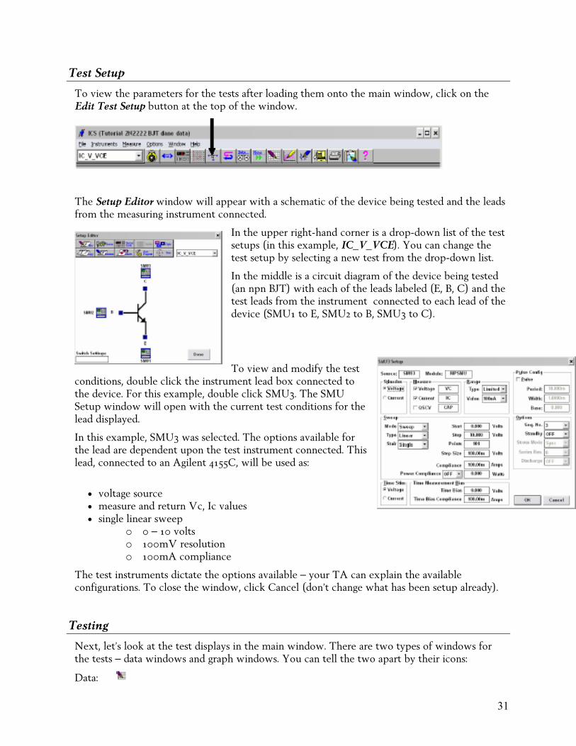
Test Setup
To view the parameters for the tests after loading them onto the main window, click on the Edit Test Setup button at the top of the window.
The Setup Editor window will appear with a schematic of the device being tested and the leads from the measuring instrument connected.
In the upper right-hand corner is a drop-down list of the test setups (in this example, IC_V_VCE). You can change the test setup by selecting a new test from the drop-down list.
In the middle is a circuit diagram of the device being tested (an npn BJT) with each of the leads labeled (E, B, C) and the test leads from the instrument connected to each lead of the device (SMU1 to E, SMU2 to B, SMU3 to C).
To view and modify the test conditions, double click the instrument lead box connected to the device. For this example, double click SMU3. The SMU Setup window will open with the current test conditions for the lead displayed.
In this example, SMU3 was selected. The options available for the lead are dependent upon the test instrument connected. This lead, connected to an Agilent 4155C, will be used as:
• voltage source • measure and return Vc, Ic values • single linear sweep
o 0 – 10 volts o 100mV resolution o 100mA compliance
The test instruments dictate the options available – your TA can explain the available configurations. To close the window, click Cancel (don’t change what has been setup already).
Testing
Next, let’s look at the test displays in the main window. There are two types of windows for the tests – data windows and graph windows. You can tell the two apart by their icons:
Data:
31
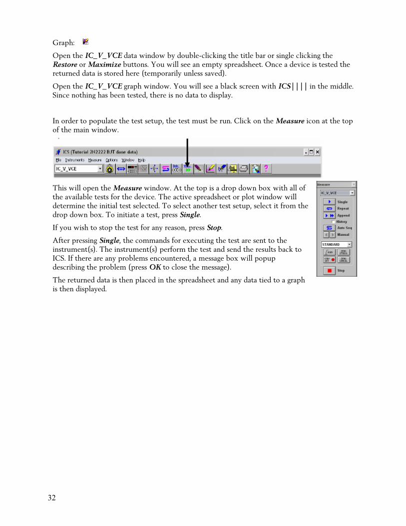
Graph:
Open the IC_V_VCE data window by double-clicking the title bar or single clicking the Restore or Maximize buttons. You will see an empty spreadsheet. Once a device is tested the returned data is stored here (temporarily unless saved).
Open the IC_V_VCE graph window. You will see a black screen with ICS|||| in the middle. Since nothing has been tested, there is no data to display.
In order to populate the test setup, the test must be run. Click on the Measure icon at the top of the main window.
This will open the Measure window. At the top is a drop down box with all of the available tests for the device. The active spreadsheet or plot window will determine the initial test selected. To select another test setup, select it from tdrop down box. To initiate a test, press Single.
he
If you wish to stop the test for any reason, press Stop.
After pressing Single, the commands for executing the test are sent to the instrument(s). The instrument(s) perform the test and send the results back to ICS. If there are any problems encountered, a message box will popup describing the problem (press OK to close the message).
The returned data is then placed in the spreadsheet and any data tied to a graph is then displayed.
32

Transforms
Not all data can be directly measured. An example would be transconductance of MOSFET devices (the derivative of Id with respect to Vg). To create a transform, click on the Transform Editor button.
The Transform Editor window will open with the active setup as the default setup.
To add a transform, type in a name for the transform in the box labeled
Transform: and set it equal to the mathematical expression desired. For example:
gm = DIFF(ID,VG)
The available functions are listed in the function box. You can add the variables measured by selecting the appropriate variable name under Vectors. Common constants are also listed.
Once created, click Save. The transform is then listed in the larger box. When you are done adding transforms click on Done.
33
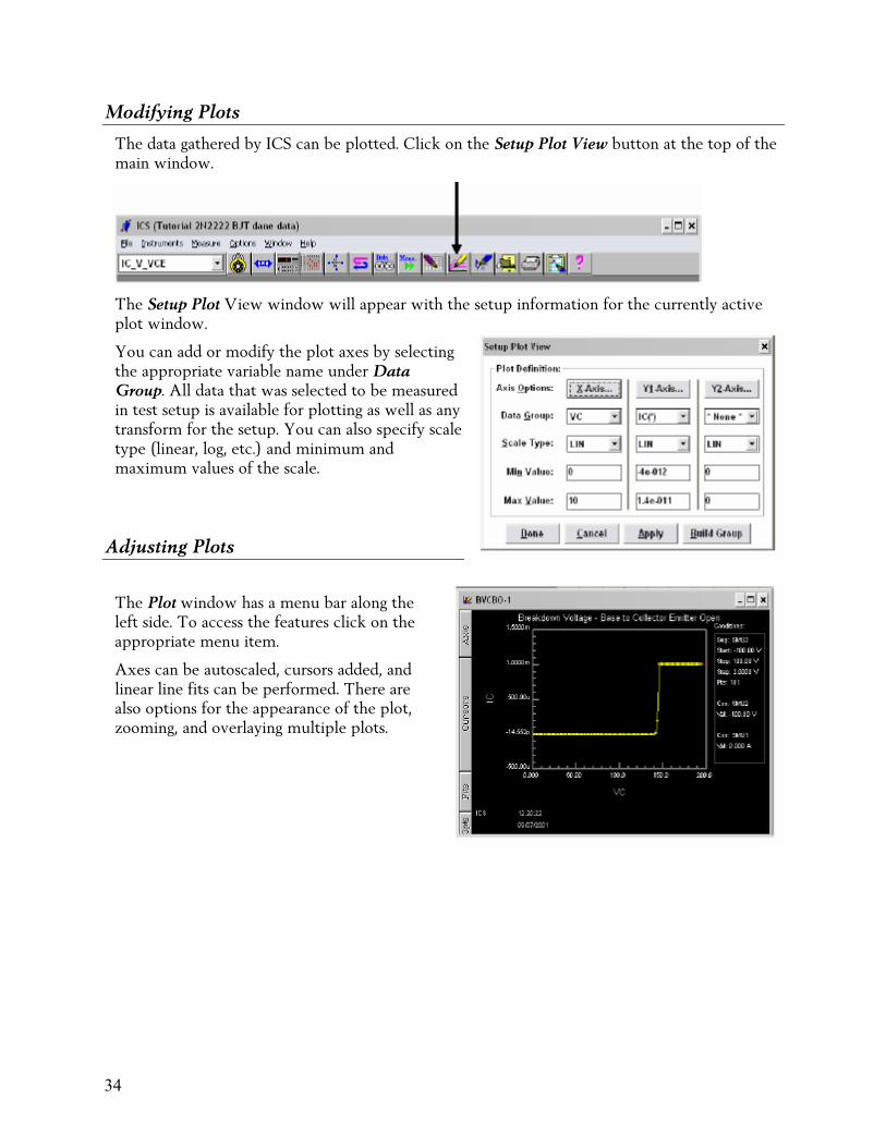
Modifying Plots
The data gathered by ICS can be plotted. Click on the Setup Plot View button at the top of the main window.
The Setup Plot View window will appear with the setup information for the currently active plot window.
You can add or modify the plot axes by selecting the appropriate variable name under Data Group. All data that was selected to be measured in test setup is available for plotting as well as atransform for the setup. You can also specify scaletype (linear, log, etc.) and minimum and maximum values of the scale.
ny
Adjusting Plots
The Plot window has a menu bar along the left side. To access the features click on the appropriate menu item.
Axes can be autoscaled, cursors added, and linear line fits can be performed. There are also options for the appearance of the plot, zooming, and overlaying multiple plots.
34

Appendix B - Evaporators
LDS-7211 Evaporator The LDS 18-7211 was designed in the Spring 2003 semester to replace the Varian 3120, which suffered from high maintenance costs. It also supplements the Cooke 301, which can only do a limited number of wafers with unpredictable metal thickness results. The 7211 was custom-built specifically for the ECE444 laboratory by Dane Sievers and Leon Schneider. It allows for nine 4” wafers to be done at one time under extremely high vacuum, with very good, predictable results.
As with most high-vacuum systems, the 7211 consists of two pumps: the roughing pump (a Leybold D65BCS), which pumps from atmospheric pressure (~760 Torr) to low vacuum (~10^-2 to 10^-3 Torr), and the high-vacuum pump (a Leybold TMP1000C), which takes over from low vacuum and pumps to high vacuum (~10^-7 Torr).
The 7211 uses a turbomolecular or ‘turbo’ pump as its high-vac pump. A turbo pump works similar to a jet engine. The pump’s intake will be connected to the vacuum chamber, and spinning blades in the pump will pull particles from the chamber through the pump and out the exhaust. Turbo pumps tend to be quiet, fast, and efficient.
Thin film deposition can be done by many methods. The 7211 uses one of the simplest. Once the atmosphere is sufficiently removed for a clean deposition, aluminum will be boiled by an electrically heated filament, coating everything within sight of it, including the wafers.
Theory of Operation
Many parts for the LDS 7211 were chosen based on their availability, provided they would not compromise the robustness and functionality of the overall system.
Turbo Pump
The high-vacuum pump, a Leybold TMP1000C, is a turbomolecular pump featuring grease-lubricated bearings. Turbomolecular (or ‘turbo’) pumps work on the basis of momentum transfer of particles.
Turbo pumps have a series of balanced spinning rotors along the main axis of the pump. The pump is usually connected directly to the vacuum chamber with a high-vacuum valve between the pump and chamber. The gas to be pumped out of the chamber arrives at the pump through the large aperture at the top of the pump. When the particles impact the spinning rotors, momentum is transferred from the rotor to the particle with a downward velocity component. The rotors at the top of the pump have a sharper angle than those at the bottom. Thus, the particles will continue to move downward along each stage of the pump. The bottom stages have rotors with a very small angle, essentially compressing the gas down to foreline pressure and pushing it out the foreline (exhaust) side.
35

Turbo pumps work from a range of ~10-2 Torr down to less than 10-10 Torr. At pressures above 10-2, the molecular flow of gases turns into a laminar viscous flow, which causes excessive loading of the motor due to frictional drag. A pressure of ~10-2 must be maintained on the foreline (exhaust) side of the pump to ensure extreme pressure differences do not cause the pump to fail. With the proper procedures followed, the pump is very reliable and requires little to no maintenance.
The TMP1000C operates at 36,000 rpm when at full speed, with acceleration, deceleration, and operational speed controlled by a Leybold Turbotronik NT1000 frequency converter. The NT1000 is extremely simple to operate, with only ‘Start’ and ‘Stop’ buttons, and provides feedback to the user about current pump status.
Upon bringing the chamber up to atmosphere, a pneumatic airing valve and a manual needle valve are used to stop the spinning rotors by bringing the pump to atmospheric pressure.
Roughing Pump
The roughing pump, a Leybold D65BCS, provides two functions in the 7211. First, it pumps the vacuum chamber from atmospheric pressure down to low vacuum (~10-2 Torr). Second, it maintains vacuum on the foreline side of the turbo pump, ensuring that the turbo will function properly.
The D65 is an oil-sealed two-stage rotary vane pump. This type of pump consists of two chambers, each of which has a rotor with a vane attached to it that extends to the chamber wall. In the first chamber (the high-vacuum chamber), air is drawn in at the pump inlet by the spinning rotor. The vane pushes the air forward into the inlet of the second chamber (the roughing chamber). In the roughing chamber, its vane pushes the air from the first chamber out the exhaust of the pump. The oil seal provides lubrication, and provides a vacuum seal in the chambers. A two-stage rotary vane pump can achieve a lower pressure than a single-stage pump because the oil has a much smaller chance of coming into contact with the normal atmosphere where it can adsorb gas, which can then enter the high-vacuum side of the pump due to the circulation of the oil.
Pressure Transducers
The 7211 uses a total of three pressure transducers. Two of these are connected directly to the vacuum chamber and measure low vacuum and high vacuum separately, and the third is connected to the foreline side of the turbo pump. Two different types of transducers are used: cold-cathode gauges and GP Convectron gauges.
The high-vacuum gauge connected to the chamber is a HPS Type 423 I-Mag cold-cathode gauge. Cold-cathode gauges are electrical gauges, meaning that they measure pressure indirectly, in terms of the number density of molecules. Cold-cathode gauges fall under a specific category of electrical gauges, called ionizations gauges, which use electron impact to produce a measurable ion current.
Cold-cathode gauges contain two unheated electrodes between which a discharge of electrons will occur at high electric field strengths. The discharge is produced through a dc voltage and maintained with the assistance of a magnetic field so that the discharge will continue at extremely low pressure. Cold cathode gauges can measure a pressure no greater than ~10-2 Torr, as above that pressure the discharge, and thus the current, depends insignificantly on the pressure. Above the ~10-2 Torr limit, the cold cathode gauge should be powered down through its control system to prevent any damage. The HPS Type 423 gauge used in the 7211 measure
36
down to ~10-10 Torr, is compact, and relatively inexpensive. There is no internal filament, thus making the gauge more resistant to vibration, debris, and sudden inrushes of air (a necessity for students!).
The other two gauges in the 7211, the low-vacuum chamber gauge and the foreline gauge, are Granville-Phillips Type 275 Convectron gauges. These are enhanced Pirani gauges which provide rapid response, a wide range of pressure transduction, stable operation, and good accuracy. The main sensor, which forms one branch of a Wheatstone bridge, is a very fine heated wire. The wire will cool down when gas molecules strike it, thus it will lose more heat as the gas pressure surrounding it increases. The heat lost from the sensor is determined by measuring the heating power that is delivered to it, while the Wheatstone bridge maintains the sensor at a constant temperature.
The Convectron is similar to a Pirani gauge but adds convection cooling to extend the measurement range up to 1000 Torr. A relatively large volume inside the gauge allows convection currents to develop. A larger wire wrapped around a cylinder enclosing the sensor, called a compensator, adjusts the operation of the gauge so that it performs relatively independent of the ambient temperature. The GP 275 measures from 1000 Torr down to approximately ~10-3 Torr.
To control the pressure transducers and provide feedback to the user, the LDS 7211 uses an MKS146A Vacuum Gauge Measurement and Control System. The 146A can monitor up to four vacuum gauges of varying types and provides readings from atmosphere down to ~10-10 Torr. For each gauge, the 146 can display the current measured pressure or the leakage rate at that gauge. Additionally, the 146 can be used to control valves, trigger alarms, and provide computer control via RS-232. These options are currently not in use, and the entire instrument is operated manually.
IC6000
The IC6000 deposition controller provides both accurate film measurement and total deposition control.
Six different film programs can be entered, each with 37 different specifiable operating parameters.
The data display gives the deposition rate, thickness, power, process time, crystal condition information, and an analog record of the quality of rate control.
When the aluminum deposition is actually performed, the deposition controller, in conjunction with a Concordia power supply, is used to control and monitor the process. The IC6000 and power supply can be used as totally automated instruments, completing the entire deposition process automatically through predefined recipes.
The IC6000 allows for different film types (gold, aluminum, etc.), different rates, and a variety of features. In its current use, the IC600 simply monitors the deposition rate and total amount for a given film type. Monitoring is done with a Leybold crystal sensor located at the same level as the wafers.
Concordia AC Power Supply
The Concordia ac power supply is used to supply the high current necessary to melt and evaporate the aluminum pellets. The current is adjusted with a rotary knob on the unit and displayed on a digital readout.
37

Chamber and Chassis
The support system, planetary, and other mechanical components were all designed or modified specifically for use on the 7211. The support structure was created to allow for balance and stability of the entire system, while allowing students to quickly gain an understanding of the entire process flow. Additionally, the current design makes system upkeep and repair relatively easy for a system this size.
The hoist system for the bell jar, part of the old Varian 3120 evaporator, was modified to support the new jar and provide a counterweight system, increasing stability.
Inside the vacuum chamber, the power supply system, in the simple shape of two parallel copper bars, provides an easy way to add aluminum pellets to the system and replace the boats in case of breakage.
The wafer holder, which holds nine 4” wafers simultaneously, is well above the aluminum pellets, ensuring uniform coating of all wafers. It also is not permanently attached to the vacuum chamber, making future upgrades to larger and different wafer sizes easy.
The valve system, with the exception of the manual needle valve for the turbo pump, is done pneumatically. Each valve is controlled by a solenoid, which is in turn controlled by a series of relays and switches in the equipment panel. The relay system allows for interlocks to be integrated, ensuring correct system operation. A ladder diagram of the relay system is included in the attached list of figures.
38

Operating Procedures
Bring up from Standby
• At standby, the system should be running under high vacuum to minimize water condensation in the system.
• Close the high-vac valve.
• Turn off the cold cathode gauge by pressing ‘Off’, then ‘1’ on the MKS146.
• Wait 15 seconds to ensure the high-vac valve is closed.
• Open the vent valve.
• Switch to the foreline Convectron (Channel 2) on the MKS145 by pressing ‘2’. This pressure should never exceed 15 mTorr (5x10⁻² Torr).
• Once the chamber is at atmosphere, raise the bell jar.
• Remove the wafers. Leave any dummy wafers in the planetary.
Loading
• Carefully load 4” wafers face down in the planetary and place the wafer cover over the wafer.
• If less than nine wafers are being processed, fill the remaining holes with the wafer covers.
• Double-check to make sure the crystal sensor has clear access to the inside of the planetary. Check the metal boats for cracks. Replace if cracks are visible.
• Take two aluminum pellets and clean with acetone. Use tweezers to load one into each of the metal boats.
• Close the planetary door.
• Lower the bell jar until it is seated on the sealing surface.
39

Pump Down
• Close the foreline valve.
• Wait 5 seconds to ensure the foreline valve is fully closed.
• Open the roughing valve.
• Monitor the foreline pressure. If it exceeds 15 mTorr, then
o Close the roughing valve.
o Wait 10 seconds to ensure the roughing valve is closed and that the pump is at a pressure less than the foreline pressure.
o Open the foreline valve until the foreline pressure is < 10 mTorr.
o Close the foreline valve.
o Wait 5 seconds and open the roughing valve.
• Once the chamber Convectron (Channel 3) reaches about 30 mTorr (3x10⁻²), close the roughing valve, wait 5 seconds, and open the foreline valve.
• Open the high-vac valve
• On the MKS146, press ‘On’, then ‘1’ to turn on the Cold Cathode Gauge
• Start the timer to monitor the pumpdown time.
Evaporation
• Once the Cold Cathode Gauge (Channel 1) has reached a pressure range of at least 10-6 Torr, evaporation can begin.
• Make sure the Local Power Adjust knob is all the way down on the power supply, and that the Local Power Output is set to 1.
• Turn on the power switch to the power supply. A reading of five to six Amps should appear immediately on the digital display.
• Press ‘FLM#’, then ‘6’ to set up the system for Aluminum operation. Gold is selected by default and must not be used.
• Press ‘START’. The controller will go through several stages:
o Ramp 1: increases current through filaments at a controlled rate.
o Soak 1: allows aluminum to heat up.
o Ramp 2: increases current through filaments to a level that begins evaporation.
• The IC6000 readout should begin to show evaporation occurring at 17-20 Amps. The top left readout will show the evaporation rate in Angstroms/s, while the top right readout will show the total accumulated metal evaporated. The rate should be 10-15 Angstroms/s normally.
• Once 2000 Angstroms have been deposited on the wafers, turn the power supply off.
40

Bring to Atmosphere
• Close the high-vac valve.
• Turn off the cold cathode gauge by hitting ‘Off’, then ‘1’ on the MKS146.
• Wait 15 seconds to ensure the high-vac valve is closed.
• Open the vent valve.
• Switch to the foreline Convectron (Channel 2) on the MKS145 by pressing ‘2’.
• Once the chamber is at atmosphere, raise the bell jar.
• Remove the wafers. Leave any dummy wafers in the planetary.
Standby
To put the system into standby, follow the same procedures as for Pump Down.
41

Schematics
Figure 1: System Overview
42

Figure 2: Ladder logic for valve relays
References
Leybold Vacuum, Inc., “Vacuum Technology: Its Foundations, Formulae and Tables”, Ch. 2, 3.
www.helixtechnology.com, Vacuum Gauge Product Tour
MKS Instruments, “MKS Type 146A Vacuum Gauge Measurement and Control System Reference”
www.mksinst.com, Cold Cathode Sensor Product Page
www.leyboldvacuum.com, Leybold Turbomolecular pumps product page
Leybold-Inficon, “Leybold IC6000 Deposition Controller Manual”
43

Cooke CVE301 The Cooke CVE 301 is a low cost one button pump down vacuum evaporator. Although it can pump down from a standby state with the push of a button, you will be operating the system in manual mode. This means you must have an understanding of how the system works.
The basic concept of a diffusion pump is to remove the atmosphere that diffuses into jets of boiling hot oil directed away from the chamber. The momentum transfer from the diffusion pump oil molecules to the atmospheric particles carries the undesirable atmosphere away so it cannot contaminate the film to be deposited. The pumping mechanism is not unlike the cause of the wind that one feels at the bottom of a waterfall on a calm day.
Complications arise from the fact that no diffusion pump oil known is capable of pumping from atmospheric pressure to more than eight orders of magnitude below. The problem is oxidation of the pump oil. It proceeds at an unacceptable rate at pressures above about 10-4 atmospheres. Therefore a mechanical pump must be employed to keep the pressure at either end of the diffusion pump below 100 microns when the diffusion pump oil is hot. Your responsibility will be to make sure the valves are sequenced properly to keep the oil from "cracking" (a term for rapid oxidation of pump oil)..
The special property that distinguishes diffusion pump oil from other oils is that it can be recycled within the diffusion pump. See figure 1. Water cooled side walls of the pump body condense virtually all the diffusion pump oil. The oil is then re-boiled (high vapor pressure) at the base of the diffusion pump while the mechanical pump removes other particles swept down by the oil jets.
Diffusion pump oil does have a measurable vapor pressure of its own, even at the cooling water temperature. The price goes up as that vapor pressure goes down. To keep diffusion pump oil from diffusing up into the chamber, first a water cooled (chevron) baffle and then a liquid nitrogen cooled "trap" are used to contain the oil. Both are "optically dense" meaning that light or particles with a mean free path greater than the system dimensions must collide with at least one surface. The cool surfaces will condense the majority of diffusion pump oil. The 77 K walls of the liquid nitrogen trap also enhance pumping speed by literally freezing out some of the atmosphere and compacting the rest (PV=nRT), a phenomenon called cryopumping.
Thin film deposition can be done by many methods. You will use the simplest. Once the atmosphere is sufficiently removed for a clean deposition, aluminum will be boiled by an electrically heated filament coating everything within sight of it. Aluminum has the useful property of clinging to the relatively inexpensive tungsten filaments when it melts rather than falling through.
44

ATM500 200 100 50 30
50
1010
1010 10
10-6-5
-4 -3-2
TC1 TC2
CONTROL POWER
OFF
ON
AUTO MANUAL
STOPSTART
RAISE
LOWER
LIFT ROUGHINGVALVE
VENTVALVE
TC1
TC2
FORELINEVALVE DIFFUSION PUMPMECHANICAL PUMP
VALVEHI-VAC
CC GAUGE
ON
OPEN
OPEN
OPEN
Figure 1
Control Panel of CVE-301
EMERGENCY PROCEDURE: A popular topic for lab final questions tests your response to high (>80 microns) pressure in a hot diffusion pump. If the foreline pressure ever does go too high, you should:
-Close the Hi-Vac valve. -Turn off the diffusion pump heater. -Make sure the mechanical pump is pumping through the foreline valve. -Mechanical pump should be running. -Roughing valve should be closed. -Foreline valve should be open. -Check for leaks if system is still not recovering. Pumping out the bell jar helps Hi-Vac leaks.
45

Operation of the Cooke 301
Warm Up (To be done by TAs only)*
1. Turn on the following utilities:*
a) Cooling Water (in chase behind evaporator)
b) N2 > 80psi (in chase behind evaporator)
2. Put the panel switches in the following positions:*
a) thermocouple gauge - TC1 (left)
b) cold cathode gauge - OFF (down)
c) vent valve - CLOSED (down)
d) hi vac valve - CLOSED (down)
e) roughing valve - CLOSED (down)
f) foreline valve - CLOSED(down)
g) mechanical pump - ON (up)
h) diffusion pump - OFF (down)
i) auto/manual - MANUAL (right)
j) mechanical pump vent (inside cabinet) - CLOSED
3. Turn on the power strip. The mechanical pump should start.*
4. Press CONTROL POWER ON. The MANUAL light should come ON.*
5. OPEN the FORELINE VALVE (up). Note: The system will not go into manual unless all the valves are momentarily closed.*
6. When TC1 reads < 50 microns, you may turn on the diffusion pump heater as long as TC1 stays below 100 microns. Turn off as necessary. Tend the unit long enough to be sure it will stay below 100 (at least 5 minutes!). Note the time when the diffusion pump was turned on.*
7. About 5 minutes after the diffusion pump is turned on, activate the cold cathode gauge. If it reads >0.01 torr, turn it off and try later. Cold Cathode gauges cannot reliably initiate ionization when the pressure is too low. The power supply can be damaged by excessive current when the pressure is too high, however.*
8. Switch to AUTO if it will be used in the automatic mode (usually not). Since this vents the system, it is best to wait until load time.*
* To be done by the instructor before class.
46

Prepare to Pump Down
The diffusion pump must be given at least 20 minutes to warm up before attempting to pump down (step 7 below).
Do not touch anything which must go into the vacuum with ungloved hands. Water, finger grease, and similar contaminants will severely slow down the pumping speed and decrease the MTBF (mean time between failures). It is good practice not to even touch anything which will touch anything which will touch anything ... which goes into the vacuum system.
1. Raise the bell jar carefully. If you can't raise the bell jar, cycle the vent switch if necessary until the bell jar can be raised. If in AUTO, switch to MANUAL, close (turn down) all the valve switches, and open (flip up) the foreline and vent switches.
2. Carefully lift the metal chimney straight up and place it on the glass plate or aluminum foil on the table. Be careful that any microscope slides do not slide off.
3. Load the filament(s) with three 0.025" diameter, 3cm long aluminum wires cleaned with IPA and a Kimwipe. By assuming that the entire volume of aluminum will be deposited uniformly in all directions, it is possible for you to calculate the thickness of the aluminum on your wafer if you measure the distance from the filament to your wafer. NOTE1: If a filament is broken or severely deteriorated, have your instructor look at it. If you plan to use both filaments in series, they should look nearly identical. If one seems more used than the other, then they should only be used one at a time. NOTE2: Always compare the configuration of the copper bars behind the door below the variac with the drawing below to see which filament(s) are active. Ask your instructor if you need a different configuration. Normally the filament on the front left (F1) will be used. NOTE3: Bent pieces of quartz are provided to prevent the aluminum from evaporating down into the diffusion pump. A third piece can also be used to prevent both filaments from evaporating through a metal mask and generating double images.
4. Carefully load wafers. It should go without saying that the thickest film will be on the wafers directly above an active loaded filament(s) so that is where your wafer should be.
5. Return the chimney assembly back to it's position.
6. If there are no uncoated areas left on the slides, replace them with an IPA and kimwiped slide and discard the old one(s).
7. Make sure there is no path for aluminum from a filament to the bell jar. Monitor slides should be placed over the small holes near the filaments. These get visibly coated during the evaporation.
8. Wipe down (with IPA on a kimwipe) as many surfaces as you can except for the bell jar gasket and surfaces inside the chimney/wafer holder assembly. The bell jar gasket has high vacuum grease on it which should never be removed. The inside of the chimney has layers of aluminum which flake off and get into the rest of the system when disturbed. The instructors will take care of excessive aluminum deposits.
9. Generally, time invested in cleaning is repaid with interest by a fast pump down.
10. Exercising extreme care, slowly lower the bell jar into position.
47

Manual Pump Down
Manual pumpdown can be dangerous to the system, but if done properly, it will be better for both the pump and the thin film. The operator can make sure the hot diffusion pump oil is never exposed to as much pressure as it often is during the automatic pump down sequence. The film quality can be better because the bell jar does not have to be evacuated as much by the mechanical pump before switching to the diffusion pump. Therefore, "backstreaming" of mechanical pump oil into the bell jar and onto the wafer is minimized. Cold traps or oil-free pumps are sometimes used to keep oil out of the bell jar.
The key concept to keep in mind during pump down is that the diffusion pump oil must never be exposed to more than 100 microns of pressure. For this reason, leave the thermocouple switch on TC-1 except for short periods to monitor TC-2. Always be ready to answer the question: What would you do if TC-1 suddenly went above 100 microns?
1. If not already in Manual mode, switch to Manual.
2. Close the foreline valve by flipping the switch downward.
3. While pressing the bell jar down onto the base plate, open the roughing valve by flipping its switch upward. You may take your hand away as soon as the mechanical pump begins to pull a vacuum on the jar.
4. Pour in a thermos full of liquid nitrogen.
5. WHILE TC-2 measures >80 microns, DO
a) Monitor TC-1, checking TC-2 only occasionally.
b) IF TC-1 > 80 microns THEN
i) Close roughing valve
ii) Wait 5 seconds
iii) Open Foreline valve until TC-1 < 20 microns.
iv) Close Foreline valve
v) Re-open roughing valve
c) END IF
6. When TC-2 = 80 microns, close the roughing valve
7. Wait 5 seconds.
8. Open the Foreline valve.
9. Wait at least 10 seconds for the Foreline pressure to "blank off" (reach its ultimate pressure).
10. If using an external cold cathode gauge controller, switch it to START now.
11. Open the Hi Vac valve. If the foreline pressure goes above 100 microns, close the Hi Vac valve until the foreline is settles back down to 80 microns, then open the foreline valve again. Observe how high the foreline pressure got. An external cold cathode gauge controller can now be safely turned to the appropriate scale to monitor the pump down.
48
Evaporation and Vent
When the cold cathode gauge reads less than 1x10⁻⁵ Torr you may perform the evaporation, but the lower the pressure, the better the film will be.
NOTE: If using an external gauge controller, return it to START before evaporating.
1. Rotate the variac control all the way to zero (CCW).
2. Turn on the power supply switch.
a) When two filaments are used in series, rotate the variac slowly clockwise (CW) to obtain and maintain a current of 40-50A for 5 seconds after the aluminum begins to darken the viewing slide. Then quickly return the variac to zero.
b) When a single filament is used by itself, 50 Amps may be used, which should result in complete evaporation in just 3 seconds after the monitor slide begins to darken. Excessive durations will deposit tungsten from the filament itself, as well as other materials nearby (most notably the Viton o-rings).
3. Turn off the power supply switch.
4. Wait about 20 seconds to allow the filament to cool.
5. Close the Hi Vac valve and then open the vent valve.
6. Wait 20 more seconds after the system has vented to allow further cooling in the nitrogen before exposing the hot surfaces to oxygen. Why?
7. Carefully, raise the bell jar and remove your wafers. If you can't raise the bell jar, it's probably because the vent cycle was incomplete. The following sub-steps are for additional venting if necessary:
a) Switch to MANUAL mode.
b) Close (flip DOWN) all the valve switches.
c) Open (flip UP) the foreline and vent valve switches.
d) Cycle the vent switch if necessary until the bell jar can be raised.
e) Close the vent valve.
8. Wipe out the system as in step 5. Keeping a vacuum system scrupulously clean is so important that the instructors will deduct lab performance points from persons ignoring this step.
9. Lower the bell jar even more carefully than before. Do not get careless with equipment as you get used to it.
Standby (To be done by TAs)*
1. Switch to MANUAL mode.*
2. Close all the valves.*
3. While pressing down on the bell jar, open the Roughing valve.*
4. Wait 30 seconds, then close the roughing valve.*
5. Wait 5 seconds, then open the foreline valve.*
49

Shutdown (To be done by the TA at the end of the day)*
During evaporation season in ece444 it is best to keep the system running in standby. The system should be off for the rest of the semester. The bell jar and diffusion pump body should be left under vacuum; however, the mechanical pump must never be left OFF with vacuum on one side of its seals and atmospheric pressure on the other. Therefore, the following procedure must be executed by the instructor.
1. Switch OFF (DOWN) the diffusion pump heater. It is strongly recommended that this be done immediately after the last students to use the system have vented (STOPPED). It will take about an hour for the diffusion pump oil to cool.*
2. Place the panel switches in the following positions (if they are not there already).*
a) thermocouple gauge - TC1 (left)
b) cold cathode gauge - OFF (down)
c) vent valve - CLOSED (down)
d) hi vac valve - CLOSED (down)
e) roughing valve - CLOSED (down)
f) foreline valve - OPEN (up)
g) mechanical pump - ON (up)
h) diffusion pump - OFF (down)
i) auto/manual - AUTO (left)
3. Switch to manual.*
a) auto/manual - MANUAL (right)
4. Close the foreline valve.*
a) foreline valve - CLOSED (down)
5. Open the roughing valve.*
a) roughing valve - OPEN (up)
6. Monitor TC2. Rough out the bell jar for 30 seconds or until TC2 reaches 80 microns. Whichever is less. Return to monitoring TC1.*
7. Close the roughing valve.*
a) ROUGHing valve - CLOSED (down)
8. Wait 2 seconds.*
9. Open the foreline valve.*
a) foreline valve - OPEN (up)
10. Wait until ALL parts of the diffusion pump body (behind the main access door) are cool enough that you could rest your hand on them indefinitely.*
11. When the diffusion pump is cool, close the foreline valve.*
12. Turn off and vent the mechanical pump. Use the manual vent valve behind the access door.*
50

13. Unplug the main power cord. (I disagree with the microprocessor's program. A power glitch would open the foreline valve.)*
14. Turn off the other utilities.*
a) cooling water - OFF (unless liquid nitrogen was used within the last hour)
b) nitrogen - OFF
*To be done by TAs after class only.
51

52

Appendix C - Wafer Cleaning Two methods are used for cleaning wafers in the ECE 444 lab. The first is simple degreasing. The other is the industry standard RCA clean.
Both procedures are posted in the wet lab area so you do not need to take your copy of this into the area. Not only is space limited, but paper is very dirty and dusty by semiconductor industry standards. There is no point in carefully cleaning a wafer if it is not kept in a clean environment. Use your individual wafer carriers to keep your wafer clean and safe from accidents after either of these cleaning procedures.
Degreasing Procedure*
The term degrease refers to the removal of the grime that often coats surfaces exposed to the atmosphere. The thin film is mostly organic in nature and is probably due to the presence of humans. 1,1,1 Trichloroethane (TCA) is particularly effective in dissolving this "grease" which is why it is commonly used in industry. Substitutes must be found, however, since compounds containing halogens (chlorine, fluorine, and bromine) are destroying our ozone.
Simple Degreasing
1. Hold wafer flat over the solvent waste container.
2. Squirt acetone over the front and back sides of the wafer.
3. Repeat step 1 using IPA.
4. Rinse wafer with DI water (either from the faucet or spray gun).
5. Repeat step 1 using IPA
6. Hold the wafer at a steep angle (~80°) and rest it against the drying block (make sure a clean wipe is covering the block).
7. Using the N2 blow gun, start at the top of the wafer and ‘chase’ the IPA down the wafer. Repeat for the back side of the wafer. Alternate front and back until all moisture is gone. Make sure that the area under the tweezers is also dry.
Note: Acetone and IPA should be used over the "waste acetone and IPA" container. Always put the lid back on the waste container when finished.
Note: Acetone dissolves organic residue. IPA dissolves acetone residue and some residues not soluble in acetone. Water dissolves IPA residue and some residues not soluble in acetone or IPA. The final IPA rinse is only for making it easier to dry the wafer.
53

The RCA Clean
This cleaning method is the industry standard for cleaning wafers. Although every company has its own way of implementing the RCA clean, and many have introduced their own proprietary improvements, they have all been significantly influenced by the work of Kern, a chemist at RCA. One of his articles is included at the end of this appendix. Please read it. Below is the recipe for our particular implementation. We substitute sulfuric acid for hydrochloric acid as described in the other article at the end of this appendix. Ideally, if we had time, we would use this procedure before every diffusion furnace operation.
Preliminary Clean
Transfer the wafers to a Teflon wafer carrier specifically reserved for the RCA clean. This step is often performed while SC-1 is warming up.
1. Securely mount the Teflon wafer carrier handle, also reserved for the RCA clean.
2. The wafers should be degreased before continuing. The SC-1 solution can be prepared during the degreasing procedure.
3. Etch the wafers for 30 seconds in the 50:1 DI:HF etch.
SC - 1: Remove residual organics and certain metals using the RCA Standard Clean Solution 1
1. Rinse the quartz tub, temperature sensor and thermometer under the SC-1 hood.
2. Place the tub on the hotplate with the temperature sensor and thermometer inside.
3. Add 1800 ml of deionized water.
4. Turn on the temperature controller. It has been set for 75° C. NOTE: Whenever handling strong chemicals it is a very good idea to have DI slowly flowing from a faucet first. Not only will it help dilute accidental spills, but it allows you to rinse your gloves without getting the faucet valve contaminated. Always use the green nitrile gloves over the thin gloves when handling strong chemicals and rinse them afterward!
5. Slowly add 360 ml of 30% hydrogen peroxide.
6. Slowly add 180 ml of 58% ammonium hydroxide. Be sure to rinse the green nitrile gloves, the graduated cylinder, and the outside of the chemical containers with DI when finished.
7. Slowly stir the solution with a thermometer (don't break it!).
8. Slowly place the wafer carrier into the solution.
9. Occasionally stir the solution until it has been over 75°C for 10 minutes.
10. After the 10 minute clean, immerse the wafer carrier in the DI Rinse tank for 15-20 seconds.
11. Spray rinse the wafer carrier and as much of the handle as you can without getting your glove wet. Remember, at this point a drop of water from a relatively dirty glove could compromise the whole cleaning process.
12. Move the wafer carrier to the cascade rinse tank for at least 2 minutes.
NOTE: While waiting for the temperature to rise it is possible to begin preparation of the SC-2 solution. Do not forget to occasionally stir and check the temperature of the SC-1 solution!
54

Prepare SC-2 solution
1. Rinse the quartz tub, temperature sensor and thermometer under the SC-2 hood.
2. Place the tub on the hotplate with the temperature sensor and thermometer inside.
3. Add 1820 ml of deionized water.
4. Turn on the temperature controller. Verify that it is set for 80°C.
5. Slowly add 320 ml of 30% hydrogen peroxide.
6. Slowly add 110 ml of sulfuric acid.
7. Occasionally stir the solution with the thermometer.
8. When the solution has reached 75°C, continue.
Strip hydrous oxide
1. Move the wafer carrier to the 50:1 HF:DI tank for 15 seconds.
2. Agitate the carrier in the DI rinse tank for 20 to 30 seconds.
Desorb remaining contaminants
1. Place the wafer carrier in the hot SC-2 solution for 10 minutes.
2. Turn off the temperature controller.
3. Carefully move the wafer carrier to SC-2 DI rinse tank for 20 seconds.
4. Spray rinse the wafer carrier and as much of the handle as you can without getting your glove wet. Remember, at this point a drop of water from a relatively dirty glove could compromise the whole cleaning process.
5. Move the wafer carrier to the cascade rinse tank for 5 minutes. Kern recommended 20 minutes.
Dry the wafers
1. Rinse the special handle for lifting the wafer carrier from one end and switch it with the other handle.
2. Load the wafer carrier into the Verteq spin-rinse-dryer and press start.
3. Wait for the rinser dryer to stop by itself. Use the time wisely (e.g. prepare for the subsequent furnace operation).
4. Return the wafer carrier to the rinser-dryer after removing the wafers.
5. Clean and reorganize the area. If the next days' instructor discovers the telltale crystals of dried acid, your whole group will lose performance points.
55

56

Hydrogen peroxide solutions for silicon wafer cleaning – W. Kern
The “RCA Standard Clean” process is so well known throughout the semiconductor industry that many may not know its RCA origins. Further refinements are described in this article. Abstract: Clean silicon wafer surfaces suitable for device fabrication have been prepared successfully for nearly 20 years by the simple and safe sequential process described in this paper. The process is based on oxidation and dissolution of residual organic impurities and certain metal contaminants in a mixture of H20-NH3OH-O2O2 at 75 to 80°C, followed by dissolution and complexing of remaining trace metals and chemisorbed ions in H2O-HCl-H2O2 at 75 to 80°C. The effectiveness of the method was demonstrated originally by radioactive-tracer techniques, and was later confirmed by extensive analytical studies and device reliability tests.
The RCA method has become widely accepted in the semiconductor industry. The original paper, published in 1970, is one of the most frequently cited publications in its field. The present report traces the development of the process since its origin in 1961, notes the supporting data from radioactive-tracer studies, and summarizes the essential facts underlying the effectiveness of the process. Additional information obtained more recently on the process and its implementation is briefly presented. An outline of the processing procedures that are now recommended has also been included.
©1983 RCA Corporation Final manuscript received June 1, 1983 Reprint RE-28-4-9
The RCA method for chemically cleaning silicon wafers has become widely accepted in the semiconductor industry. The original paper1 is one of the most frequently cited publication in its field, according to the Science Citation Index. The Institute for Scientific Information has requested a commentary on this work for publication in the “Citation Classics” section of Current Contents.2 The present paper traces the historical development of the process since its origin in 1961, notes the supporting data from radioactive-tracer studies, and summarizes the essential facts underlying the procedures. An outline of the recommended processing procedures has been included in an accompanying box. Need and requirements of a cleaning procedure The work published in our 1970 article originated in 1961 at the RCA Solid State Division is Somerville, New Jersey, when it was realized that residual trace impurities on silicon surfaces prior to high-temperature processing - particularly diffusion, thermal oxidation, and epitaxial growth - can have detrimental effects on surface stability, reliability, electrical performance, and production yield of devices, especially sensitive metal-oxide-semiconductor types. It became clear to me that a highly effective yet simple and hazard free process was needed for purifying pre-cleaned silicon wafers, as well as thermally oxidized patterned or unpatterned wafers.
The procedures used up to that time involved hot mixtures of concentrated sulfuric acid and hydrogen peroxide, or of concentrated sulfuric acid and chromic acid. The first was suspected of causing sulfur contamination and was extremely hazardous when used by operators in a production environment. The second was suspected of leading to chromium contamination and posed serious ecological problems of disposal. Clearly, a procedure was needed that was effective, free of contaminants introduced by the reagents, safe, economical, and ecologically acceptable. Chemical considerations The new cleaning method to be developed had to first be based on first removing organic contaminants (such as grease films and photoresist residues masking the surface) to expose the wafer surface and render it hydrophilic (“water loving”)., thereby rendering it accessible to aqueous chemical reagents. This step would then be followed by the removal of inorganic contaminants (such as trace metals and chemisorbed ions). Ideally, the reagents to accomplish these objectives had to be completely volatile and commercially available at high purity and low cost.
On the basis or reaction chemistry and reagent purity, water diluted, unstabilized hydrogen peroxide at high pH, attained by the addition of ammonium hydroxide solution appeared to be the ideal reagent for removing residual organic contaminants by oxidative breakdown and dissolution, if used at an elevated temperature for a suitable period of time. In addition, this solution would also remove several types of metals such as Cu, Ag, Ni, Co, Cd, and Au, due to complexing by the ammonium hydroxide.
For the second solution, I selected diluted hydrogen peroxide at low pH, prepared by adding hydrochloric acid solution. Used again at elevated temperature, this solution was to remove alkali ions and remaining metallic impurities. Displacement replating of heavy metals from solution would be prevented by the formation of soluble complexes with the resulting dissolved ions.
Deionized, distilled, and microfilterd water served as the diluent and rinsing agent. To prevent leaching of alkali and boron from Pyrex® (DuPont), and wafer holders of Teflon® (DuPont), and conducted systematic experiments for establishing optimal processing conditions and solution concentrations. Surface chemical analysis techniques and radioactive-tracer measurements served as very sensitive analytical methods for evaluating the efficiency of various cleaning processes in the course of this development.
The results of these experiments subsequently showed that the solution compositions are not critical for the effectiveness of the process, as long as one operates within volume ratios of 4:1:1 to 6:1:1 of H2O, 30 w/w% H2O2, and 29 w/w% NH4OH (as NH3) for the first mixture, and 4:1:1 to 6:1:1 of H2O, 30 w/w% H2O2, and 37% HCl for the second mixture. Treatment periods of 10 to 20
57

minutes are sufficient. The solution temperature can be maintained at 75 to 85°C, but preferably should not exceed 80°C. A higher temperature would cause rapid decomposition of the hydrogen peroxide. Radiochemical contamination and cleaning efficiency studies Concurrent with these studies I investigated the origin, cause, type, and concentration of contaminants by adding trace quantities of radioactive cations (Na22, Na24, Au198, Cu64, Fe59, Cr51, Zn65, Sb122, Sb124, Mn54, Mo99) and anions (F18, Cl38, I131, C14 - organics) to numerous etchant and reagent solutions. Radioactivity measurements, autoradiography, and gamma-ray spectroscopy of electronic solids (Si, SiO2, Ge, GaAs) treated with these tagged solutions allowed quantization of the resulting surface concentrations of specific impurities, both initially and after various rinsing and cleaning steps with the hydrogen peroxide mixtures noted.3-8
Application to silicon device production By mid-1960, the peroxide cleaning technique (dubbed “SC-1” and “SC-2” to denote “Standard Clean, Solutions 1 and 2” - see box) was well established and widely applied at RCA in the fabrication of silicon devices. A process patent that incorporated the HCl-H2O2 desorption process was issued to RCA in 1966.9 Also in 1966, I received an RCA Outstanding Achievement Award shared with James A. Amick and Arthur I. Stoller “for new technological advances for processing integrated circuits,” which included the peroxide method for attatining practically clean silicon surfaces in conjunction with glass-passivation and tungsten-metallization processes. Publications In 1970 I succeeded in obtaining permission to publish the series of papers on the radiochemical studies and the peroxide cleaning process: the latter incorporated the contributions of my co-author, David A. Puotinen, who had studied in some detail several aspects of peroxide cleaning as applied to silicon device processing.
Several of my colleagues contributed also to the success of this work, particularly Norman Goldsmith and James A. Amick10 during the development and implementation that extended over several years, and Alfted Mayer who introduced megasonic (ultrahigh-frequency) peroxide cleaning at low temperature (explained below), effectively combining the removal of particulates with the desorption of adsorbed contaminants. Introduction of additional process step An additional step in the procedure, which was not explicitly noted in our original paper because of insufficient data at that time, is the application of a brief etch in dilute HF solution after the SC-1 cleaning. I reasoned that removal of the hydrous oxide film formed during the SC-1 treatment to reexpose the silicon surface for the subsequent SC-2 desorption step should further increase the purification efficiency. However, this etching should be done with a very dilute high-purity HF solution and for a very short period of time to avoid replating of the metallic contaminants from the HF solution on the silicon surface.
Experiments have shown that a 10-second immersion in 1:50 HF-H20 is sufficient to remove this film, as evidenced by the change of the hydrophilic oxidized surface to a hydrophobic surface, which is characteristic for a fluoridated, organic contaminant-free silicon surface. Subsequent water rinsing should also be kept very brief (30 seconds), serving only to remove HF solution from the wafer assembly in order to minimize regrowth of a new hydrous oxide film Fortunately, change of a ≡Si-F surface to a ≡Si-OH surface in cold H2O is very slow, minimizing rapid regrowth of a hydrated oxide film.5 We believe that this additional step does indeed enhance the effectiveness of the subsequent SC-2 treatment, and should be part of the cleaning sequence. Reasons for popularity of cleaning procedure The original paper of 1970 has been highly cited because extensive analytical studies and device reliability and life testing by many independent researchers have confirmed the process, now widely known as “RCA Standard Clean,” to be the most effective cleaning method known for attaining the degree of purity that is imperative in the fabrication of sensitive silicon semiconductor devices. Furthermore, the process is safe and relatively simple, has attractive economic and ecological advantages, uses readily available high-purity solid free and volatile reagents, and was accepted by the American Society for Testing and Material as a standard procedure.12 Actually the process is so widely employed that most authors refer to it without citing our original work, apparently assuming it to be common knowledge. Developments since 1970 The following section reviews the more important literature references on silicon wafer cleaning with SC-1 and SC-2 hydrogen peroxide solutions. These references confirm our original statements and contribute additional new information on the subject.
Henderson13 published results in 1972 on the analytical evaluation of the SC-1/SC-2 cleaning process by high-energy electron diffraction and Auger electron spectroscopy. He concluded that the process is well suited for silicon wafer cleaning prior to high-temperature treatments, as long as quartzware is used for processing, according to our specifications, to avoid boron contamination from Pyrex® containers. He also examined the possible benefits of an additional final etch treatment in concentrated HF after completion of the SC-1/SC-2 steps, but found that it enhances carbon contamination and causes surface roughening during vacuum heating at 1100°C due to loss of the protective 15-angstrom thick carbonfree oxide film remaining after the SC-2 step. Reexposure of a bare silicon surface to HF after SC-2 would, of course, be ill advised because of recontamination with metallic impurities, obliterating the advantages of peroxide cleaning.
Meek et al, (1973)14 investigated the removal of inorganic contaminants, including copper and heavy metals, from chemically/mechanically polished silicon wafers by several reagent solutions. Using Rutherford back-scattering with 2-MeV He+ ions as an analytical tool, they concluded that the SC-1/SC-2 as preoxidation cleaning process always removed all elements heavier than chlorine to below the level of detectability. Sulfur and chlorine remained after either SC-1, SC-2, or other cleaning procedures
58

studied at levels of about 1013/cm2. SC-1/SC-2 cleaning eliminated calcium and copper much more reliable than did HF-HNO3 treatments.
Murarka et al, (1977)15 studied methods for oxidizing silicon without the formation of stacking faults. They concluded that chemical cleaning of the wafers with SC-1/SC-2 prior to an oxidation is an essential requirement to ensure the complete elimination of stacking faults after the high-temperature processing.
In 1978, we published a review16 of the entire field of surface contamination and semiconductor cleaning techniques as part of a book chapter on the chemical etching of thin films and substrates.
Gluck (1978)17 presented a paper in which he discussed the removal of radioactive gold from silicon wafers by a variety of baths containing H2O2, H2O, NH4OH, and/or HCl. The desorption efficiency of SC-1 solution was more effective than that of SC-2, but the usual sequential treatment of SC-1 followed by SC-2 was the most effective removal method at higher gold surface concentration (in the 1014/cm2 range).
Peters and Deckert (1979)18 investigated photoresist stripping b numerous solvents, chemical agents, plasma stripping, and heat treatment in air at 650°C (combustion, or ashing). They found that film residues remain on wafers in all cases except ashing. The SC-1 procedure was the only technique by which the residues could be removed consistently and completely. They recommended that SC-1 cleaning be applied routinely to SiO2-patterned silicon wafers after photoresist stripping operations in oxide masking.
In a 1981 review article on wafer cleaning, Burkman19 reported results of desorption tests for radioactive gold from silicon wafers with several reagent solutions. A centrifugal spray cleaning machine by FSI Corporation was used rather than bath immersion. An SC-1 type of H2O-NH4OH-H2O2 solution was much more effective than H2SO4-H20 mixtures, but an H2O-HCl-H2O2 solution alone showed poor efficiency, probably because an organic film masked the surface, thereby preventing efficient gold desorption.
Phillips et al, (1983)20 applied, in preliminary tests, secondary ion mass spectrometry to determine the relative quantities of contaminants on silicon wafers. Cleaned wafers were purposely contaminated gross quantities of numerous inorganic impurities and then cleaned by immersion or spray techniques with various aggressive reagents (aqua regia,, hot fuming nitric acid, sulfuric acid-hydrogen peroxide, and SC-1/HF/SC-2 type of solutions). The lowest residual concentrations for most impurity elements were obtained by spray cleaning with a sulfuric acid and hydrogen peroxide mixture as used for photoresist stripping, followed by the SC-1/HF/SC-2 cleaning sequence.
Watanabe et al (1983)21 measured the dissolution rate of SiO2 and Si3N4 films in H2O-NH4OH-H2O2 mixtures. The etching rate of thermally grown SiO2 in SC-1 (5:1:1 of H2O-NH4OH-H2O2) during a 20-minute treatment at 80°C was a constant 4 angstroms per minute. The authors state that this rate of dissolution is significant for structures incorporating thin (200 angstroms or so) oxide layers (one might argue that the processing of such layers should be designed to use as-grown films to make chemical treatments unnecessary). The etch rate of high-temperature chemically vapor-deposited Si3N4 was 2 angstroms per minute under the same conditions.
Measurements done in 1981 in the author’s laboratory at RCA, however, indicated much lower oxide-dissolution rates under nearly identical conditions. Changes in film thickness were measured by ellipsometry after each of four consecutive treatments in fresh 5:1:1 SC-1 at 85°C and totaled only 70 angstroms per 80 minutes, or 0.9 angstroms per minute, whereas in solution without peroxide (1:6 H2O-NH4OH) the rates were 1.6 angstroms per minute. Under the same conditions, 6:1:1 SC-2 solution showed practically no change in the film thicknesses, as would be expected. Alternative processing techniques using SC-1/SC-2 The original and widely used RCA cleaning procedure is based on simple immersion techniques. Two alternative and attractive techniques have been introduced in recent years: centrifugal spray cleaning19 and megasonic cleaning11,12.
In centrifugal spray cleaning, developed by FSI Corporation, the wafers are enclosed in a chamber purged with nitrogen. A sequence of continuous fine sprays of reagent solutions, including hot SC-1, SC-2, and high-purity water, wets the spinning wafers; N2 finally dries them for removal. The main advantages of this automated system are the reduced volume of chemicals needed, the continuous supply of fresh reagent solutions to the wafer surface, and the controlled environmental conditions during the processing. The cleaning efficiency of the centrifugal spray system is comparable with that obtained with the RCA immersion technique, according to claims by FSI Corporation.
The megasonic cleaning system was patented in 1975 by RCA Corporation11,12 and is manufactured under license by the Process System Division of Fluorocarbon Company. It is a noncontact, brushless scrubbing machine designed primarily for safely removing particulate contaminants from both sides of silicon wafers by use of ultrahigh-frequency sonic energy. Sonic waves of 85 kHz are generated by an array of piezoelectric transducers, providing a highly effective scrubbing action on batches of wafers immersed in the cleaning solution. Particles ranging in size from several micrometers down to about 0.3 µm can be efficiently removed with input power densities of 5 to 10 W/cm2. For comparison, ultrasonic systems that operate typically at 25 to 80 kHz require power densities of up to 50 times that of the megasonic system, and are much less effective for removing very small particles.
An interesting additional aspect of this machine is its ability to operate effectively with SC-1 and SC-2 cleaning solutions for the removal of organic and many inorganic contaminants, similar to the RCA immersion technique, even though the bath temperature rises to only 35 to 42°C during operation. Initial experimental data of desorption efficiencies for metallic and ionic contaminants are impressive, but an extensive and quantitative evaluation has not yet been carried out to assess the extent of effectiveness. At present, any degree of chemical cleaning and desorption of contaminants resulting simultaneously with particle removal, the main function intended of the machine, can be considered a highly desirable additional benefit of this system. Photographs of a typical machine are shown in Figs. 1a and 1b.
Comments and recommendations It is important to stress that the wafers during processing must never be allowed to dry, because dried residues may be difficult to redissolve and may mask the surface during subsequent treatments. Removal from a hot bath should therefore be done only after
59

cooling or quenching the solution by dilution with cold water. This technique also minimizes contamination from the solution/air interface.
Vapors of NH3 and HCl form a smog of NH4Cl when brought in close proximity to each other. Therefore, the SC-1 must be separated from the SC-2 processing by the use of two separate exhaust hoods to avoid wafer contamination from colloidal NH4Cl particles. Disregard of this recommendation has repeatedly led to problems in production application.
Pyrex® glassware should not be used with the SC-1 and SC-2 procedures because substantial amounts of sodium, potassium, boron, and impurities are leached out of the glass by the hot solutions. As noted, beakers of fused silica should be used instead; high-quality opaque fused silica is much less costly than clear fused quartz, and is acceptable for wafer-cleaning vessels. Rinse tanks and vessels for HF solution should be constructed of high-grade polypropylene plastic.
Operators frequently believe that if hot SC-1 solution is good for processing, a boiling solution must be better. This fallacy is remarkably difficult to correct. As noted, the solutions, especially the SC-1, should be used at a temperature in the range of 75 to 80°C because, at higher temperatures, H2O2 rapidly decomposes and there is increased volatilization of NH3 from the NH4OH solution. Fortunately, for SC-1 solutions the rate of H2O2 decomposition and of NH3 volatilization under the recommended processing conditions are similar; ammonia in the absence of H2O2 would immediately etch silicon. In the case of SC-2 solutions, the decomposition of the H2O2 and volatilization of HCl proceed at much slower rate than for SC-1, and there is no danger of silicon etching under any conditions. Nevertheless, excessive heating should be avoided for safe operation.
To illustrate the degree of decomposition of hydrogen peroxide in an SC-1 solution as a function of extreme temperature and time conditions, the graph from our original paper1 is reproduced in Fig. 2. It can be seen that the half-life of the solution at 88 to 90°C was approximately 5 minutes (versus 50 hours at 23°C), and the time for the concentration of peroxide to be reduced to the etching threshold level for (111)-orientated silicon was more than 40 minutes after the solution reached 79°C. Since the preferred recommended cleaning time is minutes at a temperature of 75 to 80°C, there is an adequate margin of safety if the initial peroxide concentration is at the recommended level. Recent measurements, which we conducted with SC-1/SC-2 reagents that are now available at much higher purity than before 1970, have shown considerably lower rates of decomposition.
A wide range of SC-1 and SC-2 compositions has been used successfully by many engineers. The recommended ratios of 5:1:1 for H2O-NH4OH-H2O2, and of 6:1:1 for H2O-HCl-H2O2, are effective and economical ratios used by most people. Repeated use of the solutions, or reconstitution of the reagent composition, is not recommended because it would prevent the safe technique of overflow-quenching with cold water. Besides, impurities accumulate in the solutions and accelerate the decomposition rate of H2O2.
The use of unstabilized H2O2, that is H2O2 without stabilizer additions, has been specified. Principal additives in commercial stabilized H2O2 are sodium phosphate and or sodium stannate, compounds that are highly undesirable contaminants in our application.
Occasionally, etching of silicon areas in device wafers during SC-1 cleaning has been encountered. The most likely explanation for this effect is a catalytically accelerated decomposition of the H2O2 due to trace impurities, especially heavy metals from tweezers or containers, or impurities in the reagents. Decomposition may then take place even at a low temperature, or on mixing of the solutions. In the absence of sufficient quantities of H2O2 (initial concentrations of less than 50 percent of what we recommend), the ammonium hydroxide will etch silicon at rates dependent on crystallographic orientation, dopant types and concentrations in the silicon, and proximity of p- and n-type areas.1 The light intensity during this treatment may also be a factor. A detailed outline of the exact, updated processing procedures that are recommended is presented in the accompanying box. Acknowledgment I wish to thank Richard E. Berger for carrying out the experimental work and measurements, Stanley Shwartman for providing the megasonic system photographs, and George L. Schnable for reviewing the manuscript and making valuable comments.
References 1. W. Kern and D.A. Puotinen, “Cleaning Solutions Based on Hydrogen Peroxide for Use in Silicon Semiconductor Technology,” RCA Review, Vol. 31, pp. 187-206 (1970) 2. W. Kern, “Use of Radioisotopes in the Semiconductor Field at RCA,” RCA Engineer, Vol. 9, No. 1, pp. 62-68 (1963) 3. W. Kern, “Cleaning Solutions Based on Hydrogen Peroxide for use in Silicon Semiconductor Technology,” Citation Classic, Current Contents, Engineering, Technology, and
Applied Sciences, Vol. 14, No. 11, p. 18 (March 14, 1983) 4. W. Kern, “Radioisotopes in Semiconductor Science and Technology,” Semiconductor Products & Solid State Technology, Vol. 6, No. 10, pp. 22-26: No. 11, pp. 23-27 (October
and November 1963) 5. W. Kern, “Radiochemical Studies of Semiconductor Contaminations - I. Adsorption of Reagent Components,” RCA Review, Vol. 31, pp. 207-223 (1973) 6. W. Kern, “Radiochemical Studies of Semiconductor Surface Contamination-II. Adsorption of Trace Impurities,” RCA Review, Vol. 31, pp. 234-264 (1970) 7. W. Kern, “Radiochemical Study of Semiconductor Surface Contamination-III. Deposition of Trace Impurities on Germanium and Gallium Arsenide,” RCA Review, Vol.
32, pp. 64-87 (1971) 8. W. Kern, “Semiconductor Surface Contamination Investigated by Radioactive Tracer Techniques,” Solid State Technology, vol. 5, No. 1, pp. 34-38; No. 2, pp. 39-45 (January
and February 1972) 9. J.A. Schramm, “Method of Fabricating a Semiconductor Device,” U.S. Patent No. 3,281,915 (November 1, 1966) 10. J.A. Amick, “Cleanliness and the Cleaning of Silicon Wafers,” Solid State Technology, Vol. 47, No. 11, pp. 47-52 (November 1976) 11. A. Mayer and S. Shwartzman, “Megasonic Cleaning: A New Cleaning and Drying System for Use in Semiconductor Processing,” J. Electronic Materials, Vol. 8, pp. 855-864
(1979) 12. “Standard Test Method for Detection of Swirls and Striations in Chemically Polished Silicon Wafers,” ASTM F416-77; Annual Book of ASTM Standards, Part 43, Electronics,
American Society for Testing and Materials, Philadelphia, Pa., pp. 840-851 (1981) 13. R.C. Henderson, “Silicon Cleaning with Hydrogen Peroxide Solutions: A High-Energy Electron Diffraction and Auger Electron Spectroscopy Study,” J. Eletrochem. Soc.,
Vol. 119, pp. 772-775 (1972) 14. R.L. Meek, T.M. buck, and C.F. Gibbon, “Silicon Surgace Contamination: Polishing and Cleaning,” J. Electrochem. Soc., Vol. 120, pp. 1241-1246 (1973) 15. S.P. Murarka, H.J. Levinstein, R.B. Marcus, and R.S. Wagner, “Oxidation of Silicon Without the Formation of Stacking Faults,” J. Applied Physics, Vol. 48, pp. 4001-4003
(1979) 16. W. Kern and C.A. Deckert, “Chemical Etching,” Part V-1, Thin Film Processes; J.L. Vossen and W. Kern, Editors, Academic Press, New York, N.Y., pp 411-413 (1978) 17. R.M.Gluck, “Gold Removal from Silicon with Dilute Peroxide Mixtures Containing NH4OH and/or HCl,” Electrochem. Soc. Ext. Abstr, 78-2, 640, Abstract No. 238 (1978) 18. D.A. Peters and C.A. Deckert, “Removal of Photoresist Film Residues from Wafer Surfaces,” J. Electrochem. Soc., Vol. 126, pp. 883-886 (1979) 19. D. Burkman, “Optimizing the Cleaning Procedure for Silicon Wafers Prior to High Temperature Operations,” Semiconductor International, Vol. 4, No. 7, pp. 103-116 (July
1981) 20. B.F. Phillips, D.C. Burkman, W.R. Schmidt, and C.A. Peterson, “The Impact of Surface Analysis Technolgy on the Development of Semiconductor Wafer Cleaning
Processess,” J. Vac. Sci. Tech. Vol. A1, No. 2, pp. 646-649 (1983)
60

21. M. Watanabe, M. Harazono, Y. Hiratsuka, and T. Edamure, “Etching Rates of SiO2 and Si3N4 Insulating Films in Ammonia Hydrogen-Peroxide Cleaning Process, “
Electrochem. Soc. Ext. Abstr., Vol. 83-1, pp. 221-222, Abstract No. 139 (1983) 22. S. Shwartzman and A. Mayer, “Megasonic Cleaning of Surfaces,” to be published in Treatise on Clean Surgace Technology, Vo. III, K.L. Mittal, Ed., Plenum Publishing
Corporation, New York, N.Y. (1983) 23. J.R. Zuber and A.J. Gaska, “Elimination of Impurities from Silicon Discs,” U.S. Patent No. 563,104 (March 28, 1975) 24. W. Kern, “A Technique for Measuring Etch Rates of Dielectric Filsm,” RCA Review, Vol. 29, pp. 557-565 (1968)
61

62

Keeping the ‘RCA’ in Wet Chemistry Cleaning -Taken from Semiconductor International, pp. 86-89, June 1994
Engineers will continue to tweak RCA wet chemistry formulae; it is unlikely that this, perhaps the most durable wafer processing technique, will be replaced en masse anytime soon. Pieter Burgrgraaf Senior Editor Key Technologies:
• Chemicals
• Wafer Cleaning Equipment
At A Glance:
Ever since 1965, wafer processing operators have been mixing hydrogen peroxide with ammonium hydroxide and hydrochloric acid - the reagents in the infamous RCA clean. And since then, engineers, while marveling at the capabilities of these mixtures, have experimented with the recipes to improve the results or to keep their capabilities equal to the increasing demands of wafer processing. It is somewhat amazing that today the RCA formulae are still the basis of wet chemistry cleaning in virtually all wafer processing operations worldwide. In various easily recognizable forms, often with an additional step or two added, many experts foresee hydrogen peroxide-based wet cleans meeting the industry’s needs through the turn of the century. Yet there are suggested alternatives to this technology, its relatively high cost being perhaps the driver for change.
Hydrogen peroxide-based “RCA” wet cleans still dominate in wafer processing. Researchers have tweaked the mixtures and
procedures over the years so that current recipes are just as capable of cleaning today’s wafers as Werner Kern’s original recipes (Table 1) were in cleaning wafers in 1965 at RCA1. John Rosato, Ph.D., R&D manager at Santa Clara Plastics, says, “They continue to be the cleans of choice for most pre-furnace applications, particularly for critical steps such as gate oxidation.”
Tweaking the chemistry
Certainly, much of the success of wet chemistry wafer cleaning must be attributed to today’s high purity reagents that go into the RCA formulae. Werner Kern, Werner Kern Associates (East Windsor, N.J.), notes, “High purity chemicals, including aluminum free H2O2, low particulate HF, and low metal HCl and NH4OH solutions have led to much lower trace metal contamination levels than were previously possible.”
Today it is not uncommon to find RCA wafer cleaning done with a variety of sequence and mixture modifications. Rosato explains, “These often include adding to or changing the order of the basic SC-1 and SC-2 cleaning steps. For example, ‘piranha’ (98% H2SO4 and 30% H2O2) and HF steps may be used before, after or between the SC-1 and SC-2 steps. Ending the sequence with an HF-last step is common for chemical vapor deposition and pre-metalization processes.” In other cases, either the SC-1 or SC-2 step may be deleted, depending on critical needs for a particular process.
Work on the HF-last step at the Interuniversity Micro-Electronics Center (IMEC, Leuven, Belgium) has shown that HF-dipping time must be optimized to obtain a highly passivated surface that is resistant to particle recontamination. IMEC engineers have also shown that the addition chloroacetic acid to dilute HF solutions result in excellent metal removal properties (use of “chelating agents” are discussed later in this article).
Other work has shown that surfactant additives, such as isopropyl alcohol, can lower the surface-free energy and increase surface passivation. For example, research by Dr. Tadahiro Ohmi at Tohoku University (Sendai, Japan) has found that surfactants in HF improve the wetting of hydrophobic silicon and help prevent particle adhesion.
Suggestions for more dramatic RCA clean sequence and mixture modifications have also come out of work at IMEC: Reporting at the May 1994 IES Conference in Chicago, IMEC engineers said that the standard SC-2 solution can be replaced with dilute 0.1 mol/liter HCl without H2O2. This cuts chemical consumption and cost, while maintaining metal removal efficiency.
The idea that an HF-only or simplified RCA recipe can significantly cut the cost of wet cleaning is a paramount consideration for future semiconductor manufacturing. Chris McConnel, president of CFM Technologies, notes that systematic investigations of time, temperature, reagent strength and acoustic energy have led to optimized RCA cleaning recipes. “Along with enhancements in cleaning performance, some of these studies have led to startling reductions in cost-of-ownership; for example, an IBM study co-sponsored by CFM and SEMATECH demonstrated a nearly ten-fold reduction in chemical consumption. Other savings come with overall throughput improvement and total cost per wafer pass,” he says.
Certainly, the chemical cost side of wet cleaning will continue to be addressed: J.T. Baker (Phillipsburg, N.J.), for example, has an emerging product with the code name “Dublin” slated for formal introduction in July 1994: it’s described as “an aqueous-based chemical replacement for the RCA clean.” Baker’s Mike Thompson reports, “While ‘Dublin’ is still under beta site evaluation to correlate yield and electrical improvements corresponding to improved trace impurity and particle removal as well as improved microroughness, the significant advancement may be its reduction in processing time ad the volume of liquid required for wet processing.”
Microroughening
Because the SC-1 step cleans particles and some trace metals by continuous chemical growth and etching of a hydrous oxide film on silicon, it is known that the standard 5:1:1 solution can cause microroughening of any exposed silicon in a circuit pattern. Since the pioneering work by Ohmi, this problem has received much attention in the literature; in one study, researchers at IBM,
63

CFM and SEMATECH used atomic force microscopy to observe bump-like microroughening caused by bubbles that blocked the surface reaction of SC-1 chemistry.
Other work by Ohmi, and organizations like IMEC, has shown that the NH4OH:H2O2 ratio and the temperature of the SC-1 bath have to be optimized to balance the etching action of the solution and control microroughening, as well as particle removal efficiency. The current trend is to reduce the NH4OH concentration in SC-1 by altering the mixture ratio to 5:1:0.01-0.25. IMEC engineers also found that the chemicals used in this step have to be ultraclean to avoid problems with the decomposition of hydrogen peroxide that is triggered by iron and copper impurities at part per billion levels. IMEC’s Marc Heyns says, “Such work is an excellent illustration of how a good understanding of the basic physico-chemical mechanisms involved is essential to develop cleaning recipes for the deep submicron technology era.”
The process temperature of SC-1 chemistry is also crucial. James Milinaro, senior vice president at SubMicron Systems, says, “The ammonia concentration, therefore cleaning effectiveness, depletes at an alarming rate for higher process temperatures.” He advocates point-of-use ammonia concentration monitoring to lengthen SC-1 clean effectiveness and utilization.
Systems with automatic chemical fill capabilities can also help to control reagent strength and thereby counter the unavoidable degradation of hydrogen peroxide and evaporative losses of NH4OH and HCl. McConnel notes, “More sophisticated systems include on-line instrumentation to measure chemical composition in real-time.”
In other work, Michael Olesen, process engineering manager at Verteq Process Systems, reports that megasonic energy, along with chemistry dilution, helps to remove sub-0.2µm particles without increasing surface roughness.
Molinaro adds that high power acoustics (400-800 W) allow the SC-1 and SC-2 chemistries to operate at lower temperatures. Lower temperatures mean lower metallic contamination and lower etch rate with SC-1, and higher particle removal efficiencies.
Indeed, studies at Sandia National Laboratory (Albuquerque, N.M.) and Santa Clara Plastics have shown that acoustic energy can be used to balance the “low temperature and concentration” requirements for controlling microroughening with the “high temperature and concentration” requirements for particle removal efficiency.
In addition to the reduction of microroughening and associated improvements in device performance, Kurt Christenson, Ph.D., senior process physicist at FSI International, sees other benefits for pursuing dilute blend ratios in RCA cleans: “Because DI water is normally much purer that the chemicals used, one way to improve the purity of your process chemistries is to further dilute them with pure water.”
Equipment costs issues
Increasingly, the cost savings associated with wet chemistry wafer cleaning are directly related to the equipment set (Table 2) used to implement a clean:
The trend with wet bench systems for immersion processing is smaller process vessels with “cassetteless” operation and fully robotic wafer handling within a minienvironment. Here the advantages include a substantial reduction in chemical consumption and shorter rinse times. These factors generally increase overall throughput, reduce equipment footprint, and lower the cost f ownership. Clearly, the cassetteless concept has helped change wet benches from expensive, time consuming systems that occupy enormous cleanroom space. For example, Rosato explains that Santa Clara Plastics reduced wet bench footprint by changing from the standard “poly” boat to a reduced cassette design. “The use of minienvironments also reduces exhaust costs and relaxes the requirements for the cleanroom,” he says.
The capabilities of spray acid wet processing also has resulted in savings. Brian Gardner, manger of the applications laboratory at Semitool, says, “Once considered too expensive, spray processors are now very cost-effective alternatives to conventional wet bench technology when considering price, footprint, chemical consumption and facilities requirements.” For future applications, Semitool is developing an automated high throughput batch cassetteless processor featuring both spray and immersion technology. FSI’s Christenson notes that the work of Ohmi has demonstrated significant improvements in metallic and organic contamination removal when using spin-spray cleaning techniques. Use of ozone
Ozone has been used by a few semiconductor manufacturers as a replacement for H2O2 in piranha cleans since the early 1980s; the advantages are a stronger oxidizing effect and a reduction in metallic contamination associated with liquid chemicals. Several researchers have suggested that ozone injected into DI water can replace a piranha step used for light organic cleaning; here again, the main driving force is reduction in chemical costs along with lower chemical waste.
Some cleaning researchers are suggesting that ozone can be more widely applied. Indeed, McConnell state that from the results of a literature survey, CFM has concluded that ozone has good potential for oxidizing noble metals in the SC-2 step, but that its very short half-life and low solubility in alkaline solutions precludes its use for growing silicon dioxide in the SC-1 step.
Chelating agents?
There is an older technique that may find new use: Adding a chemical chelating agent, such as ethylenediaminetetra-acetic acid (EDTA), to a cleaning solution to bind and remove metallic ions as a soluble coordination compound was developed by Werner at RCA in the late 1960s. More recently, this technique has been investigated by Ohmi and other Japanese engineers and is likely being used in Japan.
David Bohling at Air Products and Chemicals (Allentown, Pa.) explains, “As critical contamination thresholds diminish, the need for chelating agents in wet clean solutions will increase.” Bohling explains that chelating agents can reduce redeposition of metals in solution, both by altering the reduction-oxidation potential of the metallic species and by reducing the chemical activity of the species through chelation. “Metal chelate complexes are soluble in the various wet cleaning baths as discrete complexes. Equilibrium binding constants for this chelation effect are huge,” he says. Good results using organic chelating agents, as has been done at IMEC, should make engineers look more positively on this technique.
Where from here...
In the past RCA cleaning was a “cook-book” recipe; today wet chemistry is truly a science. CFM’s McConnell lists the achievements of this science: “Today we understand the fluid mechanics of interfacial phenomena such as droplets and bubbles.
64

We have calculated the contributions of various particle adhesion forces. We have mechanistic models for various reactions including F etching. We can measure and predict surface roughness from excessive SC-1 treatment and from dissolved oxygen attack on bare silicon. We can quickly measure and control extremely low levels of metal contamination using analytical techniques, and we have a better understanding of adsorption and desorption equilibria for various ionic and metallic species.”
The challenges left for wet chemistry cleaning include a further reduction of metallic and particle contamination, and improved rinsing efficiency. Enhanced drying techniques will also be needed, along with a better understanding of water spots an their deleterious impact between films. Greater understanding of gate-oxide growth is need as well, especially relative to hydrogen terminated silicon surfaces. Rosato says, “One of the biggest issues for wet processing is to achieve a controlled chemical bonding state.” Wet chemistry process costs, while not part of the science, are also a challenge, perhaps the challenge through the end of the century: Users interviewed by Semiconductor International stress the importance of reducing chemical and DI water consumption, and increasing equipment utilization. The solutions will likely come from creative combination of chemistry an equipment engineering.
Some researchers have suggested that the future lies with an alternative wet chemistry cleaning technology. The most commonly referenced possibilities are:
HF-based cleaning - HF-last or HF-only cleans result in low metallic contamination, a hydrophobic hydrogen-terminated oxide-free surface, and a reduction in the number of cleaning steps required, meaning higher throughput and lower costs. HF, especially reprocessed HF, can be one of the cleanest chemical available.
Sulfuric-based cleaning - IMEC’s proposal is for an H2SO4-H2O2 step followed by an HF step; among other advantages, this combination yields a native oxide-free surface, eliminates surface roughening, drastically reduces metallic contamination, and lowers processing costs. This clean may also benefit from acid reprocessing technology.
So far, however, most users are reluctant to stray too far from proven RCA formulae. The consensus among experts is that the RCA clean, in its various forms, will continue to see extensive use in production lines manufacturing devices down to 0.35µm - and even 0.25µm and beyond. Rosato says, “Most development work on quarter micron devices has already been demonstrated using standard wet cleaning techniques.”
What is more likely is a change in dominance of conventional wet bench equipment sets for implementing RCA-based cleaning, especially as 300 and 400 mm wafers are used in production. Spray technologies offer a way around the high chemical and water use required for larger diameter wafers.
Reference
Kern, Werner, ed., Handbook of Semiconductor Wafer Cleaning Technology, Noyes Publications, N.J., 1993.
65

66

Applied Materials’ 300 mm single-wafer Oasis Clean, with new chemistry and megasonics clean technology, removes virtually 100% of front and backside particles in <30 sec.
Single-Wafer, Short Cycle Time Wet Clean Technology
Steven Verhaverbeke, Satheesh Kuppurao, Christopher Beaudry and J. Kelly Truman,
Applied Materials Inc., Santa Clara, Calif. 7/1/2002 Semiconductor International
et chemical cleaning has been the work- horse in the semicon- ductor industry for more than 30 years. In 1965, Werner Kern and David Puotinen performed the first systematic study on the wet chemical cleaning of silicon surfaces, which was published in 1970.1 This approach proved to be
so successful that the industry adopted it. Even now, after 30 years, so-called RCA cleaning — named after the company where Kern and Puotinen developed this process — is still widely used. Other cleaning processes recently have been proposed — the IMEC clean,2 Ohmi clean3 and DDC clean4 — but each of these processes had serious limitations and did not offetype cleaning.
r a substantial advantage over conventional RCA-
Applied Materials’ 300 mm single-wafer Oasis Clean, with new chemistry and megasonics clean technology, removes virtually 100% of front and backside particles in <30 sec.
A typical RCA-type cleaning sequence consists of two steps. The first step, which is often referred to as the standard clean 1 or SC1, consists of an immersion in a bath of NH4OH/H2O2/H2O for ~10 min. This step is mainly
a2c
spgIdp
S
W
At a Glance Using a new short cycle time wet cleaning technology, a typical >1 hr HF-SC1-SC2 process can be reduced to <2 min. The new system consists of horizontal single-wafer spin processing modules with novel full-coverage megasonics.
imed at removing particles and organic contamination. The second step, which is often referred to as standard clean or SC2, uses a mixture of HCl/H2O2/H2O for ~10 min. This step primarily is aimed at removing metallic ontamination, often deposited during the SC1 step.
In a typical 0.13 µm logic flow, there are about 54 cleaning steps in the front end of line (FEOL) and 45 cleaning teps in the back end of line (BEOL).5 This is illustrated in Figure 1 . The pre-diffusion cleans (20 steps) and the ost-ash cleans (30 steps) typically include some variant of the RCA cleaning process. With smaller device eometries, the number of cleaning steps increases and is reaching >100 steps in some recent process flows. ncreasing the number of cleaning cycles contributes to additional cycle time, cumulative silicon and oxide loss, and amage to fragile structures. Therefore, a shorter, more efficient cleaning process is critical to achieving high-roductivity device manufacturing.
ingle-wafer processing
67
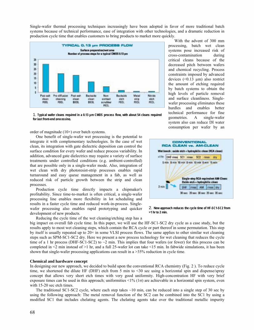
Single-wafer thermal processing techniques increasingly have been adopted in favor of more traditional batch systems because of technical performance, ease of integration with other technologies, and a dramatic reduction in production cycle time that enables customers to bring products to market more quickly.
With the advent of 300 mm processing, batch wet clean systems pose increased risk of cross-contamination during critical cleans because of the decreased pitch between wafers and chemical recycling. Process constraints imposed by advanced devices (<0.13 µm) also restrict the amount of etching required by batch systems to obtain the high levels of particle removal and surface cleanliness. Single-wafer processing eliminates these hurdles and enables better technical performance for fine geometries. A single-wafer system also can reduce DI water consumption per wafer by an
order of magnitude (10×) over batch systems.
1. Typical wafer cleans required in a 0.13 µm CMOS process flow, with about 54 cleans required for just front-end processing.
One benefit of single-wafer wet processing is the potential to integrate it with complementary technologies. In the case of wet clean, its integration with gate dielectric deposition can control the surface condition for every wafer and reduce process variability. In addition, advanced gate dielectrics may require a variety of surface treatments under controlled conditions (e.g. ambient-controlled) that are possible only in a single-wafer mode. Also, integration of wet clean with dry photoresist-strip processes enables rapid turnaround and easy queue management in a fab, as well as reduced risk of particle growth between the strip and clean processes.
Production cycle time directly impacts a chipmaker's profitability. Since time-to-market is often critical, a single-wafer processing line enables more flexibility in lot scheduling and results in a faster cycle time and reduced work-in-process. Single-wafer processing also enables rapid prototyping and quicker development of new products.
Reducing the cycle time of the wet cleaning/etching step has a big impact on overall fab cycle time. In this paper, we will use the HF-SC1-SC2 dry cycle as a case study, but the results apply to most wet cleaning steps, which contain the RCA cycle or part thereof in some permutation. This step by itself is usually repeated up to 20× in some VLSI process flows. The same applies to other similar wet cleaning steps such as SPM-SC1-SC2 dry. Here we present a new process technology for wet cleaning that reduces the cycle time of a 1 hr process (DHF-SC1-SC2) to ~2 min. This implies that four wafers (or fewer) for this process can be completed in <2 min instead of >1 hr, and a full 25-wafer lot can take <15 min. In fabwide simulations, it has been shown that single-wafer processing applications can result in a >35% reduction in cycle time.
2. New approach reduces the cycle time of HF-SC1-SC2 from >1 hr to 2 min.
Chemical and hardware concept In designing our new approach, we decided to build upon the conventional RCA chemistry (Fig. 2 ). To reduce cycle time, we shortened the dilute HF (DHF) etch from 5 min to <30 sec using a horizontal spin and dispense/spray concept that allows very short etch times with very good uniformity. High-concentration HF with very brief exposure times can be used in this approach; uniformities <1% (1σ) are achievable in a horizontal spin system, even with 15-20 sec etch times.
The traditional SC1-SC2 cycle, where each step takes ~10 min, can be reduced into a single step of 30 sec by using the following approach: The metal removal function of the SC2 can be combined into the SC1 by using a modified SC1 that includes chelating agents. The chelating agents take over the traditional metallic impurity
68

removal function of the HCl, but work at high pH. Chelating agents in SC1 have been used before, such as the use of ethylenediaminetetraacetic acid (EDTA) in SC1 about 11 years ago.6
The SC1 process itself can be reduced from 10 min to 30 sec by using a much more efficient and novel full-coverage megasonics unit. In a conventional wet bench, the megasonics crystals typically are mounted on the bottom of the tank, and their energy is dispersed over 50-100 wafers. In a single-wafer horizontal spin solution, if the megasonics system is properly designed, the acoustic energy can be focused uniformly over a wafer, making it 50-100× more efficient.
The rinse time can be reduced from 8 min to 20 sec by using the same concept and centrifugal forces to reduce the boundary layer. In immersion wet benches, boundary layers on the order of 150 µm lead to long rinsing.7 In a horizontal spin system, the boundary layers are much thinner (on the order of 10 µm), resulting in shortened rinse times.
The new cleaning approach incorporates a gentle, full-coverage, non-
damaging megasonics unit that cleans more effectively and rapidly than existing technologies. Surfactants added to the SC1 avoid any redeposition of particles and help achieve a total process time of 30 sec. Drying relies mainly on centrifugal force (spin) to dry a wafer in 20 sec.
3. Drawing of a four-chamber single-wafer, short cycle time wet clean system.
If we combine four horizontal spin chambers into a single system (Fig. 3 ), each chamber has a cycle time of 2 min for an HF-modified SC1 clean-dry cycle. Thus, a four-wafer lot can be processed in about 2 min. Such a system demonstrates a throughput of >100 wph, making it suitable for volume manufacturing.
Particle removal efficiency The addition of a surfactant to the SC1 solution greatly improves the particle removal ability of the SC1 chemical step. Surfactants increase a cleaning solution's effectiveness by helping it wet the wafer surface and dispersing (or carrying) particles from the wafer surface, all at very low concentrations. In addition, surfactants help suppress redeposition of very fine particles that are removed from the wafer surface (generally <0.14 µm) and ensure that fine particles stay in solution and can be easily rinsed later.
We investigated several types of surfactants and their ability to enhance the particle removal capability of our clean, concentrating mainly on anionic and non-ionic surfactants. A non-ionic surfactant that rinses from the wafer surface easily, leaves no residue, adds no organic or metallic contamination to the wafer surface, and is low foaming was selected. The surfactant also offers enhanced particle removal rates over a typical SC1, needs a low concentration to obtain critical micelle concentration (CMC) point and provides a high zeta potential.
We compared the Si3N4, Si and SiO2 particle removal efficiency of the traditional SC1 and our short- cycle clean in a single-wafer cleaner with novel megasonics for a 30 sec clean on 300 mm wafers. The results are shown in Figure 4 . It is clear that the traditional SC1 does quite well on SiO2 particles but has difficulty removing silicon particles. The surfactant added to the clean solves this deficiency. The SC1 clean removes only 90% of the silicon particles in 30 sec, whereas the modified SC1 clean (with surfactant) can remove up to 98% of these particles in 30 sec. 4. Comparison of SC1 and short-cycle
AM-Clean for SiO2, Si and Si3N4 particle removal efficiency.
69

Though Si3N4 particles are easier to remove than Si particles, Si3N4 particles are commonly used as the standard test for particle removal efficiency. For Si3N4 particles, the standard SC1 delivers a removal efficiency of 95%, while the modified SC1 clean (with surfactant) achieves 99% removal efficiency in 30 sec.
Metallic impurities In aqueous solutions such as SC1, a silicon wafer surface is hydroxide terminated. The interaction of the metal ions in solution and the silanol surface groups can be described by the following equation where Mx+ is the metallic ion: 5. Metallic impurity levels after the AM-Clean are at or below the VPD-ICPMS detection limits.
-Si-O-H + Mx+ ↔ -Si-O-M(x-1)+ + H+ This equation is similar to the interaction of metal ions in solution with a weak acid ion exchange resin. We can
see here that there are two ways to reduce metallic ions from depositing on the wafer surface. The first is to increase the concentration of H+. This is done by the traditional SC2 solution. Acidifying the
solution at the same time produces a solution in which most common metallic ions are soluble, provided that a suitable oxidizer, such as dissolved O2, H2O2 or O3, is present in the solution to prevent any reduction, especially of such metallic ions as Cu2+. However, this chemisorption/desorption equilibrium equation provides us with another mechanism for metallic impurity removal. If this is achieved by binding the free metal with a ligand so the combined complex remains soluble, we have created the same conditions for metallic impurity removal as the common SC2 solution. These ligands are often referred to as chelating, complexing or sequestering agents, one of the most popular being EDTA.
The advantage of this approach to metallic impurity removal is that the acid environment is no longer necessary. Metallic impurities can be removed from oxide surfaces at alkaline pH values using chelating agents, which are commonly used to remove particles such as the ubiquitous SC1 solution. This opens the door for an all-in-one universal cleaning solution, which is necessary to reduce cycle time when using single-wafer processing.
In our solution, we have used a chelating agent with a reduction in free ions of roughly 1035 for iron. We measured the metallic impurities after this clean to validate the combination of SC1-SC2 into a single step. The metallic impurities after this clean (Fig. 5 ) are below the VPD-ICPMS detection limit, which is on the order of 1E8 - 1E9 atoms/cm2.
Organic residues As mentioned above, we selected chelating agents and surfactants that can be completely rinsed. First, we measured the characteristic peaks in a time-of-flight secondary ion mass spectrometry (TOFSIMS) spectrum of the chelating agent and the surfactant by depositing a concentrated solution on the wafer and drying it in a nitrogen environment. TOFSIMS measurement following a clean and rinse cycle did not exhibit either the chelating agent or surfactant characteristic peaks. Hence, even a short 20 sec rinse effectively removes all traces of chelating agent or surfactant. This has been further evidenced by the absence of any particles on wafer surfaces that might indicate surfactant residues. Process validation Once the basic performance characteristics were established, a 10-day, >5000 wafer marathon with the DHF-AM-Clean process was carried out to validate this concept in a production environment. Wafers were sampled periodically to monitor all the basic characteristics of this clean such as throughput, reliability, metallic contamination, organic contamination, water consumption, chemical consumption, particle adders on the front and backside, particle removal efficiency, oxide etch uniformity and repeatability. The two biggest challenges in terms of repeatability for any cleaning process are the excursions of particles and control of the etch rate, especially wafer to wafer.
70

The particle removal efficiency of the modified SC1 clean with megasonics exhibits virtually 100% particle removal from both the front and backside of the wafer. During this marathon we measured all particles >0.12 µm. The starting particle count was generally <50 for particles larger than 0.12 µm. The area counts are included in the particle counts. Almost 99% of the monitor wafers exhibited <15 particle adders with an average value of <2 adders during the entire run. The tight control over particle excursion during an extended period of use indicates the stability of single-wafer processing and its ability to meet production requirements for stringent cleans.
Summary In this paper, we have presented feasibility data for a new short-cycle wet clean (AM-Clean) using a single-
wafer processing approach that offers excellent particle performance, oxide etch uniformity and metallic impurity performance. This clean combines the traditional SC1 and SC2 steps into one step by using the SC1 as the base and adding a chelating agent and surfactant to it. This allows the SC1 step to remove metals and particles in ~30 sec, when combined with an efficient megasonics set-up. Such short process times on a single-wafer platform enable high-throughput, fast-cycle-time processing that cannot be realized in batch systems. This clean meets or exceeds all regular performance metrics used to characterize cleaning, and has been proven production-worthy over an extended run.
References 1. W.A. Kern and D.A. Puotinen, "Cleaning Solutions Based on Hydrogen Peroxide for Use in Silicon Semiconductor Technology," RCA Review, 1970, Vol. 31, p. 187. 2. S. Verhaverbeke, et al, "Advanced Wet Cleaning Technology for Highly Reliable Thin Oxides," Proc. of the Fourth International Symposium on Ultra Large Scale Integration Science and Technology, 1993, Vol. 93, No. 13, p. 199. 3. T. Ohmi, "Proposal of Advanced Wet Cleaning of Silicon Surface," Cleaning Technology in Semiconductor Device Manufacturing IV, 1996, Vol. 95, No. 20, p. 1. 4. F. Tardif, et al, "Diluted Dynamic Clean: DDC," Proc. of the International Symposium on Ultra Clean Processing of Silicon Surfaces, UCPSS 96, p. 175. 5. D. Levy, et al, SEMATECH Cleaning Workshop, Austin, Texas, May 21-22, 2002. 6. S. Verhaverbeke, et al, "The Effect of Metallic Impurities on the Dielectric Breakdown of Oxides and Some New Ways of Avoiding Them," Tech. Dig. IEDM, 1991, p. 71. 7. L.M. Loewenstein and P.W. Mertens, "The Rinsing Problem: Effect of Solute-Surface Interactions on Wafer Purity," Solid State Phenomena, 1999, Vol. 65-66, p.1.
Steven Verhaverbeke is technology manager for Applied Materials ' Wet Clean Division (Materials Transistor and Capacitor Group), focusing on development of new wet cleaning concepts and processes. He received his Ph.D. in applied sciences from Katholieke University. Satheesh Kuppurao is marketing manager and strategic technologist for Applied's Wet Clean Division. He has a Ph.D. in materials science from the University of Minnesota and B. Tech from the Indian Institute of Technology. Christopher Beaudry is a member of the technical staff for Applied's Wet Clean Division. He received a Ph.D. in ceramic science and engineering from Rutgers University.
J. Kelly Truman is general manager of Applied's Wet Clean Division. He received a B.S. in metallurgical engineering and materials science from the University of Notre Dame, and M.S. and Ph.D. degrees in materials science and engineering from the University of Florida.
71

72

Wafer Cleaning Processes – A Review
Sreenivas Jayaraman
ECE 384, University of Illinois, 1406 West Green Street, Urbana, IL 61801
Abstract Increasing miniaturization of devices along with high yield and reliability requirements has made the process of wafer cleaning a very critical step in IC production. This paper reviews the sources of contamination and objectives behind a cleaning operation. The conventional RCA clean has its shortcomings due to the strong acids and bases involved, accompanying health and environmental issues and high cost. Novel cleaning processes like ozonated DI water treatment, IMEC clean, UCT process and others offer several advantages over the RCA clean. They are made of fewer process steps and have greatly reduced chemical consumption. Not only are they greener they also cost much less to operate. Such processes are the stages in the march towards the final destination in the cleaning roadmap – a single wafer, single step clean.
1. Introduction Semiconductor industry driven by the need to produce faster and cheaper computers is seeing increasing miniaturization of integrated circuits. Nanometer scale devices coupled with stringent reliability requirements has only made wafer cleanness a very critical parameter in processing. It directly affects the Gate Oxide Integrity (GOI), which in turn is closely related to the lifetime of the device. With gate oxide thickness of 25-70Å and gate length of the order of 0.35-0.1 µm (1) any residual or organic contaminant can kill the device. Wafer cleaning is especially critical before any diffusion, anneal, CVD or oxidation step. The number of cleaning steps that wafers have been undergoing has risen steadily over the years as illustrated in Fig. 1.
Fig. 1: Stronger demands to keep contamination under control, as well as an increasing number of metal layers, contribute to a rise in the number of wafer cleaning steps in the manufacturing process. (Source: VLSI Research) (ref. 7)
The RCA clean (2) with minor modifications still forms the backbone of major front-end wet cleans. The chemicals involved (H2SO4, HF, NH4OH) are costly to store, difficult to handle and need a full-fledged infrastructure to dispose. The environmental and health issues associated with the exposure to strong acids and bases involved cannot
73

be overemphasized. Alternatives to the RCA clean that are both low cost and environment friendly are hence in focus. The following paper describes the basic objectives behind any cleaning procedure, the existing conventional technique and emerging processes that may replace it. 2. Objective of wafer cleaning Before the wafer is processed upon or between processing operations (diffusion, oxidation etc.) it undergoes several cleaning procedures to take care of contaminants on its surface. These include (3) –
a) Dirt and Dust – It is a natural consequence of the exposure to the environment. The source may be a pre-processing step like dicing, sawing, storage boxes, human contact or the atmosphere of the ‘clean’ room.
b) Native oxide – It is formed when Si is exposed to air or may be remnant from some previous processing step and is usually thin (<100Å). This oxide may need to be stripped and any residual oxide may act as a barrier to any chemical treatment that the wafer has to undergo
c) Organics – Organic contamination is from human contact, prior processing step like photolithography or wafer storage boxes that are usually made of polymers.
d) Metallic residues – A major source of these are acids and organic solvents that are being used to treat the wafer or manual handling by tweezers. Hence, the need for ‘electronic grade’ solvents cannot be overemphasized.
The contaminants can affect the device reliability as follows – - Decrease in oxidation rate and oxide quality - Low breakdown field and high leakage current caused mainly by metallic contaminants - Introduction of metal impurities from the surface into silicon during diffusion, CVD and other high
temperature operations may lead to formation of carrier trap and recombination centers, hence reducing minority carrier lifetimes. It may also lead to threshold voltage shift and hot carrier degradation.
The presence and level of contamination is characterized both by simple methods like visual observation and advanced techniques. The common method to check for etch completion in oxide etching is to see the wetting of water on Si surface; water does not cling to a silicon surface free of oxide. Particulate contaminants can be observed by a surface scan under a high power microscope with a profilometer. For very fine particulate matter an Atomic Force Microscope (AFM) can be used, which yields surface roughness and particulate data in the nanometer range. Organic contamination and, especially, metallic contamination calls for advanced techniques like Secondary Ion Mass Spectrometry (SIMS) and time-of-flight SIMS. Other techniques include vapor-phase decomposition, and X-ray fluorescence. In light of the above discussion, it is clear as to why wafer cleaning is a very important step in any electronic fabrication. 3. RCA Cleaning Procedure RCA standard clean was originally developed at the RCA solid-state division in New Jersey in 1961 (2). The process involves treating an already degreased wafer in two solutions SC-1 and SC-2. SC-1 is made up of 4:1:1 to 6:1:1 of H2O, 30 w/w% H2O2 and 29 w/w% of NH4OH. This solution at elevated temperature removes residual organic contaminants by oxidative breakdown and dissolution. It also removes noble metals like Ag, Au, and Cu through complex formation with NH4OH. SC-2 is made up of 4:1:1 to 6:1:1 of H2O, 30 w/w% H2O2 and 37 w/w% of HCl. Used at 75 to 85 oC, this low pH solution effectively removes alkali ions and any other remaining metal impurities. Dissolved ions form soluble complexes and are hence prevented from re-depositing on the wafer surface. An oxide etch is done in HF before going from SC-1 to SC-2. There have been minor modifications suggested to the process like H2SO4 in place of HCl in SC-2. Also, there have been some process technology changes like the use of centrifugal spray cleaning and megasonic cleaning. In the former, an automated system sprays a fine mist of reagents and water on the wafer surface ensuring a fresh supply of reactants on the wafer surface, efficient removal of by-products and reduced volume of chemicals needed. In megasonic cleaning ultra high frequency sound waves provide scrubbing action on wafers immersed in the cleaning solution. In spite of its efficacy, the RCA process has major drawbacks, the chief among them being the strong acid and bases involved, as mentioned before. SC-1 and SC-2 need separate fume hoods as NH3 and HCl form dangerous smog of NH4Cl. Fused silica containers for the solutions and high grade polypropylene containers for wafers are some other stringent requirements. 4. Novel Cleaning Procedures Most novel cleaning techniques that have been developed are driven by the need to reduce the consumption of chemicals and ultra pure water (referred as UPW, DI water etc). This brings down the process cost and also makes the process ‘greener’. This section describes a few such techniques and the concomitant advantages.
74

4.1 Ozonated DI water (DI/O3) Ozonated DI water has been extensively studied (4,5,6) to replace strong chemicals like sulfuric acid, hydrogen peroxide and ammonium hydroxide from front-end critical cleans. DI/O3 solution is prepared by dissolving large amounts of ozone in DI water under pressures of 2-3 bar. The critical concentration of ozone needed for efficient cleaning is 60-120 ppm. A centrifugal spray system dispenses the solution on the wafer and since contact time involved is short very little ozone is lost from the solution. The typical cleaning sequence involved is DI/O3 – HF– DI/O3, with HCl added to any or all of the steps depending on the need to remove metallic impurities. The DI/O3 is a very effective oxidizer and wafer readily forms a chemical oxide on exposure. Most of the particulate contaminants are trapped in the oxide and are removed in the subsequent etching step with HF. Olson et al. (5) have reported the particle removal performance and surface roughness on Si surface post treatment with DI/O3 processes (Fig. 2). DI/O3 – HF– DI/O3 sequence showed a negligible change in surface roughness and 92% particle removal efficiency. DI/O3 process offers a huge environmental advantage in terms of water and chemical usage. The water usage is cut by almost 50% and chemical usage is either drastically reduced or eliminated. These are also the conclusions arrived at by Olson et al. (5) in comparing this clean with a standard B –clean. The latter is a sequence of four steps – SPM (H2SO4, H2O2), HF, SC-1 and SC-2. It is also offers as process time reductions as we cut down upon several rinsing and pre-rinsing operations.
Fig. 2: Particle removal efficiency and surface roughness after different DI/O3 – HF– DI/O3 treatments and B-clean (ref. 5)
75

4.2 IMEC-CleanAs the name suggests, it is a process developed by the research labs of IMEC – Belgium (8). IMEC-clean involves a two-step approach; in the first, a strong oxidant is used to remove organics from the surface.
e
r
prevents re-deposition due to repulsive zeta potentials (8). Table 1 and Table 2 present data to support the efficacy of IMEC-clean. IMEC appears to do better than RCA in metal removing efficiency and is almost 100% efficient in removing usual particulate contaminants. Measurements of defect densities, in capacitor structures fabricated on oxidized wafers cleaned by IMEC and RCA clean, yielded values below or close to the detection limit of 0.1 defect/cm2. Table 3 presents the cost of ownership comparison between IMEC and RCA process. The important
figure here is volume of chemical waste generated by the RCA process and the huge advantage offered by the novel processes in this regard. 4.3 UCT-Process
y (UCT) process is tion and removal from the
silicon surface. This process also relies on ozonated-ultra pure water (UPW) for the cleaning action. When first introduced (4) the process sequence was DI/O3 – HF– DI/O3, the efficacy of
The wafers are treated with a sulfuric acid/ozone mixture (SOM) at 90 oC followed by hot and cold DI water rinse. The wafer is left with a uniform oxide on its surface after this step. The second step is the stripping of oxide in dilutHF; 0.5 molar HCl is added to HF to dissolve any metal impurities as needed. As the oxide etches it lifts off any residual particles. Subsequently, rinsing is done in ozonated DI water (DI/O3) in a megasonic bath. The water is keptat pH =2 by adding HCl and are then marangoni dried at pH=3. This process summarized in Fig. 3, leaves the wafesurface hydrophilic as there is a very thin layer of chemical oxide. Adding HCl during rinse and dry keeps the pH below the isoelectric point of silicon oxide. This ensures particle removal and
Contaminant Ca Fe Cu Zn Initial concentration 154.4 5.6 4.4 1.8Modified RCA clean <0.26 0.2 0.4 0.2IMEC clean <0.26 0.1 <0.07 0.08
Metal concentration on the wafer (1010
atoms/cm2)
Table 1: Metal removal efficiency for a RCA clean vs IMEC clean in the same wet bench (ref. 9)
Substrate
SiO2 Si3N4 Al2O3
Si 0.99 1 1TEOS 1SiO2 1 1 1
0.98 1
Particle Type
0.99 1 The Ultra Clean Technologbased on impurity adsorp
Si3N4 0.94
which has already been discussed. The second stepTable 2: Particle different substrates (ref.
removal efficiency for an IMEC clean on 8)
Fig. 3: Schematic illustration of IMEC-Clean (ref. 9)
76

in the seq ome surfactant and a megasonic treatment. The UCT process in the current state (6) has been delineated in the flow chart in Fig. 4. As illustrated, the process utilizes v y ng chemicals and is made of four steps in eclaim the water uafter proper treatment. This process hence offers great promise in terms of cost reduction and environmental safety and health (ESH).
Baths 5 2 60er/yr 26x106l 8.7x10⁶l 76
Chem. Waste/yr 336x103l 20.8x10³l 94IPA/yr 17.5x10³l 0.4x10³l 98
t/yr 60.5x10⁶l 22x106l length 8m 4m
Conv. RCA IMEC %Chemical Baths 4 2 50Rinse DI-wat
Exhaus 6450Bench
Table 3: Cost of ownership comparison for a conventional RCA clean (SPM/SC-1/DHF/SC-2/IPA vapor dry) and IMEC clean (ref. 8)
all. It is also easy to r
uence also had some H2O2, swith the purpose of each step
quantities oer little f any strosed and recycle it
77

Process Purpose
H2-UPW + Megasonic Cleaning
(H2:1.2~1.6 ppm, pH 9.3)
FPM
(0.5% HF +0.5% H2O2)
H2-UPW + Megasonic Cleaning
(H2:1.2~1.6 ppm)
O3-UPW (O3:5ppm)
Organic, Noble metal (Cu, Ag) removal
Particle Removal
Metal, Chemical oxide removal, Hydrogen termination
Final rinse. Prevention of native oxide growth andparticle re-adhesion
Fig. 4: Process flow in UCT process 4.4 Other Cleaning Processes A one-step method suggested by Pan et al. (10) involves putting some additives in the conventional SC-1 solution.
a chelating agent. TMAH helps in removing particles while EDTA reduces metallic contamination. Their in the ratio of 1:50, 100 ppm of EDTA and operating temperature
ed an improvement of at least 50% in t in electric breakdown field compared to those subjected to
er active research as a cleaning solution (11). The collapsing aqueous oam bubbles provide the cleaning action here, a process similar though more efficient than the megasonic bath.
Since a major part of foam is made of gas phase the total volume actual aqueous reactants is very less. The cleaning action is not compromised even though reactant and solvent consumption is far reduced. A major source of contamination on the wafer is the solvents themselves that are being used to clean them. Hence, one way of obtaining ultra-clean wafers is to resort to a totally dry-clean. One such process uses the photochemical UV/Cl2 technology (12) to prepare the surface for critical operations like epilayer deposition, gate oxidation etc. An oxide layer is grown in a rapid thermal oxidation chamber and anhydrous HF is used to etch the oxide. Chlorine gas is then flown over the wafer surface in a dry vacuum chamber, with UV lamps on either side of the wafer. Chlorine disassociates activating the surface reactions that removes organics and trace metal contaminants. Careful control is
These include tetra-methyl ammonium hydroxide (TMAH), a surfactant and ethylenediamine tetra-acetic acid (EDTA), optimum recipe was made of TMAH in NH4OHof 60oC. MOS capacitors made from wafers cleaned using this process showleakage current value and 1-1.5% improvemenconventional clean. Aqueous foam is another novel technology undf
78

79
needed to avoid the wafer surface from roughening during this process. This process was initially designed as a final clean after some sequence of wet cleans to remove bulk contaminants. This clean process has led to improved performance of devices with ultra-thin (10 Å) gate oxides. 4.5 Conclusion Wafer cleaning operation was reviewed in light of ever increasing reliability requirements and shrinking device scale. The research in this area is being driven by the need to obtain better results with fewer operational steps and reduced chemical consumption. O3/HF/O3, IMEC clean and UCT clean are some new techniques that score over
RCA clean in chem duced cost. They are equally efficient and the roadmap in fig. 5 could be cleaning t e same time. References 1. Semiconductor Industr2. W. Kern and D. Poutinen,3. G.E. Anner, Planar Pr4. T.Ohmi, J. Electrochem5. E.D. Olson, C.A. Reaux, W.C.Ma and J.W. Butterbaugh, Semiconductor International, Aug (2000) 6. H. Morita, J.Ida, T. Ii and T. Ohmi, IEEE International Symposium on Semiconductor Manufacturing Conf., 453(1999) 7. A. Hand, Semiconductor International, Aug (2001) 8. M. Meuris, S. Arnauts, I. Cornelissen, K. Kenis and M. Lux, IEEE International Symposium on Semiconductor Manufacturing Conf., 157(1999) 9. M. M Heyns et al., IBM J. Res. Develop. 43, 339(1999) 10. T.M. Pan, T.F. Lei, T.S. Chao, M.C. Liaw and C.P.Lu, Jpn. J. Appl. Phys 39, 5805 (2000) 11. M.A.Lester, Semiconductor International, Feb (2002) 12. M.A.Lester, Semiconductor International, Dec (2000) 13. M.A.Lester, Semiconductor International, Feb (2001)
ical consumption, environmental and health safety, cycle time and hence re at times even better than the RCA process. The future as illustrated in
he wafers individually in one step with multiple chemistries operating at th
y Association: The National Roadmap for Semiconductors (SIA, 1997) RCA Rev. 31, 187 (1970)
ocessing Primer (Van Nostrand Reinhold, New York, 1990) ical Society 143, 2957 (1996)
Fig. 5: Progressive steps to a single wafer wet clean (ref. 13)

80

Appendix D - Photoresist Processing
Photoresist Chemistry
The ECE 444 lab currently uses SHIPLEY 1813photoresist (PR) and is also the choice of many researchers. It is one of the cheapest photoresists on the market at ~$1000 per gallon. Luckily, the chemistries for all positive photoresists are similar so learning about this one will not be for naught. Photoresists all contain 3 basic components: an organic polymer (usually novolak resin) which is what "resists" etchants, a solvent carrier (usually an acetate) so it's a liquid for easy application by spinning, and a photoactive component often called a sensitizer (usually a diazoquinone), which causes the solubility to become dependent upon exposure to UV radiation.
SHIPLEY 1813uses novolak polymer, propylene glycol monomethyl ether acetate (PGMEA) solvent, and diazonaphthoquinone as the sensitizer. On the next page is the chemical reaction used to create the novolak resin. Below that are the three distinguishable reactions undergone by the sensitizer attached to the novolak matrix during exposure. Note that some water is actually required.
For image reversal (negative) processing the indenecarboxylic acid is decomposed by a post exposure bake giving off carbon monoxide and rendering the sensitizer insoluble to the alkali developer. The previously unexposed sensitizer can then be made soluble by a subsequent flood exposure. Since there is no longer sensitizer in the previously exposed areas they will remain insoluble.
Most of the instructions for patterning with photoresist are included in this appendix, but the operation of the Ultratech steppers is described in Appendix H. Some specific variables, such as etch time, which mask to use and whether to use the image reversal technique, are left to the experiment which references this appendix. The tasks presented here take place in three
ns suitable for posting at the spinner hood, the development station, and the PR removal station.
locations and, therefore, are split accordingly into directio
81
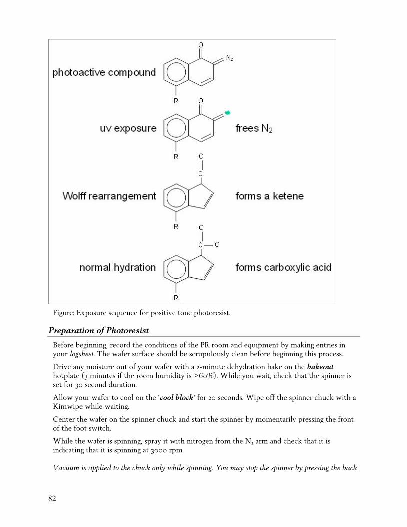
F
reparation of Photoresist
igure: Exposure sequence for positive tone photoresist.
P
Before beginning, record the conditions of the PR room and equipment by making entries in your logsheet. The wafer surface should be scrupulously clean before beginning this process.
Drive any moisture out of your wafer with a 2-minute dehydration bake on the bakeout hotplate (3 minutes if the room humidity is >60%). While you wait, check that the spinner is
ipe off the spinner chuck with a
2
ing the back
set for 30 second duration.
Allow your wafer to cool on the ‘cool block’ for 20 seconds. WKimwipe while waiting.
Center the wafer on the spinner chuck and start the spinner by momentarily pressing the front of the foot switch.
While the wafer is spinning, spray it with nitrogen from the N arm and check that it is indicating that it is spinning at 3000 rpm. Vacuum is applied to the chuck only while spinning. You may stop the spinner by press
82

of the foot switch, but don't continue blowing nitrogen on it when it stops. The spinner will automatically stop after the preset time.
pinning the wafer, drop 6 drops of hexamethyldisilazane (HMDS) onto ains
ps the photoresist adhere better. Think of it much like a detergent. In this case, the organic end (hexamethyl-) of the molecule is similar to and
e silazane end, being silicon based, sticks well to the wafer/oxide surfaces (this is a simplistic description of the mechanism - see if you can find the actual
the wafer using the filtered syringe. A pattern like that below works well for the first 9 drops.
interior dry spots within the PR puddle.
While the spinner is sthe center of the wafer and stop the spinner as soon as the appearance of the wafer remconstant. HMDS behaves as a surfactant, a wetting agent. It hel
binds well to the organic PR. Th
mechanism in Grainger). It even seems to help adhesion on aluminum as well.
Immediately place 40 to 50 drops of SHIPLEY 1813positive resist on and around the center of
Use the last few to fill in any voids between the drops. Use extra drops if necessary to fill all
Wait at least 5 seconds after the drops completely flow together, then start the spinner. This time, let the spinner stop by itself.
Co on the watheun t uniform (which is not
uniformity cause?). The thickness of the PR is ch like oxide. The color of the film is altered
Bake for 45 seconds on the
Thins
Develop until pattern is sharp (see the Development procedure to be posted on developer
lete the preparation of the PR for use as an etch stop by performing a 60 second hardbake hotplate (currently the same as the softbake hotplate).
mplete coverage of the wafer is critical to the operation of the steppers. There are targets fer which must not be etched away. If your wafer is not completely covered, ask your TA since re are places which can be etched while still allowing the stepper to perform. Check the iformity of the resist by looking for a bull’s-eye effect - if you see it, it is no
critical to our process - what problem does non~1.6μm, and exhibits thin film interference effects, muby varying thickness.
Softbake hotplate.
Allow the wafer to cool for a few seconds on the ‘cool’ plate.
e photoresist is now ready for exposure to ultraviolet light through a mask. Refer to the tructions for the stepper (Appendix H).
hood.)
Finally, comphardbake on the
Cool the PR for a few seconds on the ‘cool’ plate before putting it in the wafer carrier.
83

The photoresist is now ready for etching (or deposition if using the lift-off technique).
EVELOPMENT D
Dip development has the advantage of not pitting the surface of the PR and is used for development of the 4” wafers, although careful inspections must be followed since development slows as the PR loads up after multiple wafers have been processed. In industry, 500rpm spinners beneath a low velocity nozzle are common.
4” Immersion Development
1. It is strongly recommend
2. Open the faucet valve
ed that you change the D.I. rinses before beginning.
just barely enough to maintain a continuous stream (as opposed to a
over the entire wafer.
although this
oo fast in the rinse.
9. Move to the FINAL RINSE tank for at least 10 seconds while you calculate the total time
e
1. Return the wafer to the carrier face up.
gs.
They may take a little longer to develop because it's harder for fresh developer to reach the bottom to dissolve the PR. Gross under development will appear as splotches with multicolored rings in the larger areas which should be clear of PR. Why?
14. Repeat in 10-second intervals if necessary.
Discussion
sequence of individual drops.)
3. Make sure there is sufficient developer in the developing container to cIf not ask your TA to fill it.
4. Check the number of times that the developer has been used. If you are the first user, you will develop for ~40 seconds (do not use this as an exact time – this is just a guideline). Each additional wafer that is developed will probably take slightly longer (depends on the resist thickness).
5. Immerse the wafer into the developing container and begin timing.
6. Gently agitate the wafer and develop for the time determined from above.
7. Quickly quench the developer in the first DI rinse. Be careful not to break your wafer by swishing it t
8. Note the time.
spent developing.
10. Gently rinse your wafer with DI from the faucet (near the nozzle) and N2 dry (NO IPA.) Excessive water velocity can pit the surface of the PR. Although this is not usually a problem, it does look bad until the PR is removed. Fresh DI from the sprayer is used in casthe rinse tank has enough PR in it from previous students to deposit a thin invisible film onthe wafer. Students may change the DI rinse at their own discretion.
1
12. Gloves and tweezers should be rinsed in D.I. if developer is suspected on them. Used developer is highly water soluble, but can be difficult to remove if left to dry on thin
13. Inspect the development under a UV filtered microscope. Pay particular attention to the smallest windows to be opened.
The solubility change during exposure of photoresist is a couple of orders of magnitude at best (although chemists are constantly improving it). Consequently, all the PR will eventually
84

dissolve in the developer. Before that happens the openings in the PR will widen and loose their sharpness. Therefore, development time should be minimized. The smallest windows which are to be opened are usually the limiting factor because fresh developer must diffuse down to the surface in order to do its job. This diffusion is slowed when the width of the window in the PR is comparable to its depth. A possible technique to minimize this effect would be to hold the wafer at an angle so the PR could not puddle. Unfortunately, PR adhesion and sprayer uniformity become greater problems (at least in ECE 444 lab). A compromise seems to be the best solution. Periodic tilting of the wafer to help change the developer in the small windows is suggested. Exactly how often is optimum has not been determined. Record any useful observations you make which would help in your notebook.
Photoresist Removal
After the etch, the PR may be removed by one of the following three methods. Do not try one of the other methods before performing the microscope inspection step.
Use acetone, PGMEA, or other solvent to remove the majority of the PR by making a puddle of the solvent on the wafer while holding it level above the proper waste container. Pour the solvent off after 10-15 seconds and repeat until there is no significant improvement. Finish with a standard degrease - squirt with acetone, IPA, water, IPA again, and N2 dry.
Use the plasma asher. See Lab→Equipment→Plasma Asher on the web page for instructions. This is the most reliable method, but also the most time consuming. Please try it at least once during the semester.
Use acetone, PGMEA, or other solvent to remove the majority of the PR as in the first method. Then use heated Posistrip, Microposit Remover, or other proprietary positive PR remover. DI rinse, N2 dry.
Inspect for Residual PR Under a Microscope
Pay particular attention to the rim of the wafer where edge beading during the spin on process left extra thick PR. Removing the yellow UV filter from the illuminator will help you see PR, but be sure to return it. The residue will often look similar to slightly underdeveloped PR. Since such residues are likely to be very thin with respect to visible light wavelengths, they often take on a rainbow of colorations as the thickness variations cause different interference patterns. PR is a furnace contaminant and must be completely removed. The whole class is counting on you keep the furnaces clean.
If PR residue is detected, go back to step 1. If there is only a little left, additional soaking with acetone will usually take care of it. Stubborn PR may need the plasma asher however. Occasionally, etched features will look like PR residue so consult with your instructor before going back to step 1 a third time.
85

86

PR Process Overview
1. Start with bare silicon wafer.
Silicon Substrate
2.
Grow oxide on wafer surface.
Silicon Substrate
Grown Oxide Layer
3. Apply PR.
Silicon Substrate
Grown Oxide LayerUndeveloped PR Layer
4. Expose PR. Positive resist becomes acidic in exposed regions.
Silicon Substrate
Grown Oxide Layer
Unexposed PR Unexposed PRPR becomes acidic in exposed areas
5. Develop PR. PR will act as etch stop.
87

Silicon Substrate
Grown Oxide Layer
Unexposed PRloperExposed PR is removed by deve
Unexposed PR
6. Etch oxide. PR stops etch in undeveloped regions. Note undercutting due to isotropic tch.
nature of chemical oxide e
Silicon Substrate
Unexposed PR Unexposed PR(Note undercutting)Oxide is etched where not masked by PR
7. Remove PR. End result is patterned oxide layer on surface of wafer.
Silicon Substrate
Patterned Oxide Layer
88

Wafer Inspection At i ect it under the
ic c efully for any remaining R residue. In general, you will be looking at the “Lines” and “Spaces” patterns to determine
the level of development and the level of etch completeness.
Lines and Spaces
var ous points in the processing of your wafer, you will need to inspros ope. After PR removal, you will want to inspect your wafer carm
P
• Designed to aid in determination of development completion aces which should appear aligned under the set
ermine etch level (overetch or underetch) in the same manner. king etch level. This is because oxide will appear dark
icon will appear almost white. • Smaller lines and spaces may appear darker in color. This is ok and is most likely caused
by viewing the features at a slight angle. • Generally, as long as both the 2µm line and space is n the corners and center of
your wafer devel roce
• Each mask contains a set of lines and spfrom the previous mask
• Can also be used to det• Colors will be reversed when chec
red and bare sil
present iopment is sufficient to p ed with etching.
LINES SPACES1 2 3 4 5 6 7 8 9 0 1 2 1 2 3 4 5 6 7 8 9 0 1 2
Thin lines of PR inopened window. Usedetect overdeve
gaps in PR in to
lopment.
Numbers indicatewidth of lines or
spaces in microns.
Note that the 0, 1, and 2at the right are actually
10, 11, and 12.
d tolopment.
Thin unopened area. Useddetect underdeve
PR when checking developmentOxide when checking etch level*Oxide when checking for developmentBare silicon when che ing etch level*
* Note that actual colors will be reversed when checking etch level.
ck
89

t Severe Underdevelopmen• Several spaces are missing
eloped yet oper for additional development before etching
• Smaller features have not been dev• Return to devel
LINES SPACES1 2 3 4 5 6 7 8 9 0 1 2 1 2 3 4 5 6 7 8 9 0 1 2
Slight Underdevelopment • 1µm space is missing • Acceptable level of development • Ready to etch
LINES SPACES1 2 3 4 5 6 7 8 9 0 1 2 1 2 3 4 5 6 7 8 9 0 1 2
Perfect Development • All lines and spaces present • Ready to etch
LINES SPACES1 2 3 4 5 6 7 8 9 0 1 2 1 2 3 4 5 6 7 8 9 0 1 2
90

Slight Overdevelopment • 1µm line is missing • Acceptable level of development • Ready to etch
LINES SPACES1 2 3 4 5 6 7 8 9 0 1 2 1 2 3 4 5 6 7 8 9 0 1 2
Severe Overdevelopment • Several lines are missing • Smaller features have been erroneously removed • Strip PR, reapply, and attempt proper development again
LINES SPACES1 2 3 4 5 6 7 8 9 0 1 2 1 2 3 4 5 6 7 8 9 0 1 2
91

92
Appendix E - Hot Point Probe
A bas ther the majority carriers are holes (p-type) or electron ickly and sim ll the oxflowin
The fplasm from determ
e net current may be due to the heat reducing the probability that ssociated dopant atoms, but room temperature
is sex does not affect this measurement since the current components from can
Opera
ic electrical property of semiconductor materials is their type of conductivity, i.e., whes (n-type). This property is very qu
ply determined by employing the hot point probe. It is also a quick way of determining if aide has been removed from a test area – if there is oxide left, there can be no current g from the sample to the probes.
ree carriers in a semiconductor behave in some ways as a gas of charged particles (a a). Just as heat makes a gas expand (PV=nRT), the hot point makes carriers expand awaythe contact point. The charge of the dominant carrier species (electrons or holes)
ines the direction of the net current flow.
A small component of thcarriers remain confined spatially around their a
o high (above absolute zero) that virtually all dopant atoms are already "excited." The extra citation is negligible. Carrier pair generation caused by the heating
thermally generated electron-hole pairs would cel. Note that the measurement situation is a non-equilibrium condition.
ting Instructions
1.
2. Turn on the picoammeter. Make sure it's in ‘Auto’ scale mode.
3. Load your wafer.
a) Move the wafer chuck all the way toward the front.
b) Place your wafer on the chuck. Be careful not to hit the probe tips. As long as the test area is on the chuck, centering is not important. Do not bother to slide the wafer beneath the tips; it will only make it difficult to remove.
4. Probe the wafer.
a) Use the x-y stage to position the appropriate test area beneath the probes. Plastic "spokes" on the chuck allow rotation of the wafer.
b) Watch the probes closely as you use the green button to lower them onto the wafer. Excessive ‘skating’ can scratch the wafer. Control of the probe descent is enhanced if you simultaneously apply some pressure to the white button while the green button is pressed. Consult your instructor if you suspect the prober needs adjustment. Please do not re-adjust any of the knobs on the probe assembly unless you know how to properly reset them.
Turn on the power supply. The power supply is only used to heat the probe tip on the left – there is no electrical connection to the sample.
93

5. Interpret the reading
a) Trace the wires to determine which direction the picoammeter is connected into the circuit. Is its positive reference input (center conductor if it uses a BNC connector) connected to the hot or cold tip? Note the red and white dots on the holders for the
s. These correspond to the similarly colored banana jacks.
e
r insulating (oxide) or intrinsic (compensated). Consult
c) Remove the wafer from the chuck. Note: a drop of water can make a wafer stick to flat gh force that it's possible to break the wafer by lifting it straight up. If
he e
probe tip
b) Type determination: the picoammeter registers a positive current when direct current flows into its positive reference input. We leave it up to you to decide which sign on thpicoammeter's display corresponds to which conduction mechanism in the semiconductor. A constant sign on the picoammeter is sufficient – its magnitude is not. It may climb slowly as the hot point heats up, and may decrease as the wafer heats up. No reading means either that the circuit is open (possibly from dirty tips), the tip is not hot, or that the material is eitheyour instructor if you have reason to believe that prober has a problem.
6. Remove the sample.
a) Use the white button to raise the tips.
b) Use the x-y stage to bring the wafer out from under the tips.
surfaces with enouthe wafer resists lifting, slide it off.
7. Turn off the picoammeter and power supply unless someone else is going to use it next. Since the tips are so close, continuous heating may warm up the "cold" point and reduce tsensitivity of the apparatus, but the main reason for turning off the power supply is that wdon't have a spare heater. So don't skip this step!
94

Appendix F - Four Point Probe
ntroduction I
Resistivity (ρ) is a particularly important semiconductor parameter because it can be related directly to the impurity concentration of a sample; see GT section Figure GT-1. These plots have been determined experimentally and are specifically valid for homogeneous single crystals of Silicon at room temperature (300 K). The four point probe is the apparatus typically used to determine bulk resistivity, and in conjunction with plots like GT-l, permits one to ascertain the
We'll use the GT-1 curves.
Theory of Operation
impurity content of a given sample.
Note that the mobility of the carriers depends upon temperature, crystal defect density, and allimpurities present. If your sample differs in these respects from that used to determine the empirical GT-1 curves, the actual dopant concentration you determine will only be close, not exact. Hall effect measurements can determine the mobility of the carriers in a given sample toallow for more accurate dopant concentration measurements, but Hall measurements are usually destructive to the sample.
The four point probe, as depicted schematically in Figure 1, contains four thin collinearly placed
e
tungsten wires which are made to contact the sample under test. Current I is made to flow between the outer probes, and voltage V is measured between the two inner probes, ideally without drawing any current. If the sample is of semi-infinite volume and if the interprobe spacings are s1= s2 = s3 = s, then it can be shown that the resistivity of the semi-infinite volumis given by
( )I
Vsπρ 2= (1)
Figure 1
95

The subscript o in the preceding equati easured value of the resistivity and is f
on indicates the mequal to the actual value, ρ, only if the sample is of semi-infinite volume. Practical samples, ocourse, are of finite size. Hence, in general, ρ ≠ ρo. Correction factors for six different boundary configurations have been derived by Valdes.(1) These show that in general if l, the distance from any probe to the nearest boundary, is at least 5s, no correction is required. For the cases when the sample thickness is ≤ 5s, we can compute the true resistivity from
oaIVsa ρπρ == 2 (2)
where a is the thickness correction factor which is plotted on page GT-2. From an examinationof the plot we see that for values of t/s ≥ 5 the corresponding value of a is un
ity. Thus for
ickness is at least 5 times the probe spacing, no correction factor is needed. ls and the wafers used in most cases are only 10-20 mils, so
unfortunately we cannot ignore the co ing again at the plot, however, we t/s ≤ 0.5. Since it is a log-log plot the equation
samples whose thTypical probe spacings are 25-60 mi
rrection factor. Looksee that the curve is a straight line for values of for the line must be of the form
m
stKa ⎟⎠⎞
⎜⎝⎛= (3)
t (2ln2).) Hence for slices equal to or less than
one half the probe spacing
a = 0.72 t/s
When substituted into the basic equation we get:
where K is the value of a at (t/s) = 1, and m is the slope. Inspection of the plot shows that in this case m = 1. K is determined to be 0.72 by extrapolating the linear region up to the value a(t/s) - 1. (The exact value can be shown to be 1/
IVt
IVsa 53.42 == πρ for t/s ≤ 0.5 (4)
All samples used in the lab satisfy the one-half relationship so the above formula can be used to determine ρ. Resistivity measurements will be performed on the starting material for each experiment. The value of ρ obtained will be referred to as the bulk resistivity, and the units are Ω-cm.
If both sides of Equation (4) are divided by t we get
Rs = ρ/t = 4.53 V/I for t/s ≤ 0.5 (5) which we refer to as sheet resistance. When the thickness t is very small, as would be the case for a diffused layer, this is the preferred measurement quantity. Note that Rs is independent of any geometrical dimension and is therefore a function of the material alone. The significance of the sheet resistance can be more easily seen if we refer to the end-to-end resistance of a rectangular sample. From the familiar resistance formula
R = ρ l/wt (6)
96

we see that if w = l (a square) we get
for this reason the nits of Rs are taken to be Ohms per square or Ω/ . Dimensionally this is the same as Ω, but
le the
Rs = C V/I (7)
w
N 5).
R
R = ρ/t = Rs
Therefore, Rs may be interpreted as the resistance of a square sample, anduthis notation serves as a convenient reminder of the geometrical significance of sheet resistance.
So far in our discussion of resistivity measurements we have assumed that the size of our sampis large compared to the probe spacing so that edge effects could be ignored. This is usually case for the bulk resistivity measurement. However, the sheet resistance measurements made in lab will be made on a "test area" of the wafer. The test area dimensions (nominally 2.9 by 5.8mm) are not that large compared to the probe spacing (25 mils). In order to get accurate measurements a correction factor for edge (geometry) effects must be included. The figure onpage GT-3 gives the correction factors for two common sample geometries.
general then In
here C is the correction factor.
ote that for d/s > 40, C = 4.53, the value we had as the multiplier in Equation (
eferences
Valdes, L. G., Proc. I.R.E., 42, pp. 420-427 (February 1954).
Smits J, 37, p. 371 (1958 S
, F. M., "Measurements of Sheet Resistivity with the Four-Point Probe," BST). ( ame as BT Monograph, 3894, Part 2).
97
The LDS Four Point Probe The LDS fou r and Dane Sievers for m on wafers up to 8” in diameter. The s e for positioning the wafer in x, y, θ, and probe head z. It is connected r Analyzer controlled by Lab View. The syste a es average readings over multiple measurem tmeasurement of 1% error for NIST traceable 0.0226 ohms/sq standard). The user interface was duser inpu f mapping, standard checking, and database (logsheet) recording. Operation
r point probe was designed and developed by Leon Schneideeasuring sheet resistance precisely
yst m uses a custom built stage to an Agilent 4155C Semiconductor Parametem uto-ranges measurement conditions and taken s in both the forward and reverse current directions to derive a precise
sheet resistance (~
eveloped using LabView instrument control software and allows for t o measurement conditions, display of raw and calculated data values, wafer
1. Tur h n the back of the system.
2. Rai t
3. Load the wafer onto the stage. Position thadjustment kno tation using the handle on the u
4. Lower the 4pp head using the lever on the right hand side of the system.
•
• the 4pp probe tips are
ot come into contact notify your TA.
essing the icon labeled ‘4PP’ on the desktop of the PC.
7.
•
•
e spacings are also listed.
n t e 4pp head light on using the switch located o
se he 4pp head up using the lever on the right hand side of the system.
e sample under the 4pp head using the x and y bs located under the left side of the stage. Adjust ro
ch ck.
• The lever is locked into the ‘up’ position with a spring loaded pin.
Release the pin by pulling out (to the right).
The lever can then be lowered onto the sample. Make sure thatin direct contact with the sample (they are spring loaded and should recess into the head ~1/8” when in full contact). If they do n
5. Turn on the Agilent 4155C SPA.
6. Start the software by pr
Input the appropriate parameters for the sample being measured:
Diffusion Depth or Wafer Thickness (t):
- For bulk sheet resistance (whole wafer measurements) input the wafer thickness in microns (µm).
- For diffused layers input the junction depth in microns (µm). Calculate the diffusion depth using DifCAD or hand calculations.
Probe Spacing (s):
- Currently the probe being used has a probe spacing s = 40 mils (0.040”).
- Other common prob
• Diameter or Length of measured area:
98

- Rectangular samples: input the length of the shortest side in mm (the long side must be >4x length of the short side).
- Circular samples: input the diameter of the sample in mm.
8.
ent type:
22.6mOhm/sq standard
- 0.0026 Ohms/sq Cal – for checking calibration using the 2.6mOhms/sq standard
- Long – slow, accurate mea time based on power line cycles
ower line cycles)
• Input Number of Measurements of measurements to sample for each direction of current.
a better S/N ratio but at the expense of sample heating which um
rid,
ppear in
error from stated value is displayed beneath the sheet resistance value. ight. To
easurements the current measurement position is highlighted in red. ke sure that the 4pp head is in the appropriate position before pressing ‘Measure’.
xt position is highlighted. Reposition sample and press ‘Measure’. To manually
values can be written to your logsheet.
EET’
Configure ‘Measurement Setup’
• Select measurem
- Single measurement – for individual sites
- Pattern measurement – for mapping wafer (simple = 5 point sample, full = all 15 measuring sites)
- 0.0226 Ohms/sq Cal – for checking calibration using the
(less accurate)
• Select Integration Time:
- Short – for fast, less accurate measurements
- Medium – standard measurement conditions
surements with
• Select the number of PLCs (p
– the number
• Input Voltage Threshold – the desired voltage developed across the inner probes. High values will givecan affect the accuracy of measurement. The test instrument is limited to a maximof 100mA of force current, so this value may not be achieved.
• Test Pattern – for pattern measurements select simple for a 5 point measuring gfull for measuring all 15 points on the wafer.
9. Click on ‘Measure’ to initiate measurement. While measuring a red indicator labeled ‘Measuring’ will appear.
• For single and calibration measurements the calculated sheet resistance will athe center of the window above the ‘Measure’ button. For calibration measurements the percent Values used for calculation of the sheet resistance appear in the panel to the rremeasure the sample using the last measurement conditions press ‘Remeasure’.
• For pattern mMaThe measured value is stored at each position. After the measurement is made thenemove the current measuring position press ‘NEXT POSITION’. To reset the values press ‘RESET GRID’.
10. For pattern measurements
• Press ‘RECORD TO LOGSH
99

• A login prompt will appear. For ‘NetID’ input your NetID assigned to you by the university. For ‘Password’ input your Active Directory (AD) password used to log to the PCs in the lab.
in
s’ to overwrite the data.
The VEECO Four Po
• You will be prompted to select the appropriate diffusion step to record the values in.You must select only one diffusion step.
• Click ‘OK’
• If there are already values present in the logsheet you will be prompted to overwritethe data. Press ‘Ye
• A successful write to the logsheet is reported. Click ‘OK’.
int Probe
The Veeco four point probe provides a constant current which flows between two outer probes and then measures the voltage across the two inner probes to obtain the fundamental V/I parameter.
For the bulk resistivity measurement, the relevant formula is
ρ = 4.53 t V/I
For sheet resistance measurements the formula is
Rs = C V/I
and the measured V/I value is multiplied by C (this value is already set on the probe). Refer to Fig. GT.3 for correction factor determination, but divide the number by 4.53 for the Veeco. The probe spacing S is 25 mil.
The Veeco can penetrate thin insulating surface layers by applying a short 170v pulse to the probe tips when the PENETRATE function is selected. Then, after making the resistivity measurement, the unit can determine the type of the semiconductor. For low resistivity samples the type is determined by applying an ac signal between two probes and monitoring the dc bias of the wafer with a third probe. Lightly doped semiconductors will form rectifying contacts with the probe tips causing the wafer bias to go up (positive) for N type material and negative for P type material. Highly doped semiconductors will not develop a conclusive wafer bias, but the applied ac signal can heat such material sufficiently for observation of the thermoelectric effect (as in the hot-point probe). If neither method is conclusive, both N and P indicators will flash.
Note: The electronics does not always know when the tests for conductivity type are inconclusive. If it disagrees with the hot point probe, disregard it.
Operation
1. For Bulk Resistivity: press <SLICE RES> and dial in the wafer thickness (including the units!)
2. For Sheet Resistance: press <SHT. RES> and dial in the posted geometry correction factor.
3. For V/I ratio: press <V/I>.
4. Press the <Type Auto> button in.
100

5. Lift cover and place wafer on the glass plate. Center the 4 probes in the test area by lowering the probes (depress bar in front manually) until they are just above, but not touching, your wafer. Adjust the glass plate until your test area is centered.
6. Lower the probes by depressing the bar in front manually. Press <RETEST> until you get two consecutive readings that are the same with the possible exception of the least significant digit. Record the values. If different from the 1st value, average the two numbers.
7. With the probes still held down, press <REV. CURR> twice and record the values. Disagreement with the other values may mean a tip is bent or a poor contact exists. 10% agreement is acceptable.
8. Average the four measurements. Note that the readings are in mΩ, Ω or kΩ as per the LEDs on the display. If measuring Rs, units are (m,K) Ω/ . If measuring ρ, units are (m,K) Ω-cm.
101

102
Appendix G - Lindberg/Tempress 8500 Furnace
ntroduction I
The Lindberg/Tempress 8500 dual stack furnace bank is a precisely regulated high temperature furnace used for multiple purposes in the laboratory. Each of the chambers (eight total) is dedicated to a particular function to minimize cross contamination (especially of dopants).
Temperature Range
The furnace is capable of regulating temperatures up to 1350 ±0.1°C (at equilibrium)., althoughthe normal operating range is 400°C to 1100°C. The furnaces are kept at either 400°C (solid
rature, dopant source reproducibility, and dby condition is not utilized because the life of
es.
source chambers) or 600°C (oxidation/drive chambers) during standby, and temperatures of 950°C (boron predep), 1000°C (gate oxidation and phosphorus predep), and 1100°C (field oxidation, boron drive) during operation. These temperatures where selected based on the conditions of fast cycle time to operating tempechamber longevity. A higher temperature stanthe furnace core windings decreases rapidly at elevated temperatures. The furnaces are not completely shut off when in standby, or raised to higher temperatures during use, because cycling of temperature below 275°C or above 1100°C devitrifies (crystallizes) the quartz tub
Chamber Material
The material used for the chambers where the processes occur must meet two important criteria: 1)the ability to withstand large thermal gradients and 2) material compatibility with thesilicon process. Thus, most chambers are made of ‘quartz,’ or more correctly, ‘fused silica’.
Fused silica is amorphous silicon dioxide (SiO ), which exhibits a low coefficient of thermal
zed high purity fused silica. Stabilized refers to the thin circumference of the chamber which minimizes
2
expansion (~5x10⁻⁷mm/mm/°C) and is fully compatible when of sufficient purity, since it is the same material that is used for dopant masking.
The chambers used in the lab are stabilicristabolite, or crystalline, layer around the stress fractures from thermal cycling. Purity level is ~99.97% SiO2.
Processes
Steam Oxidation: Steam oxidation is used to form oxides used for dopant masking. The steam
own
. Prior to use the solid sources are oxidized to form a B2O3 layer. It is the oxide which has a significant vapor pressure at the diffusion temperatures. B2O3 reacts
is created pyrogenically, e.g. through the combustion of oxygen and hydrogen gases. This produces a fast growing oxide which is ideal for diffusion masking, although its electrical properties are compromised due to a more porous structure with a higher incorporation of mobiles charges compared to dry oxide.
Dry Oxidation: Dry oxidation (used for the gate dielectric of MOS devices) is accomplished using only pure oxygen. This produces a dense oxide with low pinhole density, high breakdvoltage, and low incorporated mobile charge.
Boron Doping: Boron doping utilizes solid 4” diameter disc-type sources composed of BN (boron nitride). BN is an inert ceramic with a low vapor pressure, so it must be conditioned to act as a proper dopant source
103

with silicon to form SiO2 with an extremely high concentration of boron – BSG (borosilicate glass).
Phosphorus Doping: Phosphorus doping utilizes solid 4” diameter disc-type solid sources composed of SiP2O7 in a fine SiO2 matrix. The SiP2O7 decomposes at diffusion temperatures to
form P2O5, which vaporizes and reacts with silicon to form PSG (phosphosilicate glass). Noconditioning (other than an 8 hour soak at the process temperature) is required as with the BN wafers since it is a decomposition reaction that creates a volatile oxide.
The furnace is divided into two sides: manual loading and autoloading. This arrangement allows you to experience first hand the advantages and disadvantages of both types of systems.
Control
The furnaces are controlled either by a Digital Temperature Controller (DTC) on the manual side, or a combination of a DTC and a Digital Process Controller (DPC) on the autoloader side.
DTC: The DTC is a PID (Proportional, Integral, Derivative) controller, which in simplest terms means that the temperature can be ramped extremely fast with no overshoot, allows for quick
ing in a cool boat full of wafers), and very stable setpoint
he input for the temperature control comes from two types of thermocouples: spike and spike thermocouples on the outside surface of the chamber, ating element (source, center, and handle). These are used
uple which is inserted inside the chambers. This TC is used to
ts function is to allow for automation of the furnace since there are more operations going on
an
The digital inputs currently are used for location setpoints for the cantilever loading system. The digital outputs are used for the control of the stepper motors in the loading system. Currently, the analog I/O is not used, but will be used in the future for control of mass flow controllers (MFCs). The digital outputs can also be used for control of additional equipment, and will be used for solenoid valves in the future.
Th ting of temperature through the DTC. The DPC will set the correct temperature recipe in the DTC based t ut into the DPC.
The DPC can contain up to 16 programs which are input through a simple programming recipe.
Overt uipped with overtemperature detection which prevents accidental melt down of the quartz chambers in the event of equipment failure. There
mperature off the circuit breakers supplying power
recovery during thermal loading (loadtemperature maintenance (±0.1 °C deviation).
Tpaddle. There are three type Rlocated in the center of each heduring the normal operation of the furnace, although the temperature read by the TCs is different from the actual temperature that the wafers (inside the chamber) are at. There is also one type BX paddle thermococalibrate the setpoints required for the spike TCs to achieve the desired temperature on the inside of the furnace. The paddle TC can also be used to control the furnace temperature once it is inside the chamber.
DPC: The DPC is used in conjunction with the DTC on the autoload side of the furnace. I
other than just temperature control. The DPC consists of a microprocessor interfaced with alog and digital inputs and outputs.
e DPC is also the master of the DTC when the two are connected, disabling manual set
on he program inp
emp Modules: The furnace is also eq
are three TCs per chamber which provide redundancy to the spike TCs - if the terises above the overtemp setpoints, the system will tripto the individual furnaces.
104
Hydrogen: To create pyrogenic steam, hydrogen and oxygen are combusted in the chamber. e presence of hydrogen and oxygen together can be a potentially dangerous situation, bunimized with proper interlocks. The furnace gas delivery system is interlocked
Th t is mi to prevent the introduction of hydrogen if two criteria are not met:
low temperature: the furnace temperature must be >800°C for spontaneous combustion
gas ratio analyzer: the quantity of hydrogcomplete combustion of hydrogen
en is greater than the stoichiometric ratio required for
also present to detect any potential leaks or failures of the intexwh(10the
Furnace Operating Instructions
A hydrogen gas detection system iserlocks. There are three monitoring points designed to detect the presence of gas when it ceeds 5% LEL (lower explosion limit). This system is connected to a local alarm system ich is activated by the low alarm (5% LEL) to warn of a potential release. If the high alarm % LEL is activated, the system will sound the building alarm to provide for evacuation and notification of the fire department.
Furnace Loading: Manual
The ECE 444 diffusion furnaces are very much like those described in Appendix H of Anner's Planar Processing Primer. Refer to it for construction details. The following instructions are for manual operation, however.
does not necessarily look any differe than cool quartz. Quartz is ontamination. The 6" furnace tubes cost over $1000, the boats
ead contamination from, say a small piece of , to the wafers of classmates. If you suspect
1. he re setting on the Digital Temperature controller for the chamber you are using.
ii) <temp>
all three zones (default)
2. 3.
CAUTION: Quartz hot enough to severely burnalso extremely expensive and can be ruined by c
nt
over $200. The worst thing a student can do is to knowingly sprburned glove on a boat, to the other quartzware and, consequentlyaccidental contamination, notify the instructor immediately! Do not worry about your letter grade.
Verify that the furnace is at the proper temperature for the processing step by checking ttemperatu
a) If the actual temperature (TA) of the three zones is not displayed, press the following keys:
i) <clear and display>
b) You can check individual setpoints (SP) and actual temperatures (TA) by pressing:
i) <1> = handle
ii) <2> = center
iii) <3> = source
iv) <0> =
Check that the gas panel power is ON and that it is in the MANUAL mode.
Check that only nitrogen is flowing in the furnace.
105

4. Put on the high temperature gloves over your latex gloves. Open the scavenger hood door and carefully remove the end cap. Place it on the stainless steel counter in front of thopposite bank of furnaces so it's well out of the way. Be quick, it's very hot.
e
the boat from the mouth of the chamber.
6. 7.
If doing a predep, the wafer should face the nearest source wafer. Otherwise it should not matter, but note which ter of good scientific practice. In the case of predeps, use the diagram below to determine
ectronic logsheet entry. It will help if you observe the dimensions of the boat
rent gas flow conditions.
5. Put on the high temperature gloves and unload
Carefully place the boat on the quartz plate located on the stainless steel table.
Remove the high temperature gloves.
8. Load your wafer into the boat.
way it is loaded as a matthe boat position of your wafer for the elnow since you will have to hook it at a considerable distance without damaging the wafers later. Dummy wafers are used in all the boats not only for protection from the pull rods, but because the first and last wafers experience diffe
Gas Flow
10 9 8 7 6 5 4 3 2 1
SiliconSource waferDummy wafer
9. ure gloves.
10. into the mouth of the chamber.
te long pull rod to slowly push the boat ape mark is flush with the scavenger hood face. Each furnace has its own long
l rod to cool for several seconds before returning it to the quartz storage tube.
Put on the high temperat
Reload the boat
11. With the high temperature gloves, use the appropriauntil the tpullrod.
12. Allow the pul
13. Switch gases as the recipe dictates.
Furnace Unloading: Manual
The unloading procedure is basically the same with the obviourod must be used to retrieve the boat from
s differences that the long pull the center of the furnace and wafers will be
t.
temperature gloves over your latex gloves.
e furnace using the long pull rod for that furnace. Depth perception helps a great deal in hooking the boat when it's in the middle of the furnace. Remember, the boat was left where the tape lined up with the face plate. It may help to gently touch the boat without lifting the pullrod in order to calibrate the depth. It also helps to use the end of the furnace tube as a fulcrum and pivot the hook upward as you hook the boat. Avoid touching the wafers with the rod. Pulling too fast will result in an abnormally high sheet resistance because a significant number of atoms will be frozen off lattice sites, making them inactive.
removed from the boa
1. Put on the high
2. 30 second slow pull. Pull the boat to the mouth of th
106

3. Allow the pull rod to cool for several seconds before returning it to the quartz storage tube.
4. Use the lifting fork to move the boat to the quartz disc. Leave the fork in the boat.
5. Unload the boat. Remember, it's hot! Hold the wafers in air for 10 seconds or so to cool before placing them into the plastic wafer carriers. Although wafers cool very fast, the quartz boat will retain heat and keep wafers hot for a relatively long time. What implications does this have on the "real" diffusion time?
6. Reload the boat into the mouth of the chamber using the lifting fork and high temperature gloves.
Autoload Processing
To run the process recipe for the autoloader side of the furnace, press the following keys on the DPC:
1. <clear and display> repeatedly until DISPLAY ‘PROCESS NAME’ appears (where ‘PROCESS NAME’ = BORON DRIVE, PHOSPHORUS PREDEP, or GATE OX)
2. <run/halt>
3. Make sure the display says EMPTSTMCN1 RUN? If not, press:
a) <recipe>
b) <1>
c) <enter>
d) <clear and display>
e) <run/halt>
4. The display should now read EMPTSTMCN1 RUN?
5. <enter>
The process is totally automatic for the Phosphorus Predep. Additional steps must be taken for the Boron Drive:
1. When the elephant and boat are fully loaded into the chamber the display will read: START GASES
2. As soon as this is displayed, flow your gases as specified in the lab manual and begin timing.
3. When the process is complete, press <clear and display>
4. Press <run/halt>
5. Press <enter>
The furnace will then continue the recipe and unload.
107

108

Appendix H - Ultratech 1000WF Stepper
Introduction
The Ultratech 1000 Wide Fi rs are the latest addition to lithography in the ECE444 e highly automated, extremely complex machines which have repla al
ontact aligners. There actually was a reluctance to install these machines due to their cost and e r of operator involvement w .
he 1000WF is still in use by major semiconductor fabs (su rmer AC Delco) and ere are enough left to support third party parts
ppliers and reconditioners. They are ideal for start-up co desiring reasonably priced ho tch apabilities with other steppers.
he steppers present in the lab have been modified by Intel, and their performance has been nhanced from stock machines. P g resolution has been increased (closer alignment), and e optics have been enhanced (possible to achieve submicron resolution).
System Information
eld steppelab. They arc
ced the manu
th emoval ith aligning
T ch as the fo
mpanieswere in use by Intel until December of 1996. Thsup tolithography tools for non-critical, lower resolution processes with mix-and-mac
Te ositioninth
The operation of the steppers is very exact (presently there are approximately 4 manuals, 14 hours of setup video, and 15 VHS videos covering operation and maintenance in the 444 library). Therefore a short overview is all that will be presented.
ystem Positioning S
To provide for accurate positioning, the 1000WF consists of two stepper motors with feedback from a Zeeman split HeNe laser interferometer. Laser interferometers work through the counting of interference fringes created as a laser beam is reflected back onto itself. As the stage
the laser. As the fringes move, a counter determines the number of fringes which pass through an aperture, and can correlate that with a specific distance. This distance is used to provide an absolute position of the mirrors mounted on the stage with respect to a home position. The home position is determined by a limit switch.
By implementing two mirrors and splitting the laser beam, a very accurate position of the stage can be determined for both the X and Y-axes.
The interferometric determination of stage position is used to drive two stepper motors for stage placement. The stepper motors drive pinch rollers which propel the air bearing supported stage along guide rods.
Exposure System
moves, the distance the laser traverses changes, and the phase of the beam upon reflection changes, resulting in a maxima and minima of brightness as the beam destructively and constructively interferes with itself. Each fringe signifies a specific distance based on the operating wavelength of
The 1000WF consists of a very simple but effective 1:1 image projection system. A mercury arc lamp is used for the UV source utilizing the g- and h-lines (the i-line is filtered out because the epoxy used in the optical system decomposes with exposure to that wavelength). The beam is
109

projected through a light pipe, an actinic filter (‘actinic’ means ‘active’, so it filters out the for alignment), through a reticle (mask), is redirected by a prism
Figure H1. 1000WF light system.
he PMT and Y-tilt mirror are used for pattern recognition and alignment using the darkfield age from the wafer.
egistration
‘active’ UV componentsthrough a lens doublet, reflected back by a mirror, back through the doublet, and finally through another prism to the wafer. See Figure H1.
Y-tilt mirror
PMT Actinic shutter
Hg lamp
Light pipe
Reticl D
Tim
R
One of the most important aspects of li ration. The 1000WF determines position of the mask in relation to the existing wafer pattern both mechanically and optically in
Th lind steindividual die. This first mask level contains several alignment targets which will be used by
s.
thography is regist
a multistage process.
e first mask of the process exposes the pattern onto the wafer in blind step mode. Bpping is a purely mechanical alignment, and relies on the interferometer for placement of the
subsequent mask level
oublet Mirror
Wafer
Dark field image
Prisms
110

Mechanical Alignment
There are four types of mechanical alignm e 1000WF; they are listed in order of operation:
2. Bash routine: used to center the wafer on the chuck
3. Wafer edge detection
des: used to locate the reticle in the y-axis; must be <75µm misaligned to reticle
ent used in th
1. Flat find: used for rough theta adjustment
: used to center the wafer under the optics
4. Reticle guifiducial, there is no y-axis adjustment
Optical Alignment
There are three types of optical
1. sitioning of the mask to the optical system; ing a reticle for the current mask
level – see Figure 2.
relation to the mask pattern; aligns wafer to reticle to within 10µm; this routine is performed when a wafer is loaded under the op echanical alignments have been performed – see Figure 3.
µm wide cross hair
4000
Figure 3: Optical Alignment Target (OAT)
Horizontal Alignment Marks (HAMs): used for fine alignment and theta (rotational) adjustment; aligns wafer to reticle to within <1µm; this routine is performed after the OAT is found – see Figure 4.
HAMS
targets/keys used in the 1000WF:
Reticle alignment fiducial: used for absolute pothis is the first optical registration routine, used when load
R e eticl
Reticle Fiducials
Figure 2: Reticle Alignment Fiducials
2. Optical alignment target (OAT): large target used for global positioning of the wafer in
tics and all m
4
µm
111

OAT
Reticle Field
Figure 4: Horizontal Alignment Marks (HAMS)
The Reticle
Contact aligners use a mask which covers the entire area to be exposed (Figure 5). This method of exposure has several disadvantages as they become larger:
are more prone to breakage
• larger area for particles to land, causing pattern defects
Figure 5: Contact aligner mask.
pper, on the other hand, utilizes a field instead of the entire mask pattern (Figure 6). The
peated over the wa elow is a diagram of the reticle (with 3 fields) used in the 1000WF:
Figure 6: Stepper reticle.
• large masks are cumbersome and
• difficult to clean and inspect
MASK WAFER
Afield is a subset of the desired image to be transferred to the wafer. This field is stepped and
ste
re fer. B
RETICLE WAFER
Field
112

The advantages of the reticle are:
• smaller, therefore easier to handle
changed through software
lthough there are several advantages to the reticle, there are also disadvantages:
•
• mechanical alignment of guide structures critical
t ets/keys critical
g steps)
t
• less area for particles to cause defects
• same image for every device on the wafer (can be a disadvantage)
• versatile - image pattern can be
• allows for drop-ins (test patterns, different devices) which can be temporary
A
same image for every device on the wafer (propagation of faults)
• registra ion targ
• can be more expensive (labor intensive – additional post processin
Reticle Layou
A complete reticle is more complex than a contact mask. Below is a diagram of the features explained above:
Figure 7: UltratechWidefield Reticle Layout
Reticle Fiducial
OAT
HAM
5”
Field 2
3”
Field 1 Field 3
Reticle Guide
113

Operation
Although the steppers are complex to set up, they are very easy to run. The stepper will be warmed up prior to class.
Load the Reticle
The reticle contains three fields, each corresponding to a mask level (see Figure 8.). This requires the use of two reticles to obtain the entire mask set.
Reticle 2
Mask 1 Mask 2 Mask 3
.
e stepper. The reticle data is an
Th ur TA.
Yo the correct mask level.
Load Reticle Data
Reticle 1
Mask 4 Mask 5
Figure 8: Mask locations
The mask used is determined by the reticle data loaded into tharray of data that contains all the physical characteristics of the stepper, reticle, fields, and wafer.
e reticle must not be changed by students! If you require the use of a reticle not in the stepper, contact yo
u will have to change reticle data to align and expose with
1. nload Reticle)
2. is not loaded, proceed to 4.
3. , it will ask ‘Unload the reticle?’
c) it
d) s to the main menu and proceed to 4.
4. a) ht
b)
icle data file name’
Press <K1> (Load/U
If a Reticle is loaded, proceed to 3. If the reticle
If a reticle is loaded
a) press <y> (yes)
b) The reticle will unload.
After unloading, make sure that the reticle is seated properly in its guides by pushing gently to the right and tilting the left side up about ¼” and gently letting it back down.
Press <K1> when the stepper return
If there is no reticle loaded, the stepper will ask ‘Load reticle data?’
Make sure that the reticle is seated properly in its guides by pushing it gently to the rigand tilting the left side up about ¼” and gently letting it back down.
Insert the reticle data disk
c) press <y> (yes)
d) The stepper will ask ‘Input ret
e) Type in the mask level name:
114

Step Mask level name PR1 - layer1 PR2 - layer2 PR3 - layer3 PR4 - layer4 PR5 - layer5
5. 6.
b)
Align and Expose Wafer
press <ENTER>: the HP200 will load the data into memory
The stepper will ask ‘Load reticle?’
a) Place the frosty wafer (the unpolished side of an unused wafer) into the autoloader.
press <y> (yes)
c) The reticle will go through a series of tests to line it up properly with the optics. If it should fail reticle load, contact the TA.
d) Remove the frosty wafer from the autoloader after successful loading of the reticle.
After successful completion of reticle load, the HP200 will bring up the run mode screen. Run mode determines the method of alignment and exposure.
1. For layer1, proceed to 2. For all other layers, proceed to 3.
2. For layer1, the stepper will perform a blind step. Blind stepping is the mechanical alignment of the reticle to the wafer using only the interferometer as a means of registration.
a) press <1> (run mode 1 - mechanically align and expose)
b) The stepper will ask ‘Input exposure intensity’
c) type in <150> (150mJ/cm2)
d) press <ENTER>
e) The stepper will ask ‘Exposure is 150. Ok?’
f) type <y> (yes)
g) The stepper will say ‘waiting to load wafer’
h) Load your wafer into the autoloader by placing it with tweezers into the left side of the autoloader. Place the wafer so that it rests both on the red circle and the drive belts.
i) The wafer will automatically load onto the chuck after the flat find routine, and will be aligned and exposed automatically.
j) After successful alignment and exposure, the wafer will be returned on the right side of the autoloader. Remove it and place it back into your wafer container with tweezers.
k) The stepper will say, ‘waiting to load wafer’. If there are others waiting to expose the same mask, they may continue without reloading the reticle.
3. For all layers other than layer1, the stepper will align wafer targets through reticle keys optically.
a) press <2> (align and expose)
b) The stepper will ask ‘Input exposure intensity’
115

c) type in <150> (150mJ/cm2)
e) The stepper will ask ‘Exposure is 150. Ok?’
s.
wafer will be returned on the right side of
k) The stepper will say, ‘waiting to load wafer’. If there are others waiting to expose the e mask, they may continue without reloading the reticle.
d) press <ENTER>
f) type <y> (yes)
g) The stepper will say ‘waiting to load wafer’
h) Load your wafer into the autoloader by placing it with tweezers into the left side of the autoloader. Place the wafer so that it rests both on the red circle and the drive belt
i) The wafer will automatically load onto the chuck after the flat find routine, and will be aligned and exposed automatically.
j) After successful alignment and exposure, thethe autoloader. Remove it and place it back into your wafer container with tweezers.
sam
116

Appendix J - The Test Stations
ectrical connections from the micro-world of the wafer to he typical probe pad on the ECE444 mask set is 100µm on a side,
different metal.
Making contact to the wafer is therefore left to the micromanipulators with very fine tungsten probe tips (25μm radius). Positioning of the probes requires the use of a stereozoom microscope and takes practice (which is why you are here!).
Be careful with the probers! They are extremely precise instruments, as the cost proves it.
Do not:
The purpose of a prober is to make elthe macro-world we live in. Twhich would be quite difficult to solder or otherwise make connections by eye. This is not easy considering that solder does not wet aluminum, requiring a second metallization using a
• lower the probes onto the wafer with too much force (this will curl or ‘fish hook’ the sharp points)
• overextend the micromanipulators (they will bind). If you feel any resistance at all stop!
• lower the probe stage with the probes down (a good way to ‘fish hook’ the tips)
• open the chuck vacuum without a wafer (causes excessive blow-by on the house vacuum)
• move the base of the micromanipulators (they have been setup for ease in probing)
• change the SMU leads to the probes
• leave the probe stage down when not in use
Use of the probes
• Place your wafer on the wafer chuck
m switch.
• If any of the probe tips look like they will touch the wafer before the stage is completely down, raise the tips and continue lowering the stage.
• Repeat until the stage is fully lowered with none of the probes touching the wafer.
• Turn on the microscope light – you will only need about 75% power. The lower the power, the longer the bulbs last.
• Move the first device to be tested to the center of the microscope field of view using the stage’s X and Y controls (located at the front of the stage).
• Carefully make contact to the device pads with the probes using the X, Y, and Z controls of the micromanipulator – Do not use the probe bodies!
• Turn on the chuck vacuu
• Raise each of the probes a couple of turns with the UP positioner (top knob).
• Lower the probe stage slowly with the lever on the left hand side.
117
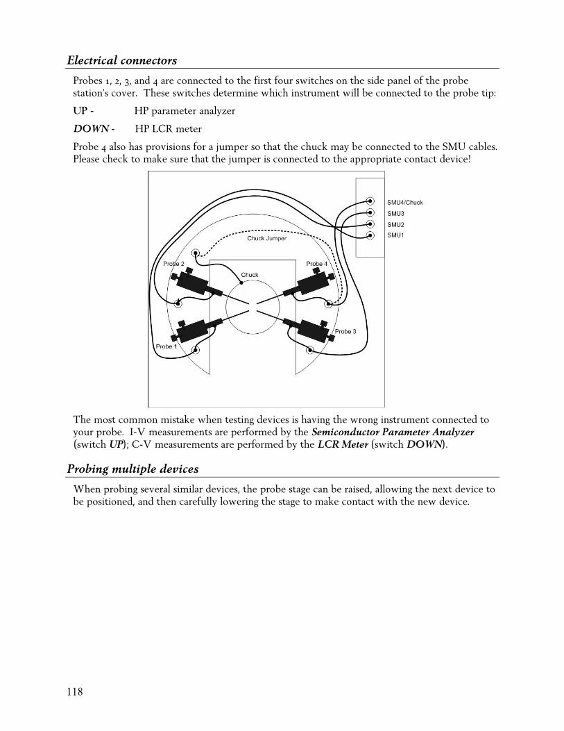
Electrical connectors
Probes 1, 2, 3, and 4 are connected to the first four switches on the side panel of the probe ches il obe tip:
meter ana
CR meter
for a b ables. sure that he ap t device!
station’s cover. These swit determine which instrument w l be connected to the pr
UP - HP para lyzer
DOWN - HP L
Probe 4 also has provisions lease che
jumper so that the chuck may e connected to the SMU cP ck to make the jumper is connected to t propriate contac
The most common mistake when testing devices is having the wrong instrument connected to
ts e Semicond( measuremen the LCR Meter h DOWN). your probe. I-V measuremenswitch UP); C-V
are performed by thy
uctor Parameter Analyzer (switcts are performed b
Probing multiple devices
When probing several similar d be rai e to en carefull n vice.
evices, the probe stage can sed, allowing the next devict with the nbe positioned, and th y lowering the stage to make co tac ew de
118

Appendix K - Semiconductor Acronyms
on spectroscopy
apor
al
e shift
AR ting er
at 193 nm wavelength)
AS an Society for Testing and
Au:
n
ry metal-miconductor
ateral
BLD
titanate ape automated bonding
CA am
esist
wafer cleaning xy
CDI: collector-diffusion isolation
position/oxidation
oscopy
nufacturing
CM entary metal-oxide
narization; ishing
CRCS
Research
isolation
DIW ized water
DLT el test
DR ion etching
DU under test let
t
nance
automation -dispersive spectroscopy; dispersive spectroscopy
ELF w frequency
ference
y
FE: mission
FES tron
pect beam
box pod
FPG ogrammable gate array nalysis,
ystem cate
aximum
ss
HA ratio inspection unication
HB ransistor
HD mical
ylene
mobility transistor
HiPOx: high-pressure oxidation
AES: Auger emission spectroscopy; Auger electr
AFM: atomic force microscopy AHU: air handling unit Al: Aluminum ALCVD: atomic layer chemical v
deposition ALD: atomic layer deposition ALE: atomic layer epitaxy; application
logic element ANSI: American National Standards
Institute APCVD: atmospheric pressure chemic
vapor deposition aPSM or APSM: attenuating phas
mask Ar: argon AR: aspect ratio
C: antireflective coaArF: Argon Fluoride (excimer far UV las
emittingAs: arsenic ASIC: application-specific integrated
circuit TM: AmericMaterials
ATE: automatic test equipment gold
B: billion; boron BARC: backside antireflective coating
iffusioBED: Boron Enhanced DBEOL: back end-of-lineBGA: ball grid array
olar complementaBiCMOS: bipoxide se
BILLI: buried implanted layer for lisolation
BIST: built-in self test : beam lead device
BOE: buffered oxide etchant BOX: buried oxide BPSG: boro phosphosilicate BST: barium strontiumBTAB: bumped tBV: breakdown voltageC-to-C: cassette-to-cassette
IBE: chemically assisted ion beetching
CARL: chemically amplified rlithography
CAWC: cryogenic aerosol CBE: chemical beam epitaCCD: charge-coupled device CD: critical dimension CDA: clean dry air
CDO: controlled decomCDSEM: critical dimension scanning
electron micrCEL: Contrast Enhancement Layer CFC: chlorofluorocarbon CFM: contamination-free maCGA: Compressed Gas Association CIC: cleanroom interface chamber
OS: complemsemiconductor
CMP: chemical mechanical plachemical mechanical pol
CNT: carbon nanotube CoO: cost of ownership COPS: crystal oriented pits
M: cost/resource model P: chip-scale package
nsion CTE: coefficient of thermal expaCu: copper CV: capacitance-to-voltage CV-BTS: capacitance-to-voltage biased
thermal stress CVD: chemical vapor deposition CZ: Czochralski process DARPA: Defense Advanced
Projects Agency (see ARPA) DCS: dichlorosilane DF: darkfield DHF: dilute hydrofluoric acid DI: deionized; dielectricDIP: dual inline package
: deionDLBI: device level burn-in
: device levDLTS: deep level transient spectroscopy DOE: design of experiments DOF: depth of field; depth of focus DOE: design of experiments DRAM: dynamic random access memory
IE: deep reactive DSWB: direct step-on-wafer
T: deviceDUV: deep ultravioE-beam: electron beam EBIC: electron beam-induced currenEBL: electron beam lithography ECC: error control coding
enECO: gineering change order; edge control only
ECP: electrochemical platingECR: electron cyclotron resoEDA: electronic design EDS: energy
electron-
EDX: energy-dispersive X ray EFEM: equipment front end module
: extremely loEM: Electro-Migration
omagnetic field EMF: electrEMI: electromagnetic interEMO: emergency off EMP: electromagnetic pulse EOS: electrical overstress EPL: electron projection lithography EPO: emergency power off
discharge ESD: electrostaticEUV: extreme ultraviolet EUVL: extreme ultraviolet lithographF: fluorine FBGA: fine pitch ball grid array FC: flip chip
finite element; field eFEOL: front end-of-line
EM: field emission scanning elecmicroscope/microscopy
F/I: final insFIB: focused ion FIFO: first-in, first-out FOSB: front opening shipping FOUP: front opening unifiedFOV: field of view FOX: field oxide
A: field-prFRACAS: Failure Reporting, A
and Corrective Action SFSG: fused silica glass; fluorinated sili
glass FTIR: Fourier transform infrared FWHM: full-width half-mFZ: float zone GCMS: gas chromatography ma
spectroscopy GSI: giga-scale integration
RI: high aspectHAZCOM: Hazard Comm
Standard T: heterojunction bipolar t
HCI: hot carrier injection HCM: hollow cathode magnetron HDP: high density plasma
P-CVD: high density plasma chevapor deposition
HDPE: high density polyethHe: helium HEMT: high electronHEPA: high efficiency particulate air HF: hydrofluoric acid
119

HMDS: hexamethyldisilizane
SP: hybrid organic silHO oxane polymer
vapor
HP h performance liquid
HR solution transmission
uioxane oxidation
ir
ent Council;
ed plasma
establishing,
IDL fe or
IGB transistor
layer
IME icro-Electronics
hy
ATECH
ap
tries nt Association
cimer uv laser h)
t
lene ralski
LEL
r
LTO ture oxidation (or oxide)
tial
er y
manufacturing nt
anical system ffect
l l
vapor
field-effect
r
ductor field
MO por phase
MR search Society
g support item
MTMW
Na: sodium
ND closure agreement ng ography
te of Standards and
for
OA n
ufacturer
OLE ganic light emitting diode or phase
ter; optical
ault
generator
g water
imit)
perfluorocarbon
gral erivative;
fect rticles
rier
hacrylate
PPE rotective equipment PPGA: plastic pin grid array
(low k dielectric) HPCVD: high pressure chemical
deposition LC: higchromatography
TEM: high reelectron microscopy
HSQ: hydrogen silsesqHTO: high temperature HVAC: heating, ventilating, and a
conditioning InI300I: ternational 300 mm Initiative
IC: integrated circuit; Investmion chromatography
ICB-CVD: ion cluster beam chemical vapor deposition
ICP: inductively-couplICW: industrial city water IDEAL: initiating, diagnosing,
acting, leveraging H: immediately dangerous to lihealth
IG: intrinsic gettering T: insulated-gate bipolar
IGFET: insulated-gate field-effect transistor
II: ion implant (also I2) ILD: interlevel dielectric; inter
dielectric IMD: intermetal dielectric
C: Inter-university MCentre (Leuven, Belgium)
IP: intellectual propertyIPA: isopropyl alcohol IPL: ion projection lithograpIR: infrared ISMT: International SEMITO: indium tin oxide ITRS: International Technology Roadm
for Semiconductors JEDEC: Joint Electron Device
Engineering Council JEIDA: Japanese Electronic Indus
DevelopmeJI: junction isolation JIT: just-in-time KGD: known good die KrF: krypton fluoride (ex
emitting 248 nm wavelengtLCC: leaded chip carrier, lifecycle costing LCL: lower confidence limit LDD: lightly doped drain LDL: lower detection limiLDP: low density plasma LDPE: low density polyethyLEC: liquid encapsulated Czoch
crystal
LEED: low-energy electron diffraction : lower explosive limit
LID: leadless inverted device LIFO: last in, first out LIGA: Lithographie Galvanoformung
Abformung LIMS: laser-induced mass spectrometry LKDM: low k dielectric material
leadless chip carrieLLCC: LOCOS: local oxidation of silicon LPCVD: low pressure chemical vapor
deposition LPE: liq y uid phase epitax
latex sphere equivaLSE: lent LSI: large-scale integration
: low-temperaLTV: local thickness variation LVDT: linear voltage differen
transducer; linear variable ar displacement transducer; line
variable differential transformMBE: molecular beam EpitaxMCBF: mean cycles between failures MCM: multichip module;
cycle managemeMEMS: microelectromechMESFET: metal-semiconductor field e
transistor MFC: mass flow controller MIC: monolithic integrated circuit MIM: metal-insulator-metaMIS: metal insulator silicon; meta
insulator semiconductor MLM: multilevel metal MMIC: monolithic microwave integrated
circuit MOCVD: metal-organic chemical
deposition MODFET: modulation-doped
transistor ctoMOS: metal-oxide semicondu
MOS-C: metal oxide semiconductor capacitor
MOSFET: metal-oxide semiconeffect transistor VPE: metalorganic vaepitaxy
mp: melting point S: Materials Re
MSDS: Material Safety Data Sheet MSI: medium-scale integration;
manufacturinMTBA: mean time between assists
ailures MTBF: mean time between fMTTF: mean time to failure
TR: mean time to repair : molecular weight
N: nitrogen
NA: numerical aperture A: nondis
NDT: nondestructive testiNGL: next generation lithNIST: National Institu
Technology NTRS: National Technology Roadmap
Semiconductors O: oxygen
I: off-axis illuminatioOBIC: optical beam induced current OD: outside diameter; optical density ODS: ozone-depleting substances OEIC: optoelectronic integrated circuit OEM: original equipment manOFA: oil-free air OL: objective lens, overlay
D: orOMVPE: organometallic vap
epitaxy OPC: optical particle coun
pro on ximity correctiOSF: Open Systems Foundation,
oxidation-induced stacking fOSG: organosilicate glass Ox: oxide P: phosphorous PAB: post apply bake PAC: photoactive compound PAG: photoacidPCB: printed circuit board PCMP: post chemical-mechanical
polishing procPCW: ess coolin
PEB: post-exposure bake PECVD: plasma-enhanced chemical
vapor deposition PEL: permissible exposure level (lPFA: perfluoroalkoxy PFC: perfluorocompound; PFPE: perfluorinated polyether PGA: pin grid arrayPGMEA: propylene glycol monomethyl
ether acetate PI: proportional intePID: proportional integral d
process-induced dePIP: process-induced paPLCC: plastic leaded chip carPM: particle monitor; preventive
maintenance; process module PMMA: polymethyl metPMT: photomultiplier tube POU: point-of-use PP: polypropylene
: personal p
120

PSG: phosphosilicate glass; phosphorus
doped silicon glass PSL: polystyrene latex PSLS: polystyrene latex sphere PSM: phase shifting mask; phase shift
mask PTC: pre- and post-process treatment
chambers PTFE: polytetrafluorethylene; Teflon PVA: polyvinylacetate PVC: polyvinylchloride PVD: physical vapor deposition PVDF: polyvinylidene fluoride PZT: lead zirconium titanate QBD: charge to breakdown QCM: quartz crystal microbalance QDR: quick dump rinse QFP: quad flat pack QFPN: quad flat pack nonleaded RBB: base sheet resistance RBS: refractive backscattering; Rutherford
backscattering spectroscopy RF: radio frequency; resonance frequency RFI: request for information; radio
frequency interference RFP: request for plan; request for
proposal; radio frequency probe RFQ: request for quote RGA: residual gas analysis RH: relative humidity RHEED: reflecting (reflected) high energy
electron diffraction RIBE: reactive ion beam etching RIE: reactive ion etch RO: reverse osmosis ROI: return on investment RS: sheet resistance RT: room temperature RTA: rapid thermal anneal RTD: resistance temperature detector RTO: rapid thermal oxidation;
regenerative thermal oxidizer RTP: rapid thermal processing (or
processor) Sb: antimony SBIR: Small Business Innovative
Research SC1: Standard Clean 1 SC2: Standard Clean 2 SCA: surface charge analysis SCALPEL: scattering with aperture limited
projection lithography SCBA: self-contained breathing apparatus SCF: super critical fluid SCFH: standard cubic feet per hour SCP: single chip package SCR: silicon controlled rectifier S/D: source/drain
SECS: Semiconductor Equipment Communications Standard
SEG: selective epitaxial growth SEM: scanning electron microscopy;
specific equipment model SEMI: Semiconductor Equipment and
Materials International SIA: Semiconductor Industry Association SiGe: silicon-germanium SiLK: silicon low-k SIMOX: separation by implantation of
oxygen SIMS: secondary ion mass spectroscopy SiON: silicon oxynitride SLAM: scanning laser acoustic
microscopy; single layer alumina metallization
SLSI: super large scale integration SMD: surface mount device SMIF: standard mechanical interface SMT: surface mount technology SO: small outline (package) SOC: system on a chip; silicon-on-chip SOD: spin-on dielectric SOG: spin-on glass SOI: silicon on insulator SOIC: small outline integrated circuit SOJ: small outline j-bend SOP: small outline gull wing SOP: standard operating procedure SOS: silicon on sapphire SPC: statistical process control SPICE: simulation program with integrated
circuit emphasis SPM: scanning probe microscopy; sulfuric
acid/hydrogen peroxide mixture SRC: Semiconductor Research
Corporation SSI: small scale integration STEL: short-term exposure limit STI: shallow trench isolation STM: scanning tunneling microscopy SWP: single wafer processing TAB: Technical Advisory Board; tape
automated bonding TBD: time to breakdown TC: time constant; temperature coefficient;
thermocouple TCE: temperature coefficient of expansion TDDB: time-dependent dielectric
breakdown TEM: transmission electron microscopy;
transverse electromagnetic TEOS: tetraethoxysilane;
tetraethylorthosilicate; tetraethelorthosilicate; tetrethoxysilicide
TFE: tetrafluorethylene
TFSMS: thin films stress measurement system
TFT: thin film transistors THC: total hydrocarbon TiN: titanium nitride TLV: threshold limit value TLV-STEL: threshold limit value-short
term exposure limit TLV/TWA: threshold limit value/time-
weighted average TMAH: tetramethyl ammonium hydroxide TMP: trimethylphosphate, turbomolecular
pump TOC: total organic carbon; total oxidizable
carbon TPG: test pattern generation TSOP: thin small outline package UCL: upper confidence limit; upper control
limit UEL: upper explosive limit UHP: ultra-high purity UHV: ultra-high vacuum ULK: ultra low-k ULPA: ultra-low particulate air ULSI: ultra large-scale integration UPDIW: ultra-pure deionized water UPW: ultrapure water USG: undoped silica glass USOP: ultra small outline package UV: ultraviolet VASE: variable angle spectroscopic
ellipsometry VCSEL: vertical cavity surface emitting
laser VDP: Van der Pauw VHSIC: very high-speed integrated circuit VLSI: very large-scale integration VOC: volatile organic compound VPE: vapor phase epitaxy VUV: vacuum ultra-violet WDS: wavelength-dispersive spectrometry
of X-rays WIB: within-batch WIP: work in process; work in progress WIW: within-wafer WLBI: wafer-level burn-in WLT: wafer-level test WPH: wafers per hour WSI: wafer-scale integration WSPW: wafer starts per week XPS: X-ray photoelectron spectroscopy XRD: X-ray diffraction XRF: X-ray fluorescence spectrometry XRL: X-ray lithography XSEM: cross-sectional scanning electron
microscopy
121

122

A ing ppendix L - Common IC Process Terms 5
tive oxide.
A
Al k: an image selectively
A
dissolve
A
A
750,000 Å.) The
A
ess, and
A
B tride: inert ceramic
a
B2 ide: volatile oxide used
B
0:1 Etch – 50 parts DI water to 1 part HF: slow silicon dioxide etch used to remove na
4PP – four point probe: resistivity characterization tool, used to determine general doping levels of wafers/diffusedareas.
cetone - [CH3]2CO: a colorless, volatile, and extremely flammable liquid used as a solvent and as a reagent. [SEMATECH]
ignment marplaced within or outside an array for either testing or aligning, or both. [ASTM F127-84] Also called alignment key and alignment target.
mmonium fluoride - NH4F: a white crystalline salt used to buffer hydrofluoric acid etches that silicon dioxide but not silicon. An example of such an etch is the buffered oxide etch. [SEMATECH]
mmonium hydroxide - NH4OH: a weak base formed when ammonia is dissolved in water. [SEMATECH]
ngstrom - Å: unit of linear measure equal to one ten billionths of a meter (10-10 m). (The diameter of a human hair is approximately preferred SI unit is nanometers. 10 Å=1 nm. [SEMATECH]
nneal: a high-temperature operation that relieves stress in silicon, activates ion-implanted dopants, reduces structural defects and strreduces interface charge at the silicon-silicon dioxide interface. [SEMATECH]
shing: process of removing photoresist with oxygen plasma.
N – boron nimachined into discs used for predeposition of boron. Before use the wafers must be oxidized to form volatile compound to transfer boron to a wafer.
O3 – boron oxto transfer boron to a wafer.
OE – buffered oxide etch: an extremely hazardous corrosive used to etch silicon dioxide from a wafer. This acid has a 20- to 30-minute reaction
B
Cone or more substrates. [SEMI E44-95]
C
precisely
ignated
C
of 1
sually, the
C
subsequent any
nt impurity
D
is not sufficient to
rge
D
on, layer-
D
ghts reserved.)
emicals (dopants) on a
Dor to expel
Adapted from SEMI M9-
ated
Dmovable by
E
ess. [SEMATECH] 2
delay after contact with skin or eyes. [SEMATECH] SG – boro-silicate glass: silicon dioxide containing a large concentration of boron. Forms when B2O3 reacts with silicon at high temperature.
assette: an open structure that holds
leanroom: a confined area in which the humidity, temperature, particulate matter, and contamination arecontrolled within specified parameters. The class of the cleanroom defines the maximum number of particles of 0.5-micrometer size or larger that may exist in one cubic foot of air in the desarea. For example, a class 1 cleanroom allows one such particle of any kind to exist in one cubic foot of space; a class 10 area may contain no more than 10 such particles in one cubic foot of space. [SEMATECH]
oefficient of thermal expansion – CTE: the increase in length or volume of a solid, liquid, or gas for a risedegree C at constant pressure. This coefficient is used, along with the glass transition temperature, to determine the expansion characteristics of moldingcompounds used in the manufacture of semiconductor packages. Ulinear coefficient is used for packaging considerations. [SEMATECH]
rystal: a solid composed of atoms, ions, or molecules arranged in a pattern that is periodic in three dimensions. [ASTM F1241]
Damage: 1 : of a single-crystal silicon specimen, a defect of the crystal lattice in the form of irreversible deformation that results from mechanical surface
D
treatments such as sawing, lapping, grinding, sandblasting, and shot peening at room temperature without heat treatments. [ASTM F1241] 2 : yield or reliability detractors other than those related to design, process specification violations, or particles. [SEMATECH]
Deep level impurity: a chemical element that, when introduced into a semiconductor, has an energy level (or levels) that lies on the midrange of the forbidden energy gap, between the energy levels of the dopaspecies. [ASTM F1241]
epletion layer: in a semiconductor, a region in which the charge-carrier charge densityneutralize the net fixed-charge density of donors and acceptors. [SEMI M1-94 and ASTM F1241] Also called barrier layer, blocking layer, and space-chalayer.
esign rules: rules that state the allowable dimensions of features used in the design and layout of integrated circuits; rules unique to a specific process technology (including limits for feature size, feature separatito-layer overlap, and layer-to-layer feature separation). [SEMATECH]
eveloper: 1 : equipment that uses liquids to remove exposed positive resist from wafers or substrates. [SEMATECH] 2 : the liquid used to remove exposed positive resist. [SEMATECH]
Dielectric constant: that property which determines the electrostatic energy stored per unit volume for unit potential gradient. The numerical value is usually given relative to a vacuum. (Copyright 1993 IEEE. All ri
Diffusion: a high-temperature process in which desired chwafer are redistributed within the silicon to form a device component. [SEMATECH]
iffusion pump: a vacuum pump that uses a stream of oil vapgases from the volume being evacuated and to create a high vacuum. [SEMATECH]
Dopant: in silicon technology, a chemical element incorporated in trace amounts in a semiconductor crystal or epitaxial layer to establish its conductivity type and resistivity. [90 and M8-84]
opant density: in an uncompensextrinsic semiconductor, the number of dopant impurity atoms per unit volume, usually given in atoms/cm3, although the SI unit is atoms/m3. Symbols: ND for donor impurities and NA for acceptor impurities. [ASTM F1241]
ust: 1 : a discrete particle of material on a wafer or reticle, usually rethe solvent cleaning method. [SEMATECH] 2: in flat panel display substrates, a foreign particle that contaminates the glass surface. [SEMI D9-94]
dge bead: 1 : a residual resist that remains on the edge of a substrate after the application proc: a thin (3 mm) ring at the edge of the wafer in which photoresist is selectively removed by solvent or exposure. [SEMATECH]
Electromagnetic interference (EMI): any electrical signal in the nonionizing (suboptical) portion of the electromagnetic spectrum with the potential to cause an undesired response in electronic equipment. [SEMI E33-94]
Electron beam lithography: a direct-write lithography technique using a beam of electrons to expose resist on a wafer. [SEMATECH]
Electrostatic discharge (ESD): 1 : a sudden electric current flow, such as
123

between a human body and a metal oxide semiconductor, with potential
equipment u
E
h. Examples
E
etch and oxide etch.
lectively. [SEMI M1-
E
roxide,
E
F anufacturing facility for
F
F
Focal plane:
Fining the
Also
F
ide
e (HMDS): a
H
H
hydrogen vapors are highly flammable,
Hydrogen is used as a means
H
sine of the angle of
In first silicon oxide layer
n a
Iny aluminum or
In om
J
damage to the component. [SEMATECH] 2 : the transfer of electrostatic charge between bodies at different electrostatic potentials. [SEMI E33-94]
Ellipsometer: sed to measure the thickness and refractive index of dielectric films. [SEMATECH]
pitaxial layer: in semiconductor technology, a layer of a single crystal semiconducting material grown on a host substrate which determines its orientation. [SEMI M2-94 and ASTM F1241]
Epitaxy (epi): a silicon crystal layer grown on top of a silicon wafer that exhibits the same crystal structure orientation as the substrate wafer with a dissimilar doping type or concentration or botare p/p+, n/n+, n/p, and n/n. [SEMATECH]
tch: a category of lithographic processes that remove material from selected areas of a die. Examples are nitride
G
[SEMATECH] 2 : in the manufacture of silicon wafers, a solution, a mixture of solutions, or a mixture of gases that attacks the surfaces of a film or substrate, removing material either selectively or nonse94 and ASTM F1241]
tchant: an acid or base (in either liquid or gaseous state) used to remove unprotected areas of a wafer layer. Examples are potassium hyd
H
buffered oxide etch, and sulfur hexafluoride. [SEMATECH]
vaporation: an operation that uses heat and vacuum to remove a material from a source and deposit it on a surface. The deposition step of an evaporation operation is condensation. [SEMATECH]
H
Evaporator: a high-vacuum apparatus for evaporating materials. [SEMATECH]
ab: the main mprocessing semiconductor wafers.[SEMATECH]
ault: 1 : an accidental condition that causes a functional unit to fail to perform its required function. [SEMATECH] 2 : a defect-causing out-of-spec operation of an integrated circuit. [SEMATECH]
Feature size: 1 : the physical dimensions of an individual pattern element, usually expressed as minimum feature size. For example, a 0.8 micrometer process has a minimum gate dimension of 0.8 micrometer. 2 : in surface characterization, any measurable three-dimensional surface irregularity, not
necessarily oriented to any particular reference plane. [SEMATECH]
lat: on a semiconductor wafer, a portion of the periphery of a circular wafer that
H
has been removed to a chord. [SEMI M1-94 and ASTM F1241]
the plane perpendicular to the optical axis of an imaging system that contains the focal point of the imaging system. [SEMI M1-94]
our-point probe: an electrical probe arrangement for determresistivity of a material, in which separate pairs of contacts are used (1) for passing current through the specimen and (2) for measuring the potential drop caused by the current. [SEMI M1-94 and ASTM F1241]
I
called collinear four-probe array.
ront end-of-line (FEOL): all processes from wafer start through final contact window processing. [SEMATECH]
line: exposure wavelength of 436 nanometers. [SEMATECH]
In
Gate oxide: a thin, high-quality silicon dioxide film that separates the gate electrode of a metal oxsemiconductor transistor from the electrically conducting channel in the silicon. [SEMATECH]
HAM – horizontal alignment mark: image located on right and left side of field used by stepper for local alignment.
ard bake: heat treatment of a wafer after develop to fully harden the resist prior to etch. [SEMATECH]
examethyldisilazan
I
chemical compound used as a preresist wafer treatment to improve adhesion of resist to wafers. [SEMATECH]
igh-efficiency particulate air (HEPA) filter: a replaceable extended media, dry-type filter in a rigid frame and having a minimum particle-collection efficiency of 99.97% on all particles larger than 0.3 micrometer. [SEMATECH]
Horizontal furnace: a family of furnaces in which the wafers are loaded and processed in a horizontal tube. [SEMATECH]
HPP – hot point probe: doping type characterization tool, can be used to determine oxide etch completeness.
ydrofluoric acid (HF): a poisonous solution of hydrogen fluoride gas in water. This colorless, fuming liquid is extremely corrosive and will etch glass. Hydrofluoric acid is used to etch silicon dioxide and, when combined with other acids, silicon. [SEMATECH]
ydrogen (H2): the lightest known gas;
colorless, odorless, tasteless, and nontoxic. of providing a reducing atmosphere, as a carrier gas for epitaxial processes, and as a reagent to produce high-purity water. It sometimes is used in gas mixtures of fluorine-based plasma etchant for the processing of silicon dioxide film. [SEMI C3.4-88]
ydrogen peroxide (H2O2): 1 : a colorless, unstable compound, soluble in water and alcohol. [SEMI C1.9-90] 2 : a compound used as a catalyst in many etch formulations, such as piranha. [SEMATECH]
line: exposure wavelength of 365 nm. [SEMATECH]
Index of refraction: the relative index of refraction defined by Snell's law as the ration of the incidence to the sine of the angle of refraction. [ASTM F1241]
ert gas: a gas that, at ambient conditions, does not react chemically with other materials. [SEMI S4-92]
itial oxide: thegrown on the surface of a silicon wafer before the first pattern step. [SEMATECH]
Inorganic: describes materials that do not contain carbon. [SEMATECH]
tegrated circuit (IC): 1 : two or more interconnected circuit elements onsingle die. [SEMATECH] 2 : a fabrication technology that combines most of the components of a circuit on a single-crystal silicon wafer. [SEMI Materials, Vol. 3, Definitions for Semiconductor Materials]
terconnect: 1 : a highly conductive material, usuallpolysilicon, that carries electrical signals to different parts of a die. [SEMATECH] 2 : the wiring between elements on a die, package, or board. [1994 National Technology Roadmap for Semiconductors]
terstitial: in a crystalline solid, an atthat is not located on a lattice site. [SEMATECH]
unction spiking: the penetration of a junction by aluminum, which occurs when silicon near the junction dissolves in aluminum and migrates along the interconnect lines. Aluminum then replaces silicon at the junction. [SEMATECH]
Large scale integration (LSI): the placement of between 100 and 1000 active devices on a single die. [SEMATECH]
Lateral diffusion: diffusion parallel to the wafer surface. Lateral diffusion of metal-oxide semiconductor source/drain
124

regions determines the effective channel length of the device. [SEMATECH]
LCR meter – Inductance, capacitance,
L
ine critical dimensions.
L
al
Lfeature produced on a wafer
Led onto a
Me total
Mmage of
M
regulate the
M
Occupational Safety and Health
the hazards of
Mctive
M
of either chemical or
M
0,000 angstroms. The
Malf of the
M
N
N
afers and etch metals.
N
ature). Its vapors are
resistance meter: electrical characterization instrument used to determine capacitance and inductance of devices.
inewidth: 1 : in semiconductor technology, the distance between the air-line material boundaries at some specified height above the interface between the patterned layer in which the line is formed and the underlying layer. [SEMI P19-92] 2 : a measurement with which to determ[SEMATECH]
inewidth, etched: a measurement of the etched feature produced on a wafer by transfer of the resist pattern into the wafer. [SEMATECH] Also called fininspect (F/I) and post etch.
inewidth, PR: a measurement of the resist during photo processing after the develop process. [SEMATECH] Also called develop/inspect (D/I) and pre-etch.
ithography: a process in which a masked pattern is projectphotosensitive coating that covers a substrate. [SEMATECH] Also called photolithography.
ajority carrier: a type of charge carrier constituting more than one-half thcharge carrier concentration (for example, holes in p-type material). [SEMI M1-94 and ASTM F1241]
ask: 1 : a flat, transparent plate that contains the photographic iwafer patterns necessary to define one process layer. [SEMATECH] 2 : a selective barrier to the passage of radiation or matter. [ASTM F127-84] Also called etched metal mask or any specific mask type. Contrast photomask.
Mask level: a numbered mask in a sequence that includes device patterns, test patterns, and alignment patterns. [SEMATECH]
ass flow controller (MFC): a self-contained device (consisting of a transducer, control valve, and control and signal-processing electronics) commonly used in the semiconductor industry to measure and mass flow of gas. [SEMI E29-93]
aterial safety data sheet (MSDS): 1 : written or printed material concerning a hazardous material that is prepared inaccordance with the provisions of 29 CFR 1910.1200. (See UFC "88" 9.115.) (Form OSHA 20) [SEMI S2-91] 2 : the descriptive data provided on a data sheet recommended by the
Administration (OSHA) to provide information regardingmaterials to prevent and respond to emergency situations. [SEMATECH]
edium scale integration (MSI): the placement of between 10 and 100 adevices on a single die. [SEMATECH]
etallization: the deposition of a thin film of conductive metal onto a wafer or substrate by use physical vapor deposition (for example, sputtering). [SEMATECH]
icrometer (µm): a metric unit of linear measure that equals 1/1,000,000 meter (10-6 m), or 1diameter of a human hair is approximately 75 micrometers. [SEMATECH] Also called micron.
inority carrier: a type of charge carrier constituting less than one-htotal charge -carrier concentration (for example, electrons in p-type material). [SEMI M1-94 and ASTM F1241] Contrast majority carrier.
isalignment: a process defect in which a pattern layer does not overlay properly with previous layers. [SEMATECH]
anometer (nm): one billionth (10-9) of a meter; used in the measurement of the wavelength of light. [SEMATECH]
itric acid (HNO3): a strong, colorless or yellowish liquid oxidant that is highly corrosive and a potential fire hazard. This acid is prepared by the action of sulfuric acid on nitrates and by the oxidation of ammonia. Nitric acid is used to clean silicon w[SEMI C1.12-90]
itrogen (N2): normally a diatomic gas, but also a cryogenic liquid (a liquid at low temperodorless, tasteless, and nonflammable. Nitrogen is used in purging, blanketing, pressurizing systems, and cooling systems. It also is used as a carrier gas in chemical vapor deposition and at ambient temperature for sintering and annealing. [SEMI C3.5-88]
OAT – optical alignment target: image located on wafer used by stepper for global alignment.
rientation: of a single crystal surface, the crystallographic plane, described in terms of its Miller indices, with which the surface is ideally coincident. NOTE-In semiconductor single crystals, whe
P
re
O
O between two masks.
O
O, grown or deposited
O
usually be removed by
P
P
O
the surface of a wafer cut from the crystal usually corresponds closely (within a degree or several degrees) to a low index plane, such as a 100 or 111 plane, the surface orientation is frequently described in terms of the maximum angular deviation of themechanically prepared surface from the
low index crystallographic plane. [ASTM F1241]
verlay (OVL): 1 : the precision with which successive masks can be aligned with previous patterns on a silicon wafer. [1994 National Technology Roadmap for Semiconductors] 2 : in semiconductor wafers and flat panel display substrates, a vector quantity defined at every point on the wafer or substrate. It is the difference, O, between the vector position, p1, of a substrate geometry, and the vector position of the corresponding point, p2, in an overlaying pattern, which may consist of photoresist. [Adapted from SEMI P18-92 and D8-94]
verlay accuracy: relative deviation of pattern position[SEMI P21-92]
xidation: a high-temperature chemical reaction in which the silicon of the wafer surface reacts with oxygen or water vapor to form an oxide such as silicon dioxide, typically at temperaturesgreater than 800 degrees C. [SEMATECH]
xide (Ox): a dielectric, or nonconducting filmon the surface of a wafer. [SEMATECH]
xide etch: an etch process in which unprotected areas of the oxide layer are eroded by use of a chemical to expose the underlying layer. [SEMATECH]
Oxygen (O2): a colorless, odorless, nontoxic, and oxidizing gas that supports combustion. Oxygen is used in the chemical vapor deposition of silicon dioxide, as a source for oxidation, as a reactant to produce high-purity water, and in plasma etching and stripping. [SEMI C3.22-88]
1 : a minute quantity of solid or Particle: liquid matter. [SEMATECH] Also see dirt. 2 : in the manufacture of photolithographic pellicles, material that can be distinguished from the film, whether on the film surface or embedded in the film. [SEMI P5-94]
articulate: 1 : discrete particle of dirt or other material. [ASTM F1241] Also see dirt. 2 (dust) : discrete particle of material that can(nonetching) cleaning. [SEMI M10-89] 3 : describes material in small, discrete pieces; anything that is not a fiber and has an aspect ratio of less than 3 to 1. Examples are dusts, fumes, smokes, mists, and fogs. [SEMATECH]
attern, test: an image that appears on a photomask for registration or evaluation. [ASTM F127-84]
hotomask, negative: a photomask having an opaque background and transparent images. [ASTM F127-84]
125

Photomask, positive: a photomask
having transparent background and opaque images. [ASTM F127-84]
hotoresist (PR): a radiation-sensitive material that, when properly applied to a variety of substrates and then properly exposed and developed, masks portions of the substrate with a high degree of integrity. [ASTM F127-84]
iranha: a r
P
P eactive etch solution
Pitch: a point on an
icle. [SEMATECH]
Prior to develop to diffuse
P
PSG – pho : silicon
Pure w water suitable for use in
ause
H]
. [ASTM F1241]
Rsent in the atmosphere
R
in the material to the
[SEMI M1-94] 3
er material is the ratio of the potential gradient (electronic field) parallel with the current to the current density. [ASTM F1241]
Resist lifting: on a wafer, the loss of adhesion of a resist coating to its substrate. [SEMI P3-90] Also called photo lifting.
Resolution: the fineness of detail revealed by an optical device. Resolution is usually specified as the minimum distance by which two lines in the object must be separated before they can be revealed as separate lines in the image. [ASTM E7-90]
eticle: a very flat glass plate that contains the patterns to be reproduced on a wafer; the image may be equal to
r than the final projected image. Typical reticle substrate material is quartz, and typical magnifications are 10, 5, and 1 times final size. The reticle is used in a stepper. [SEMATECH]
Reverse osmosis (RO): a technique used in desalination treatment. Pressure is applied to the saline solution, forcing pure water to pass from the solution through a membrane that will not pass the undesired ions. [SEMATECH]
Schottky barrier diodes: a semiconductor diode that is formed by
contact between a semiconductor layer and a metal coating; it has a nonlinear rectifying characteristic. Hot carriers are emitted from the metal coating that is the diode base; since majority carriers predominate, there is essentially no injection or storage of minority carriers to limit switching speeds. Also known as a hot-carrier diode. [SEMATECH]
dary flat: a flat of length shorter than the primary orientation flat, whose position with respect to the primary orientation flat identifies the type and orientation of the wafer. DISCUSSION-In some cases, one or more nonstandard "secondary" flats are specified to identify other attributes of the wafer. [ASTM F1241] Also called minor flat.
Sheet resistance (Rs) (Ω or Ω per square): of a semiconductor or thin metal film, the ratio of the potential gradient (electric field) parallel with the current to the product of the current density and thickness. [ASTM F1241]
Single crystal silicon: an arrangement of atoms in a solid that has perfect periodicity (that is, no defects). [SEMATECH]
Si:P2O7 – silicon pyrophosphate: stable solid source used for predeposition of phosphorus. During predeposition Si:P2O7 decomposes to a volatile compound to transfer phosphorus to the wafer.
Small scale integration (SSI): the placement of between 2 and 10 active devices on a single die. [SEMATECH]
Solvent: a substance capable of dissolving another substance, or substances, to form a solution. Examples are isopropyl alcohol, methyl alcohol, and xylene. [SEMATECH]
Solvent residue: 1 : a type of dirt found on wafer surfaces after solvent evaporation from the surface. The residue either is left by the solvent itself or is material that the solvent has removed from the surface and redeposited. [ASTM F1241] 2 : type of film found on wafer surfaces after solvent evaporation from the surface. [SEMI M10-89]
SPA – semiconductor parameter analyzer: electrical characterization instrument with multiple current/voltage sources and sweeps. Used to determine I-V characteristics of devices.
Spin: an operation in which a metered amount of resist is applied to a wafer while it is spinning; the operation in which a substrate is rotated about an axis perpendicular to its surface while, or immediately after, a coating material is applied in liquid form to the substrate surface. [SEMATECH]
the conductive impurities are at a low level. [SEMATEC
composed of sulfuric acid (H2SO4) and hydrogen peroxide (H2O2) to remove organic contaminants from a silicon wafer or a film such as SiO2. [SEMATECH]
the distance betweenimage and a point on the corresponding image in an adjacent functional pattern that lies in either a row or column on a photomask or ret
P2O5 – phosphorus pentoxide: volatile oxide used to transfer phosphorus to the wafer.
Polycrystalline silicon (poly): a nonporous form of silicon made up of randomly oriented crystallites or domains, including glassy or amorphous silicon layers. [ASTM F399-88] Also called poly and polysilicon.
ost-exposure bake (PEB): a bake after expose and pthe photoactive component of the resist; minimizes standing waves and ensures a clean develop. [SEMATECH]
rimary orientation flat: the flat of longest length on the wafer, oriented such that the chord is parallel with a specified low index crystal plane. [ASTM F1241] Also called major flat.
Prober: a piece of hardware that allows a collection of probes to be brought into contact with the die on a wafer for the purpose of testing an integrated circuit. [1994 National Technology Roadmap for Semiconductors]
Profilometer: 1 : an instrument for measuring the topographical profile of a surface. [SEMI M1-94 and ASTM F1241] 2 : An instrument for measuring the roughness of a surface by means of a diamond-pointed stylus attached to a coil in an electric field; movement of the stylus across the surface induces a current proportional to the surface
R
or large
roughness. [SEMATECH]
sphosilicate glassdioxide containing a high concentration of phosphorus. Forms when P2O5 reacts with silicon at high temperature.
ater: semiconductor processing because of the very small level of impurities. Resistivity in pure water is high bec
Pyrogenic steam: water vapor generated by combining hydrogen and oxygen in the furnace working chamber to produce high purity steam
Quartz carrier: a supporting structure that holds substrates during high-temperature operation. [SEMATECH] Also called boat.
Secon
Quartzware: containers made from amorphous material, which is resistant to high temperature. Examples are the furnace tube and the quartz carrier. [SEMATECH]
elative humidity (RH): the quantity of water vapor preas a percentage of the quantity that would saturate at the existing temperature. [SEMATECH]
esistivity (ρ): 1 : of a semiconductor, the ratio of the potential gradient parallel with the currentcurrent density. Units are Ω-cm . [SEMI M4-88] 2 : the resistance that a unit volume of semiconductor material offers to the passage of electricity when the electric current is perpendicular to two parallel faces.(electrical) : the measure of difficulty with which charge carriers flow through a material. Resistivity is the reciprocal of conductivity. DISCUSSION-The resistivity of a semiconductor or oth
126

127
Step and repeat: an operation that, by the use of a stepper, repeats the image over the wafer as the stage makes small steps in the X and Y axes. The operation dimensionally positions multiples of the same or intermixed functional patterns on a given area of a photoplate or a film by repetitions, contact printing, or projection printing of a single original pattern of each type. [SEMATECH]
Step coverage: the ratio of thickness of film along the walls of a step to the thickness of the film at the bottom of a step. Good step coverage reduces electromigration and high-resistance pathways. [SEMATECH]
Stepper: equipment used to transfer a reticle pattern onto a wafer. [SEMATECH]
Stripper: a chemical solvent used to remove resist film from wafers. [SEMATECH]
Stripping: an operation that completely removes a resist coating. [SEMATECH]
Sulfuric acid (H2SO4): a strong, poisonous, corrosive liquid that will mix with water and that will dissolve most metals. Sulfuric acid is used to clean wafers and to remove resist. [SEMI C1.16-90]
Throughput: the number of wafers per hour through a machine, assuming 100% equipment uptime and a fully loaded machine. The number is adjusted downward for any detracting factors one wants to consider (for example, downtime, setup time, idle time, etc.) [SEMATECH]
Torr: unit of measure for the pressure exerted by 1 mm of mercury, equal to 1/760th of standard atmospheric pressure; used to measure pressure in vacuum systems. The corresponding SI unit is the pascal (Pa). [SEMATECH]
Trapped charges: charges trapped either in the gate oxide or, in the case of a lightly doped drain (LDD) metal-oxide semiconductor field-effect transistor (MOSFET), in the spacer region. Trapped charges in the gate or the spacer lead to threshold voltage shift or to transconductance degradation, respectively. [SEMATECH]
Ultrapure water (UPW): deionized and filtered water. [SEMATECH]
Undercutting: the lateral etching into a substrate under a resistant coating, as at the edge of a resist image. [ASTM F127-84]
UV – ultraviolet light: invisible short-wavelength light used for exposing PR coated wafers in photolithography.
Vacuum: an absence of air or other gas. [SEMATECH]
Very large scale integration (VLSI): the placement of between 1,000 and 1,000,000 components on a die. [SEMATECH]
Wafer: in semiconductor technology, a thin slice with parallel faces cut from a semiconductor crystal. [ASTM F1241] Also called a slice.
Wafer carrier: 1 : any vessel or supporting structure used to contain or transfer wafers during processing. [SEMATECH] 2 : a device for holding a wafer for various processing steps in semiconductor manufacturing. [SEMI E1-86]
Wafer, dummy: a noncritical wafer added to a load-sensitive operation or run to complete a load of the equipment or process. Dummy wafers are never measured. [SEMATECH] Also called filler wafer.
Wafer flat: straight cuts on the side of a wafer; used to indicate the type of free-carrier conduction and orientation of the crystal surface. Also used to align the wafer during processing and scribing. [SEMATECH]
Wet chemical etch: a physical etch process that uses chemicals such as hydrofluoric acid to remove unprotected areas of a wafer layer. [SEMATECH]

128
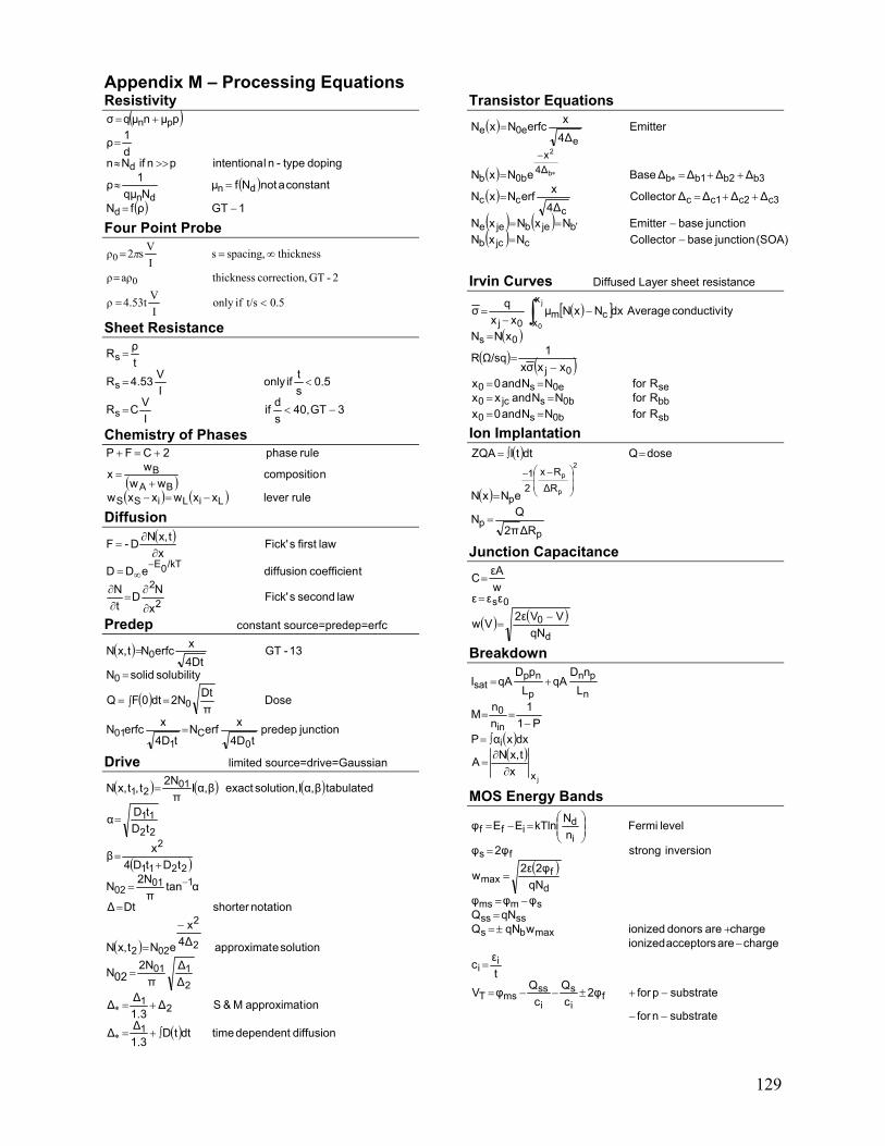
Appendix M – Processing EquationsResistivity
( )
( )( ) 1GTρfN
constantanotNfµNqµ
1ρ
doping type-n lintentiona pnifNnd1ρ
pµ nqσ
d
dndn
d
pn
−=
=≈
>>≈
=
+=
Four Point Probe
µ
0.5 t/sifonly IV4.53tρ
2-GT ,correction thicknessaρρ
thickness spacing, sIVs2ρ
0
0
<=
=
∞== π
Sheet Resistance
3GT40,sdif
IVCR
0.5stifonly
IV4.53R
tρR
s
s
s
−<=
<=
=
Chemistry of Phases
( )( ) ( ) rule lever xxwxxw
ncompositio ww
w x
rule phase 2 C F P
LiLiSSBA
B
−=−+
=
+=+
Diffusion ( )
law second sFick'xND
tN
tcoefficien diffusion eD D
law first sFick'x
tx,ND- F
2
2
/kT0E
∂
∂=
∂∂
=
∂∂
=
−∞
Predep constant source=predep=erfc
( )
( )
junctionpredept4D
xerfNt4D
xerfcN
DoseπDt2Ndt0F Q
solubility solidN
13-GT4DtxerfcNtx,N
0C
101
0
0
0
=
∫ ==
=
=
Drive limited source=drive=Gaussian
( ) ( ) ( )
( )
( )
( ) diffusiondependenttimedttD1.3∆∆
ionapproximatM&S∆1.3∆∆
∆∆
π2N
02N
solutioneapproximat4∆x
eNtx,N
notationshorterDt∆
αtanπ
2NN
tDtD4xβ
tDtDα
tabulatedβα,Ιsolution,exactβα,Ιπ
2Nt,tx,N
1
21
2101
2
2
022
10102
2211
22211
0121
∫+=
+=
=
−
=
=
=
+=
=
=
∗
∗
−
Transistor Equations
( )
( )( )
( ) ( )( ) (SOA)junctionbaseCollectorNxN
junctionbaseEmitterNxNxN
∆∆∆∆Collector4∆xerfNxN
∆∆∆∆BaseeNxN
Emitter4∆xerfcNxN
cjcbbjebjee
c3c2c1cc
cc
b3b2b1b4∆
x
0bb
e0ee
b
2
−=−==
++==
++==
=
′
∗
−
∗
Irvin Curves Diffused Layer sheet resistance
( )[ ]( )
( ) ( )
sb0bs0bb0bsjc0se0es0
0j
0s
x
xcm
0j
RforNNand0xRforNNandxxRforNNand0x
xxσx1Ω/sqR
xNN
tyconductiviAveragedxNxNµxx
qσj
0
====
==−
=
=
−−
= ∫
Ion Implantation ( )
( )
pp
∆RRx
21
p
∆R2πQN
eNxN
doseQdttIZQA2
p
p
=
=
=∫=
⎟⎟⎠
⎞⎜⎜⎝
⎛ −−
Junction Capacitance
( ) ( )d
0
0s
qNVV2εVw
εεεwεAC
−=
=
=
Breakdown
( )( )
jx
iin0
n
pn
p
npsat
xtx,NA
dxxαPP1
1nnM
LnD
qAL
pDqAI
∂∂
=
∫=−
==
+=
MOS Energy Bands
( )
substratenfor
substratepfor2φcQ
cQφV
tεc
chargeareacceptorsionizedcharge are donors ionizedwqNQ
qNQφφφqN
2φ2εw
inversion strong2φφ
level FerminNkTlnEEφ
fis
iss
msT
ii
maxbsssss
smmsd
fmax
fsi
diff
−−
−+±−−=
=
−+±=
=−=
=
=
⎟⎟⎠
⎞⎜⎜⎝
⎛=−=
129

130

131

132
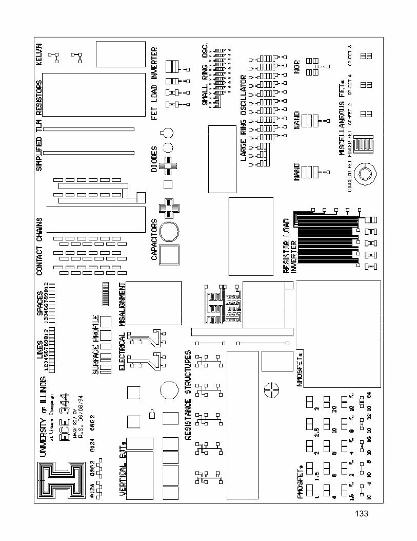
133

134

135

136

137

138

139

140

141

142

143