
05452994
13
INVITED PAPER Compressive Sensing on a CMOS Separable-Transform Image Sensor By compressing images before they are converted to digital format, this image sensor device can use analog computation to achieve much higher resolution at lower cost. By Ryan Robucci, Member IEEE , Jordan D. Gray, Student Member IEEE , Leung Kin Chiu, Student Member IEEE , Justin Romberg, Member IEEE , and Paul Hasler, Senior Member IEEE ABSTRACT | This paper demonstrates a computational image sensor capable of implementing compressive sensing opera- tions. Instead of sensing raw pixel data, this image sensor pro- jects the image onto a separable 2-D basis set and measures the corresponding expansion coefficients. The inner products are computed in the analog domain using a computational focal plane and an analog vector–matrix multiplier (VMM). This is more than mere postprocessing, as the processing circuity is integrated as part of the sensing circuity itself. We implement compressive imaging on the sensor by using pseudorandom vectors called noiselets for the measurement basis. This choice allows us to reconstruct the image from only a small percentage of the transform coefficients. This effectively compresses the image without any digital computation and reduces the throughput of the analog-to-digital converter (ADC). The re- duction in throughput has the potential to reduce power con- sumption and increase the frame rate. The general architecture and a detailed circuit implementation of the image sensor are discussed. We also present experimental results that demon- strate the advantages of using the sensor for compressive imaging rather than more traditional coded imaging strategies. KEYWORDS | CMOS analog integrated circuits; image sampling; image sensors; imaging; intelligent sensors I. HARDWARE FOR COMPRESSIVE IMAGE SENSING Following the standard model for imaging, the amount of data a sensor must capture, quantize, and transfer for processing scales linearly with its resolution. As images are typically structured, they can be compressed by significant ratios with very little information being lost, making storage and transmission less costly. But as this compres- sion is typically implemented on a digital signal processor (or other digital computing device), its benefits are realized only after the entire image has been converted to a digital representation and piped off of the sensor. In this paper, we present an imaging architecture that compresses the image before it is converted to a digital representation [Fig. 1(a)] using analog processing to remap the signal [Fig. 1(b)]. The architecture is based on a com- putational image sensor, which we call the transform imager. While most high-density imager architectures se- parate the image readout from the computation, the trans- form imager takes advantage of the required pixel readout to perform computations in analog. The imager is very flexible: by integrating focal-plane computation with peri- pheral analog computation circuitry, a variety of linear transformations can be performed (Fig. 2). Here, we con- figure the sensor to compute a separable transform of the pixelized data, and the computed coefficients are then quantized with an analog-to-digital converter (ADC). The Manuscript received April 22, 2009; revised January 4, 2010; accepted January 4, 2010. Date of publication April 22, 2010; date of current version May 19, 2010. Part of the development of IC described was supported by DARPA through the Integrated Sensing and Processing Program. R. Robucci is with the Department of Computer Science and Electrical Engineering, University of Maryland Baltimore County, Baltimore, MD 21250 USA (e-mail: [email protected]; [email protected]). J. D. Gray, L. K. Chiu, J. Romberg, and P. Hasler are with the School of Electrical and Computer Engineering, Georgia Institute of Technology, Atlanta, GA 30332-250 USA (e-mail: [email protected]; [email protected]; [email protected]; [email protected]). Digital Object Identifier: 10.1109/JPROC.2010.2041422 Vol. 98, No. 6, June 2010 | Proceedings of the IEEE 1089 0018-9219/$26.00 Ó2010 IEEE
Transcript of 05452994
INV ITEDP A P E R
Compressive Sensing on aCMOS Separable-TransformImage SensorBy compressing images before they are converted to digital format, this image sensor
device can use analog computation to achieve much higher resolution at lower cost.
By Ryan Robucci, Member IEEE, Jordan D. Gray, Student Member IEEE,
Leung Kin Chiu, Student Member IEEE, Justin Romberg, Member IEEE, and
Paul Hasler, Senior Member IEEE
ABSTRACT | This paper demonstrates a computational image
sensor capable of implementing compressive sensing opera-
tions. Instead of sensing raw pixel data, this image sensor pro-
jects the image onto a separable 2-D basis set and measures the
corresponding expansion coefficients. The inner products are
computed in the analog domain using a computational focal
plane and an analog vector–matrix multiplier (VMM). This is
more than mere postprocessing, as the processing circuity is
integrated as part of the sensing circuity itself. We implement
compressive imaging on the sensor by using pseudorandom
vectors called noiselets for the measurement basis. This choice
allows us to reconstruct the image from only a small percentage
of the transform coefficients. This effectively compresses the
image without any digital computation and reduces the
throughput of the analog-to-digital converter (ADC). The re-
duction in throughput has the potential to reduce power con-
sumption and increase the frame rate. The general architecture
and a detailed circuit implementation of the image sensor are
discussed. We also present experimental results that demon-
strate the advantages of using the sensor for compressive
imaging rather than more traditional coded imaging strategies.
KEYWORDS | CMOS analog integrated circuits; image sampling;
image sensors; imaging; intelligent sensors
I . HARDWARE FOR COMPRESSIVEIMAGE SENSING
Following the standard model for imaging, the amount of
data a sensor must capture, quantize, and transfer forprocessing scales linearly with its resolution. As images are
typically structured, they can be compressed by significant
ratios with very little information being lost, making
storage and transmission less costly. But as this compres-
sion is typically implemented on a digital signal processor
(or other digital computing device), its benefits are
realized only after the entire image has been converted
to a digital representation and piped off of the sensor.In this paper, we present an imaging architecture that
compresses the image before it is converted to a digital
representation [Fig. 1(a)] using analog processing to remap
the signal [Fig. 1(b)]. The architecture is based on a com-
putational image sensor, which we call the transformimager. While most high-density imager architectures se-
parate the image readout from the computation, the trans-
form imager takes advantage of the required pixel readoutto perform computations in analog. The imager is very
flexible: by integrating focal-plane computation with peri-
pheral analog computation circuitry, a variety of linear
transformations can be performed (Fig. 2). Here, we con-
figure the sensor to compute a separable transform of the
pixelized data, and the computed coefficients are then
quantized with an analog-to-digital converter (ADC). The
Manuscript received April 22, 2009; revised January 4, 2010; accepted January 4, 2010.
Date of publication April 22, 2010; date of current version May 19, 2010. Part of the
development of IC described was supported by DARPA through the Integrated Sensing
and Processing Program.
R. Robucci is with the Department of Computer Science and Electrical Engineering,
University of Maryland Baltimore County, Baltimore, MD 21250 USA
(e-mail: [email protected]; [email protected]).
J. D. Gray, L. K. Chiu, J. Romberg, and P. Hasler are with the School of Electrical and
Computer Engineering, Georgia Institute of Technology, Atlanta, GA 30332-250 USA
(e-mail: [email protected]; [email protected]; [email protected];
Digital Object Identifier: 10.1109/JPROC.2010.2041422
Vol. 98, No. 6, June 2010 | Proceedings of the IEEE 10890018-9219/$26.00 �2010 IEEE
compression comes from simply limiting the readout to a
subset of these coefficients.
The imager is fabricated using a 0.35-�m CMOSprocess. The current design has a 256 � 256 sensor array
using a pixel size of 8� 8 �m2 implemented in 22.75-mm2
area. Since the data compression is integrated into the
sensor array at the front end of the system, all subsequent
stages can receive the benefits of compression. Fewer
numbers have to be transferred off of the sensor array and
passed through the ADC, saving time and power. The
digital image computations can also be moved away fromthe sensor, a feature that is particularly attractive if the
camera is part of a distributed wireless sensor network that
utilizes a central processing node, as the sensor itself will
often have strict power and form-factor constraints.
The question, then, is what type of transform the
imager should take to make the compression as efficient as
possible. We compare two different sensing strategies. In
the first, the imager measures a certain number of discretecosine transform (DCT) coefficients, starting from low
spatial frequencies and working outwards. The image isreconstructedVdigitally and away from the sensorVby
taking an inverse DCT. This choice of transform (and the
ordering of the coefficients) is inspired by the JPEG
compression algorithm: it is often the case that we can
build a reasonable approximation to an image simply by
keeping its low-(spatial)-frequency components and dis-
carding its high-frequency components.
The second sensing strategy is inspired by the recentlydeveloped theory of compressive sensing (CS) [1]–[4].
CS, which is reviewed in Section II, is based on a more
refined image model than JPEG: rather than approximat-
ing an image using a small number of low-frequency DCT
coefficients, we use a small number of arbitrarily located
wavelet (or other sparsifying transform) coefficients.
From correlations of the image against pseudorandom
Bincoherent[ basis functions, convex programmingVagain implemented digitally away from the sensorVcan
be used to simultaneously locate the important transform
coefficients and reconstruct their values. The theory of
CS suggests that from m of these correlations, we can
compute an approximation to the image which is almost
as good as if we had observed the m most important
transform coefficients directly. From a broad perspective,
CS theory tells us that the amount of data the sensormust capture scales with the information content of the
image (i.e., its compressibility) rather than its resolution.
This paper is organized as follows. An overview of
compressive sensing is given in Section II. Several imaging
systems based on compressive sensing are surveyed in
Section III. Section IV presents the structure of the trans-
form image sensor, the computation of our transform
imager, and integrated test setup. Section V discussesusing the transform image sensor for compressive sensing,
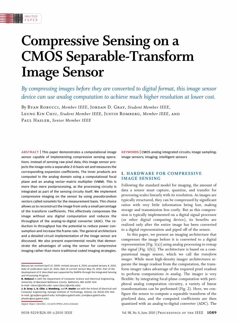
Fig. 1. Compressive sensing system design. (a) Total data manipulation
and power is reduced in the chain from sensor to transmitter by
sampling less often instead of just compressing data in the digital
domain. (b) Illustration of computation integrated into analog sensor
interface circuity. Time-varying row weightings and parallelized
column weightings are applied according to selected basis functions
as summations are performed. The output of the analog system is a
transformed version of the image. By utilizing an incomplete subset
of basis functions, fewer sensory computations and analog-to-digital
conversions (ADCs) need to be performed.
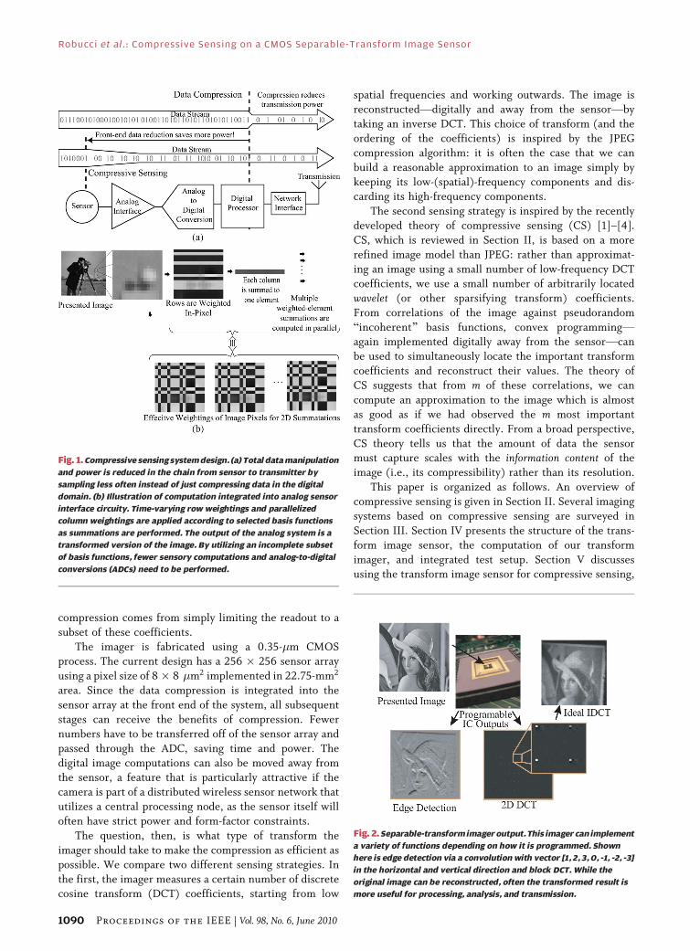
Fig. 2. Separable-transform imager output. This imager can implement
a variety of functions depending on how it is programmed. Shown
here is edge detection via a convolution with vector [1, 2, 3, 0, -1, -2, -3]
in the horizontal and vertical direction and block DCT. While the
original image can be reconstructed, often the transformed result is
more useful for processing, analysis, and transmission.
Robucci et al. : Compressive Sensing on a CMOS Separable-Transform Image Sensor
1090 Proceedings of the IEEE | Vol. 98, No. 6, June 2010
including showing experimental results for this com-pressed sensing front end, as well as the resulting
reconstruction. Integrating nonvolatile analog memory
and a versatile random access approach enables a variety of
operations such as multiresolution and selective sensing;
some of these extensions are discussed in Section VI. Final
remarks are made in Section VII.
II . COMPRESSIVE SENSING
The image sensor gives us the freedom to measure thepixelized image using inner products with any sequence of
(separable) basis functions. We would like to choose these
basis functions so that: 1) the image can be reconstructed
from the smallest number of measurements, and 2) the
reconstruction can be computed in an efficient manner.
The theory of compressed sensing [1]–[4] tells us that if we
have a sparse representation for images of interest, the
measurement functions should be chosen from a comple-mentary incoherent basis.
Mathematically, the measurements the sensor makes
can be written as a series of inner products
y1 ¼ h�1; Pi; y2 ¼ h�2; Pi; . . . ; ym ¼ h�m; Pi: (1)
Above, P is the image we are acquiring and the �k are the
measurement basis functions. As the computations in (1)
happen after the image is captured (but before it is digi-
tized), P and the �k can be taken as vectors. Even though
the image P is naturally arranged as a 2-D n� n array, we
will often treat it as a Brasterized[ n2 � 1 vector for nota-tional convenience. The entire measurement process can
be written compactly as Y ¼ �P, where � is an m� n2
matrix, Y is a vector in Rm, and P is a vector in R
n2
.
Reconstructing P from the measurements Y is then a linear
inverse problem. Since our goal is to take many fewer
measurements than there are pixels in the image, m� n2,
the inverse problem is severely underdetermined. To
counteract this, we incorporate a priori information aboutthe structure of the image into the reconstruction.
The y1; . . . ; ym can be used to calculate a projection
onto the subspace of Rn2
spanned by the �1; . . . ; �m (this is
trivial if the �k are orthogonal to one another). This points
to one possible acquisition strategy: find a subspace in
which we believe the energy of the image we are trying to
sample is concentrated, and then choose the �k as a basis
for this subspace. A good choice for this subspace, onemotivated by the fact that most of the energy in a typical
photograph-like image tends to be at low spatial frequen-
cies, is the span of the first m 2-D DCT coefficients taken in
the same Bzig-zag[ order as in the JPEG compression
standard [5].
Projecting the image onto the subspace of low-
frequency sinusoids is an effective way to get a very low-
dimensional, smoothed-out (Bblurry[) approximation to
the image. However, details in the image (sharp edges andlocalized features) resolve slowly as m increasesVthese
local features are diffused across all spatial frequencies,
making them hard to represent using the DCT. This type of
approximation also often suffers from Bringing[ around
the edges (Gibbs phenomenon).
We can construct better low-dimensional approximations
to images using the wavelet transform [6], [7]. Wavelets give
us a representation for images that is sparse and automat-ically adapts to local structure; only a small percentage of the
wavelet coefficients are significant, and they tend to cluster
around edge contours and other singuarities. This sparseness
allows us to construct an accurate and sharp approximation
of medium-size images (say, one megapixel) simply by
retaining around 2%–5% of their most significant wavelet
coefficients and throwing away the rest. That such accurate
approximations can be formed so easily is the reason that thewavelet transform lies at the heart of nearly every
competitive image compression algorithm, including the
JPEG2000 image compression standard [8].
There is a subtle difference between the two types of
approximation described above; in the first, we are pro-
jecting the image onto a fixed subspace (spanned by low-
frequency sinusoids), while in the second, we are adaptingthe subspace (spanned by the wavelet basis functions cor-responding to the largest wavelet coefficients) to the image.
It is this adaptation that accounts for almost the entire
advantage of wavelet-based approximation over DCT-based
approximation. It is also less straightforward to exploit
these advantages in our acquisition system: we would like
to measure only the significant wavelet coefficients, but we
have no idea which coefficients will be significant
beforehand.The theory of compressive sensing shows us how we can
choose a set of �k to take advantage of the fact that the
image is sparse. One of the central results of CS says that if
the image is sparse in an orthonormal basis � (e.g., the
wavelet domain), then we should select the �k from an
alternative basis �0 that is very different than (or incoherentwith) �. Formally, the coherence between two image
representations is simply the maximum correlation of abasis vector from � with a basis vector from �0
�ð�;�0Þ ¼ max 2 �� 2 �
h ; �ij j:
We will always have � � 1=n, and so we will call � and �0
Bincoherent[ if �ð�;�0Þ � 1=n. Fortunately, there is aknown orthogonal system, called the noiselet transform [9],
that is incoherent with the wavelet transform. Examples of
noiselets are shown in Fig. 7; they are binary, 2-D sepa-
rable basis vectors which look like pseudorandom noise.
They are also spread out in the wavelet domain. If � is a
2-D Daubechies-8 wavelet transform for n ¼ 256 and �0
is the noiselet transform, then �ð�;�0Þ � 4:72=n.
Robucci et al. : Compressive Sensing on a CMOS Separable-Transform Image Sensor
Vol. 98, No. 6, June 2010 | Proceedings of the IEEE 1091
Given the measurements Y, there are a variety of wayswe can reconstruct the image. One popular way, which is
provably effective, is to set up an optimization program
that encourages the image to be sparse in the � domain
while simultaneously explaining the measurements we
have made
minX
�ðXÞk k1 subject to �X ¼ Y: (2)
This program sorts through all of the images consistent
with what we have observed and returns the one with
smallest ‘1 norm in the � domain. The ‘1 norm promotes
sparsityVsparse vectors have smaller ‘1 norm thannonsparse vectors with the same energy. When there is
noise or other uncertainties in the measurements, (2) can
be relaxed to
minX
�ðXÞk k1 subject to k�X � Yk2 � � (3)
where � is chosen based on the expected noise level.
When � is chosen from an incoherent system and the
image P we are trying to recover is sparse, the recovery
programs (2) and (3) come with certain theoretical
performance guarantees [1], [2], [4]. From m incoherent
measurements, (2) will produce an approximation P to Pthat is as good as a wavelet approximation using on theorder of�m= log4 n terms. Numerical experiments suggest
even more favorable behavior; P is often as good as an
�m=4 term wavelet approximation [10], [11]. The essential
message here is that the number of measurements we need
to faithfully acquire P depends mainly on how well we can
compress P (i.e., its inherent complexity) and not on the
number of pixels it has. If the vast majority of the
information about the image is contained in 2%–5% ofthe wavelet coefficients, then we can acquire it using a
number of measurements which is �8%–20% of the total
number of pixels.
There are two extensions to the CS methodology that
help produce better image reconstructions in practice. The
first is to make � a redundant (or undecimated) wavelet
transform [12]; this choice tends to produce images with
fewer local artifacts. Another way to boost image recon-struction quality is by using an iterative reweighting scheme
[13]. After obtaining an initial solution P0 to (3) [or (2)], we
resolve the program, but with a weighted ‘1 norm
minX
W �ðXÞk k1 subject to k�X � Yk2 � �:
The weighting matrix W is diagonal, and its entries are
inversely proportional to the magnitudes of the corre-
sponding entries in �ðP0Þ
Wii ¼1
�ðP0Þi�� ��þ �
for small � > 0. This reweighting can be applied multiple
times in succession, with the weights adjusted according tothe transform coefficients of the previous solution.
III . COMPRESSIVE SENSING-INSPIREDIMAGING SYSTEMS
In this section, we briefly describe other compressive
imaging architectures that have been proposed in recent
years. Generally speaking, in these alternative architec-tures, the compressive measurements [inner products with
measurement basis functions as in (1)] are taken by mani-
pulating the light field using some type of high-resolution,
spatial light modulation or optical dispersion, and then
measured using a low-resolution sensor array, the output
of which is immediately converted into the digital domain.
In contrast, the optics in our transform imager are com-
pletely standard, and the image is measured using a high-resolution sensor array. Before the pixel values are
converted to digital, we use low-power analog electronic
processing to take the compressive measurements, and
digitize the result. Another imager architecture that uses
random electronic modulation is also discussed.
In [14], the concept of a high-resolution spatial light
modulator followed by a low-resolution sensor array is
taken to the extreme with a single pixel camera. As lightenters the system, it is focused with a lens onto a digital
micromirror device (DMD). The DMD is a large array
(1024� 768 in this case) of tiny mirrors, each of which can
be individually controlled to point in one of two directions.
In one of these directions lies another lens which focuses
the Boutput[ of the DMD onto a single photodetector. The
net effect is that the photodetector measures an inner
product of the image incident on the DMD with a singlebinary (0–1 valued) basis function. The measurements are
taken serially, and reconstructed using the same techniques
discussed in Section II. Because it only uses a single sensor,
the single pixel camera is very well suited for imaging
modes where detectors are expensive; see, for example, its
application to low-light imaging with photomultiplier tubes
[15] and terahertz imaging [16].
The Compressive Optical MONTAGE PhotographyInitiative (COMP-I) at Duke University has developed a
number of compressive imaging architectures [17]–[19]
with the goal of creating very thin cameras. In one such
architecture, described in detail in [17], compressive imag-
ing is implemented using a camera with multiple apertures.
There, a block transform is implemented on the focal plane
as follows. The incoming light meets an array of lenses (or
Blenslets[), each of which focuses the entire image onto a
Robucci et al. : Compressive Sensing on a CMOS Separable-Transform Image Sensor
1092 Proceedings of the IEEE | Vol. 98, No. 6, June 2010
different section of the sensor array. Before each image hitsits part of the array, it passes through a high-resolution
aperture mask. Each section of the pixel array then mea-
sures the correlation of the image with the code determined
by the aperture mask; if there are multiple pixel sensors per
aperture, the inner product is broken up locally.
In [20], a camera with a Brandom lens[ is detailed. In
this work, the lens of a camera is replaced with a random
reflective surface. The effect is that a single Bpixel[ in theinput image contributes to several different pixels in the
measurement array, the locations of which may be com-
pletely nonlocal. The random reflective surface is created
in an uncontrolled way, so the camera must be calibrated
to discover the sensing matrix �. There is a tradeoff here,
as the sparser the sensing matrix � is, the easier it is to
discover (by training the camera on a relatively small set
of randomly generated but known input images) andcompute with, but the less like a compressive sampling
matrix it isVsparse matrices have high coherence with
the wavelet transform (which is also sparse).
The approaches discussed thus far utilize moving parts
and/or specialized optics to perform optical computations,
while our transform imager utilizes analog electronic
computations. Another approach using electronic compu-
tations is a complementary metal–oxide–semiconductor(CMOS) convolution imager architecture introduced in [21].
Like the transform imager, this convolution imager is
based on a CMOS pixel array which does local, per-pixel
computations. As the analog image data sits on the sensor
array, it is convolved with a random, binary pulse sequence
of 1’s and �1’s, and the result is randomly subsampled
(convolution with a random pulse sequence followed by
subsampling comes with the same compressive samplingguarantees as sampling in an incoherent basis; see [22] and
[23]). The binary weights for the random pulse sequence are
passed through the array using a circular shift register
initialized with a random sequence. This imager does not rely
on a separable basis as our transform imager does, but it lacks
the ability to use adaptable or analog weights, perform other
computations such as DCT, or tailor measurements to extract
details from portions of the image plane.
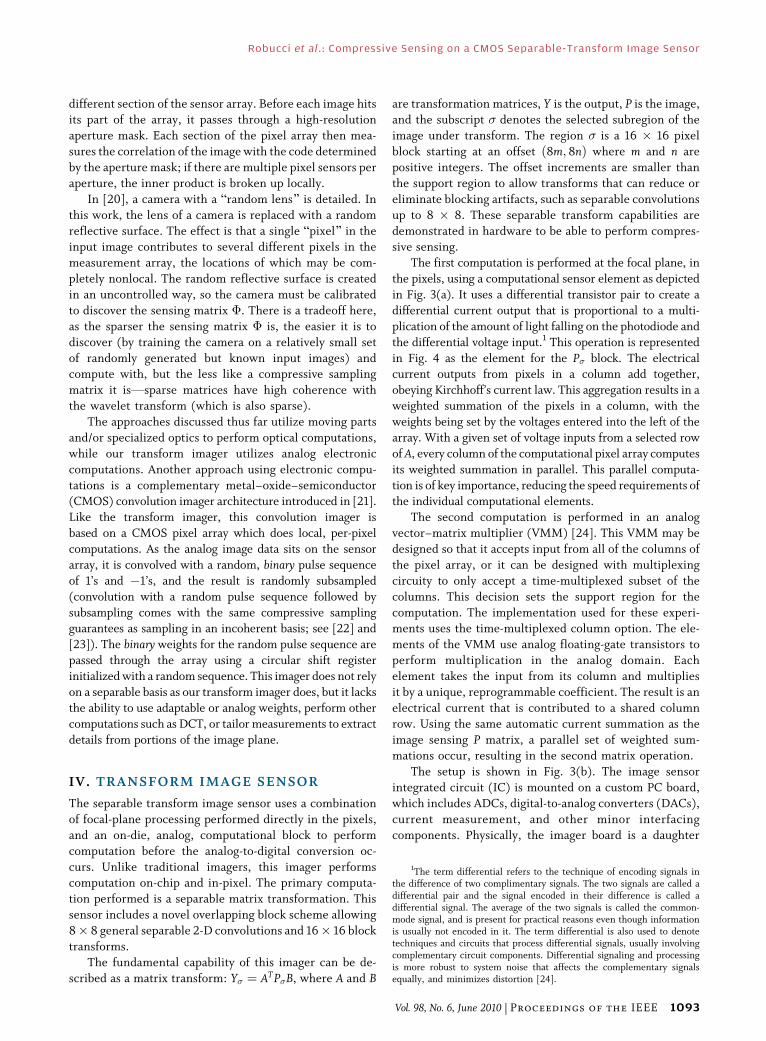
IV. TRANSFORM IMAGE SENSOR
The separable transform image sensor uses a combination
of focal-plane processing performed directly in the pixels,
and an on-die, analog, computational block to perform
computation before the analog-to-digital conversion oc-
curs. Unlike traditional imagers, this imager performscomputation on-chip and in-pixel. The primary computa-
tion performed is a separable matrix transformation. This
sensor includes a novel overlapping block scheme allowing
8� 8 general separable 2-D convolutions and 16� 16 block
transforms.
The fundamental capability of this imager can be de-
scribed as a matrix transform: Y� ¼ ATP�B, where A and B
are transformation matrices, Y is the output, P is the image,and the subscript � denotes the selected subregion of the
image under transform. The region � is a 16 � 16 pixel
block starting at an offset ð8m; 8nÞ where m and n are
positive integers. The offset increments are smaller than
the support region to allow transforms that can reduce or
eliminate blocking artifacts, such as separable convolutions
up to 8 � 8. These separable transform capabilities are
demonstrated in hardware to be able to perform compres-sive sensing.
The first computation is performed at the focal plane, in
the pixels, using a computational sensor element as depicted
in Fig. 3(a). It uses a differential transistor pair to create a
differential current output that is proportional to a multi-
plication of the amount of light falling on the photodiode and
the differential voltage input.1 This operation is represented
in Fig. 4 as the element for the P� block. The electricalcurrent outputs from pixels in a column add together,
obeying Kirchhoff’s current law. This aggregation results in a
weighted summation of the pixels in a column, with the
weights being set by the voltages entered into the left of the
array. With a given set of voltage inputs from a selected row
of A, every column of the computational pixel array computes
its weighted summation in parallel. This parallel computa-
tion is of key importance, reducing the speed requirements ofthe individual computational elements.
The second computation is performed in an analog
vector–matrix multiplier (VMM) [24]. This VMM may be
designed so that it accepts input from all of the columns of
the pixel array, or it can be designed with multiplexing
circuity to only accept a time-multiplexed subset of the
columns. This decision sets the support region for the
computation. The implementation used for these experi-ments uses the time-multiplexed column option. The ele-
ments of the VMM use analog floating-gate transistors to
perform multiplication in the analog domain. Each
element takes the input from its column and multiplies
it by a unique, reprogrammable coefficient. The result is an
electrical current that is contributed to a shared column
row. Using the same automatic current summation as the
image sensing P matrix, a parallel set of weighted sum-mations occur, resulting in the second matrix operation.
The setup is shown in Fig. 3(b). The image sensor
integrated circuit (IC) is mounted on a custom PC board,
which includes ADCs, digital-to-analog converters (DACs),
current measurement, and other minor interfacing
components. Physically, the imager board is a daughter
1The term differential refers to the technique of encoding signals inthe difference of two complimentary signals. The two signals are called adifferential pair and the signal encoded in their difference is called adifferential signal. The average of the two signals is called the common-mode signal, and is present for practical reasons even though informationis usually not encoded in it. The term differential is also used to denotetechniques and circuits that process differential signals, usually involvingcomplementary circuit components. Differential signaling and processingis more robust to system noise that affects the complementary signalsequally, and minimizes distortion [24].
Robucci et al. : Compressive Sensing on a CMOS Separable-Transform Image Sensor
Vol. 98, No. 6, June 2010 | Proceedings of the IEEE 1093
card of the field-programmable gate array (FPGA)motherboard. The FPGA is configured to implement a soft-
core processor and collection of custom hardware interface
components described in VHDL. The supporting compo-
nents handle timing-critical signal flow, allowing for more
manageable but less timing-sensitive C code to be used on the
soft-core processor. A supporting VHDL module also handles
interfacing to the external USB IC for communicating with a
computer. The user interface to the system is a set of Matlabfunctions which encapsulate the IC control. The user has the
ability to program an arbitrary set of coefficients into the Aand B matrices. A DCT is an example of such a
transformation matrix. The user can then capture the image,
which undergoes the on-chip transformation.
CMOS imaging technology can be implemented on
standard, relatively low-cost CMOS processes. CMOS im-
plementation enables integration of large amounts of com-
putational circuitry with sensor and interface circuitry. By
integrating circuit components into the image sensor, suchas in-pixel ADCs [25], CMOS technology has become
Fig. 3. Basics of the transform imager approach. (a) Block matrix computation performed in the analog domain. Illustrated here as an
8 � 8 block transform, both a computational pixel array and an analog vector–matrix multiplier are used to perform signal projection before
data are converted into the digital domain. (b) A daughter card houses the computational image sensor IC along with supporting components.
This card mounts on an FPGA board through a standard PCI mezzanine connector. Communication with the PC is done through USB.
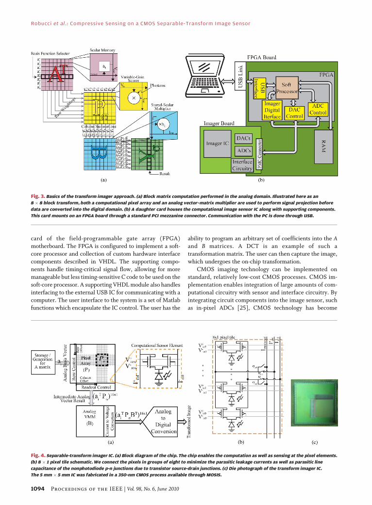
Fig. 4. Separable-transform imager IC. (a) Block diagram of the chip. The chip enables the computation as well as sensing at the pixel elements.
(b) 8 � 1 pixel tile schematic. We connect the pixels in groups of eight to minimize the parasitic leakage currents as well as parasitic line
capacitance of the nonphotodiode p-n junctions due to transistor source-drain junctions. (c) Die photograph of the transform imager IC.
The 5 mm � 5 mm IC was fabricated in a 350-nm CMOS process available through MOSIS.
Robucci et al. : Compressive Sensing on a CMOS Separable-Transform Image Sensor
1094 Proceedings of the IEEE | Vol. 98, No. 6, June 2010
competitive in the high-end camera market. Other aggressivecircuit integrations in CMOS imaging technology provide
additional computationally significant gains, such as random
image access [26], dynamic field of view capabilities [27],
multiresolution image sensing [28], and biologically inspired
abilities such as edge enhancement [29].
The system IC, as shown in Fig. 4(a), is composed of
the following: a random-access analog memory, row and
column selection control, a computational pixel array,logarithmic current-to-voltage (I-V) converter, an analog
VMM, and a bidirectional I-V converter. Fig. 4(c) shows
the die photo of the transform imager IC. We will describe
these blocks in Section IV-A–D.
A. Light Sensor and InterfacingFig. 4(b) shows a schematic of an 8 � 1 pixel tile. Each
pixel is a photosensor and a differential transistor pair,providing both a sensing capability and a multiply–
accumulate operation. The output of each pixel is a dif-
ferential current1 and it represents a multiplication of the
light intensity falling on the photosensor by a weighting
value represented by a voltage input. Pixels along a given
row of the image plane share a single, differential, voltage
input, which sets the multiplication factor for the row.
Pixels along a column share a differential-current outputline. Since the outputs of the pixels are currents, and cur-
rents onto a node sum together, an addition operation is
performed. More specifically, this is a weighted summa-
tion, also known as a dot product. Within each tile is a
switch which selectively allows the pixels in the tile to
output to the column. When deselected, the pixels’ cur-
rents are switched off of the column’s output line and onto a
separate fixed-potential line. Since only a subportion of therows of the imager are read at a time, these switches result
in a 1/8th reduction of parasitic capacitance introduced by
the deactivated pixels’ drain junctions. Furthermore, these
parasitic junctions introduce unwanted currents to the
output line, since they themselves are photo diodes.
Therefore, these switches reduce parasitic capacitances
and currents to improve signal-to-noise ratio (SNR).
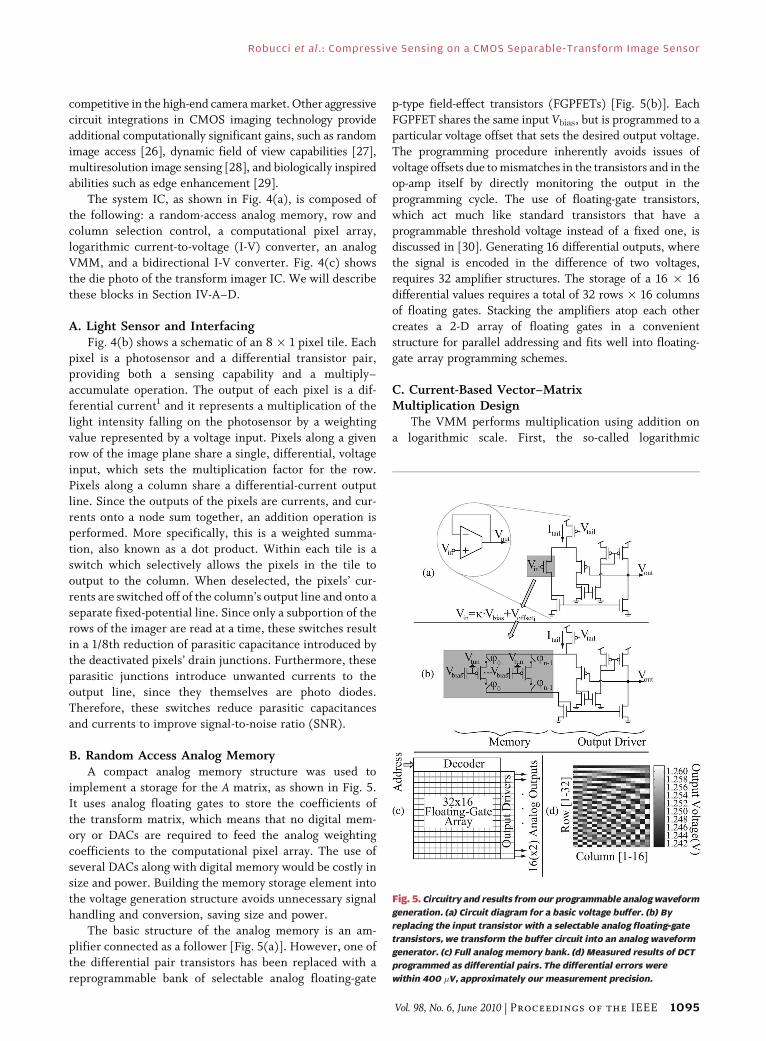
B. Random Access Analog MemoryA compact analog memory structure was used to
implement a storage for the A matrix, as shown in Fig. 5.
It uses analog floating gates to store the coefficients of
the transform matrix, which means that no digital mem-
ory or DACs are required to feed the analog weighting
coefficients to the computational pixel array. The use of
several DACs along with digital memory would be costly insize and power. Building the memory storage element into
the voltage generation structure avoids unnecessary signal
handling and conversion, saving size and power.
The basic structure of the analog memory is an am-
plifier connected as a follower [Fig. 5(a)]. However, one of
the differential pair transistors has been replaced with a
reprogrammable bank of selectable analog floating-gate
p-type field-effect transistors (FGPFETs) [Fig. 5(b)]. EachFGPFET shares the same input Vbias, but is programmed to a
particular voltage offset that sets the desired output voltage.
The programming procedure inherently avoids issues of
voltage offsets due to mismatches in the transistors and in the
op-amp itself by directly monitoring the output in the
programming cycle. The use of floating-gate transistors,
which act much like standard transistors that have a
programmable threshold voltage instead of a fixed one, isdiscussed in [30]. Generating 16 differential outputs, where
the signal is encoded in the difference of two voltages,
requires 32 amplifier structures. The storage of a 16 � 16
differential values requires a total of 32 rows � 16 columns
of floating gates. Stacking the amplifiers atop each other
creates a 2-D array of floating gates in a convenient
structure for parallel addressing and fits well into floating-
gate array programming schemes.
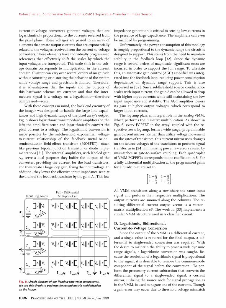
C. Current-Based Vector–MatrixMultiplication Design
The VMM performs multiplication using addition on
a logarithmic scale. First, the so-called logarithmic
Fig. 5. Circuitry and results from our programmable analog waveform
generation. (a) Circuit diagram for a basic voltage buffer. (b) By
replacing the input transistor with a selectable analog floating-gate
transistors, we transform the buffer circuit into an analog waveform
generator. (c) Full analog memory bank. (d) Measured results of DCT
programmed as differential pairs. The differential errors were
within 400 �V, approximately our measurement precision.
Robucci et al. : Compressive Sensing on a CMOS Separable-Transform Image Sensor
Vol. 98, No. 6, June 2010 | Proceedings of the IEEE 1095
current-to-voltage converters generate voltages that arelogarithmically proportional to the currents received from
the pixel plane. These voltages are passed to an array of
elements that create output currents that are exponentially
related to the voltages received from the current-to-voltage
converters. These elements have individually programmed
references that effectively shift the scales by which the
input voltages are interpreted. This scale shift in the volt-
age domain corresponds to multiplication in the currentdomain. Current can vary over several orders of magnitude
without saturating or distorting the behavior of the system
while voltage range and precision is limited. Therefore,
it is advantageous that the inputs and the outputs of
this hardware scheme are currents and that the inter-
mediate signal is a voltage on a logarithmicVtherefore
compressedVscale.
With these concepts in mind, the back end circuitry ofthe imager was designed to handle the large line capaci-
tances and high dynamic range of the pixel array’s output.
Fig. 6 shows logarithmic transimpedance amplifiers on the
left; the amplifiers sense and logarithmically convert the
pixel current to a voltage. The logarithmic conversion is
made possible by the subthreshold exponential voltage-
to-current relationship of the feedback metal–oxide–
semiconductor field-effect transistor (MOSFET), muchlike previous bipolar junction transistor or diode imple-
mentations [31]. The internal amplifiers, with labeled gain
Av, serve a dual purpose: they buffer the outputs of the
converter, providing the current for the load transistors,
and they create a large loop gain, fixing the input voltage. In
addition, they lower the effective input impedance seen at
the drain of the feedback transistor by the gain, Av. This low
impedance generation is critical to sensing low currents inthe presence of large capacitance. The amplifiers can even
be matched by programming.
Unfortunately, the power consumption of this topology
is roughly proportional to the dynamic range the circuit is
designed to support. This stems from the need to maintain
stability in the feedback loop [32]. Since the dynamic
range is several orders of magnitude, significant costs are
incurred in order to support the full range. To alleviatethis, an automatic gain control (AGC) amplifier was integ-
rated into the feedback loop, reducing power consumption
dependence on dynamic range support. This is also
discussed in [32]. Since subthreshold source conductance
scales with input current, the gain A can be allowed to drop
with higher input currents while still maintaining the low
input impedance and stability. The AGC amplifier lowers
its gain at higher output voltages, which correspond tolarger input currents.
The log amp plays an integral role in the analog VMM,
which performs the B matrix multiplication. As shown in
Fig. 6, every FGPFET in the array, coupled with the re-
spective row’s log amp, forms a wide range, programmable
gain current mirror. Rather than utilize voltage movement
on the gates of transistors, this current mirror uses changes
on the source voltages of the transistors to perform signaltransfer, as in [24], minimizing power law errors caused by
mismatches in gate-to-surface coupling. Each quadruplet
of VMM FGPFETs corresponds to one coefficient in B. For
a fully differential multiplication w, the programmed gains
for a quadruplet are set to
1þ w2
1� w2
1� w2
1þ w2
� �:
All VMM transistors along a row share the same input
signal and perform their respective multiplications. The
output currents are summed along the columns. The re-
sulting differential current output vector is a vector–matrix multiplication vB. The work in [33] implements a
similar VMM structure used in a classifier circuit.
D. Logarithmic, Bidirectional,Current-to-Voltage Conversion
Since the output of the VMM is a differential current,
and a single value is required for the final output, a dif-
ferential to single-ended conversion was required. Withthe desire to maintain the ability to process wide dynamic
range signals, a logarithmic conversion was sought. Be-
cause the resolution of a logarithmic signal is proportional
to the signal, it is desirable to remove the common-mode
component of the signal before the conversion.1 To per-
form the precursory current subtraction that converts the
differential signal to a single-ended signal, a current
mirror, utilizing the source node for signal propagation asin the VMM, is used to negate one of the currents. Though
a gain error may occur due to threshold voltage mismatch
Fig. 6. Circuit diagram of our floating-gate VMM components.
We use this circuit to perform the second matrix multiplication
on the image.
Robucci et al. : Compressive Sensing on a CMOS Separable-Transform Image Sensor
1096 Proceedings of the IEEE | Vol. 98, No. 6, June 2010
in the current mirrors, this is accounted for when prog-ramming the corresponding column of the VMM. The
resulting current signal can be positive or negative in
direction. Hence, a special converter was designed to
perform logarithmic conversion on a negative or positive
signal [34]. As the input current deviates from zero, the
converter approximates a logarithmic compression. This
bidirectional converter is very useful in applications where
support for large dynamic range is essential and smallcurrents must be sensed at moderate to high bandwidths.
V. COMPRESSIVE IMAGINGAND RECONSTRUCTION
In this section, we compare two different image acquisi-
tion strategies using the transform imager. The imager
acquires 256 � 256 pixel images; the hardware imple-mentation we discuss here breaks the image into 256 16 �16 pixel blocks, and measures a certain number of
transform coefficients in each of these blocks. In principle,
the number of coefficients can vary from block to blockVa
useful feature if there are certain regions of the image we
are more interested in than othersVbut the experiments
in this section keep this number fixed.
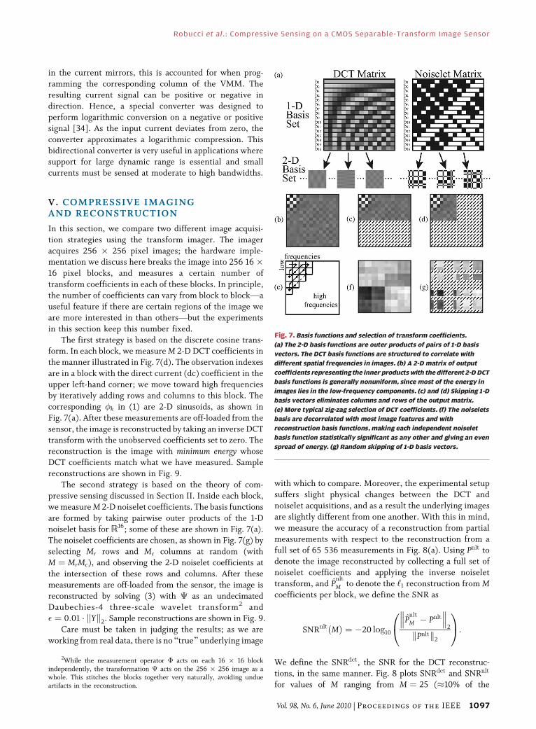
The first strategy is based on the discrete cosine trans-form. In each block, we measure M 2-D DCT coefficients in
the manner illustrated in Fig. 7(d). The observation indexes
are in a block with the direct current (dc) coefficient in the
upper left-hand corner; we move toward high frequencies
by iteratively adding rows and columns to this block. The
corresponding �k in (1) are 2-D sinusoids, as shown in
Fig. 7(a). After these measurements are off-loaded from the
sensor, the image is reconstructed by taking an inverse DCTtransform with the unobserved coefficients set to zero. The
reconstruction is the image with minimum energy whose
DCT coefficients match what we have measured. Sample
reconstructions are shown in Fig. 9.
The second strategy is based on the theory of com-
pressive sensing discussed in Section II. Inside each block,
we measure M 2-D noiselet coefficients. The basis functions
are formed by taking pairwise outer products of the 1-Dnoiselet basis for R16; some of these are shown in Fig. 7(a).
The noiselet coefficients are chosen, as shown in Fig. 7(g) by
selecting Mr rows and Mc columns at random (with
M ¼ MrMc), and observing the 2-D noiselet coefficients at
the intersection of these rows and columns. After these
measurements are off-loaded from the sensor, the image is
reconstructed by solving (3) with � as an undecimated
Daubechies-4 three-scale wavelet transform2 and� ¼ 0:01 kYk2. Sample reconstructions are shown in Fig. 9.
Care must be taken in judging the results; as we are
working from real data, there is no Btrue[ underlying image
with which to compare. Moreover, the experimental setup
suffers slight physical changes between the DCT and
noiselet acquisitions, and as a result the underlying images
are slightly different from one another. With this in mind,
we measure the accuracy of a reconstruction from partialmeasurements with respect to the reconstruction from a
full set of 65 536 measurements in Fig. 8(a). Using Pnlt to
denote the image reconstructed by collecting a full set of
noiselet coefficients and applying the inverse noiselet
transform, and Pnlt
M to denote the ‘1 reconstruction from Mcoefficients per block, we define the SNR as
SNRnltðMÞ ¼ �20 log10
Pnlt
M � Pnlt��� ���
2
kPnltk2
0@
1A:
We define the SNRdct, the SNR for the DCT reconstruc-tions, in the same manner. Fig. 8 plots SNRdct and SNRnlt
for values of M ranging from M ¼ 25 (�10% of the
2While the measurement operator � acts on each 16 � 16 blockindependently, the transformation � acts on the 256 � 256 image as awhole. This stitches the blocks together very naturally, avoiding undueartifacts in the reconstruction.
Fig. 7. Basis functions and selection of transform coefficients.
(a) The 2-D basis functions are outer products of pairs of 1-D basis
vectors. The DCT basis functions are structured to correlate with
different spatial frequencies in images. (b) A 2-D matrix of output
coefficients representing the inner products with the different 2-D DCT
basis functions is generally nonuniform, since most of the energy in
images lies in the low-frequency components. (c) and (d) Skipping 1-D
basis vectors eliminates columns and rows of the output matrix.
(e) More typical zig-zag selection of DCT coefficients. (f) The noiselets
basis are decorrelated with most image features and with
reconstruction basis functions, making each independent noiselet
basis function statistically significant as any other and giving an even
spread of energy. (g) Random skipping of 1-D basis vectors.
Robucci et al. : Compressive Sensing on a CMOS Separable-Transform Image Sensor
Vol. 98, No. 6, June 2010 | Proceedings of the IEEE 1097
measurements, or a �90% compression rate) to M ¼ 210(�82% of the measurements, or a�18% compression rate).
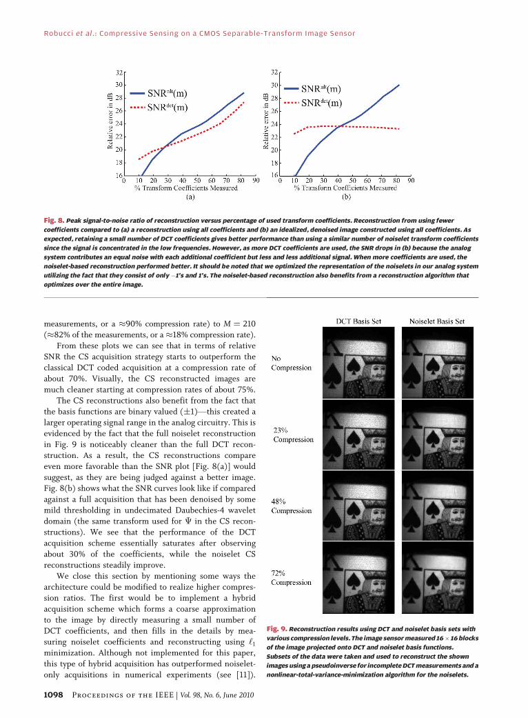
From these plots we can see that in terms of relative
SNR the CS acquisition strategy starts to outperform the
classical DCT coded acquisition at a compression rate of
about 70%. Visually, the CS reconstructed images are
much cleaner starting at compression rates of about 75%.
The CS reconstructions also benefit from the fact that
the basis functions are binary valued (1)Vthis created alarger operating signal range in the analog circuitry. This is
evidenced by the fact that the full noiselet reconstruction
in Fig. 9 is noticeably cleaner than the full DCT recon-
struction. As a result, the CS reconstructions compare
even more favorable than the SNR plot [Fig. 8(a)] would
suggest, as they are being judged against a better image.
Fig. 8(b) shows what the SNR curves look like if compared
against a full acquisition that has been denoised by somemild thresholding in undecimated Daubechies-4 wavelet
domain (the same transform used for � in the CS recon-
structions). We see that the performance of the DCT
acquisition scheme essentially saturates after observing
about 30% of the coefficients, while the noiselet CS
reconstructions steadily improve.
We close this section by mentioning some ways the
architecture could be modified to realize higher compres-sion ratios. The first would be to implement a hybrid
acquisition scheme which forms a coarse approximation
to the image by directly measuring a small number of
DCT coefficients, and then fills in the details by mea-
suring noiselet coefficients and reconstructing using ‘1
minimization. Although not implemented for this paper,
this type of hybrid acquisition has outperformed noiselet-
only acquisitions in numerical experiments (see [11]).
Fig. 8. Peak signal-to-noise ratio of reconstruction versus percentage of used transform coefficients. Reconstruction from using fewer
coefficients compared to (a) a reconstruction using all coefficients and (b) an idealized, denoised image constructed using all coefficients. As
expected, retaining a small number of DCT coefficients gives better performance than using a similar number of noiselet transform coefficients
since the signal is concentrated in the low frequencies. However, as more DCT coefficients are used, the SNR drops in (b) because the analog
system contributes an equal noise with each additional coefficient but less and less additional signal. When more coefficients are used, the
noiselet-based reconstruction performed better. It should be noted that we optimized the representation of the noiselets in our analog system
utilizing the fact that they consist of only �1’s and 1’s. The noiselet-based reconstruction also benefits from a reconstruction algorithm that
optimizes over the entire image.
Fig. 9. Reconstruction results using DCT and noiselet basis sets with
various compression levels. The image sensor measured 16� 16 blocks
of the image projected onto DCT and noiselet basis functions.
Subsets of the data were taken and used to reconstruct the shown
images using a pseudoinverse for incomplete DCT measurements and a
nonlinear-total-variance-minimization algorithm for the noiselets.
Robucci et al. : Compressive Sensing on a CMOS Separable-Transform Image Sensor
1098 Proceedings of the IEEE | Vol. 98, No. 6, June 2010
Another way to achieve higher compression ratios is toincrease the block size of the imager, which would allow
us to take advantage of the structure of the image at a
larger scale. As discussed in Section VI, this architectural
modification is being implemented at the current time.
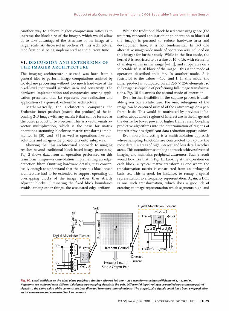
VI. DISCUSSION AND EXTENSIONS OFTHE IMAGER ARCHITECTURE
The imaging architecture discussed was born from a
general idea to perform image computations assisted by
focal-plane processing without too much hardware at the
pixel-level that would sacrifice area and sensitivity. The
hardware implementation and compressive sensing appli-
cation presented thus far represent one realization and
application of a general, extensible architecture.
Mathematically, the architecture computes theFrobenius inner product (matrix dot product) of the in-
coming 2-D image with any matrix F that can be formed as
the outer product of two vectors. This is a vector–matrix–
vector multiplication, which is the basis for matrix
operations stemming blockwise matrix transforms imple-
mented in [30] and [35] as well as operations like con-
volutions and image-wide projections onto subspaces.
Showing that this architectural approach to imagingreaches beyond traditional block-based image processing,
Fig. 2 shows data from an operation performed on this
transform imagerVa convolution implementing an edge-
detection filter. Omitting hardware details, it is concep-
tually enough to understand that the previous block-based
architecture had to be extended to support operating on
overlapping blocks of the image, rather than strictly
adjacent blocks. Eliminating the fixed block boundariesavoids, among other things, the associated edge artifacts.
While the traditional block-based processing genre (theuniform, repeated application of an operation to blocks of
the image) is pursued to reduce hardware area and
development time, it is not fundamental. In fact one
alternative image-wide mode of operation was included on
this imager for further study. While in the first mode, the
kernel F is restricted to be a size of 16 � 16, with elements
of analog values in the range ½�1; 1�, and it operates on a
selectable 16 � 16 block of the imageVthis is the mode ofoperation described thus far. In another mode, F is
restricted to the values �1; 0, and 1. In this mode, the
inner product is computed on all 256 � 256 elements; so
the imager is capable of performing full-image transforma-
tions. Fig. 10 illustrates the second mode of operation.
Even further flexibility in the capture process is avail-
able given our architecture. For one, subregions of the
image can be captured instead of the entire image on a per-frame basis. This would be motivated by previous infor-
mation about where regions of interest are in the image and
the desire for lower power or higher frame rates. Coupling
predictive algorithms into the determination of regions of
interest provides significant data reduction opportunities.
Even more interesting is a multiresolution approach
where sampling functions are constructed to capture the
most detail in areas of high interest and less detail in otherareas. This nonuniform sampling approach achieves foveated
imaging and maintains peripheral awareness. Such a result
would look like that in Fig. 11. Looking at the operation on
each block, a typical matrix transform is one where the
transformation matrix is constructed from an orthogonal
basis set. This is used, for instance, to remap a spatial
representation to a frequency representation. Again, a DCT
is one such transformation, which does a good job ofcreating an image representation which segments high- and
Fig. 10. Small additions to the pixel plane periphery circuitry allowed full 256 � 256 transforms using coefficients of 1, �1, and 0.
Negations are achieved with differential signals by swapping signals in the pair. Differential input voltages are nulled by setting the pair of
signals to the same value while currents are best diverted from the summed outputs. The output pairs signals could have been swapped after
an I-V conversion and converted back to currents.
Robucci et al. : Compressive Sensing on a CMOS Separable-Transform Image Sensor
Vol. 98, No. 6, June 2010 | Proceedings of the IEEE 1099
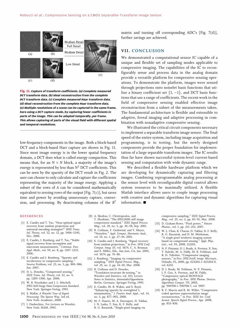
low-frequency components in the image. Both a block-based
DCT and a block-based Harr capture are shown in Fig. 11.
Since most image energy is in the lower spatial frequency
domain, a DCT does what is called energy compaction. This
means that, for an N � N block, a majority of the image’s
energy is represented by less than N2 DCT coefficients. This
can be seen by the sparsity of the DCT result in Fig. 2. Theuser can choose to only calculate and capture the coefficients
representing the majority of the image energy. Applying a
subset of the rows of A can be considered mathematically
equivalent to zeroing rows of the output [Fig. 7(c)], but saves
time and power by avoiding unnecessary capture, conver-
sion, and processing. By deactivating columns of the BT
matrix and turning off corresponding ADC’s [Fig. 7(d)],further savings are achieved.
VII. CONCLUSION
We demonstrated a computational sensor IC capable of a
unique and flexible set of sampling modes applicable to
compressive imaging. The capabilities of the IC to recon-
figurably sense and process data in the analog domainprovide a versatile platform for compressive sensing oper-
ations. To demonstrate the platform, images were sensed
through projections onto noiselet basis functions that uti-
lize a binary coefficient set f1;�1g, and DCT basis func-
tions that use a range of coefficients. The recent work in the
field of compressive sensing enabled effective image
reconstruction from a subset of the measurements taken.
The fundamental architecture is flexible and extensible toadaptive, foveal imaging and adaptive processing in com-
bination with nonadaptive compressive sensing.
We illustrated the critical circuit components necessary
to implement a separable transform image sensor. The final
speed of the entire system, including image acquisition and
programming, is in testing, but the newly designed
components provide the proper foundation for implemen-
tation of a large separable transform imager. The IC resultsthus far have shown successful system-level current-based
sensing and computation with wide dynamic range.
We described a flexible hardware platform which we
are developing for dynamically capturing and filtering
images. Combining reprogrammable analog processing at
the sensor level with reconfigurable digital control allows
system resources to be maximally utilized. A flexible
Matlab interface allows users to couple image processingwith creative and dynamic algorithms for capturing visual
information. h
REF ERENCE S
[1] E. Candes and T. Tao, BNear-optimal signalrecovery from random projections anduniversal encoding strategies?[ IEEE Trans.Inf. Theory, vol. 52, no. 12, pp. 5406–5245,Dec. 2006.
[2] E. Candes, J. Romberg, and T. Tao, BStablesignal recovery from incomplete andinaccurate measurements,[ Commun. PureAppl. Math., vol. 59, no. 8, pp. 1207–1223,2006.
[3] E. Candes and J. Romberg, BSparsity andincoherence in compressive sampling,[Inverse Problems, vol. 23, no. 3, pp. 969–986,Jun. 2007.
[4] D. L. Donoho, BCompressed sensing,[IEEE Trans. Inf. Theory, vol. 52, no. 4,pp. 1289–1306, Apr. 2006.
[5] W. B. Pennbaker and J. L. Mitchell,JPEG Still Image Data Compression Standard.New York: Springer-Verlag, 1993.
[6] S. Mallat, A Wavelet Tour of SignalProcessing: The Sparse Way, 3rd ed.New York: Academic, 2008.
[7] I. Daubechies, Ten Lectures on Wavelets.New York: SIAM, 1992.
[8] A. Skodras, C. Christopoulos, andT. Ebrahimi, BThe JPEG2000 still imagecompression standard,[ IEEE Signal Process.Mag., vol. 18, no. 5, pp. 36–58, Sep. 2001.
[9] R. Coifman, F. Geshwind, and Y. Meyer,BNoiselets,[ Appl. Comput. Harmonic Anal.,vol. 10, no. 1, pp. 27–44, 2001.
[10] E. Candes and J. Romberg, BSignal recoveryfrom random projections,[ in Proc. SPIE Conf.Comput. Imag. III, vol. 5674, C. A. Boumanand E. Miller, Eds., San Jose, CA, Jan. 2005,vol. 5674, pp. 76–86.
[11] J. Romberg, BImaging via compressivesampling,[ IEEE Signal Process. Mag.,vol. 25, no. 2, pp. 14–20, Mar. 2008.
[12] R. Coifman and D. Donoho,BTranslation-invariant de-noising,[ inWavelets and Statistics, vol. 103, LectureNotes in Statistics, Antoniadis/Oppenheim.Berlin, Germany: Springer-Verlag, 1995.
[13] E. Candes, M. B. Wakin, and S. Boyd,BEnhancing sparsity by reweighted ‘1
minimization,[ J. Fourier Anal. Appl., vol. 14,no. 5, pp. 877–905, 2008.
[14] M. F. Duarte, M. A. Davenport, D. Takhar,J. N. Laska, T. Sun, K. F. Kelly, andR. G. Baraniuk, BSingle-pixel imaging via
compressive sampling,[ IEEE Signal Process.Mag., vol. 25, no. 2, pp. 83–91, Mar. 2008.
[15] D. Graham-Rowe, BPixel power,[ NaturePhoton., vol. 1, pp. 211–212, 2007.
[16] W. L. Chan, K. Charan, D. Takhar, K. F. Kelly,R. G. Baraniuk, and D. M. Mittleman,BA single-pixel terahertz imaging systembased on compressed sensing,[ Appl. Phys.Lett., vol. 93, 2008, 112105.
[17] N. P. Pitsianis, D. J. Brady, A. Portnoy, X. Sun,T. Suleski, M. A. Fiddy, M. R. Feldman, andR. D. TeKolste, BCompressive imagingsensors,[ in Proc. SPIE Intell. Integr. Microsyst.,Orlando, FL, 2006, pp. 62320A-1–62320A-9,vol. 6232.
[18] D. J. Brady, M. Feldman, N. P. Pitsianis,J. P. Guo, A. Portnoy, and M. Fiddy,BCompressive optical MONTAGEphotography,[ in Proc. SPIE Photon. DevicesAlgorithms Comput. VII, 2005,pp. 590708-1–590708-7, vol. 5907.
[19] R. F. Marcia and R. M. Willet, BCompressivecoded aperture superresolution imagereconstruction,[ in Proc. IEEE Int. Conf.Acoust. Speech Signal Process., Apr. 2008,pp. 833–836.
Fig. 11. Capture of transform coefficients. (a) Complete measured
DCT transform data. (b) Ideal reconstruction from the complete
DCT transform data. (c) Complete measured Haar transform data.
(d) Ideal reconstruction from the complete Haar transform data.
(e) Multiple resolutions of a scene can be captured in the same frame,
here using a DCT capture mode, by capturing fewer coefficients in
parts of the image. This can be adapted temporally, per frame.
This allows capturing of parts of the visual field with different spatial
and temporal resolutions.
Robucci et al. : Compressive Sensing on a CMOS Separable-Transform Image Sensor
1100 Proceedings of the IEEE | Vol. 98, No. 6, June 2010
[20] R. Fergus, A. Torralba, and W. T. Freeman,BRandom lens imaging,[ MIT Comput. Sci.Artif. Intell. Lab. (MIT CSAIL), Cambridge,MA, Tech. Rep., Sep. 2006.
[21] L. Jacques, P. Vandergheynst, A. Bibet,V. Majidzadeh, A. Schmid, and Y. Leblebici,BCMOS compressed imaging by randomconvolution,[ in Proc. IEEE Int. Conf. Acoust.Speech Signal Process., Taipei, Taiwan, 2009,pp. 2877–2880.
[22] J. Romberg, BCompressive sensing by randomconvolution,[ SIAM J. Imag. Sci., vol. 2, no. 4,pp. 1098–1128, 2009.
[23] J. Haupt, W. Bajwa, G. Raz, and R. Nowak,BToeplitz compressed sensing matrices withapplications to sparse channel estimation,[IEEE Trans. Inf. Theory, 2010, to be published.
[24] R. Chawla, A. Bandyopadhyay, V. Srinivasan,and P. Hasler, BA 531 nw/mhz, 128 � 32current-mode programmable analogvector-matrix multiplier with over two decadesof linearity,[ in Proc. IEEE Custom Integr.Circuits Conf., Oct. 3–6, 2004, pp. 651–654.
[25] D. X. D. Yang, A. E. Gamal, B. Fowler, andH. Tian, BA 640 � 512 CMOS imagesensor with ultrawide dynamic rangefloating-point pixel-level ADC,[ IEEE J.
Solid-State Circuits, vol. 34, no. 12,pp. 339–342, Dec. 1999.
[26] O. Yadid-Pecht, R. Ginosar, andY. Shacham-Dimand, BA random accessphotodiode array for intelligent imagecapture,[ in Proc. Conv. Electr. Electron.Eng., Mar. 5–7, 1991, pp. 301–304.
[27] B. Pain, C. Sun, C. Wrigley, and G. Yang,BDynamically reconfigurable vision withhigh performance cmos active pixel sensors(APS),[ in Proc. IEEE Sens., Jun. 2002, vol. 1,pp. 21–26.
[28] S. Kemeny, R. Panicacci, B. Pain, L. Matthies,and E. Fossum, BMultiresolution imagesensor,[ IEEE Trans. Circuits Syst. VideoTechnol., vol. 7, no. 4, pp. 575–583, Aug. 1997.
[29] A. Andreou and K. Boahen, BA 590 000transistor 48 000 pixel, contrast sensitive,edge enhancing, CMOS imager-siliconretina,[ in Proc. Conf. Adv. Res. VLSI,Mar. 27–29, 1995, pp. 225–240.
[30] A. Bandyopadhyay, J. Lee, R. Robucci, andP. Hasler, BMatia: A programmable80 �w=frame CMOS block matrix transformimager architecture,[ IEEE J. Solid-StateCircuits, vol. 41, no. 3, pp. 663–672,Mar. 2006.
[31] R. McFadyen and F. Schlereth,BGain-compensated logarithmic amplifier,[ inDig. Tech. Papers IEEE Int. Solid-State CircuitsConf., Feb. 1965, vol. VIII, pp. 110–111.
[32] A. Basu, R. W. Robucci, and P. E. Hasler,BA low-power, compact, adaptive logarithmictransimpedance amplifier operating overseven decades of current,[ IEEE Trans.Circuits Syst. I, Reg. Papers, vol. 54, no. 10,pp. 2167–2177, Oct. 2007.
[33] S. Chakrabartty and G. Cauwenberghs,BSub-microwatt analog VLSI trainable patternclassifier,[ IEEE J. Solid-State Circuits, vol. 42,no. 5, pp. 1169–1179, May 2007.
[34] R. Robucci, J. Gray, D. Abramson, andP. E. Hasler, BA 256 � 256 separabletransform CMOS imager,[ in Proc. IEEE Int.Symp. Circuits Syst., 2008, pp. 1420–1423.
[35] T. Lee, L. K. Chiu, D. Anderson, R. Robucci,and P. Hasler, BRapid algorithm verificationfor cooperative analog-digital imagingsystems,[ in Proc. Midwest Symp. Circuits Syst.,2007, pp. 1305–1308.
ABOUT T HE AUTHO RS
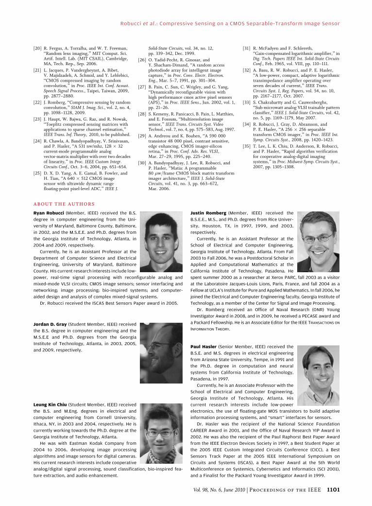
Ryan Robucci (Member, IEEE) received the B.S.
degree in computer engineering from the Uni-
versity of Maryland, Baltimore County, Baltimore,
in 2002, and the M.S.E.E. and Ph.D. degrees from
the Georgia Institute of Technology, Atlanta, in
2004 and 2009, respectively.
Currently, he is an Assistant Professor at the
Department of Computer Science and Electrical
Engineering, University of Maryland, Baltimore
County. His current research interests include low-
power, real-time signal processing with reconfigurable analog and
mixed-mode VLSI circuits; CMOS image sensors; sensor interfacing and
networking; image processing; bio-inspired systems; and computer-
aided design and analysis of complex mixed-signal systems.
Dr. Robucci received the ISCAS Best Sensors Paper award in 2005.
Jordan D. Gray (Student Member, IEEE) received
the B.S. degree in computer engineering and the
M.S.E.E and Ph.D. degrees from the Georgia
Institute of Technology, Atlanta, in 2003, 2005,
and 2009, respectively.
Leung Kin Chiu (Student Member, IEEE) received
the B.S. and M.Eng. degrees in electrical and
computer engineering from Cornell University,
Ithaca, NY, in 2003 and 2004, respectively. He is
currently working towards the Ph.D. degree at the
Georgia Institute of Technology, Atlanta.
He was with Eastman Kodak Company from
2004 to 2006, developing image processing
algorithms and image sensors for digital cameras.
His current research interests include cooperative
analog/digital signal processing, sound classification, bio-inspired fea-
ture extraction, and audio enhancement.
Justin Romberg (Member, IEEE) received the
B.S.E.E., M.S., and Ph.D. degrees from Rice Univer-
sity, Houston, TX, in 1997, 1999, and 2003,
respectively.
Currently, he is an Assistant Professor at the
School of Electrical and Computer Engineering,
Georgia Institute of Technology, Atlanta. From Fall
2003 to Fall 2006, he was a Postdoctoral Scholar in
Applied and Computational Mathematics at the
California Institute of Technology, Pasadena. He
spent summer 2000 as a researcher at Xerox PARC, fall 2003 as a visitor
at the Laboratoire Jacques-Louis Lions, Paris, France, and fall 2004 as a
Fellow at UCLA’s Institute for Pure and AppliedMathematics. In fall 2006, he
joined the Electrical and Computer Engineering faculty, Georgia Institute of
Technology, as a member of the Center for Signal and Image Processing.
Dr. Romberg received an Office of Naval Research (ONR) Young
Investigator Award in 2008, and in 2009, he received a PECASE award and
a Packard Fellowship. He is an Associate Editor for the IEEE TRANSACTIONS ON
INFORMATION THEORY.
Paul Hasler (Senior Member, IEEE) received the
B.S.E. and M.S. degrees in electrical engineering
from Arizona State University, Tempe, in 1991 and
the Ph.D. degree in computation and neural
systems from California Institute of Technology,
Pasadena, in 1997.
Currently, he is an Associate Professor with the
School of Electrical and Computer Engineering,
Georgia Institute of Technology, Atlanta. His
current research interests include low-power
electronics, the use of floating-gate MOS transistors to build adaptive
information processing systems, and Bsmart[ interfaces for sensors.
Dr. Hasler was the recipient of the National Science Foundation
CAREER Award in 2001, and the Office of Naval Research YIP Award in
2002. He was also the recipient of the Paul Raphorst Best Paper Award
from the IEEE Electron Devices Society in 1997, a Best Student Paper at
the 2005 IEEE Custom Integrated Circuits Conference (CICC), a Best
Sensors Track Paper at the 2005 IEEE International Symposium on
Circuits and Systems (ISCAS), a Best Paper Award at the 5th World
Multiconference on Systemics, Cybernetics and Informatics (SCI 2001),
and a Finalist for the Packard Young Investigator Award in 1999.
Robucci et al. : Compressive Sensing on a CMOS Separable-Transform Image Sensor
Vol. 98, No. 6, June 2010 | Proceedings of the IEEE 1101