Ultrafast, Cross-Correlated Harmonic Imaging Through Scattering Media
Upload
khangminh22Category
view
0download
0
UltraFast Design Methodology Guide for the Vivado Design Suite
UG949 (v2013.3) October 23, 2013

UltraFAST Design Methodology Guide www.xilinx.com 2UG949 (v2013.3) October 23, 2013
Notice of Disclaimer The information disclosed to you hereunder (the “Materials”) is provided solely for the selection and use of Xilinx products. To the maximum extent permitted by applicable law: (1) Materials are made available "AS IS" and with all faults, Xilinx hereby DISCLAIMS ALL WARRANTIES AND CONDITIONS, EXPRESS, IMPLIED, OR STATUTORY, INCLUDING BUT NOT LIMITED TO WARRANTIES OF MERCHANTABILITY, NON-INFRINGEMENT, OR FITNESS FOR ANY PARTICULAR PURPOSE; and (2) Xilinx shall not be liable (whether in contract or tort, including negligence, or under any other theory of liability) for any loss or damage of any kind or nature related to, arising under, or in connection with, the Materials (including your use of the Materials), including for any direct, indirect, special, incidental, or consequential loss or damage (including loss of data, profits, goodwill, or any type of loss or damage suffered as a result of any action brought by a third party) even if such damage or loss was reasonably foreseeable or Xilinx had been advised of the possibility of the same. Xilinx assumes no obligation to correct any errors contained in the Materials or to notify you of updates to the Materials or to product specifications. You may not reproduce, modify, distribute, or publicly display the Materials without prior written consent. Certain products are subject to the terms and conditions of the Limited Warranties which can be viewed at http://www.xilinx.com/warranty.htm; IP cores may be subject to warranty and support terms contained in a license issued to you by Xilinx. Xilinx products are not designed or intended to be fail-safe or for use in any application requiring fail-safe performance; you assume sole risk and liability for use of Xilinx products in Critical Applications: http://www.xilinx.com/warranty.htm#critapps.
© Copyright 2013 Xilinx, Inc. Xilinx, the Xilinx logo, Artix, ISE, Kintex, Spartan, Virtex, Vivado, Zynq, and other designated brands included herein are trademarks of Xilinx in the United States and other countries. All other trademarks are the property of their respective owners.
Revision HistoryThe following table shows the revision history for this document.
Date Version Revision
10/23/2013 2013.3 Initial Xilinx release.

Table of ContentsChapter 1: Introduction
About This Guide . . . . . . . . . . . . . . . . . . . . . . . . . . . . . . . . . . . . . . . . . . . . . . . . . . . . . . . . . . . . . . . . . . 5Guide Contents. . . . . . . . . . . . . . . . . . . . . . . . . . . . . . . . . . . . . . . . . . . . . . . . . . . . . . . . . . . . . . . . . . . . 5Guide Applicability and References . . . . . . . . . . . . . . . . . . . . . . . . . . . . . . . . . . . . . . . . . . . . . . . . . . . 6Need for Design Methodology . . . . . . . . . . . . . . . . . . . . . . . . . . . . . . . . . . . . . . . . . . . . . . . . . . . . . . . 6Design Methodology Checklist . . . . . . . . . . . . . . . . . . . . . . . . . . . . . . . . . . . . . . . . . . . . . . . . . . . . . . . 7Design Process . . . . . . . . . . . . . . . . . . . . . . . . . . . . . . . . . . . . . . . . . . . . . . . . . . . . . . . . . . . . . . . . . . . . 7Rapid Validation. . . . . . . . . . . . . . . . . . . . . . . . . . . . . . . . . . . . . . . . . . . . . . . . . . . . . . . . . . . . . . . . . . 10
Chapter 2: Vivado Design Suite FlowsOverview of Vivado Design Suite Flows . . . . . . . . . . . . . . . . . . . . . . . . . . . . . . . . . . . . . . . . . . . . . . . 12Accessing Documentation and Training . . . . . . . . . . . . . . . . . . . . . . . . . . . . . . . . . . . . . . . . . . . . . . . 12Understanding Project and Non-Project Software Use Models . . . . . . . . . . . . . . . . . . . . . . . . . . . . 15Source Management . . . . . . . . . . . . . . . . . . . . . . . . . . . . . . . . . . . . . . . . . . . . . . . . . . . . . . . . . . . . . . 18Using Archive Design . . . . . . . . . . . . . . . . . . . . . . . . . . . . . . . . . . . . . . . . . . . . . . . . . . . . . . . . . . . . . . 21Configuring and Managing IP . . . . . . . . . . . . . . . . . . . . . . . . . . . . . . . . . . . . . . . . . . . . . . . . . . . . . . . 21Using Third Party Synthesis and Simulation Tools. . . . . . . . . . . . . . . . . . . . . . . . . . . . . . . . . . . . . . . 30
Chapter 3: Board and Device PlanningOverview of Board and Device Planning . . . . . . . . . . . . . . . . . . . . . . . . . . . . . . . . . . . . . . . . . . . . . . 31PCB Layout Recommendations . . . . . . . . . . . . . . . . . . . . . . . . . . . . . . . . . . . . . . . . . . . . . . . . . . . . . . 31Clock Resource Planning and Assignment . . . . . . . . . . . . . . . . . . . . . . . . . . . . . . . . . . . . . . . . . . . . . 33I/O Planning Design Flows. . . . . . . . . . . . . . . . . . . . . . . . . . . . . . . . . . . . . . . . . . . . . . . . . . . . . . . . . . 35FPGA Power Aspects and System Dependencies. . . . . . . . . . . . . . . . . . . . . . . . . . . . . . . . . . . . . . . . 48Worst Case Power Analysis Using Xilinx Power Estimator (XPE) . . . . . . . . . . . . . . . . . . . . . . . . . . . 58Configuration . . . . . . . . . . . . . . . . . . . . . . . . . . . . . . . . . . . . . . . . . . . . . . . . . . . . . . . . . . . . . . . . . . . . 68
Chapter 4: Design CreationOverview of Design Creation. . . . . . . . . . . . . . . . . . . . . . . . . . . . . . . . . . . . . . . . . . . . . . . . . . . . . . . . 78Defining a Good Design Hierarchy . . . . . . . . . . . . . . . . . . . . . . . . . . . . . . . . . . . . . . . . . . . . . . . . . . . 79Working With Intellectual Property (IP). . . . . . . . . . . . . . . . . . . . . . . . . . . . . . . . . . . . . . . . . . . . . . . 82RTL Coding Guidelines . . . . . . . . . . . . . . . . . . . . . . . . . . . . . . . . . . . . . . . . . . . . . . . . . . . . . . . . . . . . . 89Control Signals and Control Sets. . . . . . . . . . . . . . . . . . . . . . . . . . . . . . . . . . . . . . . . . . . . . . . . . . . . . 96
UltraFAST Design Methodology Guide www.xilinx.com 3UG949 (v2013.3) October 23, 2013
Send Feedback
Know What You Infer. . . . . . . . . . . . . . . . . . . . . . . . . . . . . . . . . . . . . . . . . . . . . . . . . . . . . . . . . . . . . 106Inferring RAM and ROM . . . . . . . . . . . . . . . . . . . . . . . . . . . . . . . . . . . . . . . . . . . . . . . . . . . . . . . . . . 107Coding for Proper DSP and Arithmetic Inference . . . . . . . . . . . . . . . . . . . . . . . . . . . . . . . . . . . . . . 113Coding Shift Registers and Delay Lines. . . . . . . . . . . . . . . . . . . . . . . . . . . . . . . . . . . . . . . . . . . . . . . 114Initialization of All Inferred Registers, SRLs, and Memories . . . . . . . . . . . . . . . . . . . . . . . . . . . . . . 115Parameters, Attributes, and Constraints . . . . . . . . . . . . . . . . . . . . . . . . . . . . . . . . . . . . . . . . . . . . . 116Clocking. . . . . . . . . . . . . . . . . . . . . . . . . . . . . . . . . . . . . . . . . . . . . . . . . . . . . . . . . . . . . . . . . . . . . . . . 120Deciding When to Instantiate or Infer . . . . . . . . . . . . . . . . . . . . . . . . . . . . . . . . . . . . . . . . . . . . . . . 134Coding Styles for Higher Reliability. . . . . . . . . . . . . . . . . . . . . . . . . . . . . . . . . . . . . . . . . . . . . . . . . . 136Coding Styles to Improve Performance . . . . . . . . . . . . . . . . . . . . . . . . . . . . . . . . . . . . . . . . . . . . . . 140Coding Styles to Improve Power. . . . . . . . . . . . . . . . . . . . . . . . . . . . . . . . . . . . . . . . . . . . . . . . . . . . 145Creating Constraints . . . . . . . . . . . . . . . . . . . . . . . . . . . . . . . . . . . . . . . . . . . . . . . . . . . . . . . . . . . . . 149
Chapter 5: ImplementationOverview of Implementation . . . . . . . . . . . . . . . . . . . . . . . . . . . . . . . . . . . . . . . . . . . . . . . . . . . . . . 189Synthesis. . . . . . . . . . . . . . . . . . . . . . . . . . . . . . . . . . . . . . . . . . . . . . . . . . . . . . . . . . . . . . . . . . . . . . . 189Synthesis Attributes. . . . . . . . . . . . . . . . . . . . . . . . . . . . . . . . . . . . . . . . . . . . . . . . . . . . . . . . . . . . . . 193Bottom Up Flow . . . . . . . . . . . . . . . . . . . . . . . . . . . . . . . . . . . . . . . . . . . . . . . . . . . . . . . . . . . . . . . . . 195Moving Past Synthesis . . . . . . . . . . . . . . . . . . . . . . . . . . . . . . . . . . . . . . . . . . . . . . . . . . . . . . . . . . . . 197Implementing the Design . . . . . . . . . . . . . . . . . . . . . . . . . . . . . . . . . . . . . . . . . . . . . . . . . . . . . . . . . 199Timing Closure . . . . . . . . . . . . . . . . . . . . . . . . . . . . . . . . . . . . . . . . . . . . . . . . . . . . . . . . . . . . . . . . . . 211Causes of High Clock Skew . . . . . . . . . . . . . . . . . . . . . . . . . . . . . . . . . . . . . . . . . . . . . . . . . . . . . . . . 237Causes of High Uncertainty . . . . . . . . . . . . . . . . . . . . . . . . . . . . . . . . . . . . . . . . . . . . . . . . . . . . . . . . 243Power . . . . . . . . . . . . . . . . . . . . . . . . . . . . . . . . . . . . . . . . . . . . . . . . . . . . . . . . . . . . . . . . . . . . . . . . . 269
Chapter 6: Configuration and DebugOverview of Configuration and Debug . . . . . . . . . . . . . . . . . . . . . . . . . . . . . . . . . . . . . . . . . . . . . . . 280Configuration . . . . . . . . . . . . . . . . . . . . . . . . . . . . . . . . . . . . . . . . . . . . . . . . . . . . . . . . . . . . . . . . . . . 280Debugging. . . . . . . . . . . . . . . . . . . . . . . . . . . . . . . . . . . . . . . . . . . . . . . . . . . . . . . . . . . . . . . . . . . . . . 2921.0 Design Methodology Introduction . . . . . . . . . . . . . . . . . . . . . . . . . . . . . . . . . . . . . . . . . . . . . . . 3032.0 Board and Device Planning . . . . . . . . . . . . . . . . . . . . . . . . . . . . . . . . . . . . . . . . . . . . . . . . . . . . . 3133.0 Design Creation . . . . . . . . . . . . . . . . . . . . . . . . . . . . . . . . . . . . . . . . . . . . . . . . . . . . . . . . . . . . . . 3234.0 Implementation . . . . . . . . . . . . . . . . . . . . . . . . . . . . . . . . . . . . . . . . . . . . . . . . . . . . . . . . . . . . . . 3415.0 Configuration and Debug . . . . . . . . . . . . . . . . . . . . . . . . . . . . . . . . . . . . . . . . . . . . . . . . . . . . . . 351Xilinx Resources . . . . . . . . . . . . . . . . . . . . . . . . . . . . . . . . . . . . . . . . . . . . . . . . . . . . . . . . . . . . . . . . . 359Solution Centers. . . . . . . . . . . . . . . . . . . . . . . . . . . . . . . . . . . . . . . . . . . . . . . . . . . . . . . . . . . . . . . . . 359References . . . . . . . . . . . . . . . . . . . . . . . . . . . . . . . . . . . . . . . . . . . . . . . . . . . . . . . . . . . . . . . . . . . . . 359
UltraFAST Design Methodology Guide www.xilinx.com 4UG949 (v2013.3) October 23, 2013
Send Feedback
Chapter 1
Introduction
About This GuideXilinx® programmable devices have capacities of multi-million Logic Cells (LC), and integrate an ever-increasing share of today’s complex electronic systems, including:
• Embedded subsystems
• Analog and digital processing
• High speed connectivity
• Network processing
In order to create such complex systems within short design cycles, designers synthesize many large blocks of logic from RTL, and reuse Intellectual Property (IP) modules from Xilinx or third parties.
Given the complexity of this process, it is critical to adopt a set of best practices collectively called design methodology to maximize productivity for both system integration and design implementation.
Guide ContentsThis Guide discusses a design methodology process to follow in order to achieve an eff icient and quicker design implementation, and to derive the maximum value from Xilinx devices and tools.
In most cases, this Guide tells you the reasoning behind its recommendations. By understanding that reasoning, you can appreciate the potential consequences of deviating from the recommended methodology, and take appropriate precautions.
UltraFAST Design Methodology Guide www.xilinx.com 5UG949 (v2013.3) October 23, 2013
Send Feedback

Guide Applicability and References
Guide Applicability and ReferencesAlthough this Guide is primarily for use with the Xilinx Vivado® Design Suite, most of the conceptual information in this Guide can be leveraged for use with the Xilinx ISE® Design Suite as well. This Guide provides high-level information, design guidelines, and design decision tradeoffs.
This Guide includes references to other documents such as the Vivado Design Suite User Guides, Vivado Design Suite Tutorials, and Quick-Take Video Tutorials. This Guide is not a replacement for those documents. You should still refer to those documents for detailed, current information, including descriptions of tool use and design methodology. For a more complete listing of reference documents, see Appendix B, Additional Resources.
At various places, the Guide gives the Vivado tools command for a specif ic task. Run the command with -help for detailed information (including example usage).
Need for Design MethodologyAdvanced algorithms used in today’s increasingly complex electronic products are stretching the boundaries of density, performance, and power. This creates many challenges for the design teams to hit the target release window of opportunity within the allocated budget. The UltraFast Design Methodology allows project managers to:
• Formulate an accurate estimate of the project schedule and cost.
• Accelerate time to market, thus increasing product revenue.
The UltraFast Design Methodology Guide for the Vivado Design Suite is a collection of best practices covering aspects related to board planning, design creation, IP integration, design implementation and closure techniques, programming, and hardware debug. These best practices and recommendations have been gathered from a large pool of expert users over the past several years. The recommendations in this UltraFast Design Methodology Guide will help you succeed as they have for many of Xilinx customers.
Vivado Design Suite is also automating part of the UltraFast Design Methodology by providing:
• DRC rules providing guidance on HDL code and XDC constraints, so engineers can improve the quality of their design earlier in the flows and avoid problems downstream, when iterations would be costlier.
• Proven templates for specific HDL code and XDC constraints, enabling optimal-by-construction code.
UltraFAST Design Methodology Guide www.xilinx.com 6UG949 (v2013.3) October 23, 2013
Send Feedback

Design Methodology Checklist
Design Methodology ChecklistThis Guide includes the Design Methodology Checklist, page 303, as part of the overall methodology recommendations. This checklist includes common questions to consider starting from the critical stage of design planning and all subsequent stages.
The Design Methodology Checklist is also available in spreadsheet format at this link:
http://www.author.xilinx.com/cgi-bin/docs/rdoc?d=xtp301-design-methodology-checklist.xlsx
The questions highlight typical areas in which design decisions are likely to have downstream ramifications. These issues are often unknown or ignored. Links for each checklist question direct you to the areas in this Guide that best describe that particular design concern.
A variety of reporting commands are also included to help identify potential areas of risk with the design. This Guide also provides guidance for designers to address the specif ic concerns as well as the consequences of ignoring them.
Design ProcessThe steps in the design process are shown in Figure 1-1, Steps in Design Process. These steps are usually overlapping in time. Sometimes, the process might also return to a previous step - resulting in iterations.
This Guide demonstrates the importance of creating correct timing constraints for the system, before entering the implementation phase. Because the Vivado tools use
X-Ref Target - Figure 1-1
Figure 1-1: Steps in Design Process
UltraFAST Design Methodology Guide www.xilinx.com 7UG949 (v2013.3) October 23, 2013
Send Feedback

Design Process
timing-driven algorithms throughout, the design must be properly constrained from the beginning of the design flow.
Specifying correct timing requires (among other things) analyzing the relationship between each master clock plus their related generated clocks in the design. Unlike ISE® (UCF), in the Vivado tools (XDC) each clock interaction is timed, unless explicitly declared as asynchronous or false-path. Timing analysis should be performed after synthesis and timing should be met with the right constraints at each implementation stage before proceeding to the next.
Overall timing and implementation convergence is accelerated by following this recommendation along with using the interactive analysis environment of the Vivado Design Suite. Further acceleration can be achieved by combining the above with the HDL design guidelines in this Guide. Figure 1-2, Design Methodology for Rapid Convergence, gives some details of this high level methodology.
X-Ref Target - Figure 1-2
Figure 1-2: Design Methodology for Rapid Convergence
UltraFAST Design Methodology Guide www.xilinx.com 8UG949 (v2013.3) October 23, 2013
Send Feedback

Design Process
The synthesis portion of the design flow can be considered complete when timing goals are met with a positive slack (or a relatively small negative slack). If post-synthesis timing is not met (or close to being met), placement and routing results are not likely to meet timing. However, you may still go ahead with the rest of the flow once. You may meet the timing, because implementation tools might be able to allocate the best resources to the failing paths. Even if the timing is not met, you will have a more accurate knowledge of the slack. Having a better understanding of the final negative slack will provide a good estimate as to how much to improve the post synthesis WNS, when you come back to synthesis with possible improvements to your HDL and constraints.
Conceptually, early stages in the design flow (C, C++, and HDL synthesis) have a much higher impact on design performance, density, and power than the later stages. See Figure 1-3, Impact of Design Changes Throughout the Flow.X-Ref Target - Figure 1-3
Figure 1-3: Impact of Design Changes Throughout the Flow
Accordingly, if the design is not meeting its timing goals, instead of trying to iterate over and f ind a solution within the implementation steps only, Xilinx recommends that you revisit the steps of synthesis and its inputs (including HDL and constraints).
Because it is important to be correct from the beginning and to pay attention to design goals from the early stages, this Guide also provides guidelines for RTL, clock, pin, and PCB planning. Properly defining and validating the design at each design stage helps alleviate timing closure, routing closure, and power usage issues during subsequent stages of implementation.
UltraFAST Design Methodology Guide www.xilinx.com 9UG949 (v2013.3) October 23, 2013
Send Feedback

Rapid Validation
Rapid ValidationThis Guide introduces the concept of rapid validation of specif ic aspects of system architecture and micro-architecture choices. This concept can be applied in two different contexts.
In the context of system design, the I/O bandwidth is validated in-system, before even implementing the core of the design. For more information, see Interface Bandwidth Validation, page 40. This step may highlight the need to revise system architecture and interface choices, before finalizing on I/Os.
In the context of design implementation, baselining (see: Baselining the Design, page 213) is used to write the simplest set of constraints, which can identify internal device timing challenges. This process may identify the need to revise RTL micro-architecture choices, before moving to the implementation phase.
As part of establishing a good design methodology, it is important to establish exactly how you plan to interact with the Vivado Design Suite. It has a flexible use model to accommodate various development flows and different types of designs. Chapter 2, Vivado Design Suite Flows, discusses various use models supported by the Vivado tools. This will help you decide on your use-model. Subsequent chapters will help you understand more details on aspects of methodology and techniques related to:
• Constraints definition and validation
• I/O and clock planning within the device
• Selecting and configuring IP
• Design rule checking (DRC)
• Power analysis and optimization
• Timing closure flows
• Hardware validation (debug core insertion and configuration)
UltraFAST Design Methodology Guide www.xilinx.com 10UG949 (v2013.3) October 23, 2013
Send Feedback

Rapid Validation
Other aspects that are important to plan for, but that are not covered in this Guide, include:
• Embedded processor and DSP design and validation flows
• Logic verif ication (behavioral, structural, timing)
RECOMMENDED: Follow the design methodology recommendations discussed in this Guide to obtain the most out of Xilinx devices while consuming the least amount of your time and effort.
UltraFAST Design Methodology Guide www.xilinx.com 11UG949 (v2013.3) October 23, 2013
Send Feedback

Chapter 2
Vivado Design Suite Flows
Overview of Vivado Design Suite FlowsBefore you begin your design project with the Vivado® Design Suite, you should f irst decide how you want use the software. The Vivado Design Suite enables several different use models depending on your preference. This chapter will help guide you through some of the decisions that you must make about the use model you want to use for interacting with the Vivado tools.
These decisions include:
• Are you a script-based user, or do you prefer a graphical user interface (GUI)?
• Do you want to configure your IP cores within the design project, or do you want to establish a remote location for reusable IP cores across multiple projects?
• Do you want the tools to manage the design sources, status, and results by using a project?
• Are you using third party tools for synthesis or simulation?
• Do you want to interact with a source control systems for revision control?
RECOMMENDED: Before beginning your first FPGA design with the Vivado tools, see the Vivado Design Suite User Guide: Design Flows Overview (UG892) [Ref 9].
Accessing Documentation and TrainingAccess to the right information at the right time is critical for timely design closure and overall design success. Reference guides, user guides, tutorials, and videos get you up to speed as quickly as possible with the Vivado Design Suite. Finding the desired specif ic information can be a challenge. This section lists some of the sources for documentation and training.
UltraFAST Design Methodology Guide www.xilinx.com 12UG949 (v2013.3) October 23, 2013
Send Feedback
Accessing Documentation and Training
Using the Documentation NavigatorThe Vivado Design Suite ships with the Xilinx® Documentation Navigator, which provides an environment to access and manage the entire set of Xilinx software and hardware documentation, training, and support materials. Documentation Navigator allows you to view current and past Xilinx documentation. The documentation display can be f iltered based on release, document type, or design task. When coupled with a search capability, you can quickly f ind the right information.
Documentation Navigator scans the Xilinx website to detect and provide documentation updates. The Update Catalog feature alerts you to available updates, and gives details about the documents that are involved. Xilinx recommends that you always update the catalog when alerted to keep it current. You can establish and manage local documentation catalogs with specif ied documents.
The Documentation Navigator has a tab called the Design Hub View. Design hubs are collections of documentation related by design activity, such as Applying Design Constraints, Synthesis and Implementation, and Programming and Debug. Documents and videos are organized in each hub in order to simplify the learning curve for that area. Each hub contains a Getting Started Section, a Support Resources section with an FAQ for that flow, as well as Additional Learning Materials. For new users, the Getting Started section provides a clear place to start. For those already familiar with the flow, Key Concepts and the FAQ may be of particular interest to gain expertise.
UltraFAST Design Methodology Guide www.xilinx.com 13UG949 (v2013.3) October 23, 2013
Send Feedback

Accessing Documentation and Training
Accessing the QuickTake Video TutorialsXilinx QuickTake video tutorials provide guidance on using the features of the Vivado Design Suite. These tutorials are short and succinct training tools. They can be viewed from xilinx.com or You Tube can be downloaded locally.
TIP: Download the clips locally if connection speed interferes with viewing quality. The QuickTake video tutorials are also available through Documentation Navigator, as shown in Figure 2-2, Accessing QuickTake Video Tutorials Using Documentation Navigator.
X-Ref Target - Figure 2-1
Figure 2-1: Xilinx Documentation Navigator, Catalog Viewer
UltraFAST Design Methodology Guide www.xilinx.com 14UG949 (v2013.3) October 23, 2013
Send Feedback

Understanding Project and Non-Project Software Use Models
A full set of interactive software labs is also available. These labs provide example designs and step-by-step instructions to perform specif ic design tasks. These labs are also available at xilinx.com or through Documentation Navigator. In addition, you can also register for formal training classes offered by Xilinx or its partners.
Understanding Project and Non-Project Software Use ModelsThe Vivado Design Suite enables you to run the tools using different methods depending on your preference. You must decide up front about how you prefer to interact with the Vivado Design Suite to process your design. These decisions include:
• Whether to use: (1) a Tcl script-based flow; or (2) the Vivado Integrated Design Environment (IDE) to process the design interactively.
Note: You can use a Tcl script based flow, but still use the IDE when needed to analyze the design or apply constraints.
X-Ref Target - Figure 2-2
Figure 2-2: Accessing QuickTake Video Tutorials Using Documentation Navigator
UltraFAST Design Methodology Guide www.xilinx.com 15UG949 (v2013.3) October 23, 2013
Send Feedback

Understanding Project and Non-Project Software Use Models
• Whether to: (1) use a Vivado Design Suite project to manage the design sources, design configuration, and results automatically; or (2) manage them yourself.
Using Project ModeYou can use a project-based method (Project Mode) to automatically manage your design process and design data. When working in Project Mode, a directory structure is created on disk in order to manage design source files, run results, and track project status. The Project infrastructure is used to manage the automated synthesis and implementation process and to track run status. The entire design flow can be run with a single click within the Vivado IDE. Certain operating systems (for example, Microsoft Windows) restrict the number of characters (such as 260) that can be used to name a file (along with its path). If your operating system has such a limitation, Xilinx recommends that you start your projects closer to the root of a disk drive.
Using Non-Project ModeIn Non-Project Mode, you manage sources and the design process yourself. Sources are accessed from their current locations - rather than copied somewhere - and the design is compiled through the flow in memory.
Each design step is controlled individually using Tcl commands. Design parameters and implementation options are set using Tcl commands. You can save design checkpoints and create reports at any stage of the design process using Tcl.
You can open the Vivado IDE at any point in the design process by loading these checkpoints for interactive design analysis and constraints assignment. Because you are viewing the active design in memory, any changes are automatically passed forward in the flow. You can also save updates to new constraint f iles or design checkpoints for future runs.
Note: Most of the above capabilities are also available in Project Mode. Some Project Mode features are not available in Non-Project Mode. These include source f ile and run results management, saving design and tool configuration, design status, and IP integration.
TIP: Either mode can be run using a Tcl scripted batch mode, or run interactively in the Vivado IDE.
Working with TclAll flows can be run using Tcl commands. You can use Tcl scripts to run the entire design flow (including design analysis reporting), or to run only parts of the flow. If you prefer to work directly with Tcl, you can interact with your design using Tcl commands in any of the following methods:
• Enter individual Tcl commands in the Vivado Design Suite Tcl shell outside of the Vivado IDE.
UltraFAST Design Methodology Guide www.xilinx.com 16UG949 (v2013.3) October 23, 2013
Send Feedback
Understanding Project and Non-Project Software Use Models
• Enter individual Tcl commands in the Tcl Console at the bottom of the Vivado IDE.
• Run Tcl scripts from the Vivado Design Suite Tcl shell.
• Run Tcl scripts from the Vivado IDE.
For more information about using Tcl and Tcl scripting, see the Vivado Design Suite User Guide: Using Tcl Scripting (UG894) [Ref 11]. For a step-by-step tutorial that shows how to use Tcl in the Vivado tools, see the Vivado Design Suite Tutorial: Design Flows Overview (UG888) [Ref 25].
When working with Tcl, you can still take advantage of the interactive GUI-based analysis and constraint definition capabilities of the Vivado IDE. You can open designs in the Vivado IDE at any stage of the design cycle. You can also save design checkpoints at any time and open the checkpoints later in the Vivado IDE.
Working with the Vivado Integrated Design Environment (IDE)The Vivado Integrated Design Environment (IDE) can be used in both Project Mode and Non-Project Mode. The features displayed in the IDE vary depending on how and when you invoke the IDE.
When using Project Mode, the Vivado IDE provides an interface to assemble, implement, and validate your design and IP. In addition, the Vivado IDE supports a push-button design flow that manages all design sources, configuration, and results.
The Vivado IDE enables analysis and constraints assignment throughout the design process by introducing the concept of opening designs in memory. Opening a design loads the design netlist at that particular stage of the design flow, assigns the constraints to the design, and applies the design to the target device. This process allows you to visualize and interact with the design at each design stage.
When using Non-Project Mode, the source f iles are read from their current locations, and the entire flow is processed manually using Tcl commands or scripts. All source f ile revision control, design status reporting, and generation of output f iles is done by you by using Tcl commands or scripts.
Some users prefer Non-Project Mode because it allows explicit control of the flow and all input and output files, so they can directly control the tool flow. Project Mode provides automation that controls the flow for the user - which makes it easier to use from the IDE.
When using either mode, you can open designs for analysis after RTL elaboration, synthesis, or implementation. Doing so enables you to make changes after implementation to constraints, logic or device configuration, and implementation results. See Figure 2-3, Opening the Implemented Design in the Vivado IDE.
UltraFAST Design Methodology Guide www.xilinx.com 17UG949 (v2013.3) October 23, 2013
Send Feedback

Source Management
X-Ref Target - Figure 2-4
For more information on the Vivado IDE, see the Vivado Design Suite User Guide: Using the Vivado IDE (UG893) [Ref 10].
Source ManagementThe Vivado Design Environment references source f iles that contain design descriptions. Options in the Vivado Design Suite control how you create, use, and manage the source types. These sources include:
• HDL and netlist f iles: Verilog, VHDL, EDIF
• Tcl f iles, including constraints (.xdc) and init.tcl
• IP core files (.xci)
• IP Integrator block design files (.bd)
• Embedded subsystem (.xmp)
X-Ref Target - Figure 2-3
Figure 2-3: Opening the Implemented Design in the Vivado IDE
UltraFAST Design Methodology Guide www.xilinx.com 18UG949 (v2013.3) October 23, 2013
Send Feedback

Source Management
• System generator subsystem (.sgp)
• Side f iles - for use by related tools
• BMM
• ChipScope definition f iles (CDC)
• ELF files
• COE files
Using Remote or Local SourcesThe Vivado Design Suite can use remote sources when processing the design. Any modif ications to the sources are written back to the original locations.
TIP: You can save most source modifications with a new name.
Design sources can be read-only protected, and stored anywhere that is network accessible from where the design is being run.
When you are using Project Mode, you can copy sources into the Project directory to enable the project infrastructure to store, modify, and manage the sources. Copying sources into the Project directory makes the entire design project more portable and self-contained.
Using Source Control Systems with the Vivado ToolsMany design teams use source management systems to store various design configurations and revisions. There are many commercially available systems available, such as RCS, CVS, Subversion, ClearCase, Perforce, Git, Bitkeeper, and many others. No single system is predominant. The Vivado tools can interact with all such systems.
Most users follow a methodology in which sources are checked out into a local repository where they are modified to complete the design. These modif ied sources can be checked back into the source control system as new revisions at any time. Design results can also optionally be checked in for revision storage. Many systems use DIFF mechanisms to update only those sources that have been modified since the last check out. Most use a directory structure to store and manage sources and results.
The Vivado tool-specific input and output f iles consumed and produced in the flow most often need revision control. An illustrative list is shown above under Source Management, page 18.
Source Management with Non-Project Modes
The easiest way to interact with source control systems is to use the Non-Project scripted flow. The designer checks out the desired sources into a local directory structure of their
UltraFAST Design Methodology Guide www.xilinx.com 19UG949 (v2013.3) October 23, 2013
Send Feedback
Source Management
choice. The sources are then instantiated by the designers to create the design. New source f iles may also need to be created. Once the files are ready, the read_* tcl commands pass the files to the Vivado synthesis and implementation commands. The source files remain in their original locations. The checked-out sources can be modif ied interactively, or with Tcl commands during the design session, using appropriate code editors. A common example of such a modif ication is a timing constraint change.
Note: Although source f iles can be read-only protected, this disables them from being modified.
Source files are then checked back into the source control system at the designer’s discretion. Design results such as design checkpoints, reports, and bit f iles can also be checked in for revision management.
The run script and tool settings should also be checked in for revision control. This information can be extracted into a Tcl script using the write_project_tcl command. Because init.tcl is not included in the write_project_tcl, init.tcl must also be checked in. Checking in all these f iles enables the design to be recreated using the current sources and tool configuration settings.
Source Management with Project Modes
Using a Vivado Design Suite project can complicate the interaction with a source control system. The project can maintain its own copy of the sources, and does its own design management. However, there are methods to use the two in conjunction. The designer should be open to the fact that local and remote sources can all be interactively manipulated using the IDE. The text editor can be used to edit the sources, and the results can be analyzed and modif ied while opening designs. Read-only sources can be used, but severely limit the advantages of using the IDE.
Projects should be created using remote sources by not copying sources locally into the project directory. Sources can easily be maintained and managed using this approach.
When using projects with source control systems, the run scripts used by the IDE are intentionally hidden from users. Only the Vivado Design Suite journal f ile is visible, which shows the Tcl commands from your current session. In addition, the tool configuration settings are stored in run strategy f iles that are not easily extracted or applied to future runs. For this reason, Xilinx recommends rebuilding the project from scratch using a Tcl-scripted approach when using projects with source control systems.
The project compilation run script and tool settings should also be checked in for revision control. Use the write_project_tcl command to extract this information into a Tcl script. The script enables the design to be recreated using the current sources and tool configuration settings.
UltraFAST Design Methodology Guide www.xilinx.com 20UG949 (v2013.3) October 23, 2013
Send Feedback

Using Archive Design
Using Design CheckpointsThe Vivado Design Suite uses Design Checkpoint f iles (.dcp) to store the current state of the design being processed through the flow. These checkpoints include the netlist, constraints, and design results at the stage when the checkpoint was written.
Checkpoints should be written after each stage of the design process. They are automatically created when using a Project to process synthesis and implementation runs.
Checkpoints can be opened in the Vivado IDE for design analysis and constraints modif ication. Constraint changes can be written to new constraints f iles for use during the next run through the flow. Checkpoints are images of a design at a given state in the flow. Checkpoints do not contain the entire project or the source files.
Using Archive DesignThe archive_design command can package up an entire project into a compressed zip f ile. The command has several options for storing sources and run results. Essentially the entire project is copied locally in memory, and then zipped into a f ile on disk while leaving the original project intact. This command also copies any remote sources into the archive. This feature is useful for sending your design description to another person. You might also need to send your version of init.tcl if you are using this f ile to set specific parameters or variables that affect the design.
Configuring and Managing IPThis section discusses how to configure, use, and manage Intellectual Property (IP).
Configuring IP Using the Vivado IP CatalogIP is best configured using IP Catalog features of the Vivado IDE, which make it easy to browse, configure, and generate output products and to validate. The IP Catalog and configuration wizards of the Vivado IDE make the job easy.
There are Tcl equivalent commands that enable scripting, but not all Tcl parameters for IP configuration are documented. If scripting is desired, you can use the Vivado journal f ile to create a script after you have used the IDE to configure the IP and generate output products.
After using the configuration wizards to customize the IP, you are presented with options for generating output products for implementation and verif ication.
UltraFAST Design Methodology Guide www.xilinx.com 21UG949 (v2013.3) October 23, 2013
Send Feedback

Configuring and Managing IP
The IP can be configured so that when it is imported into a design project it can be as a set of HDL sources and constraints, or a design checkpoint f ile (.dcp) which contains a synthesized netlist and constraints. This option is set when Generating Output Products for the IP. The default for IP is to synthesize the IP standalone and to use the design checkpoint as the source for implementation. This enables you to validate and optimize your IP standalone. It may also reduce top-level design synthesis runtime.
Since IP is generated for specif ic logic devices, naming the IP with descriptive names may help identify them later.
For more information, see:
• Netlisting Options, page 26
• Vivado Design Suite User Guide: Designing with IP (UG896) [Ref 13]
Generating Output ProductsIP output products are created to enable synthesis, simulation, and implementation tools to use the specific configuration of the IP. While generating output products, a directory structure is set up to store the various output products associated with the IP. The folders and f iles are fairly self-explanatory and should be left intact. The Manage IP capability enables you to interactively manage a group of IP in one centralized environment.
You have three options on the level of data you wish to create and manage for IP. The options you choose affect how the design is implemented.
• The main IP configuration file (.xci) can be used to reproduce the IP output products, provided you are using a software release that supports that particular version of the IP (typically the release that was originally used to configure the IP). This f ile is created upon configuration of the IP. You can add an .xci f ile as a source and the output products are automatically generated prior to running synthesis.
• RTL and XDC IP source f iles are generated. Unless a design checkpoint exists for the IP, these RTL sources are used during synthesis and implementation of the top-level design. These f iles are created when generating output products.
• A synthesized Design Checkpoint (.dcp) f ile can be created that contains a synthesized netlist and constraints for the IP. This is then used during implementation. The file is created by selecting the Generate Synthesized Checkpoint (.dcp) option of the Generate Output Products dialog. Setting this option will launch synthesis on the IP as the output products are being generated. This is referred to as Out-of-Context (OOC) synthesis. It is the default behavior when generating output products for most IP cores.
Vivado creates a variety of other output products to support both Vivado and third party synthesis and simulation tools. Depending on the type of IP, other output products such as testbenches, C models, and example designs can also be created.
UltraFAST Design Methodology Guide www.xilinx.com 22UG949 (v2013.3) October 23, 2013
Send Feedback

Configuring and Managing IP
For each IP you customize, Vivado generates all available output products (except example designs). You can also create design checkpoints and example designs. Doing so provides you with a complete representation of the IP that can be archived or placed in revision control. If future Vivado IDE versions do not include that IP, or if the IP has changed in undesirable ways (such as interface changes), you have all the output products required to simulate, and to use for synthesis and implementation using future Vivado software releases.
For more information, see the Vivado Design Suite User Guide: Designing with IP (UG896) [Ref 13].
Managing IPXilinx recommends that you create project-specif ic storage locations for the IP used in the design project. Since IP can be re-configured from any design project that uses the IP, creating design-specif ic IP prevents unwanted updates by other designers. It also enables easier interaction with revision control systems.
Setting the IP Location to a directory outside of the Vivado design project writes the IP configuration file (.xci), and the various IP output products including the RTL sources and constraints into a directory structure. Follow these guidelines:
• Store each IP individually.
• Do not export multiple IP to a single directory.
• Check the IP directory structure in and out of revision control systems intact.
• Design an IP storage directory structure that differentiates device types, IP types, and other elements.
• Store example designs outside the IP directory to ensure that they are preserved when IP is updated.
Vivado IP can be configured, stored, and managed using two different methods. IP management can differ between Project Mode and Non-Project Mode. Customize and maintain IP in a central repository. The IP can be configured and stored remotely in an IP Location project that was created using the Vivado Manage IP feature. This IP Location project takes advantage of the IDE to configure and manage any number of IP simultaneously. This method may also be used when interacting with a source revision control system, but it also requires management of the IP project.
• The IP can be configured and stored within the Vivado design project. The IP output products can reside within the project directory structure or outside it in an IP directory structure. Storing the IP output products within the design project creates a standalone entity for the entire design, which can easily be packaged and shared. This is also useful if the design uses unique IP configuration that you may not want made available in an IP repository. Project based IP output products can also be stored remotely to enable easier access for source control systems and use with multiple projects.
UltraFAST Design Methodology Guide www.xilinx.com 23UG949 (v2013.3) October 23, 2013
Send Feedback
Configuring and Managing IP
Each option has its advantages and disadvantages that are covered in the next sections.
Creating Remote IP
The Vivado Design Suite enables IP to be configured as standalone individually and remotely for use in both Project Mode and Non-Project Mode. As discussed above, this is often the best method when interacting with a source revision control system. When configuring any Vivado IP, you can define the IP Location. See Figure 2-5, Defining a Remote Location for an Individual IP
Setting the IP Location to a directory outside the Vivado design project writes the IP configuration file (.xci), and the various IP output products including the RTL sources and constraints into in a directory structure.
Remote IP can be used by any number of design projects. However, since the features of the Vivado IDE enable modification and version updates to remote IP, care must be taken when modifying or updating IP, as it may affect other users. Design-specif ic IP Locations prevent unwanted modification from other designers.
Centralized IP
With centralized IP management, the customized IP and their output products are stored in a centralized remote (to the current design) location. The IP is referenced in either Project Mode or Non-Project Mode, either by a Tcl script, or by inclusion in a project.
The Manage IP feature (available from the Vivado Design Suite Getting Started page) enables IP locations to be created. This capability allows IP designers to select desired IP cores from the IP Catalog, configure them, and then generate output products. The environment also allows you to validate the IP by performing synthesis and implementation, along with behavioral and structural simulation. These IP locations enable you to configure, validate, and store multiple IP cores with the interactive environment of the IDE. They take advantage of the IDE to enable IP configuration using the IP Catalog, source management, analysis, and the runs infrastructure validates and stores the results for each IP core.
X-Ref Target - Figure 2-5
Figure 2-5: Defining a Remote Location for an Individual IP
UltraFAST Design Methodology Guide www.xilinx.com 24UG949 (v2013.3) October 23, 2013
Send Feedback

Configuring and Managing IP
Project Based IP
Using the IP Catalog within a project to customize and add IP is straightforward. The project is self-contained and easily managed in one location. When an IP is not used in multiple projects or by multiple people, this is an easy and simple approach to take. The IP is simply another part of a project that is managed along with all other sources, such as RTL and run results.
All the capabilities of a project are present including runs infrastructure; automatic log and report creation; and exploration and visualization.
Creating and Managing IP SubsystemsThis section discusses how to create and manage Intellectual Property (IP) Subsystems.
Vivado IP Subsystems
The IP Integrator feature of the Vivado Design Suite enables the creation of Block Designs (.bd). These block designs are essentially IP Subsystems containing any number of user configured IP and interconnect. The IP Integrator is the interface for doing embedded processor design with Zynq devices and MicroBlaze designs. It is used to instantiate High Level Synthesis modules from Vivado HLS, DSP modules from System Generator, and user custom IP made available using the Package IP feature.
For more information, see the Vivado Design Suite User Guide: Designing IP Subsystems Using IP Integrator (UG994) [Ref 22].
Using the Vivado IDE to Build IP Subsystems
IP Subsystems are best configured using the IP Integrator feature of the Vivado IDE. The interactive block design capabilities of the IP Integrator make the job of configuring and assembling groups of IP easy.
If scripting is desired, you can use the Vivado journal f ile after you have used the IDE to create sub-systems. The IP Integrator has a command that will create a Tcl script to re-create the current block design in memory.
The IP Subsystems can be configured so that when it is imported into a design project it can be as a set of HDL sources and constraints (default), or a design checkpoint f ile (.dcp) which contains a synthesized netlist and constraints for the entire Subsystem.
For more information, see the Vivado Design Suite User Guide: Designing IP Subsystems Using IP Integrator (UG994) [Ref 13].
UltraFAST Design Methodology Guide www.xilinx.com 25UG949 (v2013.3) October 23, 2013
Send Feedback

Configuring and Managing IP
Managing IP Subsystems
Vivado IP Subsystems can be configured, stored, and managed using two different methods. IP management can differ between Project Mode and Non-Project Mode.
Similar to IP, IP Subsystems can be configured within design projects or stored remotely. Remote is often the best method when interfacing with source revision control systems. Setting the IP Subsystem location to a directory outside of the Vivado design project writes the IP block design file (.bd), and the various IP output products including the RTL sources and constraints in a directory structure. Each IP Subsystem should be stored that way. Do not export multiple IP Subsystems to a single directory. The entire IP Subsystem directory structure should be checked in and out of revision control systems intact.
For more information, see the Vivado Design Suite User Guide: Designing IP Subsystems Using IP Integrator (UG994) [Ref 22].
Netlisting OptionsAll Vivado IP and IP Subsystems must be synthesized with Vivado Design Suite synthesis, since some of the IP cores are delivered as encrypted RTL. There is no support for third party synthesis tools with encrypted RTL. There are two ways IP and IP Subsystems can be used within a design, either as a synthesized checkpoint DCP with netlist and constraints (bottom-up) or as RTL sources, which are synthesized along with the user RTL (top-down). Both methods have their advantages and disadvantages, as explained below.
Bottom-Up Synthesis
In the default Vivado IP flow, the IP cores are synthesized out of context. This can be done individually, or for all the IP in a design. Each IP core has the default clocking information used in this flow. No clocks are provided from the user design or elsewhere. The IP is synthesized by itself.
By so doing, the IP is synthesized one time, and is kept as a DCP. The DCP consists of a netlist and associated constraints. This DCP is linked during implementation after the user part of the design is synthesized. This can dramatically reduce runtimes during development.
When linked with the rest of the design, the default clocking that was used by the IP in the bottom-up flow is replaced with the real top level clocking used in the design.
Bottom-up synthesis can be done in Project Mode directly, either in the GUI or by means of Tcl script. It is a straightforward operation to select IP cores and synthesize them in parallel runs. It is also straightforward to change back to the normal top-down flow on all or some of the IP cores.
UltraFAST Design Methodology Guide www.xilinx.com 26UG949 (v2013.3) October 23, 2013
Send Feedback
Configuring and Managing IP
You can also do bottom-up synthesis in the Managed IP flow. From your IP repository, you can select the IP cores to synthesize and produce a netlist. A design checkpoint (DCP) will be generated, which consists of the netlist and the XDC for the IP.
During the early stages of the design process, consider using a bottom-up methodology. By so doing, as portions of your design keep changing, the IP cores need not be synthesized every time. You can also optimize and validate the IP standalone and not rely on re-synthesis each time to achieve the desired performance targets. If a DCP is found in the IP or IP Subsystems directory, it is used as the default source for implementation in the design.
IP Subsystems do not use this bottom up approach by default. You can either elect to create the DCP when generating the output products for the block design, or set it as an out-of-context module to be synthesized separately in the Sources window.
Top-Down Synthesis
IP can also be configured without a DCP and during synthesis, the IP HDL is used while synthesizing the entire design. This gives the Vivado tools the most flexibility in optimizing the entire design, because it can optimize across the IP hierarchies. The penalty is that every time the design is re-synthesized, all the IP cores are also re-synthesized, even if they have not been modif ied.
IP SimulationIP also comes with simulation sources that can be used by the Vivado IDE. These sources could be either a behavioral model, plain text synthesizable source, or encrypted synthesizable source, as VHDL or Verilog simulation models. For IP delivering encrypted f iles as simulation sources, the Vivado IDE manages the compilation of the simulation sources for the selected target simulator (Vivado Design Suite simulator or QuestaSim or ModelSim).
You can do either behavioral or netlist simulation of Xilinx IP delivered with the Vivado IDE using third party simulators. Most of the IP cores in the Vivado IDE deliver HDL files encrypted using the industry standard IEEE P1735. This standard is supported by all major simulators.
Before doing behavioral simulation with a third party simulator, you must f irst determine which f iles are required for simulation, and any associated libraries to which they belong. Similarly, before you can do post-synthesis simulation you must create a structural simulation model (EDIF, Verilog, VHDL). For more information, see the Vivado Design Suite User Guide: Designing with IP (UG896) [Ref 13].
UltraFAST Design Methodology Guide www.xilinx.com 27UG949 (v2013.3) October 23, 2013
Send Feedback

Configuring and Managing IP
IP ConstraintsMany of the IP cores include XDC constraints that are used during synthesis and implementation. These constraints are used automatically either in Project Mode or Non-Project Mode if the IP is used by means of the XCI created during customization. The constraints are also packaged in the bottom-up flow and delivered with the netlist in the design checkpoint. These are the recommended ways of providing constraints for the IP cores.
Manually modifying IP constraints to work at the top level can be error prone and tedious. If you decide to use an EDIF or Verilog netlist for an IP or an older NGC of an IP for your design (as opposed to using the top-down or bottom-up flow for IP), you must provide the constraints for the IP.
Many IP cores reference their input clocks in their constraints. These clocks can come either from the user at the top level, or even other IP cores in a design. By default, the Vivado tools process any IP clock creation and any user top-level clock creation early. This process makes these clocks available to the IP cores that require them.
Archiving and Managing IP Sources with Version Control SystemsThe easiest way to manage IP and IP Subsystems source revisions for your design is to use either individual remote standalone IP sources or by using an IP Location Project.
Each IP core is stored in a subdirectory containing the main .xci IP source file, along with RTL, XDC, and other related f iles required to implement the IP. This entire directory should be placed under revision control in order to maintain the hierarchical relationship for the Vivado Design Suite. To store the IP customizations used in a design, you must at a minimum preserve the .xci for the specific configuration of the IP. From the .xci, the IP can be regenerated using the same Vivado IDE release with which it was created.
You can also generate a synthesized DCP for the IP. The synthesized design checkpoints for the IP can be used as design sources in the Vivado tools, replacing the RTL and XDC sources. If that design approach is desired, check in the IP design checkpoints for revision control.
The Vivado tools enable a variety of reports and output formats for IP such as write_verilog, write_vhdl, and write_edif. These output f iles are often used for third party synthesis and simulation software. If used, they should also be checked in for revision control.
Updating IPIf the IP is updated in a future Vivado Design Suite release, Xilinx recommends that you upgrade. When using the Vivado IDE you can usually upgrade to the latest IP. The Change
UltraFAST Design Methodology Guide www.xilinx.com 28UG949 (v2013.3) October 23, 2013
Send Feedback

Configuring and Managing IP
Log describes the upgrade. If you do not wish to upgrade, you must generate and archive all the output products for an IP. For more information, see Managing IP, page 23.
These saved targets may be used, however, they cannot be recustomized using newer version of the Vivado Design Suite. Neither can additional output products be created in a new Vivado IDE release.
When upgrading IP Subsystems, all IP contained in the block design must be upgraded. You cannot selectively update specif ic IP within an IP Integrator block design.
Migrating Designs and IP to the Latest Vivado ReleaseIt is highly likely that a new release of the Vivado Design Suite will become available during your design process. You can update to this new release, or stay with your current release. Although Xilinx recommends that you use the latest release, it is not mandatory.
New releases may contain:
• Software bug fixes
• New IP versions
• Updated device files (including speed f iles for various devices)
• New device offerings from Xilinx
• New software features
• Performance improvements
The Vivado Design Suite project may be upgraded when migrating to a newer release. The project and device f ile upgrades typically happen automatically without user interaction.
You can elect to update the latest IP version, or lock the IP at the version with which it was configured. To do so, generate the output products for the IP, and then use those during subsequent software updates. This does prevent you from reconfiguring the IP on the latest release unless you use the software version with which it was originally configured. Although Xilinx recommends that you use the latest IP versions, doing so is not mandatory.
IP Subsystems also require you to manage the IP contained in them. You can either stay with the locked version of the IP output products, or update them to the latest version. All IP included in a particular IP Subsystem must be updated simultaneously.
For more information, see:
• Working With Intellectual Property (IP), page 82.
• Vivado Design Suite User Guide: Designing with IP (UG896) [Ref 13].
• Vivado Design Suite User Guide: Designing IP Subsystems Using IP Integrator (UG994) [Ref 22].
UltraFAST Design Methodology Guide www.xilinx.com 29UG949 (v2013.3) October 23, 2013
Send Feedback
Using Third Party Synthesis and Simulation Tools
Using Third Party Synthesis and Simulation ToolsThe Vivado Design Suite also includes internal synthesis and simulation tools. However, the Vivado tools also interface with third party synthesis and simulation tools. It accepts synthesized netlists from Synopsys and Mentor Graphics synthesis tools, and has features to enable using Xilinx IP with them. The ModelSim simulation environment is integrated in the Vivado IDE. Output capabilities for Verilog, VHDL, and EDIF structural netlists are also available to interface with other third party simulation tools.
These environments can often be customized using Tcl to ensure seamless operation throughout the design cycle.
Running Logic SynthesisThe Xilinx FPGA logic synthesis tools supplied by Synopsys and Mentor Graphics are supported for use with the Vivado Design Suite. In the Vivado Design Suite, you can import the synthesized netlists outputs in structural Verilog (recommended) or EDIF format for use during implementation. For more information, see Chapter 5, Implementation.
One of the IP generated output products is a port stub f ile specifically for synthesizing Xilinx IP with third party tools. Some third party vendors may support synthesizing with encrypted white box netlists for the IP. This allows utilization and timing for the IP to be considered into the top-level synthesis run. Support for it depends on the IP and the version of third party software being used.
Running Logic SimulationThe FPGA-supported logic simulation tools from Mentor Graphics, Cadence, and Synopsys, and Aldec are supported by the Vivado IDE. The ModelSim simulator from Mentor Graphics is integrated directly with the Vivado IDE.
Source file compilation lists can be generated using Tcl for third party behavioral simulation. Structural netlists can be produced for all supported third-party logic simulators. From the Vivado Design Suite, you can export complete Verilog or VHDL netlists at any stage of the design flow for use with third-party simulators. In addition, you can export post-implementation delays in SDF for use in third-party timing simulation.
Running logic simulation is not covered in this document. For more information about logic simulation, see:
• Vivado Design Suite User Guide: Logic Simulation (UG900) [Ref 14]
• Vivado Design Suite Tutorial: Logic Simulation (UG937) [Ref 27]
UltraFAST Design Methodology Guide www.xilinx.com 30UG949 (v2013.3) October 23, 2013
Send Feedback
Chapter 3
Board and Device Planning
Overview of Board and Device PlanningProperly planning the FPGA orientation on the board and assigning signals to specif ic pins can lead to dramatic improvements in overall system performance, power consumption, and design cycle times. Visualizing how the FPGA device interacts physically and logically with the Printed Circuit Board (PCB) enables you to streamline the data flow through the device.
Failing to properly plan the I/O configuration can lead to decreased system performance and longer design closure times. Xilinx® highly recommends that you consider I/O planning in conjunction with board planning.
PCB Layout RecommendationsThe layout of the FPGA device on the board relative to other components with which it interacts can signif icantly impact the I/O Planning.
Aligning with Physical Components on the PCBThe orientation of the FPGA device on the Printed Circuit Board (PCB) should f irst be established. Consider the location of f ixed PCB components, as well as internal FPGA resources. For example, aligning the GT interfaces on the FPGA package to be as close to the components with which they interface on the PCB will lead to shorter PCB trace lengths and less PCB vias.
A sketch of the PCB including the critical interfaces can often help determine the best orientation for the FPGA device on the PCB, as well as placement of the PCB components. Once done, the rest of the FPGA I/O interface can be planned.
High speed interfaces such as memory can benefit from having very short and direct connections with the PCB components with which they interface. These PCB traces often have to be matched length and not use PCB vias, if possible. In these cases, the package pins closest to the edge of the device are preferred in order to keep the connections short and to avoid routing out of the large matrix of BGA pins.
UltraFAST Design Methodology Guide www.xilinx.com 31UG949 (v2013.3) October 23, 2013
Send Feedback

PCB Layout Recommendations
Power Distribution SystemFPGA designers are faced with a unique task when designing a Power Distribution System (PDS). Most other large, dense integrated circuits (such as large microprocessors) come with very specific bypass capacitor requirements. Since these devices are designed only to implement specific tasks in their hard silicon, their power supply demands are f ixed, and fluctuate only within a certain range.
FPGA devices do not share this property. FPGA devices can implement an almost infinite number of applications at undetermined frequencies, and in multiple clock domains. For this reason, it is critical that you refer to the device PCB design and pin planning guide to fully understand the device PDS.
Key factors to consider during PDS design include:
• Selecting the right voltage regulators to meet the noise and current requirements based on Power Estimation. For more information, see Power, page 269.
• Setting up the XADC power supply (Vrefp and Vrefn pins).
• Running PDN simulation. The recommended amount of decoupling capacitors in the PCB design and pin planning user guide assume worst-case situations, because FPGA devices can implement any arbitrary functionality. Running PDN simulations can help in reducing the amount of decoupling capacitors required to guarantee power supplies that are within the recommended operating range.
For more information on PDN simulation, see http://www.xilinx.com/support/documentation/white_papers/wp411_Sim_Power_Integrity.pdf.
Specific Considerations for PCB DesignThe PCB should be designed considering the fastest signal interfacing with the FPGA device. These high speed signals are extremely sensitive to trace geometry, vias, loss, and crosstalk. These aspects become even more prominent for multi-layer PCBs. For high speed interfaces perform a signal integrity simulation. A board re-design with improved PCB material or altered trace geometries may be necessary to obtain the desired performance.
Xilinx recommends going through the following list of items when designing your PCB:
• Review the PCB design checklist for Gigabit Transceivers (GTs).
° For more information, see the Transceiver User Guide for your device.
° Run Spice or IBIS-AMI simulations using channel parameters
• Review MIG and PCIe design guidelines
For more information, see the respective product guides.
UltraFAST Design Methodology Guide www.xilinx.com 32UG949 (v2013.3) October 23, 2013
Send Feedback

Clock Resource Planning and Assignment
• Follow the proper PCB decoupling capacitor.
For more information, see the PCB design and pin planning guide for your device.
• Run noise analysis.
The Vivado® Design Suite I/O planner can run SSN analysis for a given pinout.
• Run signal integrity analysis.
The Vivado tools can write IBIS files for the design.
• Check to see if there are any issues with overshoot or undershoot due to poor termination.
• Run the built-in Vivado DRC on I/O Pin Planning.
• Run power estimation for the design.
° Make sure you understand total power consumption.
° The Vivado Design Suite has power estimation tools (XPE) that will help analyze power for a given design.
• Determine whether the board has an adequate Power Distribution System (PDS).
• Review schematic recommendations.
For more information, see the PCB design and pin planning guide for your device.
Clock Resource Planning and AssignmentXilinx recommends that you select clocking resources as one of the f irst steps of your design, well before pinout selection. Your clocking selections can dictate a particular pinout, and can also direct logic placement for that logic. Proper clocking selections can yield superior results. Consider:
• Constraint creation, particularly in large devices with high utilization in conjunction with clock planning.
• Manual placement of clocking resources if needed for design closure. Chapter 4, Design Creation, explains more details on clocking resources, if you need to do manual placement.
UltraFAST Design Methodology Guide www.xilinx.com 33UG949 (v2013.3) October 23, 2013
Send Feedback

Clock Resource Planning and Assignment
Selecting Clocking ResourcesKintex®-7 and Virtex®-7 architectures contain thirty-two global clock buffers known as BUFG. Half of these global clock buffers are above the horizontal center of the FPGA device, and the other half are below the horizontal center.
PLLs and MMCMs in the top half of the chip can connect only to the sixteen BUFGs above the horizontal center. PLLs and MMCMs in the lower half of the chip can connect only to the sixteen BUFGs below the horizontal center. When choosing between PLLs and MMCMs, use PLLs wherever possible - as it provides tighter control of jitter. MMCMs may be used when: (1) the PLLs have been exhausted; or (2) you need advanced features available in MMCM but not in PLL.
BUFG components can meet most clocking requirements for designs with less demanding requirements, such as:
• Number of clocks
• Design performance
BUFG components are easily inferred by synthesis, and have few restrictions, allowing for most general clocking.
However, if clocking demands exceed the capabilities or number of the BUFG component, or if you require better clocking characteristics, Xilinx recommends that you:
1. Analyze the clocking needs against the available clocking resources.
2. Select and control the best resource for the task.
For information on other clocking components, see Chapter 4, Design Creation.
Single or Multi Region Clock Pin SelectionBased on the interface size, you can decide whether to use a Single Region Clock Capable (SRCC) pin or a Multi Region Clock Capable (MRCC) pin. If your interface spans multiple banks, you must use an MRCC pin.
Single ended clocks should be connected to P-side of the differential pair of clocks.
UltraFAST Design Methodology Guide www.xilinx.com 34UG949 (v2013.3) October 23, 2013
Send Feedback
I/O Planning Design Flows
I/O Planning Design FlowsThe Vivado Integrated Design Environment (IDE) allows you to interactively explore, visualize, assign, and validate the I/O ports and clock logic in your design. The environment ensures correct-by-construction I/O assignment. It also provides visualization of the external package pins in correlation with the internal die pads.
You can visualize the data flow through the device and properly plan I/Os from both an external and internal perspective. Once the I/Os have been assigned and configured through the Vivado IDE, constraints are then automatically created for the implementation tools.
For more information on Vivado Design Suite I/O and clock planning capabilities, see:
• Vivado Design Suite User Guide: I/O and Clock Planning (UG899) [Ref 8]
• Vivado Design Suite Tutorial: I/O and Clock Planning (UG935) [Ref 26]
Determine When the Final I/O Configuration is RequiredThe PCB board fabrication schedule often dictates when the final FPGA I/O configuration is required. Whenever possible, perform I/O planning after the initial RTL design has been created and synthesized. The reason for this sequence is that the synthesized netlist is clock aware, and the logic has now been defined at a structural level. This sequencing enables many more clock related DRCs to ensure that the I/O banks and clock logic have been assigned properly.
The design can also be run through implementation to ensure that: (1) all I/O and clock rules are adhered to; and (2) the design successfully generates a bitstream. This is the recommended validation process for a final I/O configuration.
However, not all design cycles allow that much time. Often the I/O configuration has to be defined before you have synthesizable RTL. Although the Vivado tools enable pre-RTL based I/O planning, the level of DRC checks performed are fairly basic. For more information, see the PCB design guide for the selected device and the related I/O hardware documentation. Alternatively, a dummy top-level design with I/O Standards and pin assignments can help perform DRCs related to banking rules.
Pre-RTL I/O Planning
If your design cycle forces you to define the I/O configuration before you have a synthesized netlist, take great care to ensure adherence to all relevant rules. The Vivado tools include a Pin Planning Project environment that allows you to import I/O definitions using a CSV or XDC format f ile.
UltraFAST Design Methodology Guide www.xilinx.com 35UG949 (v2013.3) October 23, 2013
Send Feedback
I/O Planning Design Flows
I/O ports can also be created and configured interactively. Basic I/O bank DRC rules are provided.
See the device hardware design guides to ensure proper I/O configuration. For more information, see “Pre-RTL I/O Pin Planning” in the Vivado Design Suite User Guide: I/O and Clock Planning (UG899) [Ref 8].
Netlist-Based I/O Planning
The recommended time in the design cycle to assign I/Os and clock logic constraints is after the design has been synthesized. The clock logic paths are established in the netlist for constraint assignment purposes. The I/O and clock logic DRCs are also much more comprehensive.
See the device hardware design guides to ensure proper I/O configuration. For more information, see “Netlist Based I/O Pin Planning” in the Vivado Design Suite User Guide: I/O and Clock Planning (UG899) [Ref 8].
Defining Alternate DevicesIt is often diff icult to predict the final device size for any given design during initial planning. Logic can be added or removed during the course of the design cycle, which can result in the need to change the device size.
The Vivado tools enable you to define alternate devices to ensure that the I/O pin configuration defined is compatible across all selected devices, as long as the package is the same.
IMPORTANT: The device must be in the same package.
To migrate your design with reduced risk, carefully plan the following at the beginning of the design process: device selection, pinout selection, and design criteria. Take the following into account when migrating to a larger or smaller device in the same package: pinout, clocking, and resource management. For more information, see “Selecting Alternate Devices” in the Vivado Design Suite User Guide: I/O and Clock Planning (UG899) [Ref 8].
Pin AssignmentGood pinout selection leads to good design logic placement. Poor placement may also create longer routes, causing increased power consumption and reduced performance. These consequences of good pinout selection are particularly true for large FPGA devices. Because some large FPGA devices can span multiple dies, a spread out pinout can cause related signals to span longer distances.
UltraFAST Design Methodology Guide www.xilinx.com 36UG949 (v2013.3) October 23, 2013
Send Feedback

I/O Planning Design Flows
Using Xilinx Tools in Pinout Selection
Xilinx tools assist in interactive design planning and pin selection. These tools are only as effective as the information you provide them. Tools such as the Vivado design analysis tool can assist pinout efforts. These tools can graphically display the I/O placement, show relationships among clocks and I/O components, and provide Design Rule Check (DRC) capability to analyze pin selection.
If a design version is available, a quick top-level floorplan can be created to analyze the data flow through the device. For more information, see the Vivado Design Suite User Guide: Design Analysis and Closure Techniques (UG906) [Ref 19].
Required Information
For the tools to work effectively, you must provide as much information about the I/O characteristics and topologies as possible. You must specify the electrical characteristics, including I/O standard, drive, and slew.
You must also take into account all other relevant information, including clock topology and timing constraints.
Clocking choices in particular can have a signif icant influence in pinout selection and vice-versa, as discussed in Selecting Clocking Resources, page 34.
For more information on specifying the electrical characteristics for an I/O, see “Defining and Configuring I/O Ports” in the Vivado Design Suite User Guide: I/O and Clock Planning (UG899) [Ref 8].
Aligning I/O Interfaces with Data FlowChoose a pin selection that keeps related signals and logic close together, and closer to the loads that they will eventually drive. Keep this principle in mind even when refining pinouts for board layout purposes or for late ECO changes. For example, for Source Synchronous Interface, the clock must be in the same bank as the data.
Pinout SelectionXilinx recommends careful pinout selection for some specif ic signals as discussed below.
Interface Data, Address, and Control Pins
Group the same interface data, address, and control pins into the same bank. If you cannot group these components into the same bank, group them into adjacent banks. For SSI devices, group all pins of a particular interface into the same SLR.
UltraFAST Design Methodology Guide www.xilinx.com 37UG949 (v2013.3) October 23, 2013
Send Feedback
I/O Planning Design Flows
Interface Control Signals
Place the following interface control signals in the middle of the data buses they control (clocking, enables, resets, and strobes).
Very High Fanout, Design-Wide Control Signals
Place very high fanout, design-wide control signals towards the center of the device.
For SSI devices, place the signals in the SLR located in the middle of the SLR components they drive.
Configuration Pins
To design an efficient system, you must choose the FPGA configuration mode that best matches the system requirements. Factors to consider include:
• Using dedicated vs. dual purpose configuration pins.
Each configuration mode dedicates certain FPGA pins and can temporarily use other multi-function pins during configuration only. These multi-function pins are then released for general use when configuration is completed.
• Using configuration mode to place voltage restrictions on some FPGA I/O banks.
• Choosing suitable terminations for different configuration pins.
• Using the recommended values of pullup or pulldown resistors for configuration pins.
RECOMMENDED: Even though configuration clocks are slow speed, perform signal integrity analysis on the board to ensure clean signals.
There are several different configuration options. Although the options are flexible, there is often an optimal solution for each system. Consider the following when choosing the best configuration option:
• Setup
• Speed
• Cost
• Complexity
See Configuration, page 68. For more information, see the device configuration user guide.
UltraFAST Design Methodology Guide www.xilinx.com 38UG949 (v2013.3) October 23, 2013
Send Feedback

I/O Planning Design Flows
Memory Interfaces
Memory Interface Generators (MIGs) allow you to:
• Pick banks for a new design
OR
• Specify an existing pinout. A new pinout can also be created by hand-modifying the pin out obtained through the above mechanism. If you modify the tool-created pinout or specify your own pinout, the pin out will need to be validated by the MIG.
• Generate the RTL and constraints for the pinout (new or modified or existing).
The Xilinx Memory Interface Solutions User Guide (UG086) [Ref 1] contains design and pinout guidelines. Be sure that you follow the trace length match recommendations in that Guide, verify that the correct termination is used, and validate the pinout in the MIG IP.
IMPORTANT: Use MIG to generate pinouts.
Gigabit Transceivers (GTs)
Gigabit Transceivers (GTs) have specif ic pinout requirements. You may be able to share reference clocks across multiple GTs, provided the GTs are in the same or neighboring quads. Xilinx recommends that you use the GT wizard to generate the core. For pinout recommendations, see the product guide.
Internal VREF and DCI Cascade Constraints
Based on the settings for DCI Cascade and Internal VREF, you can free up pins to be used for regular I/Os. These settings also ensure that related DRC checks are run to validate the legality of the constraints. For more information, see the 7 Series FPGAs SelectIO Resources User Guide (UG471) [Ref 3] (or the related SelectIO Resources User Guide for your device).
CCIO and CMT Usage
Balance CCIO and CMT usage between the upper and lower halves of the device in order to balance the access to upper and lower BUFG components. For SSI devices, balance upper and lower CCIO components or CMT components in an SLR against the other SLR components.
Components Located in a Particular SLR (SSI)
For SSI devices, when planning pinouts for components that are located in a particular SLR, place the pins into the same SLR. For example, when using the device DNA information as a part of an external interface, place the pins for that interface in SLR1 - the master SLR in which the DEVICE_DNA exists.
UltraFAST Design Methodology Guide www.xilinx.com 39UG949 (v2013.3) October 23, 2013
Send Feedback

I/O Planning Design Flows
Interface Bandwidth ValidationCreate small connectivity designs to validate each interface on the FPGA. These small designs exercise only the specif ic hardware interface. The internal of the design need not be created yet. A separate design should be created per hardware interface, and should be used to exercise the hardware at full bandwidth at the desired speed. FPGA internal loop-back or simple checkers can be used to verify that the data transmittal is successful at the desired speed. As the FPGA interface on the board is being designed, these designs can be used to validate that the interfaces and the board will be able to work at the desired speed.
These small test designs can be rapidly implemented through Vivado. This flow will also allow for a robust validation of the selected I/O in terms of placement legality and interface timing requirements. Thus, any potential DRC or potential timing issue can be validated as pin locations are being f inalized.
For some of the interfaces IP cores, the Vivado tools can provide the test designs; for example, IBERT for SerDes or example design for PCIe
These same designs can also be used subsequently to systematically validate each hardware component, before working on the bitstream for the whole design.
SSI ComponentsThis section discusses Stacked Silicon Interconnect (SSI) components, and includes:
• Super Logic Region (SLR)
• Silicon Interposer
• Super Long Line (SLL) Routes
• Master Super Logic Region (SLR)
Super Logic Region (SLR)
A Super Logic Region (SLR) is a single FPGA die slice contained in an SSI device.
Active Circuitry
Each SLR contains the active circuitry common to most Xilinx FPGA devices. This circuitry includes large numbers of:
• 6-input LUTs
• Registers
• I/O components
• Gigabit Transceivers (GT)
UltraFAST Design Methodology Guide www.xilinx.com 40UG949 (v2013.3) October 23, 2013
Send Feedback

I/O Planning Design Flows
• Block memory
• DSP blocks
• Other blocks
SLR Components
Multiple SLR components are assembled to make up an SSI device.
The general aspect ratio of an SLR is wider than it is tall. The orientation of the SLR components is stacked vertically onto the interposer.
Multiple SLR components are stacked vertically to create the SSI devices.
• The bottom SLR is SLR0.
• Subsequent SLR components are incremented as they ascend vertically.
For example, there are four SLR components in the XC7V2000T device.
• The bottom SLR is SLR0.
• The SLR directly above SLR0 is SLR1.
• The SLR directly above SLR1 is SLR2.
• The top SLR is SLR 3.
The Xilinx tools (including the PlanAhead™ design analysis tool) clearly identify SLR components in the graphical user interface (GUI) and in reports.
SLR Nomenclature
Understanding SLR nomenclature for your target device is important in:
• Pin selection
• Floorplanning
X-Ref Target - Figure 3-1
Figure 3-1: Single SSI SLR
UltraFAST Design Methodology Guide www.xilinx.com 41UG949 (v2013.3) October 23, 2013
Send Feedback

I/O Planning Design Flows
• Analyzing timing and other reports
• Identifying where logic exists and where that logic is sourced or destined
Virtex-7 Device Family SLR Components
Two different SLR components are used to create the Virtex®-7 device family:
• xc7v2000t Devices
• xc7vx1140t and Virtex-7 HT Device Family
X-Ref Target - Figure 3-2
Figure 3-2: Vivado Tools Representation of a 2000T Device
UltraFAST Design Methodology Guide www.xilinx.com 42UG949 (v2013.3) October 23, 2013
Send Feedback

I/O Planning Design Flows
xc7v2000t Devices
The xc7v2000t devices share the same type of SLR containing:
• Approximately 500, 000 logic cells
• A mix of the following components:
° I/O
° Block RAM
° DSP blocks
° GTX Transceivers
° Other blocks
xc7vx1140t and Virtex-7 HT Device Family
The xc7vx1140t devices and the Virtex-7 HT device family utilize SLR components containing:
• Approximately 290,000 logic cells
• GTH Transceivers
• A larger number of block RAM and DSP components than the xc7v2000t SLR components
Table 3-1: Key Resources Available in Each Virtex-7 SLR Type
Virtex-7 T SLR Virtex-7 XT/HT SLR
Logic Cells 488,640 284,800
Slices 76,350 44,500
Block RAM 323 470
DSP Slices 540 840
Clock Regions/MMCM 6 6
I/O 300 300
Transceivers 12 24
Interconnects between SLRs 13,440 10,560
UltraFAST Design Methodology Guide www.xilinx.com 43UG949 (v2013.3) October 23, 2013
Send Feedback

I/O Planning Design Flows
Silicon Interposer
The silicon interposer is a passive layer in the SSI device.
This layer routes the following between SLR components:
• Configuration
• Global clocking
• General interconnect
The silicon interposer provides:
• Power and ground
• Configuration
• Inter-die connectivity
• Other required connectivity
The active circuitry exists on the SLR. The silicon interposer is bonded to the packaging substrate using Through-Silicon Via (TSV) components. These components connect the circuitry of the FPGA device to the package balls.
The silicon interposer is the conduit between SLR components and the packaging substrate. It connects the following to the device package:
• Power and ground connections
• I/O components
• Gigabit Transceivers (GT)X-Ref Target - Figure 3-3
Figure 3-3: Silicon Interposer
UltraFAST Design Methodology Guide www.xilinx.com 44UG949 (v2013.3) October 23, 2013
Send Feedback
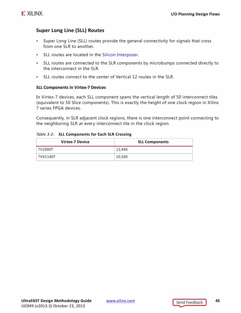
I/O Planning Design Flows
Super Long Line (SLL) Routes
• Super Long Line (SLL) routes provide the general connectivity for signals that cross from one SLR to another.
• SLL routes are located in the Silicon Interposer.
• SLL routes are connected to the SLR components by microbumps connected directly to the interconnect in the SLR.
• SLL routes connect to the center of Vertical 12 routes in the SLR.
SLL Components in Virtex-7 Devices
In Virtex-7 devices, each SLL component spans the vertical length of 50 interconnect tiles (equivalent to 50 Slice components). This is exactly the height of one clock region in Xilinx 7 series FPGA devices.
Consequently, in SLR adjacent clock regions, there is one interconnect point connecting to the neighboring SLR at every interconnect tile in the clock region.
Table 3-2: SLL Components for Each SLR Crossing
Virtex-7 Device SLL Components
7V2000T 13,440
7VX1140T 10,560
UltraFAST Design Methodology Guide www.xilinx.com 45UG949 (v2013.3) October 23, 2013
Send Feedback
I/O Planning Design Flows
The 7VX1140T device has fewer SLL components because it has more DSP and Block Memory columns. These columns displace more interconnect tiles for the same given area.
The ratios and gap size between SLR components is for illustration purposes only. The actual gap is comparatively much smaller.
The SLL components connect to the SLR at the center point of a Vertical 12 Long Line, which spans 12 interconnect tiles in the SLR.
X-Ref Target - Figure 3-4
Figure 3-4: Staggered SLLs Crossing in an SSI Device
UltraFAST Design Methodology Guide www.xilinx.com 46UG949 (v2013.3) October 23, 2013
Send Feedback

I/O Planning Design Flows
This connectivity provides three optimal places to enter or exit an SLL from SLR to adjacent SLR, and gives additional flexibility to placement with little penalty to performance or power.
Propagation Limitations
SLL signals are the only data connections between SLR components.
The following do not propagate across SLR components:
• Carry chains
• DSP cascades
• Block RAM address cascades
• Other dedicated connections such as DCI cascades
The tools normally take this limit on propagation into account. To ensure that designs route properly and meet your design goals, you must also take this limit into account when you build a very long DSP cascade and manually place such logic near SLR boundaries; and when you specify a pinout for the design.
X-Ref Target - Figure 3-5
Figure 3-5: Representation of SLL Connectivity in the SLR
UltraFAST Design Methodology Guide www.xilinx.com 47UG949 (v2013.3) October 23, 2013
Send Feedback

FPGA Power Aspects and System Dependencies
FPGA Power Aspects and System DependenciesWhen planning the PCB, you must take power into consideration:
• The FPGA device and the user design create system power supply and heat dissipation requirements.
• Electrical and physical factors can affect the power supply and cooling of the FPGA device, which in turn signif icantly impacts device performance.
For these reasons, you must understand the power and cooling requirements of the FPGA device. These must be designed on the board.
Power Supply Paths on FPGA DevicesMultiple power supplies are required to power an FPGA device. Some of this power must be provided in a specif ic sequence. Consider the use of power monitoring or sequencing circuitry to provide the correct power-on sequence to the FPGA device and GTs, as well as any additional active components on the board. More complex environments may benefit from the use of a microcontroller or system and power management bus such as SMBUS or PMBUS to control the power and reset process. Specif ic details regarding on/off sequencing can be found in the device data sheet.
The separate sources provide the required power for the different FPGA resources. This allows different resources to work at different voltage levels for increased performance or signal strength, while preserving a high immunity to noise and parasitic effects.
Components of Power Dissipated from the FPGA DeviceThree components make up the total required power for each supply source.
• Device static (leakage) power
The power required for the device to operate and be available for programming. A large portion of this power is due to leakage in the transistors used to hold the device configuration.
• Design static power
The additional continuous power drawn when the device is configured and there is no activity. This includes static current from I/O terminations, clock managers, and other circuits that need power when used, regardless of design activity.
UltraFAST Design Methodology Guide www.xilinx.com 48UG949 (v2013.3) October 23, 2013
Send Feedback

FPGA Power Aspects and System Dependencies
• Design dynamic power
The additional power resulting from the design activity. This power varies over time with the design activity. It also depends on the voltage level and the logic and routing resources used.
Power Consumption PathsThe total power supplied to the device flows in then out of the FPGA through multiple paths, including thermal power and off-chip power.
Thermal Power
Thermal power is the power consumed internally within the FPGA. This represents the generation of heat, which contributes to raising the device junction temperature. This heat is then transferred to the environment. The board design must provide heat dissipation paths to ensure that the junction temperature remains within the device operating range.
Off-Chip Power
Off-chip power is the current that flows from the supply source, through the FPGA power pins, then out of the I/Os, and is then dissipated in external board components. The currents supplied by the FPGA device are generally consumed in off-chip components such as I/O terminations, LEDs, or the I/O buffers of other chips. These do not contribute to raising the device junction temperature of the FPGA device itself. However, power and ground lines must be designed to carry this power.
Power ModesAn FPGA device goes through several power phases from power up to power down with varying power requirements:
• Power-On
• Configuration Power
• Standby Power
• Active Power
Power-On
Power-on power is the transient spike current that occurs when power is f irst applied to the FPGA device. This current varies for each voltage supply, and depends on the FPGA device construction; the ability of the power supply source to ramp up to the nominal voltage; and the device operating conditions, such as temperature and sequencing between the different supplies.
UltraFAST Design Methodology Guide www.xilinx.com 49UG949 (v2013.3) October 23, 2013
Send Feedback

FPGA Power Aspects and System Dependencies
Spike currents are not a concern in modern FPGA device architectures when the proper power-on sequencing guidelines are followed.
Configuration Power
Configuration power is the power required during the configuration of the device. Configuration power is always lower than active power, so this transient stage does not affect power supply requirements unless your application is extremely low power.
Standby Power
Standby power (also called Design Static Power) is the power supplied when the device is configured with your design and no activity is applied externally or generated internally.
Standby power represents the minimum continuous power that the supplies must provide while the design operates.
Active Power
Active power (also called Design Dynamic Power) is the power required while the device is running your application. Active power includes standby power (all static power), plus power generated from the design activity (design dynamic power). Active power is instantaneous and varies at each clock cycle depending on the input data pattern and the design internal activity.
Environmental Factors Impacting Power Power depends on several factors beyond the immediate design itself. These are the factors which influence the voltage and the junction temperature of the device, thereby impacting the power dissipation. Such environmental factors impacting power include:
• Supply Strategies
• Cooling Strategies
Supply Strategies
Supply strategies include:
• Regulator Technology
• Decoupling Network Performance
• FPGA Device Selection
UltraFAST Design Methodology Guide www.xilinx.com 50UG949 (v2013.3) October 23, 2013
Send Feedback

FPGA Power Aspects and System Dependencies
Regulator Technology
Different regulator technologies exist to balance input-to-output voltage difference, response time, maximum currents, and output voltage accuracy constraints.
Decoupling Network Performance
In addition to supplying the FPGA device during brief high power demand periods, an eff iciently designed decoupling circuit reduces current surge requests from the regulator and improves overall regulator consumption.
FPGA Device Selection
Different FPGA device families require different power supply counts and voltage levels. A careful balance among resources, performance, and power is present on all Xilinx FPGA devices. Choose the device that best matches your specif ic requirements.
Paying excessive attention to one characteristic (for example, performance) can negatively impact another characteristic (for example, power). Selecting a device that supports a lower core voltage or lower voltage I/O interfaces reduces power.
Cooling Strategies
Cooling strategies include:
• System Environment
• Heat Sink
• Package Selection
• Component Placement
System Environment
The shape and dimension of the system enclosure (together with the ambient air temperature) are the primary factors that impact the transfer of generated heat to the environment.
Heat Sink
The dimension, shape, thermal adhesive, and mounting of the heat sink and the eventual associated forced airflow system determine the amount of heat that can be extracted from the FPGA device.
Package Selection
In addition to cost and signal integrity, the package dimension, material, and connection to the board influence how the generated heat can be transferred to the environment from
UltraFAST Design Methodology Guide www.xilinx.com 51UG949 (v2013.3) October 23, 2013
Send Feedback

FPGA Power Aspects and System Dependencies
both the top and bottom level. The larger the contact surface area between the heat sink and board, the lower the thermal resistance.
Component Placement
Component placement relative to the system enclosure and other board material, assembly, and components affects how the heat is transferred to the environment. For example, an obstacle may reduce or redirect the airflow near the FPGA device. Other heat generating components in close proximity to the FPGA device may heat up the air flowing above the device and reduce the heat sink eff iciency or transfer heat into the FPGA device by means of the board material.
Power Models AccuracyThe accuracy of the characterization data embedded in the tools evolves over time to reflect the device availability or manufacturing process maturity. This accuracy designation is displayed in the Characterization f ield. Device family characterization data evolve in the following sequence:
• Advance Device Designation
• Preliminary Device Designation
• Production Device Designation
RECOMMENDED: Use the latest version of Xilinx Power Estimator (XPE) to reflect the latest available data.
Advance Device Designation
Devices with the Advance device designation have data models primarily based on simulation results or measurements from early production device lots. Advance data is typically available within a year of product launch. Advance data is considered relatively stable and conservative, although some under-reporting or over-reporting may occur. Advance data accuracy is considered lower than Preliminary and Production data. Xilinx recommends that you discuss the most recent data with your FAE.
Preliminary Device Designation
The Preliminary device designation is based on complete early production silicon. Almost all the blocks in the device fabric are characterized. The probability of accurate power reporting is improved compared to Advance data.
Production Device Designation
The Production device designation is released after enough production silicon of a particular device family member has been characterized to provide full power correlation
UltraFAST Design Methodology Guide www.xilinx.com 52UG949 (v2013.3) October 23, 2013
Send Feedback

FPGA Power Aspects and System Dependencies
over numerous production lots. Device models with Production characterization data are not expected to evolve further.
FPGA Device Power and the Overall System Design ProcessFrom project conception to completion there are many different aspects to consider that influence power. Ignoring for a moment all other issues (including functionality, performance, cost, and time to market), power-related tasks can be sorted into the following separate classes:
• Physical domain, including enclosure, board shape, power delivery system, and thermal power dissipation system
• Functional domain, including area, performance, and I/O interfaces signal integrity
Typically, hardware selection and sizing occurs very early in the design flow to give time for prototype boards to be built. The effect of the FPGA device functionality on power consumption can be estimated early in the design flow, then refined as more and more of the design logic is completed. Figure 3-6, Managing Power Aspects in the PCB Planning Process, illustrates a typical system design process and highlights power-related decision points.
When you select your device and associated cooling parts, the FPGA logic is not yet available. A careful methodology to estimate the FPGA logic power requirements is needed. Xilinx recommends using logic data from an earlier design that is comparable to the current
X-Ref Target - Figure 3-6
Figure 3-6: Managing Power Aspects in the PCB Planning Process
UltraFAST Design Methodology Guide www.xilinx.com 53UG949 (v2013.3) October 23, 2013
Send Feedback

FPGA Power Aspects and System Dependencies
design. You can enter design data using your best estimate, then revise the data later. For information on importing data from an earlier design into XPE, see Implementing the Design, page 199.
Xilinx highly recommends a thermal simulation. Thermal models can be obtained from Xilinx. This allows a higher accuracy and it also provides ThetaJA, which can be specif ied in XPE.
• If a thermal simulation is not possible, provide a best guess for environment conditions, such as heatsink and airflow.
• If the power numbers provided by XPE exceed the power budget, the design may have to be optimized for power.
• If power estimates are within the budget, but TJA is higher than the maximum allowed, consider additional cooling techniques (such as heat sink or airflow). Re-run XPE with these new values for environmental conditions, since these also will impact power.
System Level Cooling StrategyA cooling strategy ensures that the heat generated from the device is extracted and absorbed by the environment. The following cooling strategies are generally available at the beginning of the design, but become less feasible in the later stages. They signif icantly impact the device static power. These cooling strategies include increasing the airflow, lowering the ambient temperature, and using a heat sink (or a larger heat sink), or selecting a different regulator.
System Level Supply StrategyVoltage has a large impact on both static and dynamic power. Active control of the voltage level ensures that the desired voltage is applied to the device.
• Use switching regulators.
Switching regulators are more power eff icient than linear regulators, but at the expense of requiring a higher component count.
• Use adjustable regulators.
Sense voltage as close as possible to the FPGA device and to the highest consuming device if the same supply powers multiple FPGA devices.
• Select regulators with tight tolerances.
Regulators with tight tolerance ensure consistent voltage supply to the device.
UltraFAST Design Methodology Guide www.xilinx.com 54UG949 (v2013.3) October 23, 2013
Send Feedback

FPGA Power Aspects and System Dependencies
Measuring Power and TemperatureThis section briefly describes techniques for measuring FPGA device power consumption and heat dissipation. Some of these techniques use internal FPGA resources. Other techniques use board or external components. Some applications require power and temperature to be actively monitored and adjusted after deployment. Other applications use these measurement techniques in the lab during prototyping and validation phases.
Power Measurement Techniques
Power measurement techniques include:
• Using a Current Sense Resistor
• Using Advanced Regulators and Digital Power Controllers
• Performing On-Board Monitoring
• Having Separate Voltage Rails
Using a Current Sense Resistor
Inserting a Current Sense Resistor in series between the regulator output and the FPGA device creates a small voltage drop which, by Ohm’s Law, is proportional to the flowing current. Measuring this voltage through an XADC gives you the current being supplied to the FPGA device. To understand the connections needed to obtain the desired accuracy of measurements, see the 7 Series FPGAs and Zynq-7000 All Programmable SoC XADC Dual 12-Bit 1 MSPS Analog-to-Digital Converter User Guide (UG480) [Ref 7] (also known as the XADC User Guide).
Using Advanced Regulators and Digital Power Controllers
The latest evaluation kits include advanced regulator and digital power controllers that you can use to capture regulator output currents and voltages, then send this information to a monitoring computer over a USB interface. This is the simplest and most convenient way to monitor the power rails.
Most Xilinx development boards have integrated Texas Instrument UCD92xx controllers that can be accessed with the Fusions Digital Power Designer software on a PC using a PMBus (I2C) to USB interface module.
Performing On-Board Monitoring
Xilinx 7 series device families provide internal sensors and at least one analog-to-digital converter to measure supplied voltages and device temperature. The ChipScope utility provides real-time JTAG access to measure the different supply source voltages or device junction temperature before and after device configuration (see Figure 3-7, Voltage and Junction Temperature Monitoring with ChipScope, page 57). You can also instantiate a
UltraFAST Design Methodology Guide www.xilinx.com 55UG949 (v2013.3) October 23, 2013
Send Feedback

FPGA Power Aspects and System Dependencies
System Monitor or XADC component in your code to access these measurements from your FPGA application.
Having Separate Voltage Rails
If possible, have separate voltage rails for each of the supply voltages. If voltage rails are tied together, note it and account for it when power is measured across these rails.
Thermal Measurement Techniques
Thermal measurement techniques include:
• Performing External Monitoring
• Performing On-Board Monitoring
Performing External Monitoring
Because the device package prevents access to the silicon, junction temperature cannot be measured directly. Junction temperature can be approximated by measuring the temperature of the package, the heat sink, and other locations with a thermocouple.
Thermal cameras are also used to visualize the device temperature and thermal dissipation interactions with neighboring components and the larger environment.
Performing On-Board Monitoring
Thermal measurements are possible using the same techniques as power measurements. You can use ChipScope before and after device configuration. see Figure 3-7, Voltage and Junction Temperature Monitoring with ChipScope.
You can also use the System Monitor/XADC primitive within your design to read the device junction temperature.
UltraFAST Design Methodology Guide www.xilinx.com 56UG949 (v2013.3) October 23, 2013
Send Feedback
FPGA Power Aspects and System Dependencies
Methodology for Power and Temperature Measurement
To evaluate the three factors contributing to the design total power, you must control the device junction temperature and let it stabilize before making measurements. This control and stabilization is required because the device and design static power is heavily dependent on the device junction temperature.
The three factors contributing to the design total power are:
• Device Static
• Design Static
• Design Dynamic
Device Static
Download a blank design to ensure that: (1) no input noise is captured; and (2) all internal logic and configuration circuits are in a known state.
Note: A blank design is a design with a single gate or flip-flop that never toggles, and in which all outputs are in a 3-state configuration.
Wait for the junction temperature to stabilize, then measure VCCINT, VCCAUX, and any other supply source of interest. With special equipment, a simple heat gun, or cold spray, you can force temperature changes to evaluate the influence of the environment on the device static power.
X-Ref Target - Figure 3-7
Figure 3-7: Voltage and Junction Temperature Monitoring with ChipScope
UltraFAST Design Methodology Guide www.xilinx.com 57UG949 (v2013.3) October 23, 2013
Send Feedback

Worst Case Power Analysis Using Xilinx Power Estimator (XPE)
Design Static
Download the design onto the FPGA device and do not start any input or internal activity (input data and external and internal clock generation). Wait for the device temperature to stabilize, then measure power on all supply rails of interest.
Subtracting the device static measurement from these values gives you the additional static power from the specif ic logic resources and configuration used in your design (design static power).
Design Dynamic
Download the design onto the FPGA device and provide clocks and input stimulus representative of the design. Wait for the junction temperature to stabilize before measuring all supply sources of interest.
This power represents the instantaneous total power of the design. It will vary with the change in activity at each clock cycle.
Worst Case Power Analysis Using Xilinx Power Estimator (XPE)The board should be designed for worst-case power. The steps to worst case power analysis using Xilinx Power Estimator (XPE) are discussed below.
Setting ExpectationsUnderstanding the total power requirements will help you define your power delivery and cooling system specif ications. You want to finalize on the number of:
• Voltage supplies
• Power drawn by each
• Absorbed energy that will generate heat
XPE can answer these questions. It helps you develop in parallel the FPGA logic and the printed circuit board on which the device will be soldered. This exercise will also help you understand the margin you can expect to have and therefore gain confidence that your system will work within budget once implemented. Figure 3-8, Xilinx Power Estimator (XPE) Presentation of Power Information, shows a sample of Xilinx Power Estimator interface.
UltraFAST Design Methodology Guide www.xilinx.com 58UG949 (v2013.3) October 23, 2013
Send Feedback

Worst Case Power Analysis Using Xilinx Power Estimator (XPE)
X-Ref Target - Figure 3-9
Estimating Power in the XPEPower and cooling specifications must be properly set in order to create a functioning and reliable system. In most cases, these thermal and power specifications must be set before PCB design. Due to the flexibility of FPGA devices, the FPGA design often is not completed (or sometimes even started) before system design or PCB fabrication.
This sequence creates a signif icant challenge for FPGA designers, since thermal and power characteristics can vary dramatically depending on the bitstream (design), clocking, and data put into the chip.
Underdesigning the power or thermal system can make the FPGA device operate out of specification. This can result in the device not operating at the expected performance, and can have other potentially more serious consequences.
X-Ref Target - Figure 3-8
Figure 3-8: Xilinx Power Estimator (XPE) Presentation of Power Information
UltraFAST Design Methodology Guide www.xilinx.com 59UG949 (v2013.3) October 23, 2013
Send Feedback

Worst Case Power Analysis Using Xilinx Power Estimator (XPE)
Overdesigning the power system is generally less serious, but is still not desirable because it can add unnecessary cost and complexity to the overall system.
The following steps are primarily focused on power analysis. There are several techniques for power optimization that can be explored and applied during the analysis and can result in significant power savings. These techniques are discussed in Chapter 4, Design Creation, and Chapter 5, Implementation.
Step 1: Obtain the latest version of XPE for the selected target device.
Make sure you are using the latest version of the Xilinx Power Estimator (XPE) tool. Power information is updated periodically to reflect the latest power modeling and characterization data. The latest version of XPE can be obtained from the Xilinx web site at http://www.xilinx.com/power.
Check this web site occasionally for new versions. To import the data from a previous version, click Import File on the updated version’s Summary sheet.
Keeping the Xilinx Power Estimator up to date ensures that the most current power information is always used in the power analysis.
Step 2: Complete the Device information on the Summary sheet.
Make sure that each f ield in the Device section of the Summary sheet is properly set. Each f ield can significantly impact the end power calculation, particularly in static and clocking power.
Enter the following information in the Device section:
• Family and Device
• Package
• Speed Grade (If Available)
• Temp Grade
• Process
• Voltage ID Used
Family and Device
An improperly set Family or Device can lead to incorrect device and design power estimations, such as the design power reported for clocks. It can also result in improperly reported available device resources.
UltraFAST Design Methodology Guide www.xilinx.com 60UG949 (v2013.3) October 23, 2013
Send Feedback

Worst Case Power Analysis Using Xilinx Power Estimator (XPE)
Package
The package selection can affect the device’s heat dissipation and thus affect the end junction temperature. An incorrect junction temperature can result in an incorrect device static power calculation.
Speed Grade (If Available)
Choose the speed grade most appropriate to the design needs. Some FPGA families may have different power specif ications for different speed grades.
Temp Grade
Select the appropriate grade for the device (typically Commercial or Industrial). Some devices may have different device static power specif ications depending on this setting. Setting this properly also allows for the proper display of junction temperature limits for the chosen device.
Process
For the purposes of a worst-case analysis, the recommended process setting is Maximum. The default setting of Typical gives a closer picture to what would be measured statistically, but changing the setting to Maximum modifies the power specif ication to worst-case values.
Voltage ID Used
The Voltage ID (VID) voltage is the minimum possible VCCINT voltage at which the FPGA device can run and still meet its performance specifications. This voltage is tested when the FPGA device is manufactured and the value is programmed into the DNA (device identif ier) eFUSE register on the FPGA device. Activating the VID feature to operate the FPGA device at this VID voltage can result in a significant static power savings over operating the FPGA device at its nominal voltage.
Note: This option applies to Virtex-7, -1 speed grade, Commercial Temp grade, and Maximum Process FPGA devices only.
UltraFAST Design Methodology Guide www.xilinx.com 61UG949 (v2013.3) October 23, 2013
Send Feedback
Worst Case Power Analysis Using Xilinx Power Estimator (XPE)
Step 3: Complete the Environment information on the Summary sheet.
To set the proper environment conditions, enter the following information in the Environment section of the Summary sheet:
• Ambient Temp (°C)
• Airflow (LFM)
• Heat Sink (if available)
• Board Selection and Number of Board Layers
• ThetaJB
Ambient Temp (°C)
Specify the maximum possible temperature expected inside the enclosure that will house the FPGA design. This setting, along with airflow and other thermal dissipation paths (for example, the heatsink), will allow an accurate calculation of Junction Temperature, which in turn will allow a more accurate calculation of device static power.
Airflow (LFM)
The airflow across the chip is measured in Linear Feet per Minute (LFM).
LFM can be calculated from the fan output in CFM (Cubic Feet per Minute) divided by the cross sectional area through which the air passes. Specif ic placement of the FPGA device or fan can impact the effective air movement across the FPGA device, and thus the thermal dissipation. The default for this parameter is 250 LFM. If you plan to operate the device without active air flow (still air operation), change the 250 LFM default to 0 LFM.
Heat Sink (if available)
If a heatsink is used and more detailed thermal dissipation information is not available, choose an appropriate profile for the type of heatsink used. This, along with the other entered parameters, helps calculate an effective ThetaJB (printed circuit board thermal resistance), resulting in a more accurate junction temperature and quiescent power calculation.
Note: Some types of sockets may act as heatsinks, depending on the design and construction of the socket.
Board Selection and Number of Board Layers
Selecting an approximate size and stack of the board will help calculate the effective ThetaJB by taking into account the thermal conductivity of the board itself.
UltraFAST Design Methodology Guide www.xilinx.com 62UG949 (v2013.3) October 23, 2013
Send Feedback
Worst Case Power Analysis Using Xilinx Power Estimator (XPE)
ThetaJB
If more accurate thermal modeling of the board and system is available, use ThetaJB in order to specify the amount of heat dissipation expected from the FPGA device. The more accurately a custom ThetaJB can be specif ied, the more accurate the estimated junction temperature will be, thus affecting device static power calculations.
IMPORTANT: To specify a custom ThetaJB, the Board Selection must be set to Custom. If you do specify a custom ThetaJB, you must also specify a Board Temperature for an accurate power calculation.
Step 4: Set worst-case power supply voltages for all supplies.
By default, each voltage rail for a particular device is set to its nominal value. In order to obtain an accurate power estimation, the worst-case or highest voltage value seen at the FPGA device can be generally calculated using the nominal output value and tolerances from the supplies or regulators to each rail. If any signif icant IR (voltage) drop is seen, particularly with supplies that are unregulated, account for the voltage drop in the maximum voltage calculation. The power estimate corresponding to this worst case voltage may be derived by putting these values in the spreadsheet, or by reading off the graph available in the Graphs tab of the XPE spreadsheet.
If you are not using some of the VCCO or MGT voltage sources, leave the default values in the rows for those voltage sources
Step 5: Enter clock and resource information.
You can import the XPower Export File (.xpe) from a design into XPE to help f ill out the resource information if the design has already been run in the Vivado tools or if a previous revision of the design has been run, and that revision can be used as a good starting point for the analysis.
To import an xpe f ile, select the Import File button located on the Summary sheet of XPE.
TIP: After importing a Vivado Design Suite XPE file, check that the data is correct and relevant. Consider this information to be a good starting point, but not a complete solution.
UltraFAST Design Methodology Guide www.xilinx.com 63UG949 (v2013.3) October 23, 2013
Send Feedback
Worst Case Power Analysis Using Xilinx Power Estimator (XPE)
For each of the resource tabs, examine and (if necessary) f ill out the resources expected to be used in the design:
• Clock Tree Power
• Logic Power
• I/O Power
• blockRAM Power
• DSP Power
• Clock Manager (CLKMGR)
• GT
Clock Tree Power
In the Clock sheet, enter each clock, the expected Frequency, and the expected clocking resource it will use. If you are not certain which clocking resource will be used, keep the default selection for Type as Global clock. Ignore Fanout for now. Fanout is addressed in Step 6: Set the toggle and connectivity parameters. Let the Clock Buffer Enable and Slice Clock Enable be set at the system defaults of 100% and 50% respectively.
Logic Power
In the Logic sheet, enter an estimate for the number of Slice resources.
Use the different rows to separate different logic functions and characteristics such as clock speed and toggle rate.
In the early stages of the FPGA design, it can be diff icult to obtain accurate numbers for such resources. Xilinx recommends working with large round numbers early (when the end resource count is not well known). As the design progresses, update the values to better represent the f inal representation.
TIP: When entering the clock frequency information, use Excel’s capabilities to relate that cell to the cell populated in the Clock Tree Power tab. To do this, select the desired Clock (MHz) cell in the logic view, type =, and select the cell in the Clock sheet corresponding to the clock source for that logic. This should populate that cell with the value in the Clock sheet. The primary benefit of this methodology is that if the clock frequency ever must be changed, either by a specification change or by exploring
Table 3-3: Estimate for the Number of Slice Resources
Column Represents Number Of
LUTs LUTs used for arithmetic or logic
Shift Registers LUTs configured as SRLs (Shift Register LUTs)
SelectRAMs LUTs configured as memory
Registers Registers or latches configured in the design
UltraFAST Design Methodology Guide www.xilinx.com 64UG949 (v2013.3) October 23, 2013
Send Feedback

Worst Case Power Analysis Using Xilinx Power Estimator (XPE)
power tradeoffs vs. frequency, the value must be updated in one place only, and can be reflected throughout the analysis. This methodology can also reduce the chance of errors and inconsistencies during the data entry.
I/O Power
You must f ill out the I/O sheet of XPE properly to obtain an accurate overall estimation of all rails of the chip. Depending on the selected I/O Standard and I/O circuitry, a significant amount of power may be consumed not only in the VCCO rail, but also in the VCCINT and VCCAUX rails.
It is often simplest to enter each device interface separately and to break out the interface signals to the data, control, and clock signals. This makes it easier to specify different I/O Standards, as well as other I/O characteristics such as load and toggle rates.
RECOMMENDED: Use the Memory Interface Configuration wizard in XPE to ease the effort of adding I/Os associated with complex memory interfaces.
For the I/O current calculations, the predicted power assumes that standard board trace and termination is applied.
TIP: When using differential I/O, specify each input and output a pair. Do not specify two inputs in the spreadsheet to indicate a single differential input.
Enter the relevant inputs in the Memory Interface Configuration wizard. The tool automatically populates the relevant I/O rows in the I/O sheet.
blockRAM Power
In the blockRAM sheet, enter the number and configurations of the blockRAM intended to be used for the design. Be sure to adjust the Enable Rate to the percentage of time the ENA or ENB port will be enabled.
Because the amount of time the RAM is enabled directly impacts the dynamic power it consumes, entering the proper value for this parameter is important for an accurate blockRAM power estimation.
TIP: Use the Memory Generator wizard in XPE to ease the effort of adding block RAMs in the design.
DSP Power
Complete the DSP sheet in XPE. DSP blocks can be used for purposes other than multipliers, such as counters, barrel shifters, MUXs, and other common functions.
UltraFAST Design Methodology Guide www.xilinx.com 65UG949 (v2013.3) October 23, 2013
Send Feedback
Worst Case Power Analysis Using Xilinx Power Estimator (XPE)
Clock Manager (CLKMGR)
If an MMCM or PLL is used in the design, specify the use and configuration of each in the Clock Manager sheet.
GT
If GTs (serial transceivers) are used in the design, specify the use and configuration of each in the GT sheet.
RECOMMENDED: Use the Transceiver Configuration wizard to ease data entry and improve accuracy.
To launch the Transceiver Configuration wizard, click the Add GTX Interface button.
Step 6: Set the toggle and connectivity parameters.
Review the set value for each tab containing a Toggle Rate, Average Fanout, or Enable Rate.
In the absence of any other information or knowledge, leave Toggle Rate and Enable Rate settings at their defaults.
Make any necessary adjustments if the default does not accurately represent the characteristics of this design. For example:
• If a memory interface has a training pattern routine that exercises a sustained high toggle rate on that interface, raise the toggle rate to reflect this additional activity.
• If a portion of a circuit is clock enabled in a way that reduces the overall activity of the circuit, reduce the toggle rate.
For more information on how to determine toggle rate, see the Xilinx Power Estimator User Guide (UG440) [Ref 2].
The easiest way to specify clock fanout in XPE is to create an equation to sum all synchronous elements for any clock domain. For example, in the Fanout f ield for a given clock:
1. Type =SUM(
2. Select all cells that specify the number of synchronous elements sourced by that clock (such as blockRAM, FF, Shift Register, and Select RAM components).
3. Close the parenthesis.
The Fanout cell is populated with the appropriate number.
This method of entering clock fanout is often the easiest, and has the added advantage of automatically updating when adjustments are made to the spreadsheet resource counts.
UltraFAST Design Methodology Guide www.xilinx.com 66UG949 (v2013.3) October 23, 2013
Send Feedback

Worst Case Power Analysis Using Xilinx Power Estimator (XPE)
The resulting Excel equation is similar to:
=SUM(LOGIC!E3:G3,I/O!E3:G3,BRAM!C4,MULT!C3)
For logic fanout, the nature of the data and control paths must be thought out. In designs with well-structured sequential data paths (such as DSP designs), fanouts generally tend to be lower than the set default. In designs with many data execution paths (such as some embedded designs), higher fanouts may be seen. As with toggle rates, if this information is not known, leave the setting at the default and adjust later if needed.
For I/O Output Load, enter a simple capacitive load for each design output. This setting affects the dynamic power of the driven output. The Output Load value is primarily made up from the sum of the individual input capacitances of each device connected to that output. The input capacitance can generally be obtained from the data sheets of the devices to which the FPGA I/O is connected.
Step 7: Analyze the results.
Before you analyze the results, update Steps 1 through 6 if necessary. After completing these steps, analyze the results.
Be sure that the junction temperature is not exceeded, and that the power drawn is within the desired budget for the project. If the thermal dissipation or power characteristics are not within targets:
• Adjust the environmental characteristics (for example, increase airflow or add a heatsink), or
• Adjust the resource and power characteristics of the design until an acceptable result is reached.
Many times, tradeoffs can be made to derive the desired functionality with a tighter power budget. The best time to explore these options is early in the design process. Once the data is completely entered, and the part is operating within the thermal limits of the selected grade, the power reported by XPE can be used to specify the rails for the design.
If your confidence in the data entered is not very high, you can pad the numbers to circumvent the possibility of underdesigning the power system for the device. If, however, you are fairly certain of the data entered, no additional padding above the data reported by the tool is necessary.
As the design matures, continue to review and update the information in the spreadsheet to reflect the latest requirements and implementation details. This will present the most current picture of the power used in the design and can potentially allow early identif ication of adjustments to the power budgeting up or down depending on the current power trends of the design.
UltraFAST Design Methodology Guide www.xilinx.com 67UG949 (v2013.3) October 23, 2013
Send Feedback
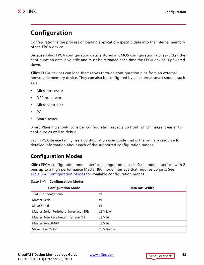
Configuration
ConfigurationConfiguration is the process of loading application-specific data into the internal memory of the FPGA device.
Because Xilinx FPGA configuration data is stored in CMOS configuration latches (CCLs), the configuration data is volatile and must be reloaded each time the FPGA device is powered down.
Xilinx FPGA devices can load themselves through configuration pins from an external nonvolatile memory device. They can also be configured by an external smart source, such as a:
• Microprocessor
• DSP processor
• Microcontroller
• PC
• Board tester
Board Planning should consider configuration aspects up front, which makes it easier to configure as well as debug.
Each FPGA device family has a configuration user guide that is the primary resource for detailed information about each of the supported configuration modes.
Configuration ModesXilinx FPGA configuration mode interfaces range from a basic Serial mode interface with 2 pins up to a high performance Master BPI mode interface that requires 50 pins. See Table 3-4, Configuration Modes for available configuration modes.
Table 3-4: Configuration Modes
Configuration Mode Data Bus Width
JTAG/Boundary Scan x1
Master Serial x1
Slave Serial x1
Master Serial Peripheral Interface (SPI) x1/x2/x4
Master Byte Peripheral Interface (BPI) x8/x16
Master SelectMAP x8/x16
Slave SelectMAP x8/x16/x32
UltraFAST Design Methodology Guide www.xilinx.com 68UG949 (v2013.3) October 23, 2013
Send Feedback
Configuration
Master Mode and Slave Mode
The FPGA configuration modes are divided into two general classif ications, Master Mode and Slave Mode. The terms Master and Slave refer to the direction of the configuration clock (CCLK).
For more information on the configuration mode connectivity diagrams, signal descriptions, and mode pin settings, see the FPGA family’s configuration user guides.
Choose the exact configuration mode based on system requirements. Some of the more commonly encountered scenarios are discussed below as examples to illustrate the tradeoffs involved when choosing the configuration mode.
Master Mode
In Master Mode, the FPGA device drives CCLK from an internal oscillator. A common configuration source in Master Mode is external flash memory, which can eliminate the need for an on-board external oscillator for configuration.
Slave Mode
In Slave Mode, the CCLK is an input from an external clock source. In this mode, a processor, microcontroller, or CPLD can be used with the external oscillator to control the FPGA configuration. The exception to this category is the JTAG/boundary-scan configuration interface which uses an external JTAG clock TCK instead of CCLK.
Pin-Limited Applications
Serial modes have fewer interface pins, making them ideal for pin-constrained applications. These configuration modes also have multiple purpose pins that can be reused for the user application design after configuration. Evaluate pin reuse carefully.
Xilinx recommends Master SPI and Slave Serial Configuration modes for pin-limited and ease-of-use applications.
Master SPI configuration mode enables an external SPI flash to load the FPGA device on power-up. This mode supports up to x4 data bus width, allowing for reasonable configuration times with relatively low interface pin count. In addition, Master modes eliminate an external clock source and reduce the system connectivity requirements.
Cost Sensitive Applications
Reusing existing on-board flash memory or system memory to store the bitstream image is cost advantageous. Bitstreams can even be stored on a hard drive or downloaded remotely
UltraFAST Design Methodology Guide www.xilinx.com 69UG949 (v2013.3) October 23, 2013
Send Feedback

Configuration
over a network connection. If extra storage exists, then (depending on the source), use one of the following modes:
• JTAG configuration mode
• Master SPI configuration mode
• Slave Serial configuration mode
• Master BPI configuration mode
If configuration from flash is required, and on-board flash cannot be reused, then SPI flash is the lowest cost external configuration flash option. Using the internal clock oscillator in SPI Master Mode can also eliminate the need (and thus the cost) for an external configuration clock source.
High Speed Configuration Applications
Several popular standards (for example, PCIe and CAN) require a fast boot up time, and require that the FPGA device be configured in less than a specif ic configuration time. The fastest available configuration options for Xilinx 7 series FPGA devices are:
• Overall
Slave SelectMAP x32 mode, if the bitstream is directly loaded at the highest configuration frequency
• Configuration from Flash
Master BPIx16 configuration mode using EMCCLK and burst synchronous read mode
Tips for High Speed Configuration Applications
Keep the following in mind for high speed configuration applications:
• At the same clock frequency, parallel configuration modes are inherently faster than the serial modes because they program 8, 16, or 32 bits at a time.
• Do not daisy-chain FPGA devices from a single configuration source. In a multi-FPGA design in which configuration speed is a concern, configure each FPGA device separately and in parallel.
• Use Slave modes or EMCCLK with Master modes. External Master Configuration Clock with the Master mode has a more precise clock, compared to internal CCLK, thus allowing for optimal configuration performance. To use this option, the EMCCLK pin must be instantiated in the design since it is a multi-purpose pin. If this pin is not instantiated in the design, the configuration startup phase does not complete, and your design will not be active.
• Many factors contribute to the maximum configuration clock rate at which a solution can run. Some of these considerations are outside of the FPGA device specif ications,
UltraFAST Design Methodology Guide www.xilinx.com 70UG949 (v2013.3) October 23, 2013
Send Feedback
Configuration
such as the access times on the flash selected. The FPGA family’s configuration user guide provides equations that will allow you to calculate the maximum configuration times for common modes based on the flash you have selected and configuration setup targeted. Choose your flash devices, so that they can operate at the highest configuration clock frequency allowed by the FPGA device.
• Explore the possibility of reducing the power on reset time (Tpor) by controlling the ramp rate on a system. For specifications on the Tpor ramp time options, see the FPGA configuration switching characteristics in the device data sheet.
• Some advanced configuration techniques such as Partial Reconfiguration may also be helpful. However, they are beyond the scope of this document.
Estimating Configuration Time
Configuration time (after Power On Reset) can be estimated using the equation:
High Density or Multi-Boot Storage Applications
Applications that require multiple FPGA devices or multiple design images for a single FPGA device or higher density FPGA devices require a configuration solution with larger flash memory density. In general, parallel NOR flash is twice the size of the available SPI flash density. If an external flash memory solution is required, and a high density solution is targeted, consider Master BPI Configuration mode.
The size of the bitstream is directly dependent on the device size and determines the flash size required. A bitstream compression option can help reduce the bitstream size. The amount of compression varies according to the design.
Density Migration Required
Systems designed to allow for future optimization or feature additions are often reviewed for migration feasibility. Migration feasibility should also consider configuration aspects. For example, if a configuration mode is selected with flash, be sure that the larger density storage can still be covered by the setup.
Voltage Compatibility
Some applications have a limited set of power supply options available in the system. These systems may require configuration solutions that are compatible with a 1.8V or 3.3V power supply. External third party SPI flash and parallel NOR flash have parts with the core at 1.8V or 3.3V. Consider both the desired I/O and core voltage compatibility when choosing flash devices.
Configuration time = bitstream size
configuration clock frequency x data bus width
UltraFAST Design Methodology Guide www.xilinx.com 71UG949 (v2013.3) October 23, 2013
Send Feedback
Configuration
Board Design TipsWhen you are designing the board, consider the following points from the perspective of configuration and debug:
• JTAG
• Debug
• Multiple Devices
• STATUS Pins
• Configuration Bank Voltage Selection
• I/O Pin Pullups
• Design Reset
• Delaying Configuration
• Configuration Clock
• CCLK Termination
• Flash Based Configuration
JTAG
Xilinx recommends that the board always have a JTAG interface connector accessible, even when JTAG is not the primary configuration mode. The four-pin JTAG interface provides direct debug access at all stages of the design and enables key checks such as the device IDCODE or device DNA read. The JTAG configuration mode can also be a valuable alternative flow if the primary configuration method is being debugged at board bring-up or because it has encountered a configuration error.
An internal configuration status register provides information about the configuration process. This register can be accessed by JTAG using a supported cable and the Vivado Design Suite Device Programmer. Details about the startup phase, DONE, INIT, and common error modes are reported by this register, and can be a helpful debug tool. For more information about the various bits of the status register, see the configuration user guide for that device.
The Vivado Design Suite Device Programmer supports direct JTAG configuration and debug with supported cables during prototyping. If the Master SPI or BPI configuration modes are selected, the JTAG interface can also provide an indirect means to program supported on-board flash connected to the FPGA device for configuration.
Because Xilinx FPGA devices do not have the optional JTAG standard reset signal (TRST), this signal should not be brought out to the JTAG connector. The TRST signal resets the JTAG TAP state machine to the RTI (Run-Test-Idle) state directly. TMS held high for f ive TCK pulses can reset the TAP, and provides the same functionality as the TRST. This method for
UltraFAST Design Methodology Guide www.xilinx.com 72UG949 (v2013.3) October 23, 2013
Send Feedback

Configuration
resetting the state machine is useful in mixed JTAG chains when the devices do not all have the TRST pin in order to prevent the JTAG TAP state machine from getting out of sync.
Debug
During I/O Design, leave adequate number of pins for debug. Connect these pins to a header, which can be used to connect to a Logic Analyzer or Scope. If needed, certain signals can be brought out to these pins, and connected to the Logic Analyzer.
Multiple Devices
JTAG is a serial interface that supports the chaining of multiple devices.
The ability to isolate a single FPGA device in the JTAG chain can be helpful for system bring-up and debug. Common techniques allow a device to be part of the JTAG multiple device chain, or to have only the single device in the JTAG chain.
In a JTAG chain, the TCK and TMS interface signals are connected together, ensuring that each device in the chain receives the same clock and mode select transitions. If the JTAG chain consists of multiple devices, buffer TCK and TMS.
STATUS Pins
Connect LEDs and pull-ups to the DONE and INIT_B signals. See the FPGA family configuration user guide for recommended pull-up values. The INIT_B signal pulses low when the configuration sequence has started, and then is pulled high externally during configuration. If an error is detected during configuration, the signal is again driven low. The DONE signal indicates a successful configuration. In case of an error, this signal does not go high. Between these two LEDs, it is possible to know the state of configuration process.
Configuration Bank Voltage Selection
Most Xilinx FPGA devices support configuration interfaces with 3.3V, 2.5V, or 1.8V I/O. There are dedicated configuration pins in bank 0, and then pins related to specif ic configuration modes which are multi-purpose spread out in other banks. For specific bank details, see the relevant FPGA configuration user guide or FPGA package user guide.
To support the appropriate configuration interface voltage on bank 0, the configuration bank voltage select pin (CFGBVS) must be set to a High or Low in order to set the dedicated configuration bank 0 I/O for 3.3V/2.5V or 1.8V operation, respectively. When CFGBVS is set to Low for 1.8V I/O operation, the VCCO_0 supply and I/O signals to bank 0 must be 1.8V (or lower) to avoid device damage. The CFGBVS pin cannot be left floating. For more information, see the configuration user guide for the appropriate device family.
UltraFAST Design Methodology Guide www.xilinx.com 73UG949 (v2013.3) October 23, 2013
Send Feedback
Configuration
I/O Pin Pullups
The SelectI/O of the device can be pulled high or 3-stated during configuration, depending upon whether PUDC (Pull Up During Configuration) is tied high or low respectively. During configuration, this pin should always be tied to a constant, depending upon the behavior desired for SelectI/O, and never left floating. Setting the property BITSTREAM.CONFIG.UNUSEDPINS during bitstream generation allows you to control whether an unused IO pin has a pulldown (default), pullup, or is left floating after configuration.
Design Reset
The PROGRAM_B input resets the FPGA device. Be sure that an external pull-up is added to the FPGA device’s PROGRAM_B signal. See the FPGA family configuration user guide for recommended pull-up values. Consider adding a push button or method to pulse the PROGRAM_B signal to reset and clear the configuration memory for tests outside of power-up.
Delaying Configuration
Some applications with external flash or power sequencing conditions may want to delay configuration in order to ensure that the power is good before the FPGA device initiates configuration. Configuration can be delayed by holding the INIT_B low for a given period of time, for example until the power supplies are stable. Holding the PROG pin low does not help in delaying the configuration.
Configuration Clock
Decisions on using internal configuration clock in master modes or external configuration clocks must be based on the cost and performance requirements.
Cost
Using internal config clock reduces cost by eliminating the need for external on-board oscillator.
Performance
For applications requiring higher speed for programming, External Master Configuration Clock must be used. The internal configuration clock oscillator has a tolerance range that can be as much as +/-50% in some families.
Selecting a clock rate of 33 MHz during creation of the configuration file can cause the actual CCLK frequency to be anywhere in the range 16.5 MHz to 49.5 MHz.
UltraFAST Design Methodology Guide www.xilinx.com 74UG949 (v2013.3) October 23, 2013
Send Feedback
Configuration
For example, if a flash device has an allowable fmax specif ied as 33 MHz, then the highest allowable selection for CCLK is 22 MHz; because, with 22MHz selection, the actual clock could reach 33 MHz.
CCLK Termination
While configuration interfaces typically run below 100 MHz, it is still important to make sure that the configuration clock seen by the flash and the FPGA device are clean with valid low and high levels. Glitches in the clock caused by reflections, poor termination, or bad trace geometries can result in configuration errors. See the particular FPGA family’s configuration user guide and the package user guide for that FPGA device family.
Flash Based Configuration
SPI and Parallel NOR flash are two popular configuration storage options. Selecting the Master SPI or Master BPI Configuration modes should resolve the following issues:
• Flash often has control signals such as Write Protect (WP), Reset (RST), or the Hold pins. The Reset signal is recommended in many cases to be tied to the INIT_B signal, so that when the FPGA device is reset, the attached configuration flash is also reset.
• Write protect is an advanced feature. When enabled, write protect prevents indirect programming. If changes to the design might be required, Xilinx recommends that you have a readily-accessible way of disabling write protect.
• Some of the supported parallel NOR flash devices offset the address, so for certain flash the bus alignment may be FPGA A0 signal to the Flash A1 signal. Please review the flash data sheet for guidance on which pin is the LSB.
Dedicated vs. Multi-Purpose Configuration PinsThe configuration pins can either be dedicated or multi-purpose. For dedicated configuration pins, the bitstream setting option determines whether they are pulled up, pulled down, or 3-stated after the configuration is completed. Multi-purpose configuration pins are used during configuration to load the FPGA device. They can later be reused by the design application for other functions. For these pins, after configuration, the signal behavior depends on the design.
There is an exception to the Multi-Purpose pin behavior described above, for the FPGA bitstream persist option. Persist is used for advanced user scenarios such as SelectMAP, readMAP, and Partial Reconfiguration, which are beyond the scope of this document. Multi-purpose configuration mode can place voltage restrictions on FPGA device I/O banks.
UltraFAST Design Methodology Guide www.xilinx.com 75UG949 (v2013.3) October 23, 2013
Send Feedback
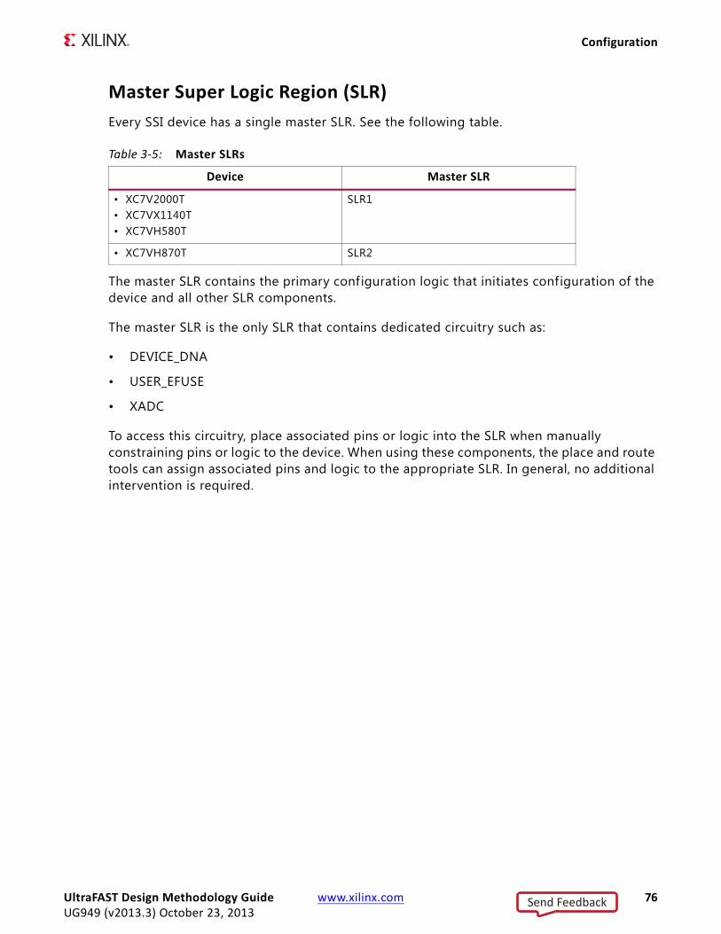
Configuration
Master Super Logic Region (SLR)Every SSI device has a single master SLR. See the following table.
The master SLR contains the primary configuration logic that initiates configuration of the device and all other SLR components.
The master SLR is the only SLR that contains dedicated circuitry such as:
• DEVICE_DNA
• USER_EFUSE
• XADC
To access this circuitry, place associated pins or logic into the SLR when manually constraining pins or logic to the device. When using these components, the place and route tools can assign associated pins and logic to the appropriate SLR. In general, no additional intervention is required.
Table 3-5: Master SLRs
Device Master SLR
• XC7V2000T• XC7VX1140T• XC7VH580T
SLR1
• XC7VH870T SLR2
UltraFAST Design Methodology Guide www.xilinx.com 76UG949 (v2013.3) October 23, 2013
Send Feedback
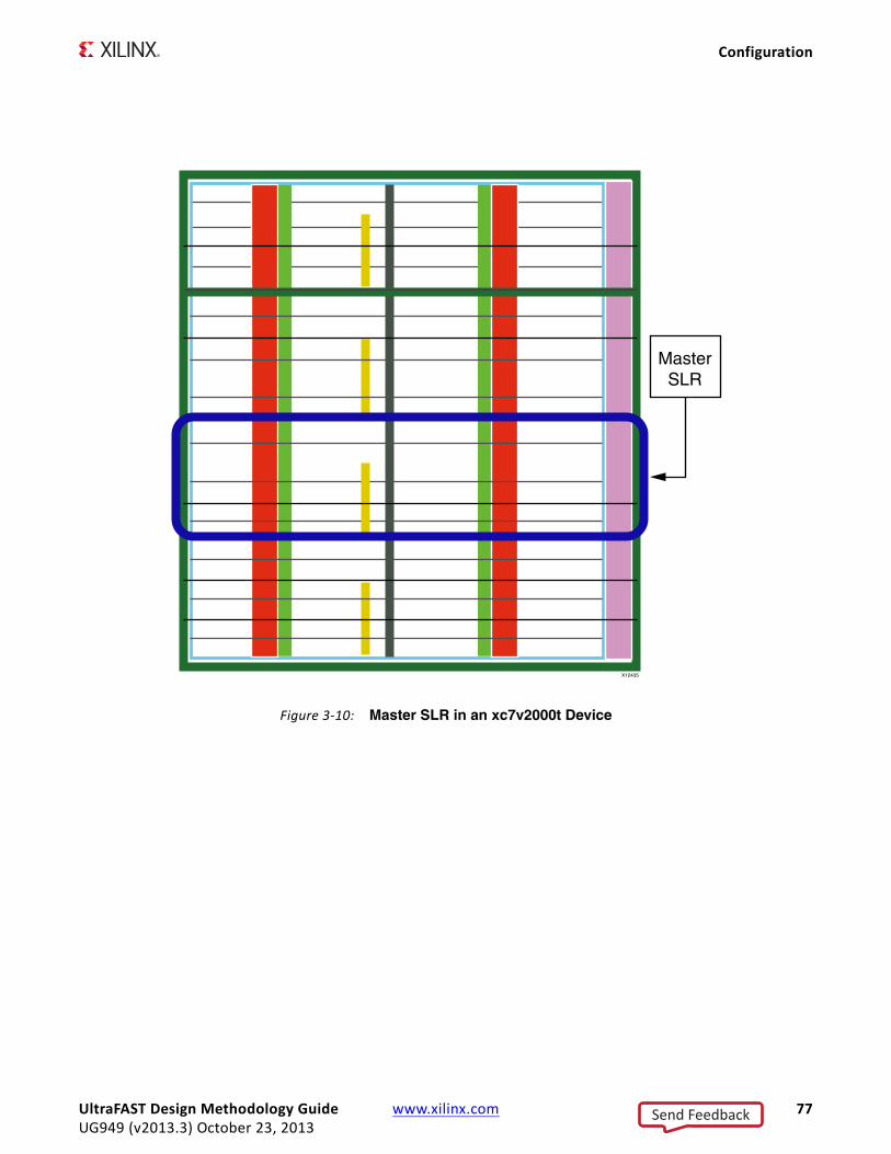
Configuration
X-Ref Target - Figure 3-10
Figure 3-10: Master SLR in an xc7v2000t Device
UltraFAST Design Methodology Guide www.xilinx.com 77UG949 (v2013.3) October 23, 2013
Send Feedback

Chapter 4
Design Creation
Overview of Design CreationYou have planned your device I/O, and you have planned on how to lay out your PCB. You have also decided on your use model for the Vivado® Design Suite. You can now begin creating your design.
The main points to consider include:
• Achieving the desired functionality.
• Operating at the desired frequency.
• Operating with the desired degree of reliability.
• Fitting within the silicon resource and power budget.
Design creation (in order to achieve the above goals) involves:
• Planning the hierarchy of your design.
• Identifying the IP cores to use and customize in your design.
• Creating the custom RTL for interconnect logic and functionality for which a suitable IP was not found.
• Creating timing and physical constraints.
• Specifying additional constraints, attributes, and other elements used during synthesis and implementation.
Any decision here has a wide and deep impact on the end product. A wrong decision at this stage can result in problems at a later stage, causing iterations through the entire design cycle. Spending the time early in the process to create a carefully planned design is worth the effort. This will help achieve the desired design goals and minimize debug time in lab.
UltraFAST Design Methodology Guide www.xilinx.com 78UG949 (v2013.3) October 23, 2013
Send Feedback
Defining a Good Design Hierarchy
Defining a Good Design HierarchyThe f irst step in design creation is to decide how to partition the design logically. The main factor when considering hierarchy is to partition a part of the design that contains a specific function. This allows a specific designer to design a piece of IP in isolation as well as isolating a piece of code for reuse.
However, defining a hierarchy based on functionality only does not take into account how to optimize for timing closure, runtime, and debugging. The following additional considerations made during hierarchy planning also help in timing closure.
Register Data Paths at Logical BoundariesRegister the outputs of hierarchical boundaries to contain critical paths within a single module or boundary. It is always easier to analyze and repair timing paths which lie within a module, rather than a path spanning multiple modules. Any paths that are not registered at hierarchy boundaries should be synthesized with hierarchy rebuilt or flat to allow cross hierarchy optimization. Registering the datapaths at logical boundaries helps to retain traceability (for debug) through the design process because cross hierarchical optimizations are kept to a minimum and logic does not move across modules.
Place Clocking Elements Towards the Top LevelPlacing the clocking elements towards the top level allows for easier clock sharing between modules. This sharing may result in fewer clocking resources needed, which helps in resource utilization, improved performance, and power.
Aside from the module the clocks are created in, clock paths should only drive down into modules. Any paths that go through (down from top and then back to top) can create a delta cycle problem in VHDL simulation that is diff icult and time consuming to debug.
Infer I/O Components Near the Top LevelWhere possible, infer I/O components near the top level for design readability. Components that can be inferred are IBUF, OBUF, and single data rate registers in the I/O. I/O components that need to be instantiated such as IBUFDS, OBUFDS should also be instantiated near the top level.
UltraFAST Design Methodology Guide www.xilinx.com 79UG949 (v2013.3) October 23, 2013
Send Feedback
Defining a Good Design Hierarchy
FloorplanningA floorplan ensures that cells belonging to a specific portion in the design netlist are placed at particular locations on the device. You can use manual floorplanning:
• To partition logic to a particular SLR when using SSI devices - to confine the launch and destination registers.
• To close timing on a design when timing is not met using standard flows.
• When using hierarchical design flows such as partial configuration.
If the cells are not contained within a level of hierarchy, all objects must be included individually in the constraint. If synthesis changes the names of these objects, you must update the constraints. A good floorplan is contained at the hierarchy level, since this requires only a one line constraint.
Floorplanning is not always required. Floorplan, only when necessary.
RECOMMENDED: While the Vivado tools allow cross hierarchy floorplans, these require more maintenance. Avoid cross hierarchy floorplans where possible.
Functional and Timing DebugAs discussed earlier in this section, keeping the critical path within the same hierarchical boundary is helpful in debugging and repairing timing. Similarly, for functional debug (and modif ication) purposes, signals that are related should be kept in the same hierarchy. This allows the related signals to be probed and modif ied with relative ease.
Attribute at the Module LevelApplying attributes at the module level can keep code tidier and more scalable. Instead of having to apply an attribute at the signal level, you can apply the attribute at the module level and have the attribute propagated to all signals declared in that region. Applying attributes at the module level also allows you to override global synthesis options. For this reason, it is sometimes advantageous to add a level of hierarchy in order to apply module level constraints in the RTL.
VHDL Example
entity vhdl_example is Port ( clk : in STD_LOGIC; a : in STD_LOGIC; b : out STD_LOGIC); attribute keep_hierarchy : string; attribute keep_hierarchy of vhdl_example : entity is “yes”;end vhdl_example
UltraFAST Design Methodology Guide www.xilinx.com 80UG949 (v2013.3) October 23, 2013
Send Feedback

Defining a Good Design Hierarchy
Verilog Example
(* keep_hierarchy = “yes” *) module verilog_example( input clk, input a, output b );endmodule
Hierarchical Considerations for Advanced Design TechniquesAdvanced design techniques such as bottom-up synthesis, partial reconfiguration, and out-of-context design require planning at the hierarchical level. The design must choose the appropriate level of hierarchy for the technique being used. These techniques are not covered in this version of the document. For more information, see “Design Considerations” in the Vivado Design Suite User Guide: Hierarchical Design (UG905) [Ref 18].
Example of Upfront Hierarchical Planning for High Speed DSP DesignsThe following example is not applicable to all designs, but demonstrates what can be done with hierarchy. DSP designs generally allow latency to be added to the design. This allows registers to be added to them to be optimized for performance. In addition, registers can be used to allow for placement flexibility. This is important because at high speed, you cannot traverse the die in one clock cycle. Adding registers can allow hard-to-reach areas to be used. Figure 4-1, Effective Hierarchy Planning Example, shows how effective hierarchy planning results in faster timing closure.
X-Ref Target - Figure 4-1
Figure 4-1: Effective Hierarchy Planning Example
UltraFAST Design Methodology Guide www.xilinx.com 81UG949 (v2013.3) October 23, 2013
Send Feedback

Working With Intellectual Property (IP)
There are three levels of hierarchy in this part of the design:
• DSP_i
• floorplanning_wrapper_i
• placement_flexibility_wrapper_i
DSP_i
In the DSP_i algorithm block, both the inputs and outputs are registered. Because registers are plentiful in an FPGA device, it is preferable to use this method to improve the timing budget.
floorplanning_wrapper_i
In floorplanning_wrapper_i, there is a CE signal. CE signals are typically heavily-loaded and can present a timing challenge. They should be included in a floorplan. By creating a floorplanning wrapper, this module can be manually floorplanned later if needed.
In additional, KEEP_HIERARCHY has been added at the module level to ensure that hierarchy is preserved for floorplanning regardless of any other global synthesis options.
placement_flexibility_wrapper_i
In placement_flexibility_wrapper_i, the DATA_IN, VALID_IN, DATA_OUT and VALID_OUT signals are registered. Because these signals are not intended to be part of the floorplan, they are outside floorplanning_wrapper_i. If they were in the floorplan, they would not be able to fulf ill the requirement for placement flexibility.
In addition, more registers can be added later as long as both DATA_IN + VALID_IN or DATA_OUT and VALID_OUT are treated as pairs. If more registers are added, the synthesis tool may infer SRLs which will force all registers into one component and not help placement flexibility. To prevent this, SHREG_EXTRACT has been added at the module level and set to NO.
Working With Intellectual Property (IP)Pre-validated Intellectual Property (IP) cores signif icantly reduce design and validation efforts, and ensure a large advantage in time-to-market.
Planning IP RequirementsPlanning IP requirements is one of the most important stages of any new project.
UltraFAST Design Methodology Guide www.xilinx.com 82UG949 (v2013.3) October 23, 2013
Send Feedback

Working With Intellectual Property (IP)
Evaluate the IP options available from Xilinx® or third party partners against required functionality and other design goals. Ask yourself:
• Is custom logic more desirable compared to an available IP core?
• Does it make sense to package a custom design for reuse in multiple projects in an industry standard format?
Consider the interfaces that are required such as, memory, network, and peripherals.
AMBA AXIXilinx has standardized IP interfaces on the open ABMA 4 AXI4 interconnect protocol. This standardization eases integration of IP from Xilinx and third party providers, and maximizes system performance. Xilinx worked with ARM to define the AXI4, AXI4-Lite, and AXI4-Stream specif ications for eff icient mapping into its FPGA device architectures.
AXI is targeted at high performance, high clock frequency system designs, and is suitable for high speed interconnects. AXI4-Lite is a light-weight version of AXI4, and is used mostly for accessing control and status registers.
AXI-Stream is used for unidirectional streaming of data from Master to Slave. This is typically used for DSP, Video and Communications applications.
Vivado Design Suite IP CatalogThe IP Catalog is a single location for Xilinx-supplied IP. IP cores for embedded systems, DSP, communication, and interfaces are all available in one place.
From the IP Catalog, you can explore the available IP cores, and view the Product Guide, Change Log, Product Webpage, and Answer Records for any IP.
You can access the IP catalog through the GUI. Tcl scripts can automate the customization of IP cores.
Custom IP
Xilinx uses the industry standard IP-XACT format for delivery of IP, and provides tools (IP Packager) to package custom IP. Accordingly, you can also add your own customized IP to the catalog and create IP repositories that can be shared in a team or across a company. IP from third party providers can also be added to this catalog.
Selecting IP from the IP Catalog
All Xilinx and third party vendor IP is categorized based on applications such as communications and networking; video and image processing; and automotive and
UltraFAST Design Methodology Guide www.xilinx.com 83UG949 (v2013.3) October 23, 2013
Send Feedback

Working With Intellectual Property (IP)
industrial. Use this categorization to browse the catalog to see which IP is available for your area of interest.
A majority of the IP in the IP catalog is free. However, some high value IP has an associated cost and requires a license. The IP Catalog informs you about whether or not the IP requires purchase, as well as the status of the license. To select an IP from the catalog, consider the following key features, based on your design requirements, and what the specif ic IP offers:
• Silicon Resources required by this IP (found in the respective IP Product Guide)
• Is this IP supported in the device speed grade being considered (the selection of the IP often drives the speed grade decision)? If supported, what is the max achievable throughput and Fmax?
• External interface standards, needed for your design to talk to its companion chip on board:
° Industry-standard interfaces such as Ethernet, Interlaken, or PCIe
° Memory interfaces - number of memory interfaces, including their size and performance.
° Xilinx proprietary interfaces such as Aurora
Note: You can also choose to design your own custom interface.
• On-chip bus protocol supported by the IP (Application interface)
• On-chip bus protocol, needed for interaction with the rest of your design. Examples:
° AXI4
° AXI4-Lite
° AXI4-Stream
• If multiple protocols are involved, bridging IP cores might have to be chosen using infrastructure IP from the IP Catalog. Examples:
° AXI-AHB bridge
° AXI-AXI interconnect
° AXI-PCIe bridge
° AXI-PLB bridge
UltraFAST Design Methodology Guide www.xilinx.com 84UG949 (v2013.3) October 23, 2013
Send Feedback

Working With Intellectual Property (IP)
IP and I/OIP that interacts with the external world must be associated with I/O pins. For this reason, Xilinx recommends that you consider the I/O assignments while choosing IP. These include:
• Parallel Interface
• Serial Interface
• I/O Voltages and I/O Standards
Parallel Interface
The number of available I/Os in the I/O bank determine which I/O bank to choose.
Serial Interface
• Low-Speed Serial Interface: The ISERDES/OSERDES that are part of the General IOB can be used.
• High-Speed Serial Interface: The low-power Gigabit transceivers (GTs) can be used.
I/O Voltages and I/O Standards
• If the I/O voltage is 1.8V, choose the I/O bank that supports Vccio of 1.8V.
• For low data rates, use single ended I/O standard such as LVCMOS.
• For high data rates, use differential I/O standard, such as:
° LVDS
° diff-SSTL
° diff-HSTL
Example Decision Process for IP Selection and Customization Consider a communication and networking system with the following requirements:
• 10-Port 10G Ethernet MAC Aggregation
• PCIe Interface for System Configuration
• External Memory Storage
Based on the requirements and the available IP, you must now check for the key functional features of each IP to decide its suitability and customization for your design. This process allows you to select the right IP needed for your purposes.
UltraFAST Design Methodology Guide www.xilinx.com 85UG949 (v2013.3) October 23, 2013
Send Feedback

Working With Intellectual Property (IP)
10-Port 10G Ethernet MAC Aggregation
The IP supports an optional XGMII interface. If the system needs an XAUI or a 10G PCS/PMA as its external interface, you must choose the XGMII option. The XAUI or the 10G PCS/PMA IP from Xilinx supports the XGMII interface.
Because data transfer from the MAC happens through the AXI4-Stream interface, the system must be able to consume the data from the MAC. It must be then connected either to an AXI interconnect to talk to other IP cores, or terminate in a wrapper with a proprietary protocol.
The core can be configured either through an optional AXI-Lite interface or a simple read/write interface. If AXI-lite is chosen, the system should have an AXI-Lite support internally.
PCIe Interface for System Configuration
In addition to the considerations mentioned above, you must be aware of the data rates requirements of the interface. For assistance in making the selection, see Table 4-1, Data Rate Requirements by Device.
* Based on symmetric f ilter implementation
External Memory Storage
You need to be aware of the number of DDR3 memories to be supported in the system. For this design, the total storage data rate requirement is about 80 Gb/s effective bandwidth or 100 Gb/s raw bandwidth when taking the MC eff iciency into account. This can be achieved by multiple ways as illustrated below:
• Single controller with 64-bit DDR3 @ 1600 Mbps
• Four controllers with 16-bit DDR3 @ 1600 Mbps
Because data transfer from the Memory controller happens through AXI4 interface, the system should be able to consume the data from the MC. You can use ½ rate or ¼ rate interfaces. When using ¼ rate, the application datawidth of the MC is 8xDDR3-width. For example, for 16-bit DDR3, the AXI-stream has 128-bits datawidth. The AXI Interconnect IP may be useful to connect the slave memory controller IP to the master peripherals which
Table 4-1: Data Rate Requirements by Device
Artix®-7 Kintex®-7 Virtex®-7T Virtex-7 XT Virtex-7
GEN (integrated block)* Gen2 Gen2 Gen2 Gen3 Gen3
Width X4 X8 X8 X8 X8
Number of Blocks 1 1 3-4 2-4 1-3
Serial Data Rate (Gb/s) 5 5 8 8 8
UltraFAST Design Methodology Guide www.xilinx.com 86UG949 (v2013.3) October 23, 2013
Send Feedback
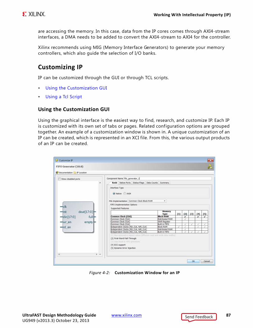
Working With Intellectual Property (IP)
are accessing the memory. In this case, data from the IP cores comes through AXI4-stream interfaces, a DMA needs to be added to convert the AXI4-stream to AXI4 for the controller.
Xilinx recommends using MIG (Memory Interface Generators) to generate your memory controllers, which also guide the selection of I/O banks.
Customizing IPIP can be customized through the GUI or through TCL scripts.
• Using the Customization GUI
• Using a Tcl Script
Using the Customization GUI
Using the graphical interface is the easiest way to find, research, and customize IP. Each IP is customized with its own set of tabs or pages. Related configuration options are grouped together. An example of a customization window is shown in. A unique customization of an IP can be created, which is represented in an XCI f ile. From this, the various output products of an IP can be created.
X-Ref Target - Figure 4-2
Figure 4-2: Customization Window for an IP
UltraFAST Design Methodology Guide www.xilinx.com 87UG949 (v2013.3) October 23, 2013
Send Feedback
Working With Intellectual Property (IP)
Using a Tcl Script
Almost every GUI action results in the issuance of a Tcl command. The creation of an IP including the setting of all the customization options can be performed in a Tcl script without user interaction.
You would need to know the names of the configuration options, and the values to which they can be set. Typically, you f irst perform the customization through the GUI, and then create the script from that. Once you see the resulting Tcl script, you can easily modify the script for your needs, such as changing data sizes.
Tcl script based IP creation is useful for automation, for example working with version control system.
Working with IPWhen IP is customized, the tool creates an XCI f ile containing all the selected parameterization values. Each Vivado IDE version supports only one version of an IP. Xilinx recommends that you use this latest IP version. If you use an older IP version, you should have saved all the output products for the older version. For more information, see Centralized IP, page 24.
TIP: For MIG, instead of an XCI file, a .prj file is created. All future references to XCI in the context of IP also means .prj for MIG.
Generated Output Products
Depending on the settings in the Vivado tools, by default some output products might be created automatically during IP customization. You can change this from the Project Settings. Using the component file created during customization, you can create any of the associated Output Products that an IP provides, including:
• Instantiation template
Shows how to instantiate the IP.
• Synthesis
Generates the script for running synthesis on this specific customized view of the IP.
• Testbench
Generates a testbench to be used for a simulation environment that can be used to verify the functionality of the IP.
UltraFAST Design Methodology Guide www.xilinx.com 88UG949 (v2013.3) October 23, 2013
Send Feedback
RTL Coding Guidelines
• Simulation
Generates the script for running simulation on this specif ic customized view of the IP, using the testbench mentioned above.
• Example design
Generates an example design. This IP remains in your design and interacts with your logic. Typically, you are expected to replace this example design with your own design.
The XCI f ile and these output products contain all that is required (for example HDL files and constraints f iles) to correctly simulate and synthesize the IP in a design.
RTL Coding GuidelinesYou might have to write your custom RTL to implement either the glue logic functionality, or for some function for which a suitable IP was not found.
Basic FunctionalityThe RTL must be coded in such a way as to be safely implementable. Otherwise, design functionality may differ from RTL simulation results. The RTL must be free of race conditions and of common coding pitfalls that can result in simulation-synthesis mismatches.
There are some basic guidelines on synthesizable RTL code. Most readily-available literature on synthesizable RTL code discusses these guidelines. Some of the more common guidelines are mentioned below, but the list is not exhaustive.
Blocking Statements vs. Non-Blocking Statements
Improper use of Verilog blocking statements or non-blocking statements might result in race conditions, causing RTL simulations to not match netlist simulation. As a general rule, Xilinx recommends using non-blocking statements for all sequential elements, and blocking statements for all combinational elements. This makes the simulation event ordering much more predictable, and less likely to cause race conditions.
Incomplete Sensitivity List
A sensitivity list in a process statement (VHDL) or always block (Verilog) is a list of signals to which the process statement (VHDL) or always block (Verilog) is sensitive. When a listed signal changes its value, the process statement (VHDL) or always block (Verilog) triggers and executes its statements.
In case of an incomplete sensitivity list, while you may get the hardware you intended, the RTL and post-synthesis simulation will differ. In this case, some synthesis tools may issue a
UltraFAST Design Methodology Guide www.xilinx.com 89UG949 (v2013.3) October 23, 2013
Send Feedback
RTL Coding Guidelines
message warning of an incomplete sensitivity list. In that event, check the synthesis log file and, if necessary, f ix the RTL code.
The following example describes a simple AND function using a process and always block. The sensitivity list is complete and a single LUT is generated.
VHDL Process Coding Example One
process (a,b) beginc <= a and b;end process;
Verilog Always Block Coding Example One
always @(a or b)c <= a & b;
However, if signal b is omitted from the sensitivity list, the synthesis tool still generates the combinational logic (AND function), though RTL simulation might not trigger the evaluation of c based on changes to b. This results in RTL simulation behaving one way, while the actual circuit behaves differently. Following is an example warning message:
WARNING: [Synth 8-567] referenced signal <signal name> should be on the sensitivity list [<file name>:<line number>]
In Verilog, when defining a combinational always block, use an asterisk sensitivity list:
always @(*)
This automatically uses a fully specif ied sensitivity list.
Delays in RTL Code
Avoid using any kind of delay in your RTL code, either through use of Wait or AFTER (VHDL) or #delay (Verilog). Delays do not synthesize to a component. In designs that include explicit delay assignments, the functionality of the simulated design does not always match the functionality of the synthesized design.
Latch Inference
Synthesizers infer latches from incomplete conditional expressions in combinational, non-sequential logic, such as:
• An if statement without an else clause
• An intended register without a rising edge or falling edge construct
UltraFAST Design Methodology Guide www.xilinx.com 90UG949 (v2013.3) October 23, 2013
Send Feedback
RTL Coding Guidelines
If Statement without an Else Clause VHDL Coding Example
process (G, D) beginif (G=‘1’) thenQ <= D;end if;end process;
If Statement without an Else Clause Verilog Coding Example
always @(G or D)if (G)Q = D;
Many times a branch or edge is missing by mistake. Check your synthesis log to see the latches being inferred. Confirm that any latches inferred are intentional, rather than an oversight.
Xilinx recommends that you avoid using latches in FPGA designs, due to the more diff icult timing analyses that occur when latches are used, even if the simulations pass.
Follow the recommended coding styles in the synthesis tool documentation to avoid inferring latches.
Incomplete Reset Specification
In the following example snippet, only reg1 is assigned within the reset branch, and reg2 is missed. Synthesis will assume that reg2 has to hold its value when reset is asserted. Thus, the reset signal will get hooked to the CE pin, thereby creating another unique control set.
always @(posedge clk) if (rst) reg1<= 1’b0;elsebegin reg1 <= din1; reg2 <= din2;end
TIP: If a reset is being used, make sure that the registers have not been missed by mistake in the reset branch.
Using Vivado Design Suite HDL Templates RECOMMENDED: Use the Vivado Design Suite language templates when creating RTL or instantiating Xilinx primitives. The language templates include recommended coding constructs for proper inference to the Xilinx FPGA device architecture. Using the templates should both ease design and lead to improved results in many cases.
UltraFAST Design Methodology Guide www.xilinx.com 91UG949 (v2013.3) October 23, 2013
Send Feedback

RTL Coding Guidelines
To access the templates from the Vivado Design Suite GUI:
1. Go to Windows > Language Template.
2. Choose the desired template.
HDL Coding for Efficiency
Use of Loops in Code
Loops in HDL are often used to minimize coding effort. When inferring hardware, loop un-rolling may lead to ineff icient structures thereby degrading performance (both area as well as timing). Mapping the un-rolled logic to available resources causes possibilities of sub-optimal implementation. Xilinx recommends representing the same functionality using constructs that are easier for the tool to interpret.
Consider a case of priority MUX code using a for loop:
always@(posedge clk)beginfor(i=0;i<=3;i=i+1)beginif(en[i])dout[i] <= i;endend
The same functionality can be coded using case/if-else, and is easier for the tool to interpret to generate eff icient hardware.
Sometimes though, a for loop might provide the required conciseness, without impacting the quality of results (for example a bus-reversal code).
Use of Loops in Code Coding Example
reg [3:0] dout;integer i;always@(posedge clk)beginfor(i=0;i<=3;i=i+1)dout[3-i] <= din[i];end
TIP: It is acceptable to infer loops for basic connectivity. However, when the code infers hardware resources (other than just wires/interconnects), it is better to avoid loops.
State-Machine Guidance
There are several methods to code state machines. Following certain coding styles ensures that the synthesis tool FSM (Finite State Machine) extraction algorithms properly identify
UltraFAST Design Methodology Guide www.xilinx.com 92UG949 (v2013.3) October 23, 2013
Send Feedback

RTL Coding Guidelines
and optimize the state machines as well as possibly improving the simulation, timing and debug of the circuit. The choice of state machines depends on the target architecture and specifics of the state machines size and behavior. Some of the basic tradeoffs for different implementation are explained below.
Mealy vs. Moore Styles
There are two well-known implementation styles for state machines, Mealy and Moore. The main difference between Mealy and Moore is that a Mealy state machine determines the output values based on both the current state as well as the inputs to the state machines, whereas a Moore state machine determines its outputs solely on the state.
In general, Moore state machines implement best in FPGA devices due to the fact that most often one-hot state machines is the chosen encoding method, and there is little decode logic necessary for output values.
For a binary encoding, sometimes a more compact or faster state machines can be built using the Mealy machine. However, this is not easy to determine without knowing more specifics of the state machines.
One-Hot vs. Binary Encoding
There are several encoding methods for state machines design. The two most popular for FPGA designs are binary and one-hot. Most modern synthesis tools contain FSM extraction algorithms that can identify state machines code and choose the best encoding method. Sometimes it can be more advantageous to manually code the encoding scheme for the design to allow better control, and possibly to ease debug of the implemented design. See your synthesis tool documentation for details about the state machines extraction capabilities.
Safe vs. Fast
When coding state machines, there are two generally conflicting goals that must be understood: safe vs. fast. A safe state machine implementation is one in which, if a state machines gets an unknown input, or goes into an unknown state, it can recover into a known state (in the next cycle) and resume from that recovery state. On the other hand, if this requirement is discarded (no recovery state), many times the state machines can be implemented with less logic and more speed. Designing a safe-state involves coding in a default state into the state machines case clause and/or specifying to the synthesis tool to implement the state machines encoding in a “safe” mode. If a safe-state capability is desired, usually binary encoding works best as there are fewer unassigned states with binary encoding. Consult your synthesis tool documentation for details about implementing a safe state machines.
Enumerated Type
SystemVerilog adds a new data type enum (short for enumerated), which in many cases is beneficial for state machines creation. The enum data type allows for named states without
UltraFAST Design Methodology Guide www.xilinx.com 93UG949 (v2013.3) October 23, 2013
Send Feedback

RTL Coding Guidelines
implicit mapping to a register encoding. The benefit this provides to synthesis is flexibility in state machine encoding techniques and for simulation, the ability to display and query specific states by name to improve overall debugging. For these reasons, Xilinx recommends using enum types when SystemVerilog, or VHDL (which always had this capability) is the chosen design language.
See UG901: Vivado Synthesis User Guide for details on Vivado synthesis features
Preserving Hierarchical Boundaries
Preserving hierarchical boundaries may lead to hardened boundaries, thereby avoiding cross-boundary optimizations.
Consider the following example code snippet:
assign ored_signal = din[3]|din[]2;sub sub_inst (.clk (clk),.din0 (ored_signal),.din1 (din[1:0]),.dout (dout));endmodulemodule sub …..assign din_tmp = |din1 || din0;endmodule
There are two ORs:
• ored_signal in the top level
• din_tmp in sub
If the hierarchical boundary between them is preserved using synthesis attributes or constraints, these two ORs cannot be combined, impacting the area and timing of the design. For more information, see Defining a Good Design Hierarchy, page 79.
Avoid Mixing Edges of a Flip Flop
If you use both positive and negative edges of clocks for triggering sequential elements, then the path between the elements being triggered by the two different polarities will get only half a clock cycle. This makes the timing more stringent.
TIP: If both clock edges are being used to capture or provide external DDR type data, use Xilinx IDDR/ODDR primitives.
Use of Debug Logic
Coding eff iciency leads to efficiency in design implementation. Unnecessary constructs often lead to unnecessary logic. Keep this in mind when designing debug signals or logic that is not necessary for the design function, but which is useful in the design analysis.
UltraFAST Design Methodology Guide www.xilinx.com 94UG949 (v2013.3) October 23, 2013
Send Feedback
RTL Coding Guidelines
Many times, such debug code serves a valuable purpose during the design phase, but becomes unwanted surplus as the design matures. You should design such logic so that it can still serve its debug purpose, yet not remain in the f inal design.
Several methods can assist in this objective:
• Guard the logic with a `ifdef, parameter, or generic that can be set to disable or enable these sections of code.
• Code the logic in a way to more easily facilitate commenting it out for the future.
• Have a separate debug version of a module or entity to interchange for this purpose.
Regardless of the method chosen, the idea remains the same: It is important not only to have a good methodology for debugging the design code and the implemented hardware, but it is also important to have a good way to remove that logic when it is no longer necessary.
For the details of debug method, see Chapter 6, Configuration and Debug.
Arrays in Port Declarations
Although VHDL allows you to declare a port as an array type, Xilinx recommends that you not do so, for the following reasons:
• Incompatibility with Verilog
• Inability to Store and Re-Create Original Array Declaration
• Miscorrelation of Software Pin Names
Incompatibility with Verilog
There is no equivalent way to declare a port as an array type in Verilog. This limits portability across languages. It also limits as the ability to use the code for mixed-language projects.
Inability to Store and Re-Create Original Array Declaration
When you declare a port as an array type in VHDL, the original array declaration cannot be stored and re-created. The Electronic Data Interchange Format (EDIF) netlist format, as well as the Xilinx database, are unable to store the original type declaration for the array. As a result, when a simulation netlist is generated, there is no information as to how the port was originally declared.
The resulting netlist generally has mismatched port declarations and resulting signal names. This is true not only for the top-level port declarations, but also for the lower-level port declarations of a hierarchical design since KEEP_HIERARCHY can be used to attempt to preserve those net names.
UltraFAST Design Methodology Guide www.xilinx.com 95UG949 (v2013.3) October 23, 2013
Send Feedback

Control Signals and Control Sets
Miscorrelation of Software Pin Names
Array port declarations can cause a miscorrelation of the software pin names from the original source code. Since the tool must treat each I/O as a separate label, the corresponding name for the broken-out port may not match your expectation. This makes design constraint passing, design analysis, and design reporting more diff icult to analyze.
Control Signals and Control SetsA control set is the grouping of control signals (set/reset, clock enable and clock) that drives any given SRL, RAM or register. For any unique combination of control signals, a unique control set is formed. The reason this is an important concept is registers within a slice all share common control signals and thus only registers with a common control set may be packed into the same slice.
Designs with several unique control sets may have a lot of wasted resources, as well as fewer options for placement resulting in higher power and lower performance. Designs with fewer control sets have more options and flexibility in terms of placement, generally resulting in improved results.
ResetsResets are one of the more common and important control signals to take into account and limit in your design. Resets can signif icantly impact your design’s performance, area, and power.
Inferred synchronous code may result in resources such as:
• LUTs
• Registers
• Shift Register LUTs (SRLs)
• Block or LUT Memory
• DSP48 registers
The choice and use of resets can affect the selection of these components, resulting in less optimal resources for a given design. A misplaced reset on an array can mean the difference between inferring one blockRAM, or inferring several thousand registers. A reset described unnecessarily on a pipeline can mean the difference between a few SRL LUTs, or several hundred registers.
Asynchronous resets described at the input or output of a multiplier may result in registers placed in the Slice rather than the DSP block. In these and other situations, the amount of
UltraFAST Design Methodology Guide www.xilinx.com 96UG949 (v2013.3) October 23, 2013
Send Feedback
Control Signals and Control Sets
resources is obviously impacted. However, overall power and performance can also be signif icantly impacted.
When and Where to Use a Reset
FPGA devices have dedicated global set/reset signals (GSR). These signals initialize all registers to the initial value specif ied state in the HDL code at the end of device configuration.
If an initial state is not specif ied, it defaults to a logic zero. Accordingly, every register is at a known state at the end of configuration, regardless of the reset topology specif ied in the HDL code. It is not necessary to code a global reset for the sole purpose of initializing the device.
Xilinx highly recommends that you take special care when deciding when the design requires a reset, and when it does not. Limiting the use of resets:
• Limits the overall fanout of the reset net.
• Reduces the amount of interconnect necessary to route the reset.
• Simplif ies the timing of the reset paths.
• Results in many cases in overall improvement in performance, area, and power.
RECOMMENDED: Evaluate each synchronous block, and attempt to determine whether a reset is required for proper operation. Do not code the reset by default without ascertaining its real need.
Functional simulation should easily identify whether a reset is needed or not.
For logic in which no reset is coded, there is much greater flexibility in selecting the FPGA resources to map the logic. For example, for a simple delay line (shift register), if a reset is coded, the tools will likely map that into a set of registers with a common reset.
If a reset is omitted, that same logic might result in:
• An SRL
• A combination of SRL and registers
• All registers
• LUT or block memory.
UltraFAST Design Methodology Guide www.xilinx.com 97UG949 (v2013.3) October 23, 2013
Send Feedback

Control Signals and Control Sets
The synthesis tool can then pick the best resource for that code in order to arrive at a potentially superior result by considering, for example:
• Requested functionality
• Performance requirements
• Available device resources
• Power
Synchronous Reset vs. Asynchronous Reset
If a reset is needed, Xilinx recommends code synchronous resets. Synchronous resets have many advantages over asynchronous resets.
• Synchronous resets can directly map to more resource elements in the FPGA device architecture.
• Some resources such as the DSP48 and blockRAM have only synchronous resets for the register elements within the block. When asynchronous resets are used on register elements associated with these elements, those registers may not be inferred directly into those blocks without a functional difference.
• Asynchronous resets also impact the performance of the general logic structures. As all Xilinx FPGA general-purpose registers can program the set/reset as either asynchronous or synchronous, it can be perceived that there is no penalty in using asynchronous resets. That assumption is often wrong. If a global asynchronous reset is used, it does not increase the control sets. However, the need to route this reset signal to all register elements increases timing complexity. For more information, see Use of Untimed Resets, page 139.
• If using asynchronous reset, remember to synchronize the deassertion of the asynchronous reset For more information, see Controlling and Synchronizing Device Startup, page 138.
• Synchronous resets give more flexibility for control set remapping when higher density or f ine tuned placement is needed. A synchronous reset may be remapped to the data path of the register if an incompatible reset is found in the more optimally placed Slice. This can reduce wire length and increase density where needed to allow proper f itting and improved performance.
Control Signal Polarity (Active-High vs. Active-Low)
For high-fanout control signals like clock enables or resets, it is best to use active high in whole of the design. If a block operates with active low resets or clock enables, inverters get added to the design and there is an associated timing penalty. It can restrict synthesis options to flat or rebuilt to optimize the inverters or require the implementation of a custom solution.
UltraFAST Design Methodology Guide www.xilinx.com 98UG949 (v2013.3) October 23, 2013
Send Feedback

Control Signals and Control Sets
The Slice and internal logic of the Xilinx FPGA clock enables and resets are inherently active-High. Describing active-Low resets or clock enables may result in additional LUTs used as simple inverters for those routes.
Reset Coding Example One
The following coding example constructs a highly pipelined multiply and parity generation function:
// Reset synchronizationalways @(posedge CLK) beginreset_sync <= SYS_RST;reset_reg <= reset_sync;end// Uses active-Low, async reset// Also using an active-Low CEalways @(posedge CLK, negedge reset_reg)if (!reset_reg) begindata1_reg <= 16’h0000;data2_reg <= 16’h0000;DATA_VALID <= 1’b0;end else if (!NEW_DATA) begindata1_reg <= DATA1;
X-Ref Target - Figure 4-3
Figure 4-3: Extra Inverters Due to Low Control Signals
UltraFAST Design Methodology Guide www.xilinx.com 99UG949 (v2013.3) October 23, 2013
Send Feedback

Control Signals and Control Sets
data2_reg <= DATA2;DATA_VALID <= data_valid_delay[3];end// Uses an async reset when a reset is not necessaryalways @(posedge CLK, negedge reset_reg)if (!reset_reg) beginparity <= 4’h0;data1_pipe <= 32’h00000000;data2_pipe <= 32’h00000000;mult_data_reg <= 32’h00000000;mult_pipe <= 32’h00000000;mult_pipe2 <= 32’h00000000;mult_par_reg <= 36’h000000000;mult_par_pipe <= 36’h000000000;data_valid_delay <= 4’h0;DATA_OUT <= 36’h000000000;end else begindata1_pipe <= data1_reg;data2_pipe <= data2_reg;mult_data_reg <= data1_pipe data2_pipe;mult_pipe <= mult_data_reg;parity <= {^mult_pipe[31:24], ^mult_pipe[23:16],^mult_pipe[15:8], ^mult_pipe[7:0]};mult_pipe2 <= mult_pipe;mult_par_reg <= {parity[3], mult_pipe2[31:24],parity[2], mult_pipe2[23:16],parity[1], mult_pipe2[15:8],parity[0], mult_pipe2[7:0]};data_valid_delay <= {data_valid_delay[2:0], NEW_DATA};mult_par_pipe <= mult_par_reg;DATA_OUT <= mult_par_pipe;end
Reset Coding Example Two
The above code can be rewritten to:
• Remove unnecessary resets
• Change Async resets to Sync
• Change active-Low reset to active-High
// Reset synchronization, inversion moved herealways @(posedge CLK) beginreset_sync <= SYS_RST;reset_reg <= ~reset_sync;end// Notice the inversion above// sync reset has become active High, though:// from the top level port (SYS_RST) perspective,// it is still active Low.// Also changed to active-High CEalways @(posedge CLK)if (reset_reg) begindata1_reg <= 16’h0000;data2_reg <= 16’h0000;DATA_VALID <= 1’b0;
UltraFAST Design Methodology Guide www.xilinx.com 100UG949 (v2013.3) October 23, 2013
Send Feedback

Control Signals and Control Sets
end else if (NEW_DATA) begindata1_reg <= DATA1;data2_reg <= DATA2;DATA_VALID <= data_valid_delay[3];end// Removed unnecessary reset on datapathalways @(posedge CLK) begindata1_pipe <= data1_reg;data2_pipe <= data2_reg;mult_data_reg <= data1_pipe data2_pipe;mult_pipe <= mult_data_reg;parity <= {^mult_pipe[31:24], ^mult_pipe[23:16],^mult_pipe[15:8], ^mult_pipe[7:0]};mult_pipe2 <= mult_pipe;mult_par_reg <= {parity[3], mult_pipe2[31:24],parity[2], mult_pipe2[23:16],parity[1], mult_pipe2[15:8],parity[0], mult_pipe2[7:0]};data_valid_delay <= {data_valid_delay[2:0], NEW_DATA};mult_par_pipe <= mult_par_reg;DATA_OUT <= mult_par_pipe;end
The implementation of the second coding example, compared to the first coding example, is shown in Table 4-2, Comparison of Coding Examples.
Table 4-2: Comparison of Coding Examples
In addition, the second coding example is more concise, and simulates faster.
Reset Coding Example Three
Sometimes, a design may have an active low negative reset (for example, AXI standard dictates the reset to be active-Low). Since asynchronous resets have synchronizing circuits to ensure deassertion being timed, it is possible to make minor modif ications to the synchronizing circuit, so that some of the LUT counts may be reduced. For an example schematic for synchronizing of asynchronous reset, see Controlling and Synchronizing Device Startup, page 138.
Original HDL Code
always @ (posedge clk or negedge rst_n) //async. negedge resetbeginif (!rst_n)synchronizer_ckt <= 4’b0; // 4 stage reset syncornization
Parameter Result
Resources 33% to 75% less depending on specif ic resource type
Performance 36% better
Number of Timing End Points 40% less
Dynamic Power @220 MHz 40% less
UltraFAST Design Methodology Guide www.xilinx.com 101UG949 (v2013.3) October 23, 2013
Send Feedback

Control Signals and Control Sets
elsesynchronizer_ckt <= {synchornizer_ckt[2:0], 1’b1};
end
assign synchronized_rst_n = synchronizer_ckt[3]; // the final reset signal which is used to reset the actual flops in the design
There is a LUT in the reset path, as shown in the black circle in Figure 4-4 Since reset signals feed many flops, saving on the delay for this LUT could impact many paths.
Modified HDL Code
always @ (posedge clk or negedge rst_n) //async. negedge resetbeginif (!rst_n)synchronizer_ckt <= 4’hf // 4 stage reset syncornization
elsesynchronizer_ckt <= {synchornizer_ckt[2:0], 1’b0};
end
assign synchronized_rst_n = ~synchronizer_ckt[3]; // the final reset signal which is used to reset the actual flops in the design
The sychronizer_ckt has been given an inverted logic, and another inversion has been added to the final synchronized_rst_n, in order to restore the polarity back. This slight modif ication to the synchronizing circuit can get rid of LUTs that exist between synchronizing circuit and the actual signal going into the flops of the design, as shown in Figure 4-5.
X-Ref Target - Figure 4-4
Figure 4-4: LUT on Reset Path
UltraFAST Design Methodology Guide www.xilinx.com 102UG949 (v2013.3) October 23, 2013
Send Feedback

Control Signals and Control Sets
Do Not Code Both a Set and a Reset in the Same Process or Always Block
Xilinx FPGA device registers have a built-in set or reset capability, but cannot natively do both at the same time. Accordingly, when using both a synchronous set and reset, an additional signal is added to the datapath. This might affect area and timing depending on placement, fanout, and timing. For this reason, Xilinx recommends coding both set and reset in the same sequential block only if absolutely required.
For an asynchronous set and reset, the effect on resource utilization and timing is more signif icant and should be avoided. Registers that contain both asynchronous reset and asynchronous set signals and/or with an asynchronous control signal with a dynamic value can be described in RTL and implemented by synthesis. However, the resulting circuit might consume more resources than desired and might have more signif icant effect on timing and verif ication than originally thought.
X-Ref Target - Figure 4-5
Figure 4-5: Modified Reset Circuit
UltraFAST Design Methodology Guide www.xilinx.com 103UG949 (v2013.3) October 23, 2013
Send Feedback
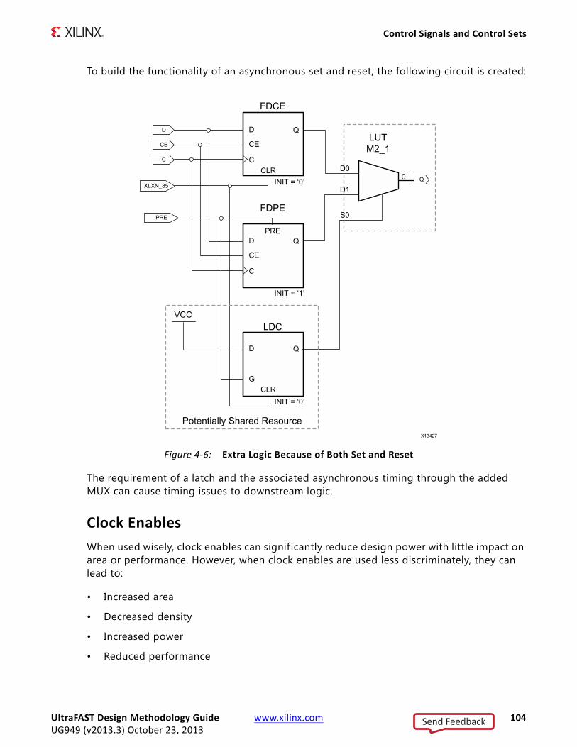
Control Signals and Control Sets
To build the functionality of an asynchronous set and reset, the following circuit is created:
The requirement of a latch and the associated asynchronous timing through the added MUX can cause timing issues to downstream logic.
Clock EnablesWhen used wisely, clock enables can significantly reduce design power with little impact on area or performance. However, when clock enables are used less discriminately, they can lead to:
• Increased area
• Decreased density
• Increased power
• Reduced performance
X-Ref Target - Figure 4-6
Figure 4-6: Extra Logic Because of Both Set and Reset
UltraFAST Design Methodology Guide www.xilinx.com 104UG949 (v2013.3) October 23, 2013
Send Feedback

Control Signals and Control Sets
In many designs with a large number of control sets, low fanout clock enables might be the main contributor to the number of control sets.
Creating Clock Enables
Clock enables are created when an incomplete conditional statement is coded into a synchronous block. A clock enable is inferred to retain the last value when the prior conditions are not met. When this is the desired functionality, it is valid to code in this manner. However, in some cases when the prior conditional values are not met, the output is a do not care. In that case, Xilinx recommends closing off the conditional (that is, use an else clause), with a defined constant (that is, assign the signal to a one or a zero).
In most implementations, this does not result in added logic, and avoids the need for a clock enable. The exception to this rule is in the case of a large bus when inferring a clock enable in which the value is held can help in power reduction. The basic premise is that when small numbers of registers are inferred, a clock enable can be detrimental because it increases control set count. However, in larger groups, it can become more beneficial and is recommended.
Reset and Clock Enable Precedence
In Xilinx FPGA devices, all registers are built to have set/reset take precedence over clock enable, whether an asynchronous or synchronous set/reset is described. In order to obtain the most optimal result, Xilinx recommends that you always code the set/reset before the enable (if deemed necessary) in the if/else constructs within a synchronous block. Coding a clock enable f irst forces the reset into the data path if synchronous and if asynchronous, creates additional logic.
For information on Clocking see Clocking, page 120.
Table 4-3, Control Set Guidelines, provides a guideline on the number of control sets that might be acceptable for your design.
Table 4-3: Control Set Guidelines
Condition Typically Acceptable Analysis Required Recommended Design Change
Number of Control Sets
<1% of total logic gates, e.g., 3150 for Kintex315.
2% of total logic gates.Caution required, review results.
10% of total logic gates.Should look to reduce total number of control sets.
Number of FFs Used by Control Sets
Device utilization <75% and Control Set FFs <4%.
Device utilization >85% and Control Set FFs >2%.
Device utilization >90%.Control Set FFs >1%.
UltraFAST Design Methodology Guide www.xilinx.com 105UG949 (v2013.3) October 23, 2013
Send Feedback

Know What You Infer
Tips• Check whether a global reset is really needed.
• Avoid asynchronous control signals.
• Keep clock, enable, and reset polarities consistent.
• Do not code a set and reset into the same register element.
• If an asynchronous reset is absolutely needed, remember to synchronize its deassertion.
Know What You InferYour code finally has to map onto the resources present on the device. Make an effort to understand the key arithmetic, storage, and logic elements in the architecture you are targeting. Then, as you code the functionality of the design, anticipate the hardware resources to which the code will map. Understanding this mapping gives you an early insight into any potential problem.
The following examples demonstrate how understanding the hardware resources and mapping can help make certain design decisions:
• For larger than 4-bit addition, subtraction and add-sub, a carry chain is generally used and one LUT per 2-bit addition is used (that is, an 8-bit by 8-bit adder uses 8 LUTs and the associated carry chain). For ternary addition or in the case where the result of an adder is added to another value without the use of a register in between, one LUT per 3-bit addition is used (that is, an 8-bit by 8-bit by 8-bit addition also uses 8 LUTs and the associated carry chain).
If more than one addition is needed, it may be advantageous to specify registers after every two levels of addition to cut device utilization in half by allowing a ternary implementation to be generated.
• In general, multiplication is targeted to DSP blocks. Signed bit widths less than 18x25 map into a single DSP Block. Multiplication requiring larger products may map into more than one DSP block. DSP blocks have pipelining resources inside them.
Pipelining properly for logic inferred into the DSP block can greatly improve performance and power. When a multiplication is described, three levels of pipelining around it generates best setup, clock-to-out, and power characteristics. Extremely light pipelining (one-level or none) may lead to timing issues and increased power for those blocks, while the pipelining registers within the DSP lie unused.
• Shift registers or delay lines that do not require reset or multiple tap points are generally mapped into Shift Register LUTs or SRLs. Two SRLs with 16 bits or less depth
UltraFAST Design Methodology Guide www.xilinx.com 106UG949 (v2013.3) October 23, 2013
Send Feedback

Inferring RAM and ROM
can be mapped into a single LUT and single SRLs up to 32 bits can also be mapped into a single LUT.
To best utilize SRLs, avoid using reset for those blocks. If a reset is not necessary, better device utilization performance and power may be found.
• For conditional code resulting in standard MUX components:
° A 4-to-1 MUX can be implemented into a single LUT, resulting in one logic level.
° An 8-to-1 MUX can be implemented into two LUTs and a MUXF7 component, still resulting in effectively one logic (LUT) level.
° A 16-to-1 MUX can be implemented into four LUTs and a combination of MUXF7 and MUXF8 resources, still resulting in effectively one logic (LUT) level.
A combination of LUTs, MUXF7, and MUXF8 within the same slice structure results in very small combinational delay. Hence, these combinations are considered as equivalent to only one logic level. Understanding this code can lead to better resource management, and can help in better appreciating and controlling logic levels for the data paths.
• For general logic, the rule of thumb is to take into account the number of unique inputs for a given register. From that number, an estimation of LUTs and logic levels can be achieved. In general, six inputs or fewer always results in a single logic level. Theoretically, two levels of logic can manage up to thirty-six inputs. However, for all practical purposes, you should assume that approximately twenty inputs is the maximum that can be managed with two levels of logic. In general, the larger the number of inputs and the more complex the logic equation, the more LUTs and logic levels are required.
IMPORTANT: Appreciating the hardware resources availability and how efficiently they are being utilized or wasted early in the design can allow for much easier modifications for better results than late in the design process during timing closure.
Inferring RAM and ROMRAM and ROM may be specif ied in multiple ways. Each has its advantages and disadvantages.
• Direct Instantiation of RAM Primitives
• Use of a Core from IP Catalog
• Inference
UltraFAST Design Methodology Guide www.xilinx.com 107UG949 (v2013.3) October 23, 2013
Send Feedback

Inferring RAM and ROM
Direct Instantiation of RAM Primitives
Advantages
• Highest level control over implementation
• Access to all capabilities of the block
Disadvantages
• Less portable code
• Wordier and more diff icult to understand functionality and intent
Use of a Core from IP Catalog
Advantages
• Generally more optimized result when using multiple components
• Simple to specify and configure
Disadvantages
• Less portable code
• Core management
Inference
Advantages
• Highly portable
• Easy to read and understand
• Self-documenting
• Fast simulation
Disadvantages
• May not have access to all RAM configurations available
• May produce less optimal results
Because inference usually gives good results, it is the recommended method, unless a given use is not supported, or it is not producing adequate results in performance, area, or power. In that case, explore other methods.
UltraFAST Design Methodology Guide www.xilinx.com 108UG949 (v2013.3) October 23, 2013
Send Feedback

Inferring RAM and ROM
When inferring RAM, Xilinx highly recommends that you use the HDL Templates provided in the Vivado tools.
Performance Considerations When Implementing RAMIn order to efficiently infer memory elements, consider these factors affecting performance:
• Using Dedicated Blocks or Distributed RAMs
• Using the Output Pipeline Registerr
• Avoiding Asynchronous Resets
Using Dedicated Blocks or Distributed RAMs
RAMs may be implemented in either: (1) the dedicated block RAM; or (2) within LUTs using distributed RAM. The choice not only impacts resource selection, but may also signif icantly impact performance and power.
In general, the required depth of the RAM is the f irst criterion. Memory arrays described up to 64-bits deep are generally implemented in LUTRAMs where depths 32-bits and less are mapped - two bits per LUT and depths up to 64-bits can be mapped one bit per LUT. Deeper RAMs may also be implemented in LUTRAM depending on available resources and synthesis tool assignment.
Memory arrays deeper than 256 are generally implemented in Block memory. Xilinx FPGA devices have the flexibility to map such structures in different width and depth combinations. You should be familiar with these configurations in order to understand the number and structure of block RAMs used for larger memory array declarations in the code.
IMPORTANT: Slight deviations in coding styles for these blocks may result in sub-optimal utilization of resources. For example, an asynchronous read of memory infers LUTRAM instead of block RAM. However, adding reset of the memory causes this to be implemented in an array of registers rather than LUTRAM.
Using the Output Pipeline Register
Using an output register is required for high performance designs, and is recommended for all designs. This improves the clock to output timing of the block RAM. Additionally, a second output register is beneficial, as slice output registers have faster clock to out timing than a block RAM register. Having both registers has a total read latency of 3. When inferring these registers, they should be in the same level of hierarchy as the RAM array. This allows the tools to merge the block RAM output register into the primitive.
UltraFAST Design Methodology Guide www.xilinx.com 109UG949 (v2013.3) October 23, 2013
Send Feedback

Inferring RAM and ROM
RECOMMENDED: Determine early whether an extra clock cycle of latency during reads is tolerable. If it is, code in an extra stage of registers to the output of the memory array in order to use this dedicated resource to improve the overall timing of these paths.
Avoiding Asynchronous Resets
As mentioned earlier, using asynchronous reset impacts RAM inference, and should be avoided.
Selecting the Proper Block RAM Write ModeXilinx block RAMs have the ability to change the write mode. This can impact functionality, behavior, and power. Xilinx recommends the following guidelines for selecting the best write mode for a particular operation:
• Consider Functionality First
• Use NO_CHANGE Mode
Consider Functionality First
When selecting a write mode, consider functionality f irst. When writing to a particular port of the block RAM, do you need the output read data to be a particular value? If you must see the prior value in the block RAM during write, select READ_FIRST. If you want to read the new data being written to the block RAM use WRITE_FIRST. If you do not care about the data read during writes, then the next selection criteria has to do with memory collisions.
If you are implementing a dual-port memory and connecting the same clock to the block RAM and cannot guarantee that a memory collision will not occur, select READ_FIRST. The READ_FIRST mode ensures that no memory collisions occur when the same clock is connected to both block RAM ports. For more information, see the 7 Series FPGA Devices Memory Resources User Guide (UG473) [Ref 5].
Use NO_CHANGE Mode
In all other cases, Xilinx recommends NO_CHANGE mode. NO_CHANGE has the best power characteristics. If read during write functionality (and if collisions are not a concern), then NO_CHANGE mode results in lower dissipated power in the block RAM and associated interconnect.
FIFO CreationFirst-In, First-Out (FIFO) buffers are one of the most common uses for memory in FPGA designs.
UltraFAST Design Methodology Guide www.xilinx.com 110UG949 (v2013.3) October 23, 2013
Send Feedback

Inferring RAM and ROM
Note: Asynchronous First-In-First-Out (FIFO) buffers are also known as async FIFO or multi-rate FIFO.
FIFO buffers are commonly used to transfer data from one clock domain to another. There are multiple methods and tradeoffs to evaluate when creating and using FIFOs.
Selecting the Proper Entry Method and Resources for Your FIFO
Xilinx 7 series FPGA devices contain block RAM that possess dedicated FIFO circuitry. In general, Xilinx recommends using it in order to obtain the best area, power, performance and MTBF characteristics.
Using the hard FIFO also eases design by not requiring additional timing constraints or memory collision considerations. If, however, this circuit does not meet your needs, other soft implementations can be created resulting in an almost infinite amount of behaviors and characteristics.
If a soft FIFO is needed, it is better to be created from the IP catalog. This eases implementation by not only creating the proper logic for most common FIFO implementations, but also creates the appropriate timing constraints and attributes for proper implementation and analysis. If ultimate customization is required, one can be inferred as well.
Design Challenges in Using a Soft Implementation for Asynchronous FIFO Buffer
If a soft FIFO is desired, here are some considerations to take into account. In order to determine the status of the FIFO and safely transfer the data, the design must monitor and react to status flags (empty and full signals).
Since these flags are based on two clock domains that do not have related phases or periods, the timing and predictability of the flags cannot always be readily determined. For this reason, you must take special precautions when using an asynchronous FIFO.
Flag assertion and de-assertion for most asynchronous FIFO implementations is not inherently cycle deterministic. A functional or timing simulation may show the status flag changing on one clock cycle, while on the FPGA device itself, the status flag may change in the previous or next clock cycle. This may occur when the timing and order of events in the simulator differs from the timing and order of events in the FPGA device.
The end timing of the FPGA device is determined by process, voltage, and temperature (PVT). It is therefore possible to have cycle differences on different chips, as well as under different environmental conditions on the same chip. You must be sure to take these differences into account when designing your circuits.
You may encounter problems if you expect data to be valid after or during a certain number of clock cycles, and you do not monitor the empty and full flags directly. In most FIFO
UltraFAST Design Methodology Guide www.xilinx.com 111UG949 (v2013.3) October 23, 2013
Send Feedback

Inferring RAM and ROM
implementations, even if there is memory space, reading from a FIFO that has its empty flag asserted, or writing to a FIFO that has its full flag asserted, gives an invalid read or write condition. This can lead to unexpected results, and can create a serious debugging problem. Xilinx strongly recommends that you always monitor the status flags, regardless of whether the asynchronous FIFO implementation passes simulation.
In most asynchronous FIFO implementations, empty and full flags default to a safe condition when a read and a write is performed at or near the same time at status flag boundaries. A full flag may assert even if the FIFO is not actually full. An empty flag may assert even if the FIFO is not actually empty. This provides an a slight degree of safety, rather than taking the risk of flags not being asserted.
Various synthesis and simulation directives can allow the asynchronous FIFO to behave in a known manner when testing asynchronous conditions.
In many cases, a timing violation cannot be avoided when designing FIFO flag logic. If a timing violation occurs during timing simulation, the simulator produces an unknown (X) output to indicate the unknown state. For this reason, if logic is being driven from a known asynchronous source, and the proper design precautions were made to ensure proper operation regardless of the violation, Xilinx recommends adding the ASYNC_REG=TRUE attribute to the associated flag register. This indicates that the register can safely receive asynchronous input. Timing violations on the register no longer result in an X, but instead maintain its previous value. This also prevents the tool from replicating the register, or performing other optimizations that can have a negative affect on the register operation.
A memory collision can occur when a read occurs at the same time as a write to the same memory location. Avoid memory collisions when possible through effective use of flags (full and empty). Otherwise, the read data may be corrupted. If you have guarded your design well against reading corrupted data due to collisions, you can disable collision checking with the SIM_COLLISION_CHECK attribute on the RAM model.
TIPS: - Use the HDL Templates within the Vivado tools. - Determine whether Block memory or distributed memory is better suited for your memory function. - Use output registers whenever possible. - Avoid asynchronous resets around memory structures. - Consider the best write mode depending on circuit requirements. - For FIFO implementation, consider the dedicated hard FIFO first.
UltraFAST Design Methodology Guide www.xilinx.com 112UG949 (v2013.3) October 23, 2013
Send Feedback

Coding for Proper DSP and Arithmetic Inference
Coding for Proper DSP and Arithmetic InferenceThe Xilinx 7 series FPGA DSP blocks can perform many different functions, including:
• Multiplication
• Addition and subtraction
• Comparators
• Counters
• General logic
The DSP blocks are highly pipelined blocks with multiple register stages allowing for high-speed operation while reducing the overall power footprint of the resource. Xilinx recommends that you fully pipeline the code intended to map into the DSP48, so that all pipeline stages are utilized. To allow the flexibility of use of this additional resource, a set condition cannot exist in the function for it to properly map to this resource.
Xilinx 7 series DSP48E1 slice registers contain only resets, and not sets. Accordingly, unless necessary, do not code a set (value equals logic 1 upon an applied signal) around multipliers, adders, counters, or other logic that can be implemented within a DSP48E1 slice. Additionally, avoid asynchronous resets, since the DSP slice only supports synchronous reset operations. Code resulting in sets or asynchronous resets may produce sub-optimal results in terms of area, performance, or power.
Many DSP designs are well-suited for the Xilinx 7 series architecture. To obtain best use of the architecture, you must be familiar with the underlying features and capabilities so that design entry code can take advantage of these resources.
The DSP48E1 blocks use a signed arithmetic implementation. Xilinx recommends code using signed values in the HDL source to best match the resource capabilities and, in general, obtain the most eff icient mapping. If unsigned bus values are used in the code, the synthesis tools may still be able to use this resource, but might not obtain the full bit precision of the component due to the unsigned-to-signed conversion.
The multiplier within the Xilinx 7 series DSP48E1 slice has an input bit precision of 18 bits by 25 bits signed data. Accordingly, the bit precision for unsigned data is 17 bits by 24 bits. For Verilog code, data is considered unsigned unless otherwise declared in the code. If the target design is expected to contain a large number of adders, Xilinx recommends that you evaluate the design to make greater use of the DSP48E1 slice pre- and post-adders. For example, with FIR f ilters, the adder cascade can be used to build a systolic f ilter rather than using multiple successive add functions (adder trees). If the f ilter is symmetric, you can evaluate using the dedicated pre-adder to further consolidate the function into both fewer LUTs and flip-flops and also fewer DSP slices as well (in most cases, half the resources).
UltraFAST Design Methodology Guide www.xilinx.com 113UG949 (v2013.3) October 23, 2013
Send Feedback
Coding Shift Registers and Delay Lines
If adder trees are necessary, the 6-input LUT architecture can eff iciently create ternary addition (A + B + C = D) using the same amount of resources as a simple 2-input addition. This can help save and conserve carry logic resources. In many cases, there is no need to use these techniques.
By knowing these capabilities, the proper tradeoffs can be acknowledged up front and accounted for in the RTL code to allow for a smoother and more eff icient implementation from the start. In most cases, DSP resources should be inferred.
For more information about the features and capabilities of the DSP48E1 slice, and how to best leverage this resource for your design needs, see the 7 Series DSP48E1 Slice User Guide (UG479) [Ref 6].
Coding Shift Registers and Delay LinesIn general, a shift register is characterized by some or all of the following control and data signals:
• Clock
• Serial input
• Asynchronous set/reset
• Synchronous set/reset
• Synchronous/asynchronous parallel load
• Clock enable
• Serial or parallel output
Xilinx FPGA devices contain dedicated SRL16 and SRL32 resources (integrated in LUTs). These allow efficiently implemented shift registers without using flip-flop resources. However, these elements support only LEFT shift operations, and have a limited number of I/O signals:
• Clock
• Clock Enable
• Serial Data In
• Serial Data Out
In addition, SRLs have address inputs (LUT A3, A2, A1, A0 inputs for SRL16) determining the length of the shift register. The shift register may be of a f ixed static length, or it may be dynamically adjusted.
UltraFAST Design Methodology Guide www.xilinx.com 114UG949 (v2013.3) October 23, 2013
Send Feedback
Initialization of All Inferred Registers, SRLs, and Memories
In dynamic mode each time a new address is applied to the address pins, the new bit position value is available on the Q output after the time delay to access the LUT. Synchronous and Asynchronous set/reset control signals are not available in the SRL primitives.
To obtain the best performance when using SRLs, Xilinx recommends that you implement the last stage of the shift register in the dedicated Slice register. The Slice registers have a better clock-to-out time than SRLs. This allows some additional slack for the paths sourced by the shift register logic. Because synthesis tools often automatically infer this register for properly coded shift register inference code, it is not necessary to do additional work unless this resource is instantiated or the synthesis tool is prevented from inferring such a register.
In order to infer SRLs, you should not code set/reset, and Xilinx recommends that you use the HDL coding styles represented in the Vivado Design Suite HDL Templates.
When using registers to obtain placement flexibility in the chip, turn off SRL inference using:
SHREG_EXTRACT = “no”
Initialization of All Inferred Registers, SRLs, and MemoriesThe GSR net initializes all registers to the specif ied initial value in the HDL code. If no initial value is supplied, the synthesis tool is at liberty to assign the initial state to either zero or one. Vivado synthesis generally defaults to zero with a few exceptions such as one-hot state machines encoding.
Any inferred SRL, memory, or other synchronous element may also have an initial state defined that will be programmed into the associated element upon configuration.
Xilinx highly recommends that you initialize all synchronous elements accordingly. Initialization of registers is completely inferable by all major FPGA synthesis tools. This lessens the need to add a reset for the sole purpose of initialization, and makes the RTL code more closely match the implemented design in functional simulation, as all synchronous element start with a known value in the FPGA device after configuration.
Initial State of the Registers and Latches VHDL Coding Example One
signal reg1 : std_logic := ‘0’; -- specifying register1 to start as a zerosignal reg2 : std_logic := ‘1’; -- specifying register2 to start as a onesignal reg3 : std_logic_vector(3 downto 0):=“1011”; -- specifying INIT value for 4-bit register
UltraFAST Design Methodology Guide www.xilinx.com 115UG949 (v2013.3) October 23, 2013
Send Feedback

Parameters, Attributes, and Constraints
Initial State of the Registers and Latches Verilog Coding Example One
reg register1 = 1’b0; // specifying regsiter1 to start as a zeroreg register2 = 1’b1; // specifying register2 to start as a onereg [3:0] register3 = 4’b1011; //specifying INIT value for 4-bit register
Initial State of the Registers and Latches Verilog Coding Example Two
Another possibility in Verilog is to use an initial statement:
reg [3:0] register3;initial beginregister3= 4’b1011;end
To ensure that all the sequential elements come out of the reset at the same time, see Controlling and Synchronizing Device Startup, page 138.
Parameters, Attributes, and ConstraintsDepending on the context, terminologies might be used interchangeably among parameters, attributes, or constraints. This section explains these concepts. You should understand the concepts, so that even if another literature uses some other terminology, you are still able to appreciate the underlying message in that literature.
• Parameters
• Constraints and Attributes
ParametersA parameter (generic in VHDL) is a property associated with a device architecture primitive component that affects an instantiated component’s functionality or implementation. These properties are passed by means of generic maps (VHDL) or inline parameter passing (Verilog). These properties are called a generic or parameter in both VHDL and Verilog.
Note: Although defparams can also be used to modify parameters, Xilinx does not recommend that you use them for this purpose.
Examples of parameters include:
• The INIT property on a LUT6 component
• The DIVCLK_DIVIDE property on a MMCM
All parameters are described in the Xilinx Libraries Guides as a part of the primitive component description. You can use parameters to customize specif ic behavior of Xilinx primitives.
UltraFAST Design Methodology Guide www.xilinx.com 116UG949 (v2013.3) October 23, 2013
Send Feedback

Parameters, Attributes, and Constraints
In the context of primitives, when explaining the properties that can be modif ied during instantiation, some literature uses the term attributes for what is defined here as parameters or generics.
VHDL Primitive Parameter (Generic) Coding Example
The following VHDL coding example shows an example of setting the INIT generic for an instantiated RAM32X1S primitive that specif ies the initial contents of this RAM symbol to the hexadecimal value of A1B2C3D4.
small_ram_inst : RAM32X1Sgeneric map (INIT => X”A1B2C3D4”)port map (O => ram_out, -- RAM outputA0 => addr(0), -- RAM address[0] inputA1 => addr(1), -- RAM address[1] inputA2 => addr(2), -- RAM address[2] inputA3 => addr(3), -- RAM address[3] inputA4 => addr(4), -- RAM address[4] inputD => data_in, -- RAM data inputWCLK => clock, -- Write clock inputWE => we -- Write enable input);
Verilog Primitive Parameter Coding Example
The following Verilog coding example shows an instantiated IBUFDS symbol in which DIFF_TERM and IOSTANDARD are specified as FALSE and LVDS_25 respectively.
IBUFDS #(.DIFF_TERM(“FALSE”), // Differential Termination.IOSTANDARD(“DEFAULT”) // Specify the input I/O standard) IBUFDS_inst (.O(O), // Buffer output.I(I), // Diff_p buffer input (connect directly to top-level port).IB(IB) // Diff_n buffer input (connect directly to top-level port));
Constraints and AttributesConstraints and attributes are often used interchangeably. Strictly speaking, attributes are directives that are provided in the HDL code itself, while constraints are provided in a constraints f ile (XDC). Both attributes and constraints provide guidance to specif ic tools on how to interpret and implement certain signals or instances.
Several properties can be provided as an attribute in the HDL or as a constraint in the XDC. For this reason, the specific property is considered both an attribute as well as a constraint. Accordingly, in the context of those properties, attributes and constraints are used interchangeably.
UltraFAST Design Methodology Guide www.xilinx.com 117UG949 (v2013.3) October 23, 2013
Send Feedback

Parameters, Attributes, and Constraints
Constraints fall into three categories:
• Synthesis Constraints
• Timing Constraints
• Physical Constraints
Synthesis Constraints and Attributes
Synthesis constraints direct the synthesis tool’s optimization techniques for a particular design or piece of HDL code. They are either embedded (also known as attribute) in the VHDL or Verilog code, or in a separate synthesis constraints f ile. Examples of synthesis attributes include USE_DSP48 and RAM_STYLE.
Xilinx recommends the following:
• Embed directives that impact functionality as an attribute in the HDL code. The HDL code always accompanies the associated attributes.
• Put temporary constraints (such as those required for debugging) in a separate constraints f ile. These constraints can then be easily dropped or added without modifying the actual HDL code.
Synthesis attributes, constraints, and directives are often embedded in the code or synthesis constraints f ile in an earlier implementation or architecture. Xilinx recommends that you comment out or remove these elements. They might lead to an inferior result, and not be the best choice in future implementations.
TIP: Remove any LOC, RLOC, or BEL constraints, or other physical constraints, embedded in the code or netlist of an existing design before retargeting to a new design or device.
An optimal placement for an older architecture is likely not optimal for new design or architecture. In some cases, certain constraints (for example related to location) may not even be valid for the new architecture.
The following examples illustrates passing attributes through HDL code only.
Attribute Declaration Example
attribute attribute_name : attribute_type;
UltraFAST Design Methodology Guide www.xilinx.com 118UG949 (v2013.3) October 23, 2013
Send Feedback

Parameters, Attributes, and Constraints
Attribute Use on a Port or Signal Example
attribute attribute_name of object_name : signal is attribute_value
See the following example:
library IEEE;use IEEE.std_logic_1164.all;entity d_reg isport (CLK, DATA: in STD_LOGIC;Q: out STD_LOGIC);attribute KEEP_HIERARCHY : string;attribute KEEP_HIERARCHY of d_reg : entity is “true”;end d_reg;
Attribute Use on an Instance Example
attribute attribute_name of object_name : label is attribute_value
See the following example:
architecture struct of spblkrams isattribute LOC: string;attribute LOC of SDRAM_CLK_IBUFG: label is “AA27”;begin-- IBUFG: Single-ended global clock input buffer-- All FPGA-- Xilinx HDL Language TemplateSDRAM_CLK_IBUFG : IBUFGgeneric map (IOSTANDARD => “DEFAULT”)port map (O => SDRAM_CLK_o, -- Clock buffer outputI => SDRAM_CLK_i -- Clock buffer input);-- End of IBUFG_inst instantiation
UltraFAST Design Methodology Guide www.xilinx.com 119UG949 (v2013.3) October 23, 2013
Send Feedback
Clocking
Attribute Use on a Component Example
attribute attribute_name of object_name : componentis attribute_value
See the following example:
architecture xilinx of tenths_ex isattribute black_box : boolean;component tenthsport (CLOCK : in STD_LOGIC;CLK_EN : in STD_LOGIC;Q_OUT : out STD_LOGIC_VECTOR(9 downto 0));end component;attribute black_box of tenths : component is true;begin
Historically, Verilog did not have a concept similar to VHDL attribute. For this reason, most tools had their own pragmas, for Verilog. Verilog 2001 provides a uniform syntax for passing VHDL-like attributes. Since the attribute is declared immediately before the object is declared, the object name is not mentioned during the attribute declaration.
(* (attribute_name = “attribute_value” *)Verilog_object;
See the following example:
(* (RLOC = “R1C0.S0” *) FDCE #(.INIT(1’b0) // Initial value of register (1’b0 or 1’b1)) U2 (.Q(q1), // Data output.C(clk), // Clock input.CE(ce), // Clock enable input.CLR(rst), // Asynchronous clear input.D(q0) // Data input);
Clocking Each FPGA architecture has some dedicated resources for clocking. Understanding the clocking resources for your FPGA architecture can allow you to plan your clocking to best utilize those resources. Most designs might not need you to be aware of these details. However, if you can control the placement, and have a good idea of the fanout on each of the clocking domains, you can explore alternatives based on the following clocking details. If you decide to exploit any of these clocking resources, you would need to explicitly instantiate the corresponding clocking element.
UltraFAST Design Methodology Guide www.xilinx.com 120UG949 (v2013.3) October 23, 2013
Send Feedback

Clocking
This Guide uses Virtex®-7 clocking resources as an example. The clocking resources for Virtex-6 devices are similar. If you are using some other architecture, read the clocking resources document for that architecture.
The Virtex-6 and Virtex-7 architectures contain thirty-two global clock buffers known as BUFGs. BUFGs can serve most clocking needs for designs with less demanding needs in terms of:
• Number of clocks
• Design performance
• Low power demands
• Other clocking characteristics such as:
° Clock gating
° Multiplexing
° Division
° Other clocking control
They are inferred by synthesis, and have very few restrictions allowing for most general clocking.
RECOMMENDED: If clocking demands exceed the number of BUFGs, or if better overall clocking characteristics are desired, analyze the clocking needs against the available clocking resources, and select the best resource for the task.
Global Clocking ResourcesThis section discusses the following global clocking resources:
• BUFG
• BUFGCE
• BUFGMUX
• BUFGCTRL
BUFG
BUFG elements are commonly used for clocking. The global clocking buffers have additional functionality. However, these additional features can be accessed with some manual intervention to your design code or synthesis.
UltraFAST Design Methodology Guide www.xilinx.com 121UG949 (v2013.3) October 23, 2013
Send Feedback

Clocking
BUFGCE
A synchronous, glitchless clock enable (gating) capability may be accessed without using any additional logic or resources by using the BUFGCE primitive. The BUFGCE may be used to stop the clock for a period of time or create lower skew and lower power clock division such as one-half (½) or one-fourth (¼) frequency clocks from a higher frequency base clock especially when different frequencies may be desired at different times of circuit operation.
BUFGMUX
A BUFGMUX can be used to safely change clocks without glitches or other timing hazards from one clock source to another. This can be used when two distinct frequencies of the clock are desired depending on time or operating conditions.
BUFGCTRL
The BUFGCTRL gives access to all capabilities of the global clocking network allowing for asynchronous control of the clocking for more complicated clocking situations such as a lost or stopped clock switch-over circuit.
In most cases, the component must be instantiated in the code, and the proper connections made to obtain the desired clocking behavior.
In some situations, IP and synthesis may use these more advanced clocking features. For example, when using the Memory Interface Generator (MIG) special clocking buffers may be used for high-speed data transmit and capture at the I/Os. It is always a good idea to recognize the clock resources required and used for the individual IP, and account for it in your overall clocking architecture and planning.
For more information on using these components, see the Clocking Resource User Guide and Libraries Guides for the specific devices.
Regional Clocking ResourcesIn addition to global clocking resources, there are also regional clocking resources:
• Horizontal Clock Region Buffers (BUFH, BUFHCE)
• Regional Buffer (BUFR)
• I/O Buffer (BUFIO)
• Multi-Regional Clock Buffer (BUFMR)
Horizontal Clock Region Buffers (BUFH, BUFHCE)
Horizontal Clock Region Buffers (BUFH, BUFHCE) may be used standalone, or in conjunction with BUFGs. These buffers allow you to derive tighter control of the clocking and placement
UltraFAST Design Methodology Guide www.xilinx.com 122UG949 (v2013.3) October 23, 2013
Send Feedback

Clocking
of the associated logic connected to the clock, and provide additional clocking resources for designs with a large number of clock domains.
The BUFH and BUFHCE resources allow the design to use the portions of the global clock network (BUFG) that connects to a given clock region. This allows access to a low skew resource from otherwise unused portions of the global clock network for smaller clock domains that can be located within a clock region. The BUFHCE has the same glitchless clock enable allowing for simple and safe clock gating of a particular clock domain.
When driven by a BUFG, the BUFHCE can be used as a medium-grained clock gating function. For portions of a clock domain ranging from a few hundred to a few thousand loads in which it is desired to stop clocking intermittently, the BUFHCE can be an effective clocking resource. A BUFG can drive multiple BUFHs in the same or different clock regions, allowing for several low skew clock domains in which the clocking can be individually controlled.
When used independently, all loads connected to the BUFH must reside in the same clock region. This makes it well-suited for very high-speed, more f ine-grained (fewer loads) clocking needs. BUFHCE may be used to achieve medium-grained clock-gating within the specific clock region. You must ensure that the resources driven by the BUFH do not exceed the available resources in the clock region, and that no other conflicts exist.
TIP: Keep loads small on these networks to avoid this problem.
The phase relationship may be different between the BUFH and clock domains driven by BUFGs, other BUFHs, or any other clocking resource. The single exception is when two BUFHs are driven to horizontally adjacent regions. In this case, the skew between left and right clock regions when both BUFHs driven by the same clock source should have a very controlled phase relationship in which data may safely cross the two BUFH clock domains. BUFHs can be used to gain access to MMCMs or PLLs in opposite regions to a clock input or GT. However, care must be taken in this approach to ensure that the MMCM or PLL is available.
X-Ref Target - Figure 4-7
Figure 4-7: Horizontal Clock Region Buffers
UltraFAST Design Methodology Guide www.xilinx.com 123UG949 (v2013.3) October 23, 2013
Send Feedback

Clocking
Regional Buffer (BUFR)
The Regional Clock Buffer (BUFR) is generally used as the slower speed I/O and fabric clock for capturing and providing higher-speed I/O data. The BUFR has the ability to enable and disable (gate) the clock as well as perform some common clock division. In Virtex-7 devices, the BUFR can drive only the clock region in which it exists. This makes the buffer better suited for slightly smaller clocking networks.
Because the performance of the BUFR is somewhat lower than the BUFG and BUFH, Xilinx does not recommend it for very high-speed clocking. However, it is well-suited for many medium to lower speed clocking needs. The added capability of built-in clock division makes it suitable for divided clock networks coming from an external clock source such as a high-speed I/O interface clock. It does not consume a global route, and is an alternative to using a BUFH.
I/O Buffer (BUFIO)
The I/O Clock Buffer (BUFIO) is used exclusively to capture I/O data into the input logic, and provide an output clock to the output logic from the device. BUFIO is generally used to:
• Capture high-speed, source synchronous data within a bank
• Gear down the data (when used in conjunction with a BUFR and an ISERDES or OSERDES logic) to more manageable speeds within the device
IMPORTANT: A BUFIO may drive only the input and output components that exist in the ILogic and OLogic structures such as the IDDR, ODDR, ISERDES, OSERDES, or simple dedicated input or output registers.
When using the BUFIO, you must take into account the need to reliably transfer the data from the I/O logic to the fabric and vice-versa.
Multi-Regional Clock Buffer (BUFMR)
The Multi-Regional Clock Buffer (BUFMR) allows a single clock pin (MRCC) to drive the BUFIO and BUFR within its bank, as well as the I/O banks above and below it (assuming they exist).
For more information on Clocking resources for Xilinx 7 series FPGA devices, see 7 Series Clocking Resources Guide (UG472) [Ref 4].
Additional Clocking Considerations for SSI DevicesIn general, all clocking considerations mentioned above also apply to SSI devices. However, there are additional considerations when targeting these devices due to their construction. As mentioned in the prior section, regional clocking can be considered the same with the
UltraFAST Design Methodology Guide www.xilinx.com 124UG949 (v2013.3) October 23, 2013
Send Feedback

Clocking
exception of when using a BUFMR, it cannot drive clocking resources across an SLR boundary. Accordingly, Xilinx recommends that you place the clocks driving BUFMRs into the bank or clocking region in the center clock region within an SLR. This gives access to all three clock regions on the left or right side of the SLR.
In terms of global clocking, for designs requiring sixteen or fewer global clocks (BUFGs), no additional considerations are necessary. The tools automatically assign BUFGs in a way to avoid any possible contention. When more than sixteen (but fewer than thirty-two) BUFGs are required, some consideration to pin selection and placement must be done in order to avoid any chance of contention of resources based on global clocking line contention and/or placement of clock loads.
As in all other Xilinx 7 series FPGA devices, Clock-Capable I/Os (CCIOs) and their associated Clock Management Tile (CMT) have restrictions on the BUFGs they can drive within the given SLR. CCIOs in the top or bottom half of the SLR can drive BUFGs only in the top or bottom half of the SLR (respectively). For this reason, pin and associated CMT selection should be done in a way in which no more that sixteen BUFGs are required in either the top or bottom half of all SLRs collectively. In doing so, the tools can automatically assign all BUFGs in a way to allow all clocks to be driven to all SLRs without contention.
For designs that require more than thirty-two global clocks, Xilinx recommends that you explore using BUFRs and BUFHs for smaller clock domains to reduce the number of needed global clock domains. BUFRs with the use of a BUFMR to drive resources within three clock regions that encompasses one-half of an SLR (approximately 250,000 logic cells in a Virtex-7 class SLR). Horizontally adjacent clock regions may have both left and right BUFH buffers driven in a low-skew manner enabling a clocking domain of one-third of an SLR (approximately 167,000 logic cells).
Using these resources when possible not only leads to fewer considerations for clocking resource contention, but many times improves overall placement, resulting in improved performance and power.
If more than thirty-two global clocks are needed that must drive more than half of an SLR or to multiple SLRs, it is possible to segment the BUFG global clocking spines. Isolation buffers exist on the vertical global clock lines at the periphery of the SLRs that allow use of two BUFGs in different SLRs that occupy the same vertical global clocking track without contention. To make use of this feature, more user control and intervention is required. In the figure below, BUFG1 in the three SLRs have been isolated, and hence can have independent clocks within their respective SLRs. On the other hand, the BUFG31 line has not been isolated. Hence, the same BUFG31 (located in SLR2 in the figure) drives the clock lines in all the 3 SLRs - and BUFG31 located in other SLRs should be disabled.
Careful selection and manual placement (LOCs) must be used for the BUFGs. Additionally, all loads for each clock domain must be manually grouped and placed in the appropriate SLR to avoid clocking contention. If all global clocks are placed and all loads managed in a way to not create any clocking contention and allow the clock to reach all loads, this can allow greater use of the global clocking resources beyond thirty-two.
UltraFAST Design Methodology Guide www.xilinx.com 125UG949 (v2013.3) October 23, 2013
Send Feedback
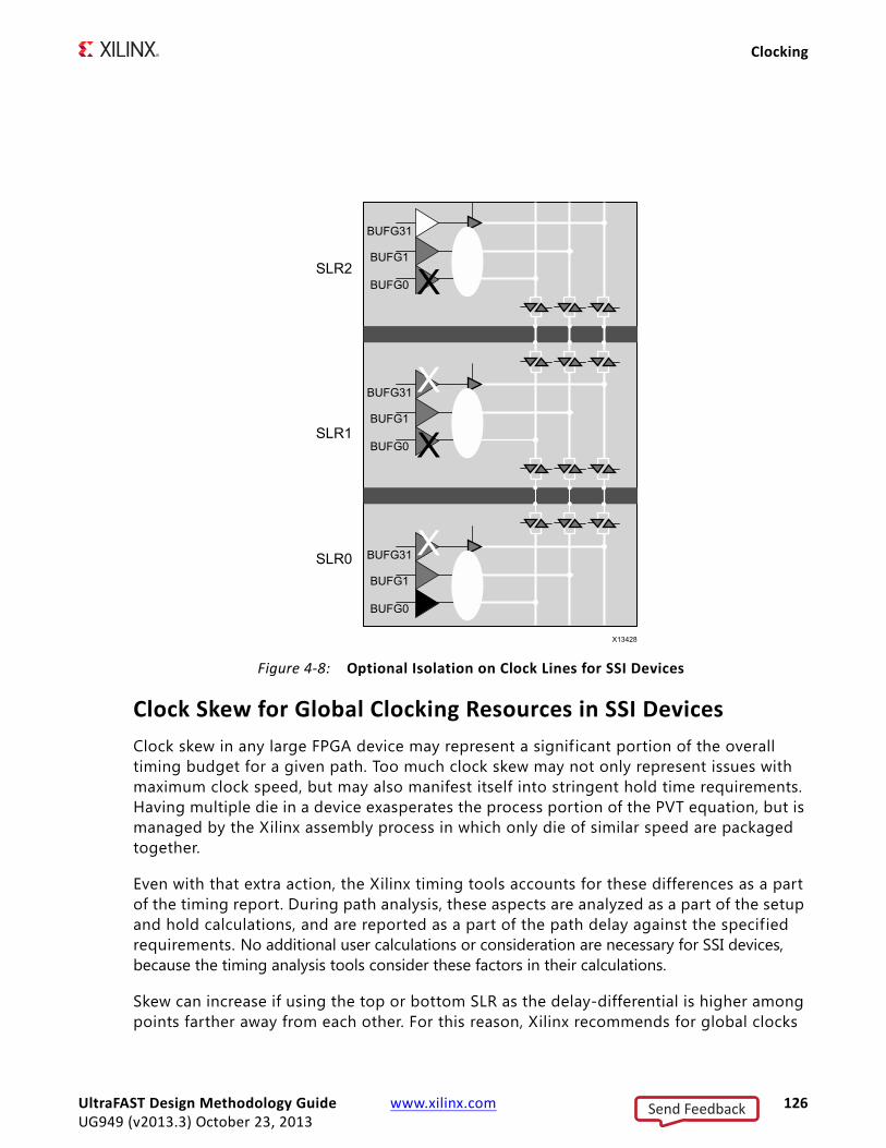
Clocking
Clock Skew for Global Clocking Resources in SSI DevicesClock skew in any large FPGA device may represent a signif icant portion of the overall timing budget for a given path. Too much clock skew may not only represent issues with maximum clock speed, but may also manifest itself into stringent hold time requirements. Having multiple die in a device exasperates the process portion of the PVT equation, but is managed by the Xilinx assembly process in which only die of similar speed are packaged together.
Even with that extra action, the Xilinx timing tools accounts for these differences as a part of the timing report. During path analysis, these aspects are analyzed as a part of the setup and hold calculations, and are reported as a part of the path delay against the specified requirements. No additional user calculations or consideration are necessary for SSI devices, because the timing analysis tools consider these factors in their calculations.
Skew can increase if using the top or bottom SLR as the delay-differential is higher among points farther away from each other. For this reason, Xilinx recommends for global clocks
X-Ref Target - Figure 4-8
Figure 4-8: Optional Isolation on Clock Lines for SSI Devices
UltraFAST Design Methodology Guide www.xilinx.com 126UG949 (v2013.3) October 23, 2013
Send Feedback
Clocking
that must drive more than one SLR to be placed into the center SLR. This allows a more even distribution of the overall clocking network across the part resulting in less overall clock skew.
Design of ClockingNow that you understand the major considerations for clocking decisions, let us see how you can achieve the desired clocking for your design.
Inference
Without user intervention, the synthesis tool automatically specif ies a global buffer (BUFG) for all clock structures up to the maximum allowed in an architecture (unless otherwise specified or controlled by the synthesis tool). As discussed above, the BUFG provides a well-controlled, low-skew network suitable for most clocking needs. Nothing additional is required unless your design clocking exceeds the number or capabilities of BUFGs in the part.
Applying additional control of the clocking structure, however, may prove to show better characteristics in terms of jitter, skew, placement, power, performance, or other characteristics.
Synthesis Constraints and Attributes
A simple way to control clocking resources is to use the proper synthesis constraints or attributes. Synthesis constraints may be used to:
• Prevent BUFG inference.
• Replace a BUFG with an alternative clocking structure.
• Specify a clock buffer where one would not exist otherwise.
Using synthesis constraints allows this type of control without requiring any modif ication to the code.
Attributes can be placed in either of the following locations:
• Directly in the HDL code, which allows them to persist in the code
• As constraints in the XDC file, which allows this control without any changes needed to the source HDL code
UltraFAST Design Methodology Guide www.xilinx.com 127UG949 (v2013.3) October 23, 2013
Send Feedback

Clocking
Use of IP
Certain IP assists in the creation of the clocking structures. Clocking Wizard and I/O Wizard specifically can assist in the selection and creation of the clocking resources and structure, including:
• BUFG
• BUFIO
• BUFR
• Clock modifying blocks such as:
° Mixed Mode Clocking Manager (MMCM)
° I/O Phase Lock Loop (PLL) components
More complex IP such as memory Interface Generator (MIG), PCIe, or Transceiver Wizard may also include clocking structures as part of the overall IP. This may provide additional clocking resources if properly taken into account. If not taken into account, it may limit some clocking options for the remainder of the design.
Xilinx highly recommends that, for any instantiated IP, the clocking requirements, capabilities and resources are well understood and leveraged where possible in other portions of the design.
Instantiation
The most low-level and direct method of controlling clocking structures is to instantiate the desired clocking resources into the HDL design. This allows you to access all possible capabilities of the device and exercise absolute control over them. When using BUFGCE, BUFGMUX, BUFHCE, or other clocking structure that requires extra logic and control, instantiation is generally the only option. However, even for simple buffers, sometimes the quickest way to obtain a desired result is to be direct and instantiate it into your design.
An effective style to manage clocking resources (especially when instantiating) is to contain the clocking resources in a separate entity or module instantiated at the top or near the top of the code. By having it at the top-level of code, it may more easily be distributed to multiple modules in your design.
Be aware of where clocking resources can and should be shared. Creating redundant clocking resources is not only a waste of resources, but generally consume more power, create more potential conflicts and placement decisions resulting in longer overall implementation tool runtimes and potentially more complex timing situations. This is another reason why having the clocking resources near the top module is important.
UltraFAST Design Methodology Guide www.xilinx.com 128UG949 (v2013.3) October 23, 2013
Send Feedback

Clocking
Controlling the Phase, Frequency, Duty-Cycle, and Jitter of the ClockThis section explains some fine-grained tuning to the clock characteristics:
• Using Clock Modifying Blocks (MMCM and PLL)
• Using IDELAYs on Clocks to Control Phase
• Using Gated Clocks
Using Clock Modifying Blocks (MMCM and PLL)
You can use an MMCM or PLL to change the overall characteristics of an incoming clock.
An MMCM is most commonly used to remove the insertion delay of the clock (phase align the clock to the incoming system synchronous data).
The MMCM can also be used to:
• Create tighter control of phase.
• Filter jitter in the clock.
• Change the clock frequency.
• Correct or change the clock duty cycle, thus giving tight control over an important aspect of your design.
Using an MMCM or PLL is fairly common for conditioning and controlling the clock characteristics.
In order to use the MMCM or PLL, several attributes must be coordinated to ensure that the MMCM is operating within specifications, and delivering the desired clocking characteristics on its output. For this reason, Xilinx highly recommends that you use the Clocking Wizard to properly configure this resource.
The MMCM or PLL can also be directly instantiated, allowing even greater control. However, be sure to use the proper settings. Incorrect settings on the MMCM or PLL may:
• Increase clock uncertainty due to increased jitter.
• Build incorrect phase relationships.
• Make timing more diff icult.
IMPORTANT: When using the Clocking Wizard to configure the MMCM or PLL, the Clocking Wizard by default attempts to configure the MMCM for low output jitter using reasonable power characteristics.
UltraFAST Design Methodology Guide www.xilinx.com 129UG949 (v2013.3) October 23, 2013
Send Feedback

Clocking
Depending on your goals, however, the settings in the Clocking Wizard may be changed to:
• Further minimize jitter, and thus improve timing at the cost of higher power, or
• Go the other way to reduce power but increase output jitter.
While using MMCM or PLL, pay attention to the following:
• Do not leave any inputs floating. Relying on synthesis or other optimization tools to tie off the floating values is not recommended, since the values that they tie to might be different from what you desire.
• RST should be connected to the user logic, so that it can be asserted as described in the 7 Series FPGA Clocking Resources User Guide (UG472). Grounding of RST can cause problems if the clock is interrupted.
• LOCKED output should be used in the implementation of reset, for example, synchronous logic clocked by the clock coming out of the PLL should be held in reset till LOCKED is asserted.
• The need for BUFG in the feedback path is important only if the PLL/MMCM output clock needs to be phase aligned with the input reference clock.
• Confirm the connectivity between CLKFBIN and CLKFBOUT.
RECOMMENDED: Explore the different settings within the Clocking Wizard to ensure that the most desirable configuration is created based on your overall design goals.
Using IDELAYs on Clocks to Control Phase
If only minor phase adjustments are necessary, you can use IDELAY or ODELAY (instead of MMCM or PLL) to add additional delay. This increases the phase offset of the clock in relation to any associated data.
Using Gated Clocks
Xilinx FPGA devices include dedicated clock networks that can provide a large-fanout, low-skew clocking resource. Fine-grained clock gating techniques implied in the HDL code can disrupt the functionality and mapping to this dedicated resource. Therefore, when coding to directly target an FPGA device, Xilinx does not recommend that you code clock gating constructs into the clock path. Instead, control clocking by using coding techniques to infer clock enables in order to stop portions of the design, either for functionality or power reasons.
If the code already contains clock gating constructs, or if it is intended for a different technology that requires such coding styles, Xilinx recommends that you use a synthesis tool that can remap gates placed within the clock path to clock enables in the data path. Doing so allows for a better mapping to the clocking resources; and simplif ies the timing analysis of the circuit for data entering and exiting the gated domain.
UltraFAST Design Methodology Guide www.xilinx.com 130UG949 (v2013.3) October 23, 2013
Send Feedback

Clocking
When larger portions of the clock network can be shut down for periods of time, the clock network can be enabled or disabled by using a BUFGCE, BUFHCE, BUFR or BUFMRCE. When a clock may be slowed down during periods of time, a BUFGCE, BUFHCE or BUFR may also be used with additional logic to periodically enable the clock net. Alternatively, you can use a BUFGMUX to switch the clock source from a faster clock signal to a slower clock.
Any of these techniques can effectively reduce dynamic power. However, depending on the requirements and clock topology, one technique may prove more effective than another. For example:
• A BUFR may work best if it is an externally generated clock (under 450 MHz) that is only needed to source up to three clock regions.
• For Virtex-7 devices, a BUFMRCE may be needed in addition in order to use this technique with more than one clock region (but only up to three vertically adjacent regions).
• A BUFHCE is better-suited for higher speed clocks that can be contained in a single clock region. While a BUFGCE may span the device (and is the most flexible), it may not be the best choice for the greatest power savings.
Creating an Output ClockAn effective way to forward a clock out of an FPGA device for clocking devices external to the FPGA device, is to use an ODDR component. By tying one of the inputs high and the other low, you can easily create a well controlled clock in terms of phase relationship and duty cycle. (for example, by holding D1 to 0 and the D2 pin to 1, you can achieve a 180 degree phase shift). By utilizing the set/reset and clock enable, you also have control over stopping the clock and holding it at a certain polarity for sustained amounts of time.
If further phase control is necessary for an external clock, an MMCM or PLL can be used with external feedback compensation and/or coarse or f ine grained, f ixed or variable phase compensation. This allows great control over clock phase and propagation times to other devices simplifying external timing requirements from the device.
UltraFAST Design Methodology Guide www.xilinx.com 131UG949 (v2013.3) October 23, 2013
Send Feedback

Clocking
Clock Resource Selection Summary
BUFG
• Use when a high-fanout clock must be provided to several clock regions throughout the device. If you see cascaded BUFG, assure yourself of the need for it, or, did a BUFG come in unintentionally?
• Use when it is not desired to instantiate or have any manual control of clocking.
• Use for very high fanout non-clock nets such as a global reset for medium to slower speed clocks where mixed polarities does not exist. Xilinx recommends limit this use to only two in any design.
• For SSI devices where clocks that must span more than one SLR, locate them in one of the center SLRs. This more evenly distributes the clocking net across the entire device thus minimizing skew.
BUFGCE
• Use to stop a large-fanout several-region clock domain.
BUFGMUX/BUFGCTRL
• Use to change clock frequencies or clock sources during the operation of your design.
BUFH
• Use for smaller clock domains of logic that can be contained within a single clock region.
• Use for very high-speed clocking domains
• Use in clock domains that are less likely to compete for clocking resources with BUFGs
• For SSI devices, Xilinx recommends generally use in the upper or lower SLRs in order to lessen the chances of competition for resources with the BUFGs placed into the center SLRs
BUFHCE
• Use for clock-gating on a medium grained portion of the clock network which can be placed into a single clock region, The BUFHCE may be driven by BUFG.
• Use for high-fanout non-clock signals such as a reset that can be contained within a single clock region.
UltraFAST Design Methodology Guide www.xilinx.com 132UG949 (v2013.3) October 23, 2013
Send Feedback

Clocking
BUFR
• Use for small to medium sized clock networks that do not require performance higher than 450 MHz.
• Use for externally provided clocks that can be constrained within up to three vertically adjacent clock region that require clock division.
• For SSI devices, Xilinx recommends generally use in the upper or lower SLRs in order to lessen the chances of competition for resources with the BUFGs placed into the center SLRs.
BUFIO
• Use for externally provided high-speed I/O clocking generally in source synchronous data capture.
BUFMR
For Xilinx 7 series FPGA devices only:
• Use when you need to use BUFRs or BUFIOs in more than one vertically adjacent clock regions for a single clock source.
• For SSI devices, Xilinx recommends locating the BUFMR and associated pin into the center clock region within an SLR. This allows access to all three clock regions from the BUFMR in case needed.
BUFMRCE
For Xilinx 7 series FPGA devices only:
• Use when you need to use BUFRs or BUFIOs in more than one vertically adjacent clock regions for a single clock source where the clock is desired to be periodically stopped.
• If using more than one BUFR where clock division is used. The BUFMRCE can be used to ensure proper phase startup of all connected BUFRs
PLL and MMCM
• Use to remove the clock insertion delay (phase align the clock to the incoming data) for system synchronous inputs and outputs.
• Use for clock phase control to align source synchronous data to the clock for proper data capture.
• Use to change the clock frequency or duty cycle of an incoming clock.
• Use to f ilter clock jitter.
UltraFAST Design Methodology Guide www.xilinx.com 133UG949 (v2013.3) October 23, 2013
Send Feedback
Deciding When to Instantiate or Infer
PLL provides a better control of jitter, while MMCM can provide a wider range of output frequencies. For tighter timing requirement, PLLs might be best, provided they can provide the frequency of interest.
IDELAY / IODELAY
• Use on an input clock to add small amounts of additional phase offset (delay).
• Use on input data to add additional delay to data thus effectively reducing clock phase offset in relation to the data.
ODDR
• Use to create an external forwarded clock from the device.
Deciding When to Instantiate or InferXilinx recommends that you have an RTL description of your design; and that you let the synthesis tool do the mapping of the code into the resources available in the FPGA device. In addition to making the code more portable, all inferred logic is visible to the synthesis tool, allowing the tool to perform optimizations between functions. These optimizations include logic replications; restructuring and merging; and retiming to balance logic delay between registers.
Synthesis Tool OptimizationWhen device library cells are instantiated, synthesis tools do not optimize them by default. Even when instructed to optimize the device library cells, synthesis tools generally cannot perform the same level of optimization as with the RTL. Therefore, synthesis tools typically only perform optimizations on the paths to and from these cells but not through the cells.
For example, if an SRL is instantiated and is part of a long path, this path might become a bottleneck. The SRL has a longer clock-to-out delay than a regular register. To preserve the area reduction provided by the SRL while improving its clock-to-out performance, an SRL of one delay less than the actual desired delay is created, with the last stage implemented in a regular flip-flop.
When Instantiation Is DesirableInstantiation may be desirable when the synthesis tool mapping does not meet the timing, power, or area constraints; or when a particular feature within an FPGA device cannot be inferred.
UltraFAST Design Methodology Guide www.xilinx.com 134UG949 (v2013.3) October 23, 2013
Send Feedback

Deciding When to Instantiate or Infer
With instantiation, you have total control over the synthesis tool. For example, to achieve better performance, you can implement a comparator using only LUTs, instead of the combination of LUT and carry chain elements usually chosen by the synthesis tool.
Sometimes instantiation may be the only way to make use of the complex resources available in the device. This can be due to:
• HDL Language Restrictions
• Hardware Complexity
• Synthesis Tools Inference Limitations
HDL Language Restrictions
For example, it is not possible to describe double data rate (DDR) outputs in VHDL because it requires two separate processes to drive the same signal.
Hardware Complexity
It is easier to instantiate the I/O SerDes elements than to create synthesizable description.
Synthesis Tools Inference Limitations
For example, synthesis tools currently do not have the capability to infer the hard FIFOs or the DSP48 symmetric rounding and saturation from RTL descriptions. Therefore, you must instantiate it.
If you decide to instantiate a Xilinx primitive, see the appropriate User Guide and Libraries Guide for the target architecture to fully understand the component functionality, configuration, and connectivity.
In case of both inference as well as instantiation, Xilinx recommends that you use the instantiation and language templates from the Vivado Design Suite language templates.
TIPS: - Infer functionality whenever possible.- When synthesized RTL code does not meet requirements, review the requirements before replacing
the code with device library component instantiations.- Consider the Vivado Design Suite language templates when writing common Verilog and VHDL
behavioral constructs or if necessary instantiating the desired primitives.
UltraFAST Design Methodology Guide www.xilinx.com 135UG949 (v2013.3) October 23, 2013
Send Feedback
Coding Styles for Higher Reliability
Coding Styles for Higher ReliabilitySome specif ic design situations require specific considerations in order to achieve higher reliability.
Clock Domain CrossingsWhenever a data or control signal transfers from one clock domain to another, you must understand the nature of the crossing. Clock crossings may be categorized into:
• Synchronous crossings
Synchronous crossings are crossings in which there is a known and predictable phase relationship between domains.
• Asynchronous crossings
Asynchronous crossings are crossings in which phase relationship may not be determined predictably.
Within synchronous crossings, there can be situations in which clock skew is very high. Situations with very high skew can make it much more diff icult to meet timing.
IMPORTANT: If skew is in a direction that helps to meet setup, that makes it difficult to meet hold. Conversely, if skew is in a direction that helps to meet hold, that makes it difficult to meet setup.
Synchronous Domain Crossing
• Going from one BUFG network to another driven from the same MMCM, PLL, or device pin, where both BUFGs exist in the same half of the chip (top half or bottom half).
• Going from a BUFH network to another BUFH network that is placed horizontally adjacent.
• Going from a BUFR to another similarly configured BUFR both driven by the same BUFMR.
Note: If the BUFRs are not in BYPASS mode, it must also be phase aligned by synchronizing the reset on all associated BUFRs.
• Going to or from a BUFIO to or from a BUFR in the same clock region from the same clock source.
Synchronous Domain Crossing, But Potentially Very High Skew
• Going to or from a clock network using an MMCM or PLL to or from a network not using one, even if generated from the same source clock.
UltraFAST Design Methodology Guide www.xilinx.com 136UG949 (v2013.3) October 23, 2013
Send Feedback

Coding Styles for Higher Reliability
• Going to or from a BUFH to any other network, except the BUFH network horizontally adjacent to it.
• Going to or from a clock network that is not directly driven by a dedicated clocking resource (such as external clock pin, MMCM, or PLL)
• Going to or from a BUFG located in the top half of the device to one located in the bottom half of the device.
Asynchronous Domain Crossing
• Going from a clock network to another clock network that have no phase relationship.
• Going to or from domains generated from the same MMCM or PLL, if the frequency intervals are not regular to each other.
• Going to or from any GT TXCLKOUT or RXCLKOUT outputs on any Xilinx FPGA device to another domain.
In short, synchronous domains are domains in which there is a known and predictable phase relationship between clocks. This generally occurs when the domains: (1) are derivatives of each other, or; (2) are provided from the same internal or external source. In these cases, timing may be analyzed and (with some considerations), be safely transferred from one domain to another.
Depending on the distance and nature of clocking resources traveled after the common node to reach source and destination, clock skew can be signif icant enough to not ignore. For small data paths such as register to register paths, the clock skew may be longer than the data delay that can result in a hold violation. If there are several logic levels, then the additional skew can make timing very diff icult. Xilinx recommends that you closely monitor logic levels in such cross clocking and take into account the effects of too few or too many logic levels.
For asynchronous domain crossing, special steps must be taken to mitigate improper bus capture, metastability, and other occurrences that can affect the data integrity in such paths.
In general, there are two popular methods to allow data to cross asynchronous clock domains safely. If only a single bit is needed or if methods such as grey-coding are used to transfer more than one bit of related data, register synchronizers can be inserted to reduce the Mean Time Before Failure (MTBF) of the circuit. For multiple bits of data (that is, a bus), the generally recommended practice is to use an independent clock (asynchronous) FIFO to safely transfer data from one domain to another. Such a FIFO can be inferred if built from soft logic. However, if the use of the dedicated hard-FIFO is desired (or if pre-characterized and predefined FIFO Logic makes the task easier), the FIFO can be directly instantiated. FIFO primitives or the FIFO Generator can be used to construct the FIFO.
Use the ASYNC_REG attribute in your HDL code to identify all synchronizing registers. By doing so, the Vivado Design Suite design tools can better understand and use special
UltraFAST Design Methodology Guide www.xilinx.com 137UG949 (v2013.3) October 23, 2013
Send Feedback

Coding Styles for Higher Reliability
algorithms to improve synthesis, simulation, placement, and routing to improve MTBF, by reducing metastability occurrences.
ASYNC_REG Example
module synchronizer #( parameter SYNC_STAGES = 2) ( input ASYNC_IN, input CLK, output SYNC_OUT); (* (ASYNC_REG = “TRUE” *) reg [SYNC_STAGES-1:0] sync_regs = {SYNC_STAGES{1’b1}};
always @(posedge CLK) sync_regs <= {sync_regs[SYNC_STAGES-2:0], ASYNC_IN}; assign SYNC_OUT = sync_regs[SYNC_STAGES-1]; endmodule
Controlling and Synchronizing Device StartupOnce the FPGA device completes configuration, a sequence of events occurs in which the device comes out of the configuration state and into general operation. In most configuration sequences, one of the last steps is the deassertion of the Global Set Reset (GSR), followed by the deassertion of the Global Enable (GWE) signal. When this happens, the design is in a known initial state, and is then released for operation.
If this release point is not synchronized to the given clock domain, or if the clock is operating at a faster time than the GWE can safely be released, portions of the design can go into an unknown state. For some designs, this is inconsequential. In other designs, this can cause the design to become unstable, or to misprocess the initial data set. If the design must come up in a known state, Xilinx recommends that you take action to control the start-up synchronization process. This can be done in several ways.
One method is to delay all design clocks until a period of time after GWE is asserted. To do this, Xilinx recommends:
• Use instantiated BUFGCE, BUFHCE, or BUFR components.
• Use the enables of those components to delay clocking a few clock cycles post-configuration.
• When using an MMCM, do so on the output clocks, but not on the feedback clock, by selecting the Safe Clock Startup option from the Clocking Wizard.
UltraFAST Design Methodology Guide www.xilinx.com 138UG949 (v2013.3) October 23, 2013
Send Feedback

Coding Styles for Higher Reliability
You can also use clock enables, local reset (synchronized), or both on critical parts of the design (such as a state machine) to ensure that the startup of those portions of the designs are controlled and known.
Use of Untimed ResetsResets (especially global resets) may have a very high fanout spanning a large portion of the FPGA array. In these cases, the reset timing may be diff icult to meet regardless of the clock frequency or timing requirements. This can be especially challenging in high-speed designs.
Missing timing on a reset path can cause indeterminate behavior such as initial or intermittent data corruption; and full design lock up or catastrophic malfunction in extreme cases.
The issue for most designs is during deassertion, rather than the assertion of the reset (although in some cases assertion may pose an issue as well). If reset is deasserted at the same time the clock asserts at a particular register, the register output may be indeterminate (recovery/removal violation). Or if the skew of the reset signal is such that parts of the design may be released from reset at one clock cycle and other parts in another, it may cause unknown circuit behavior. Controlling and Synchronizing Device Startup, page 138,shows an example method for synchronizing the deassertion of reset.
Xilinx recommends that besides adding a synchronizing circuit, you place proper timing constraints on the reset path; and, during design entry, minimize the impact for timing closure on the reset. One way to do so is to limit the number of loads a reset signal drives by either removing the reset or replicating the driver.
If this is not adequate to close timing, you can stop the clock internally using the BUFGCE capability, or externally during reset allowing for a multi-cycle deassertion period for the reset signal.
X-Ref Target - Figure 4-9
Figure 4-9: Clock Startup
UltraFAST Design Methodology Guide www.xilinx.com 139UG949 (v2013.3) October 23, 2013
Send Feedback

Coding Styles to Improve Performance
IMPORTANT: The reset deassertion must be timed, so that the entire design comes out of reset in the same cycle.
Avoid Combinational LoopsDo not use combinational feedback paths in FPGA designs. The timing ramifications are diff icult to simulate, analyze, and fully take into account under all operating conditions. Results can be unpredictable.
For information on using the check_timing command to check for any inadvertent combinational loops, see Chapter 5, Implementation.
Use of BUFG in Non-Clock SignalsBUFG may sometimes be used even for non-clock signals. A typical usage situation is described in the next section, Coding Styles to Improve Performance, page 140.
Coding Styles to Improve PerformanceViolating the coding techniques discussed in the previous section (Coding Styles for Higher Reliability, page 136) generally has a detrimental impact on performance. For high performance designs, the coding techniques discussed in this section (Coding Styles to Improve Performance) can mitigate possible timing hazards.
High Fanouts in Critical PathsHigh fanout nets are much easier to deal with early in the design process. What constitutes too high of a fanout is often dictated by performance requirements and the construction of the paths.
RECOMMENDED: Examine nets with thousands of loads early to assess their impact on the overall design.
If you identify a high fanout net, mitigation techniques include:
• Reduce Loads to Portions of the Design That Do Not Require It
• Use Register Replication
UltraFAST Design Methodology Guide www.xilinx.com 140UG949 (v2013.3) October 23, 2013
Send Feedback
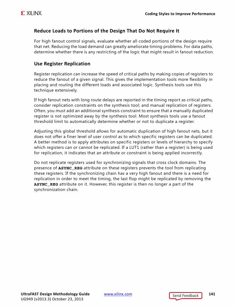
Coding Styles to Improve Performance
Reduce Loads to Portions of the Design That Do Not Require It
For high fanout control signals, evaluate whether all coded portions of the design require that net. Reducing the load demand can greatly ameliorate timing problems. For data paths, determine whether there is any restricting of the logic that might result in fanout reduction.
Use Register Replication
Register replication can increase the speed of critical paths by making copies of registers to reduce the fanout of a given signal. This gives the implementation tools more flexibility in placing and routing the different loads and associated logic. Synthesis tools use this technique extensively.
If high fanout nets with long route delays are reported in the timing report as critical paths, consider replication constraints on the synthesis tool; and manual replication of registers. Often, you must add an additional synthesis constraint to ensure that a manually duplicated register is not optimized away by the synthesis tool. Most synthesis tools use a fanout threshold limit to automatically determine whether or not to duplicate a register.
Adjusting this global threshold allows for automatic duplication of high fanout nets, but it does not offer a f iner level of user control as to which specific registers can be duplicated. A better method is to apply attributes on specif ic registers or levels of hierarchy to specify which registers can or cannot be replicated. If a LUT1 (rather than a register) is being used for replication, it indicates that an attribute or constraint is being applied incorrectly.
Do not replicate registers used for synchronizing signals that cross clock domains. The presence of ASYNC_REG attribute on these registers prevents the tool from replicating these registers. If the synchronizing chain has a very high fanout and there is a need for replication in order to meet the timing, the last flop might be replicated by removing the ASYNC_REG attribute on it. However, this register is then no longer a part of the synchronization chain.
UltraFAST Design Methodology Guide www.xilinx.com 141UG949 (v2013.3) October 23, 2013
Send Feedback

Coding Styles to Improve Performance
Table 4-4, Fanout Guidelines, gives an indicative guideline on the number of fanouts that might be acceptable for your design.
TIP: If the timing reports indicate that high-fanout signals are limiting the design performance, consider replicating them. The phys_opt_design command might do a much better job of replicating registers. For more information, see MAX_FANOUT, page 194, in Chapter 5, Implementation.
Pipelining Considerations
Another way to increase performance is to restructure long datapaths with several levels of logic, and distribute them over multiple clock cycles. This method allows for a faster clock cycle and increased data throughput at the expense of latency and pipeline overhead logic management.
As FPGA devices are register-rich, the additional registers and overhead logic are usually not an issue. With this technique, the datapath spans multiple cycles. Accordingly, special considerations must be used for the rest of the design to account for the added path latency.
Pipelining Considerations for SSI Devices
When designing high performance register-to-register connections for SLR boundary crossings, the appropriate pipelining must be described in the HDL code, and controlled at synthesis.
Table 4-4: Fanout Guidelines
Condition Fanout < 5000 Fanout < 200 Fanout < 100
Low Frequency 1 to 125 MHZ
Few logic levels between synchronous logic <13 levels of logic at maximum frequency
Medium Frequency 125 to 250 MHz
Results dependent. Might need to reduce fanout and/or logic levels to achieve.
<6 levels of logic at maximum frequency. (Driver and load types impact performance.)
High Frequency > 250 MHz
Not recommended for most designs.
Small number of logic levels is typically necessary for higher speeds.
Advance pipelining methods required. Careful logic replication. Compact functions. Low logic levels required. (Driver and load types impact performance.)
UltraFAST Design Methodology Guide www.xilinx.com 142UG949 (v2013.3) October 23, 2013
Send Feedback

Coding Styles to Improve Performance
This ensures that the Shift Register LUT (SRL) inference and other optimizations do not occur in the logic path that must cross an SLR boundary.
Modifying the code in this manner defines where the SLR boundary crossing occurs. You must define the SLR assignment to correspond to those design changes.
Consider Pipelining Up Front
Considering pipelining up front rather than later on can make timing closure much less diff icult. Adding pipelining at a later stage to certain paths often propagates latency differences across the circuit. This can make one seemingly small change require a major redesign of portions of the code.
Identifying pipelining opportunities early in the design can often signif icantly improve timing closure; implementation runtime (due to easier-to-solve timing problems); and device power (due to reduced switching of logic).
As you code your design, be aware of the logic being inferred. Monitor the following three conditions for additional pipelining considerations:
• Cones of logic with large fan-in
For example, code that requires large buses or several combinational signals to compute an output.
• Blocks with restricted placement or slow clock-to-out or large setup requirements
For example, block RAMs without output registers or arithmetic code that is not appropriately pipelined.
• When forced placement causes long routes
For example, a pinout that forces a route across the chip may require pipelining to allow for high speed operation.
In Figure 4-10: Before Pipelining Diagram, the clock speed is limited by:
• Clock-to out-time of the source flip-flop
• Logic delay through four levels of logic
• Routing associated with the four function generators
• Setup time of the destination register
UltraFAST Design Methodology Guide www.xilinx.com 143UG949 (v2013.3) October 23, 2013
Send Feedback
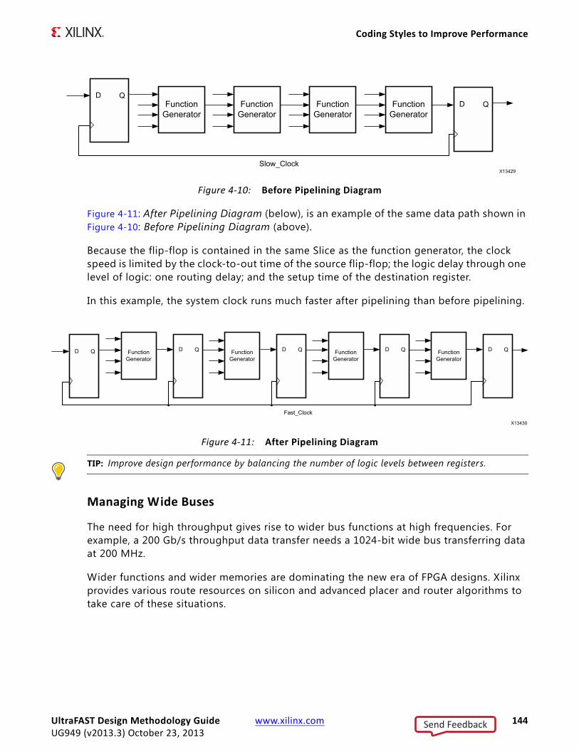
Coding Styles to Improve Performance
Figure 4-11: After Pipelining Diagram (below), is an example of the same data path shown in Figure 4-10: Before Pipelining Diagram (above).
Because the flip-flop is contained in the same Slice as the function generator, the clock speed is limited by the clock-to-out time of the source flip-flop; the logic delay through one level of logic: one routing delay; and the setup time of the destination register.
In this example, the system clock runs much faster after pipelining than before pipelining.
TIP: Improve design performance by balancing the number of logic levels between registers.
Managing Wide Buses
The need for high throughput gives rise to wider bus functions at high frequencies. For example, a 200 Gb/s throughput data transfer needs a 1024-bit wide bus transferring data at 200 MHz.
Wider functions and wider memories are dominating the new era of FPGA designs. Xilinx provides various route resources on silicon and advanced placer and router algorithms to take care of these situations.
X-Ref Target - Figure 4-10
Figure 4-10: Before Pipelining Diagram
X-Ref Target - Figure 4-11
Figure 4-11: After Pipelining Diagram
UltraFAST Design Methodology Guide www.xilinx.com 144UG949 (v2013.3) October 23, 2013
Send Feedback

Coding Styles to Improve Power
You should take into account the available resources and use them to achieve better performance. Design techniques that can be adopted to assist the flow include:
• Memory Organization
• Wide Functions
• I/Os
Memory Organization
• Register address and data-out of memories.
• RTL coding should split the memories width-wise to achieve high performance.
Wide Functions
• Have sufficient pipeline stages when implementing wide arithmetic functions and reduction operators.
• Ensure minimal SLR crossings when using SSI targets and performing manual design partition,
• Use Xilinx IP to implement wide-bus complex arithmetic operations. The IP cores take care of re-timing and pipelining requirements for high-performance.
I/Os
• Use Xilinx serial IP cores that support wide-bus and high-throughput reliable chip-to-chip data transfer.
• Allocate primary I/Os of the same bank or adjacent banks in order to minimize skew effect between individual bits of an in-coming bus interface.
Coding Styles to Improve PowerCoding styles to improve power include:
• Gate Clock or Data Paths
• Maximize Gating Elements
• Use Clock Enable Ports of Dedicated Clock Buffers
• Keep an Eye on Control Sets
• Use Case Block When Priority Encoder Not Needed
UltraFAST Design Methodology Guide www.xilinx.com 145UG949 (v2013.3) October 23, 2013
Send Feedback

Coding Styles to Improve Power
Gate Clock or Data PathsGating the clock or data paths is common technique to stop transition when the results of these paths are not used. Gating a clock stops all driven synchronous loads; and prevents data path signal switching and glitches from continuing to propagate.
The tools analyze the description and netlist to detect unwanted conditions. However, there are things you know about the application, data flow, and dependencies that are not available to the tool, and that only you can specify.
Maximize Gating ElementsMaximize the number of elements affected by the gating signal. For example, it is more power eff icient to gate a clock domain at its driving source than to gate each load with a clock enable signal.
Use Clock Enable Ports of Dedicated Clock BuffersWhen gating or multiplexing clocks to minimize activity or clock tree usage, use the clock enable ports of dedicated clock buffers. Inserting LUTs or using other methods to gate-off clock signals is not efficient for power and timing.
Keep an Eye on Control SetsAs discussed earlier, the number of control sets should be minimized. Xilinx recommends clock gating only if the gated clock drives a high number of synchronous elements. Otherwise, there is a risk of wasted flops. Adding gating signals to stop the data or clock path can require additional logic and routing (and, thus power). Minimize the number of additional structures to avoid defeating the original purpose.
RECOMMENDED: Do not use too fine-grained clock gating. Each gated clock should impact a large number of synchronous elements.
Use Case Block When Priority Encoder Not NeededWhen a priority encoding is not needed, use a case block instead of an if-then-else block or ternary operator.
UltraFAST Design Methodology Guide www.xilinx.com 146UG949 (v2013.3) October 23, 2013
Send Feedback

Coding Styles to Improve Power
Inefficient Coding Example
if (reg1) val = reg_in1;else if (reg2) val = reg_in2;else if (reg3) val = reg_in3;else val = reg_in4;
Correct Coding Example
(* parallel_case *) casex ({reg1, reg2, reg3})1xx: val = reg_in1 ;01x: val = reg_in2 ;001: val = reg_in3 ;default: val = reg_in4 ;endcase
Best Practices for Block RAM in DesignThe amount of power the block RAM consumes is directly proportional to the amount of time enabled. To save power, the block RAM enable can be driven Low on clock cycles when the block RAM is not used in the design. Both the block RAM enable rate and the clock rate •are important parameters that must be considered for power optimization.
The mode settings for block RAM (such as NO_CHANGE, READ_FIRST, and WRITE_FIRST) were explained earlier in Selecting the Proper BRAM Write Mode.
Deeper and Wider Memories
Deeper and wider memories must follow the depth wise splitting mechanism to save dynamic power. During IP customization, if you choose power-eff icient realization, Vivado IDE creates the depth wise splitting.
Figure 4-12 shows an example of the above statement with memory configuration 4Kx1024 bit.
UltraFAST Design Methodology Guide www.xilinx.com 147UG949 (v2013.3) October 23, 2013
Send Feedback

Coding Styles to Improve Power
Width Wise Splitting
In this implementation, all block RAMs are always enabled (for each read or write); and consume more power.
Depth Wise Splitting
In this implementation, because one block RAM at a time is selected (from each unit), the dynamic power contribution is almost half.
X-Ref Target - Figure 4-12
Figure 4-12: RTL Representation of 4K x 1024 Using 4K x 9
X-Ref Target - Figure 4-13
Figure 4-13: RTL Representation of 4K x 1024 Using 2K x 18
UltraFAST Design Methodology Guide www.xilinx.com 148UG949 (v2013.3) October 23, 2013
Send Feedback

Creating Constraints
Creating Constraints Design constraints define the requirements that must be met by the compilation flow in order for the design to be functional in hardware. For more complex designs, they also define guidance for the tools to help with convergence and closure. Not all constraints are used by all steps in the compilation flow. For example, physical constraints are used only during the implementation steps (that is, by the placer and the router).
Because synthesis and implementation algorithms are timing-driven, creating proper timing constraints is essential. Over-constraining or under-constraining your design makes timing closure diff icult. You must use reasonable constraints that correspond to your application requirements.
Organizing the Design ConstraintsThe constraints are usually organized by category, by design module, or both, in one or many f iles. Regardless of how you organize them, you must understand their overall dependencies and review their f inal sequence once loaded in memory. For example, because timing clocks must be defined before they can be used by any other constraints, you must make sure that their definition is located at the beginning of your constraint f ile, in the f irst set of constraint f iles loaded in memory, or both.
Recommended Constraint Files
There are many ways to organize your constraints depending on the size and complexity of your project. Following are a few suggestions.
Simple Design
For a simple design with a small team of designers:
• 1 f ile for all constraints
• 1 f ile for physical + 1 file for timing
• 1 f ile for physical + 1 file for timing (synthesis) + 1 f ile for timing (implementation)
Complex Design
For a complex design with IP cores or several designer teams:
• 1 f ile for top-level timing + 1 f ile for top-level physical + 1 file per IP/major block
UltraFAST Design Methodology Guide www.xilinx.com 149UG949 (v2013.3) October 23, 2013
Send Feedback

Creating Constraints
Validating the Read Sequence
Once you have settled on the organization of your project constraint f iles, you must validate the read sequence of the f iles depending on the content of the f iles. In Project Mode, you can modify the constraint f ile sequence in the Vivado IDE or by using the reorder_files Tcl command. In Non-Project Mode, the sequence is directly defined by the read_xdc (for XDC files) and source (for constraints generated by Tcl scripts) commands in your compilation flow Tcl script.
Recommended Constraints Sequence
The constraints language (XDC) is based on Tcl syntax and interpretation rules. Like Tcl, XDC is a sequential language:
• Variables must be defined before they can be used. Similarly, timing clocks must be defined before they can be used in other constraints.
• For equivalent constraints that cover the same paths and have the same precedence, the last one applies.
When considering the priority rules above, the timing constraints should overall use the following sequence:
## Timing Assertions Section# Primary clocks# Virtual clocks# Generated clocks# Clock Uncertainty and Jitter# Input and output delay constraints# Clock Groups
## Timing Exceptions Section# False Paths# Max Delay / Min Delay# Multicycle Paths# Case Analysis# Disable Timing
When multiple XDC files are used, you must pay particular attention to the clock definitions and validate that the dependencies are ordered correctly.
The physical constraints can be located anywhere in any constraint f ile.
Creating Synthesis Constraints
Synthesis takes the RTL description of the design and transforms it into an optimized technology mapped netlist by using timing-driven algorithms. The quality of the results is affected by the quality of the RTL code and the constraints provided. At this point of the compilation flow, the net delay modeling is approximate and does not reflect placement
UltraFAST Design Methodology Guide www.xilinx.com 150UG949 (v2013.3) October 23, 2013
Send Feedback
Creating Constraints
constraints or complex effects such as congestion. The main objective is to obtain a netlist which meets timing, or fails by a small amount, with realistic and simple constraints.
The synthesis engine accepts all XDC commands, but only some have a real effect:
• Timing constraints related to setup/recovery analysis influence the QoR:
° create_clock
° create_generated_clock
° set_input_delay and set_output_delay
° set_clock_groups
° set_false_path
° set_max_delay
° set_multicycle_path
• Timing constraints related to hold and removal analysis are ignored during synthesis:
° set_false_path -hold
° set_min_delay
° set_multicycle_path -hold
• RTL attributes forces decisions made by the mapping and optimization algorithms. Following are a few examples:
° DONT_TOUCH / KEEP / KEEP_HIERARCHY
° MAX_FANOUT
° RAM_STYLE / ROM_STYLE / USE_DSP48 / SHREG_EXTRACT
° FULL_CASE / PARALLEL_CASE (Verilog RTL only)
The same attribute can also be set as a property from an XDC file. Using XDC-based constraints is convenient for influencing the synthesis results only in some cases without changing the RTL.
• Physical constraints are ignored (LOC, BEL, Pblocks)
Synthesis constraints must use names from the elaborated netlist, preferably ports and sequential cells. During elaboration, some RTL signals can disappear and it is not possible to attach XDC constraints to them. In addition, due to the various optimizations after elaboration, nets or logical cells are merged into the various technology primitives such as LUTs or DSP blocks.
Some registers are absorbed into RAM blocks and some levels of the hierarchy can disappear to allow cross-boundary optimizations.
UltraFAST Design Methodology Guide www.xilinx.com 151UG949 (v2013.3) October 23, 2013
Send Feedback

Creating Constraints
Any elaborated netlist object or level of hierarchy can be preserved by using a DONT_TOUCH, KEEP, or KEEP_HIERARCHY constraint, at the risk of degrading timing or area QoR.
Finally, some constraints can conflict and cannot be respected by synthesis. For example, if a MAX_FANOUT attribute is set on a net that crosses multiple levels of hierarchy, and some hierarchies are preserved with DONT_TOUCH, the fanout optimization will be limited or fully prevented.
IMPORTANT: Unlike during implementation, netlist objects that are used for defining timing constraints can be optimized away by synthesis to allow better QoR. This is usually not a problem as long as the constraints are updated and validated for implementation. But if needed, you can preserve any object by using the DONT_TOUCH constraint so that the constraints will apply during both synthesis and implementation.
Once synthesis has completed, Xilinx recommends that you review the timing and utilization reports to validate that the netlist quality meets the application requirements and can be used for implementation.
Creating Implementation Constraints
The implementation constraints must accurately reflect the requirements of the f inal application. Physical constraints such as I/O location and I/O standard are dictated by the board design- including the board trace delays, as well as the design internal requirements derived from the overall system requirements. Before you proceed to implementation, Xilinx highly recommends that you validate the correctness and accuracy of all your constraints. An improper constraint will likely contribute to degradation of the implementation QoR and can lower the confidence level in the timing signoff quality.
In many cases, the same constraints can be used during synthesis and implementation. However, because the design objects can disappear or have their name changed during synthesis, you must verify that all synthesis constraints still apply properly with the implementation netlist. If this is not the case, you must create an additional XDC file containing the constraints that are valid for implementation only.
Defining Timing Constraints in Four StepsThe process of defining good constraints is broken into the four major steps shown in Figure 4-14: Steps for Developing Timing Constraints. The steps follow the timing constraints precedence and dependency rules, as well as the logical way of providing information to the timing engine to perform the analysis.
UltraFAST Design Methodology Guide www.xilinx.com 152UG949 (v2013.3) October 23, 2013
Send Feedback
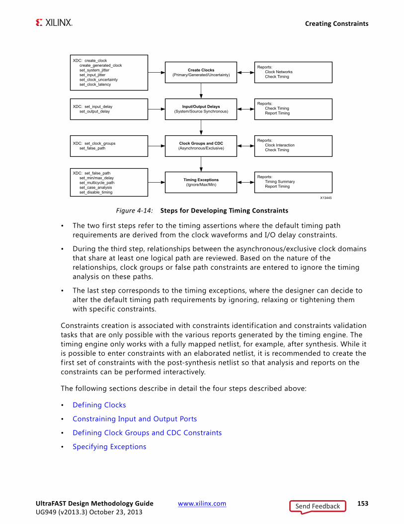
Creating Constraints
• The two f irst steps refer to the timing assertions where the default timing path requirements are derived from the clock waveforms and I/O delay constraints.
• During the third step, relationships between the asynchronous/exclusive clock domains that share at least one logical path are reviewed. Based on the nature of the relationships, clock groups or false path constraints are entered to ignore the timing analysis on these paths.
• The last step corresponds to the timing exceptions, where the designer can decide to alter the default timing path requirements by ignoring, relaxing or tightening them with specif ic constraints.
Constraints creation is associated with constraints identif ication and constraints validation tasks that are only possible with the various reports generated by the timing engine. The timing engine only works with a fully mapped netlist, for example, after synthesis. While it is possible to enter constraints with an elaborated netlist, it is recommended to create the f irst set of constraints with the post-synthesis netlist so that analysis and reports on the constraints can be performed interactively.
The following sections describe in detail the four steps described above:
• Defining Clocks
• Constraining Input and Output Ports
• Defining Clock Groups and CDC Constraints
• Specifying Exceptions
X-Ref Target - Figure 4-14
Figure 4-14: Steps for Developing Timing Constraints
UltraFAST Design Methodology Guide www.xilinx.com 153UG949 (v2013.3) October 23, 2013
Send Feedback
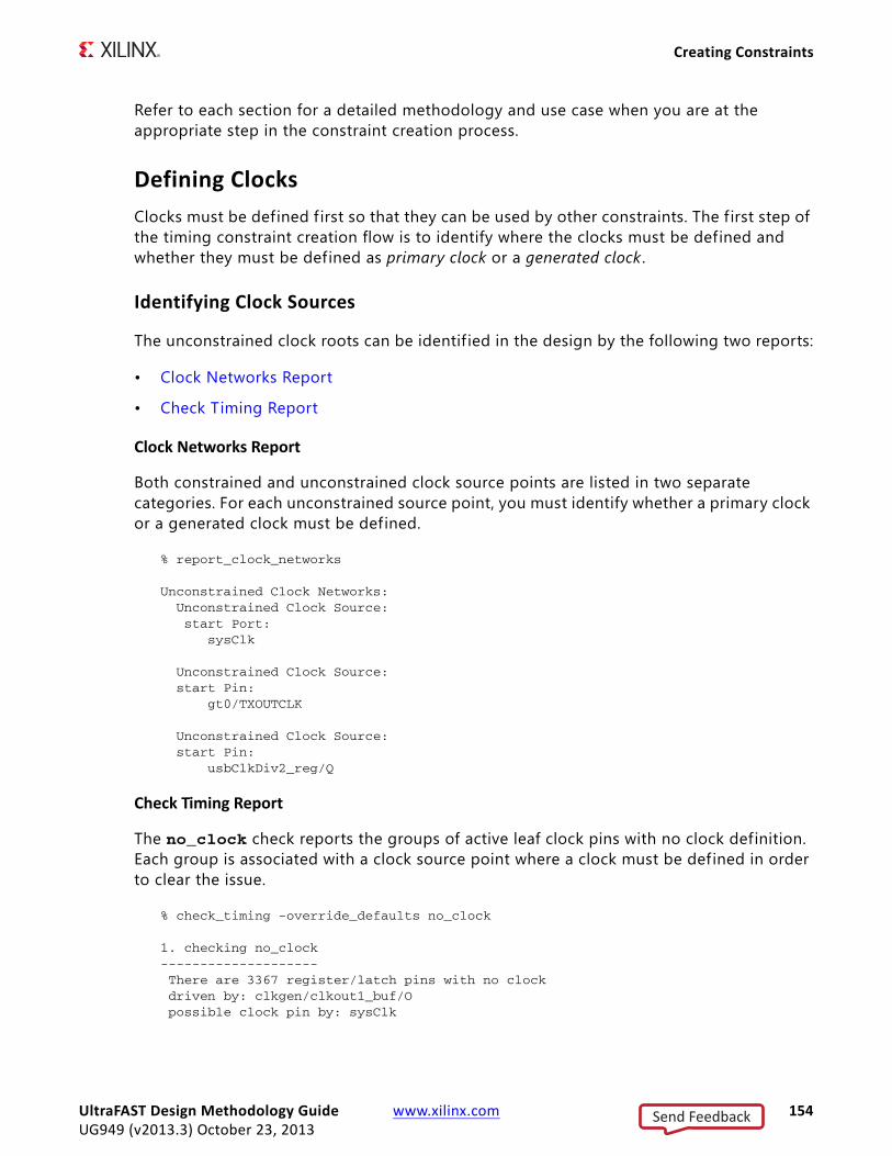
Creating Constraints
Refer to each section for a detailed methodology and use case when you are at the appropriate step in the constraint creation process.
Defining ClocksClocks must be defined f irst so that they can be used by other constraints. The f irst step of the timing constraint creation flow is to identify where the clocks must be defined and whether they must be defined as primary clock or a generated clock .
Identifying Clock Sources
The unconstrained clock roots can be identif ied in the design by the following two reports:
• Clock Networks Report
• Check Timing Report
Clock Networks Report
Both constrained and unconstrained clock source points are listed in two separate categories. For each unconstrained source point, you must identify whether a primary clock or a generated clock must be defined.
% report_clock_networks
Unconstrained Clock Networks: Unconstrained Clock Source: start Port: sysClk
Unconstrained Clock Source: start Pin: gt0/TXOUTCLK
Unconstrained Clock Source: start Pin: usbClkDiv2_reg/Q
Check Timing Report
The no_clock check reports the groups of active leaf clock pins with no clock definition. Each group is associated with a clock source point where a clock must be defined in order to clear the issue.
% check_timing -override_defaults no_clock
1. checking no_clock-------------------- There are 3367 register/latch pins with no clock driven by: clkgen/clkout1_buf/O possible clock pin by: sysClk
UltraFAST Design Methodology Guide www.xilinx.com 154UG949 (v2013.3) October 23, 2013
Send Feedback

Creating Constraints
There are 150 register/latch pins with no clock driven by: txoutclk_bufg_i/O possible clock pin by: gt0/TXOUTCLK
There are 8 register/latch pins with no clock driven by: usbClkDiv2_reg/Q possible clock pin by: usbClkDiv2_reg/Q
With check_timing, the same clock source pin or port can appear in several groups depending on the topology of the entire clock tree. In such case, creating a clock on the recommended source pin or port will resolve the missing clock definition for all the associated groups.
Creating Primary Clocks
A primary clock is a clock that defines a timing reference for your design and that is used by the timing engine to derive the timing path requirements and the phase relationship with other clocks. Their insertion delay is calculated from the clock source point (driver pin/port where the clock is defined) to the clock pins of the sequential cells to which it fans out.
For this reason, it is important to define the primary clocks on objects that correspond to the boundary of the design, so that their delay, and indirectly their skew, can be accurately computed.
Typical primary clock roots are:
• Input Ports
• Gigabit Transceiver Output Pins
• Certain Hardware Primitive Output Pins
Input Ports
Constraint example:
create_clock -name SysClk -period 10 -waveform {0 5} [get_ports sysclk]
X-Ref Target - Figure 4-15
Figure 4-15: create_clock for Input Ports
UltraFAST Design Methodology Guide www.xilinx.com 155UG949 (v2013.3) October 23, 2013
Send Feedback

Creating Constraints
In this example, the waveform is defined to have a 50% duty cycle. The -waveform argument is shown above to illustrate its usage and is only necessary to define a clock with a duty cycle other than 50%. For a differential clock input buffer, the primary clock only needs to be defined on the P-side of the pair.
Gigabit Transceiver Output Pins
Gigabit transceiver output pin, for example, a recovered clock, or:
Constraint example:
create_clock -name txclk -period 6.667 [get_pins gt0/TXOUTCLK]
Certain Hardware Primitive Output Pins
The output pin of certain hardware primitives (for example, BSCANE2) which does not have a timing arc from an input pin of the same primitive.
X-Ref Target - Figure 4-16
Figure 4-16: create_clock on a Primitive Pin
X-Ref Target - Figure 4-17
Figure 4-17: Clock Path Broken Due to a Missing Timing Arc
UltraFAST Design Methodology Guide www.xilinx.com 156UG949 (v2013.3) October 23, 2013
Send Feedback

Creating Constraints
IMPORTANT: No primary clock should be defined in the transitive fanout of another primary clock because this situation does not correspond to any hardware reality. It will also prevent proper timing analysis by preventing the complete clock insertion delay calculation. Any time this situation occurs, the constraints must be revisited and corrected.
Figure 4-18, create_clock in the Fanout of Another Clock is not Recommended, shows an example in which the clock clk1 is defined in the transitive fanout of the clock clk0: clk1 overrides clk0 starting at the output of BUFG1, where it is defined. As a consequence, the timing analysis between REGA and REGB will not be accurate because of the invalid skew computation between clk0 and clk1.
Creating Generated Clocks
A generated clock is a clock derived from another existing clock called the master clock. It usually describes a waveform transformation performed on the master clock by a logic block. Because the generated clock definition depends on the master clock characteristics, the master clock must be defined f irst. For explicitly defining a generated clock, the create_generated_clock command must be used.
Auto-Derived Clocks
Most generated clocks are automatically derived by the Vivado Design Suite timing engine which recognizes the Clock Modifying Blocks (CMB) and the transformation they perform on the master clocks. In the Xilinx 7 series device family, the CMBs are:
• MMCM*/ PLL*
• BUFR
• PHASER*
X-Ref Target - Figure 4-18
Figure 4-18: create_clock in the Fanout of Another Clock is not Recommended
UltraFAST Design Methodology Guide www.xilinx.com 157UG949 (v2013.3) October 23, 2013
Send Feedback
Creating Constraints
For any other combinatorial cell located on the clock tree, the timing clocks propagate through them and do not need to be redefined at their output, unless the waveform is transformed by the cell. In general, you must rely on the auto-derivation mechanism as much as possible as it provides the safest way to define the generated clocks that correspond to the actual hardware behavior.
If the auto-derived clock name chosen by the Vivado Design Suite timing engine does not seem appropriate, you can force your own name by using the create_generated_clock command without specifying the waveform transformation. This constraint should be located right after the constraint that defines the master clock in the constraint f ile. For example, if the default name of a clock generated by a MMCM instance is net0, you can add the following constraint to force your own name (fftClk in the given example):
create_generated_clock -name fftClk [get_pins mmcm_i/CLKOUT0]
To avoid any ambiguity, the constraint must be attached to the source pin of the clock. For more information, see Vivado Design Suite User Guide: Using Constraints (UG903) [Ref 16].
User-Defined Generated Clocks
Once all the primary clocks have been defined, you can use the Clock Networks or Check Timing (no_clock) reports to identify the clock tree portions that do not have a timing clock and define the generated clocks accordingly.
It is sometimes diff icult to understand the transformation performed by a cone of logic on the master clock. In this case, you must adopt the most conservative constraint. For example, the source pin is a sequential cell output. The master clock is at least divided by two, so the proper constraint should be, for example:
create_generated_clock -name clkDiv2 -divide_by 2 \-source [get_pins fd/C] [get_pins fd/Q]
Finally, if the design contains latches, the latch gate pins also need to be reached by a timing clock and will be reported by Check Timing (no_clock) if the constraint is missing. You can follow the examples above to define these clocks.
Path Between Master and Generated Clocks
Unlike primary clocks, generated clocks must be defined in the transitive fanout of their master clock, so that the timing engine can accurately compute their insertion delay. Failure to follow this rule will result in improper timing analysis and most likely in invalid slack computation. For example, in Figure 4-19, Generated Clock in the Fanout Of Master Clock, gen_clk_reg/Q is being used as a clock for the next flop (q_reg), and it is also in the fanout cone of the primary clock c1. Hence gen_clk_reg/Q should have a create_generated_clock on it, rather than a create_clock .
UltraFAST Design Methodology Guide www.xilinx.com 158UG949 (v2013.3) October 23, 2013
Send Feedback
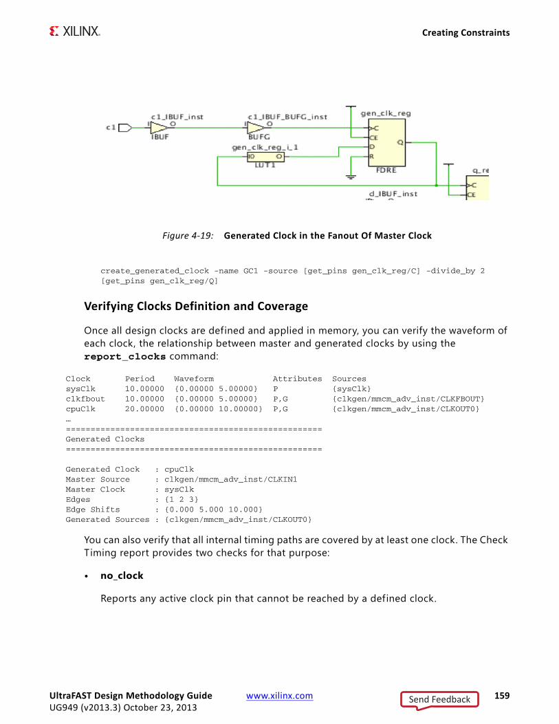
Creating Constraints
Figure 4-19: Generated Clock in the Fanout Of Master Clock
create_generated_clock -name GC1 -source [get_pins gen_clk_reg/C] -divide_by 2 [get_pins gen_clk_reg/Q]
Verifying Clocks Definition and Coverage
Once all design clocks are defined and applied in memory, you can verify the waveform of each clock, the relationship between master and generated clocks by using the report_clocks command:
Clock Period Waveform Attributes SourcessysClk 10.00000 {0.00000 5.00000} P {sysClk}clkfbout 10.00000 {0.00000 5.00000} P,G {clkgen/mmcm_adv_inst/CLKFBOUT}cpuClk 20.00000 {0.00000 10.00000} P,G {clkgen/mmcm_adv_inst/CLKOUT0}…====================================================Generated Clocks====================================================
Generated Clock : cpuClkMaster Source : clkgen/mmcm_adv_inst/CLKIN1Master Clock : sysClkEdges : {1 2 3}Edge Shifts : {0.000 5.000 10.000}Generated Sources : {clkgen/mmcm_adv_inst/CLKOUT0}
You can also verify that all internal timing paths are covered by at least one clock. The Check Timing report provides two checks for that purpose:
• no_clock
Reports any active clock pin that cannot be reached by a defined clock.
X-Ref Target - Figure 4-19
UltraFAST Design Methodology Guide www.xilinx.com 159UG949 (v2013.3) October 23, 2013
Send Feedback

Creating Constraints
• unconstrained_internal_endpoint
Reports all the data input pins of sequential cells that have a timing check relative to a clock but the clock has not been defined.
If both checks return zero, the timing analysis coverage will be high.
Adjusting Clock Characteristics
After defining the clocks and their waveform, the next step is to enter any information related to noise or uncertainty modeling. The XDC language differentiates uncertainty related to jitter and phase error from the one related to skew and delay modeling.
• Jitter
• Additional Uncertainty
• Clock Latency at the Source
• MMCM or PLL External Feedback Loop Delay
Jitter
For jitter, it is best to use the default values used by the Vivado Design Suite. You can modify the default computation as follows:
• If a different amount of jitter is coming into the device, use the set_input_jitter command on each primary clock.
• To adjust the global jitter if the device power supply is noisy, use set_system_jitter.
For generated clocks, the jitter is derived from the master clock and the characteristics of the clock modifying block. The user does not need to adjust these numbers.
Additional Uncertainty
When you need to add extra margin the timing paths of a clock or between two clocks, you must use the set_clock_uncertainty command. This is also the best and safest way to over-constrain a portion of a design without modifying the actual clock edges and the overall clocks relationships. The clock uncertainty defined by the user is additive to the jitter computed by the Vivado tools, and can be specif ied separately for setup and hold analyses.
For example, the margin on a design clock needs to be tightened by 500ps to make the design more robust to noise for both setup and hold:
set_clock_uncertainty -from clk0 -to clk0 0.500
UltraFAST Design Methodology Guide www.xilinx.com 160UG949 (v2013.3) October 23, 2013
Send Feedback

Creating Constraints
If you specify additional uncertainty between two clocks, the constraint must be applied in both directions (assuming data flows in both directions). The example below shows how to increase the uncertainty by 250ps between clk0 and clk1 for setup only:
set_clock_uncertainty -from clk0 -to clk1 0.250 -setupset_clock_uncertainty -from clk1 -to clk0 0.250 -setup
Clock Latency at the Source
It is possible to model the latency of a clock at its source by using the set_clock_latency command with the -source option. This is useful in two cases:
• To specify the clock delay propagation outside the device independently from the input and output delay constraints.
• To model the internal propagation latency of a clock used by a block during out-of-context compilation. In such a compilation flow, the complete clock tree is not described, so the variation between min and max operating conditions outside the block cannot be automatically computed and must be manually modeled.
This constraint should only be used by advanced users as it is usually diff icult to provide valid latency values.
MMCM or PLL External Feedback Loop Delay
When the MMCM or PLL feedback loop is connected for compensating a board delay instead of an internal clock insertion delay, you must specify the delay outside the FPGA device for both best and worst delay cases by using the set_external_delay command. Failure to specify this delay will make I/O timing analysis associated with the MMCM or PLL irrelevant and can potentially lead to an impossible timing closure situation. Also, when using external compensation, you must adjust the input and output delay constraint values accordingly instead of just considering the clock trace delay on the board like in normal cases.
Constraining Input and Output PortsIn addition to specifying the location and I/O standard for each port of the design, input and output delay constraints must be specified to describe the timing of external paths to/from the interface of the FPGA device. These delays are defined relatively to a clock that is usually also generated on the board and enters the FPGA device. In some cases, the delays must be defined related to an internal clock depending on the clock topology of the I/O path.
System Level Perspective
The I/O paths are modeled like any other reg-to-reg paths by the Vivado Design Suite timing engine, except that part of the path is located outside the FPGA device and needs to be described by the user. When analyzing internal paths, minimum and maximum delays are
UltraFAST Design Methodology Guide www.xilinx.com 161UG949 (v2013.3) October 23, 2013
Send Feedback

Creating Constraints
considered for both setup and hold analysis. This is also true for I/O paths. For this reason, it is important to describe both min and max delay conditions. The I/O timing paths are analyzed as single-cycle paths by default, which means:
• For max delay analysis (setup), the data is captured one clock cycle after the launch edge.
• For min delay analysis (hold), the data is launched and captured by the same clock edge.
If the relationship between the clock and I/O data must be timed differently, like for example in a source synchronous interface, different I/O delays and additional timing exceptions must be specif ied. This corresponds to an advanced I/O timing constraints scenario.
Defining Input Delays
The input delay is defined relative to a clock at the interface of the device. Unless set_clock_latency has been specif ied on the source pin of the reference clock, the input delay corresponds to the absolute time from the launch edge, through the clock trace, the external device and the data trace. If clock latency has already been specified separately, you can ignore the clock trace delay.
The input delay values for the both types of analysis are:
Input Delay(max) = Tco(max) + Ddata(max) + Dclock_to_ExtDev(max) - Dclock_to_FPGA(min)Input Delay(min) = Tco(min) + Ddata(min) + Dclock_to_ExtDev(min) - Dclock_to_FPGA(max)
Figure 4-21, Interpreting Min and Max Input Delays, shows a simple example of input delay constraints for both setup (max) and hold (min) analysis, assuming the sysClk clock has already been defined on the CLK port:
set_input_delay -max -clock sysClk 5.4 [get_ports DIN]set_input_delay -min -clock sysClk 2.1 [get_ports DIN]
X-Ref Target - Figure 4-20
Figure 4-20: Input Delay Computation
UltraFAST Design Methodology Guide www.xilinx.com 162UG949 (v2013.3) October 23, 2013
Send Feedback

Creating Constraints
A negative input delay means that the data arrives at the interface of the device before the launch clock edge.
Defining Output Delays
Output delays are similar to input delays, except that they refer to the output path minimum and maximum time outside the FPGA device in order to be functional under all conditions.
The output delay values for the both types of analysis are:
Output Delay(max) = Tsetup + Ddata(max) + Dclock_to_FPGA(max) - Dclock_to_ExtDev(min)Output Delay(min) = Thold + Ddata(min) + Dclock_to_FPGA(min) - Dclock_to_ExtDev(max)
Figure 4-23, Interpreting Min and Max Output Delays, shows a simple example of output delay constraints for both setup (max) and hold (min) analyses, assuming the sysClk clock has already been defined on the CLK port:
set_output_delay -max -clock sysClk 2.4 [get_port, s DOUT]
X-Ref Target - Figure 4-21
Figure 4-21: Interpreting Min and Max Input Delays
X-Ref Target - Figure 4-22
Figure 4-22: Output Delay Computation
UltraFAST Design Methodology Guide www.xilinx.com 163UG949 (v2013.3) October 23, 2013
Send Feedback
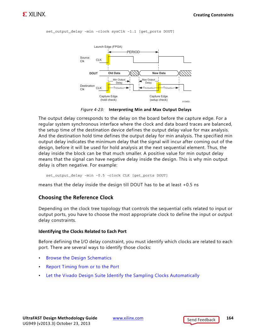
Creating Constraints
set_output_delay -min -clock sysClk -1.1 [get_ports DOUT]
The output delay corresponds to the delay on the board before the capture edge. For a regular system synchronous interface where the clock and data board traces are balanced, the setup time of the destination device defines the output delay value for max analysis. And the destination hold time defines the output delay for min analysis. The specified min output delay indicates the minimum delay that the signal will incur after coming out of the design, before it will be used for hold analysis at the next sequential element. Thus, the delay inside the block can be that much smaller. A positive value for min output delay means that the signal can have negative delay inside the design. This is why min output delay is often negative. For example:
set_output_delay -min -0.5 -clock CLK [get_ports DOUT]
means that the delay inside the design till DOUT has to be at least +0.5 ns
Choosing the Reference Clock
Depending on the clock tree topology that controls the sequential cells related to input or output ports, you have to choose the most appropriate clock to define the input or output delay constraints.
Identifying the Clocks Related to Each Port
Before defining the I/O delay constraint, you must identify which clocks are related to each port. There are several ways to identify those clocks:
• Browse the Design Schematics
• Report Timing from or to the Port
• Let the Vivado Design Suite Identify the Sampling Clocks Automatically
X-Ref Target - Figure 4-23
Figure 4-23: Interpreting Min and Max Output Delays
UltraFAST Design Methodology Guide www.xilinx.com 164UG949 (v2013.3) October 23, 2013
Send Feedback
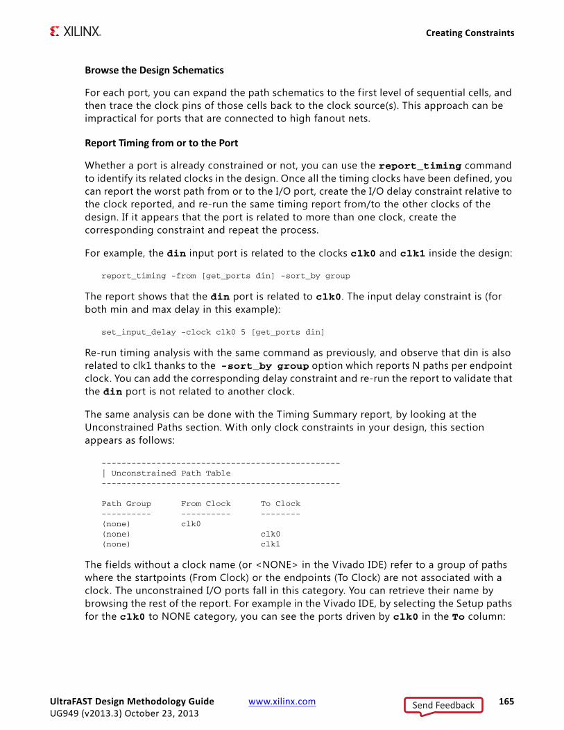
Creating Constraints
Browse the Design Schematics
For each port, you can expand the path schematics to the first level of sequential cells, and then trace the clock pins of those cells back to the clock source(s). This approach can be impractical for ports that are connected to high fanout nets.
Report Timing from or to the Port
Whether a port is already constrained or not, you can use the report_timing command to identify its related clocks in the design. Once all the timing clocks have been defined, you can report the worst path from or to the I/O port, create the I/O delay constraint relative to the clock reported, and re-run the same timing report from/to the other clocks of the design. If it appears that the port is related to more than one clock, create the corresponding constraint and repeat the process.
For example, the din input port is related to the clocks clk0 and clk1 inside the design:
report_timing -from [get_ports din] -sort_by group
The report shows that the din port is related to clk0. The input delay constraint is (for both min and max delay in this example):
set_input_delay -clock clk0 5 [get_ports din]
Re-run timing analysis with the same command as previously, and observe that din is also related to clk1 thanks to the -sort_by group option which reports N paths per endpoint clock. You can add the corresponding delay constraint and re-run the report to validate that the din port is not related to another clock.
The same analysis can be done with the Timing Summary report, by looking at the Unconstrained Paths section. With only clock constraints in your design, this section appears as follows:
------------------------------------------------| Unconstrained Path Table------------------------------------------------
Path Group From Clock To Clock ---------- ---------- -------- (none) clk0 (none) clk0 (none) clk1
The fields without a clock name (or <NONE> in the Vivado IDE) refer to a group of paths where the startpoints (From Clock) or the endpoints (To Clock) are not associated with a clock. The unconstrained I/O ports fall in this category. You can retrieve their name by browsing the rest of the report. For example in the Vivado IDE, by selecting the Setup paths for the clk0 to NONE category, you can see the ports driven by clk0 in the To column:
UltraFAST Design Methodology Guide www.xilinx.com 165UG949 (v2013.3) October 23, 2013
Send Feedback
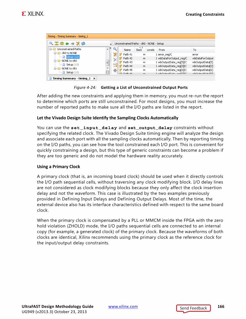
Creating Constraints
After adding the new constraints and applying them in memory, you must re-run the report to determine which ports are still unconstrained. For most designs, you must increase the number of reported paths to make sure all the I/O paths are listed in the report.
Let the Vivado Design Suite Identify the Sampling Clocks Automatically
You can use the set_input_delay and set_output_delay constraints without specifying the related clock. The Vivado Design Suite timing engine will analyze the design and associate each port with all the sampling clocks automatically. Then by reporting timing on the I/O paths, you can see how the tool constrained each I/O port. This is convenient for quickly constraining a design, but this type of generic constraints can become a problem if they are too generic and do not model the hardware reality accurately.
Using a Primary Clock
A primary clock (that is, an incoming board clock) should be used when it directly controls the I/O path sequential cells, without traversing any clock modifying block. I/O delay lines are not considered as clock modifying blocks because they only affect the clock insertion delay and not the waveform. This case is illustrated by the two examples previously provided in Defining Input Delays and Defining Output Delays. Most of the time, the external device also has its interface characteristics defined with respect to the same board clock.
When the primary clock is compensated by a PLL or MMCM inside the FPGA with the zero hold violation (ZHOLD) mode, the I/O paths sequential cells are connected to an internal copy (for example, a generated clock) of the primary clock. Because the waveforms of both clocks are identical, Xilinx recommends using the primary clock as the reference clock for the input/output delay constraints.
X-Ref Target - Figure 4-24
Figure 4-24: Getting a List of Unconstrained Output Ports
UltraFAST Design Methodology Guide www.xilinx.com 166UG949 (v2013.3) October 23, 2013
Send Feedback
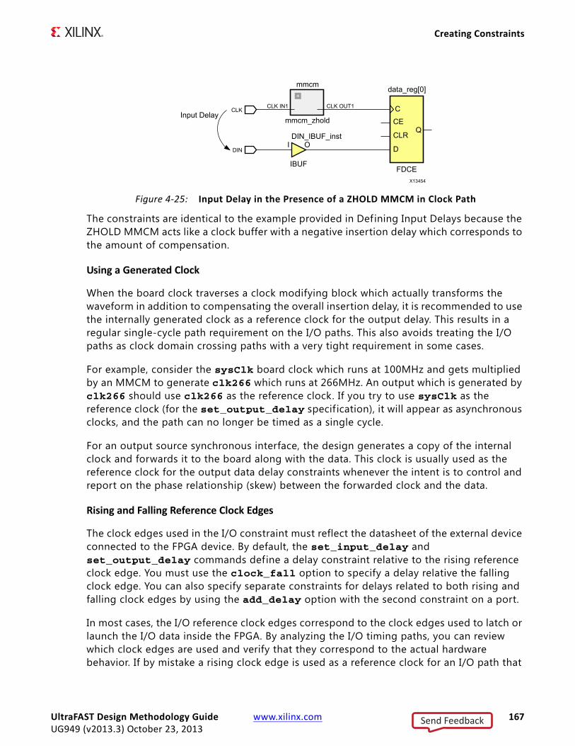
Creating Constraints
The constraints are identical to the example provided in Defining Input Delays because the ZHOLD MMCM acts like a clock buffer with a negative insertion delay which corresponds to the amount of compensation.
Using a Generated Clock
When the board clock traverses a clock modifying block which actually transforms the waveform in addition to compensating the overall insertion delay, it is recommended to use the internally generated clock as a reference clock for the output delay. This results in a regular single-cycle path requirement on the I/O paths. This also avoids treating the I/O paths as clock domain crossing paths with a very tight requirement in some cases.
For example, consider the sysClk board clock which runs at 100MHz and gets multiplied by an MMCM to generate clk266 which runs at 266MHz. An output which is generated by clk266 should use clk266 as the reference clock. If you try to use sysClk as the reference clock (for the set_output_delay specif ication), it will appear as asynchronous clocks, and the path can no longer be timed as a single cycle.
For an output source synchronous interface, the design generates a copy of the internal clock and forwards it to the board along with the data. This clock is usually used as the reference clock for the output data delay constraints whenever the intent is to control and report on the phase relationship (skew) between the forwarded clock and the data.
Rising and Falling Reference Clock Edges
The clock edges used in the I/O constraint must reflect the datasheet of the external device connected to the FPGA device. By default, the set_input_delay and set_output_delay commands define a delay constraint relative to the rising reference clock edge. You must use the clock_fall option to specify a delay relative the falling clock edge. You can also specify separate constraints for delays related to both rising and falling clock edges by using the add_delay option with the second constraint on a port.
In most cases, the I/O reference clock edges correspond to the clock edges used to latch or launch the I/O data inside the FPGA. By analyzing the I/O timing paths, you can review which clock edges are used and verify that they correspond to the actual hardware behavior. If by mistake a rising clock edge is used as a reference clock for an I/O path that
X-Ref Target - Figure 4-25
Figure 4-25: Input Delay in the Presence of a ZHOLD MMCM in Clock Path
UltraFAST Design Methodology Guide www.xilinx.com 167UG949 (v2013.3) October 23, 2013
Send Feedback

Creating Constraints
is only related to the falling clock edge internally, the path requirement is ½-period, which makes timing closure more diff icult.
Verifying Delay Constraints
Once the I/O timing constraints have been entered, it is important to review how timing is analyzed on the I/O paths and the amount of slack violation for both setup and hold checks. By using the timing reports from/to all ports for both setup and hold analysis (that is, delay type = min_max), you can verify that:
• The correct clocks and clock edges are used as reference for the delay constraints
• The expected clocks are launching and capturing the I/O data inside the FPGA device
• The violations can reasonably be f ixed by placement or by setting the proper delay line tap configuration. If this is not the case, you must review the I/O delay values entered in the constraints and evaluate whether they are realistic, and whether you must modify the design to meet timing.
I/O Path Report Command Lines Example
report_timing -from [all_inputs] -nworst 1000 -sort_by group \-delay_type min_max
report_timing -to [all_outputs] -nworst 1000 -sort_by group \-delay_type min_max
Improper I/O delay constraints can lead to impossible timing closure. The implementation tools are timing driven and work on optimizing the placement and routing to meet timing. If the I/O path requirements cannot be met and I/O paths have the worst violations in the design, the overall design QoR will be impacted.
Input to Output Feed-through Path
There are several equivalent ways to constrain a combinatorial path from an input port to an output port.
Example One
Use a virtual clock with a period greater or equal to the target maximum delay for the feed-through path, and apply max input and output delay constraints as follows:
create_clock -name vclk -period 10set_input_delay -clock vclk <input_delay_val> [get_ports din] -maxset_output_delay -clock vclk <output_delay_val> [get_ports dout] -max
where
input_delay_val + maximum feedthrough path delay + output_delay_val= vclk period.
UltraFAST Design Methodology Guide www.xilinx.com 168UG949 (v2013.3) October 23, 2013
Send Feedback

Creating Constraints
In this example, only the maximum delay is constrained.
Example Two
Use a combination of min and max delay constraints between the feedthrough ports. Example:
set_max_delay -from [get_ports din] -to [get_ports dout] 10set_min_delay -from [get_ports din] -to [get_ports dout] 2
This is a simple way to constrain both minimum and maximum delays on the path. Any existing input and output delay constraints on the same ports are also used during the timing analysis. For this reason, this style is not very popular.
The max delay is usually optimized and reported against the Slow timing corner, while the min delay is in the Fast timing corner. It is best to run a few iterations on the feedthrough path delay constraints to validate that they are reasonable and can be met by the implementation tools, especially if the ports are placed far from one another.
Using XDC Templates - Source Synchronous Interfaces
While most users can properly write timing constraints for system synchronous interfaces, Xilinx recommends using I/O constraint templates for the source synchronous interfaces. The source synchronous constraints can be written in several ways. The templates provided by the Vivado Design Suite are based on the default timing analysis path requirement. The syntax is simpler, but the delay values must be adjusted to account for how the analysis is done. The timing reports can be more diff icult to read as the clock edges do not directly correspond to the active ones in hardware. You can navigate to these templates in Vivado GUI through Window > Language Templates > XDC > TimingConstraints > Input Delay Constraints > Source Synchronous.
Defining Clock Groups and CDC ConstraintsThe Vivado IDE times the paths between all the clocks in your design by default. The set_clock_groups command disables timing analysis between groups of clocks that you identify, and not between the clocks within a same group. Unlike set_clock_groups, the set_false_path constraint ignores timing between the clocks only in the direction specified by the from and to options. In some specif ic cases, maximum delay constraints can be set on Clock Domain Crossing (CDC) paths in order to limit the latency of these paths, on one or several signals. If clock groups or false path constraints already exist between the clocks or on the same CDC paths, the maximum delay constraints will be ignored. For this reason, it is important to thoroughly review every path between all clock pairs before choosing one CDC timing constraint over another one in order to avoid constraints collision.
UltraFAST Design Methodology Guide www.xilinx.com 169UG949 (v2013.3) October 23, 2013
Send Feedback
Creating Constraints
Reviewing Clock Interactions
Clocks that have a logical path between them are timed. The possible clock relationships are:
• Synchronous
• Asynchronous
• Exclusive
Synchronous
Clock relationships are synchronous when two clocks have a fixed phase relationship. This is the case when:
• They share common circuitry (common node), or
• They share the same primary clock (same initial phase).
Asynchronous
Clock relationships are asynchronous when they do not have a fixed phase relationship. This is the case when one of the following is true:
• They do not share any common circuitry in the design and do not have a common primary clock.
• They do not have a common period within 1000 cycles (unexpandable) and the timing engine cannot properly time them together.
Exclusive
Clock relationships are exclusive when they propagate on a same clock tree and reach the same sequential cell clock pins but cannot physically be active at the same time.
Categorizing Clock Pairs
The clock pairs can be categorized by using two specif ic reports:
• Clock Interaction Report
• Check Timing Report
Clock Interaction Report
The Clock Interaction report provides a high-level summary of how two clocks are timed together:
• Do the two clocks have a common primary clock? When clocks are properly defined, all clocks that originate from the same source in the design share the same primary clock.
UltraFAST Design Methodology Guide www.xilinx.com 170UG949 (v2013.3) October 23, 2013
Send Feedback
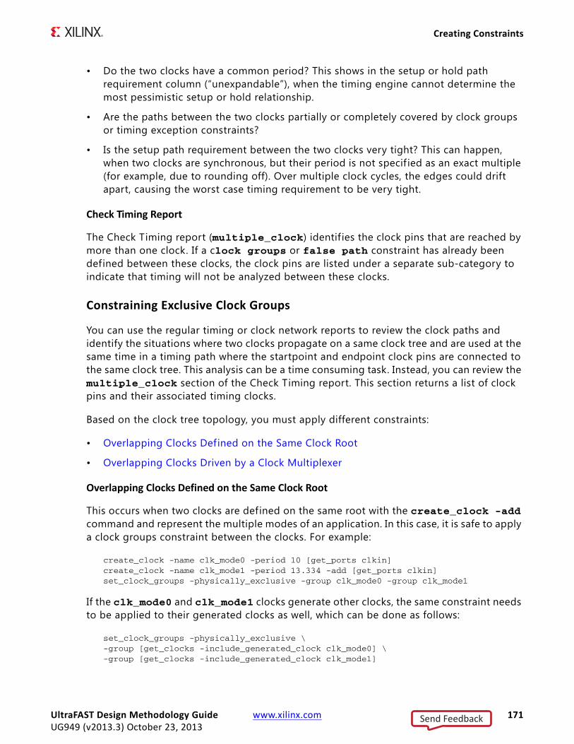
Creating Constraints
• Do the two clocks have a common period? This shows in the setup or hold path requirement column (“unexpandable”), when the timing engine cannot determine the most pessimistic setup or hold relationship.
• Are the paths between the two clocks partially or completely covered by clock groups or timing exception constraints?
• Is the setup path requirement between the two clocks very tight? This can happen, when two clocks are synchronous, but their period is not specif ied as an exact multiple (for example, due to rounding off). Over multiple clock cycles, the edges could drift apart, causing the worst case timing requirement to be very tight.
Check Timing Report
The Check Timing report (multiple_clock) identif ies the clock pins that are reached by more than one clock. If a clock groups or false path constraint has already been defined between these clocks, the clock pins are listed under a separate sub-category to indicate that timing will not be analyzed between these clocks.
Constraining Exclusive Clock Groups
You can use the regular timing or clock network reports to review the clock paths and identify the situations where two clocks propagate on a same clock tree and are used at the same time in a timing path where the startpoint and endpoint clock pins are connected to the same clock tree. This analysis can be a time consuming task. Instead, you can review the multiple_clock section of the Check Timing report. This section returns a list of clock pins and their associated timing clocks.
Based on the clock tree topology, you must apply different constraints:
• Overlapping Clocks Defined on the Same Clock Root
• Overlapping Clocks Driven by a Clock Multiplexer
Overlapping Clocks Defined on the Same Clock Root
This occurs when two clocks are defined on the same root with the create_clock -add command and represent the multiple modes of an application. In this case, it is safe to apply a clock groups constraint between the clocks. For example:
create_clock -name clk_mode0 -period 10 [get_ports clkin]create_clock -name clk_mode1 -period 13.334 -add [get_ports clkin]set_clock_groups -physically_exclusive -group clk_mode0 -group clk_mode1
If the clk_mode0 and clk_mode1 clocks generate other clocks, the same constraint needs to be applied to their generated clocks as well, which can be done as follows:
set_clock_groups -physically_exclusive \-group [get_clocks -include_generated_clock clk_mode0] \-group [get_clocks -include_generated_clock clk_mode1]
UltraFAST Design Methodology Guide www.xilinx.com 171UG949 (v2013.3) October 23, 2013
Send Feedback
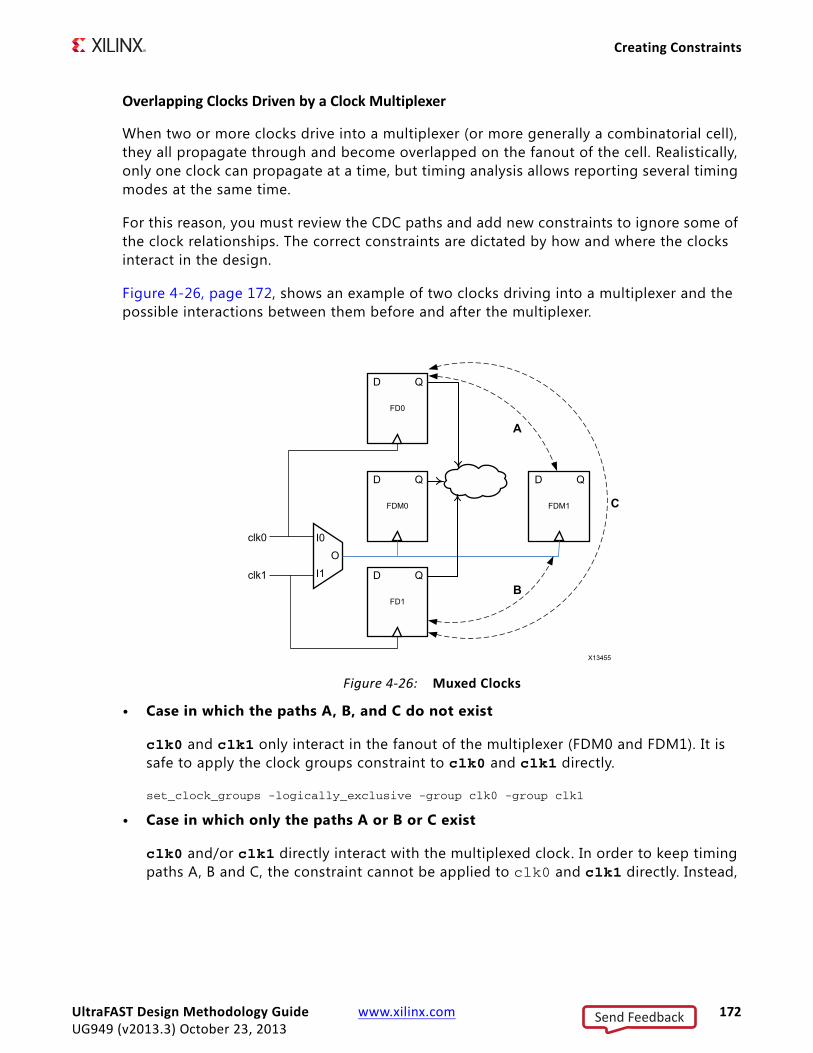
Creating Constraints
Overlapping Clocks Driven by a Clock Multiplexer
When two or more clocks drive into a multiplexer (or more generally a combinatorial cell), they all propagate through and become overlapped on the fanout of the cell. Realistically, only one clock can propagate at a time, but timing analysis allows reporting several timing modes at the same time.
For this reason, you must review the CDC paths and add new constraints to ignore some of the clock relationships. The correct constraints are dictated by how and where the clocks interact in the design.
Figure 4-26, page 172, shows an example of two clocks driving into a multiplexer and the possible interactions between them before and after the multiplexer.
• Case in which the paths A, B, and C do not exist
clk0 and clk1 only interact in the fanout of the multiplexer (FDM0 and FDM1). It is safe to apply the clock groups constraint to clk0 and clk1 directly.
set_clock_groups -logically_exclusive -group clk0 -group clk1
• Case in which only the paths A or B or C exist
clk0 and/or clk1 directly interact with the multiplexed clock. In order to keep timing paths A, B and C, the constraint cannot be applied to clk0 and clk1 directly. Instead,
X-Ref Target - Figure 4-26
Figure 4-26: Muxed Clocks
UltraFAST Design Methodology Guide www.xilinx.com 172UG949 (v2013.3) October 23, 2013
Send Feedback

Creating Constraints
it must be applied to the portion of the clocks in the fanout of the multiplexer, which requires additional clock definitions.
create_generated_clock -name clk0mux -divide_by 1 \-source [get_pins mux/I0] [get_pins mux/O]
create_generated_clock -name clk1mux -divide_by 1 \-add -master_clock clk1 \
-source [get_pins mux/I1] [get_pins mux/O]
set_clock_groups -physically_exclusive -group clk0mux -group clk1mux
Constraining Asynchronous Clock Groups and Clock Domain Crossings
The asynchronous relationship can be quickly identif ied in the Clock Interaction report: clock pairs with no common primary clock or no common period (unexpanded). Even if clock periods are same (related), the clocks will still be asynchronous, if they are being generated from different sources. The asynchronous Clock Domain Crossing (CDC) paths must be reviewed carefully to ensure that they use proper synchronization circuitry that does not rely on timing correctness and that minimizes the chance for metastability to occur. Asynchronous CDC paths usually have high skew and/or unrealistic path requirements. They should not be timed with the default timing analysis, which cannot prove they will be functional in hardware. Specif ic constraints should be applied:
• Global Constraints Between Clocks in Both Directions
• Constraints on Individual CDC Paths
Global Constraints Between Clocks in Both Directions
When there is no need to limit the maximum latency, the clock groups can be used. Following is an example to ignore paths between clkA and clkB:
set_clock_groups -asynchronous -group clkA -group clkB
When two master clocks and their respective generated clocks form two asynchronous domains between which all the paths are properly synchronized, the clock groups constraint can be applied to several clocks at once:
set_clock_groups -asynchronous \-group {clkA clkA_gen0 clkB_gen1 …} \-group {clkB clkB_gen0 clkB_gen1 …}
Or simply:
set_clock_groups -asynchronous \-group [get_clocks -include_generated_clock clkA] \-group [get_clocks -include_generated_clock clkB]
UltraFAST Design Methodology Guide www.xilinx.com 173UG949 (v2013.3) October 23, 2013
Send Feedback
Creating Constraints
Constraints on Individual CDC Paths
If a CDC bus uses gray-coding or if latency needs to be limited between the two asynchronous clocks on one or more signals, you must use the Max Delay Datapath Only constraint to ignore clock skew and jitter on these paths, plus override the default path requirement by the latency requirement. It is usually suff icient to use the source clock period for the max delay value, just to ensure that no more than one data is present on the CDC path at any given time.
When the ratio between clock periods is high, choosing the minimum of the source and destination clock periods is also a good option to reduce the transfer latency. A clean asynchronous CDC path should not have any logic between the source and destination sequential cells, so the Max Delay Datapath Only constraint is normally easy to meet for the implementation tools.
For the paths that do not need latency control, you can define a point-to-point false path constraint.
When writing the CDC constraints, verify that the precedence is respected. If you use set_max_delay -datapath_only on at least one path between two clocks, the set_clock_groups constraint cannot be used between the same clocks, and the set_false_path constraint can only be used on the other paths between the two clocks.
In Figure 4-27, Multiple Interactions Between Two Asynchronous Clocks, the clock clk0 has a period of 5ns and is asynchronous to clk1. There are two paths from clk0 domain to clk1 domain. The first path is a 1-bit data synchronization. The second path is a multi-bit gray-coded bus transfer.
X-Ref Target - Figure 4-27
Figure 4-27: Multiple Interactions Between Two Asynchronous Clocks
UltraFAST Design Methodology Guide www.xilinx.com 174UG949 (v2013.3) October 23, 2013
Send Feedback

Creating Constraints
The designer decides that the gray-coded bus transfer requires a Max Delay Datapath Only to limit the delay variation among the bits, so it becomes impossible to use a Clock Groups or False Path constraint between the clocks directly. Instead, two constraints must be defined:
set_max_delay -from [get_cells GCB0[*]] -to [get_cells [GCB1a[*]] \-datapath_only 5set_false_path -from [get_cells REG0] -to [get_cells REG1a]
There is no need to set a false path from clk1 to clk0 because there is no path in this example.
Specifying ExceptionsTiming exceptions are used to modify how timing analysis is done on specif ic paths. By default, the timing engine assumes that all paths should be timed with a single cycle requirement for setup analysis in order to cover the most pessimistic clocking scenario. For certain paths, this is not true. Following are a few examples:
• Asynchronous Clock Domain Crossing paths cannot be safely timed due to the lack of f ixed phase relationship between the clocks. They should be ignored (Clock Groups, False Path), or simply have datapath delay constraint (Max Delay Datapath Only)
• The sequential cells launch and capture edges are not active at every clock cycle, so the path requirement can be relaxed accordingly (Multicycle Path)
• The path delay requirement needs to be tightened in order to increase the design margin in hardware (Max Delay)
• A path through a combinatorial cell is static and does not need to be timed (False Path, Case Analysis)
• The analysis should be done with only a particular clock driven by a multiplexer (Case Analysis).
In any case, timing exceptions must be used carefully and must not be added to hide real timing problems.
Timing Exceptions Guidelines
Use a limited number of timing exceptions and keep them simple whenever possible. Otherwise, you will be facing two main challenges:
• The runtime of the compilation flow will signif icantly increase when many exceptions are used, especially when they are attached to a large number of netlist objects.
• Constraints debugging becomes extremely complicated when several exceptions cover the same paths.
Following is an example of timing exceptions that can negatively impact the runtime:
UltraFAST Design Methodology Guide www.xilinx.com 175UG949 (v2013.3) October 23, 2013
Send Feedback
Creating Constraints
set_false_path -from [get_ports din] -to [all_registers]
• If the din port does not have an input delay, it is not constrained. So there is no need to add a false path.
• If the din port feeds only to sequential elements, there is no need to specify the false path to the sequential cells explicitly. This constraint can be written more eff iciently:
set_false_path -from [get_ports din]
• If the false path is needed, but only a few paths exist from the din port to any sequential cell in the design, then it can be more specif ic (all_registers can potentially return thousands of cells, depending upon the number of registers used in the design):
set_false_path -from [get_ports din] \-to [get_cells blockA/config_reg[*]]
Timing Exceptions Precedence and Priority Rules
Timing exceptions are subject to strict precedence and priority rules. The most important rules are:
• The more specif ic the constraint, the higher the priority. For example:
set_max_delay -from [get_clocks clkA] -to [get_pins inst0/D] 12set_max_delay -from [get_clocks clkA] -to [get_clocks clkB] 10
The first set_max_delay constraint has a higher priority because the -to option uses a pin, which is more specif ic than a clock.
• The exceptions priority is as follows:
1. set_false_path
2. set_max_delay or set_min_delay
3. set_multicycle_path
The set_clock_groups command is not considered a timing exception even though it is equivalent to two set_false_path commands between two clocks. It has higher precedence than the timing exceptions.
The set_case_analysis and set_disable_timing commands disable timing analysis on specif ic portions of the design. They have higher precedence than the timing exceptions.
Adding False Path Constraints
False path exceptions can be added to timing paths to ignore slack computation on these paths. It is usually diff icult to prove that a path does not need timing to be functional, even
UltraFAST Design Methodology Guide www.xilinx.com 176UG949 (v2013.3) October 23, 2013
Send Feedback

Creating Constraints
with simulation tools. Xilinx does not usually recommend using a false path unless the risk associated with it has been properly assessed and appear to be acceptable.
Use Cases
The typical cases for using the false path constraint are:
• Ignoring timing on a path that is never active. For example, a path that crosses two multiplexers that can never let the data propagate in a same clock cycle because of the select pins connectivity.
set_false_path -through [get_pins MUX0/I0] -through [get_pins MUX1/I1]
• Ignoring timing on an asynchronous CDC path. This case is already discussed in the Defining Clock Groups and CDC Constraints section.
• Ignoring static paths in the design. Some registers take a value once during the initialization phase of the application and never toggle again. When they appear to be on the critical path of the design, they can be ignored for timing in order to relax the constraints on the implementation tools and help with timing closure. It is sufficient to define a false path constraint from the static register only, without explicitly specifying the paths endpoints. Example: the paths from a 32-bit configuration register config_reg[31..0] to the rest of the design can be ignored by adding the following false path constraint:
set_false_path -from [get_cells config_reg[*]]
Impact on Synthesis
The false path constraint is supported by synthesis and will only impact max delay (setup/recovery) path optimization. It is usually not needed to use false path exceptions during synthesis except for ignoring CDC paths.
Impact on Implementation
All the implementation steps are sensitive to the false path timing exception.
X-Ref Target - Figure 4-28
Figure 4-28: Path Cannot be Sensitized
UltraFAST Design Methodology Guide www.xilinx.com 177UG949 (v2013.3) October 23, 2013
Send Feedback

Creating Constraints
Adding Min and Max Delay Constraints
The min and max delay exceptions are used to override the default path requirement respectively for hold/removal and setup/recovery checks by replacing the launch and capture edge times with the delay value from the constraint.
Use Cases
Common reasons for using the min or max delay constraints are for:
• Over-constraining a few paths of the design by tightening the setup/recovery path requirement.
This is useful for forcing the logic optimization or placement tools to work harder on some critical path cells, which can provide more flexibility to the router to meet timing later on (after removing the max delay constraint).
• Replacing a multicycle constraint.
This is a valid, but not the recommended, way to relax the setup requirement on a path that has active launch and capture edges every N clock cycles. Although it is the only option to over-constrain a multicycle path by a fraction of a clock period to help with timing closure during the routing step. For example, a path with a multicycle constraint of 3 appears to be the worst violating path after route and fails timing by a few hundred ps.
The original multicycle path constraint can be replaced by the following constraint during optimization and placement:
set_max_delay -from [get_pins <startpointCell>/C] \-to [get_pins <endpointCell>/D] 14.5
where
14.5 corresponds to 3 clock periods, minus 500ps that correspond to amount of extra margin desired.
• Constraining the maximum datapath delay on asynchronous CDC paths.
This technique has already been described in Defining Clock Groups and CDC Constraints.
It is not common or recommended to force extra delay insertion on a path by using the set_min_delay constraint. The default min delay requirement for hold or removal is usually sufficient to ensure proper hardware functionality when the slack is positive.
Impact on Synthesis
The set_max_delay constraint is supported by synthesis, including the -datapath_only option. The set_min_delay constraint is ignored.
UltraFAST Design Methodology Guide www.xilinx.com 178UG949 (v2013.3) October 23, 2013
Send Feedback

Creating Constraints
Impact on Implementation
The set_max_delay constraint replaces the setup path requirement and influences the entire implementation flow. The set_min_delay constraint replaces the hold path requirement and only affects the router behavior whenever it introduces the need to fix hold.
Avoiding Path Segmentation
Path segmentation is introduced when specifying invalid startpoint or endpoint for the -from or -to options of the set_max_delay and set_min_delay commands only. When a set_max_delay introduces path segmentation on a path, the default hold analysis no longer takes place. You must constrain the same path with set_min_delay if you desire to constrain the hold analysis as well. The same rule applies with the set_min_delay command relative to the setup analysis.
Path segmentation must only be used by experts as it alters the fundamentals of timing analysis:
• Path segmentation breaks clock skew computation on the segmented path.
• Path segmentation can break more paths than the one constrained by the segmenting set_max_delay or set_min_delay command.
Path segmentation is reported by the tools in the log f ile when the constraints are applied. You must avoid it by using valid startpoints and endpoints:
• Startpoints
clock, clock pin, sequential cell (implies valid startpoint pins of the cell), input or inout port
• Endpoints
clock, input data pin of sequential cell, sequential cell (implies valid endpoint pins of the cell), output or inout port
Adding Multicycle Path ConstraintsMulticycle path exceptions must reflect the design functionality and must be applied on paths that do not have an active clock edge at every cycle, on either the source clock, the destination clock or both clocks. The path multiplier is expressed in term of clock cycles, either based on the source clock when the -start option is used, or the destination clock when the -end option is used. This is particularly convenient for modifying the setup and hold relationships between the startpoint and endpoint independently of the clock period value.
The hold relationships are always tied to the setup ones. Consequently, in most cases, the hold relationship also needs to be separately adjusted after the setup one has been
UltraFAST Design Methodology Guide www.xilinx.com 179UG949 (v2013.3) October 23, 2013
Send Feedback

Creating Constraints
modified. This is why a second constraint with the -hold option is needed. The main exception to this rule is for synchronous CDC paths between phase-shifted clocks: only setup needs to be modified. An example is provided in the Use Cases below.
Multicycle Path Exception Use Cases
There are two main categories of multicycle path exception use cases:
• Relaxing the Setup Requirement While Keeping Hold Unchanged
• Adjusting the Setup Edges Analysis on Paths Between Shifted Clocks.
Relaxing the Setup Requirement While Keeping Hold Unchanged
This occurs when the source and destination sequential cells are controlled by a clock enable signal that activates the clock every N cycles. Following are three examples:
• Example One: Same clock for both startpoint and endpoint, with a clock enable active every 3 cycles.
• Example Two: Path from a slow clock to a fast clock
• Example Three: Path from a fast clock to a slow clock
Example One: Same clock for both startpoint and endpoint, with a clock enable active every 3 cycles.
X-Ref Target - Figure 4-29
Figure 4-29: Enabled Flops with Same Clock Signal
UltraFAST Design Methodology Guide www.xilinx.com 180UG949 (v2013.3) October 23, 2013
Send Feedback

Creating Constraints
Constraints
set_multicycle_path -from [get_pins REGA/C] -to [get_pins REGB/D] -setup 3set_multicycle_path -from [get_pins REGA/C] -to [get_pins REGB/D] -hold 2
Note: With the f irst command, as the setup capture edge moved to the third edge (that is, by 2 cycles from its default position), the hold edge also moved by 2 cycles. The second command is for bringing the hold edge back to its original location by moving it again by 2 cycles (in the reverse direction).
Example Two: Path from a slow clock to a fast clock
In this case, assume that only the destination flip-flop is controlled by a clock enable, and the clock enable is always active at the same time as the slow clock rising edge. The path multiplier for setup is 3.
X-Ref Target - Figure 4-30
Figure 4-30: Timing Diagram for Setup/Hold Check
X-Ref Target - Figure 4-31
Figure 4-31: Setup/Hold Checks Modified After Multi-cycle Specification
UltraFAST Design Methodology Guide www.xilinx.com 181UG949 (v2013.3) October 23, 2013
Send Feedback

Creating Constraints
Constraints
set_multicycle_path -from [get_pins REG0/C] -to [get_pins REG1/D] -setup 3 -endset_multicycle_path -from [get_pins REG0/C] -to [get_pins REG1/D] -hold 2 -end
The -end option is used only to modify the setup and hold analysis edges with respect to the destination clock (or endpoint clock). The correct source clock edges are already used.
X-Ref Target - Figure 4-32
Figure 4-32: Slow to Fast Clock Crossing
X-Ref Target - Figure 4-33
Figure 4-33: Timing Diagram for Setup/Hold Check - Slow to Fast Clock
X-Ref Target - Figure 4-34
Figure 4-34: Timing Diagram for Setup/Hold Check - Slow To Fast Clock - After Multicycle Constraint
UltraFAST Design Methodology Guide www.xilinx.com 182UG949 (v2013.3) October 23, 2013
Send Feedback

Creating Constraints
Example Three: Path from a fast clock to a slow clock
This case is similar to the previous case (Path from a slow clock to a fast clock), except that this time only the edges of the source clock must be modif ied. Example of constraints:
set_multicycle_path -from [get_pins REGA/C] -to [get_pins REGB/D] -setup 3 -startset_multicycle_path -from [get_pins REGA/C] -to [get_pins REGB/D] -hold 2 -start
Adjusting the Setup Edges Analysis on Paths Between Shifted Clocks
The main reason for shifting two clocks is to:
• Relax the setup paths from a clock to the late clock at the expense of tightening the paths in the other direction. This is common on I/O interfaces to adjust the timing at the interface of the device.
• Create a 90 degrees phase shift between the forwarded clock and the data of a source synchronous interface.
By default, the timing engine uses the active edges of the source and destination clocks that form the most pessimistic setup relationship. When inserting a positive phase shift in the destination clock definition, the setup relationship corresponds to the phase shift instead of a period plus the phases shift, because this is the tightest positive path requirement. Following is an example:
Source clock waveform: rise @ 0ns, fall @ 5ns, rise @ 10nsDestination clock waveform: rise @ 2.5ns, fall @ 7.5ns, rise @ 12.5ns
If you decide that the capture edge #2 is the valid capture edge for the setup analysis, a multicycle path constraint must be defined. If all the paths between the two phase-shifted clocks must be modif ied, you can directly specify the constraints on the clocks:
set_multicycle_path -from [get_clocks clk] \-to [get_clocks clkshift] -setup 2
X-Ref Target - Figure 4-35
Figure 4-35: Setup/Hold Edges for Phase Shifted Clocks
UltraFAST Design Methodology Guide www.xilinx.com 183UG949 (v2013.3) October 23, 2013
Send Feedback

Creating Constraints
IMPORTANT: In this case, it is not necessary to modify the hold relationship with an additional set_multicycle_path constraint because it is already properly established relatively to the setup relationship and all rising clock edges are active.
Impact on Synthesis
The set_multicycle_path constraint is supported by synthesis and can greatly improve the timing QoR (for setup only) by relaxing long paths that are functionally not active at every clock cycle.
Impact on Implementation
As for synthesis, multicycle path exceptions help the timing-driven algorithms to focus on the real critical paths. The hold requirements are important only during route. If a setup relationship was adjusted with a set_multicycle_path constraint but not its corresponding hold relationships, the worst hold requirement may become too hard to meet if it is over two or three ns. This situation can have a negative impact on setup slack because of the additional delay inserted by the router while f ixing hold violations.
Common Mistakes
Following are two typical mistakes that you must absolutely avoid:
• Relaxing setup without adjusting hold back to same launch and capture edges in the case of a multicycle path not functionally active at every clock cycle. The hold requirement can become very high (at least one clock period in most cases) and impossible to meet.
• Setting a multicycle path exception between incorrect points in the design.
This occurs when you assume that there is only one path from a startpoint cell to an endpoint cell. In some cases this is not true. The endpoint cell can have multiple data input pins, including clock enable and reset pins, which are active on at least two consecutive clock edges.
For this reason, Xilinx recommends that you specify the endpoint pin instead of just the cell (or clock). Example: the endpoint cell REGB has three input pins: C, EN and D. Only the REGB/D pin should be constrained by the multicycle path exception, not the EN pin
X-Ref Target - Figure 4-36
Figure 4-36: Setup/Hold Edges for Phase Shifted Clocks - After Multi-cycle Specification
UltraFAST Design Methodology Guide www.xilinx.com 184UG949 (v2013.3) October 23, 2013
Send Feedback
Creating Constraints
because it can change at every clock cycle. If the constraint is attached to a cell instead of a pin, all the valid endpoint pins are considered for the constraints, including the EN (clock enable) pin.
To be safe, Xilinx recommends that you always use the following syntax:
set_multicycle_path -from [get_pins REGA/C] \-to [get_pins REGB/D] -setup 3set_multicycle_path -from [get_pins REGA/C] \-to [get_pins REGB/D] -hold 2
Creating Block-Level Constraints
When working on a multi-team project, it is convenient to create individual constraint f iles for each major block of the top-level design. Each of these blocks is usually developed and validated separately before the f inal integration into one or many top-level designs.
The block-level constraints must be developed independently from the top-level constraints, and must be as generic as possible so that they can be used in various contexts. They must also not affect any logic that is beyond the block boundaries.
Block-Level Constraint Rules
The block-level constraints must comply with the following rules:
1. Do not define clocks in the block-level constraints if they are expected to be created at the top level of the design.
Instead they can be queried inside the block by using the get_clocks -of_objects command. This command returns all the clocks that traverse a particular object in the design. Example:
set blockClock [get_clocks -of_objects [get_ports clkIn]]
If a clock needs to be defined inside the block, it must be on an input/inout port that is driving an instantiated input/inout buffer, or on the output of a cell that creates/transforms a clock (except for MMCM/PLL or special buffers that are automatically handled by the timing tools). Examples:
° Input clock with input buffer
° Clock Divider
° GT recovered clock
2. Specify input and output delay only if the port is directly connected to the top-level port and the I/O buffer is instantiated inside the IP. Example:
° Input data ports with input buffers
3. Do not define timing exceptions between two clocks that are not bounded to the IP.
UltraFAST Design Methodology Guide www.xilinx.com 185UG949 (v2013.3) October 23, 2013
Send Feedback

Creating Constraints
4. Do not refer to clocks by name as the name may vary based on the top-level clock names or if the block is instantiated multiple times.
5. Do not add placement constraints if the block can be instantiated multiple times in a same top-level design.
Reading Block-Level Constraints Into a Top-Level Design
The Vivado Design Suite provides a scoping mechanism for reading block-level constraints into a top-level design. This mechanism is based on the current_instance command behavior where all name-based queries can only return objects included in the current instance.
When reading in the block-level constraints, the current instance is set to the block instance so that only objects that belong to the block can be constrained. There are a few exceptions to this rule:
• Timing clocks are global and can be queried from anywhere in the design, including from within the block. The get_clocks command must be used carefully as it can query clocks outside the block.
• Ports of the block module definition can be queried with the get_ports command. Depending on how the block instance is connected in the top level design, the type of objects returned can differ:
° If a block port is directly connected to a top-level port, then the top-level port is returned by the get_ports command.
° If a block port is not directly connected to a top-level port, then the corresponding hierarchical pin of the block interface is returned by the get_ports command.
X-Ref Target - Figure 4-37
Figure 4-37: get_ports for Block Ports Connected Directly to Top- Level Port
UltraFAST Design Methodology Guide www.xilinx.com 186UG949 (v2013.3) October 23, 2013
Send Feedback

Creating Constraints
This scoping mechanism is used by all Vivado Design Suite IP cores that are delivered with constraints. For more information, see Vivado Design Suite User Guide: Using Constraints (UG903) [Ref 16].
Other Advanced Timing ConstraintsA few other timing constraints can be set to ignore and modify the default timing analysis:
• Case Analysis
• Disable Timing
• Data Check
• Max Time Borrow
Case Analysis
The case analysis command is commonly used to describe a functional mode in the design by setting constants in the logic like what configuration registers do. It can be applied to input ports, nets, hierarchical pins, or leaf cell input pins. The constant value propagates through the logic and turns off the analysis on any path that can never be active. The effect is similar to how the false path exception works.
The most common example is to set a multiplexer select pin to 0 or 1 in order to only allow one of the two multiplexer inputs to propagate through. The following example turns off the analysis on the paths through the mux/S and mux/I1 pins:
set_case_analysis 0 [get_pins mux/S]
X-Ref Target - Figure 4-38
Figure 4-38: get_ports for Block Ports Not Directly Connected to Top- Level Port
UltraFAST Design Methodology Guide www.xilinx.com 187UG949 (v2013.3) October 23, 2013
Send Feedback

Creating Constraints
Disable Timing
The disable timing command turns off a timing arc in the timing database, which completely prevents any analysis through that arc. The disabled timing arcs can be reported by the report_disable_timing command.
CAUTION! Use the disable timing command carefully. It can break more paths than expected!
Data Check
The set_data_check command sets the equivalent of a setup or hold timing check between two pins in a design. It is commonly used to constrain and report asynchronous interfaces. This command should be reserved to expert users.
Max Time Borrow
The set_max_time_borrow command sets the maximum amount of time a latch can borrow from the previous stage (logic before the latch), and give it the next stage (logic after the latch). Latches are not recommended in general as they are diff icult to test and validate in hardware. This command should be reserved to expert users.
Defining Physical ConstraintsPhysical constraints are used to control floorplan, specif ic placement, I/O assignments, routers and similar functions. Make sure that each pin has an I/O location and standard specified. Physical Constraints are covered in the following user guides:
• Vivado Design Suite User Guide: Using Constraints (UG903) [Ref 16] (For locking placement and routing - including relative placement of macros)
• Vivado Design Suite User Guide: Design Analysis and Closure Techniques (UG906) (For floorplanning) [Ref 19]
• Vivado Design Suite User Guide: Programming and Debugging (UG908) (For configuration) [Ref 21]
UltraFAST Design Methodology Guide www.xilinx.com 188UG949 (v2013.3) October 23, 2013
Send Feedback

Chapter 5
Implementation
Overview of ImplementationNow that you have selected your device, chosen and configured the IP, and written the RTL and the constraints, the next step is implementation. Implementation generates the bitstream that is used to program the device. The implementation process might have some iterative loops, as discussed in Chapter 1, Introduction. This chapter describes the various implementation steps; highlights points for special attention; and gives tips and tricks to identify and eliminate specif ic bottlenecks.
SynthesisSynthesis takes in RTL and timing constraints and generates an optimized netlist that is functionally equivalent to the RTL. In general, the synthesis tool can take any legal RTL and create the logic for it. Following are some special points to consider when synthesizing your design.
Synthesis Attributes During Design MigrationSynthesis attributes such as DONT_TOUCH or MAX_FANOUT can signif icantly impact your Quality of Results (QoR). Take care in setting these attributes. If your project was originally run with a different synthesis tool, and you are migrating the project to run in Vivado® Design Suite synthesis, you should be aware of the need for any of the attributes already present. Remove all attributes that were added specif ically to control the optimization behavior of the previous tool.
Attributes such as KEEP, DONT_TOUCH, and MAX_FANOUT are normally not used when the RTL is initially created. They are typically used to tweak the synthesis tool into giving the best performance. Since all synthesis tools optimize somewhat different, using these types of attributes can adversely affect your QoR when you migrate to a new tool.
RECOMMENDED: Start with fresh RTL, and then apply your attributes specifically for your new tools or requirements.
UltraFAST Design Methodology Guide www.xilinx.com 189UG949 (v2013.3) October 23, 2013
Send Feedback

Synthesis
Accurate Timing ConstraintsSince the Vivado Design Suite synthesis tool is timing-driven, be certain that the timing constraints are accurate. At a bare minimum, clock constraints must be provided. If timing exceptions are needed by the design, provide them as well. I/O constraints can be fed into the synthesis tool, but, they are more important for the Place and Route tools, rather than synthesis itself. The tool automatically sends the constraints from the XDC file to synthesis to perform a timing-driven run. If the constraints that are sent to synthesis and to place and route are different, then synthesis and place and route are working on different paths. When this happens, it can be diff icult to achieve timing closure.
Check Your HDL CodeIf after synthesis, you do not have the desired QoR, check your HDL code and the inferred logic for the following:
• Evaluate signals such as set and reset to determine if they are necessary. And, if really needed, synchronous signals (active-High) should be preferred.
• DSPs and block RAMs have internal registers. Use these registers.
To understand how the HDL code impacts inference and thus QoR, see Chapter 4, Design Creation.
A set of RTL DRC rules identify potential coding issues with your HDL. These DRC checks may be made through Elaborated Design --> Report DRC in the Flow Navigator or by executing report_drc -ruledecks methodology_checks at the TCL command prompt.
Debugging Your Synthesized DesignIf the post-synthesis netlist does not exhibit the same behavior as desired, we would need to debug the source of the problem.
Using the Elaborated Design
The elaborated design is the first step in analyzing or debugging a design. It is a direct representation of the RTL code itself. Using the elaborated design view allows you to debug your design before running synthesis. This allows problems with RTL code to be found earlier in the design flow. For example, for the following example Elaborated design view:
UltraFAST Design Methodology Guide www.xilinx.com 190UG949 (v2013.3) October 23, 2013
Send Feedback

Synthesis
It is apparent that out2_reg is enabled by the rst1 signal. This is most likely a coding error. The cross probing feature of the view will take you directly to the RTL that created this logic.
The Elaborated View is also used to help designs that are not meeting timing. After running the design through synthesis, and finding the critical path, search for the same path in the elaborated view. This often helps to f ind RTL changes that can improve the timing of a design. Such constructs as large MUX structures or unpipelined DSP or block RAM structures are easily seen in this view.
To open Elaborated View, click Open Elaborated Design in Flow Navigator.
Using the Synthesized Design View
Like the Elaborated View, the Synthesized Design View is also useful in debugging a design that has been synthesized. To open Synthesized Design View after the design has been synthesized, click Open Synthesized Design in Flow Navigator.
X-Ref Target - Figure 5-1
Figure 5-1: Elaborated Design View Example
UltraFAST Design Methodology Guide www.xilinx.com 191UG949 (v2013.3) October 23, 2013
Send Feedback

Synthesis
This view is based on the Xilinx® primitives that were used in creating the netlist. The synthesized design view can be used to view how the RTL was actually translated into the primitives. It will list all the properties of the primitives.
Consider the following example:
By viewing the property of out1_reg (lower left side of the figure), you can see that DSP48E1 is using the embedded pipeline registers called MREG and PREG. This is useful for determining how pipelined your design is.
The synthesized design is also helpful when analyzing timing. Once the design is open, run Tools > Timing > Report Timing Summary to view timing information. This report provides much useful information, including, for example:
• Summaries of each clock and inter-clock paths
• Unconstrained paths or I/Os
• Clocks that have not been given timing constraints
From the Tcl Console, you can also check your timing constraints to be sure that they were accepted. Xilinx strongly recommends that you always do so. If the constraints were not accepted, there is no guarantee that the Vivado tools are working on the correct paths.
In the Synthesized design, a hierarchy viewer shows a view of the different levels of hierarchy.
This is useful for debugging a design that you suspect has a concern around area. The different blocks are sized relatively to how many primitives they have inside of them. By
X-Ref Target - Figure 5-2
Figure 5-2: Synthesized Design View Example
UltraFAST Design Methodology Guide www.xilinx.com 192UG949 (v2013.3) October 23, 2013
Send Feedback

Synthesis Attributes
clicking on each level of hierarchy in the Netlist box, and then looking at the Statistics tab in the Netlist Properties box, you can see exactly the number and type of primitives in the design. These numbers represent the number of primitives in this level and all the levels below. Using this view, you can easily see where the area blow up happens.
Synthesis AttributesSynthesis attributes allow you to control the logic inference in a specif ic way. Although synthesis algorithms are set to give the best results for the largest number of designs, there are often designs with differing requirements. Attributes are then typically used to tweak the tool into making the design a little different for purposes of QoR. For example:
• The MAX_FANOUT attribute can enforce a maximum fanout on a specific net.
• The RAM_STYLE attribute can force a RAM to be implemented in a specif ic way.
Xilinx recommends that you allow the tool to operate without using attributes to obtain a f irst-pass run. Then specif ic to the design and the results it gives, add synthesis attributes to achieve the desired results.
Take care when putting multiple attributes on one signal, or different attributes on signals that are related to each other. While the tool will try to honor each of those attributes, in some cases it will be unsuccessful, if these attributes are trying to achieve conflicting behavior (for example, KEEP_HIERARCHY and MAX_FANOUT).
In general, when an attribute is known to the tool (for example, KEEP), it will be used by the tool and the effects will be seen in the netlist. However, the attribute itself will no longer appear in the output netlist. When the attribute is not known to the tool, it is assumed that this attribute will be used later in the flow. In that case, the attribute and value are passed to the output netlist.
For information on the attributes that synthesis supports, see the Vivado Design Suite User Guide: Synthesis (UG901) [Ref 15].
A few attributes deserve special mention because they sometimes cause issues that you need to be aware of:
• KEEP and DONT_TOUCH
• MAX_FANOUT
KEEP and DONT_TOUCH KEEP and DONT_TOUCH are valuable attributes for debugging a design. They direct the tool to not optimize the objects on which are they are placed.
UltraFAST Design Methodology Guide www.xilinx.com 193UG949 (v2013.3) October 23, 2013
Send Feedback

Synthesis Attributes
• KEEP is used by the synthesis tool and is not passed along as a property in the netlist. KEEP may be used to fine-tune the behavior of the synthesis tool, in order to retain a specific signal: namely, to turn off specif ic optimizations on the specif ic signal during synthesis.
• DONT_TOUCH is used by the synthesis tool and then passed along to the place and route tools so that it will never be optimized.
There is also a difference between putting DONT_TOUCH on a level of hierarchy or on a signal. If the attribute is placed on a signal, that signal is kept. If the attribute is placed on a level of hierarchy, the tool does not touch the boundaries of that hierarchy and no constant propagation will happen through the hierarchy, but optimizations inside that level are still OK.
Take care when using these attributes. A KEEP attribute on a register that receives RAM output prevents that register from being merged into the RAM, thereby preventing a block RAM from being inferred. Do not use these attributes on a level of hierarchy that is driving a 3-state output or bidirectional signal in the level above. This is very important! If the driving signal and the 3-state condition are in this level of hierarchy, the IOBUF will not be inferred, because in order to do so, the tool must change the hierarchy in order to create the IOBUF.
MAX_FANOUTMAX_FANOUT forces the synthesis to replicate logic in order to meet a fanout limit. The tool is able to replicate logic, but not inputs or black boxes. Accordingly, if a MAX_FANOUT attribute is placed on a signal that is driven by a direct input to the design, the tool is unable to handle the constraint.
Take care to analyze the signals on which a MAX_FANOUT is placed. If a MAX_FANOUT is placed on a signal that is driven by a register with a DONT_TOUCH or drives signals that are in a different level of hierarchy when the DONT_TOUCH attribute is on that hierarchy, the MAX_FANOUT attribute will not be honored.
RECOMMENDED: Use MAX_FANOUT sparingly during synthesis. The phys_opt_design command in the Vivado tools has a much better idea of the placement of the design, and can do a much better job of replication than synthesis. If a specific fanout is desired, it is often worth the time and effort to manually code the extra registers.
UltraFAST Design Methodology Guide www.xilinx.com 194UG949 (v2013.3) October 23, 2013
Send Feedback

Bottom Up Flow
Bottom Up FlowOften it is desirable to have pre-compiled lower level hierarchies imported into the Vivado tools as a bottom up flow. A bottom up flow can yield quicker run times, since synthesis does not compile and map these blocks every time. On the other hand, QoR can suffer if synthesis is not allowed to do cross boundary optimizations.
Creating the Lower Level NetlistTo do a bottom up flow, you first create the lower level netlist. To do so, set up your project normally, with the lower level specif ied as the top level of your design. Before running Synthesis:
1. Open Synthesis Settings.
2. In the More Options line, enter:
-mode out_of_context
This tells synthesis not to insert any I/O buffers.
This is necessary because later in the flow when this is inserted into the rest of the design, the tool will error out if there are IBUF or OBUF components that are not touching pads of the design.
CAUTION! Check to see if there are inouts or output 3-states in the design. Since the IOBUF or the OBUFT are the only components in the Xilinx library that can handle 3-states, turning off I/O insertion will cause errors.
If inouts or 3-states are needed in the lower level netlist, instantiate the IOBUF or OBUFT components in the RTL. Even if the out_of_context mode is turned on, the synthesis tool does not remove instantiated I/O buffers.
TIP: out_of_context is a Vivado Design Suite setting of the -mode option. All other synthesis tools support this flow, but in different ways. For information on how to perform this function in other tools, see the third party synthesis tool documentation.
After running synthesis, create the .edf f ile that will be used as the netlist for this portion of the design:
1. Open the synthesized design.
2. In the TCL console, enter:
write_edif <name>.edf
UltraFAST Design Methodology Guide www.xilinx.com 195UG949 (v2013.3) October 23, 2013
Send Feedback

Bottom Up Flow
Running the Top Level When Using a Lower Level NetlistOn the other end, when running the top level and instantiating a lower level netlist (often referred to as a black box), you must do the following. First, the netlist must be instantiated. The ways to do this differ in VHDL and Verilog. In both cases, the lower level ports must be described to the synthesis tool. For VHDL, a component statement is used to describe the black box.
component <name>port (in1, in2 : in std_logic;out1 : out std_logic);
Since Verilog does not have an equivalent of a component that VHDL does, a wrapper f ile is used to communicate the ports to the tool. This wrapper file looks like normal Verilog, but only contains the list of ports.
module <name> (in1, in2, out1);input in1, in2;output out1;endmodule
In both cases, make sure that the port definitions are correct. If they do not match, errors will result while trying to insert the lower level netlists after synthesis.
Assembling the Design
Now that the lower level netlists have been created and the top level is instantiating the netlists correctly, add the lower level netlists to the Vivado Design Suite project as you would any other source f ile. The tool inserts them into the flow after synthesis is run on the top level. Place and route then happens normally.
If there are lower level IOBUFs in the netlist, the synthesis tool must be told not to insert any IOUBFs on the pins of the black box in question. You need to specify BUFFER_TYPE attribute in order to prevent IOBUF insertion on specific ports during synthesis.
Other synthesis tools also support bottom-up flows. For information on how to do this with other third party synthesis tools, see the documentation for that tool.
UltraFAST Design Methodology Guide www.xilinx.com 196UG949 (v2013.3) October 23, 2013
Send Feedback

Moving Past Synthesis
Moving Past SynthesisBe sure that the netlist you obtained during synthesis is of good quality so that it does not create problems downstream. Important items to check before proceeding with the rest of the implementation flow include:
• Review and Clean DRCs
• Review Synthesis Log
• Review Timing Constraints
• Meet Post-Synthesis Timing
Review and Clean DRCsThe report_drc command runs Design Rule Checks (DRCs) to look for common design issues and errors. The command:
• Checks for DRCs related to the post synthesis netlist.
• Checks for I/O, BUFG, and other placement specific requirements.
• Performs basic checks on the attributes and wiring on MGTs, IODELAYs, MMCMs, PLLs and other primitives.
RECOMMENDED: Review and correct DRC violations as early as possible in the design process to avoid timing or logic related issues later in the implementation flow.
Review Synthesis Log You must review the synthesis log files and confirm that all messages given by the tool match your expectations in terms of the design intent. Pay special attention to Critical Warnings and Warnings. In most cases, Critical Warnings would need to be cleaned up for a reliable synthesis result.
Review Timing ConstraintsYou must provide clean timing constraints, along with timing exceptions, where applicable. Bad constraints result in long runtime, performance issues, and hardware failures.
RECOMMENDED: Review all Critical Warnings and Warnings related to timing constraints which indicate that constraints have not been loaded or properly applied.
For more information see Creating Constraints, page 149.
UltraFAST Design Methodology Guide www.xilinx.com 197UG949 (v2013.3) October 23, 2013
Send Feedback
Moving Past Synthesis
Meet Post-Synthesis TimingThe following sections discuss how to meet post-synthesis timing:
• Guidelines Regarding Remaining Violations
• Dealing with High Levels of Logic
• Reviewing Utilization
• Reviewing Clock Trees
Guidelines Regarding Remaining Violations
IMPORTANT: Analyze timing post-synthesis to identify the major design issues that must be resolved before you move forward in the flow.
HDL changes tend to have the biggest impact on QoR. You are therefore better off solving problems before implementation to achieve faster timing convergence. When analyzing timing paths, pay special attention to the following:
• Most frequent offenders (that is, the cells or nets that show up the most in the top worst failing timing paths)
• Paths sourced by unregistered block RAMs
• Paths sourced by SRL
• Paths containing unregistered, cascaded DSP blocks
• Paths with large number of logic levels
• Paths with large fanout
For more information see Timing Closure, page 211.
Dealing with High Levels of Logic
Identifying long logic paths is useful to diagnose diff icult QOR challenges. Estimated net delays post-synthesis are close to the best possible placement. To evaluate if a path with high logic-level delay is meeting timing, you can generate timing reports with no net delay. Timing closure cannot be achieved on paths that are still violating timing with no net delays.
For more information, see Timing Closure, page 211.
Reviewing Utilization
It is important to review utilization for LUT, FF, RAMB, and DSP components independently. A design with low LUT/FF utilization might still experience placement diff iculties if RAMB
UltraFAST Design Methodology Guide www.xilinx.com 198UG949 (v2013.3) October 23, 2013
Send Feedback

Implementing the Design
utilization is high. The report_utilization command generates a comprehensive utilization report with separate sections for all design objects.
Reviewing Clock Trees
This section discusses reviewing clock trees and includes:
• Clock Buffer Utilization
• Clock Tree Topology
Clock Buffer Utilization
The report_clock_utilization command provides details on clock primitive utilization. Observe the architecture clocking rules to avoid downstream placement issues. For example, a BUFH can only fanout to loads in its clock region. Invalid placement constraints or very high fanout for regional clock buffers might cause issues in the placer. For designs with very high clock buffer utilization, it might be necessary to lock the clock generators and some regional clock buffers to aid placement.
For some interfaces needing very tight timing relationship, it might sometimes be better to lock specific resources for these signals which need very tight timing relationship - for example, source synchronous interfaces. In general, as a starting point for your design, lock only the I/Os - unless, there are specific reasons as cited above.
For more information on recommended placement constraints, see Timing Closure, page 211.
Clock Tree Topology
• Run the report_clock_networks command to show the clock network in detail tree view.
• Utilize clock trees in a way to minimize skew.
• For the outputs of PLLs and MMCMs, use the same clock buffer type to minimize skew.
• Look for unintended cascaded BUFG elements that can introduce additional delay, skew, or both.
Implementing the DesignVivado Design Suite implementation includes all steps necessary to place and route the netlist onto the FPGA device resources, while meeting the design’s logical, physical, and timing constraints.
UltraFAST Design Methodology Guide www.xilinx.com 199UG949 (v2013.3) October 23, 2013
Send Feedback

Implementing the Design
Project Mode vs. Non-Project Mode OptionsImplementation can be achieved in Project Mode or Non-Project Mode. Project Mode provides the project infrastructure such as runs management, f ile sets management, reports generation, and cross probing. Non-Project Mode provides easy integration and is driven by a Tcl script which must explicitly call all the desired reports along the flow.
Project Mode
Project Mode is based on runs. You can create and launch new implementation runs that use different synthesis results, design constraints, or both, to increase the implementation solution space and find the best results. In Project Mode, the Vivado IDE allows you to run multiple strategies on a single design; customize implementation strategies to tune the algorithms to your design; and save customized implementation strategies to use in other projects. Once you have found the best strategy for your design, you can use it for future designs with similar characteristics.
Non-Project Mode
In Non-Project Mode, implementation is run using a Tcl script that defines the design flow.
Recommended Flow
Below is a minimal list of commands that you must run after reading in the design to generate a valid bitstream:
• link_design
• opt_design
• place_design
• route_design
• report_drc
• report_timing_summary
• write_bitstream
The timing constraints should be complete and correct. These constraints should be met with a positive slack to ensure a working design in hardware.
Iterative Flows
In Non-Project Mode, you can iterate between various optimization commands with different options. For example, you can run place_design -post_place_opt after route_design to run post placement optimization on a routed design that is not meeting timing on a few critical paths. The placer uses the actual timing delays to do post placement
UltraFAST Design Methodology Guide www.xilinx.com 200UG949 (v2013.3) October 23, 2013
Send Feedback

Implementing the Design
optimization which might result in positive slack on the critical paths after the final route_design step.
Running phys_opt_design iteratively can provide timing improvement. The phys_opt_design command attempts to optimize the top timing problem paths. By running phys_opt_design iteratively, lower level timing problems may benefit from the optimization.
Strategies
Strategies are a defined set of Vivado Design Suite implementation options that control the behavior of runs in Project Mode. The strategies behavior in turn is controlled by the directives that are applied to the individual implementation commands. For more information, see Directives, page 202.
RECOMMENDED: Try the default strategy Vivado Design Suite implementation defaults first. It provides a good tradeoff between runtime and design performance.
Strategies are tool and version specific. Each major release of the Vivado Design Suite includes version-specific strategies.
The strategies are broken into categories according to their purposes, with the category name as a prefix. See Table 5-1, Strategy Categories.
The Performance strategies aim to improve design performance at the expense of runtime. For example, the Performance_Explore strategy can help improve results for a large variety of designs at the expense of a large runtime increase.
IMPORTANT: Strategies containing the terms SLL or SLR provide additional control for SSI devices.
Table 5-1: Strategy Categories
Category Purpose
Performance Improve design performance.
Area Reduce LUT count.
Power Add full power optimization.
Flow Modify flow steps.
Congestion Reduce congestion and related problems.
UltraFAST Design Methodology Guide www.xilinx.com 201UG949 (v2013.3) October 23, 2013
Send Feedback

Implementing the Design
Directives
Directives provide different modes of behavior for the following implementation commands:
• opt_design
• place_design
• phys_opt_design
• route_design
Use the default directive initially. Use other directives when the design nears completion to explore the solution space for a design. Only one directive may be specif ied at a time. The directive option is incompatible with other options.
For more information on strategies and directives, see the Vivado Design Suite User Guide: Implementation (UG904) [Ref 17].
Intermediate Steps and CheckpointsThe Vivado Design Suite uses a physical design database to store placement and routing information. Design checkpoint f iles (.dcp) allow you to save (write_checkpoint command) and restore (read_checkpoint command) this physical database at key points in the design flow. Checkpoints are a snapshot of the design at a specific point in the flow.
This design checkpoint f ile includes the following:
• Current netlist, including any optimizations made during implementation
• Design constraints
• Implementation results
Checkpoint designs can be run through the remainder of the design flow using Tcl commands. They cannot be modified with new design sources.
A few common examples for the use of checkpoints are:
• Saving results so you can go back and do further analysis on that part of the flow.
• Trying place_design using multiple directives and saving the checkpoints for each. This would allow you to select the place_design checkpoint with the best timing results for the subsequent implementation steps.
UltraFAST Design Methodology Guide www.xilinx.com 202UG949 (v2013.3) October 23, 2013
Send Feedback

Implementing the Design
Incremental FlowsIncremental place and route in the Vivado Design Suite reuses existing placement and routing data to reduce implementation runtime and produce more predictable results when similarities exist between a previously implemented design and the current design. Incremental place and route can achieve an average of a threefold improvement over normal place and route runtimes when designs have at least 95 percent similar cells, nets, and ports.
The average runtime improvement decreases as similarity between the reference design and the current design decreases.
Below 80 percent, there may be little or no benefit to using the incremental place and route feature.
Good use-models for incremental flows include:
• Fixing implemented designs that are close to meeting timing and that require small localized fixes.
• Adding debug cores to an implemented design.
• Reworking critical localized paths that are impacting a limited amount of logic.
• Creating a new revision of design.
Note: This tends to have a lower level of similarities.
Besides the runtime savings, incremental compile also causes minimal disruptions to the portions of the design that have not changed, thereby, reducing timing variation.
Effective reuse of the placement and routing from the reference design depends on the design differences between the two variants. Sometimes, small differences in source can have a large impact in the f inal result, making reuse diff icult or less effective.
For more information, see “Saving Placer and Router Runtime with Incremental Compile” in the Vivado Design Suite User Guide: Implementation (UG904) [Ref 17].
Impact of Small RTL Changes
Although synthesis tries to minimize netlist name changes, small RTL changes such as the following can sometimes lead to large design changes:
• Increasing the size of an inferred memory
• Widening an internal bus
• Changing data types from unsigned to signed
UltraFAST Design Methodology Guide www.xilinx.com 203UG949 (v2013.3) October 23, 2013
Send Feedback

Implementing the Design
Impact of Changing Constraints and Synthesis Options
Similarly, changing constraints and synthesis options such as the following can also have a large impact on incremental placement and routing:
• Changing timing constraints and resynthesizing
• Preserving or dissolving logical hierarchy
• Enabling register re-timing
Validating the Netlist QualityTo ensure the best possible implementation results, it is important to check the quality of that starting netlist. See Moving Past Synthesis, page 197, for instructions on inspecting netlist quality, if these checks were not already made during synthesis stage itself, or if you are not sure of the netlist quality.
Depending on the nature of source f iles containing the design description, and the state of the design, the following Tcl commands can be used to read the synthesized design into memory:
• synth_design
• read_checkpoint
• open_run
• link_design
Logic Optimization (opt_design)Vivado Design Suite logic optimization optimizes the current in-memory netlist. Since this is the f irst view of the assembled design (RTL and IP blocks), the design can usually be further optimized. By default the opt_design command performs logic trimming, removing of cells with no loads, propagating constant inputs, and block RAM power optimization. It also optionally performs other optimizations such as remap, which combines LUTs in series into fewer LUTs to reduce path depth.
Table 5-2: Modes in Which Tcl Commands Can Be Used
Command Project Mode Non-Project Mode
synth_design X X
read_checkpoint X
open_run X
link_design X X
UltraFAST Design Methodology Guide www.xilinx.com 204UG949 (v2013.3) October 23, 2013
Send Feedback

Implementing the Design
Constraints and Attributes Affecting Logic Optimization
The Vivado Design Suite respects the DONT_TOUCH and MARK_DEBUG properties during logic optimization, and does not optimize away nets with these properties. For more information, see the Vivado Design Suite User Guide: Synthesis (UG901) [Ref 15].
• MARK_DEBUG is placed on nets that are candidates for probing with the Vivado Logic Analyzer tool. A net with MARK_DEBUG is connected to a slice boundary to ensure it can be probed.
• The DONT_TOUCH property is typically placed on leaf cells to prevent them from being optimized. DONT_TOUCH on a hierarchical cell preserves the cell boundary, but optimization may still occur within the cell.
• The DONT_TOUCH property might be applied to your design-portions and IP cores that have scoped constraint to make sure that the objects to which the constraints are applied are not optimized out.
Logic Optimization Directives
Directives exist that change the behavior of the opt_design command to run multiple passes with and without emphasis on area reduction and to add LUT remapping to the default flow.
For more information on logic optimization directives, see the Vivado Design Suite User Guide: Implementation (UG904) [Ref 17].
Optimization Analysis
The opt_design command generates messages detailing the results for each optimization phase. After optimization you can run report_utilization to analyze utilization improvements. To better analyze optimization results, use the -verbose option to see additional details of the logic affected by opt_design optimization.
Power Optimization (power_opt_design)Power optimization reduces dynamic power consumption using techniques such as clock gating. You can run power_opt_design pre-placement or post-placement. Running power_opt_design pre-placement focuses on maximizing power savings, while running power_opt_design post-placement focuses primarily on preserving timing while saving power.
In cases where portions of the design should be preserved due to legacy (IP) or timing considerations, use the set_power_opt command to exclude those portions (such as specific hierarchies, clock domains, or cell types) and rerun power optimization. To get a list of cells that were optimized during the power optimization step, run the report_power_opt command after the power optimization step.
UltraFAST Design Methodology Guide www.xilinx.com 205UG949 (v2013.3) October 23, 2013
Send Feedback

Implementing the Design
To estimate the power consumption of the design, run the report_power command post-implementation.
To maximize the impact of power optimizations, see Coding Styles to Improve Power, page 145.
Placement (place_design)The Vivado Design Suite placer engine positions cells from the netlist onto specific sites in the target Xilinx device. Like the other implementation commands, the Vivado Design Suite placer works from, and updates the in-memory design.
Constraints Affecting Placement
The following constraints affect placement of design objects in the Vivado Design Suite placer:
• I/O Constraints (Examples: IOB, IOSTANDARD)
• Location Constraints (Examples: LOC, PBLOCK, PROHIBIT)
• Timing Constraints (Examples: create_clock)
• Netlist Constraints (Example: LOCK_PINS, CLOCK_DEDICATED_ROUTE)
• RPM and XDC Macros (Example: create_macro)
For more information on placement constraints, see the Vivado Design Suite User Guide: Using Constraints (UG903) [Ref 16].
Placement Analysis
Use the timing summary report after placement to check the critical paths.
• Paths with very large negative setup time slack may require that you check the constraints for completeness and correctness, or logic restructuring to achieve timing closure.
• Paths with very large negative hold time slack are most likely due to incorrect constraints or bad clocking topologies and should be fixed before moving on to route design.
• Paths with small negative hold time slack are likely to be fixed by the router. You can also run report_clock_utilization after place_design to view a report that breaks down clock resource and load counts by clock region.
For more information, see Timing Closure, page 211.
UltraFAST Design Methodology Guide www.xilinx.com 206UG949 (v2013.3) October 23, 2013
Send Feedback

Implementing the Design
If the Vivado Design Suite placer fails to f ind a solution for the clock and I/O placement, the placer reports the placement rules that were violated; and briefly describes the affected cells.
Placement can fail for several reasons, including:
• Clock tree issues caused by conflicting constraints
• Clock tree issues that are too complex for the placer to resolve
• RAM and DSP block placement conflicts with other constraints such as Pblocks
• Overutilization of resources
• I/O bank requirements and rules
To fix any placement issues, carefully analyze the generated error messages. In many cases, messages refer to intermediate placement that could not lead to a valid solution. Try removing placement constraints that could cause placement issues, or for complex clock tree issues constraining the clock buffers might lead to a successful placement.
SSI Placement
Placement Strategies
Using the built-in placement algorithms, the tools attempt to:
1. Place the design in a way that does not exceed SLL resources.
2. Limit the number of timing critical paths that must cross SLR components.
3. Balance the resources in a way that does not overly f ill an SLR with a given resource.
4. Limit the number of SLL crossings to a minimum.
By following these strategies, the tools try to strike a balance placement while meeting performance requirements. Other Factors That Influence SLR Selection
Other design and implementation factors can also influence SLR selection. These factors include:
1. Pin placement
2. Clock selection
3. Resource type
4. Physical constraints such as floorplanning (PBlocks) and LOC constraints
5. Timing constraints
6. I/O Standards and other constraints
UltraFAST Design Methodology Guide www.xilinx.com 207UG949 (v2013.3) October 23, 2013
Send Feedback

Implementing the Design
Xilinx recommends that you allow the tools to assign SLR components while making intelligent pin placement, clock selection, and other design choices.
Manual SLR Assignment
Manual SLR assignment might be necessary when the tools do not f ind a solution that meets design requirements, or when run-to-run repeatability is important.
Performing Manual SLR Assignment
To perform manual SLR assignment:
1. Create large PBlocks (area groups).
2. Assign portions of the design to those area groups.
To assign large sections of the design to a single SLR:
1. Create a PBlock that encompasses a single SLR.
2. Assign the associated hierarchy of the logic to that PBlock.
While you can assign logic to multiple adjacent SLR components, you must ensure that the PBlock encompasses the entire SLR.
Do not create PBlocks that cross SLR boundaries without constraining the entire SLR. Doing so can it make it diff icult for the automatic SLR placement algorithms to legalize placement.
Manual SLR Assignment Guidelines
When you manually assign logic to the SLR components, Xilinx recommends that you:
1. Place the design in a way that does not exceed SLL resources.
2. Limit the number of timing critical paths that must cross SLR components.
3. Balance the resources in a way that does not overly f ill an SLR with a given resource.
4. Limit the number of SLL crossings to a minimum.
Placer Directives
Because placement typically has a major impact on overall design performance, several Placer directives exist that let you explore the solution space for different scenarios.
TIP: Use the default directive initially. Use other directives when the design nears completion to explore the solution space for a design.
UltraFAST Design Methodology Guide www.xilinx.com 208UG949 (v2013.3) October 23, 2013
Send Feedback
Implementing the Design
Table 5-3, Common Scenarios, shows which directives may benefit which types of designs.
For more information on placer directives, see the Vivado Design Suite User Guide: Implementation (UG904) [Ref 17].
Physical Optimization (phys_opt_design)Physical optimization is an optional step of the flow. It performs timing-driven optimization on the negative-slack paths of a design. Optimizations involve replication, retiming, hold f ixing, and placement improvement. Because physical optimization automatically performs all necessary netlist and placement changes, place_design is not required after phys_opt_design.
Need for Physical Synthesis
To determine if a design would benefit from physical synthesis, evaluate timing after placement. Analyze failing paths for fanout. High fanout critical paths can benefit from fanout optimization. Additionally, high-fanout data, address and control nets of large RAM blocks involving multiple block RAMs that fail timing after route_design might benefit from Forced Net Replication. For more information on physical synthesis, see the Vivado Design Suite User Guide: Implementation (UG904) [Ref 17].
Constraints Affecting Physical Optimization
Timing constraints impact physical optimization. Most physical optimizations are performed on timing paths that have a negative slack within a percentage of the WNS. The netlist is modified and the changes are incrementally placed. Changes are committed only after slack, area, and power are evaluated.
The Vivado Design Suite respects the DONT_TOUCH and MARK_DEBUG properties during physical optimization for the same reason it respects them during logic optimization.
Table 5-3: Common Scenarios
Directive Type Designs Benefitted
Block Placement Designs with many block RAM, DSP blocks, or both
NetDelay Designs that anticipate many long-distance net connections and nets that fan out to many different modules
SpreadLogic Designs with very high connectivity that tend to create congestion
ExtraPostPlacement Opt All design types
SSI SSI designs that may benefit from different styles of partitioning to relieve congestion or improve timing.
UltraFAST Design Methodology Guide www.xilinx.com 209UG949 (v2013.3) October 23, 2013
Send Feedback

Implementing the Design
Physical Optimization Directives
Several Physical Optimization directives let you explore the solution space for different scenarios.
TIP: Use the default directive initially. Use other directives when the design nears completion to explore the solution space for a design.
For more information on physical optimization directives, see the Vivado Design Suite User Guide: Implementation (UG904) [Ref 17].
Routing (route_design)The Vivado Design Suite router performs routing on the placed design, and performs optimization on the routed design to resolve hold time violations. It is timing-driven by default, although this can be disabled.
Constraints Affecting Routing
The following constraints affect routing in the Vivado Design Suite router:
• Fixed Routing (Example: FIXED_ROUTE)
• Pin Locking Constrains (Example: LOCK_PINS)
• Timing constraints (Examples: create_clock)
Conflicting constraints will cause errors in the router.
For more information on routing constraints, see the Vivado Design Suite User Guide: Using Constraints (UG903) [Ref 16].
Route Analysis
Nets that are routed sub-optimally are often the result of incorrect timing constraints. Before you experiment with router settings, make sure that you have validated the constraints and the timing picture seen by the router. Validate timing and constraints by reviewing timing reports from the placed design before routing.
Common examples of poor timing constraints include cross-clock paths and multi-cycle paths in which hold timing causes route delay insertion; and congested areas, which can be addressed by targeted fanout optimization in RTL synthesis or through physical optimization.
For more information, see Timing Closure, page 211.
UltraFAST Design Methodology Guide www.xilinx.com 210UG949 (v2013.3) October 23, 2013
Send Feedback

Timing Closure
Intermediate Route Results
When routing fails, the Vivado Design Suite router continues and tries to provide a design that is as complete as possible to aid in debug. Run report_route_status after route design to report the state of routing in the design. If the routing is not complete, you might have to provide manual intervention. For more information, see Using Re-Entrant Route Mode.
Router Directives
Several Router directives let you explore the solution space for different scenarios.
TIP: Use the default directive initially. Use other directives when the design nears completion to explore the solution space for a design.
For more information on router directives, see the Vivado Design Suite User Guide: Implementation (UG904) [Ref 17].
Using Re-Entrant Route Mode
The route_design command is re-entrant in nature. For a partially routed design, the Vivado Design Suite router uses the existing routes as the starting point, instead of starting from scratch. Re-entrant mode is usually run interactively to address specific routing issues such as pre-routing critical nets and locking down resources before a full route; and manually unrouting non-critical nets to free up routing resources for more critical nets. For more information on re-entrant mode, see the Vivado Design Suite User Guide: Implementation (UG904) [Ref 17].
Timing ClosureTiming Closure refers to the design being able to meet all its timing requirements. This section explains how to achieve timing closure on your design. Often, users attempt to close their timing through implementation stages only. However, as explained in Chapter 1, Introduction, timing closure would be easier, if we have the right HDL and the constraints while going into synthesis itself. Figure 1-2, Design Methodology for Rapid Convergence, is repeated here to recapitulate the importance of iterating over synthesis stages with improved HDL, constraints, and synthesis options.
UltraFAST Design Methodology Guide www.xilinx.com 211UG949 (v2013.3) October 23, 2013
Send Feedback

Timing Closure
Figure 5-3: Design Methodology for Rapid Convergence
Follow these guidelines:
• When not meeting timing at f irst, evaluate timing throughout the flow.
• Focus on WNS (of each clock group) as the main way to improve TNS.
• Revisit the tradeoffs between design choices, constraints and target architecture.
• Know how to use the tool options and XDC.
• Be aware that the tools do not try to further improve timing (additional margin) once timing is met.
X-Ref Target - Figure 5-3
UltraFAST Design Methodology Guide www.xilinx.com 212UG949 (v2013.3) October 23, 2013
Send Feedback

Timing Closure
Baselining the DesignCreating baseline constraints means generating the simplest set of timing constraints. Once clocks (including generated clocks) are completely constrained, all paths where the start and the end-points are within the design (all register-to-register paths) are automatically constrained. This allows for an easy mechanism to identify internal device timing challenges, even while the design is evolving. Since the design might also have clock domain crossings, baseline constraints should also include the relationship among the specified clocks (and the generated clocks).
The primary concept behind baselining is to create a minimalistic set of constraints that are correct and that cover most of the timing paths, rather than waiting until all the constraints can be completely specified. Thus, I/O timing definition and closure is deferred until later, when the design has evolved signif icantly and I/O timings are better known. Accordingly, the baseline constraints do not include I/O timing constraints.
Xilinx recommends that you create the baseline constraints very early in the design process. Any major change to the design HDL should be timed against these baseline constraints. Timing the design updates regularly ensures that any timing bottleneck is caught almost as soon as it is introduced.
TIP: See Understanding Timing Reports, page 213, to understand and interpret the timing reports. See Debugging and Fixing Timing Issues, page 227, if you face timing issues with baseline constraints.
The I/O constraints may be added when I/O timing requirements are known and determined.
Remember to include the IP constraints also as you work with baseline constraints. Since certain IP cores require a specific connectivity (and timing) to be done in the user design, , you should also refer to the constraints that come for the example design delivered for the IP.
Understanding Timing ReportsTiming reports provide high-level information on the timing characteristics of the design compared to the constraints provided. Review the timing summary numbers during signoff:
• TNS (Total Negative Slack) is the sum of the setup/recovery violations for each endpoint in the entire design or for a particular clock domain. The worst setup/recovery slack is the WNS (Worst Negative Slack).
• THS (Total Hold Slack) is the sum of the hold/removal violations for each endpoint in the entire design or for a particular clock domain. The worst hold/removal slack is the WHS (Worst Hold Slack)
UltraFAST Design Methodology Guide www.xilinx.com 213UG949 (v2013.3) October 23, 2013
Send Feedback

Timing Closure
• TPWS (Total Pulse Width Slack) is the sum of the violations for each endpoint in the entire design or a particular clock domain for the following checks:
° minimum low pulse width
° minimum high pulse width
° minimum period
° maximum period
° maximum skew (between two clock pins of a same leaf cell)
The worst slack for all combined checks on any given pin is the WPWS (Worst Pulse Width Slack).
• Worst Slack can be:
° Positive (timing met), or
° Negative (timing failed)
• Total Slack can be one of the following:
° Negative
° Null
The timing report also provides detailed information on how the slack is computed on any logical path for any timing check. In a fully constrained design, each path has one or several requirements that must all be met in order for the associated logic to be functional reliably.
The main checks covered by WNS, TNS, WHS, and THS are derived from the sequential cell functional requirements:
• The setup time is the time before which the new stable data must be available before the next active clock edge in order to be safely captured.
• The hold requirement is the amount of time the data must remain stable after an active clock edge to avoid capturing an undesired value.
• The recovery time is the minimum time before the next active clock edge after the asynchronous reset signal has toggled to its inactive state in order to safely latch a new data.
• The removal time is the minimum time after an active clock edge before the asynchronous reset signal can be safely toggled to its inactive state.
A simple example is a path between two flip-flops that are connected to the same clock net.
Once a timing clock is defined on the clock net, the timing analysis performs both setup and hold checks at the data pin of the destination flip-flop under the most pessimistic, but reasonable, operating conditions. The data transfer from the source flip-flop to the destination flip-flop occurs safely when both setup and hold checks are positive.
UltraFAST Design Methodology Guide www.xilinx.com 214UG949 (v2013.3) October 23, 2013
Send Feedback
Timing Closure
The following section provides an overview of how timing analysis works and how slack is computed based on the user constraints.
Max and Min Delay Analysis
Timing analysis is the static verif ication that a design timing behavior will be predictable once loaded and run on hardware. It considers a range of manufacturing and environmental variations that are combined into delay models that are grouped by timing corners and corner variations. It is sufficient to analyze timing against all the recommended corners, and for each corner, to perform all the checks under the most pessimistic conditions. For example, a design targeted to the Xilinx 7 series FPGA device family must pass the four following analyses:
• Max delay analysis in Slow Corner
• Min delay analysis in Slow Corner
• Max delay analysis in Fast Corner
• Min delay analysis in Fast Corner
Depending on the check performed, the delays that represent the most pessimistic situation are used. This is the reason why the following checks and delay types are always associated:
• Max delay with setup and recovery checks
• Min delay with hold and removal checks
Max delay with setup and recovery checks
• The slowest delays of a given corner are used for the source clock path and data path accumulated delay.
• The fastest delays of the same corner are used for the destination clock path accumulated delay.
Min delay with hold and removal checks
• The fastest delays of a given corner are used for the source clock path and data path accumulated delay.
• The slowest delays of the same corner are used for the destination clock path accumulated delay.
UltraFAST Design Methodology Guide www.xilinx.com 215UG949 (v2013.3) October 23, 2013
Send Feedback

Timing Closure
When mapped to the various corners, these checks become:
• setup/recovery (max delay analysis)
• hold/removal (min delay analysis)
setup/recovery (max delay analysis)
• source clock(Slow_max), datapath(Slow_max), destination clock (Slow_min)
• source clock(Fast_max), datapath(Fast_max), destination clock (Fast_min)
hold/removal (min delay analysis)
• source clock(Slow_min), datapath(Slow_min), destination clock (Slow_max)
• source clock(Fast_min), datapath(Fast_min), destination clock (Fast_max)
Delays from different corners are never mixed on a same path for slack computation.
Most often, setup or recovery violations occur with Slow corner delays, and hold or removal violations occur with Fast corner delays. However, since this is not always true (especially for I/O timing) Xilinx recommends that you perform both analyses on both corners.
Setup/Recovery Relationship
The setup check is performed only on the most pessimistic setup relationship between two clocks. By default, this corresponds to the smallest positive delta between the launch and capture edges. For example, consider a path between two flip-flops that are sensitive to the rising edge of their respective clock. The launch and capture edges of this path are the clock rising edges only.
The clocks are defined as follows:
• clk0 has a period of 6ns with f irst rising @ 0ns and falling edge @ 3ns.
• clk1 has a period of 4ns with f irst rising @ 0ns and falling edge @ 2ns.
As Figure 5-4, Setup Relationships, shows, there are two unique setup relationships: Setup(1) and Setup(2).
UltraFAST Design Methodology Guide www.xilinx.com 216UG949 (v2013.3) October 23, 2013
Send Feedback
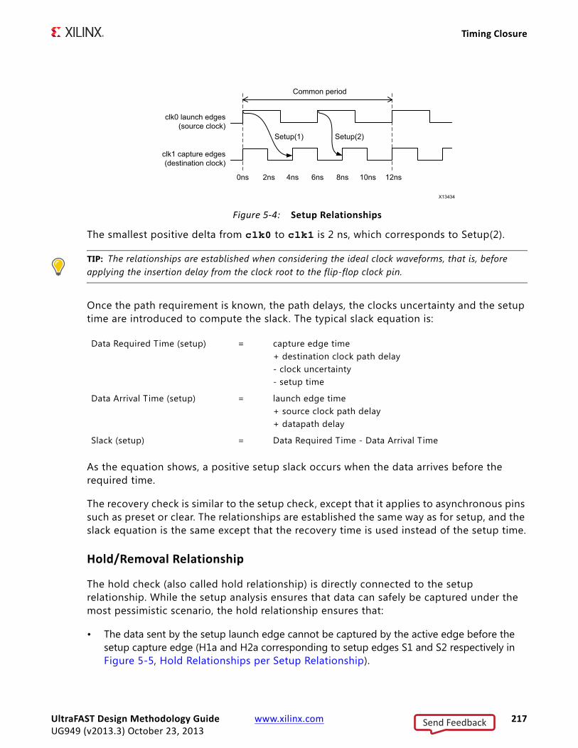
Timing Closure
The smallest positive delta from clk0 to clk1 is 2 ns, which corresponds to Setup(2).
TIP: The relationships are established when considering the ideal clock waveforms, that is, before applying the insertion delay from the clock root to the flip-flop clock pin.
Once the path requirement is known, the path delays, the clocks uncertainty and the setup time are introduced to compute the slack. The typical slack equation is:
As the equation shows, a positive setup slack occurs when the data arrives before the required time.
The recovery check is similar to the setup check, except that it applies to asynchronous pins such as preset or clear. The relationships are established the same way as for setup, and the slack equation is the same except that the recovery time is used instead of the setup time.
Hold/Removal Relationship
The hold check (also called hold relationship) is directly connected to the setup relationship. While the setup analysis ensures that data can safely be captured under the most pessimistic scenario, the hold relationship ensures that:
• The data sent by the setup launch edge cannot be captured by the active edge before the setup capture edge (H1a and H2a corresponding to setup edges S1 and S2 respectively in Figure 5-5, Hold Relationships per Setup Relationship).
X-Ref Target - Figure 5-4
Figure 5-4: Setup Relationships
Data Required Time (setup) = capture edge time+ destination clock path delay- clock uncertainty- setup time
Data Arrival Time (setup) = launch edge time+ source clock path delay+ datapath delay
Slack (setup) = Data Required Time - Data Arrival Time
UltraFAST Design Methodology Guide www.xilinx.com 217UG949 (v2013.3) October 23, 2013
Send Feedback
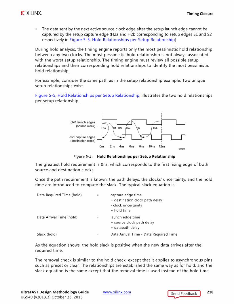
Timing Closure
• The data sent by the next active source clock edge after the setup launch edge cannot be captured by the setup capture edge (H2a and H2b corresponding to setup edges S1 and S2 respectively in Figure 5-5, Hold Relationships per Setup Relationship).
During hold analysis, the timing engine reports only the most pessimistic hold relationship between any two clocks. The most pessimistic hold relationship is not always associated with the worst setup relationship. The timing engine must review all possible setup relationships and their corresponding hold relationships to identify the most pessimistic hold relationship.
For example, consider the same path as in the setup relationship example. Two unique setup relationships exist.
Figure 5-5, Hold Relationships per Setup Relationship, illustrates the two hold relationships per setup relationship.
The greatest hold requirement is 0ns, which corresponds to the first rising edge of both source and destination clocks.
Once the path requirement is known, the path delays, the clocks’ uncertainty, and the hold time are introduced to compute the slack. The typical slack equation is:
As the equation shows, the hold slack is positive when the new data arrives after the required time.
The removal check is similar to the hold check, except that it applies to asynchronous pins such as preset or clear. The relationships are established the same way as for hold, and the slack equation is the same except that the removal time is used instead of the hold time.
X-Ref Target - Figure 5-5
Figure 5-5: Hold Relationships per Setup Relationship
Data Required Time (hold) = capture edge time+ destination clock path delay- clock uncertainty+ hold time
Data Arrival Time (hold) = launch edge time+ source clock path delay+ datapath delay
Slack (hold) = Data Arrival Time - Data Required Time
UltraFAST Design Methodology Guide www.xilinx.com 218UG949 (v2013.3) October 23, 2013
Send Feedback
Timing Closure
Path Requirement
The path requirement represents the difference in time between the capture edge and the launch edge of a timing path.
For example, when considering the same path and clocks as in the previous section, the following path requirements exist:
Setup Path Requirement (S1) = 1*T(clk1) - 0*T(clk0) = 4nsSetup Path Requirement (S2) = 2*T(clk1) - 1*T(clk0) = 2ns
The corresponding hold relationships are:
• Corresponding to setup S1
Hold Path Requirement (H1a) = (1-1)*T(clk1) - 0*T(clk0) = 0nsHold Path Requirement (H1b) = 1*T(clk1) - (0+1)*T(clk0) = -2ns
• Corresponding to setup S2
Hold Path Requirement (H2a) = (2-1)*T(clk1) - 1*T(clk0) = -2nsHold Path Requirement (H2b) = 2*T(clk1) - (1+1)*T(clk0) = -4ns
The timing analysis is performed only with the two most pessimistic requirements. In the example above, these are:
• The setup requirement S2
• The hold requirement H1a
Clock Skew and Uncertainty
Skew and uncertainty both impact setup and hold computations and slack.
Skew Definition
Clock skew is the insertion delay difference between the destination clock path and the source clock path: (1) from their common point in the design; (2) to, respectively, the endpoint and startpoint sequential cell clock pins.
In the equation below:
• Tcj is the delay from the common node to the endpoint clock pin.
• Tci is the delay from the common node to the startpoint clock pin:
Tskewi,j = Tci- Tcj
Clock Pessimism Removal
A typical timing path report shows the delay details of both source and destination clock paths, from their root to the sequential cell clock pins. As explained in Min and Max Delay
UltraFAST Design Methodology Guide www.xilinx.com 219UG949 (v2013.3) October 23, 2013
Send Feedback
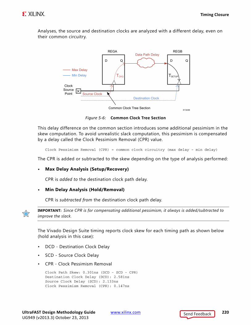
Timing Closure
Analyses, the source and destination clocks are analyzed with a different delay, even on their common circuitry.
This delay difference on the common section introduces some additional pessimism in the skew computation. To avoid unrealistic slack computation, this pessimism is compensated by a delay called the Clock Pessimism Removal (CPR) value.
Clock Pessimism Removal (CPR) = common clock circuitry (max delay - min delay)
The CPR is added or subtracted to the skew depending on the type of analysis performed:
• Max Delay Analysis (Setup/Recovery)
CPR is added to the destination clock path delay.
• Min Delay Analysis (Hold/Removal)
CPR is subtracted from the destination clock path delay.
IMPORTANT: Since CPR is for compensating additional pessimism, it always is added/subtracted to improve the slack.
The Vivado Design Suite timing reports clock skew for each timing path as shown below (hold analysis in this case):
• DCD - Destination Clock Delay
• SCD - Source Clock Delay
• CPR - Clock Pessimism Removal
Clock Path Skew: 0.301ns (DCD - SCD - CPR)Destination Clock Delay (DCD): 2.581nsSource Clock Delay (SCD): 2.133nsClock Pessimism Removal (CPR): 0.147ns
X-Ref Target - Figure 5-6
Figure 5-6: Common Clock Tree Section
UltraFAST Design Methodology Guide www.xilinx.com 220UG949 (v2013.3) October 23, 2013
Send Feedback

Timing Closure
In many cases, the CPR accuracy changes before and after routing. For example, let’s consider a timing path where the source and destination clocks are the same clock, and the startpoint and endpoint clock pins are driven by the same clock buffer.
Before routing, the common point is the clock net driver, that is, the clock buffer output pin. CPR compensates only for the pessimism from the clock root to the clock buffer output pin.
After routing, the common point is the last routing resource shared by the source and destination clock paths in the device architecture. This common point is not represented in the netlist, so the corresponding CPR cannot be directly retrieved by subtracting common clock circuitry delay difference from the timing report. The timing engine computes the CPR value based on device information not directly exposed to the user.
Optimistic Skew
Xilinx FPGA devices provide advanced clocking resources such as dedicated clock routing trees and Clock Modifying Blocks (CMB). Some of the CMBs have the capability to compensate the clock tree insertion delay by using a Phase Lock Loop circuit (present in PLL or MMCM primitives). The amount of compensation is based on the insertion delay present on the feedback loop of the PLL. In many cases, a PLL (or MMCM) drives several clock trees with the same type of buffer, including on the feedback loop. As the device can be large, the insertion delay on all these clock tree branches does not always match the feedback loop delay. The clocks driven by a PLL become over-compensated when the feedback loop delay is bigger than the source or destination clock delay. In this case, the sign of the CPR changes and it effectively removes skew optimism from the slack value. This is needed in order to ensure that there is no artif icial skew at the common node of any timing path clocks during the analysis.
RECOMMENDED: Always use the CPR compensation during timing analysis to preserve the slack accuracy and the overall timing signoff quality.
Clock Uncertainty
Clock uncertainty is the total amount of possible time variation between any pair of clock edges. The uncertainty consists of the computed clock jitter (system, input, and discrete); the phase error introduced by certain hardware primitives; and any clock uncertainty specified by the user in the design constraints (set_clock_uncertainty).
For primary clocks, the jitter is defined by set_input_jitter and set_system_jitter. For clock generators such as MMCM and PLL, the tool computes the jitter based on user-specif ied jitter on its source clock and its configuration. For other generated clocks (such as flop based clock dividers), the jitter is the same as that of its source clock.
The user-specif ied clock uncertainty is added to the uncertainty computed by the Vivado Design Suite timing engine. For generated clocks (such as from MMCM, PLL, and flop-based
UltraFAST Design Methodology Guide www.xilinx.com 221UG949 (v2013.3) October 23, 2013
Send Feedback

Timing Closure
clock dividers), uncertainty specif ied by the user on source clock does not propagate through the clock generators.
For more information on jitter and phase error definitions, see the Vivado Design Suite User Guide: Using Constraints (UG903) [Ref 16].
The clock uncertainty has two purposes:
• Reserve some amount of margin in the slack numbers for representing any noise on the clock that could affect the hardware functionality. Because the delay and jitter numbers are conservative, there is generally no need to add extra uncertainty to ensure proper hardware functionality.
• Over-constrain the paths related to a clock or a clock pair during one or several implementation steps. This increases the QoR margin that can be used to help the next steps to close timing on these paths. By using clock uncertainty, the clock waveforms and their relationships are not modified, so the rest of the timing constraints can still apply properly.
Pulse Width Checks
The pulse width checks are some rule checks on the signal waveforms when they reach the hardware primitives after propagation through the device. They usually correspond to functional limits dictated by the circuitry inside the primitive. For example, the minimum period check on a DSP clock pin ensures that the clock driving a DSP instance does not run at higher frequency than what is tolerated by the internal DSP.
The pulse width checks do not affect synthesis or implementation. Their analysis must be performed once before the bitstream generation like any other design rule check provided by the Vivado Design Suite.
Timing Closure CriteriaTiming closure starts with writing valid constraints that represent how the design will operate in hardware. The following criteria should be met:
• Clean Constraints
• No Timing Violation
UltraFAST Design Methodology Guide www.xilinx.com 222UG949 (v2013.3) October 23, 2013
Send Feedback
Timing Closure
Clean Constraints
• All active clock pins are reached by a clock definition.
• All active path endpoints have requirement with respect to a defined clock (setup/hold/recovery/removal).
• All active input ports have an input delay constraint.
• All active output ports have an output delay constraint.
• Timing exceptions are correctly specif ied.
The last three bullets are applicable only when the constraints are being completed and are not applicable for baselining constraints.
No Timing Violation
• Setup/Recovery (max analysis): WNS > 0ns and TNS = 0ns
• Hold/Removal (min analysis): WHS > 0ns and THS = 0ns
• Pulse Width: WPWS > 0ns and TPWS = 0ns
Checking That Your Design is Properly ConstrainedBefore looking at the timing results to see if there are any violations, be sure that every synchronous endpoint in your design is properly constrained.
Run check_timing to identify unconstrained paths. This command can be run as a stand-alone command, but it is also part of the report_timing_summary.
The check_timing command reports the following kinds of situations. These situations indicate something missing or wrong in the timing definition, or implication on correctly meeting timing:
• no_clock
• unconstrained_internal_endpoints
• no_input_delay
• no_output_delay
• multiple_clock
• generated_clocks
• loops
UltraFAST Design Methodology Guide www.xilinx.com 223UG949 (v2013.3) October 23, 2013
Send Feedback
Timing Closure
• partial_input_delay
• partial_output_delay
• unexpandable_clocks
• latch_loops
no_clock
Number of clock pins not reached by a defined timing clock. Constant clock pins are also reported. Check if some clock constraints are missing. Or, if some clock pins have been inadvertently connected to constant.
unconstrained_internal_endpoints
Number of path endpoints (excluding output ports) without a timing requirement. This number is directly related to missing clock definitions, reported by the no_clock check.
no_input_delay
Number of input ports without at least one input delay constraint. Check if some set_input_delay is missing.
no_output_delay
Number of output ports without at least one output delay constraint.
multiple_clock
Number of clock pins reached by more than one timing clock. This can happen if there is a clock multiplexer in one of the clock trees. The clocks that share the same clock tree are timed together by default, which does not represent a realistic timing situation. Only one clock can be present on a clock tree at any given time.
If you do not believe that the clock tree is supposed to have a MUX, review the clock tree to understand how and why multiple clocks are reaching the specif ic clock pins.
generated_clocks
Number of generated clocks that refer to a master clock source which is not in the fanin cone of the same clock tree.
loops
Number of combinational loops found in the design. These loops are automatically broken by the Vivado Design Suite timing engine in order to report timing.
UltraFAST Design Methodology Guide www.xilinx.com 224UG949 (v2013.3) October 23, 2013
Send Feedback

Timing Closure
partial_input_delay
Number of input ports with only a min input delay or max input delay constraint, but not both. These ports are not analyzed for both setup and hold analysis.
partial_output_delay
Number of output ports with only a min output delay or max output delay constraint, but not both. These ports are not analyzed for both setup and hold analysis.
unexpandable_clocks
Clock pairs for which the Vivado Design Suite timing engine could not find a common period multiplier over 1000 clock cycles. The paths between these clock pairs cannot be safely timed. You must check to see whether the clock pairs must be treated as asynchronous.
If the clock pairs are synchronous, check to be sure that the period is specified correctly, and loss of precision is not causing this. The unexpandable clock pairs that are not timed due to a timing exception are reported in a separate sub-category of this check.
latch_loops
Checks for and warns of loops passing through latches in the design. These loops will not be reported as part of combinational loops, and will affect latch time borrowing computation on the same paths.
Fixing Issues Flagged by check_timing
Not all checks are equally important. The following checks are sorted by importance (most important to least important) when reviewing and f ixing the issues flagged by check_timing.
No Clock and Unconstrained Internal Endpoints
These are the most important checks. These checks allow you to determine whether the internal paths in the design are completely constrained. You must ensure that the unconstrained internal endpoints are at zero as part of the Static Timing Analysis signoff quality review.
Zero unconstrained internal endpoints should not give a false sense of security. This indicates only that all internal paths are constrained for timing analysis. However, the correct value of the constraints is not yet guaranteed.
UltraFAST Design Methodology Guide www.xilinx.com 225UG949 (v2013.3) October 23, 2013
Send Feedback

Timing Closure
Unexpandable Clocks
IMPORTANT: Address all clock pairs listed in this section of the report!
Depending on the clock relationship, the tools may assume that there is timing margin, but if the clocks are not expandable, then the timing margin is false.
The asynchronous clocks pairs must be addressed with clocking exceptions, either the set_clock_groups, set_false_path, or set_max_delay -datapath_only constraints. If a path is covered by both set_max_delay and set_clock_groups, the set_clock_groups overrides. Thus, while applying set_clock_groups, ensure that the clock pairs (or, subsets of paths within the pair) are not supposed to have a set_max_delay.
Those which are supposed to be related should have their period and waveform reviewed again to be sure that lack of precision is not the cause. For example, two clocks with periods 16.15 and 8.07 will appear as unexpandable. The solution might be to specify the period as 16.15 and 8.075 (the first is divide_by_2 of the second).
Generated Clocks
Generated_clocks are a normal part of a design. However, if a generated clock is derived from a master clock which is not part of the same clock tree, this can be a serious problem. The timing engine cannot properly calculate the generated clock tree delay. This results in erroneous slack computation. In the worst case situation, the design meets timing according to the reports, but does not work in hardware.
Loops and Latch Loops
A good design does not have any combinational loops. The timing loop will be broken by the timing engine. The broken paths are not reported during timing analysis, or evaluated during implementation. This can lead to incorrect behavior in hardware, even if the overall timing requirements are met.
No Input/Output Delays and Partial Input/Output Delays
All I/O components must be properly constrained.
RECOMMENDED: Start with baselining constraints. Once those have been validated, complete the constraints with the I/O timing.
Multiple Clocks
Multiple clocks are usually acceptable. Xilinx recommends that you ensure that these clocks are expected to propagate on the same clock tree. You must also verify that the paths
UltraFAST Design Methodology Guide www.xilinx.com 226UG949 (v2013.3) October 23, 2013
Send Feedback

Timing Closure
requirement between these clocks does not introduce tighter requirements than needed in order for the design to be functional in hardware.
If this is the case, you must use set_clock_groups or set_false_path between these clocks on these paths. Any time that you use timing exceptions, you must ensure that they affect only the intended paths.
IMPORTANT: Since the XDC is a Tcl program, the order of constraints matters.
Debugging and Fixing Timing Issues
The following table provides a quick guidance in terms of systematic approach to debug and f ix timing failures (if any) reported in the timing report.
Once the above aspects have been determined to be good, examine the remaining violations (see: Quickly Analyzing All Failing Paths, page 263) to determine the next course of action involving different options with back end - including manually creating a floorplan, when all else fails.
Defining Clocks and Their Relationships
If you are unsure of your clock constraints, the Vivado IDE can be used to create a complete set of clock constraints on the post-synthesized netlist. The graphical interface of the IDE
Table 5-4: Steps to Debug and Fix Timing Issues
Step Section Containing More Details
Check that all clocks and their relationships are defined correctly
Defining Clocks and Their Relationships, page 227
Check that clock skew and uncertainty are not too high
Clock Skew and Uncertainty, page 219
Check that number of logic levels in the path is not too high
Datapath Delay and Logic Levels, page 245
Check that the path uses optimal resources (cells/pins)
MMCM Frequency Synthesis, page 245
Check that you do not have too many control sets unnecessarily
Control Sets, page 258
Check if any of the nets has very high fanout
Identifying High Fanout Net Drivers, page 260
Check if hold requirement is unrealistically high
Determining if Hold-Fixing is Negatively Impacting the Design, page 262
UltraFAST Design Methodology Guide www.xilinx.com 227UG949 (v2013.3) October 23, 2013
Send Feedback
Timing Closure
and the reporting capabilities of the Vivado Design Suite show precisely what must be constrained.
• Step 1: Identify Which Clocks Must be Created
• Step 2: Verify That No Clocks Are Missing
• Step 3: Identify Asynchronous Clock Domains
Step 1: Identify Which Clocks Must be Created
Begin by loading the post synthesized netlist or checkpoint into the Vivado IDE. In the Tcl console, reset the timing to ensure that all timing constraints are removed. In this way, you can be certain that the slate is clean.
A report of clock networks can be generated in order to create a list of all the primary clocks that must be defined in the design. The resulting list of clock networks shows which clock constraints should be created. Use the clock creation wizard to specify the appropriate parameters for each clock.
Step 2: Verify That No Clocks Are Missing
Once the clock network report shows that all clock networks have been constrained, verif ication of the accuracy of the generated clocks can begin. Since the Vivado tools automatically propagate clock constraints through clock-modifying blocks such as MMCMs, PLLs and BUFGCTRLs, it is important to review the constraints that were generated. Use report_clocks to show which clocks were created with a create_clock constraint, and which clocks were generated.
The report_timing results show that all clocks are propagated. The difference between the primary clocks (created with create_clock) and the generated clocks (generated by clock-modifying-block) is displayed in the attributes f ield.
• Clocks that are propagated only (P) are primary clocks.
• Clocks that were generated are shown to be both propagated (P) and Generated (G).
You can also create generated clocks using the create_generated_clock constraint. For more information, see the Vivado Design Suite User Guide: Using Constraints (UG 903) [Ref 16].
UltraFAST Design Methodology Guide www.xilinx.com 228UG949 (v2013.3) October 23, 2013
Send Feedback

Timing Closure
Step 3: Identify Asynchronous Clock Domains
Upon verif ication of the clocking constraints, asynchronous clock domain crossing paths must be identif ied.
Note: This section does not explain how to properly cross clock region boundaries, but explains how to identify which crossings exist and how to constrain them.
The clock domain interactions are best viewed using report_clock_interaction. The report shows a matrix of source clocks and destination clocks. The color in each cell indicates the nature of interaction among clocks represented by the corresponding row and the column. Figure 5-8, Sample Clock Interaction Report, shows a sample clock interaction report.
X-Ref Target - Figure 5-7
Figure 5-7: Report_Clocks Shows which Clocks were Generated from Primary Clocks
X-Ref Target - Figure 5-8
Figure 5-8: Sample Clock Interaction Report
UltraFAST Design Methodology Guide www.xilinx.com 229UG949 (v2013.3) October 23, 2013
Send Feedback

Timing Closure
Table 5-5, report_clock_interaction Colors, explains the meaning of each color in this report.
Before the creation of any false paths or clock group constraints, the only colors that appear in the matrix are black, red,and green. Because all clocks are timed by default, the process of decoupling asynchronous clocks takes on a high degree of signif icance. Failure to decouple asynchronous clocks often results in a vastly over-constrained design.
Identify Clock Pairs That Do Not Share Common Primary Clocks
The clock interaction report indicates whether or not each pair of interacting clocks has a common primary clock source. Clock pairs that do not share a common primary clock are frequently asynchronous to each other. As such, it is helpful to identify these pairs by sorting the columns in the report using the Common Primary Clock field. The report does not determine whether clock-domain crossing paths are or are not designed properly. For information about the proper design of clock-domain crossing paths, Chapter 4, Design Creation.
Table 5-5: report_clock_interaction Colors
Color Meaning What Next
Black No interaction among these clock domains.
Primarily for information unless you expected these clock domains to be interacting.
Green There is interaction among these clock domains, and the paths are getting timed.
Primarily for information unless you do not expect any interaction among the clock domains.
Cyan Some of the paths for the interacting domains are not being timed due to user exceptions.
Ensure that the timing exceptions are really desired.
Red There is interaction among these clock domains, and the paths are being timed. However, the clocks appear to be independent (and hence, asynchronous)
Check whether these clocks should have been declared as asynchronous, or whether they should be sharing a common primary source.
Orange There is interaction among these clock domains. The clocks appear to be independent (and hence, asynchronous). However, only some of the paths are not timed due to exceptions.
Check why are only a few paths getting user exception? Should all the paths be getting the exception?
Blue There is interaction among these clock domains, and the paths are not being timed.
Confirm that these clocks are supposed to be asynchronous. Also, check that the corresponding HDL code has been written correctly to ensure proper synchronization and reliable data transfer across clock domains.
UltraFAST Design Methodology Guide www.xilinx.com 230UG949 (v2013.3) October 23, 2013
Send Feedback
Timing Closure
Identify Tight Timing Requirements
For each clock pair, the clock interaction report also shows the path requirement for all paths that cross from source clock to destination clock. Sort the columns by path requirement (WNS) to view a list of the tightest requirements in the design. Figure 5-8, Sample Clock Interaction Report, shows the timing report sorted by WNS column. Review these requirements to ensure that no invalid tight requirements exist.
The Vivado tools identify the path requirements by expanding each clock out to one thousand cycles, then determining where the closest, non-coincident edge alignment occurs:
Consider a timing path that crosses from a 250 MHz clock to a 200 MHz clock.
• The positive edges of the 200 MHz clock are {0, 5, 10, 15, 20 …}.
• The positive edges of the 250 MHz clock are {0, 4, 8, 12, 16, 20 …}.
The tightest requirement for this pair of clocks occurs when:
• The 250 MHz clock has a rising edge at 4 ns, and
• The next rising edge of the 200 MHz clock is at 5 ns.
This results in all paths timed from the 250 MHz clock domain into the 200 MHz clock domain being timed at 1 ns.
Note: The simultaneous edge at 20 ns is NOT the tightest requirement in this example, because the capture edge cannot be the same as the launch edge.
Because this is a rather tight timing requirement, additional steps must be taken.
Depending on the design, one of the following requirements may be the correct way to handle these crossings:
• false_path
• max_delay_path
• multicycle path
If nothing is done, the design may exhibit timing violations that cross these two domains. Furthermore, all of the best optimization, placement and routing may end up being dedicated to these paths instead of given to the critical paths in the design. It is critical that these types of paths be identif ied before any timing-driven implementation step.
UltraFAST Design Methodology Guide www.xilinx.com 231UG949 (v2013.3) October 23, 2013
Send Feedback

Timing Closure
Using Report_Clock_Networks to Decouple Primary Clocks and Generated Clocks
Before any timing exceptions are created, it is helpful to go back to report_clock_networks to identify which primary clocks exist in the design. If all primary clocks are asynchronous to each other, as is often the case, a single constraint can be used to decouple the primary clocks from each other, and to decouple their generated clocks from each other. Using the primary clocks in report_clock_networks as a guide, each clock group and associated clocks can be decoupled as shown in Figure 5-10, Report Clock Networks.
### Decouple asynchronous clocksset_clock_groups -asynchronous \-group [get_clocks sysClk -include_generated_clocks] \-group [get_clocks gt0_txusrclk_i -include_generated_clocks] \-group [get_clocks gt2_txusrclk_i -include_generated_clocks] \-group [get_clocks gt4_txusrclk_i -include_generated_clocks] \-group [get_clocks gt6_txusrclk_i -include_generated_clocks]
Limiting I/O Constraints and Timing Exceptions
Most timing violations are on internal paths. I/O constraints are not needed during the first baselining iterations, especially for I/O timing paths in which the launching or capturing register is located inside the I/O bank. The I/O timing constraints can be added back once the design and other constraints are stable and the timing is nearly closed.
X-Ref Target - Figure 5-9
Figure 5-9: Clock Domain Crossing from 250MHz to 200 MHz
X-Ref Target - Figure 5-10
Figure 5-10: Report Clock Networks
UltraFAST Design Methodology Guide www.xilinx.com 232UG949 (v2013.3) October 23, 2013
Send Feedback

Timing Closure
Timing exceptions must be limited, based on recommendations of the RTL designer, and must not be used to hide real timing problems. The false path or clock groups between clocks must have already been reviewed and f inalized at this point.
IP constraints must be entirely kept. When IP timing constraints are missing, known false paths can end up being reported as timing violations.
Evaluating Design WNS Before and After Each Step
You must evaluate the design WNS after each implementation step. Tcl users of Tcl command line flow can easily incorporate report_timing_summary after each implementation step in their build script. IDE users can make use of simple tcl.post scripts to run report_timing_summary after each step. In both cases, when a signif icant degradation in WNS is noted, you must analyze the checkpoint immediately preceding that step.
In addition to evaluating the timing for the entire design before and after each implementation step, a more targeted approach can be taken for individual paths in order to evaluate the impact of each step in the flow on the timing. For example, the estimated net delay for a timing path after the optimization step may differ signif icantly from the estimated net delay for the same path after placement. Comparing the timing of critical paths after each step is an effective method for highlighting where the timing of a critical path diverges from closure.
Post Synthesis and Post Logic Optimization
Estimated net delays are close to the best possible placement for all paths. To fix violating paths any of the following:
• Change the RTL
• Use different synthesis options
• Add timing exceptions such as multicycle paths (if appropriate and safe for the functionality in hardware)
Pre- and Post-Placement
After placement, the estimated net delays are close to the best possible route, except for long and medium-to-high fanout nets, which use more pessimistic delays. In addition, congestion or hold fixing impact are not accounted for in the net delays at this point, which can make the timing results optimistic.
Clock skew is accurately estimated and can be used to review imbalanced clock trees impact on slack.
Hold f ixing can be estimated by running min delay analysis. High violations require clock tree modif ication. Small violations are acceptable and will likely be f ixed by the router.
UltraFAST Design Methodology Guide www.xilinx.com 233UG949 (v2013.3) October 23, 2013
Send Feedback
Timing Closure
Pre- and Post-Physical Optimization
Evaluate the need for running physical optimization in order to f ix timing problems related to:
• Nets with high fanout (report_high_fanout_nets shows highest fanout non-clock nets)
• Nets with targets located far apart
• DSP and RAMB with sub-optimal pipeline register usage
Pre and Post Route
Slack is reported with actual routed net delays except for the nets that are not completely routed. Slack reflects the impact of hold fixing on setup; and the impact of congestion.
No hold violation should remain after route, regardless of the worst setup slack (WNS) value. If the design fails hold, further analysis is needed. This is typically due to very high congestion, in which case the router gives up on optimizing timing. This can also occur for high hold violations (over 4ns) which the router does not f ix by default. High hold violations are usually due to improper clock constraints, high clock skew or, improper I/O constraints which can already be identif ied after placement or even after synthesis.
If hold is met (WHS>0) but setup fails (WNS<0), follow the analysis steps described below.
Identifying Timing Violations Root CauseThe timing-driven algorithms focus on the worst violations. Understanding and f ixing problems related to the worst violation will likely resolve most, if not all, smaller violations.
For setup, you must f irst analyze the worst violation of each clock group.
• Clock group = all intra, inter and asynchronous paths captured by a given clock
For hold, all violations must be reviewed, starting with the worst one.
Clock Skew and Uncertainty
Xilinx FPGA devices use various types of routing resources to support most common clocking schemes and requirements such as high fanout clocks; short propagation delays; and extremely low skew. Clock skew affects any register to register path with either a combinational logic or interconnect between them.
RECOMMENDED: Run a clock utilization report using the Tcl console (report_clock_utilization) to generate a clocking report. The detail clocking section contains the clock skew for Global, Regional and local clocks. Verify that the clock nets do not contain excessive clock skew.
UltraFAST Design Methodology Guide www.xilinx.com 234UG949 (v2013.3) October 23, 2013
Send Feedback
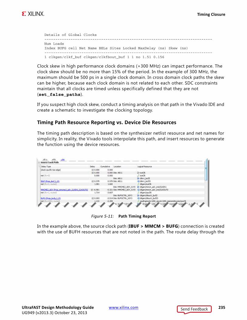
Timing Closure
Details of Global Clocks-----------------------------------------------------------------------------Num LoadsIndex BUFG cell Net Name BELs Sites Locked MaxDelay (ns) Skew (ns)-----------------------------------------------------------------------------1 clkgen/clkf_buf clkgen/clkfbout_buf 1 1 no 1.51 0.156
Clock skew in high performance clock domains (+300 MHz) can impact performance. The clock skew should be no more than 15% of the period. In the example of 300 MHz, the maximum should be 500 ps in a single clock domain. In cross domain clock paths the skew can be higher, because each clock domain is not related to each other. SDC constraints maintain that all clocks are timed unless specifically defined that they are not (set_false_paths).
If you suspect high clock skew, conduct a timing analysis on that path in the Vivado IDE and create a schematic to investigate the clocking topology.
Timing Path Resource Reporting vs. Device Die Resources
The timing path description is based on the synthesizer netlist resource and net names for simplicity. In reality, the Vivado tools interpolate this path, and insert resources to generate the function using the device resources.
In the example above, the source clock path (IBUF > MMCM > BUFG) connection is created with the use of BUFH resources that are not noted in the path. The route delay through the
X-Ref Target - Figure 5-11
Figure 5-11: Path Timing Report
UltraFAST Design Methodology Guide www.xilinx.com 235UG949 (v2013.3) October 23, 2013
Send Feedback

Timing Closure
BUFH is accounted for in the total cumulative delay value. A typical BUFH connection might appear as follows:
In Figure 5-12, Actual Physical Path, the BUFH drives a horizontal global clock tree spine in a single clock region. For more information, see Chapter 4, Design Creation.
If the source and destination elements are in different clock regions, two different BUFH components will be used. If they are in the same clock region (and source the same BUFH), the timing analysis clock reference point is analyzed back to the common node (BUFH) to calculate clock skew.
Debugging Timing Reports with High Clock Skew
You must f irst understand the source clock and destination clock and their relationship:
• When the Source and Destination Clock Are the Same
• When the Source and Destination Clock Are Not the Same (Unsafe, Unrelated)
When the Source and Destination Clock Are the Same
When the source and destination clock are the same (synchronous clocks) or automatically derived, the tools use the common node on the clock path to determine the clock skew. All synchronous paths contain a common node. When analyzing the clock path in the timing report, it may be diff icult to confirm the exact location of the common node to the device view because the skew calculation summary results is reported.
X-Ref Target - Figure 5-12
Figure 5-12: Actual Physical Path
UltraFAST Design Methodology Guide www.xilinx.com 236UG949 (v2013.3) October 23, 2013
Send Feedback

Causes of High Clock Skew
When the Source and Destination Clock Are Not the Same (Unsafe, Unrelated)
When the source and destination clocks are not the same, the tools propagate the clock back to the common driver to determine the clock skew. In the Vivado tools, all paths are automatically timed. The tool derives timing constraints for paths that cross between clock domains. For more information, see the Vivado Design Suite User Guide: Using Constraints (UG903) [Ref 16].
In the case of a multiplexing clock using a BUFGMUX, the Vivado tools propagate all incoming clocks to the output. Several timing clocks can exist on a clock tree at the same time, which is convenient for reporting on all operation modes at once, but is not possible in hardware. These clocks may must be declared in different groups, through set_clock_groups. For more information, see the Vivado Design Suite User Guide: Using Constraints (UG903) [Ref 16].
The best way to analyze the clock paths is to use the schematic viewer in the Vivado IDE and cross probe with the timing report.
Causes of High Clock SkewHigh clock skew can be caused by:
• Clock Signal Driven From a Gated Logic Source
• Serially Connected BUFG Components Driving Synchronous Elements
• BUFG Drives Synchronous Elements
• IBUFG Drives Multiple MMCMs (Related Clocks)
• BUFG Drives Register Elements and MMCMs (Related Clocks)
• BUFR/BUFIO/BUFH Drives Register Elements in Several Clock Regions
• Using the CLOCK_DEDICATED_ROUTE=FALSE Constraint
Clock Signal Driven From a Gated Logic SourceThis method is not recommended and can lead to excess clock skew. Since the gated logic driver buffer does not have direct access to the global clock lines, it uses local fabric routing resources. In some cases, although the gated logic can be connected to a BUFG, this also leads to excessive route delay. Check the report_clock_utilization results for excessive clock skew.
When verifying the clock report, there might be additional high skew clocks automatically inserted by the place and route algorithms. This is a common practice to prevent long term silicon metastability in unused clock generators. The clocks operate in the low frequency (Hz) range with minimal resources and do not impact design performance.
UltraFAST Design Methodology Guide www.xilinx.com 237UG949 (v2013.3) October 23, 2013
Send Feedback

Causes of High Clock Skew
In Figure 5-13, Skew Due to Local Routing on Clock Network, the f irst BUFG (clk1_buf) is used in LUT3 to create a gated clock condition. This practice is not recommended. In order to comply with the requirement, the connection uses slower local routing connections. The second BUFG in block gc_noisegen was inserted automatically by the synthesis algorithm.
Serially Connected BUFG Components Driving Synchronous ElementsWhen adding synthesized IP netlists, verify that the number of global clock buffers inserted by the synthesis tool is correct. A common mistake when importing black box IP is that the synthesizer automatically inserts a BUFG when it detects a signal connected to the CLK port of a cell. If the downstream black box IP contains a global clock buffer, the two BUFG components will increase the amount of clock skew.
X-Ref Target - Figure 5-13
Figure 5-13: Skew Due to Local Routing on Clock Network
UltraFAST Design Methodology Guide www.xilinx.com 238UG949 (v2013.3) October 23, 2013
Send Feedback
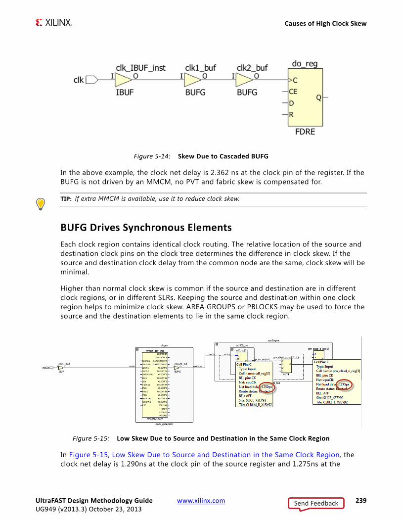
Causes of High Clock Skew
In the above example, the clock net delay is 2.362 ns at the clock pin of the register. If the BUFG is not driven by an MMCM, no PVT and fabric skew is compensated for.
TIP: If extra MMCM is available, use it to reduce clock skew.
BUFG Drives Synchronous ElementsEach clock region contains identical clock routing. The relative location of the source and destination clock pins on the clock tree determines the difference in clock skew. If the source and destination clock delay from the common node are the same, clock skew will be minimal.
Higher than normal clock skew is common if the source and destination are in different clock regions, or in different SLRs. Keeping the source and destination within one clock region helps to minimize clock skew. AREA GROUPS or PBLOCKS may be used to force the source and the destination elements to lie in the same clock region.
In Figure 5-15, Low Skew Due to Source and Destination in the Same Clock Region, the clock net delay is 1.290ns at the clock pin of the source register and 1.275ns at the
X-Ref Target - Figure 5-14
Figure 5-14: Skew Due to Cascaded BUFG
X-Ref Target - Figure 5-15
Figure 5-15: Low Skew Due to Source and Destination in the Same Clock Region
UltraFAST Design Methodology Guide www.xilinx.com 239UG949 (v2013.3) October 23, 2013
Send Feedback

Causes of High Clock Skew
destination register. This results in a clock skew of only 15ps over PVT. This clock net has a max skew of 0.287ps across all destinations.
Num LoadsIndex BUFG cell Net Name BELs Sites Locked MaxDelay (ns) Skew (ns)-----------------------------------------------------------------------------10 clkgen/clkout1_buf clkgen/cpuClk_o 3297 1298 no 1.37 0.287
IBUFG Drives a Single MMCM with Multiple Outputs (Related Clocks)
The period constraint is defined on the driver pin or port of its tree root. If the clock signal drives an MMCM to generate multiple common output frequencies, the skew from each related clock is the same to the output BUFG. The source and destination may be located in different clock regions. Xilinx recommends that you use AREA GROUPS or PBLOCKS if it impacts your timing performance. In the above example, the clock net skew between the two clock domains is 36ps.
TIP: The Clocking Wizard provides performance guidelines ( jitter and phase error) based on your clocking requirements.
IBUFG Drives Multiple MMCMs (Related Clocks)Xilinx recommends using a simplif ied clocking topology if possible. Consolidating the number of clock domains helps with performance, resources, and timing closure.
TIP: Be careful of using a MMCM output BUFG that drives other MMCMs and other registers. The extra BUFG can lead to additional skew.
BUFG Drives Register Elements and MMCMs (Related Clocks)Make sure the MMCM CLKIN BUFG is used to drive only the MMCM if possible. You can use the CLK0 output of the MMCM to drive your registered elements. The MMCM provides clock stability over PVT where the BUFG does not. Given the complexity of today’s designs, it is possible that the timing engine will detect a cross domain clock path somewhere downstream that might not be detected by the designer.
In Figure 5-16, the lock signal from the MMCM is monitored with the input clock. This is a common practice if the clock source is interrupted. The number of resources on signal clockRef is minimal.
UltraFAST Design Methodology Guide www.xilinx.com 240UG949 (v2013.3) October 23, 2013
Send Feedback
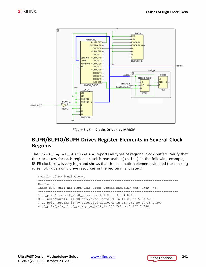
Causes of High Clock Skew
BUFR/BUFIO/BUFH Drives Register Elements in Several Clock RegionsThe clock_report_utilization reports all types of regional clock buffers. Verify that the clock skew for each regional clock is reasonable (<< 1ns.). In the following example, BUFR clock skew is very high and shows that the destination elements violated the clocking rules. (BUFR can only drive resources in the region it is located.)
Details of Regional Clocks-----------------------------------------------------------------------------Num LoadsIndex BUFR cell Net Name BELs Sites Locked MaxDelay (ns) Skew (ns)-----------------------------------------------------------------------------1 u0_pcie/txoutclk_i u0_pcie/refclk 1 2 no 0.594 0.0552 u0_pcie/usrclk1_i1 u0_pcie/pipe_userclk1_in 11 25 no 5.93 5.363 u0_pcie/usrclk2_i1 u0_pcie/pipe_userclk2_in 463 160 no 0.728 0.2024 u0_pcie/pclk_i1 u0_pcie/pipe_bclk_in 557 248 no 0.952 0.396
X-Ref Target - Figure 5-16
Figure 5-16: Clocks Driven by MMCM
UltraFAST Design Methodology Guide www.xilinx.com 241UG949 (v2013.3) October 23, 2013
Send Feedback
Causes of High Clock Skew
Using the CLOCK_DEDICATED_ROUTE=FALSE ConstraintDo not use the CLOCK_DEDICATED_ROUTE=FALSE constraint in a production design.
Use CLOCK_DEDICATED_ROUTE=FALSE only as a temporary workaround to a clock failure ONLY to obtain the design through the place and route in order to view the clocking topology in the device and schematic viewer for debugging. These types of paths can have high clock skew leading to poor performance or non-functional designs. In Figure 5-18, Use of Clock Dedicated Routing, the right side has a dedicated clock route, while on the left side, the dedicated route is disabled for clock.
X-Ref Target - Figure 5-17
Figure 5-17: BUFR Driving Flops in Two Regions
UltraFAST Design Methodology Guide www.xilinx.com 242UG949 (v2013.3) October 23, 2013
Send Feedback

Causes of High Uncertainty
Causes of High UncertaintyUncertainty is the total amount of uncertainty (relative to an ideal clock) that results from user-specified external clock uncertainty, jitter, or duty cycle distortion. Clock blocks such as MMCM and PLL generate clock uncertainty.
The Clocking Wizard provides accurate uncertainty data for the specif ied device. The Clocking Wizard can also generate various MMCM clocking configurations for comparing different topologies.
It is common to see clocking topologies created for older FPGA architectures from legacy code that has not been migrated to newer device technologies. Xilinx recommends recreating the clocking section using the target device so that system performance parameters and DRC rules are calculated and verif ied.
MMCMMMCM filters input clock uncertainty as they regenerate the required clocks. The MMCM generates some clock uncertainty composing of System Jitter, Discrete Jitter and Phase Error if multiple related clocks are used.
Designs in which phase alignment does not affect system performance such as logic clocked by the outputs from a single MMCM as shown Figure 5-19, No Impact of Phase Error Through MMCM, will not be affected.
X-Ref Target - Figure 5-18
Figure 5-18: Use of Clock Dedicated Routing
UltraFAST Design Methodology Guide www.xilinx.com 243UG949 (v2013.3) October 23, 2013
Send Feedback

Causes of High Uncertainty
MMCM and I/O Timing
Designs in which phase alignment between the input and output of the MMCM is important should be checked to ensure all timing constraints are still met (that is, set_input_delay, and set_output_delay). See Figure 5-20, Phase Alignment Through MMCM Might Impact Timing.
X-Ref Target - Figure 5-19
Figure 5-19: No Impact of Phase Error Through MMCM
X-Ref Target - Figure 5-20
Figure 5-20: Phase Alignment Through MMCM Might Impact Timing
UltraFAST Design Methodology Guide www.xilinx.com 244UG949 (v2013.3) October 23, 2013
Send Feedback

Causes of High Uncertainty
MMCM Frequency Synthesis
When configuring the MMCM for frequency synthesis, the target frequency may have several M (multiplier) and D (divider) values. To minimize clock uncertainty, use values that generate a higher VCO frequency remembering not to exceed the maximum MMCM VCO frequency switching characteristics of that device. If you are migrating your design from an older technology, make sure that you are modifying the M and D values to provide the highest VCO frequency for the current technology.
The MMCM frequency synthesis example below uses an input clock of 62.5 MHz to generate an output clock of around 40 MHz. There are two solutions, but only one (MMCM_2) generates less jitter and lower clock uncertainty.
When using Clocking Wizard from the IP catalog, make sure that Jitter Optimization Setting is set to Minimum Output Jitter, which will provide the higher VCO frequency.
Datapath Delay and Logic LevelsNumber of LUTs in the path matters the most in general.
If the path delay is dominated by:
• 50%-100% cell delay
° Can the path be modif ied to be shorter or to use faster logic cells (see technology choices)?
• 50%-100% route delay
° Was this path impacted by hold fixing? (Use the corresponding analysis technique.)
- Yes - is the impacted net part of a CDC path?
- Yes - is the CDC path missing a constraint?
- No - do the startpoint and endpoint of that hold-fixed path use a balanced clock tree?
Table 5-6: MMCM Frequency Synthesis Example
MMCM_1 MMCM_2
Input clock 62.5 MHz 62.5 MHz
Output clock 40.0 MHz 39.991 MHz
CLKFBOUT_MULT_F 16 22.875
CLKOUT0_DIVIDE_F 25 35.750
VCO Frequency 1000.000 MHz 1429.688
Jitter (ps) 167.542 128.632
Phase Error (ps) 384.432 123.641
UltraFAST Design Methodology Guide www.xilinx.com 245UG949 (v2013.3) October 23, 2013
Send Feedback
Causes of High Uncertainty
° No - see congestion below
• Was this path impacted by congestion => Look at each individual net delay, the fanout and observe the routing in the Device view with routing details enabled (post-route analysis only). You can also turn on the congestion metrics to see if the path is located in or near a congested area.
° Yes - For the nets with the highest delay value, is the fanout low (<10)?
° Yes - if the routing seems optimal (straight line) but driver-load are far apart, the sub-optimal placement is related to congestion. Try to move manually the driver, or the load, and re-run timing analysis on the same path to see if that slack improves without degrading other paths. After doing the same exercise for several nets, create floorplanning constraints which will ensure that a similar placement solution will be found the next time the implementation tools are run.
° No - try to use physical logic optimization to duplicate the driver of the net. Once duplicated, each driver can automatically be placed closer to its loads, which will reduce the overall datapath delay.
° No - the design is spread out too much. Start working on floorplanning to identify portions of the design that must be kept in particular region based on their connection to I/O components (if any) or any other particular anchor point. See the floorplanning section for more information.
Reviewing Technology Choices
It is important to be aware of how design and synthesis choices impact the overall timing, utilization, and power of a design. There are often many different resource types to implement the same logic function and the choice of resources can have a signif icant impact. For example, a RAM implemented using distributed RAM performs differently than when using block RAM. When designing with attention to technological details, good tradeoffs can be made to help improve the quality of results.
The logic fabric is constructed of configurable blocks with each block sharing the same control signals. The smallest block entity is a slice or CLB (Configurable Logic Block), depending on the architecture. The following discussions refer to fabric logic as CLBs, except when considering specific technologies such as Xilinx series FPGA devices, which use slices.
In addition to clocks, sequential primitives require control signals such as resets, sets, and clock enables. The fact that many resources share the same control signals limits their use. Inefficient use of control signals can lead to ineff icient use of device resources and packing of logic. This can later lead to other problems such as routing congestion and overutilization of slices and CLBs.
This section gives an overview of the impact of technical choices of combinational and sequential logic resources and control signal implementation. Although the examples and f igures are based on general characteristics of Xilinx 7 series FPGA device technology,
UltraFAST Design Methodology Guide www.xilinx.com 246UG949 (v2013.3) October 23, 2013
Send Feedback
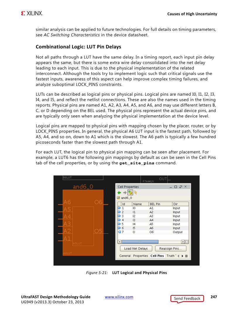
Causes of High Uncertainty
similar analysis can be applied to future technologies. For full details on timing parameters, see AC Switching Characteristics in the device datasheet.
Combinational Logic: LUT Pin Delays
Not all paths through a LUT have the same delay. In a timing report, each input pin delay appears the same, but there is some extra wire delay consolidated into the net delay leading to each input. This is due to the physical implementation of the related interconnect. Although the tools try to implement logic such that critical signals use the fastest inputs, awareness of this aspect can help improve complex timing failures, and analyze suboptimal LOCK_PINS constraints.
LUTs can be described as logical pins or physical pins. Logical pins are named I0, I1, I2, I3, I4, and I5, and reflect the netlist connections. These are also the names used in the timing reports. Physical pins are named A1, A2, A3, A4, A5, and A6, and may use different letters B, C, or D depending on the BEL used. The physical pins represent the actual device pins, and are typically only seen when analyzing the physical implementation at the device level.
Logical pins are mapped to physical pins with mapping chosen by the placer, router, or by LOCK_PINS properties. In general, the physical A6 LUT input is the fastest path, followed by A5, A4, and so on, down to A1 which is the slowest. The A6 path is typically a few hundred picoseconds faster than the slowest path through A1.
For each LUT, the logical pin to physical pin mapping can be seen after placement. For example, a LUT6 has the following pin mappings by default as can be seen in the Cell Pins tab of the cell properties, or by using the get_site_pins command.
X-Ref Target - Figure 5-21
Figure 5-21: LUT Logical and Physical Pins
UltraFAST Design Methodology Guide www.xilinx.com 247UG949 (v2013.3) October 23, 2013
Send Feedback

Causes of High Uncertainty
The BEL Pin column shows the physical pin mapped from the logical pin. Accordingly:
I0 maps to A1I1 maps to A2...I5 maps to A6
During implementation, placement, physical optimization, and routing may swap LUT input pins to improve critical path timing. A timing-critical logical pin is moved to a faster physical pin such as A6 while the slower logical pin moves to a slower physical pin. For a critical path that traverses several LUTs, the difference between using the fastest physical pins versus the slowest can be quite pronounced. Pin-swapping can be overridden by setting a LOCK_PINS property on the cell to define its explicit mapping.
Combinational Logic: Combining LUTs
The logic LUT of Xilinx 7 series FPGA devices is designed to be flexible to accommodate more than one single 6-input function. It has two outputs (O6 and O5) that allow two logical LUT functions to be combined to fit into a single resource. The internal logical representation consists of two 5-input LUTs each sharing common inputs. One LUT is used to generate the O5 output, while the O6 combines the LUT5 function with the sixth input A6.
X-Ref Target - Figure 5-22
Figure 5-22: Multiple Outputs from the Same LUT6
UltraFAST Design Methodology Guide www.xilinx.com 248UG949 (v2013.3) October 23, 2013
Send Feedback

Causes of High Uncertainty
Following are example LUT combinations:
• A LUT2 and LUT3 that are completely unrelated
• Two LUT3 with at least one common input
• Two LUT4 with at least two common inputs
• Two LUT5 with all common inputs
• A LUT5 and LUT6 in which the LUT6 is a combination of the LUT5, which generates the O5 output, and the A6 input
Because the fastest A6 input is dedicated to O6 muxing, it is important to realize that its use is limited when LUTs are combined. The A6 pin either remains unused; or, if the combined LUT includes a 6-input function, the A6 pin must be used for the uncommon input.
Sequential Logic: Registers
A register can be mapped to one of several types of resources in the device:
• CLB register
• CLB LUTRAM as an SRL
• ILOGIC
• OLOGIC
• DSP and block RAMs (if the register is adjacent to arithmetic or memory functionality)
Not all sequential logic will have the flexibility to be mapped into any of the above resources. However specif ic sequential logic can sometimes be mapped into more than one of these resources. In case such a choice exists, you may want to exploit the fastest resource available to implement that specific sequential logic.
The setup requirement for a CLB register driven by a LUT is generally very small, usually a negligible contribution to the path delay. The same goes for a register placed in an ILOGIC. The setup increases slightly when the data enters the CLB through an X input that bypasses the LUT. If the data passes through an FMUX or carry logic, the setup requirement suddenly jumps to a few hundred picoseconds. The same goes for a register mapped to an OLOGIC or LUTRAM. In these cases the setup requirement can be a signif icant contribution to a critical path.
Table 5-7: Relative Setup Requirement of Registers Placed in Different Resources
FF location
ILOGIC Faster
CLB FF driven from LUT
CLB FF driven from X input
LUTRAM (as SRL)
UltraFAST Design Methodology Guide www.xilinx.com 249UG949 (v2013.3) October 23, 2013
Send Feedback

Causes of High Uncertainty
The CLB register typically has the fastest clock to output delay, nominally around 250 ps for the fastest speedgrade of Xilinx 7 series FPGA devices. There are two BEL positions for a CLB register. The lower Q position is slightly faster than the MUX position which requires traversing a mux before exiting.
The clock to output delay of a register mapped to a LUTRAM as an SRL is significantly slower, on the order of a nanosecond. If the SRL output drives a critical path, it may be necessary to move the final register stage from the LUTRAM to its CLB pair register, to reduce the clock to output delay contribution.
CLB FF driven from MUXFX or CARRY
OLOGIC Slower
Table 5-7: Relative Setup Requirement of Registers Placed in Different Resources (Cont’d)
X-Ref Target - Figure 5-23
Figure 5-23: Lower Register Has a Lesser Delay
UltraFAST Design Methodology Guide www.xilinx.com 250UG949 (v2013.3) October 23, 2013
Send Feedback

Causes of High Uncertainty
The clock to output delays of an ILOGIC and OLOGIC are somewhat slower than the CLB register clock to output.
Memory
Memory in Xilinx devices is implemented in either block RAM or distributed RAM. Either type of RAM can be inferred by synthesis; generated using the IP Catalog; or instantiated as UNISIM. Most single-port and dual-port RAM and ROM functions can be implemented using either style of memory. Often functional requirements dictate the type of RAM needed. For example, an asynchronous read path requires a distributed RAM. Sometimes requirements steer toward one or the other. Very deep RAMs often need multiple block RAM. Narrow data widths are often more eff icient in distributed RAM. Regardless of the choice, you must be aware of the design impact of each type.
block RAM
block RAM is a dedicated hardware resources used for RAM, ROM, and FIFO, These are organized into columns that span the height of the device with the columns fairly evenly distributed between CLBs.
Because they are dedicated blocks, block RAMs are more suited to higher capacity. block RAMs also tend to have smaller power consumption compared to distributed RAM of similar capacity. However there is generally higher delay getting to and from the block RAM columns. Figure 5-24, Example: Routing to and from a block RAM, shows two such routing paths.
Table 5-8: Relative Clock to Out Delays in Different Resources
FF location
CLB FF in Q BEL Faster
CLB FF in MUX BEL
ILOGIC
OLOGIC
LUTRAM (as SRL)
DSP
BRAM Slower
UltraFAST Design Methodology Guide www.xilinx.com 251UG949 (v2013.3) October 23, 2013
Send Feedback
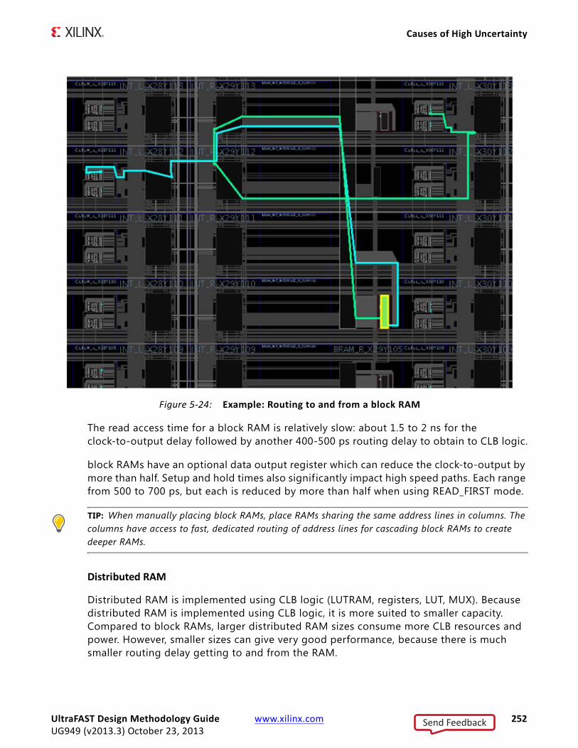
Causes of High Uncertainty
The read access time for a block RAM is relatively slow: about 1.5 to 2 ns for the clock-to-output delay followed by another 400-500 ps routing delay to obtain to CLB logic.
block RAMs have an optional data output register which can reduce the clock-to-output by more than half. Setup and hold times also signif icantly impact high speed paths. Each range from 500 to 700 ps, but each is reduced by more than half when using READ_FIRST mode.
TIP: When manually placing block RAMs, place RAMs sharing the same address lines in columns. The columns have access to fast, dedicated routing of address lines for cascading block RAMs to create deeper RAMs.
Distributed RAM
Distributed RAM is implemented using CLB logic (LUTRAM, registers, LUT, MUX). Because distributed RAM is implemented using CLB logic, it is more suited to smaller capacity. Compared to block RAMs, larger distributed RAM sizes consume more CLB resources and power. However, smaller sizes can give very good performance, because there is much smaller routing delay getting to and from the RAM.
X-Ref Target - Figure 5-24
Figure 5-24: Example: Routing to and from a block RAM
UltraFAST Design Methodology Guide www.xilinx.com 252UG949 (v2013.3) October 23, 2013
Send Feedback
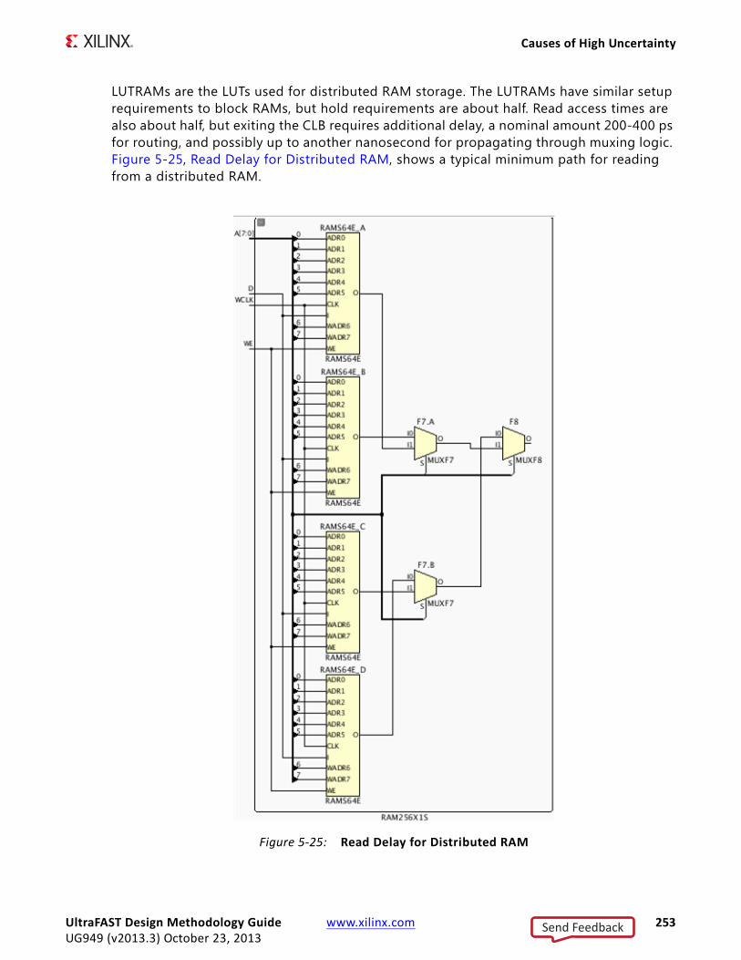
Causes of High Uncertainty
LUTRAMs are the LUTs used for distributed RAM storage. The LUTRAMs have similar setup requirements to block RAMs, but hold requirements are about half. Read access times are also about half, but exiting the CLB requires additional delay, a nominal amount 200-400 ps for routing, and possibly up to another nanosecond for propagating through muxing logic. Figure 5-25, Read Delay for Distributed RAM, shows a typical minimum path for reading from a distributed RAM.
X-Ref Target - Figure 5-25
Figure 5-25: Read Delay for Distributed RAM
UltraFAST Design Methodology Guide www.xilinx.com 253UG949 (v2013.3) October 23, 2013
Send Feedback

Causes of High Uncertainty
Comparison Between block RAM and Distributed RAM
The following examples highlight the differences between block RAM and distributed RAM. Two different sizes of single port RAMs are created using IP Catalog with the IP defaults for a Virtex®-7 -2 speedgrade. The post-route results reflect ideal conditions. Actual performance may vary depending on the surrounding logic of the containing design.
The results indicate that for this depth and width, a block RAM implementation gives better overall results. The distributed RAM critical path is shown in Figure 5-26, Critical Path through Distributed RAM.
Note: Fmax can be increased by adding pipeline stages to balance delays throughout the decoding logic, but will be limited by the delay through the RAM primitive.
For this relatively small size, a distributed RAM implementation is fast, compact, and uses less routing resources.
Table 5-9: Comparison of 8kx32 RAM Implementations
block RAM Distributed RAM
Fmax Over 500 MHz 250 MHz
Area 8 RAMB36, 18 CLBs 2043 CLBs
Power 370 mW 440 mW
X-Ref Target - Figure 5-26
Figure 5-26: Critical Path through Distributed RAM
Table 5-10: Comparison Between 128x4 RAM Implementations
NA block RAM Distributed RAM
Fmax About 400 MHz Over 500 MHz
Area 1 RAMB18, 3 slices 4 slices
Power 260 mW 260 mW
UltraFAST Design Methodology Guide www.xilinx.com 254UG949 (v2013.3) October 23, 2013
Send Feedback

Causes of High Uncertainty
DSP48E1 Blocks
In most cases, synthesis and IP Catalog determine the best implementation for arithmetic functions. Most advanced functions (especially those that depend on wide, high-speed multiplication) are best implemented in DSP48E1 blocks which have dedicated hardware multipliers and ALUs to offload CLBs. The DSP48E1 is not only highly optimized internally, but also has dedicated high-speed routing along the DSP columns where the blocks are arranged. This enables multiple DSP48E1s to implement much wider multipliers and cascaded circuits such as pipelined FIR f ilters, all while running in excess of 500 MHz.
CLB carry logic is usually more appropriate for certain circuits such as multiplication by a constant and small-width multipliers. When resources of a certain type are overutilized or highly utilized, functions can be moved from one type to another. DSP48E1-based functions can be moved to CLB logic when running low on DSP blocks.
Similarly, many CLB-logic based functions can be moved to DSP48E1 when CLBs are overutilized. The latter is useful for addressing areas of congestion. The DSP48E1 not only implements multipliers and multiply-accumulate functions, but can implement adder-subtractors, counters, and even wide parallel logic gates.
The DSP48E1 block is pipelined with input and output registers and an intermediate register between the multiplier and ALU as shown in Figure 5-27.
All register stages must be used to achieve the highest performance which corresponds to a latency of three cycles. Following is an example of how the number of stages used affects
X-Ref Target - Figure 5-27
Figure 5-27: Pipelining Registers Available Within DSP48
UltraFAST Design Methodology Guide www.xilinx.com 255UG949 (v2013.3) October 23, 2013
Send Feedback
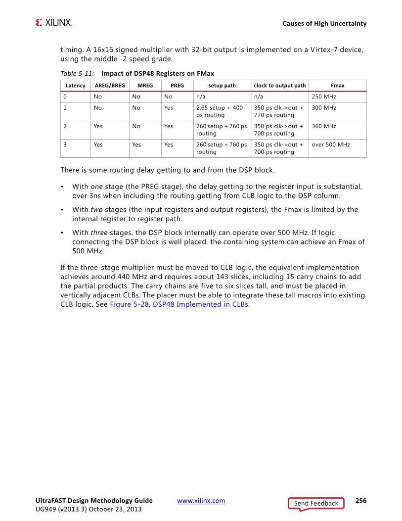
Causes of High Uncertainty
timing. A 16x16 signed multiplier with 32-bit output is implemented on a Virtex-7 device, using the middle -2 speed grade.
There is some routing delay getting to and from the DSP block.
• With one stage (the PREG stage), the delay getting to the register input is substantial, over 3ns when including the routing getting from CLB logic to the DSP column.
• With two stages (the input registers and output registers), the Fmax is limited by the internal register to register path.
• With three stages, the DSP block internally can operate over 500 MHz. If logic connecting the DSP block is well placed, the containing system can achieve an Fmax of 500 MHz.
If the three-stage multiplier must be moved to CLB logic, the equivalent implementation achieves around 440 MHz and requires about 143 slices, including 15 carry chains to add the partial products. The carry chains are f ive to six slices tall, and must be placed in vertically adjacent CLBs. The placer must be able to integrate these tall macros into existing CLB logic. See Figure 5-28, DSP48 Implemented in CLBs.
Table 5-11: Impact of DSP48 Registers on FMax
Latency AREG/BREG MREG PREG setup path clock to output path Fmax
0 No No No n/a n/a 250 MHz
1 No No Yes 2.65 setup + 400 ps routing
350 ps clk->out + 770 ps routing
300 MHz
2 Yes No Yes 260 setup + 760 ps routing
350 ps clk->out + 700 ps routing
360 MHz
3 Yes Yes Yes 260 setup + 760 ps routing
350 ps clk->out + 700 ps routing
over 500 MHz
UltraFAST Design Methodology Guide www.xilinx.com 256UG949 (v2013.3) October 23, 2013
Send Feedback
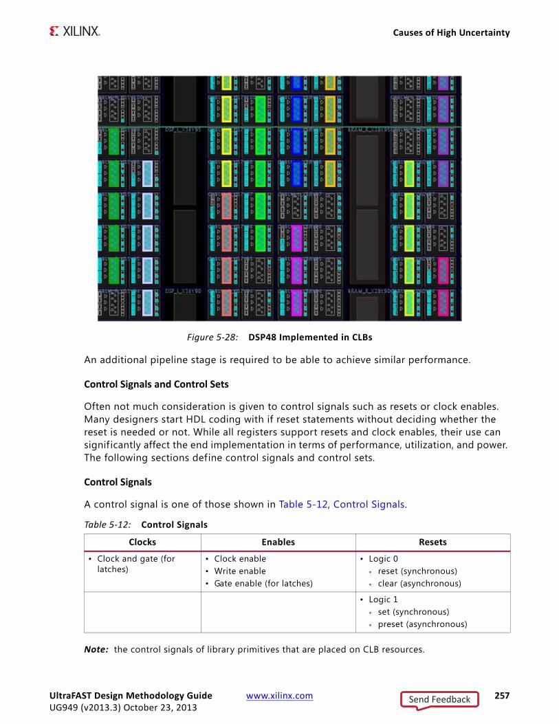
Causes of High Uncertainty
An additional pipeline stage is required to be able to achieve similar performance.
Control Signals and Control Sets
Often not much consideration is given to control signals such as resets or clock enables. Many designers start HDL coding with if reset statements without deciding whether the reset is needed or not. While all registers support resets and clock enables, their use can signif icantly affect the end implementation in terms of performance, utilization, and power. The following sections define control signals and control sets.
Control Signals
A control signal is one of those shown in Table 5-12, Control Signals.
Note: the control signals of library primitives that are placed on CLB resources.
X-Ref Target - Figure 5-28
Figure 5-28: DSP48 Implemented in CLBs
Table 5-12: Control Signals
Clocks Enables Resets
• Clock and gate (for latches)
• Clock enable• Write enable• Gate enable (for latches)
• Logic 0
° reset (synchronous)
° clear (asynchronous)
• Logic 1
° set (synchronous)
° preset (asynchronous)
UltraFAST Design Methodology Guide www.xilinx.com 257UG949 (v2013.3) October 23, 2013
Send Feedback

Causes of High Uncertainty
Control Sets
A control set is the group of clock, enable, and set/reset signals used by a sequential cell. This includes lack of enable and lack of set/reset. For example, two cells clocked by the same clock actually have different control sets if only one cell has a reset, or only one cell has a clock enable.
The number of unique control sets affects how many registers can be put together in a Slice, because all eight registers share the same clock, reset, and clock enable signal. This means that if two registers have a different clock, reset, or enable signal (including not having one), then they cannot share the same Slice. This can negatively impact not only utilization, but placement as well. This in turn can negatively impact performance and power.
In a Xilinx 7 series FPGA Slice (which is effectively half a CLB, eight registers per Slice), all share the same control signals, and therefore the same control set. If the number of registers in the control set does not divide cleanly by eight, some registers must go unused. This is mainly of concern in designs that have several very low fanout control signals, such as a clock enable that feeds a single register. A design with a large number of control sets potentially can often show lower utilization of registers due to the registers that must go unused.
For more information about control signals, see Chapter 4, Design Creation.
TIP: If you are facing issues such as utilization or congestion issues, use the report_control_sets Tcl command to see if your design has too many control signals.
If the number of control sets is high, use the following tips to reduce the number of controls sets, with special emphasis on those control sets which have a relatively low fanout.
• Avoid using sequential elements with both asynchronous and synchronous resets.
• Avoid asynchronous assignments to non-constant values. This causes many issues:
° It results in a larger circuit than most realize, two registers, a latch and a LUT.
° The sequential each have different control sets, occupying a minimum of 3 CLBs.
° Several asynchronous timing paths result that if not analyzed properly, may cause additional timing hazards affecting overall design stability.
• Use active high control signals when possible.
• Avoid asynchronous sets/resets. Each asynchronous reset is a control signal that cannot be moved to the data path. A resulting increase in control sets cannot be alleviated by dissolving the asynchronous reset or set into the data path logic, unlike when using synchronous resets or sets. This allows for greater flexibility in packing and placement.
UltraFAST Design Methodology Guide www.xilinx.com 258UG949 (v2013.3) October 23, 2013
Send Feedback

Causes of High Uncertainty
• Only use set / reset when necessary:
° Often data paths contain many registers that automatically flush uninitialized values.
° Registers of I/O, State machines and critical control signals that must be reset to known values should use sets and resets.
° With a synchronous reset, timing is assessed for both assertion and desertion of the signal. In general, synchronous signals are more predictable and suggested for use unless an asynchronous reset is absolutely needed.
• Occasionally clock enables are actually redundant logic that may not be reduced by synthesis or logic optimization.
• Use caution with fanout controls for synthesis and logic and physical optimization. Low fanout limits may unnecessarily introduce too many control sets.
Analyzing Common Design BottlenecksSome of the more commonly encountered design challenges are discussed in the following sections:
• Identifying the Longest Logic Delay Paths in the Design
• Identifying High Fanout Net Drivers
• Determining if Hold-Fixing is Negatively Impacting the Design
• Quickly Analyzing All Failing Paths
• Tuning the Compilation Flow
Identifying the Longest Logic Delay Paths in the Design
Timing paths correspond to logical paths in the design. Their delay is the accumulation of cell delays and net delays. The Vivado synthesis and implementation tools are timing-driven and work on optimizing the worst violating paths of your design throughout the compilation flow. If accumulated cell delay for a path is equal to or higher than the timing requirement (for example, usually the clock period of the path), the design is unlikely to meet timing after implementation. Analyzing the logic delay is better than simply counting logic levels, because it shows what the worst paths are before estimated or routed net delays become a factor. The result of this analysis is a list of the worst timing paths before placement and routing, and without net delay.
It is important to identify the paths that are the worst in terms of timing and not necessarily levels of logic. For example, unregistered block RAM have very large clock to out delay, while a series of carry chains may have multiple levels of levels of logic, each with a small delay.
UltraFAST Design Methodology Guide www.xilinx.com 259UG949 (v2013.3) October 23, 2013
Send Feedback

Causes of High Uncertainty
You must analyze these paths carefully before implementation. There are three typical categories for these long delay paths:
• block RAMs that do not take advantage of the embedded output register
• DSP48s that are not pipelined
• Long logic paths
The most eff icient method of identifying these long paths is to run a timing report post synthesis with the routing estimates set to none. This can be done by changing the Interconnect model to none in the Timer Settings tab of the Vivado IDE Timing Report dialog box, or by using the following Tcl command in the Tcl console or shell:
set_delay_model -interconnect none
Review the timing results to identify any failing paths. If there are paths that fail to meet timing without any routing delay, these paths will be impossible to meet timing with actual routing. These paths MUST be addressed immediately. Typically, these would have to be f ixed in RTL, but the violations could also be due to missing synthesis attributes, or incorrect timing constraints. After implementing the changes, the design will have sufficient slack as shown in Figure 5-29, Timing Report with 0 Interconnect.
Identifying High Fanout Net Drivers
High fanout nets often lead to implementation issues. As die sizes increase with each FPGA family, fanout problems also increase. It is often diff icult to meet timing on nets that have many thousands of endpoints, especially if there is additional logic on the paths, or if they are driven from non-sequential cells, such as LUTs or distributed RAMs.
Many times, designers address the high fanout nets in RTL and synthesis, but, if not, phys_opt_design also can help alleviate timing issues caused by fanout.
It is important to look at the list of high fanout signals post synthesis as well as post phys_opt. The command to identify these nets is report_high_fanout_nets .
X-Ref Target - Figure 5-29
Figure 5-29: Timing Report with 0 Interconnect
UltraFAST Design Methodology Guide www.xilinx.com 260UG949 (v2013.3) October 23, 2013
Send Feedback
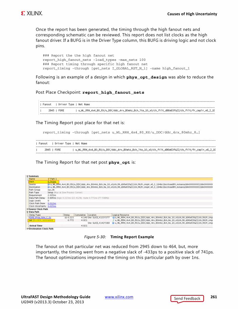
Causes of High Uncertainty
Once the report has been generated, the timing through the high fanout nets and corresponding schematic can be reviewed. This report does not list clocks as the high fanout driver. If a BUFG is in the Driver Type column, this BUFG is driving logic and not clock pins.
### Report the the high fanout netreport_high_fanout_nets -load_types -max_nets 100### Report timing through specific high fanout netreport_timing -through [get_nets I_GLOBAL_RST_N_i] -name high_fanout_1
Following is an example of a design in which phys_opt_design was able to reduce the fanout:
Post Place Checkpoint: report_high_fanout_nets
The Timing Report post place for that net is:
report_timing -through [get_nets u_WL_RRH_4x4_80_RX/u_DDC/ddc_4rx_80mhz_8…]
The Timing Report for that net post phys_opt is:
The fanout on that particular net was reduced from 2945 down to 464, but, more importantly, the timing went from a negative slack of -433ps to a positive slack of 741ps. The fanout optimizations improved the timing on this particular path by over 1ns.
X-Ref Target - Figure 5-30
Figure 5-30: Timing Report Example
UltraFAST Design Methodology Guide www.xilinx.com 261UG949 (v2013.3) October 23, 2013
Send Feedback

Causes of High Uncertainty
The FLAT_PIN_COUNT property of each net indicates the number of leaf cells connected to this net throughout the design hierarchy. Use the get_property command to extract the FLAT_PIN_COUNT property:
get_property FLAT_PIN_COUNT [get_nets my_hfn]
By using some Tcl scripting, you can easily report the worst slack of all paths that propagate through any particular high fanout net.
Determining if Hold-Fixing is Negatively Impacting the Design
The Vivado Design Suite router prioritizes f ixing hold over setup. This is because your design may work in the lab if you are failing setup by a small amount. There is always the option of lowering the clock frequency. If you have hold violations, the design will most likely not work.
In most cases, the router can meet the hold timing without affecting the setup. In some cases (mostly due to errors in the design or the constraints), the setup time will be signif icantly affected. Improper hold checks are often caused by improper set_multicycle_path constraints in which the -hold was not specified. In other cases, large hold requirements are due to excessive clock skew. In this case, Xilinx recommends that you review the clocking architecture for that particular circuit. For more information, see Identifying Timing Violations Root Cause, page 234.
This may occur if your design meets setup timing post placement, but fails set up post route.
TIP: Analyze the estimated hold timing post place and identify any unusually large hold violations (over 500ps).
If you suspect that hold f ixing is affecting timing closure, you can use one of the following to determine if this is the case:
• Method 1: Routing without hold fixing
• Method 2: Run report_timing -min on Worse Failing Setup Path
Method 1: Routing without hold fixing
1. Read the post-placed checkpoint into Vivado Design Suite.
2. Add a constraint to disable all hold checking:
set_false_path -hold -to [all_clocks]
CAUTION! This constraint is for test purposes only. Never do this for designs that will be put into production or delivered to another designer. You must remove this constraint before the production design.
UltraFAST Design Methodology Guide www.xilinx.com 262UG949 (v2013.3) October 23, 2013
Send Feedback

Causes of High Uncertainty
3. Run route_design and report_timing_summary.
If there is a significant difference between the WNS with and without the hold checks, the hold violations might be too large, and the setup paths are being affected.
Method 2: Run report_timing -min on Worse Failing Setup Path
To determine whether the worst failing setup path is due to hold fixing, review the hold timing of that path. In the Vivado IDE, right click and report timing on source to destination. As opposed to doing the setup timing analysis, it is important to look at the hold timing. Once you have the hold report, verify the requirement and ensure that additional delay was not added on the path to be able to meet hold.
Quickly Analyzing All Failing Paths
The report_timing_summary command is a powerful tool for determining all the timing information for your design. Sometimes it is beneficial to simply look at all of the failing paths in a single report. The command below works from the command line or from within the IDE.
report_timing -max_paths 100 -slack_less_than 0 -name worse_100_setup
TIP: When using the IDE, you can export the timing results to a spreadsheet to do more comprehensive analysis of the failing paths.
X-Ref Target - Figure 5-31
Figure 5-31: Running Timing Report on Specific Paths
UltraFAST Design Methodology Guide www.xilinx.com 263UG949 (v2013.3) October 23, 2013
Send Feedback
Causes of High Uncertainty
The command above reports the top 100 failing paths. If there are less than 100 failing paths, only the failing paths are reported because of the -slack_less_than 0 option. Reviewing the failing paths in a single list helps to quickly identify the order of magnitude differences among the failing paths.
For example, the WNS could be -3ns, which affects a few paths, but then the next WNS in the list could be at -300ps or better.
By default, when you analyze timing failures, you see the single worst timing path per endpoint. There are generally many similar paths for the common failing endpoint.
To review all worst paths for a single endpoint, use the -nworst option with the report_timing command. For example, run the following command to see all paths leading to the worst case failing endpoint (assuming there are less than 100):
report_timing -max_paths 100 -nworst 100
Reviewing all the worst paths may yield considerable data. To minimize the amount of data to analyze, you can review only the unique portions of paths by using the -unique_pins option with the report_timing command. This provides a single path for each unique combination of pins through the timing path. For example:
report_timing -max_paths 100 -nworst 100 -unique_pins
Tuning the Compilation Flow
The default compilation flow provides a quick way to obtain a baseline of the design and start analyzing the design if timing is not met. After initial implementation, tuning the compilation flow might be required to achieve timing closure.
• Strategies and Directives
• Optimization Iterations
• Incremental Compilation
• Overconstraining the Design
Strategies and Directives
Strategies and directives can be used to increase the implementation solution space and f ind the most optimal solution for your design. The strategies are applied globally to a project implementation run, while the directives can be set individually on each step of the implementation flow in both project and non-project modes. The pre-defined strategies should be tried f irst before trying to customize the flow with directives. Xilinx does not recommend running the SSI strategies for a non-SSI device.
If timing cannot be met with a default strategy, you can manually explore a custom combination of directives. Because placement typically has a large impact on overall design performance, it can be beneficial to try various placer directives with only the I/O location
UltraFAST Design Methodology Guide www.xilinx.com 264UG949 (v2013.3) October 23, 2013
Send Feedback

Causes of High Uncertainty
constraints and with no other placement constraints. By reviewing both WNS and TNS of each placer run (these values can be found in the placer log), you can select two or three directives that provide the best timing results as a basis for the downstream implementation flow.
For each of these checkpoints, several directives for phys_opt_design and route_design can be tried and again only the runs with the best estimated or f inal WNS/TNS should be kept. In Non-Project Mode, you must explicitly describe the flow with a Tcl script and save the best checkpoints. In Project Mode, you can create individual implementation runs for each placer directive, and launch the runs up to the placement step. You would continue implementation for the runs that have the best results after the placer step (as determined by the Tcl-post script).
Physical constraints (Pblocks and DSP and RAM macro constraints) can prevent the placer from finding the most optimal solution. Xilinx therefore recommends that you run the placer directives without any Pblock constraints. The following Tcl command can be used to delete any Pblocks before placement with directives commences:
delete_pblock [get_pblocks *]
Running place_design -directive <directive> and analyzing placement of the best results can also provide a template for floorplanning the design to stabilize the flow from run to run.
Optimization Iterations
Sometimes it is advantageous to iterate through a command multiple times to obtain the best results. For example, it might be helpful to f irst run phys_opt_design with the force_replication_on_nets option in order to optimize some critical nets that appear to have an impact on TNS during route:
phys_opt_design -force_replication_on_nets
Next run phys_opt_design with any of the directives to improve the overall WNS of the design.
In Non-Project Mode, use the following commands:
phys_opt_design -force_replication_on_nets [get_nets -hier *phy_reset*]phys_opt_design -directive <directive name>
In Project Mode, the same results can be achieved by running the first phys_opt_design command as part of a Tcl-pre script for a phys_opt_design run step which will run using the -directive option.
UltraFAST Design Methodology Guide www.xilinx.com 265UG949 (v2013.3) October 23, 2013
Send Feedback

Causes of High Uncertainty
Incremental Compilation
Incremental compilation has been discussed earlier in the chapter.
Incremental compile yields the best results when preserving QOR for a design when the critical path of the reference design is not affected by the changes in the current design.
Overconstraining the Design
When the design fails timing by a small amount after route, it is usually due to a small timing margin after placement. It is possible to increase the timing budget for the router by tightening the timing requirements during placement and physical optimization. The recommended way to do this is to use the set_clock_uncertainty constraint for the following reasons:
• It does not modify the clock relationships (clock waveforms remain unchanged).
• It is additive to the tool-computed clock uncertainty (jitter, phase error).
• It is specif ic to the clock domain or clock crossing specif ied by the -from and -to options.
• It can easily be reset by applying a null value to override the previous clock uncertainty constraint.
In any case, Xilinx recommends that you:
• Overconstrain only the clocks or clock crossing that cannot meet setup timing.
• Reset the extra uncertainty before running the router step.
See the following example:
A design misses timing by -0.2ns on paths with the clk1 clock domain and on paths from clk2 to clk3 by -0.3ns before and after route.
1. Load netlist design and apply the normal constraints.
2. Apply the additional clock uncertainty to overconstrain certain clocks.
a. The value should be at least the amount of violation.
b. The constraint should be applied only to setup paths.
set_clock_uncertainty -from clk0 -to clk0 0.3 -setupset_clock_uncertainty -from clk2 -to clk3 0.4 -setup
3. Run the flow up to the router step. It is best if the pre-route timing is met.
4. Remove the extra uncertainty.
set_clock_uncertainty -from clk0 -to clk0 0 -setupset_clock_uncertainty -from clk2 -to clk3 0 -setup
5. Run the router.
UltraFAST Design Methodology Guide www.xilinx.com 266UG949 (v2013.3) October 23, 2013
Send Feedback

Causes of High Uncertainty
After the router, you can review the timing results to evaluate the benefits of overconstraining. If timing was met after placement but still fails by some amount after route, you can increase the amount of uncertainty and try again.
RECOMMENDED: Do not overconstrain beyond 0.5ns.
Floorplanning
Floorplanning allows you to guide the tools, either through high-level hierarchy layout, or through detail placement. This can provide improved QOR and more predictable results. You will achieve the greatest improvements by f ixing the worst problems or the most common problems. For example if there are outlier paths that have signif icantly worse slack, or high levels of logic, f ix those paths f irst by grouping them in a same region of the device through a Pblock. Limit floorplanning only to portions of design that need additional human help through floorplanning, rather than floorplanning the entire design.
Floorplanning logic that is connected to the I/O to the vicinity of the I/O can sometimes yield good results in terms of predictability from one compilation to the next. In general, it is best to keep the size of the Pblocks to a clock region. This provides the most flexibility for the placer. Avoid overlapping Pblocks, as these shared areas could potentially become more congested. Minimize the number of nets that cross Pblocks.
There are extra considerations for Stacked Silicon Interconnect (SSI) devices. The SSI devices are made of multiple Super Logic Regions (SLRs), joined by an interposer. The interposer connections are called Super Long Lines (SLLs). There is some delay penalty when crossing from one SLR to another. To minimize the impact of the SLL delay on your design, floorplan the design so that SLR crossings are not part of the critical path. Minimizing SLR crossings through floorplanning by keeping a Pblock within one SLR only can also improve timing and routability of the design targeting SSI devices.
Preserving Placement and Routing
Once you have results that meet your timing constraints, you might want to lock down the placement and possibly the routing of the critical portions of your design. This can help preserve the performance of your circuitry, and also provide more predictable results for future runs.
It is fairly easy to re-use the placement of:
• I/Os
• Global Clock Resources
• block RAM macros
• DSP macros
UltraFAST Design Methodology Guide www.xilinx.com 267UG949 (v2013.3) October 23, 2013
Send Feedback
Causes of High Uncertainty
Re-using this placement helps reduce the variability in results from one netlist revision to the next. These primitives generally have stable names and the placement is usually easy to maintain.
It is sometimes desired to preserve the routing of a critical net or a portion of a critical net to guarantee the same timing from run to run. Routing for critical nets can be preserved by setting the property is_route_fixed of the net to 1. This can be done by using the Vivado IDE or through a Tcl command. To f ix the routing on a net in the Vivado Design Suite, select the net in the device view, right click and select Fix Routing from the context menu.
The Tcl command example below fixes the routing for all nets in $net:
set_property IS_ROUTE_FIXED 1 $net
This marks the route as f ixed and adds a constraint to the in-memory design. Nets with f ixed routing are shown as dashed lines in the Device View.
X-Ref Target - Figure 5-32
Figure 5-32: Preserving a Specific Route
UltraFAST Design Methodology Guide www.xilinx.com 268UG949 (v2013.3) October 23, 2013
Send Feedback
Power
Pre-Routing Critical CircuitryYou can pre-route nets of critical portions of your design. Pre-routing nets ensures that the router has the most flexibility to get the optimal route for the critical nets. The following script shows an example of pre-routing critical nets:
# Get the nets in the top 10 critical paths, assign to $preRoutesset preRoutes [get_nets -of [get_timing_paths -max_paths 10]]route_design -nets [get_nets $preRoutes] -delayroute_design -directive Explore
The strategy in this example script is to:
• Identify the top ten critical paths using get_timing_paths.
• Create a list of the net objects ($preRoutes) of those critical paths using get_nets -of.
• Route those nets f irst.
The router f inishes any remaining unrouted nets.
If timing closure continues to be a challenge, identify the portion of the design with the failing or diff icult-to-meet timing paths. The corresponding portion of the hierarchy may be implemented out of context. This allows faster iterations through the various options and strategies. For an overview of the OOC flow, see the Vivado Design Suite User Guide: Hierarchical Design (UG905) [Ref 18].
PowerGiven the importance of power, the Vivado tools support methods for obtaining an accurate estimate for power, as well as it providing some power optimization capabilities.
Estimating Power Through All Stages in the Vivado Design Suite FlowAs your design flow progresses through synthesis and implementation, you must regularly monitor and verify the power consumption to be sure that thermal dissipation remains within budget. You can then take prompt remedial actions if power approaches your budget too closely.
The accuracy of the power estimates varies depending on the design stage when the power is estimated. To estimate power post-synthesis through implementation, run the report_power command, or open the Power Report in the Vivado IDE.
UltraFAST Design Methodology Guide www.xilinx.com 269UG949 (v2013.3) October 23, 2013
Send Feedback

Power
• Post Synthesis
The netlist is mapped to the actual resources available in the target device.
• Post Placement
The netlist components are placed into the actual device resources. With this packing information, the f inal logic resource count and configuration becomes available.
This accurate data can be exported to the Xilinx Power Estimator spreadsheet. This allows you to:
° Perform what-if analysis in XPE.
° Provide the basis for accurately f illing in the spreadsheet for future designs with similar characteristics.
For more information, see Chapter 3, Board and Device Planning.
• Post Routing
After routing is complete all the details about routing resources used and exact timing information for each path in the design are defined.
In addition to verifying the implemented circuit functionality under best and worst case gate and routing delays, the simulator can also report the exact activity of internal nodes and include glitching. Power analysis at this level provides the most accurate power estimation before you actually measure power on your prototype board.
Types of Power Estimation Supported by report_powerThe report_power command supports two modes of power analysis. Depending upon the accuracy desired, you can use the appropriate style.
Vector-Based Estimation
In parallel with all stages of the design development, you will generally perform simulations to verify that the design behaves as expected. Different verif ication techniques are available depending on the design development state; the design complexity; and your company’s policy.
The following paragraphs highlight the valuable data you can capture and common pitfalls related to using this data to perform power analysis. An important factor for getting accurate power estimation is that the design activity must be realistic. It should represent the typical or worst case scenario for data coming into the simulated block. This type of information is not necessarily provided while performing verif ication or validating functions.
UltraFAST Design Methodology Guide www.xilinx.com 270UG949 (v2013.3) October 23, 2013
Send Feedback
Power
Invalid data can be input to verify that the system can handle the data, and that it remains stable even when invalid data or commands are entered. Using such test cases to perform power analysis may result in inaccurate power estimation, because the design logic is not stimulated as it would be under typical system operation.
System Transaction Level
Early in the design cycle, you may have created a description of the transactions that occur between devices on a PCB, or between the different functions of your FPGA application. You can extract from this the expected activity per functional block for certain I/O ports and most of the clock domains. This information can help you fill in the Xilinx Power Estimator spreadsheet.
FPGA Description Level
While defining the RTL for your application, you can verify the functionality by performing behavioral simulations. This helps you verify the data flow and the validity of calculations to the clock cycle. The following are not yet available:
• Exact FPGA resources used
• Count
• Configuration
You can manually extrapolate resource utilization and extract activity for I/O ports or internal control signals (set, reset, clock enable). This information can be applied to refine the Xilinx Power Estimator spreadsheet information.
Your simulator should be able to extract node activity, and export it in the form of a SAIF f ile. You can save this f ile for more accurate power analysis in the Vivado Design Suite design flow (for example after place and route) if you do not plan to run post-implementation simulations.
FPGA Implementation Level
Simulation may be performed at different stages in the implementation process with different outcomes in terms of the power-related information that can be extracted. This additional information may also be used to refine the Xilinx Power Estimator spreadsheet and the Vivado Design Suite power analysis. It may also save I/O ports and specif ic module activity, which can be reused in the Vivado Design Suite power analysis feature.
Simulation File
The Vivado Design Suite Report Power matches nets in the design database with names in the simulation results netlist. The simulation data for power is stored in a Switching Activity Interchange Format (SAIF) or Value Change Dump (VCD) f ile. Xilinx highly recommends generating a SAIF f ile. This f ile is a more compact model of the design switching activity,
UltraFAST Design Methodology Guide www.xilinx.com 271UG949 (v2013.3) October 23, 2013
Send Feedback

Power
and uses much less disk space than the VCD file. The power estimate runtime and memory consumption using a SAIF file is also considerably smaller.
Because report_power does net name matching, it is best to obtain simulation results on the same design view (such as post-synthesis and post-routing) on which the power analysis is being carried out.
IMPORTANT: In the Vivado IDE, specify a SAIF or VCD file name in the Input Files tab of the Report Power dialog box to read a SAIF or VCD simulation output file. Alternatively, use the read_saif or read_vcd Tcl command to read the SAIF or VCD simulation output file. To generate a SAIF file from the Mentor Graphics ModelSim simulator for power analysis within the Vivado Design Suite, see Answer Record 53544.
Vectorless Estimation
When design node activity is not provided (either from you or from simulation results), the vectorless power estimation algorithms can predict this activity.
The vectorless engine assigns initial seeds (default signal rates and static probability) to all undefined nodes. Starting from the design primary inputs, it then propagates activity to the internal nodes through various circuit elements; and repeats this operation until the primary outputs are reached.
The algorithm understands the design connectivity and resource functionality and configuration. Its heuristics can even approximate the glitching rate for any nodes in the netlist. Glitching occurs when design elements change states multiple times in between active clock edges before settling to a final value.
While the vectorless propagation engine is not as accurate as a post-route simulation with a reasonably long duration and realistic stimulus, it is an excellent compromise between accuracy and compute eff iciency.
Best Practices for Accurate Power AnalysisUse the following for accurate power analysis:
• Accurate Clock Constraints
• Accurate I/O Constraints
• Accurate Signal Rate and %High on Top Level Control Signals
Accurate Clock Constraints
Because power is significantly dependent on the frequency of operation, clock frequency must be specified accurately.
UltraFAST Design Methodology Guide www.xilinx.com 272UG949 (v2013.3) October 23, 2013
Send Feedback

Power
In any design, you will typically know the activity of some specific nodes, since they are imposed by the system specification or the interfaces with which the FPGA device communicates. Providing this information to the tools helps guide the power estimation algorithms.
This information is especially helpful for nodes that drive multiple cells in the FPGA device:
• Set
• Reset
• Clock enable
• Clock signals
You will typically know the exact frequency of all FPGA clock domains, whether they are externally provided (input ports); or internally generated; or externally supplied to the printed circuit board (output ports).
Accurate I/O Constraints
With your knowledge of the exact protocols and format of the data flowing in and out of the FPGA device, you can usually specify signal transition rate and/or signal percentage high rate in the tools for at least some of the I/O components.
For example, some protocols have a DC balanced requirement (signal percentage high rate =50%), or you may know how often data is written or read from your memory interface. This allows you to set the data rate of strobe and data signals.
The board and other external capacitance driven by the output ports are typically known.
Enter the following in the Tcl prompt to set the load on all the output ports:
set_load <value in pF> [all_outputs]
Accurate Signal Rate and %High on Top Level Control Signals
With your knowledge of the system and the expected functionality, you may be able to predict the activity on control signals such as Set, Reset, and Clock Enable. Because these signals typically can turn on or turn off large pieces of the design logic, providing this activity information signif icantly increases the power estimation accuracy.
If you know the data patterns of your I/O interfaces, specify this activity. Unless you are calculating the total power per supply in a separate tool (such as a spreadsheet), specify the termination technique for your outputs to allow Report Power to include the amount of power the FPGA device supplies to these external components.
Accurate signal characteristics for all of the above type of signals can be provided through set_switching_activity in the Tcl prompt; or Signal Rate and Static Probability (% High) in the Power Properties window of the Vivado IDE.
UltraFAST Design Methodology Guide www.xilinx.com 273UG949 (v2013.3) October 23, 2013
Send Feedback
Power
Project Device Settings
Review the different user-editable selections in the Environment and Power Supply tabs of the Report Power dialog box. Make sure the process, voltage, and environment data closely match your expected environment. These settings have a signif icant influence on the total estimated power.
The user-editable selections in these tabs are:
• Device Settings
• Design Thermal Settings
• Voltage Supply Settings
Device Settings
• Temp Grade
Select the appropriate grade for the device (typically Commercial or Industrial). Some devices may have different device static power specifications depending on this setting. Setting this properly allows for the proper display of junction temperature limits for the chosen device.
• Process
The recommended process setting is Maximum for a worst-case analysis. Although the default setting of Typical gives a more accurate picture of the statistical measurements, changing the setting to Maximum modifies the power specification to worst-case values.
In the Tcl prompt, use the following to set the temp grade and process selections:
set_operating_conditions -process maximumset_operating_conditions -grade industrial
Design Thermal Settings
Review the different user-editable selections in the Environment tab of the Report Power dialog box.
• Ambient Temperature (°C)
Specify the maximum possible temperature expected inside the enclosure that will house the FPGA design. This, along with airflow and other thermal dissipation paths (for example, the heatsink), allows an accurate calculation of Junction Temperature. This in turn allows a more accurate calculation of device static power.
In the Tcl prompt, enter the following to set the ambient temperature selection:
set_operating_conditions -ambient_temp 75
UltraFAST Design Methodology Guide www.xilinx.com 274UG949 (v2013.3) October 23, 2013
Send Feedback
Power
UltraFAST Design Methodology Guide www.xilinx.com 275
• Airflow (LFM)
The airflow across the chip is measured in Linear Feet per Minute (LFM). LFM can be calculated from the fan output in Cubic Feet per Minute (CFM) divided by the cross sectional area through which the air passes.
Specif ic placement of the FPGA device or fan may impact the effective air movement across the device, and thus the thermal dissipation. The default for this parameter is 250 LFM. If you plan to operate the FPGA device without active air flow (still air operation), change the 250 LFM default to 0 LFM.
In the Tcl prompt, enter the following to set the airflow selection:
set_operating_conditions - airflow 250
• Heat Sink (if available)
If a heatsink is used and more detailed thermal dissipation information is not available, choose an appropriate profile for the type of heatsink. This (along with other entered parameters) is used to help calculate an effective ThetaJB (printed circuit board thermal resistance), resulting in a more accurate junction temperature and quiescent power calculation. Some types of sockets may act as heatsinks, depending on the design and construction of the socket.
In the Tcl prompt, enter the following to set the heatsink selection:
set_operating_conditions - heatsink low
• Board Selection and # of Board Layers (if available)
Selecting an approximate size and stack of the board will help calculate the effective ThetaJB by taking into account the thermal conductivity of the board itself.
• ThetaJB (printed circuit board thermal resistance)
If more accurate thermal modeling of the board and system is available, use to specify the amount of heat dissipation expected from the FPGA device.
The more accurately custom ThetaJB can be specif ied, the more accurate the estimated junction temperature will be, thus affecting device static power calculations.
IMPORTANT: In order to specify a custom ThetaJB, the Board Selection must be set to Custom. If you specify a custom ThetaJB, you must also specify a Board Temperature for an accurate power calculation.
UG949 (v2013.3) October 23, 2013Send Feedback
U
Power
UltraFAST Design Methodology Guide www.xilinx.com 276
In the Tcl prompt, enter the following to set the board selection:
set_operating_conditions - board jedec
In the Tcl prompt, enter the following to set the ThetaJB selection:
set_operating_conditions - thetajb 3
Voltage Supply Settings
Review the different user-editable selections in the Power Supply tab of the Report Power dialog box.
• Power Supply
If this information is known, in the Power Supply tab make sure all voltage levels are set correctly for the different supply sources. Voltage is a large factor contributing to both static and dynamic power.
In the Tcl prompt, enter the following to set the voltage on the VccAux rail:
set_operating_conditions -voltage {Vccaux <value>}
Reviewing the Design Power Distribution After Running Vivado Design Suite Power AnalysisOpen the Summary view to review the Total On-Chip Power and thermal properties. The On-Chip Power graph shows the power dissipated in each of the device resource types. With this high-level view, you can determine which parts of your design contribute most to the total power. The Power Supply tab shows the current drawn for each supply source, and breaks down this total between static and dynamic power.
From the Utilization Details tab, to see more details of the power at the resource level, click the different resource types in the graph. The different resources views are organized as a tree table. Drag a column header to reorder the column arrangement. Click on a column header to change the sorting order.
Further Refining Control Signal Activity After Running Vivado Design Suite Power AnalysisWhen SAIF-based annotation has not been used for accurate power analysis, you can f ine-tune the power analysis after doing the first level analysis.
Report Power extracts and lists all the different control signals in the Signal view. You may know from the expected behavior of your application that some Set/Reset signals are not active in normal design operation. In that case, you may want to adjust the activity for these signals. Similarly, some signals in your application may disable entire blocks of the design when the blocks are not in use. Adjust their activity according to the expected functionality.
G949 (v2013.3) October 23, 2013Send Feedback
Power
UltraFAST Design Methodology Guide www.xilinx.com 277
Because synthesis tool and place and route algorithms can infer or remap control signals to optimize your RTL description, many of the signals listed in these views may be unfamiliar. If you unsure of what these signals are, let the tool determine the activity.
Writing Out a Power Report Text FileOpen the Report Power dialog box from the Flow Navigator window in the Vivado IDE. Use this dialog box to review power settings and adjust activity for known elements in your design.
For project documentation, you may want to save the power estimation results in an output text f ile.
In other circumstances, you may be experimenting with different mapping, placement, and routing options to close on performance or area constraints. Saving power results for each experiment can help you select the most power-effective solution when several experiments meet your requirements.
In the Tcl prompt, enter the following:
report_power -file report.pwr
The power engine writes out a f ile report.pwr in the current working directory. This f ile contains the power estimation results.
Exporting the Power Estimate from the Vivado Tools to XPEOpen the Report Power dialog box from the Vivado IDE. In this dialog box, you can review power settings and adjust activity for known elements in your design.
The Xilinx Power Estimator (XPE) output f ile saves all environment information, device usage, and design activity in a f ile (.xpe) which you can later import into the XPE spreadsheet. This is useful when your power budget is exceeded, and you do not think that software optimization features alone will be able to meet your budgets.
In this case, you can:
• Import the current implementation results into XPE.
• Explore different mapping, gating, folding, and other strategies.
• Estimate their impact on power before modifying the RTL code or rerunning the implementation.
Compare your assumptions in the XPE spreadsheet with these f inal results. This helps provide more accurate inputs for XPE for future designs.
UG949 (v2013.3) October 23, 2013Send Feedback

Power
UltraFAST Design Methodology Guide www.xilinx.com 278
In the Tcl prompt, enter the following:
report_power -xpe report.xpe
The power engine writes out a file report.xpe in the current working directory. This f ile can now be imported into the XPE spreadsheet.
Power OptimizationIf the power estimates are outside the budget, you must take steps to reduce power.
• Analyzing Your Power Estimation and Optimization Results
• Running Power Optimization
• Using the Power Optimization Report
• Using the Timing Report to Determine the Impact of Power Optimization
Analyzing Your Power Estimation and Optimization Results
Once you have generated the power estimation, Xilinx recommends the following:
• Examine the total power in the Summary section. Does the total power and junction temperature fit into your thermal and power budget?
• If the results are substantially over budget, review the power summary distribution by block type and by the power rails. This provides an idea of the highest power consuming blocks.
• Review the Hierarchy section. The breakdown by hierarchy provides a good idea of the highest power consuming module. You can drill down into a specific module to determine the functionality of the block. You can also cross-probe in the GUI to determine how specif ic sections of the module have been coded, and whether there are power efficient ways to recode it.
Running Power Optimization
Power optimization works on the entire design or on portions of the design (when set_power_opt is used) to minimize power consumption.
Power optimization can be run either pre-place or post-place in the design flow, but not both. The pre-place power optimization step focusses on maximizing power saving. This can result (in rare cases) in timing degradation. If preserving timing is the primary goal, Xilinx recommends the post-place power optimization step. This step performs only those power optimizations that preserve timing.
UG949 (v2013.3) October 23, 2013Send Feedback

Power
UltraFAST Design Methodology Guide www.xilinx.com 279
Using the Power Optimization Report
To determine the impact of power optimizations, run the following command in the TCL console to generate a power optimization report:
report_power_opt -file myopt.rep
Using the Timing Report to Determine the Impact of Power Optimization
Power optimization works to minimize the impact on timing while maximizing power savings. However, in certain cases, if timing degrades after power optimization, you can employ a few techniques to offset this impact.
Where possible, identify and apply power optimizations only on non-timing critical clock domains or modules using the set_power_opt XDC command. If the most critical clock domain happens to cover a large portion of the design or consumes the most power, review critical paths to see if any cells in the critical path were optimized by power optimization.
Objects optimized by power optimization have an IS_CLOCK_GATED property on them. Exclude these cells from power optimization.
To locate clock gated cells, run the following Tcl command:
get_cells -hier -filter {IS_CLOCK_GATED==1}
UG949 (v2013.3) October 23, 2013Send Feedback

Chapter 6
Configuration and Debug
Overview of Configuration and DebugConfiguration is the process of loading application-specif ic data (a bitstream) into the internal memory of the FPGA device. Debug is required if the design does meet expectations on the hardware. After successfully completing the design implementation, the next step is to load the design into the FPGA and run it on hardware.
ConfigurationThis section includes tips to successfully implement the targeted configuration solution after you have selected the configuration mode, and you are ready to load the design into the FPGA device. For the common configuration modes and for recommendations during the initial planning stage, see Chapter 3, Board and Device Planning.
Your design must be successfully synthesized and implemented before a bitstream (.bit) image can be created. Once the bitstream is created, it can be loaded onto the FPGA device through one of the two methods:
• Direct Programming
The bitstream is loaded directly to the FPGA device by means of a cable or processor.
• Indirect Programming
The bitstream can be loaded onto an external flash memory. The flash memory then loads the bitstream onto the FPGA device.
Xilinx® provides software tools that:
• Create the FPGA bitstream (.bit or .rbt)
• Format the bitstream into flash programming files (.mcs)
• Directly program the FPGA device
• Indirectly program the attached configuration flash device
UltraFAST Design Methodology Guide www.xilinx.com 280UG949 (v2013.3) October 23, 2013
Send Feedback

Configuration
Software Flow Overview
Xilinx provides several configuration solutions. There are a few general settings applicable to all modes and unique settings applicable to a specif ic configuration mode that should be reviewed in order to ensure a seamless implementation.
The section discusses recommendations beginning with the bitstream generation through the FPGA configuration.
Bitstream GenerationThis section highlights key properties related to the different configuration modes for the bitstream file generation.
• For more information on Configuration bitstream generation properties and values, see the Vivado® Design Suite User Guide: Programming and Debugging (UG908) [Ref 21].
• For more information on the write_bitstream command, see the Vivado Design Suite Tcl Command Reference Guide (UG835) [Ref 24].
• For more information on how to use the write_bitstream command, see the Vivado Design Suite Video: How to Use the “write_bitstream” Command in Vivado [Ref 29].
Bitstreams (.bit) are binary files that represent a user design. The bitstreams contain configuration data that can be loaded into the FPGA device.
There are several bitstream file format options and a variety of bitstream input options that enable features by initializing FPGA internal configuration registers. Before generating the bitstream file, it is important to review the bitstream input options to ensure they are set correctly for the target configuration mode. In the Vivado tools, the configuration settings are managed by using the Tcl command write_bitstream. Use the set_property command in an XDC file to set the appropriate configuration setting property and value.
X-Ref Target - Figure 6-1
Figure 6-1: Direct and Indirect Programming of FPGA
UltraFAST Design Methodology Guide www.xilinx.com 281UG949 (v2013.3) October 23, 2013
Send Feedback

Configuration
General Bitstream Properties
During bitstream generation, review the following common options to ensure that they are set properly for successful configuration:
• Configuration clock settings
• Configuration startup cycle settings
• Compression
• Encryption bitstream settings
These settings are needed to ensure your device will complete configuration successfully and must be tailored to the Configuration mode used.
Bitstream generation properties can be set in an XDC file or the Tcl command shell before running the Generate Bitstream step in the Vivado tools. The following examples provide the name of the property to be used through the set_property command. Use list_property_value to see the possible values that the property can take.
• The configuration clock frequency (required for master mode configuration) is set by the CONFIGRATE option. This option sets the nominal internal configuration clock oscillator frequency (in MHz). The actual clock frequency might be within a range of +-50% of the specif ied value. Hence, you should ensure that the upper value of the actual frequency range lies within the maximum supported frequency for the desired configuration mode setup. Each FPGA device family has a unique set of values.
set_property BITSTREAM.CONFIG.CONFIGRATE
• The configuration startup clock selected is dependent on the configuration mode. For JTAG, the startup clock selected in the bitstream should be JtagClk . For other configuration modes the most popular selection is Cclk , which allows the FPGA device to use the clock provided on the CCLK or EMCCLK for clocking its startup state machine.
set_property BITSTREAM.STARTUP.STARTUPCLK
• Use the External Master Configuration Clock (EMCCLK) rate option in Master Mode to obtain a more precise (and faster) configuration clock. If you use this feature, then you must:
° Instantiate the EMCCLK signal in your design at RTL entry.
° Define the I/O standard used.
° Set the bitstream property after implementation.
set_property BITSTREAM.CONFIG.EXTMASTERCCLK_EN
• Designs that are close to a flash boundary size can benefit from bitstream compression. Compression will also reduce the flash programming time.
set_property BITSTREAM.GENERAL.COMPRESS
UltraFAST Design Methodology Guide www.xilinx.com 282UG949 (v2013.3) October 23, 2013
Send Feedback

Configuration
• The startup sequence is critical. Use the default STARTUP Cycle settings in most cases.
set_property BITSTREAM.STARTUP.DONE_CYCLE
• Xilinx FPGA device programmed content can be verif ied by means of JTAG. To perform a verify operation, create a mask file (.msk) in the same directory as the bitstream using the -mask_file option along with the -readback_file option of the write_bitstream command.
Bitstream Properties for Master SPI Configuration Mode
In Master SPI configuration mode, specific options enable key features during bitstream generation. Review the following settings when generating a properly formatted bitstream for the Master SPI configuration mode.
• For SPI NOR Flash 256Mbit or larger, the FPGA device must use the 32 bit addressing option.
set_property BITSTREAM.CONFIG.SPI_32BIT_ADDR
• For SPI NOR Flash set the bus width to the correct value. Bus widths wider than default provide faster configuration performance.
set_property BITSTREAM.CONFIG.SPI_BUSWIDTH
• For SPI NOR Flash, when faster performance is required, enable the option for the FPGA device to clock in the data at the falling edge. Since SPI NOR flash clocks the data out at a falling edge, this option provides one full cycle for the data to reach the FPGA device, thus allowing for higher frequency of CCLK.
set_property BITSTREAM.CONFIG.SPI_FALL_EDGE
• Because SPI flash does not have a wraparound indicator like parallel NOR flash, enabling a timer is necessary for MultiBoot Designs to detect a configuration failure.
set_property BITSTREAM.CONFIG.TIMER_CFG
Bitstream Properties for Master BPI Configuration Mode
In Master BPI configuration mode, there are specif ic options that enable key features during bitstream generation. Review the following settings when generating a properly formatted bitstream for the Master BPI configuration mode.
• If Master BPI configuration mode with asynchronous read is required, but a faster performance is also desired, use the page mode and read cycle options. To enable these features use these options:
set_property BITSTREAM.CONFIG.BPI_PAGE_SIZE set_property BITSTREAM.CONFIG.BPI_1ST_READ_CYCLE
• For even faster performance in Master BPI Configuration mode, the burst synchronous read option is available starting with the Xilinx 7 series FPGA devices. It is supported
UltraFAST Design Methodology Guide www.xilinx.com 283UG949 (v2013.3) October 23, 2013
Send Feedback

Configuration
for select parallel NOR flash such as the Micron G18F (Type 1)and Micron P30/P33 (Type 2) flash families.
set_property BITSTREAM.CONFIG.BPI_SYNC_MODE
Bitstream Properties for Encryption
Specif ic bitstream generation options enable security encryption features during bitstream generation. Review the following settings when encryption is required:
• BITSTREAM.ENCRYPTION.ENCRYPT
• BITSTREAM.ENCRYPTION.ENCRYPTKEYSELECT
• BITSTREAM.ENCRYPTION.KEY0
• BITSTREAM.ENCRYPTION.HKEY
• BITSTREAM.ENCRYPTION.KEYFILE
• BITSTREAM.ENCRYPTION.STARTCBC
Bitstream Properties for a MultiBoot System
Some systems may want to implement fail safe implementation or enable switching amongst more than one design for different versions in an application. To support these setups there are MultiBoot settings controlled by settings in Configuration registers. These can be set in the bitstream or by writing to the Internal Configuration Access Port (ICAP). The discussion below assumes they will be set in the .bit f ile by the write_bitstream command according to the BITSTREAM properties applied.
MultiBoot configurations often refer to one image as a fallback (or golden) known good image and the other images can be updated regularly and is referred to as the MultiBoot image. Below are some of the bitstream properties that should be set when working with a MultiBoot application. This setup assumes the Golden bitstream is placed at 0x0 and a single MultiBoot in an upper sector of flash memory. The MultiBoot image is loaded f irst.
Golden Bitstream
set_property BITSTREAM.CONFIG.CONFIGFALLBACK set_property BITSTREAM.CONFIG.NEXT_CONFIG_REBOOT set_property BITSTREAM.Config.TIMER_CFG set_property BITSTREAM.Config.next_config_addr
MultiBoot Bitstream
set_property BITSTREAM.CONFIG.CONFIGFALLBACK set_property BITSTREAM.CONFIG.NEXT_CONFIG_REBOOT
UltraFAST Design Methodology Guide www.xilinx.com 284UG949 (v2013.3) October 23, 2013
Send Feedback

Configuration
Flash File GenerationFor processor usage with SelectMAP configuration modes that have differing data bus widths (x16 or x32), or for flash memory device usage in SPI or BPI configuration modes, specially formatted files are required for programming. One popular f ile format is Intel Hex (.mcs). This f ile format is an ASCII text f ile with lines containing hexadecimal values encoding a sequence of data and their starting offset or absolute address.
The Xilinx command line utility PROMGen or the GUI iMPACT PROM File Formatter are used to generate the flash programming f iles. These utilities convert a bitstream (.bit) into a flash programming f ile (.mcs).
IMPORTANT: You must install LabTools from ISE® in order to generate .mcs files.
Data ordering is a key option. You must set it properly during the flash programming file generation step. See the following two examples:
promgen -spipromgen -data_width 8|16|32
Without specifying these options appropriately for the target flash device, the files loaded into the flash do not configure properly because the data ordering for the targeted data width would be incorrect.
Vivado Design Suite Device Programmer - In-System JTAG ProgrammingThe Vivado Design Suite Device Programmer has several functions. The most common uses of the programmer are: program the FPGA device by means of JTAG with a Xilinx supported download cable, indirectly program external SPI flash and parallel NOR flash, or program FPGA device eFUSE AES key or user code.
For more information on support and commands see:
• Vivado Design Suite Tcl Command Reference Guide (UG835) [Ref 24]
• Vivado Design Suite User Guide: Programming and Debugging (UG908) [Ref 21]
Configuring the FPGA Device Using JTAG
The majority of user designs target JTAG configuration mode for board bringup. This simple interface allows for quick turns to test the FPGA design functionality. The JTAG cable connector is required for this mode. When programming the FPGA device using the Vivado Design Suite Device Programmer, keep in mind that the JTAG maximum frequency is limited by the slowest device in the JTAG chain.
UltraFAST Design Methodology Guide www.xilinx.com 285UG949 (v2013.3) October 23, 2013
Send Feedback
Configuration
Indirectly Programming SPI NOR or Parallel NOR Flash
For the basic configuration solution using external flash, the FPGA device automatically retrieves the bitstream from a flash memory at power-on. Since the FPGA device is connected to the flash memory for configuration this enables the FPGA device to program the flash through the connected interface.
Indirectly programming flash in-system is a popular option during prototyping. The iMPACT (part of LabTools in ISE) software tool supports indirectly programming select SPI NOR and parallel NOR flash. The flash is indirectly programmed by pre-loading a JTAG-to-SPI or JTAG-to-BPI bitstream image. See the iMPACT Help document for a list of supported flash memory devices. Unused I/O programmable pullup or pulldown behavior on the pre-loaded bitstream image must be handled to prevent contention. For Xilinx 7 series FPGA devices, the pre-made bitstream has unused I/O set to 3-state. If any signal cannot tolerate this state, they must be pulled up or down externally.
RECOMMENDED: Maximum cable speed for flash operations are described in the software manuals and should not be exceeded.
For additional information on indirectly programming SPI flash or parallel NOR flash, see:
• Using SPI Flash with 7 Series FPGAs (XAPP586) [Ref 32]
• BPI Fast Configuration and iMPACT Flash Programming with 7 Series FPGAs (XAPP587) [Ref 33]
Programming AES Key into BBR or eFUSE
The bitstream that defines the functionality of the FPGA device loads into the device during power-on. If you want to protect the bitstream and any intellectual property (IP) cores embedded in the device, several techniques are available. The most powerful techniques to provide a high degree of design security are:
• Advanced Encryption Standard (AES-256) encryption with a battery-backed SRAM key
• AES-256 with the non-volatile eFUSE key.
Table 6-1: Recommendations for Flash Indirect Programming
Operation Recommendation
Erase Flash devices are non-volatile devices and must be erased before programming. Unless a full chip erase is specified, only the address range covered by the assigned MCS is erased.
BlankCheck Verify the erase operation
Readback Read back the contents of the flash into a file for comparison against the original flash programming file. This operation will read back the entire flash contents, not just the address range covered by the assigned MCS
UltraFAST Design Methodology Guide www.xilinx.com 286UG949 (v2013.3) October 23, 2013
Send Feedback

Configuration
For more information, see the configuration user guide for your device family.
CAUTION! Take care when programming the eFUSE keys. These keys are one-time programmable, while the battery-backed SRAM keys can be erased and reprogrammed.
Basic Configuration Debug
The best practices discussed in this section will help enable debug and resolution if you encounter an issue when implementing a configuration solution.
Before you embark on a full debug of configuration solution, create and test a simple design using the bitstream defaults (for example, a counter or LED output pattern). This simple design test will help eliminate any potential issues with advanced bitstream settings or board interfaces.
The Xilinx Configuration Solution Center is an additional resource. For more information, see:
http://www.xilinx.com/support/answers/34904.htm
File Generation Review
If configuration does not complete successfully, review that the bitstream properties and flash programming f ile options were selected correctly. To verify the bitstream generation options used by an image, run the following Tcl command:
report_property [current_design]
This command displays all those properties that were changed from their default settings while being applied to a design. Where there are no values displayed, the default is applied.
Also, review the flash programming f ile generation options. For PROMGen, a review of the .prm f ile provides the list of options used.
Status Pins
There are physical status pins that are recommended to be accessible on the board for debug. The two most important signals are INIT_B and DONE. Connect these signals to LEDs.
The INIT_B has multiple functions. The pulsing of this pin from low to high indicates the completion of initialization at power-up. A falling INIT_B signal during configuration can indicate a CRC error in the bitstream seen by the FPGA device. Access to INIT_B and DONE is critical for FPGA configuration debug.
UltraFAST Design Methodology Guide www.xilinx.com 287UG949 (v2013.3) October 23, 2013
Send Feedback

Configuration
In addition to the status signals, certain key configuration pins provide helpful information. They must be handled carefully to prevent problems during configuration. These pins are shown in the following table
The FPGA family's configuration user guide provides additional pin description details and includes appropriate pull-up resistor values.
Status Register
If configuration has not completed properly, the status register provides important information about what errors may have caused the failure. For more information, see:
• FPGA family’s configuration user guide
• Xilinx Configuration Solution Center http://www.xilinx.com/support/answers/34909.htm
The FPGA Status register data on Xilinx 7 series FPGA devices can be read by the Vivado Design Suite Device Programmer by means of JTAG. In case of a configuration failure, this register captures the specif ic error conditions that can help identify the cause of a failure. In addition, the Status register allows you to verify the Mode pin settings M[2:0] and the bus width detect (for x16, this should be CFG BUS[25:24]=01).
Verification and Readback
If configuration is not successful, a JTAG readback/verify operation on the FPGA device can determine whether the intended configuration data was loaded correctly into the device. In the event of a discrepancy, the case can be investigated. In order to perform a JTAG verify operation with the Vivado Design Suite Device Programmer, a mask (.msk) f ile is required. The file is created during bitstream generation. See General Bitstream Properties, page 282.
Table 6-2: Key Configuration Pins
Pins Description
M[2:0] Should be tied and static during configuration. The FPGA device reads these mode pins at power up to determine what configuration mode needs to be used.
PROGRAM_B Will clear the FPGA configuration memory and cause configuration to begin again. PROGRAM_B is often tied to a push button for easy access. PROGRAM_B should be pulled high when it is not pulsed low.
CFGBVS Must be tied appropriately to support the 1.8V or 3.3V range appropriate for the user design.
PUDC_B Determines whether or not internal pull-ups are enabled on the SelectIO pin after power-up and during configuration. If enabled, the pins unused for Configuration process are pulled up. PUDC_B has no effect after configuration completes.
UltraFAST Design Methodology Guide www.xilinx.com 288UG949 (v2013.3) October 23, 2013
Send Feedback

Configuration
Configuration Sequence
During configuration, some basic checks can help isolate issues. Xilinx FPGA bitstreams have a unique header. The header includes a synchronization word, and can include an auto detect, configuration clock type and rate setting. For most FPGA devices, this sync word is AA995566
The sync word is a valuable debug parameter.
The FPGA configuration state machine does not begin until the sync word is recognized at the pins of the FPGA. In the event of a configuration that does not start, you can observe the configuration data pins to ensure the sync word is being received correctly. Additionally, if the bitstream header is seen properly, any increase in the configuration clock due to a configuration or EMCCLK option setting should be seen or the header was not recognized. See General Bitstream Properties, page 282.
Configuration StartupA common configuration sequence is followed for the FPGA device power up. This is described in detail in the FPGA device configuration user guides. Special options can require modif ications to the default sequence. For example, when the user design uses a PLL, the following options may be required so the DONE signal does not go high before the appropriate step is reached:
• Wait for PLL
• MMCM lock
• DCI match
If any of these options are used, be sure that the images in the configuration source are properly spaced for MultiBoot images. See the FPGA family's user guide for more information on MultiBoot image handling. In addition, when using Slave modes or the Master Mode EMCCLK option, be sure that enough clock cycles are supplied to complete the startup sequence.
When the startup clock (JTAGCLK, CCLK, EMCCLK) is not clocked to the end of the startup sequence, the following symptoms may indicate an incorrect or incomplete startup:
• I/O remains 3-stated.
• Dual mode pins operate in LVCMOS rather than the specif ied I/O standard.
• ICAP interface cannot be accessed from the FPGA device fabric because the configuration logic is locked.
Successful completion of startup is indicated by the EOS signal being driven High. This can be observed in the STATUS register, or detected in the FPGA device fabric using the STARTUP primitive.
UltraFAST Design Methodology Guide www.xilinx.com 289UG949 (v2013.3) October 23, 2013
Send Feedback
Configuration
For designs accessing the ICAP, Xilinx recommends that you instantiate the STARTUP primitive. This primitive has an EOS pin, which will indicate that: (1) the configuration process has completed; and (2) the ICAP is available for read and write access.
Remote UpdateXilinx FPGA devices support MultiBoot and fallback features that make updating systems in the field more robust. Bitstream images can be upgraded dynamically in the f ield. The MultiBoot and fallback feature can be used with all master configuration modes. To use 32 bit addressing, see:
http://www.xilinx.com/support/answers/51337.htm
The MultiBoot feature enables switching between images by the user application. If an error is detected during the MultiBoot configuration process, the device can trigger a fallback mechanism to retrieve a known bitstream from a different flash address.
Implementation of a robust in-system update solution involves a set of decisions around the initial configuration method, the update method, and any fallback mechanisms.
A MultiBoot solution requires a flash large enough to hold all required bitstreams. Because compression results can vary, Xilinx recommends considering the maximum uncompressed bitstream when planning the flash memory map. However, during actual saving of the multiple images in a flash, compression may be used.
There are some special cases when using advanced options with fallback.
• Master SPI configuration mode falls back to x1 mode, and the SPI 32 bit addressing requires special handling for fallback.
• BPI configuration mode synchronous read falls back to asynchronous read mode. This means that the higher clock speeds intended for synchronous read may fail if fallback is utilized. The clock frequency used must be able to accommodate both modes.
SSI ConfigurationConfiguring an SSI device is similar to configuring any traditional device. The tools create a single bitstream. All configuration features (such as encryption and SEU) and configuration modes are supported.
Configuration Details
Multi-SLR configuration is handled entirely by the configuration circuitry and Xilinx tools. Each SLR has its own configuration engine, which is virtually identical to that of a traditional device. The Master SLR contains the master configuration engine. The configuration engines of all other SLR components are treated as slaves.
UltraFAST Design Methodology Guide www.xilinx.com 290UG949 (v2013.3) October 23, 2013
Send Feedback
Configuration
The Xilinx tools create a single bitstream. When loaded, the bitstream sequentially configures the individual SLR components to provide the correct portion of the bitstream to the appropriate SLR.
Signals Tied Together
The following signals are tied together in the interposer:
• INIT
• DONE
• KEYCLEAR
This allows functions such as clear configuration key to operate quickly and consistently on all SLR components at once. Configuration feedback signaling completion of configuration or configuration error behaves the same as in a traditional device.
Bitstream Decryption
For operations such as bitstream encryption, a single key is used in all SLR components. Using a single key simplif ies the management of keys and configuration data, and allows the SSI device to appear and operate similar to all other Xilinx FPGA devices.
The bitstream decryption is performed in the SLR. The passing of data from SLR to SLR in the interposer remains encrypted to further prevent tampering or interception of configuration data.
Operations on a Per SLR Basis
While most operations behave identically as in a traditional device, the following operate on a per SLR basis:
• CAPTURE
• READBACK
• FRAME_ECC
This can help improve time to collect data, and, for ECC, correct any corrupted bits.
Components Existing Only in the Master SLR
Some configuration and device access components exist only in the Master SLR. Components such as the following are accessible only in the Master SLR:
• DEVICE_DNA
• USER_EFUSE
• XADC
UltraFAST Design Methodology Guide www.xilinx.com 291UG949 (v2013.3) October 23, 2013
Send Feedback

Debugging
While Boundary Scan exists in all SLR components, there is a weighted preference to use the Master SLR for its function.
DebuggingIn-system debugging allows you to debug your design in real time on your target device. This is an essential step in design completion. Invariably, you will encounter situations which are extremely diff icult to replicate in a simulator. Because of this, you must be able to debug the problem on the target device.
In this step, you provide your design with special debugging hardware to allow you to observe and control the design. After debugging is complete, you can remove the instrumentation or special hardware to increase performance and logic reduction.
The debugging step comes after you have successfully implemented your design. All necessary commands to perform programming of the FPGA devices and in-system debugging of the design can be run from the Program and Debug section of the Flow Navigator window in the Vivado Integrated Design Environment (IDE).
For more information, see Vivado Design Suite User Guide: Programming and Debugging (UG908) [Ref 21].
Probing the DesignThe probing phase of the in-system debugging consists of the following two steps:
1. Identify the signals or nets that must be probed. You can do this either at the RTL stage, or after synthesis.
2. Add debug cores to your design.
a. For signals selected for debug at the RTL stage, you can add the cores at RTL or post-synthesis.
b. For signals selected after synthesis, you can add the cores post-synthesis, before the rest of the implementation begins.
For signals identif ied for debug at the RTL stage, you do one of the following:
• Place the mark_debug attribute on them, and run the Set up Debug Wizard post-synthesis to connect debug cores.
• Manually add the debug cores to the design source code.
Note: This process is called HDL Instantiation Probing.
UltraFAST Design Methodology Guide www.xilinx.com 292UG949 (v2013.3) October 23, 2013
Send Feedback
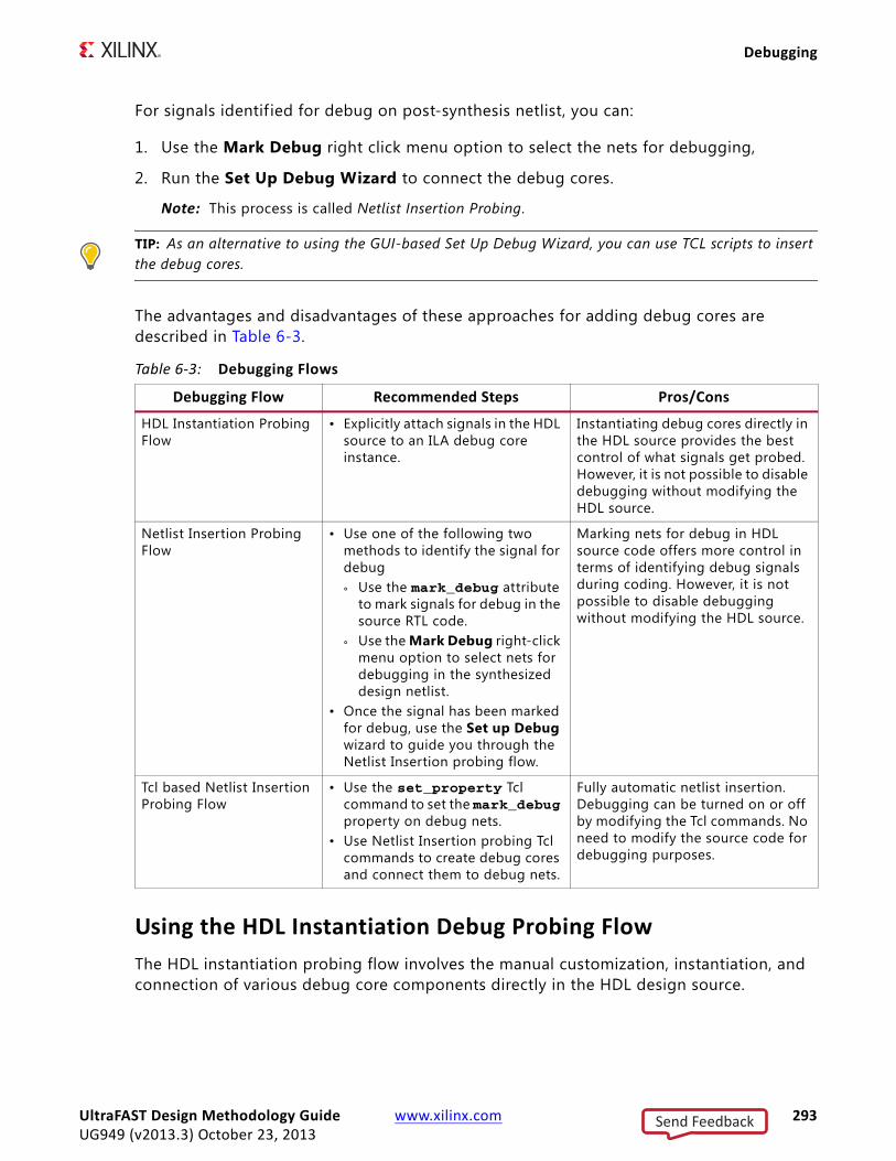
Debugging
For signals identif ied for debug on post-synthesis netlist, you can:
1. Use the Mark Debug right click menu option to select the nets for debugging,
2. Run the Set Up Debug Wizard to connect the debug cores.
Note: This process is called Netlist Insertion Probing.
TIP: As an alternative to using the GUI-based Set Up Debug Wizard, you can use TCL scripts to insert the debug cores.
The advantages and disadvantages of these approaches for adding debug cores are described in Table 6-3.
Using the HDL Instantiation Debug Probing FlowThe HDL instantiation probing flow involves the manual customization, instantiation, and connection of various debug core components directly in the HDL design source.
Table 6-3: Debugging Flows
Debugging Flow Recommended Steps Pros/Cons
HDL Instantiation Probing Flow
• Explicitly attach signals in the HDL source to an ILA debug core instance.
Instantiating debug cores directly in the HDL source provides the best control of what signals get probed. However, it is not possible to disable debugging without modifying the HDL source.
Netlist Insertion Probing Flow
• Use one of the following two methods to identify the signal for debug
° Use the mark_debug attribute to mark signals for debug in the source RTL code.
° Use the Mark Debug right-click menu option to select nets for debugging in the synthesized design netlist.
• Once the signal has been marked for debug, use the Set up Debug wizard to guide you through the Netlist Insertion probing flow.
Marking nets for debug in HDL source code offers more control in terms of identifying debug signals during coding. However, it is not possible to disable debugging without modifying the HDL source.
Tcl based Netlist Insertion Probing Flow
• Use the set_property Tcl command to set the mark_debug property on debug nets.
• Use Netlist Insertion probing Tcl commands to create debug cores and connect them to debug nets.
Fully automatic netlist insertion. Debugging can be turned on or off by modifying the Tcl commands. No need to modify the source code for debugging purposes.
UltraFAST Design Methodology Guide www.xilinx.com 293UG949 (v2013.3) October 23, 2013
Send Feedback
Debugging
To perform the HDL instantiation flow:
1. Customize and generate the ILA debug cores that have the right number of probe ports for the signals you want to probe.
2. Connect the debug cores to the signals of interest, which are to be debugged.
3. Synthesize the design containing the debug cores.
4. (Optional) Modify debug core properties such as data depth.
5. Implement the design containing the debug cores.
The debug cores are located at IP Catalog > Debug & Verification > Debug.
Once the core has been generated, it can be instantiated in your code, and connected to the signals that have been identif ied for debugging purposes.
You can now resume the regular synthesis flow.
The Vivado tools create the debug_core_hub debug cores initially as black boxes. These cores must be implemented before running the placer and router.
Debug core implementation is done automatically when implementing the design. However, you can also force debug core implementation manually for floorplanning or timing analysis. To manually implement the cores do one of the following:
1. Click Implement Debug Cores on the Debug window toolbar.
2. Right-click any debug core in the Debug window
3. Select Implement Debug Cores from the popup menu.
The Vivado IDE generates and synthesizes each black box debug core. This operation can take some time. A progress indicator shows that the operation is running. When the debug core implementation is complete, the debug core black boxes are resolved, and you can access the generated instances.
Implement the design containing the debug cores.
UltraFAST Design Methodology Guide www.xilinx.com 294UG949 (v2013.3) October 23, 2013
Send Feedback

Debugging
Using the Netlist Insertion Debug Probing FlowA signal can be marked for debug either at the RTL stage, or post-synthesis.
Nets marked for debugging are shown in the Unassigned Debug Nets folder in the Debug window. Post-synthesis, nets can be added for debugging in any of the following ways:
• Select a net in any of the design views (such as the Netlist or Schematic windows), then right-click and select Mark Debug.
• Select a net in any of the design views, then drag and drop the net into the Unassigned Debug Nets folder.
• Use the net selector in the Set Up Debug Wizard.
Assign Nets to Debug Cores
After marking nets for debugging, you next assign them to debug cores. Use the Vivado IDE Set Up Debug Wizard to guide you through the process of automatically creating the debug cores and assigning the debug nets to the inputs of the cores.
Using the Debug Cores Tab
The Debug Cores tab in the Debug window provides more fine-grained control over the ILA core and debug core hub insertion than the control available in the Set Up Debug Wizard.
The controls available in this window allow core creation, core deletion, debug net connection, and core parameter changes. The Debug Cores tab of the Debug window shows the list of debug cores that are connected to the debug_core_hub core; and maintains the list of unassigned debug nets at the bottom of the window.
Creating Debug Cores
To create debug cores in the Debug window, click Create Debug Core. Use this interface to change the parent instance and the debug core name, and to set parameters for the core.
Removing Debug Cores
To remove an existing debug core, right-click the core in the Debug window and select Delete.
Adding, Removing, and Customizing Debug Core Ports
In addition to adding and removing debug cores, you can also add, remove, and customize ports of each debug core to suit your debugging needs.
You can select, drag, and drop nets and buses (also called bus nets) from the Schematic or Netlist windows onto the debug core ports. This expands the debug port as needed to accommodate the net selection. You can also right-click on any net or bus, and select
UltraFAST Design Methodology Guide www.xilinx.com 295UG949 (v2013.3) October 23, 2013
Send Feedback

Debugging
Assign to Debug Port
To disconnect nets from the debug core port:
1. Select the nets that are connected to the debug core port.
2. Click Disconnect Net.
Each debug core has properties you can change to customize the behavior of the core.
Using Tcl Commands to Insert Debug CoresYou can also use Tcl commands to create, connect, and insert debug cores into your synthesized design netlist.
Debugging in HardwareOnce you have the debug cores in your design, you can use the runtime logic analyzer features to debug the design in hardware. Two different tools can be used depending on the type of debug cores in your design.
If you have a mixture of ICON, ILA, VIO v1.x,and ILA v2.1 debug cores in your design, you can simultaneously use both the ChipScope Pro Analyzer tool and Vivado Design Suite logic analyzer feature to debug the same design running on the same hardware target board.
Although both of these tools can be used for debugging in hardware, Xilinx recommends using the Vivado Design Suite logic analyzer for newer designs.
Notes
• The legacy ChipScope Analyzer is not covered in this Guide.
• The Netlist Insertion flow can be used only with ILA 2.1 or later.
Using Vivado Design Suite Logic Analyzer
To use the Vivado Design Suite logic analyzer to interact with the ILA debug cores instantiated in your design, select Flow Navigator > Program and Debug > Open Hardware Session.
Table 6-4: Tools Used with Debug Cores
Tool Used With
ChipScope™ Pro Analyzer ICON v1.x, ILA v1.x, VIO v1.x, and IBERT v2.x debug cores
Vivado Design Suite logic analyzer ILA v2.1, VIO v2.0, and IBERT v3.x and onwards
UltraFAST Design Methodology Guide www.xilinx.com 296UG949 (v2013.3) October 23, 2013
Send Feedback

Debugging
In this step, you do the following:
• Connect with your target hardware
• Program the bitstream into the device
• Set up the ILA debug core trigger and probe conditions
• Arm the ILA debug core trigger
• Analyze the data captured from the ILA debug core in the Waveform window.
Virtual I/O (VIO)
The Virtual Input/Output (VIO) core is a customizable core that can both monitor and drive internal FPGA signals in real time. In the absence of physical access to the target hardware, this IP can be used to drive and monitor signals that are present on the real hardware. Two different kinds of inputs and two different kinds of outputs are available. Both are customizable in size to interface with the design.
The Virtual Input/Output (VIO) core:
• Provides virtual LEDs and other status indicators through input ports.
• Includes optional activity detectors on input ports to detect rising and falling transitions between samples.
• Provides virtual buttons and other controls through output ports.
• Includes custom output initialization that allows you to specify the value of the VIO core outputs immediately following device configuration and start-up.
• Runs time reset of the VIO core to its initial values.
Connecting to the Hardware and Programming the Device
The Vivado Design Suite allows you to connect to hardware containing one or more devices in order to program and interact with those devices. You can connect to the hardware by using either the Vivado IDE graphical user interface, or Tcl commands. In either case, the steps to connect to hardware and program the target device include: (1) opening a hardware session; and (2) programming the bitstream into the device.
Vivado Design Suite ILA SettingsThe ILA cores that you add to your design appear in the Hardware window under the target device. Click the ILA core to see its properties in the ILA Core Properties window.
You can change several ILA core settings in the ILA Cores tab in the Debug Probes window. These core settings include trigger condition, trigger position, and data depth.
UltraFAST Design Methodology Guide www.xilinx.com 297UG949 (v2013.3) October 23, 2013
Send Feedback

Debugging
Setting the ILA Core Trigger Condition
You can use an AND setting or an OR setting to control the Trigger Condition. The AND setting causes a trigger event when all of the ILA probe comparisons are satisf ied. The OR setting causes a trigger event when any of the ILA probe comparisons are satisf ied.
You can set the Trigger Position to a specif ic position in the captured data buffer. For example, in the case of a captured data buffer that is 1024 samples deep:
• Sample number 0 corresponds to the f irst (left-most) sample in the captured data buffer.
• Sample number 1023 corresponds to the last (right-most) sample in the captured data buffer.
• Samples numbers 511 and 512 correspond to the two center samples in the captured data buffer.
Setting the ILA Core Data Depth
The data depth of the buffer used to capture the data can be set to any power of two from 1 to the maximum data depth.
Writing ILA Probes Information
The ILA Cores tab view in the Debug Probes window contains information about the nets that you probed in your design using the ILA core. This ILA probe information is extracted from your design and is stored in a data file that typically has an .ltx f ile extension.
The LTX f ile is based on the synthesized design. However in the flow, it is actually written after the write_bitstream in the run implementation script. You can force one to export whenever you like by opening a synthesized design and executing a write_debug_probes command from Tcl.
Reading ILA Probes Information
The ILA probe f ile (debug_nets.ltx) is automatically associated with the device and is found in the same directory as the bitstream programming (.bit) f ile that is associated with the device. You can also specify the location of the probes f ile to the desired directory.
Viewing ILA Probes
The ILA Cores tab in the Debug Probes window is used to view the probes associated with each ILA core. Once the probes f ile is associated with the device, select the device and use the right-click Refresh Device command to refresh the ILA Cores tabbed view in the Debug Probes window.
UltraFAST Design Methodology Guide www.xilinx.com 298UG949 (v2013.3) October 23, 2013
Send Feedback

Debugging
Setting Up the ILA Probe Trigger Compare Values
The ILA probe trigger comparators are used to detect specif ic equality or inequality conditions on the probe inputs to the ILA core. The trigger condition is the result of a Boolean “AND” or “OR” calculation of each of the ILA probe trigger comparator results.
Stopping the ILA Core Trigger
To stop the ILA core trigger:
1. Select the ILA core.
2. Click Stop Trigger on the Hardware or Debug Probes window toolbar.
You can also stop the trigger by selecting and right-clicking on the appropriate ILA core and selecting Stop Trigger from the popup menu.
Viewing the ILA Core Status
The Status column in the Hardware window indicates the current state or status of each ILA core.
Viewing Captured Data from the ILA Core in the Waveform Viewer
Once the ILA core captured data has been uploaded to the Vivado IDE, it is displayed in the Waveform Viewer.
Saving and Restoring Captured Data from the ILA Core
In addition to displaying the captured data that is directly uploaded from the ILA core, you can also:
1. Write the captured data to a f ile.
2. Read the data from a file.
3. Display it in the waveform viewer.
Saving and Restoring Captured ILA Data To or From a File
The captured data from an ILA core can be saved to a file using the following Tcl command:
write_hw_ila_data my_hw_ila_data_file.zip [upload_hw_ila_data hw_ila_1]
This Tcl command sequence uploads the captured data from the ILA core and writes it to an archive file called my_hw_ila_data_file.zip. The archive f ile contains the waveform database f ile, the waveform configuration f ile, a waveform comma separated value file, and a debug probes file.
UltraFAST Design Methodology Guide www.xilinx.com 299UG949 (v2013.3) October 23, 2013
Send Feedback

Debugging
Data can also be restored from a f ile and displayed in the waveform viewer by using the following Tcl command:
display_hw_ila_data [read_hw_ila_data my_hw_ila_data_file.zip]
This Tcl command sequence reads the previously saved captured data from the ILA core and displays it in the waveform window.
Note: The waveform configuration settings (dividers, markers, colors, probe radices) for the ILA data waveform window will also be saved in the ILA captured data archive f ile. Restoring and displaying any previously saved ILA data will use these stored waveform configuration settings.
Setting Up the VIO Core to Take a Measurement
The VIO cores that you add to your design appear in the Hardware window under the target device.
Viewing the VIO Core Status
The VIO core can have zero or more input probes and zero or more output probes (note that the VIO core must have at least one input or output probe). The VIO core status shown in the Hardware window is used to indicate the current state of the VIO core output probes.
Interacting with VIO Core Input Probes
The VIO core input probes are used to read values from a design that is running in an FPGA device in actual hardware. The VIO input probes are typically used as status indicators for a design-under-test.
Interacting with VIO Core Output Probes
The VIO core output probes are used to write values to a design that is running in an FPGA device in actual hardware. The VIO output probes are typically used as low-bandwidth control signals for a design-under-test.
UltraFAST Design Methodology Guide www.xilinx.com 300UG949 (v2013.3) October 23, 2013
Send Feedback

Debugging
Tcl Objects and Commands
Many of the actions described in this chapter can be accomplished by the use of Tcl commands. For a description of the Tcl commands for debug, see the Vivado Design Suite Tcl Command Reference Guide (UG835) [Ref 24].
Recommended Design Practices
1. Plan for debug well ahead during the design phase by following these guidelines:
a. Reserve logic slices and block RAMs for in-system debug.
b. Make sure that the JTAG interface to the FPGA device is accessible and used for debug.
c. Identify the appropriate debugging flow that you will use to debug your design. This flow may be:
- HDL instantiation
- Netlist insertion
- A combination of both flows.
d. Consider probing outputs of synchronous cells such as flip-flops and block RAM as opposed to combinational logic. This minimizes the impact on design optimization, and improves your chances of meeting timing.
e. Add custom debug logic to your design.
Table 6-5: Tcl Objects and Commands
Tcl Object Represents
hw_server Hardware server
hw_target Hardware target (cable) connection. A hw_target may be live and physically linked to a server or offline and created manually. Offline hardware targets have limited functionality and are meant to provide offline programming support like svf f ile generation.
hw_device A real device in the hardware. The device may be automatically detected from a live server connected to hardware or manually created from an hw_part query.
hw_ila An ILA core.
hw_ila_data A captured ILA data, together with probe information.
hw_probe A probe to debug. A probe is associated with a list of nets in your design.
hw_probeset A collection of hw_probe objects.
hw_propset A property set in the hardware core.
UltraFAST Design Methodology Guide www.xilinx.com 301UG949 (v2013.3) October 23, 2013
Send Feedback

Debugging
2. When performing debug, follow these guidelines:
a. Do not test the entire design at once.
b. Make incremental changes to the design, and test features one at a time.
c. Consider design implementation using incremental compilation.
d. Route control and high speed data signals to pins for analysis on a logic analyzer or scope.
e. In order to capture data based on events, add debug cores to your design.
3. Consider recreating the problem in RTL simulation and validate that the fix works in simulation as well.
4. After you have successfully debugged your design, consider removing the debug cores before entering production in order to:
a. Reduce the possibility of unauthorized access to the design using JTAG.
b. Reduce power consumption.
c. Take into account any effects that adding debug cores to your design might have on your design timing constraints.
For more information, see:
• Vivado Design Suite User Guide: Programming and Debugging (UG908) [Ref 21]
• Vivado Design Suite Tcl Command Reference Guide (UG835) [Ref 24]
UltraFAST Design Methodology Guide www.xilinx.com 302UG949 (v2013.3) October 23, 2013
Send Feedback

Appendix A
Design Methodology ChecklistThe tables in this chapter include common questions to consider starting from the critical stage of design planning and all subsequent stages. These questions highlight typical areas in which design decisions are likely to have downstream ramifications. These issues are often unknown or ignored. Links for each checklist question direct you to the areas in this Guide or external links that best describe that particular design concern.
The Design Methodology Checklist is also available in spreadsheet format at this link:
http://www.author.xilinx.com/cgi-bin/docs/rdoc?d=xtp301-design-methodology-checklist.xlsx
The Design Methodology Checklist includes the following sections. The numbers correspond to the numbers in the spreadsheet.
• 1.0 Design Methodology Introduction
• 2.0 Board and Device Planning
• 3.0 Design Creation
• 4.0 Implementation
• 5.0 Configuration and Debug
1.0 Design Methodology IntroductionThe Design Methodology Introduction section includes:
• 1.1 Project Introduction
• 1.2 Xilinx Documentation and Training
• 1.3 Software Design Flow
UltraFAST Design Methodology Guide www.xilinx.com 303UG949 (v2013.3) October 23, 2013
Send Feedback
1.0 Design Methodology Introduction
1.1 Project Introduction
1.1.1 General Project Overview
1.2 Xilinx Documentation and TrainingThis section includes:
• 1.2.1 Xilinx Training
• 1.2.2 QuickTake Video and Software Tutorials, User Guides
• 1.2.3 Documentation Navigator
• 1.2.4 Device and IP Notifications
1.2.1 Xilinx Training
Description Actions to Take Links to Relevant Information
Have you had an introductory design review and planning meeting with a Xilinx® representative yet?
Setup a kickoff meeting with Xilinx to discuss the design and implementation strategy.
Have you reviewed the FPGA design recommendations provided in this document?
Read this document.This appendix links to sections of this document for more information about specif ic topics.
Description Actions to Take Links to Relevant Information
Are you and your team proficient with the Vivado® Design Suite?Have you investigated the latest Vivado Design Suite Training offerings?
The Vivado Design Suite has evolved into a premier design environment with a lot of capabilities and user options. Proper training can ensure the design team quickly becomes eff icient with Vivado tools.
Attend a regularly scheduled Xilinx training class or request an onsite class.
Perform Web-based online training classes.
Xilinx.com > Support - Training
UltraFAST Design Methodology Guide www.xilinx.com 304UG949 (v2013.3) October 23, 2013
Send Feedback

1.0 Design Methodology Introduction
1.2.2 QuickTake Video and Software Tutorials, User Guides
1.2.3 Documentation Navigator
Description Actions to Take Links to Relevant Information
Have you explored the available software training collateral?
There are a whole host of Video and Software Tutorials aimed at quickly bringing users up to speed with the Vivado Design Suite. The Vivado Design Suite User Guides provide detailed information about using the various features of the Vivado Design Suite.
View the relevant QuickTake Video Tutorials. Download the videos for the best viewing quality.Perform the software tutorials to walk through example exercises.Review the Vivado Design Suite User Guides.
Accessing the QuickTake Video Tutorials, page 14
Xilinx.com > QuickTake landing page
Xilinx.com > Software Tutorials landing page
Xilinx.com > User Guides landing page
Description Actions to Take Links to Relevant Information
Are you using the Xilinx Documentation Navigator?
Documentation Navigator provides an environment to view, search, and download Xilinx documentation and collateral. The environment can be filtered to quickly locate the desired information. Design Hubs are provided to quickly gather relevant information on specif ic design tasks.
The Documentation Navigator "DocNav" should be used to access all Xilinx documentation and collateral.
The Documentation Navigator is installed with the Vivado Design Suite.
Using the Documentation Navigator, page 13
UG910: Getting Started
Have you updated Documentation Navigator to access the latest documents?
Invoke Documentation Navigator and press the Update Catalog button to refresh the list of current documents.
Using the Documentation Navigator, page 13
Have you explored Design Hubs in Documentation Navigator yet?
Invoke Documentation Navigator and select the Design Hubs link. Explore the various information made available with each one.
Using the Documentation Navigator, page 13
UltraFAST Design Methodology Guide www.xilinx.com 305UG949 (v2013.3) October 23, 2013
Send Feedback

1.0 Design Methodology Introduction
1.2.4 Device and IP Notifications
1.3 Software Design FlowThis section includes:
• 1.3.1 Design Flow Overview
• 1.3.2 Project vs. Non-Project Flow
• 1.3.3 Interacting with Source Revision Control Systems
• 1.3.4 Configuring and Managing Reusable IP
• 1.3.5 Creating IP Subsystems With IP Integrator
• 1.3.6 Migrating to New Software Releases
• 1.3.7 Working with Third-Party Tools
Description Actions to Take Links to Relevant Information
Have you subscribed to appropriate Design Advisories?Have you read all Customer Notices, Errata, and Answer Records related to the target device and IP?Have you subscribed to the appropriate Xilinx Technical Forums?
Get the latest information about the device and IP you are using in the design. Participate in the technical forums to seek help and to review past user experiences.
Xilinx.com > Support
Have you submitted any web cases for your design project yet?
If so, have you included the project name in any web cases you have submitted?
This allows you and Xilinx to search web cases by project name.
Xilinx.com > Support
UltraFAST Design Methodology Guide www.xilinx.com 306UG949 (v2013.3) October 23, 2013
Send Feedback
1.0 Design Methodology Introduction
1.3.1 Design Flow Overview
Description Actions to Take Links to Relevant Information
Are you familiar with the overall Vivado Design Suite tool flow?
If you are new to designing with Xilinx or are migrating from and ISE flow, it is best to familiarize yourself with the Vivado Design Suite recommended tool flows and features. There are options on how you want to interact with the tool.
Design Process, page 7
Need for Design Methodology, page 6
Are you familiar with the different recommended design flow options for Vivado Design Suite?
We now have options, for example, that allow for FGPA design analysis at each step of the design process vs. waiting until the end of the flow to evaluate the design.This flow can help reduce debug cycles and achieve faster design closure.
Consider adopting the recommended design flow where results are analyzed at each step, rather relying solely on implementation results. It can help reduce debug cycles and achieve faster design closure.
Chapter 2, Vivado Design Suite Flows
Rapid Validation, page 10
Baselining the Design, page 213
QuickTake: Design Flows Overview
UG888: Design Flows Overview Tutorial
UG892: Design Flows Overview
UltraFAST Design Methodology Guide www.xilinx.com 307UG949 (v2013.3) October 23, 2013
Send Feedback

1.0 Design Methodology Introduction
1.3.2 Project vs. Non-Project Flow
Description Actions to Take Links to Relevant Information
Do you intend to use a Tcl script based Non-Project flow for the design?
The Non-Project flow processes the entire design using Tcl commands and parameters. The design is compiled in memory and the user can specify what results and reports to generate and write to disk. It is a completely manual process where the user sets all tool configuration and processes the design using Tcl. The Vivado IDE can be used to interactively analyze results or define constraints at any stage of the design flow.
Review the tool interaction options for the Project and Non-Project use modes and decide which flow is best for you.
Chapter 2, Vivado Design Suite Flows
Using Non-Project Mode, page 16
Working with Tcl, page 16Using Design Checkpoints, page 21
QuickTake: Design Flows Overview
UG888: Design Flows Overview Tutorial
UG892: Design Flows Overview
If using a Project, do you intend to use remote design source f iles or copy them locally into the Project directory?
Vivado projects can take advantage remote sources or local sources copied into the project directory structure. If using a Project with a Revision Control System, you should decide on which type of sources you want to work with.
Source Management, page 18
Using Remote or Local Sources, page 19
UG895: System-Level Design Entry
Do you intend to use the graphical user interface "IDE" for any part of the design process?
The Vivado Integrated Design Environment (IDE) is a very powerful design analysis environment. The GUI itself comes with many options and customization possibilities. There are many ways to view the various types of design information provided in the IDE. It would benefit you greatly to become familiar with the viewing options and configuration possible within the IDE.
Working with the Vivado Integrated Design Environment (IDE), page 17
QuickTake: Design Flows Overview
UG893: Using the Vivado IDE
UltraFAST Design Methodology Guide www.xilinx.com 308UG949 (v2013.3) October 23, 2013
Send Feedback
1.0 Design Methodology Introduction
1.3.3 Interacting with Source Revision Control Systems
Description Actions to Take Links to Relevant Information
Are you managing your source f iles with a revision control system?
The answer to this question may help determine which design flow you use. The very nature of a Vivado design suite project is to manage the design sources and results. It sets up a directory structure to do that, which doesn’t always play well with Revision Control Systems. It is possible to use the Project flow and interact with a Revision Control System, however, the easiest flow to interact with Revision Control Systems is the Non-Project flow.
Source Management, page 18
Using Source Control Systems with the Vivado Tools, page 19
Archiving and Managing IP Sources with Version Control Systems, page 28
UG895: System-Level Design Entry
If so:Do you have a good understanding of the correct f iles to place under revision control?Do you have an acceptable work flow to check in/out your source f ile revisions?Do you also plan to place run results or reports under revision control?
You should familiarize yourself with the Vivado tools design flow you intend to use and the related f iles to place under revision control. There are options to be considered for storing the design as well as the IP. You may wish to configure and test the flow with a sample design.
Source Management, page 18
Archiving and Managing IP Sources with Version Control Systems, page 28
UG895: System-Level Design Entry
UG896: Designing with IP
UltraFAST Design Methodology Guide www.xilinx.com 309UG949 (v2013.3) October 23, 2013
Send Feedback
1.0 Design Methodology Introduction
1.3.4 Configuring and Managing Reusable IP
Description Actions to Take Links to Relevant Information
Do you have a good understanding of the various methods to configure and manage Vivado IP?Are you aware of the various IP output products and their use?Are you using a revision control system to manage IP sources?
The Vivado Design Suite offers options for IP configuration and management flows. Familiarize yourself with the options and define an IP management strategy for your design. The Vivado Design Suite enables IP to be managed in two different ways; (1) managed from within a design project (2) managed remotely within a Manage IP Location project. Each method has advantages and disadvantages. Familiarize yourself with these various options and decide which one works best for you.
Configuring and Managing IP, page 21
Centralized IP, page 24
Netlisting Options, page 26 and Using Design Checkpoints, page 21
Managing IP, page 23
QuickTake: Configuring and Managing Reusable IP
UG896: Designing with IP
UG939: Designing with IP Tutorial
Are you using top-level third party synthesis with Xilinx IP?
The Vivado Design Suite only supports using Vivado tools to synthesize the IP itself. Appropriate IP output products are generated to support using third-party synthesis with Xilinx IP.
Using Third Party Synthesis and Simulation Tools, page 30
Do you intend to simulate the IP with the Vivado Simulator?
The Vivado Design Suite provides a powerful mixed mode simulator completely integrated with the Vivado IDE. Determine whether it f its your simulation requirements.
IP Simulation, page 27
QuickTake: Logic Simulation
UG900: Logic Simulation
UG937: Logic Simulation Tutorial
Do you intend to simulate the IP with a third party simulator?
The Vivado Design Suite supports using third party simulators for both behavioral and structural simulation. A target language can be specified for most IP to write out the simulation sources in either VHDL or Verilog. The ModelSim and QuestaSim simulators are integrated with the Vivado IDE. Output products to support both VCS and IUS simulators are produced along with the other IP output products.
Using Third Party Synthesis and Simulation Tools, page 30
UG900: Logic Simulation
UG937: Logic Simulation Tutorial
UltraFAST Design Methodology Guide www.xilinx.com 310UG949 (v2013.3) October 23, 2013
Send Feedback

1.0 Design Methodology Introduction
1.3.5 Creating IP Subsystems With IP Integrator
Are you familiar with the IP level constraints?
The Vivado Design Suite provides various constraint f iles for the IP to be used either when validated standalone or when integrated into a top-level design. It is possible to adjust these constraints for optimal standalone performance or to work well within the system level design. You should familiarize yourself with the various files and configuration options.
IP Constraints, page 28
UG896: Designing with IP
UG939: Designing with IP Tutorial
UG895: System-Level Design Entry
Does your process require that you use Tcl scripts to configure and manage the IP?
Vivado IP can be configured interactively in the IDE or with scripts. If you desire scripts, you may wish to walk through it once with using the IDE and then using the journal f ile to built the script.
Customizing IP, page 87
Have you thought about your IP upgrade strategy over the life of the design?Are you upgrading your IP to the version of the Vivado Design Suite you are using?
The Vivado Design Suite enables you to lock your IP to a specif ic version or upgrade to the current version. It is always best to upgrade the IP to take advantage of RTL and constraints refinements. However, the upgrade may have a design impact. Read the IP Change Log and User Guide understand changes made in the IP upgrades. Determine an IP upgrade strategy with each software and IP update.
Archiving and Managing IP Sources with Version Control Systems, page 28
Migrating Designs and IP to the Latest Vivado Release, page 29
Description Actions to Take Links to Relevant Information
Description Actions to Take Links to Relevant Information
Are you familiar with the block design capabilities of the IP Integrator?Do you intend to include any IP Integrator block designs in the project?
The block designs created IP Integrator also require a management strategy over the life of the design. Familiarize yourself with the various options to configure and manage block designs as well as the IP contained in them an decide an upgrade strategy.
Creating and Managing IP Subsystems, page 25
UG994: Designing IP Subsystems using IP Integrator
UG895: System-Level Design Entry
Do you intend to package any custom IP for use with IP Integrator?
Familiarize yourself with the data requirements to package custom IP. Use the Vivado Package IP capabilities to prepare your IP for use with Vivado.
UG896: Designing with IP
UltraFAST Design Methodology Guide www.xilinx.com 311UG949 (v2013.3) October 23, 2013
Send Feedback
1.0 Design Methodology Introduction
1.3.6 Migrating to New Software Releases
Description Actions to Take Links to Relevant Information
Do you intend to upgrade to new software releases as they become available?
Managing a design project across while migrating to newer Vivado Design Suite and IP releases can be challenging. Occasionally, IP interfaces change with major revisions. Tool options and results can also change. You have to evaluate the impact and make a decision to either stay on the software release the design is currently in or migrate the design to a new release. Xilinx recommends that you make every effort to stay current with the software.
Migrating Designs and IP to the Latest Vivado Release, page 29
UG896: Designing with IP
Do you intend to upgrade your IP to the latest version available or lock it to a specif ic release?
IP can be locked to a particular version by generating all of the output products and then using them indefinitely. Xilinx recommends that you make every effort to stay current with the software and IP. The software reports on the IP status and enable automatic updates to IP. Occasionally, IP interfaces change with major revisions. You have to evaluate the impact and make a decision to either stay on the software release the design is currently in or migrate the design to a new release.
Migrating Designs and IP to the Latest Vivado Release, page 29
UG896: Designing with IP
UltraFAST Design Methodology Guide www.xilinx.com 312UG949 (v2013.3) October 23, 2013
Send Feedback
2.0 Board and Device Planning
1.3.7 Working with Third-Party Tools
2.0 Board and Device PlanningThe Board and Device Planning section includes:
• 2.1 Design Architecture
• 2.2 Clock and I/O Pin Planning
• 2.3 Power Planning and Analysis
• 2.4 Configuration
Description Actions to Take Links to Relevant Information
Are you using third party synthesis such as Synplify from Synopsys or Precision Synthesis from Mentor Graphics?
The Vivado Design Suite supports third party synthesis tools. You should become familiar with the tool flows and options for handling IP and constraints.
Running Logic Synthesis, page 30
QuickTake: Configuring and Managing Reusable IP
UG901: Synthesis
UG896: Designing with IP
Are you using third party logic simulation such as VCS from Synopsys or NC-Sim from Cadence Design Systems?
The Vivado Design Suite supports using third party simulators for both behavioral and structural simulation. A target language can be specified for most IP to write out the simulation sources in either VHDL or Verilog. The ModelSim and QuestaSim simulators are integrated with the Vivado IDE. Output products to support both VCS and IUS simulators are produced along with the other IP output products.
Running Logic Simulation, page 30
UG900: Logic Simulation
UG937: Logic Simulation Tutorial
Do you need to run structural simulation on any part of your design using a third party simulation tool?
Structural netlists are automatically created for most IP in the target language specif ied. The Vivado Design Suite also enables writing structural simulation netlists for Verilog or VHDL for any module or IP. You should come familiar with the process to generate structural netlists.
Generating Output Products, page 22
UG896: Designing with IP
UG939: Designing with IP Tutorial
UltraFAST Design Methodology Guide www.xilinx.com 313UG949 (v2013.3) October 23, 2013
Send Feedback

2.0 Board and Device Planning
2.1 Design ArchitectureThis section includes:
• 2.1.1 Board Planning
• 2.1.2 Device Planning
2.1.1 Board Planning
General link for these checklist items: UG483: 7 Series FPGAs PCB Design and Pin Planning Guide
Description Actions to Take Links to Relevant Information
Have you planned your FPGA location and orientation on the PCB?Have critical interfaces to the FPGA been planned?Have you visualized the data flow through the PCB and FPGA?
Determine the critical interfaces between the PCB and the FPGA. Orient the FPGA on the PCB to best align the internal FPGA resources with their PCB components. Select initial target I/O banks for critical interfaces.Create a top-level floorplan of the FPGA design in the Vivado IDE to visualize the data flow. This ability to see the package pin to internal die relationship can help you make pin assignments that will streamline the critical connectivity.
Aligning with Physical Components on the PCB, page 31
Specif ic Considerations for PCB Design, page 32
QuickTake: I/O Planning Overview
UG899: I/O and Clock Planning
UG935: I/O and Clock Planning Tutorial
Are you familiar with the FPGA Power on requirements for the PCB?Has the Power Distribution system to the FPGA been properly planned?
The method in which the FPGA gets powered up on the PCB is important. You should familiarize yourself with the various options and requirements. Ensure the FPGA has adequate access to the power related components and voltage planes.
FPGA Power Aspects and System Dependencies, page 48
Power Distribution System, page 32
UltraFAST Design Methodology Guide www.xilinx.com 314UG949 (v2013.3) October 23, 2013
Send Feedback
2.0 Board and Device Planning
2.1.2 Device Planning
2.2 Clock and I/O Pin PlanningThis section includes:
• 2.2.1 I/O Planning
• 2.2.2 Clock Resource Planning
• 2.2.3 Non-Signal and Power Pin Connectivity
Description Actions to Take Links to Relevant Information
Has the schematic review spreadsheet been completed?
Using the Schematic Review Spreadsheet will catch many system issues such as: physical interfaces configuration support supplies and power system monitor debug pinsAsk your FAE for assistance with the schematic review checklist.
Schematic Checklist
Has a pinout compatible with the next smaller or larger device in a given package been considered?
It’s a good idea to ensure I/O pin compatibility to the next smallest or larger device in case unexpected events require a smaller or larger part. Use the Vivado IDE to set Alternate Parts when the FPGA device is expected to be heavily utilized, or if the design is still being modified.
Defining Alternate Devices, page 36
Does the PCB fabrication schedule dictate when the final I/O pinout assignment is due?Is the FPGA design mature enough to do pin assignments?
The Vivado Design Suite enables interactive I/O exploration and assignment at each stage of the design process. An empty I/O Planning project can be created to perform early device exploration and I/O planning. However, performing I/O planning after synthesis ensures that the actual clock and I/O logic objects in the netlist can be placed and clock based DRCs are enforced. Some IP blocks such as memory controllers require careful alignment with I/O pins. Delaying pin assignment until after synthesis when the critical I/O blocks have been configured and potentially floorplanned can reduce routing challenges.
Determine When the Final I/O Configuration is Required, page 35
QuickTake: I/O Planning Overview
UG899: I/O and Clock Planning
UG935: I/O and Clock Planning Tutorial
UltraFAST Design Methodology Guide www.xilinx.com 315UG949 (v2013.3) October 23, 2013
Send Feedback
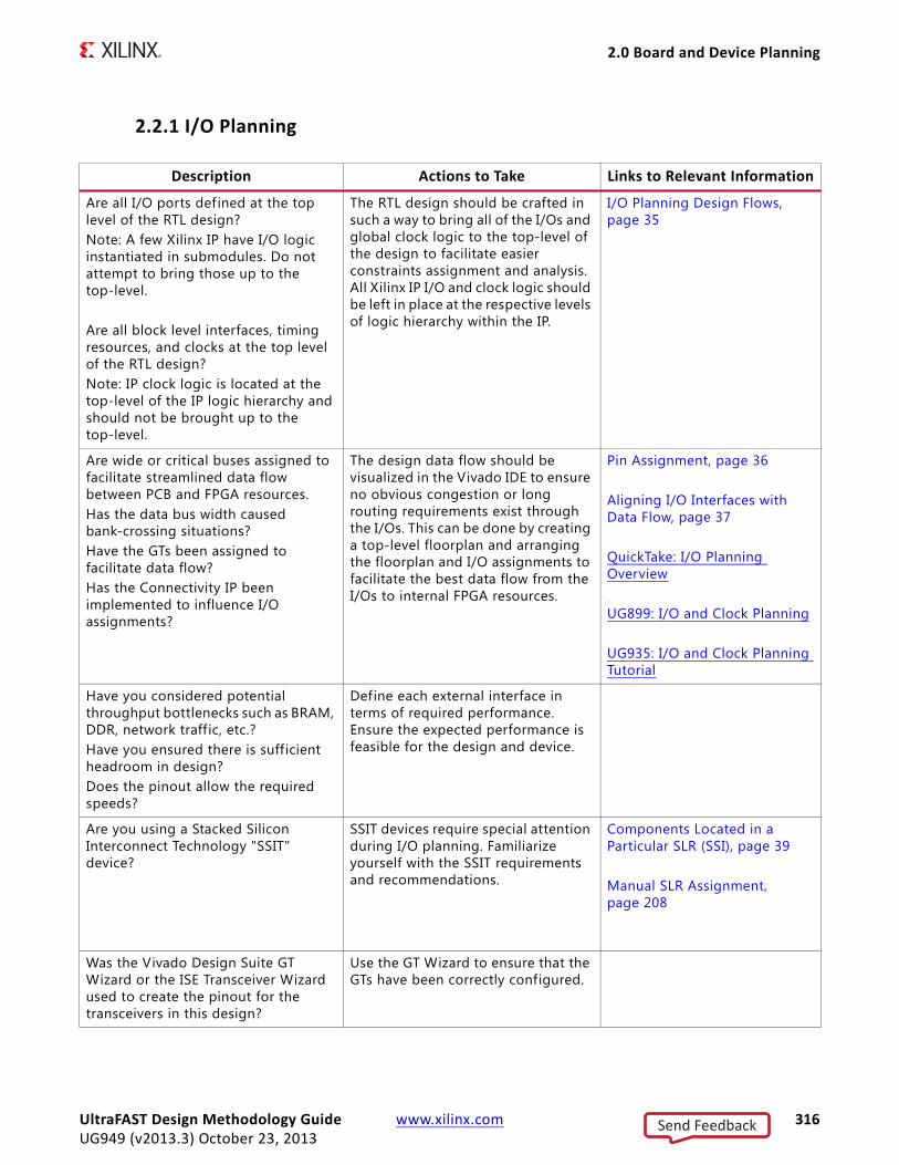
2.0 Board and Device Planning
2.2.1 I/O Planning
Description Actions to Take Links to Relevant Information
Are all I/O ports defined at the top level of the RTL design? Note: A few Xilinx IP have I/O logic instantiated in submodules. Do not attempt to bring those up to the top-level.
Are all block level interfaces, timing resources, and clocks at the top level of the RTL design?Note: IP clock logic is located at the top-level of the IP logic hierarchy and should not be brought up to the top-level.
The RTL design should be crafted in such a way to bring all of the I/Os and global clock logic to the top-level of the design to facilitate easier constraints assignment and analysis. All Xilinx IP I/O and clock logic should be left in place at the respective levels of logic hierarchy within the IP.
I/O Planning Design Flows, page 35
Are wide or critical buses assigned to facilitate streamlined data flow between PCB and FPGA resources. Has the data bus width caused bank-crossing situations?Have the GTs been assigned to facilitate data flow?Has the Connectivity IP been implemented to influence I/O assignments?
The design data flow should be visualized in the Vivado IDE to ensure no obvious congestion or long routing requirements exist through the I/Os. This can be done by creating a top-level floorplan and arranging the floorplan and I/O assignments to facilitate the best data flow from the I/Os to internal FPGA resources.
Pin Assignment, page 36
Aligning I/O Interfaces with Data Flow, page 37
QuickTake: I/O Planning Overview
UG899: I/O and Clock Planning
UG935: I/O and Clock Planning Tutorial
Have you considered potential throughput bottlenecks such as BRAM, DDR, network traff ic, etc.?Have you ensured there is sufficient headroom in design?Does the pinout allow the required speeds?
Define each external interface in terms of required performance. Ensure the expected performance is feasible for the design and device.
Are you using a Stacked Silicon Interconnect Technology "SSIT" device?
SSIT devices require special attention during I/O planning. Familiarize yourself with the SSIT requirements and recommendations.
Components Located in a Particular SLR (SSI), page 39
Manual SLR Assignment, page 208
Was the Vivado Design Suite GT Wizard or the ISE Transceiver Wizard used to create the pinout for the transceivers in this design?
Use the GT Wizard to ensure that the GTs have been correctly configured.
UltraFAST Design Methodology Guide www.xilinx.com 316UG949 (v2013.3) October 23, 2013
Send Feedback

2.0 Board and Device Planning
Are you using any Xilinx Connectivity IP?If so, has it been implemented prior to I/O pin assignment?
Xilinx Connectivity IP requires consideration during I/O planning. Ensure you have implemented it early enough to help influence the pinout.
Ensure that the example design for each IP is implemented to ensure that all I/O constraints are properly identif ied.
Have the memory interface related I/Os been assigned using MIG?Are all constraints and rules created through MIG included in the final constraints f ile?
Using MIG to configure memory interfaces involves an element of I/O planning. Physical constraints and configuration properties are generated while configuring the core. These I/O constraints and configuration properties should propagate through the flow to ensure complete and correct I/O pinout for the design. Verify that the I/Os have been assigned properly.
MIG Checklist
UG586: 7 Series FPGAs Memory Interface Solutions User Guide
PG058: LogiCORE IP Block Memory Generator Product Guide
Do any external interfaces have critical I/O timing requirements?If so list them in the Status and Notes field.
Critical interfaces require extra attention during I/O and timing constraint assignment. List them all to ensure they are properly constrained and considered during I/O planning.
Constraining Input and Output Ports, page 161
Have you considered putting prohibits on VREF pins to ensure they don't get accidentally assigned?
Use the I/O Planning view layout in the Vivado IDE to interactively select the VREF package pins and place prohibits on them.
Have the I/O Standard constraints for all I/O been considered and explicitly assigned for each I/O Port?Are Drive Strength, Slew Rate, and Pull up/down/keepers set for each I/O port?
Use the I/O Planning view layout in the Vivado IDE to interactively assign I/O physical and I/O Standard constraints. Run the I/O and Clock rules of the report_drc command to check I/O Standard assignment and compatibility.
Pin Assignment, page 36
QuickTake: I/O Planning Overview
UG899: I/O and Clock Planning
UG935: I/O and Clock Planning Tutorial
If used, have DCI Cascade constraints been analyzed for proper management?
Vivado enables interactive viewing and assignment of DCI Cascades in the design. Verify DCI Cascade assignments either using the Vivado IDE or manually.
Internal VREF and DCI Cascade Constraints, page 39
Description Actions to Take Links to Relevant Information
UltraFAST Design Methodology Guide www.xilinx.com 317UG949 (v2013.3) October 23, 2013
Send Feedback

2.0 Board and Device Planning
2.2.2 Clock Resource Planning
General link for these checklist items: UG472: 7 Series FPGA Clocking Resources
Does the design use FFs for input and output I/Os?Are ILOGIC and OLOGIC attributes correctly applied?
Run the custom Tcl command report_io_reg_checklist.tcl to determine if ILOGIC and OLOGIC are assigned properly. Check the report f ile to ensure all ports have either an OLOGIC or ILOGIC assigned. A WARNING is printed in the report if any of these ports do not.
Have you identif ied pins with internal/external terminations and annotated the XDC file?Have you shared those with the PCB designer?
Identify pins with internal/external terminations and annotate XDC file to share with PCB designer.
Are any I/O of the FPGA driving power supplies?Have you taken in to consideration the pullup/down that may occur during power up, configuration, and Flash programming?
FPGA I/Os have limited drive strength and should be considered when sinking/sourcing current to any active or passive component. Also the behavior of some pins may be different before, during and after FPGA programming and should be considered when connecting to any sensitive circuitry.
Have you resolved what to do with unconnected I/Os?
For configured but unused pins, verify that any PCB connections are not in any possible contention or left floating.
Answer Record: http://www.xilinx.com/support/answers/45985.htm
Have you considered building system-level baseline design to check component level interfaces on the FPGA?
You can build a small sample design with just the I/O interfaces and clocks in the design. This ensures proper handling of complex I/O configurations and can give you a sanity check before committing to the I/Os.
Description Actions to Take Links to Relevant Information
UltraFAST Design Methodology Guide www.xilinx.com 318UG949 (v2013.3) October 23, 2013
Send Feedback

2.0 Board and Device Planning
Description Actions to Take Links to Relevant Information
Are all the clocks and derivatives (e.g. phase shifted, multiples, divisions, etc.) for this design known? Are they assigned to clock components (e.g. MMCM, PLL, BUFG, BUFR, etc.) for the given device architecture?Are there sufficient resources and connectivity to accomplish this assignment?
Clock usage and placement have a great impact on results and starts with pin placement and planning. Run the report_clock_utilization command and analyze the resulting report. Look for undefined clocks and over utilized resources. All clocks and asynchronous clock relationships need to be defined with XDC constraints.
Clock Resource Planning and Assignment, page 33
Does the total number of global clock resources used in the design exceed the device limit of 32?Are you familiar with when to use SRCC I/O pins vs. MRCC pins?Are all internally generated clocks distributed on a dedicated clock resource (e.g. BUFG, BUFR, etc.)? List any clocks that are on local routing resources in the Status and Notes field.
There are clock placement ramifications for designs that require more than 16 global clocks. Run the report_clock_utilization command and analyze the resulting report. Look for over-utilized clock resources. Further clock planning may be required to either share some global clocks or move some of the clocks to non-global clocking resources. All clocks should be defined on either global or local clock resources.
Selecting Clocking Resources, page 34
Are you using Source Synchronous Interfaces?Has the clocking been properly configured?
Source synchronous interfaces have special clocking requirements. Familiarize yourself with these requirements.
If over utilized, can and should any of the Vivado IP share clock resources?
Sharing clocking resources many times reduces possible timing issues while reducing overall clock power dissipated. The Vivado IP has been constructed to enable sharing of top-level clock logic across multiple IP. Consider consolidating IP clock resources if additional clock resources are needed.
UG896: Designing with IP
UG895: System-Level Design Entry
Are tradeoffs between MMCM and PLL usages considered?
Have you used the Vivado Clocking Wizard to configure the MMCMs and PLLs?
The MMCM/PLL have different features and characteristics for jitter, performance, accuracy and power depending which is used and on how they are configured. Understand the tradeoffs between the two. Analyze your design usage of MMCMs and PLLs and determine if they are the optimal choices.Use the Clocking Wizard to configure MMCM/PLL settings.
Selecting Clocking Resources, page 34
Controlling the Phase, Frequency, Duty-Cycle, and Jitter of the Clock, page 129
UltraFAST Design Methodology Guide www.xilinx.com 319UG949 (v2013.3) October 23, 2013
Send Feedback
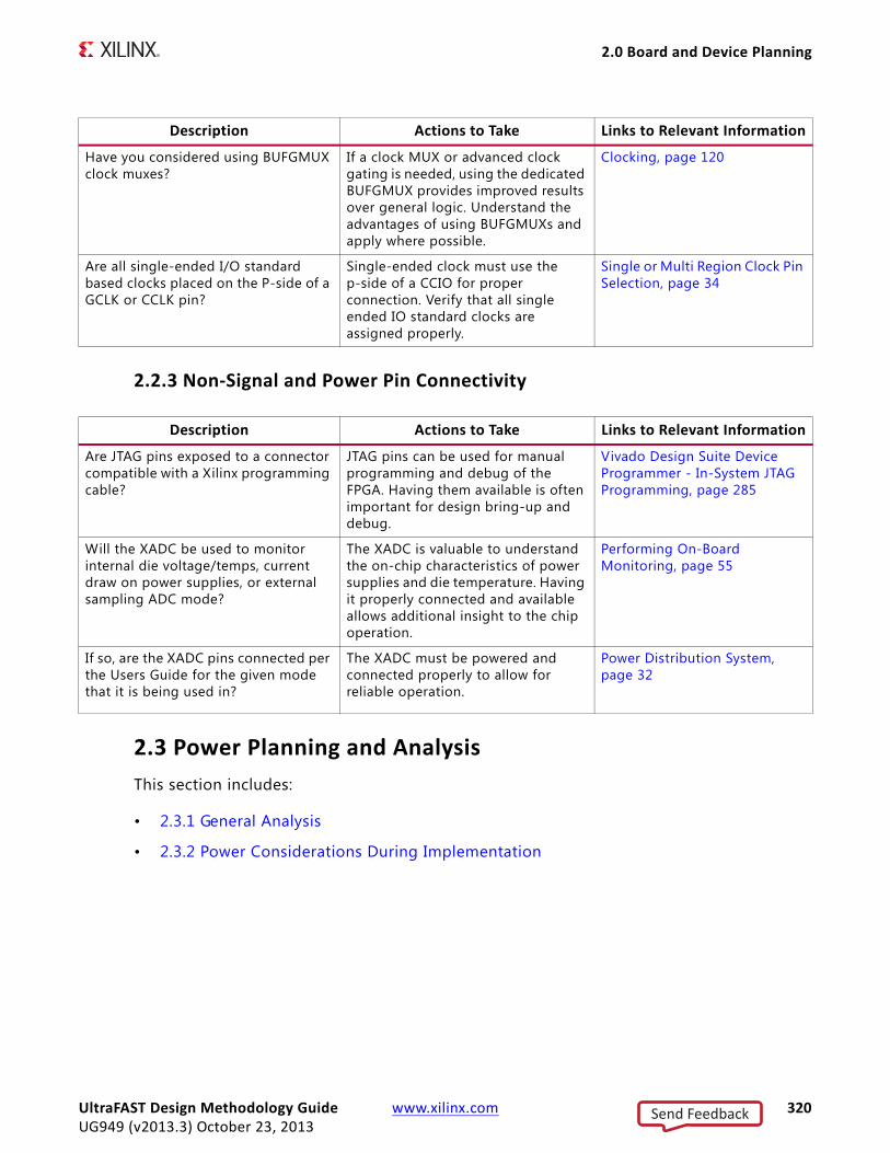
2.0 Board and Device Planning
2.2.3 Non-Signal and Power Pin Connectivity
2.3 Power Planning and AnalysisThis section includes:
• 2.3.1 General Analysis
• 2.3.2 Power Considerations During Implementation
Have you considered using BUFGMUX clock muxes?
If a clock MUX or advanced clock gating is needed, using the dedicated BUFGMUX provides improved results over general logic. Understand the advantages of using BUFGMUXs and apply where possible.
Clocking, page 120
Are all single-ended I/O standard based clocks placed on the P-side of a GCLK or CCLK pin?
Single-ended clock must use the p-side of a CCIO for proper connection. Verify that all single ended IO standard clocks are assigned properly.
Single or Multi Region Clock Pin Selection, page 34
Description Actions to Take Links to Relevant Information
Description Actions to Take Links to Relevant Information
Are JTAG pins exposed to a connector compatible with a Xilinx programming cable?
JTAG pins can be used for manual programming and debug of the FPGA. Having them available is often important for design bring-up and debug.
Vivado Design Suite Device Programmer - In-System JTAG Programming, page 285
Will the XADC be used to monitor internal die voltage/temps, current draw on power supplies, or external sampling ADC mode?
The XADC is valuable to understand the on-chip characteristics of power supplies and die temperature. Having it properly connected and available allows additional insight to the chip operation.
Performing On-Board Monitoring, page 55
If so, are the XADC pins connected per the Users Guide for the given mode that it is being used in?
The XADC must be powered and connected properly to allow for reliable operation.
Power Distribution System, page 32
UltraFAST Design Methodology Guide www.xilinx.com 320UG949 (v2013.3) October 23, 2013
Send Feedback
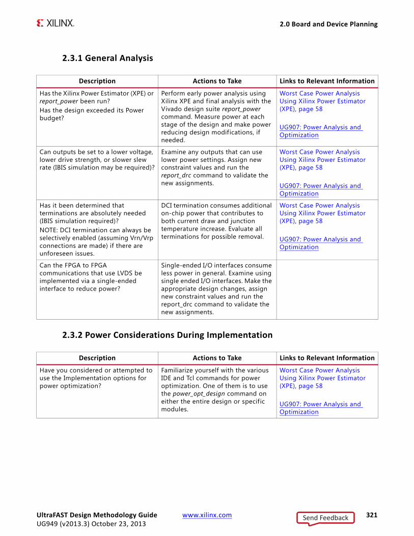
2.0 Board and Device Planning
2.3.1 General Analysis
2.3.2 Power Considerations During Implementation
Description Actions to Take Links to Relevant Information
Has the Xilinx Power Estimator (XPE) or report_power been run?Has the design exceeded its Power budget?
Perform early power analysis using Xilinx XPE and final analysis with the Vivado design suite report_power command. Measure power at each stage of the design and make power reducing design modif ications, if needed.
Worst Case Power Analysis Using Xilinx Power Estimator (XPE), page 58
UG907: Power Analysis and Optimization
Can outputs be set to a lower voltage, lower drive strength, or slower slew rate (IBIS simulation may be required)?
Examine any outputs that can use lower power settings. Assign new constraint values and run the report_drc command to validate the new assignments.
Worst Case Power Analysis Using Xilinx Power Estimator (XPE), page 58
UG907: Power Analysis and Optimization
Has it been determined that terminations are absolutely needed (IBIS simulation required)?NOTE: DCI termination can always be selectively enabled (assuming Vrn/Vrp connections are made) if there are unforeseen issues.
DCI termination consumes additional on-chip power that contributes to both current draw and junction temperature increase. Evaluate all terminations for possible removal.
Worst Case Power Analysis Using Xilinx Power Estimator (XPE), page 58
UG907: Power Analysis and Optimization
Can the FPGA to FPGA communications that use LVDS be implemented via a single-ended interface to reduce power?
Single-ended I/O interfaces consume less power in general. Examine using single ended I/O interfaces. Make the appropriate design changes, assign new constraint values and run the report_drc command to validate the new assignments.
Description Actions to Take Links to Relevant Information
Have you considered or attempted to use the Implementation options for power optimization?
Familiarize yourself with the various IDE and Tcl commands for power optimization. One of them is to use the power_opt_design command on either the entire design or specific modules.
Worst Case Power Analysis Using Xilinx Power Estimator (XPE), page 58
UG907: Power Analysis and Optimization
UltraFAST Design Methodology Guide www.xilinx.com 321UG949 (v2013.3) October 23, 2013
Send Feedback
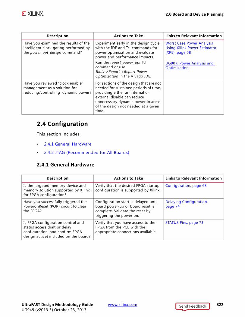
2.0 Board and Device Planning
2.4 ConfigurationThis section includes:
• 2.4.1 General Hardware
• 2.4.2 JTAG (Recommended for All Boards)
2.4.1 General Hardware
Have you examined the results of the intelligent clock gating performed by the power_opt_design command?
Experiment early in the design cycle with the IDE and Tcl commands for power optimization and evaluate power and performance impacts. Run the report_power_opt Tcl command or use Tools->Report->Report Power Optimization in the Vivado IDE.
Worst Case Power Analysis Using Xilinx Power Estimator (XPE), page 58
UG907: Power Analysis and Optimization
Have you reviewed “clock enable” management as a solution for reducing/controlling dynamic power?
For sections of the design that are not needed for sustained periods of time, providing either an internal or external disable can reduce unnecessary dynamic power in areas of the design not needed at a given time.
Description Actions to Take Links to Relevant Information
Description Actions to Take Links to Relevant Information
Is the targeted memory device and memory solution supported by Xilinx for FPGA configuration?
Verify that the desired FPGA startup configuration is supported by Xilinx.
Configuration, page 68
Have you successfully triggered the PoweronReset (POR) circuit to clear the FPGA?
Configuration start is delayed until board power-up or board reset is complete. Validate the reset by triggering the power on.
Delaying Configuration, page 74
Is FPGA configuration control and status access (halt or delay configuration, and confirm FPGA design active) included on the board?
Verify that you have access to the FPGA from the PCB with the appropriate connections available.
STATUS Pins, page 73
UltraFAST Design Methodology Guide www.xilinx.com 322UG949 (v2013.3) October 23, 2013
Send Feedback

3.0 Design Creation
2.4.2 JTAG (Recommended for All Boards)
3.0 Design CreationThe Design Creation section includes:
• 3.1 Design Hierarchy
• 3.2 IP Integration
• 3.3 RTL Coding Guidelines
• 3.4 Constraints Creation
3.1 Design Hierarchy
3.1.1 General Analysis
Description Actions to Take Links to Relevant Information
Do you have the appropriate JTAG cable for your device?
The board includes a Xilinx standard ribbon cable connector, 14-pin (TCK, TMS, TDI, TDO, 2 PWR, and 7 GND)? It is a 14-pin shrouded keyed header with 0.5 mm square posts on 2 mm centers for JTAG access to the FPGA.
JTAG, page 72
Have the test logic reset (TRST), compliance enable, or other JTAG control signals for all devices in the target chain been identif ied and properly connected?
Verify the design contains the proper connections for configuration and debug.
JTAG, page 72
Description Actions to Take Links to Relevant Information
Was the design hierarchy defined to accommodate module function or clock isolation and floorplanning?
The logic hierarchy of the design should be planned with forethought to isolate clock regions, or specif ic functions where possible. Consider restructuring hierarchy where possible to group related logic.
Floorplanning, page 80
Are all data paths registered at logical boundaries?
Register all data path signals at hierarchical boundaries to better facilitate floorplanning, timing analysis/debug and out-of-context implementation.
Register Data Paths at Logical Boundaries, page 79
UltraFAST Design Methodology Guide www.xilinx.com 323UG949 (v2013.3) October 23, 2013
Send Feedback
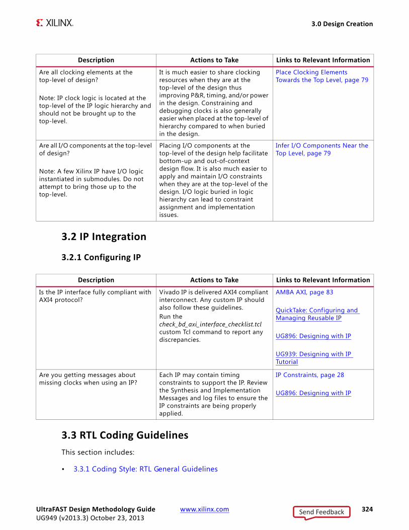
3.0 Design Creation
3.2 IP Integration
3.2.1 Configuring IP
3.3 RTL Coding GuidelinesThis section includes:
• 3.3.1 Coding Style: RTL General Guidelines
Are all clocking elements at the top-level of design?
Note: IP clock logic is located at the top-level of the IP logic hierarchy and should not be brought up to the top-level.
It is much easier to share clocking resources when they are at the top-level of the design thus improving P&R, timing, and/or power in the design. Constraining and debugging clocks is also generally easier when placed at the top-level of hierarchy compared to when buried in the design.
Place Clocking Elements Towards the Top Level, page 79
Are all I/O components at the top-level of design?
Note: A few Xilinx IP have I/O logic instantiated in submodules. Do not attempt to bring those up to the top-level.
Placing I/O components at the top-level of the design help facilitate bottom-up and out-of-context design flow. It is also much easier to apply and maintain I/O constraints when they are at the top-level of the design. I/O logic buried in logic hierarchy can lead to constraint assignment and implementation issues.
Infer I/O Components Near the Top Level, page 79
Description Actions to Take Links to Relevant Information
Description Actions to Take Links to Relevant Information
Is the IP interface fully compliant with AXI4 protocol?
Vivado IP is delivered AXI4 compliant interconnect. Any custom IP should also follow these guidelines.Run the check_bd_axi_interface_checklist.tcl custom Tcl command to report any discrepancies.
AMBA AXI, page 83
QuickTake: Configuring and Managing Reusable IP
UG896: Designing with IP
UG939: Designing with IP Tutorial
Are you getting messages about missing clocks when using an IP?
Each IP may contain timing constraints to support the IP. Review the Synthesis and Implementation Messages and log files to ensure the IP constraints are being properly applied.
IP Constraints, page 28
UG896: Designing with IP
UltraFAST Design Methodology Guide www.xilinx.com 324UG949 (v2013.3) October 23, 2013
Send Feedback

3.0 Design Creation
• 3.3.2 Coding Style: Fanout Guidelines
• 3.3.3 Coding Style: Resets
• 3.3.4 Coding Style Memories
• 3.3.5 Coding Style: DSP
• 3.3.6 Coding Style: Clocking
• 3.3.7 Coding Style: Reliability
• 3.3.8 Coding Style: Performance
• 3.3.9 Coding Style: Power
3.3.1 Coding Style: RTL General Guidelines
Description Actions to Take Links to Relevant Information
Are blocking statements used for unregistered logic and non-blocking for registered logic?
Misuse of blocking and non-blocking statements can result in synthesized results not matching RTL simulation behavior. Following this guideline helps prevent this from occurring. Review the synthesis log file for warnings.
Blocking Statements vs. Non-Blocking Statements, page 89
Are Sensitivity lists complete? Incomplete sensitivity lists can lead to synthesis results not matching RTL simulation. Review the synthesis log file for warnings.
Incomplete Sensitivity List, page 89
Have you ensured that there are no Delays in the RTL code?
Delays in HDL code is not synthesizable. Improper use of delays in synthesizable RTL code can result in synthesis results not matching RTL behavior. It is suggested to review and/or remove all delays in synthesized code.
Delays in RTL Code, page 90
Have you ensured that there are no incomplete if/else clauses?
Incomplete if/else statements can infer latches in combinatorial blocks and infer clock enables in synchronous blocks. This can result in unneeded timing issues when that is not required behavior for functionality and/or power savings. Ensure if/else clauses are complete unless determined necessary.
If Statement without an Else Clause VHDL Coding Example, page 91
Are you using the Vivado design suite HDL Templates?
The HDL templates provide recommended coding styles and instantiation templates for targeting Xilinx FPGAs. It is suggested to use these to ensure best results.
Using Vivado Design Suite HDL Templates, page 91
UltraFAST Design Methodology Guide www.xilinx.com 325UG949 (v2013.3) October 23, 2013
Send Feedback

3.0 Design Creation
Are you using for/while loops in RTL code?
For/while loops are not always synthesizable and even when deterministic, does not always create the best results in terms of logic and synthesis runtime. It is generally suggested to avoid such constructs in synthesizable code.
Use of Loops in Code, page 92
Are State-machine type, style and encoding properly selected?
Understanding and controlling state-machine implementation often results in the best trade-offs of performance, area, power and reliability of a circuit. Proper thought and guidance up front often leads to best characteristics for a given design.
State-Machine Guidance, page 92
Does any hierarchy contain mixed clock edges?
Mixing clock edges may lead to more critical paths in the design. Use this with discretion and understanding of timing impacts to the design.
Avoid Mixing Edges of a Flip Flop, page 94
Was debug logic coded for easy removal?
Debug logic serves a valuable purpose in the bring up of the design but can lead to more diff icult timing closure and increased power. For best end results, it is suggested to code any temporary debug logic in a way to facilitate easy removal.
Use of Debug Logic, page 94
Are there any arrays declared in port declarations?
Defining arrays in port declarations can lead to diff iculties in mixed-language design as well as diff iculty in verif ication/debug. It is generally suggested to avoid arrays in port declarations.
Arrays in Port Declarations, page 95
Are there a large number of Control Sets in the Design?
Large numbers of control sets (unique clock enable, clock and resets) can lead to less dense placement and thus longer wire-lengths resulting in more diff icult timing and higher power. It is suggested to understand and where possible limit unique clock enables, resets and clock domains in the design.
Control Signals and Control Sets, page 96
Description Actions to Take Links to Relevant Information
UltraFAST Design Methodology Guide www.xilinx.com 326UG949 (v2013.3) October 23, 2013
Send Feedback

3.0 Design Creation
3.3.2 Coding Style: Fanout Guidelines
Description Actions to Take Links to Relevant Information
Are High Fanout Nets Avoided? High fanout nets can lead to timing issues in critical paths of the design. Run the report_high_fanout_nets and report_timing commands and analyze the high fanout nets. Determine if any can be reduced?
High Fanouts in Critical Paths, page 140
Are Flip-flops duplicated to reduce high fanout nets?
Run the report_fanout command to identify candidates for replication.
Use Register Replication, page 141
Are high fan-in nets (associated with large muxes and buses) constrained and accommodated in the design?
Evaluate high fan-in logic for possible timing and/or routing issues and ensure best coding practices are applied including applying additional pipelining if possible.
Managing Wide Buses, page 144
UltraFAST Design Methodology Guide www.xilinx.com 327UG949 (v2013.3) October 23, 2013
Send Feedback
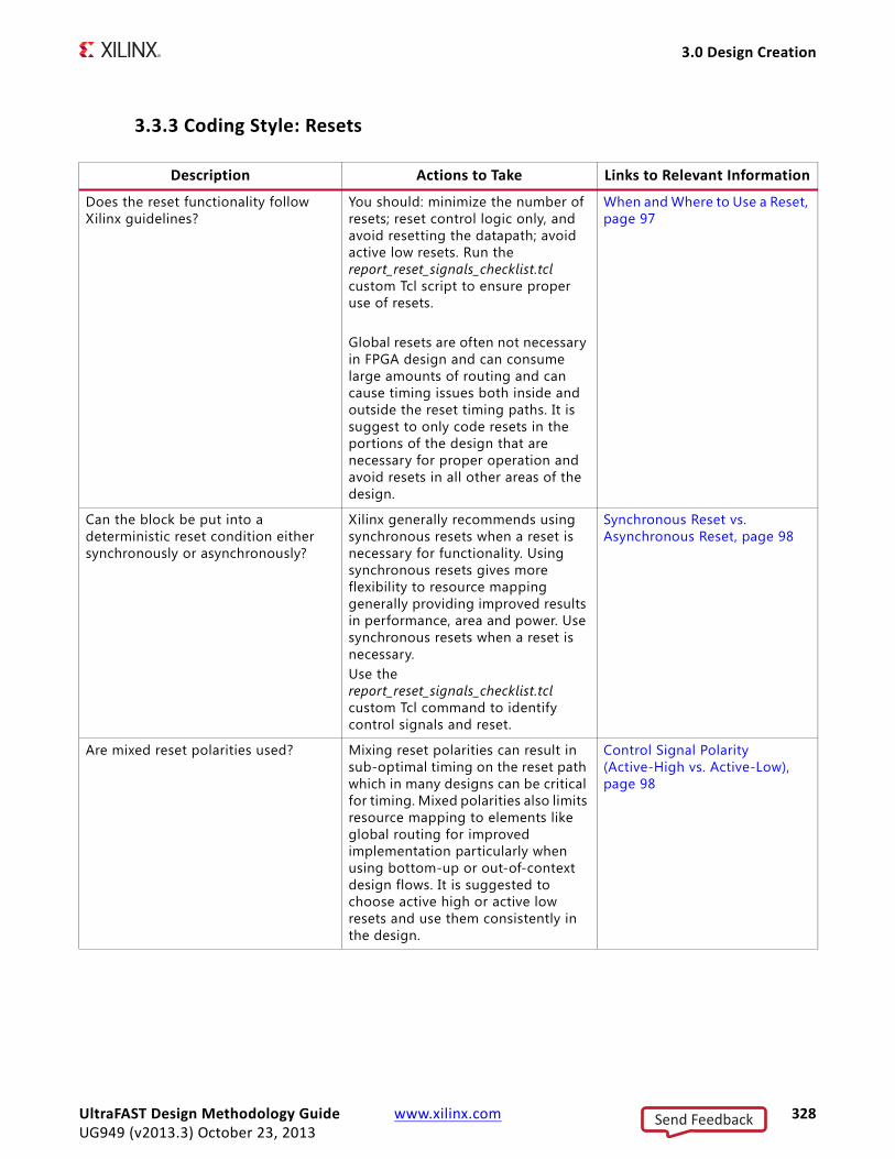
3.0 Design Creation
3.3.3 Coding Style: Resets
Description Actions to Take Links to Relevant Information
Does the reset functionality follow Xilinx guidelines?
You should: minimize the number of resets; reset control logic only, and avoid resetting the datapath; avoid active low resets. Run the report_reset_signals_checklist.tcl custom Tcl script to ensure proper use of resets.
Global resets are often not necessary in FPGA design and can consume large amounts of routing and can cause timing issues both inside and outside the reset timing paths. It is suggest to only code resets in the portions of the design that are necessary for proper operation and avoid resets in all other areas of the design.
When and Where to Use a Reset, page 97
Can the block be put into a deterministic reset condition either synchronously or asynchronously?
Xilinx generally recommends using synchronous resets when a reset is necessary for functionality. Using synchronous resets gives more flexibility to resource mapping generally providing improved results in performance, area and power. Use synchronous resets when a reset is necessary.Use the report_reset_signals_checklist.tcl custom Tcl command to identify control signals and reset.
Synchronous Reset vs. Asynchronous Reset, page 98
Are mixed reset polarities used? Mixing reset polarities can result in sub-optimal timing on the reset path which in many designs can be critical for timing. Mixed polarities also limits resource mapping to elements like global routing for improved implementation particularly when using bottom-up or out-of-context design flows. It is suggested to choose active high or active low resets and use them consistently in the design.
Control Signal Polarity (Active-High vs. Active-Low), page 98
UltraFAST Design Methodology Guide www.xilinx.com 328UG949 (v2013.3) October 23, 2013
Send Feedback

3.0 Design Creation
3.3.4 Coding Style Memories
Have you put high fanout reset nets onto BUFGs (total number less than 3), or replicated the driver for fanout limitation?
In some cases, improved timing and routability can be seen when high-fanout nets like resets are mapped to BUFGs. It is suggested to evaluate this in situations where very high fanout nets exist to see if results can be improved.
Clock Resource Selection Summary, page 132
Does each clock domain have an independent reset line?
In general, it is suggested to avoid resets on logic that does not require it. On paths that do require resets, ensure resets are properly created and constrained particularly when a common reset crosses a clock domain.
Have you checked that the design has no FFs that have an asynchronous de-assertion of the preset or clear input?
Xilinx generally recommends no resets or if needed synchronous resets but in the event asynchronous resets are used, ensure that the reset is synchronously deasserted and properly timed. Run the sync_preset_clr_deassertion_script.tcl custom Tcl script to ensure proper use of FFs.
Description Actions to Take Links to Relevant Information
Description Actions to Take Links to Relevant Information
Were the Vivado design suite HDL templates used to infer memories?
Improperly coded memory arrays can result in sub-optimal implementation results. It is suggested to use the Vivado design suite HDL Templates for memory inference to ensure that Xilinx BRAM and/or LUTRAM is properly inferred.
Direct Instantiation of RAM Primitives, page 108
Is the block RAM output register being used?
Using the output registers of the BRAM can result in over 1ns clock-to-out improvement from the BRAM at the cost of added latency during read. If this is acceptable, it is highly suggested to use these registers.
Using the Output Pipeline Register, page 109
UltraFAST Design Methodology Guide www.xilinx.com 329UG949 (v2013.3) October 23, 2013
Send Feedback

3.0 Design Creation
3.3.5 Coding Style: DSP
Is the proper write mode selected for the RAM?
BRAM write modes can impact functionality, power and reliability depending on the selected mode and operation of the BRAM. It is suggested to understand and always choose the proper write mode to match desired functionality, power and operation goals.
Selecting the Proper Block RAM Write Mode, page 110
Was the hard FIFO selected for FIFO buffering functions?
The dedicated hard-FIFO has performance, power and area benefits over using a soft implementation of a FIFO. It is suggested to evaluate and use the hard FIFO where possible.
FIFO Creation, page 110
Description Actions to Take Links to Relevant Information
Description Actions to Take Links to Relevant Information
Does the DSP bit width match the target device for optimal area and performance?
The DSP block has specific, bounded input widths per block depending on the selected operation. Understand how the desired precision width of the coded function maps to one or more DSP blocks allows for proper expectations and coding modifications like additional pipelining can be properly accounted for.
Coding for Proper DSP and Arithmetic Inference, page 113
Has signed vs. unsigned been considered both for algorithm performance and DSP48 usage?
The DSP multiplier natively performs signed operations. Using unsigned arithmetic reduces the precision of the block. Understand how this affects bit width selection and mapping into the DSP blocks.
Coding for Proper DSP and Arithmetic Inference, page 113
Have the dedicated DSP48 routing resources and logic been optimally used?
The DSP block has built-in "cascade" logic that eff iciently implements arithmetic/f ilter operations that extend beyond a single DSP block. Using cascades and getting the best implementation requires specif ic pipelining and coding style considerations. When inferring arithmetic/f ilter operations that extend beyond a single DSP block, understand the best coding practices to infer these paths.
Coding for Proper DSP and Arithmetic Inference, page 113
UltraFAST Design Methodology Guide www.xilinx.com 330UG949 (v2013.3) October 23, 2013
Send Feedback

3.0 Design Creation
Has the multiplier in the DSP48 been fully pipelined using the registers in the DSP48?
Proper pipelining for the DSP multiplier not only improves performance characteristics but also improves power for multipliers implemented in the DSP Blocks. Understand and when possible, add additional pipelining to improve performance/power characteristics.
Coding for Proper DSP and Arithmetic Inference, page 113
Is the arithmetic code reset synchronous, active high and initializes/resets to zeroes?
Best practice is to not use reset where not needed but when needed, it is suggested the reset to be synchronous, active high and reset to a zero to have it properly inferred into a DSP48 block. Follow this guideline for any register intended to be placed into a DSP block.
Coding for Proper DSP and Arithmetic Inference, page 113
Is the code structured to take advantage of multiplication-addition flows for optimal performance?
It is suggested to understand the structure and capabilities of the DSP block so that coding styles when feasible match the datapath and pipelining paths in the block to ensure optimal inference.
Coding for Proper DSP and Arithmetic Inference, page 113
Description Actions to Take Links to Relevant Information
UltraFAST Design Methodology Guide www.xilinx.com 331UG949 (v2013.3) October 23, 2013
Send Feedback
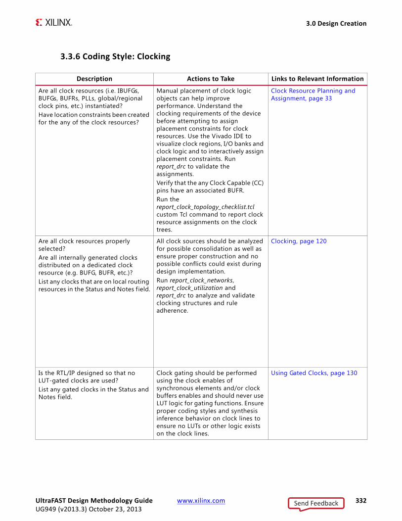
3.0 Design Creation
3.3.6 Coding Style: Clocking
Description Actions to Take Links to Relevant Information
Are all clock resources (i.e. IBUFGs, BUFGs, BUFRs, PLLs, global/regional clock pins, etc.) instantiated?Have location constraints been created for the any of the clock resources?
Manual placement of clock logic objects can help improve performance. Understand the clocking requirements of the device before attempting to assign placement constraints for clock resources. Use the Vivado IDE to visualize clock regions, I/O banks and clock logic and to interactively assign placement constraints. Run report_drc to validate the assignments.Verify that the any Clock Capable (CC) pins have an associated BUFR.Run the report_clock_topology_checklist.tcl custom Tcl command to report clock resource assignments on the clock trees.
Clock Resource Planning and Assignment, page 33
Are all clock resources properly selected?Are all internally generated clocks distributed on a dedicated clock resource (e.g. BUFG, BUFR, etc.)?List any clocks that are on local routing resources in the Status and Notes field.
All clock sources should be analyzed for possible consolidation as well as ensure proper construction and no possible conflicts could exist during design implementation. Run report_clock_networks, report_clock_utilization and report_drc to analyze and validate clocking structures and rule adherence.
Clocking, page 120
Is the RTL/IP designed so that no LUT-gated clocks are used?List any gated clocks in the Status and Notes field.
Clock gating should be performed using the clock enables of synchronous elements and/or clock buffers enables and should never use LUT logic for gating functions. Ensure proper coding styles and synthesis inference behavior on clock lines to ensure no LUTs or other logic exists on the clock lines.
Using Gated Clocks, page 130
UltraFAST Design Methodology Guide www.xilinx.com 332UG949 (v2013.3) October 23, 2013
Send Feedback

3.0 Design Creation
3.3.7 Coding Style: Reliability
Is MMCM and/or PLL LOCK signal monitored to ensure a clean clock on the input prior to the reset being released to the circuitry in that clock domain?
Run check_pll_connectivity_checklist.tcl and examine pll_io_check_report.txt to report PLL and MCMM connectivity.
Controlling and Synchronizing Device Startup, page 138
If using the mux function within the BUFGMUX, have clock transition requirements been considered?
The BUFGMUX has built in logic to ensure "glitch-free" transition of clock sources. Ensure proper considerations are made in terms of timing and input clock stability to ensure safe clock transition of clock sources.
BUFGCTRL, page 122
Does the design require that a multi-cycle path be used?
Using properly coded and constrained multi-cycle paths can relax and thus timing on related and unrelated paths in the design. Evaluate the use and constraint of multi-cycle paths to improve overall implementation results.
Adding Multicycle Path Constraints, page 179
Description Actions to Take Links to Relevant Information
Description Actions to Take Links to Relevant Information
Have all clock domain crossing been analyzed and classif ied as synchronous or asynchronous?
Synchronous CDCs should have both clocks properly related by phase. Asynchronous CDC should have proper timing exceptions and synchronization created. Run the create_cdc_reports_checklist.tcl custom Tcl command and examine the results. Verify that all clock domain crossings have been closely analyzed.
Clock Domain Crossings, page 136
Are all asynchronous crossings properly synchronized?
For reliable data capture across asynchronous clock domains, proper synchronization practices should be employed.
Asynchronous Domain Crossing, page 137
UltraFAST Design Methodology Guide www.xilinx.com 333UG949 (v2013.3) October 23, 2013
Send Feedback

3.0 Design Creation
Are phase differences between synchronous clock domains minimized for all synchronous domain crossings?
When crossing synchronous clock domains, large phase differences can cause large setup and/or hold times to occur resulting in sub-optimal timing and longer P&R times. Analyze and reduce any phase differences between clock domains in which data must be passed.
Synchronous Domain Crossing, But Potentially Very High Skew, page 136
Is the design properly synchronized for safe startup?
Upon release of the global reset and enable for the device at start-up, some considerations should be made in order to ensure the design starts in a known and desired state. Ensure that the registers are initialized to desired values and the clocks are released in a controlled manner to ensure safe startup.
Controlling and Synchronizing Device Startup, page 138
Are there any untimed resets being used in the design?
Untimed resets can produce unpredictable behavior in the design when asserted or more importantly deasserted. Ensure safe and known behavior for all design paths including reset.
Use of Untimed Resets, page 139
Has the design avoided the use of combinational feedback; (i.e. the looping of combinational processes)?
Combinatorial loops can create timing hazards that are diff icult to predict or avoid and prevents optimizations to the design to improve power and other characteristics thus should be avoided.Run the check_timing -verbose -override_defaults loops -file report.txt command to analyze for any combinatorial loops in the design.
Avoid Combinational Loops, page 140
Description Actions to Take Links to Relevant Information
UltraFAST Design Methodology Guide www.xilinx.com 334UG949 (v2013.3) October 23, 2013
Send Feedback

3.0 Design Creation
3.3.8 Coding Style: Performance
Description Actions to Take Links to Relevant Information
Is logic connecting to hard resources (DSP48, BRAMs) pipelined to achieve required frequency?
Critical timing paths often occur from larger blocks like BRAMs and DSPs and in particular, the output paths from these components. It is suggested to pipeline the outputs of such components in order to improve the overall performance of these paths. Run the input_output_registers_on_dsp_and_bram_blocks.tcl custom Tcl command to report such paths.
Pipelining Considerations, page 142
Have registers been evaluated/optimized for implementation into SRL16 resources?
Shift Register LUTs (SRLs) often help reduce FF resource needs for data buffering and pipeline balancing of sections of the design. Evaluate when to use these resources and when to use standard registers to best meet goals for performance, area and power.
Coding Shift Registers and Delay Lines, page 114
Has the recommended coding style been followed for most efficient element inference?
Best results are seen when coding is performed with knowledge and understanding of how it will map into the underlying architecture. Understand how coding decisions will result in the target architecture.
Know What You Infer, page 106
UltraFAST Design Methodology Guide www.xilinx.com 335UG949 (v2013.3) October 23, 2013
Send Feedback
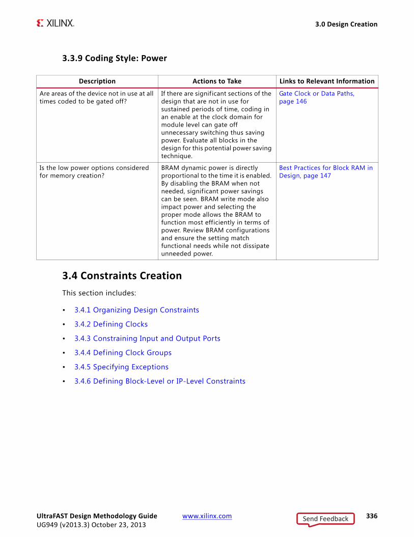
3.0 Design Creation
3.3.9 Coding Style: Power
3.4 Constraints CreationThis section includes:
• 3.4.1 Organizing Design Constraints
• 3.4.2 Defining Clocks
• 3.4.3 Constraining Input and Output Ports
• 3.4.4 Defining Clock Groups
• 3.4.5 Specifying Exceptions
• 3.4.6 Defining Block-Level or IP-Level Constraints
Description Actions to Take Links to Relevant Information
Are areas of the device not in use at all times coded to be gated off?
If there are signif icant sections of the design that are not in use for sustained periods of time, coding in an enable at the clock domain for module level can gate off unnecessary switching thus saving power. Evaluate all blocks in the design for this potential power saving technique.
Gate Clock or Data Paths, page 146
Is the low power options considered for memory creation?
BRAM dynamic power is directly proportional to the time it is enabled. By disabling the BRAM when not needed, signif icant power savings can be seen. BRAM write mode also impact power and selecting the proper mode allows the BRAM to function most efficiently in terms of power. Review BRAM configurations and ensure the setting match functional needs while not dissipate unneeded power.
Best Practices for Block RAM in Design, page 147
UltraFAST Design Methodology Guide www.xilinx.com 336UG949 (v2013.3) October 23, 2013
Send Feedback
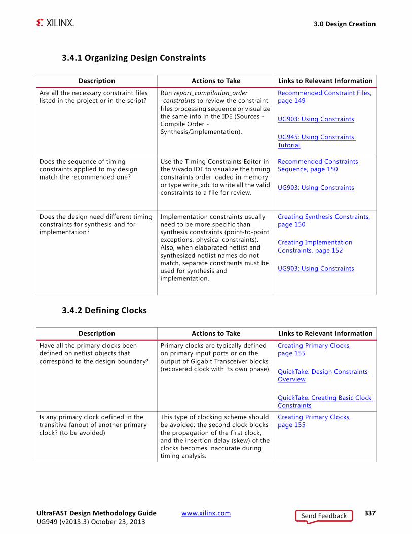
3.0 Design Creation
3.4.1 Organizing Design Constraints
3.4.2 Defining Clocks
Description Actions to Take Links to Relevant Information
Are all the necessary constraint f iles listed in the project or in the script?
Run report_compilation_order -constraints to review the constraint f iles processing sequence or visualize the same info in the IDE (Sources - Compile Order - Synthesis/Implementation).
Recommended Constraint Files, page 149
UG903: Using Constraints
UG945: Using Constraints Tutorial
Does the sequence of timing constraints applied to my design match the recommended one?
Use the Timing Constraints Editor in the Vivado IDE to visualize the timing constraints order loaded in memory or type write_xdc to write all the valid constraints to a f ile for review.
Recommended Constraints Sequence, page 150
UG903: Using Constraints
Does the design need different timing constraints for synthesis and for implementation?
Implementation constraints usually need to be more specif ic than synthesis constraints (point-to-point exceptions, physical constraints). Also, when elaborated netlist and synthesized netlist names do not match, separate constraints must be used for synthesis and implementation.
Creating Synthesis Constraints, page 150
Creating Implementation Constraints, page 152
UG903: Using Constraints
Description Actions to Take Links to Relevant Information
Have all the primary clocks been defined on netlist objects that correspond to the design boundary?
Primary clocks are typically defined on primary input ports or on the output of Gigabit Transceiver blocks (recovered clock with its own phase).
Creating Primary Clocks, page 155
QuickTake: Design Constraints Overview
QuickTake: Creating Basic Clock Constraints
Is any primary clock defined in the transitive fanout of another primary clock? (to be avoided)
This type of clocking scheme should be avoided: the second clock blocks the propagation of the f irst clock, and the insertion delay (skew) of the clocks becomes inaccurate during timing analysis.
Creating Primary Clocks, page 155
UltraFAST Design Methodology Guide www.xilinx.com 337UG949 (v2013.3) October 23, 2013
Send Feedback

3.0 Design Creation
3.4.3 Constraining Input and Output Ports
Have the generated clocks been defined in the transitive fanout of their master clock?
When there is no logical path between a generated clock and its master clock, the insertion delay of the generated clock cannot be computed and the skew becomes inaccurate during timing analysis.
Creating Generated Clocks, page 157
QuickTake: Creating Generated Clock Constraints
Are some generated clocks defined on pins where the Vivado tools automatically create some generated clocks (e.g. MMCM, BUFR, …)? If so, does their waveform match the one the tool would have automatically generated?
Validate that generated clock constraints match the auto-generated clock waveform.
Creating Generated Clocks, page 157
QuickTake: Creating Generated Clock Constraints
Description Actions to Take Links to Relevant Information
Description Actions to Take Links to Relevant Information
Are all the Input Ports constrained with an input delay?
Validate that all input ports have input delay constraints. Generate a check_timing report and review the no_input_delay/partial_input_delay sections.
Defining Input Delays, page 162Checking That Your Design is Properly Constrained, page 223
QuickTake: Setting Input Delay
Are all the Output Ports constrained with an output delay?
Validate that all output ports have output delay constraints. Generate a check_timing report and review the no_output_delay/partial_output_delay sections.
Defining Output Delays, page 163
Checking That Your Design is Properly Constrained, page 223
QuickTake: Setting Output Delay
Have all the input and output delay constraints been defined relative to the appropriate clock?
Validate that all input and output constraints are defined relative to a clock used as a reference by the external device. This clock is also used as the internal IO clock in most cases.
Choosing the Reference Clock, page 164
Are the input and output delays for synchronous interface matching the edge-aligned or center-aligned templates?
Validate that all input and output delay constraints match edge or centered aligned templates.
Verifying Delay Constraints, page 168
UltraFAST Design Methodology Guide www.xilinx.com 338UG949 (v2013.3) October 23, 2013
Send Feedback

3.0 Design Creation
3.4.4 Defining Clock Groups
Are the active edges of the input and output delay constraints matching the specs of the board?
Validate that all input and output delay constraints are defined relative to the clock edges specified in the external device datasheet.
Choosing the Reference Clock, page 164 (see especially Rising and Falling Reference Clock Edges, page 167)
Are the ports related to an internally modif ied clocks constrainted relative to a virtual clock?
Validate that ports related to internally modif ied clocks are constrained relative to a virtual clock.
Choosing the Reference Clock, page 164
Description Actions to Take Links to Relevant Information
Description Actions to Take Links to Relevant Information
Have clock groups been used instead of false paths to define clock domains that are exclusive or asynchronous to each others?
Clock groups should be used instead of false paths to identify asynchronous and exclusive clocks. Validate that clock groups have been used rather than false paths whenever possible.
Constraining Exclusive Clock Groups, page 171
Constraining Asynchronous Clock Groups and Clock Domain Crossings, page 173
Have clock groups been used to define clocks that cannot logically or physically co-exist at the same time?
Exclusive clocks are clocks that propagate on the same hardware resource (clock path). By default, timing analysis reports paths between them even if it usually does not correspond to a realistic situation.
Constraining Exclusive Clock Groups, page 171
Have any set_max_delay constraint been overridden by clock groups or false paths constraints?
Use the report_timing and the report_exceptions command identify set_max_delay constraints that have been overridden by set_clock_groups or set_false_path (higher precedence). Correct the constraints if the max delay constraint is needed.
Constraints on Individual CDC Paths, page 174
UltraFAST Design Methodology Guide www.xilinx.com 339UG949 (v2013.3) October 23, 2013
Send Feedback
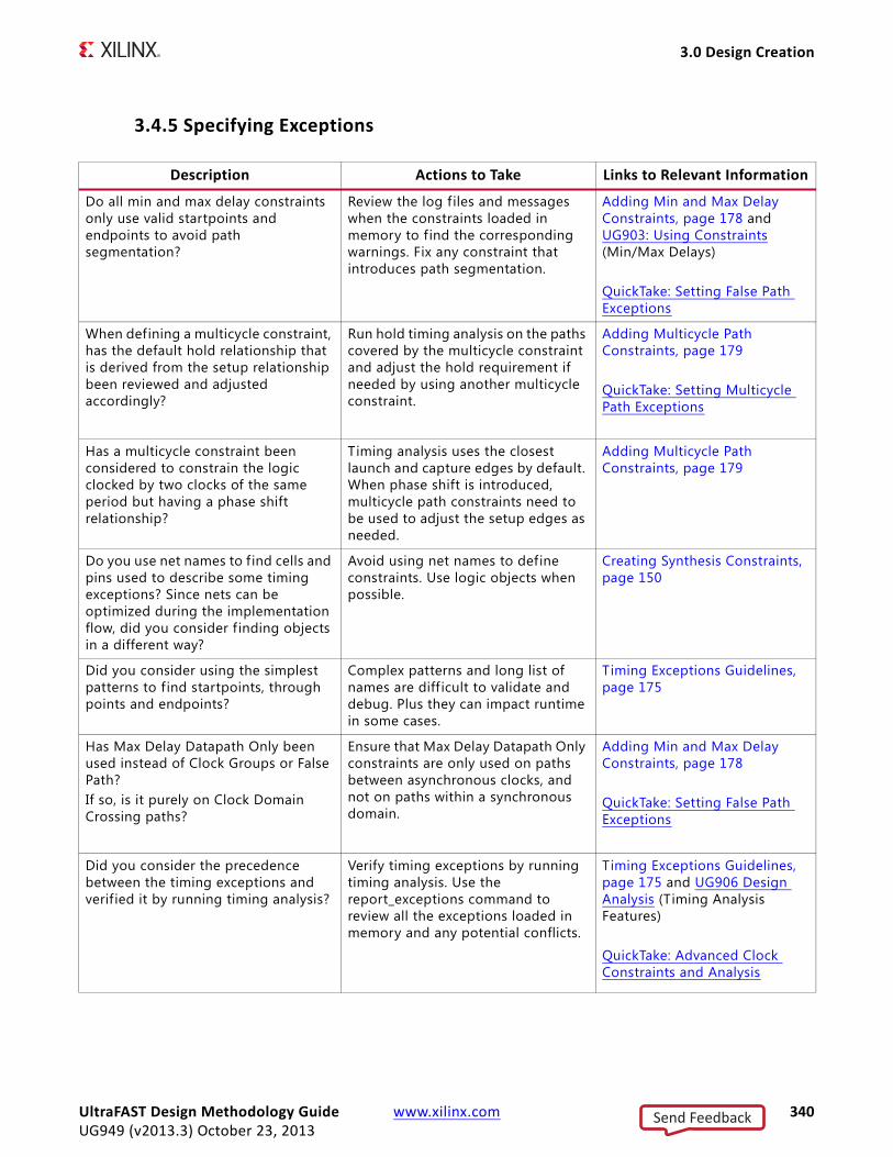
3.0 Design Creation
3.4.5 Specifying Exceptions
Description Actions to Take Links to Relevant Information
Do all min and max delay constraints only use valid startpoints and endpoints to avoid path segmentation?
Review the log f iles and messages when the constraints loaded in memory to find the corresponding warnings. Fix any constraint that introduces path segmentation.
Adding Min and Max Delay Constraints, page 178 and UG903: Using Constraints (Min/Max Delays)
QuickTake: Setting False Path Exceptions
When defining a multicycle constraint, has the default hold relationship that is derived from the setup relationship been reviewed and adjusted accordingly?
Run hold timing analysis on the paths covered by the multicycle constraint and adjust the hold requirement if needed by using another multicycle constraint.
Adding Multicycle Path Constraints, page 179
QuickTake: Setting Multicycle Path Exceptions
Has a multicycle constraint been considered to constrain the logic clocked by two clocks of the same period but having a phase shift relationship?
Timing analysis uses the closest launch and capture edges by default. When phase shift is introduced, multicycle path constraints need to be used to adjust the setup edges as needed.
Adding Multicycle Path Constraints, page 179
Do you use net names to f ind cells and pins used to describe some timing exceptions? Since nets can be optimized during the implementation flow, did you consider f inding objects in a different way?
Avoid using net names to define constraints. Use logic objects when possible.
Creating Synthesis Constraints, page 150
Did you consider using the simplest patterns to f ind startpoints, through points and endpoints?
Complex patterns and long list of names are diff icult to validate and debug. Plus they can impact runtime in some cases.
Timing Exceptions Guidelines, page 175
Has Max Delay Datapath Only been used instead of Clock Groups or False Path?If so, is it purely on Clock Domain Crossing paths?
Ensure that Max Delay Datapath Only constraints are only used on paths between asynchronous clocks, and not on paths within a synchronous domain.
Adding Min and Max Delay Constraints, page 178
QuickTake: Setting False Path Exceptions
Did you consider the precedence between the timing exceptions and verif ied it by running timing analysis?
Verify timing exceptions by running timing analysis. Use the report_exceptions command to review all the exceptions loaded in memory and any potential conflicts.
Timing Exceptions Guidelines, page 175 and UG906 Design Analysis (Timing Analysis Features)
QuickTake: Advanced Clock Constraints and Analysis
UltraFAST Design Methodology Guide www.xilinx.com 340UG949 (v2013.3) October 23, 2013
Send Feedback

4.0 Implementation
3.4.6 Defining Block-Level or IP-Level Constraints
4.0 ImplementationThe Implementation section includes:
• 4.1 Running Synthesis
• 4.2 Validating the Synthesized Design
• 4.3 Implementing the Design
• 4.4 Design Closure
4.1 Running SynthesisThis section includes:
• 4.1.1 Synthesis Best Practices
• 4.1.2 Using Synthesis Attributes
Description Actions to Take Links to Relevant Information
Did you define placement constraints when developing block-level or IP-level constraints?If so, list them in the Status and Notes field.
Identify any physical constraints such as I/Os or Floorplanning assigned.
Creating Block-Level Constraints, page 185
Did you define timing exceptions between clocks that are not entirely bounded to the IP or block? If so, list them in the Status and Notes field.
Identify timing exceptions between clocks that are not entirely bounded to an IP or block. Such constraints must be avoided as they can impact paths outside the IP.
Creating Block-Level Constraints, page 185
Have all the IP constraints been reviewed?
Ensure that IP .xdc files are properly included in the design and are scoped to correct hierarchy IP locations.
UltraFAST Design Methodology Guide www.xilinx.com 341UG949 (v2013.3) October 23, 2013
Send Feedback

4.0 Implementation
4.1.1 Synthesis Best Practices
4.1.2 Using Synthesis Attributes
Description Actions to Take Links to Relevant Information
Have you verif ied your timing constraints?Are the clock periods realistic?Are timing constraints from the .xdc file applied during synthesis?
Timing constraints syntax should verif ied with the elaborated design. The quality of results should be analyzed after synthesis to gauge the feasibility of the clock performance specif ied.Consider using the "Baselining" validation technique to assign and validate constraints.
Accurate Timing Constraints, page 190
Creating Synthesis Constraints, page 150
Baselining the Design, page 213
Are you using top-level third party synthesis?
Xilinx supports third party synthesis tools. Appropriate IP output products are generated to support using third party synthesis with Xilinx IP.Run the link_design command to prepare the design to run many of the commands described in the Validating Synthesized Design section below.
Using Third Party Synthesis and Simulation Tools, page 30
UG901: Synthesis
Description Actions to Take Links to Relevant Information
Are synth_design settings needed or have been explored? Have you checked all of your synthesis attributes present in the RTL?Do you understand why each of them is needed and if it is relevant for Vivado Synthesis?Are attributes such as KEEP, DON’T_TOUCH, MAX_FANOUT SHREG_EXTRACT, ROM_STYLE, RAM_STYLE needed and used correctly?
Familiarize yourself with the Vivado synthesis attributes and their usage. Apply synthesis attributes where desired and revisit the need for attributes when moving to a new FPGA family or a new software release.Use the "Find in Files" capability in the Vivado tools Text Editor to search for Attribute names in your design. Ensure that all attributes are being applied properly.
Synthesis Attributes, page 193
UG901: Synthesis
Have you checked your 3-states and made sure that you have not set any DONT_TOUCH or KEEP_HIERARCHY attributes on levels of hierarchy with 3-states in lower levels?
Setting these attributes can hinder the tools ability to perform logic optimization across hierarchical boundaries. Ensure that you have not set them inadvertently.
Synthesis Attributes, page 193
UltraFAST Design Methodology Guide www.xilinx.com 342UG949 (v2013.3) October 23, 2013
Send Feedback
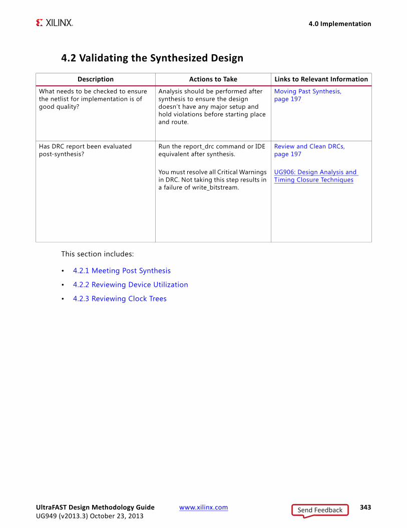
4.0 Implementation
4.2 Validating the Synthesized Design
This section includes:
• 4.2.1 Meeting Post Synthesis
• 4.2.2 Reviewing Device Utilization
• 4.2.3 Reviewing Clock Trees
Description Actions to Take Links to Relevant Information
What needs to be checked to ensure the netlist for implementation is of good quality?
Analysis should be performed after synthesis to ensure the design doesn’t have any major setup and hold violations before starting place and route.
Moving Past Synthesis, page 197
Has DRC report been evaluated post-synthesis?
Run the report_drc command or IDE equivalent after synthesis.
You must resolve all Critical Warnings in DRC. Not taking this step results in a failure of write_bitstream.
Review and Clean DRCs, page 197
UG906: Design Analysis and Timing Closure Techniques
UltraFAST Design Methodology Guide www.xilinx.com 343UG949 (v2013.3) October 23, 2013
Send Feedback

4.0 Implementation
4.2.1 Meeting Post Synthesis
4.2.2 Reviewing Device Utilization
Description Actions to Take Links to Relevant Information
Does the design close timing post-synthesis?
Run the report_timing_summary Tcl command or IDE equivalent after synthesis.
Meet Post-Synthesis Timing, page 198
UG906: Design Analysis and Timing Closure Techniques
Are all clocks properly defined with valid constraints in place?Are multi-cycle paths correctly constrained?
Continually validating that constraints are defined properly and are met will help close timing during implementation.
Checking That Your Design is Properly Constrained, page 223
Baselining the Design, page 213Understanding Timing Reports, page 213
UG906: Design Analysis and Timing Closure Techniques
Description Actions to Take Links to Relevant Information
Is the design post-synthesis utilization reasonable?
Run the report_utilization Tcl command or IDE equivalent after synthesis. Higher utilized designs may impact performance.
Reviewing Utilization, page 198
Has the complete system been reviewed for resource utilization including clocks, BRAMS, DSP48s, FFs, LUTs? Will the complete design meet the targets?
Perform early resource estimation to validate the design will f it in the target device.
Timing Closure Criteria, page 222
UltraFAST Design Methodology Guide www.xilinx.com 344UG949 (v2013.3) October 23, 2013
Send Feedback

4.0 Implementation
4.2.3 Reviewing Clock Trees
4.3 Implementing the DesignThis section includes:
• 4.3.1 Implementation Steps and Options
• 4.3.2 Logic Optimization
• 4.3.3 Power Optimization
• 4.3.4 Placement
• 4.3.5 Physical Optimization
• 4.3.6 Routing
• 4.3.7 Completing and Managing Runs
Description Actions to Take Links to Relevant Information
Is the clock buffer utilization expected?
Run the report_clock_utilization Tcl command or IDE equivalent after synthesis.
Reviewing Clock Trees, page 199
Is the clock tree topology expected? Run the report_clock_networks TCL command or IDE equivalent after synthesis.
Reviewing Clock Trees, page 199
Are you using sync vs. async resets on your registers?
Run the custom script report_reset_signals_checklist.tcl..
Meet Post-Synthesis Timing, page 198
Have you fully pipelined your add/mult structures to infer pipelined DSP48s?
Run the custom script input_output_registers_on_dsp_and_bram_blocks_script.tcl.
Meet Post-Synthesis Timing, page 198
Are the output Block RAM registers used in order to reduce the read time?
Run the custom script input_output_registers_on_dsp_and_bram_blocks_script.tcl.
Meet Post-Synthesis Timing, page 198
Have you checked the inferred SRLs and made sure they are what you want?
Validate the SRL inference was handled properly in synthesis.
Meet Post-Synthesis Timing, page 198
UltraFAST Design Methodology Guide www.xilinx.com 345UG949 (v2013.3) October 23, 2013
Send Feedback

4.0 Implementation
4.3.1 Implementation Steps and Options
4.3.2 Logic Optimization
4.3.3 Power Optimization
4.3.4 Placement
Description Actions to Take Links to Relevant Information
Have run strategies been explored to improve performance or power?
Experiment with implementation strategies and directives to improve design targets.
Strategies, page 201
Directives, page 202
QuickTake: Vivado Implementation Directives and Strategies
UG901: Synthesis
UG904: Implementation
Description Actions to Take Links to Relevant Information
Are opt_design settings and/or directives needed or have been explored?
Run the opt_design -help TCL command or IDE Implementation Settings to view the command options.
Logic Optimization (opt_design), page 204
UG904: Implementation
Description Actions to Take Links to Relevant Information
Are power_opt_design settings and/or directives needed or have been explored?
Run the report_power Tcl command before/after optimization and then run the report_power_opt TCL command.
Power Optimization (power_opt_design), page 205
UG904: Implementation
UG907: Power Optimization and Analysis
Description Actions to Take Links to Relevant Information
Are place_design settings and/or directives needed or have been explored?
Run the place_design -help TCL command or IDE Implementation Settings to view the command options.
Placement (place_design), page 206
UG904: Implementation
UltraFAST Design Methodology Guide www.xilinx.com 346UG949 (v2013.3) October 23, 2013
Send Feedback
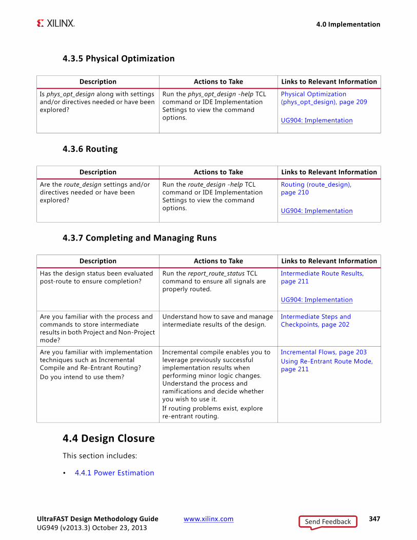
4.0 Implementation
4.3.5 Physical Optimization
4.3.6 Routing
4.3.7 Completing and Managing Runs
4.4 Design ClosureThis section includes:
• 4.4.1 Power Estimation
Description Actions to Take Links to Relevant Information
Is phys_opt_design along with settings and/or directives needed or have been explored?
Run the phys_opt_design -help TCL command or IDE Implementation Settings to view the command options.
Physical Optimization (phys_opt_design), page 209
UG904: Implementation
Description Actions to Take Links to Relevant Information
Are the route_design settings and/or directives needed or have been explored?
Run the route_design -help TCL command or IDE Implementation Settings to view the command options.
Routing (route_design), page 210
UG904: Implementation
Description Actions to Take Links to Relevant Information
Has the design status been evaluated post-route to ensure completion?
Run the report_route_status TCL command to ensure all signals are properly routed.
Intermediate Route Results, page 211
UG904: Implementation
Are you familiar with the process and commands to store intermediate results in both Project and Non-Project mode?
Understand how to save and manage intermediate results of the design.
Intermediate Steps and Checkpoints, page 202
Are you familiar with implementation techniques such as Incremental Compile and Re-Entrant Routing?Do you intend to use them?
Incremental compile enables you to leverage previously successful implementation results when performing minor logic changes. Understand the process and ramifications and decide whether you wish to use it.If routing problems exist, explore re-entrant routing.
Incremental Flows, page 203Using Re-Entrant Route Mode, page 211
UltraFAST Design Methodology Guide www.xilinx.com 347UG949 (v2013.3) October 23, 2013
Send Feedback

4.0 Implementation
• 4.4.2 Preliminary Timing Closure
• 4.4.3 Final Timing Closure
• 4.4.4 Floorplanning
4.4.1 Power Estimation
4.4.2 Preliminary Timing Closure
Description Actions to Take Links to Relevant Information
Has XPE been run on the 90% design?Does power meet budget?
Verify the that power budget estimate is reasonable. Review the Power optimization documentation if power estimation is too high.
Power, page 269
QuickTake: Power Estimation and Analysis using Vivado
UG907: Power Optimization and Analysis
Are constraints in place to accurately analyze power?
Review high fanout signals like global reset and clock enable.
Best Practices for Accurate Power Analysis, page 272
Description Actions to Take Links to Relevant Information
Does the 90% complete design meet the target speed?
Review the timing closure criteria to ensure the design is feasible as defined.
Timing Closure Criteria, page 222
UG906: Design Analysis and Timing Closure Techniques
Has the design been analyzed for trade-offs in technology choices?
Explore the device technology options to see if another speed grade would help.
Reviewing Technology Choices, page 246
Have all warnings and error messages been addressed?List the Messages that were not resolved.
Review and address all Errors and Critical Warning messages. Review all Warning messages.
Checking That Your Design is Properly Constrained, page 223
UltraFAST Design Methodology Guide www.xilinx.com 348UG949 (v2013.3) October 23, 2013
Send Feedback

4.0 Implementation
Are you familiar with the connection between clock period (waveform), setup relationships, and hold relationships?
Understanding how to configure the timing analysis and to interpret Vivado timing reports will help you identify design or constraint issues. Familiarize yourself with timing analysis and reporting options.
Understanding Timing Reports, page 213
UG906: Design Analysis and Timing Closure Techniques
Have you baselined the design before moving further in to the timing analysis?
Baselining is a technique to define and validate timing constraints in a sequential manner. It can help ensure timing constraints are properly assigned and implemented.
Baselining the Design, page 213
Have you validated again that the primary and generated clocks are completely and properly defined?Are the exclusive clock groups properly defined?
Run the check_timing Tcl command or validate by tracing the clocks in the Vivado Schematic viewer.
Checking That Your Design is Properly Constrained, page 223
Baselining the Design, page 213
Understanding Timing Reports, page 213
UG906: Design Analysis and Timing Closure Techniques
Have you validated again that the asynchronous clock groups and multi-cycle paths are properly constrained?
Run the report_clock_interaction Tcl command or use the Clock Interaction report in the Vivado IDE. Review clock domain crossing constraints, WNS path requirements and WHS path requirements. Are they reasonable?
Checking That Your Design is Properly Constrained, page 223
Defining Clocks and Their Relationships, page 227
Are you familiar with how to identify the paths with the worst cell delay in the design and how to change a net delay model for timing analysis?
Run timing analysis with no net delay, with estimated delays only or with actual net delays. Review the RTL to reduce the logic delay, or identify appropriate constraints for meeting timing on these paths.
Identifying the Longest Logic Delay Paths in the Design, page 259
Description Actions to Take Links to Relevant Information
UltraFAST Design Methodology Guide www.xilinx.com 349UG949 (v2013.3) October 23, 2013
Send Feedback

4.0 Implementation
4.4.3 Final Timing Closure
Have attribute settings for MMCL/PLL been checked for violations (e.g. performance setting violates input or output clock frequency range)?
Review the Messages and analyze the settings for MMCMs and PLLs to ensure they are correct.
Using Clock Modifying Blocks (MMCM and PLL), page 129
Understanding Timing Reports, page 213
UG906: Design Analysis and Timing Closure Techniques
Are you familiar with how to perform and review hold timing analysis before and after route?
Vivado timing analysis can be run in a variety of ways to pinpoint specific issues, such as hold violations or impact of hold fixing on setup violations. Familiarize yourself with the various options and run timing analysis with options, if needed.
Determining if Hold-Fixing is Negatively Impacting the Design, page 262
Has the design been analyzed for Control Set Usage?
Excessive number of control signals can degrade the placement quality by reducing the number of valid placement solutions. Examine the control sets in the design and take steps to reduce them if needed. Synthesis provides some control on the minimum fanout of clock enable and synchronous set/reset signals to be preserved.
Control Signals and Control Sets, page 257
Description Actions to Take Links to Relevant Information
Description Actions to Take Links to Relevant Information
Are your timing constraints signoff quality?
Review the check_timing report (also included in the timing summary report). Also review the User Ignored Paths and Unconstrained Paths section of the timing summary report to waive any ignored path.
Timing Closure Criteria, page 222
Does the design meet setup and hold for all signals?
Review the WNS/TNS/WHS/THS/WPWS/TPWS numbers displayed in the timing summary report. Go the various sections of the summary report for more details on the remaining violations.
Timing Closure Criteria, page 222
UltraFAST Design Methodology Guide www.xilinx.com 350UG949 (v2013.3) October 23, 2013
Send Feedback

5.0 Configuration and Debug
4.4.4 Floorplanning
5.0 Configuration and DebugThe Configuration and Debug section includes:
• 5.1 Device Configuration and Debug
In addition to the links in the tables in the following sections, refer to the Product family Configuration User Guide for your device.
5.1 Device Configuration and DebugThis section includes:
• 5.1.1 JTAG Interface
• 5.1.2 General Configuration Pin Handling
Description Actions to Take Links to Relevant Information
Are you considering floorplanning to try and improve timing results?
Vivado enables you to floorplan critical modules or logic in your design. Consider floorplanning if your design has been constructed logically to support it.
Floorplanning, page 267
Is the design logic hierarchy set up well for your floorplanning strategy?
Verify that the design logic hierarchy been constructed well to support your desired floorplanning.
Floorplanning, page 267
Is there a need to manually place any of the big blocks like PCIe, BRAM and DSP48s?Have you placed any logic in the design?
Vivado enables you to lock down resources to specific FPGA sites. Consider hand placing critical logic such as BRAM and DSP to better group them and to align with other FPGA resources.
Preserving Placement and Routing, page 267
Have you floorplanned any logic in the design?If so, did you consider the data flow through the design?If so, list the logic floorplanned in the Status and Notes f ield.
Proper Floorplanning requires knowledge of the design, the key interfaces, as well FPGA resources and uses. A suboptimal floorplan can hinder performance more than help it. Take care when floorplanning logic. Use the Vivado IDE to visualize the I/O connectivity and the top-level data flow as well as estimate the required resources.
Floorplanning, page 267
UltraFAST Design Methodology Guide www.xilinx.com 351UG949 (v2013.3) October 23, 2013
Send Feedback

5.0 Configuration and Debug
• 5.1.3 Voltage Compatibility
• 5.1.4 Security
• 5.1.5 Configuration Solution Selection
• 5.1.6 File Generation and Programming
5.1.1 JTAG Interface
5.1.2 General Configuration Pin Handling
Refer to the Product family Configuration User Guide
Description Actions to Take Links to Relevant Information
Are the JTAG pins exposed to a connector that is compatible with a Xilinx supported programming cable?
JTAG pins can be used for manual programming and debug of the FPGA. Having them available is often important for design bring-up and debug and the connector should be compatible with the Xilinx Platform Cable USB or supported Diligent USB cable.
Board Design Tips - JTAG, page 72
DS593: Platform Cable USB II Data Sheet
Product family Configuration User Guide
Can the Xilinx FPGA be isolated in the JTAG chain?
The capability to isolate the FPGA in a JTAG chain will accelerate the debug process should an issue be encountered. Not all devices support the optional pins or JTAG features (i.e.. TRST is an optional signal).
Board Design Tips - Multiple Devices, page 73
Product family Configuration User Guide
UltraFAST Design Methodology Guide www.xilinx.com 352UG949 (v2013.3) October 23, 2013
Send Feedback
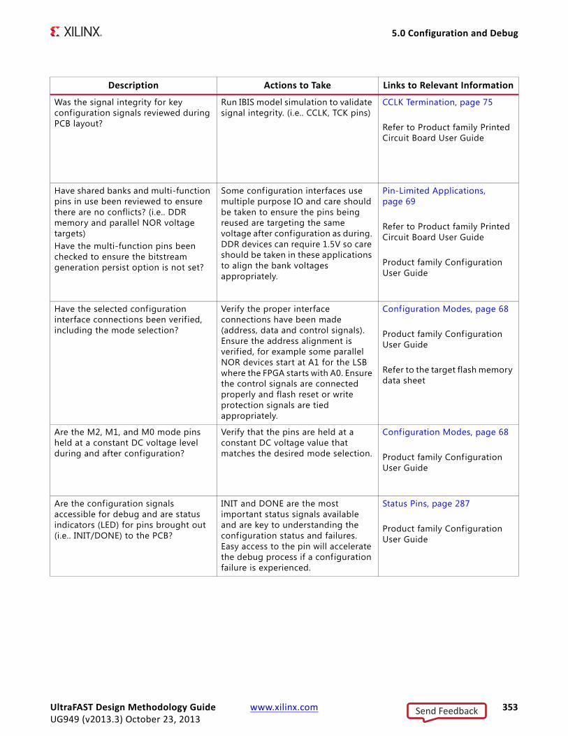
5.0 Configuration and Debug
Description Actions to Take Links to Relevant Information
Was the signal integrity for key configuration signals reviewed during PCB layout?
Run IBIS model simulation to validate signal integrity. (i.e.. CCLK, TCK pins)
CCLK Termination, page 75
Refer to Product family Printed Circuit Board User Guide
Have shared banks and multi-function pins in use been reviewed to ensure there are no conflicts? (i.e.. DDR memory and parallel NOR voltage targets)Have the multi-function pins been checked to ensure the bitstream generation persist option is not set?
Some configuration interfaces use multiple purpose IO and care should be taken to ensure the pins being reused are targeting the same voltage after configuration as during. DDR devices can require 1.5V so care should be taken in these applications to align the bank voltages appropriately.
Pin-Limited Applications, page 69
Refer to Product family Printed Circuit Board User Guide
Product family Configuration User Guide
Have the selected configuration interface connections been verif ied, including the mode selection?
Verify the proper interface connections have been made (address, data and control signals). Ensure the address alignment is verif ied, for example some parallel NOR devices start at A1 for the LSB where the FPGA starts with A0. Ensure the control signals are connected properly and flash reset or write protection signals are tied appropriately.
Configuration Modes, page 68
Product family Configuration User Guide
Refer to the target flash memory data sheet
Are the M2, M1, and M0 mode pins held at a constant DC voltage level during and after configuration?
Verify that the pins are held at a constant DC voltage value that matches the desired mode selection.
Configuration Modes, page 68
Product family Configuration User Guide
Are the configuration signals accessible for debug and are status indicators (LED) for pins brought out (i.e.. INIT/DONE) to the PCB?
INIT and DONE are the most important status signals available and are key to understanding the configuration status and failures. Easy access to the pin will accelerate the debug process if a configuration failure is experienced.
Status Pins, page 287
Product family Configuration User Guide
UltraFAST Design Methodology Guide www.xilinx.com 353UG949 (v2013.3) October 23, 2013
Send Feedback

5.0 Configuration and Debug
5.1.3 Voltage Compatibility
Refer to the Product family Configuration User Guide
Has the PUDC_B pin been tied appropriately?
If internal pull-up resistors are desired on the SelectIO pin after power-up and during configuration then verify that PUDC_B is Low. If no internal pull-ups are desired then ensure the PUDC_B signal is tied to GND. This pin must not be left floating before and during configuration.
Product family Configuration User Guide
If EMCCLK is used for fastest performance has this signal been instantiated in the design since it is a multi-function pin?
The configuration internal CCLK has a large tolerance range. If configuration speed is critical the EMCCLK will help achieve the fastest times possible. Since the pin is on a dual-purpose IO it must be defined instantiated and IO standard defined.
High Speed Configuration Applications, page 70
XAPP587: BPI Fast Configuration and iMPACT Flash Programming with 7 Series FPGAs
Product family Configuration User Guide
If using SelectMAP mode, have you ensured that the RDWR_B and CSI_B are not used after configuration or that the ABORT sequence is not entered?
Care should be taken not to enter the ABORT after configuration by sequencing the RDWR_B and CSI_B. Product family configuration user guide for details.
Configuration Modes, page 68
Product family Configuration User Guide
Description Actions to Take Links to Relevant Information
Description Actions to Take Links to Relevant Information
Is the CFGBVS pin set appropriately and have the cautions been reviewed for handling of this signal?
Verify that the pin selection matches the targeted configuration mode bank voltage. For details on this pin refer to the Configuration User Guide.
Configuration Bank Voltage Selection, page 73
Product family Configuration User Guide
If using external SPI or parallel NOR flash, have the bank voltages been verif ied to ensure they are compatible?
NOR flash often have versions within the same family that are compatible with different voltages (i.e.. 1.8V or 3.3V). Ensure that the FPGA bank voltage settings match the targeted flash requirements.
Configuration Modes, page 68
Product family Configuration User Guide
UltraFAST Design Methodology Guide www.xilinx.com 354UG949 (v2013.3) October 23, 2013
Send Feedback
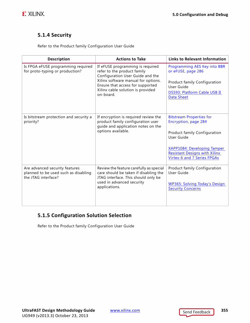
5.0 Configuration and Debug
5.1.4 Security
Refer to the Product family Configuration User Guide
5.1.5 Configuration Solution Selection
Refer to the Product family Configuration User Guide
Description Actions to Take Links to Relevant Information
Is FPGA eFUSE programming required for proto-typing or production?
If eFUSE programming is required refer to the product family Configuration User Guide and the Xilinx software manual for options. Ensure that access for supported Xilinx cable solution is provided on-board.
Programming AES Key into BBR or eFUSE, page 286
Product family Configuration User GuideDS593: Platform Cable USB II Data Sheet
Is bitstream protection and security a priority?
If encryption is required review the product family configuration user guide and application notes on the options available.
Bitstream Properties for Encryption, page 284
Product family Configuration User Guide
XAPP1084: Developing Tamper Resistant Designs with Xilinx Virtex-6 and 7 Series FPGAs
Are advanced security features planned to be used such as disabling the JTAG interface?
Review the feature carefully as special care should be taken if disabling the JTAG interface. This should only be used in advanced security applications.
Product family Configuration User Guide
WP365: Solving Today's Design Security Concerns
UltraFAST Design Methodology Guide www.xilinx.com 355UG949 (v2013.3) October 23, 2013
Send Feedback
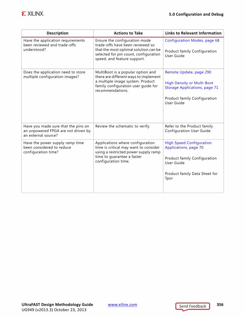
5.0 Configuration and Debug
Description Actions to Take Links to Relevant Information
Have the application requirements been reviewed and trade-offs understood?
Ensure the configuration mode trade-offs have been reviewed so that the most optimal solution can be selected for pin count, configuration speed, and feature support.
Configuration Modes, page 68
Product family Configuration User Guide
Does the application need to store multiple configuration images?
MultiBoot is a popular option and there are different ways to implement a multiple image system. Product family configuration user guide for recommendations.
Remote Update, page 290
High Density or Multi-Boot Storage Applications, page 71
Product family Configuration User Guide
Have you made sure that the pins on an unpowered FPGA are not driven by an external source?
Review the schematic to verify. Refer to the Product family Configuration User Guide
Have the power supply ramp time been considered to reduce configuration time?
Applications where configuration time is critical may want to consider using a restricted power supply ramp time to guarantee a faster configuration time.
High Speed Configuration Applications, page 70
Product family Configuration User Guide
Product family Data Sheet for Tpor
UltraFAST Design Methodology Guide www.xilinx.com 356UG949 (v2013.3) October 23, 2013
Send Feedback

5.0 Configuration and Debug
5.1.6 File Generation and Programming
How much storage is required for the configuration bitstreams?
Based on the bitstreams targeted calculate the storage size required. Ensure the flash selected or storage device has enough memory to accommodate the image(s) targeted. Some application require padding between images and this should be accommodated in the size estimation. Product family configuration user guide for details.
Remote Update, page 290
High Density or Multi-Boot Storage Applications, page 71
Product family Configuration User Guide
Is in-system flash programming required for proto-typing and debug or production? If so has a supported flash device been selected?
For supported flash families with Xilinx in-direct programming see the software manuals or the product family configuration user guide.
For SPI and BPI Configuration and Indirect Programming References, see:XAPP586
XAPP587
Product family configuration user guide
Description Actions to Take Links to Relevant Information
Description Actions to Take Links to Relevant Information
Have the required f ile generation options been verif ied for bitstream generation (.bit) and flash programming f ile generation (i.e.. .mcs) ?
Dependent on the configuration mode selected you will need to enable appropriate file generation options. These options include selecting the appropriate bus width (i.e.. x1, x2, x4, x8, 16, or x32) dependent on the mode. In addition, selections for advanced features like encryption, synchronous bpi mode, 32 bit enabled spi mode etc.
XAPP586
XAPP587
UG908:Programming and Debug
UG936:Programming and Debug Tutorial
QuickTake: How to Use the "write_bitstream" Command in Vivado
Product family Configuration User Guide
Have the DRCs warnings received during configuration bitstream generation been reviewed and corrected?
Review the DRC warnings and ensure they are corrected.
UG908:Programming and Debug
Product family Configuration User Guide
UltraFAST Design Methodology Guide www.xilinx.com 357UG949 (v2013.3) October 23, 2013
Send Feedback

5.0 Configuration and Debug
If an external flash configuration mode (SPI or BPI) is used, will the flash be reused after configuration or is Persist being used?
If the flash is being reused after configuration take care to review the handling of dedicated configuration IO (such as the SPI signals that can be accessed after configuration using the STARTUP primitive) or if Persist is being used be certain to review the software manual and configuration user guide for details.
Remote Update, page 290
High Density or Multi-Boot Storage Applications, page 71
Product family Configuration User Guide
Does the FPGA need to be held off from configuring at power up to ensure power supplies are stable?
The INIT_B pin can be used to hold off configuration. If this is required (i.e.. to ensure flash is powered up first before the FPGA tries to retrieve configuration data) then refer to the product family configuration user guide.
Delaying Configuration, page 74
Product family Configuration User Guide
Is an internal configuration clock desired? If so can a clock tolerance be accepted by application configuration time requirements?
If cost is a factor, using the internal configuration clock will prevent the need of an external clock. However, if the fastest configuration time is required, EMCCLK should be evaluated instead of the internal configuration clock. The internal configuration clock has a clock tolerance that will reduce the max freq.
Configuration Clock, page 74
Product family Configuration User Guide
Description Actions to Take Links to Relevant Information
UltraFAST Design Methodology Guide www.xilinx.com 358UG949 (v2013.3) October 23, 2013
Send Feedback
Appendix B
Additional Resources
Xilinx ResourcesFor support resources such as Answers, Documentation, Downloads, and Forums, see the Xilinx® Support website at:
www.xilinx.com/support
For a glossary of technical terms used in Xilinx documentation, see:
www.xilinx.com/company/terms.htm
Solution CentersSee the Xilinx Solution Centers for support on devices, tools, and intellectual property at all stages of the design cycle. Topics include design assistance, advisories, and troubleshooting tips.
ReferencesThese documents provide supplemental material useful with this Guide.
Vivado® Design Suite User Guides1. Memory Interface Solutions User Guide (UG086)
2. Xilinx Power Estimator User Guide (UG440)
3. 7 Series FPGAs SelectIO Resources User Guide (UG471)
4. 7 Series Clocking Resources Guide (UG472)
5. 7 Series FPGAs Memory Resources User Guide (UG473)
6. 7 Series FPGAs DSP48E1 Slice User Guide (UG479)
UltraFAST Design Methodology Guide www.xilinx.com 359UG949 (v2013.3) October 23, 2013
Send Feedback

References
7. 7 Series FPGAs and Zynq-7000 All Programmable SoC XADC Dual 12-Bit 1 MSPS Analog-to-Digital Converter User Guide (UG480)
8. Vivado Design Suite User Guide: I/O and Clock Planning (UG899)
9. Vivado Design Suite User Guide: Design Flows Overview (UG892)
10. Vivado Design Suite User Guide: Using the Vivado IDE (UG893)
11. Vivado Design Suite User Guide: Using Tcl Scripting (UG894)
12. Vivado Design Suite User Guide: System-Level Design Entry (UG895)
13. Vivado Design Suite User Guide: Designing with IP (UG896)
14. Vivado Design Suite User Guide: Logic Simulation (UG900)
15. Vivado Design Suite User Guide: Synthesis (UG901)
16. Vivado Design Suite User Guide: Using Constraints (UG903)
17. Vivado Design Suite User Guide: Implementation (UG904)
18. Vivado Design Suite User Guide: Hierarchical Design (UG905)
19. Vivado Design Suite User Guide: Design Analysis and Closure Techniques (UG906)
20. Vivado Design Suite User Guide: Power Analysis and Optimization (UG907)
21. Vivado Design Suite User Guide: Programming and Debugging (UG908)
22. Vivado Design Suite User Guide: Vivado Design Suite User Guide: Designing IP Subsystems Using IP Integrator (UG994)
Other Vivado Design Suite Documents23. 7 Series FPGAs Clocking Resources Guide (UG472)
24. Vivado Design Suite Tcl Command Reference Guide (UG835)
25. Vivado Design Suite Tutorial: Design Flows Overview (UG888)
26. Vivado Design Suite Tutorial: I/O and Clock Planning (UG935)
27. Vivado Design Suite Tutorial: Logic Simulation (UG937)
Vivado Design Suite Video Tutorials28. Vivado Design Suite Video Tutorials (http://www.xilinx.com/training/vivado/index.htm)
29. Vivado Design Suite Video: How to Use the “write_bitstream” Command in Vivado. Go to http://www.xilinx.com/training/vivado/ and click Programming and Debug.
30. Vivado Design Suite Video: I/O Pin Planning Overview. Go to http://www.xilinx.com/training/vivado/ and click I/O Pin Planning.
UltraFAST Design Methodology Guide www.xilinx.com 360UG949 (v2013.3) October 23, 2013
Send Feedback

References
Vivado Design Suite Documentation31. Vivado Design Suite Documentation
(www.xilinx.com/support/documentation/dt_vivado2013-3.htm)
32. Using SPI Flash with 7 Series FPGAs (XAPP586)
33. BPI Fast Configuration and iMPACT Flash Programming with 7 Series FPGAs (XAPP587)
TIP: A complete set of Xilinx documents can be accessed from Documentation Navigator. For more information, see Using the Documentation Navigator, page 13.
UltraFAST Design Methodology Guide www.xilinx.com 361UG949 (v2013.3) October 23, 2013
Send Feedback
Copyright © 2022 FDOKUMEN