Xilinx XAPP870 Serial ATA Physical Link Initialization with the ...
Upload
khangminh22Category
view
0download
0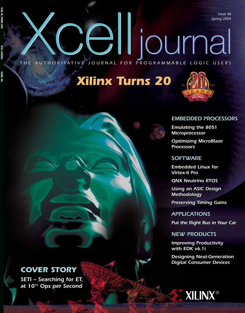
T H E A U T H O R I T A T I V E J O U R N A L F O R P R O G R A M M A B L E L O G I C U S E R S
Issue 48Spring 2004
R
Xcell journalXcell journalT H E A U T H O R I T A T I V E J O U R N A L F O R P R O G R A M M A B L E L O G I C U S E R S
ISSUE 48, SPRING 2004XCELL JOURNAL
XILINX, INC.
COVER STORYSETI – Searching for ET, at 1015 Ops per Second
COVER STORYSETI – Searching for ET, at 1015 Ops per Second
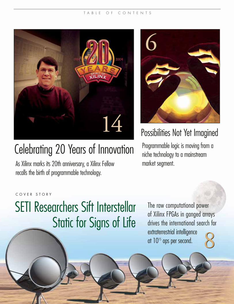
Xilinx Turns 20Xilinx Turns 20
EMBEDDED PROCESSORS
Emulating the 8051Microprocessor
Optimizing MicroBlazeProcessors
SOFTWARE
Embedded Linux for Virtex-II Pro
QNX Neutrino RTOS
Using an ASIC DesignMethodology
Preserving Timing Gains
APPLICATIONS
Put the Right Bus in Your Car
NEW PRODUCTS
Improving Productivity with EDK v6.1i
Designing Next-GenerationDigital Consumer Devices
Introducing the
SPARTAN™-3Platform FPGAs.
The New Generation of Low Cost Solutions.
The world’s lowest-cost FPGAs
The first devices ever manufactured in 90nm process technology, our new Spartan-3 FPGAs
deliver unbeatable price and performance. Packing a ton of I/Os, with densities ranging from
50K to 5 Million gates, you’ve got the lowest cost per pin and lowest cost per gate in the industry—
and it’s all in the most cost-efficient die size available.
All the density and I/O you need . . . at the price you want
The new Spartan-3 FPGAs allow you to take your design idea from the white
board to the circuit board in a huge range of applications. With cost savings
in manufacturing, easy integration of soft core processors, superior DSP
performance and full I/O support with total connectivity solutions, you
get all you need at the price you want.
The Spartan-3 Platform FPGAs are ready for a new generation of designs. . . are you?
MAKE IT YOUR ASIC
The Programmable Logic CompanySM
For more information visitwww.xilinx.com/spartan3
® 2003 Xilinx, Inc., 2100 Logic Drive, San Jose, CA 95124. Europe +44-870-7350-600; Japan +81-3-5321-7711; Asia Pacific +852-2-424-5200; Xilinx and Spartan are registered trademarks,
and The Programmable Logic Company is a service mark of Xilinx, Inc.
ilinx is now entering its 20th year in business, and in that time we have not only created awhole new category of devices – FPGAs – but we have also created a company like no other.
Our hardware and software technology, our business model, and our corporate culture have start-ed a revolution in logic design. As our device performance has dramatically increased and priceshave dramatically decreased, our technology has become the obvious choice for new designs.From miniature consumer devices to large switching systems, there simply is no better way tocreate new designs quickly and efficiently. And the trend toward higher density, lower cost, andfaster development cycles will continue well into the future.
While our technology has steadily opened new markets and design pos-sibilities, we have also built a great place to work – at last count wewere Fortune magazine’s fourth best company to work for. Our fast-paced innovation is a direct result of our corporate culture and ourvalues – it makes a strategic difference when people enjoy their work.
We also support others in their quest for excellence. As you will see fromthe SETI article on page 8, Xilinx has long been a part of this far-reachingresearch program.
What’s Next?
Our new Virtex-4™ FPGA family has just been announced, with a revolutionary modular archi-tecture. Our new Application Specific Modular Block architecture (ASMBL) segments functionblocks into interchangeable columns, rather than the traditional squares on a grid. Combinedwith flip-chip technology (which allows us to make I/O interconnects anywhere on the device –not just the periphery) this architecture allows us to provide a range of new devices optimized forspecific classes of applications. Once again, you get even higher performance and lower costs. Plus,you will have the ability to select just the right mix of features and functions, which makes yourdesign process easier. You’ll soon be seeing a lot more about the Virtex-4 family.
In the last 19 years, we have been granted more than 900 patents; that comes out to about apatent a week – not a bad record of innovation for any company. May the next 20 years be justas much fun.
L E T T E R F R O M T H E E D I T O R
Xilinx, Inc.2100 Logic DriveSan Jose, CA 95124-3400Phone: 408-559-7778FAX: 408-879-4780©2004 Xilinx, Inc.All rights reserved.
Xcell is published quarterly. XILINX, the Xilinx logo,CoolRunner, Rocket Chips, Rocket IP, Spartan, andVirtex are registered trademarks of Xilinx, Inc. ACEController, ACE Flash, Alliance Series, AllianceCORE,ChipScope, CORE Generator, Fast CONNECT, Fast FLASH,Fast Zero Power, Foundation, HDL Bencher, IRL, J Drive,LogiCORE, MicroBlaze, MultiLINX, NanoBlaze,PicoBlaze, QPro, Real-PCI, RocketIO, RocketPHY,SelectIO, SelectRAM, SelectRAM+, Smart-IP, SystemACE, Virtex-II Pro, Virtex-II EasyPath, WebFITTER,WebPACK, WebPOWERED, XACT-Floorplanner, XACT-Performance, XAPP, XC designated products, XilinxFoundation Series, Xilinx XDTV, and XtremeDSP aretrademarks, and The Programmable Logic Company isa service mark of Xilinx, Inc. Other brand or productnames are registered trademarks or trademarks oftheir respective owners.
The articles, information, and other materials includedin this issue are provided solely for the convenienceof our readers. Xilinx makes no warranties, express,implied, statutory, or otherwise, and accepts no liabilitywith respect to any such articles, information, orother materials or their use, and any use thereof issolely at the risk of the user. Any person or entityusing such information in any way releases andwaives any claim it might have against Xilinx for anyloss, damage, or expense caused thereby.
20 Years and 900 Patents Later...X
Xcell journalXcell journal
Carlis CollinsEditor-in-Chief
EDITOR IN CHIEF Carlis [email protected]
MANAGING EDITOR Tom [email protected]
ASSOCIATE EDITOR Charmaine Cooper Hussain
XCELL ONLINE EDITOR Tom [email protected]
ADVERTISING SALES Dan Teie1-800-493-5551
ART DIRECTOR Scott Blair
T A B L E O F C O N T E N T S
Celebrating 20 Years of InnovationAs Xilinx marks its 20th anniversary, a Xilinx Fellow recalls the birth of programmable technology.
SETI Researchers Sift InterstellarStatic for Signs of Life
The raw computational power of Xilinx FPGAs in ganged arraysdrives the international search forextraterrestrial intelligence at 1015 ops per second. 88
Possibilities Not Yet Imagined
6
C O V E R S T O R Y
14
6
Programmable logic is moving from aniche technology to a mainstream market segment.
Put the Right Bus in Your Car The amazing array of features available in today’s cars has spawned new in-vehicle bus standards.
62
Emulate 8051Microprocessor inPicoBlaze IP CorePut the functions of a legacy microprocessor into a Xilinx FPGA.
S P R I N G 2 0 0 4, I S S U E 4 8
18
Xcell journalXcell journal
Improve Your Productivitywith the EmbeddedDevelopment Kit v6.1iThe new version of EDK offers automaticgeneration of complex implementationdetails, new simulation capabilities, and new IP cores.
Unleash Your Creativitywith Embedded Linux on Virtex-II Pro FPGAsXilinx has partnered with MontaVistaSoftware to provide a customizedembedded Linux solution for Virtex-II Pro FPGAs.
24
38
Possibilities Not Yet Imagined – View From The Top..................6
SETI Researchers Sift Interstellar Static ....................................8
Celebrating 20 Years of Innovation .......................................14
Emulate the 8051 Microprocessor with PicoBlaze ...................18
Optimize MicroBlaze Processors for Consumer Products ............22
Improve Your Productivity with EDK v6.1i...............................24
QNX Neutrino RTOS Optimizes Programmable Systems ............28
Wind River Delivers Embedded System Performance ................32
Use an RTOS on Your Next MicroBlaze Project ........................35
Unleash Your Creativity with Embedded Linux .........................38
Get Control of Your High-Speed Designs .................................44
Use ASIC Design Methodology for Your Next Design ................48
Preserve Timing Gains in Incremental Designs .........................52
Designing Next Generation Digital Consumer Devices ...............55
Seamless Hardware/Software Co-Verification .........................56
Simplify with Synplicity Synthesis Solutions............................60
Put the Right Bus in Your Car ...............................................62
Verify Gateway Designs for Time-Triggered Networks................68
The EasyPath to Cost Reductions...........................................72
Think Outside the Chip with ChipScope Pro.............................75
ThumbPod Puts Security Under Your Thumb............................79
Develop Low-Power Telemetry Systems..................................82
Xilinx Teams with Optos – New Eye Care Technology ..............85
One of the World’s Highest Resolution Digital Cameras ............88
Accelerate JPEG2000 Compression........................................91
Get Award-Winning Support..................................................94
Customize Your Education with Skills Assessment....................96
Xilinx Wins Architecture Award..............................................98
Partner Yellow Pages.........................................................114
Reference Pages ...............................................................122
Pro g r a m m a b l elogic technology isadvancing at aphenomenal rate. Our FPGAs now contain advancedprocessors, gigabit-per-second trans-ceivers, vast num-bers of logic cells,and advanced fea-
tures that were unheard of just two shortyears ago. Plus, we’ve lowered our pricingsignificantly across the board, due to our useof the most advanced 90 nm processes andother leading manufacturing technologies.We have progressed far in a very short time –and there’s more on the way.
During the last 20 years, Xilinx hasgrown from a small startup company tohaving more than a billion dollars in rev-enue. Each step of the way, we’ve had to
transform ourselves to meet the demandsof a growing organization. Many compa-nies fail because they cannot manage thisconstant transformation.
Today, we live in “interesting times”because there are significant changes com-ing over the next few years.
Grand ChangesToday, programmable logic is 20 percent ofthe total logic market. I believe that we canget to 50-60 percent somewhere in thefuture, and that again requires us to changeour approach. Because to be a mainstreamcompany, we have to be a low-cost produc-er; we have to serve a broad range of mar-kets. Historically we’ve served a relativelylow-volume, high-cost, narrow market.
You can see that now we have a globaltransformation in front of us, a transfor-mation that requires us to discover andlearn and sell into new, high-volume mar-
kets. We must also learn how to sell intonew, more strategic applications. We mustsell not only to engineers, but to the sys-tems architects and vice presidents, whocare most about the long-range implica-tions of today’s technology.
At the same time, our internationalbusiness is growing very rapidly. Asia,which in 2000 was less than 15 percent ofour revenue, is now more than 35 percentof our revenue, which again forces us tochange the way we do things, from engi-neering to support.
I believe that the next big cycle of inno-vation ahead of us is going to be the con-vergence of digital consumer electronics.For the last 20 years, innovation has beendriven by the PC market. I believe that thenext 20 years is going to be driven by con-sumer electronics, both for the home andfor the car, and I think that the center ofthat is going to be in Asia.
As we enter our 20th year, programmable logic is moving from a niche technology to a mainstream market segment.As we enter our 20th year, programmable logic is moving from a niche technology to a mainstream market segment.
Possibilities Not Yet ImaginedPossibilities Not Yet Imagined
6 Xcell Journal Spring 2004
Viewfrom the top
by Wim RoelandtsCEO, Xilinx, Inc.

Product ChangesWe are also moving into new markets, withnew processors and very high-speed trans-ceivers capable of managing tremendousamounts of data. In many designs, there isnothing faster than our programmablelogic devices.
Historically, when programmable logicwas mainly used as glue logic, the decisionto use programmable logic products wasmade late in the design cycle, typically lessthan a year before the product went intoproduction. Therefore, we got involved latein the design cycle. Today, because FPGAsare the primary component in many sys-tems, we have to sell early in the design cycle– two to three years before the product goesinto production. This requires a very differ-ent approach to sales and marketing.
For example, we have just released ourVirtex-II Pro™ X FPGA, which is anotherimportant milestone. It will be the firsttime that a 10 gigabit transceiver is inte-grated with an FPGA.
Our next major product introduction isour Virtex™-4 FPGA family. It uses veryaggressive seamless technology and is acompletely new design concept. Every sin-gle function was redesigned, changed, mod-ified, and significantly improved to bothincrease performance and reduce costs.
The most innovative part of our newVirtex-4 family is the physical layout. Wehave moved away from the traditional lay-out (with the chip in the center and theI/O on the periphery) toward the use offlip-chip technology, which allows us tohave a very new structured columnar archi-tecture. So, we put different resources instrips or columns of technology and thenstitch the columns together.
With flip-chip packaging, we can con-nect I/Os to any part of the chip, not justthe periphery. This increases performance,decreases noise, and makes it far easier toimplement efficient designs. The Virtex-4FPGA design is truly revolutionary.
The Culture and Spirit of XilinxOur products and services are often imitat-ed by our competition, but our corporateculture of innovation is very difficult tomatch – our culture is the most important
In companies like Xilinx, people jumpin and help out when needed – it’s a veryimportant part of being an innovative com-pany. There’s no finger pointing and noblaming here, just saying “hey, let’s go for-ward, let’s help out.” All of this is part ofthe Spirit of Xilinx.
I believe you can treat people withrespect and still be a leader in your indus-try. And the difference is innovation.Because if you innovate, there’s no compe-tition. If you have the most innovativeproduct and unique features, there is nocompetition. And when there is no compe-tition, you don’t have to drive people towork 12 hours a day.
In fact, I believe that if you really wantto have innovation you cannot drive peopletoo hard, because innovation occurs whenpeople are not too busy. If you look at ourfundamental core culture, it’s innovation;innovation in everything we do. And that isalso in line with the high-tech industry,where things keep changing continuously.
Now let’s not forget that there is some-thing else that is needed, and that is busi-ness success. Whatever you do, if it doesn’tcreate business success, it’s not going towork. Fortunately, our success is tremen-dous. A couple of years ago we were noteven the number one company in pro-grammable logic, but we have come backwith a vengeance – we now have 50 percentmarket share, gaining almost 20 points ofmarket share in the last six years or so –which is really remarkable.
ConclusionXilinx is strong because our programmablelogic technology is unmatched, and it is theright technology for the future of logicdesign. There is no better way to designand develop next-generation equipment.We are also strong because our culture sup-ports continued innovation at all levels ofour company. It’s a competitive advantagethat cannot easily be surpassed.
I think that we are just at the beginningof what is possible. With our enabling tech-nology and our customers’ creativity, I’msure that there are going to be new ways ofdoing things that will emerge; possibilitieswe have not yet imagined.
long-term competitive advantage we have.Culture is not something that is fixed; it
must change and grow with circumstances;it must keep evolving and changing. Ourculture itself must not only change as need-ed, it must support change and innovationon all levels of our company, from engi-neering and support to marketing andsales. Innovation is alive and well at all lev-els of the Xilinx culture.
Partnerships are a key part of our cultureas well. Xilinx is extremely strong in creat-ing win-win solutions with our partners,because the way we treat our partners is verymuch how we treat our own employees. Wemake sure they get something more out ofthe relationship than just business fromXilinx. Because for me, our business part-ners are part of the Xilinx ecosystem (justlike our customers), and are necessary forthe health and growth of the whole.
We do interesting work at Xilinx, andthat’s what motivates us. Our employeesconsistently report in surveys that theirwork is meaningful and that they are proudof their work. That’s why we focus onindustry leadership – because if you dosomething that is really top-notch, reallystate-of-the-art, then clearly your work hasvalue and meaning. It’s not just leadershipas a way of getting market share or beingnumber one in the market. Our leadershipis also a very strong motivator for our peo-ple. Ultimately, that’s a key advantage thatcannot be matched by any competitor.
Spring 2004 Xcell Journal 7
V I E W F R O M T H E T O P

by Tom DurkinManaging Editor, Xcell JournalXilinx, [email protected]
You don’t have to leave Earth to find intelli-gent life on other worlds. All you have to dois tune in ... at the right time ... on the rightfrequency ... in the right direction ... withthe right spectrometer ... using the mostpowerful supercomputer on this planet.
With the support of the Xilinx UniversityProgram (XUP), the University of Californiaat Berkeley has emerged as the world leader inthe search for “ET” [pronounced EE-tee, as inthe popular fantasy motion picture E.T.]. UCBerkeley operates about a half-dozen differentSETI (Search for Extraterrestrial Intelligence)projects under the umbrella of theSERENDIP (Search for Extraterrestrial RadioEmissions from Nearby Developed IntelligentPopulations) Program.
“When we started 25 years ago, we built amachine that could listen to a hundred chan-nels at once. We thought that was amazing,”says Dan Werthimer, Ph.D., director of theSERENDIP SETI Program at UC Berkeley.“That was called SERENDIP I. Then wewent to 65,000 different channels withSERENDIP II – and then Xilinx technologyallowed us to go to four million channels withSERENDIP III.” And in 1997, “We went to168 million channels with SERENDIP IV.”
Later this year, SERENDIP V will goonline at the Arecibo Observatory in PuertoRico with the capability of simultaneouslyprocessing data from five billion channels(Figure 1), using several hundred Virtex™-II XC2V6000 and XC2V1000 platformFPGAs populating dozens of racks of spec-trum analyzer boards.
The raw computational power of Xilinx FPGAs in ganged arrays drives the international search for extraterrestrial intelligence at 1015 ops per second.
The raw computational power of Xilinx FPGAs in ganged arrays drives the international search for extraterrestrial intelligence at 1015 ops per second.
SETI Researchers Sift InterstellarStatic for Signs of LifeSETI Researchers Sift InterstellarStatic for Signs of Life
8 Xcell Journal Spring 2004

With such an awesome capability to col-lect massive amounts of data, theSERENDIP scientists need far more com-puting power than they could possibly havewith the high-end Sun Microsystems™workstations at the Berkeley Space SciencesLaboratory. That’s where you and I comein. SETI@home volunteers comprise thelargest supercomputer on the planet.
Meanwhile, in the next few years, UCBerkeley’s Radio Astronomy Laboratoryand the SETI Institute of MountainView, Calif., will build the AllenTelescope Array, a bold innovation inradio telescope design – and a powerfulnew tool for SETI research. As withSERENDIP, Xilinx will provide the coretechnology to enable real-time digital sig-nal processing (DSP) at the unprecedentedspeed of 1015 ops per second.
And what happens if we do find ET?Virtually all of the world’s scientific com-munity of SETI researchers have endorseda United Nations treaty that requires thefree and open disclosure of everything dis-covered and deciphered. How the rest ofhumanity will react is anybody’s guess. Alot of it depends, says Werthimer, onwhether the ET signal is accidental orintentional.
Anatomy of AreciboOperated by Cornell University and theNational Science Foundation, the NationalAstronomy and Ionosphere Center AreciboObservatory is the largest radio telescopeon this planet (Figure 2).
The spherical reflector dish measures1,000 feet (305 meters) across and covers20 acres. In what is considered a valid sci-entific calculation, Werthimer says the dishcould theoretically hold 10 billion bowls ofcornflakes. Milk, however, would quicklydrain out the almost 40,000 perforated alu-minum panels that make up the dish.
Suspended 450 feet (137 meters) abovethe dish is a 900-ton (816 metric tons)platform that can be placed with millime-ter precision anywhere up to 20 degreesfrom the vertical. A “Gregorian dome” onthe platform contains two subreflectors(secondary and tertiary) to further focusdeep space radio emissions.
The platform also houses ultra-sensitiveradio receivers cooled with liquid helium(to reduce electron noise) so the infinitesi-mally weak signals from outer space can bepicked up amidst all the interstellar staticand radio interference generated on Earth,orbiting satellites, and probes launchedfrom Earth.
Tuning In to ETRadio waves (including television, radar,cell phones, and other microwave telecom-munications) are considered the optimumband of the electromagnetic spectrum forinterstellar communication. Radio wave-lengths are relatively free of the absorptionand noise that afflictother areas of the spec-trum. Additionally, starsare generally quiet in theradio wavelengths. Thismakes radio frequenciesa natural candidate forintentional interstellarcommunications – or“leakage” of local trans-missions.
Just as the “local trans-missions” of Americantelevision shows, such as“I Love Lucy” and “TheHoneymooners,” leakedout into space 50 yearsago (and now have passedthousands of star sys-tems), it is conceivablethat we could somedayintercept an extraterrestri-al situation comedy show.
1010
109
108
107
106
105
104
103
102
101
1979 1985 1991 1997 2003 2009
Numb
er of
Chan
nels
Year
SERENDIP I100 Channels
Hat Creek
Arecibo
Arecibo
Arecibo
Arecibo
SERENDIP II65,536 Channels
SERENDIP III4,194,304
SERENDIP IV167,772,160
SERENDIP V5,637,144,576
SERENDIP Progress
Figure 1 – SERENDIP DSP growth follows Moore’s Law
Figure 2 – Arecibo Observatory, Puerto Rico
Spring 2004 Xcell Journal 9
Courtesy of the NAIC – Arecibo Observatory, a facility of the NSF

Piggyback SETIWhile most radio astronomers are lucky toget a day or two a year to use the AreciboObservatory, “We figured out how to use thetelescope 24 hours a day all year round byhaving our own feed antenna,” Werthimersays with a certain amount of glee.
“The problem with that is that wedon’t get to point the telescope, butthat’s okay, because we don’t knowwhere to look anyway,” he grins.
“We call it piggyback SETI.”
Spectacular SpectrometersAlthough radio telescope antennasare visually impressive and quiteessential, they are useless withoutthe instruments that receive andprocess the signals. The real guts ofradio telescopes are spectrometers,or spectrum analyzers, such asSERENDIP IV.
SERENDIP IV The SERENDIP IV spectrometer atArecibo consists of 120 Xilinx FPGAs on 40spectrum analyzer boards working in parallelto scan 168 million narrow-band (0.6 Hz)channels every 1.7 seconds.
Each SERENDIP IV board computes afour million point Fast Fourier Transform(FFT). This four million point FFT is bro-ken down into three smaller FFTs (128,128, and 256 points each). Xilinx chipscomb the resulting power spectra for strongnarrow-band signals and report their find-ings to the back-end computers at Berkeleyfor subsequent analysis, Werthimer says.
SERENDIP V“We don’t know what frequency ET will betransmitting at, so the name of the game inSETI is to search through as many frequen-cies as possible,” explains Aaron Parsons, adesign engineer at the Berkeley SpaceSciences Laboratory. Parsons is designingSERENDIP V, the next-generation spec-trometer that will be able to process five
billion channels simultaneously.As of press time, SERENDIP V was still
on the drawing board, but it is on scheduleto be installed at Arecibo later this year.
The whole spectrometer will consist of40 spectrum analyzer boards, each per-
forming a pair of 64 million point FFTs tohandle a real-time signal bandwidth of 100MHz, Parsons says. Because Xilinx plat-form FPGAs have the capability of inter-facing with double data rate DRAMmemory chips, SETI engineers will be ableto fit this 64 million point FFT onto a sin-gle Virtex-II XC2V6000 FPGA.
Spectrum Splitting“We did this by first cutting the spectruminto coarse frequency bins using the char-acteristic frequency response of a 4,096-channel polyphase filter bank,” Parsonsexplains (Figure 3). “The output data werethen re-ordered using 256 MB of DRAMand broken into 16,384 smaller bins usinga dual flow-through FFT we developed. Ituses one-fourth of the space of a tradition-al FFT, he says with pride.
Finally, information about the best sig-nals will be passed to a CPU over a com-pact PCI backplane using a Virtex-II
XC2V1000 running a Xilinx PCI core,according to Parsons.
Xilinx Chief DSP Architect ChrisDick, Ph.D., consulted on the design ofSERENDIP V. “The signal processingrequirements in the SETI program pres-
ent significant computational and I/Ochallenges that can only be met usingXilinx FPGAs,” Dick asserts. “Traditionalprocessor-based approaches just cannotdeliver the performance required for thischallenging application.
“The highly parallel compute fabricand I/O capability of the FPGA, however,are well suited to support the computa-tional requirements of the filter banksand FFTs used in the polyphase trans-form channelizer,” Dick says.
Key aspects of SERENDIP V wererealized using a recent generation designflow from Xilinx called System Generatorfor DSP. This visual programming devel-opment environment is based on TheMathWorks Simulink® interactive toolfor modeling, simulating, and analyzingdynamic, multidomain systems. It pro-vides a natural framework for rapidlyspecifying and verifying complex signalprocessing systems, according to Dick.
10 Xcell Journal Spring 2004
IF InputFrom Receiver
Polarization 1 (100 MHz Band)
Polarization 2 (100 MHz Band)
PolyphaseFilterBank
4K Channel
PolyphaseFilterBank
4K Channel
CornerTurner
4K x 16K
CornerTurner
4K x 16K
16K PointFFT
16K PointFFT
cos LPF ADC
LPF ADCsin
Test Signal
cos
Gain
Gain
LPF ADC
LPF ADCsin
Test Signal
Downconverter Board Spectrum Analyzer Board
1/4 XC2V6000
1/4 XC2V6000Virtex-II
Virtex-II
Virtex-II
Virtex-II
Virtex-II1/4 XC2V6000
1/4 XC2V6000
HostCPU
PostProcessor
XC2V1000
“… the name of the game in SETI is to search through as many frequencies as possible.” – Aaron Parsons, SERENDIP V design engineer
Figure 3 – SERENDIP V spectrometer module
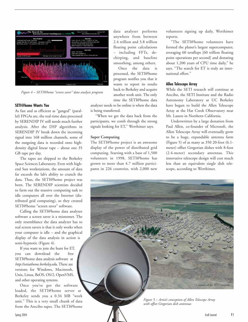
SETI@home Wants YouAs fast and as efficient as “ganged” (paral-lel) FPGAs are, the real-time data processedby SERENDIP IV still needs much furtheranalysis. After the DSP algorithms inSERENDIP IV break down the incomingsignal into 168 million channels, some ofthe outgoing data is recorded onto high-density digital linear tape – about one 35GB tape per day.
The tapes are shipped to the BerkeleySpace Sciences Laboratory. Even with high-end Sun workstations, the amount of datafar exceeds the lab’s ability to crunch thedata. Thus, the SETI@home project wasborn. The SERENDIP scientists decidedto farm out the massive computing task toidle computers all over the Internet (dis-tributed grid computing), so they createdSETI@home “screen saver” software.
Calling the SETI@home data analyzersoftware a screen saver is a misnomer. Theonly resemblance the data analyzer has toreal screen savers is that it only works whenyour computer is idle – and the graphicaldisplay of the data analysis in action issemi-hypnotic (Figure 4).
If you want to join the hunt for ET,you can download the freeSETI@home data analysis software athttp://setiathome.berkeley.edu. There areversions for Windows, Macintosh,Unix, Linux, BeOS, OS/2, OpenVMS,and other operating systems.
Once you’ve got the softwareloaded, the SETI@home server atBerkeley sends you a 0.34 MB “workunit.” This is a very small chunk of datafrom the Arecibo tapes. The SETI@home
data analyzer performsanywhere from between2.4 trillion and 3.8 trillionfloating point calculations– including FFTs, de-chirping, and baselinesmoothing, among others.
Once the data isprocessed, the SETI@homeprogram notifies you that itwants to report its resultsback to Berkeley and acquireanother work unit. The onlytime the SETI@home data
analyzer needs to be online is when the datais being transferred.
“When we get the data back from theparticipants, we comb through the strongsignals looking for ET,” Werthimer says.
Super ComputingThe SETI@home project is an awesomedisplay of the power of distributed gridcomputing. Starting with a base of 1,500volunteers in 1998, SETI@home hasgrown to more than 4.7 million partici-pants in 226 countries, with 2,000 new
volunteers signing up daily, Werthimerreports.
“The SETI@home volunteers haveformed the planet’s largest supercomputer,averaging 60 teraflops [60 trillion floatingpoint operations per second] and donatingabout 1,200 years of CPU time daily,” hesays. “The search for ET is truly an inter-national effort.”
Allen Telescope ArrayWhile the SETI research will continue atArecibo, the SETI Institute and the RadioAstronomy Laboratory at UC Berkeleyhave begun to build the Allen TelescopeArray at the Hat Creek Observatory nearMt. Lassen in Northern California.
Underwritten by a large donation fromPaul Allen, co-founder of Microsoft, theAllen Telescope Array will eventually growto be a huge, expandable antenna farm(Figure 5) of as many as 350 20-foot (6.1-meter) offset Gregorian dishes with 8-foot(2.4-meter) secondary antennas. Thisinnovative telescope design will cost muchless than an equivalent single dish tele-scope, according to Werthimer.
Spring 2004 Xcell Journal 11
Figure 5 – Artist’s conception of Allen Telescope Array with offset Gregorian dish antennas
Courtesy of the SETI Institute
Figure 4 – SETI@home “screen saver” data analysis program
12 Xcell Journal Spring 2004
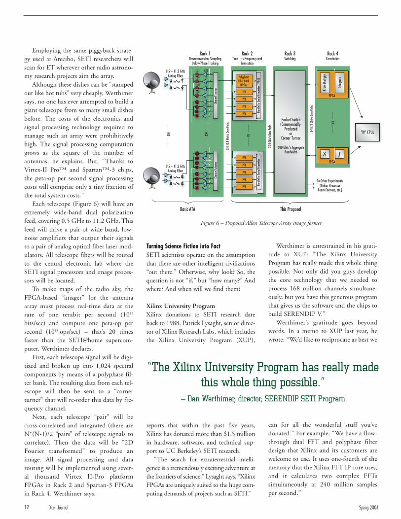
Employing the same piggyback strate-gy used at Arecibo, SETI researchers willscan for ET wherever other radio astrono-my research projects aim the array.
Although these dishes can be “stampedout like hot tubs” very cheaply, Werthimersays, no one has ever attempted to build agiant telescope from so many small dishesbefore. The costs of the electronics andsignal processing technology required tomanage such an array were prohibitivelyhigh. The signal processing computationgrows as the square of the number ofantennas, he explains. But, “Thanks toVirtex-II Pro™ and Spartan™-3 chips,the peta-op per second signal processingcosts will comprise only a tiny fraction ofthe total system costs.”
Each telescope (Figure 6) will have anextremely wide-band dual polarizationfeed, covering 0.5 GHz to 11.2 GHz. Thisfeed will drive a pair of wide-band, low-noise amplifiers that output their signalsto a pair of analog optical fiber laser mod-ulators. All telescope fibers will be routedto the central electronic lab where theSETI signal processors and image proces-sors will be located.
To make maps of the radio sky, theFPGA-based “imager” for the antennaarray must process real-time data at therate of one terabit per second (1012
bits/sec) and compute one peta-op persecond (1015 ops/sec) – that’s 20 timesfaster than the SETI@home supercom-puter, Werthimer declares.
First, each telescope signal will be digi-tized and broken up into 1,024 spectralcomponents by means of a polyphase fil-ter bank. The resulting data from each tel-escope will then be sent to a “cornerturner” that will re-order this data by fre-quency channel.
Next, each telescope “pair” will becross-correlated and integrated (there areN*(N-1)/2 “pairs” of telescope signals tocorrelate). Then the data will be “2DFourier transformed” to produce animage. All signal processing and datarouting will be implemented using sever-al thousand Virtex II-Pro platformFPGAs in Rack 2 and Spartan-3 FPGAsin Rack 4, Werthimer says.
Turning Science Fiction into Fact SETI scientists operate on the assumptionthat there are other intelligent civilizations“out there.” Otherwise, why look? So, thequestion is not “if,” but “how many?” Andwhere? And when will we find them?
Xilinx University ProgramXilinx donations to SETI research dateback to 1988. Patrick Lysaght, senior direc-tor of Xilinx Research Labs, which includesthe Xilinx University Program (XUP),
reports that within the past five years,Xilinx has donated more than $1.5 millionin hardware, software, and technical sup-port to UC Berkeley’s SETI research.
“The search for extraterrestrial intelli-gence is a tremendously exciting adventure atthe frontiers of science,” Lysaght says. “XilinxFPGAs are uniquely suited to the huge com-puting demands of projects such as SETI.”
Werthimer is unrestrained in his grati-tude to XUP: “The Xilinx UniversityProgram has really made this whole thingpossible. Not only did you guys developthe core technology that we needed toprocess 168 million channels simultane-ously, but you have this generous programthat gives us the software and the chips tobuild SERENDIP V.”
Werthimer’s gratitude goes beyondwords. In a memo to XUP last year, hewrote: “We’d like to reciprocate as best we
can for all the wonderful stuff you’vedonated.” For example: “We have a flow-through dual FFT and polyphase filterdesign that Xilinx and its customers arewelcome to use. It uses one-fourth of thememory that the Xilinx FFT IP core uses,and it calculates two complex FFTssimultaneously at 240 million samplesper second.”
Rack 1Downconversion, Sampling
Delay/Phase Tracking
Rack 4Correlation
Rack 3Switching
Rack 2Time — Frequency and
Truncation
0.5 – 11.2 GHzAnalog Fiber
0.5 – 11.2 GHzAnalog Fiber
LO1 ADC
LO2
LO3
LO4
Chan
nel S
electo
rCh
anne
l Sele
ctor
350
12.8
Gbit
/s D
ata P
aths
70 8
Gbit
/s D
ata P
aths
64 8
.75
Gbit/
s Dat
a Pat
hs
350
350
70
64
PolyphaseFilter Bank
(FPGA)
PFB
PFB
PFB
PFB
PFB
PFB
PFB
PFB
PFB
Para
llel t
o Ser
ial Co
nver
terPa
ralle
l to S
erial
Conv
erter
(FPG
A)
Integ
rate
Cros
s Mult
iply
FPGA
FPGA
To Other Experiments(Pulsar Processor
Beam Formers, etc.)
Packet Switch(Commercially-
Producedor
Corner Turner
600 Gbit/s AggregateBandwidth
”N“ CPUs
This ProposalBasic ATA
X
“The Xilinx University Program has really made this whole thing possible.”
– Dan Werthimer, director, SERENDIP SETI Program
Figure 6 – Proposed Allen Telescope Array image former
Spring 2004 Xcell Journal 13
ContactWhy are companies like Xilinx, SunMicrosystems, Intel™, Toshiba™,Hewlett Packard™, Quantum™,Network Appliance™, Fujifilm™ – aswell as non-profit organizations like theSETI Institute, the SETI League, and ThePlanetary Society – contributing millionsof dollars worth of technology and expert-ise to support the search for ET? XilinxCEO Wim Roelandts puts it this way:“You can say, well, maybe it is science fic-tion, but to prove it isn’t, you need state-of-the-art technology. This is probably theultimate science problem we must solve.The intellectual challenge is enormous.And that is what is exciting.”
Within the SETI community, the word“excited” has become almost a code wordfor the discovery of ET. Pretty much every-body uses the word “excited” when theydescribe how they’ll feel when a signalfrom ET is scientifically confirmed. Thatmeans replicated results from other, inde-pendent observatories, such as those inAustralia, Italy, France, and Argentina.
“We actually want to look at the skymany, many times,” Werthimer explains.“One of our most robust algorithms is:Did you see the signal again, in sameplace, when the telescope comes back tothe same place in the sky? Do we see it inthe same place at the same frequency? –that’s what gets us really excited.”
Unfortunately, in the last 44 years ofserious, scientific research, nobody’s foundanything to get all that excited about.
“I’m optimistic,” Werthimer says. “I think we might find ET in our lifetimes,but I think, right now, we’d be very luckyto find ET. So, I’m sort of counting onMoore’s Law. If Moore’s Law keeps going,and if Xilinx keeps on making faster andbetter chips, the better the chances we haveof finding an extraterrestrial radio signal.”
Two Scenarios“There are sort of two scenarios for con-tact with ET,” Werthimer reasons. “One isthat we find a signal, and we aren’t reallyable to decode it. It could just be a naviga-tional beacon – there’s no information. Allwe would know is that they’re out there.
“The more scary scenario to me,”Werthimer continues, “is that we mightreceive a direct broadcast with a hugeamount of information content in the ETsignal – and that could be used in good waysor bad ways.”
To prevent the potential abuse of extra-terrestrial intelligence, virtually all SETIresearch organizations – including the SETISERENDIP Program, the SETI Institute,the SETI League, and The Planetary Society,to name just a few – have endorsed ArticleXI of the United Nations Treaty onPrinciples Governing the Activities of Statesin the Exploration and Use of Outer Space.In part, Article XI decrees that the discover-ers of ET must “... inform the SecretaryGeneral of the United Nations, as well as thepublic and the international scientific com-munity, to the greatest extent feasible andpracticable, of the nature, conduct, loca-tions, and results ...” of the discovery.
Furthermore, the treaty calls for a transna-tional decision on whether to reply to ET –and if so, what to say.
ConclusionWe may discover ET any time from now
to never. And it’s impossible to predict exact-ly how humanity will react to scientificallyvalidated proof that life as we know it – isn’t.
For many years, the late astronomer-philosopher Carl Sagan was the standard-bearer for SETI research. He gave as muchthought to the implications of finding ETas he did to the technology of the searchfor ET. In a 1978 essay, he wrote: “Thesearch for extraterrestrial intelligence is thesearch for a generally acceptable cosmiccontext for the human species. … It is dif-ficult to think of another enterprise withinour capability, and at relatively modestcost, which holds as much promise for thefuture of humanity.”
Hyperlinks to SETI Research
Allen Telescope Array: www.seti.org/science/ata.html
Arecibo Observatory: www.naic.edu/bigtable.htm
Origins: Astrobiology: The Search for Life: www.exploratorium.edu/origins/arecibo/
SETI@home: setiathome.ssl.berkeley.edu
SETI at the University of California, Berkeley: seti.berkeley.edu
SETI Institute: www.seti.org
SETI League: www.setileague.org
The Planetary Society: seti.planetary.org
“The Quest for Extraterrestrial Intelligence” by Carl Sagan:www.bigear.org/vol1no2/sagan.htm
Xilinx University Program: www.xilinx.com/univ/
Protocols for Contact with ET
Treaty on Principles Governing the Activities of States in the Exploration and Use of Outer Space: www.oosa.unvienna.org/SpaceLaw/outersptxt.htm
SETI Institute: www.seti.org/science/principles.html
SETI League: www.setileague.org/general/protocol.htm
The Planetary Society: seti.planetary.org/Contact/AfterTheDetection.html
“I’m optimistic. I think we might findET in our lifetimes.”
– Dan Werthimer
by Xilinx Staff
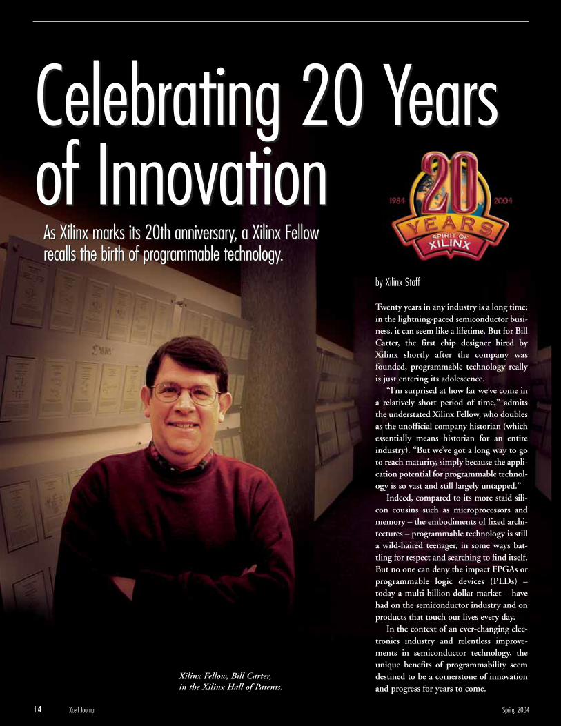
Twenty years in any industry is a long time;in the lightning-paced semiconductor busi-ness, it can seem like a lifetime. But for BillCarter, the first chip designer hired byXilinx shortly after the company wasfounded, programmable technology reallyis just entering its adolescence.
“I’m surprised at how far we’ve come ina relatively short period of time,” admitsthe understated Xilinx Fellow, who doublesas the unofficial company historian (whichessentially means historian for an entireindustry). “But we’ve got a long way to goto reach maturity, simply because the appli-cation potential for programmable technol-ogy is so vast and still largely untapped.”
Indeed, compared to its more staid sili-con cousins such as microprocessors andmemory – the embodiments of fixed archi-tectures – programmable technology is stilla wild-haired teenager, in some ways bat-tling for respect and searching to find itself.But no one can deny the impact FPGAs orprogrammable logic devices (PLDs) –today a multi-billion-dollar market – havehad on the semiconductor industry and onproducts that touch our lives every day.
In the context of an ever-changing elec-tronics industry and relentless improve-ments in semiconductor technology, theunique benefits of programmability seemdestined to be a cornerstone of innovationand progress for years to come.
Celebrating 20 Years of InnovationCelebrating 20 Years of Innovation
14 Xcell Journal Spring 2004
As Xilinx marks its 20th anniversary, a Xilinx Fellow recalls the birth of programmable technology.As Xilinx marks its 20th anniversary, a Xilinx Fellow recalls the birth of programmable technology.
Xilinx Fellow, Bill Carter, in the Xilinx Hall of Patents.

Challenging a MindsetOf course, no one could have predictedthat 20 years ago. When the foundingfathers of Xilinx – Bernie Vonderschmitt,Ross Freeman, and Jim Barnett – launchedtheir oddly named start-up venture (per-haps appropriately in the Orwellian-proph-esized year 1984), the semiconductorworld was a vastly different place than it istoday. The PC, destined to be the heavy-weight champion of silicon consumption,was just emerging from Silicon Valley labsinto commercial viability. The Internet wasan arcane communication link for scien-tists and the government, wireless tele-phones were about the dimension of acinder block, and Bill Gates still had towork for a living.
More importantly to the Xilinxfounders, many of the engrained ways ofthinking and doing business in the semi-conductor industry, while seemingly per-manently rooted, were in their mindsbecoming a bit misguided and shortsighted.
“It was Ross Freeman, really, who hadthe radical notion that transistors are free,”remembers Carter. “In those days, gateswere precious and everyone thought, ‘fewertransistors is better.’ Ross challenged allthat and saw the potential for leveragingthe available real estate on chips to allowcustomers to customize their devices. It wascontrary to everything most chip designershad learned, including me.”
Of course, Moore’s Law saw to it thateventually semiconductor designers wouldhave more transistors than they knew whatto do with.
The other tenet of the semiconductorindustry that Xilinx immediately chal-lenged was the concept of a companyowning its own manufacturing capability.Fabs were then, as they are today, anexpensive proposition, but also considereda closely guarded competitive advantagefor chip companies.
Vonderschmitt, through past relation-ships and a straightforward and fair busi-ness style, managed to convince Japan’sSeiko Corp. that allowing Xilinx-designedchips to be built in their fabs was a goodidea for both companies. Little did heknow that this would launch a whole new
1980s at “mega PALs,” which sufferedfrom critical drawbacks in terms of powerconsumption and process scalability thatwould ultimately limit broader adoption.
Xilinx’s technical strategy was basedaround Freeman’s belief that for manyapplications, flexibility and customizationwould be an attractive feature if imple-mented correctly – perhaps only for proto-typing at first, but potentially also as areplacement to more rigidly-defined cus-tom chips. ASIC design was starting to takeroot, pushed along by better design toolssuch as simulation and other computer-aided engineering (CAE) capabilities, aswell as the increasing spectrum of applica-tions for which silicon technology could beused. But Xilinx saw an opportunity tooffer an even more customizable approach.
The linchpin of their innovation was theidea of programmable interconnect. In fact,Xilinx’s name is drawn from this concept:The Xs at each end of Xilinx represent pro-grammable logic blocks (or configurablelogic blocks [CLBs]). The -linx represents
programmable interconnect connecting thelogic blocks together.
The founders took a page from printedcircuit board (PCB) design (and a precur-sor to today’s system-on-chip [SoC] design)and envisioned arrays of custom logicblocks surrounded by a perimeter of I/Os,all of which could be assembled arbitrarily,thus overcoming the scalability issue PALshad run into (which were constrained byfixed I/Os).
The concept borrowed from the increas-ingly popular gate array technique, but sup-ported the notion of post-manufacturingcustomization. Programming would beenabled by a set of graphical and intuitivePC-based design tools, and customers couldquickly change the functionality of the chips.
Best of all, it was scalable to new manu-facturing processes, a benefit perhaps eventhe founders may not have fully appreciated
approach that today is commonplace – thefabless semiconductor company.
“That part of our strategy was borne outof practicality more than anything else. Weknew we didn’t have enough money tobuild a fab, and we certainly didn’t haveenough customers to fill one,” says Carter.“Bernie was able to put together a deal thatwas truly win-win for both sides.”
Perhaps the only thing that would befamiliar to today’s semiconductor partici-pants was that in 1984, the industry wasin a slump. Undeterred, the Xilinxfounders shopped around an ambitiousbusiness plan, ultimately securing justover $4 million in funding to launch theirventure. Their initial plan called for firstsilicon by mid-1985, and $200 million insales by 1990 (a figure they would ulti-mately reach in 1993). They quicklyassembled a team of software and chipdesign experts that shared their vision(some, such as Carter, took no smallamount of convincing) and set out tochange the world, transistor by transistor.
It’s the Interconnect!Programmable devices were not a new con-cept in 1984, but they were anything frommainstream. Programmable logic arrays(PLAs) had been around since the 1970s,but were considered quirky, slow, and hardto use. In the early 1980s, configurableprogrammable array logics (PALs) hadbegun to emerge, offering a limited abilityto implement flip-flops and look-up tablesenabled by crude software tools.
Manufacturing processes were in the 2-3micron range, and transistors still were thekey to performance. PALs were seen as areplacement to small-scale integration/medi-um-scale integration (SSI/MSI) glue-logicparts, and slowly gained favor with the moreaggressive engineering set.
But programmability remained a for-eign and risky proposition for most, furthercompounded by attempts in the mid-
Spring 2004 Xcell Journal 15
“Programmable devices were not a new concept in 1984,but they were anything from mainstream.”
when the first chip rolled off the productionlines in 1985, containing 85,000 transistorsin a 2-micron process. The XC2064 wasconservatively designed even for that era,containing 64 logic blocks and probably nomore than 1,000 gates. However, Xilinx pio-neers were determined to “only take riskswith the concept, not the technology.” Andthe rest, as they say, is history.
Fast and Furious ProgressBy the third generation of Xilinx FPGAs,the 4000 series, people were beginning totake programmable technology seriously.The XC4003 contained 440,000 transistorsand was implemented in a much more lead-ing-edge 0.7-micron process.
The performance and capacity of FPGAswere closing in on fixed architecture alter-natives. In fact, FPGAs were beginning tobe looked at as good vehicles for processdevelopment by manufacturers (at thispoint, dedicated foundries had emerged as aviable component of the semiconductorsupply chain).
“By the mid 90s, we were secure enoughin the concept that we could become moreaggressive with how it was implemented,”Carter explains. “Plus, it turns out thatFPGAs provided excellent observabilityinto new processes, so they were being usedin a way that memories had been to quali-fy each new generation. That put us on theleading edge, to the point now that Ibelieve we have surpassed Moore’s Law.”
Xilinx had shipped its one-millionthdevice by 1989; a public offering in 1990established the company’s sustainability.More success came quickly after that as itrode the wave of silicon proliferation. By1995, the company was ranked as the 10thlargest ASIC supplier, revenues were close toa half billion dollars, and the company hadgrown to more than 1,000 employees, withoffices around the world.
A steady stream of innovation andincreasingly competitive capabilities wonXilinx new customers across a variety ofapplication spaces – and many new con-verts to the “programmable way.” The
Xilinx product line expanded into high-end, high-volume, and low-power varia-tions, giving customers even more freedomof choice. Its Spartan™ family set a newprice/performance standard in 1998 whenit was fist introduced, while the high-endVirtex™ device became the first million-gate FPGA in that same year, enabled byaggressive use of 0.25-micron processesfrom Xilinx’s manufacturing partners.
By 2000, sales had topped $1 billionand Xilinx was among the first semicon-ductor companies to have a reachableroadmap to 90 nm processes and 300 mmwafer manufacturing.
Heading into its 20th year, Xilinx contin-ues to set new standards, this year releasingthe world’s first one-billion transistor device– a platform FPGA that not only breaksdown another barrier in terms of complexityand integration, but establishes an innovativeapproach to bring the power and flexibilityof FPGAs to a variety of applications.
The Value is in the WordsToday Xilinx ranks as the fourth largestASIC supplier, demonstrating that pro-grammability is not only here to stay, but isquickly becoming the customizable alter-native of choice among product developers.
“ASICs are already dead as far as I’mconcerned,” declares Carter. “The technicalbarriers are gone. FPGAs are fast enough,big enough, and economically viable inhigh-volume applications. It’s really just aperception issue standing in the way ofmore widespread adoption.”
Carter feels the mindsetchallenges are slowly fad-ing away as older engi-neers are replaced by anew generation ofdesigners. Plus, FPGAsoffer undeniable benefitsin a world where productsgo out of style in months, analphabet soup of standardschanges at a dizzying pace, and compa-nies require multiple variations of thesame core design.
“Nothing can exploit the improvementsin process technology; nothing can leveragethe available transistors, like FPGAs can.The truth is that the value-add in laying outtransistors, a traditional advantage for semi-conductor companies, is diminishing. Theway of the future will be to think about deliv-ering intellectual property to more people,not in optimizing layouts,” Carter says.
Using a publishing analogy, Carterexplains, “The value is in the words, not theink and paper. We can supply the founda-tion on which to build an infinite combina-tion of words that can be customized forany number of applications.”
When asked if there are any applicationsthat can’t benefit from using programmabletechnology, Carter replies, “I really can’tthink of any. Put it this way – the thresholdfor where FPGAs make sense is gettinghigher and higher.”
In fact, Carter and his colleagues at Xilinxenvision FPGAs as the foundation to a wholenew approach to product development, anal-ogous to current software developmentapproaches. Designers would use FPGAs todo weekly design builds, running tests onboth hardware and software, essentially hav-ing access to a dynamic prototype. In someways this returns FPGAs to their originalroots, but the difference is that now you can“ship the prototype,” says Carter.
Beyond SiliconThe full potential of programmable tech-
nology may be beyond any single per-son’s wildest imagination.
Exciting and unthought-ofbreakthroughs will come
when research disciplinesare crossed, such thatideas from biology orgenetics, for example,
are merged with siliconphysics to create bold new
applications.Programmable biological sys-
tems? Not as crazy as you may think for anuninhibited adolescent who is just cominginto its own.
“...the threshold for where FPGAs make sense is getting higher and higher.”
16 Xcell Journal Spring 2004


Put the functions of a legacy microprocessor into a Xilinx FPGA.Put the functions of a legacy microprocessor into a Xilinx FPGA.
18 Xcell Journal Spring 2004
by Lance Roman PresidentRoman-Jones, [email protected]
Brad FayetteSenior Software EngineerRoman-Jones, [email protected]
Emulate 8051 Microprocessor in PicoBlaze IP Core
Emulate 8051 Microprocessor in PicoBlaze IP Core
How do you put a one-dollar Intel™ 8051microprocessor into an FPGA withoutusing 10 dollars’ worth of FPGA fabric?
The answer is emulation. Using soft-ware emulation, Roman-Jones Inc. hasdeveloped a new type of 8051 processorcore built on a Xilinx 8-bit, soft-corePicoBlaze™ (PB) processor. This “new”PB8051 is more than 70% smaller thancompeting soft-core implementations –without sacrificing any of the performanceof this legacy part. The PB8051 is a XilinxAllianceCORE™ microprocessor builtthrough emulation.
The Legacy of the 8051The Intel 8051 family of microprocessors– probably one of the most popular archi-tectures around – is still the core of manyembedded applications. This processorjust refuses to retire. Many designers areusing legacy code from previous projects,while others are actually writing new code.
The 8051 architecture was designed forASIC fabric. It is not efficient in anFPGA, resulting in excess logic usage withmarginal performance.
FPGA microprocessor integration is asolution for older 8051 products undergo-ing redesign to eliminate obsolesce, lowercosts, decrease component count, andincrease overall performance.
The new FPGA-embedded PB8051designs allow you to take advantage ofexisting in-house software tools and yourown architecture familiarity to quicklyimplement a finished design. The inte-grated PB8051 can be customized on theFPGA to exact requirements.
Processor EmulationProgrammers have used microprocessoremulation for many years as a softwaredevelopment vehicle. It allows program-mers to write and test code on a develop-ment platform before testing on targethardware.
This same concept can be practicalwhen the target microprocessor architec-ture does not lend itself to efficient imple-mentation and use of FPGA resources.
The features of our PB8051 emulatedprocessor include:
type core. Hook up block RAM oroff-chip program ROM, and you’reready to go.
• Low Cost – The PB8051 is $495with an easy Xilinx SignOnce IPlicense.
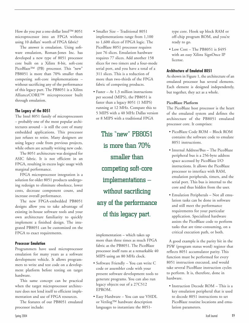
Architecture of Emulated 8051As shown in Figure 1, the architecture of anemulated processor has several elements.Each element is designed independently,but together, they act as a whole.
PicoBlaze PlatformThe PicoBlaze host processor is the heartof the emulated system and defines thearchitecture of the PB8051 emulatedprocessor core. It comprises:
• PicoBlaze Code ROM – Block ROMcontains the software code to emulate8051 instructions.
• Internal Address/Bus – The PicoBlazeperipheral bus is a 256-byte addressspace accessed by PicoBlaze I/Oinstructions. It allows the PicoBlazeprocessor to interface with RAM,emulation peripherals, timers, and theserial port. This bus is internal to thecore and thus hidden from the user.
• Emulation Peripherals – Not all emu-lation tasks can be done in softwareand still meet the performancerequirements for your particularapplication. Specialized hardwareassists the PicoBlaze code to performtasks that are time-consuming, on acritical execution path, or both.
A good example is the parity bit in thePSW (program status word) register thatreflects 8051 accumulator parity. Thisfunction must be performed for every8051 instruction executed, and wouldtake several PicoBlaze instruction cyclesto perform. It is, therefore, done inhardware.
• Instruction Decode ROM – This is akey emulation peripheral that is usedto decode 8051 instructions to setPicoBlaze routine locations and emu-lation parameters.
• Smaller Size – Traditional 8051implementations range from 1,100 to 1,600 slices of FPGA logic. ThePicoBlaze 8051 processor requiresjust 76 slices. Emulation hardwarerequires 77 slices. Add another 158slices for two timers and a four-modeserial port, and you have a total of a311 slices. This is a reduction ofmore than two-thirds of the FPGAfabric of competing products.
• Faster – At 1.3 million instructionsper second (MIPS), the PB8051 isfaster than a legacy 8051 (1 MIPS)running at 12 MHz. Compare this to5 MIPS with a 40 MHz Dallas versionor 8 MIPS with a traditional FPGA
implementation – which takes upmore than three times as much FPGAfabric as the PB8051. The PicoBlazeprocessor itself runs at a remarkable 40MIPS using an 80 MHz clock.
• Software Friendly – You can write Ccode or assembler code with yourpresent software development tools togenerate programs. You can also runlegacy objects out of a 27C512EPROM.
• Easy Hardware – You can use VHDLor Verilog™ hardware descriptionlanguages to instantiate the 8051-
Spring 2004 Xcell Journal 19
This “new” PB8051
is more than 70%
smaller than
competing soft-core
implementations –
without sacrificing
any of the performance
of this legacy part.
• Address Decode – A significantamount of the emulation peripheralhardware is dedicated to simpleaddress decode of the PicoBlazeperipheral bus. This address space isfor the PicoBlaze processor only and isinsulated from the 8051 application.
• Block RAM – 256 bytes are availableto 8051 internal RAM and some 8051registers. You can access this blockRAM via 8051 instructions.
• Serial Port and Timer – The actual8051 timer and multi-mode serial portwere best done in hardware instead oftrying to implement these functions insoftware. Clock prescaling inputs areprovided so that these functions canrun at a clock rate independent of theemulated system.
PicoBlaze Emulation SoftwareA 1K x 16 block ROM holds the PicoBlazecode that performs the actual emulation. Theemulation program is carefully constructed
in very tight PicoBlaze assembler code, opti-mized for speed and efficiency.
The emulation program is divided intoseveral segments:
• Instruction Fetch – An 8051 bus cycleis simulated to fetch the next instruc-tion from 8051 program memory (64Kb size), which may be on-chip blockRAM or off-chip EPROM (such as the27C256).
• Instruction Decode – Fetched instruc-tions are decoded to determine theaddressing mode and operation.
• Fetch Operands – Depending uponthe addressing mode, additionaloperands are fetched for the instruc-tion from program memory, internalRAM, or external RAM.
• Instruction Execution – An instructionperforms the desired operation andupdates emulated register contents,including affected 8051 PSW flags.
• Scan Interrupts – This function deter-mines if an interrupt is pending, and ifso, services it. An interrupt window isgenerated at the end of every emulatedinstruction when required.
In addition to PicoBlaze code, Java™software utilities process symbols takenfrom PicoBlaze listings (.LOG files) into aROM table. These .LOG files are used todecode 8051 opcodes.
This program also produces the .COEfiles used by the Xilinx COREGenerator™ system to create PicoBlazecode ROM. All of this is transparent todesigners integrating with the PB8051.
User Back-End InterfaceWhat gives the PB8051 its “hardware flavor” is the user back-end interface,where you interface your logic designwith the emulated 8051 processor. Theback-end interface is part of the emula-tion peripherals, controlled by thePicoBlaze platform.
20 Xcell Journal Spring 2004
1K x 16Block ROMEmulation
Program Code
256 x 8Instruction
Decode ROM
PicoBlaze
256 x 8Block RAM
Serial Port
InternalAddress/Data
Bus
Timer
AddressDecode
8051Emulation
Peripherals
AddressSERIAL0_PRE12
SERIAL2_PRE32
TIME_PRE
CLK
WR
RST_8051
RD
PSEN
INSTR_FETCH
EXT_BUS_START
EXT_BUS_HOLD
P1_IN[7:0]
P1_OUT[7:0]
P3_IN[7:0]
P3_OUT[7:0]
EXT_DATA_IN[7:0]
EXT_DATA_OUT[7:0]
EXT_ADDRESS[15:0]
ROM_ADDRESS[15:0]
ROM_DATA[7:0]
RST
Data
Interrupt
Address Decode, Data, Signals
Address Decode, Data, Signals
Figure 1 – PB8051 block diagram
Just as the 8051 processor family hasmany derivatives to define port, function-ality, features, and pinout, the back-endinterface serves the same function. ThePB8051 has a back-end interface thatresembles the generic 8031, the ROM-lessversion of the 8051.
Roman-Jones Inc. customizes back-endinterfaces to meet your exact 8051 needs,such as removing an unused serial port oradding an I2C port to emulate the 80C652derivative.
Designing with the PB8051Incorporating the PB8051 into the rest ofyour design is easy, because it comes with ref-erence designs and examples of Xilinx inte-grated software design (ISE) projects.
Hardware ConsiderationsFigure 1 illustrates the signal names avail-able on the user back-end interface. AVHDL or Verilog template provides theexact signal names – many of which arealready familiar to 8051 designers. A fewnew types of signals exist, including:
• Pre-scales used by the timer and serialport to set counting and baud rates.
• One-clock-wide read/write strobes toread and write external memory space.There is also a program store enable(PSEN) strobe for the 8051 codememory.
• Bus start and hold signals used toinsert wait states for external memorycycles that cannot be completed in onesystem clock cycle.
The PB8051 is instantiated as a compo-nent into your top-level design. You deter-mine if the 8051 program resides inon-chip block RAM or off-chip EPROM.Peripherals can be hooked up to either theP1/P3 port lines or to the external addressand data buses. For convenience, theaddress and data lines for program and datamemory spaces are separated, so conven-
tional multiplexer circuitry is not needed.If your entire design, including the 8051
program, resides on the FPGA, simply setthe EXT_BUS_HOLD to “low” to take fulladvantage of running at clock speed. If youelect to use an off-chip EPROM or haveslow peripherals, wait states can be insertedby asserting EXT_BUS_HOLD at “high.”One of our reference designs illustrates waitstate generation.
Xilinx Implementation ConsiderationsThere are few implementation considera-tions other than the need to place thePB8051 design netlist into your projectdirectory and instantiate it as a compo-nent in your VHDL or Verilog design;ISE software will do the rest. ISE schemat-ic capture is also supported.
Simulation ConsiderationsWe’ve included a behavior simulationmodel of the PB8051 for adding (alongwith the rest of your design) to your favoritesimulator. Modeltech and Aldec™ simula-tors have been tested for correct operation.Post place-and-route or timing simulationsfollow a conventional design flow.
You will enjoy watching your 8051instruction execution flow go by on thesimulation waveforms. This makes behav-ioral debugging straightforward, fast, andeasy. We’ve provided a reference testbench with example waveform files.
8051 Software ConsiderationsTo generate your 8051 programs the wayyou always have, use your favorite C com-piler or assembler and linker (if necessary) toproduce the same Intel hex format file thatyou would use to burn an EPROM. You caneven use an existing hex file, because thePB8051 looks like a regular 8051 as far assoftware code is concerned. An Intel hex to.COE utility is included for those designsthat put the 8051 software into on-chipblock RAM. On-chip program storage pro-vides maximum speed performance.
Test and Debug ConsiderationsWe recommend you use design tools toquickly and easily test and debug your design.The most useful tool will be an HDL simula-tor, such as Modeltech or Aldec programs.Most problems and bugs can be solved at thebehavioral level. For interactive debugging,the Xilinx ChipScope™ integrated logic ana-lyzer has proved to be the tool of choice. Atthe current time, no source code debuggertools are available for the PB8051.
Designer’s Learning CurveDesigners should have some experience in8051 hardware/software and FPGA designbefore attempting to consolidate the two.The PB8051 core is designed for ease ofuse and integration.
Your 8051 hardware and softwareexpertise should include hardware under-standing of the part and experience in writ-ing 8051 code using software developmenttools. The basic design flow using thePB8051 is identical to the normal pack-aged processor flow.
Integrating the PB8051 onto the Xilinxpart is much the same as instantiating a coreusing the Xilinx CORE Generator tool. Ifyou are familiar with VHDL or Verilog lan-guage, and have a couple of Xilinx designsunder your belt, you’re good to go.
ConclusionIntegrating microprocessors onto FPGAsthrough emulation, as illustrated with thePB8051, is a viable alternative to a full hard-ware functional design. The advantage ofFPGA fabric savings correlates to reducedparts cost.
Integrating the PB8051 processor into your design yields lower componentcount, easier board debugging, less noise, and optimum performance of the peripheral/8051 micro-interface,because both are in an FPGA. For moreinformation about the PB8051 microcon-troller, visit www.roman-jones.com/rj2/PB8051Microcontroller.htm.
Spring 2004 Xcell Journal 21
What gives the PB8051 its “hardware flavor” is the user back-end interface, where you interface your logic design with the emulated 8051 processor.
by John CarboneVP, MarketingExpress Logic, [email protected]
A fast processor is essential for today’sdemanding electronic products. Efficientapplication software is equally essential, asit enables the processor to keep up with thereal-world demands of networking andconsumer products.
But what about the real-time operatingsystem (RTOS) that handles your systeminterrupts and schedules your applicationsoftware’s multiple threads?
If it’s not optimized for the processoryou’re using, and isn’t efficient in its han-dling of external events, you’ll end up withonly half a processor to do useful work.
An efficient RTOS should do more thanjust handle multiple threads and serviceinterrupts. It must also have a small foot-print and be able to deliver the full power ofthe processor used by your application soft-ware. Express Logic’s ThreadX® real-timeoperating system is just such an RTOS.
The ThreadX RTOS has now been opti-mized to support the Xilinx MicroBlaze™soft processor, and is available off-the-shelffor your next development project.
A Good FitLet’s look at some of the reasons why theThreadX RTOS is a good fit with theMicroBlaze processor.
SizeThe ThreadX RTOS is only about 6 KB -12 KB in total size for a complete multi-tasking system. This includes basicservices, queues, event flags, semaphores,and memory allocation services.
Its small size means that more of yourmemory resources will be preserved foruse by the application and not absorbedby the RTOS. This will result in smallermemory requirements, lower costs, andlower power consumption. Table 1 showscode sizes for various optional compo-nents of the ThreadX RTOS on theMicroBlaze processor.
EfficiencyThe ThreadX RTOS can perform a fullcontext switch between active threads in amere 1.2 µs on a 100 MHz Xilinx Virtex-IIPro™ FPGA. This is particularly critical inapplications with high interrupt incidences,such as network packet processing.
The ability of the ThreadX RTOS tohandle interrupts efficiently means thatyour system can handle higher rates ofexternal events such as TCP/IP packetarrivals, delivering greater throughput.
SpeedThe ThreadX RTOS responds to inter-rupts and schedules required processing inless than 1 microsecond. The single-levelinterrupt processing architecture of theThreadX RTOS eliminates excess over-head found in many other RTOSs.
An RTOS can be critical for getting the most out of the MicroBlaze processor.An RTOS can be critical for getting the most out of the MicroBlaze processor.
Optimize MicroBlaze Processors for Consumer Electronics ProductsOptimize MicroBlaze Processors for Consumer Electronics Products
22 Xcell Journal Spring 2004
This keeps the ThreadX RTOS fromgobbling up valuable processor cycles withhousekeeping tasks, thus leaving moreprocessor bandwidth for your application.Thus, you can configure a less expensiveprocessor or add more features to yourapplication without increasing processorspeed and cost.
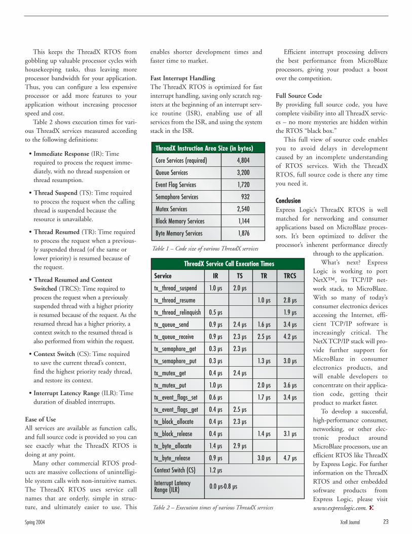
Table 2 shows execution times for vari-ous ThreadX services measured accordingto the following definitions:
• Immediate Response (IR): Timerequired to process the request imme-diately, with no thread suspension orthread resumption.
• Thread Suspend (TS): Time requiredto process the request when the callingthread is suspended because theresource is unavailable.
• Thread Resumed (TR): Time requiredto process the request when a previous-ly suspended thread (of the same orlower priority) is resumed because ofthe request.
• Thread Resumed and ContextSwitched (TRCS): Time required toprocess the request when a previouslysuspended thread with a higher priorityis resumed because of the request. As theresumed thread has a higher priority, acontext switch to the resumed thread isalso performed from within the request.
• Context Switch (CS): Time requiredto save the current thread’s context,find the highest priority ready thread,and restore its context.
• Interrupt Latency Range (ILR): Timeduration of disabled interrupts.
Ease of UseAll services are available as function calls,and full source code is provided so you cansee exactly what the ThreadX RTOS isdoing at any point.
Many other commercial RTOS prod-ucts are massive collections of unintelligi-ble system calls with non-intuitive names.The ThreadX RTOS uses service callnames that are orderly, simple in struc-ture, and ultimately easier to use. This
Efficient interrupt processing deliversthe best performance from MicroBlazeprocessors, giving your product a boostover the competition.
Full Source CodeBy providing full source code, you havecomplete visibility into all ThreadX servic-es – no more mysteries are hidden withinthe RTOS “black box.”
This full view of source code enablesyou to avoid delays in developmentcaused by an incomplete understandingof RTOS services. With the ThreadXRTOS, full source code is there any timeyou need it.
ConclusionExpress Logic’s ThreadX RTOS is wellmatched for networking and consumerapplications based on MicroBlaze proces-sors. It’s been optimized to deliver theprocessor’s inherent performance directly
through to the application.What’s next? Express
Logic is working to portNetX™, its TCP/IP net-work stack, to MicroBlaze.With so many of today’sconsumer electronics devicesaccessing the Internet, effi-cient TCP/IP software isincreasingly critical. TheNetX TCP/IP stack will pro-vide further support forMicroBlaze in consumerelectronics products, andwill enable developers toconcentrate on their applica-tion code, getting theirproduct to market faster.
To develop a successful,high-performance consumer,networking, or other elec-tronic product aroundMicroBlaze processors, use anefficient RTOS like ThreadXby Express Logic. For furtherinformation on the ThreadXRTOS and other embeddedsoftware products fromExpress Logic, please visitwww.expresslogic.com.
enables shorter development times andfaster time to market.
Fast Interrupt HandlingThe ThreadX RTOS is optimized for fastinterrupt handling, saving only scratch reg-isters at the beginning of an interrupt serv-ice routine (ISR), enabling use of allservices from the ISR, and using the systemstack in the ISR.
ThreadX Instruction Area Size (in bytes)
Core Services (required) 4,804
Queue Services 3,200
Event Flag Services 1,720
Semaphore Services 932
Mutex Services 2,540
Block Memory Services 1,144
Byte Memory Services 1,876
ThreadX Service Call Execution Times
Service IR TS TR TRCS
tx_thread_suspend 1.0 µs 2.0 µs
tx_thread_resume 1.0 µs 2.8 µs
tx_thread_relinquish 0.5 µs 1.9 µs
tx_queue_send 0.9 µs 2.4 µs 1.6 µs 3.4 µs
tx_queue_receive 0.9 µs 2.3 µs 2.5 µs 4.2 µs
tx_semaphore_get 0.3 µs 2.3 µs
tx_semaphore_put 0.3 µs 1.3 µs 3.0 µs
tx_mutex_get 0.4 µs 2.4 µs
tx_mutex_put 1.0 µs 2.0 µs 3.6 µs
tx_event_flags_set 0.6 µs 1.7 µs 3.4 µs
tx_event_flags_get 0.4 µs 2.5 µs
tx_block_allocate 0.4 µs 2.3 µs
tx_block_release 0.4 µs 1.4 µs 3.1 µs
tx_byte_allocate 1.4 µs 2.9 µs
tx_byte_release 0.9 µs 3.0 µs 4.7 µs
Context Switch (CS) 1.2 µs
Interrupt Latency Range (ILR) 0.0 µs-0.8 µs
Table 1 – Code size of various ThreadX services
Table 2 – Execution times of various ThreadX services
Spring 2004 Xcell Journal 23
by Ravi PragasamMarketing Manager, Embedded Processor Solutions,Product Solutions MarketingXilinx, [email protected]
The current market environment requiresdesigns to be completed in a short timeframe, with features that distinguish themfrom other products available in the mar-ket. Yet the majority of embedded designsfail to meet original specification goalsbecause of time constraints and featureshortcomings in the chosen solution.Often, functionality is compromised tomeet performance or quality requirements.
Over the years, embedded systemdesigners had to use standard off-the-shelfdiscrete components in their applications.Much design time was spent on integratingthese standard components so that theymet system performance.
ASICs or ASSPs are also chosen as the solution when the production volumeswarrant this path. In traditional ASICflows, designers make most changes inthe software to account for hardware lim-itations and inaccuracies, when problemsare discovered late in the design cycle.
The new version of EDK offers automatic generation of complex implementation details, new simulation capabilities, and new IP cores.The new version of EDK offers automatic generation of complex implementation details, new simulation capabilities, and new IP cores.
Improve Your Productivity with theEmbedded Development Kit v6.1iImprove Your Productivity with theEmbedded Development Kit v6.1i
24 Xcell Journal Spring 2004
This situation is exacerbated as physicalgeometries shrink and chip fabricationbecomes variable from design-to-design,not just from process-to-process. ASSPs areusually standard solutions with some non-standard sections that allow for customiza-tion. This customization can set theproduct apart from other solutions in a cer-tain application area. However, ASSP solu-tions are also not a perfect fit, as designershave to create workarounds to address fea-ture shortcomings. With standard off-the-shelf discrete components, ASICs andASSPs, designers end up with solutionsthat never quite meet their needs.
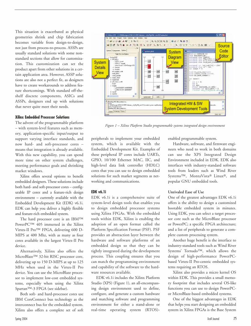
Xilinx Embedded Processor SolutionsThe advent of the programmable platform– with system-level features such as mem-ory, application-specific input/output tosupport varying interface standards, andnow hard- and soft-processor cores –means that integration is already available.With this new capability, you can spendmore time on other system challenges,meeting performance goals and shrinkingmarket windows.
Xilinx offers several options to benefitembedded designers. These solutions includeboth hard- and soft-processor cores – config-urable IP cores and a feature-rich designenvironment – currently available with theEmbedded Development Kit (EDK) v6.1i.EDK can help you deliver a highly flexibleand feature-rich embedded system.
The hard processor core is an IBM™PowerPC™ 405 immersed in the XilinxVirtex-II Pro™ FPGA, delivering 600 D-MIPS at 400 Mhz, with as many as fourcores available in the largest Virtex-II Prodevice.
Alternatively, Xilinx also offers theMicroBlaze™ 32-bit RISC processor core,delivering up to 150 D-MIPS at up to 125MHz when used in the Virtex-II Prodevice. You can use the MicroBlaze proces-sor to implement low-cost embedded sys-tems, especially when using the XilinxSpartan™-3 FPGA (see sidebar).
Both soft- and hard-processor cores useIBM CoreConnect bus technology as theinterconnect bus for the embedded system.Xilinx also offers a complete set of soft
enabled programmable system.Hardware, software, and firmware engi-
neers who need to work in both domainscan use the XPS Integrated DesignEnvironment included in EDK. EDK alsointerfaces with industry-standard softwaretools from leaders such as Wind RiverSystems™, MontaVista® Linux®, andpopular GNU embedded tools.
Unrivaled Ease of UseOne of the greatest advantages EDK v6.1ioffers is the ability to design a customizedbootable embedded system in minutes.Using EDK, you can select a target proces-sor core such as the MicroBlaze processoror PowerPC; a specific FPGA architecture;and a list of peripherals to generate a com-plete custom processing system.
Another huge benefit is the interface toindustry-standard tools such as Wind RiverSystems’ Tornado™, which allows thedesign of high-performance PowerPC-based Virtex-II Pro-centric embedded sys-tems requiring an RTOS.
Xilinx also provides a micro kernel OSwithin EDK. This provides a small memo-ry footprint that includes several OS-likefunctions you can use to design PowerPC-or MicroBlaze-based embedded systems.
One of the biggest advantages in EDKthat helps you start designing an embeddedsystem in Xilinx FPGAs is the Base System
peripherals to implement your embeddedsystem, which is available with theEmbedded Development Kit. Examples ofthese peripheral IP cores include UARTs,GPIO, 10/100 Ethernet MAC, IIC, andhigh-level data link controller (HDLC)cores that you can use to design embeddedsolutions for such market segments as net-working and communications.
EDK v6.1iEDK v6.1i is a comprehensive suite ofsystem-level design tools that enables youto design embedded processor systemsusing Xilinx FPGAs. With the embeddedtools within EDK, Xilinx is enabling theadoption of an open format called thePlatform Specification Format (PSF). PSFprovides an abstraction layer between thehardware and software platforms of anembedded design so that they can betightly integrated during the developmentprocess. This coupling ensures that youcan match the programming environmentand capability of the software to the hard-ware resources available.
EDK v6.1i includes the Xilinx PlatformStudio (XPS) (Figure 1), an all-encompass-ing design environment used to define,configure, and generate a custom hardwareand matching software and programmingenvironment for either a stand-alone orreal-time operating system (RTOS)-
Spring 2004 Xcell Journal 25
Figure 1 – Xilinx Platform Studio programmable systems integrated design environment

Builder wizard, shown in Figure2. This feature within XPSenables the creation of a customPowerPC- or MicroBlaze-basedcomputing platform (includingperipherals and a memory map)with just a few clicks of themouse. All detailed connectionsand a default memory map aregenerated automatically, result-ing in a functional hardwaredesign that is ready to be down-loaded into a target board.
The automatic generationof a ready-to-use board supportpackage (BSP) matching thedefined hardware platformprovides tremendous savings indevelopment time.Hardware/software sections ofthe embedded design that canbe problematic are handledautomatically by the tools. Thisdramatically reduces the time-consuming and frustratingphase of the debug and verification cyclecommon to many embedded applications.
Peripheral IP CatalogThe Embedded Development Kit offers anextensive list of soft IP cores that you can useto develop and design embedded systems.The cores are essentially divided into fourcategories: interface, memory controllers,infrastructure, and peripherals.
Examples of infrastructure cores includebus bridges and arbiters for differentCoreConnect buses. Examples of interfaceIP cores include memory controllers such asFlash, DDR, SDRAM, and SDR that allowthe use of external memory controllers aspart of the embedded systems. The designenvironment also allows you to integrateproprietary cores into your design. Also avail-able for your use is an extensive list of gener-al peripheral cores such as SPI, IIC, UART,Timer/Counter, Watch Dog Timer, andGPIO, found in any processor subsystem.
There is also a growing list of high-valueIP cores that you can purchase independent-ly to plug-and-play in EDK. Examples ofthese high-value cores include EthernetMAC 10/1000, 1 Gigabit Ethernet, and the
HDLC controller with as many as 256 chan-nels. The biggest advantage of these cores isthat most of them are parameterizable withinEDK. As opposed to standard solutions wherenot all of the features may be required for adesign, embedded systems using these cores useonly the logic that is needed without any waste.
Xilinx also has several partners that offerIP cores you can use to develop embeddeddesigns in FPGAs.
Integration with ISE Logic Design ToolsYet another benefit is the integration of theEmbedded Development Kit with the recentlyreleased Xilinx ISE 6.1i. You can now accessEDK from within ISE, thus eliminating theneed to leave the ISE environment, and designa complete embedded system by invoking theEDK tools within ISE. This integration withXilinx ISE 6.1i enables a more seamless andintuitive development environment with therest of your FPGA design.
Debug OptionsThe Embedded Development Kit provides afeature-rich environment to debug designs insoftware and hardware. It includes a PowerPCand MicroBlaze Instruction Set Simulator
(ISS) to enable the debugging ofsoftware code on the developmentworkstation. Hardware simulationhas been enhanced, with the abili-ty to do mixed VHDL/Verilog™simulation (including XilinxLogiCORE™ and customer-cre-ated IP) as well as the ability totoggle between real-time logic(RTL), structural, and full timing-based simulations. The Single Stepdebugger from WindRiverSystems is also available forPowerPC in Virtex-II Pro-basedembedded systems.
Extending the Xilinx leadershipin hardware on-chip debug, EDKversion 6.1i enables on-chip crosstriggering between the logic andbus analyzer cores available withthe Xilinx ChipScope™ Pro soft-ware tool and the GNU (gdb)debugger. Support for thevisionProbe hardware debuggerfrom WindRiver Systems is also
available for PowerPC in Virtex-II Pro-basedembedded systems.
ConclusionTraditional embedded designers who hadto use standard discrete off-the-shelf com-ponents, ASICs, or ASSPs to satisfy theirsystem application needs now have theoption to use a programmable platform todevelop a custom system. Using a pro-grammable platform offers several advan-tages, such as customization, consolidation,integration, and protection from compo-nent obsolescence.
The ability to use a design environmentthat provides an all-encompassing suite oftools and interfaces to familiar design entrymethods further facilitates the develop-ment process and increases the overallspeed of the design process. With EDKv6.1i, you now have access to a suite ofembedded tools from Xilinx that take careof those complicated steps that are part ofthe embedded design process. Thus, youcan focus more on creating a custom plat-form with unique features that bring valueto your system, as opposed to the mundaneones available from your competitors.
26 Xcell Journal Spring 2004
Figure 2 – The Base System Builder wizard enables easy definition of hardware platforms in FPGA-based embedded systems.
by Helen YuEmbedded Processor Solutions, Product Solutions MarketingXilinx, [email protected]
The MicroBlaze™ soft-coreprocessor in Spartan™-3 FPGAsprovides an attractive solution forlow-cost processing with its lowerprice points. You can now implementthe 32-bit MicroBlaze processor in theSpartan-3 XC3S1000 device for aneffective price of $0.73*.
Additionally, you can implement theXilinx 8-bit PicoBlaze™ soft processor inthe same device for an effective price of $0.13*.These new price points offer a significant cost savings that iscomparable to stand-alone discrete solutions available today.
The new breakthrough price points for the Spartan-3FPGA family are due to the successful implementation of 90nm technology. With new architecture optimized for 90 nmtechnology, Xilinx has packed more logic cells onto smallerdie, resulting in a cost-per-logic-cell advantage as high as 36%over competing solutions.
You can also take advantage of the new features in the just-released Embedded Development Kit v6.1i (such as the BaseSystem Builder and IP import wizard) to design a completeMicroBlaze-based system in a relatively short time, thusincreasing your overall productivity and meeting time-to-market requirements.
The MicroBlaze processor is the industry’s most popularsoft 32-bit processor, with performance up to 68 D-MIPSwhen implemented in the Spartan-3 fabric. Combined withsoft peripherals and logic, it can address many traditional 16-and 32-bit microprocessor and microcontroller applications,such as process control instrumentation, test and measure-ment, automotive, and high-end consumer.
The easy-to-use and popular PicoBlaze soft processordelivers up to 40 MIPS when implemented in the Spartan-3fabric and can be used as a simple microcontrollerin various applications.
More Features for Less CostSpartan-3 FPGAs offer a combination of fea-tures and density, along with large embeddedblock and distributed RAM, and as many as 784I/Os. This makes the devices ideal for systemintegration and the addition of unique new featuresduring the product’s life cycle.
The MicroBlaze 32-bit RISC processor core, along with astandard set of soft peripherals, is included with theEmbedded Development Kit. Advanced features in theMicroBlaze processor that can help embedded designers meettheir performance needs include:
• User-configurable caches. The MicroBlaze soft processorincludes direct-mapped, level one (L1) instruction anddata caches that are configurable up to 64 KB. Memory isdivided by address to provide 1 GB of cacheable memoryspace and 3 GB of non-cacheable memory space to signifi-cantly reduce instruction execution time and code space.
• Fast simplex link (FSL) to simplify software-to-hardwareimplementations. FSL offers a 300 MB/s direct processorinterface and point-to-point connection for custom func-tions and hardware. This high-bandwidth, configurabledepth first-in first-out (FIFO) interface to the CPU isideal for streaming applications. Each of the 32input/output FSL connections uses SRL16 for the FIFO,which consumes only 36 look-up tables for a 32-wide,16-deep FIFO.
• Hardware debug module. The MicroBlaze debug moduleoffers JTAG support for multi-processor debugging.Debug options include configurable break points andwatch points, non-intrusive debugging, and debugging ofROM code – all available as part of the EmbeddedDevelopment Kit.
• 32-bit barrel shifter. The 32-bit barrel shifter is particular-ly advantageous for applications that shift data logic leftor right – a normal code style for C programs.Independent of the shift amount or direction, barrelshifter instructions take only two clock cycles and canboost shift execution up to 15 times.
• Hardware divide. Xilinx has implemented a dedicatedMicroBlaze instruction with hardware support for dividefunctions; you no longer need to run a software libraryfunction to perform divides. The hardware divider, com-bined with other enhanced features, results in higherprocessor performance.
A typical MicroBlaze system including the soft processorcore, bus structure, timer, GPIO, and UART peripheralsconnected to the IBM™ CoreConnect bus or the newFSL direct interface consumes approximately 8% of thetotal available logic resources in the 3S1000 Spartan-3
FPGA, which works out in cost to approximately $1.01*.
* Based on volume pricing for 250K units, 2004
MicroBlaze in Spartan-3 Delivers Soft Processor for Less than 75 Cents
Spring 2004 Xcell Journal 27

by Paul LerouxTechnology AnalystQNX Software Systems [email protected]
Who would have thought RAM andROM memory, digital signaling process-ing, customizable IP, embedded hard- andsoft-core microprocessors, multi-gigabitserial transceivers, controlled impedancetechnology, and remote-reconfigurableFPGA logic fabric could all be integratedinto a single, reprogrammable device?
That's exactly the level of integrationoffered by system-on-chip (SOC) plat-forms like the Xilinx Virtex-II Pro™FPGA. This device not only reduces boardsize and simplifies the manufacturingprocess, but is programmable (fast tostart), reprogrammable (quick to fix orenhance), and field-upgradable (possibleto upgrade or optimize after deployment).Moreover, it comes in a variety of densi-ties, packages, and configurations, allow-ing you to deploy an SOC tailored to yourspecific requirements.
QNX support for Virtex-II Pro devices enables software upgrades and fault tolerance before, during, and after deployment.QNX support for Virtex-II Pro devices enables software upgrades and fault tolerance before, during, and after deployment.
QNX Neutrino RTOS OptimizesProgrammable SystemsQNX Neutrino RTOS OptimizesProgrammable Systems
28 Xcell Journal Spring 2004

To exploit these numerous capabilities,you need appropriate tools and operatingsystem technology. Consequently, Xilinxhas worked with QNX Software Systemsto provide an integrated developmentenvironment (QNX® Momentics® devel-opment suite) and real-time operating sys-tem (QNX Neutrino® RTOS) for theIBM PowerPC™ 405 processors embed-ded in Virtex-II Pro FPGAs. Together,these QNX products offer software upgrad-ability, fault tolerance, and true real-timeperformance – along with a rich comple-ment of tools for building, debugging, andfine-tuning software applications.
Why Use an RTOS?Before taking a closer look at the QNXNeutrino RTOS, let’s examine why yourprogrammable system would even need anRTOS in the first place. The answer, aswe’ll see, goes beyond issues of sheer speedor efficiency.
On any given day, you may use dozensof embedded applications. In some cases,you probably don’t mind if the applicationtakes a second or two to respond. Waitingfor an ATM machine to dispense cash is aperfect example.
An ATM represents the world of “soft”real time, where a delay might diminish thevalue of a system operation, but it doesn’tpose a safety hazard, cause a major incon-venience, or lead to an economic penalty.An RTOS, with its ability to guarantee fastresponse times, can be beneficial for suchapplications, but it is not essential.
In many applications, however, even aslight delay or timing error can constitutesystem failure. Consider a router handlingVoIP where delayed packets can result inunacceptable voice jitter, or an in-cartelematics system where consumers won’ttolerate a user interface that fails torespond immediately to input.
Similar delays can cause the effectivefailure of medical monitoring devices,consumer appliances, and a variety ofother software-dependent products. Suchsystems – often dubbed “hard” real-timesystems – need an OS like the QNXNeutrino RTOS to deliver the predictableresponse times demanded of them.
process from accessing the CPU – a condi-tion known as “priority inversion.”
Nonetheless, RTOSs aren’t just for hardreal-time systems. By providing precisecontrol over the timing of every applicationand system service, the QNX NeutrinoRTOS can make it much easier for you tooptimize the performance and behavior ofvirtually any embedded design.
Engineered for Upgradable, Reconfigurable SystemsAlthough Virtex-II Pro FPGAs provide aplatform for creating upgradable hardwaresolutions, few RTOSs offer the equivalentupgradability on the software side. Forinstance, in a conventional RTOS, mostsoftware components – the OS kernel,networking stacks, drivers, and applica-tions – run together in a single memoryaddress space. This architecture is effi-cient, but has two immediate drawbacks:
1. A memory violation in any compo-nent can corrupt the OS kernel orany other component, causing sys-tem-wide failure.
2. It is difficult, if not impossible, todynamically add, repair, or replaceindividual components.
The QNX Neutrino RTOS takes a verydifferent approach. Rather than pack soft-ware components into a single, unwieldy“monolith,” it allows applications, drivers,file systems, and networking stacks to runin separate, memory-protected addressspaces (Figure 1).
How does an RTOS enable this pre-dictability? To begin with, it ensures thatsoftware processes always execute in orderof their priority. If a high-priority, time-critical process becomes ready to run, theRTOS will immediately take over theCPU from any lower-priority process.Moreover, the high-priority process canrun uninterrupted until it has finishedwhat it needs to do – unless, of course, itis preempted by a process with an evenhigher priority.
This approach, known as “preemptivescheduling,” helps ensure that time-criti-cal processes meet their deadlines consis-tently, regardless of how many otherprocesses are competing for CPU time.
Besides preemptive scheduling, theQNX Neutrino RTOS provides a numberof other mechanisms and capabilities toenable fast, predictable response to criticalevents. These include support for:
• Microsecond and even sub-microsec-ond interrupt latencies
• Scheduling methods that set a cappedlimit on the execution time of threads
• Nested interrupts that ensure theRTOS always handles high-priorityinterrupts first.
The QNX Neutrino RTOS also sup-ports “distributed priority inheritance,”which enables any OS (for instance, adevice driver) to execute at the priority ofthe application requesting the service. Thisensures that work done for a low-priorityapplication doesn’t prevent a higher-priority
Spring 2004 Xcell Journal 29
Figure 1 – In the QNX Neutrino RTOS, you can dynamically plug in or plug out software components as needed.
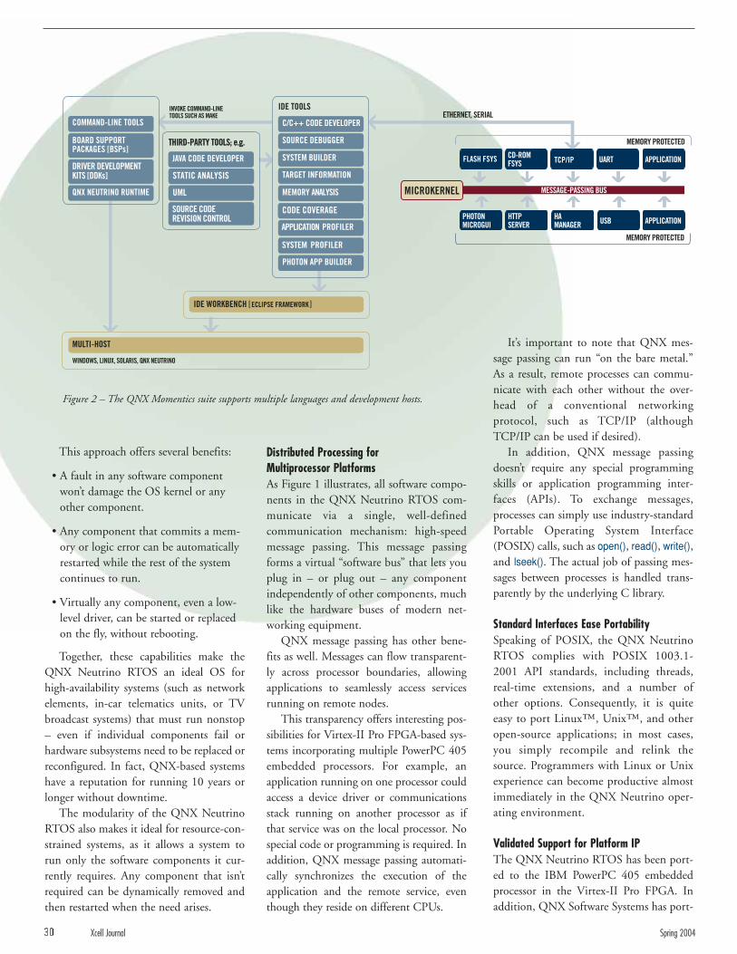
This approach offers several benefits:
• A fault in any software componentwon’t damage the OS kernel or anyother component.
• Any component that commits a mem-ory or logic error can be automaticallyrestarted while the rest of the systemcontinues to run.
• Virtually any component, even a low-level driver, can be started or replacedon the fly, without rebooting.
Together, these capabilities make theQNX Neutrino RTOS an ideal OS forhigh-availability systems (such as networkelements, in-car telematics units, or TVbroadcast systems) that must run nonstop– even if individual components fail orhardware subsystems need to be replaced orreconfigured. In fact, QNX-based systemshave a reputation for running 10 years orlonger without downtime.
The modularity of the QNX NeutrinoRTOS also makes it ideal for resource-con-strained systems, as it allows a system torun only the software components it cur-rently requires. Any component that isn’trequired can be dynamically removed andthen restarted when the need arises.
Distributed Processing for Multiprocessor PlatformsAs Figure 1 illustrates, all software compo-nents in the QNX Neutrino RTOS com-municate via a single, well-definedcommunication mechanism: high-speedmessage passing. This message passingforms a virtual “software bus” that lets youplug in – or plug out – any componentindependently of other components, muchlike the hardware buses of modern net-working equipment.
QNX message passing has other bene-fits as well. Messages can flow transparent-ly across processor boundaries, allowingapplications to seamlessly access servicesrunning on remote nodes.
This transparency offers interesting pos-sibilities for Virtex-II Pro FPGA-based sys-tems incorporating multiple PowerPC 405embedded processors. For example, anapplication running on one processor couldaccess a device driver or communicationsstack running on another processor as ifthat service was on the local processor. Nospecial code or programming is required. Inaddition, QNX message passing automati-cally synchronizes the execution of theapplication and the remote service, eventhough they reside on different CPUs.
30 Xcell Journal Spring 2004
It’s important to note that QNX mes-sage passing can run “on the bare metal.”As a result, remote processes can commu-nicate with each other without the over-head of a conventional networkingprotocol, such as TCP/IP (althoughTCP/IP can be used if desired).
In addition, QNX message passingdoesn’t require any special programmingskills or application programming inter-faces (APIs). To exchange messages,processes can simply use industry-standardPortable Operating System Interface(POSIX) calls, such as open(), read(), write(),and lseek(). The actual job of passing mes-sages between processes is handled trans-parently by the underlying C library.
Standard Interfaces Ease PortabilitySpeaking of POSIX, the QNX NeutrinoRTOS complies with POSIX 1003.1-2001 API standards, including threads,real-time extensions, and a number ofother options. Consequently, it is quiteeasy to port Linux™, Unix™, and otheropen-source applications; in most cases,you simply recompile and relink thesource. Programmers with Linux or Unixexperience can become productive almostimmediately in the QNX Neutrino oper-ating environment.
Validated Support for Platform IPThe QNX Neutrino RTOS has been port-ed to the IBM PowerPC 405 embeddedprocessor in the Virtex-II Pro FPGA. Inaddition, QNX Software Systems has port-
Figure 2 – The QNX Momentics suite supports multiple languages and development hosts.

ed (and validated with Xilinx)support for customizableplatform IP cores such asbootloader and startup code,as well as drivers for the uni-versal asynchronous receivertransmitter (UART), inter-rupt controller (INTC),10/100 Ethernet MAC, andI2C. The Xilinx ML300 refer-ence platform with Virtex-IIPro FPGA and PowerPC 405processor served as the targetboard for this process.
Integrated Toolset Optimizes WorkflowQNX Software Systems hasalso extended its QNXMomentics development suiteto target the PowerPC proces-sor in the Virtex-II Pro FPGA. The QNXMomentics suite supports all the tools youmight expect, such as graphical code edi-tors, debuggers, compilers, and projectbuilders. As Figure 2 illustrates, it alsoincludes a complement of non-intrusivediagnostic tools to fine-tune applications onyour programmable system.
The integrated development environ-ment (IDE) in the QNX Momentics suiteis extremely flexible. You can:
• Code in multiple languages (C, C++,Embedded C++, Java).
• Develop on several host environments(Windows™, Solaris™, Linux, QNXNeutrino RTOS).
• Use a mix of source-control protocols
• Choose between your own build commands or the IDE’s multi-CPUmakefile framework.
The QNX Momentics suite also sup-ports industry-standard tools such as theGNU GCC compiler and GDB debugger,as well as a graphical source debugger thatis tightly integrated with the code editors,memory analysis plug-in, and other tools.
Developers must focus on writing reli-able software in the least amount of time.As a result, the QNX Momentics suiteincludes wizards to automate mundane
tasks, such as creating new projects, config-uring remote debug sessions, and buildingcustom flash file system images for targethardware. Plus, all tools – even third-partyplug-ins – share the same user interface,making the IDE easy to learn.
To simplify diagnosis of system behav-ior, the QNX Momentics developmentsuite offers several visualization tools:
• The application profiler supports bothstatistical and instrumented profilingto pinpoint inefficient code and algo-rithms. It can drill down to the source-line level, showing which lines areconsuming the most processor cycles.
• The memory analysis plug-in graphi-cally displays memory usage to helpcatch overruns, underruns, invalid useof memory, and freeing the same mem-ory twice.
• The system profiler performs traceanalysis to revolve timing conflicts,pinpoint deadlocks, root out logicflaws, detect hidden faults, and opti-mize system-level performance. For anexample of the system profiler inaction, see Figure 3.
These tools are engineered to be non-invasive, allowing you to accurately trou-bleshoot systems both in the lab and inthe field.
To simplify integrationof third-party tools, theQNX Momentics devel-opment suite is based onthe Eclipse universal toolplatform. The Eclipseplatform is supported by alarge and rapidly growingcommunity of tool ven-dors and developers.Eclipse provides well-defined interfaces toensure that tools – eventhose from multiple ven-dors – work togetherseamlessly. Eclipse alsoallows previously isolatedor unextensible tools toshare data with eachother, without the needfor manual intervention.
This integration can improve workflowimmensely, allowing you to quickly transi-tion from one task (stepping through thestart-up code for an embedded device) toanother (debugging applications runningon the embedded device).
ConclusionTo achieve the right mix of hardware, soft-ware, and embedded operating systemtechnology in a programmable platformlike the Virtex-II Pro FPGA, you mustchoose system components and develop-ment tools wisely. The QNX NeutrinoRTOS allows your application to gain thebenefits of software reliability and hardreal-time performance, and it lets youscale OS features to the size and nature ofthe design.
Using the QNX Momentics IDE intro-duces the flexibility of choosing your pre-ferred host and language, as well ascommand-line or graphic interaction. Thehighly integrated architecture of the IDEcan streamline your development process,while the non-invasive diagnostic tools letyou quickly fine-tune your final product.
To learn more about the QNXNeutrino RTOS, the QNX Momenticsdevelopment suite, and their support forthe Virtex-II Pro FPGA, visit QNXSoftware Systems at www.qnx.com.
Spring 2004 Xcell Journal 31
Figure 3 – Diagnostic tools like the system profiler help optimize performance.
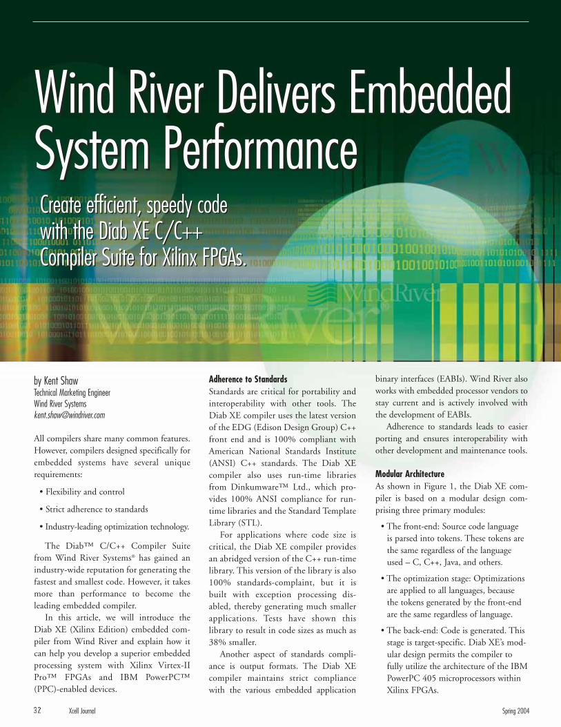
by Kent ShawTechnical Marketing EngineerWind River [email protected]
All compilers share many common features.However, compilers designed specifically forembedded systems have several uniquerequirements:
• Flexibility and control
• Strict adherence to standards
• Industry-leading optimization technology.
The Diab™ C/C++ Compiler Suitefrom Wind River Systems® has gained anindustry-wide reputation for generating thefastest and smallest code. However, it takesmore than performance to become theleading embedded compiler.
In this article, we will introduce theDiab XE (Xilinx Edition) embedded com-piler from Wind River and explain how itcan help you develop a superior embeddedprocessing system with Xilinx Virtex-IIPro™ FPGAs and IBM PowerPC™(PPC)-enabled devices.
Adherence to StandardsStandards are critical for portability andinteroperability with other tools. TheDiab XE compiler uses the latest versionof the EDG (Edison Design Group) C++front end and is 100% compliant withAmerican National Standards Institute(ANSI) C++ standards. The Diab XEcompiler also uses run-time librariesfrom Dinkumware™ Ltd., which pro-vides 100% ANSI compliance for run-time libraries and the Standard TemplateLibrary (STL).
For applications where code size iscritical, the Diab XE compiler providesan abridged version of the C++ run-timelibrary. This version of the library is also100% standards-complaint, but it isbuilt with exception processing dis-abled, thereby generating much smallerapplications. Tests have shown thislibrary to result in code sizes as much as38% smaller.
Another aspect of standards compli-ance is output formats. The Diab XEcompiler maintains strict compliancewith the various embedded application
binary interfaces (EABIs). Wind River alsoworks with embedded processor vendors tostay current and is actively involved withthe development of EABIs.
Adherence to standards leads to easierporting and ensures interoperability withother development and maintenance tools.
Modular ArchitectureAs shown in Figure 1, the Diab XE com-piler is based on a modular design com-prising three primary modules:
• The front-end: Source code language is parsed into tokens. These tokens arethe same regardless of the languageused – C, C++, Java, and others.
• The optimization stage: Optimizationsare applied to all languages, becausethe tokens generated by the front-endare the same regardless of language.
• The back-end: Code is generated. Thisstage is target-specific. Diab XE’s mod-ular design permits the compiler tofully utilize the architecture of the IBMPowerPC 405 microprocessors withinXilinx FPGAs.
Create efficient, speedy code with the Diab XE C/C++Compiler Suite for Xilinx FPGAs.
Create efficient, speedy code with the Diab XE C/C++Compiler Suite for Xilinx FPGAs.
Wind River Delivers Embedded System PerformanceWind River Delivers Embedded System Performance
32 Xcell Journal Spring 2004

Diab XE’s modular design enables youto take advantage of all non-target-specificoptimizations. As the front-end and opti-mization stages are shared, all advance-ments made in these stages apply tosupported Diab XE target architectures.
Optimization TechnologyOptimization falls into two primary areas –front-end and back-end. Front-end opti-mizations are concerned with the language.Back-end optimizations use architecture-specific code generation to use the designaspects of the particular target processor.
Although almost all compilers do agood job with front-end optimizations, theDiab tool suite distinguishes itself fromother compilers with its efficient back-endoptimization technology.
The growing hardware complexity oftoday’s processor designs makes it very dif-ficult to manually fine-tune applications.The Diab XE compiler is specifically engi-neered to enable you to maximizepipelines, caches, and other architecture-specific capabilities, including the IBM
• Support for position-independent codeand data (PIC/PID).
• Structure and bit-field packing. Heretoo, intelligent defaults are used, butwith options for complete control overhow structures are packed and howstructure members are aligned. You canalso specify the type (short, int, long)used for bit-fields.
• Function inlining, which can result in significant performance gains.Although all compiler vendors makeuse of this technique, only the DiabXE compiler enables you to specify the precise size of the functions to beinlined, giving you control over thememory footprint.
• Loop unrolling. This is similar tofunction inlining, because it canresult in significant performancegains. Most compiler vendors useloop unrolling. However, only theDiab XE compiler gives you the abili-ty to control both the size of loops tobe unrolled and the number of timesto unroll them.
• Embedded assembly code. The DiabXE compiler provides two methods: arelatively simple string-based assemblyfunction and a powerful macro-basedfunction. The string-based approach is ideal for writing values to a register.The macro approach provides totalflexibility and control over which registers are used for the macros.
• Diab XE’s robust linker command files provide the controls for you toprecisely place all program elements inthe correct memory locations. Becauseembedded applications often havestrict requirements for locating vari-ables, functions, and data in memory,this is an especially important featurewhen designing systems with multiplememory types and sizes.
Quality DocumentationDiab XE’s documentation makes it easy tolearn about and take advantage of the com-piler’s power, flexibility, and control. All
PowerPC 405 cores in Xilinx FPGAs.The Diab XE compiler can further opti-
mize your application code based on appli-cation profile information. No moremanual tweaking of your code is required –the Diab XE compiler will do this for you.
Because Wind River Systems owns andcontrols the technology that drives theDiab XE compiler, they can advance thetechnology on their own schedule withoutrequiring approval from an outside source.
Flexibility and ControlEmbedded systems typically have manydesign constraints – limited memory, limitedperformance. To meet the demands imposedby these constraints, an effective embeddedcompiler must provide a wide range of flexi-bility and control, with features such as:
• Addressing modes, which can have adirect impact on both performanceand code size. The Diab XE compileruses intelligent default settings, but itprovides options to give you completecontrol. Separate options also exist forspecifying both code and data modes.
Spring 2004 Xcell Journal 33
C Source C++ Source
C ParserNew C++ Parser
(default)Std C++ Parser
(-Xc++-old)
Run-TimeProfile Info
CPU-SpecificInfo
ASM Source
Libraries
Abridged Libs
Global Optimizer
Code Selector
Code Generator
Assembler
Linker Archiver
ELF Executable File(Native Machine Code)
CPU
Co
mm
on
Bac
kEn
dF
ron
t-E
nd
sFigure 1 – Diab modular architecture
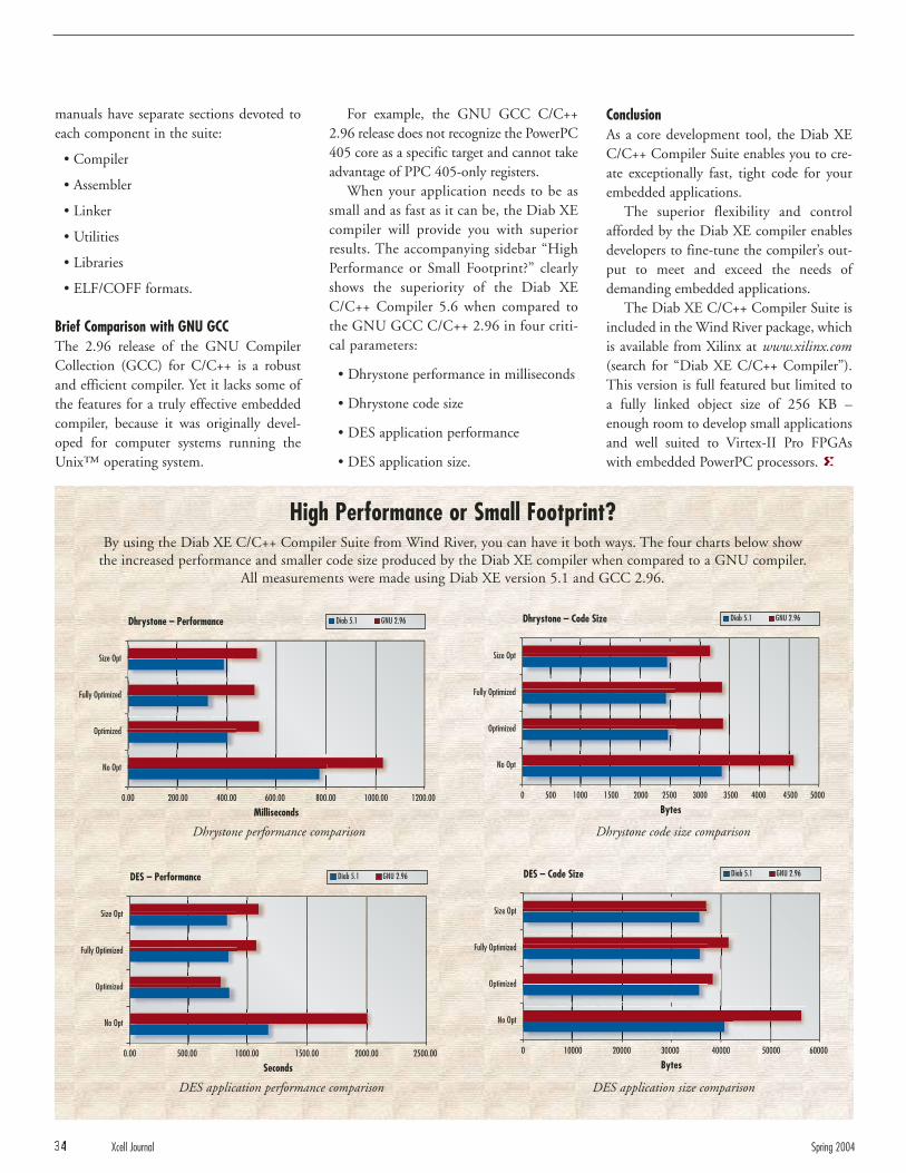
manuals have separate sections devoted toeach component in the suite:
• Compiler
• Assembler
• Linker
• Utilities
• Libraries
• ELF/COFF formats.
Brief Comparison with GNU GCCThe 2.96 release of the GNU CompilerCollection (GCC) for C/C++ is a robustand efficient compiler. Yet it lacks some ofthe features for a truly effective embeddedcompiler, because it was originally devel-oped for computer systems running theUnix™ operating system.
For example, the GNU GCC C/C++2.96 release does not recognize the PowerPC405 core as a specific target and cannot takeadvantage of PPC 405-only registers.
When your application needs to be assmall and as fast as it can be, the Diab XEcompiler will provide you with superiorresults. The accompanying sidebar “HighPerformance or Small Footprint?” clearlyshows the superiority of the Diab XEC/C++ Compiler 5.6 when compared tothe GNU GCC C/C++ 2.96 in four criti-cal parameters:
• Dhrystone performance in milliseconds
• Dhrystone code size
• DES application performance
• DES application size.
ConclusionAs a core development tool, the Diab XEC/C++ Compiler Suite enables you to cre-ate exceptionally fast, tight code for yourembedded applications.
The superior flexibility and controlafforded by the Diab XE compiler enablesdevelopers to fine-tune the compiler’s out-put to meet and exceed the needs ofdemanding embedded applications.
The Diab XE C/C++ Compiler Suite isincluded in the Wind River package, whichis available from Xilinx at www.xilinx.com(search for “Diab XE C/C++ Compiler”).This version is full featured but limited toa fully linked object size of 256 KB –enough room to develop small applicationsand well suited to Virtex-II Pro FPGAswith embedded PowerPC processors.
Diab 5.1 GNU 2.96
Size Opt
Fully Optimized
Optimized
No Opt
0.00 200.00 400.00 600.00 800.00 1000.00 1200.00
Milliseconds
Dhrystone – Performance Diab 5.1 GNU 2.96
Size Opt
Fully Optimized
Optimized
No Opt
0 500 1000 1500 25002000 35003000 4000 4500 5000
Bytes
Dhrystone – Code Size
Diab 5.1 GNU 2.96
Size Opt
Fully Optimized
Optimized
No Opt
0.00 500.00 1000.00 1500.00 2000.00 2500.00
Seconds
DES – Performance Diab 5.1 GNU 2.96
Size Opt
Fully Optimized
Optimized
No Opt
0 10000 20000 30000 40000 50000 60000
Bytes
DES – Code Size
High Performance or Small Footprint?By using the Diab XE C/C++ Compiler Suite from Wind River, you can have it both ways. The four charts below show
the increased performance and smaller code size produced by the Diab XE compiler when compared to a GNU compiler. All measurements were made using Diab XE version 5.1 and GCC 2.96.
Dhrystone performance comparison Dhrystone code size comparison
DES application performance comparison DES application size comparison
34 Xcell Journal Spring 2004
by Jean J. LabrossePresidentMicrium, [email protected]
Designing software for a microprocessor-based application can be a challengingundertaking. To reduce the risk and com-plexity of such a project, it’s always impor-tant to break the problem into small pieces,or tasks. Each task is therefore responsiblefor a certain aspect of the application.Keyboard scanning, operator interfaces,display, protocol stacks, reading sensors,performing control functions, updatingoutputs, and data logging are all examplesof tasks that a microprocessor can perform.
In many embedded applications, thesetasks are simply executed sequentially bythe microprocessor in a giant infiniteloop. Unfortunately, these types of sys-tems do not provide the level of respon-siveness required by a growing number ofreal-time applications because the codeexecutes in sequence. Thus, all tasks havevirtually the same priority.
An RTOS called µC/OS-II has been ported to the MicroBlaze soft-core processor.An RTOS called µC/OS-II has been ported to the MicroBlaze soft-core processor.
Use an RTOS on Your Next MicroBlaze-Based ProductUse an RTOS on Your Next MicroBlaze-Based Product
Spring 2004 Xcell Journal 35
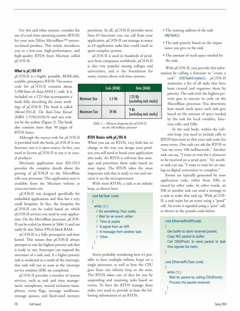
For this and other reasons, consider theuse of a real-time operating system (RTOS)for your next Xilinx MicroBlaze™ proces-sor-based product. This article introducesyou to a low-cost, high-performance, andhigh-quality RTOS from Micrium calledµC/OS-II.
What is µC/OS-II?µC/OS-II is a highly portable, ROM-able,scalable, preemptive RTOS. The sourcecode for µC/OS-II contains about5,500 lines of clean ANSI C code. It isincluded on a CD that accompanies abook fully describing the inner work-ings of µC/OS-II. The book is calledMicroC/OS-II, The Real-Time Kernel(ISBN 1-5782-0103-9) and was writ-ten by the author (Figure 2). The bookalso contains more than 50 pages ofRTOS basics.
Although the source code for µC/OS-IIis provided with the book, µC/OS-II is notfreeware, nor is it open source. In fact, youneed to license µC/OS-II to use it in actu-al products.
Micrium’s application note AN-1013provides the complete details about theporting of µC/OS-II to the MicroBlazesoft-core processor. This application note isavailable from the Micrium website atwww.micrium.com.
µC/OS-II was designed specifically forembedded applications and thus has a verysmall footprint. In fact, the footprint forµC/OS-II can be scaled based on whichµC/OS-II services you need in your applica-tion. On the MicroBlaze processor, µC/OS-II can be scaled (as shown in Table 1) and caneasily fit into Xilinx FPGA block RAM.
µC/OS-II is a fully preemptive real-timekernel. This means that µC/OS-II alwaysattempts to run the highest-priority task thatis ready to run. Interrupts can suspend theexecution of a task and, if a higher-prioritytask is awakened as a result of the interrupt,that task will run as soon as the interruptservice routines (ISR) are completed.
µC/OS-II provides a number of systemservices, such as task and time manage-ment, semaphores, mutual exclusion sema-phores, event flags, message mailboxes,message queues, and fixed-sized memory
• The starting address of the task(MyTask())
• The task priority based on the impor-tance you give to the task
• The amount of stack space needed bythe task.
With µC/OS-II, you provide this infor-mation by calling a function to “create a
task” (OSTaskCreate()). µC/OS-IImaintains a list of all tasks that havebeen created and organizes them bypriority. The task with the highest pri-ority gets to execute its code on theMicroBlaze processor. You determinehow much stack space each task getsbased on the amount of space neededby the task for local variables, func-tion calls, and ISRs.
In the task body, within the infi-nite loop, you need to include calls to
RTOS functions so that your task waits forsome event. One task can ask the RTOS to“run me every 100 milliseconds.” Anothertask can say, “I want to wait for a characterto be received on a serial port.” Yet anoth-er task can say, “I want to wait for an ana-log-to-digital conversion to complete.”
Events are typically generated by yourapplication code, either from ISRs orissued by other tasks. In other words, anISR or another task can send a message toa task to wake that task up. With µC/OS-II, a task waits for an event using a “pend”call. An event is signaled using a “post” call,as shown in the pseudo-code below:
void EthernetRxISR(void){
Get buffer to store received packet;Copy NIC packet to buffer;Call OSQPost() to send packet to task(this signals the task);
}
void EthernetRxTask (void){
while (1) {Wait for packet by calling OSQPend();Process the packet received;
}}
partitions. In all, µC/OS-II provides morethan 65 functions you can call from yourapplication. µC/OS-II can manage as manyas 63 application tasks that could result inquite complex systems.
µC/OS-II is used in hundreds of prod-ucts from companies worldwide. µC/OS-IIis also very popular among colleges anduniversities, and is the foundation formany courses about real-time systems.
RTOS Basics with µC/OS-IIWhen you use an RTOS, very little has tochange in the way you design your prod-uct; you still need to break your applicationinto tasks. An RTOS is software that man-ages and prioritizes these tasks based onyour input. The RTOS takes the mostimportant task that is ready to run and exe-cutes it on the microprocessor.
With most RTOSs, a task is an infiniteloop, as shown here:
void MyTask (void){
while (1) {// Do something (Your code)// Wait for an event, either:// Time to expire// A signal from an ISR// A message from another task// Other
}}
You’re probably wondering how it’s pos-sible to have multiple infinite loops on asingle processor, as well as how the CPUgoes from one infinite loop to the next.The RTOS takes care of that for you bysuspending and resuming tasks based onevents. To have the RTOS manage thesetasks, you need to provide at least the fol-lowing information to an RTOS:
36 Xcell Journal Spring 2004
Code (ROM) Data (RAM)
Minimum Size 5.5 Kb 1.25 Kb (excluding task stacks)
Maximum Size 24 Kb 9 Kb (excluding task stacks)
Table 1 – Memory footprint for µC/OS-II on the MicroBlaze processor
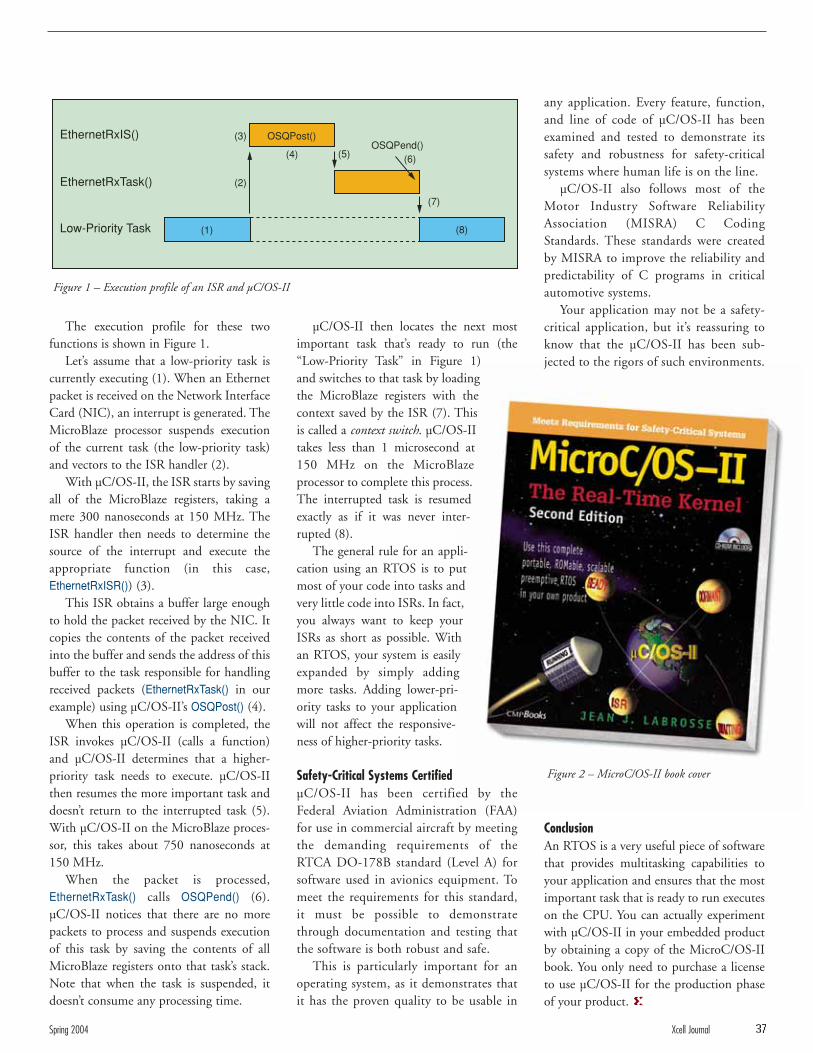
The execution profile for these twofunctions is shown in Figure 1.
Let’s assume that a low-priority task iscurrently executing (1). When an Ethernetpacket is received on the Network InterfaceCard (NIC), an interrupt is generated. TheMicroBlaze processor suspends executionof the current task (the low-priority task)and vectors to the ISR handler (2).
With µC/OS-II, the ISR starts by savingall of the MicroBlaze registers, taking amere 300 nanoseconds at 150 MHz. TheISR handler then needs to determine thesource of the interrupt and execute theappropriate function (in this case,EthernetRxISR()) (3).
This ISR obtains a buffer large enoughto hold the packet received by the NIC. Itcopies the contents of the packet receivedinto the buffer and sends the address of thisbuffer to the task responsible for handlingreceived packets (EthernetRxTask() in ourexample) using µC/OS-II’s OSQPost() (4).
When this operation is completed, theISR invokes µC/OS-II (calls a function)and µC/OS-II determines that a higher-priority task needs to execute. µC/OS-IIthen resumes the more important task anddoesn’t return to the interrupted task (5).With µC/OS-II on the MicroBlaze proces-sor, this takes about 750 nanoseconds at150 MHz.
When the packet is processed,EthernetRxTask() calls OSQPend() (6).µC/OS-II notices that there are no morepackets to process and suspends executionof this task by saving the contents of allMicroBlaze registers onto that task’s stack.Note that when the task is suspended, itdoesn’t consume any processing time.
µC/OS-II then locates the next mostimportant task that’s ready to run (the“Low-Priority Task” in Figure 1)and switches to that task by loadingthe MicroBlaze registers with thecontext saved by the ISR (7). Thisis called a context switch. µC/OS-IItakes less than 1 microsecond at150 MHz on the MicroBlazeprocessor to complete this process.The interrupted task is resumedexactly as if it was never inter-rupted (8).
The general rule for an appli-cation using an RTOS is to putmost of your code into tasks andvery little code into ISRs. In fact,you always want to keep yourISRs as short as possible. Withan RTOS, your system is easilyexpanded by simply addingmore tasks. Adding lower-pri-ority tasks to your applicationwill not affect the responsive-ness of higher-priority tasks.
Safety-Critical Systems CertifiedµC/OS-II has been certified by theFederal Aviation Administration (FAA)for use in commercial aircraft by meetingthe demanding requirements of theRTCA DO-178B standard (Level A) forsoftware used in avionics equipment. Tomeet the requirements for this standard,it must be possible to demonstratethrough documentation and testing thatthe software is both robust and safe.
This is particularly important for anoperating system, as it demonstrates thatit has the proven quality to be usable in
any application. Every feature, function,and line of code of µC/OS-II has beenexamined and tested to demonstrate itssafety and robustness for safety-criticalsystems where human life is on the line.
µC/OS-II also follows most of theMotor Industry Software ReliabilityAssociation (MISRA) C CodingStandards. These standards were createdby MISRA to improve the reliability andpredictability of C programs in criticalautomotive systems.
Your application may not be a safety-critical application, but it’s reassuring toknow that the µC/OS-II has been sub-jected to the rigors of such environments.
ConclusionAn RTOS is a very useful piece of softwarethat provides multitasking capabilities toyour application and ensures that the mostimportant task that is ready to run executeson the CPU. You can actually experimentwith µC/OS-II in your embedded productby obtaining a copy of the MicroC/OS-IIbook. You only need to purchase a licenseto use µC/OS-II for the production phaseof your product.
EthernetRxIS()
EthernetRxTask()
Low-Priority Task
(3)
(2)
(4) (5) (6)
(7)
(8)(1)
OSQPost()OSQPend()
Figure 1 – Execution profile of an ISR and µC/OS-II
Figure 2 – MicroC/OS-II book cover
Spring 2004 Xcell Journal 37

by Milan SainiTechnical Marketing ManagerXilinx, [email protected]
The open-source Linux® kernel with real-time extensions now provides most real-timeoperating system (RTOS) functionality andis rapidly emerging as a viable alternative toother commercial offerings. An RTOS is typ-ically used to operate the majority of today’shigh-performance embedded systems.
The development of embedded appli-cations on a single chip has reached newlevels of integration, performance, flexi-bility, and ease of use with the introduc-tion of Virtex-II Pro™ Platform FPGAs,which have up to four IBM™PowerPC™ 405 32-bit RISC processorswoven into the programmable fabric. Theplatform’s sophisticated technology, how-ever, typically requires newer tools andmethodologies to address the uniquecharacteristics of the device.
For those new to embedded Linuxapplications or Virtex-II Pro devices, thisarticle explains some key concepts andanswers commonly asked questions.
Key Linux FeaturesThe open-source, royalty-free, andPOSIX-compliant nature of Linux helpsdevelopers build highly customized andhighly portable applications. Linuxderives much of its value from graduallyaccumulating functionality through thecombined contributions of its worldwidebase of users. Similar to Unix in manyways, Linux offers a range of powerfuloperating system capabilities, includingmemory protection, processes, threads,and extensive networking facilities. It isgenerally considered to be a mature androbust technology.
The Linux kernel is licensed under theterms of the GPL (General PublicLicense) with an important clarification:Code that employs the normal services ofthe Linux kernel via system calls ordynamic (module) linkage is considerednormal use of the kernel and does not fallunder the heading of “derived work.”This means that dynamically linked
38 Xcell Journal Spring 2004
Unleash Your Creativitywith Embedded Linux on Virtex-II Pro FPGAs
Unleash Your Creativitywith Embedded Linux on Virtex-II Pro FPGAsXilinx has partnered with MontaVista Software to provide a customized embedded Linux solution for Virtex-II Pro FPGAs. Xilinx has partnered with MontaVista Software to provide a customized embedded Linux solution for Virtex-II Pro FPGAs.
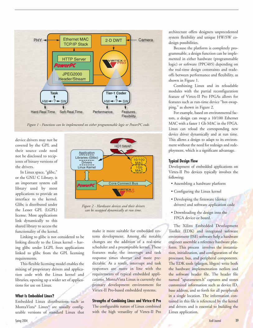
device drivers may not becovered by the GPL andtheir source code neednot be disclosed to recip-ients of binary versions ofthe drivers.
In Linux space, “glibc,”or the GNU C Library, isan important system calllibrary used by mostapplications to provide aninterface to the kernel.Glibc is distributed underthe Lesser GPL (LGPL)license. Most applicationslink dynamically to thisshared library to access thefunctionality of the kernel.
Linking to glibc is not considered to belinking directly to the Linux kernel – hav-ing glibc under LGPL frees applicationslinked to glibc from the GPL licensingrequirements.
This flexible licensing model enables themixing of proprietary drivers and applica-tion code with the Linux kernel andlibraries, opening up a wider set of applica-tions for use on Linux.
What Is Embedded Linux?Embedded Linux distributions such asMontaVista® Linux® are usually config-urable versions of standard Linux that
architecture offers designers unprecedentedsystem flexibility and unique HW/SW co-design possibilities.
Because the platform is completely pro-grammable, a design function can be imple-mented in either hardware (programmablelogic) or software (PPC405) depending onthe real-time design constraints and trade-offs between performance and flexibility, asshown in Figure 1.
Combining Linux and its reloadablemodules with the partial reconfigurationfeature of Virtex-II Pro FPGAs allows forfeatures such as run-time device “hot-swap-ping,” as shown in Figure 2.
For example, based on environmental fac-tors, a design can swap a 10/100 EthernetMAC with a faster 1 Gb MAC in the FPGA.Linux can reload the corresponding newdevice driver dynamically and at run time.This allows a design to adapt to its environ-ment without the need for redesign and rede-ployment, which is a significant advantage.
Typical Design FlowDevelopment of embedded applications onVirtex-II Pro devices typically involves thefollowing:
• Assembling a hardware platform
• Configuring the Linux kernel
• Developing the firmware (device drivers) and software application code
• Downloading the design into theFPGA device or board.
The Xilinx Embedded DevelopmentToolkit (EDK) and integrated softwareenvironment (ISE) software help a hardwareengineer assemble a reference hardware plat-form. This process involves the instantia-tion, initialization, and configuration of theprocessor, bus, and peripheral components.The EDK tools (platgen, libgen) write boththe hardware implementation netlists andthe software header file. The header filenamed “xparameters.h” captures and storescustomized information such as device ID,base address, and so forth for all peripheralsin a single location. The information con-tained in this file is referenced by the kerneland drivers and is essential to building theLinux application.
make it more suitable for embedded sys-tems development. Among the notablechanges are the addition of a real-timescheduler and a preemptable kernel. Thesefeatures make the interrupt and taskresponse times shorter and more pre-dictable. As a result, interrupt and taskresponses are more in line with therequirements of typical embedded appli-cations. MontaVista Linux is currently theprimary development environment forVirtex-II Pro-based embedded systems.
Strengths of Combining Linux and Virtex-II ProThe configurable nature of Linux combinedwith the high versatility of Virtex-II Pro
Spring 2004 Xcell Journal 39
2-D DWTEthernet MACTCP/IP Stack
CameraPHY
FeaturesFlexibility
Performance
Tier-1 Coder
?HW SW
Soft Real TimeHard Real Time
Task
?HW SW
HTTP Server
JPEG2000Header/StreamH
1GbMAC
HOT SWAP
10/100MAC
Application
Libraries (Glibc)
Drivers
Linux Kernel
Core Connect Bus
Figure 1 - Functions can be implemented on either programmable logic or PowerPC code.
Figure 2 - Hardware devices and their drivers can be swapped dynamically at run time.

Using one of several Linux configurationtools (such as the MontaVista TargetConfiguration Tool [TCT]™ GUI-basedutility), the Linux kernel is configured bymaking appropriate selections of drivers andservices required by the application software.In general, the idea is to keep the kernelimage size as small as possible by excludingfeatures not needed by the application.(Linux kernel configurations typicallyrequire between 2 and 8 Mb of memory.)
Application software for Linux can bedeveloped and debugged with GNU C andC++ compiler tool chains to create binary“elf ” images that can be deployed onto aVirtex-II Pro board.
Various methods for debugging applica-tions and downloading into the FPGA arediscussed later in this article.
Embedded Linux Environment for Virtex-II Pro Xilinx has partnered with embeddedLinux pioneer MontaVista Software toprovide a customized embedded Linuxsolution for Virtex-II Pro devices. Usersreceive the embedded Linux kernel,Virtex-II Pro device drivers, host and tar-get tools, applications, utilities, and prod-uct support. Support includes updates,enhancements, defect corrections, train-ing, and technical assistance. Some of thedevelopment tools are shown diagram-
matically in Figure 3 and include: • Cross-compiler tool chain. To increase
efficiency, developers use cross-develop-ment tools that run on faster and friend-lier host machines. The code is compiledto run on the actual target CPU.MontaVista provides these tools for mul-tiple Linux and Solaris hosts.
• Libraries. Glibc and glibc-linux threadsare the most commonly used set of libraries for Linux applicationdevelopment. These libraries contain the core set of functions to which mostutility and application code links.
• Kernel and drivers. The kernel providescore functionality such as memory man-agement, threads, and I/O behavior. A“makefile” included in the distributionpackage is used to assemble the Linuxkernel per the user and applicationrequirements.
• The target Linux file system. A kernelwithout programs to run is not useful,so a set of programs and utilities havebeen developed to run on Linux for thetarget PPC405 CPU. Examples of suchprograms include bash, tcsh, perl, awk,sed, grep, make, gcc compilers, a viclone, emacs, and X Windows.
The above tools and utilities are pack-aged and distributed by MontaVista in itsProfessional Edition. MontaVista also pro-vides a Preview Kit, a free evaluation ver-sion of this product.
The Linux kernel, libraries, and tools canalso be compiled from the open source, butthis configuration is not supported by Xilinx.
Prototyping Boards and Design AvailabilityXilinx and its partners have made several
Virtex-II Pro evaluation boards available,including the ML300 (V2P7) from Xilinxand the Insight V2P4/7 from InsightElectronics. The boards differ mostly in exter-nal-to-FPGA component configuration, withthe ML300 offering, in general, a richer set ofprocessor companion devices. These boardscan be used for evaluation, demonstration, ordevelopment. Full details can be found by fol-lowing the links at the end of this article.
The MontaVista Linux kernel and drivers
40 Xcell Journal Spring 2004
HOST TARGETLinux Sourceppc kernel v2.4.18
GNU Sourcegcc compiler v3.2.1
glibc.a v.2.2.5gdb debugger v5.2.1 +
“PowerPC-linux” compiler
“gdb” debugger
“glibc.a” library
Linux kernel + filesystem
Code Developed OnLinux/Solaris + Host CPU
Code Runs OnLinux + Target PPC
Custom Hardware Platform(CPU, Bus, Peripherals)
SW Device Drivers# Defines for Registers, ISR
Low-Level Calls, xparameters.h
Linux Adaptation LayerMemory Management, Threads
ITC, RTOS-Specific Calls
.BIT
.ELF
StaticallyLinked toKernel
DynamicallyLoaded byKernel
V2PBoard
Custom405 Linux
Kernel
Xilinx ToolsEDK, ISE
User Created
Open SourceV2P Drivers
Figure 3 - The Linux development environment
Figure 4 - Linux device drivers can be built on top of lower-level drivers provided by Xilinx.

have been tested with the ML300 ReferenceDesign using EDK (Design Source:http://www.xilinx.com/ise/embedded/edk_examples.htm). This development platformprovides a reasonable starting point fordesigning custom applications. The samedesign should run on other Virtex-II Proboards without modifications.
Linux/Virtex-II Pro Device DriversA device driver is code that provides anabstraction layer for hardware I/O devicesso that higher levels of software can accessthe devices in a uniform and hardware-independent fashion. Since Virtex-II Pro
FPGAs allow processor peripherals to beuniquely customized, the correspondingdevice-driver code must match the user-selectable configuration of the device.
The custom and dynamic nature of theembedded platform assembly is an impor-tant difference between Virtex-II Pro devel-opment and traditional embeddeddevelopment on boards and processorswith static peripheral configurations. Tospeed development, Xilinx EDK tools havebeen designed to create custom softwaredevice drivers for all relevant hardwareperipheral IP blocks Xilinx provides. Thedriver code is modular and generic and is
designed to be easily adapted to higher-level OS functions, as shown in Figure 4.
Several of the Xilinx-provided devicedrivers have been adapted for Linux andreleased as open source. Among them are:16450/16550 UARTs, 10/100 Ethernet,PS/2 for mouse and keyboard, the SystemACE™ CF configuration storage device,GPIO, PCI, TFT display, and touchscreen.The drivers can either be built directly intothe kernel or dynamically linked as load-able modules.
Loading the Application into the Target FPGAA typical boot sequence after power up isas follows:
1. Load FPGA bitstream
2. PPC boot
3. Load Linux kernel from Flash memory
4. Start application.
While an application is in activedevelopment, a software debugger likeGDB can be used to load the applicationto the target CPU through the JTAGpins of the processor.
On production boards, several methodscan be used:
• Recommended method – use theXilinx System ACE CF companionchip that can read the combined FPGAbitstream and Linux kernel image froma CompactFlash™ mass storage deviceor MicroDrive™ compact storagedevice. The System ACE CF chip con-figures the FPGA, boots the CPU,and then loads the kernel image intoprocessor memory, as shown in Figure5. The PowerPC 405 program count-er is advanced to the starting addressof the Linux kernel. After the systemis up and running, the processor canuse the CompactFlash/MicroDrive asits secondary storage device. Otherbenefits of this process include theflexibility to store multiple boot con-figurations on the FAT file system andeliminating the need for memory atthe reset vector.
• PPCBoot™/bootloader – a boot-loader is a program that runs justbefore the operating system really
Spring 2004 Xcell Journal 41
EDK/ISECOMPACTFLASH or MICRODRIVE
storage devices
FAT
LINUX
HW Design
SDRAM
PPC405
JTAG
JTAG
MPU
Linux Kernel
.bit
.elf
GenAce
MakeConfig
.ACELinux FileSystem
Linux SwapFile System
System ACE Chip1. Confiugre FPGA, PPC2. Boot Linux3. Attach MicroDrive to PowerPC
ApplicationDebug
ChipScopeLogic Analyzer
GDB
Board/ChipBringup
CORECONNECT
Xilinx Parallel Cable IV
Non-IntrusiveProb e
EMACPeripherals
UART
ChipScopeIP
J
T
A
G
Serial/Ethernet
PPC405
JTAG
JTAG I/F PROBESERIALETHERNET
XMDCODE
HOST TARGET
Figure 5 - The System ACE companion chip provides a powerful and easy-to-use method to boot both the processor and the FPGA.
Figure 6 - GNU gdb can be used in various connection schemes in combination with the ChipScope Pro Logic Analyzer tool to offer full debug visibility.
42 Xcell Journal Spring 2004
starts to work; in fact, it loads the kernelof the operating system. PPCBoot is ageneral-purpose bootloader forembedded PowerPC boards, supportingmore than 80, including boards basedon Xilinx Virtex-II Pro FPGAs. It offersmany features, including hardware ini-tialization, loading kernel image, trivialfile transfer protocol (TFTP) download,flash write access, and low-level diagnos-tics. PPCBoot is available fromppcboot.sourceforge.net.
Debugging ToolsFor initializing the board, a host-baseddebugger such as GNU gdb with its graphical front end ddd (or products from emacs, Insight, and others) can non-intrusively control the PPC405 CPU. Theprocessor’s JTAG pins are connectedthrough a debugging interface such asAbatron’s BDI2000 or Lauterbach’sTrace32™ debugger, as shown in Figure 6.Connection can also be made through aXilinx-provided resident host programcalled “xmd” in series with the XilinxParallel Cable IV. GDB has full visibilityand control of the processor memory,caches, and TLB entries.
Using a Parallel IV cable, theChipScope™ Pro Logic Analyzer tool fromXilinx helps provide visibility and debugfeatures for corresponding hardware logicwhere most of the processor peripheralsreside. Using a single cable to control andobserve both the hardware and software notonly simplifies the lab setup but also pro-vides a comprehensive, powerful, and effi-cient system-debug methodology.
ConclusionFor data sheets, application briefs, and addi-tional information on the ML 300 evalua-tion board, visit Xilinx online atwww.xilinx.com/ml300, or for informationon Virtex-II Pro FPGAs, visitwww.xilinx.com/virtex2pro. For similar infor-mation on the Insight V2B evaluation board,visit www.insight-electronics.com/virtex2pro.
Additional information on MontaVista’sProfessional Edition 3.0 can be obtained by visiting MontaVista online atwww.mvista.com.
MontaVista Linux and Virtex-II Pro Speed Your Design Cyclesby Bill WeinbergDirector of Strategic Marketing, [email protected]
Developers are drawn to embedded Linux for a variety of reasons, including its:
• Familiar and robust UNIX/POSIX programming model and APIs
• Flexibility to modify source code
• Excellent throughput and “gold standard” networking
• Universality – no “lock-in” to a single proprietary supplier
• Reduced development and deployment costs from its open source base.
In several key aspects, embedded Linux is a lot like an FPGA device. Both are flexible, configurable, and cost-effective;both integrate a broad array of functionality and programmability into a single system; and both give you a jump starton system development and deployment.
Just as Xilinx provides high-performance, off-the-shelf CPU cores in a programmable matrix of logic and peripherals,MontaVista Software offers an off-the-shelf, ready-to-deploy embedded Linux platform for the Virtex-II Pro™ platform.Together, they decrease your time to market and slash development costs.
MontaVista Linux Professional EditionMontaVista® Linux® Professional Edition delivers a development environment and Virtex-II Pro deployment platform.
Complete with IDE, cross compilers, debuggers, and configuration tools, the MontaVista Linux development platform offersreal-time responsiveness, a scalable footprint, rich networking, hundreds of utilities, and thousands of deployable softwarecapabilities. A MontaVista Linux product subscription lets your team focus on your application, not on reinventing Linux.
FeaturesMontaVista Linux Professional Edition targets the Virtex-II Pro FPGA with the following features:
• A kernel optimized for the IBM™ PowerPC™ 405GP processor, with full memory management unit (MMU) support and drivers for Virtex-II Pro physical and virtual peripherals
• Comprehensive board support for the Xilinx ML300 (V2P7)
• Easy transition to your application-specific board-level hardware
• Support for dynamic loading and field upgrade/reconfiguration of system software and device drivers for Virtex-II Pro platform reprogrammable peripherals
• Real-time application response with a fully preemptable kernel, a fixed-priority low-overhead scheduler, yielding low interrupt, and scheduling latencies
• Support for kernel and driver debugging with popular JTAG run-control devices
• Optimizing C and C++ cross compilers, debuggers, and other tools for the embedded PowerPC 405GP cores in the Virtex-II Pro family
• Cross development from Linux, Solaris, and Windows workstations.
With the MontaVista Linux development platform, your out-of-the-box experience is a snap – the MontaVista LinuxProfessional Edition tool kit installs easily on your development host and lets you boot your Virtex-II Pro target system with Ethernet-based netboot (TFTP), over a serial link, or with a JTAG bridge.
Within minutes, your development hardware appears on your local network as a peer system, speeding cross com-pilation and execution by mounting your development file systems (NFS or Samba) or by exporting its own RAMdisksoftware driver (over FTP, NFS, or Samba).
Once your team is ready to “cut the cord,” the MontaVista Linux development platform lets you build a fully cus-tomized Linux kernel and optimize the footprint of your application and run-time libraries, ready to cross-deploy toyour choice of disk, flash, network, or RAM-based file systems.
ConclusionWhether you’re building communications systems, control applications, or intelligent client devices, the integration and pro-grammability of Virtex-II Pro Platform FPGAs with MontaVista Linux Professional Edition will streamline your development effort.
The same features also reduce your bill of materials costs, translating into faster time to market and profitability. The peer-levelfield-programmable nature of Linux-based Virtex-II Pro platforms also extends the life of your embedded applications, while lowering cost of ownership.
To learn more about MontaVista Linux Professional Edition for Virtex-II Pro, visit www.mvista.com, contact MontaVista Softwareheadquarters at (408) 328-9200, or email [email protected].
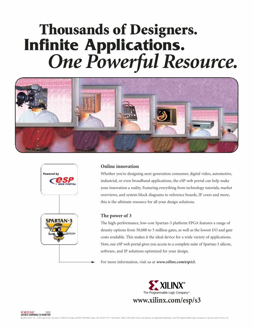
Thousands of Designers.Infinite Applications.
One Powerful Resource.
Online innovation
Whether you’re designing next-generation consumer, digital video, automotive,
industrial, or even broadband applications, the eSP web portal can help make
your innovation a reality. Featuring everything from technology tutorials, market
overviews, and system block diagrams to reference boards, IP cores and more,
this is the ultimate resource for all your design solutions.
The power of 3
The high-performance, low-cost Spartan-3 platform FPGA features a range of
density options from 50,000 to 5 million gates, as well as the lowest I/O and gate
costs available. This makes it the ideal device for a wide variety of applications.
Now, our eSP web portal gives you access to a complete suite of Spartan-3 silicon,
software, and IP solutions optimized for your design.
For more information, visit us at www.xilinx.com/esp/s3.
www.xilinx.com/esp/s3
esPPowered by
Powered by
WEB PORTAL
Powered by
® 2003 Xilinx, Inc., 2100 Logic Drive, San Jose, CA 95124. Europe +44-870-7350-600; Japan +81-3-5321-7711; Asia Pacific +852-2-424-5200; Xilinx and Spartan are registered trademarks, and The Programmable Logic Company is a service mark of Xilinx, Inc.
by Jerry A. LongTechnical Marketing ManagerChronology Division, Forte Design [email protected]
It’s a given – the ever-increasing demand to getyour designs to process more information in lesstime. Designing with new high-speed technolo-gy helps you meet market demands, but it’s like-ly you’re also encountering difficult interfacedesign challenges. Timing issues previouslydeemed insignificant are now impacting designschedules and can no longer be overlooked.
Design teams are seeking extremely effi-cient, low-latency components that can oper-ate at very high frequencies. With theintroduction of QDR™ (quad data rate)SRAMs (co-defined and developed by mem-bers of the QDR SRAM Consortium andXilinx), designers now have first-rate perform-ance devices available for their design projects.
Created for systems operating above 200MHz on Xilinx Virtex™-II FPGAs, QDRSRAM devices provide an unprecedented fourdata transactions per clock cycle. QDRSRAM devices implemented on Virtex-IIPro™ Platform FPGAs include advanced fea-tures that support the design of high-speedmemory interfaces.
To fully take advantage of the high-per-formance features of these new devices, howev-er, you must account for the intricate timingissues associated with high-speed interfacedesign (Figure 1), including:
• Analyzing timing options
• Incorporating signal integrity and physicaleffects into timing considerations
• Managing and monitoring timing marginsthroughout the design process.
If you isolate timing considerations withinthe confines of each stage of a project, the designcan be extremely costly in terms of time, effort,and resources. You simply cannot compromiseaccurate exchange of timing-critical data amongengineering teams without putting design spec-ifications and release schedules at risk.
Chronology’s interactive TimingDesigner™specification and analysis tool meets the strin-gent demands of designing high-speed memoryinterfaces implemented on Virtex-II andVirtex-II Pro Platform FPGAs.
Chronology and Xilinx team up to solve timing challengesassociated with high-speed memory interface designs.Chronology and Xilinx team up to solve timing challengesassociated with high-speed memory interface designs.
Get Control of Your High-SpeedDesigns
Get Control of Your High-SpeedDesigns
44 Xcell Journal Spring 2004

New Design ChallengesAlong with the increased throughputadvantage of high-performance devicescomes the inevitable interface design chal-lenge of ensuring accurate data transfer.
QDR SRAM devices allow four datatransactions per clock cycle by providingseparate read and write data buses, eachwith DDR (double data rate) performancecharacteristics. Separate data buses require:
• Twice the I/O pin requirement for data
• Two clocks
• “Center-aligned” data presentation.
Virtex-II Pro technology allows you toleverage these features with its abundant I/Oresources and high-performance clock man-agement circuitry. However, the benefit ofdesigning with a Virtex-II Pro device doesnot by itself address all the timing challenges.
Ever-Shrinking Timing MarginAs operating frequencies rise beyond 200MHz, the period within which data canbe captured and presented decreases to 5ns or less. At these frequencies, the marginfor setup and hold times dwindles.Shrinking margins mean less room forsecuring an accurate data capture andpresentation window.
Further complicating matters areincreased crosstalk susceptibility and trans-mission line effects that result from higheroperating frequencies. Signal integrity issuesare a significant factor in high-speeddesigns, and you must monitor them asyour design progresses. The combinedeffects of parasitic PCB traces, IC packag-ing, bond wires, and physical die character-istics adversely impact signal quality. Theseeffects require additional settling time,therefore shrinking the timing margin youhave available for reliable data capture.
Communication Is CriticalProject teams cross multiple functionalorganizations, each with their own sets ofsoftware tools and workflows to meet theirspecific design needs. For high-speeddesign, it is imperative to monitor andmanage timing margin limitations through-out the design process. This places new
TimingDesigner Analysis ToolWhen designing high-speed interfaces,you need:
• A means to detect timing problems early
• The ability to display visual representa-tions of design requirements
• A tool to easily implement alternativesolutions.
The TimingDesigner interactive timingspecification and analysis tool is being usedby interdisciplinary project teams whendesigning high-speed interfaces for Virtex-II and Virtex-II Pro FPGAs and QDRSRAM memory devices. TimingDesignerallows you to create interactive timing dia-grams for capturing interface specifications,
automation and accuracy requirements onthe exchange of design specifications amongengineering teams.
Too often, critical timing margin infor-mation is miscommunicated among engi-neering teams. These teams depend on textdocuments created by manual interpreta-tion of large complex report files that weregenerated by tools designed for other uses.Such timing documents are often laboriousto maintain.
They also introduce the opportunity forerror, especially because timing margininformation changes frequently throughoutthe course of a design project. To reduce therisk of error, teams must have a common,automated means to accurately communi-cate and exchange timing data (Figure 2).
Spring 2004 Xcell Journal 45
MasterClockGenerator
Clk
Controller
Virtex-II ProFPGA
QDRSRAM
#1
K, K#
R#
W#
A
DQ
QDRSRAM
#2
K, K#
R#
W#
A
DQ
Data Flight Time
Data Clock to Out
FPGA Clock Flight Time
Master Clock Flight Time
• Interface Models• Timing Budgets• Partitionng
• Timing Problems• What-if Analysis• Optimization
• End-User• Timing Data Archives
ConceptBlock
DiagramDesign Entry
HDL Verification PhysicalDesign
Production
Design Process
Timing Specifications Timing Analysis Timing Documentation
Figure 1 – High-speed memory interfaces present timing challenges.
Figure 2 – Timing information must be communicated throughout the design process.
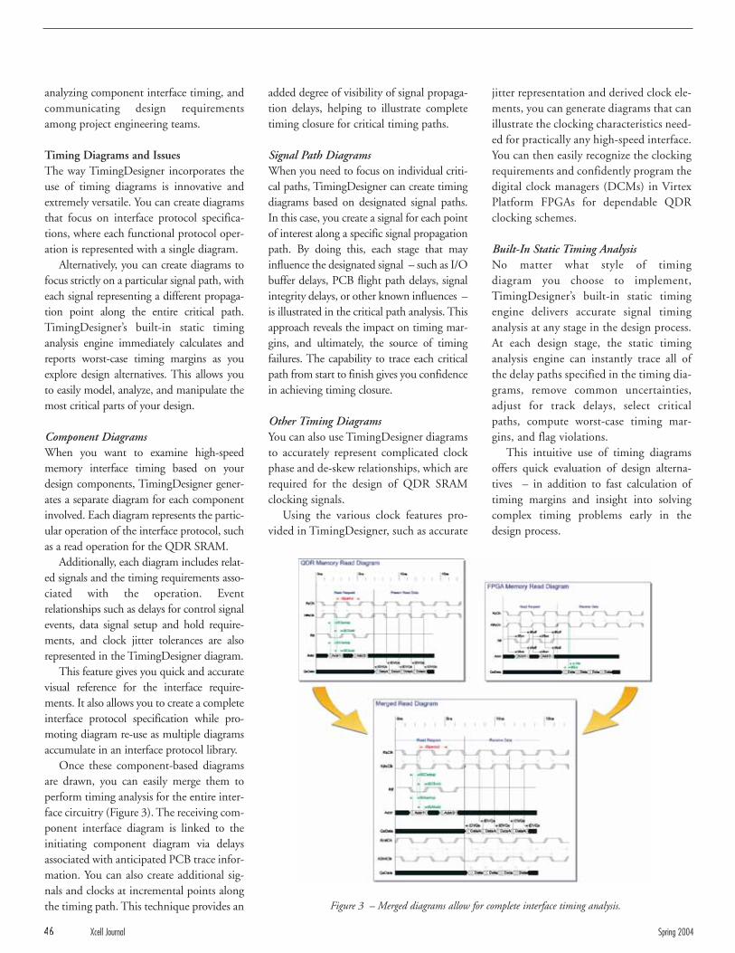
analyzing component interface timing, andcommunicating design requirementsamong project engineering teams.
Timing Diagrams and IssuesThe way TimingDesigner incorporates theuse of timing diagrams is innovative andextremely versatile. You can create diagramsthat focus on interface protocol specifica-tions, where each functional protocol oper-ation is represented with a single diagram.
Alternatively, you can create diagrams tofocus strictly on a particular signal path, witheach signal representing a different propaga-tion point along the entire critical path.TimingDesigner’s built-in static timinganalysis engine immediately calculates andreports worst-case timing margins as youexplore design alternatives. This allows youto easily model, analyze, and manipulate themost critical parts of your design.
Component DiagramsWhen you want to examine high-speedmemory interface timing based on yourdesign components, TimingDesigner gener-ates a separate diagram for each componentinvolved. Each diagram represents the partic-ular operation of the interface protocol, suchas a read operation for the QDR SRAM.
Additionally, each diagram includes relat-ed signals and the timing requirements asso-ciated with the operation. Eventrelationships such as delays for control signalevents, data signal setup and hold require-ments, and clock jitter tolerances are alsorepresented in the TimingDesigner diagram.
This feature gives you quick and accuratevisual reference for the interface require-ments. It also allows you to create a completeinterface protocol specification while pro-moting diagram re-use as multiple diagramsaccumulate in an interface protocol library.
Once these component-based diagramsare drawn, you can easily merge them toperform timing analysis for the entire inter-face circuitry (Figure 3). The receiving com-ponent interface diagram is linked to theinitiating component diagram via delaysassociated with anticipated PCB trace infor-mation. You can also create additional sig-nals and clocks at incremental points alongthe timing path. This technique provides an
added degree of visibility of signal propaga-tion delays, helping to illustrate completetiming closure for critical timing paths.
Signal Path DiagramsWhen you need to focus on individual criti-cal paths, TimingDesigner can create timingdiagrams based on designated signal paths.In this case, you create a signal for each pointof interest along a specific signal propagationpath. By doing this, each stage that mayinfluence the designated signal – such as I/Obuffer delays, PCB flight path delays, signalintegrity delays, or other known influences –is illustrated in the critical path analysis. Thisapproach reveals the impact on timing mar-gins, and ultimately, the source of timingfailures. The capability to trace each criticalpath from start to finish gives you confidencein achieving timing closure.
Other Timing DiagramsYou can also use TimingDesigner diagramsto accurately represent complicated clockphase and de-skew relationships, which arerequired for the design of QDR SRAMclocking signals.
Using the various clock features pro-vided in TimingDesigner, such as accurate
jitter representation and derived clock ele-ments, you can generate diagrams that canillustrate the clocking characteristics need-ed for practically any high-speed interface.You can then easily recognize the clockingrequirements and confidently program thedigital clock managers (DCMs) in VirtexPlatform FPGAs for dependable QDRclocking schemes.
Built-In Static Timing AnalysisNo matter what style of timing diagram you choose to implement,TimingDesigner’s built-in static timingengine delivers accurate signal timinganalysis at any stage in the design process.At each design stage, the static timinganalysis engine can instantly trace all ofthe delay paths specified in the timing dia-grams, remove common uncertainties,adjust for track delays, select criticalpaths, compute worst-case timing mar-gins, and flag violations.
This intuitive use of timing diagramsoffers quick evaluation of design alterna-tives – in addition to fast calculation oftiming margins and insight into solvingcomplex timing problems early in thedesign process.
Figure 3 – Merged diagrams allow for complete interface timing analysis.
46 Xcell Journal Spring 2004

What-If Timing AnalysisAll edge relationship events entered in aTimingDesigner diagram (for example,delays, constraints, guarantees, and meas-ures) are automatically generated in adynamically linked Parameter Spreadsheet(Figure 4). The tabular format of the timingevents represented in the diagram enablesyou to easily manipulate value fields, as wellas comment fields, for event descriptions.
The Parameter Spreadsheet also supportsthe parameterization of timing diagramswith variables to represent various timingscenarios. These variables can be referencedfrom events in the diagram.
For example, clock characteristics such asfrequency, period, phase shift, and jitter canbe represented with variables in the spread-sheet, and then used in other formulas tocreate cycle-accurate timing relationships.This aspect of TimingDesigner providesadded flexibility when designing QDRSRAM interfaces that require center-aligneddata or when illustrating various clockingsignals of your Virtex-based design.
The Parameter Spreadsheet gives you theability to create complex formulas to modelpath delay variables, signal loading, temper-ature, and other elements that may impacttiming relationships.
Using variables in the ParameterSpreadsheet facilitates quick and accurate“what-if” analysis. Throughout the designprocess, you can evaluate circuit functionali-ty and performance using different sets of
parameterized values, providing a highly flex-ible and productive design environment.
For example, you can evaluate numerousoperating frequencies by simply changingthe variable used for clock frequency. Youcan also use this method to evaluate multi-ple Virtex-II and Virtex-II Pro clockingschemes by providing variables for phaserelationships to determine the most appro-priate phase increment for the DCMs.
Library Spreadsheet Flexibility To further expand timing analysis flexibili-ty, you can use the TimingDesigner LibrarySpreadsheet to create part-specific timinginformation that can be used by any timingdiagram. This is especially useful for deviceswhere a single diagram (or set of diagrams)can model the device functionality and thenreference a Library Spreadsheet for specificspeed grades or voltage grades.
Expanding on this concept, you can easi-ly switch in and out of libraries of differenttiming relationships to evaluate cost and per-formance trade-offs and help determine thebest speed grade option for a specific design.
Timing libraries are also very effectivewhen analyzing pre-route versus post-routetiming characteristics of a design. You canuse post-route timing reports from XilinxISE tools (or other layout tools) to create aTimingDesigner library. Because the libraryfile format is a comma-separated ASCII file,creating multiple timing libraries specific to aparticular routing run is easy. You can insert
these libraries into the existing timing dia-gram analysis for a post-route confirmationthat critical timing paths have been satisfied.
TimingDesigner Saves TimeTimingDesigner diagrams are an excellentdocumentation medium for interface specifi-cations. The easy-to-understand format ofthese diagrams reduces the chances for errordue to misinterpretation by other projectteam members. The format provides a clearand concise view of available timing margins.
Each design team can interact with thetiming diagram, making available theirincremental contribution to the overall tim-ing path result. Thus, you get immediatenotification of potential timing problemsthat may be uncovered during differentstages of your design process.
Using TimingDesigner’s OLE capability,timing diagrams can be used in their nativeformat or embedded or linked into com-monly used publishing and presentationtools. This provides a simple way to conveycritical timing path information amongdesign groups. Additionally, TimingDesignerexports common image formats, includingMIF, EMF, TIF, and EPS. Import of VCDand FSDB simulation files is also supported.
ConclusionTogether, the Chronology Division of ForteDesign Systems and Xilinx provide a pow-erful solution set that allows you to tacklethe timing challenges of high-performancedesign. High-speed designs often have strin-gent specifications and tight release sched-ules, so you need an interactive timingspecification and analysis tool to obtain fastand complete timing margin analyses –addressing the factors that can ultimatelyaffect your design success.
The versatile clock configurations andabundant I/O resources of the Virtex-II ProPlatform FPGA allow high throughput datatransfer, while TimingDesigner delivers accu-rate critical path timing analysis resultsrequired for interface design with high-speedmemory devices such as the QDR SRAM.
To learn more about TimingDesignerand the Chronology Division of Forte Design Systems, please visitwww.timingdesigner.com.
Spring 2004 Xcell Journal 47
Figure 4 – A dynamically linked spreadsheet provides immediate feedback for easy exploration of timing alternatives.
by Dino Caporossi Vice President, MarketingHier Design, [email protected]
As an FPGA designer, you probably facemany of the same problems that haveplagued ASIC designers, including lengthy,repetitive place-and-route (PAR) runs;unpredictable route times; and difficultymaintaining performance throughout fre-quent design iterations. These problems candelay or even prevent you from completingyour design, resulting in increased engineer-ing costs and longer time to market.
ASIC-style methodologies, however,enable you to divide and conquer yourcomplex FPGA designs by breaking theminto component blocks, shortening thelength and increasing the predictability ofrouting. As shown in Figure 1, thesemethodologies also allow you to analyze,detect, and correct potential implementa-tion problems before PAR.
An ASIC-style methodology offers thefollowing benefits:
• Quicker incremental design changes orengineering change orders (ECOs)
• Faster, more predictable PAR
• Fewer iterations
• Improved performance
• Tighter utilization control
• Better teamwork
• IP reuse.
To give you the advantages of ASICdesign techniques, Hier Design Inc. hasdeveloped the PlanAhead™ hierarchicaldesign and physical optimization tool suiteto maximize your FPGA design efficiency.
Quicker Incremental Design Changes When you make even minor changes to agiven logic block with a flat methodology,you must redo place-and-route for theentire design. With today’s larger FPGAnetlists, 50 or more PAR iterations – ateight or more hours apiece – are common.This adds up to a significant amount ofwasted time. With an ASIC-style design
Hier Design’s PlanAhead software eliminates manyproblems encountered in high-end FPGA designs.Hier Design’s PlanAhead software eliminates manyproblems encountered in high-end FPGA designs.
Use ASIC Design Methodology for Your Next FPGA Design
Use ASIC Design Methodology for Your Next FPGA Design
48 Xcell Journal Spring 2004
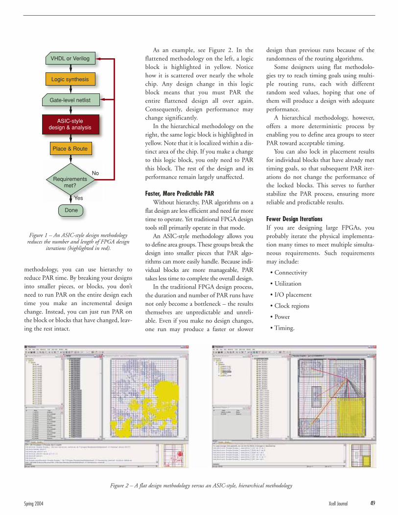
methodology, you can use hierarchy toreduce PAR time. By breaking your designsinto smaller pieces, or blocks, you don’tneed to run PAR on the entire design eachtime you make an incremental designchange. Instead, you can just run PAR onthe block or blocks that have changed, leav-ing the rest intact.
design than previous runs because of therandomness of the routing algorithms.
Some designers using flat methodolo-gies try to reach timing goals using multi-ple routing runs, each with differentrandom seed values, hoping that one ofthem will produce a design with adequateperformance.
A hierarchical methodology, however,offers a more deterministic process byenabling you to define area groups to steerPAR toward acceptable timing.
You can also lock in placement resultsfor individual blocks that have already mettiming goals, so that subsequent PAR iter-ations do not change the performance ofthe locked blocks. This serves to furtherstabilize the PAR process, ensuring morereliable and predictable results.
Fewer Design IterationsIf you are designing large FPGAs, youprobably iterate the physical implementa-tion many times to meet multiple simulta-neous requirements. Such requirementsmay include:
• Connectivity
• Utilization
• I/O placement
• Clock regions
• Power
• Timing.
As an example, see Figure 2. In theflattened methodology on the left, a logicblock is highlighted in yellow. Noticehow it is scattered over nearly the wholechip. Any design change in this logicblock means that you must PAR theentire flattened design all over again.Consequently, design performance maychange significantly.
In the hierarchical methodology on theright, the same logic block is highlighted inyellow. Note that it is localized within a dis-tinct area of the chip. If you make a changeto this logic block, you only need to PARthis block. The rest of the design and itsperformance remain largely unaffected.
Faster, More Predictable PARWithout hierarchy, PAR algorithms on a
flat design are less efficient and need far moretime to operate. Yet traditional FPGA designtools still primarily operate in that mode.
An ASIC-style methodology allows youto define area groups. These groups break thedesign into smaller pieces that PAR algo-rithms can more easily handle. Because indi-vidual blocks are more manageable, PARtakes less time to complete the overall design.
In the traditional FPGA design process,the duration and number of PAR runs havenot only become a bottleneck – the resultsthemselves are unpredictable and unreli-able. Even if you make no design changes,one run may produce a faster or slower
Spring 2004 Xcell Journal 49
VHDL or Verilog
Logic synthesis
Gate-level netlist
ASIC-styledesign & analysis
Place & Route
Requirementsmet?
Yes
No
Done
Figure 1 – An ASIC-style design methodologyreduces the number and length of FPGA design
iterations (highlighted in red).
Figure 2 – A flat design methodology versus an ASIC-style, hierarchical methodology

Without an ASIC-style methodology,there is no way to know whether all theserequirements can be met until after PAR.What’s worse, many of the requirementsare interrelated, so making design changesto achieve one requirement often preventsyou from achieving several others.Consequently, you spend too much timeiterating your designs.
ASIC-style methodologies help youquickly reach your requirements – prior toPAR – through early design analysis, tight-ly coupled with floorplanning. With floor-planning and early analysis, you cansubstantially reduce the number andlength of PAR iterations.
In Figure 3, early connectivity analysisin the PlanAhead software (left screen) pro-vides visual clues: The thickness and colorof bundled lines represent the nets betweenblocks. You can see – and fix – routing con-gestion before PAR. You can quickly adjustthe floorplan by moving, rearranging, andcombining blocks in the physical hierarchy(right screen). Moreover, you can manipu-late the physical hierarchy independentlyfrom the logical hierarchy.
Using this process, the PAR algorithmsnow have the necessary partitioning, blockarrangement, and constraints to guidethem to success.
Improved Design PerformanceWhen designing with today’s large FPGAs,you may encounter timing knots, long
critical paths spanning hierarchy, complexclocking, and high fan-out – making tim-ing goals more difficult to meet. ASICdesigners have successfully overcome thesekinds of problems through techniques nowavailable to FPGA designers.
Static timing analysis enables you toquickly visualize potential timing prob-lems early in the design cycle, before PAR.Floorplanning lets you make adjustmentsto avoid these timing problems by con-trolling logic migration and shorteningconnectivity paths.
Static timing analysis also highlightscritical paths in the floor plan so that youcan fix them by using constraints or man-ually rearranging the path instances.
In a misguided effort, some ASIC-stylemethodologies attempt to improve per-formance by floorplanning before synthe-sis. This is not a good idea, because theremay be large errors in the estimates ofdesign performance. In contrast,
PlanAhead software acquires more accu-rate timing information at the highestimpact point in the design flow, therebymaximizing performance improvement.
The PlanAhead software also includesphysical optimization capability to addressimplementation problems that may ariselater in the design cycle, post-PAR. Withthe PlanAhead tools, you can still adjustplacement at the block or leaf level toreach performance goals. You can then runtiming analysis to see if performance hasimproved. With this process you get near-ly instantaneous feedback, rather thanwaiting for hours for PAR to finish.
Methodology Results ExampleTable 1 demonstrates the advantages ofadopting an ASIC-style methodology andusing the PlanAhead design and optimiza-tion software. Our example includes hierarchical design combined with floor-planning and integrated analysis.
50 Xcell Journal Spring 2004
Methodology Used Timing Place & Route RuntimeRuntime Reduction
Traditional flattened netlist -.88 ns negative slack 5.0 hrs.
With floorplanning and analysis Meets timing 3.5 hrs. 30%
With incremental ECO capability Meets timing 40 min. 87%
Figure 3 – Avoiding routing congestion through early analysis
Table 1 – Methodology results comparison using PlanAhead design and optimization software

In this example, our cus-tomer’s designers implement-ed a wireless communicationschip with the Virtex™-II2V6000 platform as their tar-get device. Using a traditionalflat methodology, they had 18timing errors.
By using a block-based,incremental, ECO methodol-ogy, their PAR time was 87%faster than their flat method-ology. By creating a more effi-cient floor plan, they wereable to meet all of their tim-ing goals. Slice utilizationremained a constant 98%throughout.
The first row of Table 1 displays PARtime and design performance using a tra-ditional flattened methodology. The sec-ond row demonstrates the benefits offloorplanning. And the third row showseven more benefits by combining floor-planning with an incremental ECO designmethodology.
The runtime column lists the totalCPU time used by Xilinx PAR. The timingcolumn indicates whether the design wasable to meet performance goals.
Tighter Utilization ControlUtilization is an important aspect ofFPGA design. In some cases, designerscrowd as much logic into a given device aspossible to meet production volumerequirements.
In other cases, they must leave somespace in the FPGA to accommodate bugfixes, naturally occurring design changes,ECOs, or future field upgrades. Leavingroom for change is essential for electronicdevices with long serviceable life cycles.
Using block-based hierarchical designtechniques makes it easier to control uti-lization. To maximize utilization, you canset the controls at a given utilization leveland run a block-level PAR. If it producessuccessful results, you can increase the uti-lization setting, which shrinks the block,and then run another block-level PAR.
You can continue this process until thePAR fails, which means you have achieved
the maximum possible utilization for thegiven block. By applying Xilinx area groupcompression constraints on blocks that arenot timing critical, you can also signifi-cantly increase utilization.
A wise approach is to leave more spacein blocks that have yet to be verified, so youcan accommodate anticipated bug fixes.
You might, however, desire a higherutilization setting in blocks that arealready field-proven, because it is less like-ly that extra space will be needed to fixbugs within them.
Teamwork and IP ReuseLike ASIC designers, you can expeditedesign time by working as a team andreusing intellectual property (IP) fromprevious designs. The PlanAhead softwareprovides an ASIC-style hierarchicalmethodology that facilitates this kind ofteamwork.
You can use a block-based approach todivide the work into more manageableblocks and assign responsibilities ofdesigning them to individual team mem-bers. You can also reuse blocks (also knownas IP cores) from previous designs, or evenpurchase blocks from a third party to savedesign and verification time.
When working as such a team, you canbegin the physical design process much ear-lier. You can sequentially implement andassemble the design, beginning with themost critical blocks, as shown in Figure 4.
Successively, you can PAR theblocks as designers completetheir assignments.
Using ASIC-style method-ologies, you can fully charac-terize design blocks by freezingthe placement within them sothat power, timing, and othercharacteristics remain con-stant. Thus, it’s possible toreuse them with consistentresults in similar FPGAdevices. Because you knowthat these blocks meet yourphysical requirements, you canquickly connect them to formlarger designs that also meetyour requirements.
ASIC designers refer to this type ofdesign as a system-on-chip methodology,and it is particularly valuable if you are anASIC designer using FPGAs for prototyp-ing. To significantly reduce your overallverification time, use the PlanAhead analy-sis and floorplanning software to lockplacement within pre-characterized IPblocks and connect them together.Because you already know these blocksmeet timing and other design require-ments, you can create a working ASICprototype much more quickly.
ConclusionFPGAs have become so complex that youmay be encountering ASIC-size designbottlenecks. You can overcome theseproblems by adopting proven ASIC-styledesign methodologies. Hierarchical designenables you to make fast incrementalchanges, and early analysis allows you tofix problems prior to place-and-route.
You can closely control utilization,packing designs ever tighter, or leave extraroom for bug fixes, ECOs, or plannedupgrades for products that have a longfield or shelf life.
Finally, you can work as a team andshorten design and verification time byreusing blocks of pre-characterized IP.
To learn more about the PlanAheadhierarchical design and physical opti-mization software, visit the Hier Designwebsite at www.hierdesign.com.
Spring 2004 Xcell Journal 51
Figure 4 – Place critical timing blocks first.
by Mike Fingeroff Technical Marketing Engineer, Synthesis GroupMentor Graphics [email protected]
Many months’ worth of painstaking synthe-sis and place and route (PAR) iterations canbe lost instantly if you need to make a func-tional change to your high-performanceFPGA design. When ambitious perform-ance goals come into play, achieving timingclosure may involve a series of sophisticatedsynthesis, floorplanning, and PAR steps.Run times of design iterations may take anentire day, so complex designs requiringmultiple iterations could add weeks or evenmonths to a design schedule.
You can protect hard-fought timinggains from the disruptive effects of func-tional iterations through the use of a block-based incremental design methodology.Precision™ RTL Synthesis from MentorGraphics, used in conjunction with XilinxISE software, enables you to perform designiterations at the block level, thus preservingthe performance of unaffected blocks. Inthis article, I will cover the technical detailsand tradeoffs of using a block-based incre-mental design methodology.
Preserve Timing Gainsin Incremental Design
52 Xcell Journal Spring 2004
Incremental synthesis tools from Mentor Graphics combined with Xilinx incremental place and route software can reduce your design iteration time.
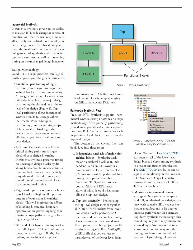
Incremental SynthesisIncremental synthesis gives you the abilityto make an RTL code change or constraintmodification that, when re-synthesized,affects only an isolated portion of yourentire design hierarchy. This allows you toreuse the unaffected portion of the tech-nology-mapped synthesis netlist, reducingsynthesis runtimes as well as preservingtiming on the unchanged design hierarchy.
Design MethodologyGood RTL design practices can signifi-cantly improve your design’s performance.
• Functional partitioning of logic –Partition your design into major hier-archical blocks based on functionality.Although your design blocks can con-tain sub-hierarchies, the major designpartitioning should be done at the toplevel of the design (Figure 1). Top-level partitioning allows incrementalsynthesis results to leverage Xilinxincremental PAR techniques.Partitioning your design into groupsof functionally related logic alsoenables the synthesis engine to moreefficiently optimize critical portions ofyour design.
• Isolation of critical paths – Isolatecritical timing paths into a singleblock of your design hierarchy.Incremental synthesis preserves timingon unchanged design blocks by dis-abling hierarchical boundary optimiza-tion on blocks that are incrementallyre-synthesized. Critical timing pathsrouted though re-synthesized blocksmay lose optimal timing.
• Registered inputs or outputs on func-tional blocks – Register all inputs oroutputs of your major hierarchicalblocks. This will minimize the effectsof disabling hierarchical boundaryoptimization by preventing long com-binatorial logic paths entering or leav-ing a design block.
• IOB and clock logic at the top level –Place all of your I/O logic, buffers, tri-states, and clock logic (DCMs, globalbuffers, and such) at the top level.
blocks. You must place DONT_TOUCHattributes on all of the lower-leveldesign blocks before running synthesisto prevent any further optimization.The DONT_TOUCH attributes can beapplied either directly in the PrecisionRTL Synthesis Design HierarchyBrowser (Figure 2) or as an HDL orTCL script attribute.
3. Making an incremental designchange – Once you have completedand fully synthesized your design, youmay wish to make HDL code or con-straint modifications to fix bugs orimprove performance. In a standardtop-down synthesis methodology, thiswould require you to re-synthesize theentire design. Not only is this time-consuming, but you may introducetiming problems into unmodifiedportions of your design. However,
Instantiation of I/O buffers in a lower-level design block is acceptable usingthe Xilinx incremental PAR flow.
Bottom-Up Synthesis FlowPrecision RTL Synthesis supports incre-mental synthesis using a bottom-up designmethodology. After properly partitioningyour design, you should create a separatePrecision RTL Synthesis project for eachmajor hierarchical block, as well as for thetop-level design.
The bottom-up incremental flow canbe divided into three steps:
1. Independent synthesis of major hier-archical blocks – Synthesize eachmajor hierarchical block as an inde-pendent Precision RTL Synthesisproject, with I/O insertion disabled.(I/O insertion will be performed laterduring the top-level assembly.)Precision RTL Synthesis producesboth an XDB and EDIF netlist,either of which is valid when assem-bling the top-level design.
2. Top-level assembly – Synthesizingthe top-level design stitches togetherall XDB or EDIF netlists from lower-level design blocks, performs I/Oinsertion, and does a complete timingcharacterization of the entire design.The top-level assembly project shouldconsist of a single VHDL, Verilog™,or EDIF file that you can use toinstantiate all of the lower-level design
Spring 2004 Xcell Journal 53
Top
Block B Block CBlock A
Block D Functional Blocks
Figure 1 – Design partitioning
Figure 2 – Applying DONT_TOUCHattributes using the Precision GUI

using the Precision RTL Synthesisbottom-up methodology for incre-mental synthesis allows you to isolatethe effects of an HDL code change tospecific design blocks. Should anHDL code change occur, you areonly required to re-synthesize theproject that references the modifiedHDL file. You must then, of course,run a final top-level assembly to gen-erate a new netlist.
Incremental Place and RouteIncremental synthesis helps you to reducesynthesis runtimes and preserve unmodi-fied portions of the technology-mappednetlist. However, you must still depend onthe back-end PAR tool to meet or preservetiming goals. You can use the Xilinx ISEincremental PAR flow in conjunctionwith the Precision RTL Synthesis incre-mental flow to preserve timing gains byonly re-placing those design blocks thathave been modified during your incre-mental synthesis run.
Floorplanning the DesignOne of the most critical steps in the XilinxISE incremental PAR flow is floorplanningyour design. You must perform floorplan-ning to minimize the interconnect delaybetween your design blocks. You may alsoneed floorplanning to overcome the per-formance limitations associated with dis-abling hierarchical boundary optimizationduring incremental synthesis.
Floorplanning consists of:• Separate area groups for each func-
tional block – You must create aXilinx area group for each majordesign block. Area groups are createdand placed using the Xilinx PACEtool, which takes as its input a UCF(produced by Precision RTLSynthesis), and an NGD file pro-duced during the translate stage(Figure 3). Area groups must notoverlap, because that might adverselyaffect performance. Assigning non-overlapping area groups to major hier-archical blocks allows the ISEprogram to completely re-place and
re-route a design block inside an areagroup when a change is made in thenetlist. If possible, you should makethe area groups slightly larger thanneeded. This will allow successful re-placement if your design blockutilization increases because of amodification. In addition to assign-ing area groups, you must also lockdown all I/Os.
• Co-location of related blocks andI/Os – Not only is it essential to par-tition your design logically to opti-mize inter-block timing paths, but itis equally important to arrange thearea groups associated with each logi-cal partition to minimize intra-blocktiming paths. Area groups, as well asI/Os, that communicate with oneanother should be placed as close aspossible to each other.
Running Place and Route• Performing initial PAR – Once you
have floorplanned your design byassigning area groups and lockingdown the I/Os, you must runthrough a first pass of technologymapping and PAR to generate an ini-tial set of guide files (*.ngm and*.ncd). You can then use the guidefiles in your next PAR iteration to re-place and re-route as much of yourdesign as possible.
• Performing guided technology map-ping and PAR – You can enable incre-mental PAR by setting the guide modeto “incremental” and specifying theguide files produced by the Xilinxtechnology mapper and PAR fromyour previous PAR iteration. Theguide mode can be specified either inthe ISE GUI or at the command lineusing the -gm switch. The Xilinx incre-mental guide mode directs the tech-nology mapper and PAR to re-placeand re-route all area groups and associ-ated logic that haven’t changed, thuspreserving timing gains from previousdesign iterations.
ConclusionSmall design changes can have a devastat-ing effect on your overall system perform-ance, sometimes undoing months’ worth ofdevelopment effort. To avoid these pitfalls,you can use Mentor Graphics PrecisionRTL Synthesis and Xilinx ISE PAR in tan-dem to implement an efficient and effec-tive incremental design methodology thatpreserves timing gains and dramaticallyreduces your design iteration time.
To learn more about Mentor Graphics Precision RTL Synthesis, visit www.mentor.com/precision/.
For a complete description of incre-mental place and route, see ApplicationNote XAPP418, “Xilinx 5.1i IncrementalDesign Flow” (search www.xilinx.com).
Figure 3 – Floorplanning using Xilinx PACE tool
54 Xcell Journal Spring 2004
by Xcell Staff
The consumer electronics market is flood-ed with new products. In fact, the sheernumber of consumer devices has intro-duced entirely new business models for theproduction and distribution of goods.These new devices have also necessitatedmajor changes in the way we access infor-mation and interact with each other.
The digitization of technology (bothproducts and media) has led to leaps inproduct development. It has enabled easierexchange of media, cheaper and more reli-able products, and convenient services.
Digitization has not only improvedexisting products – it has also createdentire new classes of products. For exam-ple, improvements in devices such asDVRs (digital video recorders) have revo-lutionized the way we watch TV. Digitalmodems bring faster Internet access tothe home. MP3 players have completelychanged portable digital music. Digitalcameras enable instant access to photo-graphs that you can e-mail seconds aftertaking them, and eBooks allow con-sumers to download entire books andmagazines to eBook tablets. Devices suchas wireless phones, personal digital assis-tants (PDAs), and other pocket-sizedcommunicators are on the brink of a newera in which mobile computing andtelephony converge.
This has been made possible through theavailability of cheaper and more powerfulsemiconductor components. With advance-ments in semiconductor technology, compo-nents such as microprocessors, memories,and logic devices are cheaper, faster, andmore powerful with every process migration.
Similar advances in programmablelogic devices have enabled manufacturersof new consumer electronics devices to useFPGAs and CPLDs to add continuousflexibility and maintain market leadership.
The Digital Consumer TechnologyHandbook – A Comprehensive Guide toDevices, Standards, Future Directions, andProgrammable Logic Solutions is a survey ofstate-of-the-art digital consumer technolo-gy and related applications. It provides abroad synthesis of information so that youcan make informed decisions about thefuture of digital appliances.
Organization and TopicsAmit Dhir, author of the DigitalConsumer Technology Handbook, says that“with so many exciting new digitaldevices available, it was difficult to nar-row the selections to the most importantcutting-edge technologies.
“In this book I have included more than20 emerging product categories that typifycurrent digital electronic trends. The chap-ters offer exclusive insight into those digitalconsumer products that have enormouspotential to enhance our life and workstyles. Each chapter follows a logical pro-gression, from a general overview of adevice to its market dynamics to the coretechnologies that make up the product.”
Who Should Read This BookThe Digital Consumer TechnologyHandbook is meant for anyone seeking abroad-based familiarity with the issues ofdigital consumer devices. It assumes youhave some knowledge of systems, generalnetworking, and Internet concepts.
The Digital Consumer TechnologyHandbook – A Comprehensive Guide toDevices, Standards, Future Directions, andProgrammable Logic Solutions is availableat all consumer bookstores after March 1,2004, or online through ElsevierPublishing at http://books.elsevier.com/computereng/.
The price of the book is $49.95, butyou can receive a special 15% discountoff the list price on orders placed beforeMarch 1, 2004. Simply enter the offercode 76899 when ordering from theElsevier website.
A new handbook guides you through the digital technology maze.A new handbook guides you through the digital technology maze.
Designing Next-Generation DigitalConsumer Electronics Devices
Designing Next-Generation DigitalConsumer Electronics Devices
Amit Dhir, author ofThe Digital ConsumerTechnology Handbook– A ComprehensiveGuide to Devices,Standards, FutureDirections, andProgrammable LogicSolutions
Spring 2004 Xcell Journal 55
by Ross Nelson Technical Marketing EngineerMentor Graphics [email protected]
Gary DareTechnical Marketing EngineerMentor Graphics [email protected]
As gate counts increase with each new gen-eration of FPGAs, it becomes easier toimplement large-scale systems using plat-form FPGAs rather than ASICs. FPGAdesign starts have grown along with thetechnology’s capabilities, exceeding thosefor ASICs by as much as 10 to 1 in 2002.
To address the challenges these largeFPGA-centric systems present, we must re-examine system-on-chip (SoC) method-ologies, such as hardware/softwareco-verification, initially developed forASIC-scale designs.
In this article, we’ll demonstrate theMentor Graphics® Seamless® hard-ware/software co-verification technolo-
gy on a design targeting the Xilinx Virtex-IIPro™ FPGA, with its embedded IBM™PowerPC™ 405 CPU. This design boots upthe Nucleus® Plus real-time operating sys-tem (RTOS), also from Mentor Graphics. Aswe’ll see, significant performance improve-ments are possible over conventional HDLsimulation when using the Seamless tool.
The Mentor Graphics Seamless co-verification tool is as applicable to large FPGA designs as it is to large ASICs.The Mentor Graphics Seamless co-verification tool is as applicable to large FPGA designs as it is to large ASICs.
Seamless HW/SW Co-Verification for Xilinx Virtex-II Pro FPGAs Seamless HW/SW Co-Verification for Xilinx Virtex-II Pro FPGAs
56 Xcell Journal Spring 2004

Co-Verification Offers Speed, High PerformanceCo-verification is proven in the develop-ment of embedded system ASICs.Hardware/software co-verification toolsallow you to run software against a hard-ware design to verify hardware/softwareinterfaces before building a physical pro-totype. This gives you concurrent accessto your hardware design while it is indevelopment and reduces overall projectcycle time.
Increased visibility into your hardwaredesign, especially when encountering prob-lems, enables you to debug designs whilethey’re exercised by actual verification soft-ware running on the CPU.
From a performance perspective, thebehavioral model of the co-verificationprocessor speeds up simulation executionversus a register transfer level (RTL) modelof the CPU.
Massive speed gains by as much as 1,000times are possible by applying Seamlessoptimizations that remove overhead, suchas explicit instruction and data fetch cyclesin hardware simulation. This performanceimprovement enables you to verify largeFPGA-based systems with as many as 2 mil-
we integrated standard IP componentsaround the IBM PowerPC 405 CPU,either from the Xilinx Embedded DesignKit (EDK) library or from third-partyproviders such as the Mentor GraphicsIntellectual Property Division.
At this scale of design, we have:
• Three standard IBM CoreConnectbuses: processor local bus (PLB), on-chip peripheral bus (OPB), and devicecontrol registers (DCR) bus
• Multiple peripherals: Two GPIO, IIC,Ethernet MAC, direct memory access(DMA) controller, PCI bridge, andmemory controllers for Flash, SRAM,and SDRAM
• Support functions such as an interruptcontroller and on-chip memory usingXilinx block RAM.
As with typical reference boards, such asthe Walnut from IBM for the 405GP, a ref-erence board for the Virtex-II Pro FPGAprovides the external memory to supportthe system.
The hardware design was assembledusing Xilinx embedded system tools, asshown in Figure 1.
Once the FPGA hardware design is cre-ated, the conversion for co-simulation isquite straightforward. The IBM PowerPC405 block in the hardware design isreplaced by the bus interface model (BIM)component of the IBM PowerPC 405model from the Seamless processor supportpackage (PSP). Software for the NucleusPlus RTOS is compiled and loaded to runfrom Flash memory, which is external tothe FPGA as part of the test bench.Hardware/software co-verification can nowbe performed on this FPGA design, just asit is for ASIC designs.
How Seamless Measures UpTable 1 outlines the relative performanceresults from executing the boot up of theNucleus Plus RTOS of our example sys-tem. The baseline figure is a measure ofSeamless hardware/software co-verificationexecuting without any optimizations.
The hardware design was created inVHDL to utilize the Xilinx EDK behav-
lion gates – gates that could not otherwisebe verified within a practical time frameusing conventional HDL simulation.
With hardware/software co-verification,you can also spot bugs that would otherwisego unnoticed, simply because it would beimpractical to test for them. This becomesmore important as systems become larger,and the portion of nodes that can be physi-cally probed from the perimeter of theFPGA becomes smaller.
The majority of nodes are internal to thedesign and observable only through simula-tion. Even those that can be probed aredependent on cycle time for the design andproduction of test boards.
Seamless Co-Verification of an FPGA DesignIn the following example, you can observesoftware – whether high-level C or low-level assembler – as well as hardware usingthe Seamless co-verification tool.
System SpecificationsOur example system is built to the scale oftypical embedded microcontrollers, such asthe IBM PowerPC 405GP, a.k.a. Galaxy. Ina Virtex-II Pro design for the Galaxy SoC,
Spring 2004 Xcell Journal 57
Figure 1 – A schematic of the reference design created with Xilinx EDK tools.
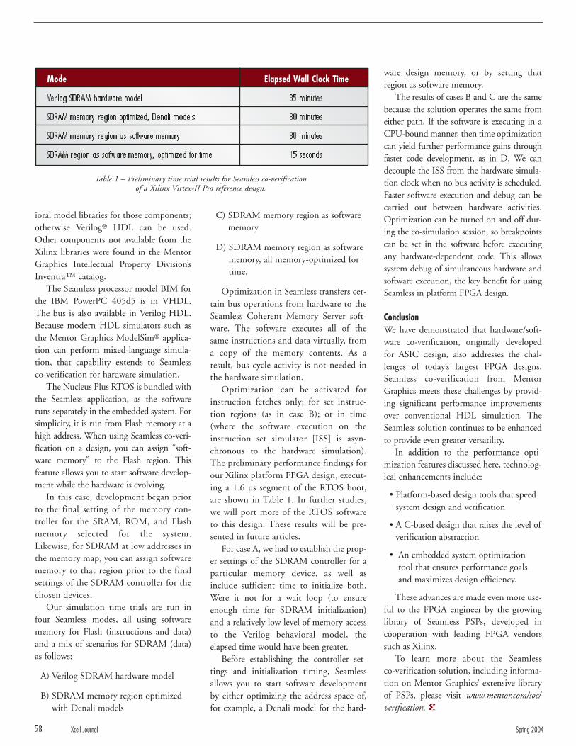
ioral model libraries for those components;otherwise Verilog® HDL can be used.Other components not available from theXilinx libraries were found in the MentorGraphics Intellectual Property Division’sInventra™ catalog.
The Seamless processor model BIM forthe IBM PowerPC 405d5 is in VHDL.The bus is also available in Verilog HDL.Because modern HDL simulators such asthe Mentor Graphics ModelSim® applica-tion can perform mixed-language simula-tion, that capability extends to Seamlessco-verification for hardware simulation.
The Nucleus Plus RTOS is bundled withthe Seamless application, as the softwareruns separately in the embedded system. Forsimplicity, it is run from Flash memory at ahigh address. When using Seamless co-veri-fication on a design, you can assign “soft-ware memory” to the Flash region. Thisfeature allows you to start software develop-ment while the hardware is evolving.
In this case, development began priorto the final setting of the memory con-troller for the SRAM, ROM, and Flashmemory selected for the system.Likewise, for SDRAM at low addresses inthe memory map, you can assign softwarememory to that region prior to the finalsettings of the SDRAM controller for thechosen devices.
Our simulation time trials are run infour Seamless modes, all using softwarememory for Flash (instructions and data)and a mix of scenarios for SDRAM (data)as follows:
A) Verilog SDRAM hardware model
B) SDRAM memory region optimizedwith Denali models
C) SDRAM memory region as softwarememory
D) SDRAM memory region as softwarememory, all memory-optimized fortime.
Optimization in Seamless transfers cer-tain bus operations from hardware to theSeamless Coherent Memory Server soft-ware. The software executes all of thesame instructions and data virtually, froma copy of the memory contents. As aresult, bus cycle activity is not needed inthe hardware simulation.
Optimization can be activated forinstruction fetches only; for set instruc-tion regions (as in case B); or in time(where the software execution on theinstruction set simulator [ISS] is asyn-chronous to the hardware simulation).The preliminary performance findings forour Xilinx platform FPGA design, execut-ing a 1.6 µs segment of the RTOS boot,are shown in Table 1. In further studies,we will port more of the RTOS softwareto this design. These results will be pre-sented in future articles.
For case A, we had to establish the prop-er settings of the SDRAM controller for aparticular memory device, as well asinclude sufficient time to initialize both.Were it not for a wait loop (to ensureenough time for SDRAM initialization)and a relatively low level of memory accessto the Verilog behavioral model, theelapsed time would have been greater.
Before establishing the controller set-tings and initialization timing, Seamlessallows you to start software developmentby either optimizing the address space of,for example, a Denali model for the hard-
ware design memory, or by setting thatregion as software memory.
The results of cases B and C are the samebecause the solution operates the same fromeither path. If the software is executing in aCPU-bound manner, then time optimizationcan yield further performance gains throughfaster code development, as in D. We candecouple the ISS from the hardware simula-tion clock when no bus activity is scheduled.Faster software execution and debug can becarried out between hardware activities.Optimization can be turned on and off dur-ing the co-simulation session, so breakpointscan be set in the software before executingany hardware-dependent code. This allowssystem debug of simultaneous hardware andsoftware execution, the key benefit for usingSeamless in platform FPGA design.
ConclusionWe have demonstrated that hardware/soft-ware co-verification, originally developedfor ASIC design, also addresses the chal-lenges of today’s largest FPGA designs.Seamless co-verification from MentorGraphics meets these challenges by provid-ing significant performance improvementsover conventional HDL simulation. TheSeamless solution continues to be enhancedto provide even greater versatility.
In addition to the performance opti-mization features discussed here, technolog-ical enhancements include:
• Platform-based design tools that speedsystem design and verification
• A C-based design that raises the level ofverification abstraction
• An embedded system optimizationtool that ensures performance goalsand maximizes design efficiency.
These advances are made even more use-ful to the FPGA engineer by the growinglibrary of Seamless PSPs, developed incooperation with leading FPGA vendorssuch as Xilinx.
To learn more about the Seamless co-verification solution, including informa-tion on Mentor Graphics’ extensive libraryof PSPs, please visit www.mentor.com/soc/verification.
Mode Elapsed Wall Clock Time
Verilog SDRAM hardware model 35 minutes
SDRAM memory region optimized, Denali models 30 minutes
SDRAM memory region as software memory 30 minutes
SDRAM region as software memory, optimized for time 15 seconds
Table 1 – Preliminary time trial results for Seamless co-verification of a Xilinx Virtex-II Pro reference design.
58 Xcell Journal Spring 2004


by Steven ElzingaProduct Applications EngineerXilinx, [email protected]
Often, simply being first to market with anexcellent product can assure its success.However, effectively harnessing availableresources to allow for less expensive parts –and thus a less expensive overall solution –can also give you a significant advantageover a competitor.
The Synplify™ FPGA synthesis solu-tions and Synplify Pro™ advanced FPGAsynthesis solutions from Synplicity™ havemany features that enable you to effectivelyuse the resources in FPGAs. For example,you can set constraints for timing-drivensynthesis that may allow you to purchaseslower speed grade parts without compro-mising on performance or quality. TheSynplify FPGA synthesis solution andSynplify Pro advanced FPGA synthesissolutions offer a perfect fit for the high-vol-ume, low-cost Spartan™ FPGAs, and theadvanced Virtex™ series of FPGAs.
Spartan/Virtex ArchitectureSpartan-II series FPGAs are based on theXilinx Virtex architecture. Each FPGA hasa number of clock delay locked loops(CLKDLL) for clock management (eachCLKDLL driving one of four global clocklines) and block RAM of 4 Kb each.
Furthermore, the basic Virtex architec-ture can be broken down into “slices,”comprising two RAM-based 4-input look-up tables (LUT), two registers, and dedi-cated “carry logic” used for arithmeticoperations (Figure 1). You can configurethe LUT as distributed RAM, a shift regis-ter LUT (SRL) with a programmablelatency of as many as 16 clock cycles, or anLUT for a 4-input Boolean function.
Inside of every input/output block(IOB) are three flip-flops so that the datacoming into and leaving the IOB can beregistered, thereby increasing the overallmaximum frequency.
Spartan-3 series FPGAs are based onthe more advanced Xilinx Virtex-II plat-form FPGA hardware. The difference isthat the CLKDLL has added functionality,
along with a total of 16 global clock lines(eight global lines in the Spartan-3). Theblock RAM is larger, with 18 Kb of mem-ory. Platform FPGAs have more registers inthe IOBs to accommodate dual data rate(DDR) applications. The Virtex-II archi-tecture also includes embedded multipliersthat can be synchronous or asynchronous.
The Synplify and Synplify Pro toolstake advantage of the hardware present inthe Spartan and Virtex families to ensureoptimal area and speed results.
Timing-Driven SynthesisThe Synplify Pro solution is an advancedsynthesis tool that performs timing opti-mizations based on the timing constraintsentered. Optimizations are based on –but not limited to – offset and periodconstraints. Timing constraints areentered in a constraints file (text or GUIentry) or through a tool command lan-guage (TCL) script.
Because Synplify Pro software is timingdriven, you must provide realistic timingconstraints. Avoid over-constraining byasking for more than 10% or 15% of whatyou really need; in other words, if you need100 MHz, enter 100 MHz or perhaps 110MHz. The timing-driven aspect of theSynplify Pro software first meets your tim-ing constraints and once met, minimizesarea. This allows you to achieve your per-formance goal while using the smallest,lowest cost device.
Synplicity’s SCOPE® (synthesis con-straints optimization environment) GUIallows you to easily manipulate constraintsfrom the register transfer level (RTL) view-er into the spreadsheet. Just click and dragany object into the spreadsheet and applythe appropriate constraint, or select theobjects from pull-down menus in thespreadsheet’s individual cells (Figure 2).
The SCOPE interface provides a singlelocation for both synthesis and place-and-route (PAR) constraints, which are passedalong to the Xilinx PAR tool. Clocks,inputs, and outputs are all automaticallyloaded into the SCOPE utility for fast andeasy constraint entry.
The Synplify Pro synthesis tool hasoptions that allow you to manipulate regis-
Conserve FPGA resources in cost-sensitive designs with Synplicity timing-driven synthesis solutions. Conserve FPGA resources in cost-sensitive designs with Synplicity timing-driven synthesis solutions.
Simplify with Synplicity Synthesis SolutionsSimplify with Synplicity Synthesis Solutions
60 Xcell Journal Spring 2004
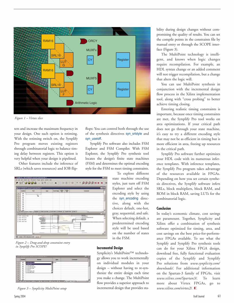
ters and increase the maximum frequency inyour design. One such option is retiming.With the retiming switch on, the SynplifyPro program moves existing registersthrough combinatorial logic to balance tim-ing delay between registers. This option isvery helpful when your design is pipelined.
Other features include the inference ofSRLs (which saves resources) and IOB flip-
bility during design changes without com-promising the quality of results. You can setthe compile points in the constraints file bymanual entry or through the SCOPE inter-face (Figure 3).
The MultiPoint technology is intelli-gent, and knows when logic changesrequire recompilation. For example, anHDL syntax change or an added commentwill not trigger recompilation, but a changethat alters the logic will.
You can use MultiPoint synthesis inconjunction with the incremental designflow process in the Xilinx implementationtool, along with “cross probing” to betterachieve timing closing.
Entering realistic timing constraints isimportant, because once timing constraintsare met, the Synplify Pro tool works onarea optimizations. If your critical pathdoes not go through your state machine,it’s easy to try a different encoding stylethat may not be as efficient in timing but ismore efficient in area, freeing up resourcesin the critical path.
Synplify Pro software further optimizesyour HDL code with its numerous infer-ence templates. With inference templates,the Synplify Pro program takes advantageof the resources available in FPGAs.Depending on how you set certain synthe-sis directives, the Synplify software infersSRLs, block multipliers, block RAM, andROM in block RAM, saving LUTs for thecombinatorial logic.
ConclusionIn today’s economic climate, cost savingsare paramount. Together, Synplicity andXilinx offer a combination of synthesissoftware optimized for timing, area, andcost savings on the best price-for-perform-ance FPGAs available. To see what theSynplify and Synplify Pro synthesis toolscan do for your Xilinx FPGA design,download free, fully functional evaluationcopies of the Synplify and Synplify Pro solutions from www.synplicity.com/downloads/. For additional information on the Spartan-3 family of FPGAs, visitwww.xilinx.com/Spartan3/. To learn more about Virtex FPGAs, go to www.xilinx.com/virtex2/.
flops: You can control both through the useof the synthesis directives syn_srlstyle andsyn_useioff.
Synplify Pro software also includes FSMExplorer and FSM Compiler. With FSMExplorer, the Synplify Pro synthesis toollocates the design’s finite state machines(FSM) and determines the optimal encodingstyle for the FSM to meet timing constraints.
To explore differentstate machine encodingstyles, just turn off FSMExplorer and select theencoding style by usingthe syn_encoding direc-tive, along with thechoices default, one-hot,gray, sequential, and safe.When selecting default, apredetermined encodingstyle will be used basedon the number of statesin the FSM.
Incremental DesignSynplicity’s MultiPoint™ technolo-gy allows you to work incrementallyon individual modules in yourdesign – without having to re-syn-thesize the entire design each timeyou make a change. The MultiPointflow provides a superior approach toincremental design that provides sta-
Spring 2004 Xcell Journal 61
RAM16
LUTG
SRL16
RAM16
LUTF
SRL16
CY
CY
MUXFx
MUXF5
ORCY
Register
Register
Arithmetic Logic
Figure 1 – Virtex slice
Figure 2 – Drag-and-drop constraint entry in Synplify Pro SCOPE?
Figure 3 – Synplicity MultiPoint setup

by Karen ParnellAutomotive Product ManagerXilinx, [email protected]
The next few years will be a rocky road forautomobile electronics designers. No sin-gle in-car data bus can adequately handlethe entertainment, safety, and intelligent-control requirements of the cars that willroll off assembly lines in North America,Europe, and Asia.
Choosing the right data bus can lead toa competitive advantage, but the selectionis increasingly difficult, as carmakersaround the globe adopt different solutions.
Electronics Drives InnovationIn-car electronics have grown tremendous-ly in recent years. Traditional body-controland engine-management functions, plusnew driver-assistance and telematics sys-
tems, have spurred annual growth rates ashigh as 16%, according to the Institute ofElectrical and Electronics Engineers(IEEE). The IEEE forecasts that electron-ics will account for 25% of the cost of amid-size car by 2005.
One high-growth area is telematics sys-tems – the convergence of mobile telecom-munications and information processingin cars. Significantly, telematics applica-tions exhibit market characteristics similarto those of consumer products: short timeto market, short time in market, andchanging standards and protocols. Thesemarket characteristics are just the oppositeof the relatively long design cycles of tradi-tional in-car electronics, which are oftendictated by safety and tooling-cost consid-erations.
Traditional systems such as CAN (con-troller area network) and J1850 have beenused in body control for many years. But
bandwidth and speed restrictions make itdifficult for these serial, event-driven busesto handle newer real-time applications.
A number of new bus standards haveemerged featuring time-triggered protocolsand optical data buses. These in-car bus net-works can be divided into four categories:
• Body control – dashboard/instrumentpanel clusters, mirrors, seat belts, doorlocks, and passive airbags
• Entertainment and driver-informationsystems – radios, Web browsers,CD/DVD players, telematics, andinfotainment systems
• Under the hood – antilock brakes,emission control, power train, andtransmission systems
• Advanced safety systems – brake-by-wire, steer-by-wire, and driver assis-tance systems (active safety).
The amazing array of features available in today’s cars has spawned new in-vehicle bus standards.
Put the Right Bus in Your Car
62 Xcell Journal Spring 2004
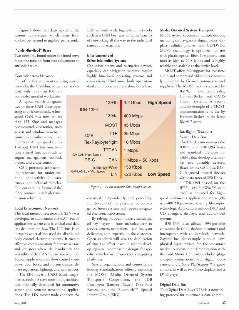
Figure 1 shows the relative speeds of thevarious bus systems, which range fromkilobits per second to gigabits per second.
“Under-the-Hood” BusesTwo networks found under the hood servefunctions ranging from seat adjustment toantilock brakes.
Controller Area NetworkOne of the first and most enduring controlnetworks, the CAN bus, is the most widelyused, with more than 100 mil-lion nodes installed worldwide.
A typical vehicle integratestwo or three CAN buses oper-ating at different speeds. A low-speed CAN bus runs at lessthan 125 Kbps and managesbody-control electronics, suchas seat and window movementcontrols and other simple userinterfaces. A high-speed (up to1 Mbps) CAN bus runs real-time critical functions such asengine management, antilockbrakes, and cruise control.
CAN protocols are becom-ing standard for under-the-hood connectivity in cars,trucks, and off-road vehicles.One outstanding feature of theCAN protocol is its high trans-mission reliability.
Local Interconnect NetworkThe local interconnect network (LIN) wasdeveloped to supplement the CAN bus inapplications where cost is critical and datatransfer rates are low. The LIN bus is aninexpensive serial bus used for distributedbody control electronic systems. It enableseffective communication for smart sensorsand actuators where the bandwidth andversatility of the CAN bus are not required.Typical applications are door control (win-dows, door locks, and mirrors), seats, cli-mate regulation, lighting, and rain sensors.
The LIN bus is a UART-based, single-master, multiple-slave networking architec-ture originally developed for automotivesensor and actuator networking applica-tions. The LIN master node connects the
Media Oriented System Transport MOST networks connect multiple devices,including car navigation, digital radios, dis-plays, cellular phones, and CD/DVDs.MOST technology is optimized for usewith plastic optical fiber. It supports datarates as high as 24.8 Mbps and is highlyreliable and scalable at the device level.
MOST offers full support for real-timeaudio and compressed video. It is vigorous-ly supported by German automakers andsuppliers. The MOST bus is endorsed by
BMW, DaimlerChrysler,Harman/Becker, and OASISSilicon Systems. A recentnotable example of a MOSTimplementation is its use byHarman/Becker in the latestBMW 7 series.
Intelligent Transport System Data BusThe IDB Forum manages theIDB-C and IDB-1394 busesand standard interfaces forOEMs that develop aftermar-ket and portable devices.Based on the CAN bus, IDB-C is geared toward deviceswith data rates of 250 Kbps.
IDB-1394 (based on theIEEE-1394 FireWire™ stan-dard) is designed for high-
speed multimedia applications. IDB-1394is a 400 Mbps network using fiber-optictechnology. Applications include DVD andCD changers, displays, and audio/videosystems.
IDB-1394 also allows 1394-portableconsumer electronic devices to connect andinteroperate with an in-vehicle network.Zayante Inc., for example, supplies 1394physical layer devices for the consumermarket. A recent joint demonstration withthe Ford Motor Company included plug-and-play connections of a digital videocamera and a Sony PlayStation™ 2 gameconsole, as well as two video displays and aDVD player.
Digital Data Bus The Digital Data Bus (D2B) is a network-ing protocol for multimedia data commu-
LIN network with higher-level networkssuch as a CAN bus, extending the benefitsof networking all the way to the individualsensors and actuators.
Entertainment and Driver Information Systems Car infotainment and telematics devices,especially car navigation systems, requirehighly functional operating systems andconnectivity. Until now, both open-stan-dard and proprietary standalone buses have
coexisted independently and peacefully.But because of the pressures of conver-gence, future systems will require integrat-ed electronic subsystems.
By relying on open industry standards,all key players – from manufacturers toservice centers to retailers – can focus ondelivering core expertise to the customer.Open standards will save the duplicationof time and effort it would take to devel-op separate, incompatible designs for spe-cific vehicles or proprietary computingplatforms.
Several organizations and consortia areleading standardization efforts, includingthe MOST (Media Oriented SystemTransport) Cooperation, the IDB(Intelligent Transport System Data Bus)Forum, and the Bluetooth™ SpecialInterest Group (SIG).
Spring 2004 Xcell Journal 63
1394b
1394a
MOST
TTP
FlexRay/byteflight
TTCAN
CANIDB-CGM-LAN High Speed
GM-LAN Low/Mid Speed
D2B
Safe-by-Wire
LIN
IDB-1394
3.2 Gbps
400 Mbps
45 Mbps
25 Mbps
10 Mbps
1 Mbps
1 Mbps – 50 Kbps
150 Kbps
<20 Kbps
High Speed
Low Speed
Figure 1 – In-car network data-transfer speeds

nication that integrates digital audio,video, and other high-data-rate synchro-nous or asynchronous signals. It can run asfast as 11.2 Mbps and be built aroundeither SmartWire™ unshielded twistedpair cable or a single optical fiber.
This communication network is beingdriven by C&C Electronics in the UK andhas industry acceptance from Jaguar andMercedes-Benz. The integrated multime-dia communication systems deployed inthe Jaguar X-Type, S-Type, and new XJSaloon, for example, use D2B.
The D2B optical multimedia system isdesigned to evolve in line with new tech-nologies while remaining backwards com-patible. D2B optical is based on an openarchitecture that simplifies expansion,because changes to the cable harness arenot required when adding a new device orfunction to the optical ring. The bus usesjust one polymer optical fiber to handlethe in-car multimedia data and controlinformation. This gives better reliability,fewer external components and connec-tors, and a significant reduction in overallsystem weight.
Bluetooth and ZigBeeBluetooth wireless technology is a low-cost,low-power, short-range radio protocol formobile devices and WAN/LAN accesspoints. Its specification describes howmobile phones, computers, and PDAs caneasily interconnect with each other, withhome and business phones, and with com-puters.
The Bluetooth SIG includes such mem-bers as AMIC, BMW, DaimlerChrysler,Ford, General Motors, Toyota, andVolkswagen. An example of Bluetoothdeployment in cars is Johnson Controls’BlueConnect™ technology, a hands-freesystem that allows drivers to keep theirhands on the wheel while staying connect-ed through a Bluetooth-enabled cellularphone.
There is, however, some concern aboutlong-term support of Bluetooth devices.The problem centers on how the electro-magnetically noisy in-car environment willaffect Bluetooth operation. The lifecycle ofcars and other vehicles is much longer than
that for consumer products or mobilephones, so silicon manufacturers mustaddress this mismatch between supportand service timescales. On the other hand,Chrysler showed Bluetooth connectivity inits vehicles at Convergence 2002.
Some feel Bluetooth technology may beoverkill in the car environment, however.So, an emerging standard for low data ratewireless data transfer and control hasentered the scene. The ZigBee™ wirelessnetworking solution is a low-data-rate (868MHz to 2.4 GHz), low-power, low-costsystem pioneered by Philips. The ZigBeerange is up to 75 meters and is equally athome in industrial control, home automa-tion, consumer, and possibly automotiveapplications.
Advanced Safety Systems Safety equipment has evolved from thephysical to the electronic domain, startingwith advancements in tire and brakingtechnology, through side impact protectionand airbags, and on to today’s driver-assis-tance systems.
The latest vehicles are electronics-richand sensor-based to continuously evaluatethe surroundings, display relevant informa-tion to the driver, and, in some instances,even take control of the vehicle.
Advanced safety systems include by-wire (for example, drive-by-wire and brake-by-wire), which will replace traditionalhydraulic and mechanical linkages withsafer, lighter electronic systems.
Other examples of advanced, real-timesafety systems include distance control,self-adjusting and sensing airbag systems,radar parking, reversing aids, and backguide monitors (cameras set in the car’sbumpers to aid parking).
FlexRayThe FlexRay™ network communicationsystem is aimed at the next generation of by-wire automotive applications. These applica-tions demand high-speed buses that aredeterministic, fault-tolerant, and capable ofsupporting distributed control systems.
BMW, DaimlerChrysler, PhilipsSemiconductors, Motorola, and the newestmember, Bosch, are developing the
FlexRay standard for next-generationapplications.
The FlexRay system is more than acommunications protocol. It also includesa specially designed high-speed transceiverand the definition of hardware and soft-ware interfaces between various compo-nents of a FlexRay “node.” The FlexRayprotocol defines the format and function ofthe communication process within a net-worked automotive system. It is designedto complement CAN, LIN, and MOSTnetworks.
As a scalable system, FlexRay technolo-gy supports both synchronous and asyn-chronous data transmission. Thesynchronous data transmission enablestime-triggered communication to meet therequirement of dependable systems.FlexRay’s synchronous data transmission isdeterministic, with guaranteed minimummessage latency and message jitter. It sup-ports redundancy and fault-tolerant dis-tributed clock synchronization to keep theschedule of all network nodes within atight, predefined, precision window.
The asynchronous transmission, based onthe fundamentals of the byteflight™ proto-col, allows each node to use the full band-width for event-driven communications.
Time-Triggered ProtocolDesigned for fault-tolerant, real-time dis-tributed systems, the time-triggered proto-col (TTP) ensures that there is no singlepoint of failure.
TTP is a mature, low-cost solution thatcan handle safety-critical applications.Second-generation silicon supporting com-munication speeds as high as 25 Mbps isavailable today. The TTA Group, the gov-erning body for TTP, includes Audi, SA,Renault, NEC, TTChip, Delphi, andVisteon among its members.
Time-Triggered CANThe time-triggered CAN (TTCAN) stan-dard is an extension of the CAN protocol.It adds a session layer on top of the existingdata link layer and physical layers to ensurethat all transmission deadlines are met,even at peak bus loads. The protocol imple-ments a hybrid, time-triggered, TDMA
64 Xcell Journal Spring 2004
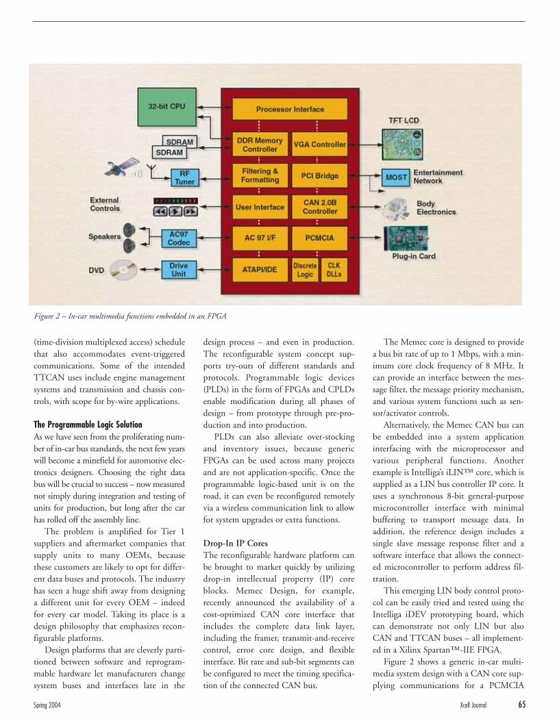
(time-division multiplexed access) schedulethat also accommodates event-triggeredcommunications. Some of the intendedTTCAN uses include engine managementsystems and transmission and chassis con-trols, with scope for by-wire applications.
The Programmable Logic SolutionAs we have seen from the proliferating num-ber of in-car bus standards, the next few yearswill become a minefield for automotive elec-tronics designers. Choosing the right databus will be crucial to success – now measurednot simply during integration and testing ofunits for production, but long after the carhas rolled off the assembly line.
The problem is amplified for Tier 1suppliers and aftermarket companies thatsupply units to many OEMs, becausethese customers are likely to opt for differ-ent data buses and protocols. The industryhas seen a huge shift away from designinga different unit for every OEM – indeedfor every car model. Taking its place is adesign philosophy that emphasizes recon-figurable platforms.
Design platforms that are cleverly parti-tioned between software and reprogram-mable hardware let manufacturers changesystem buses and interfaces late in the
design process – and even in production.The reconfigurable system concept sup-ports try-outs of different standards andprotocols. Programmable logic devices(PLDs) in the form of FPGAs and CPLDsenable modification during all phases ofdesign – from prototype through pre-pro-duction and into production.
PLDs can also alleviate over-stockingand inventory issues, because genericFPGAs can be used across many projectsand are not application-specific. Once theprogrammable logic-based unit is on theroad, it can even be reconfigured remotelyvia a wireless communication link to allowfor system upgrades or extra functions.
Drop-In IP CoresThe reconfigurable hardware platform canbe brought to market quickly by utilizingdrop-in intellectual property (IP) coreblocks. Memec Design, for example,recently announced the availability of acost-optimized CAN core interface thatincludes the complete data link layer,including the framer, transmit-and-receivecontrol, error core design, and flexibleinterface. Bit rate and sub-bit segments canbe configured to meet the timing specifica-tion of the connected CAN bus.
The Memec core is designed to providea bus bit rate of up to 1 Mbps, with a min-imum core clock frequency of 8 MHz. Itcan provide an interface between the mes-sage filter, the message priority mechanism,and various system functions such as sen-sor/activator controls.
Alternatively, the Memec CAN bus canbe embedded into a system applicationinterfacing with the microprocessor andvarious peripheral functions. Anotherexample is Intelliga’s iLIN™ core, which issupplied as a LIN bus controller IP core. Ituses a synchronous 8-bit general-purposemicrocontroller interface with minimalbuffering to transport message data. Inaddition, the reference design includes asingle slave message response filter and asoftware interface that allows the connect-ed microcontroller to perform address fil-tration.
This emerging LIN body control proto-col can be easily tried and tested using theIntelliga iDEV prototyping board, whichcan demonstrate not only LIN but alsoCAN and TTCAN buses – all implement-ed in a Xilinx Spartan™-IIE FPGA.
Figure 2 shows a generic in-car multi-media system design with a CAN core sup-plying communications for a PCMCIA
Spring 2004 Xcell Journal 65
Figure 2 – In-car multimedia functions embedded in an FPGA
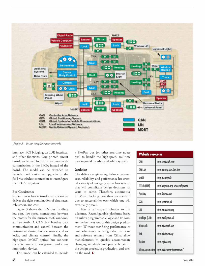
66 Xcell Journal Spring 2004
interface, PCI bridging, an IDE interface,and other functions. One printed circuitboard can be used for many customers withcustomization in the FPGA instead of theboard. The model can be extended toinclude modification or upgrades in thefield via wireless connection to reconfigurethe FPGA in-system.
Bus CoexistenceSeveral in-car bus networks can coexist todeliver the right combination of data rates,robustness, and cost.
Figure 3 shows the LIN bus handlinglow-cost, low-speed connections betweenthe motors for the mirrors, roof, windows,and so forth. A CAN bus handles datacommunication and control between theinstrument cluster, body controllers, doorlocks, and climate control. Finally, thehigh-speed MOST optical bus connectsthe entertainment, navigation, and com-munication devices.
This model can be extended to include
a FlexRay bus (or other real-time safetybus) to handle the high-speed, real-timedata required by advanced safety systems.
ConclusionThe delicate engineering balance betweencost, reliability, and performance has creat-ed a variety of emerging in-car bus systemsthat will complicate design decisions foryears to come. Therefore, automotiveOEMs are backing more than one standarddue to uncertainties over which one willeventually prevail.
There is an elegant solution to thisdilemma. Reconfigurable platforms basedon Xilinx programmable logic and IP coresare the best way out of this design predica-ment. Without sacrificing performance orcost advantages, reconfigurable hardwareand software systems from Xilinx allowmanufacturers to quickly accommodatechanging standards and protocols late inthe design process, in production, and evenon the road.
CAN www.can.bosch.com
GM LAN www.gmtcny.com/lan.htm
MOST www.mostnet.de
TTTech (TTP) www.ttagroup.org, www.ttchip.com
FlexRay www.flexray.com
D2B www.candc.co.uk
LIN www.lin-subbus.org
Intelliga (LIN) www.intelliga.co.uk
Bluetooth www.bluetooth.com
IDB www.idbforum.org
ZigBee www.zigbee.org
Xilinx Automotive www.xilinx.com/automotive/
Website resources
Figure 3 – In-car complementary networks
by Shehryar ShaheenResearch EngineerPEI Circuits and Systems Research Centre, University of [email protected]
For future automotive in-vehicle controlapplications, time-triggered networks willprovide the backbone for reliable fault-tolerant communications among controlnetwork nodes.
Although the automotive industry ispushing towards an agreement on a singlecontrol network standard, don’t assume thatone single standard will dominate. There willstill be a need to communicate across time-triggered networks with different specifica-tions and protocols – a type of gateway.
However, because some of these proto-cols are still under review, developing andtesting such a gateway design with fixedinterfaces cannot be future-proof. Thegateway core and its associated test bedmust be configurable and flexible toaccommodate future changes.
This is an ideal situation to exploit thepower and flexibility of programmablelogic. As researchers at PEI Circuits andSystems Research Centre (CSRC) at theUniversity of Limerick in Ireland, we havedeveloped a Xilinx FPGA-based config-urable frame generator/analyzer that canverify a gateway design for time-triggerednetworks, for real-time applications.
ArchitectureThe Frame Generator and Frame Analyzerare two distinct designs. Both are synthe-sized together and placed in a XilinxSpartan™-II XC2S100 FPGA on anInsight™ Electronics Spartan-II develop-ment board.
Frame GeneratorThe Frame Generator generates framesconforming to a proprietary byte-wideprotocol. The generator has the followingsub-modules:
• Transmit interfaces
• Frame generation logic
• Frame Generator state machine
• Frame sets.
Figure 1 shows the building blocks ofthe Frame Generator.
The Frame Generator’s four transmitinterfaces emulate the function of send-ing frames to the gateway from a time-triggered communication controller’shost controller. Each transmit interfacecomprises three control signals and an 8-bitport for byte-wide transmission of theframe. The three control signals are:
• Frame Start Out
• Port Ready
• Frame End Out.
Frame Start Out signals the transmis-sion of a new frame.
On each rising edge of Port Ready, themost significant byte (MSB) of the transmit-ting frame is sent to the 8-bit output port.
On the falling edge of Port Ready, thereceiving side reads in the MSB of theframe. The whole frame is broken downinto bytes like this and transmitted.
When frame transmission is complete,a Frame End Out pulse is sent to thereceiver to indicate an end-of-frametransmission so that the receiver thentakes the appropriate action, which isexplained later.
The Frame Generator state machine is a13-state finite state machine that controlsthe frame generation logic based on itspresent state.
The frame generation logic block isresponsible for generating the right timingand picking up the next frame to be trans-mitted from the set of frames as defined inthe four frame sets.
The frame sets are the offline-definedset of frames to be transmitted by theFrame Generator.
Frame AnalyzerThe Frame Analyzer receives frames con-forming to a byte-wide proprietary proto-col and stores them in message RAMs foranalysis.
Xilinx programmable logic is ideal for communicating across time-triggered networks.Xilinx programmable logic is ideal for communicating across time-triggered networks.
Verify Gateway Designs for Time-Triggered NetworksVerify Gateway Designs for Time-Triggered Networks
68 Xcell Journal Spring 2004
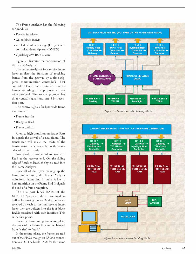
The Frame Analyzer has the followingsub-modules:
• Receive interfaces
• Xilinx block RAMs
• 4 x 1 dual inline package (DIP)-switchcontrolled demultiplexer (DMUX)
• QuickLogic™ RS 232 core.
Figure 2 illustrates the construction ofthe Frame Analyzer.
The Frame Analyzer’s four receive inter-faces emulate the function of receivingframes from the gateway by a time-trig-gered communication controller’s hostcontroller. Each receive interface receivesframes according to a proprietary byte-wide protocol. The receive protocol hasthree control signals and one 8-bit recep-tion port.
The control signals for byte-wide framereception are:
• Frame Start In
• Ready to Read
• Frame End In.
A low to high transition on Frame StartIn signals the arrival of a new frame. Thetransmitter will make the MSB of thetransmitting frame available on the risingedge of its Port Ready.
Port Ready is connected to Ready toRead at the receiver end. On the fallingedge of Ready to Read, the byte is read intothe Frame Analyzer.
Once all of the bytes making up theframe are received, the Frame Analyzerwaits for a Frame End In pulse. A low tohigh transition on the Frame End In signalsthe end of a frame reception.
The dual-port block RAMs of theXC2S100 Spartan-II device are used asbuffers for storing frames. As the frames arereceived on each of the four receive inter-faces, they are written into the four blockRAMs associated with each interface. Thisis the first phase.
Once the frame reception is complete,the mode of the Frame Analyzer is changedfrom “write” to “read.”
In the second phase, the frames are readout of the FPGA though an RS-232 connec-tion to a PC. The block RAMs for the Frame
Spring 2004 Xcell Journal 69
TX I/F 1FlexRay Host
ControllerGateway
TX I/F 2TTCAN HostControllerGateway
TX I/F 3byteflight Host
ControllerGateway
TX I/F 4TTP/C HostControllerGateway
FRAME SET 1FlexRay
FRAME SET 2TTCAN
FRAME SET 3byteflight
FRAME SET 4TTP/C
GATEWAY RECEIVER END (NOT PART OF THE FRAME GENERATOR)
FRAME GENERATORSTATE MACHINE
FRAME GENERATIONLOGIC
RX I/F 1Gateway
FlexRay HostController
RX I/F 2Gateway
TTCAN HostController
RX I/F 3Gateway
byteflight HostController
GATEWAY RECEIVER END (NOT PART OF THE FRAME GENERATOR)
RX I/F 4Gateway
TTP/C HostController
XILINX DUALPORT BLOCK
RAM
XILINX DUALPORT BLOCK
RAM
XILINX DUALPORT BLOCK
RAM
XILINX DUALPORT BLOCK
RAM
4 x 1DMUX
RS 232 CORE
DIP-Switches
Figure 1 – Frame Generator building blocks
Figure 2 – Frame Analyzer building blocks
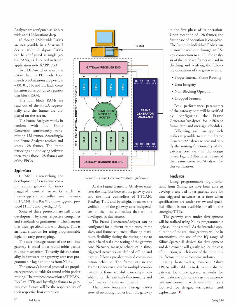
Analyzer are configured as 32 bitswide and 128 locations deep.
(Although 32-bit wide RAMsare not possible in a Spartan-IIdevice, 16-bit dual-port RAMscan be configured as single 32-bit RAMs, as described in Xilinxapplication note XAPP173.)
Two DIP-switches select theRAM that the PC reads. Fourswitch combinations are possible– 00, 01, 10, and 11. Each com-bination corresponds to a partic-ular block RAM.
The four block RAMs areread out of the FPGA sequen-tially and the frames are dis-played on the screen.
The Frame Analyzer works intandem with the FrameGenerator, continuously trans-mitting 128 frames. Accordingly,the Frame Analyzer receives andstores 128 frames. The frameretrieving and displaying softwarethen reads those 128 frames outof the FPGA.
ApplicationsPEI CSRC is researching thedevelopment of a real-time com-munication gateway for time-triggered control networks such astime-triggered controller area network(TTCAN), FlexRay™, time-triggered pro-tocol (TTP), and byteflight™.
Some of these protocols are still underdevelopment by their respective companiesand standards organizations – which meansthat their specifications will change. This isan ideal situation for using programmablelogic for early prototyping.
The core message router of the real-timegateway is based on a round-robin packetrouting mechanism. To verify this function-ality in hardware, the gateway core uses pro-grammable logic solutions from Xilinx.
The gateway’s internal protocol is a propri-etary protocol suitable for round-robin packetrouting. The protocol conversion of TTCAN,FlexRay, TTP, and byteflight frames to gate-way core format will be the responsibility oftheir respective host controllers.
As the Frame Generator/Analyzer emu-lates the interface between the gateway coreand the host controllers of TTCAN,FlexRay, TTP, and byteflight, it makes theverification of the gateway core independ-ent of the host controllers that will bedeveloped in due course.
The Frame Generator/Analyzer can beconfigured for different frame rates, framesizes, and frame sequences, allowing maxi-mum flexibility during the testing phase toenable hard real-time testing of the gatewaycore. Network message schedules in time-triggered networks are defined offline andhave to follow a pre-determined communi-cation schedule. The frame sets in theFrame Generator allow for multiple combi-nations of frame schedules, making it pos-sible to test the gateway’s functionality andperformance in a real-world sense.
The Frame Analyzer’s message RAMsstore all incoming frames from the gateway
in the first phase of its operation.Upon reception of 128 frames, thefirst phase of operation is complete.The frames in individual RAMs canbe now be read out through an RS-232 connection to a PC. The analy-sis of the retrieved frames will aid inchecking and verifying the follow-ing operations of the gateway core:
• Proper Internal Frame Routing
• Data Integrity
• Non-Blocking Operation
• Dropped Frames.
Peak performance parametersof the gateway core will be verifiedby configuring the FrameGenerator/Analyzer for differentframe rates and message schedules.
Following such an approachmakes it possible to use the FrameGenerator/Analyzer to test and ver-ify the routing functionality of thegateway core early in the designphase. Figure 3 illustrates the use ofthe Frame Generator/Analyzer forthis verification.
ConclusionUsing programmable logic solu-
tions from Xilinx, we have been able todevelop a test bed for a gateway core fortime-triggered networks at a time whenspecifications are under review and quali-fied silicon is not available for all of theemerging TTPs.
The gateway core under developmentwill be realized using Xilinx programmablelogic solutions as well. As the intended app-plication of the real-time gateway will be inautomotives, the use of the IQ range ofXilinx Spartan-II devices for developmentand deployment will greatly reduce the costof induction, which is one of the most crit-ical factors in the automotive industry.
Using best-in-class, low-cost XilinxFPGAs will enable us to deliver a real-timegateway for time-triggered networks forhard real-time applications in the automo-tive environment, with minimum costsincurred for design, verification, anddeployment.
FIF
OF
IFO
FIF
O
FIF
O
FIF
O
FIF
O
FIF
O
FIF
O
GATEWAY RECEIVER END
RE
AL
TIM
E G
AT
EW
AY
UN
DE
R D
EV
EL
OP
ME
NT
GATEWAY TRANSMITTER END
ROUND ROBINMESSAGEROUTER
FRAMEGENERATOR/
ANALYZER
TXI/F 1
TXI/F 2
TXI/F 3
TXI/F 4
RXI/F 1
RXI/F 2
RXI/F 3
RXI/F 4
RS-232
Figure 3 – Frame Generator/Analyzer application
70 Xcell Journal Spring 2004
System-on-FPGA design made easier
Altium Sales and Support:Free Call: 866 764 4377Fax: 858 521 4282 Email: [email protected]: www.altium.com/nexar
Quote Value Code 1354
Board-on-Chip development system from Altium
Multiple NanoBoards canbe chained together
On-board ADC/DAC
Plug-in daughter boardssupport different FPGA targets.A Spartan-IIE XC2S300Edaughter board is included
Connections for user-developed boards
Wide range of on-board communications connectors
Project management
Comprehensive libraries of royalty-free, pre-synthesizedIP components ready for schematic-based design (including popular CPU’s!)
Virtual instrumentsfor interactive
system debugging
FPGA Vendor-independentprocess flow
Nexar, Nexar 2004, Design Explorer and Altium and their respective logos are trademarksor registered trademarks of Altium Limited or its subsidiaries.
Integrated embedded software development
Nexar is the first comprehensive developmentsystem aimed at enabling all engineers to developcomplete processor based systems on an FPGAplatform using methodologies analogous to board-level system design - no HDL's required!
Nexar integrates hardware design tools, embeddedsoftware development tools, royalty-free IP-basedcomponents, virtual instrumentation and areconfigurable hardware platform to allowmainstream engineers to interactively design,debug and implement an entire embedded system inside an FPGA.
For more information on Nexar 2004, including a comprehensive multimedia demo, visit www.altium.com/nexar or contact yourlocal Altium sales and support center today!
only
$7,995Nexar includesNanoBoard hardware,software, royalty-freeIP cores and much more
by Frank TothMarketing Manager, EasyPath SeriesXilinx, [email protected]
A risk-free, flawless cost-reduction strategy isparamount to maintaining competitivenessin today’s cost-driven environment. TheVirtex-II EasyPath™ solution brings notonly lower costs but also a better product,with the industry’s leading test coverage.
Virtex-II EasyPath devices are identicalto the corresponding FPGA. The only dif-ference is in how they are tested – they aretested to your specific design only. Thusyou get the full-feature set rather than
“reduced ASIC” silicon, in a device that isfully pin-compatible and interchangeablewith an FPGA.
The Virtex-II EasyPath solution offers a25% to 80% cost reduction with produc-
tion quantity deliveries (thousands ofunits) in as little as 8-10 weeks (Figure 1).Device part numbers are listed in Table 1.
Identical SiliconConversion to a structured ASIC plat-form is not required. The design filesused to generate a custom test programcome directly from Xilinx IntegratedSoftware Environment (ISE) software.You don’t need to invest engineeringresources in annotating critical paths,generating test vectors, simulation, orverification.
The silicon is identical, so prototypeapproval is unnecessary. You can beginhigh-volume manufacturing quickly,with full production quantities. Thus,you can take all the time you need to testyour design and make improvementsusing the Virtex™-II family before com-mitting to full-volume production usingVirtex-II EasyPath devices. Only the test-ing is different; the silicon is identical.
Time is MoneyThe time gained by using the Virtex-IIEasyPath solution enables you to focusvaluable engineering time and resourceson product feature improvements andnew markets. As shown in Figure 2, a typ-ical structured ASIC conversion requiresmany steps that involve direct customerengineering involvement. With EasyPathdevices, no up-front ASIC softwareinvestment is required for conversion;turnaround is fast and easy because Xilinxcreates the custom test program for you.
One of the limitations of the struc-tured ASIC conversions offered by otherPLD companies is the limitation of areduced feature set when the design isconverted from the prototype or initialproduction to high volumes. Fewer pack-age types, I/Os, and RAM bits, as well asother features like DLLs, are available inthe ASIC conversion.
Test CoverageVirtex-II EasyPath devices rely on thesame patented technology as FPGAs fortesting functionality and speed, providingfull test coverage at percentages of 99%+,
The Virtex-II EasyPath solution offers a 99%+ fault test coverage.
The Easy Path to Cost ReductionsThe Easy Path to Cost Reductions
72 Xcell Journal Spring 2004
Virtex-II EasyPath Devices
Virtex-II XC2V3000, XC2V4000, Family XC2V6000, XC2V8000
Virtex-II Pro XC2VP30, XC2VP40, XC2VP50, Family XC2VP70,
XC2VP100, XC2VP125,
Table 1 – Virtex Family EasyPath Devices
which is not achievable in structuredASICs (shown in Figure 3).
ASICs can typically achieve coveragebetween 95% and 97% using hundreds oftest vectors and multiple scan chains. AsASICs grow in complexity, test issuesbecome more acute and achieving ade-quate test coverage is more difficult.Iterating multiple vectors multiple timesto guarantee coverage is costly and time-consuming. Plus, scan chains take siliconarea and can slow the device operation.
Using multiple bitstreams, the Virtex-IIEasyPath solution tests routing and logicresources with greater granularity and cov-erage, reaching deep inside the device totest resources that would be impossible totest using external test vectors.
This superior technology covers thecorner case and virtually eliminates testescapes, which may become more preva-lent as ASIC testing lags behind the com-plexity and density of newer, structuredASIC devices. This higher level of testingresults in a better quality product shippedto customers than is available with manyof today’s complex ASICs.
Testing FPGAsVirtex-II EasyPath device testing relies onthe programmability and read-back capa-bilities of the FPGA fabric to insert con-trol and observation points and to test theindividual logic and routing resources andother complex structures, such as blockRAMs and multipliers.
Used in FPGAs since their inception20 years ago, this approach is scalable,does not require additional silicon area forscan chains, and does not penalize operat-ing speed. Because Virtex-II EasyPathdevices are tested identically to FPGAs foryour specific designs, at-speed testing andlogic resource and routing resource cover-age are guaranteed.
A Better Test MethodologyBy carefully examining each of theresources used in your design, Xilinx pro-prietary test generation software deter-mines what should be tested and whatcombination of tests to use, as shown inFigure 4.
Spring 2004 Xcell Journal 73
6 - 8weeks
6 - 8weeks
Proto Eval ProductionPrototype Silicon
8 - 12weeks
10-12weeks
8-10 weeks
Custom Conversion30 - 40 weeks
EasyPathAdditional Time to Perfect Design& Test with NO RISK
Delay Conversion from FPGA
Design
Customer
Design File Netlist & Test Patterns
Constraints File Place and Route
Review Results & Signoff
Receive Prototypes
Approve Prototypes
Verify Timing
Fabricate Protos
Send Prototypes to Customer
Begin Volume Production
ASICVendor
Figure 1 – EasyPath versus ASIC leadtimes
Figure 2 – Typical structured ASIC conversion flows
EasyPath Testing Multiple TestStructures
ImplementedUsing Multiple
Bitstreams withAccess to ALL
Resources Usedin the Customer
Design Coverage Greater
Than 99.5%
Speed GradeGuaranteeand Logic
Testing of AllResources
Used
ASIC
Vectors andScan Chains
Typical Coverage95%-97%
Compare toExpected
Results
Figure 3 – Test strategy differences between EasyPath and typical ASICs

Each type of resource is measured dif-ferently. Routing resources are testedusing a source/load library that toggles theselected path (Figure 5). Combinations ofBuilt-In Self-Tests (BISTs) are used forcomplex logic structures. Speed gradesare guaranteed by using a patented rise-and-fall time measuring method that usesa loop and counter to provide highlyaccurate speed grade measurements.
Testing Routing Resources and BISTBecause the FPGA fabric is reprogramma-ble, the test program uses a single bit-stream to simultaneously test hundreds ofroutes. More complex circuits such asblock RAMs, multipliers, and three-statebuffers (TBUFs) require that BIST cir-cuits (Figure 6) are instantiated usingmultiple bitstreams. These BIST circuitsare based on industry-standard test struc-tures that are identical to those used totest ASICs or any other complex logic.
Speed GradingXilinx assigns Virtex-II EasyPath devicespeed grades the same as FPGAs, asshown in Figure 7. A patented speed bin-ning circuit tests the transition rise-and-fall times. A loop, similar in concept to aring oscillator, outputs to a counter.Various resources under test are placed inthe middle of this loop.
The number of pulses generated in aspecific time is directly related to thespeed grade of a Virtex-II EasyPathdevice. Unlike a simple ring oscillator,these circuits are capable of preciselymeasuring both rise and fall times toguarantee precise transition timesthrough the circuit under test.
ConclusionThe Virtex-II EasyPath solution is easy,fast, and cost-effective. You can nowspend more time in beta testing, ensuringthat your system is bug-free and has allthe required features, and swing directlyinto production without the need forprototype evaluations.
For more information about Virtex-IIEasyPath devices, visit www.xilinx.com/easypath.
Readback Detection Logic
Source GenerationLogic
Routing
GeneratesStimulus &ExpectedOutputs
ResourceUnder Test
(Block RAM,LUT RAM,DLL, etc.) Error
Detector
Speed Binning
External Start / Stop
Pulse
Counter Speed Test
Circuits
ResourcesUnderTest
Speed Test Circuits
Read OutResult
Tes
t C
ircu
it
Tes
t C
ircu
it
Tes
t C
ircu
it
Tes
t C
ircu
it
Figure 5 – Typical source/readback routing test logic
Figure 6 – Using Built-In Self Test for complex logic structures
Figure 7 – Speed binning circuit for FPGAs and Virtex Series EasyPath devices
Required Tests
CustomerDesign
File
VerifaultFault
Graded
TestLibraryTest
LibraryTestLibraryTest
LibraryTest
Library
TestLibraryTest
LibraryTestLibrary
TestGeneration
AnalyzeResources
Used InDesign
PullRequiredTests forCustomer
Design
GenerateTest
CoverageReport
AggregateTest
Coverage
StandardFPGATest
Library
Iterate
TestLibrary
Figure 4 – EasyPath test generation flows
74 Xcell Journal Spring 2004

by Douglas W. OlsenField Applications EngineerNuHorizons [email protected]
Your FPGA designs have become increas-ingly dense and complex. They are diffi-cult to debug because more and more ofthe relevant signals are buried deep withinthe logic fabric.
Moreover, your board and systemdesigns are also more complex and denselypackaged. Whether you’re troubleshootingin the lab or in the field, your access to sig-nals in the FPGA, on the board, or in thesystem is very restricted.
The Xilinx ChipScope™ Pro integrat-ed logic analyzer (ILA) has solved much ofthe problem at the FPGA level. You canembed its real-time data collection andreporting cores in your FPGA to providevisibility to internal FPGA signals andevents.
But if that’s all you’re usingChipScope for, you’re not getting themost out of this powerful tool. With alittle forethought during the design ofyour board and system, you can extractmore value from the ChipScope Pro ILAduring the entire product life cycle –
from initial debug of board-level signalsin the lab through system diagnosis andmaintenance in the field.
ChipScope Pro – A ReviewChipScope Pro is a “logic analyzer in anFPGA.” It provides real-time debug and ver-ification capabilities for your FPGA design.You can find all the details about theChipScope Pro ILA at www.xilinx.com/ise/verification/chipscope_pro.htm.
You interact with ChipScope Pro usinga familiar logic analyzer interface runningon your PC, which is connected to yourhardware under test via a JTAG interface.
Figure 1 illustrates a simple ChipScopePro design example.
ChipScope Pro BasicsThe ChipScope Pro program consists oftwo main core types in the FPGA, plussoftware running on your PC:
• ILA core – With the assistance of acore inserter program, you embed theChipScope Pro ILA core in yourFPGA design to collect data when trig-ger conditions are satisfied. You caneasily tailor the data size, target signals,and basic trigger architecture duringthe design phase. You can set flexibletrigger conditions at debug time.(Target signals can be changed usingthe Xilinx FPGA editor probe toolwithout requiring re-synthesis, re-place, or re-route of your design.) Asmany as 15 ILA cores can be embed-ded into one FPGA.
Use the Xilinx ChipScope Pro integrated logic analyzer for FPGAs as a board- and system-level diagnostic tool.
Think Outside the Chip
Spring 2004 Xcell Journal 75

• ICON core – You embed the inte-grated controller (ICON) core inyour FPGA design to control asmany as 15 ILA cores. This ICONcore governs each ILA core andcommunicates with the ChipScopesoftware running on your PC overthe JTAG interface and the XilinxParallel IV or MultiLINX™ cable.
• ChipScope PC software – You inter-act with the hardware under testusing ChipScope Pro software run-ning on your PC. You spend mini-mal time learning to use thissoftware, because it is so similar to ahardware logic analyzer. You can settrigger conditions and examine col-lected data using this software. Youcan also export collected data in avariety of file formats for analysis byother tools, or for incorporation intodocumentation.
• The board circuits outside your FPGAsare not going to be any easier to debugthan the internal FPGA designs.
• You do not have room to provide testpoint headers or connectors for all theboard signals that will require furtherexamination.
Should you route these board-level signalsto spare pins on the FPGA?
Yes – then you can connect the signalsto the ChipScope Pro ILA core provisionedfor internal FPGA signal debugging. If youanticipate that your primary FPGA func-tional designs will consume all of the I/Opins or internal logic resources, you mustconsider upgrading to the next package sizeor logic density. The following benefits willoutweigh the incremental cost:
• Decreased debug and development time
• Flexible, permanent debug signal routing
• Built-in board-level instrumentation,which leads to
• Reduced demand for scarce lab instru-ments during peak debug activity.
Figure 2 illustrates ChipScope Pro uti-lized as a board-level test tool. Notice itssimilarity to Figure 1, where ChipScopePro is used as an FPGA-only tool.
ChipScope Pro at the System LevelYou, as the system engineer for your com-pany’s sophisticated new product, mustachieve multiple objectives, such as:
• Ensuring that system development andintegration flow as smoothly as possible,thus minimizing your time to market
• Providing an easily maintainable prod-uct to minimize service costs for theproduct’s overall life cycle.
Incorporate InstrumentationWhat if every system that you integrateand ship could include the capability ofbuilt-in instrumentation? By utilizing thesame Xilinx ChipScope Pro program thatyour board-level engineers use to debugFPGA designs, you can configure yourproducts for system integration and fieldmaintenance.
ChipScope Pro at the Board LevelConsider this: As the lead engineer for anew board design, your job is to composethe block diagram. Your knowledge andduties include:
• Partitioning a multitude of complexfunctions into various circuits on theboard
• Allocating many of the circuits toreside in one or more Xilinx FPGAs onthe board
• Recognizing the need to provide ameans of debugging the many internalFPGA designs
• Realizing that the ChipScope Pro toolcan economically provide visibility toall FPGA signals
• Knowing that the ChipScope Pro toolrequires no more design resources thanthe JTAG interface already providedfor FPGA configuration
• Using some incremental FPGAresources (mostly block RAM) forChipScope Pro data collection.
Think Outside the ChipWhile considering FPGA debug options,you realize that:
• Your board design is very complex andspatially dense.
76 Xcell Journal Spring 2004
Host Computer withChipScope Pro Software
JTAG Cable
FPGA
ILAProbes
FPGADesign
Other Circuitson Board
Under Development
Board Under Development
ChipScopePro
JTAG Port
ICON Core
ILA Core
Figure 1 – A simple ChipScope Pro design example
This will cost you nothing more than afew judiciously chosen system-level signalsrouted to a Xilinx FPGA; some incremen-tal FPGA resources (mostly block RAM);an accessible JTAG connector; and someup-front system design time and planning.These costs will be overshadowed by thefollowing benefits:
• Decreased system integration time
• Built-in system-level instrumentation
• Reduced demand for scarce lab instru-ments during peak integration activity
• Flexible, permanent maintenance anddiagnostic signal routing.
During system integration, engineerscan connect a PC running ChipScope Prosoftware to the system JTAG port, andmonitor system-level signals.
You don’t have to use a dedicated hard-ware logic analyzer. Production test engi-neers can readily adopt this capability anduse system signals during acceptance testing.
System installers can utilize ChipScopePro’s capability at customer sites to debugproblems, or to ensure proper operation.Going forward, maintenance personnel cantroubleshoot system problems using nomore than a laptop PC running ChipScopePro software.
Figure 3 illustrates ChipScope Pro usedas a system-level test tool, which builds onthe board-level test tool of Figure 2.
Design ExampleI developed the concept of extendingChipScope Pro’s utility when I undertook adesign in my poorly equipped basement labusing a Xilinx CoolRunner-II CPLD evalua-tion board from NuHorizons Electronics.Although the design was simple, I needed toexamine four or five dynamic signals simul-taneously on the CPLD board, equippedwith only a digital volt-amp-ohmmeter, andno oscilloscope or logic analyzer.
Necessity Is the Mother of InventionFortunately, I also had a Xilinx evaluationboard containing a Virtex XCV400 FPGA.Although this was a relatively small FPGA,it was more than sufficient to house theChipScope Pro ICON core and a simpleeight-channel ILA core.
In this particular case, my implementa-tion of ChipScope Pro was the ultimate insimplicity: no internal FPGA signals wereconnected to the ILA core. Rather, theeight ILA core data/trigger signals wererouted directly to I/O pins, which termi-nated at a header on the FPGA evaluationboard. I connected wires to those pins,which I then used as probes on my CPLDboard.
I was able to debug my CPLD designafter just a few iterations of coding, down-loading, and collection of data via theChipScope Pro software.
For the modest cost of the ChipScopePro utility, plus a small FPGA board andJTAG cable, I discovered that you canreplicate the functionality of a logic ana-lyzer that would otherwise cost thousandsof dollars.
Some Suggestions To utilize the ChipScope Pro software as
a board-level tool, follow these suggestions:
• Provide access to the FPGA’s JTAG port.
• Anticipate which board-level signalsyou might want to examine duringdebug.
• Route these signals to the FPGA soyou will have board-level access.
• Dedicate some extra I/O pins on yourFPGA to accommodate board-level signals requiring examination.
• Anticipate some extra internal FPGAresources (mostly block RAM) forChipScope Pro’s collection of board-level signal samples.
• After analyzing the dynamic propertiesof the signals of interest, make sureyou have an appropriate clock signal so the ChipScope Pro tool can processyour board-level signals.
To utilize the ChipScope Pro program asa system-level tool, follow these suggestions:
• Provide access to an appropriate sys-tem-level JTAG port.
• Anticipate which system-level signalsyou will want to examine during sys-tem integration and life cycle support.
Spring 2004 Xcell Journal 77
Host Computer withChipScope Pro Software
JTAG Cable
FPGA
Board Traces
ILAProbes
FPGADesign
Other Circuitson Board
Under Development
Board Under Development
ChipScopePro
JTAG Port
ICON Core
ILA Core FP
GA
I/O
Figure 2 – ChipScope Pro board-level tool design

• Route these signals on boards andbackplanes or cables to the FPGAchosen to host the system-level JTAGinterface.
• Dedicate adequate FPGA resources(I/O pins and logic) to accommodatethe system-level signals of interest.
• After analyzing the dynamic propertiesof the signals of interest, make sureyou have an appropriate clock signal soChipScope Pro can process your sys-tem-level signals.
• In the unlikely case that your systemcontains no other FPGAs, it would be
worth the cost of a small FPGA inwhich to embed the ChipScope Procore as an economical integrated system-level logic analyzer.
ConclusionYou can add value to your FPGA-basedproduct by expanding the use of theXilinx ChipScope Pro integrated logicanalyzer “outside the chip” of theFPGA design.
You have already invested inChipScope Pro for debugging the inter-nal FPGA design. You can decreaseyour board- and system-level debugtime for zero additional tool costs, andminimal up-front design time andresources. Additionally, you canenhance your product with permanentsystem diagnostic and maintenancecapabilities for its entire life cycle.
78 Xcell Journal Spring 2004
Host Computer withChipScope Pro Software
JTAG Cable
FPGA
Board Traces
ILAProbes
FPGADesign
System-Level Signals
Other Circuitson Board
Under Development
Board #1 Under Development
Board #2 Under Development
System Interconnect
ChipScopePro
JTAG Port
ICON Core
ILA Core FP
GA
I/O
Board I/O
Figure 3 – ChipScope Pro system-level tool design
Two Thumbs Up ChipScope Pro engineers
endorse design methodology.
“I think it’s a great idea – especially for those
who don’t need or can’t afford some of the
higher-end features provided by other debug
solutions, like timing mode triggering or deep
trace memory,” said Brad Fross, design
engineering manager for Xilinx Advanced
Products Division Systems Engineering.
“This is a new, cost-effective solution that
expands the practical application of ChipScope
Pro tools beyond the chip,” agreed Brent
Przybus, product marketing manager for the
Advanced Products Division.
“The only tricky part of Doug Olsen’s solution
will be clocking,” Przybus noted, “but I believe
Doug covers this adequately in his article, given
that each system will be slightly different.”
Fross elaborated on this caution: “On-chip
debug is pretty straightforward, because the
ILA core is taken into consideration during
timing-driven design implementation. However,
it definitely gets trickier to do when off-chip
signal delay and external clock synchronization
need to be taken into account.
“In any case, I do think this is a great article to
get people thinking about how to debug their
systems way before they actually find them-
selves needing to do so,” Fross concluded.

We live in a networked world, where yourdigital alter ego is almost as important asyour physical self. Your digital identity,usually comprising a series of electronicrecords, determines whether you can buy acar, get a loan, or open a bank account.
Yet the link between your physical anddigital selves is surprisingly weak and inse-cure. Identity theft and credit card fraud areubiquitous. Indeed, we have grown used toverification via trivial secrets such as yourmother’s maiden name. But trivial secretsrequire only trivial guesswork to be revealed.
A more unique identifier is possiblethrough the use of biometrics – uniquephysical features such as DNA, fingerprintdata, iris composition, or facial structure.These are distinctive keys that cannot beforgotten or lost and, with appropriate pre-cautions, are difficult to counterfeit.
The ability to authenticate yourselfthrough biometrics opens up enormouspossibilities in embedded and portable con-texts, from key chains to credit cards. Theextraction of unique features from biomet-
rics data, however, is a complex signal-processing problem that requires a signifi-cant amount of computational power.
One solution may be ThumbPod, anFPGA-based prototype (Figure 1) of anembedded fingerprint authentication systemcreated by seven graduate students and theiradvisor at the University of California, LosAngeles. ThumbPod (www.thumbpod.com)includes a fingerprint sensor, an embeddedprocessor with memory, dedicated process-ing units, and a serial commu-nication channel.
According to design speci-fications, the unit must deliv-er 1,000 fingerprint-matchingoperations, each comprisingan estimated 250 millionoperations, on a single bat-tery. Given the complexity ofthe embedded fingerprintrecognition, we use an FPGAprototype to quickly and easi-ly evaluate critical designdecisions.
In its final form, ThumbPod could beintegrated into an embedded device notlarger than a key chain fob (Figure 2).
The Security PyramidA security application is only as safe as itsweakest link. ThumbPod is no exception.Security must be considered at all designstages and design abstraction levels.
We employ a “security pyramid” to iden-tify four different design abstraction levels inThumbPod that affect safe operation:
• The protocol level expresses howThumbPod connects to an applica-tion; that is, how it will be used toopen an electronic lock. A criticalaspect in the design of this protocol isthat fingerprints are sensitive personaldata, and thus should be processedwith adequate privacy. Unlike manyother biometrics systems, ourThumbPod processes all fingerprintdata locally. Even the fingerprint sen-sor is local and private for each per-son, and cannot be shared.
• The algorithm level collects the func-tions and algorithms used as buildingblocks in the ThumbPod securityprotocol. This includes fingerprintsignal processing to extract a uniquetemplate from a fingerprint, consist-ing of minutiae. It also includesencryption using the AdvancedEncryption Standard.
• The architecture level defines the targetonto which the algorithms are mapped.We combine a soft-core, 32-bit,
UCLA students develop a prototype fingerprint authentication device incorporating a Virtex-II FPGA.
UCLA students develop a prototype fingerprint authentication device incorporating a Virtex-II FPGA.
ThumbPod Puts Security Under Your Thumb ThumbPod Puts Security Under Your Thumb
Spring 2004 Xcell Journal 79
Figure 1 – ThumbPod prototype
by Patrick SchaumontPh.D. Candidate, Embedded Security, EE Department, [email protected]
Ingrid VerbauwhedeAssociate Professor, Embedded Security, EE Department, [email protected]
LEON2 SPARC processor with hard-ware acceleration co-processors for sig-nal processing and encryption. Thisenables the general-purpose processingrequired to integrate the application, aswell as the intensive data processingnecessary for fingerprint matching, tooperate in an embedded context.
• The circuit level deservesspecial attention, becauseit is a potential backdoorfor security hackers. Withcareful technology map-ping, however, we can makeThumbPod resistant to power andtiming attacks.
System ArchitectureThumbPod’s high design complexitymakes it impossible to capture everythingin one design layer. Instead, we approachedthe design as a stack of three machines,each one bootstrapping the next (Figure 3).
At the bottom layer is a Virtex™-IIXC2V1000 FPGA. It has a rich set of on-chip resources providing interconnection,on-chip storage, and logic. The prototypeis implemented on an Insight Electronicsdevelopment board that also offers 32 MBof DDR RAM for background storage.
On the FPGA, we configured a soft-coreprocessor with two hardware co-processors.The processor is a SPARC-compliant, 32-bitLEON2 from Gaisler Research(www.gaisler.com). An encryption processorand a discrete Fourier transform (DFT) sig-nal processor provide acceleration for thecritical processing parts of the design.
On top of the LEON2, we ran an embed-ded Java kilobyte virtual machine (KVM).The KVM offers our application developersa smooth transition from application devel-opment to the embedded design.
In addition, all platform-specific fea-tures, such as the fingerprint sensor orhardware co-processors, can be integratedinto a single programming environmentusing native interfaces. (The ThumbPodwebsite [www.thumbpod.com] collects addi-tional publications that elaborate on theperformance and test issues occurringthrough the use of these interfaces.)
ThumbPod is devoted to the extraction ofminutiae. We started with a reference soft-ware implementation from NIST(National Institute of Standards andTechnology). Subsequently, we adaptedthis for embedded processing. Thisincludes conversion from floating-point tofixed-point operation, reduction of thememory requirements, and the introduc-tion of a DFT hardware accelerator.
The operation of ThumbPod must be asreliable as possible. We verified the qualityof the fingerprint detection and matchingalgorithms by evaluating their probabilityfor error.
Two types of mistakes could occur:
1. ThumbPod could reject a fingerprintcorresponding to the true template(known as a “false reject,” or FFR).
2. ThumbPod, however, might alsoaccept an incorrect fingerprint(known as a “false accept,” or FAR).The latter case is, of course, the worsecase of the two.
Our algorithms gave an FRR of 0.5%and an FAR of 0.01%. These figures arecomparable to commercial-grade systemsthat normally run on workstations and require power-hungry processingenvironments.
Design Flow Using GEZELThumbPod is programmed ina combination of Java, C, andVHDL. Our design flow
ensures that the appropriate verificationsare complete before the design is broughtto the FPGA (Figure 6).
A key element of the design flow is the GEZEL design environment(www.ee.ucla.edu/~schaum/gezel) that sup-ports the development and prototyping ofour coprocessors. GEZEL provides instruc-tion-set co-simulation as well as VHDLcode generation. In combination with theFPGA, GEZEL technology provides ahigh-level exploration environment forcomplex system-on-chip architectures suchas ThumbPod.
Our design flow consists of three dis-tinct steps, each with an increasing amountof implementation detail.
Fingerprint MatchingWhen you put your finger on the finger-print sensor, it takes an image. From thisraw image, we extract a set of unique fea-tures, known as minutiae (Figure 4)through a sequence of image processing
steps (Figure 5). We obtain the minutiaebeginning with the raw grayscale image ofthe fingerprint and proceeding through asequence of image processing steps.
The set of minutiae forms a secret keythat is stored securely in ThumbPod as atemplate. It cannot be changed afterwards,nor can it ever be extracted. During actualuse, this template is matched to a newlycaptured fingerprint. This matchingprocess returns a score between 0 and 100,which is used to decide acceptance or rejec-tion of the ThumbPod user.
The bulk of the processing power in
80 Xcell Journal Spring 2004
ApplicationJAM
KVMNative
SecurityNative
Biometrics
Embedded Software Architecture
Hardware Architecture Configuration
Insight XC2V1000
LEON2SPARC
AESCrypto
DFTProcessor
32 MBSDRAM
XilinxVirtex-II
FingerprintSensor
Figure 2 – ThumbPod conceptual drawing
Figure 3 – ThumbPod system architecture

We developed the top-level security pro-tocol in Java. Using simulation on a work-station, we verified how the protocolbehaves under security exceptions such asreplay attacks or the use of false finger-prints. We also checked functional aspects,such as protocol communication timeoutsand transmission errors.
Next, we integrated the C code of the fin-gerprint detection and matching algorithmsinto the Java code. We used the nativemethod capabilities of Java. We developedthis C code as a separate software IP core. Wetested it extensively in overnight simulationsbefore integrating it. These overnight simula-tions were required to check the quality lossresulting from fixed-point refinement of thefingerprint algorithms.
We then ported the ensemble of Javaand C code to the embedded Java KVM.The KVM is executed on top of theLEON2 instruction-set simulator. Usingthis setup, we could simulate how theThumbPod application downloaded as anapplet to the prototype platform – and howthe protocol worked in combination with aserver application.
Once the simulationran on top of an instruc-tion-set simulator, webegan including modelsof the actual targetarchitecture, particularlythe hardware coproces-sors. The GEZEL envi-ronment capturedcycle-true descriptionsof the coprocessor archi-tectures using a special-ized programminglanguage. The modelsof the AES and DFTcoprocessors were co-simulated with theLEON2 instruction setsimulator.
Through VHDLcode generation, weobtained seamlessconnection to theFPGA platform. Wefollowed a standardFPGA design flow
based on Synplicity® synthesis softwareand Xilinx ISE software.
ConclusionWe demonstrated our ThumbPod pro-totype in a University Booth at the2003 Design Automation Conferencein Los Angeles. ThumbPod is a first-of-its-kind device that demonstratesportable and embedded biometrics pro-cessing as an FPGA prototype.
Embedded biometrics is a field infull expansion. As information technol-ogy further penetrates our everyday life,the need for privacy and authenticationwill continue to grow. Passwords andsecret questions will become impracticalcompared to the convenience of bio-metrics.
But the complex signal processingthat comes with embedded biometricswill require innovative architectures.These architectures combine sequentialprocessing with the power efficiency ofparallel hardware.
Using platform FPGAs and reconfig-urable technology, we can build and testembedded biometrics solutions likeThumbPod in a way that outperforms thedesign time and cost of other technologies,such as COTS solutions or ASICs.
Direction map
Binarization
Detection
Minutiae DetectionModule
Reference Point
Align OtherMinutiae
Score Match
MatchingModule
bytecodeKVM
Platform
Emb . SW
FPGAPlatform
object code
bitstream
Java
KVM KNI
Leon IP core Coprocessors
GEZELInstruction Set Simulator
VHDL
C GEZEL
Figure 4a – Raw fingerprint data from sensor
Figure 4b – Minutiae locationwith superimposed cleaned-up
fingerprint image
Figure 5 – Fingerprint minutiae detection and matching
Figure 6 – ThumbPod design flow
Constructing the ThumbPod system required a significant amount of dedication and time. ThumbPod is the result of the efforts of seven graduate students at the University of California, Los
Angeles, over a period of eight months. They are Yi Fan, Alireza Hodjat, David Hwang, Bo-Cheng Lai,Kazua Sakiyama, Patrick Schaumont, and Shenglin Yang.
The project enjoyed the support of many people, including the students’ advisor, Professor IngridVerbauwhede, Jiri Gaisler from Gaisler Research, and Daryl Specter from Insight Electronics.
We would also like to thank the Xilinx University Program team, including Jeff Weintraub and Anna Acevedo, for their support and generous donation.
Spring 2004 Xcell Journal 81
by Russ LindgrenDesign [email protected]
Whether underwater, in the air, or belowground, radio tracking tags bring sensors towhere they’re most useful, transmitting localdata back for logging and analysis. To ensuredata accuracy in challenging, noisy environ-ments, the tags transmit error-corrected digital IDs to represent varied sensor data.
Biotags developed the Micro-ID familyof radio tracking tags around the special fea-tures of the Xilinx CoolRunner™-II CPLD,which provides the noteworthy combinationof microampere quiescent current draw,nonvolatile ID storage, JTAG configuration,micro-ball grid array (BGA) packaging, andhigh-speed output drive.
Miniature radio tracking tags built on CoolRunner-II features can transmit environmental data hundreds of feet.
Develop Low-Power Telemetry SystemsDevelop Low-Power Telemetry Systems
82 Xcell Journal Spring 2004
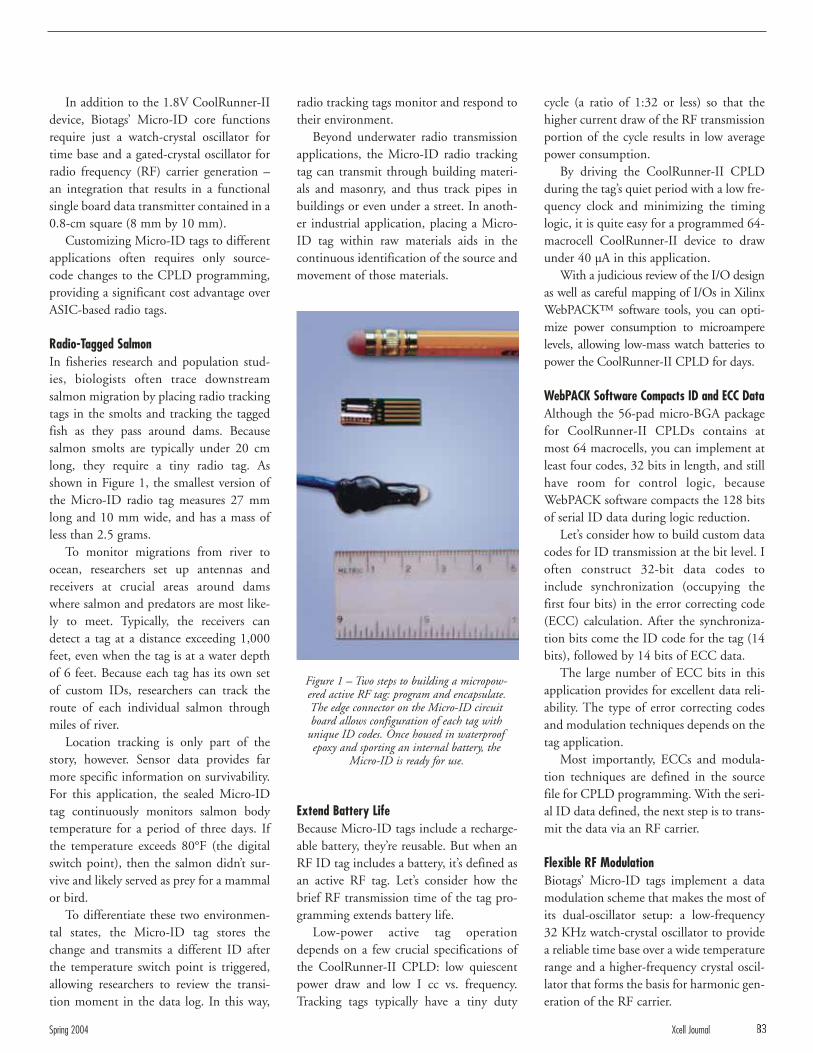
In addition to the 1.8V CoolRunner-IIdevice, Biotags’ Micro-ID core functionsrequire just a watch-crystal oscillator fortime base and a gated-crystal oscillator forradio frequency (RF) carrier generation –an integration that results in a functionalsingle board data transmitter contained in a0.8-cm square (8 mm by 10 mm).
Customizing Micro-ID tags to differentapplications often requires only source-code changes to the CPLD programming,providing a significant cost advantage overASIC-based radio tags.
Radio-Tagged SalmonIn fisheries research and population stud-ies, biologists often trace downstreamsalmon migration by placing radio trackingtags in the smolts and tracking the taggedfish as they pass around dams. Becausesalmon smolts are typically under 20 cmlong, they require a tiny radio tag. Asshown in Figure 1, the smallest version ofthe Micro-ID radio tag measures 27 mmlong and 10 mm wide, and has a mass ofless than 2.5 grams.
To monitor migrations from river toocean, researchers set up antennas andreceivers at crucial areas around damswhere salmon and predators are most like-ly to meet. Typically, the receivers candetect a tag at a distance exceeding 1,000feet, even when the tag is at a water depthof 6 feet. Because each tag has its own setof custom IDs, researchers can track theroute of each individual salmon throughmiles of river.
Location tracking is only part of thestory, however. Sensor data provides farmore specific information on survivability.For this application, the sealed Micro-IDtag continuously monitors salmon bodytemperature for a period of three days. Ifthe temperature exceeds 80°F (the digitalswitch point), then the salmon didn’t sur-vive and likely served as prey for a mammalor bird.
To differentiate these two environmen-tal states, the Micro-ID tag stores thechange and transmits a different ID afterthe temperature switch point is triggered,allowing researchers to review the transi-tion moment in the data log. In this way,
cycle (a ratio of 1:32 or less) so that thehigher current draw of the RF transmissionportion of the cycle results in low averagepower consumption.
By driving the CoolRunner-II CPLDduring the tag’s quiet period with a low fre-quency clock and minimizing the timinglogic, it is quite easy for a programmed 64-macrocell CoolRunner-II device to drawunder 40 µA in this application.
With a judicious review of the I/O designas well as careful mapping of I/Os in XilinxWebPACK™ software tools, you can opti-mize power consumption to microamperelevels, allowing low-mass watch batteries topower the CoolRunner-II CPLD for days.
WebPACK Software Compacts ID and ECC DataAlthough the 56-pad micro-BGA packagefor CoolRunner-II CPLDs contains atmost 64 macrocells, you can implement atleast four codes, 32 bits in length, and stillhave room for control logic, becauseWebPACK software compacts the 128 bitsof serial ID data during logic reduction.
Let’s consider how to build custom datacodes for ID transmission at the bit level. Ioften construct 32-bit data codes toinclude synchronization (occupying thefirst four bits) in the error correcting code(ECC) calculation. After the synchroniza-tion bits come the ID code for the tag (14bits), followed by 14 bits of ECC data.
The large number of ECC bits in thisapplication provides for excellent data reli-ability. The type of error correcting codesand modulation techniques depends on thetag application.
Most importantly, ECCs and modula-tion techniques are defined in the sourcefile for CPLD programming. With the seri-al ID data defined, the next step is to trans-mit the data via an RF carrier.
Flexible RF ModulationBiotags’ Micro-ID tags implement a datamodulation scheme that makes the most ofits dual-oscillator setup: a low-frequency32 KHz watch-crystal oscillator to providea reliable time base over a wide temperaturerange and a higher-frequency crystal oscil-lator that forms the basis for harmonic gen-eration of the RF carrier.
radio tracking tags monitor and respond totheir environment.
Beyond underwater radio transmissionapplications, the Micro-ID radio trackingtag can transmit through building materi-als and masonry, and thus track pipes inbuildings or even under a street. In anoth-er industrial application, placing a Micro-ID tag within raw materials aids in thecontinuous identification of the source andmovement of those materials.
Extend Battery LifeBecause Micro-ID tags include a recharge-able battery, they’re reusable. But when anRF ID tag includes a battery, it’s defined asan active RF tag. Let’s consider how thebrief RF transmission time of the tag pro-gramming extends battery life.
Low-power active tag operationdepends on a few crucial specifications ofthe CoolRunner-II CPLD: low quiescentpower draw and low I cc vs. frequency.Tracking tags typically have a tiny duty
Spring 2004 Xcell Journal 83
Figure 1 – Two steps to building a micropow-ered active RF tag: program and encapsulate.The edge connector on the Micro-ID circuitboard allows configuration of each tag with
unique ID codes. Once housed in waterproofepoxy and sporting an internal battery, the
Micro-ID is ready for use.
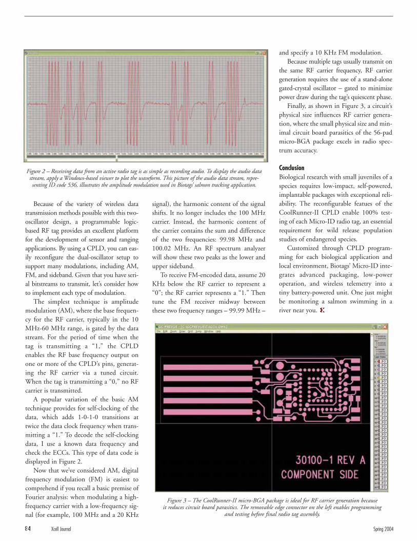
Because of the variety of wireless datatransmission methods possible with this two-oscillator design, a programmable logic-based RF tag provides an excellent platformfor the development of sensor and rangingapplications. By using a CPLD, you can eas-ily reconfigure the dual-oscillator setup tosupport many modulations, including AM,FM, and sideband. Given that you have seri-al bitstreams to transmit, let’s consider howto implement each type of modulation.
The simplest technique is amplitudemodulation (AM), where the base frequen-cy for the RF carrier, typically in the 10MHz-60 MHz range, is gated by the datastream. For the period of time when thetag is transmitting a “1,” the CPLDenables the RF base frequency output onone or more of the CPLD’s pins, generat-ing the RF carrier via a tuned circuit.When the tag is transmitting a “0,” no RFcarrier is transmitted.
A popular variation of the basic AMtechnique provides for self-clocking of thedata, which adds 1-0-1-0 transitions attwice the data clock frequency when trans-mitting a “1.” To decode the self-clockingdata, I use a known data frequency andcheck the ECCs. This type of data code isdisplayed in Figure 2.
Now that we’ve considered AM, digitalfrequency modulation (FM) is easiest tocomprehend if you recall a basic premise ofFourier analysis: when modulating a high-frequency carrier with a low-frequency sig-nal (for example, 100 MHz and a 20 KHz
signal), the harmonic content of the signalshifts. It no longer includes the 100 MHzcarrier. Instead, the harmonic content ofthe carrier contains the sum and differenceof the two frequencies: 99.98 MHz and100.02 MHz. An RF spectrum analyzerwill show these two peaks as the lower andupper sideband.
To receive FM-encoded data, assume 20KHz below the RF carrier to represent a“0”; the RF carrier represents a “1.” Thentune the FM receiver midway betweenthese two frequency ranges – 99.99 MHz –
and specify a 10 KHz FM modulation.Because multiple tags usually transmit on
the same RF carrier frequency, RF carriergeneration requires the use of a stand-alonegated-crystal oscillator – gated to minimizepower draw during the tag’s quiescent phase.
Finally, as shown in Figure 3, a circuit’sphysical size influences RF carrier genera-tion, where the small physical size and min-imal circuit board parasitics of the 56-padmicro-BGA package excels in radio spec-trum accuracy.
ConclusionBiological research with small juveniles of aspecies requires low-impact, self-powered,implantable packages with exceptional reli-ability. The reconfigurable featues of theCoolRunner-II CPLD enable 100% test-ing of each Micro-ID radio tag, an essentialrequirement for wild release populationstudies of endangered species.
Customized through CPLD program-ming for each biological application andlocal environment, Biotags’ Micro-ID inte-grates advanced packaging, low-poweroperation, and wireless telemetry into atiny battery-powered unit. One just mightbe monitoring a salmon swimming in ariver near you.
Figure 2 – Receiving data from an active radio tag is as simple as recording audio. To display the audio datastream, apply a Windows-based viewer to plot the waveform. This picture of the audio data stream, repre-senting ID code 536, illustrates the amplitude modulation used in Biotags’ salmon tracking application.
Figure 3 – The CoolRunner-II micro-BGA package is ideal for RF carrier generation because it reduces circuit board parasitics. The removable edge connector on the left enables programming
and testing before final radio tag assembly.
84 Xcell Journal Spring 2004
by Barrie MullinsIntegrated Solutions Manager, Xilinx Design ServicesXilinx, [email protected]
Optos PLC, a revolutionary eye care tech-nology company, selected Xilinx Virtex-IIPro™ FPGAs to be at the heart of theirwide-field visual imaging system. To lowerthe risk, reduce the learning curve, andmeet their time-to-market requirements forthis new technology, Optos engaged XilinxDesign Services (XDS) to help them plan,design, implement, and deliver their com-plex solution.
The Optos Panoramic System compris-es two IBM™ PowerPC™ 405 micro-processors and multiple proprietaryinterfaces, as well as industry standardinterfaces. The design utilizes the latesttechnology, tools, and software provided byXilinx and gave XDS the opportunity toapply its system, hardware, and embeddedsoftware knowledge, along with its projectmanagement expertise, to meet the time-to-market requirements.
The Design ChallengeFor Optos, the challenge was to find a tech-nology that provided them with the techni-
cal features to take their system from con-cept to reality. The system is used by aqualified operator to take a scan of thepatient’s eye while they look at a target pre-sented on an LCD panel. This image cap-ture uses Optos’ patented technology inwide-field visual imaging and transfers thedata to a microprocessor. The processor isused for storage of patient data and pro-cessing by the operator.
The challenge for XDS was to design,develop, test, simulate, integrate, andbring up the hardware and software on asingle platform to enable a complete con-nectivity solution addressing all layers ofthe Optos application. The solution alsohad to be scaleable for future features andupgrades. XDS was also required to meetbudget constraints.
The TeamsThe Xilinx Design Services team workedwith the Optos engineering team to set thesystem requirements and to agree on a sched-ule and deliverables for the project. Over theperiod of the project, the XDS project man-ager worked with the Optos project manage-ment team to ensure that milestones weredelivered and that information flowedsmoothly between the two teams.
OptosOptos was founded to develop a tech-nology that will provide ophthalmolo-gists and optometrists with improvedimage capture and analysis capability forthe early detection and prevention of eyedisease. Optos’ patented technology inwide-field visual imaging is unique.Their business strategy is to make theirvisual imaging system available to thegreatest number of practitioners, thusallowing an overall improvement in eyecare and early disease detection for a fargreater number of people.
The Optos headquarters inDunfermline, United Kingdom, is the basefor research and development of thePanoramic diagnostic ophthalmic appara-tus, the technology behind OptomapRetinal Images.
Xilinx Design ServicesOptos contracted XDS to design and deliv-er the Virtex-II Pro 2VP20 design. By doingso, they reduced the risk and learning curvefor this new technology, and they ensuredthey would meet their time-to-market goal.XDS gathered a team of experienced co-design engineers with in-depth knowledgeof project management, embedded software
Xilinx Design Services assists in the development of a new eye care technology.Xilinx Design Services assists in the development of a new eye care technology.
Xilinx Teams with OptosXilinx Teams with Optos
Spring 2004 Xcell Journal 85
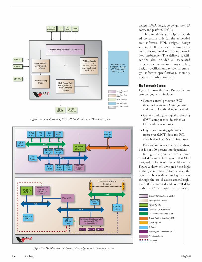
86 Xcell Journal Spring 2004
Low ResolutionCamera Data
Interfaces
Camera 1
IIC & SPIPeripherals
DDRSDRAM
3 MGTPeripherals
LCDZBTRAM Flash
PCI Interface toTransmit the
Low Res Camera and High Speed
MGT Data
PCI North/SouthBridge Interface tox86 EnvironmentRunning Linux
High Speed DataManagement andData Gathering
Interface
System Configuration and Control Block
DSP ProcessingBlock
Camera 2
ZBT RAM
System Configuration& Control
High-Speed DataLogic
FPGA Peripherals
Host x86 System
Virtex-II Pro 2VP20
OPBArbiter
PLBArbiter
PLBArbiter
EMCCore
(Flash)
EMCCore(ZBT)
IPIF Core(Proprietary
DisplayInterface)
GPIOCore
PLB2OPBBridge
OLB2PPBBridge
SPICore
IICCore
UART16550Core
DCRInterrupt
Core
PowerPC(Config.)
PowerPC(DSP)
Data Sniffer
DDRSDRAM
Core
Proprietary High Speed MGTInterface with FSM
& Control Logic
EMC Core(ZBT)
PLB2OPBBridge
256 Control & StatusRegisters
MGT 1 MGT 2 MGT 3
Proprietary LowResolution
Interface for 2 Cameras
System Configuration & Control
High-Speed Data Logic
Power PC 405
Processor Local Bus (PLB)
On-Chip Peripheral Bus (OPB)
Device Control Registers (DCR)
DCR Registers
IP Cores
Multi-Gigabit Tranceivers (MGT)
Proprietary Logic
PLB
PLB
PLB
OPB
DCR
Reg
Reg
OPB
OPB2PCICore
Data Flow
design, FPGA design, co-design tools, IPcores, and platform FPGAs.
The final delivery to Optos includ-ed the source code for the embeddedtest software, HDL designs, designscripts, HDL test vectors, simulationtest software, build scripts, and associ-ated testbenches. The delivery specifi-cations also included all associatedproject documentation: project plan,design specifications, testbench strate-gy, software specifications, memorymap, and verification plan.
The Panoramic SystemFigure 1 shows the basic Panoramic sys-tem design, which includes:
• System control processor (SCP),described as System Configurationand Control in the diagram legend
• Camera and digital signal processing(DSP) components, described asDSP and Camera Logic
• High-speed multi-gigabit serial transceiver (MGT) data and PCI,described as High-Speed Data Logic.
Each section interacts with the others,but is not 100 percent interdependent.
In Figure 2 you can see a moredetailed diagram of the system that XDSdesigned. The outer color blocks inFigure 2 show the division of the logicin the system. The interface between thetwo main blocks shown in Figure 2 wasthrough the use of device control regis-ters (DCRs) accessed and controlled byboth the SCP and associated hardware.
Figure 2 – Detailed view of Virtex-II Pro design in the Panoramic system
Figure 1 – Block diagram of Virtex-II Pro design in the Panoramic system

System Control ProcessorThe main function of the SCP is systemconfiguration management, coordination,status reporting, and control of the timingof events based on inputs. It starts imagecapture, and controls LCD display andother logic through registers in the system.
The main technical blocks of the SCPperform the following functions:
• Communicate with the Intel™ x86operating system environment overPCI and RS-232 connections
• Configure the LCD panel and camerainterfaces via IIC
• Display images on the LCD panel
• Communicate with peripheral subsys-tems via SPI
• Boot from internal Virtex-II Pro blockRAM and load application from exter-nal flash memory to ZBT RAM beforerunning it
• Schedule and control events in theapplication software via interrupts andGPIO
• Use DCR registers to gather status andcontrol operations in other sections.
DSP and Camera LogicThe camera interfaces are required to sup-port 30 frames per second (fps) of 640 x480 pixels, requiring bandwidths greaterthan 9 Mbps for each camera. The data isstored locally in ZBT RAM so that a DSPalgorithm running on the secondPowerPC 405 microprocessor can beapplied to the data. While the data is beingreceived from the cameras, it is also copiedto DDR SDRAM for transmission overthe PCI to the host x86 memory space.
High-Speed Data LogicRocketIO™ MGTs are used to receivehigh-speed data from three peripheralboards, each transmitting data from a singleMGT on a Virtex-II Pro 2VP7. The MGTdata transfers are initiated by an externalsystem triggered by the operator. This eventis synchronized using interrupts to the SCP.The data from the three MGTs is formattedin the Virtex-II Pro device and used to form
a larger data packet, which is then stored inDDR SDRAM for transmission over PCI.
The PCI section is used to transfer allthe data stored in the DDR SDRAM tothe x86 host processor environment.XDS designed a number of proprietaryhardware blocks to control the flow ofdata from DDR SDRAM to the OPB-PCI core and over to the host x86 mem-ory space. Configuration and status of thePCI core is carried out by the SCPthrough DCR registers.
ToolsDuring this project, XDS used several soft-ware tools to create the Panoramic system,to simulate the design, and to manage the
development environment to ensure trace-ability and quality releases. The tools usedare listed in Table 1.
Test and VerificationWhen designing a project of this size, testand verification are of paramount impor-tance to the successful completion of theproject. The XDS team focused a largenumber of resources to ensure the designmet Optos’ requirements.
The team developed a full testbench thatwould fit around the design (shown in Figure2). This testbench was designed to simulateevery interface in the design. It consisted of aPowerPC microprocessor with peripheralcores to test protocols and communicationinterfaces. Both the design and the testbenchused the swift model for the PowerPC micro-processor to run the software during simula-tion. A swift model is a cycle-accuratesimulation model that can interpret
PowerPC instructions and act accordingly.Two software applications were used to
test the system in simulation. The first ranon the testbench and the second ran on thesystem under test (SUT).
The function of the SUT application isto interact with the peripheral cores andto drive the inputs and outputs of theSUT. The application in the testbenchinteracts with the SUT in the followingmanner:
• Data received from the SUT is storedin memory.
• Protocol data is decoded, stored, andreplied to, if appropriate.
The application for the SUT allowshardware design engi-neers to control manydifferent features andto run a suite of tests inany order required. TheXDS team alsodesigned tests to verifythe pure hardwareinterfaces withoutinteraction with theapplications.
All functionality wastested at unit, function-al, and system level. The
tests were all documented in the test and ver-ification plan, which was approved by Optosbefore the system design phase began.
ConclusionWith Xilinx Design Services, you get ahighly skilled and experienced team thatwill help get you to market faster by bridg-ing the learning curve, delivering qualityon-time designs, and working in closecontact with your development team.
In a letter to the engineers at XilinxDesign Services, David Cairns, technicaldirector at Optos, wrote, “I have beenimpressed with Xilinx Design Services.Their commitment to quality and highstandards has eased transition into pro-duction. XDS went the extra mile, and wecould not have achieved our design goalswithout their help.”
For more information about XilinxDesign Services, visit www.xilinx.com/xds.
Function Tool Used Vendor
VHDL Design, Compile, Test ISE 5.2i Xilinx
Software Design, Compile, Test EDK 3.2 Xilinx
Logic and Software Simulation MTI 5.6d Mentor Graphics
Version Management CVS Open Source
Table 1 – Software used to develop, simulate, and manage the development environment of the Panoramic system
Spring 2004 Xcell Journal 87

by Claus MølgaardTechnical Manager – Hardware & Embedded SoftwarePhase One A/[email protected]
From casual consumers to experienced pro-fessionals, digital photography has changedthe way we all think about taking pictures.Indeed, digital cameras are replacing tradi-tional film cameras at a faster rate than ever.
At the same time, digital image qualityis improving quickly. Whereas consumerdigital cameras typically have around 3million pixels for an image, professionaldigital cameras have from 6 million to 22million pixels.
As such, they present a far greater engi-neering challenge. Their large image filesizes must be moved quickly to achieve thehigh frame rates that professionals (such asfashion photographers) require. Thesecameras must also have advanced imageprocessing capabilities and precise powermanagement to extend battery life andreduce image distortion, which can becaused by thermal noise from high powerdissipation of the built-in electronics.
At Phase One, we found a solution tothese engineering challenges by incorporat-ing the Xilinx CoolRunner-II™ CPLDand the Virtex™-II FPGA into the designof our digital camera back, the H25.
Modular Camera DesignFigure 1 shows the modular structure of ageneric professional-quality, medium-for-mat camera. This modularity allows pho-tographers to not only swap lenses, but touse a different viewfinder or an alternativecamera back.
A conventional camera back contains thetype of film being used, but Phase One nowproduces a range of digital camera backscompatible with medium-format camera sys-tems, enabling improved workflow and newcreative opportunities. Compared to film,these camera backs also improve image qual-ity and color reproduction.
Technical RequirementsAt Phase One, we have created digital imag-ing solutions for professional photographerssince 1993, supplying cameras for medical
Creating One of the World’s Highest-Resolution Digital Cameras
Creating One of the World’s Highest-Resolution Digital Cameras
88 Xcell Journal Spring 2004
Phase One combined the low power consumption of the CoolRunner-IICPLD with the functional capabilities of the Virtex-II family.Phase One combined the low power consumption of the CoolRunner-IICPLD with the functional capabilities of the Virtex-II family.
The Phase One H25 digital camera back on a Hasselblad medium-format camera ©
John
Ben
dtse
n

diagnostics and aerial photographyas well as studio and fashion pho-tography. Through the years wehave also supplied numerous OEMsolutions for technically demand-ing applications. Our customersdemand very high resolution, highsensitivity, ruggedness, reliability, ahigh continuous capture rate, andperfect color reproduction.
High-end professional film for-mats are larger than the 35-mmstandard. For example, the classic 6cm x 6 cm Hasselblad™ mediumformat is a favorite among profes-sional photographers. Newer auto-focus cameras from Hasselblad,Contax™, Mamiya™, and Fuji™use a 6 cm x 4.5 cm format, whichhas also become popular. Theselarger film formats enable higher-resolution digital camera solutionswithout compromising imagequality, which is highly dependent on pixelsize. Larger pixels typically yield higher sen-sitivity and less noise.
Phase One digital camera backs are nowavailable with image sensors ranging from 6to 22 megapixels. This enables an activeimaging area as large as 48 mm x 36 mm inour flagship H25 digital camera back.
The H25 image sensor is a huge piece ofsilicon that dwarfs even a large FPGA die. Infact, it is currently one of the world’s largestcommercially available imaging sensors, andhelps the H25 push digital photographybeyond the image quality of traditional film.
The specification for the H25 cameraplatform included the following key points:
• Huge image file sizes: 128 MB/imageallows for 16 bits per color, for a totalof 48 bits of red/green/blue (RGB)color depth
• Data moving capability as fast as 7 Gbps
• Big image buffer for long burstsequences
• Storage of uncompressed or losslesslycompressed images in the RAW imageformat to keep the highest possibleimage quality
• High sustained frame rates with more
Hardware SelectionWhen designing the H25, weused the CoolRunner-II CPLDto implement serial controllers,interrupt controller, and powermanagement functions. We alsoused the plentiful on-chipresources of the CoolRunner-IIdevice to implement the userinterface controller, camera bodyinterface, and glue logic.
The low current draw of theCoolRunner-II CPLD allowedus to minimize power dissipa-tion, extending battery life andreducing the effects of thermalnoise on image quality.
The powerful features embed-ded in the Virtex-II architectureprovided even greater opportuni-ties to maximize the performanceof the H25, while also meetingimportant marketing targets.
Apart from restrictions on size, weight,and power, cost is always a concern. Timeto market is paramount – the majority ofour income from a new camera comeswithin the first year of its lifetime.
We considered alternatives, includingASIC and other “hard-coded” FPGA tech-nologies. Although these were technicallyfeasible, it was far more cost-effective, easi-er, and faster to complete the design usingVirtex-II FPGAs.
Figure 2 outlines the functional blocks ofthe Phase One H25 digital camera platform.
than 30 frames/minute (faster framerates are possible when images are cap-tured in a burst)
• High processing power to enable severeimage processing and compression
• 400 Mb IEEE1394 connection withproprietary high-speed image datastreaming
• Advanced power management toreduce thermal dissipation as well asprolong battery life
• Small physical size.
Spring 2004 Xcell Journal 89
Lens Camera Body Camera Back
Viewfinder
Figure 1 – Modules in a medium-format camera system
With its 22 megapixels, H25 images enable an abundance of rich details.
©C
laud
i Thy
rres
trup

Implementing the H25 Camera PlatformWe combined the high parallel image pro-cessing capability of the Virtex-II on-chipmultipliers with the advanced digital clockmanagers (DCMs) and block RAMs toconfigure the Virtex-II FPGA as a powerfulco-processsor chip. The Virtex-II devicehad ample capacity to offload most of thehigh data-rate tasks and image processing.
At the same time, we were able toimplement large numbers of customizedcontrollers within the device, therebyreducing the physical size. This also made itextremely easy to interface the centralprocessor to various hardware blocks.
The DCMs are a huge benefit in sys-tems where off-chip and on-chip frequen-cies are high. They enable easy and flexiblede-skewing of board clocks and are veryuseful, for instance, in high-speed SDRAMcontrollers. No other FPGA vendor pro-vides such an abundance of DCMs.
This is especially valuable in our applica-tion, because we use many different high-speed clocks when interfacing to differentsections of the board. It also allowed us toapply a very fine-grained power managementstructure where various sections can be pow-ered down or slowed to reduce the totalpower consumption. The H25 continuouslyadjusts frequencies on-the-fly to fulfill userdemands at the lowest power consumption.
Virtex-II’s SelectIO™+ technology sup-ports high-speed signaling standards. Weused these to move data onto and off thechip at 7 Gbps.
However, internal bandwidth is muchhigher if you consider all parallel processesthat use local storage. We therefore usedthe Virtex-II block RAMs to implementvarious first in first outs (FIFOs), to handledata movement across different clockdomains and on-chip local data caches.On-chip caches are absolutely essential forimplementing high-speed image processingalgorithms as well as advanced image com-pression.
By moving these functions into theVirtex-II FPGA, we also freed the mainprocessor to execute real-time operatingsystem (RTOS)-based system controllerfunctions. This created a system perform-
ance overhead that can support additionalfunctionality as market requirementsincrease. We can also upgrade productsalready in the field, adding new functions aswe develop them.
Virtex-II’s in-field reprogramming iscrucial to this capability because it imple-ments so much of the camera’s functional-ity. This easy upgrade path also helps winloyalty from photographers, who see valuein receiving ongoing improvements. Wecan keep ahead of our competition with-out having to release a totally new productevery month. And we can assure our cus-tomers that they will always have a superi-or camera.
ConclusionAt Phase One we are committed to stayingahead of the competition, with excellentimage fidelity in the field of digital high-end imaging. We hope to continue to pushdigital imaging beyond current technicalboundaries.
The current trend towards breaking downthe barriers between embedded software andhardware will help us to continuously exploitthe technical capabilities of Xilinx FPGAsand CPLDs to achieve this ambitious goal.Visit our website at www.phaseone.com to seesample images and learn more about whyphotographers and other professionals chooseour products.
Photons Image SensorAnalog Signal
Processing ADC
Image SensorControl
Analog Signal Processor ControlImage
Processing
Camera BodyInterface
User InterfaceControl
CPU
Image Buffer
IEEE1394
Storage
CPLD
FPGA
Figure 2 – Phase One digital camera platform
A high-resolution model image captured with the H25
90 Xcell Journal Spring 2004
©Jo
hn B
endt
sen

by Olivier CantineauDesign ManagerBarco [email protected]
JPEG2000 is the latest algorithm fromthe JPEG normalization group for stillpicture compression. Based on wavelettechnology, JPEG2000 is very differentfrom its predecessor. It has capabilitiesthat allow it to be adopted in a wide spec-trum of applications, even extending tovideo encoding.
As a result, this compression schemerequires much more computational powerthan its classic JPEG predecessor.Furthermore, software implementationsmake poor candidates for applicationsrequiring very fast encoding times.
Barco Silex has developed two JPEG2000accelerator IP cores for high-performanceapplications: the BA112JPEG2000Eencoder and the BA111JPEG2000Ddecoder. These cores handle the computa-tionally intensive tasks of the JPEG2000algorithm. Together with a host CPU, thesecores create a complete JPEG2000 encodingor decoding solution.
Implementing the BA112JPEG2000Eand BA111JPEG2000D cores on XilinxVirtex™-II and Virtex II-Pro™ FPGAspaves the way to high-speed picture encod-ing applications with a very flexible archi-tecture and shortened design time.
The JPEG2000 AlgorithmAlthough JPEG2000 is based on a singlealgorithm, it offers a wide range of toolsfor compressing and representing images.It is suitable for a large spectrum of appli-cations ranging from Internet streaming tomedical imaging to digital cameras.
JPEG2000 encompasses capabilitiestraditionally encountered in separate algo-rithms, such as:
• Lossy and lossless compression withexcellent performance
• Precise compression ratio control withsingle-pass processing
• Bitstream progressivity, allowing con-sistent image previews with partial bit-stream decoding
• Support for user-defined regions ofinterest in the image, encoded withhigher quality than the other areas
• Error resilience.
Moreover, JPEG2000 compressionquality outperforms the classical JPEGscheme for high compression ratios by gen-erating fewer and less visible artifacts.
Let’s explain the two consecutive pro-cessing stages required for JPEG2000compression.
Tier 1 – DWT-Based CompressionThe JPEG2000 algorithm divides theimage into rectangular tiles of a config-urable size.
Each tile undergoes a two-dimensionaldiscrete wavelet transform (DWT), whichreorders the tile’s frequency informationinto a series of pictures (subbands). A sub-band results from the filtering of the origi-nal tile for a given frequency range.
A parameter of the transform (the num-ber of decomposition levels) defines thenumber of frequency intervals.
Each subband can then undergo selec-tive quantization by a programmable factor
Barco Silex IP cores enable high-speed picture compression on Virtex-II and Virtex-II Pro FPGAs.Barco Silex IP cores enable high-speed picture compression on Virtex-II and Virtex-II Pro FPGAs.
Accelerate JPEG2000 CompressionAccelerate JPEG2000 Compression
Spring 2004 Xcell Journal 91
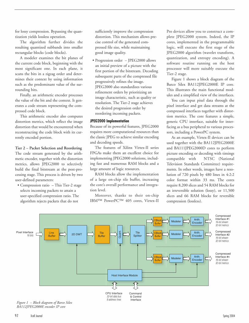
for lossy compression. Bypassing the quan-tization yields lossless operation.
The algorithm further divides theresulting quantized subbands into smallerrectangular blocks (code blocks).
A modeler examines the bit planes ofthe current code block, beginning with themost significant one. In each plane, itscans the bits in a zigzag order and deter-mines their context by using informationsuch as the predominant value of the sur-rounding bits.
Finally, an arithmetic encoder processesthe value of the bit and the context. It gen-erates a code stream representing the com-pressed code block.
This arithmetic encoder also computesdistortion metrics, which reflect the imagedistortion that would be encountered whenreconstructing the code block with its cur-rently encoded portion.
Tier 2 – Packet Selection and ReorderingThe code stream generated by the arith-metic encoder, together with the distortionmetrics, allows JPEG2000 to selectivelybuild the final bitstream at the post-pro-cessing stage. This process is driven by twouser-defined parameters:
• Compression ratio – This Tier-2 stageselects incoming packets to attain auser-specified compression ratio. Thealgorithm rejects packets that do not
Pro devices allow you to construct a com-plete JPEG2000 system. Indeed, the IPcores, implemented in the programmablelogic, will execute the first stage of theJPEG2000 algorithm (wavelet transform,quantization, and entropy encoding). Asoftware routine running on the hostprocessor will more suitably execute theTier-2 stage.
Figure 1 shows a block diagram of theBarco Silex BA112JPEG2000E IP core.This illustrates the main functional mod-ules and a simplified view of the interfaces.
You can input pixel data through thepixel interface and get data streams at thecompressed interfaces together with distor-tion metrics. The core features a simple,generic CPU interface, suitable for inter-facing as a bus peripheral to various proces-sors, including a PowerPC system.
As an example, Virtex-II devices can beused together with the BA112JPEG2000Eand BA111JPEG2000D cores to performpicture encoding or decoding with timingscompatible with NTSC (NationalTelevision Standards Committee) require-ments. In other words, images have a reso-lution of 720 pixels by 480 lines in 4:2:2color format within 33 ms. The coresrequire 8,200 slices and 54 RAM blocks foran irreversible solution (lossy), or 11,500slices and 66 RAM blocks for reversiblecompression (lossless).
sufficiently improve the compressiondistortion. This mechanism allows pre-cise control of the generated com-pressed file size, while maintaininggood image quality.
• Progression order – JPEG2000 allowsan initial preview of a picture with thefirst portion of the bitstream. Decodingsubsequent parts of the compressed fileprogressively refines the image.JPEG2000 also standardizes variousrefinement orders by prioritizing animage characteristic, such as quality orresolution. The Tier-2 stage achievesthe desired progression order byreordering incoming packets.
JPEG2000 ImplementationBecause of its powerful features, JPEG2000requires more computational resources thanthe classic JPEG to achieve similar encodingand decoding speeds.
The features of Xilinx Virtex-II seriesFPGAs make them an excellent choice forimplementing JPEG2000 solutions, includ-ing fast and numerous RAM blocks and alarge amount of logic resources.
RAM blocks allow the implementationof a large on-chip tile buffer, increasingthe core’s overall performance and integra-tion level.
Moreover, thanks to their on-chipIBM™ PowerPC™ 405 cores, Virtex-II
92 Xcell Journal Spring 2004
Pixel Interface16 bits
Line Buffer 2D DWT Tile
Buffer Qua
nt.
TileSplitter
Host Interface Module
CBlockBuffer
CBlockBuffer
CBlockBuffer
Modeler
Modeler
Modeler
Arith.Encoder
Arith.Encoder
Arith.Encoder
CPU Interface32-bit data bus8 address lines
Command & ControlInterface
CompressedInterface #116-bit stream32-bit metrics
CompressedInterface #216-bit stream32-bit metrics
CompressedInterface #n16-bit stream32-bit metrics
Figure 1 – Block diagram of Barco Silex BA112JPEG2000E encoder IP core
2-D DWTThe first module of the BA112JPEG2000Ecore is the DWT engine. This module canbe configured to accept tiles of pixels aslarge as 128 by 128. It performs two-dimensional discrete wavelet decomposi-tion on incoming data with as many as fiveprogrammable decomposition levels. Thewavelet transform can be programmed aslossy, lossless, or bypassed.
The DWT module accepts incomingpixels of any size – up to 10 bits for lossy andup to 12 bits for lossless. It stores its resultsin the on-chip tile buffer to undergo quanti-zation and code block decomposition.
QuantizerThe quantizer fetches the subbands avail-able from the tile buffer and applies a pro-grammable quantization step. Differentquantization steps are programmable foreach subband. Thus, you can weight lowerfrequency subbands differently than higherfrequency ones.
You can also bypass the quantizer forlossless mode.
Tile SplitterThis unit further divides quantized sub-bands into rectangular code blocks of aprogrammable size (as large as 32 by 32pixels) in preparation for entropy encodingby an arithmetic encoder.
The BA112JPEG2000E andBA111JPEG2000D cores feature a con-figurable number of entropy encoders,placed in parallel, to sustain high encod-ing rates. You can select the number ofimplemented chains during the IP syn-thesis process. Each entropy chainprocesses a code block independently ofneighboring chains.
The tile splitter module arbitratesbetween the available chains, dispatching thevarious code blocks to be encoded. It storescode blocks in local code block buffers.
Modeler and Arithmetic EncoderThe modeler performs the first part ofentropy encoding. It examines the codeblock bit plane by bit plane and extractsrelevant bits in zigzag order for each bitplane. The modeler then computes the
context information needed by the arith-metic encoder.
The arithmetic encoder processes thebits and contexts, and makes the streamand the distortion metrics available at thecompressed interface. These are used by theTier-2 part of the JPEG2000 algorithm.
Host Interface ModuleThis module allows the interfacing of thecore to a CPU: It contains configuration reg-isters for the various modules and gives statusinformation about the encoding progress.
The host interface module also fea-tures a separate command-and-controlinterface that allows fast control of the IPcore with minimal or no CPU interven-tion. Hence, the command-and-controlinterface makes it possible to build a sys-tem in which a small amount of logicdrives the BA112JPEG2000E andBA111JPEG2000D cores, which are notdirectly connected to a host CPU. Thisincreases the integration flexibility of theIP cores.
ConclusionBarco Silex’s BA112JPEG2000E andBA111JPEG2000D IP cores are targetedto high-speed JPEG2000 encoding anddecoding, providing access to the widerange of capabilities now possible with theJPEG2000 standard.
This new standard defines an algorithmable to offer a large spectrum of features,such as progressive bitstream, precise ratecontrol, region of interest, and high-qualityjoined lossy and lossless compressions.
This rich set of advantages turnsJPEG2000 into an important actor in thecompression world, especially as it is notlimited to still picture compression.
The computational complexity of theJPEG2000 standard requires hardwareplatforms for high-speed applicationscompatible with real-time video encoding.Barco Silex BA112JPEG2000E andBA111JPEG2000D IP cores, acting ascompression accelerators on Xilinx Virtex-II and Virtex-II Pro Platform FPGAs, cangive you the speed you need.
For more information about Barco SilexIP cores, visit www.barco-silex.com.
Spring 2004 Xcell Journal 93
Xilinx Events and Tradeshows
Xilinx participates in numerous tradeshows and events throughout the year.This is a perfect opportunity to meet
our silicon and software experts, ask questions, see demonstrations of new products and technologies, and hear other customers’ success
stories with Xilinx products.
For more information and the most up-to-date schedule, visitwww.xilinx.com/events/.
Worldwide Events Schedule
March 8-10Wireless Systems DesignSan Diego, CA
March 8-11SAE World CongressDetroit, MI
March 30-April 1electronicaUSA with Embedded Systems ConferenceSan Francisco, CA
April 19-20Mentor Users GroupSanta Clara, CA
September 14-15Embedded Systems Conference Boston, MA
September 27-30Global Signal Processing Expo*Santa Clara, CA
**Global Technology Conferences is currently seeking abstracts forGSPx 2004. If you are interested in submitting a paper, send a 500-word abstract online no laterthan March 15. Completed papersare due by May 15. For more information, visit www.gspx.com/GSPX/call_for_papers.html.

A robust online resource, MySupportstands ready to answer all of your designquestions 24 hours a day, seven days aweek, 365 days a year. Our award-winningsupport website allows you to personalizecontent so that you see only the informa-tion that’s relevant to you.
As shown in Figure 1, MySupport offersaccess to sections such as Answers Search,Documentation, Tech Tips, Forums,Problem Solvers, TechXclusives, WebCase,Software Updates, and MyAlerts; you canget the answer you need when you need it.
What Are You Looking For?
• Answers Database: With new andimproved search technology, answersdatabase searches are faster and moreaccurate than ever. Our advancedsearch or answer browser tools enableyou to easily access the latest answers
Get Award-Winning Supportat Your Fingertips
94 Xcell Journal Spring 2004
Figure 1 – A sample MySupport landing page displays the Support News and Xilinx Global Services windows.
Find the answer you need, when you need it, with MySupport.
by Doug HorneProduct Marketing and Web Development, Global Services DivisionXilinx, [email protected]

to technical issues from a huge data-base of more than 4,000 answers,indexed by logical category.
• Documentation: Your one-stop sourcefor software manuals in PDF, com-pressed PDF, or search-enabled HTMLformat. This section also includesapplication notes, data sheets, andmore. You can even browse publica-tions by part.
• Tech Tips: Get the latest technicalinformation about development tools,device families, interface tools, andhardware and IP solutions.
• Forums: Collaborate with otherdesigners in discussion groups or chatrooms; join the popular newsgroupcomp.arch.fpga.
• Problem Solvers: Get instant help withinstallation and configuration, PCIapplications, and JTAG implementa-tion. This interactive tool uses a seriesof questions to diagnose and trou-bleshoot your configuration or installa-tion problem automatically, saving youhours of work.
• TechXclusives: Expert Xilinx applica-tion engineers keep you informed ofthe hottest issues and latest techniques.
• WebCase: Use our WebCase to managehotline cases. You can check status, addnotes, and even close a case on theWeb, anytime.
Let’s Get PersonalMySupport puts powerful support tools towork for you. As shown in Figure 2, thesefeatures include:
• Support News: Get the latest in sup-port-related news and developments onXilinx products. TechXclusives are alsofeatured in this section.
• Xilinx Global Services: Here you’ll findall the latest news on the Xilinx GlobalServices Division’s offerings.
• MyAlerts: Stay current with updates totechnical publications, software updates,products, Tech Tips, and design and sys-tem resources with MyAlerts. Whenever
• MyXPA: With MySupport’s newest fea-ture, Xilinx Productivity Advantage(XPA) customers can check their train-ing credits, sign up for classes, and more.
• What’s New: View the latest products,devices, design tools, and system solu-tions from the Xilinx product catalog.
• Latest Answers: View the answer recordsyou’ve visited, make note of the mostrecent answers published by Xilinx engi-neers, and see what others are saying.
• Product Genealogy: Get quick access tofabrication, assembly, and die-relatedparts change notice (PCN) information.
• My Bookmarks: Create links to yourfavorite websites and answer records, orsearch queries on MySupport.
• Stock Quotes: Watch your favorite stockticker symbols, including latest price,change, and last trade information.
Personalization even extends to yourpreferred language (Figure 3).
MySupport makes it easy to stay on top.
Do It Today“Finish Faster” by taking advantage of thesepowerful tools. Registration is easy and free.To sign up for MySupport, visit www.xilinx.com/support or click on the “Support”button on the top navigation bar anywhereon www.xilinx.com. If you have any ques-tions, contact the author at 408-626-6317or e-mail [email protected].
you log in, you will automatically benotified of new downloads (such asservice packs and IP update releases) rel-evant to your design.
Spring 2004 Xcell Journal 95
Figure 2 – Various windows within MySupport
Figure 3 – Located in the bottom left-hand corner of the main landing page, Japanese and Chinese language translation is providedwithin MySupport.

by Cindy AndrussTechnical Writer/Production EditorXilinx, [email protected]
Xilinx Education Services offers a variety ofinstructor-led courses, e-Learning modules,and curriculum paths for your design spe-cialty to help you increase your skill set andcreate efficient designs. The diversity ofcourses and delivery methods empowersyou with the flexibility to choose the learn-ing method that best meets your needs andpreferred learning style.
But with so many training options, howdo you determine which courses willenhance your present design capabilities?Take a Xilinx skills assessment.
Available at no charge, Xilinx skillsassessments measure your current train-
ing knowledge and identify skills in needof improvement. The results of youranalysis can give you a better under-standing of your abilities and help youmake wiser registration decisions as towhich courses or modules best fulfill thegaps identified.
“Efficiency is the name of the gamethese days as companies strive to lowercosts and maximize their investments,”said Patrice Anderson, course develop-ment manager at Xilinx EducationServices. “When you take a Xilinx skillsassessment, you lower your training costsand maximize the return on your traininginvestment by taking only the courses youneed. By completing a skills assessment,you are able to develop a personalizedlearning plan that will get you on the fasttrack to implementing Xilinx solutions.”
Knowledge Drives Effective LearningWith your personalized learning plan, youcan enroll only in the Xilinx courses that areright for you. Xilinx courses will show youhow to reduce time to knowledge, boost sys-tem clock speeds, fit more functionality intosmaller devices, shorten design cycles, maxi-mize productivity, and increase your skill set.
Jahan Lotfi, a design engineer atCortina Systems™, uses skills assessmentsto prepare for class. “I always believed thatonce you ‘know the things you don’tknow,’ and then sit in the class, you paymore attention than when you are justpresented new material,” Lotfi said. “Ithink sometimes you just don’t know thesignificance of the material presented toyou until you have thought about it a bitand analyzed its advantages.
“As a result of taking the skills assess-ment, I was a better student and came outof the class more informed.”
Plan for Lowest Cost TrainingAlthough engineers can use skills assess-ments to organize a learning strategy forthemselves, their managers are also findingskills assessments a helpful planning tool.
When manager Don Meyerhoff ofStandard Microsystems™ needed a resourceto help plan the training budget for his staff,he turned to Xilinx Education ServicesRepresentative Mike Weir for assistance.Weir pointed Meyerhoff to skills assessments.
“We used to team up the customer witha Xilinx instructor on the phone to deter-mine the customer’s skill level, or we e-mailed the course syllabus or pointed thecustomer to the online course description,”Weir said. “But now we can offer a muchmore effective solution.”
By asking his engineers to take onlineskills assessments, Meyerhoff can gaugewhich skill levels they’re at and ultimately,which courses are or aren’t necessary. As aresult, his training budget is more precise.
Beyond helping you choose appropriatesingle courses or online modules, managerscan use skills assessments to help them budg-et the appropriate amount of training creditsincluded in Xilinx Productivity Advantage(XPA) agreements. The XPA Solutionincludes education, support services, soft-
By determining which Xilinx course offering is most appropriate, you can maximize your learning time and minimize training costs.
Customize Your Education withSkills Assessments
96 Xcell Journal Spring 2004

ware, and IP cores in one comprehensivepackage. Training credits are included inevery XPA and can be redeemed toward anyXilinx Education Services offering.
To help determine an adequate numberof training credits, managers can ask theirengineers to complete skills assessments todetermine which courses they should takegoing forward, and thus how many train-ing credits to include.
Completing an assessment also providesthe basis for a qualified training plan – onethat can be tailored to individual companiesbased on their needs.
The Skills Assessment AdvantageTo determine your current Xilinx designskill level, simply go to https://xilinx.onsaba.net/xilinx. Select the skills assess-ments respective to the courses for whichyou want to assess your competence.
Of course, there is no obligation toregister for any course, and you can skipthe assessment and register for a coursewithout it. But you can also test yourskills as often as you like to help betterdetermine whether you would benefitfrom attending a course.
Xilinx also recommends that you reassessyour skills after completing a course, com-paring your post-course score with yourpre-course score. Lotfi believes that takingthe skills assessment again some time aftercompleting an FPGA course helped himdiscover new tool design capabilities.
“The [skills assessment] showed me thatthere were some tool capabilities I didn’tknow about because I had not come to needthem in previous designs,” he said. “I foundthese [tool capabilities] from the [skillsassessment] questions.”
Most of the skillsassessments includematching, multiplechoice, and fill-in-the-blank exercises andtake about five to 15minutes to complete(for a sample question,see Figure 1). A scoreof 80 percent or high-er implies you arefamiliar with at least
80 percent of the course content and wouldnot benefit significantly from taking thecourse. On the other hand, if you areunable to answer at least four out of everyfive questions correctly, you should attendthe class to increase your individual produc-tivity. Ultimately, the decision is yours.
Your score is also yours. Only you haveaccess to your skills assessment results. Toview your score, simply use your usernameand password when logging in to theLearning Catalog.
ConclusionEfficiency goes beyond design. It beginswith effective training and plays an impor-tant role in meeting budget constraints andtight delivery schedules. With up-to-dateFPGA design skills, you are in a better posi-tion to maximize your investment in Xilinxsolutions and reduce your time to market.
Now you can make the most of yourlearning time and training investment withXilinx skills assessments. Enroll only in thetraining you need to get the skills andknowledge that will bring your design tomarket fast.
For more information about Xilinxskills assessments, visit https://xilinx.onsaba.net/xilinx, or contact the XilinxEducation Services registrar via e-mail [email protected] or by telephone at(877) XLX-CLAS (2627). For a list of frequently asked questions, go to www.xilinx.com/support/training/skills-assessment.htm.
To learn more about the XilinxProductivity Advantage Program, visitwww.xilinx.com/xpa, or contact an XPA representative at (800) 888-FPGA (3742)or e-mail [email protected].
Spring 2004 Xcell Journal 97
Figure 1 – A multiple-choice question from the Designing for Performance skills assessment
As a manager, the skillsassessment can help you:
❏ Assess your engineers’ Xilinx-relateddesign skills
❏ Maximize your training investment
❏ Empower your engineers to develop a personalized learning plan
❏ Order the number of training credits(TCs) your staff will use in a given term
❏ Plan an effective XPA agreement.
As a design engineer, the skillsassessment can help you:
❏ Determine which course is right for you
❏ Save money and time by taking only the right training for you
❏ Assess learning gaps on specific Xilinx products
❏ Measure your pre-course and post-course knowledge
❏ Develop a personalized learning plan.
Skills assessments are availablefor the following courses*:
❏ Fundamentals of FPGA Design
❏ Designing for Performance
❏ Advanced FPGA Implementation
❏ Designing with Multi-Gigabit Serial I/O
❏ Introduction to VHDL
❏ Introduction to Verilog.
* Additional skills assessments will be added over time. Please visit https://xilinx.onsaba.net/xilinx for current course offerings.

by Forrest JamesDirector of Corporate FacilitiesXilinx, [email protected]
When FORTUNE magazine ranked Xilinxas fourth on its 2003 list of the 100 BestCompanies to Work For™ in America, theeditors based their selection on a range of cri-teria, including benefit packages, number of
minority staff, and layoffs – or lack thereof.But Xilinx employees at the company’s
Longmont, Colorado, campus can add tothat list a literal “best place to work in.”Their new office building, opened in April2002, has garnered several awards for itsenergy conservation and building design.
In June 2003, DTJ Design (the land-scape architect, design architect, andmaster planner) and the Neenan
Company (the architect of record and gener-al contractor) received a Gold Nugget Awardfor the Best Office/Professional Building(<60,000 square feet) at the annual PacificCoast Builders’ Conference.
The Longmont office has also receivedacclaim from the Colorado RenewableEnergy Society, the Colorado Chapter of the
American Institute ofArchitects, and theColorado Society ofLandscape Architects.
Associate Len Segelof DTJ Design says,“We didn’t start outwith the idea to createan award-winningbuilding. Yet it was areally special project [forus] because it was a closecollaboration with anenlightened client inter-
ested in innovation, flexible work stations,and in particular paying attention toemployees’ needs.”
Indigenous InnovationsThe Colorado landscape and RockyMountains backdrop served as the inspira-tion for many design elements. The archi-tects fit one of three interconnectingbuildings, or “segments,” into the side of ahill. The segments themselves are named“Prairie,” “Foothills,” and “Mountains” –all following the natural curvature of thetopography.
The structure combines diverse architec-tural styles from plains, agricultural, andmountain-style dwellings, with archingcanopies of gabled roofs and trusses, local
The architects’ emphasis on native architecture and sustainable materials has received national recognition.
Xilinx Wins Architecture Awards for Colorado Office Complex
98 Xcell Journal Spring 2004
Longmont campus
Gold Nugget Award t
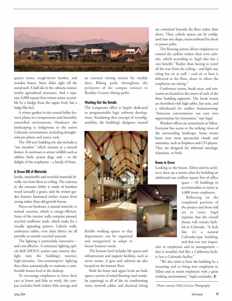
quarry stone, rough-hewn lumber, andwooden braces. Snow slides right off themetal roof. A half-silo in the cafeteria mimicsnearby agricultural structures. And a sepa-rate, 6,000-square-foot retreat center, accessi-ble by a bridge from the upper level, has alodge-like feel.
A winter garden in the central lobby fea-tures plants in a temperature-and-humiditycontrolled environment. Outdoors, thelandscaping is indigenous to the nativeColorado environment, including drought-tolerant plants and native rock.
The 100-acre building site also includes a“wet meadow,” which remains as a naturalfeature. It continues to attract wildlife such asrabbits, birds, prairie dogs, and – to thedelight of the employees – a family of foxes.
A Green Bill of MaterialsInside, sustainable and recycled materials lit-erally run from floor to ceiling. The stairwayin the entrance lobby is made of bamboowood (actually a grass), and the winter gar-den features laminated timber trusses fromyoung rather than old-growth forests.
Floors are linoleum, a natural material, orstained concrete, which is energy-efficient.Some of the interior walls comprise pressed,recycled sunflower seeds, which make for avisually appealing pattern. Cubicle walls,conference tables, even chair fabrics are allpartially or entirely recycled material.
The lighting is particularly innovative –and cost-effective. A miniature lighting opti-cal shelf (MOLS) system casts exterior day-light into the building’s interior;high-intensity, low-consumptive lightingthen dims automatically to maintain a com-fortable lumen level at the desktop.
To encourage employees to leave theircars at home and bike to work, the cam-pus includes both indoor bike storage and
are contained beneath the floor rather thanabove. Thus, cubicle spaces can be config-ured into any shape, unencumbered by ductsor power poles.
The flooring system allows employees tocontrol the airflow within their own cubi-cles, which according to Segel also has acost benefit: “Rather than having to travelall the way from the ceiling – and fight anyrising hot air as well – cool air or heat isdelivered at the floor, closer to where theemployees are sitting.”
Conference rooms, break areas, and rest-rooms are located in the center of each of thethree building segments. The break roomsare furnished with high tables, bar seats, anda whiteboard for sudden brainstorming:“Innocent conversations can turn intoopportunities for innovation,” says Segel.
Window offices are nonexistent at Xilinx.Everyone has access to the striking views ofthe surrounding landscape. Some roomsboast even more spectacular visuals andamenities, such as fireplaces and CD players.They are designed for informal meetings,relaxation, or both.
Room to GrowLooking to the future, Xilinx and its archi-tects drew up a master plan for building anadditional one million square feet of office
space – 10 buildings toaccommodate as many as4,000 more employees.
Reflecting on thecompleted portions ofthe project and those stillyet to come, Segelexplains that the overalltheme will remain faith-ful to Colorado. “It feelslike it’s a naturalColorado-type building,and that was very impor-
tant to employees and to management –that it wouldn’t feel like a California facili-ty but a Colorado facility.”
“We also tried to have the building be arecruiting tool to bring new employees toXilinx and to retain employees with a greatworking environment,” Segel concludes.
an external rinsing station for muddydays. Biking paths throughout theperimeter of the campus connect toBoulder County biking paths.
Working Out the DetailsThe Longmont office is largely dedicatedto programmable logic software develop-ment. Emulating that concept of reconfig-urability, the building’s designers created
flexible working spaces so thatdepartments can be organizedand reorganized to adapt tofuture business needs.
The bottom level includes lab spaces andinfrastructure and support facilities, such asserver rooms. A gym and cafeteria are alsolocated on the bottom floor.
Both the lower and upper levels are builtupon a system of raised flooring (and modu-lar carpeting) so all of the air conditioningvents, network cables, and electrical wiring
Spring 2004 Xcell Journal 99
Photos courtesy ©Ed LaCasse Photography

Field Programmable Gate Arrays (FPGA)
Texas Instruments PowerManagement ReferenceGuide for Xilinx® FPGAs
Powering Your FPGAs With TI’s Power Management Products
FPGA
DC/DCConverters
DC/DCConverters
DC/DCConverters
Supply VoltageSupervisor
SD RAMand
DATA CONV.
VCCINT
VCCO
Input
Supply
R E A L W O R L D S I G N A L P R O C E S S I N G™
Includes:
• Power requirements of Xilinx FPGAs intypical applications
• Recommended Texas Instruments DC/DCconverters for powering Xilinx FPGAs (Xilinx endorsed)
• DC/DC converters selection considerations
• Texas Instruments power managementreference designs
- Design considerations
- Spartan™-3
- Spartan™-IIE
- Spartan™-II
- Virtex™-II
- Virtex-II Pro™
• Texas Instruments product selection guides
1Q 2004
power.ti.com/xilinxfpga

2 POWER MANAGEMENT FPGA REFERENCE GUIDE TEXAS INSTRUMENTS 1Q 2004
This information is intended to provide the designer with a general understanding of the power requirements of Xilinx FPGA families in typical applications. Please refer to the Xilinx Power Estimators, available at www.xilinx.com/power, for closer approximations specific to individual FPGA devices and applications.
Power Requirements of Xilinx® Solutions in Typical Applications
Important Design Considerations: • The shown power solutions are for applications guidance.
Please visit the TI website for the latest updated information.
• Although Xilinx FPGAs do NOT require it, TI’s referencedesigns employ sequencing, as well as a Supply VoltageSupervisor (SVS) to monitor the input supply. This prac-tice is consistent with good power supply design and prevents the input power supply from being pulled downdue to in-rush currents for charging large capacitive loads.
• VCCAUX powers time-critical resources in the FPGA,including the Digital Clock Managers (DCMs). Therefore,this supply voltage is especially susceptible to power sup-ply noise. VCCAUX can share a power plane with VCCO,but only if VCCO does not have excessive noise. Changesin VCCAUX voltage beyond 200 mV peak-to-peak shouldtake place at a rate no faster than 10 mV per milli-second.
• These designs meet Xilinx’s VCCINT and VCCO startup profile requirements, where applicable, including monotonic voltage ramp, in-rush current and power voltage ramp time requirements.
• The designs show the most common VCCO voltages, 2.5 V or 3.3 V. Other voltages can be supported by inter-changing the depicted DC/DC converter with devices from the same family, assuming that the linear regulatordoes not exceed its power dissipation rating. Refer to the selection guides on pages 100 - 11 for alternatives.
• Only the minimum input and output capacitors for eachIC are given in the schematics. Larger bulk and/or bypasscapacitors will be required between the input supply andDC/DC converters depending on the placement of theinput supply relative to the converters. Each FPGA alsorequires a minimum amount of bypass capacitance oneach power rail as specified by Xilinx.
TI’s Power Reference Designs for Xilinx FPGAs
Complete schematics, bills of materials and additional designs available at:
power.ti.com/xilinxfpgaQuestions? [email protected]
Power Requirements of Xilinx FPGA FamiliesSpartan™-II Spartan™-IIE Spartan™-3* Virtex™-II Virtex-II Pro™
VCCINT (core) 2.5 V ±5% 1.8 V ±5% 1.2 V ±5% 1.5 V ±5% 1.5 V ±5% @ 200 mA to 2 A @ 200 mA to 2 A @ 200 mA to 5 A @ 300 mA to 10 A @ 300 mA to 10 A
VCCO (I/O) 3.3 V, 2.5 V 3.3 V, 2.5 V, 1.8 V 3.3 V, 3.0 V, 2.5 V, 1.8 V, 3.3 V, 2.5 V, 1.8 V 3.3 V, 2.5 V, 1.8 V and/or 1.5 V ±5% and/or 1.5 V ±5% 1.5 V and/or 1.2 V ±5% and/or 1.5 V ±5% and/or 1.5 V ±5%@ 50 mA to 500 mA @ 50 mA to 500 mA @ 50 mA to 1.5 A @ 50 mA to 3 A @ 50 mA to 3 A
VCCAUX — — 2.5 V ±5% 3.3 V ±5% 2.5 V ±5% @ 300 mA (max) @ 300 mA (max) @ 300 mA (max)
Digital Voltages above. Analog voltages for RocketIO Multi-Gigabit Transceiver (MGT) below.AVCCAUXTX — — — — 2.5 V ±5%
@ 60 mA/MGTAVCCAUXRX — — — — 2.5 V ±5%
@ 35 mA/MGTAVTTX — — — — 1.8 V to 2.625 V
@ 15 mA/MGTAVTRX — — — — 1.8 V to 2,625 V
@ 30 mA/MGT*Spartan-3 information is based on the advance datasheet and is current as of December 2003.
• Spartan-II/Spartan-IIE ...................................... Pages 4 - 5
• Spartan-3.......................................................... Pages 5 - 7
• Virtex-II/ Virtex-II Pro ....................................... Pages 7 - 9
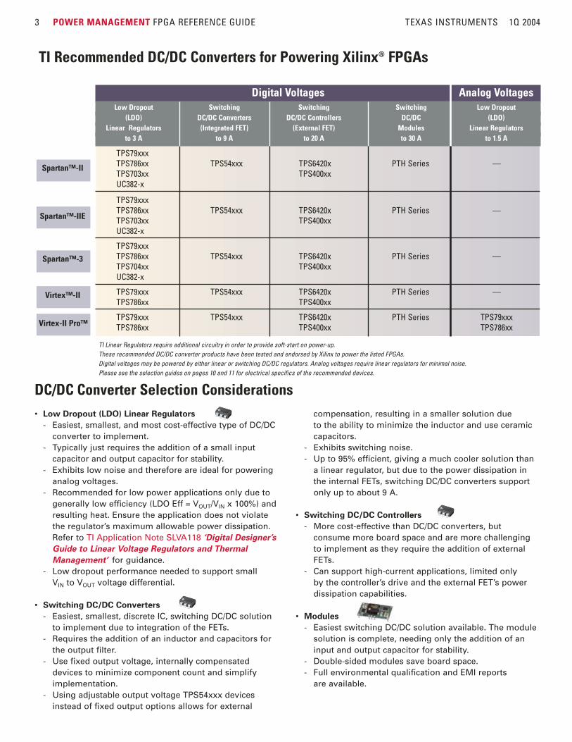
3 POWER MANAGEMENT FPGA REFERENCE GUIDE TEXAS INSTRUMENTS 1Q 2004
• Low Dropout (LDO) Linear Regulators
- Easiest, smallest, and most cost-effective type of DC/DCconverter to implement.
- Typically just requires the addition of a small inputcapacitor and output capacitor for stability.
- Exhibits low noise and therefore are ideal for poweringanalog voltages.
- Recommended for low power applications only due togenerally low efficiency (LDO Eff = VOUT/VIN x 100%) andresulting heat. Ensure the application does not violatethe regulator’s maximum allowable power dissipation.Refer to TI Application Note SLVA118 ‘Digital Designer’s
Guide to Linear Voltage Regulators and Thermal
Management’ for guidance.- Low dropout performance needed to support small
VIN to VOUT voltage differential.
• Switching DC/DC Converters
- Easiest, smallest, discrete IC, switching DC/DC solutionto implement due to integration of the FETs.
- Requires the addition of an inductor and capacitors forthe output filter.
- Use fixed output voltage, internally compensateddevices to minimize component count and simplifyimplementation.
- Using adjustable output voltage TPS54xxx devicesinstead of fixed output options allows for external
compensation, resulting in a smaller solution due to the ability to minimize the inductor and use ceramic capacitors.
- Exhibits switching noise.- Up to 95% efficient, giving a much cooler solution than
a linear regulator, but due to the power dissipation inthe internal FETs, switching DC/DC converters supportonly up to about 9 A.
• Switching DC/DC Controllers
- More cost-effective than DC/DC converters, but consume more board space and are more challenging to implement as they require the addition of externalFETs.
- Can support high-current applications, limited only by the controller’s drive and the external FET’s powerdissipation capabilities.
• Modules
- Easiest switching DC/DC solution available. The modulesolution is complete, needing only the addition of aninput and output capacitor for stability.
- Double-sided modules save board space.- Full environmental qualification and EMI reports
are available.
DC/DC Converter Selection Considerations
TI Recommended DC/DC Converters for Powering Xilinx® FPGAs
Digital Voltages Analog VoltagesLow Dropout Switching Switching Switching Low Dropout
(LDO) DC/DC Converters DC/DC Controllers DC/DC (LDO) Linear Regulators (Integrated FET) (External FET) Modules Linear Regulators
to 3 A to 9 A to 20 A to 30 A to 1.5 A
TPS79xxxTPS786xx TPS54xxx TPS6420x PTH Series —TPS703xx TPS400xxUC382-x
TPS79xxxTPS786xx TPS54xxx TPS6420x PTH Series —TPS703xx TPS400xxUC382-x
TPS79xxxTPS786xx TPS54xxx TPS6420x PTH Series —TPS704xx TPS400xxUC382-x
TPS79xxx TPS54xxx TPS6420x PTH Series —TPS786xx TPS400xx
TPS79xxx TPS54xxx TPS6420x PTH Series TPS79xxxTPS786xx TPS400xx TPS786xxVirtex-II Pro™
TI Linear Regulators require additional circuitry in order to provide soft-start on power-up.These recommended DC/DC converter products have been tested and endorsed by Xilinx to power the listed FPGAs.Digital voltages may be powered by either linear or switching DC/DC regulators. Analog voltages require linear regulators for minimal noise.Please see the selection guides on pages 10 and 11 for electrical specifics of the recommended devices.
Virtex™-II
Spartan™-3
Spartan™-IIE
Spartan™-II

4 POWER MANAGEMENT FPGA REFERENCE GUIDE TEXAS INSTRUMENTS 1Q 2004
• Dual channel LDO in PowerPAD™ packagesaves cost and space.
• U1 monitors the input rail to ensure that it is up and stable before enabling the regulator.
• Linear regulators start-up fast. Q1 is used to provide soft start to VCCINT.
• Sequencing VCCINT, then VCCO minimizes demand on the input supply.
• U2 is limited to 2 W @ TA = 55 C and no airflow due to power dissipation. Its maximum output current is split betweenthe rails.
TPS70358 for Spartan-IITPS70351 for Spartan-IIE
Up to 950 mA for Spartan-IIUp to 800 mA for Spartan-IIE
2.5 V Up to 950 mA for Spartan-II1.8 V Up to 800 mA for Spartan-IIE
1 A/2 A Dual LDO Reg
VIN1
/MR1/MR2
/SEQ
/EN
VIN2
/RESET
VOUT1
VSENSE1PG1
VOUT2
VSENSE2GND
24PWP
U2
3.3 V
C2
U1
R2C4
C3
C1
C5 C6
R1
TLC7705/RESNVDD CT SNS
CTRL GND /RSTRST
DigitalVCCO
DigitalVCCINT
Q1
DigitalVCCO
DigitalVCCINT
U1
Spartan-IIE only. Omit for Spartan-II and connect to EN.
C2
C3C1
C5 C6
C4
3.3 V Up to 1.5 A
R6
R1
R2
R4
R3
R7
R5
TPS3809K33
/RSTVDDGND
U3TPS78633
GND
1.5 A LDOENVIN VOUT
BYP
DDPAK
TPS78625 LDO for Spartan-IITPS79618 LDO for Spartan-IIE
U2
GND
1.5 A LDOVIN
ENVOUT
BYP
DDPAK
Q3
Q1Q2
Spartan™-II/ Spartan™-IIE Design 1Dual-Channel Low Dropout (LDO) Linear Regulator-Based, 800 mA VCCINT Solutionfor Spartan-IIE, 950 mA VCCINT Solution for Spartan-II
Spartan™-II/ Spartan™-IIE Design 2 Single-Channel LDO-Based, 1-A VCCINT Solution for Spartan-IIE, 1.2 A VCCINTSolution for Spartan-II
• Independent linear regulators allow higherpower dissipation than an integrated dual-channel solution.
• Linear regulator solution saves cost andspace over switching DC/DC solution.
• U1 monitors the input rail to ensure that it is up and stable before enabling the regulator.
• Linear regulators start-up fast. Q3 is used to provide soft start to VCCINT.
• Sequencing VCCINT, then VCCO minimizes demand on the input supply.
• U2 is current limited @ TA = 55 C and noairflow, due to power dissipation.
• Reduce cost by using lower current LDOsfrom U2, U3.
• Adapt to 3.3 V input:- Omit U3- Replace TPS3809K33 with TPS3809L30- With the lower VIN to U2, the LDO can
now support higher currents.
5 -V Input Supply
5-V Supply/Adaptable to 3.3 V
Complete schematics available at: power.ti.com/xilinxfpga
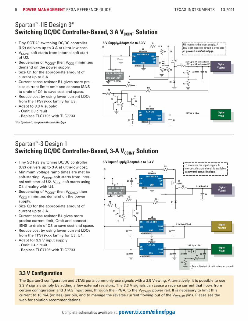
5 POWER MANAGEMENT FPGA REFERENCE GUIDE TEXAS INSTRUMENTS 1Q 2004
5-V Supply/Adaptable to 3.3 V• Tiny SOT-23 switching DC/DC controller(U2) delivers up to 3 A at ultra-low cost.
• VCCINT soft starts from internal soft start of U2.
• Sequencing of VCCINT then VCCO minimizesdemand on the power supply.
• Size Q1 for the appropriate amount of current up to 3 A.
• Current sense resistor R1 gives more pre-cise current limit; omit and connect ISNS to drain of Q1 to save cost and space.
• Reduce cost by using lower current LDOsfrom the TPS79xxx family for U3.
• Adapt to 3.3 V supply:- Omit U3 circuit- Replace TLC7705 with TLC7733
*For Spartan-II, see power.ti.com/xilinxfpga
DigitalVCCO
DigitalVCCINT
2.5 V Up to 3 A for Spartan-II1.8 V Up to 3 A for Spartan-IIE
Q1
L1
R1
R3D1
ISNSSW
FB
R2 C2 C3
C5
C1
C6
3.3 V Up to 1.5 A
R5
R4
R10
R6U3
TPS78633
GND
1.5 A LDOENVIN VOUT
BYP
DDPAK
SOT23
Q2Q3
U2TPS64203
GND
BUCK CNTRLRVIN
/EN
U1VDD
CTRL
/RESNRST
CT SNS
GND /RST
∼TLC7705
U1 monitors the input supply. A low-cost discrete circuit is available at power.ti.com/xilinxfpga.C4R7
R9 R8
Q4
Spartan™-IIE Design 3* Switching DC/DC Controller-Based, 3 A VCCINT Solution
• Tiny SOT-23 switching DC/DC controller(U2) delivers up to 3 A at ultra-low cost.
• Minimum voltage ramp times are met bysoft-starting. VCCINT soft starts from inter-nal soft start of U2. VCCO soft starts usingQ4 circuitry with U4.
• Sequencing of VCCINT then VCCAUX thenVCCO minimizes demand on the power supply.
• Size Q3 for the appropriate amount of current up to 3 A.
• Current sense resistor R4 gives more precise current limit; Omit and connectISNS to drain of Q3 to save cost and space.
• Reduce cost by using lower current LDOsfrom the TPS79xxx family for U3, U4.
• Adapt for 3.3 V input supply:- Omit U4 circuit- Replace TLC7705 with TLC7733
5-V Input Supply/Adaptable to 3.3 V
Complete schematics available at: power.ti.com/xilinxfpga
3.3 V ConfigurationThe Spartan-3 configuration and JTAG ports commonly use signals with a 2.5 V-swing. Alternatively, it is possible to use3.3 V signals simply by adding a few external resistors. The 3.3 V signals can cause a reverse current that flows from certain configuration and JTAG input pins, through the FPGA, to the VCCAUX power rail. It is necessary to limit this current to 10 mA (or less) per pin, and to manage the reverse current flowing out of the VCCAUX pins. Please see the web for solution recommendations.
GND
1.5 A LDOENVIN VOUT
BYP
MSOP8PWP
DigitalVCCINT
DigitalVCCO
DigitalVCCAUX
GND
250 mA LDOEN
VIN VOUT
BYP
MSOP8PWP
Q3Si5475
L1
D1
ISNSSW
FB
C6
C4
C1
R1
R2R5
R3
Q1Q2
GND
BUCK CNTRLRVIN
/ENU1
VDD
CTRL
/RESNRST
CT SNS
GND
1.2 V Up to 3 A
C5C3
C2
2.5 V Up to 250 mA
SOT23
3.3 V Up to 1.5 A
R4
U2TPS64203
U3TPS79425
U4TPS78633
/RST
∼
C7 C8Q4
R7
R6
TLC7705
U1 monitors the input supply. A low-cost discrete circuit is available at power.ti.com/xilinxfpga.
See soft-start circuit notes an page 6.
Spartan™-3 Design 1Switching DC/DC Controller-Based, 3-A VCCINT Solution
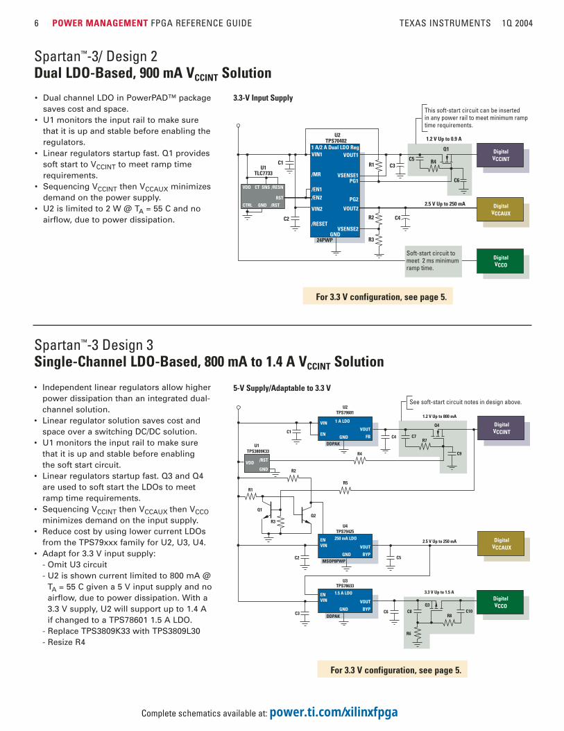
6 POWER MANAGEMENT FPGA REFERENCE GUIDE TEXAS INSTRUMENTS 1Q 2004
DigitalVCCINT
DigitalVCCO
DigitalVCCAUX
U1
C2
C4C1
C7
C9
C5
C3 C6
2.5 V Up to 250 mA
3.3 V Up to 1.5 A
1.2 V Up to 800 mA
R7
R1
R2
R5
R4
R3
TPS3809K33
/RSTVDDGND
U4TPS79425
U2TPS79601
TPS78633
GND
250 mA LDOENVIN VOUT
BYPMSOP8PWP
U3
GND
1.5 A LDOENVIN VOUT
BYP
DDPAK
GND
1 A LDOVIN
ENVOUT
FB
DDPAK
Q4
Q1Q2
C8 C10Q3
R8
R6
See soft-start circuit notes in design above.
Spartan™-3 Design 3Single-Channel LDO-Based, 800 mA to 1.4 A VCCINT Solution
• Independent linear regulators allow higherpower dissipation than an integrated dual-channel solution.
• Linear regulator solution saves cost andspace over a switching DC/DC solution.
• U1 monitors the input rail to make surethat it is up and stable before enabling the soft start circuit.
• Linear regulators startup fast. Q3 and Q4are used to soft start the LDOs to meetramp time requirements.
• Sequencing VCCINT then VCCAUX then VCCOminimizes demand on the input supply.
• Reduce cost by using lower current LDOs from the TPS79xxx family for U2, U3, U4.
• Adapt for 3.3 V input supply:- Omit U3 circuit - U2 is shown current limited to 800 mA @
TA = 55 C given a 5 V input supply and noairflow, due to power dissipation. With a3.3 V supply, U2 will support up to 1.4 A if changed to a TPS78601 1.5 A LDO.
- Replace TPS3809K33 with TPS3809L30- Resize R4
5-V Supply/Adaptable to 3.3 V
Spartan™-3/ Design 2 Dual LDO-Based, 900 mA VCCINT Solution
DigitalVCCINT
DigitalVCCO
TPS70402
DigitalVCCAUX
1 A/2 A Dual LDO RegVIN1
/MR
/EN1/EN2
VIN2
/RESET
VOUT1
VSENSE1PG1
PG2
VOUT2
VSENSE2
24PWP
VDD
CTRL
/RESNCT SNS
/RST
RST
GND
U2
2.5 V Up to 250 mA
1.2 V Up to 0.9 A
C5C3
C4
C1
C2
R1
C6
R4
R2
R3GND
U1TLC7733
Q1
This soft-start circuit can be inserted in any power rail to meet minimum ramptime requirements.
Soft-start circuit to meet 2 ms minimum ramp time.
• Dual channel LDO in PowerPAD™ packagesaves cost and space.
• U1 monitors the input rail to make surethat it is up and stable before enabling the regulators.
• Linear regulators startup fast. Q1 providessoft start to VCCINT to meet ramp timerequirements.
• Sequencing VCCINT then VCCAUX minimizesdemand on the power supply.
• U2 is limited to 2 W @ TA = 55 C and no airflow, due to power dissipation.
3.3-V Input Supply
Complete schematics available at: power.ti.com/xilinxfpga
For 3.3 V configuration, see page 5.
For 3.3 V configuration, see page 5.

7 POWER MANAGEMENT FPGA REFERENCE GUIDE TEXAS INSTRUMENTS 1Q 2004
• Highly efficient VCCINT and VCCO rails up to6 A. Interchange any of the TPS54x10 fami-ly of parts for different current levels from 1.5 A to 9 A. (See page 10 for pin compatibility).
• SWIFT™ (Switcher with Integrated FET)TPS54610 adjustable design allows use ofsmaller inductor, ceramic capacitors.
• Fixed TPS5461x 1.2-V and 3.3-V design with internal compensation and tantalumcapacitors available.
• Use SWIFT design software to customizeexternal components, or see the web forcomplete schematics.
• High UVLO (Under Voltage Lockout) andintegrated soft start of U1/U3 eliminate theneed for an external SVS to monitor theinput voltage. Soft starting also meetsramp time requirements.
• Sequencing of VCCO then VCCAUX then VCCOminimizes demand on the power supply.
• Additional VCCO rails easily added andsequenced using TPS54xxx PWRGD featureand enable.
• Adapt for 3.3 V supply:- Omit U3 circuit
DigitalVCCAUX
2.5 V Up to 250 mA
TPS79425
GND
250 mA LDOENVIN VOUT
BYP
MSOP8PWP
U2
DigitalVCCO
DigitalVCCINT
TPS546106.0 A Switcher
VIN
RT
SS/ENA
VBIAS
PWRGD
PH
BOOT
PGND
COMP
VSENSE
AGND
28PWP
U3
3.3 V Up to 6 A
TPS546106.0 A Switcher
VIN
RT
SS/ENA
VBIAS
PWRGD
PH
BOOT
PGND
COMP
VSENSE
AGND
28PWP
U1
1.2 V Up to 6 A
Spartan™-3 Design 4Switching DC/DC Converter-Based, 6-A VCCINT Solution
5-V Input Supply/Adaptable to 3.3 V
Other 2.5 V Circuits
DigitalVCCO
U2PTH03000
U1PTH03000
6 A ModuleVIN
GND VOADJVOUT
DigitalVCCAUX
2.5 V Up to 6 A
3.3 V Up to 6 A
6 A ModuleVIN
GND VOADJVOUT Digital
VCCINTC1
C3
C2
C4
1.5 V Up to 6 A
TPS79525 LDO2.5 V @ 500 mA
Analog (8)AVCCAUXTX
2.5 V @ 60 mAper MGT
C5
C7
C9
C11
C6
C8
C10
C12
TPS79525 LDO2.5 V @ 500 mA
Analog (8)AVCCAUXRX2.5 V @ 35 mA
per MGT
TPS79401 LDOAdjust @ 250 mA
Analog (8)AVTRX
1.8-2.625 V @ 30 mAper MGT
TPS79401 LDOAdjust @ 250 mA
Analog (8)AVTTX
1.8-2.625 V @ 15 mAper MGT
Virtex-II ProCircuit shown powering 8 of 24
RocketIO™ Multi-GigabitTransceivers (MGT).
All unused RocketIO transceiversmust be connected to power (2.5 V)
and ground.
Virtex-IIOmit this circuit.
R1
R2
R3
R6
R5
R4
U5
U4
U3
U6
RocketIO™ Power Section
Virtex-IIVCCAUX is 3.3 V
3.3 V Input Supply• Simple to use plug-in modules.• Highly efficient VCCINT and VCCO rails. • Additional VCCO rails easily added.• Interchange modules to support:
- 6 A to 30 A - 5.0 V or 12 V input supply- Minimum input and output capacitors may
change depending on application• Reduce cost by using lower current LDOs
from the TPS79xxx family for theRocketIO™ power section.
Virtex™-II/ Virtex-II Pro™ Design 1Module-Based, 6-A VCCINT Solution
RocketIO™ Power SectionAVCCAUXTX, VCCAUXRX, AVTRX, and AVTTXare shown powered by independent linearregulators but they may all be powered bythe same linear regulator, if desired. SeeTPS79xxx and TPS786xx LDO selectionguide (see page 10).
Complete schematics available at: power.ti.com/xilinxfpga
For 3.3 V configuration, see page 5.
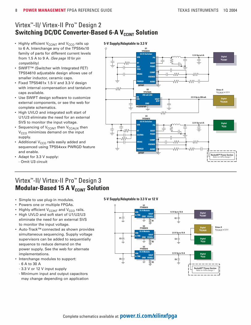
8 POWER MANAGEMENT FPGA REFERENCE GUIDE TEXAS INSTRUMENTS 1Q 2004
• Highly efficient VCCINT and VCCO rails up to 6 A. Interchange any of the TPS54x10family of parts for different current levelsfrom 1.5 A to 9 A. (See page 10 for pin compatibility).
• SWIFT™ (Switcher with Integrated FET)TPS54610 adjustable design allows use ofsmaller inductor, ceramic caps.
• Fixed TPS5461x 1.5-V and 3.3-V designwith internal compensation and tantalumcaps available.
• Use SWIFT design software to customizeexternal components, or see the web forcomplete schematics.
• High UVLO and integrated soft start ofU1/U3 eliminate the need for an externalSVS to monitor the input voltage.
• Sequencing of VCCINT then VCCAUX thenVCCO minimizes demand on the input supply.
• Additional VCCO rails easily added andsequenced using TPS54xxx PWRGD featureand enable.
• Adapt for 3.3 V supply:- Omit U3 circuit
Virtex™-II/ Virtex-II Pro™ Design 2Switching DC/DC Converter-Based 6-A VCCINT Solution
DigitalVCCAUX
2.5 V Up to 250 mA
TPS79425
GND
250 mA LDOENVIN VOUT
BYP
MSOP8PWP
U2
DigitalVCCO
DigitalVCCINT
TPS546106.0 A Switcher
VIN
RT
SS/ENA
VBIAS
PWRGD
PH
BOOT
PGND
COMP
VSENSE
AGND
28PWP
U3
3.3 V Up to 6 A
TPS546106.0 A Switcher
VIN
RT
SS/ENA
VBIAS
PWRGD
PH
BOOT
PGND
COMP
VSENSE
AGND
28PWP
U1
1.5 V Up to 6 A
Virtex-IIVCCAUX is 3.3 V
RocketIO™ Power SectionRefer to V-IIPro Design 1
5-V Supply/Adaptable to 3.3 V
• Simple to use plug-in modules.• Powers one or multiple FPGAs.• Highly efficient VCCINT and VCCO rails. • High UVLO and soft start of U1/U2/U3
eliminate the need for an external SVS to monitor the input voltage.
• Auto-Track™ connected as shown providessimultaneous sequencing. Supply voltagesupervisors can be added to sequentiallysequence to reduce demand on the power supply. See the web for alternateimplementations.
• Interchange modules to support:- 6 A to 30 A - 3.3 V or 12 V input supply- Minimum input and output capacitors
may change depending on application
Virtex™-II/ Virtex-II Pro™ Design 3Modular-Based 15 A VCCINT Solution
Virtex-IIVCCAUX is 3.3 V
DigitalVCCO
DigitalVCCO
U3PTH05010
U2PTH05010
U1PTH05010
15 A ModuleVINA-TRK
GND VOADJVOUT
3.3 V Up to 15 A
15 A ModuleVINA-TRK
GND VOADJVOUT
DigitalVCCAUX
2.5 V Up to 15 A
15 A ModuleVINA-TRK
GND VOADJVOUT Digital
VCCINTC1
C3
C5
C2
C4
C6
1.5 V Up to 15 A
RocketIO™ Power SectionRefer to V-IIPro Design 1
R1
R2
R3
5-V Supply/Adaptable to 3.3 V or 12 V
Complete schematics available at: power.ti.com/xilinxfpga

9 POWER MANAGEMENT FPGA REFERENCE GUIDE TEXAS INSTRUMENTS 1Q 2004
Virtex-IIVCCAUX is 3.3 V
DigitalVCCAUX
U3 TPS79425250 mA LDOEN
VIN VOUTBYP
Digital2X VCCINT
1.5 V @ 12 A
GNDMSOP8PWP
DigitalVCCO
U2TPS40051
U1TPS40051
Buck CntrlrILLMKFF
VFB
COMP
SS/SDBP5
BP10PGND/SGND
BOOST
HDRV
SWVIN
LDRV
RT
16PWP
R12
R13
R21C16
C17
R15 C19
C20R16
R17
R20R14
R18
C22
C15
C21 L2
R22
C23
C24
C25
R19
C18
C26 C27
3.3 V Up to 12 A
DigitalVCCINT
Buck CntrlrILLMKFF
VFB
COMP
SS/SDBP5
BP10PGND/SGND
BOOST
HDRV
SWVIN
LDRV
RT
16PWP
R1
R2
R3C3
R4 C7 C6
C4
C8R5
R6
R10R9
R7
C10
C2C1
C9 L1
R11
C11
C12
C13
R8
C5
C14
1.5 V Up to 12 A
2.5 V Up to 250 mA
12 V
RocketIO™ Power SectionRefer to V-IIPro Design 1
Q1
Q2HAT2167H
Q3
Q4HAT2167H
Virtex™-II/ Virtex-II Pro™ Design 5High-Voltage Switching DC/DC Controller-Based, 12-A VCCINT Solution• Powers one or multiple FPGAs.• Highly efficient VCCINT and VCCO rails up
to 12 A.• Flexible controller design allows optimiza-
tion for size, power dissipation, and cost.• Use TPS40K design software to customize
designs, or see the web for completeschematics.
• Soft-start feature and high UVLO of U1/U2eliminates the need for an external SVS tomonitor the input voltage.
• Sequencing minimizes demand on theinput supply.
• Additional VCCO rails easily added andsequenced.
• Reduce cost by using lower current LDOsfrom the TPS79xxx family for U3.
12-V Supply
• Powers one or multiple FPGAs. • Highly efficient VCCINT and VCCO rails up
to 20 A.• Flexible controller design allows optimiza-
tion for size, power dissipation, and cost.• Use TPS40K and SWIFT™ design software
to customize designs, or see the web forcomplete schematics.
• Adjustable TPS541x allows use of smallerinductor, ceramic capacitors.
• Fixed TPS5461x design with internal compensation and tantalum caps available.
• Interchange any of the TPS54x10 SWIFT™family of parts for different current levelsfrom 1.5 A to 9 A. (See page 10 for pin-pin compatibility).
• Soft-start feature of U1, U2, and U3 eliminates the need for an external SVS to monitor the input voltage.
• Sequencing minimizes demand on theinput supply.
• Additional VCCO rails easily added andsequenced.
• Adapt for 3.3 V supply:- Omit U3 circuit
VIN
DigitalVCCO
DigitalVCCINT
RocketIO™ Power SectionRefer to V-IIPro Design 1
TPS40021ILIM/SYNCVDDOSNSFBCOMPSS/SDRTSGND
BT1HDRV
SWBT2
PVDDLDRV
PGNDPGD
U1
TPS54610RTSYNCSS/ENAVBIASVINVINVINPGNDPGNDPGND
AGNDVSENSE
COMPPWRGD
BOOTPHPHPHPHPH
U2
U2TPS40021
VIN
ILIM/SYNCVDDOSNSFBCOMPSS/SDRTSGND
BT1HDRV
SWBT2
PVDDLDRV
PGNDPGD
+
+
+
+
Virtex-IIVCCAUX is 3.3 V
DigitalVCCO
DigitalVCCAUX
16PWP
28PWP
28PWP
3.3 V Up to 20 A
2.5 V Up to 6 A
1.5 V Up to 20 A
Virtex™-II/ Virtex-II Pro™ Design 4Low-Voltage Switching DC/DC Controller-Based, 20-A VCCINT Solution
5-V Supply/Adaptable to 3.3 V
Complete schematics available at: power.ti.com/xilinxfpga
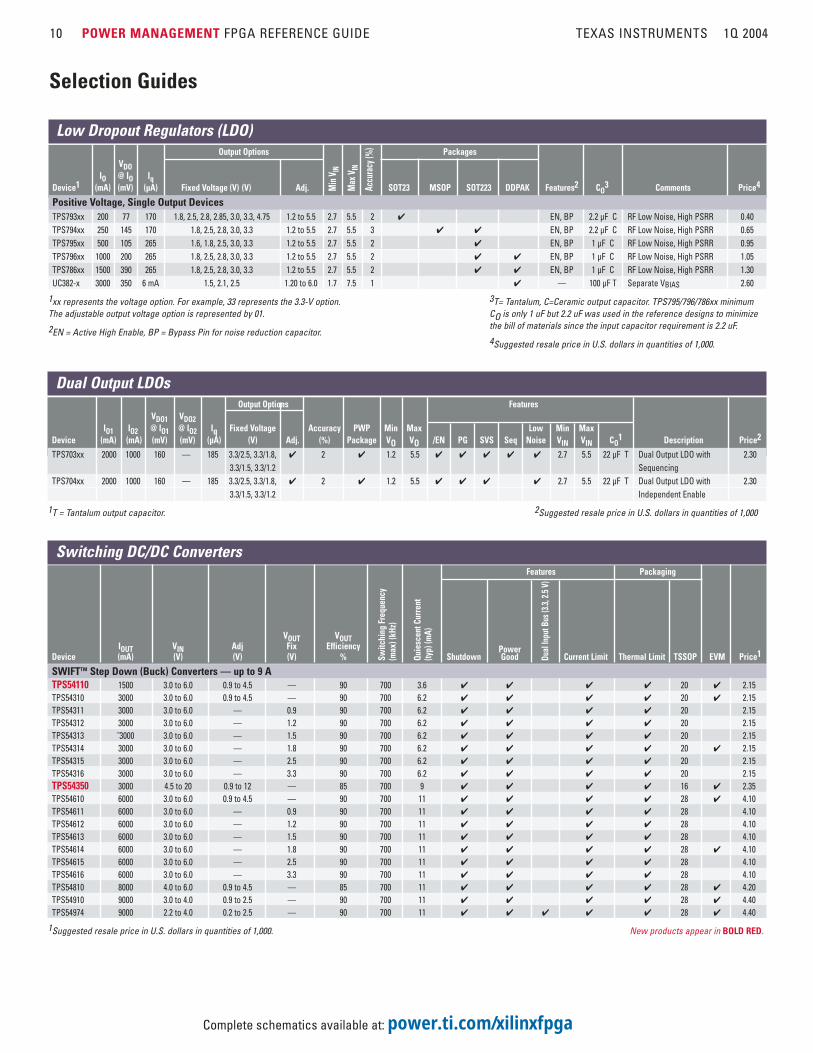
Low Dropout Regulators (LDO)Output Options Packages
VDOIO @ IO Iq
Device1 (mA) (mV) (µA) Fixed Voltage (V) (V) Adj. SOT23 MSOP SOT223 DDPAK Features2 CO3 Comments Price4
Positive Voltage, Single Output DevicesTPS793xx 200 77 170 1.8, 2.5, 2.8, 2.85, 3.0, 3.3, 4.75 1.2 to 5.5 2.7 5.5 2 ✔ EN, BP 2.2 µF C RF Low Noise, High PSRR 0.40TPS794xx 250 145 170 1.8, 2.5, 2.8, 3.0, 3.3 1.2 to 5.5 2.7 5.5 3 ✔ ✔ EN, BP 2.2 µF C RF Low Noise, High PSRR 0.65TPS795xx 500 105 265 1.6, 1.8, 2.5, 3.0, 3.3 1.2 to 5.5 2.7 5.5 2 ✔ EN, BP 1 µF C RF Low Noise, High PSRR 0.95TPS796xx 1000 200 265 1.8, 2.5, 2.8, 3.0, 3.3 1.2 to 5.5 2.7 5.5 2 ✔ ✔ EN, BP 1 µF C RF Low Noise, High PSRR 1.05TPS786xx 1500 390 265 1.8, 2.5, 2.8, 3.0, 3.3 1.2 to 5.5 2.7 5.5 2 ✔ ✔ EN, BP 1 µF C RF Low Noise, High PSRR 1.30UC382-x 3000 350 6 mA 1.5, 2.1, 2.5 1.20 to 6.0 1.7 7.5 1 ✔ — 100 µF T Separate VBIAS 2.60
1xx represents the voltage option. For example, 33 represents the 3.3-V option. 3T= Tantalum, C=Ceramic output capacitor. TPS795/796/786xx minimum The adjustable output voltage option is represented by 01. CO is only 1 uF but 2.2 uF was used in the reference designs to minimize
2EN = Active High Enable, BP = Bypass Pin for noise reduction capacitor.the bill of materials since the input capacitor requirement is 2.2 uF.
4Suggested resale price in U.S. dollars in quantities of 1,000.M
in V IN
Max
VIN
Accu
racy
(%)
10 POWER MANAGEMENT FPGA REFERENCE GUIDE TEXAS INSTRUMENTS 1Q 2004
Dual Output LDOs Output Options Features
VDO1 VDO2IO1 IO2 @ IO1 @ IO2 Iq Fixed Voltage Accuracy PWP Min Max Low Min Max
Device (mA) (mA) (mV) (mV) (µA) (V) Adj. (%) Package VO VO /EN PG SVS Seq Noise VIN VIN CO1 Description Price2
TPS703xx 2000 1000 160 — 185 3.3/2.5, 3.3/1.8, ✔ 2 ✔ 1.2 5.5 ✔ ✔ ✔ ✔ ✔ 2.7 5.5 22 µF T Dual Output LDO with 2.303.3/1.5, 3.3/1.2 Sequencing
TPS704xx 2000 1000 160 — 185 3.3/2.5, 3.3/1.8, ✔ 2 ✔ 1.2 5.5 ✔ ✔ ✔ ✔ 2.7 5.5 22 µF T Dual Output LDO with 2.303.3/1.5, 3.3/1.2 Independent Enable
1T = Tantalum output capacitor. 2Suggested resale price in U.S. dollars in quantities of 1,000
Switching DC/DC Converters Features Packaging
VOUT VOUTIOUT VIN Adj Fix Efficiency Power
Device (mA) (V) (V) (V) % Shutdown Good Current Limit Thermal Limit TSSOP EVM Price1
SWIFTTM Step Down (Buck) Converters — up to 9 ATPS54110 1500 3.0 to 6.0 0.9 to 4.5 — 90 700 3.6 ✔ ✔ ✔ ✔ 20 ✔ 2.15TPS54310 3000 3.0 to 6.0 0.9 to 4.5 — 90 700 6.2 ✔ ✔ ✔ ✔ 20 ✔ 2.15TPS54311 3000 3.0 to 6.0 — 0.9 90 700 6.2 ✔ ✔ ✔ ✔ 20 2.15TPS54312 3000 3.0 to 6.0 — 1.2 90 700 6.2 ✔ ✔ ✔ ✔ 20 2.15TPS54313 ˜3000 3.0 to 6.0 — 1.5 90 700 6.2 ✔ ✔ ✔ ✔ 20 2.15TPS54314 3000 3.0 to 6.0 — 1.8 90 700 6.2 ✔ ✔ ✔ ✔ 20 ✔ 2.15TPS54315 3000 3.0 to 6.0 — 2.5 90 700 6.2 ✔ ✔ ✔ ✔ 20 2.15TPS54316 3000 3.0 to 6.0 — 3.3 90 700 6.2 ✔ ✔ ✔ ✔ 20 2.15TPS54350 3000 4.5 to 20 0.9 to 12 — 85 700 9 ✔ ✔ ✔ ✔ 16 ✔ 2.35TPS54610 6000 3.0 to 6.0 0.9 to 4.5 — 90 700 11 ✔ ✔ ✔ ✔ 28 ✔ 4.10TPS54611 6000 3.0 to 6.0 — 0.9 90 700 11 ✔ ✔ ✔ ✔ 28 4.10TPS54612 6000 3.0 to 6.0 — 1.2 90 700 11 ✔ ✔ ✔ ✔ 28 4.10TPS54613 6000 3.0 to 6.0 — 1.5 90 700 11 ✔ ✔ ✔ ✔ 28 4.10TPS54614 6000 3.0 to 6.0 — 1.8 90 700 11 ✔ ✔ ✔ ✔ 28 ✔ 4.10TPS54615 6000 3.0 to 6.0 — 2.5 90 700 11 ✔ ✔ ✔ ✔ 28 4.10TPS54616 6000 3.0 to 6.0 — 3.3 90 700 11 ✔ ✔ ✔ ✔ 28 4.10TPS54810 8000 4.0 to 6.0 0.9 to 4.5 — 85 700 11 ✔ ✔ ✔ ✔ 28 ✔ 4.20TPS54910 9000 3.0 to 4.0 0.9 to 2.5 — 90 700 11 ✔ ✔ ✔ ✔ 28 ✔ 4.40TPS54974 9000 2.2 to 4.0 0.2 to 2.5 — 90 700 11 ✔ ✔ ✔ ✔ ✔ 28 ✔ 4.40
1Suggested resale price in U.S. dollars in quantities of 1,000. New products appear in BOLD RED.
Switc
hing
Fre
quen
cy(m
ax) (
kHz)
Quie
scen
t Cur
rent
(typ)
(mA)
Dual
Inpu
t Bus
(3.3,
2.5 V
)
Selection Guides
Complete schematics available at: power.ti.com/xilinxfpga
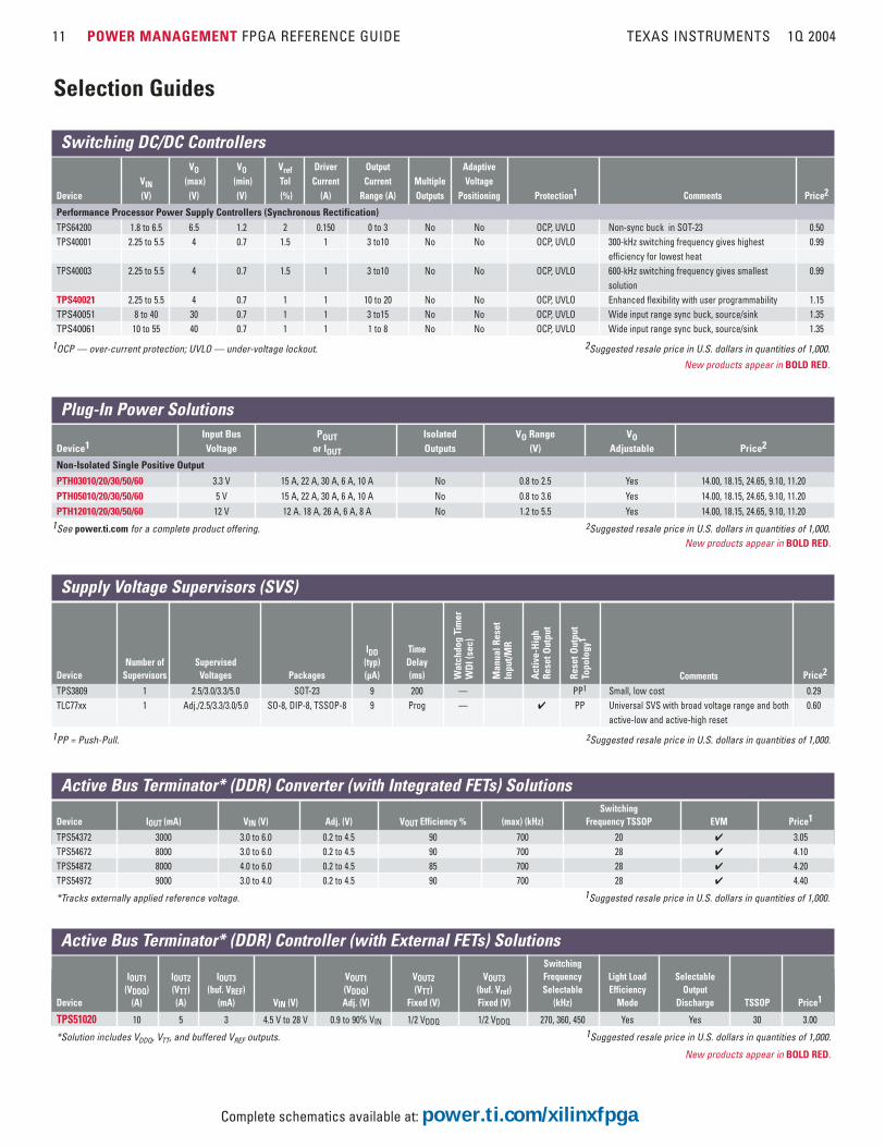
11 POWER MANAGEMENT FPGA REFERENCE GUIDE TEXAS INSTRUMENTS 1Q 2004
Selection Guides
Switching DC/DC Controllers VO VO Vref Driver Output Adaptive
VIN (max) (min) Tol Current Current Multiple VoltageDevice (V) (V) (V) (%) (A) Range (A) Outputs Positioning Protection1 Comments Price2
Performance Processor Power Supply Controllers (Synchronous Rectification)TPS64200 1.8 to 6.5 6.5 1.2 2 0.150 0 to 3 No No OCP, UVLO Non-sync buck in SOT-23 0.50TPS40001 2.25 to 5.5 4 0.7 1.5 1 3 to10 No No OCP, UVLO 300-kHz switching frequency gives highest 0.99
efficiency for lowest heatTPS40003 2.25 to 5.5 4 0.7 1.5 1 3 to10 No No OCP, UVLO 600-kHz switching frequency gives smallest 0.99
solutionTPS40021 2.25 to 5.5 4 0.7 1 1 10 to 20 No No OCP, UVLO Enhanced flexibility with user programmability 1.15TPS40051 8 to 40 30 0.7 1 1 3 to15 No No OCP, UVLO Wide input range sync buck, source/sink 1.35TPS40061 10 to 55 40 0.7 1 1 1 to 8 No No OCP, UVLO Wide input range sync buck, source/sink 1.35
1OCP — over-current protection; UVLO — under-voltage lockout. 2Suggested resale price in U.S. dollars in quantities of 1,000.New products appear in BOLD RED.
Plug-In Power Solutions Input Bus POUT Isolated VO Range VO
Device1 Voltage or IOUT Outputs (V) Adjustable Price2
Non-Isolated Single Positive Output
PTH03010/20/30/50/60 3.3 V 15 A, 22 A, 30 A, 6 A, 10 A No 0.8 to 2.5 Yes 14.00, 18.15, 24.65, 9.10, 11.20PTH05010/20/30/50/60 5 V 15 A, 22 A, 30 A, 6 A, 10 A No 0.8 to 3.6 Yes 14.00, 18.15, 24.65, 9.10, 11.20PTH12010/20/30/50/60 12 V 12 A. 18 A, 26 A, 6 A, 8 A No 1.2 to 5.5 Yes 14.00, 18.15, 24.65, 9.10, 11.20
1See power.ti.com for a complete product offering. 2Suggested resale price in U.S. dollars in quantities of 1,000.New products appear in BOLD RED.
Supply Voltage Supervisors (SVS)
IDD TimeNumber of Supervised (typ) Delay
Device Supervisors Voltages Packages (µA) (ms) Price2
TPS3809 1 2.5/3.0/3.3/5.0 SOT-23 9 200 — PP1 Small, low cost 0.29TLC77xx 1 Adj./2.5/3.3/3.0/5.0 SO-8, DIP-8, TSSOP-8 9 Prog — ✔ PP Universal SVS with broad voltage range and both 0.60
active-low and active-high reset
1PP = Push-Pull. 2Suggested resale price in U.S. dollars in quantities of 1,000.
Wat
chdo
g Ti
mer
WD
I (se
c)
Man
ual R
eset
Inpu
t/MR
Act
ive-
Hig
hRe
set O
utpu
t
Rese
t Out
put
Topo
logy
1
Comments
Active Bus Terminator* (DDR) Converter (with Integrated FETs) SolutionsSwitching
Device IOUT (mA) VIN (V) Adj. (V) VOUT Efficiency % (max) (kHz) Frequency TSSOP EVM Price1
TPS54372 3000 3.0 to 6.0 0.2 to 4.5 90 700 20 ✔ 3.05TPS54672 8000 3.0 to 6.0 0.2 to 4.5 90 700 28 ✔ 4.10TPS54872 8000 4.0 to 6.0 0.2 to 4.5 85 700 28 ✔ 4.20TPS54972 9000 3.0 to 4.0 0.2 to 4.5 90 700 28 ✔ 4.40
*Tracks externally applied reference voltage. 1Suggested resale price in U.S. dollars in quantities of 1,000.
Active Bus Terminator* (DDR) Controller (with External FETs) SolutionsSwitching
IOUT1 IOUT2 IOUT3 VOUT1 VOUT2 VOUT3 Frequency Light Load Selectable(VDDQ) (VTT) (buf. VREF) (VDDQ) (VTT) (buf. Vref) Selectable Efficiency Output
Device (A) (A) (mA) VIN (V) Adj. (V) Fixed (V) Fixed (V) (kHz) Mode Discharge TSSOP Price1
TPS51020 10 5 3 4.5 V to 28 V 0.9 to 90% VIN 1/2 VDDQ 1/2 VDDQ 270, 360, 450 Yes Yes 30 3.00
*Solution includes VDDQ, VTT, and buffered VREF outputs. 1Suggested resale price in U.S. dollars in quantities of 1,000.
New products appear in BOLD RED.
Complete schematics available at: power.ti.com/xilinxfpga
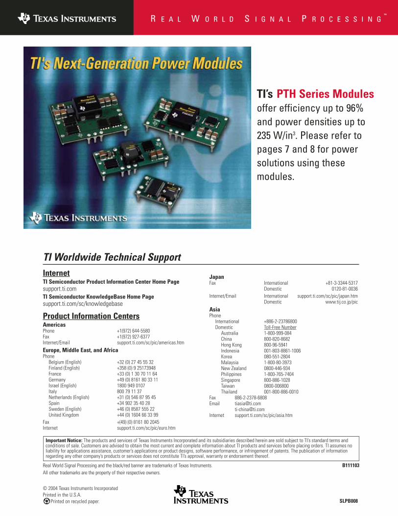
R E A L W O R L D S I G N A L P R O C E S S I N G™
SLPB008
TI’s PTH Series Modulesoffer efficiency up to 96%and power densities up to235 W/in3. Please refer topages 7 and 8 for powersolutions using these modules.
TI Worldwide Technical SupportInternetTI Semiconductor Product Information Center Home Pagesupport.ti.comTI Semiconductor KnowledgeBase Home Pagesupport.ti.com/sc/knowledgebase
Product Information CentersAmericasPhone +1(972) 644-5580Fax +1(972) 927-6377Internet/Email support.ti.com/sc/pic/americas.htmEurope, Middle East, and AfricaPhone
Belgium (English) +32 (0) 27 45 55 32Finland (English) +358 (0) 9 25173948France +33 (0) 1 30 70 11 64Germany +49 (0) 8161 80 33 11Israel (English) 1800 949 0107Italy 800 79 11 37Netherlands (English) +31 (0) 546 87 95 45Spain +34 902 35 40 28Sweden (English) +46 (0) 8587 555 22United Kingdom +44 (0) 1604 66 33 99
Fax +(49) (0) 8161 80 2045Internet support.ti.com/sc/pic/euro.htm
JapanFax International +81-3-3344-5317
Domestic 0120-81-0036Internet/Email International support.ti.com/sc/pic/japan.htm
Domestic www.tij.co.jp/picAsiaPhone
International +886-2-23786800Domestic Toll-Free Number
Australia 1-800-999-084China 800-820-8682Hong Kong 800-96-5941Indonesia 001-803-8861-1006Korea 080-551-2804Malaysia 1-800-80-3973New Zealand 0800-446-934Philippines 1-800-765-7404Singapore 800-886-1028Taiwan 0800-006800Thailand 001-800-886-0010
Fax 886-2-2378-6808Email [email protected]
[email protected] support.ti.com/sc/pic/asia.htm
B111103
Important Notice: The products and services of Texas Instruments Incorporated and its subsidiaries described herein are sold subject to TI’s standard terms andconditions of sale. Customers are advised to obtain the most current and complete information about TI products and services before placing orders. TI assumes noliability for applications assistance, customer’s applications or product designs, software performance, or infringement of patents. The publication of informationregarding any other company’s products or services does not constitute TI’s approval, warranty or endorsement thereof.
© 2004 Texas Instruments IncorporatedPrinted in the U.S.A.
Printed on recycled paper.
Real World Signal Processing and the black/red banner are trademarks of Texas Instruments.All other trademarks are the property of their respective owners.

Xilinx Alliance EDA Members and Products
AccelChipwww.accelchip.comHigh-level synthesis tools that read MATLAB and output RTL
Alatekwww.alatek.comHardware acceleration (HES)
Altiumwww.altium.com/products/nvisage.htmComplete PCB/FPGA design flow(nVisage) targeting Spartan™ Series FPGAs
Ansoftwww.ansoft.comHigh-Frequency products for system analysis, circuit design, and electromagneticsimulation (Ansoft Designer™, HFSS™)
Apache Designwww.apache-da.com/Products/nspice.htmHSPICE®-compatible simulator using actual S-parameter data (NSPICE) forVirtex-II Pro™ MGT-based PCB design
Aptixwww.aptix.comASIC emulation (Prototype Studio™)
Atrentawww.atrenta.comRTL Linter technology for Virtex™-II and Virtex-II Pro FPGAs (SpyGlass®)
Auspywww.auspy.comFPGA partition (APS II) and ASIC emula-tion (ACE Compiler)
Cadence Design Systemswww.cadence.com/feature/fpga_design.htmlVirtex-II Pro MGT support for high-speedPCB design (SPECCTRAQuest®); NCSimfamily for FPGA design simulation
Celoxicawww.celoxica.comC-level design creation, compilation, andverification for Virtex-II and Virtex-II ProFPGAs
Endeavorwww.endeav.comCo-verification for Virtex-II Pro(CoSimple™)
EVEwww.eve-team.comRTL-level Simulator Accelerator (ZEBU)
Forte Designwww.forteds.comHLL compiler to RTL (Cynlib Tool Suite);timing specification and analysis tool(TimingDesigner)
Hier Design Inc.www.hierdesign.comHierarchical floorplanning and analysissoftware (PlanAhead™) for Virtex-II,Virtex-II Pro and Spartan-3 FPGAs
MAGMAwww.magma-da.comArchitecture-specific synthesis and layoutoptimization for Virtex-II series FPGA(PALACE™)
The MathWorkswww.mathworks.comSystem-level design tools for FPGA andprocessor-based signal processing systems
Mentor Graphicswww.mentor.comVirtex-II Pro MGT support for high-speedPCB design (HyperLynx™, ICX™,Tau™); complete FPGA design flow usingthe ModelSim® family of simulators andLeonardo-Spectrum™/Precision® synthesis;Seamless® co-verification support for Virtex-II Pro; FPGA BoardLink™ FPGA symbolgeneration for fast PCB design iterations forVirtex-II and Virtex-II Pro FPGAs
Novilitwww.novilit.comDesign partitioning using ISEEDK(AnyWare) for Virtex-II and Virtex-IIPro FPGAs
Product Acceleration Inc.www.prodacc.comFPGA symbol generation(LiveComponent™); automated pin assignment optimization; PCB layer countcontrol (DesignF/X)
Simucadwww.simucad.comVerilog™ simulator for FPGAs (Silos)
Synopsyswww.synopsys.comVirtex-II Pro multigigabit transceiver support for high-speed PCB design(HSPICE®); FPGA Compiler II™ RTLsynthesis for Virtex series FPGAs;VCS™(MX)/Scirocco™(MX) simulators;Formality® formal verification, LEDA®
RTL linter, and PrimeTime™ static timing analysis; high-level design usingCoCentric System Studio
Synplicitywww.synplicity.comRTL synthesis (Synplify®), debugger technology (Identify®), physical synthesis(Amplify®), and ASIC prototyping(Certify®) for Xilinx FPGAs
114 Xcell Journal Spring 2004

Spring 2004 Xcell Journal 115
Xilinx AllianceCORE Third-PartyIP Providers and Products
Alcatel Internetworking, Inc. www.ind.alcatel.com/emac/ Ethernet media access controller cores
Amphion Semiconductor Ltd.www.amphion.comDSP, wireless communications, and multimedia cores
Barco-Silexwww.barco-silex.com DSP cores, with a specialization in image-audio applications
CAST, Inc.www.cast-inc.com General-purpose IP for processors, peripherals, multimedia, networking,encryption, serial communications, and bus interfaces
Crossbow Technologies, Inc.www.crossbowip.comSystem Interconnect IP for on-chip andchip-to-chip multiprocessing
Deltatec S.A.www.deltatec.be/IP and services for digital imaging, DSP,multimedia, PCI, and datacom
Derivation Systems, Inc.www.derivation.comIP cores for high assurance hardware/soft-ware applications and embedded systemsproducts; 32-bit Java processor core
Digital Communications Technologiewww.dctl.comEmbedded Java solutions
Digital Core Designwww.dcd.pl/Microprocessor, microcontroller, floating point, and serial communicationcontroller cores
Dolphin Integrationwww.dolphin.fr/Bus interface, processor, peripheral, andDSP cores; EDA software
Duma Video, Inc.www.dumavideo.comDigital video, AES/EBU audio, MPEGand DCT cores; real-time MPEG-2 HD and SD compression
eInfochips Pvt. Ltd.www.einfochips.comPCI, USB, 80186, multimedia, and wireless cores
Eureka Technologywww.eurekatech.comSilicon-proven IP for CPU interface, PCI,PCMCIA, memory control, and otherperipheral functions for SoC designs
GDA Technologies, Inc.www.gdatech.comHyperTransport, PCI, Ethernet, design services
GV & Associates, Inc.www.gvassociates.comBoards and expertise in DSP, processor,software, analog, and RF design
Helion Technology Limitedwww.heliontech.comEncryption and DSP algorithms; design services
iCoding Technology, Inc.www.icoding.comTurbo Code-related error correction products including system design
Intrinsyc, Inc.www.intrinsyc.comSingle board embedded computers (FPGA + external processor); peripheral IP
Loarant Corporationwww.loarant.comProprietary 16-bit RISC CPU; embeddedsystem design
MEET Ltd.www.meet-electronics.comIP cores dedicated to industrial servomotor control
Memec Corewww.memecdesign.com/xilinx/ Peripheral, bus interfaces, encryption, and communications cores
ModelWare, Inc.www.modelware.comDatacom/telecom cores including ATM,HDLC, POS, IMA, UTOPIA, and bridges
NewLogic GmbHwww.newlogic.comCores for wireless applications includingBluetooth and 802.11
Paxonet Communicationswww.paxonet.comSolutions for interworking metro networking technologies to SONET
Perigee, LLCwww.perigeellc.comDSP and image processing cores; embeddedfirmware, GUI, and application softwaredevelopment
Pinpoint Solutions, Inc.www.asic-design.comStandards-based telecom and datacom IP
QualCore Logic, Inc.www.virtualipgroup.comCores for microcontrollers, telecommunica-tions, datacom, PC peripherals, and businterface standards
RealFast Operating Systems ABwww.realfast.se/Real-time systems and RTOS; operatingsystem cores
Robert Bosch GmbHwww.can.bosch.comAutomotive, CAN
SOC Solutions, L.L.C.www.socsolutions.comEmbedded µP and software; networking,wireless, audio, GPS, and handheld; peripheral cores
X I L I N X P A R T N E R Y E L L O W P A G E S
SysOnChip, Inc.www.sysonchip.co.kr/IP and products for CDMACellular/PCS/WLL modem, FEC, and Bluetooth™
Telecom Italia Lab S.p.A.www.idosoc.com/soc/viplibrary/Cores for ATM, optical networking, and switched digital video broadcast equipment
Tensilica, Inc.www.tensilica.comConfigurable processor cores and development tools
TurboConceptwww.turboconcept.comTurbo Code forward error correction solutions
Wipro, Ltd.www.wipro.comIP building blocks for technologies likeIEEE 1394, USB, Bluetooth, and IEEE802.11
Xylon d.o.o.www.logicbricks.comHuman-machine interfaces and industrialcommunication controllers
Zuken, Inc.www.zuken.co.jp/soc/PCI2.2, 10/100 Ethernet, and GigabitEthernet cores
Reference Design PartnersThe Xilinx Reference Design AllianceProgram builds partnerships with industry-leading semiconductor manufacturers todevelop reference designs for acceleratingour customer’s product and system time tomarket. The goal is to build a library ofhigh-quality, multicomponent system-levelreference designs in the areas of networking,communications, image and video processing, DSP, and emerging technolo-gies and markets.
Agere Systemswww.agere.com
AMCCwww.amcc.com
Analog Deviceswww.analog.com
Bay MicroSystemswww.baymicrosystems.com
BitBlitz Communicationswww.bitblitz.com
Broadcom Corp.www.broadcom.com
Centilliumwww.centillium.com
Cypress Semiconductorwww.cypress.com
IBM Microelectronicswww.ibm.com/us/
IDTwww.idt.com
Ignis Opticswww.ignis-optics.com
Infineon Technologies AGwww.infineontechnologies.com
Intel Corporationdeveloper.intel.com/design/network/
Intrinsitywww.intrinsity.com/home.htm
Micron Technologywww.micron.com
Motorolawww.motorola.com
National Semiconductor Corporationwww.national.com
NetLogic Microsystems, Inc.www.netlogicmicro.com
Octasic Semiconductorwww.octasic.com
PMC-Sierra Inc.www.pmc-sierra.com/index.html
Samsung Semiconductor, Inc.www.usa.samsungsemi.com
SiberCore Technologieswww.sibercore.com
Texas Instrumentswww.ti.com
TransSwitch Coporationwww.transwitch.com/index_flash.jsp
Vitessewww.vitesse.com
ZettaComwww.zettacom.com
116 Xcell Journal Spring 2004
X I L I N X P A R T N E R Y E L L O W P A G E S
Millogic IP isXilinx Proven!
• PCI-X, VME, 12C,Video, LZS, PS2
• Design Services• Prototyping• Xilinx Xperts
Millogic, Ltd.6 Clocktower PlaceMaynard, MA [email protected]
Spring 2004 Xcell Journal 117
XPERTS Partners
3T BVwww.3T.nl/Design services; measurement instruments;fail-safe controlling; medical equipment,communication, and computer peripherals
Accent S.r.l.www.Accent.it/Complex FPGAs; SoCs; PowerPCs™; IP platforms; software, PCB, and ICfoundry services, from concept to silicon
ADI Engineeringwww.adiengineering.comReference designs; custom designs; designservices focused on Intel IXA and XScale™
Advanced Electronic Designs, Inc.www.aedbozeman.comDesign services and manufacturing support;hardware and software design for embeddedsystems
Advanced Principles Group, Inc.www.advancedprinciples.comDesign services and consulting; softwarealgorithm acceleration and application-specific computing systems
Alpha Datawww.alpha-data.comPCI/PMC/CPCI FPGA boards; embeddedapplications using HDL or SystemGenerator methodologies
AMIRIX Systems Inc.www.amirix.comDesign services for electronic product realization; high-performance digital boards;programmable logic; embedded software
Andraka Consulting Group, Inc.www.andraka.comExclusively FPGAs for DSP since 1994;applications include radar, sonar, digitalcommunications, imaging, and video
Array Electronicswww.array-electronics.de/SoC/FPGA/PCB designs in telecom, industrial, and DSPs; concepts; verification;prototypes; cores
Avnet Design Serviceswww.ads.avnet.comEmbedded processing FPGA design services; Virtex-II Pro; high-speedSERDES; IP core integration; timing closure; RLDRAM; RapidIO™
Baranti Group Inc.www.baranti.comAward-winning design/manufacturing firm;expertise in digital video, FPGAs
Barco Silexwww.barco-silex.comTotal solutions consisting of IP, FPGA, and board design
Benchmark Electronics Inc.www.bench.comEMS/JDM team; product design, support,introduction, and launch into volume production
Birger Engineering, Inc.www.birger.comDevelopment of algorithms, electronics,and systems for digital imaging
BitSim ABwww.bitsim.comDesign services; DSP, video, 3G, andWLAN designs; high-speed prototypingboards
Bottom Line Technologies Inc.www.bltinc.comFPGA, product, and system design services;networking; data communications;telecommunications; video; PCI; signalprocessing; military; aerospace
CES Design Services @ Siemens Program and System Engineeringwww.ces-designservices.comPlatform-oriented SoC/FPGA/PCB andfirmware design in telecom, industrial, andvideo processing; customized solutions;concept; verification; prototypes
CG-CoreEl Programmable Solutions P. Ltd.www.cg-coreel.comDesign services; telecom, networking, andprocessor IP and designs; turnkey FPGA;RTL design/validation
Chess iT/Embeddedwww.chess.nl/Embedded hardware and software design ofproducts and services at the chip, board,and system level
Colorado Electronic Product Design, Inc.www.cepdinc.comDesigning embedded systems with FPGAs for DSP; interfaces for medical,consumer, aerospace, and military
Comit Systems, Inc.www.comit.comHigh-end FPGA/SoC design services,including the integration of customer-developed and third-party IP
ControlNet India Pvt Ltd.www.controlnetindia.comASIC/SoC Analog/RF FPGA design services; IP development; domains:Ethernet, IEEE1394, USB, security, PCI,WLAN, Infiniband
Convergent Design LLCwww.convergent-design.comAudio/video design for professional/consumer products
DATA Respons ASAwww.datarespons.comProfessional design and development services for embedded hardware/softwaresolutions; FPGA/digital hardware applica-tion specialists
Deltatec International Inc.www.deltatec.be/Design services; digital imaging applica-tions; broadcast video, image processing, and image synthesis
Digicom Answers Pty. Ltd. www.fpga.com.au/Design services; experienced FPGAresources; design-on-demand; pre-designadvice; reviews and problem solving
Digital Design Corporation (DDC)www.digidescorp.comDesign services and products; image pro-cessing; video; communications; DSP;audio; automotive; controls; interfaces
Dillon Engineering, Inc.www.dilloneng.comDesign services; FPGA-based DSP algorithms; high-bandwidth, real-time digital signal and image processingapplications
X I L I N X P A R T N E R Y E L L O W P A G E S
118 Xcell Journal Spring 2004
DRS Tactical Systems West Inc.(formally Catalina Research)www.catalinaresearch.comDesign services; FPGAs for DSP, includingthe manufacturer of Virtex reconfigurablecomputing boards
Eden Networks, Inc.www.edennetworks.comTurnkey design services; telecom and net-working designs (Ethernet, SONET, ATM,VoIP)
Edgewood Technologies, LLCwww.edgewoodtechnologies.comDesign services; FPGAs for telecom, DSP,embedded processors
Enea Data ABwww.enea.se/Telecommunication, data communication,DSP, RTOS, automotive, defense, high-reliability, and consumer electronics design
Enterpoint Ltd.www.enterpoint.co.uk/Design services; development boards; video,telecommunications, military, and high-speed design
ESD Inc.www.esdnet.comDesign services; FPGAs for embedded systems, software/hardware design, PCBlayout
Evatronix S.A.www.evatronix.pl/Design services; FPGA design (Virtex,Virtex-E, Spartan-II); embedded systems;SoC and SoPC designs
Evermore Systems Inc.www.evermoresystems.comDesign services; FPGA designs for commu-nications, audio/video, wireless, and homenetworking
ExaLinx www.exalinx.comDesign services; ASIC emulation for high-speed communications and wireless applica-tions; reference designs
Fidus Systems Inc.www.fidus.ca/Design services; FPGAs; communications;video; DSP; interface conversions; ASICverification; hardware; PCB layout; soft-ware; SI/EMC
First Principles Technology, Inc.www.fptek.comDesign/assembly/test services; FPGA +PCB + DSP/processor + system; imaging;video; test; satellite telecom; control
Flexibilis Oywww.flexibilis.comIP development; FPGA design services;Linux device drivers
Flextronics Designwww.flextronics.com/design/Complete product design and developmentservices for high-speed communications;reconfigurable computing; imaging;audio/video; military
GDA Technologies, Inc.www.gdatech.comA leading services company focused ondesigning systems, SoC, ASIC, FPGA, and IP
HCL Technologieswww.hcltech.comHigh-speed board, ASIC, and FPGAdesign and verification services in avionics,medical, networking/telecom, and consumer electronics
Helion Technology Limitedwww.heliontech.comDesign services and IP for FPGA with afocus on data security, wireless, and DSP
IDERS Inc.www.iders.ca/Contract electronic engineering and EMSresource, providing complete product cyclesranging from specifications to production
Image Technology Laboratory Corporationwww.gazogiken.co.jp/Design services; FPGAs for image process-ing; design tools: EDK, System Generator,and Forge
Innovative Computer Technologyictconn.comDigital, analog, Xilinx FPGA, and softwaredesign solutions for customers in a widevariety of industries throughout the UnitedStates
iWave Systems Technologies Private Ltd.www.iwavesystems.comEmbedded hardware and software design;board design; FPGA and ASIC develop-ment services
Liewenthal Electronics Ltd.www.liewenthal.ee/Embedded systems design services; develop-ment of software and hardware includingVirtex and Spartan FPGAs
Logic Product Developmentwww.logicpd.comFull-service product development, includingindustrial design, mechanical, electrical, andsoftware engineering
M&M [email protected] services; imaging; video and audiodesigns; high-density ASIC emulation
Memec Design www.memecdesign.com/xilinx Focused on FPGA design for Xilinx technology, we have completed more than 1,300 designs worldwide
Memondo Graphicswww.memondo.comImplementation of digital signal processing,communications, and image processingsolutions and algorithms over Xilinx FPGAs
Mikrokrets ASwww.mikrokrets.no/FPGA development comprising telecom-munication, network communications, andembedded systems; PCB development
Millogic Ltd.www.millogic.comDesign services and synthesizable cores; expertise in PCI, video, imaging,DSP, compression, ASIC verification, and communications
Milstar Inc.www.Milstar.co.il/Design services and manufacturers (industrial and military specs); DSP; communication; video; audio; high-speed boards
Misarc srl - Agratewww.misarc.comDesign services and manufacturers;telecommunications, SoC development, and test equipment boards using FPGAsolutions
X I L I N X P A R T N E R Y E L L O W P A G E S

Spring 2004 Xcell Journal 119
Multi Video Designswww.mvd-fpga.comDesign services; DSP for video, telecom-muications; SoC with Virtex-II/Pro andSpartan (PowerPC/MicroBlaze™); Xilinxtraining
Multiple Access Communications Ltd.www.macltd.comDesign services; products and consultancy;DSP for wireless communications
Nallatechwww.nallatech.comEmbedded reconfigurable computers forhigh-performance applications in DSP,imaging, and defense; Xilinx DiamondXPERTS
NetModule AGwww.netmodule.ch/Design services for system design; FPGAapplications in telecommunication systemsand medical electronics
NetQuest Corporationwww.netquestcorp.comTurnkey engineering design and produc-tion services in advanced high-speedembedded communications
North Pole Engineering Inc.www.northpoleengineering.comHardware and software design services forFPGA, ASIC, and embedded systems
Northwest Logicwww.nwlogic.comPCI, PCI-X, and SDRAM controller IP;high-end FPGA design services
NovTech Engineeringwww.novtech.comBoard-level and IP cores; turnkey designservices; imaging; communication; PCIcores; encryption
NUVATIONwww.nuvation.comDesign services; imaging and communica-tions for defense/security, medical, con-sumer, and datacom/telecom markets
Plextek Ltd.www.plextek.comDesign services; FPGA, DSP, radio,microwave, and microprocessor technolo-gies for defense and communications
POLAR-Designwww.polar-design.de/High-end FPGA design for telecom, networking, and DSP applications
Polybus Systems Corporationwww.polybus.comTest patterns; customizable in-systemFPGA test patterns; design services; net-working and communications
Presco, Inc.www.prescoinc.comTwenty-five years of experience in customelectronics design/manufacturing for high-performance image processing, data com-munications, inkjet
Productivity Engineering GmbH www.pe-gmbh.comDesign services; PCI design; microproces-sor cores; obsolete component replace-ments; ASIC prototyping
Programall Technologies Inc.www.ProgramallTechnologies.comDesign services; embedded systems target-ing Virtex, Spartan, Virtex-II, and Virtex-IIPro FPGAs
R&D Consulting972-9-7673074 FPGA development; video; imaging;graphics; DSP; communications
Rapid Prototypes, Inc.www.FPGA.comDesign services; high-performance reconfig-urable FPGA applications requiring maxi-mum speed or density using physicaldesign principles
RDLABSwww.rdlabs.comFPGA/ASIC design; wireless communica-tions; 802.11b/a IP cores; Matlab, Sysgen,ModelSim; instruments HP1661A,HP8594E, HP54520A
RightHand Technologies, Inc.www.righthandtech.comDesign services; Virtex-II Pro FPGAs,boards, and software for video gaming, storage, medical, and wireless
Rising Edge Technology Inc.www.risingedgetech.comComplete design solutions from theground up; FPGA interface designs
Riverside Machines Ltd.www.riverside-machines.comDesign services and project management;DSP, wireless, network, and processor development; Verilog, VHDL, SystemC,Specman
Roke Manor Researchwww.roke.co.uk/Design services; IP, ATM, DSP, imaging,radar, and control solutions for FPGAs
Roman-Jones, Inc.www.roman-jones.comDesign services; FPGAs for embeddedmicroprocessors; PCI; DSP; low-cost 8051softcore
Sapphire Computers, [email protected] design consulting; high-speeddigital and FPGA design
Siemens AG, Electronic Design Housewww.eda-services.comDesign services; system-on-chip; ASICs;FPGAs; IPs; DSPs; boards; EMC; embedded software; prototypes
Silicon & Software Systems Ltd. (S3)www.s3group.comWorld-class electronics design companyuniquely combining IC, FPGA, software,and hardware design expertise
Silicon Interfaces America Inc.www.siliconinterfaces.comDesign services; develops IP in areas of networking, wireless, optical, datacom,interconnect, and microcontrollers
Silicon System Solutions P/Lwww.silicon-systems.comDesign services; FPGAs for very high-speedapplications including communications andDSP applications
Siscad S.p.A.www.siscad.it/Xilinx FPGA design services; IP development and integration
Smart Logic, Inc.www.smart-logic.comDesign services; FPGAs for rapid prototyping including imaging, compres-sion, and real-time control
X I L I N X P A R T N E R Y E L L O W P A G E S
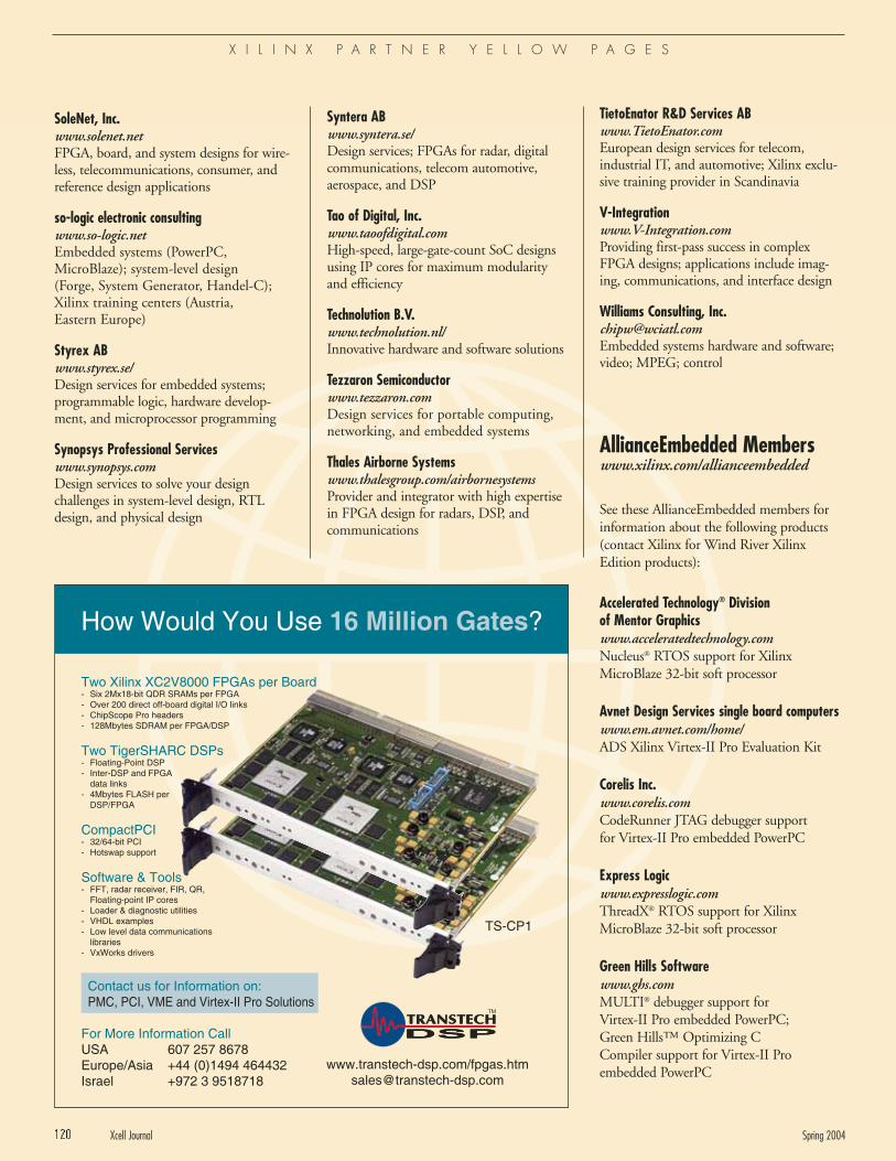
TietoEnator R&D Services ABwww.TietoEnator.comEuropean design services for telecom,industrial IT, and automotive; Xilinx exclu-sive training provider in Scandinavia
V-Integrationwww.V-Integration.comProviding first-pass success in complexFPGA designs; applications include imag-ing, communications, and interface design
Williams Consulting, [email protected] systems hardware and software;video; MPEG; control
120 Xcell Journal Spring 2004
SoleNet, Inc.www.solenet.netFPGA, board, and system designs for wire-less, telecommunications, consumer, andreference design applications
so-logic electronic consultingwww.so-logic.netEmbedded systems (PowerPC,MicroBlaze); system-level design (Forge, System Generator, Handel-C);Xilinx training centers (Austria, Eastern Europe)
Styrex ABwww.styrex.se/Design services for embedded systems; programmable logic, hardware develop-ment, and microprocessor programming
Synopsys Professional Serviceswww.synopsys.comDesign services to solve your design challenges in system-level design, RTLdesign, and physical design
Syntera ABwww.syntera.se/Design services; FPGAs for radar, digitalcommunications, telecom automotive, aerospace, and DSP
Tao of Digital, Inc.www.taoofdigital.comHigh-speed, large-gate-count SoC designsusing IP cores for maximum modularityand efficiency
Technolution B.V.www.technolution.nl/Innovative hardware and software solutions
Tezzaron Semiconductorwww.tezzaron.comDesign services for portable computing,networking, and embedded systems
Thales Airborne Systemswww.thalesgroup.com/airbornesystemsProvider and integrator with high expertisein FPGA design for radars, DSP, and communications
AllianceEmbedded Memberswww.xilinx.com/allianceembedded
See these AllianceEmbedded members forinformation about the following products(contact Xilinx for Wind River XilinxEdition products):
Accelerated Technology® Division of Mentor Graphicswww.acceleratedtechnology.comNucleus® RTOS support for XilinxMicroBlaze 32-bit soft processor
Avnet Design Services single board computerswww.em.avnet.com/home/ADS Xilinx Virtex-II Pro Evaluation Kit
Corelis Inc.www.corelis.comCodeRunner JTAG debugger support for Virtex-II Pro embedded PowerPC
Express Logicwww.expresslogic.comThreadX® RTOS support for XilinxMicroBlaze 32-bit soft processor
Green Hills Softwarewww.ghs.comMULTI® debugger support for Virtex-II Pro embedded PowerPC; Green Hills™ Optimizing C Compiler support for Virtex-II Pro embedded PowerPC
X I L I N X P A R T N E R Y E L L O W P A G E S
Contact us for Information on:
PMC, PCI, VME and Virtex-II Pro Solutions
For More Information Call
USA 607 257 8678
Europe/Asia +44 (0)1494 464432
Israel +972 3 9518718
Two Xilinx XC2V8000 FPGAs per Board- Six 2Mx18-bit QDR SRAMs per FPGA
- Over 200 direct off-board digital I/O links
- ChipScope Pro headers
- 128Mbytes SDRAM per FPGA/DSP
Two TigerSHARC DSPs- Floating-Point DSP
- Inter-DSP and FPGA
data links
- 4Mbytes FLASH per
DSP/FPGA
CompactPCI- 32/64-bit PCI
- Hotswap support
Software & Tools- FFT, radar receiver, FIR, QR,
Floating-point IP cores
- Loader & diagnostic utilities
- VHDL examples
- Low level data communications
libraries
- VxWorks drivers
TS-CP1
www.transtech-dsp.com/fpgas.htm
How Would You Use 16 Million Gates?
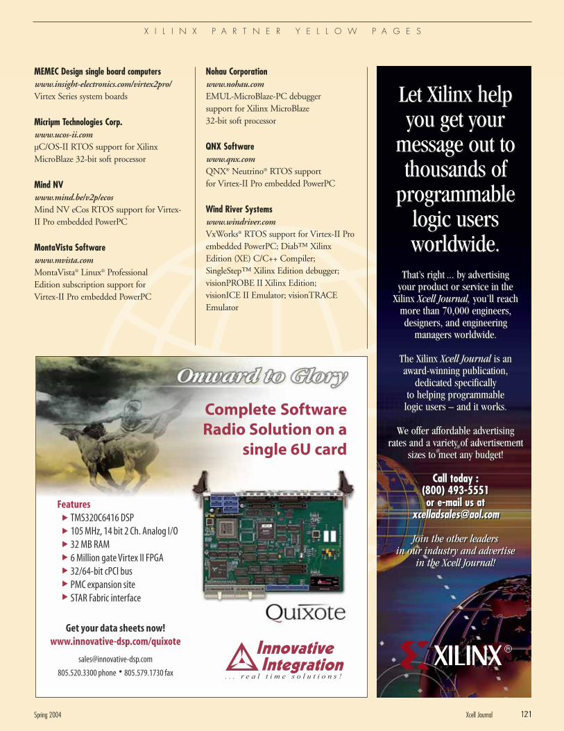
MEMEC Design single board computerswww.insight-electronics.com/virtex2pro/Virtex Series system boards
Micriµm Technologies Corp.www.ucos-ii.comµC/OS-II RTOS support for XilinxMicroBlaze 32-bit soft processor
Mind NVwww.mind.be/v2p/ecosMind NV eCos RTOS support for Virtex-II Pro embedded PowerPC
MontaVista Softwarewww.mvista.comMontaVista® Linux® Professional Edition subscription support for Virtex-II Pro embedded PowerPC
Nohau Corporationwww.nohau.comEMUL-MicroBlaze-PC debugger support for Xilinx MicroBlaze 32-bit soft processor
QNX Softwarewww.qnx.comQNX® Neutrino® RTOS support for Virtex-II Pro embedded PowerPC
Wind River Systemswww.windriver.comVxWorks® RTOS support for Virtex-II Proembedded PowerPC; Diab™ XilinxEdition (XE) C/C++ Compiler;SingleStep™ Xilinx Edition debugger;visionPROBE II Xilinx Edition; visionICE II Emulator; visionTRACEEmulator
Spring 2004 Xcell Journal 121
X I L I N X P A R T N E R Y E L L O W P A G E S
R
Let Xilinx help you get your
message out tothousands of
programmable logic users worldwide.
That’s right ... by advertising your product or service in the
Xilinx Xcell Journal, you’ll reach more than 70,000 engineers, designers, and engineering
managers worldwide.
The Xilinx Xcell Journal is an award-winning publication,
dedicated specifically to helping programmable
logic users – and it works.
We offer affordable advertising rates and a variety of advertisement
sizes to meet any budget!
Call today : (800) 493-5551 or e-mail us at
Join the other leaders in our industry and advertise
in the Xcell Journal!
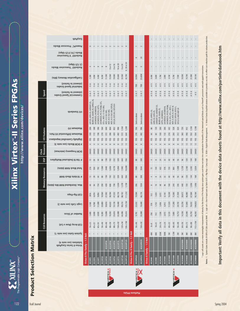
Xil
inx V
irte
x™-I
I Seri
es
FPG
As
htt
p:/
/ww
w.x
ilin
x.c
om
/de
vic
es/
122 Xcell Journal Spring 2004
System Gates (see note 1)
Virtex-II Series EasyPath Solutions (see note 4)
CLB Array (Row x Col)
XC2V
P2*
16 x
22
Number of Slices
1,40
8
Logic Cells (see note 2)
3,16
8
CLB Flip-Flops
2816
Max. Distributed RAM Bits (kbits)
44
# 18 kbits Block RAM
12
Total Block RAM (kbits)
216
# 18x18 Dedicated Multipliers
12
CLB
Reso
urce
sM
emor
y Re
sour
ces
DSP
I/O F
eatu
res
Spee
d
DCM Frequency (min/max)
24/4
20
# DCM Blocks (see note 3)
4
Digitally Controlled Impedance
YES
Maximum Differential I/O Pairs
100
Maximum I/O
204
I/O Standards
LDT-
25, L
VDS-
25, L
VDSE
XT-2
5,
BLVD
S-25
, ULV
DS-2
5, L
VPEC
L-25
, LV
CMO
S25,
LVC
MO
S18,
LV
CMO
S15,
PCI
33, L
VTTL
, LV
CMO
S33,
PCI
-X, P
CI66
, GTL
, G
TL+
, HST
L I (
1.5V
,1.8
V),
HSTL
II (1
.5V,
1.8V
), HS
TL II
I (1.
5V,1
.8V)
, HS
TL IV
(1.5
V,1.
8V),
SSTL
2I,
SSTL
2II,
SSTL
18 I,
SST
L18
II
LDT-
25, L
VPEC
L-33
, LV
DS-3
3, L
VDS-
25,
LVDS
EXT-
33, L
VDSE
XT-2
5,
BLVD
S-25
, ULV
DS-2
5,
LVTT
L, L
VCM
OS3
3,
LVCM
OS2
5, L
VCM
OS1
8,
LVCM
OS1
5, P
CI33
, PCI
66,
PCI-X
, GTL
, GTL
+, H
STL
I, HS
TL II
, HST
L III
, HST
L IV
, SS
TL2I
, SST
L2II,
SST
L3 I,
SS
TL3
II, A
GP,
AGP-
2X
Commercial Speed Grades(slowest to fastest)
-5 -6
-7
Industrial Speed Grades(slowest to fastest)
-5 -6
*XC
2VP4
40
x 2
2 3,
008
6,76
86,
016
9428
504
28
24/4
204
YES
172
348
-5 -6
-7-5
-6
Cloc
k Re
sour
ces
XC2V
P7
*40
x 3
4 4,
928
11,0
889,
856
154
4479
244
24/4
204
YES
196
396
-5 -6
-7-5
-6
XC2V
P20
*56
x 4
69,
280
20,8
8018
,560
290
881,
584
8824
/420
8YE
S27
656
4-5
-6 -7
-5 -6
XC2V
P30
*80
x 4
613
,696
30,8
1627
,392
428
136
2448
136
24/4
208
YES
372
644
-5 -6
-7-5
-6
XC2V
P40
*88
x 5
819
,392
43,6
3238
,784
606
192
3,45
619
224
/420
8YE
S39
680
4-5
-6 -7
-5 -6
XC2V
P50
*88
x 7
023
,616
53,1
3647
,232
738
232
4,17
623
224
/420
8YE
S42
085
2-5
-6 -7
-5 -6
XC2V
P70
*10
4 x
8233
,088
74,4
4866
,176
1,03
432
85,
904
328
24/4
208
YES
492
996
-5 -6
-7-5
-6
XC2V
P100
*12
0 x
9444
,096
99,2
1688
,192
1,37
844
47,
992
444
24/4
2012
YES
572
1,16
4-5
-6 -7
-5 -6
XC2V
P125
*13
6 x
106
55,6
1612
5,13
611
1,23
21,
738
556
10,0
0855
624
/420
12YE
S64
41,
200
-5 -6
-7-5
-6
XC2V
4040
K8
x 8
256
576
512
84
724
24/4
204
YES
4488
-4 -5
-6-4
-5
XC2V
8080
K16
x 8
512
1,15
21,
024
168
144
824
/420
4YE
S60
120
-4 -5
-6-4
-5
XC2V
250
250K
24 x
16
1,53
63,
456
3,07
248
2443
224
24/4
208
YES
100
200
-4 -5
-6-4
-5
XC2V
500
500K
32 x
24
3,07
26,
912
6,14
496
3257
632
24/4
208
YES
132
264
-4 -5
-6-4
-5
XC2V
1000
1M40
x 3
25,
120
11,5
2010
,240
160
4072
040
24/4
208
YES
216
432
-4 -5
-6-4
-5
XC2V
1500
1.5M
48 x
40
7,68
017
,280
15,3
6024
048
864
4824
/420
8YE
S26
452
8-4
-5 -6
-4 -5
XC2V
2000
2M56
x 4
810
,752
24,1
9221
,504
336
561,
008
5624
/420
8YE
S31
262
4-4
-5 -6
-4 -5
XC2V
3000
3M64
x 5
614
,336
32,2
5628
,672
448
961,
728
9624
/420
12YE
S36
072
0-4
-5 -6
-4 -5
XC2V
4000
4M80
x 7
223
,040
51,8
4046
,080
720
120
2,16
012
024
/420
12YE
S45
691
2-4
-5 -6
-4 -5
XC2V
6000
6M96
x 8
833
,792
76,0
3267
,584
1,05
614
42,
592
144
24/4
2012
YES
552
1,10
4-4
-5 -6
-4 -5
XC2V
8000
XCE2
VP30
XCE2
VP40
XCE2
VP50
XCE2
VP70
XCE2
VP10
0
XCE2
VP12
5
XCE2
V300
0
XCE2
V400
0
XCE2
V600
0
XCE2
V800
08M
112
x 10
446
,592
104,
832
93,1
841,
456
168
3,02
416
824
/420
12YE
S55
41,
108
-4 -5
-4 -5
Configuration Memory (Bits)
1.3M
RocketIO™
Transceiver Blocks(3.125 Gbps)
4
RocketIO™
X Transceiver Blocks (10.3125 Gbps)
3.0M
4
4.4M
8
8.2M
8
11.3
M8
15.5
M0
or 1
2
19.0
M0
or 1
6
25.6
M16
or 2
0
33.5
M0
or 2
0
42.7
M0,
20
or 2
4
XC2V
PX20
*56
x 4
69,
792
22,0
3219
,584
306
8815
8488
24/4
208
YES
276
556
Sam
e as
abo
ve
-5 -6
-7TB
D8.
05M
08
0.4M
––
0.6M
––
1.7M
––
2.8M
––
4.1M
––
5.7M
––
7.5M
––
10.5
M–
–
15.7
M–
–
21.9
M–
–
29.1
M–
–
PowerPC™ Processor Blocks
0 1 1 2 2 2 2 2 2 4 1 – – – – – – – – – – –
EasyPath
– – – – – – – – – – –
Platform FPGAs
* Lo
gic
cell
coun
ts a
re a
mor
e m
eani
ngfu
l mea
sure
men
t of d
ensi
ty fo
r the
Virt
ex-II
Pro
fam
ily s
ince
sys
tem
gat
e co
unt d
oes
not t
ake
into
con
side
ratio
n th
e be
nefit
s of
the
imm
erse
d sp
ecia
l blo
cks
such
as
Pow
erPC
pro
cess
ors
and
mul
ti-gi
gabi
t tra
nsce
iver
s. 1.
Sy
stem
Gat
es in
clud
e 20
-30%
of C
LBs
used
as
RAM
. 2
. Lo
gic
cell
= O
ne 4
-Inpu
t Loo
k U
p Ta
ble
(LU
T) +
Flip
Flo
p +
Car
ry L
ogic
. 3
. DC
M =
Dig
ital C
lock
Man
agem
ent.
4.
Virt
ex-II
Ser
ies
Easy
Path
sol
utio
n av
aila
ble
to p
rovi
de a
no
risk,
no
effo
rt c
ost r
educ
tion
path
for v
olum
e pr
oduc
tion.
Not
es:
Virt
ex-II
Pro
Fam
ily –
1.5
Vol
t
Virt
ex-II
Fam
ily –
1.5
Vol
t
Virt
ex-II
Pro
X F
amily
– 1
.5 V
olt
XC2V
PX70
*10
4 x
8233
,088
74,4
4866
,176
1034
308
5544
308
24/4
208
YES
492
996
Sam
e as
abo
ve
-5 -6
-7TB
DXC
E2VP
X70
25.6
0M0
202
Pro
du
ct S
ele
ctio
n M
atr
ix
Impo
rtan
t:Ve
rify
all
data
in t
his
docu
men
t w
ith
the
devi
ce d
ata
shee
ts f
ound
at
http
://w
ww
.xili
nx.c
om/p
arti
nfo/
data
book
.htm
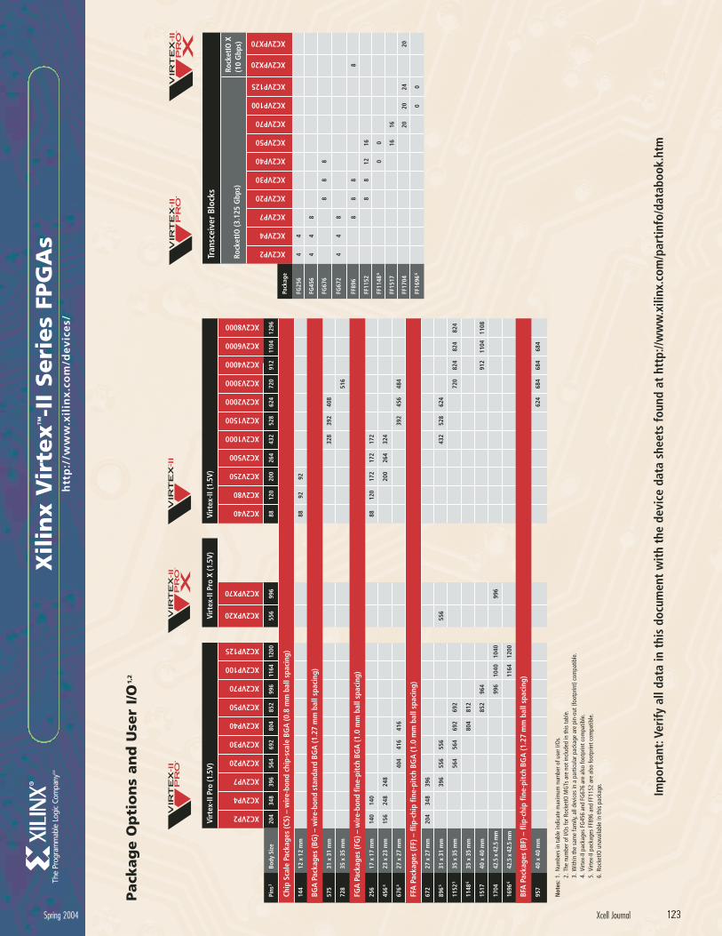
Xil
inx V
irte
x™-I
I Seri
es
FPG
As
htt
p:/
/ww
w.x
ilin
x.c
om
/de
vic
es/
Spring 2004 Xcell Journal 123
XC2VP2
204
XC2VP4
348
XC2VP7
396
XC2VP20
564
XC2VP30
692
XC2VP40
804
XC2VP50
852
XC2VP70
996
XC2VP10011
64
XC2VP125
1200
Virt
ex-II
Pro
(1.5
V)
XC2V40
88
XC2V80
120
XC2V250
200
XC2V500
264
XC2V1000
432
XC2V1500
528
XC2V2000
624
XC2V3000
720
XC2V4000
912
XC2V6000
1104
XC2V8000
1296
Virt
ex-II
(1.5
V)Vi
rtex
-II P
ro X
(1.5
V)
Pins
3Bo
dy S
ize
8892
9214
412
x 1
2 m
m
328
392
408
575
31 x
31
mm
516
728
35 x
35
mm
140
140
8812
017
217
217
225
617
x 1
7 m
m
156
248
248
200
264
324
456
423
x 2
3 m
m
404
416
416
392
456
484
676
427
x 2
7 m
m
204
348
396
672
27 x
27
mm
396
556
556
432
528
624
896
531
x 3
1 m
m
564
564
692
692
720
824
824
824
1152
535
x 3
5 m
m
804
812
1148
635
x 3
5 m
m
852
964
912
1104
1108
1517
40 x
40
mm
996
1040
1040
1704
42.5
x 4
2.5
mm
1164
1200
1696
642
.5 x
42.
5 m
m
XC2VPX20
556
556
624
684
684
684
957
Not
es:
1. N
umbe
rs in
tabl
e in
dica
te m
axim
um n
umbe
r of u
ser I
/Os.
2. T
he n
umbe
r of I
/Os
for R
ocke
tIO M
GTs
are
not
incl
uded
in th
is ta
ble.
3. W
ithin
the
sam
e fa
mily
, all
devi
ces
in a
par
ticul
ar p
acka
ge a
re p
in-o
ut (f
ootp
rint)
com
patib
le.
4. V
irtex
-II p
acka
ges
FG45
6 an
d FG
676
are
also
foot
prin
t com
patib
le.
5. V
irtex
-II p
acka
ges
FF89
6 an
d FF
1152
are
als
o fo
otpr
int c
ompa
tible
.6.
Roc
ketIO
una
vaila
ble
in th
is p
acka
ge.
40 x
40
mm
XC2VPX70
996
996
Chip
Sca
le P
acka
ges
(CS)
– w
ire-
bond
chi
p-sc
ale
BGA
(0.8
mm
bal
l spa
cing
)
BGA
Pac
kage
s (B
G) –
wir
e-bo
nd s
tand
ard
BGA
(1.2
7 m
m b
all s
paci
ng)
FGA
Pac
kage
s (F
G) –
wir
e-bo
nd fi
ne-p
itch
BG
A (1
.0 m
m b
all s
paci
ng)
FFA
Pac
kage
s (F
F) –
flip
-chi
p fin
e-pi
tch
BGA
(1.0
mm
bal
l spa
cing
)
BFA
Pac
kage
s (B
F) –
flip
-chi
p fin
e-pi
tch
BGA
(1.2
7 m
m b
all s
paci
ng)
XC2VP2
XC2VP4
XC2VP7
XC2VP20
XC2VP30
XC2VP40
XC2VP50
XC2VP70
XC2VP100
XC2VP125
Pack
age
Rock
etIO
(3.1
25 G
bps)
Rock
etIO
X
(10
Gbp
s)
Tran
scei
ver
Bloc
ks
4FG
256
4
4FG
456
48
FG67
68
88
4FG
672
48
FF89
68
88
FF11
528
812
16
FF11
486
00
FF15
1716
16
FF17
0420
2024
FF16
966
00
XC2VPX20
8
XC2VPX70
20
Pack
ag
e O
pti
on
s an
d U
ser
I/O
1,2
Impo
rtan
t:Ve
rify
all
data
in t
his
docu
men
t w
ith
the
devi
ce d
ata
shee
ts f
ound
at
http
://w
ww
.xili
nx.c
om/p
arti
nfo/
data
book
.htm
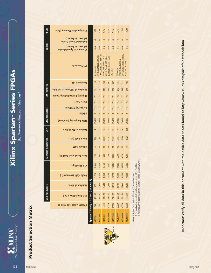
Xil
inx S
part
an
™Seri
es
FPG
As
htt
p:/
/ww
w.x
ilin
x.c
om
/de
vic
es/
124 Xcell Journal Spring 2004
Pro
du
ct S
ele
ctio
n M
atr
ix
CLB
Reso
urce
sM
emor
y Re
sour
ces
CLK
Reso
urce
sD
SPI/O
Fea
ture
sSp
eed
PRO
M
System Gates (see note 1)
CLB Array (Row x Col)
XC3S
5050
K16
x 1
2
Number of Slices
768
Logic Cells (see note 2 )1,
728
CLB Flip-Flops
1,53
6
Max. Distributed RAM Bits
12K
# Block RAM
4
Block RAM (bits)
72K
Dedicated Multipliers
4
DCM Frequency (min/max)
25/3
26
# DCMs
2
Frequency Synthesis
YES
Phase Shift
YES
Digitally Controlled Impedance
Number of Differential I/O Pairs
Maximum I/O
I/O Standards
Commercial Speed Grades(slowest to fastest)
YES
5612
4Si
ngle
-end
edLV
TTL,
LVC
MO
S3.3
/2.5
/1.8
/1.
5/1.
2, P
CI 3
.3V
– 32
/64-
bit
33M
Hz, S
STL2
Cla
ss I
& II
, SS
TL18
Cla
ss I,
HST
L Cl
ass
I, III
, HST
L1.8
Cla
ss I,
II &
III,
GTL
, GTL
+
Diffe
rent
ial
LVDS
2.5,
Bus
LVD
S2.5
,U
ltra
LVDS
2.5,
LVD
S_ex
t2.5
,RS
DS, L
DT2.
5, L
VPEC
L
-4 -5
Industrial Speed Grades(slowest to fastest)
-4
Configuration Memory (Bits)
.4M
XC3S
200
200K
24
x 2
01,
920
4,32
03,
840
30K
1221
6K12
25/3
264
YES
YES
YES
7617
3-4
-5-4
1.0M
XC3S
400
400K
32
x 2
83,
584
8,06
47,
168
56K
1628
8K16
25/3
264
YES
YES
YES
116
264
-4 -5
-41.
7M
XC3S
1000
10
00K
48 x
40
7,68
017
,280
15,3
6012
0K24
432K
2425
/326
4YE
SYE
SYE
S17
539
1-4
-5-4
3.2M
XC3S
1500
15
00K
64 x
52
13,3
1229
,952
26,6
2420
8K32
576K
3225
/326
4YE
SYE
SYE
S22
148
7-4
-5-4
5.2M
XC3S
2000
20
00K
80 x
64
20,4
8046
,080
40,9
6032
0K40
720K
4025
/326
4YE
SYE
SYE
S27
056
5-4
-5-4
7.7M
XC3S
4000
40
00K
96 x
72
27,6
4862
,208
55,2
9643
2K96
1,72
8K96
25/3
264
YES
YES
YES
312
712
-4 -5
-411
.3M
XC3S
5000
50
00K
104
x 80
33,2
8074
,880
66,5
6052
0K10
41,
872K
104
25/3
264
YES
YES
YES
344
784
-4 -5
-413
.3M
Not
es: 1
. Sys
tem
Gat
es in
clud
e 20
-30%
of C
LBs
used
as
RAM
s.
2. F
or S
part
an-3
, a L
ogic
Cel
l is
defin
ed a
s a
4-in
put L
UT
+ F
lip-F
lop.
3. A
utom
otiv
e Q
-Gra
de S
olut
ions
for S
part
an-3
will
be
avai
labl
e 2H
2004
.
Spar
tan-
3 Fa
mily
– 1
.2 V
olt
(see
not
e 3)
Impo
rtan
t:Ve
rify
all
data
in t
his
docu
men
t w
ith
the
devi
ce d
ata
shee
ts f
ound
at
http
://w
ww
.xili
nx.c
om/p
arti
nfo/
data
book
.htm

Xil
inx S
part
an
™Seri
es
FPG
As
htt
p:/
/ww
w.x
ilin
x.c
om
/de
vic
es/
Spring 2004 Xcell Journal 125
CLB
Reso
urce
sM
emor
y Re
sour
ces
CLK
Reso
urce
sI/O
Fea
ture
sSp
eed
System Gates (see note 1)
CLB Array (Row x Col)
XC2S
50E
50K
16 x
24
Number of Slices76
8
Logic Cells (see notes 2 and 3)
1,72
8
CLB Flip-Flops
1,53
6
Max. Distributed RAM Bits
24K
# Block RAM
8
Block RAM (bits)
32K
DLL Frequency (min/max)
25/3
20
# DLLs
4
Frequency Synthesis
YES
Phase Shift
YES
Number of Differential I/O Pairs
Maximum I/O
I/O Standards
Commercial Speed Grades(slowest to fastest)
8318
2LV
TTL,
LVC
MO
S2,
LVCM
OS1
8, P
CI33
, PCI
66,
GTL
, GTL
+, H
STL
I, HS
TL II
I, HS
TL IV
, SST
L3 I,
SST
L3 II
, SS
TL2
I, SS
TL2
II, A
GP-
2X,
CTT,
LVDS
, BLV
DS, L
VPEC
L
LVTT
L, L
VCM
OS2
,PC
I33
(3.3
V &
5V)
,PC
I66
(3.3
V), G
TL, G
TL+
,
HS
TL I,
HST
L III
, HST
L IV
,
SS
TL3
I, SS
TL3
II, S
STL2
I,
SSTL
2 II,
AG
P-2X
, CTT
-6 -7
Industrial Speed Grade(slowest to fastest)
-6
Configuration Memory (Bits)
0.6M
XC2S
100E
100K
20 x
30
1,20
02,
700
2,40
037
K10
40K
25/3
204
YES
YES
8620
2-6
-7-6
0.9M
XC2S
150E
150K
24 x
36
1,72
83,
888
3,45
654
K12
48K
25/3
204
YES
YES
114
265
-6 -7
-61.
1M
XC2S
200E
200K
28 x
42
2,35
25,
292
4,70
473
K14
56K
25/3
204
YES
YES
120
289
-6 -7
-61.
4M
XC2S
300E
300K
32 x
48
3,07
26,
912
6,14
496
K16
64K
25/3
204
YES
YES
120
329
-6 -7
-61.
9M
XC2S
400E
400K
40 x
60
4,80
010
,800
9,60
015
0K40
160K
25/3
204
YES
YES
172
410
-6 -7
-62.
7M
XC2S
600E
600K
48 x
72
6,91
215
,552
13,8
2421
6K72
288K
25/3
204
YES
YES
205
514
-6 -7
-64.
0M
XC2S
1515
K8
x 12
192
432
384
6K4
16K
25/2
004
YES
YES
NA
86-5
-6-5
0.2M
XC2S
3030
K12
x 1
843
297
286
413
.5K
624
K25
/200
4YE
SYE
SN
A13
2-5
-6-5
0.4M
XC2S
5050
K16
x 2
476
81,
728
1,53
624
K8
32K
25/2
004
YES
YES
NA
176
-5 -6
-50.
6M
XC2S
100
100K
20 x
30
1,20
02,
700
2,40
037
.5K
1040
K25
/200
4YE
SYE
SN
A19
6-5
-6-5
0.8M
XC2S
150
150K
24 x
36
1,72
83,
888
3,45
654
K12
48K
25/2
004
YES
YES
NA
260
-5 -6
-51.
1M
XC2S
200
200K
28 x
42
2,35
25,
292
4,70
473
.5K
1456
K25
/200
4YE
SYE
SN
A28
4-5
-6-5
1.4M
XCS0
5XL
5K10
x 1
010
023
820
03.
1KN
AN
AN
AN
AN
AN
AN
A77
-4 -5
-40.
05M
XCS1
0XL
10K
14 x
14
196
466
392
6.1K
NA
NA
NA
NA
NA
NA
NA
112
-4 -5
-40.
09M
XCS2
0XL
20K
20 x
20
400
950
800
12.5
KN
AN
AN
AN
AN
AN
AN
A16
0-4
-5-4
0.18
M
XCS3
0XL
30K
24 x
24
576
1,36
81,
152
18.0
KN
AN
AN
AN
AN
AN
AN
A19
2-4
-5-4
0.25
M
XCS4
0XL
40K
28 x
28
784
1,86
21,
568
24.5
KN
AN
AN
AN
AN
AN
AN
A22
4-4
-5-4
Automotive Q-Grade Speed Grade
-6 -6 -6 -6 -6 -6 -6 -5 -5 -5 -5 -5 -5 -4 -4 -4 -4 -40.
33M
Automotive Q-Grade Solutions(see note 4)
✔ ✔ ✔ ✔ ✔ ✔ ✔ ✔ ✔ ✔ ✔ ✔ ✔ ✔ ✔ ✔ ✔ ✔
Not
es: 1
. Sy
stem
Gat
es in
clud
e 20
-30%
of C
LBs
used
as
RAM
.
2. L
ogic
cel
l = (1
) 4-In
put (
LUT)
and
a re
gist
er.
3. F
or S
part
an-II
E/II/
XL, a
Log
ic C
ell i
s de
fined
as
a 4-
inpu
t LU
T +
a re
gist
er.
4. A
utom
otiv
e Q
-Gra
de S
olut
ions
are
qua
lifie
d to
-40º
C to
+12
5ºC
junc
tion
tem
pera
ture
for F
PGAs
. Q-G
rade
pro
duct
s fo
r Spa
rtan
-3 w
ill b
e av
aila
ble
2H20
04.
Spar
tan-
II Fa
mily
– 2
.5 V
olt
Spar
tan-
XL F
amily
– 3
.3 V
olt
Spar
tan-
IIE F
amily
– 1
.8 V
olt
Pro
du
ct S
ele
ctio
n
Matr
ix
Impo
rtan
t:Ve
rify
all
data
in t
his
docu
men
t w
ith
the
devi
ce d
ata
shee
ts f
ound
at
http
://w
ww
.xili
nx.c
om/p
arti
nfo/
data
book
.htm
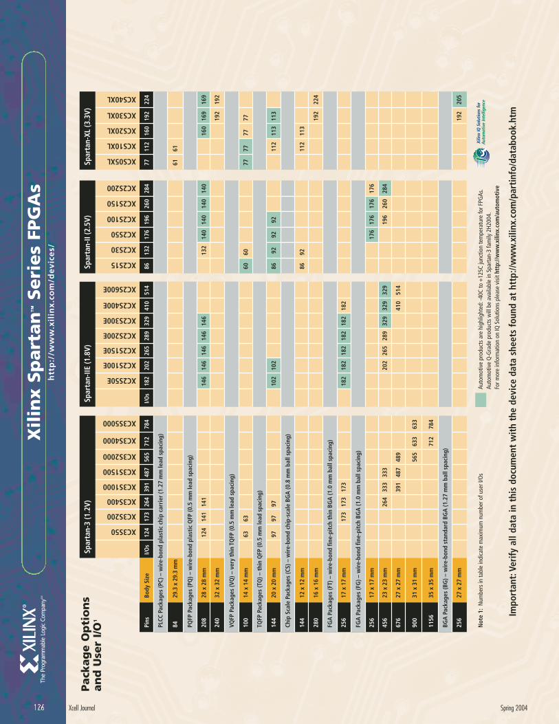
Xil
inx S
part
an
™Seri
es
FPG
As
htt
p:/
/ww
w.x
ilin
x.c
om
/de
vic
es/
126 Xcell Journal Spring 2004
Not
e 1:
Num
bers
in ta
ble
indi
cate
max
imum
num
ber o
f use
r I/O
sAu
tom
otiv
e pr
oduc
ts a
re h
ighl
ight
ed: -
40C
to +
125C
junc
tion
tem
pera
ture
for F
PGAs
.Au
tom
otiv
e Q
-Gra
de p
rodu
cts
will
be
avai
labl
e in
Spa
rtan
-3 fa
mily
2H2
004.
For m
ore
info
rmat
ion
on IQ
Sol
utio
ns p
leas
e vi
sit h
ttp:
//ww
w.x
ilinx
.com
/aut
omot
ive
XC2S50E
XC2S100E
XC2S150E
XC2S200E
XC2S300E
XC2S400E
XC2S600E
I/Os
182
202
265
289
329
410
514
XC2S15
XC2S30
XC2S50
XC2S100
XC2S150
XC2S200
8613
217
619
626
028
4
XCS05XL
XCS10XL
XCS20XL
XCS30XL
XCS40XL
7711
216
019
222
4
6161
192
192
6077
77
112
8692
112
113
192
224
176
202
265
289
196
260
410
514
192
182
146
146
146
146
146
140
140
140
140
160
169
169
6077
77
102
102
86 9
2 9
2 9
211
311
3
182
182
182
182
182
176
176
176
329
329
329
284
205
Spar
tan-
IIE (1
.8V)
Spar
tan-
II (2
.5V)
Spar
tan-
XL (3
.3V)
XC3S50
XC3S200
XC3S400
XC3S1000
XC3S1500
XC3S2000
XC3S4000
Body
Siz
e
29.3
x 2
9.3
mm
Pins
84
I/Os
124
173
264
391
487
565
712
784
28 x
28
mm
208
32 x
32
mm
240
14 x
14
mm
100
6363
20 x
20
mm
144
97
12 x
12
mm
144
16 x
16
mm
280
17 x
17
mm
256
17 x
17
mm
256
23 x
23
mm
456
264
333
27 x
27
mm
676
391
487
489
27 x
27
mm
256
124
141
141
9797 17
317
317
3
333
XC3S5000
PQFP
Pac
kage
s (P
Q) –
wir
e-bo
nd p
last
ic Q
FP (0
.5 m
m le
ad s
paci
ng)
PLCC
Pac
kage
s (P
C) –
wir
e-bo
nd p
last
ic c
hip
carr
ier
(1.2
7 m
m le
ad s
paci
ng)
Spar
tan-
3 (1
.2V)
VQFP
Pac
kage
s (V
Q) –
ver
y th
in T
QFP
(0.5
mm
lead
spa
cing
)
TQFP
Pac
kage
s (T
Q) –
thi
n Q
FP (0
.5 m
m le
ad s
paci
ng)
Chip
Sca
le P
acka
ges
(CS)
– w
ire-
bond
chi
p-sc
ale
BGA
(0.8
mm
bal
l spa
cing
)
FGA
Pac
kage
s (F
T) –
wir
e-bo
nd fi
ne-p
itch
thi
n BG
A (1
.0 m
m b
all s
paci
ng)
FGA
Pac
kage
s (F
G) –
wir
e-bo
nd fi
ne-p
itch
BG
A (1
.0 m
m b
all s
paci
ng)
BGA
Pac
kage
s (B
G) –
wir
e-bo
nd s
tand
ard
BGA
(1.2
7 m
m b
all s
paci
ng)
31 x
31
mm
900
565
633
633
35 x
35
mm
1156
712
784
132
Pack
ag
e O
pti
on
s an
d U
ser
I/O
1
Impo
rtan
t:Ve
rify
all
data
in t
his
docu
men
t w
ith
the
devi
ce d
ata
shee
ts f
ound
at
http
://w
ww
.xili
nx.c
om/p
arti
nfo/
data
book
.htm
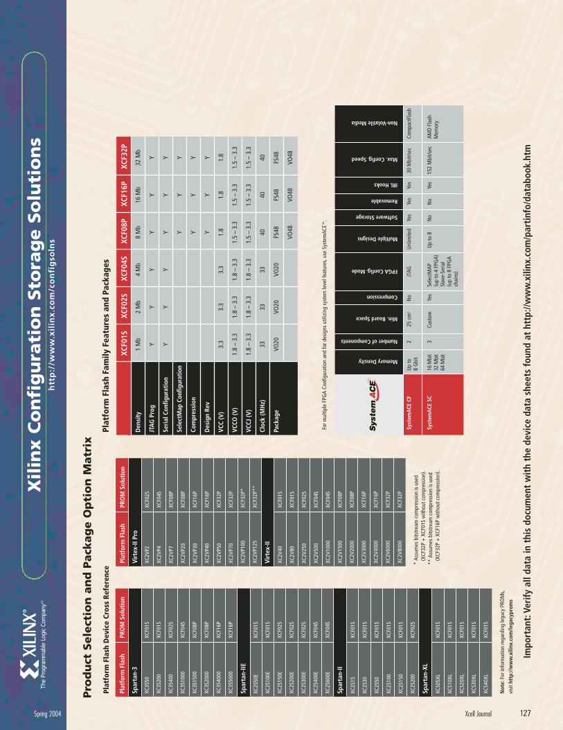
Xil
inx C
on
fig
ura
tio
n S
tora
ge S
olu
tio
ns
htt
p:/
/ww
w.x
ilin
x.c
om
/co
nfi
gso
lns
Spring 2004 Xcell Journal 127
Impo
rtan
t:Ve
rify
all
data
in t
his
docu
men
t w
ith
the
devi
ce d
ata
shee
ts f
ound
at
http
://w
ww
.xili
nx.c
om/p
arti
nfo/
data
book
.htm
Pro
du
ct S
ele
ctio
n a
nd
Pack
ag
e O
pti
on
Matr
ix
Syst
emAC
E CF
Up
to8
Gbi
t2
25 c
m2
No
JTAG
Unl
imite
dYe
sYe
sYe
s30
Mbi
t/sec
Com
pact
Flas
h
Non-Volatile Media
Max. Config. Speed
IRL Hooks
FPGA Config. Mode
Multiple Designs
Software Storage
Removable
Compression
Min. Board Space
Number of Components
Memory Density
Syst
emAC
E SC
For m
ultip
le F
PGA
Conf
igur
atio
n an
d fo
r des
igns
util
izin
g sy
stem
leve
l fea
ture
s, us
e Sy
stem
ACE™
.
16 M
bit
32 M
bit
64 M
bit
3Cu
stom
Yes
Sele
ctM
AP(u
p to
4 F
PGA)
Slav
e-Se
rial
(up
to 8
FPG
A ch
ains
)
Up
to 8
No
No
Yes
152
Mbi
t/sec
AMD
Flas
h M
emor
y
Den
sity
Plat
form
Fla
sh F
amily
Fea
ture
s an
d Pa
ckag
es
1 M
b
XCF0
1S
2 M
b
XCF0
2S
4 M
b
XCF0
4S
8 M
b
XCF0
8P
16 M
b
XCF1
6P
JTAG
Pro
gY
YY
YY
Seri
al C
onfig
urat
ion
YY
YY
Y
32 M
b
XCF3
2P
Y Y
Sele
ctM
ap C
onfig
urat
ion
YY
Y
Com
pres
sion
YY
Y
Des
ign
Rev
YY
Y
VCC
(V)
3.3
3.3
3.3
1.8
1.8
1.8
VCCO
(V)
1.8
– 3.
31.
8 –
3.3
1.8
– 3.
31.
5 –
3.3
1.5
– 3.
31.
5 –
3.3
VCCJ
(V)
1.8
– 3.
31.
8 –
3.3
1.8
– 3.
31.
5 –
3.3
1.5
– 3.
31.
5 –
3.3
Cloc
k (M
Hz)
3333
3340
4040
Pack
age
VO20
VO20
VO20
FS48
FS48
FS48
VO48
VO48
VO48
Plat
form
Fla
sh
Plat
form
Fla
sh D
evic
e Cr
oss
Refe
renc
e
XC3S
50XC
F01S
PRO
M S
olut
ion
Not
e: F
or in
form
atio
n re
gard
ing
lega
cy P
ROM
s,
visi
t htt
p://w
ww
.xili
nx.c
om/le
gacy
prom
s
XC3S
200
XCF0
1S
XC3S
400
XCF0
2S
XC3S
1000
XCF0
4S
XC3S
1500
XCF0
8P
XC3S
2000
XC
F08P
XC3S
4000
XC
F16P
XC3S
5000
XC
F16P
XC2S
50E
XCF0
1S
XC2S
100E
XC
F01S
XC2S
150E
XC
F02S
XC2S
200E
XC
F02S
XC2S
300E
XC
F02S
XC2S
400E
XC
F04S
XC2S
600E
XC
F04S
XC2S
15
XCF0
1S
XC2S
30
XCF0
1S
XC2S
50
XCF0
1S
XC2S
100
XCF0
1S
XC2S
150
XCF0
1S
XC2S
200
XCF0
2S
XCS0
5XL
XCF0
1S
XCS1
0XL
XCF0
1S
XCS2
0XL
XCF0
1S
XCS3
0XL
XCF0
1S
XCS4
0XL
XCF0
1S
Spar
tan-
3
Spar
tan-
IIE
Spar
tan-
II
Spar
tan-
XL
Plat
form
Fla
sh
XC2V
P2
* As
sum
es b
itstr
eam
com
pres
sion
is u
sed
(X
CF32
P +
XCF
01S
with
out c
ompr
essi
on).
**
Ass
umes
bits
trea
m c
ompr
essi
on is
use
d
(XCF
32P
+ X
CF16
P w
ithou
t com
pres
sion
).
XCF0
2S
PRO
M S
olut
ion
Virt
ex-II
Pro
XC2V
P4XC
F04S
XC2V
P7XC
F08P
XC2V
P20
XCF0
8P
XC2V
P30
XCF1
6P
XC2V
P40
XCF1
6P
XC2V
P50
XCF3
2P
XC2V
P70
XCF3
2P
XC2V
P100
XC
F32P
*
XC2V
P125
XC
F32P
**
XC2V
40
XCF0
1S
Virt
ex-II
XC2V
80
XCF0
1S
XC2V
250
XCF0
2S
XC2V
500
XCF0
4S
XC2V
1000
XC
F04S
XC2V
1500
XC
F08P
XC2V
2000
XC
F08P
XC2V
3000
XC
F16P
XC2V
4000
XC
F16P
XC2V
6000
XC
F32P
XC2V
8000
XC
F32P
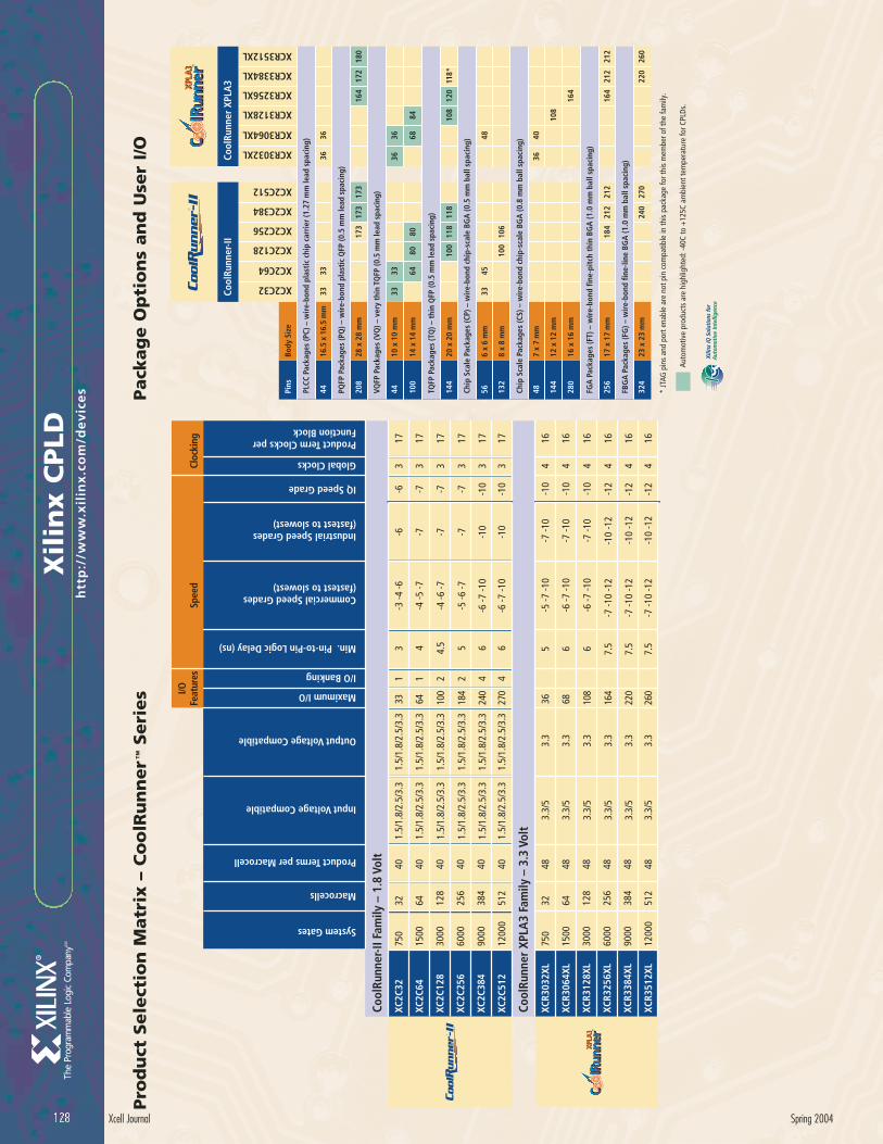
Xil
inx C
PLD
htt
p:/
/ww
w.x
ilin
x.c
om
/de
vic
es
128 Xcell Journal Spring 2004
XCR3
032X
L75
032
XCR3
064X
L15
0064
XCR3
128X
L30
0012
8
XCR3
256X
L60
0025
6
XCR3
384X
L90
0038
4
XCR3
512X
L12
000
512
48 48 48 48 48
365
-5 -7
-10
-7 -1
04
16
686
-6 -7
-10
-7 -1
04
16
108
6-6
-7 -1
0 -7
-10
416
164
7.5
-7 -1
0 -1
2-1
0 -1
24
16
220
7.5
-7 -1
0 -1
2-1
0 -1
24
16
3.3/
5
3.3/
5
3.3/
5
3.3/
5
3.3/
5
3.3/
5
3.3
3.3
3.3
3.3
3.3
3.3
260
7.5
-7 -1
0 -1
2-1
0 -1
24
16
XC2C
3275
032
XC2C
6415
0064
XC2C
128
3000
128
XC2C
256
6000
256
XC2C
384
9000
384
XC2C
512
1200
051
2
40 40 40 40 40 40
System Gates
Macrocells
Product Terms per Macrocell
1.5/
1.8/
2.5/
3.3
Input Voltage Compatible
1.5/
1.8/
2.5/
3.3
33Output Voltage Compatible
Maximum I/O
13
I/O Banking
Min. Pin-to-Pin Logic Delay (ns)
-3 -4
-6-6
Commercial Speed Grades(fastest to slowest)
Industrial Speed Grades(fastest to slowest)
3Global Clocks
17
1.5/
1.8/
2.5/
3.3
1.5/
1.8/
2.5/
3.3
641
4-4
-5 -7
-73
17
1.5/
1.8/
2.5/
3.3
1.5/
1.8/
2.5/
3.3
100
24.
5-4
-6 -7
-73
17
1.5/
1.8/
2.5/
3.3
1.5/
1.8/
2.5/
3.3
184
25
-5 -6
-7-7
317
1.5/
1.8/
2.5/
3.3
1.5/
1.8/
2.5/
3.3
240
46
-6 -7
-10
-10
317
1.5/
1.8/
2.5/
3.3
1.5/
1.8/
2.5/
3.3
270
46
-6 -7
-10
-10
317Product Term Clocks per
Function Block
Cool
Runn
er-II
Fam
ily –
1.8
Vol
t
Cool
Runn
er X
PLA
3 Fa
mily
– 3
.3 V
olt
-10
-10
-10
-12
-12
-12-6
IQ Speed Grade
-7 -7 -7 -10
-10
I/OFe
atur
esSp
eed
Cloc
king
48
Pro
du
ct S
ele
ctio
n M
atr
ix –
Co
olR
un
ner™
Seri
es
Pack
ag
e O
pti
on
s an
d U
ser
I/O
* JT
AG p
ins
and
port
ena
ble
are
not p
in c
ompa
tible
in th
is p
acka
ge fo
r thi
s m
embe
r of t
he fa
mily
.
Auto
mot
ive
prod
ucts
are
hig
hlig
hted
: -40
C to
+12
5C a
mbi
ent t
empe
ratu
re fo
r CPL
Ds.
XC2C512
XCR3032XL
XCR3064XL
XCR3128XL
XCR3256XL
XCR3384XL
3636
XCR3512XL
Body
Siz
ePi
ns
16.5
x 1
6.5
mm
44
XC2C32
XC2C64
XC2C128
XC2C256
XC2C384
XC2C512
28 x
28
mm
208
10 x
10
mm
44
3333
14 x
14
mm
100
118*
20 x
20
mm
144
486
x 6
mm
5633
45
8 x
8 m
m13
210
010
6
4036
7 x
7 m
m48
108
12 x
12
mm
144
164
16 x
16
mm
280
212
164
212
17 x
17
mm
256
184
212
212
260
220
23 x
23
mm
324
240
270
173
173
173
180
164
172
3333
3636
6884
6480
80
108
120
100
118
118
PQFP
Pac
kage
s (P
Q) –
wir
e-bo
nd p
last
ic Q
FP (0
.5 m
m le
ad s
paci
ng)
VQFP
Pac
kage
s (V
Q) –
ver
y th
in T
QFP
(0.5
mm
lead
spa
cing
)
TQFP
Pac
kage
s (T
Q) –
thi
n Q
FP (0
.5 m
m le
ad s
paci
ng)
FGA
Pac
kage
s (F
T) –
wir
e-bo
nd fi
ne-p
itch
thi
n BG
A (1
.0 m
m b
all s
paci
ng)
FBG
A P
acka
ges
(FG
) – w
ire-
bond
fine
-line
BG
A (1
.0 m
m b
all s
paci
ng)
Chip
Sca
le P
acka
ges
(CS)
– w
ire-
bond
chi
p-sc
ale
BGA
(0.8
mm
bal
l spa
cing
)
Chip
Sca
le P
acka
ges
(CP)
– w
ire-
bond
chi
p-sc
ale
BGA
(0.5
mm
bal
l spa
cing
)
Cool
Runn
er X
PLA
3Co
olRu
nner
-II
PLCC
Pac
kage
s (P
C) –
wir
e-bo
nd p
last
ic c
hip
carr
ier
(1.2
7 m
m le
ad s
paci
ng)

Xil
inx C
PLD
htt
p:/
/ww
w.x
ilin
x.c
om
/de
vic
es
Spring 2004 Xcell Journal 129
Pro
du
ct S
ele
ctio
n M
atr
ix –
9500 S
eri
es
Pack
ag
e O
pti
on
s an
d U
ser
I/O
XC9536XV
XC9572XV
XC95144XV
XC95288XV
3434
XC9536XL
XC9572XL
XC95144XL
XC95288XL
3434
3434
8181
117
117
117
117
3836
3836
117
117
192
192
192
192
192
72
34
5236
72
Auto
mot
ive
prod
ucts
are
hig
hlig
hted
: -40
C to
+12
5C a
mbi
ent t
empe
ratu
re fo
r CPL
Ds.
Body
Siz
ePi
ns
16.5
x 1
6.5
mm
44
18.8
5 x
12.3
5 m
m10
0
10 x
10
mm
44
10 x
10
mm
64
14 x
14
mm
100
20 x
20
mm
144
6 x
6 m
m56
8 x
8 m
m13
2
7 x
7 m
m48
12 x
12
mm
144
16 x
16
mm
280
27 x
27
mm
256
17 x
17
mm
256
17 x
17
mm
256
23 x
23
mm
324
XC9536
XC9572
XC95108
XC95144
3434 72
8181
8181
34
XC95216
XC95288
29.3
x 2
9.3
mm
8469
69
28.0
x 2
8.0
mm
160
108
133
133
168
168
168
28.0
x 2
8.0
mm
208
166
168
192
35.0
x 3
5.0
mm
352
166
192
FGA
Pac
kage
s (F
T) –
wir
e-bo
nd fi
ne-p
itch
thi
n BG
A (1
.0 m
m b
all s
paci
ng)
FBG
A P
acka
ges
(FG
) – w
ire-
bond
fine
-line
BG
A (1
.0 m
m b
all s
paci
ng)
BGA
Pac
kage
s (B
G) –
wir
e-bo
nd s
tand
ard
BGA
(1.2
7 m
m b
all s
paci
ng)
3434XC
9500
XC95
00XL
XC95
00XV
72
TQFP
Pac
kage
s (T
Q) –
thi
n Q
FP (0
.5 m
m le
ad s
paci
ng)
VQFP
Pac
kage
s (V
Q) –
ver
y th
in T
QFP
(0.5
mm
lead
spa
cing
)
PQFP
Pac
kage
s (P
Q) –
wir
e-bo
nd p
last
ic Q
FP (0
.5 m
m le
ad s
paci
ng)
PLCC
Pac
kage
s (P
C) –
wir
e-bo
nd p
last
ic c
hip
carr
ier
(1.2
7 m
m le
ad s
paci
ng)
Chip
Sca
le P
acka
ges
(CP)
– w
ire-
bond
chi
p-sc
ale
BGA
(0.5
mm
bal
l spa
cing
)
Chip
Sca
le P
acka
ges
(CS)
– w
ire-
bond
chi
p-sc
ale
BGA
(0.8
mm
bal
l spa
cing
)
System Gates
Macrocells
Product Terms per Macrocell
Input Voltage Compatible
Output Voltage Compatible
Maximum I/O
I/O Banking
Min. Pin-to-Pin Logic Delay (ns)
Commercial Speed Grades(fastest to slowest)
Industrial Speed Grades(fastest to slowest)
Global Clocks
Product Term Clocks perFunction Block
IQ Speed Grade
I/OFe
atur
esSp
eed
Cloc
king
XC95
3680
036
XC95
7216
0072
XC95
108
2400
108
XC95
144
3200
144
90 90 90 90
3610
-7 -1
0 -1
53
18
7210
-10
-15
318
108
10-7
-10
-15
-20
318
133
10
-5 -6
-10
-15
-7 -1
0 -1
5
-7 -1
0 -1
5 -2
0
-7 -1
0 -1
5-1
0 -1
5
-15
-15
NA
NA
318
5 5 5 5
5 5 5 5
XC95
216
4800
216
9016
610
-10
-15
-20
-10
-15
-20
NA
318
55
XC95
288
6400
288
9019
210
-10
-15
-20
-15
-20
NA
318
55
XC95
00 F
amily
– 5
Vol
t
XC95
36XL
800
36
XC95
72XL
1600
72
XC95
144X
L32
0014
4
XC95
288X
L64
0028
8
90 90 90 90
365
-7 -1
03
18
725
-7 -1
03
18
117
5-7
-10
318
192
6
-5 -7
-10
-5 -7
-10
-5 -7
-10
-6 -7
-10
-7 -1
0
-10
-10
NA
NA
318
2.5/
3.3/
5
2.5/
3.3/
5
2.5/
3.3/
5
2.5/
3.3/
5
2.5/
3.3
2.5
/3.3
2.5/
3.3
2.5
/3.3
XC95
00XL
Fam
ily –
3.3
Vol
t
XC95
36XV
800
36
XC95
72XV
1600
72
XC95
144X
V32
0014
4
XC95
288X
V64
0028
8
90 90 90 90
365
-7
318
725
-7
318
117
5-7
3
18
192
6
1 1 2 4
-5 -7
-5 -7
-5 -7
-6 -7
-10
-7 -1
0
NA
NA
NA
NA
318
2.5/
3.3
2.5/
3.3
2.5/
3.3
2.5/
3.3
1.8/
2.5/
3.3
1.8
/2.5
/3.3
1.8/
2.5/
3.3
1.8/
2.5/
3.3
XC95
00XV
Fam
ily –
2.5
Vol
t
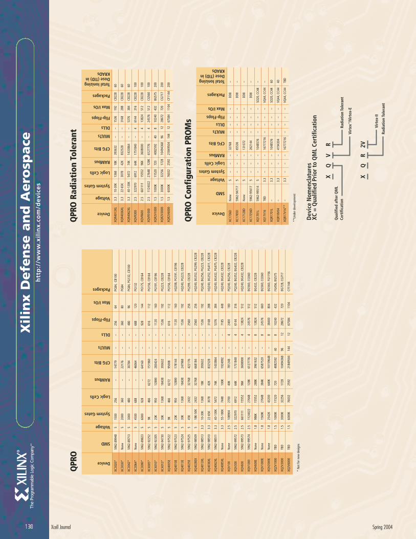
Xil
inx D
efe
nse
an
d A
ero
space
htt
p:/
/ww
w.x
ilin
x.c
om
/de
vic
es
130 Xcell Journal Spring 2004
XC30
20*
QPR
ODevice
5962
-899
48
SMD
5Voltage
1500
System Gates
Logic Cells
RAMbus
CFG Bits
MULTs
DLLs
256
–14
779
––
Flip-Flops
256
Max I/Os
64
Packages
PG84
, CB
100
XC30
30*
Non
e 5
2000
360
–22
176
––
360
80PG
84
XC30
42*
5962
-897
13
530
0048
0–
3078
4–
–48
0 96
PG84
, PG
132,
CB1
00
XC30
64*
Non
e 5
4500
68
8 –
4606
4–
–68
8 12
0PG
132
XC30
90*
5962
-898
23
560
00
928
–64
160
––
928
144
PG17
5, C
B164
XC40
05*
5962
-922
52
59K
46
6 62
72
1519
60
––
616
112
PG15
6, C
B164
XC40
10*
5962
-923
05
520
K 95
0 12
800
2834
24
––
1120
16
0PG
191,
CB1
96
XC40
13*
5962
-947
30
530
K 13
68
1843
8 39
3632
–
–15
36
192
PG22
3, C
B228
XQ40
05E
5962
-975
22
59K
46
6 62
72
9500
8–
–61
6 11
2 PG
156,
CB1
64
XQ40
10E
5962
-975
23
520
K 95
0 12
800
1781
44–
–11
20
160
HQ20
8, P
G19
1, C
B196
XQ40
13E
5962
-975
24
530
K 13
68
1843
8 24
7968
–
–15
36
192
HQ24
0, P
G22
3, C
B228
XQ40
25E
5962
-975
25
545
K 24
32
3276
8 42
2176
–
–25
60
256
PG29
9, C
B228
XQ40
28EX
59
62-9
8509
5
18K-
50K
2432
32
768
6681
84
––
2560
25
6 HQ
240,
BG
352,
PG
299,
CB2
28
XQ40
13XL
59
62-9
8513
3.
3 10
-30K
13
68
18K
3936
32
––
1536
19
2 PQ
240,
BG
256,
PG
223,
CB2
28
XQ40
36XL
59
62-9
8510
3.
3 22
-65K
30
78
42K
8325
28
––
3168
28
8 HQ
240,
BG
352,
PG
411,
CB2
28
XQ40
62XL
59
62-9
8511
3.
3 40
-130
K 54
72
74K
1433
864
––
5376
38
4 HQ
240,
BG
432,
PG
475,
CB2
28
XQ40
85XL
N
one
3.3
55-1
80K
7448
10
0K
1924
992
––
7185
44
8 HQ
240,
BG
432,
CB2
28
XQV1
00
Non
e 2.
5 10
8904
27
00
40K
7812
48
–4
2400
18
0 PQ
240,
BG
256,
CB2
28
XQV3
00
5962
-995
72
2.5
3229
70
6912
64
K 17
5184
0 –
461
44
316
PQ24
0, B
G35
2, B
G43
2, C
B228
XQV6
00
5962
-995
73
2.5
6611
11
1555
2 96
K 36
0800
0 –
413
824
512
HQ24
0, B
G43
2, C
B228
XQV1
000
5962
-995
74
2.5
1124
022
2764
8 12
8K
6127
776
–4
2457
6 51
2 BG
560,
CG
560
XQV6
00E
Non
e 1.
898
6K
1555
2 28
8K
3961
632
–8
1382
4 51
2 BG
432,
CB2
28
XQV1
000E
N
one
1.8
1569
K 27
648
384K
65
8752
0 –
824
576
660
BG56
0, C
G56
0
XQV2
000E
N
one
1.8
2542
K 43
200
640K
10
1596
48
–8
3840
0 80
4 BG
560,
FG
1156
XQ2V
1000
TB
D 1.
510
00K
1152
0 72
0 40
8259
2 40
810
240
432
FG45
6, B
G57
5
XQ2V
3000
TB
D 1.
530
00K
3225
6 17
28
1049
4368
96
1228
672
720
BG72
8, C
G71
7
XQ2V
6000
* N
ot fo
r new
des
igns
TBD
1.5
6000
K 76
032
2592
21
8495
04
144
1267
584
1104
CF
1144
Qua
lifie
d af
ter
QM
LCe
rtifi
cati
on
X
Dev
ice
Nom
encl
atur
esXC
= Q
ualif
ied
Prio
r to
QM
L Ce
rtifi
cati
on
QV
R
XQ
R2V
Radi
atio
n To
lera
nt
Virt
ex™/V
irte
x-E
Virt
ex-II
Radi
atio
n To
lera
nt
XQR4
013X
L
QPR
O R
adia
tion
Tol
eran
t
Device
3.3 Voltage
10-3
0K System Gates
Logic Cells
RAMbus
CFG Bits
MULTs
DLLs
1368
18
K 39
3632
–
–
Flip-Flops
1536
Max I/Os
192
Packages
CB22
8
Total IonizingDose (TID) inKRADs
60
XQR4
036X
L 3.
3 22
-65K
30
78
42K
8325
28
––
3168
28
8 CB
228
60
XQR4
062X
L 3.
3 40
-130
K 54
72
74K
1433
864
––
5376
38
4 CB
228
60
XQVR
300
2.5
3229
70
6912
64
K 17
5184
0 –
461
44
316
CB22
8 10
0
XQVR
600
2.5
6611
11
1555
2 96
K 36
0800
0 –
413
824
512
CB22
8 10
0
XQVR
1000
2.
5 11
2402
2 27
648
128K
61
2777
6 –
424
576
512
CG56
0 10
0
XQR2
V100
0 1.
5 10
00K
1152
0 72
0 40
8259
2 40
810
240
432
BG57
5 20
0
XQR2
V300
0 1.
5 30
00K
3225
6 17
28
1049
4368
96
1228
672
720
CG71
7 20
0
XQR2
V600
0 1.
5 60
00K
7603
2 25
92
2184
9504
14
412
6758
4 11
04
CF11
44
200
XC17
36D
QPR
O C
onfi
gura
tion
PRO
Ms
Device
5
Voltage
–
System Gates
Logic Cells
RAMbus
CFG Bits
MULTs
DLLs
Non
e
SMD
––
3276
8 –
–
Flip-Flops
–
Max I/Os
–
Packages
DD8
Total IonizingDose (TID) inKRADs
–
XC17
65D
5 –
5962
-947
17
––
6553
6 –
––
–DD
8 –
XC17
128D
5
–N
one
––
1310
72
––
––
DD8
–
XC17
256D
5
–59
62-9
5617
–
–26
2144
–
––
–DD
8 –
XQ17
01L
5 –
5962
-995
14
––
1048
576
––
––
SO20
, CC4
4 –
XQ17
V16
3.3
–TB
D –
–16
7772
16
––
––
VQ44
, CC4
4 –
XQR1
701L
3.
3 –
––
–10
4857
6 –
––
–SO
20, C
C44
60
XQR1
8V04
3.
3 –
––
–41
9430
4 –
––
–VQ
44, C
C44
40
XQR1
7V16
**3.
3 –
––
–16
7772
16–
––
–VQ
44, C
C44
TBD
**U
nder
dev
elop
men
t

Xil
inx G
lob
al
Serv
ices
htt
p:/
/ww
w.x
ilin
x.c
om
/gsd
/in
de
x.h
tm
Spring 2004 Xcell Journal 131
Xilin
x D
esig
n Se
rvic
es (X
DS)
•XD
S pr
ovid
es e
xten
sive
FPG
A ha
rdw
are
and
embe
dded
sof
twar
e de
sign
exp
erie
nce
back
ed b
y in
dust
ry
reco
gniz
ed e
xper
ts a
nd re
sour
ces
to s
olve
eve
n th
e m
ost c
ompl
ex d
esig
n ch
alle
nge.
•Sy
stem
Arc
hite
ctur
e Co
nsul
ting
— P
rovi
de e
ngin
eerin
g se
rvic
es t
o de
fine
syst
em a
rchi
tect
ure
and
part
ition
ing
for
desi
gn s
peci
ficat
ion.
•Cu
stom
Des
ign
Solu
tion
s—
Pro
ject
des
igne
d,ve
rifie
d,an
d de
liver
ed to
mut
ually
agr
eed
upon
des
ign
spec
ifica
tions
.
•IP
Cor
e D
evel
opm
ent,
Opt
imiz
atio
n,In
tegr
atio
n,M
odifi
cati
on,a
nd V
erifi
cati
on—
Mod
ify,i
nteg
rate
,an
d op
timiz
e cu
stom
er in
telle
ctua
l pro
pert
y or
third
par
ty c
ores
to w
ork
with
Xili
nx te
chno
logy
.Dev
elop
cu
stom
er-r
equi
red
spec
ial f
eatu
res
to X
ilinx
IP c
ores
or t
hird
par
ty c
ores
.Per
form
inte
grat
ion,
optim
izat
ion,
and
verif
icat
ion
of IP
cor
es in
Xili
nx te
chno
logy
.
•Em
bedd
ed S
oftw
are
— D
evel
op c
ompl
ex e
mbe
dded
sof
twar
e w
ith re
al-t
ime
cons
trai
nts,
usin
g ha
rdw
are/
soft
war
e co
-des
ign
tech
niqu
es.
•Co
nver
sion
s—
Con
vert
ASI
C de
sign
s an
d ot
her F
PGAs
to X
ilinx
tech
nolo
gy a
nd d
evic
es.
MyS
uppo
rt
•Si
gn u
p fo
r per
sona
lized
em
ail a
lert
s at
mys
uppo
rt.x
ilinx
.com
•Se
arch
our
kno
wle
dge
data
base
•Tr
oubl
esho
ot w
ith P
robl
em S
olve
rs
•Co
nsul
t with
eng
inee
rs in
For
ums
Tita
nium
Tec
hnic
al S
ervi
ce•
Ded
icat
ed A
pplic
atio
n En
gine
er
•Se
rvic
e at
cus
tom
er s
ite o
r at
Xili
nx
•D
esig
n flo
w m
etho
dolo
gy c
oach
ing
•En
gine
er/e
xper
tise
spec
ific
to c
usto
mer
nee
d
•A
ll ex
pert
ise
leve
ls a
vaila
ble
•Se
rvic
e gu
aran
teed
via
a c
ontr
act
Educ
atio
n Se
rvic
es
•Re
duce
tim
e to
kno
wle
dge
•Im
prov
e de
sign
eff
icie
ncy
•Re
duce
ove
rall
deve
lopm
ent
cost
s
Publ
ic a
nd p
rivat
e cl
asse
s av
aila
ble
wor
ldw
ide
http
://w
ww
.xili
nx.c
om/s
uppo
rt/e
duca
tion
-hom
e.ht
m
Plat
inum
Tec
hnic
al S
ervi
ce•
Acce
ss to
a d
edic
ated
team
of S
enio
r App
licat
ions
Eng
inee
rs
•D
edic
ated
tol
l fre
e nu
mbe
r*
•Pr
iorit
y ca
se r
esol
utio
n
•Te
n Ed
ucat
ion
Cred
its
•El
ectr
onic
new
slet
ter
•Fo
rmal
esc
alat
ion
proc
ess
•Se
rvic
e Pa
cks
and
Soft
war
e up
date
s
•A
pplic
atio
n En
gine
er t
o cu
stom
er r
atio
is 2
x th
e G
old
Leve
l
*Tol
l fre
e nu
mbe
r av
aila
ble
in U
S on
ly,
dedi
cate
d lo
cal n
umbe
rs
avai
labl
e ac
ross
Eur
ope
Xilin
x Pr
oduc
tivi
ty A
dvan
tage
(XPA
) Pro
gram
Th
e Xi
linx
Prod
uctiv
ity A
dvan
tage
(XPA
) del
ivers
eve
ryth
ing
your
cust
omer
nee
ds to
crea
te th
eir b
est
desig
n us
ing
Xilin
x Pr
ogra
mm
able
Sol
utio
ns,in
cludi
ng S
oftw
are,
Supp
ort,
Serv
ices a
nd IP
core
s.A
singl
e PO
allo
ws d
esig
ners
to g
et w
hat t
hey
need
,whe
n th
ey n
eed
it,at
a g
reat
pric
e.
Two
type
s of X
PAs a
re a
vaila
ble.
The
cust
om X
PA,t
ailo
red
to y
our c
usto
mer
s spe
cific
requ
irem
ents,
and
the
XPA
Seat
,an
off-t
he-s
helf
pre-
pack
aged
solu
tion
for t
he in
divid
ual d
esig
ner.
http
://su
ppor
t.xili
nx.co
m/su
ppor
t/gsd
/xpa
_pro
gram
.htm
Part
Num
ber
Prod
uct
Des
crip
tion
Dur
atio
n
Fund
amen
tals
of F
PGA
Desi
gnFP
GA
1300
0-6-
ILT
8
Educ
atio
n Se
rvic
esH
ours
Desi
gnin
g fo
r Per
form
ance
V6
FPG
A23
000-
6-IL
T16
Adva
nced
FPG
A Im
plem
enta
tion
FPG
A33
000-
6-IL
T16
Intr
oduc
tion
to V
HDL
LAN
G11
000-
5-IL
T24
Adva
nced
VHD
LLA
NG
2100
0-5-
ILT
16
Intr
oduc
tion
to V
erilo
gLA
NG
1200
0-5-
ILT
24
PCI C
ORE
Bas
ics
PCI8
000-
4-IL
T8
Desi
gnin
g a
PCI S
yste
mPC
I280
00-4
-ILT
16
Desi
gnin
g fo
r PCI
-XPC
I290
0-5-
ILT
16
DSP
Impl
emen
tatio
n Te
chni
ques
for X
ilinx
FPG
As
DSP
2000
-3-IL
T24
DSP
Desi
gn F
low
DSP
-100
001-
5-IL
T24
Desi
gnin
g w
ith M
ulti-
Gig
abit
Seria
l I/O
RIO
2200
0-6-
ILT
16
Embe
dded
Sys
tem
s De
velo
pmen
tEM
BD-2
1000
-5-IL
T16
Seat
Pla
tinum
Tech
nica
l Ser
vice
w/1
0 ed
ucat
ion
cred
itsSC
-PLA
T-SV
C-10
N/A
Plat
inum
Tech
nica
l Ser
vice
site
lice
nse
up to
50
cust
omer
sSC
-PLA
T-SI
TE-5
0N
/A
Plat
inum
Tech
nica
l Ser
vice
site
lice
nse
for 5
1-10
0 cu
stom
ers
SC-P
LAT-
SITE
-100
N/A
Plat
inum
Tech
nica
l Ser
vice
site
lice
nse
for 1
01-1
50 c
usto
mer
sSC
-PLA
T-SI
TE-1
50N
/A
Tita
nium
Tech
nica
l Ser
vice
(min
imum
40
hour
s)PS
-TEC
-SER
VN
/A
Desi
gn S
ervi
ces
Cont
ract
DC-
DES
-SER
VN
/A
Cust
om X
PA P
acka
ged
Solu
tion
DS-
XPA
N/A
Plat
inum
Tec
hnic
al S
ervi
ce
Tita
nium
Tec
hnic
al S
ervi
ce
Hou
rs
Hou
rs
Xilin
x Pr
oduc
tivi
ty A
dvan
tage
Hou
rs
Prom
otio
n Pa
ckag
es
Cust
om X
PA fo
r $0
– $1
0,00
0 D
S-XP
A-1
0KN
/A
Cust
om X
PA fo
r $10
,001
– $
25,0
00
DS-
XPA
-25K
N/A
Cust
om X
PA fo
r $25
,001
– $
100,
000
DS-
XPA
N
/A
Cust
om X
PA (I
nter
natio
nal)
for $
0 –
$10,
000
DS-
XPA
-10K
-INT
N/A
Cust
om X
PA (I
nter
natio
nal)
for $
10,0
01 –
$25
,000
D
S-XP
A-2
5K-IN
T N
/A
Cust
om X
PA (I
nter
natio
nal)
for $
25,0
01 –
$10
0,00
0 D
S-XP
A-IN
T N
/A
XPA
Seat
, ISE
Alli
ance
D
S-IS
E-A
LI-X
PA
N/A
XPA
Seat
, ISE
Fou
ndat
ion
DS-
ISE-
FND
-XPA
N
/A
Desi
gnin
g fo
r Per
form
ance
, Liv
e O
nlin
ePR
OM
O-5
003-
6-IL
T 9
FPG
A Es
sent
ials
: Inc
lude
s bo
th F
unda
men
tals
of F
PGA
Desi
gn a
nd D
esig
ning
for P
erfo
rman
ce c
lass
esPR
OM
O-5
004-
6-IL
T 24
EDK
Bund
le (E
DK +
10
TC’s
tow
ards
Em
bedd
ed S
yste
ms
Dev.
Cour
se)
DO
-ED
K-T
NA
DSP
Bund
le (S
ysge
n +
15T
C’s
tow
ards
DSP
Des
ign
Flow
Cou
rse)
D
S-SY
SGEN
-4SL
-T
NA
Hou
rs
Des
ign
Serv
ices
Con
tact
s
Nor
th A
mer
ica:
Rich
ard
Fodo
r:40
8-62
6-42
56M
ike
Baro
ne:5
12-2
38-1
473
Euro
pe:
Alex
Hill
ier:
+44
-870
-735
0-51
6M
artin
a Fi
nner
ty:+
353-
1-40
3-24
69
Asia
Pac
ific:
Davi
d Ke
efe:
+85
2-24
01-5
171
desi
gnse
rvic
es@
xilin
x.co
m
Educ
atio
n Se
rvic
es C
onta
cts
Nor
th A
mer
ica:
877-
XLX-
CLAS
(877
-959
-252
7)ht
tp://
supp
ort.x
ilinx
.com
/sup
port
/trai
ning
/trai
ning
.htm
Euro
pe:+
44-8
70-7
350-
548
euro
trai
ning
@xi
linx.
com
Japa
n:+
81-3
-532
1-77
50
http
://su
ppor
t.xili
nx.c
o.jp
/sup
port
/edu
catio
n-ho
me.
htm
Asia
Pac
ific:
+85
2-24
24-5
200
educ
atio
n_ap
@xi
linx.
com
ht
tp://
supp
ort.x
ilinx
.com
/sup
port
/edu
catio
n-ho
me.
htm
XPA
Con
tact
s
Nor
th A
mer
ica:
800-
888-
FPG
A (3
742)
fpga
.xili
nx.c
om
Euro
pe:
Stua
rt E
lsto
n:+
44-8
70-7
350-
532
Asia
Pac
ific:
Davi
d Ke
efe:
+85
2-24
01-5
171
Tita
nium
Tec
hnic
al S
ervi
ce C
onta
cts
Nor
th A
mer
ica:
Tele
sale
s:80
0-88
8-37
42
Euro
pe:
Stua
rt E
lsto
n:+
44-8
70-7
350-
632
Japa
n:+
81-3
-532
1-77
30
or ja
pant
itani
um@
xilin
x.co
m
Asia
Pac
ific:
Davi
d Ke
efe:
+85
2-24
01-5
171
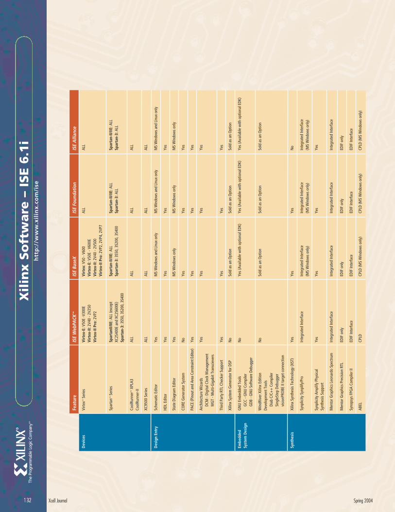
Xil
inx S
oft
ware
– I
SE 6
.1i
htt
p:/
/ww
w.x
ilin
x.c
om
/ise
132 Xcell Journal Spring 2004
Dev
ices
Feat
ure
Virt
ex™
Ser
ies
ISE
Web
PACK
™
Virt
ex-E
: V50
E -V
300E
Virt
ex-II
: 2V4
0 - 2
V250
Virt
ex-II
Pro
: 2VP
2
ISE
Base
X
Virt
ex: V
50 -
V600
Virt
ex-E
: V50
E - V
600E
Virt
ex-II
: 2V4
0 - 2
V500
Virt
ex-II
Pro
: 2VP
2, 2
VP4,
2VP
7
ISE
Foun
dati
on
ALL
ISE
Alli
ance
ALL
Spar
tan™
Ser
ies
Spar
tanI
I/IIE
: ALL
(exc
ept
XC2S
400E
and
XC2
S600
E)
Spar
tan-
3: 3
S50,
3S2
00, 3
S400
Spar
tan-
II/IIE
: ALL
Spar
tan-
3: 3
S50,
3S2
00, 3
S400
Spar
tan-
II/IIE
: ALL
Spar
tan-
3: A
LLSp
arta
n-II/
IIE: A
LLSp
arta
n-3:
ALL
Cool
Runn
er™
XPL
A3Co
olRu
nner
-IIAL
LAL
LAL
LAL
L
XC95
00 S
erie
sAL
LAL
LAL
LAL
L
HDL
Edito
r Ye
s
Yes
Ye
s
Yes
Stat
e Di
agra
m E
dito
r Ye
s
MS
Win
dow
s on
lyM
S W
indo
ws
only
MS
Win
dow
s on
ly
CORE
Gen
erat
or S
yste
m
No
Yes
Ye
s
Yes
PACE
(Pin
out a
nd A
rea
Cons
train
t Edi
tor)
Yes
Ye
s
Yes
Ye
s
Arch
itect
ure
Wiz
ards
D
CM -
Digi
tal C
lock
Man
agem
ent
M
GT
- Mul
ti-G
igab
it Tr
ansc
ieve
rs
Yes
Ye
s
Yes
Ye
s
Third
Par
ty R
TL C
heck
er S
uppo
rt
Yes
Ye
s
Yes
Ye
s
Xilin
x Sy
stem
Gen
erat
or fo
r DSP
N
oSo
ld a
s an
Opt
ion
So
ld a
s an
Opt
ion
So
ld a
s an
Opt
ion
Win
dRiv
er X
ilinx
Edi
tion
Deve
lopm
ent T
ools
Dia
b C/
C++
Com
pile
r
Sin
gleS
tep
Debu
gger
v
isio
nPRO
BE II
targ
et c
onne
ctio
n
No
Sold
as
an O
ptio
n
Sold
as
an O
ptio
n
Sold
as
an O
ptio
n
Synp
licity
Syn
plify
/Pro
In
tegr
ated
Inte
rface
In
tegr
ated
Inte
rface
(M
S W
indo
ws
only
) In
tegr
ated
Inte
rface
(M
S W
indo
ws
only
) In
tegr
ated
Inte
rface
(M
S W
indo
ws
only
)
Synp
licity
Am
plify
Phy
sica
l Sy
nthe
sis
Supp
ort
Yes
Yes
Yes
Yes
Men
tor G
raph
ics
Leon
ardo
Spe
ctru
m
Inte
grat
ed In
terfa
ce
Inte
grat
ed In
terfa
ce
Inte
grat
ed In
terfa
ce
Inte
grat
ed In
terfa
ce
Men
tor G
raph
ics
Prec
isio
n RT
L
EDIF
onl
yED
IF o
nly
EDIF
onl
yED
IF o
nly
Syno
psys
FPG
A Co
mpi
ler I
I ED
IF In
terfa
ce
EDIF
Inte
rface
ED
IF In
terfa
ce
EDIF
Inte
rface
ABEL
CP
LD
CPLD
(MS
Win
dow
s on
ly)
CPLD
(MS
Win
dow
s on
ly)
CPLD
(MS
Win
dow
s on
ly)
Des
ign
Entr
ySc
hem
atic
Edi
tor
Ye
sM
S W
indo
ws
and
Linu
x on
lyM
S W
indo
ws
and
Linu
x on
lyM
S W
indo
ws
and
Linu
x on
ly
Embe
dded
Syst
em D
esig
nG
NU
Em
bedd
ed T
ools
G
CC -
GN
U C
ompi
ler
G
DB -
GN
U S
oftw
are
Debu
gger
No
Yes
(Ava
ilabl
e w
ith o
ptio
nal E
DK)
Yes
(Ava
ilabl
e w
ith o
ptio
nal E
DK)
Yes
(Ava
ilabl
e w
ith o
ptio
nal E
DK)
Synt
hesi
sXi
linx
Synt
hesi
s Te
chno
logy
(XST
) Ye
s
Yes
Ye
s
No
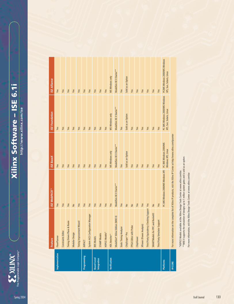
Xil
inx S
oft
ware
– I
SE 6
.1i
htt
p:/
/ww
w.x
ilin
x.c
om
/ise
Spring 2004 Xcell Journal 133
Feat
ure
ISE
Web
PACK
™IS
E Ba
seX
ISE
Foun
dati
onIS
E A
llian
ce
Cons
trai
nts
Edito
r Ye
s
Yes
Ye
s
Yes
Tim
ing
Driv
en P
lace
& R
oute
Ye
s
Yes
Ye
s
Yes
Mod
ular
Des
ign
N
oYe
s
Yes
Ye
s
Tim
ing
Impr
ovem
ent W
izar
d
Yes
Ye
s
Yes
Ye
s
Syst
em A
CE C
onfig
urat
ion
Man
ager
Ye
s
Yes
Ye
s
Yes
STAM
P M
odel
s
Yes
Ye
s
Yes
Ye
s
HSPI
CE M
odel
s*
Yes
Ye
s
Yes
Ye
s
Mod
elSi
m®
Xili
nx E
ditio
n (M
XE II
) M
odel
Sim
XE
II St
arte
r**
M
odel
Sim
XE
II St
arte
r**
M
odel
Sim
XE
II St
arte
r**
M
odel
Sim
XE
II St
arte
r**
Stat
ic T
imin
g An
alyz
er
Yes
Ye
s
Yes
Ye
s
Chip
Scop
e™ P
ro
No
So
ld a
s an
Opt
ion
So
ld a
s an
Opt
ion
So
ld a
s an
Opt
ion
FPG
A Ed
itor w
ith P
robe
N
o
Yes
Ye
s
Yes
Chip
View
er
Yes
Ye
s
Yes
Ye
s
XPow
er (P
ower
Ana
lysi
s)
Yes
Ye
s
Yes
Ye
s
Third
Par
ty E
quiv
alen
cy C
heck
ing
Supp
ort
Yes
Ye
s
Yes
Ye
s
SMAR
TMod
els
for P
PC a
nd R
ocke
tIO
No
Yes
Ye
s
Yes
Third
Par
ty S
imul
ator
Sup
port
Ye
sYe
s
Yes
Ye
s
Impl
emen
tati
onFl
oorP
lann
er
Yes
Ye
s
Yes
Ye
s
iMPA
CT
Prog
ram
min
gYe
s
Yes
Ye
s
Yes
IBIS
Mod
els
Bo
ard
Leve
lIn
tegr
atio
nYe
s
Yes
Ye
s
Yes
HDL
Benc
her™
Veri
ficat
ion
Yes
M
S W
indo
ws
only
MS
Win
dow
s on
lyM
S W
indo
ws
only
PC (M
S W
indo
ws 2
000/
MS
Win
dow
s XP)
Pl
atfo
rms
PC (M
S W
indo
ws
2000
/MS
Win
dow
s XP
), Li
nux
PC (M
S W
indo
ws
2000
/MS
Win
dow
s XP
), Su
n, S
olar
is, L
inux
PC(M
S W
indo
ws
2000
/MS
Win
dow
s XP
), Su
n, S
olar
is, L
inux
For m
ore
info
rmat
ion
on th
e co
mpl
ete
list o
f Xili
nx IP
pro
duct
s, v
isit
the
Xilin
x IP
Cen
ter a
t htt
p://w
ww
.xili
nx.c
om/ip
cent
er
IP
/CO
RE
*HSP
ICE
Mod
els
avai
labl
e at
the
Xilin
x De
sign
Too
ls C
ente
r at w
ww
.xili
nx.c
om/is
e.**
MXE
II s
uppo
rts
the
sim
ulat
ion
of d
esig
ns u
p to
1 m
illio
n sy
stem
gat
es a
nd is
sol
d as
an
optio
n. Fo
r mor
e in
form
atio
n, v
isit
the
Xilin
x De
sign
Too
ls C
ente
r at w
ww
.xili
nx.c
om/is
e
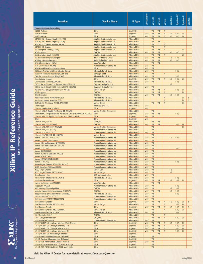
Xil
inx I
P R
efe
ren
ce G
uid
eh
ttp
://w
ww
.xil
inx
.co
m/i
pce
nte
r
134 Xcell Journal Spring 2004
Function
Virt
ex-II
Pro
Virt
ex-II
Virt
ex-E
Virt
ex
Spar
tan-
3
Spar
tan-
IIE
Spar
tan-
II
Spar
tan
Vendor Name IP Type
Communication & Networking3G FEC Package Xilinx LogiCORE V-II V-E V8b/10b Decoder Xilinx LogiCORE V-IIP V-II V-E V S-3 S-IIE S-II8b/10b Encoder Xilinx LogiCORE V-IIP V-II V-E V S-3 S-IIE S-IIADPCM, 1024 Channel Simplex (CS4190) Amphion Semiconductor, Ltd. AllianceCORE V-IIADPCM, 256 Channel Simplex (CS4130) Amphion Semiconductor, Ltd. AllianceCORE V-II V-EADPCM, 512 Channel Duplex (CS4180) Amphion Semiconductor, Ltd. AllianceCORE V-II VADPCM, 768 Channel Amphion Semiconductor, Ltd. AllianceCORE V-II VAES Decryption Family (CS5200) Amphion Semiconductor, Ltd. AllianceCORE V-II V-E V S-IIAES Encryption CAST, Inc. AllianceCORE V-IIP V-II V-E S-3 S-IIEAES Encryption Family (CS5200) Amphion Semiconductor, Ltd. AllianceCORE V-II V-E V S-IIAES Standard Encryptor/Decryptor Helion Technology Limited AllianceCORE V-IIP V-II V-E S-3 S-IIEAES Tiny Encryptor/Decryptor Helion Technology Limited AllianceCORE V-IIP V-II V-E S-3 S-IIEATM Adaption Layer 1 (AAL1) ModelWare, Inc. AllianceCORE V-II V-EATM Cell Processor (CC200) Paxonet Communications, Inc. AllianceCORE V-IIP V-IIAWGN - Additive White Gaussian Noise Xilinx LogiCORE V-IIP V-IIBit Stream Analyzer and Data Extractor (Parser) Telecom Italia Lab S.p.A. AllianceCORE V-IIP V-II S-IIEBluetooth Baseband Processor (BOOST Lite) NewLogic GmbH AllianceCORE V-II VCAM for Internet Protocol (IPlogiCAM) Telecom Italia Lab S.p.A. AllianceCORE V-IIP V-II S-IIEConvolutional Encoder Xilinx LogiCORE V-IIP V-II V-E V S-3 S-IIE S-IIConvolutional Encoder (CONV_ENC) Telecom Italia Lab S.p.A. AllianceCORE V-IIP V-II S-IIECRC-32 for 10 Gbps OC192 Systems (CORE-CRC-128) Calyptech Design Services AllianceCORE S-3CRC-32 for 40 Gbps OC-768 Systems (CORE-CRC-256) Calyptech Design Services AllianceCORE V-IIP V-IIDES and DES3 Encryption Engine (MC-XIL-DES) Memec Design AllianceCORE V-II V-E V S-IIE S-IIDES Encryption CAST, Inc. AllianceCORE V-II V-E V S-IIDES3 Encryption CAST, Inc. AllianceCORE V-IIP V-II V-E S-3 S-IIEDistributed Sample Descrambler (DSD) Telecom Italia Lab S.p.A. AllianceCORE V S-II SDistributed Sample Scrambler (DSS) Telecom Italia Lab S.p.A. AllianceCORE V S-II SDVB Satellite Modulator (MC-XIL-DVBMOD) Memec Design AllianceCORE V-II V-E V S-IIEmail Trigger Amirix Systems, Inc. AllianceCORE V-IIPEthernet 1000BASE-X PCS/PMA Xilinx LogiCORE V-IIPEthernet MAC, 1 Gigabit Full Duplex (PE-GMAC0) Mentor Graphics Corporation AllianceCORE V-IIEthernet MAC, 1 Gigabit Half/Full Duplex with GMII or 1000BASE-X PCS/PMA Xilinx LogiCORE V-IIP V-II V-E S-IIEEthernet MAC, 10 Gigabit Full Duplex with XGMII or XAUI Xilinx LogiCORE V-IIP V-IIXAUI Xilinx LogiCORE V-IIPEthernet MAC, 10/100 Zuken, Inc. AllianceCORE V-II V-EEthernet MAC, 10/100 (MAC) CAST, Inc. AllianceCORE V-IIP V-II V-E S-IIE S-IIEthernet MAC, 10/100 (PE-MACMII) Mentor Graphics Corporation AllianceCORE V-II S-IIEthernet MAC, 10G (CC410) Paxonet Communications, Inc. AllianceCORE V-IIEthernet PCS, 10G (CC411) Paxonet Communications, Inc. AllianceCORE V-IIP V-IIEthernet PCS, 10G (MC-XIL-10GEPCS) Memec Design AllianceCORE V-IIFramer, 1.25 Gbps GFP (CC224) Paxonet Communications, Inc. AllianceCORE V-IIP V-II S-3 S-IIEFramer, 2.5 Gbps GFP (CC226) Paxonet Communications, Inc. AllianceCORE V-IIP V-IIFramer, 8-Bit Multilchannel GFP (CC225) Paxonet Communications, Inc. AllianceCORE V-IIP V-IIFramer, 8-Bit Transparent GFP (CC124) Paxonet Communications, Inc. AllianceCORE V-IIP V-IIFramer, E1 (CC303) Paxonet Communications, Inc. AllianceCORE V-IIP V-II S-IIEFramer, OC12 (CC351) Paxonet Communications, Inc. AllianceCORE V-IIP V-IIFramer, OC192/10 Gbps GFP (CC327) Paxonet Communications, Inc. AllianceCORE V-IIP V-IIFramer, OTU2 (CC481) Paxonet Communications, Inc. AllianceCORE V-IIP V-IIFramer, STS192/STM64 (CC314) Paxonet Communications, Inc. AllianceCORE V-IIP V-IIFramer, T1 (CC302) Paxonet Communications, Inc. AllianceCORE V-IIP V-II S-IIEFramer/Digital Wrapper, STS48 OTN (CC381) Paxonet Communications, Inc. AllianceCORE V-IIP V-IIG.709 Compliant FEC Core (CC345) Paxonet Communications, Inc. AllianceCORE V-IIP V-IIHDLC, Single-Channel Memec Core AllianceCORE V-IIP V-II S-3HDLC, Single-Channel (MC-XIL-HDLC) Memec Design AllianceCORE V-IIP V-II S-3HyperTransport Cave GDA Technologies, Inc. AllianceCORE V-IIP V-IIInterleaver De-interleaver (INT_DEINT) Telecom Italia Lab S.p.A. AllianceCORE V-IIP V-II S-IIEInterleaver/De-interleaver Xilinx LogiCORE V-IIP V-II V-E V S-3 S-IIE S-IIInverse Multiplexer for ATM (IMA) ModelWare, Inc. AllianceCORE V-II V-EMapper, E1 (CC333) Paxonet Communications, Inc. AllianceCORE V-IIP V-II S-IIEMD5 Message Digest Algorithm CAST, Inc. AllianceCORE V-IIP V-II S-3 S-IIEModular Exponentiation Accelerator (MODEXP1) CAST, Inc. AllianceCORE V-IIP V-II V-E S-3 S-IIENoisy Transmission Channel Model (CHANNEL) Telecom Italia Lab S.p.A. AllianceCORE V-IIP V-II S-IIEPath Processor, OC12c (CC321) Paxonet Communications, Inc. AllianceCORE V-IIP V-IIPath Processor, STS192/STM64 (CC324) Paxonet Communications, Inc. AllianceCORE V-IIP V-IIReed Solomon Decoder Xilinx LogiCORE V-IIP V-II V-E V S-3 S-IIE S-II SReed Solomon Decoder (MC-XIL-RSDEC) Memec Design AllianceCORE V-II V S-IIE S-IIReed Solomon Encoder Xilinx LogiCORE V-IIP V-II V-E V S-3 S-IIE S-II SReed Solomon Encoder (MC-XIL-RSENC) Memec Design AllianceCORE V-II V S-IIE S-IIReed-Solomon Decoder (RS_DEC) Telecom Italia Lab S.p.A. AllianceCORE V-IIP V-II S-IIESDLC Controller (SDLC) CAST, Inc. AllianceCORE V-II VSHA-1 Encryption Processor CAST, Inc. AllianceCORE V-II V-E V S-IIE S-IISPI 4.2 Interface (CC401) Paxonet Communications, Inc. AllianceCORE V-IIP V-IISPI-3 (POS-PHY L3) Link Layer Interface, Multi-Channel Xilinx LogiCORE V-IIP V-II V-E V S-3 S-IIE S-IISPI-3 (POS-PHY L3) Link Layer Interface, 1-Ch Xilinx LogiCORE V-IIP V-II V-E V S-IIE S-IISPI-3 (POS-PHY L3) Link Layer Interface, 2-Ch Xilinx LogiCORE V-IIP V-II V-E V S-IIE S-IISPI-3 (POS-PHY L3) Link Layer Interface, 4-Ch Xilinx LogiCORE V-IIP V-II V-E V S-IIE S-IISPI-3 (POS-PHY L3) Physical Layer Interface Xilinx LogiCORE V-ESPI-4.1 (Flexbus 4) Interface Core, 1-Channel Xilinx LogiCORE V-IISPI-4.1 (Flexbus 4) Interface Core, 4-Channel Xilinx LogiCORE V-IISPI-4.2 (POS-PHY L4) Multi-Channel Interface Xilinx LogiCORE V-IIP V-IISPI-4.2 (POS-PHY L4) to SPI-4.1 (Flexbus 4) Bridge Xilinx LogiCORE V-IISPI-4.2 (POS-PHY L4) to XGMII (10GE MAC) Bridge Xilinx LogiCORE V-II
Visit the Xilinx IP Center for more details at www.xilinx.com/ipcenter

Function
Virt
ex-II
Pro
Virt
ex-II
Virt
ex-E
Virt
ex
Spar
tan-
3
Spar
tan-
IIE
Spar
tan-
II
Spar
tan
Vendor Name IP Type
Xil
inx I
P R
efe
ren
ce G
uid
eh
ttp
://w
ww
.xil
inx
.co
m/i
pce
nte
r
Spring 2004 Xcell Journal 135
SPI-4.2 Lite (POS_PHY L4) Xilinx LogiCORE V-II S-3Turbo Decoder (TURBO_DEC) Telecom Italia Lab S.p.A. AllianceCORE V-II VTurbo Decoder, 3GPP SysOnChip, Inc. AllianceCORE V-II V-ETurbo Decoder, 3GPP (S3000) iCoding Technology, Inc. AllianceCORE V-II V-E S-IIETurbo Decoder, Convolutional, 3GPP Compliant Xilinx LogiCORE V-II V-E VTurbo Decoder, Convolutional, 3GPP2/CDMA2000 Xilinx LogiCORE V-IIP V-II S-3Turbo Decoder, DVB-RCS (S2000) iCoding Technology, Inc. AllianceCORE V-II V-E VTurbo Decoder, DVB-RCS (TC1000) TurboConcept AllianceCORE V-II V-ETurbo Decoder, Product Code Xilinx LogiCORE V-IIP V-II S-3Turbo Encoder (TURBO_ENC) Telecom Italia Lab S.p.A. AllianceCORE V-IIP V-II S-IIETurbo Encoder, Convolutional, 3GPP Compliant Xilinx LogiCORE V-II V-E VTurbo Encoder, Convolutional, 3GPP2/CDMA2000 Xilinx LogiCORE V-IIP V-II S-3Turbo Encoder, DVB-RCS (S2001) iCoding Technology, Inc. AllianceCORE V-II V-E VTurbo Encoder, Product Code Xilinx LogiCORE V-IIP V-II S-3Turbo Product Code Decoder, 25 Mbps (TC3000) TurboConcept AllianceCORE V-II V-ETurbo Product Code Decoder, 30 Mbps (TC3401) TurboConcept AllianceCORE V-E S-IIETurbo Product Code Decoder, 160 Mbps (TC3404) TurboConcept AllianceCORE V-II V-EUTOPIA Level-2 PHY Side RX Interface (UTOPIA L2 PHY Rx) Telecom Italia Lab S.p.A. AllianceCORE V-IIP V-II S-IIEUTOPIA Level-2 PHY Side TX Interface (UTOPIA L2 PHY Tx) Telecom Italia Lab S.p.A. AllianceCORE V-IIP V-II S-IIEUTOPIA RX Level 2 Master Interface (UTOPIA2M_RX) Telecom Italia Lab S.p.A. AllianceCORE V-IIP V-II S-IIEViterbi Decoder (VITERBI_DEC) Telecom Italia Lab S.p.A. AllianceCORE V-IIP V-II S-IIEViterbi Decoder, General Purpose Xilinx LogiCORE V-IIP V-II V-E V S-3 S-IIE S-IIViterbi Decoder, IEEE 802-Compatible Xilinx LogiCORE V-IIP V-II V-E V S-3 S-IIE S-IIXAPP 289: Common Switch Interface CSIX-L1 Reference Design Xilinx Reference Design V-IIP V-IIDigital Signal ProcessingBit Correlator Xilinx LogiCORE V-IIP V-II V-E V S-IIE S-IICascaded Integrator Comb (CIC) Filter Xilinx LogiCORE V-IIP V-II V-E V S-IIE S-IIComb Filter Xilinx LogiCORE SCORDIC Xilinx LogiCORE V-IIP V-II V-E V S-3 S-IIE S-IIDigital Down Converter (DDC) Xilinx LogiCORE V-IIP V-II V-E V S-IIE S-IIDigital Up Converter (DUC) Xilinx LogiCORE V-IIPDirect Digital Synthesizer (DDS) Xilinx LogiCORE V-IIP V-II V-E V S-3 S-IIE S-IIDiscrete Cosine Transform (eDCT) eInfochips Pvt. Ltd. AllianceCORE V-II V-E V S-IIE S-IIDiscrete Cosine Transform, 2D Inverse (IDCT) CAST, Inc. AllianceCORE V-II V-E V S-IIDiscrete Cosine Transform, Combined 2D Forward/Inverse (DCT_FI) CAST, Inc. AllianceCORE V-II V-E V S-IIDiscrete Cosine Transform, Forward 2D (DCT) CAST, Inc. AllianceCORE V-II V-E V S-IIDiscrete Cosine Transform, Forward/Inverse (FIDCT) Telecom Italia Lab S.p.A. AllianceCORE V-IIP V-II S-IIEDiscrete Cosine Transform, Forward/Inverse 2D (DCT/IDCT 2D) Barco-Silex AllianceCORE V-II V-E V S-IIDiscrete Wavelet Transform, Combined 2D Forward/Inverse (RC_2DDWT) CAST, Inc. AllianceCORE V-II V-E V S-IIDiscrete Wavelet Transform, Line-Based Programmable Forward (LB_2DFDWT) CAST, Inc. AllianceCORE V-II V-E V S-IIDOCSIS ITU-T J.83 Modulator Xilinx LogiCORE V-IIP V-II S-3DOCSIS ITU-T J.83 Modulator Xilinx LogiCORE V-IIP V-II S-3DSP Hardware Accelerator, Virtex-E (GVA-290) GV & Associates, Inc. AllianceCORE V-EDSP Hardware Accelerator, Virtex-II (GVA-300) GV & Associates, Inc. AllianceCORE V-IIDSP Hardware Accelerator, Virtex-II (GVA-325) GV & Associates, Inc. AllianceCORE V-IIDSP Hardware Accelerator, Virtex-II (GVA-350) GV & Associates, Inc. AllianceCORE V-IIFast Fourier Transform Xilinx LogiCORE V-IIP V-II S-3FFT/IFFT for Virtex-II, 1024-Point Complex Xilinx LogiCORE V-IIFFT/IFFT for Virtex-II, 16-Point Complex Xilinx LogiCORE V-IIFFT/IFFT for Virtex-II, 256-Point Complex Xilinx LogiCORE V-IIFFT/IFFT for Virtex-II, 64-Point Complex Xilinx LogiCORE V-IIFFT/IFFT, 1024-Point Complex Xilinx LogiCORE V-E VFFT/IFFT, 16-Point Complex Xilinx LogiCORE V-II V-E VFFT/IFFT, 256-Point Complex Xilinx LogiCORE V-II V-E VFFT/IFFT, 32-Point Complex Xilinx LogiCORE V-IIP V-II V-E V S-IIE S-IIFFT/IFFT, 64-, 256-, 1024-Point Complex Xilinx LogiCORE V-IIP V-II S-3FFT/IFFT, 64-Point Complex Xilinx LogiCORE V-E VFIR Filter Using DPRAM eInfochips Pvt. Ltd. AllianceCORE V-II V-E V S-IIE S-IIFIR Filter, Distributed Arithmetic (DA) Xilinx LogiCORE V-IIP V-II V-E V S-3 S-IIE S-IIFIR Filter, Distributed Arithmetic Parallel Xilinx LogiCORE SFIR Filter, Distributed Arithmetic Serial Xilinx LogiCORE SFIR Filter, MAC Xilinx LogiCORE V-IIP V-II V-E V S-3 S-IIE S-IIFIR Filter, Parallel Distributed Arithmetic eInfochips Pvt. Ltd. AllianceCORE V-II V-E V S-IIE S-IILFSR, Linear Feedback Shift Register Xilinx LogiCORE V-IIP V-II V-E V S-3 S-IIE S-IIOscillator, Dual-Channel Numerically Controlled Xilinx LogiCORE V-E V S-IIE S-II SOscillator, Numerically Controlled Xilinx LogiCORE V-E V S-IIE S-II STime-Skew Buffer, Nonsymmetric 16-Deep Xilinx LogiCORE STime-Skew Buffer, Nonsymmetric 32-Deep Xilinx LogiCORE STime-Skew Buffer, Symmetric 16-Deep Xilinx LogiCORE STMS32025 DSP Processor (C32025) CAST, Inc. AllianceCORE V-II V-E V S-IIMath Functions1s and 2s Complement Xilinx LogiCORE SAccumulator Xilinx LogiCORE V-IIP V-II V-E V S-3 S-IIE S-IIAdder Subtracter Xilinx LogiCORE V-IIP V-II V-E V S-3 S-IIE S-IIDivider, Pipelined Xilinx LogiCORE V-II V-E V S-IIE S-II SFloating Point Adder (DFPADD) Digital Core Design AllianceCORE V-II V S-IIFloating Point Comparator (DFPCOMP) Digital Core Design AllianceCORE V-II V S-IIFloating Point Divider (DFPDIV) Digital Core Design AllianceCORE V-II V S-IIFloating Point Multiplier (DFPMUL) Digital Core Design AllianceCORE V-II V-E V S-IIFloating Point Square Root Operator (DFPSQRT) Digital Core Design AllianceCORE V-II V-E S-IIFloating Point to Integer Converter (DFP2INT) Digital Core Design AllianceCORE V-II V S-IIInteger to Floating Point Converter (DINT2FP) Digital Core Design AllianceCORE V-II V S-IIIntegrator Xilinx LogiCORE S
Visit the Xilinx IP Center for more details at www.xilinx.com/ipcenter

Function
Virt
ex-II
Pro
Virt
ex-II
Virt
ex-E
Virt
ex
Spar
tan-
3
Spar
tan-
IIE
Spar
tan-
II
Spar
tan
Vendor Name IP Type
Xil
inx I
P R
efe
ren
ce G
uid
eh
ttp
://w
ww
.xil
inx
.co
m/i
pce
nte
r
136 Xcell Journal Spring 2004
Multiplier for Virtex, Variable Parallel Xilinx LogiCORE V-E V S-IIE S-IIMultiplier, Constant Coefficient Xilinx LogiCORE SMultiplier, Constant Coefficient - Pipelined Xilinx LogiCORE SMultiplier, Dynamic Constant Coefficient Xilinx LogiCORE V-E VMultiplier, Parallel - Area Optimized Xilinx LogiCORE SMultiply Accumulator (MAC) Xilinx LogiCORE V-IIP V-II V S-3 S-IIE S-IIMultiply Generator Xilinx LogiCORE V-IIP V-II V-E V S-3 S-IIE S-IIRegistered Adder Xilinx LogiCORE SRegistered Loadable Adder Xilinx LogiCORE SRegistered Loadable Subtracter Xilinx LogiCORE SRegistered Scaled Adder Xilinx LogiCORE SRegistered Serial Adder Xilinx LogiCORE SRegistered Subtracter Xilinx LogiCORE SScaled-by-One-Half Accumulator Xilinx LogiCORE SSine Cosine Look Up Table Xilinx LogiCORE V-IIP V-II V-E V S-3 S-IIE S-II SSquare Root Xilinx LogiCORE STwos Complementer Xilinx LogiCORE V-IIP V-II V-E V S-3 S-IIE S-IIMemories & Storage ElementsATM Utopia Level 2 Xilinx LogiCORE V-IIPBlock Memory, Dual-Port Xilinx LogiCORE V-IIP V-II V-E V S-3 S-IIE S-IIBlock Memory, Single-Port Xilinx LogiCORE V-IIP V-II V-E V S-3 S-IIE S-IIContent Addressable Memory (CAM) Xilinx LogiCORE V-IIP V-II V-E V S-3 S-IIE S-IIDistributed Memory Xilinx LogiCORE V-IIP V-II V-E V S-3 S-IIE S-IIFIFO, Asynchronous Xilinx LogiCORE V-IIP V-II V-E V S-3 S-IIE S-IIFIFO, Synchronous Xilinx LogiCORE SFIFO, Synchronous Xilinx LogiCORE V-IIP V-II V-E V S-3 S-IIE S-IIPipelined Delay Element Xilinx LogiCORE SRegistered ROM Xilinx LogiCORE SRegistered Single Port RAM Xilinx LogiCORE SRLDRAM Memory Controller Avnet Design Services AllianceCORE V-IISDRAM Controller (EP520) Eureka Technology AllianceCORE VSDRAM Controller, DDR (EP525) Eureka Technology AllianceCORE V-IIP V-II S-3 S-IIESDRAM Controller, DDR (MC-XIL-SDRAMDDR) Memec Design AllianceCORE V-II V-E S-IIMicroprocessors, Controllers & Peripherals1 Gigabit Ethernet MAC w/PLB Interface Xilinx LogiCORE V-IIP10/100 Ethernet MAC Lite w/OPB Interface Xilinx LogiCORE V-IIP V-II V-E V S-IIE S-II10/100 Ethernet MAC w/OPB Interface Xilinx LogiCORE V-IIP V-II V-E V S-IIE S-II16450 UART (H16450) CAST, Inc. AllianceCORE V-II V-E V S-IIE S-II16450 UART w/OPB Interface Xilinx LogiCORE V-IIP V-II V-E V S-3 S-IIE S-II16450 UART w/Synchronous Interface (H16450S) CAST, Inc. AllianceCORE V-II V-E V S-IIE S-II16550 UART w/FIFOs & Synchronous Interface (H16550S) CAST, Inc. AllianceCORE V-II V-E V S-IIE S-II16550 UART w/FIFOs (H16550) CAST, Inc. AllianceCORE V-II V-E V S-IIE S-II16550 UART w/OPB interface Xilinx LogiCORE V-IIP V-II V-E V S-3 S-IIE S-II2910A Microprogram Controller (C2910A) CAST, Inc. AllianceCORE V S-II S2D Fabric Evaluation and Demo Board Crossbow Technologies, Inc. AllianceCORE S-II2D Multiprocessing Interface Fabric (2D-fabric402C) Crossbow Technologies, Inc. AllianceCORE V-IIP V-II S-IIE S-II68000 Compatible Microprocessor (C68000) CAST, Inc. AllianceCORE V-II V-E V S-380186 Compatible Microprocessor (e80186) eInfochips Pvt. Ltd. AllianceCORE V-II V8051 Base Compatible Microcontroller (DR8051BASE) Digital Core Design AllianceCORE V-II V S-II8051 Compatible Microcontroller (C8051) CAST, Inc. AllianceCORE V-IIP V-II V-E V S-3 S-IIE S-II8051 Compatible Microcontroller (Flip805x-PR) Dolphin Integration AllianceCORE V S-II S8051 RISC Microcontroller (DR8051) Digital Core Design AllianceCORE V-II V S-II80515 High-speed 8-bit RISC Microcontroller (R80515) CAST, Inc. AllianceCORE V8052 Compatible Microcontroller (DR8052EX) Digital Core Design AllianceCORE V-II V S-II80C51 Compatible RISC Microcontroller (R8051) CAST, Inc. AllianceCORE V-E V S-II8237 Programmable DMA Controller (C8237) CAST, Inc. AllianceCORE V-II V-E V S-II8250 UART (H8250) CAST, Inc. AllianceCORE V-II V-E S-IIE S-II8254 Programmable Interval Timer/Counter (C8254) CAST, Inc. AllianceCORE V-II V-E V S-II8254 Programmable Interval Timer/Counter (e8254) eInfochips Pvt. Ltd. AllianceCORE V-II S-II8255 Programmable I/O Controller (e8255) eInfochips Pvt. Ltd. AllianceCORE V-II S-II8259A Programmable Interrupt Controller (C8259A) CAST, Inc. AllianceCORE V-II V-E V S-IIArbiter and Bus Structure w/OPB Interface Xilinx LogiCORE V-IIP V-II V-E V S-3 S-IIE S-IIArbiter and Bus Structure w/PLB Interface Xilinx LogiCORE V-IIPATM Utopia Level 2 Master and Slave w/OPB Interface Xilinx LogiCORE V-IIP V-II V-E V S-IIE S-IIATM Utopia Level 2 Master and Slave w/PLB Interface Xilinx LogiCORE V-IIPBRAM Controller w/LMB Interface Xilinx LogiCORE V-IIP V-II V-E V S-IIE S-IIBRAM Controller w/OPB Interface Xilinx LogiCORE V-IIP V-II V-E V S-3 S-IIE S-IIBRAM Controller w/PLB Interface Xilinx LogiCORE V-IIPBSP Generator (SW only) Xilinx LogiCORE V-IIPCompact Video Controller (logiCVC) Xylon d.o.o. AllianceCORE V-II V S-IICRT Controller (C6845) CAST, Inc. AllianceCORE V-II V-E S-IIE S-IIDCR Bus Structure Xilinx LogiCORE V-IIPExternal Memory Controller (EMC) w/OPB Interface (Includes support for Flash, SRAM, ZBT, System ACE) Xilinx LogiCORE V-IIP V-II V-E V S-3 S-IIE S-IIExternal Memory Controller (EMC) w/PLB Interface (Includes support for Flash, SRAM, ZBT, System ACE) Xilinx LogiCORE V-IIPFPU for MicroBlaze QinetiQ Limited AllianceCORE V-IIP V-IIGeneric compact UART Memec Core Submitted V-IIP V-II S-3GPIO w/OPB Interface Xilinx LogiCORE V-IIP V-II V-E V S-3 S-IIE S-IIHDLC Controller (Single Channel) w/OPB Interface Xilinx LogiCORE V-IIP V-II V-E V S-IIE S-IIIIC w/OPB Interface Xilinx LogiCORE V-IIP V-II V-E V S-3 S-IIE S-IIInternet Appliance (socPiP-1A_Platform) SoC Solutions, LLC AllianceCORE V-II V-EInterrupt Controller (IntC) w/DCR Interface Xilinx LogiCORE V-IIP V-II V-E V S-IIE S-II
Visit the Xilinx IP Center for more details at www.xilinx.com/ipcenter
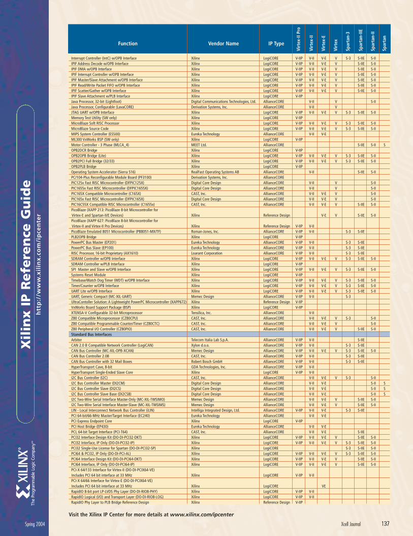
Function
Virt
ex-II
Pro
Virt
ex-II
Virt
ex-E
Virt
ex
Spar
tan-
3
Spar
tan-
IIE
Spar
tan-
II
Spar
tan
Vendor Name IP Type
Xil
inx I
P R
efe
ren
ce G
uid
eh
ttp
://w
ww
.xil
inx
.co
m/i
pce
nte
r
Spring 2004 Xcell Journal 137
Interrupt Controller (IntC) w/OPB Interface Xilinx LogiCORE V-IIP V-II V-E V S-3 S-IIE S-IIIPIF Address Decode w/OPB Interface Xilinx LogiCORE V-IIP V-II V-E V S-IIE S-IIIPIF DMA w/OPB Interface Xilinx LogiCORE V-IIP V-II V-E V S-IIE S-IIIPIF Interrupt Controller w/OPB Interface Xilinx LogiCORE V-IIP V-II V-E V S-IIE S-IIIPIF Master/Slave Attachment w/OPB Interface Xilinx LogiCORE V-IIP V-II V-E V S-IIE S-IIIPIF Read/Write Packet FIFO w/OPB Interface Xilinx LogiCORE V-IIP V-II V-E V S-IIE S-IIIPIF Scatter/Gather w/OPB Interface Xilinx LogiCORE V-IIP V-II V-E V S-IIE S-IIIPIF Slave Attachment w/PLB Interface Xilinx LogiCORE V-IIPJava Processor, 32-bit (Lightfoot) Digital Communications Technologies, Ltd. AllianceCORE V-II V S-IIJava Processor, Configurable (LavaCORE) Derivation Systems, Inc. AllianceCORE V-II VJTAG UART w/OPB Interface Xilinx LogiCORE V-IIP V-II V-E V S-3 S-IIE S-IIMemory Test Utility (SW only) Xilinx LogiCORE V-IIPMicroBlaze Soft RISC Processor Xilinx LogiCORE V-IIP V-II V-E V S-3 S-IIE S-IIMicroBlaze Source Code Xilinx LogiCORE V-IIP V-II V-E V S-3 S-IIE S-IIMIPS System Controller (ES500) Eureka Technology AllianceCORE V-II V-EML300 VxWorks BSP (SW only) Xilinx LogiCORE V-IIPMotor Controller - 3 Phase (MLCA_4) MEET Ltd. AllianceCORE S-IIE S-II SOPB2DCR Bridge Xilinx LogiCORE V-IIPOPB2OPB Bridge (Lite) Xilinx LogiCORE V-IIP V-II V-E V S-3 S-IIE S-IIOPB2PCI Full Bridge (32/33) Xilinx LogiCORE V-IIP V-II V-E V S-3 S-IIE S-IIOPB2PLB Bridge Xilinx LogiCORE V-IIPOperating System Accelerator (Sierra S16) RealFast Operating Systems AB AllianceCORE V-II S-IIE S-IIPC/104-Plus Reconfigurable Module Board (PF3100) Derivation Systems, Inc. AllianceCOREPIC125x Fast RISC Microcontroller (DFPIC125X) Digital Core Design AllianceCORE V-II V S-IIPIC1655x Fast RISC Microcontroller (DFPIC1655X) Digital Core Design AllianceCORE V-II V S-IIPIC165X Compatible Microcontroller (C165X) CAST, Inc. AllianceCORE V-II V-E V S-IIPIC165x Fast RISC Microcontroller (DFPIC165X) Digital Core Design AllianceCORE V-II V-E V S-IIPIC16C55X Compatible RISC Microcontroller (C1655x) CAST, Inc. AllianceCORE V-II V-E V S-IIE S-IIPicoBlaze (XAPP 213: PicoBlaze 8-bit Microcontroller for Virtex-E and Spartan-II/E Devices) Xilinx Reference Design V-E V S-IIE S-IIPicoBlaze (XAPP 627: PicoBlaze 8-bit Microcontroller for Virtex-II and Virtex-II Pro Devices) Xilinx Reference Design V-IIP V-IIPicoBlaze Emulated 8051 Microcontroller (PB8051-MX/TF) Roman-Jones, Inc. AllianceCORE V-IIP V-II S-3 S-IIEPLB2OPB Bridge Xilinx LogiCORE V-IIPPowerPC Bus Master (EP201) Eureka Technology AllianceCORE V-IIP V-II S-3 S-IIEPowerPC Bus Slave (EP100) Eureka Technology AllianceCORE V-IIP V-II S-3 S-IIERISC Processor, 16-bit Proprietary (AX1610) Loarant Corporation AllianceCORE V-IIP V-II S-3 S-IIESDRAM Controller w/OPB Interface Xilinx LogiCORE V-IIP V-II V-E V S-3 S-IIE S-IISDRAM Controller w/PLB Interface Xilinx LogiCORE V-IIPSPI Master and Slave w/OPB Interface Xilinx LogiCORE V-IIP V-II V-E V S-3 S-IIE S-IISystems Reset Module Xilinx LogiCORE V-IIPTimebase/Watch Dog Timer (WDT) w/OPB Interface Xilinx LogiCORE V-IIP V-II V-E V S-3 S-IIE S-IITimer/Counter w/OPB Interface Xilinx LogiCORE V-IIP V-II V-E V S-3 S-IIE S-IIUART Lite w/OPB Interface Xilinx LogiCORE V-IIP V-II V-E V S-3 S-IIE S-IIUART, Generic Compact (MC-XIL-UART) Memec Design AllianceCORE V-IIP V-II S-3UltraContoller Solution: A Lightweight PowerPC Microcontroller (XAPP672) Xilinx Reference Design V-IIPVxWorks Board Support Package (BSP) Xilinx LogiCORE V-IIPXTENSA-V Configurable 32-bit Microprocessor Tensilica, Inc. AllianceCORE V-IIZ80 Compatible Microprocessor (CZ80CPU) CAST, Inc. AllianceCORE V-II V-E V S-3 S-IIZ80 Compatible Programmable Counter/Timer (CZ80CTC) CAST, Inc. AllianceCORE V-II V-E V S-IIZ80 Peripheral I/O Controller (CZ80PIO) CAST, Inc. AllianceCORE V-II V-E V S-IIE S-IIStandard Bus InterfacesArbiter Telecom Italia Lab S.p.A. AllianceCORE V-IIP V-II S-IIECAN 2.0 B Compatible Network Controller (LogiCAN) Xylon d.o.o. AllianceCORE V-IIP V-II S-3 S-IIECAN Bus Controller (MC-XIL-OPB-XCAN) Memec Design AllianceCORE V-IIP V-II V-E V S-3 S-IIE S-IICAN Bus Controller 2.0B CAST, Inc. AllianceCORE V-IIP V-II S-3 S-IIECAN Bus Controller with 32 Mail Boxes Robert Bosch GmbH AllianceCORE V-IIP V-II S-3 S-IIEHyperTransport Cave, 8-bit GDA Technologies, Inc. AllianceCORE V-IIP V-IIHyperTransport Single-Ended Slave Core Xilinx LogiCORE V-IIP V-III2C Bus Controller (I2C) CAST, Inc. AllianceCORE V-II V-E V S-3 S-III2C Bus Controller Master (DI2CM) Digital Core Design AllianceCORE V-II V-E S-II SI2C Bus Controller Slave (DI2CS) Digital Core Design AllianceCORE V-II V-E S-II SI2C Bus Controller Slave Base (DI2CSB) Digital Core Design AllianceCORE V-II V-E S-II SI2C Two-Wire Serial Interface Master-Only (MC-XIL-TWSIMO) Memec Design AllianceCORE V-II V-E V S-IIE S-III2C Two-Wire Serial Interface Master-Slave (MC-XIL-TWSIMS) Memec Design AllianceCORE V-II V-E V S-IIE S-IILIN - Local Interconnect Network Bus Controller (iLIN) Intelliga Integrated Design, Ltd. AllianceCORE V-IIP V-II V-E S-3 S-IIEPCI 64-bit/66-MHz Master/Target Interface (EC240) Eureka Technology AllianceCORE V-II V-EPCI Express Endpoint Core Xilinx LogiCORE V-IIPPCI Host Bridge (EP430) Eureka Technology AllianceCORE V-II V-EPCI, 64-bit Target Interface (PCI-T64) CAST, Inc. AllianceCORE V-II V-E S-IIEPCI32 Interface Design Kit (DO-DI-PCI32-DKT) Xilinx LogiCORE V-IIP V-II V-E V S-IIE S-IIPCI32 Interface, IP Only (DO-DI-PCI32-IP) Xilinx LogiCORE V-IIP V-II V-E V S-3 S-IIE S-IIPCI32 Single-Use License for Spartan (DO-DI-PCI32-SP) Xilinx LogiCORE S-3 S-IIE S-IIPCI64 & PCI32, IP Only (DO-DI-PCI-AL) Xilinx LogiCORE V-IIP V-II V-E V S-3 S-IIE S-IIPCI64 Interface Design Kit (DO-DI-PCI64-DKT) Xilinx LogiCORE V-IIP V-II V-E V S-IIE S-IIPCI64 Interface, IP Only (DO-DI-PCI64-IP) Xilinx LogiCORE V-IIP V-II V-E V S-IIE S-IIPCI-X 64/133 Interface for Virtex-II (DO-DI-PCIX64-VE) Includes PCI 64 bit interface at 33 MHz Xilinx LogiCORE V-IIP V-IIPCI-X 64/66 Interface for Virtex-E (DO-DI-PCIX64-VE) Includes PCI 64 bit interface at 33 MHz Xilinx LogiCORE VERapidIO 8-bit port LP-LVDS Phy Layer (DO-DI-RIO8-PHY) Xilinx LogiCORE V-IIP V-IIRapidIO Logical (I/O) and Transport Layer (DO-DI-RIO8-LOG) Xilinx LogiCORE V-IIP V-IIRapidIO Phy Layer to PLB Bridge Reference Design Xilinx Reference Design V-IIP
Visit the Xilinx IP Center for more details at www.xilinx.com/ipcenter
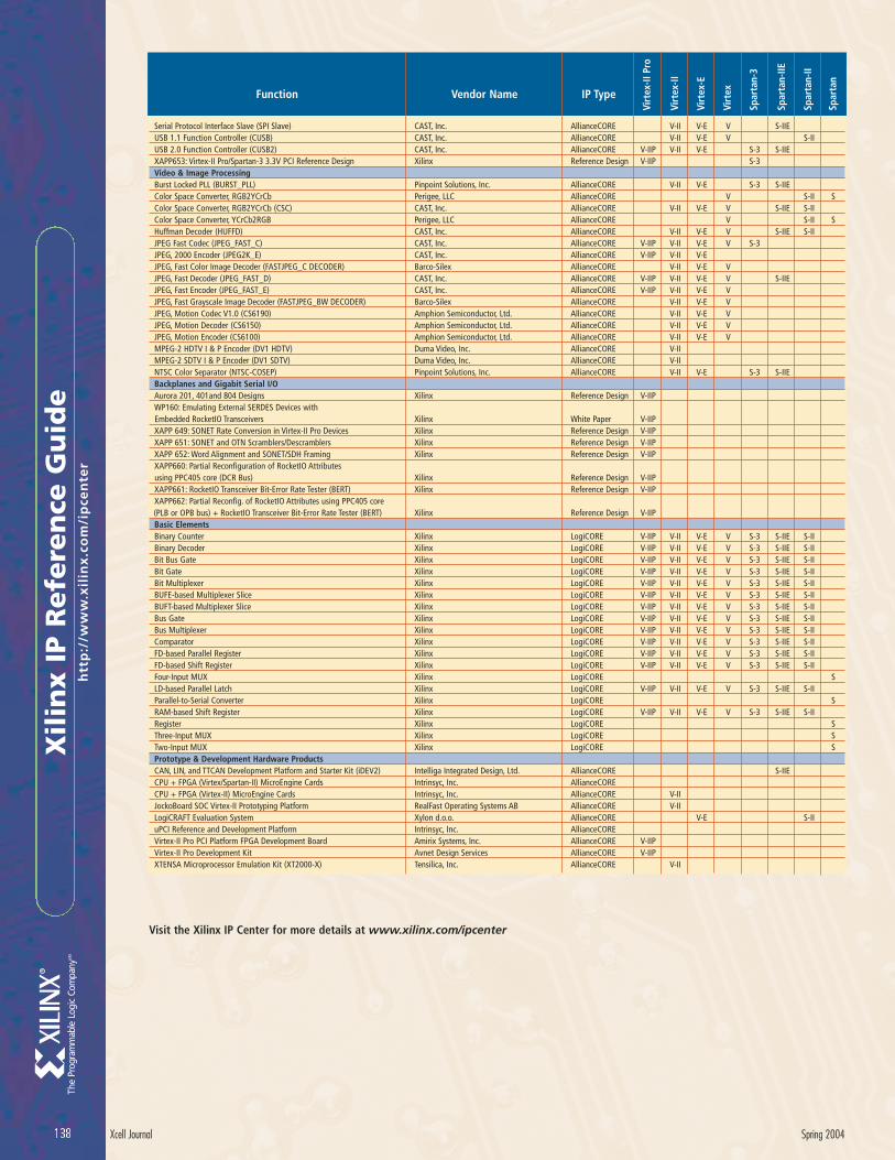
Function
Virt
ex-II
Pro
Virt
ex-II
Virt
ex-E
Virt
ex
Spar
tan-
3
Spar
tan-
IIE
Spar
tan-
II
Spar
tan
Vendor Name IP Type
Xil
inx I
P R
efe
ren
ce G
uid
eh
ttp
://w
ww
.xil
inx
.co
m/i
pce
nte
r
138 Xcell Journal Spring 2004
Serial Protocol Interface Slave (SPI Slave) CAST, Inc. AllianceCORE V-II V-E V S-IIEUSB 1.1 Function Controller (CUSB) CAST, Inc. AllianceCORE V-II V-E V S-IIUSB 2.0 Function Controller (CUSB2) CAST, Inc. AllianceCORE V-IIP V-II V-E S-3 S-IIEXAPP653: Virtex-II Pro/Spartan-3 3.3V PCI Reference Design Xilinx Reference Design V-IIP S-3Video & Image ProcessingBurst Locked PLL (BURST_PLL) Pinpoint Solutions, Inc. AllianceCORE V-II V-E S-3 S-IIEColor Space Converter, RGB2YCrCb Perigee, LLC AllianceCORE V S-II SColor Space Converter, RGB2YCrCb (CSC) CAST, Inc. AllianceCORE V-II V-E V S-IIE S-IIColor Space Converter, YCrCb2RGB Perigee, LLC AllianceCORE V S-II SHuffman Decoder (HUFFD) CAST, Inc. AllianceCORE V-II V-E V S-IIE S-IIJPEG Fast Codec (JPEG_FAST_C) CAST, Inc. AllianceCORE V-IIP V-II V-E V S-3JPEG, 2000 Encoder (JPEG2K_E) CAST, Inc. AllianceCORE V-IIP V-II V-EJPEG, Fast Color Image Decoder (FASTJPEG_C DECODER) Barco-Silex AllianceCORE V-II V-E VJPEG, Fast Decoder (JPEG_FAST_D) CAST, Inc. AllianceCORE V-IIP V-II V-E V S-IIEJPEG, Fast Encoder (JPEG_FAST_E) CAST, Inc. AllianceCORE V-IIP V-II V-E VJPEG, Fast Grayscale Image Decoder (FASTJPEG_BW DECODER) Barco-Silex AllianceCORE V-II V-E VJPEG, Motion Codec V1.0 (CS6190) Amphion Semiconductor, Ltd. AllianceCORE V-II V-E VJPEG, Motion Decoder (CS6150) Amphion Semiconductor, Ltd. AllianceCORE V-II V-E VJPEG, Motion Encoder (CS6100) Amphion Semiconductor, Ltd. AllianceCORE V-II V-E VMPEG-2 HDTV I & P Encoder (DV1 HDTV) Duma Video, Inc. AllianceCORE V-IIMPEG-2 SDTV I & P Encoder (DV1 SDTV) Duma Video, Inc. AllianceCORE V-IINTSC Color Separator (NTSC-COSEP) Pinpoint Solutions, Inc. AllianceCORE V-II V-E S-3 S-IIEBackplanes and Gigabit Serial I/OAurora 201, 401and 804 Designs Xilinx Reference Design V-IIPWP160: Emulating External SERDES Devices with Embedded RocketIO Transceivers Xilinx White Paper V-IIPXAPP 649: SONET Rate Conversion in Virtex-II Pro Devices Xilinx Reference Design V-IIPXAPP 651: SONET and OTN Scramblers/Descramblers Xilinx Reference Design V-IIPXAPP 652: Word Alignment and SONET/SDH Framing Xilinx Reference Design V-IIPXAPP660: Partial Reconfiguration of RocketIO Attributes using PPC405 core (DCR Bus) Xilinx Reference Design V-IIPXAPP661: RocketIO Transceiver Bit-Error Rate Tester (BERT) Xilinx Reference Design V-IIPXAPP662: Partial Reconfig. of RocketIO Attributes using PPC405 core (PLB or OPB bus) + RocketIO Transceiver Bit-Error Rate Tester (BERT) Xilinx Reference Design V-IIPBasic ElementsBinary Counter Xilinx LogiCORE V-IIP V-II V-E V S-3 S-IIE S-IIBinary Decoder Xilinx LogiCORE V-IIP V-II V-E V S-3 S-IIE S-IIBit Bus Gate Xilinx LogiCORE V-IIP V-II V-E V S-3 S-IIE S-IIBit Gate Xilinx LogiCORE V-IIP V-II V-E V S-3 S-IIE S-IIBit Multiplexer Xilinx LogiCORE V-IIP V-II V-E V S-3 S-IIE S-IIBUFE-based Multiplexer Slice Xilinx LogiCORE V-IIP V-II V-E V S-3 S-IIE S-IIBUFT-based Multiplexer Slice Xilinx LogiCORE V-IIP V-II V-E V S-3 S-IIE S-IIBus Gate Xilinx LogiCORE V-IIP V-II V-E V S-3 S-IIE S-IIBus Multiplexer Xilinx LogiCORE V-IIP V-II V-E V S-3 S-IIE S-IIComparator Xilinx LogiCORE V-IIP V-II V-E V S-3 S-IIE S-IIFD-based Parallel Register Xilinx LogiCORE V-IIP V-II V-E V S-3 S-IIE S-IIFD-based Shift Register Xilinx LogiCORE V-IIP V-II V-E V S-3 S-IIE S-IIFour-Input MUX Xilinx LogiCORE SLD-based Parallel Latch Xilinx LogiCORE V-IIP V-II V-E V S-3 S-IIE S-IIParallel-to-Serial Converter Xilinx LogiCORE SRAM-based Shift Register Xilinx LogiCORE V-IIP V-II V-E V S-3 S-IIE S-IIRegister Xilinx LogiCORE SThree-Input MUX Xilinx LogiCORE STwo-Input MUX Xilinx LogiCORE SPrototype & Development Hardware ProductsCAN, LIN, and TTCAN Development Platform and Starter Kit (iDEV2) Intelliga Integrated Design, Ltd. AllianceCORE S-IIECPU + FPGA (Virtex/Spartan-II) MicroEngine Cards Intrinsyc, Inc. AllianceCORECPU + FPGA (Virtex-II) MicroEngine Cards Intrinsyc, Inc. AllianceCORE V-IIJockoBoard SOC Virtex-II Prototyping Platform RealFast Operating Systems AB AllianceCORE V-IILogiCRAFT Evaluation System Xylon d.o.o. AllianceCORE V-E S-IIuPCI Reference and Development Platform Intrinsyc, Inc. AllianceCOREVirtex-II Pro PCI Platform FPGA Development Board Amirix Systems, Inc. AllianceCORE V-IIPVirtex-II Pro Development Kit Avnet Design Services AllianceCORE V-IIPXTENSA Microprocessor Emulation Kit (XT2000-X) Tensilica, Inc. AllianceCORE V-II
Visit the Xilinx IP Center for more details at www.xilinx.com/ipcenter
FPGA
Design
©2003 Mentor Graphics Corporation. All Rights Reserved. Mentor Graphics is a registered trademark of Mentor Graphics Corporation.
Avoid messy timing mistakes.Use Mentor Graphics®
FPGA design tools.
PRECISION SYNTHESIS As any FPGA designer can tell you, achieving precise timing is their single most critical challenge. That's why
Mentor Graphics® created Precision Synthesis, a powerful new tool suite that lets designers close on timing faster than ever. Precision
Synthesis provides the most comprehensive analysis for complex FPGAs with the only complete, built-in incremental timing analysis.
Quickly find and optimize the most critical paths and avoid frustrating trial-and-error design iterations. Visit www.mentor.com/fpga
today or call 877.387.5873 for more information on how Precision Synthesis can help you find the fastest path to a completed design.
TM
TM TM
TM

Industry’s bestFPGA fabric
Industry-leading ISE software solutions
Comprehensive family of 12 devices
Xtreme DSP solutions
Over 200 IP core solutions
World-class servicesand partners Embedded PowerPC
processing solutions
Ultimate connectivity solutions
Virtex-II Pro™ Platform FPGAs deliver more capabilities
and performance than any other FPGA.
In a single device, you get the highest density, most memory,
best performance, and at no additional charge 400MHz PowerPC™
processors, plus 3.125 Gbps RocketIO™ or 10.3125 Gbps RocketIO X
serial transceivers. This gives you the fastest DSP, connectivity and
processing solutions in the industry.
The Power to Develop Your Design
The Xilinx ISE software tools are the easiest to use solution for
high-density logic. With over 200 IP cores, ChipScope Pro debug
environment, and compile times up to 6x
faster than our nearest competitor, you can
quickly take your Virtex-II Pro FPGA design
from concept to reality.
Guaranteed 25% And Up To 80% SavingsWith Virtex-II Pro EasyPath Solutions
For high-volume system production, Xilinx offers a lower cost
path with Virtex-II Pro EasyPath. You can immediately take
advantage of dramatic cost reduction
at no risk and no effort. Only Xilinx
can offer you this flexibility for design
and production.
Visit www.xilinx.com/virtex2pro today to get the price and
performance you’re looking for.
The Programmable Logic CompanySM
www.xilinx.com/virtex2pro
©2003, Xilinx, Inc. All rights reserved. The Xilinx name, the Xilinx logo are registered trademarks. Rocket I/O and Virtex-II Pro are trademarks, and The ProgrammableLogic Company is a service mark of Xilinx, Inc. PowerPC is a trademark of International Business Machines Corporation in the United States, or other countries, orboth: All other trademarks and registered trademarks are the property of their respective owners.
Pb-free devicesavailable now
PN 0010764
Copyright © 2022 FDOKUMEN