X-ray diffraction, dielectric, conduction and Raman studies in Na0.925Bi0.075Nb0.925Mn0.075O3...
9
X-ray diffraction, dielectric, conduction and Raman studies in Na0.925Bi0.075Nb0.925Mn0.075O3 ceramic Chiheb Chaker, Y. Gagou, N. Abdelmoula, J.-L. Dellis, C. Masquelier et al. Citation: J. Appl. Phys. 111, 044101 (2012); doi: 10.1063/1.3684961 View online: http://dx.doi.org/10.1063/1.3684961 View Table of Contents: http://jap.aip.org/resource/1/JAPIAU/v111/i4 Published by the American Institute of Physics. Related Articles Growth and piezo-/ferroelectric properties of PIN-PMN-PT single crystals J. Appl. Phys. 111, 034105 (2012) Dielectric relaxation in the DyMn1−xFexO3 system J. Appl. Phys. 111, 034104 (2012) The effect of Li-substitution on the M-phases of AgNbO3 J. Appl. Phys. 111, 024107 (2012) Response to “Comment on ‘The electromagnetic property of chemically reduced graphene oxide and its application as microwave absorbing material’” [Appl. Phys. Lett. 100, 046101 (2012)] Appl. Phys. Lett. 100, 046102 (2012) Evidence of ferroelectricity and phase transition in pressed diphenylalanine peptide nanotubes Appl. Phys. Lett. 100, 043702 (2012) Additional information on J. Appl. Phys. Journal Homepage: http://jap.aip.org/ Journal Information: http://jap.aip.org/about/about_the_journal Top downloads: http://jap.aip.org/features/most_downloaded Information for Authors: http://jap.aip.org/authors Downloaded 17 Feb 2012 to 194.57.107.121. Redistribution subject to AIP license or copyright; see http://jap.aip.org/about/rights_and_permissions
Transcript of X-ray diffraction, dielectric, conduction and Raman studies in Na0.925Bi0.075Nb0.925Mn0.075O3...

X-ray diffraction, dielectric, conduction and Raman studies inNa0.925Bi0.075Nb0.925Mn0.075O3 ceramicChiheb Chaker, Y. Gagou, N. Abdelmoula, J.-L. Dellis, C. Masquelier et al. Citation: J. Appl. Phys. 111, 044101 (2012); doi: 10.1063/1.3684961 View online: http://dx.doi.org/10.1063/1.3684961 View Table of Contents: http://jap.aip.org/resource/1/JAPIAU/v111/i4 Published by the American Institute of Physics. Related ArticlesGrowth and piezo-/ferroelectric properties of PIN-PMN-PT single crystals J. Appl. Phys. 111, 034105 (2012) Dielectric relaxation in the DyMn1−xFexO3 system J. Appl. Phys. 111, 034104 (2012) The effect of Li-substitution on the M-phases of AgNbO3 J. Appl. Phys. 111, 024107 (2012) Response to “Comment on ‘The electromagnetic property of chemically reduced graphene oxide and itsapplication as microwave absorbing material’” [Appl. Phys. Lett. 100, 046101 (2012)] Appl. Phys. Lett. 100, 046102 (2012) Evidence of ferroelectricity and phase transition in pressed diphenylalanine peptide nanotubes Appl. Phys. Lett. 100, 043702 (2012) Additional information on J. Appl. Phys.Journal Homepage: http://jap.aip.org/ Journal Information: http://jap.aip.org/about/about_the_journal Top downloads: http://jap.aip.org/features/most_downloaded Information for Authors: http://jap.aip.org/authors
Downloaded 17 Feb 2012 to 194.57.107.121. Redistribution subject to AIP license or copyright; see http://jap.aip.org/about/rights_and_permissions
X-ray diffraction, dielectric, conduction and Raman studiesin Na0.925Bi0.075Nb0.925Mn0.075O3 ceramic
Chiheb Chaker,1,2,a) Y. Gagou,2 N. Abdelmoula,1 J.-L. Dellis,2 C. Masquelier,3
H. Khemakhem,1 and M. El Marssi21Laboratoire des Materiaux Ferroelectriques (LMF), Unite de Recherche Physique-Mathematiques05UR15-04, Universite de Sfax, Faculte des Sciences de Sfax, Route de Soukra km 3,5 - B.P.1171,3000 Sfax, Tunisia2Laboratoire de Physique de la Matiere Condensee (LPMC), Universite de Picardie Jules Verne,Pole Scientifique, 33 rue Saint-Leu, 80039 Amiens Cedex 1, France3Laboratoire de Reactivite et Chimie des Solides (LRCS), UMR 6007, Universite de Picardie Jules Verne,Pole Scientifique, 33 rue Saint-Leu, 80039 Amiens Cedex 1, France
(Received 12 August 2011; accepted 9 January 2012; published online 17 February 2012)
Ceramic with composition Na0.925Bi0.075Nb0.925Mn0.075O3 (NNBM0075) was synthesized by high
temperature solid state reaction technique. It was studied using X-ray diffraction (XRD), dielectric
measurements and Raman spectroscopy. The sample crystallizes in orthorhombic perovskite
structure with space group Pbma at room temperature. Dielectric properties of the ceramic was
investigated in a broad range of temperatures (�150 to 450 �C) and frequencies (0.1–103 kHz), and
show two different anomalies connected to the symmetry change and electrical conductivity.
Dielectric frequency dispersion phenomena in the NNBM0075 ceramic was analyzed by
impedance spectroscopy in the temperature range from 55 to 425 �C. The Cole-Cole analysis based
on electrical circuit and least square method was used to characterize the conduction phenomenon.
A separation of the grain and grain boundary properties was achieved using an equivalent circuit
model. The different parameters of this circuit were determined using impedance studies. Four
conduction ranges, with different activation energies, were determined using the Arrhenius
model. Raman spectra were studied as a function of temperatures and confirmed the X-ray and
dielectric results. This composition is of interest for applications due to his physical properties and
environmentally friendly character. VC 2012 American Institute of Physics. [doi:10.1063/1.3684961]
I. INTRODUCTION
The past few years have seen a flurry of studies on ferro-
electric materials due to their large range of applications:
capacitors using their high dielectric permittivity, trans-
ducers and actuators using their piezoelectric properties and
ferroelectric memories using the remanent polarization of
these materials. Our study is based on the modification of
Na1-xBixNb1-xMnxO3 ceramics belonging to the system
NaNbO3-BiMnO3. These compounds show relaxation phe-
nomenon visible in the dielectric permittivity and conductiv-
ity dependences. It is worthwhile mentioning that they
correspond to the niobate NaNbO3 and manganite BiMnO3,
which attract attention as multiferroic materials. There is
much interest in multiferroic materials1,2 showing simultane-
ous ferroelectricity, ferromagnetism, and ferroelasticity
given their potential applications in magneto-electrics and
spintronics. The ferromagnetism of BiMnO3, along with
recent experimentally verified ferroelectric (FE) behavior,3
makes this compound potentially interesting for technologi-
cal applications.
BiMnO3 attracts much interest as a multiferroic mate-
rial,4,5 where anti-ferroelectricity and magnetism coexist.6
However, despite of a large number of works on BiMnO3,
there is still no consensus on its FE properties. There are a
growing number of publications recently emphasizing that
FE properties of BiMnO3 have not been well established.7
On the other hand, pure NaNbO3 is anti-ferroelectric (AF) at
room temperature, the FE phase can be rather easily induced
by a small amount of appropriate dopants (e.g., Li or K) or
by application of a moderate electric field and also by intrin-
sic defects like oxygen vacancy.8–10
A preliminary work has been reported on (Na1-xBix(Nb1-yMny)O3 ceramics by Lawniczak-Jablonska et al.,11
where they have studied the chemistry and the structure. In
this system, the manganese valence is Mn2þ and in order to
fulfill the charge neutrality condition, the varying amounts of
x and y of the two constituents have to form a stable solid so-
lution at steady proportion of xBi : yMn¼ 3:2 while xBi3þ
replaced (1�x)Naþ and yMn2þ replaced (1�y)Nb5þ. In addi-
tion, a series of works were carried out by Molak et al.12,14
where they have also studied (Na0.75Bi0.25)(Mn0.25Nb0.75)O3
(Ref. 12) and (Bi1/9Na2/3)(Mn1/3Nb2/3)O3 (Refs. 13 and 14)
electric properties in which the manganese valence is Mn2þ
or Mn4þ. The (Na1-xBix)(Nb1-yMny)O3,11 (Na0.75Bi0.25)
(Mn0.25Nb0.75) O3,12 and (Bi1/9Na2/3)(Mn1/3Nb2/3)O3 (Ref.
14) ceramics were prepared by dry sintering at ambient air
pressure, using a two-stage synthesis process. In the first
stage, (Na1-x)(MnyNb1-y)O3 precursor phase was produced
from Na2CO3, Nb2O5, and MnO powders prepared with stoi-
chiometric proportions. In the second stage, the crushed con-
stituent of the precursor phase was mixed with Bi2O3, but ina)Electronic mail: [email protected]. Fax:þ 216 74 274 437.
0021-8979/2012/111(4)/044101/8/$30.00 VC 2012 American Institute of Physics111, 044101-1
JOURNAL OF APPLIED PHYSICS 111, 044101 (2012)
Downloaded 17 Feb 2012 to 194.57.107.121. Redistribution subject to AIP license or copyright; see http://jap.aip.org/about/rights_and_permissions

(Bi1/9Na2/3)(Mn1/3Nb2/3)O3 (Ref. 13) ceramics preparation,
the same preparation method was used with the MnO2 precur-
sor instead of MnO.
In the present paper, we have studied the
NNBM0075 ceramic derived from the NaNbO3 and
BiMnO3 mixture where Naþ and Nb5þ cations are substi-
tuted by Bi3þ and Mn3þ, respectively. Compared to the
last studies,11–14 our system was prepared by a traditional
solid state reaction using the Mn2O3 precursor where the
valence of the manganese is Mn3þ. We have reported, in
particular, the structure, dielectric properties, conduction
phenomenon, and Raman scattering of NNBM0075 ce-
ramic. This ceramic exhibits many interesting features,
such as diffuse phase transition. It is therefore, of great
interest to study the origin of these remarkable dielectric
properties in this material. The structure analysis versus
temperature was studied using X-ray diffraction (XRD).
The diffuse phase transition, observed by dielectric meas-
urements and confirmed by Raman spectroscopy charac-
terizations, is in agreement with XRD measurements. A
relationship between dielectric properties and conduction
phenomenon through the modified Cole-Cole analysis is
reported. Equivalent circuit model, impedance, and
Arrhenius studies are carried out.
II. EXPERIMENTAL PROCEDURE
NNBM0075 ceramic was prepared by a conventional
standard solid state reaction technique. Powders of Na2CO3,
Nb2O5, Bi2O3, and Mn2O3 of high purity 99.99% were taken
in stoichiometric ratio, weighed and mixed in an agate mor-
tar for 2 h. The 5% excess bismuth oxide was added to com-
pensate for the expected evaporation during sintering. The
appropriate mixture of powders was pressed into pellets and
calcined at 900 �C in air for 10 h. After calcination, powder
was mixed for 2 h and pressed into 8 mm diameter and about
1 mm in thickness. Finally, the pressed pellet was sintered in
oxygen atmosphere at 1130 �C for 3 h.
X-ray powder diffraction pattern of the sample was
recorded at several temperatures using a high-resolution
Brucker D8 diffractometer with filtered cobalt Ka1 and Ka2
radiations (kKa1¼ 1.788970 A and kKa2¼ 1.792850 A) in the
angular range of 10� � 2h � 90� with 20 s counting time for
each step of 0.02� in order to determine the structure of the
NNBM0075 ceramic. A profile matching of the XRD spectra
were made using the FullProf software.15 A good fitting was
obtained using a pseudo-Voigt (pV) profile function and the
background level was defined by an interpolation polynomial
function. Raman scattering data was collected in the fre-
quency range 50-1000 cm�1 using a Raman spectrometer
(J.Y. T64000).
The compactness value C defined as the ratio between
the experimental density dexp (determined from the weight
and geometrical dimensions of the cylindrical pellets) and
theoretical density dtheor (determined from XRD) and the rel-
ative diameter shrinkage of ceramic disks was systematically
determined as DU/U¼ (Uinit – Ufin)/Uinit where Uinit and Ufin
represent initial and final diameter. Their values were 95%
and 0.15, respectively.
III. RESULTS AND DISCUSSION
A. X-ray diffraction analysis
Powder XRD patterns profile analysis of NNBM0075
ceramic, at the temperature range between room temperature
(RT) and 500 �C, was performed to determine structural
phase transitions in this compound. The structural analysis
shows a pure perovskite phase and a good homogeneity.
Figure 1 shows the XRD pattern of NNBM0075 sample
taken at room temperature. Experimental conditions and rel-
evant data for refinements at room temperature are reported
in Table I. The background was fitted by a polynomial inter-
polation function from about 90 chosen points. The refine-
ment takes into account instrument zero point, unit cell
parameters, and the profile shape related to instrument
parameters (U,V,W) through the Caglioti function. The cal-
culations lead to a rapid convergence with a mean reliability
factor v2¼ 1.41 deduced from all calculated diagrams
through this temperature range. We have successfully per-
formed profile adjustment in high temperature region basing
on NaNbO3 high temperature tetragonal phase with space
group P4/mbm (N� 127). The structure was stabilized when
decreasing temperature until 320 �C. Lattice parameters were
found to be closed and can be considered as pseudo cubic.
On the other hand, the room temperature phase was success-
fully refined in the orthorhombic system with space group
Pbma (N� 57). This structural symmetry is conserved until
175 �C with good reliability factors. We deduce that this
compound presents the existence of an intermediate phase
which seems to be stabilized in the space group Ccmm (N�
63). Refinement in this space group leads to a rapid conver-
gence and consistent parameters.
Moreover, we do not observe any other different inter-
mediate phase as it was proved in pure NaNbO3 by Ahtee
et al.16 and the phase diagram is shifted to the left side at
about 270 �C when compared with the transition observed by
Ishida et al.17 This phase transition is tetragonal to the ortho-
rhombic type as confirmed in X-ray data by the splitting of
the line (400) or (222) in the high symmetry to the line (044)
FIG. 1. (Color online) XRD pattern of Na0.925Bi0.075Nb0.925Mn0.075O3 ce-
ramic at room temperature.
044101-2 Chaker et al. J. Appl. Phys. 111, 044101 (2012)
Downloaded 17 Feb 2012 to 194.57.107.121. Redistribution subject to AIP license or copyright; see http://jap.aip.org/about/rights_and_permissions
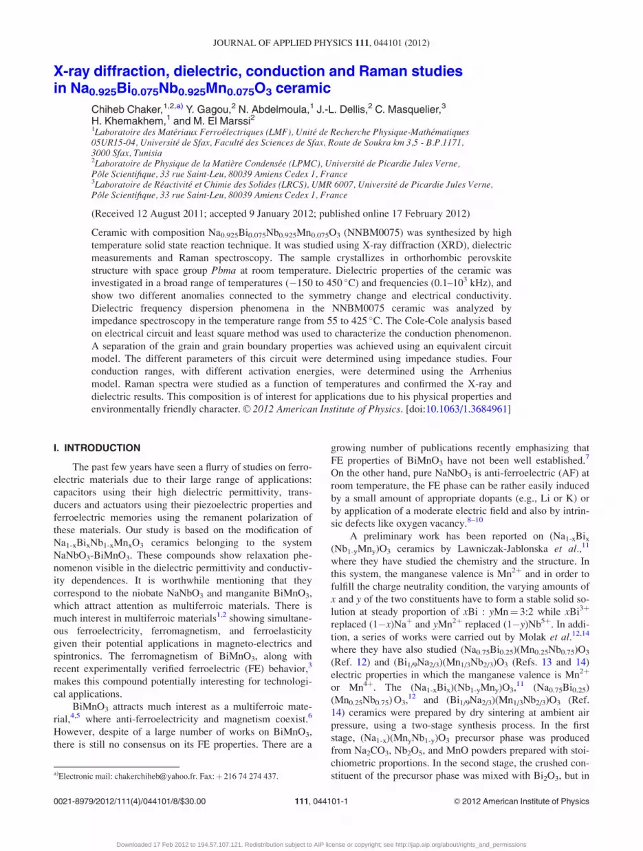
and (440) or (440) and, (404) in the low symmetry phases as
shown in Fig. 2. We can conclude that chemical elements
substitution in NaNbO3 lead to the destruction of two others
intermediate complementary phases; only one intermediate
antiferroelectric remained. Lattice parameters versus temper-
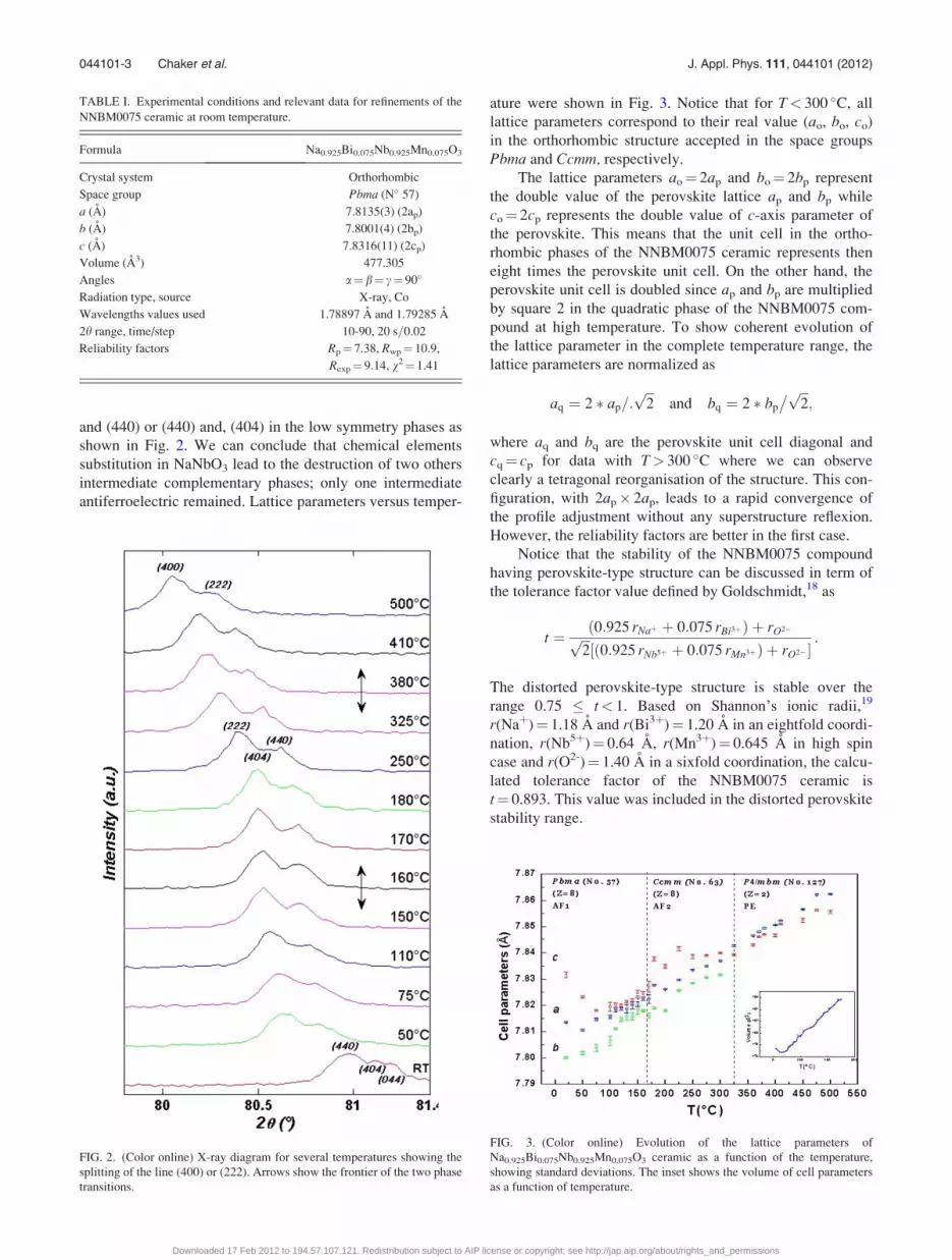
ature were shown in Fig. 3. Notice that for T< 300 �C, all
lattice parameters correspond to their real value (ao, bo, co)
in the orthorhombic structure accepted in the space groups
Pbma and Ccmm, respectively.
The lattice parameters ao¼ 2ap and bo¼ 2bp represent
the double value of the perovskite lattice ap and bp while
co¼ 2cp represents the double value of c-axis parameter of
the perovskite. This means that the unit cell in the ortho-
rhombic phases of the NNBM0075 ceramic represents then
eight times the perovskite unit cell. On the other hand, the
perovskite unit cell is doubled since ap and bp are multiplied
by square 2 in the quadratic phase of the NNBM0075 com-
pound at high temperature. To show coherent evolution of
the lattice parameter in the complete temperature range, the
lattice parameters are normalized as
aq ¼ 2 � ap=:ffiffiffi2p
and bq ¼ 2 � bp
� ffiffiffi2p
;
where aq and bq are the perovskite unit cell diagonal and
cq¼ cp for data with T> 300 �C where we can observe
clearly a tetragonal reorganisation of the structure. This con-
figuration, with 2ap� 2ap, leads to a rapid convergence of
the profile adjustment without any superstructure reflexion.
However, the reliability factors are better in the first case.
Notice that the stability of the NNBM0075 compound
having perovskite-type structure can be discussed in term of
the tolerance factor value defined by Goldschmidt,18 as
t ¼ 0:925 rNaþ þ 0:075 rBi3þð Þ þ rO2�ffiffiffi2p
0:925 rNb5þ þ 0:075 rMn3þð Þ þ rO2�½ �:
The distorted perovskite-type structure is stable over the
range 0.75 � t< 1. Based on Shannon’s ionic radii,19
r(Naþ)¼ 1.18 A and r(Bi3þ)¼ 1.20 A in an eightfold coordi-
nation, r(Nb5þ)¼ 0.64 A, r(Mn3þ)¼ 0.645 A in high spin
case and r(O2-)¼ 1.40 A in a sixfold coordination, the calcu-
lated tolerance factor of the NNBM0075 ceramic is
t¼ 0.893. This value was included in the distorted perovskite
stability range.
TABLE I. Experimental conditions and relevant data for refinements of the
NNBM0075 ceramic at room temperature.
Formula Na0.925Bi0.075Nb0.925Mn0.075O3
Crystal system Orthorhombic
Space group Pbma (N� 57)
a (A) 7.8135(3) (2ap)
b (A) 7.8001(4) (2bp)
c (A) 7.8316(11) (2cp)
Volume (A3) 477.305
Angles a¼b¼ c¼ 90�
Radiation type, source X-ray, Co
Wavelengths values used 1.78897 A and 1.79285 A
2h range, time/step 10-90, 20 s=0.02
Reliability factors Rp¼ 7.38, Rwp¼ 10.9,
Rexp¼ 9.14, v2¼ 1.41
FIG. 2. (Color online) X-ray diagram for several temperatures showing the
splitting of the line (400) or (222). Arrows show the frontier of the two phase
transitions.
FIG. 3. (Color online) Evolution of the lattice parameters of
Na0.925Bi0.075Nb0.925Mn0.075O3 ceramic as a function of the temperature,
showing standard deviations. The inset shows the volume of cell parameters
as a function of temperature.
044101-3 Chaker et al. J. Appl. Phys. 111, 044101 (2012)
Downloaded 17 Feb 2012 to 194.57.107.121. Redistribution subject to AIP license or copyright; see http://jap.aip.org/about/rights_and_permissions

B. Dielectric measurements
Dielectric measurements were performed on pellets
ceramic which both sides are polished by platinised electrodes
using a cathodic sputtering technique with Baltec-SCD500.
The dielectric permittivity was measured as a function of
temperature at different frequencies. Measurements were
performed with a heating rate of 1 �C/min, using a Solartron
SI-1260 spectrometer in the temperature and frequency
ranges between �150 �C and 450 �C and 100 Hz to 103 kHz,
respectively. The temperature is controlled using a Linkam
TMS94 allowing a temperature stability of 60.1 �C.
Figures 4(a) and 4(b) show the temperature dependence
of the permittivities e0r and e00r determined for the NNBM0075
ceramic. On the e0r(T) curved presented in Fig. 4(a) and
according to the XRD analysis, two interesting behaviors
were noticed: a first anomaly at the temperature T1¼ 155 �Ccorresponding to the transition from the first anti-
ferroelectric (AF1) phase to the second anti-ferroelectric
(AF2) phase, and a second anomaly at the temperature
T2¼ 380 �C corresponding to the transition from the AF2
phase to the paraelectric (PE) phase. This intermediate AF2
phase seems to be stabilized at low frequencies and disap-
pears at high frequencies electrical field excitation as showed
clearly in Fig. 4(a), where the second anomaly vanishes for
high frequencies.
When analyzing the permittivity thermal hysteresis,
shown in Fig. 4(c) at the frequency 10 kHz, we remark 10 �Cunder room temperature where the heating and cooling
curves became again identical after a thermal hysteresis loop
of about 5 �C. That could be the Q phase considered as the
beginning (under �10 �C) of the FE as reported by Yuzyuk
et al.20 This temperature can be also considered as depolar-
ized temperature as reported by Ying et al.21 In addition,
this study shows that the value of the first temperature
(T1¼ 155 �C) is not depending on frequency, implying that
this composition is without any relaxor-type perovskite. A
similar behavior was seen in the Na1-xLixNbO3 (Ref. 22)
solid solution where the AF phase was observed up to
x¼ 0.02 and the ferroelectric Q-phase was appeared when
x> 0.03 as reported by Yuzyuk et al.23 and also in the
Na1-xLixNb1-xSbxO3 (Ref. 24) and Na1-xLixNbO3 (Ref. 25)
systems with compositions 0.05 � x � 0.15. The broadened
peaks indicate that the transition, in this composition, is of
diffuse type showing an important characteristic of a disor-
dered perovskite structure. It appears from experiments that
the titled compound has specific properties. In particular, a
clear evidence of enhanced dielectric anomaly around the
temperature 155 �C at heating and 150 �C at cooling runs
exhibiting then the existence of a thermal hysteresis of about
5 �C. That proves also a first-order-type structural transition
as shown in Fig. 4(c) at the frequency 10 kHz. The principal
parameters, determining the phase transitions and related to
the physical properties of the crystalline materials possessing
the oxygen octahedral, is a non-stoichiometric cationic sub-
stitution which may cause additional increase of an harmonic
electron-phonon interactions responsible for the phase transi-
tions, as it was shown for niobate.26 The loss factor
(tan d ¼ e00=e0), at different frequencies (100 Hz, 1 kHz, and
10 kHz), exhibits also a peak at the transition temperature TC
as shown in Fig. 4(d) where a dielectric loss of about
8� 10�2 was observed. The rapid increasing of loss factor in
the PE phase is related to the ionic conduction phenomena.
FIG. 4. (Color online) (a) Temperature de-
pendence of the permittivity e0r at various
frequencies of the NNBM0075 ceramic. (b)
Temperature dependence of the imaginary
part of the relative permittivity e00r at various
frequencies of the NNBM0075 ceramic. (c)
Temperature dependence of the dielectric
constant at 10 kHz (heating and cooling
runs) of the NNBM0075 ceramic. (d) Tem-
perature dependence of the dielectric loss
(tan d) of the NNBM0075 ceramic.
044101-4 Chaker et al. J. Appl. Phys. 111, 044101 (2012)
Downloaded 17 Feb 2012 to 194.57.107.121. Redistribution subject to AIP license or copyright; see http://jap.aip.org/about/rights_and_permissions

C. Conduction phenomenon
1. Cole-Cole plot analysis
NNBM0075 ceramic presents also the presence of con-
ducting phenomenon. As we can see in Figs. 4(b) and 4(d),
the imaginary part of the dielectric permittivity and the loss
factor present a sharp increasing which suggests the presence
of conductivity. On the real part of dielectric permittivity, a
first anomaly at the temperature T1¼ 155 �C has been seen
and also a second anomaly around T2¼ 380 �C can be
observed for low frequencies (for example at 100 Hz). The
second anomaly must correspond to the change of a struc-
tural phase accompanied with ion motions through the com-
pound since the peak tends to vanish at high frequencies. So,
we perform our investigation using modified Cole-Cole anal-
ysis through our own simulation based on electrical circuit
model and least square method in order to optimize the e00-e0,Z00-Z0 or M00-M0 curve plots of the compound, where e00-e0,Z00-Z0, and M00-M0 are, respectively, the imaginary and real
part of the permittivity, the impedance and the electric mod-
ulus characteristic of the compound. The real (e0, Z0, M0) and
imaginary (e00, Z00, M00) parts of the complex parameters are
in turn related to one another as follows:
e� ¼ e0 � je00 where
e0 ¼ � Z00
xC0 Z02 þ Z002ð Þe00 ¼ � Z0
xC0 Z02 þ Z002ð Þ
8>><>>:
Z� ¼ Z0 � jZ00 ¼ 1
jxC0e�where
Z0 ¼ e00
xC0 e02 þ e002ð ÞZ00 ¼ e0
xC0 e02 þ e002ð Þ
8>><>>:
M� ¼ M0 þ jM00 ¼ 1
e�¼ jxC0Z� where
M0 ¼ e0
e02 þ e002
M00 ¼ e00
e02 þ e002;
8>><>>:
where x is the angular frequency linked to the frequency fby the relation x¼ 2pf, j2 ¼ �1 and C0 is the geometrical
capacitance. These relations offer wide scope for a graphical
analysis of the various parameters under different conditions
of temperature or frequency. The useful separation of inter-
granular phenomena depends ultimately on the choice of an
appropriate equivalent circuit to represent the sample
properties.
The displaying method data is in the complex plane in
which Z00 is plotted against Z0. In the ideal case, a plot of Z00
versus Z0 is a semicircle whose center lies in the Z0 axis and
whose intercepts with the Z0 axis. Figure 5 shows the com-
plex impedance plot of the NNBM0075 ceramic, plotting the
imaginary part Z00 against the real part Z0 at different tempera-
tures. Arrhenius type law was used to elucidate the conduc-
tion phenomenon and the activation energy calculation.
2. Equivalent circuit model
A better understanding of the conductivity mechanisms
requires an equivalent circuit model that provides the best
representation of the electrical properties. The overall elec-
trical properties of a polycrystalline ceramic have a contribu-
tion from grains and grains boundaries. In our case, the best
calculation is obtained using circuits containing resistor (R)
and a constant phase elements (CPE) instead of simple
capacitances. The best equivalent circuit modeling conduc-
tion phenomenon in this compound is constituted by a paral-
lel connection of one resistance R and two different CPE as
shown in Fig. 6. In this model, the resistance impedance is
ZR¼R and the CPE impedance is expressed as the Warburg
element by the formula,
ZCPE ¼1
A jxð Þa ;
where A is a physical quantity and a is the circuit parameter
which gives to ZCPE its limiting behavior as a capacitance
for a¼ 1, a resistor for a¼ 0, and an inductance for
a¼�1.27,28 Intermediate values correspond to Warburg im-
pedance.29 The Z00-Z0 curve fitting leads to the determination
of five parameters: the resistance R and two other parameters
(A and a) of each CPE. The resistance and the first CPE cor-
respond to the ceramic grain behavior and the second CPE
corresponds to interstice or grain boundary and space charge
behaviors modeled by CPE.
FIG. 5. (Color online) Complex-plane impedance plots for
Na0.925Bi0.075Nb0.925Mn0.075O3 at different temperatures.
FIG. 6. Equivalent circuit model for Na0.925Bi0.075Nb0.925Mn0.075O3
ceramic.
044101-5 Chaker et al. J. Appl. Phys. 111, 044101 (2012)
Downloaded 17 Feb 2012 to 194.57.107.121. Redistribution subject to AIP license or copyright; see http://jap.aip.org/about/rights_and_permissions
3. Arrhenius study
In order to understand the conduction phenomena, we
have used the Arrhenius modeling equation,
r ¼ r0 e� DE=kTð Þ;
where DE is the activation energy, r0 is the pre-exponential
factor, k is the Boltzmann constant, and T is the temperature.
We have determined the conductivity of the sample bulk
response using the calculated resistors. The plot of logarithm
(r) as a function 1000/T of the NNBM0075 ceramic, shown
in Fig. 7, allowed us to highlight four areas characterized by
four different activation energies. The results are summar-
ized in the Table II.
When compared to dielectric measurements, we can
attribute the slope change occurring at the temperature of
275 �C to the beginning of the second anomaly observed in
er(T) variation at low frequencies. This can be attributed to
ions motion through the compound. Thermal energy is suffi-
cient to activate ions or carrier motion. The second slope
change corresponds to the paraelectric to anti-ferroelectric
structural phase transition at 155 �C. Every phase is charac-
terized by a different cohesion energy needed to structure
stability. The last slope change at 135 �C, corresponds to the
beginning of the diffuse phase transition. At this temperature
in the case of low frequencies, the system begins the struc-
tural change mechanism. These behaviors are in favor of ion
conduction that can be attributed to the displacement of
atoms at octahedral sites of the solution solid because of the
occupation disorder. In addition, the displacement can result
in jumping from one site to another because of the crystal
lattice dilatation.
D. Raman scattering
Raman spectroscopy measurements were performed
using the 514.5 nm calibration line from an argon ion laser
and analyzed using a Jobin Yvon T64000 spectrometer
equipped with a charge coupled device. An optical micro-
scope was used to focus the incident light as a spot of about
2 lm in diameter on the sample. Depolarized Raman spectra
were obtained in backscattering geometry.
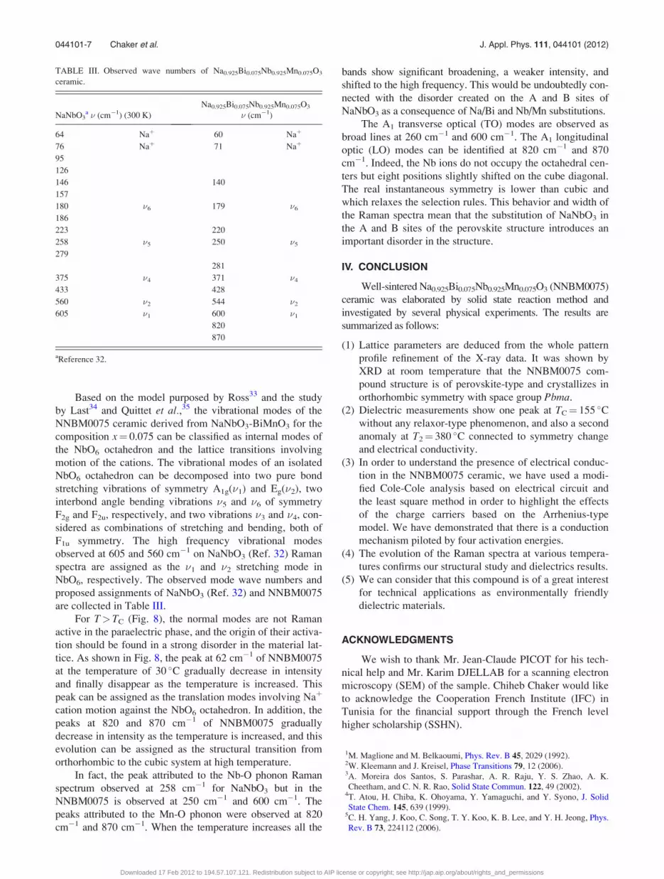
Raman spectroscopy has been successfully used as a
tool for studying the structure and the phase transitions of
NaNbO3 (Refs. 30 and 31) and Li doped NaNbO3 (Ref. 22)
compounds. Figure 8 shows the temperature dependence of
the Raman spectra of NNBM0075 ceramics showing distinct
changes. As can be shown in Table III, the Raman peaks
reported in anti-ferroelectric phase of NaNbO3 (Ref. 32) at
95, 126, 157, and 186 cm�1 are forbidden in NNBM0075
ceramic. Similar room temperature spectrum of NNBM0075
is observed in the orthorhombic anti-ferroelectric phase of
Na1-xLixNbO3.22 This confirms the anti-ferroelectric charac-
ter of the NNBM0075 room temperature.
On the other hand, the temperature dependence of the
Raman spectra (Fig. 8) does not show any significant change
on heating up to the transition temperature TC. Above TC, the
symmetry changes obtained in X-ray refinements between
space groups Pbma and Ccmm have not been observed
significantly on Raman spectra, because of the broadened
Raman modes. We have observed the merging of Raman
modes around 800 cm�1 when the temperature approaches
300 �C. It is clear therefore that orthorhombic anti-
ferroelectric to paraelectric phase changes, in this wide tem-
perature range appear, when going to the paraelectric phase.
Above 160 �C, the intensity of all Raman modes decreases
gradually and disappears around 300 �C. This result confirms
the structural phase transition occurring at TC, observed by
XRD and dielectric measurements. In addition, our Raman
results confirm that the anti-ferroelectric paraelectric phase
transition is diffuse as suggested by the broad peak of the
dielectric maximum observed around TC.
FIG. 7. (Color online) Logarithm of r as a function 1000=T for
Na0.925Bi0.075Nb0.925Mn0.075O3 ceramic.
TABLE II. The values of the conductivity r0 and the activation energy DE
obtained at fitting with the modified Cole-Cole of the NNBM0075 ceramic.
Zone 1 from
T¼ 425 �C to
T¼ 275 �C
Zone 2 from
T¼ 275 �C to
T¼ 155 �C
Zone 3 from
T¼ 155 �C to
T¼ 135 �C
Zone 4 from
T¼ 135 �C to
T¼ 55 �C
r0 (Sm�1) 0.1075 1.2523� 10�3 3.0698� 10�10 1.1211� 10�6
DE (eV) 0.235 0.118 0.598 0.075
FIG. 8. (Color online) Raman spectra for Na0.925Bi0.075Nb0.925Mn0.075O3
ceramic at different temperatures.
044101-6 Chaker et al. J. Appl. Phys. 111, 044101 (2012)
Downloaded 17 Feb 2012 to 194.57.107.121. Redistribution subject to AIP license or copyright; see http://jap.aip.org/about/rights_and_permissions
Based on the model purposed by Ross33 and the study
by Last34 and Quittet et al.,35 the vibrational modes of the
NNBM0075 ceramic derived from NaNbO3-BiMnO3 for the
composition x¼ 0.075 can be classified as internal modes of
the NbO6 octahedron and the lattice transitions involving
motion of the cations. The vibrational modes of an isolated
NbO6 octahedron can be decomposed into two pure bond
stretching vibrations of symmetry A1g(�1) and Eg(�2), two
interbond angle bending vibrations �5 and �6 of symmetry
F2g and F2u, respectively, and two vibrations �3 and �4, con-
sidered as combinations of stretching and bending, both of
F1u symmetry. The high frequency vibrational modes
observed at 605 and 560 cm�1 on NaNbO3 (Ref. 32) Raman
spectra are assigned as the �1 and �2 stretching mode in
NbO6, respectively. The observed mode wave numbers and
proposed assignments of NaNbO3 (Ref. 32) and NNBM0075
are collected in Table III.
For T> TC (Fig. 8), the normal modes are not Raman
active in the paraelectric phase, and the origin of their activa-
tion should be found in a strong disorder in the material lat-
tice. As shown in Fig. 8, the peak at 62 cm�1 of NNBM0075
at the temperature of 30 �C gradually decrease in intensity
and finally disappear as the temperature is increased. This
peak can be assigned as the translation modes involving Naþ
cation motion against the NbO6 octahedron. In addition, the
peaks at 820 and 870 cm�1 of NNBM0075 gradually
decrease in intensity as the temperature is increased, and this
evolution can be assigned as the structural transition from
orthorhombic to the cubic system at high temperature.
In fact, the peak attributed to the Nb-O phonon Raman
spectrum observed at 258 cm�1 for NaNbO3 but in the
NNBM0075 is observed at 250 cm�1 and 600 cm�1. The
peaks attributed to the Mn-O phonon were observed at 820
cm�1 and 870 cm�1. When the temperature increases all the
bands show significant broadening, a weaker intensity, and
shifted to the high frequency. This would be undoubtedly con-
nected with the disorder created on the A and B sites of
NaNbO3 as a consequence of Na/Bi and Nb/Mn substitutions.
The A1 transverse optical (TO) modes are observed as
broad lines at 260 cm�1 and 600 cm�1. The A1 longitudinal
optic (LO) modes can be identified at 820 cm�1 and 870
cm�1. Indeed, the Nb ions do not occupy the octahedral cen-
ters but eight positions slightly shifted on the cube diagonal.
The real instantaneous symmetry is lower than cubic and
which relaxes the selection rules. This behavior and width of
the Raman spectra mean that the substitution of NaNbO3 in
the A and B sites of the perovskite structure introduces an
important disorder in the structure.
IV. CONCLUSION
Well-sintered Na0.925Bi0.075Nb0.925Mn0.075O3 (NNBM0075)
ceramic was elaborated by solid state reaction method and
investigated by several physical experiments. The results are
summarized as follows:
(1) Lattice parameters are deduced from the whole pattern
profile refinement of the X-ray data. It was shown by
XRD at room temperature that the NNBM0075 com-
pound structure is of perovskite-type and crystallizes in
orthorhombic symmetry with space group Pbma.
(2) Dielectric measurements show one peak at TC¼ 155 �Cwithout any relaxor-type phenomenon, and also a second
anomaly at T2¼ 380 �C connected to symmetry change
and electrical conductivity.
(3) In order to understand the presence of electrical conduc-
tion in the NNBM0075 ceramic, we have used a modi-
fied Cole-Cole analysis based on electrical circuit and
the least square method in order to highlight the effects
of the charge carriers based on the Arrhenius-type
model. We have demonstrated that there is a conduction
mechanism piloted by four activation energies.
(4) The evolution of the Raman spectra at various tempera-
tures confirms our structural study and dielectrics results.
(5) We can consider that this compound is of a great interest
for technical applications as environmentally friendly
dielectric materials.
ACKNOWLEDGMENTS
We wish to thank Mr. Jean-Claude PICOT for his tech-
nical help and Mr. Karim DJELLAB for a scanning electron
microscopy (SEM) of the sample. Chiheb Chaker would like
to acknowledge the Cooperation French Institute (IFC) in
Tunisia for the financial support through the French level
higher scholarship (SSHN).
1M. Maglione and M. Belkaoumi, Phys. Rev. B 45, 2029 (1992).2W. Kleemann and J. Kreisel, Phase Transitions 79, 12 (2006).3A. Moreira dos Santos, S. Parashar, A. R. Raju, Y. S. Zhao, A. K.
Cheetham, and C. N. R. Rao, Solid State Commun. 122, 49 (2002).4T. Atou, H. Chiba, K. Ohoyama, Y. Yamaguchi, and Y. Syono, J. Solid
State Chem. 145, 639 (1999).5C. H. Yang, J. Koo, C. Song, T. Y. Koo, K. B. Lee, and Y. H. Jeong, Phys.
Rev. B 73, 224112 (2006).
TABLE III. Observed wave numbers of Na0.925Bi0.075Nb0.925Mn0.075O3
ceramic.
NaNbO3a � (cm�1) (300 K)
Na0.925Bi0.075Nb0.925Mn0.075O3
� (cm�1)
64 Naþ 60 Naþ
76 Naþ 71 Naþ
95
126
146 140
157
180 �6 179 �6
186
223 220
258 �5 250 �5
279
281
375 �4 371 �4
433 428
560 �2 544 �2
605 �1 600 �1
820
870
aReference 32.
044101-7 Chaker et al. J. Appl. Phys. 111, 044101 (2012)
Downloaded 17 Feb 2012 to 194.57.107.121. Redistribution subject to AIP license or copyright; see http://jap.aip.org/about/rights_and_permissions
6N. A. Hill, J. Phys. Chem. B 104, 6694 (2000).7W. Eerenstein, F. D. Morrison, F. Sher, J. L. Prieto, J. P. Attfield, J. F.
Scott, and N. D. Mathur, Philos. Mag. Lett. 87, 249 (2007).8Z. Kutnjak, C. Filipic, R. Pirc, A. Levstik, R. Farhi, and M. El Marssi,
Phys. Rev. B 59, 294 (1999).9F. Le Marrec, R. Farhi, M. El Marssi, J.-L. Dellis, M. G. Karkut, and D.
Ariosa, Phys. Rev. B 61, 6447 (2000).10I. P. Raevski, S. A. Prosandeev, A. S. Emelyanov, S. I. Raevskaya, E. V.
Colla, D. Viehland, W. Kleemann, S. B. Vakhrushev, J.-L. Dellis, M. El
Marssi, and L. Jastrabik, Phys. Rev. B 72, 184104 (2005).11K. Lawniczak-Jablonska, I. N. Demchenko, E. Piskorska, A. Molak,
J. Kachiarz, and M. Heinonen, Microchim. Acta 145, 95 (2004).12A. Molak, M. Paluch, S. Pawlus, J. Klimontko, Z. Ujma, and I. Gruszka,
J. Phys. D: Appl. Phys. 38, 1450 (2005).13A. Molak, M. Paluch, S. Pawlus, Z. Ujma, M. Pawelczyk, and I. Gruszka,
Phase Transitions 79, 447 (2006).14A. Molak and M. Pawelczyk, Ferroelectrics 367, 179 (2008).15J. Rodriguez-Carvajal, computer program FullProf, Laboratoire Leon
Brillouin, CEA-CNRS, version April 2008, LLB-LCSIM, 2008.16M. Ahtee, A. M. Glazer, and H. D. Megaw, Phil. Mag. 26, 995 (1972).17K. Ishida and G. Honjo, J. Phys. Soc. Jpn. 34, 1279 (1973).18P. Ganguly and C. N. R. Rao, J. Solid State Chem. 53, 193 (1984).19R. D. Shannon and C. T. Prewitt, Acta Crystallogr., Sect. A: Cryst. Phys.,
Diffr., Theor. Gen. Crystallogr. A32, 751 (1976).20Yu. I. Yuzyuk, R. A. Shakhovoy, S. I. Raevskaya, I. P. Raevski, M. El
Marssi, M. G. Karkut, and P. Simon, Appl. Phys. Lett. 96, 222904
(2010).
21Y. Ying, Z. Shuren, Z. Xiaohua and L. Jingsong, J. Mater. Sci. 41, 565
(2006).22W. L. Zhong, P. L. Zhang, H. S. Zhao, Z. H. Yang, Y. Y. Song, and H. C.
Chen, Phys. Rev. B 46, 10583 (1992).23Yu. I. Yuzyuk, E. Gagarina, P. Simon, L. A. Reznitchenko, L. Hennet, and
D. Thiaudiere, Phys. Rev. B 69, 144105 (2004).24C. Chaker, W. Elgharbi, N. Abdelmoula, H. Khemakhem, A. Simon, and
M. Maglione, J. Alloy. Compd. 481, 305 (2009).25C. Chaker, W. Elgharbi, N. Abdelmoula, A. Simon, H. Khemakhem, and
M. Maglione, J. Phys. Chem. Solids 72, 1140 (2011).26I. V. Kityk, M. Makowska-Janusik, M. D. Fontana, M. Aillerie, and F.
Abdi, J. Appl. Phys. 90, 5542 (2001).27P. Zoltowski, J. Electroanal. Chem. 443, 149 (1998).28J. Ross Macdonald, Impedance Spectroscopy: Emphasizing Solid Materi-
als and Analysis (Wiley & Sons, New York, 1987), p. 133.29J.-B. Jorcin, M. E. Orazem, N. Pebere, and B. Tribollet, Electrochim. Acta
51, 1473 (2006).30Y. D. Juang, M. L. Hu, and W. S. Tse, J. Appl. Phys. 76, 3746 (1994).31Yu. I. Yuzyuk, P. Simon, E. Gagarina, L. Hennet, D. Thiaudiere, V. I.
Torgashev, S. I. Raevskaya, I. P. Raevskii, L. A. Reznitchenko, and J. L.
Sauvajol, J. Phys. Condens. Matter 17, 4977 (2005).32Y. D. Juang, S. B. Dai, Y. C. Wang, W. Y. Chou, J. S. Hwang, M. L. Hu,
and W. S. Tse, Solid State Commun. 111, 723 (1999).33S. D. Ross, J. Phys. C 3, 1785 (1970).34J. T. Last, Phys. Rev. 105, A1740 (1957).35A. M. Quittet, M. I. Bell, M. Krauzman, and P. M. Raccah, Phys. Rev. B
14, 5068 (1976).
044101-8 Chaker et al. J. Appl. Phys. 111, 044101 (2012)
Downloaded 17 Feb 2012 to 194.57.107.121. Redistribution subject to AIP license or copyright; see http://jap.aip.org/about/rights_and_permissions