Tuning and Sensitivity Enhancement of Surface Plasmon Resonance Sensor
lable at ScienceDirect
Journal of Alloys and Compounds 647 (2015) 566e572
Contents lists avai
Journal of Alloys and Compounds
journal homepage: http: / /www.elsevier .com/locate/ ja lcom
Work function tuning and fluorescence enhancement of hydrogenannealed Ag-doped Al-rich zinc oxide nanostructures using a solegelprocess
Firoz Khan a, Seong-Ho Baek a, Jae Young Lee b, Jae Hyun Kim a, *
a Energy Research Division, Daegu Gyeongbuk Institute of Science & Technology (DGIST), 50-1 Sang-Ri, Hyeonpung-Myeon, Dalseong-Gun, Daegu 711-873,Republic of Koreab School of Mechanical and Control Engineering, Handong Global University, 558 Handong-Ro, Heunghae-Eub, Buk-Ku, Pohang, Gyung-Buk 791-708,Republic of Korea
a r t i c l e i n f o
Article history:Received 26 April 2015Received in revised form19 May 2015Accepted 21 May 2015Available online 18 June 2015
Keywords:Thin filmsSolegel processWork functionAbsorptionOptical band-gap
* Corresponding author.E-mail address: [email protected] (J.H. Kim).
http://dx.doi.org/10.1016/j.jallcom.2015.05.2430925-8388/© 2015 Elsevier B.V. All rights reserved.
a b s t r a c t
Effect of incorporation of Ag on the structural, optical, electrical, and fluorescence properties of solegelderived Al-rich zinc oxide (ZnO:Al:Ag) nanostructured films was studied. The Eg of the film slightlydecreased to a minimal value with Ag doping, and was found to be about 3.65 eV for RAg/Zn ¼ 1% from itsinitial value of 3.72 eV (RAg/Zn ¼ 0%). The WF sudden increased to a maximal value of 5.12 eV with Agdoping (for RAg/Zn ¼ 1%) from its initial value of 4.73 eV for RAg/Zn ¼ 0% due to substitution of Ag into Znsites until saturation was achieved (RAg/Zn ¼ 1%). After more Ag doping, WF started to decrease andfinally, reached a value of 4.81 eV for RAg/Zn ¼ 3% because of the formation of an impurity-defect energylevel below the intrinsic Fermi level of ZnO. With Ag-doping, the current increased up to RAg/Zn ¼ 1% dueto the increase in carrier density. For RAg/Zn ¼ 3% doping, the current density started to increase due tothe influence of metallic Ag. The defective peak position was blue shifted, with increased Ag-doping,from 536 nm (RAg/Zn ¼ 1%) to 527 nm for RAg/Zn ¼ 2% due to the sizes of the Agþ and Zn2þ ions. TheFL defective peak intensity (ID) in the green region increased with the concentration of Ag used fordoping, up to RAg/Zn ¼ 2%. The enhancement in the ID may be due to charge difference between the Zn2þ
ions, caused by Agþ ions.© 2015 Elsevier B.V. All rights reserved.
1. Introduction
Zinc oxide (ZnO) is an emerging material due to its potentialapplications in light emitting diodes [1,2], solar cells [3], thin-filmgas sensors [4], waveguides [5], lasers [6], photodetector [7], andsurface acoustic wave devices [8]. Regarding such applications, theeffect of Al doping has been the subject of studies relating changesin annealing temperature to structural, optical, photoluminescent,and electrical properties [9e11]. Sol-gel-derived, Al-rich (doped)ZnO film has been used as antireflection coating [12], and apassivating layer [13e16] of silicon solar cells. Some researchgroups [17,18] have used Ag doping to enhance the electrical con-ductivity of ZnO. The electrical conductivity of Ag-doped ZnOgradually increased with the amount of Ag, but the transmittancedeclined. Jeong and coworkers [18] used Ag as a dopant in ZnO
films and studied their conductivity, photosensitivity, luminescentproperties, nonlinearity, and electrical stability. Recently, the in-fluence of Ag doping on the optical band-gap (Eg) of solegel derivedAg-doped Al-rich zinc oxide (ZnO:Al:Ag) thin film, annealed inambient oxygen, was studied [19]. Later on, it has been investigatedthat hydrogen annealed ZnO:Al:Ag passivates well the n-type sili-con [20]. The work function (WF) and Eg may be playing importantroles in the passivation of the silicon surfaces [21].
In this work, we studied the effect of Ag-doping on the prop-erties of absorption, WF, and Eg of hydrogen-annealed, Ag-doped,Al-rich, ZnO nanostructured film.
2. Experimental details
2.1. Synthesis of ZnO:Al:Ag film
ZnO:Al:Ag nanostructured films were synthesized using thesolutions with various Ag/Zn molar ratio (RAg/Zn). Zinc acetate
F. Khan et al. / Journal of Alloys and Compounds 647 (2015) 566e572 567
dihydrate and aluminum nitrate nonahydrate were used as Zn andAl sources in a molar ratio of 20% in ethanol. AgNO3 was used for Agdoping. The RAg/Zn concentration was varied (0, 1, 2, and 3%) indifferent solutions. A small amount of diethanolamine (DEA) wasdripped into the solution as a stabilizer to clear it. After propermixing by amagnetic stirrer for 4 h at 60 �C the solutions were keptfor one day at room temperature. The films were coated on thor-oughly cleaned glass and on chemically mechanically polishedsilicon substrates by spin coating with the above solutions. Thespin-coated ZnO:Al:Ag films were annealed under a mix of forminggases (N2:H2:90:10) at 500 �C for 30 min.
2.2. Characterization techniques
X-ray diffraction (XRD) patterns of the thin films were recordedin the 2q range from 20� to 50� using Cu/Ka radiation (l¼ 1.5406 Å)from an X-ray diffractometer (Model Empyrean, Pananalytical HR-XRD). Field emission scanning electron microscopy (FE-SEM) mi-crographs of Ag-AZO films coated on glass substrates were takenafter Pt coating using Hitachi FE-SEM, Model S-4800. Absorptionspectra of all the Ag-AZO films were recorded using Agilent Tech-nologies UVeViseNIR system,Model Carry-5000. Fluorescence (FL)measurements were performed using a PerkineElmer Model LS-55with a xenon flash lamp and gratings to provide the requiredexcitation. The emission spectra were recorded in fluorescencemode over a range of 360e800 nm. All the measurements werecarried out at room temperature at an excitation wavelength of240 nm. The WF was measured in contact mode using the Kelvinprobe method (XE-150, Park Systems). Measurements of cur-rentevoltage (IeV) were carried out using a source meter (Keithley2400). All measurements were done at room temperature. In all theZnO:Al:Ag nanostructured films, the Al/Zn molar ratio (RAl/Zn) was20%, whereas, the Ag/Zn molar ratio (RAg/Zn) was varied from 0% to3%. Henceforth, we shall refer to the ZnO:Al:Ag films with RAg/
Zn ¼ 0%, 1%, 2%, and 3% as ZnO:Al:Ag-0, ZnO:Al:Ag-1, ZnO:Al:Ag-2,and ZnO:Al:Ag-3, respectively, in the text. The detailed study wasmade of ZnO:Al:Ag-2, thus in general ZnO:Al:Ag-2 is written asZnO:Al:Ag. The possible reactions regarding ZnO:Al:Ag film for-mation are reported elsewhere [19].
3. Results and discussion
3.1. Structure properties
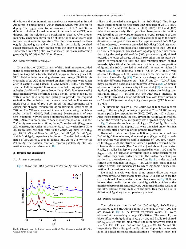
Fig. 1 shows the XRD patterns of ZnO:Al:Ag films coated on
Fig. 1. XRD patterns of the hydrogen annealed ZnO:Al:Ag films annealed at 500 �C forvarious Ag/Zn molar ratio.
silicon and annealed under gas. In the ZnO:Al:Ag-0 film, Braggpeaks corresponding to hexagonal ZnO appeared at 2q ¼ 31.82�,34.41�, 36.21�, and 47.60� from the (100), (002), (101), and (102)reflections, respectively. This crystalline phase present in the filmwas identified as the wurtzite hexagonal crystal structure of ZnO(JCPDS card no 36-1451) [22]. The peak corresponding to the (002)direction is strongest in the case of hydrogen-annealed ZnO:Al:Ag-0 film, whereas, the oxygen-annealed ZnO:Al:Ag-0 had less crys-tallinity [19]. The peak intensities corresponding to the (100) and(101) reflection planes increased with Ag-doping. After incorpora-tion of Ag, the peak position of the (100) plane was slightly shiftedtowards the lower 2q value, whereas, two other intense peak po-sitions (corresponding to (002) and (101) reflection planes) shiftedtowards higher 2q value. Substitutional or interstitial incorporationof Ag into the ZnO lattice, led to peak shifts to lower or higher 2qvalues [23,24]. An additional peak of Ag, at 2q ¼ 38.13� wasobserved for RAg/Zn ¼ 1. This corresponds to the most intense dif-fractions of metallic Ag [25]. The lattice enlargement due to theionic size difference between Agþ (1.26 Å) and Zn2þ (0.74 Å) ionsmay also causes a positional shift to lower 2q values [26]. A similarobservation has also been made by Yildirim et al. [25] in the case ofAg doping in ZnO nanoparticles. Upon increasing the doping con-centration (RAg/Zn ¼ 2% and 3%), the XRD peak intensity at2q ¼ 38.13� increased, and an additional peak with lower intensity(at 2q¼ 44.25�) corresponding to Ag, also appeared (JCPDS card no:4-0783).
The crystalline quality of the ZnO:Al:Ag-0 film was highestowing to the very high intensity of peaks at 2q ¼ 34.48� amongintense peaks [corresponding to (100), (002), and (101) planes].After incorporation of Ag, the poly-crystalline naturewas increased.Hence, the overall crystalline quality was degraded by Ag-doping.
Fig. 2 shows the surface morphology of ZnO:Al:Ag films withvarious amounts of Ag doping, that were annealed under forminggas directly after drying in air (no preheat treatment).
Banana-like structures (size ~ 800 nm) were observed forZnO:Al:Ag-0 film, whereas, after Ag-doping (RAg/Zn ¼ 1%), a seed-like structure was obtained with a diameter of ~200 nm. Howev-er, for RAg/Zn ¼ 2%, the structure formed a partially covered hemi-sphere with nano-leafs (10e15 nm thick) and about 1 mm in size.Finally, a smaller hemisphere was formed (diameter ~ 450 nm) forRAg/Zn ¼ 3%. The formation of various kinds of nano-structures onthe surface may cause surface defects. The surface defect is pro-portional to the surface area. It is clear from Fig. 2 that the maximalsurface area obtained for RAg/Zn ¼ 3% which may cause highestsurface defects. The mechanism by which Ag-doping causes for-mation of the various structures is still unclear.
Elemental analysis was done using energy dispersive x-rayspectroscopy (EDS) color mapping for Zn, Al, O, Si, and Ag to see thecross-sectional elemental distributions (as shown in Fig. 3). It canbe seen that the distribution density of Ag is slightly higher at theinterface (between silicon and ZnO:Al:Ag film) and at the surface ofthe film, relative to the middle of the film. This may be due todiffusion of Ag along the temperature gradient.
3.2. Optical properties
The reflectance spectra of the ZnO:Al:Ag-0, ZnO:Al:Ag-1,ZnO:Al:Ag-2, and ZnO:Al:Ag-3 films in the range of 400e1200 nmare shown in Fig. 4. The lowest reflectance values (Rl) wereobserved at the wavelength range 430e540 nm. The lowest Rl wasblue shifted with Ag doping to RAg/Zn ¼ 2%, and finally red shiftedfor RAg/Zn ¼ 3% from its initial value. The Rl minima were found atl ¼ 517, 438, 430, and 540 nm for RAg/Zn ¼ 0%, 1%, 2% and 3%,respectively. This shifting of the Rl with Ag doping is due to vari-ation of optical thickness (multiplication of refractive index and
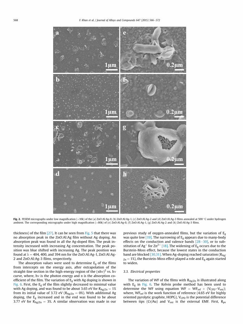
Fig. 2. FESEM micrographs under low magnification (�10k) of the (a) ZnO:Al:Ag-0, (b) ZnO:Al:Ag-1, (c) ZnO:Al:Ag-2 and (d) ZnO:Al:Ag-3 films annealed at 500 �C under hydrogenambient. The corresponding micrographs under high magnification (�80k) of (e) ZnO:Al:Ag-0, (f) ZnO:Al:Ag-1, (g) ZnO:Al:Ag-2 and (h) ZnO:Al:Ag-3 films.
F. Khan et al. / Journal of Alloys and Compounds 647 (2015) 566e572568
thickness) of the film [27]. It can be seen from Fig. 5 that there wasno absorption peak in the ZnO:Al:Ag film without Ag doping. Anabsorption peak was found in all the Ag-doped film. The peak in-tensity increased with increasing Ag concentration. The peak po-sition was blue shifted with increasing Ag. The peak position wasfound at l ¼ 404, 400, and 394 nm for the ZnO:Al:Ag-1, ZnO:Al:Ag-2 and ZnO:Al:Ag-3 films, respectively.
The absorption values were used to determine Eg of the filmsfrom intercepts on the energy axis, after extrapolation of thestraight-line section in the high-energy region of the (ahn)2 vs. hncurve, where, hn is the photon energy and a is the absorption co-efficient of the film. The variation of Eg with Ag doping is shown inFig. 6. First, the Eg of the film slightly decreased to minimal valuewith Ag doping, and was found to be about 3.65 eV for RAg/Zn ¼ 1%from its initial value of 3.72 eV (RAg/Zn ¼ 0%). With additional Agdoping, the Eg increased and in the end was found to be about3.77 eV for RAg/Zn ¼ 3%. A similar observation was made in our
previous study of oxygen-annealed films, but the variation of Egwas quite low [19]. The narrowing of Eg appears due to many-bodyeffects on the conduction and valence bands [28e30], or to sub-stitution of Agþ for Zn2þ [18]. The widening of Eg occurs due to theBurstein-Moss effect, because the lowest states in the conductionband are blocked [30,31]. When Ag-doping reached saturation (RAg/
Zn ¼ 1%), the Burstein-Moss effect played a role and Eg again startedto widen.
3.3. Electrical properties
The variation of WF of the films with RAg/Zn is illustrated alongwith Eg in Fig. 6. The Kelvin probe method has been used todetermine the WF using equation WF ¼ WFref þ (VCPDeVext);where, WFref is the work function of reference (4.65 eV for highlyoriented pyrolytic graphite, HOPG), VCPD is the potential differencebetween tips (Cr/Au) and Vext is the external EMF. First, Rpv
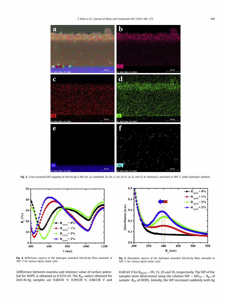
Fig. 3. Cross-sectional EDS mapping of ZnO:Al:Ag-2 film for (a) combined, (b) Zn, (c) Al, (d) O, (e) Si, and (f) Ar element(s) annealed at 500 �C under hydrogen ambient.
Fig. 4. Reflectance spectra of the hydrogen annealed ZnO:Al:Ag films annealed at500 �C for various Ag/Zn molar ratio.
Fig. 5. Absorption spectra of the hydrogen annealed ZnO:Al:Ag films annealed at500 �C for various Ag/Zn molar ratio.
F. Khan et al. / Journal of Alloys and Compounds 647 (2015) 566e572 569
(difference between maxima and minima) value of surface poten-tial for HOPG is obtained as 0.5214 eV. The Rpv values obtained forZnO:Al:Ag samples are 0.60141 V, 0.99139 V, 0.86138 V and
0.68141 V for RAg/Zn ¼ 0%,1%, 2% and 3%, respectively. TheWF of thesamples were determined using the relation WF ¼ WFref þ Rpv ofsampleeRpv of HOPG. Initially, the WF increased suddenly with Ag
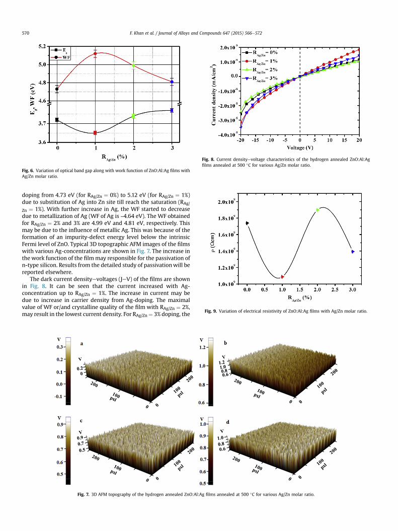
Fig. 6. Variation of optical band gap along with work function of ZnO:Al:Ag films withAg/Zn molar ratio.
Fig. 8. Current densityevoltage characteristics of the hydrogen annealed ZnO:Al:Agfilms annealed at 500 �C for various Ag/Zn molar ratio.
Fig. 9. Variation of electrical resistivity of ZnO:Al:Ag films with Ag/Zn molar ratio.
F. Khan et al. / Journal of Alloys and Compounds 647 (2015) 566e572570
doping from 4.73 eV (for RAg/Zn ¼ 0%) to 5.12 eV (for RAg/Zn ¼ 1%)due to substitution of Ag into Zn site till reach the saturation (RAg/
Zn ¼ 1%). With further increase in Ag, the WF started to decreasedue to metallization of Ag (WF of Ag is ~4.64 eV). The WF obtainedfor RAg/Zn ¼ 2% and 3% are 4.99 eV and 4.81 eV, respectively. Thismay be due to the influence of metallic Ag. This was because of theformation of an impurity-defect energy level below the intrinsicFermi level of ZnO. Typical 3D topographic AFM images of the filmswith various Ag-concentrations are shown in Fig. 7. The increase inthe work function of the filmmay responsible for the passivation ofn-type silicon. Results from the detailed study of passivationwill bereported elsewhere.
The dark current densityevoltages (JeV) of the films are shownin Fig. 8. It can be seen that the current increased with Ag-concentration up to RAg/Zn ¼ 1%. The increase in current may bedue to increase in carrier density from Ag-doping. The maximalvalue of WF or/and crystalline quality of the film with RAg/Zn ¼ 2%,may result in the lowest current density. For RAg/Zn¼ 3% doping, the
Fig. 7. 3D AFM topography of the hydrogen annealed ZnO:Al:Ag films annealed at 500 �C for various Ag/Zn molar ratio.

Fig. 10. Fluorescence spectra of the hydrogen annealed ZnO:Al:Ag films coated onsilicon annealed at 500 �C for various Ag/Zn molar ratio.
F. Khan et al. / Journal of Alloys and Compounds 647 (2015) 566e572 571
current density increased slightly due to the influence of metallicAg. The JeV data were used to calculate the resistivity (r) of thefilm. The variation of r is shown in Fig. 9. The lowest value of rwasobtained for ZnO:Al:Ag-1, whereas, ZnO:Al:Ag-2 had the highestvalue.
3.4. Fluorescence properties
Fig. 10 shows the normalized FL spectra of the films in theemission wavelength (lem) range of 360e800 nm for the excitationwavelength (lex) ¼ 240 nm. Normally, in the Ag-doped samples,two peaks were observed. The first peak was in the near-band re-gion (NBE/UV) observed at about 414 nm, whereas, anotherdefective peak (in the green region) was observed in the lem range525e540 nm. The defective peak position was blue shifted withincreased Ag-doping from 536 nm (RAg/Zn ¼ 1%) to 527 nm for RAg/
Zn ¼ 2%. The blue shifting of the FL peak positions in green regionsmay be due to the sizes of the Agþ and Zn2þ ions [25]. The FL in-tensity in NBE region decreased with increasing RAg/Zn as thecrystalline quality decreased. This can be seen in the XRD data. TheFL defective peak intensity (ID) in the green region increased with
Fig. 11. Variation of the ratio of peak intensity in green to UV region of ZnO:Al:Ag filmswith Ag/Zn molar ratio. (For interpretation of the references to color in this figurelegend, the reader is referred to the web version of this article.)
the Ag-doping concentration up to RAg/Zn ¼ 2%. The enhancementin the ID may be due to replacement of Zn2þ ions by Agþ ions,because Ag addition leads to an increase in the Zni occupancy [25].Silver doping may also cause increased Ozn and Oi vacancies due tothe charge difference between Agþ and Zn2þ ions [19]. Lin andcoworkers [32] observed that the energy intervals from the bottomof the conduction band to the Ozn and Oi levels were 2.38 eV and2.28 eV, respectively and that these two defects are responsible forthe green emission. Wang et al. [33] and Singhal et al. [34] madesimilar observations. The variation of ID/INBE is illustrated in Fig. 11.The ID/INBE ratio increased with Ag-concentration to RAg/Zn ¼ 2%,and then began to decline with further increase in Ag. Among theAg-doped samples, the dependency of ID/INBE with RAg/Zn is similarto the observed variation in the current density.
4. Conclusions
The Eg of the film slightly decreased to the minimal value withAg doping, and was found to be about 3.65 eV for RAg/Zn ¼ 1% fromits initial value of 3.72 eV (RAg/Zn ¼ 0%). The narrowing of Eg is dueto many body effects, whereas, widening of Eg occurs due to theBurstein-Moss effect, since the lowest states in the conductionband are blocked. Initially, the WF was increased with Ag dopingfrom 4.73 eV for RAg/Zn ¼ 0% to 5.12 eV for RAg/Zn ¼ 1% due tosubstitution of Agþ into Znþ sites until reaching saturation (RAg/
Zn¼ 1%). With further increase in Ag doping,WF started to decreaseand finally, reached a value of 4.81 eV for RAg/Zn ¼ 3%. This wasbecause of the formation of an impurity-defect energy level belowthe intrinsic Fermi level of ZnO. The current increased with Ag-doping up to RAg/Zn ¼ 1%. The increase in current may be due toincrease in carrier density from Ag-doping. For RAg/Zn ¼ 3% doping,the current density started to increase due to the influence ofmetallic Ag. The defective peak position was blue shifted with in-crease of Ag-doping from 536 nm (RAg/Zn ¼ 1%) to 527 nm for RAg/
Zn ¼ 2%, due to the sizes of the Agþ and Zn2þ ions. A 30 foldenhancement has been observed in FL intensity in green regionincrease with Ag doping concentration for RAg/Zn ¼ 2%. Theenhancement in the ID may be due to replacement of Zn2þ ions byAgþ ions, because the addition of Ag leads to an increase in the Znioccupancy.
Acknowledgment
This study was carried out with the support of the DGIST R&DProgram (Grant No 15-EN-01) funded by the Ministry of Science,ICT, and Future Planning of the Korean government.
References
[1] U. €Ozgür, D. Hofstetter, H. Morkoç, Proc. IEEE 98 (2010) 1255e1268.[2] Y. Liu, Q. Li, H. Shao, J. Alloy. Comp. 485 (2009) 529e531.[3] F.J. Ramos, M.C. Lopez-Santos, Elena Guill, M.K. Nazeeruddin, Michael Gratzel,
A.R. Gonzalez-Elipe, S. Ahmad, Chem. Phys. Chem. 15 (2014) 1148e1153.[4] O. Kluth, G. Sch€ope, J. Hüpkes, C. Agashe, J. Müller, B. Rech, Thin Solid Films
442 (2003) 80e85.[5] A. Chiappini, C. Armellini, A. Chiasera, M. Ferrari, R. Guider, Y. Jestin, L. Minati,
E. Moser, G. Nunzi Conti, S. Pelli, J. Non-Cryst. Solids 355 (2009) 1132e1135.[6] M.H. Huang, S. Mao, H. Feick, H. Yan, Y. Wu, H. Kind, E. Weber, R. Russo,
P. Yang, Science 292 (2001) 1897e1899.[7] B.K. Sharma, N. Kharea, S. Ahmad, A ZnO/PEDOT: PSS based inorganic/organic
heterojunction, Solid State Comm. 149 (2009) 771e774.[8] N.W. Emanetoglu, C. Gorla, Y. Liu, S. Liang, Y. Lu, Mater. Sci. Semicond. Process
2 (1999) 247e255.[9] K. Bahedi, M. Addou, M. El Jouad, Z. Sofiani, S. Bayoud, M.E.L. Haouti, J. Ebothe,
in: Proceedings of the ICTON-mediterranean Winter Conference, 2009, http://dx.doi.org/10.1109/ICTONMW, 5385535 (1e4).
[10] F. Khan, S.H. Baek, N. Ahmad, G.H. Lee, T.H. Seo, E.K. Suh, J.H. Kim, Met. Mater.Inter. 21 (2015) 561e568.
[11] F. Khan, S. Ameen, M. Song, M. Husain, A. Mobin, H.S. Shin, Met. Mater. Inter19 (2013) 245e250.

F. Khan et al. / Journal of Alloys and Compounds 647 (2015) 566e572572
[12] A. Verma, F. Khan, D. Kumar, M. Kar, B.C. Chakravarty, S.N. Singh, M. Husain,Thin Solid Films 518 (2010) 2649e2653.
[13] F. Khan, Vandana, S.N. Singh, M. Husain, P.K. Singh, Sol. Energy Mater. Sol.Cells 100 (2012) 57e60.
[14] F. Khan, S.H. Baek, S.N. Singh, P.K. Singh, J.H. Kim, Sol. Energy 97 (2013)474e483.
[15] F. Khan, S.H. Baek, A. Mobin, J.H. Kim, Sol. Energy 101 (2014) 265e271.[16] F. Khan, S.H. Baek, S.N. Singh, P.K. Singh, M. Husain, J.H. Kim, Sol. Energy 110
(2014) 595e602.[17] S.H. Jeong, B.N. Park, S.B. Lee, J.H. Boo, Surf. Coat. Technol. 193 (2005)
340e344.[18] K.Y. Wu, C.C. Wang, D.H. Chen, Nanotechnology 18 (2007) 305604 (1-6).[19] F. Khan, S.H. Baek, J.H. Kim, J. Alloy. Comp. 584 (2014) 190e194.[20] F. Khan, S.H. Baek, J. H. Kim, Passivation of n-type silicon wafers, Korean
Patent (Submitted, application no. KO-10-2014-0157939).[21] F. Khan, S.H. Baek, J.H. Kim, Semicond. Sci. Technol. 30 (2015) 015012.[22] Joint Committee on Powder Diffraction Standards International, Center for
Diffraction Data, ICDD. (JCPDS Card No. 361451).[23] C. Karunakaran, V. Rajeswari, P. Gomathisankar, Antibact. J. Alloy. Comp. 508
(2010) 587e591.[24] Y. Jin, Q. Cui, K. Wang, J. Hao, Q. Wang, J. Zhang, J. Appl. Phys. 109 (2011)
053521 (1e5).[25] O.A. Yildirim, H.E. Unalan, C. Durucan, J. Am. Ceram. Soc. 96 (2013) 766e773.[26] B.D. Ahn, H.S. Kang, J.H. Kim, G.H. Kim, H.W. Chang, S.Y. Lee, J. Appl. Phys. 100
(2006) 093701e093706.[27] D. Verma, F. Khan, S.N. Singh, P.K. Singh, Sol. Energy Mater. Sol. Cells 95 (2011)
30e33.[28] K.F. Berggren, B.E. Sernelius, Phys. Rev. B 24 (1981) 1971e1986.[29] E. Burstein, Phys. Rev. 93 (1954) 632e633.[30] B.E. Sernelius, Phys. Rev. B 36 (1987) 4878e4887.[31] B.E. Sernelius, K.F. Berggren, Z.C. Jin, I. Hamberg, C.G. Granqvist, Phys. Rev. B
37 (1988) 10244e10248.[32] B. Lin, Z. Fu, Y. Jia, Appl. Phys. Lett. 79 (2001) 943e945.[33] R. Wang, J.H. Xin, Y. Yang, H. Liu, L. Xu, J. Hu, Appl. Surf. Sci. 227 (2004)
312e317.[34] R.K. Singhal, A. Samariya, Y.T. Xing, S. Kumar, S.N. Dolia, U.P. Deshpande,
T. Shripathi, E.B. Saitovitch, J. Alloy. Comp. 496 (2010) 324e330.
Copyright © 2022 FDOKUMEN