

WITH ENHANCED INSULATION PROPERTIES - Bodo's ...
52
Electronics in Motion and Conversion August 2019 ISSN: 1863-5598 ZKZ 64717 08-19 WITH ENHANCED INSULATION PROPERTIES
-
Upload
khangminh22 -
Category
Documents
-
view
0 -
download
0
Transcript of WITH ENHANCED INSULATION PROPERTIES - Bodo's ...

Electronics in Motion and Conversion August 2019
ISSN: 1863-5598 ZKZ 6471708-19
WITH ENHANCED INSULATION PROPERTIES

WELCOME TO THE HOUSE OF COMPETENCE
PRODUCTIONENGINEERING GvA SOLUTIONS DISTRIBUTION
Whether you need power electronic stacks, turnkey switchboard systems or retrofit projects:
we always burn to do the job and can fulfil even unusual requirements. Benefit from our
Production Power for your success.
Vast and comprehensive production experience
Flexible capacity ranging from prototyping to series production
Short lead times through optimized production processes and our own materials warehouse
Maximum quality requirements for our partners, too
Safety certified through 100% outgoing checks before delivery
GvA Leistungselektronik GmbH
Boehringer Straße 10 - 12
D-68307 Mannheim
Phone +49 (0) 621/7 89 92-0
www.gva-leistungselektronik.de
PRODUCTION
POWER IS IN OUR NATURE!
170626GvA_Anzeige Production_engl_170830_RZ.indd 1 30.08.17 09:28
www.bodospower.com August 2019 Bodo´s Power Systems® 1
CONTENT
CONTENT
Viewpoint ������������������������������������������������������������������������������������������ 4 Summer in San Francisco
Events ������������������������������������������������������������������������������������������������ 4
News ��������������������������������������������������������������������������������������������� 6-13
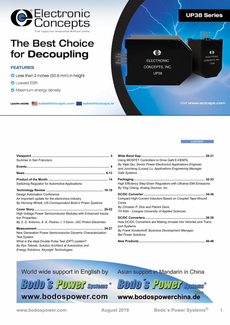
Product of the Month ��������������������������������������������������������������������� 14 Switching Regulator for Automotive Applications
Technology Review ������������������������������������������������������������������ 16-18 Design Automation Conference An important update for the electronics industry By Henning Wriedt, US-Correspondent Bodo’s Power Systems
Cover Story �������������������������������������������������������������������������������� 20-22 High Voltage Power Semiconductor Modules with Enhanced Insula-tion Properties By S. D. Antonov, A. A. Pisarev, I. Y.Savin, JSC Proton-Electrotex
Measurement ����������������������������������������������������������������������������� 24-27 New Generation Power Semiconductor Dynamic Characterization Test System What is the ideal Double Pulse Test (DPT) system? By Ryo Takeda, Solution Architect at Automotive and Energy Solutions, Keysight Technologies
Wide Band Gap �������������������������������������������������������������������������� 28-31 Using MOSFET Controllers to Drive GaN E-HEMTs By Yajie Qiu, Senior Power Electronics Applications Engineer, and Juncheng (Lucas) Lu, Applications Engineering Manager, GaN Systems
Packaging����������������������������������������������������������������������������������� 32-33 High Efficiency Step-Down Regulators with Ultralow EMI Emissions By Ying Cheng, Analog Devices, Inc.
DC/DC Converter ����������������������������������������������������������������������� 34-36 Compact High-Current Inductors Based on Coupled Tape-Wound Cores By Christian P. Dick and Patrick Deck, TH Köln - Cologne University of Applied Sciences
DC/DC Converters ����������������������������������������������������������������������38-39How DC/DC Converters are Making Inroads Into Vehicles and Trans-port Systems By Frank Vondenhoff, Business Development Manager, Bel Power Solutions
New Products����������������������������������������������������������������������������� 40-48
WITH ENHANCED INSULATION PROPERTIES
Bodo´s Power Systems® August 2019 www�bodospower�com2
The Gallery
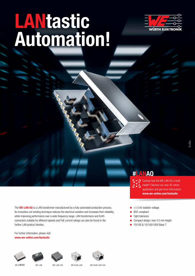
WITH ENHANCED INSULATION PROPERTIES The WE-LAN AQ is a LAN transformer manufactured by a fully automated production process.
Its innovative coil winding technique reduces the electrical variation and increases their reliability,
while improving performance over a wide frequency range. LAN transformers and RJ45
connectors suitable for different speeds and PoE current ratings can also be found in the
further LAN product families.
For further information, please visit:
www.we-online.com/lantastic
LANtasticAutomation!
© e
iSos
WE-LAN AQ WE-LAN WE-LAN 10G WE-RJ45 LAN WE-RJ45 LAN 10GWE-LAN AQ
#LANAQCurious how the WE-LAN AQ is built
inside? Discover our new 3D online
application and get more information:
www.we-online.com/lantastic
n >1.5 kV isolation voltage
n IEEE compliant
n Tight tolerance
n Compact design: max 4.5 mm height
n 10/100 & 10/100/1000 Base-T

Bodo´s Power Systems® August 2019 www.bodospower.com4
CONTENT
A Media Katzbek 17a D-24235 Laboe, Germany Phone: +49 4343 42 17 90 Fax: +49 4343 42 17 89 [email protected] www.bodospower.com
Publishing Editor Bodo Arlt, Dipl.-Ing.
[email protected] Editor
Holger Moscheik Phone + 49 4343 428 5017 [email protected] Editor China Min Xu Phone: +86 156 18860853 [email protected] Support June Hulme
Phone: +44 1270 872315 [email protected]
US Support Cody Miller Phone +1 208 429 6533 [email protected]
Creative Direction & Production Repro Studio Peschke
[email protected] Subscription to qualified readersBodo´s Power Systems is available for the following subscription charges:Annual charge (12 issues)
is 150 € world wideSingle issue is 18 €[email protected]
Printing by: Brühlsche Universitätsdruckerei GmbH
& Co KG; 35396 Gießen, GermanyA Media and Bodos Power Systems
assume and hereby disclaim any liability to any person for any loss or damage by errors or omissions in the material contained herein regardless of whether such errors result from negligence accident or any other cause whatsoever.
VIEWPOINT
California and Silicon Valley are always worth a trip. Nearly 40 years ago I first drove down from San Francisco to Los Angeles on Route 1 – an impressive coast line. Silicon Valley hosted most of the integrated circuit development by the big players and is still an innovation center for semiconductors.
As a young boy I learned about germanium as a semiconductor material and that a transistor was a device to control electric current. As a student, silicon took over the semiconductor area. Then while I was work-ing as an engineer, bipolar transistors were widely replaced by MOS, and then the IGBT was invented. I had a hand in getting MOS-FETs and IGBTs implemented in European industry.
The continual objective of improved efficien-cy for power systems has led to the develop-ment of devices that replace silicon with new semiconductor materials. Wide band gap (WBG) transistor and rectifier devices in SiC and GaN material are now in full production. Integrated circuits for fully integrated power IC solutions are in progress using wide band gap technology. For example, Navitas is driv-ing ahead with solutions for IC technology in GaN. Visiting SEMICON West in San Fran-cisco, I could see all the people focused on optimized manufacturing and testing of wide band gap devices.
For sure, wide band gap devices have reached a mature position and significant investment is ongoing for production quantity. These new generations of semiconductors will drastically improve efficiency and the investment is warranted. So, stay in touch with the magazine for upcoming articles and future activities on WBG development. We will continue to deliver you the important fresh information, through articles written by the experts.
Such experts will once again gather together in Munich for a WBG power conference at the Hilton Hotel at Munich airport on Decem-ber 3rd, 9 am to 5 pm. We are in the final planning phase of the event - more details will be published soon. Look out for it – it’s a hot topic.
Bodo’s magazine is delivered by postal ser-vice to all places in the world. It is the only magazine that spreads technical informa-tion on power electronics globally. We have EETech as a partner serving North America efficiently. If you are using any kind of tablet or smart phone, you will find all of our con-tent on the website www.eepower.com. If you speak the language, or just want to have a look, don’t miss our Chinese version: www.bodospowerchina.com
My Green Power Tip for the Month: Toys for kids can be battery free – be on the lookout for them. The kids will have fun play-ing with simple toys.
Best Regards
Summer in San Francisco
Thermal Management 2019 Denver, CO, USA August 7-8
www.thermalconference.com
GBF ASIA 2019 Guangzhou, China August 16-18
www.battery-expo.com
EPE ECCE 2019 Genova, Italy September 2-5
www.epe2019.com
SPS Middle East 2019 Dubai, UAE September 3-4 www.spsautomationme.com
IEEE DAPE 2019 Genova, Italy September 6
https://e3da.csce.uark.edu/dape
EU PVSEC 2019 Marseille, France September 9-13 www.photovoltaic-conference.com
EV Tech Expo 2019 Novi, MI, USA September 10-12
evtechexpo.com
PCNS 2019 Bucharest, Romania September 10-13
www.passive-components.eu/pcns
CWIEME Americas Chicago, IL, USA September 17-18 www.coilwindingexpo.com/americas
Events
www.bodospower.com

Cost effective miniature and accurate isolated current sensor GO speeds your drives applications. A unique sensor with an integrated primary conductor achieves optimum temperature accuracy, measuring from -40 to +125 °C in a surface mounted SO8 or SO16 package.
• 10-30 A nominal current • Better than 1.3 % accuracy @ +25°C • Differential Hall principle measurement: Very
robust against external fields • 2 μs response time • Up to 3 kV RMS isolation • Double Overcurrent detection outputs for short
circuit and over-load protection (SO16 version)
www.lem.com
At the heart of power electronics.
GO. A breath of fresh air in power electronics.

Bodo´s Power Systems® August 2019 www.bodospower.com6
CONTENTNEWS
Fuji Electric is pleased to announce the launch of the 7400WX-T3U, a high-capacity uninterruptible power supply system (hereinafter, “UPS”), to strengthen its overseas power supply business. With the development of cloud information systems and e-commerce, more data centers are being constructed around the world. Data centers must supply power continuously in order to protect, maintain, and operate servers that store important information and to provide Inter-net connection lines. One of the core pieces of equipment in doing this is the UPS, which continues to supply power even during power outages. The global UPS market is expected to grow to $30.2 billion with a compound annual growth rate of approximately 10% by 2022. Fuji Electric has developed the high-capacity UPS “7400WX-T3U” for very large systems. It enables the construction of large-scale systems of up to 8000 kVA, and is equipped with SiC power semiconductors
to achieve one of the highest efficiency rating in the industry. In ad-dition to the originally developed reverse-blocking IGBT (RB-IGBT), Fuji Electric applied SiC power semiconductors to the UPS circuits, achieving an efficiency rating of 97.4%, one of the highest in the industry. It has achieved an efficiency rating of 96% or more even at low loads (load factor of 25%), reducing power loss and contributing to energy saving.
www�fujielectric�com
Power Supply System for Overseas Markets
EPC announces the availability of their enhancement-mode gallium nitride (GaN) devices in wafer form for ease of integration. EPC’s eGaN FETs and ICs are traditionally sold as singulated chip-scale
devices with solder bars or solder bumps. Chip-scale packaging is a more efficient form of packaging that reduces the resistance, induc-tance, size, thermal impedance, and cost of power transistors. These attributes of eGaN devices enable unmatched in-circuit performance at competitive prices. Wafer-level offerings of these devices allows for easier integration in customer power system sub-assemblies, further reducing device interconnect inductances and the interstitial space needed on the printed circuit board (PCB). This increases both efficiency and power density while reducing assembly costs. “We have listened to our partners and are pleased to offer our industry-leading GaN products in wafer form that can accommodate a variety of assembly techniques and applications,” commented Alex Lidow, CEO and co-founder of EPC. EPC is offering eGaN power devices in wafer form either with or without solder bumps. Extra services such as wafer thinning, metallization of the wafer backside, and application of backside coating tape are also available.
www�epc-co�com
GaN Power Devices in Wafer Form
On June 14th, Analog Devices opened the doors of its new head-quarters office in Hayes, London, a location which will strengthen its ability to connect customers with the best engineering talent in the UK and overseas. By locating its new office in London, close to a fast
Elizabeth Line link to the city centre, Analog Devices has made itself accessible to the capital’s huge pool of talent - not only software and hardware engineers, but also a vibrant community of entrepreneurs and start-up workers, as well as skilled staff in non-engineering disciplines. Close to Heathrow airport, the new HQ office is also a convenient hub for the company’s domain specialists located in other Analog Devices locations such as Munich, Germany, Boston, US and Limerick, Ireland. These technology and applications experts will now more easily be able to take part in UK customer meetings hosted by Analog Devices. The new office, which has a distinctly contemporary look in contrast to the bland aesthetic commonly adopted by many engineering companies, underpins Analog Devices’ ambitious plans for growth in the UK: it easily accommodates all the staff who previ-ously worked at Analog Devices and legacy Linear Technology offices in Weybridge and Marlow, with a generous additional floating capacity to accommodate customer meetings, visits by field engineers, training facilities and an expanding staff headcount.
www�analog�com
UK Headquarters Office Opened

Get smart at www.microchip.com/Smart
The Microchip name and logo and the Microchip logo are registered trademarks of Microchip Technology Incorporated in the U.S.A. and other countries. All other trademarks are the property of their registered owners. © 2019 Microchip Technology Inc. All rights reserved. DS00002769A. MEC2237A-Eng-06-19
Smart Solutions to Accelerate DesignBuilding Blocks to Optimize Your Design’s Intelligence
As technology has evolved, more and more devices demand intelligent systems. Microchip has been on the forefront of this evolution, bringing you a broad portfolio of solutions that helps you:
• Easily find the right level of intelligence for your design with our broad portfolio of8-, 16- and 32-bit MCUs, DSCs and MPUs
• Efficiently create differentiated designs with flexible peripherals and functions• Accelerate design time with our intuitive development environments, complete
reference designs, free software libraries and automatic code generation tools.
Learn how Microchip can get you to production faster by providing solutions that are not only smart, but also connected and secure.

Bodo´s Power Systems® August 2019 www.bodospower.com8
CONTENTNEWS
EMC specialists from science and industry can submit topics for conference lectures and workshops for the EMV 2020. At the event, the speakers will present current results from research and develop-ment and impart industry-specific know-how. “Every two years, the EMV conference offers an excellent platform to present work and findings to a technical and scientific audience. Contributions are very welcome, especially if trend topics such as autonomous driving, elec-tromobility, wireless technology or digitization are included,” explains the Chairman of the EMV 2020 committee Professor Dr.-Ing. Heyno Garbe from the Leibniz University Hannover. The event will take place for the first time in Cologne from 17 – 19 March 2020.
https://emv�mesago�com
EMV 2020 Call for Papers
TDK Corporation is pleased to announce that Rohde & Schwarz has awarded TDK-Lambda the “preferred supplier” certificate for the third time in a row. Rohde & Schwarz is a leading German electronics group for metrology, broadcast and media technology, secure com-munication, cyber security and monitoring and network testing. This award accentuates an on-going partnership with TDK-Lambda which has been in place for over 20 years. By presenting the classification
of “preferred status”, Rohde & Schwarz honors those companies in its supplier management program that provide outstanding performance in the development, production and supply of products or services.With their classification as “preferred supplier” Rohde & Schwarz hon-ors companies that have performed outstandingly well in the develop-ment, manufacture and delivery of products or services in the past fiscal year. Ulrich Schwarz, Sales Director TDK-Lambda Germany, is delighted about the appreciation of Rohde & Schwarz and the as-sociated recognition of the services rendered in the areas of product quality, cooperative partnership and the contributed know-how. “The entire TDK-Lambda team is proud to have been named preferred sup-plier by Rohde & Schwarz for the third time in a row. The strict quality requirements for standard devices as well as customer-specific power supply solutions for Rohde & Schwarz devices coincide with our un-derstanding of industrial-suited power supplies. Our aim is to be one of the top suppliers again next year”, said Ulrich Schwarz.
www�tdk-lambda�com
www�rohde-schwarz�com
“Preferred Supplier” for the Third Time
An increase of visitors and exhibitors as well as high satisfaction rates on all sides confirm that the PCIM Europe, the leading international Exhibition and Conference for Power Electronics and its applications, was a great success. With 12,182 visitors and 515 exhibitors, this
year’s PCIM Europe that took place on 7 – 9 May in Nuremberg reg-istered another record result. As far as the Conference is concerned, the numbers were on the same level as the previous year, showing a slight upward trend with 804 international delegates. More than half of this year’s exhibiting companies are based outside of Germany; the number of American enterprises was a remarkable 14%. Furthermore, China, Italy, Great Britain, France and Japan were strongly repre-sented. 76% of the exhibitors rated the PCIM Europe “good” or “very good” and they praised, in particular, the quality of trade visitors at their booths as well as the organization of the event. The international trade visitors (46%) predominantly came from German-speaking countries, but also from Italy, Great Britain, France and the USA, the large proportion of decision-makers (79%) mirroring the superior qual-ity of the clientele. 93% of the visitors would recommend the PCIM Europe to others and 75% of them intend to attend the exhibition again next year. The PCIM Europe 2020 will take place from 5 – 7 May 2020 in Nuremberg.
https://pcim�mesago�com
Statistics on the PCIM Europe 2019 Available

Lunch time?
Scan for shortdocumentary.
Scan for product.
… or work time?
When you need efficiency,performance is mandatory.

Bodo´s Power Systems® August 2019 www.bodospower.com10
CONTENTNEWS
The APEC 2020 Conference Committee is seeking qualified engi-neers and scientists to assist in the peer review of the large quantity of paper digests expected for APEC 2020, to be held in New Orleans, March 15-19, 2020. All technical program papers presented, either in the technical presentations or as dialog (poster) sessions, have been chosen as a result of a rigorous, peer-review process. Nearly 1200 paper digests are expected. Based upon the scores received, about 650 papers will be chosen for inclusion in the program. Interested par-ties are invited to apply using this link: https://epapers.org/apec2020/ESR/reviewer_signup.php
www�apec-conf�org
APEC 2020 Seeking Qualified Reviewers
Renesas announced that Hidetoshi Shibata has been named its Representative Direc-tor, President and CEO, effective July 1, 2019. Hidetoshi Shibata joined Renesas in 2013 when the company was in crisis, and as Executive Vice President, Member of the Board and CFO, led the structural reform measures, such as personnel cost reduc-tions, and the reorganization of production sites, etc. After the structural reforms, he was instrumental in leading the acquisitions
of two U.S.-based semiconductor companies, Intersil Corporation and Integrated Device Technology, Inc., which are critical measures for
the company’s future growth. The Nomination Committee, an advisory body reporting to the Board of Directors, reported the following rea-sons for selecting Hidetoshi Shibata as candidate for the next Presi-dent and CEO. “We evaluated Mr. Shibata highly for his experience in leading structural reforms, which will enable him to leverage the lessons learned to take effective measures quickly in order to break away from the current unfavorable business performance and stock price stagnation. When considering the company’s rebuilding and further growth amidst the rapidly changing semiconductor industry, we determined that he is best qualified to be the next President and CEO.”
www�renesas�com
Hidetoshi Shibata Next CEO
TTI has released three whitepapers to help design engineers take advantage of the latest technologies that optimize industrial applica-tions and environments. The papers explore machine vision and the way it is applied to user interfaces, discuss cobotics as an enabler for increased production flexibility and look at the role of sensor technol-ogy in improving Indoor Air Quality (IAQ) monitoring. “The potential of sensors is endless,” said Ros Kruger, Director Supplier Marketing Europe Electromechanical, Sensors & Power, TTI Europe. “They are a cost-effective way of introducing automation to industrial applica-tions and gaining access to the data needed to optimize efficiency and productivity, whilst improving safety and quality of life for people working in those environments. We created this set of whitepapers to provide an easily accessible overview of these key technologies in order to help design engineers understand and implement them.”
Together, the papers provide comprehensive insight into where these technologies fit in the industrial landscape, and give practical guid-ance to design engineers looking to implement them.
www�ttieurope�com
Whitepapers Help Design Engineers
• ECPE Tutorial ‘Passives in Power Electronics: Magnetic Compo-nent Design and Simulation’ 19 - 20 September 2019, Birmingham, United Kingdom
• Packaging’ 1 - 2 October 2019, Hanau, Germany
• ECPE Workshop ‘Advanced Power Packaging - Power Modules 2.0’ 9 - 10 October 2019, Hamburg, Germany
• ECPE Tutorial ‘Thermal Engineering of Power Electronic Systems - Part II: Thermal Management and Reliability’ 15 - 16 October 2019, Nuremberg, Germany
• ECPE Tutorial ‘Power Circuits for Clean Switching and Low Losses’ 6 - 7 November 2019, Barcelona, Spain
• ECPE Tutorial ‘Power Semiconductor Devices & Technologies’ 20 - 21 November 2019, Frankfurt am Main, Germany
• ECPE Workshop ‘Power Semiconductors in Medium Voltage Ap-plications - SiC vs. Silicon’ 3 - 4 December 2019, Freiburg i.B., Germany
www�ecpe�org
ECPE Events

UNITEDSIC.COM APPLICATION NOTES TECHNICAL BLOGS WHITE PAPERS
UF3C SeriesFAST 650V & 1200V SiC FETs
Get faster switching speeds, lower switching
conversion efficiencyThe new UnitedSiC UF3C series of FAST
650V and 1200V SiC FETs deliver:
• Easy drop-in replacement for IGBTs, Si
and other SiC MOSFETs
• Lowest RDS(on) @ 27mohm in TO-220-3L
and D2PAK-3L
• Excellent reverse recovery
• Full suite of industry standard packages –
TO-220-3L, D2PAK-3L, TO-247-3L and
TO-247-4L (Kelvin)
Get started now. Go to
unitedsic.com/cascodes to learn
how to make your next design

Bodo´s Power Systems® August 2019 www.bodospower.com12
CONTENT
One of the most important challenges in the development of electric drive mechanisms is the thermal management of the batteries. This is what decides the vehicle range and battery lifetime, while also being a major factor in fast charging. Current development is moving towards liquid cooling. One particular challenge is to create the best possible thermal connection between the battery cells and the cooling element. The FLEXcooler®, developed by the Austrian technology group Miba, is a battery cooling system with a flexible shape that enables it to adjust itself to the battery cells in the best possible way. It is the first liquid cooling system in the market that does more than optimising the absorption and dissipation of heat. The close connection between the battery cells and the cooling system means that the cooler can do completely without gap fillers, i.e. materials that fill the gaps between the battery cells and cooling system. The Miba FLEXcooler® also scores highly with its low weight. It can be used for prismatic, cylindri-cal and pouch battery cells alike.
www�miba�com
Battery Cooling for Electric Vehicles
A total of 81 exhibitors presented the latest trends, developments and product innovations for all application areas of power electronics in Asia from 26 - 28 June 2019. With a total area of 7,000 square meters in Shanghai, PCIM Asia closed its doors after a successful three days. PCIM Asia is jointly organized by Guangzhou Guangya Trade Fair Frankfurt Co Ltd and Mesago Messe Frankfurt GmbH. The PCIM Asia 2019 offered an extensive supporting program that promoted the exchange between visitors and exhibitors and gave exhibitors the op-portunity to present their latest products and technologies. Highlights in the exhibition hall included the E-Mobility Forum and Power Elec-tronics Applied Technologies Forum with renowned companies such as AkzoNobel, BYD, Danfoss, Eagtop, Firstack, Harting, Heraeus, Hitachi Metals, Infineon, Isabellenhuette, MacDermid Alpha, Sanrise, Sabic, Toshiba, Wevo-Chemie. The conference, held parallel to the fair, also achieved a good result with 407 participants. Well-known speakers from all over the world showcased the latest developments in silicon carbide (SiC) and gallium nitride (GaN) devices and their respective applications in renewable energy, transmission and electric vehicles. This year, a total of 47 conference papers were presented,
including 27 oral presentations and 20 posters. The next PCIM Asia will take place from 1 - 3 July 2020 in Shanghai.
https://pcimasia-expo�cn�messefrankfurt�com
Platform for Power Electronics in Asia
NEWS
Rogers Corporation’s Advanced Connectivity Solutions (ACS) busi-ness unit announced the introduction of a new distribution channel with the addition of International Electronic Components (IEC) to their sales and service team in the United States and Canada effective July 8, 2019. ACS provides global customers with market-leading high per-formance and high reliability RF material solutions. IEC comes with over 53 years of sales and service experience in PCB processing and materials distribution. Rogers ACS’ continued expansion in the United States, combined with IEC’s extensive experience and distribution network, will provide the highest level of support to customers. Rog-ers and IEC, working closely as a team, will provide both sales and onsite service/support to PCB manufacturing customers throughout the United States and Canada. IEC President Shawn Stone com-mented, “We are thrilled to be working with Rogers Corporation and their RO3000® and RO4000® product lines. Their material technology offering is leading edge and will go a long way in helping our custom-
ers excel in producing RF and low loss PCB’s. Our local team will ensure our clients receive market leading materials, along with world class service and support.” Ron Bader, Rogers General Manager of High Reliability Solutions, noted, “I am pleased IEC and Rogers were able to form this relationship that focuses on enhancing our ability to service our customers in North America through improved service and local support.”
www�rogerscorp�com
Advanced Connectivity Solutions Business

www.bodospower.com August 2019 Bodo´s Power Systems® 13
CONTENT
After three scorching days, the SENSOR+TEST Measuring Technolo-gy trade fair in Nuremberg, Germany, closed its gates. Despite record temperatures outside, about 7,000 visitors from all over the world found their way to the pleasantly cool exhibition halls. The number
of exhibitors, 538, was regularly under that of the previous year. The share of foreign exhibitors, 40%, remained unchanged. Thus, the SENSOR+TEST once again asserted its position as the international leading sensor, measuring, and testing fair. The visitors made good use of the opportunity to obtain information on a plethora of inter-esting innovations at stands on a floor space amounting to 18,000 square meters. Here as well as at the popular exhibitors’ forums, ani-mated discussions were held especially on this year’s special topic, Sensor and Measuring Technology for Process Automation. Holger Bödeker, the managing director of the organizing AMA Service GmbH company, stated, “Both of these free exhibitor forums in the exhibition halls are turning into real audience magnets.”Next year, the SENSOR+TEST will be held from the 23rd to the 25th of June, 2020, in halls 1, 2, and 3C. Holger Bödeker, commented on this, saying, “Both, exhibitors and visitors, can already look forward to the new, modern hall 3C. It promises a most attractive stand-space layout, providing high efficiency for our visitors.”
www�sensor-test�com
Final Report SENSOR+TEST 2019
PowerAmerica is pleased to an-nounce that Dr. Victor Veliadis has been named its Executive Director effective July 1, 2019. Under Dr. Veliadis’ tenure as Deputy Director and CTO, PowerAmerica has grown into a world-class Manufacturing USA institute accelerating wide bandgap power electronics com-mercialization and creating jobs in advanced technology. Dr. Veliadis is Executive Director and CTO of PowerAmerica, which is a U.S. De-partment of Energy wide bandgap power electronics Manufacturing Innovation Institute. He manages a budget in excess of $30 million per year that he strategically allocates
to over 35 industrial, University, and National-Laboratory projects, to enable U.S. leadership in WBG power electronics manufacturing, work force development, job creation, and energy savings. Dr. Velia-dis has given over 60 invited presentations/tutorials and keynotes at major conferences in India, Korea, China, Europe and the U.S. He is an IEEE Fellow and an IEEE EDS Distinguished Lecturer. Dr. Veliadis has 25 issued U.S. patents, 6 book chapters, and 115 peer-reviewed technical publications to his credit. He is also Professor in Electrical and Computer Engineering at North Carolina State University. He received the Ph.D. degree from Johns Hopkins University in 1995 in Electrical and Computer Engineering. Prior to taking an executive position at Power America in 2016, Dr. Veliadis spent 21 years in the semiconductor industry where his work included design, fabrication, and testing of 1-12 kV SiC SITs, JFETs, MOSFETs, Thyristors, and JBS and PiN diodes, as well as operations and financial planning of a commercial foundry.
www�poweramericainstitute�org
Dr� Victor Veliadis Named Executive Director
NEWS
Asahi Kasei Honorary Fellow Dr. Akira Yoshino has received the European Inventor Award 2019 by the European Patent Office (EPO) in the category of Non-EPO countries for his invention and refinement of the lithium-ion battery. The award ceremony was held in Vienna, Austria, at the Wiener Stadthalle and was attended by some 600 guests from the fields of intellectual property, politics, business, sci-ence and academia. “Yoshino created the foundation of today’s lithium-ion technology and
industry. His inventions can be found in the smartphones that connect people around the world and are enabling the emergence of electric vehicles too,” said EPO President António Campinos. “His technology has trans-formed our society, in part because the licenses granted to other companies for the use of his pa-tented inventions helped to decisively speed up its commercialization.”“I am greatly honored to receive this year’s European Inventor Award. It was gratifying that the EPO President said my invention significantly impacted society,” commented Dr. Akira Yoshino. “I hope that my accomplishment will help make the name of Asahi Kasei well known throughout Europe. The series of events associated with this award reminded me of how concerned European people are about envi-ronmental issues. I am humbled that my invention is contributing to solutions.”
www�asahi-kasei�co�jp
Akira Yoshino Receives Award
Bodo´s Power Systems® August 2019 www.bodospower.com14
CONTENT
The STMicroelectronics A7987 automotive switching regulator has a wide input-voltage range that allows use in trucks and buses, and an adjustable output voltage that ensures flexibility and stable performance to power the numerous voltage rails in automotive ap-plications such as body infotainment and telematics. With maximum input voltage of 61V, the A7987 can operate from a 24V battery in a conventional or hybrid/electric vehicle and maintain a regulated output despite disturbances such as load-dump. The output is adjustable from 0.8V up to the input voltage, with low dropout, and can provide up to 3A for a wide variety of loads from logic to lighting.
The current limit and switching frequency up to 1.5MHz are set with external pulldown resistors, letting designers create compact power modules by optimizing the output-inductor size. Pulse-by-pulse cur-rent sensing with digital frequency foldback in short-circuit minimizes stress on power components to enhance reliability. Thermal protection is built-in, with shutdown and auto-recovery to minimize reliance on external intervention. The A7987 embeds a low-resistance N-channel power MOSFET. At light load, pulse skipping maintains output regula-tion and a bias-voltage input with integrated switchover allows power-ing analog circuitry from an external source for optimum efficiency.
A synchronization pin allows up to five regulators to coexist by switch-ing out of phase to avoid noise effects and reduce the RMS current flowing in the input capacitor. An Enable pin and a Power-Good indicator with adjustable delay permit power-up sequencing. There is also an adjustable soft-start function to limit inrush current. AEC-Q100 certified, the A7987 switching regulator is in production now, in a 5mm x 6.4mm HTSSOP16 exposed-pad package. ST has also released the STEVAL-ISA207V1 evaluation board to accelerate new projects leveraging the A7987.
www�st�com
Switching Regulator for Automotive Applications
PRODUCT OF THE MONTH

cde.com/MLSHSlimpack
Your Mission-critical applicationsrequire SlimPack performance
MLSH Slimpack is designed to meet the most demanding military and aerospace applications. It’s the world’s only hermetic aluminum electrolytic capacitor with a glass-to-metal seal. Slimpack delivers extremely high capacitance at ultra-low temperatures. Energize your next idea with MLSH Slimpack.
Replaces 3 or more wet tantalum capacitors in parallel or series
Less weight and requires less space
Glass-to-metal seal prevents dry-out for exceptionally long life
Superior capacitance retention at -55ºC
Rugged stainless steel case withstands up to 80g’s

Bodo´s Power Systems® August 2019 www.bodospower.com16
CONTENT
Founded in 1964, DAC is one of the longest running conferences especially tailored to the design and automation of electronic circuits and systems. And, according to Technical Program Chair Harry Foster (Mentor), an industry authority and sought-after expert on formal verification, 2019 was a record year in terms of research paper submissions and accepted papers: 815 papers were submitted, and 202 accepted (35% EDA; 32% Design; 17% Embedded Systems and 16% Security/Safety/ Autonomous Systems). Just these numbers are a clear sign, that the DAC is still going strong.
Foster: „Yet, DAC has evolved over the years to address emerging challenges - beginning with its roots in traditional electronic design au-tomation (EDA) and in recent years expanding into a broad spectrum of research topics associated with chip and system design. About two thirds of this year’s papers focus on many other important aspects of design, such as the design of autonomous systems, security, em-bedded systems, artificial intelligent architectures, and cyber-physical systems.”
“The conference was organized in 44 technical sessions conducted in five daily parallel tracks. A few highlights from this year’s conferen-ce included 22 papers on machine-learning and artificial-intelligent architectures. For example “Emerging Technologies Meet Intelligent Machines”, highlighted recent advances in emerging device technolo-gies for hardware implementation of neural networks.”
Of course, the more than 40 technical sessions covered almost every aspect of the electronic design automation business, but there were also presentations, which gave the audience an interesting look towards upcoming developments not only in the EDA-world. Here are just a few examples:* Future AI Trends for IP within the automotive industry* Designing efficient and safe autonomy* Faster compute in smarter industries* Design-Time optimization of Power, Temperature, and Accuracy* IP to secure devices in a hostile world* Hide and seek: Encryption and Obfuscation
The complete proceedings of this conference can be searched in the digital libraries of the ACM and the IEEE. Just a reminder: The subtitle of the DAC conference is: From Chip to Systems - Learn today, create tomorrow!
Secure IoT?Especially the keynotes drew always a big crowd. Galen C. Hunt, Managing Director of Microsoft, presented his thoughts about: „Securing the billions of devices around us". He pointed to the fact, that those billions of devices are controlled by microcontrollers, which in his opinion are ill-prepared for the security challenges of Internet connectivity.
To overcome this situation, Hunt refers to Microsoft‘s „Azur Sphere“, which brings together the company’s expertise in cloud, software, and device technology to provide a unique approach to security that starts in the silicon and extends to the cloud.
A custom Linux kernel enables silicon diversity and innovation. The new crossover class of MCUs now combines both real-time and application processors with built-in Microsoft security technology and connectivity.
www�microsoft�com/en-us/research/people/galenh/
Reverse Engineering visual IntelligenceDr. James DiCarlo from the Massachusetts Institute of Technology explained an impressed audience his thoughts about „Reverse En-gineering visual Intelligence“. Here is a summary in his own words:
„The brain and cognitive sciences are hard at work on a great scienti-fic quest - to reverse engineer the human mind and its intelligent be-havior. These fields are still in their infancy. Not surprisingly, forward engineering approaches that aim to emulate human intelligence in artificial systems are also still in their infancy. Yet the intelligence and cognitive flexibility evidenced in human behavior are an existence proof that machines can be constructed to emulate and work alongside the human mind.
I believe that the challenges of reverse engineering human intelligen-ce will be solved by guiding forward engineering aimed at emulating intelligent behavior with knowledge and data from brain and cogni-tive sciences. To demonstrate this, I focus on one aspect of human intelligence - visual object categorization and detection - and I will explain the story of how work in brain science, cognitive science and computer science converged to create deep neural networks that can support such abilities. These networks not only reach human perfor-mance for many images, but their internal workings are modeled after - and largely explain and predict - the internal neural processing of the primate visual system.
As this approach discovers the correct neural network models, those models will not only advance engineered systems - they will be the basis of novel brain interfaces for therapeutic and augmentation goals. To make that point, I can show that the knowledge embedded in the current best neural network models of the primate visual system already enables unprecedented precision in non-invasive control of neural population states deep in the brain.
This is only the first wave of advances in artificial systems. For ex-ample, the primate visual system still outperforms current generation artificial deep neural networks, and I can show some recent clues that the brain and cognitive sciences can offer to help advance the
Design Automation ConferenceAn important update for the electronics industry
This year the 56th Design Automation Conference (DAC) plus Exhibition took place in early June in Las Vegas, USA. DAC covers an important part of the world-wide electronics industry.
By Henning Wriedt, US-Correspondent Bodo’s Power Systems
TECHNOLOGY REVIEW

www.bodospower.com August 2019 Bodo´s Power Systems® 17
CONTENTTECHNOLOGY REVIEW
next wave. More broadly, our species is the beginning of its most important science quest - the quest to understand human intelligence - and I hope to motivate engineers and other scientists to engage that frontier alongside us.”
https://cbmm�mit�edu/about/people/dicarlo
DAC and Semicon co-locateJust these two keynote examples show clearly, that the DAC should be worth a visit for every electronic engineer. No wonder, that SEMI and the Design Automation Conference announced during the confe-rence, that DAC and SEMICON West will co-locate in July, 2020 and July, 2021.
„The co-location represents a game-changing combination of world-class technical programs and exhibitions designed to give en-gineering attendees a central event to network, attend technical sessi-ons and get exposed to the latest vendor technologies from the entire design and manufacturing ecosystem“ so the official announcement.
Research TrackSeveral design topics were covered in the Research Track, including the design of cyber-physical and Internet-of-Things (IoT) systems, SoC architectures, accelerator-based computing, emerging models of computation such as brain-inspired and quantum computing, digital and analog circuits, and emerging device technologies.
So for instance, Ahmad-Reza Sadeghi, Technische Universität Darm-stadt, Germany, moderated the topic “ Secure Open-Source Hard-ware: Hype or Reality?” Key findings were: Hardware security plays a key role which has led to huge research and development efforts on designing and deploying hardware security architectures incorporating increasing number of security mechanisms.
As a result, the Trusted Computing Base in hardware is not only constantly growing but is also typically highly proprietary through strict IP protection. Consequently, hardware platforms contain design and implementation flaws that are discovered after the fact and exploited by adversaries, as it has been repeatedly and impressively demon-strated in the recent years. It seems questionable that semiconductor industry would ever be willing to adopt the necessary solutions and open-source their entire hardware designs in the future.
A second very interesting topic was “Resilience Revisited – Towards a System Perspective” moderated by Muhammad Shafique, Technische Universität, Vienna, Austria. Facing the upcoming age of autonomous driving, drone deliveries and Industry 4.0 automation, powerful com-puting platforms are increasingly deployed in safety-critical applica-tions.
The underlying complex electronics suffer from random hardware faults such as radiation-induced soft errors, which may cause a cor-ruption of data or program execution. Therefore, safety standards such as the ISO 26262 are introduced, which demand that the overall system must remain in a safe state even in the presence of such random faults.
ESS & Autonomous SystemsThe Embedded Systems and Software sessions and the Autonomous Systems sessions at DAC provided a forum for discussing the chal-lenges of embedded design and an opportunity to exchange ideas and roadmaps for the future for this rapidly expanding area.
Many visitors of the DAC-Show attended the session “Co-designing Hardware and Software for Secure Next Generation Platforms” because next generation platforms are expected to be intelligent and processing or communicating critical information.
Hardware and software vulnerabilities in these platforms can be exploited to leak critical information or even to invoke denial of service attacks resulting in catastrophic consequences. Hardware and soft-ware security experts discussed different ways to detect and prevent attacks on next generation platforms.
DAC Product Highlights
Single and dual Output Power Supplies Keysight Technologies presented a new series (E36200/300) of single and dual output power supplies that delivers more usable power, bench friendly design with low background noise, small footprint and large display. Customers can integrate the E36200 into existing sys-tem using the rear output terminals, modern I/O and trigger port. The trigger port allows synchronization of other instruments and the ability to add an emergency shutdown control. The E36200 series show standard commands for programmable instrument (SCPI) power supplies with built-in USB, LAN, and optional GPIB.
www�keysight�com
EDA software scalability on the MS AzureMentor, a Siemens business, announced that the Calibre™ plat-form Physical Verification Suite has achieved a new standard for EDA software scalability on the Microsoft Azure cloud platform. The benchmarks were achieved during scaling experiments on 5 nm test chips and a full reticle-sized 7 nm production design on Azure. In these deployments, Calibre scaled out to more than 4,000 CPUs - an industry record for an EDA tool scaling a single job on Azure.
A case study worth sharing: Toshiba offers a variety of brush/brus-hless motor drivers that follow the Automotive Electronics Council (AEC-Q100) qualification to meet the device specifications suitable for use in harsh automotive environments. High output current ICs usually generate a lot of heat from the driver transistor which affects the surrounding circuits. For the motor driver IC, the current must be set up accurately for the driver.
This motor control driver includes an on-chip DMOS device with a cur-rent control circuit that operates as a regulator for the output current of the DMOS transistor. The DMOS transistor’s high temperature affects the circuit behavior and functionality. It is typically difficult to design the circuit and to optimize all device parameters without proper verification of the temperature change when the DMOS transistor is turned on and off.
The Eldo® circuit simulator supports fully-coupled electrothermal simulations. In high voltage/power applications, controlling the temperature and its propagation throughout the circuit and the system is critical. Using a global uniform temperature for the entire IC is no longer accurate enough. Eldo solves this problem by allowing the local temperature of devices or entire cells (SPICE subcircuits and Verilog-A models) to be true variables in the system. Temperatures are solved simultaneously with the voltages and the currents through the devices. This is called true electrothermal simulation.
www�mentor�com
Bodo´s Power Systems® August 2019 www.bodospower.com18
CONTENT
Simulation requirements for PMICsAccording to Karthik Srinivasan, Sr. Product Manager (Analog Mixed Signal, Ansys, Inc.), today’s PMICs contain one or multiple linear and switching regulators supplying power to different SoCs on an electronic subsystem. Since they operate at higher voltages supplying larger current demand of SoCs, they are typically fabricated in planar or specialized process technologies like BCD. The key for efficient power management design is low quiescent cur-rent and faster response. For faster response the switching regulators are switching at higher frequencies which also means they can use smaller off-chip inductors which offers a better form factor. On top of scaling of technology and frequency, Power FETs are going from discrete single FETs to complex multifunctional PMICs supply-ing several voltage levels and current loads. PMICs are also running complex algorithms performing battery management, and power se-quencing. So, what used to be a discrete bulky power FET is getting condensed into a Power Management Chip. The ANSYS Totem platform offers a comprehensive suite of tools that can aid designers to optimize the designs for power loss, thermal im-pact, noise coupling and EMI. It has a built-in extraction with user con-trollable and auto meshing for handling complex geometries on chip and package layers. It also has a built-in simulation and electromigra-tion engine to understand the current crowding issues in the layout.
www�ansys�com
Power System-on-Chip Intels Enpirion Power Solutions are high frequency, high efficiency power management devices for FPGAs, SoCs, CPUs, ASICs, and other semiconductor devices. These robust products meet stringent power requirements in a small footprint. The PowerSoC modules integrate nearly all the components needed to build a power supply without sacrificing performance or efficiency. The EN29A0QI 10A PowerSoC DC-DC step-down power converter is designed to power supply rails requiring very low ripple, low EMI, and tight DC and AC accuracy. The device is optimized specifically to meet the requirements for Intel FPGA and SoC transceivers, as well as transceivers for other FPGA and ASIC devices.
www�intel�com
Dynamic Power Device Analyzer with Double-Pulse Test CapabilityA dynamic power device analyzer from Keysight Technologies with double-pulse tester (PD1500A) to deliver reliable, repeatable measu-rements of wide-bandgap (WBG) semiconductors, while ensuring the safety of the measurement hardware and the professionals perfor-ming the tests. Fully characterizing a SiC or GaN device requires static and dynamic measurements. The B1505A and B1506A Power Device Analyzers deliver these static measurements and, with the addition of the new PD1500A, now also provides the flexibility needed to address a variety of dynamic measurements.
www�keysight�com
GaN-ICs for monolithic IntegrationWith a higher breakdown strength, faster switching speed, higher thermal conductivity and lower on-resistance, power devices based on GaN significantly outperform Si-based power chips. The first-generation GaN-based power devices will play a key role in the power conversion of various applications. Today, GaN is grown on a variety of substrates, including sapphire, silicon carbide (SiC) and silicon (Si).
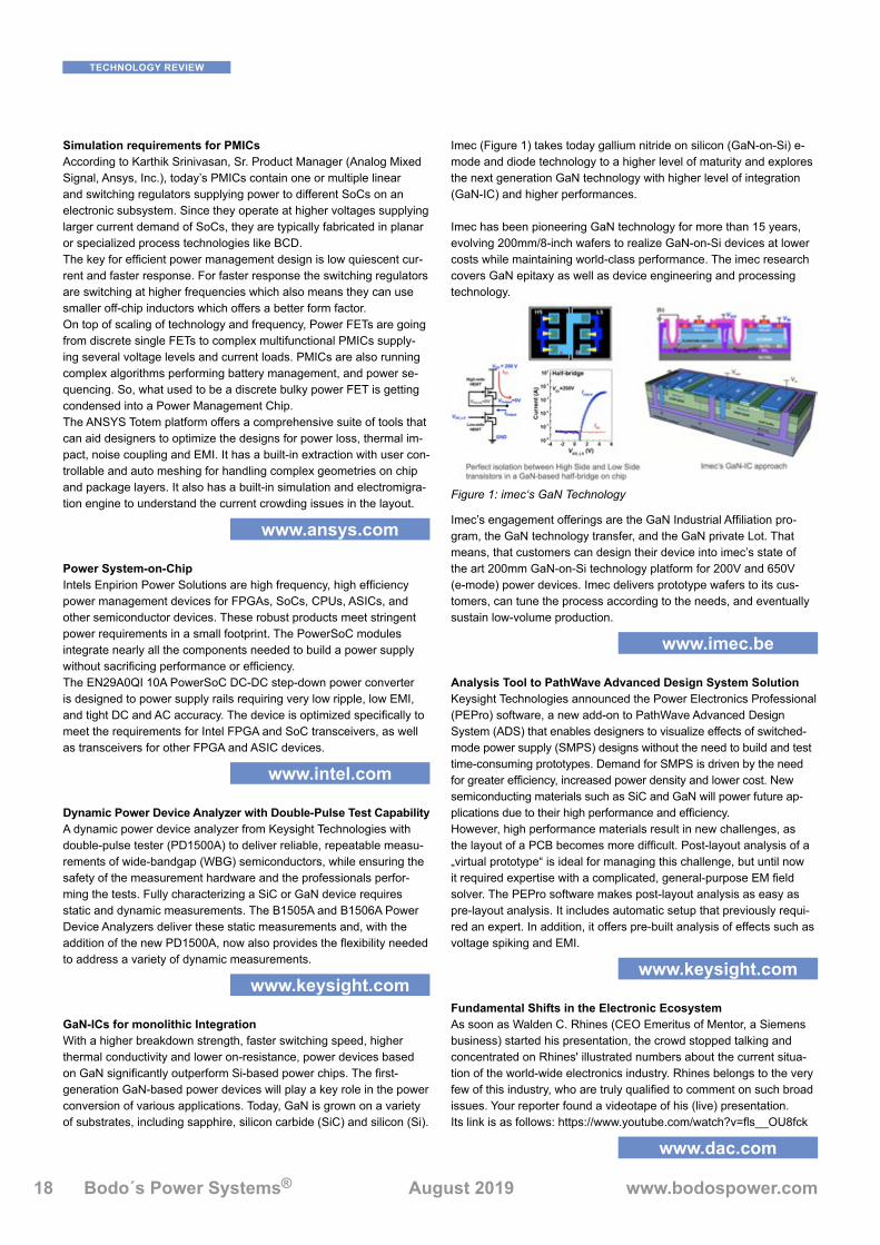
Imec (Figure 1) takes today gallium nitride on silicon (GaN-on-Si) e-mode and diode technology to a higher level of maturity and explores the next generation GaN technology with higher level of integration (GaN-IC) and higher performances.
Imec has been pioneering GaN technology for more than 15 years, evolving 200mm/8-inch wafers to realize GaN-on-Si devices at lower costs while maintaining world-class performance. The imec research covers GaN epitaxy as well as device engineering and processing technology.
Imec’s engagement offerings are the GaN Industrial Affiliation pro-gram, the GaN technology transfer, and the GaN private Lot. That means, that customers can design their device into imec’s state of the art 200mm GaN-on-Si technology platform for 200V and 650V (e-mode) power devices. Imec delivers prototype wafers to its cus-tomers, can tune the process according to the needs, and eventually sustain low-volume production.
www�imec�be
Analysis Tool to PathWave Advanced Design System SolutionKeysight Technologies announced the Power Electronics Professional (PEPro) software, a new add-on to PathWave Advanced Design System (ADS) that enables designers to visualize effects of switched-mode power supply (SMPS) designs without the need to build and test time-consuming prototypes. Demand for SMPS is driven by the need for greater efficiency, increased power density and lower cost. New semiconducting materials such as SiC and GaN will power future ap-plications due to their high performance and efficiency. However, high performance materials result in new challenges, as the layout of a PCB becomes more difficult. Post-layout analysis of a „virtual prototype“ is ideal for managing this challenge, but until now it required expertise with a complicated, general-purpose EM field solver. The PEPro software makes post-layout analysis as easy as pre-layout analysis. It includes automatic setup that previously requi-red an expert. In addition, it offers pre-built analysis of effects such as voltage spiking and EMI.
www�keysight�com
Fundamental Shifts in the Electronic EcosystemAs soon as Walden C. Rhines (CEO Emeritus of Mentor, a Siemens business) started his presentation, the crowd stopped talking and concentrated on Rhines' illustrated numbers about the current situa-tion of the world-wide electronics industry. Rhines belongs to the very few of this industry, who are truly qualified to comment on such broad issues. Your reporter found a videotape of his (live) presentation. Its link is as follows: https://www.youtube.com/watch?v=fls__OU8fck
www�dac�com
TECHNOLOGY REVIEW
Figure 1: imec‘s GaN Technology
electrical engineering software
THE SIMULATION SOFTWARE PREFERRED BY POWER ELECTRONICS ENGINEERS
MODELING DOMAINS ElectricalControlThermalMagneticMechanical
KEY FEATURES Fast simulation of complex systemsCode generationFrequency analysisAvailable as standalone program or Simulink blockset
Get a free test license
www.plexim.com/trial
cara
binb
ackh
aus.
com

Bodo´s Power Systems® August 2019 www.bodospower.com20
CONTENT
The current market situation and relevance of the problemPower semiconductor devices are one of the primary elements of electrical energy converters. The power electronics market features devices for various power ranges in disc, stud and module versions. Each of these designs has its own advantages and disadvantages. The widespread use of power semiconductor modules with insu-lated basement results from their easy mounting, optimal weight and dimensions.
Power modules with a base width of 60 mm (A2-type modules by the Proton-Electrotex designation) found wide application in the market. Modern serial modules with this design normally have insulation volt-age of 3-3.6 kV (AC, 50 Hz, 60 seconds).
However, modules with higher insulation voltages up to 7 kV (AC, 50 Hz, 60 seconds) become more demanded on the market too. Module designs currently offered on the market usually do not meet such requirements. The main reasons of their limited electric strength value are:1. Breakdown of insulation to the base, either due to insufficient width
of the ceramic insulator, or presence of irregularities of the insulat-ing gel (foreign inclusions or air bubbles), or unsuitable structure of the area responsible for isolating the base from elements with a potential.
2. Overlap between module elements having different potentials, either due to the presence of irregularities of the insulating gel (foreign inclusions or air bubbles), or due to the penetration of moisture, conductive dust or other ionic materials.
It is worth to note the importance of not only the high dielectric strength of the power module, but also its stability throughout the entire period of operation. The process of insulating properties degra-dation is inevitable during operation of the module. There are several factors affecting the rate of insulation strength degradation, including:- factors related to design and manufacturing technologies;- factors related to microclimate of the operating environment.
The first group of factors includes changes in polymerization chains of the insulating gel during operation due to thermal processes, and influence of partial discharges in the insulating elements.
The second group of factors includes presence of moisture and / or conductive dust in the power module.
One of the most important aspects affecting degradation of the electri-cal insulation strength is the occurrence of partial discharges.
Research subject� Approach to testing�A research program based on potential-free MD3-320-65-A2-type power modules was carried out to find design and manufacturing solutions ensuring increased insulation strength up to 7 kV (AC) throughout the entire module service life.
A complicated test procedure was used to measure the electrical strength of modules with the new solutions, including the following successive stages:• test for insulation strength at room temperature at 7 kV (AC, 50 Hz,
60 seconds);• test for effects of static dust according to standard GOST 20.57.406
(the dust was not removed after the tests);• tests for resistance to high humidity, GOST 20.57.406;• treatment of the modules with saline solution;• measurement of insulation strength.
As such, the tests were held in more demanding conditions than the normal operating environment required by the climatic version ac-cording to GOST 15150, ensuring reliability of the devices in actual operating conditions.
It was established that the suggested measures not only increased the insulation strength of a semiconductor module, but also effectively protected it from surface discharges bypassing though the conductive dust.
High Voltage Power Semiconductor Modules with
Enhanced Insulation PropertiesOne of the main parameters related to reliability and safety of power semiconductor
modules is the strength of electric insulation. Breakdown of the electric insulation not only causes failure of the module, but also damages the entire converter leading to high
financial losses. This article discusses the current situation on the market of bipolar power modules, the importance of improving their insulation properties and stability of insulating
properties throughout the entire life cycle. The Proton-Electrotex company has carried out research and development to find structural and technological solutions providing
increased insulation strength up to 7 kV (AC) throughout the entire service life.
By S. D. Antonov, A. A. Pisarev, I. Y.Savin, JSC Proton-Electrotex
COVER STORY

www.bodospower.com 21
Stability of the module insulation properties over time becomes espe-cially important as the range of blocking voltage grows wider. One of such properties is the amount of partial discharges. Partial discharge (PD) is a type of spark discharge of very low power occurring inside insulating materials in equipment of medium and high voltage classes [2].
A review of publications confirms the relevance of the problem of partial discharges in insulation of high-voltage equipment, but there are very few references related to bipolar semiconductor devices. Typically, isolation gets damaged by PD over many months or even years. In most cases, analysis of the reasons for such failures is not carried out and the topic remains without proper attention.
In other words, the lower the insulation voltage, the longer the defect does not manifest itself, and if the insulation voltage is below 3000 V, PD does not occur at all. The amount of power bipolar modules with a blocking voltage above 3.6 kV on the market is low, while the amount of failures due to other reasons is quite large, so failures associated with insulation degradation due to the occurrence of a PD are not predominant. However, the situation is different for power modules with blocking voltage up to 6.5 kV, since the time before the critical degradation of the insulating properties due to PD is dramatically re-duced. Therefore, when designing and manufacturing power modules with insulation voltages up to 7 kV, it is extremely important to monitor the characteristics of the partial discharge.
Currently there are many available methods to measure PD param-eters, including:• electric;• electromagnetic, or remote, microwave method;• acoustic;• chemical;• optical or optoelectronic;• thermal [1].
Proton-Electrotex is currently engaged in studies of PD properties in power modules with a base width of 60 mm and insulation voltage of up to 7 kV and identifying the mechanisms of their formation.
The workstation required to measure PD consists of:1. Measuring system Omicron MPD 600.2. High-voltage transformer.3. A coupling capacitor with minimal inductance.4. Calibrator Omicron CAL 542 1 - 100 pC.5. Sensor of partial discharge current.6. Systems to process the measurement results.
Figure 1: Functional diagram of the measurement system, where:U – high voltage power supply; Zmi – input impedance of the measur-ing system; CC – connecting cable; Ca – test object; Ck – coupling capacitor; CD – coupling device; MI – measuring device; Z – filter.
Bodo´s Power Systems® August 2019 www.bodospower.com22
CONTENT
To reduce the level of interference caused by external electric fields, the entire measuring system is placed in a Faraday cage. Measure-ments of all samples are made according to an electrical method meeting GOST R 55191 (IEC 60270: 2000). Functional diagram of the system is shown in Figure 1 [3].
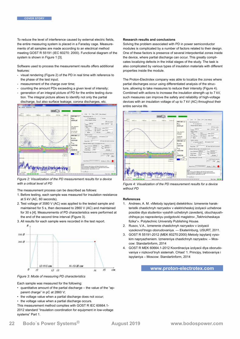
Software used to process the measurement results offers additional features:- visual rendering (Figure 2) of the PD in real time with reference to
the phase of the test input;- measurement of the charge over time;- counting the amount PDs exceeding a given level of intensity;- generation of an integral picture of PD for the entire testing dura-
tion. The integral picture allows to identify not only the partial discharge, but also surface leakage, corona discharges, etc.
The measurement process can be described as follows:1. Before testing, each sample was measured for insulation resistance
at 5 kV (AC, 60 seconds).2. Test voltage of 3580 V (AC) was applied to the tested sample and
maintained for 5 s, then decreased to 2860 V (AC) and maintained for 30 s [4]. Measurements of PD characteristics were performed at the end of the second time interval (Figure 3).
3. All results for each sample were recorded in the test report.
Each sample was measured for the following:• quantitative amount of the partial discharge – the value of the “ap-
parent charge” in pC at 2860 V;• the voltage value when a partial discharge does not occur;• the voltage value when a partial discharge occurs.This measurement method complies with GOST R IEC 60664.1-2012 standard “Insulation coordination for equipment in low-voltage systems” Part 1.
Research results and conclusionsSolving the problem associated with PD in power semiconductor modules is complicated by a number of factors related to their design. One of these factors is presence of several interpotential zones inside the device, where partial discharge can occur. This greatly compli-cates localizing defects in the initial stages of the study. The task is also complicated by various types of insulation materials with different properties inside the module.
The Proton-Electrotex company was able to localize the zones where partial discharges occur using differentiated analysis of the struc-ture, allowing to take measures to reduce their intensity (Figure 4). Combined with actions to increase the insulation strength up to 7 kV, such measures can improve the safety and reliability of high-voltage devices with an insulation voltage of up to 7 kV (AC) throughout their entire service life.
References1. Andreev, A. M. «Metody ispytanij dielektrikov. Izmerenie harak-
teristik chastichnyh razryadov v elektricheskoj izolyacii uchebnoe posobie dlya studentov vysshih uchebnyh zavedenij, obuchayush-chihsya po napravleniyu podgotovki magistrov „Tekhnicheskaya fizika“». Polytechnic University Publishing House.
2. Rusov, V.A., Izmerenie chastichnyh razryadov v izolyacii vysokovol’tnogo oborudovaniya. — Ekaterinburg, USURT, 2011.
3. GOST R 55191-2012 (MEK 60270:2000) Metody ispytanij vyso-kim napryazheniem. Izmereniya chastichnyh razryadov. – Mos-cow: Standartinform, 2014
4. GOST R MEK 60664.1-2012 Koordinaciya izolyacii dlya oborudo-vaniya v nizkovol’tnyh sistemah. CHast’ 1. Principy, trebovaniya i ispytaniya – Moscow: Standartinform, 2014
www�proton-electrotex�com
COVER STORY
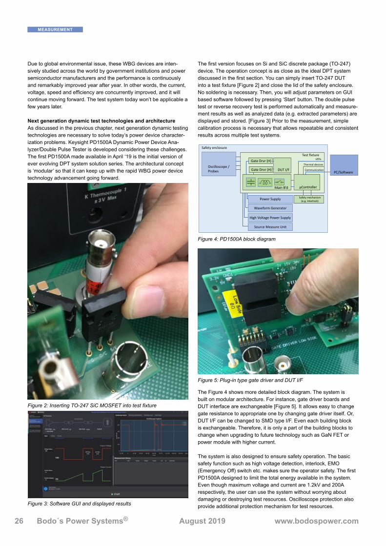
Figure 4: Visualization of the PD measurement results for a device without PD
Figure 2: Visualization of the PD measurement results for a device with a critical level of PD
Figure 3: Mode of measuring PD characteristics

Power Electronic Stacks
Four Key Factors for Your Success
210x297
www.semikron.com
SEMIKRON’s Power Electronic Stacks enable our customers to prosper in dynamic markets and meet any global challenge.
With more than 200,000 stacks in the field, SEMIKRON is the global market leader for power electronic stacks. Our comprehensive portfolio of power assemblies include the outstanding innovations we have achieved over a period of 40 years of successful stack design.
Our services are as multifaceted as our customers, highlighted by these four distinctive attributes: time to market, cost savings, global production and engineering experience. Our passion for power electronics and our commitment to high-performance design are the factors that make us your ultimate partner for value creation in the dynamic power electronics market.
Contact us: [email protected]/video/power-electronic-stacks

Bodo´s Power Systems® August 2019 www.bodospower.com24
CONTENT
Challenges of power device dynamic testingConventional challenges associated with power device dynamic test are high voltage and high current. Its high power naturally creates safety issue, measurement accuracy issues for both current and voltage. These are still and continuously the issues to be taken care of when building DPT system. For instance, the test system must be safe to people as the voltage used in the system is significantly higher than 42V which is already dangerous to human. The test resources should also be protected by covering multiple fail scenarios.
Today, the wall of the challenge for the dynamic test becomes even higher due to emerging Wide Band Gap (WBG) power devices such as SiC or GaN.
The supreme material properties of these devices make the switch-ing speed significantly faster than conventional power devices. Although the faster switching speed brings about a lot of benefit such as minimizing the overlap of current and voltage during the transition and making the peripheral component much small, it makes ‘high frequency measurement expertise’ a mandatory technology when building a dynamic test or DPT system. When the electrical signal in a system goes into high frequency range such as hundreds of MHz or GHz, the entire test system needs to be treated appropriately by considering the effect of parasitic inductance and capacitance. The sudden change of current or voltage, which are often represented as di/dt or dv/dt, couples with surrounding parasitic and causes unex-pected voltage or current to appear. They become the trigger of the ringing or reflection in a system that sometimes significantly distorts the measurement waveform [Figure 1]. It easily makes uncontrollable measurement data variability. Even though ‘accuracy’ is a simple word, you can’t get accurate measurement results unless you handle the high frequency signal appropriately. If you build multiple DPT sys-tems, it is common that you don’t get the same results across these systems.
Another critical test is temperature dependency measurement. Be-cause WBG devices are used in mission critical application such as automotive, ensuring the switching operation with raised temperature is very important. Hot plate is often used to control the temperature which sometimes heats up not only the DUT but also surrounding circuitry.
New Generation Power Semiconductor Dynamic Characterization Test System
What is the ideal Double Pulse Test (DPT) system?A question we often ask as a test & measurement equipment manufacturer is ‘What is the ideal power semiconductor dynamic test or double pulse test system?’. There are many responses depending on the challenges people encounter at their work. But one of the
typical answers for this question is something like this. Insert DUT to the system, push a button and then the system safely performs measurement with excellent accuracy.
It is simple to say. However, it is not so easy to make the ideal DPT system.
By Ryo Takeda, Solution Architect at Automotive and Energy Solutions, Keysight Technologies
MEASUREMENT
Figure 1: Example unexpected ringing seen at the double pulse test
Newly developed 7G IGBT & FWD
Improved solder material for higher reliability
HigherlifetimeatsameΔTj
Increased output power
Higher power cycling capability
Lower conducting and switching losses
2nd label with VCE(sat) and VFclassificationforeasierparalleling
FEATURES
PrimePACKTM 7G IGBT ModulesUpgrading to 1200 A in PP2, 1800 A in PP3 &
new PP3 with additional AC-terminal
PrimePACKTMisregisteredtrademarkofInfineonTechnologiesAG,Germany.
FWD
IGBT
Prr
Pf
Poff
Pon
Psat
www.americas.fujielectric.com/semiconductorswww.fujielectric-europe.com
Bodo´s Power Systems® August 2019 www.bodospower.com26
CONTENTMEASUREMENT
Due to global environmental issue, these WBG devices are inten-sively studied across the world by government institutions and power semiconductor manufacturers and the performance is continuously and remarkably improved year after year. In other words, the current, voltage, speed and efficiency are concurrently improved, and it will continue moving forward. The test system today won’t be applicable a few years later.
Next generation dynamic test technologies and architecture As discussed in the previous chapter, next generation dynamic testing technologies are necessary to solve today’s power device character-ization problems. Keysight PD1500A Dynamic Power Device Ana-lyzer/Double Pulse Tester is developed considering these challenges. The first PD1500A made available in April ‘19 is the initial version of ever evolving DPT system solution series. The architectural concept is ‘modular’ so that it can keep up with the rapid WBG power device technology advancement going forward.
The first version focuses on Si and SiC discrete package (TO-247) device. The operation concept is as close as the ideal DPT system discussed in the first section. You can simply insert TO-247 DUT into a test fixture [Figure 2] and close the lid of the safety enclosure. No soldering is necessary. Then, you will adjust parameters on GUI based software followed by pressing ‘Start’ button. The double pulse test or reverse recovery test is performed automatically and measure-ment results as well as analyzed data (e.g. extracted parameters) are displayed and stored. [Figure 3] Prior to the measurement, simple calibration process is necessary that allows repeatable and consistent results across multiple test systems.
The Figure 4 shows more detailed block diagram. The system is built on modular architecture. For instance, gate driver boards and DUT interface are exchangeable [Figure 5]. It allows easy to change gate resistance to appropriate one by changing gate driver itself. Or, DUT I/F can be changed to SMD type I/F. Even each building block is exchangeable. Therefore, it is only a part of the building blocks to change when upgrading to future technology such as GaN FET or power module with higher current.
The system is also designed to ensure safety operation. The basic safety function such as high voltage detection, interlock, EMO (Emergency Off) switch etc. makes sure the operator safety. The first PD1500A designed to limit the total energy available in the system. Even though maximum voltage and current are 1.2kV and 200A respectively, the user can use the system without worrying about damaging or destroying test resources. Oscilloscope protection also provide additional protection mechanism for test resources. Figure 3: Software GUI and displayed results
Figure 2: Inserting TO-247 SiC MOSFET into test fixture
S
Safety enclosure
PC/Software
Waveform Generator
High Voltage Power Supply
Source Measure Unit
Power Supply
LEDs
Thermal devices
Communication
Main B’d μController
Test fixture
DUT I/F
Gate Drvr (H)
Gate Drvr (H)
Safety mechanism(e.g. Interlock)
Oscilloscope / Probes
Figure 4: PD1500A block diagram
Figure 5: Plug-in type gate driver and DUT I/F

www.bodospower.com August 2019 Bodo´s Power Systems® 27
CONTENT
Temperature dependent measurement can be performed using a small heating device which heats up only the DUT locally. [Figure 6]
For accuracy, the high frequency measurement technologies that are accumulated at Keysight over 80 years are blended into high power measurement technologies. The fast slew rate of the waveform seen
with SiC MOSFET includes high frequency component. If the test circuit has a big stray inductance in the power loop, it acts as a kind of spring that generates ringing. Therefore, careful circuit board design is critical to minimize stray inductance in the power loop. All boards in the PD1500A are designed with the high frequency expertise. In addition to the calibration techniques applied to each measure-
ment components to produce repeatable and consistent measurement results across multiple test systems, some of high frequency measure-ment techniques are also applied. For instance, some of components are characterized through s-parameter measurement allowing further so-phisticated compensation.
SummaryKeysight PD1500A Dynamic Power Device Ana-lyzer/Double Pulse Tester is the next generation dynamic test platform for power semiconductor device. Various technologies solve challenges seen in the emerging WBG power device testing. The first version allows ‘plug-in DUT, push but-ton, and then get results and analysis safely and accurately’ operation. Its modular architecture enables further capability expansion as power device/electronics technology advancement with just small change in the system.
www�keysight�comFigure 6: Heating device that locally heats up DUT only
MEASUREMENT

Bodo´s Power Systems® August 2019 www.bodospower.com28
CONTENT
GaN power transistors have demonstrated high-frequency perfor-mance advantages over Si MOSFETS for several years and continue to make significant advancements, including improving ease of driving the power transistor. Enhancement mode GaN (E-HEMTs) are driven with positive voltage between the gate and source, similar to N-chan-nel Si MOSFETs, provide a familiar solution for driving the devices. GaN Systems has a solution to easily use the MOSFET controller 12 V output voltage to drive the GaN 7 V gate input without the need of an external or integrated additional driver.
This paper describes an innovative circuit that permits the safe and reliable use of standard controller MOSFET drivers with GaN devices. The paper also compares this approach with an alternative of combin-ing the driver and GaN power device into an integrated circuit.
GaN Technology Background and Drive Technology RequirementsGaN E-HEMTs eliminate the parasitic diode inherent in Si MOSFETs and have faster switching speeds and slew rates as well as higher operating temperatures that result from using a wide bandgap mate-rial. These and other improved characteristics allow GaN E-HEMTs to have reduced size and weight – a quarter that of a silicon design – and deliver lower system cost and increased efficiency as well.With their high-volume usage for Si MOSFETs, PFC and DC-DC controllers are widely available, and competition has made the pric-ing acceptable for even the most competitive Si MOSFET designs. However, as noted in the introduction, the output voltage of these devices is incompatible with the safe operating area (SOA) of e-mode GaN devices. Manufacturers of e-mode GaN devices have utilized a number of alternative drive schemes, all of which require alternatives to utilizing the standard Si MOSFET drivers.
An Integrated Circuit SolutionMore recently, some manufacturers addressed this situation by devel-oping a monolithic driving solution to allow use of Si MOSFET drivers. An integrated GaN/driver has the low drop out (LDO) regulator and driver integrated into a monolithic structure. The Si driving signal is regulated first, then drives the GaN using the GaN driver inside the chip. This approach actually has redundant drivers (external MOS-FET drivers and internal GaN drivers) that increase the cost and add complexity to the GaN devices.
WIDE BAND GAP
Using MOSFET Controllers to Drive GaN E-HEMTs
Before gallium nitride (GaN), the silicon (Si) MOSFET was the standard for power in adapter applications for decades. As a result, many of the existing controllers in the marketplace, including power factor correction (PFC) and DC-DC controllers, have
already integrated silicon drivers into the controller chip. These controllers have proven to be a cost-effective and complete solution. However, the poor figure-of-merit (FOM) of Si MOSFETs limit the controller’s capability of high switching frequency performance to
meet the requirement of high-power density vital to modern power systems.
By Yajie Qiu, Senior Power Electronics Applications Engineer, and Juncheng (Lucas) Lu, Applications Engineering Manager, GaN Systems
Table 1: A high-level comparison of key characteristics of Si MOSFET with separate controller driver, an integrated GaN/driver, and GaN power transistors with a separate controller driver.
Figure 1: The EZ Drive solution consists of GaN transistors, a standard MOSFET controller, and discrete components.
SiC-BASED POWER MODULES
Main benefits/ Standard and custom products featuring state-of-the-art components
/ Multi-sourced for more freedom of choice, less risk
/ Optional integrated capacitors for improved EMC performance
/ Easy assembly with pre-applied phase change material and Press-fit pins
/ Low-inductive packages to downsize external passive components
www.vincotech.com/sic
SiC-driven power from VincotechEngineers tasked to build better devices and applications want power modules that boost efficiency and performance. Yet they also need compact solutions that shrink the component footprint. Vincotech's SiC-based power modules square that circle for all applications. These modules not only deliver better switching performance; they also enable you to design smaller, lighter systems.
Vincotech has been empowering customers' ideas for 20+ years now. Our experience and SiC-based power modules paired with your designs – that sounds like a winning idea to us.
System Cost Reduction
VIN_ADs_SiC_BASED_MODULES_08_2019.indd 1 16.07.19 14:30

Bodo´s Power Systems® August 2019 www.bodospower.com30
CONTENT
An Easier Drive SolutionTo avoid this cost and take advantage of readily available MOSFET controllers, GaN Systems developed a drive solution to utilize the Si driver inside the controller to directly drive the GaN E-HEMT. This topology is referred to as an EZDriveTM circuit. Table 1 shows a summary of advantages and disad-vantages of the three driver designs.
A New GaN Design Tool: the EZDrive SolutionFigure 1 shows the diagram of the EZDrive solution for GaN E-HEMTs. It consists of a SI MOSFET controller with drivers integrated, a small number of external components (two
resistors, two capacitors, two sets of back-to-back Zener diodes and one general diode), and discrete GaN E-HEMTs.
The EZDrive solution has three operating modes which are similar to those of the conventional bootstrap half-bridge driver. As shown in Figure 2, in Mode 1, assum-ing the Vcc of the controller is 12 V, the high-side GaN is off and the low-side GaN is on. The driving voltage on the low-side GaN is clamped at 6 V by the Zener diode and the rest of the Vcc (6 V) is stored across the capacitor CUD2. In this mode, CBoot is charged.
In Mode 2, both the high-side and low-side GaN devices are off. The voltage stored in CUD2 is applied to the gate reversely, so the low-side GaN can be turned off quickly. In this mode, CBoot is still charged.
Finally, in Mode 3, the high-side GaN is on and the low-side GaN is off. Cboot is dis-charged providing the driving voltage to the high-side GaN.
In comparison with an integrated GaN/driver approach, the number of external compo-nents is similar with the EZDrive solution re-quiring 11 components (turn on/off gate resis-tors included), while the monolithic approach requires 10. However, the integrated GaN/driver suffers from high cost and complexity because of the redundant GaN driver and LDO regulator in the chip.
Since the driver and gate are connected inside the chip in the monolithic approach, the gate resistor is not adjustable. This makes the current, charging and discharging the gate, a fixed value that influences (fixes) the switching speed of the power device and limits the ability to address electromagnetic interference (EMI) and other gate drive aspects.
EZDrive Solution Verified in Different CircuitsTo verify the EZDrive performance, a half-bridge GaN daughter card was designed with EZDrive external components on it. This circuitry was applied to an LLC stage with Si MOSFETs replaced by the daughter card: Vcc=12 V, Vin = 400 V, Vout = 12 V and the LLC controller is the NCP13992. The driving voltage is 6.5 V/-5.8 V. Measurement results are shown in Figure 3.
The experimental results show that no over-shoot/undershoot occurs on the driving volt-age or VDS under all operating conditions. In addition, the operating temperature is quite low with maximum temperatures below 44°C (well below the safe maximum operating temperature).
The EZDrive solution has also been applied to a PFC stage. To do this, a daughter card was used with diode, GaN transistors, the EZDrive circuit, and a current sensing resis-tor. As a result of this effort, suggestions on layout to reduce the trace inductance as well as the mutual inductance have been developed.
Even EasierTo make designing with GaN power transis-tors even easier, evaluation kits with the
Figure 2: With operation modes similar to a conventional non-isolated bootstrap high side/low side driver, the EZDrive circuitry allows a wide (9~18 V) controller driving voltage range.
Figure 3: Verification measurements in the LLC stage demonstrate exceptional performance of the EZDrive circuit.
WIDE BAND GAP
Table 2: The summary of the advantages and disadvantages of the three drivers discussed in this article.
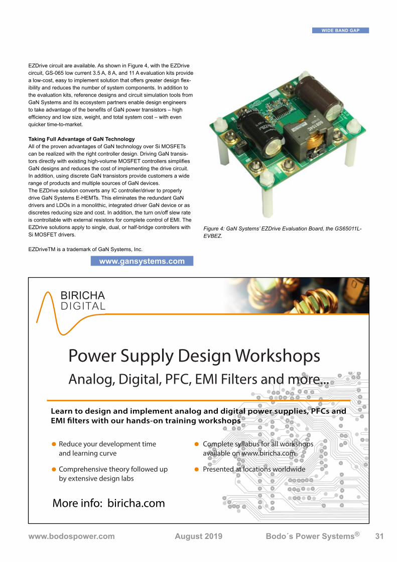
www.bodospower.com August 2019 Bodo´s Power Systems® 31
CONTENT
EZDrive circuit are available. As shown in Figure 4, with the EZDrive circuit, GS-065 low current 3.5 A, 8 A, and 11 A evaluation kits provide a low-cost, easy to implement solution that offers greater design flex-ibility and reduces the number of system components. In addition to the evaluation kits, reference designs and circuit simulation tools from GaN Systems and its ecosystem partners enable design engineers to take advantage of the benefits of GaN power transistors – high efficiency and low size, weight, and total system cost – with even quicker time-to-market.
Taking Full Advantage of GaN Technology All of the proven advantages of GaN technology over Si MOSFETs can be realized with the right controller design. Driving GaN transis-tors directly with existing high-volume MOSFET controllers simplifies GaN designs and reduces the cost of implementing the drive circuit. In addition, using discrete GaN transistors provide customers a wide range of products and multiple sources of GaN devices. The EZDrive solution converts any IC controller/driver to properly drive GaN Systems E-HEMTs. This eliminates the redundant GaN drivers and LDOs in a monolithic, integrated driver GaN device or as discretes reducing size and cost. In addition, the turn on/off slew rate is controllable with external resistors for complete control of EMI. The EZDrive solutions apply to single, dual, or half-bridge controllers with Si MOSFET drivers.
EZDriveTM is a trademark of GaN Systems, Inc.
www�gansystems�com
WIDE BAND GAP
Figure 4: GaN Systems’ EZDrive Evaluation Board, the GS65011L-EVBEZ.
Power Supply Design WorkshopsAnalog, Digital, PFC, EMI Filters and more...
Learn to design and implement analog and digital power supplies, PFCs andEMI �lters with our hands-on training workshops
More info: biricha.com
Reduce your development time and learning curve
Comprehensive theory followed upby extensive design labs
Complete syllabus for all workshops available on www.biricha.com
Presented at locations worldwide

Bodo´s Power Systems® August 2019 www.bodospower.com32
CONTENT
Easy Layout and Ultralow EMI Silent Switcher 2 with High EfficiencyLT8640S/LT8643S are 42 V, 6 A continuous/7 A peak current mono-lithic step-down regulators featuring the second-generation Silent Switcher® 2 architecture. Silent Switcher regulators suppress EMI emissions by splitting the high frequency hot loop in two—the split loops produce mutually cancelling magnetic fields. The second-generation Silent Switcher 2 integrates bypass ceramic capacitors inside the package. These capacitors lie within fast ac loops (VIN, BST, and INTVCC) and would otherwise require precise and repeat-able PCB layout to ensure EMI performance. Integrating them greatly simplifies PCB layout and manufacturing requirements. Even a low cost 2-layer board can now exhibit exceptional EMI performance.
In automotive applications, designers prefer power supplies with a 2 MHz or higher switching frequency to avoid the AM frequency band and minimize solution size. Unfortunately, high switching frequency usually equates to lower efficiency and higher power dissipation, forcing designers to trade-off small size and low EMI performance against efficiency. The LT8640S and LT8643S eliminate this trade-off: they are capable of high efficiency and low power dissipation even at high switching frequencies, thanks to controlled, fast clean switching edges.
Figure 1 shows an ultralow EMI and high efficiency LT8640S 12 V to 5 V/6 A design. The internal regulator is supplied from the 5 V output through BIAS pin for lower power dissipation. This design is pro-grammed at 2 MHz. The spread spectrum mode is enabled (SYNC/MODE = INTVCC) to allow the switching frequency to vary from 2 MHz to 2.4 MHz with 3 kHz triangular modulation.
Figure 2 compares EMI emissions for 2-layer and 4-layer boards for the design of Figure 1. Both boards meet the stringent automotive CISPR 25 Class 5 radiated EMI specification using only a ferrite bead at the input side. Figure 3 shows efficiency. With switching frequency as high as 2 MHz, the LT8640S 12 V input peak efficiency reaches 95% and 24 V input peak efficiency reaches 92%.
Multiple LT8643S devices can be paralleled to support more than 7 A (peak) output current. The LT8643S utilizes current-mode control with external compensation to allow balanced current sharing—critical in a parallel configuration. Current sharing is naturally implemented by connecting all the error amplifier output VC pins together. The CLKOUT and SYNC/MODE pins enable frequency synchronization without additional clock devices.
High Efficiency Step-Down Regulators with Ultralow EMI
EmissionsMonolithic step-down regulators combine a compact layout, high efficiency,
and ultralow EMI for automotive environments.
By Ying Cheng, Analog Devices, Inc.
PACKAGING
Figure 1: Ultralow EMI LT8640S 5 V/6 A step-down converter with Spread Spectrum mode.
Figure 2: CISPR 25 radiated EMI emission comparison between 2-layer and 4-layer boards using the Figure 1 design.
Figure 3: LT8640S 5 V/6 A output efficiency using Figure 1 design (fSW = 2 MHz).

www.bodospower.com August 2019 Bodo´s Power Systems® 33
CONTENTPACKAGING
Figure 4 shows an LT8640S design with 9 V output. Figure 5 shows thermal results at 5 A load. With 45 W output power and 1 MHz switching frequency, the LT8640S 4 mm × 4 mm LQFN package tem-perature rise is below 50°C, due to enhanced thermal technology.
Figure 6 shows the simplicity of a paralleled 12 V to 3.3 V/12 A LT8643S design. The top LT8643S is set to forced continuous mode by floating the SYNC/MODE pin; its CLKOUT signal drives the bottom LT8643S SYNC/MODE pin for synchronization. Figure 7 shows the efficiency of this design, while Figure 8 shows the 8 A step transient response.
ConclusionLT8640S and LT8643S are 6 A (7 A peak) synchronous, ultralow EMI monolithic switching regulators in a small, 4 mm × 4 mm LQFN pack-age. The patented Silent Switcher 2 architecture ensures remarkably low EMI emissions. The integrated hot-loop capacitors eliminate
PCB layout sensitivity, which saves design effort and solution cost. Synchronous design and fast switching edges improve efficiency at heavy loads, while the light load efficiency benefits from low quiescent current. A wide input range of 3.4 V to 42 V and low dropout allow the LT8640S and LT8643S to meet the demands of automotive cold crank or load dump scenarios.
Ying Cheng graduated from Missouri University of Science and Technology (formerly Univer-sity of Missouri-Rolla) with a Ph.D. in electrical engineering. She has been with Linear Technol-ogy (now part of Analog Devices) for six years as a senior applications engineer in the Power Products Group, working on dc-to-dc switching regulators and LDOs. She can be reached at [email protected].
www�analog�com
Figure 4: Design (fSW = 1 MHz, TA = 25°C).
Figure 5: LT8640S 24 V to 9 V/5 A thermal picture using Figure 4 design (fSW = 1 MHz, TA = 25°C).
Figure 6: Paralleling 3.3 V/12 A step-down converter using two LT8643S devices.
Figure 7: LT8643S 12 V to 3.3 V, 8 A step load transient using Figure 6 parallel design (fSW = 1 MHz).
Figure 8: LT8643S 12 V to 3.3 V/12 A efficiency using Figure 6 paral-lel design (fSW = 1 MHz)

Bodo´s Power Systems® August 2019 www.bodospower.com34
CONTENT
IntroductionIn case of high-current applications inverter-branches are in parallel to have feasible current carrying capability per phase. Compared to such interleaved converter solutions, the approach using coupled-inductors means no extra effort in terms of semiconductor, driver and current sensing. However, cost-intensive magnetics are minimized that far that it is also worth considering whether single-phase solutions should be substituted by the coupled approach. One example, a 48V-12V demonstrator is depicted in Figure 1.
In the subsequent chapters it is motivated why some of a high-perfor-mant soft magnetic material is chosen and how it is configured to take advantage of its properties. Furthermore, this article puts emphasis on the understanding and discussion of the behavior of our prototypes. Other designs with need for high power density at high currents (e.g. 400V-800V DC-converter) can be derived.
Soft-magnetic core material at high peak-to-peak flux excitation Nanocrystalline tape material is typically known for its high relative permeability such that it is often used in common-mode chokes. How-ever, today it is possible to manufacture such material at low relative permeability (µr= 150 …. 2000) without loosing the high performance
properties of the material, i.e. saturation flux density of 1,2 T and low losses [1][2]. Thus it is possible to basically store magnetic energy in the quasi-distributed airgap of tape-wound cores, featuring the big advantage of low proximity losses especially at high currents.
Discussing single-phase inductors, flux excitation is proportional to inductor current. In high-current applications coming with a signifi-cant amount of dc-current such tape-wound cores would result in an inductor operating at its saturation limit with a small ac-flux compo-nent, such that the thermal limit of the material is never reached. To really stress the material it would be beneficial to have a pure ac-flux at much higher peak-to-peak flux excitation and design the system to its thermal limitation. One mechanism to do this is using coupled inductors. For better understanding a two-phase inductor is depicted in Figure 2.
Compact High-Current Inductors Based on Coupled
Tape-Wound CoresCoupled-inductor configurations are proposed featuring high power densities based
on two mechanisms i) using some high-performance magnetic material and ii) dc-flux cancellation to minimize cross-section of the core.
Low Proximity Effect, HF EMI damping and mass manufacturability are regarded.
By Christian P. Dick and Patrick Deck, TH Köln - Cologne University of Applied Sciences
DC/DC CONVERTERS
Figure 1: Four-phase coupled-inductor Vh = 48V, i = 170A, Vvol = 24cm3 = 46.3 x 46.3 x 11.25mm3 overall outer cuboid inductor volume
Figure 2: Principle sketch of a two-phase coupled-inductor setup & self-wound core (Vh = 400V, i = 100A, arbitrary duty cycle, SiC con-verter operating at 90 kHz, inner leakage-flux cores might be replaced by powder cores)
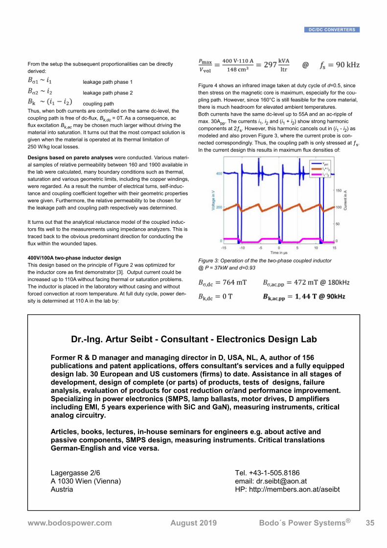
www.bodospower.com August 2019 Bodo´s Power Systems® 35
CONTENT
From the setup the subsequent proportionalities can be directly derived:
leakage path phase 1
leakage path phase 2
coupling path Thus, when both currents are controlled on the same dc-level, the coupling path is free of dc-flux, Bk,dc = 0T. As a consequence, ac flux excitation Bk,ac may be chosen much larger without driving the material into saturation. It turns out that the most compact solution is given when the material is operated at its thermal limitation of 250 W/kg local losses.
Designs based on pareto analyses were conducted. Various materi-al samples of relative permeability between 160 and 1900 available in the lab were calculated, many boundary conditions such as thermal, saturation and various geometric limits, including the copper windings, were regarded. As a result the number of electrical turns, self-induc-tance and coupling coefficient together with their geometric properties were given. Furthermore, the relative permeability to be chosen for the leakage path and coupling path respectively was determined.
It turns out that the analytical reluctance model of the coupled induc-tors fits well to the measurements using impedance analyzers. This is traced back to the obvious predominant direction for conducting the flux within the wounded tapes.
400V/100A two-phase inductor designThis design based on the principle of Figure 2 was optimized for the inductor core as first demonstrator [3]. Output current could be increased up to 110A without facing thermal or saturation problems. The inductor is placed in the laboratory without casing and without forced convection at room temperature. At full duty cycle, power den-sity is determined at 110 A in the lab by:
Figure 4 shows an infrared image taken at duty cycle of d=0.5, since then stress on the magnetic core is maximum, especially for the cou-pling path. However, since 160°C is still feasible for the core material, there is much headroom for elevated ambient temperatures. Both currents have the same dc-level up to 55A and an ac-ripple of max. 30App. The currents i1, i2 and (i1 + i2) show strong harmonic components at 2ƒs. However, this harmonic cancels out in (i1 - i2) as modeled and also proven Figure 3, where the current probe is con-nected correspondingly. Thus, the coupling path is only stressed at ƒs. In the current design this results in maximum flux densities of:
DC/DC CONVERTERS
Figure 3: Operation of the the two-phase coupled inductor @ P = 37kW and d=0.93
Dr�-Ing� Artur Seibt - Consultant - Electronics Design Lab
Former R & D manager and managing director in D, USA, NL, A, author of 156 publications and patent applications, offers consultant's services and a fully equipped design lab� 30 European and US customers (firms) to date� Assistance in all stages of development, design of complete (or parts) of products, tests of designs, failure analysis, evaluation of products for cost reduction or/and performance improvement�Specializing in power electronics (SMPS, lamp ballasts, motor drives, D amplifiers including EMI, 5 years experience with SiC and GaN), measuring instruments, critical analog circuitry�
Articles, books, lectures, in-house seminars for engineers e�g� about active and passive components, SMPS design, measuring instruments� Critical translations German-English and vice versa�
Lagergasse 2/6 Tel. +43-1-505.8186A 1030 Wien (Vienna) email: [email protected] HP: http://members.aon.at/aseibt

Bodo´s Power Systems® August 2019 www.bodospower.com36
CONTENT
Latter number is considered enormous in conjunction with the steady state thermal image. The overall converter using SiC MOSFETs sho-wed an efficiency of 98,7% ± 0,98%, about 100 W losses are traced back to the inductor.
There is room for improvements, pareto analysis shows even higher compactness when relative permeability could even be reduced for the leakage path (125 instead of 160) and the coupling path (780 instead of 900). Such material can be produced, optimization potential is given.
48V/170A four-phase inductor designA second GaN-based demonstrator as depicted in Figure 1 is designed based on pareto analysis. All phases operate 90° phase-shifted at 100kHz, a current controller shares the load equally.
Many of the indicated effects in the two-phase system are valid as well in this four-phase configuration [4]. The system is capable of driving the full duty cycle, however, in the application of mild hybrid vehicles with 48V-12V DC-DC converters 14V is considered as maxi-mum output voltage. A high power density is demonstrated at high flux excitation:
Overall efficiency of the converter is up to 96,5%, losses being traced back to the inductor are below 20 W. Under full load conditions the 24 cm3 inductor (outer cuboid volume) is thermally feasible, see also Figure 1. The maximum temperature of about 100°C, measured in the lab without casing at room temperature without forced convection or cooling plate, is basically too low. In a future design maximum local losses should be limited to higher numbers than 250W/kg (current design). Again, choosing material with slightly adapted relative permeability is basically another optimization potential.
Conclusions and outlookTwo very compact coupled inductors were presented for high-current applications. The demonstrated power densities are higher than all solutions known to the authors as state of the art (partly multiple).• Demonstrated solutions are thermally feasible: There is some
headroom for further shrinking• Efficient inductor: Low proximity losses due to quasi distributed
airgap in high-current inductor• Mass producibility: Single copper-turns can be welded automati-
cally in lead frame• HF-EMI (both DM and CM) is dampened due to eddy currents in
the tape material (not quantified yet)• Cost reduction potential: Major contributor for gaining such high
power densities is using some high performant low-µ nanocrystal-line tape material in the coupling path at extreme flux excitation. The inner leakage path with elevated dc-flux offset may be realized by powder cores
• Many other designs with need for power density at high currents (e.g. 400V-800V DC onboard-charger) can be derived, tool is available
References [1] C. Polak - Vacuumschmelze GmbH & Co.KG: private communica-
tion and “Nanocrystalline Materials for High Frequency Applica-tions”, Invited Talk, 4th International Conference on Superconduc-tivity and Magnetism- ICSM2014, 27.4.-2.5.2014, Antalia, Turkey, 2014
[2] Magnetec GmbH: Datasheet information “Nanoperm® LM Cores for DC biased applications” (www.magnetec.de, Download 29.05.2019)
[3] Patrick Deck, Christian P. Dick: High power density dc/dc-con-verter using coupled inductors. In EPE ECCE Europe 2017, Sept. 2017, ISBN: 9789075815276
[4] Patrick Deck, Christian P. Dick: Ultra compact 2kW 12V-48V converter using a 4-phase coupled inductor; PCIM Europe 2018; International Exhibition and Conference for Power Electronics, Intelligent Motion, Renewable Energy and Energy Management; June 2018 Nuremberg Germany, ISBN: 978-3-8007-4646-0
www�th-koeln�de/lea
DC/DC CONVERTERS
Figure 4: Thermal image at critical duty cycle of d = 0.5
Figure 5: Operation of the 48V/170A four-phase coupled inductor here @ d=0.17 (e.g. 53V ↔ 9V)

Automotive Home Appliances Industrial Power Transmission Renewables Railway
High power applications in the field of renewable energy and industry require reliable, scalable and standardized power modules. Providing optimized solutions, Mitsubishi Electric is expanding the line-up of the standardized LV100 package to 1200V and 1700V blocking voltages by utilization of proven SLC package and 7th Gen. IGBT/Diode chips technology.
Scan and learn more about this product series on YouTube.
Power Devices from Mitsubishi Electric.
More Information: [email protected]
One of our key products:Trust.
LV100 optimized for renewable and industrial applications
7th Generation IGBT Module LV100 Package– New standardized package for high power applications– Highest power density IC up to 1400A– Latest 7th Gen. IGBT and Diode chips– Thermal cycle failure free SLC package technology– Easy paralleling providing scalable solutions– Advanced layout provides low stray inductance and symmetrical current sharing
ME_SC_PowerDevices_Renewables_Windenergy_AZ_A4_QR_E_RZ.indd 1 15.07.19 09:24

Bodo´s Power Systems® August 2019 www.bodospower.com38
CONTENT
To serve this emerging market, Bel Power Solutions has developed the eMobility family, which targets the electrification needs of road and air transport systems. The product family is focused on the develop-ment and improvement of EV power components and, like other Bel initiatives, the eMobility products are developed globally, at design centers in Slovakia, Switzerland, China and the US. The product family is able to address the emerging needs of electric and hybrid electric vehicles of all sizes and power requirements.
Globally, there is a strong focus on replacing buses and trucks with EV alternatives, as well as all types of passenger vehicles, from sports cars to people carriers. DC/DC converters can now meet the needs of all road-going, off-road and workplace transportation, includ-ing ground-support and construction vehicles. Even rollercoaster operators are switching on to DC/DC converters.
The convincing advantagesWhen discussing the advantages of DC/DC converters in contrast to traditional rotating alternators, it is apparent that they are powered directly from high-voltage battery packs instead of a generator that is mechanically coupled to the engine. The advantage here is higher efficiency; there are no moving parts, such as belts and pulleys that can also represent a point of failure. DC/DC converters are also much reliable and efficient in the regulation of their output voltage.
To support this emerging trend, Bel has committed to the design, specification and support of DC/DC converters that can maximize business value. By leveraging the latest advances in CAN bus com-munication and other technologies, they deliver high performance with the option for customization for specific applications. Prices are com-petitive, lead times are short and are offered with excellent customer service and technical advice.
Examples of Bel’s DC/DC technology includes the 350/700 DNC40-12/24-8G (liquid-cooled) and the 350/700 DNC40-12/24-CG (con-vection-cooled) ranges of down-converters that deliver up to 4kW of power with liquid cooling, or 3.3kW with convection cooling. There are models available in these series that can handle input voltages from 240 to 850 VDC. With high efficiency of typically up to 93%, the products in these ranges deliver robust and highly dependable perfor-mance with low output voltage noise, and excellent dynamic response to changes in load or input.
The output voltage is nominally either 14.4 or 28V but can be adjusted over the CAN bus serial interface. Input and output are fully, galvani-cally, isolated. Communication and control are optimized via CAN bus according to SAE J1939.
As mentioned, cooling can be achieved either by liquid or convection. The operating temperature of liquid-cooled models ranges between -40° and +85°C, while convection-cooled models offer -40° to +45°C. Each converter in the 350/700 DNC40-12/24 Series is equipped with
DC/DC CONVERTERS
How DC/DC Converters are Making Inroads Into Vehicles
and Transport SystemsAutomotive manufacturers are now seriously considering moving away from the
traditional rotating alternator and migrating to DC/DC converters for road transport applications. Thanks to the efficiency, reliability, compactness and practicability of modern DC/DC converters based on the latest semiconductor technology, DC/DC
converters can now displace alternators for powering auxiliary components and battery charging. To meet this growing demand, power solution companies are now offering a line of products in a wide variety of standard configurations, with custom modifications also
available.
By Frank Vondenhoff, Business Development Manager, Bel Power Solutions
Figure 1: The Bel Power Solutions 350DNC40 is a 4 kW DC/DC Converter that creates DC voltages in hybrid and electric vehicles suitable to power low voltage accessories. Features include very high efficiency, high reliability, low output voltage noise and excellent dynamic response to load/input changes.
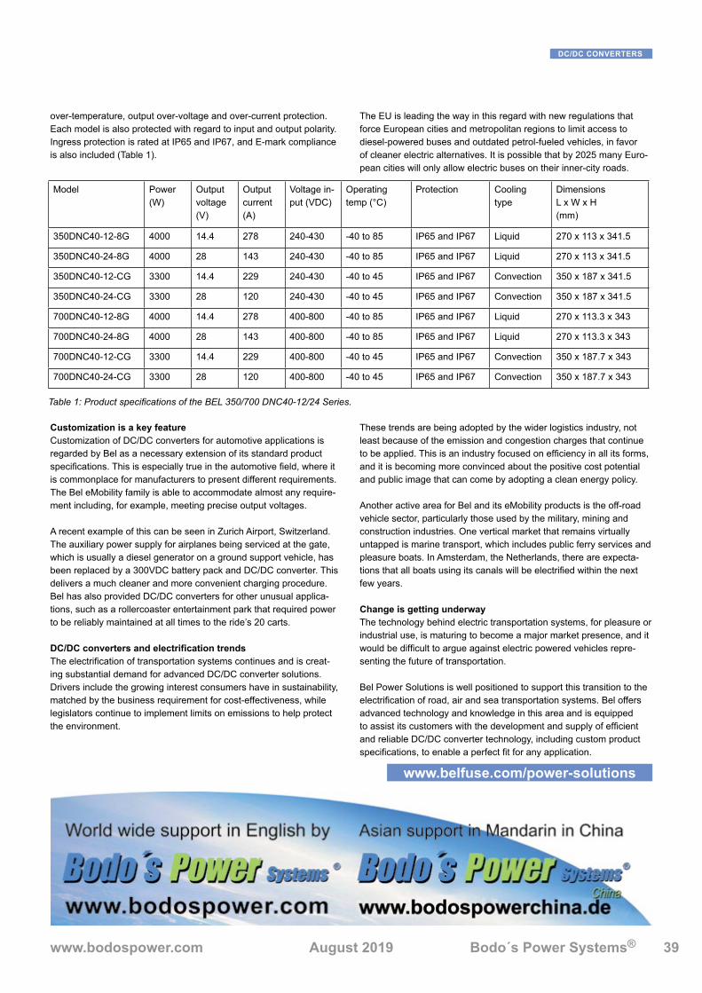
www.bodospower.com August 2019 Bodo´s Power Systems® 39
CONTENT
over-temperature, output over-voltage and over-current protection. Each model is also protected with regard to input and output polarity. Ingress protection is rated at IP65 and IP67, and E-mark compliance is also included (Table 1).
Customization is a key featureCustomization of DC/DC converters for automotive applications is regarded by Bel as a necessary extension of its standard product specifications. This is especially true in the automotive field, where it is commonplace for manufacturers to present different requirements. The Bel eMobility family is able to accommodate almost any require-ment including, for example, meeting precise output voltages.
A recent example of this can be seen in Zurich Airport, Switzerland. The auxiliary power supply for airplanes being serviced at the gate, which is usually a diesel generator on a ground support vehicle, has been replaced by a 300VDC battery pack and DC/DC converter. This delivers a much cleaner and more convenient charging procedure. Bel has also provided DC/DC converters for other unusual applica-tions, such as a rollercoaster entertainment park that required power to be reliably maintained at all times to the ride’s 20 carts.
DC/DC converters and electrification trendsThe electrification of transportation systems continues and is creat-ing substantial demand for advanced DC/DC converter solutions. Drivers include the growing interest consumers have in sustainability, matched by the business requirement for cost-effectiveness, while legislators continue to implement limits on emissions to help protect the environment.
The EU is leading the way in this regard with new regulations that force European cities and metropolitan regions to limit access to diesel-powered buses and outdated petrol-fueled vehicles, in favor of cleaner electric alternatives. It is possible that by 2025 many Euro-pean cities will only allow electric buses on their inner-city roads.
These trends are being adopted by the wider logistics industry, not least because of the emission and congestion charges that continue to be applied. This is an industry focused on efficiency in all its forms, and it is becoming more convinced about the positive cost potential and public image that can come by adopting a clean energy policy.
Another active area for Bel and its eMobility products is the off-road vehicle sector, particularly those used by the military, mining and construction industries. One vertical market that remains virtually untapped is marine transport, which includes public ferry services and pleasure boats. In Amsterdam, the Netherlands, there are expecta-tions that all boats using its canals will be electrified within the next few years.
Change is getting underwayThe technology behind electric transportation systems, for pleasure or industrial use, is maturing to become a major market presence, and it would be difficult to argue against electric powered vehicles repre-senting the future of transportation.
Bel Power Solutions is well positioned to support this transition to the electrification of road, air and sea transportation systems. Bel offers advanced technology and knowledge in this area and is equipped to assist its customers with the development and supply of efficient and reliable DC/DC converter technology, including custom product specifications, to enable a perfect fit for any application.
www�belfuse�com/power-solutions
DC/DC CONVERTERS
Table 1: Product specifications of the BEL 350/700 DNC40-12/24 Series.
Model Power (W)
Output voltage (V)
Output current (A)
Voltage in-put (VDC)
Operating temp (°C)
Protection Cooling type
Dimensions L x W x H (mm)
350DNC40-12-8G 4000 14.4 278 240-430 -40 to 85 IP65 and IP67 Liquid 270 x 113 x 341.5
350DNC40-24-8G 4000 28 143 240-430 -40 to 85 IP65 and IP67 Liquid 270 x 113 x 341.5
350DNC40-12-CG 3300 14.4 229 240-430 -40 to 45 IP65 and IP67 Convection 350 x 187 x 341.5
350DNC40-24-CG 3300 28 120 240-430 -40 to 45 IP65 and IP67 Convection 350 x 187 x 341.5
700DNC40-12-8G 4000 14.4 278 400-800 -40 to 85 IP65 and IP67 Liquid 270 x 113.3 x 343
700DNC40-24-8G 4000 28 143 400-800 -40 to 85 IP65 and IP67 Liquid 270 x 113.3 x 343
700DNC40-12-CG 3300 14.4 229 400-800 -40 to 45 IP65 and IP67 Convection 350 x 187.7 x 343
700DNC40-24-CG 3300 28 120 400-800 -40 to 45 IP65 and IP67 Convection 350 x 187.7 x 343

Bodo´s Power Systems® August 2019 www.bodospower.com40
CONTENTNEW PRODUCTS
UnitedSiC has further expanded its UF3C FAST series product offer-ing by introducing an additional 1200V high-performance SiC FET de-vice in a TO-247-4L 4-leaded Kelvin Sense discrete package option. The UF3C120150K4S offers a typical on-resistance (RDS(on)) of 150 mΩ, bringing the total number of 4-leaded FAST Series devices up to six and extending the on-resistance range of the entire series from 30
mΩ all the way up to 150 mΩ. With a maximum operating temperature of 175°C, the UF3C120150K4S offers excellent reverse recovery, low gate charge and low intrinsic capacitance. The ESD protected, HBM class 2 TO-247-4L package offers faster switching and much cleaner gate waveforms compared to a standard 3-leaded TO-247. The 4-pin Kelvin package avoids gate ringing and false triggering which would normally require switching speeds to be limited to manage the large common source inductance of 3-leaded packages. This device is ideal for EV charging, photovoltaic inverters, switch mode power supplies, power factor correction (PFC) modules, motor drives and in-duction heating. UnitedSiC’s UF3C FAST SiC series, which now totals 13 devices, is available in TO-247-3L and TO-247-4L packages with 1200V and 650V options. The range offers very fast switching, high-power devices in a package capable of high-power dissipation based on its efficient “cascode” configuration. The 4-terminal Kelvin package offers easy screw or clamp mounting with very low junction-to-case thermal resistance, taking advantage of the high junction temperature capabilities of SiC.
www�unitedsic�com
SiC FET in a 4-Lead Kelvin Device
ROHM recently announced the availability of a power supply moni-toring IC, the BD39040MUF-C, with BIST (Built-In Self Test) that supports functional safety. This IC is ideal for automotive application power supply systems requiring fail-safe measures such as electric power steering as well as sensors and cameras for autonomous driving and ADAS. The BD39040MUF-C is a power monitoring IC that provides monitoring functions required for functional safety in the power supply systems of ADAS sensor modules. In addition to volt-age monitoring functions (Power Good, reset) and a watchdog timer for monitoring the ECU essential for functional safety, ROHM’s power supply monitoring IC is the first in the industry to introduce a self-diagnostic function. By utilizing original technology, this IC makes it possible to detect potential failure of the power supply IC itself without affecting existing systems. The integration of these functions into a compact 3mm square package makes it ideal for ADAS applications demanding high miniaturization.
www�rohm�com/eu
Power Supply Monitoring IC with Built-In Self-Diagnostic
RECOM’s addition to its low power AC/DC portfolio includes durable modules with full certifications for household and ITE applica-tions. Their 4kV isolation, 150% peak power capability and -40°C to +90°C operating temperature make them suitable for a wide range of operating conditions. The RAC04-K/277 series delivers an uncompromising 4 watts of continuous output power in harsh environments worldwide with up to 5000m altitude. They also feature a peak load capability of up to 150% for dynamic power demands. These modules deliver full load output power from -40°C to 75°C across the entire input range of 80VAC to 305VAC and are certified for operation with power derating
up to 90°C air ambient. With international safety certifications for industrial, domestic, ITE, and household applications, these are some of the most versatile power modules
on the market. This series of fully encapsu-lated AC/DC modules is a complete solution without the need for external components, which supports Ecodesign Lot 6 standby mode operation for worldwide applications in automation, industry 4.0, IoT, household, and home automation. Due to their reinforced class II installation rating for floating outputs and their wide margin to class B emissions compliance without external components, these are the easiest to use modular power solutions in the industry. Samples and OEM pricing are available from all authorized distributors or directly from RECOM. www�recom-power�com
AC/DC Modules for IoT and Industrial Automation

Accelerating Innovation
November 12–15, 2019
World’s Leading Trade Fair for Electronics Development and ProductionNovember 12–15, 2019, Messe Münchenproductronica.com
Connecting Global Competence
co-located event

Bodo´s Power Systems® August 2019 www.bodospower.com42
CONTENTNEW PRODUCTS
KEMET expanded the temperature capability of T598 devices, a first-to-market Tantalum Polymer Surface Mount Capacitor. These devices uniquely address the stringent requirements and new challenges presented by megatrend applications in automotive Ad-vanced Driver Assistance Systems (ADAS), autonomous driving and in digitalization uses such as supercomputing, mobility services, connectivity and infotainment. T598 automotive grade polymer electrolytic devices combine multiple high-performance characteristics including high capacitance / voltage (CV) ratings, single digit equivalent series resistance (ESR), class-leading ripple performance, and ultra-extended life to truly enable the development and deployment of exciting and revolutionary technologies.
KEMET T598 devices provide component solutions for ADAS, autonomous driving and digitalizationAEC-200 qualified T598 devices have excel-lent volumetric efficiency, which in tandem with high capacitance values now up to 470µF, voltage offerings of 2.5VDC – 50VDC
and new single digit ESR, means single components can be used where current solutions dictate that multiple devices must be used. Therefore, KEMET’s devices can help designers achieve both vital board real estate and cost savings. Robust and stable performance to 2000 hours at temperatures to 125°C - equating to an ultra-extended mission profile of around 15 years - aligns with the requirements for vehicle applica-tions ranging from ADAS features such as blind spot detection, adaptive cruise control and emergency brake assist, to safety systems including airbag occupant detection and alarm systems and electronic stability control.
www�kemet�com
Tantalum Polymer Capacitors
Navitas Semiconductor announced that GaNFast™ power ICs enable Fulham’s HotSpot Plus™ FHSAC1-UNV-70S, a high-reliability 70W normal + 7W emergency back-up lighting power system. GaN power IC technology powers both the main LED luminaire and charges the on-board LiFePO4 battery to provide everyday lighting and up to 90 minutes of emergency runtime. Gal-lium Nitride (GaN) power integrated circuits have up to 20x the performance of old silicon chips. By operating at high frequency and simultaneously increasing efficiency, GaNFast power ICs reduce the size, weight and cost of components such as transform-ers, heatsinks, and printed-circuit boards. The GaNFast 3x-4x increase in power
density enables a 2-to-1 reduction in LED hardware and leaves room to expand battery size to 14.4 Whr and increase emergency lighting by 75% for increased safety when compared to similar sized 4W emergency-only systems. The Hotspot Plus 70S was developed for OEMs looking for a highly reliable, universal LED driver that would meet state and city safety requirements in a single, compact, all-in-one Emergency / LED driver. Ideal for luminaire manufacturers where LED driver space is limited, the HotSpot Plus 70S has the smallest form-factor available (424 x 30 x 25 mm) and features universal 120-277VAC input with a maximum of 70W (program-
mable constant current output of 350mA – 2400mA /11-55VDC) normal and up to 7W emergency output, which means customers can stock a single LED driver for a broad range of fixtures.
www�navitassemi�com
GaN Power ICs for LED Lighting
Micrometals is proud to introduce its Optil-loy Alloy Powder materials. The offering includes three formulations, OD, OC and OE, which are specifically formulated to deliver optimal core performance for demanding applications. All Optilloy materials are unique formulations of iron, silicon, aluminum and nickel and are available in toroid shapes with permeabilities from 14µ to 125µ.The original Optilloy material, OP, was for-mulated to provide low core losses and high saturation.The OD material, Optimized DC Bias, is optimized to provide superior DC Bias while maintaining low losses and be very cost competitive. OD material is ideal for applica-tions that require high saturation magnetiza-
tion that may have traditionally used high flux materials like FluxSan or Hi-Flux. Optimized DC Bias cores are available in toroids from 3.5mm to 196mm with permeabilities from 14µ to 90µ.The OC material, Optimized Core Loss, is optimized for provide very low losses while maintaining good DC bias at an economical price. OC material is economical alternative for applications that may have tradition-ally used Sendust or MPP type materials. Optimized Core Loss cores are available in toroids from 3.5mm to 196mm with perme-abilities from 14µ to 125µ.OE, Optimized Economy, has been specifi-cally formulated to provide an economical alternative to applications that require moder-
ate, but consistent magnetic performance. Optimized Economy cores are available in toroids from 3.5mm to 196mm with perme-abilities from 14µ to 90µ. www�micrometals�com
Alloy Powder Materials Optimize Inductor Performance

www.lps2019.com
LpS2019
Organized by Co-hosted with
LpS is Europe’s leading international lighting technologies conference and exhibition for
DESIGN, TESTING and PRODUCTION of lighting systems, controls and equipment.
Don't miss out on hearing from the greatest minds in lighting technology.
Speaker highlights 2019
The lighting event for technologies of tomorrow
9th International LpS | September 24th - 26th 2019 | Bregenz | Austria
Dietmar ZembrotTrilux, Germany
Dr. Andreas WojtysiakOSRAM, Germany
Makoto OgawaraNichia, Japan
Dr. Dee DenteneerZhaga, The Netherlands
Fabian GerschwilerRegent, Switzerland
DALI Summit 2019

www.bodospower.com August 2019 Bodo´s Power Systems® 45
CONTENTNEW PRODUCTS
Designers can now improve motor efficiency and reduce vibration us-ing the MAX40056 bi-directional current sense amplifier with patented pulse-width modulation (PWM) rejection from Maxim Integrated. MAX40056 rejects PWM slew rates of greater than 500V/µs and
settles within 500ns to provide 0.3 percent accurate, full-scale winding current measurement. The patented PWM rejection scheme achieves 4 times faster settling time than competitive offerings, allowing motor control designers to increase drive frequency or decrease minimum duty cycle without sacrificing measurement accuracy. Higher PWM frequency smoothes out the current flow and reduces torque ripple, resulting in more efficient motor operation. Accurate winding current measurement at low duty cycle helps reduce or virtually eliminate vibration when the motor is running at a slow speed. MAX40056 has a wide common mode voltage range of -0.1V to +65V and a protec-tion range of -5V to 70V to ensure the inductive kickback does not damage the IC. With bi-directional sensing capability, it is ideal for DC motor control, base station, datacenter, battery stack and many other applications which require precise current measurements in noisy environments.
www�maximintegrated�com
Bi-Directional Current Sense Amplifier with PWM Rejection
Ideal Power has introduced the latest Xelite XT-GR series of dim-mable LED drivers for smart-building applications. Ready to connect a motion sensor for fast and reliable proximity activation, the XT-GR drivers are ideal for use in interior or exterior lighting situations such as warehouses, passageways, schools, parking lots, supermarkets,
and office buildings. The sensor can be connected to the driver’s AC or DC side, giving extra flexibility and convenience. The series covers power ratings from 12W to 30W and all models come in a compact 288mm x 30mm x 28mm form factor. Power factor as high as 0.9 and maximum efficiency up to 86% ensure excellent energy-saving credentials. Ensuring safety and longevity, all models integrate over-voltage and short-circuit protection with automatic recovery for minimal disruption. A selection of output-voltage ranges is offered including 24-40V, 27-40V, and 36-50V for use with lights of various sizes and LED-string lengths. The XT-GR motion-ready series joins the extensive range of Xelite drivers available in the UK from Ideal Power. The complete portfolio supports major dimming techniques including DALI, 1-10V, and ZigBee®, and is manufactured in Xelite’s ISO 9001-accredited factory in Guangdong, China. All models are certified in accordance with international standards including CE.
www�idealpower�co�uk
Dimmable Drivers for Fast-Acting LED Lighting
ZH Wielain Electronic (Hangzhou Co.,LTD)Hangzhou, China
E-mail: [email protected]://www.zhwielain.com
+86 571 28898137
Power Module Product and Packaging & Interconnect Power Module Products Press Fit Solderless Connection Solution
Connect teminals
DBC connectors
IGBT body

Bodo´s Power Systems® August 2019 www.bodospower.com46
CONTENTNEW PRODUCTS
Infineon Technologies will launch a mono-lithically integrated linear Hall sensor which was developed entirely according to the safety standard ISO26262 for automo-tive applications: With just one device, the XENSIV™ TLE4999I3 enables the development of fault-tolerant systems that have to meet the highest level of func-tional safety (ASIL D). These include, for example, electric steering systems, electric throttle control systems, and pedal applica-tions. ISO26262 requires a system to keep functioning even if a single fault occurs – for example if one of the components fails.
Thus, the TLE4999I3 allows uninterrupted operation at system level. The device consists of a monolithic design with two independent Hall elements. Their signal paths are separate from each other. Internal control mechanisms carry out a plausibility check of the sensor data already within the chip. Furthermore, the new linear Hall sensor also provides extensive status information to the system.In addition to functional safety, the TLE4999I3 also offers very high magnetic sensitivity with an error tolerance of less than 2 percent. The offset error drift, also an important parameter for magnetic sensors to determine the absolute position in a magnetic field, is maximum 100µT. This is just half that of comparable products. The values of these parameters apply across the entire temperature range and lifetime of the product. www.infineon.com
Monolithically Integrated Linear Hall Sensor
Bel Power Solutions announced their Melcher™ LR Series 300 W AC-DC cassette converters, which are designed for railway and rugged industrial applications. These LR Series products are an enhancement to Bel Power Solutions’ existing broad range of 19”
cassette power supplies, ideal for when robustness and high reliability are required. The products feature a universal AC input voltage range including active inrush current limitation and power factor correction (PFC). Two highly efficient, isolated outputs of 12 or 15 V up to 300 W offer maximized
flexibility in system architecture and make them uniquely suited for various railway applications, such as signaling, rugged communica-tion, heavy duty industrial control, as well as mission-critical defense and security systems. The converters are incorporated in a rugged aluminum extruded case and can operate in a convection / conduction cooled environment at temperatures from -40° up to 85°C. All PCBs are conformal coated and protected against humidity and pollution which occurs during typical lifecycles of +20 years. LR Series are fully compliant and safety approved to the latest edition of IEC/EN 62368-1 and UL/CSA 62368-1. Underlining the high quality and reliability of the LR Series, Bel Power Solutions is offering an extended warranty of 5 years on all LR Series power converters.
www�belfuse�com
AC-DC Cassette Converters for Railway and Industrial Applications
TDK Corporation announces the introduction of 250W rated SIP (Single In-line Package) models to the TDK-Lambda i6A4W product family of non-isolated DC-DC converters.
Utilizing less than 0.47 in2 of board area, this represents a 60% saving compared to 1/16th brick format converters. Capable of operating from a wide input volt-age of up to 9 to 53V, the i6A4W step-down converters deliver an output voltage that can be adjustable from 3.3V to 15V or 3.3V to 40V. The i6A4W series can operate from existing 12, 24, 36 or 48V system voltages to generate additional high power voltages in medical, communications, industrial and test and measurement equipment.With efficiencies of up to 97.5%, power losses are minimized allowing the products to operate in harsh ambient temperatures
of -40oC to +125oC even with low airflow requirements. The need for external output capacitance is reduced due to an optimized dynamic voltage response, thus further reducing board space requirements. The basic feature models include an output volt-age adjustment pin, positive or negative logic remote on-off, remote sense, input under-voltage, over-current and thermal protection. The full-featured models are equipped with a power good signal, output voltage sequenc-ing and the ability to synchronize the operat-ing frequency to minimize system noise.
www�tdk-lambda�com
250W Non-Isolated SIP DC-DC Converter
AgileSwitch introduces the ASDAK (Aug-mented Switching™ Accelerated Develop-ment Kit) for power electronics engineers working with SiC MOSFET modules. Applica-tions for the kit including heavy-duty traction vehicles, auxiliary power units in trains, buses and trolleys, EV charging and other high-power industrial systems. AgileSwitch’s ASDAKs include the hardware and software elements required to rapidly optimize the per-formance of SiC modules and systems. This tool enables designers to adjust system per-formance through software upgrades using the AgileSwitch Intelligent Configuration Tool (ICT) and a Device Programmer. No solder-
ing required. The ICT offers configuration of different drive parameters including On/Off Gate Voltages, DC Link and Temperature Fault Levels, and Augmented SwitchingTM
profiles. “Small changes to the Augmented Switching profiles can yield dramatic im-provements in switching efficiency, over-shoot, ringing, and short-circuit protection,” said Rob Weber, AgileSwitch CEO. Each kit includes: (3) 2ASC Series Gate Driver Cores, (1) Module Adapter Board, (1) Device Pro-grammer Kit and a link to AgileSwitch’s new Intelligent Configuration software tool. The kits are designed to support SiC MOSFET modules from Wolfspeed, Infineon, Semik-ron, Mitsubishi Electric, Microsemi, Sanrex, StarPower, Rohm, ABB, Fuji and others. www�agileswitch�com
Augmented Switching Accelerated Development Kits

www.bodospower.com August 2019 Bodo´s Power Systems® 47
CONTENTNEW PRODUCTS
Alpha and Omega Semiconductor Limited (AOS) announced the re-lease of 700V and 600V αMOS5™ Super Junction MOSFET families in 300mm technologies. αMOS5 is AOS’ latest generation of high voltage MOSFET, designed to meet the high efficiency and high-den-sity needs for Quick Charger, Adapter, PC Power, Server, Industrial Power, Telecom, and Hyperscale Datacenter applications. The αMOS5 family is designed to fit into a variety of hard and soft switching topologies including PFC, Flyback, LLC, ZVS FB, and other resonant structures. With 30% lower ‟RDS x A” versus the previous generation, αMOS5 helps further reduce the conduction and switching losses, and drives SMPS design’s efficiency to the next level. The 700V and 600V αMOS5 Super Junction MOSFET families will be manufactured in AOS’ world-class 300mm Fab to ensure AOS’ com-petence in technology, quality, and capacity to serve worldwide OEM and ODM customers. Both 700V and 600V αMOS5 Super Junction MOSFET families provide a broad selection of RDS(ON) and package options to address applications of different power ratings and design form factors. Our Best-In-Class part is a 600V 40mOhm device in a TO247 package.
www�aosmd�com
700V and 600V Super Junction MOSFETs
From large AC drives and aluminum smelters to trackside power and high voltage power recti-fiers: all applications that demand the ultimate in reliability. That’s why our high power rectifier diodes, with their excellent nominal and surge current capabilities ranging up to 8500 V, are clearly built to keep going for years to come. abb.com/semiconductors
— Rectifier diodes Keeping the toughest industrial and traction applications running reliably.
Factory of the Year 2018“Excellent Location Safeguarding by Digitalization”Awarded by A.T. Kearney/SV Veranstaltungen
Indium Corporation has added to its line of thermal interface materials (TIMs) with the introduction of HSMF-OS, a non-silicone based metal/polymer material designed for burn-in and test applications.HSMF-OS is designed for high insertion capability. Its high tensile strength and soft compliant polymer backing allow it to survive mul-tiple insertions. It has been tested to withstand over 5,000 insertion cycles without any loss of performance. One of the challenges associ-ated with a burn-in TIM is the attachment method. HSMF-OS has in-herent adhesive properties on one side that allow for hand placement, removing the need for these additional steps and fixtures without compromising thermal performance. The opposite side is aluminum and it will not mark or stain the DUI (device under test).HSMF-OS offers consistently good performance without phase change.
www�indium�com
Non-Silicone-Based TIM for Burn-in and Test

Bodo´s Power Systems® August 2019 www.bodospower.com48
CONTENT
ABB Semi 47Asahi Kasei 27Biricha 31Cornell Dubilier 15Dr.-Ing. Artur Seibt 35Electronic Concepts 1EPE ECCE 43Fuji Electric Europe 25 GvA C2
Hioki 48Hitachi 9Infineon C4LEM 5Littelfuse / IXYS C3LPS 44Microchip 7Mitsubishi Electric 37Plexim 19
productronica 41Semikron 23TDK Lambda 21United SiC 11Vincotech 29Würth Elektronik eiSos 3ZH Wielain 45
Advertising Index
Dean Technology announced the addition of Type 1 and Type 2 power line surge protection devices, the HE series, to its vast CKE sup-pression line of products. The surge protection devices (SPD) cover system voltages from 120 to 600 volts and 25 to 300 kA per phase, in four different package sizes with a variety of features. DTI’s HE series SPDs are designed with industry leading, internally fused, thermally
protected MOV technology and are UL 1449 4th edition certified. The series also features parallel redundancy module architecture making them extremely robust and reliable, and capable of han-dling impulse current
up to 300 kA at 8/20 μs and multiple impulse currents up to their highest rated levels. “The new HE series SPDs are a great extension to our substantial surge suppression line,” said Jawanza Hall, product engineer for Dean Technology, Inc. “They are built using the most reliable structure possible and incorporate the most modern technolo-gies. With UL certification, they’re ready to be dropped into almost any commercial or industrial system.” The HE series devices are designed specifically for use with ANSI/UL Type 1 or 2 SPD installations, have exceptional monitoring and status features, and are constructed in a NEMA 4x plastic or NEMA 4 metal enclosure. They are available for multiple modes of protection including L-N (line to neutral), L-L (line to line), L-G (line to ground), and N-G (neutral to ground). The parts are available immediately with full product details to be found on the company’s website and are available directly from Dean Technology or through any approved sales channel. www�deantechnology�com
Thermally Protected, Power Line, Surge Protection Devices

WELCOME TO THE HOUSE OF COMPETENCE
PRODUCTIONENGINEERING GvA SOLUTIONS DISTRIBUTION
Whether you need power electronic stacks, turnkey switchboard systems or retrofit projects:
we always burn to do the job and can fulfil even unusual requirements. Benefit from our
Production Power for your success.
Vast and comprehensive production experience
Flexible capacity ranging from prototyping to series production
Short lead times through optimized production processes and our own materials warehouse
Maximum quality requirements for our partners, too
Safety certified through 100% outgoing checks before delivery
GvA Leistungselektronik GmbH
Boehringer Straße 10 - 12
D-68307 Mannheim
Phone +49 (0) 621/7 89 92-0
www.gva-leistungselektronik.de
PRODUCTION
POWER IS IN OUR NATURE!
170626GvA_Anzeige Production_engl_170830_RZ.indd 1 30.08.17 09:28
• Comprehensive and complete portfolio of SiC diodes (AEC-Q101) and SiC MOSFETs.
• Rugged planar MOSFET design offers state-of-the-art gate stability. Excellent behavior at high operating temperatures.
• Stable supply chain ensures product availability when and where needed.
YOUR DESIGN, FULLY SUPPORTED
©2019 Littelfuse
Combining Leading SiC Technology With A Broad Power Semiconductor Portfolio
Let’s work together to solve your design challenges. We deliver access to a broad range of devices, including IGBTs, MOSFETs, bipolar, power ICs, and emerging SiC offerings.
Standard discrete packages and advanced innovative packages (ISOPLUS™ Family)
Visit Littelfuse.com/IXYSpowersemi for product samples and application support.
SiC Schottky Diodes 650-1700 V, 5-120 A
SiC MOSFETs 1200-1700 V, 25-750 mOhm
LITT_4680_1_1 Full Page Bodo Print Ad_Mech.indd 1 7/15/19 8:19 AM

www.ifbip-shop.com
› Eco Line: Designed for pure function with proven reliability. Choose between solder bond and pressure contact technology.
› Power Line: Designed for outstanding lifetime. Benefit from the broadest portfolio with blocking voltages of up to 4400 V.
› Prime Line: Designed for highest performance in solder bond and pressure contact technology. Experience best-in-class power density in a standard housing.
Tailored to your needs
Eco BlockModules
Power BlockModules
Prime Block Modules
Eco Line Power Line Prime Line