
Wide dynamic-range sigma –delta modulator with adaptive feed-forward coefficients
14
Published in IET Circuits, Devices & Systems Received on 2nd March 2009 Revised on 13th September 2009 doi: 10.1049/iet-cds.2009.0079 ISSN 1751-858X Wide dynamic-range sigma –delta modulator with adaptive feed-forward coefficients R.-G. Chang 1 C.-Y. Chen 1 J.-H. Hong 2 S.-Y. Lee 2 1 Department of Computer Science and Information Engineering, National Chung Cheng University, Chia-Yi, Taiwan 2 Department of Electrical Engineering, National Chung Cheng University, Chia-Yi, Taiwan E-mail: [email protected] Abstract: A novel adaptive approach for sigma-delta modulators (SDMs) to improve dynamic range significantly is proposed. Based on adapting the signal power gain of SDMs, several dynamic-range curves can be obtained. The cascade of integrators with distributed feedback (CIFB) structure is used to demonstrate the basic idea. A systematic approach with the proposed optimising algorithm is used to acquire the boundary constraints. Therefore, a wider dynamic range can be achieved without changing the original architecture. The simulation results reveal that the proposed method under coefficient spread of 60 000 can improve dynamic ranges by 39 and 20 dB for a fourth-order CIFB structure with an oversampling ratio (OSR) of 32 and 64, respectively. Moreover, a fourth-order SDM with CIFB structure and OSR of 32 under the coefficient spread of 3 455 with less hardware is implemented by switched-capacitor circuits, and a 16 dB dynamic range improvement is revealed to agree with the proposed method. 1 Introduction Recently, sigma –delta modulators (SDMs) have become cost-effective and high-quality solutions for many applications such as audio systems [1–4]. Many researchers have addressed adaptive techniques to improve the dynamic range (DR). For example, Chakravarthy [5] proposed a technique based on the average number of transitions at the modulator output. Yu et al. [6] applied a backward adaptation to estimate the maximum magnitude of the input for the adaptation. Ramesh and Chao [7] utilised the digital output of the analog-to-digital converter (ADC) to develop a converter. Although their work is similar to that presented by Yu et al., Ramesh and Chao’s system complexity is low. Aldajani and Sayed [8] devised an adaptive technique based on the amplitude estimation of the quantiser input instead of the input signal itself, such that the step size of the quantiser can be adapted. Zierhofer [9] proposed a technique to replace the two-level feedback signal of a standard SDM with a multilevel signal, which is a superposition of two parts. One part represents an estimation of the instantaneous amplitude of the input signal (prediction signal) and the other is the sign of the quantiser output multiplied by a constant. Previous works have mainly focused on the step size of quantisation. In this paper, an innovative search algorithm is proposed to adapt the feed-forward coefficients of the SDM architecture. These different feed-forward coefficients can be obtained in accordance with the change of the power gain of the signal transfer function (SPG). Different dynamic-range curves can be created based on different feed-forward coefficients, because the maximum input depends on the value of SPG. Based on the adaptive algorithm and structure described in Section 4, dynamic range can be greatly extended. To obtain different SPGs and dynamic-range curves, a systematic approach searching the required zeros of SPGs in the unit circle is proposed and described in Section 3. The cascade of integrators with distributed feedback (CIFB) structure is used to verify the proposed method. In Section 4, two peak detectors are adopted to monitor the output levels of the first and the last integrators, respectively, to accomplish the switch algorithm automatically. The rest of this paper is organised as follows. Section 2 introduces the stability and architecture of SDM. Section 3 presents the searching algorithm of a new dynamic-range curve, and the adaptive approach is described in Section 4. IET Circuits Devices Syst., 2010, Vol. 4, Iss. 2, pp. 99–112 99 doi: 10.1049/iet-cds.2009.0079 & The Institution of Engineering and Technology 2010 www.ietdl.org Authorized licensed use limited to: National Chung Cheng University. Downloaded on June 22,2010 at 09:25:06 UTC from IEEE Xplore. Restrictions apply.
Transcript of Wide dynamic-range sigma –delta modulator with adaptive feed-forward coefficients
Id
www.ietdl.org
Published in IET Circuits, Devices & SystemsReceived on 2nd March 2009Revised on 13th September 2009doi: 10.1049/iet-cds.2009.0079
ISSN 1751-858X
Wide dynamic-range sigma–delta modulatorwith adaptive feed-forward coefficientsR.-G. Chang1 C.-Y. Chen1 J.-H. Hong2 S.-Y. Lee2
1Department of Computer Science and Information Engineering, National Chung Cheng University, Chia-Yi, Taiwan2Department of Electrical Engineering, National Chung Cheng University, Chia-Yi, TaiwanE-mail: [email protected]
Abstract: A novel adaptive approach for sigma-delta modulators (SDMs) to improve dynamic range significantly isproposed. Based on adapting the signal power gain of SDMs, several dynamic-range curves can be obtained. Thecascade of integrators with distributed feedback (CIFB) structure is used to demonstrate the basic idea.A systematic approach with the proposed optimising algorithm is used to acquire the boundary constraints.Therefore, a wider dynamic range can be achieved without changing the original architecture. The simulationresults reveal that the proposed method under coefficient spread of 60 000 can improve dynamic ranges by39 and 20 dB for a fourth-order CIFB structure with an oversampling ratio (OSR) of 32 and 64, respectively.Moreover, a fourth-order SDM with CIFB structure and OSR of 32 under the coefficient spread of 3 455 withless hardware is implemented by switched-capacitor circuits, and a 16 dB dynamic range improvement isrevealed to agree with the proposed method.
E
1 IntroductionRecently, sigma–delta modulators (SDMs) have becomecost-effective and high-quality solutions for manyapplications such as audio systems [1–4]. Many researchershave addressed adaptive techniques to improve the dynamicrange (DR). For example, Chakravarthy [5] proposed atechnique based on the average number of transitions at themodulator output. Yu et al. [6] applied a backwardadaptation to estimate the maximum magnitude of theinput for the adaptation. Ramesh and Chao [7] utilised thedigital output of the analog-to-digital converter (ADC) todevelop a converter. Although their work is similar to thatpresented by Yu et al., Ramesh and Chao’s systemcomplexity is low. Aldajani and Sayed [8] devised anadaptive technique based on the amplitude estimation ofthe quantiser input instead of the input signal itself, suchthat the step size of the quantiser can be adapted. Zierhofer[9] proposed a technique to replace the two-level feedbacksignal of a standard SDM with a multilevel signal, which isa superposition of two parts. One part represents anestimation of the instantaneous amplitude of the inputsignal (prediction signal) and the other is the sign of thequantiser output multiplied by a constant.
T Circuits Devices Syst., 2010, Vol. 4, Iss. 2, pp. 99–112oi: 10.1049/iet-cds.2009.0079
Authorized licensed use limited to: National Chung Cheng University. Download
Previous works have mainly focused on the step size ofquantisation. In this paper, an innovative search algorithmis proposed to adapt the feed-forward coefficients of theSDM architecture. These different feed-forwardcoefficients can be obtained in accordance with the changeof the power gain of the signal transfer function (SPG).Different dynamic-range curves can be created based ondifferent feed-forward coefficients, because the maximuminput depends on the value of SPG. Based on the adaptivealgorithm and structure described in Section 4, dynamicrange can be greatly extended. To obtain different SPGsand dynamic-range curves, a systematic approach searchingthe required zeros of SPGs in the unit circle is proposedand described in Section 3. The cascade of integrators withdistributed feedback (CIFB) structure is used to verify theproposed method. In Section 4, two peak detectors areadopted to monitor the output levels of the first and thelast integrators, respectively, to accomplish the switchalgorithm automatically.
The rest of this paper is organised as follows. Section 2introduces the stability and architecture of SDM. Section 3presents the searching algorithm of a new dynamic-rangecurve, and the adaptive approach is described in Section 4.
99
& The Institution of Engineering and Technology 2010
ed on June 22,2010 at 09:25:06 UTC from IEEE Xplore. Restrictions apply.
10
&
www.ietdl.org
Section 5 shows the simulation results for differentoversampling ratios (OSRs) and architecture. An SDMimplemented by switched-capacitor circuits is presented inSection 6. Finally, we conclude our work in Section 7.
2 Sigma–delta modulators2.1 Stable transfer function
Stability consideration is an important issue for the systemdesign of high-order SDMs [1, 10–14]. According toKuo et al. [10], the stability of SDMs is constrained by thepower gain of noise transfer function (NPG), and theirapproximate empirical equation can be shown as
NPG ≤ NPGmax = C − 3Pinmax (1)
where NPG is denoted as
NPG = 1
p
∫p0
(|NTF(e jv)|)2 dv (2)
where C is a constant depending on the order of the SDM andis assigned to be 2.55, 2.4 and 2.35 for SDM orders N ¼ 3,N ¼ 4 and N ≥ 5, respectively; and Pinmax is the maximumpower of the SDM input signal. For example, according tothe fourth-order SDM with the maximum dc inputmagnitude of 26 dB (i.e. sinusoidal magnitude of 0.5), thePinmax and NPGmax are 0.1256 and 2.0232, respectively. Inthis paper, the inverse-Chebyshev high-pass function with amaximally flat passband and equal-ripple stopband isadopted to synthesise noise transfer function (NTF)employed in the CIFB structure [1, 10]. The requiredspecifications for the NTF design are shown in Table 1. TheNPG calculated with these specifications is 2.0017, and thepeak signal-to-quantisation-noise ratio (PSQR) of 100 dBcan be achieved under OSR of 64. The NTF will not bechanged when adapting the coefficient of the SDMstructures; therefore, the stability issue can be neglected inthe adaptive algorithm.
2.2 Basic idea
Fig. 1a shows the general model of an SDM, and therelations between input signal (u(t)), quantisation noise(e(t)) and output signal (v(t)) with linear model can be
0The Institution of Engineering and Technology 2010
Authorized licensed use limited to: National Chung Cheng University. Download
described as
V (z) = STF(z) · U (z) + NTF(z) · E(z) (3)
where U(z), (z) and V (z) are the Z-transform of input signal(u(t)), quantisation noise (e(t)) and output signal (v(t)),respectively; STF(z) is the signal transfer function; andNTF(z) is the noise transfer function.
Similar to the definition of NPG illustrated in (2) [10], theSPG can be denoted as
SPG = 1
p
∫p0
(|STF(e jv)|)2 dv (4)
According to the stability issue [10] and (3), when the inputsignal is larger (smaller) than the required maximum input,the system will be unstable (stable). The basic idea is that ifSPG is decreased, will stability be recovered? If stability canbe recovered, how can the required SPG be designed? Thefourth-order CIFB architecture [1] is used to check this issue.
Fig. 1b illustrates another represented model of a single-stage SDM, where L0 is the feed-forward loop filter and L1
is the feedback loop filter [1]. Furthermore, the Nth-orderCIFB structure is shown in Fig. 2, which consists of severalintegrators and the modulator coefficients: ai, bi, gi and fi.Based on Figs. 1b and 2b, the NTF of an even-order CIFBstructure can be denoted as [1]
NTF = 1
1 − L1(z)= B(z)
A(z) + B(z)(5)
Table 1 Specifications for the simulations in this paper
Specifications Values
modulator order 4
oversampling ratio 64
signal bandwidth 22.5 KHz
input signal 14 signal bandwidth
required PSQR 100 dB
Figure 1 General model
a The general model of an SDM used to explain the relation between input and output signal, where U(z), E(z) and V (z) are the Z-transform of input signal, quantisation noise and output signal, respectivelyb Another represented model of a single-stage SDM
IET Circuits Devices Syst., 2010, Vol. 4, Iss. 2, pp. 99–112doi: 10.1049/iet-cds.2009.0079
ed on June 22,2010 at 09:25:06 UTC from IEEE Xplore. Restrictions apply.
IEdo
www.ietdl.org
Figure 2 General structure
a Odd-orderb Even-order CIFB SDMs used to synthesise the required noise transfer function and signal transfer function
and STF can be expressed as
STF = L0
1 − L1(z)= C(z)
A(z) + B(z)(6)
where
A(z) =∑n/2
i=1
[an−2i+1z + an−2i+2(z − 1)] · zi−1
{
·∏n/2
j=i+1
[(z − 1)2 + bn/2−j+1z]
}(7)
T Circuits Devices Syst., 2010, Vol. 4, Iss. 2, pp. 99–112i: 10.1049/iet-cds.2009.0079
Authorized licensed use limited to: National Chung Cheng University. Downloa
B(z) =∏n/2
i=1
[(z − 1)2 + biz] (8)
and
C(z) =∑n/2
i=1
[f n−2i+1z + f n−2i+2(z − 1)] · zi−1
{
·∏n/2
j=i+1
[(z − 1)2 + bn/2−j+1z]
}+ f n+1 · B(z)
(9)
Equations (5)–(9) reveal that the feed-forward coefficients,fi, are only related to the numerators of STF, which meansthat the different SPGs can be obtained by varying the
Figure 3 Dynamic ranges of 4th CIFB SDM architectures with coefficients shown in Tables 2 and 3 obtained from simulationsand used to verify the basic idea of extended dynamic range
In the figure, the dynamic range synthesised in [10] can be improved by 15 dB with the proposed idea
101
& The Institution of Engineering and Technology 2010
ded on June 22,2010 at 09:25:06 UTC from IEEE Xplore. Restrictions apply.
1
&
www.ietdl.org
zeros of STF, and the dynamic range can further be extended.The results can be verified in Fig. 3 and will be discussed indetail as follows.
A coefficient synthesis tool developed by Kuo et al. [10] isadopted to calculate the coefficients. According to thespecifications listed in Table 1, the tool should find a setof coefficients that can generate a PSQR to meet thespecifications. Table 2 lists the coefficients ai, bi and gi ofthe fourth-order CIFB structure synthesised by the tool, andthe PSQR is 102 dB, which is higher than the specificationlisted in Table 1. Next, the zeros of STF are arbitrarilychanged in the unit circle in order to obtain different SPGs.When the new STFs with different SPGs are used to fit thefourth-order CIFB architecture, new coefficients, fi, shown inTable 3 are calculated. The new coefficients, fi, can produce anumber of different dynamic-range curves, as shown in Fig. 3.
As presented in Fig. 3, the dynamic range of the CIFBstructure synthesised in [10] can be improved by 15 dBusing the proposed method. That is, the performanceunder low input signal can be enhanced by adapting the
Table 2 Coefficients ai, bi and gi of the fourth-order CIFBgenerated by the synthesis tool [10] under specifications inTable 1
Coefficients CIFB
a1 1
a2 1.653
a3 1.304
a4 1.004
b1 0.079
b2 0.002
g1 0.156
g2 0.166
g3 0.292
g4 0.691
simulated PSQR (dB) 102
original DR (dB) 108
Table 3 Coefficients fi calculated by the system withdifferent STFs where the zeros of the STFs are changedrandomly
Architecture SPG f1 f2 f3 f4 Max.spread
CIFB 0.0757 1 0 0 0 31,590
1758.6 1 0.156 63.18 0
02The Institution of Engineering and Technology 2010
Authorized licensed use limited to: National Chung Cheng University. Download
STF. As the NTF is not changed, the stability ismaintained. Although the traditional approach of adding avariable gain amplifier (VGA) in front of the converter canprovide a similar result as the proposed method, its noisesource and non-linearity will be directly contributed to theSDM system and destroy the original characteristic of theSDM with high resolution. In this concept of adaptingthe coefficients, no extra noise source and non-linearity inthe input will be contributed. Even non-ideal effects areintroduced in the internal stages; they are shaped by theSDM structure. According to the concept, an algorithm,which can systematically adapt the zeros of STF, isproposed to obtain the optimally extended dynamic range.
3 Dynamic range searchingIt has been concluded in Section 2 that no matter how thezeros of STF changed, the NTF will not be influenced andthe system performance of the SDM will be preserved. Inthis section, searching for the lower-bound and upper-bound dynamic ranges and obtaining the new curve ofwide dynamic range are presented in detail.
Fig. 4 shows the flow chart representing the implementationof the proposed algorithm. Before the searching algorithm, thesystem generates an STF, calculates SPGi21 and produces theoriginal dynamic range. A complex zero is then selected fromthe numerator of the generated STF. Next, the system fixes
Figure 4 Flow chart of the dynamic-range searchingalgorithm used for searching the upper-bound dynamicrange
It has 14 steps, and is described in Section 3 in detail
IET Circuits Devices Syst., 2010, Vol. 4, Iss. 2, pp. 99–112doi: 10.1049/iet-cds.2009.0079
ed on June 22,2010 at 09:25:06 UTC from IEEE Xplore. Restrictions apply.
IETdo
www.ietdl.org
the phase of the given zero and changes its magnitudes in orderto collect a group of complex zeros with larger SPG.
Assume that the total number of produced zeros is N. Ifone of these N zeros is selected, then N is decremented by1. Next, the system increases its phase from 08 to 908 witha fixed magnitude. If the phase exceeds 908, the calculationof SPG is stopped, and a jump to step 4 to continue thefollowing steps until N ¼ 0 is conducted. If the phase islegal, then SPGi is calculated. As SPGi is larger thanSPGi21, a test signal is used to check whether SNRi
is better than SNRi21; if not, the process will proceed tostep 6. In step 10, C is a constant defined by the user todetermine how many dynamic ranges can be extended. Forinstance, if C is set to 10, it means that SNRi should be10 dB better than SNRi21 at the same input magnitude,i.e. SPGi can be improved by 10 dB better than SPGi21.This improvement is the amount of dynamic rangeextended by the proposed algorithm. If C is large, thenumber of dynamic-range curves obtained by thisalgorithm will be less and vice versa. C should be definedcarefully because it can affect hardware cost andperformance. For example, if C is too small, the system willproduce too many dynamic-range curves and increase thehardware cost. In contrast, if C is too large, the dynamicrange will appear as a large gap after using the adaptivescheme. After step 10, the coefficients, fi, will be fit. Withregard to the hardware design issue [1], the coefficientspread (CS) is limited by a maximum value (CSmax) in step12, such as CSmax ¼ 62 000 in our algorithm.
If reasonable coefficients, fi, are found, the new dynamicrange is obtained, and steps 4–12 are repeated to find theupper-bound dynamic range. On the other hand, if anSPG is smaller than the others, it becomes the lowerdynamic range. The same algorithm can also be usedto search for the lower-bound dynamic range by changingthe conditions in steps 9 and 10 to SPGi , SPGi21 andSNRi21 2 SNRi . C, respectively.
Circuits Devices Syst., 2010, Vol. 4, Iss. 2, pp. 99–112i: 10.1049/iet-cds.2009.0079
Authorized licensed use limited to: National Chung Cheng University. Downloa
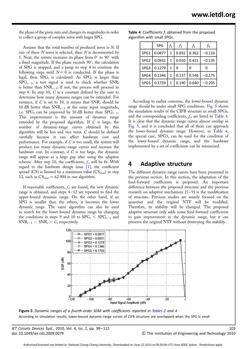
According to earlier concerns, the lower-bound dynamicrange should be under small SPG conditions. Fig. 5 showsthe simulation results of the CIFB structure in small SPGs,and the corresponding coefficients, fi, are listed in Table 4.It is clear that the dynamic-range curves almost overlap inFig. 5, and it is concluded that all of them can approachthe lower-bound dynamic range. However, in Table 4,the special case, SPG3, can be used for the condition ofthe lower-bound dynamic range, and the hardwareimplemented by a set of coefficients can be minimised.
4 Adaptive structureThe different dynamic-range curves have been presented inthe previous section. In this section, the adaptation of thefeed-forward coefficients is proposed. An importantdifference between the proposed structure and the previousresearch on adaptive mechanism [5–9] is the modificationof structure. Previous studies are mainly focused on thequantiser and the original NTF will be modified.Therefore, its stability will be changed. The proposedadaptive structure only adds some feed-forward coefficientsto gain improvement in the dynamic range, but it canpreserve the original NTF without destroying the stability.
Table 4 Coefficients fi obtained from the proposedalgorithm with small SPGs
SPG f1 f2 f3 f4
SPG1 0.0877 1 0.032 0.362 20.116
SPG2 0.0931 1 0.010 0.421 20.135
SPG3 0.1279 1 0 0 0
SPG4 0.1346 1 0.137 0.546 20.175
SPG5 0.1759 1 0.190 0.640 20.205
Figure 5 Dynamic ranges of a fourth-order SDM with coefficients reported in Tables 2 and 4
According to simulation results, lower-bound dynamic-range curves of CIFB structure are overlapped when the SPG is small
103
& The Institution of Engineering and Technology 2010
ded on June 22,2010 at 09:25:06 UTC from IEEE Xplore. Restrictions apply.
10
&
www.ietdl.org
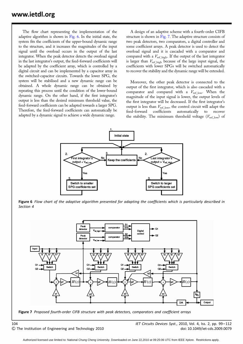
The flow chart representing the implementation of theadaptive algorithm is shown in Fig. 6. In the initial state, thesystem fits the coefficients of the upper-bound dynamic rangeto the structure, and it increases the magnitudes of the inputsignal until the overload occurs in the output of the lastintegrator. When the peak detector detects the overload signalin the last integrator’s output, the feed-forward coefficients willbe adapted by the coefficient array, which is controlled by adigital circuit and can be implemented by a capacitor array inthe switched-capacitor circuits. Towards the lower SPG, thesystem will be stabilised and a new dynamic range can beobtained. A whole dynamic range can be obtained byrepeating this process until the condition of the lower-bounddynamic range. On the other hand, if the first integrator’soutput is less than the desired minimum threshold value, thefeed-forward coefficients can be adapted towards a larger SPG.Therefore, the feed-forward coefficients can automatically beadapted by a dynamic signal to achieve a wide dynamic range.
4The Institution of Engineering and Technology 2010
Authorized licensed use limited to: National Chung Cheng University. Download
A design of an adaptive scheme with a fourth-order CIFBstructure is shown in Fig. 7. The adaptive structure consists oftwo peak detectors, two comparators, a digital controller andsome coefficient arrays. A peak detector is used to detect theoverload signal and it is cascaded with a comparator andcompared with a Vref_high. If the output of the last integratoris larger than Vref_high because of the large input signal, thecoefficients with lower SPGs will be switched automaticallyto recover the stability and the dynamic range will be extended.
Moreover, the other peak detector is connected to theoutput of the first integrator, which is also cascaded with acomparator and compared with a Vref_low. When themagnitude of the input signal is lower, the output levels ofthe first integrator will be decreased. If the first integrator’soutput is less than Vref_low, the control circuit will adapt thefeed-forward coefficients automatically to recoverthe stability. The minimum threshold voltage (Vref_low) of
Figure 6 Flow chart of the adaptive algorithm presented for adapting the coefficients which is particularly described inSection 4
Figure 7 Proposed fourth-order CIFB structure with peak detectors, comparators and coefficient arrays
IET Circuits Devices Syst., 2010, Vol. 4, Iss. 2, pp. 99–112doi: 10.1049/iet-cds.2009.0079
ed on June 22,2010 at 09:25:06 UTC from IEEE Xplore. Restrictions apply.
Id
www.ietdl.org
the first integrator output can be employed to switch back thedynamic-range curve automatically. According to ourproposed method, if the system adapts the feed-forwardcoefficients, the program will record the magnitude of theintegrator outputs of the new dynamic-range curve andincrease the value of the magnitude by 10% to become theminimum value of the first integrator output. This stepguarantees that the switch backward is still stable.
5 Simulation resultsThe system is simulated by Matlab and Simulink, and thespecifications of the system are the same as in the previousdescriptions shown in Table 1. In this section, the OSReffect to the proposed algorithm is discussed.
5.1 OSR effects
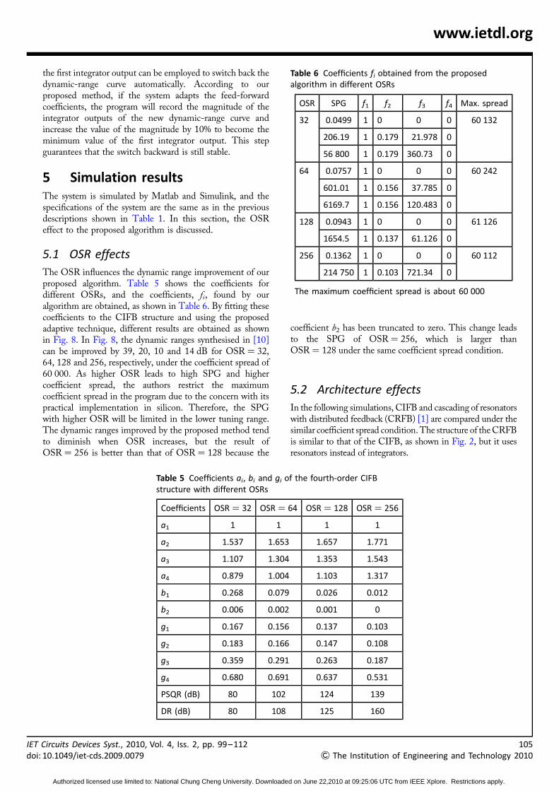
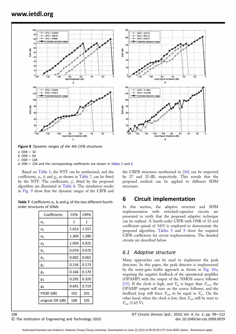
The OSR influences the dynamic range improvement of ourproposed algorithm. Table 5 shows the coefficients fordifferent OSRs, and the coefficients, fi, found by ouralgorithm are obtained, as shown in Table 6. By fitting thesecoefficients to the CIFB structure and using the proposedadaptive technique, different results are obtained as shownin Fig. 8. In Fig. 8, the dynamic ranges synthesised in [10]can be improved by 39, 20, 10 and 14 dB for OSR ¼ 32,64, 128 and 256, respectively, under the coefficient spread of60 000. As higher OSR leads to high SPG and highercoefficient spread, the authors restrict the maximumcoefficient spread in the program due to the concern with itspractical implementation in silicon. Therefore, the SPGwith higher OSR will be limited in the lower tuning range.The dynamic ranges improved by the proposed method tendto diminish when OSR increases, but the result ofOSR ¼ 256 is better than that of OSR ¼ 128 because the
ET Circuits Devices Syst., 2010, Vol. 4, Iss. 2, pp. 99–112oi: 10.1049/iet-cds.2009.0079
Authorized licensed use limited to: National Chung Cheng University. Download
coefficient b2 has been truncated to zero. This change leadsto the SPG of OSR ¼ 256, which is larger thanOSR ¼ 128 under the same coefficient spread condition.
5.2 Architecture effects
In the following simulations, CIFB and cascading of resonatorswith distributed feedback (CRFB) [1] are compared under thesimilar coefficient spread condition. The structure of the CRFBis similar to that of the CIFB, as shown in Fig. 2, but it usesresonators instead of integrators.
Table 6 Coefficients fi obtained from the proposedalgorithm in different OSRs
OSR SPG f1 f2 f3 f4 Max. spread
32 0.0499 1 0 0 0 60 132
206.19 1 0.179 21.978 0
56 800 1 0.179 360.73 0
64 0.0757 1 0 0 0 60 242
601.01 1 0.156 37.785 0
6169.7 1 0.156 120.483 0
128 0.0943 1 0 0 0 61 126
1654.5 1 0.137 61.126 0
256 0.1362 1 0 0 0 60 112
214 750 1 0.103 721.34 0
The maximum coefficient spread is about 60 000
Table 5 Coefficients ai, bi and gi of the fourth-order CIFBstructure with different OSRs
Coefficients OSR ¼ 32 OSR ¼ 64 OSR ¼ 128 OSR ¼ 256
a1 1 1 1 1
a2 1.537 1.653 1.657 1.771
a3 1.107 1.304 1.353 1.543
a4 0.879 1.004 1.103 1.317
b1 0.268 0.079 0.026 0.012
b2 0.006 0.002 0.001 0
g1 0.167 0.156 0.137 0.103
g2 0.183 0.166 0.147 0.108
g3 0.359 0.291 0.263 0.187
g4 0.680 0.691 0.637 0.531
PSQR (dB) 80 102 124 139
DR (dB) 80 108 125 160
105
& The Institution of Engineering and Technology 2010
ed on June 22,2010 at 09:25:06 UTC from IEEE Xplore. Restrictions apply.
10
&
www.ietdl.org
Figure 8 Dynamic ranges of the 4th CIFB structures
a OSR ¼ 32b OSR ¼ 64c OSR ¼ 128d OSR ¼ 256 and the corresponding coefficients are shown in Tables 5 and 6
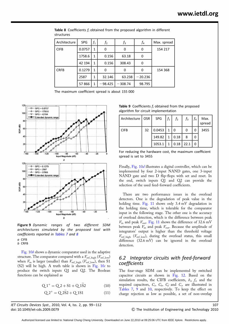
Based on Table 1, the NTF can be synthesised, and thecoefficients, ai, bi and gi, as shown in Table 7, can be fittedby the NTF. The coefficients, fi, fitted by the proposedalgorithm are illustrated in Table 8. The simulation resultsin Fig. 9 show that the dynamic ranges of the CIFB and
Table 7 Coefficients ai, bi and gi of the two different fourth-order structures of SDMs
Coefficients CIFB CRFB
a1 1 1
a2 1.653 1.557
a3 1.304 1.280
a4 1.004 0.925
b1 0.079 0.070
b2 0.002 0.002
g1 0.156 0.173
g2 0.166 0.170
g3 0.292 0.320
g4 0.691 0.719
PSQR (dB) 102 101
original DR (dB) 108 105
6The Institution of Engineering and Technology 2010
Authorized licensed use limited to: National Chung Cheng University. Download
the CRFB structures synthesised in [10] can be improvedby 27 and 25 dB, respectively. This reveals that theproposed method can be applied to different SDMstructures.
6 Circuit implementationIn this section, the adaptive structure and SDMimplementation with switched-capacitor circuits arepresented to verify that the proposed adaptive techniquecan be realised. A fourth-order CIFB with OSR of 32 andcoefficient spread of 3455 is employed to demonstrate theproposed algorithm. Tables 5 and 9 show the requiredCIFB coefficients for circuit implementation. The detailedcircuits are described below.
6.1 Adaptive structure
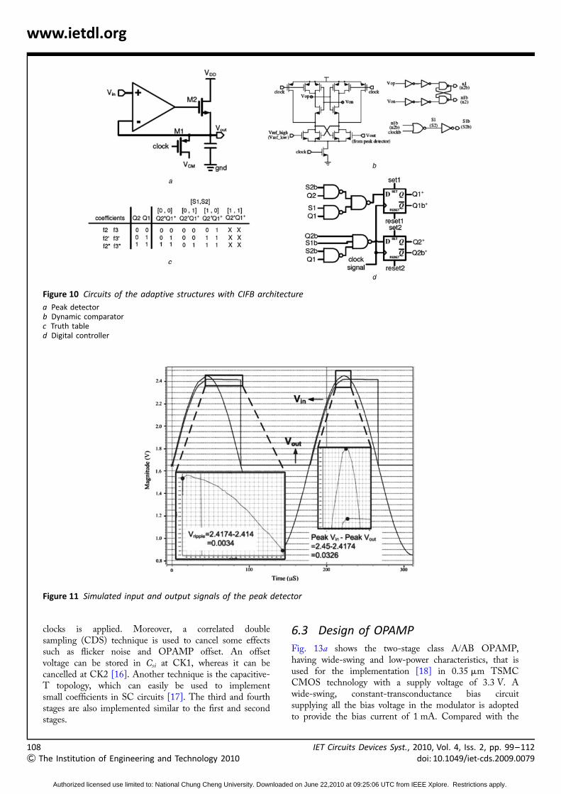
Many approaches can be used to implement the peakdetectors. In this paper, the peak detector is implementedby the unity-gain buffer approach as shown in Fig. 10a,requiring the negative feedback of the operational amplifier(OPAMP) with the output of the NMOS source follower[15]. If the clock is high, and Vin is larger than Vout, theOPAMP output will turn on the source follower, and thefeedback loop will force Vout to be equal to Vin. On theother hand, when the clock is low, then Vout will be reset toVcm (1.65 V).
IET Circuits Devices Syst., 2010, Vol. 4, Iss. 2, pp. 99–112doi: 10.1049/iet-cds.2009.0079
ed on June 22,2010 at 09:25:06 UTC from IEEE Xplore. Restrictions apply.
IET Circuits Devices Syst.,doi: 10.1049/iet-cds.2009
www.ietdl.org
Authorized licensed use
Table 8 Coefficients fi obtained from the proposed algorithm in differentstructures
Architecture SPG f1 f2 f3 f4 Max. spread
CIFB 0.0757 1 0 0 0 154 217
1758.6 1 0.156 63.18 0
42 194 1 0.156 308.43 0
CRFB 0.1279 1 0 0 0 154 368
2587 1 32.146 63.238 220.236
57 866 1 298.425 2308.74 98.795
The maximum coefficient spread is about 155 000
Fig. 10b shows a dynamic comparator used in the adaptivestructure. The comparator compared with a Vref_high (Vref_low)when Vin is larger (smaller) than Vref_high (Vref_low), then S1(S2) will be high. A truth table is shown in Fig. 10c toproduce the switch inputs Q1 and Q2. The Booleanfunctions can be explained as
Q 1+ = Q 2 + S1 + Q 1S̄2 (10)
Q 2+ = Q 2S̄2 + Q 1S1 (11)
Figure 9 Dynamic ranges of two different SDMarchitectures simulated by the proposed tool withcoefficients reported in Tables 7 and 8
a CIFBb CRFB
2010, Vol. 4, Iss. 2, pp. 99–112.0079
limited to: National Chung Cheng University. Downloa
Finally, Fig. 10d illustrates a digital controller, which can beimplemented by four 2-input NAND gates, one 3-inputNAND gate and two D flip-flops with set and reset. Inthe end, switch inputs Q1 and Q2 can provide theselection of the used feed-forward coefficients.
There are two performance issues in the overloaddetectors. One is the degradation of peak value in theholding time. Fig. 11 shows only 3.4 mV degradation inthe holding time, which is tolerable for the comparatorinput in the following stage. The other one is the accuracyof overload detection, which is the difference between peakVin and peak Vout. Fig. 11 shows the difference of 32.6 mVbetween peak Vin and peak Vout. Because the amplitude ofintegrators’ output is higher than the threshold voltageVref_high (Vref_low), during the overload status, this smalldifference (32.6 mV) can be ignored in the overloaddetection.
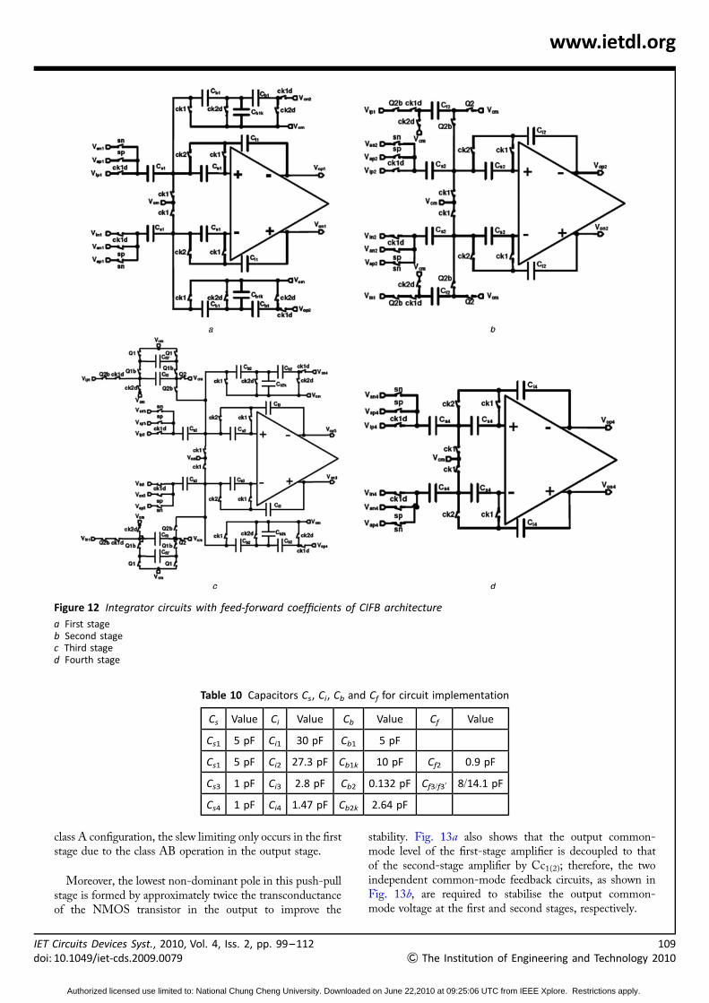
6.2 Integrator circuits with feed-forwardcoefficients
The four-stage SDM can be implemented by switchedcapacitor circuits as shown in Fig. 12. Based on thesimulation results, the CIFB coefficients, bi, fi, and therequired capacitors, Ci, Cb, Cf and Cs, are illustrated inTables 7, 9 and 10, respectively. To keep the effect oncharge rejection as low as possible, a set of non-overlap
Table 9 Coefficients fi obtained from the proposedalgorithm for circuit implementation
Architecture OSR SPG f1 f2 f3 f4 Max.spread
CIFB 32 0.0453 1 0 0 0 3455
149.82 1 0.18 8 0
1053.1 1 0.18 22.1 0
For reducing the hardware cost, the maximum coefficientspread is set to 3455
107
& The Institution of Engineering and Technology 2010
ded on June 22,2010 at 09:25:06 UTC from IEEE Xplore. Restrictions apply.
108
&
www.ietdl.org
Figure 10 Circuits of the adaptive structures with CIFB architecture
a Peak detectorb Dynamic comparatorc Truth tabled Digital controller
Figure 11 Simulated input and output signals of the peak detector
clocks is applied. Moreover, a correlated doublesampling (CDS) technique is used to cancel some effectssuch as flicker noise and OPAMP offset. An offsetvoltage can be stored in Csi at CK1, whereas it can becancelled at CK2 [16]. Another technique is the capacitive-T topology, which can easily be used to implementsmall coefficients in SC circuits [17]. The third and fourthstages are also implemented similar to the first and secondstages.
The Institution of Engineering and Technology 2010
Authorized licensed use limited to: National Chung Cheng University. Download
6.3 Design of OPAMP
Fig. 13a shows the two-stage class A/AB OPAMP,having wide-swing and low-power characteristics, that isused for the implementation [18] in 0.35 mm TSMCCMOS technology with a supply voltage of 3.3 V. Awide-swing, constant-transconductance bias circuitsupplying all the bias voltage in the modulator is adoptedto provide the bias current of 1 mA. Compared with the
IET Circuits Devices Syst., 2010, Vol. 4, Iss. 2, pp. 99–112doi: 10.1049/iet-cds.2009.0079
ed on June 22,2010 at 09:25:06 UTC from IEEE Xplore. Restrictions apply.
IETdoi
www.ietdl.org
Figure 12 Integrator circuits with feed-forward coefficients of CIFB architecture
a First stageb Second stagec Third staged Fourth stage
Table 10 Capacitors Cs, Ci, Cb and Cf for circuit implementation
Cs Value Ci Value Cb Value Cf Value
Cs1 5 pF Ci1 30 pF Cb1 5 pF
Cs1 5 pF Ci2 27.3 pF Cb1k 10 pF Cf2 0.9 pF
Cs3 1 pF Ci3 2.8 pF Cb2 0.132 pF Cf3/f3′ 8/14.1 pF
Cs4 1 pF Ci4 1.47 pF Cb2k 2.64 pF
class A configuration, the slew limiting only occurs in the firststage due to the class AB operation in the output stage.
Moreover, the lowest non-dominant pole in this push-pullstage is formed by approximately twice the transconductanceof the NMOS transistor in the output to improve the
Circuits Devices Syst., 2010, Vol. 4, Iss. 2, pp. 99–112: 10.1049/iet-cds.2009.0079
Authorized licensed use limited to: National Chung Cheng University. Downloade
stability. Fig. 13a also shows that the output common-mode level of the first-stage amplifier is decoupled to thatof the second-stage amplifier by Cc1(2); therefore, the twoindependent common-mode feedback circuits, as shown inFig. 13b, are required to stabilise the output common-mode voltage at the first and second stages, respectively.
109
& The Institution of Engineering and Technology 2010
d on June 22,2010 at 09:25:06 UTC from IEEE Xplore. Restrictions apply.
110
&
www.ietdl.org
Figure 13 Two-stage amplifier
a Two-stage class A/AB OPAMPb Its common-mode feedback circuit
6.4 Switch thermal noise
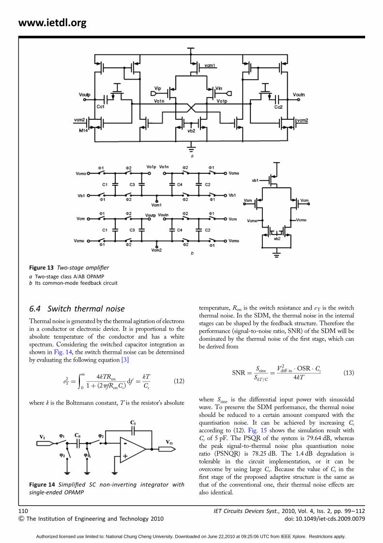
Thermal noise is generated by the thermal agitation of electronsin a conductor or electronic device. It is proportional to theabsolute temperature of the conductor and has a whitespectrum. Considering the switched capacitor integration asshown in Fig. 14, the switch thermal noise can be determinedby evaluating the following equation [3]
e2T =
∫1
0
4kTRon
1 + (2pfRonCs)df = kT
Cs
(12)
where k is the Boltzmann constant, T is the resistor’s absolute
Figure 14 Simplified SC non-inverting integrator withsingle-ended OPAMP
The Institution of Engineering and Technology 2010
Authorized licensed use limited to: National Chung Cheng University. Download
temperature, Ron is the switch resistance and eT is the switchthermal noise. In the SDM, the thermal noise in the internalstages can be shaped by the feedback structure. Therefore theperformance (signal-to-noise ratio, SNR) of the SDM will bedominated by the thermal noise of the first stage, which canbe derived from
SNR = Ssine
SkT/C
= V 2diff ·in · OSR · Cs
4kT(13)
where Ssine is the differential input power with sinusoidalwave. To preserve the SDM performance, the thermal noiseshould be reduced to a certain amount compared with thequantisation noise. It can be achieved by increasing Cs
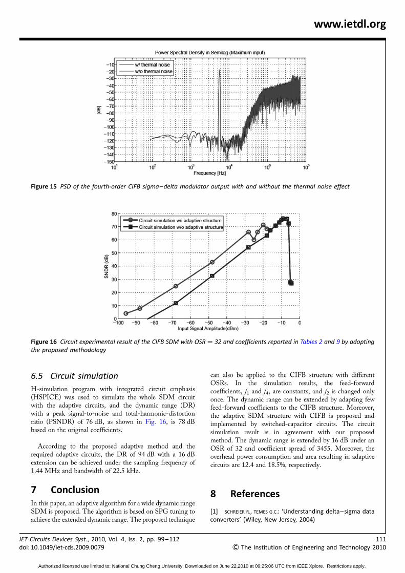
according to (12). Fig. 15 shows the simulation result withCs of 5 pF. The PSQR of the system is 79.64 dB, whereasthe peak signal-to-thermal noise plus quantisation noiseratio (PSNQR) is 78.25 dB. The 1.4 dB degradation istolerable in the circuit implementation, or it can beovercome by using large Cs. Because the value of Cs in thefirst stage of the proposed adaptive structure is the same asthat of the conventional one, their thermal noise effects arealso identical.
IET Circuits Devices Syst., 2010, Vol. 4, Iss. 2, pp. 99–112doi: 10.1049/iet-cds.2009.0079
ed on June 22,2010 at 09:25:06 UTC from IEEE Xplore. Restrictions apply.
IEd
www.ietdl.org
Figure 15 PSD of the fourth-order CIFB sigma–delta modulator output with and without the thermal noise effect
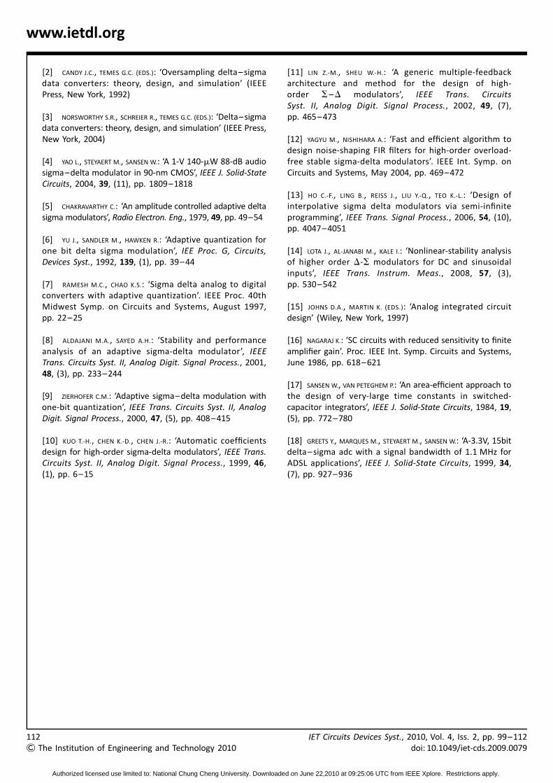
Figure 16 Circuit experimental result of the CIFB SDM with OSR ¼ 32 and coefficients reported in Tables 2 and 9 by adoptingthe proposed methodology
6.5 Circuit simulation
H-simulation program with integrated circuit emphasis(HSPICE) was used to simulate the whole SDM circuitwith the adaptive circuits, and the dynamic range (DR)with a peak signal-to-noise and total-harmonic-distortionratio (PSNDR) of 76 dB, as shown in Fig. 16, is 78 dBbased on the original coefficients.
According to the proposed adaptive method and therequired adaptive circuits, the DR of 94 dB with a 16 dBextension can be achieved under the sampling frequency of1.44 MHz and bandwidth of 22.5 kHz.
7 ConclusionIn this paper, an adaptive algorithm for a wide dynamic rangeSDM is proposed. The algorithm is based on SPG tuning toachieve the extended dynamic range. The proposed technique
T Circuits Devices Syst., 2010, Vol. 4, Iss. 2, pp. 99–112oi: 10.1049/iet-cds.2009.0079
Authorized licensed use limited to: National Chung Cheng University. Downloa
can also be applied to the CIFB structure with differentOSRs. In the simulation results, the feed-forwardcoefficients, f1 and f4, are constants, and f2 is changed onlyonce. The dynamic range can be extended by adapting fewfeed-forward coefficients to the CIFB structure. Moreover,the adaptive SDM structure with CIFB is proposed andimplemented by switched-capacitor circuits. The circuitsimulation result is in agreement with our proposedmethod. The dynamic range is extended by 16 dB under anOSR of 32 and coefficient spread of 3455. Moreover, theoverhead power consumption and area resulting in adaptivecircuits are 12.4 and 18.5%, respectively.
8 References
[1] SCHREIER R., TEMES G.C.: ‘Understanding delta–sigma dataconverters’ (Wiley, New Jersey, 2004)
111
& The Institution of Engineering and Technology 2010
ded on June 22,2010 at 09:25:06 UTC from IEEE Xplore. Restrictions apply.
11
&
www.ietdl.org
[2] CANDY J.C., TEMES G.C. (EDS.): ‘Oversampling delta – sigmadata converters: theory, design, and simulation’ (IEEEPress, New York, 1992)
[3] NORSWORTHY S.R., SCHREIER R., TEMES G.C. (EDS.): ‘Delta–sigmadata converters: theory, design, and simulation’ (IEEE Press,New York, 2004)
[4] YAO L., STEYAERT M., SANSEN W.: ‘A 1-V 140-mW 88-dB audiosigma–delta modulator in 90-nm CMOS’, IEEE J. Solid-StateCircuits, 2004, 39, (11), pp. 1809–1818
[5] CHAKRAVARTHY C.: ‘An amplitude controlled adaptive deltasigma modulators’, Radio Electron. Eng., 1979, 49, pp. 49–54
[6] YU J., SANDLER M., HAWKEN R.: ‘Adaptive quantization forone bit delta sigma modulation’, IEE Proc. G, Circuits,Devices Syst., 1992, 139, (1), pp. 39–44
[7] RAMESH M.C., CHAO K.S.: ‘Sigma delta analog to digitalconverters with adaptive quantization’. IEEE Proc. 40thMidwest Symp. on Circuits and Systems, August 1997,pp. 22–25
[8] ALDAJANI M.A., SAYED A.H.: ‘Stability and performanceanalysis of an adaptive sigma-delta modulator’, IEEETrans. Circuits Syst. II, Analog Digit. Signal Process., 2001,48, (3), pp. 233–244
[9] ZIERHOFER C.M.: ‘Adaptive sigma–delta modulation withone-bit quantization’, IEEE Trans. Circuits Syst. II, AnalogDigit. Signal Process., 2000, 47, (5), pp. 408–415
[10] KUO T.-H., CHEN K.-D., CHEN J.-R.: ‘Automatic coefficientsdesign for high-order sigma-delta modulators’, IEEE Trans.Circuits Syst. II, Analog Digit. Signal Process., 1999, 46,(1), pp. 6–15
2The Institution of Engineering and Technology 2010
Authorized licensed use limited to: National Chung Cheng University. Downloa
[11] LIN Z.-M., SHEU W.-H.: ‘A generic multiple-feedbackarchitecture and method for the design of high-order S–D modulators’, IEEE Trans. CircuitsSyst. II, Analog Digit. Signal Process., 2002, 49, (7),pp. 465–473
[12] YAGYU M., NISHIHARA A.: ‘Fast and efficient algorithm todesign noise-shaping FIR filters for high-order overload-free stable sigma-delta modulators’. IEEE Int. Symp. onCircuits and Systems, May 2004, pp. 469–472
[13] HO C.-F., LING B., REISS J., LIU Y.-Q., TEO K.-L.: ‘Design ofinterpolative sigma delta modulators via semi-infiniteprogramming’, IEEE Trans. Signal Process., 2006, 54, (10),pp. 4047–4051
[14] LOTA J., AL-JANABI M., KALE I.: ‘Nonlinear-stability analysisof higher order D-S modulators for DC and sinusoidalinputs’, IEEE Trans. Instrum. Meas., 2008, 57, (3),pp. 530–542
[15] JOHNS D.A., MARTIN K. (EDS.): ‘Analog integrated circuitdesign’ (Wiley, New York, 1997)
[16] NAGARAJ K.: ‘SC circuits with reduced sensitivity to finiteamplifier gain’. Proc. IEEE Int. Symp. Circuits and Systems,June 1986, pp. 618–621
[17] SANSEN W., VAN PETEGHEM P.: ‘An area-efficient approach tothe design of very-large time constants in switched-capacitor integrators’, IEEE J. Solid-State Circuits, 1984, 19,(5), pp. 772–780
[18] GREETS Y., MARQUES M., STEYAERT M., SANSEN W.: ‘A-3.3V, 15bitdelta – sigma adc with a signal bandwidth of 1.1 MHz forADSL applications’, IEEE J. Solid-State Circuits, 1999, 34,(7), pp. 927–936
IET Circuits Devices Syst., 2010, Vol. 4, Iss. 2, pp. 99–112doi: 10.1049/iet-cds.2009.0079
ded on June 22,2010 at 09:25:06 UTC from IEEE Xplore. Restrictions apply.