(CMMEProject)IMPLEMENTING A FREQUENCY MODULATION (FM) MODULATOR AND DEMODULATOR
10
Khalifa University of Science for Technology and Research Communication Engineering Department CMME300 Communication Systems Laboratory: Project Report: IMPLEMENTING A FREQUENCY MODULATION (FM) MODULATOR AND DEMODULATOR Group Members: Eman AlQawasmi 100038660 Bushra Alyas 100038656 | Page
-
Upload
independent -
Category
Documents
-
view
4 -
download
0
Transcript of (CMMEProject)IMPLEMENTING A FREQUENCY MODULATION (FM) MODULATOR AND DEMODULATOR
Khalifa University of Science for Technology andResearch
Communication Engineering Department
CMME300 Communication Systems Laboratory:
Project Report:
IMPLEMENTING A FREQUENCY MODULATION (FM)MODULATOR AND DEMODULATOR
Group Members:
Eman AlQawasmi 100038660Bushra Alyas 100038656
| P a g e

Submitted to: Mr. Hirminio Vendiola
Submission On: Monday – 13/ April, 2014
Spring2
Table of Contents
ABSTRACT 3
LIST OF FIGURES 4
2. CONCEPT DISCUSSION 6
3. DESIGN EXPERIMENT DISCUSSION 8
4. CONCLUSIONS 18
5. REFERENCES 19
| P a g e

List of Figures
Figure 1 – Carrier, Modulating and Modulated Waves........6
Figure 2 – FM Spectrum …..................................6
Figure 3 – Spectra of an FM Signal with Differing Levels of
Modulation Index........................................7
Figure 4 – Block Diagram of a Basic PLL...................7
Figure 5 – FM Modulator and Demodulator Block Diagram.....8
Figure 6 – Connections Diagram of PLL Chips...............8
Figure 7 – FM Circuit Schematic...........................9
Figure 8 – Shows the simulation results...................9
Figure 9 – Demodulation simulation results...............11
Figure 10 – FM modulator Circuit on Multisim............12
Figure 11 – Square wave to Sinewave convertor.............12
Figure 12 – Demodulator circuit on Multisim..............13
Figure 13 – The whole implemented Circuit................13
Figure 14 – Carrier Signal...............................14
| P a g e

Figure 15 – Modulating process (the message signal, and Modulated
Signal)................................................14
Figure 16 – FM Spectrum showing no Input.................15
Figure 17 – FM Demodulator Circuit Schematic.............15
Figure 18 – WBFM Spectrum................................16
Figure 19 – The Original Message and the Recovered Signal 17
Figure 20 – Testing the FM circuit to transmit speech. . . .17
Figure 21 – The oscilloscope view when transmitting the speech
.......................................................18
Abstract
This report gives a brief discussion of the frequency modulation(FM).It highlights significant basics of the telecommunicationsand signal processing which revolves around modulation and
| P a g e
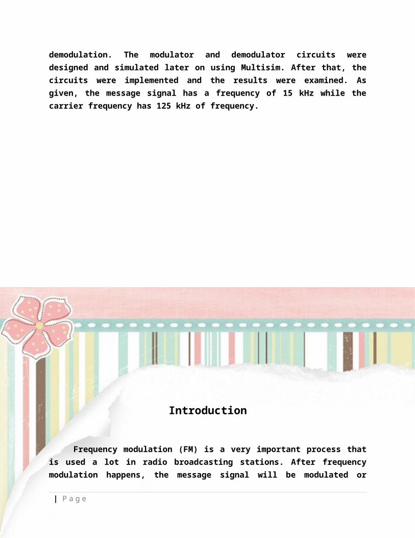
demodulation. The modulator and demodulator circuits weredesigned and simulated later on using Multisim. After that, thecircuits were implemented and the results were examined. Asgiven, the message signal has a frequency of 15 kHz while thecarrier frequency has 125 kHz of frequency.
Introduction
Frequency modulation (FM) is a very important process thatis used a lot in radio broadcasting stations. After frequencymodulation happens, the message signal will be modulated or
| P a g e

changed in transmission. Indeed, understanding the process ofmodulation and demodulation and observing the concept of FMsignals is very important in communication systems. The projectwas achieved by applying the knowledge that has been gained fromthe previous lab sessions and the theoretical discussions. Thisreport cites the steps that were done during this project (whichincludes designing the FM modulator and the demodulator andimplementing them).
Aim:
This project aims to design and implement the FM modulator anddemodulator on hardware after designing them on software. Themodulating signal that is used has a frequency of 15 kHzfrequency and a carrier of 125 kHz frequency.
Objectives:
The objectives of this project are to:
1) Understand the process of generating an FM signal usinga voltage-controlled oscillator (VCO).
2) Design and simulate a modulator by building a circuit toconvert the VCO output using Multisim based on the givenfrequencies and components.
3) Design and simulate a demodulator by using the PLLnetwork circuit provided in the manufacturer’s datasheet that can satisfy the expected output.
4) Implement the simulated circuits using the actualcalculated values of the components and verify theresults obtained.
| P a g e

Concept Discussion
Modulation is used since the first days of the 20th century
mainly for transmitting voice and signals. In Modulation, we vary
the carrier signal according to the changes that happen in the
information signal. In frequency modulation, we change the
frequency of the carrier according to the amplitude of the
information signal. FM modulation can be achieved simply by using
a VCO. You enter the information signal through the VCO, then you
control your frequency by adjusting the amplitude of you
information signal, (changing the voltage that is supplied by the
function generator). Bearing in mind, the frequency of the
modulated signal (which contains the carrier) will increase as we
are increasing the voltage of the information signal
(amplitude).Moreover, The modulated FM signal frequency changes
above and below the carrier frequency depending on the modulating
signal peaks of amplitude. When the modulating signal crosses the
axis, the modulated signal frequency will have a frequency that
is equal to the carrier frequency (see figure 1 below). Also,
there is another way to do the FM modulation, you can integrate
the modulating signal to generate a phase-modulated signal, and
thus, modulate a crystal-controlled oscillator and, then, the
output will go through the multiplier.
| P a g e
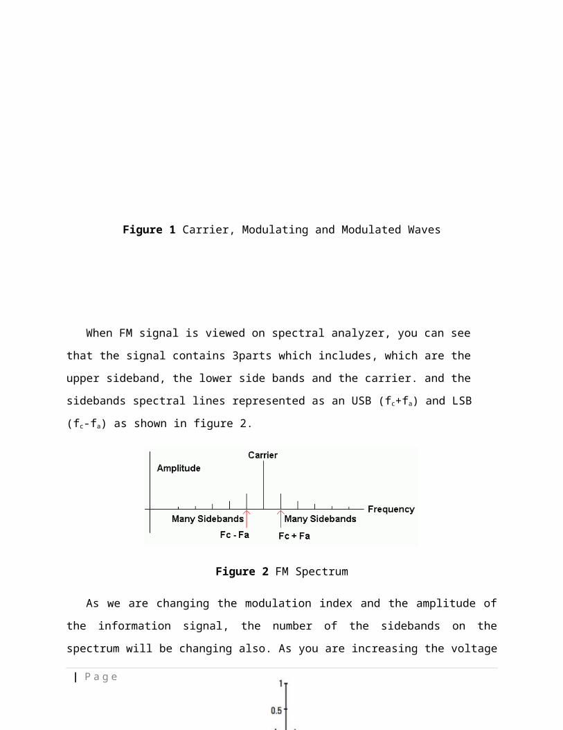
Figure 1 Carrier, Modulating and Modulated Waves
When FM signal is viewed on spectral analyzer, you can see
that the signal contains 3parts which includes, which are the
upper sideband, the lower side bands and the carrier. and the
sidebands spectral lines represented as an USB (fc+fa) and LSB
(fc-fa) as shown in figure 2.
Figure 2 FM Spectrum
As we are changing the modulation index and the amplitude of
the information signal, the number of the sidebands on the
spectrum will be changing also. As you are increasing the voltage
| P a g e

(amp), the power will be distributed over more sidebands and the
carrier will be decreasing to balance what’s happening as it’s
shown in the figure below.
Figure 3 Spectra of an FM Signal with Differing Levels of
Modulation Index
Back ground about Phase-Locked Loop (PLL) and how it does operates:
The PLL is an electronic feedback control system, as illustratedby the block diagram below, of locking the output and inputsignals in good agreements in both frequency and phase. In radiocommunication, if a carrier frequency drifts due to transmission,the PLL in receiver circuit will track the carrier frequency | P a g e

automatically.
| P a g e


![48216 Baack Final Proof [FM]](https://static.fdokumen.com/doc/165x107/631bfe5b3e8acd997705b218/48216-baack-final-proof-fm.jpg)