Ultra-low-energy all-CMOS modulator integrated with driver
12
Ultra-low-energy all-CMOS modulator integrated with driver Xuezhe Zheng 1* , Jon Lexau 2 , Ying Luo 1 , Hiren Thacker 1 , Thierry Pinguet 3 , Attila Mekis 3 , Guoliang Li 1 , Jing Shi 1 , Philip Amberg 2 , Nathaniel Pinckney 2 , Kannan Raj 1 , Ron Ho 2 , John E. Cunningham 1 , and Ashok V. Krishnamoorthy 1 1 Sun Microsystems Physical Sciences Center, San Diego, CA 92121, USA 2 Sun Laboratories, Menlo Park, CA 94025, USA 3 Luxtera Inc., Carlsbad, CA 92011, USA *[email protected] Abstract: We report the first sub-picojoule per bit (400fJ/bit) operation of a silicon modulator intimately integrated with a driver circuit and embedded in a clocked digital transmitter. We show a wall-plug power efficiency below 400μW/Gbps for a 130nm SOI CMOS carrier-depletion ring modulator flip-chip integrated to a 90nm bulk Si CMOS driver circuit. We also demonstrate stable error-free transmission of over 1.5 petabits of data at 5Gbps over 3.5 days using the integrated modulator without closed-loop ring resonance tuning. Small signal measurements of the CMOS ring modulator, sans circuit, showed a 3dB bandwidth in excess of 15GHz at 1V of reverse bias, indicating that further increases in transmission rate and reductions of energy-per-bit is possible while retaining compatibility with CMOS drive voltages. ©2010 Optical Society of America OCIS codes: (250.0250) Optoelectronics; (250.7360) Waveguide modulators; (130.0130) Integrated optics devices; (130.6622) Subsystems integration and techniques; (060.4510) Optical communications References and links 1. D. A. B. Miller, “Device requirements for optical interconnects to Silicon chips,” Proc. IEEE 97(7), 1166–1185 (2009). 2. A. V. Krishnamoorthy, R. Ho, X. Zheng, H. Schwetman, J. Lexau, P. Koka, G. Li, I. Shubin, and J. E. Cunningham, “Computer systems based on silicon photonic interconnects,” Proc. IEEE 97(7), 1337–1361 (2009). 3. D. Vantrease, R. Schreiber, M. Monchiero, M. McLarenz, N. P. Jouupi, M. Fiorentino, A. Davis, N. Binkert, R. G. Beausolei, and J. H. Ahn, “Corona: System Implications of Emerging Nanophotonic Technology,” ISCA '08, pp. 153–164, June 2008. 4. A. Shacham, K. Bergman, and L. P. Carloni, “On the Design of a Photonic Network-on-Chip,” Proceedings of the First International Symposium on Networks-on-Chip (NOCS) 2007, pp.53–64, 2007. 5. C. Batten, A. Joshi, J. Orcutt, A. Khilo, B. Moss, C. Holzwarth, H. Li, H. Smith, J. Hoyt, F. Kartner, R. Ram, V. Stojanovic, and K. Asanovic, “Building manycore processor-to-DRAM network with monolithic silicon photonics,” HOTI 2008, 21–30 (2008). 6. S. Manipatruni, Q. Xu, B. Schmidt, J. Shakya, and M. Lipson, “High speed carrier injection 18Gb/s silicon micro-ring electro-optic modulator,” in proceedings of IEEE on the Annual Meeting of the IEEE LEOS (Institute of Electrical and Electronics Engineers, New York, 2007), pp.537–538, 2007. 7. T. Pinguet, V. Sadagopan, A. Mekis, B. Analui, D. Kucharski, and S. Gloeckner, “A 1550 nm, 10 Gbps optical modulator with integrated driver in 130 nm CMOS,” Proceedings of IEEE conference on Group IV Photonics (Institute of Electrical and Electronics Engineers, New York, 2007), pp.1–3, 2007. 8. L. Liao, A. Liu, J. Basak, H. Nguyen, M. Paniccia, D. Rubin, Y. Chetrit, R. Cohen, and N. Izhaky, “40 Gbit/s silicon optical modulator for high speed applications,” Electron. Lett. 43(22), 1196–1197 (2007). 9. W. M. J. Green, M. J. Rooks, L. Sekaric, and Y. A. Vlasov, “Ultra-compact, low RF power, 10 Gb/s silicon Mach-Zehnder modulator,” Opt. Express 15(25), 17106–17113 (2007). 10. J. E. Roth, O. Fidaner, R. K. Schaevitz, Y. H. Kuo, T. I. Kamins, J. S. Harris, and D. A. B. Miller, “Optical modulator on silicon employing germanium quantum wells,” Opt. Express 15(9), 5851–5859 (2007). #117299 - $15.00 USD Received 16 Sep 2009; revised 15 Jan 2010; accepted 17 Jan 2010; published 28 Jan 2010 (C) 2010 OSA 1 February 2010 / Vol. 18, No. 3 / OPTICS EXPRESS 3059
-
Upload
independent -
Category
Documents
-
view
0 -
download
0
Transcript of Ultra-low-energy all-CMOS modulator integrated with driver
Ultra-low-energy all-CMOS modulator
integrated with driver
Xuezhe Zheng1*
, Jon Lexau2, Ying Luo
1, Hiren Thacker
1, Thierry Pinguet
3, Attila
Mekis3, Guoliang Li
1, Jing Shi
1, Philip Amberg
2, Nathaniel Pinckney
2, Kannan Raj
1,
Ron Ho2, John E. Cunningham
1, and Ashok V. Krishnamoorthy
1
1Sun Microsystems Physical Sciences Center, San Diego, CA 92121, USA 2Sun Laboratories, Menlo Park, CA 94025, USA
3Luxtera Inc., Carlsbad, CA 92011, USA
Abstract: We report the first sub-picojoule per bit (400fJ/bit) operation of a
silicon modulator intimately integrated with a driver circuit and embedded
in a clocked digital transmitter. We show a wall-plug power efficiency
below 400µW/Gbps for a 130nm SOI CMOS carrier-depletion ring
modulator flip-chip integrated to a 90nm bulk Si CMOS driver circuit. We
also demonstrate stable error-free transmission of over 1.5 petabits of data
at 5Gbps over 3.5 days using the integrated modulator without closed-loop
ring resonance tuning. Small signal measurements of the CMOS ring
modulator, sans circuit, showed a 3dB bandwidth in excess of 15GHz at 1V
of reverse bias, indicating that further increases in transmission rate and
reductions of energy-per-bit is possible while retaining compatibility with
CMOS drive voltages.
©2010 Optical Society of America
OCIS codes: (250.0250) Optoelectronics; (250.7360) Waveguide modulators; (130.0130)
Integrated optics devices; (130.6622) Subsystems integration and techniques; (060.4510)
Optical communications
References and links
1. D. A. B. Miller, “Device requirements for optical interconnects to Silicon chips,” Proc. IEEE 97(7), 1166–1185
(2009).
2. A. V. Krishnamoorthy, R. Ho, X. Zheng, H. Schwetman, J. Lexau, P. Koka, G. Li, I. Shubin, and J. E.
Cunningham, “Computer systems based on silicon photonic interconnects,” Proc. IEEE 97(7), 1337–1361
(2009).
3. D. Vantrease, R. Schreiber, M. Monchiero, M. McLarenz, N. P. Jouupi, M. Fiorentino, A. Davis, N. Binkert, R. G.
Beausolei, and J. H. Ahn, “Corona: System Implications of Emerging Nanophotonic Technology,” ISCA '08, pp.
153–164, June 2008.
4. A. Shacham, K. Bergman, and L. P. Carloni, “On the Design of a Photonic Network-on-Chip,” Proceedings of
the First International Symposium on Networks-on-Chip (NOCS) 2007, pp.53–64, 2007.
5. C. Batten, A. Joshi, J. Orcutt, A. Khilo, B. Moss, C. Holzwarth, H. Li, H. Smith, J. Hoyt, F. Kartner, R. Ram, V.
Stojanovic, and K. Asanovic, “Building manycore processor-to-DRAM network with monolithic silicon
photonics,” HOTI 2008, 21–30 (2008).
6. S. Manipatruni, Q. Xu, B. Schmidt, J. Shakya, and M. Lipson, “High speed carrier injection 18Gb/s silicon
micro-ring electro-optic modulator,” in proceedings of IEEE on the Annual Meeting of the IEEE LEOS (Institute
of Electrical and Electronics Engineers, New York, 2007), pp.537–538, 2007.
7. T. Pinguet, V. Sadagopan, A. Mekis, B. Analui, D. Kucharski, and S. Gloeckner, “A 1550 nm, 10 Gbps optical
modulator with integrated driver in 130 nm CMOS,” Proceedings of IEEE conference on Group IV Photonics
(Institute of Electrical and Electronics Engineers, New York, 2007), pp.1–3, 2007.
8. L. Liao, A. Liu, J. Basak, H. Nguyen, M. Paniccia, D. Rubin, Y. Chetrit, R. Cohen, and N. Izhaky, “40 Gbit/s
silicon optical modulator for high speed applications,” Electron. Lett. 43(22), 1196–1197 (2007).
9. W. M. J. Green, M. J. Rooks, L. Sekaric, and Y. A. Vlasov, “Ultra-compact, low RF power, 10 Gb/s silicon
Mach-Zehnder modulator,” Opt. Express 15(25), 17106–17113 (2007).
10. J. E. Roth, O. Fidaner, R. K. Schaevitz, Y. H. Kuo, T. I. Kamins, J. S. Harris, and D. A. B. Miller, “Optical
modulator on silicon employing germanium quantum wells,” Opt. Express 15(9), 5851–5859 (2007).
#117299 - $15.00 USD Received 16 Sep 2009; revised 15 Jan 2010; accepted 17 Jan 2010; published 28 Jan 2010
(C) 2010 OSA 1 February 2010 / Vol. 18, No. 3 / OPTICS EXPRESS 3059
11. J. Liu, M. Beals, A. Pomerene, S. Bernardis, R. Sun, J. Chen, L. C. Kimerling, and J. Michel, “Ultralow energy,
Integrated GeSi electroabsorption modulators on SOI,” in Proceedings of IEEE conference on Group IV
Photonics (Institute of Electrical and Electronics Engineers, New York, 2008), pp.10–12, 2008.
12. Y. H. Kuo, H. W. Chen, and J. E. Bowers, “High speed hybrid silicon evanescent electroabsorption modulator,”
Opt. Express 16(13), 9936–9941 (2008).
13. M. R. Watts, D. C. Trotter, R. W. Young, and A. L. Lentine, “Ultralow power silicom microdisk modulators and
switches,” Proceedings of IEEE conference on Group IV Photonics (Institute of Electrical and Electronics
Engineers, New York, 2008), pp.4–6, 2008.
14. D. Marris-Morini, L. Vivien, G. Rasigade, J.-M. Fedeli, E. Cassan, X. Le Roux, P. Crozat, S. Maine, A. Lupu, P.
Lyan, P. Rivallin, M. Halbwax, and S. Laval, “Recent progress in high-speed silicon-based optical modulators,”
Proc. IEEE 97(7), 1199–1215 (2009).
15. J. S. Orcutt, K. Anatol, M. A. Popovic, C. W. Holzwarth, B. Moss, H. Li, M. S. Dahlem, T. D. Bonifield, F. X.
Kartner, E. P. Ippen, and J. L. Hoyt, R. J. ram, and V. Stojanovic, “Demonstration of an electronic photonic
integrated circuit in a commercial scaled bulk cmos process,” in Proc. CLEO/IQEC Conf. Lasers Electro
Opt/Intl. Quant. Elec. Conf., March 2008.
16. K. W. Goossen, J. E. Cunningham, and W. Y. Jan, “GaAs 850 nm modulators solder-bonded to silicon,” IEEE
Photon. Technol. Lett. 5(7), 776–778 (1993).
17. A. L. Lentine, K. W. Goossen, J. A. Walker, L. M. F. Chirovsky, L. A. D’Asaro, S. P. Hui, B. J. Tseng, R. E.
Leibenguth, J. E. Cunningham, W. Y. Jan, J.-M. Kuo, D. W. Dahringer, D. P. Kossives, D. D. Bacon, G.
Livescu, R. L. Morrison, R. A. Novotny, and D. B. Buchholz, “High-speed Optoelectronic VLSI Switching Chip
with >4000 Optical I/O Based on Flip-Chip Bonding of MQW Modulators and Detectors to Silicon CMOS,”
lEEE J. Sel. Top. Quantum Electron. 2(1), 77–84 (1996).
18. A. V. Krishnamoorthy, J. E. Ford, F. E. Kiamilev, R. G. Rozier, S. Hunsche, K. W. Goossen, B. Tseng, J. A.
Walker, J. E. Cunningham, W. Y. Jan, and M. C. Nuss, “The AMOEBA switch: an optoelectronic switch for
multiprocessor networking using dense WDM,” lEEE J,” Sel. Top. Quantum Electron. 5(2), 261–275 (1999).
19. A. V. Krishnamoorthy, T. K. Woodward, K. W. Goossen, J. A. Walker, A. L. Lentine, L. M. F. Chirovsky, S. P.
Hui, B. Tseng, R. Leibenguth, J. E. Cunningham, and W. Y. Jan, “Operation of a single-ended 550Mbit/s, 41fJ,
hybrid CMOS/MQW receiver-transmitter,” Electron. Lett. 32(8), 764–765 (1996).
20. A. V. Krishnamoorthy, K. W. Goossen, L. M. F. Chirovsky, R. G. Rozier, P. Chandramani, W. S. Hobson, S. P.
Hui, J. Lopata, J. A. Walker, and L. A. D’Asaro, “16x16 vcsel array flip-chip bonded to CMOS VLSI circuit,”
IEEE Photon. Technol. Lett. 12(8), 1073–1075 (2000).
21. T. Woodward, A. V. Krishnamoorthy, K. W. Goossen, J. A. Walker, B. Tseng, J. Lothian, S. Hui, and R.
Leibenguth, “Modulator-driver circuits for optoelectronic VLSI,” IEEE Photon. Technol. Lett. 9(6), 839–841
(1997).
22. S. Palermo, and M. Horowitz, “High-speed transmitters in 90nm CMOS for high-density optical interconnects,”
in Proceedings of IEEE on European Solid-State Circuits Conference (Institute of Electrical and Electronics
Engineers, New York, 2006), pp.508–511, 2006.
23. R. Ho, J. Lexau, F. Liu, D. Patil, R. Hopkins, E. Alon, N. Pinckney, P. Amberg, X. Zheng, J. E. Cunningham,
and A. V. Krishnamoorthy, “Circuits for silicon photonics on a ‘macrochip’, ” IEEE Asian Solid-State Circuits
Conference 2009, Industry Session 1–3, Nov. 2009.
1. Introduction
Silicon photonics (SiP) is envisioned as a promising technology solution for low latency, high
bandwidth intra-system interconnections in future computing systems [1]. A universal
requirement for implementing these system architectures is the dense integration of ultra
energy-efficient silicon photonic links, beginning with picojoule-per-bit links and scaling
down to hundreds of femtojoule-per-bit in the near future [2–5]. There has been a great deal
of effort put into the fabrication of silicon-on-insulator modulator devices at high-speed [6–
14]. While these experiments have shown the feasibility of high-speed modulation and the
potential for low-power operation, they have not simultaneously demonstrated compact size,
CMOS driver integration, low-power, and the ability to be manufactured in a silicon CMOS
foundry. We present the first three-dimensional integration of micro-ring resonators
manufactured in a CMOS SOI photonics platform intimately integrated to a 90nm bulk
CMOS circuit. We demonstrate: (i) resonator device fabrication compatibility with a
commercial 130nm CMOS process; (ii) compatibility of device bias and drive voltages with
an ultra-fine-line (sub-100nm) CMOS circuit platform; (iii) sub-picojoule per bit data
modulation using the hybrid CMOS photonic modulator; (iv) insertion of the driver-integrated
silicon photonic modulator into a clocked digital link; and (v) stable error free data
transmission of over 1.5 petabits of data using the micro-resonator devices, corresponding to a
raw bit-error-rate below 10−15
.
#117299 - $15.00 USD Received 16 Sep 2009; revised 15 Jan 2010; accepted 17 Jan 2010; published 28 Jan 2010
(C) 2010 OSA 1 February 2010 / Vol. 18, No. 3 / OPTICS EXPRESS 3060
2. All-CMOS driver-integrated silicon photonic modulator
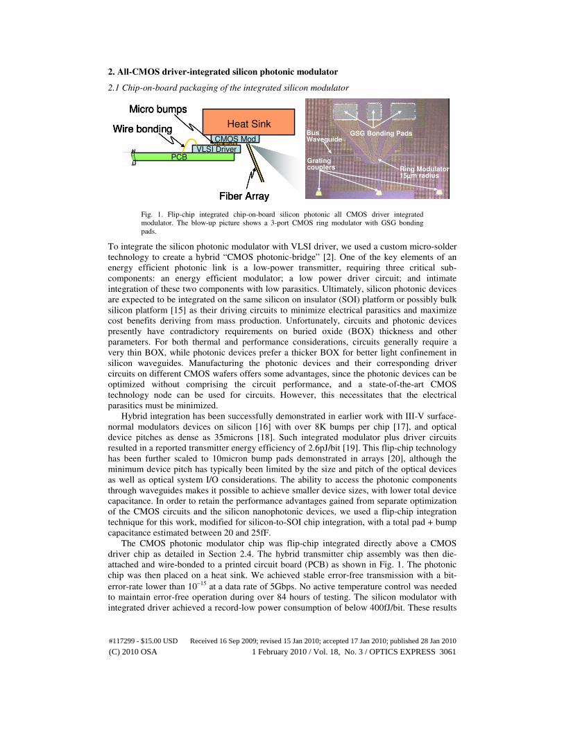
2.1 Chip-on-board packaging of the integrated silicon modulator
CMOS Mod
VLSI DriverPCB
Heat Sink
Fiber Array
Micro bumps
Wire bondingGSG Bonding PadsBus
Waveguide
Grating couplers Ring Modulator
15µµµµm radius
CMOS Mod
VLSI DriverPCB
Heat Sink
Fiber Array
Micro bumps
Wire bondingCMOS Mod
VLSI DriverPCB
Heat Sink
Fiber Array
Micro bumps
Wire bondingGSG Bonding PadsBus
Waveguide
Grating couplers Ring Modulator
15µµµµm radius
GSG Bonding PadsBusWaveguide
Grating couplers Ring Modulator
15µµµµm radius
Fig. 1. Flip-chip integrated chip-on-board silicon photonic all CMOS driver integrated
modulator. The blow-up picture shows a 3-port CMOS ring modulator with GSG bonding
pads.
To integrate the silicon photonic modulator with VLSI driver, we used a custom micro-solder
technology to create a hybrid “CMOS photonic-bridge” [2]. One of the key elements of an
energy efficient photonic link is a low-power transmitter, requiring three critical sub-
components: an energy efficient modulator; a low power driver circuit; and intimate
integration of these two components with low parasitics. Ultimately, silicon photonic devices
are expected to be integrated on the same silicon on insulator (SOI) platform or possibly bulk
silicon platform [15] as their driving circuits to minimize electrical parasitics and maximize
cost benefits deriving from mass production. Unfortunately, circuits and photonic devices
presently have contradictory requirements on buried oxide (BOX) thickness and other
parameters. For both thermal and performance considerations, circuits generally require a
very thin BOX, while photonic devices prefer a thicker BOX for better light confinement in
silicon waveguides. Manufacturing the photonic devices and their corresponding driver
circuits on different CMOS wafers offers some advantages, since the photonic devices can be
optimized without comprising the circuit performance, and a state-of-the-art CMOS
technology node can be used for circuits. However, this necessitates that the electrical
parasitics must be minimized.
Hybrid integration has been successfully demonstrated in earlier work with III-V surface-
normal modulators devices on silicon [16] with over 8K bumps per chip [17], and optical
device pitches as dense as 35microns [18]. Such integrated modulator plus driver circuits
resulted in a reported transmitter energy efficiency of 2.6pJ/bit [19]. This flip-chip technology
has been further scaled to 10micron bump pads demonstrated in arrays [20], although the
minimum device pitch has typically been limited by the size and pitch of the optical devices
as well as optical system I/O considerations. The ability to access the photonic components
through waveguides makes it possible to achieve smaller device sizes, with lower total device
capacitance. In order to retain the performance advantages gained from separate optimization
of the CMOS circuits and the silicon nanophotonic devices, we used a flip-chip integration
technique for this work, modified for silicon-to-SOI chip integration, with a total pad + bump
capacitance estimated between 20 and 25fF.
The CMOS photonic modulator chip was flip-chip integrated directly above a CMOS
driver chip as detailed in Section 2.4. The hybrid transmitter chip assembly was then die-
attached and wire-bonded to a printed circuit board (PCB) as shown in Fig. 1. The photonic
chip was then placed on a heat sink. We achieved stable error-free transmission with a bit-
error-rate lower than 10−15
at a data rate of 5Gbps. No active temperature control was needed
to maintain error-free operation during over 84 hours of testing. The silicon modulator with
integrated driver achieved a record-low power consumption of below 400fJ/bit. These results
#117299 - $15.00 USD Received 16 Sep 2009; revised 15 Jan 2010; accepted 17 Jan 2010; published 28 Jan 2010
(C) 2010 OSA 1 February 2010 / Vol. 18, No. 3 / OPTICS EXPRESS 3061
indicate that micro-resonator based modulators can provide stable and efficient modulation
without dynamic closed-loop bias setting and temperature control, using a chip-on-board
package and a heat sink for thermal management.
2.2 Depletion-mode CMOS photonic ring modulator
Significant progress has been made on the development of high performance modulators on
silicon, including Mach-Zehnder Interferometer (MZI) based silicon photonic modulators
using either carrier injection or depletion [7–9]. Such modulators have been integrated with
drivers in [7], but do not meet the energy targets stated above. On the other hand, electro-
absorption modulators based on quantum confined stark effect (QCSE) in SiGe quantum
wells [10]; Franz-Keldysh (FK) effect in tensile strained Ge-on-Si [11]; evanescent coupled
III-V on SOI devices [12]; and silicon micro-disc resonator based modulators [13] have been
shown to be promising candidates for lowering energy requirements. But none of the reported
work has demonstrated low power operation of a modulator integrated with corresponding
CMOS VLSI driver circuits. High-speed operation of compact ring modulators using carrier
injection has been demonstrated up to 18Gbps [6]. However, these devices were limited by
carrier life times, and a pre-emphasized electrical drive signal (Vpp = 4 V plus +/−2 V pre-
emphasized pulse) was needed, making it very challenging to design a low-power modulator
driver compatible with CMOS voltage levels. To avoid bandwidth limits resulting from
carrier lifetimes and to secure compatibility with CMOS drive voltages, we employed a
reverse-biased carrier-depletion ring modulator.
We designed and fabricated a carrier-depletion ring of 15µm in radius, coupled to two
waveguides, using the Luxtera-Freescale 130nm SOI CMOS process [7]. As is generally
accepted, it can be challenging to obtain stable operation with a high-Q resonator based
devices because they can be sensitive to temperature changes. A lower Q device can
potentially offer better stability, at the cost of a lower extinction ratio (ER) in modulation. To
balance the stability of the device versus its modulation quality, we used a device with a
“medium” Q which was a three-port (optical) device with GSG bonding pads, as shown in
Fig. 1. Grating couplers were used for the through waveguide and add or drop port with
surface normal optical coupling. The pitch for the grating couplers was selected to be 250µm
to match the pitch of arrayed fibers in silicon V-grooves. The two through ports were used as
the modulator Optical I/O. In this device, a third optical port was available for monitoring the
optical quality of the device and/or the modulated optical signal (bar-state) of the
transmission. In practice, we did not use this output for the experiments reported here. The
gap between the bus waveguide and the ring was 420nm.
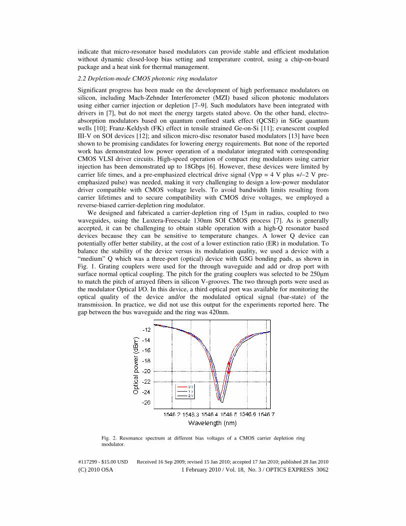
Fig. 2. Resonance spectrum at different bias voltages of a CMOS carrier depletion ring
modulator.
#117299 - $15.00 USD Received 16 Sep 2009; revised 15 Jan 2010; accepted 17 Jan 2010; published 28 Jan 2010
(C) 2010 OSA 1 February 2010 / Vol. 18, No. 3 / OPTICS EXPRESS 3062
DC characterization was performed on die using both electrical probes and arrayed fiber
probes. Figure 2 shows the through-port (Port1 to Port 3) spectral profile of one of the ring
resonances for different reverse bias voltages of 0V, 1V and 2V respectively. From these
measurements, we obtained a ring resonator Q of approximately 8300, and a wavelength shift
of approximately 10pm/V. With a voltage swing of 2V, a modulation with about 3dB
extinction ratio (ER) and a 6dB insertion loss could be achieved, as indicated by the arrow in
Fig. 2. Note that y-axis in Fig. 2 represents the optical power of the ring output, not the loss.
The input power from the fiber to the chip was about −8dBm, corresponding to a total fiber
coupling loss of about 4dB to and from the chip.
(a) (b)
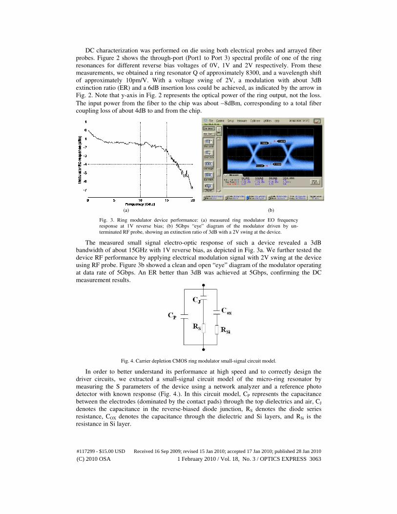
Fig. 3. Ring modulator device performance: (a) measured ring modulator EO frequency
response at 1V reverse bias; (b) 5Gbps “eye” diagram of the modulator driven by un-
terminated RF probe, showing an extinction ratio of 3dB with a 2V swing at the device.
The measured small signal electro-optic response of such a device revealed a 3dB
bandwidth of about 15GHz with 1V reverse bias, as depicted in Fig. 3a. We further tested the
device RF performance by applying electrical modulation signal with 2V swing at the device
using RF probe. Figure 3b showed a clean and open “eye” diagram of the modulator operating
at data rate of 5Gbps. An ER better than 3dB was achieved at 5Gbps, confirming the DC
measurement results.
Fig. 4. Carrier depletion CMOS ring modulator small-signal circuit model.
In order to better understand its performance at high speed and to correctly design the
driver circuits, we extracted a small-signal circuit model of the micro-ring resonator by
measuring the S parameters of the device using a network analyzer and a reference photo
detector with known response (Fig. 4.). In this circuit model, CP represents the capacitance
between the electrodes (dominated by the contact pads) through the top dielectrics and air, CJ
denotes the capacitance in the reverse-biased diode junction, RS denotes the diode series
resistance, COX denotes the capacitance through the dielectric and Si layers, and RSi is the
resistance in Si layer.
#117299 - $15.00 USD Received 16 Sep 2009; revised 15 Jan 2010; accepted 17 Jan 2010; published 28 Jan 2010
(C) 2010 OSA 1 February 2010 / Vol. 18, No. 3 / OPTICS EXPRESS 3063
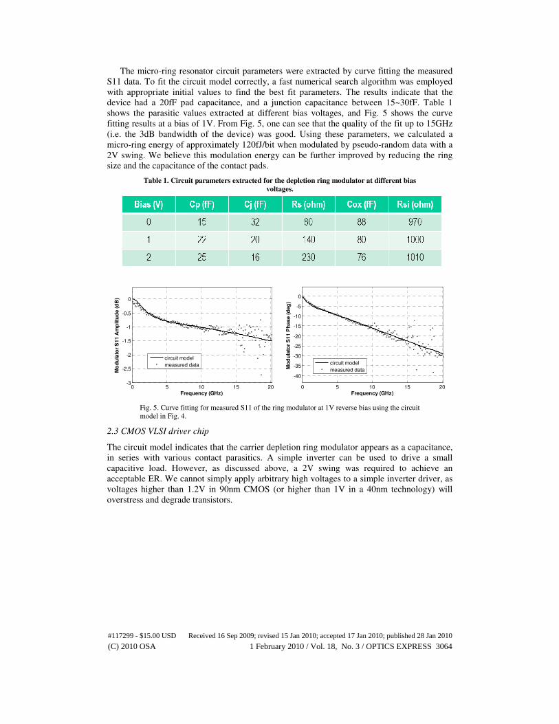
The micro-ring resonator circuit parameters were extracted by curve fitting the measured
S11 data. To fit the circuit model correctly, a fast numerical search algorithm was employed
with appropriate initial values to find the best fit parameters. The results indicate that the
device had a 20fF pad capacitance, and a junction capacitance between 15~30fF. Table 1
shows the parasitic values extracted at different bias voltages, and Fig. 5 shows the curve
fitting results at a bias of 1V. From Fig. 5, one can see that the quality of the fit up to 15GHz
(i.e. the 3dB bandwidth of the device) was good. Using these parameters, we calculated a
micro-ring energy of approximately 120fJ/bit when modulated by pseudo-random data with a
2V swing. We believe this modulation energy can be further improved by reducing the ring
size and the capacitance of the contact pads.
Table 1. Circuit parameters extracted for the depletion ring modulator at different bias
voltages.
0 5 10 15 20-3
-2.5
-2
-1.5
-1
-0.5
0
Frequency (GHz)
Mo
du
lato
r S
11
Am
plitu
de
(d
B)
circuit model
measured data
0 5 10 15 20
-40
-35
-30
-25
-20
-15
-10
-5
0
Frequency (GHz)
Mo
du
lato
r S
11
Ph
as
e (
de
g)
circuit model
measured data
Fig. 5. Curve fitting for measured S11 of the ring modulator at 1V reverse bias using the circuit
model in Fig. 4.
2.3 CMOS VLSI driver chip
The circuit model indicates that the carrier depletion ring modulator appears as a capacitance,
in series with various contact parasitics. A simple inverter can be used to drive a small
capacitive load. However, as discussed above, a 2V swing was required to achieve an
acceptable ER. We cannot simply apply arbitrary high voltages to a simple inverter driver, as
voltages higher than 1.2V in 90nm CMOS (or higher than 1V in a 40nm technology) will
overstress and degrade transistors.
#117299 - $15.00 USD Received 16 Sep 2009; revised 15 Jan 2010; accepted 17 Jan 2010; published 28 Jan 2010
(C) 2010 OSA 1 February 2010 / Vol. 18, No. 3 / OPTICS EXPRESS 3064
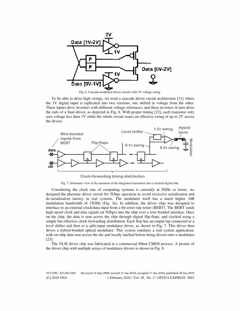
Fig. 6. Cascode modulator driver circuits with 2V voltage swing.
To be able to drive high swings, we used a cascode driver circuit architecture [21] where
the 1V digital input is replicated into two versions, one shifted in voltage from the other.
These inputs drive inverters with different voltage references, and these inverters in turn drive
the rails of a final driver, as depicted in Fig. 6. With proper timing [22], each transistor only
sees voltage less than 1V while the whole circuit issues an effective swing of up to 2V across
the device.
Fig. 7. Schematic view of the insertion of the integrated transmitter into a clocked digital link.
Considering the clock rate of computing systems is currently at 5GHz or lower, we
designed the photonic driver circuit for 5Gbps operation to avoid excessive serialization and
de-serialization latency in real systems. The modulator itself has a much higher 3dB
modulation bandwidth of 15GHz (Fig. 3a). In addition, the driver chip was designed to
interface to an external clock/data input from a bit-error-rate tester (BERT). The BERT sends
high-speed clock and data signals (at 5Gbps) into the chip over a wire bonded interface. Once
on the chip, the data is sent across the chip through digital flip-flops, and clocked using a
simple but effective clock-forwarding distribution. Each flop has an output tap connected to a
level shifter and then to a split-input modulator driver, as shown in Fig. 7. This driver then
drives a hybrid-bonded optical modulator. This system emulates a real system application,
with on-chip data sent across the die and locally latched before being driven onto a modulator
[23].
The VLSI driver chip was fabricated in a commercial 90nm CMOS process. A picture of
the driver chip with multiple arrays of modulator drivers is shown in Fig. 8.
#117299 - $15.00 USD Received 16 Sep 2009; revised 15 Jan 2010; accepted 17 Jan 2010; published 28 Jan 2010
(C) 2010 OSA 1 February 2010 / Vol. 18, No. 3 / OPTICS EXPRESS 3065
GS
GG
SG
Fig. 8. 90nm CMOS driver chip with 330 digitally clocked low power modulator drivers, high
speed digital I/Os and other test circuitry.The blow-up shows the GSG pads of one modulator
driver with under-bump metallization.
2.4 Flip-chip integration of the hybrid photonic bridge
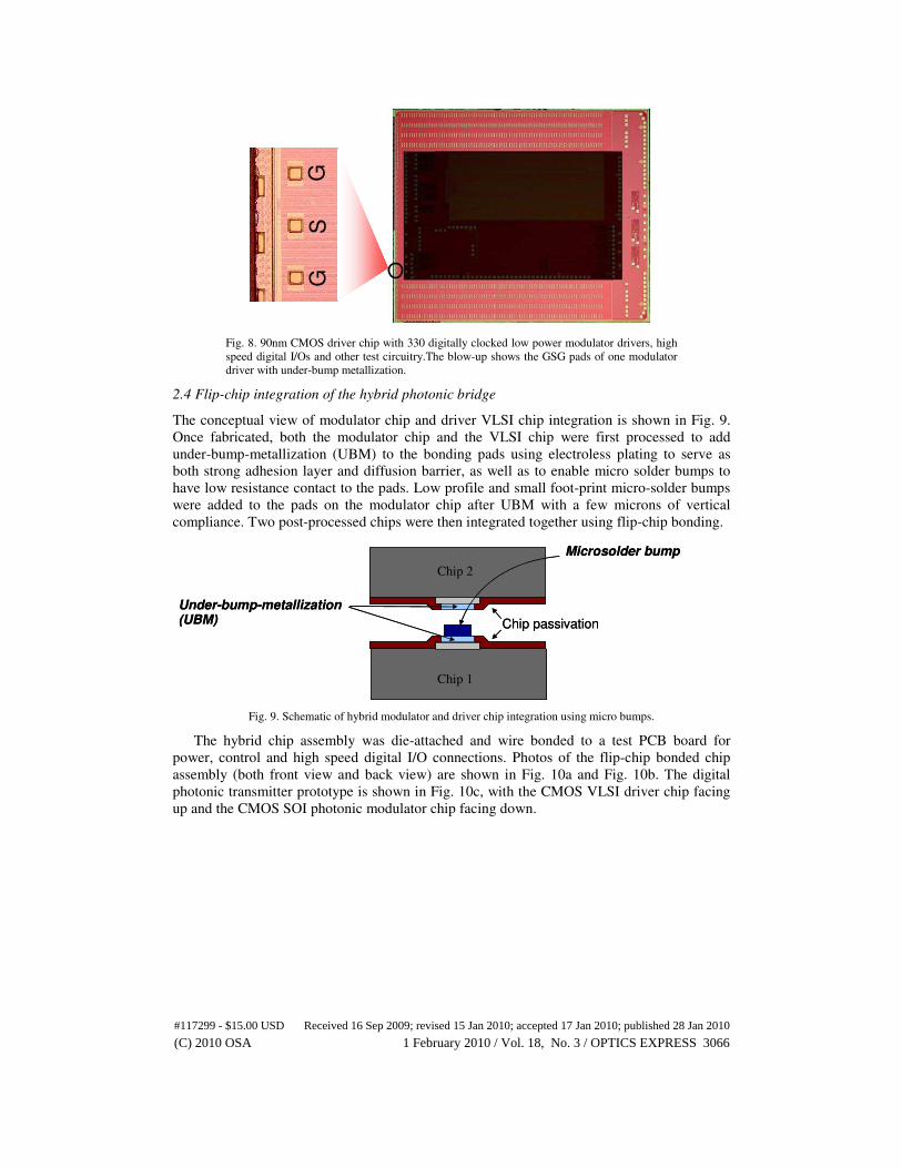
The conceptual view of modulator chip and driver VLSI chip integration is shown in Fig. 9.
Once fabricated, both the modulator chip and the VLSI chip were first processed to add
under-bump-metallization (UBM) to the bonding pads using electroless plating to serve as
both strong adhesion layer and diffusion barrier, as well as to enable micro solder bumps to
have low resistance contact to the pads. Low profile and small foot-print micro-solder bumps
were added to the pads on the modulator chip after UBM with a few microns of vertical
compliance. Two post-processed chips were then integrated together using flip-chip bonding.
Chip 1
Chip 2
Chip passivation
Under-bump-metallization (UBM)
Microsolder bump
Chip 1
Chip 2
Chip passivation
Under-bump-metallization (UBM)
Microsolder bump
Fig. 9. Schematic of hybrid modulator and driver chip integration using micro bumps.
The hybrid chip assembly was die-attached and wire bonded to a test PCB board for
power, control and high speed digital I/O connections. Photos of the flip-chip bonded chip
assembly (both front view and back view) are shown in Fig. 10a and Fig. 10b. The digital
photonic transmitter prototype is shown in Fig. 10c, with the CMOS VLSI driver chip facing
up and the CMOS SOI photonic modulator chip facing down.
#117299 - $15.00 USD Received 16 Sep 2009; revised 15 Jan 2010; accepted 17 Jan 2010; published 28 Jan 2010
(C) 2010 OSA 1 February 2010 / Vol. 18, No. 3 / OPTICS EXPRESS 3066
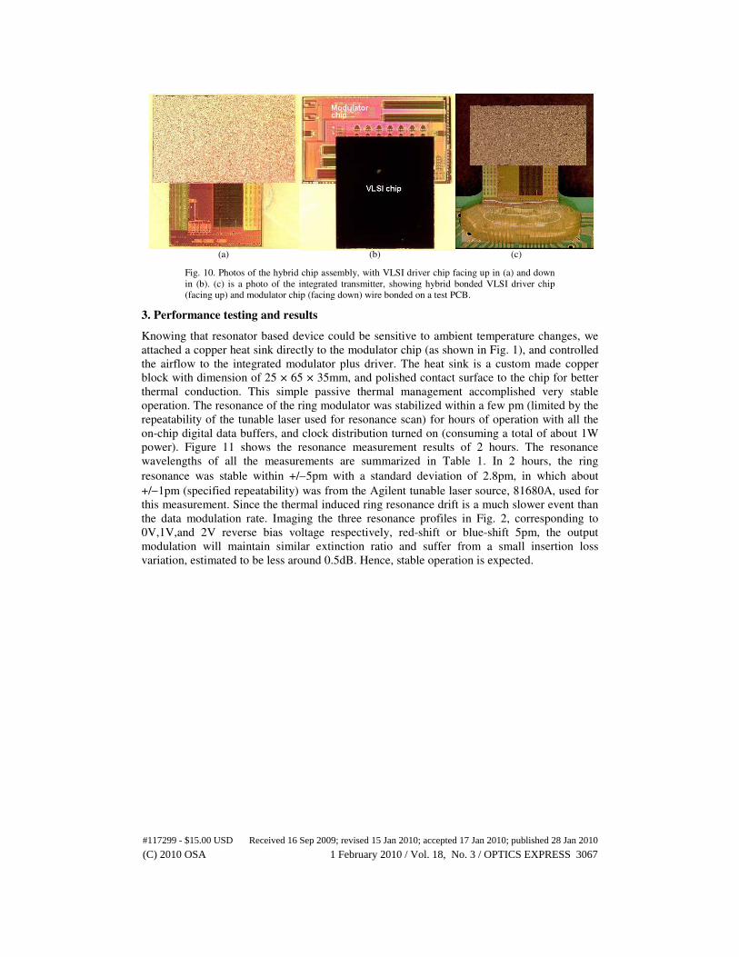
(a) (b) (c)
Fig. 10. Photos of the hybrid chip assembly, with VLSI driver chip facing up in (a) and down
in (b). (c) is a photo of the integrated transmitter, showing hybrid bonded VLSI driver chip
(facing up) and modulator chip (facing down) wire bonded on a test PCB.
3. Performance testing and results
Knowing that resonator based device could be sensitive to ambient temperature changes, we
attached a copper heat sink directly to the modulator chip (as shown in Fig. 1), and controlled
the airflow to the integrated modulator plus driver. The heat sink is a custom made copper
block with dimension of 25 × 65 × 35mm, and polished contact surface to the chip for better
thermal conduction. This simple passive thermal management accomplished very stable
operation. The resonance of the ring modulator was stabilized within a few pm (limited by the
repeatability of the tunable laser used for resonance scan) for hours of operation with all the
on-chip digital data buffers, and clock distribution turned on (consuming a total of about 1W
power). Figure 11 shows the resonance measurement results of 2 hours. The resonance
wavelengths of all the measurements are summarized in Table 1. In 2 hours, the ring
resonance was stable within +/−5pm with a standard deviation of 2.8pm, in which about
+/−1pm (specified repeatability) was from the Agilent tunable laser source, 81680A, used for
this measurement. Since the thermal induced ring resonance drift is a much slower event than
the data modulation rate. Imaging the three resonance profiles in Fig. 2, corresponding to
0V,1V,and 2V reverse bias voltage respectively, red-shift or blue-shift 5pm, the output
modulation will maintain similar extinction ratio and suffer from a small insertion loss
variation, estimated to be less around 0.5dB. Hence, stable operation is expected.
#117299 - $15.00 USD Received 16 Sep 2009; revised 15 Jan 2010; accepted 17 Jan 2010; published 28 Jan 2010
(C) 2010 OSA 1 February 2010 / Vol. 18, No. 3 / OPTICS EXPRESS 3067
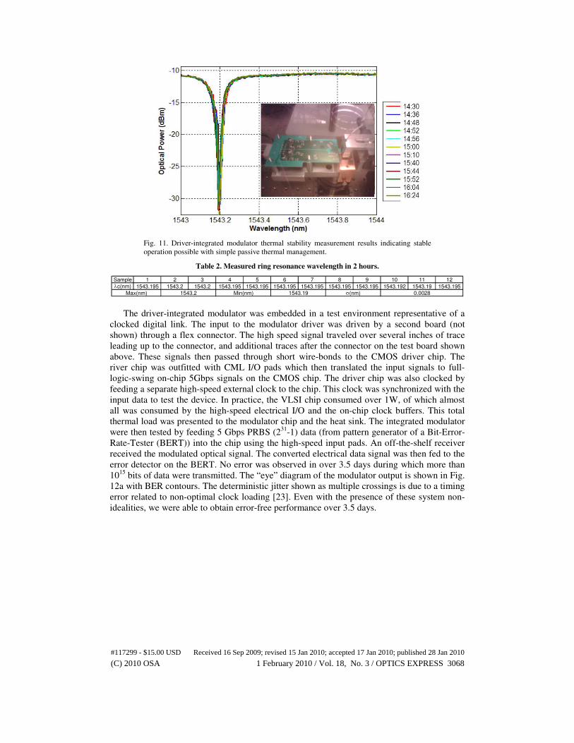
Fig. 11. Driver-integrated modulator thermal stability measurement results indicating stable
operation possible with simple passive thermal management.
Table 2. Measured ring resonance wavelength in 2 hours.
Sample 1 2 3 4 5 6 7 8 9 10 11 12λc(nm) 1543.195 1543.2 1543.2 1543.195 1543.195 1543.195 1543.195 1543.195 1543.195 1543.192 1543.19 1543.195
Max(nm) Min(nm) σ(nm) 0.00281543.191543.2
The driver-integrated modulator was embedded in a test environment representative of a
clocked digital link. The input to the modulator driver was driven by a second board (not
shown) through a flex connector. The high speed signal traveled over several inches of trace
leading up to the connector, and additional traces after the connector on the test board shown
above. These signals then passed through short wire-bonds to the CMOS driver chip. The
river chip was outfitted with CML I/O pads which then translated the input signals to full-
logic-swing on-chip 5Gbps signals on the CMOS chip. The driver chip was also clocked by
feeding a separate high-speed external clock to the chip. This clock was synchronized with the
input data to test the device. In practice, the VLSI chip consumed over 1W, of which almost
all was consumed by the high-speed electrical I/O and the on-chip clock buffers. This total
thermal load was presented to the modulator chip and the heat sink. The integrated modulator
were then tested by feeding 5 Gbps PRBS (231
-1) data (from pattern generator of a Bit-Error-
Rate-Tester (BERT)) into the chip using the high-speed input pads. An off-the-shelf receiver
received the modulated optical signal. The converted electrical data signal was then fed to the
error detector on the BERT. No error was observed in over 3.5 days during which more than
1015
bits of data were transmitted. The “eye” diagram of the modulator output is shown in Fig.
12a with BER contours. The deterministic jitter shown as multiple crossings is due to a timing
error related to non-optimal clock loading [23]. Even with the presence of these system non-
idealities, we were able to obtain error-free performance over 3.5 days.
#117299 - $15.00 USD Received 16 Sep 2009; revised 15 Jan 2010; accepted 17 Jan 2010; published 28 Jan 2010
(C) 2010 OSA 1 February 2010 / Vol. 18, No. 3 / OPTICS EXPRESS 3068
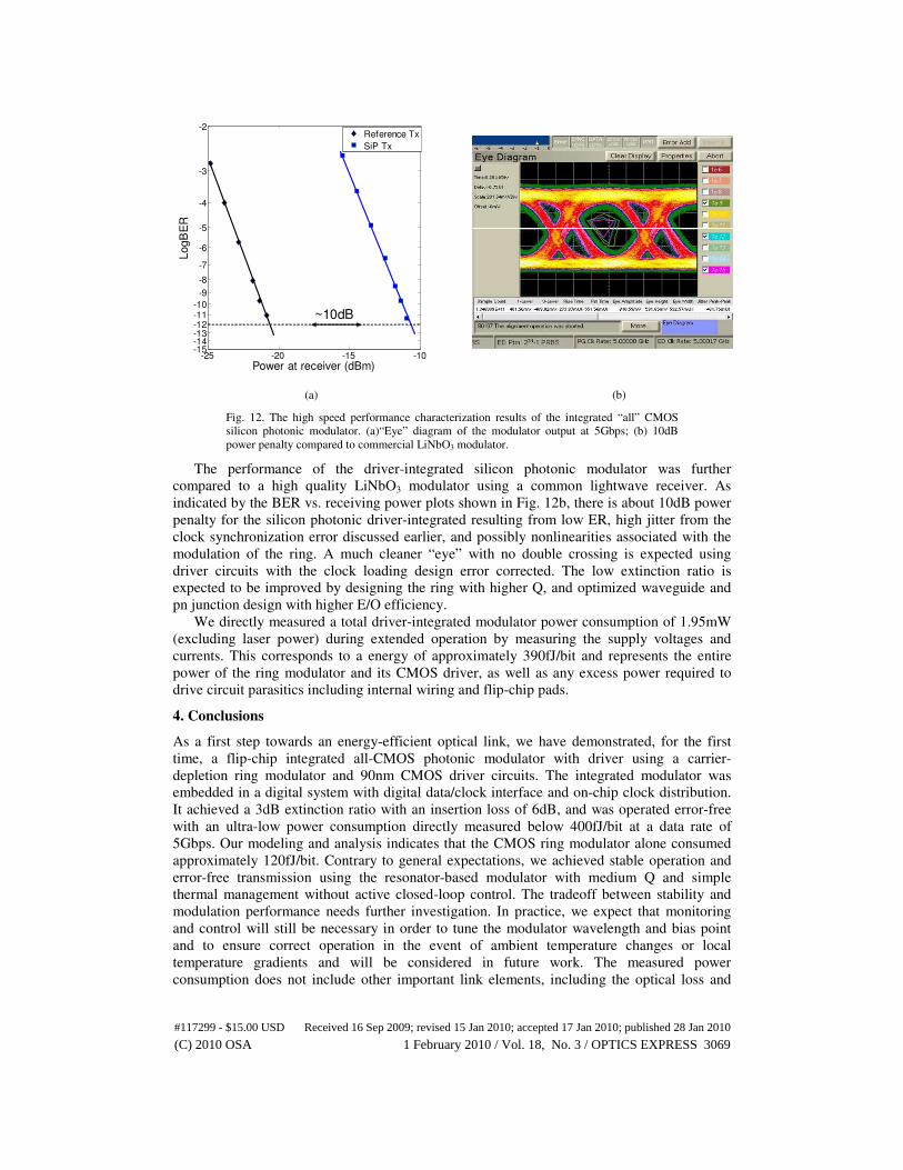
-25 -20 -15 -10-15-14-13-12-11-10
-9
-8
-7
-6
-5
-4
-3
-2
Power at receiver (dBm)
Log
BE
R
Reference Tx
SiP Tx
~10dB
(a) (b)
Fig. 12. The high speed performance characterization results of the integrated “all” CMOS
silicon photonic modulator. (a)“Eye” diagram of the modulator output at 5Gbps; (b) 10dB
power penalty compared to commercial LiNbO3 modulator.
The performance of the driver-integrated silicon photonic modulator was further
compared to a high quality LiNbO3 modulator using a common lightwave receiver. As
indicated by the BER vs. receiving power plots shown in Fig. 12b, there is about 10dB power
penalty for the silicon photonic driver-integrated resulting from low ER, high jitter from the
clock synchronization error discussed earlier, and possibly nonlinearities associated with the
modulation of the ring. A much cleaner “eye” with no double crossing is expected using
driver circuits with the clock loading design error corrected. The low extinction ratio is
expected to be improved by designing the ring with higher Q, and optimized waveguide and
pn junction design with higher E/O efficiency.
We directly measured a total driver-integrated modulator power consumption of 1.95mW
(excluding laser power) during extended operation by measuring the supply voltages and
currents. This corresponds to a energy of approximately 390fJ/bit and represents the entire
power of the ring modulator and its CMOS driver, as well as any excess power required to
drive circuit parasitics including internal wiring and flip-chip pads.
4. Conclusions
As a first step towards an energy-efficient optical link, we have demonstrated, for the first
time, a flip-chip integrated all-CMOS photonic modulator with driver using a carrier-
depletion ring modulator and 90nm CMOS driver circuits. The integrated modulator was
embedded in a digital system with digital data/clock interface and on-chip clock distribution.
It achieved a 3dB extinction ratio with an insertion loss of 6dB, and was operated error-free
with an ultra-low power consumption directly measured below 400fJ/bit at a data rate of
5Gbps. Our modeling and analysis indicates that the CMOS ring modulator alone consumed
approximately 120fJ/bit. Contrary to general expectations, we achieved stable operation and
error-free transmission using the resonator-based modulator with medium Q and simple
thermal management without active closed-loop control. The tradeoff between stability and
modulation performance needs further investigation. In practice, we expect that monitoring
and control will still be necessary in order to tune the modulator wavelength and bias point
and to ensure correct operation in the event of ambient temperature changes or local
temperature gradients and will be considered in future work. The measured power
consumption does not include other important link elements, including the optical loss and
#117299 - $15.00 USD Received 16 Sep 2009; revised 15 Jan 2010; accepted 17 Jan 2010; published 28 Jan 2010
(C) 2010 OSA 1 February 2010 / Vol. 18, No. 3 / OPTICS EXPRESS 3069
associated laser power, or the energy requirements of the receiver. Nonetheless, this
successful demonstration of a low energy silicon photonic modulator with integrated CMOS
driver is a significant step towards a complete sub-pJ/bit link that is expected to be critical for
future inter-chip and intra-chip interconnect applications.
Acknowledgements
This material is based upon work supported, in part, by DARPA under Agreement No.
HR0011-08-09-0001. The authors thank Dr. Jag Shah of DARPA MTO for his inspiration and
support of this program. The views, opinions, and/or findings contained in this
article/presentation are those of the author/presenter and should not be interpreted as
representing the official views or policies, either expressed or implied, of the Defense
Advanced Research Projects Agency or the Department of Defense. Approved for Public
Release. Distribution Unlimited.
#117299 - $15.00 USD Received 16 Sep 2009; revised 15 Jan 2010; accepted 17 Jan 2010; published 28 Jan 2010
(C) 2010 OSA 1 February 2010 / Vol. 18, No. 3 / OPTICS EXPRESS 3070