Wave-vector analysis of plasmon-assisted distributed ...
9
HAL Id: hal-03025461 https://hal.archives-ouvertes.fr/hal-03025461 Submitted on 26 Nov 2020 HAL is a multi-disciplinary open access archive for the deposit and dissemination of sci- entific research documents, whether they are pub- lished or not. The documents may come from teaching and research institutions in France or abroad, or from public or private research centers. L’archive ouverte pluridisciplinaire HAL, est destinée au dépôt et à la diffusion de documents scientifiques de niveau recherche, publiés ou non, émanant des établissements d’enseignement et de recherche français ou étrangers, des laboratoires publics ou privés. Wave-vector analysis of plasmon-assisted distributed nonlinear photoluminescence along Au nanowires Deepak K Sharma, Adrian Agreda, Julien Barthes, Gérard Colas Des Francs, G V Pavan Kumar, Alexandre Bouhelier To cite this version: Deepak K Sharma, Adrian Agreda, Julien Barthes, Gérard Colas Des Francs, G V Pavan Kumar, et al.. Wave-vector analysis of plasmon-assisted distributed nonlinear photoluminescence along Au nanowires. Physical Review B, American Physical Society, 2020, 102, 10.1103/physrevb.102.115414. hal-03025461
-
Upload
khangminh22 -
Category
Documents
-
view
0 -
download
0
Transcript of Wave-vector analysis of plasmon-assisted distributed ...

HAL Id: hal-03025461https://hal.archives-ouvertes.fr/hal-03025461
Submitted on 26 Nov 2020
HAL is a multi-disciplinary open accessarchive for the deposit and dissemination of sci-entific research documents, whether they are pub-lished or not. The documents may come fromteaching and research institutions in France orabroad, or from public or private research centers.
L’archive ouverte pluridisciplinaire HAL, estdestinée au dépôt et à la diffusion de documentsscientifiques de niveau recherche, publiés ou non,émanant des établissements d’enseignement et derecherche français ou étrangers, des laboratoirespublics ou privés.
Wave-vector analysis of plasmon-assisted distributednonlinear photoluminescence along Au nanowires
Deepak K Sharma, Adrian Agreda, Julien Barthes, Gérard Colas Des Francs,G V Pavan Kumar, Alexandre Bouhelier
To cite this version:Deepak K Sharma, Adrian Agreda, Julien Barthes, Gérard Colas Des Francs, G V Pavan Kumar,et al.. Wave-vector analysis of plasmon-assisted distributed nonlinear photoluminescence along Aunanowires. Physical Review B, American Physical Society, 2020, 102, �10.1103/physrevb.102.115414�.�hal-03025461�

PHYSICAL REVIEW B 102, 115414 (2020)
Wave-vector analysis of plasmon-assisted distributed nonlinearphotoluminescence along Au nanowires
Deepak K. Sharma ,1,2,* Adrian Agreda,1 Julien Barthes ,1 Gérard Colas des Francs ,1 G. V. Pavan Kumar ,2
and Alexandre Bouhelier 1,†
1Laboratoire Interdisciplinaire Carnot de Bourgogne, UMR 6303 CNRS, Université de Bourgogne Franche-Comté,9 avenue Alain Savary, 21000 Dijon, France
2Department of Physics, Indian Institute of Science Education and Research, Pune 411008, India
(Received 24 June 2020; revised 24 August 2020; accepted 26 August 2020; published 14 September 2020)
We report a quantitative analysis of the wave-vector diagram emitted by nonlinear photoluminescence gen-erated by a tightly focused pulsed laser beam and distributed along Au nanowire via the mediation of surfaceplasmon polaritons. The nonlinear photoluminescence is locally excited at key locations along the nanowirein order to understand the different contributions constituting the emission pattern measured in a conjugateFourier plane of the microscope. Polarization-resolved measurements reveal that the nanowire preferentiallyemits nonlinear photoluminescence polarized transverse to the long axis at close to the detection limit wavevectors with a small azimuthal spread in comparison to the signal polarized along the long axis. We utilizethe finite-element method to simulate the observed directional scattering by using localized incoherent sourcesplaced on the nanowire. Simulation results faithfully mimic the directional emission of the nonlinear signalemitted by the different portions of the nanowire.
DOI: 10.1103/PhysRevB.102.115414
I. INTRODUCTION
Metal nanostructures confine electromagnetic fields inthe subwavelength regime by controlling resonant modesknown as surface plasmons polaritons (SPPs) [1,2]. Thevery large electric field present at the metal surface makesplasmonic-based devices excellent candidates to harness weaklight-matter interactions [3,4] and to enhance optical non-linear signals at the nanoscale [5,6]. Hand in hand with theelectric field enhancement, a plasmonic nanostructure candirect the light according to the structural modes it sup-ports [7–10]. For instance, placement of multiple elements in aspecific spatial arrangement can provide unidirectional emis-sion according to phase retardation produced by the wholegeometry. A combination of plasmonic nanostructures placedin the form of the Yagi-Uda design [11,12] and metasur-faces [13] have been utilized to provide high directivity andbeaming effect from dipolar emitters.
In this context, a metal nanowire is an interesting plas-monic nanostructure that can confine, guide, and routeSPPs [14–16]. Plasmonic nanowires confine surface plasmonswell below the diffraction limit in the transverse dimensionsand propagate the mode up to several micrometers along itsmain axis. The SPP may then out couple to free-space pho-tons emitted in a defined angular direction when it scattersfrom the extremity of the metal waveguide [14]. For instance,plasmonic nanowires have been utilized for collecting anddirecting fluorescence signals emitted by nanocrystals [17]and quantum emitters [18] mainly in a direction imposed bythe along the main axis.
*[email protected]†[email protected]
Another interesting property brought by the large enhance-ment of the electric field associated with the excitation of thesurface plasmon is the ability of the metal structure to generateits own surface nonlinearities [19,20]. We recently showedthat Au nanowires (AuNWs), and, more generally, extendedtwo-dimensional structures, may produce a distributed non-linear photoluminescence (NPL) when excited locally by atightly focused ultrafast laser beam [21,22]. This nonlinearsignal holds potential for developing advanced functionalitiessuch as wavelength conversion [23] and all-optical Booleanoperations [22,24]. Understanding this nonlinear responsespatially transported in the geometry brings strategies on howto control it. Equally important is the knowledge of the direc-tion the frequency-converted photons take when they scatterout of the structure and travel in free space.
With this motivation, we perform an analysis of the in-plane wave-vector distribution of the NPL developing on theAuNW. We locally excite the NPL at the extremity and at thecenter of a AuNW in order to understand and discriminatecontributions from the different sections of the nanowire. Weanalyze the resulting Fourier plane pattern emitted by thedistributed NPL as a function of its polarization. We furtheruse finite-element method based simulations to understandour experimental results.
II. RESULTS AND DISCUSSION
A. Experimental procedures
1. Fabrication of the Au nanowires
We fabricated a 3.5-µm-long and 160-nm-wide poly-crystalline AuNW on a glass substrate using a top-downfabrication procedure. Fabrication steps involve standardelectron-beam lithography (Pioneer, Raith GmbH) followed
2469-9950/2020/102(11)/115414(8) 115414-1 ©2020 American Physical Society
DEEPAK K. SHARMA et al. PHYSICAL REVIEW B 102, 115414 (2020)
FIG. 1. (a) A scanning electron micrograph of a 3.5-µm-longAuNW. (b) Schematic diagram (not to scale) of the experimentalsetup. The laser beam is tightly focused using a high-NA objectivelens at the AuNW. Scattered optical responses into the glass substrateare collected by the same objective lens. Different combinations ofrelay lenses are used to capture the Fourier plane images and wide-field real-plane images or spectrum from the sample. A half-waveplate is used to control input polarization, and NPL is analyzed by alinear polarizer in the output path. A set of filters is used to spectrallyselect the NPL response of the AuNW.
by metal depositions and a liftoff process. The subsequentmetal layers consist of a 3-nm-thick adhesive layer of tita-nium deposited by electron-beam physical vapor deposition(MEB 400, Plassys) and a 50-nm-thick Au layer deposited bythermal evaporation. Figure 1(a) presents a scanning electronmicrograph of the AuNW.
2. Optical measurements
The AuNW and the glass coverslip are then placed onan inverted optical microscope (Nikon, Eclipse). The exper-imental setup is schematically illustrated in the Fig. 1(b). Thenanowire is optically excited at a wavelength of λ0 = 808 nmat one of its extremities by a femtosecond pulsed laser beam(Coherent, Chameleon). The beam is tightly focused throughthe glass by a high numerical aperture (NA) oil-immersionobjective lens (Nikon, 100×, NA = 1.49). The same objec-tive lens is utilized for the collection of light scattered andemitted by the nanowire. Using relay lenses placed after theexit port of the microscope, the collected light is sent toa charge-coupled device (CCD) camera (Andor, Luca) or a
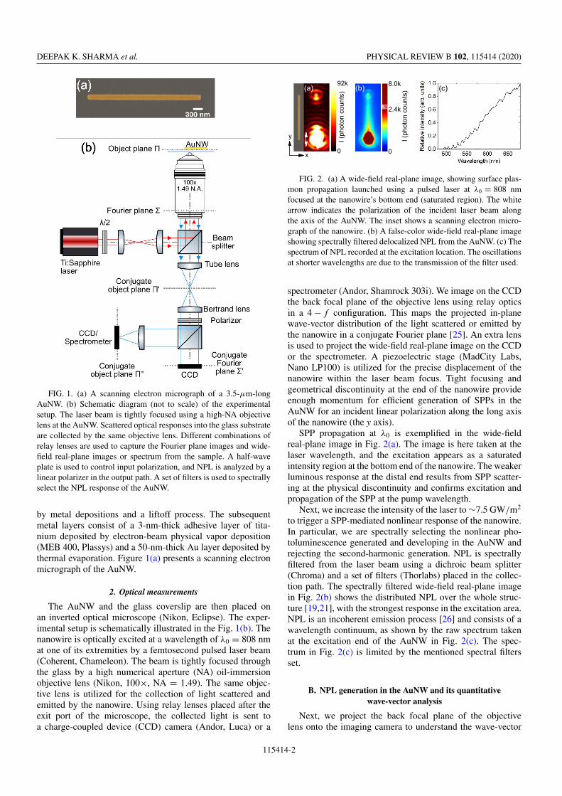
FIG. 2. (a) A wide-field real-plane image, showing surface plas-mon propagation launched using a pulsed laser at λ0 = 808 nmfocused at the nanowire’s bottom end (saturated region). The whitearrow indicates the polarization of the incident laser beam alongthe axis of the AuNW. The inset shows a scanning electron micro-graph of the nanowire. (b) A false-color wide-field real-plane imageshowing spectrally filtered delocalized NPL from the AuNW. (c) Thespectrum of NPL recorded at the excitation location. The oscillationsat shorter wavelengths are due to the transmission of the filter used.
spectrometer (Andor, Shamrock 303i). We image on the CCDthe back focal plane of the objective lens using relay opticsin a 4 − f configuration. This maps the projected in-planewave-vector distribution of the light scattered or emitted bythe nanowire in a conjugate Fourier plane [25]. An extra lensis used to project the wide-field real-plane image on the CCDor the spectrometer. A piezoelectric stage (MadCity Labs,Nano LP100) is utilized for the precise displacement of thenanowire within the laser beam focus. Tight focusing andgeometrical discontinuity at the end of the nanowire provideenough momentum for efficient generation of SPPs in theAuNW for an incident linear polarization along the long axisof the nanowire (the y axis).
SPP propagation at λ0 is exemplified in the wide-fieldreal-plane image in Fig. 2(a). The image is here taken at thelaser wavelength, and the excitation appears as a saturatedintensity region at the bottom end of the nanowire. The weakerluminous response at the distal end results from SPP scatter-ing at the physical discontinuity and confirms excitation andpropagation of the SPP at the pump wavelength.
Next, we increase the intensity of the laser to ∼7.5 GW/m2
to trigger a SPP-mediated nonlinear response of the nanowire.In particular, we are spectrally selecting the nonlinear pho-toluminescence generated and developing in the AuNW andrejecting the second-harmonic generation. NPL is spectrallyfiltered from the laser beam using a dichroic beam splitter(Chroma) and a set of filters (Thorlabs) placed in the collec-tion path. The spectrally filtered wide-field real-plane imagein Fig. 2(b) shows the distributed NPL over the whole struc-ture [19,21], with the strongest response in the excitation area.NPL is an incoherent emission process [26] and consists of awavelength continuum, as shown by the raw spectrum takenat the excitation end of the AuNW in Fig. 2(c). The spec-trum in Fig. 2(c) is limited by the mentioned spectral filtersset.
B. NPL generation in the AuNW and its quantitativewave-vector analysis
Next, we project the back focal plane of the objectivelens onto the imaging camera to understand the wave-vector
115414-2

WAVE-VECTOR ANALYSIS OF PLASMON-ASSISTED … PHYSICAL REVIEW B 102, 115414 (2020)
FIG. 3. (a) Fourier plane image of the delocalized NPL cor-responding to the real-plane image shown in Fig. 2(b). (b) NPLintensity plots along the ky/k0 (black) and kx/k0 (red) axes of theFourier plane image. (c) NPL intensity distribution profile alongthe azimuthal coordinate φ plotted at radial coordinates of 1.1, 1.3,and 1.43.
distribution of the distributed NPL [25]. Figure 3(a) showsthe Fourier plane pattern of the distributed NPL captured inthe 480–680-nm wavelength range. Axes are in units of NA,where ky/k0 and kx/k0 are relative to normalized in-planewave vectors, with k0 being the wave vector in free space. Themaximum detectable in-plane wave vector is given by the NAof the objective and sets the outer rim radius of the Fourierplane at 1.49. The inner ring is located at NA = 1.0 andcorresponds to the critical angle at the glass-air interface. The
emission diagram of the NPL features an inhomogeneous dis-tribution of the intensity, indicating that some in-plane wavevectors bear more weight than others. This is particularly thecase for the +ky/k0 wave vectors located near the detectionlimit.
We quantitatively analyze this Fourier plane pattern byplotting radial cross sections along the ky/k0 (at kx/k0 = 0)and kx/k0 axes (at ky/k0 = 0), shown as black and red curvesin Fig. 3(b), respectively. The cross sections indicate thatintensity maximum is aligned along the ky/k0 axis with a peakat ky/k0 ∼ +1.43. As a reminder, we recall that the main axisof the AuNW is oriented along the y axis. The black curveshows that the intensity in the −ky/k0 direction is smoothlydistributed for ky/k0 > 1.0, with a small increase towardshigher wave vectors in comparison to the +ky/k0 direction,where the maximum intensity clearly peaks. We hypothesizethat the asymmetric distribution of intensity along the ky/k0axis is an effect of the asymmetry of the NPL intensity dis-tributed all along the AuNW [Fig. 2(b)], as discussed later on.The red curve shows that the intensity maxima along kx/k0 arelocated near the critical angle (±kx/k0 ∼ 1.1). This feature isunderstood from the local excitation of the NPL by the tightlyfocused excitation spot. We have quantified the directional-ity D = 10 log10 IF/IB along the ky/k0 axis by measuring theintensity ratio between the point with maximum intensity IFin the upper half and the diametrically opposite point withintensity IB in the lower half of the Fourier plane. The D valueis 3.15 dB for the intensity maximum at ky/k0 = +1.43.
The Fourier plane highlights that the emitted rays not onlyemerge at specific ky/k0 wave vectors but also feature a limitedazimuthal spread. We quantitatively evaluate the azimuthalextension by plotting the intensity as a function of the az-imuthal angle φ at NA = 1.1, 1.3, and 1.43, shown in Fig. 3(c).The azimuthal plots show that the maximum NPL is angularlyrestricted and symmetric around the ky/k0 axis correspondingto the long axis of the AuNW. The intensity maxima are atφ ∼ 90◦ (−ky/k0 axis) and φ ∼ 270◦ (+ky/k0 axis), withthe angular spread decreasing as NA increases in the lowerhalf of the Fourier plane image.
In what follows, we provide an understanding of the dif-ferent parts of the AuNW contributing to the complex Fourierplane pattern quantified in Fig. 3.
C. Position-dependent scattering of the NPL local sourceby the AuNW
1. Definition of the NPL emissive regions
The distribution of NPL intensity across the AuNW isa result of multiple processes generating the nonlinear re-sponse [21]. Figure 4(a) schematically pictures how the NPLdevelops in a AuNW. Overlapping the input laser beam witha AuNW extremity results in a large electric field at thedielectric discontinuity, leading to enhanced localized NPLemission at the excitation point. This region is indicated asregion I in Fig. 4(a). The excitation of the extremity launchesa SPP propagating in the AuNW at the excitation wavelength(808 nm), as already illustrated in Fig. 2. If the intensityof the pump is large enough, the SPP triggers a nonlinearinteraction as it propagates and results in the distributed NPLalong the AuNW, represented as region II. This delocalized
115414-3

DEEPAK K. SHARMA et al. PHYSICAL REVIEW B 102, 115414 (2020)
FIG. 4. (a) Schematic representation of the NPL distributed in aAuNW. (b) Intensity cross section along the AuNW indicates threedifferent regions (I, II, and III) of the distributed NPL in the AuNW.NPL is generated at the input end of the AuNW by direct laser beamexcitation (region I). A SPP traveling in the AuNW at the excitationwavelength (λ0 = 808 nm) generates NPL along the nanowire (regionII). NPL in region III is a sum of a local NPL emission produced bythe pump SPP scattering at the extremity and a continuum of SPPmodes launched in region I within the NPL spectrum, traveling andout coupled by the distal end.
NPL signature is not a mode but is locally produced at themetal surface by the underlying SPP traveling at λ0 [19,21].When the SPP reaches the distal end, it produces a localizedNPL response, indicated as region III. Region III also containsscattering of a surface plasmon continuum. These secondaryplasmons are launched at the input extremity by the strongand localized NPL produced by the laser focus. They areexcited with a continuum of wavelength contained withinthe NPL emission spectrum (Fig. 2). These NPL SPPs outcouple at +ky/k0 directions at higher wave vectors with a wideazimuthal spread [14]. This contribution is, however, not thepredominant source of the NPL photons at the distal end sincethis set of secondary plasmons suffers from large propagationlosses compared to the plasmon excited at the near-infraredpump wavelength. Considering the NPL produced at bothextremities to be two local secondary sources of light, thenanowire scatters the source located in region III in the exactopposite way it scatters NPL from region I because of themirror symmetry. However, the intensity in region III remainsmuch weaker than that in the other two regions [see Fig. 4(b)],and we do not observe a clear symmetric −ky/k0 signature at−1.43.
Hence, understanding the contributions from the two re-maining regions, i.e., regions I and II, can provide information
about the effect of different parts of the AuNW on the NPLwave-vector distribution presented in Fig. 3(a). This analysisis possible only because NPL is an incoherent process and theFourier plane is not an interferogram.
2. Fourier contributions from region I
As illustrated in Fig. 4, NPL emission in region I re-gards the AuNW in the +y axis and free space in the−y axis. NPL emission in the region II perceives the pres-ence of AuNW in both directions. To separately study thewave-vector distribution stemming from these two situationswhich, considering the relative weight of the nonlinear re-sponse at these positions, maximally contribute to the Fourierplane distribution in Fig. 3(a), we excite the AuNW attwo different locations and for two incident polarizationorientations.
First, to extract the wave-vector content of the local NPLproduced by the laser in region I and scattered by the physicaldiscontinuity, we excite one end of the AuNW with an inputpolarization transverse to its long axis. In this configuration,coupling to a SPP at λ0 remains inefficient [27], as illustratedin the wide-field real-plane image in Fig. 5(a) taken at theexcitation wavelength. Hence, NPL is generated essentially inregion I and is absent from region II [Fig. 5(b)]. We observe aninsignificant contribution in region III from the NPL-excitedsecondary SPP discussed above.
The Fourier plane image in Fig. 5(c) shows the wave-vectordistribution of the NPL for this excitation configuration. Weobserve a strong intensity at +ky/k0 near the detection limitwhich strongly resembles the one measured in Fig. 3(a). Thisshared feature suggests that it is not the result of a SPP atλ0. We claim that the reduction of the azimuthal and ra-dial wave-vector spread is due to the quasi-one-dimensionalnanowire geometry. The directivity value calculated for theintensity maximum at ky/k0 = +1.43 is D = 5.6 dB, which isin the range of directionality achieved for the optical Yagi-Udaantenna [11].
The Fourier plane in Fig. 5(c) also contains marked dif-ferences from Fig. 3(a). In particular, the intensity of thewave vectors located in the lower half of the diagram has amuch larger azimuthal spread than the one measured for apolarization aligned with the nanowire. Azimuthal plots inFig. 5(d) indicate broader wave-vector spread at NA = 1.05and negligible intensity at NA = 1.43 in the lower half of theFourier plane. This can be understood from the absence of thenanowire in the −y axis to the excitation spot and the absenceof NPL in region II.
3. Fourier contributions from region II
Now, we try to understand the Fourier contribution to NPLemitted from region II of the nanowire. To remove the influ-ence of the strong local response of the extremity, we movethe laser beam to the center of the AuNW and align the inci-dent polarization along the main axis. Here again, no SPP islaunched in the AuNW because there is no momentum trans-fer provided by the geometry along the polarization direction.This is pictured in the wide-field image in Fig. 6(a) taken atthe laser wavelength. In the laser-filtered image in Fig. 6(b),the NPL spatial extension is thus limited to the focus size with
115414-4

WAVE-VECTOR ANALYSIS OF PLASMON-ASSISTED … PHYSICAL REVIEW B 102, 115414 (2020)
FIG. 5. (a) Wide-field real-plane image taken at λ0 for an exci-tation polarized transverse to the nanowire. No SPP is generated forthis polarization and position of the nanowire in the focus. (b) and(c) Corresponding filtered NPL wide-field real- and Fourier planeimages, respectively. (d) NPL intensity distribution profile along theazimuthal coordinate φ plotted at NA = 1.05 and NA = 1.43. Smalldiffraction rings observed in the Fourier plane are from hard-to-remove stains at the surface of relay lenses.
a negligible coupling of the NPL-excited secondary SPP tothe nanowire. This situation mimics the effect of the nanowireon the NPL generated locally along the AuNW surface at thecenter of region II (Fig. 4). As expected, the presence of thenanowire on both sides of the localized NPL source renders asymmetric Fourier plane. This is pictured in Fig. 6(c), wherethe wave-vector intensity peaks at the detection limit on boththe +ky/k0 and −ky/k0 axes. The angular azimuthal spreadsare narrow on both the +ky/k0 and −ky/k0 axes, with anaverage FWHM = 40◦, as shown in the cross-sectional profileplotted at NA = 1.41 in Fig. 6(d).
We can summarize the explanation of the Fourier plane ofdistributed NPL (Fig. 3) using the above observations. Themaximum intensity towards +ky/k0 is due to the dominantNPL emitted in region I and redirected there by the scatteringinfluence of the nanowire. A second contributor to this inten-sity maximum originates from the NPL present in region IIand, to a much lesser extent, the secondary SPPs launched bythe local NPL at the input and scattering in region III fromthe distal end. In-plane wave vectors emerging at numerical
FIG. 6. (a) Wide-field real-plane image taken at λ0 for an ex-citation located at the center of the AuNW. Polarization is alongthe main axis (double arrow). SPP excitation is absent. (b) and(c) Corresponding filtered NPL wide-field real-plane and Fourierplane images, respectively. (d) NPL intensity distribution profilealong the azimuthal coordinate φ plotted at NA = 1.41.
aperture values near NA ∼1 in the lower half of the Fourierplane are wave vectors which are not affected by the nanowire.NPL filling the Fourier space above the critical angle inthe −ky/k0 direction comes from region II complementedby the weak scattering of the localized NPL source presentat the distal end (region III).
D. Polarization-analyzed wave-vector distributionof the distributed NPL
We complete our measurements by analyzing the polar-ization of the emitted NPL. We record the NPL intensitydistributions in real and Fourier spaces for two polarizationorientations of the emitted NPL. Polarization of the inputbeam remains fixed along the long axis of the AuNW, andthe analyzer axis is rotated either along or transverse to thelong axis of the AuNW. The excitation stays fixed at the lowerextremity of the AuNW.
Figures 7(a) and 7(b) show a wide-field real-plane imageand the corresponding Fourier plane image of the NPL po-larized along the long axis of the AuNW, respectively. Whilethe wide-field image does not qualitatively differ from Fig. 2,
115414-5

DEEPAK K. SHARMA et al. PHYSICAL REVIEW B 102, 115414 (2020)
FIG. 7. Polarization-analyzed (a) and (c) wide-field real plane-images and (b) and (d) Fourier plane images. White and red arrowsindicate the axis of polarization of the input laser beam and of theanalyzer, respectively.
the Fourier plane is now essentially symmetric with respectto the ky/k0 and kx/k0 axes. The narrowing of the wave-vectorspread in the radial and azimuthal directions at +ky/k0 ∼ 1.43imparted by the nanowire is absent. We understand this fromthe following argumentation. We assume for the sake of theargument that the local sources positioned at either extremityand along the nanowire can be considered a random distri-bution of oriented dipoles. The orientation of the analyzerselects the dipole moments preferentially emitting along thenanowire. In the far field, these dipole emission diagramsfeatures the well-known two-lobe pattern oriented perpendic-ularly to the dipole moment (and the axis of the nanowire).This particular orientation of the emission lobes mitigatesthe possible effect of the nanowire on the directionalityof NPL.
Now, the analyzer axis is rotated transverse to the longaxis of the AuNW to analyze the NPL polarized along thisdirection. The results are displayed in the wide-field real-and Fourier plane images in Figs. 7(c) and 7(d). Again, thespatial distribution of the NPL closely resembles those alreadyobserved for the cross-polarization detection and for the un-polarized detection (Fig. 2). Quantitatively, the intensity ofthe NPL in region II is higher than in the previous polariza-tion detection, mainly because the efficiency of the nonlinearprocess is helped by an interaction with the surface of themetal [21].
The Fourier plane essentially features all the impor-tant details already observed in Fig. 3. Considering againthe local NPL sources at the extremities and along thenanowire to be dipoles oscillating perpendicularly to thenanowire axis, this particular orientation of the analyzerfavors an emission diagram aligned with the AuNW, maxi-mizing henceforth the directional emission and concentratingthe wave-vector content to a narrow angular distribution athigh +ky/k0.
FIG. 8. (a) and (c) Schematic placement of dipoles at the endand at the center of the AuNW, respectively. Fourier plane images aresimulated for a single dipole placed at positions x = 0, −40, and +40nm across the AuNW width for a wavelength range of 550–680 nmin 10-nm steps. (b) and (d) Fourier plane images representing theincoherent sum for the dipoles placed at the extremity in (a) and thecenter of the nanowire in (c), respectively.
E. Simulation results
We have performed a series of simulations to confirmthe experimental NPL wave-vector distributions. The three-dimensional finite-element method is used to calculate thenear-field electric field using COMSOL MULTIPHYSICS soft-ware. The far-field wave-vector intensity distribution of thefields emitted into the substrate is calculated by an analyticaltreatment based on reciprocity arguments [28]. The AuNWis modeled as a 3.5-µm-long, 160-nm-wide, and 50-nm-tallcuboidal structure. The cuboid is placed on a glass substrate(refractive index = 1.50) and is covered with air (refractiveindex = 1). The Au wavelength-dependent refractive index istaken from [29]. The top edges of the cuboid are rounded witha 5-nm radius to reproduce the definition of lithographicallyproduced AuNW. A dipole source is positioned at one endof the nanowire, as schematically shown in Fig. 8(a). Theextent of NPL along the width is mimicked by positioningdipoles at positions x = 0, −40, and +40 nm along the widthof the AuNW at the glass-metal interface. Fourier plane pat-terns are simulated for dipoles with equal strength, oscillatingalong the x (transverse to the long axis of the nanowire), y(along the long axis of the nanowire), and z (out of plane)axes in the NPL wavelength range (550–680 nm).
The NPL is an incoherent process, and its wave-vectordistribution emitted in the substrate may be modeled as anincoherent sum of Fourier plane patterns obtained for dipolesoscillating in the x, y, and z axes within the NPL wavelengthrange:
INPL(kx, ky) =!
λ
aλ[Ix(kx, ky, λ)
+ Iy(kx, ky, λ) + Iz(kx, ky, λ)]. (1)
115414-6

WAVE-VECTOR ANALYSIS OF PLASMON-ASSISTED … PHYSICAL REVIEW B 102, 115414 (2020)
FIG. 9. (a)–(c) Calculated Fourier plane images for the inco-herent dipole source placed at the end of the AuNW at singlewavelengths of 550, 620, and 680 nm, respectively.
Here aλ is a coefficient that includes the weight of the NPL atdifferent wavelengths taken from the NPL spectrum (Fig. 2)and I(x,y,z) are the calculated intensity diagrams for each dipoleaxis. The resultant sum of INPL(kx, ky ) for different positionsalong the x axis in Fig. 8(b) resembles the experimentallyobserved wave-vector distribution in Fig. 5(c). The salientfeatures observed experimentally are reproduced in the sim-ulations, especially the distribution of intensity peaking alongthe +ky/k0 axis. Additional fringes not observed experimen-tally come from the coherent nature of dipole sources at aparticular wavelength and for a particular polarization in thesimulations. In contrast, NPL, by the nature of its generation,is an incoherent emission process [30].
Next, the probing dipole is moved to the center (length-wise) of the AuNW, as shown in Fig. 8(c), and the samesimulations as above are repeated to mimic the Fourier planepattern of the NPL in Fig. 6(c). In this configuration dipolesperceive the presence of the nanowire in both the −y and +ydirections and hence have a symmetric distribution along theky/k0 axis [Fig. 8(d)]. The resultant incoherent sum of Fourierplane patterns in Fig. 8(d) is in qualitative agreement withthe experimental distribution directions in Fig. 6(c). Hence,the simulation results qualitatively support the experimentalobservation that different parts of the AuNW generate NPLin-plane wave vectors differently and confirm our hypothesis.
The wave-vector distribution of NPL depends on thedetection window of the spectrum [19]. For qualitativeunderstanding of the wavelength-dependent wave-vector dis-tribution of NPL, we have calculated Fourier plane imagesfor the incoherent dipole source at the end of the AuNW
[Fig 8(a)] at single wavelengths of 550, 620, and 680 nmin Figs. 9(a)–9(c). Observed wave-vector distributions differfrom each other, and Fourier plane images suggest that theintensity maximum observed in the upper half of the exper-imental Fourier plane image has a greater weight at higherwavelengths. This feature can be understood from materialdispersion, which prevents the AuNW from operating effi-ciently for shorter wavelengths.
III. CONCLUSION
Using a quantitative analysis of Fourier plane patterns, wehave demonstrated the effect of the AuNW on the direction-ality of NPL. Distributed NPL over the AuNW results in anintricate Fourier plane pattern, which is explained by excitingdifferent parts of the nanowire separately. Our polarization-analyzed study suggests that the directional signal of thedistributed NPL, mapped at higher wave vectors, is maxi-mally polarized transversely to the long axis of the nanowire.Finite-element method based simulations confirm that the di-rectionality of the radiation pattern depends on the placementof the incoherent source at different positions on the nanowire.Our simulation results have considered a NPL source mim-icked by dipoles and are in qualitative agreement with ourexperimental results. Hence, our study of wave-vector anal-ysis may be equally applied to NPL generated by structuresmore complex than a nanowire.
ACKNOWLEDGMENTS
The work was made possible through the Indo-FrenchCentre for the Promotion of Advanced Research, ProjectNo. 5504-3, the APEX project funded by the Conseil Ré-gional de Bourgogne Franche-Comté, the European RegionalDevelopment Fund (ERDF), and EUR-EIPHI Grant No.17-EURE-0002. Device fabrication was performed in thetechnological platform ARCEN Carnot with the support ofthe Région de Bourgogne Franche-Comté and the DélégationRégionale à la Recherche et à la Technologie (DRRT). Calcu-lations were partially performed using HPC resources fromDSI-CCuB (Université de Bourgogne). G.V.P.K. acknowl-edges Department of science and technology, India, for aSwarnajayanti fellowship Grant No. DST/SJF/PSA-02/2017-18. D.K.S. thanks A. B. Vasista and D. Paul for fruitfuldiscussions.
[1] H. Raether, Surface Plasmons on Smooth and Rough Surfacesand on Gratings (Springer, Berlin, 1988), pp. 4–39.
[2] W. L. Barnes, A. Dereux, and T. W. Ebbesen, Surface plasmonsubwavelength optics, Nature (London) 424, 824 (2003).
[3] P. Anger, P. Bharadwaj, and L. Novotny, Enhancement andQuenching of Single-Molecule Fluorescence, Phys. Rev. Lett.96, 113002 (2006).
[4] J. Langer et al., Present and future of surface-enhanced ramanscattering, ACS Nano 14, 28 (2020).
[5] M. Kauranen and A. V. Zayats, Nonlinear plasmonics, Nat.Photonics 6, 737 (2012).
[6] S. Kim, J. Jin, Y.-J. Kim, I.-Y. Park, Y. Kim, and S.-W. Kim,High-harmonic generation by resonant plasmon field enhance-ment, Nature (London) 453, 757 (2008).
[7] C. Huang, A. Bouhelier, G. Colas des Francs, A. Bruyant, A.Guenot, E. Finot, J.-C. Weeber, and A. Dereux, Gain, detuning,and radiation patterns of nanoparticle optical antennas, Phys.Rev. B 78, 155407 (2008).
[8] T. H. Taminiau, F. D. Stefani, and N. F. van Hulst, Opticalnanorod antennas modeled as cavities for dipolar emitters: Evo-lution of sub- and super-radiant modes, Nano Lett. 11, 1020(2011).
115414-7

DEEPAK K. SHARMA et al. PHYSICAL REVIEW B 102, 115414 (2020)
[9] D. Vercruysse, Y. Sonnefraud, N. Verellen, F. B. Fuchs, G. DiMartino, L. Lagae, V. V. Moshchalkov, S. A. Maier, and P.Van Dorpe, Unidirectional side scattering of light by a single-element nanoantenna, Nano Lett. 13, 3843 (2013).
[10] L. Novotny and N. Van Hulst, Antennas for light, Nat. Photonics5, 83 (2011).
[11] A. G. Curto, G. Volpe, T. H. Taminiau, M. P. Kreuzer, R.Quidant, and N. F. van Hulst, Unidirectional emission of aquantum dot coupled to a nanoantenna, Science 329, 930(2010).
[12] T. Kosako, Y. Kadoya, and H. F. Hofmann, Directional controlof light by a nano-optical Yagi-Uda antenna, Nat. Photonics 4,312 (2010).
[13] K. Lindfors, D. Dregely, M. Lippitz, N. Engheta, M. Totzeck,and H. Giessen, Imaging and steering unidirectional emissionfrom nanoantenna array metasurfaces, ACS Photonics 3, 286(2016).
[14] T. Shegai, V. D. Miljkovic, K. Bao, H. Xu, P. Nordlander, P.Johansson, and M. Käll, Unidirectional broadband light emis-sion from supported plasmonic nanowires, Nano Lett. 11, 706(2011).
[15] P. Geisler, E. Krauss, G. Razinskas, and B. Hecht, Transmis-sion of plasmons through a nanowire, ACS Photonics 4, 1615(2017).
[16] H. Wei, D. Pan, S. Zhang, Z. Li, Q. Li, N. Liu, W. Wang, and H.Xu, Plasmon waveguiding in nanowires, Chem. Rev. 118, 2882(2018).
[17] N. Hartmann, D. Piatkowski, R. Ciesielski, S. Mackowski,and A. Hartschuh, Radiation channels close to a plasmonicnanowire visualized by back focal plane imaging, ACS Nano7, 10257 (2013).
[18] Q. Li, H. Wei, and H. Xu, Quantum yield of single surfaceplasmons generated by a quantum dot coupled with a silvernanowire, Nano Lett. 15, 8181 (2015).
[19] S. Viarbitskaya, O. Demichel, B. Cluzel, G. Colas des Francs,and A. Bouhelier, Delocalization of Nonlinear Optical Re-sponses in Plasmonic Nanoantennas, Phys. Rev. Lett. 115,197401 (2015).
[20] A. de Hoogh, A. Opheij, M. Wulf, N. Rotenberg, and L.Kuipers, Harmonics generation by surface plasmon polaritonson single nanowires, ACS Photonics 3, 1446 (2016).
[21] A. Agreda, D. K. Sharma, S. Viarbitskaya, R. Hernandez, B.Cluzel, O. Demichel, J.-C. Weeber, G. Colas des Francs, G. P. V.Kumar, and A. Bouhelier, Spatial distribution of the nonlinearphotoluminescence in au nanowires, ACS Photonics 6, 1240(2019).
[22] U. Kumar, S. Viarbitskaya, A. Cuche, C. Girard, S. Bolisetty, R.Mezzenga, G. Colas des Francs, A. Bouhelier, and E. Dujardin,Designing plasmonic eigenstates for optical signal transmissionin planar channel devices, ACS Photonics 5, 2328 (2018).
[23] S. B. Hasan, F. Lederer, and C. Rockstuhl, Nonlinear plasmonicantennas, Mater. Today 17, 478 (2014).
[24] S. Viarbitskaya, A. Teulle, R. Marty, J. Sharma, C. Girard, A.Arbouet, and E. Dujardin, Tailoring and imaging the plasmoniclocal density of states in crystalline nanoprisms, Nat. Mater. 12,426 (2013).
[25] A. B. Vasista, D. K. Sharma, and G. V. P. Kumar, Fourier planeoptical microscopy and spectroscopy, in Digital Encyclopediaof Applied Physics (Wiley-VCH Verlag GmbH & Co. KGaA,2019).
[26] G. T. Boyd, Z. H. Yu, and Y. R. Shen, Photoinduced lumines-cence from the noble metals and its enhancement on roughenedsurfaces, Phys. Rev. B 33, 7923 (1986).
[27] M. Song, J. Dellinger, O. Demichel, M. Buret, G. Colasdes Francs, D. Zhang, E. Dujardin, and A. Bouhelier, Selec-tive excitation of surface plasmon modes propagating in Agnanowires, Opt. Express 25, 9138 (2017).
[28] J. Yang, J.-P. Hugonin, and P. Lalanne, Near-to-far field trans-formations for radiative and guided waves, ACS Photonics 3,395 (2016).
[29] P. B. Johnson and R.-W. Christy, Optical constants of the noblemetals, Phys. Rev. B 6, 4370 (1972).
[30] V. Remesh, M. Stührenberg, L. Saemisch, N. Accanto, andN. F. van Hulst, Phase control of plasmon enhanced two-photonphotoluminescence in resonant gold nanoantennas, Appl. Phys.Lett. 113, 211101 (2018).
115414-8