
Waste-heat Recovery Using Thermoelectricity and Silicon ...
122
Waste-heat Recovery Using Thermoelectricity and Silicon Carbide Power Electronics ARASH EDVIN RISSEH Doctoral Thesis Stockholm, Sweden 2019
-
Upload
khangminh22 -
Category
Documents
-
view
0 -
download
0
Transcript of Waste-heat Recovery Using Thermoelectricity and Silicon ...

Waste-heat Recovery Using Thermoelectricity andSilicon Carbide Power Electronics
ARASH EDVIN RISSEH
Doctoral ThesisStockholm, Sweden 2019

TRITA-EECS-AVL-2019:24ISBN 978-91-7873-137-4
KTH, Royal Institute of TechnologyElectric Power and Energy Systems
School of Electrical EngineeringSE-100 44 Stockholm
SWEDEN
Akademisk avhandling som med tillstånd av Kungl Tekniska högskolan framläggestill offentlig granskning för avläggande av Teknologie doktorsexamen i Elektro- ochSystemteknik måndagen den 8 april 2019 klockan 10.00 i Kollegiesalen, Brinellvägen8, KTH-huset, KTH Royal Institute of Technology, Stockholm.
© Arash Edvin Risseh, Mars 2019
Tryck: Universitetsservice US AB

iii
‘The world is a dangerous place to live; not because of the people who are evil,but because of the people who don’t do anything about it.’
- Albert Einstein


v
Abstract
Energy consumption in the world has increased continuously due to a grow-ing population and increased energy consumption per capita. Moreover, thelargest part of consumed energy still comes from fossil sources which in 2016was more than 130 PWh. In order to minimize the greenhouse effect and meetthe climate targets, the world’s energy consumption must be greatly reducedand the energy also has to be used more efficiently. Due to the low efficiencyof internal combustion engines in vehicles, the transport sector is the secondlargest source of greenhouse gas emissions, responsible for 20 % of the totalCO2 emissions in the EU.
In this work the electrical arrangement and power conditioning systemsuitable for waste heat recovery, using thermoelectric energy conversion inheavy duty vehicles, are investigated. Without a proper power conditioningsystem, the recovered power from a thermoelectric generator (TEG) disap-pears in form of Joule-losses. High-efficiency inter-leaved step-down converterwith 98 % efficiency was developed and tested on a real-scale prototype truck,equipped with two TEGs. In addition, a strategy was required for the con-nection of thermoelectric modules (TEM) in the TEGs. A TEG may consistof several hundred TEMs and without a suitable connection, the thermallosses can be so high that the net power, recovered by the TEG is insignif-icant. In the worst case this can lead to an even higher fuel consumption.Moreover, the possibility to employ silicon carbide (SiC) metal oxide semi-conductor field-effect transistor (MOSFET), which is a voltage-controlled andnormally-OFF device, with high electric field strength, in such a low-voltageapplication (100-200 V), was investigated. Due to the high blocking volt-age and power density, SiC MOSFETs are expected to replace silicon (Si)insulated gate bipolar transistors (IGBTs) in power converters. However,in low-voltage applications where Si MOSFETs are usually used, there havenot been any obvious advantages to use SiC MOSFETs as a substitute forSi MOSFETs. Here, it is shown that SiC MOSFETs can advantageously beused in low-voltage applications. SiC MOSFETs have exceptional propertiesthat nevertheless are fully utilized today. The packages of currently availableSiC devices are the same as those previously used for Si devices, with mod-erate electrical and thermal characteristics. This results in slow switchingspeed, unnecessary losses. A half-bridge planar module using SiC MOSFETbare dies were designed, manufactured and tested. It was shown that a mod-ule with the same structure and 8 SiC MOSFETs can be manufactured withultra-low parasitic inductances. The total switching energy was found to be4.4 mJ which is approx. 63 % lower than commercially available modules.
This thesis can be divided into three parts. In the first part, thermoelec-tricity is introduced and an introduction of SiC MOSFETs and its applicationsare given. In the second part, the results of waste heat recovery using TEGand its electrical arrangement in a Scania truck are presented. In this part,also the output power and the efficiency of the converter, using Si and SiCMOSFETs, are discussed. In the final part, the proposed planar power mod-ule with SiC MOSFET bare dies, its benefits such as reduced switching lossesand double-sided cooling, are presented.


vii
Sammanfattning
Energianvändningen i världen har ökat stadigt under det senaste seklet dåbåde världens population samt energin som används per capita har ökat.Fortfarande kommer den största delen av energin som används från fossilaenergikällor. Av den totala energin som användes under år 2016 kom mer än130 PWh från fossila källor. Om man ska klara av klimatmålen som ställtsmåste världens energianvändning minskas kraftigt samt effektiviseras i störreutsträckning än det görs idag. Efter energisektorn är transportsektorn denstörsta källan av utsläppet av växthusgaser. Inom EU är transportsektornensam ansvarig för 20 % av det totala CO2 utsläppet. Detta beror till stordel på den låga (30 %) verkningsgraden hos förbränningsmotorer som användsi fordon.
I denna avhandling behandlas ämnet termoelektrisk energiomvandlingfrån spillvärmen i avgassystemet i tunga fordon, med särskild fokus på el-komponenter och effektomvandlare som passar bäst till sådana applikationer.Utan en passande omvandlartopologi som kontrollerar och justerar effekten,skulle en stor del av den utvunna effekten från en termoelektrisk generator(TEG) försvinna i form av värme-förluster. Högverkningsgradig inter-leavedstep-down effektomvandlare med 98 % verkningsgrad utvecklades och tes-tades på en prototyplastbil. Vidare behövde en strategi tas fram för kopplingav termoelektriska moduler (TEM) i TEG:en. En TEG kan bestå av flerahundra TEM:ar och utan korrekt koppling, kan de termiska förlusterna bliså stora att uteffekten från en TEG kan bli obetydlig och i värsta fall ävenleda till högre bränsleförbrukning. I avhandlingen har även möjligheterna tillatt använda kiselkarbid (SiC) metal-oxide semiconductor field-effect transis-tor (MOSFET) som är spänningsstyrd och normally-OFF, med hög elektriskfältstyrka (1.2-1.7 kV) i en sådan lågspänningsapplikation (100-200 V), un-dersöktes. På grund av den höga blockeringsspänningen och effektdensiteten,antas SiC MOSFET:ar ersätta kisel (Si) insulated-gate bipolar transistorer(IGBT:er) i effektomvandlare. I lågspänningsapplikationer används Si MOS-FET:ar ofta, och det har inte funnits några självklara fördelar med att ersättade lågspända Si MOSFET:arna med högspända SiC MOSFET:ar. Här visasdet att det finns fördelar med att använda SiC MOSFET:ar även för lägrespänningar. SiC MOSFET:ar har exceptionella egenskaper som dock intekan utnyttjas fullständigt idag eftersom det fortfarande används äldre, icke-anpassade kåpor som är lämpade för Si komponenter. En halvbrygga med4st. SiC MOSFET bare dies blev designad, tillverkad och testad. Den föres-lagna modulen klarar av 1.2 kV & 400 A med Eon och Eoff på 4.4 mJ vilketär ca. 63 % lägre än kommersiellt tillgängliga moduler.
Avhandlingen kan delas i tre delar. I första delen introduceras termoelek-tricitet. I andra delen redovisas resultaten från återvinning av spillvärmen,med hjälp av TEG och dess elektriska anordning i en Scania lastbil. Härpresenteras även omvandlarens verkningsgrad med Si- eller SiC MOSFET:arsom switch. Slutligen presenteras användningen av SiC MOSFET:ar, dessfördelar samt förslag på förbättring för att minska switchförlusterna.


Acknowledgements
The work presented in this thesis has been conducted at the Department of ElectricPower and Energy Systems (EPE), School of Electrical Engineering (EES), KTHRoyal Institute of Technology since April 2013. Although working as a Ph.D.student is an independent and lonely journey, I would never have been able tofinalize it without the help and support of various persons.
First of all, I would like to express my sincere and deep gratitude to mysupervisor professor Hans-Peter Nee, who supported me not only as a skilled andexperienced scientist but also as a family member and friend during these years. Iam glad and very proud to have had the opportunity to participate in this projectand to work with professor Nee. I am really thankful for his support and construc-tive, and valuable feedbacks during these years. Without him this work would havenever been completed.
I would also like to thank professor Christophe Goupil at Universitè ParisDiderot for his guidance and support during the years. Professor Goupil is oneof the best physicists I know and his extensive knowledge in thermoelectricity is avaluable resource for researchers in this field.
Special thanks to my friends, current and former colleagues at the department.Thanks to Prof. Lennart Harnefors, Dr. Niki Harnefors, Prof. Stefan Östlund,Associated Prof. Staffan Norrga, Associated Prof. Oskar Wallmark, AssociatedProf. Konstantin Kostov, Dr. Patrik Janus, Dr. Alija Cosic, Dr. Mats Leksell,Dr. Dimosthenis Peftitsi, Dr. Juan Colmenares, Dr. Anders Hagnestål, Dr. Chris-tian Dubar, Dr. Arman Hassanpoor, Dr. Hui Zhang, Dr. Dian Sadik, Dr. ErikVelander, Dr. Kalle Ilves, Dr. Tomas Modeer, Dr. Lebing Jin, Simon Nee, Ilka,Stefanie, Keijo, Rudi, Tim, Panagiotis, Luca, Matthijs, Baris, Giovanni, Daniel,Nicholas, Jesper, Brigitt Högberg, Eva Pettersson, Peter Lönn, Eleni Nylén, andSofi Fjellvind for creating a great working environment at KTH.
During my time as Ph.D. student, I had opportunity to work with many won-derful people who worked with the TEG-project. Special thanks to Dr. Ali Saramatfor his support and helpful guidance. I would also like to thank Jan Dellrud, Dr.Klas Brinkfeldt, Dr. Olof Erlandsson, Dr. Gerd Gaiser and Dr. Fabian Frobeniusfor their support, valuable feedbacks and sharing information. Scania is grate-fully acknowledged for collecting these wonderful and skilled persons from differentcompanies and research institutes to work with the TEG-project.
ix

x
I would also like to express my gratitude to Dr. Khaled Abawi, Prof. KaleviHyyppä, Anna Backhans, Vidar Wernöe, Henrik Sennerö and all my friends andcolleagues at EK Power Solutions. Their support, guidance and enthusiasm duringthis journey have been extremely important and valuable to me. Without thesepersons this work would have not been completed.
Last but not least, infinite thanks to my family. I would like to thank youViktoria. Your endless love, support and encouragement have given me the strengthI needed to complete this journey. Thank you Krister and Kristina for your supportsand all your goodness. Thank you Nooshin, Ava and Aria for your patience andsupport during the most difficult times and also thanks to my parents who havealways supported me with their unlimited love.
Stockholm, February 2019Arash Edvin Risseh

Contents
Contents xi
1 Introduction 11.1 Background . . . . . . . . . . . . . . . . . . . . . . . . . . . . . . . . 11.2 Main Objectives . . . . . . . . . . . . . . . . . . . . . . . . . . . . . 41.3 Outline of the Thesis . . . . . . . . . . . . . . . . . . . . . . . . . . . 51.4 Methodology . . . . . . . . . . . . . . . . . . . . . . . . . . . . . . . 51.5 Main Scientific Contributions . . . . . . . . . . . . . . . . . . . . . . 61.6 List of Appended Publications . . . . . . . . . . . . . . . . . . . . . 7
2 Thermoelectricity 112.1 Introduction . . . . . . . . . . . . . . . . . . . . . . . . . . . . . . . . 112.2 Seebeck Effect and Coefficient . . . . . . . . . . . . . . . . . . . . . . 112.3 Peltier Effect and Coefficient . . . . . . . . . . . . . . . . . . . . . . 132.4 Thomson Effect and Coefficient . . . . . . . . . . . . . . . . . . . . . 142.5 Kelvin Relationship . . . . . . . . . . . . . . . . . . . . . . . . . . . 142.6 Energy Balance and Figure of Merit . . . . . . . . . . . . . . . . . . 152.7 Applications . . . . . . . . . . . . . . . . . . . . . . . . . . . . . . . . 162.8 Conclusion . . . . . . . . . . . . . . . . . . . . . . . . . . . . . . . . 17
3 Thermoelectric Generator on a Vehicle 193.1 Introduction . . . . . . . . . . . . . . . . . . . . . . . . . . . . . . . . 193.2 System Description and Requirements . . . . . . . . . . . . . . . . . 203.3 Results From the Thermodynamical System . . . . . . . . . . . . . . 233.4 Thermal cycling of the TEMs . . . . . . . . . . . . . . . . . . . . . . 273.5 Conclusion . . . . . . . . . . . . . . . . . . . . . . . . . . . . . . . . 28
4 From TEM to TEG - Connection 314.1 Introduction . . . . . . . . . . . . . . . . . . . . . . . . . . . . . . . . 314.2 Electrical Behavior of a TEM . . . . . . . . . . . . . . . . . . . . . . 324.3 Relation of the Thermal and Electrical Conductance . . . . . . . . . 344.4 Series and Parallel Connection - Consequences . . . . . . . . . . . . 374.5 Connection Strategy of the TEGs . . . . . . . . . . . . . . . . . . . . 42
xi

xii CONTENTS
4.6 Simulation Results . . . . . . . . . . . . . . . . . . . . . . . . . . . . 454.7 Conclusion . . . . . . . . . . . . . . . . . . . . . . . . . . . . . . . . 48
5 Electrical Power Conditioning System of the TEG 495.1 Introduction . . . . . . . . . . . . . . . . . . . . . . . . . . . . . . . . 495.2 Electrical System and Converter Topologies . . . . . . . . . . . . . . 505.3 Required component values . . . . . . . . . . . . . . . . . . . . . . . 525.4 Simulation Results of the Converter . . . . . . . . . . . . . . . . . . 555.5 Power converter . . . . . . . . . . . . . . . . . . . . . . . . . . . . . . 575.6 Conclusion . . . . . . . . . . . . . . . . . . . . . . . . . . . . . . . . 59
6 Experimental Results From the On-board TEGs 616.1 Introduction . . . . . . . . . . . . . . . . . . . . . . . . . . . . . . . . 616.2 System Overview . . . . . . . . . . . . . . . . . . . . . . . . . . . . . 626.3 Types of measurements . . . . . . . . . . . . . . . . . . . . . . . . . 646.4 Experimental Results . . . . . . . . . . . . . . . . . . . . . . . . . . . 646.5 Conclusion . . . . . . . . . . . . . . . . . . . . . . . . . . . . . . . . 67
7 Semiconductor Device of the Converter 697.1 Introduction . . . . . . . . . . . . . . . . . . . . . . . . . . . . . . . . 697.2 Comparison of the Si and SiC MOSFETs . . . . . . . . . . . . . . . 707.3 Results . . . . . . . . . . . . . . . . . . . . . . . . . . . . . . . . . . . 717.4 Conclusion . . . . . . . . . . . . . . . . . . . . . . . . . . . . . . . . 74
8 Planar Power Module Using SiC MOSFETs 778.1 Introduction . . . . . . . . . . . . . . . . . . . . . . . . . . . . . . . . 778.2 System Overview . . . . . . . . . . . . . . . . . . . . . . . . . . . . . 788.3 Simulation-ANSYS Q3D . . . . . . . . . . . . . . . . . . . . . . . . . 808.4 Experimental Results . . . . . . . . . . . . . . . . . . . . . . . . . . . 828.5 Simulations in LT-Spice . . . . . . . . . . . . . . . . . . . . . . . . . 858.6 Expanded model of the planar power module . . . . . . . . . . . . . 868.7 Conclusion . . . . . . . . . . . . . . . . . . . . . . . . . . . . . . . . 89
9 Conclusions and Future Work 91
List of Figures 95
List of Tables 101
Bibliography 103

Chapter 1
Introduction
1.1 Background
According to the European Environment Agency approximately 4.5 billion tonnesof greenhouse gases were emitted in the European Union in 2015. In Europe thetransport sector has been the largest energy consumer during the last decade, andused approx. 353 million tonnes of oil-equivalent energy which is equal to 33.2 %of the total consumed energy in 2014, see Fig. 1.1. The CO2 emissions from thetransport sector during 2015 reached about 1 billion tonnes, and it is expected toincrease furthermore. At best, only 40 % of the fuel energy reaches the wheelsin vehicles equipped with internal combustion engines (ICE). The remaining partof the fuel burns unused, converts to waste heat and generates unnecessary green-house gases. In a heavy duty vehicle (HDV) the heat power that escapes fromthe exhaust system may reach 170 kW. Much work has been done to improvethe efficiency of combustion engines internally, this by improving the mechanicaland electrical components of the vehicles. For example the six-stroke engines, tur-bocharging, turbo-compounding, exhaust gas recirculation (EGR) and waste heatrecovery (WHR), can be mentioned [1–5]. However, a large amount of waste heatstill generates during the combustion process. Thus the scientific communities andcompanies around the world are investigating the possibility to improve the fuelconsumption, by recovering the waste heat to useful energy. Today, the focus ofresearch in this field is on two types of WHR systems; the organic rankine cycle(ORC) and the thermoelectric generator (TEG). In an ORC, a fluid extracts theheat from the exhaust gases and through a steam turbine, connected to the powershaft, relieves the ICE, improving the overall efficiency [6,7]. Relatively high recov-ered power and efficiency have been reported from ORC in different studies [8, 9].However, the highly transient conditions in vehicles in general and HDVs in partic-ular, creates control-issues that need to be addressed before ORC can take place inany series production. In fact, the relatively large time constant in an ORC causesa demand & supply mismatch in the system, which is complex to handle in a me-
1

2 CHAPTER 1. INTRODUCTION
chanical system. Moreover, the ORC requires large volume, with a large numberof moving parts operating at high temperature and pressure steam. Therefore, theORC may be a preferred WHR-solution in marine applications or stationary powergenerators, where the demand & supply of power is comparably constant over time,and space and weight are not as critical as in vehicles.
Figure 1.1: Ratio of the energy consumption in percent by sector in Europe 2015[10].
The second category of WHR system, suitable for automotive applications, is ther-moelectric generation where the heat converts directly to electrical power. Thermo-electric energy conversion is based on the Seebeck effect and can be implemented asa single thermoelectric module (TEM). A typical TEM is made by a large numberof n- and p-type semiconductor legs sandwiched between two ceramic plates. ATEM is a compact solid-state device producing no pollutants and without needfor maintenance. A thermoelectric material exhibits maximum performance at acertain temperature, which can be optimized to peak at different temperatures byadjusting the carrier concentration through doping [28]. This means that differ-ent thermoelectric materials are suitable for various operating temperature ranges.Bi2Te3 alloys with Sb have been the primary thermoelectric material since the1950s and are the most efficient material for low-temperature applications (<200°C) today [11,12]. For moderate temperature (400-700 °C), half-Heuslers skutteru-dites, and lead chalcogenides are mainly utilized [13, 14]. For high-temperatureoperation (>700 °C) silicon-germanium alloys are the most suitable alloy [15,16].
In order to produce the required power and voltage, a number of TEMs areconnected in a string forming a TEG. Thermoelectric generators have been used

1.1. BACKGROUND 3
in different applications and power ranges, as heat harvesting systems or in caseswhere supplying electrical power in commercial ways are impossible. For instance,TEGs have been used in medical- as well as in aerospace and military applica-tions [17–26]. Thermoelectricity has also been combined with photovoltaic systemsto harvest heat energy [27, 28]. Several extensive studies on WHR using TEGs inautomotive applications have been performed in recent years [29–34]. Mostly, re-sults from simulations or experiments with emulated or real TEGs, in laboratories,have been reported. In these studies heater and cooler with unlimited capacities,or in some cases heat from a real ICE have been used. It has to be mentionedthat thermoelectric effects are complex phenomena where different physical actionsare affecting each other simultaneously. Therefore, a TEG-system has to be inves-tigated under real operating conditions, considering the thermal, mechanical andelectrical systems [35]. This is extremely important especially in automotive ap-plications, where a large number of primary components highly influenced by eachother, are involved. In other words, significant parameters will be disregarded instudies where different components are observed as an isolated system (e.g. theTEG itself, its power conditioning system or heat exchanger (HX)) while they are,in fact, parts of an extremely interdependent and larger system. Consequently,most studies release only the amount of the gross power recovered by TEGs whichdoes not illustrate the actual benefit i.e. the reduction of the fuel consumption,dictated by the net power.
In a unique project, KTH Royal Institute of Technology together with Scania,TitanX, Eberspaecher and Swerea IVF designed, manufactured and tested twoTEGs on a full-scale HDV prototype. The TEGs consist of 464 TEMs and wereoperated under real conditions, with exhaust gases on the hot side and coolantfrom the vehicle’s cooling system on the cold side. The TEGs were communicatingwith the on-board computers reporting the status and operating conditions of theTEGs. The entire system needed to fulfill all requirements and safety regulationsthat on-board components have to meet in a drivable vehicle. The aim of the mainproject was to high-light the advantages and limitations of WHR using TEGs incommercial vehicles. By studying the behavior of the complete system and notexcluding any components, it would be possible to determine the real advantagesof the TEGs and possible decrease in fuel consumption. Moreover, in the mainproject the other prtners developed a model of the entire system to predict thenet power, using TEM material with higher performance than currently existingTEMs.
Generally, an entire TEG system consists of a heat source, HXs, a coolingsystem, a number of TEMs and an electrical power management system. The finalresult from the TEG relies on interactions between different parts in the TEG andthe vehicle. This was a multidisciplinary project where KTH was responsible fordeveloping an efficient electrical power conditioning system for TEGs in a HDV(DC13-10-440 Euro6-12.74 L-2300 Nm-440 kW), considering power variations andthe thermoelectric effects. In this thesis, the power conditioning system for theTEGs is considered. It can be divided into two parts; the connection arrangement

4 CHAPTER 1. INTRODUCTION
of the TEMs, and the power converter which needs to handle the gross power of theTEG. The converter itself consists of different components, where the semiconduc-tor device determines a large part of losses in the converter. Therefore, the choiceof a suitable semiconductor device for TEG applications is also discussed in thethesis.
A number of studies have been performed on the electrical system of a TEG.In [36] a high-ratio step-up converter was proposed and simulated for marine ap-plications. In [37] and [38] extensive studies have been conducted on the controlsystem of a converter connected to an emulated TEG. Moreover, Zhang et al. con-ducted a study where a prototype of a thermoelectric-photovoltaic hybrid systemand its power conditioning system were designed. This experiment, using an induc-tion heater to heat up the hot side of a real TEG, was performed in a laboratory [39].Still, there are many questions regarding the impact of the power conditioning sys-tem of TEGs and the arrangement of the TEMs. This thesis aims to contributesolutions for the the entire electrical power management system of TEGs operatedunder real conditions in a commercial vehicle, and reviews the amount of the netpower recovered by the TEG. Moreover, in the last chapters, the effect of the semi-conductor device on the converter efficiency is discussed. Also, a proposition for alow parasitic-inductance-package, generating low switching losses is presented.
1.2 Main Objectives
The main objectives of this thesis are to evaluate TEGs from an electrical powergeneration point-of-view, and to propose and develop a suitable and high-efficiencypower conditioning system. Furthermore, the impact of the type of switches onthe converter efficiency, as well as an investigation on a low parasitic-inductance-package are part of the objectives of this work. The objectives can be itemized asfollows:
• Study thermoelectricity in general, design and propose a practical and reliableconnection strategy for the number of TEMs, used in two TEGs in an HDV.The number and placement of TEMs were provided by Scania.
• Study the potential power that could be recovered by the TEG on-board areal-scale HDV. Propose, design and experimentally verify a high-efficiency(>98 %) power converter suitable for that power range while considering thelarge power variation.
• Investigate and develop a suitable control algorithm to extract the highestavailable power from the TEG during different driving cycles. The extractedpower has to be fed back into the electrical system of the vehicle.
• Study and verify the impact of the semiconductor device on the system effi-ciency and propose improvements to reduce the power losses in the device.
1.3. OUTLINE OF THE THESIS 5
1.3 Outline of the Thesis
This PhD thesis is organized in the form of a compilation thesis. The chapterspresent only key concepts, information, important simulations and experimentalresults. The detailed scientific contributions are presented in the appended publi-cations. The outline of the thesis is as follows:
Chapter 1 introduces the thesis, gives a short background of the topic, shows themain objectives as well as the methodology. Moreover, it itemizes the mainscientific contributions.
Chapter 2 gives a description of the thermoelectricity, background, and theory.In this chapter a review of possible and attractive applications using thermo-electricity are given.
Chapter 3 presents the system requirements and the most important results fromthe project partners. The results were used as input for designing the powerconditioning system of the TEGs.
Chapter 4 gives different aspects and discusses the practical issues and conse-quences regarding the connection of the TEMs. In this chapter the mostsuitable connection strategy is presented.
Chapter 5 presents the electrical simulation results from the TEGs and discussesthe suitable converter topology, based on the available electrical power. Theelectrical system needs to fulfill all requirements and safety regulations thaton-board components have to meet in a drivable vehicle, which will also bebriefly be discussed here.
Chapter 6 presents the experimental results, collected from the vehicle under realdriving conditions.
Chapter 7 gives a comparison of using Si and SiC MOSFETs as switches in thepower converter of the TEGs.
Chapter 8 proposes a planar power module made by SiC MOSFET with ultra-lowparasitic inductances and possible double-sided cooling. In addition, simu-lation and experimental results from the module will be presented in thischapter.
Chapter 9 draws the conclusions of the work done in this thesis and gives ideasfor future work.
1.4 Methodology
The results of this thesis are mainly observed by experiments but are also demon-strated by simulations. In fact, simulations have been performed for two reasons;

6 CHAPTER 1. INTRODUCTION
to determine the behavior of an already known but complicated system, and/orto develop an accurate model of a partly unknown system. In order to develop amodel, the simulation results were studied and the model was adjusted in a waythat the simulation results resemble the results obtained empirically. The experi-mental results in the first part (TEG) were collected by measuring the voltage andcurrent waveforms using a high-accuracy (99.98 %) power analyzer. The controlsystem of the converters on-board the HDV was equipped with current transducerLEMs and optically isolated voltage sensors. Moreover, communication between theconverters and also to the main electronic control unit (ECU) of the vehicle wasmaintained via a controller area network (CAN), processed by a CAN-transceiveras the interface, and a digital signal processor (DSP). Simulations were performedin MATLAB and OrCAD/Pspice.
In the second part of the study, isolated differential voltage probes and Ro-gowski CWR Current Transducers were used to study the voltages and currentforms of the planar power module. The parasitic elements of the module were sim-ulated by implementing the module geometry into the ANSYS-Q3D software, andthe electrical behavior of the module was simulated in LT-Spice.
1.5 Main Scientific Contributions
This thesis has resulted in the following original scientific contributions:
• Based on thermoelectric effects and the relation between the heat and elec-trical current as well as practical reasons, a connection strategy for a largenumber of TEMs was proposed and implemented.
• The electrical power from a TEG is dictated by the available heat power. Asuitable power converter topology for TEG applications in a real-scale HDVwas proposed, designed and tested.
• The amount of gross- and net power from the TEGs under real driving con-ditions were determined together with the project partners and reported inscientific papers.
• Converters suitable for TEG applications operate with large power variationsand comparably low voltages. A comparison of two different semiconductordevices was performed, and it was proposed that it is beneficial to employSiC MOSFETs also in such a low-voltage application.
• A power planar module with directly attached SiC MOSFET bare dies withextremely low stray inductance was proposed, developed and tested. Thevolume of the module was 1.5 cm3 and operated as a step-down converter.
• A model of a power planar module with directly attached SiC MOSFET baredies with ultra-low stray inductance was proposed, developed and simulated.

1.6. LIST OF APPENDED PUBLICATIONS 7
The module handles 1.2 kV, 400 A and has Eon och Eoff of 4.4 mJ. The weightand volume of the module were calculated to 20 g and 4.8 cm3, respectively.
1.6 List of Appended Publications
I. A. E. Risseh and H.–P. Nee, “Design of High-Efficient Converter for On-board Thermoelectric Generator”, Published in Proc. 2014 IEEE Conferenceand Expo Transportation Electrification Asia-Pacific (ITEC Asia-Pacific),2014, pp. 1–6.This paper explains the reasons and the importance of employing a powerconverter, and presents previously published studies on different convertertopologies that may be suitable for TEG applications. Unlike most studiesin this field, the paper looks into practical issues such as connection of theTEMs in a TEG, and discuss the advantages of the step-down topology.The main contributions to this paper are calculations on required componentvalues, simulations in OrCAD/Pspice showing the converter efficiency at tem-peratures close to the TEG temperatures, and preparation and presentationof the manuscript.
II. A. E. Risseh and H.–P. Nee, “High-Efficiency Step-down Converter forOn-board Thermoelectric Generators on Heavy Duty Vehicles”, Publishedin Proc. 9th International Conference on Power Electronics and ECCE Asia(ICPE-ECCE), 2015, pp. 869–873.The project partners have completed their investigations regarding the TEGsand provided the numbers and the conditions of the TEMs on-board theHDV. The provided values were used to determine the electrical power, todevelop a connection strategy and to divide the TEMs into groups. Moreover,a synchronous step-down converter was designed, simulated and built.The main contributions to this paper are the design and construction of theexperimental setup and simulations, as well as preparing and presenting thepaper. In this study, converter efficiency of over 95 % (at approx. 100 W)using Si MOSFETs was experimentally obtained in most of the operatingpoints of the vehicle.
III. A. E. Risseh, H.–P. Nee, Olof Erlandsson, Klas Brinkfeldt, Arnaud Contet,Fabian Frobenius, Gerd Gaiser, Ali Saramat, Thomas Skare, Simon Nee andJan Dellrud “Design of a Thermoelectric Generator for Waste Heat RecoveryApplication on a Drivable Heavy Duty Vehicle”, Published in SAE Inter-national Journal of Commercial Vehicles, vol. 10, no. 1, pp. 26–44, Apr.2017.This paper briefly describes different components and parts of the entire TEG-system and the related component in the vehicle. It gives guidance of howthe thermodynamical system and other components in a commercial vehicle

8 CHAPTER 1. INTRODUCTION
may be designed and built. The experimental results, showing the recoveredelectrical power, the net power, and the system losses from two TEGs underreal driving conditions, are presented. Moreover, results presenting the ex-pected power from other TEM-material than the commonly used BiTe, areshown.The main contributions to this paper are the design and construction of theTEG-related electrical components of the system and integration of the powerconditioning system into the vehicle as well as verification of correct operationand measurements. Moreover, all thermodynamical data presented in thepaper, were collected from project partners and the manuscript was prepared.The project partners constructed and were responsible for integration of theheat exchangers and other thermodynamical components in the system.
IV. A. E. Risseh, H.–P. Nee and C. Goupil, “Electrical Power ConditioningSystem for Thermoelectric Waste Heat Recovery in Commercial Vehicles”,Accepted for publication in IEEE Transactions on Transportation Electrifi-cation, 2018, DOI: 10.1109/TTE.2018.2796031.This paper discusses the final design of the electrical system of the TEGs.It describes and thoroughly discusses the consequences of the electrical ar-rangement of the TEMs and analyzes the relation between the electrical andthermal current which is usually neglected in the context. The proposedpower converter contains a minimum number of passive components keepingthe power losses, cost, weight and complexity of the system at a level theautomotive industry expects for a full-scale drivable vehicle. Furthermore,efficiency measurements were performed on the power converter with twodifferent semiconductor devices and their impacts and losses are analyzed.The main contributions to the manuscript are calculation and simulations ondifferent TEM-connection in a TEG, preparation and performing experimentsand analyzing the losses and the impact of the switching device, as well aspreparing the paper.
V. A. E. Risseh, H.–P. Nee and Konstantin Kostov “Electrical Performanceof Directly Attached SiC Power MOSFET Bare Dies in a Half-Bridge Confi-guration”, Published in Proc. 2017 IEEE 3th International Future EnergyElectronics Conference and ECCE Asia (IFEEC 2017 - ECCE ), 2017, pp.417–421.This paper briefly describes the impact of the parasitic inductance of thepackage of power semiconductor devices on the switching performance. Itproposes a planar power module using SiC MOSFETs with low parasiticinductance. In order to eliminate the parasitic inductance of the package,four 1.2 kV SiC-MOSFET bare dies, two in parallel in each position, weredirectly attached to two PCBs designed as a half bridge. From ANSYS Q3Dsimulations it was found that the parasitic inductance between drain and

1.6. LIST OF APPENDED PUBLICATIONS 9
source for each transistor in the proposed structure could be reduced by 92 %compared to a TO247 package. The module was experimentally verified as astep-down converter with an efficiency of 97.7 % at Vin=100 V & 50 W.The main contributions are simulations in LT-Spice, designing and performingthe experiments as well as preparing and presenting the manuscript.
VI. A. E. Risseh, H.–P. Nee and Konstantin Kostov “Realization of a PlanarPower Circuit With Silicon Carbide MOSFETs on Printed Circuit Board”,Accepted for publication in 24th International Symposium on Power Elec-tronics, Electrical Drives, Automation and Motion - (SPEEDAM 2018).In this article, the procedure of manufacturing a second version of the half-bridge planar power module, using four SiC MOSFET bare dies and PCBs,is described in detail. According to simulations in ANSYS-Q3D, the par-asitic inductance Lstray of the structure is approximately 96 % lower thanmost commercial half-bridge modules. The proposed planar module was ex-posed to a double-pulse test. Fast Switching speed was obtained and nosignificant oscillations in voltage and current could be observed at 400 V &75 A . Moreover, unlike the commercial modules, the proposed module allowsdouble-sided cooling to extract the generated heat from the device, resultingin lower operating temperature.The main contributions are simulations in LT-Spice, designing and performingthe experiments as well as preparing and presenting the manuscript.
VII. A. E. Risseh, H.–P. Nee and Konstantin Kostov “Fast Switching PlanarPower Module With SiC MOSFETs and Ultra-low Parasitic Inductance’, Ac-cepted for publication in The 2018 International Power Electronics Confer-ence -ECCE - (IPEC-Niigata 2018).This study presents the experimental results of the planar power module. Thevalues from ANSYS-Q3D were fed into LT-Spice to simulate the electricalbehavior of the half-bridge. The experimental results from a double-pulsetest (DPT) and simulation results were compared to each other and wereused to adjust the model. The model could then easily extend with additionalMOSFETs for higher current capability. It was shown that the new proposedplanar module, with four parallel SiC MOSFETs at each position, is able toswitch 600 V and 400 A during 40 and 17 ns with EON and EOFF equal to 3.1and 1.3 mJ, respectively. This is approximately 63 % lower switching energylosses than most commercial modules. Moreover, the weight and volume ofthe proposed module was determined to be approximately 93 % and 76 %lower than commercial modules.The main contributions are simulations in LT-Spice, constructing and per-forming the experiments as well as preparing the manuscript.


Chapter 2
Thermoelectricity
The information presented in this chapter is in general terms and gives an overviewon laws of thermoelectricity and its applications.
2.1 Introduction
In the beginning of the 19th century Thomas Seebeck found that a compass, placedclose to two different connected conductors, will be affected if a temperature gradi-ent is applied on their junctions. He concluded that this is a magnetic phenomenonand tried to relate the magnetic field of the earth to the temperature difference atpoles and equator. Later on, another physicist, Jean Peltier discovered another butrelated phenomenon. He found that when an electric current flows through twodissimilar conductors, a temperature difference will occur at the junctions. In fact,Peltier failed to explain this phenomenon as well. William Thomson (Lord Kelvin)could in 1851 explain the observations by Seebeck and Peltier and established therelationship between the Seebeck and Peltier effects. Thomson’s invention is knownas the Thomson effect and after the Seebeck and Peltier effects, it is the third ther-moelectric effect. Almost a century after Seebeck’s observation, Heinrich Lenzcould demonstrate how water could be cooled down at one junction and boiled atthe other by applying electric current into two dissimilar conductors. Later on, inthe middle of the 20th century, at the height of the semiconductors invention era,thermoelements based on n- and p-type semiconductors were developed which arestill used in thermoelectric modules (TEMs) today [40].
2.2 Seebeck Effect and Coefficient
When an isolated conductive material is exposed to a temperature difference, chargecarriers in the conductor are transported in the same direction as the thermal energyflow. The temperature gradient creates movement of the charge carriers, which inturn builds up a potential difference at the ends of the conductor, see Fig. 2.1. This
11

12 CHAPTER 2. THERMOELECTRICITY
phenomenon is known as the Seebeck effect and the generated voltage is definedas the absolute Seebeck effect (ASE). If a temperature difference is applied on twodissimilar and connected conductors, the resulting voltage is refereed to as therelative Seebeck emf (RSE), see Fig. 2.2.
Figure 2.1: Seebeck effect on a single conductor. The generated voltage on theconductor when it is exposed to a temperature gradient is called ASE.
Figure 2.2: Seebeck effect on two dissimilar conductors. The generated voltage iscalled RSE.
The resulting voltage Voc is a function of temperature difference and material prop-erties and can be described by
Voc =∫ T2
T1
(α1 − α2) dT = (α1 − α2)(T1 − T2), (2.1)
and can rewritten as
Voc = α∆T, (2.2)
where T1 and T2 are the temperatures at the cold and hot junctions, α1 and α2are the absolute Seebeck coefficients of each conductor, respectively, and α is therelative Seebeck coefficient. Figure 2.3 shows an n- and a p-type thermocouple,

2.3. PELTIER EFFECT AND COEFFICIENT 13
acting as a Seebeck element and converting the heat power into electrical power.Typically, 127 to 254 pieces of highly doped n- and p-type semiconductor elementsare sandwiched between two ceramic plates, and form a thermoelectric module(TEM) as seen in Fig. 2.4. In order to provide a certain amount of power, a numberof TEMs may be be connected in a string, creating a thermoelectric generator(TEG).
Figure 2.3: A thermocouple made by n- and p-doped semiconductors. Thermalpower is converted to electrical power in this configuration, referred to as Seebeckelement [41].
Figure 2.4: A typical thermoelectric module made by a large number of n- andp-doped semiconductors [41].
2.3 Peltier Effect and Coefficient
The reverse process where an electric current applies to dissimilar conductors isknown as the Peltier effect. The electrical current actively pumps the heat from onejunction to another, causing a temperature difference ∆T between the junctions.

14 CHAPTER 2. THERMOELECTRICITY
The Peltier coefficient Π, defines the rate of heating or cooling Q per unit currentI or:
Π = Q
I. (2.3)
In Figure 2.5 a thermocouple, acting as a Peltier element can be seen.
Figure 2.5: By applying electrical current to a thermocouple, heat will be absorbedat one junction and rejected at the other one [41].
2.4 Thomson Effect and Coefficient
The third thermoelectric effect is known as the Thomson effect which was discov-ered by William Thomson in 1851. It refers to reversible heating or cooling in ahomogeneous single conductor, when the conductor is simultaneously exposed toa temperature gradient and an electrical current. This effect causes absorptionand rejection of heat and thereby the temperature changes in the conductor. TheThomson effect can be explained by
Q = βI∆T, (2.4)
where β is the Thomson coefficient, I is the electrical current, ∆T is the temperaturedifference, and Q is the heat rate absorbed or rejected at a certain point on theconductor.
2.5 Kelvin Relationship
The Seebeck, Peltier and Thomson coefficients are related by the Kelvin relation-ships
α = ΠT, (2.5)
and

2.6. ENERGY BALANCE AND FIGURE OF MERIT 15
dα
dT= β
T. (2.6)
2.6 Energy Balance and Figure of Merit
Assuming the thermocouple in Fig. 2.6 the input and output thermal current, Qin
and Qout, are described by
Qin = αTHI −RinI2 + κ(TH − TC), (2.7)
andQout = αTCI +RinI
2 + κ(TH − TC), (2.8)
where TH and TC are the temperatures at the hot and cold sides respectively, Rin
is the total electrical resistance of the thermocouple, α is the Seebeck coefficientand κ is the thermal conductance. The output electrical power, Pel, from thethermocouple is determined by
Pel = Qin −Qout = αI(TH − TC) −RinI2, (2.9)
From (2.8) and (2.9) is concluded that an optimal thermoelectric material exhibits ahigh Seebeck coefficient α, a low electrical resistivity and a low thermal conductivitywhich is characterized by the dimensionless figure-of-merit:
ZT = α2σ
κT, (2.10)
where σ and κ are the electrical- and thermal conductivities respectively, and T isthe absolute temperature.
Figure 2.6: By applying thermal current to a thermocouple, electrical power isproduced.

16 CHAPTER 2. THERMOELECTRICITY
Nonetheless, the challenge of optimizing ZT arises from the dependence of α, σ,and κ on one another through physical properties of materials, such as Fermi level,effective mass, carrier concentration, lattice thermal conductivity (κl), and thermalconductivity caused by electrical current (κe). As illustrated in Fig. 2.7, maximiz-ing ZT involves a compromise between large α and σ with low κ. This behavioris observed at concentrations between 1019 and 1020 carriers per cm3, which corre-sponds to metals and heavily doped semiconductors.
Figure 2.7: Optimizing ZT through carrier concentration tuning. As seen, thermaland electrical conductivities increase with carrier concentration while the Seebeckcoefficient decreases [42].
2.7 Applications
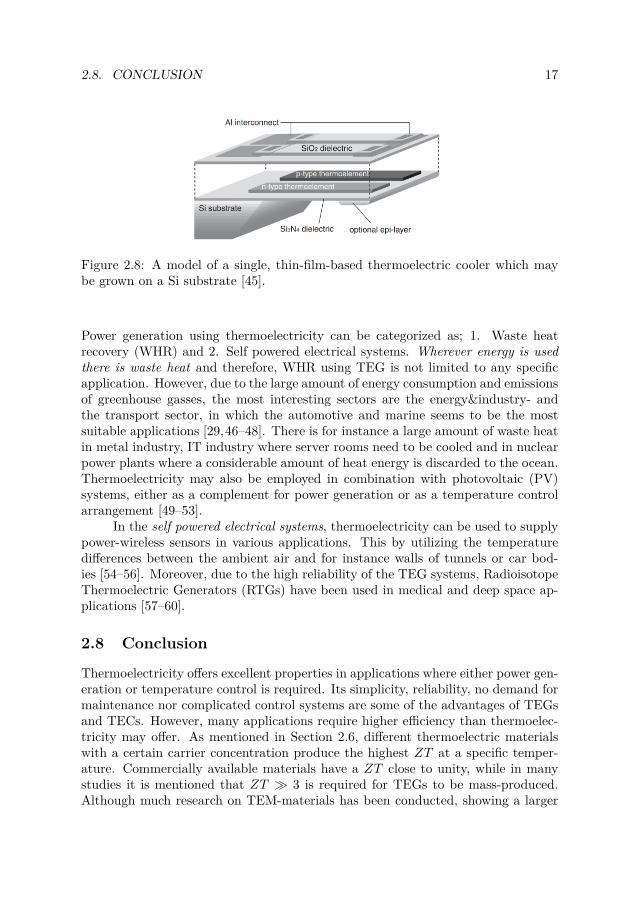
Thermoelectricity enables cooling/heating (TEC) or power generation (TEG). Asmentioned above, particular thermoelectric materials with a certain carrier con-centration are suitable for different temperature ranges. For cooling applications,TEMs have been employed to extract the heat to control or to redirect heat flowfrom hot-spots on micro-controllers or other semiconductor devices. In addition,many studies and applications have been reported where thermoelectricity has beenused as a thermal management system of power electronic semiconductors. Sincethe active part of the semiconductor is very small but the electrical power passingthrough the semiconductor is large, the temperature of the semiconductor chip in-creases by hundreds of degrees Celsius in the range of milliseconds. Therefore, athin-film-based and integrated planar thermoelectric cooler has been developed toactively extract the generated heat from semiconductor devices, see Fig. 2.8 [43–45].One of the most important advantages of the thin-film-based thermocouple is thepossibility to build it during the manufacturing process of semiconductor devices.
2.8. CONCLUSION 17
Figure 2.8: A model of a single, thin-film-based thermoelectric cooler which maybe grown on a Si substrate [45].
Power generation using thermoelectricity can be categorized as; 1. Waste heatrecovery (WHR) and 2. Self powered electrical systems. Wherever energy is usedthere is waste heat and therefore, WHR using TEG is not limited to any specificapplication. However, due to the large amount of energy consumption and emissionsof greenhouse gasses, the most interesting sectors are the energy&industry- andthe transport sector, in which the automotive and marine seems to be the mostsuitable applications [29,46–48]. There is for instance a large amount of waste heatin metal industry, IT industry where server rooms need to be cooled and in nuclearpower plants where a considerable amount of heat energy is discarded to the ocean.Thermoelectricity may also be employed in combination with photovoltaic (PV)systems, either as a complement for power generation or as a temperature controlarrangement [49–53].
In the self powered electrical systems, thermoelectricity can be used to supplypower-wireless sensors in various applications. This by utilizing the temperaturedifferences between the ambient air and for instance walls of tunnels or car bod-ies [54–56]. Moreover, due to the high reliability of the TEG systems, RadioisotopeThermoelectric Generators (RTGs) have been used in medical and deep space ap-plications [57–60].
2.8 Conclusion
Thermoelectricity offers excellent properties in applications where either power gen-eration or temperature control is required. Its simplicity, reliability, no demand formaintenance nor complicated control systems are some of the advantages of TEGsand TECs. However, many applications require higher efficiency than thermoelec-tricity may offer. As mentioned in Section 2.6, different thermoelectric materialswith a certain carrier concentration produce the highest ZT at a specific temper-ature. Commercially available materials have a ZT close to unity, while in manystudies it is mentioned that ZT 3 is required for TEGs to be mass-produced.Although much research on TEM-materials has been conducted, showing a larger

18 CHAPTER 2. THERMOELECTRICITY
ZT than unity, no TEM has been commercialized with such materials. The otherrelated problem is the small temperature range where the ZT of a certain ma-terial is maximum. This issue limits the low efficiency of a TEM even more inapplications with large temperature variations. In other words, to maximize thesystem efficiency, it is also important to maximize the ZT over a wide tempera-ture range [42, 61, 62]. However, it is important to mention that due to the lack ofenthusiasm in the industry and comprehensive studies at system level, the develop-ment in this field has been held back. In fact, since thermoelectricity is a complexphenomenon where heat and electrical power affect each other, only investigationson an entire system will demonstrate the real advantages of TECs or TEGs.

Chapter 3
Thermoelectric Generator on aVehicle
The information presented in this chapter is based on Publications II, III, IV.It has to be mentioned that part of the studies presented in this chapter has beenperformed by the project partners (Eberspächer, Scania and TitanX) but for thepurpose of the thesis and to give the reader an overview on a TEG-system, it wasnecessary to present this information here.
3.1 Introduction
Generally, a TEG system makes use of two heat exchangers (HXs) for the hot andcold sides respectively, and a number of TEMs which are electrically and thermallyconnected so that the highest possible electrical power is generated. Furthermore,an electrical power management- and a control system of the hot- and cold me-dia have to be employed to ensure the correct operation of the TEG. A TEG is amulti-disciplinary system where mechanical, electrical, and thermodynamical com-ponents have to, individually and collectively, work in an optimal way. For thatreason, the design of a TEG for vehicles is a complicated process because all com-ponents in the system are interdependent, and the final result relies on interactionbetween different parts. For example, various modules are optimized for differenttemperatures and heat fluxes while the actual hot and cold side temperatures, onthe other hand, are dependent on the design of the HXs. This in turn gives rise toa design-dependent amount of losses and therefore affects the recovered net power.Due to the large variation in exhaust gas temperatures, the greatest challenge be-comes designing a system optimized for a wide range of temperatures and power,while the losses are kept at low level. The only realistic way to overcome thesedesign problems is by optimizing the system iteratively. Therefore, the main partswere studied first and added together into a model of a complete TEG system to besimulated later on. The results of the simulations were used to change and improve
19

20 CHAPTER 3. THERMOELECTRIC GENERATOR ON A VEHICLE
the system properties and boundary conditions. With the new parameters an im-proved TEG-model was built and simulated again [46]. Moreover, a TEG for WHRin a drivable vehicle has to fulfill other important criteria and standards which aredictated by the automotive industry. For instance, it is important that the TEGis designed in such a way that its disturbance on the main and existing systemson-board is minimal. For example, extremely small, long channels or aggressivesurface enhancement in the HXs results in very high pressure drop in the exhaustsystem. Placing the TEG upstream, the after treatment system (ATS) causes ahigh temperature drop and obstructs the ATS function and has to be avoided. Thelimited volume, the allowed weight, the reliability of the system, and the cost ofthe TEG are other restrictions when it comes to the design and manufacturingprocess. Furthermore, the design of the TEG has to be performed such that thehighest possible power can be extracted and stored. The type of TEMs, the designof the HXs, the attachment of the TEMs, the thermal and electrical arrangementof the TEMs, and also the power converter and its control system have a significantimpact on the final generated power which has to be taken into account in seriesmass-production.
3.2 System Description and Requirements
Since the TEG would be designed for an existing HDV, it was important to thor-oughly study the vehicle. Firstly, the most suitable heat sources on the vehiclehad to be identified. Four different heat sources may be recognized on an HDV; ex-haust gas in the after treatment system (ATS), exhaust gas recycling (EGR), chargeair cooler (CAC), and the engine coolant. However, there are several aspects toconsider when choosing the heat source and the placement of a TEG. By placingthe TEG close to the hot media streams, unnecessary tubing can be avoided andthereby the pressure and heat losses to the ambient can be minimized. On the otherhand, to capture a large part of the heat power from the exhaust system a relativelylarge TEG should be designed, and consequently it cannot be placed anywhere inthe vehicle due to space constraints. Also, a larger TEG is heavier and the weightissues have to be considered. For the key function of transforming a temperaturedifference between two fluid streams into electrical power, it is beneficial with highgas mass flows, and high temperature for the hot side and low temperature forthe cold side. Fluids with high specific heat capacity are desirable, since the tem-perature will not change rapidly when heat is transferred. This means that coldsinks will still keep cold, and hot sources still keep hot, despite the heat transfer.This is also the reason for preferring TEMs with low heat flux. Furthermore, thefluids should have a high thermal conductivity, which enables heat to easily bepulled or released, to and from the media. The most suitable heat sources for theTEGs, according to an internal investigation, were determined to be downstreamthe ATS and upstream the EGR, see Fig. 3.1 [Publication III]. The reason forthis choice is the high gas mass flow in the ATS, the high temperature in the EGR,

3.2. SYSTEM DESCRIPTION AND REQUIREMENTS 21
and minimal disturbance to their functionality.According to Scania, the operation of an internal combustion engine (ICE)
in an HDV can be described by the 9-steady-state-points, which together createthe long haulage cycle (LHC). In other words, the 9-LHC emulates the real drivingconditions for a long haulage HDV, which is usually used for research purposes.The most important parameters in the 9-LHC, provided by Scania, are presentedin Table 3.1. Therefore, the design of the TEGs was also based on the 9-LHC. Ithas to be mentioned that additional confidential parameters related to 9-LHC, areexcluded from Table 3.1.
Figure 3.1: Available heat sources on an HDV. The most suitable heat sources forWHR using TEG are upstream the EGR and downstream the ATS.
Table 3.1: Table shows the exhaust gas temperatures and mass flow in the ATSand the EGR as a function of the speed and load of the engine, according to the9-LHC. The measurements presented in this Table are provided by Scania.LHC 1 2 3 4 5 6 7 8 9Engine Speed [RPM] 1000 1000 1000 1150 1150 1300 1300 1300 1300Relative Load [%] 25 50 100 25 75 25 50 75 100ATS mass flow [kg/h] 420 556 1017 423 949 532 803 1079 1393ATS Temp. [°C] 248 347 386 259 352 251 323 346 396EGR mass flow [kg/h] 127 143 167 197 194 215 247 276 213EGR Temp. [°C] 318 452 551 335 489 325 425 481 560
Based on the provided data and the determined volume, two of the project partners(Eberspächer and TitanX) designed two HXs with cross-counter flow for the ATS

22 CHAPTER 3. THERMOELECTRIC GENERATOR ON A VEHICLE
and EGR. Figure 3.2 shows the CAD drawing of the ATS-TEG. The cross-counterflow was used in both TEGs for practical reasons. The HXs were designed to pro-duce the same hot- and cold side temperatures, and thereby the same temperaturedifference (∆T ) in each column along the Y-direction.
The simulations on the thermodynamical system and the heat exchangers wereperformed using different Off-the-shelf TEMs. Parameters like the channel lengthand height, and the thickness of the fins were swept in the simulation to determinethe highest power per volume. Basically, TEMs with higher heat flux also producehigher electrical power. However, when determining or reporting the output powerof a TEG mistakes may be made by assuming that the most suitable TEM wouldbe the one with highest output power, when in fact this is the one with highestheat flux. This is extremely important in applications where the heat source andsink have a limited capacity, and where another medium is the carrier of the heatenergy (forced convection). Generally, when the heat source and the heat sink havea limited capacity, which is the case in automotive applications, a module withlower heat flux is desirable. Further simulations on the entire TEG-system showedthat a thicker version of the Thermonamic module (1264-3.4) generates the sameamount of net power as for instance 1264-1.5, although the last mentioned TEM isthinner and has a higher heat flux (133 W compared to 98.2 W). Obviously, a TEGusing the thinner TEMs would contain a grater number of TEMs per volume.
In order to keep the same ∆T over the module with higher heat flux, a moreextensive cooling system decreasing the net power, is required. Therefore, thethicker TEM, Thermonamic’s TEP1-164-3.4, is the most suitable one and was se-lected to be used in the TEGs [Publication III]. According to the calculationsmade by the project partners, the ATS-TEG would contain 224 TEMs and theEGR-TEG would contain 240 TEMs in a configuration shown in Fig. 3.2.
Figure 3.2: An illustration of the ATS-TEG and the HX configuration. The exhaustgas flows in X-direction and the coolant flows in Z-direction according to cross-counter flow configuration.

3.3. RESULTS FROM THE THERMODYNAMICAL SYSTEM 23
3.3 Results From the Thermodynamical System
Due to the differences in the operation environments, and in order to evaluatedifferent configurations, the ATS- and EGR-TEGs were designed in different ways[46]. However, the most important objectives during the design of both TEGs wereto obtain a homogenous flow at the cold and hot sides, and to create the same hotgas and coolant temperature in each column in Y-direction. Simulations on theexhaust- and the cold sides of the TEMs for each positions (1-8), for 9-LHC wereperformed. Different channel configurations of the coolant and the hot-gas sideswere simulated to obtain a design with the most homogenous flow. An example ofsuch a simulation is shown in Fig. 3.3 where the velocity of the coolant for a typeof channel configuration is shown.
Figure 3.3: Different designs of coolant channels were simulated to obtain aconfiguration with the most homogenous coolant flow.
Another type of performed simulations were those where the input and outputcoolant temperatures were predicted. In those simulations, based on the heat fluxthrough the TEMs, the temperature of the coolant could be determined. Fig. 3.4shows the coolant temperature downstream the ATS-TEG, using data from twodifferent modules. As seen in this figure, unlike the thicker TEMs, a larger amountof the heat passes through the thinner TEMs and increases the coolant temperaturefurthermore. This will affect the amount of net power from the TEGs, and thereforeit is important to investigate the impact of different components on the net power.Therefore, other types of simulations showing the optimal operation conditions,were performed. In Fig. 3.6, the net power as a function of the coolant andexhaust mass gas flow in the ATS is shown. In this simulation, the temperatures ofthe coolant and the exhaust gas were kept constant. These types of investigationswere used to predict the output gross and the net power, and to develop a maximumnet power tracker (MNPT). In fact, the MNPT is an algorithm which adjusts thegas and coolant mass flows, and thereby adjust the temperatures on the hot andcold sides such that maximum net power can be extracted from the TEGs [46].

24 CHAPTER 3. THERMOELECTRIC GENERATOR ON A VEHICLE
Figure 3.4: Temperature of the coolant downstream TEG as a function of LHCs andthe coolant mass flow. The simulation was performed for two types of TEMs fromThermonamic, 1264-1.5 (thickness=3.6 mm) and 1264-3.4 (thickness=4.6 mm).The inlet coolant temperature was assumed to be 38°C in this simulation.
Moreover, in order to determine the most suitable cooling circuit and to studythe effect of the temperature changes on the other components, different coolingcircuits were studied. In Fig. 3.5 two cases are shown. In the left-side figure, aconfiguration where the TEG cooling radiator is divided into two parts, is shown.In the right-side figure the cooling radiator of the TEG is a single unit and placedin front of the radiator of the charge air cooler (CAC) radiator.
Figure 3.5: Different configurations of cooling circuits were studied. In the left-sidepart the cooling radiator of the TEG is divided into two parts, which was foundto be the most effective configuration. The right-side part shows a configurationwhere the TEG-radiator is placed in front of the CAC radiator.

3.3. RESULTS FROM THE THERMODYNAMICAL SYSTEM 25
Simulations of different cases were performed. It was found that the cooling circuitof the TEG has minimum effect on the temperature of the CAC and the ordinaryhigh temperature (HT) radiator, when the TEG radiator is divided into two parts.However, this solution requires additional space in the front of the vehicle and needsthe most modifications in the system.The most important simulation results, generated by the project partners for thefinal configuration of the TEGs, from the electrical system point-of-view are thetemperatures at the cold- and hot sides of the TEMs. The hot- and cold sidetemperatures of the TEMs were generated as a function of LHCs, and their positionsin the HX according to Fig. 3.2. Later on, those values were used to calculate thetemperature differences (∆T ) over the TEMs, and predict the open source voltagesand the internal resistances of each TEM. Since, all modules in each column inthe Y-direction experience the same ∆T , theoretically, it would be sufficient todetermine the temperature differences for each number in Fig. 3.2. Figure 3.7shows ∆T over each TEM in the ATS-TEG and EGR-TEG. According to thecalculations, LHC nr. 1 generates the lowest ∆T , LHC nr. 9 generates the highest∆T and LHC nr. 2 is one of the LHCs that generates the temperatures in-betweenLHC nr. 1 and 9.
Figure 3.6: The graph shows the net power generated by the ATS-TEG as a functionof the coolant flow (FC) and exhaust gas (EG) mass flow. Maximum net powerin this simulation was obtained at EG= 450 kg/h and CF=23 l/min. The inlettemperature of coolant and exhaust gas were kept constant at 20°C and 350°C,respectively.
The selected TEM was treated and modeled as a unit and in order to create anaccurate model, the TEM was exposed to different but known heat fluxes on atest bench at Eberspächer. Using regression analysis, the experimental results

26 CHAPTER 3. THERMOELECTRIC GENERATOR ON A VEHICLE
were fitted into polynomial expressions for the electrical properties, such as theinternal resistance (Rin) and open circuit voltage (Voc) of the TEM at differenttemperatures and positions in the TEGs. The extracted Voc and Rin were used tosimulate strings of connected TEMs, forming a TEG in OrCAD/Pspice. Since, thenumber of obtained values are related to two different TEGs, at 8 different TEM-positions, and are associated with to two different properties (Voc and Rin), onlyvalues for one TEG (ATS) are presented here in Tables 3.2 and 3.3. The ATS-TEGwas designed to have 28 TEMs at each position (a total of 224 TEMs) and theEGR-TEG was designed to have 30 TEMs at each position (a total of 240 TEMs).In other words, there are 464 small voltage sources that need to be connected toeach other, such that the maximum available power is extracted; this while factorslike reliability, simplicity, cost, and weight of the system are considered. It has tobe mentioned that these voltage sources differ from the conventional sources, sincethere is a negative feedback caused by electrical current which affects the heat fluxand thereby the temperature difference (∆T ).
Figure 3.7: Calculated ∆T for LHC nr. 1, 2 and 9 as a function of TEM positionsaccording to Fig. 3.2 in the EGR-TEG (left) and ATS-TEG (right).
Table 3.2: The open circuit voltages Voc [V] of the TEMs in the ATS-TEG, as afunction of 9-LHC and the position of the TEMs according to Fig. 3.2.
TEM Position
LH
C
1 2 3 4 5 6 7 81 4.07 4.11 4.14 4.17 3.20 3.17 3.13 3.102 5.95 6.02 6.09 6.16 5.20 5.14 5.08 5.023 6.79 6.91 7.02 7.13 6.88 6.79 6.69 6.604 4.28 4.31 4.35 4.39 3.37 3.34 3.30 3.275 6.43 6.53 6.62 6.71 6.29 6.21 6.13 6.056 4.36 4.40 4.44 4.48 3.64 3.60 3.57 3.537 5.79 5.86 5.93 6.0 5.38 5.32 5.26 5.198 6.43 6.53 6.62 6.72 6.39 6.31 6.23 6.159 6.94 7.07 7.21 7.34 7.42 7.31 7.19 7.08

3.4. THERMAL CYCLING OF THE TEMS 27
Table 3.3: The internal resistance, Rin [Ω] of the TEMs in the ATS-TEG as afunction of 9-LHC and the position of the TEMs according to Fig. 3.2 .
TEM Position
LH
C
1 2 3 4 5 6 7 81 4.95 4.94 4.92 4.91 4.61 4.62 4.63 4.642 5.38 5.38 5.37 5.36 5.09 5.10 5.12 5.133 5.52 5.53 5.53 5.53 5.42 5.43 5.44 5.444 5.0 5.0 4.98 4.96 4.65 4.67 4.68 4.695 5.48 5.48 5.47 5.47 5.31 5.32 5.33 5.346 5.03 5.02 5.0 4.99 4.72 4.73 4.74 4.757 5.36 5.35 5.34 5.33 5.13 5.14 5.15 5.168 5.48 5.48 5.47 5.47 5.33 5.34 5.35 5.369 5.53 5.54 5.55 5.56 5.51 5.51 5.52 5.52
3.4 Thermal cycling of the TEMs
In order to measure possible changes in performance of the selected TEM-type, asmaller TEG unit was manufactured by Eberspächer. The TEG unit included 8TEMs and was thermally cycled at Scania facilities. The hot side of the sub-TEGwas cycled from 95 °C to 335 °C. Once the maximum temperature was reached adwell time of 10 seconds was applied prior to cooling back to 95 °C. The test setupand the cycling profile is shown in Fig. 3.8.
Figure 3.8: The test rig (left), used to thermally cycle 8 TEMs, and the thermal-cycle profile (right).
The system allowed a cycling time of approx. 400 s per cycle, which after morethan a week of testing enabled 1605 temperature cycles. The maximum voltages ofeach TEM were evaluated during the thermal cycling. Due to measurement issues,data could be collected for 6 out of 8 modules. The result of this test is presentedin Fig. 3.9. The voltage was changed 1-2 % compared to the nominal values for

28 CHAPTER 3. THERMOELECTRIC GENERATOR ON A VEHICLE
5 TEMs after the test. The voltage for the TEM at position 10 decreased 7 %compared to the nominal voltage. The TEG unit as well as the individual TEMswere investigated afterward and no visible damages were found. However, scanningelectron microscopy (SEM) showed smaller cracks on some of the thermocouple legsbut these cracks were found to be from thermocouple dicing from manufacturing,since they appeared also in non-cycled TEMs.
Figure 3.9: Results of the thermal cycling show the open-load voltage of 6 TEMsin the sub-TEG as a function of number of cycles.
3.5 Conclusion
Due to the available volume and the dissimilar conditions in the EGR and ATS,the TEGs needed to be adapted and optimized to those conditions. This willcreate some natural differences between the ATS- and EGR-TEGs. Moreover, thedevelopment and evaluation of different TEG-techniques in this study, was the otherreason to the slightly different TEG designs. A short list of the differences in theATS and EGR-TEG is as follows:
• The mean gas temperature is approx. 200 °C higher in the EGR than in theATS.
• The mean mass flow is approx. 600 kg/h higher in the ATS than in the EGR.
• The heat exchanger used in the EGR-TEG is the plate rectangular HX, whilean offset structure HX is used in the ATS-TEG where the higher pressuredrop could be tolerated.

3.5. CONCLUSION 29
• EGR-gases are not actively pumped; the gas flow is due to the pressure dropin the EGR. However, the gas pumps actively through the ATS by the ICE.This is the reason for why the EGR is not able to manage similar amount ofpressure drop as the ATS.
• The design of the EGR-TEG was chosen in such a way that the whole TEGwas pressed together with a large force as one single block while, the ATS-TEG was made with sub-TEGs and forced together as smaller free units.
There are a number of commercial TEMs that may be used in a TEG ap-plication. A rough study, only looking into the amount of generated power, mayindicate that a module generating highest electrical power is the most suitablechoice. However, when comparing two different modules at the same ∆T , whereone TEM generates higher electrical power than the other, the TEM with higherpower also has the higher heat flux. Therefore, when considering the entire systemas a unit, a TEM with larger heat flux is not the desirable one. This is especiallyimportant in applications where the heat power is forced convected as in exhaustgases, which need to be pumped out through an HX. Therefore, it is important tothoroughly study the capacity of the cooling system, and the impact of increasedtemperature in that system before selecting a TEM. A comprehensive thermal cy-cling test was performed with the selected module. It was concluded that the testhad an insignificant impact on the generated voltage of the TEMs. Moreover, anSEM analysis was performed on the exposed TEMs, also indicating no significantchanges on the modules after the test.


Chapter 4
From TEM to TEG - Connection
The information presented in this chapter is based on Publications II, IV.
4.1 Introduction
The placements and volumes of the TEGs were dictated by Scania. It was decidedto have two TEGs, one in the ATS containing 224 TEMs, and the other in the EGRcontaining 240 TEMs. The electrical power from the TEGs was used to charge theelectrical energy storage on-board the vehicle, relieving the alternator and therebythe internal combustion engine (ICE). Due to the temperature variations in theexhaust gases, and the fact that the voltages and internal resistances of the TEMsare functions of the applied temperatures across the TEMs, it is necessary to employa power conditioning system. It ensures correct operation and controls the level ofvoltage and the extracted power from the TEGs, see Fig. 4.1. A power conditioningsystem of a TEG can be divided into three different components; a power converter,a maximum power point tracker (MPPT) and the connection between the TEMs.In fact, the connection of the TEMs affects the design and operation of the othertwo components in the power conditioning system. The connection of the TEMs,as will be shown, also influences the cooling system and thereby the amount ofthe net effect. Moreover, there are some practical issues arising with the type ofconnection of a large number of TEMs in vehicles, where the weight and volumeare limited [Publications I & II & IV].
31

32 CHAPTER 4. FROM TEM TO TEG - CONNECTION
Figure 4.1: The output voltage and power of a TEG are temperature-dependent.Therefore, a power conditioning system controlling the power and voltage of theTEG is necessary.
Figure 4.2 shows the final CAD layout of the ATS- and EGR-TEG. Firstly, when thenumber of the TEMs and ∆Ts across the TEMs are known, a suitable connectionstrategy has to be developed. This will determine the level of the output voltages,the total output power and thereby the converter topology. In this chapter, subjectsrelated to the connection strategy and some practical issues will be discussed.
Figure 4.2: CAD layout of the ATS-TEG (left) and EGR-TEG (right).
4.2 Electrical Behavior of a TEM
According to the 9-LHC, the gas temperatures in the ATS change between 248 °Cand 396 °C and between 318 °C and 560 °C in the EGR, depending on the load ofthe ICE. The temperature variations in the exhaust gases will cause two issues in theelectrical part of the system. Since the output voltage V of the TEG is a functionof the temperature difference (∆T ) across the TEMs, the output voltage will followthe temperature variations. The voltage of the electrical system of the vehicle isconstant and controlled by the alternator. Therefore, the output voltage of theTEGs also has to be controlled. Moreover, at the same time as the temperaturesand the voltage of the TEMs change, the internal resistance (Rin) of the TEMswill change as well. Due to the reduction of mobility of the charge carriers in thesemiconductor with increased mean operating temperature (Tm), the resistivity ofthe semiconductor in a TEM increases. Therefore, a TEM produces less power

4.2. ELECTRICAL BEHAVIOR OF A TEM 33
for the same ∆T at a higher Tm. This behavior can be seen in Fig. 4.3, where aHZ-20 module from HiZ was exposed to a constant ∆T at 50 °C, and the electricalproperties of the TEM as a function of Tm was recorded. Clearly, the internalresistance Rin, of the TEMs is increasing with increased Tm.
Moreover, the Seebeck coefficient of thermoelectric elements is also temperature-dependent, which can also be observed in Fig. 4.3. It can be seen that the opencircuit voltage of the TEM is also varying although ∆T is fixed. The variationof internal resistance of a TEM, as well as the variation of the output voltage ofthe TEMs, give rise to the characteristics shown in Fig. 4.4, where two different∆T s result in two voltage-, current- and power functions. The voltage variationsgive rise to different levels of power while the variations of Rin shift the maximumavailable power along the current-axis. Another challenge within the design of theelectrical components of a TEG is the low conversion efficiency of thermoelectricityin general. For that reason the power conditioning system and the other relatedcomponents have to operate at highest possible efficiency over the large variationrange of the temperature and power.
The behavior of a TEM at different ∆T s, as seen in Fig. 4.3 creates difficultiesto predict the current where the available power is maximum. This is especially anissue in applications where the temperatures are unknown during the most part ofthe operation time. Therefore, the best approach to extract the highest availablepower from a TEG is considered to be MPPT.
Figure 4.3: The internal resistance, open circuit voltage and power of a HZ-20 mod-ule as a function of the mean operating temperature Tm. Temperature difference,∆T , is kept to 50 °C. Both the internal resistance and the open circuit voltage areaffected by the Tm.

34 CHAPTER 4. FROM TEM TO TEG - CONNECTION
Figure 4.4: Temperature variations in the exhaust system give rise to variations inthe internal resistance and different V-I-P curves, as a function of ∆T . This is anexample showing the behavior of the output power and voltage of a TEM at twodifferent ∆T s, as functions of load current.
4.3 Relation of the Thermal and Electrical Conductance
The maximum delivered power from a TEM to a load is obtained when Rin =RLoad, i.e. the internal resistance of the module is matched with the load resistance.It is important to mention that Rin of a module, which has to be considered forthe maximum power tracking, is the effective value of the internal resistance. Theeffective internal resistance is a function of thermal conductance of the module(s)itself, as well as the thermal conductance between the heat- source and sink (κhot
and κcold) [63]. Reffin can be described by,
Reffin = Rin + Tcα
2(κc + κh) κTEM
κc + κh + κTEM, (4.1)
where Tc is the cold side temperature, κc and κh are the thermal conductanceat the cold- and hot side of the module respectively, and κTEM is the thermalconductance of the module itself, see Fig. 4.5.
The maximum output power PRLmax of a single module can be determinedby,
PRLmax = V 2oc
4Rin, (4.2)
while the maximum output power of n number of TEMs creating a TEG, connectedin series or in parallel, is obtained by

4.3. RELATION OF THE THERMAL AND ELECTRICAL CONDUCTANCE35
PRLmax−series = 14
(ΣVn)2
ΣRn, (4.3)
and
PRLmax−parallel = 14
(Σ Vn
Rn)2
Σ 1Rn
, (4.4)
where Vn is the open circuit voltage and Rn is the internal resistance of eachspecific TEM. Clearly, when the TEMs operate in identical conditions, the voltagesand the internal resistances of all modules are the same. Therefore, the powerobtained by (4.3) and (4.4) will have the same value, i.e. the electrical connectionof the TEMs does not affect the total output power [64]. However, in practicalapplications there are restrictions and practical issues that give rise to differentoperating conditions for each TEM. The impact of TEMs’ thermal and electricalconnections on the performance of a TEG can be investigated using Fig. 4.5 [65,66].Employing the Onsager compact expression where Joule losses are disregarded, thesystem in Fig. 4.5 can be described by
(I
IQ
)= 1Rin
(−1 α
αT α2T +RinκI=0
)(∆V∆T
), (4.5)
where I and IQ are the electrical- and thermal current respectively, and ∆V is thevoltage over the electrical load. ∆T is the temperature difference (ThM − TcM )across the module, T is the average temperature and κI=0 denotes the thermalconductance at zero electrical current. From (4.5) the electrical current and thermalcurrent are obtained as
I = α∆TRin +RL
, (4.6)
IQ = αTI + κI=0∆T. (4.7)

36 CHAPTER 4. FROM TEM TO TEG - CONNECTION
Figure 4.5: The electrical and thermal model of a TEM.
Combining (4.6) and (4.7) yields the relation between the thermal current IQ, zerocurrent thermal conductance κCond and the thermal conductance associated withthe electrical current κConv, i.e.
IQ = ( α2T
Rin +RL+ κI=0)∆T, (4.8)
which can be expressed as
IQ = (κConv + κCond)∆T = κTEM∆T, (4.9)
where
κConv = α2T
Rin +RL. (4.10)
Equations (4.8) and (4.9) show that not only the electrical current but also part ofthe thermal current can be controlled by the total resistance in the circuit. Thisis a very important property and an excellent tool when the heat source and thecooling system have a limited capacity, as in the case of vehicle applications. Thischaracteristic enables possibility of controlling the thermal current by adjusting theelectrical current, and vice versa whenever it is necessary, for instance to protectthe TEMs or the cooling circuit from overheating. Furthermore, since a largeelectrical current increases the thermal current through a module, a low-currentTEG is preferred to keep the ∆T on an acceptable level in a system with limitedcooling capacity. This can be achieved by connecting a number of TEMs in seriesto increase the internal resistance of the TEG.

4.4. SERIES AND PARALLEL CONNECTION - CONSEQUENCES 37
4.4 Series and Parallel Connection - Consequences
As discussed earlier, the design of the HX, based on the available space and heatpower, dictates the number of TEMs in a TEG. Moreover, the type of the HXwill determine the temperatures at the hot- and cold sides, allowing to predictthe electrical power each TEM will generate. However, in real applications, theanalytically calculated power for each TEM can not be added together to predictthe total power of the TEG. This is a consequence of the power loss due to differencein ∆T s, and the electrical connection between the TEMs.
In the previous section the relation between the electrical and thermal currentwas described. Due to that relation a low-current TEG is preferred. Anotherissue regarding the connection of the TEMs is the mismatch caused by the appliedmechanical force on different TEMs in a TEG system. In real applications, where alarge number of TEMs are used, it is impossible to ensure an identical applied forceon all TEMs. A TEG, where there is a mismatch in mechanical force on one TEM,is considered. Due to the force-mismatch the TEMs will obtain different κh and κc,and thereby different internal resistances. If all modules in the TEG are electricallyconnected in parallel, and the requested current from the load is low at the moment,or in the case of failure when the output of the TEG is completely disconnectedfrom the load, the TEM with lower internal resistance will not generate any powerbut may consume power from the other TEMs. This issue was investigated in [67]where three TEMs were characterized and exposed to different temperatures. Itwas suggested that further investigations on systems with larger number of TEMsmust be performed. Therefore, investigations were performed to propose the mostsuitable TEM-connection for the designed HXs in the ATS- and EGR-TEG.
Two connection cases were studied; all modules in series and all modules inparallel. 14 TEMs from HiZ were chosen and connected together. In both casesall TEMs except one were exposed to Th = 200 C and Tc = 50 C and the lastmodule (the unmatched TEM) was exposed to Th = 170 C and Tc = 50 C.Figure 4.6 shows the power and current as functions of load resistance for the seriesand parallel connection. The upper part of Fig. 4.6 shows the current throughall the modules in the series connection (red line nr.1), the current through oneof the matched modules (green line nr.2), and the current through the unmatchedmodule in the parallel configuration (blue line nr.3). The middle and lowest graphsshow the output powers of the entire string of the TEMs, for parallel and seriesconnection, respectively. The currents and the powers are plotted as functionsof the load resistance. Note that the lowest graph is plotted for very small loadresistance values. The maximum power is obtained at RL = 4 Ω for the seriesconfiguration, since at that point the load resistance is equal to the the total internalresistance of the TEMs (RL = Rin = 4 Ω). Likewise, in the parallel configurationthe maximum extracted power is generated at RL = Rin = 18 mΩ. As will beexplained later, the maximum power point tracker (MPPT) continuously adjustthe load current such that the output power varies between maximum availablepower and for instance 95 % of the maximum power. This results in an average

38 CHAPTER 4. FROM TEM TO TEG - CONNECTION
extracted power of approximately 97.5 % of the maximum power. In that case,the series connection results in a significantly wider operating range (2 Ω < RL <6 Ω at Rin = 4 Ω), with smoother derivative compared to the parallel connection(12 mΩ < RL < 29 mΩ at Rin = 18 mΩ) with sharper derivative.
Figure 4.6: 14 pieces HZ-20 modules were connected to each other, first in seriesand then in parallel. All modules except one were exposed to Th= 200 C and Tc=50 C. One module was exposed to Th= 170 C (the unmatched TEM). The uppergraph shows the total current of the series configuration (1), the current of one ofthe matched TEMs (2) and the current of the unmatched TEM (3) in the parallelconfiguration. The middle and lower graphs show the power of parallel and seriesconnection as a function of load resistance.
The behavior of the series connection is due to the larger internal resistance com-pared to the parallel connection, and is extremely important in real applicationswhen employing an MPPT. The small operating region of the parallel connectionresults in difficulties to search for the highest available power. In this case, smallchanges in the load current will result in significant changes in the output power,and thereby cause oscillations in the system. Moreover, as shown in the upper graphin Fig. 4.6, the current of the unmatched TEM changes direction from negative topositive, when the load resistance increases above 70 mΩ. A positive current indi-cates that the module consumes electrical power. For instance, at RL= 100 mΩ,the current into that module is 0.64 A indicating that the power generated by theother TEMs is consumed by the unmatched TEM. The current into the unmatched

4.4. SERIES AND PARALLEL CONNECTION - CONSEQUENCES 39
module will increase to 3 A at RL= 50 Ω. A module which consumes power actsas a Peltier element, and actively pumps the heat from the hot side to the coldside, and thereby decreases the temperature differences of the nearby modules. Incase of failure, if the TEG becomes disconnected from the load, or if the requestedpower to the load (controlled by the converter) is small, the unmatched TEM willconsume 12 W from the other modules. This is equal to 7.5 % of the total powergenerated by the whole string. This behavior is highly undesirable, and arises in aparallel configuration when the contact forces on all of the TEMs are not identical.This issue will be aggravated, and has to be considered when a larger number ofTEMs are used and/or the differences in ∆T over the TEMs are large.
Furthermore, the current in the series connection through all modules at max-imum power is 6.7 A, while the current through each matched module in the parallelconnection is 7 A for this configuration. According to (4.7) a thermoelectrical sys-tem with higher electrical current also allows higher thermal current through theTEMs, which results in lower ∆T and thereby a lower output power.
Earlier it was found that modules with same Th and Tc can be connected ei-ther in series or parallel without any significant difference in output power [68,69].However, in practice as discussed above, it is not possible to make sure that a largenumber of modules that are exposed to same Th and Tc will experience the same∆T . Therefore, the TEMs may be connected in series which produces a higherinternal resistance and preferably increases the efficiency and controllability of thesystem. A summary of the advantages and disadvantages of the parallel and seriesconnection, in real applications is given below.
Parallel connection:
• Needs extra space and long cables when a large number of modules have tobe connected along the y-direction (see Fig. 4.7) .
• Creates a large output current which requires bulky cables to be carried fromthe TEG to the load or a converter. The large current flows close to a coldliquid (coolant) and a hot medium (exhaust gas).
• The large current gives rise to higher electrical and thermal losses.
• Power losses are larger in case of mismatch in κh and κc, caused by forcemismatch or materiel mismatch. If the unmatched module acts as a Peltierelement, it will decrease ∆T of adjacent TEMs. The mismatch issue will alsolead to damage on the particular module in the long term.
• For TEGs in automotive applications, parallel connection requires a step-upconverter with a non-linear gain.
• Due to the sharper and smaller maximum power region, the system will notbe able to find the maximum available power and may show stability issuesif a sufficient number of TEMs are connected in parallel.

40 CHAPTER 4. FROM TEM TO TEG - CONNECTION
• In case of damage and open circuit of one module, the other modules will stillgenerate power to the load.
Series connection:
• Only the closest modules along the y-direction (Fig. 4.7) need to be connectedto each other.
• The output current is limited by the large internal resistance which is lowerthan that of the parallel connection. The electrical and thermal losses areminimized due to the low electrical current in the system.
• Series connection causes lower losses and lower electrical stress on the un-matched modules.
• Due to the lower electrical current, a smaller cooling system may be designed.
• The same amount of current flows through all TEMs.
• In automotive applications a series connection requires a step-down converterwith a linear gain and a less complex control system.
• In case of damage and open circuit of one module, power from the completestring will be lost.
There are two important issues when it comes to a large number of TEMsoperating on a drivable vehicle; parallel connection will result in a large outputcurrent, and in a series connection the complete string will be lost in case of failureof one TEM. By compromising, it is possible to reduce the total output currentand minimize the risk of disconnecting an entire string of TEMs, while taking intoaccount the other issues mentioned above. By looking at the design of the HXin the vehicle while considering the issues above, different connection types andcombinations were simulated. Number of DC/DC channels, the amount of outputpower as well as the open circuit issue were considered in order to select the mostsuitable connection strategy. Figure 4.8 shows a few numbers of the simulatedconfigurations. In part 1 in this figure, the TEG is divided into four sub-TEGs andeach is connected to a separate sub-DC/DC. All TEMs in column 1 are connectedin series ("S"), and then connected in series with TEMs in column 2. Part 2 shows aconfiguration where column 1, 2, 3 and 4 are connected in series, while in part 3 theTEMs in each column are connected in series and then the entire column is parallelconnected ("P") with the next column. Figure 4.9 shows one result of simulationsthat were performed in order to determine the most suitable connection strategy.In this simulation, the ATS-TEG was divided into 1, 2, 4 and 8 sub-TEGs wherethe TEMs are connected in series.

4.4. SERIES AND PARALLEL CONNECTION - CONSEQUENCES 41
Figure 4.7: A CAD illustration of the ATS-TEG and the HX configuration. Theexhaust gas flows in X-direction, and the coolant flows in Z-direction according tocross-counter flow configuration.
Figure 4.8: Different connection combinations were simulated to determine thenumber of DC/DC converters, the amount of the output power from the TEGs ingeneral, and in case of failure when a TEM is disconnected (open circuit). In thisfigure only three simulated configurations are shown. "P"=parallel connection &"S"=Series connection.
The total output power was plotted considering two situations; when all TEMs areconnected and producing power, and when one TEM (nr.4) is, due to failure, dis-connected from the sub-TEG it is attached to. Clearly, by splitting the entire TEGinto 8 parts, where each part contains the TEMs in one column (in Y-direction)with the same ∆T , the highest available power is obtained. Furthermore, if onemodule becomes disconnected, only power from one column will be lost. In con-trast, due to the difference in ∆T in different columns, when all TEMs in the entire

42 CHAPTER 4. FROM TEM TO TEG - CONNECTION
TEG are connected together ("1" in fig. 4.9 ) the output power decreases some-what. However, if one module in such a configuration becomes disconnected nopower will be delivered to the load.
Figure 4.9: A result from performed simulations showing the output power of theATS-TEG during LHC nr.7. X-axis represents the number of sub-TEGs and Y-axis represents the output power[W]. The blue bars correspond to the output powerwhen all TEMs are connected and produce power, and the yellow bars show thepower when module nr. 4 failed and was disconnected.
4.5 Connection Strategy of the TEGs
Assuming an ideal and identical installation of all TEMs, the values of Khot andKcold remain the same for all modules. In that case, the TEMs at each position inY-direction (28 TEMs in ATS-TEG), will experience the same ∆T . As discussedearlier, the ∆T s for modules in position 1 to 8 in Fig. 4.7, are different. ∆T overeach TEMs for three operating points number 1, 2 and 9 in the ATS-TEG areshown in Fig. 4.10. As seen in this figure, because of the low heat capacity of theexhaust gasses and losses in HXs, TEMs will experience lower temperatures thanthe actual exhaust temperatures listed in Table 3.1. Since the HXs are designedto give the same ∆T in the Y-direction, the type of connection in each column inthat direction does not affect the maximum output power. However, connecting 28or 30 modules in parallel and in the limited space is challenging, since the TEMat the highest position has to be connected to the TEM at the lowest position.Moreover, connecting all the modules in parallel results in a low output voltageand a large output current, which needs to be carried to a step-up power converter.According to the simulations, the total output current in the ATS-TEG in case ofparallel connection will reach approximately 30 A in each column in Y-direction

4.5. CONNECTION STRATEGY OF THE TEGS 43
during LHC nr. 9. However, a series connection would reduce the current toapproximately 1 A. Clearly, choosing the connection with 1 A is beneficial sincethe physical distance from the TEG to the converters, determining the resistanceof transmission cables, may be large and depending on the available space in thevehicle. Moreover, the mechanical mismatch, discussed earlier in this section, islargest between the modules physically placed far from each other. For that reason,adjacent modules in the same column may be connected in parallel since the riskof mismatch is minor. Furthermore, connecting a minor number of TEMs in eachcolumn in parallel is less complicated in practice. The group of parallel connectedmodules can then be connected in series with another group, in order to reducethe total output current and to increase the internal resistance of the entire stringof TEMs. Further simulations were performed on such a configuration, where anumber of TEMs are connected in parallel and then in series with the next groupof parallel connected TEMs. It was proposed that two modules may be connectedin parallel in pairs, and then in series with the next pair, according to Fig. 4.11.Due to the locally parallel connections of the two nearby TEMs, this configurationreduces the risk of power loss in the whole string if one module would fail, andacts as an open circuit. In addition, the mismatch on the force contacts on the twonearby modules connected in parallel is minimal. However, in case of a significantmismatch, the current flowing through the module with low internal resistance islower than for the entirely parallel connected TEM-string.
As it can be recognized in Fig. 4.10, the differences between ∆T s of TEMsin columns 1 & 2, and columns 3 & 4, are insignificant. Since, in automotiveapplication cost and weight of on-board components are important parameters,connecting the mentioned columns together would reduce the number of converters,and thereby the complexity of the system as well as cost and weight. Therefore, itwas suggested that these columns may be connected together to create four sub-TEGs in the ATS-TEG, and four in EGR-TEG. The proposed connection for twosub-TEGs can be seen in Fig. 4.11. This seems to be the most suitable connectioncombination from practical point-of-view, where also the internal resistance keepslarge and the current keeps low. However, due to the difference in ∆T in thetwo connected columns the electrical power will decrease compared to the casewhere each column alone would make a sub-TEG. Therefore, in order to determinethe electrical properties and the amount of power loss of the proposed connectionstrategy, simulations were performed in OrCAD/Pspice. In Fig. 4.12 the hierarchyblocks at different levels, created in OrCAD, is shown. At the top level, the ATS-TEG, converter and driver blocks are shown. In mid-level, 8 columns creating foursub-TEGs are presented, and in the lowest levels the model of the TEMs, drivingcircuit and converters are created.

44 CHAPTER 4. FROM TEM TO TEG - CONNECTION
Figure 4.10: Temperature difference ∆T across the modules at position 1 to 8(according to Fig. 4.7) in the ATS-TEG for the lowest power produced duringLHC nr. 1, mid power produced during LHC nr. 2, and the highest power producedduring LHC nr. 9.
Figure 4.11: The final connection of TEMs in one column (along y-direction inFig. 4.7) with 28 TEMs in the ATS-TEG and 30 TEMs in the EGR-TEG.

4.6. SIMULATION RESULTS 45
4.6 Simulation Results
It has to be noted that the components shown in Fig. 4.12 were not accuratelyselected at this stage, since the aim of these simulations was to observe the generalbehavior of the TEGs and determine the output power. Accurate calculationson required components were carried out later on, and components were selectedaccording to the final calculations.
Figure 4.12: In order to determine the electrical properties of the proposed con-nection strategy, hierarchy blocks representing the TEGs at different levels werecreated in OrCAD to be simulated with Pspice. In this figure the highest level ofthe system, the mid-level containing the string of the TEMs, the model of TEMsas well as converter and driving circuit at the lowest level are shown.

46 CHAPTER 4. FROM TEM TO TEG - CONNECTION
Figure 4.13 presents one of the simulation results showing the output power of thesub-ATS-TEGs (sub-ATEGs) nr. 1, 2, 3 and 4. The output powers and the loadvoltages of each sub-TEG are plotted as a function of load resistance. From thesesimulations, data were extracted to design the electrical power conditioning systemof the TEGs. The most important parameters for the design of the power systemare Voc and Rin of each sub-TEG. In Table 4.1 and 4.2, Voc and Rin for Sub-ATEGsduring 9-LHC is presented. Similar simulations were also performed for sub-EGR-TEGs (sub-ETEGs) in order to determine the electrical properties of sub-ETEGs.Figure 4.14 shows the ATS-TEG when 224 TEMs are installed and prepared to beconnected in strings according to the schematic in Fig. 4.11.
Figure 4.13: Simulation results showing the loaded voltages and load power of allsub-ATEGs at LHC nr. 7 as functions of load resistance.
Table 4.1: The open circuit voltages Voc [V] of each sub-TEG in ATS (sub-ATEG)as a function of 9-LHC, and the proposed connection strategy according to Fig.4.10 and Fig. 4.11.
Sub-ATEG
LH
C
1 2 3 4
1 115 117 89 882 168 171 145 1413 192 198 191 1864 120 122 94 925 181 187 175 1706 123 125 101 997 163 167 150 1468 181 187 178 1739 196 203 206 200

4.6. SIMULATION RESULTS 47
Table 4.2: The internal resistance Rin [Ω] of each sub-TEG in ATS (sub-ATEG) asa function of 9-LHC, and the proposed connection strategy according to Fig. 4.10and Fig. 4.11.
Sub-ATEG
LH
C
1 2 3 4
1 69 69 64.5 652 75.5 75 71.5 71.53 77.5 77.5 76 764 70 70 65 655 76.5 76.5 74.5 74.56 70.5 70 66 66.57 75 74.5 72 728 76.5 76.5 74.5 759 77.5 77.5 77 77
Table 4.3: The total gross power determined as a function of 9-LHC, and theproposed connection strategy according to Fig. 4.10 and Fig. 4.11.
LHC 1 2 3 4 5 6 7 8 9ATS power [W] 156 333 447 169 419 182 328 425 523EGR power [W] 165 315 112 260 348 261 426 376 105Total power [W] 321 648 559 429 767 443 754 801 628
Figure 4.14: The figure shows the ATS-TEG containing 224 TEMs prepared to beconnected as four separate sub-TEGs.

48 CHAPTER 4. FROM TEM TO TEG - CONNECTION
4.7 Conclusion
In this chapter the connection between the thermal and the electrical current and itsimportance were discussed. Moreover, the electrical behavior of a TEM exposed todifferent ∆T s were presented. The base of the electrical power system of the TEGsare the electrical properties of each single TEM in the TEGs at different LHCs,which were also presented in this chapter. The importance of creating a TEG withlow current and large internal resistance, as well as experimental and simulationsresults demonstrating issues with series and parallel connection of a large numberof TEMs, are discussed. Furthermore, a limited number of simulation results fordifferent connection strategies, and their impact on the total output power of theTEGs, was presented and briefly discussed. Considering the practical issues such asthe size of the transmission cables, the required power converter for the particularconnection type as well as the limited volume, and by compromising a small amountof power, a suitable connection strategy was developed, simulated and presented.The connection type of the TEMs dictates the electrical properties of the sub-TEGs,which in turn will enforce a particular converter topology to be used. The electricalpower conditioning system and the proposed converter topology will be discussedin the next chapter.

Chapter 5
Electrical Power ConditioningSystem of the TEG
The information presented in this chapter is based on Publications I, II, IV.
5.1 Introduction
The power conditioning system of a TEG can be divided into three parts: a con-nection arrangement of the TEMs, a power converter and an MPPT algorithm. Inthe previous chapter the most important parameters required to design the powerconditioning system of the TEGs were determined. It included the open circuitvoltages and the internal resistances of the TEMs. In addition, different connectionstrategies of the TEMs were discussed. In this chapter the other two components ofthe power conditioning system will be considered. Here, different converter topolo-gies will be briefly discussed and the converter requirements for TEG-applicationsas well as the most suitable topology will be addressed. Moreover, simulation re-sults on the power converter at different LCHs are analyzed and presented. Thepower converter for a thermoelectric waste-heat recovery system is essential in orderto harvest as much power as possible. The reason for this is that the thermal oper-ating point of the TEMs varies substantially. As previously discussed, simulationsshowed that ∆T s across the TEMs vary from 70 °C to 200 °C. This means thatthe induced voltage and internal resistance of the TEMs vary considerably, andwithout a controllable power converter with high efficiency, only a small amountof the energy in the heat flows can be harvested as electrical energy. Furthermore,in order to extract highest available power from the TEGs, the internal resistanceand the load resistance of a sub-TEG have to be equal. However, the variationsof temperature in the exhaust system lead to variations in the voltage and the in-ternal resistance of the TEG, resulting in the behavior shown in Fig. 4.4. On theother hand, the load resistance also varies and is dependent on the condition of theelectrical energy storage, the ambient temperature and the entire electrical system
49

50CHAPTER 5. ELECTRICAL POWER CONDITIONING SYSTEM OF THE
TEG
of the vehicle. In fact, it is nearly impossible to measure the load resistance ofthe system. Therefore, the MPPT algorithm, which controls the amount of powerand adjusts the load current such that the internal resistance is equal to the loadresistance, is required in TEG applications and discussed in this chapter.
5.2 Electrical System and Converter Topologies
Two TEGs were designed to be placed in the ATS and EGR of a HDV. They contain224 and 240 TEMs in the ATS and EGR, respectively. Based on the temperaturesacross the TEMs, they were connected such that the TEGs were divided into 8 sub-TEGs in total. For 9-LHC, the voltages and internal resistances of each sub-TEGwere determined and use in the design process of the power converters. As seen inFig. 5.1, each converter has to be connected to the electrical system of the vehicle.
Figure 5.1: An overview of the TEGs’ electrical system in the HDV.
Several studies have been performed, proposing different converter topologiesfor waste heat recovery systems using thermoelectricity. Usually, boost or buck-boost topologies are proposed in such applications [70–76]. However, only thenumber of TEMs and their connections dictate which converter topology should beused. Depending on the output voltage of the TEG and the required load voltage,buck, boost or buck-boost may be suitable. In commercial, non-electric vehicles thenominal operating voltage of the electrical system is approximately 28 V. As seenin Table 4.1, the obtained voltage from each sub-TEG is larger than the systemvoltage. The minimum voltage of a sub-TEG in the ATS-TEG is equal to 88 V,

5.2. ELECTRICAL SYSTEM AND CONVERTER TOPOLOGIES 51
and 30 V in a sub-TEG in the EGR-TEG. Clearly, in order to control the powerand the voltage of the TEGs, a buck converter has to be employed. The advantageof a buck converter is the transfer-function (Vout/Vin), which is linearly dependenton the duty ratio (D) of the switching devices. In contrast, a boost converterhas a non-linear transfer function. In Table 5.1 the transfer functions of commonconverter topologies are listed.
Table 5.1: Transfer functions of some common power converters in continuousconduction mode.
Topology Transfer function [V/V]
Buck D
Boost1
1 −D
Buck-boost − D
1 −D
Ćuk − D
1 −D
SEPICD
1 −D
Figure 5.2 shows a theoretically calculated example of the output voltages ofa buck, a boost, and a buck-boost converter as a function of the duty ratio. In thisexample the input voltage of the buck converter is 50 V and the input voltage ofthe boost converter is 10 V. Two cases for the buck-boost was demonstrated; 1. theinput voltage is 10 V and 2. the input voltage is 50 V. Moreover, the horizontallydrawn lines show the required output voltage from the converters which is the nomi-nal operating voltage (28 V) on a commercial HDV. The non-linearities of the boostand buck-boost converters at duty ratio >0.6 are undesirable behaviors, especiallyin automotive applications where efficiency and safety are extremely important fac-tors. Moreover, disregarding the non-linearity causing unnecessary complexity inthe system, controlling the output voltage by the MPPT in the non-linear regionis a challenging task. In fact, the nature of the MPPT algorithm is based on con-tinuous variations in D searching for the maximum power. This is an issue causingoscillations in the system. Although, a buck-boost converter could be used in thisapplication, it would not obtain the same performance as a buck converter. There-fore, investigations on high-efficiency buck converters were performed, and basedon the input- and output voltages and the available electrical power, the requiredconverter components were determined.

52CHAPTER 5. ELECTRICAL POWER CONDITIONING SYSTEM OF THE
TEG
Figure 5.2: Theoretically calculated output voltages of three converter topologiesin continuous conduction mode as function of the duty ratio (D). The upper graphshows the output voltage of a buck converter when the input is 50 V. In the middlegraph the output voltage of a boost converter, when the input is 10 V, is shown.The lowest graph shows the output voltages of a buck-boost converter, when theinputs are 10 and 50 V, respectively.
5.3 Required component values
Figure 5.3 shows the configuration and the main components of a typical buckconverter. The converter is formed by an active semiconductor switch (S), a diode(D), an inductor (L), an input- (Cin) and output capacitor (Co). To achieve a highconverter efficiency, the diode (D) may be replaced by an active switch forming asynchronous converter, since the switching time of an active semiconductor deviceis shorter than the diode recovery time. Moreover, the forward voltage drop of theactive switch is typically lower than that of the diode, generating less conductinglosses.
Figure 5.3: Configuration of a typical buck converter.

5.3. REQUIRED COMPONENT VALUES 53
A synchronous, step-down power converter was considered. The properties of themain components were calculated to handle the powers and voltages according toTables 4.1 and 4.2. Clearly, values of the passive components are also dependent onthe switching frequency, which was chosen to 100 kHz as an initial value. The dutyratio, input and output currents as well as current through the upper and lowerswitches, were calculated according to
Vout
Vin= Iin
Iout= D, (5.1)
Iout = Ilower + Iupper, (5.2)
andIupper = IoutD, (5.3)
where Vin and Vout are the input and output voltages of each sub-converter, respec-tively. Iin and Iout are the average input and output currents, Ilower and Iupper
are the average currents through the lower and upper position switches, and Dis the duty ratio of the upper switch. The minimum required inductor value wascalculated using
L = Vout(1 −D)Ts
∆IL, (5.4)
where L is the inductance, Ts (=1/switching frequency) is the time period, and∆IL is the inductor current ripple. The core and coil properties can be obtainedby Ampere’s law: ∮
C
H dl = NIL, (5.5)
where H is the magnetic field strength, dl is a length element of the contour C,N is the number of turns and IL is the current in the inductor. As the contour ischosen such that dl and H are parallel, and as flux density is
B = µ0µrH, (5.6)
(5.5) can be written as
B
µ0µrlc = NIL. (5.7)
Using the fact that the magnetic flux is the product of B times the area AC of thecore, and that the linked flux is the product of the current and the inductance Lyields
B = ΦAc
= LIL
AcN, (5.8)

54CHAPTER 5. ELECTRICAL POWER CONDITIONING SYSTEM OF THE
TEG
from (5.7) and (5.8), L for a particular core is obtained by
L = N2Acµ0µr
lc, (5.9)
where N is the number of turns of the coil, AC is the cross-section area of the core,lc is the magnetic path, Φ is the total magnetic flux, IL is the inductor current,and µ0 and µr are the permeabilities of the vacuum and the magnetic component.Using (5.4), (5.8), and (5.9) one can determine the required inductance and numberof turns for a certain core. Performing an iterative design procedure as describedin [77], an ETD core was selected. Results of calculations on the required inductanceand the number of turns as a function of LHC, and number of sub-TEG (relatedto the TEM positions) can be seen in Fig. 5.4.
Figure 5.4: Minimum required inductance to keep 30 % current ripple in the in-ductors of the sub-converters (sub-ATEGs). The lower part shows the number ofturns of windings, resulting in the required inductance using an ETD-59 core. Thevalues are determined as a function of LHC and number of sub-TEG.
Using the relation between the current and voltage of a capacitor in (5.10)
ic = Cdvc
dt, (5.10)
the input capacitance was calculated by
Cin = IoutD(1 −D)Ts
∆Vin, (5.11)
and the output capacitance using,

5.4. SIMULATION RESULTS OF THE CONVERTER 55
Co = 12
∆IL
21
∆Vout
Ts
2 , (5.12)
where ic is the capacitor current, C is the capacitance value, and vc is the voltageof the capacitor. Cin denotes the input capacitance, Iout is the output current ofthe converter, Ts is the switching period, ∆Vin and ∆Vout are the voltage ripples atthe input and the output of the converter, respectively. Fig. 5.5 shows the requiredvalues for the input and output capacitances for each sub-TEG in ATS-TEG.
Figure 5.5: Minimum required capacitance to keep 0.10 % voltage ripple at theinput and 0.15 % ripple at the output of the sub-converters (sub-ATEGs). Thevalues are determined as a function of LHC and number of sub-TEG.
Based on the calculation results presented in Table 4.1 and 4.2 , the switches haveto handle at least 200 V and 4 A. The first choice of switch in this range is Si-MOSFETs. The N-channel MOSFET, IPP200N25N3 from Infineon was selectedfor this purpose.
5.4 Simulation Results of the Converter
The converter and the components discussed earlier were simulated in Pspice inorder to determine the behavior of the system. Moreover, an optimistic efficiencyof the converter could be calculated. In Fig. 5.6 the schematic diagram of thesimulated converter is shown. Later on, this model was slightly modified withmeasured values of a few components such as parasitic capacitance and resistanceof the inductor. From the simulations the time-constant, stability and the efficiencyof the system could be extracted, see Fig 5.7. This figure shows the input and outputvoltage, the output power and the efficiency of the sub-converter 1 at LHC nr. 8.

56CHAPTER 5. ELECTRICAL POWER CONDITIONING SYSTEM OF THE
TEG
The time to reach the steady-state operation at this point is approx. 20 ms andthe efficiency of the system is 96 %. The simulations were performed individuallyfor all 9-LHC and the complete results are presented in Table 5.2.
Figure 5.6: Schematic diagram of the converter simulated in OrCAD/Pspice.
Figure 5.7: The simulation result for sub-ATS1 at LHC nr. 8. The graph showsthe output power, efficiency, input and output voltage of the converter. The outputpower reaches 101 W at 35 ms and the efficiency is 96 %.

5.5. POWER CONVERTER 57
Table 5.2: Results from the simulations in Pspice, listing the received power tothe load and converter efficiency as a function of 9-LHC for sub-converter 1. Theopen circuit voltage Voc[V] and the internal resistance Rin[Ω] were used as inputparameters.
LHC 1 2 3 4 5 6 7 8 9Voc [V] 116.2 166.4 190.3 121.5 179.2 122.3 162.9 180.1 201.1Rin [Ω] 69 75 77 70 76 70 75 76 77
Power [W] 47.1 88.7 117.6 50.7 101.3 51.4 85 102.3 124η [%] 96.3 96.1 96.1 96.3 96 96.3 96.2 96 95.6
5.5 Power converter
The first version of a converter was designed, manufactured and tested. The mea-surements were performed in the laboratory since the TEGs were not manufacturedat this stage. The most important parameters of the converter are listed in Table5.3. It has to be noted that the requirements of the final version of the converterswere: to control the power using MPPT, to block the battery current back to theTEGs, and communication via CAN to the vehicle’s ECU, reporting the status ofthe system. None of the above mentioned requirements were implemented in thefirst version of the power converter shown in Fig. 5.8. In this setup two variablepower resistors emulating the input resistance of the sub-TEGs and the load, aswell as a direct voltage source were employed. The input and output voltages andcurrents were measured by a power meter and the inductor current was measuredby a Rogowski coil. The duty ratio of the switches was adjusted manually, usingthe analog to digital converter (ADC) of the DSP.
Table 5.3: Components and parameters of the fist version of the sub-converter.
Component/Parameter Value/ModelSwitching frequency [KHz] 100
Inductance [µH] 650Input capacitance (Ci) [µF] 100 (107TTA350M)
Output capacitance (Co) [µF] 100 (107TTA350M)Switches (upper and lower positions) IPB200N25N3
Gate driver ADuM4224Control unit (DSP) TMDSCNCD28335

58CHAPTER 5. ELECTRICAL POWER CONDITIONING SYSTEM OF THE
TEG
Figure 5.8: The experimental setup of the first version of the sub-converter.
Figure 5.9: The experimental results of the first version of the sub-converter in thelaboratory using components listed in Table 5.3.
Figure 5.10 shows the final version of the sub-converters for the ATS-TEG. A sim-ilar box, also equipped with four sub-converters, was manufactured and used forthe EGR-TEG. The box contains four synchronous step-down inter-leaved sub-converters, communicating via CAN with each other and with the vehicle’s ECU.Schottky diodes were placed at the inputs of each sub-converter in order to pre-vent the battery current flowing back to the TEGs through the upper positioned

5.6. CONCLUSION 59
switches when the TEGs are not able to generate any power. Moreover, two currenttransducers and two optically isolated voltage sensors, were included at the inputsand outputs of the sub-converters. The purpose of the sensors were to report thepower of the TEGs to the ECU, as well as provide data to the DSP controlling theMPPT-algorithm.
Figure 5.10: The final version of the sub-converters for the ATS-TEG.
5.6 Conclusion
In this chapter an overview of the power conditioning system of the TEGs aregiven, and different suitable converter topologies are briefly discussed. In fact, theconnection of the TEMs and the voltage of the TEG, as well as the required outputvoltage dictates the converter topology to be used. In this application the bucktopology is favorable, since the TEGs output voltages are higher than the voltageof the vehicle’s electrical system. Fortunately, the buck converter has the lowestnumber of components compared to the other topologies. This together with a lin-ear transfer function allows the buck converter to be optimized for high efficiency,making this topology the most suitable one for automotive applications. Due tothe temperature differences, the TEGs were divided into a number of sub-TEGswhich were connected to their individual sub-converters. The required componentvalues were calculated and finally, in order to determine the functionality and be-havior of the converter, simulations were performed for all 9-LHC. Moreover, theoutput powers and the efficiencies of each sub-converter were determined from thesimulations, and were presented in this chapter.


Chapter 6
Experimental Results From theOn-board TEGs
The information presented in this chapter is based on Publication III, IV.
6.1 Introduction
In order to thoroughly evaluate the entire TEG-system a number of quantitiesneed to be collected and studied. Among others, the temperatures of a numberof TEMs placed at critical positions, the exhaust gas and coolant temperaturesand mass flows as well as the input and output powers of each sub-TEG are suchimportant parameters. Moreover, in order to determine the hydraulic losses andthereby evaluate the gained net power, pressure drops at different positions have tobe monitored and studied at all 9-LHCs. Figure 6.1 shows the type and placementof some of the sensors placed in the EGR- and ATS-TEG. In addition, the systemhas to be studied in a controlled environment for that purpose. Usually, this type ofinvestigations are performed in a dyno-cell, where the operation of the ICE can becontrolled and observed. In a dyno-cell the ICE can be loaded with a certain speedand torque, and the room temperature and wind speed can be controlled. Thereare a few number of dyno-cells at Scania’s facilities where different kind of studieson vehicles are preformed and new products are evaluated. Figure 6.2 shows theHDV under test in a dyno-cell.
61

62CHAPTER 6. EXPERIMENTAL RESULTS FROM THE ON-BOARD TEGS
Figure 6.1: Placement of temperature- and pressure sensors in the EGR-TEG (left)and ATS-TEG (right).
Figure 6.2: HDV under test in a dyno-cell.
6.2 System Overview
In addition to attaching the TEGs, a number of modifications had to be made onthe existing vehicle. Figure 6.3 shows the schematic diagram of the entire system.A large number of sensors, by-pass valves, distribution valve and a coolant pumpwere added to the system. In order to take advantage of the cooling capacity of theordinary cooling (HT-radiator) system of the vehicle, the TEG-coolant passes theHT-radiator first and enters the TEG-radiator later. The coolant flow is controlledby an additional coolant pump. A distribution valve determines the volume of thecoolant each TEG receives. Moreover, two by-pass valves were employed to control

6.2. SYSTEM OVERVIEW 63
the mass flow of exhaust gasses into the TEGs. Low-current cables transmit theproduced electrical power by the TEGs to the power converters, which is placedclose to the electrical energy storage of the vehicle.
Figure 6.3: Schematic diagram of the ICE and TEGs in the HDV. A large numberof sensors were placed at different positions to acquire data for later analysis. Threetypes of sensors, temperature (T), pressure (P) and flow (Q) sensors were used inthe study.
Figure 6.4: The on-board power converter.

64CHAPTER 6. EXPERIMENTAL RESULTS FROM THE ON-BOARD TEGS
6.3 Types of measurements
The behavior of the system was studied both at steady-state and in transient con-ditions, which is important in case of city-driving. The transient behavior of thesystem is determined by the amount of heat developed in the ICE, and the massof the TEG [34]. Therefore, a test map was developed for transient measurementswhere the behavior of the system was studied jumping from one point of LHC toanother, before the complete steady-state condition was reached. In order to collectdata for the steady-state condition, the system was exposed to all 9-LHCs.
6.4 Experimental Results
The experiments were performed during two different days/occasions, referred toas CD2 and CD5. The first occasion (CD2), was mainly performed to verify thefunctionality and to identify possible issues in the system. For that reason, somesafety precautions were taken. For instance, in order to avoid overheat, the coolantpump operated at highest possible power. Moreover, bypass valves were more openthan necessary and power converters were operated outside of the vehicle and fed anexternal load. These actions resulted in higher gross power than the power obtainedfrom CD5. It has to be noted that the configurations of different parts of the systemin CD5 are the most realistic and closer to real driving. Therefore, the outcomefrom this occasion has been analyzed and presented as the main result from thisstudy. However, since the electrical power generated from the TEGs always mustbe conditioned, the power converters had to be able to manage the highest possiblepower.
Figure 6.5: The graph shows the ATS-TEG gross power as a function of LHCdriving cycles from two different measurement occasions, CD2 and CD5.
The results showing the gross power obtained from CD2 and CD5 are presented inFig. 6.5. A part of the transient measurements from CD5 are shown in Fig. 6.6.From this figure it is possible to observe the influence of the lower gas flow in the

6.4. EXPERIMENTAL RESULTS 65
EGR compared to the ATS, on the output power. The EGR-TEG has a larger timeconstant than the ATS-TEG.
In order to estimate the net power obtained from the system, the most signif-icant losses were recorded and analyzed, see Fig. 6.7. In this figure, the variationof the gross- and net power as well as losses in the system are shown. An examplefrom the steady-state measurements is given in Fig 6.8, where the output power ofthe ATS-TEG, pressure drop, the coolant temperature, and bypass valve positionare shown.
Figure 6.6: Results of a transient measurement of the gross electrical power."Power-IN A" denotes the input power of the ATS-converters, and "Power-IN E"denotes the input power of the EGR-converters.
Figure 6.7: The graph shows the power from the ATS- and EGR-TEG as well asthe most important hydraulic losses at LHC 1, 4 , 6 and 7 from CD5.

66CHAPTER 6. EXPERIMENTAL RESULTS FROM THE ON-BOARD TEGS
Figure 6.8: Steady-state measurement in point 1 of LHC, showing the electricalpower of the ATS-TEG, the temperature of the LT-circuit into and out of theTEG and the hot-side temperature of a TEM. Moreover, the pressure drop of theexhaust gases and the position of the bypass valve are plotted. The values arecollected during CD5.
Table 6.1: The output power obtained from CD5. Based on the measurements,Scania developed and refined a simulation model for the entire system. The resultsfrom those simulations are also presented in this table. TAGS is a composition ofTellurium (Te), Silver (Ag), Germanium (Ge) and Antimony (Sb).
TEG Power [W] MaterialLHC
1 2 3 4 5 6 7 8 9
ATS-Measured BiTe 199 326 362 215 350 246 300 327 368
ATS-Simulated BiTe 185 340 377 229 362 260 350 317 375
EGR-Measured BiTe 46 217 247 83 290 123 330 364 408
EGR-Simulated BiTe 50 205 238 90 285 125 288 365 410
Total-Measured BiTe 245 543 609 298 640 369 630 691 776
Total-Simulated BiTe 235 545 615 319 647 385 638 682 785
Total-Simulated TAGS 315 895 1020 385 979 470 875 1015 1148
Total-Simulated QW 1140 2700 2885 1305 2850 1580 2630 2890 3135
In Table 6.1 the measurement results from CD5 are presented. It has to be notedthat the net power determines the gained power and the actual fuel saving. Thegross power, however, determines the design of the power conditioning system ofthe TEGs. The net power is incorporating various components such as pressuredrops in the exhaust system, increased temperature in the CAC and the ordinaryhigh-temperature radiator in the vehicle etc. Therefore, discussing the net powerin depth is out of the scope of this thesis, and only the gross power producedby the TEGs are presented here. Based on the results from the measurements,

6.5. CONCLUSION 67
and in order to estimate the generated power from other and future TE-materials,Scania refined an earlier developed simulation model for the entire system. Thesimulation results, also presented in Table 6.1, provide necessary information fordesigning power conditioning systems for TEGs when other thermoelectric materialthan BiTe are employed.
6.5 Conclusion
Comparing the initial simulation results, presented in Table 4.3, used for designingthe power conditioning system, and the measured results presented in Table 6.1,it is possible to note a mismatch in power in most of the LHCs. One can observea general overestimation in the initial simulation results. In four LHCs the powerfrom the ATS-TEG was overestimated, while the power from the EGR-TEG wasoverestimated in seven LHCs. The mismatch in different LHCs resulted in a over-sized design of the power converters, and thereby higher cost and weight. Usingthe obtained data in Table 6.1, the power conditioning system could be reducedin size and weight. As was mentioned earlier, the initial simulation model was re-fined and adjusted afterward, and the new simulation results fit the experimentalresults. The main reason of the deviation of estimated power in the EGR-TEG isthe software-dependent mass-flow. By changing internal variables in the softwareand the EGR-bypass strategy, which is different in different vehicles, the mass-flow in the EGR changes. Another reason for the deviations between the initialsimulation results and the final measurement results could be the extremely shorttime of performing the experiments for such a complex system. The measurementshad to be performed during two occasions making any adjustment or optimizationimpossible. More effort would be needed to study such a system and optimize itempirically.
The power converters were identically designed to manage the power from thesub-TEG generating the highest power, based on the initial simulations. Anotheroptimization would include designing the EGR-converters for lower power and/oroptimize each sub-converter individually, based on the output power from each sub-TEG. In that case, when the power converters are optimized for the actual receivedpower, a higher converter efficiency would be obtained.


Chapter 7
Semiconductor Device of theConverter
The information presented in this chapter is based on Publication IV.
7.1 Introduction
Currently, wide band-gap SiC devices have become popular and many studies havebeen conducted, resulting in better understanding of the properties of such de-vices [78, 79]. The higher blocking voltage, lower on-state resistance, and lowerswitching energies (EON, EOFF) as well as capability of operating at high tempera-ture and frequency, are the reasons making SiC devices into potential replacementsfor Si devices. However, there are a few studies which have been conducted to putthe differences of Si and SiC devices in a system perspective, and compare the per-formance and characteristics of SiC devices to highlight the benefits and drawbacksin a power conditioning system.
L. Abbatelli et al. performed a study regarding the impact of employing SiIGBTs and SiC MOSFETs in a converter. It was found that the efficiency wasimproved by 1.2 percentage units in a 3 kW converter, using SiC MOSFETs as asubstitute for Si IGBT [80]. In an extensive study, Z. Chen and J. Li compareda Si CoolMOS from Microsemi with a SiC MOSFET from CREE in an isolateddual-active bridge converter. The study showed that it is beneficial to use theSiC MOSFETs up to 100 kHz operating frequency, while at higher frequency theswitching losses were larger than the losses for the CoolMOS [81]. In anotherstudy, M. Nawaz and K. Ilves compared the losses of a SiC MOSFET with a SiIGBT power module, both rated for 1.7 kV and 300 A. It was shown that the totallosses of the SiC module was only 18 % of the total losses of the Si module at 400 Vand 100 A [82]. The losses in the SiC module became larger at higher power (1200V & 280 A), but they were still lower than for the Si module. John S. Glaser et al.
69

70 CHAPTER 7. SEMICONDUCTOR DEVICE OF THE CONVERTER
reported a reduction of device losses by a factor of 2-5 in a 6 kW converter usingSiC MOSFETs compared to different Si-devices [83].
In a unique study, comparison between three different SiC and Si power mod-ules were done by R. Wood and T. Salem. This study was performed to investigatethe losses of the devices in a DC/DC converter, and a DC-AC inverter at differentpower levels. For instance, it was reported that the losses in the inverter, with mod-ules rated for 300 A, would be reduced by 31 % at 4 kHz and by 5 % at 20 kHz usingSiC MOSFET [84]. Since SiC-devices are able to handle high power and blockingvoltage, these devices are obviously compared to Si IGBTs or in some cases withCoolMOS. Hence, there is a lack of studies and information that emphasize pos-sible benefits of using SiC MOSFETs as a substitution for Si MOSFETs in powerconditioning systems, designed for lower power ranges.
This part of the study was carried out to investigate the performance of thepower converter used for the TEG, employing Si and SiC MOSFETs. For this pur-pose, two different MOSFETs, one SiC (Cree’s 1200 V) and one Si (Infineon’s 250V) were evaluated. Two efficiency maps for the converter, as a function of powerand switching frequency for the two devices, were produced and presented.
7.2 Comparison of the Si and SiC MOSFETs
As it was mentioned earlier, in WHR applications the efficiency of the electricalpower conditioning system is an important factor, since the conversion efficiencyfrom heat to electricity is already low. For the power converter in the HDV, theSi MOSFET is a suitable choice since it can handle the power from the TEGs.However, there are SiC MOSFETs with the same or even lower RDS(ON) whichoperate at high frequency and temperature. It would be beneficial to take advantageof the SiC MOSFETs, if it results in higher system efficiency than the Si MOSFETswithout any additional effort. In Table 7.1 specifications of the switches used inthis comparison are listed.
Table 7.1: Specification of two different switches used in sub-converters for com-parison.
Rated parameters VDS [V] ID [A] RDSON [mΩ] VGS(th) [V] Ciss [nF]Si - IPP200N25 250 64 20 3 5.3
SiC - C2M0025120 1200 90 25 2.6 2.7
In order to compare the impact of the semiconductor devices on the efficiency of theconverter, the Si- and SiC MOSFETs were used in sub-converter nr. 1 at a time.The Si MOSFETs could easily be replaced by SiC MOSFETs in the same converter,and the efficiency could be measured using a high-accuracy power analyzer. Toremind the reader about the electrical specifications of the sub-converter 1 thevalues of Voc (the open circuit voltage of the TEG) and Rin (the internal resistance

7.3. RESULTS 71
of the TEG) are listed in Table 7.2 once again. The galvanically isolated gatedrivers of the power converters operated between -3 to +15 V. In order to comparethe impact of the switching frequency on the efficiency, the converter frequencywas swept from 27 kHz to 100 kHz. The measurements were performed first withthe Si MOSFETs at the high and low sides. The Si devices were later replaced bySiC MOSFETs and in the same conditions, similar measurements were performed.Only the external gate resistances were changed together with the semiconductordevices, to keep the total gate resistance constant at 15 Ω in all cases.
Table 7.2: The open circuit voltage Voc[V] and internal resistance Rin[Ω] of sub-converter 1.
LHC 1 2 3 4 5 6 7 8 9Voc [V] 116.2 166.4 190.3 121.5 179.2 122.3 162.9 180.1 201.1Rin [Ω] 69 75 77 70 76 70 75 76 77
7.3 Results
The measured results were plotted and are shown in Fig. 7.1 and 7.2. As seenin these figures, the overall efficiency of the power converter is higher using SiCMOSFETs at high and low positions in the converter. In both cases the efficiencydecreases by increased switching frequency, due to switching losses. The highestefficiency is obtained at 37 kHz in both cases. Further experiments showed that theefficiency decreases again when operating at 27 kHz. It is likely that this reducedefficiency is caused by an increased ripple current in the converter.
At the actual operating points, the Si device has a RDS(ON) of 16 mΩ whilethe RDS(ON) of the SiC device is approx. 25mΩ. The input capacitance of the Sidevice is 5200 pF, and the input capacitance of the SiC device is 2900 pF. Althoughthe RDS(ON) of the SiC device is 31 % higher than that of the Si device, the impactof the lower input capacitance is dominating and makes the system more efficient.The lower input capacitance of the SiC device affects the switching speed, andrequires lower gate-power in order to turn the device on and off.

72 CHAPTER 7. SEMICONDUCTOR DEVICE OF THE CONVERTER
Figure 7.1: Efficiency map of a sub-converter 1 using Si MOSFET as the switchingdevice. The efficiency is plotted as a function of LHC and switching frequency.
Figure 7.2: Efficiency map of a sub-converter 1 using SiC MOSFET as the switchingdevice. The efficiency is plotted as a function of LHC and switching frequency.
Figures 7.3 and 7.4 show the switching instance of the converter using Si MOSFETsat upper and lower position and Fig. 7.5 shows the switching instance using SiCMOSFETs. Looking to the figures, the differences between Si- and SiC MOSFETsare not clear except slightly higher oscillations on voltages in the Si MOSFETs.
The switching losses have been theoretically calculated for LHC 9 at twoswitching frequencies (37 and 100 kHz), and are listed in Tables 7.3 and 7.4. Thesecalculations indicate an increase of switching losses at higher frequency. Moreover,

7.3. RESULTS 73
it can be noted that the switching losses (PSW) are the significant part of the totallosses, which are lower for the SiC MOSFET.
Figure 7.3: The switching instance of Si MOSFETs in the sub-converter 1. It showsthe Vds of the upper and lower (VdsU & VdsL) switches, as well as the inductorcurrent (ILs).
Figure 7.4: The switching instance of Si MOSFETs in the sub-converter 1. It showsthe Vds of the upper and lower (VdsU & VdsL) switches as well as the inductorcurrent (ILs).

74 CHAPTER 7. SEMICONDUCTOR DEVICE OF THE CONVERTER
Figure 7.5: The switching instance of SiC MOSFETs in the sub-converter 1. Itshows the Vds of the upper and lower (VdsU & VdsL) switches as well as theinductor current (ILs).
Table 7.3: Theoretically calculated losses for Si and SiC MOSFETs used in sub-converter 1 at LHC 9. Switching frequency assumed to be 100 kHz.
Fsw=100 kHz Psw [W] PGate [W] Pconduction [W] Total switch losses [W]Si - IPP200N25 2 0.12 0.20 2.3
SiC - C2M0025120 1.25 0.068 0.31 1.6
Table 7.4: Theoretically calculated losses for Si and SiC MOSFETs used in sub-converter 1 at LHC 9. Switching frequency assumed to be 37 kHz.
Fsw=37 kHz Psw [W] PGate [W] Pconduction [W] Total switch losses [W]Si - IPP200N25 0.74 0.044 0.20 0.98
SiC - C2M0025120 0.41 0.025 0.31 0.75
7.4 Conclusion
In this study, a Si MOSFET and a SiC MOSFET were compared as switches in asynchronous DC/DC power converter, designed for a thermoelectric generator. Thecomparison was performed in terms of system efficiency and losses. SiC MOSFETsare often compared to Si IGBTs, usually showing a better performance and lowerlosses. The aim of this part of the study was to investigate whether it is benefi-cial to employ SiC MOSFETs also in converters designed for low power (<1 kW).

7.4. CONCLUSION 75
The comparison was done in such a way that the performance of each particularMOSFET can be analyzed as a function of switching frequency i.e. the optimal fre-quency can be selected for the particular MOSFET. Furthermore, the MOSFETsare compared with each other, supporting the choice of the optimal component.It was found that the SiC MOSFET enabled the highest converter efficiency, andtheoretical calculation showed that the switch losses decreased by 40 % just byreplacing the Si MOSFETs with SiC MOSFETs. The highest converter efficiencywas measured to 97.4 % using the Si device, while the identical converter with SiCdevice had an efficiency of 98 %. The benefits of replacing the Si- with SiC MOS-FETs may seem negligible but in some applications the small amount of energyis important and cannot be ignored. In case of power converter for TEG in thisrange of power (100 W - 1 kW), using SiC is still beneficial since the difference inpower is approx. 6 W. This can be compared to the power consumption of the logicand gate driver circuits in such a system. For instance, the digital signal processor(DSP) handling the control of MPPT, CAN, PWM and ADC measurements fromthe input and output of the converter, consumes less than 0.4 W. In other words,depending on the desired efficiency, it is possible to gain useful power from thesystem using SiC as a substitution for Si MOSFET also in low-power applications.In terms of fuel economy, a truck equipped with a TEG employing SiC MOSFETas a switch, could save 30 L of fuel in average during a year compared to the otherconverter equipped with Si MOSFET. Furthermore, the higher blocking voltage ofthe SiC device allows other type of TEM-connections and TEM material, this whilethe system still operates reliably with longer lifetime.


Chapter 8
Planar Power Module Using SiCMOSFETs
The information presented in this chapter is based on Publications V, VI, VII.
8.1 Introduction
Some benefits of using SiC MOSFETs were discussed in the previous chapter. Un-fortunately, due to economical reasons the packages of currently available SiC de-vices are the same as those previously used for silicon devices with moderate electri-cal and thermal characteristics, resulting in accelerated aging and reliability issues.In other words, the package of these devices prevent utilizing the advantages ofSiC MOSFETs. For instance, the package dictates the junction to ambient ther-mal resistance of the device. That is, the junction temperature of the SiC deviceremains the same as for the Si device for the same amount of power losses. More-over, the SiC MOSFETs enable the possibility of fast switching speed and therebylower losses, in the switch as well as in the passive components. That opportu-nity also remains limited when the package of the device is the same as for the SiMOSFET. The reason is the parasitic elements produced by the package of the SiCMOSFETs. The parasitic Drain-Source inductance of a TO-247 package is 8.7 nHand approx. 15 nH for a power module, containing two SiC MOSFETs arrangedas a half-bridge. Theoretically, a SiC MOSFET can be operated at much higherswitching speed and frequency than the Si MOSFET, but that is not possible inpractice. In this chapter, the possibilities of decreasing the parasitic inductance ofa half-bridge module employing 1.2 kV SiC MOSFETs are investigated. Decreasingthe parasitic inductance of the package of the SiC device allows faster switchingspeed, and thereby decreases switching losses.
77

78 CHAPTER 8. PLANAR POWER MODULE USING SIC MOSFETS
8.2 System Overview
A Power MOSFET has a number of parasitic elements which are created by theinternal structure of the device, by the package of the device and by the externalcircuit. The parasitic elements produced by the package of a power MOSFET, andthe external circuit are shown in Fig. 8.1. The aim of this part of the study was toinvestigate the impact of the parasitic inductances and possibilities to decrease theinternal parasitic inductances LD-in and LS-in. The external parasitic inductances,LD-ext, LS-ext and LG-ext, can be manipulated by the designer of the external circuit.
Figure 8.1: Parasitic elements of a MOSFET. The external elements are producedby the circuit, and the internal elements are produced by the package of the MOS-FET.
The system to be investigated is a half-bridge employing four SiC power MOS-FETs, two in parallel at the high-side and two in parallel at the low-side, see Fig.8.2. Employing Wolf Speeds C2M0025120 SiC power MOSFET, such a half-bridgewould manage 1.2 kV & 200 A according to the datasheet. If the packages of theMOSFETs are excluded completely, the parasitic inductances can be reduced sig-nificantly. The package contains contacts and wire-bonds which produce parasiticinductances. Therefore, a planar power module using SiC MOSFET bare dies wasdesigned, manufactured and tested. The idea was to directly attach the bare diesto a substrate. In that way the whole pad area can be used for the connections tothe circuit, decreasing the contact- and the thermal resistance. Moreover, due tothe size of a bare die and the short distances between the pads, the external circuitcan be designed in such a way that the external inductances can also be reduced.The layout of the bare dies used in C2M0025120 is shown in Fig. 8.3. On the topside of the dies the Gate- and Source pads are placed, and the Drain-pad is placedon the back side of the chip. The placement of the pads creates difficulties but also

8.2. SYSTEM OVERVIEW 79
has some advantages. It would be difficult to connect both sides of the dies on asingle substrate, and because of that reason two substrates are needed. However,the two substrates allow double-sided cooling.
Figure 8.2: A schematic diagram of a half-bridge, with two parallel-connected MOS-FETs at the low- and high-side positions.
Figure 8.3: Layout and the size of the bare die and its pads. The thickness of thebare die is 180±40 µm.
A standard printed circuit board (PCB) exhibits relatively poor thermal con-duction. Therefore, employing a PCB is not an optimal choice for this purpose.However, since the aim of the study was to verify and analyze the electrical proper-ties of a low-inductance switching circuit, regular PCB was chosen as a substrate.A PCB can easily be redesigned and manufactured with low cost which is beneficial.In order to analyze the electrical performance of the module and generate lowest

80 CHAPTER 8. PLANAR POWER MODULE USING SIC MOSFETS
possible heat, a double pulse test (DPT) can be performed. The structure of theconsidered planar power module is shown in Fig. 8.4, where four SiC MOSFETbare dies were sandwiched between two parallel PCBs forming a half-bridge. Thelarger PCB(1) can be used as the base for driving electronics, and the purposeof the smaller PCB (2) is to create a bridge between the two sides of the baredies. Driving signals can be transmitted between PCB 1 and PCB 2 through theconnection pins and vias.
Figure 8.4: Structure of the half-bridge planar power module where two bare diesare connected in parallel at each position, and can be sandwiched between twosubstrates.
8.3 Simulation-ANSYS Q3D
The half-bridge was constructed and a compact layout was designed. The layout ofthe board can be divided into two parts; a driving- and DC-part, and a module-partwhere the MOSFETs are placed. The module is placed on both PCB 1 and PCB 2and the boundary of the module part is determined by PCB 2. The layout of themodule part is shown in Fig. 8.5. Later on, the structure of the module was drawnin ANSYS Q3D to be simulated, see Fig. 8.6.
Figure 8.5: Part of PCB 1 (right) and PCB 2 (left) creates the planar power module.

8.3. SIMULATION-ANSYS Q3D 81
Figure 8.6: The structure of the module drawn in ANSYS Q3D.
The parasitic inductances and resistances of the module could be determined andextracted from the simulation software. The parasitic inductances for differentparts of the module are listed in Table 8.1, and the parasitic resistances are listedin Table 8.2. Adding the obtained parasitic inductances from ANSYS Q3D into theschematic diagram of the half-bridge results in Fig. 8.7.
Table 8.1: Values of the parasitic inductances of the module were extracted fromANSYS Q3D and are listed below.
Parasitic Inductance [nH] FET 1 FET 2 FET 3 FET 4GATE 7.20 3.47 2.37 5.96
DRAIN 0.0862 0.0876 0.347 0.346SOURCE 0.632 0.638 0.249 0.254
Table 8.2: Values of the parasitic resistances of the traces in the module wereextracted from ANSYS Q3D and are listed below.
Parasitic Resistance [µΩ] FET 1 FET 2 FET 3 FET 4GATE 8534 4323 3131 7344
DRAIN 58.51 59.14 132.3 132.6SOURCE 216.5 217.1 122.4 124.2

82 CHAPTER 8. PLANAR POWER MODULE USING SIC MOSFETS
Figure 8.7: Schematic diagram of the half-bridge including the parasitic inductancein [nH] of the module.
8.4 Experimental Results
The planar power module was manufactured using a PCB and components wereadded onto the board. The bare dies were soldered and sandwiched between thetwo PCBs see Fig. 8.8. The module was manufactured and in order to verifyproper switching, the system was configured as a synchronous step-down converterwith an operating frequency of 27 kHz and tested with an obtained efficiency of97.7 % at Vin 100 V and and input power of 50 W. However, due to the poorthermal properties of the PCBs, the system broke down during the performedmeasurements. Inspections of the components showed that the MOSFETs werecompletely burned due to the high temperature developed inside the module, seeFig. 8.9. Later on, another similar prototype was manufactured and this time adouble-pulse test (DPT) was performed.
Figure 8.8: The bare dies are prepared and placed on PCB 1 (lower). PCB 2(upper) will be placed on the bare dies and connects the source and gate pads ofthe dies to the circuit.

8.4. EXPERIMENTAL RESULTS 83
Figure 8.9: The bare dies were burned due to the high temperature inside themodule when it operated as a DC/DC converter.
Figure 8.10 shows the later version of the planar power module and in Fig. 8.11the set-up of the DPT can be seen. A variable DC source was used as the voltagesource, and an external inductor was connected to the half-bridge to be charged.The pulses were generated using a DSP, and signals were measured by differentialvoltage probes and a Rogowski-coil. The results could be studied on an oscilloscopeas seen in Fig. 8.11. An inductor (≈30 µH) was connected in parallel to the low-sideswitches and the applied voltage was increased stepwise, and at 400 V a current of75 A was flowing through the switches. The results of the measurement are shownin Fig. 8.12.
As seen in Fig. 8.12, there is one overshoot in VDS reaching just above 500V, and no significant oscillations during the turn-off instant could be observed. Ithas to be mentioned that the circuit did not contain any snubber circuits to dampovershoots or oscillations. The rise time of VDS was measured to approximately23 ns which is equal to 17.4 V/ns. During the turn-on, no oscillation could beobserved and the turn-on time was measured to approximately 60 ns.
Figure 8.10: The planar power module used in the DPT.

84 CHAPTER 8. PLANAR POWER MODULE USING SIC MOSFETS
Figure 8.11: The set-up of the planar power module during the DPT.
Figure 8.12: Measurement results from the DPT. Time base for the lower graph is50 ns/div. The drain-source voltage (VDS), the gate voltage (VGS) and the inductorcurrent (IL) as well as the the input signal of the gate-driver (Vsig) are shown here.

8.5. SIMULATIONS IN LT-SPICE 85
8.5 Simulations in LT-Spice
A simulation model of the bare die was provided by the semiconductor manufac-turer. That model together with the parasitic elements obtained from ANSYS Q3Dwere imported into the simulation software LT-Spice. The aim of the simulations inLT-Spice was to resemble the behavior of the real circuit in the simulation environ-ment, which would help to verify the parasitic elements from the ANYS Q3D andidentify the unknown elements. Additional parasitic elements, for instance capac-itances which were excluded from ANSYS Q3D simulations, were added into theLT-SPICE model. The capacitances C1-C4 are produced due to the fact that thetwo parall PCBs (1 & 2) are close to each other. The values of these capacitancesare adjusted to resemble the measurement results. Moreover, the resistance andinductance of the connectors and cables were added into the model of the planarpower module, see Fig. 8.13.
Figure 8.13: The model of the planar power module simulated in LT-Spice.
Transient simulations were carried out in LT-Spice and were performed as theDPT in earlier experiments (Fig. 8.12). The results of the simulations were plottedand can be seen in Fig. 8.14. Clearly, due to the large number of different parasiticelements in the real circuit, it is impossible to adjust the model to resemble thereality perfectly. However, the obtained results were the most accurate that couldbe derived from the experiment. When adjusting the model, the focus was on the

86 CHAPTER 8. PLANAR POWER MODULE USING SIC MOSFETS
rise and fall times and oscillations of VDS, as well as the value and the derivativeof the inductor current.
Figure 8.14: Simulation results of the planar power module. The upper graph showsthe entire double pulse applied to the model. The lower graph show the zoomedarea of the turn-off instant. The rise time of VDS was measured to approx. 23 ns.
8.6 Expanded model of the planar power module
The model obtained in Fig. 8.13 would theoretically manage 1.2 kV and 200 A. Inorder to create similar capacity as the most common power modules, for instanceCAS300M12BM2, additional bare dies have to be added into the model. The struc-ture of the planar power module allows attachment of a large number of bare dieson the horizontal plane. The advantage of a larger structure is the wider conduc-

8.6. EXPANDED MODEL OF THE PLANAR POWER MODULE 87
tive plane (copper trace in Fig. 8.4), and thereby lower parasitic inductance in thecircuit. In order to determine the behavior of a module with a higher current capa-bility, four additional SiC power MOSFETs were added into the LT-Spice model.The new model consists of eight SiC MOSFETs, four and four connected in parallelforming a half-bridge, which would manage 1.2 kV and 400 A, see Fig. 8.15.
The results of a similar DPT as earlier, on the expanded model of the planarpower module with four MOSFETs at each position can be seen in Fig. 8.16.In this figure, the switching power loss, VDS of the upper switches, the inductorcurrent and the VGS of the upper and lower switches are shown. The switchingenergies, EON and EOFF were calculated to 3.1 and 1.3 mJ, respectively. Theproposed structure of the planar power module with 8 SiC MOSFETs could bemanufactured employing advanced ceramic material with low thermal resistance assubstrates. Such a structure would also allow double-sided cooling as shown in Fig.8.17. In an industrial process other components such as the gate-driver circuitsmay also be sandwiched between the two substrates, this in order to minimize thesize and other parasitic elements.
Figure 8.15: Schematic diagram of the expanded model of the planar module inFig. 8.13, with additional four SiC MOSFET bare dies. This model was used forsimulation in LT-spice in order to determine the behavior of the expanded moduleat VDS=600 V and ID=400 A.

88 CHAPTER 8. PLANAR POWER MODULE USING SIC MOSFETS
Figure 8.16: Simulation results of the proposed planar power module. The totalswitch current is shown in grey, VDS in turquoise, VGS of the upper switches inblue and VGS of the lower switches in green. The instantaneous power is shown inred. The turn-on and turn-off times are 40.7 ns and 17.2 ns, respectively.

8.7. CONCLUSION 89
Figure 8.17: The proposed structure of the power planar module, with four parallelSiC MOSFETs at each position. Unlike regular power modules, the proposed planarmodule can be cooled from both sides.
8.7 Conclusion
In this chapter, the parasitic elements of a planar power module employing SiCMOSFET bare dies were discussed. The module was designed, manufactured andtested. The aim of the study was to characterize the electrical performance of theproposed module, as well as to highlight the benefits of such a structure. Thecontent of this chapter is a summary of publications V, VI and VII.
The planar power module was designed and the physical structure was sim-ulated in ANSYS Q3D. The parasitic elements (inductances and resistances) wereextracted from the simulation software. The real planar power module was manu-factured on PCB, which maintains a poor thermal performance as substrate. How-ever, using DPT, minimum power losses were generated in the module and therebyelectrical tests could be performed. By characterizing the electrical performanceof the module, a simulation model could be developed. Later on, the model wasexpanded with additional MOSFETs for higher current capability.
Most commercial half-bridge modules with 1.2 kV blocking voltage and 400 Acurrent capability, have a switching energy losses of approximately 11-13 mJ. Itwas found that the proposed module (1.2 kV & 400 A) has a total switching energyof 4.4 mJ. The lower power losses, in combination with possibility of double-sidedcooling of a such power module would give opportunity to increase the power densityof converters to a large extend. However, there are issues that were not studied

90 CHAPTER 8. PLANAR POWER MODULE USING SIC MOSFETS
in this project. For instance, in order to create reliable connections between thebare dies and the substrates, the metalization of the pads need to be modified.Moreover, an insulating filler has to be used which may cause other issues since itmay increase the parasitic capacitances in the circuit.

Chapter 9
Conclusions and Future Work
In an extensive study the department of Electric Power and Energy systems(EPE) at KTH together with Scania, Eberspächer, TitanX and Swerea designed,built and tested two thermoelectric generators (TEGs) for waste heat recovery ina heavy duty vehicle. A TEG can be divided into two categories; the thermody-namical system and the electrical system. EPE was responsible for the electricalsystem and for development of the electrical power conditioning components of theTEGs. In this thesis the topic of thermoelectricity for power generation in heavyduty vehicles and the related power conditioning system is discussed. A connectionstrategy, fulfilling requirements on power and reliability was developed. Based onthe obtained voltages in different operating cycles, a high-efficiency, synchronous,and inter-leaved power converter was proposed and tested. A power converter forTEGs in automotive applications is exposed to different voltages and powers at dif-ferent operating conditions, and therefore has to handle a wide range of power whileit operates with high efficiency. In this study, without any actual optimization ei-ther in the thermodynamical system or in the electrical system, approximately 1 kWof electrical power was generated by the TEGs and conditioned by the converterswith 98 % efficiency. Moreover, the impact of two different types of semiconductordevices, as switches in the power converter, was studied and presented. It wasfound that SiC MOSFETs can preferably be used also in converters designed forlow-power applications. Based on the ∆Ts, the TEGs were divided into 8 sub-TEGs and each sub-TEG was connected to a sub-converter. The sub-converterswere identically designed without considering the differences in the input voltagesand powers from the different sub-TEGs. From later analysis it was found thatdividing the TEGs into 4 sub-converters (instead of 8) would give the same amountof net power. When the TEGs are divided into a less number of sub-TEGs thelosses in the TEGs will increase due to the larger deviations in the temperaturedifferences. However, the losses in this case (4 vs. 8 sub-TEGs) is as low as theconverter losses, generated by the four additional converters. Another optimizationof the power conditioning system would be to design each sub-converter based on
91

92 CHAPTER 9. CONCLUSIONS AND FUTURE WORK
the properties (voltage and power) of its own dedicated sub-TEG. This would in-crease the system efficiency, and both save space and cost of the system. Moreover,the measurements of the entire system in the dyno-cell was completed during twodays. Most of that time was spent to take actions for safety and measure the mostimportant quantities, in order to ensure that the TEGs generate power and thevehicle operates normally. It is believed that more power can be recovered fromsuch a system if more time could be spent to optimize the entire system.
A common mistake when designing TEGs, is that a thermoelectric modulegenerating the highest power is chosen. Such a module also allows a higher heat fluxfrom the hot side to the cold side. That is, in a system with limited heating/coolingcapacity it is difficult to keep the hot side hot, and the cold side cold. This affectsthe amount of gross and net power in the system. Therefore, a module with lowheat flux is desirable for instance in automotive applications. Moreover, in order tocreate a sufficient voltage when a few number of modules are employed, usually astep-up converter is used. However, a common misunderstanding is the belief thatstep-up converters are generally the most suitable converters in TEG-applications.There are examples of studies where a large number of modules have been connectedin parallel to be able to use a step-up converter. Besides a more complex and anon-linear behavior of the step-up converter, connecting the modules in parallelproduces a low internal resistance. This creates two issues, the first is difficultiesto track the maximum available power from the TEG and the other is that a largecurrent flows through the TEMs. The large current increases the heat flux evenmore and decreases the amount of recovered power.
In this study approx. 1 kW of power was conditioned by the power converter.Simulations performed by Scania presented in Table 6.1 show that using anotherTEM material would increase the TEG-power up to 3 kW. The role of the powerconverter and its efficiency is even more important when the power recovered bythe TEG is higher. Moreover, using other TEM material with the same connectionstrategy as explained in this study would generate higher voltage. Therefore, em-ploying switches with higher blocking voltages than what common power Si MOS-FETs offer is important. For that reason also the impact of using SiC MOSFETsas switches was studied in this project. It was shown that SiC MOSFETs operatesvery well in such an application and decrease the losses in the system compared toSi MOSFETs. There are Si MOSFETs with blocking voltages of 700-900 V but theon-state resistance of such a MOSFET is usually unproportionally high, generatingunnecessarily high conduction losses.
Unfortunately, SiC MOSFETs make use of the same packages as the Si MOS-FETs, limiting the fast switching time that the device can handle. Moreover, thecommonly used Si- and SiC packages have moderate thermal properties, anotherlimiting factor to fully take advantages of SiC MOSFETs. For that reason a planarpower module using SiC MOSFETs was developed and manufactured on a PCB.Based on measurements an electrical model of the module, including all parasiticelements, could be created. The model was then used to expand the module withadditional MOSFETs to create higher current capability. Without any snubber

93
circuit, the switching energy of the proposed planar power module with 8 powerMOSFETs in total, is equal to 4.4 mJ per cycle. This number can be comparedto approx. 11-13 mJ for today’s commercial SiC modules and 30-50 mJ for IGBTmodules with the same voltage and current capabilities as the proposed module.Moreover, the suggested module allows integration of the gate-driver circuit as wellas double-sided cooling when thermally conductive substrates are used. It can beexpanded with additional MOSFETs, which would decrease the parasitic induc-tances even more because of its structure. The most challenging task to realizethe proposed module would be to create reliable connections between the pads ofthe bare dies to the substrate, and applying an electrical isolating and thermallyconductive filler between the two substrates without affecting the connections.


List of Figures
1.1 Ratio of the energy consumption in percent by sector in Europe 2015 [10]. 2
2.1 Seebeck effect on a single conductor. The generated voltage on theconductor when it is exposed to a temperature gradient is called ASE. . 12
2.2 Seebeck effect on two dissimilar conductors. The generated voltage iscalled RSE. . . . . . . . . . . . . . . . . . . . . . . . . . . . . . . . . . . 12
2.3 A thermocouple made by n- and p-doped semiconductors. Thermalpower is converted to electrical power in this configuration, referred toas Seebeck element [41]. . . . . . . . . . . . . . . . . . . . . . . . . . . . 13
2.4 A typical thermoelectric module made by a large number of n- and p-doped semiconductors [41]. . . . . . . . . . . . . . . . . . . . . . . . . . 13
2.5 By applying electrical current to a thermocouple, heat will be absorbedat one junction and rejected at the other one [41]. . . . . . . . . . . . . 14
2.6 By applying thermal current to a thermocouple, electrical power is pro-duced. . . . . . . . . . . . . . . . . . . . . . . . . . . . . . . . . . . . . . 15
2.7 Optimizing ZT through carrier concentration tuning. As seen, thermaland electrical conductivities increase with carrier concentration whilethe Seebeck coefficient decreases [42]. . . . . . . . . . . . . . . . . . . . . 16
2.8 A model of a single, thin-film-based thermoelectric cooler which may begrown on a Si substrate [45]. . . . . . . . . . . . . . . . . . . . . . . . . 17
3.1 Available heat sources on an HDV. The most suitable heat sources forWHR using TEG are upstream the EGR and downstream the ATS. . . 21
3.2 An illustration of the ATS-TEG and the HX configuration. The exhaustgas flows in X-direction and the coolant flows in Z-direction accordingto cross-counter flow configuration. . . . . . . . . . . . . . . . . . . . . . 22
3.3 Different designs of coolant channels were simulated to obtain a configurationwith the most homogenous coolant flow. . . . . . . . . . . . . . . . . . . 23
95

96 List of Figures
3.4 Temperature of the coolant downstream TEG as a function of LHCs andthe coolant mass flow. The simulation was performed for two types ofTEMs from Thermonamic, 1264-1.5 (thickness=3.6 mm) and 1264-3.4(thickness=4.6 mm). The inlet coolant temperature was assumed to be38°C in this simulation. . . . . . . . . . . . . . . . . . . . . . . . . . . . 24
3.5 Different configurations of cooling circuits were studied. In the left-sidepart the cooling radiator of the TEG is divided into two parts, whichwas found to be the most effective configuration. The right-side partshows a configuration where the TEG-radiator is placed in front of theCAC radiator. . . . . . . . . . . . . . . . . . . . . . . . . . . . . . . . . 24
3.6 The graph shows the net power generated by the ATS-TEG as a func-tion of the coolant flow (FC) and exhaust gas (EG) mass flow. Maxi-mum net power in this simulation was obtained at EG= 450 kg/h andCF=23 l/min. The inlet temperature of coolant and exhaust gas werekept constant at 20°C and 350°C, respectively. . . . . . . . . . . . . . . 25
3.7 Calculated ∆T for LHC nr. 1, 2 and 9 as a function of TEM positionsaccording to Fig. 3.2 in the EGR-TEG (left) and ATS-TEG (right). . . 26
3.8 The test rig (left), used to thermally cycle 8 TEMs, and the thermal-cycle profile (right). . . . . . . . . . . . . . . . . . . . . . . . . . . . . . 27
3.9 Results of the thermal cycling show the open-load voltage of 6 TEMs inthe sub-TEG as a function of number of cycles. . . . . . . . . . . . . . . 28
4.1 The output voltage and power of a TEG are temperature-dependent.Therefore, a power conditioning system controlling the power and volt-age of the TEG is necessary. . . . . . . . . . . . . . . . . . . . . . . . . . 32
4.2 CAD layout of the ATS-TEG (left) and EGR-TEG (right). . . . . . . . 324.3 The internal resistance, open circuit voltage and power of a HZ-20 mod-
ule as a function of the mean operating temperature Tm. Temperaturedifference, ∆T , is kept to 50 °C. Both the internal resistance and theopen circuit voltage are affected by the Tm. . . . . . . . . . . . . . . . . 33
4.4 Temperature variations in the exhaust system give rise to variations inthe internal resistance and different V-I-P curves, as a function of ∆T .This is an example showing the behavior of the output power and voltageof a TEM at two different ∆T s, as functions of load current. . . . . . . 34
4.5 The electrical and thermal model of a TEM. . . . . . . . . . . . . . . . 364.6 14 pieces HZ-20 modules were connected to each other, first in series
and then in parallel. All modules except one were exposed to Th=200 C and Tc= 50 C. One module was exposed to Th= 170 C (theunmatched TEM). The upper graph shows the total current of the seriesconfiguration (1), the current of one of the matched TEMs (2) and thecurrent of the unmatched TEM (3) in the parallel configuration. Themiddle and lower graphs show the power of parallel and series connectionas a function of load resistance. . . . . . . . . . . . . . . . . . . . . . . . 38

List of Figures 97
4.7 A CAD illustration of the ATS-TEG and the HX configuration. Theexhaust gas flows in X-direction, and the coolant flows in Z-directionaccording to cross-counter flow configuration. . . . . . . . . . . . . . . . 41
4.8 Different connection combinations were simulated to determine the num-ber of DC/DC converters, the amount of the output power from theTEGs in general, and in case of failure when a TEM is disconnected(open circuit). In this figure only three simulated configurations areshown. "P"=parallel connection & "S"=Series connection. . . . . . . . . 41
4.9 A result from performed simulations showing the output power of theATS-TEG during LHC nr.7. X-axis represents the number of sub-TEGsand Y-axis represents the output power[W]. The blue bars correspondto the output power when all TEMs are connected and produce power,and the yellow bars show the power when module nr. 4 failed and wasdisconnected. . . . . . . . . . . . . . . . . . . . . . . . . . . . . . . . . . 42
4.10 Temperature difference ∆T across the modules at position 1 to 8 (ac-cording to Fig. 4.7) in the ATS-TEG for the lowest power producedduring LHC nr. 1, mid power produced during LHC nr. 2, and thehighest power produced during LHC nr. 9. . . . . . . . . . . . . . . . . 44
4.11 The final connection of TEMs in one column (along y-direction in Fig. 4.7)with 28 TEMs in the ATS-TEG and 30 TEMs in the EGR-TEG. . . . . 44
4.12 In order to determine the electrical properties of the proposed connectionstrategy, hierarchy blocks representing the TEGs at different levels werecreated in OrCAD to be simulated with Pspice. In this figure the highestlevel of the system, the mid-level containing the string of the TEMs, themodel of TEMs as well as converter and driving circuit at the lowestlevel are shown. . . . . . . . . . . . . . . . . . . . . . . . . . . . . . . . . 45
4.13 Simulation results showing the loaded voltages and load power of allsub-ATEGs at LHC nr. 7 as functions of load resistance. . . . . . . . . 46
4.14 The figure shows the ATS-TEG containing 224 TEMs prepared to beconnected as four separate sub-TEGs. . . . . . . . . . . . . . . . . . . . 47
5.1 An overview of the TEGs’ electrical system in the HDV. . . . . . . . . . 505.2 Theoretically calculated output voltages of three converter topologies in
continuous conduction mode as function of the duty ratio (D). The uppergraph shows the output voltage of a buck converter when the input is50 V. In the middle graph the output voltage of a boost converter, whenthe input is 10 V, is shown. The lowest graph shows the output voltagesof a buck-boost converter, when the inputs are 10 and 50 V, respectively. 52
5.3 Configuration of a typical buck converter. . . . . . . . . . . . . . . . . . 525.4 Minimum required inductance to keep 30 % current ripple in the in-
ductors of the sub-converters (sub-ATEGs). The lower part shows thenumber of turns of windings, resulting in the required inductance usingan ETD-59 core. The values are determined as a function of LHC andnumber of sub-TEG. . . . . . . . . . . . . . . . . . . . . . . . . . . . . . 54

98 List of Figures
5.5 Minimum required capacitance to keep 0.10 % voltage ripple at the inputand 0.15 % ripple at the output of the sub-converters (sub-ATEGs). Thevalues are determined as a function of LHC and number of sub-TEG. . 55
5.6 Schematic diagram of the converter simulated in OrCAD/Pspice. . . . . 565.7 The simulation result for sub-ATS1 at LHC nr. 8. The graph shows
the output power, efficiency, input and output voltage of the converter.The output power reaches 101 W at 35 ms and the efficiency is 96 %. . 56
5.8 The experimental setup of the first version of the sub-converter. . . . . 585.9 The experimental results of the first version of the sub-converter in the
laboratory using components listed in Table 5.3. . . . . . . . . . . . . . 585.10 The final version of the sub-converters for the ATS-TEG. . . . . . . . . 59
6.1 Placement of temperature- and pressure sensors in the EGR-TEG (left)and ATS-TEG (right). . . . . . . . . . . . . . . . . . . . . . . . . . . . . 62
6.2 HDV under test in a dyno-cell. . . . . . . . . . . . . . . . . . . . . . . . 626.3 Schematic diagram of the ICE and TEGs in the HDV. A large number
of sensors were placed at different positions to acquire data for lateranalysis. Three types of sensors, temperature (T), pressure (P) andflow (Q) sensors were used in the study. . . . . . . . . . . . . . . . . . . 63
6.4 The on-board power converter. . . . . . . . . . . . . . . . . . . . . . . . 636.5 The graph shows the ATS-TEG gross power as a function of LHC driving
cycles from two different measurement occasions, CD2 and CD5. . . . . 646.6 Results of a transient measurement of the gross electrical power. "Power-
IN A" denotes the input power of the ATS-converters, and "Power-INE" denotes the input power of the EGR-converters. . . . . . . . . . . . . 65
6.7 The graph shows the power from the ATS- and EGR-TEG as well asthe most important hydraulic losses at LHC 1, 4 , 6 and 7 from CD5. . 65
6.8 Steady-state measurement in point 1 of LHC, showing the electricalpower of the ATS-TEG, the temperature of the LT-circuit into and outof the TEG and the hot-side temperature of a TEM. Moreover, thepressure drop of the exhaust gases and the position of the bypass valveare plotted. The values are collected during CD5. . . . . . . . . . . . . . 66
7.1 Efficiency map of a sub-converter 1 using Si MOSFET as the switchingdevice. The efficiency is plotted as a function of LHC and switchingfrequency. . . . . . . . . . . . . . . . . . . . . . . . . . . . . . . . . . . . 72
7.2 Efficiency map of a sub-converter 1 using SiC MOSFET as the switchingdevice. The efficiency is plotted as a function of LHC and switchingfrequency. . . . . . . . . . . . . . . . . . . . . . . . . . . . . . . . . . . . 72
7.3 The switching instance of Si MOSFETs in the sub-converter 1. It showsthe Vds of the upper and lower (VdsU & VdsL) switches, as well as theinductor current (ILs). . . . . . . . . . . . . . . . . . . . . . . . . . . . . 73

List of Figures 99
7.4 The switching instance of Si MOSFETs in the sub-converter 1. It showsthe Vds of the upper and lower (VdsU & VdsL) switches as well as theinductor current (ILs). . . . . . . . . . . . . . . . . . . . . . . . . . . . . 73
7.5 The switching instance of SiC MOSFETs in the sub-converter 1. Itshows the Vds of the upper and lower (VdsU & VdsL) switches as wellas the inductor current (ILs). . . . . . . . . . . . . . . . . . . . . . . . . 74
8.1 Parasitic elements of a MOSFET. The external elements are producedby the circuit, and the internal elements are produced by the packageof the MOSFET. . . . . . . . . . . . . . . . . . . . . . . . . . . . . . . . 78
8.2 A schematic diagram of a half-bridge, with two parallel-connected MOS-FETs at the low- and high-side positions. . . . . . . . . . . . . . . . . . 79
8.3 Layout and the size of the bare die and its pads. The thickness of thebare die is 180±40 µm. . . . . . . . . . . . . . . . . . . . . . . . . . . . 79
8.4 Structure of the half-bridge planar power module where two bare dies areconnected in parallel at each position, and can be sandwiched betweentwo substrates. . . . . . . . . . . . . . . . . . . . . . . . . . . . . . . . . 80
8.5 Part of PCB 1 (right) and PCB 2 (left) creates the planar power module. 808.6 The structure of the module drawn in ANSYS Q3D. . . . . . . . . . . . 818.7 Schematic diagram of the half-bridge including the parasitic inductance
in [nH] of the module. . . . . . . . . . . . . . . . . . . . . . . . . . . . . 828.8 The bare dies are prepared and placed on PCB 1 (lower). PCB 2 (upper)
will be placed on the bare dies and connects the source and gate padsof the dies to the circuit. . . . . . . . . . . . . . . . . . . . . . . . . . . 82
8.9 The bare dies were burned due to the high temperature inside the mod-ule when it operated as a DC/DC converter. . . . . . . . . . . . . . . . 83
8.10 The planar power module used in the DPT. . . . . . . . . . . . . . . . . 838.11 The set-up of the planar power module during the DPT. . . . . . . . . . 848.12 Measurement results from the DPT. Time base for the lower graph is 50
ns/div. The drain-source voltage (VDS), the gate voltage (VGS) and theinductor current (IL) as well as the the input signal of the gate-driver(Vsig) are shown here. . . . . . . . . . . . . . . . . . . . . . . . . . . . . 84
8.13 The model of the planar power module simulated in LT-Spice. . . . . . 858.14 Simulation results of the planar power module. The upper graph shows
the entire double pulse applied to the model. The lower graph show thezoomed area of the turn-off instant. The rise time of VDS was measuredto approx. 23 ns. . . . . . . . . . . . . . . . . . . . . . . . . . . . . . . . 86
8.15 Schematic diagram of the expanded model of the planar module in Fig.8.13, with additional four SiC MOSFET bare dies. This model wasused for simulation in LT-spice in order to determine the behavior ofthe expanded module at VDS=600 V and ID=400 A. . . . . . . . . . . 87

100 List of Figures
8.16 Simulation results of the proposed planar power module. The totalswitch current is shown in grey, VDS in turquoise, VGS of the upperswitches in blue and VGS of the lower switches in green. The instanta-neous power is shown in red. The turn-on and turn-off times are 40.7ns and 17.2 ns, respectively. . . . . . . . . . . . . . . . . . . . . . . . . . 88
8.17 The proposed structure of the power planar module, with four parallelSiC MOSFETs at each position. Unlike regular power modules, theproposed planar module can be cooled from both sides. . . . . . . . . . 89

List of Tables
3.1 Table shows the exhaust gas temperatures and mass flow in the ATS andthe EGR as a function of the speed and load of the engine, according tothe 9-LHC. The measurements presented in this Table are provided byScania. . . . . . . . . . . . . . . . . . . . . . . . . . . . . . . . . . . . . . 21
3.2 The open circuit voltages Voc [V] of the TEMs in the ATS-TEG, as afunction of 9-LHC and the position of the TEMs according to Fig. 3.2. . 26
3.3 The internal resistance, Rin [Ω] of the TEMs in the ATS-TEG as afunction of 9-LHC and the position of the TEMs according to Fig. 3.2 . 27
4.1 The open circuit voltages Voc [V] of each sub-TEG in ATS (sub-ATEG)as a function of 9-LHC, and the proposed connection strategy accordingto Fig. 4.10 and Fig. 4.11. . . . . . . . . . . . . . . . . . . . . . . . . . . 46
4.2 The internal resistance Rin [Ω] of each sub-TEG in ATS (sub-ATEG)as a function of 9-LHC, and the proposed connection strategy accordingto Fig. 4.10 and Fig. 4.11. . . . . . . . . . . . . . . . . . . . . . . . . . . 47
4.3 The total gross power determined as a function of 9-LHC, and the pro-posed connection strategy according to Fig. 4.10 and Fig. 4.11. . . . . . 47
5.1 Transfer functions of some common power converters in continuous con-duction mode. . . . . . . . . . . . . . . . . . . . . . . . . . . . . . . . . . 51
5.2 Results from the simulations in Pspice, listing the received power to theload and converter efficiency as a function of 9-LHC for sub-converter 1.The open circuit voltage Voc[V] and the internal resistance Rin[Ω] wereused as input parameters. . . . . . . . . . . . . . . . . . . . . . . . . . . 57
5.3 Components and parameters of the fist version of the sub-converter. . . 57
6.1 The output power obtained from CD5. Based on the measurements, Sca-nia developed and refined a simulation model for the entire system. Theresults from those simulations are also presented in this table. TAGSis a composition of Tellurium (Te), Silver (Ag), Germanium (Ge) andAntimony (Sb). . . . . . . . . . . . . . . . . . . . . . . . . . . . . . . . . 66
101

102 List of Tables
7.1 Specification of two different switches used in sub-converters for com-parison. . . . . . . . . . . . . . . . . . . . . . . . . . . . . . . . . . . . . 70
7.2 The open circuit voltage Voc[V] and internal resistance Rin[Ω] of sub-converter 1. . . . . . . . . . . . . . . . . . . . . . . . . . . . . . . . . . . 71
7.3 Theoretically calculated losses for Si and SiC MOSFETs used in sub-converter 1 at LHC 9. Switching frequency assumed to be 100 kHz. . . 74
7.4 Theoretically calculated losses for Si and SiC MOSFETs used in sub-converter 1 at LHC 9. Switching frequency assumed to be 37 kHz. . . . 74
8.1 Values of the parasitic inductances of the module were extracted fromANSYS Q3D and are listed below. . . . . . . . . . . . . . . . . . . . . . 81
8.2 Values of the parasitic resistances of the traces in the module were ex-tracted from ANSYS Q3D and are listed below. . . . . . . . . . . . . . . 81

Bibliography
[1] W. Ping, J. Chunjun, T. Bin, and S. Xigeng, “Effect of common rail systemon vehicle engine combustion performance,” in 2010 International Conferenceon Optoelectronics and Image Processing, vol. 1, Nov. 2010, pp. 464 – 467.
[2] H. Kang, C. Hanbao, Q. Jianwen, and A. Shijie, “The exploration of HCCIcombustion in the high-power direct-injection diesel engine,” in 2011 IEEE 2ndInternational Conference on Computing, Control and Industrial Engineering,vol. 1, Aug. 2011, pp. 133 – 135.
[3] I. Arsie, A. Cricchio, C. Pianese, M. De Cesare, and W. Nesci, “A compre-hensive powertrain model to evaluate the benefits of electric turbo compound(ETC) in reducing CO2 emissions from small diesel passenger cars,” in SAE2014 World Congress & Exhibition. SAE International, Apr. 2014.
[4] M. Hatami, D. Ganji, and M. Gorji-Bandpy, “A review of different heat ex-changers designs for increasing the diesel exhaust waste heat recovery,” Re-newable and Sustainable Energy Reviews, vol. 37, pp. 168 – 181, Aug. 2014.
[5] D. Hountalas, C. Katsanos, and V. Lamaris, “Recovering energy from thediesel engine exhaust using mechanical and electrical turbocompounding,” inSAE World Congress & Exhibition. SAE International, Apr. 2007.
[6] J. Peralez, M. Nadri, P. Dufour, P. Tona, and A. Sciarretta, “Organic rank-ine cycle for vehicles: Control design and experimental results,” IEEE Trans.Control Syst. Technol., vol. 25, no. 3, pp. 952 – 965, May 2017.
[7] A. Yebi, B. Xu, X. Liu, J. Shutty, P. Anschel, Z. Filipi, S. Onori, and M. Hoff-man, “Estimation and predictive control of a parallel evaporator diesel enginewaste heat recovery system,” IEEE Trans. Control Syst. Technol., vol. PP,no. 99, pp. 1 – 14, Oct. 2017.
[8] S. Amicabile, J.-I. Lee, and D. Kum, “A comprehensive design methodologyof organic rankine cycles for the waste heat recovery of automotive heavy-dutydiesel engines,” Applied Thermal Engineering, vol. 87, pp. 574 – 585, Aug.2015.
103

104 BIBLIOGRAPHY
[9] L. Feng, W. Gao, H. Qin, and B. Xie, “Heat recovery from internal combustionengine with rankine cycle,” in Asia-Pacific Power and Energy EngineeringConference, Mar. 2010, pp. 1 – 4.
[10] “Total final energy consumption by sector,” www.eea.europa.eu/data-and-maps/daviz/sds/total-final-energy-consumption-by-sector-4, lastaccessed 2018-12-20.
[11] F. Rosi, “Thermoelectricity and thermoelectric power generation,” Solid-StateElectronics, vol. 11, no. 9, pp. 833 – 868, Sep. 1968.
[12] F. D. Rosi, J. P. Dismukes, and E. F. Hockings, “Semiconductor materials forthermoelectric power generation up to 700 °C,” Electrical Engineering, vol. 79,no. 6, pp. 450–459, Jun. 1960.
[13] J. P. Heremans, V. Jovovic, E. S. Toberer, A. Saramat, K. Kurosaki,A. Charoenphakdee, S. Yamanaka, and G. J. Snyder, “Enhancement of ther-moelectric efficiency in PbTe by distortion of the electronic density of states,”Science, vol. 321, no. 5888, pp. 554 – 557, Jul. 2008.
[14] G. Joshi, X. Yan, H. Wang, W. Liu, G. Chen, and Z. Ren,“Enhancement in thermoelectric figure-of-merit of an n-type half-heuslercompound by the nanocomposite approach,” Advanced Energy Materials,vol. 1, no. 4, pp. 643 – 647, May. 2011. [Online]. Available: http://dx.doi.org/10.1002/aenm.201100126
[15] B. Yu, M. Zebarjadi, H. Wang, K. Lukas, H. Wang, D. Wang, C. Opeil,M. Dresselhaus, G. Chen, and Z. Ren, “Enhancement of thermoelectric proper-ties by modulation-doping in silicon germanium alloy nanocomposites,” NanoLetters, vol. 12, no. 4, pp. 2077 – 2082, Mar. 2012.
[16] A. Saramat, G. Svensson, A. E. C. Palmqvist, C. Stiewe, E. Mueller,D. Platzek, S. G. K. Williams, D. M. Rowe, J. D. Bryan, and G. D. Stucky,“Large thermoelectric figure of merit at high temperature in czochralski-grownclathrate Ba 8 Ga 16 Ge 30,” Journal of Applied Physics, vol. 99, no. 2, p.023708, Jan. 2006.
[17] A. Killander and J. C. Bass, “A stove-top generator for cold areas,” in Ther-moelectrics, Fifteenth International Conference on, Mar. 1996, pp. 390 – 393.
[18] M. Ashraf and N. Masoumi, “A thermal energy harvesting power supply withan internal startup circuit for pacemakers,” IEEE Trans. VLSI Syst., vol. 24,no. 1, pp. 26 – 37, Jan. 2016.
[19] C. Watkins, B. Shen, and R. Venkatasubramanian, “Low-grade-heat energyharvesting using superlattice thermoelectrics for applications in implantablemedical devices and sensors,” in 24th International Conference on Thermo-electrics (ICT)., Jun. 2005, pp. 265 – 267.

BIBLIOGRAPHY 105
[20] G. J. Snyder, A. Borshchevsky, A. Zoltan, T. Caillat, J. P. Fleurial, B. Ne-smith, J. Mondt, T. McBirney, D. Allen, J. C. Bass, S. Ghamaty, N. Elsner,and L. Anatychuk, “Testing of milliwatt power source components,” in Ther-moelectrics, Proceedings ICT ’02. Twenty-First International Conference on,Aug. 2002, pp. 463 – 470.
[21] G. C. Christidis, I. C. Karatzaferis, M. Sautreuil, E. C. Tatakis, and N. P.Papanikolaou, “Modeling and analysis of an innovative waste heat recoverysystem for helicopters,” in 15th European Conference on Power Electronicsand Applications (EPE), 2013, pp. 1 – 10.
[22] F. Ritz and C. E. Peterson, “Multi-mission radioisotope thermoelectric genera-tor (MMRTG) program overview,” in IEEE Aerospace Conference Proceedings(IEEE Cat. No.04TH8720), vol. 5, Mar. 2004, p. 2957.
[23] J. Dongsheng and Z. Pei, “An electrical power system of mars rover,” in IEEEConference and Expo Transportation Electrification Asia-Pacific (ITEC Asia-Pacific), Aug. 2014, pp. 1 – 4.
[24] “Green Car Congress: GMZ Energy successfully demonstrates 1 kW thermo-electric generator for Bradley Fighting Vehicle,” www.greencarcongress.com/2014/12/20141203-gmz.html, last accessed 2017-09-01.
[25] L. A. Fisk, “Journey into the unknown beyond,” Science, vol. 309, no. 5743,pp. 2016 – 2017, 2005.
[26] A. R. Kahn, J. D. Hixson, J. E. Puffer, and E. E. Bakken, “Three-years’ clin-ical experience with radioisotope powered cardiac pacemakers,” IEEE Trans.Biomed. Eng., vol. BME-20, no. 5, pp. 326 – 331, Sep. 1973.
[27] M. M. M. Daud, N. B. M. Nor, and T. Ibrahim, “Novel hybrid photovoltaicand thermoelectric panel,” in IEEE International Power Engineering and Op-timization Conference Melaka, Malaysia, Jun. 2012, pp. 269 – 274.
[28] D. Yang and H. Yin, “Energy conversion efficiency of a novel hybrid solarsystem for photovoltaic, thermoelectric, and heat utilization,” IEEE Trans.Energy Convers., vol. 26, no. 2, pp. 662 – 670, Jun. 2011.
[29] L. Kütt and M. Lehtonen, “Automotive waste heat harvesting for electricitygeneration using thermoelectric systems 2014; an overview,” in IEEE 5th In-ternational Conference on Power Engineering, Energy and Electrical Drives(POWERENG), May 2015, pp. 55 – 62.
[30] L. Heber, S. Vale, and H. E. Friedrich, “Preliminary investigations for a ther-moelectric generator as an alternative energy converter for commercial vehi-cles,” in 11th International Conference on Ecological Vehicles and RenewableEnergies (EVER), 2016, pp. 1–8.

106 BIBLIOGRAPHY
[31] M. Srinivasan and S. M. Praslad, “Advanced thermoelectric energy recov-ery system in light duty and heavy duty vehicles: Analysis on technical andmarketing challenges,” in International Conference on Power Electronics andDrives Systems, vol. 2, 2005, pp. 977 – 982.
[32] D. M. Rowe, J. Smith, G. Thomas, and G. Min, “Weight penalty incurredin thermoelectric recovery of automobile exhaust heat,” Journal of ElectronicMaterials, vol. 40, no. 5, p. 784, Mar. 2011.
[33] J. C. Bass, N. B. Elsner, and F. A. Leavitt, “Performance of the 1 kW ther-moelectric generator for diesel engines,” in AIP Conference Proceedings, vol.316, no. 1, 1994, pp. 295 – 298.
[34] Q. E. Hussain, D. R. Brigham, and C. W. Maranville, “Thermoelectric exhaustheat recovery for hybrid vehicles,” SAE Int. J. Engines, vol. 2, pp. 1132 – 1142,Apr. 2009.
[35] C. Goupil, W. Seifert, K. Zabrocki, E. Müller, and G. J. Snyder, “Thermody-namics of thermoelectric phenomena and applications,” Entropy, vol. 13, no. 8,pp. 1481 – 1517, Aug. 2011.
[36] N. A. Zarkadis, C. G. Zogogianni, and E. C. Tatakis, “Investigation of thebehaviour of a high step-up DC/DC converter used in a waste heat recov-ery system for marine applications,” in 18th European Conference on PowerElectronics and Applications (ECCE Europe), Sep. 2016, pp. 1 – 10.
[37] J. H. Carstens and C. Gühmann, “Adaptive control of a boost-buck converterfor thermoelectric generators,” in European Control Conference (ECC), Jun.2014, pp. 2121 – 2126.
[38] R.-y. Kim and J.-S. Lai, “Aggregated modeling and control of a boost-buckcascade converter for maximum power point tracking of a thermoelectric gen-erator,” in Twenty-Third Annual IEEE Applied Power Electronics Conferenceand Exposition, (APEC), Feb. 2008, pp. 1754 – 1760.
[39] X. Zhang, K. T. Chau, C. C. Chan, and S. Gao, “An automotive thermoelec-tric - photovoltaic hybrid energy system,” in 2010 IEEE Vehicle Power andPropulsion Conference, Sep. 2010, pp. 1 – 5.
[40] D. M. Rowe, "CRC Handbook of Thermoelectrics", 1st ed. CRC Press LLC,1995, ch. Introduction.
[41] D. M. ROWE, "Thermoelectrics Handbook, Macro to Nano", 1st ed. CRCPress Inc, 2006, ch. General Principles and Basic Considerations.
[42] G. J. Snyder and E. S. Toberer, “Complex thermoelectric materials,” NatureMaterials, vol. 7, no. 2, pp. 105 – 114, Feb. 2008.

BIBLIOGRAPHY 107
[43] A. Bar-Cohen and P. Wang, Nano-Bio- Electronic, Photonic and MEMS Pack-aging. Boston, MA: Springer US, 2010, ch. 12, On-Chip Thermal Managementand Hot-Spot Remediation, pp. 349 – 429.
[44] D. D. L. Wijngaards and R. F. Wolffenbuttel, “Study on temperature stabilityimprovement of on-chip reference elements using integrated peltier coolers,”IEEE Trans. Instrum. Meas., vol. 52, no. 2, pp. 478 – 482, Apr. 2003.
[45] S.-H. Kong, D. D. L. Wijngaards, and R. F. Wolffenbuttel, “Study of IC com-patible on-chip thermoelectric coolers,” Jpn. J. Appl. Phys., vol. 44, no. 7S, p.5736, Jul. 2005.
[46] A. E. Risseh, H. P. Nee, O. Erlandsson, K. Brinkfeldt, A. Contet, F. Frobenius,G. Gaiser, A. Saramat, T. Skare, S. Nee, and J. Dellrud, “Design of a ther-moelectric generator for waste heat recovery application on a drivable heavyduty vehicle,” SAE Int. J. Commer. Veh., vol. 10, pp. 26–44, Apr. 2017.
[47] N. R. Kristiansen, G. J. Snyder, H. K. Nielsen, and L. Rosendahl, “Waste heatrecovery from a marine waste incineratorusing a thermoelectric generator,”Journal of Electronic Materials, vol. 41, no. 6, pp. 1024 – 1029, Jun. 2012.
[48] C. G. Zogogianni, N. A. Zarkadis, and E. C. Tatakis, “Energy savings in ma-rine applications using thermoelectric modules and high step-up DC/DC con-verter,” in 8th IET International Conference on Power Electronics, Machinesand Drives (PEMD 2016), Apr. 2016, pp. 1 – 5.
[49] A. Steinhuser, G. Hille, R. Kugele, W. Roth, and W. Schulz, “Reliable powersupply with photovoltaic-thermoelectric hybrid systems,” in The Second Inter-national Telecommunications Energy Special Conference, Apr. 1997, pp. 111 –117.
[50] J. A. Gastelo-Roque and A. Morales-Acevedo, “Design of a photovoltaic systemusing thermoelectric peltier cooling for vaccines refrigeration,” in 2017 IEEEMIT Undergraduate Research Technology Conference (URTC), Nov. 2017, pp.1 – 4.
[51] F. Attivissimo, A. M. L. Lanzolla, D. Passaghe, M. Paul, D. Gregory, andA. Knox, “Photovoltaic-thermoelectric modules: A feasibility study,” in 2014IEEE International Instrumentation and Measurement Technology Conference(I2MTC) Proceedings, May 2014, pp. 659 – 664.
[52] M. Ramasamy, S. Oh, P. Rai, and V. K. Varadan, “Enhancement of hybridtandem photovoltaic thermoelectric devices by fishnet through metamateri-als and nanoporous te materials,” in 2014 IEEE 40th Photovoltaic SpecialistConference (PVSC), Jun. 2014, pp. 0275 – 0279.

108 BIBLIOGRAPHY
[53] L. Kütt, J. Millar, M. Lehtonen, and M. Märss, “Optimization of concentratedsolar thermoelectric generator system for highest yearly electric output,” in2015 56th International Scientific Conference on Power and Electrical Engi-neering of Riga Technical University (RTUCON), Oct. 2015, pp. 1 – 6.
[54] A. Moser, M. Erd, M. Kostic, K. Cobry, M. Kroener, and P. Woias, “Ther-moelectric energy harvesting from transient ambient temperature gradients,”Journal of Electronic Materials, vol. 41, no. 6, pp. 1653 – 1661, Jun. 2012.
[55] M. Stordeur and I. Stark, “Low power thermoelectric generator-self-sufficientenergy supply for micro systems,” in Thermoelectrics, 1997. Proceedings ICT’97. XVI International Conference on, 1997, pp. 575 – 577.
[56] S. K. T. Ravindran, T. Huesgen, M. Kroener, and P. Woias, “A self-sustainingmicro thermomechanic-pyroelectric generator,” Appl. Phys. Lett., vol. 99,no. 10, p. 104102, Aug. 2011.
[57] G. M. Reppucci and E. Jesse, “The electrical power subsystem of the pioneerF/G spacecraft,” in 1971 IEEE Power Electronics Specialists Conference, Apr.1971, pp. 124 – 133.
[58] J. F. Mondt, M. L. Underwood, and B. J. Nesmith, “Future radioisotopepower needs for missions to the solar system,” in IECEC-97 Proceedings of theThirty-Second Intersociety Energy Conversion Engineering Conference (Cat.No.97CH6203), vol. 1, Jul. 1997, pp. 460 – 464.
[59] T. Hammel, R. Bennett, and B. Sievers, “Evolutionary upgrade for the multi-mission radioisotope thermoelectric generator (MMRTG),” in 2016 IEEEAerospace Conference, Mar. 2016, pp. 1 – 8.
[60] L. I. Anatychuk and B. M. Demchuk, “Particularly reliable microthermopilesfor generators with isotopic heat source based on Pu238,” in Thermoelectrics,2003 Twenty-Second International Conference on - ICT, Aug. 2003, pp. 594 –597.
[61] I. Atassi, E. Bauer, J. Nicolics, B. Dangl, L. Spendlhofer, D. Knospe, andF. Faistauer, “Current thermoelectric materials and an evaluation of thermo-electric materials contacting approaches,” in 2012 35th International SpringSeminar on Electronics Technology, May 2012, pp. 70 – 75.
[62] E. A. Skrabek and D. S. Trimmer, "CRC Handbook of Thermoelectrics", 1st ed.CRC Press LLC, 1995, ch. 22, Properties of the General TAGS System.
[63] M. Freunek, M. Müller, T. Ungan, W. Walker, and L. M. Reindl, “New physicalmodel for thermoelectric generators,” Journal of Electronic Materials, vol. 38,no. 7, pp. 1214 – 1220, 2009.

BIBLIOGRAPHY 109
[64] A. E. Risseh and H. P. Nee, “High-efficiency step-down converter for on-boardthermoelectric generators on heavy duty vehicles,” in 9th International Con-ference on Power Electronics and ECCE Asia (ICPE), Jun. 2015, pp. 869 –873.
[65] Y. Apertet, H. Ouerdane, O. Glavatskaya, C. Goupil, and P. Lecoeur, “Op-timal working conditions for thermoelectric generators with realistic thermalcoupling,” EPL (Europhysics Letters), vol. 97, no. 2, p. 28001, 2012.
[66] Y. Apertet, H. Ouerdane, C. Goupil, and P. Lecoeur, “From local force-fluxrelationships to internal dissipations and their impact on heat engine perfor-mance: The illustrative case of a thermoelectric generator,” Phys. Rev. E,vol. 88, p. 022137, Aug. 2013.
[67] A. Montecucco, J. Siviter, and A. R. Knox, “The effect of temperature mis-match on thermoelectric generators electrically connected in series and paral-lel,” Applied Energy, vol. 123, pp. 47 – 54, 2014.
[68] A. E. Risseh and H. P. Nee, “Design of high-efficient converter for on-boardthermoelectric generator,” in IEEE Conference and Expo Transportation Elec-trification Asia-Pacific (ITEC), Aug. 2014, pp. 1 – 6.
[69] A. E. Risseh, H. P. Nee, and C. Goupil, “Electrical power conditioning systemfor thermoelectric waste heat recovery in commercial vehicles,” IEEE Trans.Transp. Electrif., vol. PP, no. 99, pp. 1 – 1, Jan. 2018.
[70] L. Chen, D. Cao, Y. Huang, and F. Z. Peng, “Modeling and power condi-tioning for thermoelectric generation,” in IEEE Power Electronics SpecialistsConference, Jun. 2008, pp. 1098 – 1103.
[71] B. Shen, R. Hendry, J. Cancheevaram, C. Watkins, M. Mantini, andR. Venkatasubramanian, “DC-DC converter suitable for thermoelectric gen-erator,” in 24th International Conference on Thermoelectrics, Jun. 2005, pp.529 – 531.
[72] L. x. Ni, K. Sun, H. f. Wu, Z. Chen, and Y. Xing, “A high efficiency step-upDC-DC converter for thermoelectric generator with wide input voltage range,”in IEEE International Symposium on Industrial Electronics, May 2012, pp. 52– 57.
[73] I. Doms, P. Merken, and C. V. Hoof, “Comparison of DC-DC-converter archi-tectures of power management circuits for thermoelectric generators,” in 2007European Conference on Power Electronics and Applications, Sep. 2007, pp. 1– 5.
[74] I. Laird and D. D. C. Lu, “High step-up DC/DC topology and MPPT algorithmfor use with a thermoelectric generator,” IEEE Trans. Power Electron., vol. 28,no. 7, pp. 3147 – 3157, Jul. 2013.

110 BIBLIOGRAPHY
[75] J. Kim and C. Kim, “A DC-DC boost converter with variation-tolerant MPPTtechnique and efficient ZCS circuit for thermoelectric energy harvesting appli-cations,” IEEE Trans. Power Electron., vol. 28, no. 8, pp. 3827 – 3833, Aug.2013.
[76] S. Carreon-Bautista, A. Eladawy, A. N. Mohieldin, and E. Sánchez-Sinencio,“Boost converter with dynamic input impedance matching for energy harvest-ing with multi-array thermoelectric generators,” IEEE Trans. Ind. Electron.,vol. 61, no. 10, pp. 5345 – 5353, Oct. 2014.
[77] A. V. D. Bossche and V. C. Valchev, "Inductors and Transformers for PowerElectronics", 1st ed. CRC Press, 2005, ch. 2, Fast Design Approach IncludingEddy Current Losses.
[78] P. Friedrichs, “Silicon carbide power semiconductors — new opportunities forhigh efficiency,” in 3rd IEEE Conference on Industrial Electronics and Appli-cations, Jun. 2008, pp. 1770–1774.
[79] S. Sandeep and R. Komaragiri, “Simulation and comparison studies of siliconcarbide and silicon power devices,” in India International Conference on PowerElectronics (IICPE2010), Jan. 2011, pp. 1–5.
[80] L. Abbatelli, M. Macauda, and G. Catalisano, “Fully sic based high efficiencyboost converter,” in IEEE Applied Power Electronics Conference and Exposi-tion - APEC 2014, Mar. 2014, pp. 1835–1837.
[81] Z. Chen, D. Boroyevich, and J. Li, “Behavioral comparison of Si and SiCpower MOSFETs for high-frequency applications,” in Twenty-Eighth AnnualIEEE Applied Power Electronics Conference and Exposition (APEC), Mar.2013, pp. 2453–2460.
[82] M. Nawaz and K. Ilves, “On the comparative assessment of 1.7 kv, 300 a fullSiC-MOSFET and Si-IGBT power modules,” in IEEE Applied Power Elec-tronics Conference and Exposition (APEC), Mar. 2016, pp. 276–282.
[83] J. S. Glaser, J. J. Nasadoski, P. A. Losee, A. S. Kashyap, K. S. Matocha,J. L. Garrett, and L. D. Stevanovic, “Direct comparison of silicon and sili-con carbide power transistors in high-frequency hard-switched applications,”in Twenty-Sixth Annual IEEE Applied Power Electronics Conference and Ex-position (APEC), Mar. 2011, pp. 1049–1056.
[84] R. A. Wood and T. E. Salem, “Application study of the benefits for usingsilicon-carbide versus silicon in power modules,” in Twenty-Seventh AnnualIEEE Applied Power Electronics Conference and Exposition (APEC), Feb.2012, pp. 2499–2505.