
Warwick Bowen Frank Vollmer Reuven Gordon Editors
426
Series Editor: David J. Lockwood Nanostructure Science and Technology Warwick Bowen Frank Vollmer Reuven Gordon Editors Single Molecule Sensing Beyond Fluorescence
-
Upload
khangminh22 -
Category
Documents
-
view
1 -
download
0
Transcript of Warwick Bowen Frank Vollmer Reuven Gordon Editors

Series Editor: David J. LockwoodNanostructure Science and Technology
Warwick BowenFrank VollmerReuven Gordon Editors
Single Molecule Sensing Beyond Fluorescence

Nanostructure Science and Technology
Series Editor
David J. Lockwood, FRSCNational Research Council of CanadaOttawa, ON, Canada

Nanostructure science and technology now forms a common thread that runs throughall physical and materials sciences and is emerging in industrial applications asnanotechnology. The breadth of the subject material is demonstrated by the fact thatit covers and intertwines many of the traditional areas of physics, chemistry, biology,and medicine. Within each main topic in this field there can be many subfields. Forexample, the electrical properties of nanostructuredmaterials is a topic that can coverelectron transport in semiconductor quantum dots, self-assembled molecular nanos-tructures, carbon nanotubes, chemically tailored hybrid magnetic-semiconductornanostructures, colloidal quantum dots, nanostructured superconductors, nanocrys-talline electronic junctions, etc. Obviously, no one book can cope with such a diver-sity of subject matter. The nanostructured material system is, however, of increasingsignificance in our technology-dominated economy and this suggests the need for aseries of books to cover recent developments.
The scope of the series is designed to cover as much of the subject matter aspossible – from physics and chemistry to biology and medicine, and from basicscience to applications. At present, themost significant subject areas are concentratedin basic science and mainly within physics and chemistry, but as time goes by moreimportance will inevitably be given to subjects in applied science and will alsoinclude biology and medicine. The series will naturally accommodate this flow ofdevelopments in the sciences and technology of nanostructures and maintain itstopicality by virtue of its broad emphasis. It is important that emerging areas inthe biological and medical sciences, for example, not be ignored as, despite theirdiversity, developments in this field are often interlinked. The series will maintain therequired cohesiveness from a judicious mix of edited volumes and monographs thatwhile covering subfields in depth will also containmore general and interdisciplinarytexts.
Thus the series is planned to cover in a coherent fashion the developments in basicresearch from the distinct viewpoints of physics, chemistry, biology, and materialsscience and also the engineering technologies emerging from this research. Eachvolume will also reflect this flow from science to technology. As time goes by, theearlier series volumes will then serve as reference texts to subsequent volumes.
More information about this series at https://link.springer.com/bookseries/6331

Warwick Bowen · Frank Vollmer · Reuven GordonEditors
Single Molecule SensingBeyond Fluorescence
EditorsWarwick BowenSchool of Mathematics and PhysicsUniversity of QueenslandBrisbane, QLD, Australia
Reuven GordonDepartment of Computer and ElectricalEngineeringUniversity of VictoriaVictoria, BC, Canada
Frank VollmerDepartment of Physics and AstronomyUniversity of ExeterExeter, UK
ISSN 1571-5744 ISSN 2197-7976 (electronic)Nanostructure Science and TechnologyISBN 978-3-030-90338-1 ISBN 978-3-030-90339-8 (eBook)https://doi.org/10.1007/978-3-030-90339-8
© The Editor(s) (if applicable) and The Author(s), under exclusive license to Springer NatureSwitzerland AG 2022This work is subject to copyright. All rights are solely and exclusively licensed by the Publisher, whetherthe whole or part of the material is concerned, specifically the rights of translation, reprinting, reuseof illustrations, recitation, broadcasting, reproduction on microfilms or in any other physical way, andtransmission or information storage and retrieval, electronic adaptation, computer software, or by similaror dissimilar methodology now known or hereafter developed.The use of general descriptive names, registered names, trademarks, service marks, etc. in this publicationdoes not imply, even in the absence of a specific statement, that such names are exempt from the relevantprotective laws and regulations and therefore free for general use.The publisher, the authors and the editors are safe to assume that the advice and information in this bookare believed to be true and accurate at the date of publication. Neither the publisher nor the authors orthe editors give a warranty, expressed or implied, with respect to the material contained herein or for anyerrors or omissions that may have been made. The publisher remains neutral with regard to jurisdictionalclaims in published maps and institutional affiliations.
This Springer imprint is published by the registered company Springer Nature Switzerland AGThe registered company address is: Gewerbestrasse 11, 6330 Cham, Switzerland

At quite uncertain times and placesThe atoms left their heavenly path,
And by tortuitous embracesEngendered all that being hath.
And though they seem to cling togetherAnd form “associations” here,
Yet, late or soon, they burst their tether,And through the depths of space career.
James Clerk MaxwellFrom the poem Molecular EvolutionNature 8, 473 (1873).
Reprinted by permission from Springer Nature.
Almost all aspects of life are engineered at the molecular level, andwithout understanding molecules we can only have a very sketchy
understanding of life itself.
Francis Crick, What Mad Pursuit, Basic Books, 1988.
But, to reconcile the high durability of the hereditary substance withits minute size, we had to evade the tendency to disorder by
‘inventing the molecule’, in fact, an unusually large molecule whichhas to be a masterpiece of highly differentiated order, safeguarded by
the conjuring rod of quantum theory.
Erwin Schrödinger, What is Life?, Cambridge University Press, 1944.
Preface
The importance of biomolecules can hardly be overstated. They are the fundamentalbuilding blocks of life, driving active processes in cells ranging from gene tran-scription to catalysis and cell division. To understand a biomolecule is to under-stand its structure, its dynamics, and how it interacts with its environment. However,because biomolecules generally consist ofmany thousands of atoms and interact withcomplex environments, ab initiomodels are fraught with uncertainty. As such, directmeasurements of single-molecule behaviours are vital. In the midst of the COVID19pandemic this importance has perhaps never been more evident, with the behaviourof spike proteins on the virus surface playing a key role in both the function of thevirus and the development of targeted vaccines.
Experimental methods to resolve single-molecule dynamics are faced with thechallenge of size-scales. Biomolecules tend to be small, of size below a few nanome-ters, and are therefore difficult to observe. Formany decades, the primary approach toovercome this challenge has been to attach bright fluorescent labels to the molecule,which act like a beacon lighting the molecule up. This has proved tremendouslysuccessful, as illustrated by the award of the 2014Nobel Prize inChemistry.However,fluorescent techniques have significant drawbacks. The label can alter both the phys-ical and chemical environment of the molecule, changing its behaviour. The fluo-rescence can bleach, blink or quench, degrading the measurement and limiting thetime over which it can be made. This motivates the development of alternative tech-niques that do not rely on labels and can therefore go beyond the capabilities offluorescence. Techniques to sense and visualise molecules are particularly importantin biology where movements of motor proteins and conformational (shape) changesof enzymes occur on length and timescales often difficult to access with fluorescencemeasurement techniques.
The past decade has seen an explosion of activity in unlabelled single-moleculebiosensing. The purpose of this book is to provide an overview of this activity,current capabilities, and future possibilities. It is a particularly exciting time for sucha book. Sensor systems have started to emerge that enable the detection of moleculeseven down to small organic molecules and single atomic ions. The emerging sensorsystems often use interferometry to probe complex biomolecules such as nanoscale
vii
viii Preface
proteins with exceedingly high sensitivity. Some sensors enable the detection ofmicrosecond molecular dynamics such as the conformational (shape) changes ofenzymes; others measure current changes when a single DNA strand passes througha synthetic or protein nanopore. These electrical sensor signals can resolve the DNAsequence down to single nucleotides. The making of molecular movies is startingto become a reality, by operating optical and electrical sensors at their ultimate(fundamental) detection limits, and by utilising multiple detection channels to accessthe biomolecular information. Exquisitely precise tools to manipulate moleculesusing electrical and optical forces are also being developed, providing the means todeliver molecules to the sensor, to control their position and orientationwhile sensingand, thereby, to gain a great deal more information about them.
Single-molecule sensing transcends disciplines, benefiting from the sustainedefforts of physicists, engineers, chemists and biologists, as well as researchers inallied fields. We aim for this book to serve as a proper introduction to the fieldof single-molecule sensing beyond fluorescence. The book introduces the reader tosome of the most exciting and emerging single-molecule sensing technologies thatare currently investigated around the world. It is the editors hope that the book willinspire new ideas and fruitful collaborations, stimulating further advances in the field.Our goal when preparing the book has been to provide a balanced overview of thefundamental physics, the engineering principles and the applications of the label-free single-molecule sensors, in areas such as biology and chemistry, highlightingsome of the pioneering single-molecule sensing techniques that are being developedby our colleagues. We are immensely grateful to all authors for their high qualitycontributions to the book, and of course for driving our field forward with so manyimpressive achievements over the last decade. The book serves as a testament to theimmense scientific breadth, collaborative spirit and research excellence that we areall deeply grateful to be a part of.
As one might understand, with a book of this nature a tension exists betweenwide coverage and substantive treatments. In developing the book we deliberatelychose not to seek to be exhaustive, but rather focus on key advances in optical andnanopore-based single-molecule sensing techniques. For instance, we do not discussquite remarkable progress towards room-temperature structural imaging using X-ray lasers or electron microscopy, nor do we discuss progress on quantum probes ofbiomolecules such as nitrogen-vacancy centres in diamond. We also do not includea substantial treatment of surface-enhanced Raman spectroscopy (SERS), which isperhaps themostwell established of unlabelled single-molecule sensing technologiesbut which is well treated in existing literature.1
The book is an edited volume of chapters from prominent researchers in the fieldof unlabelled single-molecule sensing. It is separated into four parts, each focusedon a different form of single-molecule sensing. Part 1 treats optical single-moleculesensors that use light scattering, optical cavities and nonlinear effects; Part 2 treatsoptomechanical single-molecule sensors, where light interacts with a mechanical
1 For instance, see Surface-Enhanced Raman Scattering: Physics and Applications, Eds. KatrinKneipp, Martin Moskovits & Harald Kneipp, Springer, 2006.

Preface ix
degree of freedom such as a vibrational mode of the molecule; Part 3 treats single-molecule sensors that employ optical or radio-frequency molecular traps; and Part 4treats single-molecule sensors based on nanopores with both optical and electricalreadout. Together, this comprises a wide spectrum of recent advances in unlabelledsingle-molecule sensors. In the future, we envisage that these sensing technolo-gies will be combined into multi-modal technologies capable of unravel the deepestmysteries of biomolecular dynamics, advancing our understanding of the buildingblocks of life and transforming biomedical and pharmaceutical capabilities.
Brisbane, AustraliaExeter, UKVictoria, CanadaMay 2021
Warwick BowenFrank Vollmer
Reuven Gordon

Contents
Part I Optical Sensing
1 Interferometric Biosensing . . . . . . . . . . . . . . . . . . . . . . . . . . . . . . . . . . . . . 5Nicolas P. Mauranyapin, Larnii Booth, Igor Marinkovic,and Warwick P. Bowen
2 Optoplasmonic Whispering Gallery Mode Sensors for SingleMolecule Characterization: A Practical Guide . . . . . . . . . . . . . . . . . . . 37Sivaraman Subramanian, Kulathunga Mudalige Kalani Perera,Srikanth Pedireddy, and Frank Vollmer
3 Nonlinear Optical Microcavities Towards Single-MoleculeSensing . . . . . . . . . . . . . . . . . . . . . . . . . . . . . . . . . . . . . . . . . . . . . . . . . . . . . . . 97Wenjing Liu, Shui-Jing Tang, and Yun-Feng Xiao
Part II Optomechanical Sensing
4 Optomechanical Sensing . . . . . . . . . . . . . . . . . . . . . . . . . . . . . . . . . . . . . . . 127Wenyan Yu, Wei C. Jiang, Qiang Lin, and Tao Lu
5 Quantum Optical Theories of Molecular Optomechanics . . . . . . . . . . 163Mohsen Kamandar Dezfouli and Stephen Hughes
Part III Biomolecular Manipulation
6 Dielectrophoresis of Single Molecules . . . . . . . . . . . . . . . . . . . . . . . . . . . 207Binoy Paulose Nadappuram, Christopher T. Ertsgaard,Joshua B. Edel, and Sang-Hyun Oh
7 Optical Trapping of Single Molecules . . . . . . . . . . . . . . . . . . . . . . . . . . . 233Joshua Kolbow, Nathan Lindquist, and Sang-Hyun Oh
8 Applications of Trapping to Protein Analysis and Interactions . . . . . 249Reuven Gordon
xi

xii Contents
9 Towards Single-Molecule Chiral Sensing and Separation . . . . . . . . . . 271Riley Sanders, Yaoran Liu, and Yuebing Zheng
Part IV Nanopores
10 Experimental Approaches to Solid-State Nanopores . . . . . . . . . . . . . . 297Y. M. Nuwan D. Y. Bandara, Jugal Saharia, Min Jun Kim,Scott Renkes, and George Alexandrakis
11 Challenges in Protein Sequencing Using 2-D MoS2 Nanopores . . . . . 343Adrien Nicolaï and Patrick Senet
12 Single-Molecule Ionic and Optical Sensing with Nanoapertures . . . . 367Wayne Yang and Cees Dekker
13 Self-induced Back-Action Actuated Nanopore Electrophoresis(SANE) Sensing . . . . . . . . . . . . . . . . . . . . . . . . . . . . . . . . . . . . . . . . . . . . . . . 389Scott Renkes, Sai Santosh Sasank Peri, Muhammad Usman Raza,Jon Weidanz, Min Jun Kim, and George Alexandrakis
Index . . . . . . . . . . . . . . . . . . . . . . . . . . . . . . . . . . . . . . . . . . . . . . . . . . . . . . . . . . . . . 413
Editors and Contributors
About the Editors
Warwick Bowen earned a Ph.D. in experimental physics from the AustralianNational University in 2004 for his work on quantum information technologies.He is currently a professor of physics at the University of Queensland. His researchinterests centre on the development of precise measurement techniques based onquantum science, and their application in areas such as biological imaging, precisionmetrology and advanced sensing.
Frank Vollmer obtained his Ph.D. in ‘Physics & Biology’ from the RockefellerUniversity in NYC, USA, in 2004. He was Rowland Fellow at Harvard Univer-sity from 2004 to 2009, Scholar-in-Residence at the Wyss Institute at Harvard,Group Leader (untenured Associate Professor) at the Max Planck Institute for theScience of Light in Germany, and Instructor in Medicine at Brigham and Women’sHospital/HarvardMedical Schoolwhere he directed a satellite laboratory. Since 2016he is a Professor in Biophysics at the School of Physics, University of Exeter, UK.His research centres on biosensing with optical microcavities.
Reuven Gordon earned his Ph.D. in Physics from Cambridge (UK) in 2003. Heholds a Professor position at the University of Victoria (Canada) and he is the formerCanada Research Chair of Nanoplasmonics (10-year term). He is a Fellow of theOptical Society of America, the Society of Photo-Optical Instrumentation Engineersand the Institute of Electrical and Electronics Engineers. His research interests arein the area of nanostructured metals for enhanced light-matter interactions.
xiii
xiv Editors and Contributors
Contributors
George Alexandrakis Department of Bioengineering, University of Texas atArlington, Arlington, TX, USA
Y. M. Nuwan D. Y. Bandara Research School of Physics, Australian NationalUniversity, Canberra, Australia
Larnii Booth School of Mathematics and Physics, The University of Queensland,Brisbane, Australia
Warwick P. Bowen School ofMathematics and Physics, TheUniversity ofQueens-land, Brisbane, Australia
Cees Dekker Kavli Institute ofNanoscience,Delft University of Technology,Delft,The Netherlands
Joshua B. Edel Imperial College London, London, UK
Christopher T. Ertsgaard University of Minnesota, Minneapolis, USA
Reuven Gordon University of Victoria, Victoria, BC, Canada
Stephen Hughes Department of Physics, Engineering Physics and Astronomy,Queen’s University, Kingston, ON, Canada
Wei C. Jiang Science and Technology Division, Corning Research and Develop-ment Corporation, Corning, NY, USA
Kulathunga Mudalige Kalani Perera Living Systems Institute, University ofExeter, Exeter, UK
Mohsen Kamandar Dezfouli Advanced Electronics and Photonics ResearchCentre, National Research Council Canada, Ottawa, ON, Canada
Min Jun Kim Department ofMechanicalEngineering, SouthernMethodistUniver-sity, Dallas, TX, USA
Joshua Kolbow University of Minnesota, Minneapolis, MN, USA
Qiang Lin Institute of Optics, University of Rochester, Rochester, NY, USA;Department of Electrical and Computer Engineering, University of Rochester,Rochester, NY, USA
Nathan Lindquist Bethel University, Minneapolis, MN, USA
Wenjing Liu State Key Laboratory for Mesoscopic Physics and Frontiers ScienceCenter for Nano-optoelectronics, School of Physics, Peking University, Beijing,China
Yaoran Liu Department of Electrical and Computer Engineering, The Universityof Texas at Austin, Austin, USA
Editors and Contributors xv
Tao Lu Department of ECE, University of Victoria, Victoria, Canada
Igor Marinkovic School of Mathematics and Physics, The University of Queens-land, Brisbane, Australia
Nicolas P. Mauranyapin School of Mathematics and Physics, The University ofQueensland, Brisbane, Australia
Adrien Nicolaï Laboratoire Interdisciplinaire Carnot de Bourgogne, UMR 6303CNRS-Université de Bourgogne Franche-Comté, Dijon Cedex, France
Sang-Hyun Oh University of Minnesota, Minneapolis, MN, USA
Binoy Paulose Nadappuram Imperial College London, London, UK
Srikanth Pedireddy Living Systems Institute, University of Exeter, Exeter, UK
Sai Santosh Sasank Peri Department of Electrical Engineering, University ofTexas at Arlington, Arlington, TX, USA
Muhammad Usman Raza Department of Electrical Engineering, University ofTexas at Arlington, Arlington, TX, USA
Scott Renkes Department of Bioengineering, University of Texas at Arlington,Arlington, TX, USA
Jugal Saharia Department of Mechanical Engineerings, Southern MethodistUniversity, Dallas, TX, USA
Riley Sanders Walker Department of Mechanical Engineering, The University ofTexas at Austin, Austin, USA
Patrick Senet Laboratoire Interdisciplinaire Carnot de Bourgogne, UMR 6303CNRS-Université de Bourgogne Franche-Comté, Dijon Cedex, France
Sivaraman Subramanian Living Systems Institute, University of Exeter, Exeter,UK
Shui-Jing Tang Collaborative Innovation Center of Extreme Optics, Taiyuan,Shanxi, China
Frank Vollmer Living Systems Institute, University of Exeter, Exeter, UK
Jon Weidanz Department of Biology, University of Texas at Arlington, Arlington,TX, USA
Yun-Feng Xiao Peking University Yangtze Delta Institute of Optoelectronics,Nantong, Jiangsu, China
Wayne Yang Kavli Institute ofNanoscience, Delft University of Technology, Delft,The Netherlands
Wenyan Yu Department of ECE, University of Victoria, Victoria, Canada

xvi Editors and Contributors
Yuebing Zheng Walker Department of Mechanical Engineering, Texas MaterialsInstitute, Department of Electrical and Computer Engineering, and Department ofBiomedical Engineering, The University of Texas at Austin, Austin, USA
Part IOptical Sensing
In optical sensing, one detects the interaction of light with amolecule. The interactionwith a singlemolecule is a relativelyweak optical interaction becausemostmoleculesand biomolecules are less than 10 nm in diameter and are essentially non-absorbingat the probing wavelength. The following three chapters discuss the emerging andmost exciting optical techniques that are being developed to detect the weak opticalinteraction of a single molecule.
Chapter 1 discusses the interferometric single-molecule sensing techniques whichmake use of the polarisability ofmolecules and biomolecules for detection. The inter-ferometric phase shift of the light scattered from a biomolecule in close proximity tothe partially reflecting surface of a flat microscope cover-glass is detected in inter-ferometric scattering microscopy, iSCAT. iSCAT achieves contrasts on the order of0.4%/MDa of molecular mass for illumination in the near-ultraviolet. It is not onlypossible to localise larger proteins on the iSCAT microscope but also to estimatetheir molecular mass in single-molecule mass photometry. Other important single-molecule interferometric sensing approaches modulate the input light to increasethe sensitivity in heterodyne detection. An optical nanofiber is used to collect thelight scattered from a single molecule located in the proximity of the fibre which isimmersed in an aqueous solution. The probing light is focused onto the moleculelocated at a sufficient distance from the nanofiber to reduce the background scatteringand then modulated, to detect the molecule from a beat note signal that results frominterfering the scattered light with a frequency-shifted local oscillator. The inten-sity of the beat note is proportional to the scattered light intensity. This heterodynedetection scheme achieves a high single-molecule sensitivity at the shot-noise limit.Single bovine serum albumin protein (BSA) which has a molecular mass of approx.66 kDa was detected at a time resolution of up to 200 Hz, sufficiently fast to fol-low the varying amplitude of the beat note signal of the slowly diffusing protein.Chapter 1 provides a scholarly introduction to the various homodyne and heterodyneinterferometric biosensing techniques, an in-depth analysis of their noise sourcesand detection limits, and exciting examples for their applications in single-moleculebiosensing.
Chapter 2 discusses optical microcavities that enhance the interaction of lightwith a molecule. Molecules are placed within the evanescent field of the whisperinggallery mode (WGM) microcavity. The WGM microcavity is an approx. 100 um
2 Optical Sensing
diameter glass microbead that confines light by near-total internal reflection. Afterwater immersion, the glassmicrobead confines the light for prolonged time achievinga high Q factor of 106−7 and a Finesse of approx. 104 in the visible to near-infrared.Approximately 300 femtometers of effective path-length change can be detectedwiththe WGM glass micro-interferometer, by tracking the WGM resonance wavelengthshifts. The sensitivity is sufficient to detect single Influenza A, Adenovirus, andSARS-CoV2 Coronavirus particles which are all about 100 nm in diameter andhave a refractive index of approximately n=1.5. Even though the virus particles’refractive index contrast is reduced in water and they interact with only about 4% ofthe circulating light intensity via the evanescent tail of the WGM, the single virionsand their Brownian motions are detected with a good signal-to-noise ratio >10.
In single-molecule detection, the molecule is best placed at the location of thehighest WGM intensity, thereby experiencing the smallest mode volume V and max-imal Q/V for a high detection sensitivity. The optoplasmonic WGM sensors achieveexactly this, by attaching a plasmonic nanoparticle such as a gold nanorod at thesurface of the glass microsphere, where the WGM excites the localised plasmonresonance (LSPR) of the nanorod. The plasmonic near-field enhancement at the tipof the gold nanorod is on the order of 103. Different from the all-dielectric WGMmicrocavity, the highest field intensity of the optoplasmonic WGM is now locatedoutside of the glass microsphere, at the tips of the gold nanorods which are immersedin aqueous solution. The gold nanorods provide the binding sites for various chemicalgroups (thiols, amines). Alternatively, the gold surface can be chemically modifiedwith ligand molecules to provide specific binding and interaction sites for detect-ing molecules in solution. The ohmic losses of the metal nanoparticles introducean extra decay channel for the intracavity photons, slightly degrading the qualityQ factor by a factor of 1.3–1.5. Nevertheless, the large intensity enhancement fac-tor due to the LSPR and the corresponding suppression of the mode volume greatlyenhance the optoplasmonic sensor’s sensitivity, practically by a factor of 1000–10000as compared to the all-dielectric WGM sensor. The optoplasmonic WGM sensorshave detected small organic molecules such as cysteamine (77 Da), amino acids suchas cysteine (121 Da) and Glycine (75 Da), neurotransmitters such as GABA (103Da) and dopamine (153 Da), and even single atomic ions such as Zn2+ (65 Da),all in aqueous solution. For larger molecules such as proteins, the WGM resonanceshift signal further depends on the overlap of the protein molecule with the LSPRhotspots which have decay lengths on the order of 10 nm or less. Fortuitously, theLSPR decay lengths approximately match the size of a typical protein such as BSA,thereby creating a partial near-field overlap with the protein when it is attached to thenanorod. Conformational (shape) changes of the immobilised protein are detectedat a microsecond time resolution. The corresponding intra-protein distance changesof a few Angstroms would be difficult to detect with the fluorescence-based rulerssuch as fluorescence-resonance energy transfer (FRET).
Chapter 3 discusses the nonlinear interactions of light with the analyte moleculeswhich are enhanced by the high Q optical microcavities. The high Q factor andFinesse of the microcavity are the important metrics for the generation of the newfrequencies of light. The intensity of the light that is generated by a nonlinear optical
Optical Sensing 3
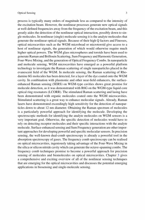
process is typically many orders of magnitude less as compared to the intensity ofthe excitation beam. However, the nonlinear processes generate new optical signalsat well-defined frequencies away from the frequency of the excitation beam, and thisgreatly aides the detection of the nonlinear optical interaction, possibly down to sin-gle molecules. In nonlinear (single) molecule sensing it is the analyte molecules thatgenerate the nonlinear optical signals. Because of their high Q factors and Finesses,optical microcavities such as the WGM microbead or microtoroid give access to ahost of nonlinear signals, the generation of which would otherwise require muchhigher optical powers. The WGM glass microspheres and toroids have been used togenerate Raman andBrillouin Scattering, SumFrequency andHarmonicGeneration,Four-WaveMixing, and the generation of Optical Frequency Combs. In nanoparticleand molecule sensing, WGM microcavities have emerged as a powerful platformtechnology to investigate the Raman scattering of single nanoparticles placed in theevanescent field of the WGM. In molecule sensing, the Raman scattering of Rho-damine 6Gmolecules has been detected, for a layer of the dye coated onto theWGMcavity. In combination with plasmonic and other near-field enhancers, the surface-enhanced Raman sensing (SERS) on WGM-type cavities shows great promise formolecule detection, as it was demonstrated with R6G on the WGM-type liquid coreoptical ring resonators (LCORR). The stimulated Raman scattering and lasing havebeen demonstrated with organic molecules coated onto the WGM microcavities.Stimulated scattering is a great way to enhance molecular signals. Already, Ramanlasers have demonstrated exceedingly high sensitivity for the detection of nanopar-ticles down to about 12 nm diameter. Obtaining the Raman spectrum of moleculesis a particularly powerful approach for identifying the molecule. Developing thespectroscopic methods for identifying the analyte molecules on WGM sensors is avery important goal. Otherwise, the specific detection of molecules would have torely on detecting receptor molecules and their specific interactions with the analytemolecule. Surface-enhanced sensing and SumFrequency generation are other impor-tant approaches for developing powerful and specific molecular sensors. In precisionsensing, the well-known dual-comb spectroscopy is already a powerful tool in theabsorption spectroscopy of gases. The frequency comb spectroscopy can be realisedon optical microcavities, ingeniously taking advantage of the Four-Wave Mixing inthe silica or silicon nitride cavity which can generate the octave-spanning combs. Thefrequency comb techniques promise to become a powerful approach for precisionsensing of molecules and biomolecules on optical microcavities. Chapter 3 givesa comprehensive and exciting overview of all of the nonlinear sensing techniquesthat are emerging for the optical microcavities and discusses the potential emergingapplications in biosensing and single-molecule sensing.
Chapter 1Interferometric Biosensing
Nicolas P. Mauranyapin, Larnii Booth, Igor Marinkovic,and Warwick P. Bowen
Abstract Interferometric biosensors characterise biological specimens via theeffects they have on the interference between two optical fields. Generally, one fieldis arranged to interact with the specimen, perhaps propagating through it and incur-ring a phase shift, or scattering from it. Interference with the second field can bothallow phase shifts to be resolved, and amplify weak scattering signals to measurablelevels. While widely used in biological imaging, recent experiments have shownthat interferometric sensors are also capable of probing the size and dynamics ofsingle protein molecules. This chapter reviews this recent progress, outlines the con-cepts and techniques involved, and discusses areas in which such single-moleculeinterferometric biosensors have been applied.
1.1 Introduction
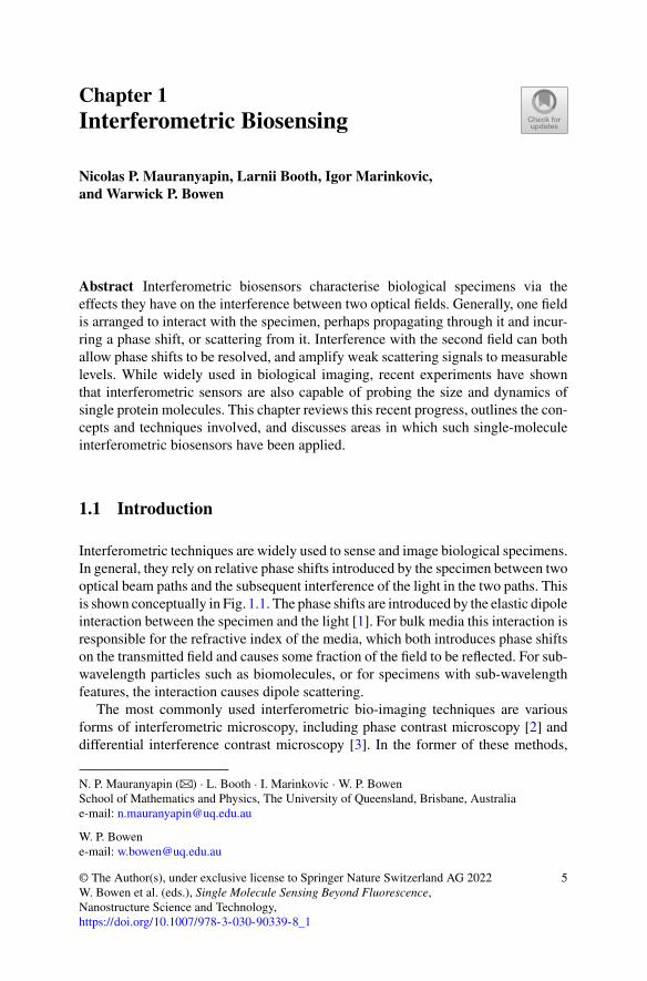
Interferometric techniques are widely used to sense and image biological specimens.In general, they rely on relative phase shifts introduced by the specimen between twooptical beam paths and the subsequent interference of the light in the two paths. Thisis shown conceptually in Fig. 1.1. The phase shifts are introduced by the elastic dipoleinteraction between the specimen and the light [1]. For bulk media this interaction isresponsible for the refractive index of the media, which both introduces phase shiftson the transmitted field and causes some fraction of the field to be reflected. For sub-wavelength particles such as biomolecules, or for specimens with sub-wavelengthfeatures, the interaction causes dipole scattering.
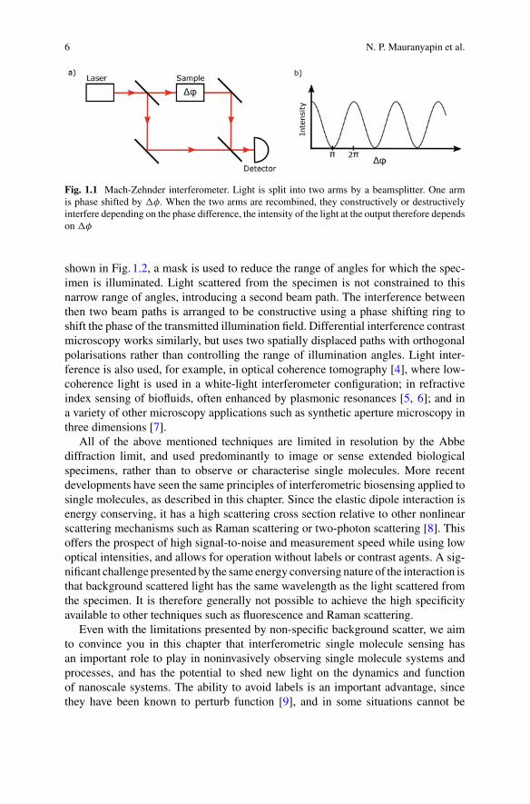
The most commonly used interferometric bio-imaging techniques are variousforms of interferometric microscopy, including phase contrast microscopy [2] anddifferential interference contrast microscopy [3]. In the former of these methods,
N. P. Mauranyapin (B) · L. Booth · I. Marinkovic · W. P. BowenSchool of Mathematics and Physics, The University of Queensland, Brisbane, Australiae-mail: [email protected]
W. P. Bowene-mail: [email protected]
© The Author(s), under exclusive license to Springer Nature Switzerland AG 2022W. Bowen et al. (eds.), Single Molecule Sensing Beyond Fluorescence,Nanostructure Science and Technology,https://doi.org/10.1007/978-3-030-90339-8_1
5
6 N. P. Mauranyapin et al.
Fig. 1.1 Mach-Zehnder interferometer. Light is split into two arms by a beamsplitter. One armis phase shifted by �φ. When the two arms are recombined, they constructively or destructivelyinterfere depending on the phase difference, the intensity of the light at the output therefore dependson �φ
shown in Fig. 1.2, a mask is used to reduce the range of angles for which the spec-imen is illuminated. Light scattered from the specimen is not constrained to thisnarrow range of angles, introducing a second beam path. The interference betweenthen two beam paths is arranged to be constructive using a phase shifting ring toshift the phase of the transmitted illumination field. Differential interference contrastmicroscopy works similarly, but uses two spatially displaced paths with orthogonalpolarisations rather than controlling the range of illumination angles. Light inter-ference is also used, for example, in optical coherence tomography [4], where low-coherence light is used in a white-light interferometer configuration; in refractiveindex sensing of biofluids, often enhanced by plasmonic resonances [5, 6]; and ina variety of other microscopy applications such as synthetic aperture microscopy inthree dimensions [7].
All of the above mentioned techniques are limited in resolution by the Abbediffraction limit, and used predominantly to image or sense extended biologicalspecimens, rather than to observe or characterise single molecules. More recentdevelopments have seen the same principles of interferometric biosensing applied tosingle molecules, as described in this chapter. Since the elastic dipole interaction isenergy conserving, it has a high scattering cross section relative to other nonlinearscattering mechanisms such as Raman scattering or two-photon scattering [8]. Thisoffers the prospect of high signal-to-noise and measurement speed while using lowoptical intensities, and allows for operation without labels or contrast agents. A sig-nificant challenge presented by the same energy conversing nature of the interaction isthat background scattered light has the same wavelength as the light scattered fromthe specimen. It is therefore generally not possible to achieve the high specificityavailable to other techniques such as fluorescence and Raman scattering.
Even with the limitations presented by non-specific background scatter, we aimto convince you in this chapter that interferometric single molecule sensing hasan important role to play in noninvasively observing single molecule systems andprocesses, and has the potential to shed new light on the dynamics and functionof nanoscale systems. The ability to avoid labels is an important advantage, sincethey have been known to perturb function [9], and in some situations cannot be
1 Interferometric Biosensing 7
Fig. 1.2 Phase contrast microscope. Input light (red) is shone through an annulus and focused onthe sample. The input light is phase shifted with a ring phase plate, making it constructively interferewith the scattered light (orange), enhancing the signal from the sample
easily introduced. Perhaps more importantly, much of the dynamics of biologi-cal machines occurs at kilohertz to gigahertz speeds. For instance, the myosinmotors responsible for muscle cell contraction and nutrient transport along actinfilaments can have stepping frequencies up to a few kilohertz [10], enzymes suchas ATPase and carbonic anhydrase have frequencies ranging from hundreds-of-hertz to a megahertz [11, 12], while biomolecular conformational changes canoccur over picosecond timescales [13]. Conventional fluorescence-based single-moleculemicroscopy techniques such asSTORM(StochasticOpticalReconstructionMicroscopy), STED (Stimulated Emission Depletion Microscopy), FRET (Fluores-cence Resonant Energy Transfer microscopy), and PALM (Photo Activated Local-ization Microscopy) struggle to reach these timescales and frequencies, since thequality fluorescent labels they use typically emit only around ten thousand photonsper second [14, 15]. By contrast, it is becoming clear that these frequencies andtimescales may be obtainable using dipole scattering, providing a new set of eyes tolook upon many important nanoscale processes.
8 N. P. Mauranyapin et al.
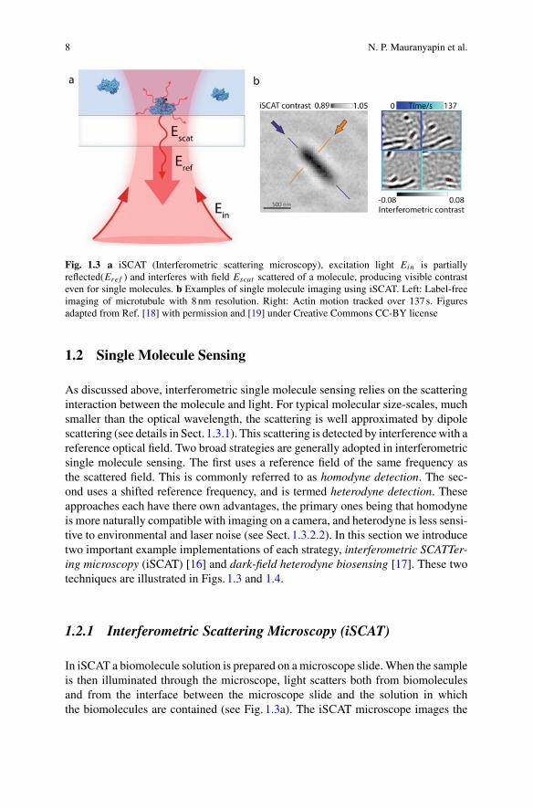
Fig. 1.3 a iSCAT (Interferometric scattering microscopy), excitation light Ein is partiallyreflected(Eref ) and interferes with field Escat scattered of a molecule, producing visible contrasteven for single molecules. b Examples of single molecule imaging using iSCAT. Left: Label-freeimaging of microtubule with 8nm resolution. Right: Actin motion tracked over 137s. Figuresadapted from Ref. [18] with permission and [19] under Creative Commons CC-BY license
1.2 Single Molecule Sensing
As discussed above, interferometric single molecule sensing relies on the scatteringinteraction between the molecule and light. For typical molecular size-scales, muchsmaller than the optical wavelength, the scattering is well approximated by dipolescattering (see details in Sect. 1.3.1). This scattering is detected by interferencewith areference optical field. Two broad strategies are generally adopted in interferometricsingle molecule sensing. The first uses a reference field of the same frequency asthe scattered field. This is commonly referred to as homodyne detection. The sec-ond uses a shifted reference frequency, and is termed heterodyne detection. Theseapproaches each have there own advantages, the primary ones being that homodyneis more naturally compatible with imaging on a camera, and heterodyne is less sensi-tive to environmental and laser noise (see Sect. 1.3.2.2). In this section we introducetwo important example implementations of each strategy, interferometric SCATTer-ing microscopy (iSCAT) [16] and dark-field heterodyne biosensing [17]. These twotechniques are illustrated in Figs. 1.3 and 1.4.
1.2.1 Interferometric Scattering Microscopy (iSCAT)
In iSCAT a biomolecule solution is prepared on amicroscope slide.When the sampleis then illuminated through the microscope, light scatters both from biomoleculesand from the interface between the microscope slide and the solution in whichthe biomolecules are contained (see Fig. 1.3a). The iSCAT microscope images the
1 Interferometric Biosensing 9
interferencebetween these twofields on a camera.Asdiscussed further inSect. 1.3.2.2,the few-micron-scale pathlength difference between the two fields results in a highlystable interference pattern. Even so, the variations in measured intensity across thecamera are typically much larger than the signal from a biomolecule. To overcomethis, a difference imaging technique is employed, monitoring the change in inten-sity distribution when a biomolecule arrives close to the microscope slide. As canbeen seen in Fig. 1.3b, this allows single biomolecules such as bovine serum albu-min (BSA, Stokes radius 3.5nm) to be resolved and to be distinguished from aggre-gates [16]. iSCAT has been shown to allow imaging and tracking single proteins [20],as well as observation of the motion of single protein filaments such as actin [19](Fig. 1.3b). It also allows measurements of single molecule structures such as thelength of microtubules with sub 5nm precision [21].
Single molecule mass photometry is an important application of iSCAT. It hasbeen shown experimentally that, to good approximation, the amplitude of scatteredlight from protein molecules is linearly proportional to the molecular mass [16, 22].The contrast of the interference pattern collected in iSCAT can then be directlyused to determine mass. This method has been used to determine the mass of singleproteins with amass resolution of 19 kDa and a precision of 1 kDa [23]. The ability tonondestructively determine the mass of single molecules is a useful tool for a rangeof applications, discussed further in Sect. 1.4.
1.2.2 Dark-Field Heterodyne Biosensing
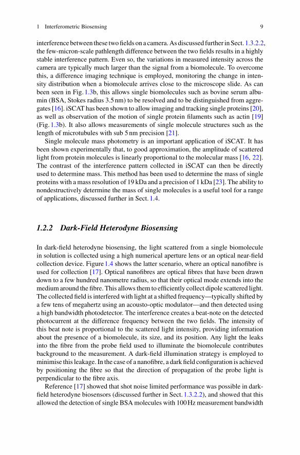
In dark-field heterodyne biosensing, the light scattered from a single biomoleculein solution is collected using a high numerical aperture lens or an optical near-fieldcollection device. Figure1.4 shows the latter scenario, where an optical nanofibre isused for collection [17]. Optical nanofibres are optical fibres that have been drawndown to a few hundred nanometre radius, so that their optical mode extends into themedium around the fibre. This allows them to efficiently collect dipole scattered light.The collected field is interferedwith light at a shifted frequency—typically shifted bya few tens of megahertz using an acousto-optic modulator—and then detected usinga high bandwidth photodetector. The interference creates a beat-note on the detectedphotocurrent at the difference frequency between the two fields. The intensity ofthis beat note is proportional to the scattered light intensity, providing informationabout the presence of a biomolecule, its size, and its position. Any light the leaksinto the fibre from the probe field used to illuminate the biomolecule contributesbackground to the measurement. A dark-field illumination strategy is employed tominimise this leakage. In the case of a nanofibre, a dark field configuration is achievedby positioning the fibre so that the direction of propagation of the probe light isperpendicular to the fibre axis.
Reference [17] showed that shot noise limited performance was possible in dark-field heterodyne biosensors (discussed further in Sect. 1.3.2.2), and showed that thisallowed the detection of single BSAmolecules with 100Hzmeasurement bandwidth
10 N. P. Mauranyapin et al.
Fig. 1.4 a Evanescent optical nanofiber, where light scattered from the particle (Escat ) is evanes-cently coupled into the nanofibre. The collected scattered signal is interfered with a frequencyshifted local oscillator and collected on a balanced detector, b Time trace of the detection of a singleBSA molecule, with a detection event highlighted. Figure adapted from Ref. [17] with permission
using probe intensities four orders of magnitude below the photodamage thresholdfor biological samples (see Fig. 1.4b) [17]. Reference [17] further showed that themotion of these biomolecules within the near-field of the sensor could be track witha resolution down to 1nm with a bandwidth 100Hz.
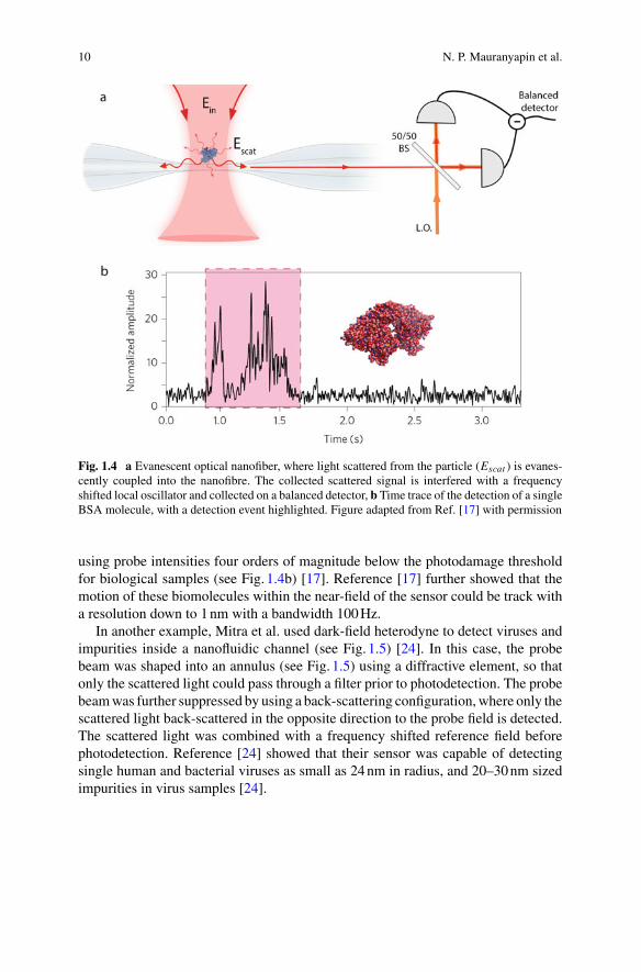
In another example, Mitra et al. used dark-field heterodyne to detect viruses andimpurities inside a nanofluidic channel (see Fig. 1.5) [24]. In this case, the probebeam was shaped into an annulus (see Fig. 1.5) using a diffractive element, so thatonly the scattered light could pass through a filter prior to photodetection. The probebeamwas further suppressed by using a back-scattering configuration,where only thescattered light back-scattered in the opposite direction to the probe field is detected.The scattered light was combined with a frequency shifted reference field beforephotodetection. Reference [24] showed that their sensor was capable of detectingsingle human and bacterial viruses as small as 24nm in radius, and 20–30nm sizedimpurities in virus samples [24].
1 Interferometric Biosensing 11
Fig. 1.5 Mitra et al. [24] use dark field heterodyne to image single molecules flowing inside ananofluidic channel. a Input light (Ein) is filtered from the scattered light with an iris and thescattered light is combined with a frequency shifted reference beam. b Detection events for HIVAT2WTwild type virus (smaller spikes) and 75nmpolystyrene beads (larger spikes). Figure adaptedfrom Ref. [24] with permission
1.3 Signal to Noise
The signal to noise (or SNR) is a key parameter for all biosensors, determining thesmallest resolvable signals in a given measurement time. For a signal n, the SNR canbe generally defined as
SN R ≡ 〈n〉2Var [n] , (1.1)
where 〈n〉 and Var [n] represent the expected value of the signal and its variance.A great deal of effort has been made during the past decade to increase the SNRof single molecule biosensor in a variety of ways, as also discussed in many otherchapters of this book, since improved SNR promises to allow the observation ofnew biological phenomena. In this section of this chapter we will examine the signalmagnitude available to interferometric single molecule biosensors, and the varietyof noise sources present in such measurements.
1.3.1 Signal Strength
In interferometric singlemolecule sensing, themolecule is illuminatedwith anopticalprobe field as shown in Figs. 1.3 and 1.4. In the typical case where it is smaller thanthe wavelength of the probe field, it will be polarised and form an electric dipolethat oscillates at the same frequency as the probe field. This dipole emits opticalradiations as a scattered field, which is the signal that biosensor aims to detect.
12 N. P. Mauranyapin et al.
1.3.1.1 Photon Flux from Dipole Scattering
Themean photon number 〈nscat 〉 contained in the scatteredfield from the biomoleculeis given by
〈nscat 〉 = σ
4πw2〈nin〉 (1.2)
whereσ is the scattering cross-section of themolecule,w is thewaist of the probefieldat the position of the particle, and 〈nin〉 is the mean number of photons incident fromthe probe field in the measurement duration [17, 25]. In many cases it is reasonableto approximate the biomolecule as an isotropic sphere of radius r (see e.g. [17, 26,27]), in which the scattering cross-section can be expressed as:
σ = 8πk4r6
3
(m2 − 1
m2 + 2
)2
, (1.3)
where k is the norm of the probe field wave vector, andm = np/nm is the ratio of therefractive indices of the molecule and the surrounding medium [25]. For a proteinmolecule, the bulk refractive index is generally in the range off 1.35–1.45.
From Eqs. (1.2) and (1.3) one can calculate that with a beam waist of 1µm and aprobe wavelength of λ = 2π/k = 780nm, a 10nm silica nano-sphere (np = 1.45)in water (nm = 1.33) will scatter one photon for every∼1011 incident probe photons.For a BSA molecule approximated as a uniform sphere of refractive index 1.45 andradius equal to the Stokes radius of BSA (3.5nm), only two photons will be scatteredevery ∼1014 incident probe photons. While this level of scattering is relatively low,it compares favourably to most inelastic scattering processes.
The magnitude of scattering ultimately determines the maximum rate at whicha biomolecule can be measured, since at least one photon must be scattered in themeasurement time. As an example, let us consider again a BSA molecule illumi-nated with a probe beam of 1µm radius and wavelength λ = 2π/k = 780nm. If1mW of probe power is used, corresponding to ∼1016 probe photons per second,∼200 photons are scattered per second. Assuming that every one of these photonsis detected and all noise sources (apart from the shot noise introduced by the veryquantisation of light) are removed, the maximum possible measurement rate in thisscenario is therefore 200Hz. This is fast enough to capture the slow diffusion andconformational changes of biomolecules.
1.3.1.2 Atomistic Model of Molecular Polarizability
The approximations that biomolecules are uniform spheres as performed above, orthat they are simple arrangements of uniform blocks with bulk properties, are com-monly used in biosensing [17, 26–28]. However, for sufficiently small molecules itcan be expected that their atomistic nature will play an important role in determin-ing how they polarize and therefore their scattering cross-section. It is especially
1 Interferometric Biosensing 13
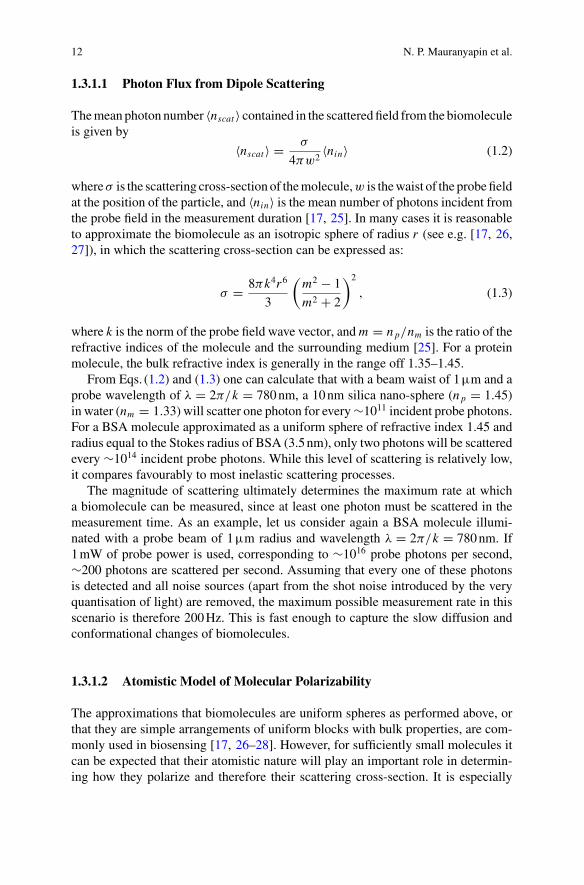
Fig. 1.6 Scattering of a fiveatoms (black spheres)molecule based on theatomistic model of molecularpolarizability. A probe fieldE illuminates the atoms fromabove, polarising them. Eachpolarized atom emits adipole field which induces itsown polarization on the otheratoms. In this way the totalscattering depends on thearrangement of atoms
αi αj μj
Scattered
μi
important to understand how the shifting coordinates of atoms in a molecule affecttheir scatteringwhen the aim is to observe conformational changes andothermotionaldynamics.
Booth et al. [29] develop a method to perform atomistic modelling for scattering-based single-molecule biosensors. Following earlier proposals by [30, 31], themethod considers that at any given time the molecule is a rigid ensemble of atoms.Each atomhas its own atomic polarizability, therefore, when illuminated by the probefield it forms an induced dipole and create its own scattered field (as was the case inthe previous section). The scattered field of each atom contributes to the total scat-tering of the molecule. However it also changes the field experienced by neighbouratoms (see Fig. 1.6). The total induced dipole moment μi of each atom i thereforedepends both on its own atomic polarizability αi and on the induced dipole momentsof every other atom μ j , which themselves depend on the atomic polarizability ofatom i . Booth et al. [29] show that it is possible to account for these couplings in acomputationally efficient way, allowing the excess polarizability of αex of moleculesthat are as large as 1600 kDa (110.000 atoms) to be calculated from their atomicstructure. The excess polarizability can be related to the scattering cross-section by
αex =(6πn4mk4
σ
)1/2
. (1.4)
The coordinates of the atoms in a biomolecule can be calculated as a function oftime using molecular dynamics simulations. The approach of Booth et al. [29] thenprovides straightforward predictions of the magnitude of scattered light, and how itchanges over time. For example, Booth et al. used molecular dynamic simulation ofBSA to extract the variation of its polarizability due to thermal fluctuations.
Molecules that exhibit different conformations have been studied with singlemolecule biosensors [28]. Kim et al. observed, for the first time without label, thedynamics of DNA polymerase as it changes conformation using a plasmonicallyenhanced whispering gallery mode microcavity sensors (see Chap.2). Prediction of
14 N. P. Mauranyapin et al.
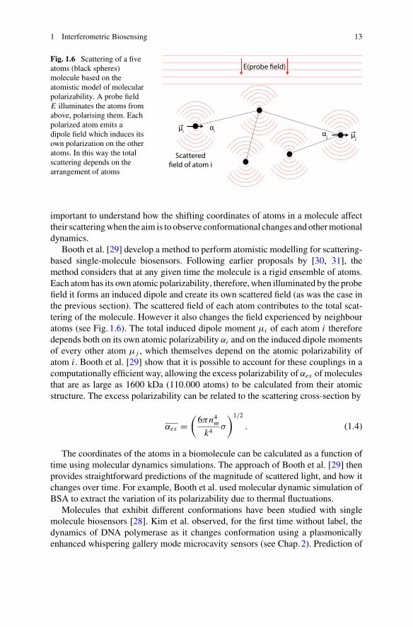
Fig. 1.7 Three conformational steps taken by aChloroplast F1F0ATPase during the decompositionof ATP into ADP. Structures were determined in Ref. [32] by cryo-EM and are generated from thePDB files 6FKF, 6FKH, and 6FKI using UCSF Chimera
the signal was computed using the bulk model as DNA polymerase executes largemotion within the non-uniform electric field of the sensor. In this case, the dominantmodulation of the signal does not originate from changes in polarizability but ratherfrom the DNA polymerase moving from a high intensity probing field region to alow intensity region. However, many molecules undergo rotation and smaller-scaleconformational rearrangements, for which such model would predict no signal. Theapproach of Booth et al. allows the signal due to these effects to be predicted. Forinstance, in the case of Chloroplast F1F0 ATPase shown in Fig. 1.7, rotation is pre-dicted to result in a significant change in polarizability. To reach this conclusion,Booth et al. compare the optically-induced polarization of each conformation thata F1F0 ATPase molecule takes during the decomposition of adenosine triphosphate(ATP) into adenosine diphosphate (ADP). The atomic structures of these conforma-tions have been determined by cryogenic electron microscopy [32] and are availablefrom the Protein Data Bank (PDB). Using them, Booth et al. predict that the polar-izability should change by as much as 350 Å3 (4.3%) between conformations. Thissignal is within reach of interferometric single molecule sensors, as well as othersingle molecule sensors such as the optoplasmonic sensors discussed in Chap. 2.
1.3.1.3 Methods to Enhance the Signal Strength
As seen in Eq.1.2, the scattered photon flux is proportional to the mean incidentphoton flux divided by the waist of the incident beam. It can therefore be increasedsimply by increasing the mean intensity of the incident field at the biomolecule. Thebenefit of this approach is constrained, however, by photodamage to the specimenwhich can occur at the high intensities using in single molecule biosensing experi-ments. This photodamage includes photochemical effects, local heating and physicaldamage and can affect growth, viability and function [33–36].
1 Interferometric Biosensing 15
Fig. 1.8 Schematic of theelectric double layerformation around a silicananosphere
To further increase the scattering of biomolecules, their scattering cross-sectioncan be enhanced. This can be done,for example, by attaching a label to the molecule[34], by using fluorescence or by changing the surrounding medium to increase therefractive index contrast. A disadvantage of this approach is that it negates the benefitof observing the molecule, and its behaviour, in its natural state [37–43].
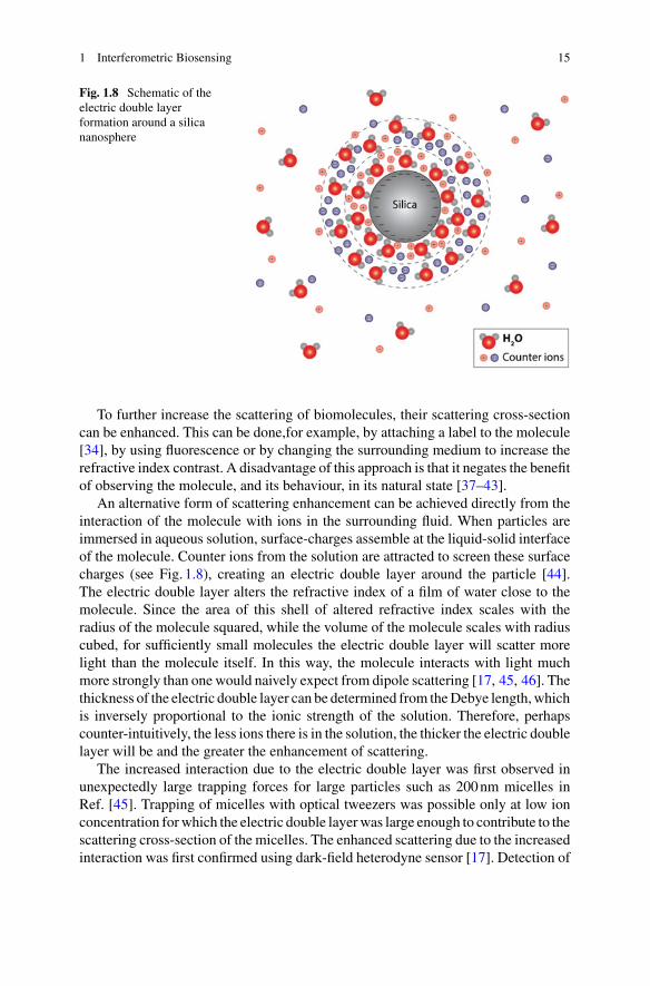
An alternative form of scattering enhancement can be achieved directly from theinteraction of the molecule with ions in the surrounding fluid. When particles areimmersed in aqueous solution, surface-charges assemble at the liquid-solid interfaceof the molecule. Counter ions from the solution are attracted to screen these surfacecharges (see Fig. 1.8), creating an electric double layer around the particle [44].The electric double layer alters the refractive index of a film of water close to themolecule. Since the area of this shell of altered refractive index scales with theradius of the molecule squared, while the volume of the molecule scales with radiuscubed, for sufficiently small molecules the electric double layer will scatter morelight than the molecule itself. In this way, the molecule interacts with light muchmore strongly than one would naively expect from dipole scattering [17, 45, 46]. Thethickness of the electric double layer can be determined from theDebye length,whichis inversely proportional to the ionic strength of the solution. Therefore, perhapscounter-intuitively, the less ions there is in the solution, the thicker the electric doublelayer will be and the greater the enhancement of scattering.
The increased interaction due to the electric double layer was first observed inunexpectedly large trapping forces for large particles such as 200nm micelles inRef. [45]. Trapping of micelles with optical tweezers was possible only at low ionconcentration forwhich the electric double layerwas large enough to contribute to thescattering cross-section of the micelles. The enhanced scattering due to the increasedinteraction was first confirmed using dark-field heterodyne sensor [17]. Detection of
16 N. P. Mauranyapin et al.
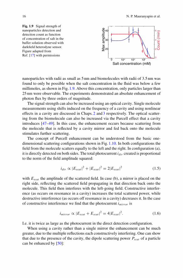
Fig. 1.9 Signal strength ofnanoparticles detection anddetection count as functionof concentration of salt in thebuffer solution observed withdarkfield heterodyne sensor.Figure adapted fromRef. [17] with permissions
0 10-4 10-2 100
20
30
40
Max
am
plitu
de
0
2
4
6
Cou
nt (
/min
)
Salt concentration (mM)
nanoparticles with radii as small as 5nm and biomolecules with radii of 3.5nm wasfound to only be possible when the salt concentration in the fluid was below a fewmillimoles, as shown in Fig. 1.9. Above this concentration, only particles larger than25nm were observable. The experiments demonstrated an absolute enhancement ofphoton flux by three orders of magnitude.
The signal strength can also be increased using an optical cavity. Single moleculemeasurements using shifts induced on the frequency of a cavity and using nonlineareffects in a cavity are discussed in Chaps. 2 and3 respectively. The optical scatter-ing from the biomolecule can also be increased via the Purcell effect that a cavityintroduces [47–49]. In this case, the enhancement occurs because scattering fromthe molecule that is reflected by a cavity mirror and fed back onto the moleculestimulates further scattering.
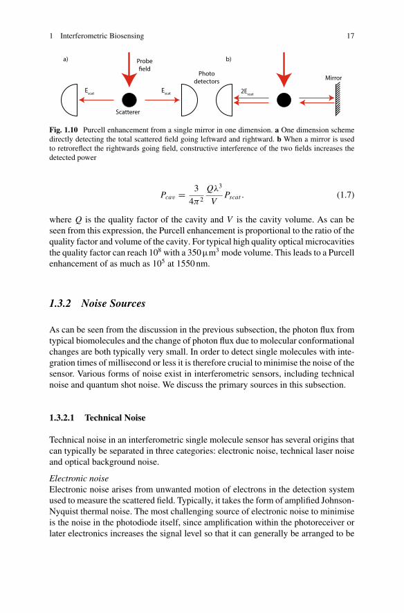
The concept of Purcell enhancement can be understood from the basic one-dimensional scattering configurations shown in Fig. 1.10. In both configurations thefield from the molecule scatters equally to the left and the right. In configuration (a),it is directly detected on both sides. The total photocurrent idir created is proportionalto the norm of the field amplitude squared:
idir ∝ |Escat |2 + |Escat |2 = 2|Escat |2 (1.5)
with Escat the amplitude of the scattered field. In case (b), a mirror is placed on theright side, reflecting the scattered field propagating in that direction back onto themolecule. This field then interferes with the left-going field. Constructive interfer-ence (as occurs on resonance in a cavity) increases the total scattered power, whiledestructive interference (as occurs off resonance in a cavity) decreases it. In the caseof constructive interference we find that the photocurrent imirror is
imirror ∝ |Escat + Escat |2 = 4|Escat |2. (1.6)
I.e. it is twice as large as the photocurrent in the direct detection configuration.When using a cavity rather than a single mirror the enhancement can be much
greater, due to the multiple reflections each constructively interfering. One can showthat due to the presence of the cavity, the dipole scattering power Pscat of a particlecan be enhanced by [50]:
1 Interferometric Biosensing 17
Scatterer
a) b)
MirrorPhoto
detectorsEscatEscat 2Escat
Probe
Fig. 1.10 Purcell enhancement from a single mirror in one dimension. a One dimension schemedirectly detecting the total scattered field going leftward and rightward. b When a mirror is usedto retroreflect the rightwards going field, constructive interference of the two fields increases thedetected power
Pcav = 3
4π2
Qλ3
VPscat . (1.7)
where Q is the quality factor of the cavity and V is the cavity volume. As can beseen from this expression, the Purcell enhancement is proportional to the ratio of thequality factor and volume of the cavity. For typical high quality optical microcavitiesthe quality factor can reach 108 with a 350µm3 mode volume. This leads to a Purcellenhancement of as much as 105 at 1550nm.
1.3.2 Noise Sources
As can be seen from the discussion in the previous subsection, the photon flux fromtypical biomolecules and the change of photon flux due to molecular conformationalchanges are both typically very small. In order to detect single molecules with inte-gration times of millisecond or less it is therefore crucial to minimise the noise of thesensor. Various forms of noise exist in interferometric sensors, including technicalnoise and quantum shot noise. We discuss the primary sources in this subsection.
1.3.2.1 Technical Noise
Technical noise in an interferometric single molecule sensor has several origins thatcan typically be separated in three categories: electronic noise, technical laser noiseand optical background noise.
Electronic noiseElectronic noise arises from unwanted motion of electrons in the detection systemused to measure the scattered field. Typically, it takes the form of amplified Johnson-Nyquist thermal noise. The most challenging source of electronic noise to minimiseis the noise in the photodiode itself, since amplification within the photoreceiver orlater electronics increases the signal level so that it can generally be arranged to be
18 N. P. Mauranyapin et al.
larger than down stream electronic noise. The photodiode electronic noise can bereduced by careful choice of photodiode, and through techniques such a dark-fieldheterodyne detection [17] which uses a bright optical local oscillator field to amplifythe scattering signal detected by the photodiode. The photodiode electronic noisecan also be reduced by cooling the photoreceiver.
Line noise and electronic pick-up, can introduce noise tones at characteristicfrequencies, though due to their near mono-frequency nature these noise sourcesare typically not problematic. Conversion of the analog photocurrent to a digitalsignal (for example using a data acquisition card or oscilloscope) can also introducenoise, both digitisation noise and aliasing of high frequency noise or signals to lowfrequencies. Digitisation noise can be challenging if a high dynamic range is desired,in which case a data acquisition system with a high bit depth is advisable. Aliasingcan be avoided using an appropriate antialiasing filter.
Technical laser noiseLight emitted by lasers inherently contains intensity and frequency noise.
The intensity, or amplitude, noise is any unwantedfluctuations of the field intensityand has a variety of origins. Relaxation noise of the laser medium due to the lasingprocess is one important source of intensity noise that often occurs at frequenciesrelevant to biosensors. Intensity fluctuations can also be transferred from the laserpump, and polarization noise due to relative phase fluctuations between two orthog-onal polarization components can be converted to amplitude noise by polarizationselective elements such as waveguide modulators or polarization beam splitters.
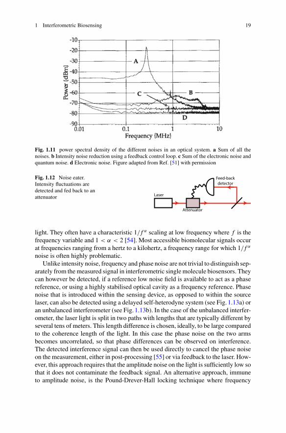
Intensity noise can be directly be detected on a photodetector, and analysed viapower spectral analysis, as shown for example in Fig. 1.11a. In this case, the primaryamplitude noise arises from laser relaxation oscillation, and features a characteristicplateau at low analysis frequencies, followed by a resonance, and decay as the fre-quency increases. Considerable efforts have been made to reduce the intensity noiseof laser system to increase the sensitivity of precision optical sensors (for examplesee Refs. [51, 52]). Intensity noise can be suppressed by using a noise eater wheretypically, fluctuations of the intensity are detected and fed back to an attenuator(see Fig. 1.12) that correct them (see e.g. traces B in Fig. 1.11). The feedback canalso be directly applied to the laser itself. These feedback systems can reduce theintensity noise by hundreds of decibel at low frequencies (100Hz) but their efficiencydecreases with frequency. However, as shown in Fig. 1.11, reduction of the relaxationnoise by 50 decibels can still be achieved at frequencies above 100kHz.
The frequency noise comes from drifts in the frequency of the laser, while phasenoise is introduced by fluctuations of the optical path length. Since frequency noisealso causes phase fluctuations, after the field propagates over a length, frequencyand phase noise are often treated together. They can arise due to the laser cavityvibrations, acoustic vibrations of optical elements along the beam path, changesin temperature, and coupling of intensity noise into frequency noise via nonlinear-ities [53]. The frequency noise is responsible for the laser linewidth broadening.Frequency and phase noise are a major concern for interferometric sensors since theinterferometric signals to be detected are intrinsically sensitive to the phase of the
1 Interferometric Biosensing 19
Fig. 1.11 power spectral density of the different noises in an optical system. a Sum of all thenoises. b Intensity noise reduction using a feedback control loop. c Sum of the electronic noise andquantum noise. d Electronic noise. Figure adapted from Ref. [51] with permission
Fig. 1.12 Noise eater.Intensity fluctuations aredetected and fed back to anattenuator
Feed-back detector
Laser
Attenuator
light. They often have a characteristic 1/ f α scaling at low frequency where f is thefrequency variable and 1 < α < 2 [54]. Most accessible biomolecular signals occurat frequencies ranging from a hertz to a kilohertz, a frequency range for which 1/ f α
noise is often highly problematic.Unlike intensity noise, frequency and phase noise are not trivial to distinguish sep-
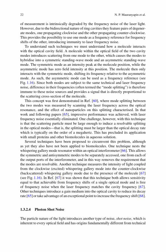
arately from themeasured signal in interferometric single molecule biosensors. Theycan however be detected, if a reference low noise field is available to act as a phasereference, or using a highly stabilised optical cavity as a frequency reference. Phasenoise that is introduced within the sensing device, as opposed to within the sourcelaser, can also be detected using a delayed self-heterodyne system (see Fig. 1.13a) oran unbalanced interferometer (see Fig. 1.13b). In the case of the unbalanced interfer-ometer, the laser light is split in two paths with lengths that are typically different byseveral tens of meters. This length difference is chosen, ideally, to be large comparedto the coherence length of the light. In this case the phase noise on the two armsbecomes uncorrelated, so that phase differences can be observed on interference.The detected interference signal can then be used directly to cancel the phase noiseon the measurement, either in post-processing [55] or via feedback to the laser. How-ever, this approach requires that the amplitude noise on the light is sufficiently low sothat it does not contaminate the feedback signal. An alternative approach, immuneto amplitude noise, is the Pound-Drever-Hall locking technique where frequency
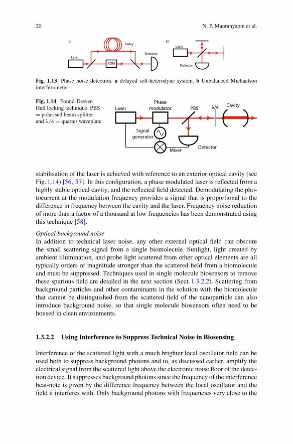
20 N. P. Mauranyapin et al.
Laser
a) b)Delay
AOM
Detector
Laser
Detector
Fig. 1.13 Phase noise detection. a delayed self-heterodyne system. b Unbalanced Michaelsoninterferometer
Fig. 1.14 Pound-Drever-Hall locking technique. PBS= polarised beam splitterand λ/4 = quarter waveplate
Detector
Cavity
Mixer
Signal generator
LaserPhase
modulator PBS λ/4
stabilisation of the laser is achieved with reference to an exterior optical cavity (seeFig. 1.14) [56, 57]. In this configuration, a phase modulated laser is reflected from ahighly stable optical cavity, and the reflected field detected. Demodulating the pho-tocurrent at the modulation frequency provides a signal that is proportional to thedifference in frequency between the cavity and the laser. Frequency noise reductionof more than a factor of a thousand at low frequencies has been demonstrated usingthis technique [58].
Optical background noiseIn addition to technical laser noise, any other external optical field can obscurethe small scattering signal from a single biomolecule. Sunlight, light created byambient illumination, and probe light scattered from other optical elements are alltypically orders of magnitude stronger than the scattered field from a biomoleculeand must be suppressed. Techniques used in single molecule biosensors to removethese spurious field are detailed in the next section (Sect. 1.3.2.2). Scattering frombackground particles and other contaminants in the solution with the biomoleculethat cannot be distinguished from the scattered field of the nanoparticle can alsointroduce background noise, so that single molecule biosensors often need to behoused in clean environments.
1.3.2.2 Using Interference to Suppress Technical Noise in Biosensing
Interference of the scattered light with a much brighter local oscillator field can beused both to suppress background photons and to, as discussed earlier, amplify theelectrical signal from the scattered light above the electronic noise floor of the detec-tion device. It suppresses background photons since the frequency of the interferencebeat-note is given by the difference frequency between the local oscillator and thefield it interferes with. Only background photons with frequencies very close to the

1 Interferometric Biosensing 21
Signal Shifted signal
Frequency
a) b)
Pow
er sp
ectra
l d
ensit
y
Quantum noise limited signal
Frequency
Fig. 1.15 a Scheme of the heterodyne frequency shift to move the signal into a frequency regionwhere the local oscillator is quantum noise limited b Scheme of the quantum noise limited signalshifted back to its original frequency using a dual quadratures lock-in amplifier
frequency of the scattered field produce a beat-note that is indistinguishable fromthat of the scattered field. Indeed, so long as the frequency of the background lightis different from that of the scattered light by at least the frequency resolution of themeasurement, it can be fully suppressed. The frequency resolution is equal to theinverse of the measurement duration, and so can often be beneath a hertz. We cansee, therefore, that an interferometer is equivalent to an exceptionally narrow bandfrequency filter—one that is much narrower than could be built conveniently throughother means, and one that also amplifies the signal above electronic noise.
In iSCAT a homodyne configuration is used to interfere the scattered signal witha local oscillator that has the same frequency [59]. The challenge with this con-figuration is that, since there is no frequency difference between signal and localoscillator, slow phase fluctuations can masquerade as signals. The extreme stabilityof the iSCAT configuration, in which the reference beam and the scattered beamfollow almost identical paths, allows commonmode rejection of most sources of thisphase noise.
In dark field heterodyne detection [17], a local oscillator is also used to removebackground photons. However, the technical laser and background noise is avoidedusing a heterodyne configuration where the local oscillator and the scattered signalhave different frequencies (see Fig. 1.15). This shifts the interference beat-note tohigh frequencies (typically tens of megahertz) where the local oscillator is onlylimited by the optical shot noise (see Fig. 1.15). After detection, a dual quadratureslock-in amplifier is then used to electronically remove the technical noise on thedetected photocurrent and shift the shot noise limited signal back to low frequencies(see Fig. 1.15).
1.3.2.3 Removing Technical Noise Using Two Optical Cavity Modes
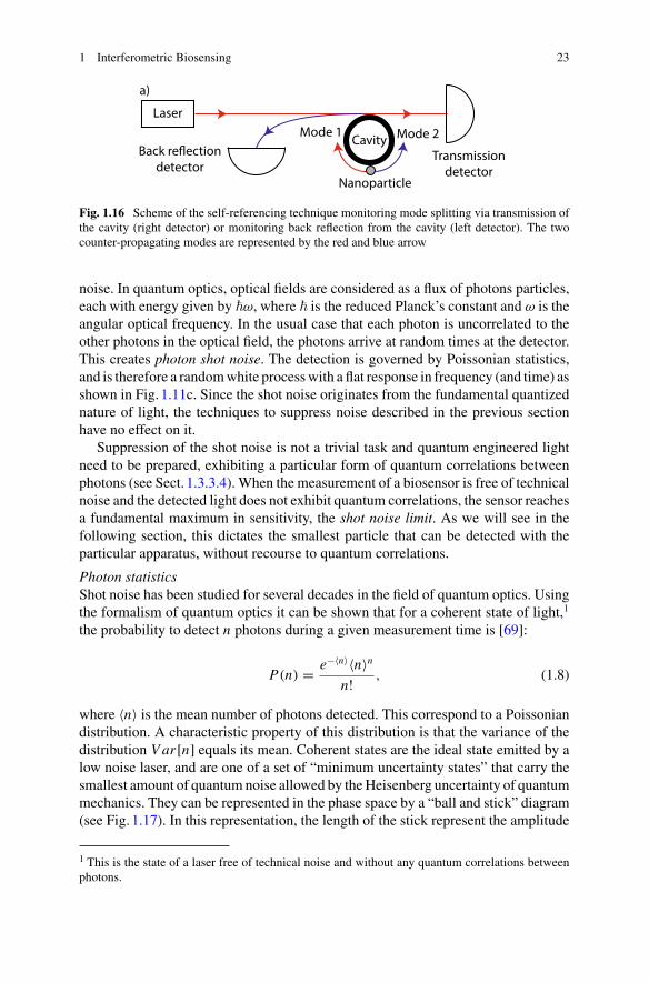
Biosensors that use optical ring cavities, such as like whispering gallery res-onators (e.g. see [28, 48, 60–64]) typically monitor frequency shift of the cavitydue to the presence of the molecule of interest (see Chap. 2). Therefore this types
22 N. P. Mauranyapin et al.
of measurement is intrinsically degraded by the frequency noise of the laser light.However, due to the bidirectional nature of ring cavities they feature pairs of degener-ate modes, one propagating clockwise and the other propagating counter-clockwise.This provides the possibility to use one mode as a frequency reference for frequencyshifts of the other, introducing immunity to laser frequency noise.
To understand such techniques we must understand how a molecule interactswith the optical cavity field. A molecule within the optical field of the two cavitymodes introduces scattering from one mode to the other, which causes the modes tohybridise into a symmetric standing-wave mode and an asymmetric standing-wavemode. The symmetric mode as an intensity peak at the molecule position, while theasymmetric mode has zero field intensity at this position. The molecule then onlyinteracts with the symmetric mode, shifting its frequency relative to the asymmetricmode. As such, the asymmetric mode can be used as a frequency reference (seeFig. 1.16). Since both modes are subject to the same technical and laser frequencynoise, difference in their frequencies (often termed the “mode splitting”) is thereforeimmune to these noise sources and provides a signal that is directly proportional tothe scattering cross-section of the molecule.
This concept was first demonstrated in Ref. [60], where mode splitting betweenthe two modes was measured by scanning the laser frequency across the opticalresonance, and the effect of nanoparticles on this splitting characterised. In thatwork and following papers [65], impressive performance was achieved, with laserfrequency noise essentially eliminated. One challenge, however, with this techniqueis that the scattering particle must be large enough to induce a resolvable splittingin the optical modes—that is, the splitting must be larger than the optical decay ratewhich is typically on the order of a megahertz. This has precluded its applicationwith small proteins and other biomolecules in aqueous solution.
Several techniques have been proposed to circumvent this problem, althoughas yet they also have not been applied to biomolecules. One technique nests thewhispering gallery mode resonator within an optical interferometer [66]. This allowsthe symmetric and antisymmetric modes to be separately accessed, one from each ofthe output ports of the interferometer, and in this way removes the requirement thatthe modes are resolvable. Another technique measures the intensity of light coupledfrom the clockwise (excited) whispering gallery mode into the counter-clockwise(backscattered) whispering gallery mode due to the presence of the molecule [67](see Fig. 1.16). In Ref. [67] it was shown that this technique both allows sensitivityequal to that achievable from frequency shifts of a single optical mode and is freeof frequency noise when the laser frequency matches the cavity frequency [67].Other techniques introduce a gain medium into the optical cavity to reduce its decayrate [65] or take advantage of an exceptional point to increase the frequency shift [68].
1.3.2.4 Photon Shot Noise
The particle nature of the light introduces another type of noise, shot noise, which isinherent to every optical field and has origins fundamentally different from technical
1 Interferometric Biosensing 23
Cavity
LaserMode 1 Mode 2
Nanoparticledetector
Transmission detector
a)
Fig. 1.16 Scheme of the self-referencing technique monitoring mode splitting via transmission ofthe cavity (right detector) or monitoring back reflection from the cavity (left detector). The twocounter-propagating modes are represented by the red and blue arrow
noise. In quantum optics, optical fields are considered as a flux of photons particles,each with energy given by �ω, where � is the reduced Planck’s constant and ω is theangular optical frequency. In the usual case that each photon is uncorrelated to theother photons in the optical field, the photons arrive at random times at the detector.This creates photon shot noise. The detection is governed by Poissonian statistics,and is therefore a randomwhite processwith a flat response in frequency (and time) asshown in Fig. 1.11c. Since the shot noise originates from the fundamental quantizednature of light, the techniques to suppress noise described in the previous sectionhave no effect on it.
Suppression of the shot noise is not a trivial task and quantum engineered lightneed to be prepared, exhibiting a particular form of quantum correlations betweenphotons (see Sect. 1.3.3.4). When the measurement of a biosensor is free of technicalnoise and the detected light does not exhibit quantum correlations, the sensor reachesa fundamental maximum in sensitivity, the shot noise limit. As we will see in thefollowing section, this dictates the smallest particle that can be detected with theparticular apparatus, without recourse to quantum correlations.
Photon statisticsShot noise has been studied for several decades in the field of quantum optics. Usingthe formalism of quantum optics it can be shown that for a coherent state of light,1
the probability to detect n photons during a given measurement time is [69]:
P(n) = e−〈n〉〈n〉nn! , (1.8)
where 〈n〉 is the mean number of photons detected. This correspond to a Poissoniandistribution. A characteristic property of this distribution is that the variance of thedistribution Var [n] equals its mean. Coherent states are the ideal state emitted by alow noise laser, and are one of a set of “minimum uncertainty states” that carry thesmallest amount of quantum noise allowed by theHeisenberg uncertainty of quantummechanics. They can be represented in the phase space by a “ball and stick” diagram(see Fig. 1.17). In this representation, the length of the stick represent the amplitude
1 This is the state of a laser free of technical noise and without any quantum correlations betweenphotons.
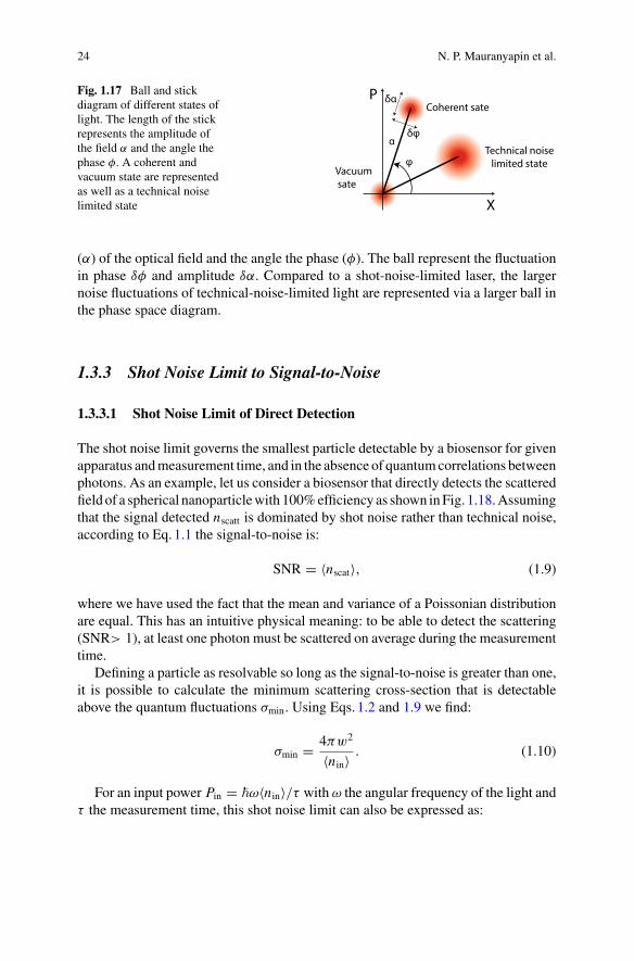
24 N. P. Mauranyapin et al.
Fig. 1.17 Ball and stickdiagram of different states oflight. The length of the stickrepresents the amplitude ofthe field α and the angle thephase φ. A coherent andvacuum state are representedas well as a technical noiselimited state
P
X
Coherent sate
Vacuum sate
Technical noise limited state
α
φ
δφ
δα
(α) of the optical field and the angle the phase (φ). The ball represent the fluctuationin phase δφ and amplitude δα. Compared to a shot-noise-limited laser, the largernoise fluctuations of technical-noise-limited light are represented via a larger ball inthe phase space diagram.
1.3.3 Shot Noise Limit to Signal-to-Noise
1.3.3.1 Shot Noise Limit of Direct Detection
The shot noise limit governs the smallest particle detectable by a biosensor for givenapparatus andmeasurement time, and in the absence of quantumcorrelations betweenphotons. As an example, let us consider a biosensor that directly detects the scatteredfield of a spherical nanoparticlewith 100%efficiency as shown inFig. 1.18.Assumingthat the signal detected nscatt is dominated by shot noise rather than technical noise,according to Eq.1.1 the signal-to-noise is:
SNR = 〈nscat〉, (1.9)
where we have used the fact that the mean and variance of a Poissonian distributionare equal. This has an intuitive physical meaning: to be able to detect the scattering(SNR> 1), at least one photon must be scattered on average during the measurementtime.
Defining a particle as resolvable so long as the signal-to-noise is greater than one,it is possible to calculate the minimum scattering cross-section that is detectableabove the quantum fluctuations σmin. Using Eqs. 1.2 and 1.9 we find:
σmin = 4πw2
〈nin〉 . (1.10)
For an input power Pin = �ω〈nin〉/τ withω the angular frequency of the light andτ the measurement time, this shot noise limit can also be expressed as:
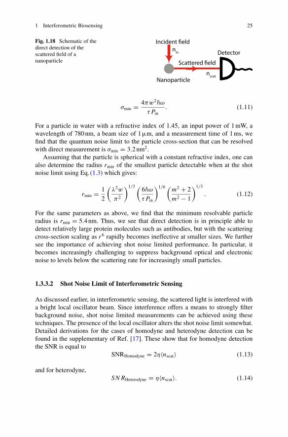
1 Interferometric Biosensing 25
Fig. 1.18 Schematic of thedirect detection of thescattered field of ananoparticle
Nanoparticlenscat
nin Detector
σmin = 4πw2�ω
τ Pin. (1.11)
For a particle in water with a refractive index of 1.45, an input power of 1mW, awavelength of 780nm, a beam size of 1µm, and a measurement time of 1ms, wefind that the quantum noise limit to the particle cross-section that can be resolvedwith direct measurement is σmin = 3.2nm2.
Assuming that the particle is spherical with a constant refractive index, one canalso determine the radius rmin of the smallest particle detectable when at the shotnoise limit using Eq. (1.3) which gives:
rmin = 1
2
(λ2w
π2
)1/3 (6�ω
τ Pin
)1/6 (m2 + 2
m2 − 1
)1/3
. (1.12)
For the same parameters as above, we find that the minimum resolvable particleradius is rmin = 5.4nm. Thus, we see that direct detection is in principle able todetect relatively large protein molecules such as antibodies, but with the scatteringcross-section scaling as r6 rapidly becomes ineffective at smaller sizes. We furthersee the importance of achieving shot noise limited performance. In particular, itbecomes increasingly challenging to suppress background optical and electronicnoise to levels below the scattering rate for increasingly small particles.
1.3.3.2 Shot Noise Limit of Interferometric Sensing
As discussed earlier, in interferometric sensing, the scattered light is interfered witha bright local oscillator beam. Since interference offers a means to strongly filterbackground noise, shot noise limited measurements can be achieved using thesetechniques. The presence of the local oscillator alters the shot noise limit somewhat.Detailed derivations for the cases of homodyne and heterodyne detection can befound in the supplementary of Ref. [17]. These show that for homodyne detectionthe SNR is equal to
SNRHomodyne = 2η〈nscat〉 (1.13)
and for heterodyne,SN RHeterodyne = η〈nscat〉. (1.14)
26 N. P. Mauranyapin et al.
with η the percentage of scattered photon collected by the detector. These shot noiselimit are similar to direct detection, showing the advantage of interferometric sensing:the same or better shot-noise limited sensitivity can be achieved as direct detection,with the signal amplified above electronic noise and background optical noise sup-pressed.
1.3.3.3 Optical Noise Scaling
To determine if a sensor operates at the shot noise limit, it is not necessary to beable to resolve single photon detection events. Instead, to test whether the sensor islimited by technical or shot noise, one can study how the noise scales with opticalpower.
Let us consider the experimental setup of Fig. 1.19. Here a laser field Ein contain-ing some signal passes through a variable efficiency γ beam splitter used to changethe optical power arriving at a sample and a photo-sensitive detector. When the opti-cal field at the detector Eout is transformed into a photocurrent i via the photoelectriceffect one can show that if Eout is dominated by technical noise,
itech ≈ γ 〈n〉 + 2γ√〈n〉δsig + 2γ
√〈n〉δtech (1.15)
where δsig is the signal amplitude, δtech is the fluctuation amplitude due to the technicalnoise, 〈n〉 is the mean incident photon number, and we have assumed that 〈n〉 �{δ2sig, 〈δtech〉2}. This assumption is generally valid. For amicro-watt optical field 〈n〉 ≈1012 and 〈δtech〉2 is typically in the range of 100–10,000. From this relation, we cansee that the signal and technical noise both scale with the detected optical power. Thisis expected since when attenuating or amplifying the laser power, by changing γ , thesignal or fluctuations of the laser intensity will be reduced or amplified accordingly.
Equation1.15 also shows that increasing the mean incident photon number (〈n〉)amplifies both the signal and the technical noise contribution and therefore will notincrease the signal to noise ratio when technical noise dominates. However, whenincreasing the intensity at the particle of interest, more photons interact with theparticle (δsig increases) and if 〈n〉 is kept constant, δtech stays constant and the signalto noise ratio can be increased. This is the technique leveraged by the WGM andplasmonic sensors to detect label free single proteinswhen limited by technical noise.
The scaling of the quantum noise fluctuations with optical power is different.In the quantum picture, when optical power fluctuates, by changing γ in Fig. 1.19,this results in adding or removing quantum vacuum fluctuations to the optical field.Counter intuitively, even if it contains zero photons, vacuum noise is a coherent stateof light and contains the same quantum fluctuations in phase and amplitude as acoherent state with many photons. Therefore, vacuum noise creates additional quan-tum noise and prevent the total quantum noise to be attenuated or amplified as fastas the technical noise. Semi-classically, the vacuum noise can be approximated as anadditional noise created because the beam splitter randomly chooses which photons

1 Interferometric Biosensing 27
δvac
EoutEin
Loses
i
γ
Optical amplitude
Electronic noise
Quantum noise
Classical noise
Det
ecte
d no
ise
b)a)
Sample
Fig. 1.19 a Scheme of light detection with a variable ratio γ (t) beam splitter. Note that the beamsplitter can be placed anywhere before the detector along the horizontal beam b Noise scaling asfunction of optical amplitude. The technical noise scales and quantum noise scale quadratically andlinearly with optical amplitude while the electronic noise is constant
are transmitted and which photons are reflected creating additional quantum noisewhich does not affect the technical noise. Therefore, when detecting the photocurrentfrom an optical field containing technical and quantum noise, we have:
itot ≈ γ 〈n〉 + 2γ√〈n〉 (
δsig + δtech + δq) + 2
√〈n〉γ (1 − γ )δvac (1.16)
with δq the amplitude of the quantum shot noise of the Ein and δvac the amplitude of thevacuum noise created by the beam splitter. Since the different noises are uncorrelatedand knowing that the quantum shot noise and the vacuum noise are both coherentstate therefore have equal variance, one can show that the power spectral density Itotof the the photocurrent is equal to:
Itot ≈ 4γ 2〈n〉 (Var[�sig] + Var[�tech]
) + 4γ 〈n〉Var[�q] (1.17)
where �sig, �tech and �q are the Fourier transform of the signal, technical noiseand quantum noise respectively and Var [X ] is the variance of X over the resolutionbandwidth of the measurement.2 Equation1.17 shows that, if the dominant noisescales linearly with γ , that is to say linearly with the detected field amplitude, it hasa quantum origin or if it scales quadratically, it has a technical origin [69] as shownin Fig. 1.19. From Eq.1.16, we also see that the quantum noise will dominates at lowpower and therefore, biosensors detecting small amount of power can be assumed tobe quantum noise limited.
1.3.3.4 Overcoming the Shot Noise Limit
It is possible to create states of light which have smaller uncertainty in some quadra-ture in phase space than a coherent state. This type of light is called squeezedlight [70]. For instance, an optical field that has less noise than a coherent statein its amplitude, is called an amplitude squeezed state, and one that has less noise
2 Var [X ]( f ) = ∫ f +RBW/2f −RBW/2 |X ( f ′)|2d f ′ whith RBW the resolution bandwidth.
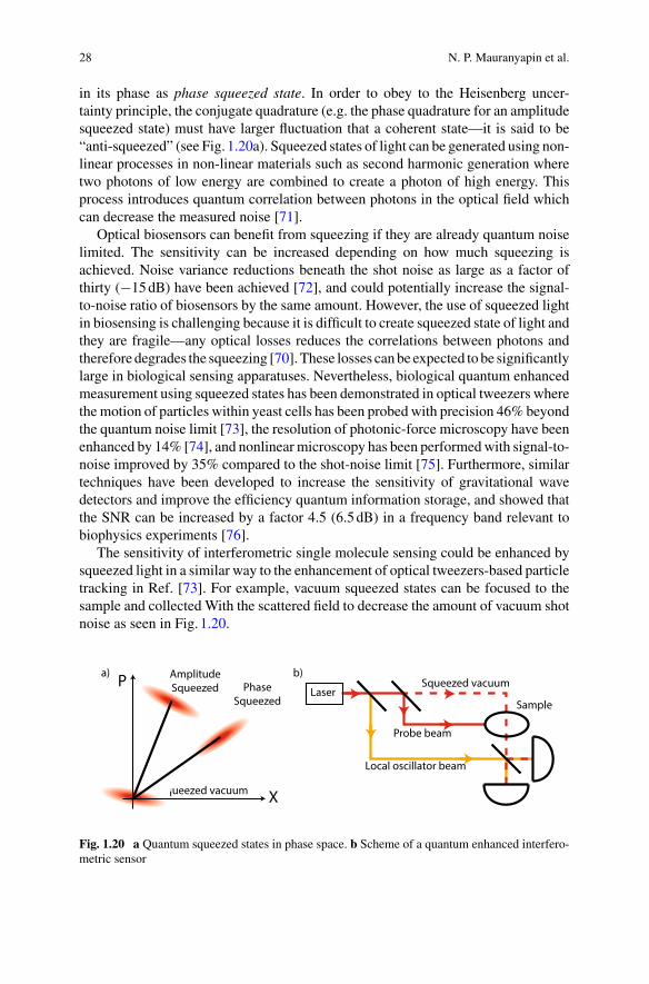
28 N. P. Mauranyapin et al.
in its phase as phase squeezed state. In order to obey to the Heisenberg uncer-tainty principle, the conjugate quadrature (e.g. the phase quadrature for an amplitudesqueezed state) must have larger fluctuation that a coherent state—it is said to be“anti-squeezed” (see Fig. 1.20a). Squeezed states of light can be generated using non-linear processes in non-linear materials such as second harmonic generation wheretwo photons of low energy are combined to create a photon of high energy. Thisprocess introduces quantum correlation between photons in the optical field whichcan decrease the measured noise [71].
Optical biosensors can benefit from squeezing if they are already quantum noiselimited. The sensitivity can be increased depending on how much squeezing isachieved. Noise variance reductions beneath the shot noise as large as a factor ofthirty (−15dB) have been achieved [72], and could potentially increase the signal-to-noise ratio of biosensors by the same amount. However, the use of squeezed lightin biosensing is challenging because it is difficult to create squeezed state of light andthey are fragile—any optical losses reduces the correlations between photons andtherefore degrades the squeezing [70]. These losses canbe expected to be significantlylarge in biological sensing apparatuses. Nevertheless, biological quantum enhancedmeasurement using squeezed states has been demonstrated in optical tweezers wherethe motion of particles within yeast cells has been probed with precision 46% beyondthe quantum noise limit [73], the resolution of photonic-force microscopy have beenenhanced by 14% [74], and nonlinear microscopy has been performedwith signal-to-noise improved by 35% compared to the shot-noise limit [75]. Furthermore, similartechniques have been developed to increase the sensitivity of gravitational wavedetectors and improve the efficiency quantum information storage, and showed thatthe SNR can be increased by a factor 4.5 (6.5dB) in a frequency band relevant tobiophysics experiments [76].
The sensitivity of interferometric single molecule sensing could be enhanced bysqueezed light in a similar way to the enhancement of optical tweezers-based particletracking in Ref. [73]. For example, vacuum squeezed states can be focused to thesample and collected With the scattered field to decrease the amount of vacuum shotnoise as seen in Fig. 1.20.
Sample
Local oscillator beam
Probe beam
Laser
b)a)Squeezed vacuum
Squeezed vacuum
P
X
PhaseSqueezed
AmplitudeSqueezed
Fig. 1.20 a Quantum squeezed states in phase space. b Scheme of a quantum enhanced interfero-metric sensor
1 Interferometric Biosensing 29
1.4 Applications
The main applications of interferometric sensing so far have been in single-particletracking and molecule size detection.
Single particle tracking in biology is commonly performed via fluorescence mea-surements. However, this type ofmeasurement suffers from relatively slow speed duefluorescence saturation limiting the emitted photon flux, as well as limited acquisi-tion times over which the particle can be tracked due to photobleaching of labelmolecules. Although interferometric sensing does not suffer from these issues, flu-orescence is the primary approach to single-particle tracking used so far in biology.The reason for this is that in fluorescence imaging it is easy to filter out scatteringthat does not come from molecules of interest (see Sect. 1.3.2). This is not so trivialin case of interferometric sensing, and as a consequence interferometric techniqueshave been primarily used in an environment without scatterers other than the particleof interest. Most interferometric sensing applications demonstrated to date have usediSCAT microscopy, as it provides a high degree of spatial information.
At a scale of nanometers, gold nanoparticles were among the first to be detectedand tracked by an interferometric technique [79]. Because of their strong scatteringand biocompatibility, they are often used as labels in image scanning microscopy.Gold nanoparticles as small as 2nm have been imaged with iSCAT [80]. Larger par-ticles in the 20nm to micrometer range scatter more light (see Sect. 1.3.1.1) enablingfaster and more precise localisation of particles [81]. However, this comes with thecompromise of greater invasion into the natural dynamics of the biosystem, and lowersensitivity to environmental forces due to the increased mass. Rotational diffusionof gold nanorods has also been investigated using iSCAT [82]. The speed of iSCATmeasurements is limited by the cameras used for detection, so other techniques likedark-field heterodyne detection [17] are more suitable for achieving measurementsat speeds in the hundreds of kilohertz and above.
Tracking of viruses was demonstrated in the early days of interferometric sens-ing, thanks to their large size between tens and hundreds of nanometers. Comparedto these earlier experiments, the two dimensional spatial resolution of iSCAT canprovide additional information. For instance, it can be used to determine whether thevirus contains DNA or not [77] (Fig. 1.21), since the presence of DNA affected thepolarizability.
Even though much smaller than viruses, single proteins have been detected,starting with the detection of myosin VA (500kDa) [20] (Fig. 1.22). By detecting74nm steps of myosin along actin filaments at speeds unattainable for fluorescencemicroscopy, it was possible to unravel additional dynamics of molecular motion.Later experiments were able to detect molecules down to about 50 kDa in size, bothwith dark-field heterodyne sensing [17] and iSCAT microscopy [26]. Heterodynesensing has demonstrated quantum limited detection and can be naturally integratedwith microfluidics using hollow core fibers [83].
Tracing viruses and proteins on the surface of a cell is of great importance forbiology. Unfortunately, it is not straight forward to maintain the same tracking
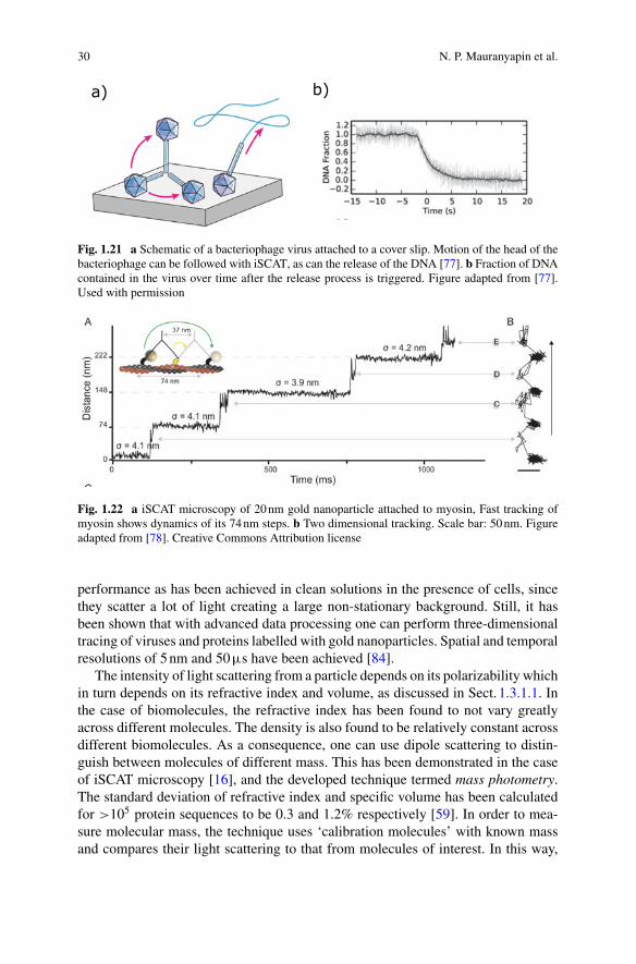
30 N. P. Mauranyapin et al.
a) b)
Fig. 1.21 a Schematic of a bacteriophage virus attached to a cover slip. Motion of the head of thebacteriophage can be followed with iSCAT, as can the release of the DNA [77]. b Fraction of DNAcontained in the virus over time after the release process is triggered. Figure adapted from [77].Used with permission
Fig. 1.22 a iSCAT microscopy of 20nm gold nanoparticle attached to myosin, Fast tracking ofmyosin shows dynamics of its 74nm steps. b Two dimensional tracking. Scale bar: 50nm. Figureadapted from [78]. Creative Commons Attribution license
performance as has been achieved in clean solutions in the presence of cells, sincethey scatter a lot of light creating a large non-stationary background. Still, it hasbeen shown that with advanced data processing one can perform three-dimensionaltracing of viruses and proteins labelled with gold nanoparticles. Spatial and temporalresolutions of 5nm and 50µs have been achieved [84].
The intensity of light scattering from a particle depends on its polarizability whichin turn depends on its refractive index and volume, as discussed in Sect. 1.3.1.1. Inthe case of biomolecules, the refractive index has been found to not vary greatlyacross different molecules. The density is also found to be relatively constant acrossdifferent biomolecules. As a consequence, one can use dipole scattering to distin-guish between molecules of different mass. This has been demonstrated in the caseof iSCAT microscopy [16], and the developed technique termed mass photometry.The standard deviation of refractive index and specific volume has been calculatedfor >105 protein sequences to be 0.3 and 1.2% respectively [59]. In order to mea-sure molecular mass, the technique uses ‘calibration molecules’ with known massand compares their light scattering to that from molecules of interest. In this way,
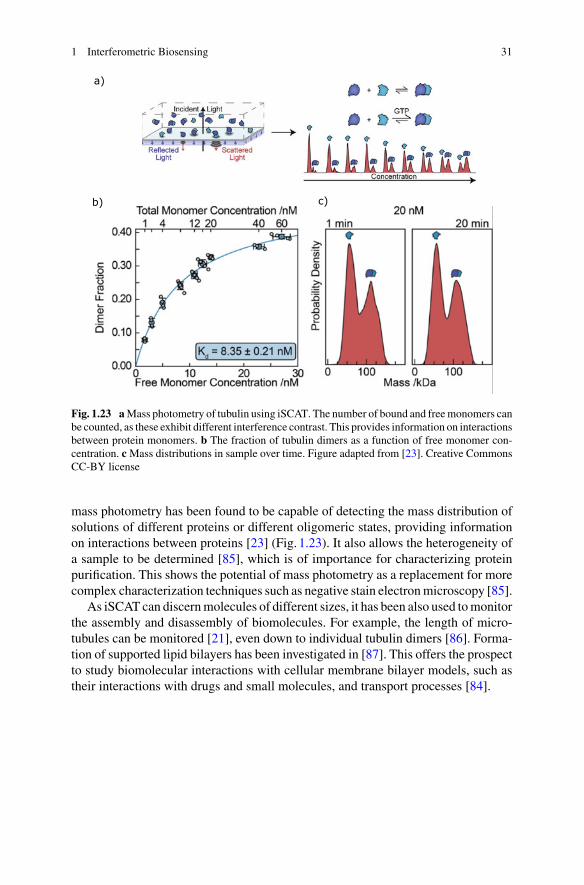
1 Interferometric Biosensing 31
a)
b) c)
Fig. 1.23 aMass photometry of tubulin using iSCAT. The number of bound and freemonomers canbe counted, as these exhibit different interference contrast. This provides information on interactionsbetween protein monomers. b The fraction of tubulin dimers as a function of free monomer con-centration. cMass distributions in sample over time. Figure adapted from [23]. Creative CommonsCC-BY license
mass photometry has been found to be capable of detecting the mass distribution ofsolutions of different proteins or different oligomeric states, providing informationon interactions between proteins [23] (Fig. 1.23). It also allows the heterogeneity ofa sample to be determined [85], which is of importance for characterizing proteinpurification. This shows the potential of mass photometry as a replacement for morecomplex characterization techniques such as negative stain electronmicroscopy [85].
As iSCAT can discernmolecules of different sizes, it has been also used tomonitorthe assembly and disassembly of biomolecules. For example, the length of micro-tubules can be monitored [21], even down to individual tubulin dimers [86]. Forma-tion of supported lipid bilayers has been investigated in [87]. This offers the prospectto study biomolecular interactions with cellular membrane bilayer models, such astheir interactions with drugs and small molecules, and transport processes [84].
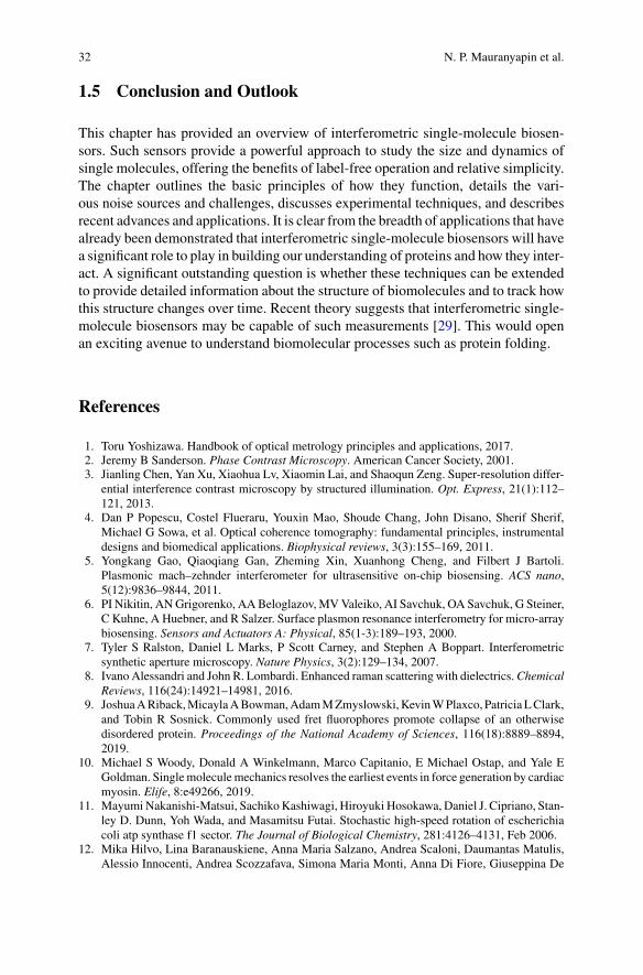
32 N. P. Mauranyapin et al.
1.5 Conclusion and Outlook
This chapter has provided an overview of interferometric single-molecule biosen-sors. Such sensors provide a powerful approach to study the size and dynamics ofsingle molecules, offering the benefits of label-free operation and relative simplicity.The chapter outlines the basic principles of how they function, details the vari-ous noise sources and challenges, discusses experimental techniques, and describesrecent advances and applications. It is clear from the breadth of applications that havealready been demonstrated that interferometric single-molecule biosensors will havea significant role to play in building our understanding of proteins and how they inter-act. A significant outstanding question is whether these techniques can be extendedto provide detailed information about the structure of biomolecules and to track howthis structure changes over time. Recent theory suggests that interferometric single-molecule biosensors may be capable of such measurements [29]. This would openan exciting avenue to understand biomolecular processes such as protein folding.
References
1. Toru Yoshizawa. Handbook of optical metrology principles and applications, 2017.2. Jeremy B Sanderson. Phase Contrast Microscopy. American Cancer Society, 2001.3. Jianling Chen, Yan Xu, Xiaohua Lv, Xiaomin Lai, and Shaoqun Zeng. Super-resolution differ-
ential interference contrast microscopy by structured illumination. Opt. Express, 21(1):112–121, 2013.
4. Dan P Popescu, Costel Flueraru, Youxin Mao, Shoude Chang, John Disano, Sherif Sherif,Michael G Sowa, et al. Optical coherence tomography: fundamental principles, instrumentaldesigns and biomedical applications. Biophysical reviews, 3(3):155–169, 2011.
5. Yongkang Gao, Qiaoqiang Gan, Zheming Xin, Xuanhong Cheng, and Filbert J Bartoli.Plasmonic mach–zehnder interferometer for ultrasensitive on-chip biosensing. ACS nano,5(12):9836–9844, 2011.
6. PI Nikitin, ANGrigorenko, AABeloglazov,MVValeiko, AI Savchuk, OA Savchuk, G Steiner,C Kuhne, A Huebner, and R Salzer. Surface plasmon resonance interferometry for micro-arraybiosensing. Sensors and Actuators A: Physical, 85(1-3):189–193, 2000.
7. Tyler S Ralston, Daniel L Marks, P Scott Carney, and Stephen A Boppart. Interferometricsynthetic aperture microscopy. Nature Physics, 3(2):129–134, 2007.
8. Ivano Alessandri and John R. Lombardi. Enhanced raman scattering with dielectrics.ChemicalReviews, 116(24):14921–14981, 2016.
9. JoshuaARiback,MicaylaABowman,AdamMZmyslowski,KevinWPlaxco, PatriciaLClark,and Tobin R Sosnick. Commonly used fret fluorophores promote collapse of an otherwisedisordered protein. Proceedings of the National Academy of Sciences, 116(18):8889–8894,2019.
10. Michael S Woody, Donald A Winkelmann, Marco Capitanio, E Michael Ostap, and Yale EGoldman. Singlemoleculemechanics resolves the earliest events in force generation by cardiacmyosin. Elife, 8:e49266, 2019.
11. MayumiNakanishi-Matsui, SachikoKashiwagi, Hiroyuki Hosokawa, Daniel J. Cipriano, Stan-ley D. Dunn, Yoh Wada, and Masamitsu Futai. Stochastic high-speed rotation of escherichiacoli atp synthase f1 sector. The Journal of Biological Chemistry, 281:4126–4131, Feb 2006.
12. Mika Hilvo, Lina Baranauskiene, Anna Maria Salzano, Andrea Scaloni, Daumantas Matulis,Alessio Innocenti, Andrea Scozzafava, Simona Maria Monti, Anna Di Fiore, Giuseppina De

1 Interferometric Biosensing 33
Simone, Mikaela Lindfors, Janne Jänis, Jarkko Valjakka, Silvia Pastoreková, Jaromir Pastorek,Markku S. Kulomaa, Henri R. Nordlund, Claudiu T. Supuran, and Seppo Parkkila. Biochemicalcharacterization of ca ix, one of the most active carbonic anhydrase isozymes*. Journal ofBiological Chemistry, 283(41):27799–27809, 2008.
13. Haruto Ishikawa, Kyungwon Kwak, Jean K. Chung, Seongheun Kim, and Michael D. Fayer.Direct observation of fast protein conformational switching. Proceedings of the NationalAcademy of Sciences, 105(25):8619–8624, 2008.
14. Joshua C Vaughan, Shu Jia, and Xiaowei Zhuang. Ultrabright photoactivatable fluorophorescreated by reductive caging. Nature methods, 9(12):1181–1184, 2012.
15. Jonathan B Grimm, Brian P English, Jiji Chen, Joel P Slaughter, Zhengjian Zhang, AndreyRevyakin, Ronak Patel, John J Macklin, Davide Normanno, Robert H Singer, et al. A generalmethod to improve fluorophores for live-cell and single-molecule microscopy.Nature methods,12(3):244–250, 2015.
16. Gavin Young, Nikolas Hundt, Daniel Cole, Adam Fineberg, Joanna Andrecka, Andrew Tyler,Anna Olerinyova, Ayla Ansari, Erik G Marklund, Miranda P Collier, et al. Quantitative massimaging of single biological macromolecules. Science, 360(6387):423–427, 2018.
17. NP Mauranyapin, LS Madsen, MA Taylor, M Waleed, and WP Bowen. Evanescent single-molecule biosensing with quantum-limited precision.Nature Photonics, 11(8):477–481, 2017.
18. Joanna Andrecka, Jaime Ortega Arroyo, Katie Lewis, Robert A. Cross, and Philipp Kukura.Label-free imaging of microtubules with sub-nm precision using interferometric scatteringmicroscopy. Biophysical Journal, 110(1):214–217, 2016.
19. Lewis S Mosby, Nikolas Hundt, Gavin Young, Adam Fineberg, Marco Polin, Satyajit Mayor,Philipp Kukura, and Darius V Köster. Myosin ii filament dynamics in actin networks revealedwith interferometric scattering microscopy. Biophysical Journal, 2020.
20. J Ortega Arroyo, J Andrecka, KM Spillane, N Billington, Y Takagi, JR Sellers, and P Kukura.Label-free, all-optical detection, imaging, and tracking of a single protein. Nano letters,14(4):2065–2070, 2014.
21. Joanna Andrecka, Jaime Ortega Arroyo, Katie Lewis, Robert A Cross, and Philipp Kukura.Label-free imaging of microtubules with sub-nm precision using interferometric scatteringmicroscopy. Biophysical journal, 110(1):214–217, 2016.
22. M. Noto, M. Khoshsima, D. Keng, I. Teraoka, V. Kolchenko, and S. Arnold. Molecular weightdependence of a whispering gallery mode biosensor. Applied Physics Letters, 87(22):223901,2005.
23. Adam Fineberg, Thomas Surrey, and Philipp Kukura. Quantifying the monomer–dimer equi-librium of tubulin with mass photometry. Journal of molecular biology, 432(23):6168–6172,2020.
24. Anirban Mitra, Filipp Ignatovich, and Lukas Novotny. Real-time optical detection of singlehuman and bacterial viruses based on dark-field interferometry. Biosensors and Bioelectronics,31(1):499–504, 2012.
25. John David Jackson. Classical electrodynamics, 1999.26. Marek Piliarik and Vahid Sandoghdar. Direct optical sensing of single unlabelled proteins and
super-resolution imaging of their binding sites. Nature communications, 5(1):1–8, 2014.27. Fea Vollmer, Daniela Braun, Albert Libchaber, Masoud Khoshsima, Iwao Teraoka, and Susan
Arnold. Protein detection by optical shift of a resonant microcavity. Applied physics letters,80(21):4057–4059, 2002.
28. Eugene Kim,Martin D Baaske, Isabel Schuldes, Peter SWilsch, and Frank Vollmer. Label-freeoptical detection of single enzyme-reactant reactions and associated conformational changes.Science advances, 3(3):e1603044, 2017.
29. Larnii S. Booth, Eloise V. Browne, Nicolas P. Mauranyapin, Lars S. Madsen, Shelley Barfoot,Alan Mark, and Warwick P. Bowen. Dynamic polarizability of macromolecules for single-molecule optical biosensing. arXiv, 2021.
30. Jon Applequist, James R Carl, and Kwok-Kueng Fung. Atom dipole interaction model formolecular polarizability. application to polyatomic molecules and determination of atom polar-izabilities. Journal of the American Chemical Society, 94(9):2952–2960, 1972.
34 N. P. Mauranyapin et al.
31. B Th Thole. Molecular polarizabilities calculated with a modified dipole interaction. ChemicalPhysics, 59(3):341–350, 1981.
32. Alexander Hahn, Janet Vonck, Deryck J Mills, Thomas Meier, and Werner Kühlbrandt. Struc-ture, mechanism, and regulation of the chloroplast atp synthase. Science, 360(6389), 2018.
33. Utkur Mirsaidov, Winston Timp, Kaethe Timp, Mustafa Mir, Paul Matsudaira, and GregoryTimp. Optimal optical trap for bacterial viability. Physical Review E, 78(2):021910, 2008.
34. Yoshiyuki Sowa, Alexander D Rowe, Mark C Leake, Toshiharu Yakushi, Michio Homma,Akihiko Ishijima, and Richard M Berry. Direct observation of steps in rotation of the bacterialflagellar motor. Nature, 437(7060):916–919, 2005.
35. Markita P Landry, Patrick M McCall, Zhi Qi, and Yann R Chemla. Characterization of pho-toactivated singlet oxygen damage in single-molecule optical trap experiments. Biophysicaljournal, 97(8):2128–2136, 2009.
36. Sina Wäldchen, Julian Lehmann, Teresa Klein, Sebastian Van De Linde, and Markus Sauer.Light-induced cell damage in live-cell super-resolution microscopy. Scientific reports, 5(1):1–12, 2015.
37. Marina S Dietz, S Sophia Wehrheim, Marie-Lena IE Harwardt, Hartmut H Niemann, andMike Heilemann. Competitive binding study revealing the influence of fluorophore labels onbiomolecular interactions. Nano letters, 19(11):8245–8249, 2019.
38. Sofie Fogh Hedegaard, Mohammed Sobhi Derbas, Tania Kjellerup Lind, Marina RobertnovaKasimova, Malene Vinther Christensen, Maria Høtoft Michaelsen, Richard A Campbell, LeneJorgensen, Henrik Franzyk, Marité Cárdenas, et al. Fluorophore labeling of a cell-penetratingpeptide significantly alters the mode and degree of biomembrane interaction. Scientific reports,8(1):1–14, 2018.
39. Ágnes Szabó, Tímea Szendi-Szatmári, László Ujlaky-Nagy, Ildikó Rádi, György Vereb, JánosSzöllosi, and Peter Nagy. The effect of fluorophore conjugation on antibody affinity and thephotophysical properties of dyes. Biophysical journal, 114(3):688–700, 2018.
40. Jutta Pauli, Marieke Pochstein, Andrea Haase, Joanna Napp, Andreas Luch, and Ute Resch-Genger. Influence of label and charge density on the association of the therapeutic monoclonalantibodies trastuzumab and cetuximab conjugated to anionic fluorophores. ChemBioChem,18(1):101–110, 2017.
41. Carolina Sanchez-Rico, Lena Voith von Voithenberg, Lisa Warner, Don C Lamb, and MichaelSattler. Effects of fluorophore attachment on protein conformation and dynamics studied byspfret and nmr. Chemistry (Weinheim an der Bergstrasse, Germany), 23(57):14267, 2017.
42. Kapil Dave, HannahGelman, Chu Thi Hien Thu, Drishti Guin, andMartin Gruebele. The effectof fluorescent protein tags on phosphoglycerate kinase stability is nonadditive. The Journal ofPhysical Chemistry B, 120(11):2878–2885, 2016.
43. Linliang Yin, Wei Wang, Shaopeng Wang, Fenni Zhang, Shengtao Zhang, and Nongjian Tao.How does fluorescent labeling affect the binding kinetics of proteins with intact cells? Biosen-sors and Bioelectronics, 66:412–416, 2015.
44. Amy E Larsen and David G Grier. Like-charge attractions in metastable colloidal crystallites.Nature, 385(6613):230–233, 1997.
45. Seongmin Park, Siyoung Q Choi, Chaeyeon Song, Mahn Won Kim, and Myung Chul Choi.Surface charge effects on optical trapping of nanometer-sized lipid vesicles. Soft matter,10(42):8406–8412, 2014.
46. Kevin Namink, Xuanhui Meng, Marc TM Koper, Philipp Kukura, and Sanli Faez. Electric-double-layer-modulation microscopy. Physical Review Applied, 13(4):044065, 2020.
47. Matthew R Foreman, Jon D Swaim, and Frank Vollmer. Whispering gallery mode sensors.Advances in optics and photonics, 7(2):168–240, 2015.
48. Eugene Kim,Martin D Baaske, and Frank Vollmer. Towards next-generation label-free biosen-sors: recent advances in whispering gallery mode sensors. Lab on a Chip, 17(7):1190–1205,2017.
49. Tobias J Kippenberg, AL Tchebotareva, J Kalkman, A Polman, and Kerry J Vahala. Purcell-factor-enhanced scattering from si nanocrystals in an optical microcavity. Physical reviewletters, 103(2):027406, 2009.
1 Interferometric Biosensing 35
50. MichaelMotsch,Martin Zeppenfeld, PepijnWHPinkse, andGerhardRempe. Cavity-enhancedrayleigh scattering. New Journal of Physics, 12(6):063022, 2010.
51. CC Harb, MB Gray, H-A Bachor, R Schilling, P Rottengatter, I Freitag, and H Welling. Sup-pression of the intensity noise in a diode-pumped neodymium: Yag nonplanar ring laser. IEEEjournal of quantum electronics, 30(12):2907–2913, 1994.
52. Michèle Heurs, Volker M Quetschke, Benno Willke, Karsten Danzmann, and Ingo Freitag.Simultaneously suppressing frequency and intensity noise in a nd: Yag nonplanar ring oscillatorby means of the current-lock technique. Optics letters, 29(18):2148–2150, 2004.
53. B Daino, P Spano, M Tamburrini, and S Piazzolla. Phase noise and spectral line shape insemiconductor lasers. IEEE Journal of Quantum Electronics, 19(3):266–270, 1983.
54. Aditya Kakkar, Jaime Rodrigo Navarro, Richard Schatz, Xiaodan Pang, Oskars Ozolins, Alek-sejs Udalcovs, Hadrien Louchet, Sergei Popov, and Gunnar Jacobsen. Laser frequency noisein coherent optical systems: spectral regimes and impairments. Scientific reports, 7(1):1–10,2017.
55. Tao Lu, Hansuek Lee, Tong Chen, Steven Herchak, Ji-Hun Kim, Scott E Fraser, Richard CFlagan, and Kerry Vahala. High sensitivity nanoparticle detection using optical microcavities.Proceedings of the National Academy of Sciences, 108(15):5976–5979, 2011.
56. Eric D Black. An introduction to pound–drever–hall laser frequency stabilization. Americanjournal of physics, 69(1):79–87, 2001.
57. Jon D Swaim, Joachim Knittel, and Warwick P Bowen. Detection of nanoparticles witha frequency locked whispering gallery mode microresonator. Applied Physics Letters,102(18):183106, 2013.
58. Daryl T Spencer, Michael L Davenport, Tin Komljenovic, Sudharsanan Srinivasan, and John EBowers. Stabilization of heterogeneous silicon lasers using pound-drever-hall locking to si 3n 4 ring resonators. Optics express, 24(12):13511–13517, 2016.
59. Gavin Young and Philipp Kukura. Interferometric scattering microscopy. Annual review ofphysical chemistry, 70:301–322, 2019.
60. Jiangang Zhu, Sahin Kaya Ozdemir, Yun-Feng Xiao, Lin Li, Lina He, Da-Ren Chen, and LanYang. On-chip single nanoparticle detection and sizing by mode splitting in an ultrahigh-qmicroresonator. Nature photonics, 4(1):46, 2010.
61. Jon D Swaim, Joachim Knittel, and Warwick P Bowen. Detection limits in whispering gallerybiosensors with plasmonic enhancement. Applied Physics Letters, 99(24):243109, 2011.
62. Andrea M Armani, Rajan P Kulkarni, Scott E Fraser, Richard C Flagan, and Kerry J Vahala.Label-free, single-molecule detection with optical microcavities. science, 317(5839):783–787,2007.
63. FVollmer, S Arnold, andDKeng. Single virus detection from the reactive shift of a whispering-gallery mode. Proceedings of the National Academy of Sciences, 105(52):20701–20704, 2008.
64. Martin D Baaske, Matthew R Foreman, and Frank Vollmer. Single-molecule nucleic acidinteractions monitored on a label-free microcavity biosensor platform.Nature nanotechnology,9(11):933, 2014.
65. Lina He, Sahin Kaya Özdemir, Jiangang Zhu, Woosung Kim, and Lan Yang. Detecting sin-gle viruses and nanoparticles using whispering gallery microlasers. Nature nanotechnology,6(7):428–432, 2011.
66. Joachim Knittel, Terry G McRae, Kwan H Lee, and Warwick P Bowen. Interferometricdetection of mode splitting for whispering gallery mode biosensors. Applied Physics Letters,97(12):123704, 2010.
67. JoachimKnittel, Jon D Swaim, David LMcAuslan, George ABrawley, andWarwick P Bowen.Back-scatter based whispering gallery mode sensing. Scientific reports, 3(1):1–5, 2013.
68. WeijianChen, SahinKayaÖzdemir, GuangmingZhao, JanWiersig, andLanYang. Exceptionalpoints enhance sensing in an optical microcavity. Nature, 548(7666):192–196, 2017.
69. Hans-Albert Bachor, Timothy C Ralph, St Lucia, and Timothy C Ralph. A guide to experimentsin quantum optics, volume 1. Wiley Online Library, 2004.
70. Michael A Taylor and Warwick P Bowen. Quantum metrology and its application in biology.Physics Reports, 615:1–59, 2016.
36 N. P. Mauranyapin et al.
71. SF Pereira, Min Xiao, HJ Kimble, and JL Hall. Generation of squeezed light by intracavityfrequency doubling. Physical review A, 38(9):4931, 1988.
72. Henning Vahlbruch, Moritz Mehmet, Karsten Danzmann, and Roman Schnabel. Detection of15 db squeezed states of light and their application for the absolute calibration of photoelectricquantum efficiency. Physical review letters, 117(11):110801, 2016.
73. Michael A Taylor, Jiri Janousek, Vincent Daria, Joachim Knittel, Boris Hage, Hans-A Bachor,and Warwick P Bowen. Biological measurement beyond the quantum limit. Nature Photonics,7(3):229–233, 2013.
74. Michael A Taylor, Jiri Janousek, Vincent Daria, Joachim Knittel, Boris Hage, Hans-A Bachor,and Warwick P Bowen. Subdiffraction-limited quantum imaging within a living cell. PhysicalReview X, 4(1):011017, 2014.
75. Catxere A Casacio, Lars S Madsen, Alex Terrasson, Muhammad Waleed, Kai Barnscheidt,Boris Hage, Michael A Taylor, and Warwick P Bowen. Quantum correlations overcome thephotodamage limits of light microscopy. arXiv preprint arXiv:2004.00178, 2020.
76. Henning Vahlbruch, Simon Chelkowski, Karsten Danzmann, and Roman Schnabel. Quantumengineering of squeezed states for quantum communication and metrology. New Journal ofPhysics, 9(10):371, 2007.
77. Aaron M Goldfain, Rees F Garmann, Yan Jin, Yoav Lahini, and Vinothan N Manoharan.Dynamic measurements of the position, orientation, and dna content of individual unlabeledbacteriophages. The Journal of Physical Chemistry B, 120(26):6130–6138, 2016.
78. Joanna Andrecka, Jaime Ortega Arroyo, Yasuharu Takagi, Gabrielle de Wit, Adam Fineberg,Lachlan MacKinnon, Gavin Young, James R Sellers, and Philipp Kukura. Structural dynamicsof myosin 5 during processive motion revealed by interferometric scattering microscopy. Elife,4:e05413, 2015.
79. Kalkbrenner Lindfors, Thomas Kalkbrenner, Patrick Stoller, and Vahid Sandoghdar. Detectionand spectroscopy of gold nanoparticles using supercontinuumwhite light confocal microscopy.Physical review letters, 93(3):037401, 2004.
80. Kristyna Holanová, Milan Vala, and Marek Piliarik. Optical imaging and localization ofprospective scattering labels smaller than a single protein.Optics&LaserTechnology, 109:323–327, 2019.
81. Ying-Hsiu Lin,Wei-Lin Chang, and Chia-LungHsieh. Shot-noise limited localization of single20 nm gold particles with nanometer spatial precision within microseconds. Optics Express,22(8):9159–9170, 2014.
82. Mahdi Mazaheri, Jens Ehrig, Alexey Shkarin, Vasily Zaburdaev, and Vahid Sandoghdar.Ultrahigh-speed imaging of rotational diffusion on a lipid bilayer. Nano letters, 20(10):7213–7219, 2020.
83. Nicolas P Mauranyapin, Lars S Madsen, Larnii Booth, Lu Peng, Stephen C Warren-Smith,Erik P Schartner, Heike Ebendorff-Heidepriem, andWarwick P Bowen. Quantum noise limitednanoparticle detection with exposed-core fiber. Optics express, 27(13):18601–18611, 2019.
84. RichardW Taylor and Vahid Sandoghdar. Interferometric scattering microscopy: seeing singlenanoparticles and molecules via rayleigh scattering. Nano letters, 19(8):4827–4835, 2019.
85. Adar Sonn-Segev, Katarina Belacic, Tatyana Bodrug, Gavin Young, Ryan T VanderLin-den, Brenda A Schulman, Johannes Schimpf, Thorsten Friedrich, Phat Vinh Dip, Thomas USchwartz, et al. Quantifying the heterogeneity of macromolecular machines by mass photom-etry. Nature communications, 11(1):1–10, 2020.
86. Keith J Mickolajczyk, Elisabeth A Geyer, Tae Kim, Luke M Rice, and William O Hancock.Direct observation of individual tubulin dimers binding to growing microtubules. Proceedingsof the National Academy of Sciences, 116(15):7314–7322, 2019.
87. Joanna Andrecka, Katelyn M Spillane, Jaime Ortega-Arroyo, and Philipp Kukura. Directobservation and control of supported lipid bilayer formation with interferometric scatteringmicroscopy. ACS nano, 7(12):10662–10670, 2013.
Chapter 2Optoplasmonic Whispering GalleryMode Sensors for Single MoleculeCharacterization: A Practical Guide
Sivaraman Subramanian, Kulathunga Mudalige Kalani Perera,Srikanth Pedireddy, and Frank Vollmer
Abstract Optoplasmonic sensors are a new class of single-molecule sensors thatleverage the exceptional quality factor of dielectric micro cavities and the stronglocalization of electromagnetic fields by metal nanoparticles. These sensors haveeven enabled the detection of the smallest entities in solution, that is, single atomicions. This chapter describes theworking principle of these sensors with a focus on theexperimental aspects of the sensor. An overview of various dielectric micro cavitiesand their fabrication techniques is provided. The synthesis and fabrication of metalnanoparticles and the techniques for combining them with micro cavities are alsodiscussed. Various aspects of the sensor such as the sensitivity, limits of detection,time resolution, methods for functionalization, and robustness are discussed. Finally,solutions and approaches to overcome many of the limitations are presented and anoutlook on the future applications of these sensors is presented.
2.1 Introduction
Optoplasmonic sensors are a class of sensors developed in the past decade that com-bine the high quality factors of dielectricmicrocavities and the small nanometer-scalelocalization of electric fields by metal nanoparticles to achieve exceptional sensitiv-ity for detecting down to single molecules in solution. These sensors have enabledthe detection of even the smallest chemical species in solution, that is, single ions[1]. This chapter describes the working principle of these sensors with a focus on the
S. Subramanian · K. M. Kalani Perera · S. Pedireddy · F. Vollmer (B)Living Systems Institute, University of Exeter, Stocker Road, Exeter EX4 4QD, UKe-mail: [email protected]
S. Subramaniane-mail: [email protected]
K. M. Kalani Pererae-mail: [email protected]
S. Pedireddye-mail: [email protected]
© The Author(s), under exclusive license to Springer Nature Switzerland AG 2022W. Bowen et al. (eds.), Single Molecule Sensing Beyond Fluorescence,Nanostructure Science and Technology,https://doi.org/10.1007/978-3-030-90339-8_2
37
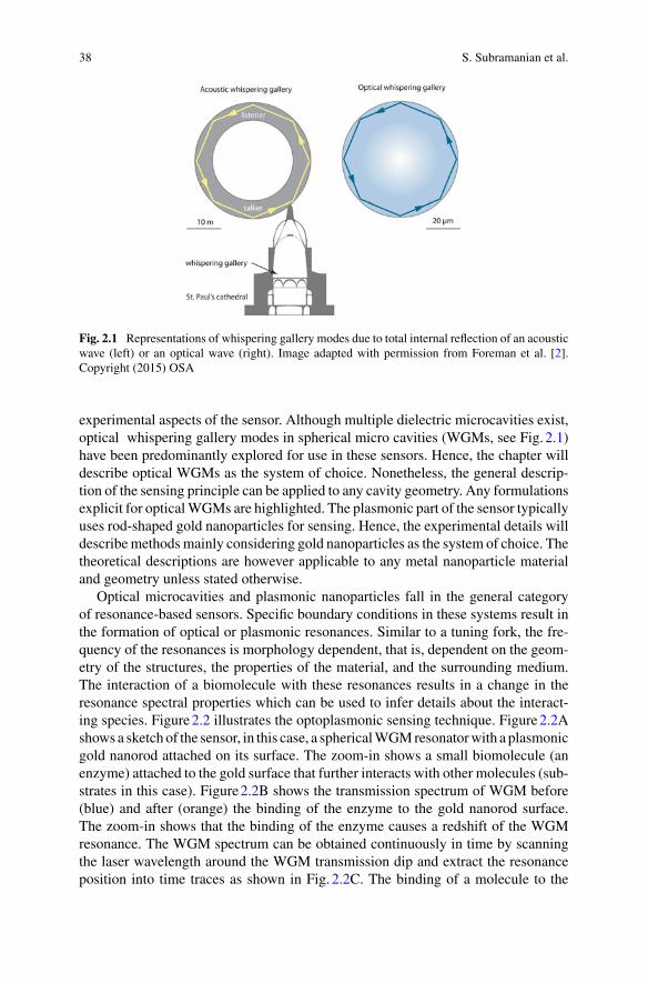
38 S. Subramanian et al.
Fig. 2.1 Representations of whispering gallery modes due to total internal reflection of an acousticwave (left) or an optical wave (right). Image adapted with permission from Foreman et al. [2].Copyright (2015) OSA
experimental aspects of the sensor. Although multiple dielectric microcavities exist,optical whispering gallery modes in spherical micro cavities (WGMs, see Fig. 2.1)have been predominantly explored for use in these sensors. Hence, the chapter willdescribe optical WGMs as the system of choice. Nonetheless, the general descrip-tion of the sensing principle can be applied to any cavity geometry. Any formulationsexplicit for opticalWGMs are highlighted. The plasmonic part of the sensor typicallyuses rod-shaped gold nanoparticles for sensing. Hence, the experimental details willdescribemethodsmainly considering gold nanoparticles as the system of choice. Thetheoretical descriptions are however applicable to any metal nanoparticle materialand geometry unless stated otherwise.
Optical microcavities and plasmonic nanoparticles fall in the general categoryof resonance-based sensors. Specific boundary conditions in these systems result inthe formation of optical or plasmonic resonances. Similar to a tuning fork, the fre-quency of the resonances is morphology dependent, that is, dependent on the geom-etry of the structures, the properties of the material, and the surrounding medium.The interaction of a biomolecule with these resonances results in a change in theresonance spectral properties which can be used to infer details about the interact-ing species. Figure2.2 illustrates the optoplasmonic sensing technique. Figure2.2Ashows a sketch of the sensor, in this case, a sphericalWGMresonatorwith a plasmonicgold nanorod attached on its surface. The zoom-in shows a small biomolecule (anenzyme) attached to the gold surface that further interacts with other molecules (sub-strates in this case). Figure2.2B shows the transmission spectrum of WGM before(blue) and after (orange) the binding of the enzyme to the gold nanorod surface.The zoom-in shows that the binding of the enzyme causes a redshift of the WGMresonance. The WGM spectrum can be obtained continuously in time by scanningthe laser wavelength around the WGM transmission dip and extract the resonanceposition into time traces as shown in Fig. 2.2C. The binding of a molecule to the
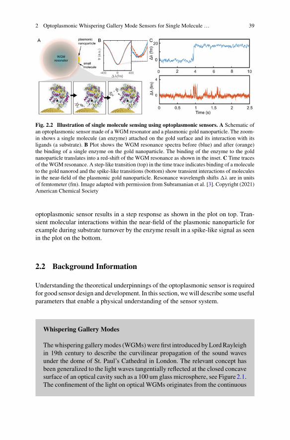
2 Optoplasmonic Whispering Gallery Mode Sensors for Single Molecule … 39
Fig. 2.2 Illustration of single molecule sensing using optoplasmonic sensors. A Schematic ofan optoplasmonic sensor made of a WGM resonator and a plasmonic gold nanoparticle. The zoom-in shows a single molecule (an enzyme) attached on the gold surface and its interaction with itsligands (a substrate). B Plot shows the WGM resonance spectra before (blue) and after (orange)the binding of a single enzyme on the gold nanoparticle. The binding of the enzyme to the goldnanoparticle translates into a red-shift of the WGM resonance as shown in the inset. C Time tracesof theWGM resonance. A step-like transition (top) in the time trace indicates binding of a moleculeto the gold nanorod and the spike-like transitions (bottom) show transient interactions of moleculesin the near-field of the plasmonic gold nanoparticle. Resonance wavelength shifts �λ are in unitsof femtometer (fm). Image adapted with permission from Subramanian et al. [3]. Copyright (2021)American Chemical Society
optoplasmonic sensor results in a step response as shown in the plot on top. Tran-sient molecular interactions within the near-field of the plasmonic nanoparticle forexample during substrate turnover by the enzyme result in a spike-like signal as seenin the plot on the bottom.
2.2 Background Information
Understanding the theoretical underpinnings of the optoplasmonic sensor is requiredfor good sensor design and development. In this section, wewill describe some usefulparameters that enable a physical understanding of the sensor system.
Whispering Gallery Modes
Thewhispering gallerymodes (WGMs)were first introduced byLordRayleighin 19th century to describe the curvilinear propagation of the sound wavesunder the dome of St. Paul’s Cathedral in London. The relevant concept hasbeen generalized to the light waves tangentially reflected at the closed concavesurface of an optical cavity such as a 100 um glass microsphere, see Figure2.1.The confinement of the light on optical WGMs originates from the continuous

40 S. Subramanian et al.
total internal reflection. In the wave picture, aWGM acquires an extra phase ofan integer times 2π after one round-trip, constructively interfering with itself.The WGM microcavities possess wide potential applications in the fields ofintegrated optics and biosensing [4].
The signals from the optoplasmonic sensor are primarily observed as changesin the spectral properties of the optical microcavity. The power stored in the cavityexhibits a Lorentzian lineshape in the frequency domain given by,
P(ω) = P(κ/2)2
(ω − ω0)2 + (κ/2)2, (2.1)
where P is the power, κ is the full-width-at-half-maximum (FWHM) of the cavityresonance spectrum, andω0 the resonance frequency [141]. Although direct observa-tion of the cavity power spectrum is usually not feasible, it can be inferred indirectly.For example, the transmitted/reflected light from the cavity can be used to obtain thecavity spectrum. Figure2.3 shows an example transmission spectrum of an opticalmicrocavity.
A dimensionless parameter Q termed the quality factor captures the temporalconfinement of light in the cavity as,
Q = ω0
κ= ω0τ (2.2)
where τ is the cavity lifetime [142]. The quality factor is influenced by many lossmechanisms in the cavity such as radiation, material absorption, and surface and bulkscattering. The intrinsic quality factor of the cavity is can be written in the form,
Q−1int = Q−1
mat + Q−1sur f + Q−1
scat + Q−1rad . (2.3)
Here, Qint is the intrinsic quality factor of the resonator, Qmat describes the intrinsicmaterial absorption, Qsur f surface absorption losses, Qscat describes the scatteringlosses (such as due to imperfections in the form of surface roughness) and Qbend
describes bending loss (or radiation loss or tunnel loss) [142].The transmitted power spectrum shown in Fig. 2.3 is typically obtained indirectly
using the light transmitted or reflected from an evanescent coupler such as taperedoptical fiber or a prism.Hence, the observed Qspectrum is a combination of the intrinsicand coupling Q given as,
Q−1spectrum = Q−1
int + Q−1coupling (2.4)
where additional losses occur when using the coupler. Typical loaded Qspectrum arein the range of 107–108 in aqueous medium for glass microsphere resonators ofdiameter ∼80µm used in optoplasmonic sensing.
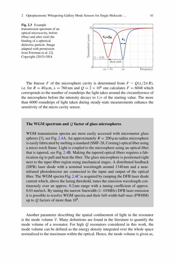
2 Optoplasmonic Whispering Gallery Mode Sensors for Single Molecule … 41
Fig. 2.3 Exampletransmission spectrum of anoptical microcavity, before(blue) and after (red) thebinding of a sphericaldielectric particle. Imageadapted with permissionfrom Foreman et al. [2].Copyright (2015) OSA
The finesse F of the microsphere cavity is determined from F ∼ Q(λ/2π R),i.e. for R = 40µm, λ = 760 nm and Q = 2 × 10⁶ one calculates F = 6048 whichcorresponds to the number of roundtrips the light takes around the circumference ofthe microsphere before the intensity decays to 1/e of the starting value. The morethan 6000 roundtrips of light taken during steady-state measurements enhance thesensitivity of the micro cavity sensor.
The WGM spectrum and Q factor of glass microspheres
WGM transmission spectra are most easily accessed with micrometer glassspheres [5], see Fig. 2.4A. An approximately R = 200µm radius microsphereis easily fabricated bymelting a standard (SMF-28, Corning) optical fiber usinga micro torch flame. Light is coupled to the microsphere using an optical fiberthat is tapered, see Fig. 2.4B. Making the tapered optical fibers requires a fab-rication rig to pull and heat the fiber. The glass microsphere is positioned rightnext to the taper-fiber region using mechanical stages. A distributed feedback(DFB) laser diode with a nominal wavelength around 1340nm and a near-infrared photodetector are connected to the input and output of the opticalfiber. The WGM spectra Fig. 2.4C is acquired by ramping the DFB laser diodecurrent which, above the lasing threshold, tunes the emission wavelength con-tinuously over an approx. 0.2nm range with a tuning coefficient of approx.0.01nm/mA. By tuning the narrow linewidth (1–10MHz) DFB laser emissionit is possible to resolve WGM spectra and their full-width-half-max (FWHM)up to Q factors of more than 108.
Another parameter describing the spatial confinement of light in the resonatoris the mode volume V . Many definitions are found in the literature to quantify themode volume of a resonator. For high Q resonators considered in this work, themode volume can be defined as the energy density integrated over the whole spacenormalized to the maximum within the optical. Hence, the mode volume is given as,
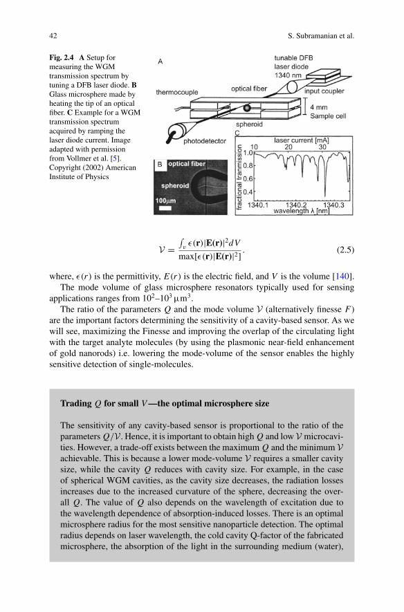
42 S. Subramanian et al.
Fig. 2.4 A Setup formeasuring the WGMtransmission spectrum bytuning a DFB laser diode. BGlass microsphere made byheating the tip of an opticalfiber. C Example for a WGMtransmission spectrumacquired by ramping thelaser diode current. Imageadapted with permissionfrom Vollmer et al. [5].Copyright (2002) AmericanInstitute of Physics
V =∫vε(r)|E(r)|2dV
max[ε(r)|E(r)|2] . (2.5)
where, ε(r) is the permittivity, E(r) is the electric field, and V is the volume [140].The mode volume of glass microsphere resonators typically used for sensing
applications ranges from 102–103µm3.The ratio of the parameters Q and the mode volume V (alternatively finesse F)
are the important factors determining the sensitivity of a cavity-based sensor. As wewill see, maximizing the Finesse and improving the overlap of the circulating lightwith the target analyte molecules (by using the plasmonic near-field enhancementof gold nanorods) i.e. lowering the mode-volume of the sensor enables the highlysensitive detection of single-molecules.
Trading Q for small V —the optimal microsphere size
The sensitivity of any cavity-based sensor is proportional to the ratio of theparameters Q/V . Hence, it is important to obtain high Q and low V microcavi-ties. However, a trade-off exists between the maximum Q and the minimum Vachievable. This is because a lower mode-volume V requires a smaller cavitysize, while the cavity Q reduces with cavity size. For example, in the caseof spherical WGM cavities, as the cavity size decreases, the radiation lossesincreases due to the increased curvature of the sphere, decreasing the over-all Q. The value of Q also depends on the wavelength of excitation due tothe wavelength dependence of absorption-induced losses. There is an optimalmicrosphere radius for the most sensitive nanoparticle detection. The optimalradius depends on laser wavelength, the cold cavity Q-factor of the fabricatedmicrosphere, the absorption of the light in the surrounding medium (water),
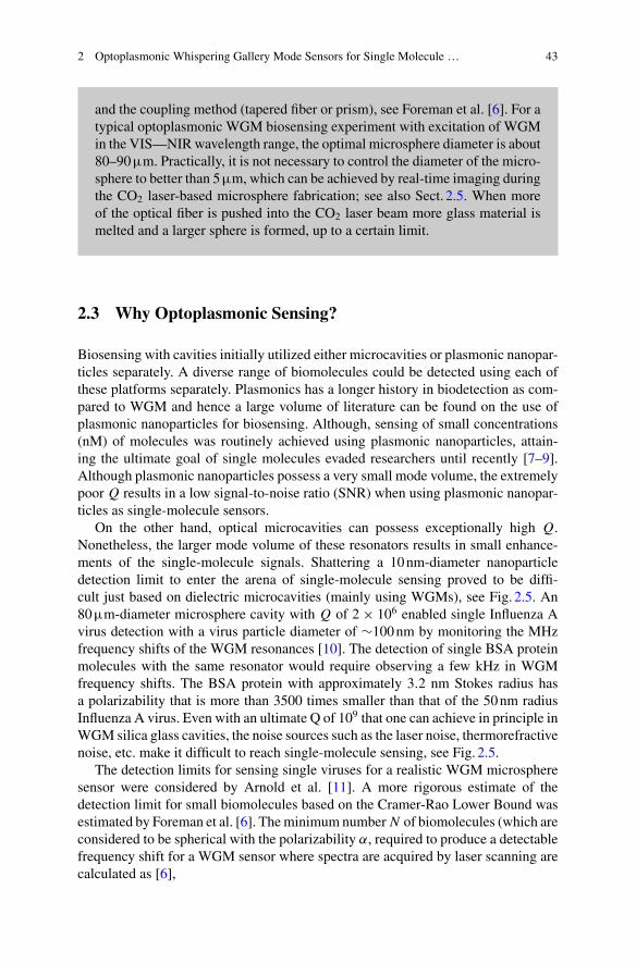
2 Optoplasmonic Whispering Gallery Mode Sensors for Single Molecule … 43
and the coupling method (tapered fiber or prism), see Foreman et al. [6]. For atypical optoplasmonic WGM biosensing experiment with excitation of WGMin the VIS—NIRwavelength range, the optimal microsphere diameter is about80–90µm. Practically, it is not necessary to control the diameter of the micro-sphere to better than 5µm, which can be achieved by real-time imaging duringthe CO2 laser-based microsphere fabrication; see also Sect. 2.5. When moreof the optical fiber is pushed into the CO2 laser beam more glass material ismelted and a larger sphere is formed, up to a certain limit.
2.3 Why Optoplasmonic Sensing?
Biosensing with cavities initially utilized either microcavities or plasmonic nanopar-ticles separately. A diverse range of biomolecules could be detected using each ofthese platforms separately. Plasmonics has a longer history in biodetection as com-pared to WGM and hence a large volume of literature can be found on the use ofplasmonic nanoparticles for biosensing. Although, sensing of small concentrations(nM) of molecules was routinely achieved using plasmonic nanoparticles, attain-ing the ultimate goal of single molecules evaded researchers until recently [7–9].Although plasmonic nanoparticles possess a very small mode volume, the extremelypoor Q results in a low signal-to-noise ratio (SNR) when using plasmonic nanopar-ticles as single-molecule sensors.
On the other hand, optical microcavities can possess exceptionally high Q.Nonetheless, the larger mode volume of these resonators results in small enhance-ments of the single-molecule signals. Shattering a 10nm-diameter nanoparticledetection limit to enter the arena of single-molecule sensing proved to be diffi-cult just based on dielectric microcavities (mainly using WGMs), see Fig. 2.5. An80µm-diameter microsphere cavity with Q of 2 × 10⁶ enabled single Influenza Avirus detection with a virus particle diameter of ∼100nm by monitoring the MHzfrequency shifts of the WGM resonances [10]. The detection of single BSA proteinmolecules with the same resonator would require observing a few kHz in WGMfrequency shifts. The BSA protein with approximately 3.2 nm Stokes radius hasa polarizability that is more than 3500 times smaller than that of the 50nm radiusInfluenza A virus. Even with an ultimate Q of 109 that one can achieve in principle inWGM silica glass cavities, the noise sources such as the laser noise, thermorefractivenoise, etc. make it difficult to reach single-molecule sensing, see Fig. 2.5.
The detection limits for sensing single viruses for a realistic WGM microspheresensor were considered by Arnold et al. [11]. A more rigorous estimate of thedetection limit for small biomolecules based on the Cramer-Rao Lower Bound wasestimated by Foreman et al. [6]. Theminimum number N of biomolecules (which areconsidered to be spherical with the polarizability α, required to produce a detectablefrequency shift for a WGM sensor where spectra are acquired by laser scanning arecalculated as [6],
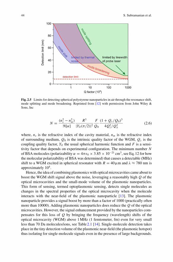
44 S. Subramanian et al.
Fig. 2.5 Limits for detecting spherical polystyrene nanoparticles in air through the resonance shift,mode splitting and mode broadening. Reprinted from [12] with permission from John Wiley &Sons, Inc
N = (n2s − n2
m)
�[α]R3
|Yll(π/2)|2F
Q0
(1 + Qc/Q0)3
4Q2c/Q2
o
(2.6)
where, ns is the refractive index of the cavity material, nm is the refractive indexof surrounding medium, Q0 is the intrinsic quality factor of the WGM, Qc is thecoupling quality factor, Yll the usual spherical harmonic function and F is a sensi-tivity factor that depends on experimental configuration. The minimum number Nof BSAmolecules (polarizability α = 4πε0 × 3.85 × 10−21 cm3, see Eq.12 for howthe molecular polarizability of BSA was determined) that causes a detectable (MHz)shift to a WGM excited in spherical resonator with R = 40µm and λ ≈ 780 nm isapproximately 104.
Hence, the idea of combining plasmonicswith opticalmicrocavities came about toboost the WGM shift signal above the noise, leveraging a reasonably high Q of theoptical microcavities and the small-mode volume of the plasmonic nanoparticles.This form of sensing, termed optoplasmonic sensing, detects single molecules aschanges in the spectral properties of the optical microcavity when the moleculeinteracts with the near-field of the plasmonic nanoparticle [13]. The plasmonicnanoparticle provides a signal boost by more than a factor of 1000 (practically oftenmore than 10000). Adding plasmonic nanoparticles does reduce the Q of the opticalmicrocavities. However, the signal enhancement provided by the nanoparticles com-pensates for this loss of Q by bringing the frequency (wavelength) shifts of theoptical microcavity (WGM) above 1MHz (1 femtometer, fm) even for very smallless than 70 Da molecules/ions, see Table2.1 [14]. Single-molecule detection takesplace in the tiny detection volume of the plasmonic near-field (the plasmonic hotspot)thus isolating for single-molecule signals even in the presence of large backgrounds.

2 Optoplasmonic Whispering Gallery Mode Sensors for Single Molecule … 45
Additionally, the strong non-linear decay of the plasmonic near-field enables study-ing not only the presence of relatively large molecules such as proteins, enzymes,or other nanomachines but also their conformational dynamics due to the differentenhancements experienced by different parts of the protein [3, 15].
Adding the plasmonic nanoparticle in optoplasmonic sensing does not fundamen-tally change the noise floor in practice. Typically, a 1.3–1.5 times increase in WGMlinewidth is observed and thus the noise floor of the estimated WGM resonancefrequency does not change significantly. Hence, leveraging the near-field enhance-ments of plasmonic nanorods and taking into account the only mild suppression ofthe Q factor due to the excitation of the localized plasmon resonances can explainthe foundations for the large gains in sensitivity that enable the detection of singlemolecules on the optoplasmonic sensors. Table2.1 gives an overview of some of thesmall molecules and ions which have been detected on plasmonic nanorods coupledto WGM glass microspheres.
2.3.1 Optoplasmonic Sensing Theory
As introduced previously, the optoplasmonic sensor is made up of two components,an optical microcavity and one or more plasmonic nanoparticles attached to the cav-ity. The principle of optoplasmonic sensing is based on the changes to the spectralproperties of the optical microcavity upon the interaction of analytes with the plas-monic nanoparticle excited by the opticalmicrocavity. There exist threemain spectralchanges that can be monitored to infer about the analytes. These are the shift of thecavity resonance frequency, the change in the cavity linewidth, or the splitting of thecavity resonance.
The case of small particles such as micro/nanoparticles of dielectrics as well asbiomolecules such as proteins can be considered using a perturbation theory approach[5, 19]. In Fig. 2.6A, consider the small dielectric particle (in red) diffusing into theevanescent field of the WGM. Assuming the interaction of the particle with WGM isin the weak coupling regime (as opposed to strong coupling which can occur in thecase of two coupled resonances), the fractional shift inWGMwavelength (frequency)can be given as [2, 20, 141],
�λ
λ= −�ω
ω≈
∫Vp
(εp(r) − εm)E(r)*E(r)dr
2∫
V ε(r)E(r)*.E(r)dr(2.7)
whereE*(r) is the Hermitian adjoint ofE(r), εp(r) is the permittivity of the dielectricparticle, V is volume of all space, Vp is the volume of the particle, E(r) is theelectric field before the perturbation, E(r) is the perturbed electric field, ε(r) =εs (microcavity permittivity) for r < R and ε(r) = εm (host medium permittivity)otherwise. Equation2.7 can be rewritten in terms of the difference in polarizabilityof the particle and surrounding medium αex as,
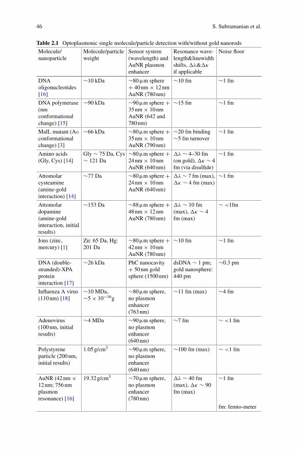
46 S. Subramanian et al.
Table 2.1 Optoplasmonic single molecule/particle detection with/without gold nanorods
Molecule/nanoparticle
Molecule/particleweight
Sensor system(wavelength) andAuNR plasmonenhancer
Resonance wave-length&linewidthshifts, �λ&�κ
if applicable
Noise floor
DNAoligonucleotides[16]
∼10 kDa ∼80µm sphere+ 40nm × 12nmAuNR (780nm)
∼10 fm ∼1 fm
DNA polymerase(nmconformationalchange) [15]
∼90 kDa ∼90µm sphere +35nm × 10nmAuNR (642 and780nm)
∼15 fm ∼1 fm
MalL mutant (A◦conformationalchange) [3]
∼66 kDa ∼80µm sphere +35nm × 10nmAuNR (790nm)
∼20 fm binding∼5 fm turnover
∼1 fm
Amino acids(Gly, Cys) [14]
Gly ∼ 75 Da, Cys∼ 121 Da
∼80µm sphere +24nm × 10nmAuNR (640nm)
�λ ∼ 4–30 fm(on gold), �κ ∼ 4fm (via disulfide)
∼1 fm
Attomolarcysteamine(amine-goldinteraction) [14]
∼77 Da ∼80µm sphere +24nm × 10nmAuNR (640nm)
�λ ∼ 7 fm (max),�κ ∼ 4 fm (max)
∼1 fm
Attomolardopamine(amine-goldinteraction, initialresults)
∼153 Da ∼88µm sphere +48nm × 12nmAuNR (780nm)
�λ ∼ 10 fm(max), �κ ∼ 4fm (max)
∼ <1fm
Ions (zinc,mercury) [1]
Zn: 65 Da, Hg:201 Da
∼80µm sphere +42nm × 10nmAuNR (780nm)
∼10 fm ∼1 fm
DNA (double-stranded)-XPAproteininteraction [17]
∼26 kDa PhC nanocavity+ 50nm goldsphere (1500nm)
dsDNA ∼ 1 pm;gold nanosphere:440 pm
∼0.3 pm
Influenza A virus(110nm) [18]
∼10 MDa,∼5 × 10⁻¹⁶g
∼80µm sphere,no plasmonenhancer(763nm)
∼11 fm (max) ∼4 fm
Adenovirus(100nm, initialresults)
∼4 MDa ∼90µm sphere,no plasmonenhancer(640nm)
∼7 fm ∼ <1 fm
Polystyreneparticle (200nm,initial results)
1.05g/cm3 ∼90µm sphere,no plasmonenhancer(640nm)
∼100 fm (max) ∼ <1 fm
AuNR (42nm ×12nm; 756nmplasmonresonance) [16]
19.32g/cm3 ∼70µm sphere,no plasmonenhancer(780nm)
�λ ∼ 40 fm(max), �κ ∼ 90fm (max)
∼1 fm
fm: femto-meter

2 Optoplasmonic Whispering Gallery Mode Sensors for Single Molecule … 47
Fig. 2.6 A Illustration of a small spherical dielectric nanoparticle interaction with a WGMmicro-cavity surface (red) and another dielectric (green) interacting within the enhanced near-field of theplasmonic nanoparticle attached to the microcavity. B Simulated electric field amplitude with andwithout the presence of the plasmonic enhancement. The field experienced by the green dielectric isat least an order of magnitude higher than that of the red dielectric. Image reprinted with permissionfrom [16] Copyright 2014, Rights Managed by Nature Publishing Group@
�λ
λ= −�ω
ω≈ �[αex ]
2
fd |E(rp)|2∫V ε(r)|E(r)|2dr
(2.8)
where rp is the position of the nanoparticle, fd is a correction term to account for theexponential decay of the evanescent field [2]. For very small nanoparticles, fd ≈ 1.Thus, optical microcavities can be used for detecting small dielectrics (particle inred in Fig. 2.6A) by the shift of the resonance frequency due to the energy stored inpolarizing the particle.
The smallest size of a particle detected by a bare microcavity is typically in therange of d > 10 nm, where d is the particle diameter. Various sources of noiseprevents the detection of smaller entities, especially biological molecules whoserefractive index is close to that of water. We will discuss more about noise andsensitivity limits of WGM sensors in Sect. 2.8. For now, it is sufficient to say thatadditional signal enhancement is required to detect single biomolecular entities insolution. This sensitivity enhancement is provided by the plasmonic aspect of theoptoplasmonic sensors. Figure2.6A also shows a small dielectric particle (in green)interacting within the near-field of the plasmonic nanoparticle attached to the opticalmicrocavity. Now, the signal obtained as the shift in the WGM frequency is ordersof magnitude higher (as compared to the particle in red interacting directly with themicrocavity) due to the plasmonic enhancement.
A intuitive understanding of this enhanced frequency shift may be obtained byrewriting Eq.2.8 as,
�ω
ω0= −�λ
λ0≈ −�[α]
2
εm f 2(rp)
V (2.9)
where, f 2(rp) = |E(rp)|2/max[ε(r)|E(r)|2] is the normalized mode distribution,V = ∫
V ε(r)|E(r)|2dr/max[ε(r)|E(r)|2] is the mode volume and ε(r) is the per-
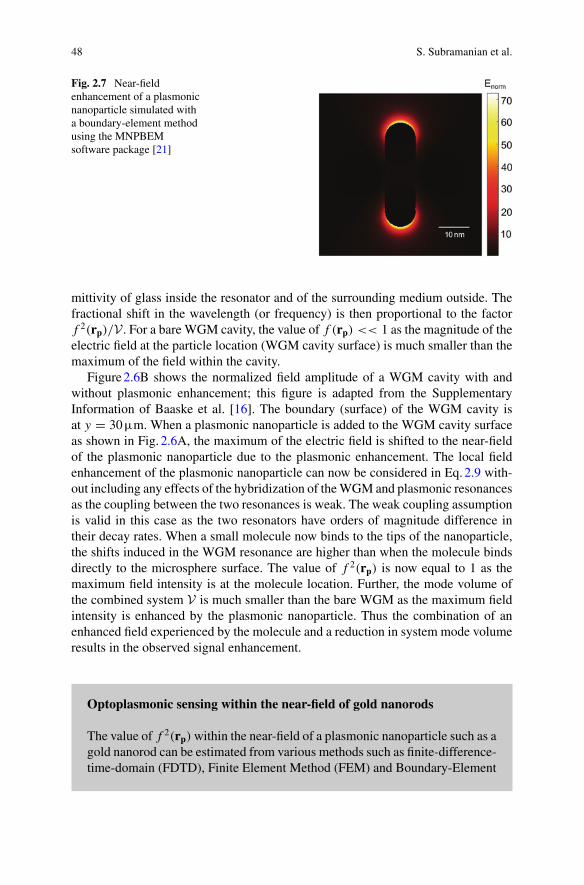
48 S. Subramanian et al.
Fig. 2.7 Near-fieldenhancement of a plasmonicnanoparticle simulated witha boundary-element methodusing the MNPBEMsoftware package [21]
mittivity of glass inside the resonator and of the surrounding medium outside. Thefractional shift in the wavelength (or frequency) is then proportional to the factorf 2(rp)/V . For a bare WGM cavity, the value of f (rp) << 1 as the magnitude of theelectric field at the particle location (WGM cavity surface) is much smaller than themaximum of the field within the cavity.
Figure2.6B shows the normalized field amplitude of a WGM cavity with andwithout plasmonic enhancement; this figure is adapted from the SupplementaryInformation of Baaske et al. [16]. The boundary (surface) of the WGM cavity isat y = 30µm. When a plasmonic nanoparticle is added to the WGM cavity surfaceas shown in Fig. 2.6A, the maximum of the electric field is shifted to the near-fieldof the plasmonic nanoparticle due to the plasmonic enhancement. The local fieldenhancement of the plasmonic nanoparticle can now be considered in Eq.2.9 with-out including any effects of the hybridization of theWGMand plasmonic resonancesas the coupling between the two resonances is weak. The weak coupling assumptionis valid in this case as the two resonators have orders of magnitude difference intheir decay rates. When a small molecule now binds to the tips of the nanoparticle,the shifts induced in the WGM resonance are higher than when the molecule bindsdirectly to the microsphere surface. The value of f 2(rp) is now equal to 1 as themaximum field intensity is at the molecule location. Further, the mode volume ofthe combined system V is much smaller than the bare WGM as the maximum fieldintensity is enhanced by the plasmonic nanoparticle. Thus the combination of anenhanced field experienced by the molecule and a reduction in system mode volumeresults in the observed signal enhancement.
Optoplasmonic sensing within the near-field of gold nanorods
The value of f 2(rp)within the near-field of a plasmonic nanoparticle such as agold nanorod can be estimated from various methods such as finite-difference-time-domain (FDTD), Finite Element Method (FEM) and Boundary-Element
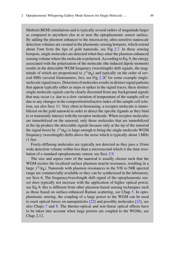
2 Optoplasmonic Whispering Gallery Mode Sensors for Single Molecule … 49
Method (BEM) simulations and is typically several orders of magnitude largeras compared to anywhere else at or near the optoplasmonic sensor surface.By adding the plasmon enhancer to the microcavity, ultra-sensitive nanoscaledetection volumes are created in the plasmonic sensing hotspots, which extendabout 5nm from the tips of gold nanorods, see Fig. 2.7. In these sensinghotspots, single molecules are detected when they enter the plasmon-enhancedsensing volumewhere themolecule is polarised. According to Eq.9, the energyassociated with the polarization of the molecule (the induced dipole moment)results in the detectable WGM frequency (wavelength) shift signals, the mag-nitude of which are proportional to f 2(rp) and typically on the order of sev-eral MHz (several femtometers, fm); see Fig. 2.2C for some example single-molecule signal traces. Detection ofmolecules results in distinct signal patternsthat appear typically either as steps or spikes in the signal traces; these distinctsingle-molecule signals can be clearly discerned from any background signalsthat may occur i.e. due to a slow variation of temperature of the sample cell ordue to any changes in the composition/refractive index of the sample cell solu-tion, see also Sect. 11. Very often in biosensing, a receptor molecule is immo-bilized on the gold nanorod in order to detect the specific ligands as they bindto or transiently interact with the receptor molecule. When receptor moleculesare immobilized on the nanorod, only those molecules that are immobilizedat the tip produce the detectable signals because only at the tip of the nanorodthe signal boost by f 2(rp) is large enough to bring the single-molecule WGMfrequency (wavelength) shifts above the noise which is typically about 1MHz(1 fm).
Freely-diffusing molecules are typically not detected as they pass a 10nmwide detection volume within less than a microsecond which is the time reso-lution of a standard optoplasmonic sensor, see Sect. 2.9.
The size and aspect ratio of the nanorod is usually chosen such that theWGM excites the localized surface plasmon near/at resonance, resulting in alarge f 2(rp). Nanorods with plasmon resonances in the VIS to NIR spectralrange are commercially available or they can be synthesized in the laboratory,see Sect. 6. The frequency/wavelength shift signal of the optoplasmonic sen-sor does typically not increase with the application of higher optical power,see Eq.9; this is different from other plasmon-based sensing techniques suchas those based on surface-enhanced Raman scattering, see Chap.5. In opto-plasmonic sensing, the coupling of a large power to the WGM can be usedto exert optical forces on nanoparticles [22] and possibly molecules [23], seealso Chaps. 7 and 8. The thermo-optical and non-linear optical effects haveto be taken into account when large powers are coupled to the WGMs, seeChap.2.12.
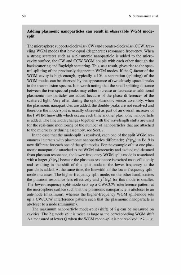
50 S. Subramanian et al.
Adding plasmonic nanoparticles can result in observable WGM mode-split
Themicrosphere supports clockwise (CW)and counter-clockwise (CCW) trav-eling WGM modes that have equal (degenerate) resonance frequency. Whena strong scatterer such as a plasmonic nanoparticle is added to the micro-cavity surface, the CW and CCW WGM couple with each other through thebackscattering and Rayleigh scattering. This, as a result, gives rise to the spec-tral splitting of the previously degenerate WGM modes. If the Q-factor of theWGM cavity is high enough, typically >107, a separation (splitting) of theWGMmodes can be observed by the appearance of two closely-spaced peaksin the transmission spectra. It is worth noting that the small splitting distancebetween the two spectral peaks may either increase or decrease as additionalplasmonic nanoparticles are added because of the phase differences of thescattered light. Very often during the optoplasmonic sensor assembly, whenthe plasmonic nanoparticles are added, the double-peaks are not resolved andtherefore the mode-split is usually observed as part of an overall increase ofthe FWHM linewidth which occurs each time another plasmonic nanoparticleis added. The linewidth changes together with the wavelength shifts are usedfor the real-time monitoring of the number of nanoparticles that are attachedto the microcavity during assembly, see Sect. 7.
In the case that the mode-split is resolved, each one of the split WGM res-onances interacts with plasmonic nanoparticles differently; f 2(rp) in Eq.9 isnow different for each one of the split modes. For the example of just one plas-monic nanoparticle attached to theWGMmicrocavity and excited red-detunedfrom plasmon resonance, the lower-frequency WGM split-mode is associatedwith a larger f 2(rp) because the plasmon resonance is excited more efficientlyand resulting in the shift of this split mode to the lower frequency as theparticle is added. At the same time, the linewidth of the lower-frequency split-mode increases. The higher-frequency split mode, on the other hand, excitesthe plasmon resonance less effectively and f 2(rp) for this mode is smaller.The lower-frequency split-mode sets up a CW/CCW interference pattern atthe microsphere surface such that the plasmonic nanoparticle is at/closer to ananti-node (maximum), whereas the higher-frequency WGM split-mode setsup a CW/CCW interference pattern such that the plasmonic nanoparticle isat/closer to a node (minimum).
The maximum nanoparticle mode-split (shift) of 2g can be measured oncavities. The 2g mode split is twice as large as the corresponding WGM shift�λ measured at lower Q when the WGMmode-split is not resolved: �λ = g.
2 Optoplasmonic Whispering Gallery Mode Sensors for Single Molecule … 51
Fig. 2.8 AWGM linewidth shifts (|�κ|) magnitude versusWGM resonance wavelength shift (�λ)for binding of small sub-kDa molecules measured using three different resonators. Solid lines of�κ = �λ and �κ = 2�λ are also plotted for reference. B Relative angular position (ψ1 − ψi ) ofthe molecules binding on resonator 3 estimated from the ratio of �κ and �λ. Image adapted withpermission from Subramanian et al. [25]. Copyright (2021) American Institute of Physics
Single-molecule linewidth shifts can be larger than the wavelength shifts
For the case that the plasmonic-nanoparticle induced mode-split is notresolved, single-molecule signals can be observed not only from theWGM fre-quency/wavelengths shifts but also from the changes of the effective FWHMlinewidths of the unresolved mode-split. The perturbation by the molecule(which is proportional to f 2(rp)) is different for each mode [14]. Figure2.8shows that the single-molecule FWHM linewidth shifts can provide higheramplitude signals (points between the green and purple line) than previouslypredicted using a first-order perturbation theory that did not consider the modesplitting introduced by the plasmonic nanoparticles [25]. The optoplasmonicsingle-molecule linewidth shift �κ can vary from −2g to 2g with g = �λ
being the predicted wavelength shift magnitude from the perturbation theoryEq.9. Recently, Vincent et al. [14] showed linewidth shifts �κ for the inter-action of single-L-cysteine and DTNB (5,5-dithio-bis-(2-nitrobenzoic acid))with the thiol group of cysteamine molecules using a similar sensor. Theyshowed that |�κ| > 2�λ, that is, the points would fall above the green linein Fig. 2.8A. The shifts in �κ on the order of 8 fm with no significant shiftsin �λ above the noise are attributed to an alternate sensing mechanism thatrequires additional investigation and is not additional discussed here. Note thatthe change in the sign of the linewidth shifts can be either positive or nega-tive. This shows that the observed single-molecule linewidth shifts do not arisefrom additional losses induced by the molecules which are non-absorbing attheWGMwavelength. The shifts rather arise from the change in the frequencysplitting of the standing wave modes. Since the small frequency splitting isunresolved, this is observed as the change in resonance linewidth.
52 S. Subramanian et al.
Optoplasmonic shifts inform about a molecules’ binding location
The frequency splitting SN after binding of N plasmonic nanoparticles to theWGM can be given as [26]
SN =N∑
i=1
2gi cos (2ψ1 − 2ψi ), (2.10)
where, gi = �ωi ≡ −�λi is the splitting caused by the i th particle, ψ1 is thespatial phase difference between the first particle and the anti-node of onestanding wave mode, and ψi is the angular distance between the i th particleand the first particle. When a molecule interacts with the near-field of theplasmonic nanoparticles, it can be seen as introducing a shift of g′ accordingto 2.8. A corresponding change in the splitting SN is introduced depending onthe position of the gold nanoparticle where the molecule binds. This change insplitting translates into a change in the linewidth as the splitting is unresolved.A value of �S = S′
N − SN < 0 provides a negative shift (decrease) in thelinewidth, and�S > 0 provides a positive shift (increase) in the linewidth. Therelative azimuthal position of the binding molecules can be estimated usingEq.2.10 as plotted in Fig. 2.8B. It is seen from the plots that the binding eventscluster around six different values of ψ1 − ψi . The clustering of the eventsindicates the relative azimuthal position of the gold nanoparticles attached tothe WGM resonator. The differences in amplitude of �κ within each clusterarise from the different enhancements experienced by the molecules attachedto different locations on the same nanoparticle. Moreover, the polar positionof the nanoparticles can be estimated using multiple WGMs of different polarorders [27].
2.4 Sensing Single-Molecule Reactions and Interactions
Numerous single-molecule systems, from interaction of small sub-kDa molecules tothe conformational dynamics of large polymerase proteins have been explored usingoptoplasmonic sensors. A few examples of the systems studied in literature and adescription of the experiments are presented in this section.
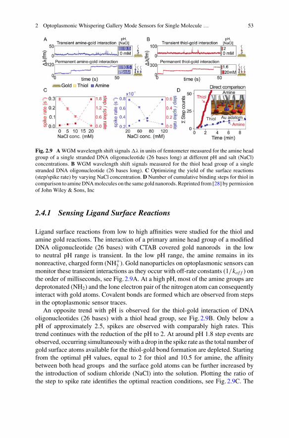
2 Optoplasmonic Whispering Gallery Mode Sensors for Single Molecule … 53
Fig. 2.9 A WGMwavelength shift signals �λ in units of femtometer measured for the amine headgroup of a single stranded DNA oligonucleotide (26 bases long) at different pH and salt (NaCl)concentrations. B WGM wavelength shift signals measured for the thiol head group of a singlestranded DNA oligonucleotide (26 bases long). C Optimizing the yield of the surface reactions(step/spike rate) by varying NaCl concentration. D Number of cumulative binding steps for thiol incomparison to amineDNAmolecules on the same gold nanorods. Reprinted from [28] by permissionof John Wiley & Sons, Inc
2.4.1 Sensing Ligand Surface Reactions
Ligand surface reactions from low to high affinities were studied for the thiol andamine gold reactions. The interaction of a primary amine head group of a modifiedDNA oligonucleotide (26 bases) with CTAB covered gold nanorods in the lowto neutral pH range is transient. In the low pH range, the amine remains in itsnonreactive, charged form (NH+
3 ). Gold nanoparticles on optoplasmonic sensors canmonitor these transient interactions as they occur with off-rate constants (1/kof f ) onthe order of milliseconds, see Fig. 2.9A. At a high pH, most of the amine groups aredeprotonated (NH2) and the lone electron pair of the nitrogen atom can consequentlyinteract with gold atoms. Covalent bonds are formed which are observed from stepsin the optoplasmonic sensor traces.
An opposite trend with pH is observed for the thiol-gold interaction of DNAoligonucleotides (26 bases) with a thiol head group, see Fig. 2.9B. Only below apH of approximately 2.5, spikes are observed with comparably high rates. Thistrend continues with the reduction of the pH to 2. At around pH 1.8 step events areobserved, occurring simultaneouslywith a drop in the spike rate as the total number ofgold surface atoms available for the thiol-gold bond formation are depleted. Startingfrom the optimal pH values, equal to 2 for thiol and 10.5 for amine, the affinitybetween both head groups and the surface gold atoms can be further increased bythe introduction of sodium chloride (NaCl) into the solution. Plotting the ratio ofthe step to spike rate identifies the optimal reaction conditions, see Fig. 2.9C. The
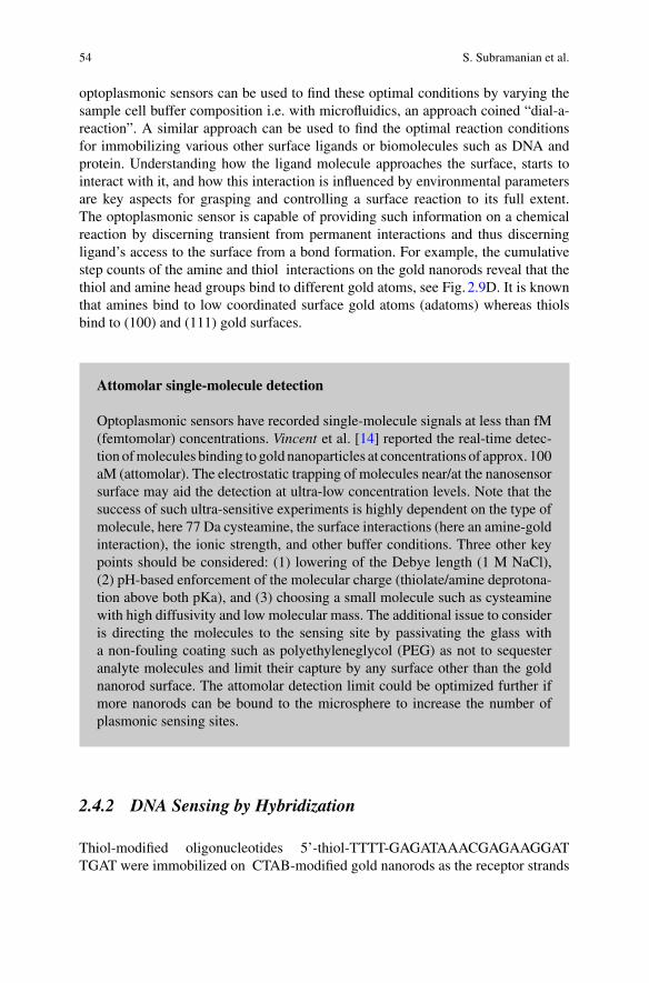
54 S. Subramanian et al.
optoplasmonic sensors can be used to find these optimal conditions by varying thesample cell buffer composition i.e. with microfluidics, an approach coined “dial-a-reaction”. A similar approach can be used to find the optimal reaction conditionsfor immobilizing various other surface ligands or biomolecules such as DNA andprotein. Understanding how the ligand molecule approaches the surface, starts tointeract with it, and how this interaction is influenced by environmental parametersare key aspects for grasping and controlling a surface reaction to its full extent.The optoplasmonic sensor is capable of providing such information on a chemicalreaction by discerning transient from permanent interactions and thus discerningligand’s access to the surface from a bond formation. For example, the cumulativestep counts of the amine and thiol interactions on the gold nanorods reveal that thethiol and amine head groups bind to different gold atoms, see Fig. 2.9D. It is knownthat amines bind to low coordinated surface gold atoms (adatoms) whereas thiolsbind to (100) and (111) gold surfaces.
Attomolar single-molecule detection
Optoplasmonic sensors have recorded single-molecule signals at less than fM(femtomolar) concentrations. Vincent et al. [14] reported the real-time detec-tion ofmolecules binding to gold nanoparticles at concentrations of approx. 100aM (attomolar). The electrostatic trapping of molecules near/at the nanosensorsurface may aid the detection at ultra-low concentration levels. Note that thesuccess of such ultra-sensitive experiments is highly dependent on the type ofmolecule, here 77 Da cysteamine, the surface interactions (here an amine-goldinteraction), the ionic strength, and other buffer conditions. Three other keypoints should be considered: (1) lowering of the Debye length (1 M NaCl),(2) pH-based enforcement of the molecular charge (thiolate/amine deprotona-tion above both pKa), and (3) choosing a small molecule such as cysteaminewith high diffusivity and low molecular mass. The additional issue to consideris directing the molecules to the sensing site by passivating the glass witha non-fouling coating such as polyethyleneglycol (PEG) as not to sequesteranalyte molecules and limit their capture by any surface other than the goldnanorod surface. The attomolar detection limit could be optimized further ifmore nanorods can be bound to the microsphere to increase the number ofplasmonic sensing sites.
2.4.2 DNA Sensing by Hybridization
Thiol-modified oligonucleotides 5’-thiol-TTTT-GAGATAAACGAGAAGGATTGAT were immobilized on CTAB-modified gold nanorods as the receptor strands

2 Optoplasmonic Whispering Gallery Mode Sensors for Single Molecule … 55
Fig. 2.10 WGMwavelength shift signals recorded the for hybridization of a 22-mer oligonucleotidewith its three base-pair-mismatched complementary strand immobilized on a gold nanorod of theoptoplasmonic sensor. WGM wavelength shifts were recorded for a TE and a TM mode. No shiftswere recorded for theWGM linewidth in this example. Adapted from [16]. Copyright (2014), RightsManaged by Nature Publishing Group
for the specific detection of complementary DNA strands by hybridization [16].The typical medium condition used for immobilization of the thiol-modified DNAoligonucleotide receptor strands onto the gold nanorods was a pH of 1.8 and increas-ing concentrations of NaCl in steps of 5 mM up to 50 mM. The number of immo-bilized oligonucleotides was tracked in real-time. The protocol results in an averageof about 10 oligonucleotides per nanorod contributing to the sensing signals in thisexperiment. The affinity of DNA hybridization to the complementary strand dependson many factors that include the number of complementary base pairs, the specificDNA sequence, pH, salt, and temperature. In this experiment, base mismatches wereintroduced so that the hybridization kinetics was transient.
Once the nucleotide probe strand was immobilized on the CTAB gold nanorod,the interaction with the (partially) complementary oligonucleotide strand was inves-tigated. Figure2.10 shows the WGM wavelength shift signals that were recordedfor the interaction of the gold-nanorod-bound docking strand with a 22mer analytestrand that contained 3 mismatched base pairs. The melting temperature for thisDNA interaction was below room temperature and therefore the transient interactionkinetics between the complementary DNA strands were observed. For the perfectlymatching strands, on the other hand, the melting temperature is above room tempera-ture and the single-stranded DNA hybridization to the receptor strands is permanentand recorded as step signals. NoWGM linewidths shift signals were recorded in thisexperiment [16].
56 S. Subramanian et al.
How to determine the polarizability of the analyte particle/molecule?
A dielectric nanoparticle’s excess polarisability in solution can be expressedas
αex = 4πa3 εp − εm
εp + 2εm(2.11)
where εp is the relative permittivity of the particle and εm is the relative per-mittivity of the surrounding medium i.e. aqueous solution, ε = n2 with n therefractive index [142]. Using this equation can be a convenient way of estimat-ing the polarizabily of bioparticles such as virus particles with a = 20–1000nmin radius and a typical refractive index of about n= 1.45–1.5. The excess polar-izability αex for protein or DNA is determined from the measurements of therefractive index increment dn/dc of the pure protein/DNA aqueous solution.The excess polarizability is estimated from the refractive index increment by
αex = 2ε0nm × (dn/dc)protein/DNA × MWprotein/DNA (2.12)
where ε0 is the free space permittivity, MW is the molecular weight of theprotein/DNAmolecule and dn/dc of protein and DNA are approx. 0.183cm3/gand 0.166cm3/g, respectively [2, 145]. The dn/dc value can be determinedfrom the refractive index measurements of the pure protein/DNA solutions ona standard Abbe refractometer.
Optoplasmonic sensing compared with other single-molecule techniques
Single-molecule techniques influence amolecule system in different ways. Forexample, fluorescence labelsmay affect the kinetics anddynamics of biomolec-ular interactions, while the optoplasmonic approaches use local field enhance-ments that are not uniform across a plasmonic nanostructure, both of whichcan play a significant role in the observed statistics. Before one can combinethe information obtained from fluorescence and optoplasmonic techniques,single-molecule experiments must be compared and cross-validated.
The detection of DNA hybridization on fluorescence-based DNA-PAINTand optoplasmonic sensors has been cross-validated [29]. The study investi-gated the impact of (i) the presence of labels, and (ii) the potential influenceof the plasmonic nanoparticle surface, and (iii) plasmonic heating effects. Themeasurements reveal that the dissociation rates of hybridized DNA strands arethe same for both techniques within the experimental error. The compatiblekof f values suggest that there is no significant local temperature increase due
2 Optoplasmonic Whispering Gallery Mode Sensors for Single Molecule … 57
to the near-field enhancement of the gold nanorods at the light intensities usedwith both techniques. On the other hand, the rates of association of the com-plementary strands show large discrepancies which originate from differencesin the surface heterogeneities of the plasmonic nanoparticles, as well as fromthe fraction of DNA strands that are contributing to the signals.
2.4.3 Sensing Enzyme Conformational Dynamics
The plasmonic near-field of optoplasmonic sensors defines a detection length scalethat, fortuitously, is on the order of the diameter of a protein such as BSA with aprotein diameter estimated from x-ray crystallography of about 3–4nm.Any changesin the chemical structure or physical shape (conformation) of a protein such as anenzyme that remains immobilized within the nanometer-scale plasmonic sensinghotspot can be observed in real-time [15] (for a discussion of the time resolutionof optoplasmonic sensors see Sect. 2.9). Optoplasmonic sensors are thus sensitive tostructural changes in proteins because the detection signal, the resonance frequencyorwavelength shift, changes as the overlap of the protein with the highly localized nearfield changes. Likewise, any chemical changes in the composition of the immobilizedprotein or the binding of a substrate to an enzyme or a ligand to a receptor would allcontribute to the shifts. The variations of the wavelength shift signal �λ caused bye.g. conformational (shape) changes of a protein can be estimated from:
�λ ∝ α′ex (
∫
vm (αex t2)|E(r)|2dV −
∫
vm (αex t1)|E(r)|2dV ) (2.13)
The magnitude and sign of these �λ wavelength shifts are proportional to thechanges in the electric field intensity integrated over the volume occupied by themolecule vm(t) at the times t1 and t2, where α′
ex is the excess volume polarizabilityof the protein, and vm(t) is the volume taken up by the protein which depends on theconformation (shape) of the protein adopted at time points t1 and t2 [143].
Optoplasmonic sensing of conformational changes has been used to study sub-strate turnover of active enzymes. Many enzymes undergo conformational changesto find the reaction-ready conformation of the enzyme-substrate complex. A studywith the glucosidase enzyme MalL [3] shows that the optoplasmonic sensor traceslikely comprise information about chemically distinct processes such as (i) rapidbinding of substrate to give ES; (ii) conformational fluctuation/rearrangement toform the catalytically competent binary complex, ES* (a transition state-like con-formation); (iii) decay of this complex and chemical turnover to form product EP;(iv) product release and new substrate binding. Figure2.11A shows the concept forsensing active protein dynamics and the conformational changes associated withsubstrate turnover. Figure2.11B shows the specific signals that were obtained for theactive enzyme MalL, a glucosidase enzyme. This particular signal pattern has been
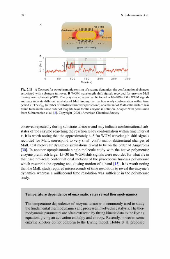
58 S. Subramanian et al.
Fig. 2.11 A Concept for optoplasmonic sensing of enzyme dynamics, the conformational changesassociated with substrate turnover. B WGM wavelength shift signals recorded for enzyme Mallturning over substrate pNPG. The gray shaded areas can be found in 10–20% of the WGM signalsand may indicate different substates of Mall finding the reaction ready conformation within timeperiod T . The kcat (number of substrate turnovers per second) of a mutant of Mall at the surface wasfound to be in the same order of magnitude as for the enzyme in solution. Adapted with permissionfrom Subramanian et al. [3]. Copyright (2021) American Chemical Society
observed repeatedly during substrate turnover and may indicate conformational sub-states of the enzyme searching the reaction ready conformation within time intervalτ . It is worth noting that the approximately 4–5 fm WGM wavelength shift signalsrecorded for MalL correspond to very small conformational/structural changes ofMalL that molecular dynamics simulations reveal to be on the order of Angstroms[30]. In another optoplasmonic single-molecule study with the active polymeraseenzyme pfu, much larger 15–30 fmWGM shift signals were recorded for what are inthat case nm-scale conformational motions of the pyrococcus furiosus polymerasewhich resemble the opening and closing motion of a hand [15]. It is worth notingthat the MalL study required microseconds of time resolution to reveal the enzyme’sdynamics whereas a millisecond time resolution was sufficient in the polymerasestudy.
Temperature dependence of enzymatic rates reveal thermodynamics
The temperature dependence of enzyme turnover is commonly used to studythe fundamental thermodynamics and processes involved in catalysis. The ther-modynamic parameters are often extracted by fitting kinetic data to the Eyringequation, giving an activation enthalpy and entropy. Recently, however, someenzyme kinetics do not conform to the Eyring model. Hobbs et al. proposed
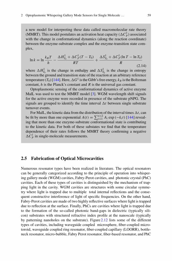
2 Optoplasmonic Whispering Gallery Mode Sensors for Single Molecule … 59
a new model for interpreting these data called macromolecular rate theory(MMRT). This model postulates an activation heat capacity (�C‡
P ) associatedwith the change in conformational dynamics (along the reaction coordinate)between the enzyme-substrate complex and the enzyme-transition state com-plex,
ln k = lnkB T
h− �H ‡
T0+ �C‡
P(T − T0)
RT+ �S‡
T0+ �C‡
P(ln T − ln T0)
R(2.14)
where �H ‡T0
is the change in enthalpy and �S‡T0
is the change in entropybetween the ground and transition state of the reaction at an arbitrary referencetemperature (T0) [144]. Here,�G‡ is theGibb’s free energy, kB is theBoltzmanconstant, h is the Planck’s constant and R is the universal gas constant.
Optoplasmonic sensing of the conformational dynamics of active enzymeMalL was used to test the MMRT model [3]. WGM wavelength shift signalsfor the active enzyme were recorded in presence of the substrate pNPG. Thesignals are grouped to identify the time interval �t between single substrateturnover events.
ForMalL, the kinetic data from the distribution of the interval times�t , canbe fit by more than one exponential A(t) = ∑n≤2
i=1 Ai exp (−ki t) [144] reveal-ing that more than one enzyme-substrate conformational state is contributingto the kinetic data. For both of these substates we find that the temperaturedependence of their rates follows the MMRT theory confirming a negative�C‡
P in single-molecule measurements.
2.5 Fabrication of Optical Microcavities
Numerous resonator types have been realized in literature. The optical resonatorscan be generally categorized according to the principle of operation into whisper-ing gallery mode (WGM) cavities, Fabry-Perot cavities, and photonic crystal (PhC)cavities. Each of these types of cavities is distinguished by the mechanism of trap-ping light in the cavity. WGM cavities are structures with some circular symme-try where light is trapped due to multiple total internal reflections and the conse-quent constructive interference of light of specific frequencies. On the other hand,Fabry-Perot cavities are made of two highly reflective surfaces where light is trappeddue to reflection at the surface. Finally, PhCs are cavities where light is trapped dueto the formation of the so-called photonic band-gaps in dielectric (typically sili-con) substrates with structured refractive index profile at the nanoscale (typicallyby patterning nanoholes on the substrate). Figure2.12 lists some of the differenttypes of cavities, including waveguide coupled microsphere, fiber-coupled micro-toroid, waveguide coupled ring resonator, fiber-coupled capillary (LOORR), bottle-neck resonator, micro-bubble, Fabry Perot resonator, fiber-based resonator, and PhC
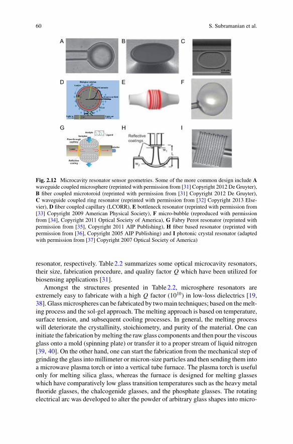
60 S. Subramanian et al.
Fig. 2.12 Microcavity resonator sensor geometries. Some of the more common design include Awaveguide coupled microsphere (reprinted with permission from [31] Copyright 2012 De Gruyter),B fiber coupled microtoroid (reprinted with permission from [31] Copyright 2012 De Gruyter),C waveguide coupled ring resonator (reprinted with permission from [32] Copyright 2013 Else-vier), D fiber coupled capillary (LCORR), E bottleneck resonator (reprinted with permission from[33] Copyright 2009 American Physical Society), F micro-bubble (reproduced with permissionfrom [34], Copyright 2011 Optical Society of America), G Fabry Perot resonator (reprinted withpermission from [35], Copyright 2011 AIP Publishing), H fiber based resonator (reprinted withpermission from [36], Copyright 2005 AIP Publishing) and I photonic crystal resonator (adaptedwith permission from [37] Copyright 2007 Optical Society of America)
resonator, respectively. Table2.2 summarizes some optical microcavity resonators,their size, fabrication procedure, and quality factor Q which have been utilized forbiosensing applications [31].
Amongst the structures presented in Table2.2, microsphere resonators areextremely easy to fabricate with a high Q factor (1010) in low-loss dielectrics [19,38]. Glassmicrospheres can be fabricated by twomain techniques; based on themelt-ing process and the sol-gel approach. The melting approach is based on temperature,surface tension, and subsequent cooling processes. In general, the melting processwill deteriorate the crystallinity, stoichiometry, and purity of the material. One caninitiate the fabrication bymelting the raw glass components and then pour the viscousglass onto a mold (spinning plate) or transfer it to a proper stream of liquid nitrogen[39, 40]. On the other hand, one can start the fabrication from the mechanical step ofgrinding the glass into millimeter or micron-size particles and then sending them intoa microwave plasma torch or into a vertical tube furnace. The plasma torch is usefulonly for melting silica glass, whereas the furnace is designed for melting glasseswhich have comparatively low glass transition temperatures such as the heavy metalfluoride glasses, the chalcogenide glasses, and the phosphate glasses. The rotatingelectrical arc was developed to alter the powder of arbitrary glass shapes into micro-
2 Optoplasmonic Whispering Gallery Mode Sensors for Single Molecule … 61
Table 2.2 A summary of some common resonator geometries, Q factor, size, and fabricationmethods.
Resonator type Q factorin water
Typical size Fabrication methods
Spherical [5,10, 11, 20,43–49]
108 50–500µm CO2 laser melting, butane/oxygen flame melting of opticalfiber tips
Microtoroid[50–53]
108 30–200µm CO2 reflow of an under-cut silica micro-disk on siliconwafer
Ring-resonator[54–59]
105 20–200µm Lithography techniques; substrates include silicon nitride(visible operation), silicon (near-IR) and polymer thin-films
Capillary [60,61]
107−8 150µm Softening by CO2 laser and stretching a fused silicacapillary
Disk resonator[62, 63]
104 10–100µm Fabricated from siliconoxy- nitride film on a silicon waferby lithography technology
Bottleneckresonator [33]
108 40µm Fabricated from standard optical glass using a two-step heatand pull process
Microtube ringresonator [64,65]
108 10µm Roll-up of a strained SiO/SiO2 Nano membrane to form amicro-tube with a thin wall
Microbubble[34, 66]
103−7 30–500µm CO2 heating and pulling of glass capillary
Micro-coil [67,68]
106 500µm Wind a microfiber coil on a cylindrical rod with a lowerrefractive index
Fiber-based[36, 69]
106 20–200µm Resonator is formed between the plane tip of a fiber and aconcave micro-mirror fabricated by standard silicon etchingand optical coating techniques
Fabry-Perot[70]
104−6 40µm The resonator is formed between two reflectors composedof two period Si/SiO2 Bragg structures
Photoniccrystal cavity[37, 71]
106 <10µm e-beam lithography and reactive ion etching
spheres [41, 42].With this technique, a large number of spheres can be made at once,and with high throughput. The size distribution of the spheres is seen as drifting toa large size and hence controlling the fabrication of very small spheres <100µmcan become difficult. Furthermore, fabricating spheres of an exact size repeatedly ischallenging; an optical microscope is required to sort out the microspheres of thedesired size. The microspheres can be picked up with the help of a glass capillarywhich is connected to a vacuum pump. Once picked up, the microspheres can beglued to the end of an optical fiber facet [38].
Alternatively, spherical glass resonators can be formed by melting a glass rod ora standard telecom fiber to the desired diameter. Upon heating, the end of the glassfiber forms a spherical volume under the surface tension. Thismethod is reproducibleand inexpensive, which gives high-quality spheres. In addition to that, this techniqueproduces a highly spherical, uniform, and very low intrinsic roughness microsphere
62 S. Subramanian et al.
due to the glass’s high viscosity and hence helps to reduce the surface scatteringenergy losses. Different heating sources, including high-power (e.g., a CO2) laser,an oxygen/butane or nitrous oxide/butane micro torch, or an electric arc available ina commercial fiber splicer, have been used to initiate the reflow process [43, 72, 73].The major drawback of these techniques is that they only create one microspherecavity at a time, and the micro flame process produces asymmetrical spheres [38,74]. Figure2.13A illustrates the fabrication of silica microspheres using a CO2 laser.
The interesting fact of the sol-gel method is that this process starts from theprecursor level and ends up with a spherical microsphere and the same process canbe used to coat a spherical cavity. For example, silica spheres have been synthesizedvia the sol-gel method using base-catalyzed hydrolysis of tetraethyl orthosilicate.If the earth metals are incorporated with the synthesis, it is necessary to use anacid catalyst to overcome the hydroxide formation [38]. Furthermore, the sol-geltechnique is considered the best method to coat a uniform layer on top of a sphericalmicroresonator [2]. The Q factor of a microsphere is generally reduced by the coatedmaterial due to the absorption of the light by the coating and due to the scatteringat the interfaces. The microspheres have been coated with many materials includingthe conjugated polymers, PMMA, nanocrystalline silicon, silica-hafnia glass, andmanymore. Recently, other methods such as low-pressure chemical vapor deposition(LPCVD) and thermal annealing have been introduced as alternative methods forcoating a thin film onto a microsphere [75–77].
The micro bottle resonators are fabricated from the silica fiber by changing thefiber morphology into a bump, which looks like a bottle. Previously, micro bottleresonators were fabricated using the heat and pull method. The most basic methodconsists of thinning the fiber at two positions such that the thicker area in betweenthese segments forms the bottle shape, as shown in Fig. 2.13B. As per the first demon-stration of the micro bottle resonator fabrication, a small section of a fiber capillary isexposed to the melting process using the CO2 laser beam by pulling the optical fiber[80]. The computer control of the heating and pulling process has been enabled thefabrication of bottle resonators with a Q factor up to 108. [33, 81, 82]. In an alternateprocess, Ganapathy et al. used short sections of optical fiber in a standard fusionsplicer to form micro bottles, which is a thermo-mechanical process. The cleavedends of two optical fibers are pushed towards each other while heated to a particulartemperature at which it softens and fuses. The heating process was done using thearc discharge with an arc duration of one second, where it was exploited spliceractions on a piece of fiber to soften a small region with simultaneous compression.The combined splicer efforts resulted in a significant bulge along with the fiber. Inaddition to that, multiple short arcs were used to soften the glass controllably [81].
Toroid microcavities are made from a 2–3 µm layer of silicon dioxide on thesurface of the silicon wafer. The fabrication process consists of four main steps. Thefirst step is photolithography is used to define a disk-shaped photoresist pad on asilicon substrate that undergoes wet thermal oxidation in a horizontal tube furnace.Secondly, this pad pattern acts as a etch mask under hydrofluoric acid (HF). The thirdstep is a selective etching process where the edges of the SiO2 circular pad are equallyundercut with xenon difluoride (XeF2) just leaving circular silicon pillars to support

2 Optoplasmonic Whispering Gallery Mode Sensors for Single Molecule … 63
Fig. 2.13 The fabrication process of a A microsphere resonator; B microbottle resonator; C micro-toroid resonator: (i) SiO2 is deposited on a silicon wafer, (ii) HCl etching is applied to create thedisk structure on top of the wafer, (iii) XeF2 etching is used to create a post structure, (iv) CO2laser irradiation for the structure to smoothen to form the toroid structure [78]; D microdisk res-onator: (i) photolithography to pattern the photoresist onto a silicon oxide layer, (ii) reactive ionetching to transfer the pattern of the photoresist into the silicon oxide layer, (iii) remove the residualphotoresist using photoresist remover and H2SO4/H2O2 solution, (iv) undercut the silica microdiskresonator using XeF2dry etching to form a silicon pillar [78]; and E polymer-based waveguidering resonator: (i) the core layer was spin-coated on the adhesive layer and Al layer deposition andphotoresist layer spin-coated on the core layer, respectively, (ii) photoresist layer patterning, (iii)double layers patterning, (iv) core layer patterning, (v) removing the mask, cladding and annealing[79]
the larger SiO2 disks. Lastly, silica edge of the undercut disk is selectively melt andreflow under a CO2 laser without disturbing the underlying silicon support pillar. Thesilica disk shrinks and etches at the border to form the toroidal morphology mainlydue to the surface tension. The main fabrication stages of the microtoroid resonatorsare depicted in Fig. 2.13C [83, 84]. Recently, electron beam lithography has beenutilized to pattern a silicon layer via reactive ion etched. This step was followed bynon-selective etching of the native oxide and the main etching using Cl2, HBr, andO2 to obtain torroidal resonators [85]. The on-chip fabrication of microtoroids vialithography provides a more precise method to tailor the desired geometry [84].
Microdisk fabrication is quite similar to microtoroids and fabricated via lithog-raphy method (wet and dry chemical etching). The reflow process is absent in themicrodisk fabrication process, and this tends to result in a lower Q factor due to thehigher surface roughness of the disk resonator as compared to the microtoroid. The
64 S. Subramanian et al.
main advantages of the microdisks are that they can be integrated with microme-chanical devices (e.g. high-stress Si3N4 nanomechanical beam) to detect the forceand mechanical motions and have been tailored via many materials such as siliconnitride, titanium dioxide, silicon carbide, lithium niobite, chalcogenide glass, andpolymers in addition to silica and silicon. The major steps of the fabrication of sil-ica microdisk are exemplified by Fig. 2.13D (i–iv) [86, 87] which was reported byGuanyu et al. The fabrication process of the silica microdisk consists of four mainsteps. Firstly, a photoresist (AZ6130) is patterned on top a thermally grown sili-con oxide layer. The resultant mold is subjected to bake to get rid of the sidewallroughness of the photoresist pattern. Then a reactive ion etching step is performedwith SF6/CHF3/HeSF6/CHF3/He to transfer the photoresist pattern onto the siliconoxide coating. The residual photoresist is removed by the solution of H2SO4/H2O2.As the final step, the silica microdisk is undercut XeF2 by dry etching to form thesilicon pillar [78].
Microrings havebeen fabricated via photolithography and etchingmethods.More-over, these resonators are coupled via a bus waveguide , which is fabricated on thesame chip. Silicon insulators, silicon nitride, and polymers have been used as fab-rication materials [82]. As an illustration, the fabrication steps of polymer-basedwaveguide ring resonator are shown in Fig. 2.13E (i–v) [79]. Firstly, a thin film ofthe adhesive layer is coated on a silicon wafer, and lower cladding is spin-coated onthe top of the adhesive layer. The core layer of the same thickness is placed on topof the cladding layer. The aluminum (Al) film is coated on the surface of the core bythermal evaporation deposition. The photoresist layer is spin-coated on the layer ofAl, patterned and developed. A mixture of hydrogen peroxide and phosphoric acidis used to remove the exposed part of the Al layer. The double-layer pattern is usedas the mask for deep reactive ion etching of the core layer. The solution of hydrogenperoxide and phosphoric acid helps to get rid of the mask. Once the core fabricationis done, it is exposed to spin coating to thicken the upper cladding layer and is curedby ultraviolet light. Typically the Q factor of the ring resonators falls within the range104−5. Silicon microrings have been multiplexed and integrated with microfluidics.Additonally, space couplers have also developed [82].
2.6 Plasmonic Gold Nanoparticles: Synthesis andFunctionalization
In general, metal nanoparticles are fabricated using two approaches: top-down andbottom-up approaches. The former approach uses traditional lithographic techniquesto pattern nanostructures onto a substrate. Though this technique has good controlover structures such as clean surfaces, control of composition and to achieve periodicarrays, it involves complex and multistep procedures which may also result in unde-sirable polycrystalline nanostructures. The cost and time invested increase with thedecrease in the size of the nanoparticles. These disadvantages are overcome by thelatter approach which uses chemical synthesis routes to directly synthesize the metalnanostructures on a large scale with tailored morphologies. Here we focus on only
2 Optoplasmonic Whispering Gallery Mode Sensors for Single Molecule … 65
Fig. 2.14 A Schematic for chemical synthesis of anisotropic gold nanoparticles ranging fromspherical to nanostar morphology. B An illustration of synthetic strategies for controlling size andshape of metal nanoparticles along with LaMer diagram
noble metal nanoparticles because of their enhanced optical and catalytic properties.A variety of anisotropic noble metal nanoparticles such as nanorods [88], nanostars[89], nanocubes [90], nanowires [91], nanoprisms [92], octahedron [93] and so forthwere prepared using various chemical approaches (Fig. 2.14A).
The synthesis of larger nanoparticles from small seeds is hindered by the for-mation of a wide distribution of sizes without uniformity. This problem could beovercome by seed-mediated synthesis using step by step growth on seeds and pre-venting secondary nucleation to control the size of the nanoparticles. In this methodnucleation and growth, steps are separated to get better control over the morphologyof the nanoparticles. Typically, seeds are synthesized by the reduction of HAuCl4in a boiling aqueous sodium citrate solution. When the sodium citrate is added, thiswill reduce the Au3+ ions to gold atoms (Fig. 2.14B) [94, 95]. As time proceeds theconcentration of gold atoms rises rapidly until it exceeds saturation, resulting in theformation of nuclei. The free gold ions in the solution will then bind to the nucleisurface and growth continues. In this method, the citrate ions act as both reducingagents and surface stabilizers. The size of the nanoparticles can be tuned by choosingthe proper ratios of HAuCl4 and sodium citrate. The synthesis typically proceeds bythe injection of seed (small cluster of metal) solution to the growth solution whichis prepared by the reduction of metal precursor; and by controlling the parameterssuch as concentration of seed solution, the morphology of seeds, temperature, etc.The seed concentration greatly affects the kinetics of the metal reduction [96].
The metal nanostructures are composed of a metal core which is stabilized by aligand shell. Ligands, in general, are bifunctional molecules; one end binds to thenanoparticle core-forming compact monolayers and the other end (functional groupssuch as −OH, −NH2,−SO3H and −COOH) faces outwards from the core nanopar-ticle and dictates the molecular interactions with the surrounding environment andwith the biomolecules. As prepared, metal nanoparticles cannot be readily appliedin optoplasmonic sensing due to incompatibility of the ligand(s) with the desired
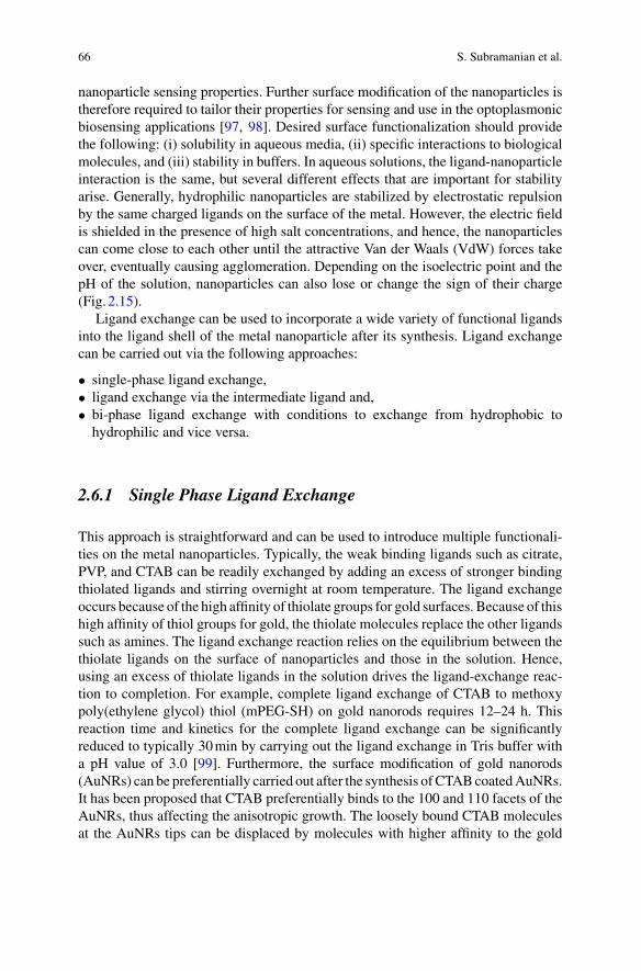
66 S. Subramanian et al.
nanoparticle sensing properties. Further surface modification of the nanoparticles istherefore required to tailor their properties for sensing and use in the optoplasmonicbiosensing applications [97, 98]. Desired surface functionalization should providethe following: (i) solubility in aqueous media, (ii) specific interactions to biologicalmolecules, and (iii) stability in buffers. In aqueous solutions, the ligand-nanoparticleinteraction is the same, but several different effects that are important for stabilityarise. Generally, hydrophilic nanoparticles are stabilized by electrostatic repulsionby the same charged ligands on the surface of the metal. However, the electric fieldis shielded in the presence of high salt concentrations, and hence, the nanoparticlescan come close to each other until the attractive Van der Waals (VdW) forces takeover, eventually causing agglomeration. Depending on the isoelectric point and thepH of the solution, nanoparticles can also lose or change the sign of their charge(Fig. 2.15).
Ligand exchange can be used to incorporate a wide variety of functional ligandsinto the ligand shell of the metal nanoparticle after its synthesis. Ligand exchangecan be carried out via the following approaches:
• single-phase ligand exchange,• ligand exchange via the intermediate ligand and,• bi-phase ligand exchange with conditions to exchange from hydrophobic tohydrophilic and vice versa.
2.6.1 Single Phase Ligand Exchange
This approach is straightforward and can be used to introduce multiple functionali-ties on the metal nanoparticles. Typically, the weak binding ligands such as citrate,PVP, and CTAB can be readily exchanged by adding an excess of stronger bindingthiolated ligands and stirring overnight at room temperature. The ligand exchangeoccurs because of the high affinity of thiolate groups for gold surfaces. Because of thishigh affinity of thiol groups for gold, the thiolate molecules replace the other ligandssuch as amines. The ligand exchange reaction relies on the equilibrium between thethiolate ligands on the surface of nanoparticles and those in the solution. Hence,using an excess of thiolate ligands in the solution drives the ligand-exchange reac-tion to completion. For example, complete ligand exchange of CTAB to methoxypoly(ethylene glycol) thiol (mPEG-SH) on gold nanorods requires 12–24 h. Thisreaction time and kinetics for the complete ligand exchange can be significantlyreduced to typically 30min by carrying out the ligand exchange in Tris buffer witha pH value of 3.0 [99]. Furthermore, the surface modification of gold nanorods(AuNRs) can be preferentially carried out after the synthesis ofCTABcoatedAuNRs.It has been proposed that CTAB preferentially binds to the 100 and 110 facets of theAuNRs, thus affecting the anisotropic growth. The loosely bound CTAB moleculesat the AuNRs tips can be displaced by molecules with higher affinity to the gold
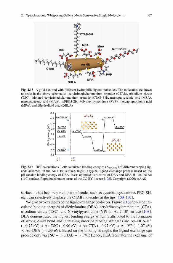
2 Optoplasmonic Whispering Gallery Mode Sensors for Single Molecule … 67
Fig. 2.15 A gold nanorod with different hydrophilic ligand molecules. The molecules are drawnto scale in the above schematics. cetyltrimethylammonium bromide (CTAB), trisodium citrate(TSC), thiolated cetyltrimethylammonium bromide (CTAB-SH), mercaptosuccinic acid (MSA),mercaptoacetic acid (MAA), mPEG5-SH, Polyvinylpyrrolidone (PVP), mercaptopropionic acid(MPA), and dihydrolipid acid (DHLA)
Fig. 2.16 DFT calculations. Left: calculated binding energies (Ebinding) of different capping lig-ands adsorbed on the Au (110) surface. Right: a typical ligand exchange process based on thepH-tunable binding energy of DEA. Inset: optimized structures of DEA and DEA-H+ on the Au(110) surface. Reproduced under terms of the CC-BY licence [103]. Copyright (2020) AAAS
surface. It has been reported that molecules such as cysteine, cysteamine, PEG-SH,etc., can selectively displace the CTAB molecules at the tips [100–102].
Wegive two examples of the ligand exchange protocols. Figure2.16 shows the cal-culated binding energies of diethylamine (DEA), cetyltrimethylammonium (CTA),trisodium citrate (TSC), and N-vinylpyrrolidone (VP) on Au (110) surface [103].DEA demonstrated the highest binding energy which is attributed to the formationof strong Au-N bond and increasing order of binding strengths are Au–DEA-H+(−0.72 eV) < Au-TSC (−0.90 eV) < Au-CTA (−0.97 eV) < Au–VP (−1.07 eV)< Au–DEA (−1.33 eV). Based on the binding strengths the ligand exchange canproceed only via TSC− >CTAB− > PVP. Hence, DEA facilitates the exchange of

68 S. Subramanian et al.
Fig. 2.17 A typical ligandexchange of AuNRs toreplace the native CTABwith TSC. A A schemeillustrating the ligandexchange process. B, CPotentials and UV-VIS-NIRspectra of the AuNRsobtained at different stages ofthe ligand exchange. D TEMimages of the AuNRs withdifferent capping ligands.Reproduced under terms ofthe CC-BY licence [103].Copyright (2020) AAAS
many commonly used ligands from noble metal nanoparticle surfaces. Interestingly,protonated form of DEA (DEA-H+) becomes the weakest ligand favoring subse-quent ligand exchange with many common ligands. Firstly, the CTAB moleculeson the AuNRs are exchanged with PVP molecules in an ethanolic solution by stir-ring overnight. Secondly, PVP molecules are displaced by strong DEA moleculesby stirring for 2h which impart a negative charge to the AuNRs. Finally, the DEAmolecules on the surface are protonated using tannic acid in the presence of TSC lig-and for the completed exchange of DEA with TSC. As result, the CTAB on AuNRswas exchanged to weak ligand TSC by exploiting pH switchable binding affinity ofDEA on the metal surface. No changes in the shape and size of the AuNRs were dis-cernible by the transmission electron microscopy (TEM) imaging (Fig. 2.17), whichcould be attributed to the mild conditions that have been involved in the whole ligandexchange process.
In another example, Wei et al., demonstrated the exchange of cetyltrimethylam-monium bromide (CTAB)-stabilized Au NRs to citrate stabilized Au NRs usingpolystyrenesulfonate (PSS) as an intermediate ligand. Yin et al., demonstrated theligand exchange on CTAB coated Au NRs coating and etching of Cu2O [104]. TheCTAB-coated Au NRs are exchanged with poloxamer ligand F127 via coating andexchange of Cu2O as a sacrificial layer on the Au NRs.
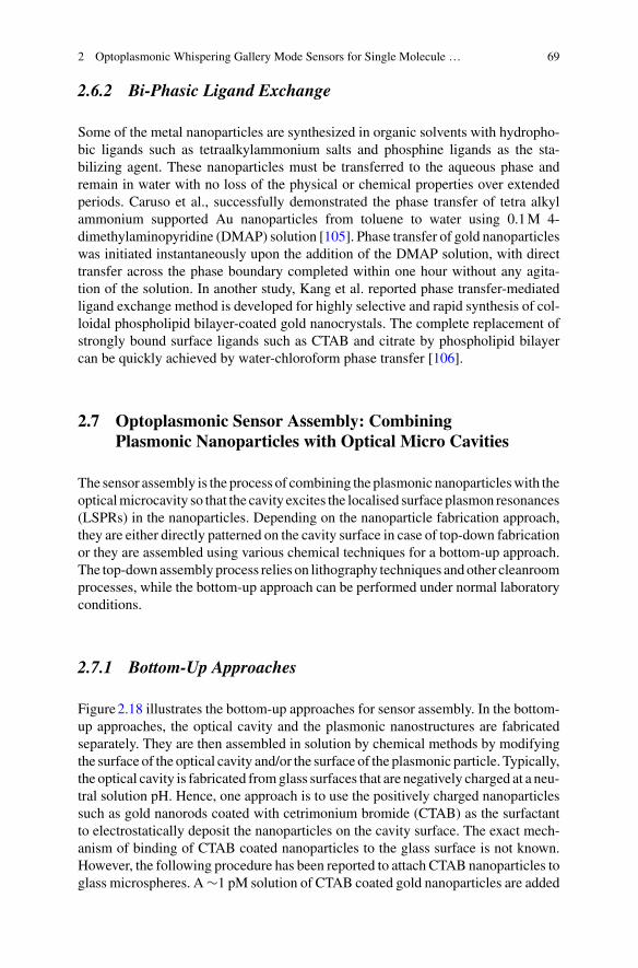
2 Optoplasmonic Whispering Gallery Mode Sensors for Single Molecule … 69
2.6.2 Bi-Phasic Ligand Exchange
Some of the metal nanoparticles are synthesized in organic solvents with hydropho-bic ligands such as tetraalkylammonium salts and phosphine ligands as the sta-bilizing agent. These nanoparticles must be transferred to the aqueous phase andremain in water with no loss of the physical or chemical properties over extendedperiods. Caruso et al., successfully demonstrated the phase transfer of tetra alkylammonium supported Au nanoparticles from toluene to water using 0.1M 4-dimethylaminopyridine (DMAP) solution [105]. Phase transfer of gold nanoparticleswas initiated instantaneously upon the addition of the DMAP solution, with directtransfer across the phase boundary completed within one hour without any agita-tion of the solution. In another study, Kang et al. reported phase transfer-mediatedligand exchange method is developed for highly selective and rapid synthesis of col-loidal phospholipid bilayer-coated gold nanocrystals. The complete replacement ofstrongly bound surface ligands such as CTAB and citrate by phospholipid bilayercan be quickly achieved by water-chloroform phase transfer [106].
2.7 Optoplasmonic Sensor Assembly: CombiningPlasmonic Nanoparticles with Optical Micro Cavities
The sensor assembly is the process of combining the plasmonic nanoparticleswith theopticalmicrocavity so that the cavity excites the localised surface plasmon resonances(LSPRs) in the nanoparticles. Depending on the nanoparticle fabrication approach,they are either directly patterned on the cavity surface in case of top-down fabricationor they are assembled using various chemical techniques for a bottom-up approach.The top-downassemblyprocess relies on lithography techniques andother cleanroomprocesses, while the bottom-up approach can be performed under normal laboratoryconditions.
2.7.1 Bottom-Up Approaches
Figure2.18 illustrates the bottom-up approaches for sensor assembly. In the bottom-up approaches, the optical cavity and the plasmonic nanostructures are fabricatedseparately. They are then assembled in solution by chemical methods by modifyingthe surface of the optical cavity and/or the surface of the plasmonic particle. Typically,the optical cavity is fabricated fromglass surfaces that are negatively charged at a neu-tral solution pH. Hence, one approach is to use the positively charged nanoparticlessuch as gold nanorods coated with cetrimonium bromide (CTAB) as the surfactantto electrostatically deposit the nanoparticles on the cavity surface. The exact mech-anism of binding of CTAB coated nanoparticles to the glass surface is not known.However, the following procedure has been reported to attach CTAB nanoparticles toglass microspheres. A∼1 pM solution of CTAB coated gold nanoparticles are added
70 S. Subramanian et al.
Fig. 2.18 Bottom-up assembly of an optoplasmonic sensor. In the bottom-up approaches, the sensoris assembled in solution via chemical methods
to a chamber containing the microsphere at a solution pH of 1.6. CTAB coatednanoparticles attach to the cavity surface as can be observed via binding step in theWGM wavelength/frequency/FWHM traces [16].
Alternatively, the surface charge of the glassmicrosphere is transformed by aminosilanization of the microcavity. Molecules such as 3-aminopropyltriethoxysilane(APTES) or N-(2-aminoethyl)-3-aminopropyltrimethoxysilane (AEAPTMS) con-tain silanol (Si-OH) groups that can hydrolyze on the surface of the glass where theyform the siloxane (Si-O-Si) linkages [107, 108]. The solvent-exposed amino groupsare then typically positively charged at neutral pH, allowing electrostatic attachmentof the negatively charged nanoparticles (e.g. citrate, carboxyl, lipoic capped) asshown in Fig. 2.18. The aminosilanization further allows for amide linkages betweenthe primary amines on the glass and carboxyl groups on the gold nanoparticles bythe well-known carbodiimide cross-linking reaction [109]. This heterobifunctionalcross-linking reaction can be carried out in solution or the vapor phase. First, thesurface of the microcavity is activated by immersing the cavity in a piranha solution(7xH2SO4:3xH2O2) for 10–20 mins. For solution-phase deposition, a 1–2% solutionof the aminosilane is prepared in water, ethanol, or anhydrous toluene. Althoughusing water as a solvent makes the solution preparation simple, the formation ofpolymer chains of the silanes results in uneven multilayered deposition and a loss ofQ. Hence, anhydrous toluene or ethanol is preferred. For a complete deposition, areaction time of over 24h may be required. Since partial coverage is sufficient, reac-tion times as short as 45 s can be used. However, the variation in the layer thicknesscould result in loss of cavity Q. Aminosilanes deposited from solution have beenfound to form unstable layers that degrade upon exposure to water over a long time[108]. Alternatively, the vapor phase deposition provides better (thinner) layer thick-ness with small standard deviations. The vapor phase deposition can be performedby placing the cavity in a chamber with a small amount (∼0.5 ml) of the aminosilane.The chamber can then be heated to 90 ◦C or evacuated to deposit the aminosilaneon the microcavity surface. For both solution or vapor phase, the cavity is washed
2 Optoplasmonic Whispering Gallery Mode Sensors for Single Molecule … 71
in toluene (2x), ethanol (2x), and water (2x) to displace any weakly bound silanes.The cavity is then typically dried and cured at 110 ◦C for 15mins to promote theformation of siloxane bonds.
Finally the surface of the nanoparticles can be coated with an mercaptosilanesuch as (3-Mercaptopropyl)trimethoxysilane (MPTMS). The thiol (SH) group inMPTMS binds to the gold nanoparticle whereas the silanol groups can bind to theglass following the above procedure for APTES silanization of glass. Once the ligandexchange (from CTAB or citrate to MPTMS) is performed, the gold nanoparticlescan be attached to the glass surface in solution at neutral pH conditions.
Table2.3 lists the common nanorod functionalizations used for immobilizing thenanorods on the resonator. The pros and cons of each functionalization are also listed.Typically, CTAB (cetrimonium bromide) or citrate capped nanorods are easily avail-able via commercial sources. MPTMS ((3-mercaptopropyl)trimethoxysilane) func-tionalized nanorods have to be synthesized in the lab starting from citrate cappednanorods and exchanging the ligand. CTAB capped nanorods have been predomi-nantly used in the past as they can be attached via a one-step immobilization proce-dure. This reduces measurement time significantly while increasing the likelihood ofobtaining a high Q resonator before nanorod attachment. Citrate capped resonatorsrequire the resonator surface to be pre-functionalized with aminosilanes. This pro-cess can result in the reduction of the Q due to the non-uniform coating of theaminosilanes. Additional issues with aminosilanization of the resonators arise dueto the high positive charge on the surface. Biomolecules having negatively chargedregions attach to the resonator surface in bulk further reducing the Q. Hence, anti-fouling agents have to be added to the resonator [14]. However, perfect coverage ofthe surface with an anti-fouling agent is very difficult to achieve.
2.7.2 Top-Down Approaches
Unlike the bottom-up approaches, the top-down approaches require clean-roomlithography processes. Figure2.19 illustrates some top-down approaches for assem-bly of optoplasmonic sensors. Themicrocavities such as toroids, disks or PhCs can befabricated using lithography techniques as described in Sect. 2.5. Then, a photo resistis spin coated on top of the cavity and patterned into the form of nanostructures usingE-beam lithography techniques. Then gold layers are fabricated i.e. by sputtering.The resist layer is then lifted-off to obtain gold nanostructures on the microcavitysurface (Fig. 2.19A). Alternatively, the gold nanostructures can be patterned on aglass substrate and the microcavity can be placed on top of the nanostructures asshown in (Fig. 2.19B). Since lithography techniques are mainly applicable to pla-nar substrates, these approaches are useful for planar cavities such as PhCs. Due tothe requirement of expensive equipment and the long parameter optimization timerequired, these approaches have not been explored sufficiently in the literature.
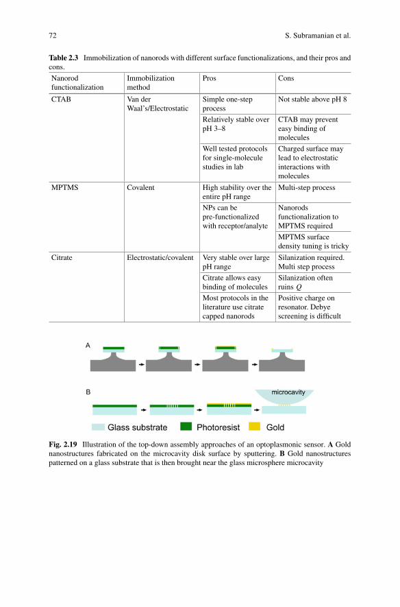
72 S. Subramanian et al.
Table 2.3 Immobilization of nanorods with different surface functionalizations, and their pros andcons.
Nanorodfunctionalization
Immobilizationmethod
Pros Cons
CTAB Van derWaal’s/Electrostatic
Simple one-stepprocess
Not stable above pH 8
Relatively stable overpH 3–8
CTAB may preventeasy binding ofmolecules
Well tested protocolsfor single-moleculestudies in lab
Charged surface maylead to electrostaticinteractions withmolecules
MPTMS Covalent High stability over theentire pH range
Multi-step process
NPs can bepre-functionalizedwith receptor/analyte
Nanorodsfunctionalization toMPTMS required
MPTMS surfacedensity tuning is tricky
Citrate Electrostatic/covalent Very stable over largepH range
Silanization required.Multi step process
Citrate allows easybinding of molecules
Silanization oftenruins Q
Most protocols in theliterature use citratecapped nanorods
Positive charge onresonator. Debyescreening is difficult
Fig. 2.19 Illustration of the top-down assembly approaches of an optoplasmonic sensor. A Goldnanostructures fabricated on the microcavity disk surface by sputtering. B Gold nanostructurespatterned on a glass substrate that is then brought near the glass microsphere microcavity
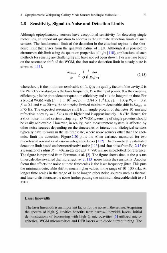
2 Optoplasmonic Whispering Gallery Mode Sensors for Single Molecule … 73
2.8 Sensitivity, Signal-to-Noise and Detection Limits
Although optoplasmonic sensors have exceptional sensitivity for detecting singlemolecules, an important question to address is the ultimate detection limits of suchsensors. The fundamental limit of the detection in the classical regime is the shot-noise limit that arises from the quantum nature of light. Although it is possible tocircumvent this limit using the quantum properties of light [110], applications of suchmethods for sensing are challenging and have not yet been shown. For a sensor basedon the resonance shift of the WGM, the shot noise detection limit in steady-state isgiven as [111],
δωmin
ω≥ 1
Q
√�ω
P0βητ(2.15)
where δωmin is theminimum resolvable shift, Q is the quality factor of the cavity, � isthe Planck’s constant,ω is the laser frequency, P0 is the input power, β is the couplingefficiency, η is the photodetector quantum efficiency and τ is the integration time. Fora typicalWGMwith Q = 1 × 10⁷,ω/2π = 3.84 × 10⁴ Hz, P0 = 100µW, η = 0.9,β = 0.1 and τ = 20ms, the shot noise limited minimum detectable shift is δωmin =5.75Hz. The expected resonance shift from single protein of diameter 10 nm andrefractive index n p = 1.54 is much higher and is approximately 1.8 kHz. Hence, fora shot-noise limited system using high-Q WGMs, sensing of single proteins shouldbe easily achievable. However, in reality, each measurement system is affected byother noise sources depending on the timescales of interaction. Biological sensorstypically have to work in the μs timescale, where noise sources other than the shot-noise limit the detection. Figure2.20 plots the Allan variance measured for twomicrotoroid resonators at various integration times [112]. The theoretically estimateddetection limit based on thermorefractive noise [113] and shot noise fromEq.2.15 fora resonator of radius R = 40µmexcited atλ ≈ 780 nm are also plotted for reference.The figure is reprinted from Foreman et al. [2]. The figure shows that, at the µ s-mstimescale, the so-called thermorefractive [2, 113] noise limits the sensitivity. Anotherfactor that affects the noise at these timescales is the laser frequency jitter. This putsthe minimum detectable shift to much higher values in the range of 10–100 kHz. Atlonger time scales in the range of 1s or longer, other noise sources such as thermaland laser drifts increase the noise further putting the minimum detectable shift to>1MHz.
Laser linewidth
The laser linewidth is an important factor for the noise in the sensor. Acquiringthe spectra of high-Q cavities benefits from narrow-linewidth lasers. Initialdemonstrations of biosensing with high-Q microcavities [5] utilized micro-spherical WGM microcavities and DFB lasers with diode current tuning. The
74 S. Subramanian et al.
Fig. 2.20 Allan variance ofthe a WGM resonancefrequency for twomicrotoroid resonatorsmeasured by Dobrindt [112].The theoretical detectionlimits estimated based on thethermorefractive noise [113]and shot noise are plotted forreference. Image reprintedwith permission fromForeman et al. [2]. Copyright(2015) OSA
light was coupled into the microsphere from another single-mode optical fiberthat was tapered in the coupling region. Both, WGMmicrosphere and taperedfiber were immersed in a liquid sample cell. The DFB laser linewidth was(1–10 MHz) at a wavelength of 1340nm and tuning was performed over a0.2nm range with a current tuning coefficient of approximately 0.01nm/mA.Subsequent demonstrations, especially for single-molecule sensing [16, 114]utilized ECDLs with linewidths <1MHz reducing the system noise consider-ably [115].
2.9 Time Resolution
The time resolution of a cavity-based sensor is ultimately limited by the cavitylifetime, that is the time required for the light to decay from the cavity. The qualityfactor Q of a cavity is related to the cavity lifetime as Q = ω0τ , where ω0 is theangular resonance frequency in radians and τ is the cavity lifetime in seconds. Typicalcavity lifetimes for the resonators described in previous sections are of the order of0.1–10nswhere a lower Q resonator provides a lower cavity decay time τ . Hence, thesignals can be acquired with nanosecond time resolution. The trade-off here is one ofthe signal bandwidth to sensitivity. As the quality factor of the resonator is inverselyproportional to the time resolution, faster acquisition of the signal results in a lowersensitivity. One can imagine this as a higher Q resonator confining light longer andhence accumulates more of the molecular information more before reaching thedetector. Hence, the longer confinement leads to a lower time resolution and highersensitivity, and vice-versa.
2 Optoplasmonic Whispering Gallery Mode Sensors for Single Molecule … 75
Bandwidth and noise trade-off
The implications of the noise as the acquisition bandwidth increases has to beconsidered. An increase in acquisition bandwidth also increases the integratedfrequency noise at each time point.
Typical quality factors for resonators that enable single-molecule sensing are inthe range of 106 and hence a time resolution of approx. 5ns can be theoreticallyachieved. In practice, however, the signals are typically acquired by scanning a tun-able laser over a bandwidth B around the cavity resonance to obtain the completecavity spectrum. This limits the scan time to be slow enough to cover the bandwidthof interest,
s >B
κτ, (2.16)
where s is the scan time, κ is the cavity linewidth in Hz, τ is the cavity lifetime inseconds and B is the bandwidth of interest in Hz. The two main methods of tuning alaser are by tuning the temperature of the laser module or by tuning a grating using apiezo. The temperature methods allow for a larger scan bandwidth B but are limitedto a time resolution of approx. 100 ms. The piezo tuning has a smaller bandwidth butallows a higher time resolution in the order of 100kHz. Typically, tuning frequenciesare however <1 kHz.
Some alternative methods have been proposed to overcome the technical limita-tions of laser scanning and acquire the single-molecule signals with a nanosecondtime resolution. A frequency lock-in method based on the Pound-Drever-Hall (PDH)lock-in method was used by Swaim et al. [116] to detect single gold nanoparticlesin solution with a ms time resolution. This method was extended by Subramanian etal. to detect conformational dynamics of single enzymes using the optoplasmonicsensor with a time resolution of 10 µs. The idea is to lock the laser frequency tothe cavity resonance peak using a feedback controller. Fluctuations in the cavity fre-quency can then be read out continuously by directmeasurement of the feedback errorsignal. Rosenblum et al. [117] proposed another method they termed cavity ring-upspectroscopy. They used laser pulses with sharp rise times slightly detuned from thecavity resonance to obtain interferograms from which the cavity resonance can beobtained by a simple Fourier transform. Although this method has not been appliedin the context of bio-sensing so far, it shows promise for acquiring the completecavity spectrum with a nanosecond resolution.
Locking to the cavity resonance is challenging as the resonance spectrum cannotbe directly used as it is symmetric on both sides of the resonance as shown inFig. 2.21A (top). Nonetheless, the derivative of the cavity resonance as shown inFig. 2.21A (bottom) is antisymmetric and hence can be used to lock the laser tothe cavity. Since there are no methods to directly find the derivative of the cavityspectrum, an indirect method based on frequency modulation is used.
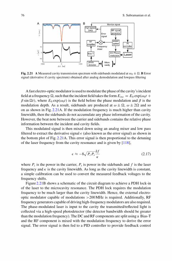
76 S. Subramanian et al.
Fig. 2.21 A Measured cavity transmission spectrum with sidebands modulated atw0 ± �. B Errorsignal (derivative if cavity spectrum) obtained after analog demodulation and lowpass filtering
A fast electro-opticmodulator is used tomodulate the phase of the cavity’s incidentfield at a frequency�, such that the incident field takes the form Einc = E0 exp(ω0t +β sin�t), where E0 exp(ω0t) is the field before the phase modulation and β is themodulation depth. As a result, sidebands are produced at ω ± �, ω ± 2� and soon as shown in Fig. 2.21A. If the modulation frequency is much higher than cavitylinewidth, then the sidebands do not accumulate any phase information of the cavity.However, the beat note between the carrier and sidebands contains the relative phaseinformation between the incident and cavity fields.
This modulated signal is then mixed down using an analog mixer and low passfiltered to extract the derivative signal ε (also known as the error signal) as shown inthe bottom plot of Fig. 2.21A. This error signal is then proportional to the detuningof the laser frequency from the cavity resonance and is given by [118],
ε ≈ −8√
Pc Psδ f
κ(2.17)
where Pc is the power in the carrier, Ps is power in the sidebands and f is the laserfrequency and κ is the cavity linewidth. As long as the cavity linewidth is constant,a simple calibration can be used to convert the measured feedback voltages to thefrequency shifts.
Figure2.21B shows a schematic of the circuit diagram to achieve a PDH lock-inof the laser to the microcavity resonance. The PDH lock requires the modulationfrequency to be much larger than the cavity linewidth. Hence, the external electro-optic modulator capable of modulations >200MHz is required. Additionally, RFfrequency generators capable of driving high-frequencymodulators are also required.The phase-modulated laser is input to the cavity the transmitted/reflected light iscollected via a high-speed photodetector (the detector bandwidth should be greaterthan themodulation frequency). The DC and RF components are split using a Bias-Tand the RF component is mixed with the modulation frequency to derive the errorsignal. The error signal is then fed to a PID controller to provide feedback control
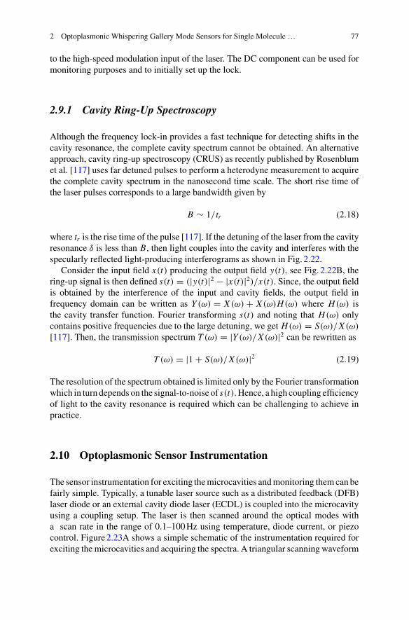
2 Optoplasmonic Whispering Gallery Mode Sensors for Single Molecule … 77
to the high-speed modulation input of the laser. The DC component can be used formonitoring purposes and to initially set up the lock.
2.9.1 Cavity Ring-Up Spectroscopy
Although the frequency lock-in provides a fast technique for detecting shifts in thecavity resonance, the complete cavity spectrum cannot be obtained. An alternativeapproach, cavity ring-up spectroscopy (CRUS) as recently published by Rosenblumet al. [117] uses far detuned pulses to perform a heterodyne measurement to acquirethe complete cavity spectrum in the nanosecond time scale. The short rise time ofthe laser pulses corresponds to a large bandwidth given by
B ∼ 1/tr (2.18)
where tr is the rise time of the pulse [117]. If the detuning of the laser from the cavityresonance δ is less than B, then light couples into the cavity and interferes with thespecularly reflected light-producing interferograms as shown in Fig. 2.22.
Consider the input field x(t) producing the output field y(t), see Fig. 2.22B, thering-up signal is then defined s(t) = (|y(t)|2 − |x(t)|2)/x(t). Since, the output fieldis obtained by the interference of the input and cavity fields, the output field infrequency domain can be written as Y (ω) = X (ω) + X (ω)H(ω) where H(ω) isthe cavity transfer function. Fourier transforming s(t) and noting that H(ω) onlycontains positive frequencies due to the large detuning, we get H(ω) = S(ω)/X (ω)
[117]. Then, the transmission spectrum T (ω) = |Y (ω)/X (ω)|2 can be rewritten as
T (ω) = |1 + S(ω)/X (ω)|2 (2.19)
The resolution of the spectrum obtained is limited only by the Fourier transformationwhich in turn depends on the signal-to-noise of s(t). Hence, a high coupling efficiencyof light to the cavity resonance is required which can be challenging to achieve inpractice.
2.10 Optoplasmonic Sensor Instrumentation
The sensor instrumentation for exciting themicrocavities andmonitoring themcan befairly simple. Typically, a tunable laser source such as a distributed feedback (DFB)laser diode or an external cavity diode laser (ECDL) is coupled into the microcavityusing a coupling setup. The laser is then scanned around the optical modes witha scan rate in the range of 0.1–100Hz using temperature, diode current, or piezocontrol. Figure2.23A shows a simple schematic of the instrumentation required forexciting themicrocavities and acquiring the spectra. A triangular scanning waveform
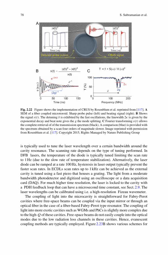
78 S. Subramanian et al.
Fig. 2.22 Figure shows the implementation of CRUS by Rosenblum et al. reprinted from [117]. ASEM of a fiber coupled microtoroid. Sharp probe pulse (left) and beating signal (right). B Showsthe signal s(t). The detuning δ is exhibited by the fast oscillations, the linewidth 2κ is given by theexponential decay and beat note gives the g the mode splitting. C Fourier transforming s(t) allowsthe complete retrieval of of the transmission spectrum (black). A comparison (blue) is provided withthe spectrum obtained by a scan four orders of magnitude slower. Image reprinted with permissionfrom Rosenblum et al. [117]. Copyright 2015, Rights Managed by Nature Publishing Group
is typically used to tune the laser wavelength over a certain bandwidth around thecavity resonance. The scanning rate depends on the type of tuning performed. InDFB lasers, the temperature of the diode is typically tuned limiting the scan rateto 1Hz (due to the slow rate of temperature stabilization). Alternatively, the laserdiode can be ramped at a rate 100Hz, hysteresis in laser output typically prevent thefaster scan rates. In ECDLs scan rates up to 1kHz can be achieved as the externalcavity is tuned using a fast piezo that houses a grating. The light from a moderatebandwidth photodetector and digitized using an oscilloscope or a data acquisitioncard (DAQ). For much higher time resolution, the laser is locked to the cavity witha PDH feedback loop that can have a microsecond time constant, see Sect. 2.9. Thelaser wavelengths can be calibrated using i.e. a high-resolution Fizeau wavemeter.
The coupling of light into the microcavity is straightforward for Fabry-Perotcavities where free-space beams can be coupled via the input mirror or through anoptical fiber in the case of a fiber-based Fabry-Perot type resonator. The coupling oflight into more exotic cavities such asWGMs and PhCs is slightly more complex dueto the high-Q of these cavities. Free-space beams do not easily couple into the opticalmodes due to the low radiation loss channels in these cavities. Hence, evanescentcoupling methods are typically employed. Figure2.23B shows various schemes for
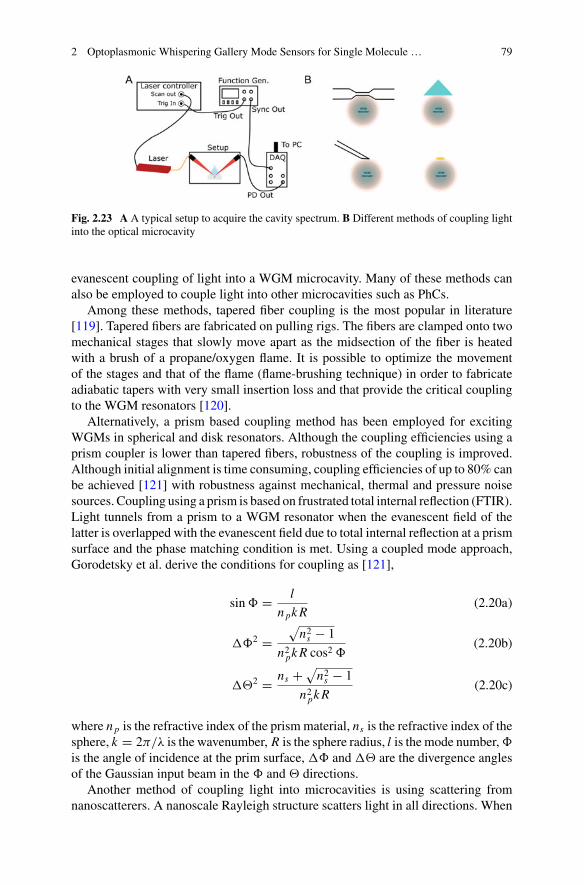
2 Optoplasmonic Whispering Gallery Mode Sensors for Single Molecule … 79
Fig. 2.23 A A typical setup to acquire the cavity spectrum. B Different methods of coupling lightinto the optical microcavity
evanescent coupling of light into a WGM microcavity. Many of these methods canalso be employed to couple light into other microcavities such as PhCs.
Among these methods, tapered fiber coupling is the most popular in literature[119]. Tapered fibers are fabricated on pulling rigs. The fibers are clamped onto twomechanical stages that slowly move apart as the midsection of the fiber is heatedwith a brush of a propane/oxygen flame. It is possible to optimize the movementof the stages and that of the flame (flame-brushing technique) in order to fabricateadiabatic tapers with very small insertion loss and that provide the critical couplingto the WGM resonators [120].
Alternatively, a prism based coupling method has been employed for excitingWGMs in spherical and disk resonators. Although the coupling efficiencies using aprism coupler is lower than tapered fibers, robustness of the coupling is improved.Although initial alignment is time consuming, coupling efficiencies of up to 80% canbe achieved [121] with robustness against mechanical, thermal and pressure noisesources. Coupling using a prism is based on frustrated total internal reflection (FTIR).Light tunnels from a prism to a WGM resonator when the evanescent field of thelatter is overlapped with the evanescent field due to total internal reflection at a prismsurface and the phase matching condition is met. Using a coupled mode approach,Gorodetsky et al. derive the conditions for coupling as [121],
sin� = l
n pk R(2.20a)
��2 =√
n2s − 1
n2pk R cos2 �
(2.20b)
��2 = ns + √n2
s − 1
n2pk R
(2.20c)
where n p is the refractive index of the prismmaterial, ns is the refractive index of thesphere, k = 2π/λ is the wavenumber, R is the sphere radius, l is the mode number,�is the angle of incidence at the prim surface, �� and �� are the divergence anglesof the Gaussian input beam in the � and � directions.
Another method of coupling light into microcavities is using scattering fromnanoscatterers. A nanoscale Rayleigh structure scatters light in all directions. When
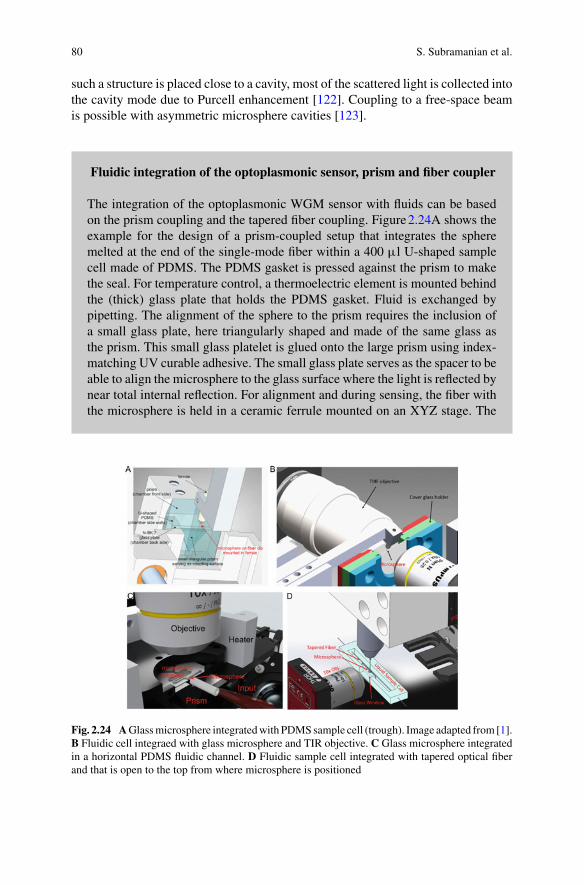
80 S. Subramanian et al.
such a structure is placed close to a cavity, most of the scattered light is collected intothe cavity mode due to Purcell enhancement [122]. Coupling to a free-space beamis possible with asymmetric microsphere cavities [123].
Fluidic integration of the optoplasmonic sensor, prism and fiber coupler
The integration of the optoplasmonic WGM sensor with fluids can be basedon the prism coupling and the tapered fiber coupling. Figure2.24A shows theexample for the design of a prism-coupled setup that integrates the spheremelted at the end of the single-mode fiber within a 400 µl U-shaped samplecell made of PDMS. The PDMS gasket is pressed against the prism to makethe seal. For temperature control, a thermoelectric element is mounted behindthe (thick) glass plate that holds the PDMS gasket. Fluid is exchanged bypipetting. The alignment of the sphere to the prism requires the inclusion ofa small glass plate, here triangularly shaped and made of the same glass asthe prism. This small glass platelet is glued onto the large prism using index-matching UV curable adhesive. The small glass plate serves as the spacer to beable to align the microsphere to the glass surface where the light is reflected bynear total internal reflection. For alignment and during sensing, the fiber withthe microsphere is held in a ceramic ferrule mounted on an XYZ stage. The
Fig. 2.24 AGlassmicrosphere integratedwith PDMSsample cell (trough). Image adapted from [1].B Fluidic cell integraed with glass microsphere and TIR objective. C Glass microsphere integratedin a horizontal PDMS fluidic channel. D Fluidic sample cell integrated with tapered optical fiberand that is open to the top from where microsphere is positioned
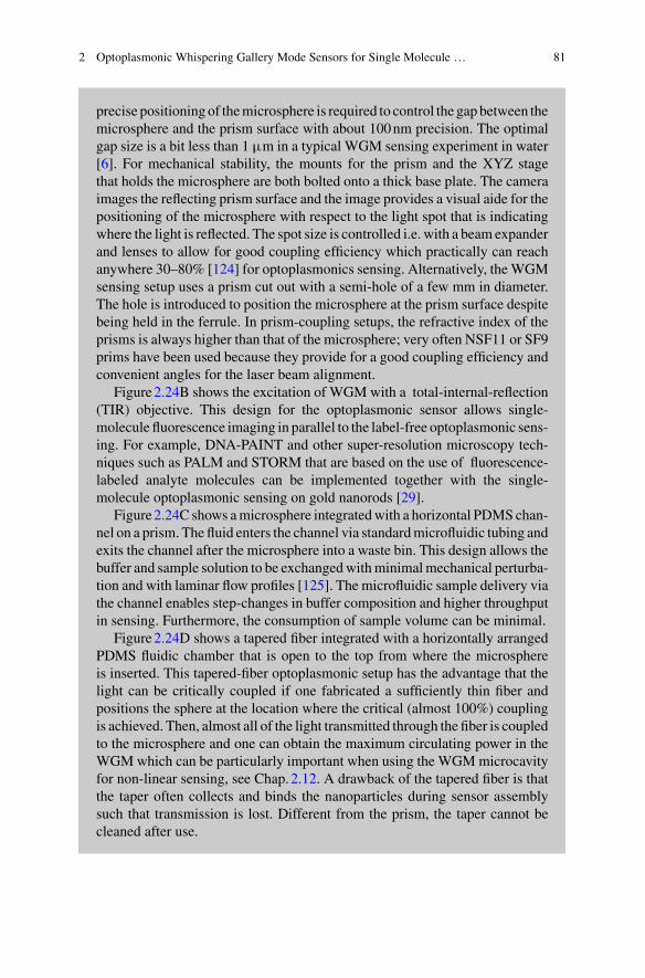
2 Optoplasmonic Whispering Gallery Mode Sensors for Single Molecule … 81
precise positioningof themicrosphere is required to control the gapbetween themicrosphere and the prism surface with about 100nm precision. The optimalgap size is a bit less than 1 µm in a typical WGM sensing experiment in water[6]. For mechanical stability, the mounts for the prism and the XYZ stagethat holds the microsphere are both bolted onto a thick base plate. The cameraimages the reflecting prism surface and the image provides a visual aide for thepositioning of the microsphere with respect to the light spot that is indicatingwhere the light is reflected. The spot size is controlled i.e. with a beam expanderand lenses to allow for good coupling efficiency which practically can reachanywhere 30–80% [124] for optoplasmonics sensing. Alternatively, theWGMsensing setup uses a prism cut out with a semi-hole of a few mm in diameter.The hole is introduced to position the microsphere at the prism surface despitebeing held in the ferrule. In prism-coupling setups, the refractive index of theprisms is always higher than that of the microsphere; very often NSF11 or SF9prims have been used because they provide for a good coupling efficiency andconvenient angles for the laser beam alignment.
Figure2.24B shows the excitation of WGMwith a total-internal-reflection(TIR) objective. This design for the optoplasmonic sensor allows single-molecule fluorescence imaging in parallel to the label-free optoplasmonic sens-ing. For example, DNA-PAINT and other super-resolution microscopy tech-niques such as PALM and STORM that are based on the use of fluorescence-labeled analyte molecules can be implemented together with the single-molecule optoplasmonic sensing on gold nanorods [29].
Figure2.24C shows amicrosphere integratedwith a horizontal PDMSchan-nel on a prism. The fluid enters the channel via standardmicrofluidic tubing andexits the channel after the microsphere into a waste bin. This design allows thebuffer and sample solution to be exchangedwithminimalmechanical perturba-tion and with laminar flow profiles [125]. The microfluidic sample delivery viathe channel enables step-changes in buffer composition and higher throughputin sensing. Furthermore, the consumption of sample volume can be minimal.
Figure2.24D shows a tapered fiber integrated with a horizontally arrangedPDMS fluidic chamber that is open to the top from where the microsphereis inserted. This tapered-fiber optoplasmonic setup has the advantage that thelight can be critically coupled if one fabricated a sufficiently thin fiber andpositions the sphere at the location where the critical (almost 100%) couplingis achieved. Then, almost all of the light transmitted through the fiber is coupledto the microsphere and one can obtain the maximum circulating power in theWGMwhich can be particularly important when using the WGMmicrocavityfor non-linear sensing, see Chap. 2.12. A drawback of the tapered fiber is thatthe taper often collects and binds the nanoparticles during sensor assemblysuch that transmission is lost. Different from the prism, the taper cannot becleaned after use.
82 S. Subramanian et al.
2.11 Signal Acquisition and Analysis
The full spectrum of the WGM is obtained using laser scanning. The recorded spec-tra are first processed to obtain a WGM resonance position (λ) and linewidth (κ)using a centroid fitting algorithm [1]. Figure2.25A shows the photodetector voltageobtained using the setups described in the previous section. The x-axis in Fig. 2.25Ais represented in points that can be easily transformed to the laser frequency usinga simple scaling factor obtained previously using a wavemeter for calibration. Typi-cally, a triangular waveform is used to tune the laser wavelength. Either the upscan(as shown in Fig. 2.25A) or the down scan of the triangular waveform can be used totrack the WGM transmission dip (black trace). As seen in the plot, the output powerof the laser varies with the triangular waveform. Hence, a background trace beforecoupling of the WGM is recorded.
First, the position of the WGM transmission dip is found by aligning the res-onator with the coupler and the coupling is optimized. Then, the resonator is movedaway from the coupler using the micrometer stage, and the background (red trace) isrecorded with no coupling. The resonator is moved back to the position of maximumcoupling. The WGM spectra at each sweep are divided by the background to nor-malize the transmission spectrum as shown in Fig. 2.25B. In experiment, the laserpower output fluctuates over time and small differences in voltage can be observedover time (the black trace is recorded 10mins after recording the background redtrace). Hence, after dividing the WGM spectrum by the background, the trace isre-normalized to unity as maximum as shown in Fig. 2.25B (blue trace). Then, the
Fig. 2.25 Illustration of the extraction of the WGM resonance wavelength and FWHM. A Pho-todetector voltage of the WGM transmission (black) measured ≈10min after start of measurementand the background (red) measured before start of measurement. B Renormalization of the WGMspectra using the background to compensate for intensity drifts. C A zoom of the normalized spec-trum and extraction of the mode position and FWHM. Image adapted with permission from Baaskeet al. [1]. Copyright 2016, Rights Managed by Nature Publishing Group
2 Optoplasmonic Whispering Gallery Mode Sensors for Single Molecule … 83
Fig. 2.26 WGM wavelength in fm plotted over the wavelength sweep iteration. Each iterationpoint corresponds to a 20ms time interval. The plot on top has been offset for clarity. The WGMwavelength over time is composed of a slow background drift (due to temperature and pressure),a high frequency noise (corresponding to laser linewidth as indicated by 3σ , bottom trace) andthe single molecule signals (spike-like transitions). The slow background drift is removed by sub-tracting the trace (top) with a filtered version of the signal to obtain the detrended trace (bottom).Image adapted with permission from Baaske et al. [1]. Copyright 2016, Rights Managed by NaturePublishing Group
WGMresonance peak position and linewidth are extracted using a centroid algorithm[1] using a threshold (red, dashed) as shown in the zoom-in of Fig. 2.25C.
A custom Labview (National Instruments Inc., USA) program is used to recordand process the raw WGM spectra and used to track the WGM resonance positionin the PDH lock-in scheme. Once the WGM λ and κ time traces are obtained, thedata is analyzed for peaks using the MATLAB GUI. After extraction of the WGMwavelength and FWHM, time traces as shown in Fig. 2.26 (top) are obtained. TheWGMwavelength is plotted as a function of the sweep iteration. Each iteration pointcorresponds to a 20 ms time interval. The plot on top has been offset for clarity. TheWGMwavelength over time is composed of a slow background drift (due to ambienttemperature and pressure fluctuation [126]), a high-frequency noise (correspondingto laser linewidth as indicated by σ , bottom trace), and the single-molecule signals(spike-like transitions). Hence, drift correction is applied to remove the slowvariationof the resonance position (�λ). The drift of �λ occurs due to the slow variation oftemperature which is typically on the order 0.2 K over the course of the experiment ifthe sample-cell temperature is not actively controlled. In the case of the PDH signal,most of the drift is automatically accounted for by the PID feedback to the laser.However, large amplitude changes in pressure and temperature are still measured bythe error signal.
A first-order Savitzky-Golay filter with a window length (typically 101 points)depending on the sampling rate is applied to the signal. A low pass filtered versionof the time trace (Fig. 2.26 blue trace) is obtained upon filtering. Then, the low-passfiltered trace (blue) is subtracted from the original time trace to obtain the detrendedtrace as shown in Fig. 2.26 (bottom). Now, only the random noise remains which canbe quantified as the minimum standard deviation σ of the time trace. Any transitionsin the detrended trace with magnitude above a level of 3σ as marked by the orangebounds (bottom trace) are considered as the signal for further peak analysis.
84 S. Subramanian et al.
A peak detection algorithm based on either the MATLAB function f indpeaks isused to find the �λ values corresponding to single-molecule events. The ‘spike’ liketransitions seen in Fig. 2.27A is defined as the signals. Hence, the signal is similar tothe noise but has a higher amplitude. We quantify as signal peaks, all ‘spikes’ withamplitude higher than 3 − 5σ (the standard deviation of the background). The valueof σ is evaluated by dividing the WGM time trace into windows of N points andevaluating the standard deviation of each N -point window. The minimum value ofthe standard deviation obtained is taken as the σ of the background. Typically, thevalue is 0.4–0.5 fm. Then, the threshold of detecting peaks using f indpeaks is cho-sen manually between 3 − 5σ . Figure2.27B shows the peaks detected in a segmentof the WGM time trace. The triangles show all the individual peaks detected abovethe threshold. The detected peaks are then classified into single-molecule ‘events’.A single molecule ‘event’ defines the set of signal peaks that belong to one setof interactions (one enzyme-substrate interaction in our case). The detected peaksare coalesced into ‘events’ using the nearest neighbor search based on a groupingthreshold. Essentially, any consecutive peaks within a time separation of τ are coa-lesced into one single-molecule ‘event’. The grouping threshold τ used in this work isbetween 50–150ms. Figure2.27C shows the peaks detected from Fig. 2.27B groupedinto single-molecule events using τ = 50 ms. Further, single-molecule events cancontain sub-domains. These are extracted by using a smaller grouping thresholdof 10–30ms (Fig. 2.27D). The signal peaks likely indicate the conformational fluc-tuations of the enzyme after substrate binding as described in the manuscript. Thesource code of theGUI can be obtained fromhttps://github.com/ssubram905/WGM_DataAnalysis.git.
2.12 Outlook
For optoplasmonic sensors to find more widespread use, a more versatile sensorsetup is needed; one that allows for the multiplexed detection of biomarkers in par-allel. This platform could use microspheres fabricated by one of the glass meltingtechniques or by the sol-gel synthesis approaches, see Sect. 2.5. Fabricated in bulk,the free-floating glass microspheres could then be aligned in a microfluidic channelintegrated on a suitable prism coupling device. The assembly and disassembly of thearray of microspheres could be controlled by actuating flow, or by pressing/releasingmicrospheres via suitable air channels that are integrated as the control channelstogether with the fluidic channels in the same PDMS structure [127]. The micro-spheres could be fabricated in batches; they could be batch-functionalized withdifferent biorecognition elements such as antibodies, aptamers, or proteins; for thespecific detection of important biomarkers such as viral biomarkers [128]. Imag-ing the light scattered by each one of the microspheres as the laser wavelength istuned across the WGM resonances could enable a parallel readout. Detecting theWGM spectra from the scattered light is furthermore a suitable, nearly background-free approach when the coupling efficiency is low. To couple many microspheres inparallel, the prism coupler could be replaced by a slab waveguide coupler.
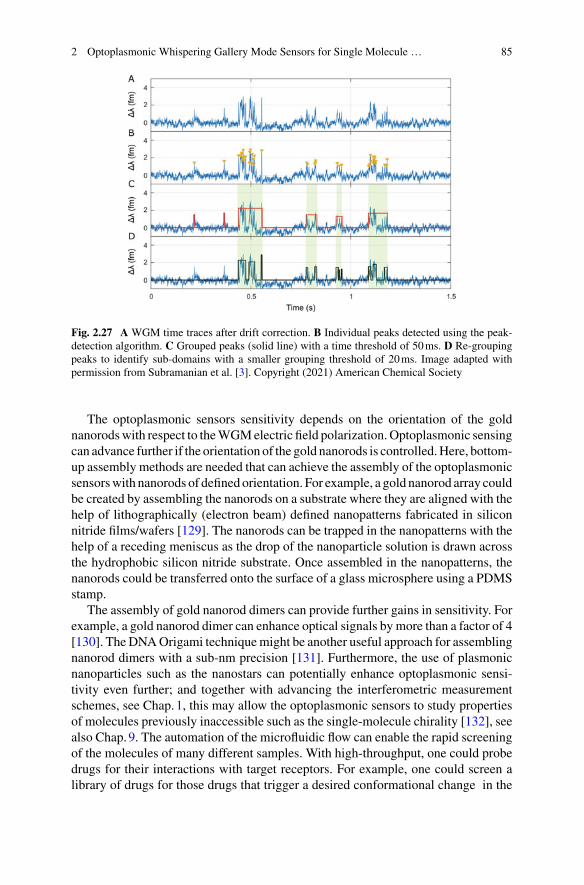
2 Optoplasmonic Whispering Gallery Mode Sensors for Single Molecule … 85
Fig. 2.27 A WGM time traces after drift correction. B Individual peaks detected using the peak-detection algorithm. C Grouped peaks (solid line) with a time threshold of 50ms. D Re-groupingpeaks to identify sub-domains with a smaller grouping threshold of 20ms. Image adapted withpermission from Subramanian et al. [3]. Copyright (2021) American Chemical Society
The optoplasmonic sensors sensitivity depends on the orientation of the goldnanorodswith respect to theWGMelectric field polarization.Optoplasmonic sensingcan advance further if the orientation of the gold nanorods is controlled.Here, bottom-up assembly methods are needed that can achieve the assembly of the optoplasmonicsensorswith nanorods of definedorientation. For example, a gold nanorod array couldbe created by assembling the nanorods on a substrate where they are aligned with thehelp of lithographically (electron beam) defined nanopatterns fabricated in siliconnitride films/wafers [129]. The nanorods can be trapped in the nanopatterns with thehelp of a receding meniscus as the drop of the nanoparticle solution is drawn acrossthe hydrophobic silicon nitride substrate. Once assembled in the nanopatterns, thenanorods could be transferred onto the surface of a glass microsphere using a PDMSstamp.
The assembly of gold nanorod dimers can provide further gains in sensitivity. Forexample, a gold nanorod dimer can enhance optical signals by more than a factor of 4[130]. TheDNAOrigami techniquemight be another useful approach for assemblingnanorod dimers with a sub-nm precision [131]. Furthermore, the use of plasmonicnanoparticles such as the nanostars can potentially enhance optoplasmonic sensi-tivity even further; and together with advancing the interferometric measurementschemes, see Chap.1, this may allow the optoplasmonic sensors to study propertiesof molecules previously inaccessible such as the single-molecule chirality [132], seealso Chap.9. The automation of the microfluidic flow can enable the rapid screeningof the molecules of many different samples. With high-throughput, one could probedrugs for their interactions with target receptors. For example, one could screen alibrary of drugs for those drugs that trigger a desired conformational change in the
86 S. Subramanian et al.
target receptor. Here, the target receptor could be one of the G-protein coupled recep-tors (GPCR). Approximately 35% of approved drugs target GPCRs [133]. Screeningfor allosteric drugs [134] can help the pharmaceutical industry with developing drugsthat have higher efficacy and fewer side effects.
Further, an optoplasmonic sensor with automated microfluidics and data acqui-sition, real-time signal analysis and sensor feedback could greatly facilitate thefundamental single-molecule studies. Programming of the microfluidic flow wouldenable the automated bottom-up optoplasmonic sensor assembly. Automated single-molecule measurement protocols could facilitate the repetitive measurement cyclesand the implementation of more complicated flow profiles including concentrationgradients.
The magnitude and temporal characteristics of the sensor signals contain impor-tant information about microscopic dynamics and the identity of molecular speciespresent in the sensing volume. More sophisticated signal-analysis methods will beneeded as more complex biomolecular systems are probed. Analysis methods areneeded that can scrutinized the WGM sensor signals for all of the information thatthey carry about the molecular process. The signal analysis might be customized forthe specific signal shapes and patterns associated with the biomolecular process. Forexample, some of our initial results indicate that the turnover of substrate moleculesby hinge-bending enzymes such as the phosphoglycerate kinase enzyme PGK pro-duces a characteristic double-peak sensor signal. The double-peak signals may be fitby two Gaussian line profiles to scrutinize the fitting parameters for the informationthey contain about the molecular aspects of the enzymatic reaction. With improvedcontrol over the orientation of an enzyme on the gold nanorod, [3], reproducible sen-sor signals (with reproducible amplitude levels and/or overall signal patterns) can beobserved and this could be used to identify some of the (conformational) sub-states asthey are accessed by enzymes or molecular motors [135]. The predictive capabilitiesof molecular dynamics (MD) simulations could be combined with electromagneticsimulations of the optoplasmonic sensor response. A coarse-grained MD model ofa protein combined with the simulation of the corresponding optoplasmonic sen-sor signal might allow the full reconstruction of the 3D movements; a first steptowards reconstructing molecular movies from the optoplasmonic sensor measure-ments. Reconstructing the full 3D movements of enzymes and nanomachines couldbe aided by the use of the near-field of an optoplasmonic sensor that could be used toprobe different parts of the enzyme/nanomachine. By recording sensor signals withlasers operating at different wavelengths one could probe different volume sectionsof an enzyme/nanomachine for itsmovements. This is possible since the decay lengthof the plasmonic near-field is proportional to the wavelength of the probing light.By exciting WGM in the VIS to near-IR, one could ’scan’ the detection volume ona nanometer length scale to obtain sensor signals that contain complementary spa-tial information about the dynamics of a biomolecular process. Importantly in thiscontext, it has been shown that the optoplasmonic single-molecule signals can beobtained even far-detuned from the plasmon resonance [17].
More advanced signal analysis of the signal patternsmay be needed, one that iden-tifies the principal components that may vary slightly because of the internal degreesof freedom of the enzyme/nanomachine. A wavelet-based algorithm, suitable for de-
2 Optoplasmonic Whispering Gallery Mode Sensors for Single Molecule … 87
noising aperiodic streaming data, could be applied. Combinedwith the high samplingrate (up to MHz) of the optoplasmonic sensor, the wavelet-based signal processingmethodology could enable the real-time detection of the principal components. Fur-thermore, the real-time (microsecond) signal analysis on field-programmable gatearrays could be used for the real-time control of an enzyme’s activity. A feedbackloop that controls the enzyme activity could be implemented for example by therapid heating/cooling of the gold nanorod the enzyme is attached to. In this way, itmay become possible to control synthetic biomolecular processes where one steersthe enzyme such as a polymerase along its reaction pathway to achieve specificbiochemical outcomes. Controlling the synthesis of complex enzymes such as poly-merases could become useful for example for the on-demand de novo synthesis ofDNA strands.
In the future, the optoplasmonic sensor with its high detection sensitivity andspeed could be used to probe biomolecular dynamics and properties that have beendifficult to accesswith other single-molecule techniques. For example,more complexbiomaterial systems could be probed such as those that are based on membranes.Lipid membranes could be coated around the plasmonic nanoparticle [136] or theycould be deposited by fusing lipid vesicles onto themicrosphere sensor at the locationof the plasmon enhancer. Binding entire synthetic cells to the sensors may enableus to study the transport of small molecules across passive and active membranechannels. Single-molecule sensing of membranes might also provide the opportunityfor combining or complementing the optoplasmonic sensing capabilities with thoseof the nanopore sensors, see Chaps. 10–13. Combining optoplasmonic sensing withother single-molecule techniques can broaden the applications of the technique. Oneidea is to combine the optoplasmonic sensor with the optical tweezer technique, seealso Chaps. 7 and 8. One could use the plasmonic hotspot of the nanoparticle toexert the optical trapping forces on a protein, i.e. plasmonic tweezer. If successful,the optoplasmonic tweezer could apply very small, femtonewton (fN) forces tomake some conformational states of an enzyme more likely than others, and thiscould be used to control enzymatic activity. The optoplasmonic force sensor couldthen detect fN forces of enzymes through the application of the minute counter-acting optoplasmonic tweezer forces which affect the enzyme movement/function.Furthermore, the combination of the optoplasmonic sensing with the DNA-Painttechnique [29] and with other super-resolved microscopies may provide a powerfulplatform for combining high-resolution sensing and imaging of biomolecular processsuch as those of biomolecular motors. Separating the molecular signals that originatefrom the optical force from the signals due to any temperature changes will be oneof the challenges.
Spectroscopy could be added to optoplasmonic sensing. An amplitude-modulatedpump beam could be used to cause vibrations of the protein due to electrostrictiveforces caused by the near-field of the plasmonic nanostructure. Alternatively, theinterference of two laser beams could be used to apply the electrostrictive forcesat the frequency of the beat note. This could enable a technique for protein finger-printing by observing the movements of low frequency (GHz) extraordinary acousticRaman (EAR) modes [137], see also Chap.8. Optoplasmonic sensors will be capa-ble of detecting GHz motions of protein domains because, from a time-averaging
88 S. Subramanian et al.
perspective, the spatial overlap of a vibrating protein domain with the probing nearfield is slightly different as compared to the overlap of a static domain. This changein overlap causes the sensor signal to change. A sweep of the amplitude modulationfrequency from 10–100 GHz could provide EAR signals in optoplasmonic spec-troscopy. This may enable a novel approach for the identification of a protein fromits EAR spectrum.
Extracting most information per photon resource will be ideally suited to studybiological samples with minimal perturbation, ultimately probing single moleculeswith single photons. This would allow optoplasmonic sensors to probe a photosen-sitive biomolecule for longer time periods than otherwise possible. This approachcould also make use of quantum-optical measurement techniques. Applied to opto-plasmonic single-molecule sensing, one could achieve the highest possible sensitivityper photon budget [138].
Ensemble measurements of nanoparticles do not provide a detailed understand-ing of how nanoparticle’s size and composition affect the activity and selectivityof a reaction occurring at their catalytic surface. Also, it is important to track thecatalyst surface changes and dynamics of reactions occurring at the surface. Thesesurface changes are asynchronous, which are difficult to characterize in ensemblemeasurements. The choice of nanoparticles on optoplasmonic sensors that catalyzeinorganic/organic reactions can provide a window into observing those catalytic pro-cesses that have evaded a more detailed analysis, such as the catalytic reactions ofsingle enzymes, nanozymes, metal nanoclusters, and the analysis of low-yield reac-tion pathways that usually go undetected in bulk measurements. The optoplasmonicsensor system couldmake contributions to the analysis of these nano chemical events,events that occur at the location of single atoms and molecules and that occur un-synchronized and sporadically in time. Preparing the suitable nanoparticles on thesensor will be one of the challenges to overcome.
To date, the optoplasmonic single-molecule sensing capability has not been com-mercialized. One way to approach the development of a commercial optoplasmonicsensor platform could be to design throw-away PDMS sample cells that include themicrospheres in a fluidic channel on a glass substrate and that are mounted on a sta-tionaryWGM reader i.e. with a prism coupler. The plasmonic nanostructure/particle-coupledmicrospheres could be fabricated to scale in bulk,with customized plasmonicnanoparticles and surface functionalities. The microsphere sensors could even con-tain a laser-barcode to identify each one of the different sensing spheres and itssurface functionalities [139]. Another approach to commercializing the optoplas-monic sensor platform could make use of the fabrication method shown in Fig. 18.Plasmonic nanostructure arrays could be fabricated on a planar substrate that is thencombined with the microspheres. With a potential for attomolar single-moleculedetection capabilities, the possibility for multiplexed sensing, and automated sam-ple analysis, optoplasmonic sensors could provide for extremely sensitive nanosen-sors that quickly and accurately detect novel viruses, identify critical health-relatedbiomarkers, and uncover harmful toxins in your drinking water.
In closing, we hope that this manual on optoplasmonic single-molecule sensingwill facilitate the uptake of the technique as a research tool. The authors hope thisbook chapter will inspire many new single-molecule optoplasmonic experiments,
2 Optoplasmonic Whispering Gallery Mode Sensors for Single Molecule … 89
together with new optoplasmonic sensor instrumentations and the development ofnew optoplasmonic detection modalities. We hope that this book chapter is a usefulguide for implementing the optoplasmonic sensor and sensing technique in the labo-ratory. For a more general discussion of the physics of the optical whispering gallerymodes and their applications in sensing, we refer the reader to [4].
Acknowledgements We thank Dr Hsin-Yu Wu and Dr Samir Vartabi Kashanian for contributingto Fig. 2.24. FV acknowledges funding from EPSRC EP/R031428/1 and EP/T002875/1 and fromthe Royal Society (Wolfson Research Merit Award).
References
1. Martin D. Baaske and Frank Vollmer. Optical observation of single atomic ions interactingwith plasmonic nanorods in aqueous solution. Nature Photonics, 10(11):733–739, 2016.
2. Matthew R. Foreman, Jon D. Swaim, and Frank Vollmer. Whispering gallery mode sensors.Advances in Optics and Photonics, 7(2):168, jun 2015.
3. Sivaraman Subramanian, Hannah B.L. Jones, Simona Frustaci, Samuel Winter, Marc W.van der Kamp, Vickery L. Arcus, Christopher R. Pudney, and Frank Vollmer. Sensing enzymeactivation heat capacity at the single-molecule level using gold-nanorod-based optical whis-pering gallery modes. ACS Applied Nano Materials, 2021.
4. Frank Vollmer and Deshui Yu. Optical Whispering Gallery Modes for Biosensing: FromPhysical Principles to Applications. Springer International Publishing, Cham, 2020.
5. F.Vollmer,D.Braun,A.Libchaber,M.Khoshsima, I. Teraoka, andS.Arnold. Protein detectionby optical shift of a resonant microcavity. Applied Physics Letters, 80(21):4057–4059, may2002.
6. Matthew R Foreman, Wei-Liang Jin, and Frank Vollmer. Optimizing detection limits in whis-pering gallery mode biosensing. Optics express, 22(5):5491–511, 2014.
7. Irene Ament, Janak Prasad, Andreas Henkel, Sebastian Schmachtel, and Carsten Sönnichsen.Single Unlabeled Protein Detection on Individual Plasmonic Nanoparticles. Nano Letters,12(2):1092–1095, feb 2012.
8. Peter Zijlstra, Pedro M.R. Paulo, and Michel Orrit. Optical detection of single non-absorbingmolecules using the surface plasmon resonance of a gold nanorod. Nature Nanotechnology,7(6):379–382, 2012.
9. Adam B. Taylor and Peter Zijlstra. Single-Molecule Plasmon Sensing: Current Status andFuture Prospects. ACS Sensors, 2(8):1103–1122, aug 2017.
10. FVollmer, SArnold, andDKeng. Single virus detection from the reactive shift of awhispering-gallery mode. Proceedings of the National Academy of Sciences of the United States of Amer-ica, 105(52):20701–20704, 2008.
11. S. Arnold, R. Ramjit, D. Keng, V. Kolchenko, and I. Teraoka. MicroParticle photophysicsilluminates viral bio-sensing. Faraday Discuss., 137:65–83, 2008.
12. Linbo Shao, Xue-Feng Jiang, Xiao-Chong Yu, Bei-Bei Li, William R. Clements, FrankVollmer, Wei Wang, Yun-Feng Xiao, and Qihuang Gong. Detection of Single Nanopar-ticles and Lentiviruses Using Microcavity Resonance Broadening. Advanced Materials,25(39):5616–5620, oct 2013.
13. Miguel A. Santiago-Cordoba, Svetlana V. Boriskina, Frank Vollmer, and Melik C. Demirel.Nanoparticle-based protein detection by optical shift of a resonant microcavity. AppliedPhysics Letters, 99(7):073701, 2011.
14. Serge Vincent, Sivaraman Subramanian, and Frank Vollmer. Optoplasmonic characterisa-tion of reversible disulfide interactions at single thiol sites in the attomolar regime. NatureCommunications, 11(1):2043, dec 2020.
90 S. Subramanian et al.
15. EugeneKim,MartinDBaaske, Isabel Schuldes, Peter SWilsch, andFrankVollmer. Label-freeoptical detection of single enzyme-reactant reactions and associated conformational changes.Science Advances, 3(3):e1603044, mar 2017.
16. MartinDBaaske,MatthewRForeman, andFrankVollmer. Single-molecule nucleic acid inter-actions monitored on a label-free microcavity biosensor platform. Nature Nanotechnology,9(August):1–7, 2014.
17. Feng Liang, Yuzheng Guo, Shaocong Hou, and Qimin Quan. Photonic-plasmonic hybridsingle-molecule nanosensormeasures the effect of fluorescent labels on dna-protein dynamics.Science Advances, 3(5), 2017.
18. Frank Vollmer, Stephen Arnold, and David Keng. Single virus detection from the reac-tive shift of a whispering-gallery mode. Proceedings of the National Academy of Sciences,105(52):20701–20704, 2008.
19. S Arnold, M Khoshsima, I Teraoka, S Holler, and F Vollmer. Shift of whispering-gallerymodes in microspheres by protein adsorption. Optics letters, 28(4):272–274, 2003.
20. Iwao Teraoka and Stephen Arnold. Theory of resonance shifts in TE and TM whisperinggallery modes by nonradial perturbations for sensing applications. Journal of the OpticalSociety of America B, 23(7):1381, jul 2006.
21. Ulrich Hohenester and Andreas Trügler. MNPBEM - A Matlab toolbox for the simulation ofplasmonic nanoparticles. Computer Physics Communications, 183(2):370–381, feb 2012.
22. S. Arnold, D. Keng, S. I. Shopova, S. Holler,W. Zurawsky, and F. Vollmer.Whispering gallerymode carousel – a photonic mechanism for enhanced nanoparticle detection in biosensing.Opt. Express, 17(8):6230–6238, Apr 2009.
23. Miguel A. Santiago-Cordoba, Murat Cetinkaya, Svetlana V. Boriskina, Frank Vollmer, andMelik C. Demirel. Ultrasensitive detection of a protein by optical trapping in a photonic-plasmonic microcavity. Journal of Biophotonics, 5(8-9):629–638, 2012.
24. Deshui Yu and Frank Vollmer. Allan deviation tells the binding properties in single-moleculesensing with whispering-gallery-mode optical microcavities. Phys. Rev. Research, 3:023087,May 2021.
25. Sivaraman Subramanian, Serge Vincent, and Frank Vollmer. Effective linewidth shifts insingle-molecule detection using optical whispering gallery modes. Applied Physics Letters,117(15):151106, oct 2020.
26. Lina He, Sahin Kaya Özdemir, Jiangang Zhu, Faraz Monifi, Huzeyfe Yılmaz, and Lan Yang.Statistics of multiple-scatterer-induced frequency splitting in whispering gallery microres-onators and microlasers. New Journal of Physics, 15(7):073030, jul 2013.
27. D. Keng, X. Tan, and S. Arnold. Whispering gallery micro-global positioning system fornanoparticle sizing in real time. Applied Physics Letters, 105(7), 2014.
28. Eugene Kim, Martin D. Baaske, and Frank Vollmer. In Situ Observation of Single-MoleculeSurface Reactions from Low to High Affinities. Advanced Materials, 28(45):9941–9948,2016.
29. Narima Eerqing, Sivaraman Subramanian, Jesús Rubio, Tobias Lutz, Hsin-Yu Wu, JanetAnders, Christian Soeller, and FrankVollmer. Comparing transient oligonucleotide hybridiza-tion kinetics using dna-paint and optoplasmonic single-molecule sensing on gold nanorods,2021.
30. Marc W. van der Kamp, Erica J. Prentice, Kirsty L. Kraakman, Michael Connolly, Adrian J.Mulholland, and Vickery L. Arcus. Dynamical origins of heat capacity changes in enzyme-catalysed reactions. Nature Communications, 9(1):1177, dec 2018.
31. FrankVollmer andLanYang.ReviewLabel-free detectionwith high-Qmicrocavities: a reviewof biosensing mechanisms for integrated devices. Nanophotonics, 1(3-4):267–291, 2012.
32. Mi Kyoung Park, Jack Sheng Kee, Jessie Yiying Quah, Vivian Netto, Junfeng Song, QingFang, Eric Mouchel La Fosse, and Guo-Qiang Lo. Label-free aptamer sensor based on siliconmicroring resonators. Sensors and Actuators B: Chemical, 176:552–559, 2013.
33. M. Pöllinger, D. O’Shea, F. Warken, and A. Rauschenbeutel. Ultrahigh-Q TunableWhispering-Gallery-ModeMicroresonator.Physical Review Letters, 103(5):053901, jul 2009.
2 Optoplasmonic Whispering Gallery Mode Sensors for Single Molecule … 91
34. Amy Watkins, Jonathan Ward, Yuqiang Wu, and Síle Nic Chormaic. Single-input sphericalmicrobubble resonator. Optics letters, 36(11):2113–2115, 2011.
35. YunboGuo, Hao Li, Karthik Reddy, Hrishikesh S. Shelar, Vasuki R. Nittoor, and Xudong Fan.Optofluidic Fabry-Pérot cavity biosensor with integrated flow-through micro-/nanochannels.Applied Physics Letters, 98(4):041104, jan 2011.
36. Michael Trupke, Edward A Hinds, S Eriksson, EA Curtis, Zakaria Moktadir, ElenaKukharenka, andMichael Kraft. Microfabricated high-finesse optical cavity with open accessand small volume. Applied Physics Letters, 87(21):211106, 2005.
37. Mindy Lee and PhilippeM. Fauchet. Two-dimensional silicon photonic crystal based biosens-ing platform for protein detection. Opt. Express, 15(8):4530–4535, Apr 2007.
38. Giancarlo C Righini and Silvia Soria. Biosensing by WGM microspherical resonators. Sen-sors, 16(6):905, 2016.
39. K J Vahala. Optical microcavities. Nature, 424(6950):839–846, 2003.40. Kiyotaka Miura, Koichiro Tanaka, and Kazuyuki Hirao. CW laser oscillation on both the
3/2-11/2 and 3/2-13/2 transitions of Nd3+ ions using a fluoride glass microsphere. Journal ofNon-Crystalline Solids, 213-214:276–280, may 1997.
41. Ioan Bica. Formation of glass microspheres with rotating electrical arc. Materials Scienceand Engineering: B, 77(2):210–212, 2000.
42. Jibo Yu, Elfed Lewis, Gerald Farrell, and Pengfei Wang. Compound glass microsphere res-onator devices. Micromachines, 9(7), 2018.
43. KerryAWilson,CraigAFinch, PhillipAnderson, FrankVollmer, and James JHickman.Whis-pering gallery mode biosensor quantification of fibronectin adsorption kinetics onto alkylsi-lane monolayers and interpretation of resultant cellular response. Biomaterials, 33(1):225–236, 2012.
44. Carol E Soteropulos, Heather K Hunt, and Andrea M Armani. Determination of bindingkinetics usingwhispering gallerymodemicrocavities.Applied physics letters, 99(10):103703,2011.
45. NiranjanM.Hanumegowda, Caleb J. Stica, Bijal C. Patel, IanWhite, andXudong Fan. Refrac-tometric sensors based on microsphere resonators. Applied Physics Letters, 87(20):201107,nov 2005.
46. Julie Lutti, Wolfgang Langbein, and Paola Borri. A monolithic optical sensor basedon whispering-gallery modes in polystyrene microspheres. Applied Physics Letters,93(15):151103, 2008.
47. Julie Lutti, Wolfgang Langbein, and Paola Borri. High Q optical resonances of polystyrenemicrospheres inwater controlled by optical tweezers.Applied Physics Letters, 91(14):141116,oct 2007.
48. Vladimir S Ilchenko,XSteveYao, andLuteMaleki. Pigtailing the high-qmicrosphere cavity:?a simple fiber coupler for optical whispering-gallery modes. Optics letters, 24(11):723–725,1999.
49. Vladimir S Ilchenko and Andrey B Matsko. Optical resonators with whispering-gallerymodes-part ii: applications. IEEE Journal of selected topics in quantum electronics, 12(1):15–32, 2006.
50. Heather K Hunt, Carol Soteropulos, and Andrea M Armani. Bioconjugation strategies formicrotoroidal optical resonators. Sensors, 10(10):9317–9336, 2010.
51. Lina He, Sahin Kaya Özdemir, Jiangang Zhu, Woosung Kim, and Lan Yang. Detecting sin-gle viruses and nanoparticles using whispering gallery microlasers. Nature Nanotechnology,6(7):428–432, 2011.
52. Tao Lu, Hansuek Lee, Tong Chen, Steven Herchak, Ji-Hun Kim, Scott E Fraser, Richard CFlagan, and Kerry Vahala. High sensitivity nanoparticle detection using optical microcavities.Proceedings of the National Academy of Sciences, 108(15):5976–5979, 2011.
53. Lina He, Sahin Kaya Özdemir, Jiangang Zhu, and Lan Yang. Ultrasensitive detection of modesplitting in active optical microcavities. Physical Review A, 82(5):053810, 2010.
54. Muzammil Iqbal,Martin AGleeson, Bradley Spaugh, Frank Tybor,WilliamGGunn,MichaelHochberg, Tom Baehr-Jones, Ryan C Bailey, and L Cary Gunn. Label-free biosensor arraysbased on silicon ring resonators and high-speed optical scanning instrumentation. IEEE Jour-nal of selected topics in quantum electronics, 16(3):654–661, 2010.
92 S. Subramanian et al.
55. Camille Delezoide, Marion Salsac, Joseph Lautru, Hervé Leh, Claude Nogues, Joseph Zyss,Malcolm Buckle, Isabelle Ledoux-Rak, and Chi Thanh Nguyen. Vertically coupled polymermicroracetrack resonators for label-free biochemical sensors. IEEE Photonics TechnologyLetters, 24(4):270–272, 2011.
56. A. Ksendzov and Y. Lin. Integrated optics ring-resonator sensors for protein detection. OpticsLetters, 30(24):3344, 2005.
57. AycaYalcin, Ketul C Popat, JohnCAldridge, Tejal ADesai, JohnHryniewicz, Nabil Chbouki,Brent E Little, Oliver King, Vien Van, Sai Chu, et al. Optical sensing of biomolecules usingmicroring resonators. IEEE Journal of Selected Topics in Quantum Electronics, 12(1):148–155, 2006.
58. Tom Claes, Jordi Girones Molera, Katrien De Vos, Etienne Schacht, Roel Baets, and PeterBienstman. Label-free biosensing with a slot-waveguide-based ring resonator in silicon oninsulator. IEEE Photonics journal, 1(3):197–204, 2009.
59. Arthur Nitkowski, Antje Baeumner, and Michal Lipson. On-chip spectrophotometry for bio-analysis using microring resonators. Biomedical optics express, 2(2):271–277, 2011.
60. JohnTGohring, Paul SDale, andXudongFan.Detectionof her2breast cancer biomarker usingthe opto-fluidic ring resonator biosensor. Sensors and Actuators B: Chemical, 146(1):226–230, 2010.
61. Ian M White, Hesam Oveys, and Xudong Fan. Liquid-core optical ring-resonator sensors.Optics letters, 31(9):1319–1321, 2006.
62. Robert W Boyd and John E Heebner. Sensitive disk resonator photonic biosensor. Appliedoptics, 40(31):5742–5747, 2001.
63. Aaron Schweinsberg, Sandrine Hocdé, Nick N Lepeshkin, Robert W Boyd, ChristopherChase, and Julie E Fajardo. An environmental sensor based on an integrated optical whis-pering gallery mode disk resonator. Sensors and Actuators B: Chemical, 123(2):727–732,2007.
64. Elliot J Smith, Sabine Schulze, Suwit Kiravittaya, Yongfeng Mei, Samuel Sanchez, andOliver G Schmidt. Lab-in-a-tube: detection of individual mouse cells for analysis in flexi-ble split-wall microtube resonator sensors. Nano letters, 11(10):4037–4042, 2011.
65. Stefan M Harazim, Vladimir A Bolaños Quiñones, Suwit Kiravittaya, Samuel Sanchez, andOliver G Schmidt. Lab-in-a-tube: on-chip integration of glass optofluidic ring resonators forlabel-free sensing applications. Lab on a Chip, 12(15):2649–2655, 2012.
66. Rico Henze, Tom Seifert, Jonathan Ward, and Oliver Benson. Tuning whispering gallerymodes using internal aerostatic pressure. Optics letters, 36(23):4536–4538, 2011.
67. Jacob Scheuer andMikhail Sumetsky. Optical-fiber microcoil waveguides and resonators andtheir applications for interferometry and sensing. Laser & Photonics Reviews, 5(4):465–478,2011.
68. Fei Xu, Peter Horak, and Gilberto Brambilla. Optical microfiber coil resonator refractometricsensor. Optics express, 15(12):7888–7893, 2007.
69. FrankVollmer andPeer Fischer.Ring-resonator-based frequency-domain optical activitymea-surements of a chiral liquid. Optics letters, 31(4):453–455, 2006.
70. David A Bergstein, Emre Ozkumur, Arthur C Wu, Ayca Yalcin, Jeremy R Colson, James WNeedham, Rostem J Irani, Jonathan M Gershoni, Bennett B Goldberg, Charles DeLisi, et al.Resonant cavity imaging: Ameans toward high-throughput label-free protein detection. IEEEJournal of Selected Topics in Quantum Electronics, 14(1):131–139, 2008.
71. Sudeep Mandal, Julie M Goddard, and David Erickson. A multiplexed optofluidic biomolec-ular sensor for low mass detection. Lab on a Chip, 9(20):2924–2932, 2009.
72. Lefevreseguin Collot, V Lefevre-Seguin, M Brune, JM Raimond, and S Haroche. Very high-q whispering-gallery mode resonances observed on fused silica microspheres. EPL (Euro-physics Letters), 23(5):327, 1993.
73. Pham Van Hoi, Chu Thi Thu Ha, and Hoang Quang Hung. Long-band emission of micro-sphere lasers based on erbium-doped sol-gel silica-alumina glasses. Applied Physics Letters,87(16):161110, 2005.
2 Optoplasmonic Whispering Gallery Mode Sensors for Single Molecule … 93
74. Lu Cai, Junyao Pan, Yong Zhao, Jin Wang, and Shiyuan Xiao. Whispering Gallery ModeOptical Microresonators: Structures and Sensing Applications. physica status solidi (a),217(6):1900825, mar 2020.
75. D. Ristic, V. Holý, M. Ivanda, M. Marciuš, M. Buljan, O. Gamulin, K. Furic, M. Ristic,S. Music, M. Mazzola, A. Chiasera, M. Ferrari, and G.C. Righini. Surface characterization ofthin silicon-rich oxide films. Journal of Molecular Structure, 993(1-3):214–218, may 2011.
76. Shancheng Yang, Yue Wang, and Handong Sun. Advances and prospects for whisperinggallery mode microcavities. Advanced Optical Materials, 3(9):1136–1162, 2015.
77. Davor Ristic,Mile Ivanda, Giorgio Speranza, Zdravko Siketic, Ivancica Bogdanovic-Radovic,Marijan Marciuš, Mira Ristic, Ozren Gamulin, Svetozar Music, Krešimir Furic, Giancarlo CRighini, and Maurizio Ferrari. Local Site Distribution of Oxygen in Silicon-Rich OxideThin Films: A Tool to Investigate Phase Separation. The Journal of Physical Chemistry C,116(18):10039–10047, may 2012.
78. GuanyuLi, Pei Liu,Xiaoshun Jiang, ChaoYang, JiyangMa,HongyaWu, andMinXiao.High-Q silica microdisk optical resonators with large wedge angles on a silicon chip. PhotonicsResearch, 3(5):279, oct 2015.
79. Zuo Feng, Yuming He, Wei Yan, Fuhua Yang, Weihua Han, and Zhaofeng Li. Progress ofwaveguide ring resonators used in micro-optical gyroscopes. Photonics, 7(4):1–16, 2020.
80. G. Kakarantzas, T. E. Dimmick, T. A. Birks, R. Le Roux, and P. St. J. Russell. Minia-ture all-fiber devices based on C O2 laser microstructuring of tapered fibers. Optics Letters,26(15):1137, aug 2001.
81. Ganapathy SenthilMurugan, James S.Wilkinson, andMichalisN. Zervas. Selective excitationof whispering gallery modes in a novel bottle microresonator. Optics Express, 17(14):11916,jul 2009.
82. G. C. Righini, Y. Dumeige, P. Féron, M. Ferrari, G. Nunzi Conti, D. Ristic, and S. Soria.WhisperingGalleryModemicroresonators: Fundamentals and applications.Rivista del NuovoCimento, 34(7):435–488, 2011.
83. D K Armani, T J Kippenberg, S M Spillane, and K J Vahala. Ultra-high-Q toroid microcavityon a chip. Nature, 421(6926):925–928, 2003.
84. Xuefeng Jiang, Abraham J. Qavi, Steven H. Huang, and Lan Yang. Whispering-Gallery Sen-sors. Matter, 3(2):371–392, aug 2020.
85. Mark Lawrence, David R. Barton, Jefferson Dixon, Jung-Hwan Song, Jorik van de Groep,MarkL.Brongersma, and JenniferA.Dionne.Highquality factor phase gradientmetasurfaces.Nature Nanotechnology, 15(11):956–961, nov 2020.
86. E. Gavartin, P. Verlot, and T. J. Kippenberg. A hybrid on-chip optomechanical transducer forultrasensitive force measurements. Nature Nanotechnology, 7(8):509–514, 2012.
87. T. Wienhold, S. Kraemmer, S. F. Wondimu, T. Siegle, U. Bog, U. Weinzierl, S. Schmidt,H.Becker,H.Kalt, T.Mappes, S.Koeber, andC.Koos.All-polymer photonic sensing platformbased on whispering-gallery mode microgoblet lasers. Lab on a Chip, 15(18):3800–3806,2015.
88. Xiaolong Xu, Yuanyuan Zhao, Xiangdong Xue, Shuaidong Huo, Fei Chen, Guozhang Zou,and Xing Jie Liang. Seedless synthesis of high aspect ratio gold nanorods with high yield.Journal of Materials Chemistry A, 2(10):3528–3535, 2014.
89. Andrés Guerrero-Martínez, Silvia Barbosa, Isabel Pastoriza-Santos, and LuisM. Liz-Marzán.Nanostars shine bright for you. Colloidal synthesis, properties and applications of branchedmetallic nanoparticles. Current Opinion in Colloid and Interface Science, 16(2):118–127,2011.
90. Sara E. Skrabalak, Leslie Au, Xingde Li, and Younan Xia. Facile synthesis of Ag nanocubesand Au nanocages. Nature Protocols, 2(9):2182–2190, 2007.
91. Elcin Dertli, Sahin Coskun, and Emren Nalbant Esenturk. Gold nanowires with high aspectratio and morphological purity: Synthesis, characterization, and evaluation of parameters.Journal of Materials Research, 28(2):250–260, 2013.
94 S. Subramanian et al.
92. Leonardo Scarabelli, Marc Coronado-Puchau, Juan J. Giner-Casares, Judith Langer, andLuis M. Liz-Marzán. Monodisperse gold nanotriangles: Size control, large-scale self-assembly, and performance in surface-enhanced raman scattering. ACS Nano, 8(6):5833–5842, 2014.
93. Yonggang Lu, Haibin Zhang, Fan Wu, Hong Liu, and Jingzhong Fang. Size-tunable uniformgold octahedra: fast synthesis, characterization, and plasmonic properties. RSC Advances,7(30):18601–18608, 2017.
94. G. Frens. Particle size and sol stability in metal colloids. Kolloid-Zeitschrift & Zeitschrift fürPolymere, 250(7):736–741, 1972.
95. John Turkevich, Peter Cooper Stevenson, and James Hillier. A study of the nucleation andgrowth processes in the synthesis of colloidal gold. Discussions of the Faraday Society,11(c):55–75, 1951.
96. Sandeep Ghosh and Liberato Manna. The Many “facets” of Halide Ions in the Chemistry ofColloidal Inorganic Nanocrystals. Chemical Reviews, 118(16):7804–7864, 2018.
97. Luca Guerrini, Ramon A. Alvarez-Puebla, and Nicolas Pazos-Perez. Surface modificationsof nanoparticles for stability in biological fluids. Materials, 11(7):1–28, 2018.
98. Meghana Matur, Harishkumar Madhyastha, T. S. Shruthi, Radha Madhyastha, S. P. Srinivas,P. N. Navya, and Hemant Kumar Daima. Engineering bioactive surfaces on nanoparticles andtheir biological interactions. Scientific Reports, 10(1):1–14, 2020.
99. Zhong Zhang and Mengshi Lin. Fast loading of PEG-SH on CTAB-protected gold nanorods.RSC Advances, 4(34):17760–17767, 2014.
100. Brian Szychowski, Haixu Leng, Matthew Pelton, and Marie Christine Daniel. Controlledetching and tapering of Au nanorods using cysteamine. Nanoscale, 10(35):16830–16838,2018.
101. Xin Shi, HannahL. Perry, and JamesD. E. T.Wilton-Ely. Strategies for the functionalisation ofgold nanorods to reduce toxicity and aid clinical translation.Nanotheranostics, 5(2):155–165,2021.
102. Matthew R. Hauwiller, Xingchen Ye, Matthew R. Jones, Cindy M. Chan, Jason J. Calvin,Michelle F. Crook, Haimei Zheng, and A. Paul Alivisatos. Tracking the Effects of Ligandson Oxidative Etching of Gold Nanorods in Graphene Liquid Cell Electron Microscopy. ACSNano, 14(8):10239–10250, 2020.
103. Qikui Fan, Hao Yang, Juan Ge, Shumeng Zhang, Zhaojun Liu, Bo Lei, Tao Cheng, YouyongLi, Yadong Yin, and Chuanbo Gao. Customizable Ligand Exchange for Tailored SurfaceProperty of Noble Metal Nanocrystals. Research, 2020:1–12, 2020.
104. Chunyu Zhou, Yaocai Bai, Fan Yang, Tao Sun, Liang Zhang, Yuanqing Cai, Tao Gu, Yun Liu,Mingfu Gong, Dong Zhang, and Yadong Yin. Ligand exchange on noble metal nanocrystalsassisted by coating and etching of cuprous oxide. Materials Chemistry Frontiers, 4(6):1614–1622, 2020.
105. David I. Gittins and Frank Caruso. Spontaneous phase transfer of nanoparticulate metals fromorganic to aqueous media. Angewandte Chemie - International Edition, 40(16):3001–3004,2001.
106. Youngjae Lee, Jungwoo Jang, Jinho Yoon, Jeong Woo Choi, Inhee Choi, and Taewook Kang.Phase transfer-driven rapid and complete ligand exchange formolecular assembly of phospho-lipid bilayers on aqueous gold nanocrystals. Chemical Communications, 55(22):3195–3198,2019.
107. E. Metwalli, D. Haines, O. Becker, S. Conzone, and C. G. Pantano. Surface characterizationsof mono-, di-, and tri-aminosilane treated glass substrates. Journal of Colloid and InterfaceScience, 298(2):825–831, 2006.
108. Mojun Zhu, Maria Z. Lerum, and Wei Chen. How To Prepare Reproducible, Homogeneous,and Hydrolytically Stable Aminosilane-Derived Layers on Silica. Langmuir, 28(1):416–423,jan 2012.
109. Thermo Fisher. Chemical Reactivity of Crosslinkers and Modification Reagents. Technicalreport, Thermo Fisher Scientific, 2012.

2 Optoplasmonic Whispering Gallery Mode Sensors for Single Molecule … 95
110. Changhyoup Lee, Frederik Dieleman, Jinhyoung Lee, Carsten Rockstuhl, Stefan A. Maier,and Mark Tame. Quantum Plasmonic Sensing: Beyond the Shot-Noise and Diffraction Limit.ACS Photonics, 3(6):992–999, jun 2016.
111. R. W P Drever, J. L. Hall, F. V. Kowalski, J. Hough, G. M. Ford, a. J. Munley, and H. Ward.Laser phase and frequency stabilization using an optical resonator. Applied Physics B Photo-physics and Laser Chemistry, 31(2):97–105, 1983.
112. Jens M Dobrindt. Bio-sensing using toroidal microresonators & Theoretical cavity optome-chanics. PhD thesis, Ludwig-Maximilians-University of Munich, 2012.
113. JonD. Swaim, JoachimKnittel, andWarwick P. Bowen.Detection limits inwhispering gallerybiosensors with plasmonic enhancement. Applied Physics Letters, 99(24):243109, dec 2011.
114. Jiangang Zhu, Sahin Kaya Ozdemir, Yun-Feng Xiao, Lin Li, Lina He, Da-Ren Chen, and LanYang. On-chip single nanoparticle detection and sizing by mode splitting in an ultrahigh-Qmicroresonator. Nature Photonics, 4(1):46–49, 2010.
115. Marina S. Dietz, S. Sophia Wehrheim, Marie Lena I.E. Harwardt, Hartmut H. Niemann, andMike Heilemann. Competitive Binding Study Revealing the Influence of Fluorophore Labelson Biomolecular Interactions. Nano Letters, 19(11):8245–8249, 2019.
116. Jon D. Swaim, Joachim Knittel, and Warwick P. Bowen. Detection of nanoparticles witha frequency locked whispering gallery mode microresonator. Applied Physics Letters,102(18):2011–2015, 2013.
117. Serge Rosenblum, Yulia Lovsky, Lior Arazi, Frank Vollmer, and Barak Dayan. Cavity ring-up spectroscopy for ultrafast sensing with optical microresonators. Nature Communications,6:6788, 2015.
118. Eric D. Black. An introduction to Pound-Drever-Hall laser frequency stabilization. AmericanJournal of Physics, 69(1):79, 2001.
119. J. C. Knight, G. Cheung, F. Jacques, and T. A. Birks. Phase-matched excitation of whispering-gallery-mode resonances by a fiber taper. Opt. Lett., 22(15):1129–1131, Aug 1997.
120. R Garcia-Fernandez, W Alt, F Bruse, C Dan, K Karapetyan, O Rehband, A Stiebeiner,U Wiedemann, D Meschede, and A Rauschenbeutel. Optical nanofibers and spectroscopy.Applied Physics B, 105(1):3, 2011.
121. Michael L. Gorodetsky and Vladimir S. Ilchenko. Optical microsphere resonators: optimalcoupling to high-Q whispering gallery modes. J. Opt. Soc. Am., 16(1):14, 1998.
122. Jiangang Zhu, Sahin K. Özdemir, Huzeyfe Yilmaz, Bo Peng, Mark Dong, Matthew Tomes,Tal Carmon, and Lan Yang. Interfacing whispering-gallery microresonators and free spacelight with cavity enhanced Rayleigh scattering. Scientific Reports, 4(1):6396, may 2015.
123. ZacharyBallard,MartinD. Baaske, and FrankVollmer. Stand-off biodetectionwith free-spacecoupled asymmetric microsphere cavities. Sensors, 15(4):8968–8980, 2015.
124. Yu A Demchenko, I A Bilenko, and M L Gorodetsky. Optimisation of the prism couplingof optical whispering-gallery-mode microcavities. Quantum Electronics, 47(8):743–747, aug2017.
125. Ying-Jen Chen, Ulrike Schoeler, Chung-Hsuan (Benjamin) Huang, and Frank Vollmer. Com-bining whispering-gallery mode optical biosensors with microfluidics for real-time detectionof protein secretion from living cells in complex media. Small, 14(22):1703705, 2018.
126. Arturo Bianchetti, Alejandro Federico, Serge Vincent, Sivaraman Subramanian, and FrankVollmer. Refractometry-based air pressure sensing using glass microspheres as high-qwhispering-gallery mode microresonators. Optics Communications, 394:152–156, 2017.
127. Jessica Melin and Stephen R. Quake. Microfluidic large-scale integration: The evolutionof design rules for biological automation. Annual Review of Biophysics and BiomolecularStructure, 36(1):213–231, 2007. PMID: 17269901.
128. Nikita Toropov, Eleanor Osborne, Tina Loveleen Joshi, James Davidson, Caitlin Morgan,Joseph Page, Justin Pepperell, and Frank Vollmer. Sars-cov-2 tests: Bridging the gap betweenlaboratory sensors and clinical applications. ACS Sensors 6(8), 2815–2837, 2021.
129. Valentin Flauraud, Massimo Mastrangeli, Gabriel D Bernasconi, Jeremy Butet, Duncan T LAlexander,ElmiraShahrabi,Olivier J FMartin, and JuergenBrugger.Nanoscale topographicalcontrol of capillary assembly of nanoparticles. Nature Nanotechnology, 12(1):73–80, 2017.
96 S. Subramanian et al.
130. Maxim L Nesterov, Xinghui Yin, Martin Schäferling, Harald Giessen, and Thomas Weiss.The Role of Plasmon-Generated Near Fields for Enhanced Circular Dichroism Spectroscopy.ACS Photonics, 3(4):578–583, apr 2016.
131. MengWang, Jinyi Dong, Chao Zhou, Hao Xie, Weihai Ni, ShunWang, Huile Jin, and Qiang-bin Wang. Reconfigurable plasmonic diastereomers assembled by dna origami. ACS Nano,13(12):13702–13708, 2019. PMID: 31550129.
132. Aneeth Kakkanattu, Narima Eerqing, Shahin Ghamari, and Frank Vollmer. Review of opticalsensing and manipulation of chiral molecules and nanostructures with the focus on plasmonicenhancements. Opt. Express, 29(8):12543–12579, Apr 2021.
133. Krishna Sriram and Paul A. Insel. G protein-coupled receptors as targets for approved drugs:How many targets and how many drugs? Molecular Pharmacology, 93(4):251–258, 2018.
134. Cody J. Wenthur, Patrick R. Gentry, Thomas P. Mathews, and Craig W. Lindsley. Drugs forallosteric sites on receptors.Annual Review of Pharmacology and Toxicology, 54(1):165–184,2014. PMID: 24111540.
135. Salma Kassem, Thomas van Leeuwen, Anouk S. Lubbe, Miriam R. Wilson, Ben L. Feringa,and David A. Leigh. Artificial molecular motors. Chem. Soc. Rev., 46:2592–2621, 2017.
136. Joanna L. Richens, Jonathan P. Bramble, Jennifer Bain, and Paul O’Shea. Plasmon-baseddetermination of macromolecular interactions with membrane-encapsulated nanoparticles.In David L. Andrews, Angus J. Bain, Jean-Michel Nunzi, and Andreas Ostendorf, editors,Nanophotonics VII, volume 10672, pages 20 – 35. International Society for Optics and Pho-tonics, SPIE, 2018.
137. Timothy DeWolf and Reuven Gordon. Theory of acoustic raman modes in proteins. Phys.Rev. Lett., 117:138101, Sep 2016.
138. Jolly Xavier, Deshui Yu, Callum Jones, Ekaterina Zossimova, and Frank Vollmer. Quantumnanophotonic and nanoplasmonic sensing: towards quantum optical bioscience laboratorieson chip. Nanophotonics, 10(5):1387–1435, 2021.
139. Nikita Toropov, Gema Cabello, Mariana P Serrano, Rithvik R Gutha, Matías Rafti, and FrankVollmer. Review of biosensing with whispering-gallery mode lasers. Light: Science & Appli-cations, 10(1):42, 2021.
140. J. Xavier, S. Vincent, F. Meder and F. Vollmer (2018) Advances in optoplasmonic sensors–combining optical nano/microcavities and photonic crystals with plasmonic nanostructuresand nanoparticles. Nanophotonics, 7(1), 1–38. De Gruyter.
141. Baaske, Martin D and Foreman, Matthew R and Vollmer, Frank (2014) Single-moleculenucleic acid interactions monitored on a label-free microcavity biosensor platform. Naturenanotechnology, 9(11), 933–939. Nature Publishing Group.
142. Vollmer, Frank and Yang, Lan (2012) Review label-free detection with high-Q microcavities:a review of biosensing mechanisms for integrated devices. Nanophotonics, 1(3–4), 267–291.Walter de Gruyter.
143. Kim, Eugene and Baaske, Martin D and Schuldes, Isabel and Wilsch, Peter S and Vollmer,Frank (2017) Label-free optical detection of single enzyme-reactant reactions and associ-ated conformational changes. Science advances, 3, e1603044. American Association for theAdvancement of Science.
144. Subramanian, Sivaraman, Jones, Hannah BL, Frustaci, Simona, Winter, Samuel, van derKamp, MarcW, Arcus, Vickery L, Pudney, Christopher R and Vollmer, Frank (2021) SensingEnzyme Activation Heat Capacity at the Single-Molecule Level Using Gold-Nanorod-BasedOptical Whispering Gallery Modes. ACS Applied Nano Materials. ACS Publications.
145. Tathyana Tumolo, LucioAngnes andMauricio S. Baptista (2004) Determination of the refrac-tive index increment (dn/dc) of molecule and macromolecule solutions by surface plasmonresonance. Analytical Biochemistry, 333(2), 273–279. 0003-2697. https://doi.org/10.1016/j.ab.2004.06.010.
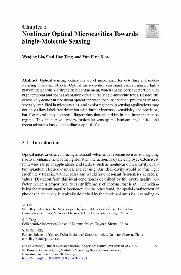
Chapter 3Nonlinear Optical Microcavities TowardsSingle-Molecule Sensing
Wenjing Liu, Shui-Jing Tang, and Yun-Feng Xiao
Abstract Optical sensing techniques are of importance for detecting and under-standing nanoscale objects. Optical microcavities can significantly enhance light-matter interactions via strong field confinement, which enable optical detection withhigh temporal and spatial resolution down to the single-molecule level. Besides theextensively demonstrated linear optical approach, nonlinear optical processes are alsostrongly amplified in microcavities, and exploring them in sensing applications maynot only allow label-free detection with further increased sensitivity and precision,but also reveal unique spectral fingerprints that are hidden in the linear interactionregime. This chapter will review molecular sensing mechanisms, modalities, andrecent advances based on nonlinear optical effects.
3.1 Introduction
Opticalmicrocavities confine light to small volumes by resonant recirculation, givingrise to an enhancement of the light-matter interaction. They are employed extensivelyfor a wide range of applications and studies, such as nonlinear optics, cavity quan-tum quantum electrodynamics, and sensing. An ideal cavity would confine lightindefinitely (that is, without loss) and would have resonant frequencies at precisevalues. Deviation from this ideal condition is described by the cavity quality (Q)factor, which is proportional to cavity lifetime τ of photons, that is Q = ωτ with ω
being the resonant angular frequency. On the other hand, the spatial confinement ofphotons in the cavity is typically described by the mode volume (V ). According to
W. LiuState Key Laboratory for Mesoscopic Physics and Frontiers Science Center forNano-optoelectronics, School of Physics, Peking University, Beijing, China
S.-J. TangCollaborative Innovation Center of Extreme Optics, Taiyuan, Shanxi, China
Y.-F. Xiao (B)Peking University Yangtze Delta Institute of Optoelectronics, Nantong, Jiangsu, Chinae-mail: [email protected]
© The Author(s), under exclusive license to Springer Nature Switzerland AG 2022W. Bowen et al. (eds.), Single Molecule Sensing Beyond Fluorescence,Nanostructure Science and Technology,https://doi.org/10.1007/978-3-030-90339-8_3
97
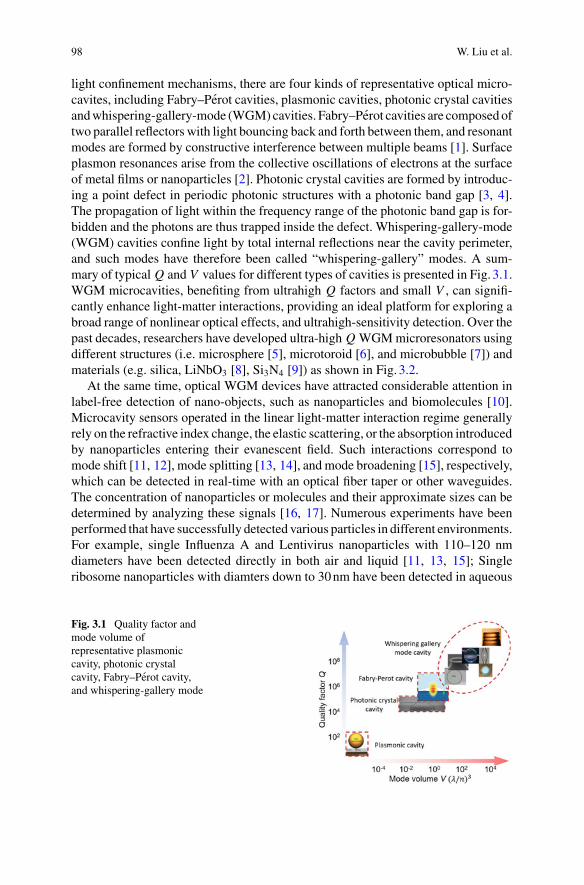
98 W. Liu et al.
light confinement mechanisms, there are four kinds of representative optical micro-cavites, including Fabry–Perot cavities, plasmonic cavities, photonic crystal cavitiesandwhispering-gallery-mode (WGM)cavities. Fabry–Perot cavities are composedoftwo parallel reflectors with light bouncing back and forth between them, and resonantmodes are formed by constructive interference between multiple beams [1]. Surfaceplasmon resonances arise from the collective oscillations of electrons at the surfaceof metal films or nanoparticles [2]. Photonic crystal cavities are formed by introduc-ing a point defect in periodic photonic structures with a photonic band gap [3, 4].The propagation of light within the frequency range of the photonic band gap is for-bidden and the photons are thus trapped inside the defect. Whispering-gallery-mode(WGM) cavities confine light by total internal reflections near the cavity perimeter,and such modes have therefore been called “whispering-gallery” modes. A sum-mary of typical Q and V values for different types of cavities is presented in Fig. 3.1.WGM microcavities, benefiting from ultrahigh Q factors and small V , can signifi-cantly enhance light-matter interactions, providing an ideal platform for exploring abroad range of nonlinear optical effects, and ultrahigh-sensitivity detection. Over thepast decades, researchers have developed ultra-high Q WGMmicroresonators usingdifferent structures (i.e. microsphere [5], microtoroid [6], and microbubble [7]) andmaterials (e.g. silica, LiNbO3 [8], Si3N4 [9]) as shown in Fig. 3.2.
At the same time, optical WGM devices have attracted considerable attention inlabel-free detection of nano-objects, such as nanoparticles and biomolecules [10].Microcavity sensors operated in the linear light-matter interaction regime generallyrely on the refractive index change, the elastic scattering, or the absorption introducedby nanoparticles entering their evanescent field. Such interactions correspond tomode shift [11, 12], mode splitting [13, 14], and mode broadening [15], respectively,which can be detected in real-time with an optical fiber taper or other waveguides.The concentration of nanoparticles or molecules and their approximate sizes can bedetermined by analyzing these signals [16, 17]. Numerous experiments have beenperformed that have successfully detected various particles in different environments.For example, single Influenza A and Lentivirus nanoparticles with 110–120 nmdiameters have been detected directly in both air and liquid [11, 13, 15]; Singleribosome nanoparticles with diamters down to 30nm have been detected in aqueous
Fig. 3.1 Quality factor andmode volume ofrepresentative plasmoniccavity, photonic crystalcavity, Fabry–Perot cavity,and whispering-gallery mode
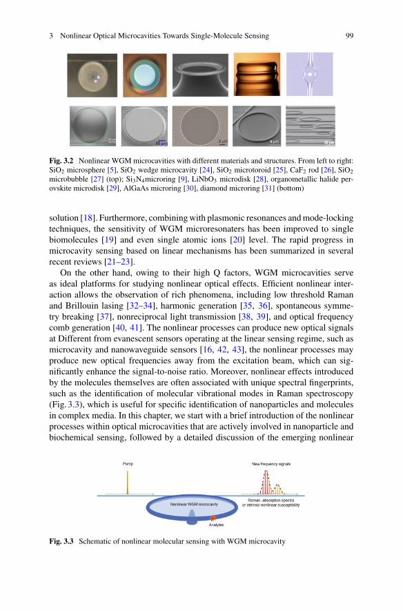
3 Nonlinear Optical Microcavities Towards Single-Molecule Sensing 99
Fig. 3.2 Nonlinear WGMmicrocavities with different materials and structures. From left to right:SiO2 microsphere [5], SiO2 wedge microcavity [24], SiO2 microtoroid [25], CaF2 rod [26], SiO2microbubble [27] (top); Si3N4microring [9], LiNbO3 microdisk [28], organometallic halide per-ovskite microdisk [29], AlGaAs microring [30], diamond microring [31] (bottom)
solution [18]. Furthermore, combiningwith plasmonic resonances andmode-lockingtechniques, the sensitivity of WGM microresonaters has been improved to singlebiomolecules [19] and even single atomic ions [20] level. The rapid progress inmicrocavity sensing based on linear mechanisms has been summarized in severalrecent reviews [21–23].
On the other hand, owing to their high Q factors, WGM microcavities serveas ideal platforms for studying nonlinear optical effects. Efficient nonlinear inter-action allows the observation of rich phenomena, including low threshold Ramanand Brillouin lasing [32–34], harmonic generation [35, 36], spontaneous symme-try breaking [37], nonreciprocal light transmission [38, 39], and optical frequencycomb generation [40, 41]. The nonlinear processes can produce new optical signalsat Different from evanescent sensors operating at the linear sensing regime, such asmicrocavity and nanowaveguide sensors [16, 42, 43], the nonlinear processes mayproduce new optical frequencies away from the excitation beam, which can sig-nificantly enhance the signal-to-noise ratio. Moreover, nonlinear effects introducedby the molecules themselves are often associated with unique spectral fingerprints,such as the identification of molecular vibrational modes in Raman spectroscopy(Fig. 3.3), which is useful for specific identification of nanoparticles and moleculesin complex media. In this chapter, we start with a brief introduction of the nonlinearprocesses within optical microcavities that are actively involved in nanoparticle andbiochemical sensing, followed by a detailed discussion of the emerging nonlinear
Fig. 3.3 Schematic of nonlinear molecular sensing with WGM microcavity
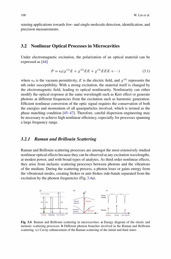
100 W. Liu et al.
sensing applications towards few- and single-molecule detection, identification, andprecision measurements.
3.2 Nonlinear Optical Processes in Microcavities
Under electromagnetic excitation, the polarization of an optical material can beexpressed as [44]
P = ε0(χ(1)E + χ(2)EE + χ(3)EEE +· · ·) (3.1)
where ε0 is the vacuum permittivity, E is the electric field, and χ(n) represents thenth order susceptibility. With a strong excitation, the material itself is changed bythe electromagnetic field, leading to optical nonlinearity. Nonlinearity can eithermodify the optical response at the same wavelength such as Kerr effect or generatephotons at different frequencies from the excitation such as harmonic generation.Efficient nonlinear conversion of the optic signal requires the conservation of boththe energies and momentum of all quasiparticles involved, which is termed as thephase matching condition [45–47]. Therefore, careful dispersion engineering maybe necessary to achieve high nonlinear efficiency, especially for processes spanninga large frequency range.
3.2.1 Raman and Brillouin Scattering
Raman and Brillouin scattering processes are amongst the most extensively studiednonlinear optical effects because they can be observed at any excitation wavelengths,at modest power, and with broad types of analytes. As third order nonlinear effects,they arise from inelastic scattering processes between photons and the vibrationsof the medium. During the scattering process, a photon loses or gains energy fromthe vibrational modes, creating Stokes or anti-Stokes side-bands separated from theexcitation by the phonon frequencies (Fig. 3.4a).
Stokes Anti-StokesRayleigh
virtual statesCavity modes
Raman
PumpStokesf
Anti-Stokes
Optical phonon
Acoustic phonon
E
k
Raman
Brillouin
(a) (b) (c)
Fig. 3.4 Raman and Brillouin scattering in microcavities. a Energy diagram of the elastic andinelastic scattering processes. b Different phonon branches involved in the Raman and Brillouinscattering. (c) Cavity enhancement of the Raman scattering of the initial and final states
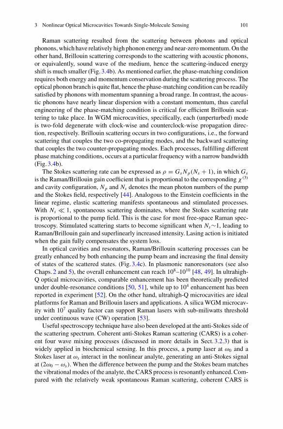
3 Nonlinear Optical Microcavities Towards Single-Molecule Sensing 101
Raman scattering resulted from the scattering between photons and opticalphonons,which have relatively high phonon energy and near-zeromomentum.On theother hand, Brillouin scattering corresponds to the scattering with acoustic phonons,or equivalently, sound wave of the medium, hence the scattering-induced energyshift is much smaller (Fig. 3.4b). As mentioned earlier, the phase-matching conditionrequires both energy and momentum conservation during the scattering process. Theoptical phonon branch is quite flat, hence the phase-matching condition can be readilysatisfied by phonons with momentum spanning a broad range. In contrast, the acous-tic phonons have nearly linear dispersion with a constant momentum, thus carefulengineering of the phase-matching condition is critical for efficient Brillouin scat-tering to take place. In WGM microcavities, specifically, each (unperturbed) modeis two-fold degenerate with clock-wise and counterclock-wise propagation direc-tion, respectively. Brillouin scattering occurs in two configurations, i.e., the forwardscattering that couples the two co-propagating modes, and the backward scatteringthat couples the two counter-propagating modes. Each processes, fulfilling differentphase matching conditions, occurs at a particular frequency with a narrow bandwidth(Fig. 3.4b).
The Stokes scattering rate can be expressed as ρ = GsNp(Ns + 1), in which Gs
is the Raman/Brillouin gain coefficient that is proportional to the corresponding χ(3)
and cavity configuration, Np and Ns denotes the mean photon numbers of the pumpand the Stokes field, respectively [44]. Analogous to the Einstein coefficients in thelinear regime, elastic scattering manifests spontaneous and stimulated processes.With Ns � 1, spontaneous scattering dominates, where the Stokes scattering rateis proportional to the pump field. This is the case for most free-space Raman spec-troscopy. Stimulated scattering starts to become significant when Ns∼1, leading toRaman/Brillouin gain and superlinearly increased intensity. Lasing action is initiatedwhen the gain fully compensates the system loss.
In optical cavities and resonators, Raman/Brillouin scattering processes can begreatly enhanced by both enhancing the pump beam and increasing the final densityof states of the scattered states. (Fig. 3.4c). In plasmonic nanoresonators (see alsoChaps. 2 and 5), the overall enhancement can reach 108–1010 [48, 49]. In ultrahigh-Q optical microcavities, comparable enhancement has been theoretically predictedunder double-resonance conditions [50, 51], while up to 104 enhancement has beenreported in experiment [52]. On the other hand, ultrahigh-Q microcavities are idealplatforms for Raman and Brillouin lasers and applications. A silicaWGMmicrocav-ity with 107 quality factor can support Raman lasers with sub-miliwatts thresholdunder continuous wave (CW) operation [53].
Useful spectroscopy technique have also been developed at the anti-Stokes side ofthe scattering spectrum. Coherent anti-Stokes Raman scattering (CARS) is a coher-ent four wave mixing processes (discussed in more details in Sect. 3.2.3) that iswidely applied in biochemical sensing. In this process, a pump laser at ω0 and aStokes laser at ωs interact in the nonlinear analyte, generating an anti-Stokes signalat (2ω0 − ωs). When the difference between the pump and the Stokes beam matchesthe vibrationalmodes of the analyte, theCARSprocess is resonantly enhanced. Com-pared with the relatively weak spontaneous Raman scattering, coherent CARS is
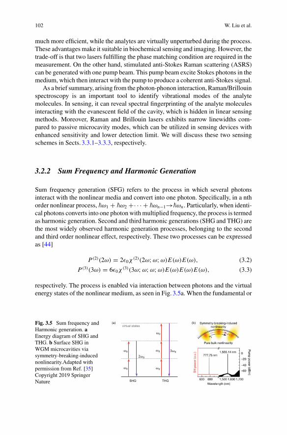
102 W. Liu et al.
much more efficient, while the analytes are virtually unperturbed during the process.These advantages make it suitable in biochemical sensing and imaging. However, thetrade-off is that two lasers fulfilling the phase matching condition are required in themeasurement. On the other hand, stimulated anti-Stokes Raman scattering (ASRS)can be generated with one pump beam. This pump beam excite Stokes photons in themedium, which then interact with the pump to produce a coherent anti-Stokes signal.
As a brief summary, arising from the photon-phonon interaction, Raman/Brillouinspectroscopy is an important tool to identify vibrational modes of the analytemolecules. In sensing, it can reveal spectral fingerprinting of the analyte moleculesinteracting with the evanescent field of the cavity, which is hidden in linear sensingmethods. Moreover, Raman and Brillouin lasers exhibits narrow linewidths com-pared to passive microcavity modes, which can be utilized in sensing devices withenhanced sensitivity and lower detection limit. We will discuss these two sensingschemes in Sects. 3.3.1–3.3.3, respectively.
3.2.2 Sum Frequency and Harmonic Generation
Sum frequency generation (SFG) refers to the process in which several photonsinteract with the nonlinear media and convert into one photon. Specifically, in a nthorder nonlinear process, �ω1 + �ω2 +· · · + �ωn−1→�ωn . Particularly, when identi-cal photons converts into one photonwithmultiplied frequency, the process is termedas harmonic generation. Second and third harmonic generations (SHG and THG) arethe most widely observed harmonic generation processes, belonging to the secondand third order nonlinear effect, respectively. These two processes can be expressedas [44]
P (2)(2ω) = 2ε0χ(2)(2ω;ω;ω)E(ω)E(ω), (3.2)
P (3)(3ω) = 6ε0χ(3)(3ω;ω;ω;ω)E(ω)E(ω)E(ω), (3.3)
respectively. The process is enabled via interaction between photons and the virtualenergy states of the nonlinear medium, as seen in Fig. 3.5a. When the fundamental or
Fig. 3.5 Sum frequency andHarmonic generation. aEnergy diagram of SHG andTHG. b Surface SHG inWGM microcavities viasymmetry-breaking-inducednonlinearity.Adapted withpermission from Ref. [35]Copyright 2019 SpringerNature
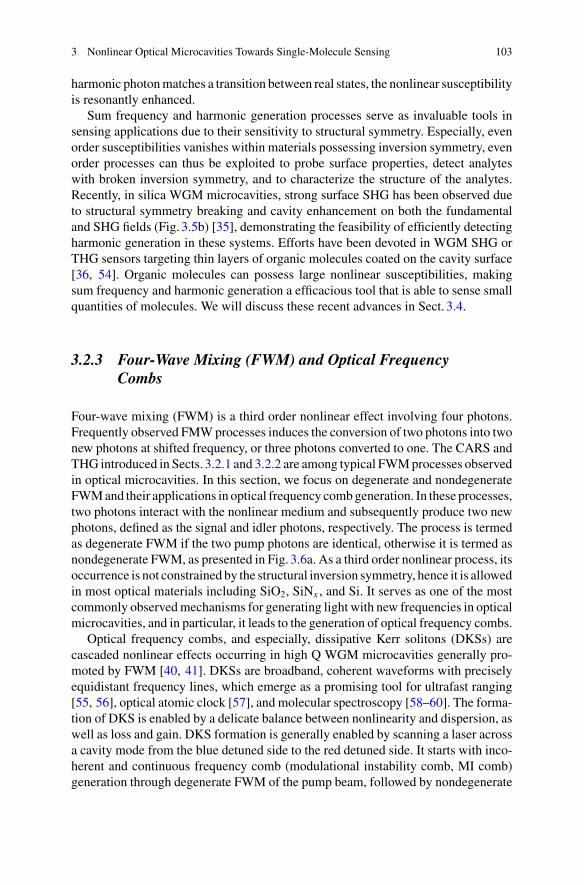
3 Nonlinear Optical Microcavities Towards Single-Molecule Sensing 103
harmonic photonmatches a transition between real states, the nonlinear susceptibilityis resonantly enhanced.
Sum frequency and harmonic generation processes serve as invaluable tools insensing applications due to their sensitivity to structural symmetry. Especially, evenorder susceptibilities vanishes within materials possessing inversion symmetry, evenorder processes can thus be exploited to probe surface properties, detect analyteswith broken inversion symmetry, and to characterize the structure of the analytes.Recently, in silica WGM microcavities, strong surface SHG has been observed dueto structural symmetry breaking and cavity enhancement on both the fundamentaland SHG fields (Fig. 3.5b) [35], demonstrating the feasibility of efficiently detectingharmonic generation in these systems. Efforts have been devoted in WGM SHG orTHG sensors targeting thin layers of organic molecules coated on the cavity surface[36, 54]. Organic molecules can possess large nonlinear susceptibilities, makingsum frequency and harmonic generation a efficacious tool that is able to sense smallquantities of molecules. We will discuss these recent advances in Sect. 3.4.
3.2.3 Four-Wave Mixing (FWM) and Optical FrequencyCombs
Four-wave mixing (FWM) is a third order nonlinear effect involving four photons.Frequently observed FMWprocesses induces the conversion of two photons into twonew photons at shifted frequency, or three photons converted to one. The CARS andTHG introduced in Sects. 3.2.1 and 3.2.2 are among typical FWMprocesses observedin optical microcavities. In this section, we focus on degenerate and nondegenerateFWMand their applications in optical frequency combgeneration. In these processes,two photons interact with the nonlinear medium and subsequently produce two newphotons, defined as the signal and idler photons, respectively. The process is termedas degenerate FWM if the two pump photons are identical, otherwise it is termed asnondegenerate FWM, as presented in Fig. 3.6a. As a third order nonlinear process, itsoccurrence is not constrained by the structural inversion symmetry, hence it is allowedin most optical materials including SiO2, SiNx , and Si. It serves as one of the mostcommonly observedmechanisms for generating light with new frequencies in opticalmicrocavities, and in particular, it leads to the generation of optical frequency combs.
Optical frequency combs, and especially, dissipative Kerr solitons (DKSs) arecascaded nonlinear effects occurring in high Q WGM microcavities generally pro-moted by FWM [40, 41]. DKSs are broadband, coherent waveforms with preciselyequidistant frequency lines, which emerge as a promising tool for ultrafast ranging[55, 56], optical atomic clock [57], and molecular spectroscopy [58–60]. The forma-tion of DKS is enabled by a delicate balance between nonlinearity and dispersion, aswell as loss and gain. DKS formation is generally enabled by scanning a laser acrossa cavity mode from the blue detuned side to the red detuned side. It starts with inco-herent and continuous frequency comb (modulational instability comb, MI comb)generation through degenerate FWM of the pump beam, followed by nondegenerate
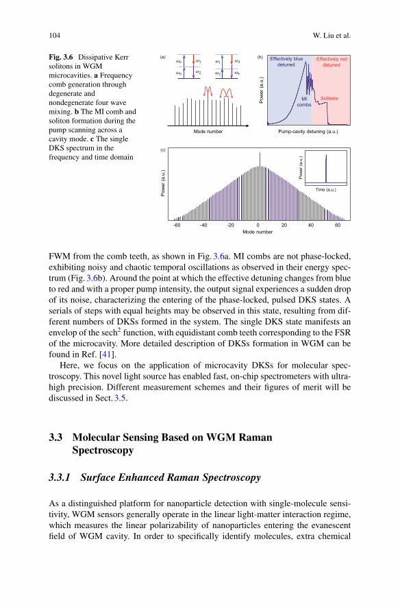
104 W. Liu et al.
Fig. 3.6 Dissipative Kerrsolitons in WGMmicrocavities. a Frequencycomb generation throughdegenerate andnondegenerate four wavemixing. b The MI comb andsoliton formation during thepump scanning across acavity mode. c The singleDKS spectrum in thefrequency and time domain
FWM from the comb teeth, as shown in Fig. 3.6a. MI combs are not phase-locked,exhibiting noisy and chaotic temporal oscillations as observed in their energy spec-trum (Fig. 3.6b). Around the point at which the effective detuning changes from blueto red and with a proper pump intensity, the output signal experiences a sudden dropof its noise, characterizing the entering of the phase-locked, pulsed DKS states. Aserials of steps with equal heights may be observed in this state, resulting from dif-ferent numbers of DKSs formed in the system. The single DKS state manifests anenvelop of the sech2 function, with equidistant comb teeth corresponding to the FSRof the microcavity. More detailed description of DKSs formation in WGM can befound in Ref. [41].
Here, we focus on the application of microcavity DKSs for molecular spec-troscopy. This novel light source has enabled fast, on-chip spectrometers with ultra-high precision. Different measurement schemes and their figures of merit will bediscussed in Sect. 3.5.
3.3 Molecular Sensing Based on WGM RamanSpectroscopy
3.3.1 Surface Enhanced Raman Spectroscopy
As a distinguished platform for nanoparticle detection with single-molecule sensi-tivity, WGM sensors generally operate in the linear light-matter interaction regime,which measures the linear polarizability of nanoparticles entering the evanescentfield of WGM cavity. In order to specifically identify molecules, extra chemical
3 Nonlinear Optical Microcavities Towards Single-Molecule Sensing 105
functionalization on cavity surface is required to bind analyte molecules with recep-tor molecules with a high specification and selectivity. Therefore, the specificity ofWGM microsensor mainly relies on the chemical composition and functionaliza-tion of the device. On the contrary, Raman spectroscopy provides a powerful wayfor specificity identification without receptor molecules via the molecular finger-prints, i.e., their vibrational modes. Hence, surface enhanced Raman spectroscopy(SERS), and cavity enhanced Raman spectroscopy (CERS) in WGM microcavitieshave attracted considerable interests in the past decades.
Conventional plasmonic SERS techniques are based on noblemetal nanoparticles,whileRaman sensors could bemore biocompatible relyingondielectricWGMmicro-cavities. For examples, the heating effects are negligible because the low absorptionof dielectric materials and the low excitation powers benefiting from high Q factors.Moreover, all-dielectric sensors are more robust against harsh electrochemical con-ditions, in which metals would be attacked to shift plasmonic resonances. Distinctfrom plasmonic SERS techniques that enhance both the pump and the Raman fieldssimultaneously in a broadband plasmonic resonance, WGM microcavities exhibitmany opticalmodeswith ultra-narrowbandwidths determined by ultrahighQ factors.Therefore, Raman enhancement in WGM microresonators relies on the resonanceconditions and field overlapping at both the excitation and the Stokes wavelengths.
In 2008, Ausman and Schatz [50] firstly built the formulas of WGM enhancedRaman scattering based on the Lorentz-Mie theory. In their theory, a microspherewith radii of 5–20µm is illuminated by a plane wave light field to calculate the fieldenhancement at the pump frequency in the visible wavelength range. The Ramanemission is investigated by calculating the far-field radiation intensity of a dipolaremitter located at the cavity surface. As compared to a free-space excitation of thesame point dipole, an enhancement factor of 103–104 is obtained for an analytelocated on the WGM hotspot when the pump light is enhanced by the cavity reso-nance. When both the pump and Stokes-shifted Raman peaks are in resonance, theRaman enhancement increases to 108. Then, the theory was soon been exploited inseveral experimental works. In 2010, Anderson [61] experimentally explored SERSin silica spheres with diameters of 5–10µm with molecular films, and an enhance-ment factor as high as 103 was obtained for two touchingmicrospheres. Later, Ramansensing of solution and gas was also demonstrated by using SiO2-TiO2 core-shellmicrospheres. Since the TiO2 shell has a higher refractive index, the WGM wasexcited in a TiO2 shell so that the electric field is tightly confined [62, 63]. With self-assembled and multi-stacked core-shell microspheres allowing for large area detec-tion, an overall enhancement up to 140-fold was experimentally observed (Fig. 3.7).
Efforts towards few- and single- particle sensing have been devoted to enhancingthe signal-to-noise ratio, via optimizing the sensing scheme and parameters. Limitedby fabrication techniques, the early progresses in WGM Raman sensing mainly uti-lize microspheres with moderate Q, and conventional Raman spectroscopy systemequipped with free-space illumination and collection geometry. More recently, withthe rapid development of microcavity fabrication and coupling techniques, SERScould be further enhanced by evanescently-coupled ultrahigh-Q WGM microres-onators. While ultrahigh-Q microcavities could enhance intracavity power by sev-
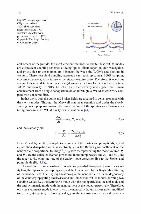
106 W. Liu et al.
Fig. 3.7 Raman spectra ofCO2 adsorbed ontoSiO2-TiO2 core-shellmicrospheres and TiO2substrate. Adapted withpermission from Ref. [62].Copyright The Royal Societyof Chemistry 2016
1250 1300 1350 1400
Raman Shift (cm-1)
Inte
nsity
(a.u
.)
1450
TiO2
SiO2
Microsphere
Planar substrate
eral orders of magnitude, the most efficient methods to excite these WGM modesare evanescent coupling schemes utilizing optical fibers taper, on-chip waveguide,and prism, due to the momentum mismatch between the WGMs and photons invacuum. These near-field coupling approach can reach up to near 100% couplingefficiency, hence greatly improve the signal-to-noise ratio. Therefore, it opens anavenue to Raman detection towards single-nanoparticle/molecule level with opticalWGM microcavity. In 2015, Liu et al. [51] theoretically investigated the Ramanenhancement from a single nanoparticle on an ultrahigh-Q WGM microcavity cou-pled with a tapered fiber.
In that work, both the pump and Stokes fields are assumed to be in resonance withthe cavity modes. Through the Maxwell nonlinear equation and under the slowlyvarying envelop approximation, the rate equations of the spontaneous Raman scat-tering processes in a WGM cavity can be written as [44]
dNs
dt= −κs Ns + gs Np (3.4)
and the Raman yield
Y = PsPin
= 2κs,1κp,1gsκsκ2
p
(3.5)
Here Ns and Np are the mean photon numbers of the Stokes and pump fields, κs andκp are their dissipation rates, respectively. gs is the Raman gain coefficient of thenanoparticle proportional to Im(χ(3))/VR with Vr representing the mode volume. Psand Pin are the collected Raman power and input pump power, and κs,1 and κp,1 arethe taper-cavity coupling rate of the cavity mode corresponding to the Stokes andpump fields (Fig. 3.8a).
The total dissipation rate of eachmode is composed of three parts; the intrinsic cav-ity loss, the taper-cavity coupling rate, and the loss induced by theRayleigh scatteringof the nanoparticle. The Rayleigh scattering of the nanoparticle lifts the degeneracyof the counterpropagating clockwise and anti-clockwise WGMmodes, forming twostanding waves, i.e., the symmetric mode with the nanoparticle at the anti-node andthe anti-symmetric mode with the nanoparticle at the node, respectively. Therefore,only the symmetric mode interacts with the nanoparticle, and its loss rate is modifiedto κi = κi,r + κi,0 + κi,1. Here κi,0 and κi,1 are the intrinsic cavity loss and the taper-
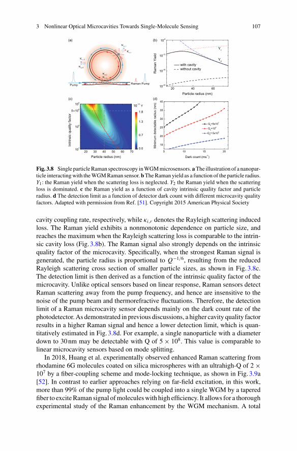
3 Nonlinear Optical Microcavities Towards Single-Molecule Sensing 107
(a) (b)
(c) (d)
Fig. 3.8 Single particleRaman spectroscopy inWGMmicrosensors.aThe illustration of a nanopar-ticle interactingwith theWGMRaman sensor.bTheRaman yield as a function of the particle radius.Y1: the Raman yield when the scattering loss is neglected. Y2 the Raman yield when the scatteringloss is dominated. c the Raman yield as a function of cavity intrinsic quality factor and particleradius. d The detection limit as a function of detector dark count with different microcavity qualityfactors. Adapted with permission from Ref. [51]. Copyright 2015 American Physical Society
cavity coupling rate, respectively, while κi,r denotes the Rayleigh scattering inducedloss. The Raman yield exhibits a nonmonotonic dependence on particle size, andreaches the maximum when the Rayleigh scattering loss is comparable to the intrin-sic cavity loss (Fig. 3.8b). The Raman signal also strongly depends on the intrinsicquality factor of the microcavity. Specifically, when the strongest Raman signal isgenerated, the particle radius is proportional to Q−1/6, resulting from the reducedRayleigh scattering cross section of smaller particle sizes, as shown in Fig. 3.8c.The detection limit is then derived as a function of the intrinsic quality factor of themicrocavity. Unlike optical sensors based on linear response, Raman sensors detectRaman scattering away from the pump frequency, and hence are insensitive to thenoise of the pump beam and thermorefractive fluctuations. Therefore, the detectionlimit of a Raman microcavity sensor depends mainly on the dark count rate of thephotodetector. As demonstrated in previous discussions, a higher cavity quality factorresults in a higher Raman signal and hence a lower detection limit, which is quan-titatively estimated in Fig. 3.8d. For example, a single nanoparticle with a diameterdown to 30nm may be detectable with Q of 5 × 10⁸. This value is comparable tolinear microcavity sensors based on mode splitting.
In 2018, Huang et al. experimentally observed enhanced Raman scattering fromrhodamine 6G molecules coated on silica microspheres with an ultrahigh-Q of 2 ×10⁷ by a fiber-coupling scheme and mode-locking technique, as shown in Fig. 3.9a[52]. In contrast to earlier approaches relying on far-field excitation, in this work,more than 99% of the pump light could be coupled into a single WGM by a taperedfiber to exciteRaman signal ofmoleculeswith high efficiency. It allows for a thoroughexperimental study of the Raman enhancement by the WGM mechanism. A total
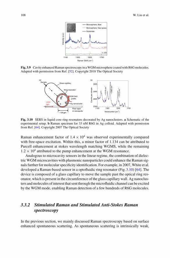
108 W. Liu et al.
Fig. 3.9 Cavity enhancedRaman spectroscopy in aWGMmicrosphere coatedwithR6Gmolecules.Adapted with permission from Ref. [52]. Copyright 2018 The Optical Society
Fiber taperor waveguide
Glass capillarySample
Laser light
Ring resonator
~100 µm
WGM field profile
Ag nanocluster
µ
2200
2600
3000
3400
Cou
nts
per
min
ute
1100 1300 1500 1700
Wavenumber (cm )-1
~13
10 c
m-1
~13
60 c
m-1
~15
10 c
m-1
(a) (b)
Fig. 3.10 SERS in liquid core ring resonators decorated by Ag nanoclusters. a Schematic of theexperimental setup. b Raman spectrum for 33 nM R6G in Ag colloid. Adapted with permissionfrom Ref. [64]. Copyright 2007 The Optical Society
Raman enhancement factor of 1.4 × 10⁴ was observed experimentally comparedwith free-space excitation. Within this, a minor factor of 1.134 can be attributed toPurcell enhancement at stokes wavelength matching WGMS, while the remaining1.2 × 104 attributed to the pump enhancement at the WGM resonance.
Analogous to microcavity sensors in the linear regime, the combination of dielec-tricWGMmicrocavities with plasmonic nanoparticles could enhance the Raman sig-nals further formolecular specificity identification. For example, in 2007,White et al.developed a Raman-based sensor in a optofluidic ring resonator (Fig. 3.10) [64]. Thedevice is composed of a glass capillary to move the sample past the optical ring res-onator, which is present in the circumference of the glass capillarywall. Ag nanoclus-ters andmolecules of interest that sent through themicrofluidic channel can be excitedby theWGMmode, enabling Raman detection of a few hundreds of R6Gmolecules.
3.3.2 Stimulated Raman and Stimulated Anti-Stokes Ramanspectroscopy
In the previous section, we mainly discussed Raman spectroscopy based on surfaceenhanced spontaneous scattering. As spontaneous scattering is intrinsically weak,
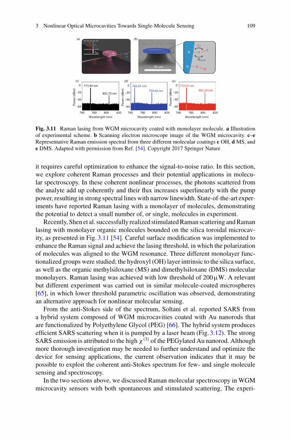
3 Nonlinear Optical Microcavities Towards Single-Molecule Sensing 109
Fig. 3.11 Raman lasing from WGM microcavity coated with monolayer molecule. a Illustrationof experimental scheme. b Scanning electron microscope image of the WGM microcavity. c–eRepresentative Raman emission spectral from three different molecular coatings c OH, d MS, ande DMS. Adapted with permission from Ref. [54]. Copyright 2017 Springer Nature
it requires careful optimization to enhance the signal-to-noise ratio. In this section,we explore coherent Raman processes and their potential applications in molecu-lar spectroscopy. In these coherent nonlinear processes, the photons scattered fromthe analyte add up coherently and their flux increases superlinearly with the pumppower, resulting in strong spectral lineswith narrow linewidth. State-of-the-art exper-iments have reported Raman lasing with a monolayer of molecules, demonstratingthe potential to detect a small number of, or single, molecules in experiment.
Recently, Shen et al. successfully realized stimulatedRaman scattering andRamanlasing with monolayer organic molecules bounded on the silica toroidal microcav-ity, as presented in Fig. 3.11 [54]. Careful surface modification was implemented toenhance the Raman signal and achieve the lasing threshold, in which the polarizationof molecules was aligned to the WGM resonance. Three different monolayer func-tionalized groupswere studied; the hydroxyl (OH) layer intrinsic to the silica surface,as well as the organic methylsiloxane (MS) and dimethylsiloxane (DMS) molecularmonolayers. Raman lasing was achieved with low threshold of 200µW. A relevantbut different experiment was carried out in similar molecule-coated microspheres[65], in which lower threshold parametric oscillation was observed, demonstratingan alternative approach for nonlinear molecular sensing.
From the anti-Stokes side of the spectrum, Soltani et al. reported SARS froma hybrid system composed of WGM microcavities coated with Au nanorods thatare functionalized by Polyethylene Glycol (PEG) [66]. The hybrid system producesefficient SARS scattering when it is pumped by a laser beam (Fig. 3.12). The strongSARS emission is attributed to the high χ(3) of the PEGylated Au nanorod. Althoughmore thorough investigation may be needed to further understand and optimize thedevice for sensing applications, the current observation indicates that it may bepossible to exploit the coherent anti-Stokes spectrum for few- and single moleculesensing and spectroscopy.
In the two sections above, we discussed Raman molecular spectroscopy in WGMmicrocavity sensors with both spontaneous and stimulated scattering. The experi-
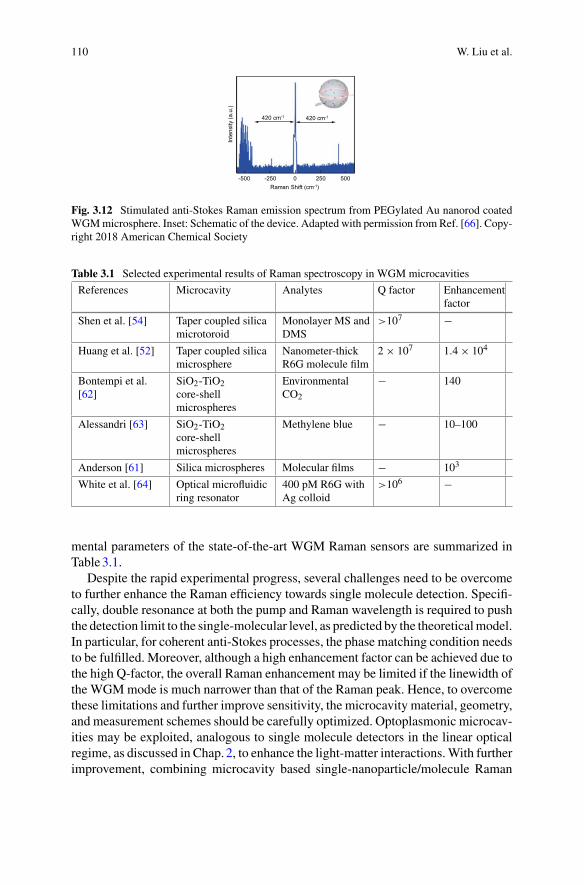
110 W. Liu et al.
Fig. 3.12 Stimulated anti-Stokes Raman emission spectrum from PEGylated Au nanorod coatedWGMmicrosphere. Inset: Schematic of the device. Adapted with permission from Ref. [66]. Copy-right 2018 American Chemical Society
Table 3.1 Selected experimental results of Raman spectroscopy in WGM microcavities
References Microcavity Analytes Q factor Enhancementfactor
Shen et al. [54] Taper coupled silicamicrotoroid
Monolayer MS andDMS
>107 −
Huang et al. [52] Taper coupled silicamicrosphere
Nanometer-thickR6G molecule film
2 × 10⁷ 1.4 × 10⁴
Bontempi et al.[62]
SiO2-TiO2core-shellmicrospheres
EnvironmentalCO2
− 140
Alessandri [63] SiO2-TiO2core-shellmicrospheres
Methylene blue − 10–100
Anderson [61] Silica microspheres Molecular films − 103
White et al. [64] Optical microfluidicring resonator
400 pM R6G withAg colloid
>106 −
mental parameters of the state-of-the-art WGM Raman sensors are summarized inTable3.1.
Despite the rapid experimental progress, several challenges need to be overcometo further enhance the Raman efficiency towards single molecule detection. Specifi-cally, double resonance at both the pump and Raman wavelength is required to pushthe detection limit to the single-molecular level, as predicted by the theoreticalmodel.In particular, for coherent anti-Stokes processes, the phase matching condition needsto be fulfilled. Moreover, although a high enhancement factor can be achieved due tothe high Q-factor, the overall Raman enhancement may be limited if the linewidth ofthe WGMmode is much narrower than that of the Raman peak. Hence, to overcomethese limitations and further improve sensitivity, the microcavity material, geometry,and measurement schemes should be carefully optimized. Optoplasmonic microcav-ities may be exploited, analogous to single molecule detectors in the linear opticalregime, as discussed in Chap.2, to enhance the light-matter interactions.With furtherimprovement, combining microcavity based single-nanoparticle/molecule Raman

3 Nonlinear Optical Microcavities Towards Single-Molecule Sensing 111
spectroscopy and ultrasensitive linear WGM sensing scheme is promising to achievereal-time, label-free nanoparticle/molecule counting and identification.
3.3.3 Stimulated Scattering Based Sensitivity Enhancement
The sensitivity of microcavity based sensors is highly dependent on the spectrallinewidth of WGM mode in the linear regime. Stimulated nonlinear processes canbe introduced to act as an intrinsic gain mechanism to compensate the loss of micro-cavities, and thus reduce the mode linewidth and further lower the detection limit.In 2014, Ozdemir et al. [67] and Li et al. [53] used mode splitting of Raman laser todetect single particle with the detection limit of 10nm.
The initially degenerate clockwise and counterclockwise propagating modes arecoupled via backscattering derived from the nanoparticle at the WGM cavity sur-face. Once the coupling exceeds the loss rate in the system, the mode splitting canbe observed. When the pumping power is higher than the Raman lasing threshold(Fig. 3.13a), the two split modes generate a beat oscillation in the time domain thatthe beatnote frequency corresponds to the mode splitting, as shown in Fig. 3.13b. Bymonitoring the beatnote frequency change, the number of single particles attachedonto the microcavity can be detected in real-time (Fig. 3.13c, d). In these studies,the Raman gain significantly compensates the intrinsic microcavity loss, allowing
Fig. 3.13 Split-mode Raman laser based single particle detection. a Schematic of the experimentand Raman lasing spectrum. bBeatnote generated by the interference between the split mode lasers.c Beat frequency as a function of the number of nanoparticles attached onto the microcavity sensor.d Beat frequency as a function of time. Adapted with permission from Ref. [53]. Copyright 2014National Academy of Sciences
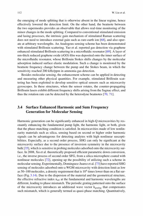
112 W. Liu et al.
the emerging of mode splitting that is otherwise absent in the linear regime, henceeffectively lowered the detection limit. On the other hand, the beatnote betweenthe two supermodes provides an observable that allows real-time monitoring of theminor changes in the mode splitting. Compared to conventional stimulated emissionand lasing processes, the intrinsic gain mechanism of stimulated Raman scatteringdoes not need to introduce external gain such as rare-earth ion [68], and also oper-ate at arbitrary wavelengths. An Analogous sensing scheme has been demonstratedwith stimulated Brillouin scattering. Yao et al. reported gas detection via grapheneenhanced stimulated Brillouin scattering in a microfluidic resonator [69]. A layer ofnm-thick reduced graphene oxide (rGO) film was deposited onto the inner surface ofthe microfluidic resonator, whose Brillouin Stokes shifts changes by the molecularadsorption induced surface elastic modulation. Such a change is monitored by thebeatnote frequency change between the pump and the Stokes beam, in which thesensitivity reached 200 kHz/ppm in ammonia gas detection.
Besides molecular sensing, the enhancement scheme can be applied in detectingand measuring other physical quantities. For example, stimulated Brillouin scat-tering has been exploited to develop sensitive optical sensors such as microcavitygyroscopes. In these structures, when the sensor rotates, the counter-propagatingBrillouin lasers exhibit different frequency shifts arising from the Sagnac effect, andthus the rotation rate can be detected by the heterodyne beatnotes [70, 71].
3.4 Surface Enhanced Harmonic and Sum FrequencyGeneration for Molecular Sensing
Harmonic generation can be significantly enhanced in high-Q microcavities by res-onantly enhancing the fundamental pump light, the harmonic light, or both, giventhat the phase-matching condition is satisfied. In microcavities made of low nonlin-earity materials such as silica, sensing based on second or higher order harmonicsignals can be advantageous for detecting analytes with high nonlinear suscepti-bilities. Especially, as a second order process, SHG can only be significant at themicrocavity surface due to the presence of inversion symmetry in the microcavitybulk [35], which is sensitive in probingmolecules adsorbed onto the microcavity sur-face. In 2008, Xu et al. theoretically proposed efficient parametric down conversion,i.e., the inverse process of second order SFG, from a silica microsphere coated withnonlinear molecules [72], opening up the possibility of utilizing such a scheme inmolecular sensing. Experimentally, Dominguez-Juarez et al. [73] have reported SHGsensing of molecules adsorbed onto a WGMmicrocavity with detection limit as lowas 50–100 molecules, a density requirement that is 104 times lower than on a flat sur-face (Fig. 3.14). Due to the dispersion of the material and the geometrical structure,the effective refractive index neff at the fundamental and harmonic wavelengths aredifferent, leading to phase mismatch. The periodic grating patterned onto the surfaceof the microcavity introduces an additional wave vector kgrating that compensatessuch mismatch, which is generally termed as quasi-phase matching. Quantitatively,
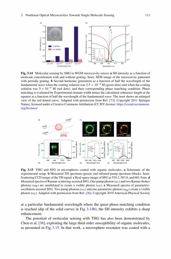
3 Nonlinear Optical Microcavities Towards Single-Molecule Sensing 113
(a) (b)
w/ grating
w/o grating
Fig. 3.14 Molecular sensing by SHG in WGMmicrocavity sensor. a SH intensity as a function ofmolecule concentration with and without grating. Inset: SEM image of the microcavity patternedwith periodic grating. b Second harmonic generation as a function of half the wavelength of thefundamental wave when the coating solution was 2.5 × 10⁻⁴ M (green dots) and when the coatingsolution was 5 × 10⁻⁹ M (red dots), and their corresponding phase matching condition. Phasematching is evaluated by Experimental domain width minus the calculated coherence length at theequator as a function of half the wavelength of the fundamental wave. The inset shows an enlargedview of the red dotted curve. Adapted with permission from Ref. [73]. Copyright 2011 SpringerNature, licensed under a Creative Commons Attribution (CCBY) license: https://creativecommons.org/licenses/
Fig. 3.15 THG and SFG in microspheres coated with organic molecules. a Schematic of theexperimental setup. b Measured TH spectrum (green) and infrared pump spectrum (black). Inset:Scattering CCD image of the TH signal. cReal-space image of SFG at 539.2, 583.0, and 601.9nm. dMeasured spectra of Raman-scattering-assisted SFG.One pump photon (ω1) and twoRaman Stokesphotons (ωR) are annihilated to create a visible photon (ω2). e Measured spectra of parametric-oscillation-assisted SFG. Two pump photons (ω1) and one parametric photon (ωpp) create a visiblephoton (ω2). Adapted with permission from Ref. [36]. Copyright 2019 American Physical Society
at a particular fundamental wavelength where the quasi-phase-matching conditionis reached (dip of the solid curves in Fig. 3.14b), the SH intensity exhibits a sharpenhancement.
The potential of molecular sensing with THG has also been demonstrated byChen et al. [36], exploiting the large third order susceptibility of organic molecules,as presented in Fig. 3.15. In that work, a microsphere resonator was coated with a
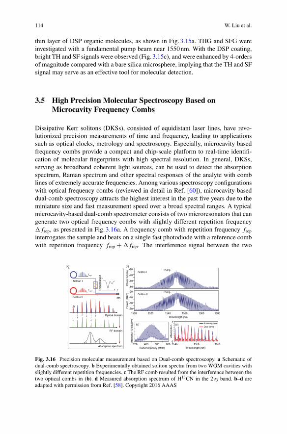
114 W. Liu et al.
thin layer of DSP organic molecules, as shown in Fig. 3.15a. THG and SFG wereinvestigated with a fundamental pump beam near 1550nm. With the DSP coating,bright TH and SF signals were observed (Fig. 3.15c), and were enhanced by 4-ordersof magnitude compared with a bare silica microsphere, implying that the TH and SFsignal may serve as an effective tool for molecular detection.
3.5 High Precision Molecular Spectroscopy Based onMicrocavity Frequency Combs
Dissipative Kerr solitons (DKSs), consisted of equidistant laser lines, have revo-lutionized precision measurements of time and frequency, leading to applicationssuch as optical clocks, metrology and spectroscopy. Especially, microcavity basedfrequency combs provide a compact and chip-scale platform to real-time identifi-cation of molecular fingerprints with high spectral resolution. In general, DKSs,serving as broadband coherent light sources, can be used to detect the absorptionspectrum, Raman spectrum and other spectral responses of the analyte with comblines of extremely accurate frequencies. Among various spectroscopy configurationswith optical frequency combs (reviewed in detail in Ref. [60]), microcavity-baseddual-comb spectroscopy attracts the highest interest in the past five years due to theminiature size and fast measurement speed over a broad spectral ranges. A typicalmicrocavity-based dual-comb spectrometer consists of two microresonators that cangenerate two optical frequency combs with slightly different repetition frequency� frep, as presented in Fig. 3.16a. A frequency comb with repetition frequency frepinterrogates the sample and beats on a single fast photodiode with a reference combwith repetition frequency frep + � frep. The interference signal between the two
Fig. 3.16 Precision molecular measurement based on Dual-comb spectroscopy. a Schematic ofdual-comb spectroscopy. b Experimentally obtained soliton spectra from two WGM cavities withslightly different repetition frequencies. c The RF comb resulted from the interference between thetwo optical combs in (b). d Measured absorption spectrum of H13CN in the 2ν3 band. b–d areadapted with permission from Ref. [58]. Copyright 2016 AAAS
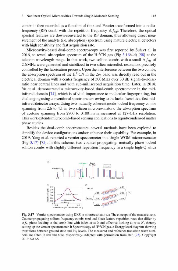
3 Nonlinear Optical Microcavities Towards Single-Molecule Sensing 115
combs is then recorded as a function of time and Fourier transformed into a radio-frequency (RF) comb with the repetition frequency � frep. Therefore, the opticalspectral features are down-converted to the RF domain, thus allowing direct mea-surement of the analyte (i.e. absorption) spectrum using mature electrical detectorswith high sensitivity and fast acquisition rate.
Microcavity-based dual-comb spectroscopy was first reported by Suh et al. in2016, to reveal absorption spectrum of the H13CN gas (Fig. 3.16b–d) [58] at thetelecom wavelength range. In that work, two soliton combs with a small � frep of2.6MHz were generated and stabilized in two silica microdisk resonators preciselycontrolled by the fabrication process. Upon the interference between the two combs,the absorption spectrum of the H13CN in the 2ν3 band was directly read out in theelectrical domain with a center frequency of 500MHz over 30 dB signal-to-noise-ratio near central lines and with sub-millisecond acquisition time. Later, in 2018,Yu et al. demonstrated a microcavity-based dual-comb spectrometer in the mid-infrared domain [74], which is of vital importance to molecular fingerprinting, butchallenging using conventional spectrometers owing to the lack of sensitive, fastmid-infrared detector arrays. Using twomutually coherentmode-locked frequency combsspanning from 2.6 to 4.1 in two silicon microresonators, the absorption spectrumof acetone spanning from 2900 to 3100nm is measured at 127-GHz resolution.Thiswork extendsmicrocomb-based sensing applications to liquid/condensedmatterphase studies.
Besides the dual-comb spectrometers, several methods have been explored tosimplify the device configurations and/or enhance their capability. For example, in2019, Yang et al. reported a vernier spectrometer in a single WGM microresonator(Fig. 3.17) [75]. In this scheme, two counter-propagating, mutually phase-lockedsoliton combs with slightly different repetition frequency in a single high-Q silica
Fig. 3.17 Vernier spectrometer using DKS in microresonators. a The concept of the measurement.Counterpropagating soliton frequency combs (red and blue) feature repetition rates that differ by� fr , phase-locking at the comb line with index m = 0 and effective locking at m = N , therebysetting up the vernier spectrometer. b Spectroscopy of H12CN gas. c Energy level diagram showingtransitions between ground state and 2ν1 levels. The measured and reference transition wave num-bers are noted in red and blue, respectively. Adapted with permission from Ref. [75]. Copyright2019 AAAS
116 W. Liu et al.
microresonator were utilized to implement a frequency vernier scale, which enablesrapid and broadband measurement of optical frequencies. The absorption spectrumof H12CN was measured with exceptionally high precision by this vernier spec-trometer. Also in a single high-Q WGM microcavity, direct frequency comb [76]for performing high-precision atomic spectroscopy and stabilization, and frequencycomb spectroscopy combined with a low-resolution Fourier transform spectrometer[77] have been demonstrated experimentally.
Comparedwith typicalmode-locked lasers, themicrocavity frequency combswithhigh repetition frequencies up to 101–103 GHz are desirable in many aspects, includ-ing the high detection speed scaling with the repetition frequency, the feasibility ofchip-scale integration, and ability to resolve adjacent comb teeth via conventionalspectral analyzers. However, the relatively large linespacing of a fixed microcomblimits the spectral resolution of the spectrometer, making it challenging to resolvenarrow spectral features of the molecules of interest. Therefore, microcombs withprecise frequency and repetition rate control are highly demanded in practical spec-troscopy applications. In order to overcome such challenge, several efforts have beendevoted, mainly by tuning the WGM resonances via the temperature control. Tem-perature tuning of microcomb frequency was first reported by Yu et al., and 12.5%of comb line spacing has been experimentally demonstrated with a bulk thermalelectric cooler [59]. Later, they develop an integrated microheaters on top of themicroresonator that can tune the comb tooth by over a full free spectral range forboth single- and dual-comb spectrometers [77, 78]. Besides comb frequency tun-ing, temperature controlling of the microcavity resonance have shown to be ableto help the DKS initiation and stabilization for high resolution spectroscopy. Laterin 2020, Liu et al. [79] reported fast electrical tuning of the comb frequency up toMHz bandwidth via applying piezoelectric components. Very recently, a microcombspectrometer with independent and simultaneous control of the comb frequency andrepetition rate was demonstrated by Stern et al. [76], and it was employed to accu-rately resolve the hyperfine manifold of rubidium atoms. In that experiment, via thePound-Drever-Hall technique, the pump laser was locked to the WGM resonanceand fine tuned by the intracavity pump power, while the repetition rate was alignedwith a seeding frequency of the phase modulation of the pump laser. Therefore,this configuration allow precise frequency control of each comb tooth suitable forspectroscopy applications.
The major figure of merits of the state-of-the-art microcomb spectrometers arepresented in Table3.2.
Chip-scale microcombs have shown their extraordinary performances with greatrobustness and tunability. However, several crucial challenges still hinder their prac-tical spectroscopy applications, such as the lowmicrocomb efficiency and the limita-tion of their workingwavelength range. Owing to the small temporal overlap betweenthe pulsed soliton state and the continuous pump light, the microcomb efficiency isgenerally low. The efficiency could be enhanced by applying gain materials in micro-cavities or exploiting dark solitons [41].Moreover, currentmicrocomb spectrometersare mainly limited to near- or mid-infrared bands, however, it would be important toextend their operation to the visible or even ultraviolet wavelength ranges, which is
3 Nonlinear Optical Microcavities Towards Single-Molecule Sensing 117
Table 3.2 Selected experimental demonstrations of microcomb based molecular spectroscopy
References Mechanism Frequency span(THz)
Repetitionfrequency (GHz)
Minimumacquisition time
Stern et al. [76] Direct combspectroscopy
192–198 22 −
Yang et al. [75] Vernierspectrometer
192–194 22 0.1 ps for laserchirping ratemonitor
Yu et al. [78] Direct combspectroscopy
176–207 195 <2s with200GHzFSR-spanningtuning
Yu et al. [74] Dual-combspectroscopy
73–115 127 78 ns
Dutt et al. [59] Dual-combspectroscopy
170–220 452 1.79 ns
Yu et al. [77] Direct combspectroscopy
76–124 127 −
Suh et al. [58] Dual-combspectroscopy
191–195 22 386 ns
crucial for the characterization of the electronic transitions of molecules and atoms.Lately, Chen et al. demonstrated microcomb of more than two-octave span rang-ing from 450 to 2000nm through both second- and third-order nonlinearities in adeformed silica microcavity [80], holding great potential for unlocking the applica-tions of microcomb spectroscopy in the visible band.
3.6 Emerging Sensing Methods via Other NonlinearProcesses
In the past decade, sensing techniques have been rapidly developed by incorporatingrich nonlinear effects including photothermal effect and optomechanical interac-tions. Measurements of effects enable comprehensive evaluation of various physicalquantities of the analytes, including temperature, optical susceptibility, mass, andvibrational modes, opening up opportunities for multidimensional sensing and pre-cision measurements.
Thermal-optical effect describes the phenomenon that the refractive indexofmate-rial changes with the temperature change induced by light. Specifically, in microcav-ity sensors, the heat due to absorption of the analytes can be dissipate into the cavity,leading to power dependent resonance frequency shifts. Measurements of such shiftshave experimentally enabled detection of individual nanoparticles [81–83]. More-over, this method may not only provide an alternative approach for molecular sens-ing, but also be utilized for studying the thermodynamic and dissipative properties
118 W. Liu et al.
of molecules. Reported by Heylman et al. [81] in 2016, a WGM microtoroid wasable to be utilized as an ultrasensitive single nanoparticle absorption spectrometer.In that work, a gold nanorod as the analyte was excited by a pump beam, while asecond off-resonance probe beamwas employed tomeasure the local refractive indexchange by monitoring the shift of the cavity resonance. Ultrahigh sensitivity down to�T ∼ 100 nK was enabled owing to the ultra-high Q factor of the cavity resonancecombined with the Pound-Drever-Hall locking technique. As a result, a minimumdetectable frequency shift as small 84Hz was successfully realized. An analogousmeasurement scheme has later been demonstrated in an inverted excitation geometry,with the pump beam delivered from the substrate of a microtoroid cavity [82]. Thisalternation in the exprimental setup may be beneficial for optical integration andsensing in microfluidics. Furthermore, in a same gold nanorod-microtoroid coupledsystem, Pan et al. demonstrated simultaneous identification of scattering, absorp-tion and transmission cross sections of the gold nanorod, by further combining theaforementioned absorption measurements with the two-side transmission measure-ment [83]. This experiment thus allowed the quantitative elucidation of all the energydissipation pathways of the coupled system.
Optomechanical oscillators (OMO) have found applications in high sensitivitynanoparticle detection and precision measurements of force, mass, and accelera-tions by utilizing the coupling between the mechanical vibration and optical modes.In microcavities with simultaneous high-Q optical and mechanical modes, a tinynanoparticle adsorption is enough to perturb the mechanical oscillation, which canbe read-out by the modulation of the optical mode. Specifically, for single moleculeswith mass much smaller than the OMO sensor, the adsorption of the analytes canbe viewed as adding a mass to the sensor, which leads to a redshift of the mechan-ical mode. Through this effect, sub-pg single-molecule sensing has been realizedin microtoroid and microsphere OMA sensors [84, 85]. A detailed discussion onoptomechanical sensing can be found in Chap.5.
3.7 Conclusion and Outlook
To conclude, we have introduced commonly observed nonlinear effects in WGMmicrocavities and their applications in nonlinear optical sensing focusing on single-and few-molecule detection and precision measurement of atomic and molecularspectra. Compared with evanescent sensors [16, 17, 42, 43, 86, 87] operated inthe linear optical regime, incorporating the rich nonlinear optical interactions greatlyextended the sensing functionalities, i.e. enabling spectral fingerprinting and specificidentification of nanoparticles and molecules, as well as precision measurements ofthermal and mechanical biomaterial properties. While this chapter mainly focus onnanoparticle and molecule detection, nonlinear sensing can find widespread appli-cations in diverse sensing fields such as optical ranging [55, 56] and quantum non-demolition measurements [88]. While theoretical estimations prove their promise,experimentally, the detection limit of nonlinear sensors should be further pushed
3 Nonlinear Optical Microcavities Towards Single-Molecule Sensing 119
for single-molecule sensing, identification, and measurement. The accomplishmentof such target may require the cooperative efforts from different aspects, includ-ing the development of high-quality factor microcavities made of high nonlinear-ity materials, sophisticated dispersion engineering, and advanced measurement andsignal-to-noise ratio techniques [89].
References
1. Daniel Najer, Immo Söllner, Pavel Sekatski, Vincent Dolique, Matthias C Löbl, Daniel Riedel,Rüdiger Schott, Sebastian Starosielec, Sascha R Valentin, Andreas D Wieck, et al. A gatedquantum dot strongly coupled to an optical microcavity. Nature, pages 1–1, 2019.
2. Rohit Chikkaraddy, Bart DeNijs, Felix Benz, Steven J Barrow, Oren A Scherman, Edina Rosta,Angela Demetriadou, Peter Fox, OrtwinHess, and Jeremy J Baumberg. Single-molecule strongcoupling at room temperature in plasmonic nanocavities. Nature, 535(7610):127–130, 2016.
3. Yoshihiro Akahane, Takashi Asano, Bong-Shik Song, and Susumu Noda. High-q photonicnanocavity in a two-dimensional photonic crystal. nature, 425(6961):944–947, 2003.
4. Parag B Deotare, Murray W McCutcheon, Ian W Frank, Mughees Khan, and MarkoLoncar. High quality factor photonic crystal nanobeam cavities. Applied Physics Letters,94(12):121106, 2009.
5. Alessandro Chiasera, Yannick Dumeige, Patrice Feron, Maurizio Ferrari, Yoann Jestin,Gualtiero Nunzi Conti, Stefano Pelli, Silvia Soria, and Giancarlo C Righini. Sphericalwhispering-gallery-mode microresonators. Laser & Photonics Reviews, 4(3):457–482, 2010.
6. DK Armani, TJ Kippenberg, SM Spillane, and KJ Vahala. Ultra-high-q toroid microcavity ona chip. Nature, 421(6926):925–928, 2003.
7. Shui-JingTang, ZhiheLiu,Yan-JunQian,KebinShi,Yujie Sun,ChangfengWu,QihuangGong,and Yun-Feng Xiao. A tunable optofluidic microlaser in a photostable conjugated polymer.Advanced Materials, 30(50):1804556, 2018.
8. JintianLin,NiYao, ZhenzhongHao, JianhaoZhang,WenboMao,MinWang,WeiChu,RongboWu, Zhiwei Fang, Lingling Qiao, et al. Broadband quasi-phase-matched harmonic generationin an on-chip monocrystalline lithium niobate microdisk resonator. Physical review letters,122(17):173903, 2019.
9. Jacob S. Levy, Mark A. Foster, Alexander L. Gaeta, and Michal Lipson. Harmonic generationin silicon nitride ring resonators. Optics Express, 19(12):11415-11421, 2011.
10. Matthew R Foreman, Jon D Swaim, and Frank Vollmer. Whispering gallery mode sensors.Advances in optics and photonics, 7(2):168–240, 2015.
11. FVollmer, S Arnold, andDKeng. Single virus detection from the reactive shift of a whispering-gallery mode. Proceedings of the National Academy of Sciences, 105(52):20701–20704, 2008.
12. Siyao Zhang, Shui-Jing Tang, Shengfei Feng, Yun-Feng Xiao,Wanyin Cui, XinkeWang,Wen-feng Sun, Jiasheng Ye, Peng Han, Xinping Zhang, et al. High-q polymer microcavities inte-grated on amulticore fiber facet for vapor sensing.AdvancedOpticalMaterials, 7(20):1900602,2019.
13. Jiangang Zhu, Sahin Kaya Ozdemir, Yun-Feng Xiao, Lin Li, Lina He, Da-Ren Chen, and LanYang. On-chip single nanoparticle detection and sizing by mode splitting in an ultrahigh-qmicroresonator. Nature photonics, 4(1):46, 2010.
14. Yinglun Xu, Shui-Jing Tang, Xiao-Chong Yu, You-Ling Chen, Daquan Yang, Qihuang Gong,and Yun-Feng Xiao. Mode splitting induced by an arbitrarily shaped rayleigh scatterer in awhispering-gallery microcavity. Physical Review A, 97(6):063828, 2018.
15. Linbo Shao, Xue-Feng Jiang, Xiao-Chong Yu, Bei-Bei Li, William R Clements, FrankVollmer, Wei Wang, Yun-Feng Xiao, and Qihuang Gong. Detection of single nanoparticlesand lentiviruses using microcavity resonance broadening. Advanced Materials, 25(39):5616–5620, 2013.
120 W. Liu et al.
16. Shui-Jing Tang, Shuai Liu, Xiao-Chong Yu, Qinghai Song, Qihuang Gong, and Yun-FengXiao. On-chip spiral waveguides for ultrasensitive and rapid detection of nanoscale objects.Advanced Materials, 30(25):1800262, 2018.
17. Xiao-Chong Yu, Yanyan Zhi, Shui-Jing Tang, Bei-Bei Li, Qihuang Gong, Cheng-Wei Qiu, andYun-Feng Xiao. Optically sizing single atmospheric particulates with a 10-nm resolution usinga strong evanescent field. Light: Science & Applications, 7(4):18003–18003, 2018.
18. Judith Su, Alexander F. G. Goldberg, and Brian M. Stoltz. Label-free detection of singlenanoparticles and biological molecules using microtoroid optical resonators. Light: Science &Applications, 5(1):e16001–e16001, 2016.
19. Martin D Baaske, Matthew R Foreman, and Frank Vollmer. Single-molecule nucleic acidinteractions monitored on a label-free microcavity biosensor platform.Nature nanotechnology,9(11):933, 2014.
20. Martin D Baaske and Frank Vollmer. Optical observation of single atomic ions interacting withplasmonic nanorods in aqueous solution. Nature Photonics, 10(11):733–739, 2016.
21. Xuefeng Jiang, Abraham J Qavi, Steven H Huang, and Lan Yang. Whispering-gallery sensors.Matter, 3(2):371–392, 2020.
22. Yanyan Zhi, Xiao-Chong Yu, Qihuang Gong, Lan Yang, and Yun-Feng Xiao. Single nanopar-ticle detection using optical microcavities. Advanced Materials, 29(12):1604920, 2017.
23. Frank Vollmer and Stephen Arnold. Whispering-gallery-mode biosensing: label-free detectiondown to single molecules. Nature methods, 5(7):591, 2008.
24. Hansuek Lee, Tong Chen, Jiang Li, Ki Youl Yang, Seokmin Jeon, Oskar Painter, and Kerry JVahala. Chemically etched ultrahigh-q wedge-resonator on a silicon chip. Nature Photonics,6(6):369–373, 2012.
25. Tobias J Kippenberg, AL Tchebotareva, J Kalkman, A Polman, and Kerry J Vahala. Purcell-factor-enhanced scattering from Si nanocrystals in an optical microcavity. Physical reviewletters, 103(2):027406, 2009.
26. Tobias J Kippenberg, AL Tchebotareva, J Kalkman, A Polman, and Kerry J Vahala. UltrahighopticalQ factors of crystalline resonators in the linear regime.Physical ReviewA, 74(6):063806,2006.
27. Yong Yang, Jonathan Ward, and Síle Nic Chormaic. Quasi-droplet microbubbles for highresolution sensing applications. Optics express, 22(6):6881–6898, 2014.
28. Jintian Lin, Yingxin Xu, Jielei Ni, Min Wang, Zhiwei Fang, Lingling Qiao, Wei Fang, and YaChang. Phase-Matched Second-Harmonic Generation in an On-Chip LiNbO3 MicroresonatorPhysical Review Applied, 6(1):014002, 2016.
29. Nan Zhang, Wenzhao Sun, Sean P Rodrigues, Kaiyang Wang, Zhiyuan Gu, Shuai Wang,Wenshan Cai, Shumin Xiao, and Qinghai Song. Highly reproducible organometallic halideperovskitemicrodevices based on top-down lithography.AdvancedMaterials, 29(15):1606205,2017.
30. Lin Chang, Weiqiang Xie, Haowen Shu, Qi-Fan Yang, Boqiang Shen, Andreas Boes, Jon DPeters, Warren Jin, Chao Xiang, Songtao Liu, et al. Ultra-efficient frequency comb generationin AlGaAs-on-insulator microresonators. Nature communications, 11(1):1–8, 2020.
31. BJM Hausmann, I Bulu, V Venkataraman, P Deotare, and Marko Loncar. Diamond nonlinearphotonics. Nature Photonics, 8(5), 369–374, 2014.
32. TJ Kippenberg, SM Spillane, DK Armani, and KJ Vahala. Ultralow-threshold microcavityraman laser on a microelectronic chip. Optics letters, 29(11):1224–1226, 2004.
33. Bei-Bei Li, Yun-Feng Xiao, Meng-Yuan Yan, William R Clements, and Qihuang Gong. Low-threshold raman laser from an on-chip, high-q, polymer-coated microcavity. Optics letters,38(11):1802–1804, 2013.
34. SM Spillane, TJ Kippenberg, and KJ Vahala. Ultralow-threshold raman laser using a sphericaldielectric microcavity. Nature, 415(6872):621–623, 2002.
35. Xueyue Zhang, Qi-TaoCao, ZhuoWang,Yu-xi Liu, Cheng-WeiQiu, LanYang, QihuangGong,and Yun-Feng Xiao. Symmetry-breaking-induced nonlinear optics at a microcavity surface.Nature Photonics, 13(1):21–24, 2019.
3 Nonlinear Optical Microcavities Towards Single-Molecule Sensing 121
36. Jin-hui Chen, Xiaoqin Shen, Shui-Jing Tang, Qi-Tao Cao, Qihuang Gong, and Yun-Feng Xiao.Microcavity nonlinear optics with an organically functionalized surface. Physical Review Let-ters, 123(17):173902, 2019.
37. Qi-TaoCao,HemingWang, Chun-HuaDong,Hui Jing, Rui-ShanLiu, Xi Chen, LiGe,QihuangGong, and Yun-Feng Xiao. Experimental demonstration of spontaneous chirality in a nonlinearmicroresonator. Physical Review Letters, 118(3):033901, 2017.
38. JunHwan Kim, Mark C Kuzyk, Kewen Han, Hailin Wang, and Gaurav Bahl. Non-reciprocalbrillouin scattering induced transparency. Nature Physics, 11(3):275–280, 2015.
39. Zhen Shen, Yan-Lei Zhang, Yuan Chen, Chang-Ling Zou, Yun-Feng Xiao, Xu-Bo Zou, Fang-WenSun,Guang-CanGuo, andChun-HuaDong. Experimental realization of optomechanicallyinduced non-reciprocity. Nature Photonics, 10(10):657–661, 2016.
40. Pascal Del’Haye, Albert Schliesser, Olivier Arcizet, Tom Wilken, Ronald Holzwarth, andTobias J Kippenberg. Optical frequency comb generation from a monolithic microresonator.Nature, 450(7173):1214–1217, 2007.
41. Tobias J. Kippenberg, Alexander L. Gaeta, Michal Lipson, and Michael L. Gorodetsky. Dissi-pative kerr solitons in optical microresonators. Science, 361(6402):eaan8083, 2018.
42. NP Mauranyapin, LS Madsen, MA Taylor, M Waleed, and WP Bowen. Evanescent single-molecule biosensing with quantum-limited precision.Nature Photonics, 11(8):477–481, 2017.
43. Hongtao Li, Yunyun Huang, Guanhua Hou, Aoxiang Xiao, Pengwei Chen, He Liang, YugangHuang, Xiaotian Zhao, Lili Liang, Xinhuan Feng, et al. Single-molecule detection of biomarkerand localized cellular photothermal therapy using an optical microfiber with nanointerface.Science advances, 5(12):eaax4659, 2019.
44. Robert W Boyd. Nonlinear optics. Academic press, 2019.45. QingHai Song. Emerging opportunities for ultra-high qwhispering gallerymodemicrocavities.
Science China Physics, Mechanics & Astronomy, 62(7):74231, 2019.46. Guoping Lin, Aurélien Coillet, and Yanne K Chembo. Nonlinear photonics with high-q
whispering-gallery-mode resonators. Advances in Optics and Photonics, 9(4):828–890, 2017.47. Yihang Li, Xuefeng Jiang, Guangming Zhao, and Lan Yang. Whispering gallery mode
microresonator for nonlinear optics. arXiv preprint arXiv:1809.04878, 2018.48. Katrin Kneipp, Yang Wang, Harald Kneipp, Lev T Perelman, Irving Itzkan, Ramachandra R
Dasari, andMichael S Feld. Singlemolecule detection using surface-enhanced raman scattering(sers). Physical review letters, 78(9):1667, 1997.
49. Alan Campion and Patanjali Kambhampati. Surface-enhanced raman scattering. Chemicalsociety reviews, 27(4):241–250, 1998.
50. Logan K. Ausman and George C. Schatz. Whispering-gallery mode resonators: Sur-face enhanced raman scattering without plasmons. The Journal of Chemical Physics,129(5):054704, 2008.
51. Rui-Shan Liu, Wei-Liang Jin, Xiao-Chong Yu, Yong-Chun Liu, and Yun-Feng Xiao. Enhancedraman scattering of single nanoparticles in a high-q whispering-gallery microresonator. Phys-ical Review A, 91(4):043836, 2015.
52. Steven H. Huang, Xuefeng Jiang, Bo Peng, Corey Janisch, Alexander Cocking, Sahin KayaÖzdemir, Zhiwen Liu, and Lan Yang. Surface-enhanced raman scattering on dielectric micro-spheres with whispering gallery mode resonance. Photonics Research, 6(5):346–356, 2018.
53. Bei-Bei Li, William R. Clements, Xiao-Chong Yu, Kebin Shi, Qihuang Gong, and Yun-FengXiao. Single nanoparticle detection using split-mode microcavity raman lasers. Proceedingsof the National Academy of Sciences, 111(41):14657–14662, 2014.
54. Xiaoqin Shen, Hyungwoo Choi, Dongyu Chen, Wei Zhao, and Andrea M. Armani. Ramanlaser from an optical resonator with a grafted single-molecule monolayer. Nature Photonics,14(2):95–101, 2020.
55. Myoung-Gyun Suh and Kerry J Vahala. Soliton microcomb range measurement. Science,359(6378):884–887, 2018.
56. Philipp Trocha,MKarpov, DGanin,Martin HP Pfeiffer, ArneKordts, SWolf, J Krockenberger,PabloMarin-Palomo,ClaudiusWeimann, and SebastianRandel. Ultrafast optical ranging usingmicroresonator soliton frequency combs. Science, 359(6378):887–891, 2018.
122 W. Liu et al.
57. Th Udem, Ronald Holzwarth, and Theodor W Hänsch. Optical frequency metrology. Nature,416(6877):233–237, 2002.
58. Myoung-Gyun Suh, Qi-Fan Yang, Ki Youl Yang, Xu Yi, and Kerry J. Vahala. Microresonatorsoliton dual-comb spectroscopy. Science, 354(6312):600–603, 2016.
59. Avik Dutt, Chaitanya Joshi, Xingchen Ji, Jaime Cardenas, Yoshitomo Okawachi, Kevin Luke,Alexander L. Gaeta, and Michal Lipson. On-chip dual-comb source for spectroscopy. ScienceAdvances, 4(3):e1701858, 2018.
60. Nathalie Picqué and Theodor W. Hänsch. Frequency comb spectroscopy. Nature Photonics,13(3):146–157, 2019.
61. Mark S. Anderson. Nonplasmonic surface enhanced raman spectroscopy using silica micro-spheres. Applied Physics Letters, 97(13):131116, 2010.
62. Nicolò Bontempi, Luca Carletti, Costantino De Angelis, and Ivano Alessandri. Plasmon-freesers detection of environmental CO2 on TiO2 surfaces. Nanoscale, 8(6):3226–3231, 2016.
63. Ivano Alessandri. Enhancing raman scattering without plasmons: Unprecedented sensitiv-ity achieved by tio2 shell-based resonators. Journal of the American Chemical Society,135(15):5541–5544, 2013.
64. Ian M. White, John Gohring, and Xudong Fan. Sers-based detection in an optofluidic ringresonator platform. Optics Express, 15(25):17433–17442, 2007.
65. Xiaoqin Shen, Rigoberto Castro Beltran, Vinh M Diep, Soheil Soltani, and Andrea M Armani.Low-threshold parametric oscillation in organically modified microcavities. Science advances,4(1):eaao4507, 2018.
66. Soheil Soltani, VinhM.Diep, Rene Zeto, andAndreaM. Armani. Stimulated anti-stokes ramanemissiongenerated bygold nanorod coated optical resonators.ACSPhotonics, 5(9):3550–3556,2018.
67. Sahin Kaya Özdemir, Jiangang Zhu, Xu Yang, Bo Peng, Huzeyfe Yilmaz, Lina He, FarazMonifi, Steven He Huang, Gui Lu Long, and Lan Yang. Highly sensitive detection of nanopar-ticles with a self-referenced and self-heterodyned whispering-gallery raman microlaser. Pro-ceedings of the National Academy of Sciences, 111(37):E3836–E3844, 2014.
68. Xue-Feng Jiang, Yun-Feng Xiao, Chang-Ling Zou, Lina He, Chun-Hua Dong, Bei-Bei Li, YanLi, Fang-Wen Sun, LanYang, andQihuangGong. Highly unidirectional emission and ultralow-threshold lasing from on-chip ultrahigh-q microcavities. Advanced Materials, 24(35):OP260–OP264, 2012.
69. Baicheng Yao, Caibin Yu, Yu Wu, Shu-Wei Huang, Han Wu, Yuan Gong, Yuanfu Chen, Yan-rong Li, Chee Wei Wong, Xudong Fan, et al. Graphene-enhanced brillouin optomechanicalmicroresonator for ultrasensitive gas detection. Nano letters, 17(8):4996–5002, 2017.
70. Jiang Li, Myoung-Gyun Suh, and Kerry Vahala. Microresonator brillouin gyroscope. Optica,4(3):346–348, 2017.
71. Yu-Hung Lai, Myoung-Gyun Suh, Yu-Kun Lu, Boqiang Shen, Qi-Fan Yang, Heming Wang,Jiang Li, Seung Hoon Lee, Ki Youl Yang, and Kerry Vahala. Earth rotation measured by achip-scale ring laser gyroscope. Nature Photonics, pages 1–5, 2020.
72. Yong Xu, Ming Han, Anbo Wang, Zhiwen Liu, and James R Heflin. Second order parametricprocesses in nonlinear silica microspheres. Physical review letters, 100(16):163905, 2008.
73. J. L. Dominguez-Juarez, G. Kozyreff, and Jordi Martorell. Whispering gallery microresonatorsfor second harmonic light generation from a low number of small molecules. Nature Commu-nications, 2(1):254, 2011.
74. Mengjie Yu, Yoshitomo Okawachi, Austin G. Griffith, Nathalie Picqué, Michal Lipson, andAlexander L. Gaeta. Silicon-chip-based mid-infrared dual-comb spectroscopy. Nature Com-munications, 9(1):1869, 2018.
75. Qi-Fan Yang, Boqiang Shen, Heming Wang, Minh Tran, Zhewei Zhang, Ki Youl Yang, LueWu, Chengying Bao, John Bowers, Amnon Yariv, et al. Vernier spectrometer using counter-propagating soliton microcombs. Science, 363(6430):965–968, 2019.
76. Liron Stern, Jordan R. Stone, Songbai Kang, Daniel C. Cole, Myoung-Gyun Suh, ConnorFredrick, Zachary Newman, Kerry Vahala, John Kitching, Scott A. Diddams, and Scott B.Papp. Direct kerr frequency comb atomic spectroscopy and stabilization. Science Advances,6(9):eaax6230, 2020.
3 Nonlinear Optical Microcavities Towards Single-Molecule Sensing 123
77. Mengjie Yu, YoshitomoOkawachi, Austin G. Griffith, Michal Lipson, and Alexander L. Gaeta.Microresonator-based high-resolution gas spectroscopy. Optics Letters, 42(21):4442–4445,2017.
78. Mengjie Yu, Yoshitomo Okawachi, Chaitanya Joshi, Xingchen Ji, Michal Lipson, and Alexan-der L. Gaeta. Gas-phase microresonator-based comb spectroscopy without an external pumplaser. ACS Photonics, 5(7):2780–2785, 2018.
79. Junqiu Liu, Hao Tian, Erwan Lucas, Arslan S Raja, Grigory Lihachev, Rui Ning Wang, JijunHe, Tianyi Liu, Miles H Anderson, Wenle Weng, et al. Monolithic piezoelectric control ofsoliton microcombs. Nature, 583(7816):385–390, 2020.
80. Hao-Jing Chen, Qing-Xin Ji, HemingWang, Qi-Fan Yang, Qi-Tao Cao, Qihuang Gong, Xu Yi,and Yun-Feng Xiao. Chaos-assisted two-octave-spanning microcombs. Nature Communica-tions, 11(1):2336, 2020.
81. Kevin D. Heylman, Niket Thakkar, Erik H. Horak, Steven C. Quillin, Charles Cherqui, Kas-sandra A. Knapper, David J. Masiello, and Randall H. Goldsmith. Optical microresonators assingle-particle absorption spectrometers. Nature Photonics, 10(12):788–795, 2016.
82. KassandraAKnapper, FengPan,MorganTRea,ErikHHorak, JeremyDRogers, andRandallHGoldsmith. Single-particle photothermal imaging via inverted excitation through high-q all-glass toroidal microresonators. Optics express, 26(19):25020–25030, 2018.
83. Feng Pan, Kevin C. Smith, Hoang L. Nguyen, Kassandra A. Knapper, David J. Masiello, andRandall H. Goldsmith. Elucidating energy pathways through simultaneous measurement ofabsorption and transmission in a coupled plasmonic–photonic cavity. Nano Letters, 20(1):50–58, 2020.
84. Fenfei Liu, Seyedhamidreza Alaie, Zayd C Leseman, and Mani Hossein-Zadeh. Sub-pg masssensing and measurement with an optomechanical oscillator. Optics express, 21(17):19555–19567, 2013.
85. Wenyan Yu, Wei C Jiang, Qiang Lin, and Tao Lu. Cavity optomechanical spring sensing ofsingle molecules. Nature communications, 7(1):1–9, 2016.
86. Sanli Faez, Yoav Lahini, Stefan Weidlich, Rees F Garmann, Katrin Wondraczek, MatthiasZeisberger, Markus A Schmidt, Michel Orrit, and Vinothan N Manoharan. Fast, label-freetracking of single viruses and weakly scattering nanoparticles in a nanofluidic optical fiber.ACS nano, 9(12):12349–12357, 2015.
87. Shui-Jing Tang, Fei Gao, Da Xu, Yan Li, Qihuang Gong, and Yun-Feng Xiao. Rayleigh scat-tering in an emitter-nanofiber-coupling system. Physical Review A, 95(4):043801, 2017.
88. A Pontin, M Bonaldi, Antonio Borrielli, L Marconi, F Marino, Gregory Pandraud, GA Prodi,PM Sarro, Enrico Serra, and F Marin. Quantum nondemolition measurement of optical fieldfluctuations by optomechanical interaction. Physical Review A, 97(3):033833, 2018.
89. Wenjing Liu, You-Ling Chen, Shui-Jing Tang, Frank Vollmer, and Yun-Feng Xiao. Nonlinearsensing with whispering-gallery mode microcavities: From label-free detection to spectralfingerprinting. Nano Letters, 2020.
Part IIOptomechanical Sensing
Raman spectroscopy techniques are well developed to probe the mechanical vibra-tions of biological media. Combined with plasmonic nanoparticles, they allow vibra-tions sensing down to the single-molecule sensing. Surface enhanced Raman scat-tering (SERS) in particular is powerful tool that allows both fundamental studies ofbiomolecular interactions and the unlabeled detection of low-abundance biomarkersassociated with specific diseases. However, Raman spectroscopy is well treated in anumber of existing textbooks1. In this book we instead focus on two new areas ofoptomechanical sensing; the first using a mechanical resonator that is coupled to anoptical cavity to detect the presence of single biomolecules, and the second usingquantum optics theories to build a new understanding of SERS and of the new areaof molecular optomechanics, where an optical nanocavity is used to both enhanceand control the light-molecule interaction.
In Chap. 4 the authors show that the mechanical resonances of an optical whisper-ing gallery mode cavity can be driven into coherent oscillation by radiation pressure,even in the presence of a surrounding fluid. They then show that by monitoring thefrequency of the oscillation it is possible to resolve frequency shifts due to smallmolecules that bond to the surface of the cavity. In Chap. 5 the authors developquantum optics models for the interactions of the vibrations of molecules with lightconfinedwithin an optical cavity. They use thesemodels to identify limits to the usualelectric-field-to-the-fourth-power scaling of SERS signals with light and to predictthat at high powers the scaling may experience a dramatic change to electric-field-to-the-eighth-power. They develop master equation approaches to model SERS withinan optical cavity and explore the possibility of using the molecular optomechanicsin the good cavity regime—where the cavity decay rate is slower than the molecularvibration frequency—to control the vibrations of the molecule.
1 E.g. see Infrared and Raman Spectroscopy: Principles and Spectral Interpretation, P. J. Larkin,Elsevier, 2018.
Chapter 4Optomechanical Sensing
Wenyan Yu, Wei C. Jiang, Qiang Lin, and Tao Lu
Abstract In this chapter, we present a cavity optomechanical sensor. Utilizing therigidity of the optical spring in a quivering whispering gallery microcavity, singleprotein molecules can be detected at high signal-to-noise ratio. In addition to its highsensitivity, such a sensor also offers an effective detection area that is many ordersof magnitude larger than plasmonic counterparts.
4.1 Introduction
Detecting individual nanoparticles, molecules and messenger ribonucleic acid(mRNA), etc., imaging them, finding their chemical composition and observingtheir mutual interactions are of constant interests to scientists and engineers fortheir broad medical, biological and chemical applications, e.g., early disease diag-nosis and understanding how a drug interacts with its target molecules. In the pastdecades, a variety of tools have been developed to observe single particles downto molecular scale [1, 2], among which whispering gallery microcavities (WGMs)become one of the most attractive candidates [3–9] (also discussed in Chap.2).
W. Yu · T. Lu (B)Department of ECE, University of Victoria, EOW 448, 3800 Finnerty Rd., Victoria V8P 5C2,Canadae-mail: [email protected]
W. C. JiangScience and Technology Division, Corning Research and Development Corporation, Corning, NY14831, USAe-mail: [email protected]
Q. LinInstitute of Optics, University of Rochester, Rochester, NY 14627, USAe-mail: [email protected]
Department of Electrical and Computer Engineering, University of Rochester, Rochester, NY14627, USA
© The Author(s), under exclusive license to Springer Nature Switzerland AG 2022W. Bowen et al. (eds.), Single Molecule Sensing Beyond Fluorescence,Nanostructure Science and Technology,https://doi.org/10.1007/978-3-030-90339-8_4
127

128 W. Yu et al.
Named after the whispering gallery at St. Pauls Cathedral, London for its similarproperties, an optical WGM allows photons to circulate along its edge through totalinternal reflection (TIR). When the photon round trip optical path length equals tothe integer multiples of its wavelength, resonance occurs [10]. An important figureof merit for WGMs is the optical quality factor (Q), a measure of how long a photoncan survive in the cavity. An ultra-high Q WGM resonantly builds up a substantialoptical intensity in close proximity to its surface with a small amount of opticalpower supplied by an external source. As an illustration, a 10 milli-watt laser powercontinuously delivered to a 108-Q microcavity may establish an intracavity intensityas high as multiple tera-watts per square meter. Such high optical intensity triggersa plurality of nonlinear optical effects upon which many micron scale, low powerconsumption devices have been developed. To date, researchers have demonstratedseveral silica based microcavity structures with Q above 108, which include micro-sphere [11], microtoroid [12] and microdisk [13], etc. Among them, a microsphere,usually reflowed on a fiber tip, can reach quality factor as high as 109 while a micro-toroid fabricated on a silicon wafer is the first on-chip device that has achieved a Q ashigh as 5 × 10⁸. Further, microdisks with Q as high as 109 have been demonstratedwith advanced lithography technologies, providing an alternative to microtoroids asan on-chip microcavity [13, 14].
Several unique features of an ultra-high Q WGM make it a perfect device fornanosensing. Firstly, a nanoparticle binding on the cavity surface causes a suddenchange in cavity resonance wavelength. Therefore, by monitoring the cavity reso-nant wavelength change, one may sense a particle. This is called the reactive sensingmethod and the wavelength change can be probed by highly accurate interferom-etry method [4, 5, 15]. Secondly, a pair of counter propagating resonance modesexist in WGM. Their interaction yields a scattering dependent mode splitting. Bydetecting the change of mode splitting, one may detect scatters such as nanoparti-cles [5, 6, 16]. Thirdly, the strong optical intensity build-up at the WGM surfacecan trigger lasing, nonlinear, Raman process and short pulse generation at a thresh-old pump power orders of magnitude lower than the conventional methods [17–20].More importantly, such high intensity can generate an optical force strong enoughto quiver a WGMmechanically, a phenomenon known as the cavity optomechanicaloscillation [21–30]. This oscillation modulates the light signal escaping from thecavity and can be interrogated through a photodetector. According to Hooke’s law, aparticle attached to the cavity will increase the cavity effective mass and thus causethe shift in the mechanical oscillation frequency. By monitoring this shift one canalso detect the particle. These unique features of a WGM are still under-explorationfor sensing.
Progress on reactive sensing has been rapid since it was first proposed in 1995 [3].In 2008, a silica microsphere with a Q of 2.6 × 10⁵ in water was employed to demon-strate the detection of a single Influenza A virion at a signal-to-noise ratio of 3:1 [4].In 2011, by adopting a silica microtoroid with a reference interferometer, a ten-foldimprovement of detection sensitivity was achieved [5]. The detection resolution ofthis approach is limited by two major factors: a thermal refractive noise that causesthe cavity resonance wavelength fluctuation and the bandwidth of the resonance
4 Optomechanical Sensing 129
structures that contributes to the uncertainty on locating the resonance wavelength.A passive microtoroid typically yields a thermal refractive noise induced optical res-onant frequency fluctuation of around 100 kHz and a bandwidth of several MHz inwater. That limits the minimum detectable particle to be 12.5nm in radius to date.
Typically, two approaches can be taken to improve the detection sensitivity: toenhance the signal or to reduce the detection uncertainty from noises (see Chap. 1).In the former approach, progress was made by combining the cavity with gold plas-monic nanoantennas [31–34] as discussed in detail in Chap.2. In that case, the sig-nal is enhanced by the conventional plasmonic structures while the cavity helps toovercome the high loss drawback of the plasmonic nanoantenna. Along the samevein, gold nanobeads, nanorods or nanoshells randomly adsorbed to a cavity wereemployed as a plasmonic nanoantenna. In these articles, single molecule sensitivityhas been demonstrated but with orders of magnitude smaller effective detection areathan conventional reactive sensing. Therefore, cavity sensing without a plasmonicantenna is still of significant importance.
On the other hand, cavity optomechanical oscillation displayed a much lower fre-quency noise and narrower bandwidth in liquid [35]. This makes it an attractive can-didate along the sensitivity improvement through latter approach. In the past, sensingthroughoptical or electrical drivenmechanical oscillations havebeendemonstrated invarious fields. These sensing applications typically exploit the dynamical interactionof light with a mechanical resonator together with the precision readout provided bya high quality optical microcavity. For example, a room-temperature optoelectrome-chanical transducer using nanomembrane was reported [36] to be capable of strongcoupling of both microwave and optical fields. A GaAs-based electromechanicalresonator was futher used for the study of nuclear magnetic resonance (NMR) [37].Meanwhile, optomechanical cavities have been used for ultrabroadband and ultrasen-sitive magnetometry [38, 39], acceleration sensing [40–43], ultrasound sensing [44,45], forces detection [46, 47], and potentially of quantum primary thermometry[48–50].
Cavity optomechanical sensing in liquid requires high optical quality factor andstrong optical force to overcome themechanical dissipation from the liquid viscosity,which is challenging because of large optical loss from water and solvent contam-inants that could easily adhere to the cavity surface. Therefore, this approach wasdemonstrated mainly in gaseous environments and in cases where bulk liquid solu-tions flow inside the cavity so that the cavity Q will not degrade [51, 52]. To achieveoptomechanical oscillation of a cavity immersed in liquid, care must be taken toprevent possible contamination. Meanwhile the cavity should be properly designedsuch that optical Q will not drop significantly from water absorption [35].
In this chapter we demonstrate an optomechanical sensor based on optical springeffects [53].With this approach, sensing resolution can be enhanced byorders ofmag-nitude compared with conventional approaches. As a result, single protein moleculescan be detected at high signal-to-noise ratio (SNR).
This chapter is organised as follows, in Sect. 4.2 we first lay out the theory ofcavity optomechanics and its principle for sensing while Sect. 4.3 demonstrates thecoherent regenerative optomechanical oscillation of a silica microsphere immersed
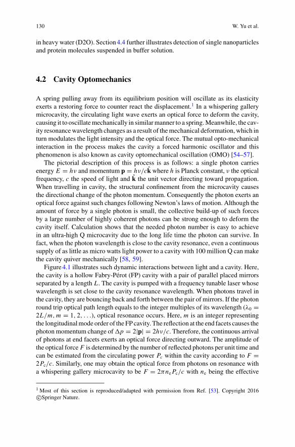
130 W. Yu et al.
in heavy water (D2O). Section4.4 further illustrates detection of single nanoparticlesand protein molecules suspended in buffer solution.
4.2 Cavity Optomechanics
A spring pulling away from its equilibrium position will oscillate as its elasticityexerts a restoring force to counter react the displacement.1 In a whispering gallerymicrocavity, the circulating light wave exerts an optical force to deform the cavity,causing it to oscillatemechanically in similarmanner to a spring.Meanwhile, the cav-ity resonancewavelength changes as a result of themechanical deformation, which inturn modulates the light intensity and the optical force. The mutual opto-mechanicalinteraction in the process makes the cavity a forced harmonic oscillator and thisphenomenon is also known as cavity optomechanical oscillation (OMO) [54–57].
The pictorial description of this process is as follows: a single photon carriesenergy E = hν and momentum p = hν/ckwhere h is Planck constant, ν the opticalfrequency, c the speed of light and k the unit vector directing toward propagation.When travelling in cavity, the structural confinement from the microcavity causesthe directional change of the photon momentum. Consequently the photon exerts anoptical force against such changes following Newton’s laws of motion. Although theamount of force by a single photon is small, the collective build-up of such forcesby a large number of highly coherent photons can be strong enough to deform thecavity itself. Calculation shows that the needed photon number is easy to achievein an ultra-high Q microcavity due to the long life time the photon can survive. Infact, when the photon wavelength is close to the cavity resonance, even a continuoussupply of as little as micro watts light power to a cavity with 100 million Q can makethe cavity quiver mechanically [58, 59].
Figure4.1 illustrates such dynamic interactions between light and a cavity. Here,the cavity is a hollow Fabry-Pérot (FP) cavity with a pair of parallel placed mirrorsseparated by a length L . The cavity is pumped with a frequency tunable laser whosewavelength is set close to the cavity resonance wavelength. When photons travel inthe cavity, they are bouncing back and forth between the pair of mirrors. If the photonround trip optical path length equals to the integer multiples of its wavelength (λ0 =2L/m,m = 1, 2, . . .), optical resonance occurs. Here, m is an integer representingthe longitudinalmode order of the FP cavity. The reflection at the end facets causes thephoton momentum change of�p = 2|p| = 2hν/c. Therefore, the continuous arrivalof photons at end facets exerts an optical force directing outward. The amplitude ofthe optical force F is determined by the number of reflected photons per unit time andcan be estimated from the circulating power Pc within the cavity according to F =2Pc/c. Similarly, one may obtain the optical force from photons on resonance witha whispering gallery microcavity to be F = 2πnePc/c with ne being the effective
1 Most of this section is reproduced/adapted with permission from Ref. [53]. Copyright 2016c©Springer Nature.
4 Optomechanical Sensing 131
Fig. 4.1 Schematic plot showing the concept of radiation pressure. The continuous wave at awavelength close to the cavity resonance enters a Fabry-Pérot cavity. The radiation pressure causedby the light reflecting at the mirror displaces the mirror front by an amount of dx , which modulatesthe output light with an oscillation frequency �′
m jointly determined by the natural mechanicalresponse of the cavity and the radiation pressure
refractive index of the cavity. Further, the high intensity buildup at the cavity sidewalldue to the combined effects of small mode volume and high optical Q of the WGMmicrocavity, the resulting pressure is sufficient to deform the cavity structure. Forexample, an ultrahighQ (Q > 108)WGMmicrocavity generates a radiation pressureabove thousands of Pascal with as little as 1 mW external optical power continuouslysupplied to the cavity. With a sufficient power, the radiation pressure is able to pushthe cavity wall outward from its original position with a small radial displacementof x . Consequently, the cavity resonance shifts toward a longer wavelength becauseof the increased optical path length.
To describe the dynamic process, consider a pump laser operating with constantpower at a fixed wavelength slightly shorter than cavity resonance (blue detuning)initially delivers light to the cavity, the radiation pressure will be established tostretch the cavity along the radial direction. Meanwhile, the increasing cavity defor-mation results in an increasing tensile force to counteract the radiation pressure.On the other hand, the increasing cavity circumference due to the deformation fur-ther increases the relative detuning between the cavity resonance and the pumplaser wavelength and reduces radiation pressure. The combined efforts from theincreasing tensile force and decreasing radiation pressure will eventually revert thestretching to compressing with tensile force starting to decrease and radiation pres-sure to increase. Consequently, the cavity oscillates mechanically. As portion of theintracavity light leaks out, the dynamical backaction between the optical mode andmechanical motion leads to an observable transmission modulation on the cavityoutput spectrum.
132 W. Yu et al.
4.2.1 Optical Spring Effect
Here we further analyse cavity optomechanics in details with a silica microsphereas an example, and in the context of single molecule sensing. As known [60], awaveguide coupled microresonator follows the dynamic equation
da
dt=
(j�ω − �t
2
)a + j
√�eAin (4.1)
where a is the field amplitude of an optical whispering-gallery mode (WGM), nor-malized such that the cavity mode energy U = |a|2. Ain is the amplitude of inputlaser field, normalized such that Pin = |Ain|2 is the laser power at the waveguideinput. �ω = ωl − ω0 is the optical angular frequency detuned from the laser angularfrequency ωl to the cold cavity resonance ω0. �t is the total photon decay rate ofthe loaded cavity such that it relates to the loaded optical quality factor according toQt = ω0/�t , and �e is the extrinsic photon decay rate associated with the externalwaveguide coupling and inverse proportional to the coupled optical quality factorfollowing Qe = ω0/�e. The decay rates �t and �e are related to the intrinsic photondecay rate �i with �t = �i + �e. Again, �i and the intrinsic optical quality fac-tor follows Qi = ω0/�i. In continuous wave (CW) mode, the steady state solution(da/dt ≡ 0) of Eq. (4.1) can be expressed as
a0 = j√
�eAin�t2 − j�ω
(4.2)
Consequently, the amplitude of the optical wave at the output of the waveguide Aout
can be found as
Aout = Ain + j√
�ea0 =�i−�e
2 − j�ω
�i+�e2 − j�ω
Ain (4.3)
Accordingly, one may rewrite the transmission spectrum in Chap.2 as
T = |Aout|2|Ain|2 = 1 − �i�e
�2ω + (�t/2)2
(4.4)
Further, we can define the power dropped to the cavity Pd as
Pd = |Ain|2(1 − T )
= �i�e
�2ω + (�t/2)2
Pin
= �i|a0|2(4.5)
which indicates that Pd is expended to compensate the cavity energy dissipation�i |a0|2.

4 Optomechanical Sensing 133
When the circulating power is strong enough, it will produce a radiation pres-sure that is sufficient to drive the mechanical vibration mode of the cavity. Themechanical mode for a microsphere has a motion that modulates the device radiuswhich in turn modulates the optical cavity resonance ω′
0 = ω0 + gomx with x rep-resenting the effective mechanical displacement of the cavity radius from its coldcavity value. gom = dω0/dx is the optomechanical coupling coefficient, which scalesinversely with the radius for a microsphere. A finite element simulation shows that|gom|/(2π) ≈ 6.2 GHz/nm at a wavelength of 974 nm for a 100µm-diameter silicamicrosphere. Such an optomechanical coupling modifies Eq. (4.1) by an additionaldetuning term − jgomx and can be described by the following coupled equations ofmotion [54]:
da
dt=
(j�ω − jgomx − �t
2
)a + j
√�eAin, (4.6)
d2x
dt2+ �m
dx
dt+ �2
mx = Frad(t)
meff+ FL(t)
meff, (4.7)
Equation (4.6) reflects the cavity optical resonance modulation due to its mechanicalmotion through the optomechanical coupling coefficient. Consequently, the cavitymechanical displacement changes the optical mode by altering the laser cavity detun-ing according to �′
ω(x) = ωl − ω0(x) = �ω − gomx .Equation (4.7) describes themechanical oscillation of the cavity,�m,�m, andmeff
are the damping rate, intrinsic mechanical resonance frequency, and effective massof the mechanical mode, respectively. FL is the thermal Langevin force responsiblefor the thermal Brownian motion of the mechanical mode and Frad describes theradiation pressure produced by the intra-cavity laser intensity. Note that the totalphoton energy in the cavity can be expressed as
U (x) = N�ω′0 = N�(ω0 + gomx) (4.8)
where N = |a|2�ω′
0≈ |a|2
�ω0is the total number of photons in the cavity. We obtain the
radiation force [61]
Frad = −dU (x)
dx= −N�gom ≈ −gom|a|2
ω0(4.9)
In general, x(t), a(t) and Frad(t) are all functions of time. Seeking close formsolutions is impossible given the highly nonlinear nature of the equation. How-ever, when the mechanical displacement is small, under the linear approximation,we may assume that a(t) = a0 + δa(t) and x(t) = x0 + δx(t) where |δa(t)| � |a0|and |δx | � |x0|. x0 and a0 are steady state solutions of Eqs. (4.6) and (4.7) by settingall time derivatives to zero (da0/dt = dx0/dt = d2x0/dt2 ≡ 0).
a0 = j√
�eAin�t2 − j (�ω − gomx0)
(4.10)
134 W. Yu et al.
x0 = − gom|a0|2ω0meff�2
m
(4.11)
Again, the presence of cavity optomechanics simply modifies a0 in Eq. (4.2)by an additional static cavity resonance shift gomx0 as the effective cavity radiusstretches to R + x0 in equilibrium by the radiation force. Subsequently, Eq. (4.6) canbe decomposed into
da0dt
+ dδa(t)
dt=
[j (�ω − gom(x0 + δx)) − �t
2
](a0 + δa) + j
√�eAin
=[j (�ω − gomx0) − �t
2
]a0 + j
√�eAin
+[j (�ω − gomx0) − �t
2
]δa(t) − jgoma0δx(t) − jgomδx(t)δa(t)
(4.12)Here, the first term on the left side of the equation, da0/dt , and the first two terms onthe right of the second equation sign vanish as they form the steady state equation ofa0. Further, the second order perturbation term− jgomδxδa can be neglected, leadingto a simple expression
dδa(t)
dt=
(j�′
ω − �t
2
)δa(t) − jgoma0δx(t) (4.13)
Using the the Fourier transform defined as δa(�) = F {δa(t)} = ∫ +∞−∞ δa(t)
e j�t dt , Eq. (4.13) can be expressed in frequency domain
− j�δa(�) =(j�′
ω − �t
2
)δa(�) − jgoma0δ x(�) (4.14)
with δ x(�) = F {δx(t)}. Consequently, we obtain the spectral response of the per-turbed field as
δa(�) = jgoma0j (�′
ω + �) − �t/2δ x(�) (4.15)
and its complex conjugate δa(�) has the form
δa∗(�) = jgoma∗0
j (�′ω + �) + �t/2
δ x∗(�). (4.16)
To obtain the field pattern in frequency domain, one need to find the Fourier trans-form of the mechanical displacement δ x(�). To do so, we first apply the similarperturbation approach to Eq. (4.7)
d2δx(t)
dt2+ �m
dδx(t)
dt+ �2
mδx(t) = Frad,0
meff− �2
mx0 + δFrad(t)
meff+ FL(t)
meff(4.17)
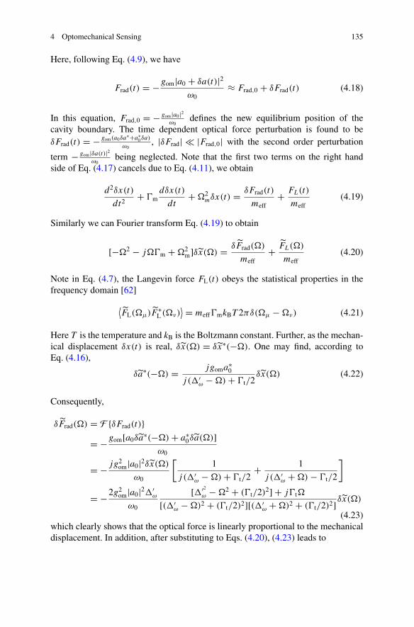
4 Optomechanical Sensing 135
Here, following Eq. (4.9), we have
Frad(t) = −gom|a0 + δa(t)|2ω0
≈ Frad,0 + δFrad(t) (4.18)
In this equation, Frad,0 = − gom |a0|2ω0
defines the new equilibrium position of thecavity boundary. The time dependent optical force perturbation is found to beδFrad(t) = − gom(a0δa∗+a∗
0 δa)
ω0, |δFrad| � |Frad,0| with the second order perturbation
term − gom |δa(t)|2ω0
being neglected. Note that the first two terms on the right handside of Eq. (4.17) cancels due to Eq. (4.11), we obtain
d2δx(t)
dt2+ �m
dδx(t)
dt+ �2
mδx(t) = δFrad(t)
meff+ FL(t)
meff(4.19)
Similarly we can Fourier transform Eq. (4.19) to obtain
[−�2 − j��m + �2m]δ x(�) = δ Frad(�)
meff+ FL(�)
meff(4.20)
Note in Eq. (4.7), the Langevin force FL(t) obeys the statistical properties in thefrequency domain [62]
⟨FL(�μ)F∗
L (�ν)⟩ = meff�mkBT 2πδ(�μ − �ν) (4.21)
Here T is the temperature and kB is the Boltzmann constant. Further, as the mechan-ical displacement δx(t) is real, δ x(�) = δ x∗(−�). One may find, according toEq. (4.16),
δa∗(−�) = jgoma∗0
j (�′ω − �) + �t/2
δ x(�) (4.22)
Consequently,
δ Frad(�) = F {δFrad(t)}= −gom[a0δa∗(−�) + a∗
0δa(�)]ω0
= − jg2om|a0|2δ x(�)
ω0
[1
j (�′ω − �) + �t/2
+ 1
j (�′ω + �) − �t/2
]
= −2g2om|a0|2�′ω
ω0
[�′2ω − �2 + (�t/2)2] + j�t�
[(�′ω − �)2 + (�t/2)2][(�′
ω + �)2 + (�t/2)2]δ x(�)
(4.23)which clearly shows that the optical force is linearly proportional to the mechanicaldisplacement. In addition, after substituting to Eqs. (4.20), (4.23) leads to

136 W. Yu et al.
δ x(�) = FL (�)
meff
⎧⎨⎩−�2 − j��m + �2
m + 2g2om |a0|2�′ω
ω0meff
[�′2ω − �2 + (�t/2)2] + j�t�
[(�′ω − �)2 + (�t/2)2][(�′
ω + �)2 + (�t/2)2]
⎫⎬⎭
−1
= − FL (�)
meff
1
�′m2 − �2 − j�′
m�
(4.24)
According to Eq. (4.5), the interaction between Pd and the mechanical motionmodifies the dynamics of the mechanical mode, resulting in an effective mechanicaldamping rate �′
m and an effective mechanical frequency �′m given by [54],
�′m2 ≈ �2
m + 2g2omPd�′ω
meffω0�i
�′ω2 − �2
m + (�t/2)2
[(�′ω + �m)2 + (�t/2)2][(�′
ω − �m)2 + (�t/2)2](4.25)
�′m ≈ �m − 2g2omPd�
′ω
meffω0�i
�t
[(�′ω + �m)2 + (�t/2)2][(�′
ω − �m)2 + (�t/2)2] ,(4.26)
which are obtained from Eqs. (4.6) and (4.7) by treating the mechanical motion as aperturbation to the optomechanical system. Equation (4.26) shows the dependence ofoptomechanical amplification/cooling on the laser-cavity detuning. The mechanicaldamping rate �′
m is modulated by the radiation pressure according to the sign of thedetuning �′
ω. When the pump laser is operating at a frequency ωl higher than thecavity resonance ω′
0 = ω0 + gomx0, the blue detuned pump laser (�′ω > 0) leads to
a decrease of the mechanical damping rate and drives the cavity into “amplification”regime. With sufficient optical power, �′
m = 0 and regenerative coherent oscilla-tion or “phonon lasing” occurs. Therefore, the optical drop power threshold PT
d forregenerative optomechanical oscillation can be found from Eq. (4.26)
PTd = meffω0�m�i
2g2om�′ω�t
[(�′
ω + �m)2 + (�t/2)2] [
(�′ω − �m)2 + (�t/2)
2]
(4.27)
Consequently, Eqs. (4.25) and (4.26) can be simplified to
�′m2 ≈ �2
m + Pd�m
PTd �t
[�′
ω
2 − �2m + (�t/2)
2]
(4.28)
�′m ≈
(1 − Pd
PTd
)�m (4.29)
When Pd > PTd , the cavity mechanical motion (�′
m) is amplified by the radiationpressure and induces the mechanical instability. Due to the backaction of the cavitymotion, the circulating light (ωl) is then Doppler shifted so that has two sidebands at(ωl − �′
m) and (ωl + �′m) on its spectrum [63]. Affected by the power distribution
within one cavity resonance mode, the sideband with a frequency closer to the res-onance has a enhanced intensity compared to the other. The unbalanced sidebands
4 Optomechanical Sensing 137
cause a net energy transfer from optical mode to mechanical motion in the bluedetuning regime, since the sideband with lowered frequency photons (ωl − �′
m) isenhanced by the cavity.
In general, the cavity mechanical frequency �m is much smaller than effectivelaser cavity detuning (�′
ω ≈ �ω) and total cavity photon decay rate �t . Therefore,Eqs. (4.26), (4.25) and (4.27) can be further simplified to
�′m2 ≈ �2
m + 2g2om�ePinmeffω0
�ω[�2
ω + (�t/2)2]2 (4.30)
�′m ≈ �m − 2g2om�ePin
meffω0
�ω�t[�2
ω + (�t/2)2]3 (4.31)
PTd = meffω0�m�i
2g2om�ω�t
[�2
ω + (�t/2)2]2
, (4.32)
With a red detuned laser on the opposite side of the cavity resonance (�′ω < 0),
the negative sign of the frequency detuning adds an extra effective damping rate tothe intrinsic one so that further suppresses the mechanical motion of the cavity ordrives the cavity to a “cooling” regime. There exists an net energy transfer from themechanical motion to the optical mode through the optomechanics. Therefore, thecavity is considered to be cooling down by the optical force under this situation.
In summary, the dynamic backaction between the laser field and mechanicalmotion can be either in phase or out of phase, resulting amplifying or cooling themechanical motion. The efficiency relies on gom, the optical Q, and the laser-cavitydetuning �′
ω. Therefore, the high optical quality and strong optomechanical cou-pling in a cavity would provide efficient optomechanical excitation. In addition, onthe blue detuning side, the optical wave amplifies the mechanical motion and leadsto a decrease of the mechanical damping rate that depends linearly on the opticalpower. A large enough optical power is able to boost the mechanical motion abovethe oscillation threshold resulting in a coherent optomechanical oscillation (OMO)with a very narrow linewidth. This underlies the principle of cavity optomechanicaltransduction sensing, or optical spring sensing, whichwill be discussed in detail later.
The dynamic interaction between light and cavity mechanics can be further inter-preted by an optical spring. It is well known that the harmonic oscillation angularfrequency �m of a spring follows the Hooke’s law �m = √
k/meff where k is thespring constant. When two spring k1 and k2 are connected in parallel to a load meff ,they are equivalent to a spring k = k1 + k2 with eigen frequency square �2
m equalsto the sum of each spring’s eigen frequency (�1,2 = √
k1,2/meff , �2m = �2
1 + �22. In
analogy, the oscillation angular frequency of the OMO can be described by the sameequation, by including the radiation pressure contribution to the spring constant,k = kmech + kopt [64].
�′m2 = kmech
meff+ kopt(�′
ω, �t)
meff(4.33)
138 W. Yu et al.
Here, kmech = meff�2m is the cavity intrinsic mechanical spring constant and we call
kopt the optical spring constant as the optomechanical coupling behaves like anotherspring connect in parallel to the intrinsic one. According to Eq. (4.25), the opticalspring constant can be expressed as
kopt(�′ω, �t) = 2g2omPd�
′ω
ω0�i
�′ω2 − �2
m + (�t/2)2
[(�′ω + �m)2 + (�t/2)2][(�′
ω − �m)2 + (�t/2)2](4.34)
which can be further simplified, according to Eq. (4.30),
kopt(�′ω, �t) ≈ 2g2om�ePin
ω0
�ω[�2
ω + (�t/2)2]2 (4.35)
under the assumption that the cavity mechanical frequency is much smaller than theeffective laser cavity detuning. Evidently, as the magnitude of the radiation pressurechanges due to the cavity resonance detuning, the optical spring constant dependssensitively on the cavity resonance. The optical spring effect provides an effectivemechanical stiffness that relies on the radiation pressure produced by the WGM,which is essential for OMO sensing described in the latter sections.
4.2.2 Principles of Optical Spring Sensing
When the laser wavelength λl is blue detuned to the cavity resonance, the opticalwave can efficiently boost the mechanical motion above the threshold of regen-erative coherent oscillation [54, 65], resulting in highly coherent optomechanicaloscillation (OMO) with a narrow mechanical linewidth. According to Eq. (4.34),the intracavity laser field produce an effective mechanical rigidity [54], resultingthe overall frequency fm = �′
m/2π depending sensitively on the laser-cavity detun-ing �λ = λl − λ′
0 with λ′0 = 2πc/(ω0 + gomx0) and λl = 2πc/ωl. Consequently,
according to Eq. (4.25), particle binding induced cavity resonance wavelength shift,δλ, is transduced to the frequency shift, δ fm according to δ fm = − d fm
d�λδλ which can
be probed with an electrical spectrum analyzer (Fig. 4.2).Theminimal detectable frequency shift (δ fm)min is determined byOMO linewidth
� fm, which in turn determines the minimal detectable cavity resonance shift(δλ/λ0)min = � fm
λ0/(− d fm
d�λ). By defining an effectivemechanical Q factor of coherent
OMO, Qeffm ≡ fm/� fm. One may derive the sensing resolution
(δλ
λ0
)min
= 1
ηomQeffm Qt
, (4.36)
where ηom represents the optomechanical transduction factor with a value in the orderof ηom ∼ 1. Equation (4.36) shows clearly that the sensing resolution scales not only
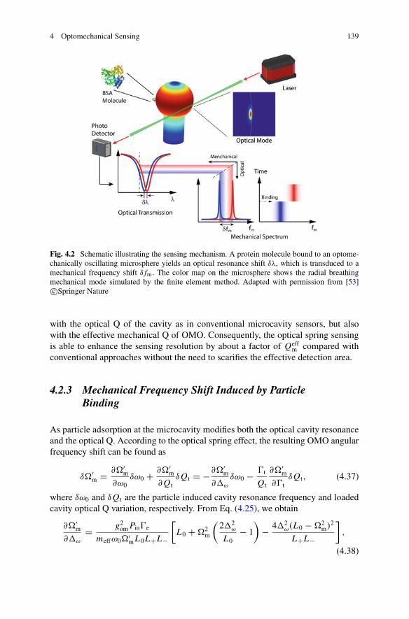
4 Optomechanical Sensing 139
Fig. 4.2 Schematic illustrating the sensing mechanism. A protein molecule bound to an optome-chanically oscillating microsphere yields an optical resonance shift δλ, which is transduced to amechanical frequency shift δ fm. The color map on the microsphere shows the radial breathingmechanical mode simulated by the finite element method. Adapted with permission from [53]c©Springer Nature
with the optical Q of the cavity as in conventional microcavity sensors, but alsowith the effective mechanical Q of OMO. Consequently, the optical spring sensingis able to enhance the sensing resolution by about a factor of Qeff
m compared withconventional approaches without the need to scarifies the effective detection area.
4.2.3 Mechanical Frequency Shift Induced by ParticleBinding
As particle adsorption at the microcavity modifies both the optical cavity resonanceand the optical Q. According to the optical spring effect, the resulting OMO angularfrequency shift can be found as
δ�′m = ∂�′
m
∂ω0δω0 + ∂�′
m
∂QtδQt = −∂�′
m
∂�ω
δω0 − �t
Qt
∂�′m
∂�tδQt, (4.37)
where δω0 and δQt are the particle induced cavity resonance frequency and loadedcavity optical Q variation, respectively. From Eq. (4.25), we obtain
∂�′m
∂�ω
= g2omPin�e
meffω0�′mL0L+L−
[L0 + �2
m
(2�2
ω
L0− 1
)− 4�2
ω(L0 − �2m)2
L+L−
],
(4.38)
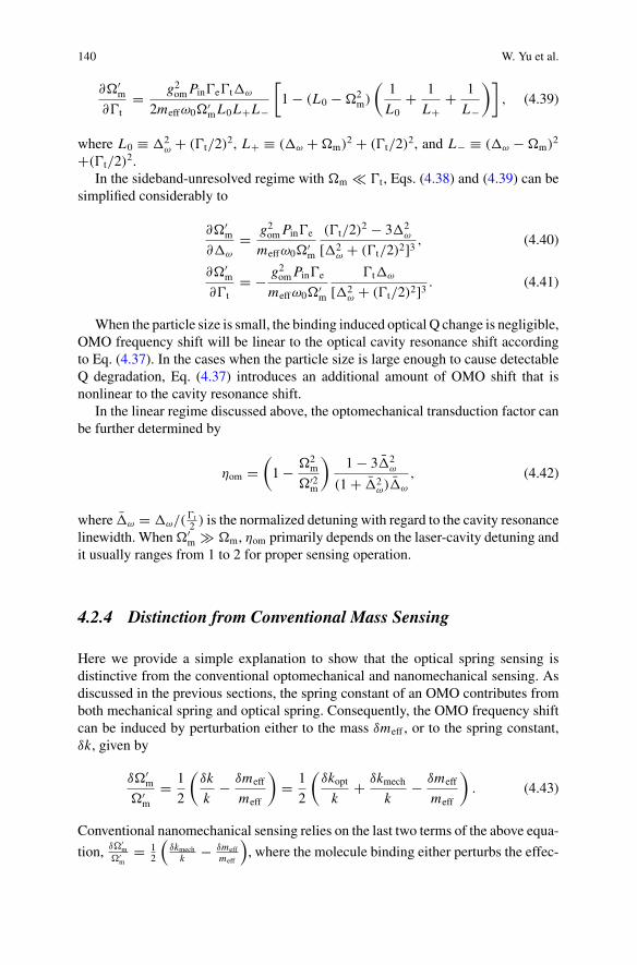
140 W. Yu et al.
∂�′m
∂�t= g2omPin�e�t�ω
2meffω0�′mL0L+L−
[1 − (L0 − �2
m)
(1
L0+ 1
L++ 1
L−
)], (4.39)
where L0 ≡ �2ω + (�t/2)2, L+ ≡ (�ω + �m)2 + (�t/2)2, and L− ≡ (�ω − �m)2
+(�t/2)2.In the sideband-unresolved regime with �m � �t , Eqs. (4.38) and (4.39) can be
simplified considerably to
∂�′m
∂�ω
= g2omPin�e
meffω0�′m
(�t/2)2 − 3�2ω
[�2ω + (�t/2)2]3 , (4.40)
∂�′m
∂�t= − g2omPin�e
meffω0�′m
�t�ω
[�2ω + (�t/2)2]3 . (4.41)
When the particle size is small, the binding induced optical Q change is negligible,OMO frequency shift will be linear to the optical cavity resonance shift accordingto Eq. (4.37). In the cases when the particle size is large enough to cause detectableQ degradation, Eq. (4.37) introduces an additional amount of OMO shift that isnonlinear to the cavity resonance shift.
In the linear regime discussed above, the optomechanical transduction factor canbe further determined by
ηom =(1 − �2
m
�′2m
)1 − 3�2
ω
(1 + �2ω)�ω
, (4.42)
where �ω = �ω/(�t2 ) is the normalized detuning with regard to the cavity resonance
linewidth. When�′m � �m, ηom primarily depends on the laser-cavity detuning and
it usually ranges from 1 to 2 for proper sensing operation.
4.2.4 Distinction from Conventional Mass Sensing
Here we provide a simple explanation to show that the optical spring sensing isdistinctive from the conventional optomechanical and nanomechanical sensing. Asdiscussed in the previous sections, the spring constant of an OMO contributes fromboth mechanical spring and optical spring. Consequently, the OMO frequency shiftcan be induced by perturbation either to the mass δmeff , or to the spring constant,δk, given by
δ�′m
�′m
= 1
2
(δk
k− δmeff
meff
)= 1
2
(δkoptk
+ δkmech
k− δmeff
meff
). (4.43)
Conventional nanomechanical sensing relies on the last two terms of the above equa-
tion, δ�′m
�′m
= 12
(δkmech
k − δmeffmeff
), where the molecule binding either perturbs the effec-
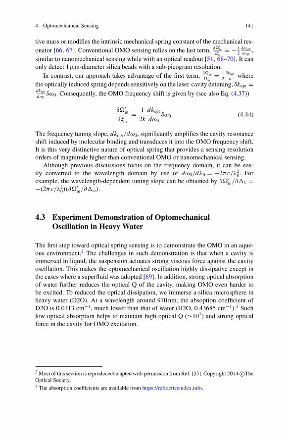
4 Optomechanical Sensing 141
tive mass or modifies the intrinsic mechanical spring constant of the mechanical res-onator [66, 67]. Conventional OMO sensing relies on the last term, δ�′
m�′
m= − 1
2δmeffmeff
,similar to nanomechanical sensing while with an optical readout [51, 68–70]. It canonly detect 1µm-diameter silica beads with a sub-picogram resolution.
In contrast, our approach takes advantage of the first term, δ�′m
�′m
= 12
δkoptk where
the optically induced spring depends sensitively on the laser-cavity detuning, δkopt =dkoptdω0
δω0. Consequently, the OMO frequency shift is given by (see also Eq. (4.37))
δ�′m
�′m
= 1
2k
dkoptdω0
δω0. (4.44)
The frequency tuning slope, dkopt/dω0, significantly amplifies the cavity resonanceshift induced by molecular binding and transduces it into the OMO frequency shift.It is this very distinctive nature of optical spring that provides a sensing resolutionorders of magnitude higher than conventional OMO or nanomechanical sensing.
Although previous discussions focus on the frequency domain, it can be eas-ily converted to the wavelength domain by use of dω0/dλ0 = −2πc/λ2
0. Forexample, the wavelength-dependent tuning slope can be obtained by ∂�′
m/∂�λ =−(2πc/λ2
0)(∂�′m/∂�ω).
4.3 Experiment Demonstration of OptomechanicalOscillation in Heavy Water
The first step toward optical spring sensing is to demonstrate the OMO in an aque-ous environment.2 The challenges in such demonstration is that when a cavity isimmersed in liquid, the suspension actuates strong viscous force against the cavityoscillation. This makes the optomechanical oscillation highly dissipative except inthe cases where a superfluid was adopted [69]. In addition, strong optical absorptionof water further reduces the optical Q of the cavity, making OMO even harder tobe excited. To reduced the optical dissipation, we immerse a silica microsphere inheavy water (D2O). At a wavelength around 970nm, the absoption coefficient ofD2O is 0.0113 cm−1, much lower than that of water (H2O, 0.43685 cm−1).3 Suchlow optical absorption helps to maintain high optical Q (∼107) and strong opticalforce in the cavity for OMO excitation.
2 Most of this section is reproduced/adapted with permission from Ref. [35]. Copyright 2014 c©TheOptical Society.3 The absorption coefficients are available from https://refractiveindex.info.

142 W. Yu et al.
4.3.1 Experiment Results and Discussions
The experiment setup is shown in Fig. 4.3. An external cavity tunable laser (Newport6300LN) operating at 970 nm wavelength range is used to drive the cavity OMO. Atthe laser output, a variable optical attenuator (VOA A) is inserted for power control.A 99/1 optical directional coupler (OC A) further split the light to two branches. The99% port was connected to the input of a tapered optical fiber to actuate the OMOof silica microsphere under test. The 100µm-diameter microsphere was fabricatedby melting a silica fiber with a CO2 laser and immersed in heavy water (D2O). Forprecision position control, the microsphere was mounted on a nanopositioner. Thetransmitted optical signal from the microsphere was converted to electrical signalsby a photodetector (New focus 1811) placed at the output of the same tapered fiber.The electrical signal was further split by a 50/50 electrical splitter such that the signalcan be examined in both time and frequency domain with an Agilent DSO 90404Aoscilloscope and a Tektronix RSA 3408B real time spectrum analyzer.
The 1% output branch of the directional coupler is connected to a reference inter-ferometer to provide accurate optical frequency calibration in optical Q measure-ments. As shown in Fig. 4.3, the reference interferometer is built with a pair ofoptical fiber connected between two 50/50 optical couplers. The lengths of the twofibers differ by�L , when light enters the first coupler (OCB), its power splits evenlyat the coupler outputs. The light then propagates along the fiber pair, resulting a rel-ative time delay τ = �L/(ne · c) when arriving at the inputs of the other coupler(OC C). The light will be photo mixed at OC C and converted to electrical signal bythe balanced photo detector. The detector output voltage V0 is related to the opticalfrequency ν and fiber delay τ through
V0
V0,max= cos(2πντ) (4.45)
Fig. 4.3 Experiment setup for the OMOmeasurements. Adapted with permission from [35] c©TheOptical Society
4 Optomechanical Sensing 143
Fig. 4.4 RF power spectrum of the reference interferometer output calibrated from the dark currentspectrum. Adapted with permission from [35] c©The Optical Society
withV0,max being themaximumoutput voltage.Therefore,when τ is precisely known,V0 maps to the optical frequency ν with high precision. To determine τ , we set thelaser in CW mode and connect the photo detector output to an electrical spectrumanalyzer. Figure4.4 shows the power spectrum of the output signal after averagingover 100 measurements and calibrated by subtracting it from the 100 measurementsaveraged dark current spectrum. As shown, the signal spectrum displays a sinc-square shape (blue trace) and the free spectral range � fFSR of the spectrum is theinverse of the delay τ = 1/� fFSR. In this experiment, � fFSR = 21.3 MHz wasdetermined through a least square fit (red dashed line). Equivalently a time delay ofτ = 0.0469µs or length difference �L = 9.73 m is obtained. After calibration, theoutput of the balanced detector is then connected to the oscilloscope shown inFig. 4.3.
To measure the optical Q of the microsphere immersed in D2O, we scan the laserwavelengths around the cavity resonance while reducing its power till the thermaleffect diminishes. The cavity transmission spectrum averaged over 100 measure-ments is displayed as the blue trace in Fig. 4.5. According to Eq. (4.4), the spectrumdisplays a Lorentzian shape. Meanwhile, due to Eq. (4.45), the interferometer sig-nal (green trace) has a sinusoidal shape with a periodicity precisely equals to �FSR.Therefore, using the fitted curve of the interferometer signal, we can accurately mapthe frequency detuning of the transmission spectrum for precision Q measurement.In this experiment, through the least square fit, we obtained an intrinsic optical Q of1.4 × 107 when the microsphere is immersed in D2O. Under the operation couplingcondition, an overall loaded optical Q of 9.8×10⁶ is obtained.
To actuate OMO, we scan the wavelength of the probe laser around the resonancewhile gradually increasing the laser power to about 2.5 mW. With fine adjustment

144 W. Yu et al.
Fig. 4.5 Cavity transmitted optical power (blue trace) displays a Lorentzian shape. The laserfrequency is calibrated through the transmitted signal of the reference interferometer (green trace).The red dashed lines are least square fitting results. Adapted with permission from [35] c©TheOptical Society
Fig. 4.6 Transmitted optical power as a function of probe laser wavelength detune. At a droppedoptical power close to the threshold power, the left inset displayed a sinusoidal spectrum whileat a high dropped power the spectrum displayed in the right inset was distorted by the high orderharmonics. Adapted with permission from [35] c©The Optical Society
of the gap between the tapered fiber and the microsphere, OMO can be observed asshown in Fig. 4.6. As shown, the thermal broaden effect at the blue detuned regimefacilitates the OMO, which helps the locking in sensing experiment discussed inlater section. The insets at the bottom left of the figure shows that the OMO is single

4 Optomechanical Sensing 145
mode when the Pd is slightly above the threshold power. When the dropped powerincreases, however, high order harmonics occurs due to the nonlinear nature of cavityresponse.
To characterize OMO, we set the laser in CW mode and adjust the laser opticalpower using the optical attenuator (VOA A) while keeping the off-resonance trans-mission signal voltage at 0.6Vby adjusting the other attenuator (VOAB) accordingly.The coupler (OC A) 1% output port is switched to an optical power meter for Pdmonitoring. We then scan the laser from lower wavelength toward cavity resonancetill the transmission signal voltage dropped by half. At each wavelength detuningpoint, wemeasure Pd through the readings from the optical powermeter.Meanwhile,transmission signal frequency spectra are collected using the spectrum analyzer andaveraged every 100 traces. Figure4.7 displays the averaged spectrum when Pd is0.4, 1 and 1.1 mW. As shown, when Pd is at 0.4 mW, OMO is well below thresholdwith large spectral bandwidth of 269 kHz and the oscillation is dominated by thenatural mechanical oscillation of the microsphere. When Pd increases to around thethreshold power of 1 mW, the linewidth gradually reduces to 61 kHz. With furtherincreasing Pd above threshold by as little as 0.1 to 1.1 mW, coherent regenerativeoptical spring oscillation rapidly narrows down the linewidth 232Hz. As laser fre-quency jitter noise broadens the averaged spectrum, we examine each individualtrace of the spectrum and find the narrowest linewidth to be 99Hz, corresponding toan effective Qm of 3,884.
Fig. 4.7 RF spectra at dropped power of 1.1, 1 and 0.4 mW, least square fittings to the Lorentzianfunction indicate the linewidths of the optomechanical tones to be 232 Hz, 61 kHz and 269 kHzrespectively. In the main plot, each spectrum was averaged over 100 spectral traces collected seam-lessly at the same drop power level. The inset is the spectrum of single trace measurement. Adaptedwith permission from [35] c©The Optical Society

146 W. Yu et al.
Fig. 4.8 The plot of mechanical linewidth versus dropped power, which indicates an intrinsicmechanical linewidth of 431 kHz and an effective mechanical quality factor of Qm = 0.5 throughthe linear extrapolation. Adapted with permission from [35] c©The Optical Society
According to Eqs. (4.28) and (4.29), at the dropped power well below threshold,�′
m and�′m are linear to the droppedpower.Whenoptical springdiminishes at Pd = 0,
they equals to the intrinsic frequency and decay rate of the cavity’s naturalmechanicaloscillation. In the inset of Fig. 4.9,we plot theOMOpeak frequency vs dropped power(blue square markers). As indicated by Eq. (4.28), when below threshold and in bluedetuning regime (�ω > 0), the optical spring drives the peak frequency graduallyfrom 253 kHz at Pd = 0.3 mW to 370 kHz at 1.0 mW [71]. A linear extrapolation atPd = 0 (red dashed line) predicts an intrinsic mechanic frequency of fm = 199 kHz.To obtain the intrinsic decay rate �m, we plot the linewidth (blue circles) versusPd in Fig. 4.8. Again, a linear extrapolation (red dashed line) predicts an intrinsiclinewidth of 431 kHz at Pd = 0. Accordingly, we obtain �m = 431 (ms)−1, yieldinga Qm = 2π fm/�m ≈ 0.5. The low intrinsic Q is expected due to the mechanicalenergy dissipation to liquid.
In Fig. 4.9, we further plot the cavity mechanical energy normalized to its peakvalue (blue circle markers) versus Pd. Here, the mechanical energy is calculated byintegrating the RF spectrum over the frequency interval as it denotes the oscillationdisplacement. As shown in the figure, at above PT
d , the mechanical energy linearlyincreases with the dropped power at a rapid rate while at below the threshold, theenergy grows slowly. This threshold is a typical “lasing” behaviour and confirmsthe observed oscillation is coherent in nature. Through a linear fit to the mechanicalenergy (red dashed trace), we obtain the threshold power to be 0.98 mW.
Figure4.10 further displays asmanyas 24highorder harmonicswithin a frequencyspan of 10MHz in the transmission spectrum when Pd = 2.6 mW. Meanwhile the

4 Optomechanical Sensing 147
Fig. 4.9 Mechanical energy (normalized to the maximum value) as a function of the droppedpower. The peak frequency as a function of the dropped power is displayed in the inset and a linearextrapolation predicts an intrinsic mechanical frequency of 198.7 kHz. Adapted with permissionfrom [35] c©The Optical Society
Fig. 4.10 In a separate measurement, as high as 24th order harmonics was observed in a frequencyspan of 10 MHz. The inset further displayed the spectrum with a frequency span set at 1 MHz.Adapted with permission from [35] c©The Optical Society
frequency doubling of the second harmonic is evident from the inset when the spanis set to 1 MHz.
To characterise the oscillation stability, we collect the spectrogram in Fig. 4.11with the peak frequency plotted as the black line. Over a time interval of 392 ms,
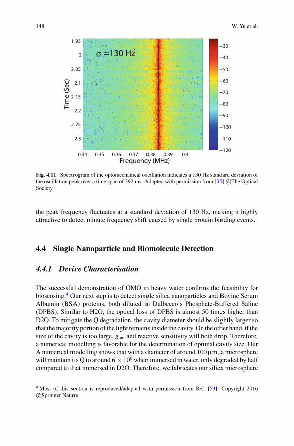
148 W. Yu et al.
Fig. 4.11 Spectrogram of the optomechanical oscillation indicates a 130 Hz standard deviation ofthe oscillation peak over a time span of 392 ms. Adapted with permission from [35] c©The OpticalSociety
the peak frequency fluctuates at a standard deviation of 130 Hz, making it highlyattractive to detect minute frequency shift caused by single protein binding events.
4.4 Single Nanoparticle and Biomolecule Detection
4.4.1 Device Characterisation
The successful demonstration of OMO in heavy water confirms the feasibility forbiosensing.4 Our next step is to detect single silica nanoparticles and Bovine SerumAlbumin (BSA) proteins, both diluted in Dulbecco’s Phosphate-Buffered Saline(DPBS). Similar to H2O, the optical loss of DPBS is almost 50 times higher thanD2O. To mitigate the Q degradation, the cavity diameter should be slightly larger sothat themajority portion of the light remains inside the cavity.On the other hand, if thesize of the cavity is too large, gom and reactive sensitivity will both drop. Therefore,a numerical modelling is favorable for the determination of optimal cavity size. OurA numerical modelling shows that with a diameter of around 100µm, a microspherewill maintain its Q to around 6 × 10⁶ when immersed in water, only degraded by halfcompared to that immersed in D2O. Therefore, we fabricates our silica microsphere
4 Most of this section is reproduced/adapted with permission from Ref. [53]. Copyright 2016c©Springer Nature.
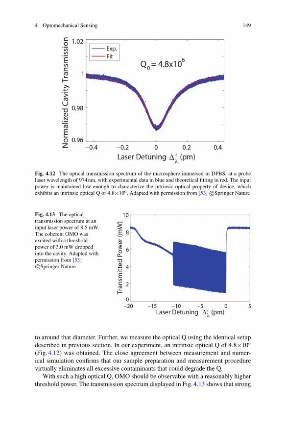
4 Optomechanical Sensing 149
Fig. 4.12 The optical transmission spectrum of the microsphere immersed in DPBS, at a probelaser wavelength of 974nm, with experimental data in blue and theoretical fitting in red. The inputpower is maintained low enough to characterize the intrinsic optical property of device, whichexhibits an intrinsic optical Q of 4.8×10⁶. Adapted with permission from [53] c©Springer Nature
Fig. 4.13 The opticaltransmission spectrum at aninput laser power of 8.5 mW.The coherent OMO wasexcited with a thresholdpower of 3.0 mW droppedinto the cavity. Adapted withpermission from [53]c©Springer Nature
to around that diameter. Further, we measure the optical Q using the identical setupdescribed in previous section. In our experiment, an intrinsic optical Q of 4.8×10⁶
(Fig. 4.12) was obtained. The close agreement between measurement and numer-ical simulation confirms that our sample preparation and measurement procedurevirtually eliminates all excessive contaminants that could degrade the Q.
With such a high optical Q, OMO should be observable with a reasonably higherthreshold power. The transmission spectrum displayed in Fig. 4.13 shows that strong
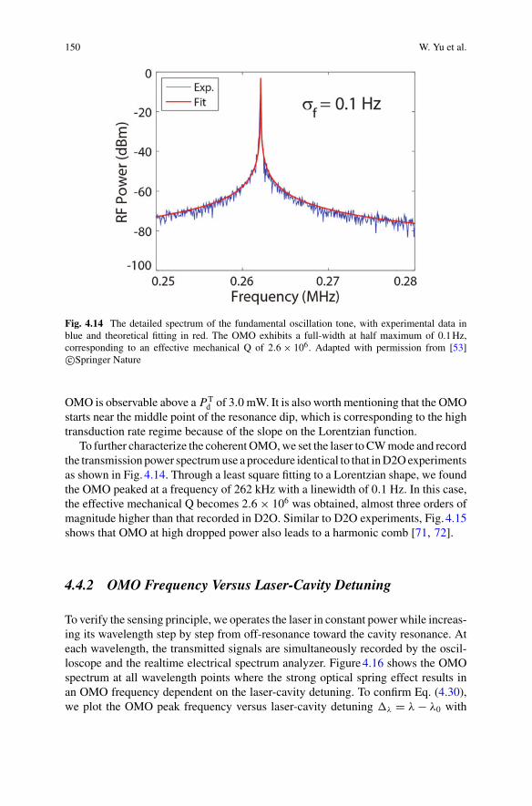
150 W. Yu et al.
Fig. 4.14 The detailed spectrum of the fundamental oscillation tone, with experimental data inblue and theoretical fitting in red. The OMO exhibits a full-width at half maximum of 0.1Hz,corresponding to an effective mechanical Q of 2.6 × 10⁶. Adapted with permission from [53]c©Springer Nature
OMO is observable above a PTd of 3.0 mW. It is also worth mentioning that the OMO
starts near the middle point of the resonance dip, which is corresponding to the hightransduction rate regime because of the slope on the Lorentzian function.
To further characterize the coherentOMO,we set the laser toCWmode and recordthe transmission power spectrumuse a procedure identical to that inD2Oexperimentsas shown in Fig. 4.14. Through a least square fitting to a Lorentzian shape, we foundthe OMO peaked at a frequency of 262 kHz with a linewidth of 0.1 Hz. In this case,the effective mechanical Q becomes 2.6 × 10⁶ was obtained, almost three orders ofmagnitude higher than that recorded in D2O. Similar to D2O experiments, Fig. 4.15shows that OMO at high dropped power also leads to a harmonic comb [71, 72].
4.4.2 OMO Frequency Versus Laser-Cavity Detuning
To verify the sensing principle, we operates the laser in constant power while increas-ing its wavelength step by step from off-resonance toward the cavity resonance. Ateach wavelength, the transmitted signals are simultaneously recorded by the oscil-loscope and the realtime electrical spectrum analyzer. Figure4.16 shows the OMOspectrum at all wavelength points where the strong optical spring effect results inan OMO frequency dependent on the laser-cavity detuning. To confirm Eq. (4.30),we plot the OMO peak frequency versus laser-cavity detuning �λ = λ − λ0 with
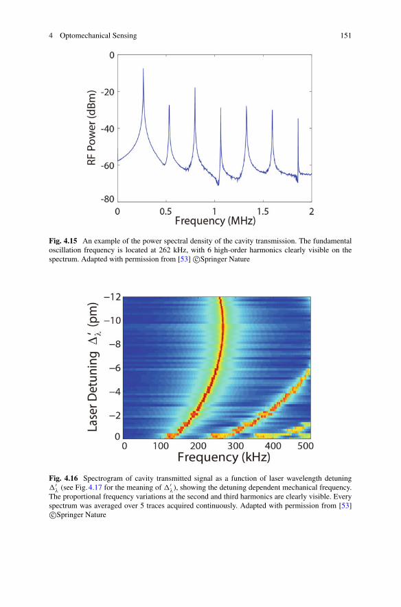
4 Optomechanical Sensing 151
Fig. 4.15 An example of the power spectral density of the cavity transmission. The fundamentaloscillation frequency is located at 262 kHz, with 6 high-order harmonics clearly visible on thespectrum. Adapted with permission from [53] c©Springer Nature
Fig. 4.16 Spectrogram of cavity transmitted signal as a function of laser wavelength detuning�′
λ (see Fig. 4.17 for the meaning of �′λ), showing the detuning dependent mechanical frequency.
The proportional frequency variations at the second and third harmonics are clearly visible. Everyspectrum was averaged over 5 traces acquired continuously. Adapted with permission from [53]c©Springer Nature
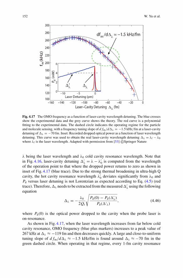
152 W. Yu et al.
Fig. 4.17 The OMO frequency as a function of laser-cavity wavelength detuning. The blue crossesshow the experimental data and the grey curve shows the theory. The red curve is a polynomialfitting to the experimental data. The dashed circle indicates the operating regime for the particleand molecule sensing, with a frequency tuning slope of d fm/d�λ = −1.5 kHz/fm at a laser-cavitydetuning of�λ = −70 fm. Inset: Recorded dropped optical power as a function of laser wavelengthdetuning. This curve was used to obtain the real laser-cavity wavelength detuning �λ = λl − λ0where λl is the laser wavelength. Adapted with permission from [53] c©Springer Nature
λ being the laser wavelength and λ0 cold cavity resonance wavelength. Note thatin Fig. 4.16, laser-cavity detuning �′
λ = λ − λ′0 is computed from the wavelength
of the operation point to that where the dropped power returns to zero as shown ininset of Fig. 4.17 (blue trace). Due to the strong thermal broadening in ultra-high Qcavity, the hot cavity resonance wavelength λ′
0 deviates significantly from λ0 andPd versus laser detuning is not Lorentzian as expected according to Eq. (4.5) (redtrace). Therefore,�λ needs to be extracted from themeasured�′
λ using the followingequation
�λ = − λ0
2Qt
√Pd(0) − Pd(�′
λ)
Pd(�′λ)
, (4.46)
where Pd(0) is the optical power dropped to the cavity when the probe laser ison-resonance.
As shown in Fig. 4.17, when the laser wavelength increases from far below coldcavity resonance, OMO frequency (blue plus markers) increases to a peak value of267 kHz at�λ ≈ −119 fm and then decreases quickly. A large and close-to-uniformtuning slope of d fm/d�λ ≈ −1.5 kHz/fm is found around �λ ≈ −70 fm in thegreen dashed circle. When operating in that regime, every 1-fm cavity resonance
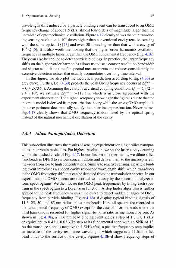
4 Optomechanical Sensing 153
wavelength shift induced by a particle binding event can be transduced to an OMOfrequency change of about 1.5 kHz, almost four orders of magnitude larger than thelinewidth of optomechanical oscillation. Figure4.17 clearly shows that our transduc-ing sensing resolution is 104 times higher than conventional cavity reactive sensingwith the same optical Q [73] and even 50 times higher than that with a cavity of108 Q [5]. It is also worth mentioning that the higher order harmonics oscillationfrequency is multiple times larger than the OMO fundamental frequency (Fig. 4.16).They can also be applied to detect particle bindings. In practice, the larger frequencyshifts on the higher-order harmonics allows us to use a coarser resolution bandwidthand shorter acquisition time for spectral measurements and reduces considerably theexcessive detection noises that usually accumulates over long time interval.
In this figure, we also plot the theoretical prediction according to Eq. (4.30) asgrey curve. Further, Eq. (4.30) predicts the peak OMO frequency occurs at �max
λ =−λ0/(2
√3Qt). Assuming the cavity is at critical coupling condition, Qt = Q0/2 =
2.4 × 10⁶, we estimate �maxλ = −117 fm, which is in close agreement with the
experiment observation. The slight discrepancy showing in the figure is due to that thetheoretic model is derived from perturbation theory while the strong OMO amplitudein our experiment does not fully satisfy the underline approximation. Nevertheless,Fig. 4.17 clearly shows that OMO frequency is dominated by the optical springinstead of the natural mechanical oscillation of the cavity.
4.4.3 Silica Nanoparticles Detection
This subsection illustrates the results of sensing experiments on single silica nanopar-ticles and protein molecules. For highest resolution, we set the laser-cavity detuningwithin the dashed circle of Fig. 4.17. In our first set of experiments, we dilute silicananobeads in DPBS to various concentrations and deliver them to the microsphere inthe order from low to high concentrations. Similar to reactive sensing, a particle bind-ing event introduces a sudden cavity resonance wavelength shift, which transducesto the OMO frequency shift that can be detected from the transmission spectra. In ourexperiment, the OMO spectra are recorded seamlessly by the spectrum analyzer toform spectrograms. We then locate the OMO peak frequencies by fitting each spec-trum in the spectrogram to a Lorentzian function. A step finder algorithm is furtherapplied to the peak frequency versus time curve to detect sudden changes of OMOfrequency from particle binding. Figure4.18a–d display typical binding signals of11.6, 25, 50, and 85 nm radius silica nanobeads. Here all spectra are recorded atthe fundamental frequency of OMO except for the case of 11.6nm beads where thethird harmonic is recorded for higher signal-to-noise ratio as mentioned before. Asshown in Fig. 4.18a, a 11.6 nm bead binding event yields a step of 1.3 ± 0.1 kHz,or equivalent to 0.43 ± 0.03 kHz step at its fundamental tone with an SNR of 13.As the transduce slope is negative (∼1.5kHz/fm), a positive frequency step impliesan increase of the cavity resonance wavelength, which suggests a 11.6nm silicabead binds to the surface of the cavity. Figures4.18b–d show frequency steps of
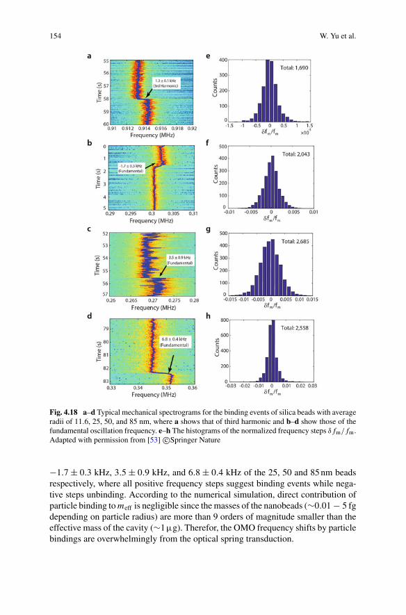
154 W. Yu et al.
Fig. 4.18 a–d Typical mechanical spectrograms for the binding events of silica beads with averageradii of 11.6, 25, 50, and 85 nm, where a shows that of third harmonic and b–d show those of thefundamental oscillation frequency. e–h The histograms of the normalized frequency steps δ fm/ fm.Adapted with permission from [53] c©Springer Nature
−1.7 ± 0.3 kHz, 3.5 ± 0.9 kHz, and 6.8 ± 0.4 kHz of the 25, 50 and 85nm beadsrespectively, where all positive frequency steps suggest binding events while nega-tive steps unbinding. According to the numerical simulation, direct contribution ofparticle binding tomeff is negligible since themasses of the nanobeads (∼0.01 − 5 fgdepending on particle radius) are more than 9 orders of magnitude smaller than theeffective mass of the cavity (∼1µg). Therefor, the OMO frequency shifts by particlebindings are overwhelmingly from the optical spring transduction.
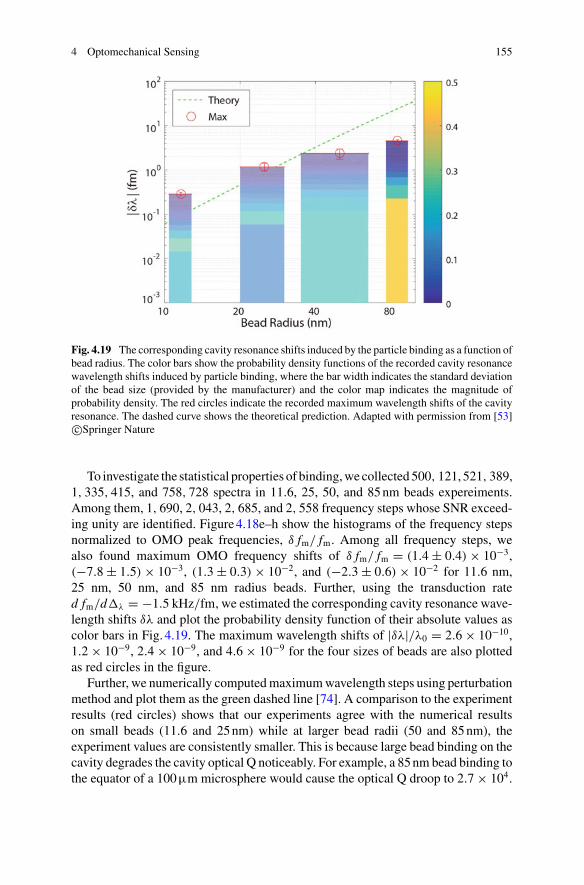
4 Optomechanical Sensing 155
Fig. 4.19 The corresponding cavity resonance shifts induced by the particle binding as a function ofbead radius. The color bars show the probability density functions of the recorded cavity resonancewavelength shifts induced by particle binding, where the bar width indicates the standard deviationof the bead size (provided by the manufacturer) and the color map indicates the magnitude ofprobability density. The red circles indicate the recorded maximum wavelength shifts of the cavityresonance. The dashed curve shows the theoretical prediction. Adapted with permission from [53]c©Springer Nature
To investigate the statistical properties of binding,wecollected500, 121, 521, 389,1, 335, 415, and 758, 728 spectra in 11.6, 25, 50, and 85nm beads expereiments.Among them, 1, 690, 2, 043, 2, 685, and 2, 558 frequency steps whose SNR exceed-ing unity are identified. Figure4.18e–h show the histograms of the frequency stepsnormalized to OMO peak frequencies, δ fm/ fm. Among all frequency steps, wealso found maximum OMO frequency shifts of δ fm/ fm = (1.4 ± 0.4) × 10−3,(−7.8 ± 1.5) × 10−3, (1.3 ± 0.3) × 10−2, and (−2.3 ± 0.6) × 10−2 for 11.6 nm,25 nm, 50 nm, and 85 nm radius beads. Further, using the transduction rated fm/d�λ = −1.5 kHz/fm, we estimated the corresponding cavity resonance wave-length shifts δλ and plot the probability density function of their absolute values ascolor bars in Fig. 4.19. The maximum wavelength shifts of |δλ|/λ0 = 2.6 × 10−10,1.2 × 10−9, 2.4 × 10⁻⁹, and 4.6 × 10⁻⁹ for the four sizes of beads are also plottedas red circles in the figure.
Further, we numerically computedmaximumwavelength steps using perturbationmethod and plot them as the green dashed line [74]. A comparison to the experimentresults (red circles) shows that our experiments agree with the numerical resultson small beads (11.6 and 25nm) while at larger bead radii (50 and 85nm), theexperiment values are consistently smaller. This is because large bead binding on thecavity degrades the cavity optical Q noticeably. For example, a 85nm bead binding tothe equator of a 100µm microsphere would cause the optical Q droop to 2.7 × 10⁴.
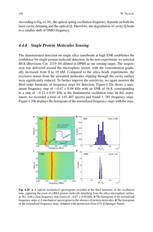
156 W. Yu et al.
According to Eq. (4.30), the optical spring oscillation frequency depends on both thelaser-cavity detuning and the optical Q. Therefore, the degradation of cavity Q leadsto a smaller shift of OMO frequency.
4.4.4 Single Protein Molecules Sensing
The demonstrated detection on single silica nanobeads at high SNR establishes theconfidence for single protein molecule detection. In the next experiment, we selectedBSA (Biovision, Cat. 2119-10) diluted in DPBS as our sensing target. The suspen-sion was delivered around the microsphere sensor, with the concentration gradu-ally increased from 0 to 10 nM. Compared to the silica beads experiments, theexcessive noises from the unwanted molecules slipping through the cavity surfacewere significantly reduced. To further improve the sensitivity, we again monitor thethird order harmonic of frequency steps for detection. Figure4.20a shows a max-imum frequency step of −0.67 ± 0.04 kHz with an SNR of 16.8, correspondingto a step of −0.22 ± 0.01 kHz at the fundamental oscillation tone. In this exper-iment, we recorded a total of 145, 407 spectra and found 1, 785 frequency steps.Figure4.20b displays the histogram of the normalized frequency steps with the max-
Fig. 4.20 a A typical mechanical spectrogram recorded at the third harmonic of the oscillationtone, capturing the event of a BSA protein molecule detaching from the silica microsphere surfaceat 38 s, with a clear frequency step (inset) of −0.67 ± 0.04 kHz. b The histogram of the normalizedfrequency steps. c Amechanical spectrogram in the absence of protein molecules. d The histogramof the normalized frequency steps. Adapted with permission from [53] c©Springer Nature
4 Optomechanical Sensing 157
imum step of δ fm/ fm = (−7.6 ± 0.4) × 10−4, corresponding to a cavity resonanceshift of |δλ| = 0.15 fm.
As a control experiment, we also collected spectra from pure DPBS. The spectro-gram shown in Fig. 4.20c indicates the OMO is stable. Further, the histogram of all118 steps found by our program displayed in Fig. 4.20d shows the baseline noise iswell below the signal detected in BSA experiments. This observation clearly provesthe capability of sensing single BSA molecules with a molecule weight of 66 kDa.By assuming the resonance shift is proportional to the mass (or equivalently, to thevolume) of the protein [75], we derive that our current set-up is capable of detectingproteins as small as 3.9 kDa with an SNR above unity.
The double digit SNR for BSA molecule detection and the predicted 3.9 kDasensitivity demonstrated the astounding sensitivity of optical spring sensors. Notethat improvements can be further made to significantly increase the sensitivity. Forexample, in our current setup, the external cavity laser used in our experiments pro-duces large frequency jitter noise that is transduced to OMO frequency noise andlimits the detection sensitivity. With the future adoption of advanced frequency lock-ing circuitry can further improve the sensing resolution by ∼100 times to aroundδλ/λ0 ∼ 10−14. On the other hand, the optical Q can be increased to above 108 if avisible laser is employed [5], which would further improve the sensing resolution bymore than one order of magnitude. Further, the proposed approach does not needsadditional sensing element such as plasmonic nanoantenna [31–33] attached to thedevice. Therefore, it is capable of utilizing the entire effective sensing area offered bya whispering-gallery microcavity which is more than five orders of magnitude largerthan that with a plasmonic strucutre. Moreover, an incorporation of a plasmonicnanoantenna can enhance the cavity resonance wavelength shift by orders of magni-tude and consequently transducing to the OMO frequency shift by the same order ofmagnitude. These future improvements would enable detecting small molecules andatoms with a mass down to sub-Dalton level in cryogenic environment, with a greatpotential for dramatically advancing the capability of sensing to an unprecedentedlevel. In particular, as the molecule binding occurs during the coherent mechanicalmotion of the sensor, controlling themotion pattern of the coherent OMO (amplitude,phase, time waveform and so on) may function as a unique paradigm to study/controlthe mechanical properties of molecule binding and unbinding. This, in combinationwith certain functionalization of the sensor surface [76] and with implementationof potentially versatile optomechanical motions [54], may offer a unique multifunc-tional biomolecule toolbox that is not only able to observe cellular machineries atwork, but also to selectively manipulate single-molecule interactions.
Additionally, although we focus here on the particle and molecule sensing, thedemonstrated optical spring sensing principle can be applied for other physical sens-ing applications [77], such as inertial sensing [78, 79], electromagnetic field sens-ing [80], gas sensing [81] and so on, which are based upon sensitive detection ofoptical cavity resonance shifts induced by external physical perturbations. There-fore, we expect the demonstrated optical spring to be of great promise for broadapplications beyond the particle and molecule sensing itself.
158 W. Yu et al.
References
1. M. S. Hanay, S. Kelber, A. K. Naik, D. Chi, S. Hentz, E. C. Bullard, E. Colinet, L. Duraffourg,and M. L. Roukes. Single-protein nanomechanical mass spectrometry in real time. NatureNanotech., 7:602–608, 2012.
2. Marek Piliarik and Vahid Sandoghdar. Direct optical sensing of single unlabelled proteins andsuper-resolution imaging of their binding sites. Nature Communications, 5:4495, 2013.
3. A. Serpengüzel, G. Griffel, and S. Arnold. Excitation of resonances of microspheres on anoptical fiber. Opt. Lett., 20(7):654–656, Apr. 1995.
4. F. Vollmer, S. Arnold, and D. Keng. Single virus detection from the reactive shift of awhispering-gallery mode. Proceedings of the National Academy of Sciences, 105(52):20701–20704, 2008.
5. Tao Lu, Hansuek Lee, Tong Chen, Steven Herchak, Ji-Hun Kim, Scott E. Fraser, Richard C.Flagan, and Kerry Vahala. High sensitivity nanoparticle detection using optical microcavities.Proceedings of the National Academy of Sciences, 108(15):5976–5979, 2011.
6. JGZhu, SKOzdemir, YFXiao, LLi, LNHe,DRChen, andLYang.On-chip single nanoparticledetection and sizing by mode splitting in an ultrahigh-Q microresonator. Nature Photonics,4(1):46–49, January 2010.
7. Robert W. Boyd and John E. Heebner. Sensitive disk resonator photonic biosensor. Appl. Opt.,40(31):5742–5747, Nov. 2001.
8. Joachim Knittel, Jon D. Swaim, David L. McAuslan, George A. Brawley, and Warwick P.Bowen. Back-scatter based whispering gallery mode sensing. Scientific Reports, 3:2974, Aug.2013.
9. Saverio Avino, Anika Krause, Rosa Zullo, Antonio Giorgini, Pietro Malara, Paolo De Natale,Hans Peter Loock, and Gianluca Gagliardi. Direct sensing in liquids using whispering-gallery-mode droplet resonators. Advanced Optical Materials, 2(12):1155–1159, 2014.
10. KJ Vahala. Optical microcavities. Nature, 424(6950):839–846, 8 2003.11. M. L. Gorodetsky, A. A. Savchenkov, and V. S. Ilchenko. Ultimate Q of optical microsphere
resonators. Optics Letters, 21(7):453–455, Apr. 1996.12. DK Armani, TJ Kippenberg, SM Spillane, and KJ Vahala. Ultra-high-Q toroid microcavity on
a chip. Nature, 421(6926):925–928, Feb. 27 2003.13. Hansuek Lee, Tong Chen, Jiang Li, Ki Youl Yang, Seokmin Jeon, Oskar Painter, and Kerry J.
Vahala. Chemically etched ultrahigh-Q wedge-resonator on a silicon chip. Nat. Photonics,6(6):369–373, June 2012.
14. Lue Wu, Heming Wang, Qifan Yang, Qingxin Ji, Boqiang Shen, Chengying Bao, MaodongGao, and Kerry Vahala. Greater than one billion Q factor for on-chip microresonators. OpticsLetters, 45(18):5129–5131, 2020.
15. Xudong Fan, Ian M. White, Siyka I. Shopova, Hongying Zhu, Jonathan D. Suter, and YuzeSun. Sensitive optical biosensors for unlabeled targets: A review. Analytica Chimica Acta,620(1-2):8 – 26, 2008.
16. Tao Lu, Tsu-Te Judith Su, Kerry J. Vahala, and Scott Fraser. Split frequency sensing methodsand systems. US Patent, pages US 8,593,638 B2, November 2013. preliminary filing in Oct.2008.
17. Po Dong, Long Chen, Qianfan Xu, and Michal Lipson. On-chip generation of high-intensityshort optical pulses using dynamic microcavities. Opt. Lett., 34(15):2315–2317, Aug. 2009.
18. Jiang Li, Hansuek Lee, and Kerry J. Vahala. Low-noise Brillouin laser on a chip at 1064 nm.Opt. Lett., 39(2):287–290, Jan. 2014.
19. Eric P. Ostby and Kerry J. Vahala. Yb-doped glass microcavity laser operation in water.OpticsLetters, 34(8):1153–1155, 2009.
20. Ivan S. Grudinin, Andrey B.Matsko, and LuteMaleki. Brillouin lasing with a CaF2 whisperinggallery mode resonator. Phys. Rev. Lett., 102:043902, Jan. 2009.
21. H. Rokhsari, T. Kippenberg, T. Carmon, and K.J. Vahala. Radiation-pressure-driven micro-mechanical oscillator. Opt. Express, 13(14):5293–5301, Jul. 2005.
4 Optomechanical Sensing 159
22. T. J. Kippenberg, H. Rokhsari, T. Carmon, A. Scherer, and K. J. Vahala. Analysis of radiation-pressure induced mechanical oscillation of an optical microcavity. Physical Review Letters,95:033901, Jul. 2005.
23. Tal Carmon, Hossein Rokhsari, LanYang, Tobias J. Kippenberg, andKerry J. Vahala. Temporalbehavior of radiation-pressure-induced vibrations of an optical microcavity phonon mode.Physical Review Letters, 94:223902, June 2005.
24. Matt Eichenfield, RyanCamacho, JasperChan,Kerry J.Vahala, andOskar Painter. A picogram-and nanometre-scale photonic-crystal optomechanical cavity.Nature, 459:550–555,May 2009.
25. Siddharth Tallur, Suresh Sridaran, and Sunil A. Bhave. Amonolithic radiation-pressure driven,low phase noise silicon nitride opto-mechanical oscillator.Opt. Express, 19(24):24522–24529,Nov. 2011.
26. Michael A. Taylor, Alex Szorkovszky, Joachim Knittel, Kwan H. Lee, Terry G. McRae, andWarwick P. Bowen. Cavity optoelectromechanical regenerative amplification. Opt. Express,20(12):12742–12751, June 2012.
27. WeiC. Jiang,XiyuanLu, JidongZhang, andQiangLin.High-frequency silicon optomechanicaloscillator with an ultra low threshold. Opt. Express, 20(14):15991–15996, July 2012.
28. Xiankai Sun, King Y. Fong, Chi Xiong, Wolfram H. P. Pernice, and Hong X. Tang. Ghzoptomechanical resonators with high mechanical Q factor in air. Opt. Express, 19(22):22316–22321, Oct. 2011.
29. Yang Deng, Fenfei Liu, Zayd C. Leseman, and Mani Hossein-Zadeh. Thermo-optomechanicaloscillator for sensing applications. Opt. Express, 21(4):4653–4664, Feb. 2013.
30. Kyu Hyun Kim, Gaurav Bahl, Wonsuk Lee, Jing Liu, Matthew Tomes, Xudong Fan, and TalCarmon. Cavity optomechanics on a microfluidic resonator with water and viscous liquids.Light: Science & Applications, 2, 2013.
31. S. I. Shopova, R. Rajmangal, S. Holler, and S. Arnold. Plasmonic enhancement of awhispering-gallery-mode biosensor for single nanoparticle detection. Appl. Phys. Lett., 98(24):243104,2011.
32. Venkata R. Dantham, Stephen Holler, Curtis Barbre, David Keng, Vasily Kolchenko, andStephen Arnold. Label-free detection of single protein using a nanoplasmonic-photonic hybridmicrocavity. Nano Letters, 13(7):3347–3351, 2013.
33. Martin D. Baaske, Matthew R. Foreman, and Frank Vollmer. Single-molecule nucleic acidinteractionsmonitored on a label-freemicrocavity biosensor platform.NatureNanotechnology,9:933–939, 2014.
34. Bumki Min, Eric Ostby, Volker Sorger, Erick Ulin-Avila, Lan Yang, Xiang Zhang, andKerry Vahala. High-Q surface plasmon polariton whispering gallery microcavity. Nature,457(7228):455–458, January 2009.
35. Wenyan Yu, Wei C. Jiang, Qiang Lin, and Tao Lu. Coherent optomechanical oscillation of asilica microsphere in an aqueous environment.Opt. Express, 22(18):21421–21426, Sept. 2014.
36. T Bagci, A Simonsen, S Schmid, L GVillanueva, E Zeuthen, J Appel, J M Taylor, A S�rensen,K Usami, A Schliesser, and E S Polzik. Optical detection of radio waves through a nanome-chanical transducer. Nature, 507(7490):81–5, 3 2014.
37. Yuma Okazaki, Imran Mahboob, Koji Onomitsu, Satoshi Sasaki, Shuji Nakamura, Nobu-HisaKaneko, and Hiroshi Yamaguchi. Dynamical coupling between a nuclear spin ensemble andelectromechanical phonons. Nature Communications, 9:2993, 2018.
38. Bei-Bei Li, George Brawley, Hamish Greenall, Stefan Forstner, Eoin Sheridan, HalinaRubinsztein-Dunlop, and Warwick P. Bowen. Ultrabroadband and sensitive cavity optome-chanical magnetometry. Photon. Res., 8(7):1064–1071, Jul. 2020.
39. S. Forstner, S. Prams, J. Knittel, E.D. van Ooijen, J.D. Swaim, G.I. Harris, A. Szorkovszky,W.P. Bowen, and J. Rubinsztein-Dunlop. Cavity Optomechanical Magnetometer. Phys. Rev.Lett.108, 120801, 2012.
40. Alexander G. Krause, Martin Winger, Tim D. Blasius, Qiang Lin, and Oskar Painter. A high-resolution microchip optomechanical accelerometer. Nature Photonics, 6:768–772, 2012.
41. F. Zhou, Y. Bao, R. Madugani, D.A. Long, J.J. Gorman, and T.W. LeBrun. Broadband ther-momechanically limited sensing with an optomechanical accelerometer. Optica, 8:350–356,2021.
160 W. Yu et al.
42. F. GuzmanCervantes, L. Kumanchik, J. Pratt, and J.M. Taylor. High sensitivity optomechanicalreference accelerometer over 10 kHz. Applied Physics Letters104, 221111, 2014.
43. O. Gerberding, F.G. Cervantes, J. Melcher, J.R. Pratt, and J.M. Taylor. Optomechanical refer-ence accelerometer.Metrologia52, 654, 2015.
44. Sahar Basiri-Esfahani, Ardalan Armin, Stefan Forstner, and Warwick P. Bowen. Precisionultrasound sensing on a chip. Nature Communications, 10:132, 2019.
45. W.J. Westerveld, M. Mahmud-Ul-Hasan, R. Shnaiderman, V. Ntziachristos, X. Rottenberg,S. Severi, and V. Rochus. Sensitive, small, broadband and scalable optomechanical ultrasoundsensor in silicon photonics. Nature Photonics, 15, 341–345 2021
46. E. Gavartin, P. Verlot, and T.J. Kippenberg. A hybrid on-chip optomechanical transducer forultrasensitive force measurements. Nature Nanotechnology7, 509–514, 2012.
47. G.I. Harris, D.L. McAuslan, T.M. Stace, A.C. Doherty, and W.P. Bowen. Minimum require-ments for feedback enhanced force sensing. Physical Review Letters111, 103603, 2013.
48. T. P. Purdy, K. E. Grutter, K. Srinivasan, and J. M. Taylor. Quantum correlations from a room-temperature optomechanical cavity. Science, 356(6344):1265–1268, 2017.
49. T. Purdy, P.L. Yu, N. Kampel, R. Peterson, K. Cicak, R. Simmonds, and C. Regal. Optome-chanical Raman-ratio thermometry. Physical Review A92 031802, 2015.
50. R. Singh, and T.P. Purdy. Detecting Acoustic Blackbody Radiation with an OptomechanicalAntenna. Physical Review Letters125, 120603, 2020.
51. Fenfei Liu, Seyedhamidreza Alaie, Zayd C. Leseman, and Mani Hossein-Zadeh. Sub-pg masssensing and measurement with an optomechanical oscillator. Opt. Express, 21(17):19555–19567, Aug. 2013.
52. G. Bahl, Kyu H. Kim, W. Lee, J. Liu, X. Fan, and T. Carmon. Brillouin cavity optomechanicswith microfluiuidic devices. Nature Communications, 4:1994, 2013.
53. Wenyan Yu, Wei C. Jiang, Qiang Lin, and Tao Lu. Cavity optomechanical spring sensing ofsingle molecules. Nature Communications, 7:12311, 2016.
54. Markus Aspelmeyer, Tobias J. Kippenberg, and Florian Marquardt. Cavity optomechanics.Rev. Mod. Phys., 86:1391–1452, Dec. 2014.
55. Ivan Favero andKhaled Karrai. Optomechanics of deformable optical cavities.Nature Photon.,3:201–205, Mar. 2009.
56. Dries Van Thourhout and Joris Roels. Optomechanical device actuation through the opticalgradient force. Nature Photonics, 4(4):211–217, Apr. 2010.
57. F. Marquardt and S. M. Girvin. Optomechanics. Physics, 2:40, 2009.58. V.B. Braginsky, S.E. Strigin, and S.P. Vyatchanin. Parametric oscillatory instability in Fabry-
Perot interferometer. Physics Letters A, 287:331–338, September 2001.59. Vladimir B Braginsky, Sergey E Strigin, and Sergey P Vyatchanin. Analysis of parametric
oscillatory instability in power recycled LIGO interferometer. Physics Letters A, 305:111 –124, 2002.
60. H. A. Haus, Waves and fields in optoelectronics, Prentice Hall, Inc., 1984.61. Qiang Lin, Jessie Rosenberg, Xiaoshun Jiang, Kerry J. Vahala, and Oskar Painter. Mechanical
oscillation and cooling actuated by the optical gradient force. Phys. Rev. Lett., 103:103601,Aug. 2009.
62. W. Coffey, Y.P. Kalmykov, and J.T. Waldron. The Langevin Equation: With Applications toStochastic Problems in Physics, Chemistry, andElectrical Engineering. Series in contemporarychemical physics. World Scientific, 2004.
63. Tobias J. Kippenberg and Kerry J. Vahala. Cavity opto-mechanics. Optics Express,15(25):17172–17205, Dec 2007.
64. ManiHossein-Zadeh andKerry J.Vahala.Observation of optical spring effect in amicrotoroidaloptomechanical resonator. Optics Letters, 32(12):1611–1613, June 2007.
65. T. J. Kippenberg and K. J. Vahala. Cavity optomechanics: Back-action at the mesoscale. Sci-ence, 321(5893):1172–1176, 2008.
66. P. S. Waggoner and H. G. Craighead. Micro- and nanomechanical sensors for envinronmental,chemical, and biological detection. Lab on a Chip, 7:1238, 2007.
4 Optomechanical Sensing 161
67. J. L. Arlett, E. B.Myers, andM. L. Roukes. Comparative advantages of mechanical biosensors.Nature Nanotech., 6:203–215, 2011.
68. Fenfei Liu and M. Hossein-Zadeh. Mass sensing with optomechanical oscillation. SensorsJournal, IEEE, 13(1):146–147, Jan. 2013.
69. S. Forstner, S. Prams, J. Knittel, E. D. van Ooijen, J. D. Swaim, G. I. Harris, A. Szorkovszky,W. P. Bowen, and H. Rubinsztein-Dunlop. Cavity optomechanical magnetometer. Phys. Rev.Lett., 108:120801, Mar. 2012.
70. K. H. Kim and X. Fan. Surface sensitive microfluidic optomechanical ring resonator sensors.Appl. Phys. Lett., 105:191101, 2014.
71. Mani Hossein-Zadeh, Hossein Rokhsari, Ali Hajimiri, and Kerry J. Vahala. Characterization ofa radiation-pressure-driven micromechanical oscillator. Physical Review A, 74:023813, Aug.2006.
72. ChiXiong, Xiankai Sun, KingY. Fong, andHongX. Tang. Integrated high frequency aluminumnitride optomechanical resonators. Appl. Phy, 100:171111, 2012.
73. Ian M. White and Xudong Fan. On the performance quantification of resonant refractive indexsensors. Opt. Express, 16(2):1020–1028, Jan. 2008.
74. S. Arnold, M. Khoshsima, I. Teraoka, S. Holler, and F. Vollmer. Shift of whispering-gallerymodes in microspheres by protein absorption. 28(4):272–274, February 2003.
75. Iwao Teraoka, Stephen Arnold, and Frank Vollmer. Perturbation approach to resonance shiftsof whispering-gallery modes in a dielectric microsphere as a probe of a surrounding medium.J. Opt. Soc. Am. B, 20(9):1937–1946, Sep. 2003.
76. F. Vollmer and S. Arnold. Whispering-gallery-mode biosening: label-free detection down tosingle molecules. Nature Methods, 5:591–596, 2008.
77. Matthew R. Foreman, Jon D. Swaim, and Frank Vollmer. Whispering gallery mode sensors.Adv. Opt. Photon., 7(2):168–240, June 2015.
78. Caterina Ciminelli, Francesco Dell’Olio, Carlo E. Campanella, and Mario N. Armenise. Pho-tonic technologies for angular velocity sensing. Adv. Opt. Photon., 2(3):370–404, Sept. 2010.
79. Alexander G. Krause, Martin Winger, Tim D. Blasius, Qiang Lin, and Oskar Painter. A high-resolution microchip optomechanical accelerometer. Nature Photon., 6:768–772, 2012.
80. Tindaro Ioppolo, Ulas Ayaz, and M. Volkan Ötügen. Tuning of whispering gallery modes ofspherical resonators using an external electric field. Opt. Express, 17(19):16465–16479, Sept.2009.
81. Nebiyu A. Yebo, Sreeprasanth Pulinthanathu Sree, Elisabeth Levrau, Christophe Detavernier,Zeger Hens, Johan A. Martens, and Roel Baets. Selective and reversible ammonia gas detec-tion with nanoporous film functionalized silicon photonic micro-ring resonator. Opt. Express,20(11):11855–11862, May 2012.
Chapter 5Quantum Optical Theories of MolecularOptomechanics
Mohsen Kamandar Dezfouli and Stephen Hughes
Abstract We present several quantum optics models to describe regimes ofmolecular optomechanics for single molecules coupled to plasmonic cavity sys-tems and show how this relates to surface enhanced Raman spectroscopy (SERS).We first present a general-medium open system picture of single molecule SERS(or molecular optomechanics) in a system-bath approximation, and show how thedetected Raman spectrum originates from an interplay of nonlinear light generationand propagation. We apply this theory to study several different resonator systemswhose cavity modes are described through a quasinormal theory of open cavities,and identify important limits of commonly used electric-field rules for Raman signalenhancement. Second, in the good cavity limit, we present a quantum optics pictureof off-resonant SERS to explore molecular optomechanics in the sideband-resolvedregime, where the cavity-emitted spectrum results in anharmonic resonances. Thislatter regime exploits hybrid metal-dielectric resonators, which yield deep sub-wavelength plasmonic confinement and dielectric-like quality factors. Finally, wepresent a generalized master equation approach to describe resonant SERS in thestrong coupling regime of cavity-QED, while also in the ultrastrong vibrational cou-pling regime, and show several applications of the theory, including signatures ofphonon-dressed polaritons in the emission spectrum.
M. Kamandar DezfouliAdvanced Electronics and Photonics Research Centre, National Research Council Canada, 1200Montreal Rd., Ottawa, ON K1A 0R6, Canadae-mail: [email protected]
S. Hughes (B)Department of Physics, Engineering Physics and Astronomy, Queen’s University, Kingston, ONK7L 3N6, Canadae-mail: [email protected]
© The Author(s), under exclusive license to Springer Nature Switzerland AG 2022W. Bowen et al. (eds.), Single Molecule Sensing Beyond Fluorescence,Nanostructure Science and Technology,https://doi.org/10.1007/978-3-030-90339-8_5
163
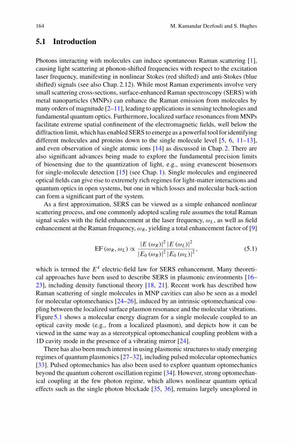
164 M. Kamandar Dezfouli and S. Hughes
5.1 Introduction
Photons interacting with molecules can induce spontaneous Raman scattering [1],causing light scattering at phonon-shifted frequencies with respect to the excitationlaser frequency, manifesting in nonlinear Stokes (red shifted) and anti-Stokes (blueshifted) signals (see also Chap.2.12). While most Raman experiments involve verysmall scattering cross-sections, surface-enhanced Raman spectroscopy (SERS) withmetal nanoparticles (MNPs) can enhance the Raman emission from molecules bymany orders ofmagnitude [2–11], leading to applications in sensing technologies andfundamental quantum optics. Furthermore, localized surface resonances fromMNPsfacilitate extreme spatial confinement of the electromagnetic fields, well below thediffraction limit, which has enabled SERS to emerge as a powerful tool for identifyingdifferent molecules and proteins down to the single molecule level [5, 6, 11–13],and even observation of single atomic ions [14] as discussed in Chap.2. There arealso significant advances being made to explore the fundamental precision limitsof biosensing due to the quantization of light, e.g., using evanescent biosensorsfor single-molecule detection [15] (see Chap. 1). Single molecules and engineeredoptical fields can give rise to extremely rich regimes for light-matter interactions andquantum optics in open systems, but one in which losses and molecular back-actioncan form a significant part of the system.
As a first approximation, SERS can be viewed as a simple enhanced nonlinearscattering process, and one commonly adopted scaling rule assumes the total Ramansignal scales with the field enhancement at the laser frequency, ωL , as well as fieldenhancement at the Raman frequency, ωR , yielding a total enhancement factor of [9]
EF (ωR, ωL) ∝ |E (ωR)|2 |E (ωL)|2|E0 (ωR)|2 |E0 (ωL)|2
, (5.1)
which is termed the E4 electric-field law for SERS enhancement. Many theoreti-cal approaches have been used to describe SERS in plasmonic environments [16–23], including density functional theory [18, 21]. Recent work has described howRaman scattering of single molecules in MNP cavities can also be seen as a modelfor molecular optomechanics [24–26], induced by an intrinsic optomechanical cou-pling between the localized surface plasmon resonance and the molecular vibrations.Figure5.1 shows a molecular energy diagram for a single molecule coupled to anoptical cavity mode (e.g., from a localized plasmon), and depicts how it can beviewed in the same way as a stereotypical optomechanical coupling problem with a1D cavity mode in the presence of a vibrating mirror [24].
There has also beenmuch interest in using plasmonic structures to study emergingregimes of quantum plasmonics [27–32], including pulsed molecular optomechanics[33]. Pulsed optomechanics has also been used to explore quantum optomechanicsbeyond the quantum coherent oscillation regime [34]. However, strong optomechan-ical coupling at the few photon regime, which allows nonlinear quantum opticaleffects such as the single photon blockade [35, 36], remains largely unexplored in

5 Quantum Optical Theories of Molecular Optomechanics 165
Fig. 5.1 aMolecular energy level diagram showing two photon manifolds (n = 0, 1) with phononstates (k), where the n = 1 photon manifold has a normalized displacement (d0) and a polaronicfrequency shift (−�P). bMetal dimer with an oscillating molecule, represented through b, ωm , anda cavity mode profile of the localized plasmon mode (formally a quasinormal mode, representedwith a, ωc), and an analogue optomechanics system using a simple 1D cavity with a vibratingmirror
the context of SERS, and new ideas with hybrid resonator systems are now emerg-ing [37, 38].
Various photonic systems can be used to enhance SERS and molecular optome-chanics, including plasmonic resonators [12, 13, 30, 42, 43], waveguide geometries[44–46], and hybrid material systems [47–50]. A few example systems are shownschematically in Fig. 5.2. In order to be able to describe a wide range of differentphotonic systems, we need accurate and flexible theoretical formalisms.
In this chapter, we present several theoretical techniques for studying molecularoptomechanics and single molecule SERS for plasmonic cavity systems, with a com-mon theme of using formalisms from the viewpoint of open system quantum optics.We first present a quantum optical theory of SERS in a system-bath approximation,and show how the Raman spectrum stems from an interplay of nonlinear light gen-eration and light propagation. We also identify the limits of the E4 electric-field rulefor Raman signal enhancement for low pump powers, and derive a different E8 ruleat higher pump powers. We derive a quantum master equation where the generalphotonic system (e.g., lossy and inhomogeneous) is treated as a photonic bath. Thephotonic bath function is implicitly contained in the electric-field Green function.Wethenuse this theory to investigate a selection of resonator systemswhose cavitymodesare conveniently described through quasinormal modes (QNMs) [51, 52]. Second,we study molecular optomechanics in a strong vibrational coupling regime, wherethe cavity modes are quantized at the system level, without any form of linearizationfor the optomechanical coupling. Although the significant dissipation inherent toMNPs can prevent accessing such a regime, hybrid plasmonic devices, consisting ofdielectric and metal parts, offer extra design flexibility in terms of the resonance lineshapes and cavity mode properties [41, 47, 48, 53, 54], where the system-bath theo-
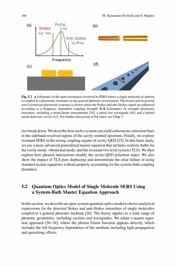
166 M. Kamandar Dezfouli and S. Hughes
Fig. 5.2 a Schematic of the main resonances involved in SERS where a single molecule of interestis coupled to a plasmonic resonator or any general photonic environment. The broad (and in generalnon-Lorentzian) plasmonic response is shownwhere the Stokes and anti-Stokes signal are enhancedaccording to a frequency dependent coupling strength. b–d Schematics of example plasmonicstructures, including a metal-dimer nanoantenna [39], a metal slot waveguide [40], and a hybridmetal-dielectric cavity [41]. For further discussion of the latter, see Chap. 2
ries break down.We describe how such a system can yield anharmonic emission linesin the sideband-resolved regime of the cavity-emitted spectrum. Finally, we exploreresonant SERS in the strong coupling regime of cavity-QED [55]. In this latter study,we use a more advanced generalized master equation that includes realistic baths forthe cavity mode, vibrational mode, and the resonant two level system (TLS).We thenexplore how phonon interactions modify the cavity-QED polariton states. We alsoshow the impact of TLS pure dephasing and demonstrate the clear failure of usingstandard master equations without properly accounting for the system-bath couplingdynamics.
5.2 Quantum Optics Model of Single Molecule SERS Usinga System-Bath Master Equation Approach
In this section,we describe an open-systemquantumopticsmodel to derive analyticalexpressions for the detected Stokes and anti-Stokes intensities of single moleculescoupled to a general photonic medium [26]. The theory applies to a wide range ofphotonic geometries, including cavities and waveguides. We adopt a master equa-tion approach [56–58], where the photon Green function appears directly, whichincludes the full frequency dependence of the medium, including light propagationand quenching effects.
5 Quantum Optical Theories of Molecular Optomechanics 167
Importantly, the theory uses a quantum field theory that is valid for any inhomo-geneous and lossy medium [59, 60]. We include the vibrational mode (or phononmode) at the system level and trace out the field operators in a bath approximation;however, we still treat the bath interaction in a self-consistent way. Using the mas-ter equation, and the quantum field theory, we then derive a simple and transparentanalytical formula for the emitted SERS spectrum, and we use this to connect toapproximate SERS theories in the literature, and point out their limitations.
We subsequently apply the theory to model single molecule SERS from severalresonator structures, including a metal dimer resonator made of two gold cylindricalnanorods (which has good quantum efficiency [39]) as shown in Fig. 5.1b (and alsoFig. 5.2b). We then study a more complex hybrid photonic-plasmonic system, wherethe dimer is on top of a photonic crystal nanobeam cavity (see Fig. 5.2d). The opticalcavity modes of these resonator systems are obtained using a powerful QNM theory,which allows the Green function to be obtained analytically in terms of a QNMexpansion.
5.2.1 System Hamiltonian, Photonic Green Function andInteraction Hamiltonian for the Raman Induced Dipole
Here we introduce the system Hamiltonian, including the molecular vibrations of agiven frequency, the photon bath of the photonic medium, and discuss the Ramaninteraction between phonons and the electromagnetic fields. We then present thequantized electric field operator for an arbitrary plasmonic/photonic environment,the photonicGreen function, aswell as the induceddipole through theRamanprocess.
Themolecular vibrational mode is treated as a quantized harmonic oscillator, withthe corresponding Hamiltonian (cf. Fig. 5.1b)
Hm = �ωmb†b, (5.2)
where b and b† satisfy Bosonic commutation rules,[b, b†
]= 1, and ωm is the vibra-
tional mode frequency. For simplicity, we assume that there is only one vibrationalmode (or phonon mode) of interest, though the theory can easily include multiplevibrational modes. The Hamiltonian for the fields, which is valid for an arbitraryinhomogeneous and lossy medium, is expressed in terms of a continuum of fieldoperators, f (r, ω), with [59, 60]
Hph = �
∫dr
∫ ∞
0dω ω f† (r, ω) f (r, ω) , (5.3)
where [f (r, ω) , f†
(r′, ω′)] = 1 δ
(r − r′) δ
(ω − ω′) . (5.4)
168 M. Kamandar Dezfouli and S. Hughes
For any general medium described by the complex permittivity function ε (r, ω),the electric-field operator is [59, 60]
E (r, ω) =∫
dr′G(r, r′;ω
) ·√
�
πε0Im {ε (r′, ω)} f (
r′, ω), (5.5)
where the two space-point Green function satisfies
∇ × ∇ × G(r, r′;ω
) − ω2
c2ε (r, ω)G
(r, r′;ω
) = ω2
c21 δ
(r − r′) , (5.6)
subjected to appropriate boundary conditions.Assuming a dipole interaction between the fields and the molecule, the induced
Raman polarization ispR = αR · E (rm) , (5.7)
where αR is the Raman polarizability tensor of the molecule, which can be expressedin terms of the Raman tensor of the molecule, R, through [9]
αR = R
√�
2ωm
(b + b†
), (5.8)
and E (rm) is the total electric field operator at the molecule location rm ,
E (r) =∫ ∞
0dω E (r, ω) + H.c. (5.9)
Subsequently, the interaction Hamiltonian is
Hint = −pR · E (rm) = −√
�
2ωm
(b + b†
)E (rm) · R · E (rm) . (5.10)
Note the general structure of the total Hamiltonian is similar in form to the simplecoupled-mode approaches [25, 61], which we discuss in more detail later.
5.2.2 Pump Field Enhancement Simplified InteractionHamiltonian
We now derive the pump field enhancement term and use that to obtain a simplifiedversion of the interaction Hamiltonian.
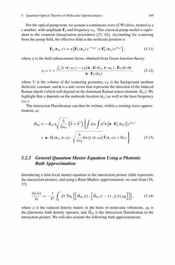
5 Quantum Optical Theories of Molecular Optomechanics 169
For the optical pump term, we assume a continuous wave (CW) drive, treated as ac number, with amplitude F0 and frequency ωL . This classical pump model is equiv-alent to the common linearization procedures [25, 62]. Accounting for scatteringfrom the pump field, the effective field at the molecule position is
Fp (rm, t) = η[F0 (rm) e−iωL t + F∗
0 (rm) eiωL t], (5.11)
where η is the field enhancement factor, obtained from Green function theory:
η = 1 +∫V [ε (r, ωL) − εB]n · G (rm, r;ωL) · F0 (r) dr
n · F0 (rm), (5.12)
where V is the volume of the scattering geometry, εB is the background mediumdielectric constant, and n is a unit vector that represents the direction of the inducedRaman dipole (which will depend on the dominant Raman tensor element, Rnn). Wehighlight that η depends on the molecule location (rm) as well as the laser frequency(ωL ).
The interaction Hamiltonian can then be written, within a rotating-wave approx-imation, as
Hint = −Rnnη
√�
2ωm
(b + b†
) {∫dω
∫d3r
[n · F∗
0 (rm)]eiωL t
× n · G (rm, r;ω) ·√
�
πε0Im {ε (r, ω)} f (r, ω) + H.c.
}. (5.13)
5.2.3 General Quantum Master Equation Using a PhotonicBath Approximation
Introducing a time-local master equation in the interaction picture (tilde representsthe interaction picture), and using a Born-Markov approximation, we start from [56,57]
∂ρ (t)
∂t= − 1
�2
∫ t
0dτ TrR
{[Hint (t) ,
[Hint (t − τ) , ρ (t) ρR
]]}, (5.14)
where ρ is the reduced density matrix in the basis of molecular vibrations, ρR isthe plasmonic bath density operator, and Hint is the interaction Hamiltonian in theinteraction picture. We will also assume the following bath approximations:

170 M. Kamandar Dezfouli and S. Hughes
TrR{f† (r, ω) f
(r′, ω′) ρR
}= 0,
TrR{f (r, ω) f†
(r′, ω′) ρR
}= 1 δ
(r − r′) δ
(ω − ω′) . (5.15)
If we now transform the Hamiltonian (5.13) to the interaction picture, and substi-tute into the master Eq. (5.14), we obtain the reduced density matrix of the system,1
∂ρ
∂t= Jph (ωL + ωm)
(2bρb† − b†bρ − ρb†b
)
+ Jph (ωL − ωm)(2b†ρb − bb†ρ − ρbb†
), (5.16)
where Jph(ω) is defined through
Jph (ω) ≡ R2nn |η|2 |n · F0|2
2ε0ωmIm {Gnn (rm, rm;ω)} , (5.17)
which includes the effects of the Raman tensor element, the medium local densityof states (LDOS), and the enhancement factor of the pump field. Note that Jph hasthe same units as γ (a rate).
In Eq. (5.16), the first term represents the Stokes signal (emitted at ωL − ωm), andis proportional to Jph (ωL + ωm); while the second term represent the anti-Stokessignal (emitted at ωL + ωm), which is proportional to Jph (ωL − ωm). Consequently,the Stokes (anti-Stokes) emission depends on the plasmonic enhancement throughthe projected LDOS at the anti-Stokes (Stokes) frequency. This may seem contraryto the commonwisdom that SERS involves a field enhancement at the correspondingfrequencies for both Stokes and anti-Stokes signals, but the actual detected signalalso depends on light propagation effects as well as pump enhancement effects (at thelaser frequency), as will be made clear later. Note also that while the unusual mixedLDOS features may seem surprising, similar effects often occur in the domain ofquantum nonlinear optics, e.g., a similar non-trivial LDOS coupling has been notedwith the Mollow triplet spectrum emitted from TLSs coupled to metal resonators,where the center peak width of the Mollow triplet depends only on the LDOS at thetwo side peaks and not on the LDOS at the laser frequency [63].
To obtain the full master equation, we also account for the coupling of the Ramanvibrations to the thermal environmental, by using additional Lindblad terms asso-ciated with thermal dissipation and incoherent pumping [25]. We then derive thefollowing master equation for the total molecule-photonic system:
1 To obtain Eq. (5.16) from Eq. (5.14), the upper limit in the time integral has been extended toinfinity, as the time scale for system changes are much longer than the bath correlation time.
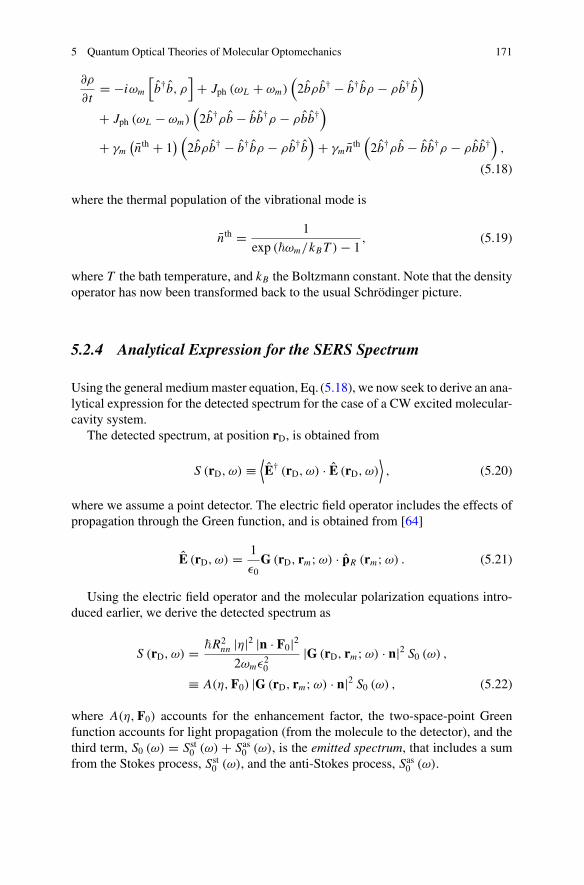
5 Quantum Optical Theories of Molecular Optomechanics 171
∂ρ
∂t= −iωm
[b†b, ρ
]+ Jph (ωL + ωm)
(2bρb† − b†bρ − ρb†b
)
+ Jph (ωL − ωm)(2b†ρb − bb†ρ − ρbb†
)
+ γm(nth + 1
) (2bρb† − b†bρ − ρb†b
)+ γmn
th(2b†ρb − bb†ρ − ρbb†
),
(5.18)
where the thermal population of the vibrational mode is
nth = 1
exp (�ωm/kBT ) − 1, (5.19)
where T the bath temperature, and kB the Boltzmann constant. Note that the densityoperator has now been transformed back to the usual Schrödinger picture.
5.2.4 Analytical Expression for the SERS Spectrum
Using the general mediummaster equation, Eq. (5.18), we now seek to derive an ana-lytical expression for the detected spectrum for the case of a CW excited molecular-cavity system.
The detected spectrum, at position rD, is obtained from
S (rD, ω) ≡⟨E† (rD, ω) · E (rD, ω)
⟩, (5.20)
where we assume a point detector. The electric field operator includes the effects ofpropagation through the Green function, and is obtained from [64]
E (rD, ω) = 1
ε0G (rD, rm;ω) · pR (rm;ω) . (5.21)
Using the electric field operator and the molecular polarization equations intro-duced earlier, we derive the detected spectrum as
S (rD, ω) = �R2nn |η|2 |n · F0|2
2ωmε20|G (rD, rm;ω) · n|2 S0 (ω) ,
≡ A(η,F0) |G (rD, rm;ω) · n|2 S0 (ω) , (5.22)
where A(η,F0) accounts for the enhancement factor, the two-space-point Greenfunction accounts for light propagation (from the molecule to the detector), and thethird term, S0 (ω) = Sst0 (ω) + Sas0 (ω), is the emitted spectrum, that includes a sumfrom the Stokes process, Sst0 (ω), and the anti-Stokes process, Sas0 (ω).
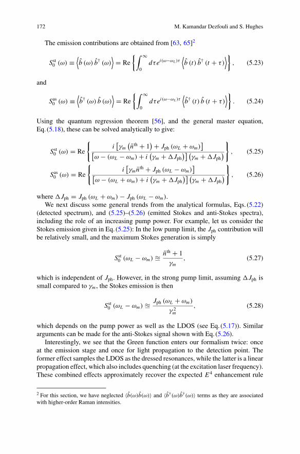
172 M. Kamandar Dezfouli and S. Hughes
The emission contributions are obtained from [63, 65]2
Sst0 (ω) ≡⟨b (ω) b† (ω)
⟩= Re
{∫ ∞
0dτei(ω−ωL )τ
⟨b (t) b† (t + τ)
⟩}, (5.23)
and
Sas0 (ω) ≡⟨b† (ω) b (ω)
⟩= Re
{∫ ∞
0dτei(ω−ωL )τ
⟨b† (t) b (t + τ)
⟩}. (5.24)
Using the quantum regression theorem [56], and the general master equation,Eq. (5.18), these can be solved analytically to give:
Sst0 (ω) = Re
{i[γm
(nth + 1
) + Jph (ωL + ωm)]
[ω − (ωL − ωm) + i
(γm + �Jph
)] (γm + �Jph
)}
, (5.25)
Sas0 (ω) = Re
{i[γmnth + Jph (ωL − ωm)
][ω − (ωL + ωm) + i
(γm + �Jph
)] (γm + �Jph
)}
, (5.26)
where �Jph = Jph (ωL + ωm) − Jph (ωL − ωm).We next discuss some general trends from the analytical formulas, Eqs. (5.22)
(detected spectrum), and (5.25)–(5.26) (emitted Stokes and anti-Stokes spectra),including the role of an increasing pump power. For example, let us consider theStokes emission given in Eq. (5.25): In the low pump limit, the Jph contribution willbe relatively small, and the maximum Stokes generation is simply
Sst0 (ωL − ωm) �nth + 1
γm, (5.27)
which is independent of Jph. However, in the strong pump limit, assuming �Jph issmall compared to γm , the Stokes emission is then
Sst0 (ωL − ωm) �Jph (ωL + ωm)
γ 2m
, (5.28)
which depends on the pump power as well as the LDOS (see Eq. (5.17)). Similararguments can be made for the anti-Stokes signal shown with Eq. (5.26).
Interestingly, we see that the Green function enters our formalism twice: onceat the emission stage and once for light propagation to the detection point. Theformer effect samples the LDOS as the dressed resonances, while the latter is a linearpropagation effect, which also includes quenching (at the excitation laser frequency).These combined effects approximately recover the expected E4 enhancement rule
2 For this section, we have neglected 〈b(ω)b(ω)〉 and 〈b†(ω)b†(ω)〉 terms as they are associatedwith higher-order Raman intensities.
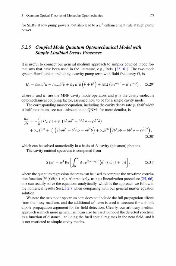
5 Quantum Optical Theories of Molecular Optomechanics 173
for SERS at low pump powers, but also lead to a E8 enhancement rule at high pumppower.
5.2.5 Coupled Mode Quantum Optomechanical Model withSimple Lindblad Decay Processes
It is useful to connect our general medium approach to simpler coupled mode for-malisms that have been used in the literature, e.g., Refs. [25, 61]. The two-modesystem Hamiltonian, including a cavity pump term with Rabi frequency �, is
Hs = �ωca†a + �ωmb
†b + �g a†a(b + b†
)+ i��
(a eiωL t − a†eiωL t
), (5.29)
where a and a† are the MNP cavity mode operators and g is the cavity-moleculeoptomechanical coupling factor, assumed now to be for a single cavity mode.
The corresponding master equation, including the cavity decay rate γc (half widthat half maximum, see next subsection on QNMs for more details), is
dρ
dt= − i
�[Hs, ρ] + γc
(2aρa† − a†aρ − ρa†a
)
+ γm(nth + 1
) (2bρb† − b†bρ − ρb†b
)+ γmn
th(2b†ρb − bb†ρ − ρbb†
),
(5.30)
which can be solved numerically in a basis of N cavity (plasmon) photons.The cavity emitted spectrum is computed from
S (ω) = ω4 Re
[∫ ∞
0dτ ei(ω−ωL )τ
⟨a† (t) a (t + τ)
⟩], (5.31)
where the quantum regression theorem can be used to compute the two-time correla-tion function
⟨a†(t)a(t + τ)
⟩. Alternatively, using a linearization procedure [25, 66],
one can readily solve the equations analytically, which is the approach we follow inthe numerical results Sect. 5.2.7 when comparing with our general master equationsolution.
We note the two mode spectrum here does not include the full propagation effectsfrom the lossy medium, and the additional ω4 term is used to account for a simpledipole propagation argument for far field detection. Clearly, our arbitrary mediumapproach is muchmore general, as it can also be used to model the detected spectrumas a function of distance, including the fuell spatial regimes in the near field, and itis not restricted to simple cavity modes.
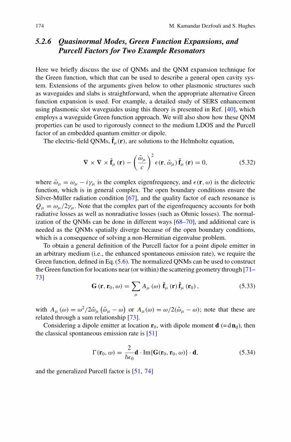
174 M. Kamandar Dezfouli and S. Hughes
5.2.6 Quasinormal Modes, Green Function Expansions, andPurcell Factors for Two Example Resonators
Here we briefly discuss the use of QNMs and the QNM expansion technique forthe Green function, which that can be used to describe a general open cavity sys-tem. Extensions of the arguments given below to other plasmonic structures suchas waveguides and slabs is straightforward, when the appropriate alternative Greenfunction expansion is used. For example, a detailed study of SERS enhancementusing plasmonic slot waveguides using this theory is presented in Ref. [40], whichemploys a waveguide Green function approach. We will also show how these QNMproperties can be used to rigorously connect to the medium LDOS and the Purcellfactor of an embedded quantum emitter or dipole.
The electric-field QNMs, fμ(r), are solutions to the Helmholtz equation,
∇ × ∇ × fμ (r) −(
ωμ
c
)2
ε(r, ωμ) fμ (r) = 0, (5.32)
where ωμ = ωμ − iγμ is the complex eigenfrequency, and ε(r, ω) is the dielectricfunction, which is in general complex. The open boundary conditions ensure theSilver-Müller radiation condition [67], and the quality factor of each resonance isQμ = ωμ/2γμ. Note that the complex part of the eigenfrequency accounts for bothradiative losses as well as nonradiative losses (such as Ohmic losses). The normal-ization of the QNMs can be done in different ways [68–70], and additional care isneeded as the QNMs spatially diverge because of the open boundary conditions,which is a consequence of solving a non-Hermitian eigenvalue problem.
To obtain a general definition of the Purcell factor for a point dipole emitter inan arbitrary medium (i.e., the enhanced spontaneous emission rate), we require theGreen function, defined in Eq. (5.6). The normalized QNMs can be used to constructtheGreen function for locations near (orwithin) the scattering geometry through [71–73]
G (r, r0, ω) =∑
μ
Aμ (ω) fμ (r) fμ (r0) , (5.33)
with Aμ (ω) = ω2/2ωμ
(ωμ − ω
)or Aμ(ω) = ω/2(ωμ − ω); note that these are
related through a sum relationship [73].Considering a dipole emitter at location r0, with dipole moment d (=dnd), then
the classical spontaneous emission rate is [51]
(r0, ω) = 2
�ε0d · Im{G(r0, r0, ω)} · d, (5.34)
and the generalized Purcell factor is [51, 74]
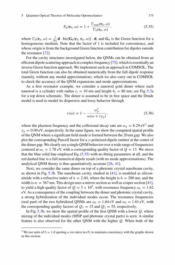
5 Quantum Optical Theories of Molecular Optomechanics 175
FP(r0, ω) = 1 + total(r0, ω)
0(r0, ω), (5.35)
where 0(r0, ω) = 2�ε0
d · Im{G0(r0, r0, ω)} · d, and G0 is the Green function for ahomogeneous medium. Note that the factor of 1 is included for convenience, andwhose origin is from the background Green function contribution for dipoles outsidethe resonator [72].
For the cavity structures investigated below, the QNMs can be obtained from anefficient dipole scattering approach in complex frequency [75],which is essentially aninverse Green function approach.We implement such an approach in COMSOL. Thetotal Green function can also be obtained numerically from the full dipole response(namely, without any modal approximation), which we also carry out in COMSOLto check the accuracy of the QNM expansions and mode approximations.
As a first resonator example, we consider a nanorod gold dimer where eachnanorod is a cylinder with radius rr = 10 nm and height hr = 80 nm; see Fig. 5.3afor a top down schematic. The dimer is assumed to be in free space and the Drudemodel is used to model its dispersive and lossy behavior through
ε(ω) = 1 − ω2p
ω(ω + iγp), (5.36)
where the plasmon frequency and the collisional decay rate are ωp = 8.29 eV3 andγp = 0.09 eV, respectively. In the same figure, we show the computed spatial profileof the QNMwhere a significant field mode is formed between the 20nm gap.We alsoplot the corresponding Purcell factor for a y-polarized dipole emitter at the center ofthe dimer gap.We clearly see a singleQNMbehavior over awide range of frequenciescentered at ωc = 1.78 eV, with a corresponding quality factor of Q = 13. We stressthat the blue solid line employed Eq. (5.35) with no fitting parameters at all, and thered dashed line is a full numerical dipole result (with no mode approximations). Theanalytical QNM theory is thus quantitatively accurate [26, 41].
Next, we consider the same dimer on top of a photonic crystal nanobeam cavity,as shown in Fig. 5.3b. The nanobeam cavity, studied in [41], is modeled as silicon-nitride with a refractive index of n = 2.04, where the height is h = 200 nm, and thewidth isw = 367 nm. This design uses amirror section aswell as a taper section [41],to yield a high quality factor of Q = 3 × 10⁵, with resonance frequency ωc = 1.62eV. As a consequence of the coupling between the dimer and photonic crystal cavity,a strong hybridization of the individual modes occur. The resonance frequencies(real part) of the two hybridized QNMs are ω1 = 1.64 eV and ω2 = 1.61 eV, withthe corresponding quality factors of Q1 = 15 and Q2 = 55, respectively.
In Fig. 5.3b, we show the spatial profile of the first QNM with a lower Q, wheremixing of the individual modes (MNP and photonic crystal parts) is seen. A similarfeature is also observed for the other QNM with the higher Q. When both of the
3 We use units of � = 1 if quoting ω (or rates) in eV, to maintain consistency with the graphs shownin this section.
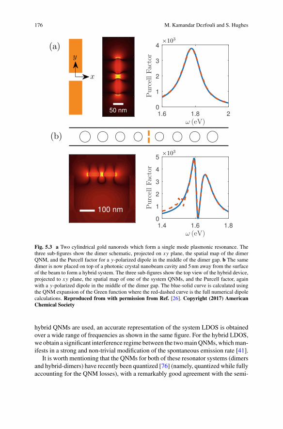
176 M. Kamandar Dezfouli and S. Hughes
Fig. 5.3 a Two cylindrical gold nanorods which form a single mode plasmonic resonance. Thethree sub-figures show the dimer schematic, projected on xy plane, the spatial map of the dimerQNM, and the Purcell factor for a y-polarized dipole in the middle of the dimer gap. b The samedimer is now placed on top of a photonic crystal nanobeam cavity and 5nm away from the surfaceof the beam to form a hybrid system. The three sub-figures show the top view of the hybrid device,projected to xy plane, the spatial map of one of the system QNMs, and the Purcell factor, againwith a y-polarized dipole in the middle of the dimer gap. The blue-solid curve is calculated usingthe QNM expansion of the Green function where the red-dashed curve is the full numerical dipolecalculations. Reproduced from with permission from Ref. [26]. Copyright (2017) AmericanChemical Society
hybrid QNMs are used, an accurate representation of the system LDOS is obtainedover a wide range of frequencies as shown in the same figure. For the hybrid LDOS,we obtain a significant interference regime between the twomainQNMs,whichman-ifests in a strong and non-trivial modification of the spontaneous emission rate [41].
It is worth mentioning that the QNMs for both of these resonator systems (dimersand hybrid-dimers) have recently been quantized [76] (namely, quantized while fullyaccounting for the QNM losses), with a remarkably good agreement with the semi-
5 Quantum Optical Theories of Molecular Optomechanics 177
classical results; this work also highlights regimes where the usual quantized modetheories (such as the dissipative Jaynes-Cummings models) can completely fail, e.g.,for describing the Fano resonance feature of the hybrid coupling regime [76]. Fea-tures unique to a fully quantized QNMmodel have also been recently explored, wellbeyond the bad cavity limit [77].
We can now use the analytical QNM theory to connect to the the E4 scaling rulefor the SERS spectrum. From Eq. (5.22), we first consider the enhancement at thelaser pump frequency through η. We consider a single QNM expansion of the Greenfunction, Eq. (5.33), using f (r). Assuming an initial pump field that is polarizedalong n, η becomes
η = A (ωL)[n · f (rm)
] {∫[ε (r, ωL) − εB] f (r) dr
}, (5.37)
where A (ωL) ≈ Q near resonance, and the spatial integration is performed overthe cavity resonator. Using the modal field value at the molecule location, f (rm), inEq. (5.22), we obtain the expected squared dependence of the SERS spectrum at thelaser frequency.
Finally,we also consider the propagation effects from the term |G (rD, rm;ω) · n|2,and again use a single QNM expansion to obtain
G (rD, rm;ω) · n = A (ω) f (rD)[f (rm) · n
], (5.38)
where f (rD) QNM is the detection point, and f (rm) · n is the projected QNM valueat the molecule location. Combining these enhancement and propagation effectstogether, then indeed we recover the approximate |f (rm) |4 scaling rule for thedetected SERS spectrum.
Similar arguments can be made for the LDOS at the molecule location,Im {Gnn (rm, rm;ω)}, where we find that Jph, defined in Eq. (5.17), is also propor-tional to |f (rm) |4. Thus, for sufficiently high pump powers, we now find that theRaman signal scales approximately with |f (rm) |8 instead.
5.2.7 Numerical Results for the Cavity-Emitted SERSSpectrum from Single Molecules
We next present example numerical results of our SERS theory using the QNMsand Green functions for the resonators discussed above. For the molecule, we usea vibrational mode similar to the R6G molecule at ωm = 160meV [78], with adissipation rate of γm = 1.6 meV.
The spectrum obtained fromEq. (5.22) (alongwith Eqs. (5.25) and (5.26) as input)is shown in Fig. 5.4 for three different excitation conditions; in all cases, we showthe emitted spectrum (using S0 (ω), left column) and the detected spectrum (using
178 M. Kamandar Dezfouli and S. Hughes
S (R, ω), when the detector is at x = 500nm away form the dimer, right column);the results are qualitatively the same for larger propagation distances.4 The threecases shown in Fig. 5.4 are: (a)/(d) ωL = ωc, where the pump laser is on-resonancewith the plasmonic mode; (b)/(e) ωL = ωc + ωm , where the laser pump is detuned tothe blue side of the plasmonic resonance by exactly the frequency of R6G vibration;and (c)/(f),ωL = ωc − ωm . These calculations assume room temperature conditions,where nth = 0.002, and the pump intensity is fixed for all cases.
As discussed in the theory section above, the spectral properties of the emittedRaman signals can be quite different to the detected spectrum. The differences partlydepend on the operating frequency for the pump field and the changes of the LDOSbetween the laser drive frequency and the Raman sidebands. For example, by com-paring Fig. 5.4a and d, when the system is pumped on resonance with the plasmonicmode, the propagation effect to the far-field hasmore enhancement for the anti-Stokessignal compared to the Stokes signal. This difference becomes evenmore pronouncedwhen one excites the system in a red detuning configuration, where the anti-Stokesemission exploits the maximum enhancement from the MNP environment.
Next, in Fig. 5.5, we study the effects of laser detuning from the plasmonic res-onance in more detail. We first show the two different theory results in Fig. 5.5a,b, where the Stokes and anti-Stokes signals are calculated as follows: (a) using thesimple quantum optomechanical description shown in Sect. 5.2.5; (b) using our ana-lytical expression for the detected spectrum given in Eq. (5.22), where the gold dimerGreen function is computed using the QNM expansion of Eq. (5.33). The agreementbetween the two methods is clearly qualitatively good, since the response of thesystem happens to be very similar to a Lorentzian line shape; but there are stillquantitative differences, in part from the differences to our estimation of the pumpenhancement effect, which involves computing η from Eq. (5.12). To help clarify thisfurther, we note that there is an excellent agreement between the prediction of ourmodel and the coupled-mode quantum optomechanical model of Ref. [25], if η wasestimated using the plasmonic LDOS rather than using Eq. (5.12). This response isobviously a limitation of the coupled mode formalism.
We also consider three different pump intensity regimes in Fig. 5.5c. For the R6Gmolecule in the gold dimer, an increasing pump field reshapes the anti-Stokes signalso that a single peak feature at a different spectral location is observed. For the samepump values, small changes to the general shape of the Stokes signal also occur.Similar effects were noted in Ref. [25], due to nonlinear interactions. We highlightagain that the Jph terms in the master equations are proportional to square of thepump field, in comparison to the thermal dissipation terms. We also note that thepump values used in Fig. 5.5 are rather high, with 2ε0c |F0|2 = 1.3 × 10⁵ W/μm2,which is mainly due to the lower plasmonic enhancement achieved in the gold dimersystem.
4 Note that at sufficiently large distances away from the resonator, QNMs can be used in con-junction with the background propagator to obtain the renormalized QNM fields, which are non-divergent [72]; renormalizedQNMscan also be obtained using near-field to far-field transforms [79].
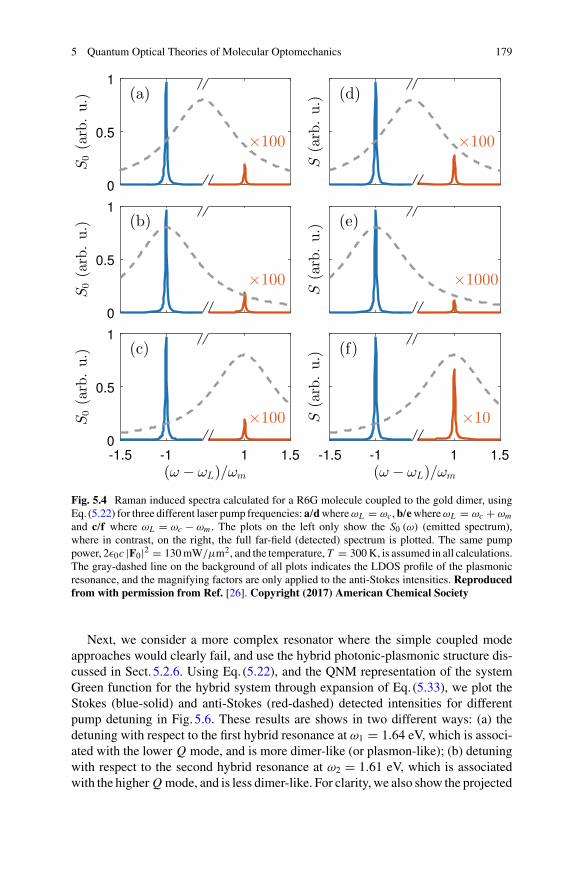
5 Quantum Optical Theories of Molecular Optomechanics 179
Fig. 5.4 Raman induced spectra calculated for a R6G molecule coupled to the gold dimer, usingEq. (5.22) for three different laser pump frequencies: a/dwhereωL = ωc,b/ewhereωL = ωc + ωmand c/f where ωL = ωc − ωm . The plots on the left only show the S0 (ω) (emitted spectrum),where in contrast, on the right, the full far-field (detected) spectrum is plotted. The same pumppower, 2ε0c |F0|2 = 130mW/μm2, and the temperature, T = 300K, is assumed in all calculations.The gray-dashed line on the background of all plots indicates the LDOS profile of the plasmonicresonance, and the magnifying factors are only applied to the anti-Stokes intensities. Reproducedfrom with permission from Ref. [26]. Copyright (2017) American Chemical Society
Next, we consider a more complex resonator where the simple coupled modeapproaches would clearly fail, and use the hybrid photonic-plasmonic structure dis-cussed in Sect. 5.2.6. Using Eq. (5.22), and the QNM representation of the systemGreen function for the hybrid system through expansion of Eq. (5.33), we plot theStokes (blue-solid) and anti-Stokes (red-dashed) detected intensities for differentpump detuning in Fig. 5.6. These results are shows in two different ways: (a) thedetuning with respect to the first hybrid resonance at ω1 = 1.64 eV, which is associ-ated with the lower Q mode, and is more dimer-like (or plasmon-like); (b) detuningwith respect to the second hybrid resonance at ω2 = 1.61 eV, which is associatedwith the higher Qmode, and is less dimer-like. For clarity, we also show the projected
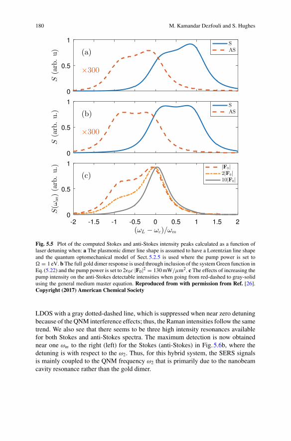
180 M. Kamandar Dezfouli and S. Hughes
Fig. 5.5 Plot of the computed Stokes and anti-Stokes intensity peaks calculated as a function oflaser detuning when: a The plasmonic dimer line shape is assumed to have a Lorentzian line shapeand the quantum optomechanical model of Sect. 5.2.5 is used where the pump power is set to� = 1 eV. b The full gold dimer response is used through inclusion of the system Green function inEq. (5.22) and the pump power is set to 2ε0c |F0|2 = 130mW/μm2. c The effects of increasing thepump intensity on the anti-Stokes detectable intensities when going from red-dashed to gray-solidusing the general medium master equation. Reproduced from with permission from Ref. [26].Copyright (2017) American Chemical Society
LDOS with a gray dotted-dashed line, which is suppressed when near zero detuningbecause of the QNM interference effects; thus, the Raman intensities follow the sametrend. We also see that there seems to be three high intensity resonances availablefor both Stokes and anti-Stokes spectra. The maximum detection is now obtainednear one ωm to the right (left) for the Stokes (anti-Stokes) in Fig. 5.6b, where thedetuning is with respect to the ω2. Thus, for this hybrid system, the SERS signalsis mainly coupled to the QNM frequency ω2 that is primarily due to the nanobeamcavity resonance rather than the gold dimer.
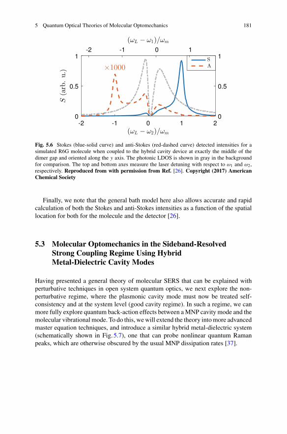
5 Quantum Optical Theories of Molecular Optomechanics 181
Fig. 5.6 Stokes (blue-solid curve) and anti-Stokes (red-dashed curve) detected intensities for asimulated R6G molecule when coupled to the hybrid cavity device at exactly the middle of thedimer gap and oriented along the y axis. The photonic LDOS is shown in gray in the backgroundfor comparison. The top and bottom axes measure the laser detuning with respect to ω1 and ω2,respectively. Reproduced from with permission from Ref. [26]. Copyright (2017) AmericanChemical Society
Finally, we note that the general bath model here also allows accurate and rapidcalculation of both the Stokes and anti-Stokes intensities as a function of the spatiallocation for both for the molecule and the detector [26].
5.3 Molecular Optomechanics in the Sideband-ResolvedStrong Coupling Regime Using HybridMetal-Dielectric Cavity Modes
Having presented a general theory of molecular SERS that can be explained withperturbative techniques in open system quantum optics, we next explore the non-perturbative regime, where the plasmonic cavity mode must now be treated self-consistency and at the system level (good cavity regime). In such a regime, we canmore fully explore quantum back-action effects between aMNP cavity mode and themolecular vibrational mode. To do this, wewill extend the theory intomore advancedmaster equation techniques, and introduce a similar hybrid metal-dielectric system(schematically shown in Fig. 5.7), one that can probe nonlinear quantum Ramanpeaks, which are otherwise obscured by the usual MNP dissipation rates [37].

182 M. Kamandar Dezfouli and S. Hughes
Fig. 5.7 Schematic of another hybrid metal-dielectric device with a MNP dimer (now with ellip-tical rods) coupled to a photonic crystal nanobeam cavity; the inset shows a closeup of the metaldimer where molecules (shown by a red filled circle) can be located. A partial energy diagram of thecoupled molecule-cavity system is also shown, where red/green/blue/purple show four transitionlines for the cavity emitted SERS spectrum. For example, the cyan and orange arrows show stan-dard harmonic transitions associated with first order and second order Raman (Stokes/anti-Stokes),respectively. Reproduced from with permission from Ref. [37]. Copyright (2019) AmericanChemical Society
5.3.1 Optomechanical System Hamiltonian and the DressedStates
The optomechanical interaction, without any form of linearization, including thecavity pump term, and in the interaction picture [66], is
Hs = �� a†a + �ωm b†b − �g a†a(b† + b
)+ ��
(a† + a
), (5.39)
where � = ωc − ωL , ωm is again the frequency of molecular vibrational mode, and� is the Rabi frequency of the optical cavity mode. Note that cavity operator termsaa and a†a† (dynamical Casimir effects) can be ignored here, as ωc � ωm [80, 81].The optomechanical coupling factor is defined from [24]
g = (�Rm/2ωm)−1/2 ωc
ε0Vc, (5.40)
5 Quantum Optical Theories of Molecular Optomechanics 183
with Rm the Raman activity5 that depends on the vibrational mode of interest, andVc as the effective mode volume of the cavity mode.
The optomechanical coupling term in Eq. (5.39) is appropriate for describing off-resonant Raman interactions. For resonant interactions, as discussed later, the plas-monicMNP also interacts with electronic (two-level) vibrational degrees of freedom,yielding the Raman term [82] ωm
√SHR σ+σ−(b + b†), where σ+, σ− are the Pauli
operators and SHR is the Huang-Rhys parameter [83], which accounts for the phonondisplacement between the ground and excited electronic states. For certain excitationconditions, resonant Raman effects may be treated phenomenologically [9], result-ing in an effective increase of the off-resonant interaction above. However, this islikely only a good approximation for weak pumping fields (and/or sufficiently broadresonances), where the Fermionic states behave as harmonic oscillator states.6 Forour studies below, we concentrate on the off-resonant Raman interactions but alsouse Raman cross sections that can increased using resonant Raman interactions.Resonant Raman effects are discussed in Sect. 5.4.
With optical pumping, the SERS Hamiltonian (Eq. (5.39)) can be solved analyti-cally, and the eigenenergies take the form [84]:
En,k = n�� + k�ωm − n2�g2
ωm, (5.41)
with the corresponding eigenstates,
∣∣�n,k⟩ = D†
(gn
ωm
)|n, k〉 , (5.42)
where D is the displacement operator. We see that the phonon states are displacedas: b → b − d0a†a, where d0 = g/ωm is the normalized displacement. Figure5.1ashows these energy states as well as the normalized displacement. Note that thepolaron shift of the n = 1 cavity manifold (which is a red shift) is �P = g2/ωm =d0ωm .
The optomechanical coupling thus yields photon manifolds that contain phononsub-levels, and the sub-level splitting depends on the photon number state. To resolvethe lowest-order anharmonic levels (n = 1 photonmanifold), we require g2/ωm > κ .However, one also requires κ < ωm , to be in the sideband resolved regime [85]. Theseoptomechanical states now involve interactions beyond the rotating-wave approxi-mation for the mechanical mode, where one also finds that g/ωm > 0.1, which is theregime of ultrastrong coupling (USC) [82, 86–89] for the photon-phonon interac-tions. Figure5.7 show six of the optomechanical energy levels that can be resolvedin the emitted spectrum, in the presence of cavity pumping. For � = 0, the first
5 Note that the Raman activity is related to the elements of the Raman tensor, but they have differentunits.6 A more detailed discussion between these two models, also from a polaron viewpoint, is given inthe next section.
184 M. Kamandar Dezfouli and S. Hughes
three energy levels for n = 0, are E0,0 = 0, E0,1 = �ωm and E0,2 = 2�ωm for theground state, first order and second order Raman states – these relate to the stan-dard Stokes and anti-Stokes resonances. However, the first three energy levels forthe n = 1 photon manifold contain the anharmonic side-bands, E1,0 = −�g2/ωm ,E1,1 = �ωm−�g2/ωm and E1,2 = 2�ωm−�g2/ωm .
5.3.2 Quantum Master Equations for Exploring MolecularOptomechanics in the Sideband-Resolved Regime
We can first employ a standard master equation approach [56, 57], including cavityand mechanical bath interactions [25, 26]:
dρ(t)
dt= − i
�[Hs, ρ(t)] + κ
2D[a]ρ(t) +
γm
(nth + 1
)
2D[b]ρ(t) + γmnth
2D[b†]ρ(t),
(5.43)
where κ is the cavity decay rate, γm is the vibrational decay rate, nth is again thethermal population of the vibrational mode, and the Lindblad superoperator D isdefined via:
D[O]ρ(t) = 2Oρ(t)O† − O† Oρ(t) − ρ(t)O† O. (5.44)
Note that the decay rates here are defined with a factor of 2 greater than the ones usedin Eq. (5.30) (to be consistent with a full-width half-maximum of a spectral line).
A general problem with the standard master equation is that it neglects internalcoupling effects between the system operators [90], since the correct bath interactionshould occur at the dressed resonances of the system. This internal coupling interac-tion has been used to highlight various effects in quantum optics, e.g.,Mollow tripletswith MNP resonators interacting with two level atoms [63], circuit QED [91], andgeneral regimes of USC physics [81]. Neglecting the influence of the weak pumpingfield, then b and a can be solved solved analytically (without dissipation). Neglectingterms that oscillate at exp(±iωmt) and exp(±i2ωmt) (in the interaction picture), andtreating the phonon bath spectral function as Ohmic, the modified master equationis [88]
dρ(t)
dt= − i
�[Hs, ρ(t)] + κ
2D[a]ρ(t) + γm
(nth + 1
)
2D[b − d0a
†a]ρ(t)
+ γmnth
2D[b† − d0a
†a]ρ(t) + 2γmkBT
�ωmd20 D[a†a]ρ(t). (5.45)
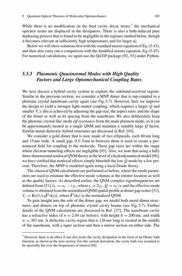
5 Quantum Optical Theories of Molecular Optomechanics 185
While there is no modification on the final cavity decay terms,7 the mechanicaloperator terms are displaced in the dissipators. There is also a bath-induced puredephasing process that is found to be negligible in the regimes studied below, thoughit becomes relevant at sufficiently high temperatures and for larger d0.
Belowwewill show solutions first with the standardmaster equation of Eq. (5.43),and then also carry out a comparison with the modified master equation, Eq. (5.45).For numerical calculations, we again use the QuTiP package [92, 93] under Python.
5.3.3 Plasmonic Quasinormal Modes with High QualityFactors and Large Optomechanical Coupling Rates
We next discuss a hybrid cavity system to explore the sideband-resolved regime.Similar to the previous section, we consider a MNP dimer that is top-coupled to aphotonic crystal nanobeam cavity again (see Fig. 5.7). However, here we improvethe design to yield a stronger light-matter coupling, which requires a larger Q andsmaller Vc); this is achieved by adjusting the gap size, the aspect ratio, and the shapeof the dimer as well as its spacing from the nanobeam. We also deliberately keepthe photonic crystal-like mode off resonance from the main plasmon mode, so it canbe approximately treated as a single QNM and maintain a suitably large Q factor.Similar metal-dielectric hybrid structures are discussed in Ref. [94].
We consider a gold dimer that is now made of two ellipsoids, each 60 nm longand 15 nm wide. A small gap, 0.5–5nm in between them is used to create a pro-nounced field for coupling to the molecule. These gap sizes are within the rangewhere electron tunneling effects are negligible [95]. Also, we note that using a fullythree-dimensional nonlocalQNMtheory at the level of a hydrodynamicalmodel [96],we have verified that nonlocal effects simply blueshift the low Q mode by a few per-cent. Therefore, the MNP is modeled again using a local Drude theory.
The classical QNM calculations are performed as before, where the mode param-eters are used to estimate the effective mode volumes at the emitter location as wellas the quality factors. As described earlier, the QNM complex eigenfrequencies aredefined from [51] ωc = ωc − iγc, where κ = 2γc, Q = ωc/κ and the effective modevolume is obtained from the normalizedQNMspatial profile at dimer gap center [51],Vc = Re{1/εB f2(r0)}, where f2(r0) is the normalized QNM.
To gain insight into the role of the dimer gap, we model both metal dimer struc-tures, and dimers on top of photonic crystal cavity beams (see Fig. 5.7). Furtherdetails of the QNM calculations are discussed in Ref. [37]. The nanobeam cavityhas a refractive index of n = 2.04 (as before), with height h = 200 nm, and widthw = 367 nm. A dielectric cavity region that is 126 nm long is created in the middleof the nanobeam, with a taper section and then a mirror section on either side. The
7 However, there is an effect if one also treats the cavity dissipation in the form of an Ohmic bathfunction, as shown in the next section. For this current derivation, the cavity bath was assumed tobe spectrally flat over the frequencies of interest [88].
186 M. Kamandar Dezfouli and S. Hughes
Fig. 5.8 a Purcell factor calculations for the smaller gaps size of 0.5nm using the analytical QNMtheory (solid curve) and fully vectorial solutions to Maxwell’s equations from a dipole excitation(symbols). bQNMcalculated Purcell factors for dimer designswith different gap sizes. cCalculatedmode profile of two gold dimerswith different gaps, 0.5nm (left) and 5nm (right). d Purcell factor ofa dipole emitter placed inside the plasmonic gap of the hybrid device, where a sharp high Q mode(dielectric-like) is present next to the broader low Q mode (plasmon-like). Reproduced (withmodification) from with permission from Ref. [37]. Copyright (2019) American ChemicalSociety
taper section is made of 7 holes linearly increasing from 68 nm to 86 nm in radius,and from 264 nm to 299 nm in spacing. The mirror section consists of 7 more holeshaving the same radius of r = 86 nm and the same spacing of a = 306 nm. For themainmode of interest for this cavity design,we obtained the effectivemode volume atthe beam center inside dielectric region to be Vc = 0.078 λ3, with the correspondingquality factor of Q = 3 × 10⁵.
Figure5.8 shows how the MNP dimer response changes as a function of gap size(a-c), and also displays the hybrid modes for the smallest gap size on a photoniccrystal cavity beam cavity (d). Figure5.8c shows the near-field mode profile for gapsizes of 0.5nm and 5nm, respectively. In Fig. 5.8a, we confirm the accuracy of theQNM theory for accurately capturing the system Purcell factor; even for this verysmall gap sizes of 0.5nm, a single QNM evidently gives an excellent fit compared tofull numerical dipole simulations. Figure5.8b shows how theQNMcomputed Purcellfactors [51] change for several dimer designs with different gap sizes, ranging from
5 Quantum Optical Theories of Molecular Optomechanics 187
0.5 nm to 5 nm. The smaller dimer gaps cause a rapid decrease of the effective modevolume and a spectral redshift.
These hybrid MNP-dielectric modes can trap molecules that couple to extremelylocalized fields, while maintaining a sufficiently large Q factor in the presence ofdielectric mode coupling. Figure5.8d shows the total Purcell factors for a dipoleemitter that is (again) oriented along the dimer axis when on top of the photoniccrystal cavity. Over the wide spectral range of 400meV, only two modes contributedominantly, which are the two hybrid cavity modes [41]. The resonant frequenciesof the hybrid modes are �ωHQ
c = 1.61 eV and �ωLQc = 1.83 eV, with corresponding
quality factors of QHQ = 3500 (�κ = 23.3 meV) and QLQ = 17 (�κ = 108 meV),respectively. The effective mode volumes for the two hybrid modes are V HQ
c =5.36 × 10⁻⁶ λ3
c and V LQc = 4.54 × 10⁻⁸ λ3
c . Note that, as discussed before, the highQ mode has an extremely small mode volume inherited from the plasmonic dimerstructure.
Turning now to the molecular vibrational mode, we consider a low frequencyoscillation with resonance energy �ωm = 10meV, with a Raman activity of Rm =103 A4amu−1; these values are within the range of values reported in the literature,e.g., for single-walled carbon nanotubes [24, 97]. We also consider a mechanicalquality factor of Qm = ωm/γm = 100 for the molecular vibrational mode, thoughnote the temperature dependence will increase the vibrational linewidth, throughnth, as shown in Eq. (5.51). For this vibrational mode, the two hybrid optical modesyield �gHQ = 0.1meV and �gLQ = 20meV. As discussed earlier, even though thelow Q mode offers a much larger coupling factor, it fails to exploit the strong cou-pling interaction for sideband resolution, since one requires κ < ωm . We note thatthese estimates assume standard off-resonant SERS, and with resonant enhancementeffects, the effective coupling factor can likely be enhanced by more than ×1000when resonant Raman regimes are used, and so we also consider several values ofthe coupling factor within the range: �gHQ = 0.1 − 4meV [37].
5.3.4 Cavity Emitted Spectrum and Population Dynamics inthe Sideband-Resolved Regime
Employing the good- cavity master equations, Eqs. (5.43) and (5.45), and the quan-tum regression theorem [56], we calculate the cavity-emitted (incoherent) spectrumfrom:
S (ω) ≡ Re
{∫ ∞
0dt ei(ω−ωL )t
[⟨a† (t) a (0)
⟩ss − ⟨
a†⟩ss
⟨a⟩ss
]}, (5.46)
where the expectation values are computed in steady state, and the latter contributionsubtracts off the coherent contribution. The population dynamics of the cavity modepopulation is obtained from nc(t) = ⟨
a†a⟩(t).
188 M. Kamandar Dezfouli and S. Hughes
Fig. 5.9 a Cavity emitted spectrum and b cavity photon population versus time, for �g = 0.1, 2, 4meV, top to bottom, respectively. The temperature is T = 4K, and for the larger values of g, we haved0 = g/ωm = 0.4. which is also in the (vibrational) USC regime. The first (lowest) g value is for thehybrid high Q design shown earlier, with the estimated non-resonant Raman configuration. Here,the cavity decay rate is �κ = 0.46meV, the frequency of vibration is �ωm = 10meV, and the Rabienergy is�� = 0.1meV.Note thatωm � κ , which is required for sideband resolution.Reproduced(withmodification) fromwithpermission fromRef. [37].Copyright (2019)AmericanChemicalSociety
Fig. 5.10 Cavity emittedspectrum for differentcavity-laser detunings� = −ωm , ωm , g2/ωmfrom top to bottom,respectively. Reproduced(with modification) fromwith permission fromRef. [37]
In Figs. 5.9a, b, we show the cavity-emitted spectrum and corresponding cavitymode population dynamics, for the three optomechanical coupling rates: �gHQ =0.1, 2, 4meV. The simulations in Figs. 5.9a, b use the standard master equation(Eq. (5.51)), with a bath temperature of T = 4K. By increasing g, we see signifi-cant spectral shifts of the cavity mode resonance and the emergence of the Ramanside-peaks (Fig. 5.9a). In Fig. 5.9b, the corresponding cavity mode populations alsobecome non-trivial as one enter a strong coupling regime. Referring to the schematicenergy diagram of Fig. 5.7, the usual Raman emissions (first-order and second-order)correspond to single phonon step and two phonon step jumps on the molecule (har-
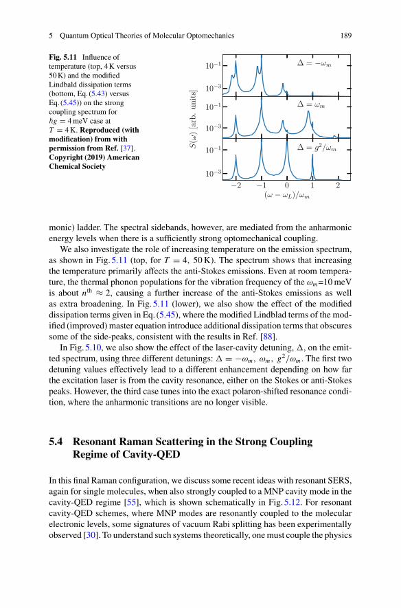
5 Quantum Optical Theories of Molecular Optomechanics 189
Fig. 5.11 Influence oftemperature (top, 4K versus50K) and the modifiedLindbald dissipation terms(bottom, Eq. (5.43) versusEq. (5.45)) on the strongcoupling spectrum for�g = 4meV case atT = 4K. Reproduced (withmodification) from withpermission from Ref. [37].Copyright (2019) AmericanChemical Society
monic) ladder. The spectral sidebands, however, are mediated from the anharmonicenergy levels when there is a sufficiently strong optomechanical coupling.
We also investigate the role of increasing temperature on the emission spectrum,as shown in Fig. 5.11 (top, for T = 4, 50K). The spectrum shows that increasingthe temperature primarily affects the anti-Stokes emissions. Even at room tempera-ture, the thermal phonon populations for the vibration frequency of the ωm=10meVis about nth ≈ 2, causing a further increase of the anti-Stokes emissions as wellas extra broadening. In Fig. 5.11 (lower), we also show the effect of the modifieddissipation terms given in Eq. (5.45), where the modified Lindblad terms of the mod-ified (improved) master equation introduce additional dissipation terms that obscuressome of the side-peaks, consistent with the results in Ref. [88].
In Fig. 5.10, we also show the effect of the laser-cavity detuning, �, on the emit-ted spectrum, using three different detunings: � = −ωm, ωm, g2/ωm . The first twodetuning values effectively lead to a different enhancement depending on how farthe excitation laser is from the cavity resonance, either on the Stokes or anti-Stokespeaks. However, the third case tunes into the exact polaron-shifted resonance condi-tion, where the anharmonic transitions are no longer visible.
5.4 Resonant Raman Scattering in the Strong CouplingRegime of Cavity-QED
In this final Raman configuration, we discuss some recent ideas with resonant SERS,again for single molecules, when also strongly coupled to a MNP cavity mode in thecavity-QED regime [55], which is shown schematically in Fig. 5.12. For resonantcavity-QED schemes, where MNP modes are resonantly coupled to the molecularelectronic levels, some signatures of vacuum Rabi splitting has been experimentallyobserved [30]. To understand such systems theoretically, onemust couple the physics
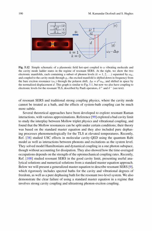
190 M. Kamandar Dezfouli and S. Hughes
Fig. 5.12 Simple schematic of a plasmonic field hot-spot coupled to a vibrating molecule andthe cavity mode ladder states in the regime of resonant SERS. At the right, we show the twoelectronic manifolds, each containing a subset of phonon levels (k = 1, 2, . . .) separated by ωm ,and coupled to the cavity mode through gc; the excited manifold is shifted down in frequency fromthe bare exciton resonance (ωx ) through the polaron shift, �P = d2ωm , and shifted in space bythe normalized displacement d. This graph is similar to Fig. 5.1, but now we also have coupling toelectronic levels for the resonant TLS, described by Pauli operators, σ+ and σ− (see text)
of resonant SERS and traditional strong coupling physics, where the cavity modecannot be treated as a bath, and the effects of system-bath coupling can be muchmore subtle.
Several theoretical approaches have been developed to explore resonant Ramaninteractions, with various approximations. Reference [99] explored a bad cavity limitto study the interplay between Mollow triplet physics and vibrational coupling, andfound that the Mollow resonances can be split under certain conditions; their theorywas based on the standard master equation and they also included pure dephas-ing processes phenomenologically for the TLS at elevated temperatures. Recently,Ref. [38] studied USC effects in molecular cavity-QED using the quantum Rabimodel as well as interactions between phonons and excitations as the system level.They solved model Hamiltonians and dynamical coupling in a one photon subspace,though without accounting for dissipation. They also showed how the time-averagedoccupations depends on the strength of the optomechanical coupling rates. Recently,Ref. [100] studied resonant SERS in the good cavity limit, presenting useful ana-lytical solutions and numerical solutions from a standard master equation approach.Below we will present a generalized master equation to describe resonant SERS [9],which rigorously includes spectral baths for the cavity and vibrational degrees offreedom, as well as a pure dephasing bath for the resonant two-level system. We alsodemonstrate the clear failure of using a standard master equation in a regime thatinvolves strong cavity coupling and ultrastrong phonon-exciton coupling.

5 Quantum Optical Theories of Molecular Optomechanics 191
5.4.1 Polaronic Picture and Connection BetweenOff-Resonant SERS and Resonant SERS
To make a closer connection between off-resonant SERS and resonant SERS, it isuseful to consider the system Hamiltonians in a polaronic picture.
For the off-resonant SERS Hamiltonian, the polaron transform yields a a†a-dependent displacement of the mechanical resonator: S = d0a†a(b† − b).Thepolaron transformed systemHamiltonian. for off-resonant SERS,H ′
s = eS Hse−S .is then
H ′s = �(ωc − �P)a
†a + �ωmb†b − ��Pa
†a†aa, (5.47)
where a → a X , and the displacement operator is X = exp[d0(b − b†)]. In thepolaron frame, the effective cavity resonance is shifted down by �P = g2om/ωm =d20ωm (see Fig. 5.1), as also shown from the eigenvalues of the optomechanical cou-pling problem. Note, the Kerr-like term (4 operators) causes a nonlinear (photon-photon) dependence on photon number. However, if term can be neglected, then onecan write
H ′s ≈ �(ωc − �P)a
†a + �ωmb†b, (5.48)
which clearly has a very simple form and interpretation.For resonant Raman interactions (see Fig. 5.12), the system Hamiltonian is
Hs = �ωca†a + �ωmbb
† + �ωx σ+σ− + �dωm σ+σ− (
b† + b)
+ �gc(σ+a + a†σ−),
(5.49)
where the latter term is the Jaynes-Cummings term. Here we assume gc � ωc, so canneglect USC effects related to the TLS-cavity coupling [38]; the TLS has a resonanceexciton energyωx , and gc is the exciton-cavity coupling rate (we use the ‘c’ subscriptto avoid confusion with the g used in the off-resonant SERS scheme). The polarontransformed systemHamiltonian, for resonant SERS, now using S=dσ+σ−(b† − b)and X = exp(d(b − b†)), is
H ′s = �ωca
†a + �ωmbb† + �(ωx − �P)σ
+σ− + �gc(σ+a X + a† X†σ−). (5.50)
The equivalence between the off-resonant and resonant SERS can then be made,by invoking a harmonic oscillator approximation for the TLS in a bad cavity limit.Thus, in such a regime, the resonant SERS polaron transformed Hamiltonian thenbecomes identical in form to the off-resonance case, apart from the Kerr-like term(which vanishes for Fermions). Therefore, a one simply replaces a, a† with σ−, σ+,and identifies d0 = d. Clearly, when Fermionic behavior becomes important in the
192 M. Kamandar Dezfouli and S. Hughes
two state system, e.g., Mollow physics and strong coupling between the cavity modeand TLS, then one must use the Pauli operators to describe the resonant Raman.
5.4.2 Standard and Generalized Master Equations forResonant SERS
Including cavity and mechanical bath interactions, the standard master equation forresonant SERS is
dρ(t)
dt= − i
�
[Hs + Hpump, ρ(t)
] + κ
2D[a]ρ(t) + γφ
2D[σ+σ−]ρ(t)
+ γm(nth + 1
)
2D[b]ρ(t) + γmnth
2D[b†]ρ(t), (5.51)
where γφ = φ(0) (see below) is the pure dephasing rate of the TLS, Hs is the systemHamiltonian in the interaction picture in a rotating frame at the laser frequency,
Hs = �(ωc − ωL)a†a + �ωmbb
† + �(ωx − ωL)σ+σ− + �dωm σ+σ−
(b† + b
)
+ �gc(σ+a + a†σ−), (5.52)
and Hpump is the CW pump term for the cavity mode:
Hpump = �(a + a†). (5.53)
As highlighted earlier, the standard master equation will generally fail in suchregimes, since it neglects internal coupling between the system operators when deriv-ing the dissipators [63, 81, 90, 91], and these interactions can be significant forMNP-molecular systems. We also have the additional problem here of including theexciton-cavity coupling, and one has to introduce amore general pure dephasing bathfunction, which is known experimentally [101] and theoretically [102] to introducepronounced spectral asymmetries. Thus for a suitably large gc and d, one needs amore general master equation, where the dissipators are derived with respect to thedressed states of the hybrid system. However, in contrast to our earlier SERS theorywith a generalized bath function, we are now including the MNP cavity mode at thesystem level, as well as a resonant exciton, and we need to include an appropriatebath function for pure dephasing as well.
To address this problem rigorously, we exploit a generalized master equationapproach [81], which first computes the eigenstates and eigenenergies of the systemHamiltonian, and account for the fact that the bath interactions occur as the dressedresonances of the system, The generalized master equation for the resonant Raman
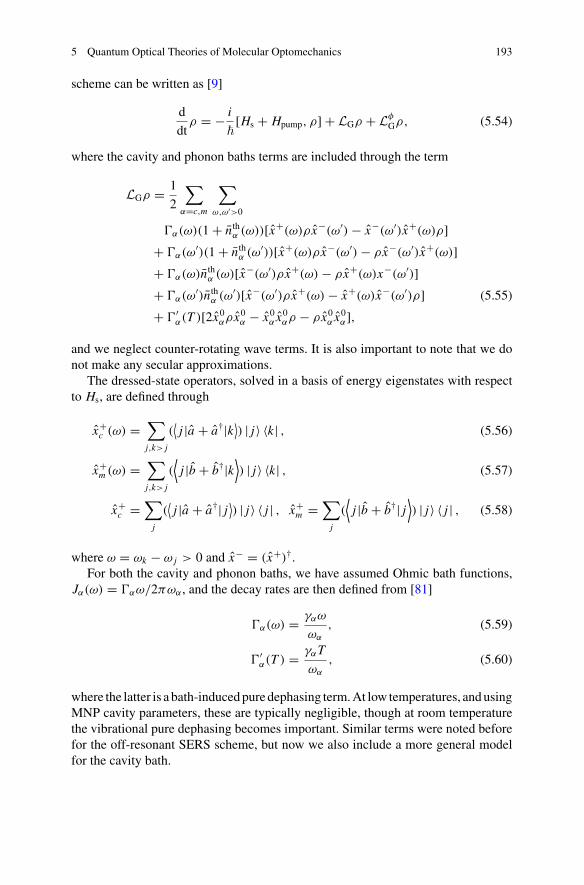
5 Quantum Optical Theories of Molecular Optomechanics 193
scheme can be written as [9]
d
dtρ = − i
�[Hs + Hpump, ρ] + LGρ + Lφ
Gρ, (5.54)
where the cavity and phonon baths terms are included through the term
LGρ = 1
2
∑α=c,m
∑ω,ω′>0
α(ω)(1 + nthα (ω))[x+(ω)ρ x−(ω′) − x−(ω′)x+(ω)ρ]+ α(ω′)(1 + nthα (ω′))[x+(ω)ρ x−(ω′) − ρ x−(ω′)x+(ω)]+ α(ω)nthα (ω)[x−(ω′)ρ x+(ω) − ρ x+(ω)x−(ω′)]+ α(ω′)nthα (ω′)[x−(ω′)ρ x+(ω) − x+(ω)x−(ω′)ρ] (5.55)
+ ′α(T )[2x0αρ x0α − x0α x
0αρ − ρ x0α x
0α],
and we neglect counter-rotating wave terms. It is also important to note that we donot make any secular approximations.
The dressed-state operators, solved in a basis of energy eigenstates with respectto Hs, are defined through
x+c (ω) =
∑j,k> j
(⟨j |a + a†|k⟩) | j〉 〈k| , (5.56)
x+m (ω) =
∑j,k> j
(⟨j |b + b†|k
⟩) | j〉 〈k| , (5.57)
x+c =
∑j
(⟨j |a + a†| j ⟩) | j〉 〈 j | , x+
m =∑j
(⟨j |b + b†| j
⟩) | j〉 〈 j | , (5.58)
where ω = ωk − ω j > 0 and x− = (x+)†.
For both the cavity and phonon baths, we have assumed Ohmic bath functions,Jα(ω) = αω/2πωα , and the decay rates are then defined from [81]
α(ω) = γαω
ωα
, (5.59)
′α(T ) = γαT
ωα
, (5.60)
where the latter is a bath-inducedpure dephasing term.At low temperatures, andusingMNP cavity parameters, these are typically negligible, though at room temperaturethe vibrational pure dephasing becomes important. Similar terms were noted beforefor the off-resonant SERS scheme, but now we also include a more general modelfor the cavity bath.

194 M. Kamandar Dezfouli and S. Hughes
In addition to the above phonon and cavity bath interaction terms, the puredephasing term associated with the TLS, e.g., through electron-phonon interactions,becomes
Lφ
Gρ = 1
2
∑ω,ω′>0
↓φ (ω)[x+
a (ω)ρ x−a (ω′) − x−
a (ω′)x+a (ω)ρ]
+ ↓φ (ω′)[x+
a (ω)ρ x−a (ω′) − x−
a (ω′)x+a (ω)ρ]
+ ↑φ (ω)[x−
a (ω)ρ x+a (ω′) − x+
a (ω′)x−a (ω)ρ]
+ ↑φ (ω′)[x−
a (ω)ρ x+a (ω′) − x+
a (ω′)x−a (ω)ρ]
+ φ(0)[2x+a ρ x−
a − x−a x
+a ρ − ρ x+
a x−a ], (5.61)
where for clarity, we define the TLS pure dephasing rates implicitly including nth(ω)
(upwards transition) and (1 + nth(ω)) (downward transition) to better explain thephysics of the asymmetric baths coupling:
↑(ω) = 2π Jφ(ω)[1 + nth(ω)], ω ≥ 0,
↓(ω) = 2π Jφ(−ω)nth(−ω), ω < 0. (5.62)
The TLS dressed state operators for molecular pure dephasing are defined through:
x+a (ω) =
∑j,k> j
(⟨j |σ+σ−|k⟩) | j〉 〈k| , (5.63)
x+a =
∑j
(⟨j |σ+σ−| j ⟩) | j〉 〈 j | , (5.64)
Note that in the standard master equation, only the final term in Eq. (5.61) wouldbe used for TLS pure dephasing. We use the ‘a’ subscript here to represent a puredephasing bath the resonant atom or TLS.
For the pure dephasing spectral function, we use an Ohmic form with a cut-offfrequency [82],
Jφ(ω) = ηφωe−
(ω
ωcut
)2
, (5.65)
whereωcut = 160meV is the cut-off frequency, and ηφ is the coupling strengthwhichwe define from having γφ = φ(0) = 10 meV at room temperature (and we assumethis value scales linearly with temperature).
In the time domain, it is also useful to define the bath correlation function:
φ(τ) =∫ ∞
0dωJφ(ω)[(nth(ω) + 1)e−iωτ + nth(ω)eiωτ ], (5.66)
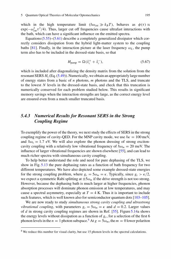
5 Quantum Optical Theories of Molecular Optomechanics 195
which in the high temperature limit (�ωcut � kBT ), behaves as φ(τ) ∝exp(−ω2
cutτ2/4). Thus, larger cut off frequencies cause ultrafast interactions with
the bath, which can have a significant influence on the emitted spectra.Equations (5.55)–(5.61) describe a completely generalized dissipator which cor-
rectly considers dissipation from the hybrid light-matter system to the couplingbaths [81]. Finally, in the interaction picture at the laser frequency ωL , the pumpterm also has to be included in the dressed-state basis, so that
Hpump = �(x+c + x−
c ), (5.67)
which is included after diagonalizing the density matrix from the solution from theresonant SERS Hs (Eq. (5.49)).Numerically,weobtain an appropriately large numberof energy states from a basic of n photons, m photons and the TLS, and truncateto the lowest N levels in the dressed-state basis, and check that this truncation isnumerically conserved for each problem studied below. This results in significantmemory savings when the interaction strengths are large, as the correct energy levelare ensured even from a much smaller truncated basis.
5.4.3 Numerical Results for Resonant SERS in the StrongCoupling Regime
To exemplify the power of the theory, we next study the effects of SERS in the strongcoupling regime of cavity-QED. For the MNP cavity mode, we use �κ = 100meV,and �ωc = 1.7 eV. We will also explore the phonon dressing of strong exciton-cavity coupling with a relatively low vibrational frequency of �ωm = 20 meV. Theinfluence of larger vibrational frequencies are shown elsewhere [55], and can lead tomuch richer spectra with simultaneous cavity coupling.
To help better understand the role and need for pure dephasing of the TLS, weshow in Fig. 5.13 the pure dephasing rates as a function of bath frequency for twodifferent temperatures. We have also depicted some example dressed-state energiesfor the strong coupling problem, where gc = 5ωm = κ . Typically, since gc > κ/2,we expect a symmetric Rabi splitting at ±5ωm if the drive strength is not too strong.However, because the dephasing bath is much larger at higher frequencies, phononabsorption processes will dominate phonon emission at low temperatures, and maycause a spectral asymmetry, especially at T = 4 K. Thus it is important to includesuch features, which is well known also for semiconductor quantum dots [103–105].
We are now ready to study simultaneous strong cavity coupling and ultrastrongvibrational coupling, with parameters gc = 5ωm = κ and d = 0.2. Larger valuesof d in strong cavity coupling regimes are shown in Ref. [55]. Figure5.14a showsthe energy levels without dissipation as a function of gc, for a selection of the first 6phonon levels in the n = 1 photon subspace.8 At g = 5ωm, them = 0 lower polariton
8 We reduce this number for visual clarity, but use 15 phonon levels in the spectral calculations.
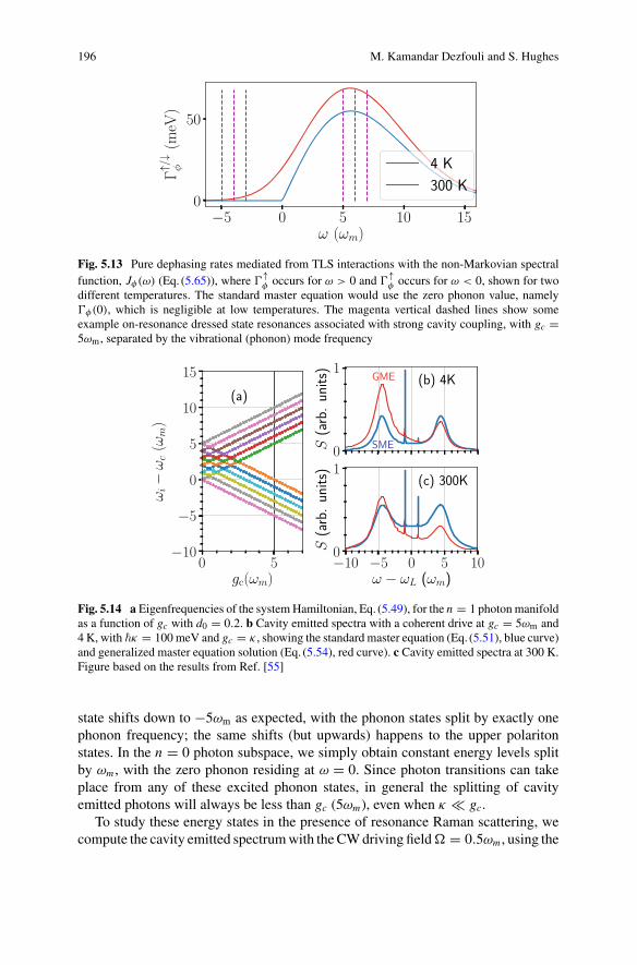
196 M. Kamandar Dezfouli and S. Hughes
Fig. 5.13 Pure dephasing rates mediated from TLS interactions with the non-Markovian spectralfunction, Jφ(ω) (Eq. (5.65)), where
↑φ occurs for ω > 0 and
↑φ occurs for ω < 0, shown for two
different temperatures. The standard master equation would use the zero phonon value, namely φ(0), which is negligible at low temperatures. The magenta vertical dashed lines show someexample on-resonance dressed state resonances associated with strong cavity coupling, with gc =5ωm, separated by the vibrational (phonon) mode frequency
Fig. 5.14 a Eigenfrequencies of the systemHamiltonian, Eq. (5.49), for the n = 1 photon manifoldas a function of gc with d0 = 0.2. b Cavity emitted spectra with a coherent drive at gc = 5ωm and4 K, with �κ = 100 meV and gc = κ , showing the standard master equation (Eq. (5.51), blue curve)and generalized master equation solution (Eq. (5.54), red curve). c Cavity emitted spectra at 300 K.Figure based on the results from Ref. [55]
state shifts down to −5ωm as expected, with the phonon states split by exactly onephonon frequency; the same shifts (but upwards) happens to the upper polaritonstates. In the n = 0 photon subspace, we simply obtain constant energy levels splitby ωm , with the zero phonon residing at ω = 0. Since photon transitions can takeplace from any of these excited phonon states, in general the splitting of cavityemitted photons will always be less than gc (5ωm), even when κ � gc.
To study these energy states in the presence of resonance Raman scattering, wecompute the cavity emitted spectrumwith the CWdriving field� = 0.5ωm , using the
5 Quantum Optical Theories of Molecular Optomechanics 197
same techniques as before (see Eq. (5.46)). Figure5.14b shows the results at a temper-ature of 4K, showing the first Stokes and anti-Stokes sidebands at±ωm , and polaritonpeaks (from cavity-exciton coupling) around ±4.5ωm < gc; these resonance ener-gies are not increased with smaller κ and are due to the collective summation of thephonon dressed states contributing to the total emission linewidth.
Interestingly, we also see a pronounced asymmetry in the generalized masterequation solution calculations, which is mainly coming from the spectral propertiesof the pure dephasing bath. This shows that even though the zero phonon line hasnegligible dephasing, the properties of the bath at the dressed resonances can have asubstantial influence on the oscillator strengths. The bath-induced resonances causedownward transitions between the upper polariton and lower polariton states, whilethe transitions from the lower to higher states are negligible at low temperature.Such an effect cannot be predicted by the SME regardless of what φ value is used.Specifically, Jφ(ω) > Jφ(−ω), which breaks the detailed balance of the diagonaldephasing process in the SME [62, 91].
Figure5.14c shows room temperature results (300K), which shows that theseeffects survive at elevated temperatures, and that the bath-induced asymmetry is stillvisible but less pronounced in the generalized master equation, since now there isa larger probability also for bath-induced upwards transitions between the polaritonstates. The anti-Stokes Raman transition is also much more visible as one mightexpect.
5.5 Conclusions and Outlook
We have presented several different theoretical approaches to model SERS andmolecular optomechanics for single molecules coupled to plasmonic cavity systems,from the framework of open systemquantumoptics. These regimes aremade possibleby the tremendous progress over the years with MNP fabrication and spectroscopictechniques related to trapping and positioning single molecules in plasmonic cav-ities and other photonic structures. While MNP cavities naturally come with verylossy modes (low Q), they also yield regimes of extreme spatial confinement, andwith suitable cavity designs, it is possible to have both high Q and very low modevolumes. Emerging hybrid quantum systems also motivate the need for new the-ories to understand emerging light-matter and optomechanical coupling effects inthese extreme confinement regimes, which allow one to explore fundamentally newregimes in quantum plasmonics, where traditional theories in quantum optics canfail.
In the first part, we presented an intuitive Green function formalism that canbe used to model SERS using plasmonic systems of arbitrary geometry. A generalmedium master equation was derived where the plasmonic environment is treated asa photonic bath and the system dynamics are projected onto the basis of the molec-ular vibrations. While the plasmonic degrees of freedom are traced out, the exactmedium Green function is self-consistently included to account for the plasmonic

198 M. Kamandar Dezfouli and S. Hughes
LDOS characteristics at the dressed-state resonances and for describing importantlight propagation effects. This approach describes the nonlinear light generation,enhancement, and quenching effects of light detection during SERS. Using this gen-eral medium approach, analytical expressions were derived for the molecular SERSspectrum near plasmonic environments which can be used to quantify the Stokes andanti-Stokes emission intensities. We also discussed how the dynamics of the SERSprocess is quite different in the emission process compared to light propagation anddetection. The induced Raman polarization emits photons at Stokes frequencies thatare proportional to the plasmonic enhancement (LDOS) at the co-existing anti-Stokesfrequency, and vice-versa for the anti-Stokes frequencies. However, the plasmonicLDOS also comes into play differently at the light propagation stage, such that boththe Stokes and anti-Stokes photons are enhanced at their respective frequencies. Ourmodel can easily explore SERS as a function of laser detuning, pump power, spatiallocation of the molecule/detector, and the medium LDOS. We also demonstratedhow the Green function response and LDOS can be efficiently described in termsof QNMs, which allow one to model SERS from various molecular positions anddetector positions in a very efficient way. Examples were shown for a gold dimercavity and a more complex hybrid photonic-plasmonic cavity system.
In the second part, we explored the regime of molecular optomechanics in astrong vibrational coupling regime (requiring multiple phonons and cavity dynamicsto be included self-consistently), where a strong modification of the usual SERSspectrum is obtained because of the influence of higher lying quantum states, whichhave an anharmonic level spacing g2/ωm . These quantum states can be spectrallyresolved if g2/ωm > κ and κ < ωm is satisfied, which is typically not possible withbroadband plasmonic resonators. However, our cavity design uses a hybrid metal-dielectric system where a MNP dimer is on top of a photonic crystal nanobeamcavity, which enables very small effective mode volumes as well as a sufficientlyhigh quality factor (QHQ = 3500). The high Q (small κ) and large optomechanicalg are two essential criteria to probe the strong coupling anharmonic ladder states ofthe optomechanical system.While our designs use extremely small gap antennas, theprospect of using larger Raman active and resonant Raman processes in moleculesindicates that emerging experiments in quantum plasmonic systems are not too faroff reaching such a regime. There is also prospects for exploring similar regimeswith new designs of very small mode dielectric systems [106, 107].
In the third and final part, we introduced a theory of resonant SERS using a gen-eralized master equation approach, which treats system-bath coupling rigorously forthe cavity, phonon (molecular vibration), and TLS interactions.We showed explicitlyhow the system eigenenergies are affected by an increasing exciton cavity couplingrate, and explored how phonon dressing affects the cavity emitted spectra in thestrong coupling regime of cavity-QED. We also demonstrated the important roleof including a pure dephasing bath, which results in pronounced spectral asymme-tries, which is caused by the relatively large spectral splitting in the strong couplingregime. We described a rich regime of phonon-dressed polaritons, which coupledstrong cavity QED effects with ultrastrong exciton-phonon interactions.
5 Quantum Optical Theories of Molecular Optomechanics 199
With the continued experimental and theoretical progress in single molecularsensing, trapping, quantum plasmonics, and MNP cavity designs, we anticipate con-tinued improvements in both dielectric and plasmonic systems, as well as hybridplasmon-dielectric cavities, opening up a wide range of effects in and applications inmolecular cavity QED and plasmonic cavity QED in general. Since MNP environ-ments are inherently very lossy, we also believe that future theoretical developmentswill benefit significantly from a quantized QNM approach, where unique featurescan appear such as quantum mechanical loss-induced coupling between classicallyorthogonal modes [76, 77].
Acknowledgements We acknowledge Queen’s University, the Canadian Foundation for Innova-tion (CFI), and the Natural Sciences and Engineering Research Council of Canada (NSERC) forfinancial support, as well as CMC Microsystems for the provision of COMSOL Multiphysics. Wegratefully acknowledge Reuven Gordon for collaborations and discussions on the hybrid cavitydesign and molecular optomechanics work in the off-resonant strong vibrational coupling regime.SH thanks Salvatore Savasta and Franco Nori for collaborations and discussions on the resonantRaman work.
References
1. C. V. Raman and K. S. Krishnan. A new type of secondary radiation. Nature, 121:501–502,March 1928.
2. Surbhi Lal, Stephan Link, and Naomi J. Halas. Nano-optics from sensing to waveguiding.Nature Photonics, 1:641, 2007.
3. Katherine A. Willets and Richard P. Van Duyne. Localized surface plasmon resonance spec-troscopy and sensing. Annual Review of Physical Chemistry, 58(1):267–297, 2007.
4. Janina Kneipp, Harald Kneipp, and Katrin Kneipp. SERS-a single-molecule and nanoscaletool for bioanalytics. Chem. Soc. Rev., 37:1052–1060, 2008.
5. Shuming Nie and Steven R. Emory. Probing single molecules and single nanoparticles bysurface-enhanced Raman scattering. Science, 275(5303):1102–1106, 1997.
6. Katrin Kneipp, YangWang, Harald Kneipp, Lev T. Perelman, Irving Itzkan, Ramachandra R.Dasari, and Michael S. Feld. Single molecule detection using surface-enhanced Raman scat-tering (SERS). Phys. Rev. Lett., 78:1667–1670, Mar 1997.
7. AlexandreG.Brolo, ErinArctander, ReuvenGordon, Brian Leathem, andKarenL.Kavanagh.Nanohole-enhanced Raman scattering. Nano Letters, 4(10):2015–2018, October 2004.
8. Stefan Alexander Maier. Plasmonics: Fundamentals and Applications. Springer, 2007.9. Eric C. Le Ru and Pablo G. Etchegoin. Principles of Surface-Enhanced Raman Spectroscopy.
Elsevier, 2009.10. Aftab Ahmed and Reuven Gordon. Single molecule directivity enhanced Raman scattering
using nanoantennas. Nano Letters, 12(5):2625–2630, April 2012.11. Eric C. Le Ru and Pablo G. Etchegoin. Single-molecule surface-enhanced Raman spec-
troscopy. Annual Review of Physical Chemistry, 63(1):65–87, 2012.12. R. Zhang,Y. Zhang, Z.C.Dong, S. Jiang,C. Zhang, L.G.Chen, L. Zhang,Y. Liao, J.Aizpurua,
Y. Luo, J. L. Yang, and J. G. Hou. Chemical mapping of a single molecule by plasmon-enhanced Raman scattering. Nature, 498:82–86, 2012.
13. StevenYampolsky,DmitryA. Fishman, ShirshenduDey, EeroHulkko,MayukhBanik, EricO.Potma, and Vartkess A. Apkarian. Seeing a single molecule vibrate through time-resolvedcoherent anti-Stokes Raman scattering. Nat Photon, 8:650–656, 2014.
200 M. Kamandar Dezfouli and S. Hughes
14. Martin D. Baaske and Frank Vollmer. Optical observation of single atomic ions interactingwith plasmonic nanorods in aqueous solution. Nature Photonics, 10:733, 2016.
15. N. P. Mauranyapin, L. S. Madsen, M. A. Taylor, M. Waleed, and W. P. Bowen. Evanescentsingle-molecule biosensing with quantum-limited precision. Nature Photonics, 11(8):477–481, August 2017.
16. Wenhua Gu, Hyungsoo Choi, and Kyekyoon (Kevin) Kim. A quantum mechanical theoryfor single molecule-single nanoparticle surface enhanced raman scattering. The Journal ofPhysical Chemistry A, 111(33):8121–8125, August 2007.
17. Anne Myers Kelley. A molecular spectroscopic view of surface plasmon enhanced resonanceRaman scattering. The Journal of Chemical Physics, 128(22):224702, 2008.
18. David J. Masiello and George C. Schatz. Many-body theory of surface-enhanced Ramanscattering. Phys. Rev. A, 78:042505, Oct 2008.
19. David J.Masiello andGeorgeC. Schatz. On the linear response and scattering of an interactingmolecule-metal system. The Journal of Chemical Physics, 132(6):064102, 2010.
20. Aida Delfan, Marco Liscidini, and John E. Sipe. Surface enhanced Raman scattering in thepresence of multilayer dielectric structures. J. Opt. Soc. Am. B, 29(8):1863–1874, Aug 2012.
21. John L. Payton, Seth M. Morton, Justin E. Moore, and Lasse Jensen. A hybrid atomisticelectrodynamics-quantummechanical approach for simulating surface-enhancedRaman scat-tering. Accounts of Chemical Research, 47(1):88–99, 2014.
22. John R. Lombardi and Ronald L. Birke. Theory of surface-enhanced Raman scattering insemiconductors. The Journal of Physical Chemistry C, 118(20):11120–11130, 2014.
23. Niclas S. Mueller, Sebastian Heeg, and Stephanie Reich. Surface-enhanced Raman scatteringas a higher-order raman process. Phys. Rev. A, 94:023813, Aug 2016.
24. PhilippeRoelli, ChristopheGalland, Nicolas Piro, and Tobias J. Kippenberg.Molecular cavityoptomechanics as a theory of plasmon-enhanced Raman scattering. Nat Nano, 11:164–169,Feb 2016.
25. Mikolaj K. Schmidt, Ruben Esteban, Alejandro González-Tudela, Geza Giedke, and JavierAizpurua. Quantummechanical description of Raman scattering frommolecules in plasmoniccavities. ACS Nano, 10(6):6291–6298, 2016.
26. MohsenKamandarDezfouli andStephenHughes.Quantumopticsmodel of surface-enhancedRaman spectroscopy for arbitrarily shaped plasmonic resonators. ACS Photonics, 4(5):1245–1256, 2017.
27. M. S. Tame, K. R. McEnery, S. K. Özdemir, J. Lee, S. A. Maier, and M. S. Kim. Quantumplasmonics. Nature Physics, 9(6):329–340, June 2013.
28. Armin Regler, Konrad Schraml, Anna A. Lyamkina, Matthias Spiegl, Kai Müller, JelenaVuckovic, Jonathan J. Finley, and Michael Kaniber. Emission redistribution from a quantumdot-bowtie nanoantenna. Journal of Nanophotonics, 10(3):033509, 2016.
29. Tao Cai, Subhojit Dutta, Shahriar Aghaeimeibodi, Zhili Yang, Sanghee Nah, John T. Fourkas,and Edo Waks. Coupling emission from single localized defects in two-dimensional semi-conductor to surface plasmon polaritons. Nano Letters, 17(11):6564–6568, 2017.
30. Rohit Chikkaraddy, Bart de Nijs, Felix Benz, Steven J. Barrow, Oren A. Scherman, EdinaRosta, Angela Demetriadou, Peter Fox, Ortwin Hess, and Jeremy J. Baumberg. Single-molecule strong coupling at room temperature in plasmonic nanocavities. Nature, 535:127–130, 2016.
31. C. Belacel, B. Habert, F. Bigourdan, F.Marquier, J.-P. Hugonin, S.Michaelis de Vasconcellos,X. Lafosse, L. Coolen, C. Schwob, C. Javaux, B. Dubertret, J.-J. Greffet, P. Senellart, andA. Maitre. Controlling spontaneous emission with plasmonic optical patch antennas. NanoLetters, 13(4):1516–1521, 2013.
32. GlebM. Akselrod, Christos Argyropoulos, Thang B. Hoang, Cristian Ciracì, Chao Fang, JianiHuang, David R. Smith, and Maiken H. Mikkelsen. Probing the mechanisms of large Purcellenhancement in plasmonic nanoantennas. Nat Photon, 8:835–840, 2014.
33. Anna Lombardi, Mikołaj K. Schmidt, Lee Weller, William M. Deacon, Felix Benz, Bartde Nijs, Javier Aizpurua, and Jeremy J. Baumberg. Pulsed molecular optomechanics in plas-monic nanocavities: From nonlinear vibrational instabilities to bond-breaking. Phys. Rev. X,8:011016, Feb 2018.
5 Quantum Optical Theories of Molecular Optomechanics 201
34. Kiran E. Khosla, George A. Brawley, Michael R. Vanner, and Warwick P. Bowen. Quan-tum optomechanics beyond the quantum coherent oscillation regime. Optica, 4(11):1382,November 2017.
35. P. Rabl. Photon blockade effect in optomechanical systems. Phys. Rev. Lett., 107:063601,Aug 2011.
36. A. Nunnenkamp, K. Børkje, and S.M. Girvin. Single-photon optomechanics. Phys. Rev. Lett.,107:063602, Aug 2011.
37. Mohsen Kamandar Dezfouli, Reuven Gordon, and Stephen Hughes. Molecular optomechan-ics in the anharmonic cavity-QED regime using hybrid metal–dielectric cavity modes. ACSPhotonics, 6(6):1400–1408, May 2019.
38. JorgeCalvo,DavidZueco, andLuisMartin-Moreno.Ultrastrong coupling effects inmolecularcavity QED. Nanophotonics, 9(2):277–281, February 2020.
39. Rong-Chun Ge and S. Hughes. Design of an efficient single photon source from a metal-lic nanorod dimer: a quasi-normal mode finite-difference time-domain approach. Opt. Lett.,39(14):4235–4238, Jul 2014.
40. Herman M. K. Wong, Mohsen Kamandar Dezfouli, Lu Sun, Stephen Hughes, and Amr S.Helmy. Nanoscale plasmonic slot waveguides for enhanced Raman spectroscopy. Phys. Rev.B, 98:085124, Aug 2018.
41. MohsenKamandarDezfouli, ReuvenGordon, and StephenHughes.Modal theory ofmodifiedspontaneous emission of a quantum emitter in a hybrid plasmonic photonic-crystal cavitysystem. Phys. Rev. A, 95:013846, Jan 2017.
42. P. Alonso-González, P. Albella, M. Schnell, J. Chen, F. Huth, A. Garcia-Etxarri, F. Casanova,F. Golmar, L. Arzubiaga, L.E. Hueso, J. Aizpurua, and R. Hillenbrand. Resolving the elec-tromagnetic mechanism of surface-enhanced light scattering at single hot spots. Nature Com-munications, 3:684, 2012.
43. Felix Benz, Mikolaj K. Schmidt, Alexander Dreismann, Rohit Chikkaraddy, Yao Zhang,Angela Demetriadou, Cloudy Carnegie, Hamid Ohadi, Bart de Nijs, Ruben Esteban, JavierAizpurua, and Jeremy J. Baumberg. Single-molecule optomechanics in “picocavities”. Sci-ence, 354(6313):726–729, 2016.
44. Yingzhou Huang, Yurui Fang, Zhenglong Zhang, Ling Zhu, and Mengtao Sun. Nanowire-supported plasmonic waveguide for remote excitation of surface-enhanced Raman scattering.Light: Science & Applications, 3:e199, 2014.
45. Stephan J. P. Kress, Felipe V. Antolinez, Patrizia Richner, Sriharsha V. Jayanti, David K.Kim, Ferry Prins, Andreas Riedinger, Maximilian P. C. Fischer, Stefan Meyer, Kevin M.McPeak, Dimos Poulikakos, and David J. Norris. Wedge waveguides and resonators forquantum plasmonics. Nano Letters, 15(9):6267–6275, 2015.
46. Changhyoup Lee, Frederik Dieleman, Jinhyoung Lee, Carsten Rockstuhl, Stefan A. Maier,and Mark Tame. Quantum plasmonic sensing: Beyond the shot-noise and diffraction limit.ACS Photonics, 3(6):992–999, 2016.
47. Frédéric Peyskens, Ashim Dhakal, Pol Van Dorpe, Nicolas Le Thomas, and Roel Baets. Sur-face enhanced Raman spectroscopy using a single mode nanophotonic-plasmonic platform.ACS Photonics, 3(1):102–108, 2016.
48. Michael Barth, Stefan Schietinger, Sabine Fischer, Jan Becker, Nils Nüsse, Thomas Aichele,Bernd Löchel, Carsten Sönnichsen, and Oliver Benson. Nanoassembled plasmonic-photonichybrid cavity for tailored light-matter coupling. Nano Letters, 10(3):891–895, 2010.
49. Martin D. Baaske and Frank Vollmer. Optical observation of single atomic ions interactingwith plasmonic nanorods in aqueous solution. Nat Photon, 10:733–739, 2016.
50. Ishita Mukherjee, Ghazal Hajisalem, and Reuven Gordon. One-step integration of metalnanoparticle in photonic crystal nanobeam cavity. Opt. Express, 19(23):22462–22469, Nov2011.
51. Philip Trøst Kristensen and Stephen Hughes. Modes and mode volumes of leaky opticalcavities and plasmonic nanoresonators. ACS Photonics, 1(1):2–10, 2014.
52. Philippe Lalanne, Wei Yan, Kevin Vynck, Christophe Sauvan, and Jean-Paul Hugonin.Light interaction with photonic and plasmonic resonances. Laser & Photonics Reviews,12(5):1700113, 2018.
202 M. Kamandar Dezfouli and S. Hughes
53. Ali El Eter, ThierryGrosjean, PierreViktorovitch,Xavier Letartre, TahaBenyattou, and Fadi I.Baida. Huge light-enhancement by coupling a bowtie nano-antenna’s plasmonic resonanceto a photonic crystal mode. Opt. Express, 22(12):14464–14472, Jun 2014.
54. Hugo M. Doeleman, Ewold Verhagen, and A. Femius Koenderink. Antenna-cavity hybrids:Matching polar opposites for Purcell enhancements at any linewidth. ACS Photonics,3(10):1943–1951, 2016.
55. Stephen Hughes, Alessio Settineri, Salvatore Savasta, and Franco Nori. Resonant Ramanscattering of single molecules under simultaneous strong cavity coupling and ultrastrongoptomechanical coupling in plasmonic resonators: phonon-dressed polaritons, Phys. Rev. B104, 045431, 2021.
56. Howard J. Carmichael. Statistical Methods in Quantum Optics I. Springer, 2002.57. Heinz-Peter Breuer and Francesco Petruccione. The Theory of Open Quantum Systems.
Oxford, 2007.58. Anna Kowalewska-Kudlaszyk and Ryszard Tanas. Generalized master equation for a two-
level atom in a strong field and tailored reservoirs. Journal of Modern Optics, 48(2):347–370,2001.
59. Ho Trung Dung, Ludwig Knöll, and Dirk-GunnarWelsch. Three-dimensional quantization ofthe electromagnetic field in dispersive and absorbing inhomogeneous dielectrics. Phys. Rev.A, 57:3931–3942, May 1998.
60. L. G. Suttorp and A. J. van Wonderen. Fano diagonalization of a polariton model for aninhomogeneous absorptive dielectric. EPL (Europhysics Letters), 67(5):766, 2004.
61. Philippe Roelli, Nicolas Piro, and Tobias J Kippenberg. Molecular cavity optomechanics asa theory of plasmon-enhanced Raman scattering. Nat Nano, 11:164–169, 2016.
62. A. A. Clerk, M. H. Devoret, S. M. Girvin, Florian Marquardt, and R. J. Schoelkopf. Intro-duction to quantum noise, measurement, and amplification. Rev. Mod. Phys., 82:1155–1208,Apr 2010.
63. Rong-Chun Ge, C. Van Vlack, P. Yao, Jeff. F. Young, and S. Hughes. Accessing quantumnanoplasmonics in a hybrid quantum dot–metal nanosystem: Mollow triplet of a quantum dotnear a metal nanoparticle. Physical Review B, 87(20):205425, may 2013.
64. Peijun Yao, C. Van Vlack, A. Reza, M. Patterson, M. M. Dignam, and S. Hughes. Ultra-high Purcell factors and Lamb shifts in slow-light metamaterial waveguides. Phys. Rev. B,80:195106, Nov 2009.
65. MarlanO. Scully andM. Suhail Zubairy.QuantumOptics. CambridgeUniversity Press, 1997.66. Markus Aspelmeyer, Tobias J. Kippenberg, and Florian Marquardt. Cavity optomechanics.
Rev. Mod. Phys., 86:1391–1452, Dec 2014.67. Philip Trøst Kristensen, Rong-Chun Ge, and Stephen Hughes. Normalization of quasinormal
modes in leaky optical cavities and plasmonic resonators. Phys. Rev. A, 92:053810, Nov 2015.68. P. T. Kristensen, C. Van Vlack, and S. Hughes. Generalized effective mode volume for leaky
optical cavities. Opt. Lett., 37(10):1649–1651, May 2012.69. C. Sauvan, J. P. Hugonin, I. S. Maksymov, and P. Lalanne. Theory of the spontaneous optical
emission of nanosize photonic and plasmon resonators. Phys. Rev. Lett., 110:237401, Jun2013.
70. E. A. Muljarov, W. Langbein, and R. Zimmermann. Brillouin-wigner perturbation theory inopen electromagnetic systems. EPL, 92(5):50010, 2010.
71. P. T. Leung, S. Y. Liu, and K. Young. Completeness and orthogonality of quasinormal modesin leaky optical cavities. Physical Review A, 49(4):3057–3067, April 1994.
72. Rong-Chun Ge, Philip Trøst Kristensen, Jeff F Young, and Stephen Hughes. Quasinormalmode approach to modelling light-emission and propagation in nanoplasmonics.New Journalof Physics, 16(11):113048, 2014.
73. Philip Trøst Kristensen, Kathrin Herrmann, Francesco Intravaia, and Kurt Busch. Modelingelectromagnetic resonators using quasinormal modes. Advances in Optics and Photonics,12(3):612, 2020.
74. Pascal Anger, Palash Bharadwaj, and Lukas Novotny. Enhancement and quenching of single-molecule fluorescence. Phys. Rev. Lett., 96:113002, Mar 2006.

5 Quantum Optical Theories of Molecular Optomechanics 203
75. Q. Bai, M. Perrin, C. Sauvan, J-P Hugonin, and P. Lalanne. Efficient and intuitive methodfor the analysis of light scattering by a resonant nanostructure. Opt. Express, 21(22):27371–27382, Nov 2013.
76. Sebastian Franke, Stephen Hughes, Mohsen Kamandar Dezfouli, Philip Trøst Kristensen,Kurt Busch, Andreas Knorr, and Marten Richter. Quantization of quasinormal modes foropen cavities and plasmonic cavity quantum electrodynamics. Phys. Rev. Lett., 122:213901,May 2019.
77. Sebastian Franke, Marten Richter, Juanjuan Ren, Andreas Knorr, and Stephen Hughes. Quan-tized quasinormal-mode description of nonlinear cavity-QED effects from coupled resonatorswith a Fano-like resonance. Phys. Rev. Research, 2:033456, Sep 2020.
78. Hiroyuki Watanabe, Norihiko Hayazawa, Yasushi Inouye, and Satoshi Kawata. DFT vibra-tional calculations of Rhodamine 6G adsorbed on silver: Analysis of tip-enhanced Ramanspectroscopy. The Journal of Physical Chemistry B, 109(11):5012–5020, 2005.
79. Juanjuan Ren, Sebastian Franke, Andreas Knorr, Marten Richter, and Stephen Hughes. Near-field to far-field transformations of optical quasinormal modes and efficient calculation ofquantized quasinormal modes for open cavities and plasmonic resonators. Physical ReviewB, 101(20), May 2020.
80. Vincenzo Macrì, Alessandro Ridolfo, Omar Di Stefano, Anton Frisk Kockum, Franco Nori,and Salvatore Savasta. Nonperturbative dynamical Casimir effect in optomechanical systems:Vacuum Casimir-Rabi splittings. Phys. Rev. X, 8:011031, Feb 2018.
81. Alessio Settineri, Vincenzo Macrí, Alessandro Ridolfo, Omar Di Stefano, Anton FriskKockum,FrancoNori, andSalvatore Savasta.Dissipation and thermal noise in hybrid quantumsystems in the ultrastrong-coupling regime. Physical Review A, 98(5), November 2018.
82. Javier del Pino, Johannes Feist, and F. J. Garcia-Vidal. Signatures of vibrational strong cou-pling in Raman scattering. The Journal of Physical Chemistry C, 119(52):29132–29137, dec2015.
83. K. Huang and A. Rhys. Theory of light absorption and non-radiative transitions in F -centres.Proceedings of the Royal Society of London. Series A. Mathematical and Physical Sciences,204(1078):406–423, December 1950.
84. Girish S. Agarwal. Quantum Optics. Cambridge, 2012.85. Lukas Neumeier, Tracy E. Northup, and Darrick E. Chang. Reaching the optomechanical
strong-coupling regime with a single atom in a cavity. Physical Review A, 97(6):063857, jun2018.
86. Anton Frisk Kockum, AdamMiranowicz, Simone De Liberato, Salvatore Savasta, and FrancoNori. Ultrastrong coupling between light and matter. Nature Reviews Physics, 1(1):19–40,January 2019.
87. T. Niemczyk, F. Deppe, H. Huebl, E. P. Menzel, F. Hocke, M. J. Schwarz, J. J. Garcia-Ripoll,D. Zueco, T. Hümmer, E. Solano, A. Marx, and R. Gross. Circuit quantum electrodynamicsin the ultrastrong-coupling regime. Nature Physics, 6(10):772–776, Jul 2010.
88. DanHu, Shang-YuHuang, Jie-Qiao Liao, Lin Tian, andHsi-ShengGoan. Quantum coherencein ultrastrong optomechanics. Phys. Rev. A, 91:013812, Jan 2015.
89. P. Forn-Díaz, L. Lamata, E. Rico, J. Kono, and E. Solano. Ultrastrong coupling regimes oflight-matter interaction. Rev. Mod. Phys., 91:025005, Jun 2019.
90. H. J. Carmichael and D. F. Walls. Master equation for strongly interacting systems. Journalof Physics A: Mathematical, Nuclear and General, 6(10):1552–1564, Oct 1973.
91. Félix Beaudoin, JayM.Gambetta, andA. Blais. Dissipation and ultrastrong coupling in circuitQED. Physical Review A, 84(4):043832, oct 2011.
92. J. R. Johansson, P. D. Nation, and Franco Nori. Qutip: An open-source Python framework forthe dynamics of open quantum systems. Computer Physics Communications, 183(8):1760 –1772, 2012.
93. J. R. Johansson, P. D. Nation, and FrancoNori. Qutip 2: A Python framework for the dynamicsof open quantum systems. Computer Physics Communications, 184(4):1234 – 1240, 2013.
94. Isabelle M. Palstra, Hugo M. Doeleman, and A. Femius Koenderink. Hybrid cavity-antennasystems for quantum optics outside the cryostat?Nanophotonics, 8(9):1513–1531,May 2019.
204 M. Kamandar Dezfouli and S. Hughes
95. Wenqi Zhu, Ruben Esteban, Andrei G. Borisov, Jeremy J. Baumberg, Peter Nordlander,Henri J. Lezec, and Kenneth B. Aizpurua, Javier an Crozier. Quantum mechanical effectsin plasmonic structures with subnanometre gaps. Nature Communications, 7:11495, June2016.
96. Mohsen Kamandar Dezfouli, Christos Tserkezis, N. Asger Mortensen, and Stephen Hughes.Nonlocal quasinormal modes for arbitrarily shaped three-dimensional plasmonic resonators.Optica, 4(12):1503–1509, Dec 2017.
97. Sergei Lebedkin, Carolin Blum, Ninette Stürzl, Frank Hennrich, and Manfred M. Kappes. Alow-wavenumber-extended confocal Raman microscope with very high laser excitation linediscrimination. Review of Scientific Instruments, 82(1):013705, 2011.
98. MaurizioMontagna and Roberto Dusi. Raman scattering from small spherical particles.Phys.Rev. B, 52:10080–10089, Oct 1995.
99. Tomáš Neuman, Ruben Esteban, Geza Giedke, Mikołaj K. Schmidt, and Javier Aizpu-rua. Quantum description of surface-enhanced resonant Raman scattering within a hybrid-optomechanical model. Phys. Rev. A, 100:043422, Oct 2019.
100. TomášNeuman and JavierAizpurua andRubenEsteban.Quantum theory of surface-enhancedresonant Raman scattering (SERRS) of molecules in strongly coupled plasmon–exciton sys-tems. Nanophotonics, 121:295–308, Feb 2020.
101. Jino George, Shaojun Wang, Thibault Chervy, Antoine Canaguier-Durand, Gael Schaeffer,Jean-Marie Lehn, James A. Hutchison, Cyriaque Genet, and Thomas W. Ebbesen. Ultra-strong coupling of molecular materials: spectroscopy and dynamics. Faraday Discussions,178:281–294, 2015.
102. Tomáš Neuman and Javier Aizpurua. Origin of the asymmetric light emission frommolecularexciton–polaritons. Optica, 5(10):1247, October 2018.
103. S. Weiler, A. Ulhaq, S. M. Ulrich, D. Richter, M. Jetter, P. Michler, C. Roy, and S. Hughes.Phonon-assisted incoherent excitation of a quantum dot and its emission properties. Phys.Rev. B, 86:241304, Dec 2012.
104. Kaushik Roy-Choudhury and Stephen Hughes. Quantum theory of the emission spectrumfrom quantum dots coupled to structured photonic reservoirs and acoustic phonons. Phys.Rev. B, 92:205406, Nov 2015.
105. Ahsan Nazir and Dara P S McCutcheon. Modelling exciton–phonon interactions in opticallydriven quantum dots. Journal of Physics: Condensed Matter, 28(10):103002, February 2016.
106. Shuren Hu and Sharon M. Weiss. Design of photonic crystal cavities for extreme light con-centration. ACS Photonics, 3(9):1647–1653, 2016.
107. Hyeongrak Choi, Mikkel Heuck, and Dirk Englund. Self-similar nanocavity design withultrasmall mode volume for single-photon nonlinearities. Phys. Rev. Lett., 118:223605, May2017.
Part IIIBiomolecular Manipulation
Themanipulation and detection of biomolecules by electromagnetic fields is the topicof the third part of this book, particularly using dielectrophoresis (DEP) and opticaltweezers. While physically the same, the main difference between dielectrophoresisand optical tweezers is the frequency of operation—dielectrophoresis operates inthe radiofrequency regime, whereas optical tweezers are in the UV-NIR regime. Toreach down the scale of single biomolecules, nanoscale features are used. In DEP,these are electrodes. DEP has the advantage of not requiring an external laser tomanipulate biomolecules; however, the detection of biomolecules still often requiresfluorescence. In the future, one may envision that simple changes in local dielectricenvironment could be directly detected through capacitance changes. The theory,geometries, and practicalities of DEP manipulation are outlined in Chap. 6. Foroptical tweezers, the nanostructures can be photonic crystals, resonators, plasmonicparticles, or apertures inmetal films.Abrief introduction to trapping singlemoleculesis outlined in Chap. 7. Apertures in metal films allow for trapping and detecting thepresence of biomolecules by simply measuring changes in the aperture transmission.This ‘dielectric loading’ effect provides a useful way to monitor proteins and theirinteractionswithout labels or tethers, as detailed inChap. 8. Finally, onemay considerextending these approaches to detect andmanipulate chiral molecules, since chiralityplays an important role in biomolecular function—emerging approaches towards thisend-goal are outlined in Chap. 9.

Chapter 6Dielectrophoresis of Single Molecules
Binoy Paulose Nadappuram, Christopher T. Ertsgaard, Joshua B. Edel,and Sang-Hyun Oh
Abstract The ability to manipulate individual molecules with high spatio-temporalresolution is critical for understanding the structural, functional and compositionalfeatures of various biological molecules. Since Phol and Hank demonstrated singleentity manipulation using dielectrophoresis (DEP), many researchers have attemptedto extend the capability of this technique to develop easy and inexpensive methodsfor trapping and sorting of single molecules. Many of these devices can be easilyfabricated using the existing micro/nanofabrication methods standard to the semi-conductor industry. To date, DEP based platforms were reported for the precisemanipulation of a range of biomolecules including nucleic acids and proteins. Thischapter aims to provide an overview of nanoscale DEP and introduce the differ-ent device configurations and experimental strategies reported for single moleculemanipulation.
6.1 Introduction
As detection schemes move towards single particle and single molecules, analytedimensions approach the sub-micron and sub-nanometer regimes. Often variousnanotechnology techniques can be employed to more tightly focus measurementsignals to volumes comparable in size for efficient measurement transduction. How-ever, often with the reduction now of sensing volumes, the next challenge posed is
B. Paulose Nadappuram · J. B. EdelImperial College London, London, UKe-mail: [email protected]
J. B. Edele-mail: [email protected]
C. T. Ertsgaard · S.-H. Oh (B)University of Minnesota, Minneapolis, USAe-mail: [email protected]
C. T. Ertsgaarde-mail: [email protected]
© The Author(s), under exclusive license to Springer Nature Switzerland AG 2022W. Bowen et al. (eds.), Single Molecule Sensing Beyond Fluorescence,Nanostructure Science and Technology,https://doi.org/10.1007/978-3-030-90339-8_6
207
208 B. P. Nadappuram et al.
delivering target analytes to these volumes. Common techniques consist of cen-trifugation and sedimentation, convective stirring/vortexing, and/or electromagnetic(EM) tags (e.g. for electrophoresis or magnetic separation). However, most of thesetechniques require a laboratory setting and/or relevant and expertise to facilitate.Therefore, more commonly simple diffusion is used in which analytes follow arandom walk (i.e. Brownian motion) to the sensing surface. In this regard, detec-tion times can be quite long (e.g. hours or days) and ultimately results in randomplacement of the analyte on the sensing surface [1, 2].
Consequently, active trapping and positioning of suspended analytes in solutionposes great advantage. Namely, it can accelerate detection times and precisely placetarget analytes to interfaces with the most sensitive regions of nanostructures andsensing elements. This is especially advantageous when the delivery technique issimple, portable, and cheap to operate. Dielectrophoresis (DEP) offers these advan-tageous by utilizing radio-frequency (RF) signals to manipulate unlabeled dielectricparticles. By using non-uniform electric fields (E-fields), unbalanced forces on theinduced dipole causes particle movement toward or away from the increasing E-fieldgradient. Capable of manipulating unlabeled particles, this contrasts EM taggingand electrophoresis which manipulates only a subset of particles (i.e. bearing a netcharge) and/or requires chemical tagging steps. Operating within the RF regime, thisenables DEP to utilize digital power sources which may be more readily available toa broader community compared to laboratory specific techniques (e.g. centrifugationor vortexing). Further, DEP electrodes can typically be constructed using standardmicrofabrication processes that arewell developed in the complementarymetal oxidesemiconductor (CMOS) technology. This mature infrastructure promotes a moredirect path to commercialization as it does not require intricate assembly or opticalalignment compared to micro-electromechanical systems (MEMS) based convectivestirring or optical trapping.
In the following chapter, a conceptual description of the DEP force and its deriva-tion will be provided. An overview of its application for single particle manipulationand integration with various sensing techniques will be explored, followed by adiscussion on the limits to the technique and the future vision for this powerfultechnology.
6.2 Theory
In order to appreciate the origin of the DEP force, a conceptual description is help-ful to lay the foundation and provide intuition for future design and optimization.While electrophoresis refers to the movement and/or separation of charged speciesin the presence of an electric field (E-field), E, dielectrophoresis is the “uncharged”equivalent–in which dielectric particles can be manipulated in the presence of anE-field gradient, ∇E. This is felt as a macroscopic DEP force, that will be derivedbelow.
6 Dielectrophoresis of Single Molecules 209
This derivation will consist of first defining a complex dielectric permittivity todescribe general dielectric materials with some conductive components and their fre-quency response to an oscillating E-field followed by the description of an “effective”polarizability and subsequent Clausius-Mossotti factor (CMF). Then, a derivation ofthe DEP force will bemade using the Kelvin Polarization force conceptually outlinedbelow. Finally, a description of a trapping volume will be outlined, defined as thevolume in which the DEP force is able to manipulate a given particle.
6.2.1 Conceptual Description
Two point charges will exhibit a mutual force (either repulsion or attraction) dueto Coulomb interaction. More practically, if a conductive surface is now held at agiven voltage potential (i.e. an accumulation of surface charges on an electrode),a corresponding electric field (E-field) will extend radially and terminate at someground reference frame. A test charge now placed within this E-field will againexperience a force (i.e. Lorentz Force) in the direction towards opposite charge, seeFig. 6.1.
However, if now instead a complex particle which generally will contain bothpositive charge (e.g. atomic nuclei) and negative (e.g. electron electrode or freeelectrons), these individual charges within the composite particle can respond withopposite responses and induce more complex responses from the particle as a whole.For instance, if the net charge of the particle zero (i.e. an even balance/distribution ofpositive and negative charge throughout) then these individual charges will polarizeacross the volume of the particle exhibiting equal and opposite forces resulting in anet zero force induces on the particle. This scenario is often the case for most polar-izable materials (i.e. dielectrics). While there are multiple configuration of chargedistribution about a given particle (i.e. n-pole), the most common and useful for thisdiscussion is the dipole, in which an asymmetry of opposite charge exists across onlyone spatial axis. Therefore, a dipole moment, p [units: Cm], can be defined simplyas the product between the magnitude of charge, |q|, and their distance of separation,r, see Eq.6.1.
p = |q| r= α E
(6.1)
The particle’s polarizability, α [units: Cm2/V], then is simply a proportionality relat-ing how “able” the said particle can form a dipole moment in the presence of anE-field, E. Consequently, a larger dipole moment for a given E-field will indicatea more polarizable particle. Adding to the complexity, this polarizability term, α,depends on many factors including atomic composition, size, shape and orientation,electrical properties of the interfacial ambient environment and frequency at whichthe E-field oscillates [3–5]. This will be developed further below.
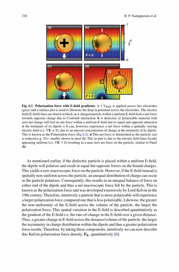
210 B. P. Nadappuram et al.
Fig. 6.1 Polarization force with E-field gradients: A 1 VRMS is applied across two electrodes(gray) and a surface plot is used to illustrate the drop in potential across the electrodes. The electricfield (E-field) lines are drawn in black. aA charged particle within a uniform E-field feels a net forcetowards opposite charge due to Coulomb interaction. b A dielectric or polarizable material withzero net charge will feel no net force within a uniform E-field due to equal and opposite attractionat the terminals of its dipole. c It can, however, experience a net force within a spatially varyingelectric field (i.e. ∇E �= 0), due to an uneven concentration of charge at the terminals of its dipole.This is known as the Polarization force (Eq.6.2). d This net force is diminished as the particle sizeis reduced-e.g. 10× smaller shown in inset (i). This in part is due to the electric field lines locallyappearing uniform (i.e. ∇E ≈ 0) resulting in a near zero net force on the particle, similar to Panel(b)
As mentioned earlier, if the dielectric particle is placed within a uniform E-field,the dipole will polarize and result in equal but opposite forces on the bound charges.This yields a zeromacroscopic force on the particle. However, if the E-field instead isspatially non-uniform across the particle, an unequal distribution of charge can occuras the particle polarizes. Consequently, this results in an unequal balance of force oneither end of the dipole and thus a net macroscopic force felt by the particle. This isknown as the polarization force and was developed extensively by Lord Kelvin in the19th century. Therefore, intuitively a particle that is more polarizable will experiencea larger polarization force compared one that is less polarizable. Likewise, the greaterthe non-uniformity of the E-field across the volume of the particle, the larger thepolarization force. This spatial variation in the E-field is described quantitatively asthe gradient of the E-field-i.e. the rate-of-change in the E-field over a given distance.Thus, a greater change in E-field across the distance/volume of the particle, the largerthe asymmetry in charge distribution within the dipole and thus a greater polarizationforce results. Therefore, by taking these components, intuitively we can now describethis Kelvin polarization force density, FK, quantitatively [6]:

6 Dielectrophoresis of Single Molecules 211
FK = P · ∇E (6.2)
where, P [C/m2], is the particle’s polarization defined simply as the effective dipolemoment, p, per volume.
The reader may already begin to appreciate some of the dilemmas that arise as oneseeks to use the DEP force to trap and manipulate smaller/single molecule particlesin polar water solution. First, as the the particle volume is reduced, the extent of theE-field gradient across the particle is reduced. This is analogous to the mathematicalconceptwhen approximating the derivative of an arbitrary function as a linear/straightline with a small spatial step, dx . Similarly, the E-fields will begin to appear more“uniform” across the particle’s volume as it is reduced in size. Additionally, theambient solution in which the particle is suspended will typically also be a dielectricand can polarize. Water molecules carry a fixed dipole moment and thus respondto the Kelvin polarization force as well. The frequency of operation then becomesa critical parameter as particles larger than water molecules will typically polarizemore slowly or less effectively at higher frequencies. Therefore, the particle size andfrequency of operation will become an important consideration when consideringDEP actuation.
6.2.2 Polarizability and Clausius-Mossotti Factor (CMF)
As mentioned in Sect. 6.2.1, the polarizability, α, of a given particle depends onmultiple factors including geometry, frequency of E-field oscillation (with angularfrequency, ω) and the electrical properties of the particle and ambient surroundingenvironment. The constitutive law governing these properties of interest will be thedielectric permittivity, ε, and conductivity,σ , of the particle and surrounding solution.Since nearly all real materials will contain both a polarizable dielectric property andconductive component, it is helpful to characterize thematerials’ electrical propertiesusing a single complex dielectric permittivity, ε (ω), see Eq.6.3.
ε = ε − ıσ
ω(6.3)
Since DEP typically operates within the low-frequency (e.g. RF regime), ε and σ
are simply the material’s DC dielectric permittivity and conductivity constants and ıis the imaginary unit. This complex term, ε, can then capture both its dielectric andconductive components and frequency response in a single term [3–5].
An effective polarizability, α [units: C/Vm], then will be defined per unit volumeof the particle containing both the complex permittivity of the particle, εp, and thesurrounding liquid medium, εL–both frequency, ω, dependent.
In addition to the electric properties of the particle and solution, the geometry ofthe particle also plays a significant role in its effective polarizability. For instance, anellipsoidal or elongated particle will feel a larger polarization force due to a greater

212 B. P. Nadappuram et al.
spatial extent across theE-field gradient as compared to a spherical counterpart. Oftenanalytes are approximated as spheres (classic spherical “horse” physics approach)to simplify derivation. This in fact is a fair approach as many particles are sphericalin nature and/or are spherical shells (e.g. membrane found cells, exosomes, viralcapsids, etc.). Additionally, the spherical derivation will serve as a conservative“upper-bound” on the DEP force as geometrically it is the least polarizable shape(i.e. the 3D shape with smallest surface area and largest symmetry) and thus willbe the shape with the smallest DEP force [3, 4]. Therefore, the polarizability for asphere and spherical shell will be discussed.
The effective polarizability for a sphere has been derived in extensive detail inother works [3, 4] and is provided below-written in a form to include the Clausius-Mossotti factor (CMF), ˜fcm(ω) [4], see Eq.6.4.
α = 3 εL ˜fcm(ω) (6.4)
The, εL , is the real dielectric constant of the surrounding medium/liquid. All of thecomplex components have been captured by the CMF for simplicity. A sphere with acomplex dielectric permittivity, εp (defined using Eq.6.3), surrounded in a mediumwith a complex dielectric permittivity, εL , the classic CMF equation becomes thefollowing:
˜fcm(ω) = εp − εL
εp + 2 εL(6.5)
When considering a spherical shell particle (e.g. cell, virus, functionalizednanoparticle, etc.), a similar effective polarizability will result. The significant dif-ference is a change in the complex dielectric permittivity of the particle, εp, whichbecomes more complicated due to a core with a different material and polarizabilityresponse. Therefore, Eq. 6.5 will instead replace the solid sphere complex permit-tivity, εp with it composite shell counterpart, i.e. εp → εsp, defined as the following[3, 4]:
εsp = εs
(
�3 + 2 ˜Msc
�3 − ˜Msc
)
(6.6)
˜Msc = εc − εs
εc + 2 εs(6.7)
� = a
a − k(6.8)
where, εc, and, εs , is the complexdielectric permittivity of the particle’s core and shell,respectively. Additionally, a, and, k, is the radius of the particle and the thickness ofits shell/membrane layer, respectively.
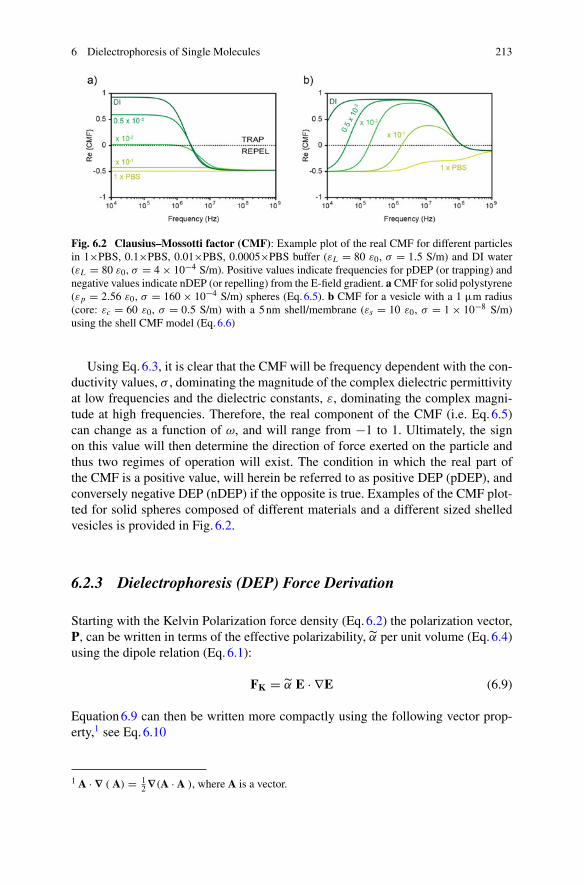
6 Dielectrophoresis of Single Molecules 213
Fig. 6.2 Clausius–Mossotti factor (CMF): Example plot of the real CMF for different particlesin 1×PBS, 0.1×PBS, 0.01×PBS, 0.0005×PBS buffer (εL = 80 ε0, σ = 1.5 S/m) and DI water(εL = 80 ε0, σ = 4 × 10⁻⁴ S/m). Positive values indicate frequencies for pDEP (or trapping) andnegative values indicate nDEP (or repelling) from the E-field gradient. a CMF for solid polystyrene(εp = 2.56 ε0, σ = 160 × 10−4 S/m) spheres (Eq.6.5). b CMF for a vesicle with a 1 µm radius(core: εc = 60 ε0, σ = 0.5 S/m) with a 5nm shell/membrane (εs = 10 ε0, σ = 1 × 10⁻⁸ S/m)using the shell CMF model (Eq.6.6)
Using Eq.6.3, it is clear that the CMF will be frequency dependent with the con-ductivity values, σ , dominating the magnitude of the complex dielectric permittivityat low frequencies and the dielectric constants, ε, dominating the complex magni-tude at high frequencies. Therefore, the real component of the CMF (i.e. Eq. 6.5)can change as a function of ω, and will range from −1 to 1. Ultimately, the signon this value will then determine the direction of force exerted on the particle andthus two regimes of operation will exist. The condition in which the real part ofthe CMF is a positive value, will herein be referred to as positive DEP (pDEP), andconversely negative DEP (nDEP) if the opposite is true. Examples of the CMF plot-ted for solid spheres composed of different materials and a different sized shelledvesicles is provided in Fig. 6.2.
6.2.3 Dielectrophoresis (DEP) Force Derivation
Starting with the Kelvin Polarization force density (Eq. 6.2) the polarization vector,P, can be written in terms of the effective polarizability, α per unit volume (Eq.6.4)using the dipole relation (Eq.6.1):
FK = α E · ∇E (6.9)
Equation6.9 can then be written more compactly using the following vector prop-erty,1 see Eq.6.10
1 A · ∇ ( A) = 12∇(A · A ), where A is a vector.
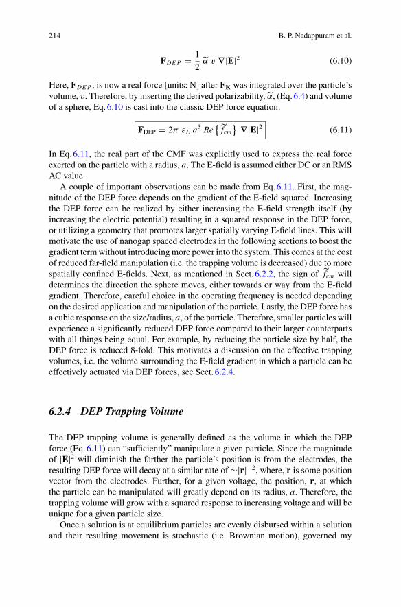
214 B. P. Nadappuram et al.
FDEP = 1
2α v ∇|E|2 (6.10)
Here, FDEP , is now a real force [units: N] after FK was integrated over the particle’svolume, v. Therefore, by inserting the derived polarizability, α, (Eq. 6.4) and volumeof a sphere, Eq.6.10 is cast into the classic DEP force equation:
FDEP = 2π εL a3 Re{
˜fcm} ∇|E|2 (6.11)
In Eq.6.11, the real part of the CMF was explicitly used to express the real forceexerted on the particle with a radius, a. The E-field is assumed either DC or an RMSAC value.
A couple of important observations can be made from Eq.6.11. First, the mag-nitude of the DEP force depends on the gradient of the E-field squared. Increasingthe DEP force can be realized by either increasing the E-field strength itself (byincreasing the electric potential) resulting in a squared response in the DEP force,or utilizing a geometry that promotes larger spatially varying E-field lines. This willmotivate the use of nanogap spaced electrodes in the following sections to boost thegradient termwithout introducingmore power into the system. This comes at the costof reduced far-field manipulation (i.e. the trapping volume is decreased) due to morespatially confined E-fields. Next, as mentioned in Sect. 6.2.2, the sign of ˜fcm willdetermines the direction the sphere moves, either towards or way from the E-fieldgradient. Therefore, careful choice in the operating frequency is needed dependingon the desired application and manipulation of the particle. Lastly, the DEP force hasa cubic response on the size/radius, a, of the particle. Therefore, smaller particles willexperience a significantly reduced DEP force compared to their larger counterpartswith all things being equal. For example, by reducing the particle size by half, theDEP force is reduced 8-fold. This motivates a discussion on the effective trappingvolumes, i.e. the volume surrounding the E-field gradient in which a particle can beeffectively actuated via DEP forces, see Sect. 6.2.4.
6.2.4 DEP Trapping Volume
The DEP trapping volume is generally defined as the volume in which the DEPforce (Eq.6.11) can “sufficiently” manipulate a given particle. Since the magnitudeof |E|2 will diminish the farther the particle’s position is from the electrodes, theresulting DEP force will decay at a similar rate of ∼|r|−2, where, r is some positionvector from the electrodes. Further, for a given voltage, the position, r, at whichthe particle can be manipulated will greatly depend on its radius, a. Therefore, thetrapping volume will grow with a squared response to increasing voltage and will beunique for a given particle size.
Once a solution is at equilibrium particles are evenly disbursed within a solutionand their resulting movement is stochastic (i.e. Brownian motion), governed my
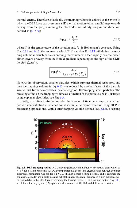
6 Dielectrophoresis of Single Molecules 215
thermal energy. Therefore, classically the trapping volume is defined as the extent inwhich the DEP force can overcome a 1D thermal motion (either a radial step towardsor way from the gap), assuming the electrodes are infinity long in one direction,defined as [4, 7–9]:
|FDEP| >kb T
2a(6.12)
where T is the temperature of the solution and, kb, is Boltzmann’s constant. UsingEqs. 6.11 and 6.12, the volume in which ∇|E| satisfies Eq.6.13 will define the trap-ping volume in which particles entering the volume will then rapidly be acceleratedeither toward or away from the E-field gradient depending on the sign of the CMF,i.e. Re
{
˜fcm(ω)}
.
∇|E|2 >kb T
4π εL a4 Re{
˜fcm} (6.13)
Noteworthy observation, smaller particles exhibit stronger thermal responses, andthus the trapping volume in Eq.6.13 was reduced by another factor of the particlesize, a, that further exacerbates the challenge of DEP trapping small particles. Thereducing effect on the trapping volume as a function of the particle size is illustratedusing coplanar electrodes, see Fig. 6.3.
Lastly, it is often useful to consider the amount of time necessary for a certainparticle concentration is reached for discernible detection when utilizing DEP inbiosensing applications. With a DEP trapping volume defined (Eq. 6.13), a sensing
Fig. 6.3 DEP trapping radius: A 2D electroquasistatic simulation of the spatial distribution of∇|E |2 for a 10nm conformal Al2O3 layer (purple) that defines the electrode gap between coplanarelectrodes. Simulation was ran for a 1 VRMS (1MHz signal) electric potential and is assumed thecoplanar electrodes are infinite into and out of the page. The radial distance in which the beads willbe trapped due to the DEP force overcoming the thermal force, Fth, of Brownian motion (Eq.6.13)are defined for polystyrene (PS) spheres with diameters of 40, 200, and 400nm in DI water

216 B. P. Nadappuram et al.
surface is now effectively projected onto the surface area of this volume whereparticles that pass through the surface of this volume with pDEP will be acceleratedto the sensor. Therefore, Eq. 6.15 can be used to predict the relative speed DEP willaccelerate the time of detection.
Considering a sensing area in which analytes will stick upon collision (e.g. chem-ical binding or DEP trapping) that is semi-infinite, the diffusion driven surface cov-erage per area as a function of time has been derived and is provided below (ignoringsurface saturation effects) [10]:
�(t) = 2 CB
√
Dt
π(6.14)
where CB is the equilibrium bulk concentration, D is the Stokes-Einstein diffusionconstant and t is the time for the sensing area to reach a coverage of:�(t) [units:m−2].Now, if analyte detection can be made at some limit-of-detection surface coverage,�LOD, the time, td , for diffusion to fill the sensing surface to this value is:
td = π
4D
(
�LOD
CB
)2
(6.15)
TheDEP force can then reduces the time for detection, td , by effectively decreasingthe limit-of-detection,�LOD, due to the increased sensing surface area. For example,if the limit of detection was one particle within a diffraction-limited laser spot (waist= 1 µm), the �LOD ≈ 1/π(0.5 µm)2, where the area of the laser spot defined thesensing area.Now, ifDEP is usedwith a cylindrical trapping volume (radius= 1µm),the projected sensing area is expanded resulting in a 4-fold reduction in the limit ofdetection: �LOD ≈ 1/π(1 µm)2 and thus 16× faster detection. In this way, Eq.6.15can be used to approximate the quantitative gains DEP can offer for acceleratedsensing applications.
6.3 DEP Design and Fabrication for Single MoleculeManipulation
Precise manipulation of single molecules such as DNA, RNA and protein are highlyimportant for various biomedical and biotechnological applications [11–14]. Tomanipulate thesemolecules, whose diameters range from fewnanometers tomicrom-eters, researchers have developed various micro-/nanofluidic platforms that employsmethods including electrophoresis, electroosmosis, electrofusion, electrowetting,and dielectrophoresis (DEP) [15, 16]. Among these methods, DEP has been widelyreported for sorting, trapping, concentrating, and general manipulation of singlemolecules [17–19]. Typically, these devices are coupled to microfluidics, either ina basic configuration or more complex geometries up to full lab-on-a-chip systems.Often DEP is coupled with other AC electrokinetic phenomena to achieve addi-

6 Dielectrophoresis of Single Molecules 217
tional capabilities (e.g. electroosmosis). Besides singlemoleculemanipulation, thesedevices are also widely employed for the manipulation of single particle such as cell,virus etc. A comprehensive review of single particle manipulation using DEP is notattempted here but can be found elsewhere [3, 20].
A typical DEP device structure used for single molecule manipulation consists ofat least two metal electrodes with a gap size from 100nm down to 10nm betweenthem. More often an array of such electrodes was employed to scale up the deviceefficiency.Amajor bottleneck inDEPmanipulation of singlemolecules is the fabrica-tion of metal and/or insulating structures capable of generating the high electric fieldgradients required for trapping and concentrating sub-micron/nano sized particles—such as biomolecules. At these scales, particles exhibit high thermal forces due toBrownian movement that must be overcome. Since FDEP is proportional to V 2 L−3,(where V is the applied voltage and L is the distance between electrodes), a highdielectric trapping force can be achieved either by increasing the voltage between theelectrodes or by reducing the distance between electrodes. Increasing applied voltagecould lead to unwanted heat generation, bubble formation, and electrochemical reac-tions (e.g. hydrolysis) and hence is not desirable. On the other hand, shrinking theseparation between two electrodes can significantly increase the force for a given biasvoltage. Hitherto, most common DEP devices reported for single molecule manipu-lation are nanogaps between at least two adjacent planar electrode structures [21–23],although there are several reports on using nanopipettes for DEP trapping [24–26].
Different methods including electron beam lithography, electrochemical plating,Atomic layer deposition (ALD), focused ion beam (FIB) lithography, shadow maskevaporation, scanning probe microscopy lithography, on-wire lithography, and for-mation of mechanical break junctions were reported to fabricate DEP devices forsingle molecule manipulation [23, 30]. In many cases, different methods are oftencombined to obtain the desired device design. Figure1.4 shows the different DEPdevice designs used for single molecule manipulation. The first design is a commonfour electrode assembly, called quadrupole electrode configuration [3, 31–34] (orsometimes called polynomial electrode system because the electrode potential inthese system at any point is defined by a polynomial that obeys Laplace’s equation)which are used for DEP trapping while maintaining the capability for electrorotationfor additional characterization of molecules (Fig. 6.4a). Molecules are trapped due topositiveDEPbetween the electrodeswhere the electric field gradient is high (betweenAC/ground pairs) and negative DEP causes them to accumulate towards the center ofthe structure. Generally, this design consists of a pair of two electrodes (AC/ground),but most common one employs four electrodes or the quadrupole for more stabletrapping. Versions of this configuration were reported for trapping and manipulationof oligonucleotides [35], proteins [33] and single entities such as cells and viruses [3].The design in Fig. 6.4b is an example of anAC/ground pair with a sharp end electrodeassembly reported for trapping small molecules such as proteins [9]. These devicesare fabricated mainly using electron beam lithography that offers precise controlof the electrode design. The small interelectrode distance realized in these devicesenables the generation of large electric field gradients required for the manipula-tion of small biomolecules. The interdigitated device design depicted in Fig. 6.4c is
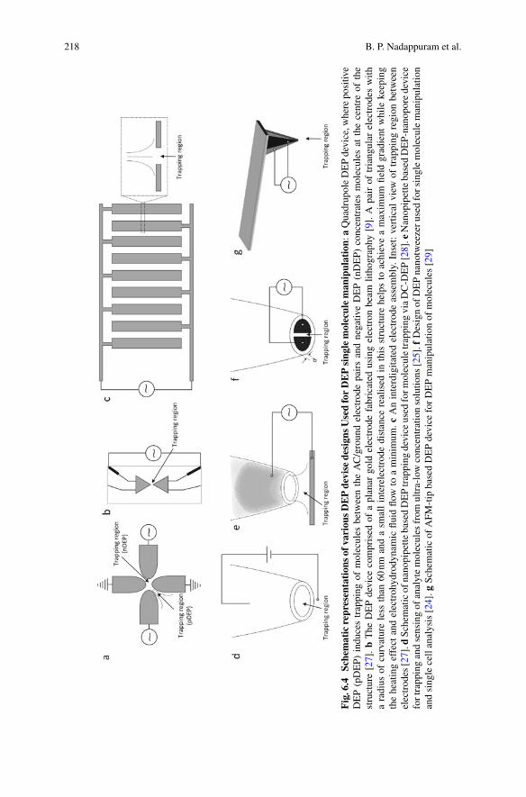
218 B. P. Nadappuram et al.
Fig.6.4
Sche
maticrepresen
tation
sof
variou
sDEPdevise
design
sUsedforDEPsing
lemoleculeman
ipulation:
aQuadrupoleDEPdevice,w
herepositiv
eDEP(pDEP)
inducestrapping
ofmolecules
betweentheAC/groundelectrodepairsandnegativ
eDEP(nDEP)
concentrates
molecules
atthecentre
ofthe
structure[27].bThe
DEPdevice
comprised
ofaplanar
gold
electrod
efabricated
usingelectron
beam
litho
graphy
[9].A
pairof
triang
ular
electrod
eswith
aradius
ofcurvatureless
than
60nm
andasm
allinterelectrode
distance
realised
inthisstructurehelpsto
achieveamaxim
umfie
ldgradient
while
keeping
theheatingeffect
andelectrohyd
rody
namic
fluid
flow
toaminim
um.c
Aninterdigita
tedelectrod
eassembly.Inset:vertical
view
oftrapping
region
betw
een
electrod
es[27].d
Schematicof
nano
pipette
basedDEPtrapping
device
used
form
oleculetrapping
viaDC-D
EP[28].e
NanopipettebasedDEP-nanoporedevice
fortrappingandsensingof
analytemolecules
from
ultra-lowconcentrationsolutio
ns[25].f
Designof
DEPnano
tweezeru
sedforsinglemoleculemanipulation
andsing
lecellanalysis[24].g
Schematicof
AFM
-tip
basedDEPdevice
forDEPmanipulationof
molecules
[29]
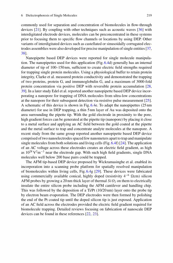
6 Dielectrophoresis of Single Molecules 219
commonly used for separation and concentration of biomolecules in flow-throughdevices [21]. By coupling with other techniques such as acoustic waves [36] withinterdigitated electrode devices, molecules can be preconcentrated in these systemsprior to focusing them to specific flow channels or locations by using DEP. Othervariants of interdigitated devices such as castellated or sinusoidally corrugated elec-trodes assemblies were also developed for precisemanipulation of single entities [37,38].
Nanopipette based DEP devices were reported for single molecule manipula-tion. The nanopipettes used for this application (Fig. 6.4d) generally has an internaldiameter of tip of 100–150nm, sufficient to create electric field strengths requiredfor trapping single protein molecules. Using a physiological buffer to retain proteinintegrity, Clarke et al. measured protein conductivity and demonstrated the trappingof two proteins, protein G, and immunoglobulin G, and a maximum of 3000-foldprotein concentration via positive DEP with reversible protein accumulation [28,39]. In a later study Edel et al. reported another nanopipette based DEP device incor-porating a nanopore for trapping of DNA molecules from ultra-low concentrationsat the nanopore for their subsequent detection via resistive pulse measurement [25].A schematic of this device is shown in Fig. 6.4e. To adapt the nanopipettes (25nmdiameter) for use in DEP trapping, a thin 5nm layer of Au was deposited onto thearea surrounding the pipette tip. With the gold electrode in proximity to the pore,high gradient forces can be generated at the pipette tip (nanopore) by placing it closeto a metal surface and applying an AC field between the gold coated at the pipetteand the metal surface to trap and concentrate analyte molecules at the nanopore. Arecent study from the same group reported another nanopipette based DEP devicecomprised of two nanoelectrodes spaced few nanometers apart to trap andmanipulatesingle molecules from both solutions and living cells (Fig. 6.4f) [24]. The applicationof an AC voltage across these electrodes creates an electric field gradient, as highas 1028 V2m−3 near the electrode gap. With such high field gradients, single DNAmolecules well below 200 base pairs could be trapped.
The AFM tip-based DEP device proposed by Wickramasinghe et al. enabled itsincorporation into a scanning probe platform for spatially resolved manipulationof biomolecules within living cells, Fig. 6.4g [29]. These devices were fabricatedusing commercially available conical, highly doped (resistivity 4−6 cm) siliconAFM probes by growing a 20nm thick layer of thermal SiO2 on them to electricallyinsulate the entire silicon probe including the AFM cantilever and handling chip.This was followed by the deposition of a Ti/Pt (10/20nm) layer onto the probe tipby electron beam evaporation. The DEP electrodes were then formed by polishingthe end of the Pt coated tip until the doped silicon tip is just exposed. Applicationof an AC field across the electrodes provided the electric field gradient required forbiomolecule trapping. Detailed reviews focusing on fabrication of nanoscale DEPdevices can be found in these references [22, 23].
220 B. P. Nadappuram et al.
6.4 Dielectrophoretic Manipulation of Single Molecules
Single molecule sensing is a rapidly expanding technology for the detection andquantification of a wide range of biomolecules including nucleic acids and pro-teins. Many single-molecule detection technologies, such as nanopore sensing [40]and field-effect biosensing [41] architectures offer significant opportunities for theadvancement of rapid Point-of-Care (POC) diagnostics. Nevertheless, the dominantmechanism of capture and detection of the analyte in these sensors is diffusion-limited, making it difficult to concentrate and perform high-throughput detection ofultra-dilute samples [25]. Ever since Pohl and Hank first demonstrated the possibilityof employing DEP for selective separation of single entities [42], many researchersattempted to extend the capability of this platform to break the diffusion barrier toincrease the selectivity and sensitivity of single molecule techniques. Hitherto, DEPwas reported for the manipulation of a range of biomolecules including DNA, RNAand proteins [3, 17, 43]. However, as will be highlighted in the following sections,DEPmanipulation of single molecules is at varying stages of development with eachmethod requiring continued research to reach its full potential.
6.4.1 Dielectrophoretic Manipulation of DNA and RNA
The ability to manipulate DNA molecules by exploiting its induced dipole momentoffers exciting possibilities for the development of novel DNA separation techniquesand their controlled movement for DNA diagnostics to a wider use in genomicsand proteomics. Experiments over the past three decades, have demonstrated waysto orient, stretch, transport, and trap DNA using nonuniform fields generated inmicrofabricated devices [3, 44–48].
In the first reported study on DEP behavior of DNA,Washizu showed that lambdaphage DNA (λ DNA) suspended in deionized water attracted towards the high fieldregions of DEP electrodes upon application of a 1MHz voltage bias [49]. A follow upstudy from the samegroupdemonstrated theDEP induced stretching andalignment ofsingle λDNAmolecule in solution [48]. Subsequent studies using different electrodedesigns investigated the dielectric and DEP behavior of DNA.
Anexciting applicationof the earlier researchonDEPeffect onDNAcanbe seen inthe study by Yamamoto et al. where a novel method for the space-resolved dissection(molecular surgery) of deoxyribonucleic acid (DNA) using electrostatic molecularmanipulation is demonstrated [46]. Unlike in the conventional restriction digestionof DNA where DNA-cutting enzymes (Restriction enzymes, e.g. DNase) and DNAare mixed in the reaction buffer and the restriction process is depending on stochasticchances, the presented method offered a reproducible cutting of DNA at any desiredposition along the DNAmolecule by its physical manipulation using DEP. To realizethis space-resolved fragmentation, DEP was employed to stretch and anchor themolecule on a solid surface. Besides these applications, a wide range of reports on
6 Dielectrophoresis of Single Molecules 221
Fig. 6.5 DEP-Nanopore device for single molecule detection from ultra-low concentrationsolutions: a Schematic of the nanopipette DEP-nanopore device showing DNA being threadedthrough the tip of the device. b Fluorescent micrograph of DEP trapping showing the progressionof DNA trapping at the tip of the nanopipette at different time intervals. c Typical current modulationassociated with single DNA molecule translocation recoded across the nanopore. d Current tracesobtained using DEP as a pre-concentration step for four different concentrations (5 pM, 500 fM, 50fM and 5 fM). A bias of |�V | = 500 mV was applied across the nanopore for all the experiments.A single molecule translocation event is seen as spikes in the current trace. Figures reprinted in partwith permission from Freedman et al. [25] Copyright 2016, Springer Nature
DNA fragments sorting and concentration using various electrode configurationsand DEP characterization of different DNA molecules in low and high conductivitymedia have also been reported. Comprehensive reviews on these developments canbe seen in these references [3, 44].
As mentioned in the previous section, an important aspect of single moleculemanipulation is to overcome the diffusion barrier in delivering analyte moleculesinto the sensing regions of single molecule detection platforms—such as nanoporesensors. This is particularly important for detecting ultra-low concentration ana-lytes such as cell-free circulating DNAs for early cancer diagnosis. To address thischallenge, Edel et al. demonstrated a simple, yet powerful, method based on cou-pling single-molecule dielectrophoretic trapping to nanopore sensing for trappingand delivering DNA from ultra-diluted sample solution to the sensing region for fastand easy single molecule detection [25]. A schematic of the experimental set-upused for this study is show in Fig. 6.5a. Incorporation of a DEP trap to the nanoporewas achieved by adding a 5nm layer of gold onto the area surrounding the nanopore(tip of the nanopipette). Typical nanopore experiments use a constant DC bias toprompt the translocation of the analyte molecule through the nanopore while moni-toring the current across the nanopore. The DC current modulation resulting from thetranslocation of an analyte molecule across the nanopore is used to identify and char-acterize the translocating molecule (Fig. 6.5c). In this study, an AC voltage (10–20Vand 0.5–4MHz) was applied to the metallized layer surrounding the nanopipette fordielectrophoretic trapping and delivery of DNA (Fig. 6.5b) to the nanopore followedby a DC voltage which translocates the molecules across the nanopore for sensing.The AC and DC voltages are applied to the system using the two Au electrodes andtwo Ag/AgCl electrodes, respectively. By using this set-up, high sensitivity detec-tion in concentrations as low as 5 fM was achieved using optimized DEP trapping

222 B. P. Nadappuram et al.
conditions (Vpp= 20V and 1MHz), Fig. 6.5d. The sensitivity enhancement is shownto stem from a larger DEP trapping volume in combinationwith an enhanced deliveryof the DNA molecule into the sensing region by overcoming the challenges posedby diffusion and electrophoretic properties of the analytes.
In another recent report, Edel et al. demonstrated the ability of DEP devices topick-and-place individual molecules of DNAby using aDEP nanotweezer [24]. DEPtweezers were reported previously for picking and relocating single target cells buttheir application for single molecule manipulation was limited by their large foot-print and the difficulty in generating high DEP forces required for small moleculemanipulation. The DEP nanotweezer, on the other hand, was fabricated easily andinexpensively from dual barrel capillaries by pulling them into sharp end pipettesand pyrolytically depositing carbon inside the nanopipette to form two co-planarnanoscale electrodes separated by ca. 20nm septum to generate high DEP forcesrequired for single molecule manipulation (Fig. 6.6a). This nanotweezer was thenemployed in conjunction with an XYZ positioning platform to perform ‘pick-and-place’-typemeasurements inwhich singlemolecules were trapped, moved at a veloc-ity as high as 30µms−1 and then released at a specific location.Thiswas demonstratedfor DNA molecules of which a single molecule was traced using an image trackingalgorithm to follow the trajectory of the molecule from capture (Fig. 6.6b), move-ment in the x–y plane (Fig. 6.6 panels c and d) and subsequent release (Fig. 6.6e).Apart from using the DEP nanotweezers for performing single molecule manipula-tion in solutions, they were also employed for trapping and extracting DNA, RNAand individual organelles from living cells without affecting their viability.
One of the most important aspects in designing a DEP device for single moleculemanipulation is the voltage required for its operation. Most of the DEP devicesemployed fromDNAmanipulation requires a high voltage for generating sufficientlylarge electric field gradients [51]. Because of the sophisticated electronic instrumen-tation required for generating these high voltages, it is of utmost importance to devisestrategies to reduce input voltage requirements to facilitate their deployment in ana-
Fig. 6.6 DEP nanotweezer for single molecule manipulation: a Schematic of a typical DEPnanotweezer. Application of an AC voltage on the nanotweezer generates a highly localized electricfield gradient that is suitable for targeted molecular trapping in solution or inside a cell. Panelsb to e Pick-and-place of single molecule DNA using the DEP nanotweezer. The DNA moleculeis captured at the nanotweezer tip by turning on the AC field (b), the captured single molecule istransferred from one position to another by moving the nanotweezer using a micromanipulator withthe AC field kept on (panels(c) and (d)) and then released by turning off the DEP (e). Scale bars(right), 10 µm; inset, 2 µm [24]
6 Dielectrophoresis of Single Molecules 223
lytical platforms.Additionally, the use of high voltages inmicrofluidic channels filledwith conductive solutions generate significant Joule heating affecting the device sen-sitivity. Thus, high input-voltages represent an obstacle toward creating fully inte-grated, stand-alone platforms that can be used outside of a laboratory. To overcomethis challenge, Barik et al. developed a Graphene-edge dielectrophoretic tweezers forlow-voltage trapping of biomolecules [50].A combination ofALD,Photolithographyand electron beam depositionwas used to fabricate this DEP device, in addition to theatomically sharp edges of monolayer graphene to generate singular electrical fieldgradients for trapping DNAmolecules. A schematic of the device design is shown inFig. 6.7a where a metal electrode (Ti/Pd) was first patterned using photolithographyonto a thick layer of SiO2 (300nm) thermally grown on a Si wafer. This was followedby a combination of reactive ion etc.hing and wet etc.hing. An 8nm thick dielec-tric layer was deposited on top of the Pd electrodes with HfO2 using atomic layerdeposition (ALD). Then, single-layer graphene grown by chemical vapor deposition(CVD)was transferred onto the wafer and etched into rectangular patterns. Electricalcontacts (Cr/Au) were patterned on top of the graphene layer via photolithographyand electron beam deposition. The bottom electrode and these top contact electrodeswere arranged in an interdigitated fashion to minimize series resistance and to pro-duce more exposed edges to efficiently trap the DNA molecules. To demonstratethe utility of the graphene electrodes in capturing biomolecules, DEP trapping of 10kbp and 500 bp DNA molecules tagged with YOYO-1 dye at a final concentrationof 10 pM in a 10 µM KCl solution was performed. Trapping and releasing of 10kbp DNA was observed at 1MHz and 10MHz, respectively (Fig. 6.7b panels i tovii). 500 bp DNA molecules were found to trap along the graphene edge at 2.5Vand 1MHz frequency. This approach is scalable and highly reproducible at the waferscale. Additionally, the interdigitated electrode arrays allowed large coverage selec-tive trapping and positioning of these DNAmolecules precisely along the atomicallysharp edges of graphene under the same low-voltage operation due to the extremeDEP forces generated from the atomic graphene electrode flake.
High-aspect ratio, coplanar nanogaps have also been demonstrated for large sur-face coverage with low-volt DEP; this configuration was especially optimal forintegration with anamorphic optics for rapid, real-time vibrational spectroscopicimaging of molecular cargo within liposome capsules [52]. Moreover, the extremecoplanar nanogaps were fabricated using a novel atomic layer lithography techniquethat comprises the peeling of adhesive tape for creating the extreme aspect ratio(e.g. <10nm electrode gap maintained over several millimeters in length) coplanarelectrodes [7, 53]. The entire coplanar nanogap can then be excited simultaneouslyfor Raman imaging using a laser line (via anamorphic optics) in which DEP pre-cisely positions the analytes within the excitation and imaging path for readout usingan imaging spectrometer (Fig. 6.8). The nanogap separation offered 1V amplitudetrapping and active passing between segmented parallel structures of 70nm lipo-somes containing 4-Mercaptopyridine (4-MPY), a small (0.1 kDa) Raman activecarbon ring molecule. Bare gold nanoparticles (AuNP) spiked into solution wouldsimultaneously be trapped (over a wide range of operating frequencies) to offer sur-face enhanced Raman spectroscopy of the 4-MPY molecular cargo. Referred to as
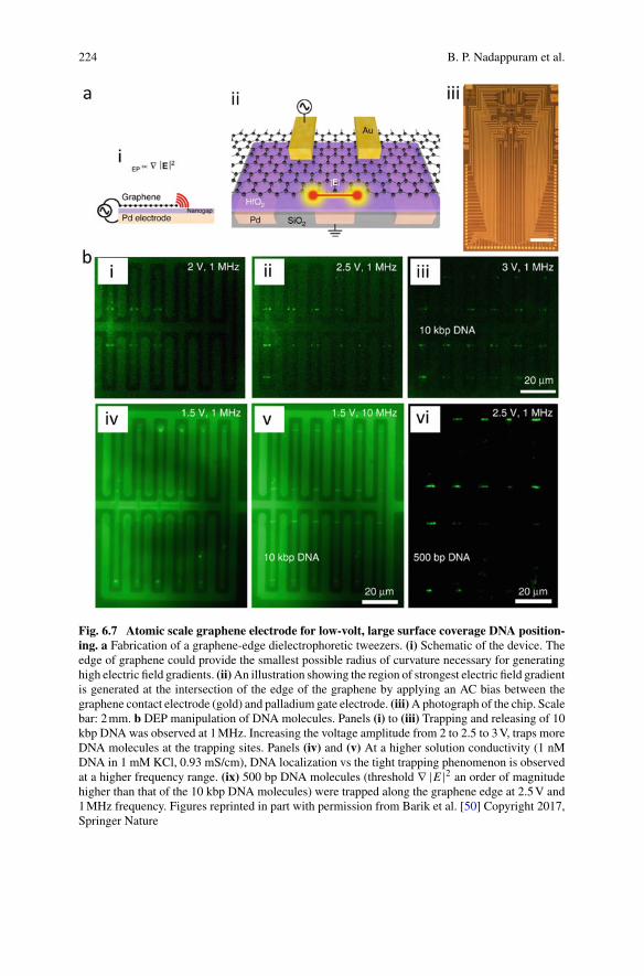
224 B. P. Nadappuram et al.
Fig. 6.7 Atomic scale graphene electrode for low-volt, large surface coverage DNA position-ing. a Fabrication of a graphene-edge dielectrophoretic tweezers. (i) Schematic of the device. Theedge of graphene could provide the smallest possible radius of curvature necessary for generatinghigh electric field gradients. (ii)An illustration showing the region of strongest electric field gradientis generated at the intersection of the edge of the graphene by applying an AC bias between thegraphene contact electrode (gold) and palladium gate electrode. (iii)Aphotograph of the chip. Scalebar: 2mm. b DEP manipulation of DNA molecules. Panels (i) to (iii) Trapping and releasing of 10kbp DNA was observed at 1MHz. Increasing the voltage amplitude from 2 to 2.5 to 3V, traps moreDNA molecules at the trapping sites. Panels (iv) and (v) At a higher solution conductivity (1 nMDNA in 1 mM KCl, 0.93 mS/cm), DNA localization vs the tight trapping phenomenon is observedat a higher frequency range. (ix) 500 bp DNA molecules (threshold ∇ |E |2 an order of magnitudehigher than that of the 10 kbp DNA molecules) were trapped along the graphene edge at 2.5V and1MHz frequency. Figures reprinted in part with permission from Barik et al. [50] Copyright 2017,Springer Nature
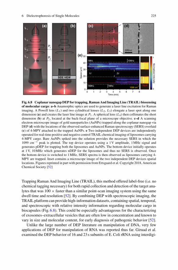
6 Dielectrophoresis of Single Molecules 225
Fig. 6.8 Coplanar nanogapDEP for trapping, RamanAnd Imaging Line (TRAIL) biosensingof molecular cargo: a–b Anamorphic optics are used to generate a laser line excitation for Ramanimaging. A Powell lens (L1) and two cylindrical lenses (L2, L3) elongate a laser spot along onedimension (a) and creates the laser line image at P1. A spherical lens (L4) then collimates the shortdimension (b) at P2, located at the back-focal plane of a microscope objective. c–d A scanningelectron microscope image of gold nanoparticles (AuNPs) trapped along the coplanar nanogap viaDEP (d) with the locations of the observed surface-enhanced Raman spectroscopy (SERS) overlaid(c) of 4-MPY attached to the trapped AuNPs. e Two independent DEP devices are independentlyoperated for real-time positive and negative control TRAIL chemical imaging of liposomes carrying4-MPY cargo. Bare AuNPs spiked into the solution provides the necessary SERS in which the1099 cm−1 peak is plotted. The top device operates using a 1V amplitude, 1MHz signal andgenerates pDEP for trapping both the liposomes and AuNPs. The bottom device initially operatesat 1V, 10MHz which generates nDEP for the liposomes and thus no SERS is observed. Oncethe bottom device is switched to 1MHz, SERS spectra is then observed as liposomes carrying 4-MPY are trapped. Inset contains a microscope image of the two independent DEP devices spatiallocations. Figures reprinted in part with permission from Ertsgaard et al. Copyright 2018, AmericanChemical Society [52]
Trapping Raman And Imaging Line (TRAIL), this method offered label-free (i.e. nochemical tagging necessary) for both rapid collection and detection of the target ana-lytes that was 100 × faster than a similar point-scan imaging system using the samedwell time and resolution [52]. By combining DEP with spectroscopic imaging, theTRAIL platform can provide high-information datasets, containing spatial, temporal,and spectroscopic with relative intensity information regarding molecular cargo inbiocapsules (Fig. 6.8). This could be especially advantageous for the characterizingof exosomes–extracellular vesicles that are often low in concentration and known tovary in size and molecular content, for early diagnosis of pathogenic behavior [52].
Unlike the large number of DEP literature on manipulation of DNA, very fewapplications of DEP for manipulation of RNA was reported thus far. Giruad et al.examined the DEP behavior of 16 and 23s subunits of E. Coli rRNA using interdigi-
226 B. P. Nadappuram et al.
tated microelectrodes [54]. In their study the authors characterized the frequency andvoltage dependence on the trapping efficiency of the RNAs. The voltage dependencemeasured at 1MHz ruled out any significant contribution of possible permanentdipole moment of RNA molecules on their DEP response. In each bias, these RNAmolecules showedmaximumDEP trapping (positiveDEP) between3kHz and1MHzand a negative DEP response above 9MHz. More recently, Edel et al. demonstratedDEP trapping and extraction of RNA molecules from living cells [24]. Even thoughthe technology is in its infancy, DEP manipulation of RNA hold high potential interms of analytical applications especially for spatially resolved single cell RNAmapping.
6.4.2 Dielectrophoretic Manipulation of Protein
Selective trapping and manipulation of proteins is essential for diagnostic applica-tions as well as for understanding their structural and functional features. Hitherto,many examples of DEP devices for trapping and manipulation of protein have beenreported in the literature [27]. A comprehensive review of dielectrophoretic trappingcan be seen in these references [27, 55]. Among the examples of DEP manipu-lation of proteins reported thus far, the seminal work by Washizu et al. deservesspecial mentioning [37]. Up until then, DEP was mainly employed for manipulationof micrometer-sized particles such as biological cells, since DEP manipulation ofproteins requires relatively high electric field gradients to overcome the high Brow-nian motion. Nevertheless, by using an interdigitated sinusoidally corrugated DEPdevice,Washizu et al. demonstrated theDEP trappingofAvidin, concanavalinA, chy-motripsinogen A and Ribonuclease A and attempted to perform ‘dielectrophoreticchromatography’ to separate biopolymers based on their polarizability. Nearly adecade later, Asokan et al., demonstrated another example of DEP manipulation ofactin-myosin systems using a quadrupole electrode system [56]. Figure6.9a showsthe actin filaments trapped at high field region in the quadrupole electrode with thefilaments oriented parallel to the field lines.
Another study by Holzel et al. demonstrating the trapping of freely diffusing R-phycoerythrin protein deserves special attention, partially because of the improve-ment in device design that enabled the generation of relatively high electric fieldgradients [9]. The DEP device was comprised of planar gold electrodes prepared ona low n-doped silicon substrate. To achieve a maximum field gradient while keepingthe heating effects and electrohydrodynamic fluid flow to a minimum, a pair of tri-angular electrodes with a radius of curvature of less than 60nm and an interelectrodedistance of 500nmwas fabricated using electronbeam lithography. Figure6.9b showsan electron micrograph of a typical DEP device used in this study. R-phycoerythrinwas chosen as the analyte molecule because of its intense autofluorescence and thevisualization of the trapping was achieved by recording the fluorescence intensity atthe electrode surface. Applications of a sinusoidal signal of 10V (root mean square)at 1MHz resulted in fluorescing spots appearing independently at both electrode tips

6 Dielectrophoresis of Single Molecules 227
Fig. 6.9 Dielectrophoretic manipulation of protein a Fluorescent micrograph showing actinfilaments collected at the high field regions of a quadrupole electrode at an applied frequency of1MHz and 7V. The polarized filaments orient themselves parallel to the field lines. Figures reprintedin part with permission from Asokan et al. [56] Copyright 2003, American Chemical Society. bElectron micrograph of DEP device used for trapping freely suspended R-phycoerythrin molecules.Scale bar 5 µm. The largest electrode pair with 500nm gap width was used for DEP trapping ofthe protein molecule. c Fluorescence micrograph recorded 10s after applying a voltage bias andsubsequent DEP trapping. The fluorescent spot at the electrode tip is due to the accumulation of R-phycoerythrin molecules. Figures reprinted in part with permission from Holzel et al. [9] Copyright2005, American Physical Society
within about 10 s Fig. 6.9c).When the voltagewas turned off, the fluorescent intensitydecreased as the molecules freely diffused away from the electrode tip. Subsequentstudies have demonstrated the DEP trapping and manipulation of a wide range ofprotein molecules including streptavidin, immunoglobulins and amyloid beta fibrils.An updated list of list of proteins captured or trapped using DEP devices can be seenin this reference [55].
6.5 Discussion
Whilemanyadvantages existwith usingDEP for particlemanipulation, it is importantto understand its limitations and how it can be optimized in the future. The firstconsideration is the operating frequency. It was provided in Sect. 6.2 that the CMFdetermines the frequency response of the particle and that the sign on the real partof Eq.6.5 indicates whether the particle feels pDEP where the particle feels a forcetowards theE-field gradient (i.e. trapping) or nDEPwhere the particle is repelled fromthe E-field gradient. Composite particles (e.g. a shell) can have complex frequencyresponses that limit the range of frequency for either pDEP or nDEP (Fig. 6.2). Twoadditional constraints can existwhich can further limit the operating frequency and/orwhether DEP actuation can be feasible.
228 B. P. Nadappuram et al.
6.5.1 Electrolysis
The first is electrolysis and/or hydrolysis. Electrolysis refers to the oxidation orreduction (REDOX) of chemical species within liquid bodies that is activated undera voltage potential. This is called hydrolysis if the REDOX occurs with specificallywater molecules–generating hydrogen and oxygen gas. Hydrolysis can occur withDC voltages as low as 1.23V [57]. Often passivization layers are used to mitigatethis effect and prevent the transfer of charge and REDOX reactions. However, thiscan be problematic for DEP by consuming most of the strong E-field (especially fornanogap DEP) within the passivation layer itself and thus reducing DEP actuation.
Another approach is to increase the operating frequency of theAC signal to reducethe time for REDOX reactions. With sufficiently high operating frequency, the elec-trolytic reactions can be reversed before adequate separation of the products canaccumulate (e.g. bubbles and gas formation) [58, 59]. Therefore, a balance mustbe kept between the voltage, current, frequency, and passivization layer used. As areference, frequencies around 100 kHz, using 1Wof power (under 6–7V) and no pas-sivation layer was at the threshold of negligible bubble formation as observed underhigh-speed camera [58]. This then motivates using the highest operating frequencyavailable that still satisfies the CMF for the desired DEP actuation.
6.5.2 RC Roll-Off
The second limit on the operating frequency is RC roll-off [60, 61]. This is animportant consideration for nanogap DEP which will typically have larger devicecapacitance and/or transparent and thin DEP electrodes which will typically havelarger series resistance. In principle, the DEP device behaves like a low-pass filterwith an upper bound cutoff frequency that must be considered. The DEP electrodeswill possess a capacitance,C , thatmust be given adequate time to fully “fill” or chargefor actuation. If the signal oscillates with too high of a frequency, only a fraction ofthe voltage signal is dropped over the device resulting in poor DEP actuation.
Therefore, the operating frequency should be kept below the circuit’s cutoff fre-quency (Eq.6.16) for all applications and is an upper bound for efficient power usagefor liquid actuation.
ω <1
RC(6.16)
In Eq.6.16, ω, is the angular operating frequency and R, is the entire circuit’s seriesresistance (and/or sheet resistance for 2Dmaterials). Thin, transparent, or 2Dmaterialconductors and semi-conductors used as DEP electrodes will often large resistancewhich can reduce the cutoff frequency. Further, RF power sources are typically issueda standard output impedance of 50 . Therefore, this too will pose a limit on thedesign of the DEP device and/or max frequency that can be used. Since nanogap
6 Dielectrophoresis of Single Molecules 229
DEP will have relatively larger capacitance due to a small electrode nanogap, g (seeEquation for a parallel plate capacitor) the electrodes should then be designed withminimal area of overlap, A, (e.g. coplanar electrodes) to mitigate RC roll-off.
C = εA
g(6.17)
6.5.3 Joule Heating
Lastly, as EM power is dissipated either as Ohmic current in ionic solutions ordisplacement current in dielectric, the dissipation of this power often is convertedinto heat (i.e. Joule heating) of the sample. The change in temperature, �T , of thesolution scales with the power dissipated (i.e. ∝ V 2) and can be approximated asfollows [7, 62]:
�T ≈ σV 2
2k(6.18)
where σ is the electrical conductivity of the solution and k is the thermal conductivityof the solution. Therefore, to mitigate the effects of Joule heating increasing the E-field gradient (rather than the operating voltage) is desirable and is a main advantageof using nanogap DEP.
6.6 Future Outlook
DEP has proven to be a versatile method for trapping, concentration, sorting andmanipulation of single molecules including nucleic acids and proteins. Singlemolecule manipulation using DEP is straightforward and fully tuneable by alter-ing the electric field strength and the medium conductivity. Hitherto, DEP devicesfor single molecule manipulation are mainly composed of planar electrode geome-tries that can be readily integrated intomicrofluidic platforms. Nevertheless, there areseveral reports on using nanopipettes forDEPmanipulation of singlemolecules. Eversince the first demonstration of DEP trapping of DNA, the huge amount of researchon single molecule manipulation using DEP has resulted in the development of avariety of device configurations and experimental strategies. The mechanical robust-ness and portability makes these platforms ideal candidates for using them withvarious point-of-care applications in clinical diagnostics. Although much progresshas been made in the last three decades, the DEP single molecule manipulation sys-tems can be further improved in many ways and adopted for new applications suchas continuous live cell sampling, early detection of disease biomarkers (e.g. exosomecharacterization) and the structural investigation of biomolecules.

230 B. P. Nadappuram et al.
References
1. Paul E. Sheehan andLloyd J.Whitman.Detection limits for nanoscale biosensors.NanoLetters,5(4):803–807, apr 2005.
2. ToddMSquires, Robert JMessinger, and Scott RManalis.Making it stick: convection, reactionand diffusion in surface-based biosensors. Nature Biotechnology, 26(4):417–426, apr 2008.
3. Ronald R. Pethig. Dielectrophoresis: Theory, Methodology and Biological Applications.WILEY, 2017.
4. Hywel Morgan. AC electrokinetics : colloids and nanoparticles. Research Studies Press,Philadelphia, PA, 2003.
5. Parikha Mehrotra, Baibhab Chatterjee, and Shreyas Sen. EM-wave biosensors: A review ofRF, microwave, mm-wave and optical sensing. Sensors, 19(5):1013, feb 2019.
6. Hermann Haus. Electromagnetic fields and energy. Prentice Hall, Englewood Cliffs, NewJersey, 1989.
7. Avijit Barik, Xiaoshu Chen, and Sang-Hyun Oh. Ultralow-power electronic trapping ofnanoparticles with sub-10 nm gold nanogap electrodes. Nano Letters, 16(10):6317–6324, sep2016.
8. Herbert Pohl. Dielectrophoresis : the behavior of neutral matter in nonuniform electric fields.Cambridge University Press, Cambridge New York, 1978.
9. Ralph Holzel, Nils Calander, Zackary Chiragwandi, Magnus Willander, and Frank F. Bier.Trapping single molecules by dielectrophoresis. Physical Review Letters, 95(12), sep 2005.
10. D. Brynn Hibbert, J. Justin Gooding, and Paul Erokhin. Kinetics of irreversible adsorption withdiffusion: application to biomolecule immobilization. Langmuir, 18(5):1770–1776, mar 2002.
11. Susan K Sarkar. Single molecule biophysics. In Single Molecule Biophysics and Poisson Pro-cess Approach to Statistical Mechanics. IOP Publishing, 2016.
12. Deyu Zhao, Siyun Liu, and Ying Gao. Single-molecule manipulation and detection. ActaBiochimica et Biophysica Sinica, 50(3):231–237, jan 2018.
13. Christopher P. Calderon, Nolan C. Harris, Ching-Hwa Kiang, and Dennis D. Cox. Analyzingsingle-moleculemanipulation experiments. Journal ofMolecular Recognition, 22(5):356–362,may 2009.
14. Ulrich Bockelmann. Single-molecule manipulation of nucleic acids.Current Opinion in Struc-tural Biology, 14(3):368–373, jun 2004.
15. ChengQian, HaiboHuang, Liguo Chen, Xiangpeng Li, Zunbiao Ge, Tao Chen, ZhanYang, andLining Sun. Dielectrophoresis for bioparticlemanipulation. International Journal ofMolecularSciences, 15(10):18281–18309, oct 2014.
16. P.K.Wong, T.-H.Wang, J.H. Deval, andC.-M.Ho. Electrokinetics inmicro devices for biotech-nology applications. IEEE/ASME Transactions on Mechatronics, 9(2):366–376, jun 2004.
17. Talukder Z. Jubery, Soumya K. Srivastava, and Prashanta Dutta. Dielectrophoretic separationof bioparticles in microdevices: A review. Electrophoresis, 35(5):691–713, feb 2014.
18. Daihyun Kim, Mukul Sonker, and Alexandra Ros. Dielectrophoresis: From molecular tomicrometer-scale analytes. Analytical Chemistry, 91(1):277–295, nov 2018.
19. Nurhaslina Abd Rahman, Fatimah Ibrahim, and Bashar Yafouz. Dielectrophoresis for biomed-ical sciences applications: A review. Sensors, 17(3):449, feb 2017.
20. Linbo Liu, Ke Chen, Nan Xiang, and Zhonghua Ni. Dielectrophoretic manipulation of nano-materials: A review. Electrophoresis, 40(6):873–889, oct 2018.
21. Khashayar Khoshmanesh, Saeid Nahavandi, Sara Baratchi, Arnan Mitchell, and KouroshKalantar-zadeh. Dielectrophoretic platforms for bio-microfluidic systems.Biosensors and Bio-electronics, 26(5):1800–1814, jan 2011.
22. Anton Kuzyk. Dielectrophoresis at the nanoscale. Electrophoresis, 7(10217), jul 2011.23. M Li, W H Li, J Zhang, G Alici, and W Wen. A review of microfabrication techniques and
dielectrophoretic microdevices for particle manipulation and separation. Journal of Physics D:Applied Physics, 47(6):063001, jan 2014.
6 Dielectrophoresis of Single Molecules 231
24. Binoy Paulose Nadappuram, Paolo Cadinu, Avijit Barik, Alexander J. Ainscough, Michael J.Devine, Minkyung Kang, Jorge Gonzalez-Garcia, Josef T. Kittler, Keith R. Willison, RamonVilar, Paolo Actis, Beata Wojciak-Stothard, Sang-Hyun Oh, Aleksandar P. Ivanov, andJoshuaB. Edel. Nanoscale tweezers for single-cell biopsies.NatureNanotechnology, 14(1):80–88, dec 2018.
25. Kevin J. Freedman, Lauren M. Otto, Aleksandar P. Ivanov, Avijit Barik, Sang-Hyun Oh, andJoshua B. Edel. Nanopore sensing at ultra-low concentrations using single-molecule dielec-trophoretic trapping. Nature Communications, 7(10217), jan 2016.
26. Kevin J. Freedman, Colin R. Crick, Pablo Albella, Avijit Barik, Aleksandar P. Ivanov, Ste-fan A. Maier, Sang-Hyun Oh, and Joshua B. Edel. On-demand surface- and tip-enhancedraman spectroscopy using dielectrophoretic trapping and nanopore sensing. ACS Photonics,3(6):1036–1044, may 2016.
27. Asuka Nakano and Alexandra Ros. Protein dielectrophoresis: Advances, challenges, and appli-cations. Electrophoresis, 34(7):1085–1096, apr 2013.
28. Richard W. Clarke, Samuel S. White, Dejian Zhou, Liming Ying, and David Klenerman.Trapping of proteins under physiological conditions in a nanopipette. Angewandte Chemie,117(24):3813–3816, jun 2005.
29. D. Nawarathna, T. Turan, and H. KumarWickramasinghe. Selective probing of mRNA expres-sion levels within a living cell. Applied Physics Letters, 95(8):083117, aug 2009.
30. Tao Li, Wenping Hu, and Daoben Zhu. Nanogap electrodes. Advanced Materials, 22(2):286–300, jan 2010.
31. Ling-Sheng Jang, Pao-Hua Huang, and Kung-Chieh Lan. Single-cell trapping utilizing neg-ative dielectrophoretic quadrupole and microwell electrodes. Biosensors and Bioelectronics,24(12):3637–3644, aug 2009.
32. Satoshi Tsukahara, Katsuyuki Yamanaka, and HitoshiWatarai. Flow fractionation of micropar-ticles under a dielectrophoretic field in a quadrupole electrode capillary. Analytical Chemistry,73(23):5661–5668, dec 2001.
33. Eva-Maria Laux, Frank F. Bier, and Ralph Hölzel. Electrode-based AC electrokinetics of pro-teins: A mini-review. Bioelectrochemistry, 120:76–82, apr 2018.
34. Lifeng Zheng, James P. Brody, and Peter J. Burke. Electronic manipulation of DNA, proteins,and nanoparticles for potential circuit assembly.Biosensors andBioelectronics, 20(3):606–619,oct 2004.
35. Satoshi Tsukahara, Katsuyuki Yamanaka, and Hitoshi Watarai. Dielectrophoretic behavior ofsingle DNA in planar and capillary quadrupole microelectrodes.Chemistry Letters, 30(3):250–251, mar 2001.
36. R. Ghayour, Y. Hojjat, M.R. Karafi, and H. Sadeghiyan. Development of a hybrid DEP-SAWdevice for trapping/sensing target cells. Applied Acoustics, 141:355–361, dec 2018.
37. M. Washizu, S. Suzuki, O. Kurosawa, T. Nishizaka, and T. Shinohara. Molecular dielec-trophoresis of biopolymers. IEEETransactions on Industry Applications, 30(4):835–843, 1994.
38. R Pethig, Ying Huang, Xiao bo Wang, and J P H Burt. Positive and negative dielectrophoreticcollection of colloidal particles using interdigitated castellated microelectrodes. Journal ofPhysics D: Applied Physics, 25(5):881–888, may 1992.
39. Richard W. Clarke, Samuel S. White, Dejian Zhou, Liming Ying, and David Klenerman.Trapping of proteins under physiological conditions in a nanopipette. Angewandte ChemieInternational Edition, 44(24):3747–3750, jun 2005.
40. Liang Xue, Hirohito Yamazaki, Ren Ren, Meni Wanunu, Aleksandar P. Ivanov, and Joshua B.Edel. Solid-state nanopore sensors. Nature Reviews Materials, 5(12):931–951, sep 2020.
41. Yu-Cheng Syu, Wei-En Hsu, and Chih-Ting Lin. Review—field-effect transistor biosens-ing: Devices and clinical applications. ECS Journal of Solid State Science and Technology,7(7):Q3196–Q3207, 2018.
42. H. A. Pohl and I. Hawk. Separation of living and dead cells by dielectrophoresis. Science,152(3722):647–649, apr 1966.
43. Seungjun Lee, Seong Min Roh, Eunji Lee, Yejin Park, Byung Chul Lee, Youngeun Kwon,Hye Jin Kim, and Jinsik Kim. Applications of converged various forces for detection of
232 B. P. Nadappuram et al.
biomolecules and novelty of dielectrophoretic force in the applications. Sensors, 20(11):3242,jun 2020.
44. R. Holzel. Dielectric and dielectrophoretic properties of DNA. IET Nanobiotechnology,3(2):28, 2009.
45. S Nedelcu and J H P Watson. Size separation of DNA molecules by pulsed electric fielddielectrophoresis. Journal of Physics D: Applied Physics, 37(15):2197–2204, jul 2004.
46. T. Yamamoto, O. Kurosawa, H. Kabata, N. Shimamoto, andM.Washizu. Molecular surgery ofDNA based on electrostatic micromanipulation. IEEE Transactions on Industry Applications,36(4):1010–1017, 2000.
47. M. Washizu, O. Kurosawa, I. Arai, S. Suzuki, and N. Shimamoto. Applications of electrostaticstretch-and-positioning of DNA. InConference Record of the 1993 IEEE Industry ApplicationsConference Twenty-Eighth IAS Annual Meeting. IEEE, 1993.
48. M.Washizu andO.Kurosawa.Electrostaticmanipulation ofDNA inmicrofabricated structures.IEEE Transactions on Industry Applications, 26(6):1165–1172, 1990.
49. Masao Washizu. Electrostatic manipulation of biological objects. Journal of Electrostatics,25(1):109–123, jun 1990.
50. Avijit Barik, Yao Zhang, Roberto Grassi, Binoy Paulose Nadappuram, Joshua B. Edel, TonyLow, Steven J. Koester, and Sang-Hyun Oh. Graphene-edge dielectrophoretic tweezers fortrapping of biomolecules. Nature Communications, 8(1867), nov 2017.
51. Cinthia J. Ramirez-Murillo, J. Martin de los Santos-Ramirez, and Victor H. Perez-Gonzalez.Toward low-voltage dielectrophoresis-based microfluidic systems: A review. Electrophoresis,nov 2020.
52. Christopher T. Ertsgaard, Nathan J. Wittenberg, Daniel J. Klemme, Avijit Barik, Wei-ChuanShih, and Sang-Hyun Oh. Integrated nanogap platform for sub-volt dielectrophoretic trappingand real-time raman imaging of biological nanoparticles. Nano Letters, 18(9):5946–5953, aug2018.
53. XiaoshuChen, Hyeong-Ryeol Park,MatthewPelton, Xianji Piao, NathanC. Lindquist, Hyung-soon Im, Yun Jung Kim, Jae Sung Ahn, Kwang Jun Ahn, Namkyoo Park, Dai-Sik Kim, andSang-Hyun Oh. Atomic layer lithography of wafer-scale nanogap arrays for extreme confine-ment of electromagnetic waves. Nature Communications, 4(1), sep 2013.
54. Gerard Giraud, Ronald Pethig, Holger Schulze, Grace Henihan, Jonathan G. Terry, AnoopMenachery, IleniaCiani,DamionCorrigan,Colin J.Campbell,AndrewR.Mount, PeterGhazal,Anthony J. Walton, Jason Crain, and Till T. Bachmann. Dielectrophoretic manipulation ofribosomal RNA. Biomicrofluidics, 5(2):024116, jun 2011.
55. Mark A. Hayes. Dielectrophoresis of proteins: experimental data and evolving theory. Analyt-ical and Bioanalytical Chemistry, 412(16):3801–3811, apr 2020.
56. Sreeja B. Asokan, L. Jawerth, R. Lloyd Carroll, R. E. Cheney, S. Washburn, and R. Superfine.Two-dimensionalmanipulation and orientation of actin-myosin systemswith dielectrophoresis.Nano Letters, 3(4):431–437, apr 2003.
57. Mingyong Wang, Zhi Wang, Xuzhong Gong, and Zhancheng Guo. The intensification tech-nologies to water electrolysis for hydrogen production – a review. Renewable and SustainableEnergy Reviews, 29:573–588, jan 2014.
58. A. V. Postnikov, I. V. Uvarov,M.V. Lokhanin, andV. B. Svetovoy. Highly energetic phenomenain water electrolysis. Scientific Reports, 6(1):39381, dec 2016.
59. Naohiro Shimizu, Souzaburo Hotta, Takayuki Sekiya, and Osamu Oda. A novel method ofhydrogen generation by water electrolysis using an ultra-short-pulse power supply. Journal ofApplied Electrochemistry, 36(4):419–423, dec 2005.
60. Shih-Kang Fan, Po-Wen Huang, Tsu-Te Wang, and Yu-Hao Peng. Cross-scale electric manip-ulations of cells and droplets by frequency-modulated dielectrophoresis and electrowetting.Lab on a Chip, 8(8):1325, 2008.
61. Michael B. Sano, Alireza Salmanzadeh, and Rafael V. Davalos. Multilayer contactless dielec-trophoresis: Theoretical considerations. Electrophoresis, 33(13):1938–1946, jul 2012.
62. A Castellanos, A Ramos, A González, N G Green, and H Morgan. Electrohydrodynamicsand dielectrophoresis in microsystems: scaling laws. Journal of Physics D: Applied Physics,36(20):2584–2597, oct 2003.
Chapter 7Optical Trapping of Single Molecules
Joshua Kolbow, Nathan Lindquist, and Sang-Hyun Oh
Abstract Since their invention in the 1970s, optical trapping techniques havebecome well-known and effective methods for trapping particles on the micrometerand nanometer scale. However, conventional optical trapping methods are unable totrap particles as small as single molecules without using high optical powers thatwould undoubtedly damage the sample. A variety of methods for single-moleculetrapping have been proposed and developed; this chapter discusses these methodsand their applications. The instrumentation and fabrication methods for performingsingle-molecule trapping are also discussed.
7.1 Introduction
Because light carries momentum, when light collides with an object it transfers someof its momentum to that object, exerting a force. This force is known as radiationpressure. In the 1970s, Arthur Ashkin discovered that it was possible to utilize radia-tion pressure to manipulate the position of micron-scale particles [1]. A laser beam,when tightly focused, can produce radiation pressure high enough to generate whatis known as an optical potential well at the center of the focus. The result is thatnearby particles experience a force pulling them toward the center of the focus and,if strong enough, holding them stationary there.
Duringhis foundational experiments,Ashkin used focused laser light to counteractthe Brownian motion of polystyrene microspheres ranging from 10µm to 25µm insize suspended inwater [2]. He called this device a single-beam gradient force optical
J. Kolbow · S.-H. Oh (B)University of Minnesota, Kenneth H. Keller Hall, 200 Union St SE, Minneapolis, MN 55455, USAe-mail: [email protected]
J. Kolbowe-mail: [email protected]
N. LindquistBethel University, 3900 Bethel Dr, St. Paul, MN 55112, USAe-mail: [email protected]
© The Author(s), under exclusive license to Springer Nature Switzerland AG 2022W. Bowen et al. (eds.), Single Molecule Sensing Beyond Fluorescence,Nanostructure Science and Technology,https://doi.org/10.1007/978-3-030-90339-8_7
233
234 J. Kolbow et al.
trap. These experiments demonstrated that optical methods alone can be used to trapparticles on these small scales. Ever since, plentiful research has been devoted toutilizing and improving optical trapping techniques. In particular, it has found usein microbiological research because of its ability to trap particles within biologicalfluids for analysis. Optical trapping techniques have even been used to trap and coolatoms to near absolute zero [3].
7.1.1 Theory
The basic theory behind optical trapping lies in the interaction between the electro-magnetic field generated by light and the matter of the trapped particle. When placedin an electromagnetic field, an object will experience a force, F, that can be writtenin terms of the Maxwell Stress Tensor, T, as follows [4]:
< F >=∫
σ
< T > ·nds (7.1)
where ds is an infinitesimal surface element and n is the unit vector normal to ds.This equation can be expanded to be generally written as the sum of three forces.The first is the gradient force which, in the context of optical trapping, pulls objectstoward points of local maxima in the electric field magnitude. The second force isthe primary scattering force, pulling objects in the direction of light propagation. Thethird force is a secondary scattering force; for the purposes of optical trapping, thisforce is generally significantly smaller than the other two and, thus, can be ignored[4]. This expanded equation can be written as follows [5]:
< F >= 1
4R[α]∇|E|2 + σ
1
2R[1
cE × H∗] + σ
1
2R[i ε0
k0(E · ∇)E∗] (7.2)
where F is the force on the object, α is the polarizability of the object, c is the speedof light, E is the electric field, H is the magnetic field, k0 is the wavenumber, ε0 isthe permittivity of free space, and σ ≡ k0 Im[α]
ε0.
The behavior of these forces is significantly impacted by the size of the objectrelative to the wavelength of the light carrying the field. In conventional opticaltrapping, generally the object size is on the sameorder ofmagnitude as thewavelengthof the trapping light, at the boundary of Mie theory (for objects significantly largerthan the wavelength) and Rayleigh theory (for objects significantly smaller thanthe wavelength). Single-molecule trapping, however, deals with particles lying wellwithin the Rayleigh regime. For such small particles, the magnitudes of the gradientforce and trapping force can be rewritten as follows [6]:
Fscat = I0c
128π5r6
3λ4(N 2 − 1
N 2 + 2)2n (7.3)
7 Optical Trapping of Single Molecules 235
Fgrad = −n3r3
2(N 2 − 1
N 2 − 2)2∇|E|2 (7.4)
where I0 is the intensity of the trapping laser, r is the radius of the object, λ is thewavelength of the incident light, N is the ratio of the refractive index of the objectto that of the surrounding medium, n is the refractive index of the object, E is theelectric field.
As can be discerned from Eq.7.4, the only way to increase the optical trappingforcewithout altering the particle to be trapped or the environment around the particleis to increase the gradient of the electric field magnitude. This can be done in twoways. The first is to increase the overall magnitude of the electric field. The simplestway to achieve this is to increase the power of the trapping laser. The second way isto localize the electric field in a smaller volume. This is difficult to achieve becausethe spot size of a laser beam at its focus is subject to the diffraction limit. Specifically,the radius of the spot at the focus is given by this equation [7]:
r = 1.22λ
2N A(7.5)
where λ is the wavelength of the light and N A is the numerical aperture of thefocusing lens. There are a variety of factors that limit these values that are discussedin Sect. 7.3.2.
Equations7.3 and 7.4 also make it clear that, in most cases of trapping objectsin the Rayleigh regime, the gradient force will dominate over the scattering force.This is because the gradient force is proportional to r3 while the scattering force isproportional to r6. Thus, decreasing the size of the object decreases the scatteringforce much more than the gradient force. Because the gradient force is dominant,optical traps can be understood as optical potential wells located within the potentiallandscape created by a light field. The optical potential created by a light field canbe described at any point r0 in terms of the gradient force, F, by the equation [8]:
U (r0) = −∫ r0
∞F(r) · dr (7.6)
The strength or stiffness of an optical trap can be understood as the depth of theoptical potential well. In order for an optical trap to be effective, the depth of thepotential well must exceed the kinetic energy of the object, which is approximatelyequal to its thermal energy kT where k is Boltzmann’s constant and T is the object’stemperature (Fig. 7.1).
The depth of the potential well is directly related to the gradient force on anobject and, therefore, is similarly proportional to the cube of the radius of the object.Thus, the depth of the potential well decreases significantly with the size of theparticle. This is why optical trapping gets significantly more difficult when trying totrap particles on the nanometer scale. In order to account for this, the electric field
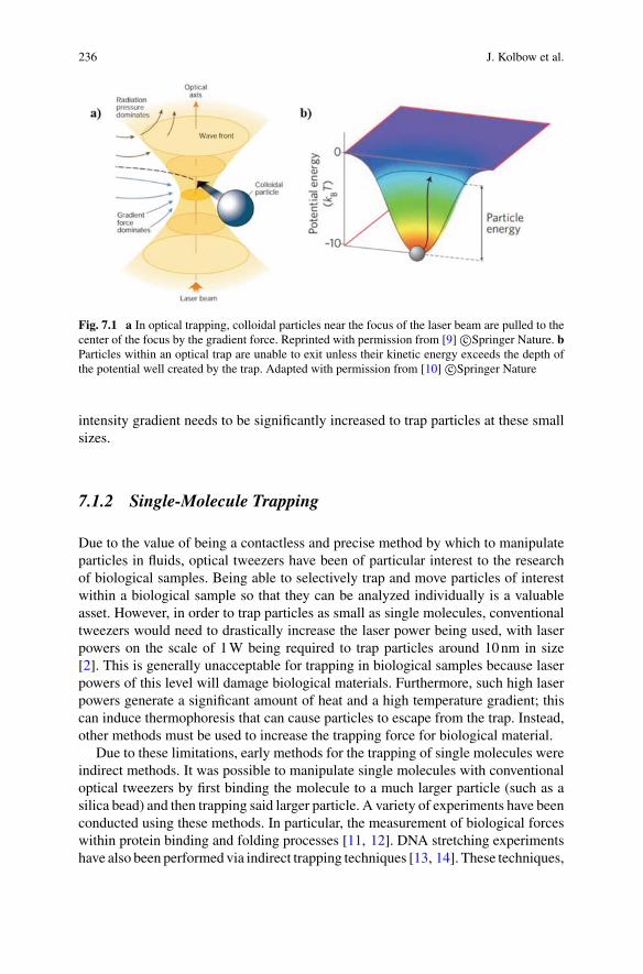
236 J. Kolbow et al.
Fig. 7.1 a In optical trapping, colloidal particles near the focus of the laser beam are pulled to thecenter of the focus by the gradient force. Reprinted with permission from [9] c©Springer Nature. bParticles within an optical trap are unable to exit unless their kinetic energy exceeds the depth ofthe potential well created by the trap. Adapted with permission from [10] c©Springer Nature
intensity gradient needs to be significantly increased to trap particles at these smallsizes.
7.1.2 Single-Molecule Trapping
Due to the value of being a contactless and precise method by which to manipulateparticles in fluids, optical tweezers have been of particular interest to the researchof biological samples. Being able to selectively trap and move particles of interestwithin a biological sample so that they can be analyzed individually is a valuableasset. However, in order to trap particles as small as single molecules, conventionaltweezers would need to drastically increase the laser power being used, with laserpowers on the scale of 1W being required to trap particles around 10nm in size[2]. This is generally unacceptable for trapping in biological samples because laserpowers of this level will damage biological materials. Furthermore, such high laserpowers generate a significant amount of heat and a high temperature gradient; thiscan induce thermophoresis that can cause particles to escape from the trap. Instead,other methods must be used to increase the trapping force for biological material.
Due to these limitations, early methods for the trapping of single molecules wereindirect methods. It was possible to manipulate single molecules with conventionaloptical tweezers by first binding the molecule to a much larger particle (such as asilica bead) and then trapping said larger particle. A variety of experiments have beenconducted using these methods. In particular, the measurement of biological forceswithin protein binding and folding processes [11, 12]. DNA stretching experimentshave also been performed via indirect trapping techniques [13, 14]. These techniques,
7 Optical Trapping of Single Molecules 237
while effective, are not always useful and often complex because of the necessity ofbinding mechanisms to tether the molecule to the larger particle.
In order to realize the nano-optical traps necessary for the trapping of singlemolecules, a variety of methods have been proposed. In order to increase the trap-ping force, there are two primary phenomena commonly utilized by these meth-ods. The first of these is the use of nanostructures. When light is incident on thesenanostructures, the electric field is influenced by the shape of the structure. Thesenanostructures can induce resonances in the electric field leading to much highermagnitudes than the the focused light on its own. Furthermore, nanostructures cansignificantly decrease the trapping volume by localizing the electric field maximawithin and at the edges of these nanostructure. These highly localized maxima arecommonly known as “hotspots.” As discussed earlier, both of these effects will leadto an increase in the trapping force.
The other phenomena that many nano-optical trapping techniques utilize is plas-monics. When light is incident on a metallic surface, the electric field causes oscil-lations of the free electrons at the surface. These oscillations are known as surfaceplasmons. These plasmons propagate along the surface from where the light is inci-dent, generating electric fields at the surface as they go. Plasmons are useful fortrapping techniques because they can be localized far beyond the diffraction limitof light [15]. Furthermore, the electric field magnitude generated by these plasmonsdrops off exponentially from the surface. As such, the field gradients generated byplasmons can be orders of magnitude higher than those generated by the incidentlight source.
7.2 Single-Molecule Trapping Techniques
A variety of techniques have been proposed and implemented to enable single-molecule optical trapping. In this section we will provide an overview of a fewof these techniques and the results they have achieved.
7.2.1 Plasmonic Nanostructure-Based Traps
Some of the earliest nano-optical traps were achieved by combining the two phe-nomena described in Sect. 7.1.2. By designing metallic nanostructures specifically toinduce plasmonic resonance, it is possible to produce high-intensity sub-wavelengthtrapping volumes and thereby achieve significantly higher trapping forces than con-ventional optical traps. There are a variety of nanostructures that have been pursuedand are capable of accomplishing this (Fig. 7.2).
One of the first instances of such a trapping device was realized in 2008 byGrigorenko et al. [16] and consisted of an array of gold nanopillars in closely spacedpairs on a glass surface. These nanopillars, when illuminated, each had their own
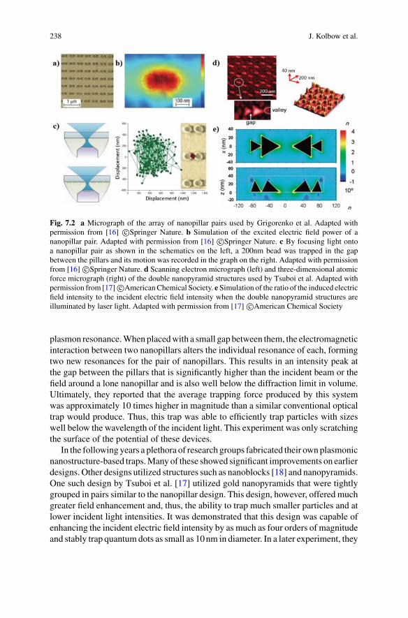
238 J. Kolbow et al.
Fig. 7.2 a Micrograph of the array of nanopillar pairs used by Grigorenko et al. Adapted withpermission from [16] c©Springer Nature. b Simulation of the excited electric field power of ananopillar pair. Adapted with permission from [16] c©Springer Nature. c By focusing light ontoa nanopillar pair as shown in the schematics on the left, a 200nm bead was trapped in the gapbetween the pillars and its motion was recorded in the graph on the right. Adapted with permissionfrom [16] c©Springer Nature. d Scanning electron micrograph (left) and three-dimensional atomicforce micrograph (right) of the double nanopyramid structures used by Tsuboi et al. Adapted withpermission from [17] c©AmericanChemical Society. e Simulation of the ratio of the induced electricfield intensity to the incident electric field intensity when the double nanopyramid structures areilluminated by laser light. Adapted with permission from [17] c©American Chemical Society
plasmon resonance.Whenplacedwith a small gap between them, the electromagneticinteraction between two nanopillars alters the individual resonance of each, formingtwo new resonances for the pair of nanopillars. This results in an intensity peak atthe gap between the pillars that is significantly higher than the incident beam or thefield around a lone nanopillar and is also well below the diffraction limit in volume.Ultimately, they reported that the average trapping force produced by this systemwas approximately 10 times higher in magnitude than a similar conventional opticaltrap would produce. Thus, this trap was able to efficiently trap particles with sizeswell below the wavelength of the incident light. This experiment was only scratchingthe surface of the potential of these devices.
In the following years a plethora of research groups fabricated their ownplasmonicnanostructure-based traps.Many of these showed significant improvements on earlierdesigns. Other designs utilized structures such as nanoblocks [18] and nanopyramids.One such design by Tsuboi et al. [17] utilized gold nanopyramids that were tightlygrouped in pairs similar to the nanopillar design. This design, however, offered muchgreater field enhancement and, thus, the ability to trap much smaller particles and atlower incident light intensities. It was demonstrated that this design was capable ofenhancing the incident electric field intensity by as much as four orders of magnitudeand stably trap quantum dots as small as 10nm in diameter. In a later experiment, they
7 Optical Trapping of Single Molecules 239
demonstrated that this structure could be utilized for the trapping andmicropatterningof DNA [19]. Plasmonic nanostructure devices also can be integrated with heat sinksto avoid the potential problem of thermophoresis from heating due to high intensitypeaks [20].
Nanoapertures are another type of nanostructure that have been extensively usedfor nanoscale trapping. Apertures such as double nanoholes and nanobowties inparticular have been utilized in a variety of single-molecule trapping experiments.These structures are particularly effective compared to other nanostructures due totheir ability to utilize a phenomena known as self-induced back-action to improvetrap stability. This phenomena and the devices that utilize them are discussed in detailin Sect. 7.2.2. Saleh and Dionne suggested that a coaxial nanoaperture could be apowerful trapping structure, specifically by tapering the thickness of the aperture itcould be capable of trapping particles under 2nm in size while using reasonably lowtrapping powers. Zhao et al. demonstrated that coaxial nanostructures and circularlypolarized trapping light could be used to selectively trap sub-20nm chiral moleculesbased on the handedness of their chirality [21].
One of the primary drawbacks of these plasmonic nanostructure-based traps isthat their ability to manipulate the position of a trapped particle is severely limitedbecause the trap is located at a stationary nanostructure. A few setups have showna limited ability to manipulate the position of a trapped particle around the surfaceof a nanostructure by utilizing the effects of polarization on plasmon propagationto control the location of the trap [20]. A common method by which conventionaloptical tweezers manipulate particles is by using holography to shape the trappingbeam and adjust the position of the trap. Holographic beam-shaping can similarly beused to control the position of plasmonic traps. Huft et al. [22] utilized holography tocontrol the phase of a ring-shaped beamof light incident on a bull’s eye nanostructure.In doing so, they demonstrated control over the location of positive interference ofthe plasmons (the trapping location) in the region at the center of the structure. Whileallowing for more arbitrary movement, manipulation was still limited to the confinesof the structure.
One method by which the manipulation capabilities of these structures has beensignificantly increased is by attaching these structures to probe tips. A commonmethod of doing this is to place a plasmonic nanoaperture at the tip of a near-fieldscanning optical microscopy (NSOM) probe [23]. Berthelot et al. [24] demonstratedthat such a setupwas capable of stably trapping particles as small as 20nm in diameterand arbitrarily moving them through the sample.
7.2.2 Self-Induced Back-Action Traps
While nanoaperture structures allow for significant increases in optical trappingforces through plasmonic amplification alone, there is also another effect presentwhen using such structures. This effect is reliant on the fact that the presence ofa particle within an aperture has a significant impact on the transmission of light

240 J. Kolbow et al.
Fig. 7.3 a Scanning electron microscope image of the double nanohole aperture used by Pangand Gordon. Adapted with permission from [25] c©American Chemical Society. b Graph of theoptical transmission through a double nanohole aperture during the trapping of a BSAmolecule. Thetrapping event can be seen clearly as well as the unfolding of the protein within the trap. Adaptedwith permission from [25] c©American Chemical Society. c A schematic of a bowtie nanoapertureat the tip of an NSOM probe. Adapted with permission from [24] c©Springer Nature. dMicroscopeimage of a laser beam shaped into a ring via hologram and focused onto a bull’s eye nanostructurefor the experiment done by Huft et al. Adapted with permission from [22] c©American ChemicalSociety. e Illustration of the constructive interference of plasmons at the center of the bull’s eyestructure in the Huft et al. experiment. Adapted with permission from [22] c©American ChemicalSociety
through said aperture. If the particle being trapped within the aperture has a higherindex of refraction then water, the transmission through the aperture will increase.This increase in transmission is equivalent to an increase in the amount of photonmomentum travelling through the aperture. Similarly, the particle moving out of theaperture will decrease the amount of photon momentum travelling through the aper-ture. Newton’s third law dictates that a restorative forcewill act in opposition to eitherof these momentum changes. Essentially, this restorative force will act opposite tothe movement of any particle within the aperture. This phenomenon is known as self-induced back-action (SIBA) and significantly increases the efficacy and efficiencyof plasmonic nanoaperture traps (Fig. 7.3).
Juan et al. [26] investigated the benefits of SIBA in gold single nanohole apertures.They found that SIBA actually had a greater impact on the trapping efficiency thanthe Rayleigh gradient force that accounts for the entirety of trapping in most othertechniques. In fact, it was determined that the introduction of SIBA allowed for stabletrapping at optical powers an order of magnitude lower than other methods allowed.This is particularly impactful for single-molecule trapping because it enables trappingsignificantly smaller particles without increasing the optical intensity, significantlyreducing the risk of photothermal damage to the molecule or thermophoretic effectsdestabilising the trap.
7 Optical Trapping of Single Molecules 241
Pang and Gordon [25] demonstrated the power of SIBA traps using a double-nanohole aperture in a gold film. Using this structure, they were able to trap a singleBSA molecule with a radius of 3.4nm at the boundary between the two nanoholes.Furthermore, theywere able to stably trap thesemoleculeswith laser powers as low as3.5mW,which is quite low formost optical trapping setups.A subsequent experimentdemonstrated that itwas possible to performRaman spectroscopyonparticles trappedin this structure [27]. Another aspect of SIBA traps that was demonstrated by thisexperiment was that the significant impact a particle has on transmission through theaperture can serve as an extremely sensitive sensor with a high signal to noise ratio.Because they are nanoaperture-based, SIBA traps can similarly be attached to theend of probe tips to allow manipulation of the position of trapped particles [24].
7.2.3 Waveguide-Based Traps
Another method proposed to overcome the diffraction limit to increase the trappingforce is by using optical waveguides that are sub-wavelength in size. By using suchwaveguides it is possible to condense the electromagnetic energyof light into volumessmaller than is allowed by the diffraction limit. However, most of this energy iscontained within the waveguide itself and, thus, is not helpful for trapping purposes.However, structures known as slotwaveguides are able to confine the electromagneticenergy of light within a liquid core by surrounding that core with materials of highrefractive index. Thus, slot waveguide based optical traps are able to trap particleswithin the core of the waveguide.
Yang et al. [28] demonstrated the efficacy of such a method. Their slot waveguidewas capable of achieving trapping volumes on the scale of 10 s of nm, thus beingable to trap sub-100nm particles across the length of the waveguide. Furthermore,the trapped particles were simultaneously transported along the length of the waveg-uide by the propagation of light within the waveguide. Such a system is potentiallya powerful tool as it can serve as an optically-driven microfluidic channel whichparticles can be pulled into and transported throughout the system.
Waveguides have also been used in coordination with photonic crystal resonatorsto produce stable nanoscale optical traps. Mandal et al. [29] demonstrated this bycoupling a waveguide to a silicon photonic crystal resonator producing a stationaryinterference pattern within the resonator. This interference pattern resulted in anelectric field thatwas both high intensity and tightly confined in a sub-100nmvolume.This setup was able to stably trap sub-100nm particles. Chen et al. demonstrated thata similar device could be used to trap individual Wilson disease proteins [30].

242 J. Kolbow et al.
Fig. 7.4 a Schematic illustrating the trapping and transport of nanoparticles within a slot waveg-uide. Adapted with permission from [28] c©Springer Nature. b Illustration of the electric moderesponsible for trapping within a slot waveguide. Adapted with permission from [28] c©SpringerNature. c Schematic of the waveguide-integrated photonic crystal resonator trap used by Mandal etal. Adapted with permission from [29] c©American Chemical Society. d Simulation of the electricalfield and optical forces present within the architecture used by Mandal et al. Adapted with permis-sion from [29] c©American Chemical Society. e Diagram of the WGM resonator optical trappingsetup. Adapted with permission from [31] c©John Wiley and Sons. f BSA molecules are trapped atplasmonic hotspots and cause a shift in the resonance peak detected at the photodetector. Adaptedwith permission from [31] c©John Wiley and Sons
7.2.4 Whispering Gallery Mode Based Traps
Whispering gallery mode (WGM) resonators are devices wherein a laser source iscoupled to a microsphere (often glass or silica) where the light is contained at thesurface of the sphere via total internal reflection. Due to the high Q-factors thatthese devices are able to achieve, these devices are able to detect minute wavelengthshifts in optical spectra. For this reason, they have been used as extremely effectivebiosensors. By coupling these devices to plasmonic structures, it is possible to createnanoscale optical traps (Fig. 7.4).
Such a device was first realized by coupling a silica microsphere WGM resonatorto a random array of gold nanoparticles [31]. The electric field at the surface ofthe WGM resonator excited plasmons within the 55nm diameter nanoparticles. Theresult was a random array of sub-wavelength plasmonic hotspots that each act asan optical trap. Santiago et al. created such a device and demonstrated the opti-cal trapping of BSA molecules at these plasmonic hotspots. The integrated opticaltrapping allows this device to achieve significantly higher sensitivities than similarWGM biosensors. A recently proposedWGM device based on a silica double-toroidstructure with a nanoscale gap between the toroids [32]. Simulations suggest thatthis structure should be able to stably trap sub-10nm particles.
7 Optical Trapping of Single Molecules 243
7.3 Fabrication and Instrumentation
Beyond the underlying theory, single-molecule optical trapping experiments rely ona variety of fabrication techniques, optical components, and other instruments. In thissection we provide an overview of the fabrication techniques and instrumentationthat enable single-molecule optical trapping.
7.3.1 Fabrication of Plasmonic and Resonant Nanostructures
Because so many single-molecule optical trapping techniques rely on nanostruc-tures and the potential landscapes that they are capable of producing, fabricationmethods are a vital step in the development of these techniques. Many of the pre-viously discussed methods relied on the creation of structures with features on thenanometer scale. Furthermore, the propagation of surface plasmons across a metal-lic surface relies on the smoothness of said surface, with atomic-scale defects beingcapable of disturbing plasmon propagation and the field it produces. The develop-ment and improvement of fabrication methods capable of producing small featuresizes and atomically-flat surfaces has similarly enhanced the capabilities of thesesingle-molecule trapping techniques.
A common approach to fabricating these structures is by utilizing top-downlithography techniques of which there are two primary varieties: electron beam (E-beam) lithogrpahy and focused ion beam (FIB) lithography. FIB lithography, uses abeam of charged ions as a method of etching through materials. As such, many ofthe plasmonic nano-apertures (negative-type structures) discussed previously wereconstructed via FIB lithography [24]. In contrast, positive-type structures such asnanopillars [16, 20] and nanoblocks [18] tend to be fabricated using E-beam lithog-raphy. E-beam lithography is an extremely versatile technique because it does not relyon photomasks and instead can expose resist in arbitrary patterns. It is also capableof producing the nanometer-scale feature sizes that many nano-optical traps require.E-beam lithography is often used with positive resists such as PMMA followed by ametal lift-off process.
For plasmonic nanostructures, there are a variety of methods that can be usedto create atomically-flat surfaces. A common method is to use e-beam lithographyto pattern an atomically-flat substrate such as silicon to use as a template for thestructure [20, 22]. Metal can then be deposited onto this patterned substrate andsubsequently removed by adhering the metal to another, unpatterned, substrate. Thepatterned substrate can then be reused to fabricate more structures. This process isknown as template-stripping. Another valuable method is atomic layer deposition(ALD). ALD is a process characterized by deposition of metallic material by onelayer of atoms at a time. This allows for the fabrication of layers and, thus, featureswith sub-nm resolutions and atomically-flat surfaces.
244 J. Kolbow et al.
Though these two techniques are the most common, there are a variety of othertechniques that have been utilized for optical trapping purposes. Of particular interestare methods that are able to fabricate many nanostructures in parallel. One suchmethod is colloidal lithography. It was recently shown that by randomly attachingnanospheres to a surface by evaporating a solution of these colloidal nanospheresatop the surface and subsequently depositing metal onto the surface it is possibleto create single and double nanohole apertures [33]. The nanopyramid structuresused by Tsuboi et al. [17] were fabricated using a similar nanosphere lithographytechnique known as angle-resolved nanosphere lithography (AR NSL).
7.3.2 Instrumentation
At the most basic level, an optical trapping setup only requires a trapping laser andlens to focus the laser to a diffraction-limited spot.
There are a variety of factors that affect the choice of trapping laser for an opticaltrapping setup. In general, optical trapping setups have incorporated lasers withwavelengths in the red or infrared regime, though some have reported achievinghigher trapping efficiencies using green light [34]. Infrared lasers, despite their longerwavelengths leading to larger trapping volumes, have been commonly used in theoptical trapping of biological material because biological material tends to have amuch lower absorption coefficient in the infrared regime. Infrared lasers, therefore,are much less likely to damage such material even at the high intensities requiredfor optical trapping. Most commonly, continuous-wave lasers are used to ensureconstant and stable trapping; however, in some cases it is preferable to use a pulsedlaser because it is possible to achieve significantly higher electric field intensities,and thus larger trapping forces, momentarily without significantly increasing thephotothermal effects on the sample. Shoji et al. demonstrated that when trappingbiological material using plasmonic nanostructures using a pulsed laser can preventthe material from becoming fixed on the surface of the nanostructure [19].
The choice of focusing lens can also have a significant impact on the efficacy of thetrap. In particular, choosing a lens with a high numerical aperture can significantlydecrease the spot size at the focus (as can be seen in Eq.7.5). Generally, a microscopeobjective is used as the focusing lens. These lenses are readily available and allowoptical tweezing setups to be integrated into existing microscope setups. This is veryuseful for simultaneous observation of the sample during trapping. In particular, oilimmersion objectives are highly valuable for optical tweezing as they allownumericalapertures between 1 and 1.4, whereas 1 is the theoretical maximum for conventionalobjectives.
While these are the two primary components of every optical trapping setups,there are a variety of other components that are commonly and preferentially used.Most often, the trapping laser is sent through a series of optical elements to align andcollimate the laser. Ideally, the trapping laser is expanded and collimated such thatit fills the back aperture of the focusing lens; this guarantees that the laser beam is
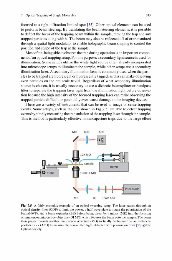
7 Optical Trapping of Single Molecules 245
focused to a tight diffraction-limited spot [35]. Other optical elements can be usedto perform beam steering. By translating the beam steering elements, it is possibleto deflect the focus of the trapping beam within the sample, moving the trap and anytrapped particles along with it. The beam may also be reflected off of or transmittedthrough a spatial light modulator to enable holographic beam-shaping to control theposition and shape of the trap at the sample.
Most often, being able to observe the trap during operation is an important compo-nent of an optical trapping setup. For this purpose, a secondary light source is used forillumination. Some setups utilize the white light source often already incorporatedinto microscope setups to illuminate the sample, while other setups use a secondaryillumination laser. A secondary illumination laser is commonly used when the parti-cles to be trapped are fluorescent or fluorescently tagged, as this can make observingeven particles on the nm scale trivial. Regardless of what secondary illuminationsource is chosen, it is usually necessary to use a dichroic beamsplitter or bandpassfilter to separate the trapping laser light from the illumination light before observa-tion because the high intensity of the focused trapping laser can make observing thetrapped particle difficult or potentially even cause damage to the imaging device.
There are a variety of instruments that can be used to image or sense trappingevents. Some setups, such as the one shown in Fig. 7.5, are able to detect trappingevents by simplymeasuring the transmission of the trapping laser through the sample.This is method is particularly effective in nanoaperture traps due to the large effect
Fig. 7.5 A fairly orthodox example of an optical tweezing setup. The laser passes through anoptical density filter (ODF) to limit the power, a half-wave plate to rotate the polarization of thebeam(HWP), and a beam expander (BE) before being direct by a mirror (MR) into the focusingoil immersion microscope objective (OI MO) which focuses the beam onto the sample. The beamthen passes through another microscope objective (MO) to finally be focused on an avalanchephotodetector (APD) to measure the transmitted light. Adapted with permission from [36] c©TheOptical Society
246 J. Kolbow et al.
nanoparticles present in the aperture have on transmission through the aperture, asdiscussed in detail in Sect. 7.2.2. Similar results can be achieved with other resonantplasmonic nanostructures since nearby particleswill affect the resonantmodeswithinthe structure, though the effect will be considerably less and thus must be measuredusing sensitive devices such as an avalanche photodiode or electronmultiplyingCCD.In contrast, when illuminating the sample with a secondary source, observation cansimply be done using a CCD camera. It is also often desirable to be able to quantifythe position of the trapped particle in order to quantify the stiffness of the trap.Processing the images from a CCD camera using position tracking software (e.g.rapidSTORM) makes acquiring this information fairly straightforward.
7.4 Outlook
Optical tweezers have proven themselves to be a valuable tool in research in micro-biology and throughout the field of nanotechnology. The last two decades have seensignificant strives made in improving optical trapping techniques and pushing theminto the trapping of nanoscale particles. As can be seen throughout this chapter, thereare a variety of paths and techniques that have been and continue to be explored for thetrapping of single-molecules. Optical trapping can significantly increase the sensitiv-ity and effectiveness of biosensors and spectroscopy techniques. Asmicrofabricationtechnology improves, the capabilities of these techniques continue to improvewith it,opening up new opportunities in the pursuit and utilization of single-molecule opticaltrapping techniques. Furthermore, the continued growth of interest in the develop-ment of lab-on-a-chip devices drives an increased need for effective and non-invasivemethods by which to transport material throughout these devices. Optical tweezerscan surely be an effective tool through which to do so.
References
1. Arthur Ashkin. Acceleration and trapping of particles by radiation pressure. Physical ReviewLetters, 24(4):156, 1970.
2. Arthur Ashkin, James M Dziedzic, John E Bjorkholm, and Steven Chu. Observation of asingle-beam gradient force optical trap for dielectric particles. Optics Letters, 11(5):288–290,1986.
3. Steven Chu, Leo Hollberg, John E Bjorkholm, Alex Cable, and Arthur Ashkin. Three-dimensional viscous confinement and cooling of atoms by resonance radiation pressure. Phys-ical Review Letters, 55(1):48, 1985.
4. Lukas Novotny and Bert Hecht. Principles of nano-optics. Cambridge university press, 2012.5. Silvia Albaladejo, Manuel I Marqués, Marine Laroche, and Juan José Sáenz. Scattering
forces from the curl of the spin angular momentum of a light field. Physical Review Letters,102(11):113602, 2009.
6. Justin E Molloy and Miles J Padgett. Lights, action: optical tweezers. Contemporary Physics,43(4):241–258, 2002.
7 Optical Trapping of Single Molecules 247
7. E. Hecht. Optics. Pearson, 2014.8. Lukas Novotny, Randy X Bian, and X Sunney Xie. Theory of nanometric optical tweezers.
Physical Review Letters, 79(4):645, 1997.9. David G Grier. A revolution in optical manipulation. Nature, 424(6950):810–816, 2003.10. Mathieu L Juan, Maurizio Righini, Romain Quidant. Plasmon nano-optical tweezers. Nature
Physics, 5(6):349–356, 2011.11. Zhiqun Xi, Ying Gao, George Sirinakis, Honglian Guo, and Yongli Zhang. Single-molecule
observation of helix staggering, sliding, and coiled coil misfolding.Proceedings of the NationalAcademy of Sciences, 109(15):5711–5716, 2012.
12. Ciro Cecconi, Elizabeth A Shank, Frederick W Dahlquist, Susan Marqusee, and Carlos Bus-tamante. Protein-dna chimeras for single molecule mechanical folding studies with the opticaltweezers. European Biophysics Journal, 37(6):729–738, 2008.
13. Michelle DWang, Hong Yin, Robert Landick, Jeff Gelles, and StevenM Block. Stretching dnawith optical tweezers. Biophysical Journal, 72(3):1335, 1997.
14. Steven B Smith, Yujia Cui, and Carlos Bustamante. Overstretching b-dna: the elastic responseof individual double-stranded and single-stranded dnamolecules. Science, 271(5250):795–799,1996.
15. DmitriKGramotnev andSergey IBozhevolnyi. Plasmonics beyond the diffraction limit.NaturePhotonics, 4(2):83–91, 2010.
16. AN Grigorenko, NW Roberts, MR Dickinson, and Y Zhang. Nanometric optical tweezersbased on nanostructured substrates. Nature Photonics, 2(6):365–370, 2008.
17. Yasuyuki Tsuboi, Tatsuya Shoji, Noboru Kitamura, Mai Takase, Kei Murakoshi, YoshihikoMizumoto, and Hajime Ishihara. Optical trapping of quantum dots based on gap-mode-excitationof localized surface plasmon.The Journal ofPhysicalChemistryLetters, 1(15):2327–2333, 2010.
18. Yoshito Tanaka and Keiji Sasaki. Optical trapping through the localized surface-plasmon res-onance of engineered gold nanoblock pairs. Optics Express, 19(18):17462–17468, 2011.
19. Tatsuya Shoji, Junki Saitoh, Noboru Kitamura, Fumika Nagasawa, Kei Murakoshi, HiroakiYamauchi, Syoji Ito, Hiroshi Miyasaka, Hajime Ishihara, and Yasuyuki Tsuboi. Permanentfixing or reversible trapping and release of dna micropatterns on a gold nanostructure usingcontinuous-wave or femtosecond-pulsed near-infrared laser light. Journal of the AmericanChemical Society, 135(17):6643–6648, 2013.
20. Kai Wang, Ethan Schonbrun, Paul Steinvurzel, and Kenneth B Crozier. Trapping and rotatingnanoparticles using a plasmonic nano-tweezer with an integrated heat sink. Nature Communi-cations 2, 469, 2011.
21. Yang Zhao, Amr AE Saleh, and Jennifer A Dionne. Enantioselective optical trapping of chiralnanoparticles with plasmonic tweezers. Acs Photonics, 3(3):304–309, 2016.
22. Preston R Huft, Joshua D Kolbow, Jonathan T Thweatt, and Nathan C Lindquist. Holographicplasmonic nanotweezers for dynamic trapping and manipulation. Nano Letters, 17(12):7920–7925, 2017.
23. Ali El Eter, NyhaMHameed, Fadi I Baida, Roland Salut, Claudine Filiatre, DusanNedeljkovic,Elie Atie, Samuel Bole, and Thierry Grosjean. Fiber-integrated optical nano-tweezer based ona bowtie-aperture nano-antenna at the apex of a snom tip.Optics Express, 22(8):10072–10080,2014.
24. Johann Berthelot, Srdjan S Acimovic, Mathieu L Juan, Mark P Kreuzer, Jan Renger, andRomainQuidant. Three-dimensional manipulationwith scanning near-field optical nanotweez-ers. Nature Nanotechnology, 9(4):295–299, 2014.
25. Yuanjie Pang andReuvenGordon.Optical trappingof a single protein.NanoLetters, 12(1):402–406, 2012.
26. Mathieu L Juan, Reuven Gordon, Yuanjie Pang, Fatima Eftekhari, and Romain Quidant. Self-induced back-action optical trapping of dielectric nanoparticles. Nature Physics, 5(12):915–919, 2009.
27. Steven Jones, Ahmed A Al Balushi, and Reuven Gordon. Raman spectroscopy of singlenanoparticles in a double-nanohole optical tweezer system. Journal of Optics, 17(10):102001,2015.
248 J. Kolbow et al.
28. Allen HJ Yang, Sean D Moore, Bradley S Schmidt, Matthew Klug, Michal Lipson, and DavidErickson. Optical manipulation of nanoparticles and biomolecules in sub-wavelength slotwaveguides. Nature, 457(7225):71–75, 2009.
29. Sudeep Mandal, Xavier Serey, and David Erickson. Nanomanipulation using silicon photoniccrystal resonators. Nano Letters, 10(1):99–104, 2010.
30. Yih-FanChen,Xavier Serey,RupaSarkar, PengChen, andDavidErickson.Controlled photonicmanipulation of proteins and other nanomaterials. Nano Letters, 12(3):1633–1637, 2012.
31. Miguel A Santiago-Cordoba, Murat Cetinkaya, Svetlana V Boriskina, Frank Vollmer, andMelik C Demirel. Ultrasensitive detection of a protein by optical trapping in a photonic-plasmonic microcavity. Journal of Biophotonics, 5(8-9):629–638, 2012.
32. Huibo Fan, Xiaodong Gu, Dawei Zhou, Huili Fan, Li Fan, and Changquan Xia. Confinedwhispering-gallery mode in silica double-toroid microcavities for optical sensing and trapping.Optics Communications, 434:97–103, 2019.
33. AdarshLalithaRavindranath,Mirali Seyed Shariatdoust, SamuelMathew, andReuvenGordon.Colloidal lithography double-nanohole optical trapping of nanoparticles and proteins. OpticsExpress, 27(11):16184–16194, 2019.
34. Shih-Kun Liu, Wen-Kai Hsieh, Wei-Yi Sung, Yong-Jai Shen, Chia-Ching Tsai, and Fong-MinHsu. Wavelength dependence of trapping efficiency in optical tweezers. In 2015 InternationalSymposium on Next-Generation Electronics (ISNE), pages 1–3. IEEE, 2015.
35. Karel Svoboda and Steven M Block. Biological applications of optical forces. Annual Reviewof Biophysics and Biomolecular Structure, 23(1):247–285, 1994.
36. Ahmed A Al Balushi, Ana Zehtabi-Oskuie, and Reuven Gordon. Observing single proteinbinding by optical transmission through a double nanohole aperture in a metal film. BiomedicalOptics Express, 4(9):1504–1511, 2013.
Chapter 8Applications of Trapping to ProteinAnalysis and Interactions
Reuven Gordon
Abstract While optical tweezers have long allowed for studying proteins and theirinteractions, nanotechnology has allowed for fabrication of tweezers that are capableof trapping even single proteins. The use of apertures in sensing applications has beenintroduced in previous chapters, as well as a discussion of optical tweezers for singlemolecule analysis. The present chapter focuses on applications to protein analysis,showing different techniques that have been developed as well as challenges forthe approach. This includes analysis based on intensity changes due to proteins andnanoparticles entering the optical trapping region, moving in the trapping region,and being modulated by high-frequency laser intensity beating (in the 1–1000GHzregime).
8.1 Introduction
The advancement of nanotechnology has allowed for probing the nature of life at thesingle molecule level. Single molecule techniques show a diversity of interactionsthat are washed out by ensemble measurements: rare events, events that have a lowersignal, events that operate at a different timescale [1]. They allow for seeing dynamicswithout synchronization: getting all the molecules to the same starting point requiressome synchronization that perturbs the system away from its natural conditions. Theyallow for probing interactions at equilibrium, such as on-off binding, whereas mostother kinetic measurements need to be perturbed away from equilibrium.
Fluorescence labeling is one of the primary ways of studying single molecules.While already established and continually providing significant scientific advances,fluorescence has the drawbacks of:
• limited time resolution due to the requirement for photon counting;• blinking;• bleaching;
R. Gordon (B)University of Victoria, Victoria, BC, Canadae-mail: [email protected]
© The Author(s), under exclusive license to Springer Nature Switzerland AG 2022W. Bowen et al. (eds.), Single Molecule Sensing Beyond Fluorescence,Nanostructure Science and Technology,https://doi.org/10.1007/978-3-030-90339-8_8
249
250 R. Gordon
• tags altering biomolecule propertes; and• indirect measurement of properties that are interpreted from changes in the fluo-rescence signal (e.g. Förster resonance energy transfer).
While the ideal fluorescent label will not change the properties of the protein, studiesare showing that labelling changes the energy characteristics [2], and interactions [3].To overcome these limitations, techniques that do not use fluorescence are desired.
Another common approach to understanding biomolecules is to use tethers. Thishas been applied to fluorescence studies, such as those that interrogate protein confor-mation changes [4], as well as to numerous works with optical tweezers [5]. Again,the tether immobilizes the biomolecule againsts its free motion, changes its naturalproperties and introduces steric hindrance. Ways of holding onto single moleculesthat do not require tethering are desired.
Optical tweezers use laser light to hold onto nanoparticles. By monitoring thescattering of this light, it is possible to gain information about the particle that istrapped in the tweezer. This can be done for extended periods, at the single particlelevel, without the need for tethers or labels, and at high speeds (potentially fasterthan nanoseconds). These features make optical tweezers, particularly nanoaperturetweezers capable of trapping single proteins, of interest to single molecule studies.
8.2 Optical Tweezers and Proteins
We consider a basic treatment of optical tweezers and how they hold onto nanoparti-cles. The aim is to show that the laser powers required for manipulating proteins areimpractically large with conventional optical tweezers, and that focusing the opti-cal power down to the nanoscale (extreme subwavelength) and using “self-inducedback-action” (SIBA) are beneficial ways to make protein trapping practical. We alsoshow the influence of the optical potential to change the shape of the trapped particle.
8.2.1 Stable Trapping Against Thermal Motion
Weconsider the problemof using an optical tweezer tomanipulate a protein. The typeof tweezer we consider is a non-resonant focused beam that scatters off a nominallyneutral particle. Such a tightly focused beam was used to trap colloidal particles of100nm in size in 1986 [6]. This was then promptly applied to the trapping of bacteriaand large viruses [7].
For trapping proteins, in the single digit nanometer range, impractically highintensities are required. The potential energy associated with a polarizable dipole(the model for the protein) in a electromagnetic field (the light) is given by:

8 Applications of Trapping to Protein Analysis and Interactions 251
U = −1
2p · E (8.1)
where p is the dipole moment and E is the electric field.While the energy of the dipole itself increases, the total energy decreases by an
equal amount and so the potential minimum occurs for location of the highest fieldintensity [8]. The optical potential energy should be significantly larger than thethermal energy kBT (where kB is Boltzmann’s constant and T is temperature inKelvin) to hold the particle stably against thermal motion [6].
To give numerical examples, we estimate the intensity required to give the samepotential energy as the thermal energy kBT at 300K for a 5nm diameter sphericalparticle (approximate size of a globular protein of 50 kDa), assuming the relativepermittivity of the particle εd is 2.25 and the surroundingmedium relative permittivityεb is 1.77.
Ignoring retardation and losses, the polarizability of a prolate spheroid (theapproximate shape of the protein—say a globular protein) is:
α = V ε0 (εd − εb)
A (εd − εb) + εb(8.2)
where V is the volume of the particle and ε0 is the free-space permittivity and A isa geometric factor:
A = (ξ 2 − 1
) (ξ
2ln
[ξ + 1
ξ − 1
]− 1
)(8.3)
where ξ = a/√a2 − b2 and a and b are the long and short axes, with A = 1/3
for a sphere. Since p = αE, using these values, we find that 1014 W/m2 is the beamintensity required, which corresponds to approximately a 100W laser beam focusseddown to a micrometer squared, or a 10 mW beam focussed down to 10nm squared.(Conventional lenses can focus down to a spot size of approximately the wavelengthsquared, so this is the reason for themicrometer squared diameter;whereas plasmonicstructures allow for much tighter field confinement near the surface of a metal). It isclear that focusing down to subwavelength volumes allows for more practical beampowers. It also means that the particle is more confined. Even so, this is a substantialamount of tightly focussed power that is required to even reach the thermal energythreshold—even higher powers would be required for stable trapping.
8.2.2 Elongation and Orientation
We now consider the deformation of the nanoparticle/protein from the optical poten-tial. Changes in the shape of the particle can also result in changes in p, and so thepotential energy associated with those changes are also reflected in Eqs. 8.1 and 8.2.If the particle is extended by 10% along one axis while maintaining the volume, the

252 R. Gordon
polarizability changes by 1%. The amount of energy available to elongate the parti-cle by 10% is about 1% of the trapping energy, so typically some (small) fraction ofthe thermal energy when stable trapping is achieved. This elongation is commonlyreferred to as electrostriction.
It is also noted that the polarizability along the long axis is the highest, and so thepotential energy minimum occurs when the particle is oriented along the direction ofthe electric field of the light. This acts to rotate the nanoparticle/protein to be orientedwith its long axis aligned with the electric field polarization.
8.2.3 SIBA
Additional trapping efficiency is gained if the nanoparticle/protein itself influencesthe field, E, in Eq.8.1. One example is in a photonic crystal cavity: the nanoparti-cle/protein itself shifts the resonance of the cavity and thereby changes how muchlaser energy is coupled into the cavity [9]. Analysis in that work showed that stabletrapping could be achieved for 100nm particles that are about half the size of thephotonic crystal holes using 100 mW of power inside the cavity. Actual trappingof mutant Wilson disease protein (estimated to be about 10nm in diameter) in aphotonic crystal cavity was published in 2012 [10]. In that work, the protein wasfluorescently labelled to identify when it was trapped and around 10 mW of powerwas coupled into the cavity (although with a quality factor of several thousand, theintensity is expected to be 3–4 orders of magnitude larger inside the cavity, which issimilar to the analysis above).
The nanoparticle did not have a large influence on the field distribution in thephotonic crystal cavity case. Calculations of the force by energy methods (MaxwellStress Tensor) or perturbative dipole analysis yielded the same results [9]. By con-trast, in subwavelength circular apertures in metal films the nanoparticle has a largeinfluence on the field distribution and so the force calculated with Maxwell StressTensor analysis was around 5 times larger [11]. Other works had previously investi-gated trapping with circular apertures prior to the investigation of SIBA [12, 13].
Trapping withmetal apertures can be thought of as a resonance effect if plasmonicresonances are considered. Since the field distribution is changed substantially, it canalso be thought of as effectively increasing the size of the aperture through “dielectricloading”. Hans Bethe showed that apertures in thin metal films limit transmissionas the fourth power of the aperture size [14], so that making the aperture biggershould give a substantiallymore transmission—for example, making the aperture 1%wider gives 4% more transmission. This is a primary benefit of using apertures—thetransmission changes can be detected to monitor the trapping event and the amountof transmission is “amplified” by the effect of the aperture.
Greater field confinement is achieved by creating small gaps in the aperture aboutthe size of the nanoparticle/protein of interest. The double-nanohole is one way toachieve this and trappingof a single proteinwith 3.4nmhydrodynamic radius (BovineSerum Albumin) was achieved for that aperture [15] (see Fig. 3 of Chap. 7). It has

8 Applications of Trapping to Protein Analysis and Interactions 253
been shown that tapering in the double nanohole plays a significant role in enhancingthe efficiency of trapping [16]. Other shapes such as coaxial structures [17–19], alsoallow for trapping of single proteins by confinement of the field to a narrow gap.Researchers have also studied rectangular [20] and bowtie [21, 22] apertures fortrapping objects down to the single digit nanometer range.
8.3 Optical Tweezer Studies of Proteins with Tetheringand/or Labelling
Conventional optical tweezers using amicroscope objective to focus the beam cannottypically hold onto single proteins or other small biomolecules. For this reason,the proteins being studied are usually tethered to larger particles, lipid droplets,flat surfaces or micropipettes [5]. The optical tweezer allows for measuring forcesand displacements in biomolecular interactions, for example: (i) in observing thetranscription of DNA to RNA via the enzyme RNA polymerase [23], (ii) the motionof kinesin along a microtuble taking 8nm steps [24, 25], (iii) the winding of DNAinto a virus capsid by the molecular motor [26], and (iv) measuring the energylandscape of protein folding [27, 28]. While these approaches have been valuablein determining the properties of biomolecules and their interactions at the singlemolecule level, the impact of the tether on the natural function, hindrance formultiplesmall molecules interacting close to one another, and overall complexity all call foradditional approaches to probe biomolecule interactions at the single molecule level.
8.4 Protein Analysis with Nanoapertures
Considering the interest in single protein and biomolecule studies that are label freeand tether free, the aperture-based trapping, particularly with double-nanoholes, hasbeen widely investigated for its analytical capability. In this section, we overviewsome of examples of the analysis that can be achieved.
8.4.1 Protein Mass and Mixtures
The polarizability of a nanoparticle varies with the size, approximately as the volumeas in Eq.8.2. When the nanoparticle/protein is trapped in an aperture, the thermalmotion leads to intensity fluctuations in the transmission through the aperture thatscale as the volume, or mass [29].
254 R. Gordon
With this approach, resolution in the protein mass below a kDa is possible, allow-ing for measuring the mass of a small protein fragment removed during trypticcleaving [29].
It is also possible to gain information from the autocorrelation of the intensityfluctuations. Considering that the Stokes drag, γ , on a particle in a nanofluidic envi-ronment scales as the radius of the particle, and the stiffness, k of the trap scales asthe volume (from the polarizability above), we consider a Langevin analysis:
m∂2x
∂t2+ γ
∂x
∂t− kx = Fl (8.4)
where x is the particle position and Fl is a Langevinwhite noise term. The first inertialterm is usually neglected in a highly damped environment, so the characteristic timeconstant for the autocorrelation of the trapping intensity fluctuations is [29]:
τ = γ /k ∝ m−2/3 (8.5)
where m is the particle mass. In cases where intensity fluctuations arise from slowerconformational changes of the protein, a two exponential fit to the autocorrelationdata can be used to achieve time constants with the −2/3 scaling [30].
Since the tweezer is a single molecule approach, repeated or parallel measure-ments can be used to sample a heterogeneous mixture. In this way, the distributionof protein sizes can be found from an unprocessed (dirty) solution [30]. Figure8.1shows the comparison in the autocorrelation functions for pure protein solutionscompared with buffer solution diluted (but otherwise unprocessed) egg white. Thisdemonstrates the use of single protein analysis to determine the components of anunprocessed “dirty” solution.
8.4.2 Conformational Changes
Several works have studied conformational changes (including folding) of proteinsusing fluorescence [4] and tweezers [28]. Equations8.1and 8.2 show that changes inthe polarizability of the protein from conformational changes will be transduced intochanges in energy of the optical tweezer and also changes in the transmission forthe aperture optical tweezer. There is as driving force on this conformational changefrom the optical tweezer, as described above.
For example, Bovine SerumAlbumin, a proteinwith conformation changes from aheart-shaped F isoform to and extended N isoform was trapped in a double-nanoholeoptical tweezer and spontaneous jumps in the trapping intensity were seen after theinitial trapping event [15] (see Fig. 3b of Chap. 7). These jumps were attributed tothe transition between the two isoforms, which was confirmed by forcing the proteininto the N state by reducing the pH (at which point only the higher intensity levelwas seen from the trapping laser transmission through the aperture).
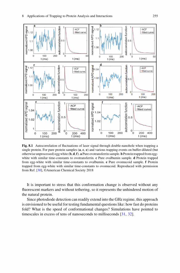
8 Applications of Trapping to Protein Analysis and Interactions 255
Fig. 8.1 Autocorrelation of fluctuations of laser signal through double-nanohole when trapping asingle protein. For pure protein samples (a, c, e) and various trapping events on buffer-diluted (butotherwise unprocessed) eggwhite (b,d, f).aPure ovotransferrin sample.bProtein trapped fromegg-white with similar time-constants to ovotransferrin. c Pure ovalbumin sample. d Protein trappedfrom egg-white with similar time-constants to ovalbumin. e Pure ovomucoid sample. f Proteintrapped from egg-white with similar time-constants to ovomucoid. Reproduced with permissionfrom Ref. [30], ©American Chemical Society 2018
It is important to stress that this conformation change is observed without anyfluorescent markers and without tethering, so it represents the unhindered motion ofthe natural protein.
Since photodiode detection can readily extend into the GHz regime, this approachis envisioned to be useful for testing fundamental questions like: how fast do proteinsfold? What is the speed of conformational changes? Simulations have pointed totimescales in excess of tens of nanoseconds to milliseconds [31, 32].
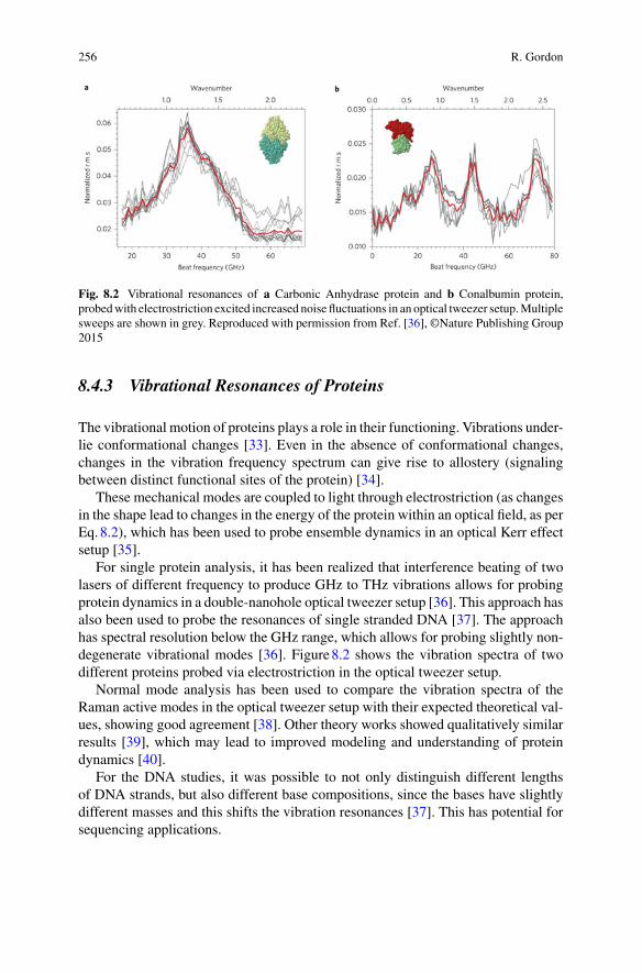
256 R. Gordon
Fig. 8.2 Vibrational resonances of a Carbonic Anhydrase protein and b Conalbumin protein,probedwith electrostriction excited increased noise fluctuations in an optical tweezer setup.Multiplesweeps are shown in grey. Reproduced with permission from Ref. [36], ©Nature Publishing Group2015
8.4.3 Vibrational Resonances of Proteins
The vibrational motion of proteins plays a role in their functioning. Vibrations under-lie conformational changes [33]. Even in the absence of conformational changes,changes in the vibration frequency spectrum can give rise to allostery (signalingbetween distinct functional sites of the protein) [34].
These mechanical modes are coupled to light through electrostriction (as changesin the shape lead to changes in the energy of the protein within an optical field, as perEq.8.2), which has been used to probe ensemble dynamics in an optical Kerr effectsetup [35].
For single protein analysis, it has been realized that interference beating of twolasers of different frequency to produce GHz to THz vibrations allows for probingprotein dynamics in a double-nanohole optical tweezer setup [36]. This approach hasalso been used to probe the resonances of single stranded DNA [37]. The approachhas spectral resolution below the GHz range, which allows for probing slightly non-degenerate vibrational modes [36]. Figure8.2 shows the vibration spectra of twodifferent proteins probed via electrostriction in the optical tweezer setup.
Normal mode analysis has been used to compare the vibration spectra of theRaman active modes in the optical tweezer setup with their expected theoretical val-ues, showing good agreement [38]. Other theory works showed qualitatively similarresults [39], which may lead to improved modeling and understanding of proteindynamics [40].
For the DNA studies, it was possible to not only distinguish different lengthsof DNA strands, but also different base compositions, since the bases have slightlydifferent masses and this shifts the vibration resonances [37]. This has potential forsequencing applications.
8 Applications of Trapping to Protein Analysis and Interactions 257
Higher frequency vibrations may be probed with conventional Raman methods,and the Raman spectra of individual trapped polystyrene and titania nanoparticleshas been achieved using the double-nanohole optical tweezer setup [41], as well asa rectangular aperture tweezer setup to probe polystyrene particles [42]. In the latterwork, the onset of a shifted Raman peak was found with increasing power and it wasspeculated that this was the result of the nanoparticle interacting with the surface.
8.5 Analysis of Protein Interactions at Single MoleculeLevel
The function of proteins comes from their interactions, and therefore, it is useful tostudy these interactions at the single molecule level. The techniques using opticaltweezers to probe protein–small molecule, protein–protein and protein–DNA inter-actions are described in this section.
8.5.1 Protein–Small Molecule Interactions
It was recognized that binding to a protein could alter its fluctuations within the dou-ble nanohole optical tweezer [43]. This can be explained by changes in the flexibilityof the protein being translated into changes in the thermally driven motion. A sim-ple example of this was demonstrated first for the well-studied biotin-streptavidininteraction. Not only does binding of biotin to streptavidin produce a change in thefluctuations, but a mutant version of streptavidin was also investigated with onlya single binding site, showing distinct autocorrelation of the intensity fluctations.As a practical example for drug research, the binding of salicylic acid (commonlyknown as aspirin) to the protein cyclooxygenase-2 was measured, showing distinctautocorrelation for the bound and unbound cases.
Of course, these binding event examples were practically irreversible, and soextended observation periods could be taken for the bound and unbound cases, butnot the transition between these two cases. For lower binding affinities, it is possi-ble to measure the binding by changes in the amplitude of the trapping laser powertransmitted through the double nanohole [44]. It was demonstrated that the dissocia-tion constants for the small molecules tolubutamide and phenytoin to protein humanserum albumin matched to literature reported values. The case of tolubutamide isshown in Fig. 8.3.
Unlike other methods to determine binding affinities, these studies were doneat a single concentration, at the single molecule level and at equilibrium. Thesefavourable characteristics are unique to such single molecule studies. Compared toother single molecule approaches, these studies were done without labels or tethersthat are known to influence binding kinetics [45].
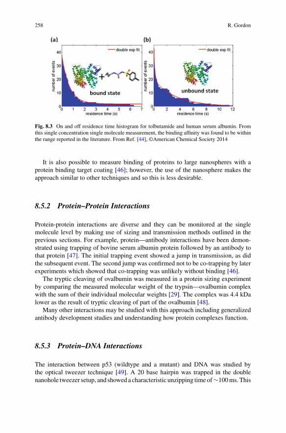
258 R. Gordon
Fig. 8.3 On and off residence time histogram for tolbutamide and human serum albumin. Fromthis single concentration single molecule measurement, the binding affinity was found to be withinthe range reported in the literature. From Ref. [44], ©American Chemical Society 2014
It is also possible to measure binding of proteins to large nanospheres with aprotein binding target coating [46]; however, the use of the nanosphere makes theapproach similar to other techniques and so this is less desirable.
8.5.2 Protein–Protein Interactions
Protein-protein interactions are diverse and they can be monitored at the singlemolecule level by making use of sizing and transmission methods outlined in theprevious sections. For example, protein—antibody interactions have been demon-strated using trapping of bovine serum albumin protein followed by an antibody tothat protein [47]. The initial trapping event showed a jump in transmission, as didthe subsequent event. The second jump was confirmed not to be co-trapping by laterexperiments which showed that co-trapping was unlikely without binding [46].
The tryptic cleaving of ovalbumin was measured in a protein sizing experimentby comparing the measured molecular weight of the trypsin—ovalbumin complexwith the sum of their individual molecular weights [29]. The complex was 4.4 kDalower as the result of tryptic cleaving of part of the ovalbumin [48].
Many other interactions may be studied with this approach including generalizedantibody development studies and understanding how protein complexes function.
8.5.3 Protein–DNA Interactions
The interaction between p53 (wildtype and a mutant) and DNA was studied bythe optical tweezer technique [49]. A 20 base hairpin was trapped in the doublenanohole tweezer setup, and showed a characteristic unzipping time of∼100ms. This
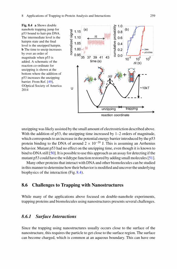
8 Applications of Trapping to Protein Analysis and Interactions 259
Fig. 8.4 a Shows doublenanohole trapping jump forp53 bound to hair-pin DNA.The intermediate level is thehairpin state and the finallevel is the unzipped hairpin.b The time to unzip increasesby over an order ofmagnitude when p53 isadded. A schematic of thereaction co-ordinate forunzipping is shown at thebottom where the addition ofp53 increases the unzippingbarrier. From Ref. [49],©Optical Society of America2014
unzippingwas likely assisted by the small amount of electrostriction described above.With the addition of p53, the unzipping time increased by 1–2 orders of magnitude,which corresponds to an increase in the potential energy barrier introduced by the p53protein binding to the DNA of around 2 × 10⁻²⁰ J. This is assuming an Arrheniusbehavior. Mutant p53 had no effect on the unzipping time, even though it is known tobind toDNAstill [50]. It is possible to use this approach as an assay for detecting if themutant p53 could have thewildtype function restored by adding smallmolecules [51].
Many other proteins that interact withDNA and other biomolecules can be studiedin thismanner to determine how their behavior ismodified anduncover the underlyingbiophysics of the interaction (Fig. 8.4).
8.6 Challenges to Trapping with Nanostructures
While many of the applications above focused on double-nanohole experiments,trapping proteins and biomolecules using nanostructures presents several challenges.
8.6.1 Surface Interactions
Since the trapping using nanostructures usually occurs close to the surface of thenanostructure, this requires the particle to get close to the surface region. The surfacecan become charged, which is common at an aqueous boundary. This can have one
260 R. Gordon
of two effects, either attracting or repelling the particle. For attraction, this can createan electrostatic trap, which is largely irreversible and not desirable if the intention isto trap using optical forces [52]. For repulsive interactions, the particle may take along time to be trapped because it cannot get close enough to the surface. A commonsolution to each of these problems is to increase the ionic strength in solution toscreen out surface charges [53].
One can estimate the expected time for a particle to get to the trap based ondiffusion in a viscous medium, using the diffusion coefficient:
D = kBT
6πηa= l2/τ (8.6)
where η is the viscosity, a is the particle radius, l is the average particle separationand τ is the diffusion time. Considering a 2nm diameter particle in water with anaverage separation of 2 microns between particles, τ is around 4 ms. In practice, thetime to trap in aqueous solution has been observed to be much greater than this—ofthe order of seconds, which is attributed to surface interactions. The time to trapin hexane for inorganic nanoparticles was in the millisecond range, consistent withthe estimate for τ above [54], which further underscores the importance of surfacecharge mediated through the solvent.
Proteins can also stick to surfaces. A typical approach to avoid this is to use amPEG coating, attaching with mPEG-thiol to a gold surface, for example. This wasused to prevent sticking of BSA in initial experiments, but found not to be crucialsince the proteins were not overly sticky [15]. The trapping usually shows increasednoise in the laser fluctuations, indicating that the protein is diffusing freely in thetrap and not stuck. Some have used surfactant in solution to limit sticking [10], butthis can denature proteins or otherwise change their characteristics.
Surfaces change the natural diffusion of the particle due to hydrodynamic inter-actions. A simplification to form proposed by Brenner [55] gives an approximatecorrection to the perpendicular diffusion as [56]:
D⊥ = D(1 − γ ) (8.7)
where γ = a/h and h is the height from the surface measured from the centre whereasthe approximate correction to the parallel diffusion from Faxén is:
D‖ = D
(1 − 9
16γ + 1
8γ 3 − 45
256γ 4 − 1
16γ 5
)(8.8)
which approaches roughly a third of the free diffusion at small distances. Theseeffects should be taken into account when calculating the properties of the particlein the trap, but also when calibrating the stiffness of the trap itself [57].
8 Applications of Trapping to Protein Analysis and Interactions 261
8.6.2 Thermal Effects
Nanostructuredmetals can concentrate the light intensity to extremely small volumes,which can lead to local heating. Excessive heating can damage the sample beingstudied (e.g., denaturing proteins). Moderate local heating can have benefits, suchas raising the local temperature to physiological levels, or providing thermophoreticforces to attract particles to the trapping aperture. Apertures have a metal film sur-rounding them, so this helps to remove heat due to the thermal conductivity of themetal. Comparison between isolated metal nanoparticles and apertures with similarfield enhancement showed that the temperature increase was 3 orders of magnitudelower for the aperture [58].
Heating at bowtie and double nanohole apertures has been measured and calcu-lated to be in the range of 0.5–5K/mW focused on a micron squared area, dependingon the geometry, the wavelength of operation and the materials used. An order ofmagnitude lower heating was achieved by exciting on the low-loss side of the aper-ture (opposite to the adhesion layer which is a metal with higher losses), by using amore conductive substrate and by using a lower loss adhesion layer [59, 60].
Heating can also lead to convective or thermophoretic effects that can either assistor hinder in trapping [61–63].
8.7 Technological Advances
8.7.1 Trapping Characterization
Autocorrelation of the noise in the trapping laser gives an indication of the timeconstant for diffusion and can be used to find the trapping efficiency [57]. In addi-tion, the transient to the trapped state has a similar time dependence. From thesemeasurements, an efficiency was estimated of ∼0.1 fN/(nm mW) [57], which isamong the highest values. Fano resonances have been employed to achieve higherefficiencies [64].
8.7.2 Aperture Fabrication
Ion beammilling is a direct approach to create apertures in metal films with a varietyof shapes [65–67]. Cusps, like those found in bowtie and double-nanoholes, help toenhance the local field [68].
Electron beam/UV lithography processes have also been used in an approach akinto those used in near-field aperture probes [20]. Anisotropic etching of silicon createsa taper to an aperture, which can be coated with a metal.
262 R. Gordon
Nanosphere lithography allows for low cost fabrication of circular [13] anddouble-nanoholes [69]. Randomly deposited colloids serve as a mask for metalevapouration—the random distribution makes finding the apertures of interest chal-lenging. By plasma etching the spheres prior to deposition of the metal, the gap sizeat the cusps of double-nanoholes, as well as the size of nanoholes could be tuned.Gaps as small as 10nm were made with this approach [70].
A pattern can be transferred from a silicon master by making use of the pooradhesion of a metal overlayer [71]. This template strippingmethod has been used tomake double-nanoholes with gaps below 10nm [72].
Atomic layer deposition allows for making coaxial structures with gaps in thenanometer range [73]. Protein trapping was demonstrated with these coaxial struc-tures [19].
8.7.3 Microfluidic Integration
Fluidic delivery can allow for delivering proteins to the trap as well as introducingparticles for them to interact with [10, 47, 74]. Having awell-defined flow also allowsfor characterizing the strength of the trap against the drag force.
8.7.4 Fiber Based Methods
By integrating the tweezer on the end of a translatable probe, it is possible to simplifythe setup (removing the microscope, for example) and translate the trapped parti-cle [21, 75, 76]. Cleaved fibers can be used as well, which is simpler and less fragilethan tapered ones and may be fabricated using template stripping [77, 78].
8.7.5 Potential for Complementary Analysis
Aperture optical trapping has been combined with Raman spectroscopy, using thetrapping laser as the excitation source, allowing for identifying the material of thetrapped particle [41, 42].
There are several works that have started combining nanoaperture and plasmonictweezers with nanopores that monitor particles by translocation in an ionic liq-uid. Nanopores are used widely in nanoscale analysis, as outlined in this book inChaps. 10, 12, 11 and 13 and elsewhere [79–93]. There has been interest in slowingnanopore translocation using a tweezer force [94].
Theuse of plasmonic apertureswithflow through amembrane has been consideredfor over a decade [95–99]. Pressure and electrically driven flow can be used toconcentrate particles of interest in the vicinity of the apertures.
8 Applications of Trapping to Protein Analysis and Interactions 263
This has been adapted for a single nanopore and a single nanoaperture for opticaltrapping or sensing of particles delivered to and through the pore, such as DNA andproteins, as well as monitoring their interactions [100–104]. One potential avenueof investigation is for membrane proteins over apertures, since membranes havebeen fabricated with nanopores [105]. Several works have looked at apertures forfluorescence correlation spectroscopy [106], and there is potential to combine thiswith tweezer approaches.
8.8 Conclusions and Outlook
Nanoapertures inmetal films allow for trapping and studying particles below 100nm,and down to the single digit nanometer size. This enables trapping of biomoleculesincluding proteins and DNA, as well as studying molecular interactions. The tech-nique benefits fromworking at the single molecule level, without the need for tethersor labels. This allows for processing in dirty samples (e.g., raw blood, or egg white)and gets rid of the need for processing and tagging. The molecular weight of proteinscan be found with this method, their binding affinities to small molecules and eventhe vibrational modes of proteins and DNA. This may lead to better understandingof protein vibrations and the role they play in biological function. It may also allowfor molecular identification and potentially even sequencing.
Due to the early stage of its development, the technique is still being refinedand adapted by different research groups worldwide. It is unlikely that nanoapertureoptical tweezers will replace embedded methods for drug discovery and proteinanalysis in the near future. Nevertheless, the potential to obtain direct measurementsabout the structure and dynamics of biomolecules is expected to be immediatelyuseful in verifying the biophysical processes involved in new drug candidates. Forexample, the study of p53-DNA interactions demonstrated using the nanoaperturetrapping is a powerful technique to validate the role of smallmolecules in p53 functionrestoration [107]. Significant advances have been made in nanofabrication, and it isenvisioned that “nanopipettes” may soon be available where multiple nanoaperturesare integrated on fibers to enable parallel well-plate interrogation in an automatedfashion.
Some other challenges remain in the widescale adoption of this technique. Relia-bility in time to trap needs to be addressed—presently trapping can take a few secondsto a few hours depending on sample preparation. The influence of surface chargingshould be addressed, and it has been demonstrated that ionic strength tuning willaffect binding events (e.g., see Ref. [53]). The problem may be solved by combiningthe approach with existing methods from the nanopore community. Alternatively, adeeper understanding of the nanofluidics may provide the insight to make the onsetof trapping more predictable.
264 R. Gordon
References
1. WE Moerner and David P Fromm. Methods of single-molecule fluorescence spectroscopyand microscopy. Review of Scientific instruments, 74(8):3597–3619, 2003.
2. Kapil Dave, Hannah Gelman, Chu Thi Hien Thu, Drishti Guin, and Martin Gruebele. Theeffect of fluorescent protein tags on phosphoglycerate kinase stability is nonadditive. TheJournal of Physical Chemistry B, 120(11):2878–2885, 2016.
3. Feng Liang, Yuzheng Guo, Shaocong Hou, and Qimin Quan. Photonic-plasmonic hybridsingle-molecule nanosensormeasures the effect of fluorescent labels on dna-protein dynamics.Science advances, 3(5):e1602991, 2017.
4. Hoi Sung Chung, Kevin McHale, John M Louis, and William A Eaton. Single-molecule fluorescence experiments determine protein folding transition path times. Science,335(6071):981–984, 2012.
5. HongbaoXin,YuchaoLi, Yong-ChunLiu,YaoZhang,Yun-FengXiao, andBaojunLi. Opticalforces: from fundamental to biological applications. Advanced Materials, 32(37):2001994,2020.
6. Arthur Ashkin, James M Dziedzic, JE Bjorkholm, and Steven Chu. Observation of a single-beam gradient force optical trap for dielectric particles. Optics Letters, 11(5):288–290, 1986.
7. Arthur Ashkin and James M Dziedzic. Optical trapping and manipulation of viruses andbacteria. Science, 235(4795):1517–1520, 1987.
8. John David Jackson. Classical electrodynamics. John Wiley & Sons, 2007.9. Michael Barth and Oliver Benson. Manipulation of dielectric particles using photonic crystal
cavities. Applied Physics Letters, 89(25):253114, 2006.10. Yih-Fan Chen, Xavier Serey, Rupa Sarkar, Peng Chen, and David Erickson. Controlled pho-
tonicmanipulation of proteins and other nanomaterials.NanoLetters, 12(3):1633–1637, 2012.11. Mathieu L Juan, Reuven Gordon, Yuanjie Pang, Fatima Eftekhari, and Romain Quidant. Self-
induced back-action optical trapping of dielectric nanoparticles. Nature Physics, 5(12):915,2009.
12. K Okamoto and S Kawata. Radiation force exerted on subwavelength particles near ananoaperture. Physical Review Letters, 83(22):4534, 1999.
13. Eun-Soo Kwak, Tiberiu-Dan Onuta, Dragos Amarie, Radislav Potyrailo, Barry Stein,Stephen C Jacobson, WL Schaich, and Bogdan Dragnea. Optical trapping with integratednear-field apertures. The Journal of Physical Chemistry B, 108(36):13607–13612, 2004.
14. Hans Albrecht Bethe. Theory of diffraction by small holes. Physical Review, 66(7-8):163,1944.
15. Yuanjie Pang and Reuven Gordon. Optical trapping of a single protein. Nano Letters,12(1):402–406, 2012.
16. Mostafa Ghorbanzadeh, Steven Jones, Mohammad Kazem Moravvej-Farshi, and ReuvenGordon. Improvement of sensing and trapping efficiency of double nanohole apertures viaenhancing thewedge plasmonpolaritonmodeswith tapered cusps.ACSPhotonics, 4(5):1108–1113, 2017.
17. AmrAESaleh and JenniferADionne. Toward efficient optical trapping of sub-10-nmparticleswith coaxial plasmonic apertures. Nano Letters, 12(11):5581–5586, 2012.
18. Amr AE Saleh, Sassan Sheikhoelislami, Steven Gastelum, and Jennifer A Dionne. Grating-flanked plasmonic coaxial apertures for efficient fiber optical tweezers. Optics Express,24(18):20593–20603, 2016.
19. Daehan Yoo, Gurunatha Kargal, Daniel Mohr, Han-Kyu Choi, Reuven Gordon, and Sang-Hyun Oh. Low-power optical trapping of nanoparticles and proteins with resonant coaxialnanoapertures using 8 nm gaps. Nano Letters, 2018.
20. Chang Chen, Mathieu L Juan, Yi Li, Guido Maes, Gustaaf Borghs, Pol Van Dorpe, andRomain Quidant. Enhanced optical trapping and arrangement of nano-objects in a plasmonicnanocavity. Nano Letters, 12(1):125–132, 2012.
8 Applications of Trapping to Protein Analysis and Interactions 265
21. J Berthelot, SS Acimovic, ML Juan, MP Kreuzer, J Renger, and R Quidant. Three-dimensional manipulation with scanning near-field optical nanotweezers. Nature Nanotech-nology, 9(4):295–299, 2014.
22. Russell A Jensen, I-Chun Huang, Ou Chen, Jennifer T Choy, Thomas S Bischof, MarkoLoncar, and Moungi G Bawendi. Optical trapping and two-photon excitation of colloidalquantum dots using bowtie apertures. ACS Photonics, 3(3):423–427, 2016.
23. Hong Yin, Michelle D Wang, Karel Svoboda, Robert Landick, Steven M Block, and JeffGelles. Transcription against an applied force. Science, 270(5242):1653–1657, 1995.
24. Steven M Block, Lawrence SB Goldstein, and Bruce J Schnapp. Bead movement by singlekinesin molecules studied with optical tweezers. Nature, 348(6299):348–352, 1990.
25. Karel Svoboda, Christoph F Schmidt, Bruce J Schnapp, and Steven M Block. Direct obser-vation of kinesin stepping by optical trapping interferometry. Nature, 365(6448):721–727,1993.
26. Douglas E Smith, Sander J Tans, Steven B Smith, Shelley Grimes, Dwight L Anderson, andCarlos Bustamante. The bacteriophage ϕ29 portal motor can package dna against a largeinternal force. Nature, 413(6857):748–752, 2001.
27. Bharat Jagannathan, Phillip J Elms, Carlos Bustamante, and SusanMarqusee. Direct observa-tion of a force-induced switch in the anisotropic mechanical unfolding pathway of a protein.Proceedings of the National Academy of Sciences, 109(44):17820–17825, 2012.
28. Krishna Neupane, Ajay P Manuel, and Michael T Woodside. Protein folding trajectories canbe described quantitatively by one-dimensional diffusion over measured energy landscapes.Nature Physics, 12(7):700–703, 2016.
29. Skyler Wheaton and Reuven Gordon. Molecular weight characterization of single globularproteins using optical nanotweezers. Analyst, 140(14):4799–4803, 2015.
30. NoaHacohen,Candice JX Ip, andREuvenGordon.Analysis of eggwhite protein compositionwith double nanohole optical tweezers. ACS Omega, page to appear, 2018.
31. Kresten Lindorff-Larsen, Stefano Piana, Ron O Dror, and David E Shaw. How fast-foldingproteins fold. Science, 334(6055):517–520, 2011.
32. Sudha Chakrapani and Anthony Auerbach. A speed limit for conformational change of anallostericmembrane protein.Proceedings of theNational Academy of Sciences, 102(1):87–92,2005.
33. Aline Thomas, Konrad Hinsen, Martin J Field, and David Perahia. Tertiary and quaternaryconformational changes in aspartate transcarbamylase: a normal mode study. Proteins: Struc-ture, Function, and Bioinformatics, 34(1):96–112, 1999.
34. A Cooper and DTF Dryden. Allostery without conformational change. European BiophysicsJournal, 11(2):103–109, 1984.
35. David A Turton, Hans Martin Senn, Thomas Harwood, Adrian J Lapthorn, Elizabeth M Ellis,and KlaasWynne. Terahertz underdamped vibrational motion governs protein-ligand bindingin solution. Nature Communications, 5:3999, 2014.
36. Skyler Wheaton, Ryan M Gelfand, and Reuven Gordon. Probing the raman-active acousticvibrations of nanoparticles with extraordinary spectral resolution.Nature Photonics, 9(1):68–72, 2015.
37. Abhay Kotnala, Skyler Wheaton, and Reuven Gordon. Playing the notes of dna with light:extremely high frequency nanomechanical oscillations. Nanoscale, 7(6):2295–2300, 2015.
38. Timothy DeWolf and Reuven Gordon. Theory of acoustic raman modes in proteins. PhysicalReview Letters, 117(13):138101, 2016.
39. Adrien Nicolaï, Patrice Delarue, and Patrick Senet. Theoretical insights into sub-terahertzacoustic vibrations of proteins measured in single-molecule experiments. The Journal ofPhysical Chemistry Letters, 7(24):5128–5136, 2016.
40. Adrien Nicolaï, Fatima Barakat, Patrice Delarue, and Patrick Senet. Fingerprints of confor-mational states of human hsp70 at sub-thz frequencies. ACS Omega, 1(6):1067–1074, 2016.
41. Steven Jones, Ahmed A Al Balushi, and Reuven Gordon. Raman spectroscopy of singlenanoparticles in a double-nanohole optical tweezer system. Journal of Optics, 17(10):102001,2015.
266 R. Gordon
42. Sarp Kerman, Chang Chen, Yi Li, Wim Van Roy, Liesbet Lagae, and Pol Van Dorpe.Raman fingerprinting of single dielectric nanoparticles in plasmonic nanopores. Nanoscale,7(44):18612–18618, 2015.
43. Ahmed A Al Balushi and Reuven Gordon. Label-free free-solution single-molecule protein–small molecule interaction observed by double-nanohole plasmonic trapping. ACS Photonics,1(5):389–393, 2014.
44. AhmedAAlBalushi andReuvenGordon.A label-free untethered approach to single-moleculeprotein binding kinetics. Nano Letters, 14(10):5787–5791, 2014.
45. Ahmed A Al Balushi, Abhay Kotnala, Skyler Wheaton, Ryan M Gelfand, YashaswiniRajashekara, and Reuven Gordon. Label-free free-solution nanoaperture optical tweezersfor single molecule protein studies. Analyst, 140(14):4760–4778, 2015.
46. Ahmed A Al Balushi, Ana Zehtabi-Oskuie, and Reuven Gordon. Observing single proteinbinding byoptical transmission through a double nanohole aperture in ametal film.BiomedicalOptics Express, 4(9):1504–1511, 2013.
47. Ana Zehtabi-Oskuie, Hao Jiang, Bryce R Cyr, Douglas W Rennehan, Ahmed A Al-Balushi,and Reuven Gordon. Double nanohole optical trapping: dynamics and protein-antibody co-trapping. Lab on a Chip, 13(13):2563–2568, 2013.
48. Débora Bonenfant, Tobias Schmelzle, Estela Jacinto, José L Crespo, ThierryMini, Michael NHall, and Paul Jenoe. Quantitation of changes in protein phosphorylation: a simple methodbased on stable isotope labeling andmass spectrometry.Proceedings of the National Academyof Sciences, 100(3):880–885, 2003.
49. Abhay Kotnala and Reuven Gordon. Double nanohole optical tweezers visualize protein p53suppressing unzipping of single dna-hairpins. Biomedical Optics Express, 5(6):1886–1894,2014.
50. Dmitry B Veprintsev and Alan R Fersht. Algorithm for prediction of tumour suppressor p53affinity for binding sites in dna. Nucleic Acids Research, 36(5):1589–1598, 2008.
51. Xin Yu, Adam R Blanden, Sumana Narayanan, Lalithapriya Jayakumar, David Lubin, DavidAugeri, S David Kimball, Stewart N Loh, and Darren R Carpizo. Small molecule restorationof wildtype structure and function of mutant p53 using a novel zinc-metallochaperone basedmechanism. Oncotarget, 5(19):8879, 2014.
52. Madhavi Krishnan, Nassiredin Mojarad, Philipp Kukura, and Vahid Sandoghdar. Geometry-induced electrostatic trapping of nanometric objects in a fluid. Nature, 467(7316):692, 2010.
53. Martin D Baaske and Frank Vollmer. Optical observation of single atomic ions interactingwith plasmonic nanorods in aqueous solution. Nature Photonics, 10(11):733, 2016.
54. Amirhossein Alizadehkhaledi, Adriaan L Frencken, Mohsen Kamandar Dezfouli, StephenHughes, Frank CJM van Veggel, and Reuven Gordon. Cascaded plasmon-enhanced emissionfrom a single upconverting nanocrystal. ACS Photonics, 6(5):1125–1131, 2019.
55. Howard Brenner. The slowmotion of a sphere through a viscous fluid towards a plane surface.Chemical engineering science, 16(3-4):242–251, 1961.
56. MIM Feitosa and ON Mesquita. Wall-drag effect on diffusion of colloidal particles nearsurfaces: a photon correlation study. Physical Review A, 44(10):6677, 1991.
57. Abhay Kotnala and Reuven Gordon. Quantification of high-efficiency trapping of nanoparti-cles in a double nanohole optical tweezer. Nano Letters, 14(2):853–856, 2014.
58. PavelNMelentiev,AntonEAfanasiev,ArturAKuzin,Andrey SBaturin, andVictor I Balykin.Giant optical nonlinearity of a single plasmonic nanostructure.Optics Express, 21(12):13896–13905, 2013.
59. Quanbo Jiang, Benoit Rogez, Jean-Benoît Claude, Guillaume Baffou, and Jérôme Wenger.Temperature measurement in plasmonic nanoapertures used for optical trapping. ACS Pho-tonics, 6(7):1763–1773, 2019.
60. Quanbo Jiang, Benoît Rogez, Jean-Benoît Claude, Antonin Moreau, Julien Lumeau, Guil-laume Baffou, and JérômeWenger. Adhesion layer influence on controlling the local temper-ature in plasmonic gold nanoholes. Nanoscale, 12(4):2524–2531, 2020.
8 Applications of Trapping to Protein Analysis and Interactions 267
61. Justus C Ndukaife, Alexander V Kildishev, Agbai George Agwu Nnanna, Vladimir M Sha-laev, Steven TWereley, and Alexandra Boltasseva. Long-range and rapid transport of individ-ual nano-objects by a hybrid electrothermoplasmonic nanotweezer. Nature nanotechnology,11(1):53, 2016.
62. Abhay Kotnala, Pavana Siddhartha Kollipara, Jingang Li, and Yuebing Zheng. Overcomingdiffusion-limited trapping in nanoaperture tweezers using opto-thermal-induced flow. Nanoletters, 20(1):768–779, 2019.
63. Quanbo Jiang, Benoît Rogez, Jean-Benoît Claude, Guillaume Baffou, and Jérôme Wenger.Quantifying the role of the surfactant and the thermophoretic force in plasmonic nano-opticaltrapping. Nano Letters, 2020.
64. Domna G Kotsifaki, Viet Giang Truong, and Síle Nic Chormaic. Fano-resonant, asymmetric,metamaterial-assisted tweezers for single nanoparticle trapping. Nano Letters, 20(5):3388–3395, 2020.
65. ThomasWEbbesen, HJ Lezec, HFGhaemi, Tineke Thio, and PAWolff. Extraordinary opticaltransmission through sub-wavelength hole arrays. Nature, 391(6668):667, 1998.
66. JAMatteo,DPFromm,YYuen, PJ Schuck,WEMoerner, andLHesselink. Spectral analysis ofstrongly enhanced visible light transmission through single c-shaped nanoapertures. AppliedPhysics Letters, 85(4):648–650, 2004.
67. R Gordon, AG Brolo, A McKinnon, A Rajora, B Leathem, and KL Kavanagh. Strong polar-ization in the optical transmission through elliptical nanohole arrays. Physical Review Letters,92(3):037401, 2004.
68. Antoine Lesuffleur, L Kiran Swaroop Kumar, and Reuven Gordon. Enhanced second har-monic generation from nanoscale double-hole arrays in a gold film. Applied Physics Letters,88(26):261104, 2006.
69. Tiberiu-DanOnuta,MatthiasWaegele, ChristopherCDuFort,WilliamLSchaich, andBogdanDragnea. Optical field enhancement at cusps between adjacent nanoapertures. Nano Letters,7(3):557–564, 2007.
70. Adarsh Lalitha Ravindranath, Mirali Seyed Shariatdoust, Samuel Mathew, and Reuven Gor-don. Colloidal lithography double-nanohole optical trapping of nanoparticles and proteins.Optics Express, 27(11):16184–16194, 2019.
71. Prashant Nagpal, Nathan C Lindquist, Sang-Hyun Oh, and David J Norris. Ultrasmooth pat-terned metals for plasmonics and metamaterials. Science, 325(5940):594–597, 2009.
72. Ana Zehtabi-Oskuie, Aurora A Zinck, Ryan M Gelfand, and Reuven Gordon. Tem-plate stripped double nanohole in a gold film for nano-optical tweezers. Nanotechnology,25(49):495301, 2014.
73. Hyungsoon Im, Kyle C Bantz, Nathan C Lindquist, Christy L Haynes, and Sang-Hyun Oh.Vertically oriented sub-10-nm plasmonic nanogap arrays. Nano Letters, 10(6):2231–2236,2010.
74. Ana Zehtabi-Oskuie, Jarrah Gerald Bergeron, and Reuven Gordon. Flow-dependent double-nanohole optical trapping of 20 nm polystyrene nanospheres. Scientific Reports, 2:966, 2012.
75. Ali El Eter, Nyha M Hameed, Fadi I Baida, Roland Salut, Claudine Filiatre, DusanNedeljkovic, Elie Atie, Samuel Bole, and Thierry Grosjean. Fiber-integrated optical nano-tweezer based on a bowtie-aperture nano-antenna at the apex of a snom tip. Optics express,22(8):10072–10080, 2014.
76. Nyha M Hameed, Ali El Eter, Thierry Grosjean, and Fadi I Baida. Stand-alone three-dimensional optical tweezers based on fibred bowtie nanoaperture. IEEE Photonics Journal,6(4):1–10, 2014.
77. Ryan M Gelfand, Skylar Wheaton, and Reuven Gordon. Cleaved fiber optic double nanoholeoptical tweezers for trapping nanoparticles. Optics Letters, 39(22):6415–6417, 2014.
78. Jamal M Ehtaiba and Reuven Gordon. Template-stripped nanoaperture tweezer integratedwith optical fiber. Optics Express, 26(8):9607–9613, 2018.
79. Stefan Howorka, Stephen Cheley, and Hagan Bayley. Sequence-specific detection of individ-ual dna strands using engineered nanopores. Nature Biotechnology, 19(7):636, 2001.
268 R. Gordon
80. Grégory F Schneider, Stefan W Kowalczyk, Victor E Calado, Grégory Pandraud, Henny WZandbergen, LievenMKVandersypen, and Cees Dekker. Dna translocation through graphenenanopores. Nano Letters, 10(8):3163–3167, 2010.
81. Peng Chen, Jiajun Gu, Eric Brandin, Young-Rok Kim, Qiao Wang, and Daniel Branton.Probing single dna molecule transport using fabricated nanopores.Nano Letters, 4(11):2293–2298, 2004.
82. Stijn Van Dorp, Ulrich F Keyser, Nynke H Dekker, Cees Dekker, and Serge G Lemay. Originof the electrophoretic force on dna in solid-state nanopores. Nature Physics, 5(5):347, 2009.
83. Grégory F Schneider and Cees Dekker. Dna sequencing with nanopores. Nature Biotechnol-ogy, 30(4):326, 2012.
84. Erik C Yusko, Jay M Johnson, Sheereen Majd, Panchika Prangkio, Ryan C Rollings, Jiali Li,Jerry Yang, and Michael Mayer. Controlling protein translocation through nanopores withbio-inspired fluid walls. Nature Nanotechnology, 6(4):253, 2011.
85. Erik CYusko, Brandon RBruhn, OliviaMEggenberger, Jared Houghtaling, Ryan CRollings,Nathan CWalsh, Santoshi Nandivada, Mariya Pindrus, Adam R Hall, David Sept, et al. Real-time shape approximation and fingerprinting of single proteins using a nanopore. NatureNanotechnology, 12(4):360, 2017.
86. Breton Hornblower, Amy Coombs, Richard D Whitaker, Anatoly Kolomeisky, Stephen JPicone, Amit Meller, and Mark Akeson. Single-molecule analysis of dna-protein complexesusing nanopores. Nature Methods, 4(4):315, 2007.
87. Stefan W Kowalczyk, Adam R Hall, and Cees Dekker. Detection of local protein structuresalong dna using solid-state nanopores. Nano Letters, 10(1):324–328, 2009.
88. Wenhong Li, Nicholas AW Bell, Silvia Hernández-Ainsa, Vivek V Thacker, Alana M Thack-ray, Raymond Bujdoso, and Ulrich F Keyser. Single protein molecule detection by glassnanopores. ACS Nano, 7(5):4129–4134, 2013.
89. Kyle Briggs, Harold Kwok, and Vincent Tabard-Cossa. Automated fabrication of 2-nm solid-state nanopores for nucleic acid analysis. Small, 10(10):2077–2086, 2014.
90. Zachary Roelen, José A Bustamante, Autumn Carlsen, Aidan Baker-Murray, and VincentTabard-Cossa. Instrumentation for low noise nanopore-based ionic current recording underlaser illumination. Review of Scientific Instruments, 89(1):015007, 2018.
91. Paolo Cadinu, Giulia Campolo, Sergii Pud, Wayne Yang, Joshua B Edel, Cees Dekker, andAleksandar P Ivanov. Double barrel nanopores as a new tool for controlling single-moleculetransport. Nano Letters, 18(4):2738–2745, 2018.
92. Benjamin N Miles, Aleksandar P Ivanov, Kerry A Wilson, Fatma Dogan, Deanpen Japrung,and Joshua B Edel. Single molecule sensing with solid-state nanopores: novel materials,methods, and applications. Chemical Society Reviews, 42(1):15–28, 2013.
93. Jeffrey D Uram, Kevin Ke, Alan J Hunt, and Michael Mayer. Submicrometer pore-basedcharacterization and quantification of antibody–virus interactions. Small, 2(8-9):967–972,2006.
94. Chang Chen, Pol Van Dorpe, Kai Cheng, Tim Stakenborg, and Liesbet Lagae. Plasmonicforce manipulation in nanostructures, January 9 2018. US Patent 9,862,601.
95. Fatemeh Eftekhari, Carlos Escobedo, Jacqueline Ferreira, Xiaobo Duan, Emerson MGirotto,Alexandre G Brolo, Reuven Gordon, and David Sinton. Nanoholes as nanochannels: flow-through plasmonic sensing. Analytical Chemistry, 81(11):4308–4311, 2009.
96. Ahmet Ali Yanik, Min Huang, Alp Artar, Tsung-Yao Chang, and Hatice Altug. Integratednanoplasmonic-nanofluidic biosensors with targeted delivery of analytes. Applied PhysicsLetters, 96(2):021101, 2010.
97. Ahmet A Yanik, Min Huang, Osami Kamohara, Alp Artar, Thomas W Geisbert, John HConnor, and Hatice Altug. An optofluidic nanoplasmonic biosensor for direct detection oflive viruses from biological media. Nano letters, 10(12):4962–4969, 2010.
98. Carlos Escobedo, AlexandreGBrolo, ReuvenGordon, andDavid Sinton. Optofluidic concen-tration: plasmonic nanostructure as concentrator and sensor. Nano letters, 12(3):1592–1596,2012.

8 Applications of Trapping to Protein Analysis and Interactions 269
99. Ana ZehtabiOskuie, Jarrah Bergeron, Yuanjie Pang, Matthew Moffitt, and Reuven Gordon.Optical trapping of an encapsulated quantum dot using a double nanohole aperture in a metalfilm. In Optical Trapping and Optical Micromanipulation IX, volume 8458, page 84581P.International Society for Optics and Photonics, 2012.
100. Daniel VVerschueren, Sergii Pud, Xin Shi, Lorenzo DeAngelis, L Kuipers, and Cees Dekker.Label-free optical detection of dna translocations through plasmonic nanopores. ACS Nano,13(1):61–70, 2018.
101. Daniel Verschueren, Xin Shi, and Cees Dekker. Nano-optical tweezing of single proteins inplasmonic nanopores. Small Methods, 3(5):1800465, 2019.
102. Muhammad Usman Raza, Sai Santosh Sasank Peri, Liang-Chieh Ma, Samir M Iqbal, andGeorge Alexandrakis. Self-induced back action actuated nanopore electrophoresis (sane).Nanotechnology, 29(43):435501, 2018.
103. Sai Santosh Sasank Peri, Manoj K Sabnani, Muhammad Usman Raza, Soroush Ghaffari,Susanne Gimlin, Debra D Wawro, Jung Soo Lee, Min Jun Kim, Jon Weidanz, and GeorgeAlexandrakis. Detection of specific antibody-ligand interactions with a self-induced back-action actuated nanopore electrophoresis sensor. Nanotechnology, 31(8):085502, 2019.
104. Sai Santosh Sasank Peri, Manoj Kumar Sabnani, Muhammad Usman Raza, Elizabeth LUrquhart, Soroush Ghaffari, Jung Soo Lee, Min Jun Kim, Jon Weidanz, and George Alexan-drakis. Quantification of low affinity binding interactions between natural killer cell inhibitoryreceptors and targeting ligands with a self-induced back-action actuated nanopore elec-trophoresis (sane) sensor. Nanotechnology, 32(4):045501, 2020.
105. Hyungsoon Im, Nathan J Wittenberg, Antoine Lesuffleur, Nathan C Lindquist, and Sang-Hyun Oh. Membrane protein biosensing with plasmonic nanopore arrays and pore-spanninglipid membranes. Chemical Science, 1(6):688–696, 2010.
106. Raju Regmi, Ahmed A Al Balushi, Hervé Rigneault, Reuven Gordon, and Jérôme Wenger.Nanoscale volume confinement andfluorescence enhancementwith double nanohole aperture.Scientific Reports, 5:15852, 2015.
107. Vladimir JN Bykov, Sofi E Eriksson, Julie Bianchi, and Klas GWiman. Targeting mutant p53for efficient cancer therapy. Nature Reviews Cancer, 18(2):89, 2018.
Chapter 9Towards Single-Molecule Chiral Sensingand Separation
Riley Sanders, Yaoran Liu, and Yuebing Zheng
Abstract Molecular chirality refers to molecules with the same composition butwith different three-dimensional orientation. In biological systems, almost allmolecules have chiral structures. Since molecules with different chirality may varydifferently in their biochemical reaction, it is important to detect and separatethese molecules in the biomedical and pharmaceutical industry. Despite significantprogress made toward single-molecule sensing, it is still challenging to differenti-ate and detect chiral molecules at single-molecule resolution in racemic mixtures.Herein, we discuss the existing techniques towards single chiral molecule sensingand separation.We startwith traditionalmethods, specifically chiral chromatographicmethods,which label the chiralmoleculeswith surfactants or othermolecules in orderto separate and detect them. New techniques using electromagnetic fields for label-free chiral sorting will also be explored. We then review the use of nanophotonicplatforms to increase chiro-optical responses for chiral sensing with high sensitivitydown to picogram quantities. We finalize with our perspective on opportunities andchallenges for future development.
R. SandersWalker Department of Mechanical Engineering, The University of Texas at Austin, 204 E. DeanKeeton St., Austin, USAe-mail: [email protected]
Y. LiuDepartment of Electrical and Computer Engineering, The University of Texas at Austin, 2501Speedway, Austin, USAe-mail: [email protected]
Y. Zheng (B)Walker Department of Mechanical Engineering, Texas Materials Institute, Department ofElectrical and Computer Engineering, and Department of Biomedical Engineering, TheUniversity of Texas at Austin, 204 E. Dean Keeton St., Austin, USAe-mail: [email protected]
© The Author(s), under exclusive license to Springer Nature Switzerland AG 2022W. Bowen et al. (eds.), Single Molecule Sensing Beyond Fluorescence,Nanostructure Science and Technology,https://doi.org/10.1007/978-3-030-90339-8_9
271
272 R. Sanders et al.
9.1 Introduction
So complex are protein structures and biomolecular interactions that two moleculeswith the exact same chemical formula can have completely different effects on agiven organism. In 1848, French biochemist Louis Pasteur observed a mirror imagemolecule of tartaric acid, paratartaric acid, when looking at wine under a microscope[1]. Now, we call tartaric and paratartaric acid enantiomers, or non-superimposablemirror image molecules.
Since Pasteur’s discovery, the field of molecular chirality, or asymmetry such thata molecule cannot be superimposed over its mirror image, has uncovered that simplemolecular asymmetry has many practical applications. For example, ibuprofen, theactive ingredient in Advil, is a chiral molecule; that is, there are two enantiomers ofibuprofen [2]: ibuprofen R− (rectus, or right-handed), and ibuprofen S+ (sinister, orleft-handed). These molecules are both considered ibuprofen, and they both have thesame chemical formula, but inside the human body, their different shapes play a rolein how they interact with intricately shaped proteins and bioreceptors. The Advil inour cabinets includes both ibuprofen enantiomers, making it a racemic mixture, butonly ibuprofen S+ works as an anti-inflammatory. The other enantiomer is largelyinactive [2].
Ibuprofen is not the only example of a chiral biomolecule; there are hundredsof examples, from medicines to agrochemicals to the amino acids that make up theproteins in our bodies. In fact, it has been shown that the left to right-handed (Lto D) racemization, or conversion from one enantiomer to another, of amino acidsin biological tissues can be a predictor of diseases like Parkinson’s, Alzheimer’s,and more [3]. The enantiomeric ratio of amino acids is also a fairly reliable tool ingeological dating [4].
This chapterwill review developments in the field of chiral sensing and separation,as well as discuss recent strides in the field towards separation and sensing down tosingle biomolecules by use of circularly polarized light (CPL) and nanoplasmonics.
9.2 Chromatographic and Related Methods
Early attempts towards enantioseparation began in the 1960s and utilized chromato-graphic methods with chiral selective stationary phases. Specifically, gas chromatog-raphy and gas-liquid chromatography emerged as prominentmethods in the fieldwithhigh throughput and lower retention times [4]. Figure9.1a shows a typical chiral gaschromatography sensor. Gas flow carries the molecule to the column and the columninteracts differently between enantiomers inducing different retention times beforethe detection. Early experiments focused on finding stationary phases that couldselectively bind to chiral molecules due to their specific geometries [5, 6]. For exam-ple, a 1966 Israeli experiment used an optically active stationary phase in order topreferentially bond to diasteriomeric derivatives of enantiomers of N-TFA-alanine
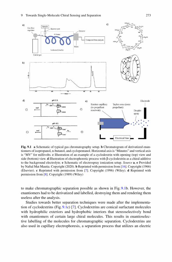
9 Towards Single-Molecule Chiral Sensing and Separation 273
Fig. 9.1 a Schematic of typical gas chromatography setup. b Chromatogram of derivatized enan-tiomers of isopropanol, n-butanol, and cyclopentanol. Horizontal axis is “Minutes” and vertical axisis “MV” for millivolts. c Illustration of an example of a cyclodextrin with opening (top) view andside (bottom) view. d Illustration of electrophoretic process with β-cyclodextrin as a chiral additiveto the background electrolyte. e Schematic of electrospray ionization setup. Source a, e Providedby Naftal Mat Mautia. Copyright (2020). b Reprinted with permission from [16]. Copyright (1966)(Elsevier). c Reprinted with permission from [7]. Copyright (1996) (Wiley). d Reprinted withpermission from [8]. Copyright (1989) (Wiley)
to make chromatographic separation possible as shown in Fig. 9.1b. However, theenantiomers had to be derivatized and labelled, destroying them and rendering themuseless after the analysis.
Studies towards better separation techniques were made after the implementa-tion of cyclodextrins (Fig. 9.1c) [7]. Cyclodextrins are conical surfactant moleculeswith hydrophilic exteriors and hydrophobic interiors that stereoselectively bondwith enantiomers of certain large chiral molecules. This results in enantioselec-tive labelling of the molecules for chromatographic separation. Cyclodextrins arealso used in capillary electrophoresis, a separation process that utilizes an electric
274 R. Sanders et al.
field gradient, a background electrolyte, and a cyclodextrin to separate two or moreenantiomers in a capillary tube.
When the chiral compounds bond with the cyclodextrins, their apparent mobilitychanges according to the Eq.9.1:
µapp = lL
txV+ lL
t0V(9.1)
where µapp is the apparent mobility of the compounds, l is the distance from thecapillary inlet to the detector, L is the total capillary length, and tx and t0 are thetimes elapsed for the compound and electroosmotic marker to travel to the detector,respectively. The bound compounds are mobilized towards or away from a cathodedepending on their mobilities.
An experiment shown in Fig. 9.1d depicts high resolving power using capillaryelectrophoresis for all but two enantiomers tested, as well as much faster resolutiontime than traditional chromatographic methods [5]. Differently from flow drivenchiral chromatography, separation is achieved by applying high voltage, initiatingthe migration of the sample from the anode to the cathode through the chiral capil-lary channel. By this method, the size of the column can be significantly reduced.However, the need for higher concentrations of enantiomers as well as cyclodex-trins leaves room for improvement from this method towards the ultimate goal ofsingle-molecule, labelless separation.
The field of chromatographic separation has continued to evolve, utilizing differ-ent chiral selectors and varied, more tailored chromatographic systems. Sørensen etal. used high performance liquid chromatography (HPLC) coupled with electrosprayionization-mass spectrometry (ESI-MS) shown in Fig. 9.1e in order to separate andmeasure L and D aspartic acid from human teeth [9]. The use of electrospray ion-ization resulted in increased sensing resolution in the subsequent mass spectrometrystep. This ground-breaking experiment leveraged addition of formic acid to opti-mize eluent pH for maximum resolution and tested different spray-needle voltagesaiming for forensic diagnostics and age determination [9]. Rather than derivatizingthe aspartic acid or using cyclodextrins, this process used teicoplanin, a chiral com-mercially available antibiotic biomolecule, as a chirally selective stationary phasein the separation column. The retention times were 4min and 6min for L- and D-aspartate respectively, which is fast compared to most other chiral selective chro-matography. Sørensen et al. found that applying a zero-voltage to the spray needle asopposed to a 4 kV voltage increased resolution and signal to noise ratio, and proposesthat a zero voltage may also be advantageous in the enantio-differential detection ofother polar chiral biomolecules [9]. The experiment ultimately obtained a minimumdetection resolution of 0.2 nanograms, which is excellent compared to other formsof chromatography.
Another labelled chiral separation method involves using enantioselective lipaseenzymes to react with one racemate in order to separate chiral molecules [10].The particular lipase used, an enzyme from Candida antarctica yeast called Can-dida antarctica Lipase B (CALB), selectively binds to R enantiomers in a certain
9 Towards Single-Molecule Chiral Sensing and Separation 275
temperature and pH range [10]. The CALB was used in conjunction with an enzy-matic membrane reactor (EMR) which binds to the CALB after the enantioselec-tive (R)-ketoprofen-EMR binding step. These two binding mechanisms were ableto facilitate chiral selection. The experiment achieved a maximum (R)-ketoprofenconversion rate of up to 73%with all parameters optimized [10]. However, the immo-bilized CALB had to be left to react with the racemates for 24h [10], which is notcompetitive with some chromatographic methods that take only minutes.
More recently, research has improved the chiral selective properties of chromato-graphic separation methods by focusing on the stationary phase. Molecular imprint-ing, amethod inwhich the stationary phase ismanufactured using the targetmoleculefor separation, has shown promise when used in conjunction with HPLC as well assupercritical fluid chromatography (SFC) [11].
One of the most effective documented use cases of molecular imprinting wasdemonstrated by Gutierrez-Climente et al. with the chiral drug citalopram and itsderivatives [12]. This experiment overcame some limitations of traditional chiralchromatography by decreasing the particle size of the chiral selective stage and bycovalently immobilizing molecularly imprinted nanoparticles onto silica beads [12].This technique provided sufficient access to chiral selective binding sites and allowedfor the use of various solvents that would otherwise cause the dissolution of the chiralselective stage [13]. Percent recovery varied from 91.5 to 103.7% across a wide rangeof concentrations (0.1 to 5µg of analyte per milliliter) [12], which is acceptably highfor commercial use. However, the resolution (R) and separation (α) factors werenot impressive compared to some more specialized liquid chromatography methodsusing proteins or polysaccharides for chiral selective stationary phases. For example,chromatographic columns using amylose have shown separation factors of up to 4.60and resolutions of up to 10.60 under highly controlled and optimized conditions [14],while many of the samples tested in the silica-MIN case had resolution factors of lessthan 1, meaning resolution was not achieved [12]. Equations9.2 and 9.3 show theseparation factor, which is a measure of relative retention time, and the resolutionfactor, which quantifies how well the analytes are separated with respect to oneanother:
α = tr,2 − tmtr,1 − tm
(9.2)
R = tr,2 − tr,112 (W1 + W2)
(9.3)
where tr is the resolution time,W is the width of the resolution peak of an enantiomeron a resolution versus time graph, tm is the time required for the eluent to pass throughthe column, and the 1 and 2 subscripts refer to the first and second enantiomers.
Chiral chromatography offers a variety of different methods for chiral separa-tion, each having its advantages and disadvantages. Table 9.1 summarizes a fewof the aforementioned examples. While chiral chromatography is extremely usefulfor bulk commercial enantioseparation, efforts to increase sensitivity and extend itsapplication to the molecular scale are still ongoing.
276 R. Sanders et al.
Table 9.1 Select chromatographic methods compared
Method Cyclodextrin-Based Electrophoretic Molecular Imprinting
Derivation Necessary [6] Not Necessary [5] Not Necessary [13]
Resolving Time 10–20 mins [6] <5 mins [5] 5–30 mins [14]
Resolution 2–4 (ideal) [6] <1 (most amino acids)[13]
Separation Factor 1–1.3 [6] 1–1.5 [12]
Analyte Concentration 10−5 M [5] 10−4 M [15]
9.3 Optical Foundations for Chiral Selection
The mechanism of traditional chiral chromatography relies on the recognition ofchiral molecules coupled by another material, inducing different retention times ina separation medium. Therefore, chromatographic methods require a chiral selec-tor or chiral column, which is time-consuming to set up, complex, and often mustbe adapted for different racemic compounds [13]. To overcome the limitations ofchromatographic methods, several methods have been proposed to achieve label-free chiral sorting through circularly polarized light (CPL). CPL is light which hasa constant-magnitude electric field vector that rotates in the plane perpendicular tothe propagating direction of the light. CPL can be either left-handed or right-handed,meaning that the electric field vector can rotate counterclockwise or clockwise in therotational plane, respectively.
Formolecular sortingwith chiral light, twometrics are of primary concern: opticalchirality (C) and optical helicity (H) [28]. The optical helicity of an electromagneticfield is the volume integral of the optical helicity density, h; likewise, the chiralityof an electromagnetic field is the volume integral of its optical chirality density,χ. Helicity density results from the projection of an electromagnetic (EM) wave’sangular momentum vector onto its linear momentum vector, and is analogous to thewave’s potential to impart a chiral-selective force,which is proportional to its chiralitydensity. Optical helicity density and chirality density are described analytically withEqs. 9.4 and 9.5:
h = 1
2
[√ε0
µ0A(∇ × A) +
õ0
ε0C(∇ × C)
](9.4)
χ = 1
2
[ε0E(∇ × E) + 1
µ0B(∇ × B)
](9.5)
where A is the magnetic vector potential, C is the electric vector potential, and E andB are the electric and magnetic fields, respectively. ε0 andµ0 are the permittivity andpermeability of free space, respectively.

9 Towards Single-Molecule Chiral Sensing and Separation 277
In 2014, Tkachenko and Brasselet first demonstrated using CPL to sort chiralmicrodroplets (diameter 20 microns) made of chiral liquid crystals [17]. The natureof the chirality of the droplets was cholesteric, meaning that the individual moleculesmaking the liquid crystals were achiral while the crystals themselves were chiral.As shown in Fig. 9.2a, left and right-handed CPL lasers with wavelength of 532nmilluminated the samples from left and right of the capillary containing the droplets,respectively, and the light interacted chiral-selectively with the droplets dependingon their liquid crystal chirality. As the droplets travelled down the capillary tube at aconstant velocity due to gravity, they also travelled laterally in the+ or− z directiondepending on their chirality. Achiral droplets did not travel laterally because thechiral light forces cancelled each other out.
As previously discussed, light with a non-zero helicity (and therefore a non-zerochirality), can impart a force proportional to the chirality of the light, which is ±1for perfectly CPL. Equation9.6 governs the optical force on a microdroplet.
Fz(x) = 2nextPR2(1 − cos4 θB,ext)
w20c
exp
(−2x2
w20
)(9.6)
where R is the radius of the spherical droplets, x is the coordinate in the direction ofgravity, c is the speed of light, and θB is the mathematical term that comes from theassumption that a certain area of the sphere, defined by the projection of a circularcross-section on the concave surface of the droplet, behaves as a perfect sphericalmirror. next is the extinction coefficient, and P and w0 are parameters associated withthe opposing and conversely-rotational chiral laser beams (beam power and beamwaist, or diameter, respectively).
The mechanism is based on the opposite sorting force due to the different pref-erential absorption of opposite CPL between chiral liquid crystals. As shown inFig. 9.2b, when illuminating chiral particles (from microscale chiral structures toindividual molecules) with CPL, preferential absorption and/or refraction occurs.Therefore, after passing through a chiral medium with circular differential absorp-tion or refraction, CPL experiences either a differential reduction in the magnitudeof the left and right components (circular dichroism), or a phase offset between theleft and right components (circular birefringence), respectively.
However, Tkachenko and Brasselet were only able to harness these principles tosort microscale particles. To further improve the sorting efficiency, several methodshave been demonstrated. Zhang et al. were able to theoretically determine idealoptical field conditions for chiral trapping and sorting by illuminating chiral particlesin the interference field of two evanescent laser beams [18]. This method achieveschiral particle separation from around 100nm to micro-scale sizes, which showssignificant improvement in size compared with the previous work [18]. This method,shown in Fig. 9.2c, takes advantage of evanescent waves and reflected waves byplacing the chiral molecules at the interface between media of different refractiveindices. It was found that the combination of one linearly polarized beam and onecircularly polarizedbeamworked thebest to separate particles basedon their chirality,creating a non-chiral-selective force in the direction of propagation of the waves and

278 R. Sanders et al.
Fig. 9.2 a Schematic showing the light-matter interaction geometries with different light beamcircular polarizations and dielectric droplet chiralities (top) and the corresponding superimposedsnapshots demonstrating the droplet movements (below). Positive � denotes a counter-clockwisepolarization and negative � denotes a clockwise polarization; the material chirality is denotedby χ. b Depiction of electric field vectors for light undergoing circular birefringence (left) andcircular dichroism (right). c Schematic of two interference fields to achieve chiral separation. dThe phase of the trapping force (ϕx) and the phase of the lateral force (ϕy) with the different chiralparameters for case D as shown in Fig. 9.2c. e The lateral (Fy) trapping forces with different chiralparameters for case D as shown in Fig. 9.2c. f Schematic showing chiral nanoplasmonic tweezerswith illustration of CPL. g The calculated trapping potentials at 20nm above the nanoaperture forR and S enantiomers when illuminating with linearly polarized and left-handed circularly polarizedlight. Source a Reprinted with permission from [17]. Copyright (2014) (Nature). b Provided byNaftal Mat Mautia. Copyright (2020). c–e Reprinted with permission from [18]. Copyright (2017)(ACSPublications). f–gReprintedwith permission from [19]. Copyright (2016) (ACSPublications)
a chirally selective perpendicular force shown in Fig. 9.2d, e [18]. Furthermore, themethod has been proven to apply to a variety of particle chiralities and sizes, fromthe nanometer to micron scale.
Other chiral sorting methods have been demonstrated by coupling CPL withnanostructures to achieve low concentration chiral sorting with nanoscale
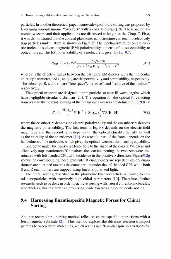
9 Towards Single-Molecule Chiral Sensing and Separation 279
particles. In another theoretical paper, nanoscale optofluidic sorting was proposed byleveraging nanoplasmonic “tweezers” with a coaxial design [19]. These nanoplas-nomic tweezers and their applications are discussed at length in the Chap. 7. First,it was demonstrated that the coaxial plasmonic nanostructure can enantioselectivelytrap particles under 10nm as shown in Fig. 9.2f. The mechanism relies on a dielec-tric molecule’s electromagnetic (EM) polarizability, a metric of its susceptibility tooptical forces. The EM polarizability of a molecule is given by Eq.9.7:
αEM = −12πr3jκ
√µ0ε0
(εr + 2εrm)(µr + 2µ) − κ2(9.7)
where r is the effective radius between the particle’s EM dipoles, κ , is the molecularchirality parameter, and ε0 andµ0 are the permittivity and permeability, respectively.The subscripts 0, r, and rm are “free space”, “relative”, and “relative of the medium”respectively.
The optical tweezers are designed to trap particles at near-IR wavelengths, whichhave negligible circular dichroism [20]. The equation for the optical force actingtransverse to the coaxial opening of the plasmonic tweezers are defined in Eq.9.8 as:
Ftr ≈ �(αee)
4∇|E|2 + �(αem)
1
2∇�(E · H) (9.8)
where the ee subscript denotes the electric polarizability and the em subscript denotesthe magnetic polarizability. The first term in Eq.9.8 depends on the electric fieldmagnitude and the second term depends on the optical chirality density as wellas the chirality of the enantiomer [19]. As a result, part of the force depends on thehandedness of the molecule, which gives the optical tweezers their sorting capability.
In order tomatch the transverse force field to the shape of the coaxial tweezers andeffectively trap enantiomers 20nm above the coaxial opening, the tweezers were illu-minated with left-handed CPL with incidence in the positive z direction. Figure9.2gshows the corresponding force gradients. R enantiomers are repelled while S enan-tiomers are attracted towards the nanoaperture under the left-handed CPL while bothS and R enantiomers are trapped using linearly polarized light.
The chiral sorting described in the plasmonic tweezers article is limited to chi-ral nanoparticles with extremely high chiral parameters [19]. Therefore, furtherresearch needs to be done in order to achieve sortingwith natural chiral biomolecules.Nonetheless, this research is a promising stride towards single-molecule sorting.
9.4 Harnessing Enantiospecific Magnetic Forces for ChiralSorting
Another recent chiral sorting method relies on enantiospecific interactions with aferromagnetic substrate [21]. This method exploits the different electron transportpatterns between chiral molecules, which results in differential spin polarizations for
280 R. Sanders et al.
Fig. 9.3 a SEM image of the chiral PAL oligopeptide adsorbed on ferromagnetic samples mag-netized with the magnetic dipole pointing up (H+) or down (H−) relative to the substrate surface.Panels (i) and (ii) L-PAL and (iii) and (iv) D-PAL were adsorbed for 2 s on a substrate magne-tized up or down. b CD spectra of a racemic oligopeptide mixture before (red) and after (blackand blue) the magnetic chiral separation. Source Reprinted with permission from [21]. Copyright(2018) (American Association for the Advancement of Science)
the two enantiomers [22]. The magnetized substrate induces electric dipole polar-ization in a racemic solution flowing over it, which causes an enantiospecific spinorientation at the poles of the molecules. Subsequently, the enantiomers are adsorbedonto the substrate at different rates as shown in Fig. 9.3a [21].
Banergee-Ghosh et al. harnessed this magnetic enantiospecific force by using acolumn coatedwith an externallymagnetized ferromagneticmetal alloy and allowinga racemic oligopeptide mixture to flow through it. Figure9.3b shows the CD spectraat the inlet and outlet of the column, which is clear evidence of high-resolution chiralsorting. The results indicate that the spin polarizations for L and D enantiomers areattracted to “up” and “down” polarized magnetic surfaces, respectively [21].
It is fascinating to achieve selector free chiral separation using light and a mag-netic field. By tailoring the EM field with a nanoaperture, it is possible to achievesingle moleclue chiral separation. However, most studies are still at theoretical lev-els. Meanwhile, a limitation of current selector free chiral separation is that currentmethods require extremely close (nanometer scale) distances between molecule andsubstrate. Therefore, quickly bringing the molecule of interest closer to the substrateis necessary for enantioseparation of chiral molecules with low concentrations.
9.5 Using Achiral Nanoparticles to Increase Chiro-OpticalSignaling
Plasmonic nanostructures can be used not only for chiral sorting but also for chi-ral sensing. Most chiral mediums display both circular birefringence and circulardichroism. Cohen and Tang first discovered the link between the optical chirality of
9 Towards Single-Molecule Chiral Sensing and Separation 281
an electromagnetic field and the differential excitation of enantiomers in 2010 [23].Furthermore, it was proven analytically that at the nodes of a superchiral field, chi-ral signals from excited enantiomers were enhanced 400-fold. Therefore, enhancinglocal optical field chirality gives an extremely large advantage with high sensitivity.
On the quest to enhance the inherently weak chiro-optical signals of individualmolecules, we concern ourselves with the optical chirality parameter, κ , ascribed toa chiral molecular medium and representing the differential refraction of left andright CPL, leading to a circular birefringent chiro-optical signal [24]. The opticalchirality parameter is complex, where the real part of the parameter describes thecircular birefringent signal and the imaginary part describes the circular dichroismsignal of the molecule [25]. Since circular birefringence results from a differentialeffect of a medium on CPL, the chirality parameter of a chiral medium describeshow the wave-vector, and by extension, wavelength, are modulated by the mediumaccording to Eqs. 9.9 and 9.10:
kL,R = (n ± κ)k0 (9.9)
k0 = 2πλ
(9.10)
where k is the wave vector, λ is the wavelength, and n is the refractive index of themedium. Yoo and Park’s research on signal enhancement using nanoparticles in theMie regime (radius of the nanoparticle on the same order as the wavelength of thelight) demonstrates that high refractive index plasmonic and dielectric nanoparticlesincrease light scattering, leading to chiral differential signal enhancement [24].
Yoo and Park focused on particles in the Mie regime, but their findings translateto the Rayleigh regime as well. They first experimentally and theoretically determinethat different frequencies of light can lead to different scattering cross-sections byilluminating particles in the Mie regime with different wavelengths of light. Theyshow that the degree of non-differential scattering affected by both plasmonic anddielectric achiral nanoparticles (Ag and Si, respectively) is linearly proportional tothe measured chirality parameter of the medium in the near field of the nanoparticles,as shown in Fig. 9.4a.
Optical chirality, as previously mentioned in the context of electromagnetic fields,is a measure of the enantioselective potential of an electric field [26], which can bedefined in (9.11):
C = ε0
2ω�[E · B] (9.11)
where ε0 is the permittivity of free space, ω is the angular frequency of the incidentlight, and E and B are the electric and magnetic fields.
Yoo and Park showed that scattering by dielectric and plasmonic nanoparticlescan affect optical chirality conservation, but an analysis of scattering effects onchirality enhancement is not complete without a parallel discussion of absorption, the

282 R. Sanders et al.
Fig. 9.4 a Left: circular differential scattering cross-section for a spherical gold nanoparticle ofradius 50nm in a medium of refractive index = 1.5 with different chirality parameters. Right: Themaximum value of circular differential scattering cross-section for a spherical gold nanoparticle ina medium of refractive index = 1.5 with different chirality parameters. b Total volume-integratedchirality flux calculated for plasmonic (left) and dielectric (right) nanoparticles of 75nm radii versuswavelength. Source a Reprinted with permission from [24]. Copyright (2015) (Nature). bReprintedwith permission from [28]. Copyright (2019) (Multidisciplinary Digital Publishing Institute)
mechanism responsible for circular dichroic signals. Together, differential scatteringand absorption of light constitute the light’s circular differential extinction [27]. Adifference in the measured extinction coefficient for left-handed and right-handedCPL constitutes a CD signal.
The authors find that the differential extinction coefficient is a function of the plas-monic response (present only inmetallic particles) aswell as the electric andmagneticdipoles, quadrupoles, and even octupoles for both metallic and dielectric particles[24, 27]. Figure9.4b shows the wavelength dependent resonant response of metallicand dielectric nanoparticles, indicating that the plasmonic resonant response domi-nates and acts in opposition to the electric and magnetic polar resonant responses.Therefore, optical chirality flux, or the change in the control volume “flow” of thechirality parameter has a much larger response when using dielectric particles versusplasmonic particles, interestingly enough.
Further research into the optical enhancement of dielectric and plasmonic nanos-tructures by Raziman et al. in 2019 parameterizes certain desired optical effects andanalytically determines how nanodisk arrays made of silver and silicon alter these
9 Towards Single-Molecule Chiral Sensing and Separation 283
effects in the near field [29]. Logically, inherently achiral nanophotonic platformshave no circular differential effect; therefore, Raziman et al. illuminated the arraywith left CPL in order to enhance the chirality parameter and the degree of circularpolarization (DOCP).
Raziman’s team was interested in the effect of the nanophotonic platforms on thenear field intensity of the electric field as well as the near field chirality. The idealnanoparticles need to enhance the intensity of the electric field in order to increasesensitivity to chiral molecules in the near field, while preserving the original circularpolarization of the incident light so as to not create a signal that obfuscates the signalof the chiral molecules [29]. The parameters used to describe these changes arepresented in Eqs. (9.12, 9.13, 9.14):Degree of Circular Polarization:
DOCP = V
I(9.12)
where I is the Intensity of the electric field and V is the difference in left and rightCPL intensities.Electric energy density:
Ue = ε0
4|E|2 (9.13)
where ε0 is the permittivity of free space and E is the electric field vector.Circular dichroism enhancement is given by:
CDE = C
Ue(9.14)
where C is the optical chirality and Ue is the electric energy density.The ideal nanophotonic platform, when illuminated by left CPL, as discussed
above, should show a high near field increase in both intensity and electric energydensity, while providing a spatially invariant degree of DOCP equal to one (or greaterthan one in the case of superchiral fields) and a high CDE. In the metallic nanodisks,the plasmonic response at the resonantwavelength creates strong electric field aroundthe disk while the stokes parameter shows a lower value as shown in Fig. 9.5a. Mean-while, the CD enhancement is suppressed and the abrupt change of DOCP from pos-itive to negative values leads to its lower value, as also shown in Fig. 9.5a. Therefore,metallic nanodisks show poor performance to enhance the chiral interaction in thenear field.
Another study conducted by Lee, Yoo, and Park clarified surface enhanced CDfrom the microscopic perspective. Briefly, the near field circular dichroism effect canbe measured by a medium’s differential reflectance, transmittance, and absorptionon the two circularly polarized superpositions of linearly polarized light, which isincident on the medium [25]. Herein, reflection, transmission, and absorption makeup the collectively exhaustive set ofwhat happens to the light incident on themedium;
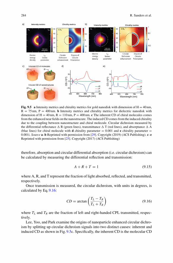
284 R. Sanders et al.
Fig. 9.5 a Intensity metrics and chirality metrics for gold nanodisk with dimension of H = 40nm,R = 75nm, P = 400nm. b Intensity metrics and chirality metrics for dielectric nanodisk withdimension of H = 40nm, R = 110nm, P = 400nm. c The inherent CD of chiral molecules comesfrom the enhanced near fields on the nanostrucure. The inducedCDcomes from the induced chiralitydue to the coupling between nanostructure and chiral molecule. Circular dichroism measured bythe differential reflectance R (green lines), transmittance T (red lines), and absorptance A(blue lines) for chiral molecule with d chirality parameter = 0.001 and e chirality parameter =0.001i. Source a–b Reprinted with permission from [29]. Copyright (2019) (ACS Publishing). c–eReprinted with permission from [25]. Copyright (2017) (ACS Publishing)
therefore, absorption and circular differential absorption (i.e. circular dichroism) canbe calculated by measuring the differential reflection and transmission:
A + R + T = 1 (9.15)
where A, R, and T represent the fraction of light absorbed, reflected, and transmitted,respectively.
Once transmission is measured, the circular dichroism, with units in degrees, iscalculated by Eq.9.16:
CD = arctan
(TL − TRTL + TR
)(9.16)
where TL and TR are the fraction of left and right-handed CPL transmitted, respec-tively.
Lee, Yoo, and Park examine the origins of nanoparticle enhanced circular dichro-ism by splitting up circular dichroism signals into two distinct causes: inherent andinduced CD as shown in Fig. 9.5c. Specifically, the inherent CD is the molecular CD
9 Towards Single-Molecule Chiral Sensing and Separation 285
enhanced by the near field of the nanoparticles. The induced CD is the asymmetricexcitation and absorption of the chiral EM field due to the chiral molecules [25].
To study the contribution from the inherent CD and induced CD for chiral molec-ular sensing, the authors compare circular dichroism signals using either a purelyreal or purely imaginary chirality parameter as shown in Fig. 9.5d, e. The chiralmolecule with the purely real chirality parameter can introduce neither differentialabsorption nor differential transmittance. However, from the simulation results, weobserve the differential absorption is same as differential transmittance with the peaknear plasmonic resonance of the nanoparticles indicating the induced CD. The chiralmolecule with pure imaginary chirality parameters shows totally different trends.Herein, both the inherent CD and induced CD can contribute to the total CD signal.Therefore, the CD spectra is enhanced both in UV and visible range [25].
Achiral plasmonic nanostructures have been shown to have an ability to increasethe magnitude of the electric field, optical helicity, and optical chirality in the nearfield, which make them useful for chiral molecular sensing in small molecular quan-tities. Another advantage of achiral plasmonic and dielectric nanostructures, as pre-viously stated, is that they have no background CD spectra to skew or obfuscate theCD emission spectra of the chiral molecules subject to sensing. This gives achiralnanostructures an advantage over chiral nanostructures for sensing purposes.
9.6 Chiral Sensing with Inherently Chiral Metasurfaces
Apart from the achiral nanoparticles for chiral molecule sensing, alternative struc-tures such as nanoparticles or metasurfaces with inherent chirality are also shown tobe promising for chiral sensing. Similarly to chiral molecules, these structures can beeither left handed or right handed chiral structure depending on the optical responseto CPL.
In particular, Fig. 9.6a shows an example of the two chiral metasurfaces fabricatedusing stacked gold nanorods with ±60◦ angles between them [26]. The structuralchirality of the resulting metasurface exhibits a distinct optical response of the meta-surface with adsorbed chiral molecules, termed an output CD response (CDO) underdifferent CPL where the response is calculated in Eq.9.17:
CDO = CDi + 4kw�[κm] |TLRTRL|2 − |TLLTRR|2(|TLR|2 + |TRR|2)2 + (|TLL|2 + |TRL|2)2 (9.17)
where CDi is the background CD signal of the metasurface, k is the wave vector, wis the width of the metasurface, and T is the transmission coefficient, with first andsecond subscripts denoting the circular handedness of the coefficient and the circularpolarization of incident light, respectively [26].

286 R. Sanders et al.
Fig. 9.6 a Schematic and scanning electron microscope images of+60◦ gold rod chiral metamate-rial. Scale bar 500nm. b with RCP (red curve) and LCP (black curve) excitation. c Experimentallymeasured transmission and CD of the +606◦ chiral metamaterial with RCP (red curve) and LCP(black curve) excitation. d Simulated CD summation of±60◦ chiral metamaterial. e Scanning elec-tronmicroscope image of nanoholeMCMwith layers turned±10◦. Scale bar 500nm. f λ valuesfor R and S thalidomide. f Schematic drawing of OPN laser manipulation of colloidal particles.g CDS spectra of left-handed and right-handed structures with (solid line) and without (dashedline) adsorbed L-phenylalanine Source a–c Reprinted with permission from [26]. Copyright (2017)(Nature). d–e Reprinted with permission from [31]. Copyright (2017) (Wiley). f–g Reprinted withpermission from [32]. Copyright (2019) (ACS Publishing)
9 Towards Single-Molecule Chiral Sensing and Separation 287
Zhao et al. first conducted calibration to isolate backgroundCD signals originatingfrom the chiral nanostructures themselves [25] as well as to control for discrepanciescaused by fabrication errors.
The experimentalCD resultswith+60◦ angles chiralmetasurfaces showsoppositeresponse as shown in Fig. 9.6b. The chiral metasurface shows different transmissionunder RCP and LCP inducing CD spectra peak near 1000nm. Then enantiopuresolutions of R and S Propanediol were added, and the team was able to isolate thebackground CD signals and successfully sense the molecules down to zeptomole(10−21) quantities as shown in Fig. 9.6c. They also conducted a numerical simulation(Fig. 9.6c) and the result shows a similar trend as the experimental results.
Such picogram level sensitivity is a step towards single-molecule sensing. Theauthors further propose that these chiral metasurfaces, if used in conjunction withnanophotonic optofluidic platforms [19, 30], may even be able to sense enantiopureclusters of just a few biomolecules. The biomolecules sensed can also be a widerange of molecular weights and can be sensed extremely quickly (in fractions of asecond), which may suit this method to high throughput operations requiring highprecision and versatility.
Wu et al. recently developed alternative chiral metamaterials called Moiré chiralmetamaterials (MCMs) [31], as shown in Fig. 9.6e. The metamaterial consists of twomonolayers of gold nanohole arrays stacked with an in-plane rotation. Depending onthe relative orientation of the two nanohole arrays, MCMs can be either left-handedor right-handed structures, inducing strongly enhanced localized optical chirality.Wuet al. further demonstrated the capability ofMCMs for chiral sensing. The adsorptionof chiral proteins on the MCMs caused asymmetric spectral shifts of measured CDfor the MCMs with opposite handedness [31]. The team also used the bilayer meta-material to distinguish small enantiomers, specifically R-thalidomide and its and its“evil twin” as shown in Fig. 9.6f. The reconfigurable and high sensitivity MCMs canachieve detecting variable chiral molecules with a variety of molecular weights.
Emerging research through optical photon nudging (OPN) can be used to fabricatechiral structure for chiral sensing [32]. The mechanism of OPN is based on the opti-cal scattering forces [33, 34] created by the illumination of gold nanoparticles witha laser. The heat generated laser mobilizes particles, allowing them to release froma surfactant substrate. Once the particles are mobilized, they can be pushed by thelaser beam to the desired location as shown in Fig. 9.6f. Li et al. further demonstratedthe application of OPN to assemble both metal and silicon nanoparticles as a tun-able nanostructure [32]. Specifically, they fabricated the dielectric chiral metasurfaceusing a single silicon nanowire and a single silicon nanoparticle for chiral moleculesensing. As shown in Fig. 9.6g, left-handed and right-handed chiral structures cansuccessfully detect the handedness of L-phenylalanine at low quantities.
Further research has been done into chiral plasmonic nanostructures [35], withvarying degrees of complexity in shape. For example, a bilayer chiral metamaterialsubstrate proves that by using two mirror image chiral arrays, the chirality parameterand circular dichroism can be enhanced in the near field with chiral nanoplasmonicswhile controlling for background circular dichroism [26]. After this proof of concept,it was also shown that a racemic array of plasmonic nanoparticles can mitigate
288 R. Sanders et al.
background circular dichroism signals by cancelling them [36]. The advantage ofusing a racemic metasurface instead of a chiral metasurface is that it can cancelstructural CD signals without any decrease in near field chirality or electric fieldmagnitude compared to purely handed arrays [36].
Shown in Fig. 9.7a is an example of a racemic array made using gammadionnanostructures. After deposition of D, L, and DL phenylalanine, the racemic plas-monic gammadion array displayed distinct residual circular dichroism signals foreach coating as shown in Fig. 9.7b. These signals arose from selective plasmoniccoupling between the enantiomers and specific left or right-handed gammadions inthe array, which increased both the local optical chirality and electric field enhance-ment in the near field of the gammadion array.
García et al. observed mirror image circular dichroism enhancement of the Dand L enantiomers, as well as the aforementioned electric field and its chiral dis-symmetry. Note that the sign of C determines which enantiomer will interact withwhich gammadion pair. The chiral dissymmetry, C, is a measure of the platform’scapacity for differential chiral signalling [36]. This signal enhancement resulted inopposite plasmonic coupling between D and L enantiomers, enabling clear chiraldifferentiation.
Along with the gammadion structure, other chiral plasmonic structures such asshuriken-shaped structures have also been studied. These structures produced super-chiral nearfield chirality with the chirality parameter reaching magnitudes of up to100 in some near field areas [37] as shown in Fig. 9.7c. These chiral fields wereshown to interact asymmetrically with the nanostructure’s plasmonic dipolar andquadrupolar modes, a phenomenon referred to as “dichroic coupling” [37]. Kelly etal. propose that dichroic coupling can be used to manipulate a number of opticalproperties, which has practical applications in the chiral sensing field [37].
Figure9.7d shows how shuriken structures submerged in water, an isotropicdielectric medium, are used for chiral sensing of an enantiopure solution containingthe amino acid alpha-pipene. When the handedness of the structure and the chiralbiomolecules agree, this causes the distance between the reflectivity minima to becloser to that of the pure dielectric (in this case, water) than when they do not agree[37]. This method of analysis, when using pure left-handed CPL, can be used todetermine the handedness of an enantiomeric coating 20nm thick [37]. While thisconcentration is a far cry from single-molecule, it is an improvement from the 150nmthickness required for the gammadion structures.
9.7 Cavity-Based Nanophotonic Platforms for ChiralSensing and Sorting
Chiral nanostructures interact selectively with chiral light, and as a result, cou-ple selectively to chiral molecules [36, 37]. Recently, experimentation with chiralnanocavities has taken advantage of the inverse of this effect, exploiting the chiral
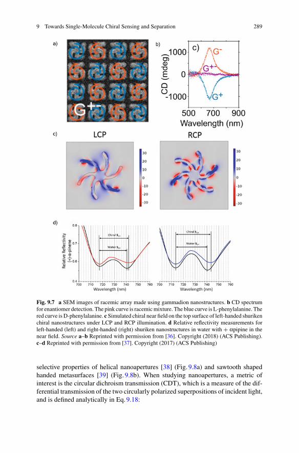
9 Towards Single-Molecule Chiral Sensing and Separation 289
Fig. 9.7 a SEM images of racemic array made using gammadion nanostructures. b CD spectrumfor enantiomer detection. The pink curve is racemicmixture. The blue curve is L-phenylalanine. Thered curve is D-phenylalanine. c Simulated chiral near field on the top surface of left-handed shurikenchiral nanostructures under LCP and RCP illumination. d Relative reflectivity measurements forleft-handed (left) and right-handed (right) shuriken nanostructures in water with + αpipine in thenear field. Source a–b Reprinted with permission from [36]. Copyright (2018) (ACS Publishing).c–d Reprinted with permission from [37]. Copyright (2017) (ACS Publishing)
selective properties of helical nanoapertures [38] (Fig. 9.8a) and sawtooth shapedhanded metasurfaces [39] (Fig. 9.8b). When studying nanoapertures, a metric ofinterest is the circular dichroism transmission (CDT), which is a measure of the dif-ferential transmission of the two circularly polarized superpositions of incident light,and is defined analytically in Eq.9.18:
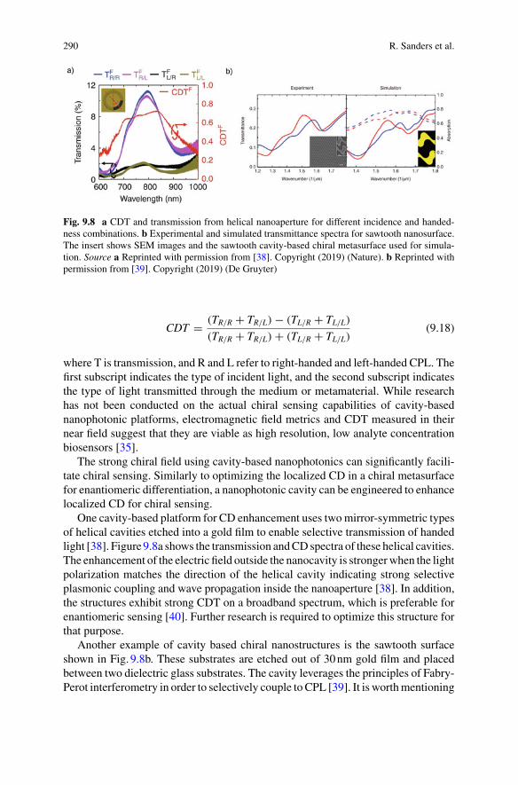
290 R. Sanders et al.
Fig. 9.8 a CDT and transmission from helical nanoaperture for different incidence and handed-ness combinations. b Experimental and simulated transmittance spectra for sawtooth nanosurface.The insert shows SEM images and the sawtooth cavity-based chiral metasurface used for simula-tion. Source a Reprinted with permission from [38]. Copyright (2019) (Nature). b Reprinted withpermission from [39]. Copyright (2019) (De Gruyter)
CDT = (TR/R + TR/L) − (TL/R + TL/L)
(TR/R + TR/L) + (TL/R + TL/L)(9.18)
where T is transmission, and R and L refer to right-handed and left-handed CPL. Thefirst subscript indicates the type of incident light, and the second subscript indicatesthe type of light transmitted through the medium or metamaterial. While researchhas not been conducted on the actual chiral sensing capabilities of cavity-basednanophotonic platforms, electromagnetic field metrics and CDT measured in theirnear field suggest that they are viable as high resolution, low analyte concentrationbiosensors [35].
The strong chiral field using cavity-based nanophotonics can significantly facili-tate chiral sensing. Similarly to optimizing the localized CD in a chiral metasurfacefor enantiomeric differentiation, a nanophotonic cavity can be engineered to enhancelocalized CD for chiral sensing.
One cavity-based platform for CD enhancement uses twomirror-symmetric typesof helical cavities etched into a gold film to enable selective transmission of handedlight [38]. Figure9.8a shows the transmission andCDspectra of these helical cavities.The enhancement of the electric field outside the nanocavity is strongerwhen the lightpolarization matches the direction of the helical cavity indicating strong selectiveplasmonic coupling and wave propagation inside the nanoaperture [38]. In addition,the structures exhibit strong CDT on a broadband spectrum, which is preferable forenantiomeric sensing [40]. Further research is required to optimize this structure forthat purpose.
Another example of cavity based chiral nanostructures is the sawtooth surfaceshown in Fig. 9.8b. These substrates are etched out of 30nm gold film and placedbetween two dielectric glass substrates. The cavity leverages the principles of Fabry-Perot interferometry in order to selectively couple to CPL [39]. It is worthmentioning

9 Towards Single-Molecule Chiral Sensing and Separation 291
that T peaks in a very narrow range of incident wavelengths around 650nm [39],which makes this metasurface promising for extremely low analyte volume chiralsensing [40].
9.8 Conclusion
We have discussed several methods toward single chiral molecule sensing and detec-tion. Traditional chromatographic methods can achieve high resolution chiral sep-aration in biological samples. However, these methods are bulky and require chiralselectors to achieve chiral separation. Other techniques using optical or magneticfields have been recently proposed to overcome this challenge. Of these techniques,the plasmonic nanoaperature tweezers are particularly promising. Based on theo-retical analysis, it is possible to leverage this technique to achieve chiral molecularseparation with a few molecules, or possibly even a single molecule. Meanwhile,plasmonic structures can also significantly enhance the local optical chirality andtherefore achieve high resolution chiral molecule detection with small quantities.However, it is still challenging to achieve chiral separation using plasmonic struc-tures at the molecular levels due to the small scale. With new developing technologyconstantly supplementing and replacing existing methods, we believe there is stillmuch room for improvement left towards single chiral molecule detection and sep-aration.
Acknowledgements The authors acknowledge the financial support of the National Science Foun-dation (NSF–ECCS–2001650), the National Aeronautics and Space Administration Early CareerFaculty Award (80NSSC17K0520), and the National Institute of General Medical Sciences of theNational Institutes of Health (DP2GM128446). The authors also acknowledge the generous contri-bution of three illustrations by Naftal Mat Mautia.
References
1. J. Gal, “Molecular chirality in chemistry and biology: Historical milestones,” Helvetica Chim-ica Acta, vol. 96, no. 9, pp. 1617–1657, 2013.
2. A. M. Evans, “Comparative pharmacology of s (+)-ibuprofen and (rs)-ibuprofen,” Clinicalrheumatology, vol. 20, no. 1, pp. 9–14, 2001.
3. J. Kumar, H. Eraña, E. López-Martínez, N. Claes, V. F. Martín, D. M. Solís, S. Bals, A. L.Cortajarena, J. Castilla, and L. M. Liz-Marzán, “Detection of amyloid fibrils in parkinson,Äôsdisease using plasmonic chirality,” Proceedings of the National Academy of Sciences, vol. 115,no. 13, pp. 3225–3230, 2018.
4. K. Kalíková, T. Šlechtová, and E. Tesarová, “Enantiomeric ratio of amino acids as a tool fordetermination of aging and disease diagnostics by chromatographic measurement,” Separa-tions, vol. 3, no. 4, p. 30, 2016.
5. W. König, R. Krebber, and P.Mischnick, “Cyclodextrins as chiral stationary phases in capillarygas chromatography. part v: Octakis (3-o-butyryl-2, 6-di-o-pentyl)-γ -cyclodextrin,” Journalof High Resolution Chromatography, vol. 12, no. 11, pp. 732–738, 1989.

292 R. Sanders et al.
6. S. Fox, H. Strasdeit, S. Haasmann, and H. Brückner, “Gas chromatographic separation ofstereoisomers of non-protein amino acids on modified γ -cyclodextrin stationary phase,” Jour-nal of Chromatography A, vol. 1411, pp. 101–109, 2015.
7. T. Loftsson and M. E. Brewster, “Pharmaceutical applications of cyclodextrins. 1. drug solubi-lization and stabilization,” Journal of pharmaceutical sciences, vol. 85, no. 10, pp. 1017–1025,1996.
8. Z. Aturki, “Use of β-cyclodextrin polymer as a chiral selector in capillary electrophoresis,”Journal of Chromatography A, vol. 680, no. 1, pp. 137–146, 1994.
9. M. B. Sørensen, P. Aaslo, H. Egsgaard, and T. Lund, “Determination of d/l-amino acids byzero needle voltage electrospray ionisation,” Rapid Communications in Mass Spectrometry:An International Journal Devoted to the Rapid Dissemination of Up-to-the-Minute Researchin Mass Spectrometry, vol. 22, no. 4, pp. 455–461, 2008.
10. A. L. Ong, A. H. Kamaruddin, S. Bhatia, and H. Y. Aboul-Enein, “Enantioseparation of (r,s)-ketoprofen using candida antarctica lipase b in an enzymatic membrane reactor,” Journal ofseparation science, vol. 31, no. 13, pp. 2476–2485, 2008.
11. B. Sellergren, “Imprinted chiral stationary phases in high-performance liquid chromatography,”Journal of Chromatography A, vol. 906, no. 1-2, pp. 227–252, 2001.
12. R. Gutierrez-Climente, A. Gomez-Caballero, A. Guerreiro, D. Garcia-Mutio, N. Unceta, M. A.Goicolea, and R. J. Barrio, “Molecularly imprinted nanoparticles grafted to porous silica aschiral selectors in liquid chromatography,” Journal of Chromatography A, vol. 1508, pp. 53–64,2017.
13. J. Teixeira, M. E. Tiritan, M. M. Pinto, and C. Fernandes, “Chiral stationary phases for liquidchromatography: Recent developments,” Molecules, vol. 24, no. 5, p. 865, 2019.
14. R. Sardella, F. Ianni, A. Lisanti, S. Scorzoni, F. Marini, S. Sternativo, and B. Natalini, “Directchromatographic enantioresolution of fully constrained β-amino acids: exploring the use ofhigh-molecular weight chiral selectors,” Amino acids, vol. 46, no. 5, pp. 1235–1242, 2014.
15. C.-C. Hwang and W.-C. Lee, “Chromatographic resolution of the enantiomers of phenyl-propanolamine by using molecularly imprinted polymer as the stationary phase,” Journal ofChromatography B: Biomedical Sciences and Applications, vol. 765, no. 1, pp. 45–53, 2001.
16. E. Gil-Av, B. Feibush, and R. Charles-Sigler, “Separation of enantiomers by gas liquid chro-matography with an optically active stationary phase,” Tetrahedron Letters, vol. 7, no. 10,pp. 1009–1015, 1966.
17. G. Tkachenko andE.Brasselet, “Optofluidic sorting ofmaterial chirality by chiral light,”Naturecommunications, vol. 5, no. 1, pp. 1–7, 2014.
18. T. Zhang, M. R. C. Mahdy, Y. Liu, J. H. Teng, C. T. Lim, Z. Wang, and C.-W. Qiu, “All-opticalchirality-sensitive sorting via reversible lateral forces in interference fields,” ACS nano, vol. 11,no. 4, pp. 4292–4300, 2017.
19. Y. Zhao, A. Saleh, and J. Dionne, “Enantioselective optical trapping of chiral nanoparticleswith plasmonic tweezers.”
20. I. Liberal, I. Ederra, R. Gonzalo, and R. W. Ziolkowski, “Near-field electromagnetic trappingthrough curl-spin forces,” Physical Review A, vol. 87, no. 6, p. 063807, 2013.
21. K. Banerjee-Ghosh, O. B. Dor, F. Tassinari, E. Capua, S. Yochelis, A. Capua, S.-H. Yang,S. S. Parkin, S. Sarkar, L. Kronik, et al., “Separation of enantiomers by their enantiospecificinteractionwith achiralmagnetic substrates,” Science, vol. 360, no. 6395, pp. 1331–1334, 2018.
22. A. Kumar, E. Capua, M. K. Kesharwani, J. M. Martin, E. Sitbon, D. H. Waldeck, and R. Naa-man, “Chirality-induced spin polarization places symmetry constraints on biomolecular inter-actions,” Proceedings of the National Academy of Sciences, vol. 114, no. 10, pp. 2474–2478,2017.
23. Y. Tang and A. E. Cohen, “Optical chirality and its interaction with matter,” Physical reviewletters, vol. 104, no. 16, p. 163901, 2010.
24. S. Yoo and Q.-H. Park, “Enhancement of chiroptical signals by circular differential mie scat-tering of nanoparticles,” Scientific reports, vol. 5, no. 1, pp. 1–8, 2015.
25. S. Lee, S. Yoo, and Q.-H. Park, “Microscopic origin of surface-enhanced circular dichroism,”ACS Photonics, vol. 4, no. 8, pp. 2047–2052, 2017.
9 Towards Single-Molecule Chiral Sensing and Separation 293
26. Y. Zhao, “Chirality detection of enantiomers using twisted optical metamaterials,” NatureCommunications, vol. 8, no. 1, pp. 1–8, 2017.
27. P. Gutsche and M. Nieto-Vesperinas, “Optical chirality of time-harmonic wavefields for clas-sification of scatterers,” Scientific reports, vol. 8, no. 1, pp. 1–13, 2018.
28. L. V. Poulikakos, J. A. Dionne, and A. García-Etxarri, “Optical helicity and optical chiralityin free space and in the presence of matter,” Symmetry, vol. 11, no. 9, p. 1113, 2019.
29. T. Raziman, R. H. Godiksen, M. A. Müller, and A. G. Curto, “Conditions for enhancing chiralnanophotonics near achiral nanoparticles,”ACSPhotonics, vol. 6, no. 10, pp. 2583–2589, 2019.
30. M. Soltani, J. Lin, R. A. Forties, J. T. Inman, S. N. Saraf, R. M. Fulbright, M. Lipson, andM. D.Wang, “Nanophotonic trapping for precise manipulation of biomolecular arrays,”Naturenanotechnology, vol. 9, no. 6, p. 448, 2014.
31. Y. Liu, Z. Wu, and Y. Zheng, “Moiré chiral metamaterials,” Communication, vol. 5, no. 16,2017.
32. J. Li, M. Wang, Z. Wu, H. Li, G. Hu, T. Jiang, J. Guo, Y. Liu, K. Yao, Z. Chen, et al., “Tunablechiral optics in all-solid-phase reconfigurable dielectric nanostructures,” Nano Letters, 2020.
33. M. Selmke, U. Khadka, A. P. Bregulla, F. Cichos, and H. Yang, “Theory for controlling individ-ual self-propelled micro-swimmers by photon nudging i: directed transport,” Physical Chem-istry Chemical Physics, vol. 20, no. 15, pp. 10502–10520, 2018.
34. B. Qian, D. Montiel, A. Bregulla, F. Cichos, and H. Yang, “Harnessing thermal fluctuations forpurposeful activities: themanipulation of singlemicro-swimmers by adaptive photon nudging,”Chemical Science, vol. 4, no. 4, pp. 1420–1429, 2013.
35. W. A. Paiva-Marques, F. Reyes Gómez, O. N. Oliveira, and J. R. Mejía-Salazar, “Chiral plas-monics and their potential for point-of-care biosensing applications,” Sensors, vol. 20, no. 3,p. 944, 2020.
36. J. García-Guirado, M. Svedendahl, J. Puigdollers, and R. Quidant, “Enantiomer-selectivemolecular sensing using racemic nanoplasmonic arrays,”Nano letters, vol. 18, no. 10, pp. 6279–6285, 2018.
37. C. Kelly, L. Khosravi Khorashad, N. Gadegaard, L. D. Barron, A. O. Govorov, A. S. Karimul-lah, and M. Kadodwala, “Controlling metamaterial transparency with superchiral fields,” ACSPhotonics, vol. 5, no. 2, pp. 535–543, 2018.
38. Y. Chen, X. Yang, and J. Gao, “3d janus plasmonic helical nanoapertures for polarization-encrypted data storage,” Light: Science & Applications, vol. 8, no. 1, pp. 1–9, 2019.
39. R. Zhang, Q. Zhao, X. Wang, W. Gao, J. Li, and W. Y. Tam, “Measuring circular phase-dichroism of chiral metasurface,” Nanophotonics, vol. 8, no. 5, pp. 909–920, 2019.
40. M. Schäferling, X. Yin, N. Engheta, and H. Giessen, “Helical plasmonic nanostructures asprototypical chiral near-field sources,” Acs Photonics, vol. 1, no. 6, pp. 530–537, 2014.
Part IVNanopores
While apertures in metal films are conduits for light, pores are conduits for massand charge. The last part of this book outlined how the passage of light can bemodified by biomolecules; in this Part, it is shown how nanopores be used to monitorbiomolecules by changes in the charge transport. Nanotechnology again plays a vitalrole in fabrication and performance, as detailed in Chap. 10. Chapter 11 considerstwo dimensional films as a special class of nanopore. It is possible to combine theoptical methods of the last Part with nanopores. This has the advantage of trappingor slowing down the biomolecules in the pore. It also provides an optical method todetect them, in addition to the usual ionic current. The principle is outlined in Chaps.12 and 13, and as well as applications to proteins and their interactions. Overall, thispart of the book demonstrates that nanopores provide a powerful tool for analysingbiomolecules, assisted in some cases by optical detection and manipulation.
Chapter 10Experimental Approaches to Solid-StateNanopores
Y. M. Nuwan D. Y. Bandara, Jugal Saharia, Min Jun Kim, Scott Renkes,and George Alexandrakis
Abstract Solid-state nanopores have seen widespread adoption as a promisingsingle-molecule device class with applications spanning a plethora of bio- and syn-theticmolecules and particles that have biochemical, biomedical, and pharmaceuticalrelevance. The operational principle is ostensibly simple where an analyte added toone side (cis) of a membrane is electrically transported to the other side (trans)through a nanopore, stamping analyte-specific information through perturbationsto the open-pore current (i.e., events characterized by their width and depth). Thetransport is fundamentally through electrophoresis or electroosmosis (and some-times diffusion) which could be opposing or reinforcing depending on the surfacecharge of the nanopore and the analyte. Mechanistically, the translocations couldeither be diffusion-limited or barrier-limited with the former characterized by a lin-ear increase in capture rate with applied voltage and the latter with an exponentialcapture rate. The open-pore noise plays a vital role in the signal-to-noise ratio of themeasurement (and by extension, the detectability of an event) and several chemical,physical, electronic, and architectural measures are available for noise reduction andimproved event-detectability and characterization. This chapter is dedicated to solid-state nanopores with insight into transport phenomena and their modeling, experi-ment planning, electrical signalmeasurements, nanopore characterization, noise and,improvements in measurements.
Y. M. N. D. Y. BandaraResearch School of Physics, Australian National University, Canberra, Australia
J. Saharia · M. J. KimDepartment of Mechanical Engineerings, Southern Methodist University, Dallas, TX, USA
S. Renkes · G. Alexandrakis (B)Department of Bioengineering, University of Texas at Arlington, Arlington, TX, USAe-mail: [email protected]
© The Author(s), under exclusive license to Springer Nature Switzerland AG 2022W. Bowen et al. (eds.), Single Molecule Sensing Beyond Fluorescence,Nanostructure Science and Technology,https://doi.org/10.1007/978-3-030-90339-8_10
297
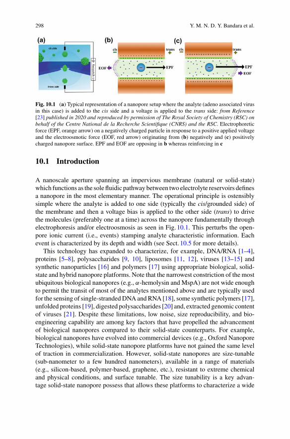
298 Y. M. N. D. Y. Bandara et al.
Fig. 10.1 (a) Typical representation of a nanopore setup where the analyte (adeno associated virusin this case) is added to the cis side and a voltage is applied to the trans side: from Reference[23] published in 2020 and reproduced by permission of The Royal Society of Chemistry (RSC) onbehalf of the Centre National de la Recherche Scientifique (CNRS) and the RSC. Electrophoreticforce (EPF, orange arrow) on a negatively charged particle in response to a positive applied voltageand the electroosmotic force (EOF, red arrow) originating from (b) negatively and (c) positivelycharged nanopore surface. EPF and EOF are opposing in b whereas reinforcing in c
10.1 Introduction
A nanoscale aperture spanning an impervious membrane (natural or solid-state)which functions as the sole fluidic pathway between two electrolyte reservoirs definesa nanopore in the most elementary manner. The operational principle is ostensiblysimple where the analyte is added to one side (typically the cis/grounded side) ofthe membrane and then a voltage bias is applied to the other side (trans) to drivethe molecules (preferably one at a time) across the nanopore fundamentally throughelectrophoresis and/or electroosmosis as seen in Fig. 10.1. This perturbs the open-pore ionic current (i.e., events) stamping analyte characteristic information. Eachevent is characterized by its depth and width (see Sect. 10.5 for more details).
This technology has expanded to characterize, for example, DNA/RNA [1–4],proteins [5–8], polysaccharides [9, 10], liposomes [11, 12], viruses [13–15] andsynthetic nanoparticles [16] and polymers [17] using appropriate biological, solid-state and hybrid nanopore platforms. Note that the narrowest constriction of the mostubiquitous biological nanopores (e.g., α-hemolysin and MspA) are not wide enoughto permit the transit of most of the analytes mentioned above and are typically usedfor the sensing of single-strandedDNAandRNA [18], some synthetic polymers [17],unfolded proteins [19], digested polysaccharides [20] and, extracted genomic contentof viruses [21]. Despite these limitations, low noise, size reproducibility, and bio-engineering capability are among key factors that have propelled the advancementof biological nanopores compared to their solid-state counterparts. For example,biological nanopores have evolved into commercial devices (e.g., Oxford NanoporeTechnologies), while solid-state nanopore platforms have not gained the same levelof traction in commercialization. However, solid-state nanopores are size-tunable(sub-nanometer to a few hundred nanometers), available in a range of materials(e.g., silicon-based, polymer-based, graphene, etc.), resistant to extreme chemicaland physical conditions, and surface tunable. The size tunability is a key advan-tage solid-state nanopore possess that allows these platforms to characterize a wide
10 Experimental Approaches to Solid-State Nanopores 299
range of proteins, polysaccharides, liposomes and, viruses absent any digestion ordenaturing steps. Until 2014, solid-state nanopores were primarily fabricated usingtransmission electronmicroscope (TEM), focused ion beam (FIB), helium ionmicro-scope (HIM), and track etching methods. Most of these methods require access to anelectron/ionmicroscope facility and the throughput of nanopore fabrication is limitedby the capabilities of the electron/ion microscope and/or user. The nanopore tech-nology has seen widespread adoption and democratization with the introduction ofthe controlled dielectric breakdown (CDB) method which is low-cost, time-efficient,and solution-based [22]. Conveniently, there are now companies that sell membranechips (both intact membranes and membranes with nanopores), which eliminates thefabrication requirement froma research-group point-of-view.The fabricationmethodis inextricably linked with the surface chemistry of the nanopore and thus on the finalsensing throughput, noise, and, signal-to-noise ratio (SNR) of the device. Sensingthroughput, noise, SNR, analyte transport mechanismwould also depend on the solu-tion chemistry and electronic settings as well. This chapter is dedicated to solid-statenanopores with insight into transport phenomena, experiment planning, measure-ments, models, characterization, noise and, improvements in somewhat detail.
10.2 Transport Phenomena in Nanopores
10.2.1 Analyte Capture
The translocation of an analyte through a nanopore takes place fundamentally inthree steps. When an electric field is applied, an analyte (i) undergoes free diffusionfrom the bulk to the capture zone, (ii) changes its transport mechanism from diffusiveto drift-dominated as it gets funneled to the pore entrance in response to the appliedvoltage, and (iii) translocates through the pore provided applied voltage is sufficientto overcome the entropic penalty (in case of longer coiled biopolymers such as DNA)and/or electrostatic barriers. The first step is characterized by free diffusion of theanalyte that is initiated far away from the pore. Nanopore experiments typicallyinvolve sub-10 nM concentrations (and sometimes in pM and fM range) of analytes.Assuming negligible intramolecular interactions, the capture rate, Rc (molecules/s)can be expressed as:
Rc = J/C (10.2.1)
where J is the analyte flux rate (1/m2s) and C is the analyte concentration(molecules/m3). At the vicinity of the pore, however, the analyte must overcomeentropic (in the case of long-chain polymers such asDNA) aswell as electrostatic bar-riers to finally translocate through the pore (rather than colliding with the pore open-ing). Therefore, analyte transport can be explained by two limiting cases: diffusion-limited, and barrier-limited regimes. Diffusion-limited transport could be explained
300 Y. M. N. D. Y. Bandara et al.
using classical Smoluchowski theory, whereas barrier-limited transport could be elu-cidated with classical Kramer theory [24].
a Diffusion-limited regime:This is typically applicable to the capture of long-chainmolecules (e.g., DNA with >∼ 104 base pairs [24]) under a high electric field.If this is the limiting case, a linear increase of the capture rate with the appliedvoltage is seen. The capture rate in this regime (Rdiff
c ) can be obtained from theSmoluchowski’s rate equation; J = 2πDr∗C . Therefore,
Rdiffc = 2πDr∗ (10.2.2)
where D is the analyte diffusion coefficient and r∗ is the capture radius—definedin such a way that free diffusion of the analyte takes place beyond the captureradius in the bulk solution while the analyte is captured irreversibly within thecapture radius, and drift-dominated motion prevails. Grosberg et al. obtained thefollowing expression for r∗[26]:
r∗ = r2μ
2lDV (10.2.3)
Equations (10.2.2) and (10.2.3) induce
Rdiffc = πr2μ
lV (10.2.4)
where, V ,μ, l and r are the applied voltage, electrophoretic mobility, pore length,and pore radius, respectively.
b Barrier-limited regime: The barrier-limited regime is typically for shortmolecules (e.g., proteins, short DNA strands) under weak electric fields. In thisregime, the capture rate (Rbar
c ) increases exponentially with the applied voltage.The exponential relationship could be understood from the fact that, as the voltageis increased, the barrier against the translocation decreases, leading to an expo-nential increase in the event frequency. Pelta et al. used the following Van’t HoffArrhenius formalism to describe the capture rate in this regime [27, 28]:
Rbarc = R0 exp (|V |/V0) (10.2.5)
where R0 is the zero-voltage capture rate given by R0 ∝ f ∗ exp (−U ∗/kBT ), kB isthe Boltzmann constant and T is the temperature. The activation energyU ∗(f ∗is afrequency factor) originates from entropic and electrostatic barriers and controlsR0. The barrier at the pore entrance dominates the capture rate and the height ofthis barrier decreases with increasing the applied voltage. The barrier reductionfactor due to the applied voltage is given by the ratio |V | /V0 = (zeV/kBT ),where z is the magnitude of the effective total number of elementary chargesof the analyte and e is the magnitude of the elementary charge. V0 represents
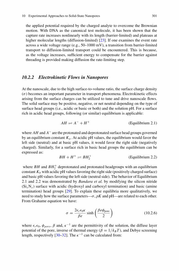
10 Experimental Approaches to Solid-State Nanopores 301
the applied potential required by the charged analyte to overcome the Brownianmotion. With DNA as the canonical test molecule, it has been shown that thecapture rate increases nonlinearly with its length (barrier-limited) and plateaus athigher molecular lengths (diffusion-limited) [23]. If one examines the event rateacross a wide voltage range (e.g., 50–1000 mV), a transition from barrier-limitedtransport to diffusion-limited transport could be encountered. This is because,as the voltage increases, sufficient energy to compensate for the barrier againstthreading is provided making diffusion the rate-limiting step.
10.2.2 Electrokinetic Flows in Nanopores
At the nanoscale, due to the high surface-to-volume ratio, the surface charge density(σ ) becomes an important parameter in transport phenomena. Electrokinetic effectsarising from the surface charges can be utilized to tune and drive nanoscale flows.The solid surface may be positive, negative, or net neutral depending on the type ofsurface head groups (i.e., acidic or basic or both) and the solution pH. For a surfacerich in acidic head groups, following (or similar) equilibrium is applicable:
AH � A− + H+ (Equilibrium 2.1)
where AH and A− are the protonated and deprotonated surface head groups governedby an equilibrium constant Ka . At acidic pH values, the equilibrium would favor theleft side (neutral) and at basic pH values, it would favor the right side (negativelycharged). Similarly, for a surface rich in basic head groups the equilibrium can beexpressed as:
BH + H+ � BH+2 (Equilibrium 2.2)
where BH and BH+2 deprotonated and protonated headgroups with an equilibrium
constant Kb with acidic pH values favoring the right side (positively charged surface)and basic pH values favoring the left side (neutral side). The behavior of Equilibrium2.1 and 2.2 was demonstrated by Bandara et al. by modifying the silicon nitride(SixNy) surface with acidic (hydroxyl and carboxyl termination) and basic (aminetermination) head groups [29]. To explain these equilibria more qualitatively, weneed to study how the surface parameters—σ , pK and pH—are related to each other.From Grahame equation we have:
σ = 2εrε0κ
βesinh
(βeφpore
2
)(10.2.6)
where εrε0, φpore, β and, κ−1 are the permittivity of the solution, the diffuse layerpotential of the pore, inverse of thermal energy (β = 1/kBT ), and Debye screeninglength, respectively [30–32]. The κ−1 can be calculated from:
302 Y. M. N. D. Y. Bandara et al.
κ =√
βe2nM X
εrε0(10.2.7)
where nM X is the numerical concentration of the electrolyte M X . Due to the pres-ence of surface charge, oppositely charged ions or counterions from the solutionare attracted towards the surface while similarly charged ions are repelled from it.The layer of counterions immediately next to the wall is immobilized due to thestrong electrostatic forces. This layer is known as the Stern layer and its thicknessis typically one ionic diameter [33, 34]. The loosely bound mobile layer of counte-rions, immediately next to the Stern layer, is known as the diffuse layer. The Sternlayer and the diffuse layer together constitute the electrical double layer (EDL).The electric potential at the shear plane between the Stern layer and the diffuselayer is called the zeta potential (ζ ) [35]. The thickness of the EDL can be esti-mated by the Debye length. For a negatively charged surface, φpore can be writtenas [36]:
φpore = 1
βeln
[ −σ
e + σ
]− ln(10)
βe(pH − pKa) − σ
Cs(10.2.8)
where is the number of surface chargeable groups and Cs is Stern layer capaci-tance. Equations (10.2.6) and (10.2.8) must be solved self consistently to solve forσ . Circumventing this requirement, another approximation for σ has been developed[28, 36]:
|σ | ∼= Ceff
βeW
(βe
Ceffexp ((pH − pKa)ln(10) + ln(e))
)(10.2.9)
where Ceff , and W are effective Stern layer capacitance and Lambert W functionrespectively. For a surface rich in basic head groups, the (pH − pKa) in Eq. (10.2.9)has to be substituted with (−pH + pKb). Given the complexity associated with thesurface chemistry of non-stoichiometric SixNy—the material most commonly usedin nanopores—it is somewhat customary to explain its nature using silanol (Si-OH)and Si-NH2 models:
Si − OH (σ = 0) � Si − O−(σ < 0) + H+ (Equilibrium 2.3)
Si − NH2(σ = 0) + H+ � Si − NH+2 (σ > 0) (Equilibrium 2.4)
Natively, SixNy would have both these chemistries. Therefore, like amino acids, itwould have an isoelectric point (pI) and when pI=pH, it would be net-neutral (usu-ally at pH ∼ 4.1–4.3 [29, 37, 38]). The native surface chemistry can be changedduring fabrication as demonstrated by our recent work with chemically-tuned con-trolled dielectric breakdown (CT-CDB) through SixNy membranes [36], where thesurface chemistry of the resulting nanopores resembled acid-rich head groups rather
10 Experimental Approaches to Solid-State Nanopores 303
than being natively amphiphilic [36]. Consequently, σ can also be tuned throughpost-fabrication modifications [29, 39, 40].
10.2.2.1 Electroosmosis (EO)
Since hydrodynamic resistance is extremely high in nano-sized conduits, a macro-scopic gradient (for example, an external electric field) is required for the generationof flow. Under the influence of an external electric field, the charged ions or parti-cles in the diffuse layer are electrophoretically driven along the electric field [41].Due to viscous interactions, the ions drag the liquid, producing an effective slipvelocity. This movement of the bulk solution against the charged surface is calledEO. The thickness of the EDL plays a significant role in the electroosmotic force(EOF). This thickness is primarily dependent on the concentration of the electrolyteused. Thicker EDL results from lower electrolyte concentrations (Eq. (10.2.7)). Forsmaller nanopores and/or at low electrolyte concentrations, the thicker EDL couldoverlap and prevent the formation of bulk electrolyte at the pore center [42]. Theconditions in typical nanopore experiments produce thinner EDLs so that the ionconcentration far from the pore wall can be approximated to be equal to that of thebulk solution.
TheHelmholtz-Smoluchowski equation gives themagnitude of the electroosmoticmobility for an infinitesimally thin EDL [43]:
μeo = εrε0ζw
η(10.2.10)
where η is the dynamic viscosity of the electrolyte solution and ζw is the zeta poten-tial of the pore wall. The electroosmotic migration velocity, given by veo = μeoE ,can therefore be expressed as:
veo = εrε0ζw
ηE (10.2.11)
where E is the externally applied electric field (V/ l). Although EO is not the mostcommon dominant transport mechanism in solid-state nanopore experiments, thereare some notable examples of analyte classes where EO dominates, and we notethese here briefly:
a DNA: Yang et al. demonstrated the transport of single nucleotides through a∼1.8nm diameter SixNy pore by EO dominant transport [44]. In most cases,EOF is used to slow down transport by opposing the electrophoretic force (EPF)[24] and tune the conformation of the translocating molecule [45].
b Proteins: Zhang et al. showed that streptavidin can be transported throughnanopores using EO with a diameter slightly larger than their length, producingcapture rates ∼17× greater compared to a previous study [46]. Huang et al. used
304 Y. M. N. D. Y. Bandara et al.
FragaceatoxinC(FraC) nanopores to discriminate peptide and protein biomarkers[47]. EO was used as the transport mechanism of unfolded polypeptides.
c Polysaccharides: Karawdeniya et al. demonstrated the EO dominant transportof alginate through SixNy nanopores. Not all polysaccharides are transportedthrough EO as evident by their work [9]. Later we showed that maltodextrin—acharge-neutral polysaccharide—also translocates through EO using SixNy
nanopores fabricated through CT-CDB method with event frequency increasingwith increasing solution pH (attributed to the increase in σ with increasing pH,which leads to an increase in EOF) [37].
10.2.2.2 Electrophoresis (EP)
Electrophoresis is themigration of charged particles in a stationary conducting liquidunder the influence of an applied electric field. Electrophoretic transport of macro-molecules is the most common mode of analyte transport in nanopore experimentsand has been observed in both biological and synthetic nanopores. A charged analyteplaced in an electrolyte will be screened by an EDL composed of counterions. Whenan electric field is applied, the oppositely chargedmobile counterions in the EDLwillalso experience an electrophoretic force. However, these counterions will experiencea force in the opposite direction to that experienced by the charged analyte (Fbare).The resulting hydrodynamic drag on the analyte (Fdrag) counters the electrical forceand slows down the translocation process [48, 49]. The net EPF acting on the analytedriving its translocation is, therefore, given by Felec = Fbare -Fdrag. Schoch et al. reportthat the thickness of the EDL influences the electrophoretic mobility of the analyte.Henry’s formulation for electrophoretic motion is given by [50]:
μep = 2εrε0ζp3η
f (κa) (10.2.12)
where a is the radius of the analyte, ζp is the zeta potetial of the particle/analyteand f (κa) is known as Henry’s function [30], f (κa) depends on the thickness of theEDL. For a thick EDL where κa � 1, f (κa) can be approximated as 1, leading tothe Hückel-Onsager limit:
μep = 2εrε0ζp3η
(10.2.13)
In this case, the Stokes drag counters the Coulomb forces and analyte motion iscontrolled by the resultant of these two forces. Thin EDLs (κa � 1), f (κa) → 3
2 ,lead to the Helmholtz-Smoluchowski limit:
μep = εrε0ζp
η(10.2.14)
Thin EDLs are commonly encountered in nanopore experiments, which justifies theuse of Eq. (10.2.14) in most cases.
10 Experimental Approaches to Solid-State Nanopores 305
The translocation of an analyte through a nanopore is eventually dependent onthe interplay between the EPF and the EOF. Consider the translocation of a DNAmolecule through a nanopore drilled through a SixNy membrane whose surfacecharge is negative at the physiological pH. When a positive bias voltage is appliedacross the nanopore, the negatively charged DNA molecule will experience an EPFpulling it towards the positive electrode. At the same time, the positive counterions inthe EDL screening the pore wall will be repelled away from the positive electrode. Asa result, the EOF will counter the EPF, slowing down DNA transport. If, on the otherhand, the nanopore wall is positively charged, the EO flow of the negatively chargedcounterionswill reinforce theEPF acting on themolecule. The translocation directionand speed are determined by themagnitude of the EOF and EPF, which are dependenton the applied voltage, molecule charge, and the surface charge of the pore walls. Insome instances, translocation of an analyte can be observed at both voltage polarities.For example, Saharia et al. [6] and Rant et al. [51] showed protein translocations atpH∼ 4 at both voltage polarities and attributed this phenomenon to simple diffusion.The event frequency in such cases is generally lower than those due to EP or EO.
10.3 Planning a Nanopore Experiment
Before proceeding to a nanopore experiment, one has to be mindful of the chem-ical (e.g. electrolyte pH, electrolyte type and concentration), physical (e.g. tem-perature), electronic (e.g. applied voltage, low-pass setting, acquisition frequency)and membrane (e.g. type, fabrication method, thickness and pore diameter) param-eters/properties as they would ultimately govern translocation and open-pore char-acteristics. We discuss these here briefly to provide some insight into choosing theappropriate conditions for an experiment.
10.3.1 Chemical Conditions
10.3.1.1 pH
The pH is especially important as it governs the net charge of the analyte and thenanopore surface (see Equilibrium 2.1–2.4). The analyte could have a pKa, pKb orpI depending on its chemical nature.
a Proteins: They are amphiphilic and have a pI. Operating at pH values closer to thepI would render the net EPF imparted on themolecule to bemeager as themoleculewould be net-neutral at this pH. The native protein structure depends on the pH aswell. For example, holo-human serum transferrin protein—a glycoprotein with anaveragemolecularweight of∼80kDa [52],whichdelivers otherwise insoluble ironto cells via receptor-mediated endocytosis—has a pI of ∼ 5.2–5.6 and is nativelyfolded when pH > pI and natively unfolded when pH < pI . Proteins are also
306 Y. M. N. D. Y. Bandara et al.
susceptible to extreme pH values. Thus, before proceeding with any experiments,the pH conditions where proteins denature, or undergo conformational changesshould be found through a literature search.
b Polysaccharides: Although a pH of ∼7 would render SixNy fabricated throughCDB or TEM to be net negatively charged, CT-CDB fabricated SixNy poreswould be near-neutral. The consequences are evident through translocation ofmaltodextrin—acharge-neutral glycan translocating through theEOmechanism—where no translocationswere seen at pH∼ 7whenusingCT-CDBfabricatedSixNy
nanopores. However, when pH was increased to ∼9, events were observed as thesurface was now net-negative in charge, activating the EO mechanism. Thus, forcharge-neutral molecules, the pH must be tuned such that the nanopore is appro-priately charged to facilitate the transport through the EO mechanism.
c DNA: Considered as a gold standard in nanopore science, DNA is generallyregarded to have a pI ∼ 5 (the value depends on the sequence). Thus, operat-ing at pH values where EP is meager would render the capture rate impracticallylow. The capture rate of 1 kb ds-DNA in 4 M LiCl and at an applied voltage of200 mV in experiments with CT-CDB fabricated SixNy nanopores was found tobe <3 events/s for pH ∼ 5 and ∼6 whereas at pH ∼ 7 and ∼8, it was at least 9.5×greater [53].
d Pore Surface: Pores fabricated through SixNy using TEM and CDB are ampho-teric with a pI of ∼4.1–4.3 [29, 38], whereas those fabricated through CT-CDBresemble a surface rich in acid head groups with a pKa of ∼9.7 [37].
10.3.1.2 Electrolyte Chemistry
Generally, the chlorides of group IA cations are used in nanopore sensing. Group IIAcations such as Ca2+ andMg2+ are not desirable as they can lead to crosslinking ofbiopolymers and adhering them to the nanopore surface [54, 55]. The more ubiqui-tous electrolytes are LiCl and KCl (NaCl is also seldom used). LiCl is known to slowdown the translocation of DNA [31]. Although this would reduce the capture proba-bility, it would increase the dwell time of the DNA molecule. Tuning the dwell timeis important to be above the lowpass filter response (discussed later in this chapter).The choice of electrolyte, according to the Hofmeister series, would have a salting-in(chaotropic—destabilizing effects) or salting-out (kosmotropic—stabilizing effects)effects on protein solubility [56]. The work of Green et al. [57] and Medda et al.[58] provides more insight into the concentration ranges where these effects areactive, with the former work claiming Hofmeister series effects are prominent athigher salt concentrations (0.5–3.0 M) whereas the latter work showed that theseeffects can be present at physiological concentrations as well. Although DNA andpolysaccharide experiments are present across a range of electrolyte concentrations(up to 4 M KCl and LiCl), such high salt concentrations could denature proteins.However, it is not uncommon to see protein experiments done up to about 2 M saltconcentration [6, 7]. A high electrolyte concentration would essentially diminish thecontribution of EO to the overall transport mechanism. At lower concentrations, the
10 Experimental Approaches to Solid-State Nanopores 307
EO mechanism becomes active (Debye length increases inversely with electrolyteconcentration), which has been shown to reserve the resistive-pulse direction [31]and promote single file translocation of DNA [45].
10.3.2 Electronics
10.3.2.1 Applied Voltage
The applied voltage can govern the translocation speed, transport mechanism (e.g.,diffusion or barrier-limited [25, 59]), conformation (e.g., folded, unfolded [60])and, structural properties (e.g., electro-deformation [12, 13]) of the analyte. Ana-lyte translocation can occur only when the applied voltage is sufficient to overcomethe entropic penalty and/or the electrostatic barriers. If the applied voltage is notsufficient to overcome the energetic barriers, the analyte may simply collide with thepore entrance rather than penetrating it. Although the applied voltage would increasethe capture probability and accommodates sufficient energy to overcome energeticbarriers, it would increase the translocation speed as well. If the analyte is movingtoo fast it could completely go undetected or its signal metrics could be attenuatedby the electronic response time (i.e., rather than the actual metrics, what the userwould see is the response time of the electronics—discussed later in this chapter [61,62]). The magnitude of the applied voltage would also determine whether the trans-port is diffusion or barrier-limited as discussed in Sect. 10.2.1. Unlike DNA, whichcan withstand an appreciable voltage range, proteins could undergo voltage-drivenunfolding [6, 26]. Above a certain voltage, the protein could be fully stretched ormayreach its limit of unfolding [27]. Although it is not uncommon to perform proteinexperiments at high voltages, they could force the protein to unfold and informationon the native state may not be achievable. The applied voltage also deforms soft par-ticles which depend on, for example, the particle membrane mechanical propertiesand on cargo content [12, 13, 23, 63]. Voltage-induced deformation of viruses wereshown to depend on virus maturity [13] and cargo content [23], both of which areof clinical relevance. Thus, voltage should be carefully chosen to inhibit or promotedeformation depending on the study.
10.3.2.2 Lowpass Filter Setting
Although this filter removes high-frequency noise features from the measurement,if not used properly, it could also attenuate the signal and a distorted picture oftranslocation characteristics may arise. The rise time (Tr ) of the lowpass filter isgiven by [61, 64]:
Tr = 0.3321/fc (10.3.1)
308 Y. M. N. D. Y. Bandara et al.
where fc is the cutoff frequency of the filter. Dwell times< 2Tr would be attenuated—theminimum falling edge to overcome the filter response is Tr and similarly, themin-imum rising edgemust be Tr as well. Thus, the lowpass filter requires 2Tr of the eventdwell time to respond properly. If the event is shorter than 2Tr , the recording wouldbe limited by the lowpass filter response and the data would correlate to the filterresponse rather than to the actual transit time. Several methods have been proposedto correct the dwell time in such instances including, for example, the integratedarea [61], adaptive time series [65], falling-edge [60], and full width half maximum(FWHM) methods [62]. One option to overcome such attenuation is to opt for ahigher lowpass filter setting with the caveat of higher background noise. Recently,complementary metal-oxide-semiconductor (CMOS) integrated nanopore platformshave been used to reach MHz level bandwidths due to the low parasitic capacitancesuch designs possess [66]. With a 1MHz lowpass filter, the 2Tr would theoreticallybe ∼0.6 µs. Another option is to slow down the translocation such that dwell timesbecome > 2Tr (see Sect. 10.7.1 for more details). Unfortunately, increased dwelltimes could negatively impact the event frequency and a balance should be achievedbetween throughput and the lowpass filter setting. If the Axopatch 200A (Molecu-lar Devices, LLC) is used, the two most common settings are the 10 and 50 kHzwhereas, in the case of the Axopatch 200B, they are 10 and 100 kHz. The samplingrate (discussed below) should also be sufficient for the filter setting. If no useful/extrainformation is gained by operating at 50 or 100 kHz compared to the 10 kHz lowpasssetting, it (10 kHz) is typically preferred as this settingwould have a lower r.m.s. (rootmean square) open-pore noise compared to the highest lowpass setting. Additionally,for current-voltage (I-V) curves, the 1 kHz low pass setting is more than adequate.
10.3.2.3 Acquisition/Sampling Frequency
This depends on whether the data is analyzed in the frequency domain (e.g. noiseanalysis) or in the time domain (current traces). For the former, twice the bandwidthis acceptable provided the anti-aliasing filter is ideal. Since ideal anti-aliasing filtersare somewhat theoretical, it is typical to sample∼2.5× the bandwidth. Time-domainanalysis requires ideal anti-aliasing and reconstruction filters. For such, 5× the band-width is typical, whereas 10× the bandwidth is considered optimal. For example, a10 kHz lowpass filtering may require 25 kHz sampling in the frequency domain and50–100 kHz sampling in the time domain. Thus, high filter settings require highersampling rates. Therefore, the digitizer must be able to cope with the filter settingof the amplifier for the proper (re-)construction of the analog signal from digitizedsamples, without distortion.
10 Experimental Approaches to Solid-State Nanopores 309
10.3.3 Membrane Properties
10.3.3.1 Membrane Thickness
The ubiquitous membrane architectures are 2D, silicon-based, high-κ dielectric, andpolymer-based. The adoption of each type depends on the application. For example,sequencing is best suited with ultra-thin membranes (i.e., 2D material) whereas vol-ume estimation is better suited with relatively thick membranes. Thicker membranesoffer low capture rates while also increasing the risk of (irreversible) analyte sticking.Therefore, depending on the analyte and the application of interest, the appropriatethickness should be chosen. The pore fabrication would also depend on the mem-brane type and thickness. For example, CDB is more suited for l < 50 nm (although,30nm could ideally be an upper limit based on our experience) with fabrication timeincreasing with increasing l. Thus, choosing a thin enough membrane could savetime in fabrication. The controlled breakdown is also used in 2D materials such asgraphene and MoS2 [67, 68]. However, the more conventional way to make poresthrough 2D material is by using a TEM, which requires expert user input.
10.3.3.2 Membrane Type
The more commonly used membrane types include:
a Silicon-based: e.g. low-stress SixNy and silicon oxide (SiO2). SixNy membranesare typically deposited on Si supports using LPCVD, PECVD, or PVD. Althoughthe ubiquitous material of choice, this architecture suffers somewhat from highdielectric and 1/f noise. Consequently,SixNy membranes fabricated with a SiO2
underlayer (between SixNy and the Si support) have lower capacitance noise com-pared to SiO2-free conventional ones [66] (see Sect. 10.6 for more information onnoise).
b 2D material: e.g. Graphene, MoS2, hexagonal boron nitride (h-BN). These areusually transferred on to silicon-based substrates. Although these materials carrythe promise for next-generation solid-state nanopore-based sequencing, they sufferfrom high (DNA) transport velocity, pinhole formation and membrane stabilityissues.
c High-κ dielectric material: e.g. HfO2 [69], Al2O3 [68, 70], Al2O3 stacked withgraphene [69, 71]. Although not commonly used, these are typically known forlow-noise and enhanced mechanical properties.
d Polymer-based:Typical examples include poly-ethylene terephthalate (PET) [70]and, polycarbonate (PC) [71]. Thickness is usually in the micron scale. Pore fab-rication is done by etching the tracks created by bombarding the membrane withheavy ions, where fluence of the ion source must be controlled to control the poredensity. Single swift heavy ion sources enable the fabrication of single pores, e.g.GSI (Darmstadt, Germany) [70].
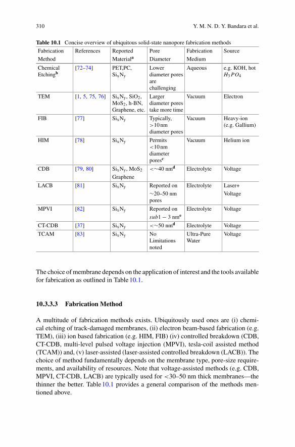
310 Y. M. N. D. Y. Bandara et al.
Table 10.1 Concise overview of ubiquitous solid-state nanopore fabrication methods
Fabrication References Reported Pore Fabrication Source
Method Materiala Diameter Medium
ChemicalEtchingb
[72–74] PET,PC,SixNy
Lowerdiameter poresarechallenging
Aqueous e.g. KOH, hotH3PO4
TEM [1, 5, 75, 76] SixNy, SiO2,MoS2, h-BN,Graphene, etc.
Largerdiameter porestake more time
Vacuum Electron
FIB [77] SixNy Typically,>10nmdiameter pores
Vacuum Heavy-ion(e.g. Gallium)
HIM [78] SixNy Permits<10nmdiameterporesc
Vacuum Helium ion
CDB [79, 80] SixNy, MoS2 <∼40 nmd Electrolyte Voltage
Graphene
LACB [81] SixNy Reported on Electrolyte Laser+
∼20–50 nmpores
Voltage
MPVI [82] SixNy Reported on Electrolyte Voltage
sub1 − 3 nme
CT-CDB [37] SixNy <∼50 nmd Electrolyte Voltage
TCAM [83] SixNy NoLimitationsnoted
Ultra-PureWater
Voltage
The choice ofmembrane depends on the application of interest and the tools availablefor fabrication as outlined in Table10.1.
10.3.3.3 Fabrication Method
A multitude of fabrication methods exists. Ubiquitously used ones are (i) chemi-cal etching of track-damaged membranes, (ii) electron beam-based fabrication (e.g.TEM), (iii) ion based fabrication (e.g. HIM, FIB) (iv) controlled breakdown (CDB,CT-CDB, multi-level pulsed voltage injection (MPVI), tesla-coil assisted method(TCAM)) and, (v) laser-assisted (laser-assisted controlled breakdown (LACB)). Thechoice of method fundamentally depends on the membrane type, pore-size require-ments, and availability of resources. Note that voltage-assisted methods (e.g. CDB,MPVI, CT-CDB, LACB) are typically used for <30–50 nm thick membranes—thethinner the better. Table10.1 provides a general comparison of the methods men-tioned above.
10 Experimental Approaches to Solid-State Nanopores 311
a: Only the more commonly reported materials are included. There could be otherexamples.b: The number of pores depends on the fluence of the ion source and window size.c:Most ion-beam methods are not conducive for <10 nm diameter pore fabricationand HIM permits such and even the coveted <5 nm regime with SNR comparableto TEM [84].d: Not recommended to go beyond ∼30 nm.e: Multiple pore formation if not optimized properly [85]
The table above is a general guide that can be used to determine the appropriatemethod for pore fabrication depending on themembrane properties and targeted poreproperties.
10.3.3.4 Pore Diameter
Fine control is needed to allow the entrance of the molecule, minimize stickingto the nanopore surface, maintain an appreciable capture rate and maximize thesignal to noise ratio (SNR). For example, if the pore diameter is too large SNR willbe low and without adequate confinement. In that case, molecules may transportballistically without been detected. In contrast, if the pore diameter is too smallanalytes may collide with the pore opening rather than translocate, clogging maybecome prominent and the capture rate would be too low to attain practically usefulthroughput rates.
10.4 Nanopore Characterization
After fabricating a pore, it is important to characterize it. This short section is intendedto provide some insight into pertinent pore characterization steps:
a Size estimationb Shape characterizationc Surface characterizationd Noise characterization (see Sect. 10.6)e Analyte responsiveness/sensitivityf Pore quality and resilience (e.g., sticking probability, rectification, open-pore cur-rent stability)
Note that, other than (a), the rest are generally known for a givenmaterial, fabricationmethod, electrolyte chemistry, experimental conditions (e.g. applied voltage, lowpassfiltering), and analyte. However, properties such as noise, rectification, and open-porestability are important parameters to check for each fabricated pore.
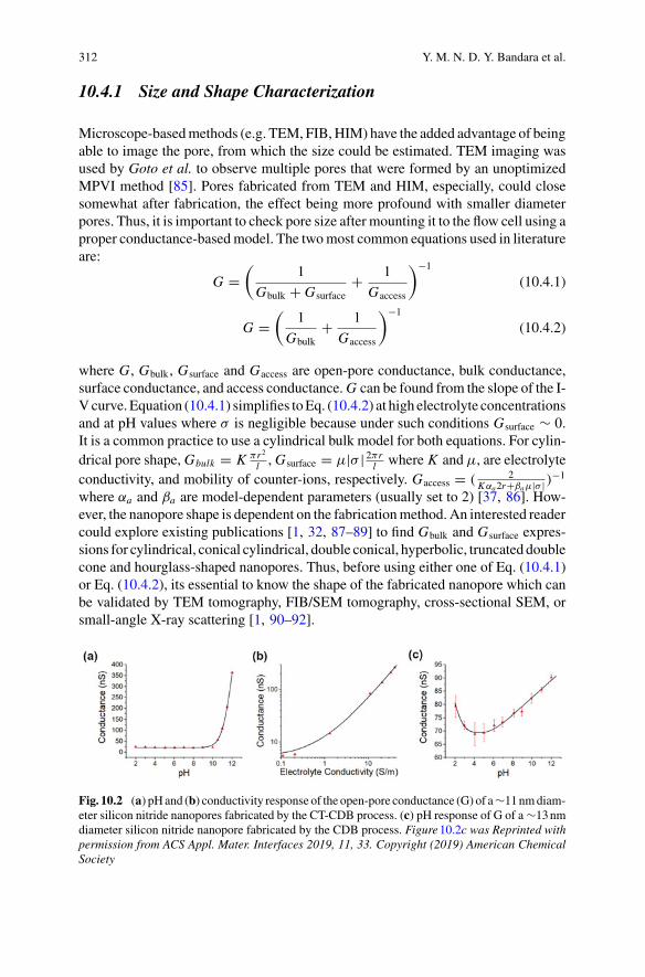
312 Y. M. N. D. Y. Bandara et al.
10.4.1 Size and Shape Characterization
Microscope-basedmethods (e.g. TEM, FIB,HIM) have the added advantage of beingable to image the pore, from which the size could be estimated. TEM imaging wasused by Goto et al. to observe multiple pores that were formed by an unoptimizedMPVI method [85]. Pores fabricated from TEM and HIM, especially, could closesomewhat after fabrication, the effect being more profound with smaller diameterpores. Thus, it is important to check pore size after mounting it to the flow cell using aproper conductance-basedmodel. The twomost common equations used in literatureare:
G =(
1
Gbulk + Gsurface+ 1
Gaccess
)−1
(10.4.1)
G =(
1
Gbulk+ 1
Gaccess
)−1
(10.4.2)
where G, Gbulk, Gsurface and Gaccess are open-pore conductance, bulk conductance,surface conductance, and access conductance.G can be found from the slope of the I-Vcurve. Equation (10.4.1) simplifies toEq. (10.4.2) at high electrolyte concentrationsand at pH values where σ is negligible because under such conditions Gsurface ∼ 0.It is a common practice to use a cylindrical bulk model for both equations. For cylin-drical pore shape, Gbulk = K πr2
l , Gsurface = μ|σ | 2πrl where K andμ, are electrolyteconductivity, and mobility of counter-ions, respectively. Gaccess = ( 2
Kαa2r+βaμ|σ | )−1
where αa and βa are model-dependent parameters (usually set to 2) [37, 86]. How-ever, the nanopore shape is dependent on the fabricationmethod. An interested readercould explore existing publications [1, 32, 87–89] to find Gbulk and Gsurface expres-sions for cylindrical, conical cylindrical, double conical, hyperbolic, truncated doublecone and hourglass-shaped nanopores. Thus, before using either one of Eq. (10.4.1)or Eq. (10.4.2), its essential to know the shape of the fabricated nanopore which canbe validated by TEM tomography, FIB/SEM tomography, cross-sectional SEM, orsmall-angle X-ray scattering [1, 90–92].
Fig. 10.2 (a) pHand (b) conductivity response of the open-pore conductance (G) of a∼11nmdiam-eter silicon nitride nanopores fabricated by the CT-CDB process. (c) pH response of G of a ∼13nmdiameter silicon nitride nanopore fabricated by the CDB process. Figure10.2c was Reprinted withpermission from ACS Appl. Mater. Interfaces 2019, 11, 33. Copyright (2019) American ChemicalSociety
10 Experimental Approaches to Solid-State Nanopores 313
10.4.2 Surface Characterization
Both σ and ζw can be calculated from streaming potential measurements as outlinedin [93]. These parameters are inextricably linked with transient interactions, EOF,capture rate, etc. One convenient way to estimate σ is to survey the pH dependentopen-pore conductance (Fig. 10.2a), and then fit the data with Eq. (10.2.9). Given theapproximations associated with Eq. (10.2.9), one could also plot electrolyte conduc-tivity with open-pore conductance and fit the data with Eq. (10.4.1) [94] (Fig. 10.2).Small Angle X-ray Scattering (SAXS) has been recently used to characterize axialand radial ion track etch rates with unprecedented precision. This study showed astrong correlation between the ion energy and the morphology of the etched channelsin thin films of amorphous SiO2 [95].
10.4.3 Analyte Responsiveness/Sensitivity (�anal yte)
DNA is the gold standard to gauge analyte responsiveness given its uniform charge,known length, and ruggedness.One canmeasure the rate of translocation as a functionof (i) pore diameter, (ii) pH, (iii) electrolyte type and concentration, (iv) appliedvoltage, and then compare the results with a comparative (or competitive) fabricationmethod. The most common methods for event-rate quantification include (i) slopeof cumulative events versus experiment time [25], (ii) survival probability method[25], (iii) exponential fit to arrival time distribution [96], (iv) the average numberof events across the experiment time and, (v) average of the inter-translocation timeacross the experimental time. These methods could suffer from inter- and intra-porevariations and could be improved through controlled counting [25]. The slope of acalibration curve constructed with the desired event counting method against analyteconcentration would yield the sensitivity of the pore to the analyte (�analyte). Whenthe CT-CDB fabrication method was developed, its performance was gauged againstthe conventional CDB process using double-stranded DNA (dsDNA) fromwhich wefound Six Ny nanopores fabricated through the CT-CDB process were ∼6.5× moresensitive to dsDNA compared to their CDB counterpart [37].
10.4.4 Pore Quality and Resilience
a Ionic Current Rectification (RICR): Although the I-V curve of some pores areinherently asymmetric due to geometric and surface properties, it is desirable tohave RICR ∼1 in cylindrical pores.Wewould define RICR =G+/G-, where G+ andG- are the slope of the I-V curve at positive and negative voltage regimes. We haveobserved, pores (CDB, CT-CDB, and TEM fabricated SixNy) that significantlydeviate from RICR ∼1 are noisy, less responsive to analytes, and prone to clogging.
b Sticking Probability (Sp): Transient perturbations due to analyte sticking on thenanoporewalls that aremuch longer than regular translocationswould change both
314 Y. M. N. D. Y. Bandara et al.
chemical and physical properties with the potential to render the pore futile forfurther experiments. An intervention may be necessary (e.g., zapping, electrolyteexchange) unless sticking is self-corrected. A lower Sp and higher open-porestability are preferred.
c Open-Pore Current Stability: One could measure this parameter by fitting acurrent trace with a function in the form I0 = It=0 + β1t , where It=0, β1 and t areinitial open-pore current, slope-factor and time, respectively. For an ultra-stablepore with no current drifts, β1 = 0.
d Open-Pore Lifetime (topen):This is the time duration during which a pore remainsopen before clogging irreversibly with the analyte, or undergoes a drastic changein current due to enlargement or pore closure. Higher topen values are desirable.
10.5 Features Defining a Resistive Pulse
Although an event looks trivial, determining its bounds and depth is not alwayssimple. A brief account of the commonmethods used for calculation of translocationtime (td ) and current drop (�IB) are provided here. Note that most methods arecalibrated by feeding pulses (using a pulse generator) of known height (huser) andwidth (wuser) to the amplifier (i.e., the nanopore is replaced by a pulse-generator).That way the ideal �IB and td would be known and based on the readout of thesystem, correlations between �IB and huser and td and wuser could be developed tobetter estimate the event characteristics.
10.5.1 Translocation Time (td)
Since td is greatly affected by the rise-time of the lowpass filter (especially whentd < 2Tr ), the common approaches to estimate td include (i) FWHM of the peak, (ii)two sides of the blockage (analogous to B1 and S2 points of Fig. 10.3c), (iii) modifiedstop point [61, 62], and (iv) fitting and algorithmic approaches [65]. A given eventwould have three key regions: a falling edge, a plateau region, and a rising edge.These can be prominently seen in events with td > 2Tr whereas in shorter events,the plateaued region can be absent, and the event would be represented solely by thefalling and rising edge responses of the filter. The finite rise time of the filter wouldaccount for most of the rising edge width, which leads to an overestimation of thetrue pulse width with approaches that take two sides of the blockage. The modifiedstop-point method circumvents this by taking the last local minima before the signalstarts to rise as the endpoint (Fig. 10.3c). The FWHM approach has been found tohave performance comparable to this approach. Thus, one could define the pulsewidth as the distance between the starting point of the falling edge and the beginningof the rising edge [60]. However, for such approaches, the event would need to reacha plateau and the stop point should not coincide with the falling edge [62]. Gu et al.used a second order-differential-based calibration (DBC) to estimate td [61]. In this

10 Experimental Approaches to Solid-State Nanopores 315
Fig. 10.3 a Current trace and b scatter plot of the log of translocation time versus change inconductance corresponding to 1 kb dsDNA translocating through a ∼3.4nm diameter pore (4 MLiCl, pH∼ 7,+200mV). cA single level event with td < 2Tr . B1 and S2 correspond to the start andendpoint that take two sides of the blockage and the S1 is the stop point corresponding to modifiedstop point methods. d Single level event with td > 2Tr , e folded-over event and f multi-level event;d–f were collected from a ∼12nm diameter pore. Red lines are fits made with a custom program
method, events were fitted with a fourth order Fourier series (although higher ordersare possible) as a smoothing step followed by the DBC method, where inflectionpoints at the two edges defined the primitive event boundaries before refining theend point by moving it to the local minima to account for the rising response of thefilter to prevent overestimation of the td .
10.5.2 Current Drop (�IB)
The local minima, or sometimes the mean current of the event, are most commonlyused as �IB . The former makes the method susceptible to sudden point-variationsand the latter could under-estimate event amplitudes, especially those with no appre-ciable plateau. Consequently, like td characterization, some key approaches existin literature to define �IB . One approach uses a python-based MOSAIC softwarewith Adaptive Time-Series Analysis (ADEPT) [65]. For attenuate-prone events, thismethod fits data to an electric circuit model to estimate the current drop. During theDBC implementation by Gu et al., they have noted that the area of the event (e.g.,one can calculate this by the trapz function of MATLAB) is seldom affected by thefilter response [61]. If this is the case, after estimation of the event area and td byDBC, one can back-calculate �IB (i.e., �IB × td = event area). Pedone et al. useda method based on the slope of the falling edge to estimate the height of truncated
316 Y. M. N. D. Y. Bandara et al.
events where they recovered pulse heights of events as short as ∼30 µs with 10 kHzlowpass filtering (2Tr was ∼66 µs): huser = mxevent where xevent and m are pulseslope and the correlation factor with m been appreciably constant for td >∼ 30 µs.The relative constancy of m offers the capability to correct �IB without having toworry much about td . One caveat of this method is the somewhat high standarddeviation of the histograms corresponding to reconstructed signal height.
10.5.3 Multi-Level Events
This is where things start to get somewhat tricky. For example, if the DNA translo-cates as a single-file it would produce a single-level event. However, DNA can also becaptured as symmetrically folded-over, partially folded, circular, and knotted (e.g.prime-L knot, Fused knot, prime-H knot, prime-L knot, factored knot) structures[97, 98]. Although circular and symmetrically folded-over conformations wouldproduce a single level (∼2× deeper than single-file) event structure, the rest wouldproduce stepwise and sharp drop event structures. Thus, a simple single-level anal-ysis could critically mask information that sub-events carry and undermine the finalanalysis. More notable multi-level event-analysis methods include CUSUM-basedmultilevel fitting [99–101], the MOSAIC algorithm [65] and hidden Markov modelapproaches [102, 103]. The OpenNanopore application (CUSUM-based) developedby the Radenovic group [99] has, to some extent, paved the way for a standardizedanalysis approach. Thus, one should develop or use an existing platform for eventanalysis that can detect and fit multi-level events. However, one should be cautiousof how a given software estimates �IB and td for reasons mentioned previously.
10.5.4 Event Analysis
Now that the experiment is done and the salient features are extracted, what is thenext step? In an ideal world, if we use one molecule type, one would optimisticallyexpect a single �IB and td . However, this is far from reality and we would see adistribution of �IB and td . This is because not every molecule translocates the sameway due to, for example, the spatial trajectory through the pore [104], analyte-analyteand/or analyte-surface interactions (e.g. adsorption, electrostatic, specific binding,chelation/cross-linking [105]), analyte conformation (e.g. voltage induced structuralchanges [6, 8], DNA knots [98]). The result is a scattered population for �IB and td .
10 Experimental Approaches to Solid-State Nanopores 317
10.5.5 Analysis of �IB
The first step is to histogram the data with a suitable bin size. For DNA, one wouldtypically see three peaks with the first corresponding to collisions, the second cor-responding to single-file translocations, and the third corresponding to folded-overtranslocations, among other possibilities discussed above that give deeper block-ages (see Supporting Information of [37] for a more detailed discussion). The his-togram can be fitted with a summation of Gaussian functions, each in the form ofAi exp(−(�G − μi )
2/s2i )where Ai ,μi and, si are the amplitude,mean, and standarddeviation of the i th population. While this could be done in MATLAB and other pro-grams, we have foundMathematica to be convenient for symbolic operations such asthis. For dsDNA, the division of μi for i = 3 by i = 2 would ideally be∼2: an inter-nal check to make sure that data is from DNA but not from contamination, or othersources. Let the radius of dsDNA be rdsDNA and the charge of dsDNA be QdsDNA.Assuming a cylindrical nanopore profile, the effective radius of the open-pore during
dsDNA confinement would be rwith DNA =√r20 − r2dsDNA. G can be evaluated using
Eq. (10.4.1). Then, one canwrite, change in conductance due to dsDNA translocation(�GdsDNA) as:
�GdsDNA = G − K
(1
πr2with DNAl + μ|σ |
K2πr0l + μ
Kqλ−DNA
l
+ 2
αa 2rwith DNA + βaμ|σ |K
)−1
(10.5.1)The rdsDNA and Q(dsDNA) can be approximated to ∼1.1 nm and ∼ − 0.96 nC/m.Then, the theoretical �G(dsDNA) can be calculated using Eq. (10.5.1). However, onemight find that the experimental and the theoretical values may differ because of,for example, variations in (i) l (typically ±1–±2), (ii) QdsDNA (can be changedby the electrolyte-DNA interactions among other possibilities) and (iii) rdsDNA (i.e.hydrated radius ranging from 1.1–1.3nm, [89, 106, 107]). Thus, one can use theextreme boundaries in each case and calculate a range for the theoretical �GdsDNA
to see whether the experimental value falls within that range. Disagreements mayindicate flaws in, for example, data collection, data analysis, or contamination.
10.5.6 Volume Exclusion Models for �IB
The formula widely used for spherical nanoparticles and globular proteins [5, 6, 108,109] is:
�IB = Kγ V�
(l + 1.6r)2Sr,d (10.5.2)
where γ , �, and Sr,d are shape factor, transiently excluded electrolyte volume andthe correction factor (typically assumed to be 1), respectively. It must be noted that
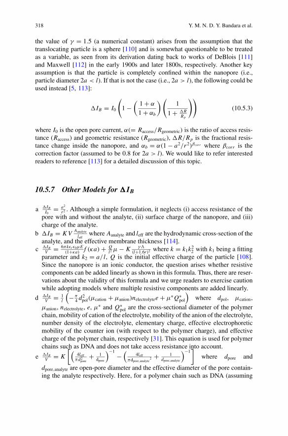
318 Y. M. N. D. Y. Bandara et al.
the value of γ = 1.5 (a numerical constant) arises from the assumption that thetranslocating particle is a sphere [110] and is somewhat questionable to be treatedas a variable, as seen from its derivation dating back to works of DeBlois [111]and Maxwell [112] in the early 1900s and later 1800s, respectively. Another keyassumption is that the particle is completely confined within the nanopore (i.e.,particle diameter 2a < l). If that is not the case (i.e., 2a > l), the following could beused instead [5, 113]:
�IB = I0
(1 −
(1 + α
1 + αb
)(1
1 + �RRp
))(10.5.3)
where I0 is the open pore current, α(= Raccess/Rgeometric) is the ratio of access resis-tance (Raccess) and geometric resistance (Rgeometric), �R/Rp is the fractional resis-tance change inside the nanopore, and αb = α(1 − a2/r2)βcorr where βcorr is thecorrection factor (assumed to be 0.8 for 2a > l). We would like to refer interestedreaders to reference [113] for a detailed discussion of this topic.
10.5.7 Other Models for �IB
a �IBI0
= a2
r2 . Although a simple formulation, it neglects (i) access resistance of thepore with and without the analyte, (ii) surface charge of the nanopore, and (iii)charge of the analyte.
b �IB = KV Aanalyte
leffwhere Aanalyte and leff are the hydrodynamic cross-section of the
analyte, and the effective membrane thickness [114].c �IB
V = 6πkεr ε0μE(1+κa)
f (κa) + Ql2 μ − K γ�
(l+1.6r)2 where k = k1k22 with k1 being a fittingparameter and k2 = a/ l, Q is the initial effective charge of the particle [108].Since the nanopore is an ionic conductor, the question arises whether resistivecomponents can be added linearly as shown in this formula. Thus, there are reser-vations about the validity of this formula and we urge readers to exercise cautionwhile adopting models where multiple resistive components are added linearly.
d �IBV = 1
l
(−π
4 d2pol(μcation + μanion)nelectrolytee + μ∗Q∗
pol
)where dpol, μcation,
μanion, nelectrolyte, e, μ∗ and Q∗pol are the cross-sectional diameter of the polymer
chain, mobility of cation of the electrolyte, mobility of the anion of the electrolyte,number density of the electrolyte, elementary charge, effective electrophoreticmobility of the counter ion (with respect to the polymer charge), and effectivecharge of the polymer chain, respectively [31]. This equation is used for polymerchains such as DNA and does not take access resistance into account.
e �IBV = K
[(4leff
πd2pore
+ 1dpore
)−1 −(
4leffπdpore,analyte2
+ 1dpore,analyte
)−1]
where dpore and
dpore,analyte are open-pore diameter and the effective diameter of the pore contain-ing the analyte respectively. Here, for a polymer chain such as DNA (assuming
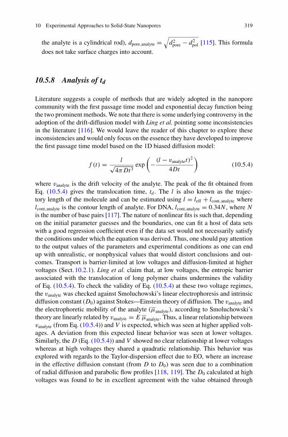
10 Experimental Approaches to Solid-State Nanopores 319
the analyte is a cylindrical rod), dpore,analyte =√d2pore − d2
pol [115]. This formula
does not take surface charges into account.
10.5.8 Analysis of td
Literature suggests a couple of methods that are widely adopted in the nanoporecommunity with the first passage time model and exponential decay function beingthe two prominent methods. We note that there is some underlying controversy in theadoption of the drift-diffusion model with Ling et al. pointing some inconsistenciesin the literature [116]. We would leave the reader of this chapter to explore theseinconsistencies and would only focus on the essence they have developed to improvethe first passage time model based on the 1D biased diffusion model:
f (t) = l√4πDt3
exp
(− (l − vanalytet)2
4Dt
)(10.5.4)
where vanalyte is the drift velocity of the analyte. The peak of the fit obtained fromEq. (10.5.4) gives the translocation time, td . The l is also known as the trajec-tory length of the molecule and can be estimated using l = leff + lcont,analyte wherelcont,analyte is the contour length of analyte. For DNA, lcont,analyte = 0.34N , where Nis the number of base pairs [117]. The nature of nonlinear fits is such that, dependingon the initial parameter guesses and the boundaries, one can fit a host of data setswith a good regression coefficient even if the data set would not necessarily satisfythe conditions under which the equation was derived. Thus, one should pay attentionto the output values of the parameters and experimental conditions as one can endup with unrealistic, or nonphysical values that would distort conclusions and out-comes. Transport is barrier-limited at low voltages and diffusion-limited at highervoltages (Sect. 10.2.1). Ling et al. claim that, at low voltages, the entropic barrierassociated with the translocation of long polymer chains undermines the validityof Eq. (10.5.4). To check the validity of Eq. (10.5.4) at these two voltage regimes,the vanalyte was checked against Smoluchowski’s linear electrophoresis and intrinsicdiffusion constant (D0) against Stokes—Einstein theory of diffusion. The vanalyte andthe electrophoretic mobility of the analyte (μanalyte), according to Smoluchowski’stheory are linearly related by vanalyte = E μanalyte. Thus, a linear relationship betweenvanalyte (from Eq. (10.5.4)) and V is expected, which was seen at higher applied volt-ages. A deviation from this expected linear behavior was seen at lower voltages.Similarly, the D (Eq. (10.5.4)) and V showed no clear relationship at lower voltageswhereas at high voltages they shared a quadratic relationship. This behavior wasexplored with regards to the Taylor-dispersion effect due to EO, where an increasein the effective diffusion constant (from D to D0) was seen due to a combinationof radial diffusion and parabolic flow profiles [118, 119]. The D0 calculated at highvoltages was found to be in excellent agreement with the value obtained through
320 Y. M. N. D. Y. Bandara et al.
the Stokes-Einstein theory of diffusion. Thus, we would urge readers to be carefulwhen implementing Eq.10.5.4 and check the validity of the resulting parameters bycarrying out a vigilant study equivalent to Ling et al.
10.5.9 Other Models for td
a td = CpηLm
qV where Cp, Lm and q are a proportionality constant, length of themolecule and the linear charge density of the molecule, respectively [114]. Sinceη depends on temperature, the above equation can be used to explain the behaviorof td with temperature as well.
b td = ηl2eff(V+C1)ζpεr ε0
where C1 is the integration constant [30]. This is applicable fordevices that satisfy κa � 1which allows the simplification of theHenry’s function(f (κa)) to derive the equation for td [30].
c f (t) = ∑ni=1 Ai exp (−t/τi ) where Ai and, τi , are the pre-exponential constant
and the time constant, respectively. In this method, the tail of the histogram cor-responding to translocation time is fitted [120].
d f (t) = exp (−t/2s2)((∑n
i=1 Ai exp (−t/τi ))δ)where s, and δ are standard devi-
ation and step function to truncate values below the mode threshold defined withrespect to the translocation time corresponding to the peak of the histogram of thetranslocation time distribution. The peak of this fit is then taken as the correspond-ing td of the population [29].
e f (t) = At exp
[−
(ln(t)−μt√
2s
)2]where all parameters bear the same definitions as
above with μt being the mean of the log translocation time distribution. In thiscase, the log of translocation time is fitted with this equation and the antilog of μt
is treated as the corresponding td of the population [29, 121].
10.5.10 Machine Learning
Although it is customary to characterize an event using a single td and �IB , this, insome sense, overlooks the underlying information of the event and potentially under-mines the prowess of the technology.With advancements in computing power, signalprocessing, and software development,we seemore andmore studies that incorporatemachine learning (ML) and deep neural networks (DNN).MLapproacheswould playa key role in sequencing efforts where accurate assignment of current modulationsto the correct nucleotide base is imperative for minimizing false positive and falsenegatives (and increase true negatives and true positives). Solid-state nanopores areyet to reach the sequencing advancement their biological counterparts have attained.ML approaches with solid-state nanopores are mostly seen with virus and bacte-rial studies where the following references would provide the interested reader with

10 Experimental Approaches to Solid-State Nanopores 321
an understanding of the advancement and progress in ML implementations in solid-state nanopore technology [122–125]. More recently,Karawdeniya et al. showed thepossibility of using DNN based on ResNet50 and solid-state nanopore-based elec-trodeformation to distinguish and discriminate between adeno associated viruses(AAVs) based on their cargo content (i.e., empty, ssDNA, and dsDNA) [23].
10.6 Noise in Solid-State Nanopores
The noise associated with nanopores can be segmented into four regimes based onorigin and frequency: (i) 1/ f noise (S1/f , typically <100 Hz), (ii) white noise (Sw,typically 0.1–10 kHz), (iii) dielectric noise (Sd ) and (iv) amplifier noise (Sa) [126].The noise is typically evaluated through a power spectral density (PSD) plot. Thenext question is, how can one construct a PSDplot? The open-pore current at a chosenoperational condition is acquired and a few seconds-long segment is chosen for Fast-Fourier-Transform, which converts the time-domain signal into a frequency-domainsignal. In-built functions such as fft of MATLAB can be easily used for this purpose.However, one must be mindful of the trace length and computational power availableas an unnecessarily long trace would cause the program to crash or take an extremelylong time to process. Typically, we try to keep the trace length <10 seconds longand evaluate multiple traces for statistical significance. We would discuss S1/f insomewhat detail and provide a concise overview of the other noise sources.
10.6.1 1/f Noise
Although the exact origin of this noise type is unclear, several mechanisms includingfabrication and characterization conditions [127, 128], and structural and chemicalproperties [115, 129, 130] have been proposed. In this section, we will focus on thenoise properties of pores fabricated using CT-CDB through SixNy membranes thatare nominally ∼12nm thick, as a model system. CT-CDB method is a compellingnew method for pore fabrication as it offers the typical advantages of CDB (e.g.,cost and time efficiency) in addition to other features (e.g. high temporal stability ofthe open-pore current, resilience against irreversible pore-clogging) that improvesand address legacy issues that were once acceptable work practices in nanoporetechnology. The low-frequency noise can be expressed as:
Slow,f = Sw + V 2
f R4total
[αbR2
access
Naccess+ αbR4
pore
R2cylNcyl
+ αsR4pore
R2surfaceNsurface
](10.6.1)
where Nx, Rx, αb and αs are the number of charge carriers corresponding to eachionic resistor component, resistive components of the nanopore sensor (e.g., surface,
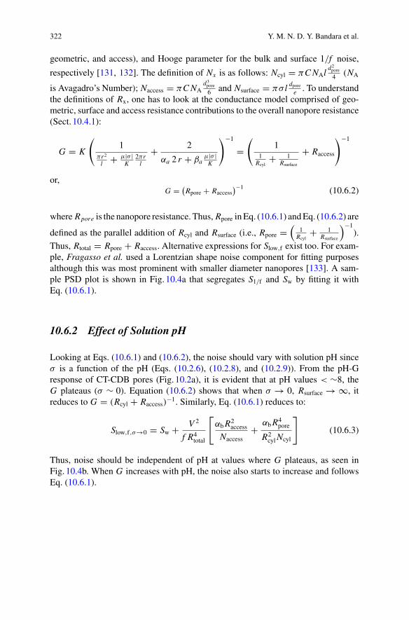
322 Y. M. N. D. Y. Bandara et al.
geometric, and access), and Hooge parameter for the bulk and surface 1/f noise,
respectively [131, 132]. The definition of Nx is as follows: Ncyl = πCNAld2pore
4 (NA
is Avagadro’s Number); Naccess = πCNAd3pore
6 and Nsurface = πσ l dporee . To understandthe definitions of Rx, one has to look at the conductance model comprised of geo-metric, surface and access resistance contributions to the overall nanopore resistance(Sect. 10.4.1):
G = K
(1
πr2l + μ|σ |
K2πrl
+ 2
αa 2 r + βaμ|σ |K
)−1
=(
11Rcyl
+ 1Rsurface
+ Raccess
)−1
or,G = (
Rpore + Raccess)−1 (10.6.2)
where Rpore is the nanopore resistance. Thus, Rpore inEq. (10.6.1) andEq. (10.6.2) are
defined as the parallel addition of Rcyl and Rsurface (i.e., Rpore =(
1Rcyl
+ 1Rsurface
)−1).
Thus, Rtotal = Rpore + Raccess. Alternative expressions for Slow,f exist too. For exam-ple, Fragasso et al. used a Lorentzian shape noise component for fitting purposesalthough this was most prominent with smaller diameter nanopores [133]. A sam-ple PSD plot is shown in Fig. 10.4a that segregates S1/f and Sw by fitting it withEq. (10.6.1).
10.6.2 Effect of Solution pH
Looking at Eqs. (10.6.1) and (10.6.2), the noise should vary with solution pH sinceσ is a function of the pH (Eqs. (10.2.6), (10.2.8), and (10.2.9)). From the pH-Gresponse of CT-CDB pores (Fig. 10.2a), it is evident that at pH values < ∼8, theG plateaus (σ ∼ 0). Equation (10.6.2) shows that when σ → 0, Rsurface → ∞, itreduces to G = (Rcyl + Raccess)
−1. Similarly, Eq. (10.6.1) reduces to:
Slow,f,σ→0 = Sw + V 2
f R4total
[αbR2
access
Naccess+ αbR4
pore
R2cylNcyl
](10.6.3)
Thus, noise should be independent of pH at values where G plateaus, as seen inFig. 10.4b. When G increases with pH, the noise also starts to increase and followsEq. (10.6.1).
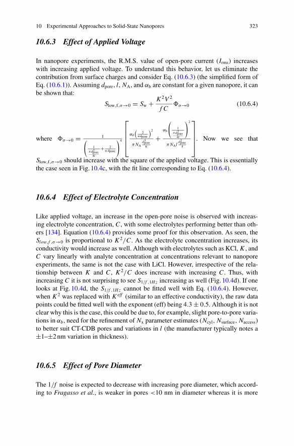
10 Experimental Approaches to Solid-State Nanopores 323
10.6.3 Effect of Applied Voltage
In nanopore experiments, the R.M.S. value of open-pore current (Irms) increaseswith increasing applied voltage. To understand this behavior, let us eliminate thecontribution from surface charges and consider Eq. (10.6.3) (the simplified form ofEq. (10.6.1)). Assuming dpore, l, NA, and αb are constant for a given nanopore, it canbe shown that:
Slow,f,σ→0 = Sw + K 2V 2
f C�σ→0 (10.6.4)
where �σ→0 = 1⎛⎝ 1
πd2pore4l
+ 2α dpore
⎞⎠
4
⎡⎢⎢⎢⎣
αb
(2
αdpore
)2
πNAd3pore6
+αb
⎛⎝ 1
πd2pore4l
⎞⎠
2
πNAld2pore4
⎤⎥⎥⎥⎦. Now we see that
Slow,f,σ→0 should increase with the square of the applied voltage. This is essentiallythe case seen in Fig. 10.4c, with the fit line corresponding to Eq. (10.6.4).
10.6.4 Effect of Electrolyte Concentration
Like applied voltage, an increase in the open-pore noise is observed with increas-ing electrolyte concentration, C , with some electrolytes performing better than oth-ers [134]. Equation (10.6.4) provides some proof for this observation. As seen, theSlow,f ,σ→0 is proportional to K 2/C . As the electrolyte concentration increases, itsconductivity would increase as well. Although with electrolytes such as KCl, K , andC vary linearly with analyte concentration at concentrations relevant to nanoporeexperiments, the same is not the case with LiCl. However, irrespective of the rela-tionship between K and C , K 2/C does increase with increasing C . Thus, withincreasing C it is not surprising to see S1/f ,1Hz increasing as well (Fig. 10.4d). If onelooks at Fig. 10.4d, the S1/f ,1Hz cannot be fitted well with Eq. (10.6.4). However,when K 2 was replaced with Keff (similar to an effective conductivity), the raw datapoints could be fitted well with the exponent (eff) being 4.3 ± 0.5. Although it is notclear why this is the case, this could be due to, for example, slight pore-to-pore varia-tions in αb, need for the refinement of Nx parameter estimates (Ncyl, Nsurface, Naccess)to better suit CT-CDB pores and variations in l (the manufacturer typically notes a±1–±2nm variation in thickness).
10.6.5 Effect of Pore Diameter
The 1/f noise is expected to decrease with increasing pore diameter, which accord-ing to Fragasso et al., is weaker in pores <10 nm in diameter whereas it is more
324 Y. M. N. D. Y. Bandara et al.
prominent at larger diameter pores [133]. Such a decrease in 1/f noise was attributedto two reasons: (i) pore-diameter dependent redistribution of the voltage across theaccess and pore regions with the former dominating in larger pores and the latterat smaller diameter pores, and (ii) surface contributions accounting for much of the1/f noise than its bulk counterpart (evident by the few magnitudes larger αs thanαb) with surface 1/f noise dominating in smaller diameter pores. In larger pores,the surface contributions are smaller and are dominated, as mentioned earlier, byaccess contributions (i.e., 1/f noise decrease). However, these results pertain toSix Ny pores fabricated by TEM. Pores fabricated by CT-CDB pores (or even CDB)on the other hand, exhibit an increase in 1/f noise with increasing pore diameter(Fig. 10.4e). This is counterintuitive based on the reasoning and equations providedso far. However, the equations do not take Joule heating into account, that occursduring breakdown-type voltage induced fabrication methods. Larger diameter poreswould require higher voltages to fabricate, which would lead to higher Joule heatingthat may in turn lead to an increase in 1/f noise. While trying to make larger pores,higher voltage requirements could lead to unstable open-pore currents and multiplepore-formation that would affect the performance of the fabricated nanopores. Thus,CDB (and CT-CDB) is most suitable for the fabrication of <30 nm diameter pores(although successful nanopore fabrication up to ∼50 nm diameter has been reportedin literature).
10.6.6 Reducing Noise
Various approaches have been pursued to reduce noise components associated withnanopore measurements through strategies and measures such as:
a Amplifier noise (Sa): Although elementary, it is important to remember that thefront switch of the Axopatch 200B (±200 mV) has less R.M.S. noise compared tothe rear-switch (±1V) setting. Unless one requires> ±200mV, it is best to operatein the front switchmode. The complementarymetal-oxide semiconductor (CMOS)devices offer low noise with more compact designs such as Nanopore Reader(developed by Elements SRL) having low instrument footprint and portability.
b Digitizer noise: The analog signal of the amplifier must be digitized before it canbe read by the software. We have observed a reduction in the R.M.S. noise fromDigidata 1440A to Digidata 1550B (both are digitizers developed by MolecularDevice, LLC).
c S1/f and Sd reduction: e.g., Polydimethylsiloxane (PDMS) coating (S1/f and Sdreduction) [135], Piranha treatment (S1/f reduction) [135] (should be handled withcare and not suitable for chips susceptible to such harsh chemical treatments) and,Low-loss factor material (e.g., quartz, Sd reduction) [136].
d Surface passivation: e.g., Atomic layer deposition [127].e Vibration and electrical isolation: Attention should be paid on using, for exam-ple, active vibration isolation table, Faraday cage, insulation of wires, and ded-
10 Experimental Approaches to Solid-State Nanopores 325
Fig. 10.4 (a) PSD with blue, magenta, and green fit lines corresponding to Eq. (10.6.1), 1/f , andSw components, respectively. 1/f noise at 1Hz (S1/f ,1Hz) with (b) solution pH (the fit line fromEq. (10.6.1)), (c) applied voltage (the fit line from Eq.10.6.4), (d) LiCl conductivity (solid anddashed fit lines from Eq. (10.6.4) and replacing K 2 of Eq. (10.6.4) with Keff respectively) and (e)pore diameter (linear fit line as a guide to the eye). All traces were recorded at 10 kHz low passfiltering
icated power line. Although elementary facts, if not done properly, these couldintroduce noise features originating from surrounding vibrations, electrical noise,magnetic noise, electrical cross talk, and instrument cross talk. 60Hz noise (50Hzin some parts of the world) is easy to recognize—a tell-tale sign of poor electricalinsulation—through the rhythmicwave-like noise pattern in the open-pore current.Something that is mostly overlooked is the high-frequency noise of computers—keep them as far away as possible or replace them with a low-noise modules.
The electrical performance of the most ubiquitous material used in solid-statenanopore technology, SixNy, heavily hinges on the Sf and Sd noise characteristics.Unfortunately, the Sd of SixNy is aggravated by its high loss factor. However, asexplained above, methods are available to handle this issue without resorting to achange of material.
10.7 Improving Measurements
Ideally, one would require td > 2Tr (see Sect. 10.5 for more details) and �IB to beas deep as possible (higher SNR). Thus, it is desirable to slow down the translocationtime and increase the blockage depth. Slowing down the translocation time typicallycomes at the expense of overall throughput (exceptions exist such as the salt-gradientmethod [24]). Thus, it is required to strike a balance between the throughput of the
326 Y. M. N. D. Y. Bandara et al.
sensor and td . Ideally, we would recommend collecting 1000 events for statisticalanalysis (one should be mindful of subtle baseline variations that could sometimesgive rise to false events). However, it is not uncommon to see analysis done with<1000 events or the number of events not been reported at all.
10.7.1 Slowing Down td
Generally used strategies are:
a Use of electrolytes that reduce the overall charge of the analyte, such as LiCl (andeven NaCl to some extent) in DNA sensing experiments. Care must be exercisedwhen using multivalent cations as they could crosslink analytes and/or attachanalyte to the pore surface [54]. In case of proteins, as mentioned previously, theHofmeister series positioning of the ions in the electrolyte must be inspected aswell.
b Decreasing operational temperature [137]. There must be sufficient energy fordiffusion and drift to overcome entropic (for long polymers) and other energeticbarriers for translocation to be feasible.
c Increasing the viscosity of the electrolyte by adding additives such as glycerol[114].
d Tuning the electrolyte concentration. For example, in the case of DNA, increasingLiCl and, NaCl concentration is found to increase the translocation time with theadded benefit of increasing �IB [54].
e Ionic liquids: care must be taken to avoid any unnecessary analyte-electrolyteinteractions in ionic liquids [138].
f Application of pressure gradient (typically configured to have opposing voltageand pressure forces) [139].
g Reducing the applied voltage (must be high enough to overcome the entropic andother energy barriers) [140].
h Salt gradient (typically decrease td while increasing the capture rate) [24].i Organo-surface chemical coating to increase electrostatic interactions [29, 39].j pHmodulation to manipulate analyte and surface charge (care should be taken notto denature, or unfavorably cause pH-induced conformational changes) [39].
k Tuning of pore diameter and length—smaller diameters and longer lengths wouldtypically increase td yet promote analyte clogging [141].
l Analyte tagging: Keyser’s group have demonstrated the use of engineered DNAstrands with protein binding sites which generate a knot-like signal with the deeperand sharper event structure corresponding to the protein-DNAcomplex [142, 143].With such techniques, small proteins that would otherwise defy the electroniclimitations of the amplifier could be detected.
m Optical trapping: care must be exercised to ensure that the laser power is lowenough to minimize any structural changes of the molecule [144]. More detailscan be found in Chaps. 7 and 8.

10 Experimental Approaches to Solid-State Nanopores 327
n Topological modifications (e.g. electrospinning of nanofiber mesh [145], mem-brane metallization [146]).
o Pore material: Larkin et al. showed that strong interactions of the DNA phosphatebackbone with HfO2 nanopores yielded a reduction in the translocation speedcompared to SixNy nanopores, with the added advantage of admitting DNA at alower operational voltage [69].
Although these strategies would decrease td , many of them would reduce the cap-ture rate as well (lower throughput). One important factor to note is the distributionof td : the narrower the better. However, transport distribution depends on a host offactors including the initial conformation of themolecule (correlated to viscous-drag-induced velocity fluctuations) [147], non-transport collisions with the pore opening,access trajectory [148], transient conformational changes (e.g. protein unfolding),pore surface-analyte interactions (including kinetics and location [104]), interactionswith extra-pore and intra-pore segments (e.g. DNA) [117], and thermal fluctuations.Since most nanopore technologies are developed with a focus on DNA sequencing,it is imperative to minimize the distribution width of td . For this, strategies such asentropic reduction through preconfinement [149], molecular stepper motors (biolog-ical nanopores) [150], and reducing the pore diameter for smooth transport [117]have been used.
10.7.2 Increasing �IB
Unlike td , which could be manipulated through a multitude of approaches, tuning of�IB is not associated with the same multitude of options. Guide inserted nanopores[151], smaller diameter pores [117], ultra-thin membranes [152], reducing R.M.S.noise of open-pore current [66, 136], increasing electrolyte concentration (increases1/f noise) [31, 54], increasing the applied voltage (increases td and 1/f noise) [114]are some of the available options.
10.7.3 Increasing Analyte Detection Sensitivity/Throughput
Here we discuss some common approaches:
a Salt Gradient:By having a low electrolyte concentration in the cis side comparedto the trans side,Wanunu et al.were able to reach sub-10 pMDNA concentrationswhile maintaining an appreciable capture rate (∼1 event/s) [24]. The increasein capture rate was attributed to the effective polarization of the pore entrancedue to transport of K+ ions (electrolyte was KCl) along both the chemical andelectrical potential gradients. Interestingly, the increase in capture did not inducefast DNA translocation, but the opposite. Similar experiments have been donewithLiCl gradients as well [153, 154]. Note that I-V response, unlike with the usual
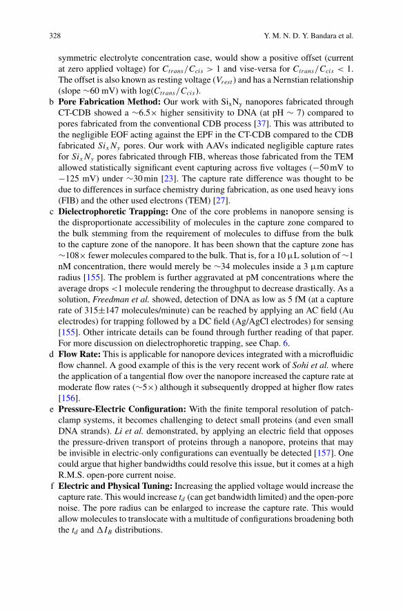
328 Y. M. N. D. Y. Bandara et al.
symmetric electrolyte concentration case, would show a positive offset (currentat zero applied voltage) for Ctrans/Ccis > 1 and vise-versa for Ctrans/Ccis < 1.The offset is also known as resting voltage (Vrest ) and has a Nernstian relationship(slope ∼60 mV) with log(Ctrans/Ccis).
b Pore Fabrication Method: Our work with SixNy nanopores fabricated throughCT-CDB showed a ∼6.5× higher sensitivity to DNA (at pH ∼ 7) compared topores fabricated from the conventional CDB process [37]. This was attributed tothe negligible EOF acting against the EPF in the CT-CDB compared to the CDBfabricated Six Ny pores. Our work with AAVs indicated negligible capture ratesfor Six Ny pores fabricated through FIB, whereas those fabricated from the TEMallowed statistically significant event capturing across five voltages (−50mV to−125 mV) under ∼30min [23]. The capture rate difference was thought to bedue to differences in surface chemistry during fabrication, as one used heavy ions(FIB) and the other used electrons (TEM) [27].
c Dielectrophoretic Trapping: One of the core problems in nanopore sensing isthe disproportionate accessibility of molecules in the capture zone compared tothe bulk stemming from the requirement of molecules to diffuse from the bulkto the capture zone of the nanopore. It has been shown that the capture zone has∼108× fewer molecules compared to the bulk. That is, for a 10µL solution of∼1nM concentration, there would merely be ∼34 molecules inside a 3 µm captureradius [155]. The problem is further aggravated at pM concentrations where theaverage drops <1 molecule rendering the throughput to decrease drastically. As asolution, Freedman et al. showed, detection of DNA as low as 5 fM (at a capturerate of 315±147 molecules/minute) can be reached by applying an AC field (Auelectrodes) for trapping followed by a DC field (Ag/AgCl electrodes) for sensing[155]. Other intricate details can be found through further reading of that paper.For more discussion on dielectrophoretic trapping, see Chap. 6.
d Flow Rate: This is applicable for nanopore devices integrated with a microfluidicflow channel. A good example of this is the very recent work of Sohi et al. wherethe application of a tangential flow over the nanopore increased the capture rate atmoderate flow rates (∼5×) although it subsequently dropped at higher flow rates[156].
e Pressure-Electric Configuration: With the finite temporal resolution of patch-clamp systems, it becomes challenging to detect small proteins (and even smallDNA strands). Li et al. demonstrated, by applying an electric field that opposesthe pressure-driven transport of proteins through a nanopore, proteins that maybe invisible in electric-only configurations can eventually be detected [157]. Onecould argue that higher bandwidths could resolve this issue, but it comes at a highR.M.S. open-pore current noise.
f Electric and Physical Tuning: Increasing the applied voltage would increase thecapture rate. This would increase td (can get bandwidth limited) and the open-porenoise. The pore radius can be enlarged to increase the capture rate. This wouldallow molecules to translocate with a multitude of configurations broadening boththe td and �IB distributions.
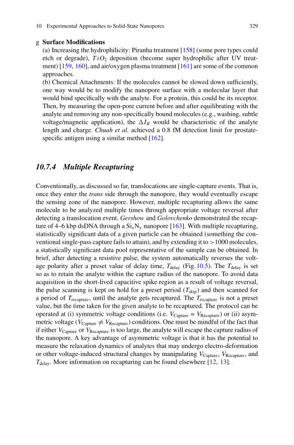
10 Experimental Approaches to Solid-State Nanopores 329
g Surface Modifications(a) Increasing the hydrophilicity: Piranha treatment [158] (some pore types couldetch or degrade), T iO2 deposition (become super hydrophilic after UV treat-ment) [159, 160], and air/oxygen plasma treatment [161] are some of the commonapproaches.(b) Chemical Attachments: If the molecules cannot be slowed down sufficiently,one way would be to modify the nanopore surface with a molecular layer thatwould bind specifically with the analyte. For a protein, this could be its receptor.Then, by measuring the open-pore current before and after equilibrating with theanalyte and removing any non-specifically bound molecules (e.g., washing, subtlevoltage/magnetic application), the �IB would be characteristic of the analytelength and charge. Chuah et al. achieved a 0.8 fM detection limit for prostate-specific antigen using a similar method [162].
10.7.4 Multiple Recapturing
Conventionally, as discussed so far, translocations are single-capture events. That is,once they enter the trans side through the nanopore, they would eventually escapethe sensing zone of the nanopore. However, multiple recapturing allows the samemolecule to be analyzed multiple times through appropriate voltage reversal afterdetecting a translocation event. Gershow and Golovchenko demonstrated the recap-ture of 4–6 kbp dsDNA through a SixNy nanopore [163]. With multiple recapturing,statistically significant data of a given particle can be obtained (something the con-ventional single-pass capture fails to attain), and by extending it to>1000molecules,a statistically significant data pool representative of the sample can be obtained. Inbrief, after detecting a resistive pulse, the system automatically reverses the volt-age polarity after a preset value of delay time, Tdelay (Fig. 10.5). The Tdelay is setso as to retain the analyte within the capture radius of the nanopore. To avoid dataacquisition in the short-lived capacitive spike region as a result of voltage reversal,the pulse scanning is kept on hold for a preset period (Tskip) and then scanned fora period of Trecapture, until the analyte gets recaptured. The Trecapture is not a presetvalue, but the time taken for the given analyte to be recaptured. The protocol can beoperated at (i) symmetric voltage conditions (i.e. VCapture = VRecapture) or (ii) asym-metric voltage (VCapture = VRecapture) conditions. One must be mindful of the fact thatif either VCapture or VRecapture is too large, the analyte will escape the capture radius ofthe nanopore. A key advantage of asymmetric voltage is that it has the potential tomeasure the relaxation dynamics of analytes that may undergo electro-deformationor other voltage-induced structural changes by manipulating VCapture, VRecapture, andTdelay. More information on recapturing can be found elsewhere [12, 13].
330 Y. M. N. D. Y. Bandara et al.
Fig. 10.5 Schematic of themultiple recapture protocol where upon the detection of a resistive pulse(green circle), the voltage is reversed after a preset time (Tdelay). The data acquisition is kept holdfor a preset time (Tskip) and then scanned for a period of Trecapture, until the protein gets recaptured
10.7.5 Electrode Maintenance
The most common electrode used is the Ag/AgCl electrode. It is an exhaustibleelectrode, yet it is reversible and has minimal polarization and predictable junctionpotential. The electrode reaction can be written as AgCl + e � Ag + Cl−. How-ever, when the AgCl is depleted, the bare Ag wire would be exposed which couldcause silver ions to leak into the solution. The silver ions can react with biomoleculesand alter their structure and function. If the bare Ag is exposed (electrode would lookwhitish), a freshly prepared Ag/AgCl electrode should be used. If the same bare Agis required to be reused, it should be sanded down until it becomes glossy and thendipped in a bleach solution, preferably overnight. A proper Ag/AgCl electrode wouldbe black in color. Additionally, one must be mindful of the composition of the bufferas well.
10.7.6 Analyte Concentration
Although it might seem a good idea to add as much analyte as possible becausethe capture rate is proportional to it, a higher capture rate would induce irreversiblepore-clogging as well. As a rule of thumb, we aim to collect a minimum of 1000events in 15min. If a lower analyte concentration could achieve this, it would havethe added benefit of minimal sample usage as well.
10 Experimental Approaches to Solid-State Nanopores 331
10.7.7 Optimizing Lowpass Filter Settings
See detailed discussed in Sects. 10.3 and 10.5 above.
10.8 Conclusions
In this chapter, we broadly discussed the transport phenomena and their model-ing, experiment planning, electrical signal measurements, nanopore characteriza-tion, noise and, improvements in measurements corresponding to nanopore singlemolecule sensing. Moreover, the analyte translocation methods (e.g. EO,EP and dif-fusion), mechanisms (e.g. diffusion and barrier limited) and the impact of analytechemistry, electrolyte chemistry, nanopore chemistry and electronic settings (e.g.applied voltage) on these are discussed in Sect. 10.2. The same conditions wouldalso dictate the translocation characteristics such as �IB and td and should be care-fully optimized or chose as discussed in Sects. 10.3 and 10.5. Section10.4 discussthe strategies ubiquitously used for physical and chemical nanopore characteriza-tion. For nanopore sensing to be successful, low noise is key and Sect. 10.6 discussthe noise properties associated with nanopores along with strategies to improve theinherent noise. Finally, furthermethods to improve sensing such as increasing td ,�IB(for higher SNR) and throughput along with vital maintenance tips are provided inSect. 10.7. Broadly, this chapter discuss the key aspects of nanopore sensing essen-tial to properly setup a nanopore experiment, characterization metrics, challengesassociated with nanopores, strategies developed to overcome them.
10.9 Acronym Glossary
αs: surface Hooge parameterαb: bulk Hooge parameterβ: inverse of thermal energy�: number of surface chargeable groupsεrε0: permittivity of the solutionζ p: zeta potential of the analyteζw: zeta potential of the nanopore wallη: dynamic viscosity of the electrolyteκ−1: Debye screening lengthμ: electrophoretic mobilityσ : surface charge densityφ pore: diffuse layer potentialC: analyte concentration
Ceff : effective stern layer capacitanceCs: stern layer capacitanceD: analyte diffusion coefficiente: elementary chargeE: electric fieldf ∗: frequency factorfc: cut-off frequency of the filterG: open pore conductanceGbulk: bulk conductanceGaccess: access conductanceGsurf ace: surface conductanceIrms: root mean square of open-pore cur-rent
332 Y. M. N. D. Y. Bandara et al.
J: analyte flux rateK : electrolyte conductivityKa: acid dissociation constantKb: base dissociation constantkB: Boltzmann constantl: pore lengthr: pore radiusr∗: capture radiusRdiffc : diffusion-limited capture rate
Rbarc : barrier-limited capture rate
R0: zero-voltage capture rateS1/f : 1/f noiseSw: white noiseSd: dielectric noiseSa: amplifier noiseT : temperatureTr : rise timetd: translocation/dwell time of the resis-tive pulseU∗: activation energyV : applied voltageVcross: cross-over voltageW : lambert W functionpI: isoelectric pointADEPT: adaptive time-series analysisCDB: controlled dielectric breakdownCMOS: complementary metal-oxide-semiconductorCT-CDB: chemically tuned CDBDBC: differential-based calibrationdsDNA: double-stranded DNAEDL: electrical double layer
EO: electroosmosisEOF: electrosomostic forceEP: electrophoresisEPF: electrophoretic forceFIB: focused ion beamFWHM: full width at the half maximumh-BN: hexagonal boron nitrideHIM: helium ion microscope�IB: current drop of the resistive pulseICR: ion current rectificationLACB: laser-assisted controlled break-downLPCVD: low-pressure chemical vapordepositionMPVI: multi-level pulsed voltage injec-tionPC: polycarbonatePECVD: plasma-enhanced chemicalvapor depositionPET: polyethylene terephthalatePSD: power spectral densityPVD: physical vapor depositionR.M.S: root mean squareRNA: ribonucleic acidSAXS: small angle X-ray scatteringSEM: scanning electron microscopeSNR: signal to noise ratioSixNy: silicon nitrideSiO2: silicon dioxideTCAM: tesla-coil assisted methodTEM: transmission electron microscope
References
1. Min Jun Kim, Meni Wanunu, David C Bell, and Amit Meller. Rapid fabrication of uni-formly sized nanopores and nanopore arrays for parallel dna analysis. Advanced Materials,18(23):3149–3153, 2006.
2. Kevin J Freedman, Chi Won Ahn, and Min Jun Kim. Detection of long and short dna usingnanopores with graphitic polyhedral edges. ACS Nano, 7(6):5008–5016, 2013.
3. Amir Barati Farimani, Kyoungmin Min, and Narayana R Aluru. Dna base detection using asingle-layer mos2. ACS Nano, 8(8):7914–7922, 2014.
10 Experimental Approaches to Solid-State Nanopores 333
4. JiandongFeng,KeLiu,RomanDBulushev, SergeyKhlybov,DumitruDumcenco,AndrasKis,and Aleksandra Radenovic. Identification of single nucleotides in mos2 nanopores. NatureNanotechnology, 10(12):1070, 2015.
5. Jugal Saharia, YM Nuwan DY Bandara, Jung Soo Lee, Qingxiao Wang, Moon J Kim, andMin Jun Kim. Fabrication of hexagonal boron nitride based 2d nanopore sensor for the assess-ment of electro-chemical responsiveness of human serum transferrin protein.Electrophoresis,41(7-8):630–637, 2020.
6. Jugal Saharia, YM Nuwan DY Bandara, Gaurav Goyal, Jung Soo Lee, Buddini IroshikaKarawdeniya, andMin JunKim.Molecular-level profiling of human serum transferrin proteinthrough assessment of nanopore-based electrical and chemical responsiveness. ACS Nano,13(4):4246–4254, 2019.
7. Y. M. Nuwan D.Y. Bandara, Jiannan Tang, Jugal Saharia, Louis William Rogowski, Chi WonAhn, and Min Jun Kim. Characterization of flagellar filaments and flagellin through opticalmicroscopy and label-free nanopore responsiveness. Analytical Chemistry, 91(21):13665–13674, 2019.
8. Kevin J Freedman, Maike Jürgens, Anmiv Prabhu, Chi Won Ahn, Per Jemth, Joshua B Edel,and Min Jun Kim. Chemical, thermal, and electric field induced unfolding of single proteinmolecules studied using nanopores. Analytical Chemistry, 83(13):5137–5144, 2011.
9. Buddini Iroshika Karawdeniya, Y. M. Nuwan D. Y. Bandara, Jonathan W. Nichols, Robert B.Chevalier, and Jason R. Dwyer. Surveying silicon nitride nanopores for glycomics and heparinquality assurance. Nature Communications, 9(1):3278, 2018.
10. James T Hagan, Brian S Sheetz, YMNuwan DY Bandara, Buddini I Karawdeniya, Melissa AMorris, Robert B Chevalier, and Jason R Dwyer. Chemically tailoring nanopores for single-molecule sensing and glycomics. Analytical and Bioanalytical Chemistry, 6:10.
11. Gaurav Goyal, Armin Darvish, and Min Jun Kim. Use of solid-state nanopores for sensingco-translocational deformation of nano-liposomes. Analyst, 140(14):4865–4873, 2015.
12. JungSooLee, Jugal Saharia,YMNuwanDYBandara, Buddini IroshikaKarawdeniya,GauravGoyal, Armin Darvish, Qingxiao Wang, Moon J Kim, and Min Jun Kim. Stiffness measure-ment of nanosized liposomes using solid-state nanopore sensor with automated recapturingplatform. Electrophoresis, 40(9):1337–1344, 2019.
13. Armin Darvish, Jung Soo Lee, Bin Peng, Jugal Saharia, Ramalingam VenkatKalyana Sun-daram, Gaurav Goyal, Nuwan Bandara, Chi Won Ahn, Jungsuk Kim, and Prashanta Dutta.Mechanical characterization of hiv-1 with a solid-state nanopore sensor. Electrophoresis,40(5):776–783, 2019.
14. Kaimeng Zhou, Lichun Li, Zhenning Tan, Adam Zlotnick, and Stephen C Jacobson. Char-acterization of hepatitis b virus capsids by resistive-pulse sensing. Journal of the AmericanChemical Society, 133(6):1618–1621, 2011.
15. AngusMcMullen, HendrickWDeHaan, Jay X Tang, and Derek Stein. Stiff filamentous virustranslocations through solid-state nanopores. Nature Communications, 5:4171, 2014.
16. GauravGoyal,Kevin JFreedman, andMin JunKim.Goldnanoparticle translocationdynamicsand electrical detection of single particle diffusion using solid-state nanopores. AnalyticalChemistry, 85(17):8180–8187, 2013.
17. Joseph WF Robertson, Claudio G Rodrigues, Vincent M Stanford, Kenneth A Rubinson,Oleg V Krasilnikov, and John J Kasianowicz. Single-molecule mass spectrometry in solutionusing a solitary nanopore. Proceedings of the National Academy of Sciences, 104(20):8207–8211, 2007.
18. John J Kasianowicz, Eric Brandin, Daniel Branton, and DavidWDeamer. Characterization ofindividual polynucleotide molecules using a membrane channel. Proceedings of the NationalAcademy of Sciences, 93(24):13770–13773, 1996.
19. Jeff Nivala, Douglas B Marks, and Mark Akeson. Unfoldase-mediated protein translocationthrough an α-hemolysin nanopore. Nature Biotechnology, 31(3):247–250, mar 2013.
20. Aziz Fennouri, Régis Daniel, Manuela Pastoriza-Gallego, Loïc Auvray, Juan Pelta, and Lau-rent Bacri. Kinetics of Enzymatic Degradation of High Molecular Weight Polysaccharidesthrough a Nanopore: Experiments and Data-Modeling. Analytical Chemistry, 85(18):8488–8492, sep 2013.
334 Y. M. N. D. Y. Bandara et al.
21. Thomas Hoenen, Allison Groseth, Kyle Rosenke, Robert J Fischer, Andreas Hoenen, Seth DJudson, CynthiaMartellaro, Darryl Falzarano, AndreaMarzi, and R Burke Squires. Nanoporesequencing as a rapidly deployable ebola outbreak tool. Emerging Infectious Diseases,22(2):331, 2016.
22. Harold Kwok, Kyle Briggs, and Vincent Tabard-Cossa. Nanopore fabrication by controlleddielectric breakdown. PloS one, 9(3):e92880, 2014.
23. Buddini Iroshika Karawdeniya, Y. M. Nuwan D. Y. Bandara, Aminul Islam Khan, Wei TongChen, Hoang-Anh Vu, Adnan Morshed, Junghae Suh, Prashanta Dutta, and Min Jun Kim.Adeno-associated virus characterization for cargo discrimination through nanopore respon-siveness. Nanoscale, 2020.
24. Meni Wanunu, Will Morrison, Yitzhak Rabin, Alexander Y Grosberg, and Amit Meller.Electrostatic focusing of unlabelled dna into nanoscale pores using a salt gradient. NatureNanotechnology, 5(2):160, 2010.
25. Martin Charron, Kyle Briggs, Simon King, Matthew Waugh, and Vincent Tabard-Cossa.Precise dna concentration measurements with nanopores by controlled counting. AnalyticalChemistry, 91(19):12228–12237, 2019.
26. Alexander YGrosberg and Yitzhak Rabin. Dna capture into a nanopore: interplay of diffusionand electrohydrodynamics. The Journal of chemical physics, 133(16):10B617, 2010.
27. Benjamin Cressiot, Abdelghani Oukhaled, Gilles Patriarche, Manuela Pastoriza-Gallego,Jean-Michel Betton, Loïc Auvray, Murugappan Muthukumar, Laurent Bacri, and Juan Pelta.Protein transport through a narrow solid-state nanopore at high voltage: experiments andtheory. ACS Nano, 6(7):6236–6243, 2012.
28. Abdelghani Oukhaled, Benjamin Cressiot, Laurent Bacri, Manuela Pastoriza-Gallego, Jean-Michel Betton, Eric Bourhis, Ralf Jede, Jacques Gierak, Loïc Auvray, and Juan Pelta. Dynam-ics of Completely Unfolded and Native Proteins through Solid-State Nanopores as a Functionof Electric Driving Force. ACS Nano, 5(5):3628–3638, may 2011.
29. YM Nuwan DY Bandara, Buddini I Karawdeniya, James T Hagan, Robert B Chevalier, andJason R Dwyer. Chemically functionalizing controlled dielectric breakdown silicon nitridenanopores by direct photohydrosilylation. ACS Applied Materials Interfaces, 11(33):30411–30420, 2019.
30. Nima Arjmandi, Willem Van Roy, Liesbet Lagae, and Gustaaf Borghs. Measuring the electriccharge and zeta potential of nanometer-sized objects using pyramidal-shaped nanopores.Analytical Chemistry, 84(20):8490–8496, 2012.
31. RalphMMSmeets, Ulrich F Keyser, Diego Krapf, Meng-YueWu, Nynke HDekker, and CeesDekker. Salt dependence of ion transport and dna translocation through solid-state nanopores.Nano Letters, 6(1):89–95, 2006.
32. Cameron M Frament, Nuwan Bandara, and Jason R Dwyer. Nanopore surface coating deliv-ers nanopore size and shape through conductance-based sizing. ACS Applied Materials &Interfaces, 5(19):9330–9337, 2013.
33. George Karniadakis, Ali Beskok, and Narayan Aluru.Microflows and nanoflows: fundamen-tals and simulation, volume 29. Springer Science & Business Media, 2006.
34. J. Lyklema, S. Rovillard, and J. de Coninck. Electrokinetics: the properties of the stagnantlayer unraveled. Langmuir, 14:5659–5663, 1998.
35. PatrickAbgrall andNamTrungNguyen.Nanofluidic devices and their applications.AnalyticalChemistry, 80(7):2326–2341, 2008.
36. Sven H Behrens and David G Grier. The charge of glass and silica surfaces. The Journal ofChemical Physics, 115(14):6716–6721, 2001.
37. Y.M.NuwanD. Y. Bandara, Jugal Saharia, Buddini I. Karawdeniya, James T. Hagan, Jason R.Dwyer, and Min Jun Kim. Beyond nanopore sizing: improving solid-state single-moleculesensing performance, lifetime, and analyte scope for omics by targeting surface chemistryduring fabrication. Nanotechnology, 31(33):335707, 2020.
38. D. P. Hoogerheide, S. Garaj, and J. A. Golovchenko. Probing surface charge fluctuations withsolid-state nanopores. Physical Review Letters, 102(25):256804, 2009.
10 Experimental Approaches to Solid-State Nanopores 335
39. Brett NAnderson,MurugappanMuthukumar, andAmitMeller. ph tuning of dna translocationtime through organically functionalized nanopores. ACS Nano, 7(2):1408–1414, 2012.
40. Meni Wanunu and Amit Meller. Chemically modified solid-state nanopores. Nano Letters,7(6):1580–1585, 2007.
41. Olivia M Eggenberger, Cuifeng Ying, and Michael Mayer. Surface coatings for solid-statenanopores. Nanoscale, 11(42):19636–19657, 2019.
42. Eszter Mádai, Bartłomiej Matejczyk, András Dallos, Mónika Valiskó, and Dezso Boda. Con-trolling ion transport through nanopores: modeling transistor behavior. Physical ChemistryChemical Physics, 20(37):24156–24167, 2018.
43. Robert J Hunter. Zeta potential in colloid science: principles and applications, volume 2.Academic press, 2013.
44. Haojie Yang, Zhongwu Li, Wei Si, Kabin Lin, Jian Ma, Kun Li, Litao Sun, Jingjie Sha, andYunfei Chen. Identification of single nucleotides by a tiny charged solid-state nanopore. TheJournal of Physical Chemistry B, 122(32):7929–7935, 2018.
45. Niklas Ermann, Nikita Hanikel, VivianWang, Kaikai Chen, Nicole EWeckman, and Ulrich FKeyser. Promoting single-file dna translocations through nanopores using electro-osmoticflow. The Journal of Chemical Physics, 149(16):163311, 2018.
46. Yin Zhang, Jiabin Zhao, Wei Si, Yajing Kan, Zheng Xu, Jingjie Sha, and Yunfei Chen. Elec-troosmotic facilitated protein capture and transport through solid-state nanopores with diam-eter larger than length. Small Methods, page 1900893, 2020.
47. Gang Huang, Kherim Willems, Misha Soskine, Carsten Wloka, and Giovanni Maglia.Electro-osmotic capture and ionic discrimination of peptide and protein biomarkers withfrac nanopores. Nature Communications, 8(1):1–11, 2017.
48. Stijn Van Dorp, Ulrich F Keyser, Nynke H Dekker, Cees Dekker, and Serge G Lemay. Originof the electrophoretic force on dna in solid-state nanopores. Nature Physics, 5(5):347, 2009.
49. Reto B Schoch, Jongyoon Han, and Philippe Renaud. Transport phenomena in nanofluidics.Reviews of Modern Physics, 80(3):839, 2008.
50. James W Swan and Eric M Furst. A simpler expression for henry’s function describingthe electrophoretic mobility of spherical colloids. Journal of Colloid and Interface Science,388(1):92–94, 2012.
51. M. Firnkes,D. Pedone, J. Knezevic,M.Doblinger, andU.Rant. Electrically facilitated translo-cations of proteins through silicon nitride nanopores: conjoint and competitive action of dif-fusion, electrophoresis, and electroosmosis. Nano Letters, 10(6):2162–2167, 2010.
52. Simon Welch. Transferrin: the iron carrier. CRC Press, 1992.53. Jugal Saharia, YM Nuwan DY Bandara, Buddini I Karawdeniya, George Alexandrakis,
and Min Jun Kim. Assessment of 1/f noise associated with nanopores fabricated throughchemically-tuned controlled dielectric breakdown. Electrophoresis, 42:899–909, 2021.
54. S. W. Kowalczyk, D. B. Wells, A. Aksimentiev, and C. Dekker. Slowing down dna transloca-tion through a nanopore in lithium chloride. Nano Letters, 12(2):1038–44, 2012.
55. R Russo, M Malinconico, and G Santagata. Effect of cross-linking with calcium ions on thephysical properties of alginate films. Biomacromolecules, 8(10):3193–3197, 2007.
56. James M Broering and Andreas S Bommarius. Evaluation of hofmeister effects on the kineticstability of proteins. The Journal of Physical Chemistry B, 109(43):20612–20619, 2005.
57. Arda Alden Green. Studies in the physical chemistry of the proteins x. the solubility ofhemoglobin in solutions of chlorides and sulfates of varying concentration. Journal of Bio-logical Chemistry, 95(1):47–66, 1932.
58. Luca Medda, Cristina Carucci, Drew F Parsons, Barry W Ninham, Maura Monduzzi, andAndrea Salis. Specific cation effects on hemoglobin aggregation below and at physiologicalsalt concentration. Langmuir, 29(49):15350–15358, 2013.
59. Payam Rowghanian and Alexander Y Grosberg. Electrophoretic capture of a dna chain intoa nanopore. Physical Review E, 87(4):042722, 2013.
60. Kevin J Freedman, S Raza Haq, Joshua B Edel, Per Jemth, andMin Jun Kim. Single moleculeunfolding and stretching of protein domains inside a solid-state nanopore by electric field.Scientific Reports, 3:1638, 2013.

336 Y. M. N. D. Y. Bandara et al.
61. Zhen Gu, Yi-Lun Ying, Chan Cao, Pingang He, and Yi-Tao Long. Accurate data process fornanopore analysis. Analytical Chemistry, 87(2):907–913, 2015.
62. Daniel Pedone, Matthias Firnkes, and Ulrich Rant. Data analysis of translocation events innanopore experiments. Analytical Chemistry, 81(23):9689–9694, 2009.
63. A. Morshed, B. I. Karawdeniya, Ymndy Bandara, M. J. Kim, and P. Dutta. Mechanicalcharacterization of vesicles and cells: A review. Electrophoresis, 41(7-8):449–470, 2020.
64. C. Plesa, S. W. Kowalczyk, R. Zinsmeester, A. Y. Grosberg, Y. Rabin, and C. Dekker. Fasttranslocation of proteins through solid state nanopores. Nano Letters, 13(2):658–63, 2013.
65. Jacob H Forstater, Kyle Briggs, Joseph WF Robertson, Jessica Ettedgui, Olivier Marie-Rose,Canute Vaz, John J Kasianowicz, Vincent Tabard-Cossa, and Arvind Balijepalli. Mosaic: amodular single-molecule analysis interface for decoding multistate nanopore data. AnalyticalChemistry, 88(23):11900–11907, 2016.
66. Jacob K Rosenstein, Meni Wanunu, Christopher A Merchant, Marija Drndic, and Kenneth LShepard. Integrated nanopore sensing platform with sub-microsecond temporal resolution.Nature Methods, 9(5):487, 2012.
67. J Feng, Ke Liu, Michael Graf, Martina Lihter, Roman D Bulushev, Dumitru Dumcenco,DuncanTLAlexander,DariaKrasnozhon, TomislavVuletic, andAndrasKis. Electrochemicalreaction in single layer mos2: nanopores opened atom by atom. Nano Letters, 15(5):3431–3438, 2015.
68. AaronTKuan,BoLu,PingXie,TamasSzalay, and JeneAGolovchenko.Electrical pulse fabri-cationof graphenenanopores in electrolyte solution.AppliedPhysicsLetters, 106(20):203109,2015.
69. Joseph Larkin, Robert Henley, David C Bell, Tzahi Cohen-Karni, Jacob K Rosenstein, andMeni Wanunu. Slow dna transport through nanopores in hafnium oxide membranes. ACSNano, 7(11):10121–10128, 2013.
70. Bala Murali Venkatesan, Brian Dorvel, Sukru Yemenicioglu, Nicholas Watkins, Ivan Petrov,and Rashid Bashir. Highly sensitive, mechanically stable nanopore sensors for dna analysis.Advanced Materials, 21(27):2771–2776, 2009.
71. Bala Murali Venkatesan, David Estrada, Shouvik Banerjee, Xiaozhong Jin, Vincent E Dor-gan, Myung-Ho Bae, Narayana R Aluru, Eric Pop, and Rashid Bashir. Stacked graphene-al2o3 nanopore sensors for sensitive detection of dna and dna–protein complexes. ACS Nano,6(1):441–450, 2012.
72. Youwen Zhang, Xiaohan Chen, Ceming Wang, Golbarg M Roozbahani, Hsueh-Chia Chang,and Xiyun Guan. Chemically functionalized conical pet nanopore for protein detection at thesingle-molecule level. Biosensors and Bioelectronics, page 112289, 2020.
73. Timothy Plett, Wenqing Shi, Yuhan Zeng, William Mann, Ivan Vlassiouk, Lane A Baker,and Zuzanna S Siwy. Rectification of nanopores in aprotic solvents–transport properties ofnanopores with surface dipoles. Nanoscale, 7(45):19080–19091, 2015.
74. Ivan Vlassiouk, Pavel Y Apel, Sergey N Dmitriev, Ken Healy, and Zuzanna S Siwy. Versatileultrathin nanoporous silicon nitride membranes. Proceedings of the National Academy ofSciences, 106(50):21039–21044, 2009.
75. Meni Wanunu, Tali Dadosh, Vishva Ray, Jingmin Jin, Larry McReynolds, andMarija Drndic.Rapid electronic detection of probe-specific micrornas using thin nanopore sensors. NatureNanotechnology, 5(11):807–814, 2010.
76. KeLiu, Jiandong Feng, AndrasKis, andAleksandra Radenovic. Atomically thinmolybdenumdisulfide nanopores with high sensitivity for dna translocation. ACS Nano, 8(3):2504–2511,2014.
77. Birgitta Schiedt, Loïc Auvray, Laurent Bacri, G Oukhaled, Ali Madouri, Eric Bourhis, GillesPatriarche, Juan Pelta, Ralf Jede, and Jacques Gierak. Direct fib fabrication and integrationof “single nanopore devices” for the manipulation of macromolecules.Microelectronic Engi-neering, 87(5-8):1300–1303, 2010.
78. Jijin Yang, David C Ferranti, Lewis A Stern, Colin A Sanford, Jason Huang, Zheng Ren,Lu-Chang Qin, and Adam R Hall. Rapid and precise scanning helium ion microscope millingof solid-state nanopores for biomolecule detection. Nanotechnology, 22(28):285310, 2011.
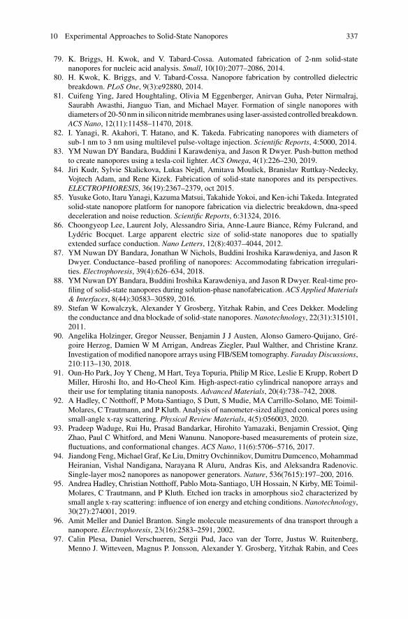
10 Experimental Approaches to Solid-State Nanopores 337
79. K. Briggs, H. Kwok, and V. Tabard-Cossa. Automated fabrication of 2-nm solid-statenanopores for nucleic acid analysis. Small, 10(10):2077–2086, 2014.
80. H. Kwok, K. Briggs, and V. Tabard-Cossa. Nanopore fabrication by controlled dielectricbreakdown. PLoS One, 9(3):e92880, 2014.
81. Cuifeng Ying, Jared Houghtaling, Olivia M Eggenberger, Anirvan Guha, Peter Nirmalraj,Saurabh Awasthi, Jianguo Tian, and Michael Mayer. Formation of single nanopores withdiameters of 20-50 nm in silicon nitridemembranes using laser-assisted controlled breakdown.ACS Nano, 12(11):11458–11470, 2018.
82. I. Yanagi, R. Akahori, T. Hatano, and K. Takeda. Fabricating nanopores with diameters ofsub-1 nm to 3 nm using multilevel pulse-voltage injection. Scientific Reports, 4:5000, 2014.
83. YM Nuwan DY Bandara, Buddini I Karawdeniya, and Jason R Dwyer. Push-button methodto create nanopores using a tesla-coil lighter. ACS Omega, 4(1):226–230, 2019.
84. Jiri Kudr, Sylvie Skalickova, Lukas Nejdl, Amitava Moulick, Branislav Ruttkay-Nedecky,Vojtech Adam, and Rene Kizek. Fabrication of solid-state nanopores and its perspectives.ELECTROPHORESIS, 36(19):2367–2379, oct 2015.
85. Yusuke Goto, Itaru Yanagi, KazumaMatsui, Takahide Yokoi, and Ken-ichi Takeda. Integratedsolid-state nanopore platform for nanopore fabrication via dielectric breakdown, dna-speeddeceleration and noise reduction. Scientific Reports, 6:31324, 2016.
86. Choongyeop Lee, Laurent Joly, Alessandro Siria, Anne-Laure Biance, Rémy Fulcrand, andLydéric Bocquet. Large apparent electric size of solid-state nanopores due to spatiallyextended surface conduction. Nano Letters, 12(8):4037–4044, 2012.
87. YM Nuwan DY Bandara, Jonathan W Nichols, Buddini Iroshika Karawdeniya, and Jason RDwyer. Conductance–based profiling of nanopores: Accommodating fabrication irregulari-ties. Electrophoresis, 39(4):626–634, 2018.
88. YMNuwan DY Bandara, Buddini Iroshika Karawdeniya, and Jason R Dwyer. Real-time pro-filing of solid-state nanopores during solution-phase nanofabrication. ACS Applied Materials& Interfaces, 8(44):30583–30589, 2016.
89. Stefan W Kowalczyk, Alexander Y Grosberg, Yitzhak Rabin, and Cees Dekker. Modelingthe conductance and dna blockade of solid-state nanopores. Nanotechnology, 22(31):315101,2011.
90. Angelika Holzinger, Gregor Neusser, Benjamin J J Austen, Alonso Gamero-Quijano, Gré-goire Herzog, Damien W M Arrigan, Andreas Ziegler, Paul Walther, and Christine Kranz.Investigation of modified nanopore arrays using FIB/SEM tomography. Faraday Discussions,210:113–130, 2018.
91. Oun-Ho Park, Joy Y Cheng, M Hart, Teya Topuria, Philip M Rice, Leslie E Krupp, Robert DMiller, Hiroshi Ito, and Ho-Cheol Kim. High-aspect-ratio cylindrical nanopore arrays andtheir use for templating titania nanoposts. Advanced Materials, 20(4):738–742, 2008.
92. A Hadley, C Notthoff, P Mota-Santiago, S Dutt, S Mudie, MA Carrillo-Solano, ME Toimil-Molares, C Trautmann, and P Kluth. Analysis of nanometer-sized aligned conical pores usingsmall-angle x-ray scattering. Physical Review Materials, 4(5):056003, 2020.
93. Pradeep Waduge, Rui Hu, Prasad Bandarkar, Hirohito Yamazaki, Benjamin Cressiot, QingZhao, Paul C Whitford, and Meni Wanunu. Nanopore-based measurements of protein size,fluctuations, and conformational changes. ACS Nano, 11(6):5706–5716, 2017.
94. Jiandong Feng,Michael Graf, Ke Liu, Dmitry Ovchinnikov, Dumitru Dumcenco,MohammadHeiranian, Vishal Nandigana, Narayana R Aluru, Andras Kis, and Aleksandra Radenovic.Single-layer mos2 nanopores as nanopower generators. Nature, 536(7615):197–200, 2016.
95. Andrea Hadley, Christian Notthoff, Pablo Mota-Santiago, UH Hossain, N Kirby, ME Toimil-Molares, C Trautmann, and P Kluth. Etched ion tracks in amorphous sio2 characterized bysmall angle x-ray scattering: influence of ion energy and etching conditions.Nanotechnology,30(27):274001, 2019.
96. Amit Meller and Daniel Branton. Single molecule measurements of dna transport through ananopore. Electrophoresis, 23(16):2583–2591, 2002.
97. Calin Plesa, Daniel Verschueren, Sergii Pud, Jaco van der Torre, Justus W. Ruitenberg,Menno J. Witteveen, Magnus P. Jonsson, Alexander Y. Grosberg, Yitzhak Rabin, and Cees
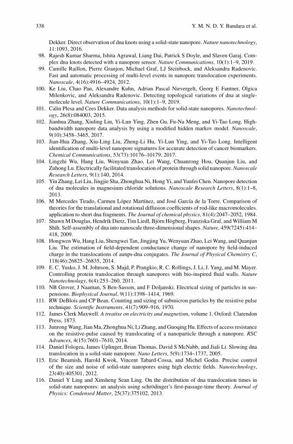
338 Y. M. N. D. Y. Bandara et al.
Dekker. Direct observation of dna knots using a solid-state nanopore.Nature nanotechnology,11:1093, 2016.
98. Rajesh Kumar Sharma, Ishita Agrawal, Liang Dai, Patrick S Doyle, and Slaven Garaj. Com-plex dna knots detected with a nanopore sensor. Nature Communications, 10(1):1–9, 2019.
99. Camille Raillon, Pierre Granjon, Michael Graf, LJ Steinbock, and Aleksandra Radenovic.Fast and automatic processing of multi-level events in nanopore translocation experiments.Nanoscale, 4(16):4916–4924, 2012.
100. Ke Liu, Chao Pan, Alexandre Kuhn, Adrian Pascal Nievergelt, Georg E Fantner, OlgicaMilenkovic, and Aleksandra Radenovic. Detecting topological variations of dna at single-molecule level. Nature Communications, 10(1):1–9, 2019.
101. Calin Plesa and Cees Dekker. Data analysis methods for solid-state nanopores. Nanotechnol-ogy, 26(8):084003, 2015.
102. Jianhua Zhang, Xiuling Liu, Yi-Lun Ying, Zhen Gu, Fu-Na Meng, and Yi-Tao Long. High-bandwidth nanopore data analysis by using a modified hidden markov model. Nanoscale,9(10):3458–3465, 2017.
103. Jian-Hua Zhang, Xiu-Ling Liu, Zheng-Li Hu, Yi-Lun Ying, and Yi-Tao Long. Intelligentidentification of multi-level nanopore signatures for accurate detection of cancer biomarkers.Chemical Communications, 53(73):10176–10179, 2017.
104. Lingzhi Wu, Hang Liu, Wenyuan Zhao, Lei Wang, Chuanrong Hou, Quanjun Liu, andZuhong Lu. Electrically facilitated translocation of protein through solid nanopore.NanoscaleResearch Letters, 9(1):140, 2014.
105. Yin Zhang, Lei Liu, Jingjie Sha, ZhonghuaNi, HongYi, andYunfei Chen. Nanopore detectionof dna molecules in magnesium chloride solutions. Nanoscale Research Letters, 8(1):1–8,2013.
106. M Mercedes Tirado, Carmen López Martínez, and José García de la Torre. Comparison oftheories for the translational and rotational diffusion coefficients of rod-like macromolecules.application to short dna fragments. The Journal of chemical physics, 81(4):2047–2052, 1984.
107. ShawnMDouglas, Hendrik Dietz, Tim Liedl, Björn Högberg, Franziska Graf, andWilliamMShih. Self-assembly of dna into nanoscale three-dimensional shapes.Nature, 459(7245):414–418, 2009.
108. HongwenWu, Hang Liu, Shengwei Tan, Jingjing Yu,Wenyuan Zhao, LeiWang, and QuanjunLiu. The estimation of field-dependent conductance change of nanopore by field-inducedcharge in the translocations of aunps-dna conjugates. The Journal of Physical Chemistry C,118(46):26825–26835, 2014.
109. E. C. Yusko, J. M. Johnson, S. Majd, P. Prangkio, R. C. Rollings, J. Li, J. Yang, andM.Mayer.Controlling protein translocation through nanopores with bio-inspired fluid walls. NatureNanotechnolagy, 6(4):253–260, 2011.
110. NB Grover, J Naaman, S Ben-Sasson, and F Doljanski. Electrical sizing of particles in sus-pensions. Biophysical Journal, 9(11):1398–1414, 1969.
111. RW DeBlois and CP Bean. Counting and sizing of submicron particles by the resistive pulsetechnique. Scientific Instruments, 41(7):909–916, 1970.
112. James Clerk Maxwell. A treatise on electricity and magnetism, volume 1. Oxford: ClarendonPress, 1873.
113. JunrongWang, JianMa, ZhonghuaNi, Li Zhang, andGuoqingHu. Effects of access resistanceon the resistive-pulse caused by translocating of a nanoparticle through a nanopore. RSCAdvances, 4(15):7601–7610, 2014.
114. Daniel Fologea, James Uplinger, Brian Thomas, David S McNabb, and Jiali Li. Slowing dnatranslocation in a solid-state nanopore. Nano Letters, 5(9):1734–1737, 2005.
115. Eric Beamish, Harold Kwok, Vincent Tabard-Cossa, and Michel Godin. Precise controlof the size and noise of solid-state nanopores using high electric fields. Nanotechnology,23(40):405301, 2012.
116. Daniel Y Ling and Xinsheng Sean Ling. On the distribution of dna translocation times insolid-state nanopores: an analysis using schrödinger’s first-passage-time theory. Journal ofPhysics: Condensed Matter, 25(37):375102, 2013.
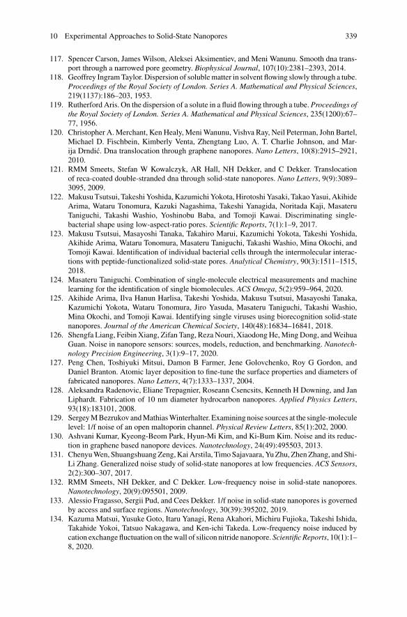
10 Experimental Approaches to Solid-State Nanopores 339
117. Spencer Carson, James Wilson, Aleksei Aksimentiev, and Meni Wanunu. Smooth dna trans-port through a narrowed pore geometry. Biophysical Journal, 107(10):2381–2393, 2014.
118. Geoffrey IngramTaylor. Dispersion of solublematter in solvent flowing slowly through a tube.Proceedings of the Royal Society of London. Series A. Mathematical and Physical Sciences,219(1137):186–203, 1953.
119. Rutherford Aris. On the dispersion of a solute in a fluid flowing through a tube.Proceedings ofthe Royal Society of London. Series A. Mathematical and Physical Sciences, 235(1200):67–77, 1956.
120. Christopher A.Merchant, Ken Healy, MeniWanunu, Vishva Ray, Neil Peterman, John Bartel,Michael D. Fischbein, Kimberly Venta, Zhengtang Luo, A. T. Charlie Johnson, and Mar-ija Drndic. Dna translocation through graphene nanopores. Nano Letters, 10(8):2915–2921,2010.
121. RMM Smeets, Stefan W Kowalczyk, AR Hall, NH Dekker, and C Dekker. Translocationof reca-coated double-stranded dna through solid-state nanopores. Nano Letters, 9(9):3089–3095, 2009.
122. MakusuTsutsui, TakeshiYoshida,KazumichiYokota,HirotoshiYasaki, TakaoYasui, AkihideArima, Wataru Tonomura, Kazuki Nagashima, Takeshi Yanagida, Noritada Kaji, MasateruTaniguchi, Takashi Washio, Yoshinobu Baba, and Tomoji Kawai. Discriminating single-bacterial shape using low-aspect-ratio pores. Scientific Reports, 7(1):1–9, 2017.
123. Makusu Tsutsui, Masayoshi Tanaka, Takahiro Marui, Kazumichi Yokota, Takeshi Yoshida,Akihide Arima, Wataru Tonomura, Masateru Taniguchi, Takashi Washio, Mina Okochi, andTomoji Kawai. Identification of individual bacterial cells through the intermolecular interac-tions with peptide-functionalized solid-state pores. Analytical Chemistry, 90(3):1511–1515,2018.
124. Masateru Taniguchi. Combination of single-molecule electrical measurements and machinelearning for the identification of single biomolecules. ACS Omega, 5(2):959–964, 2020.
125. Akihide Arima, Ilva Hanun Harlisa, Takeshi Yoshida, Makusu Tsutsui, Masayoshi Tanaka,Kazumichi Yokota, Wataru Tonomura, Jiro Yasuda, Masateru Taniguchi, Takashi Washio,Mina Okochi, and Tomoji Kawai. Identifying single viruses using biorecognition solid-statenanopores. Journal of the American Chemical Society, 140(48):16834–16841, 2018.
126. Shengfa Liang, Feibin Xiang, Zifan Tang, RezaNouri, XiaodongHe,MingDong, andWeihuaGuan. Noise in nanopore sensors: sources, models, reduction, and benchmarking. Nanotech-nology Precision Engineering, 3(1):9–17, 2020.
127. Peng Chen, Toshiyuki Mitsui, Damon B Farmer, Jene Golovchenko, Roy G Gordon, andDaniel Branton. Atomic layer deposition to fine-tune the surface properties and diameters offabricated nanopores. Nano Letters, 4(7):1333–1337, 2004.
128. Aleksandra Radenovic, Eliane Trepagnier, Roseann Csencsits, Kenneth H Downing, and JanLiphardt. Fabrication of 10 nm diameter hydrocarbon nanopores. Applied Physics Letters,93(18):183101, 2008.
129. SergeyMBezrukov andMathiasWinterhalter. Examining noise sources at the single-moleculelevel: 1/f noise of an open maltoporin channel. Physical Review Letters, 85(1):202, 2000.
130. Ashvani Kumar, Kyeong-Beom Park, Hyun-Mi Kim, and Ki-Bum Kim. Noise and its reduc-tion in graphene based nanopore devices. Nanotechnology, 24(49):495503, 2013.
131. ChenyuWen, ShuangshuangZeng,KaiArstila, TimoSajavaara,YuZhu, ZhenZhang, andShi-Li Zhang. Generalized noise study of solid-state nanopores at low frequencies. ACS Sensors,2(2):300–307, 2017.
132. RMM Smeets, NH Dekker, and C Dekker. Low-frequency noise in solid-state nanopores.Nanotechnology, 20(9):095501, 2009.
133. Alessio Fragasso, Sergii Pud, and Cees Dekker. 1/f noise in solid-state nanopores is governedby access and surface regions. Nanotechnology, 30(39):395202, 2019.
134. Kazuma Matsui, Yusuke Goto, Itaru Yanagi, Rena Akahori, Michiru Fujioka, Takeshi Ishida,Takahide Yokoi, Tatsuo Nakagawa, and Ken-ichi Takeda. Low-frequency noise induced bycation exchange fluctuation on thewall of silicon nitride nanopore. ScientificReports, 10(1):1–8, 2020.
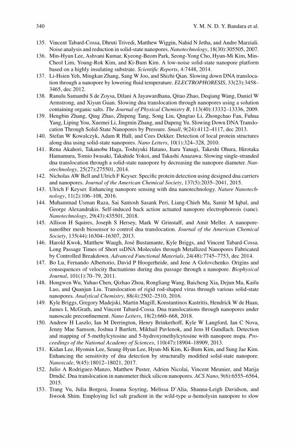
340 Y. M. N. D. Y. Bandara et al.
135. Vincent Tabard-Cossa, Dhruti Trivedi, MatthewWiggin, Nahid N Jetha, and Andre Marziali.Noise analysis and reduction in solid-state nanopores.Nanotechnology, 18(30):305505, 2007.
136. Min-Hyun Lee, Ashvani Kumar, Kyeong-Beom Park, Seong-Yong Cho, Hyun-Mi Kim, Min-Cheol Lim, Young-Rok Kim, and Ki-Bum Kim. A low-noise solid-state nanopore platformbased on a highly insulating substrate. Scientific Reports, 4:7448, 2014.
137. Li-Hsien Yeh, Mingkan Zhang, SangW Joo, and Shizhi Qian. Slowing down DNA transloca-tion through a nanopore by lowering fluid temperature. ELECTROPHORESIS, 33(23):3458–3465, dec 2012.
138. Ranulu Samanthi S de Zoysa, Dilani A Jayawardhana, Qitao Zhao, Deqiang Wang, Daniel WArmstrong, and Xiyun Guan. Slowing dna translocation through nanopores using a solutioncontaining organic salts. The Journal of Physical Chemistry B, 113(40):13332–13336, 2009.
139. Hengbin Zhang, Qing Zhao, Zhipeng Tang, Song Liu, Qingtao Li, Zhongchao Fan, FuhuaYang, Liping You, Xuemei Li, Jingmin Zhang, and Dapeng Yu. Slowing Down DNATranslo-cation Through Solid-State Nanopores by Pressure. Small, 9(24):4112–4117, dec 2013.
140. Stefan W Kowalczyk, Adam R Hall, and Cees Dekker. Detection of local protein structuresalong dna using solid-state nanopores. Nano Letters, 10(1):324–328, 2010.
141. Rena Akahori, Takanobu Haga, Toshiyuki Hatano, Itaru Yanagi, Takeshi Ohura, HirotakaHamamura, Tomio Iwasaki, Takahide Yokoi, and Takashi Anazawa. Slowing single-strandeddna translocation through a solid-state nanopore by decreasing the nanopore diameter. Nan-otechnology, 25(27):275501, 2014.
142. Nicholas AWBell and Ulrich F Keyser. Specific protein detection using designed dna carriersand nanopores. Journal of the American Chemical Society, 137(5):2035–2041, 2015.
143. Ulrich F Keyser. Enhancing nanopore sensing with dna nanotechnology. Nature Nanotech-nology, 11(2):106–108, 2016.
144. Muhammad Usman Raza, Sai Santosh Sasank Peri, Liang-Chieh Ma, Samir M Iqbal, andGeorge Alexandrakis. Self-induced back action actuated nanopore electrophoresis (sane).Nanotechnology, 29(43):435501, 2018.
145. Allison H Squires, Joseph S Hersey, Mark W Grinstaff, and Amit Meller. A nanopore-nanofiber mesh biosensor to control dna translocation. Journal of the American ChemicalSociety, 135(44):16304–16307, 2013.
146. Harold Kwok, Matthew Waugh, José Bustamante, Kyle Briggs, and Vincent Tabard-Cossa.Long Passage Times of Short ssDNA Molecules through Metallized Nanopores Fabricatedby Controlled Breakdown. Advanced Functional Materials, 24(48):7745–7753, dec 2014.
147. Bo Lu, Fernando Albertorio, David P Hoogerheide, and Jene A Golovchenko. Origins andconsequences of velocity fluctuations during dna passage through a nanopore. BiophysicalJournal, 101(1):70–79, 2011.
148. Hongwen Wu, Yuhao Chen, Qizhao Zhou, Rongliang Wang, Baicheng Xia, Dejun Ma, KaifuLuo, and Quanjun Liu. Translocation of rigid rod-shaped virus through various solid-statenanopores. Analytical Chemistry, 88(4):2502–2510, 2016.
149. Kyle Briggs, Gregory Madejski, Martin Magill, Konstantinos Kastritis, HendrickW de Haan,James L McGrath, and Vincent Tabard-Cossa. Dna translocations through nanopores undernanoscale preconfinement. Nano Letters, 18(2):660–668, 2018.
150. Andrew H Laszlo, Ian M Derrington, Henry Brinkerhoff, Kyle W Langford, Ian C Nova,Jenny Mae Samson, Joshua J Bartlett, Mikhail Pavlenok, and Jens H Gundlach. Detectionand mapping of 5-methylcytosine and 5-hydroxymethylcytosine with nanopore mspa. Pro-ceedings of the National Academy of Sciences, 110(47):18904–18909, 2013.
151. Kidan Lee, Hyomin Lee, Seung-Hyun Lee, Hyun-Mi Kim, Ki-Bum Kim, and Sung Jae Kim.Enhancing the sensitivity of dna detection by structurally modified solid-state nanopore.Nanoscale, 9(45):18012–18021, 2017.
152. Julio A Rodriguez-Manzo, Matthew Puster, Adrien Nicolai, Vincent Meunier, and MarijaDrndic. Dna translocation in nanometer thick silicon nanopores. ACS Nano, 9(6):6555–6564,2015.
153. Trang Vu, Julia Borgesi, Joanna Soyring, Melissa D’Alia, Shanna-Leigh Davidson, andJiwook Shim. Employing licl salt gradient in the wild-type α-hemolysin nanopore to slow
10 Experimental Approaches to Solid-State Nanopores 341
down dna translocation and detect methylated cytosine. Nanoscale, 11(21):10536–10545,2019.
154. Julian Bello, Maksudul Mowla, Nicholas Troise, Joanna Soyring, Julia Borgesi, and JiwookShim. Increased dwell time and occurrence of dsdna translocation events through solid statenanopores by licl concentration gradients. Electrophoresis, 40(7):1082–1090, 2019.
155. Kevin J Freedman, Lauren M Otto, Aleksandar P Ivanov, Avijit Barik, Sang-Hyun Oh, andJoshua B Edel. Nanopore sensing at ultra-low concentrations using single-molecule dielec-trophoretic trapping. Nature Communications, 7:10217, 2016.
156. Ali Najafi Sohi, Eric Beamish, Vincent Tabard-Cossa, and Michel Godin. Dna capture bynanopore sensors under flow. Analytical Chemistry, 2020.
157. Ji Li, Rui Hu, Xiaoqing Li, Xin Tong, Dapeng Yu, and Qing Zhao. Tiny protein detectionusing pressure through solid-state nanopores. ELECTROPHORESIS, 38(8):1130–1138, apr2017.
158. Yann Astier, Lucien Datas, Randy Carney, Francesco Stellacci, Francesco Gentile, and EnzoDiFabrizio. Artificial surface-modified si3n4 nanopores for single surface-modified goldnanoparticle scanning. Small, 7(4):455–459, 2011.
159. Christopher A Merchant, Ken Healy, Meni Wanunu, Vishva Ray, Neil Peterman, John Bar-tel, Michael D Fischbein, Kimberly Venta, Zhengtang Luo, and AT Charlie Johnson. Dnatranslocation through graphene nanopores. Nano Letters, 10(8):2915–2921, 2010.
160. RongWang, Kazuhito Hashimoto, Akira Fujishima, Makoto Chikuni, Eiichi Kojima, AtsushiKitamura, Mitsuhide Shimohigoshi, and Toshiya Watanabe. Photogeneration of highlyamphiphilic tio2 surfaces. Advanced Materials, 10(2):135–138, 1998.
161. Dae-Sik Lee, Seokhan Park, Yong Duk Han, Jae Eun Lee, Hu Young Jeong, Hyun C Yoon,Moon Yeon Jung, Sang Ouk Kim, and Sung-Yool Choi. Selective protein transport throughultra-thin suspended reduced graphene oxide nanopores. Nanoscale, 9(36):13457–13464,2017.
162. Kyloon Chuah, Yanfang Wu, SRC Vivekchand, Katharina Gaus, Peter J Reece, Adam PMicolich, and J Justin Gooding. Nanopore blockade sensors for ultrasensitive detection ofproteins in complex biological samples. Nature Communications, 10(1):1–9, 2019.
163. Marc Gershow and Jene Andrew Golovchenko. Recapturing and trapping single moleculeswith a solid-state nanopore. Nature nanotechnology, 2(12):775, 2007.
Chapter 11Challenges in Protein Sequencing Using2-D MoS2 Nanopores
Adrien Nicolaï and Patrick Senet
Abstract Solid-state nanopores (SSN) made of 2-D materials such asmolybdenum disulfide (MoS2) have emerged as one of the most versatile sensors forsingle-molecule detection. One of the most promising applications of SSN is DNAand protein sequencing, at a low cost and faster than the current standard methods.The detection principle relies on measuring the relatively small variations of ioniccurrent as charged biomolecules immersed in an electrolyte traverse the nanopore,in response to an external voltage applied across the membrane. The passage of abiomolecule through the pore yields information about its structure and chemicalproperties, as demonstrated experimentally particularly for DNAmolecules. Indeed,protein sequencing using SSN remains highly challenging since the protein ensembleis far more complex than the DNAone. In the present chapter, we focus on challengesin protein sequencing using 2-D MoS2 nanopores. Three challenges are highlightedusing Molecular Dynamics to simulate protein translocation experiments throughMoS2 nanopores. First, the threading of the protein through the nanopore is dis-cussed. Second, the modification of the nanopore dimensions in order to slow downthe passage of the protein through the pore is detailed. Finally, the application oftime series analysis tools in order to identify protein sequence motif from measuredraw data is presented.
11.1 Introduction
After three decades of research [1], development of label-free, electrical-based nan-odevice for DNA sequencing is a mature field [2]. The first sequence reads ofDNA strands using nanopores was published 10 years ago [3] and the commer-cial sequencer MinION of Oxford Nanopore Technology was successfully appliedto sequence a human genome [4]. Both biological nanopores [1–4] as well as solid-
A. Nicolaï · P. Senet (B)Laboratoire Interdisciplinaire Carnot de Bourgogne, UMR 6303 CNRS-Université de BourgogneFranche-Comté, 9 Av. A. Savary, BP 47 870, 21078 Dijon Cedex, Francee-mail: [email protected]
© The Author(s), under exclusive license to Springer Nature Switzerland AG 2022W. Bowen et al. (eds.), Single Molecule Sensing Beyond Fluorescence,Nanostructure Science and Technology,https://doi.org/10.1007/978-3-030-90339-8_11
343

344 A. Nicolaï and P. Senet
Fig. 11.1 Principle and detection method of solid-state nanopore technology. A Schematic repre-sentation of protein sensing using MoS2 nanopore. Two reservoirs filled with a KCl electrolyte areseparated by a SL-MoS2 membrane and connected via a single pore of nanometer size (see TEMimage as inset). Electrodes (in red) are immersed in the two compartments and a constant voltagebias is applied across the membrane causing an ionic-current flow through the pore. B Ionic currenttrace as a function of time during the passage of a protein through the pore. Usually, the ionic currentdecreases and the features of the current drop, such as its amplitude �I , duration ≡ dwell time τDand fluctuations, contain important information about the protein, including its size, charge, shapeor sequence, as represented with transparent color rectangles in the given trace
state nanopores (SSN) [5–8] were developed to sequence single DNA molecules.Protein sequencing using nanopores is less advanced [9, 10] and is the focus of thepresent chapter.
The general principle of electrical-based nanopore sequencing of a biopolymerby a SSN is illustrated in Fig. 11.1. A 2-D material, MoS2 nanoporous membrane,discussed further below, is shown (panel A). The charged biopolymer to be detectedand sequenced is driven by an electric field to a pore of dimension comparableto its molecular dimensions (typical values are 1–3 nm) and is immersed in anelectrolyte (typicallyNaCl orKCl). The ionic current induced by the electric potentialdifference applied to the membrane is measured with a high temporal resolution [11](up to 100 ns). Obstruction of the nanopore while the biopolymer is passing throughthe channel decreases the ionic conductance of the device. Consequently, the ioniccurrent variations depend on the molecular fragment residing in the nanopore. Theread of the current drops (�I ) and their duration (τD) as a function of time providefingerprints of the individual fragments translocating through the nanopore (Fig. 11.1,Panel B). At best, each monomer is expected to be revealed by a distinct fingerprint,allowing the identification of the biopolymer primary structure.
Invention of the electrical-based nanopore sequencing in 1998 featured a methodfor evaluating a polymer molecule which includes linearly (connected) sequentialmonomer residues and envisioned protein sequencing [1]. The two main advantagesof the nanopore technology for protein sequencing compared to other technique ofprotein identification such as mass spectroscopy for instance are: (i) its sensitivity, assingle-molecule can be detected and (ii) the possibility to develop a portable medical
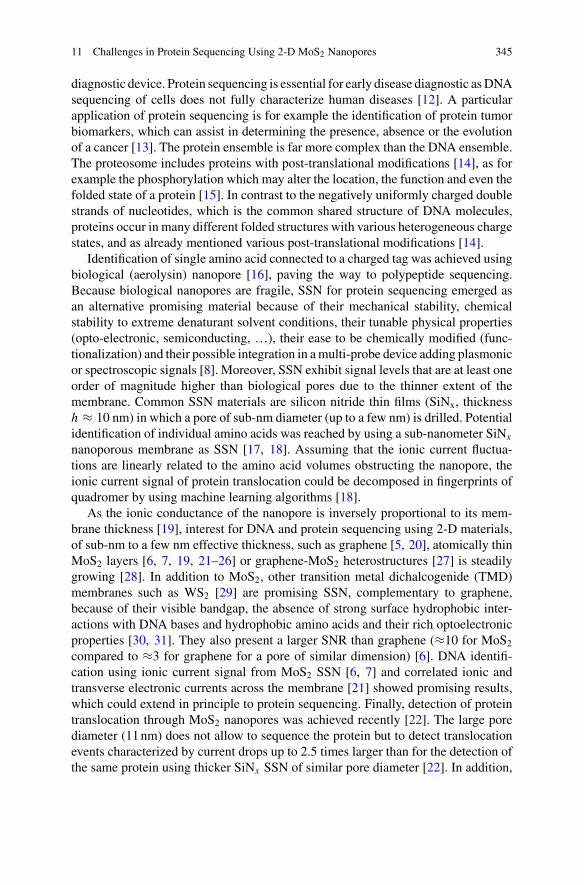
11 Challenges in Protein Sequencing Using 2-D MoS2 Nanopores 345
diagnostic device. Protein sequencing is essential for early disease diagnostic asDNAsequencing of cells does not fully characterize human diseases [12]. A particularapplication of protein sequencing is for example the identification of protein tumorbiomarkers, which can assist in determining the presence, absence or the evolutionof a cancer [13]. The protein ensemble is far more complex than the DNA ensemble.The proteosome includes proteins with post-translational modifications [14], as forexample the phosphorylation which may alter the location, the function and even thefolded state of a protein [15]. In contrast to the negatively uniformly charged doublestrands of nucleotides, which is the common shared structure of DNA molecules,proteins occur in many different folded structures with various heterogeneous chargestates, and as already mentioned various post-translational modifications [14].
Identification of single amino acid connected to a charged tag was achieved usingbiological (aerolysin) nanopore [16], paving the way to polypeptide sequencing.Because biological nanopores are fragile, SSN for protein sequencing emerged asan alternative promising material because of their mechanical stability, chemicalstability to extreme denaturant solvent conditions, their tunable physical properties(opto-electronic, semiconducting, …), their ease to be chemically modified (func-tionalization) and their possible integration in amulti-probe device adding plasmonicor spectroscopic signals [8]. Moreover, SSN exhibit signal levels that are at least oneorder of magnitude higher than biological pores due to the thinner extent of themembrane. Common SSN materials are silicon nitride thin films (SiNx, thicknessh ≈ 10 nm) in which a pore of sub-nm diameter (up to a few nm) is drilled. Potentialidentification of individual amino acids was reached by using a sub-nanometer SiNx
nanoporous membrane as SSN [17, 18]. Assuming that the ionic current fluctua-tions are linearly related to the amino acid volumes obstructing the nanopore, theionic current signal of protein translocation could be decomposed in fingerprints ofquadromer by using machine learning algorithms [18].
As the ionic conductance of the nanopore is inversely proportional to its mem-brane thickness [19], interest for DNA and protein sequencing using 2-D materials,of sub-nm to a few nm effective thickness, such as graphene [5, 20], atomically thinMoS2 layers [6, 7, 19, 21–26] or graphene-MoS2 heterostructures [27] is steadilygrowing [28]. In addition to MoS2, other transition metal dichalcogenide (TMD)membranes such as WS2 [29] are promising SSN, complementary to graphene,because of their visible bandgap, the absence of strong surface hydrophobic inter-actions with DNA bases and hydrophobic amino acids and their rich optoelectronicproperties [30, 31]. They also present a larger SNR than graphene (≈10 for MoS2compared to ≈3 for graphene for a pore of similar dimension) [6]. DNA identifi-cation using ionic current signal from MoS2 SSN [6, 7] and correlated ionic andtransverse electronic currents across the membrane [21] showed promising results,which could extend in principle to protein sequencing. Finally, detection of proteintranslocation through MoS2 nanopores was achieved recently [22]. The large porediameter (11nm) does not allow to sequence the protein but to detect translocationevents characterized by current drops up to 2.5 times larger than for the detection ofthe same protein using thicker SiNx SSN of similar pore diameter [22]. In addition,

346 A. Nicolaï and P. Senet
ability to discriminate single amino acidwithMoS2 SSNwas simulated byMolecularDynamics [23–27].
In spite of recent progress, protein sequencing using nanopore technology remainschallenging [9, 10] and no systematic current method is able to visually differentiatetwo polypeptides with different sequences at the single amino-acid level, althoughthe difference in unfolded states [32] or between homopolymeric peptides [33] can bedetected. Three challenges may be identified to achieve single amino-acid resolutionusing 2-D TMD materials, which are particularly promising to sequence proteinsusing SSN.
• The first challenge is threading the protein into the nanopore. It requires to unfoldits compact tertiary structure for example by chemical [17, 34] or thermal denatu-ration [17, 35]. However, the unfolded state of a protein in solution remains com-pact; if the unfolded chain of N residues is represented by a self-avoiding randomchain, its gyration radius can be approximated to Rg ≈ 0.059 × (N − 1)0.6 nm,i.e. ≈14 nm for N = 100 amino acids. Therefore, the interaction of the unfoldedproteinwith the surface of the nanopore is an important parameter which facilitatesor slow down the protein diffusion towards the nanopore. Moreover, as the passageof monomers across the membrane is driven by an electric field, an appropriatecontrol of the protein net charge using tags [12, 25] or chemical denaturant [17]is also necessary.
• The second challenge is tomeasure the translocation events within the limited tem-poral resolution of the ionic current recording experimentally, which is between100 ns and 10–100 µs. Because of the small thickness of the nanoporous mem-brane, the residence time of molecular fragments may be much shorter than thebin of the ionic current time series. The geometrical parameters of the SSN and thesolvent properties can be modified in order to slow down the passage of monomersacross the membrane.
• The third challenge is to associate specific ionic current fingerprints from the mea-sured current time series to each amino-acid sequence. In this context, time seriesanalysismethods are applied to extract relevant information about the peptide fromionic current measurements.
These challenges are illustrated next fromMolecular Dynamics (MD) simulationsof peptide translocation through MoS2 nanopores. In fact, polypeptide sequencingis the preliminary step to protein sequencing.
11.2 Methods
In this section, we briefly describe all-atom modeling of MoS2 nanopore device andMD simulations of the translocation of biological peptides throughMoS2 nanopores.In addition, an analyticalmodel of ionic conductance ofMoS2 nanopores is presented.Finally, ionic current measurements and statistical distributions extracted from MD
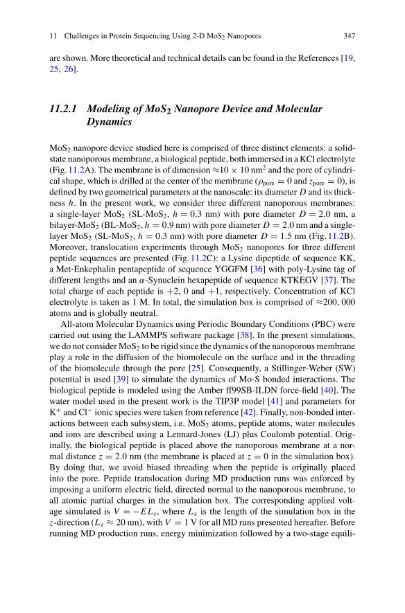
11 Challenges in Protein Sequencing Using 2-D MoS2 Nanopores 347
are shown. More theoretical and technical details can be found in the References [19,25, 26].
11.2.1 Modeling of MoS2 Nanopore Device and MolecularDynamics
MoS2 nanopore device studied here is comprised of three distinct elements: a solid-state nanoporousmembrane, a biological peptide, both immersed in aKCl electrolyte(Fig. 11.2A). The membrane is of dimension≈10 × 10 nm2 and the pore of cylindri-cal shape, which is drilled at the center of the membrane (ρpore = 0 and zpore = 0), isdefined by two geometrical parameters at the nanoscale: its diameter D and its thick-ness h. In the present work, we consider three different nanoporous membranes:a single-layer MoS2 (SL-MoS2, h = 0.3 nm) with pore diameter D = 2.0 nm, abilayer-MoS2 (BL-MoS2, h = 0.9 nm) with pore diameter D = 2.0 nm and a single-layer MoS2 (SL-MoS2, h = 0.3 nm) with pore diameter D = 1.5 nm (Fig. 11.2B).Moreover, translocation experiments through MoS2 nanopores for three differentpeptide sequences are presented (Fig. 11.2C): a Lysine dipeptide of sequence KK,a Met-Enkephalin pentapeptide of sequence YGGFM [36] with poly-Lysine tag ofdifferent lengths and an α-Synuclein hexapeptide of sequence KTKEGV [37]. Thetotal charge of each peptide is +2, 0 and +1, respectively. Concentration of KClelectrolyte is taken as 1 M. In total, the simulation box is comprised of ≈200, 000atoms and is globally neutral.
All-atom Molecular Dynamics using Periodic Boundary Conditions (PBC) werecarried out using the LAMMPS software package [38]. In the present simulations,we do not considerMoS2 to be rigid since the dynamics of the nanoporousmembraneplay a role in the diffusion of the biomolecule on the surface and in the threadingof the biomolecule through the pore [25]. Consequently, a Stillinger-Weber (SW)potential is used [39] to simulate the dynamics of Mo-S bonded interactions. Thebiological peptide is modeled using the Amber ff99SB-ILDN force-field [40]. Thewater model used in the present work is the TIP3P model [41] and parameters forK+ and Cl− ionic species were taken from reference [42]. Finally, non-bonded inter-actions between each subsystem, i.e. MoS2 atoms, peptide atoms, water moleculesand ions are described using a Lennard-Jones (LJ) plus Coulomb potential. Orig-inally, the biological peptide is placed above the nanoporous membrane at a nor-mal distance z = 2.0 nm (the membrane is placed at z = 0 in the simulation box).By doing that, we avoid biased threading when the peptide is originally placedinto the pore. Peptide translocation during MD production runs was enforced byimposing a uniform electric field, directed normal to the nanoporous membrane, toall atomic partial charges in the simulation box. The corresponding applied volt-age simulated is V = −ELz, where Lz is the length of the simulation box in thez-direction (Lz ≈ 20 nm), with V = 1 V for all MD runs presented hereafter. Beforerunning MD production runs, energy minimization followed by a two-stage equili-
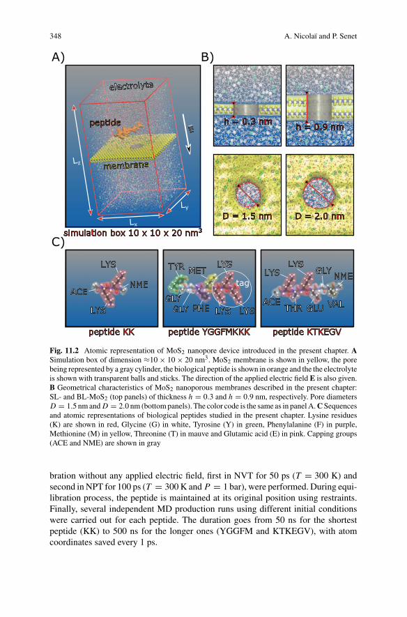
348 A. Nicolaï and P. Senet
Fig. 11.2 Atomic representation of MoS2 nanopore device introduced in the present chapter. ASimulation box of dimension ≈10 × 10 × 20 nm3. MoS2 membrane is shown in yellow, the porebeing represented by a gray cylinder, the biological peptide is shown in orange and the the electrolyteis shown with transparent balls and sticks. The direction of the applied electric field E is also given.B Geometrical characteristics of MoS2 nanoporous membranes described in the present chapter:SL- and BL-MoS2 (top panels) of thickness h = 0.3 and h = 0.9 nm, respectively. Pore diametersD = 1.5 nmand D = 2.0 nm (bottompanels). The color code is the same as in panelA.CSequencesand atomic representations of biological peptides studied in the present chapter. Lysine residues(K) are shown in red, Glycine (G) in white, Tyrosine (Y) in green, Phenylalanine (F) in purple,Methionine (M) in yellow, Threonine (T) in mauve and Glutamic acid (E) in pink. Capping groups(ACE and NME) are shown in gray
bration without any applied electric field, first in NVT for 50 ps (T = 300 K) andsecond in NPT for 100 ps (T = 300 K and P = 1 bar), were performed. During equi-libration process, the peptide is maintained at its original position using restraints.Finally, several independent MD production runs using different initial conditionswere carried out for each peptide. The duration goes from 50 ns for the shortestpeptide (KK) to 500 ns for the longer ones (YGGFM and KTKEGV), with atomcoordinates saved every 1 ps.
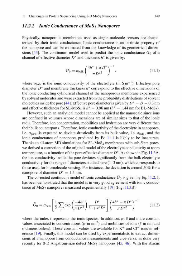
11 Challenges in Protein Sequencing Using 2-D MoS2 Nanopores 349
11.2.2 Ionic Conductance of MoS2 Nanopores
Physically, nanoporous membranes used as single-molecule sensors are charac-terized by their ionic conductance. Ionic conductance is an intrinsic property ofthe nanopore and can be estimated from the knowledge of its geometrical dimen-sions [43]. The continuum model used to predict the ionic conductance G0 of achannel of effective diameter D∗ and thickness h∗ is given by:
G0 = σbulk
(4h∗ + πD∗
πD∗2
)−1
, (11.1)
where σbulk is the ionic conductivity of the electrolyte (in Sm−1). Effective porediameter D∗ and membrane thickness h∗ correspond to the effective dimensions ofthe ionic conducting cylindrical channel of the nanoporous membrane experiencedby solvent molecules and were extracted from the probability distributions of solventmolecules inside the pore [44]. Effective pore diameter is given by D∗ = D − 0.3 nmand effective thickness for SL-MoS2 is h∗ = 0.96 nm (h∗ = 1.44 nm for BL-MoS2).
However, such an analytical model cannot be applied at the nanoscale since ionsare confined in volumes whose dimensions are of similar sizes to that of the ionicradii. Therefore, ion concentration, mobilities and hydration are very different thantheir bulk counterparts. Therefore, ionic conductivity of the electrolyte in nanopores,i.e. σpore, is expected to deviate drastically from its bulk value, i.e. σbulk, and theionic conductance of nanopores predicted by Eq.11.1 is likely to be inaccurate.Thanks to all-atom MD simulations for SL-MoS2 membranes with sub-5nm pores,we derived a correction of the original model of the electrolyte conductivity at roomtemperature, as a function of the pore effective diameter D∗. As shown in Fig. 11.3A,the ion conductivity inside the pore deviates significantly from the bulk electrolyteconductivity for the range of diameters studied here (1–3 nm), which corresponds tothose used for biomolecule sensing. For instance, the deviation is around 50% for ananopore of diameter D∗ = 1.5 nm.
The corrected continuum model of ionic conductance G0 is given by Eq.11.2. Ithas been demonstrated that the model is in very good agreement with ionic conduc-tance of MoS2 nanopores measured experimentally [19] (Fig. 11.3B).
G0 = σbulk
[1
2
∑i
exp
( −4ϕi
πD∗2
)D∗
δi + εi D∗
] (4h∗ + πD∗
πD∗2
)−1
(11.2)
where the index i represents the ionic species. In addition, ϕ, δ and ε are constantvalues associated to concentrations (ϕ in nm2) and mobilities of ions (δ in nm andε dimensionless). These constant values are available for K+ and Cl− ions in ref-erence [19]. Finally, this model can be used by experimentalists to extract dimen-sions of a nanopore from conductance measurements and vice-versa, as done veryrecently for 0-D Angstrom-size defect MoS2 nanopores [45, 46]. With the abacus
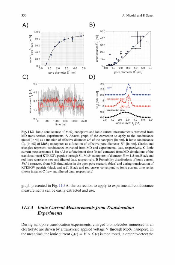
350 A. Nicolaï and P. Senet
Fig. 11.3 Ionic conductance of MoS2 nanopores and ionic current measurements extracted fromMD translocation experiments. A Abacus graph of the correction to apply to the conductancemodel [in %] as a function of effective diameter D∗ of the nanopore [in nm]. B Ionic conductanceG0 [in nS] of MoS2 nanopores as a function of effective pore diameter D∗ [in nm]. Circles andtriangles represent conductance extracted from MD and experimental data, respectively. C Ioniccurrent measurements Ic [in nA] as a function of time [in ns] extracted fromMD simulations of thetranslocation ofKTKEGVpeptide through SL-MoS2 nanopores of diameter D = 1.5 nm.Black andred lines represents raw and filtered data, respectively. D Probability distributions of ionic currentP(Ic) extracted from MD simulations in the open pore scenario (blue) and during translocation ofKTKEGV peptide (black and red). Black and red curves correspond to ionic current time seriesshown in panel C (raw and filtered data, respectively)
graph presented in Fig. 11.3A, the correction to apply to experimental conductancemeasurements can be easily extracted and use.
11.2.3 Ionic Current Measurements from TranslocationExperiments
During nanopore translocation experiments, charged biomolecules immersed in anelectrolyte are driven by a transverse applied voltage V through MoS2 nanopore. Inthe meantime, the ionic current Ic(t) = V × G(t) is monitored, in order to detect the
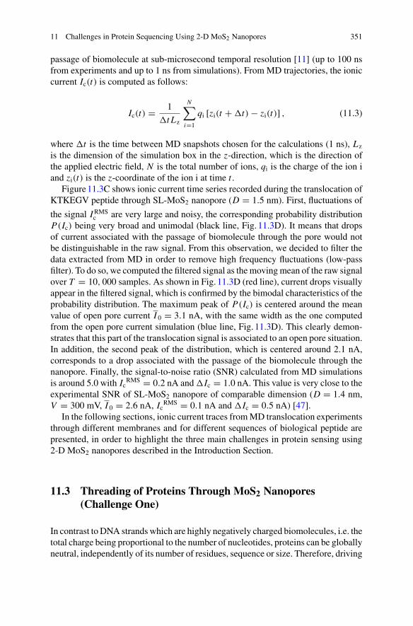
11 Challenges in Protein Sequencing Using 2-D MoS2 Nanopores 351
passage of biomolecule at sub-microsecond temporal resolution [11] (up to 100 nsfrom experiments and up to 1 ns from simulations). From MD trajectories, the ioniccurrent Ic(t) is computed as follows:
Ic(t) = 1
�t Lz
N∑i=1
qi [zi(t + �t) − zi(t)] , (11.3)
where �t is the time between MD snapshots chosen for the calculations (1 ns), Lz
is the dimension of the simulation box in the z-direction, which is the direction ofthe applied electric field, N is the total number of ions, qi is the charge of the ion iand zi(t) is the z-coordinate of the ion i at time t .
Figure11.3C shows ionic current time series recorded during the translocation ofKTKEGV peptide through SL-MoS2 nanopore (D = 1.5 nm). First, fluctuations of
the signal IRMSc are very large and noisy, the corresponding probability distribution
P(Ic) being very broad and unimodal (black line, Fig. 11.3D). It means that dropsof current associated with the passage of biomolecule through the pore would notbe distinguishable in the raw signal. From this observation, we decided to filter thedata extracted from MD in order to remove high frequency fluctuations (low-passfilter). To do so, we computed the filtered signal as the movingmean of the raw signalover T = 10, 000 samples. As shown in Fig. 11.3D (red line), current drops visuallyappear in the filtered signal, which is confirmed by the bimodal characteristics of theprobability distribution. The maximum peak of P(Ic) is centered around the meanvalue of open pore current I 0 = 3.1 nA, with the same width as the one computedfrom the open pore current simulation (blue line, Fig. 11.3D). This clearly demon-strates that this part of the translocation signal is associated to an open pore situation.In addition, the second peak of the distribution, which is centered around 2.1 nA,corresponds to a drop associated with the passage of the biomolecule through thenanopore. Finally, the signal-to-noise ratio (SNR) calculated from MD simulationsis around 5.0 with Ic
RMS = 0.2 nA and �Ic = 1.0 nA. This value is very close to theexperimental SNR of SL-MoS2 nanopore of comparable dimension (D = 1.4 nm,V = 300 mV, I 0 = 2.6 nA, IcRMS = 0.1 nA and �Ic = 0.5 nA) [47].
In the following sections, ionic current traces fromMD translocation experimentsthrough different membranes and for different sequences of biological peptide arepresented, in order to highlight the three main challenges in protein sensing using2-D MoS2 nanopores described in the Introduction Section.
11.3 Threading of Proteins Through MoS2 Nanopores(Challenge One)
In contrast to DNA strandswhich are highly negatively charged biomolecules, i.e. thetotal charge being proportional to the number of nucleotides, proteins can be globallyneutral, independently of its number of residues, sequence or size. Therefore, driving
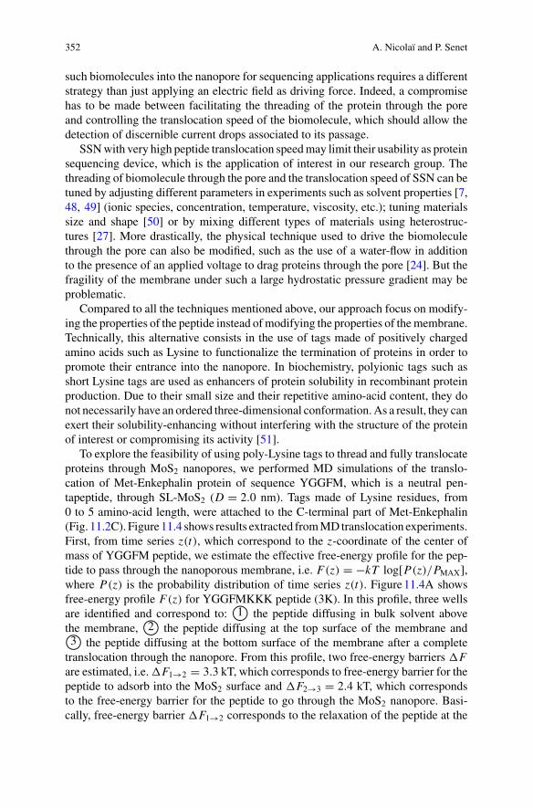
352 A. Nicolaï and P. Senet
such biomolecules into the nanopore for sequencing applications requires a differentstrategy than just applying an electric field as driving force. Indeed, a compromisehas to be made between facilitating the threading of the protein through the poreand controlling the translocation speed of the biomolecule, which should allow thedetection of discernible current drops associated to its passage.
SSNwith very high peptide translocation speedmay limit their usability as proteinsequencing device, which is the application of interest in our research group. Thethreading of biomolecule through the pore and the translocation speed of SSN can betuned by adjusting different parameters in experiments such as solvent properties [7,48, 49] (ionic species, concentration, temperature, viscosity, etc.); tuning materialssize and shape [50] or by mixing different types of materials using heterostruc-tures [27]. More drastically, the physical technique used to drive the biomoleculethrough the pore can also be modified, such as the use of a water-flow in additionto the presence of an applied voltage to drag proteins through the pore [24]. But thefragility of the membrane under such a large hydrostatic pressure gradient may beproblematic.
Compared to all the techniques mentioned above, our approach focus on modify-ing the properties of the peptide instead ofmodifying the properties of themembrane.Technically, this alternative consists in the use of tags made of positively chargedamino acids such as Lysine to functionalize the termination of proteins in order topromote their entrance into the nanopore. In biochemistry, polyionic tags such asshort Lysine tags are used as enhancers of protein solubility in recombinant proteinproduction. Due to their small size and their repetitive amino-acid content, they donot necessarily have an ordered three-dimensional conformation.As a result, they canexert their solubility-enhancing without interfering with the structure of the proteinof interest or compromising its activity [51].
To explore the feasibility of using poly-Lysine tags to thread and fully translocateproteins through MoS2 nanopores, we performed MD simulations of the translo-cation of Met-Enkephalin protein of sequence YGGFM, which is a neutral pen-tapeptide, through SL-MoS2 (D = 2.0 nm). Tags made of Lysine residues, from0 to 5 amino-acid length, were attached to the C-terminal part of Met-Enkephalin(Fig. 11.2C). Figure11.4 shows results extracted fromMDtranslocation experiments.First, from time series z(t), which correspond to the z-coordinate of the center ofmass of YGGFM peptide, we estimate the effective free-energy profile for the pep-tide to pass through the nanoporous membrane, i.e. F(z) = −kT log[P(z)/PMAX],where P(z) is the probability distribution of time series z(t). Figure11.4A showsfree-energy profile F(z) for YGGFMKKK peptide (3K). In this profile, three wellsare identified and correspond to: 1© the peptide diffusing in bulk solvent abovethe membrane, 2© the peptide diffusing at the top surface of the membrane and3© the peptide diffusing at the bottom surface of the membrane after a completetranslocation through the nanopore. From this profile, two free-energy barriers �Fare estimated, i.e.�F1→2 = 3.3 kT, which corresponds to free-energy barrier for thepeptide to adsorb into the MoS2 surface and �F2→3 = 2.4 kT, which correspondsto the free-energy barrier for the peptide to go through the MoS2 nanopore. Basi-cally, free-energy barrier �F1→2 corresponds to the relaxation of the peptide at the
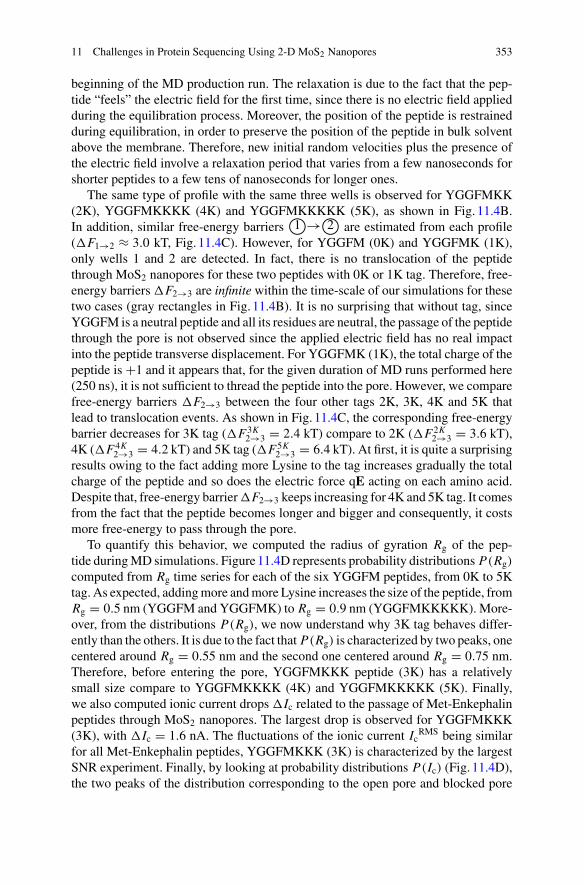
11 Challenges in Protein Sequencing Using 2-D MoS2 Nanopores 353
beginning of the MD production run. The relaxation is due to the fact that the pep-tide “feels” the electric field for the first time, since there is no electric field appliedduring the equilibration process. Moreover, the position of the peptide is restrainedduring equilibration, in order to preserve the position of the peptide in bulk solventabove the membrane. Therefore, new initial random velocities plus the presence ofthe electric field involve a relaxation period that varies from a few nanoseconds forshorter peptides to a few tens of nanoseconds for longer ones.
The same type of profile with the same three wells is observed for YGGFMKK(2K), YGGFMKKKK (4K) and YGGFMKKKKK (5K), as shown in Fig. 11.4B.In addition, similar free-energy barriers 1©→ 2© are estimated from each profile(�F1→2 ≈ 3.0 kT, Fig. 11.4C). However, for YGGFM (0K) and YGGFMK (1K),only wells 1 and 2 are detected. In fact, there is no translocation of the peptidethrough MoS2 nanopores for these two peptides with 0K or 1K tag. Therefore, free-energy barriers �F2→3 are infinite within the time-scale of our simulations for thesetwo cases (gray rectangles in Fig. 11.4B). It is no surprising that without tag, sinceYGGFM is a neutral peptide and all its residues are neutral, the passage of the peptidethrough the pore is not observed since the applied electric field has no real impactinto the peptide transverse displacement. For YGGFMK (1K), the total charge of thepeptide is +1 and it appears that, for the given duration of MD runs performed here(250 ns), it is not sufficient to thread the peptide into the pore. However, we comparefree-energy barriers �F2→3 between the four other tags 2K, 3K, 4K and 5K thatlead to translocation events. As shown in Fig. 11.4C, the corresponding free-energybarrier decreases for 3K tag (�F3K
2→3 = 2.4 kT) compare to 2K (�F2K2→3 = 3.6 kT),
4K (�F4K2→3 = 4.2 kT) and 5K tag (�F5K
2→3 = 6.4 kT). At first, it is quite a surprisingresults owing to the fact adding more Lysine to the tag increases gradually the totalcharge of the peptide and so does the electric force qE acting on each amino acid.Despite that, free-energy barrier�F2→3 keeps increasing for 4K and 5K tag. It comesfrom the fact that the peptide becomes longer and bigger and consequently, it costsmore free-energy to pass through the pore.
To quantify this behavior, we computed the radius of gyration Rg of the pep-tide duringMD simulations. Figure11.4D represents probability distributions P(Rg)
computed from Rg time series for each of the six YGGFM peptides, from 0K to 5Ktag. As expected, addingmore andmore Lysine increases the size of the peptide, fromRg = 0.5 nm (YGGFM and YGGFMK) to Rg = 0.9 nm (YGGFMKKKKK). More-over, from the distributions P(Rg), we now understand why 3K tag behaves differ-ently than the others. It is due to the fact that P(Rg) is characterized by two peaks, onecentered around Rg = 0.55 nm and the second one centered around Rg = 0.75 nm.Therefore, before entering the pore, YGGFMKKK peptide (3K) has a relativelysmall size compare to YGGFMKKKK (4K) and YGGFMKKKKK (5K). Finally,we also computed ionic current drops �Ic related to the passage of Met-Enkephalinpeptides through MoS2 nanopores. The largest drop is observed for YGGFMKKK(3K), with �Ic = 1.6 nA. The fluctuations of the ionic current IcRMS being similarfor all Met-Enkephalin peptides, YGGFMKKK (3K) is characterized by the largestSNR experiment. Finally, by looking at probability distributions P(Ic) (Fig. 11.4D),the two peaks of the distribution corresponding to the open pore and blocked pore
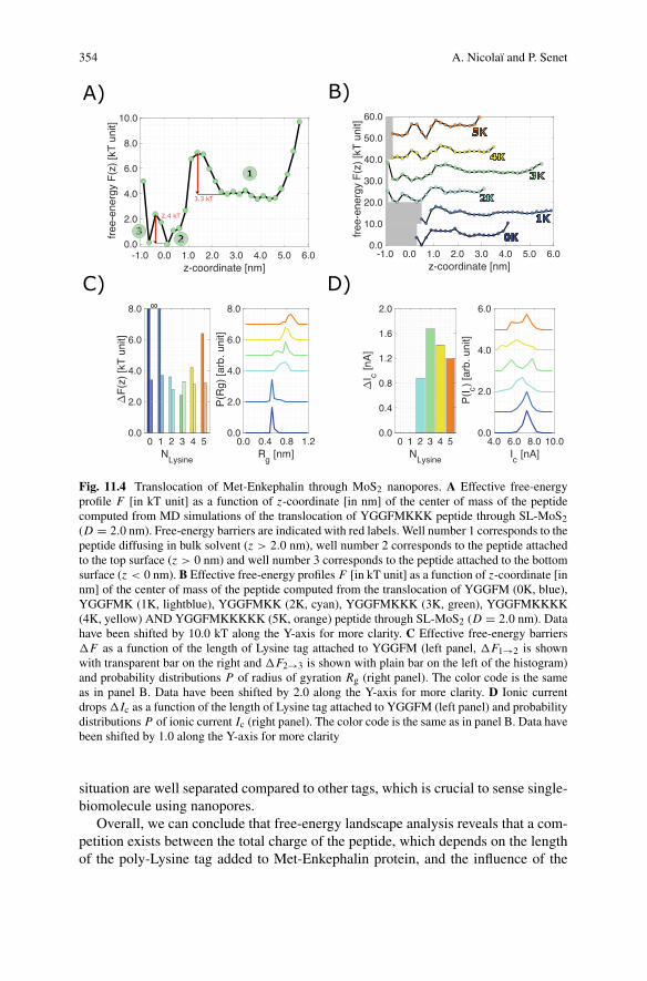
354 A. Nicolaï and P. Senet
Fig. 11.4 Translocation of Met-Enkephalin through MoS2 nanopores. A Effective free-energyprofile F [in kT unit] as a function of z-coordinate [in nm] of the center of mass of the peptidecomputed from MD simulations of the translocation of YGGFMKKK peptide through SL-MoS2(D = 2.0 nm). Free-energy barriers are indicated with red labels. Well number 1 corresponds to thepeptide diffusing in bulk solvent (z > 2.0 nm), well number 2 corresponds to the peptide attachedto the top surface (z > 0 nm) and well number 3 corresponds to the peptide attached to the bottomsurface (z < 0 nm). B Effective free-energy profiles F [in kT unit] as a function of z-coordinate [innm] of the center of mass of the peptide computed from the translocation of YGGFM (0K, blue),YGGFMK (1K, lightblue), YGGFMKK (2K, cyan), YGGFMKKK (3K, green), YGGFMKKKK(4K, yellow) AND YGGFMKKKKK (5K, orange) peptide through SL-MoS2 (D = 2.0 nm). Datahave been shifted by 10.0 kT along the Y-axis for more clarity. C Effective free-energy barriers�F as a function of the length of Lysine tag attached to YGGFM (left panel, �F1→2 is shownwith transparent bar on the right and �F2→3 is shown with plain bar on the left of the histogram)and probability distributions P of radius of gyration Rg (right panel). The color code is the sameas in panel B. Data have been shifted by 2.0 along the Y-axis for more clarity. D Ionic currentdrops �Ic as a function of the length of Lysine tag attached to YGGFM (left panel) and probabilitydistributions P of ionic current Ic (right panel). The color code is the same as in panel B. Data havebeen shifted by 1.0 along the Y-axis for more clarity
situation are well separated compared to other tags, which is crucial to sense single-biomolecule using nanopores.
Overall, we can conclude that free-energy landscape analysis reveals that a com-petition exists between the total charge of the peptide, which depends on the lengthof the poly-Lysine tag added to Met-Enkephalin protein, and the influence of the
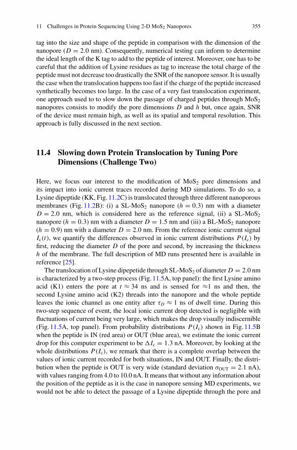
11 Challenges in Protein Sequencing Using 2-D MoS2 Nanopores 355
tag into the size and shape of the peptide in comparison with the dimension of thenanopore (D = 2.0 nm). Consequently, numerical testing can inform to determinethe ideal length of the K tag to add to the peptide of interest. Moreover, one has to becareful that the addition of Lysine residues as tag to increase the total charge of thepeptidemust not decrease too drastically the SNRof the nanopore sensor. It is usuallythe case when the translocation happens too fast if the charge of the peptide increasedsynthetically becomes too large. In the case of a very fast translocation experiment,one approach used to to slow down the passage of charged peptides through MoS2nanopores consists to modify the pore dimensions D and h but, once again, SNRof the device must remain high, as well as its spatial and temporal resolution. Thisapproach is fully discussed in the next section.
11.4 Slowing down Protein Translocation by Tuning PoreDimensions (Challenge Two)
Here, we focus our interest to the modification of MoS2 pore dimensions andits impact into ionic current traces recorded during MD simulations. To do so, aLysine dipeptide (KK, Fig. 11.2C) is translocated through three different nanoporousmembranes (Fig. 11.2B): (i) a SL-MoS2 nanopore (h = 0.3) nm with a diameterD = 2.0 nm, which is considered here as the reference signal, (ii) a SL-MoS2nanopore (h = 0.3) nm with a diameter D = 1.5 nm and (iii) a BL-MoS2 nanopore(h = 0.9) nm with a diameter D = 2.0 nm. From the reference ionic current signalIc(t), we quantify the differences observed in ionic current distributions P(Ic) byfirst, reducing the diameter D of the pore and second, by increasing the thicknessh of the membrane. The full description of MD runs presented here is available inreference [25].
The translocation of Lysine dipepetide through SL-MoS2 of diameter D = 2.0 nmis characterized by a two-step process (Fig. 11.5A, top panel): the first Lysine aminoacid (K1) enters the pore at t ≈ 34 ns and is sensed for ≈1 ns and then, thesecond Lysine amino acid (K2) threads into the nanopore and the whole peptideleaves the ionic channel as one entity after τD ≈ 1 ns of dwell time. During thistwo-step sequence of event, the local ionic current drop detected is negligible withfluctuations of current being very large, which makes the drop visually indiscernible(Fig. 11.5A, top panel). From probability distributions P(Ic) shown in Fig. 11.5Bwhen the peptide is IN (red area) or OUT (blue area), we estimate the ionic currentdrop for this computer experiment to be �Ic = 1.3 nA. Moreover, by looking at thewhole distributions P(Ic), we remark that there is a complete overlap between thevalues of ionic current recorded for both situations, IN and OUT. Finally, the distri-bution when the peptide is OUT is very wide (standard deviation σOUT = 2.1 nA),with values ranging from 4.0 to 10.0 nA. It means that without any information aboutthe position of the peptide as it is the case in nanopore sensing MD experiments, wewould not be able to detect the passage of a Lysine dipeptide through the pore and
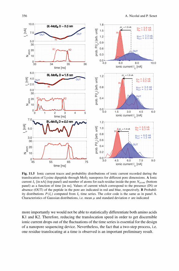
356 A. Nicolaï and P. Senet
Fig. 11.5 Ionic current traces and probability distributions of ionic current recorded during thetranslocation of Lysine dipeptide through MoS2 nanopores for different pore dimensions. A Ioniccurrent Ic [in nA] (top panel) and number of atoms for each residue inside the pore Natom (bottompanel) as a function of time [in ns]. Values of current which correspond to the presence (IN) orabsence (OUT) of the peptide in the pore are indicated in red and blue, respectively. B Probabil-ity distributions P(Ic) computed from Ic time series. The color code is the same as in panel A.Characteristics of Gaussian distributions, i.e. mean μ and standard deviation σ are indicated
more importantly we would not be able to statistically differentiate both amino acidsK1 and K2. Therefore, reducing the translocation speed in order to get discernibleionic current drops out of the fluctuations of the time series is essential for the designof a nanopore sequencing device. Nevertheless, the fact that a two-step process, i.e.one residue translocating at a time is observed is an important preliminary result.
11 Challenges in Protein Sequencing Using 2-D MoS2 Nanopores 357
First, the diameter of SL-MoS2 nanopore was reduced from D = 2.0 to D =1.5 nm. This decrease of diameter leads to a pore conductance reduction from G0 ≈ 8to 4 nS, according to our model (Fig. 11.3B). As observed for SL-MoS2 nanoporeof diameter D = 2.0 nm, the translocation follows a two-step process, although anattempt of translocation of the peptide as a whole is observed at the beginning ofthe translocation process (Fig. 11.5A, middle panel). The N-terminal Lysine (K1)enters the pore first and after ≈3 ns, the C-terminal Lysine (K2) threads into thepore and the full translocation occurs. The dwell time τD is around 3 ns, whichis three times longer than the one detected for the larger pore. From probabilitydistributions of ionic current P(Ic) (Fig. 11.5B, middle panel), we estimate the ioniccurrent drop to be �Ic = 1.2 nA, which is similar to the previous one detected fora larger pore. In addition, reducing diameter D of the nanopore involves smallerfluctuations of the ionic current in an open pore configuration, with σOUT = 1.1 nA.It means that SNR would be larger and the detection of the peptide translocationthrough the pore should be visually more clear, even though a second peak in thedistribution when the peptide is IN is observed around 3.6 nA (corresponding tovalues of current for an open pore situation). Finally, as it is the case for diameterD = 2.0 nm, distinguishing each Lysine residue separately from ionic current tracesrecorded during MD translocation experiments remains unachievable.
Last but not least, the thickness of the MoS2 membrane h was increased fromsingle-layer (h = 0.3 nm) to bilayer (h = 0.9 nm), with a pore diameter of D =2.0 nm. Compared to the decrease of the pore diameter, the conductance of thenanopore only drops from G0 ≈ 8.0 to 6.0 nS, according to our model (Fig. 11.3B).The expected maximum conductance drop is then larger by increasing the thicknessh than reducing the diameter D of the nanoporous membrane. Therefore, a largerSNR is expected (at constant IcRMS), leading to a good compromise in terms of sensorresolution. Figure11.5A (bottom panel) shows ionic current trace recorded duringthe translocation of Lysine dipepetide through BL-MoS2. As already observed forSL-MoS2 membranes, the translocation process can de described by two steps: theN-terminal Lysine (K1) threading first into the pore followed by the C-terminal Lysine(K2), ≈15 ns later. In total, the dwell time τD ≈ 18 ns, reducing significantly thetranslocation speed compared to SL-MoS2. Furthermore, ionic current trace recordedduring the passage of Lysine dipeptide through the pore shows two distinct and dis-cernible drops: the first one when K1 enters the pore at t ≈ 50 ns and a seconddrop of the same magnitude when K2 threads into the pore at t ≈ 65 ns. The corre-sponding current drop is �Ic = 1.2 nA, estimated from probability distributions ofionic current shown in Fig. 11.5B (bottom panel). It corresponds to the same orderof magnitude as the ones for the two other membranes (with similar fluctuations asSL-MoS2 with D = 1.5 nm) but this time, two ionic current fingerprints of the signalare clearly and visually observed for the first time from MD.
This result is crucial for the design of protein sequencing devices. Indeed, forseveral years, experimentalists have been trying to reduce the thickness of themembrane, particularly using 2-D materials in order to get larger SNR and bet-ter spatial resolution. Here, we show that considering bilayer 2-D transition metaldichalcogenides materials instead of single-layer may lead to drops of ionic current
358 A. Nicolaï and P. Senet
directly related to the passage of individual amino acids through the nanopore. Con-sequences of improving the time resolution of the sensor by increasing the thicknessof the nanoporous membrane is that the spatial resolution is downgraded. Therefore,visually reading the primary structure of proteins from ionic current measurementsremains very challenging and time series algorithm are sometimes inevitable. Thischallenge is presented in the next section.
11.5 Identifying Protein Sequence Motifs from IonicCurrent Measurements (Challenge Three)
The variability in ionic current traces associated with peptide translocation, as shownparticularly in the previous section, requires a deep understanding and learning ofthe data. This can be done by applying time series analysis tools to ionic currentmeasurements recorded during translocation experiments. Over the past few years,sophisticated algorithms have been developed to detect and statistically characterizeionic current drops and dwell time of biomolecule translocation through nanoporefrom experimental measurements [52, 53]. Indeed, it is necessary to establish thenon-linear relationship that exists between the presence of amino acids of the peptideinside the nanopore and the ionic current variations measured. This can only be doneif the position of the peptide is known at every single time step of the translocationexperiment, which is what Molecular Dynamics is all about.
In order to understand the variability of peptide translocation fingerprints, a mean-ingful and reliable physical parameter is required to characterize the complexity ofionic current time series measured during nanopore sensing of proteins. In physics,the complexity of a time series is associated with the disorder degree, i.e. randomnessand unpredictability. In this context, entropy is one of themost powerful metrics [54].Specifically, Permutation Entropy (PE), which combined the concept of entropy andtemporal order in a time series, measures information based on the occurrence or theabsence of certain permutation patterns of the ranks of values in a time series [55]. Inaddition, PE can be calculated for arbitrary real-world time series [56], the methodbeing extremely fast and robust. Here, we applied PE algorithm to ionic current timeseries recorded during the translocation of KTKEGV peptide through SL-MoS2 ofdiameter D = 1.5 nm, the time series being shown in Fig. 11.3C (red line).
In nanopore experiments, single-molecule sensing events are extracted from ioniccurrent time series using a current threshold value Icthr. A drop of ionic current �Icis considered as a sensing event if values of current Ic(t) measured during a certainamount of time, i.e. dwell time τD , are below the threshold. In order to mimic asclose as possible the experimental investigation of sensing events from nanoporemeasurements, we first perform a blind detection of sensing events based on a currentthreshold, as in experiments. The current threshold was defined from the probabilitydistribution of open pore ionic current as Icthr = 5σI0 , which corresponds to fivetimes the standard deviation of the open pore ionic current I0 probability distribution
11 Challenges in Protein Sequencing Using 2-D MoS2 Nanopores 359
shown in Fig. 11.3D (blue line). In several experimental works, the current thresholdused is 3σI0 . However, in the case of MoS2 nanopores, we demonstrated that a 3σI0current threshold is not sufficient [26]. With the 5σI0 threshold, a total of 49 sensingevents are detected (Fig. 11.6A), representing cumulatively around 20% of the total2.5µs ionic current time series. As observed experimentally and detailed recently forDNA in reference [57], there is a large variability of current versus time traces withinsensing events. For instance, some events maintain fairly constant current drop andothers show switching levels and bumps.
Therefore, it is impossible to visually associate each level of ionic current to thepassage of specific amino acids through the nanopore. Nevertheless, informationabout the biomolecule may be hidden in the ionic current time series and the ques-tion is where is this information localized. In other words, which levels and bumpsof current and its variations are relevant for protein sequencing and how much infor-mation do they contain. To answer these questions, we quantify the complexity ofthe ionic current traces extracted from MD using PE algorithm. PE measures thedisorder of n successive values in a given time series by using the probability ofdifferent permutation patterns for a given time window of length T within the timeseries. Technically, PE is computed as:
PE = − 1
log2(n!)n!∑j=1
p j log2(p j ), (11.4)
where p j represents the relative frequencies of the possible permutation patterns(n!). More details about PE algorithm can be found in references [55, 56].
PE algorithm was applied to each ionic current trace shown in Fig. 11.6A withn = 3 and T = 1,000 samples, then sliding the time window by 500 samples [26].Figure11.6B shows PE as a function of time window for a specific sensing event(index 41, Fig. 11.6A), with a maximum current drop�Ic = 0.34 nA and dwell timeτD = 19.5 ns. The corresponding ionic current trace is presented in Fig. 11.6B andis overall characterized by three different levels of ionic current, i.e. �Ic ≈ 0.05 nAfor τ ∈ [0; 3] ns and τ ∈ [15; 19] ns,�Ic ≈ 0.25 nA for τ ∈ [6.5; 8.5] ns and�Ic ≈0.30 nA for τ ∈ [10; 13] ns. Moreover, several bumps are observed within levels ofionic current. Applying PE reveals four time windows for which PE is almost null,corresponding to regular linear drops of ionic current between each level and namedhereafter sub-events [26].
Each sub-event is then depicted by the absolute value of its slope, i.e.�(�Ic)/�τ ,which corresponds to an ionic current drop speed. This new parameter named v�Ic isdefined here to characterize ionic current traces variability from protein translocationexperiments. Furthermore, each ionic current drop speed detected using PE algorithmcan be associated to protein sequence motifs. Namely, an ionic current drop speedv�Ic is associated to a protein sequence motif comprised of N amino acids if theN amino acids are inside the pore at the same time during its detection. Severalexamples about the detection of protein sequence motifs are described in details inReference [26]. For the specific event shown in Fig. 11.6B, two distinct motifs are
360 A. Nicolaï and P. Senet
Fig. 11.6 Ionic current traces variability observed during the translocation of KTKEGV peptidethrough SL-MoS2 nanopores (D = 1.5 nm).A Signatures of ionic current drop�Ic as a function oftime τ for the 49 sensing events extracted fromMD translocation experiments shown in Fig. 11.3C.B Permutation Entropy as a function of time [in ns] (top panel) for a specific sensing event (index41, panel A) of 19.5 ns duration. Ionic current drop as a function of time [in ns] (bottom panel)is also shown. Blue lines correspond to parts of the signal for which PE <0.11, named hereaftersub-events. C Average current drop �I c [in nA] (top panel) and average ionic current drop speedv�Ic [in nA/ns] (bottom panel) per protein sequence motif
associated to ionic current drop speed, i.e. T2K3 and E4G5. Finally, we performedthe same PE analysis for each of the 49 events shown in Fig. 11.6A. In total, elevenmotifs are associated to ionic current drop speed v�Ic , the four most probable onesbeing: E4G5 (≈40%), E4 (≈28%), T2K3 (≈12%) and E4G5V6 (≈10%).
Lastly, we evaluate the impact of biological mutations onto ionic current tracesand their characteristics v�Ic described above for the translocation of KTKEGV pep-
11 Challenges in Protein Sequencing Using 2-D MoS2 Nanopores 361
tide through SL-MoS2 nanopores. The mutation selected here is replacing Valine V6(hydrophobic neutral amino acid) by anArginine R6 (positively charged amino acid).Consequently, the total charge of the peptide is modified from +1 to +2. Using thesame procedure to detect sensing events, 26 eventswere detected, representing cumu-latively 10% of the total ionic current time series. In addition, 11 protein sequencemotifs were associated to ionic current traces of the mutant peptide KTKEGR. Thefour most probable motifs are given in Fig. 11.6C and were compared to the onesextracted from KTKEGV peptide. Among these four motifs, three are similar forboth peptides: E4G5, E4, and T2K3. Moreover, these three motifs are characterizedby similar average ionic current drop speed v�Ic , which is a very important result forsequencing application. Indeed, from independent MD simulations, we demonstratefor the first time to the best of our knowledge that protein sequence motifs involvesimilar ionic current related parameters. A difference of maximum 4% is observedfor v�Ic for identical motifs. For information, the comparison of average ionic currentdrop �I c, usually use to try to sequence biomolecule using SSN shows up to 51%difference for identical motifs, which is definitely not suitable for protein sequenc-ing application. This result confirms that the application of PE algorithm to extractrelevant characteristics of protein sequence motifs from the ionic current traces isappropriate and consistent.
11.6 Concluding Remarks
Identification of proteins by solid-state nanopores sequencing is very challenging.Most probably, it will require to cut into polypeptides pieces [58]. Understanding andcontrol polypeptides sequencing using SSN is thus a prerequisite. Heterogeneity ofamino-acid properties and of nanoporous membranes at the atomic scale, as well asthe complicated conformational dynamics of a polypeptide chain, render difficult theprediction and the interpretation of translocation events. Experimentally, a detailedinformation at the atomic scale, as accessible for protein in their native state by NMRor XRD is not available. Therefore, MD simulations of protein sequencing usingSSN may play a role in contributing to a better understanding of the complexity oftranslocation of polypeptides.
In the present chapter, all-atomMDsimulations of translocationofmodel polypep-tides through promising MoS2 nanopores were analyzed. From them, several usefulinformation were extracted:
1. “A larger net peptide charge is not necessarily better”. A compromise must befound in the number of charged residues (Lysine or Arginine) added to improvethe threading of the peptide through the nanopore. Increasing the length of thetag may increase the free-energy barrier to cross the membrane. Further studiesare needed to quantify the relative contributions of entropy and enthalpy to thecrossing barrier.
362 A. Nicolaï and P. Senet
2. “A thinner membrane is not necessarily the best”. Indeed, increasing the thicknessdecreases SNR of the nanopore sensor but also slows down the passage of thepeptide to the other side of the membrane. As shown here, a comprise must befound between these two effects. For MoS2 nanopores, a double-layer appears tobe a working concept.
3. “Current drops are maybe not the best fingerprints”. In fact, larger variations ofcurrent drops are observed in simulations for the translocation of the same proteinsequence motif, whereas the current drop slope is much more discriminant.
Moreover, what MD can provide next? As demonstrated for DNA and poly-Lysine peptides [21], the combination of several signals characterizing the biopoly-mer translocation would improve the accuracy of biomolecule sequence reads. Weenvision that Extraordinary Acoustic Raman (EAR) spectroscopy [59], which char-acterize the acoustical modes of proteins (<100 GHz), might be integrated in prin-ciple to a SSN device. MD would be essential to interpret such possible 2-D signal(ionic current/spectroscopic data) as predictions of protein acoustical modes requireall-atom description of their vibrational spectra [60, 61].
From a fundamental point of view, realistic simulations of polypeptide transloca-tions including protein diffusion, state-of-the art atomic potentials and simulation ofthe current fluctuations, can contribute to decipher the nonlinear relations betweenthe ionic current time series and its meaning, i.e. its information content. As shownhere, application of time series analysis, as high frequency filtering and permutationentropy, better reveal information embedded in the noisy signal. Certainly, super-vised machine learning techniques, already used in this context [18], may assist inthe identification of motifs and ultimately in sequences of polypeptides.
What machine learning techniques coupled to MD could bring in the future is therelation between the polypeptide structures and the current measured. Indeed, everyvalue in the time series corresponds to an ensemble of polypeptide configurationsknown by MD but invisible to experiments. Applying deep learning techniques toestablish links between current and structures might be one of the next challenges.
Acknowledgements The simulations were performed usingHPC resources fromDSI-CCuB (Uni-versité de Bourgogne). The work was supported by a grant from the Air Force Office of ScientificResearch (AFOSR), as part of a joint program with the Directorate for Engineering of the NationalScienceFoundation (NSF),EmergingFrontiers andMultidisciplinaryOffice (GrantNo.FA9550-17-1-0047). Moreover, this work is part of the project NANOSEQ (2018–2021) and NANO-NEURO-MED (2019–2022) supported by the EIPHI Graduate School (contract ANR-17- EURE-0002), theConseil Régional de Bourgogne Franche-Comté and the European Union through the PO FEDER-FSE Bourgogne 2014/2020 programs.
References
1. AkesonMark, Branton Daniel, Church Geroge, Deamer DavidW, and Church George. Charac-terization of individual polymermolecules based onmonomer-interface interactions.December2003.
11 Challenges in Protein Sequencing Using 2-D MoS2 Nanopores 363
2. David Deamer, Mark Akeson, and Daniel Branton. Three decades of nanopore sequencing.Nat. Biotechnol., 34(5):518–524, May 2016.
3. Elizabeth A. Manrao, Ian M. Derrington, Andrew H. Laszlo, Kyle W. Langford, Matthew K.Hopper, Nathaniel Gillgren, Mikhail Pavlenok, Michael Niederweis, and Jens H. Gundlach.Reading DNA at single-nucleotide resolution with a mutant MspA nanopore and phi29 DNApolymerase. Nat. Biotechnol., 30(4):349–353, March 2012.
4. Nicole Rusk. MinION takes center stage. Nat. Methods, 12(1):12–13, January 2015.5. Christopher A. Merchant, Ken Healy, Meni Wanunu, Vishva Ray, Neil Peterman, John Bartel,
Michael D. Fischbein, Kimberly Venta, Zhengtang Luo, A. T. Charlie Johnson, and MarijaDrndic. DNA translocation through graphene nanopores.Nano Lett., 10(8):2915–2921, August2010.
6. Ke Liu, Jiandong Feng, Andras Kis, andAleksandra Radenovic. Atomically ThinMolybdenumDisulfideNanoporeswithHighSensitivity forDNATranslocation.ACSNano, 8(3):2504–2511,March 2014.
7. Jiandong Feng, Ke Liu, Roman D. Bulushev, Sergey Khlybov, Dumitru Dumcenco, AndrasKis, and Aleksandra Radenovic. Identification of single nucleotides in MoS2 nanopores. Nat.Nanotechnol., 10(12):1070–1076, December 2015.
8. Liang Xue, Hirohito Yamazaki, Ren Ren, Meni Wanunu, Aleksandar P. Ivanov, and Joshua B.Edel. Solid-state nanopore sensors.NatureReviewsMaterials, 5(12):931–951,December 2020.
9. Laura Restrepo-Pérez, Chirlmin Joo, and Cees Dekker. Paving the way to single-moleculeprotein sequencing. Nat. Nanotechnol., 13(9):786–796, September 2018.
10. Nitinun Varongchayakul, Jiaxi Song, Amit Meller, and Mark W. Grinstaff. Single-moleculeprotein sensing in a nanopore: a tutorial.Chem. Soc. Rev., 47(23):8512–8524, November 2018.
11. Siddharth Shekar, David J. Niedzwiecki, Chen-Chi Chien, Peijie Ong, Daniel A. Fleischer,Jianxun Lin, Jacob K. Rosenstein, Marija Drndic, and Kenneth L. Shepard. Measurement ofDNA Translocation Dynamics in a Solid-State Nanopore at 100 ns Temporal Resolution.NanoLett., 16(7):4483–4489, 2016.
12. Benjamin Cressiot, Laurent Bacri, and Juan Pelta. The Promise of Nanopore Technology:Advances in the Discrimination of Protein Sequences and Chemical Modifications. SmallMethods, 4(11):2000090, 2020.
13. Carl A. K. Borrebaeck. Precision diagnostics: moving towards protein biomarker signatures ofclinical utility in cancer. Nat. Rev. Cancer, 17(3):199–204, March 2017.
14. Robert S. B. Clark, Hülya Bayir, and LarryW. Jenkins. Posttranslational protein modifications.Crit. Care Med., 33(12 Suppl):S407–409, December 2005.
15. Alaji Bah, RobertM. Vernon, Zeba Siddiqui, Mickaël Krzeminski, RanjithMuhandiram, Char-lie Zhao,NahumSonenberg, Lewis E.Kay, and JulieD. Forman-Kay. Folding of an intrinsicallydisordered protein by phosphorylation as a regulatory switch. Nature, 519(7541):106–109,March 2015.
16. Hadjer Ouldali, Kumar Sarthak, Tobias Ensslen, Fabien Piguet, Philippe Manivet, Juan Pelta,Jan C. Behrends, Aleksei Aksimentiev, and Abdelghani Oukhaled. Electrical recognition of thetwenty proteinogenic amino acids using an aerolysin nanopore. Nat. Biotechnol., 38(2):176–181, February 2020.
17. Eamonn Kennedy, Zhuxin Dong, Clare Tennant, and Gregory Timp. Reading the primarystructure of a protein with 0.07 nm3 resolution using a subnanometre-diameter pore. Nat.Nanotechnol., 11(11):968–976, November 2016.
18. Mikhail Kolmogorov, Eamonn Kennedy, Zhuxin Dong, Gregory Timp, and Pavel A.Pevzner. Single-molecule protein identification by sub-nanopore sensors. PLOSComput. Biol.,13(5):e1005356, 2017.
19. María Daniela Barrios Pérez, AdrienNicolaï, PatriceDelarue, VincentMeunier,Marija Drndic,and Patrick Senet. Improved model of ionic transport in 2-D MoS2 membranes with sub-5 nmpores. Appl. Phys. Lett., 114(2):023107, January 2019.
20. Y. P. Shan, P. B. Tiwari, P. Krishnakumar, I. Vlassiouk, W. Z. Li, X. W. Wang, Y. Darici, S. M.Lindsay, H. D. Wang, S. Smirnov, and J. He. Surface modification of graphene nanopores forprotein translocation. Nanotechnology, 24(49):495102, December 2013.
364 A. Nicolaï and P. Senet
21. Michael Graf, Martina Lihter, Damir Altus, Sanjin Marion, and Aleksandra Radenovic. Trans-verse Detection of DNA Using a MoS2 Nanopore. Nano Lett., 19(12):9075–9083, December2019.
22. Chaoming Gu, Zhoubin Yu, Xiaojie Li, Xin Zhu, Zhen Cao, Zhi Ye, Chuanhong Jin, and YangLiu. Experimental study of protein translocation through MoS2 nanopores. Appl. Phys. Lett.,115(22):223702, November 2019.
23. Amir Barati Farimani, Mohammad Heiranian, and Narayana R. Aluru. Identification of aminoacids with sensitive nanoporous MoS 2 : towards machine learning-based prediction. npj 2DMaterials and Applications, 2(1):1–9, May 2018.
24. Huang Chen, Libo Li, Tao Zhang, Zhiwei Qiao, Jinhui Tang, and Jian Zhou. Protein Transloca-tion through aMoS2 Nanopore:AMolecular Dynamics Study. J. Phys. Chem. C, 122(4):2070–2080, February 2018.
25. AdrienNicolaï,Maria Daniela Barrios Pérez, PatriceDelarue, VincentMeunier,Marija Drndic,and Patrick Senet. Molecular Dynamics Investigation of Polylysine Peptide Translocationthrough MoS2 Nanopores. J. Phys. Chem. B, 123(10):2342–2353, March 2019.
26. Adrien Nicolaï, Aniket Rath, Patrice Delarue, and Patrick Senet. Nanopore sensing of single-biomolecules: a new procedure to identify protein sequence motifs from molecular dynamics.Nanoscale, 12(44):22743–22753, November 2020.
27. Binquan Luan and Ruhong Zhou. Single-File Protein Translocations through Graphene-MoS2Heterostructure Nanopores. J. Phys. Chem. Lett., 9(12):3409–3415, June 2018.
28. HadiArjmandi-Tash, LiubovA.Belyaeva, andGrégory F. Schneider. Singlemolecule detectionwith graphene and other two-dimensional materials: nanopores and beyond. Chem. Soc. Rev.,45(3):476–493, February 2016.
29. Gopinath Danda, Paul Masih Das, Yung-Chien Chou, Jerome T. Mlack, William M. Parkin,Carl H. Naylor, Kazunori Fujisawa, Tianyi Zhang, Laura Beth Fulton, Mauricio Terrones, AlanT. Charlie Johnson, and Marija Drndic. Monolayer WS2 Nanopores for DNA Translocationwith Light-Adjustable Sizes. ACS Nano, 11(2):1937–1945, February 2017.
30. Humberto R. Gutiérrez, Nestor Perea-López, Ana Laura Elías, Ayse Berkdemir, Bei Wang,Ruitao Lv, Florentino López-Urías, Vincent H. Crespi, Humberto Terrones, and Mauricio Ter-rones. Extraordinary room-temperature photoluminescence in triangular WS2 monolayers.Nano Lett., 13(8):3447–3454, August 2013.
31. Mike Tebyetekerwa, Jian Zhang, Zhen Xu, Thien N. Truong, Zongyou Yin, Yuerui Lu,Seeram Ramakrishna, Daniel Macdonald, and Hieu T. Nguyen. Mechanisms and Applica-tions of Steady-State Photoluminescence Spectroscopy in Two-Dimensional Transition-MetalDichalcogenides. ACS Nano, 14(11):14579–14604, November 2020.
32. FangzhouHu, BorislavAngelov, Shuang Li, Na Li, Xubo Lin, andAihua Zou. Single-MoleculeStudy of Peptides with the Same Amino Acid Composition but Different Sequences by Usingan Aerolysin Nanopore. Chembiochem, 21(17):2467–2473, September 2020.
33. Fabien Piguet, Hadjer Ouldali, Manuela Pastoriza-Gallego, Philippe Manivet, Juan Pelta, andAbdelghani Oukhaled. Identification of single amino acid differences in uniformly chargedhomopolymeric peptides with aerolysin nanopore. Nature Communications, 9(1):966, March2018.
34. Linda Payet,MarlèneMartinho,Manuela Pastoriza-Gallego, Jean-Michel Betton, LoïcAuvray,Juan Pelta, and Jérôme Mathé. Thermal unfolding of proteins probed at the single moleculelevel using nanopores. Anal. Chem., 84(9):4071–4076, May 2012.
35. Kevin J. Freedman, Maike Jürgens, Anmiv Prabhu, Chi Won Ahn, Per Jemth, Joshua B. Edel,and Min Jun Kim. Chemical, thermal, and electric field induced unfolding of single proteinmolecules studied using nanopores. Anal. Chem., 83(13):5137–5144, July 2011.
36. François Sicard and Patrick Senet. Reconstructing the free-energy landscape ofMet-enkephalinusing dihedral principal component analysis andwell-temperedmetadynamics. J. Chem. Phys.,138(23):235101, June 2013.
37. Ulf Dettmer, Andrew J. Newman, Victoria E. von Saucken, Tim Bartels, and Dennis Selkoe.KTKEGV repeat motifs are key mediators of normal α-synuclein tetramerization: Their muta-tion causes excess monomers and neurotoxicity. Proc. Natl. Acad. Sci. U.S.A., 112(31):9596–9601, August 2015.
11 Challenges in Protein Sequencing Using 2-D MoS2 Nanopores 365
38. Steve Plimpton. Fast Parallel Algorithms for Short-Range Molecular Dynamics. J. Comput.Phys., 117(1):1–19, March 1995.
39. Jin-Wu Jiang. Parametrization of Stillinger–Weber potential based on valence force fieldmodel:application to single-layer MoS 2 and black phosphorus. Nanotechnology, 26(31):315706,2015.
40. Kresten Lindorff-Larsen, Stefano Piana, Kim Palmo, Paul Maragakis, John L. Klepeis, Ron O.Dror, and David E. Shaw. Improved side-chain torsion potentials for the Amber ff99SB proteinforce field. Proteins: Structure, Function, and Bioinformatics, 78(8):1950–1958, 2010.
41. William L. Jorgensen, Jayaraman Chandrasekhar, Jeffry D. Madura, Roger W. Impey, andMichael L. Klein. Comparison of simple potential functions for simulating liquid water. J.Chem. Phys., 79(2):926–935, July 1983.
42. In Suk Joung and Thomas E. Cheatham. Determination of alkali and halide monovalention parameters for use in explicitly solvated biomolecular simulations. J. Phys. Chem. B,112(30):9020–9041, July 2008.
43. Stefan W. Kowalczyk, Alexander Y. Grosberg, Yitzhak Rabin, and Cees Dekker. Modeling theconductance and DNA blockade of solid-state nanopores. Nanotechnology, 22(31):315101,2011.
44. Marıa Daniela Barrios Perez, Patrick Senet, Vincent Meunier, and Adrien Nicola. Com-putational Investigation of the Ionic Conductance through Molybdenum Disulfide (MoS2)Nanopores. WSEAS Transactions On Circuits And Systems, 16, 2017.
45. Jothi Priyanka Thiruraman, Kazunori Fujisawa, Gopinath Danda, Paul Masih Das, TianyiZhang, Adam Bolotsky, Néstor Perea-López, Adrien Nicolaï, Patrick Senet, Mauricio Ter-rones, and Marija Drndic. Angstrom-Size Defect Creation and Ionic Transport through Poresin Single-Layer MoS2. Nano Lett., 18(3):1651–1659, March 2018.
46. Jothi Priyanka Thiruraman, Paul Masih Das, and Marija Drndic. Stochastic Ionic Transport inSingle Atomic Zero-Dimensional Pores. ACS Nano, 14(9):11831–11845, September 2020.
47. Alessio Fragasso, Sonja Schmid, and Cees Dekker. Comparing Current Noise in Biologicaland Solid-State Nanopores. ACS Nano, 14(2):1338–1349, February 2020.
48. Daniel Fologea, James Uplinger, Brian Thomas, David S. McNabb, and Jiali Li. Slowing DNATranslocation in a Solid-State Nanopore. Nano Lett., 5(9):1734–1737, September 2005.
49. Stefan W. Kowalczyk, David B. Wells, Aleksei Aksimentiev, and Cees Dekker. Slowing downDNA Translocation through a Nanopore in Lithium Chloride. Nano Lett., 12(2):1038–1044,February 2012.
50. Ke Liu, Martina Lihter, Aditya Sarathy, Sabina Caneva, Hu Qiu, Davide Deiana, VasilikiTileli, Duncan T. L. Alexander, Stephan Hofmann, Dumitru Dumcenco, Andras Kis, Jean-Pierre Leburton, and Aleksandra Radenovic. Geometrical Effect in 2D Nanopores. Nano Lett.,17(7):4223–4230, July 2017.
51. Vasiliki Paraskevopoulou and Franco H. Falcone. Polyionic Tags as Enhancers of ProteinSolubility in Recombinant Protein Expression. Microorganisms, 6(2), May 2018.
52. C. Raillon, P. Granjon,M. Graf, L. J. Steinbock, and A. Radenovic. Fast and automatic process-ing of multi-level events in nanopore translocation experiments. Nanoscale, 4(16):4916–4924,July 2012.
53. Calin Plesa andCeesDekker.Data analysismethods for solid-state nanopores.Nanotechnology,26(8):084003, February 2015.
54. C. E. Shannon. A mathematical theory of communication. Bell Syst. Tech. J., 27(3):379–423,July 1948.
55. Christoph Bandt and Bernd Pompe. Permutation Entropy: A Natural Complexity Measure forTime Series. Phys. Rev. Lett., 88(17):174102, April 2002.
56. M. Riedl, A.Müller, and N.Wessel. Practical considerations of permutation entropy. Eur. Phys.J. Spec. Top., 222(2):249–262, June 2013.
57. Chen-Chi Chien, Siddharth Shekar, David J. Niedzwiecki, Kenneth L. Shepard, and MarijaDrndic. Single-Stranded DNA Translocation Recordings through Solid-State Nanopores onGlass Chips at 10 MHz Measurement Bandwidth. ACS Nano, 13(9):10545–10554, September2019.

366 A. Nicolaï and P. Senet
58. G. Sampath. Amino acid discrimination in a nanopore and the feasibility of sequencing peptideswith a tandem cell and exopeptidase. RSC Adv., 5(39):30694–30700, March 2015.
59. Skyler Wheaton, Ryan M. Gelfand, and Reuven Gordon. Probing the Raman-active acousticvibrations of nanoparticles with extraordinary spectral resolution. Nature Photonics, 9(1):68–72, January 2015.
60. Adrien Nicolaï, Patrice Delarue, and Patrick Senet. Theoretical Insights into Sub-TerahertzAcoustic Vibrations of Proteins Measured in Single-Molecule Experiments. J. Phys. Chem.Lett., 7(24):5128–5136, December 2016.
61. Adrien Nicolaï, Fatima Barakat, Patrice Delarue, and Patrick Senet. Fingerprints of Confor-mational States of Human Hsp70 at Sub-THz Frequencies. ACS Omega, 1(6):1067–1074,December 2016.
Chapter 12Single-Molecule Ionic and OpticalSensing with Nanoapertures
Wayne Yang and Cees Dekker
Abstract Solid-state nanoapertures (nanometer sized holes within a membrane)allow for the interrogation of singlemolecules by probing themwithin their nanoscalevolume through which molecules pass in a single-file manner. Molecules are probedusing two main techniques: ionic sensing where a salt solution and applied voltage isused to produce an ionic current through the nanopore, and optical sensing througha shift in the resonance wavelength of the plasmonic nanoaperture. Here, we brieflyreview the basic principles, applications, and challenges in sensing with solid-statenanoapertures, as well as some strategies for further improvements. We comparethe complimentary features of the two approaches and highlight recent attempts tocombine them into new sensing platforms.
12.1 Introduction
All biosensors can be categorized by the size of their sensing region which is impor-tant for their detection sensitivity. By constraining a sensor to a small enough volumeand by tuning the concentration of the analyte to low values, even single moleculescan be sensed and studied [1–3]. Properties on the single-molecule level often dif-fer from ensemble studies [4–6]. For example, transient intermittent conformationalstates of proteins, which are important for an understanding of their function, areoften lost with ensemble techniques such as crystallography [7–9]. Similarly, detec-tion of single-base mutations in the DNA sequence (known as single nucleotidepolymorphisms) which are only present on some DNA strands, are quickly lost inthe background signal when an ensemble of DNA molecules is sequenced [10, 11].Indeed, the ability for sensing on the single-molecule level is important for both
W. Yang · C. Dekker (B)Kavli Institute of Nanoscience, Delft University of Technology, Delft, The Netherlandse-mail: [email protected]
W. Yange-mail: [email protected]
© The Author(s), under exclusive license to Springer Nature Switzerland AG 2022W. Bowen et al. (eds.), Single Molecule Sensing Beyond Fluorescence,Nanostructure Science and Technology,https://doi.org/10.1007/978-3-030-90339-8_12
367
368 W. Yang and C. Dekker
the understanding of biological processes as well as in applications for diagnostics[12–15].
Solid-state nanopores are a common way of building such single-molecule sen-sors. Here one etches a tiny hole (aperture) into a solid-state membrane which allowssingle molecules to physically pass by, as they are small enough to pass, similar to amolecular tunnel [16]. The apertures need to be reliably fabricated on the nanometerscale, i.e. the size scale of single biomolecules—in order to physically restrict thepassage of molecules to a single-file manner. During the passage of the molecule,its properties can be probed. Interestingly, in cells, such pores are formed naturallywithin the membranes of cells where they serve to control the passage of moleculeslike DNA, RNA, and proteins. However, such biological pores are hard to integrateinto solid-state platforms as the fabrication of such systems requires a wide rangeof material science, engineering, and nanofabrication techniques [1, 17, 18]. For-tunately, the rapid development and the increasing availability of nanolithographytechniques in the last few decades have enabled the top-down fabrication of simi-lar solid-state nanoapertures [19]. Apertures, of various shapes on the scale of oneto many tens of nanometers, can be reliably formed in a variety of different solid-state membranes (e.g. silicon nitride-SiN). The use of novel 2D materials, such asgraphene or hexagonal boron nitride (hBN), has pushed the membrane thickness andtherefore the volume of the sensing region down to the ultimate thickness of a singleatomic layer [20–22].
We define a nanoaperture to be a nanometer-sized hole (of varying shape and withlateral dimensions of 1–100nm) that is fabricated within a free-standing membranethat is of a similar thickness. In this chapter, we cover two commonways to probe thepassage of the molecules of interest through such nanoapertures. First, ionic sens-ing which involves the detection of a temporary blockade in the ionic current whenmolecules translocates through the nanopore [23]. Second, optical sensing where achange is detected in the light transmission or reflection upon the molecular passage,which arises due to a change in the optical resonance of the nanoaperture (which willbe further explained below) [24]. Notably, both of these methods do not require thebiomolecule of interest to be labelled. Such label-free techniques are to be preferredover other single-molecule techniques such as electron microscopy, fluorescencemicroscopy, or force techniques such as AFM or optical/magnetic tweezers, that allrequire the use of labels such as heavy-atom stains in electron microscopy, fluo-rophores in fluorescence techniques, and attachment groups for force spectroscopy,which might alter the native behavior of the molecule of interest [25–27]. Below, weintroduce the ionic and optical sensing techniques, describe a few applications, andlay out the limitations and challenges facing each approach.
12.2 Principle of Ionic Current Sensing with Nanopores
A long-standing idea in biosensing has been tomonitor blockades in the ionic currentin order to detect single particles. This idea was first proposed by Wallace Coulterin the 1940s for the screening and counting of blood cells [28]. In so-called ‘Coulter
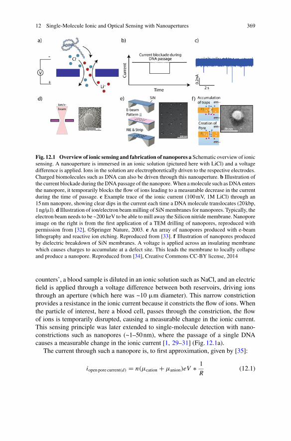
12 Single-Molecule Ionic and Optical Sensing with Nanoapertures 369
Fig. 12.1 Overview of ionic sensing and fabrication of nanopores a Schematic overview of ionicsensing. A nanoaperture is immersed in an ionic solution (pictured here with LiCl) and a voltagedifference is applied. Ions in the solution are electrophoretically driven to the respective electrodes.Charged biomolecules such as DNA can also be driven through this nanoaperture. b Illustration ofthe current blockade during theDNApassage of the nanopore.When amolecule such asDNA entersthe nanopore, it temporarily blocks the flow of ions leading to a measurable decrease in the currentduring the time of passage. c Example trace of the ionic current (100mV, 1M LiCl) through an15nm nanopore, showing clear dips in the current each time a DNA molecule translocates (20kbp,1ng/µl). d Illustration of ion/electron beammilling of SiNmembranes for nanopores. Typically, theelectron beam needs to be ~200 keV to be able to mill away the Silicon nitride membrane. Nanoporeimage on the right is from the first application of a TEM drilling of nanopores, reproduced withpermission from [32], ©Springer Nature, 2003. e An array of nanopores produced with e-beamlithography and reactive ion etching. Reproduced from [33]. f Illustration of nanopores producedby dielectric breakdown of SiN membranes. A voltage is applied across an insulating membranewhich causes charges to accumulate at a defect site. This leads the membrane to locally collapseand produce a nanopore. Reproduced from [34], Creative Commons CC-BY license, 2014
counters’, a blood sample is diluted in an ionic solution such as NaCl, and an electricfield is applied through a voltage difference between both reservoirs, driving ionsthrough an aperture (which here was ~10 µm diameter). This narrow constrictionprovides a resistance in the ionic current because it constricts the flow of ions. Whenthe particle of interest, here a blood cell, passes through the constriction, the flowof ions is temporarily disrupted, causing a measurable change in the ionic current.This sensing principle was later extended to single-molecule detection with nano-constrictions such as nanopores (~1–50nm), where the passage of a single DNAcauses a measurable change in the ionic current [1, 29–31] (Fig. 12.1a).
The current through such a nanopore is, to first approximation, given by [35]:
iopen pore current(d) = n(μcation + μanion)eV ∗ 1
R(12.1)

370 W. Yang and C. Dekker
where n is the number of charge carriers in solution, μcation and μanion are the mobil-ities of the cation and anions, respectively, V is the applied voltage, and R is thegeometric resistance of the nanoconstriction which is given by [36]:
R(d) = 4L
πd2+ 1
d(12.2)
where L is the approximate thickness of the membrane and d is the diameter ofthe nanopore. In most literature, the conductance rather than the current is reported,which is given by G = iopen pore current/V.
When an analyte passes through the constriction, it disrupts the flow of ions byway of the excluded volume, thereby inducing a lower pore conductance. This changein conductance is given by:
�G = Gopen pore current − Ganalyte = G(d) − G(dreduced) (12.3)
where Ganalyte is the reduced ionic conductance of the nanopore when the analyteresides in the pore. For an extended object that spans the entire thickness of the pore(such as a long DNA molecule), this dreduced is equal to the new effective diameterfrom the reduction of the open pore volume that is now occupied by the analyte:
dreduced =√d2 − d2
analyte (12.4)
where danalyte is the diameter of the rod that approximates the analyte (2.2nm for thecase of DNA), see Fig. 12.1b. Figure12.1c shows an example of ionic current tracefor a buffer of 2M LiCl containing DNA. Clear dips can be seen which are caused bythe passage of individual DNAmolecules. Equation12.3 highlights a few parametersthat are crucial for ionic sensing: the salt concentration, the applied voltage whichsupplies the driving force to force the molecule through the constriction, and the sizeof the constriction that defines the geometric resistance [37, 38].
The nanoscale apertures for ionic sensing are usually fabricated in a thin mem-brane (such as 5–20nm thick SiN membrane) through direct-milling techniqueswith an electron beam in a Transmission Electron Microscope (TEM), typicallywith electron energies over 200KeV or with a Focused Ion Beam (FIB) [32, 39,40] (Fig. 12.1d). In recent years, more accessible pore-fabrication techniques havebeen developed such as nanolithography combined with a dry etching (Fig. 12.1e)or dielectric breakdown by applying a large applied voltage (Fig. 12.1f) [33, 34, 41–43]. There also has been a drive to control the fabrication of such pores down tothe precision of a single atoms with crystalline 2D materials and advanced millingtechniques [21, 44].
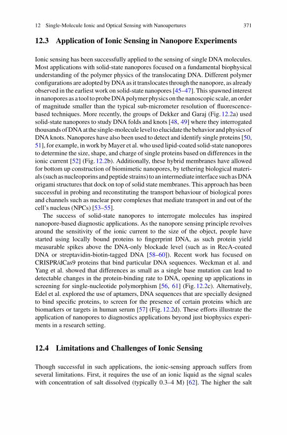
12 Single-Molecule Ionic and Optical Sensing with Nanoapertures 371
12.3 Application of Ionic Sensing in Nanopore Experiments
Ionic sensing has been successfully applied to the sensing of single DNAmolecules.Most applications with solid-state nanopores focused on a fundamental biophysicalunderstanding of the polymer physics of the translocating DNA. Different polymerconfigurations are adopted byDNAas it translocates through the nanopore, as alreadyobserved in the earliest work on solid-state nanopores [45–47]. This spawned interestinnanopores as a tool toprobeDNApolymerphysics on thenanoscopic scale, anorderof magnitude smaller than the typical sub-micrometer resolution of fluorescence-based techniques. More recently, the groups of Dekker and Garaj (Fig. 12.2a) usedsolid-state nanopores to study DNA folds and knots [48, 49] where they interrogatedthousandsofDNAat the single-molecule level to elucidate thebehavior andphysicsofDNA knots. Nanopores have also been used to detect and identify single proteins [50,51], for example, in work byMayer et al. who used lipid-coated solid-state nanoporesto determine the size, shape, and charge of single proteins based on differences in theionic current [52] (Fig. 12.2b). Additionally, these hybrid membranes have allowedfor bottom up construction of biomimetic nanopores, by tethering biological materi-als (suchasnucleoporins andpeptide strains) to an intermediate interface suchasDNAorigami structures that dock on top of solid state membranes. This approach has beensuccessful in probing and reconstituting the transport behaviour of biological poresand channels such as nuclear pore complexes that mediate transport in and out of thecell’s nucleus (NPCs) [53–55].
The success of solid-state nanopores to interrogate molecules has inspirednanopore-based diagnostic applications. As the nanopore sensing principle revolvesaround the sensitivity of the ionic current to the size of the object, people havestarted using locally bound proteins to fingerprint DNA, as such protein yieldmeasurable spikes above the DNA-only blockade level (such as in RecA-coatedDNA or streptavidin-biotin-tagged DNA [58–60]). Recent work has focused onCRISPR/dCas9 proteins that bind particular DNA sequences. Weckman et al. andYang et al. showed that differences as small as a single base mutation can lead todetectable changes in the protein-binding rate to DNA, opening up applications inscreening for single-nucleotide polymorphism [56, 61] (Fig. 12.2c). Alternatively,Edel et al. explored the use of aptamers, DNA sequences that are specially designedto bind specific proteins, to screen for the presence of certain proteins which arebiomarkers or targets in human serum [57] (Fig. 12.2d). These efforts illustrate theapplication of nanopores to diagnostics applications beyond just biophysics experi-ments in a research setting.
12.4 Limitations and Challenges of Ionic Sensing
Though successful in such applications, the ionic-sensing approach suffers fromseveral limitations. First, it requires the use of an ionic liquid as the signal scaleswith concentration of salt dissolved (typically 0.3–4 M) [62]. The higher the salt
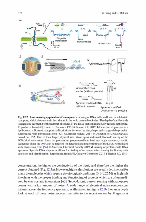
372 W. Yang and C. Dekker
Fig. 12.2 Ionic-sensing application of nanopores a Sensing of DNA folds and knots in solid-statenanopore, which show up as distinct shapes in the ionic current blockades. The depth of the blockadeis quantized according to the number of strands of the DNA that simultaneously resides in the pore.Reproduced from [48], Creative Commons CC-BY license 4.0, 2019. b Detection of proteins in alipid-coated solid-state nanopore to discriminate between the size, shape, and charge of the proteins.Reproduced with permission from [52], ©Springer Nature, 2017. c Detection of CRISPR/dCas9bound on DNA. Due to their larger physical size, show up as additional blockade on top of theDNA blockade current. Since the proteins are programmable to bind any target sequence, specificsequences along the DNA can be targeted for detection and fingerprinting of the DNA. Reproducedwith permission from [56], ©American Chemical Society 2019. d Sensing of proteins with DNAaptamers. Specific DNA sequences allows for binding of certain proteins, thereby facilitating theirdetection and identification. Reproduced from [57], Creative Commons CC-BY license 4.0, 2017
concentration, the higher the conductivity of the liquid and therefore the higher thecurrent obtained (Fig. 12.3a). However, high-salt solutions are usually detrimental formany biomolecules which require physiological conditions (0.1–0.25M) as high saltinterferes with the proper binding and functioning of proteins which are often medi-ated by electrostatic interactions [63]. Second, ionic current sensing with nanoporescomes with a fair amount of noise. A wide range of electrical noise sources con-tributes across the frequency spectrum, as illustrated in Figure12.3b. For an in depthlook at each of these noise sources, we refer to the recent review by Fragasso et
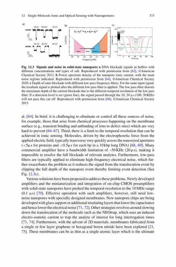
12 Single-Molecule Ionic and Optical Sensing with Nanoapertures 373
Fig. 12.3 Signals and noise in solid-state nanopores a DNA blockade signals in buffers withdifferent concentrations and types of salt. Reproduced with permission from [62], ©AmericanChemical Society 2012. b Power spectrum density of the nanopore ionic current, with the mainnoise regions indicated. Reproduced with permission from [64], ©American Chemical Society2020. cDepth of ionic blockade with different low-pass frequency filters. For the same input signal,the resultant signal is plotted after the different low pass filter is applied. The low pass filter distortsthe maximum depth of the current blockade due to the different temporal resolution of the low passfilter. If a detection level is set (green line), the signal passed through the 10, 20 µs (100, 50KHz)will not pass this cut off. Reproduced with permission from [68], ©American Chemical Society2015
al. [64]. In brief, it is challenging to eliminate or control all these sources of noise,for example, those that arise from chemical processes happening on the membranesurface (e.g., transient binding and unbinding of ions to defect sites) which are veryhard to prevent [64–67]. Third, there is a limit to the temporal resolution that can beachieved in ionic sensing. Molecules, driven by the electrophoretic force from theapplied electric field, typically transverse very quickly across the nanosized apertures(<5µs for proteins and <0.5µs for each bp in a 10kbp long DNA) [68, 69]. Manycommercial amplifier have a bandwidth limitation of ~50KHz (20µs), making itimpossible to resolve the full blockade of relevant analytes. Furthermore, low-passfilters are typically applied to eliminate high-frequency electrical noise, which fur-ther exacerbates the problem as it reduces the signal from the translocation event byclipping the full depth of the nanopore event thereby limiting event detection (SeeFig. 12.3c).
Various solutions have been proposed to address these problems.Newly developedamplifiers and the miniaturization and integration of on-chip CMOS preamplifierswith solid-state nanopores have pushed the temporal resolution to the 10MHz range(0.1 µs) [70]. Effective operation with such amplifiers, however, still need low-noise nanopores with specially designed membranes. New nanopore chips are beingdevelopedwith glass support or additional insulating layers that lower the capacitanceandhence lower the electrical noise [71, 72].Other strategies revolves around slowingdown the translocation of the molecule such as the NEOtrap, which uses an inducedelectro-osmotic current to trap the analyte of interest for long interrogation times[73, 74]. Furthermore, with the advent of 2D materials, membranes fabricated froma single or few layer graphene or hexagonal boron nitride have been explored [21,75]. These membranes can be as thin as a single atomic layer which is the ultimate
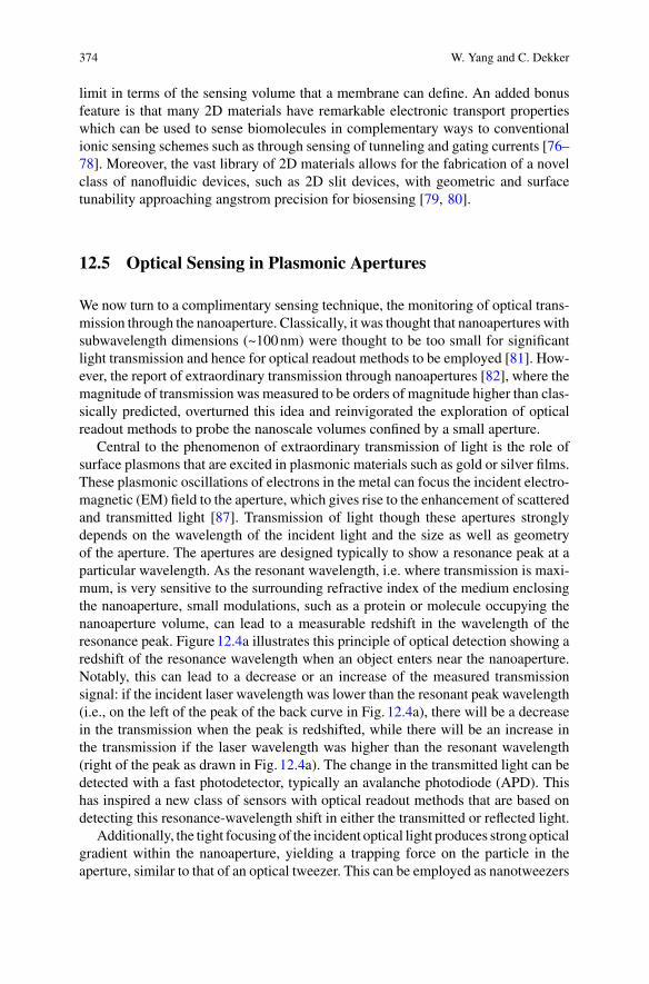
374 W. Yang and C. Dekker
limit in terms of the sensing volume that a membrane can define. An added bonusfeature is that many 2D materials have remarkable electronic transport propertieswhich can be used to sense biomolecules in complementary ways to conventionalionic sensing schemes such as through sensing of tunneling and gating currents [76–78]. Moreover, the vast library of 2D materials allows for the fabrication of a novelclass of nanofluidic devices, such as 2D slit devices, with geometric and surfacetunability approaching angstrom precision for biosensing [79, 80].
12.5 Optical Sensing in Plasmonic Apertures
We now turn to a complimentary sensing technique, the monitoring of optical trans-mission through the nanoaperture. Classically, it was thought that nanoapertures withsubwavelength dimensions (~100nm) were thought to be too small for significantlight transmission and hence for optical readout methods to be employed [81]. How-ever, the report of extraordinary transmission through nanoapertures [82], where themagnitude of transmission was measured to be orders of magnitude higher than clas-sically predicted, overturned this idea and reinvigorated the exploration of opticalreadout methods to probe the nanoscale volumes confined by a small aperture.
Central to the phenomenon of extraordinary transmission of light is the role ofsurface plasmons that are excited in plasmonic materials such as gold or silver films.These plasmonic oscillations of electrons in the metal can focus the incident electro-magnetic (EM) field to the aperture, which gives rise to the enhancement of scatteredand transmitted light [87]. Transmission of light though these apertures stronglydepends on the wavelength of the incident light and the size as well as geometryof the aperture. The apertures are designed typically to show a resonance peak at aparticular wavelength. As the resonant wavelength, i.e. where transmission is maxi-mum, is very sensitive to the surrounding refractive index of the medium enclosingthe nanoaperture, small modulations, such as a protein or molecule occupying thenanoaperture volume, can lead to a measurable redshift in the wavelength of theresonance peak. Figure12.4a illustrates this principle of optical detection showing aredshift of the resonance wavelength when an object enters near the nanoaperture.Notably, this can lead to a decrease or an increase of the measured transmissionsignal: if the incident laser wavelength was lower than the resonant peak wavelength(i.e., on the left of the peak of the back curve in Fig. 12.4a), there will be a decreasein the transmission when the peak is redshifted, while there will be an increase inthe transmission if the laser wavelength was higher than the resonant wavelength(right of the peak as drawn in Fig. 12.4a). The change in the transmitted light can bedetected with a fast photodetector, typically an avalanche photodiode (APD). Thishas inspired a new class of sensors with optical readout methods that are based ondetecting this resonance-wavelength shift in either the transmitted or reflected light.
Additionally, the tight focusing of the incident optical light produces strong opticalgradient within the nanoaperture, yielding a trapping force on the particle in theaperture, similar to that of an optical tweezer. This can be employed as nanotweezers
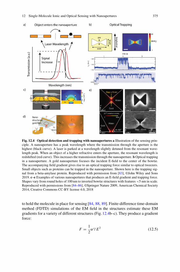
12 Single-Molecule Ionic and Optical Sensing with Nanoapertures 375
Fig. 12.4 Optical detection and trapping with nanoapertures a Illustration of the sensing prin-ciple. A nanoaperture has a peak wavelength where the transmission through the aperture is thehighest (black curve). A laser is parked at a wavelength slightly detuned from the resonant wave-length peak. When an object of a higher refractive enters the aperture, the resonant wavelength isredshifted (red curve). This increases the transmission through the nanoaperture. bOptical trappingin a nanoaperture. A gold nanoaperture focuses the incident E-field to the center of the bowtie.The accompanying field gradient gives rise to an optical trapping force similar to optical tweezers.Small objects such as proteins can be trapped in the nanoaperture. Shown here is the trapping sig-nal from a beta-amylase protein. Reproduced with permission from [83], ©John Wiley and Sons2019. c–e Examples of various nanoapertures that produces an E-field gradient and trapping force.Shapes vary from round holes of 100nm to inverted bowtie structures with features <5 nm in scale.Reproduced with permissions from [84–86], ©Springer Nature 2009, American Chemical Society2014, Creative Commons CC-BY license 4.0, 2018
to hold the molecule in place for sensing [84, 88, 89]. Finite-difference time-domainmethod (FDTD) simulations of the EM field in the structures estimate these EMgradients for a variety of different structures (Fig. 12.4b–c). They produce a gradientforce:
F = 1
2α�E2 (12.5)
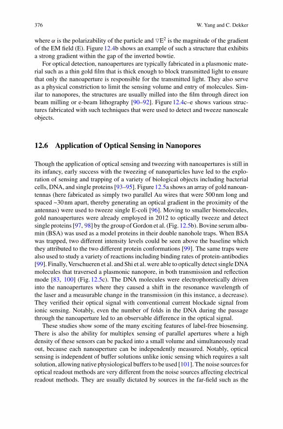
376 W. Yang and C. Dekker
where α is the polarizability of the particle and �E2 is the magnitude of the gradientof the EM field (E). Figure12.4b shows an example of such a structure that exhibitsa strong gradient within the gap of the inverted bowtie.
For optical detection, nanoapertures are typically fabricated in a plasmonic mate-rial such as a thin gold film that is thick enough to block transmitted light to ensurethat only the nanoaperture is responsible for the transmitted light. They also serveas a physical constriction to limit the sensing volume and entry of molecules. Sim-ilar to nanopores, the structures are usually milled into the film through direct ionbeam milling or e-beam lithography [90–92]. Figure12.4c–e shows various struc-tures fabricated with such techniques that were used to detect and tweeze nanoscaleobjects.
12.6 Application of Optical Sensing in Nanopores
Though the application of optical sensing and tweezing with nanoapertures is still inits infancy, early success with the tweezing of nanoparticles have led to the explo-ration of sensing and trapping of a variety of biological objects including bacterialcells, DNA, and single proteins [93–95]. Figure12.5a shows an array of gold nanoan-tennas (here fabricated as simply two parallel Au wires that were 500nm long andspaced ~30nm apart, thereby generating an optical gradient in the proximity of theantennas) were used to tweeze single E-coli [96]. Moving to smaller biomolecules,gold nanoapertures were already employed in 2012 to optically tweeze and detectsingle proteins [97, 98] by the group ofGordon et al. (Fig. 12.5b). Bovine serum albu-min (BSA) was used as a model proteins in their double nanohole traps. When BSAwas trapped, two different intensity levels could be seen above the baseline whichthey attributed to the two different protein conformations [99]. The same traps werealso used to study a variety of reactions including binding rates of protein-antibodies[99]. Finally, Verschueren et al. and Shi et al. were able to optically detect singleDNAmolecules that traversed a plasmonic nanopore, in both transmission and reflectionmode [83, 100] (Fig. 12.5c). The DNA molecules were electrophoretically driveninto the nanoapertures where they caused a shift in the resonance wavelength ofthe laser and a measurable change in the transmission (in this instance, a decrease).They verified their optical signal with conventional current blockade signal fromionic sensing. Notably, even the number of folds in the DNA during the passagethrough the nanoaperture led to an observable difference in the optical signal.
These studies show some of the many exciting features of label-free biosensing.There is also the ability for multiplex sensing of parallel apertures where a highdensity of these sensors can be packed into a small volume and simultaneously readout, because each nanoaperture can be independently measured. Notably, opticalsensing is independent of buffer solutions unlike ionic sensing which requires a saltsolution, allowing native physiological buffers to be used [101]. The noise sources foroptical readout methods are very different from the noise sources affecting electricalreadout methods. They are usually dictated by sources in the far-field such as the
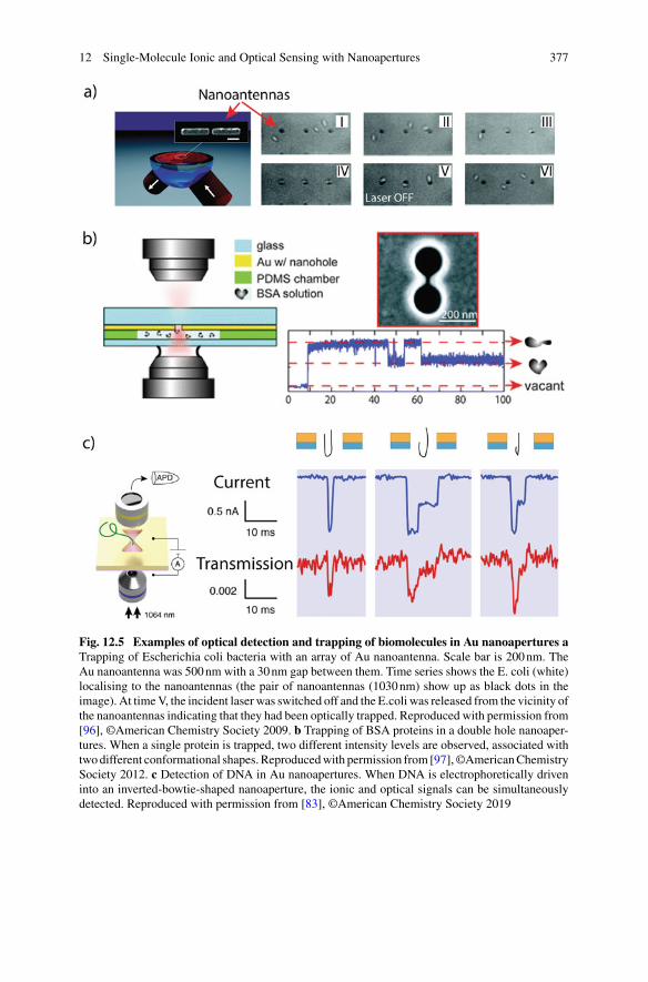
12 Single-Molecule Ionic and Optical Sensing with Nanoapertures 377
Fig. 12.5 Examples of optical detection and trapping of biomolecules in Au nanoapertures aTrapping of Escherichia coli bacteria with an array of Au nanoantenna. Scale bar is 200nm. TheAu nanoantenna was 500nm with a 30nm gap between them. Time series shows the E. coli (white)localising to the nanoantennas (the pair of nanoantennas (1030nm) show up as black dots in theimage). At timeV, the incident laser was switched off and the E.coli was released from the vicinity ofthe nanoantennas indicating that they had been optically trapped. Reproduced with permission from[96], ©American Chemistry Society 2009. b Trapping of BSA proteins in a double hole nanoaper-tures. When a single protein is trapped, two different intensity levels are observed, associated withtwodifferent conformational shapes.Reproducedwith permission from [97],©AmericanChemistrySociety 2012. c Detection of DNA in Au nanoapertures. When DNA is electrophoretically driveninto an inverted-bowtie-shaped nanoaperture, the ionic and optical signals can be simultaneouslydetected. Reproduced with permission from [83], ©American Chemistry Society 2019
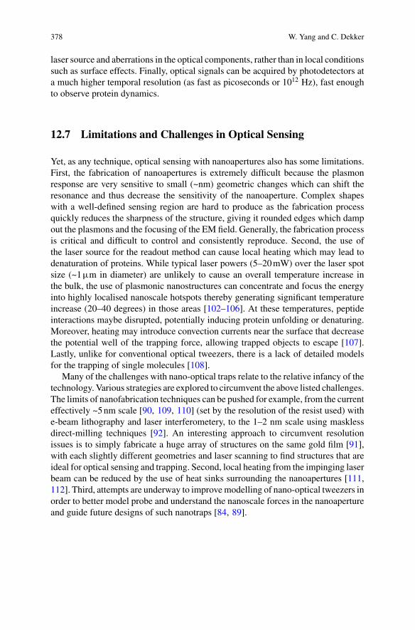
378 W. Yang and C. Dekker
laser source and aberrations in the optical components, rather than in local conditionssuch as surface effects. Finally, optical signals can be acquired by photodetectors ata much higher temporal resolution (as fast as picoseconds or 1012 Hz), fast enoughto observe protein dynamics.
12.7 Limitations and Challenges in Optical Sensing
Yet, as any technique, optical sensing with nanoapertures also has some limitations.First, the fabrication of nanoapertures is extremely difficult because the plasmonresponse are very sensitive to small (~nm) geometric changes which can shift theresonance and thus decrease the sensitivity of the nanoaperture. Complex shapeswith a well-defined sensing region are hard to produce as the fabrication processquickly reduces the sharpness of the structure, giving it rounded edges which dampout the plasmons and the focusing of the EM field. Generally, the fabrication processis critical and difficult to control and consistently reproduce. Second, the use ofthe laser source for the readout method can cause local heating which may lead todenaturation of proteins. While typical laser powers (5–20mW) over the laser spotsize (~1µm in diameter) are unlikely to cause an overall temperature increase inthe bulk, the use of plasmonic nanostructures can concentrate and focus the energyinto highly localised nanoscale hotspots thereby generating significant temperatureincrease (20–40 degrees) in those areas [102–106]. At these temperatures, peptideinteractions maybe disrupted, potentially inducing protein unfolding or denaturing.Moreover, heating may introduce convection currents near the surface that decreasethe potential well of the trapping force, allowing trapped objects to escape [107].Lastly, unlike for conventional optical tweezers, there is a lack of detailed modelsfor the trapping of single molecules [108].
Many of the challenges with nano-optical traps relate to the relative infancy of thetechnology. Various strategies are explored to circumvent the above listed challenges.The limits of nanofabrication techniques can be pushed for example, from the currenteffectively ~5nm scale [90, 109, 110] (set by the resolution of the resist used) withe-beam lithography and laser interferometery, to the 1–2 nm scale using masklessdirect-milling techniques [92]. An interesting approach to circumvent resolutionissues is to simply fabricate a huge array of structures on the same gold film [91],with each slightly different geometries and laser scanning to find structures that areideal for optical sensing and trapping. Second, local heating from the impinging laserbeam can be reduced by the use of heat sinks surrounding the nanoapertures [111,112]. Third, attempts are underway to improvemodelling of nano-optical tweezers inorder to better model probe and understand the nanoscale forces in the nanoapertureand guide future designs of such nanotraps [84, 89].
12 Single-Molecule Ionic and Optical Sensing with Nanoapertures 379
Fig. 12.6 Combined optical-ionic nanopores a Zero mode waveguides where an aperture is fab-ricated in a thin metal film to sense single enzymes. At the bottom of the well, a DNA polymerasecomplex is bound that produces a fluorescence signal that can be used to identify the DNA sequenceof interest. Reproduced with permission from [113], ©The American Association for the Advance-ment of Science, 2003. b Illustration of a nanowell milled in a thin gold film with an integratednanopore termed “opto-nanopore”. The nanopore is used to electrophoretically drive the DNA intothe sensing area where it is optically sensed. Reproduced with permission from [114], ©JohnWileyand Sons 2017. c Integration of a zero-mode waveguide with a nanopore that drives DNAmoleculesto the sensing area. Reproduced with permission from [115], ©Springer Nature 2017
380 W. Yang and C. Dekker
12.8 Simultaneous Ionic and Optical Sensing
In the preceding sections, we have covered the features and limitations of both theionic and optical sensing approaches. Given their complimentary advantages, effortsare ongoing to develop new sensors that combine the optical and ionic readout read-outs [116]. A variety of schemes are proposed to combine the thermophoretic (abyproduct of the optical readout) and electrophoretic effect to transport particles totargeted sensing area [117]. One such approach builds upon zero mode waveguideswhich are a class of nanoapertures where the fluorescence is enhanced in a stronglylocalised regions,which can be used to sense single enzymes (Fig. 12.6a) [113].How-ever, these devices suffered from a lack of active delivery of the biomolecules intothe sensing region. Wanunu et al. took inspiration from ionic sensing approaches andintegrated a nanopore at the bottom of the zero-mode waveguide well where a DNApolymerase was assembled, in order to deterministically drive and deliver DNA forsequencing (Fig. 12.6c) with a fluorescent readout method [115]. Similarly, Meller etal. developed what they called “opto-nanopores” where they integrated a nanoporeat the bottom of the well of a nanoaperture (Fig. 12.6b), thus allowing to combineionic sensing techniques in nanopores with a variety of optical readout methodsfor high-bandwidth measurements [118–120]. They, along with others, demonstrateoptical detection and fingerprinting of DNAmolecules through the use of fluorescentlabels [83, 100]. The expansion of research in combining ionic and optical sensingin nanoapertures also led to the discovery that nanopores can be directly fabricatedin thin SiN membranes with a laser beam. This opens up yet another scalable avenuefor the reliable fabrication of nanopore arrays [121, 122].
12.9 Summary and Outlook
Summing up, nanoapertures define a sensing volume that can be probed with an ioniccurrent or through optical sensing at the single-molecule level. The two approachesoffer complimentary advantages and recent attempts to combine them have led to theadvent of a new class of optical nanopores for detection and manipulation of singlebiomolecules. These nanosensors will increasingly be beneficial for a fundamentalunderstanding of biology as well as for real-world applications such as the detectionof biomarkers in point-of-care devices.
Acknowledgements We would like to thank Alessio Fragasso, Xin Shi and Sonja Schmid forfruitful discussions. C.D would like to acknowledge funding from ERC grant SynDiv 669598 andthe Netherlands Organization for Scientific Research (NWO/OCW) as part of the Frontiers ofNanoscience and Basyc programs.
12 Single-Molecule Ionic and Optical Sensing with Nanoapertures 381
References
1. Daniel Branton, DavidW.Deamer, AndreMarziali, Hagan Bayley, StevenA. Benner, ThomasButler, Massimiliano Di Ventra, Slaven Garaj, Andrew Hibbs, Xiaohua Huang, Stevan B.Jovanovich, Predrag S. Krstic, Stuart Lindsay, Xinsheng Sean Ling, Carlos H. Mastrangelo,Amit Meller, John S. Oliver, Yuriy V. Pershin, J. Michael Ramsey, Robert Riehn, Gautam V.Soni, Vincent Tabard-Cossa, Meni Wanunu, Matthew Wiggin, and Jeffery A. Schloss. Thepotential and challenges of nanopore sequencing. 26(10):1146–1153, 2008.
2. Laura Restrepo-Pérez, Chirlmin Joo, and Cees Dekker. Paving the way to single-moleculeprotein sequencing. Nature nanotechnology, 13(9):786–796, 2018.
3. John J Kasianowicz and Sergey M Bezrukov. On ’three decades of nanopore sequencing’.Nature Biotechnology, 34(5), 2016.
4. Jordanka Zlatanova and Kensal van Holde. Single-Molecule Biology: What Is It and HowDoes It Work? Molecular cell, 24(3):317–329, 2006.
5. Taekjip Ha, Alexander G. Kozlov, and TimothyM. Lohman. Single-molecule views of proteinmovement on single-stranded DNA. Annual Review of Biophysics, 2012.
6. Weichun Zhang, Martín Caldarola, Xuxing Lu, Biswajit Pradhan, and Michel Orrit. Single-molecule fluorescence enhancement of a near-infrared dye by gold nanorods using DNAtransient binding. Physical Chemistry Chemical Physics, 20(31):20468–20475, 2018.
7. K Ravi Acharya and Matthew D Lloyd. The advantages and limitations of protein crystalstructures. Trends in pharmacological sciences, 26(1):10–14, 2005.
8. Xavier Michalet, Shimon Weiss, and Marcus Jäger. Single-molecule fluorescence studies ofprotein folding and conformational dynamics. Chemical reviews, 106(5):1785–1813, 2006.
9. Eugene Kim, Martin D. Baaske, Isabel Schuldes, Peter S. Wilsch, and Frank Vollmer. Label-free optical detection of single enzyme-reactant reactions and associated conformationalchanges. Science Advances, 3(3):e1603044, 2017.
10. J Kong, J Zhu, and U F Keyser. Single molecule based SNP detection using designed DNAcarriers and solid-state nanopores. Chemical Communications, 53(2):436–439, 2017.
11. Q. Zhao, G. Sigalov, V. Dimitrov, B. Dorvel, U. Mirsaidov, S. Sligar, A. Aksimentiev, andG. Timp. Detecting SNPs using a synthetic nanopore. Nano Letters, 7(6):1680–1685, 2007.
12. AndreaM.Armani, Rajan P. Kulkarni, Scott E. Fraser, Richard C. Flagan, andKerry J. Vahala.Label-free, single-molecule detection with optical microcavities. Science, 317(5839):783–787, 2007.
13. D Cibran Perez-Gonzalez and J Carlos Penedo. Single-molecule strategies for DNA and RNAdiagnostics. RNA and DNA Diagnostics, Springer: 297-312, 2015.
14. David R. Walt. Optical methods for single molecule detection and analysis. Analytical Chem-istry, 85(3):1258–1263, 2013.
15. Eugene Kim, Martin D. Baaske, and Frank Vollmer. Towards next-generation label-freebiosensors: recent advances in whispering gallery mode sensors. Lab on a Chip 17(7):1190–1205, 2017.
16. Murugappan Muthukumar, Calin Plesa, and Cees Dekker. Single-molecule sensing withnanopores. Physics Today, 68(8):40–46, 2015.
17. Nitinun Varongchayakul, Jiaxi Song, Amit Meller, and Mark W. Grinstaff. Single-moleculeprotein sensing in a nanopore: a tutorial. Chemical Society reviews, 47(23):8512–8524, 2018.
18. Yanxiao Feng, Yuechuan Zhang, Cuifeng Ying, Deqiang Wang, and Chunlei Du. Nanopore-based Fourth-generation DNA Sequencing Technology. Genomics, Proteomics & Bioinfor-matics, 13(1):4–16, 2015.
19. Qi Chen and Zewen Liu. Fabrication and applications of solid-state nanopores. Sensors,19(8):1886, 2019.
20. S. Garaj, W. Hubbard, A. Reina, J. Kong, D. Branton, and J. A. Golovchenko. Graphene as asubnanometre trans-electrode membrane. Nature, 467(7312):190–193, 2010.
21. KeLiu,MartinaLihter,Aditya Sarathy, SabinaCaneva,HuQiu,DavideDeiana,Vasiliki Tileli,Duncan T. L. Alexander, Stephan Hofmann, Dumitru Dumcenco, Andras Kis, Jean-Pierre
382 W. Yang and C. Dekker
Leburton, and Aleksandra Radenovic. Geometrical effect in 2d nanopores. Nano Letters,17(7):4223–4230, 07 2017.
22. Christopher A Merchant, Ken Healy, Meni Wanunu, Vishva Ray, Neil Peterman, John Bar-tel, Michael D Fischbein, Kimberly Venta, Zhengtang Luo, AT Charlie Johnson, et al. Dnatranslocation through graphene nanopores. Nano letters, 10(8):2915–2921, 2010.
23. John J.Kasianowicz, EricBrandin,Daniel Branton, andDavidW.Deamer. Characterization ofindividual polynucleotide molecules using a membrane channel. Proceedings of the NationalAcademy of Sciences of the United States of America, 93(24):13770–13773, 1996.
24. Yi Xu, Ping Bai, Xiaodong Zhou, Yuriy Akimov, Ching Eng Png, Lay-Kee Ang, WolfgangKnoll, and LinWu. Optical Refractive Index Sensors with Plasmonic and Photonic Structures:Promising and Inconvenient Truth. Advanced Optical Materials, 7(9):1801433, 2019.
25. Helen Miller, Zhaokun Zhou, Jack Shepherd, Adam J.M. Wollman, and Mark C. Leake.Single-molecule techniques in biophysics: a review of the progress in methods and applica-tions. Reports on Progress in Physics, 81(2):024601, 2017.
26. Björn Hellenkamp, Sonja Schmid, Olga Doroshenko, Oleg Opanasyuk, Ralf Kühnemuth,Soheila Rezaei Adariani, Benjamin Ambrose, Mikayel Aznauryan, Anders Barth, Victo-ria Birkedal, et al. Precision and accuracy of single-molecule fret measurements—a multi-laboratory benchmark study. Nature methods, 15(9):669–676, 2018.
27. M. Götz, P. Wortmann, S. Schmid, and T. Hugel. A Multicolor Single-Molecule FRETApproach to Study Protein Dynamics and Interactions Simultaneously. Methods in enzy-mology 581:487–516, 2016.
28. Wallace H Coulter. Means for counting particles suspended in a fluid. US Patent 2,656,508,1953.
29. Hagan Bayley and Charles R Martin. Resistive-pulse sensing from microbes to molecules.Chemical reviews, 100(7):2575–2594, 2000.
30. Meni Wanunu. Nanopores: A journey towards DNA sequencing. Physics of Life Reviews,9(2):125–158, 2012.
31. Tim Albrecht. Single-Molecule Analysis with Solid-State Nanopores. Annual Review of Ana-lytical Chemistry, 12(1):371–387, 2019.
32. A. J. Storm, J.H.Chen,X. S. Ling,H.W.Zandbergen, andC.Dekker. Fabrication of solid-statenanopores with single-nanometre precision. Nature Materials, 2(8):537–540, 2003.
33. Daniel V. Verschueren, Wayne Yang, and Cees Dekker. Lithography-based fabricationof nanopore arrays in freestanding SiN and graphene membranes. Nanotechnology,29(14):145302, 2018.
34. Harold Kwok, Kyle Briggs, and Vincent Tabard-Cossa. Nanopore fabrication by controlleddielectric breakdown. PloS one, 9(3):92880, 2014.
35. Benjamin N. Miles, Aleksandar P. Ivanov, Kerry A. Wilson, Fatma Dogan, Deanpen Japrung,and Joshua B. Edel. Single molecule sensing with solid-state nanopores: Novel materials,methods, and applications. Chemical Society Reviews, 42(1):15–28, 2013.
36. Stefan W Kowalczyk, Alexander Y Grosberg, Yitzhak Rabin, and Cees Dekker. Modelingthe conductance and DNA blockade of solid-state nanopores. Nanotechnology, 22:315101–315106, 2011.
37. Ralph M.M. Smeets, Ulrich F. Keyser, Diego Krapf, Meng Yue Wu, Nynke H. Dekker, andCees Dekker. Salt dependence of ion transport and DMA translocation through solid-statenanopores. Nano Letters, 6(1):89–95, 2006.
38. Daniel Fologea, James Uplinger, Brian Thomas, David S. McNabb, and Jiali Li. SlowingDNA translocation in a solid-state nanopore. Nano Letters, 5(9):1734-1737, 2005.
39. Jiali Li, Derek Stein, Ciaran McMullan, Daniel Branton, Michael J. Aziz, and Jene A.Golovchenko. Ion-beam sculpting at nanometre length scales. Nature, 412(6843):166–169,2001.
40. Laurent D. Menard and J. Michael Ramsey. Fabrication of Sub-5 nm Nanochannels in Insu-lating Substrates Using Focused Ion Beam Milling. Nano Letters, 11(2):512–517, 2011.
41. Sergii Pud, Daniel Verschueren, Nikola Vukovic, Calin Plesa, Magnus P. Jonsson, and CeesDekker. Self-Aligned Plasmonic Nanopores by Optically Controlled Dielectric Breakdown.Nano Letters, 15(10), 2015.
12 Single-Molecule Ionic and Optical Sensing with Nanoapertures 383
42. Kyle Briggs, Martin Charron, Harold Kwok, Timothea Le, Sanmeet Chahal, José Busta-mante, Matthew Waugh, and Vincent Tabard-Cossa. Kinetics of nanopore fabrication duringcontrolled breakdown of dielectric membranes in solution. Nanotechnology, 26(8), 2015.
43. Yuning Zhang, Yoichi Miyahara, Nassim Derriche, Wayne Yang, Khadija Yazda, XavierCapaldi, Zezhou Liu, Peter Grutter, and Walter Reisner. Nanopore Formation via Tip-Controlled Local Breakdown Using an Atomic Force Microscope. Small Methods,3(7):1900147, 2019.
44. Jothi Priyanka Thiruraman, Paul Masih Das, and Marija Drndic. Stochastic Ionic Transportin Single Atomic Zero-D Pores. ACS Nano, 14(9):11831-11845, 2020.
45. Jiali Li, Marc Gershow, Derek Stein, Eric Brandin, and Jene Andrew Golovchenko. Dnamolecules and configurations in a solid-state nanopore microscope. Nature materials,2(9):611–615, 2003.
46. Mirna Mihovilovic, Nicholas Hagerty, and Derek Stein. Statistics of dna capture by a solid-state nanopore. Physical Review Letters, 110(2):028102, 2013.
47. A. J. Storm, J. H. Chen, H. W. Zandbergen, and C. Dekker. Translocation of double-strandDNA through a silicon oxide nanopore. Physical Review E - Statistical, Nonlinear, and SoftMatter Physics, 71(5):051903, 2005.
48. Rajesh Kumar Sharma, Ishita Agrawal, Liang Dai, Patrick S. Doyle, and Slaven Garaj. Com-plex DNA knots detected with a nanopore sensor.Nature Communications, 10(1):4473, 2019.
49. C Plesa, DVerschueren, S Pud, J VanDer Torre, JWRuitenberg,M JWitteveen,M P Jonsson,A Y Grosberg, Y Rabin, and C Dekker. Direct observation of DNA knots using a solid-statenanopore. Nature Nanotechnology, 11(12):1093–1097, 2016.
50. Calin Plesa, StefanWKowalczyk, RubenZinsmeester, AlexanderYGrosberg, YitzhakRabin,and Cees Dekker. Fast translocation of proteins through solid state nanopores. Nano letters,13(2):658–663, 2013.
51. Roman DBulushev, SanjinMarion, Ekaterina Petrova, Sebastian J Davis, Sebastian JMaerkl,and Aleksandra Radenovic. Single molecule localization and discrimination of dna–proteincomplexes by controlled translocation through nanocapillaries. Nano letters, 16(12):7882–7890, 2016.
52. Erik C. Yusko, Brandon R. Bruhn, Olivia M. Eggenberger, Jared Houghtaling, Ryan C.Rollings, Nathan C. Walsh, Santoshi Nandivada, Mariya Pindrus, Adam R. Hall, David Sept,Jiali Li, Devendra S. Kalonia, and Michael Mayer. Real-time shape approximation and fin-gerprinting of single proteins using a nanopore. Nature Nanotechnology, 12(4), 2017.
53. Alessio Fragasso, Hendrik W De Vries, John Andersson, Eli O Van Der Sluis, Erik VanDer Giessen, Andreas Dahlin, Patrick R Onck, and Cees Dekker. A designer fg-nup thatreconstitutes the selective transport barrier of the nuclear pore complex. Nature communica-tions, 12(1):1–15, 2021.
54. Philip Ketterer, Adithya N Ananth, Diederik S Laman Trip, Ankur Mishra, Eva Bertosin,Mahipal Ganji, Jaco van der Torre, Patrick Onck, Hendrik Dietz, and Cees Dekker. Dnaorigami scaffold for studying intrinsically disordered proteins of the nuclear pore complex.Nature communications, 9(1):1–8, 2018.
55. Stefan W Kowalczyk, Timothy R Blosser, and Cees Dekker. Biomimetic nanopores: learningfrom and about nature. Trends in biotechnology, 29(12):607–614, 2011.
56. Nicole E. Weckman, Niklas Ermann, Richard Gutierrez, Kaikai Chen, James Graham, RanTivony, Andrew Heron, and Ulrich F. Keyser. Multiplexed DNA Identification Using SiteSpecific dCas9 Barcodes and Nanopore Sensing. ACS Sensors, 4(8):2065–2072, 2019.
57. JYYSze,AP Ivanov,AEGCass, and JBEdel. Singlemoleculemultiplexed nanopore proteinscreening in human serum using aptamer modified DNA carriers. Nature Communications,8(1):1-10, 2017.
58. RMM Smeets, Stefan W Kowalczyk, AR Hall, NH Dekker, and C Dekker. Translocationof reca-coated double-stranded dna through solid-state nanopores. Nano letters, 9(9):3089–3095, 2009.
59. Kaikai Chen, Matyas Juhasz, Felix Gularek, Elmar Weinhold, Yu Tian, Ulrich F Keyser,and Nicholas AW Bell. Ionic current-based mapping of short sequence motifs in single dnamolecules using solid-state nanopores. Nano letters, 17(9):5199–5205, 2017.
384 W. Yang and C. Dekker
60. Aleksandre Japaridze, Wayne Yang, Cees Dekker, William Nasser, and Georgi Muskhel-ishvili. Dna sequence-directed cooperation between nucleoid-associated proteins. iScience,24(5):102408, 2021.
61. WayneYang, LauraRestrepo-Pérez,MichelBengtson, Stephanie J.Heerema,AnthonyBirnie,Jaco van der Torre, and Cees Dekker. Detection of CRISPR-dCas9 on DNA with Solid-StateNanopores. Nano Letters, 18(10):6469–6474, 2018.
62. Stefan W Kowalczyk, David BWells, Aleksei Aksimentiev, and Cees Dekker. Slowing downdna translocation through a nanopore in lithium chloride. Nano letters, 12(2):1038–1044,2012.
63. Stephen E Halford and John F Marko. How do site-specific dna-binding proteins find theirtargets? Nucleic acids research, 32(10):3040–3052, 2004.
64. Alessio Fragasso, Sonja Schmid, and Cees Dekker. Comparing current noise in biologicaland solid-state nanopores. ACS nano, 14(2):1338–1349, 2020.
65. Alessio Fragasso, Sergii Pud, and Cees Dekker. 1/f noise in solid-state nanopores is governedby access and surface regions. Nanotechnology, 30(39):395202, 2019.
66. Chenyu Wen, Shuangshuang Zeng, Kai Arstila, Timo Sajavaara, Yu Zhu, Zhen Zhang, andShi Li Zhang. Generalized Noise Study of Solid-State Nanopores at Low Frequencies. ACSSensors, 2(2):300–307, 2017.
67. Ralph MM Smeets, Ulrich F Keyser, Nynke H Dekker, and Cees Dekker. Noise in solid-statenanopores. Proceedings of the National Academy of Sciences, 105(2):417–421, 2008.
68. Calin Plesa, JustusW.Ruitenberg,Menno J.Witteveen, andCeesDekker.Detection of individ-ual proteins bound along DNA using solid-state nanopores. Nano Letters, 15(5):3153-3158,2015.
69. Calin Plesa, Nick Van Loo, Philip Ketterer, Hendrik Dietz, and Cees Dekker. Velocity of dnaduring translocation through a solid-state nanopore. Nano letters, 15(1):732–737, 2015.
70. Jacob K Rosenstein, Meni Wanunu, Christopher A Merchant, Marija Drndic, and Kenneth LShepard. Integrated nanopore sensing platform with sub-microsecond temporal resolution.Nature methods, 9(5):487, 2012.
71. Adrian Balan, Chen-Chi Chien, Rebecca Engelke, and Marija Drndic. Suspended solid-statemembranes on glass chips with sub 1-pf capacitance for biomolecule sensing applications.Scientific reports, 5(1):1–8, 2015.
72. Min-Hyun Lee, Ashvani Kumar, Kyeong-Beom Park, Seong-Yong Cho, Hyun-Mi Kim, Min-Cheol Lim, Young-Rok Kim, and Ki-Bum Kim. A low-noise solid-state nanopore platformbased on a highly insulating substrate. Scientific reports, 4(1):1–7, 2014.
73. Sonja Schmid, Pierre Stömmer, Hendrik Dietz, and Cees Dekker. Nanopore electro-osmotictrap for the label-free study of single proteins and their conformations. bioRxiv, 2021.
74. Sonja Schmid and Cees Dekker. Nanopores: a versatile tool to study protein dynamics. Essaysin Biochemistry, 65(1):93–107, 2021.
75. GrégoryF. Schneider,QiangXu,SusanneHage, StephanieLuik, JohannesN.H.Spoor, SairamMalladi, Henny Zandbergen, and Cees Dekker. Tailoring the hydrophobicity of graphene forits use as nanopores for DNA translocation. Nature Communications, 4(1):2619, 2013.
76. Stephanie J. Heerema and Cees Dekker. Graphene nanodevices for DNA sequencing. NatureNanotechnology, 11(2):127–136, 2016.
77. Michael Graf,Martina Lihter, DamirAltus, SanjinMarion, andAleksandra Radenovic. Trans-verse Detection of DNA Using a MoS2 Nanopore. Nano Letters, 19(12):9075–9083, 2019.
78. Mingye Xiong, Michael Graf, Nagendra Athreya, Aleksandra Radenovic, and Jean-PierreLeburton. Microscopic detection analysis of single molecules in mos2 membrane nanopores.ACS nano, 14(11):16131–16139, 2020.
79. Wayne Yang, Boya Radha, Adnan Choudhary, Yi You, Gangaiah Mettela, Andre K Geim,Aleksei Aksimentiev, AshokKeerthi, and CeesDekker. Translocation of dna through ultrathinnanoslits. Advanced Materials, 33(11):2007682, 2021.
80. B Radha, Ali Esfandiar, FC Wang, AP Rooney, K Gopinadhan, Ashok Keerthi, ArtemMishchenko, Amritha Janardanan, Peter Blake, Laura Fumagalli, et al. Molecular transportthrough capillaries made with atomic-scale precision. Nature, 538(7624):222–225, 2016.
12 Single-Molecule Ionic and Optical Sensing with Nanoapertures 385
81. C. Genet and T. W. Ebbesen. Light in tiny holes. Nature, 445(7123):39–46, 2007.82. Thomas W Ebbesen, Henri J Lezec, HF Ghaemi, Tineke Thio, and Peter A Wolff. Extraordi-
nary optical transmission through sub-wavelength hole arrays. Nature, 391(6668):667–669,1998.
83. DanielV.Verschueren, Sergii Pud,Xin Shi, LorenzoDeAngelis, L.Kuipers, andCeesDekker.Label-Free Optical Detection of DNA Translocations through Plasmonic Nanopores. ACSNano, 13(1):61–70, 2019.
84. Mathieu L. Juan, ReuvenGordon, Yuanjie Pang, Fatima Eftekhari, and Romain Quidant. Self-induced back-action optical trapping of dielectric nanoparticles. Nature Physics, 5(12):915–919, 2009.
85. AvijitBarik, LaurenMOtto,DaehanYoo, Jincy Jose, TimothyWJohnson, andSang-HyunOh.Dielectrophoresis-Enhanced Plasmonic Sensing with Gold Nanohole Arrays. Nano Letters,14:2020, 2014.
86. Seung JuYoon, JungminLee, SangyoonHan, ChangKyuKim,ChiWonAhn,MyungKiKim,and Yong Hee Lee. Non-fluorescent nanoscopic monitoring of a single trapped nanoparticlevia nonlinear point sources. Nature Communications, 9(1):341401, 2018.
87. James V Coe, Joseph M Heer, Shannon Teeters-Kennedy, Hong Tian, and Kenneth RRodriguez. Extraordinary transmission of metal films with arrays of subwavelength holes.Annu. Rev. Phys. Chem., 59:179–202, 2008.
88. Reuven Gordon. Biosensing with nanoaperture optical tweezers.Optics & Laser Technology,109:328–335, 2019.
89. Pau Mestres, Johann Berthelot, Srdjan S Acimovic, and Romain Quidant. Unraveling theoptomechanical nature of plasmonic trapping. Light: Science & Applications, 5(7):16092–16092, 2016.
90. Serap Aksu, Ahmet A. Yanik, Ronen Adato, Alp Artar, Min Huang, and Hatice Altug.High-throughput nanofabrication of infrared plasmonic nanoantenna arrays for vibrationalnanospectroscopy. Nano Letters, 10(7):2511–2518, 2010.
91. Xin Shi, Daniel Verschueren, Sergii Pud, and Cees Dekker. Integrating Sub-3 nm PlasmonicGaps into Solid-State Nanopores. Small, 14(18):1703307, 2018.
92. Myung Ki Kim, Hongchul Sim, Seung Ju Yoon, Su Hyun Gong, Chi Won Ahn, Yong HoonCho, and Yong Hee Lee. Squeezing Photons into a Point-Like Space. Nano Letters,15(6):4102–4107, 2015.
93. Alemayehu Nana Koya, Joao Cunha, Tian-Long Guo, Andrea Toma, Denis Garoli, TaoWang,Saulius Juodkazis, Dan Cojoc, and Remo Proietti Zaccaria. Novel plasmonic nanocavities foroptical trapping-assisted biosensing applications.AdvancedOpticalMaterials, 8(7):1901481,2020.
94. Mathieu L Juan, Maurizio Righini, and Romain Quidant. Plasmon nano-optical tweezers.Nature photonics, 5(6):349, 2011.
95. Abhay Kotnala and Reuven Gordon. Double nanohole optical tweezers visualize protein p53suppressing unzipping of single dna-hairpins. Biomedical optics express, 5(6):1886–1894,2014.
96. M Righini, P Ghenuche, S Cherukulappurath, Viktor Myroshnychenko, Francisco Javier Gar-cia deAbajo, andRomainQuidant. Nano-optical trapping of rayleigh particles and escherichiacoli bacteria with resonant optical antennas. Nano letters, 9(10):3387–3391, 2009.
97. Yuanjie Pang and Reuven Gordon. Optical trapping of a single protein. Nano Letters,12(1):402–406, 2012.
98. Daniel Verschueren, Xin Shi, and Cees Dekker. Nano-Optical Tweezing of Single Proteins inPlasmonic Nanopores. Small Methods, 3(5):1800465, 2019.
99. Ana Zehtabi-Oskuie, Hao Jiang, Bryce R. Cyr, DouglasW. Rennehan, Ahmed A. Al-Balushi,and Reuven Gordon. Double nanohole optical trapping: Dynamics and protein-antibody co-trapping. Lab on a Chip, 13(13):2563–2568, 2013.
100. Xin Shi, Daniel V. Verschueren, and Cees Dekker. Active Delivery of Single DNAMoleculesinto a Plasmonic Nanopore for Label-Free Optical Sensing.Nano Letters, 18(12):8003–8010,2018.
386 W. Yang and C. Dekker
101. NoaHacohen, Candice JX Ip, and ReuvenGordon. Analysis of eggwhite protein compositionwith double nanohole optical tweezers. ACS omega, 3(5):5266–5272, 2018.
102. Quanbo Jiang, Benoit Rogez, Jean-Benoît Claude, Guillaume Baffou, and Jérôme Wenger.Temperature measurement in plasmonic nanoapertures used for optical trapping. ACS pho-tonics, 6(7):1763–1773, 2019.
103. Liselotte Jauffred, Akbar Samadi, Henrik Klingberg, Poul Martin Bendix, and Lene B Odd-ershede. Plasmonic heating of nanostructures. Chemical reviews, 119(13):8087–8130, 2019.
104. Colin R Crick, Pablo Albella, Hyung-Jun Kim, Aleksandar P Ivanov, Ki-Bum Kim, Stefan AMaier, and Joshua B Edel. Low-noise plasmonic nanopore biosensors for single moleculedetection at elevated temperatures. ACS Photonics, 4(11):2835–2842, 2017.
105. Ulrich F Keyser, Diego Krapf, Bernard N Koeleman, Ralph MM Smeets, Nynke H Dekker,and Cees Dekker. Nanopore tomography of a laser focus. Nano letters, 5(11):2253–2256,2005.
106. Francesca Nicoli, Daniel Verschueren, Misha Klein, Cees Dekker, and Magnus P Jonsson.Dna translocations through solid-state plasmonic nanopores.Nano letters, 14(12):6917–6925,2014.
107. Brian J Roxworthy, AbdulMBhuiya, Surya PVanka, andKimani C Toussaint. Understandingand controlling plasmon-induced convection. Nature communications, 5(1):1–8, 2014.
108. Erik Schäffer, SimonFNørrelykke, and JonathonHoward. Surface forces and drag coefficientsof microspheres near a plane surface measured with optical tweezers. Langmuir, 23(7):3654–3665, 2007.
109. Bita Malekian, Kunli Xiong, Evan SH Kang, John Andersson, Gustav Emilsson, MarcusRommel, Takumi Sannomiya, Magnus P Jonsson, and Andreas Dahlin. Optical properties ofplasmonic nanopore arrays prepared by electron beam and colloidal lithography. NanoscaleAdvances, 1(11):4282–4289, 2019.
110. Liang Pan, Yongshik Park, Yi Xiong, Erick Ulin-Avila, YuanWang, Li Zeng, Shaomin Xiong,Junsuk Rho, Cheng Sun, David B Bogy, and Xiang Zhang. Maskless plasmonic lithographyat 22 nm resolution. Scientific reports, 1(1):1–6, 2011.
111. Quanbo Jiang, Benoît Rogez, Jean-Benoît Claude, Antonin Moreau, Julien Lumeau, Guil-laume Baffou, and JérômeWenger. Adhesion layer influence on controlling the local temper-ature in plasmonic gold nanoholes. Nanoscale, 12(4):2524–2531, 2020.
112. KaiWang, Ethan Schonbrun, Paul Steinvurzel, and Kenneth B. Crozier. Trapping and rotatingnanoparticles using a plasmonic nano-tweezer with an integrated heat sink. Nature Commu-nications, 2(1):1–6, 2011.
113. H. J. Levene, J. Korlach, S. W. Turner, M. Foquet, H. G. Craighead, and W. W.Webb. Zero-mode waveguides for single-molecule analysis at high concentrations. Science,299(5607):682–686, 2003.
114. Ossama N. Assad, Tal Gilboa, Joshua Spitzberg, Matyas Juhasz, Elmar Weinhold, andAmit Meller. Light-Enhancing Plasmonic-Nanopore Biosensor for Superior Single-MoleculeDetection. Advanced Materials, 29(9):1605442, 2017.
115. Joseph Larkin, Robert Y Henley, Vivek Jadhav, Jonas Korlach, and Meni Wanunu. Length-independent dna packing into nanopore zero-mode waveguides for low-input dna sequencing.Nature nanotechnology, 12(12):1169–1175, 2017.
116. Joshua D Spitzberg, Adam Zrehen, Xander F van Kooten, and Amit Meller.Plasmonic-nanopore biosensors for superior single-molecule detection. Advanced Materials,31(23):1900422, 2019.
117. Justus C Ndukaife, Alexander V Kildishev, Agbai George, Agwu Nnanna, Vladimir M Sha-laev, Steven TWereley, and Alexandra Boltasseva. Long-range and rapid transport of individ-ual nano-objects by a hybrid electrothermoplasmonic nanotweezer. Natue Nanotechnology,11, 2016.
118. BenMcNally, Alon Singer, ZhiliangYu,Yingjie Sun, ZhipingWeng, andAmitMeller. Opticalrecognition of converted dna nucleotides for single-molecule dna sequencing using nanoporearrays. Nano letters, 10(6):2237–2244, 2010.

12 Single-Molecule Ionic and Optical Sensing with Nanoapertures 387
119. Brett N Anderson, Ossama N Assad, Tal Gilboa, Allison H Squires, Daniel Bar, and AmitMeller. Probing solid-state nanopores with light for the detection of unlabeled analytes. ACSnano, 8(11):11836–11845, 2014.
120. TalGilboa andAmitMeller.Optical sensing andanalytemanipulation in solid-state nanopores.Analyst, 140(14):4733–4747, 2015.
121. Tal Gilboa, Adam Zrehen, Arik Girsault, and Amit Meller. Optically-monitored nanoporefabrication using a focused laser beam. Scientific reports, 8(1):1–10, 2018.
122. Tal Gilboa, Eran Zvuloni, Adam Zrehen, Allison H. Squires, and Amit Meller. Automated,Ultra-Fast Laser-Drilling of Nanometer Scale Pores and Nanopore Arrays in Aqueous Solu-tions. Advanced Functional Materials, 30(18):1900642, 2020.
Chapter 13Self-induced Back-Action ActuatedNanopore Electrophoresis (SANE)Sensing
Scott Renkes, Sai Santosh Sasank Peri, Muhammad Usman Raza,Jon Weidanz, Min Jun Kim, and George Alexandrakis
Abstract Wepresent amethod to trap nanoscale analytes in double nanohole (DNH)nanoapertures integrated on top of solid-state nanopores (ssNPs). The analytes arepropelled by an electrophoretic force from the cis towards the trans side of thenanopore but are trapped in the process when they have reached the vicinity of theDNH-ssNP interface. The self-induced back action (SIBA) force, created by theplasmonic field between the tips of the DNH, opposes the electrophoretic force andenables simultaneous optical and electrical sensing of a single nanoparticle for manyseconds. The SIBA actuated nanopore electrophoresis (SANE) sensor was fabri-cated using two-beam gas field ion source (GFIS) focused ion beam (FIB). Firstly,Ne FIB milling was used to create the DNH features and was combined with endpointing to stop milling at the metal-dielectric interface. Subsequently, He FIB wasused to drill a 25nm nanopore through the center of the DNH. The capabilities of thedevice are demonstrated using a series of three experiments involving nanoparticles,high-affinity protein ligand interactions and low-affinity protein-ligand interactions.The presence of optical trapping in the SANE sensor extended electrical sensingand translocation times by up to four orders of magnitude over classical nanopores.In addition, SANE sensor measurements enabled quantification of bimodal optical-electrical parameters thatwere quantified concurrently for each trapping event, whichenabled distinguishing analytes from each other, specific from non-specific binding
S. Renkes · G. Alexandrakis (B)Department of Bioengineering, University of Texas at Arlington, Arlington, TX, USAe-mail: [email protected]
S. Renkese-mail: [email protected]
S. S. S. Peri · M. U. RazaDepartment of Electrical Engineering, University of Texas at Arlington, Arlington, TX, USA
J. WeidanzDepartment of Biology, University of Texas at Arlington, Arlington, TX, USAe-mail: [email protected]
M. J. KimDepartment of Mechanical Engineering, Southern Methodist University, Dallas, TX, USAe-mail: [email protected]
© The Author(s), under exclusive license to Springer Nature Switzerland AG 2022W. Bowen et al. (eds.), Single Molecule Sensing Beyond Fluorescence,Nanostructure Science and Technology,https://doi.org/10.1007/978-3-030-90339-8_13
389
390 S. Renkes et al.
events, and protein complex formation. Importantly, the SANE sensor enabled ultra-high sensitivity in protein-ligand interaction detection. Electrically driven focusing ofreactants into the sensor’s nanoscopic optical trap volume enabled formation of sig-nificant bound fractions (30–50% range) at reactant concentrations up to three ordersofmagnitude lower than the free solution equilibrium binding constant. Furthermore,the SANE sensor could measure the off-binding rate of low-affinity (micromolar)protein-ligand interactions that are challenging to measure with current label-freecommercial assays.
13.1 Introduction
The self-induced back action nanopore electrophoresis (SANE) sensor utilizes aself-induced back action (SIBA) force [1], created by a plasmonic trap, to oppose anelectrophoretic force trying to pushmolecules past the trap and through an underlyingnanopore. As a result, the SIBA effect provides an opportunity to observe molecules,or molecular complexes, label-free and tether-free for many seconds before theytranslocate through the sensor. In addition, the opposing optical force enables sig-nificant slowdown of the actual translocation through the underlying nanopore thatlasts for tens of milliseconds [2]. This is in contrast to traditional nanopores wheremoleculeswill translocate, primarily impeded by barrier forces andmolecular crowd-ing while electroosmosis impedes or facilitates translocation depending on its direc-tion. The typical nanopore translocation event is tens of microseconds [3]. Molec-ular trapping and slower translocation times with the SANE sensor enable bimodaloptical-electrical data acquisition, which we show to be favorable for separating indi-vidual proteins and ligands from the complexes they form and significantly enhanc-ing the bound fraction relative to free solution. In addition, we show that the opticaland electrical data types quantified concurrently by SANE sensing can potentiallyimprove separation of specific from non-specific interactions.
13.1.1 The SIBA Effect
Optical trapping of nanoparticles at low laser powers (mW range) can be attained inthe immediate vicinity of metallic nanoapertures through a SIBA mechanism [1]. InSIBA, when a dielectric nanoparticle has a slightly different refractive index than itssurrounding medium, a photon-mediated feedback force is actuated due to conser-vation of momentum against diffusion forces near the nanoaperture. The resultingcoupling of light to the far field via the dielectric nanoparticle results in increasedlight transmission through the plasmonic nanoaperture and therefore enables label-free detection [4]. Double nanohole (DNH) nanoapertures have been reported asSIBA-mediated optical traps by Gordon et al. for high local field enhancement at theintersection of the nanoholes [5]. The Gordon group has reported a series of studies
13 Self-induced Back-Action Actuated Nanopore Electrophoresis (SANE) Sensing 391
on the design characteristics of the DNH structure [6–8] and their use in manyapplications, including the trapping of nanoparticles [9–11] and single proteinmolecules [12–15].
It should be emphasized that the SIBA effect is qualitatively different from opti-cal tweezing. In the latter case, a high numerical aperture objective lens creates astrong electric field gradient near the beam waist. Dielectric particles are attractedto the region of strongest gradient and displaced slightly by scattering, which placesthem just downstream of the beam waist. Because optical tweezing relies the gradi-ent of light intensity to attract the particle, it is dependent on laser power [16]. Thiscan cause problems with heat dissipation when trying to trap smaller particles. TheDNH structure is more efficient than tweezers in heat dissipation due to the ther-mal conductivity of the surrounding gold (Au) layer. Polarized illumination of theDNH induces plasmonic enhancement of light intensity parallel to its narrow waistto induce the SIBA effect that enables trapping smaller particles, including singleproteins and protein complexes.
In opposition to the trapping force from the SIBA effect are four forces of note:electrophoretic, electroosmotic, passive diffusive and thermophoretic forces. Theelectrophoretic force is the prevalent pulling force in the SANE sensor. It arisesfrom the bias voltage applied to the experimental setup which exerts a force on allcharged particles pulling them based on the direction of the electric field and thezeta potential of the particles [17]. The electroosmotic force is the result of a doublelayer of charges that forms on all the dielectric surfaces in and around the nanopore.This double layer will function as a pump to pull or push ions in solution throughor away from the nanopore. The magnitude and direction of this force is primarilydependent on concentration and ionic properties of the bulk ionic solution while thecharge of analytes has a minor impact [18, 19]. Passive diffusion, which is driven byconcentration gradients, is a relatively small force with respect to the electrophoreticor electroosmotic forces [20]. Thermophoretic forces pull or push particles awayfrom hot spots depending on whether they are thermophilic or thermophobic [21].By altering properties of the solution through the use of surfactants, a particle canbe made more thermophilic, which will increase the force toward the optical trap[22]. Thermophilicity will cause two effects: increase trapping duration while alsodecreasing the time between trapping events. For thermophilic particles inside theoptical trap, the increased thermophoretic forces will offset the electrophoretic forcesand make it more difficult for a particle to leave the trap. For a particle on the cis sideof the nanopore, the thermophoretic forces will combine with the electrophoreticforces drawing it more quickly toward the trap.

392 S. Renkes et al.
13.1.2 Concurrent Optical and Electrical Data Capture withthe SANE Sensor
The SANE sensor is capable of bimodal, optical-electrical sensing and provides fourdata types, two of which are optical and two of which are electrical. These fourmetrics are optical step change, optical trap time, electrical translocation time andtranslocation current:
i Optical step change is the change in optical transmission as a particle entersthe optical trap. The dielectric properties of the molecule act qualitatively as alens, focusing the light through the plasmonic nanoaperture, increasing opticaltransmission [23]. For molecules with spherical shapes, optical step change canbe used to estimate the volume of a molecule.
ii Optical trap time is the time duration that a molecule spends inside the opticaltrap, defined as the time between the timepoint of optical step change completionand the beginning of a translocation event for a single molecule or complex.The optical trap time is a function of the balance between optical forces (SIBA),electrical forces (electrophoresis, electroosmosis and barrier force) and analyte-related forces (concentration gradient and thermophilicity). Depending on thedetailed experimental conditions, the relative contributions of these forces canvary, making this a rather complicated system to study.
iii Translocation time is the measurement of the time it takes a molecule that hasjust escaped the optical trap to travel through the nanopore to the trans well. Thetranslocation event is usually denoted by a negative electrical current spike and adecrease in the optical step back to baseline. Like the optical trap time, this metricis also dependent on the voltage and molecule polarity where a larger voltage andlarger polarity contribute to increased translocation speed [2].
iv Translocation current is the measurement of current change during a pore translo-cation event. The negative current spike usually seen in translocation events isdue to the molecule blocking the baseline ionic current flow. The size of thenegative spike is dependent on analyte size due to its mass blocking the ioniccurrent through the nanopore as well as the charge and concentration of the bulkion solution and the geometry and charge of the nanopore [24].
The ability to perform optical and electrical sensing concurrently with the SANEsensor enables label-free study of molecules and their interactions in ways that arenot accessible by use of traditional optical trapping or classical nanopores on theirown:
1 It can offer higher throughput than pure optical trapping because: (a) pure opticaltrapping can last indefinitely, in principle, and (b) at very low analyte concentra-tions the time interval between successive trapping events can be impracticallylong as it is diffusion-limited [25]. In the case of the SANE sensor, the externallyapplied electric field has a focusing effect, pushing analytes from the cis chambertowards the optical trap. The focusing effect is driven by the silicon nitride (SixNy)region not covered by Au. The latter acts as a shield to the applied electric field
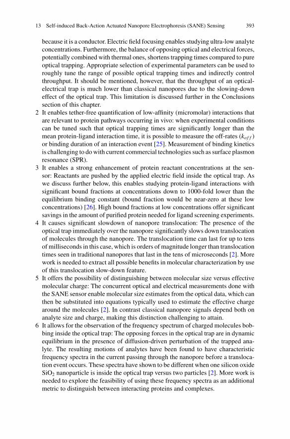
13 Self-induced Back-Action Actuated Nanopore Electrophoresis (SANE) Sensing 393
because it is a conductor. Electric field focusing enables studying ultra-low analyteconcentrations. Furthermore, the balance of opposing optical and electrical forces,potentially combined with thermal ones, shortens trapping times compared to pureoptical trapping. Appropriate selection of experimental parameters can be used toroughly tune the range of possible optical trapping times and indirectly controlthroughput. It should be mentioned, however, that the throughput of an optical-electrical trap is much lower than classical nanopores due to the slowing-downeffect of the optical trap. This limitation is discussed further in the Conclusionssection of this chapter.
2 It enables tether-free quantification of low-affinity (micromolar) interactions thatare relevant to protein pathways occurring in vivo: when experimental conditionscan be tuned such that optical trapping times are significantly longer than themean protein-ligand interaction time, it is possible to measure the off-rates (kof f )or binding duration of an interaction event [25]. Measurement of binding kineticsis challenging to dowith current commercial technologies such as surface plasmonresonance (SPR).
3 It enables a strong enhancement of protein reactant concentrations at the sen-sor: Reactants are pushed by the applied electric field inside the optical trap. Aswe discuss further below, this enables studying protein-ligand interactions withsignificant bound fractions at concentrations down to 1000-fold lower than theequilibrium binding constant (bound fraction would be near-zero at these lowconcentrations) [26]. High bound fractions at low concentrations offer significantsavings in the amount of purified protein needed for ligand screening experiments.
4 It causes significant slowdown of nanopore translocation: The presence of theoptical trap immediately over the nanopore significantly slows down translocationof molecules through the nanopore. The translocation time can last for up to tensofmilliseconds in this case, which is orders of magnitude longer than translocationtimes seen in traditional nanopores that last in the tens of microseconds [2]. Morework is needed to extract all possible benefits in molecular characterization by useof this translocation slow-down feature.
5 It offers the possibility of distinguishing between molecular size versus effectivemolecular charge: The concurrent optical and electrical measurements done withthe SANE sensor enable molecular size estimates from the optical data, which canthen be substituted into equations typically used to estimate the effective chargearound the molecules [2]. In contrast classical nanopore signals depend both onanalyte size and charge, making this distinction challenging to attain.
6 It allows for the observation of the frequency spectrum of charged molecules bob-bing inside the optical trap: The opposing forces in the optical trap are in dynamicequilibrium in the presence of diffusion-driven perturbation of the trapped ana-lyte. The resulting motions of analytes have been found to have characteristicfrequency spectra in the current passing through the nanopore before a transloca-tion event occurs. These spectra have shown to be different when one silicon oxideSiO2 nanoparticle is inside the optical trap versus two particles [2]. More work isneeded to explore the feasibility of using these frequency spectra as an additionalmetric to distinguish between interacting proteins and complexes.
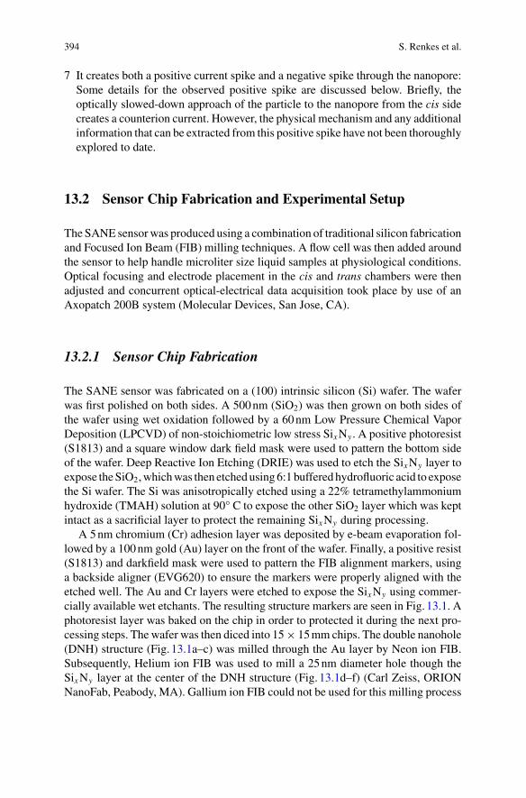
394 S. Renkes et al.
7 It creates both a positive current spike and a negative spike through the nanopore:Some details for the observed positive spike are discussed below. Briefly, theoptically slowed-down approach of the particle to the nanopore from the cis sidecreates a counterion current. However, the physical mechanism and any additionalinformation that can be extracted from this positive spike have not been thoroughlyexplored to date.
13.2 Sensor Chip Fabrication and Experimental Setup
The SANE sensorwas produced using a combination of traditional silicon fabricationand Focused Ion Beam (FIB) milling techniques. A flow cell was then added aroundthe sensor to help handle microliter size liquid samples at physiological conditions.Optical focusing and electrode placement in the cis and trans chambers were thenadjusted and concurrent optical-electrical data acquisition took place by use of anAxopatch 200B system (Molecular Devices, San Jose, CA).
13.2.1 Sensor Chip Fabrication
The SANE sensor was fabricated on a (100) intrinsic silicon (Si) wafer. The waferwas first polished on both sides. A 500nm (SiO2) was then grown on both sides ofthe wafer using wet oxidation followed by a 60nm Low Pressure Chemical VaporDeposition (LPCVD) of non-stoichiometric low stress SixNy . A positive photoresist(S1813) and a square window dark field mask were used to pattern the bottom sideof the wafer. Deep Reactive Ion Etching (DRIE) was used to etch the SixNy layer toexpose theSiO2,whichwas then etchedusing6:1 bufferedhydrofluoric acid to exposethe Si wafer. The Si was anisotropically etched using a 22% tetramethylammoniumhydroxide (TMAH) solution at 90° C to expose the other SiO2 layer which was keptintact as a sacrificial layer to protect the remaining SixNy during processing.
A 5nm chromium (Cr) adhesion layer was deposited by e-beam evaporation fol-lowed by a 100nm gold (Au) layer on the front of the wafer. Finally, a positive resist(S1813) and darkfield mask were used to pattern the FIB alignment markers, usinga backside aligner (EVG620) to ensure the markers were properly aligned with theetched well. The Au and Cr layers were etched to expose the SixNy using commer-cially available wet etchants. The resulting structure markers are seen in Fig. 13.1. Aphotoresist layer was baked on the chip in order to protected it during the next pro-cessing steps. The wafer was then diced into 15× 15mm chips. The double nanohole(DNH) structure (Fig. 13.1a–c) was milled through the Au layer by Neon ion FIB.Subsequently, Helium ion FIB was used to mill a 25nm diameter hole though theSixNy layer at the center of the DNH structure (Fig. 13.1d–f) (Carl Zeiss, ORIONNanoFab, Peabody, MA). Gallium ion FIB could not be used for this milling process
13 Self-induced Back-Action Actuated Nanopore Electrophoresis (SANE) Sensing 395
Fig. 13.1 a Frontside view of SANE chip. b Backside view of SANE chip. c Cross-section of theSANE sensor chip. d SEM micrograph of front side of the SANE chip before FIB drilling. He ionmicroscope image of top view (e) and tilted view (f) of milled DNH with 17% sidewall taper anda 25nm ssNP drilled at its center. Figure and caption reproduced with permissions by [2]
due to the limitation of its feature resolution. A more detailed fabrication processcan be found in Raza et al. [2].

396 S. Renkes et al.
Fig. 13.2 a PDMS flow cell cross-sectional view with SANE sensor. b Image of prepared PDMSflow cell with SANE chip ready for placement on piezo-controlled stage. c Complete optical setupwith PDMSflow cell placement andmeasurement instruments. LD: laser diode, QWP: quarter waveplate, GTP: Glan-Thompson polarizer, HWP: half wave plate, 4× BE: 4× beam expander, MR:mirror, OL: Carl Zeiss 1.3N.A. 63× objective lens, CL: condenser lens, PD: photodiode. Figureand caption reproduced with permissions by [2]
13.2.2 Optical Measurement Setup
The beam from an 820nm laser diode (L820P200, Thorlabs, Newton, NJ) was col-limated to a 2mm diameter and circularly polarized through a quarter-waveplate(QWP) (WPQ05M, Thorlabs), followed by a Glan-Thompson linear polarizer(GTH10M, Thorlabs) for controlling the polarization of light incident on thechip (Fig. 13.2c). The light then passed through a tunable half-waveplate (HWP)(WPH05M, Thorlabs) to make the direction of polarization perpendicular to theDNH’s long axis to maximally excite wedge plasmons for trapping [10]. A down-stream 4× beam expander (Newport) was used in combination with an 8mm circularaperture (ID.1.0, Newport) to make the intensity profile of the cylindrical beam flat-ter. The beam then went through a periscope and into the back aperture of a 63× oilimmersion objective lens and was focused onto the front Au side of the SANE chip.The 360 µm working distance of the objective lens defined the cis flow cell design.A 170 µm thick cover slide was used as the foundation of the cis flow cell. Thatallowed for only 190 µm of height left for the flow cell. Light transmission throughthe FIB alignment markers was used as a first, coarse step to find the DNH on thechip. The objective’s focal spot was aligned with the DNH center by adjusting apiezoelectric stage’s controls until polarized light transmission was maximized. Thelight transmitted through the chip’s center and any leakage light scattering through
13 Self-induced Back-Action Actuated Nanopore Electrophoresis (SANE) Sensing 397
alignment markers was collected by a condenser lens and focused onto a photodiode(PDA36A, Thorlabs) (Fig. 13.2c).
13.2.3 Flow Cell and Electrical Measurement Setup
Flow cells were created from polydimethylsiloxane (PDMS) in three sections. Thebase was made from a 2mm thick piece of PDMS that had two 10mm square holescut at both ends and then connected by a 2mmwide trough. The side with the troughwas then bonded to a 3 in × 2 in glass slide using oxygen plasma, sealing the troughand the bottom of the holes. The trans side of the SANE sensor was bonded to onewell with double-sided tape. A second piece of PDMS, 3mm thick with a 10mmholecut into it, was bonded to the other open hole in the base piece using double-sidedtape. This structure serves as a reservoir for ionic solution. A third piece of PDMSwas made that was roughly 150 µm thick and bonded to a 170µm cover slip (themicroscope slide intended for use with the objective lens). A 10mm hole was cut outof the PDMS. This final piece was then bonded to the cis side of the SANE sensorusing double-sided tape. A 1mm slit was then cut into the cis side of the PDMS toallow the electrode and analytes to be introduced to the cis well. The device wasattached to the piezoelectric stage for fine positioning. The wells were then filledwith an electrolyte solution specific to the experiment. Two silver electrodes wereimmersed in bleach solution to form a coating of silver chloride (Ag/AgCl). Oneelectrode was inserted in the cis and one in the trans chamber. The electrode in thetrans chamber was positioned so that the tip of the electrode was directly below thesensor.
The electrodes were connected to an Axon Axopatch 200B patch clamp ampli-fier and digitizer equipment (Molecular Devices) through an Axon Headstage (CV203BU) and operated in voltage clamp mode. A Faraday cage was built with alu-minum foil (Reynolds) around the piezo-stage with the PDMS flow cell to elimi-nate low-frequency electromagnetic noise while recording the ionic current traces.Translocation events were performed at 100 mV voltage bias across the nanopore[25]. The photodiode and Axopatch 200B signals were both sent through an AxonDigidata 1440 ADC to a PC for recording and subsequent data analyses with theAxon pClamp software (version10.6). The electrical signals were filtered by a low20Hz 8-pole Bessel filter to remove high frequency noise providing both filtered andunfiltered current data.
13.3 Experiments
SANE sensor measurements were collected and characterized for three differ-ent types of analytes. First, experiments were performed with 20nm SiO2 andAu nanoparticles to characterize bimodal optical-electrical signatures for rigid
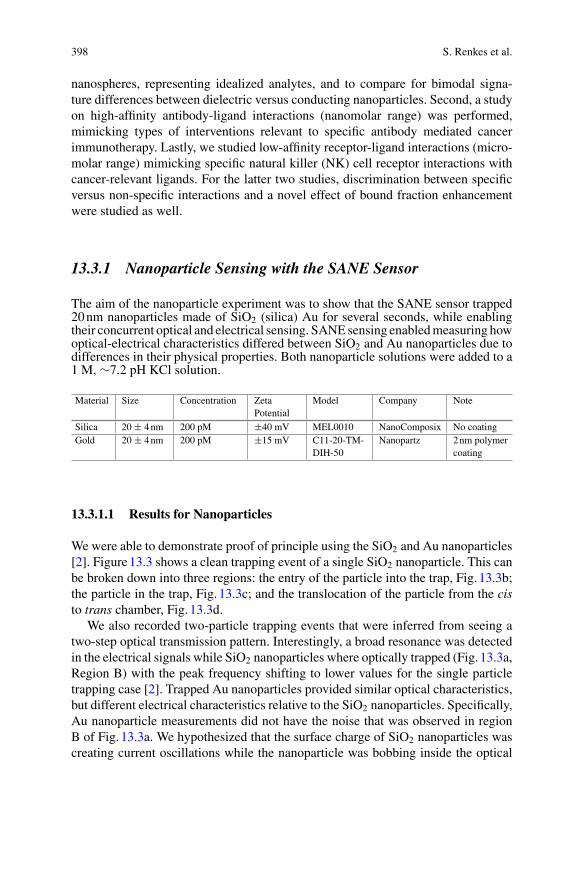
398 S. Renkes et al.
nanospheres, representing idealized analytes, and to compare for bimodal signa-ture differences between dielectric versus conducting nanoparticles. Second, a studyon high-affinity antibody-ligand interactions (nanomolar range) was performed,mimicking types of interventions relevant to specific antibody mediated cancerimmunotherapy. Lastly, we studied low-affinity receptor-ligand interactions (micro-molar range) mimicking specific natural killer (NK) cell receptor interactions withcancer-relevant ligands. For the latter two studies, discrimination between specificversus non-specific interactions and a novel effect of bound fraction enhancementwere studied as well.
13.3.1 Nanoparticle Sensing with the SANE Sensor
The aim of the nanoparticle experiment was to show that the SANE sensor trapped20nm nanoparticles made of SiO2 (silica) Au for several seconds, while enablingtheir concurrent optical and electrical sensing. SANEsensing enabledmeasuring howoptical-electrical characteristics differed between SiO2 and Au nanoparticles due todifferences in their physical properties. Both nanoparticle solutions were added to a1 M, ∼7.2 pH KCl solution.
Material Size Concentration ZetaPotential
Model Company Note
Silica 20 ± 4nm 200 pM ±40 mV MEL0010 NanoComposix No coatingGold 20 ± 4nm 200 pM ±15 mV C11-20-TM-
DIH-50Nanopartz 2nm polymer
coating
13.3.1.1 Results for Nanoparticles
We were able to demonstrate proof of principle using the SiO2 and Au nanoparticles[2]. Figure13.3 shows a clean trapping event of a single SiO2 nanoparticle. This canbe broken down into three regions: the entry of the particle into the trap, Fig. 13.3b;the particle in the trap, Fig. 13.3c; and the translocation of the particle from the cisto trans chamber, Fig. 13.3d.
We also recorded two-particle trapping events that were inferred from seeing atwo-step optical transmission pattern. Interestingly, a broad resonance was detectedin the electrical signals while SiO2 nanoparticles where optically trapped (Fig. 13.3a,Region B) with the peak frequency shifting to lower values for the single particletrapping case [2]. Trapped Au nanoparticles provided similar optical characteristics,but different electrical characteristics relative to the SiO2 nanoparticles. Specifically,Au nanoparticle measurements did not have the noise that was observed in regionB of Fig. 13.3a. We hypothesized that the surface charge of SiO2 nanoparticles wascreating current oscillations while the nanoparticle was bobbing inside the optical

13 Self-induced Back-Action Actuated Nanopore Electrophoresis (SANE) Sensing 399
Fig. 13.3 a Plots of simultaneously recorded optical transmission (top, blue; V), raw ionic current(middle, red; nA) 20Hz low-pass filtered ionic current (bottom, green; nA) versus time (sec) forthe single 20nm SiO2 nanoparticle trapped in the SANE sensor. Physical interpretation schematicsfor the signals recorded within gray-shaded regions A, B and C are shown in panels (b), (c) and (d),respectively. b Region A: negatively charged nanoparticle entering the DNH-ssNP under appliedbias. c Region B: nanoparticle trapped and bobbing inside the DNH near the ssNP mouth. d RegionC: nanoparticle exiting the optical trap after the electrophoretic force dominates translocation.Figure and caption reproduced with permissions by [2]
trap, immediately above the underlying nanopore. In contrast, the Au nanoparticleswere conducting and likely remained electrically neutral.
13.3.2 High-Affinity (Nanomolar) Interaction Sensing withthe SANE Sensor
To expand upon the work of the nanoparticles, we designed an experiment to lookat high affinity bonding to determine if we could distinguish between individualproteins and protein complexes. For this experiment we used T-cell receptor-likeantibodies (TCRmAbs) that targeted peptide-presenting major histocompatibility
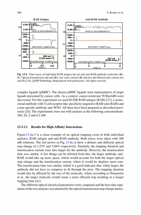
400 S. Renkes et al.
Fig. 13.4 Time traces of individual RAH antigen (a)–(c) and anti-RAH antibody molecules (d)–(f). Optical transmission ((a) and (d)), raw ionic current ((b) and (e)) and filtered ionic current ((c)and (f)) [26]. c©IOP Publishing. Reproduced with permission. All rights reserved
complex ligands (pMHC). The chosen pMHC ligands were representative of targetligands presented by cancer cells. As a control, cancer-irrelevant TCRmABS werealso tested. For this experiment we used H-2Db RAH antigen (RAH) [27], a mono-clonal antibody with T-cell receptor-like specificity targeted to RAH (anti-RAH) anda non-specific antibody anti-WNV. All three have been prepared as described previ-ously [26]. The experiments were run with analytes at the following concentrations:200, 20, 2 and 0.2 nM.
13.3.2.1 Results for High-Affinity Interactions
Figure13.4a–f is a clean example of an optical trapping event in both individualanalytes, RAH antigen and anti-RAH antibody. Both traces were taken with 300nM solutions. The red arrows in Fig. 13.4a, d show a distinct and different opticalstep change of 2.25% and 3.04% respectively. Similarly, the trapping duration andtranslocation current were also larger for the antibody. However, the translocationtime was similar. A few things can be inferred from this: the larger antibody, anti-RAH would take up more space, which would account for both the larger opticalstep change and the translocation current, where it would be displace more ions.The translocation time was similar, which is a good indicator that, while larger, theantibody did not have to compress to fit through the pore. The trapping durationwould also be affected by the size of the molecule, where according to Neumerieret al., the larger molecule would create a more efficient trap resulting in a longertrapping time [41].
The different optical-electrical parameters were compared and the best data sepa-ration of the two analytes was attained by the optical transmission step changemetric.

13 Self-induced Back-Action Actuated Nanopore Electrophoresis (SANE) Sensing 401
Fig. 13.5 Histogram ofoptical step change forRAH-anti-RAH equimolarmixtures. A threshold of4.20% (red dashed line) wasdefined for classifying eventsas bound complex (greenregion) versus unboundRAH (blue region) andanti-RAH (yellow region)[26]. c©IOP Publishing.Reproduced with permission.All rights reserved
Based on the aggregation of data from multiple experiments, a threshold was set toseparate between individual analytes and likely complexes (Fig. 13.5) [26].
To look at specific versus non-specific binding event detection with the SANEsensor, we used anti-WNV, an RAH irrelevant antibody. Anti-WNV was chosenbecause it closely matched the weight and electrical properties of anti-RAH whilenot having a specific binding site for RAH. In this case, the electrical data alonecould not be used to distinguish between the RAH–anti–RAH and RAH–anti–WNVbut when combined with the optical data, a clear delineator was present.
Importantly, in all our publishedwork so far, we have focused on separating boundfrom unbound fraction using 2D projections of these multi-dimensional datasets.However, in future work it may be worthwhile to explore the feasibility of sepa-rating interactions, like molecular complexes from unbound ligands, using multi-dimensional data classification approaches such as support vector machine [28] andmachine learning [29] algorithms. To elaborate this point, Fig. 13.6a shows a 2Dplot of the translocation current versus optical step change for all analytes in thatexperiment. There is a clear separation of the RAH–anti–RAH complex using thethreshold shown in Fig. 13.5. Nevertheless, if a 3rd dimension is added, the opticaltrap time in this case, one can see a more complex feature (purple plane in Fig. 13.6b)hidden behind a larger mass of data in Fig. 13.6a. This observation suggests that abetter threshold for determining bound versus unbound analytes can be developedusing a surface derived from multi-dimensional data.
When the bound fraction of a specific complex was compared to estimates basedon the KD value derivedby a commercial resonant sensor system (ResoSens,RSI Inc.,Arlington, TX, Fig. 13.7a), it was found that the SANE sensor detected considerablyhigher bound fraction values at corresponding antigen concentrations (Fig. 13.7b).The bound fraction gain with the SANE sensor was lowest at 100 nM possibly due totarget saturation and a lower number of available binding sites at that concentration,which was above the KD value. Bound fraction gains were higher at lower concen-trations and followed a pattern that qualitatively mirrored the relative reduction ofbound fraction estimated for the bulk solution reactions using the KD value derivedby the commercial resonant sensor system. Interestingly, the resonant sensor didnot show appreciable target binding at concentrations <10 nM, whereas the SANEsensor was able to detect interactions down to much lower concentrations (10, 1 and
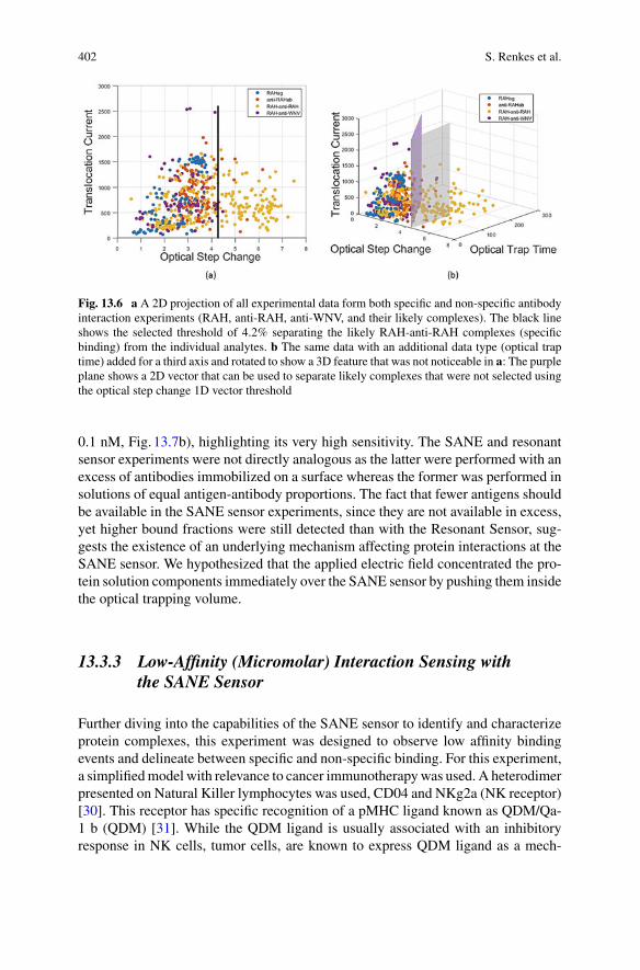
402 S. Renkes et al.
Fig. 13.6 a A 2D projection of all experimental data form both specific and non-specific antibodyinteraction experiments (RAH, anti-RAH, anti-WNV, and their likely complexes). The black lineshows the selected threshold of 4.2% separating the likely RAH-anti-RAH complexes (specificbinding) from the individual analytes. b The same data with an additional data type (optical traptime) added for a third axis and rotated to show a 3D feature that was not noticeable in a: The purpleplane shows a 2D vector that can be used to separate likely complexes that were not selected usingthe optical step change 1D vector threshold
0.1 nM, Fig. 13.7b), highlighting its very high sensitivity. The SANE and resonantsensor experiments were not directly analogous as the latter were performed with anexcess of antibodies immobilized on a surface whereas the former was performed insolutions of equal antigen-antibody proportions. The fact that fewer antigens shouldbe available in the SANE sensor experiments, since they are not available in excess,yet higher bound fractions were still detected than with the Resonant Sensor, sug-gests the existence of an underlying mechanism affecting protein interactions at theSANE sensor. We hypothesized that the applied electric field concentrated the pro-tein solution components immediately over the SANE sensor by pushing them insidethe optical trapping volume.
13.3.3 Low-Affinity (Micromolar) Interaction Sensing withthe SANE Sensor
Further diving into the capabilities of the SANE sensor to identify and characterizeprotein complexes, this experiment was designed to observe low affinity bindingevents and delineate between specific and non-specific binding. For this experiment,a simplifiedmodel with relevance to cancer immunotherapywas used. A heterodimerpresented on Natural Killer lymphocytes was used, CD04 and NKg2a (NK receptor)[30]. This receptor has specific recognition of a pMHC ligand known as QDM/Qa-1 b (QDM) [31]. While the QDM ligand is usually associated with an inhibitoryresponse in NK cells, tumor cells, are known to express QDM ligand as a mech-
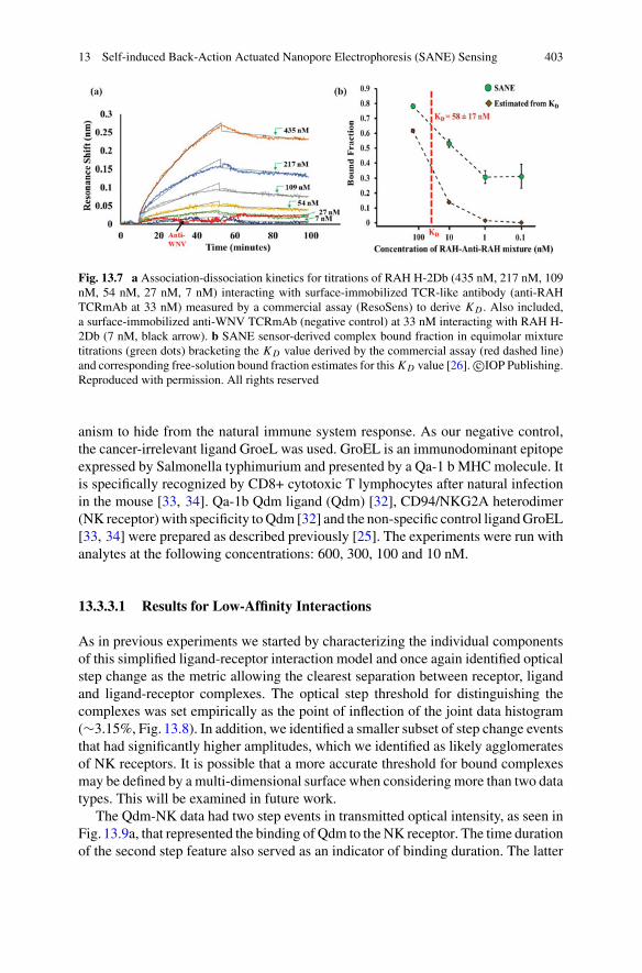
13 Self-induced Back-Action Actuated Nanopore Electrophoresis (SANE) Sensing 403
Fig. 13.7 a Association-dissociation kinetics for titrations of RAH H-2Db (435 nM, 217 nM, 109nM, 54 nM, 27 nM, 7 nM) interacting with surface-immobilized TCR-like antibody (anti-RAHTCRmAb at 33 nM) measured by a commercial assay (ResoSens) to derive KD . Also included,a surface-immobilized anti-WNV TCRmAb (negative control) at 33 nM interacting with RAH H-2Db (7 nM, black arrow). b SANE sensor-derived complex bound fraction in equimolar mixturetitrations (green dots) bracketing the KD value derived by the commercial assay (red dashed line)and corresponding free-solution bound fraction estimates for this KD value [26]. c©IOP Publishing.Reproduced with permission. All rights reserved
anism to hide from the natural immune system response. As our negative control,the cancer-irrelevant ligand GroeL was used. GroEL is an immunodominant epitopeexpressed by Salmonella typhimurium and presented by a Qa-1 b MHCmolecule. Itis specifically recognized by CD8+ cytotoxic T lymphocytes after natural infectionin the mouse [33, 34]. Qa-1b Qdm ligand (Qdm) [32], CD94/NKG2A heterodimer(NK receptor)with specificity toQdm [32] and the non-specific control ligandGroEL[33, 34] were prepared as described previously [25]. The experiments were run withanalytes at the following concentrations: 600, 300, 100 and 10 nM.
13.3.3.1 Results for Low-Affinity Interactions
As in previous experiments we started by characterizing the individual componentsof this simplified ligand-receptor interaction model and once again identified opticalstep change as the metric allowing the clearest separation between receptor, ligandand ligand-receptor complexes. The optical step threshold for distinguishing thecomplexes was set empirically as the point of inflection of the joint data histogram(∼3.15%, Fig. 13.8). In addition, we identified a smaller subset of step change eventsthat had significantly higher amplitudes, which we identified as likely agglomeratesof NK receptors. It is possible that a more accurate threshold for bound complexesmay be defined by a multi-dimensional surface when considering more than two datatypes. This will be examined in future work.
The Qdm-NK data had two step events in transmitted optical intensity, as seen inFig. 13.9a, that represented the binding of Qdm to the NK receptor. The time durationof the second step feature also served as an indicator of binding duration. The latter
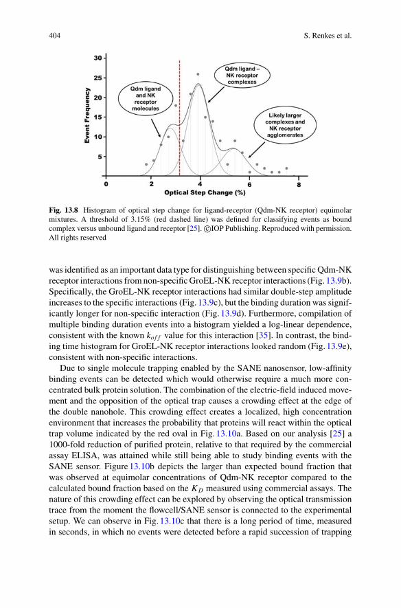
404 S. Renkes et al.
Fig. 13.8 Histogram of optical step change for ligand-receptor (Qdm-NK receptor) equimolarmixtures. A threshold of 3.15% (red dashed line) was defined for classifying events as boundcomplex versus unbound ligand and receptor [25]. c©IOP Publishing. Reproduced with permission.All rights reserved
was identified as an important data type for distinguishing between specificQdm-NKreceptor interactions fromnon-specificGroEL-NK receptor interactions (Fig. 13.9b).Specifically, the GroEL-NK receptor interactions had similar double-step amplitudeincreases to the specific interactions (Fig. 13.9c), but the binding duration was signif-icantly longer for non-specific interaction (Fig. 13.9d). Furthermore, compilation ofmultiple binding duration events into a histogram yielded a log-linear dependence,consistent with the known kof f value for this interaction [35]. In contrast, the bind-ing time histogram for GroEL-NK receptor interactions looked random (Fig. 13.9e),consistent with non-specific interactions.
Due to single molecule trapping enabled by the SANE nanosensor, low-affinitybinding events can be detected which would otherwise require a much more con-centrated bulk protein solution. The combination of the electric-field induced move-ment and the opposition of the optical trap causes a crowding effect at the edge ofthe double nanohole. This crowding effect creates a localized, high concentrationenvironment that increases the probability that proteins will react within the opticaltrap volume indicated by the red oval in Fig. 13.10a. Based on our analysis [25] a1000-fold reduction of purified protein, relative to that required by the commercialassay ELISA, was attained while still being able to study binding events with theSANE sensor. Figure13.10b depicts the larger than expected bound fraction thatwas observed at equimolar concentrations of Qdm-NK receptor compared to thecalculated bound fraction based on the KD measured using commercial assays. Thenature of this crowding effect can be explored by observing the optical transmissiontrace from the moment the flowcell/SANE sensor is connected to the experimentalsetup. We can observe in Fig. 13.10c that there is a long period of time, measuredin seconds, in which no events were detected before a rapid succession of trapping
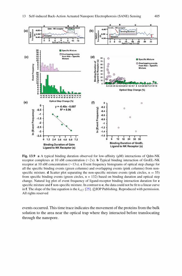
13 Self-induced Back-Action Actuated Nanopore Electrophoresis (SANE) Sensing 405
Fig. 13.9 a A typical binding duration observed for low-affinity (µM) interactions of Qdm-NKreceptor complexes at 10 nM concentration (∼2s). b Typical binding interaction of GroEL-NKreceptor at 10 nM concentration (∼13s). c Event frequency histograms of optical step change forall the specific binding events (green columns) and overlapping events (pink columns) from non-specific mixture. d Scatter plot separating the non-specific mixture events (pink circles, n = 55)from specific binding events (green circles, n = 132) based on binding duration and optical stepchange. Natural log plot of event frequency of ligand-receptor binding interaction duration for especific mixture and f non-specific mixture. In contrast to e, the data could not be fit to a linear curvein f. The slope of the line equation is the kof f [25]. c©IOP Publishing. Reproduced with permission.All rights reserved
events occurred. This time trace indicates themovement of the proteins from the bulksolution to the area near the optical trap where they interacted before translocatingthrough the nanopore.

406 S. Renkes et al.
Fig. 13.10 a Schematic of the protein crowding effect created by the applied electric field immedi-ately over the SANE sensor. bThe observedQdm-NK receptor bound fraction is significantly higherthan corresponding values at the same bulk Qdm-NK receptor concentrations, due to the sensor-induced protein crowding. c Zoomed out time-series plot showing no trapping events for severalseconds at the beginning of an experiment [25]. c©IOP Publishing. Reproduced with permission.All rights reserved
13.4 Conclusions
13.4.1 Identification of Analytes and Complexes They Formin Simple Mixtures
Using optical-electrical sensing,wewere able to collect high quality data that allowedus to successfully identify each individual analyte in all three experiment typesperformed (nanoparticles, high-affinity, and low-affinity protein-ligand interactions).A set of basic bimodal parameters was acquired that contributed to distinguishingbetween analytes: optical step change, optical trap time, translocation current, andnanopore translocation time. For the experiments involving protein-ligand interac-tions, optical data appeared to offer qualitatively better separation between analytesand the complexes that they formed. Optical step change stood out as the best singlemetric for this purpose in the experiments performed to date.
Interestingly though, using optical step change to separate specific from non-specific interactions workswell in onemodel system (RAH–anti–RAHversus RAH–anti–WNV), but not as well in another (Qdm-NK receptor versus GroEL-NK recep-tor). An additional data type was identified, namely binding duration, which enabledclear identification of specific interaction in the latter case. Two more data typeswere identified in our prior studies: bobbing frequency and trapping current. Firstly,the bobbing frequency spectrum of current fluctuations while a charged analyte is in
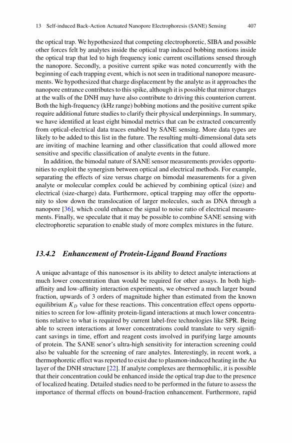
13 Self-induced Back-Action Actuated Nanopore Electrophoresis (SANE) Sensing 407
the optical trap. We hypothesized that competing electrophoretic, SIBA and possibleother forces felt by analytes inside the optical trap induced bobbing motions insidethe optical trap that led to high frequency ionic current oscillations sensed throughthe nanopore. Secondly, a positive current spike was noted concurrently with thebeginning of each trapping event, which is not seen in traditional nanopore measure-ments. We hypothesized that charge displacement by the analyte as it approaches thenanopore entrance contributes to this spike, although it is possible that mirror chargesat the walls of the DNH may have also contribute to driving this counterion current.Both the high-frequency (kHz range) bobbing motions and the positive current spikerequire additional future studies to clarify their physical underpinnings. In summary,we have identified at least eight bimodal metrics that can be extracted concurrentlyfrom optical-electrical data traces enabled by SANE sensing. More data types arelikely to be added to this list in the future. The resulting multi-dimensional data setsare inviting of machine learning and other classification that could allowed moresensitive and specific classification of analyte events in the future.
In addition, the bimodal nature of SANE sensor measurements provides opportu-nities to exploit the synergism between optical and electrical methods. For example,separating the effects of size versus charge on bimodal measurements for a givenanalyte or molecular complex could be achieved by combining optical (size) andelectrical (size-charge) data. Furthermore, optical trapping may offer the opportu-nity to slow down the translocation of larger molecules, such as DNA through ananopore [36], which could enhance the signal to noise ratio of electrical measure-ments. Finally, we speculate that it may be possible to combine SANE sensing withelectrophoretic separation to enable study of more complex mixtures in the future.
13.4.2 Enhancement of Protein-Ligand Bound Fractions
A unique advantage of this nanosensor is its ability to detect analyte interactions atmuch lower concentration than would be required for other assays. In both high-affinity and low-affinity interaction experiments, we observed a much larger boundfraction, upwards of 3 orders of magnitude higher than estimated from the knownequilibrium KD value for these reactions. This concentration effect opens opportu-nities to screen for low-affinity protein-ligand interactions at much lower concentra-tions relative to what is required by current label-free technologies like SPR. Beingable to screen interactions at lower concentrations could translate to very signifi-cant savings in time, effort and reagent costs involved in purifying large amountsof protein. The SANE senor’s ultra-high sensitivity for interaction screening couldalso be valuable for the screening of rare analytes. Interestingly, in recent work, athermophoretic effect was reported to exist due to plasmon-induced heating in the Aulayer of the DNH structure [22]. If analyte complexes are thermophilic, it is possiblethat their concentration could be enhanced inside the optical trap due to the presenceof localized heating. Detailed studies need to be performed in the future to assess theimportance of thermal effects on bound-fraction enhancement. Furthermore, rapid
408 S. Renkes et al.
advances in the design and fabrication of complex all-dielectric nanostructures thatare less prone to heating than plasmonic metal nanostructures could decouple opticalfrom thermal effects. For example, a bullseye all-dielectric structure was developedthat has about half the optical trap stiffness of the Au DNH, but had very little Jouleheating [37].
13.4.3 Limitations in Sensor Throughput
As a general rule, an acceptable throughput by a classical nanopore is ∼1000 eventsover a 15-min data run. In the case of the SANE sensor, with optical trapping extend-ing individual event times to many seconds, a typical event rate is a few tens of eventsover the same 15-min period. It is clear therefore that the SANE sensor’s throughputis very limited compared to classical nanopores and data acquisition durations addingup to several hours are needed to acquire hundreds of events for robust statisticalanalysis. In addition, as the objective lens’s focal area (∼500 µm) is not much largerthan the widest sensor feature size (∼200 µm), optical alignment may need to beadjusted between successive 15-min experimental runs due to piezoelectric stagedrift.
Limited SANE sensor throughput could be overcome in the future by multiplexeddetection over an array of sensors fabricated on a wafer. On the optical sensing side,a microlens array could enable simultaneous illumination on numerous SANE sen-sors if the pitch of sensors and lenslets is matched. For further scaling, a verticalcavity surface emitting laser (VCSEL) array is a potential technology that could beused for optical trapping and sensing on SANE sensor array. On the light detectionside, a photodiode array, or a scientific complementary metal oxide semiconductor(sCMOS) camera, could be used for parallel light collection from multiple sen-sors. For nanopore multiplexed sensing, low-noise, high bandwidth on-chip readoutelectronics have been previously developed [38, 39] and could potentially be inte-grated with the SANE sensor technology. Recently, Ontera Inc. (Santa Cruz, CA)developed a nanopore array integrated into a CMOS chip to enable readout of 264separate nanopores simultaneously, recording each one with built-in individual elec-trodes. Additionally, any future incarnation of a multiplexed platform will requirecareful engineering tominimize optical and electronic crosstalk between neighboringsensors and the likely addition of microfluidics to enable rapid sample loading andflushing. Finally, it is worth noting that multiplexing of protein-ligand interactionsat the single sensor level could be attained if one of the reactants could be barcodedwith a unique single strand of DNA or RNA [40]. In that case, the sensor couldact as an active nanosieve letting through, say, only bound complexes, that could beidentified subsequently by amplification of the nucleotide strands.

13 Self-induced Back-Action Actuated Nanopore Electrophoresis (SANE) Sensing 409
13.5 Acronym Glossary
CMOS: complementary metal oxide semiconductorDNH: double nanoholeDRIE: deep reactive ion etchingFIB: focused ion beamGFIS: gas field ion sourceHWP: half wave plateKD: dissociation constantkof f : binding durationLPCVD: low pressure chemical vapor depositionNK: natural killerPDMS: polydimethylsiloxanepMHC: histocompatibility complexQDM: Qa-1b Qdm ligandQWP: quarter wave plateRAH: H-2Db RAH antigenSANE: self-induced back-action actuated nanopore electrophoresisSixNy : silicon nitrideSiO2: silicon oxideSIBA: self-induced back actionSPR: surface plasmon resonancessNP: solid-state nanoporesTCRmAbs: T-cell receptor-like antibodiesTMAH: tetramethylammonium hydroxideVCSEL: vertical cavity surface emitting laserWNV: West Nile virus
Acknowledgements We thankMr. Soeren Eyhusen andMr. Chuong Huynh for permitting us withthe access and providing technical guidance on focused ion beam milling at the Zeiss ORIONNanoFab facility in Peabody, MA. We are also thankful to all the engineers and staff at the Shi-madzu Institute Nanotechnology Research Center at the University of Texas at Arlington for theirsupport and guidance. The authors acknowledge the financial support from the National Can-cer Institute (1R21CA240220-01A1) and the National Science Foundation (CBET#2022398 andCBET#2022374).
References
1. Mathieu L Juan, Reuven Gordon, Yuanjie Pang, Fatima Eftekhari, and Romain Quidant. Self-induced back-action optical trapping of dielectric nanoparticles. Nature Physics, 5(12):915–919, 2009.
2. Muhammad Usman Raza, Sai Santosh Sasank Peri, Liang-Chieh Ma, Samir M Iqbal, andGeorge Alexandrakis. Self-induced back action actuated nanopore electrophoresis (sane).Nan-otechnology, 29(43):435501, 2018.

410 S. Renkes et al.
3. Benjamin Cressiot, Esther Braselmann, Abdelghani Oukhaled, Adrian H Elcock, Juan Pelta,and Patricia L Clark. Dynamics and energy contributions for transport of unfolded pertactinthrough a protein nanopore. ACS nano, 9(9):9050–9061, 2015.
4. Ahmed A. Al Balushi and Reuven Gordon. Label-free free solution single protein-smallmolecule binding kinetics: An optical tweezer approach. In Optics in the Life Sciences, pageOtT2E.3. Optical Society of America, 2015.
5. LKiranSwaroopKumar andReuvenGordon.Overlappingdouble-hole nanostructure in ametalfilm for localized field enhancement. IEEE Journal of selected topics in quantum electronics,12(6):1228–1232, 2006.
6. LKSKumar, A Lesuffleur, MCHughes, and RGordon. Double nanohole apex-enhanced trans-mission in metal films. Applied Physics B, 84(1-2):25–28, 2006.
7. Mostafa Ghorbanzadeh, Steven Jones, Mohammad KazemMoravvej-Farshi, and Reuven Gor-don. Improvement of sensing and trapping efficiency of double nanohole apertures via enhanc-ing the wedge plasmon polariton modes with tapered cusps. ACS Photonics, 4(5):1108–1113,2017.
8. Pau Mestres, Johann Berthelot, Srdjan S Acimovic, and Romain Quidant. Unraveling theoptomechanical nature of plasmonic trapping. Light: Science & Applications, 5(7):e16092–e16092, 2016.
9. Yuanjie Pang and Reuven Gordon. Optical trapping of 12 nm dielectric spheres using double-nanoholes in a gold film. Nano letters, 11(9):3763–3767, 2011.
10. Abhay Kotnala, Damon DePaoli, and Reuven Gordon. Sensing nanoparticles using a doublenanohole optical trap. Lab on a Chip, 13(20):4142–4146, 2013.
11. AbhayKotnala andReuvenGordon. Quantification of high-efficiency trapping of nanoparticlesin a double nanohole optical tweezer. Nano letters, 14(2):853–856, 2014.
12. Yuanjie Pang and Reuven Gordon. Optical trapping of a single protein. Nano letters, 12:402–406, 2011.
13. Ahmed A Al Balushi, Ana Zehtabi-Oskuie, and Reuven Gordon. Observing single proteinbinding by optical transmission through a double nanohole aperture in a metal film. Biomedicaloptics express, 4(9):1504–1511, 2013.
14. Ahmed A Al Balushi and Reuven Gordon. Label-free free-solution single-molecule protein–small molecule interaction observed by double-nanohole plasmonic trapping. ACS Photonics,1(5):389–393, 2014.
15. AhmedAAl Balushi and Reuven Gordon. A label-free untethered approach to single-moleculeprotein binding kinetics. Nano letters, 14(10):5787–5791, 2014.
16. Jong Min Sung. Dielectrophoresis and optoelectronic tweezers for nanomanipulation. 2007.17. Mathilde Lepoitevin, Tianji Ma, Mikhael Bechelany, Jean-Marc Janot, and Sebastien Balme.
Functionalization of single solid state nanopores to mimic biological ion channels: A review.Advances in colloid and interface science, 250:195–213, 2017.
18. Patrick Abgrall and Nam Trung Nguyen. Nanofluidic devices and their applications. Analyticalchemistry, 80(7):2326–2341, 2008.
19. Eszter Mádai, Bartłomiej Matejczyk, András Dallos, Mónika Valiskó, and Dezso Boda. Con-trolling ion transport through nanopores: modeling transistor behavior. Physical ChemistryChemical Physics, 20(37):24156–24167, 2018.
20. Matthias Firnkes, Daniel Pedone, Jelena Knezevic, Markus Doblinger, and Ulrich Rant. Elec-trically facilitated translocations of proteins through silicon nitride nanopores: conjoint andcompetitive action of diffusion, electrophoresis, and electroosmosis.Nano letters, 10(6):2162–2167, 2010.
21. Jan KGDhont, SWiegand, S Duhr, and D Braun. Thermodiffusion of charged colloids: Single-particle diffusion. Langmuir, 23(4):1674–1683, 2007.
22. Quanbo Jiang, Benoît Rogez, Jean-Benoît Claude, Guillaume Baffou, and Jérôme Wenger.Quantifying the role of the surfactant and the thermophoretic force in plasmonic nano-opticaltrapping. Nano Letters, 2020.
23. Ahmed A Al Balushi, Abhay Kotnala, Skyler Wheaton, Ryan M Gelfand, YashaswiniRajashekara, and Reuven Gordon. Label-free free-solution nanoaperture optical tweezers forsingle molecule protein studies. Analyst, 140(14):4760–4778, 2015.
13 Self-induced Back-Action Actuated Nanopore Electrophoresis (SANE) Sensing 411
24. Junrong Wang, Jian Ma, Zhonghua Ni, Li Zhang, and Guoqing Hu. Effects of access resis-tance on the resistive-pulse caused by translocating of a nanoparticle through a nanopore. RSCAdvances, 4(15):7601–7610, 2014.
25. Sai Santosh Sasank Peri, Manoj Kumar Sabnani, Muhammad Usman Raza, Elizabeth LUrquhart, Soroush Ghaffari, Jung Soo Lee, Min Jun Kim, Jon Weidanz, and George Alexan-drakis. Quantification of low affinity binding interactions between natural killer cell inhibitoryreceptors and targeting ligandswith a self-induced back-action actuated nanopore electrophore-sis (sane) sensor. Nanotechnology, 32(4):045501, 2020.
26. Sai Santosh Sasank Peri, Manoj K Sabnani, Muhammad Usman Raza, Soroush Ghaffari,Susanne Gimlin, Debra D Wawro, Jung Soo Lee, Min Jun Kim, Jon Weidanz, and GeorgeAlexandrakis. Detection of specific antibody-ligand interactions with a self-induced back-action actuated nanopore electrophoresis sensor. Nanotechnology, 31(8):085502, 2019.
27. Mariet CW Feltkamp, Gienke R Vreugdenhil, Michel PM Vierboom, Elisabeth Ras, Sjoerd Hvan der Burg, Jan Ter Schegget, Cornelis JM Melief, and W Martin Kast. Cytotoxic t lym-phocytes raised against a subdominant epitope offered as a synthetic peptide eradicate humanpapillomavirus type 16-induced tumors. European journal of immunology, 25(9):2638–2642,1995.
28. K SRIVASTAVA Durgesh and B Lekha. Data classification using support vector machine.Journal of theoretical and applied information technology, 12(1):1–7, 2010.
29. Howard B Demuth, Mark H Beale, Orlando De Jess, and Martin T Hagan. Neural networkdesign. Martin Hagan, 2014.
30. Andrew G Brooks, Phillip E Posch, Christopher J Scorzelli, Francisco Borrego, and John EColigan. Nkg2a complexed with cd94 defines a novel inhibitory natural killer cell receptor.The Journal of experimental medicine, 185(4):795–800, 1997.
31. Russell E Vance, Jennifer R Kraft, John D Altman, Peter E Jensen, and David H Raulet.Mouse cd94/nkg2a is a natural killer cell receptor for the nonclassical major histocompatibilitycomplex (mhc) class i molecule qa-1b. The Journal of experimental medicine, 188(10):1841–1848, 1998.
32. JenniferRKraft, Russell EVance, JanPohl,AmyMMartin,DavidHRaulet, andPeterE Jensen.Analysis of qa-1bpeptide binding specificity and the capacity of cd94/nkg2a to discriminatebetween qa-1–peptide complexes. The Journal of experimental medicine, 192(5):613–624,2000.
33. Wei-Feng Lo, Helena Ong, Eleanor S Metcalf, and Mark J Soloski. T cell responses to gram-negative intracellular bacterial pathogens: a role for cd8+ t cells in immunity to salmonella infec-tion and the involvement of mhc class ib molecules. The Journal of Immunology, 162(9):5398–5406, 1999.
34. Wei-Feng Lo, Amina SWoods, Amy DeCloux, Robert J Cotter, Eleanor SMetcalf, and Mark JSoloski. Molecular mimicry mediated by mhc class ib molecules after infection with gram-negative pathogens. Nature medicine, 6(2):215–218, 2000.
35. Mar Valés-Gómez, Hugh T Reyburn, Robert A Erskine, Miguel López-Botet, and Jack LStrominger. Kinetics and peptide dependency of the binding of the inhibitory nk receptorcd94/nkg2-a and the activating receptor cd94/nkg2-c to hla-e.TheEMBOjournal, 18(15):4250–4260, 1999.
36. Maxim Belkin, Shu-Han Chao, Magnus P Jonsson, Cees Dekker, and Aleksei Aksimentiev.Plasmonic nanopores for trapping, controlling displacement, and sequencing of dna.ACS nano,9(11):10598–10611, 2015.
37. Wei Zhan, Kui Gao, Chenjun Zhu, andWuzhou Song. Optical trapping using all silicon nanoan-tennas with ultra-high electric field enhancement. Applied Physics Letters, 117(24):241102,2020.
38. J Rosenstein, V Ray, M Drndic, and KL Shepard. Nanopore dna sensors in cmos with on-chip low-noise preamplifiers. In 2011 16th International Solid-State Sensors, Actuators andMicrosystems Conference, pages 874–877. IEEE, 2011.
39. Jacob K Rosenstein, Meni Wanunu, Christopher A Merchant, Marija Drndic, and Kenneth LShepard. Integrated nanopore sensing platform with sub-microsecond temporal resolution.Nature methods, 9(5):487, 2012.

412 S. Renkes et al.
40. Marlon Stoeckius, ChristophHafemeister,WilliamStephenson, BrianHouck-Loomis, PratipKChattopadhyay, Harold Swerdlow, Rahul Satija, and Peter Smibert. Simultaneous epitope andtranscriptome measurement in single cells. Nature methods, 14(9):865, 2017.
41. Lukas Neumeier, Romain Quidant, Darrick E Chang Self-induced back-action optical trappingin nanophotonic systems New Journal of Physics, 17(12):123008, 2015.

Index
AAchiral, 282Acoustic
vibration, 18Acoustic phonon, 101Acousto-optic modulator, 9Actin, 7, 9, 29Activation energy, 300Adatoms, 54Adeno associated virus, 321Adenosine Diphosphate (ADP), 14Adenosine Triphosphate (ATP), 14Ag/AgCl, 330Aggregate, 9Alginate, 304Aliasing, 18Allan variance, Allan deviation, 73Allostery, 256α-Synuclein, 347Amine, thiol, 53, 54Aminosilanization, 70, 71Amphiphilic, 303Analyte, 299Angle-resolved nanosphere lithography,
244Anisotropic nanoparticles, 65Anti-Stokes, 100Anti-Stokes Raman Scattering (ASRS), 102Aperture, 252Aperture shape, 253Applied voltage, 343, 347, 350, 352Aptamers, 371Asymmetric microsphere, 80Atomic layer deposition, 243Atomic polarizability, 13
Atomistic model, 12, 13ATPase, 7, 14Attomolar sensitivity, 54, 88Autocorrelation analysis, 254
BBackscattered light, 22Backscattering, 50Bandwidth, 74, 308Beam expander, 81Beam waist, 12, 14Beat note, 78Bethe theory, 252Bias-T, 76Binding affinity
high, 389, 398, 399, 406, 407low, 389, 390, 393, 398, 402, 404–407
Binding energy, 67Binding location, 52Biological nanopores, 343, 345Biomarker, 304, 345Biomolecule, 38, 45Biopolymer, 306Biorecognition element, 84Biosensing, 43, 49Bi-phase ligand exchange, 66Birefringence, 277Blue detune, 136Blue detuning, 131Bottom-up assembly, 69Bound fraction, 390, 393, 398, 401, 403,
406, 407Bovine Serum Albumin (BSA), 9, 12, 13Brillouin scattering, 100, 101
© The Editor(s) (if applicable) and The Author(s), under exclusive licenseto Springer Nature Switzerland AG 2022W. Bowen et al. (eds.), Single Molecule Sensing Beyond Fluorescence,Nanostructure Science and Technology,https://doi.org/10.1007/978-3-030-90339-8
413
414 Index
Brownian motion, 208Bus waveguide, 64
CCancer, 258, 345Capture radius, 300, 327Carbonic anhydrase, 7Carrier, sideband, 76Cas9, 371, 372Catalytic nanoparticle, 88Catalytic reaction, 88Cation, 306Cavity, 16Cavity Enhanced Raman Spectroscopy
(CERS), 105Cavity lifetime, 40, 74Cavity linewidth, 76Cavity optomechanics, 129, 130Cavity resonance, 16, 76Cavity Ring-Up Spectroscopy (CRUS), 75,
77Centroid, 83Cetrimonium Bromide (CTAB), 53, 54,
67–69, 71Chelation, 316Chemical turnover, 57Chiral, 272Chirality, 276Chromatography, 272Circulating power, 81Citrate, 65Clausius-Mossotti factor, 209, 212Coherence
length, 19Coherent Anti-Stokes Raman Scattering
(CARS), 101Colloidal lithography, 244Commercialization, 88Complementary analysis, 262Complementary
Metal-Oxide-Semiconductor(CMOS), 308
Concentration gradient, 86Conductance, 312Conformation, 7, 12–14Conformational change, 17, 57, 85, 86Conformational dynamics, 84Conformational dynamics, enzyme, 75Conformation, conformational change, 52Conformations, 254Counterion, 302Coupling distance, 81
Coupling efficiency, 77Coupling method, 78Covalent bond, 53Cramer-Rao Lower Bound, 43Critical coupling, 81Cross-linker, 70Cross-linking, 316CW and CCW modes, 50Cyclodextrin, 273Cysteamine, 51, 54Cystein, cysteamine, CTAB, 67
DDark solitons, 116Data Acquisition (DAQ), 78Debye length, 15, 302Degenerate FWM, 103Deoxyribonucleic Acid (DNA), 53, 298,
343, 345, 351, 359, 362DEP force, 214DEP trapping volume, 214Detection limit, 43, 107Detection volume, 49Detrending, 83DFT, 67Dial-a-reaction, 54Dichroism, 277Dielectric breakdown, 299Dielectric particle, 45Differential interference contrast
microscopy, 5Diffraction limit, 6, 235Diffuse layer, 302Diffusion, 299Diffusion near surfaces, 260Dipole moment, 13Direct frequency comb spectroscopy, 116“Dirty” samples, 254Dissipative Kerr Solitons (DKSs), 103Dissociation constant, 401, 403, 404, 407,
409Distributed Feedback Laser (DFB), 41, 74,
78DNA folds, 371, 372DNA knots, 371DNA melting temperature, 55DNA oligonucleotide, 53, 55DNA origami, 85DNA-PAINT, 56, 81, 87DNA, protein, 54DNA sequence, 55DNA vibration spectra, 256
Index 415
dn/dc, refractive index increment, 56Double nanohole, 389–391, 394–396, 399,
407–409Drude model, 175Drug discovery, 257Drug screen, 86Dual-comb spectroscopy, 114Dwell time, 355, 357–359
EElastic modes, 256Elastic network model, 256Electric double layer, 15, 302Electric field, 344, 346–348, 351–353Electrodeformation, 321Electrolysis, 228Electrolyte, 344, 347, 349, 350Electron beam lithography, 243Electro-optic modulator, 76Electroosmosis, 298, 390, 392Electrophoresis, 298, 389, 390, 392, 409
electrophoretic, 389–391, 399, 407Electrophoretic mobility, 300Electrostatic trapping, 54Electrostriction, 251Electrostrictive force, 87Enantiomer, 272Enantiopure, 280Endocytosis, 305Enhanced frequency shift, 47Enthalpy, entropy, 59Entropic, 299Enzymatic rates, 58Enzyme, 39Enzyme immobilisation, 57Enzyme kinetics, 58Enzyme, MalL, 57, 58Enzyme-substrate complex,
enzyme-transition-state complex, 59Error signal, 76Excess polarizability, 13, 56External Cavity Diode Laser (ECDL), 77Extraordinary Acoustic Raman (EAR)
modes, 88
FFabry-Perot, 59, 78Fabry–Perot cavity, 98FDTD, FEM, BEM, 48Feedback, 18, 19Feedback control, 19Femtometer, 39, 44, 83
Femtonewton force, 87Ferrule, 80Fiber coupling, prism coupling, 80Findpeaks algorithm, 84Finesse, 41Finite-Difference Time-Domain method
(FDTD), 375Fizeau wavemeter, wavemeter, 78Flow cell, 394, 396, 397Fluidic integration, microfluidics, 80Fluorescence, 81, 249Fluorescence label, 56Fluorescence Resonant Energy Transfer
Microscopy (FRET), 7Focused ion beam lithography, 243, 389,
394–396, 409Fourier transform, 75Four-Wave Mixing (FWM), 103Free-energy, 352–354, 361Free-space coupler, 64Frequency noise, 75Frequency resolution, 21Frequency shift, 76Frequency shift, wavelength shift, 49Frequency splitting, 51Full width half maximum, 308Functionalization, 71, 84Fusion splicer, 62
GGammadion, 288Generalized master equation, 192Gibb’s free energy, 59Glass microsphere, 42, 60, 61, 84Glass reflow process, 62Glycan, 306Glycoprotein, 305Gold nanoparticles, 64Gold nanorod, 38G-Protein Coupled Receptors (GPCR), 86Gradient force, 234Graphene, 298, 345, 368Green function, 168, 173Grouping threshold, single-molecule event,
84
HHamiltonian, 167Hamiltonian for SERS, 167Harmonic generation, 102Head group, 53Heating, 261
416 Index
Heisenberg uncertainty, 23, 28Helicity, 276Henry’s function, 320Heterodyne
self, 19, 20Heterodyne biosensing, 8–11, 29Heterodyne biosensor, 9, 15, 16Heterodyne detection, 8, 18, 21, 25, 29Heterodyne frequency shift, 21Heterodyne measurement, 77Hexagonal Boron Nitride (hBN), 368High-frequency electrical noise, 373High Q, 73High throughput, 81Hinge-bending enzyme, 86Homodyne detection, 8, 21, 25Hooge parameter, 322Hybridization, 55Hybrid metal-cavity resonators, 175, 185Hydrophobic, hydrophilic, 66Hydrophobic ligand, 69
IInduced dipole, dipole moment, 49Inelastic scattering process, 100Influenza A virus, 43Interference
beat-note, 9, 20, 21contrast, 9pattern, 9
Interferometric, 5Interferometric imaging, 5Interferometric SCATTering microscopy
(iSCAT), 8, 9, 21, 29–31Interferometric sensing, 6, 8, 11, 14, 17, 18,
25, 26, 28, 29Interferometric sensor, 5, 6, 17, 32Intrinsic quality factor, 44Ion
counter, 15Ionic, 298Ionic conductance, 344–346, 349, 350, 357Ionic conductivity, 349Ionic current, 351, 353, 355–362, 368Ionic current drops, 345, 351–353,
355–359, 361, 362Ionic current drop speed, 359–361Ionic current rectification, 313Isoelectric point, 302
JJoule heating, 229
KKelvin polarization force, 210Kramer theory, 300
LLabelling, 253Labview, 83Laser
cavity, 18linewidth, 18, 73
Laser relaxation oscillation, 18Laser scanning, 82Lasing threshold, 111Lift-off, 243Ligand exchange, 66–69Ligand exchange via intermediate, 66Ligands, 49Ligand shell, 65Linewidth shifts, 51Linewidth shift, single-molecule linewidth
shift, 51Lipid bilayer, 31Lipid membrane, 87Liposomes, 298Liquid Core Optical Ring Resonators
(LCORR), 59Local oscillator, 18, 20, 21, 25Lorentzian lineshape, 40Lowpass filter, 306Low Pressure Chemical Vapor Deposition
(LPCVD), 309Lysine, 347, 352–355, 357, 361, 362
MMachine learning, 345, 362Macromolecular rate theory, 59Macromolecule, 304Maltodextrin, 304Mass distribution, 31Mass photometry, 9, 30, 31Mass sensing, 140Master equations, 169, 170, 173, 184, 192MATLAB GUI, 83Maxwell Stress Tensor, 252Mercaptosilane, 71Metal nanoparticles, 37Metasurface, 285Met-Enkephalin, 347, 352–354Micelle, 15Micodisk, 64Micro-bottle resonator, 62
Index 417
Micro-bubble, 59Microcavity, 13, 37Microcavity frequency combs, 114, 116Microfluidics, 80, 81, 84, 262Microlens array, 408Microring, 64Microsphere radius, 43Microspheres, 59Microtoroid, 59, 63Microtoroid, microdisk, photonic crystal,
71Microtubule, 9, 31Mie, 281Minimum shift, 73Mode-locked lasers, 116Mode splitting, 22, 78Mode volume, 41, 43, 48Modulational instability comb, 103Moiré, 287Molecular dynamics, 346, 347, 358Molecular dynamics simulation, 13Molecular mass, 9Molecular mass resolution, 9Molecular optomechanics, 167Molecular optomechanics in the strong
vibrational coupling regime, 181Molecular polarizability, 12, 13, 44, 56Molecular weight, 253Molecules, ions, 45MoS2 nanopores, 343–347, 349–353, 355,
357–359, 361, 362Muscle cell, 7Myosin, 7, 29
NNanoaperture, 239, 368Nanodisk, 282Nanofabrication, 261Nanofibre, 9, 10Nanofluidic channel, 10, 11Nano-optical traps, 378Nanoparticle, 389, 390, 393, 398, 399Nanoplasmonic, 272, 279Nanopore, 87, 262, 298, 389–394, 397,
399, 405–409solid state nanopore, 389, 395, 399, 409
Nanopore device resolution, 344, 355, 357,358
Nanorod dimer, 85Nanorod orientation, 85Nanorods, nanostars, nanocubes,
nanowires, nanoprisms, 65
Nanoscatter coupling, 79Nanosensor, 407Nanostar, 65Nanostructure arrays, 88Nanostructures, 237Nanotweezers, 374Natural killer, 403, 409
natural killer receptor, 398, 402–406Near-field, 44Negative DEP, 213Noise, 373
amplitude, 18background, 20digitisation, 18eater, 18electronic, 17–21, 25–27frequency, 18, 20, 22intensity, 18laser, 8, 17, 18, 20line, 18phase, 18, 19polarization, 18relaxation, 18shot, 9, 12, 17, 21–28technical, 17, 20, 21, 23, 24, 26, 27vacuum, 26
Noise floor, 45Noise sources, 43Nondegenerate FWM, 103Noninvasive, 6Nonlinear optical effects, 98Normalized WGM spectrum, 82Normal mode analysis, 256NSF11 prism, SF9 prism, 81Numerical aperture, 9
OOff-binding constant, 393, 404, 405, 409Open pore, 351, 353, 357, 358Optical cavity, 16, 17, 19–23, 45Optical coherence tomography, 6Optical fiber, 41Optical frequency combs, 103Optical gradients, 374Optical phonon, 101Optical potential well, 233Optical resonance, 22Optical spring, 129, 138Optical step change, 392, 401–406Optical transmission, 374Optical trap, 390–393, 398, 399, 407, 408Optical trapping, 233
418 Index
Optical trap time, 392, 401, 402, 406Optical tweezer, 15, 28, 87Optical tweezing, 391Optomechanical amplification/cooling, 136Optomechanical Hamiltonian, 173Optomechanical oscillator, 118Optomechanical sensing, 148Optomechanical sensor, 127Optomechanics, 117Optomechanics, Biosensing, Single
molecule detection, 127Optoplasmonic, 37Optoplasmonic sensing, 44, 45, 48, 81Optoplasmonic sensor, 45Orientation, 251
PP53, 258Particle tracking, 29Pathlength, 9PDH, PDH lock, Pound-Drever-Hall, 76PDMS gasket, sample cell, 80Peak detection, 84PECVD, 309Peptide, 304Peptide Major Histocompatibility Complex
(pMHC), 400Permittivity, 56Permutation entropy, 358–362Perturbation theory, 45Phase contrast microscopy, 5Phase matching, 100Phase shift, 5, 7Phase space diagram, 24Photo Activated Localization Microscopy
(PALM), 7Photobleaching, 29Photodamage, 10, 14Photolithography, 62Photonic band-gap, 59Photonic crystal, 59Photonic crystal cavity, 98, 175Photonic crystal resonator, 241Photoresist AZ6130, 64Photothermal effect, 117Physical Vapor Deposition (PVD), 309Pick-up, 18Picosecond, 7PID loop, 76Piranha, 324Plasmonic, 279, 389, 390, 392, 408Plasmonic enhancement, 47, 49
Plasmonic heating, 56Plasmonic hotspot, 44, 49Plasmonic nanoantenna, 129Plasmonic nanoparticle, 38, 44Plasmonic nanopore, 376Plasmonic nanostructures, 237Plasmonic resonance, 6, 38Plasmonics, 43Plasmonic tweezer, 87Plasmon resonance, 49Plasmons, 374Poissonian distribution, 23Poissonian statistics, 23Polarizability, 13, 14, 29, 30, 56, 209, 251Polaron transforms, 190Polycrystalline nanostructures, 64Polydimethylsiloxane (PDMS), 80, 84, 88,
324Polyethylenglycol, 54Polymerase, 13, 58Polymerase enzyme, enzyme, 87Polypeptide, 345, 346, 361, 362Polysaccharide, 298Positive DEP, 213Pound-Drever-Hall locking, 19Pound-Drever-Hall (PDH), 75, 78, 83Power spectral density, 321Power spectrum, 18, 19, 27, 40Principal component, 86, 87Prism coupling, 79, 81Probe field, 9–13, 20Probe photons, 12Probe power, 12Probe wavelength, 12Protein conformations, 254Protein-DNA interactions, 258Protein folding, 345, 346Protein interactions, 258Proteins, 298, 345, 346, 351, 352, 358, 361,
362Protein sizing, 253Protein vibration spectra, 256Protonate, 301Purcell effect, 16, 174Purcell enhancement, 17, 80Purcell factors, 174Pure dephasing, 193
QQ, 40Q over V ratio, 42Quality, 37

Index 419
Quality factor, 17, 40, 74Quantum-optical measurement, 88Quasinormal modes, 173, 185
RRacemic, 280Radiation pressure, 233Raman lasing, 111Raman scattering, 100, 101Raman spectra, 177Raman spectroscopy, 166, 257Rayleigh, 281Rayleigh scattering, 50RC roll-off, 228Reactive sensing, 128Receptor, 49Redshift, 38, 374Reference interferometer, 128, 142Refractive index, 5, 12, 15, 25, 30Refractive index sensing, 6Resolution, 6, 10
bandwidth, 27Resonance shift, linewidth shift, resonance
splitting, 45Resonance shift, mode splitting, mode
broadening, 44Resonance-wavelength, 374Resonant SERS, 189Resonant SERS Hamiltonian, 191Resonant wavelength, 374Ribonucleic Acid (RNA), 298Ring-up signal, 77
SSampling frequency, 308SARS, 109Savitzky-Golay filter, 83Scan rate, 77Scattering
back, 10cross-section, 12, 13, 15, 22, 24, 25dipole, 5, 7–9, 11, 15, 16, 30inelastic, 12
Scattering force, 234Second Harmonic Generation (SHG), 28,
102, 112Seed-mediated synthesis, 65Self-Induced Back-Action (SIBA), 240,
252, 389–392, 407, 409Self-induced Back-action Actuated
Nanopore Electrophoresis (SANE),389–399, 401–403, 406–409
Sensing sites, 54Sensitivity, 41, 42, 45, 73, 74Sensitivity, photon budget, 88Sensor assembly, 85Sensor assembly, optoplasmonic sensor, 69,
72Sequencing, 343–346, 352, 356, 357, 359,
361SERS spectrum, 171Shot noise, 73Shot noise limit, 23–27Shuriken, 288Sideband, 76Signal analysis, 86Signal enhancement, 47Signal-to-Noise Ratio (SNR), 11, 345, 351,
353, 355, 357, 362Signal-to-noise, SNR, detection limit,
sensitivity, 71Silane, 70Silanization, 70Silanol, 71, 302Silica glass, 60Silica nanoparticles detection, 153Silicon nitride, 345Silicon nitride, titanium dioxide, silicon
carbide, lithium niobate,chalcogenide, polymers, 64
Single-mode fiber, 80Single-molecule event, 84Single-molecule fluorescence, 81Single-Molecule reaction, 52Single-molecule scanner, 86Single-molecule sensing, 43, 44, 49, 59, 74Single molecule techniques, 249Single-molecule trapping, 233Single-phase ligand exchange, 66Single protein, 156Slot waveguide, 241Small molecule interactions with proteins,
257Sol-gel, 62Solid-state, 298Solid-state nanopores, 343–348, 352, 361,
362, 368Solvent, 345, 346, 349, 352–354Spatial resolution, 28–30Spectroscopy, 262Spike transition, 84Spin coating, 64Split modes, mode-split, 50Spontaneous Raman scattering, 101Spontaneous scattering, 101

420 Index
Statecoherent, 23, 26–28oligomeric, 31squeezed, 27, 28
Step rate, spike rate, surface reaction, 53Stern layer, 302Stimulated anti-Stokes Raman
spectroscopy, 108Stimulated Brillouin scattering, 112Stimulated Emission Depletion Microscopy
(STED), 7Stimulated Raman spectroscopy, 108Stimulated scattering, 101, 111Stochastic Optical Reconstruction
Microscopy (STORM), 7Stokes, 100
radius, 9, 12Stokes and anti-Stokes spectra, 172Stokes radius, 43Strong coupling, 189, 195Substrate turnover, 58Sum Frequency Generation (SFG), 102Surface
charges, 15Surface-Enhanced Raman Spectroscopy
(SERS), 104, 105, 166Surface functionalization, 66Surface interactions, 259Surface plasmon resonance, 98, 393, 407,
409Surface plasmons, 237Surface reaction, 53Surface scattering, 62
TTapered fiber, 81Tapered-fiber coupling, 79Tapered optical fiber, 41T-cell
T-cell receptor-like antibodies, 399, 409Temperature tuning, 75Template-stripping, 243Temporal resolution, 30Tethering, 250, 253Thermal fluctuations, 13Thermal-optical effect, 117Thermodynamics, 58Thermophoresis, 236, 239, 261Thermophoretic, 391, 407Thermorefractive noise, 73, 74Thiol, 66Third Harmonic Generation (THG)), 102,
113
Threading of biomolecule, 347, 352, 357,361
3-Aminopropyltriethoxysilane (APTES),70
Time resolution, 49, 74TIR objective, 81Top-down assembly, 71Toroidal microcavity, microtoroid, 62Total internal reflection, 59, 79, 81Toxin, drinking water, 88Transferrin, 305Transition metal dichalcogenides, 345, 346,
357Translocation, 313Translocation current, 392, 401, 406Translocation experiments, 347, 350–352,
355, 357–360Translocation time, 392, 393, 406Transmission spectrum, 77Transport phenomena, 299Trapping potential, 250Tubulin, 31Tunable laser, ECDL, external-cavity diode
laser, 752D materials, 343–345, 357, 3742D slit, 374
UUltimate detection limit, 73Unprocessed samples, 254Unresolved mode-split, unresolved
split-mode, 51UV curable adhesive, 80
VVan der Waals (VdW) forces, 66Vapor phase, 70Vernier comb spectroscopy, 115Vertical Cavity Surface Emitting Laser
(VCSEL), 408, 409Viability, 14
WWaveguide, 241Wavelength shift, 53, 55, 57Wavelet, 87Wavemeter, 82Wave vector, 12Weak coupling, 45WGM resonances, 43WGM spectra, 82

Index 421
WGM standing wave, 52
WGM time trace, 84
WGM transmission spectrum, 41
Whispering gallery microcavity, 127
Whispering gallery mode, 38, 242
XXenon difluoride, 62x-ray crystallography, 57
ZZero-mode waveguide, 380Zeta potential, 302