W79E8213/W79E8213R Data Sheet - Micro-Semiconductor.com
96
W79E8213/W79E8213R Data Sheet -1- Table of Contents 1. GENERAL DESCRIPTION ......................................................................................................... 4 2. FEATURES ................................................................................................................................. 5 3. PARTS INFORMATION LIST ..................................................................................................... 6 3.1 Lead Free (RoHS) Parts information list ......................................................................... 6 4. PIN CONFIGURATION ............................................................................................................... 6 5. PIN DESCRIPTIONS .................................................................................................................. 7 6. FUNCTIONAL DESCRIPTION.................................................................................................... 8 6.1 On-Chip Flash EPROM .................................................................................................. 8 6.2 I/O Ports .......................................................................................................................... 8 6.3 Timers ............................................................................................................................. 8 6.4 Interrupts ......................................................................................................................... 8 6.5 Data Pointer .................................................................................................................... 8 6.6 Architecture ..................................................................................................................... 8 6.6.1 ALU .................................................................................................................................. 8 6.6.2 Accumulator ..................................................................................................................... 9 6.6.3 B Register......................................................................................................................... 9 6.6.4 Program Status Word ....................................................................................................... 9 6.6.5 Scratch-pad RAM ............................................................................................................. 9 6.6.6 Stack Pointer .................................................................................................................... 9 6.7 Power Management ........................................................................................................ 9 7. MEMORY ORGANIZATION...................................................................................................... 10 7.1 Program Memory (on-chip Flash) ................................................................................. 10 7.2 Data Flash Memory ...................................................................................................... 10 7.3 Data Memory (accessed by MOVX) ............................................................................. 11 7.4 Scratch-pad RAM and Register Map ............................................................................ 11 7.4.1 Working Registers .......................................................................................................... 12 7.4.2 Bit addressable Locations .............................................................................................. 13 7.4.3 Stack .............................................................................................................................. 13 8. SPECIAL FUNCTION REGISTERS ......................................................................................... 14 9. INSTRUCTION SET.................................................................................................................. 40 9.1 Instruction Timing ......................................................................................................... 48 10. POWER MANAGEMENT .......................................................................................................... 51 10.1 Idle Mode ...................................................................................................................... 51 10.2 Power-down Mode ........................................................................................................ 51 11. RESET CONDITIONS............................................................................................................... 52 11.1 Sources of reset ............................................................................................................ 52 11.1.1 External Reset .............................................................................................................. 53 11.1.2 Power-On Reset (POR) ................................................................................................ 53 11.1.3 Watchdog Timer Reset ................................................................................................. 54 11.2 Reset State ................................................................................................................... 54 12. INTERRUPTS ........................................................................................................................... 55
-
Upload
khangminh22 -
Category
Documents
-
view
3 -
download
0
Transcript of W79E8213/W79E8213R Data Sheet - Micro-Semiconductor.com

W79E8213/W79E8213R Data Sheet
-1-
Table of Contents 1. GENERAL DESCRIPTION ......................................................................................................... 4 2. FEATURES ................................................................................................................................. 5 3. PARTS INFORMATION LIST ..................................................................................................... 6
3.1 Lead Free (RoHS) Parts information list ......................................................................... 6 4. PIN CONFIGURATION ............................................................................................................... 6 5. PIN DESCRIPTIONS .................................................................................................................. 7 6. FUNCTIONAL DESCRIPTION.................................................................................................... 8
6.1 On-Chip Flash EPROM .................................................................................................. 8 6.2 I/O Ports .......................................................................................................................... 8 6.3 Timers ............................................................................................................................. 8 6.4 Interrupts ......................................................................................................................... 8 6.5 Data Pointer .................................................................................................................... 8 6.6 Architecture ..................................................................................................................... 8
6.6.1 ALU .................................................................................................................................. 8 6.6.2 Accumulator ..................................................................................................................... 9 6.6.3 B Register ......................................................................................................................... 9 6.6.4 Program Status Word ....................................................................................................... 9 6.6.5 Scratch-pad RAM ............................................................................................................. 9 6.6.6 Stack Pointer .................................................................................................................... 9
6.7 Power Management ........................................................................................................ 9 7. MEMORY ORGANIZATION ...................................................................................................... 10
7.1 Program Memory (on-chip Flash) ................................................................................. 10 7.2 Data Flash Memory ...................................................................................................... 10 7.3 Data Memory (accessed by MOVX) ............................................................................. 11 7.4 Scratch-pad RAM and Register Map ............................................................................ 11
7.4.1 Working Registers .......................................................................................................... 12 7.4.2 Bit addressable Locations .............................................................................................. 13 7.4.3 Stack .............................................................................................................................. 13
8. SPECIAL FUNCTION REGISTERS ......................................................................................... 14 9. INSTRUCTION SET .................................................................................................................. 40
9.1 Instruction Timing ......................................................................................................... 48 10. POWER MANAGEMENT .......................................................................................................... 51
10.1 Idle Mode ...................................................................................................................... 51 10.2 Power-down Mode ........................................................................................................ 51
11. RESET CONDITIONS ............................................................................................................... 52 11.1 Sources of reset ............................................................................................................ 52
11.1.1 External Reset .............................................................................................................. 53 11.1.2 Power-On Reset (POR) ................................................................................................ 53 11.1.3 Watchdog Timer Reset ................................................................................................. 54
11.2 Reset State ................................................................................................................... 54 12. INTERRUPTS ........................................................................................................................... 55

W79E8213/W79E8213R Data Sheet
-2-
12.1 Interrupt Sources .......................................................................................................... 55 12.2 Priority Level Structure ................................................................................................. 57 12.3 Response Time ............................................................................................................. 58 12.4 Interrupt Inputs .............................................................................................................. 58
13. PROGRAMMABLE TIMERS/COUNTERS ............................................................................... 60 13.1 Timer/Counters 0 & 1 .................................................................................................... 60
13.1.1 Time-Base Selection .................................................................................................... 60 13.1.2 Mode 0 ......................................................................................................................... 60 13.1.3 Mode 1 ......................................................................................................................... 61 13.1.4 Mode 2 ......................................................................................................................... 62 13.1.5 Mode 3 ......................................................................................................................... 62
14. NVM MEMORY ......................................................................................................................... 64 15. WATCHDOG TIMER ................................................................................................................. 65
15.1 WATCHDOG CONTROL .............................................................................................. 66 15.2 CLOCK CONTROL of Watchdog .................................................................................. 66
16. TIME ACCESS PROCTECTION .............................................................................................. 67 17. EDGE DETECT INTERRUPT ................................................................................................... 69 18. I/O PORT CONFIGURATION ................................................................................................... 71
18.1 Quasi-Bidirectional Output Configuration ..................................................................... 71 18.2 Open Drain Output Configuration ................................................................................. 72 18.3 Push-Pull Output Configuration .................................................................................... 72 18.4 Input Only Configuration ............................................................................................... 73
19. OSCILLATOR ........................................................................................................................... 74 19.1 Internal RC Oscillator Option ........................................................................................ 74 19.2 External Clock Input Option .......................................................................................... 74
20. BUZZER OUTPUT .................................................................................................................... 75 21. POWER MONITORING FUNCTION ........................................................................................ 78
21.1 Power On Detect .......................................................................................................... 78 21.2 Brownout Detect ........................................................................................................... 78
22. PULSE-WIDTH-MODULATED (PWM) OUTPUTS ................................................................... 79 23. ANALOG-TO-DIGITAL CONVERTER ...................................................................................... 82
23.1 ADC Resolution and Analog Supply ............................................................................. 83 24. ICP (IN-CIRCUIT PROGRAM) FLASH PROGRAM ................................................................. 85 25. CONFIG BITS ........................................................................................................................... 86
25.1 CONFIG0 ...................................................................................................................... 86 25.2 CONFIG1 ...................................................................................................................... 88
26. ELECTRICAL CHARACTERISTICS ......................................................................................... 89 26.1 Absolute Maximum Ratings .......................................................................................... 89 26.2 DC ELECTRICAL CHARACTERISTICS ...................................................................... 89 26.3 The ADC Converter DC ELECTRICAL CHARACTERISTICS ..................................... 91 26.4 Internal RC Oscillator Accuracy .................................................................................... 92 26.5 AC ELECTRICAL CHARACTERISTICS ...................................................................... 93 26.6 EXTERNAL CLOCK CHARACTERISTICS .................................................................. 93 26.7 AC SPECIFICATION .................................................................................................... 93

W79E8213/W79E8213R Data Sheet
-3-
26.8 TYPICAL APPLICATION CIRCUITS ............................................................................ 93 27. PACKAGE DIMENSIONS ......................................................................................................... 94
27.1 20-pin SOP-300mil ....................................................................................................... 94 27.2 20-pin PDIP-300mil ....................................................................................................... 95
28. REVISION HISTORY ................................................................................................................ 96

W79E8213/W79E8213R Data Sheet
-4-
1. GENERAL DESCRIPTION The W79E8213 series are an 8-bit 4T-8051 microcontroller which has Flash EPROM which is programmable by ICP (In Circuit Program) or by hardware writer. The instruction set of the W79E8213 series are fully compatible with the standard 8052. The W79E8213 series contain a 4Kbytes of main Flash EPROM; a 128bytes of RAM; two 16-bit timer/counters; 4-channel 10-bit PWM; 3 edge detector inputs; 8-channel multiplexed 10-bit A/D convert. The W79E8213 series supports 128 bytes NVM Data Flash EPROM. These peripherals are supported by 10 sources four-level interrupt capability. To facilitate programming and verification, the Flash EPROM inside the W79E8213 series allow the program memory to be programmed and read electronically. Once the code is confirmed, the user can protect the code for security.

W79E8213/W79E8213R Data Sheet
-5-
2. FEATURES Fully static design 8-bit 4T-8051 CMOS microcontroller:
VDD = 4.5V to 5.5V @20MHz VDD = 2.7V to 5.5V @12MHz VDD = 2.4V to 5.5V @4MHz
Instruction-set compatible with MSC-51. Flexible CPU clock source configurable by config bit and software:
High speed external oscillator: upto 20MHz Crystal and resonator (enabled by config bit). Internal RC oscillator: 20/10MHz selectable by config bit, only W79E8213R supports ±2%
accuracy internal RC oscillator at fixed voltage and temperature condition. 4K bytes of AP Flash EPROM, with ICP and external writer programmable mode. 128 bytes of on-chip RAM. W79E8213 series supports 128 bytes NVM Data Flash EPROM for customer data storage used
and 10K writer cycles. 8 pages. Page size is 16 bytes.
Two 16-bit timer/counters. Ten interrupts source with four levels of priority. Three-edge detect interrupt inputs. Programmable Watchdog Timer. Four-channel 10-bit PWM (Pulse Width Modulator). Internal square wave generator for buzzer. Up to 18 I/O pins. The 4 outputs mode and TTL/Schmitt trigger selectable Port. LED drive capability on all port pins. Sink 20mA; Drive: -15~-20mA @push-pull mode. Eight high sink capability (40mA) port pins. Eight-channel multiplexed with 10-bits A/D convert. Low Voltage Detect interrupt and reset. Development Tools:
ICP(In Circuit Programming) writer Packages:
- Lead Free (RoHS) DIP 20: W79E8213AKG - Lead Free (RoHS) SOP 20: W79E8213ASG - Lead Free (RoHS) DIP 20: W79E8213RAKG - Lead Free (RoHS) SOP 20: W79E8213RASG

W79E8213/W79E8213R Data Sheet
-6-
3. PARTS INFORMATION LIST 3.1 Lead Free (RoHS) Parts information list
PART NO. EPROM FLASH SIZE RAM NVM FLASH
EPROM
INTERNAL RC 1 OSCILLATOR ACCURACY
PACKAGE
W79E8213AKG 4KB 128B 128B ±30% DIP-20 Pin
W79E8213ASG 4KB 128B 128B ±30% SOP-20 Pin
W79E8213RAKG 4KB 128B 128B ±2% DIP-20 Pin
W79E8213RASG 4KB 128B 128B ±2% SOP-20 Pin
Note: 1. Test conditions are VDD = 3.3V, TA = 25°C Table 3-1: Lead Free (RoHS) Parts information list
4. PIN CONFIGURATION
1
2
20
19
18
17
16
15
14
13
12
11
3
4
5
6
7
8
9
10
PWM3/AD6/P0.0
PWM2/P1.7
PWM1/P1.6
RST/P1.5
VSS
XTAL1/P2.1
XTAL2/CLKOUT/P2.0
INT0/P1.3T0/ED2/P1.2
P0.1/AD5/PWM0
P0.2/AD4/BRAKEP0.3/AD0
P0.4/AD1
P0.5/AD2VDD
P0.6/AD3
P0.7/T1/AD7P1.0/ED0/BUZ
P1.1/ED1
20-PIN DIP/SOP/SSOP
STADC/INT1/P1.4
W79E8213AKGW79E8213ASG
W79E8213RAKGW79E8213RASG
Figure 4-1: Pin Configuration
W79E8213/W79E8213R Data Sheet
-7-
5. PIN DESCRIPTIONS
SYMBOL ALTERNATE FUNCTION 1
ALTERNATE FUNCTION 2
ALTERNATE FUNCTION 3
ALTERNATE FUNCTION 4 (ICP MODE)
TYPE DESCRIPTION
VDD P POWER SUPPLY: Supply voltage for operation.
VSS P GROUND: Ground potential. P0.0 AD6 PWM3 I/O Port0:
Support 4 output modes and TTL/Schmitt trigger. Multifunction pins for T1, PWM0, PWM3, BRAKE, AD0-7, Data and Clock (for ICP).
P0.1 AD5 PWM0 I/O P0.2 AD4 BRAKE I/O P0.3 AD0 I/O P0.4 AD1 Data I/O P0.5 AD2 Clock I/O P0.6 AD3 I/O P0.7 AD7 T1 I/O P1.0 BUZ ED0 I/O Port1:
Support 4 output modes and TTL/Schmitt trigger (except for P1.5 input only). Multifunction pins for /RST, T0, /INT0-1, BUZ, PWM1-2, ED0-2, STADC, and HV (for ICP). P1.0-P1.7 have 40mA high sink capability.
P1.1 ED1 I/O P1.2 ED2 T0 I/O P1.3 /INT0 I/O P1.4 STADC /INT1 I/O
P1.5 STR HV I
P1.6 PWM1 I/O
P1.7 PWM2 I/O
P2.0 XTAL2/CLKOUT I/O
CRYSTAL2: This is the crystal oscillator output. It is the inversion of XTAL1. Also a configurable i/o pin. When operating as I/O, it supports 4 output modes and TTL/Schmitt trigger.
P2.1 XTAL1 I/O
CRYSTAL1: This is the crystal oscillator input. This pin may be driven by an external clock or configurable I/O pin. When operating as I/O, it supports 4 output modes and TTL/Schmitt trigger.
* TYPE: P: power, I: input, O: output, I/O: bi-directional, H: pull-high, L: pull-low, D: open-drain.
Table 5-1: Pin Description
Note:
On power-on-reset, all port pins will be tri-stated.
After power-on-reset, all port pins state will follow CONFIG0.PRHI bit definition.

W79E8213/W79E8213R Data Sheet
-8-
6. FUNCTIONAL DESCRIPTION The W79E8213 series architecture consist of a 4T 8051 core controller surrounded by various registers, 4K bytes Flash EPROM, 128 bytes of RAM, up to 18 general purpose I/O ports, two timer/counters, 3 edge detector inputs, 4-channel PWM with 10-bits counter, 8-channel multiplexed with 10-bit ADC analog input, Flash EPROM program by Writer and ICP. W79E8213 series supported 128 bytes NVM Data Flash EPROM.
6.1 On-Chip Flash EPROM The W79E8213 series include one 4K bytes of main Flash EPROM for application program. A Writer or ICP programming board is required to program the Flash EPROM or NVM Data Flash EPROM. This ICP (In-Circuit Programming) feature makes the job easy and efficient when the application’s firmware needs to be updated frequently. In some applications, the in-circuit programming feature makes it possible for the end-user to easily update the system firmware without opening the chassis.
6.2 I/O Ports The W79E8213 series have up to 18 I/O pins using internal RC oscillator & /RST is input only by reset options. All ports can be used as four outputs mode when it may set by PxM1.y and PxM2.y SFR’s registers, it has strong pull-ups and pull-downs, and does not need any external pull-ups. Otherwise it can be used as general I/O port as open drain circuit. All ports can be used bi-directional and these are as I/O ports. These ports are not true I/O, but rather are pseudo-I/O ports. This is because these ports have strong pull-downs and weak pull-ups.
6.3 Timers The W79E8213 series have two 16-bit timers that are functionally and similar to the timers of the 8052 family. When used as timers, the user has a choice of 12 or 4 clocks per count that emulates the timing of the original 8052.
6.4 Interrupts The Interrupt structure in the W79E8213 series is slightly different from that of the standard 8052. Due to the presence of additional features and peripherals, the number of interrupt sources and vectors has been increased.
6.5 Data Pointer The data pointer of W79E8213 series is same as standard 8052 which have 16-bit Data Pointer (DPTR).
6.6 Architecture The W79E8213 series are based on the standard 8052 device. It is built around an 8-bit ALU that uses internal registers for temporary storage and control of the peripheral devices. It can execute the standard 8052 instruction set.
6.6.1 ALU The ALU is the heart of the W79E8213 series. It is responsible for the arithmetic and logical functions. It is also used in decision making, in case of jump instructions, and is also used in calculating jump addresses. The user cannot directly use the ALU, but the Instruction Decoder reads the op-code,
W79E8213/W79E8213R Data Sheet
-9-
decodes it, and sequences the data through the ALU and its associated registers to generate the required result. The ALU mainly uses the ACC which is a special function register (SFR) on the chip. Another SFR, namely B register is also used in Multiply and Divide instructions. The ALU generates several status signals which are stored in the Program Status Word register (PSW).
6.6.2 Accumulator The Accumulator (ACC) is the primary register used in arithmetic, logical and data transfer operations in the W79E8213 series. Since the Accumulator is directly accessible by the CPU, most of the high speed instructions make use of the ACC as one argument.
6.6.3 B Register This is an 8-bit register that is used as the second argument in the MUL and DIV instructions. For all other instructions it can be used simply as a general purpose register.
6.6.4 Program Status Word This is an 8-bit SFR that is used to store the status bits of the ALU. It holds the Carry flag, the Auxiliary Carry flag, General purpose flags, the Register Bank Select, the Overflow flag, and the Parity flag.
6.6.5 Scratch-pad RAM The W79E8213 series have a 128 bytes on-chip scratch-pad RAM. These can be used by the user for temporary storage during program execution. A certain section of this RAM is bit addressable, and can be directly addressed for this purpose.
6.6.6 Stack Pointer The W79E8213 series have an 8-bit Stack Pointer which points to the top of the Stack. This stack resides in the Scratch Pad RAM in the W79E8213 series. Hence the size of the stack is limited by the size of this RAM.
6.7 Power Management Power Management like the standard 8052, the W79E8213 series also have the IDLE and POWER DOWN modes of operation. In the IDLE mode, the clock to the CPU is stopped while the timers, serial ports and interrupt block continue to operate. In the POWER DOWN mode, all clocks are stopped and the chip operation is completely stopped. This is the lowest power consumption state.
W79E8213/W79E8213R Data Sheet
-10-
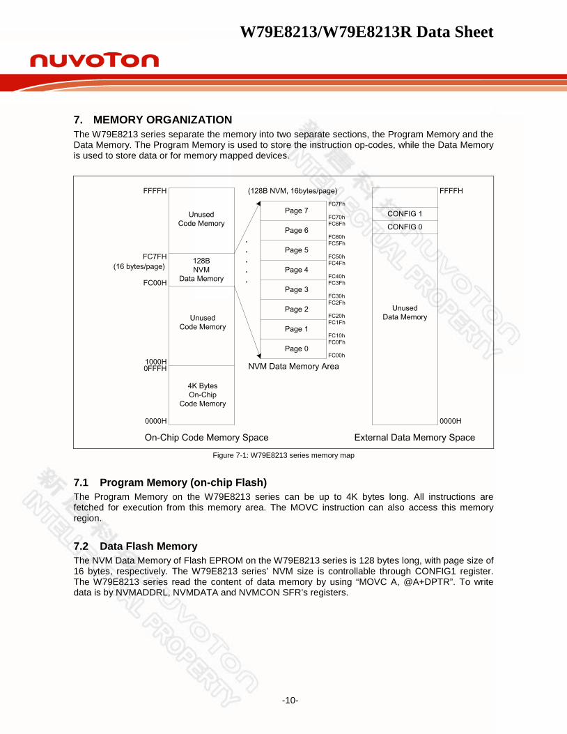
7. MEMORY ORGANIZATION The W79E8213 series separate the memory into two separate sections, the Program Memory and the Data Memory. The Program Memory is used to store the instruction op-codes, while the Data Memory is used to store data or for memory mapped devices.
0000H
External Data Memory SpaceOn-Chip Code Memory Space
0000H
4K BytesOn-Chip
Code Memory
UnusedCode Memory
UnusedCode Memory
CONFIG 0
0FFFH1000H
FFFFH FFFFH
FC00H
CONFIG 1
FC7FH 128BNVM
Data Memory
UnusedData Memory
NVM Data Memory Area
(16 bytes/page)
FC1Fh
FC10hFC0Fh
FC00hPage 0
Page 1
Page 7
Page 2
Page 3
Page 4
Page 5
Page 6
(128B NVM, 16bytes/page)
FC3Fh
FC30hFC2Fh
FC20h
FC5Fh
FC50hFC4Fh
FC40h
FC7Fh
FC70hFC6Fh
FC60h
Figure 7-1: W79E8213 series memory map
7.1 Program Memory (on-chip Flash) The Program Memory on the W79E8213 series can be up to 4K bytes long. All instructions are fetched for execution from this memory area. The MOVC instruction can also access this memory region.
7.2 Data Flash Memory The NVM Data Memory of Flash EPROM on the W79E8213 series is 128 bytes long, with page size of 16 bytes, respectively. The W79E8213 series’ NVM size is controllable through CONFIG1 register. The W79E8213 series read the content of data memory by using “MOVC A, @A+DPTR”. To write data is by NVMADDRL, NVMDATA and NVMCON SFR’s registers.

W79E8213/W79E8213R Data Sheet
-11-
7.3 Data Memory (accessed by MOVX) Not available in this product series.
7.4 Scratch-pad RAM and Register Map As mentioned before the W79E8213 series have separate Program and Data Memory areas. The on-chip 128 bytes scratch pad RAM is in addition to the external memory. There are also several Special Function Registers (SFRs) which can be accessed by software. The SFRs can be accessed only by direct addressing, while the on-chip RAM can be accessed by either direct or indirect addressing.
Unused IndirectRAM
Direct &
IndirectRAM
Addressing
SFRDirect
AddressingOnly
00H
7FH80H
FFH
Figure 7-2: W79E8213 RAM and SFR memory map
Since the scratch-pad RAM is only 128 bytes it can be used only when data contents are small. There are several other special purpose areas within the scratch-pad RAM. These are described as following.

W79E8213/W79E8213R Data Sheet
-12-
Bank 0
Bank 1
Bank 2
Bank 3
03 02 01 0004050607
0B 0A 09 080C0D0E0F
13 12 11 1014151617
1B 1A 19 181C1D1E1F
23 22 21 2024252627
2B 2A 29 282C2D2E2F
33 32 31 3034353637
3B 3A 39 383C3D3E3F
43 42 41 4044454647
4B 4A 49 484C4D4E4F
53 52 51 5054555657
5B 5A 59 585C5D5E5F
63 62 61 6064656667
6B 6A 69 686C6D6E6F
73 72 71 7074757677
7B 7A 79 787C7D7E7F
Direct RAM
Indirect RAM
00H
07H
28H
08H
0FH10H
17H18H
1FH20H
21H
22H
23H
24H
25H
26H
27H
29H
2AH
2BH
2CH
2DH
2EH
2FH30H
7FH80H
FFH
Figure 7-3: Scratch pad RAM
7.4.1 Working Registers There are four sets of working registers, each consisting of eight 8-bit registers. These are termed as Banks 0, 1, 2, and 3. Individual registers within these banks can be directly accessed by separate instructions. These individual registers are named as R0, R1, R2, R3, R4, R5, R6 and R7. However, at one time the W79E8213 series can work with only one particular bank. The bank selection is done by setting RS1-RS0 bits in the PSW. The R0 and R1 registers are used to store the address for indirect accessing.
W79E8213/W79E8213R Data Sheet
-13-
7.4.2 Bit addressable Locations The Scratch-pad RAM area from location 20h to 2Fh is byte as well as bit addressable. This means that a bit in this area can be individually addressed. In addition some of the SFRs are also bit addressable. The instruction decoder is able to distinguish a bit access from a byte access by the type of the instruction itself. In the SFR area, any existing SFR whose address ends in a 0 or 8 is bit addressable.
7.4.3 Stack The scratch-pad RAM can be used for the stack. This area is selected by the Stack Pointer (SP), which stores the address of the top of the stack. Whenever a jump, call or interrupt is invoked the return address is placed on the stack. There is no restriction as to where the stack can begin in the RAM. By default however, the Stack Pointer contains 07h at reset. The user can then change this to any value desired. The SP will point to the last used value. Therefore, the SP will be incremented and then address saved onto the stack. Conversely, while popping from the stack the contents will be read first, and then the SP is decreased.

W79E8213/W79E8213R Data Sheet
-14-
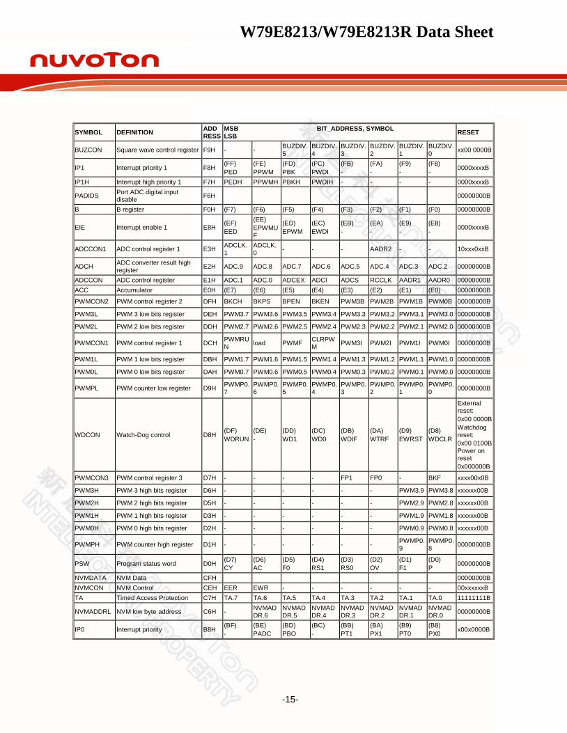
8. SPECIAL FUNCTION REGISTERS The W79E8213 series uses Special Function Registers (SFRs) to control and monitor peripherals and their Modes. The SFRs reside in the register locations 80-FFh and are accessed by direct addressing only. Some of the SFRs are bit addressable. This is very useful in cases where users wish to modify a particular bit without changing the others. The SFRs that are bit addressable are those whose addresses end in 0 or 8. The W79E8213 series contain all the SFRs present in the standard 8052. However some additional SFRs are added. In some cases the unused bits in the original 8052, have been given new functions. The list of the SFRs is as following.
F8 IP1 BUZCON
F0 B PADIDS IP1H
E8 EIE
E0 ACC ADCCON ADCH ADCCON1
D8 WDCON PWMPL PWM0L PWM1L PWMCON1 PWM2L PWM3L PWMCON2
D0 PSW PWMPH PWM0H PWM1H PWM2H PWM3H PWMCON3
C8 NVMCON NVMDATA
C0 NVMADDRL TA
B8 IP0
B0 P0M1 P0M2 P1M1 P1M2 P2M1 P2M2 IP0H
A8 IE
A0 P2 AUXR1 EDIC
98
90 P1
88 TCON TMOD TL0 TL1 TH0 TH1 CKCON
80 P0 SP DPL DPH PCON
Table 8-1: Special Function Register Location Table
Note: 1. The SFRs in the column with dark borders are bit-addressable
2. The table is condensed with eight locations per row. Empty locations indicate that these are no registers at these addresses. When a bit or register is not implemented, it will read high.
W79E8213/W79E8213R Data Sheet
-15-
SYMBOL DEFINITION ADD
RESS MSB BIT_ADDRESS, SYMBOL LSB RESET
BUZCON Square wave control register F9H - - BUZDIV.5
BUZDIV.4
BUZDIV.3
BUZDIV.2
BUZDIV.1
BUZDIV.0 xx00 0000B
IP1 Interrupt priority 1 F8H (FF) PED
(FE) PPWM
(FD) PBK
(FC) PWDI
(FB) -
(FA) -
(F9) -
(F8) - 0000xxxxB
IP1H Interrupt high priority 1 F7H PEDH PPWMH PBKH PWDIH - - - - 0000xxxxB
PADIDS Port ADC digital input disable F6H 00000000B
B B register F0H (F7) (F6) (F5) (F4) (F3) (F2) (F1) (F0) 00000000B
EIE Interrupt enable 1 E8H (EF) EED
(EE) EPWMUF
(ED) EPWM
(EC) EWDI
(EB) -
(EA) -
(E9) -
(E8) - 0000xxxxB
ADCCON1 ADC control register 1 E3H ADCLK.1
ADCLK.0 - - - AADR2 - - 10xxx0xxB
ADCH ADC converter result high register E2H ADC.9 ADC.8 ADC.7 ADC.6 ADC.5 ADC.4 ADC.3 ADC.2 00000000B
ADCCON ADC control register E1H ADC.1 ADC.0 ADCEX ADCI ADCS RCCLK AADR1 AADR0 00000000B ACC Accumulator E0H (E7) (E6) (E5) (E4) (E3) (E2) (E1) (E0) 00000000B
PWMCON2 PWM control register 2 DFH BKCH BKPS BPEN BKEN PWM3B PWM2B PWM1B PWM0B 00000000B
PWM3L PWM 3 low bits register DEH PWM3.7 PWM3.6 PWM3.5 PWM3.4 PWM3.3 PWM3.2 PWM3.1 PWM3.0 00000000B
PWM2L PWM 2 low bits register DDH PWM2.7 PWM2.6 PWM2.5 PWM2.4 PWM2.3 PWM2.2 PWM2.1 PWM2.0 00000000B
PWMCON1 PWM control register 1 DCH PWMRUN load PWMF CLRPW
M PWM3I PWM2I PWM1I PWM0I 00000000B
PWM1L PWM 1 low bits register DBH PWM1.7 PWM1.6 PWM1.5 PWM1.4 PWM1.3 PWM1.2 PWM1.1 PWM1.0 00000000B
PWM0L PWM 0 low bits register DAH PWM0.7 PWM0.6 PWM0.5 PWM0.4 PWM0.3 PWM0.2 PWM0.1 PWM0.0 00000000B
PWMPL PWM counter low register D9H PWMP0.7
PWMP0.6
PWMP0.5
PWMP0.4
PWMP0.3
PWMP0.2
PWMP0.1
PWMP0.0 00000000B
WDCON Watch-Dog control D8H (DF) WDRUN
(DE) -
(DD) WD1
(DC) WD0
(DB) WDIF
(DA) WTRF
(D9) EWRST
(D8) WDCLR
External reset: 0x00 0000B Watchdog reset: 0x00 0100B Power on reset 0x000000B
PWMCON3 PWM control register 3 D7H - - - - FP1 FP0 - BKF xxxx00x0B
PWM3H PWM 3 high bits register D6H - - - - - - PWM3.9 PWM3.8 xxxxxx00B
PWM2H PWM 2 high bits register D5H - - - - - - PWM2.9 PWM2.8 xxxxxx00B
PWM1H PWM 1 high bits register D3H - - - - - - PWM1.9 PWM1.8 xxxxxx00B
PWM0H PWM 0 high bits register D2H - - - - - - PWM0.9 PWM0.8 xxxxxx00B
PWMPH PWM counter high register D1H - - - - - - PWMP0.9
PWMP0.8 00000000B
PSW Program status word D0H (D7) CY
(D6) AC
(D5) F0
(D4) RS1
(D3) RS0
(D2) OV
(D1) F1
(D0) P 00000000B
NVMDATA NVM Data CFH 00000000B NVMCON NVM Control CEH EER EWR - - - - - - 00xxxxxxB TA Timed Access Protection C7H TA.7 TA.6 TA.5 TA.4 TA.3 TA.2 TA.1 TA.0 11111111B
NVMADDRL NVM low byte address C6H - NVMADDR.6
NVMADDR.5
NVMADDR.4
NVMADDR.3
NVMADDR.2
NVMADDR.1
NVMADDR.0 00000000B
IP0 Interrupt priority B8H (BF) -
(BE) PADC
(BD) PBO
(BC) -
(BB) PT1
(BA) PX1
(B9) PT0
(B8) PX0 x00x0000B

W79E8213/W79E8213R Data Sheet
-16-
Continued
SYMBOL DEFINITION ADDRESS
MSB BIT_ADDRESS, SYMBOL LSB RESET
IP0H Interrupt high priority B7H - PADCH PBOH - PT1H PX1H PT0H PX0H x00x0000B P2M2 Port 2 output mode 2 B6H - - - - - - P2M2.1 P2M2.0 xxxxxx 00B P2M1 Port 2 output mode 1 B5H P2S P1S P0S ENCLK T1OE T0OE P2M2.1 P2M2.0 00000000B P1M2 Port 1 output mode 2 B4H P1M2.7 P1M2.6 - P1M2.4 P1M2.3 P1M2.2 P1M2.1 P1M2.0 00x00000B P1M1 Port 1 output mode 1 B3H P1M1.7 P1M1.6 - P1M1.4 P1M1.3 P1M1.2 P1M1.1 P1M1.0 00x00000B P0M2 Port 0 output mode 2 B2H P0M2.7 P0M2.6 P0M2.5 P0M2.4 P0M2.3 P0M2.2 P0M2.1 P0M2.0 00000000B P0M1 Port 0 output mode 1 B1H P0M1.7 P0M1.6 P0M1.5 P0M1.4 P0M1.3 P0M1.2 P0M1.1 P0M1.0 00000000B
IE Interrupt enable A8H (AF) EA
(AE) EADC
(AD) EBO
(AC) -
(AB) ET1
(AA) EX1
(A9) ET0
(A8) EX0 000x0000B
EDIC Edge detect control register A3H EDFLT.1 EDFLT.0 ED2TRG ED2EN ED1TRG ED1EN ED0TRG ED0EN 00000000B AUXR1 AUX function register A2H EDF BOD BOI LPBOV SRST ADCEN BUZE - 000X000xB
P2 Port 2 A0H (A7) -
(A6) -
(A5) -
(A4) -
(A3)
(A2)
(A1) P2.1 XTAL1
(A0) P2.0 XTAL2 CLKOUT
xxxxxxxxB
P1 Port 1 90H (97) P1.7 PWM2
(96) P1.6 PWM1
(95) P1.5 /RST
(94) P1.4 /INT1 STADC
(93) P1.3 /INT0
(92) P1.2 ED2 T0
(91) P1.1 ED1
(90) P1.0 ED0 BUZ
11111111B
CKCON Clock control 8EH - - - T1M T0M - - - xxx00xxxB TH1 Timer high 1 8DH 00000000B TH0 Timer high 0 8CH 00000000B TL1 Timer low 1 8BH 00000000B TL0 Timer low 0 8AH 00000000B TMOD Timer mode 89H GATE C/T M1 M0 GATE C/T M1 M0 00000000B
TCON Timer control 88H (8F) TF1
(8E) TR1
(8D) TF0
(8C) TR0
(8B) IE1
(8A) IT1
(89) IE0
(88) IT0 00000000B
PCON Power control 87H - - BOF POR GF1 GF0 PD IDL xxxx0000B DPH Data pointer high 83H 00000000B DPL Data pointer low 82H 00000000B SP Stack pointer 81H 00000111B
P0 Port 0 80H
(87) P0.7 AD7 T1
(86) P0.6 AD3
(85) P0.5 AD2
(84) P0.4 AD1
(83) P0.3 AD0
(82) P0.2 AD4 BRAKE
(81) P0.1 AD5 PWM0
(80) P0.0 AD6 PWM3
11111111B
Table 8-2: Special Function Registers

W79E8213/W79E8213R Data Sheet
-17-
PORT 0 Bit: 7 6 5 4 3 2 1 0
P0.7 P0.6 P0.5 P0.4 P0.3 P0.2 P0.1 P0.0
Mnemonic: P0 Address: 80h P0.7-0: General purpose Input/Output port. Most instructions will read the port pins in case of a port read access, however in case of read-modify-write instructions, the port latch is read. These alternate functions are described below:
BIT NAME FUNCTION
7 P0.7 AD7 pin or Timer 1 pin by alternative.
6 P0.6 AD3 pin by alternative.
5 P0.5 AD2 pin by alternative.
4 P0.4 AD1 pin by alternative.
3 P0.3 AD0 pin by alternative.
2 P0.2 AD4 pin or BRAKE pin by alternative.
1 P0.1 AD5 pin or PWM0 pin by alternative.
0 P0.0 AD6 pin or PWM3 pin by alternative. Note: During power-on-reset, the port pins are tri-stated. After power-on-reset, the value of the port is set by CONFIG0.PRHI
bit. The default setting for CONFIG0.PRHI =1 which the alternative function output is turned on upon reset. If CONFIG0.PRHI is set to 0, the user has to write a 1 to port SFR to turn on the alternative function output.
STACK POINTER Bit: 7 6 5 4 3 2 1 0
SP.7 SP.6 SP.5 SP.4 SP.3 SP.2 SP.1 SP.0
Mnemonic: SP Address: 81h
BIT NAME FUNCTION
7-0 SP.[7:0] The Stack Pointer stores the Scratch-pad RAM address where the stack begins. In other words it always points to the top of the stack.
DATA POINTER LOW Bit: 7 6 5 4 3 2 1 0
DPL.7 DPL.6 DPL.5 DPL.4 DPL.3 DPL.2 DPL.1 DPL.0
Mnemonic: DPL Address: 82h
BIT NAME FUNCTION
7-0 DPL.[7:0] This is the low byte of the standard 8052 16-bit data pointer.
W79E8213/W79E8213R Data Sheet
-18-
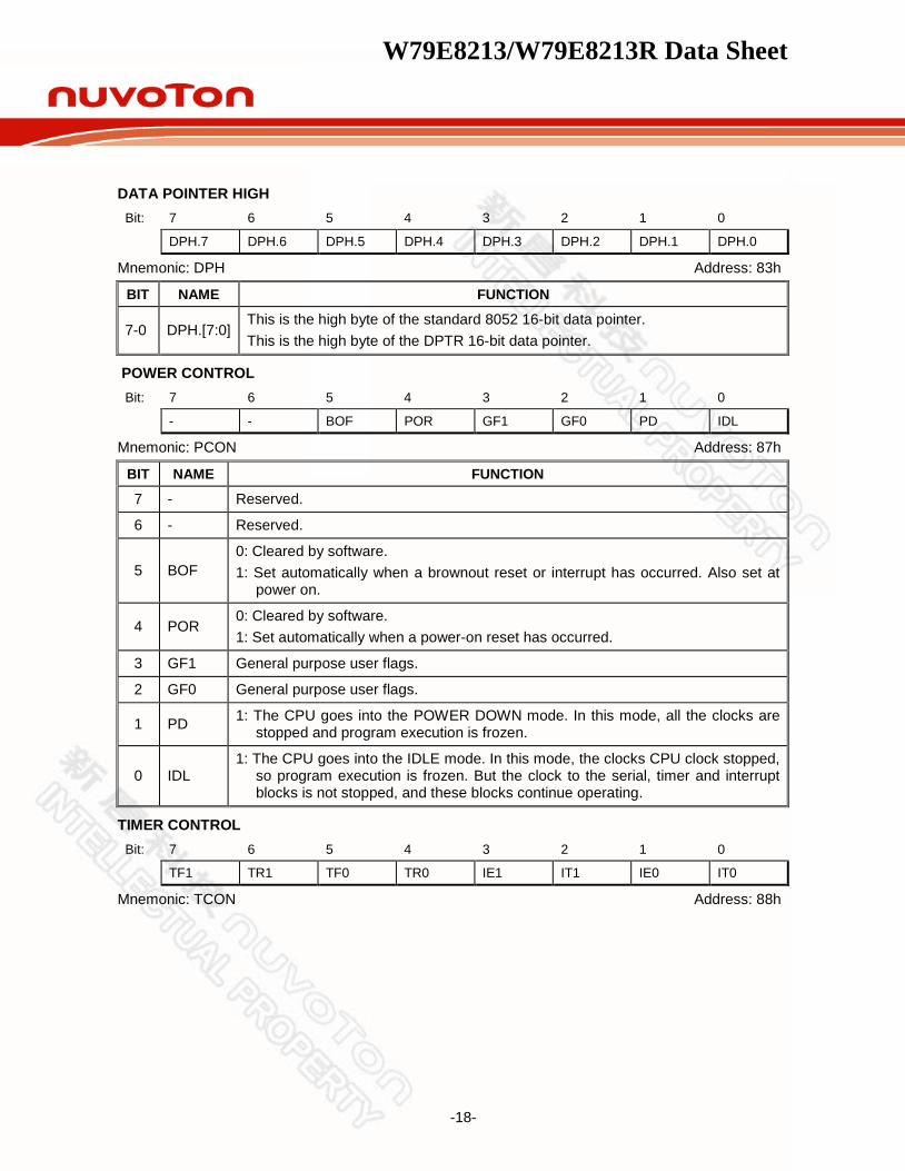
DATA POINTER HIGH Bit: 7 6 5 4 3 2 1 0
DPH.7 DPH.6 DPH.5 DPH.4 DPH.3 DPH.2 DPH.1 DPH.0
Mnemonic: DPH Address: 83h
BIT NAME FUNCTION
7-0 DPH.[7:0] This is the high byte of the standard 8052 16-bit data pointer. This is the high byte of the DPTR 16-bit data pointer.
POWER CONTROL Bit: 7 6 5 4 3 2 1 0
- - BOF POR GF1 GF0 PD IDL
Mnemonic: PCON Address: 87h
BIT NAME FUNCTION
7 - Reserved.
6 - Reserved.
5 BOF 0: Cleared by software. 1: Set automatically when a brownout reset or interrupt has occurred. Also set at
power on.
4 POR 0: Cleared by software. 1: Set automatically when a power-on reset has occurred.
3 GF1 General purpose user flags.
2 GF0 General purpose user flags.
1 PD 1: The CPU goes into the POWER DOWN mode. In this mode, all the clocks are stopped and program execution is frozen.
0 IDL 1: The CPU goes into the IDLE mode. In this mode, the clocks CPU clock stopped,
so program execution is frozen. But the clock to the serial, timer and interrupt blocks is not stopped, and these blocks continue operating.
TIMER CONTROL Bit: 7 6 5 4 3 2 1 0
TF1 TR1 TF0 TR0 IE1 IT1 IE0 IT0
Mnemonic: TCON Address: 88h

W79E8213/W79E8213R Data Sheet
-19-
BIT NAME FUNCTION
7 TF1 Timer 1 Overflow Flag. This bit is set when Timer 1 overflows. It is cleared automatically when the program does a timer 1 interrupt service routine. Software can also set or clear this bit.
6 TR1 Timer 1 Run Control. This bit is set or cleared by software to turn timer/counter on or off.
5 TF0 Timer 0 Overflow Flag. This bit is set when Timer 0 overflows. It is cleared automatically when the program does a timer 0 interrupt service routine. Software can also set or clear this bit.
4 TR0 Timer 0 Run Control. This bit is set or cleared by software to turn timer/counter on or off.
3 IE1 Interrupt 1 Edge Detect Flag: Set by hardware when an edge/level is detected on INT1. This bit is cleared by hardware when the service routine is vectored to only if the interrupt was edge triggered. Otherwise it follows the inverse of the pin.
2 IT1 Interrupt 1 Type Control. Set/cleared by software to specify falling edge/ low level triggered external inputs.
1 IE0 Interrupt 0 Edge Detect Flag. Set by hardware when an edge/level is detected on INT0 . This bit is cleared by hardware when the service routine is vectored to only if the interrupt was edge triggered. Otherwise it follows the inverse of the pin.
0 IT0 Interrupt 0 Type Control: Set/cleared by software to specify falling edge/ low level triggered external inputs.
TIMER MODE CONTROL Bit: 7 6 5 4 3 2 1 0 GATE TC / M1 M0 GATE TC / M1 M0
TIMER1 TIMER0
Mnemonic: TMOD Address: 89h
BIT NAME FUNCTION
7 GATE Gating control: When this bit is set, Timer/counter 1 is enabled only while the INT1 pin is high and the TR1 control bit is set. When cleared, the INT1 pin has no effect, and Timer 1 is enabled whenever TR1 control bit is set.
6 TC/ Timer or Counter Select: When clear, Timer 1 is incremented by the internal clock. When set, the timer counts falling edges on the T1 pin.
5 M1 Timer 1 mode select bit 1. See table below. 4 M0 Timer 1 mode select bit 0. See table below.
3 GATE Gating control: When this bit is set, Timer/counter 0 is enabled only while the INT0 pin is high and the TR0 control bit is set. When cleared, the INT0 pin has no effect, and Timer 0 is enabled whenever TR0 control bit is set.
2 TC/ Timer or Counter Select: When clear, Timer 0 is incremented by the internal clock. When set, the timer counts falling edges on the T0 pin.
1 M1 Timer 0 mode select bit 1. See table below. 0 M0 Timer 0 mode select bit 0. See table below.
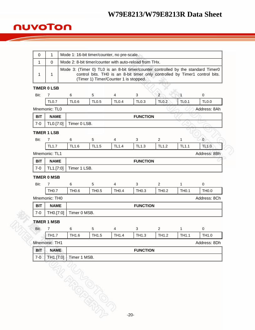
M1, M0: Mode Select bits: M1 M0 MODE
0 0 Mode 0: 13-bits timer/counter; THx 8 bits and TLx 5 bits which serve as pre-scalar.
W79E8213/W79E8213R Data Sheet
-20-
0 1 Mode 1: 16-bit timer/counter, no pre-scale.
1 0 Mode 2: 8-bit timer/counter with auto-reload from THx.
1 1 Mode 3: (Timer 0) TL0 is an 8-bit timer/counter controlled by the standard Timer0
control bits. TH0 is an 8-bit timer only controlled by Timer1 control bits. (Timer 1) Timer/Counter 1 is stopped.
TIMER 0 LSB Bit: 7 6 5 4 3 2 1 0
TL0.7 TL0.6 TL0.5 TL0.4 TL0.3 TL0.2 TL0.1 TL0.0
Mnemonic: TL0 Address: 8Ah
BIT NAME FUNCTION
7-0 TL0.[7:0] Timer 0 LSB.
TIMER 1 LSB Bit: 7 6 5 4 3 2 1 0
TL1.7 TL1.6 TL1.5 TL1.4 TL1.3 TL1.2 TL1.1 TL1.0
Mnemonic: TL1 Address: 8Bh
BIT NAME FUNCTION
7-0 TL1.[7:0] Timer 1 LSB.
TIMER 0 MSB Bit: 7 6 5 4 3 2 1 0
TH0.7 TH0.6 TH0.5 TH0.4 TH0.3 TH0.2 TH0.1 TH0.0
Mnemonic: TH0 Address: 8Ch
BIT NAME FUNCTION
7-0 TH0.[7:0] Timer 0 MSB.
TIMER 1 MSB Bit: 7 6 5 4 3 2 1 0
TH1.7 TH1.6 TH1.5 TH1.4 TH1.3 TH1.2 TH1.1 TH1.0
Mnemonic: TH1 Address: 8Dh
BIT NAME FUNCTION
7-0 TH1.[7:0] Timer 1 MSB.
W79E8213/W79E8213R Data Sheet
-21-
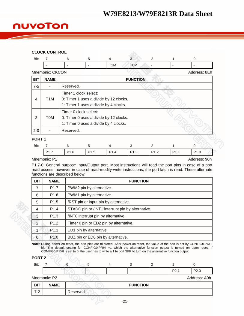
CLOCK CONTROL Bit: 7 6 5 4 3 2 1 0
- - - T1M T0M - - -
Mnemonic: CKCON Address: 8Eh
BIT NAME FUNCTION
7-5 - Reserved.
4 T1M Timer 1 clock select: 0: Timer 1 uses a divide by 12 clocks. 1: Timer 1 uses a divide by 4 clocks.
3 T0M Timer 0 clock select: 0: Timer 0 uses a divide by 12 clocks. 1: Timer 0 uses a divide by 4 clocks.
2-0 - Reserved.
PORT 1 Bit: 7 6 5 4 3 2 1 0
P1.7 P1.6 P1.5 P1.4 P1.3 P1.2 P1.1 P1.0
Mnemonic: P1 Address: 90h P1.7-0: General purpose Input/Output port. Most instructions will read the port pins in case of a port read access, however in case of read-modify-write instructions, the port latch is read. These alternate functions are described below:
BIT NAME FUNCTION
7 P1.7 PWM2 pin by alternative.
6 P1.6 PWM1 pin by alternative.
5 P1.5 /RST pin or input pin by alternative.
4 P1.4 STADC pin or /INT1 interrupt pin by alternative.
3 P1.3 /INT0 interrupt pin by alternative.
2 P1.2 Timer 0 pin or ED2 pin by alternative.
1 P1.1 ED1 pin by alternative.
0 P1.0 BUZ pin or ED0 pin by alternative. Note: During power-on-reset, the port pins are tri-stated. After power-on-reset, the value of the port is set by CONFIG0.PRHI
bit. The default setting for CONFIG0.PRHI =1 which the alternative function output is turned on upon reset. If CONFIG0.PRHI is set to 0, the user has to write a 1 to port SFR to turn on the alternative function output.
PORT 2 Bit: 7 6 5 4 3 2 1 0
- - - - - - P2.1 P2.0
Mnemonic: P2 Address: A0h
BIT NAME FUNCTION
7-2 - Reserved.
W79E8213/W79E8213R Data Sheet
-22-
1 P2.1 XTAL1 clock input pin.
0 P2.0 XTAL2 or CLKOUT pin by alternative. Note: During power-on-reset, the port pins are tri-stated. After power-on-reset, the value of the port is set by CONFIG0.PRHI
bit. The default setting for CONFIG0.PRHI =1 which the alternative function output is turned on upon reset. If CONFIG0.PRHI is set to 0, the user has to write a 1 to port SFR to turn on the alternative function output.
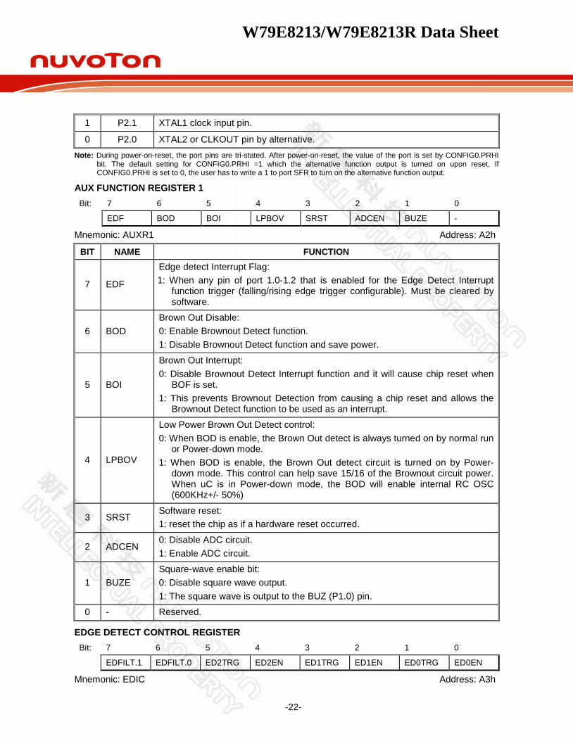
AUX FUNCTION REGISTER 1 Bit: 7 6 5 4 3 2 1 0
EDF BOD BOI LPBOV SRST ADCEN BUZE -
Mnemonic: AUXR1 Address: A2h
BIT NAME FUNCTION
7 EDF
Edge detect Interrupt Flag: 1: When any pin of port 1.0-1.2 that is enabled for the Edge Detect Interrupt
function trigger (falling/rising edge trigger configurable). Must be cleared by software.
6 BOD Brown Out Disable: 0: Enable Brownout Detect function. 1: Disable Brownout Detect function and save power.
5 BOI
Brown Out Interrupt: 0: Disable Brownout Detect Interrupt function and it will cause chip reset when
BOF is set. 1: This prevents Brownout Detection from causing a chip reset and allows the
Brownout Detect function to be used as an interrupt.
4 LPBOV
Low Power Brown Out Detect control: 0: When BOD is enable, the Brown Out detect is always turned on by normal run
or Power-down mode. 1: When BOD is enable, the Brown Out detect circuit is turned on by Power-
down mode. This control can help save 15/16 of the Brownout circuit power. When uC is in Power-down mode, the BOD will enable internal RC OSC (600KHz+/- 50%)
3 SRST Software reset: 1: reset the chip as if a hardware reset occurred.
2 ADCEN 0: Disable ADC circuit. 1: Enable ADC circuit.
1 BUZE Square-wave enable bit: 0: Disable square wave output. 1: The square wave is output to the BUZ (P1.0) pin.
0 - Reserved.
EDGE DETECT CONTROL REGISTER Bit: 7 6 5 4 3 2 1 0
EDFILT.1 EDFILT.0 ED2TRG ED2EN ED1TRG ED1EN ED0TRG ED0EN
Mnemonic: EDIC Address: A3h

W79E8213/W79E8213R Data Sheet
-23-
BIT NAME FUNCTION
7-6
Edge detect filter type bits: 00 – Filter clock = Fosc. 01 – Filter clock = Fosc/2. 10 – Filter clock = Fosc/4. 11 – Filter clock = Fosc/8.
5 ED2TRG
Edge detect 2 (ED2) trigger type bit: 0 – Falling edge on ED2 pin will cause EDF to be set (if ED2EN is enabled). 1 – Either falling or rising edge on ED2 pin will cause EDF to be set (if ED2EN is
enabled).
4 ED2EN Edge detect 2 (ED2) enable bit: 0 – Disabled. 1 – Enable ED2 (P1.2 pin) as a cause of an edge detect interrupt.
3 ED1TRG
Edge detect 1 (ED1) trigger type bit: 0 – Falling edge on ED1 pin will cause EDF to be set (if ED1EN is enabled). 1 – Either falling or rising edge on ED1 pin will cause EDF to be set (if ED1EN is
enabled).
2 ED1EN Edge detect 1 (ED1) enable bit: 0 – Disabled. 1 – Enable ED1 (P1.1 pin) as a cause of an edge detect interrupt.
1 ED0TRG
Edge detect 0 (ED0) trigger type bit: 0 – Falling edge on ED0 pin will cause EDF to be set (if ED0EN is enabled). 1 – Either falling or rising edge on ED0 pin will cause EDF to be set (if ED0EN is
enabled).
0 ED0EN Edge detect 0 (ED0) enable bit: 0 – Disabled. 1 – Enable ED0 (P1.0 pin) as a cause of an edge detect interrupt.
INTERRUPT ENABLE Bit: 7 6 5 4 3 2 1 0
EA EADC EBO - ET1 EX1 ET0 EX0
Mnemonic: IE Address: A8h

W79E8213/W79E8213R Data Sheet
-24-
BIT NAME FUNCTION
7 EA Global enable. Enable/Disable all interrupts. 6 EADC Enable ADC interrupt. 5 EBO Enable Brown Out interrupt. 4 - Reserved. 3 ET1 Enable Timer 1 interrupt. 2 EX1 Enable external interrupt 1. 1 ET0 Enable Timer 0 interrupt. 0 EX0 Enable external interrupt 0.
PORT 0 OUTPUT MODE 1 Bit: 7 6 5 4 3 2 1 0
P0M1.7 P0M1.6 P0M1.5 P0M1.4 P0M1.3 P0M1.2 P0M1.1 P0M1.0
Mnemonic: P0M1 Address: B1h
BIT NAME FUNCTION
7-0 P0M1.[7:0] To control the output configuration of P0 bits [7:0]
PORT 0 OUTPUT MODE 2 Bit: 7 6 5 4 3 2 1 0
P0M2.7 P0M2.6 P0M2.5 P0M2.4 P0M2.3 P0M2.2 P0M2.1 P0M2.0
Mnemonic: P0M2 Address: B2h
BIT NAME FUNCTION
7-0 P0M2.[7:0] To control the output configuration of P0 bits [7:0]
PORT 1 OUTPUT MODE 1 Bit: 7 6 5 4 3 2 1 0
P1M1.7 P1M1.6 - P1M1.4 P1M1.3 P1M1.2 P1M1.1 P1M1.0
Mnemonic: P1M1 Address: B3h
BIT NAME FUNCTION
7-0 P1M1.[7:0] To control the output configuration of P1 bits [7:0]
PORT 1 OUTPUT MODE 2 Bit: 7 6 5 4 3 2 1 0
P1M2.7 P1M2.6 - P1M2.4 P1M2.3 P1M2.2 P1M2.1 P1M2.0
Mnemonic: P1M2 Address: B4h
BIT NAME FUNCTION
7-0 P1M2.[7:0] To control the output configuration of P1 bits [7:0]
PORT 2 OUTPUT MODE 1 Bit: 7 6 5 4 3 2 1 0

W79E8213/W79E8213R Data Sheet
-25-
P2S P1S P0S ENCLK T1OE T0OE P2M1.1 P2M1.0
Mnemonic: P2M1 Address: B5h
BIT NAME FUNCTION
7 P2S 0: Disable Schmitt trigger inputs on port 2 and enable TTL inputs on port 2. 1: Enables Schmitt trigger inputs on Port 2.
6 P1S 0: Disable Schmitt trigger inputs on port 1 and enable TTL inputs on port 1. 1: Enables Schmitt trigger inputs on Port 1.
5 P0S 0: Disable Schmitt trigger inputs on port 0 and enable TTL inputs on port 0 1: Enables Schmitt trigger inputs on Port 0.
4 ENCLK 1: Enabled clock output to XTAL2 pin (P2.0).
3 T1OE 1: The P0.7 pin is toggled whenever Timer 1 overflows. The output frequency is therefore one half of the Timer 1 overflow rate.
2 T0OE 1: The P1.2 pin is toggled whenever Timer 0 overflows. The output frequency is therefore one half of the Timer 0 overflow rate.
1 P2M1.1 To control the output configuration of P2.1.
0 P2M1.0 To control the output configuration of P2.0.
PORT 2 OUTPUT MODE 2 Bit: 7 6 5 4 3 2 1 0
- - - - - - P2M2.1 P2M2.0
Mnemonic: P2M2 Address: B6h
BIT NAME FUNCTION
7-2 - Reserved.
1-0 P2M2.[1:0] To control the output configuration of P2 bits [1:0]
Port Output Configuration Settings: PXM1.Y
(SEE NOTE) PXM2.Y PORT INPUT/OUTPUT MODE
0 0 Quasi-bidirectional
0 1 Push-Pull
1 0 Input Only (High Impedance) P2M1.PxS=0, TTL input P2M1.PxS=1, Schmitt input
1 1 Open Drain
W79E8213/W79E8213R Data Sheet
-26-
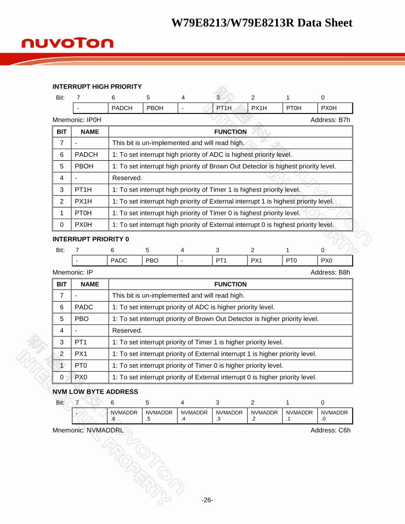
INTERRUPT HIGH PRIORITY Bit: 7 6 5 4 3 2 1 0
- PADCH PBOH - PT1H PX1H PT0H PX0H
Mnemonic: IP0H Address: B7h
BIT NAME FUNCTION
7 - This bit is un-implemented and will read high.
6 PADCH 1: To set interrupt high priority of ADC is highest priority level.
5 PBOH 1: To set interrupt high priority of Brown Out Detector is highest priority level.
4 - Reserved.
3 PT1H 1: To set interrupt high priority of Timer 1 is highest priority level.
2 PX1H 1: To set interrupt high priority of External interrupt 1 is highest priority level.
1 PT0H 1: To set interrupt high priority of Timer 0 is highest priority level.
0 PX0H 1: To set interrupt high priority of External interrupt 0 is highest priority level.
INTERRUPT PRIORITY 0 Bit: 7 6 5 4 3 2 1 0
- PADC PBO - PT1 PX1 PT0 PX0
Mnemonic: IP Address: B8h
BIT NAME FUNCTION
7 - This bit is un-implemented and will read high.
6 PADC 1: To set interrupt priority of ADC is higher priority level.
5 PBO 1: To set interrupt priority of Brown Out Detector is higher priority level.
4 - Reserved.
3 PT1 1: To set interrupt priority of Timer 1 is higher priority level.
2 PX1 1: To set interrupt priority of External interrupt 1 is higher priority level.
1 PT0 1: To set interrupt priority of Timer 0 is higher priority level.
0 PX0 1: To set interrupt priority of External interrupt 0 is higher priority level.
NVM LOW BYTE ADDRESS Bit: 7 6 5 4 3 2 1 0
- NVMADDR.6
NVMADDR.5
NVMADDR.4
NVMADDR.3
NVMADDR.2
NVMADDR.1
NVMADDR.0
Mnemonic: NVMADDRL Address: C6h

W79E8213/W79E8213R Data Sheet
-27-
BIT NAME FUNCTION
7 - Please Keep it at 0.
6~0 NVMADDR.[7:0] The NVM address: The register indicates NVM data memory address on On-Chip code memory space.
TIMED ACCESS Bit: 7 6 5 4 3 2 1 0
TA.7 TA.6 TA.5 TA.4 TA.3 TA.2 TA.1 TA.0
Mnemonic: TA Address: C7h
BIT NAME FUNCTION
7-0 TA.[7:0]
The Timed Access register: The Timed Access register controls the access to protected bits. To access protected bits, the user must first write AAH to the TA. This must be immediately followed by a write of 55H to TA. Now a window is opened in the protected bits for three machine cycles, during which the user can write to these bits.
NVM CONTROL Bit: 7 6 5 4 3 2 1 0
EER EWR - - - - - -
Mnemonic: NVMCON Address: CEh
BIT NAME FUNCTION
7 EER
NVM page(n) erase bit: 0: Without erase NVM page(n). 1: Set this bit to erase page(n) of NVM. The NVM has 8 pages and each page
have 16 bytes data memory. Initiate page select by programming NVMADDL register, which will automaticly enable page area. When user set this bit, the page erase process will begin and program counter will halt at this instruction. After the erase process is completed, program counter will continue executing next instruction.
6 EWR
NVM data write bit: 0: Without write NVM data. 1: Set this bit to write NVM bytes and program counter will halt at this instruction.
After write is finished, program counter will kept next instruction then executed.
5-0 - Reserved
NVM DATA Bit: 7 6 5 4 3 2 1 0
NVMDATA.7
NVMDATA.6
NVMDATA.5
NVMDATA.4
NVMDATA3
NVMDATA.2
NVMDATA.1
NVMDATA.0
Mnemonic: NVMDATA Address: CFh
BIT NAME FUNCTION
7~0 NVMDATA.[7:0] The NVM data write register. The read NVM data is by MOVC instruction.

W79E8213/W79E8213R Data Sheet
-28-
PROGRAM STATUS WORD Bit: 7 6 5 4 3 2 1 0
CY AC F0 RS1 RS0 OV F1 P
Mnemonic: PSW Address: D0h
BIT NAME FUNCTION
7 CY Carry flag: Set for an arithmetic operation which results in a carry being generated from the ALU. It is also used as the accumulator for the bit operations.
6
AC Auxiliary carry: Set when the previous operation resulted in a carry from the high order nibble.
5 F0 User flag 0: The General purpose flag that can be set or cleared by the user.
4~3 RS1~RS0 Register bank select bits.
2 OV Overflow flag: Set when a carry was generated from the seventh bit but not from the 8th bit as a result of the previous operation, or vice-versa.
1 F1 User Flag 1: The General purpose flag that can be set or cleared by the user software.
0 P Parity flag: Set/cleared by hardware to indicate odd/even number of 1's in the accumulator.
RS.1-0: Register Bank Selection Bits:
RS1 RS0 REGISTER BANK ADDRESS
0 0 0 00-07h
0 1 1 08-0Fh
1 0 2 10-17h
1 1 3 18-1Fh
PWMP COUNTER HIGH BITS REGISTER Bit: 7 6 5 4 3 2 1 0
- - - - - - PWMP.9 PWMP.8
Mnemonic: PWMPH Address: D1h

W79E8213/W79E8213R Data Sheet
-29-
BIT NAME FUNCTION
7-2 - Reserved.
1-0 PWMP.[9:8] The PWM Counter Register bits 9~8.
PWM 0 HIGH BITS REGISTER Bit: 7 6 5 4 3 2 1 0
- - - - - - PWM0.9 PWM0.8
Mnemonic: PWM0H Address: D2h
BIT NAME FUNCTION
7~2 - Reserved.
1~0 PWM0.[9:8] The PWM 0 High Bits Register bit 9~8.
PWM 1 HIGH BITS REGISTER Bit: 7 6 5 4 3 2 1 0
- - - - - - PWM1.9 PWM1.8
Mnemonic: PWM1H Address: D3h
BIT NAME FUNCTION
7~2 - Reserved.
1~0 PWM1.[9:8] The PWM 1 High Bits Register bit 9~8.
PWM 2 HIGH BITS REGISTER Bit: 7 6 5 4 3 2 1 0
- - - - - - PWM2.9 PWM2.8
Mnemonic: PWM2H Address: D5h
BIT NAME FUNCTION
7~2 - Reserved.
1~0 PWM2.[9:8] The PWM 2 High Bits Register bit 9~8.
PWM 3 HIGH BITS REGISTER Bit: 7 6 5 4 3 2 1 0
- - - - - - PWM3.9 PWM3.8
Mnemonic: PWM3H Address: D6h
BIT NAME FUNCTION
7~2 - Reserved.
1~0 PWM3.[9:8] The PWM 3 High Bits Register bit 9~8.

W79E8213/W79E8213R Data Sheet
-30-
PWM CONTROL REGISTER 3 Bit: 7 6 5 4 3 2 1 0
- - - - FP1 FP0 - BKF
Mnemonic: PWMCON3 Address: D7h
BIT NAME FUNCTION 7-4 - Reserved.
3-2 FP[1:0]
Select PWM frequency pre-scale select bits. The clock source of pre-scaler, Fpwm is in phase with Fosc if PWMRUN=1.
FP[1:0] Fpwm 00 FOSC 01 FOSC/2 10 FOSC/4 11 FOSC/16
1 - Reserved.
0 BKF The external brake pin flag: 0: The PWM is not brake. 1: The PWM is brake by external brake pin. It is cleared by software.
WATCHDOG CONTROL Bit: 7 6 5 4 3 2 1 0
WDRUN - WD1 WD0 WDIF WTRF EWRST WDCLR
Mnemonic: WDCON Address: D8h
BIT NAME FUNCTION
7 WDRUN 0: The Watchdog is stopped. 1: The Watchdog is running.
6 - Reserved. 5 WD1 Watchdog Timer Time-out Select bits. These bits determine the time-out period
of the watchdog timer. The reset time-out period is 512 clocks longer than the watchdog time-out.
WD1 WD0 Interrupt time-out Reset time-out 0 0 217 217 + 512 0 1 220 220 + 512 1 0 223 223 + 512 1 1 226 226 + 512
4 WD0
3 WDIF
Watchdog Timer Interrupt Flag 0: If the interrupt is not enabled, then this bit indicates that the time-out period
has elapsed. This bit must be cleared by software. 1: If the watchdog interrupt is enabled, hardware will set this bit to indicate that
the watchdog interrupt has occurred.
2 WTRF
Watchdog Timer Reset Flag 1: Hardware will set this bit when the watchdog timer causes a reset. Software
can read it but must clear it manually. A power-fail reset will also clear the bit. This bit helps software in determining the cause of a reset. If EWRST =

W79E8213/W79E8213R Data Sheet
-31-
0, the watchdog timer will have no affect on this bit.
1 EWRST 0: Disable Watchdog Timer Reset. 1: Enable Watchdog Timer Reset.
0 WDCLR
Reset Watchdog Timer This bit helps in putting the watchdog timer into a know state. It also helps in resetting the watchdog timer before a time-out occurs. Failing to set the EWRST before time-out will cause an interrupt, if EWDI (EIE.4) is set, and 512 clocks after that a watchdog timer reset will be generated if EWRST is set. This bit is self-clearing by hardware.
The WDCON SFR is set to 0x000000B on a reset. WTRF (WDCON.2) is set to a 1 on a Watchdog timer reset, but to a 0 on power on/down resets. WTRF (WDCON.2) is not altered by an external reset. EWRST (WDCON.1) is set to 0 on a Power-on reset, reset pin reset, and Watch Dog Timer reset. All the bits in this SFR have unrestricted read access. WDRUN, WD0, WD1, EWRST, WDIF and WDCLR require Timed Access procedure to write. The remaining bits have unrestricted write accesses. Please refer TA register description.
TA REG C7H WDCON REG D8H MOV TA, #AAH ; To access protected bits MOV TA, #55H SETB WDCON.0 ; Reset watchdog timer ORL WDCON, #00110000B ; Select 26 bits watchdog timer MOV TA, #AAH MOV TA, #55H ORL WDCON, #00000010B ; Enable watchdog reset
PWMP COUNTER LOW BITS REGISTER Bit: 7 6 5 4 3 2 1 0 PWMP.7 PWMP.6 PWMP.5 PWP.4 PWMP.3 PWMP.2 PWMP.1 PWMP.1
Mnemonic: PWMPL Address: D9h
BIT NAME FUNCTION 7~0 PWMP.[7:0] PWM Counter Low Bits Register.
PWM0 LOW BITS REGISTER Bit: 7 6 5 4 3 2 1 0 PWM0.7 PWM0.6 PWM0.5 PWM0.4 PWM0.3 PWM0.2 PWM0.1 PWM0.1
Mnemonic: PWM0L Address: DAh
BIT NAME FUNCTION 7~0 PWM0.[7:0] PWM 0 Low Bits Register.
PWM1 LOW BITS REGISTER Bit: 7 6 5 4 3 2 1 0 PWM1.7 PWM1.6 PWM1.5 PWM1.4 PWM1.3 PWM1.2 PWM1.1 PWM1.0
Mnemonic: PWM1L Address: DBh
BIT NAME FUNCTION

W79E8213/W79E8213R Data Sheet
-32-
7~0 PWM1.[7:0] PWM 1 Low Bits Register.
PWM CONTROL REGISTER 1 Bit: 7 6 5 4 3 2 1 0
PWMRUN Load PWMF CLRPWM - - PWM1I PWM0I
Mnemonic: PWMCON1 Address: DCh
BIT NAME FUNCTION
7 PWMRUN 0: The PWM is not running. 1: The PWM counter is running.
6 Load
0: The registers value of PWMP and PWMn are never loaded to counter and Comparator registers.
1: The PWMP and PWMn registers load value to counter and compare registers at the counter underflow. This bit is auto cleared by hardware at next clock cycle.
5 PWMF
PWM underflow flag: 0: The 10-bit counter down count is not underflow. 1: The 10-bit counter down count is underflow. (PWM interrupt is requested if PWM interrupt is enabled). This bit is Software clear.
4 CLRPWM 1: Clear 10-bit PWM counter to 000H. This bit is auto cleared by hardware.
3 PWM3I 0: PWM3 out is non-inverted. 1: PWM3 output is inverted.
2 PWM2I 0: PWM2 out is non-inverted. 1: PWM2 output is inverted.
1 PWM1I 0: PWM1 out is non-inverted. 1: PWM1 output is inverted.
0 PWM0I 0: PWM0 out is non-inverted. 1: PWM0 output is inverted.
PWM2 LOW BITS REGISTER Bit: 7 6 5 4 3 2 1 0
PWM2.7 PWM2.6 PWM2.5 PWM2.4 PWM2.3 PWM2.2 PWM2.1 PWM2.0
Mnemonic: PWM2L Address: DDh
BIT NAME FUNCTION
7~0 PWM2.[7:0] PWM 2 Low Bits Register.

W79E8213/W79E8213R Data Sheet
-33-
PWM3 LOW BITS REGISTER Bit: 7 6 5 4 3 2 1 0
PWM3.7 PWM3.6 PWM3.5 PWM3.4 PWM3.3 PWM3.2 PWM3.1 PWM3.0
Mnemonic: PWM3L Address: DEh
BIT NAME FUNCTION
7~0 PWM3.[7:0] PWM 3 Low Bits Register.
PWM CONTROL REGISTER 2 Bit: 7 6 5 4 3 2 1 0
BKCH BKPS BPEN BKEN PWM3B PWM2B PWM1B PWM0B
Mnemonic: PWMCON2 Address: DFh
BIT NAME FUNCTION
7 BKCH See the below table, when BKEN is set.
6 BKPS 0: Brake is asserted if P0.2 is low. 1: Brake is asserted if P0.2 is high
5 BPEN See the below table, when BKEN is set.
4 BKEN 0: The Brake is never asserted. 1: The Brake is enabled, and see the below table.
3 PWM3B 0: The PWM3 output is low, when Brake is asserted. 1: The PWM3 output is high, when Brake is asserted.
2 PWM2B 0: The PWM2 output is low, when Brake is asserted. 1: The PWM2 output is high, when Brake is asserted.
1 PWM1B 0: The PWM1 output is low, when Brake is asserted. 1: The PWM1 output is high, when Brake is asserted.
0 PWM0B 0: The PWM0 output is low, when Brake is asserted. 1: The PWM0 output is high, when Brake is asserted.

W79E8213/W79E8213R Data Sheet
-34-
Brake Condition Table: BPEN BKCH BRAKE CONDITION
0 0
Brake On (software brake and keeping brake). Software brake condition. When active (BPEN=BKCH=0, and BKEN=1), PWM output follows PWMnB setting. This brake has no effect on PWMRUN bit, therefore, internal PWM generator continues to run. When the brake is released, the state of PWM output depends on the current state of PWM generator output during the release.
0 1
Brake On; This condition is when BKEN set (BKEN=1) and PWM is not running (PWMRUN=0), the PWMn output follows PWMnB setting. When the brake is released (by disabling BKEN = 0), the PWMn output resumes to the state when PWM generator stop running prior to enabling the brake. Brake Off; This condition is when PWM is running (PWMRUN=1).
1 0
Brake On, when Brake Pin asserted. External pin brake condition. When active (by external pin), PWM output follows PWMnB setting, PWMRUN will be cleared by hardware, and BKF flag will be set. When the brake is released (by de-asserting the external pin and disabling BKEN = 0), the PWM output resumes to the state of the PWM generator output prior to the brake.
1 1 This is another brake condition (by Brake Pin) which causes BKF to be set, but PWM generator continues to run. The PWM output does not follow PWMnB, instead it output continuously as per normal.
ACCUMULATOR Bit: 7 6 5 4 3 2 1 0
ACC.7 ACC.6 ACC.5 ACC.4 ACC.3 ACC.2 ACC.1 ACC.0
Mnemonic: ACC Address: E0h
BIT NAME FUNCTION
7-0 ACC.[7:0] The A or ACC register is the standard 8052 accumulator
ADC CONTROL REGISTER Bit: 7 6 5 4 3 2 1 0
ADC.1 ADC.0 ADCEX ADCI ADCS RCCLK AADR1 AADR0
Mnemonic: ADCCON Address: E1h
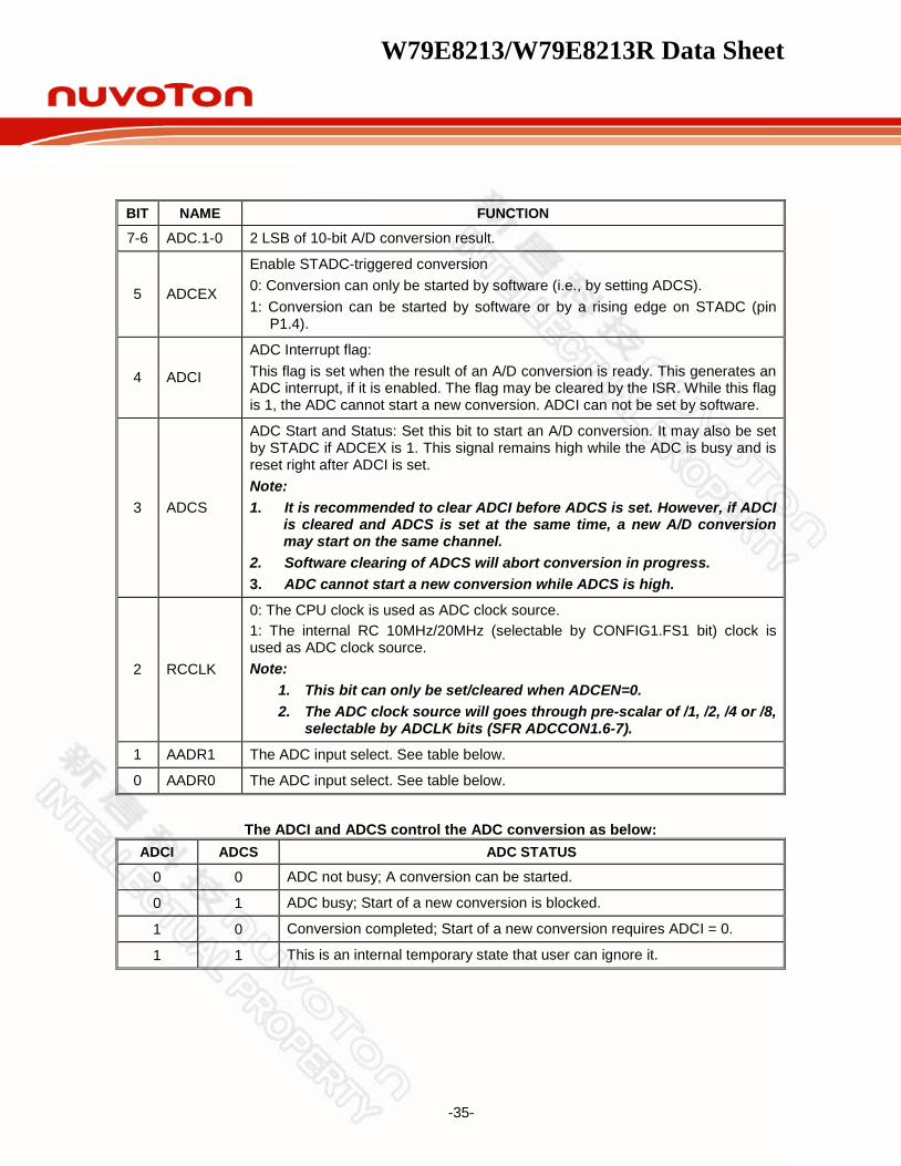
W79E8213/W79E8213R Data Sheet
-35-
BIT NAME FUNCTION
7-6 ADC.1-0 2 LSB of 10-bit A/D conversion result.
5 ADCEX
Enable STADC-triggered conversion 0: Conversion can only be started by software (i.e., by setting ADCS). 1: Conversion can be started by software or by a rising edge on STADC (pin
P1.4).
4 ADCI
ADC Interrupt flag: This flag is set when the result of an A/D conversion is ready. This generates an ADC interrupt, if it is enabled. The flag may be cleared by the ISR. While this flag is 1, the ADC cannot start a new conversion. ADCI can not be set by software.
3 ADCS
ADC Start and Status: Set this bit to start an A/D conversion. It may also be set by STADC if ADCEX is 1. This signal remains high while the ADC is busy and is reset right after ADCI is set. Note: 1. It is recommended to clear ADCI before ADCS is set. However, if ADCI
is cleared and ADCS is set at the same time, a new A/D conversion may start on the same channel.
2. Software clearing of ADCS will abort conversion in progress. 3. ADC cannot start a new conversion while ADCS is high.
2 RCCLK
0: The CPU clock is used as ADC clock source. 1: The internal RC 10MHz/20MHz (selectable by CONFIG1.FS1 bit) clock is used as ADC clock source. Note:
1. This bit can only be set/cleared when ADCEN=0. 2. The ADC clock source will goes through pre-scalar of /1, /2, /4 or /8,
selectable by ADCLK bits (SFR ADCCON1.6-7).
1 AADR1 The ADC input select. See table below.
0 AADR0 The ADC input select. See table below.
The ADCI and ADCS control the ADC conversion as below:
ADCI ADCS ADC STATUS
0 0 ADC not busy; A conversion can be started.
0 1 ADC busy; Start of a new conversion is blocked.
1 0 Conversion completed; Start of a new conversion requires ADCI = 0.
1 1 This is an internal temporary state that user can ignore it.

W79E8213/W79E8213R Data Sheet
-36-
AADR1, AADR0: ADC Analog Input Channel select bits: These bits can only be changed when ADCI and ADCS are both zero.
AADR2 AADR1 AADR0 SELECTED ANALOG INPUT CHANNEL 0 0 0 AD0 (P0.3) 0 0 1 AD1 (P0.4) 0 1 0 AD2 (P0.5) 0 1 1 AD3 (P0.6) 1 0 0 AD4 (P0.2) 1 0 1 AD5 (P0.1) 1 1 0 AD6 (P0.0) 1 1 1 AD7 (P0.7)
ADC CONVERTER RESULT HIGH REGISTER Bit: 7 6 5 4 3 2 1 0
ADC.9 ADC.8 ADC.7 ADC.6 ADC.5 ADC.4 ADC.3 ADC.2
Mnemonic: ADCH Address: E2h
BIT NAME FUNCTION
7-0 ADC.[9:2] 8 MSB of 10-bit A/D conversion result.
ADC CONTROL REGISTER 1 Bit: 7 6 5 4 3 2 1 0
ADCLK.1 ADCLK.0 - - - AADR2 - -
Mnemonic: ADCCON1 Address: E3h
BIT NAME FUNCTION
7-6 ADCLK.1~0
ADC Clock Prescaler: The 10-bit ADC needs a clock to drive the converting and the clock frequency need to be within 200KHz to 5MHz. ADCLK[1:0] controls the frequency of the clock to ADC block as below table.
ADCLK.1 ADCLK.0 ADC Clock Frequency 0 0 ADCCLK/1 0 1 ADCCLK/2 1 0 ADCCLK/4 (default) 1 1 ADCCLK/8
Note: User required to clear ADCEN (ADCEN = 0) when re-configure the ADC clock prescaler.
5-3 - Reserved.
2 AADR2 The ADC input select. See table in SFR ADCCON.
1-0 - Reserved.
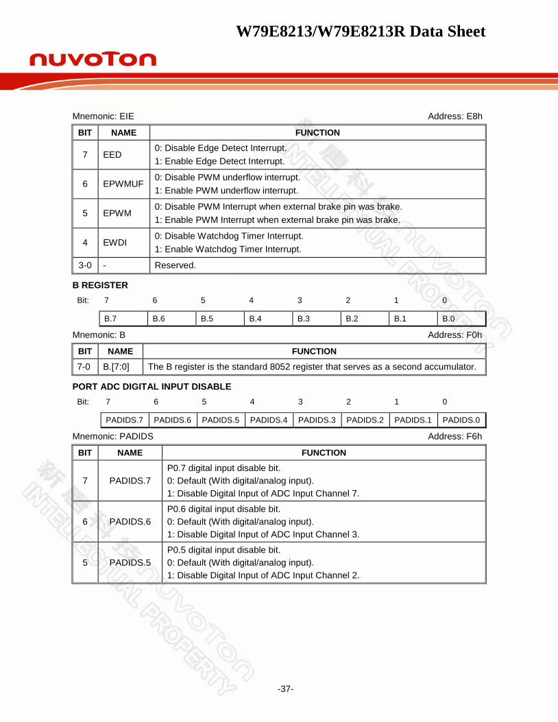
INTERRUPT ENABLE REGISTER 1 Bit: 7 6 5 4 3 2 1 0
EED EPWMUF EPWM EWDI - - - -
W79E8213/W79E8213R Data Sheet
-37-
Mnemonic: EIE Address: E8h
BIT NAME FUNCTION
7 EED 0: Disable Edge Detect Interrupt. 1: Enable Edge Detect Interrupt.
6 EPWMUF 0: Disable PWM underflow interrupt. 1: Enable PWM underflow interrupt.
5 EPWM 0: Disable PWM Interrupt when external brake pin was brake. 1: Enable PWM Interrupt when external brake pin was brake.
4 EWDI 0: Disable Watchdog Timer Interrupt. 1: Enable Watchdog Timer Interrupt.
3-0 - Reserved.
B REGISTER Bit: 7 6 5 4 3 2 1 0
B.7 B.6 B.5 B.4 B.3 B.2 B.1 B.0
Mnemonic: B Address: F0h
BIT NAME FUNCTION
7-0 B.[7:0] The B register is the standard 8052 register that serves as a second accumulator.
PORT ADC DIGITAL INPUT DISABLE Bit: 7 6 5 4 3 2 1 0
PADIDS.7 PADIDS.6 PADIDS.5 PADIDS.4 PADIDS.3 PADIDS.2 PADIDS.1 PADIDS.0
Mnemonic: PADIDS Address: F6h
BIT NAME FUNCTION
7 PADIDS.7 P0.7 digital input disable bit. 0: Default (With digital/analog input). 1: Disable Digital Input of ADC Input Channel 7.
6 PADIDS.6 P0.6 digital input disable bit. 0: Default (With digital/analog input). 1: Disable Digital Input of ADC Input Channel 3.
5 PADIDS.5 P0.5 digital input disable bit. 0: Default (With digital/analog input). 1: Disable Digital Input of ADC Input Channel 2.
W79E8213/W79E8213R Data Sheet
-38-
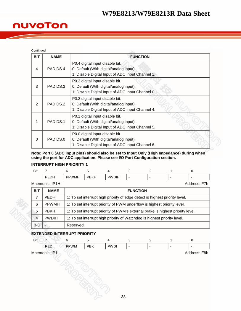
Continued
BIT NAME FUNCTION
4 PADIDS.4 P0.4 digital input disable bit. 0: Default (With digital/analog input). 1: Disable Digital Input of ADC Input Channel 1.
3 PADIDS.3 P0.3 digital input disable bit. 0: Default (With digital/analog input). 1: Disable Digital Input of ADC Input Channel 0.
2 PADIDS.2 P0.2 digital input disable bit. 0: Default (With digital/analog input). 1: Disable Digital Input of ADC Input Channel 4.
1 PADIDS.1 P0.1 digital input disable bit. 0: Default (With digital/analog input). 1: Disable Digital Input of ADC Input Channel 5.
0 PADIDS.0 P0.0 digital input disable bit. 0: Default (With digital/analog input). 1: Disable Digital Input of ADC Input Channel 6.
Note: Port 0 (ADC input pins) should also be set to Input Only (High Impedance) during when using the port for ADC application. Please see I/O Port Configuration section.
INTERRUPT HIGH PRIORITY 1 Bit: 7 6 5 4 3 2 1 0
PEDH PPWMH PBKH PWDIH - - - -
Mnemonic: IP1H Address: F7h
BIT NAME FUNCTION
7 PEDH 1: To set interrupt high priority of edge detect is highest priority level.
6 PPWMH 1: To set interrupt priority of PWM underflow is highest priority level.
5 PBKH 1: To set interrupt priority of PWM’s external brake is highest priority level.
4 PWDIH 1: To set interrupt high priority of Watchdog is highest priority level.
3-0 - Reserved.
EXTENDED INTERRUPT PRIORITY Bit: 7 6 5 4 3 2 1 0
PED PPWM PBK PWDI - - - -
Mnemonic: IP1 Address: F8h

W79E8213/W79E8213R Data Sheet
-39-
BIT NAME FUNCTION
7 PED 1: To set interrupt priority of Edge Detect is higher priority level.
6 PPWM 1: To set interrupt priority of PWM underflow is higher priority level.
5 PBK 1: To set interrupt priority of PWM’s external brake is higher priority level.
4 PWDI 1: To set interrupt priority of Watchdog is higher priority level.
3-0 - Reserved.
BUZZER CONTROL REGISTER Bit: 7 6 5 4 3 2 1 0
- - BUZDIV.5 BUZDIV.4 BUZDIV.3 BUZDIV.2 BUZDIV.1 BUZDIV.0
Mnemonic: BUZCON Address: F9h
BIT NAME FUNCTION
7-6 - Reserved.
5-0 BUZDIV
Buzzer division select bits: These bits are division selector. User may configure these bits to further divide the cpu clock in order to generate the desired buzzer output frequency. The following shows the equation for the buzzer output rate; Fbuz = Fcpu x 1/[(256)x(BUZDIV + 1)]
W79E8213/W79E8213R Data Sheet
-40-
9. INSTRUCTION SET The W79E8213 series execute all the instructions of the standard 8052 family. The operations of these instructions, as well as their effects on flag and status bits, are exactly the same. However, the timing of these instructions is different in two ways. Firstly, the machine cycle is four clock periods, while the standard-8051/52 machine cycle is twelve clock periods. Secondly, it can fetch only once per machine cycle (i.e., four clocks per fetch), while the standard 8051/52 can fetch twice per machine cycle (i.e., six clocks per fetch). The timing differences create an advantage for the W79E8213 series. There is only one fetch per machine cycle, so the number of machine cycles is usually equal to the number of operands in the instruction. (Jumps and calls do require an additional cycle to calculate the new address.) As a result, the W79E8213 series reduces the number of dummy fetches and wasted cycles, and therefore improves overall efficiency, compared to the standard 8051/52.
Op-code HEX Code Bytes W79E8213 series Machine Cycle
W79E8213 series Clock cycles
8032 Clock cycles
W79E8213 series v.s. 8032 Speed Ratio
NOP 00 1 1 4 12 3
ADD A, R0 28 1 1 4 12 3
ADD A, R1 29 1 1 4 12 3
ADD A, R2 2A 1 1 4 12 3
ADD A, R3 2B 1 1 4 12 3
ADD A, R4 2C 1 1 4 12 3
ADD A, R5 2D 1 1 4 12 3
ADD A, R6 2E 1 1 4 12 3
ADD A, R7 2F 1 1 4 12 3
ADD A, @R0 26 1 1 4 12 3
ADD A, @R1 27 1 1 4 12 3
ADD A, direct 25 2 2 8 12 1.5
ADD A, #data 24 2 2 8 12 1.5
ADDC A, R0 38 1 1 4 12 3
ADDC A, R1 39 1 1 4 12 3
ADDC A, R2 3A 1 1 4 12 3
ADDC A, R3 3B 1 1 4 12 3
ADDC A, R4 3C 1 1 4 12 3
ADDC A, R5 3D 1 1 4 12 3
ADDC A, R6 3E 1 1 4 12 3
ADDC A, R7 3F 1 1 4 12 3
ADDC A, @R0 36 1 1 4 12 3
ADDC A, @R1 37 1 1 4 12 3
ADDC A, direct 35 2 2 8 12 1.5
W79E8213/W79E8213R Data Sheet
-41-
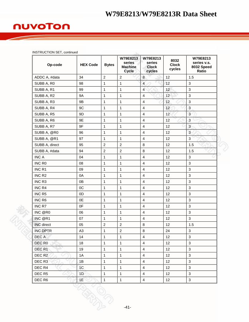
INSTRUCTION SET, continued
Op-code HEX Code Bytes W79E8213
series Machine
Cycle
W79E8213 series Clock cycles
8032 Clock cycles
W79E8213 series v.s.
8032 Speed Ratio
ADDC A, #data 34 2 2 8 12 1.5
SUBB A, R0 98 1 1 4 12 3
SUBB A, R1 99 1 1 4 12 3
SUBB A, R2 9A 1 1 4 12 3
SUBB A, R3 9B 1 1 4 12 3
SUBB A, R4 9C 1 1 4 12 3
SUBB A, R5 9D 1 1 4 12 3
SUBB A, R6 9E 1 1 4 12 3
SUBB A, R7 9F 1 1 4 12 3
SUBB A, @R0 96 1 1 4 12 3
SUBB A, @R1 97 1 1 4 12 3
SUBB A, direct 95 2 2 8 12 1.5
SUBB A, #data 94 2 2 8 12 1.5
INC A 04 1 1 4 12 3
INC R0 08 1 1 4 12 3
INC R1 09 1 1 4 12 3
INC R2 0A 1 1 4 12 3
INC R3 0B 1 1 4 12 3
INC R4 0C 1 1 4 12 3
INC R5 0D 1 1 4 12 3
INC R6 0E 1 1 4 12 3
INC R7 0F 1 1 4 12 3
INC @R0 06 1 1 4 12 3
INC @R1 07 1 1 4 12 3
INC direct 05 2 2 8 12 1.5
INC DPTR A3 1 2 8 24 3
DEC A 14 1 1 4 12 3
DEC R0 18 1 1 4 12 3
DEC R1 19 1 1 4 12 3
DEC R2 1A 1 1 4 12 3
DEC R3 1B 1 1 4 12 3
DEC R4 1C 1 1 4 12 3
DEC R5 1D 1 1 4 12 3
DEC R6 1E 1 1 4 12 3

W79E8213/W79E8213R Data Sheet
-42-
INSTRUCTION SET, continued
Op-code HEX Code Bytes W79E8213
series Machine
Cycle
W79E8213 series Clock cycles
8032 Clock cycles
W79E8213 series v.s 8032
Speed Ratio
DEC R7 1F 1 1 4 12 3
DEC @R0 16 1 1 4 12 3
DEC @R1 17 1 1 4 12 3
DEC direct 15 2 2 8 12 1.5
DEC DPTR A5 1 2 8 24 3
MUL AB A4 1 5 20 48 2.4
DIV AB 84 1 5 20 48 2.4
DA A D4 1 1 4 12 3
ANL A, R0 58 1 1 4 12 3
ANL A, R1 59 1 1 4 12 3
ANL A, R2 5A 1 1 4 12 3
ANL A, R3 5B 1 1 4 12 3
ANL A, R4 5C 1 1 4 12 3
ANL A, R5 5D 1 1 4 12 3
ANL A, R6 5E 1 1 4 12 3
ANL A, R7 5F 1 1 4 12 3
ANL A, @R0 56 1 1 4 12 3
ANL A, @R1 57 1 1 4 12 3
ANL A, direct 55 2 2 8 12 1.5
ANL A, #data 54 2 2 8 12 1.5
ANL direct, A 52 2 2 8 12 1.5
ANL direct, #data 53 3 3 12 24 2
ORL A, R0 48 1 1 4 12 3
ORL A, R1 49 1 1 4 12 3
ORL A, R2 4A 1 1 4 12 3
ORL A, R3 4B 1 1 4 12 3
ORL A, R4 4C 1 1 4 12 3
ORL A, R5 4D 1 1 4 12 3
ORL A, R6 4E 1 1 4 12 3
ORL A, R7 4F 1 1 4 12 3
ORL A, @R0 46 1 1 4 12 3
ORL A, @R1 47 1 1 4 12 3
ORL A, direct 45 2 2 8 12 1.5
ORL A, #data 44 2 2 8 12 1.5

W79E8213/W79E8213R Data Sheet
-43-
INSTRUCTION SET, continued
Op-code HEX Code Bytes W79E8213
series Machine
Cycle
W79E8213 series Clock cycles
8032 Clock cycles
W79E8213 series v.s 8032
Speed Ratio
ORL direct, A 42 2 2 8 12 1.5
ORL direct, #data 43 3 3 12 24 2
XRL A, R0 68 1 1 4 12 3
XRL A, R1 69 1 1 4 12 3
XRL A, R2 6A 1 1 4 12 3
XRL A, R3 6B 1 1 4 12 3
XRL A, R4 6C 1 1 4 12 3
XRL A, R5 6D 1 1 4 12 3
XRL A, R6 6E 1 1 4 12 3
XRL A, R7 6F 1 1 4 12 3
XRL A, @R0 66 1 1 4 12 3
XRL A, @R1 67 1 1 4 12 3
XRL A, direct 65 2 2 8 12 1.5
XRL A, #data 64 2 2 8 12 1.5
XRL direct, A 62 2 2 8 12 1.5
XRL direct, #data 63 3 3 12 24 2
CLR A E4 1 1 4 12 3
CPL A F4 1 1 4 12 3
RL A 23 1 1 4 12 3
RLC A 33 1 1 4 12 3
RR A 03 1 1 4 12 3
RRC A 13 1 1 4 12 3
SWAP A C4 1 1 4 12 3
MOV A, R0 E8 1 1 4 12 3
MOV A, R1 E9 1 1 4 12 3
MOV A, R2 EA 1 1 4 12 3
MOV A, R3 EB 1 1 4 12 3
MOV A, R4 EC 1 1 4 12 3
MOV A, R5 ED 1 1 4 12 3
MOV A, R6 EE 1 1 4 12 3
MOV A, R7 EF 1 1 4 12 3
MOV A, @R0 E6 1 1 4 12 3
MOV A, @R1 E7 1 1 4 12 3
MOV A, direct E5 2 2 8 12 1.5

W79E8213/W79E8213R Data Sheet
-44-
INSTRUCTION SET, continued
Op-code HEX Code Bytes W79E8213
series Machine
Cycle
W79E8213 series Clock cycles
8032 Clock cycles
W79E8213 series v.s 8032
Speed Ratio
MOV A, #data 74 2 2 8 12 1.5
MOV R0, A F8 1 1 4 12 3
MOV R1, A F9 1 1 4 12 3
MOV R2, A FA 1 1 4 12 3
MOV R3, A FB 1 1 4 12 3
MOV R4, A FC 1 1 4 12 3
MOV R5, A FD 1 1 4 12 3
MOV R6, A FE 1 1 4 12 3
MOV R7, A FF 1 1 4 12 3
MOV R0, direct A8 2 2 8 12 1.5
MOV R1, direct A9 2 2 8 12 1.5
MOV R2, direct AA 2 2 8 12 1.5
MOV R3, direct AB 2 2 8 12 1.5
MOV R4, direct AC 2 2 8 12 1.5
MOV R5, direct AD 2 2 8 12 1.5
MOV R6, direct AE 2 2 8 12 1.5
MOV R7, direct AF 2 2 8 12 1.5
MOV R0, #data 78 2 2 8 12 1.5
MOV R1, #data 79 2 2 8 12 1.5
MOV R2, #data 7A 2 2 8 12 1.5
MOV R3, #data 7B 2 2 8 12 1.5
MOV R4, #data 7C 2 2 8 12 1.5
MOV R5, #data 7D 2 2 8 12 1.5
MOV R6, #data 7E 2 2 8 12 1.5
MOV R7, #data 7F 2 2 8 12 1.5
MOV @R0, A F6 1 1 4 12 3
MOV @R1, A F7 1 1 4 12 3
MOV @R0, direct A6 2 2 8 12 1.5
MOV @R1, direct A7 2 2 8 12 1.5
MOV @R0, #data 76 2 2 8 12 1.5
MOV @R1, #data 77 2 2 8 12 1.5
MOV direct, A F5 2 2 8 12 1.5
MOV direct, R0 88 2 2 8 12 1.5
MOV direct, R1 89 2 2 8 12 1.5

W79E8213/W79E8213R Data Sheet
-45-
INSTRUCTION SET, continued
Op-code HEX Code Bytes W79E8213
series Machine
Cycle
W79E8213 series Clock cycles
8032 Clock cycles
W79E8213 series v.s 8032
Speed Ratio
MOV direct, R2 8A 2 2 8 12 1.5
MOV direct, R3 8B 2 2 8 12 1.5
MOV direct, R4 8C 2 2 8 12 1.5
MOV direct, R5 8D 2 2 8 12 1.5
MOV direct, R6 8E 2 2 8 12 1.5
MOV direct, R7 8F 2 2 8 12 1.5
MOV direct, @R0 86 2 2 8 12 1.5
MOV direct, @R1 87 2 2 8 12 1.5
MOV direct, direct 85 3 3 12 24 2
MOV direct, #data 75 3 3 12 24 2
MOV DPTR, #data 16 90 3 3 12 24 2
MOVC A, @A+DPTR 93 1 2 8 24 3
MOVC A, @A+PC 83 1 2 8 24 3
MOVX A, @R0 E2 1 2 - 9 8 - 36 24 3 - 0.66
MOVX A, @R1 E3 1 2 - 9 8 - 36 24 3 - 0.66
MOVX A, @DPTR E0 1 2 - 9 8 - 36 24 3 - 0.66
MOVX @R0, A F2 1 2 - 9 8 - 36 24 3 - 0.66
MOVX @R1, A F3 1 2 - 9 8 - 36 24 3 - 0.66
MOVX @DPTR, A F0 1 2 - 9 8 - 36 24 3 - 0.66
PUSH direct C0 2 2 8 24 3
POP direct D0 2 2 8 24 3
XCH A, R0 C8 1 1 4 12 3
XCH A, R1 C9 1 1 4 12 3
XCH A, R2 CA 1 1 4 12 3
XCH A, R3 CB 1 1 4 12 3
XCH A, R4 CC 1 1 4 12 3
XCH A, R5 CD 1 1 4 12 3
XCH A, R6 CE 1 1 4 12 3
XCH A, R7 CF 1 1 4 12 3
XCH A, @R0 C6 1 1 4 12 3
XCH A, @R1 C7 1 1 4 12 3
XCHD A, @R0 D6 1 1 4 12 3
XCHD A, @R1 D7 1 1 4 12 3
XCH A, direct C5 2 2 8 12 1.5
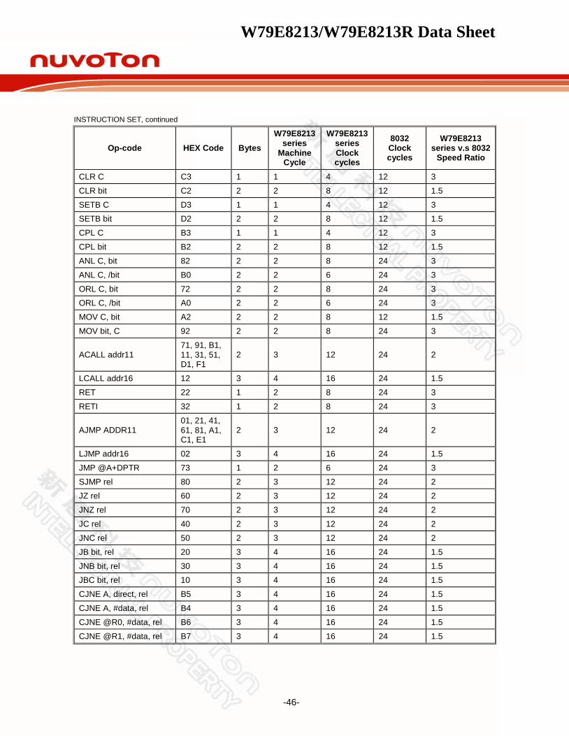
W79E8213/W79E8213R Data Sheet
-46-
INSTRUCTION SET, continued
Op-code HEX Code Bytes W79E8213
series Machine
Cycle
W79E8213 series Clock cycles
8032 Clock cycles
W79E8213 series v.s 8032
Speed Ratio
CLR C C3 1 1 4 12 3
CLR bit C2 2 2 8 12 1.5
SETB C D3 1 1 4 12 3
SETB bit D2 2 2 8 12 1.5
CPL C B3 1 1 4 12 3
CPL bit B2 2 2 8 12 1.5
ANL C, bit 82 2 2 8 24 3
ANL C, /bit B0 2 2 6 24 3
ORL C, bit 72 2 2 8 24 3
ORL C, /bit A0 2 2 6 24 3
MOV C, bit A2 2 2 8 12 1.5
MOV bit, C 92 2 2 8 24 3
ACALL addr11 71, 91, B1, 11, 31, 51, D1, F1
2 3 12 24 2
LCALL addr16 12 3 4 16 24 1.5
RET 22 1 2 8 24 3
RETI 32 1 2 8 24 3
AJMP ADDR11 01, 21, 41, 61, 81, A1, C1, E1
2 3 12 24 2
LJMP addr16 02 3 4 16 24 1.5
JMP @A+DPTR 73 1 2 6 24 3
SJMP rel 80 2 3 12 24 2
JZ rel 60 2 3 12 24 2
JNZ rel 70 2 3 12 24 2
JC rel 40 2 3 12 24 2
JNC rel 50 2 3 12 24 2
JB bit, rel 20 3 4 16 24 1.5
JNB bit, rel 30 3 4 16 24 1.5
JBC bit, rel 10 3 4 16 24 1.5
CJNE A, direct, rel B5 3 4 16 24 1.5
CJNE A, #data, rel B4 3 4 16 24 1.5
CJNE @R0, #data, rel B6 3 4 16 24 1.5
CJNE @R1, #data, rel B7 3 4 16 24 1.5

W79E8213/W79E8213R Data Sheet
-47-
INSTRUCTION SET, continued
Op-code HEX Code Bytes W79E8213
series Machine
Cycle
W79E8213 series Clock cycles
8032 Clock cycles
W79E8213 series v.s 8032
Speed Ratio
CJNE R0, #data, rel B8 3 4 16 24 1.5
CJNE R1, #data, rel B9 3 4 16 24 1.5
CJNE R2, #data, rel BA 3 4 16 24 1.5
CJNE R3, #data, rel BB 3 4 16 24 1.5
CJNE R4, #data, rel BC 3 4 16 24 1.5
CJNE R5, #data, rel BD 3 4 16 24 1.5
CJNE R6, #data, rel BE 3 4 16 24 1.5
CJNE R7, #data, rel BF 3 4 16 24 1.5
DJNZ R0, rel D8 2 3 12 24 2
DJNZ R1, rel D9 2 3 12 24 2
DJNZ R5, rel DD 2 3 12 24 2
DJNZ R2, rel DA 2 3 12 24 2
DJNZ R3, rel DB 2 3 12 24 2
DJNZ R4, rel DC 2 3 12 24 2
DJNZ R6, rel DE 2 3 12 24 2
DJNZ R7, rel DF 2 3 12 24 2
DJNZ direct, rel D5 3 4 16 24 1.5
Table 9-1: Instruction Set for W79E8213
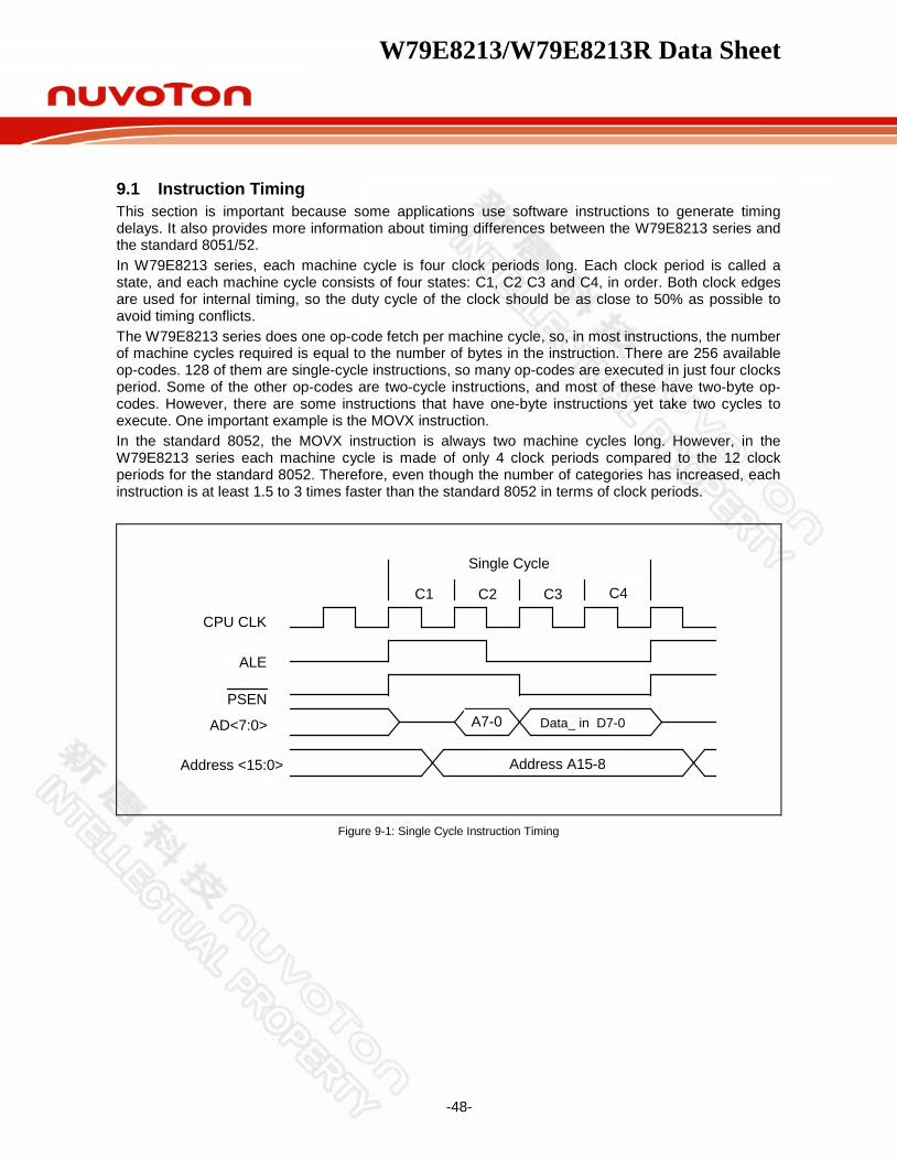
W79E8213/W79E8213R Data Sheet
-48-
9.1 Instruction Timing This section is important because some applications use software instructions to generate timing delays. It also provides more information about timing differences between the W79E8213 series and the standard 8051/52. In W79E8213 series, each machine cycle is four clock periods long. Each clock period is called a state, and each machine cycle consists of four states: C1, C2 C3 and C4, in order. Both clock edges are used for internal timing, so the duty cycle of the clock should be as close to 50% as possible to avoid timing conflicts. The W79E8213 series does one op-code fetch per machine cycle, so, in most instructions, the number of machine cycles required is equal to the number of bytes in the instruction. There are 256 available op-codes. 128 of them are single-cycle instructions, so many op-codes are executed in just four clocks period. Some of the other op-codes are two-cycle instructions, and most of these have two-byte op-codes. However, there are some instructions that have one-byte instructions yet take two cycles to execute. One important example is the MOVX instruction. In the standard 8052, the MOVX instruction is always two machine cycles long. However, in the W79E8213 series each machine cycle is made of only 4 clock periods compared to the 12 clock periods for the standard 8052. Therefore, even though the number of categories has increased, each instruction is at least 1.5 to 3 times faster than the standard 8052 in terms of clock periods.
Single Cycle
C4C3C2C1
CPU CLK
ALE
PSEN
AD<7:0>
Address <15:0>
A7-0
Address A15-8
Data_ in D7-0
Figure 9-1: Single Cycle Instruction Timing

W79E8213/W79E8213R Data Sheet
-49-
Instruction Fetch
C4C3C2C1
OP-CODE
Address A15-8Address A15-8
ALE
PSEN
PCAD<7:0>
Address<15:0>
CPU CLK
Operand Fetch
C4C3C2C1
OPERANDPC+1
Figure 9-2: Two Cycles Instruction Timing
OPERANDOPERAND A7-0A7-0 A7-0OP-CODE
Address A15-8Address A15-8Address A15-8
Operand FetchOperand FetchInstruction Fetch
C2 C3 C4C2 C3 C4C4C3C2 C1C1C1
CPU CLK
ALE
PSEN
AD<7:0>
Address<15:0>
Figure 9-3: Three Cycles Instruction Timing
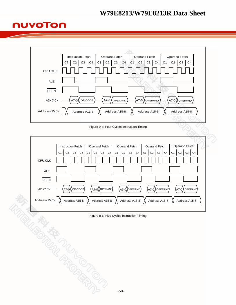
W79E8213/W79E8213R Data Sheet
-50-
OPERANDOPERANDOPERANDOP-CODE
Address A15-8Address A15-8Address A15-8Address A15-8
A7-0A7-0A7-0A7-0
Operand FetchOperand FetchOperand FetchInstruction Fetch
C2C1 C4C3C2C1
CPU CLK
ALE
PSEN
AD<7:0>
Address<15:0>
C4C3 C2C1 C4C3 C2C1 C4C3
Figure 9-4: Four Cycles Instruction Timing
OPERANDOPERANDOPERANDOP-CODE
Address A15-8Address A15-8Address A15-8Address A15-8
A7-0A7-0A7-0A7-0
Operand Fetch Operand FetchOperand FetchOperand FetchInstruction Fetch
C2C1 C4C3C2C1
CPU CLK
ALE
PSEN
AD<7:0>
Address<15:0>
C4C3 C2C1 C4C3 C2C1 C4C3 C2C1 C4C3
OPERANDA7-0
Address A15-8
Figure 9-5: Five Cycles Instruction Timing

W79E8213/W79E8213R Data Sheet
-51-
10. POWER MANAGEMENT The W79E8213 series has several features that help the user to control the power consumption of the device. These modes are discussed in the next two sections.
10.1 Idle Mode The user can put the device into idle mode by writing 1 to the bit PCON.0. The instruction that sets the idle bit is the last instruction that will be executed before the device goes into Idle Mode. In the Idle mode, the clock to the CPU is halted, but not to the Interrupt, Timer, PWM and Watchdog timer blocks. This forces the CPU state to be frozen; the Program counter, the Stack Pointer, the Program Status Word, the Accumulator and the other registers hold their contents. The port pins hold the logical states they had at the time Idle was activated. The Idle mode can be terminated in two ways. Since the interrupt controller is still active, the activation of any enabled interrupt can wake up the processor. This will automatically clear the Idle bit, terminate the Idle mode, and the Interrupt Service Routine (ISR) will be executed. After the ISR, execution of the program will continue from the instruction which put the device into Idle Mode. The Idle mode can also be exited by activating the reset. The device can put into reset either by applying a low on the external /RST pin, a Power on reset condition or a Watchdog timer reset. The external reset pin has to be held low for at least two machine cycles i.e. 8 clock periods to be recognized as a valid reset. In the reset condition the program counter is reset to 0000h and all the SFRs are set to the reset condition. Since the clock is already running there is no delay and execution starts immediately. In the Idle mode, the Watchdog timer continues to run, and if enabled, a time-out will cause a watchdog timer interrupt which will wake up the device. The software must reset the Watchdog timer in order to preempt the reset which will occur after 512 clock periods of the time-out. When the W79E8213 series are exiting from an Idle Mode with a reset, the instruction following the one which put the device into Idle Mode is not executed. So there is no danger of unexpected writes.
10.2 Power-down Mode The device can be put into Power-down mode by writing 1 to bit PCON.1. The instruction that does this will be the last instruction to be executed before the device goes into Power-down mode. In the Power-down mode, all the clocks are stopped and the device comes to a halt. All activity is completely stopped and the power consumption is reduced to the lowest possible value. The port pins output the values held by their respective SFRs. The W79E8213 series will exit the Power-down mode with a reset or by an external interrupt pin enabled as level detected. An external reset can be used to exit the Power down state. The low on /RST pin terminates the Power-down mode, and restarts the clock. The program execution will restart from 0000h. In the Power-down mode, the clock is stopped, so the Watchdog timer cannot be used to provide the reset to exit Power-down mode when its clock source is external OSC or crystal. The sources that can wake up from the power-down mode are external interrupts, brownout reset (BOR) and ADC. Note that for ADC waking up from powerdown, the device need to run on internal rc and software perform start ADC prior to powerdown. The W79E8213 series can be waken up from the Power-down mode by forcing an external interrupt pin activation, provided the corresponding interrupt is enabled, while the global enable (EA) bit is set. If these conditions are met, then either a low-level or a falling-edge at external interrupt pin will re-start the oscillator. The device will then execute the interrupt service routine for the corresponding external interrupt. After the interrupt service routine is completed, the program execution returns to the instruction after one which put the device into Power-down mode and continues from there. During Power-down mode, if AUXR1.LPBOV = 1 and AUXR1.BOD = 0, the internal RC clock will be enabled and hence save power.
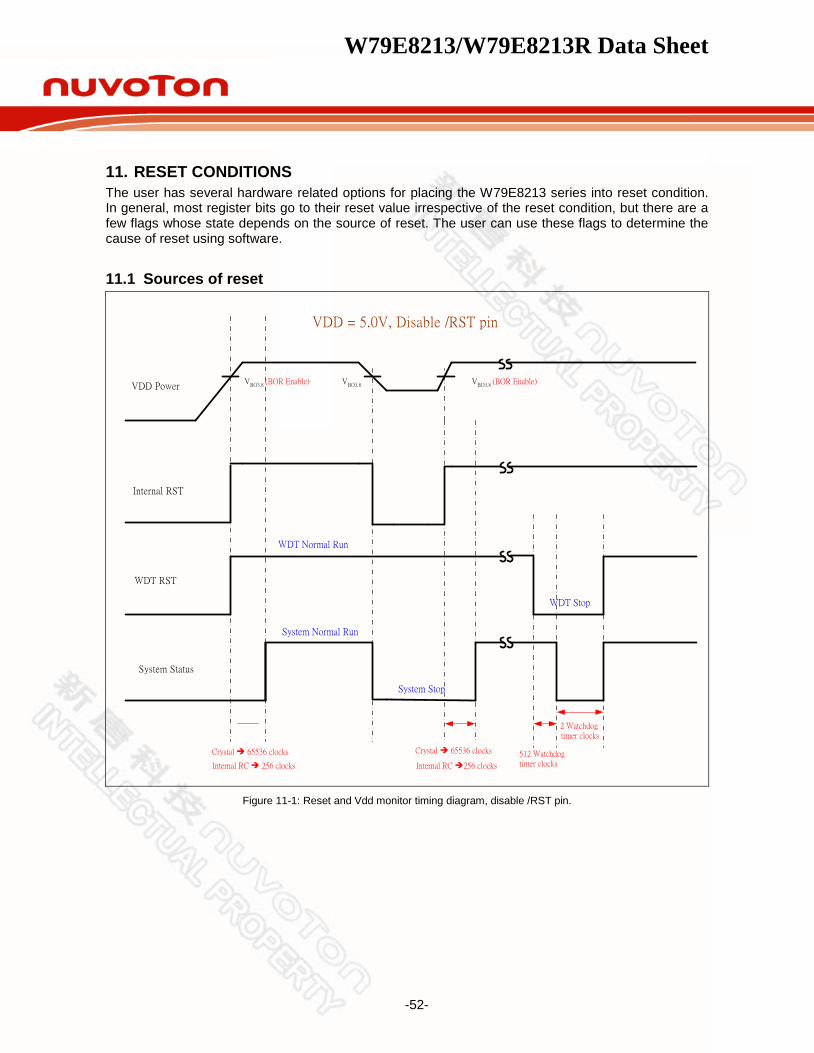
W79E8213/W79E8213R Data Sheet
-52-
11. RESET CONDITIONS The user has several hardware related options for placing the W79E8213 series into reset condition. In general, most register bits go to their reset value irrespective of the reset condition, but there are a few flags whose state depends on the source of reset. The user can use these flags to determine the cause of reset using software.
11.1 Sources of reset
System Status
System Stop
System Normal Run
WDT RST
WDT Stop
Internal RST
WDT Normal Run
VDD Power
512 Watchdog timer clocks
Crystal 65536 clocks
Internal RC 256 clocks
Crystal 65536 clocks
Internal RC 256 clocks
VDD = 5.0V, Disable /RST pin
VBO3.8 (BOR Enable)VBO3.8 (BOR Enable) VBO3.8
2 Watchdog timer clocks
Figure 11-1: Reset and Vdd monitor timing diagram, disable /RST pin.
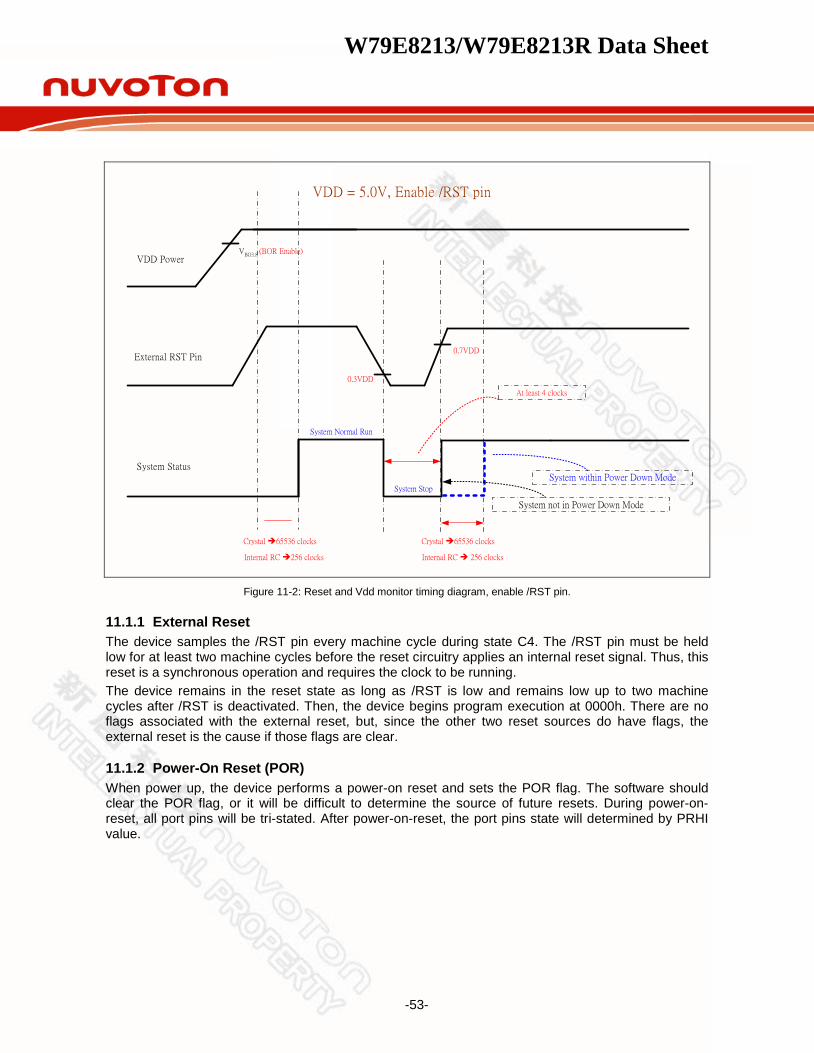
W79E8213/W79E8213R Data Sheet
-53-
System Status
System Stop
System Normal Run
External RST Pin
VDD Power
0.3VDD
Crystal 65536 clocks
Internal RC 256 clocks
Crystal 65536 clocks
Internal RC 256 clocks
System within Power Down Mode
System not in Power Down Mode
At least 4 clocks
VDD = 5.0V, Enable /RST pin
0.7VDD
VBO3.8 (BOR Enable)
Figure 11-2: Reset and Vdd monitor timing diagram, enable /RST pin.
11.1.1 External Reset The device samples the /RST pin every machine cycle during state C4. The /RST pin must be held low for at least two machine cycles before the reset circuitry applies an internal reset signal. Thus, this reset is a synchronous operation and requires the clock to be running. The device remains in the reset state as long as /RST is low and remains low up to two machine cycles after /RST is deactivated. Then, the device begins program execution at 0000h. There are no flags associated with the external reset, but, since the other two reset sources do have flags, the external reset is the cause if those flags are clear.
11.1.2 Power-On Reset (POR) When power up, the device performs a power-on reset and sets the POR flag. The software should clear the POR flag, or it will be difficult to determine the source of future resets. During power-on-reset, all port pins will be tri-stated. After power-on-reset, the port pins state will determined by PRHI value.

W79E8213/W79E8213R Data Sheet
-54-
11.1.3 Watchdog Timer Reset The Watchdog Timer is a free-running timer with programmable time-out intervals. The program must clear the Watchdog Timer before the time-out interval is reached to restart the count. If the time-out interval is reached, an interrupt flag is set. 512 clocks later, if the Watchdog Reset is enabled and the Watchdog Timer has not been cleared, the Watchdog Timer generates a reset. The reset condition is maintained by the hardware for two machine cycles, and the WTRF bit in WDCON is set. Afterwards, the device begins program execution at 0000h.
11.2 Reset State When the device is reset, most registers return to their initial state. The Watchdog Timer is disabled if the reset source was a power-on reset. The port registers are set to FFh, which puts most of the port pins in a high state. The Program Counter is set to 0000h, and the stack pointer is reset to 07h. After this, the device remains in the reset state as long as the reset conditions are satisfied. Reset does not affect the on-chip RAM, however, so RAM is preserved as long as VDD remains above approximately 2V, the minimum operating voltage for the RAM. If VDD falls below 2V, the RAM contents are also lost. In either case, the stack pointer is always reset, so the stack contents are lost.
The WDCON SFR bits are set/cleared in reset condition depending on the source of the reset. The WDCON SFR is set to a 0x00 0000B on the reset. WTRF (WDCON.2) is set to a 1 on a Watchdog timer reset, but to a 0 on power on/down resets. WTRF (WDCON.2) is not altered by external reset. EWRST (WDCON.1) is cleared by any reset. Software or any reset will clear WDIF (WDCON.3) bit. Some of the bits in the WDCON SFR (WDRUN, WDCLR, EWRST, WDIF, WD0 and WD1) have unrestricted read access which required Timed Access procedure to write. The remaining bits have unrestricted write accesses. Please refer TA register description. For all SFR reset state values, please refer to Table 8-2: Special Function Registers.
W79E8213/W79E8213R Data Sheet
-55-
12. INTERRUPTS The W79E8213 series have four priority level interrupts structure with 10 interrupt sources. Each of the interrupt sources has an individual priority bit, flag, interrupt vector and enable bit. In addition, the interrupts can be globally enabled or disabled.
12.1 Interrupt Sources The External Interrupts INT0 and INT1 can be either edge triggered or level triggered, programmable through bits IT0 and IT1. The bits IE0 and IE1 in the TCON register are the flags which are checked to generate the interrupt. In the edge triggered mode, the INTx inputs are sampled in every machine cycle. If the sample is high in one cycle and low in the next, then a high to low transition is detected and the interrupts request flag IEx in TCON is set. The flag bit requests the interrupt. Since the external interrupts are sampled every machine cycle, they have to be held high or low for at least one complete machine cycle. The IEx flag is automatically cleared when the service routine is called. If the level triggered mode is selected, then the requesting source has to hold the pin low till the interrupt is serviced. The IEx flag will not be cleared by the hardware on entering the service routine. If the interrupt continues to be held low even after the service routine is completed, then the processor may acknowledge another interrupt request from the same source. The Timer 0 and 1 Interrupts are generated by the TF0 and TF1 flags. These flags are set by the overflow in the Timer 0 and Timer 1. The TF0 and TF1 flags are automatically cleared by the hardware when the timer interrupt is serviced. The Watchdog timer can be used as a system monitor or a simple timer. In either case, when the time-out count is reached, the Watchdog Timer interrupt flag WDIF (WDCON.3) is set. If the interrupt is enabled by the enable bit EIE.4, then an interrupt will occur. PWM interrupt is generated when its’ 10-bit down counter underflows. PWMF flag is set and PWM interrupt is generated if enabled. PWMF is set by hardware and can only be cleared by software. Alternatively, PWM function can also generate interrupt by BKF flag, after external brake pin has brake occurred. This bit will be cleared by software. The ADC can generate interrupt after finished ADC converter. There is one interrupt source, which is obtained by the ADCI bit in the ADCCON SFR. This bit is not automatically cleared by the hardware, and the user will have to clear this bit using software. Edge detect interrupt is generated when any of the keypad connected to P1.0-P1.2 pins is pressed. Each edge detect interrupt can be individually enabled/disabled. User will have to software clear the flag bit. The ED pins have edge type and filter type control, configurable through EDIC SFR. Brownout detect can cause brownout flag, BOF, to be asserted if power voltage drop below brownout voltage level. Interrupt will occur if BOI (AUXR1.5), EBO (IE.5) and global interrupt enable are set. All the bits that generate interrupts can be set or reset by software, and thereby software initiated interrupts can be generated. Each of the individual interrupts can be enabled or disabled by setting or clearing a bit in the IE SFR. IE also has a global enable/disable bit EA, which can be cleared to disable all interrupts. The interrupt flags are sampled every machine cycle. In the same machine cycle, the sampled interrupts are polled and their priority is resolved. If certain conditions are met then the hardware will execute an internally generated LCALL instruction which will vector the process to the appropriate interrupt vector address. The conditions for generating the LCALL are; 1. An interrupt of equal or higher priority is not currently being serviced. 2. The current polling cycle is the last machine cycle of the instruction currently being execute. 3. The current instruction does not involve a write to IE, EIE, IP0, IP0H, IP1 or IPH1 registers and is not a RETI. If any of these conditions are not met, then the LCALL will not be generated. The polling cycle is repeated every machine cycle, with the interrupts sampled in the same machine cycle. If an interrupt
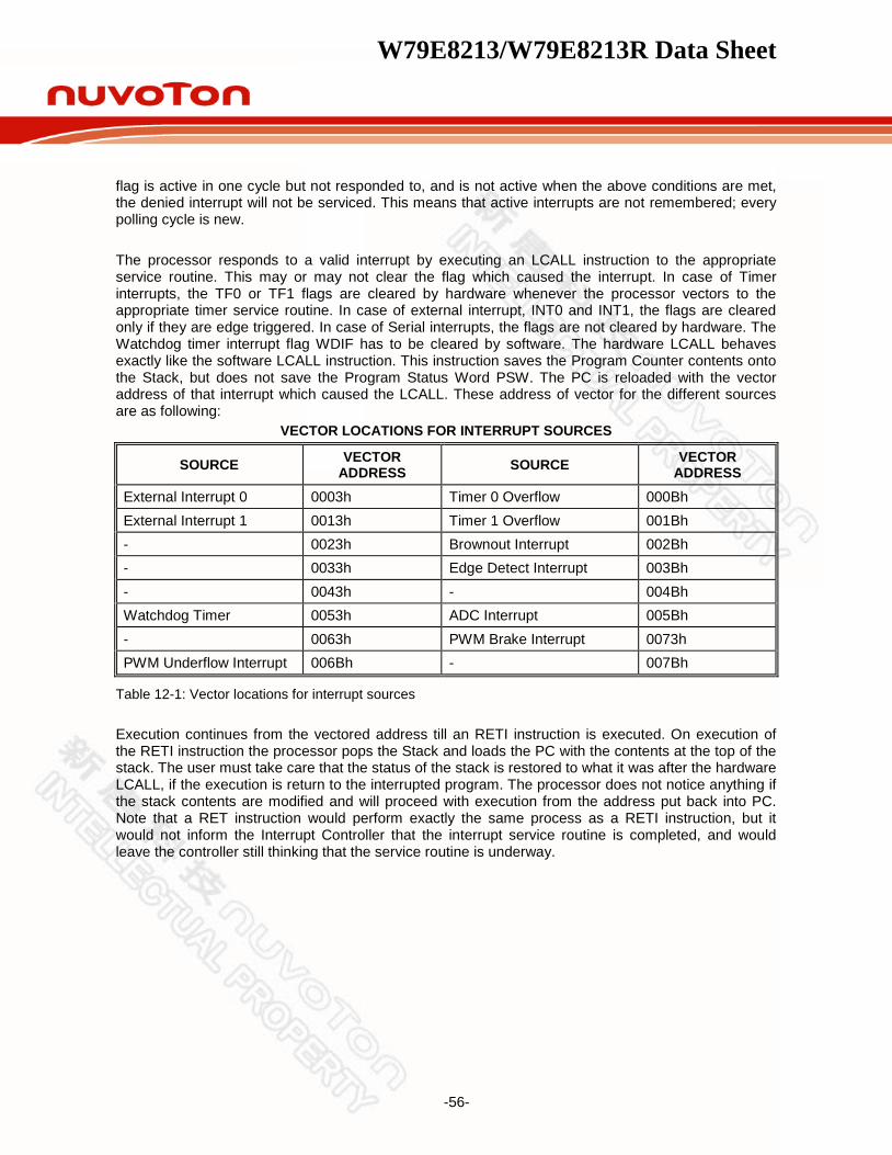
W79E8213/W79E8213R Data Sheet
-56-
flag is active in one cycle but not responded to, and is not active when the above conditions are met, the denied interrupt will not be serviced. This means that active interrupts are not remembered; every polling cycle is new. The processor responds to a valid interrupt by executing an LCALL instruction to the appropriate service routine. This may or may not clear the flag which caused the interrupt. In case of Timer interrupts, the TF0 or TF1 flags are cleared by hardware whenever the processor vectors to the appropriate timer service routine. In case of external interrupt, INT0 and INT1, the flags are cleared only if they are edge triggered. In case of Serial interrupts, the flags are not cleared by hardware. The Watchdog timer interrupt flag WDIF has to be cleared by software. The hardware LCALL behaves exactly like the software LCALL instruction. This instruction saves the Program Counter contents onto the Stack, but does not save the Program Status Word PSW. The PC is reloaded with the vector address of that interrupt which caused the LCALL. These address of vector for the different sources are as following:
VECTOR LOCATIONS FOR INTERRUPT SOURCES
SOURCE VECTOR ADDRESS SOURCE VECTOR
ADDRESS
External Interrupt 0 0003h Timer 0 Overflow 000Bh External Interrupt 1 0013h Timer 1 Overflow 001Bh - 0023h Brownout Interrupt 002Bh - 0033h Edge Detect Interrupt 003Bh - 0043h - 004Bh Watchdog Timer 0053h ADC Interrupt 005Bh - 0063h PWM Brake Interrupt 0073h PWM Underflow Interrupt 006Bh - 007Bh
Table 12-1: Vector locations for interrupt sources Execution continues from the vectored address till an RETI instruction is executed. On execution of the RETI instruction the processor pops the Stack and loads the PC with the contents at the top of the stack. The user must take care that the status of the stack is restored to what it was after the hardware LCALL, if the execution is return to the interrupted program. The processor does not notice anything if the stack contents are modified and will proceed with execution from the address put back into PC. Note that a RET instruction would perform exactly the same process as a RETI instruction, but it would not inform the Interrupt Controller that the interrupt service routine is completed, and would leave the controller still thinking that the service routine is underway.

W79E8213/W79E8213R Data Sheet
-57-
12.2 Priority Level Structure The W79E8213 series uses a four priority level interrupt structure (highest, high, low and lowest) and supports up to 10 interrupt sources. The interrupt sources can be individually set to either high or low levels. Naturally, a higher priority interrupt cannot be interrupted by a lower priority interrupt. However there exists a pre-defined hierarchy amongst the interrupts themselves. This hierarchy comes into play when the interrupt controller has to resolve simultaneous requests having the same priority level. This hierarchy is defined as table below. This allows great flexibility in controlling and handling many interrupt sources.
PRIORITY BITS INTERRUPT PRIORITY LEVEL
IPXH IPX
0 0 Level 0 (lowest priority)
0 1 Level 1
1 0 Level 2
1 1 Level 3 (highest priority)
Table 12-2: Four-level interrupt priority
Each interrupt source can be individually programmed to one of four priority levels by setting or clearing bits in the IP0, IP0H, IP1, and IP1H registers. An interrupt service routine in progress can be interrupted by a higher priority interrupt, but not by another interrupt of the same or lower priority. The highest priority interrupt service cannot be interrupted by any other interrupt source. So, if two requests of different priority levels are received simultaneously, the request of higher priority level is serviced. If requests of the same priority level are received simultaneously, an internal polling sequence determines which request is serviced. This is called the arbitration ranking. Note that the arbitration ranking is only used to resolve simultaneous requests of the same priority level. As below Table summarizes the interrupt sources, flag bits, vector addresses, enable bits, priority bits, arbitration ranking, and whether each interrupt may wake up the CPU from Power-down mode.
Source Flag Vector
address Interrupt
Enable Bits Interrupt Priority
Flag cleared by
Arbitration Ranking
Power- Down
Wakeup
External Interrupt 0 IE0 0003H EX0 (IE0.0) IP0H.0, IP0.0
Hardware, Follow the inverse of pin
1(highest) Yes
Brownout Detect BOF 002BH EBO (IE.5) IP0H.5, IP0.5 Software 2 Yes
Watchdog Timer WDIF 0053H EWDI (EIE.4) IP1H.4, IP1.4 Software 3 No
Timer 0 Interrupt TF0 000BH ET0 (IE.1) IP0H.1, IP0.1 Hardware,
software 4 No

W79E8213/W79E8213R Data Sheet
-58-
Continued
Source Flag Vector
address Interrupt
Enable Bits Interrupt Priority
Flag cleared by
Arbitration Ranking
Power- Down
Wakeup
ADC Converter ADCI 005BH EAD (IE.6) IP0H.6, IP0.6 Hardware 5 Yes(1)
External Interrupt 1 IE1 0013H EX1 (IE.2) IP0H.2, IP0.2
Hardware, Follow the inverse of pin
6 Yes
Edge Detect Interrupt EDF 003BH EED (EIE.7) IP1H.7, IP1.7 Software 7 No
Timer 1 Interrupt TF1 001BH ET1 (IE.3) IP0H.3, IP0.3 Hardware,
software 8 No
PWM Period Interrupt PWMF 006BH EPWMUF
(EIE.6) IP1H.6, IP1.6 Software 9 No
PWM Brake Interrupt BKF 0073H EPWM (EIE.5) IP1H.5, IP1.5 Software 10 (lowest) No
Note: 1. ADC Converter can wake up Power-down Mode when its clock source is from internal RC.
Table 12-3: Vector location for Interrupt sources and power-down wakeup
12.3 Response Time The response time for each interrupt source depends on several factors, such as the nature of the interrupt and the instruction underway. In the case of external interrupts INT0 and INT1 , they are sampled at C3 of every machine cycle and then their corresponding interrupt flags IEx will be set or reset. The Timer 0 and 1 overflow flags are set at C3 of the machine cycle in which overflow has occurred. These flag values are polled only in the next machine cycle. If a request is active and all three conditions are met, then the hardware generated LCALL is executed. This LCALL itself takes four machine cycles to be completed. Thus there is a minimum time of five machine cycles between the interrupt flag being set and the interrupt service routine being executed. A longer response time should be anticipated if any of the three conditions are not met. If a higher or equal priority is being serviced, then the interrupt latency time obviously depends on the nature of the service routine currently being executed. If the polling cycle is not the last machine cycle of the instruction being executed, then an additional delay is introduced. The maximum response time (if no other interrupt is in service) occurs if the W79E8213 series are performing a write to IE, EIE, IP0, IP0H, IP1 or IP1H and then executes a MUL or DIV instruction. From the time an interrupt source is activated, the longest reaction time is 12 machine cycles. This includes 1 machine cycle to detect the interrupt, 2 machine cycles to complete the IE, EIE, IP0, IP0H, IP1 or IP1H access, 5 machine cycles to complete the MUL or DIV instruction and 4 machine cycles to complete the hardware LCALL to the interrupt vector location. Thus in a single-interrupt system the interrupt response time will always be more than 5 machine cycles and not more than 12 machine cycles. The maximum latency of 12 machine cycles is 48 clock cycles. Note that in the standard 8051 the maximum latency is 8 machine cycles which equals 96 machine cycles. This is a 50% reduction in terms of clock periods.
12.4 Interrupt Inputs The W79E8213 series have total 10 interrupt sources with two individual interrupt inputs sources.
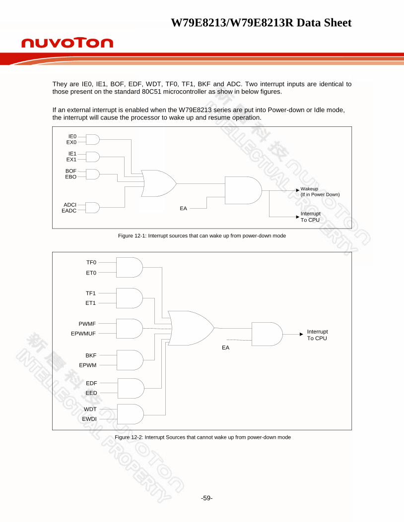
W79E8213/W79E8213R Data Sheet
-59-
They are IE0, IE1, BOF, EDF, WDT, TF0, TF1, BKF and ADC. Two interrupt inputs are identical to those present on the standard 80C51 microcontroller as show in below figures. If an external interrupt is enabled when the W79E8213 series are put into Power-down or Idle mode, the interrupt will cause the processor to wake up and resume operation.
IE0EX0
IE1EX1
BOFEBO
ADCIEADC EA
Wakeup(If in Power Down)
InterruptTo CPU
Figure 12-1: Interrupt sources that can wake up from power-down mode
EPWMUF
PWMF
ET0
TF0
EA
InterruptTo CPU
ET1
TF1
EPWM
BKF
EED
EDF
EWDI
WDT
Figure 12-2: Interrupt Sources that cannot wake up from power-down mode

W79E8213/W79E8213R Data Sheet
-60-
13. PROGRAMMABLE TIMERS/COUNTERS The W79E8213 series have two 16-bit programmable timer/counters and one programmable Watchdog Timer. The Watchdog Timer is operationally quite different from the other two timers. Its’ timer/counters have additional timer 0 or timer 1 overflow toggle output enable feature as compare to conventional timer/counters. This timer overflow toggle output can be configured to automatically toggle T0 or T1 pin output whenever a timer overflow occurs.
13.1 Timer/Counters 0 & 1 The W79E8213 series have two 16-bit Timer/Counters. Each of these Timer/Counters has two 8 bit registers which form the 16 bit counting register. For Timer/Counter 0 they are TH0, the upper 8 bits register, and TL0, the lower 8 bit register. Similarly Timer/Counter 1 has two 8 bit registers, TH1 and TL1. The two can be configured to operate either as timers, counting machine cycles or as counters counting external inputs. When configured as a "Timer", the timer counts clock cycles. The timer clock can be programmed to be thought of as 1/12 of the system clock or 1/4 of the system clock. In the "Counter" mode, the register is incremented on the falling edge of the external input pin, T0 for Timer 0, and T1 for Timer 1. The T0 and T1 inputs are sampled in every machine cycle at C4. If the sampled value is high in one machine cycle and low in the next, then a valid high to low transition on the pin is recognized and the count register is incremented. Since it takes two machine cycles to recognize a negative transition on the pin, the maximum rate at which counting will take place is 1/8 of the master clock frequency. In either the "Timer" or "Counter" mode, the count register will be updated at C3. Therefore, in the "Timer" mode, the recognized negative transition on pin T0 and T1 can cause the count register value to be updated only in the machine cycle following the one in which the negative edge was detected.
The "Timer" or "Counter" function is selected by the " TC/ " bit in the TMOD Special Function Register. Each Timer/Counter has one selection bit for its own; bit 2 of TMOD selects the function for Timer/Counter 0 and bit 6 of TMOD selects the function for Timer/Counter 1. In addition each Timer/Counter can be set to operate in any one of four possible modes. The mode selection is done by bits M0 and M1 in the TMOD SFR.
13.1.1 Time-Base Selection The W79E8213 series can operate like the standard 8051/52 family, counting at the rate of 1/12 of the clock speed, or in turbo mode, counting at the rate of 1/4 clock speed. The speed is controlled by the T0M and T1M bits in CKCON, and the default value is zero, which uses the standard 8051/52 speed.
13.1.2 Mode 0 In Mode 0, the timer/counter is a 13-bit counter. The 13-bit counter consists of THx (8 MSB) and the five lower bits of TLx (5 LSB). The upper three bits of TLx are ignored. The timer/counter is enabled when TRx is set and either GATE is 0 or INTx is 1. When TC / is 0, the timer/counter counts clock cycles; when TC / is 1, it counts falling edges on T0 (P1.2 for Timer 0) or T1 (P0.7 for Timer 1). For clock cycles, the time base may be 1/12 or 1/4 clock speed, and the falling edge of the clock increments the counter. When the 13-bit value moves from 1FFFh to 0000h, the timer overflow flag TFx is set, and an interrupt occurs if enabled. This is illustrated in next figure below. In “Timer” mode, if output toggled enable bit of P2M1.T0OE or P2M1.T1OE is enable, T0 or T1 output pin will toggle whenever a timer overflow occurs.
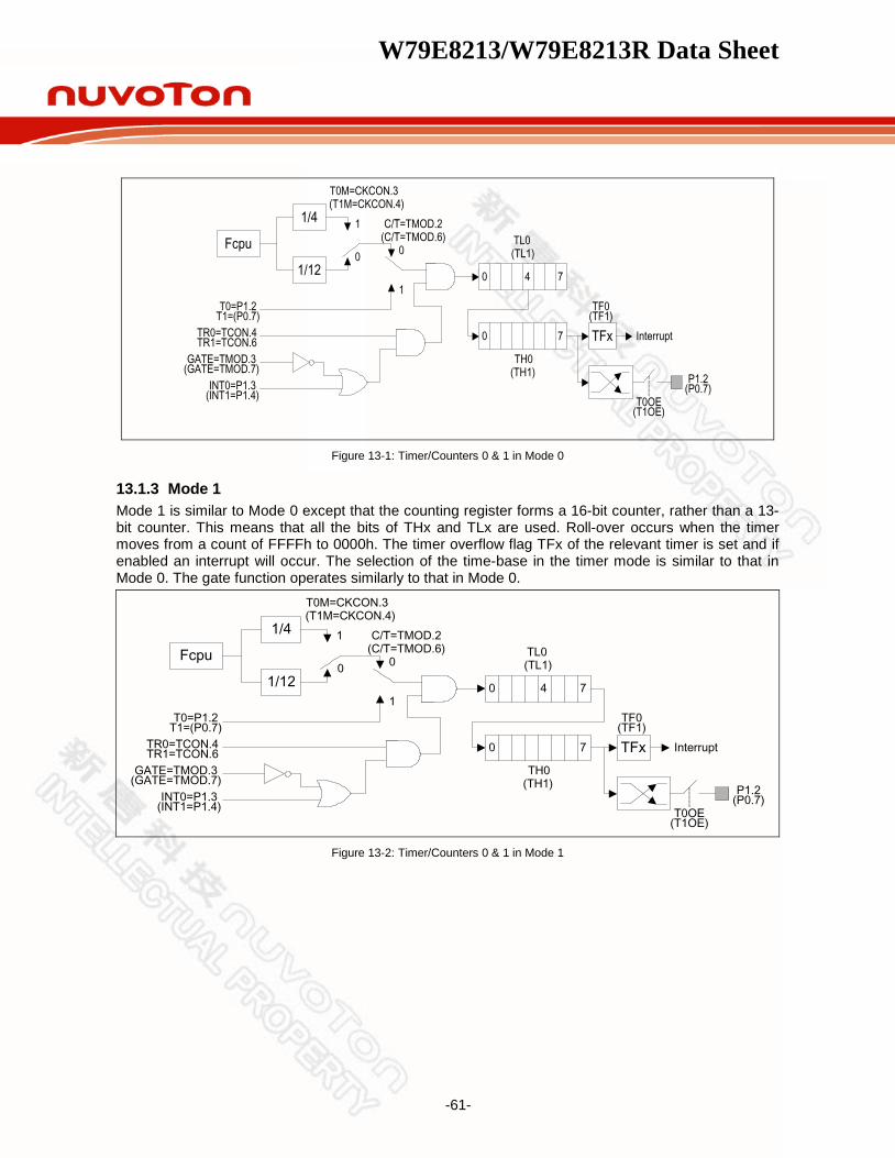
W79E8213/W79E8213R Data Sheet
-61-
Fcpu
1/120
10 4 7
0 7 TFxTH0
(TH1)
TL0(TL1)
Interrupt
T0OE
T0=P1.2
(C/T=TMOD.6)C/T=TMOD.2
GATE=TMOD.3(GATE=TMOD.7)
INT0=P1.3(INT1=P1.4)
T1=(P0.7)
P1.2(P0.7)
TF0(TF1)
TR0=TCON.4TR1=TCON.6
(T1OE)
1/4
T0M=CKCON.3(T1M=CKCON.4)
0
1
Figure 13-1: Timer/Counters 0 & 1 in Mode 0
13.1.3 Mode 1 Mode 1 is similar to Mode 0 except that the counting register forms a 16-bit counter, rather than a 13-bit counter. This means that all the bits of THx and TLx are used. Roll-over occurs when the timer moves from a count of FFFFh to 0000h. The timer overflow flag TFx of the relevant timer is set and if enabled an interrupt will occur. The selection of the time-base in the timer mode is similar to that in Mode 0. The gate function operates similarly to that in Mode 0.
Fcpu
1/120
10 4 7
0 7 TFxTH0
(TH1)
TL0(TL1)
Interrupt
T0OE
T0=P1.2
(C/T=TMOD.6)C/T=TMOD.2
GATE=TMOD.3(GATE=TMOD.7)
INT0=P1.3(INT1=P1.4)
T1=(P0.7)
P1.2(P0.7)
TF0(TF1)
TR0=TCON.4TR1=TCON.6
(T1OE)
1/4
0
1
T0M=CKCON.3(T1M=CKCON.4)
Figure 13-2: Timer/Counters 0 & 1 in Mode 1

W79E8213/W79E8213R Data Sheet
-62-
13.1.4 Mode 2 In Mode 2, the timer/counter is in the Auto Reload Mode. In this mode, TLx acts as 8-bit count register, while THx holds the reload value. When the TLx register overflows from FFh to 00h, the TFx bit in TCON is set and TLx is reloaded with the contents of THx, and the counting process continues from here. The reload operation leaves the contents of the THx register unchanged. Counting is enabled by the TRx bit and proper setting of GATE and INTx pins. As in the other two modes 0 and 1 mode 2 allows counting of either clock cycles (clock/12 or clock/4) or pulses on pin Tn. In “Timer” mode, if output toggled enable bit of P2M1.T0OE or P2M1.T1OE is enable, T0 or T1 output pin will toggle whenever a timer overflow occurs.
0
10 7
0 7
TFx
TH0(TH1)
TL0(TL1)
Interrupt
T0OE
T0=P1.2
(C/T=TMOD.6)C/T=TMOD.2
GATE=TMOD.3(GATE=TMOD.7)
INT0=P1.3(INT1=P1.4)
T1=(P0.7)
P1.2(P0.7)
TF0(TF1)
TR0=TCON.4TR1=TCON.6
(T1OE)
Fcpu
1/120
1/4
0
1
T0M=CKCON.3(T1M=CKCON.4)
Figure 13-3: Timer/Counter 0 & 1 in Mode 2
13.1.5 Mode 3 Mode 3 has different operating methods for the two timer/counters. For timer/counter 1, mode 3 simply freezes the counter. Timer/Counter 0, however, configures TL0 and TH0 as two separate 8 bit count registers in this mode. The logic for this mode is shown in the figure. TL0 uses the Timer/Counter 0 control bits TC/ , GATE, TR0, INT0 and TF0. The TL0 can be used to count clock cycles (clock/12 or clock/4) or 1-to-0 transitions on pin T0 as determined by C/T (TMOD.2). TH0 is forced as a clock cycle counter (clock/12 or clock/4) and takes over the use of TR1 and TF1 from Timer/Counter 1. Mode 3 is used in cases where an extra 8 bit timer is needed. With Timer 0 in Mode 3, Timer 1 can still be used in Modes 0, 1 and 2, but its flexibility is somewhat limited. While its basic functionality is maintained, it no longer has control over its overflow flag TF1 and the enable bit TR1. Timer 1 can still be used as a timer/counter and retains the use of GATE and INT1 pin. In this condition it can be turned on and off by switching it out of and into its own Mode 3. It can also be used as a baud rate generator for the serial port. In “Timer” mode, if output toggled enable bit of P2M1.T0OE or P2M1.T1OE is enable, T0 or T1 output pin will toggle whenever a timer overflow occurs.
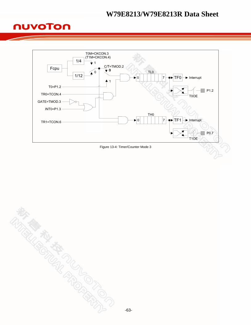
W79E8213/W79E8213R Data Sheet
-63-
0
10 7
0 7
TF0
TH0
TL0Interrupt
T0OE
T0=P1.2
C/T=TMOD.2
GATE=TMOD.3
INT0=P1.3
P1.2TR0=TCON.4
TR1=TCON.6 TF1 Interrupt
T1OEP0.7
Fcpu
1/120
1/4
0
1
T0M=CKCON.3(T1M=CKCON.4)
Figure 13-4: Timer/Counter Mode 3

W79E8213/W79E8213R Data Sheet
-64-
14. NVM MEMORY The W79E8213 series have NVM data memory of 128 bytes for customer’s data store used. The NVM data memory has 8 pages area and each page of 16 bytes. The NVM memory can be read/write by customer program to access. Read NVM data is by MOVC A,@A+DPTR instruction, and write data is by SFR of NVMADDRL, NVMDATA and NVMCON. Before write data to NVM memory, the page must be erased by providing page address on NVMADDRL, which address of On-Chip Code Memory space will decode, then set EER of NVMCON.7. This will automatically hold fetch program code and PC Counter, and execute page erase. After finished, this bit will be cleared by hardware. The erase time is ~ 5ms. For writing data to NVM memory, user must set address and data to NVMADDRL and NVMDATA, then set EWR of NVMCON.6 to initiate nvm data write. The uC will hold program code and PC Counter, and then write data to mapping address. Upon write completion, the EWR bit will be cleared by hardware, the uC will continue execute next instruction. The program time is ~50us.
0000H
External Data Memory SpaceOn-Chip Code Memory Space
0000H
4K BytesOn-Chip
Code Memory
UnusedCode Memory
UnusedCode Memory
CONFIG 0
0FFFH1000H
FFFFH FFFFH
FC00H
CONFIG 1
FC7FH 128BNVM
Data Memory
UnusedData Memory
NVM Data Memory Area
(16 bytes/page)
FC1Fh
FC10hFC0Fh
FC00hPage 0
Page 1
Page 7
Page 2
Page 3
Page 4
Page 5
Page 6
(128B NVM, 16bytes/page)
FC3Fh
FC30hFC2Fh
FC20h
FC5Fh
FC50hFC4Fh
FC40h
FC7Fh
FC70hFC6Fh
FC60h
Figure 14-1: W79E8213 Memory Map
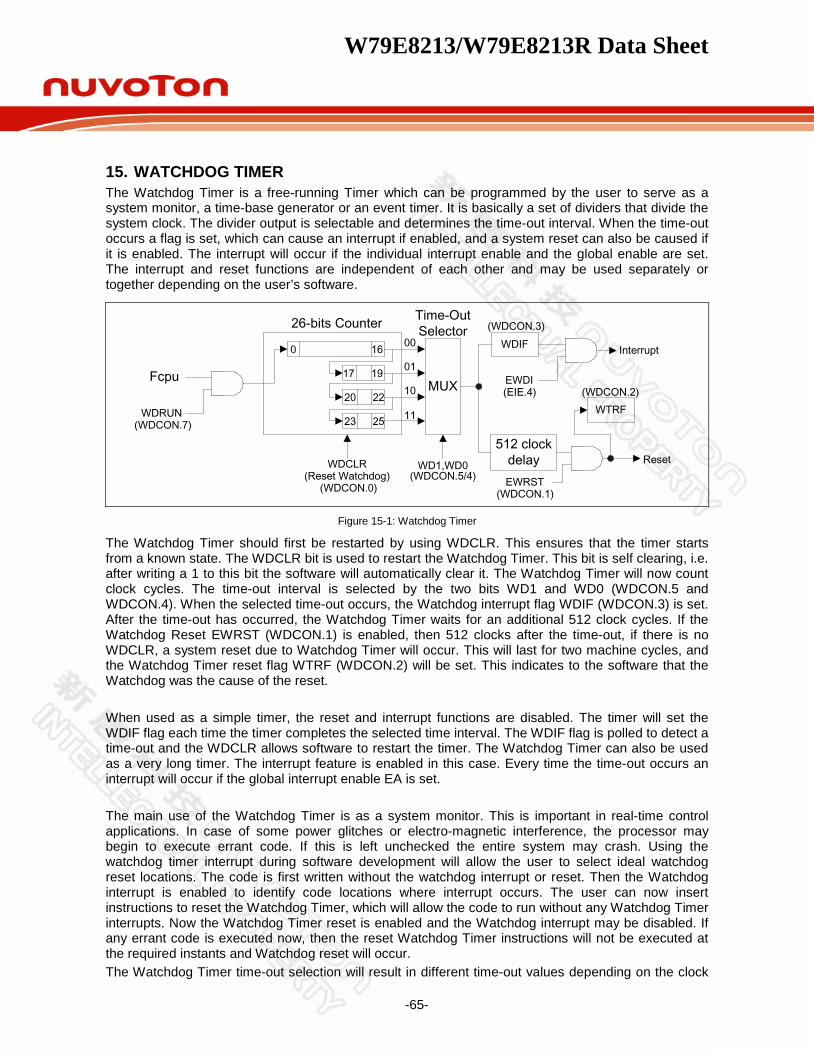
W79E8213/W79E8213R Data Sheet
-65-
15. WATCHDOG TIMER The Watchdog Timer is a free-running Timer which can be programmed by the user to serve as a system monitor, a time-base generator or an event timer. It is basically a set of dividers that divide the system clock. The divider output is selectable and determines the time-out interval. When the time-out occurs a flag is set, which can cause an interrupt if enabled, and a system reset can also be caused if it is enabled. The interrupt will occur if the individual interrupt enable and the global enable are set. The interrupt and reset functions are independent of each other and may be used separately or together depending on the user’s software.
WDIF
512 clockdelay
MUX
WDRUN
WD1,WD0WDCLR
EWDI
EWRST
Reset
Interrupt00
01
10
11 WTRF
26-bits Counter Time-OutSelector
160
17 19
20 22
23 25
(Reset Watchdog)(WDCON.1)
(WDCON.3)
(EIE.4) (WDCON.2)
(WDCON.0)
(WDCON.7)
(WDCON.5/4)
Fcpu
Figure 15-1: Watchdog Timer
The Watchdog Timer should first be restarted by using WDCLR. This ensures that the timer starts from a known state. The WDCLR bit is used to restart the Watchdog Timer. This bit is self clearing, i.e. after writing a 1 to this bit the software will automatically clear it. The Watchdog Timer will now count clock cycles. The time-out interval is selected by the two bits WD1 and WD0 (WDCON.5 and WDCON.4). When the selected time-out occurs, the Watchdog interrupt flag WDIF (WDCON.3) is set. After the time-out has occurred, the Watchdog Timer waits for an additional 512 clock cycles. If the Watchdog Reset EWRST (WDCON.1) is enabled, then 512 clocks after the time-out, if there is no WDCLR, a system reset due to Watchdog Timer will occur. This will last for two machine cycles, and the Watchdog Timer reset flag WTRF (WDCON.2) will be set. This indicates to the software that the Watchdog was the cause of the reset. When used as a simple timer, the reset and interrupt functions are disabled. The timer will set the WDIF flag each time the timer completes the selected time interval. The WDIF flag is polled to detect a time-out and the WDCLR allows software to restart the timer. The Watchdog Timer can also be used as a very long timer. The interrupt feature is enabled in this case. Every time the time-out occurs an interrupt will occur if the global interrupt enable EA is set. The main use of the Watchdog Timer is as a system monitor. This is important in real-time control applications. In case of some power glitches or electro-magnetic interference, the processor may begin to execute errant code. If this is left unchecked the entire system may crash. Using the watchdog timer interrupt during software development will allow the user to select ideal watchdog reset locations. The code is first written without the watchdog interrupt or reset. Then the Watchdog interrupt is enabled to identify code locations where interrupt occurs. The user can now insert instructions to reset the Watchdog Timer, which will allow the code to run without any Watchdog Timer interrupts. Now the Watchdog Timer reset is enabled and the Watchdog interrupt may be disabled. If any errant code is executed now, then the reset Watchdog Timer instructions will not be executed at the required instants and Watchdog reset will occur. The Watchdog Timer time-out selection will result in different time-out values depending on the clock

W79E8213/W79E8213R Data Sheet
-66-
speed. The reset, when enabled, will occur when 512 clocks after time-out has occurred.
WD1 WD0 INTERRUPT TIME-OUT
RESET TIME-OUT
NUMBER OF CLOCKS
TIME @ 10 MHZ
0 0 217 217 + 512 131072 13.11 mS
0 1 220 220 + 512 1048576 104.86 mS
1 0 223 223 + 512 8388608 838.86 mS
1 1 226 226 + 512 67108864 6710.89 mS
Table 15-1: Time-out values for the Watchdog Timer
The Watchdog Timer will be disabled by a power-on/fail reset. The Watchdog Timer reset does not disable the Watchdog Timer, but will restart it. In general, software should restart the timer to put it into a known state. The control bits that support the Watchdog Timer are discussed below.
15.1 WATCHDOG CONTROL WDIF: WDCON.3 - Watchdog Timer Interrupt flag. This bit is set whenever the time-out occurs in the Watchdog Timer. If the Watchdog interrupt is enabled (EIE.4), then an interrupt will occur (if the global interrupt enable is set and other interrupt requirements are met). Software or any reset can clear this bit. WTRF: WDCON.2 - Watchdog Timer Reset flag. This bit is set whenever a watchdog reset occurs. This bit is useful for determined the cause of a reset. Software must read it, and clear it manually. A Power-fail reset will clear this bit. If EWRST = 0, then this bit will not be affected by the Watchdog Timer. EWRST: WDCON.1 - Enable Watchdog Timer Reset. This bit when set to 1 will enable the Watchdog Timer reset function. Setting this bit to 0 will disable the Watchdog Timer reset function, but will leave the timer running. WDCLR: WDCON.0 - Reset Watchdog Timer. This bit is used to clear the Watchdog Timer and to restart it. This bit is self-clearing, so after the software writes 1 to it the hardware will automatically clear it. If the Watchdog Timer reset is enabled, then the WDCLR has to be set by the user within 512 clocks of the time-out. If this is not done then a Watchdog Timer reset will occur.
15.2 CLOCK CONTROL of Watchdog WD1, WD0: WDCON.5, WDCON.4 - Watchdog Timer Mode select bits. These two bits select the time-out interval for the watchdog timer. The reset time is 512 clocks longer than the interrupt time-out value. The default Watchdog time-out is 217 clocks, which is the shortest time-out period. The WDRUN, WD0, WD1, EWRST, WDIF and WDCLR bits are protected by the Timed Access procedure. This prevents software from accidentally enabling or disabling the watchdog timer. More importantly, it makes it highly improbable that errant code can enable or disable the Watchdog Timer.
W79E8213/W79E8213R Data Sheet
-67-
16. TIME ACCESS PROCTECTION The W79E8213 series have a new feature, like the Watchdog Timer which is a crucial to proper operation of the system. If left unprotected, errant code may write to the Watchdog control bits resulting in incorrect operation and loss of control. In order to prevent this, the W79E8213 series have a protection scheme which controls the write access to critical bits. This protection scheme is done using a timed access. In this method, the bits which are to be protected have a timed write enable window. A write is successful only if this window is active, otherwise the write will be discarded. This write enable window is open for 3 machine cycles if certain conditions are met. After 3 machine cycles, this window automatically closes. The window is opened by writing AAh and immediately 55h to the Timed Access (TA) SFR. This SFR is located at address C7h. The suggested code for opening the timed access window is TA REG 0C7h ; Define new register TA, @0C7h MOV TA, #0AAh
MOV TA, #055h When the software writes AAh to the TA SFR, a counter is started. This counter waits for 3 machine cycles looking for a write of 55h to TA. If the second write (55h) occurs within 3 machine cycles of the first write (AAh), then the timed access window is opened. It remains open for 3 machine cycles, during which the user may write to the protected bits. Once the window closes the procedure must be repeated to access the other protected bits. Examples of Timed Assessing are shown below. Example 1: Valid access MOV TA, #0AAh ; 3 M/C Note: M/C = Machine Cycles MOV TA, #055h ; 3 M/C MOV WDCON, #00h ; 3 M/C Example 2: Valid access MOV TA, #0AAh ; 3 M/C MOV TA, #055h ; 3 M/C NOP ; 1 M/C SETB EWRST ; 2 M/C Example 3: Valid access MOV TA, #0AAh ; 3 M/C MOV TA, #055h ; 3 M/C ORL WDCON, #00000010B ; 3M/C Example 4: Invalid access MOV TA, #0AAh ; 3 M/C MOV TA, #055h ; 3 M/C NOP ; 1 M/C NOP ; 1 M/C CLR EWT ; 2 M/C

W79E8213/W79E8213R Data Sheet
-68-
Example 5: Invalid Access MOV TA, #0AAh ; 3 M/C NOP ; 1 M/C MOV TA, #055h ; 3 M/C SETB EWT ; 2 M/C
In the first three examples, the writing to the protected bits is done before the 3 machine cycles window closes. In Example 4, however, the writing to the protected bit occurs after the window has closed, and so there is effectively no change in the status of the protected bit. In Example 5, the second write to TA occurs 4 machine cycles after the first write, therefore the timed access window is not opened at all, and the write to the protected bit fails.
W79E8213/W79E8213R Data Sheet
-69-
17. EDGE DETECT INTERRUPT The W79E8213 series are provided edge detect interrupt function to detect keypad status which key is acted, and allow a single interrupt to be generated when any key is pressed on a keyboard or keypad connected to specific pins of the W79E8213 series, as shown below Figure. This interrupt may be used to wake up the CPU from Idle, after chip is in Idle Mode.
Edge detect function is supported through Port 1.0-1.2. It can allow any or all pins of P1.0-P1.2 to be enabled to cause this interrupt. Port pins are enabled by the setting of bits of ED0EN ~ ED2EN in the EDIC register, as shown below Figure. The edge detect trigger option is programmable through EDxTRG bits (EDIC). It supports falling edge, and either falling edge or rising edge triggers. It also has a global digital noise filter type control which can filter noisy edge detect inputs. The trigger pulse must be over 1 machine cycle (for Clk = Fosc filter type), 2 machine cycles (for Clk = Fosc/2 filter type), 4 machine cycles (for Fosc/4 filter type) and 8 machine cycles (for Fosc/8 filter type). The Edge Detect Interrupt Flag (EDF) in the AUXR1 register is set when any enabled pin is triggered while the ED interrupt function is active. An interrupt will be generated if it has been enabled. The EDF bit set by hardware and must be cleared by software. Due to human time scales and the mechanical delay associated with key-switch closures, the edge detect feature will typically allow the interrupt service routine to poll P1.0-P1.2 in order to determine which key was pressed.
Note: As this device support falling and rising edge triggers, user has to ensure the Edge Detection pins at high initial state when using edge detection. This is necessary to avoid false detection. It applies to both trigger types.
P1.2 (ED2)
P1.1 (ED1)
P1.0 (ED0)
ED2EN
EED(From EIE Register)
EDF (Edge DetectInterrupt)
ED1EN
ED0EN
[0]
[1]
[0]
[1]
[0]
[1]
Noise Filter
EDFILT.1-0
Fosc/1,2,4,8
Noise FilterFosc/1,2,4,8
Noise FilterFosc/1,2,4,8
ED2TRG
ED1TRG
ED0TRG
Figure 17-1: Edge Detect Interrupt

W79E8213/W79E8213R Data Sheet
-70-
Q
QSET
CLR
D
Q
QSET
CLR
D
Q
QSET
CLR
D
Q
QSET
CLR
D
J
Q
Q
K
SET
CLR
Tx filtered
Clk
Tx
Divider/1,/2,/4,/8
2
EDFILT.1-0
Figure 17-2: Edge Detect Noise Filter

W79E8213/W79E8213R Data Sheet
-71-
18. I/O PORT CONFIGURATION The W79E8213 series have three I/O ports, port 0, port 1 and port 2. All pins of I/O ports can be configured to one of four types by software except P1.5 is only input pin. When P1.5 is configured reset pin by RPD=0 in the CONFIG 1 register, the W79E8213 series can support 17 I/O pins by use Crystal. If used internal RC oscillator the P1.5 is configured input pin, the W79E8213 series can be supported up to 18 I/O pins. The I/O ports configuration setting as below table.
PXM1.Y PXM2.Y PORT INPUT/OUTPUT MODE
0 0 Quasi-bidirectional
0 1 Push-Pull
1 0 Input Only (High Impedance)
P2M1.PxS=0, TTL input P2M1.PxS=1, Schmitt input
1 1 Open Drain Table 18-1: I/O port Configuration Table
All port pins can be determined to high or low after reset by configure PRHI bit in the CONFIG0 register. During power-on-reset, all port pins will be tri-stated. After reset, these pins are in quasi-bidirectional mode. The port pin of P1.5 only is a Schmitt trigger input. Enabled toggle outputs from Timer 0 and Timer 1 by T0OE and T1OE on P2M1 register, the output frequency of Timer 0 or Timer 1 is by Timer overflow. Each I/O port of the W79E8213 series may be selected to use TTL level inputs or Schmitt inputs by P(n)S bit on P2M1 register, where n is 0, 1 or 2. When P(n)S is set to 1, Ports are selected Schmitt trigger inputs on Port(n). The P2.0 (XTAL2) can be configured clock output when used internal RC or external Oscillator is clock source, and the frequency of clock output is divided by 4 on internal RC clock or external Oscillator.
Note: During power-on-reset, all port pins will be tri-stated. However, PWM pins will be tr-stated longer until cpu clock is stable.
18.1 Quasi-Bidirectional Output Configuration After chip was power on or reset, the all ports output are this mode, and output is common with the 8051. This mode can be used as both an input and output without the need to reconfigure the port. When the pin is pulled low, it is driven strongly and able to sink a fairly large current. These features are somewhat similar to an open drain output except that there are three pull-up transistors in the quasi-bidirectional output that serve different purposes. This mode has three pull-up resisters that are “strong” pull-up, “weak” pull-up and “very weak” pull-up. The “strong” pull-up is used fast transition from logic “0” change to logic “1”, and it is fast latch and transition. When port pins is occur from logic “0” to logic “1”, the strong pull-up will quickly turn on two CPU clocks to pull high then turn off. The “weak” pull-up is turned on when the input port pin is logic “1” level or itself is logic “1”, and it
W79E8213/W79E8213R Data Sheet
-72-
provides the most source current for a quasi-bidirectional pin that output is “1” or port latch is logic “0”’. The “very weak” pull-up is turned on when the port latch is logic “1”. If port latch is logic “0”, it will be turned off. The very weak pull-up is support a very small current that will pull the pin high if it is left floating. And the quasi-bidirectional port configuration is shown as below figure. If port pin is low, it can drives large sink current for output, and it is similar with push-pull and open drain on sink current output.
Port Pin
2 CPUClock Delay
Input Data
Port LatchData
P P P
N
VDD
Strong VeryWeak Weak
Figure 18-1: Quasi-Bidirectional Output
18.2 Open Drain Output Configuration To configure this mode is turned off all pull-ups. If used similar as a logic output, the port must has an external pull-up resister. The open drain port configuration is shown as below.
Port Pin
Port LatchData
N
Input Data
Figure 18-2: Open Drain Output
18.3 Push-Pull Output Configuration The push-pull output mode has two strong pull-up and pull-down structure that support large source and sink current output. It removes “weak” pull-up and “very weak” pull-up resister and remains “strong pull-up resister on quasi-bidirectional output mode. The “strong” pull-up is always turns on when port latch is logic “1” to support source current. The push-pull port configuration is shown in below Figure.

W79E8213/W79E8213R Data Sheet
-73-
Port Pin
Input Data
Port LatchData
P
N
VDD
Figure 18-3: Push-Pull Output
18.4 Input Only Configuration By configure this mode, the ports are only digital input and disable digital output. The W79E8213 series can select input pin to Schmitt trigger or TTL level input by PxM1.y and PxM2.y registers.

W79E8213/W79E8213R Data Sheet
-74-
19. OSCILLATOR The W79E8213 series provides three oscillator input option. These are configured at CONFIG register (CONFIG0) that include Internal RC Oscillator Option, External Clock Input Option and Crystal Oscillator Input Option. The Crystal Oscillator Input frequency may be supported from 4MHz to 20MHz, and without capacitor or resister.
FOSC0FOSC1
00B
11B
01B
Crystal Oscillator
External Clock input
Internal RC Oscillator 16 bits RippleCounter
CPU Clock
Power Monitor Reset
Power Down
To ADC Block
PeripheralClock
Figure 19-1: Oscillator
19.1 Internal RC Oscillator Option The internal RC Oscillator is configurable to 10MHz/20MHz (through CONFIG1.FS1 bit) frequency to support clock source. When FOSC1, FOSC0 = 01b, the internal RC oscillator is enabled. A clock output on P2.0 (XTAL2) may be enabled when internal RC oscillator is used.
19.2 External Clock Input Option The clock source pin (XTAL1) is from External Clock Input by FOSC1, FOSC0 = 11b, and frequency range is form 4MHz up to 20MHz. A clock output on P2.0 (XTAL2) may be enabled when External Clock Input is used. The W79E8213 series supports a clock output function when either the internal RC oscillator or the external clock input options is selected. This allows external devices to synchronize to the W79E8213 serial. When enabled, via the ENCLK bit in the P2M1 register, the clock output appears on the XTAL2/CLKOUT pin whenever the internal RC oscillator is running, including in Idle Mode. The frequency of the clock output is 1/4 of the CPU clock rate. If the clock output is not needed in Idle Mode, it may be turned off prior to entering Idle mode, saving additional power. The clock output may also be enabled when the external clock input option is selected.

W79E8213/W79E8213R Data Sheet
-75-
20. BUZZER OUTPUT The W79E8213 series support square wave output capability. The square wave is output through P1.0 (BUZ) pin. The square wave can be enabled through bit BUZE (SFR AUXR1.1). Depending on Fcpu clock input to the buzzer output block, user is able to control the output frequency by configure the 6-bit Divider through BUZDIV bits in BUZCON SFR. The following shows the block diagram of square wave output generator.
1/256 6-bit Divider
Buz Output
BUZE, buzzer enable bit
Fcpu clock BUZ pin(P1.0)
1
BUZE
P1.0
1
0
BUZDIV.5-0
6
Figure 20-1: Square wave output
Buzzer output frequency equation: Fbuz = Fcpu x 1/[256x(BUZDIV+1)] The following table tabulates examples of the BUZDIV setting needed in order to generate buzzer output at rate of 1953Hz and 3906Hz, for each cpu clock frequency.
W79E8213/W79E8213R Data Sheet
-76-
Frequency, Fcpu (Hz)
Division 4000000 6000000 8000000 10000000 11000000 12000000 20000000
/256 15625 23437.5 31250 39062.5 42968.75 46875 78125
BU
ZDIV
+ 1
1
.
4 3906.25
5
6 3906.25
7
8 1953.125 3906.25
9
10 3906.25
11 3906.25
12 1953.125 3906.25
13
14
15
16 1953.125
17
18
19
20 1953.125 3906.25
21
22 1953.125
23
24 1953.125
25
.
40 1953.125
.
64

W79E8213/W79E8213R Data Sheet
-77-
For supporting active low buzzer, this buzzer output is implemented with an off-state of high. The following pseudo code shows the operating procedure when working with active high and low buzzer; (Assume PRHI=1): 1) During power on, P1.0/BUZ will be high;
<For active high buzzer> Clear SFR P1.0 ; user has to take care to output this pin low
; at the top of s/w code to avoid initial beep sound. <For active low buzzer> No action needed.
2) To turn-on buzzer; <For active high buzzer> Set BUZE bit Set SFR P1.0 bit ; to push out the buzout. <For active low buzzer> Set BUZE bit
3) To turn-off buzzer;
<For active high buzzer> Clear SFR P1.0 ; user has to take care to output this pin low. Clear BUZE bit <For active low buzzer> Set BUZE bit

W79E8213/W79E8213R Data Sheet
-78-
21. POWER MONITORING FUNCTION Power-On Detect and Brownout are two additional power monitoring functions implemented in W79E8213 series to prevent incorrect operation during power up and power drop or loss.
21.1 Power On Detect The Power–On Detect function is a designed to detect power up after power voltage reaches to a level where Brownout Detect can work. After power on detect, the POR (PCON.4) will be set to “1” to indicate an initial power up condition. The POR flag will be cleared by software.
21.2 Brownout Detect The Brownout Detect function is detect power voltage is drops to brownout voltage level, and allows preventing some process work or indicate power warming. The W79E8213 series have two brownout voltage levels to select by BOV (CONFIG0.4). If BOV =0 that brownout voltage level is 3.8V, If BOV = 1 that brownout voltage level is 2.5V. When the Brownout voltage is drop to select level, the brownout detector will detect and keeps this active until VDD is returns to above brownout Detect voltage. The Brownout Detect block is as follow.
BOI(Enable Brownout Detect)
BrownoutDetectCircuit
0
1BOF
To Reset
To Brownout interrupt
BOD
Figure 21-1: Brownout Detect Block
When Brownout Detect is enabled by BOD (AUXR1.6), the BOF (PCON.5) flag will be set and brownout reset will occur. If BOI (AUXR1.5) is set to “1”, the brownout detect will cause interrupt via the EA (IE.7) and EBO (IE.5) bits is set. BOF is cleared by software. In order to guarantee a correct detection of Brownout, The VDD fail time must be slower than 50mV/us, and rise time is slower than 2mV/us to ensure a proper reset.

W79E8213/W79E8213R Data Sheet
-79-
22. PULSE-WIDTH-MODULATED (PWM) OUTPUTS The W79E8213 series have 4 Pulse Width Modulated (PWM) channels, and the PWM outputs are PWM0(P0.1), PWM1(P1.6), PWM2(P1.7), PWM3(P0.0). The initial PWM outputs level correspondingly depend on the PRHI level set prior to the chip reset. When PRHI set to high, PWM output will initialize to high after chip reset; if PRHI set to low, PWM output will be initialize to low after chip reset. The W79E8213 series support 10-bits down counter with cpu clock as its input. The PWM counter clock, has the frequency as FCPWM = FOSC/Prescaler. The two pre-scaler selectable bits FP[1:0] are located at PWMCON3[3:2]. When the counter reaches underflow it will automatic reloaded from counter register. The PWM frequency is given by: fPWM = FCPWM / (PWMP+1), where PWMP is 10-bits register of PWMPH.1, PWMPH.0 and PWMPL.7~PWMPL.0.
The counter register will be loaded with the PWMP register value when PWMRUN, load and PWMF are equal to 1; the load bit will be automatically cleared to zero on the next clock cycle, and at the same time the counter register value will be loaded to the 10 bits down counter. PWMF flag is set when 10-bits down counter underflow, the PWMF flag can only be cleared by software.
The pulse width of each PWM output is determined by the Compare registers of PWM0L through PWM3L and PWM0H through PWM3H. When PWM compare register is greater than 10-bits counter register, the PWM output is low. Load bit has to be set to 1 for alteration of PWMn width. After the new values are written to the PWMn registers, and if load bit is set to 1, the new PWMn values will be loaded to the PWMn registers upon the next underflow. The PWM output high pulses width is given by: tHI = (PWMP – PWMn+1). The following equations show the formula for period and duty:
Period = (pwmp +1) * ioclock period * 1/prescaler Duty = duty * ioclock period
Note: 1. If compare register is set to 000H, the PWMn output will stay at high, and if compare register is
set to 3FFH, the PWMn output will stuck at low until there is a change in the compare register. [n = 0-3].
2. During ICP mode, PWM pins will be tri-stated. PWM operation will be stop. When exit from ICP mode, the PWM pins will follow the last SFR port values.

W79E8213/W79E8213R Data Sheet
-80-
10-bit Down Counter
Compare Register
Counter Register
PWM0 register
+
-
Compare Register
PWM1 register
+
-
Compare Register
PWM2 register
+
-
PWM0(P0.1)
+
-
X
X
X
Y
Y
Y
>
>
>
load
PWMP Register
Clear Counter
PWM1(P1.6)
PWM2(P1.7)
PWM1I
PWM2I
PWM0IUnderflow
CLRPWM
PWMRUN
Fosc
Prescaler(1/1, 1/2, 1/4, 1/16)
Fcpwm
(FP1, FP0)
Posc
BKCH
BPEN
BKEN
Brake Control Block
BKF
BKPS
0
1
P0.1
PWM0B
0
1
0
1
P1.6
PWM1B
PWM2B
P1.7
Brake Pin (P0.2)
P0.2=0
P0.2=11
0
Enable External Brake Pin(BPEN,BKCH)=(1,X)
+
-
X
Y >PWM3(P0.0)
PWM3I
0
1PWM3B
P0.0
Compare Register
PWM3 register
PWMF
S/W Clear
Q
QSET
CLR
D
Figure 22-1: PWM Block Diagram
The W79E8213 series devices support brake function which can be activated by software or external pin (P0.2). The Brake function is controlled by the PWMCON2 register. The setting and details description of software brake and external pin brake can be found at the brake condition table at the SFR section. As for external brake, the user program can poll the brake flag (BKF) or enable PWM’s brake interrupt to determine when the external Brake Pin is asserted and causes a brake to occur. The brake pin (P0.2) can be set to trigger the brake function by either low or high level, by clearing or setting the PWMCON2.6 (BKPS) bit respectively. The details description of varies brake functions can be found in the brake condition table.

W79E8213/W79E8213R Data Sheet
-81-
Since the Brake Pin being asserted will automatically clear the Run bit of PWMCON1.7 and BKF (PWMCON3.0) flag will be set, the user program can poll this bit or enable PWM’s brake interrupt to determine when the Brake Pin causes a brake to occur. The other method for detecting a brake caused by the Brake Pin would be to tie the Brake Pin to one of the external interrupt pins. This latter approach is needed if the Brake signal is of insufficient length to ensure that it can be captured by a polling routine. When, after being asserted, the condition causing the brake is removed, the PWM outputs go to whatever state that had immediately prior to the brake. This means that in order to go from brake being asserted to having the PWM run without going through an indeterminate state, care must be taken. If the Brake Pin causes brake to be asserted, the following prototype code will allow the PWM to go from brake and then run smoothly after brake is released.
1. PWMn output=PWMnB2. H/W set BKF=1 & PWMRUN=03. S/W switch to S/W Brake (BKEN,BPEN,BKCH)=(1,0,0)4. Set PWMn comparator output = PWMnB or a given pattern
1. Clear 10-bit PWM counter CLRPWM=12. Reload PWMP & PWM registers3. Enable brake function (BKEN,BPEN,BKCH)=(1,1,0)
1. Clear BKF PWM output=PWM comparator output2. Re-start PWM Running by setting PWMRUN=1; load bit=1
Start
End
Initialize PWM function1. Set PWM Control Regs2. Set PWM brake output pattern(PWMnB)3. Enable brake function (BKEN,BPEN,BKCH)=(1,1,0)
PWM starts running
Brake occurs?
Yes
No
Brake pin is asserted?
No
Yes
Figure 22-2: PWM Brake Function
W79E8213/W79E8213R Data Sheet
-82-
23. ANALOG-TO-DIGITAL CONVERTER The ADC contains a DAC which converts the contents of a successive approximation register to a voltage (VDAC) which is compared to the analog input voltage (Vin). The output of the comparator is fed to the successive approximation control logic which controls the successive approximation register. A conversion is initiated by setting ADCS in the ADCCON register. There are two triggering methods by ADC to start conversion, either by purely software start or external pin STADC triggering. The software start mode is used to trigger ADC conversion regardless of ADCCON.5 (ADCEX) bit is set or cleared. A conversion will start simply by setting the ADCCON.3 (ADCS) bit. As for the external STADC pin triggering mode, ADCCON.5 (ADCEX) bit has to be set and a rise edge pulse has to apply to STADC pin to trigger the ADC conversion. For the rising edge triggering method, a minimum of at least 2 machine cycles symmetrical pulse is required. The low-to-high transition of STADC is recognized at the end of a machine cycle, and the conversion commences at the beginning of the next cycle. When a conversion is initiated by software, the conversion starts at the beginning of the machine cycle which follows the instruction that sets ADCS. ADCS is actually implemented with tpw flip-flops: a command flip-flop which is affected by set operations, and a status flag which is accessed during read operations. The next two machine cycles are used to initiate the converter. At the end of the first cycle, the ADCS status flag is set end a value of “1” will be returned if the ADCS flag is read while the conversion is in progress. Sampling of the analog input commences at the end of the second cycle.
During the next eight machine cycles, the voltage at the previously selected pin of one of analog input pin is sampled, and this input voltage should be stable in order to obtain a useful sample. In any event, the input voltage slew rate must be less than 10V/ms in order to prevent an undefined result.
The successive approximation control logic first sets the most significant bit and clears all other bits in the successive approximation register (10 0000 0000b). The output of the DAC (50% full scale) is compared to the input voltage Vin. If the input voltage is greater than VDAC, then the bit remains set; otherwise if is cleared.
The successive approximation control logic now sets the next most significant bit (11 0000 0000b or 01 0000 0000b, depending on the previous result), and the VDAC is compared to Vin again. If the input voltage is greater then VDAC, then the bit remains set; otherwise it is cleared. This process is repeated until all ten bits have been tested, at which stage the result of the conversion is held in the successive approximation register. The conversion takes four machine cycles per bit.
The end of the 10-bit conversion is flagged by control bit ADCCON.4 (ADCI). The upper 8 bits of the result are held in special function register ADCH, and the two remaining bits are held in ADCCON.7 (ADC.1) and ADCCON.6 (ADC.0). The user may ignore the two least significant bits in ADCCON and use the ADC as an 8-bit converter (8 upper bits in ADCH). In any event, the total actual conversion time is 52 ADC clock cycles. ADCI will be set and the ADCS status flag will be reset 52 cycles after the ADCS is set. Control bits ADCCON.0~1 and ADCCON1.2 are used to control an analog multiplexer which selects one of 8 analog channels. An ADC conversion in progress is unaffected by an external or software ADC start. The result of a completed conversion remains unaffected provided ADCI = logic 1; a new ADC conversion already in progress is aborted when the idle or power-down mode is entered. The result of a completed conversion (ADCI = logic 1) remains unaffected when entering the idle mode.

W79E8213/W79E8213R Data Sheet
-83-
DAC
MSB
LSB
SuccessiveApproximation
Register
Vin +
-Comparator
Start
Ready(Stop)
SuccessiveApproximationControl Logic
VDAC
Figure 23-1: Successive Approximation ADC
23.1 ADC Resolution and Analog Supply The ADC circuit has its own supply pins (AVDD and AVSS) and one pins (Vref+) connected to each end of the DAC’s resistance-ladder that the AVDD and Vref+ are connected to VDD and AVSS is connected to VSS. The ladder has 1023 equally spaced taps, separated by a resistance of “R”. The first tap is located 0.5×R above AVSS, and the last tap is located 0.5×R below Vref+. This gives a total ladder resistance of 1024×R. This structure ensures that the DAC is monotonic and results in a symmetrical quantization error. For input voltages between VSS and [(Vref+) + ½ LSB], the 10-bit result of an A/D conversion will be 0000000000B = 000H. For input voltages between [(Vref+) – 3/2 LSB] and Vref+, the result of a conversion will be 1111111111B = 3FFH. Vref+ and AVSS may be between AVDD + 0.2V and VSS – 0.2 V. Vref+ should be positive with respect to VSS, and the input voltage (Vin) should be between Vref+ and VSS. The result can always be calculated from the following formula:
Result = Vref
Vin1024
+× or Result =
VDD
Vin1024 ×
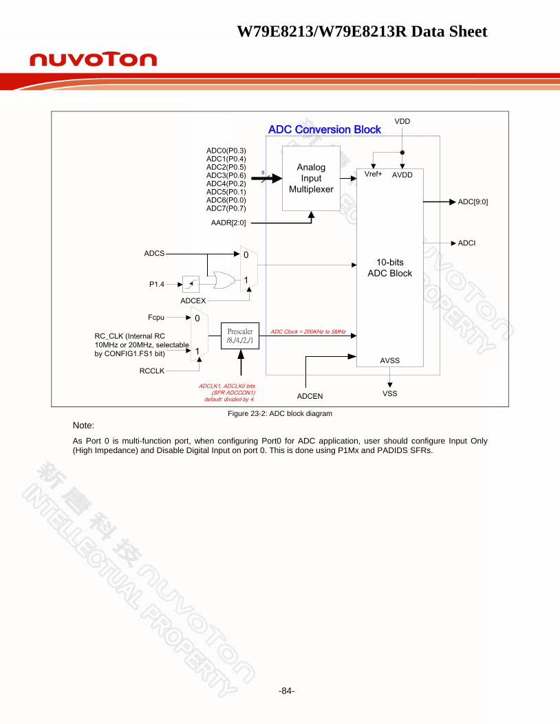
W79E8213/W79E8213R Data Sheet
-84-
10-bitsADC Block
ADC[9:0]
ADCIADCS
VDD
Vref+
VSS
AnalogInput
Multiplexer
0
1P1.4
ADCEX
Fcpu
ADC Conversion Block
ADCEN
AVSS
AVDD
RC_CLK (Internal RC 10MHz or 20MHz, selectable by CONFIG1.FS1 bit) 1
0
RCCLK
Prescaler /8,/4,/2,/1
ADCLK1, ADCLK0 bits (SFR ADCCON1)
default: divided by 4.
ADC0(P0.3)
AADR[2:0]
ADC1(P0.4)ADC2(P0.5)ADC3(P0.6)ADC4(P0.2)ADC5(P0.1)ADC6(P0.0)ADC7(P0.7)
8
ADC Clock = 200KHz to 5MHz
Figure 23-2: ADC block diagram
Note:
As Port 0 is multi-function port, when configuring Port0 for ADC application, user should configure Input Only (High Impedance) and Disable Digital Input on port 0. This is done using P1Mx and PADIDS SFRs.
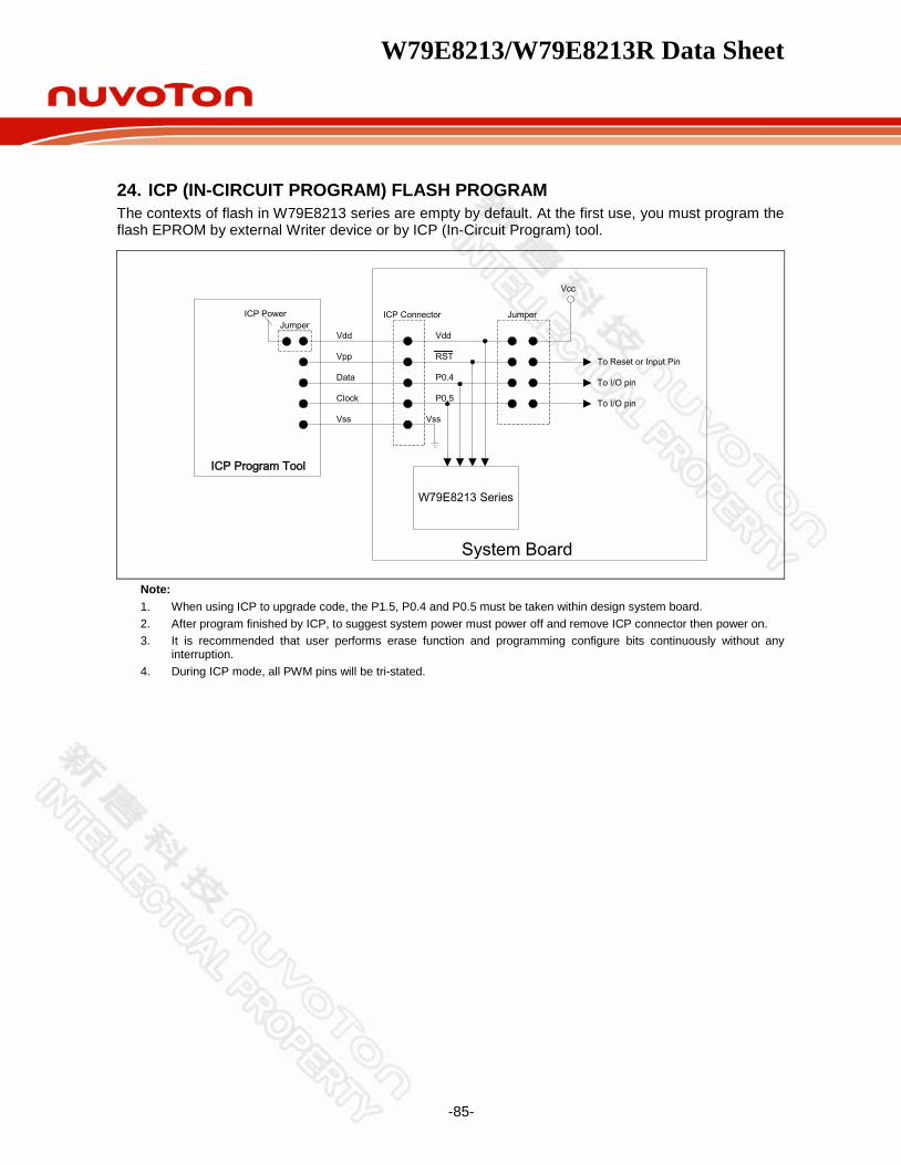
W79E8213/W79E8213R Data Sheet
-85-
24. ICP (IN-CIRCUIT PROGRAM) FLASH PROGRAM The contexts of flash in W79E8213 series are empty by default. At the first use, you must program the flash EPROM by external Writer device or by ICP (In-Circuit Program) tool.
W79E8213 Series
RST
P0.4
P0.5
Vdd
Vss
To I/O pin
To I/O pin
To Reset or Input Pin
Vdd
Vpp
Data
Clock
Vss
ICP Program Tool
Vcc
JumperICP Connector
System Board
ICP PowerJumper
Note: 1. When using ICP to upgrade code, the P1.5, P0.4 and P0.5 must be taken within design system board. 2. After program finished by ICP, to suggest system power must power off and remove ICP connector then power on. 3. It is recommended that user performs erase function and programming configure bits continuously without any
interruption. 4. During ICP mode, all PWM pins will be tri-stated.
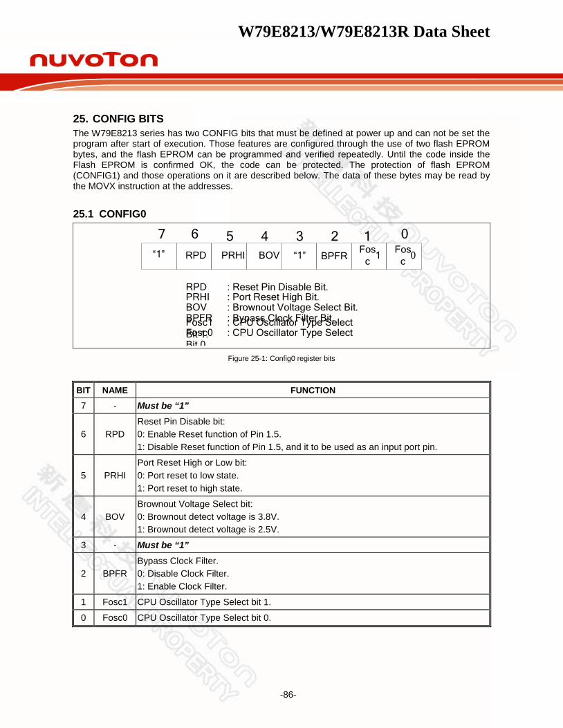
W79E8213/W79E8213R Data Sheet
-86-
25. CONFIG BITS The W79E8213 series has two CONFIG bits that must be defined at power up and can not be set the program after start of execution. Those features are configured through the use of two flash EPROM bytes, and the flash EPROM can be programmed and verified repeatedly. Until the code inside the Flash EPROM is confirmed OK, the code can be protected. The protection of flash EPROM (CONFIG1) and those operations on it are described below. The data of these bytes may be read by the MOVX instruction at the addresses.
25.1 CONFIG0
RPD PRHI BOV “1” BPFRFos
c 1 Fosc 0
7 6 5 4 3 2 1 0
RPD : Reset Pin Disable Bit.PRHI : Port Reset High Bit.BOV : Brownout Voltage Select Bit.
Fosc1 : CPU Oscillator Type Select Bit 1.Fosc0 : CPU Oscillator Type Select Bit 0
BPFR : Bypass Clock Filter Bit.
“1”
Figure 25-1: Config0 register bits
BIT NAME FUNCTION
7 - Must be “1”
6 RPD Reset Pin Disable bit: 0: Enable Reset function of Pin 1.5. 1: Disable Reset function of Pin 1.5, and it to be used as an input port pin.
5 PRHI Port Reset High or Low bit: 0: Port reset to low state. 1: Port reset to high state.
4 BOV Brownout Voltage Select bit: 0: Brownout detect voltage is 3.8V. 1: Brownout detect voltage is 2.5V.
3 - Must be “1”
2 BPFR Bypass Clock Filter. 0: Disable Clock Filter. 1: Enable Clock Filter.
1 Fosc1 CPU Oscillator Type Select bit 1.
0 Fosc0 CPU Oscillator Type Select bit 0.

W79E8213/W79E8213R Data Sheet
-87-
Oscillator Configuration bits:
Fosc1 Fosc0 OSC source 0 0 4MHz ~ 20MHz crystal
0 1 Internal RC Oscillator (FS1 bit in CONFIG1.5 will determine either 10MHz or 20MHZ)
1 0 Reserved
1 1 External Oscillator in XTAL1

W79E8213/W79E8213R Data Sheet
-88-
25.2 CONFIG1
7 6 5 4 3 2 1 0
C6C7 FS1
Bit7: C7 : 4K Flash EPROM Code Lock BitBit6: C6 : 128 byte Data Lock Bit
“1”
Bit5: FS1 : Internal RC 10MHz/20MHz Selection BitBit4~0: : Must be “1”
“1” “1” “1” “1”
Figure 25-2: Config1 register bits (W79E8213 series)
C7: 4K Flash EPROM Lock bit This bit is used to protect the customer’s program code. It may be set after the programmer finishes the programming and verifies sequence. Once this bit is set to logic 0, both the Flash EPROM data and CONFIG Registers can not be accessed again. C6: 128 byte Data Flash EPROM Lock bit This bit is used to protect the customer’s 128 bytes of data code. It may be set after the programmer finishes the programming and verifies sequence. Once this bit is set to logic 0, both the 128 bytes of Flash EPROM data and CONFIG Registers can not be accessed again.
BIT 7 BIT 6 FUNCTION DESCRIPTION
1 1 Both security of 4KB program code and 128 Bytes data area are not locked. They can be erased, programmed or read by Writer or ICP.
0 1 The 4KB program code area is locked. It can’t be read by Writer or ICP. The 128 Bytes data area can be program or read. The bank erase is invalid.
1 0 Not supported.
0 0 Both security of 4KB program code and 128 Bytes data area are locked. They can’t be read by Writer or ICP.
FS1: Internal RC Oscillator 10MHz/20MHz selection bit This bit is used to select 10MHz or 20MHz internal RC oscillator.
FS1 Internal RC Oscillator Output
0 10MHz
1 20MHz (default)
Internal Oscillator Selection Table
W79E8213/W79E8213R Data Sheet
-89-
26. ELECTRICAL CHARACTERISTICS 26.1 Absolute Maximum Ratings
PARAMETER SYMBOL MIN MAX UNIT
DC Power Supply VDD−VSS -0.3 +7.0 V
Input Voltage VIN VSS-0.3 VDD+0.3 V
Operating Temperature TA -40 +85 °C
Storage Temperature Tst -55 +150 °C
P1 Sink current ISK - 90 mA Note: Exposure to conditions beyond those listed under absolute maximum ratings may adversely affects the lift and reliability
of the device.
26.2 DC ELECTRICAL CHARACTERISTICS (TA = -40~85°C, unless otherwise specified.)
PARAMETER SYM. SPECIFICATION
TEST CONDITIONS MIN. TYP. MAX. UNIT
Operating Voltage VDD1 2.4 - 5.5
V
VDD=4.5V ~ 5.5V @ 20MHz
VDD=2.7V ~ 5.5V @ 12MHz
VDD=2.4V ~ 5.5V @ 4MHz
VDD2 3.0 - 5.5 NVM program and erase
operation.
Operating Current (20MHz)
IDD1 - 8.30 12
mA
No load, /RST = VSS, VDD= 5.0V @ 20MHz
IDD2 - 4.20 6 No load, /RST = VSS, VDD= 3.0V @ 20MHz
IDD3 - 14.50 20 No load, /RST = VDD, VDD= 5.0V @ 20MHz, RUN NOP
IDD4 - 5.20 7 No load, /RST = VDD, VDD= 3.0V @ 20MHz, RUN NOP
Operating Current (4MHz)
IDD5 - 3.60 5
mA
No load, /RST = VSS, VDD= 5.0V @ 4MHz
IDD6 - 1.86 3 No load, /RST = VSS, VDD= 3.0V @ 4MHz
IDD7 - 8.60 12 No load, /RST = VDD, VDD= 5.0V @ 4MHz, RUN NOP
IDD8 - 2.20 3.5 No load, /RST = VDD, VDD= 3.0V @ 4MHz, RUN NOP
Idle Current IIDLE1 - 5.70 8
mA
No load, VDD = 5.0V @ 20MHz
IIDLE2 - 2.48 3.5 No load, VDD = 3.0V @ 20MHz

W79E8213/W79E8213R Data Sheet
-90-
DC ELECTRICAL CHARACTERISTICS, continued
PARAMETER SYM. SPECIFICATION
TEST CONDITIONS MIN. TYP. MAX. UNIT
Power-down Current IPWDN1 - 1 10 µA
No load, VDD = 5.5V @ Disable BOV function
IPWDN2 - 1 10 uA No load, VDD = 3.0V @ Disable BOV function
Input / Output
Input Current P0, P1, P2 IIN1 -50 - +10 µA VDD = 5.5V, VIN = 0V or VIN=VDD
Input Current P1.5(RST pin)[1] IIN2 -30 -45 -55 µA VDD = 5.5V, VIN = 0.45V
Input Leakage Current P0, P1, P2 (Open Drain) ILK -10 0.1 +10 µA VDD = 5.5V, 0<VIN<VDD
Logic 1 to 0 Transition Current P0, P1, P2 ITL
[*3] -200 - -500 µA VDD = 5.5V, VIN<2.0V
Input Low Voltage P0, P1, P2 (TTL input) VIL1
0 - 0.8 V
VDD = 4.5V 0 - 0.5 VDD = 2.4V
Input High Voltage P0, P1, P2 (TTL input) VIH1
2.4 - VDD +0.2
V VDD = 5.5V
1.7 - VDD +0.2 VDD = 2.4V
Input Low Voltage XTAL1[*2] VIL3 0 - 0.8
V VDD = 4.5V
0 - 0.4 VDD = 3.0V
Input High Voltage XTAL1[*2] VIH3 3.5 - VDD
+0.2 V
VDD = 5.5V
2.4 - VDD +0.2 VDD = 3.0V
Negative going threshold (Schmitt input) VILS -0.5 - 0.3VDD V VDD = 2.4V~5.5V
Positive going threshold (Schmitt input) VIHS 0.7VDD - VDD+0.5 V VDD = 2.4V~5.5V
Hysteresis voltage VHY - 0.2VDD - V Source Current P0, P1, P2 (PUSH-PULL Mode) ISR1
-16 -25 - mA
VDD = 4.5V, VS = 2.4V -2 -3.8 - VDD = 2.4V, VS = 2.0V
Source Current P0, P1, P2 (Quasi-bidirectional Mode) ISR2
-150 -225 -360 µA
VDD = 4.5V, VS = 2.4V
-18 -28.5 -69 VDD = 2.4V, VS = 2.0V
Sink Current P0, P2 (Quasi-bidirectional, Open drain and PUSH-PULL Mode) [*4]
ISK1 13 21.5 -
mA VDD = 4.5V, VS = 0.45V
9 13.7 - VDD = 2.4V, VS = 0.45V
Sink Current P1 (Quasi-bidirectional, Open drain and PUSH-PULL Mode) [*4]
ISK2 35 42.5 -
mA VDD = 4.5V, VS = 0.45V
22 28.7 - VDD = 2.4V, VS = 0.45V

W79E8213/W79E8213R Data Sheet
-91-
DC ELECTRICAL CHARACTERISTICS, continued
PARAMETER SYM. SPECIFICATION
TEST CONDITIONS MIN. TYP. MAX. UNIT
Brownout voltage with BOV=1 VBO2.5 2.4 - 2.7 V TA = -0 to 70°C
Brownout voltage with BOV=0 VBO3.8 3.5 - 4 V TA = -0 to 70°C
ADC current consumption IADC - 0.4 0.8
mA VDD = 5.0V, ADCCLK = 4MHz
- 0.25 0.5 VDD = 3.0V, ADCCLK = 4MHz
Brownout voltage detect current IBOD
- 1.2 1.8 mA
VDD = 5.0V - 0.8 1.2 VDD = 3.0V
*1. /RST pin is a Schmitt trigger input. *2. XTAL1 is a CMOS input. *3. Pins of P0, P1 and P2 can source a transition current when they are being externally driven from 1 to 0. The transition
current reaches its maximum value when Vin approximates to 2V. *4. Only one of the 8 pins sinks high current at a time.
26.3 The ADC Converter DC ELECTRICAL CHARACTERISTICS (VDD−VSS = 3.0~5V, TA = -40~85°C, Fosc = 4MHz, unless otherwise specified.)
PARAMETER SYMBOL SPECIFICATION TEST
CONDITIONS MIN. TYP. MAX. UNIT
Analog input AVin VSS-0.2 VDD+0.2 V
ADC clock ADCCLK 200KHz - 5MHz Hz ADC block circuit input clock
Conversion time tC 52tADC1 us
Differential non-linearity DNL -1 - +1 LSB
Integral non-linearity INL -2 - +2 LSB
Offset error Ofe -1 - +1 LSB
Gain error Ge -1 - +1 %
Absolute voltage error Ae -3 - +3 LSB Notes: 1. tADC: The period time of ADC input clock.

W79E8213/W79E8213R Data Sheet
-92-
26.4 Internal RC Oscillator Accuracy Parameter Specification (Reference) Test Conditions
Min. Typ. Max. Unit
W79E8213 Frequency accuracy of On-chip RC oscillator (Fosc = 20/10MHz without calibration)
- ±30 - % VDD = 3.3V, TA = 25°C
W79E8213R On-chip RC oscillator with calibration1,2 (Fosc = 20/10MHz with factory calibration)
-2 2 % VDD = 5.0V, TA = 25°C
-5 5 % VDD = 2.7V~5.5V, TA = 0~85°C
-7 7 % VDD = 2.7V~5.5V, TA = -20~85°C
-9 7 % VDD = 2.7V~5.5V, TA = -40~85°C
Wakeup time 256 clk
Note: 1. These values are for design guidance only and are not tested. 2. RC frequency deviation v.s VDD and Temperature is shown below
-12
-9
-6
-3
0
3
6
2.2 2.7 3.2 3.7 4.2 4.7 5.2
Supply Voltage (V)
Freq
uenc
y D
evia
tion
(%)
T=85CT=50CT=25CT=0CT=-20CT=-40C
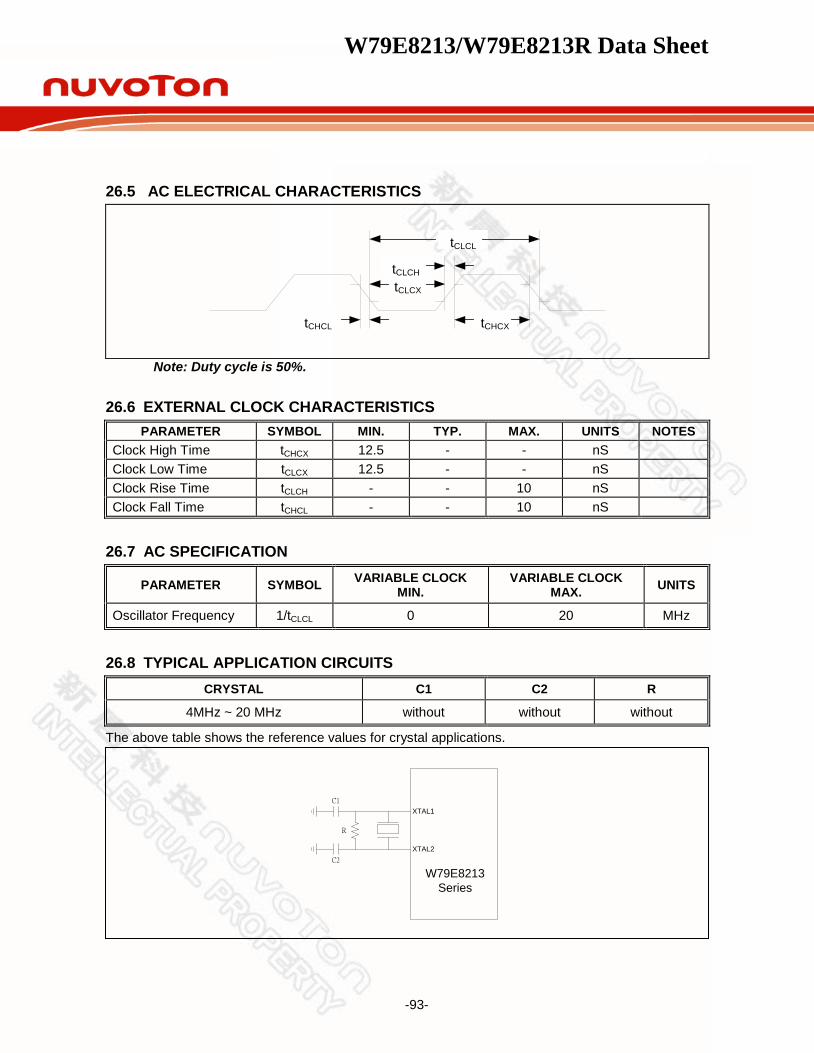
W79E8213/W79E8213R Data Sheet
-93-
26.5 AC ELECTRICAL CHARACTERISTICS
tCLCL
tCLCX
tCHCX
tCLCH
tCHCL
Note: Duty cycle is 50%.
26.6 EXTERNAL CLOCK CHARACTERISTICS PARAMETER SYMBOL MIN. TYP. MAX. UNITS NOTES
Clock High Time tCHCX 12.5 - - nS Clock Low Time tCLCX 12.5 - - nS Clock Rise Time tCLCH - - 10 nS Clock Fall Time tCHCL - - 10 nS
26.7 AC SPECIFICATION
PARAMETER SYMBOL VARIABLE CLOCK MIN.
VARIABLE CLOCK MAX. UNITS
Oscillator Frequency 1/tCLCL 0 20 MHz
26.8 TYPICAL APPLICATION CIRCUITS CRYSTAL C1 C2 R
4MHz ~ 20 MHz without without without
The above table shows the reference values for crystal applications.
XTAL2
XTAL1C1
C2
R
W79E8213Series

W79E8213/W79E8213R Data Sheet
-94-
27. PACKAGE DIMENSIONS 27.1 20-pin SOP-300mil
L
O
c
E H
A1
A
e
b
D
SEATING PLANEY
0.25
GAUGE P
E
1
20 11
10
7.600.320.510.30
EcbA1
7.400.230.330.10
0.2990.0130.0200.012
0.2910.0090.0130.004
MAX.DIMENSION IN MM
2.65A
SYMBOL MIN.2.35
DIMENSION IN INCH
0.104MIN.
0.093MAX.
Control demensions are in milmeters .
1.270.1010.65
Lθ
YH
0 80.40
10.00e 1.27 BSC
0.0500.0040.419
00.016
0.394
8
0.050 BSCE
D 12.60 13.00 0.496 0.512

W79E8213/W79E8213R Data Sheet
-95-
27.2 20-pin PDIP-300mil
1.631.470.0640.058
SymbolMin Nom Max MaxNomMinDimension in inch Dimension in mm
A
B
cD
e
A
L
S
AA
1
2
E
0.060 1.52
0.175 4.45
0.010
0.125
0.016
0.130
0.018
0.135
0.022
3.18
0.41
0.25
3.30
0.46
3.43
0.56
0.008
0.120
0.375
0.010
0.130
0.014
0.140
0.20
3.05
0.25
3.30
0.36
3.56
0.2550.2500.245 6.486.356.22
9.53
7.627.37 7.870.3000.290 0.310
2.29 2.54 2.790.090 0.100 0.110
B1
1
e
E1
1.026 1.040 20.06 26.42
0 15
0.075 1.91
0.3550.335 8.51 9.02
150
Seating Plane
Ae
2A
c
E
Base Plane1A
1e
L
A
S
1E
D
1B
B
20
1 10
11
α
α

W79E8213/W79E8213R Data Sheet
-96-
28. REVISION HISTORY VERSION DATE PAGE DESCRIPTION
A1 May 20, 2008 - Initial Issued
A2 July 11, 2008 5
92
Add VDD = 2.7V to 5.5V @12MHz CPU operation condition
Revise ADC current consumption specification
A3 August 5, 2008 91 Revise Power down current to typical 1uA, max.10uA
A4 September 1, 2008
6 93
Revise Lead Free (RoHS) Parts information list Revise Internal RC Oscillator Accuracy table
A5 November 12, 2008 30 Remove duplicate description about SFR WDCON register
A6 November 21, 2009
87 91
Remove the “prelimanry” Add defaule value for the reserved bit of CONFIG0 Add defaule value for the reserved bit of CONFIG1
A7 November 12, 2012 92 Revise chapter 26.4 “Internal RC ± 2% with VDD = 5.0V, TA
= 25C”.
Important Notice Nuvoton Products are neither intended nor warranted for usage in systems or equipment, any malfunction or failure of which may cause loss of human life, bodily injury or severe property damage. Such applications are deemed, “Insecure Usage”.
Insecure usage includes, but is not limited to: equipment for surgical implementation, atomic energy control instruments, airplane or spaceship instruments, the control or operation of dynamic, brake or safety systems designed for vehicular use, traffic signal instruments, all types of safety devices, and other applications intended to support or sustain life.
All Insecure Usage shall be made at customer’s risk, and in the event that third parties lay claims to Nuvoton as a result of customer’s Insecure Usage, customer shall indemnify the damages and liabilities thus incurred by Nuvoton.