vlsi
22
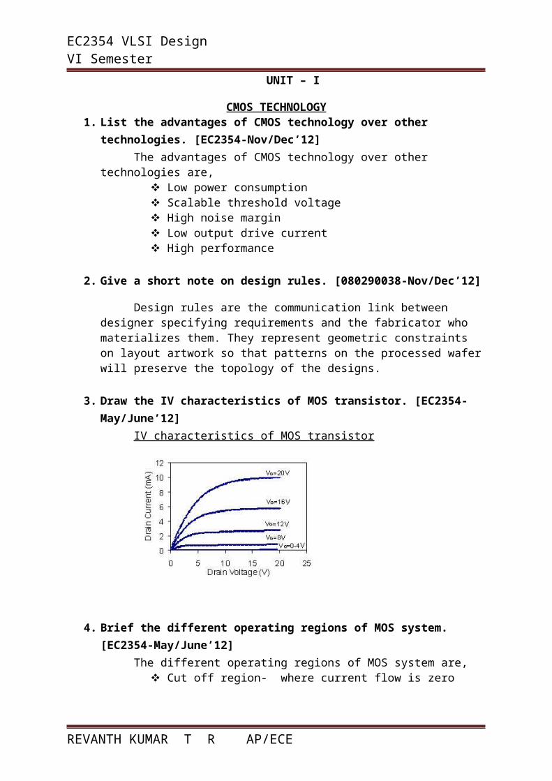
EC2354 VLSI Design VI Semester UNIT – I CMOS TECHNOLOGY 1. List the advantages of CMOS technology over other technologies. [EC2354-Nov/Dec’12] The advantages of CMOS technology over other technologies are, Low power consumption Scalable threshold voltage High noise margin Low output drive current High performance 2. Give a short note on design rules. [080290038-Nov/Dec’12] Design rules are the communication link between designer specifying requirements and the fabricator who materializes them. They represent geometric constraints on layout artwork so that patterns on the processed wafer will preserve the topology of the designs. 3. Draw the IV characteristics of MOS transistor. [EC2354- May/June’12] IV characteristics of MOS transistor 4. Brief the different operating regions of MOS system. [EC2354-May/June’12] The different operating regions of MOS system are, Cut off region- where current flow is zero REVANTH KUMAR T R AP/ECE
Transcript of vlsi
EC2354 VLSI Design VI Semester
UNIT – I
CMOS TECHNOLOGY1. List the advantages of CMOS technology over other
technologies. [EC2354-Nov/Dec’12]The advantages of CMOS technology over other
technologies are, Low power consumption Scalable threshold voltage High noise margin Low output drive current High performance
2. Give a short note on design rules. [080290038-Nov/Dec’12]
Design rules are the communication link between designer specifying requirements and the fabricator who materializes them. They represent geometric constraints on layout artwork so that patterns on the processed waferwill preserve the topology of the designs.
3. Draw the IV characteristics of MOS transistor. [EC2354-May/June’12]
IV characteristics of MOS transistor
4. Brief the different operating regions of MOS system. [EC2354-May/June’12]
The different operating regions of MOS system are, Cut off region- where current flow is zero
REVANTH KUMAR T R AP/ECE

EC2354 VLSI Design VI Semester
Non – saturated region- where drain current id depended on gate and drain voltage
Saturated region –where drain current flow is ideally independent of drain-source voltage
5. Determine whether an NMOS transistor with a threshold voltage of 0.7 v is operating in the saturation region ifVGS=2 V and VDS= 3 V[EC2354 Nov/Dec’11]
Given: VGS=2 V and VDS= 3 V Vt =0.7 vFor saturation region, Vds > Vgs-Vt
i,e 3 > (2-0.7) 3 > 1.3Therefore, the NMOS transistor is in saturation
region.
6. What is body effect coefficient? [EC2354 Apr/May’11]
The substrate voltage vsb increases, with the increase in the width of channel substrate and thereby resulting in an increase in the density of trapped carriers in the depletion layer. This results in increase of channel-substrate junction potential and an overall effect in an increase in the threshold voltage. This is known as body effect coefficient and is given by,
where : Body effect coefficient
: Electric charge
: Permittivity of silicon = 1.06 x 10⁻¹²
: Density of the carriers in the doped semiconductor substrate
: Gate - oxide capacitance
REVANTH KUMAR T R AP/ECE
EC2354 VLSI Design VI Semester
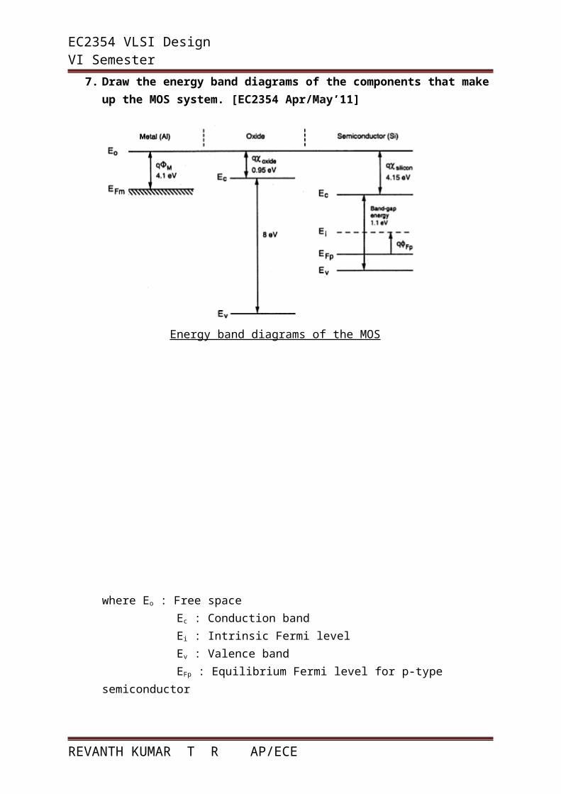
7. Draw the energy band diagrams of the components that makeup the MOS system. [EC2354 Apr/May’11]
Energy band diagrams of the MOS
where Eo : Free space Ec : Conduction band Ei : Intrinsic Fermi level Ev : Valence band EFp : Equilibrium Fermi level for p-type semiconductor
REVANTH KUMAR T R AP/ECE

EC2354 VLSI Design VI Semester
q : Electron affinity of silicon
q m : work function of an aluminium gate = 4.1eV
Fp : Fermi potential for p-type semiconductor
8. Write down the equation for describing the channel lengthmodulation effect in NMOS transistors. [EC2354 Nov/Dec’11]
The channel length modulation effect in NMOS transistors is given by,
where : Drain - source current
: MOS transistor gain factor
: Gate – Source voltage
: Threshold voltage
: An Empirical channel length modulation factor
: Drain – Source voltage
9. Why the tunneling current is higher for NMOS transistors than PMOS transistors with silica gate? [EC2354 Nov/Dec’12]
The tunneling current is higher for nMOS transistors thanpMOS transistors with silica gate because electrons tunnel from the conduction band while the holes tunnel from valence band and see a higher barrier.
10. What is the objective of layout rules? [EC2354 Nov/Dec’12]
REVANTH KUMAR T R AP/ECE
EC2354 VLSI Design VI Semester
The objective of layout rules is to describe how smallfeatures can be and how closely they can be packed in aparticular manufacturing process. They are usually specifiedin microns.
UNIT – IICIRCUIT CHARACTERIZATION AND SIMULATION
PART-A
1. Define: Body effect. [080290038-Nov/Dec’12]The threshold voltage Vt is not constant with respect to
voltage differencebetween the substrate and the source of MOS transistor. Thisis known as body effect.
where γ : Body effect coefficientεsi- : Dielectric constant of silicon dioxideq : Charge of an electronNA : Doping concentration density of substrateCox : Oxide capacitance
2. Express TPHL and TPLH in terms of Cload.[EC2354 Apr/May’11]TPHL and TPLH in terms of Cload are expressed as,
TPHL in terms of Cload is defined as the time delaybetween the transition of the rising input voltage andthe transition of the falling output voltage.
TPLH in terms of Cload is defined as the time delaybetween the transition of the falling input voltage andthe transition of the rising output voltage.
TPHL = (RN1+RN2) Cload
TPLH = (RN1+RN2) Cload
TPHL : High-to-Low Propagation DelayTPLH : Low-to-High Propagation DelayCload : Load capacitance
3. Write the expressions for the logical effort and parasiticdelay of n input NOR gate. [EC2354 Nov/Dec’11]
The expressions for the logical effort and parasiticdelay of n input NOR gate is
REVANTH KUMAR T R AP/ECE
EC2354 VLSI Design VI Semester
Logical effort = (2n+1)/3 Parasitic delay = nPinv
where n :number of inputs Pinv :Normalised parasitic delay
4. What are the factors that cause static power dissipation inCMOS family? [EC2354-Nov/Dec’12]
The factors that cause static power dissipation in CMOSfamily are,
Sub-threshold conduction through OFF transistors Tunnelling current through gate oxide Leakage through reverse –biased diodes Contention current in ratioed circuits.
5. What is meant by channel resistance? [EC2354-Nov/Dec’12]The channel resistance of a MOS transistor in the linear
region, Rc = k (L/W)where k = 1/μ Cox(Vgs-Vt)
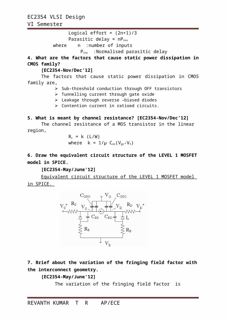
6. Draw the equivalent circuit structure of the LEVEL 1 MOSFETmodel in SPICE.
[EC2354-May/June’12]Equivalent circuit structure of the LEVEL 1 MOSFET model
in SPICE.
7. Brief about the variation of the fringing field factor withthe interconnect geometry. [EC2354-May/June’12]
The variation of the fringing field factor is
REVANTH KUMAR T R AP/ECE

EC2354 VLSI Design VI Semester
FF = Ctotal / Cpp
where FF – fringing field factorCtotal – total capacitanceCpp – parallel plate capacitance
The influence of fringing field increases with the decreasing (w/h) ratio.
(w-width of the wire and h-height of the wire)The fringing field capacitance can be as much as 10-20 times larger than the parallel plate capacitance.
8. What is meant by design margin? [EC2354-May/June’13]The aim of design margin is to design the circuit,
which will reliably operate over all extremes of the three variables:
Supply Voltage Operating temperature Process variation
9. Define device modelling [EC2354-May/June’13]Device modelling is defined as the circuit design to
which a model is adopted, which describes the behaviour of all componentssuccessfully. A model includes a set of mathematical formulas, circuit representations, tables,reference standards etc.
10. What is the influence of voltage scaling on power and delay? [EC2354 Apr/May’11]
The influence of voltage scaling on power is that when VDD is kept constant ,
the device is scaled down by dimension α. The influence of voltage scaling on delay is that when VDD is kept constant , the device is scaled down by dimension 1/α.
11. Give the effects of supply voltage and temperature variations on the CMOS system performance. [EC2354-Nov/Dec’12]
REVANTH KUMAR T R AP/ECE

EC2354 VLSI Design VI Semester
The effects of supply voltage on the CMOS system vary due to tolerance of
voltage regulators, IR drop along the supply rail and di/dt noise.
The effects of temperature variations on the CMOS system is that when the
temperature is increased, the drain current is reduced for a given set of operating conditions.
12. What is the influence of voltage scaling on power and delay? [EC2354 Apr/May’11]
The influence of voltage scaling on power is that when VDD is kept constant , the device is scaled down by dimension α. The influence of voltage scaling on delay is that when VDD is kept constant , the device is scaled down by dimension 1/α.
13. What are the factors that cause static power dissipation in CMOS circuits? [EC2354-Nov/Dec’12]
The factors that cause static power dissipation in CMOS circuits are,
a) Sub-threshold conduction through OFF transistorsb) Tunneling current through gate oxidec) Leakage through through reverse-biased diodesd) Contention current in ratioed circuits
REVANTH KUMAR T R AP/ECE
EC2354 VLSI Design VI Semester
UNIT-IIICOMBINATIONAL AND SEQUENTIAL CIRCUIT DESIGN
1. State the advantages of static CMOS circuits?
The advantages of static CMOS circuits are,a) Good noise marginb) Fastc) Low powerd) Intensive to device variationse) Easy to designf) Widely supported by CAD toolsg) Readily available in standard cell libraries
2. Write the commonly used logic families alternative to complementary CMOS?
The commonly used alternatives to complementary CMOS are,a) Dominob) Pseudo-nMOSc) Pass transistor logic
3. What is meant by pass transistor logic? [EC2354-Nov/Dec’12]It is the MOS transistor, in which a gate is driven by a control signal.When the control signal is high, input is passed to the output and when the control signal is low, the output is floating such topology circuit is called pass transistor.
4. What is a pseudo-nMOS logic gate? . Draw a pseudo NMOS inverter . [EC2354 Nov/Dec’11]
Pseudo NMOS ierter:
REVANTH KUMAR T R AP/ECE

EC2354 VLSI Design VI Semester
A pseudo-nMOS logic gate is the common form of CMOS ratioed circuits in which the pull-down network is like that of a static gate, and the pull-up network is replaced with a singlepMOS transistor that is grounded so it is always ON.
5. What are the disadvantages of using a pseudo n MOS gate instead of a full CMOS gate? [EC2354-May/June’12]
The disadvantages of using a pseudo nMOS gate instead of a full CMOS gate are
a) Slow rising transistorsb) Contention on the falling transistorsc) Static power dissipation that occurs whenever the pull-
down is turned on.d) Reduced output voltage swing and gain , which makes the
gate more susceptible to noise
6. What is CVSL? State the reasons for the speed advantage of CVSL family.
[EC2354-Nov/Dec’12]
REVANTH KUMAR T R AP/ECE

EC2354 VLSI Design VI Semester
CVSL (Cascode Voltage Switch Logic) is a gate which
performs like the of ratioed circuits but without the static power consumption. It has the following advantages
a) Quite fast - since the positive feed-back of the two PMOS accelerates the switching of the gate
b) Very good noise margins.
7. What are the disadvantages of CVSL gate?
The disadvantages of CVSL gate are,a) CVSL gate requires both the low- and high-
going transitions, adding more delay.b) Contention current during the switching
period increases power consumption.c) It also requires more area.
8. What is monotonicity problem?
In the evaluating phase of a dynamic gate, the inputs must be monotonically rising. The output of a dynamic gate begins HIGH and monotonically falls LOW which is not a suitable input to a second dynamic gate expecting montonicallyrising signals. This is called as monotonicity problem.
9. How can monotonicity problem be solved?
The monotonicity problem can be solved by placing a static CMOS inverter between dynamic gates which converts the
REVANTH KUMAR T R AP/ECE
EC2354 VLSI Design VI Semestermonotonically falling output into a monotonically rising signal suitable for the next gate.
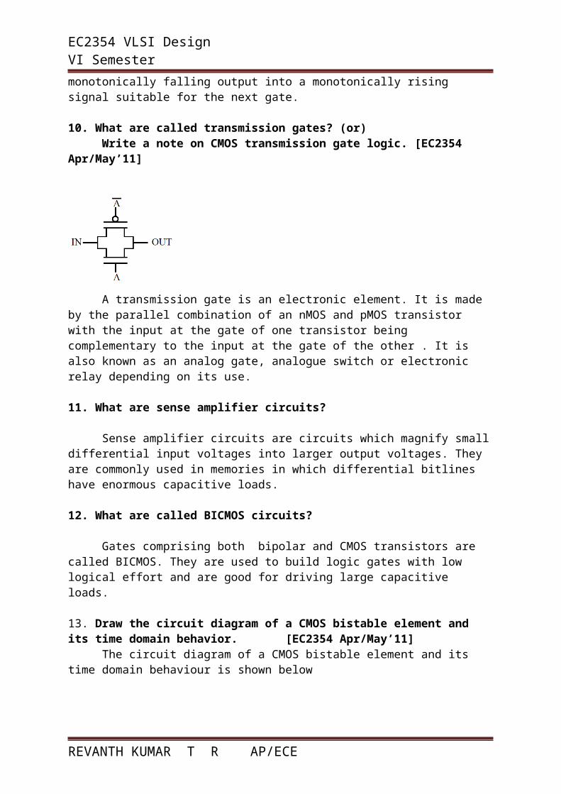
10. What are called transmission gates? (or) Write a note on CMOS transmission gate logic. [EC2354 Apr/May’11]
A transmission gate is an electronic element. It is made by the parallel combination of an nMOS and pMOS transistor with the input at the gate of one transistor being complementary to the input at the gate of the other . It is also known as an analog gate, analogue switch or electronic relay depending on its use.
11. What are sense amplifier circuits?
Sense amplifier circuits are circuits which magnify smalldifferential input voltages into larger output voltages. They are commonly used in memories in which differential bitlines have enormous capacitive loads.
12. What are called BICMOS circuits?
Gates comprising both bipolar and CMOS transistors are called BICMOS. They are used to build logic gates with low logical effort and are good for driving large capacitive loads.
13. Draw the circuit diagram of a CMOS bistable element and its time domain behavior. [EC2354 Apr/May’11]
The circuit diagram of a CMOS bistable element and its time domain behaviour is shown below
REVANTH KUMAR T R AP/ECE

EC2354 VLSI Design VI Semester
REVANTH KUMAR T R AP/ECE

EC2354 VLSI Design VI Semester
14. What are called sequencing elements?
The elements which is not really memory, instead it enforce sequence to distinguish the current data or token fromthe previous or next token are called sequencing elements.
15. List some of the sequencing elements for static circuits.
Some of the sequencing elements for static circuits are,a) Flip-flopsb) 2-phase transparent latchesc) Pulsed latches
16. What are the advantages of sequencing methodology?
The advantages of sequencing methodology are,i No sequencing overhead.ii Allows sequencing elements back-to-back with no
logic in between.iii Grant the designer flexibility in balancing the
amount of logic in each clock cycle.iv Tolerate moderate amounts of clock skew without
degrading performance.v Consumes zero area and power.
17. What are the sequencing methods applied for sequencing blocks of combinational logic?
The sequencing methods applied for sequencing blocks of combinational logic are,
i 2-phase systemii Pulsed systemiii Flip-flop based system
18. What is called a race condition?
Data incorrectly propagate through two successive elements on one clock edge. This is due to the holding time
REVANTH KUMAR T R AP/ECE
EC2354 VLSI Design VI Semesteris large and the contamination delay is small thus corruptingthe state of the system. This is called a race condition, holdtime failure, or min-delay failure.
19. What is called setup time failure and can it be reduced?
The receiving element of the combinational logic miss itssetup time and sample the wrong value, if the combinational logic delay is more. This is called setup time failure or max-delay failure.
The problem of setup time can be solved by redesigning the logic to be faster or by increasing the clock period.
20. What is time borrowing?
The technique of borrowing time from the shorter paths ofthe subsequent logic stages to the longer path in a logical circuit is called time borrowing or cycle stealing
21. What are the schemes of time borrowing for the system designer?
The schemes of time borrowing for the system designer are,
a) Intentional time borrowingb) Opportunistic time borrowing
22. What are conventional CMOS latches?
Conventional CMOS latches are circuits which are built using pass transistors or tristate buffers. These latches pass data when the latch is transparent and has feedback to hold the data when the latch is opaque.
23. What is a synchronizer? Write its common application.
REVANTH KUMAR T R AP/ECE
EC2354 VLSI Design VI Semester
A synchronizer is a circuit that accepts an input that change at arbitrary times and produces an output aligned to the synchronizer’s clock.
The common application of synchronizers is to communicatebetween asynchronous clock domains, i,e., blocks of circuits that do not share a common clock.
UNIT-IVCMOS TESTING
1. What is the need for testing?Testing is the process of identifying the fault in the
design process or IC. The role of testing is to detect whether something went wrong in the design process.2. What are the objectives of functionality test?
(Nov/Dec 2011)The objective of functionality test is, to test the
functions of the design by giving them the inputs and examining the outputs.
3. Distinguish between testers and test fixtures. (Nov/Dec 2012)
TESTERS TEST FIXTURESA tester is a device which is used to drive the inputs and to monitor the outputs of a device under test.
A test fixture is a socket for transmitting electrical signals from the test signalgeneration to an IC device under test.
4. What are the stages at which a chip can be tested? (Nov/Dec 2012)A chip can be tested at the following stages
a) At the wafer levelb) At the packaged chip levelc) At the system leveld) At the board levele) In the field
5. What are the advantages of single stuck at fault? (Apr/May 2012)The advantages of single stuck at fault are
REVANTH KUMAR T R AP/ECE
EC2354 VLSI Design VI Semester
a) Stuck at fault can be applied at the logic level or module level.
b) Algorithms for ATPG and fault simulation arewell developed.
c) Other fault models such as stuck open and bridging fault can be
mapped into stuck at fault.
6. List the basic types of CMOS testing.(May/June 2013)The basic types of CMOS testing are
a) Production testb) Burn-in testc) Incoming Inspection testd) Characterization test
7. What is meant by logic verification? (May/June 2013)Logic verification is a method of checking the
functionality of a circuit by giving inputs and checking the outputs.
8. What is controllability and observability?Controllability for a digital circuit is defined as
the difficulty of setting a particular logic signal to a 0 or a 1.
Observability for a digital circuit is defined as the difficulty of observing the state of logic signal.
9. What is ATPG?Automatic Test Pattern Generation is algorithm that
injects a fault into a circuit, and then uses a variety of mechanisms to activate the fault and causes its effectto propagate through the hardware and manifest itself at a circuit output. The output signal changes from the value expected for the fault-free circuit, and this causes the fault to be detected.
10. What is PODEM algorithm?The Path-Oriented Decision Making algorithm solves
the problem of reconvergent fanout and allows multipath sensitization.
REVANTH KUMAR T R AP/ECE

EC2354 VLSI Design VI Semester
11. What is stuck at fault?The fault at the interconnection of gates is called
stuck-at fault. This fault is modeled by assigning a fixed 0 or 1 value to a signal line in the circuit.
12. What is Ad-Hoc testing? (Nov/Dec 2009)Ad-hoc testing is one of the DFT methods for testing
the design.The main objective of Ad-Hoc testing is
a) Avoid asynchronous logic feedbacksb) Avoid gates with a large fan-in
13. What are the classifications of fault simulation?The classifications of fault simulations are
a) Serial fault simulationb) Parallel fault simulationc) Concurrent fault simulationd) Non-deterministic fault simulation
14. Define RTLRegister Transfer Level-a text-based design description
where the behaviour of a circuit is modelled as dataflow andcontrol from register to register in reference to an appliedclock, clocks or other synchronizing signals.
15. Define test vectorsTest vectors are the binary input bit patterns used to
verify the functionality of the device under test.
16. What are the different formats of test data?The different formats of test data are
a) Non-Return to zerob) Return to zeroc) Surrounding by complement
17. Define Bridging FaultsThe short-circuit faults occur in interconnect of groups of signals is called bridging faults. In bridging faults the logic value of the shorted net may be modeled as 1-dominant or0-dominant.
UNIT VSPECIFICATONS USING VERILOG HDL
REVANTH KUMAR T R AP/ECE

EC2354 VLSI Design VI Semester1. State the comparison between behavioral and Data flow level
modeling (May/June
2013)Behavioral modeling represents digital circuits at a functional and algorithmic level. Behavioral description uses the keyword always and initial followed by a list ofprocedural assignment statements.Dataflow modeling represents digital circuits by their
function rather than by their gate structure. Dataflow description uses continuous
assignment statements.
2. What are gate primitives (May/June 2013)Gate primitives are generalized modules that already
exist in verilog. They can be instantiated directly in other modules.
3. Write the verilog module for a 1-bit full adder.(Nov/Dec 2012)
module full_adder(a,b,c, sum,carry);output sum,carryinput a;b,c;wire w1,w2,w3;xor (sum,a,b,c);and(w1,a,b);and(w2,b,c);and(w3,c,a);or(carry,w1,w2,w3);endmodule
4. Give an example for implicit continuous assignment.(Nov/Dec 2012)
Regular continuous assignmentwire c,a,b;assign c=a & b;Implicit continuous assignmentwire c= a & b;
5. What is transport delay? (Apr/May 2011)
Transport delay is the delay caused by the wires connecting the gates. Wire do delay the signal they carry, this is due to the wire resistance, capacitance, and
REVANTH KUMAR T R AP/ECE

EC2354 VLSI Design VI Semester
inductance. Simply transport delay is propagation delay on awire. In verilog transport delay is modeled as follows: a <=#10 b.
6. What is subprogram overloading (Apr/May 2011)
Subprogram overloading is a process of using the same (function) name for many subprograms. The overloaded subprograms may differ in the number, type or order of its parameters.
7. Write the verilog module for an half adder(Nov/Dec 2011)module halfadder(sum,carry,a,b);output sum, carry;input a,b;xor(a,b,sum);and (carry,a,b);endmodule
8. What are the delays available in verilog HDL(Nov/Dec 2011)The delays available in verilog HDL area) Regular Assignment Delayb) Implicit Continuous Assignment Delayc) Net Declaration Delay
9. Distinguish between task and function(Nov/Dec2009)
FUNCTION TASKA function can enable another function but not another task
A task can anable other tasks and functions
Function always execute in 0 simulation time
Tasks may execute in non-zero simulation time
Functions must not contain any delay, event, or timingcontrol statements.
Tasks may contain delay, event, or timing control statements
Functions must have at least one input argument.
Tasks may have zero or more arguments of type
REVANTH KUMAR T R AP/ECE
EC2354 VLSI Design VI Semester
They can have more than oneinput
input, output, or inout.
10. What is the difference between = = = and = =?(Nov/Dec 2009) = = Logical equalityExample: If a=4; b=3;Then a= =b Results in logical 0= = = Case equalityExample: If a= 4’b1xxz; b=4’b1xxzThen a=b Results in logical 1.
11. What is CBIC ?(Nov/Dec 2009)A cell based ASIC uses predesigned logic cells, known as
standard cells. The standard cell areas in a CBIC are built of rows of standard celllike a wall built of bricks.12. Write a verilog code for D latch
(Nov/Dec 2009)module d_latch(q,qbar,d,c);output q,qbar;input d,c;wire x1, x2, x3;not g1(x1,d);nand g2(x2,d,c);nand g3(x3,x1,c);nand g4(q,x2,qbar);nand q5(qbar,x3,q); endmodule
13. What are the three types of gate delays?The three types of gate delays are
a) Rise Delayb) Fall delayc) Turn-off delay
14. What are the different types of operators used in verilog?
The different types of operators used in veriloga) Arithmeticb) Logicalc) Relationald) Equality
REVANTH KUMAR T R AP/ECE

EC2354 VLSI Design VI Semester
e) Bitwisef) Reductiong) Shifth) Conditional
15. What is compiler directive?A compiler directive when compiled remains in effect
through the entire compilation process until a different compiler directive specifies otherwise.
16. Write a verilog module for CMOS inverter using switch level modelling.
module cmos_inverter(out,in);output out;input in;supply1 pwr;supply0 gnd;pmos u1(out,pwr,in);nmos u2(out,gnd,in);endmodule
17. What are the conditional statements of verilog HDL?The conditional statements of verilog HDL are
a) If statementb) Case statementc) Loop statement
i. Forever loopii. Repeat loopiii. While loopiv. For loop
18. List the types of Design MethodologyThe types of design methodology are
a) Top-Down methodologyb) Bottom-up methodology
REVANTH KUMAR T R AP/ECE