M. Tech-ECE (VLSI Design) First Semester S. No ... - IGDTUW
59
M. Tech-ECE (VLSI Design) First Semester S. No. Code Subject L-T-P Credits Category 1. MVD-101 CMOS Analog Circuit Design 3-0-2 4 DCC 2. MVD-103 Semiconductor Devices for Digital Integrated Circuits 3-0-2 4 DCC 3. MVD-105 Hardware Description Languages 3-0-2 4 DCC 4. MVD-107 Advanced IC Processing 3-1-0 4 DCC 5 GEC-101 Generic Open Elective 2-0-0 1-1-0 0-0-4 2 GEC 6. ROC-101 Research Methodology 3-0-0 3 ROC Total credits 21 Second Semester S. No. Code Subject L-T-P Credits Category 1. MVD-102 Device Modeling & Circuit simulation 3-0-2 4 DCC 2. MVD-104 Digital System Design with FPGA 3-0-2 4 DCC 3. MVD-106 Deep Submicron CMOS ICs 3-1-0 4 DCC 4. DEC1 xx Departmental Elective Course – 1 3-0-2 3-1-0 4 DEC 5. DEC1 xx Departmental Elective Course - 2 3-0-2 3-1-0 4 DEC 6 ROC-102 Research Ethics 3-0-0 3 ROC Total credits 23 Indira Gandhi Delhi Technical University For Women (Established by Govt. of Delhi vide Act 09 of 2012) Department of Electronics and Communication Engineering
-
Upload
khangminh22 -
Category
Documents
-
view
1 -
download
0
Transcript of M. Tech-ECE (VLSI Design) First Semester S. No ... - IGDTUW

M. Tech-ECE (VLSI Design) First Semester
S. No. Code Subject L-T-P Credits Category
1. MVD-101 CMOS Analog Circuit Design 3-0-2 4 DCC
2. MVD-103 Semiconductor Devices for Digital Integrated Circuits
3-0-2 4 DCC
3. MVD-105 Hardware Description Languages 3-0-2 4 DCC
4. MVD-107 Advanced IC Processing 3-1-0 4 DCC
5 GEC-101 Generic Open Elective 2-0-0 1-1-0 0-0-4
2 GEC
6. ROC-101 Research Methodology 3-0-0 3 ROC
Total credits 21
Second Semester
S. No. Code Subject L-T-P Credits Category
1. MVD-102 Device Modeling & Circuit simulation
3-0-2 4 DCC
2. MVD-104 Digital System Design with FPGA 3-0-2 4 DCC
3. MVD-106 Deep Submicron CMOS ICs 3-1-0 4 DCC
4. DEC1 xx Departmental Elective Course – 1 3-0-2 3-1-0
4 DEC
5. DEC1 xx Departmental Elective Course - 2 3-0-2 3-1-0
4 DEC
6 ROC-102 Research Ethics 3-0-0 3 ROC
Total credits 23
Indira Gandhi Delhi Technical University For Women
(Established by Govt. of Delhi vide Act 09 of 2012) Department of Electronics and Communication Engineering

Third Semester
S. No. Code Subject L-T-P Credits Category
1. MVD-201 ASIC and SoC Design 3-0-2 4 DCC
2. DEC-2xx Departmental Elective-3 3-0-2 3-1-0
4 DEC
3. DEC-2xx Departmental Elective-4 3-0-2 3-1-0
4 DEC
4 GEC-201 General Open Elective 2-0-0 1-1-0 0-0-4
2 GEC
5. MVD-251 Dissertation-1/Project Work - 8 DCC
6. MVD-253 Industrial Training/Internship - 1 DCC
Total credits 23
Fourth Semester
S. No. Code Subject L-T-P Credits Category
1. MVD-252 Dissertation -2/Project Work - 20 DCC
Total credits 20

List of Departmental Elective Courses
Category Course Code Subject Credits
Departmental Elective Course-1
MVD-108 MVD-110 MVD-112 MVD-114 MVD-116
Semiconductor Memory Design Digital VLSI design Analog filter Design Digital Techniques for High Speed Design CMOS Mixed-Signal VLSI Design
3-0-2 3-0-2 3-0-2 3-1-0 3-0-2
Departmental Elective Course-2
MVD-118 MVD-120 MVD-122 MVD-124 MVD-126
Advanced Embedded System Design Analog Integrated Circuits Digital System Design using Verilog MEMS & Microsystems Internet of Things
3-0-2 3-1-0 3-0-2 3-1-0 3-1-0
Departmental Elective Course-3
MVD-203 MVD-205 MVD-207 MVD-209 MVD-211
Low Power VLSI Design VLSI Design Verification and Test Advance Image Processing Neural Networks in Embedded Applications Nature Inspired VLSI Circuits
3-0-2 3-1-0 3-0-2 3-1-0 3-1-0
Departmental Elective Course-4
MVD-213 MVD-215 MVD-217 MVD-219 MCS-221
VLSI Interconnects VLSI design Algorithms VLSI Design Techniques for Analog IC Artificial Intelligence Data Structures
3-1-0 3-1-0 3-1-0 3-0-2 3-0-2
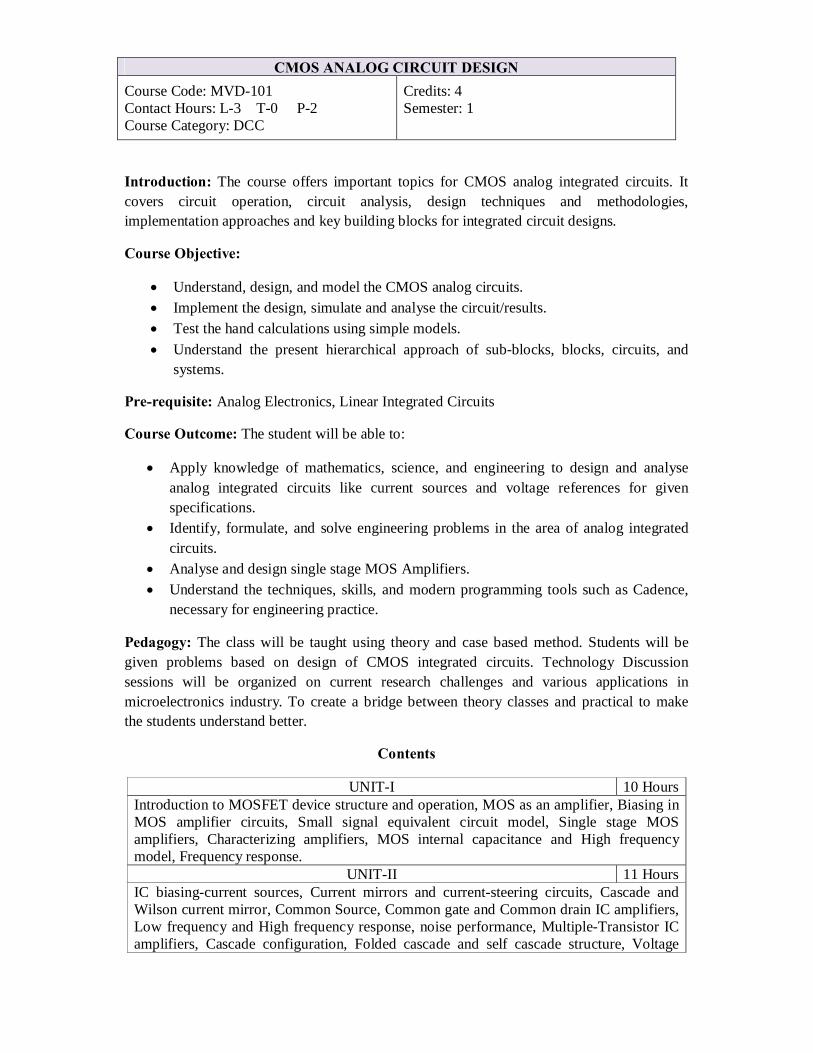
Introduction: The course offers important topics for CMOS analog integrated circuits. It covers circuit operation, circuit analysis, design techniques and methodologies, implementation approaches and key building blocks for integrated circuit designs.
Course Objective:
• Understand, design, and model the CMOS analog circuits. • Implement the design, simulate and analyse the circuit/results. • Test the hand calculations using simple models. • Understand the present hierarchical approach of sub-blocks, blocks, circuits, and
systems.
Pre-requisite: Analog Electronics, Linear Integrated Circuits
Course Outcome: The student will be able to:
• Apply knowledge of mathematics, science, and engineering to design and analyse analog integrated circuits like current sources and voltage references for given specifications.
• Identify, formulate, and solve engineering problems in the area of analog integrated circuits.
• Analyse and design single stage MOS Amplifiers. • Understand the techniques, skills, and modern programming tools such as Cadence,
necessary for engineering practice.
Pedagogy: The class will be taught using theory and case based method. Students will be given problems based on design of CMOS integrated circuits. Technology Discussion sessions will be organized on current research challenges and various applications in microelectronics industry. To create a bridge between theory classes and practical to make the students understand better.
Contents
UNIT-I 10 Hours Introduction to MOSFET device structure and operation, MOS as an amplifier, Biasing in MOS amplifier circuits, Small signal equivalent circuit model, Single stage MOS amplifiers, Characterizing amplifiers, MOS internal capacitance and High frequency model, Frequency response.
UNIT-II 11 Hours IC biasing-current sources, Current mirrors and current-steering circuits, Cascade and Wilson current mirror, Common Source, Common gate and Common drain IC amplifiers, Low frequency and High frequency response, noise performance, Multiple-Transistor IC amplifiers, Cascade configuration, Folded cascade and self cascade structure, Voltage
CMOS ANALOG CIRCUIT DESIGN Course Code: MVD-101 Contact Hours: L-3 T-0 P-2 Course Category: DCC
Credits: 4 Semester: 1

follower, Flipped voltage follower. UNIT-III 11 Hours
MOS differential pair, Small signal operation, Differential gain, Common mode gain, Common mode rejection ration, Non ideal characteristics, Active loaded differential amplifier, Frequency response, Noise Spectrum - sources, types, Thermal and Flicker noise, Representation in circuits, Noise bandwidth, Noise figure.
UNIT-IV 10 Hours General feedback structure, Negative feedback, Four basic topologies, Loop gain, Stability, Effect of feedback on amplifier poles, Single pole response, Two pole response, Frequency compensation, Compensation Techniques, Pole splitting. Text Books:
1 Sedra and Smith, “Microelectronic circuits”, 7th Edition, Oxford University Press, 2017.
2 Kenneth R. Laker and Willy M.C. Sansen, “Design of Analog Integrated Circuits and systems”, 2nd Edition, McGraw-Hill, 2010.
3 Philip E. Allen and Douglas R. Holberg, “CMOS Analog Circuit Design”, 3rd
Edition, Oxford University Press, 2012. Reference Books:
1 Behzad Razavi, “Design of Analog CMOS Integrated Circuit”, 2nd Edition, Tata McGraw Hill, 2017.
2 Gray R.Paul, Hurst J. Paul, Lewis H. Stephen and Meyer G. Robert, “Analysis and Design of Analog Integrated Circuits”, 5th Edition, John Wiley and Sons, 2012.
3 R. Jacob Baker,” CMOS: Mixed-Signal Circuit Design”, 2nd Edition, John Wiley and Sons, 2009.

Introduction: Semiconductor fundamentals, PN junctions, metal-semiconductor contacts, metal-oxide semiconductor capacitors and field-effect transistors, bipolar junction transistors.
Course Objective:
• To acquire knowledge about different types of semiconductor memories. • To study about architecture and operations of different semiconductor memories. • To comprehend the low power design techniques and methodologies. • To understand the principles and fundamentals of semiconductor electronic and
photonic devices and their applications. • To provide students with the necessary basic understanding and knowledge in
semiconductors so that they understand various applications in discrete and integrated analogue electronic circuits.
Pre-requisite: Semiconductor fundamentals
Course Outcome: On successful completion of the course, the students will be able to
• Comprehend the properties of materials and its application in electronics • Experiment the knowledge of semiconductors to illustrate the functioning of basic
electronic devices. • Analyse the application of the semiconductor devices. • Construct the control applications using semiconductor devices. • Define the fabrication methods of integrated circuits. • Develop and construct the semiconductor devices for special applications.
Pedagogy : Learning modes will be PowerPoint slides, assignments and research paper discussion. To create a bridge between theory classes and practical to make the students understand better.
Contents
UNIT-I 10 Hours Elemental and compound semiconductors, Narrow & wide energy gap semiconductors, Direct & Indirect semiconductors, Choice of semiconductors for specific applications, Review of semiconductor fundamentals, Energy band, Carrier transport phenomena, Recombination and generation, surface effects, traps.
UNIT-II 11Hours PN junction, Schottky junction, Ohmic contacts, BJT device design, nonideal effects, frequency limitations, MOSFET Operation, Subthreshold conduction, Mobility variation, Velocity saturation threshold voltage modifications, Threshold adjustment by ion implantation, Lightly doped drain MOS transistor, Breakdown voltage, Radiations and Hot electron effects.
UNIT-III 11Hours
SEMICONDUCTOR DEVICES FOR DIGITAL INTEGRATED CIRCUITS Course Code: MVD 103 Contact Hours: L-3 T-0 P-2 Course Category: DCC
Credits: 4 Semester: 1

Introduction to modern VLSI Devices, Polysilicon emitter transistors, Heterojunctions, 2D electron gas, Band alignment, SOI MOSFETs, PDSOI, FDSOI, Source/drain engineering, Brief Introduction to HEMTS, MESFET (Metal semiconductor FET) and MODFET (Modulation doped FET).
UNIT IV 10Hours New VLSI device structures from bulk to SOI to multi-gate, Double gate MOSFET, FinFET, SiGe technology, Strain influence on electron mobility, Strain enhanced Si based transistors, Strained Si CMOS, SiGe HBTs, SiGe MODFETs, Nanowires. Text Books
1 Donald A. Neamen, “Semiconductor Physics and devices”, 4th Edition, Tata McGraw Hill, 2017.
2 Taur and Ning, “Fundamental of Modern VLSI Devices”, 2nd Edition, Cambridge Press, 2016.
3 Balbir Kumar, Shail B. Jain, “Electronic Devices and Circuits”, PHI Publication, 2013.
Reference Books
1 Ben G. Streetman & S. Banerjee, “Solid state electronic devices”, 6th Edition, Prentice Hall, 2010.
2 A. G. Milnes, “Semiconductor Devices and Integrated Electronics”, Springer, 2012.
3 Jan M.Rabaey” Digital Integrated Circuits: A design perspective”, Pearson, 2016.

Introduction: This course teaches basics as well as advance topics of Verilog and basics of VHDL. The objective of this course is to introduce a hardware description language (HDL) for the specification, simulation, synthesis and implementation of digital logic systems. The students will have design practice sessions and will implement digital logic systems with electronic design automation (EDA) tools.
Course Objective:
• Understand a hardware description language (HDL) for the specification, simulation, synthesis and implementation of digital logic systems.
• Implement the design digital logic systems with commercial electronic design (EDA) tools.
• Understand the usage of digital systems. • Develop the synthesis of digital systems for programmable logic VLSI.
Pre-requisite: Student must have studied
• Digital design fundamentals: Logic gates and boolean logic. • Sequential circuit fundamentals: State machines and sequential logic. • Basic programming skills as procedural programming in C.
Course Outcome:
• Implementation of logic fundamentals using hardware description languages. • Comprehend the difference between procedural programming and hardware
description languages. • Develop synthesizable Verilog code for Combinational and Sequential logic circuits. • Execute code state machines in a hardware description language. • Analyse and develop basic logic pipelined machines. • Understand basic programmable logic architectures. • Synthesize working circuits using programmable logic. • Understand sequential and combinatorial logic timing. • Understand the impact of actual routing and circuit parasitics.
Pedagogy: Learning modes will be PowerPoint slides, assignments and research paper discussion. To create a bridge between theory classes and practical to make the students understand better.
Contents
UNIT-I 10Hours Introduction to VHDL, Behavioural , Data flow, Structural models, Simulation cycles, Process, concurrent & sequential statements, Loops, Delay models, Library, Packages, Functions, Procedures, Test bench, Design of digital circuits using VHDL.
UNIT-II 11Hours
HARDWARE DESCRIPTION LANGUAGES Course Code: MVD 105 Contact Hours: L-3 T-0 P-2 Course Category: DCC
Credits: 4 Semester: 1

Introduction to Verilog HDL, Hierarchical modelling concepts, Lexical conventions, Data types, System tasks and Compiler directives, Modulus and ports, Variable, Arrays, Tables, operators, Expressions, Signal assignments, Nets, Registers, Concurrent & Sequential Constructs, Tasks & Functions.
UNIT-III 11Hours Gate-level Dataflow and behavioural modelling using Verilog HDL, Advanced Verilog topics, Timing and delays, Delay models, Path delay modelling, Timing checks, Switch level modeling, User defined primitives, Programming language interface.
UNIT-IV 10Hours Logic Synthesis with hardware description language, Impact of logic synthesis, Synthesis design flow, RTL description, Technology mapping and optimization, Technology library, Design constraints, Introduction to System Verilog, Verification techniques Text Books
1 J. Bhaskar, “Verilog HDL Synthesis – A Practical Primer”, 3rd Edition, Star Galaxy Publishing 2008.
2 S. Palnitkar, “Verilog HDL: A Guide to Digital Design and Synthesis”, 2nd Edition, Prentice Hall, 2006.
3 Mintz, Mike, Ekendahl, Robert, “Hardware Verification with System Verilog: An Object-Oriented Framwork”, 1st Edition, Springer, 2010.
Reference Books 1 Peter J Ashenden, “The Designer’s Guide to VHDL”, 3rd Edition, Morgan
Kaufmann Publishers, 2011. 2 Stefan Sjoholm&LennartLindth, “VHDL for Designers”, 2nd Edition, Prentice
Hall, 2008. 3 Michael D. Ciletti,” Advanced Digital Design with the Verilog HDL”, 2nd
Edition, Prentice Hall, 2010.

Introduction: This course will examine the process technology that has enabled the integrated circuit revolution and investigate new technologies and layout/circuit techniques aimed at sustaining the current rate of progress in integrated circuits. The course emphasizes the physical principles and mathematical models used to characterize fabrication and inspection processes in micro fabrication technology.
Course Objective:
• Integration density and performance of analog and digital integrated circuits have undergone an astounding revolution in the last couple of decades.
• To understand the clock frequencies of microprocessors • To analyse both logic IC’s and memories, integration complexity and density. • The goal is to achieve a working knowledge of the driving and limiting factors in
circuit performance, of the fabrication and design techniques that influence performance, and of likely future trends.
Pre-requisite: Basic solid-state device design, operation, physics, diodes, bipolar junction transistors, and MOS field-effect transistors, and methods for their wafer-level fabrication. Familiarity with integrated circuit processing techniques, including oxidation diffusion, ion implantation, epitaxy, deposition, and etching.
Course Outcome: After successful completion of the course student will be able to • Understand about various types of modern technologies. • Identify the working knowledge of the driving and limiting factors in circuit
performance of the fabrication and design techniques. • Implement the fabrication process for designing digital ICs. • Compare the various analog and digital circuits.
Pedagogy: The course Advanced IC Processing has been designed to enable the student to keep them in pace with the integrated circuit revolution and investigate new technologies and layout/circuit techniques provide a thorough exposure to the topic with the opportunity for flexible scheduling. The course materials consist of four basic elements: the lecture, course notes, problems and solutions, and the textbook. These elements have been carefully integrated, with each having an important role in the overall effectiveness of the course.
Contents
UNIT-I 10 Hours Overview of modern CMOS technology, Substrate selection, Active region formation, Device isolation, Well formation, Gate and source/drain formation, Contact and local interconnects, Multilevel metal formation, Comparison between bulk and SOI CMOS technologies.
UNIT-II 11 Hours Crystal growth, Crystal structure, Crystal defects, Raw materials and purification,
ADVANCED IC PROCESSING Course Code: MVD 107 Contact Hours: L-3 T-1 P-0 Course Category: DCC
Credits: 4 Semester: 1

Electronic grade silicon, Czochralski and float-zone crystal growth methods, Wafer preparation and specifications, SOI wafer manufacturing clean rooms, Wafer cleaning and gettering, Basic concepts, Manufacturing methods and equipment, Measurement methods.
UNIT-III 10 Hours Photolithography, Light sources, Photoresists, Wet and Dry oxidation, growth kinetics, Diffusion, Fick’s laws, Ion implantation, Chemical and physical vapour deposition, Epitaxial growth, Deposition of dielectrics and metals commonly used in VLSI, Wet etching, Plasma etching, Etching of materials used in VLSI, Contacts, Vias, Multi-level Interconnects, Silicided gates and S/D regions, Reflow & planarization
UNIT-IV 10 Hours Functions of packaging, Rent’s Rule, Packaging techniques, Through hole, Surface mount, Types of single chip packaging, Bond wire, Flip chip technology, Tape automated Bonding, Thermal Management, Interconnection topology, Introduction to system packaging, System-in-package, Multi-Chip Module, 3D Packaging, Future Trends Text Books 1 James D. Plummer, M.D. Deal and P.B.Griffin, “Silicon VLSI Technology,
Fundamentals, Practice and Modeling”, 1st Edition, Pearson Education, 2009. 2 Sorab Ghandhi, “VLSI Fabrication Principles”, 2nd Edition, John Wiley and Sons,
2008. 3 Yasuo Tarui,” VLSI Technology: Fundamentals and Applications”, Springer, 2011. Reference Books 1 H. B. Bakoglu, “Circuits, Interconnections, and Packaging for VLSI”, 1st Edition,
Addison Wesley Longman Publishing, 1990. 2 S.M.Sze, “VLSI Technology”, 2nd Edition, McGraw-Hill, 2017.

DEVICE MODELING & CIRCUIT SIMULATION Course Code: MVD 102 Contact Hours: L-3 T-0 P-2 Course Category: DCC
Credits: 4 Semester: 2
Introduction: The course deals with the study of device models that are used in the design and analysis of circuits using any simulator.
Course Objective:
• To explain the fundamental knowledge of semiconductor devices. • To provide an introduction to the basic semiconductor physics/solid-state physics
needed to understand device modelling of electronic devices. • To understand the operation of several basic semiconductor devices: p-n junctions,
metal-semiconductor junctions, Diodes, metal oxide semiconductor field effect transistors (MOSFETs), Complementary MOSFETs (CMOS).
• To provide fundamental understanding of device modeling and numerical simulation techniques.
Pre-requisite: Basic course of VLSI design
Course Outcome: After successful completion of the course student will be able to • Understand concepts of MOSFET modelling. • Implement the device models on software. • Design and implement the codes for device modelling. • Implement the analog and digital circuit simulation.
Pedagogy: Learning modes will be Power Point slides, assignments and research paper discussion. Use of ICT modes and classroom teaching. To create a bridge between theory classes and practical to make the students understand better.
Contents
UNIT-I 10 Hours Introduction to SPICE modelling, Growth of fables design industry, SPICE modelling of resistor, Capacitor, Inductor, Semiconductor devices such as Diode, BJT, FET, MOSFET.MOSFET model parameters, Introduction to MOSFET SPICE Level 1, Level 2 and Level 3 models. CAD tools, Introduction to Device simulators, Tools for simulating device performance, Introduction to Circuit simulators
UNIT-II 10 Hours Circuit simulation techniques, DC analysis, AC analysis, Transient analysis, Modelling of Process Variation, Process corners, Monte Carlo simulation, and Sensitivity/worst case analysis, Simulation of digital and analog circuits, Transfer function, Frequency response, Noise analysis, Distortion and Spectral analysis.
UNIT-III 10 Hours MOSFET DC model, Static model and dynamic model, MOSFET Models for Digital

Design, performance considering short channel and narrow width effects, Mechanical stress etc. MOSFET Models for Analog Design, Long Channel MOS model, Short Channel MOS model. Large signal and Small signal model. Analog Circuit Performance Parameters: Impact of parasitic effects, Process /temperature variation, Device reliability effects. Effect of temperature on model parameters.
UNIT-IV 11 Hours Data Acquisition and model parameter measurements, MOSFET models for mixed Analog-Digital circuit design, MOSFET models for Radio frequency circuit design, Deep submicron MOSFET models, Power MOSFET Simulation Models, Advanced MOSFET Models for Circuit Simulators, Brief overview of BSIM and EKV model. Text Books
1 Tor A. Fjeldly, Trond Ytterdal, Michael S. Shur, “Introduction to Device Modeling and Circuit Simulation” Wiley, Latest Edition.
2 Paul W. Tuinenga, “SPICE: A Guide to Circuit Simulation and Analysis Using PSpice”, 3rd Edition, Pearson, 2006.
3 Paolo Antognetti and Giuseppe Massobrio, “Semiconductor Device Modeling with SPICE”, 2nd Edition, McGraw-Hill, 2010.
Reference Books 1 Y. Tsividis, “Operation and Modeling of MOS transistors”, 3rd Edition, Oxford
University Press, 2010. 2 Jacob Millman, “Millman's Electronic Devices and Circuits”, 4th Edition, McGraw
Hill, 2015. 3 Muhammad H. Rashid, “Introduction to PSpice Using OrCAD for Circuits and
Electronics”, Pearson, 2015.

DIGITAL SYSTEM DESIGN WITH FPGA Course Code: MVD-104 Contact Hours: L-3 T-0 P-2 Course Category: DCC
Credits: 4 Semester: 2
Introduction: Digital Systems Design with FPGAs and CPLDs explains how to design and develop digital electronic systems using programmable logic devices (PLDs). This deals with case study designs using a variety of Field Programmable Gate Array (FPGA) and Complex Programmable Logic Devices (CPLD). They also involve the study of ASM chart and Arbiter Design for a range of applications. Course Objective:
• To understand various complex programmable Logic devices of different families. • To study Field programmable gate arrays and realization techniques. • To study various architecture of combinational/ sequential circuits.
Pre-requisites: Basic knowledge of Programmable logic devices, combinational and sequential logic circuit design and memories. Course Outcome: After successful completion of the course student will be able to
• Demonstrate the use and application of Boolean algebra in the areas of digital circuit reduction, expansion, and factoring.
• Design and analysis of combinational and sequential digital systems. • Simulate and debug digital systems described in VHDL. • Apply complex digital circuits at several levels of abstractions. • Implement logic on an FPGA. • Understand different memory types and technologies. • Design and implement hardware digital systems incorporating memory modules.
Pedagogy: Classroom teaching will be supported by Learning Management System (LMS) and multimedia. Learning modes will include PowerPoint slides, assignments and research paper discussion. To create a bridge between theory classes and practical to make the students understand better.
Contents
UNIT-I 11 Hours Introduction to VLSI Design, Review of Latch and Flip-Flops, Design of Combinational circuit and AOI Logic Implementation, Design of Adders, Multipliers, Code Convertors, Magnitude Comparator, Multiplexer and Demultiplexer, CMOS Adder Architectures, ALU, Verilog Modeling of Combinational Circuits.
UNIT-II 11 Hours Design of sequential circuits (Various Shift Registers and Counters), Review of state table and State diagram, Mealy and Moore state machines, Implementation of Sequential Circuits, Modeling of Verilog Sequential Circuits, Analysis and Synthesis of Sequential Circuits.
UNIT-III 10 Hours RTL coding guidelines, Coding organization- complete realization, Writing a test bench, System design using ASM chart, Micro programmed design, Design flow of VLSI

Circuits, Simulation of combinational and sequential Circuits, Analysis of waveforms, Optimizing data paths.
UNIT-IV 10 Hours PCI Arbiter Design using ASM Chart, Semiconductor Memories- ROM, RAM, SRAM, EPROM, Memory classification, Organization and technologies, Design, Architecture, Implementation of ROM chip, HDL based memory design examples. Programmable logic devices, Programmable array logic, CPLD and FPGA. Text Books
1 Ian Grout, “Digital Systems Design with FPGAs and CPLDs”, 1st Edition Newnes, 2011.
2 Manjita Srivastava, Mahesh C. Srivastava, and Atul K. Srivastava,”Digital Design- HDL Based Approach”, Cengage Learning, 2010.
3 Kevin Skahill, “VHDL for Programmable Logic”, Pearson Education, 1st Edition 2006.
Reference Books 1 A. Anand Kumar, “Fundamentals of Digital Circuits”, 3rd Edition, PHI publication,
2014. 2 Roth Kinney, “Fundamentals of Logic Design”, 7th Edition, CengagE Learning,
2015. 3 Wayne Wolf, “FPGA-Based System Design”, Pearson Education , 2004

DEEP SUBMICRON CMOS ICS Course Code: MVD 106 Contact Hours: L-3 T-1 P-0 Course Category: DCC
Credits: 4 Semester: 2
Introduction: The course provides a solid and fundamental engineering view of digital system operation and how to design systematically well performing digital VLSI systems exceeding consistently, customer expectations and competitor fears. The aim is to teach the critical methods and circuit structures to identify the key 1 % of the circuitry on-chip which dominates the performance, reliability, manufacturability, and the cost of the VLSI circuit. With the current utilisation of the deep submicron CMOS technologies (0.25 micron and below design rules) the major design paradigm shift is associated with the fact that the interconnections (metal Al or Cu wires connecting gates) and the chip communication in general is the main design object instead of active transistors or logic gates. The main design issues defining the make-or-break point in each project is associated with power and signal distribution and bit/symbol communication between functional blocks on-chip and off-chip.
Course Objective: In this course we provide a solid framework in understanding: -
• To understand the Scaling of technology and their impact on interconnects. • To explain the Interconnects as design objects. • To understand the noise in digital systems and its impact on system operation. • Power distribution schemes for low noise • Signal and signalling conventions for on-chip and off-chip communication • Timing and synchronisation for fundamental operations and signalling
Pre-requisite:Analog VLSI Design, VLSI Design
Course Outcome: After successful completion of the course student will be able to
• Understand the Deep Submicron CMOS Technology. • Understand the basic Process technology. • Apply and implement the Modelling systems. • Understand the basic Analog blocks. • Design CMOS Analog Circuits. • Understand the concepts of Computer Aided Design (CAD).
Pedagogy: The class will be taught using theory and case based method. Since this is design course, students are given problems based on design of Deep Submicron CMOS signal circuits. Technology Discussion sessions are organized on current research challenges in design, their relevance and applications in microelectronics industry. Design using CAD tools in CMOS design will also be done.

Contents UNIT-I 10 Hours
MOS scaling, classification, DSM (Deep submicron) effects on devices, physical and geometrical effects on the behaviour of MOS transistor, carrier mobility, channel length modulation, short channel, narrow channel effects, drain feedback, hot carrier effects.
UNIT-II 11 Hours MOS transistor leakage mechanisms, weak inversion behaviour, gate oxide tunnelling, reverse-bias junction leakage, Gate induced drain leakage, Impact ionization, overall leakage interactions and considerations.
UNIT-III 11 Hours Signal integrity, cross talk and signal propagation, power integrity, supply and ground bounce, substrate bounce, EMC, soft errors, Variability, spatial and time based variations, global and local variations, transistor matching, parameter, process corners, causes for variations.
UNIT-IV 10 Hours Deep submicron IC reliability, punch through, electromigration, hot carrier degradation, negative bias temperature instability, Latch-up, Electro-static discharge, charge injection during fabrication process, Effects of scaling on MOS IC design and consequences for the technology roadmap for Semiconductors. Text Books 1 Harry Veendrick, “Deep-Submicron CMOS ICs”, 2ndEdition, Kluwer Academic
publishers,2000. 2 John Paul Uyemura, “Chip Design for Submicron VLSI”, 2ndEdition., Thomson,
2006 3 Digital integrated circuit Design from VLSI architecture to CMOS, Hubert Kaeslin
2008 Reference Books 1 Wolfgang nebel and Jean mermet, “Low power design in deep submicron
electronics”, NATO ASI series, Kluwer Academic publishers, 2012. 2 Analysis and design of Digital integrated circuit, David A. Hodges 2005.

Introduction: This course gives basics of RAM, ROM etc in semiconductor field. Semiconductor memory design is an essential course of today's electronics and is used in any equipment that uses a processor of one form or another.
Course Objective:
• To acquire knowledge about different types of semiconductor memories. • To study about architecture and operations of different semiconductor memories. • To comprehend the low power design techniques and methodologies. • To verify the theoretical concepts through laboratory and simulation experiments.
Pre-requisite: Basic SRAM, ROM memory knowledge
Course Outcome: After successful completion of the course student will be able to • Analyze different types of RAM, ROM designs. • Analyze different RAM and ROM architecture and interconnects. • Analyze the design and characterization technique. • Understand different memory testing and design for testability. • Identify new developments in semiconductor memory design.
Pedagogy: Learning modes will be PowerPoint slides, assignments and research paper discussion. To create a bridge between theory classes and practical to make the students understand better.
Contents
UNIT-I 10Hours MOS RAM technologies, SRAMs, architecture, SRAM cell and peripheral, Circuit operation, SRAM Technologies, SOI Technology, advanced SRAM architectures and technologies, DRAM technology development, CMOS SRAMs cell, Theory and advanced cell structures.
UNIT-II 11Hours Nonvolatile memories, MOS ROMs, PROMs, EPROMs, One-Time Programmable EPROMS, Electrically erasable PROMs, EEPROM technology and architecture, Nonvolatile SRAM-Flash Memories, advanced Flash Memory architecture.
UNIT-III 10Hours Memory failure modes, Reliability modelling, Prediction design for reliability, Reliability test Structure, Reliability screening and qualification, Radiation effects, Radiation hardening, Process and techniques, Radiation hardened memory characteristics, Soft errors.
UNIT IV 11Hours Ferroelectric random access memories (FRAMs), Gallium arsenide FRAMs, Analog memories, resistive RAMs, Experimental memory devices, Memory hybrids and MCMs (2D), Memory stacks and MCMs(3D), Memory cards, High density memory packaging. Text Books
SEMICONDUCTOR MEMORY DESIGN Course Code: MVD 108 Contact Hours: L-3 T-0 P-2 Course Category: DEC
Credits: 4 Semester: 2

1 Ashok K. Sharma, “Advanced Semiconductor Memories: Architectures, Designs, and Applications”, 2nd Edition, John Wiley, 2009.
2 A.K Sharma, “Semiconductor Memories Technology, Testing and Reliability”, 1st Edition IEEE Press, 2003.
3 Santosh K. Kurinec and KrzysztolIniewski, “Nanoscalesemiconducter Memories”, CRC Press, 2017.
Reference Books
1 Luecke Mire Care, “Semiconductor Memory Design and Application”, 1st Edition, Mc-Graw Hill, 1999.
2 Belty Prince, “Semiconductor Memory Design Handbook”, 1st Edition, IEEE Computer Society, 2001.
3 William D. Brown, and Joe E.Brewer, “Nonvolatile Semiconductor Memory Technology”, IEEE Press, 2018.

DIGITAL VLSI DESIGN Course Code: MVD-110 Contact Hours: L-3 T-0 P-2 Course Category: DEC
Credits: 4 Semester: 2
Introduction: This course brings circuit and system level views on design on the same platform. The course starts with basic device understanding and then deals with complex digital circuits keeping in mind the current trend in technology. The course aims at covering the important problems/algorithms/tools so that students get a comprehensive idea of the whole digital VLSI design flow. VLSI Design: High level Synthesis, Combinational and Sequential Synthesis Logic Synthesis. Course Objective:
• To introduce digital integrated circuits • To provide an understanding of CMOS devices and manufacturing technology. • To provide an understanding of CMOS logic gates and their layout. • To design Combinational and sequential circuit. • To provide an understanding of memory design.
Pre- requisites: Basic knowledge of MOSFET, CMOS, Digital design and Memory elements. Course Outcome: After successful completion of the course student will be able to
• Analyse the CMOS layout levels, understand CMOS fabrication. • Implement digital logic designs of various circuits. • Analyse performance issues and the inherent trade-offs involved in system design
Pedagogy: The course materials consist of four basic elements: the lecture, course notes, problems and solutions, and the textbook. These elements have been carefully integrated, with each having an important role in the overall effectiveness of the course. Learning modes will be PowerPoint slides, assignments and research paper discussion. To create a bridge between theory classes and practical to make the students understand better.
Contents
UNIT-I 11 Hours Review of micro electronics, MOS structure and operation, Introduction, Structure and operation of MOSFET, Threshold voltage, Inversion region, Current-voltage characteristics, CMOS Technology, MOS capacitance, CMOS fabrication process.
UNIT-II 11 Hours MOS inverter and its characteristics, Inverter, Static CMOS Inverter, Propagation delay, Power dissipation, Parasitic capacitances and resistances- input capacitance, Interconnect Line/ Wire, Parasitic resistance, Impact of resistance, RC delay model.
UNIT-III 10 Hours Combinational static logic circuits, MOS logic, Complementary logic, AOI and OAI gates, Pseudo- nMOS Logic, Sequential logic circuits, Introduction, Sequential logic circuit, Latch and Flip-flop, Registers and counters, Dynamic logic gates.
UNIT-IV 10 Hours
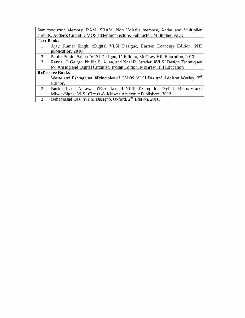
Semiconductor Memory, RAM, SRAM, Non Volatile memory, Adder and Multiplier circuits, Adder’s Circuit, CMOS adder architecture, Subtractor, Multiplier, ALU. Text Books
1 Ajay Kumar Singh, “Digital VLSI Design”, Eastern Economy Edition, PHI publication, 2010.
2 Partha Pratim Sahu,” VLSI Design”, 1st Edition, McGraw Hill Education, 2013. 3 Randall L.Geiger, Phillip E. Allen, and Noel R. Strader, “VLSI Design Techniques
for Analog and Digital Circuits”, Indian Edition, McGraw Hill Education. Reference Books
1 Weste and Eshraghian, “Principles of CMOS VLSI Design” Addison Wesley, 3rd Edition.
2 Bushnell and Agrawal, “Essentials of VLSI Testing for Digital, Memory and Mixed-Signal VLSI Circuits”, Kluwer Academic Publishers, 2002.
3 Debaprasad Das, “VLSI Design”, Oxford, 2nd Edition, 2016.

ANALOG FILTER DESIGN Course Code: MVD-112 Contact Hours: L-3 T-0 P-2 Course Category: DEC
Credits: 4 Semester: 2
Introduction: This course covers the techniques of modern signal processing that are fundamental to a wide variety of application areas. Special emphasis is placed on the architectures and design techniques for active and passive filters.
Course Objective: • To understand the active filter design • To explain the normalization, Frequency and impedance scaling. • Determination of the transfer functions of filters. • Frequency transformations, design of highpass, bandpass and band reject filters • Active‐RC realizations of the transfer function of the filter • To analyse the Elliptic (Cauer) approximation and filter design • Introduction of passive filter design • Design of doubly terminated passive LC ladder Cauer approximations • Active‐RC simulation of passive doubly terminated LC filters
Pre-requisite: Signals, Systems and Circuits, Operational amplifiers
Course Outcome: After successful completion of the course student will be able to • Understand the operation of electronic filters and describe them in the frequency
domain from their magnitude characteristics • Design lowpass, highpass, bandpass and band reject passive and active‐RC filters
with all‐pole and rational approximations using the appropriate mathematics or filter tables.
• Implement the software system simulation tools to verify filter specifications in the frequency domain
• Analyse software tools to design frequency selective electronic circuits. • Collaborate with fellow students in a team, in order to solve complex filter design
and implementation problems
Pedagogy: Learning modes will be PowerPoint slides, assignments and research paper discussion. To create a bridge between theory classes and practical to make the students understand better.
Contents
UNIT-I 10 Hours Monolithic filters, Digital filters, Analog discrete-time filters, Analog continous-time filters, Introduction to analog filters, CMOS filters descriptive terminology, Filter transmission, Types and specifications, Filter transfer function, Relationship among the

time domain, Frequency domain, s domain. UNIT-II 11 Hours
Active and passive filter synthesis. Standard low-pass approximations, Butterworth, Chebyshev, Inverse Chebyshev, Cauer, Bessel, Elliptical, Frequency transformations, First-order and Second order filter functions, Active filters, Inductor based filter, Two Integrator loop topology.
UNIT-III 11 Hours
Switched capacitor filters, Basic principle and practical circuits, Continuous type filters MOSFET-C, OTA-C filters, Implementation techniques towards low power supply voltages and low distortion, Frequency and time domain relationship, Pole and Zero locations.
UNIT-IV 10 Hours Filter synthesis for very high frequencies, Synthesis methods, Biquads, Gyrators, Generalized immittance converter (GIC), Inductor simulation using GIC, Introduction to Log-domain filters, Analog adaptive filters, Low voltage Analog filters in nanometer CMOS. Text Books 1 M. E. Van Valkenburg and Mac Elwyn Van Valkenburg, “Analog Filter Design” 1st
Edition, Oxford University Press, 2000. 2 Lawrence P. Huelsman, “Active and Passive Analog Filter Design: An Introduction,
volume 1”, 1st Edition, McGraw-Hill, 1993. 3 Williams and Fred Taylor, “Electronics Filter Design”, McGraw-Hill Education, 4th
Edition, 2006. Reference Books 1 Larry D. Paarmann, “Design and Analysis of Analog Filters: A Signal Processing
Perspective”, 1st Edition, Kluwer Academic Publishers, 2001. 2 Arthur B. Williams, “Analog Filter and Circuit Design Handbook” McGraw- Hill
Education, 2014. 3 Rolf Schaumann, Haiqiao Xiao, Mac E. Van Valkenburg, “Design of Analog Filters”,
2nd Edition, Oxford University Press, 2009.

DIGITAL TECHNIQUES FOR HIGH SPEED DESIGN Course Code: MVD 114 Contact Hours: L-3 T-1 P-0 Course Category: DEC
Credits: 4 Semester: 2
Introduction: Digital techniques for high speed design, is a subject that deals with the basic theory of different trends in high-speed design, backplane configurations, signal integrity and signaling technologies. Further this course will give some idea of memory signaling technologies, differential and mixed-mode parameters, simulation, verification and layout of high speed designs and advances in their modelling and design. Course Objective:
• To enhance the knowledge about the real challenges faced by the designers while preparing high speed designs.
• To meet thesignaling technologies of high speed devices as well as circuits. • To provide some idea of good design principles, and to simplify the process for
simulation, verification and layout of high speed designs. • To understand the in-depth knowledge of effects of various parameter’s variations on
the designed circuit. • To utilize the knowledge to design high speed designs as per the given specifications.
Course Outcomes: After successful completion of the course student will be able to • Understand the knowledge of different trends in high speed design. • Understand the memory signalling technologies. • Analyse all the differential and mixed mode S parameters needed to be considered in
time domain. • Understand the Advances in design, Modeling, Simulation and measurement
validation of high performance interconnects.
Pedagogy: Classroom teaching which focuses upon relating the textbook concepts with real world phenomena, along with periodic tutorial classes to enhance the problem-solving ability.
Contents
UNIT-I 10 Hours Trends in High-Speed Design, backplane configurations, SerDes technology, Signal integrity, Signaling technologies and devices, Gunning transceiver Logic, Low voltage differential signaling(LVDS), Bus LVDS, LVDS multipoint, High-speed transceiver logic and Stub-series terminated logic, ECL, Current-mode logic, FPGAs - 3.125 Gbps rocket IOs and Hard copy devices, Fiber optic components, High speed interconnects and cabling.
UNIT-II 11 Hours Memory device overview, memory signaling technologies, double data rate SDRAM (DDR, DDR2), GDDR3, ZBT, FCRAM, SigmaRAM, RLDRAM, DDR SRAM, Flash, FeRAM, and MRAM, Quad data rate SRAM, Direct Rambus DRAM(DRDRAM), Xtreme data rate DRAM, Flex Phase and ODR.
UNIT-III 10 Hours Differential and mixed-mode S parameters, Time domain reflectometry (TDR), Time

domain transmission (TDT) and VNAs, Modeling with IBIS, Overview of EDA Tools for high-speed design, simulation, verification and layout.
UNIT-IV 11 Hours Advances in design, Modeling, Simulation and measurement validation of high performance Board-to-Board 5-to-10 Gbps Interconnects, High-Speed Fiber-Optic transceivers, SerDes transceivers, serializers and deserializers, WarpLinkSerDes system, Emerging protocols and technologies, Electrical Optical Circuit Board, Rapid IO, PCI Express and express card. Text Books
1 Tom Granberg, “Handbook of Digital Techniques for High-Speed Design”, 1stEdition, Prentice hall, 2012
2 Stephen H. Hall and Howard L. Heck, “ Advance Signal Integrity for High speed Digital Designs”, Willy, IEEE Press, 2009.
Reference Books 1 Howard Johnson and Martin Graham, “High Speed Digital Design: A Handbook of
Black Magic”, 2nd Edition, Prentice Hall, 2000 2 Stephen H. Hall, Garrett W. Hall, & James A. McCall, “High speed Digital system
Design”, WILLY -IEEE Press, 2000.

CMOS MIXED-SIGNALS VLSI DESIGN Course Code: MVD 116 Contact Hours: L-3 T-0 P-2 Course Category: DEC
Credits: 4 Semester: 2
Introduction: The course will give practical aspect of mixed signal VLSI blocks such as comparators, data converters, oscillators and phase locked loop. As a part of this course, the students will use industry standard softwares and tools such as Cadence's Virtuoso schematic, Spectre simulator and MentorGraphics' Eldo and Calibre for post layout simulations along with the parasitic extractions. The design problems given in the form of assignments will be designed and simulated in a standard CMOS technology by students. The study will cover design issues on the PVT variations and statistical mismatches in temperature and process (MonteCarlo).
Course Objective:
• To understand the basic theory of analog circuits, design principles and techniques for analog ICs blocks implemented in CMOS technology.
• To explain the theory and design skills of CMOS op-amps, voltage reference circuits, switched capacitor circuits, sample-and- hold circuits, and A/D & D/A converters used in modern communication systems and consumer electronic products.
• To understand the design of core mixed-signal IC blocks: comparators and data converters and system level design flow: top-down and bottom-up design methodologies
Pre-requisite: Analog VLSI Design, VLSI Design
Course Outcome: After successful completion of the course student will be able to
• Understand analog and discrete-time signal processing • Undersatnd the basics of Analog to digital converters (ADC) and Digital to analog
converters (DAC). • Analyse High-speed ADCs (e.g. flash ADC, pipeline ADC and related architectures)
and successive approximation ADCs. • Understand the concept of High-resolution ADCs (e.g. delta-sigma converters). • Analyse Mixed-Signal layout and Interconnects. • Understand the Phase locked loops. • Demonstrate the ability to design practical circuits that perform the desired
operations.
Pedagogy: The class will be taught using theory and case based method. Since this is design course, students are given problems based on design of CMOS mixed signal circuits. Technology Discussion sessions are organized on current research challenges in design, their

relevance and applications in microelectronics industry. Design using CAD tools in CMOS design will also be done. To create a bridge between theory classes and practical to make the students understand better.
Contents
UNIT-I 10 Hours Analog and discrete-time signal processing, analog integrated continuous-time and discrete-time filters, Analog continuous-time filters, passive and active filters, basics of analog discrete-time filters and Z-transform.
UNIT-II 11 Hours Switched-capacitor filters, Nonidealities in switched-capacitor filters, switched capacitor filter architectures, switched capacitor filter applications, Basics of data converters, Successive approximation ADCs, Dual slope ADCs, Flash ADC, Pipeline ADC.
UNIT-III 11 Hours Hybrid ADC structures, high resolution ADC, DAC, Mixed signal layout, Interconnects and data transmission, Voltage-mode signaling and data transmission, Current-mode signaling and data transmission.
UNIT-IV 10 Hours Introduction to frequency synthesizers and synchronization, basics of (Phase Locked Loop)PLL, PLL implementation techniques, Digital and Analog PLL, performance parameters, Delay Locked Loop(DLL), characteristics, advantages over PLL, implementation techniques. Text Books 1 R. Jacob Baker, “CMOS mixed-signal circuit design”, 2ndEdition, John Wiley,
2009 2 BehadRazavi, “Design of analog CMOS integrated circuits”, McGraw-Hill, 2003. 3 R. Jacob Baker, “CMOS circuit design, layout and simulation” 2ndEdition, IEEE
press, 2008. Reference Books 1 Phillip E.Allen,Douglas R.Holberg,”CMOS Analog Circuit Design”,2nd
Edition,Oxford University Press,2002. 2 Gray, Hurst, Lewis, and Meyer, “Analysis and Design of Analog Integrated
Circuits”, 5thEdition Wiley, 2009. 3 Willy M.C. Sansen, “Analog Design Essentials”, International Edition, Springer,
2006.

ADVANCED EMBEDDED SYSTEM DESIGN Course Code: MVD 118 Contact Hours: L-3 T-0 P-2 Course Category: DEC
Credits: 4 Semester: 2
Introduction of machine learning course: Embedded system design needs knowledge of hardware as well as software concepts. This course will pay attention to introduce some of the basic concepts of hardware and software designing of embedded systems with a well motivated perspective. The course will cover embedded hardware architecture, design process and approaches, interfacing techniques, buses and protocols, hardware and software interrupts, embedded software programming, modelling of programs, inter-process synchronization and real time operating systems.
Course Objective:
• To develop the ability of solving real world problems. • To develop background knowledge and core expertise of microprocessor. • To know the importance of different peripheral devices and their interfacing to
microcontrollers. • To understand the concept of embedded systems. • To design various projects using the embedded system applications. • To understand the knowledge of machine learning concepts and various methods.
Course outcomes: After successful completion of the course student will be able to
• Understand the fundamental concepts that form the basis of hardware and software designing of embedded systems.
• Understands the widely used real time operating systems • Design and program a system, interfacing techniques. • Execute programs and software engineering practices of system design
Pedagogy: Classroom teaching which focuses upon relating the textbook concept with real world phenomenon, along with periodic lecture to enhance the problem-solving ability. To create a bridge between theory classes and practical to make the students understand better.
Contents
UNIT-I 10 Hours INTRODUCTION AND REVIEW OF EMBEDDED HARDWARE Terminology, Gates, Timing diagram, Memory , Microprocessor buses ,Direct memory access, Interrupts, Built interrupts, Interrupts basis, Shared data problems, Interrupt latency, Embedded system evolution trends, Round-Robin, Round Robin with interrupt function, Rescheduling architecture, algorithm.
UNIT-II 11 Hours REAL TIME OPERATING SYSTEM Task and Task states, Task and data, Semaphore and shared data operating system services, Message queues timing functions , Events , Memory management, Interrupt

routines in an RTOS environment , Basic design using RTOS. UNIT-III 10 Hours
EMBEDDED HARDWARE, SOFTWARE AND PERIPHERALS Custom single purpose processors: Hardware, Combination Sequence , Processor design, RT level design, optimizing software: Basic Architecture, Operation, Programmers view, Development Environment, ASIP, Processor Design, Peripherals, Timers, counters and watch dog timers, UART, Pulse width modulator, LCD controllers, Key pad controllers, Stepper motor controllers, A/D converters, Real time clock.
UNIT-IV 11 Hours MEMORY AND INTERFACING Memory write ability and storage performance, Memory types, composing memory, Advance RAM interfacing communication basic, Microprocessor interfacing I/O addressing, Interrupts, Direct memory access, Arbitration multilevel bus architecture, Serial protocol, Parallel protocols, Wireless protocols PROCESS MODELS AND HARDWARE SOFTWARE CO-DESIGN Modes of operation, Finite state machine, HCFSL and state charts language, state machine models, Concurrent process model, Concurrent process, Communication among process, Synchronization among process, Implementation, Data Flow model, Design technology, Automation synthesis, Hardware & software co-simulation, IP cores, Design Process Model. Text Books
1 David. E.Simon, “An Embedded Software Primer”, 1st Edition, Pearson Education, 2002.
2 Frank Vahid and Tony Gwargie, “Embedded System Design”, Student Edition,John Wiley & sons, 2006.
3 W. Wolf, Computers as Components: Principles of Embedded Computing System Design, 2nd Edition, Burlington, 2008.
Reference Books 1 Steve Heath, “Embedded System Design”, Elsevier, 2ndEdition, 2004 2 T Noergaard, Embedded Systems Architecture: A comprehensive Guide for
Engineers and Prgrammers, 2nd Edition, Newness, 2013. 3 Wireless communication Networks and internet of things, AdamuMurtalaZungeru
2018.

ANALOG INTEGRATED CIRCUITS Course Code: MVD-120 Contact Hours: L-3 T-1 P-0 Course Category: DEC
Credits: 4 Semester: 2
Introduction: Analog integrated circuit design is used for designing operational amplifiers, linear regulators, oscillators, active filters, and phase locked loops. The semiconductor parameters such as power dissipation, gain, and resistance are more concerned in the designing of analog integrated circuit.
Course Objective:
• To understand the theoretical & circuit aspects of Op-amp, which is the backbone for the basics of linear integrated circuits
• To perform analysis of circuits based on linear integrated circuits. • To design circuits and systems for particular applications using linear integrated
circuits. • Fundamentals of analog and digital integrated circuits.
Pre-requisite: Knowledge of mathematics on secondary education level (operations with fractions, solving system of the linear equations, algebraic handling with equations) and electronics (principles of the passive elements, describe simple circuit by using differential equations).
Course Outcome: After successful completion of the course student will be able to • Understand fundamental properties of the electronic filters in time and frequency
domain. • Design passive as well as active filter for particular application including calculation
of the values of circuit elements. • Understand the differences between theoretical, practical & simulated results in
integrated circuits. • Interpret function of the crystal filters and structures with switched capacitors • Analyse and design filtering networks.
Pedagogy: Learning modes will be PowerPoint slides, assignments and research paper discussion.
Contents
UNIT-I 10 Hours Signals, Information, Interference and noise, signal classification, Dynamic range, S/N ratio, Functions in analog signal processing, Linear non-linear functions, Impedance adaptation, Amplitude and level matching, Terminal matching, Buffering filtering, Linearization, Domain conversions, Errors in analog signal processing,
UNIT-II 11 Hours Voltage amplification, Practical voltage amplifiers, Effects of finite input impedances,

Building blocks for voltage amplifiers, Current to voltage and voltage to current conversion, Current Integrators, Mirrors, Amplifiers, and Conveyors.
UNIT-III 11 Hours
CMOS analog integrated circuits, Analog building blocks, Op-amp design, Practical opamp characteristics and model, DC offset and DC bias currents, Gain, bandwidth and slew rate, Noise, Input stage, Output stage, CMOS OTA, Ideal model, OTA building block circuits, Design of simple OTA.
UNIT-IV 10 Hours Signal rectifications, AC/DC conversion, CMOS implementation of Adder, Subtractor, Squarer, Analog Multiplier, Analog Dividers, Differentiator and Integrator circuits, Impedance transformation and conversion, Analog multiplexers. Text Books 1 Pallas Areny and John G.Webster, “Analog Signal Processing”, Student Edition,
John Wiley, 2011. 2 Tlelo-Cuautle and Esteban, “Integrated Circuits for Analog Signal Processing”, 1st
Edition, Springer, 2013. 3 Behzad Razavi, “Design of Analog CMOS Integrated Circuits”, 2nd Edition,
McGraw Hill, 2017. Reference Books 1 Ismail, Mohammed and Sawan, Mohamad, “Analog Circuits and Signal
Processing”, The Springer International Series in Engineering and Computer Science, 2012.
2 M.Ismail and T. Fiez, “Analog VLSI Signal and Information Processing”, 2nd Edition, McGraw Hill, 2000.
3 Tahira Parveen, “Textbook of Operational Transconductance Amplifier and Analog Integrated Circuits”, I.K International Publishing house Pvt. Ltd, 2013.

Introduction: This course will teach the basics and advance topics of verilog digital system design
Course Objective: This course will enable students to:
• Understand the concepts of Verilog Language. • Design the digital systems as an activity in a larger systems design context. • Study the design and operation of semiconductor memories frequently used in
application specific digital system. • Inspect how effectively IC’s are embedded in package and assembled in PCB’s for
different application. • Design and diagnosis of processors and I/O controllers used in embedded systems. • Design embedded systems using small microcontrollers, larger CPUs/DSPs, or hard
or soft processor cores. • Synthesize different types of processor and I/O controllers that are used in embedded
system.
Pre-requisite: Any programming language.
Course outcomes: After successful completion of the course student will be able to
• Understand and construct the combinational circuits, using discrete gates and programmable logic devices.
• Design Verilog model for sequential circuits and test pattern generation. • Design a semiconductor memory for specific chip design. • Understand the memory designs.
Pedagogy: Learning modes will be PowerPoint slides, assignments and research paper discussion. To create a bridge between theory classes and practical to make the students understand better.
Contents
UNIT-I 10 Hours Digital Systems and Embedded Systems, Real-World Circuits, Models, Design Methodology, Hierarical design flow, Designing Hardware with software. Memories: Concepts, Memories types, Error Detection and Correction.
UNIT-II 11 Hours Combinational Basics: Combinational Components and Circuits, Verification of Combinational Circuits, Sequential Basics: Sequential Datapaths and Control Clocked Synchronous Timing Methodology. SM Charts: Concept, Derivation of SM Charts, Realization of SM Charts.
UNIT-III 11 Hours Implementation Fabrics: Integrated Circuits, Programmable Logic Devices, Packaging and Circuit boards, Interconnection and Signal integrity, I/O interfacing: I/O devices, I/O controllers, Parallel Buses, Serial Transmission, I/O software.
DIGITAL SYSTEM DESIGN USING VERILOG Course Code: MVD-122 Contact Hours: L-3 T-0 P-2 Course Category: DEC
Credits: 4 Semester: 2

UNIT IV 10 Hours Design Methodology: Design flow, Design optimization, Design for testability, HDL based Synthesis-technology independent design, Styles for synthesis of combinational and sequential logic Text Books 1 Peter J. Ashenden, “Digital Design: An Embedded Systems Approach Using
VERILOG”, Elesvier, 2010. 2 Samir palnitkar, “Verilog HDL, A Guide to Digital Design and Synthesis”, 2ndedition,
Prentice Hall, 2003 Reference Books 1 Nazeih Botros ,”HDL Programming Fundamentals :VHDL and Verilog” ,
Dreamtech Press,2006 2 Vaibbah Taraate ,”Digital logic design using Verilog” ,Springer, 2016 3 John Williams ,”Digital VLSI design with Verilog” , 2nd Edition, Springer, 2008

Introduction: This course teaches basics of MEMS, with emphasis on MEMS sensors
Course Objective: The objective of this course is
• To understand basic knowledge on overview of MEMS (Micro electro Mechanical System) and various fabrication techniques.
• To study the design, analysis, fabrication and testing the MEMS based components. • To understand various opportunities in the emerging field of MEMS. • To study and implement various applications of MEMS.
Pre-requisite:Electronic circuits, basic knowledge of material science, Basic physics, chemistry, electronics and mechanics at the sophomore level. Understanding of basic physics. Understanding of engineering materials of basic level. Understanding of electronics and semiconductors to the basic semiconductors and electronics.
Course Outcome: After successful completion of the course student will be able to
• Understand new applications and directions of modern engineering. • Apply the techniques for building microdevices in silicon, polymer, metal and other
materials. • Understand the physical, chemical, biological, and engineering principles involved in
the design and operation of current and future micro devices. • Analyze microsystems technology for technical feasibility as well as practicality. • Describe the limitations and current challenges in microsystems technology.
Pedagogy:Learning modes will be PowerPoint slides, assignments and research paper discussion.
Contents
UNIT-I 10 Hours Introduction to MEMS & Microsystems, Introduction to Microsensors, Evaluation of MEMS, Microsensors, Market survey, application of MEMS, MEMS Material, MEMS materials properties, microelectronics technology for MEMS, micromachining technology for MEMS.
UNIT-II 11Hours Micromachining process, Etch stop techniques and microstructure, surface and quartz Micromachining fabrication of micromachined microstructure, Microstereolithography MEMS microsensors, thermal micromachined microsensors, Mechanical MEMS, Pressure and flow sensor, Micromachined flow sensors, MEMS inertial sensors.
UNIT-III 11 Hours
MEMS AND MICROSYSTEMS Course Code: MVD 124 Contact Hours: L-3 T-1 P-0 Course Category: DEC
Credits: 4 Semester:2

Micromachined microaccelerometers for MEMS, MEMS accelerometers for avionics, Temperature drift and damping analysis, Piezoresistive accelerometer technology, MEMS capacitive accelerometer, MEMS capacitive accelerometer process.
UNIT IV 10 Hours MEMS gyro sensor, MEMS for space application, Polymer MEMS & carbon nano tubes(CNT),Wafer bonding & packaging of MEMS, Interface electronics for MEMS, MEMS for biomedical application (Bio-MEMS) . Text Books
1 Adams, Thomas M., Layton, Richard A.,” Introductory MEMS: Fabrication and Applications”, Springer, 2010.
2 MinhangBao,”Analysis and design principles of MEMS device”, 1st Edition, Elsevier Science, 2005.
Reference Books 1 Tai-Ran Hsu, “MEMS and Microsystems: Design and Manufacture”, 1st Edition,
McGraw-Hill, 2002. 2 Ghodssi, Reza: Lin, Pinyen, “MEMS Materials and Processes Handbook”, 1st
Edition, Springer, 2011. 3 Mohamed Gad-el-Hak, “MEMS: Introduction and Fundamentals”, 1st Edition,
Taylor and Francis, 2006. 4 Jan Korvink and Oliver Paul, “MEMS: A Practical Guide to Design, Analysis and
Applications”, 1st Edition, Springer, 2006.

Introduction: Internet of Things is currently a hot technology across the globe. It has a vast application domain which includes agriculture, space, healthcare and manufacturing. IoT based applications such as innovative shopping system, infrastructure management in both urban and rural areas, remote health monitoring and emergency notification systems and transportation systems are gradually relying on IoT based systems. Wide application domain necessitates learning of the emerging technology. The course covers the following areas Internet in general and Internet of Things: layers, protocols, packets, services, performance parameters of a packet network as well as applications
Course Objective: The purpose of this course is
• To understand the knowledge on IoT architecture and various protocols, study their implementations.
• To explain in a concise manner how the general Internet as well as Internet of Things work.
• To understand constraints and opportunities of wireless and mobile networks for Internet of Things.
• To use basic measurement tools to determine the real-time performance of packet based networks.
• Analyse trade-offs in interconnected wireless embedded sensor networks.
Pre-requisite: Basic programming knowledge
Course Outcome: After successful completion of the course student will be able to
• Understand the Architectural Overview of IoT. • Understand the IoT Reference Architecture and Real World Design Constraints. • Understand the various IoT Protocols (Data link, Network, Transport, Session, and
Service). • Design and implement the security protocols on IoT based circuits.
Pedagogy:The course Internet of things has been designed to enable the student to understand constraints and opportunities of wireless and mobile networks for Internet of Things. A variety of teaching and learning tools may be employed including readings, videos, discussion, and simulations. Complete and actively participate in weekly discussions with timely initial posts and responses. Completion of other course assignments.
Contents
UNIT-I 11Hours IoT-An Architectural Overview– Building an architecture, Main design principles and needed capabilities, An IoT architecture outline, standards considerations. M2M and IoT Technology Fundamentals- Devices and gateways, Local and wide area networking, Data
INTERNET OF THINGS Course Code: MVD 126 Contact Hours: L-3 T-1 P-0 Course Category: DEC
Credits: 4 Semester: 2

management, Business processes in IoT, Everything as a Service (XaaS), M2M and IoT Analytics, Knowledge Management.
UNIT-II 11Hours IoT Architecture-State of the Art – Introduction, State of the art, Reference Model and architecture, IoT reference Model - IoT Reference Architecture, Introduction, Functional View, Information View, Deployment and Operational View, Other Relevant architectural views. Real-World Design Constraints- Introduction, Technical Design constraints-hardware is popular again, Data representation and visualization, Interaction and remote control.
UNIT-III 10Hours PHY/MAC Layer(3GPP MTC, IEEE 802.11, IEEE 802.15), Wireless HART,Z-Wave, Bluetooth Low Energy, Zigbee Smart Energy, DASH7 - Network Layer-IPv4, IPv6, 6LoWPAN, 6TiSCH,ND, DHCP, ICMP, RPL, CORPL, CARP.
UNIT-IV 10Hours Transport Layer (TCP, MPTCP, UDP, DCCP, SCTP)-(TLS, DTLS) – Session Layer-HTTP, CoAP, XMPP, AMQP, MQTT ,Service layer Protocols & Security, Service Layer -oneM2M, ETSI M2M, OMA, BBF – Security in IoT Protocols – MAC 802.15.4 , 6LoWPAN, RPL, Application Layer. Text Books
1 Jan Holler, Vlasios Tsiatsis, Catherine Mulligan, Stefan Avesand, Stamatis Karnouskos, David Boyle, “From Machine-to-Machine to the Internet of Things: Introduction to a New Age of Intelligence”, 1st Edition, Academic Press, 2014.
2 Peter Waher, “Learning Internet of Things”, PACKT publishing, 2015 3 RajkumarBuyya, Amir Vahid Dastjerdi ,”Internet of Things: Principles and
paradigms”,Elsevier, 2016 Reference Books
1 Daniel Minoli, “Building the Internet of Things with IPv6 and MIPv6: The Evolving World of M2M Communications”, Wiley Publications,2013.
2 Vijay Madisetti and Arshdeep Bahga, “Internet of Things (A Hands-on Approach)”, 1st Edition, Universities Press, 2015.
3 Qusay F Hassan ,”Internet of Things A TO Z: Technologies and Applications “, Wiley Publication,2018

ASIC and SoC Design Course Code: MVD-201 Contact Hours: L-3 T-0 P-2 Course Category: DCC
Credits: 4 Semester: 3
Introduction:A current-day system on a chip (SoC) consists of several different processor subsystems together with memories and I/O interfaces. This course covers SoC design and modelling techniques with emphasis on power consumption and partition of functionality between hardware and software. Study of high-level modelling techniques for rapid architectural exploration and assertion-driven design for correctness will be an integral part of the course. Course Objective:
To familiarize the student with ASIC. Introduction of SOC, NoC architectures. To introduce students with Intellectual Property(IP) based design, Floor planning
methods and design. Understand the hardware and software structures used to implement and model inter-
component communication in such devices. Understand the concept of pipelining and Subsystem optimization.
Pre-requisite: Basic Digital Design/ Digital Logic, basic VLSI technology.
Course Outcome: Having successfully completed this course, the student will be able to
Learn Placement, floor planning & pin assignment floor planning algorithms for mixed block & cell design understand Global Routing, problem formulation, classification of global routing algorithms.
Understand the various components of system on chip. Analyze partitioning and floor planning algorithms. Learn to design Combinational circuits. Understand the concept of physical verification and hardware software co-simulation. Understand the difference between SOC, ASIC, NoC.
Pedagogy: This class focuses on the major design tools used in the creation of an Application Specific Integrated Circuit (ASIC) or System on Chip (SoC) design.Learning modes will be PowerPoint slides, assignments and research paper discussion.
Contents
UNIT-I 10 Hours
Moore’s Law, technology node, ITRS, VLSI and systems, cost of design, types of chips, Specialized standard parts, Introduction to ASICs, types of ASICs, design flow, Economics of ASICs, ASIC Library Design – Transistor parasitic capacitance, Logical Effort, Library Cell Design and Library Architecture, IC design techniques, Hierarchical Design, Design Abstraction, Computer-Aided Design, IC design flow, Chips and their subsystems, Combinational Shifter, Adder, ALU, Multiplier, high density Memory, Image sensor.
UNIT-II 10 Hours
FPGA, Programmable logic array, Buses and Networks-on-Chips, Data Paths, Subsystem optimization, pipelining, Configurable Logic, FPGA Organization, Accelerated system architecture, Soft Core and Hard Core Approach, Design and Architecture considerations. Introduction to Network-on-Chip and Buses, Trends, NoC Architecture. Intellectual property (IP)-based design, IP types, IP Across the Design Hierarchy, The IP Life Cycle, Creating IP, Using IP, VLSI subsystems as IP.

UNIT-III 12 Hours ASIC construction, Physical Design, CAD Tools, System Partitioning, FPGA partitioning, partitioning methods, Introduction to Floor planning, Floor planning methods, Global Interconnect, Floor plan Design, Off-Chip Connections, Placement, Physical Design Flow, Routing- Global routing, Detailed routing, Special routing, Circuit extraction & DRC.
UNIT-IV 10 Hours ASIC Design flow, Systems-on-chips and embedded CPUs, SoC design flow, Difference between SoC and SIP or SoPC, SoC, - Evolution, Design, Features, SoC Design requirement, challenges and practices, Platform based SoC, OMAP, Configurable SoC, Multiprocessor System-on-Chip Design.
Text Books: 1 M.J.S Smith, “Application-Specific Integrated Circuits”, 1st Edition, Addison Wesley
Longman Inc.1997. 2 Wayne Wolf, “Modern VLSI design: System –on- Chip Design”, 3rd Edition, Pearson,
2002. 3 Steve Furber,”ARM System-on-Chip Architecture”, 2nd Edition, Pearson, 2000. Reference Books: 1 Wayne Wolf,” Modern VLSI design: IP-Based Design”, 4th Edition, Pearson, 2008. 2 Keith Barr,” ASIC Design in the Silicon Sandbox: A Complete Guide to Building Mixed
Signal Integrated Circuits”, 1st Edition, McGraw Hill, 2008.

Low power VLSI Design Course Code: MVD-203 ContactHours: L-3 T-0 P-2 Course Category:DEC
Credits: 4 Semester: 3
Introduction: The course offers important topics for Low power VLSI design. As the technology node scales down, there is not much increase in battery technology. Design for low-power implies the ability to reduce all components of power consumption in CMOS digital/analog circuits during the development of a low power electronic product.
Course Objective:
Understand the design, analyze, model and simulate the low power CMOS circuits. Implement the design methodology and understand the experiment of thesubject. Test the hand calculations using simplemodels. Understand that Low power design not only needed for portable applications but also to
reduce the power of high performance systems.
Pre-requisite: Analog Integrated Circuits, Digital Integrated Circuits.
Course Outcome: The student will be able to:
Apply knowledge of mathematics, science and engineering to design and analysis of low
power analog/digital integrated circuits for givenspecifications.
Identify, formulates, and solves engineering problems in the area of low power design.
Analyze and understand power management in electronic circuits Understand Low voltage analog circuit design techniques and modern programming tools
such as Cadence, necessary for engineeringpractice.
Pedagogy: The class will be taught using theory and case based method. Students are given problems based on design of low power CMOS circuits. Technology discussion sessions are organized on current research challenges in design, their relevance and applications in microelectronics industry. Design using CAD tools in low power CMOS design will also be done.
Contents
UNIT-I 11 Hours
Introduction, Battery technology summary, Sources of CMOS power consumption, Need for low power VLSI chips, Dynamic power, Static power, Switching power, Computing power versus Chip power, SOI and Bulk technology.
UNIT-II 10 Hours Impact of technology Scaling - Technology and Device, transistor sizing, gate oxide thickness, Technology options for low power, design options for power reduction, architectural level approaches, voltage scaling, power management, Circuit level approaches, Low power digital cells library.
UNIT-III 11 Hours Low power Analog integrated circuits, Challenges in low voltage analog circuit design, Issues about low power supply voltage. Basic building blocks in analog design, Cascode structure, Selfcascode structure, Voltage follower, Flipped voltage follower.

UNIT-IV 10 Hours Low voltage analog circuit design techniques, Roadmap, Design of analog circuits using low voltage implementation techniques, Classification of body bias techniques, Dynamic Threshold MOSFET, Bulk driven technique, Floating Gate MOSFET, Subthreshold analog circuits Text Books: 1 Gary K. Yeap, Farid N. Najm, “Low power VLSI design and technology”, 1st Edition,
World Scientific Publishing Ltd.,2004. 2 Rabaey, Pedram, “Low power design methodologies”, 2nd Edition, Kluwer Academic,
2004 Reference Books: 1 Kaushik Roy, Sharat Prasad,“Low-Power CMOS VLSI Circuit Design”, 2nd Edition,
Wiley, 2008. 2 Christian Piguet, “Low-power CMOS circuits: technology, logic design and CAD tools”,
1st Edition, Taylor & Francis Group, 2006.

VLSI Design Verification and Test Course Code: MVD-205 ContactHours: L-3 T-1 P-0 Course Category:DEC
Credits: 4 Semester: 3
Introduction: The course offers important topics for VLSI Design Verification and Test. It covers Predictive analysis to ensure that the synthesized design, when manufactured, will perform the given I/O function. Test: A manufacturing step that ensures that the physical device, manufactured from the synthesized design, has no manufacturing defects. Course Objective:
Introduction to the concepts and techniques of VLSI design verification and testing. Details of test economy. Understand fault modeling and simulation and defects. Use of Automatic Test Pattern Generation (ATPG) and design for testability. Pre-requisite: Verilog Programming
Course Outcome: The student will be able to:
How Verification is done before silicon development.
Product development for quality checking and bug fixing in design.
Various type of verification, like IP verification, RTL verification, timing verification etc. Testing level to validate the quality of silicon.
Finding Bug at validation level and how to fix.
Pedagogy: The class will be taught using theory and case based method. Students are given problems based on design of VLSI Design Verification and Test. Technology discussion sessions are organized on current research challenges in design, their relevance and applications in microelectronics industry.
Contents
UNIT-I 11 Hours
Introduction to digital VLSI Design flow, Design Representation, 3 Hardware Specific Transformations, Scheduling, Allocation and Binding, High level Synthesis, Verilog RTL Design, Combinational and Sequential Synthesis Logic Synthesis.
UNIT-II 11 Hours Logic Optimization, Technology Mapping, Introduction to Hardware Verification and methodologies, Binary Decision Diagrams, construction, Reduction rules and Algorithms, Temporal Logic, Basic Operators, Syntax and Semantics of LTL, CTL and CLT.
UNIT-III 10 Hours Equivalence and Expressive Power, Combinational equivalence checking, Introduction to verification, Modeling sequential systems, Model checking algorithm, Symbolic model checking, Automata and its use in Verification, Automata Theoretic Model Checking.

UNIT-IV 10 Hours VLSI Testing, Introduction, Test process, Test economics, Testing Defects, Errors, Fault models, Fault Simulation, Test generation for combinational circuits, Introduction to Automatic Test Pattern Generation, ATPG Algebras, Test generation algorithms for sequential circuits and Built in self-test. Text Books: 1 D. D. Gajski, N. D. Dutt, A.C.-H. Wu and S.Y.-L. Lin, “High-Level Synthesis:
Introduction to Chip and System Design”, paperback Edition, Springer, 2012. 2 S. Palnitkar, “Verilog HDL: A Guide to Digital Design and Synthesis”, Prentice Hall, 2nd
Edition, 2003 Reference Books: 1 G. De Micheli, “Synthesis and optimization of digital circuits”, McGraw-Hill, TMH
Edition, 2003. 2 M. Huth and M. Ryan, “Logic in Computer Science modeling and reasoning about
systems”, Cambridge University Press, 2nd Edition, 2004.

Advance Image Processing Course Code: MVD-207 ContactHours: L-3 T-0 P-2 Course Category:DEC
Credits: 4 Semester: 3
Introduction: This course introduces the design and implementation of algorithms that perform basic image processing as noise removal and image enhancement as well as describes the image segmentation methods. This course will cover algorithms for advanced image analysis defines the applications in area of medical image processing. The course is primarily meant to develop on-hand experience in applying tools to process the images. Hence the programming assignments form a key component of this course.
Course Objective:
Students will be able to understand the basic principles and advanced concepts of digital image processing.
To implement algorithms that perform basic image processing operations like filtering of noise and image enhancement.
To design, analyze and implement algorithms for advanced image analysis like image compression, image reconstruction, image segmentation.
To enable students to implements solutions for complex image processing problems. To explore the different applications of medical image processing for MRI, X-ray
and CT scan images.
Pre-requisite: Basic knowledge of Digital Signal Processing, basic Python programming language.
Course Outcome: The student will be able to:
Examine various types of images, intensity transformations and applying various filtering techniques.
Identify the suitable image enhancement and restoration techniques based upon the application.
Show how higher-level image concepts such as edge detection, segmentation, representation can be implemented and used.
To manipulate both binary and gray scale digital images using morphological filters and operators to achieve a desired result.
Filter given image using spatial and frequency domain filtering technique. Apply image processing algorithms in practical applications.
Pedagogy: Learning modes will be PowerPoint slides, assignments and research paper discussion. To create a bridge between theory classes and practical to make the students understand better. Students will be introduced to various practical image processing techniques through different programming skills like basic Python coding language.

Contents
UNIT-I 11 Hours Introduction: Fundamentals of Digital Image Processing, Components of digital image processing system, Brightness adaptation and discrimination, light, Image sensing and acquisition, Image formation model, definition and some properties of two dimensional system. Spatial and gray level resolution, Zooming and shrinking, some basic relationships between pixels. Discrete 2D convolution, 2D discrete Fourier transform and its properties, Spectral density function. Sampling and quantization of images. Gray level transformations, Smoothing and sharpening spatial filters, Smoothing and Sharpening frequency domain filters.
UNIT-II 10 Hours
Image Restoration:Model of image degradation/ Restoration process, Noise models, Noise reduction in spatial domain and frequency domain, Adaptive filtering, Inverse filtering, Wiener filtering. Morphological Image processing: Basics, SE, Erosion, Dilation, Opening, Closing, Hit-or-Miss Transform, Boundary Detection, Hole filling, Connected components, convex hull, thinning, thickening, skeletons, pruning, Geodesic Dilation, Erosion, Reconstruction by dilation and erosion.
UNIT-III 10 Hours Image Segmentation:Edge detection, Thresholding, Otsu’s thresholding, Region growing, Fuzzy clustering, Watershed algorithm, Active contour methods, and Texture feature based segmentation, Wavelet based segmentation methods.
UNIT-IV 11 Hours Image Processing applications: Study of various formats of medical images, Study of medical images in X-ray, MRI, CT imaging, Medical image enhancement and filtering. Medical image segmentation methods.
Text Books:
1 Gonzalez. R.C & Woods. R.E “Digital Image Processing”, 4th edition, Pearson Education, 2018.
2 Anil K. Jain,”Fundamentals of Digital Image Processing”, Pearson, 2002.
Reference Books:
1 Kenneth R. Castleman,“Digital Image Processing”, Pearson, 2006.
2 Geoff Dougherty,“Digital Image Processing for Medical Applications”, Cambridge University Press; South Asian edition, 2010.
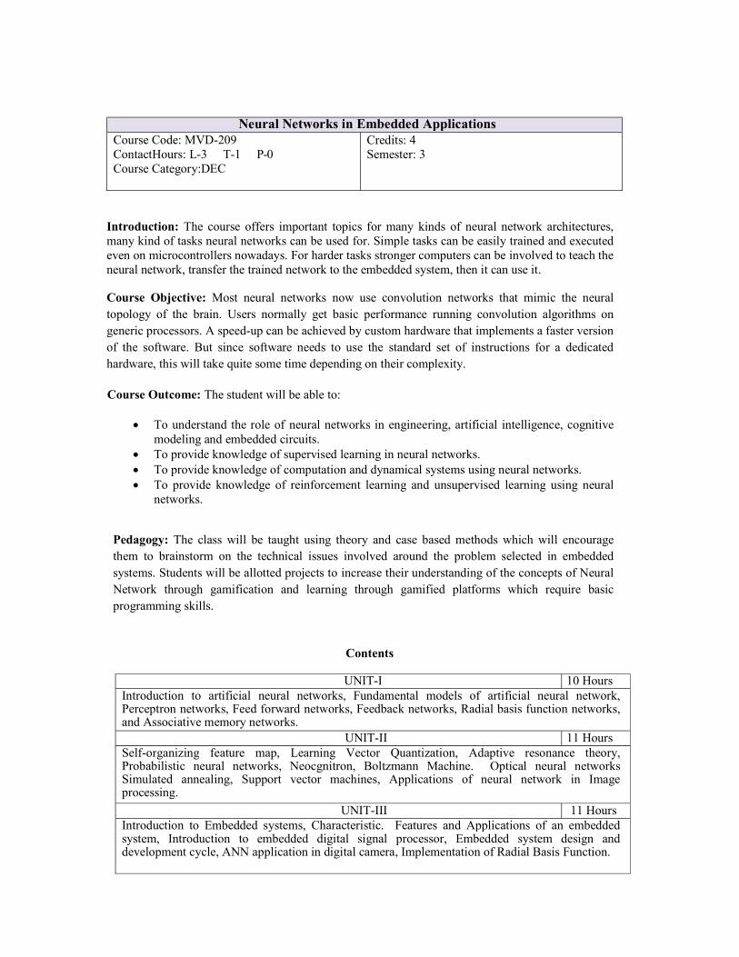
Neural Networks in Embedded Applications Course Code: MVD-209 ContactHours: L-3 T-1 P-0 Course Category:DEC
Credits: 4 Semester: 3
Introduction: The course offers important topics for many kinds of neural network architectures, many kind of tasks neural networks can be used for. Simple tasks can be easily trained and executed even on microcontrollers nowadays. For harder tasks stronger computers can be involved to teach the neural network, transfer the trained network to the embedded system, then it can use it.
Course Objective: Most neural networks now use convolution networks that mimic the neural topology of the brain. Users normally get basic performance running convolution algorithms on generic processors. A speed-up can be achieved by custom hardware that implements a faster version of the software. But since software needs to use the standard set of instructions for a dedicated hardware, this will take quite some time depending on their complexity.
Course Outcome: The student will be able to:
To understand the role of neural networks in engineering, artificial intelligence, cognitive modeling and embedded circuits.
To provide knowledge of supervised learning in neural networks. To provide knowledge of computation and dynamical systems using neural networks. To provide knowledge of reinforcement learning and unsupervised learning using neural
networks.
Pedagogy: The class will be taught using theory and case based methods which will encourage them to brainstorm on the technical issues involved around the problem selected in embedded systems. Students will be allotted projects to increase their understanding of the concepts of Neural Network through gamification and learning through gamified platforms which require basic programming skills.
Contents
UNIT-I 10 Hours Introduction to artificial neural networks, Fundamental models of artificial neural network, Perceptron networks, Feed forward networks, Feedback networks, Radial basis function networks, and Associative memory networks.
UNIT-II 11 Hours Self-organizing feature map, Learning Vector Quantization, Adaptive resonance theory, Probabilistic neural networks, Neocgnitron, Boltzmann Machine. Optical neural networks Simulated annealing, Support vector machines, Applications of neural network in Image processing.
UNIT-III 11 Hours Introduction to Embedded systems, Characteristic. Features and Applications of an embedded system, Introduction to embedded digital signal processor, Embedded system design and development cycle, ANN application in digital camera, Implementation of Radial Basis Function.

UNIT-IV 10 Hours Neural Network on embedded system: Real time face tracking and identity verification, Overview of design of ANN based sensing logic and implementation for fully automatic washing machine.
Text Books: 1. S N Sivanandam, S Sumathi, S N Deepa, “Introduction to Neural Networks Using Matlab
6.0,” Tata McGraw Hill Publication, 2005. 2. Simon Haykin, “Neural Networks: Comprehensive foundation,” 2nd edition, Prentice Hall
Publication, 1998. 3. Satish Kumar, “Neural Networks: A Classroom Approach”, 2nd edition, McGraw Hill
Education, 2017. Reference Books: 1. Frank Vahid, TonyGivargis, “Embedded System Design A unified Hardware/ Software
Introduction,” student edition, Wiley India Pvt. Ltd, 2006. 2. Rajkamal, “Embedded Systems Architecture, Programming and Design,” Tata McGraw-
Hill, 2003. 3. MohamadHassoun, “Fundamentals of Artificial Neural Networks”, MIT Press, 2003.

Nature Inspired VLSI Circuits Course Code: MVD-211 ContactHours: L-3 T-1 P-0 Course Category:DEC
Credits: 4 Semester:3
Introduction: The course offers unique approach for studying, analyzing, designing, and implementing VLSI circuits through perception, reasoning and action mimicking the nature. Such circuit technology covers various aspects of nature-inspired VLSI circuit design techniques, such as the design rule bases, design principles, computing and information processing algorithms, sensing and interfacing techniques.
Course Objective:
Understand the concepts of Physical Design Process such as partitioning,Floorplanning, Placement and Routing.
Discuss the concepts of design optimization algorithms and their application to physical design automation.
Study, analyze, design, and implement VLSI circuits through perception, reasoning and action mimicking the nature.
Understand the application of nature inspired algorithms in the field of VLSI.
Pre-requisite:Analog Electronics I and II, Linear Integrated Circuits Course Outcome: The student will be able to:
Analyze and design MOS Amplifiers Analyze physical design problems and employ appropriate automation algorithms
for partitioning, floor planning, placement and routing. Solve the performance issues in circuit layout. Decompose large mapping problem into pieces, including logic optimization with
partitioning, placement and routing.
Pedagogy: Lectures and problem-based learning techniques will be included. Learning through research will be one of the key methods. Technological Discussions related to current research challenges in design, their relevance and applications in microelectronics industry will be included.
Contents
UNIT-I 10 Hours Introduction to Optimization, Convex Optimization, Concave Optimization, KKT Lagrange Multipliers, NP Completeness: NP, P, NP Complete, NP Hard Problems, Evolutionary Nature Inspired Algorithms.
UNIT-II 11 Hours Introduction to Metaheuristic, Classification of Metaheuristics: Local Search vs Global Search, Single Solution vs Population Based, Hybridization and Memetic Algorithms, Parallel Metaheuristics, Nature inspired and Metaphor Based Metaheuristics, Application of Metaheuristics in the Area of VLSI.
UNIT-III 11 Hours Nature Inspired Algorithms: Simulated Annealing, Genetic Algorithm, Cuckoo Search, Differential Evolution, Ant and Bee Algorithms, Particle Swarm Optimization, The Firefly

Algorithm, The Bat Algorithm, Harmony Search, The Flower Algorithm. MOSFET device structure and its operation, Biasing, Small signal equivalent circuit model, MOS internal capacitance and High frequency model, Frequency response, Noise Spectrum, Thermal and Flicker noise, Noise bandwidth, Noise figure, Feedback and its effect, Compensation Techniques, VLSI Design Cycle.
UNIT-IV 10 Hours Genetic Algorithm for VLSI: Introduction to GA Technology, Simple GA algorithm, Steady State Algorithm, Selection, Crossover, Mutation, Fitness Scaling, Inversion, GA for VLSI Design, Layout and Test automation, Partitioning, Automatic Placement, Automatic Routing, Technology mapping for FPGAs, Automatic test generation, Genetic Multiway Partitioning.
Text Books: 1 Xin-She Yang, “Nature-Inspired Optimization Algorithms”, 1st Edition, Elsevier, 2014.
2 S.H. Gerez, “Algorithms for VLSI Design Automation”, John Wiley, 1998. 3 BehzadRazavi, “Design of Analog CMOS Integrated Circuit”, 2ndEdition, Tata McGraw Hill,
2017. Reference Books: 1 N.A.Sherwani“Algorithms for VLSI Physical Design Automation”, 3rd Edition, Kluwer,2005.
2 Randy L. Haupt, Sue Ellen Haupt, "Practical Genetic Algorithms" 2nd Edition, John Wiley &Sons, 2004
3 Hongjiang Song, “Nature-Inspired VLSI Circuits - From Concept to Implementation”, 1st Edition, Hongjiang Song, 2019.

VLSI Interconnects
Course Code: MVD-213 Hours: L-3 T-1 P-0 Course Category:DEC
Credits: 4 Semester: 3
Introduction: The course offers important topics for VLSI Interconnects. It covers description of types of interconnects, modeling of interconnects, delays and crosstalk in interconnects and brief introduction to the testing of logic circuits.
Course Objective:
To sketch the equivalent circuit of interconnect using transmission line theory.
Understand the concept of designing and modeling of VLSI interconnects.
Detailed study of effect of crosstalk noise and delay in electrical signal transmission through interconnects.
Techniques that can be adopted to mitigate the effect of crosstalk noise and delay in electrical signal transmission via VLSI interconnects.
Pre-requisite: Electromagnetic field theory, Basic concepts of circuit theory, Basic CMOS design.
Course Outcome:
Knowledge and understanding of drawing equivalent circuit of interconnects
Complete understanding of designing and modeling of VLSI interconnects Identify, formulates, and solves engineering problems in the area of VLSI
interconnects. Knowledge and understanding of reducing crosstalk noise and delay in Electrical
circuits through simulation in VLSI interconnects
Pedagogy: The course involves the use of a coordinated set of lectures, homework, power point presentations and exams to teach VLSI interconnect concepts. Students will be given problems based on electrical circuits to form their equivalent VLSI interconnects.Exposure to advanced VLSI interconnects used for better performance of circuits.
Contents
UNIT-I 10 Hours
Introduction to VLSI interconnects classification, Cu interconnection and dual damascene structure, stress void and electromigration phenomenon, Signal transmission on interconnects, On-chip interconnections, Packagelevelinterconnections.
UNIT-II 11 Hours Analog VLSI Interconnects, physics of interconnects in VLSI, scaling of interconnects, Model for estimating wiring density, configurable architecture for prototyping analog circuits, Interconnect modeling, physical foundations for circuit models of interconnections, Loss and Lossless transmission line model, Optimum linemodelselection .
UNIT-III 11 Hours Active and Passive interconnections, Multilevel and multilayer interconnections, Propagation delays, Crosstalk effects in digital circuits, spurious signals, crosstalk induced delay, energy dissipation due to crosstalk, crosstalk effects in logicVLSIcircuits.

UNIT-IV 10 Hours Techniques for avoiding interconnection noise, noise detection problem, brief introduction to the testing of logic circuits, crosstalk-induced spurious signal detection, Introduction to optical and superconducting interconnectsbasic parameters. Text Books:
1 Grabinski, Hartmut, “Interconnects in VLSI Design”, 1st Edition, Springer, 2000. 2 Moll, Francesc, Roca, Miquel, “Interconnection Noise in VLSI Circuits”, 1st Edition,
Springer, 2004. Reference Books:
1 Modeling and Simulation of High Speed VLSI Interconnects, A Special Issue of Analog Integrated Circuits and Signal Processing An International Journal, Vol. 5, No. 1, 1994.

VLSI Design Algorithms Course Code: MVD-215 ContactHours: L-3 T-1 P-0 Course Category:DEC
Credits: 4 Semester: 3
Introduction: The course offers important topics for VLSI Design Algorithms. It covers VLSI automation algorithm, graph theory and basics of VLSI algorithms, floor-planning algorithms for mixed blocks and cell design, and different routing algorithms.
Course Objective:
Understand effective algorithm design to integrated circuit implementations. Carry out mapping of the given structural representation into layout representation
optimally using computers. Implement the design using the various algorithms and understand the experiment of
thesubject. Test the resulting layout satisfies topological, geometric, timing and power-consumption
constraints of the design. Develop understanding of state-of-the-art tools and algorithms, which address design tasks
such as floor planning, module placement and signal routing for VLSI logic and physical level design.
Pre-requisite: Basic course of VLSI design
Course Outcome: The student will be able to:
Understand relation between automation algorithms and constraints posed by VLSI technology.
Adopt algorithms to meet critical design parameters. Design area efficient logics by employing different routing algorithms and shape functions. Simulate and synthesis different mixed block and cell design. Identify algorithms required for circuit simulators. Apply physical design techniques and design an IC for specific area, delay and power
requirements.
Pedagogy: Learning modes will be classroom teaching, Power Point slides, assignments and research paper discussion. Design using CAD tools in CMOS design will also be done.
Contents
UNIT-I 10 Hours VLSI automation algorithms, General graph theory and basic VLSI algorithms, Partitioning, Problem formulation, Classification of partitioning algorithms, Group migration algorithms, Simulated annealing & evolution, Other partitioning algorithms.
UNIT-II 11 Hours Placement, Floor planning & Pin assignment, Problem formulation, Simulation base placement algorithms, Other placement algorithms, Constraint based floor planning, Floor planning algorithms for mixed block & cell design, General & Channel pin assignment.

UNIT-III 11 Hours Global Routing, problem formulation, Classification of global routing algorithms, Maze routing algorithm, Line probe algorithm, Steiner tree based algorithms, ILP based approaches, Problem formulation, Classification of routing algorithms, Single layer routing algorithms, Two layer channel routing algorithms, Three layer channel routing algorithms and Switchbox routing algorithms.
UNIT-IV 10 Hours Over the cell routing & via minimization, two layers over the cell routers constrained & unconstrained via minimization, compaction, problem formulation, one-dimensional compaction, two dimension based compaction, hierarchical compaction.
Text Books: 1 Sahib H.Gerez, “Algorithms for VLSI design automation”, John Wiley & Sons John Wiley
& Sons, 2006. 2 NaveedShervani, “Algorithms for VLSI physical design Automation”, 2nd Edition, Kluwer
Academic Publisher, 2005. 3 ChristophnMeinel& Thorsten Theobold, “Algorithm and Data Structures for VLSI
Design”,1st Edition, Kluwer Academic Publisher, 2002. 4 C. J. Alpert, D. P. Mehta, S. S. Sapatnekar, “Handbook of Algorithms for Physical Design
Automation”, Auerbach Publications, 2008. Reference Books: 1 Rolf Drechsheler, “Evolutionary Algorithm for VLSI”, 2nd Edition, 2002.
2 Trimburger,”Introduction to CAD for VLSI”, 1st Edition, Kluwer Academic publisher, 2002.
3 T. H. Cormen, C. E. Leiserson, R. L. Rivest, and C. Stein, “Introduction to Algorithms”, MIT Press, Third Edition, 2009.
4 S. M. Sait, and H. Youssef, “VLSI Physical Design Automation: Theory and Practice”, World Scientific, 1999.

VLSI Design Techniques for Analog IC Course Code: MVD-217 ContactHours: L-3 T-1 P-0 Course Category:DEC
Credits: 4 Semester: 3
Introduction: The course offers important topics for VLSI Design Techniques for Analog IC. It covers basics of MOS transistor operations, fabrication process and layout design of CMOS technology. This course also covers the analysis and design of analog integrated circuits starting from basic building blocks to different implementations of the amplifiers in CMOS technology.
Course Objective:
To understand the concepts of MOS transistors operations and their AC , DC characteristics.
To know the fabrication process of C-MOS technology and its layout design rules. To know the concepts of power estimation and delay calculations in C-MOS circuits. To design the single stage amplifiers using P-MOS and N-MOS driver circuits with
different loads. To analyse high frequency concepts of single stage amplifiers and noise characteristics
associated with differential amplifiers.
Pre-requisite: Basic course of VLSI design
Course Outcome: The student will be able to:
Understand the significance of different biasing styles and apply them for different circuits. Design basic building blocks of analog ICs up to layout level. Identify suitable topologies of the constituent sub systems and corresponding circuits as per
the specifications of the system. Design op-amps for applications demanding high speed, low power and rail-to-rail swing.
Pedagogy: The course involves the use of a coordinated set of lectures, labs, homework, and exams to teach VLSI design techniques for analog/mixed-signal integrated circuit design based on today’s CMOS technologies.
Contents
UNIT-I 10 Hours NMOS and PMOS transistors, CMOS logic, MOS transistor theory – Introduction, Enhancement mode transistor action, Ideal I-V characteristics, DC transfer characteristics, Threshold voltageBody effect- Design equations- Second order effects. MOS models and small signal AC characteristics, Simple MOS capacitance Models, Detailed MOS gate capacitance model, Detailed MOS Diffusion capacitance model.
UNIT-II 12 Hours Common source stage, Source follower, Common gate stage, Cascode stage, Single ended and
differential operation, Basic differential pair, Differential pair with MOS loads, Telescopic and Folded cascode amplifiers, Slew-rate, Pole splitting, Two-stage amplifiers - analysis, Frequency response, Stability compensation, Common mode feedback analysis, feedback amplifier topologies. Supply independent biasing, Band gap reference, Constant-Gm biasing.

UNIT-III 11 Hours CMOS fabrication and Layout, CMOS technologies, P -Well process, N -Well process, twin -tub
process, MOS layers stick diagrams and Layout diagram, Layout design rules, Latch up in CMOS circuits, CMOS process enhancements, Technology – related CAD issues, Fabrication and packaging
UNIT-IV 9 Hours CMOS comparator, comparator parameters: Sensitivity, Offset, speed, power dissipation, power
supply rejection, input capacitance, kickback noise, Metastability, input CM range, Comparator design issues, Offset cancellation, Correlated Double sampling, Differential comparators, Latches, Pre amplifier stages. Text Books: 1 Geiger, Allen and Stradder,” VLSI Design Techniques for Analog and Digital Circuits”,
Tata McGraw-HillEducation,2010. 2 P. Gray, P. Hurst, S. Lewis, R. Meyer, “Analysis and Design of Analog Integrated
Circuits”, Wiley-India, 2008. 3 B. Razavi, “Design of Analog CMOS Integrated Circuits”, Mcgraw-Hill Education, 2002.
Reference Books: 1 P. Allen & D. R. Holberg,” CMOS Analog Circuit Design”, Oxford Press, 2011.
2 David Johns & Ken Martin, “Analog Integrated Circuit Design”, Wiley-India, 2008.
3 Neil H.E. Weste and Kamran Eshraghian, “Principles of CMOS VLSI Design”, PearsonEducation ASIA, 2nd edition, 2000.
4 Eugene D.Fabricius, “Introduction to VLSI Design”, McGraw Hill, International Editions, 1990.

Artificial Intelligence Course Code: MVD-219 ContactHours: L-3 T-0 P-2 Course Category:DEC
Credits: 4 Semester: 3
Introduction: The course is designed to enable students to build intelligent machines, software, or applications with a cutting-edge combination of machine learning, analytics and visualization technologies. The main goal of artificial intelligence (AI) is to program computers to use example data or experience to solve a given problem.
Course Objective: This course introduces basic aspects of Artificial intelligence comparing the AI and conventional solutions to real world problems utilizing and analyze AI techniques for identifying optimal solutions to search strategies.
Course Outcome: The student will be able to:
To understand and relate to the human-machine interactions to identify and interact with the three different domains of AI: Data, Computer Vision and Natural Language Processing.
To get familiar and motivated towards Artificial Intelligence and Identify the fundamental blocks of computer vision.
To provide knowledge to learn problem scoping and ways to set goals for an AI project. To understand the iterative nature of problem scoping in the AI project cycle.
Pedagogy: This course will allow the studentsto construct meaning of AI through interactive participation and engaging hands-on activities in class. Students will be introduced to AI Project Cycle through different programming skills like basic Python coding language.
Contents
UNIT-I 10 Hours Knowledge Representation: The First Order Predicate Logic, Production Systems, Semantic Nets, Frames and Scripts Formalisms. Forward reasoning Conflict resolution, Backward reasoning. Use of non-back track.
UNIT-II 12 Hours Knowledge Acquisition and learning: Learning from examples and analogy, Rote learning, Neural Learning, Integrated Approach. Planning and Robotics: STRIPS, ABSTRIPS, NOAH and MOLGEN planners, preliminary ideas of distributed and real time planning, Subsumption architecture based planning.
UNIT-III 10 Hours Expert Systems: Fundamental blocks, case studies in various domains, concept of shells, connectionist expert systems. Introduction to Natural Language Understanding: problems of ambiguity, ellipsis and polysemy, lexicalization and parsing, Transition and Augmented Transition networks, Natural Language Interfaces.

UNIT-IV 10 Hours Introduction to Computer Vision: Edge detection, Point Correspondence and Stereopsis, Surface directions. Basics of Neural Networks: Perceptions, Feed forward nets Back propagation algorithm, preliminary understanding of unsupervised learning. Text Books: 1 E. Charniak,” Introduction to Artificial Intelligence”, Pearson Education, 2007. 2 Education. E. Rich and K. Knight, “Artificial Intelligence”,3rd edition, Pearson Education,
2017. 3 P. H. Winston, “Artificial Intelligence”, 3rd edition, Pearson, 1992.
Reference Books: 1 Neural Networks, Academic Press, 1992.
2 F. Hayes Roth,” Building Expert Systems”, Pearson Education.
3 Carbonell,”Machine Learning paradigms and Methods”, MIT Press, 1990.

Data Structures using C++ Course Code: MVD-221 ContactHours: L-3 T-0 P-2 Course Category: DEC
Credits: 4 Semester: 3
Introduction: This course introduces about data structures and their useful applications in Computer Science & Engineering. It deals with all aspects of Data structures like static and dynamic data structure. How to choose a particular data structure for any specific problem.
Course Objective:
To study different kinds of data structures with their respectiveapplications. To learn applications of data structures To apply data structures in variousprograms Learn to use data structures for differentprograms
Pre-requisite: Fundamentals of Programming.
Course Outcome:
Knowledge of different kinds of data structures with their respectiveapplications. Devise data structures forprograms Differentiate between static and dynamic datastructures Develop programs using different types of datastructures
Pedagogy: Classroom teaching which focuses on developing understanding of students to digest the concepts of subject with large number of examples.
Contents
UNIT-I 10 Hours
Introduction: Introduction to Algorithmic, Complexity- Time-Space Trade off. Introduction to abstract data types, design, implementation and applications. Introduction to List data structure. Arrays and Strings: Representation of Arrays in Memory: one dimensional, Two dimensional and Multidimensional, Accessing of elements of array, performing operations like Insertion, Deletion and Searching. Sorting elements of arrays. Strings and String Operations.
UNIT-II 10 Hours
Stacks and Queues: Introduction to data structures like Stacks and Queues. Operations on Stacks and Queues, Array representation of Stacks, Applications of Stacks:recursion, Polish expression and their compilation conversion of infix expression to prefix and postfix expression, Operations of Queues, Representations of Queues, Applications of Queues, Priority queues.

Linked Lists: Singly linked lists, Representation of linked list, Operations of Linked list such as Traversing, Insertion and Deletion, Searching, Applications of Linked List. Concepts of Circular linked list and Doubly linked list and their Applications. Stacks and Queues as linked list.
UNIT-III 12 Hours Trees: Basic Terminology, Binary Trees and their representation, binary search trees, various operations on Binary search trees like traversing, searching, Insertion and Deletion, Applications of Binary search Trees, Complete Binary trees, Extended binary trees. General trees, AVL trees, Threaded trees, B-trees. Searching and Sorting: Linear Search, Binary search, Interpolation Search,Insertion Sort, Quick sort, Merge sort, Heap sort, sorting on different keys, Externalsorting.
UNIT-IV 10 Hours Graphs: Terminology and Representations, Graphs & Multi-graphs, Directed Graphs, Representation of graphs and their Transversal, Spanning trees, shortest path and Transitive Closure, Activity Networks, Topological Sort and Critical Paths. File Structure: File Organization, Indexing & Hashing, Hash Functions,Collision ResolutionTechniques. Text Books: 1 Horowitz and Sahni, “Fundamentals of Data structures”, 2nd edition, Universities Press, 2008.
2 Tannenbaum, “Data Structures using C”, 5th edition, PHI, 2008. 3 Jean Paul Tremblay & Pal G.Sorenson, ”An introduction to data structures and application”, 2nd
edition, McGraw Hill, 2017. Reference Books: 1 R.L. Kruse, B.P. Leary, C.L. Tondo, “Data structure and program design in C”,
PHI, 2009( Fourth Impression). 2 SeymourLipschutzSaucham’s series ,” Data Structures”, Mc, GrawHill
Publication,2018.
3. NitinUpadhaya, “Data Structures using C”, S K KatariaPublicatrions, 2015.