M. Tech in Tech in VLSI Design - First Year - NIET
48
NOIDA INSTITUTE OF EN DR. A.P.J. ABDUL E M. T (E 1 NGINEERING AND TECHNOLOGY, GREA (An Autonomous Institute) Affiliated to L KALAM TECHNICAL UNIVERSIT Evaluation Scheme & Syllabus For Tech in VLSI Design - First Year Effective from the Session: 2020-21) ATER NOIDA TY, LUCKNOW
-
Upload
khangminh22 -
Category
Documents
-
view
0 -
download
0
Transcript of M. Tech in Tech in VLSI Design - First Year - NIET

NOIDA INSTITUTE OF ENGINEERING AND TECHNOLOGY, GREATER NOIDA
DR. A.P.J. ABDUL KALAM TECHNICAL UNIVERSITY
Evaluation Scheme & Syllabus
M. Tech in
(Effective from the
1
NOIDA INSTITUTE OF ENGINEERING AND TECHNOLOGY, GREATER NOIDA
(An Autonomous Institute)
Affiliated to
DR. A.P.J. ABDUL KALAM TECHNICAL UNIVERSITY
Evaluation Scheme & Syllabus
For
Tech in VLSI Design - First Year
(Effective from the Session: 2020-21)
NOIDA INSTITUTE OF ENGINEERING AND TECHNOLOGY, GREATER NOIDA
DR. A.P.J. ABDUL KALAM TECHNICAL UNIVERSITY, LUCKNOW
2
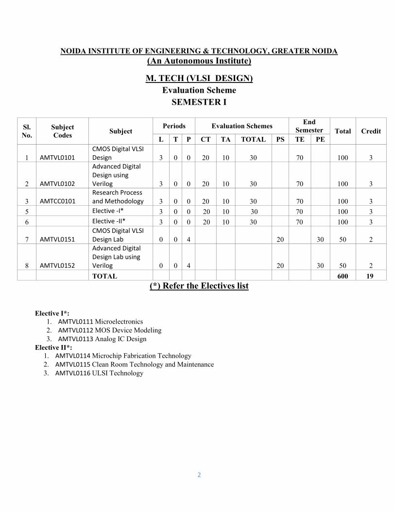
NOIDA INSTITUTE OF ENGINEERING & TECHNOLOGY, GREATER NOIDA (An Autonomous Institute)
M. TECH (VLSI DESIGN) Evaluation Scheme
SEMESTER I
Sl. No.
Subject Codes
Subject Periods Evaluation Schemes
End Semester Total Credit
L T P CT TA TOTAL PS TE PE
1 AMTVL0101 CMOS Digital VLSI Design 3 0 0 20 10 30 70 100 3
2 AMTVL0102
Advanced Digital Design using Verilog 3 0 0 20 10 30 70 100 3
3 AMTCC0101 Research Process and Methodology 3 0 0 20 10 30 70 100 3
5 Elective -I* 3 0 0 20 10 30 70 100 3
6 Elective -II* 3 0 0 20 10 30 70 100 3
7 AMTVL0151 CMOS Digital VLSI Design Lab 0 0 4 20 30 50 2
8 AMTVL0152
Advanced Digital Design Lab using Verilog 0 0 4 20 30 50 2
TOTAL 600 19
(*) Refer the Electives list
Elective I*:
1. AMTVL0111 Microelectronics 2. AMTVL0112 MOS Device Modeling 3. AMTVL0113 Analog IC Design
Elective II*: 1. AMTVL0114 Microchip Fabrication Technology 2. AMTVL0115 Clean Room Technology and Maintenance 3. AMTVL0116 ULSI Technology

3
NOIDA INSTITUTE OF ENGINEERING & TECHNOLOGY, GREATER NOIDA (An Autonomous Institute)
M. TECH (VLSI DESIGN)
Evaluation Scheme SEMESTER II
Sl. No
Subject Codes
Subject Periods Evaluation Schemes
End Semester Total Credit
L T P CT TA TOTAL PS TE PE
1 AMTVL0201
Digital Design Using FPGA and CPLD
3 0 0 20 10 30
70
100 3
2 AMTVL0202 Low Power VLSI Design
3 0 0 20 10 30
70
100 3
3 Elective –III* 3 0 0 20 10 30
70
100 3
4 Elective- IV* 3 0 0 20 10 30
70
100 3
5 Elective- V* 3 0 0 20 10 30 70 100 3
6 AMTVL0251 Digital Design Using FPGA and CPLD Lab
0 0 4
20
30 50 2
7 AMTVL0252 Low Power VLSI Design Lab
0 0 4
20
30 50 2
8 AMTVL0253 Seminar-I 0 0 2
50
50 1
TOTAL
650 20
(*) Refer the Electives list
Elective III*:
1. AMTVL0211 VLSI Testing and Testability 2. AMTVL0212 VLSI DSP Architectures 3. AMTVL0213 Full Custom Design
Elective IV*: 1. AMTVL0214 MEMS Sensor Design 2. AMTVL0215 Nanoscale Devices: Modeling &Simulation 3. AMTVL0216 Physical Design & Automation
Elective V*: 1. AMTVL0217 Embedded Microcontrollers 2. AMTVL0218 Real Time Operating System 3. AMTVL0219 SOC Design using ARM

4
M. TECH FIRST YEAR
Course Code AMTVL0101 L T P Credit Course Title CMOS Digital VLSI Design 3 0 0 03 Course Objective:
1 To explain basics of MOS switch, MOS fabrication and their characteristics.
2 To explain basic concept of CMOS inverter operation, its characteristics and switching power dissipation.
3 To design static CMOS combinational and sequential logic at the transistor level, including mask layout.
4 To explain the concept of dynamic logic circuits. 5 To design functional units including ROMs, SRAMs, and
DRAM.
Pre-requisites: Basics of CMOS.
Course Contents / Syllabus
UNIT-I MOS TRANSISTOR BASIC 10 hours MOS Transistor Basic, MOS switch, VLSI Design flow & Y-Chart, Basic MOS Device design equation and second order effect, Fabrication Process Flow: Basic Steps, The CMOS n-Well Process, Layout Design Rules, MOS inverters: DC transfer characteristics, latchup, MOSFET capacitances. UNIT-II CMOS INVERTER 9hours CMOS inverter: Circuit operation, DC transfer characteristics, noise margin: calculation of VIL, VIH, Vth, Design of CMOS inverter, Supply voltage scaling, power and area considerations. Switching characteristic: Delay time definition, calculation of delay times, inverter design with delay constraints, Switching Power dissipation of CMOS inverter. UNIT-III COMBINATIONAL & SEQUENTIAL MOS LOGIC
CIRCUITS 8hours
Combinational MOS Logic Circuits: MOS logic circuits with NMOS loads, Complex Logic circuits design – Realizing Boolean expressions using NMOS gates and CMOS gates, AOI and OIA gates, CMOS full adder, CMOS transmission gates, Designing with Transmission gates,
Sequential MOS Logic Circuits: Behavior of bi-stable elements, D latch, SR Latch, Clocked latch and flip flop circuits, CMOS, and edge triggered flip-flop. UNIT-IV DYNAMIC LOGIC CIRCUITS 9hours Logic Circuits: Basic principle of pass transistor circuits, Voltage Bootstrapping, Synchronous dynamic circuit techniques, Dynamic CMOS transmission gate logic, High performance Dynamic CMOS UNIT-V SEMICONDUCTOR MEMORIES 8 hours Semiconductor Memories: Types, RAM array organization, DRAM – Types, Operation, Leakage currents in DRAM cell and refresh operation, SRAM operation Leakage currents in SRAM cells, Flash Memory- NOR flash and NAND flash Course Outcome:After successful completion of this course students will be able to
CO 1 To identifythe fabrication process of CMOS transistor.

5
CO 2 To identify basic concept of CMOS inverter operation, its characteristics and switching power dissipation.
CO 3 Design combinational & Sequential MOS logic circuits like latches and flip flops.
CO 4 Explain and design synchronous dynamic pass transistor circuits
CO 5 Analyse SRAM cell and memory arrays.
Text Books 1. Sung-Mo Kang & Yusuf Leblebici, CMOS Digital Integrated Circuits - Analysis & Design, , MGH, Third Ed., 2003 2. Jan M Rabaey, Digital Integrated Circuits - A Design Perspective, Prentice Hall, Second Edition, 2005 3. David A. Hodges, Horace G. Jackson, and Resve A. Saleh, Analysis and Design of Digital Integrated Circuits, Third Edition, McGraw-Hill, 2004 Reference Books
1. R. J. Baker, H. W. Li, and D. E. Boyce, CMOS circuit design, layout, and simulation, Wiley-IEEE Press, 2007 2. Christopher Saint and Judy Saint, IC layout basics: A practical guide, McGraw-Hill Professional, 2001

6
M. TECH FIRST YEAR
Course Code AMTVL0102 L T P Credit
Course Title Advanced Digital Design using Verilog 3 0 0 03
Course Objective: 1 Study and explain the basic concepts Verilog HDL. 2 Implement digital circuits using distinct design styles. 3 Design and synthesis digital circuits using HDLs. 4 Study the concepts of data path design and switch level
modeling.
5 Explain about pipelining and processor design.
Pre-requisites: Digital System Design
Course Contents / Syllabus
UNIT-I INTRODUCTION TO HARDWARE DESCRIPTION LANGUAGE (HDL)
8 hours
Introduction to hardware description language (HDL), Verilog language and data types Digital System Design Process, Hardware modeling, Introduction to hardware description language (HDL), Verilog language features, elements of Verilog, Top-Down, Bottom-up Design, Verilog operators, Data types in Verilog; net type , reg type, wire type, Verilog Models of propagation delay and net delay path delays and simulation, inertial delay effects and pulse rejection UNIT-II DISTINCT DESIGN STYLES 8 hours Verilog description styles, behavioral and structural design style, Verilog attributes; Gate level, data flow level, procedural assignment, blocking / non-blocking assignments, user defined primitives, Verilog test bench, writing Verilog test benches. UNIT-III SYNTHESIS OF COMBINATIONAL &
SEQUENTIAL LOGIC 8 hours
HDL-based synthesis - technology-independent design, styles for synthesis of combinational and sequential logic, synthesis of finite state machines, synthesis of gated clocks, design partitions and hierarchical structures. UNIT-IV DATA PATH AND CONTROLLER DESIGN 8 hours Modeling finite state machines, Data-path and Controller Design, Synthesizable Verilog, Modeling memory, Modeling register banks, Switch level modeling. UNIT-V PIPELINING AND PROCESSOR DESIGN 8 hours Basic pipelining concepts, Pipeline modeling, Pipeline implementation of a processor, Verilog modeling of the processor. Course Outcome: After successful completion of this course students will be able to
CO 1 Outline the basic concepts Verilog HDL.
CO 2 Design of digital circuits using distinct design styles.
CO 3 Model HDL based Synthesis of digital circuits.
CO 4 Analyze the concepts of data path design and switch level

7
modeling.
CO 5 Implement pipelining and processor design using Verilog modeling.
Text books 1. Navabi, Z., 1999. Verilog digital system design. McGraw-Hill. 2. Palnitkar, S., 2003. Verilog HDL: a guide to digital design and synthesis (Vol. 1). Prentice Hall Professional. 3. Arnold, M.G., 1998. Verilog digital computer design: Algorithms into hardware. Prentice-Hall, Inc. Reference Books
1. Lin, M.B., 2008. Digital system designs and practices: using Verilog HDL and FPGAs. Wiley Publishing. 2. Unsalan, C. and Tar, B., 2017. Digital system design with FPGA: implementation using Verilog and VHDL. McGraw-H
Link:
Unit 1 https://www.youtube.com/watch?v=wiNDn19GpRU&list=PLUtfVcb-iqn-EkuBs3arreilxa2UKIChl&index=3
Unit 2 https://www.youtube.com/watch?v=xWimKdisUXE&list=PLUtfVcb-iqn-EkuBs3arreilxa2UKIChl&index=12
Unit 3 https://www.youtube.com/watch?v=lpS3S2gVoB4&list=PLUtfVcb-iqn-EkuBs3arreilxa2UKIChl&index=23
Unit 4 https://www.youtube.com/watch?v=cIDoJtYdDVA&t=66s
Unit 5 https://www.youtube.com/watch?v=w1u338oIeTQ

8
M. TECH FIRST YEAR
Course Code AMTCC0101 L T P Credit Course Title Research Process & Methodology 3 0 0 03
Course Objective: 1 To explain the concept / fundamentals of research and their types 2 To study the methods of research design and steps of research process
3 To explain the methods of data collection and procedure of sampling techniques
4 To analyze the data, apply the statistical techniques and understand the concept of hypothesis testing
5 To study the types of research report and technical writing.
Pre-requisites: Basics of Statistics
Course Contents / Syllabus
UNIT-I INTRODUCTION TO RESEARCH 8 hours Definition, objective and motivation of research, types and approaches of research, Descriptive vs. Analytical, Applied vs. Fundamental, Quantitative vs. Qualitative, Conceptual vs. Empirical, Research methods versus Methodology, significance of research, criteria of good research. UNIT-II RESEARCH FORMULATION AND DESIGN 8 hours Research process and steps involved, Definition and necessity of research problem. Importance and objective of Literature review, Locating relevant literature, Reliability of a source, Writing a survey and identifying the research problem, Literature Survey, Research Design , Methods of research design. UNIT-III DATA COLLECTION 8 hours Classification of Data, accepts of method validation, Methods of Data Collection, Collection of primary and secondary data, sampling, need of sampling, sampling theory and Techniques, steps in sampling design, different types of sample designs, ethical considerations in research. UNIT-IV DATA ANALYSIS 8 hours Processing Operations, Data analysis, Types of analysis, Statistical techniques and choosing an appropriate statistical technique, Hypothesis Testing, Data processing software (e.g. SPSS etc.), statistical inference, Chi-Square Test, Analysis of variance(ANOVA) and covariance, Data Visualization – Monitoring Research Experiments ,hands-on with LaTeX. UNIT-V TECHNICAL WRITING AND REPORTING OF RESEARCH 8 hours Types of research report: Dissertation and Thesis, research paper, review article, short communication, conference presentation etc., Referencing and referencing styles, Research Journals, Indexing, citation of Journals and Impact factor, Types of Indexing-SCI/SCIE/ESCI/SCOPUS/DBLP/Google Scholar/UGC-CARE etc. Significance of conferences and their ranking, plagiarism, IPR- intellectual property rights and patent law, commercialization, copy right, royalty, trade related aspects of intellectual property rights (TRIPS); scholarly publishing- IMRAD concept and design of research paper, reproducibility and accountability.
Course outcome: Upon completion of the course, the student will be able to

9
CO 1 Explain concept / fundamentals for different types of research
CO 2 Apply relevant research Design technique
CO 3 Use appropriate Data Collection technique
CO 4 Evaluate statistical analysis which includes various parametric test and non-parametric test and ANOVA technique
CO 5 Prepare research report and Publish ethically.
Text books 1. C. R. Kothari, Gaurav Garg, Research Methodology Methods and Techniques , New Age
International publishers, Third Edition. 2. Ranjit Kumar, Research Methodology: A Step‐by‐Step Guide for Beginners, 2nd Edition,
SAGE 2005. 3. Deepak Chawla, NeenaSondhi, Research Methodology, Vikas Publication
Reference Books
1. Donald Cooper & Pamela Schindler, Business Research Methods, TMGH, 9th edition 2. Creswell, John W. ,Research design: Qualitative, quantitative, and mixed methods approaches sage publications,2013
NPTEL/ You tube/ Faculty Video Link:
https://www.youtube.com/playlist?list=PL6G1C6j0WUTXqXL9O0CgTXCr1hL8HR2dY https://www.youtube.com/playlist?list=PLVok63jpnHrFFQI6BqkIksVqDnYG0ZI41 https://www.youtube.com/playlist?list=PLnbm2MNkZYwOVVedGBQtID-jKgj9dD8kW https://www.youtube.com/playlist?list=PLPjSqITyvDeWBBaFUbkLDJ0egyEYuNeR1 https://www.youtube.com/playlist?list=PLdj5pVg1kHiOypKNUmO0NKOfvoIThAv4N

10
M. TECH FIRST YEAR Course Code AMTVL0151 L T P Credit Course Title CMOS Digital VLSI Design Lab 0 0 4 02
List of Experiment Sr. No. Name of Experiment
1 Study of Microwind software and its features. 2 Design, simulate and verify the stick diagram of CMOS Inverter using Microwind. 3 Design, simulate and verify the result of universal gates using Microwind
(a) NAND (b) NOR 4 Design, simulate and verify theresult of following gates using Microwind
(a) XOR (b) XNOR
5 Design, simulate and verify the operation of logic function using Microwind Y=((𝑩+𝑪𝑫)(𝑬+𝑭))’
6 Design, simulate and verify the operation of CMOS half adder using Microwind. 7 Design, simulate and verify the operation of CMOS full adder using two half adders in
Microwind. 8 Design, simulate and verify the operation of 4:1 Multiplexer in Microwind. 9 Design, simulate and verify the operation of logic function using Dynamic and Domino
logic in Microwind: Y=((𝑩+𝑪𝑫)(𝑬+𝑭))’ 10 Design, simulate and verify pseudo NMOS Inverter.
Lab Course Outcome: After completion of this course students will be able to CO 1 Analyze the features of Microwind software. CO 2 Design, simulate and verify the result of universal gates, XOR, XNOR. CO 3 Design, simulate and verify the operation of logic function using Microwind. CO 4 Design, simulate and verify the operation of CMOS half/full adder using Microwind. CO 5 Design, simulate and verify the operation of Multiplexer in Microwind.
Link:
https://www.youtube.com/watch?v=F-8_caipPsY https://www.youtube.com/watch?v=S1VOEqApQvA
https://www.youtube.com/watch?v=EHUJda2ttU8
https://www.youtube.com/watch?v=yHJmFuexWbM
https://www.youtube.com/watch?v=7K_0I6CjBOY

11
M. TECH FIRST YEAR Course Code AMTVL0152 L T P Credit Course Title Advanced Digital Design Lab using Verilog 0 0 4 02
Modeling and Functional Simulation of the following digital circuits (with Xilinx/ ModelSim tools) using Verilog Hardware Description Language.
Sr. No. Name of Experiment 1 Design and simulate the Verilog HDL code to describe the functions of a Full
Adder and Subtractor using three modeling styles. 2 Design and simulate the Verilog HDL code for the following
combinational circuits: a) 4x1 Multiplexer using gate level modeling
b) 8x1 Multiplexer using dataflow level modeling c) 4-Bit Binary to Gray Code Converter using structural modeling
3 Design and simulate the Verilog HDL code for the following combinational circuit:
a) 3 to 8 Decoder b) 8 to 3 Encoder
4 Design and simulate the Verilog HDL code for the following combinational circuits using structural modeling.
a) 16x1 Multiplexer using 4x1 Mux b) 4- Bit Comparator using 1 Bit Comparator
5 Design and simulate the Verilog HDL code for the basic arithmetic and bitwise logical operations of ALU.
6 Design and simulate the Verilog HDL code for the flip-flops: a) SR FF b) JK FF c) D FF d) T FF
7 Design and simulate the Verilog HDL code for the following counters: a) 4- Bit Up-Down Counter b) BCD counter (Synchronous reset and asynchronous reset)
8 Design and simulate the Verilog HDL code for the following 4- Bit Shift register:
a) SISO b) SIPO c) PIPO d) PISO
9 Design and simulate the Verilog HDL code for 4- Bit universal shift register. 10 Design and simulate the Verilog HDL code to detect the sequence 1010101.
Lab Course Outcome: After completion of this course students are able CO 1 Translate the digital design into the Verilog HDL. CO 2 Design the combinational circuits in Verilog HDL. CO 3 Design the sequential circuits in Verilog HDL.

12
CO 4 Implement different digital circuits with component testing. Link:
Unit 1 https://www.youtube.com/watch?v=wiNDn19GpRU&list=PLUtfVcb-iqn-EkuBs3arreilxa2UKIChl&index=3
Unit 2 https://www.youtube.com/watch?v=xWimKdisUXE&list=PLUtfVcb-iqn-EkuBs3arreilxa2UKIChl&index=12
Unit 3 https://www.youtube.com/watch?v=lpS3S2gVoB4&list=PLUtfVcb-iqn-EkuBs3arreilxa2UKIChl&index=23
Unit 4 https://www.youtube.com/watch?v=cIDoJtYdDVA&t=66s
Unit 5 https://www.youtube.com/watch?v=w1u338oIeTQ

13
M. TECH FIRST YEAR
Course Code AMTVL0111 L T P Credit
Course Title Microelectronics 3 0 0 03
Course Objective: 1 To provide the knowledge of different fabrication processes like
epitaxy, oxidation and their applications.
2 To provide the knowledge of diffusion, ion implantation and different types of lithography and etching.
3 To provide the knowledge of Discrete devices and its fabrication. 4 To provide the knowledge of Different digital logic circuits and analog
circuits.
5 To provide the basic knowledge of BiCMOS ICs and their packaging.
Pre-requisites:Basics of digital electronics, CMOS designing.
Course Contents / Syllabus
UNIT-I FABRICATION PROCESS 8 hours Need for epitaxy, Vapour phase epitaxy, Liquid phase epitaxy and Molecular-Beam epitaxy, Silicon on insulators. Oxidation & Polysilicon Film Deposition: Thermal oxidation, Dielectric and Polysilicon deposition, Metallization & it’s Application, Masking.
UNIT-II DIFFUSION & ION IMPLANTATION 8 hours Basic diffusion, Distribution and range of implanted ions, Annealing and activation of dopants. LITHOGRAPHY & ETCHING: Optical lithography, X-ray lithography, Ion lithography, Electron beam lithography, Wet chemical etching and Dry chemical etching.
UNIT-III DISCRETE DEVICE FABRICATION 8 hours Fabrication of p-n junction, Bipolar junction transistor, JFET, MOSFET, CMOS Fabrication (P-well, N-well & Twin top Process)
UNIT-IV DESIGNING OF ANALOG AND DIGITAL CIRCUITS
8 hours
Basic circuit for analog and digital ICs, functional elements available in the market. CMOS Logic Circuits– Inverter, Two Input NOR Gate, Two Input NAND Gate. Analog circuits– single stage CE Amplifier and Emitter Follower.
UNIT-V BICMOS ICs 8 hours Design rules and Scaling, BICMOS ICs: Choice of transistor types, pnp transistors, Resistors, capacitors, Packaging: Chip characteristics, package functions, package operations.
Course Outcome: After successful completion of this course students will be able to
CO 1 Identify different fabrication processes
CO 2 Implement diffusion, ion implantation and different

14
types of lithography and etching.
CO 3 Explain Discrete devices and their fabrication.
CO 4 Design different digital logic circuits and analogcircuits..
CO 5 Categorize BiCMOS ICs and their packaging.
Text books 1. Peter Van Zant, Microchip fabrication, McGraw Hill, 1997. 2. S.M. Sze, VLSI technology, McGraw-Hill Book company, NY, 1988.
Reference Books
1. S.K. Gandhi, ‘VLSI Fabrication Principles’. 2. S.M. Sze, ‘Semiconductor Devices Physics and Technology’. 3. Puckness Douglas A, Eshraghiaw Kamran “Basic VLSI Design” – Prentice Hall (India) 4. K.R. Botkar, ‘Integrated Circuits’

15
M. TECH FIRST YEAR
Course Code AMTVL0112 L T P Credit Course Title MOS Device Modeling 3 0 0 03 Course Objective:
1 To study and analysis of MOS structure, its operations and , MOS as a capacitor.
2 To study and analysis of MOSFET Device Characteristics. 3 To study and analysis of Mobility models, MOS Performance parameters and
its frequency limitations.
4 To study and analysis of SOI MOSFET. 5 To study and analysis of SPICE Models for Semiconductor Devices.
Pre-requisites: Basic Electronics Engineering
Course Contents / Syllabus UNIT-I MOS PHYSICS 8 hours Semiconductor surfaces, Ideal MOS structure, MOS device in thermal equilibrium, Non-Ideal MOS: work function differences, charges in oxide, interface states, band diagram of non-ideal MOS, flat-band voltage, electrostatics of a MOS (charge based calculations), calculating various charges across the MOSC, threshold voltage, MOS as a capacitor (2 terminal device), Three terminal MOS, effect on threshold voltage. UNIT-II MOSFET DEVICE CHARACTERISTICS 8 hours Field-Effect Transistors: MOSFET- basic operation and fabrication; threshold voltages; output and transfer characteristics of MOSFET, short channel and Narrow width effects, MOSFET scaling, Small signal modeling for low frequency and High frequency, high-k gate dielectrics, ultra-shallow junctions, source and drain resistance.
UNIT-III MOBILITY MODELS AND MOS PERFORMANCE PARAMETERS
10 hours
Low field mobility, high field mobility, mobility various models, on current characteristics, off current characteristics, sub threshold swing, effect of interface states on sub threshold swing, drain conductance and transconductance, effect of source bias and body bias on threshold voltage and device operation, Large signal Modeling, small signal model for low, medium and high frequencies. UNIT-IV THE SOI MOSFET 6 hours Multiple gate SOI MOSFETs: double gate, FINFET, comparison of capacitances with bulk MOSFET, PD and FD SOI devices, short channel effects, current-voltage characteristics: Lim &Fossum model and C-∞ model, impact ionization and high field effects: Kink effect and Hot-carrier degradation, Floating body and parasitic BJT effects, self-heating. UNIT-V SPICE MODELS FOR SEMICONDUCTOR
DEVICES 8 hours
SPICE Models for Semiconductor Devices: MOSFET Level 1, Level 2 and level 3 model, Model parameters; Course Outcome: After successful completion of this course students will be able to
CO 1 Explain and analyse MOS structure, its operations and , MOS as a capacitor.
CO 2 Explain and analyse MOSFET Device Characteristics.

16
CO 3 Explain and analyse the Mobility models, MOS Performance parameters and its frequency limitations.
CO 4 Explain and analyse SOI MOSFET.
CO 5 Explain and analyse SPICE Models for Semiconductor Devices.
Text Books 1. E.H. Nicollian, J. R. Brews, Metal Oxide Semiconductor - Physics and Technology, John
Wiley and Sons. 2. Nandita Das Guptha, Amitava Das Guptha, Semiconductor Devices Modeling and
Technology, Prentice Hall India 3. Jean- PierrieColinge, Silicon-on-insulator Technology: Materials to VLSI, Kluwer Academic
publishers group. Reference Books
1. P. Colinge, “FinFETs and Other Multi-Gate Transistors”, Springer. 2009 2. Yannis Tsividis, Operation and Modeling of the MOS transistor, Oxford University Press.
Video Lecture Links: Unit I: https://www.youtube.com/watch?v=KohWxkovp0k https://www.youtube.com/watch?v=CT6olzelSKQ https://ocw.tudelft.nl/course-lectures/semiconductor-junction/ Unit II: https://www.youtube.com/watch?v=0C4uxtS-tlQ https://www.youtube.com/watch?v=XcDeh98ppXk https://www.youtube.com/watch?v=uHTyw4GGnRo https://www.youtube.com/watch?v=xSh9PZZPpOc Unit III: https://www.youtube.com/watch?v=4m49vM0Ryt8 https://www.youtube.com/watch?v=xgYdLvWcvms https://www.youtube.com/watch?v=IrbGAgrcvic Unit IV: https://www.youtube.com/watch?v=WWjldCmRteg https://www.youtube.com/watch?v=syRQTHF88eQ https://nptel.ac.in/courses/113/104/113104012/ https://www.youtube.com/watch?v=vS3S1KfNLhE Unit V: https://nptel.ac.in/courses/117/106/117106033/ https://www.digimat.in/nptel/courses/video/108107129/L04.html https://www.digimat.in/nptel/courses/video/117105147/L01.html https://www.coursera.org/lecture/averagedswitchmodelingandsimulation/spice-simulation-example-pJ99m NPTEL course video link: https://nptel.ac.in/courses/117/106/117106033/

17
M. TECH FIRST YEAR
Course Code AMTVL0113 L T P Credit Course Title Analog IC Design 3 0 0 03
Course Objective: 1 To develop the ability to design and analyze MOS based
Analog VLSI circuits.
2 To analyze the performance of single stage amplifier 3 To develop the skills to design Differential Amplifier
circuits for a given specification.
4 Analyze the frequency response of the different configurations of an amplifier
5 To provide the knowledge of operational amplifier & feedback topologies.
Pre-requisites: Basic electronics devices, Semiconductor & Amplifiers
Course Contents / Syllabus
UNIT-I BASIC MOS DEVICE PHYSICS 8 hours General Considerations, MOSFET as a Switch, MOS I/V Characteristics, Second-Order Effects, MOS Device Models, MOS Device Capacitances, NMOS versus PMOS Devices, Long-Channel versus Short-Channel Devices. UNIT-II SINGLE-STAGE AMPLIFIERS 8 hours Basic Concepts, Common-Source Stage, Common-Source Stage with Resistive Load, CS Stage with Diode-Connected Load, CS Stage with Current-Source Load, Source Follower, Common-Gate Stage, Cascode Stage, Folded Cascode.
UNIT-III DIFFERENTIAL AMPLIFIERS 8 hours Single-Ended and Differential Operation, Basic Differential Pair, Common-Mode Response, Differential Pair with MOS Loads, Gilbert Cell, Passive and Active Current Mirrors, Basic Current Mirrors, Cascode Current Mirrors, Active Current Mirrors, Common-Mode Properties UNIT-IV FREQUENCY RESPONSE OF AMPLIFIERS 8 hours General Considerations, Miller Effect, Association of Poles with Nodes, Common-Source Stage, Source Followers, Common-Gate Stage, Cascode Stage, Differential Pair, Noise in Differential Pairs Feedback Topologies, Effect of Loading, Effect of Feedback on Noise
UNIT-V OPERATIONAL AMPLIFIERS 8 hours General Considerations, Performance Parameters, One-Stage Op Amps, Two-Stage Op Amps , Gain Boosting , Comparison , Common-Mode Feedback . Input Range Limitations, Slew Rate, Power Supply Rejection.
Course Outcome: After successful completion of this course students will be able to
CO 1 Draw the equivalent circuits of MOS based Analog VLSI and analyse their performance.
CO 2 Design analog VLSI circuits for a given specification.
CO 3 Analyse the frequency response of the different configurations of an amplifier.
CO 4 Analyse the feedback topologies involved in the amplifier design.
CO 5 Appreciate the design features of the differential amplifiers.

18
Text books 1. Razavi, “Design of Analog CMOS Integrated Circuits”, 2nd Edition, McGraw Hill Edition
2016. 2. Paul. R.Gray&Robert G. Meyer, “Analysis and Design of Analog Integrated Circuits”,
Wiley, 5th Edition, 2009. 3. R. Gregorian and Temes, “Analog MOS Intgrated Circuits for Signal Processing”, Wiley Publications Reference Books
1. Ken Martin, “Analog Integrated Circuit Design”, Wiley Publications. 2. Sedra and Smith, “Microelectronic Circuits”, Oxford Publications. 3. B.Razavi, “Fundamentals of Microelectronics”, Wiley Publications

19
M. TECH FIRST YEAR
Course Code AMTVL0114 L T P Credit Course Title Microchip Fabrication Technology 3 0 0 03 Course Objective:
1 To analyze the basic stages of manufacturing and crystal growth. 2 To evaluate the process of wafer preparation and oxidation. 3 To analyze the lithography and etching process 4 To explain process of diffusion and ion implantation. 5 To learn the basic process involved in metallization and packaging
Pre-requisites:Basics of semiconductors and their properties.
Course Contents / Syllabus
UNIT-I OVERVIEW OF SEMICONDUCTOR INDUSTRY 8 hours Overview of semiconductor industry, Process and Product Trends, Stages of Manufacturing, Semiconductor material properties, Crystal growth, Basic wafer fabrication operations, Semiconductor Silicon Preparation, Czochralski (CZ) method, Float zone, Crystal and Wafer Quality. UNIT-II WAFER FABRICATION 8 hours Basic Wafer Preparation, Wafer Terminology , Basic Wafer-Fabrication Operations: Layering , Patterning , Doping, Heat treatments, Circuit design, masks, Example of Fabrication Process, Oxidation: Dry and wet oxidation, Clean room Construction. UNIT-III LITHOGRAPHY AND ETCHING 8 hours Ten step patterning process, Lithography: Optical Lithography, Electron beam lithography, Photo masks, Wet Chemical Etching, Dry etching Wet etching. UNIT-IV DOPING AND DEPOSITION 8 hours Doping and depositions: Diffusion process steps, deposition, Drive-in oxidation, Ion-Implantation: Ion-Implantation Technique, Implantation Equipment, CVD basics, CVD process steps, Low pressure CVD systems, Plasma enhanced CVD systems, Vapour phase epitaxy, molecular beam epitaxy. UNIT-V METALLIZATION AND PACAKAGING 8 hours Metallization: Metallization Application, Metallization Choices, Physical Vapour Deposition, Vacuum Deposition, Sputtering Apparatus. Packaging of VLSI devices: Package Types, Packaging Design Consideration, Package Fabrication Technologies. Course Outcome: After successful completion of this course students will be able to
CO 1 Analyze the basic stages of manufacturing and crystal growth.
CO 2 Evaluate the process of wafer preparation and oxidation.
CO 3 Analyze the lithography and etching process.
CO 4 Explain the process of diffusion and ion implantation.
CO 5 Learn the basic process involved in metallization and packaging
Text books 1. Peter Van Zant, Microchip fabrication, McGraw Hill, 1997.

20
2. S.M. Sze, VLSI technology, McGraw-Hill Book company, NY, 1988 Reference Books
1. Wani-Kai Chen (editor), The VLSI Hand book, CRI/IEEE press, 2000 2. C.Y. Chang and S.M. Sze, ULSI technology, McGraw Hill, 2000 3. S.K. Ghandhi, "VLSI Fabrication Principles", Willy-India Pvt. Ltd, 2008. 4. J. D. Plummer, M. D. Deal and Peter B. Griffin, “Silicon VLSI Technology: Fundamentals, Practice and Modeling", Pearson Education Publication, 2009

21
M. TECH FIRST YEAR
Course Code AMTVL0115 LT P Credit
Course Title Clean Room Technology And Maintenance 3 0 0 03
Course Objective: 1 Study and explain cleanroom standards and ancillary
cleanrooms.
2 Knowledge about clean room fabrication environment. 3 Identify the various filtration mechanisms. 4 Categorize cleanroom testing and monitoring system. 5 Analyze air quantities, pressure differences and clean room
disciplines.
Pre-requisites: Basics of IC Technology
Course Contents / Syllabus
UNIT-I INTRODUCTION TO CLEAN ROOM TECHNOLOGY 8 hours Introduction, Cleanroom Classification Standards, Unidirectional air flow clean room, Basis of Clean room standards, Federal Standards 209 ,ISO standard 14644-1:1999,Cleanroom classification(Pharmaceutical, cleanrooms) UNIT-II CLEAN ROOM ENVIRONMENT 8 hours Design of Turbulently Ventilated and Ancillary Cleanrooms, Mini environments, isolators and RABS, Containment zone, Construction and clean build, Design of Unidirectional Cleanrooms.
UNIT-III FILTRATION MECHANISM 8 hours High Efficiency Air filtration, Particle removal mechanisms, testing of high efficiency filters.
UNIT-IV TESTING & MONITORING SYSTEM 8 hours Cleanroom Testing and Monitoring, Principles of cleanroom testing, Testing in relation to room type and occupation state, Monitoring of cleanroom.
UNIT-V CLEAN ROOM STANDARD PARAMETERS 8 hours Measurement of Air Quantities and Pressure Differences, Air movement control, Recovery test methods, Cleanroom containment leak testing.
Course Outcome: After successful completion of this course students will be able to
CO 1 Specify cleanroom standards and ancillary cleanrooms.
CO 2 Explain about clean room fabrication environment.
CO 3 Identify the surface finishes and filtration mechanisms.
CO 4 Categorize cleanroom testing and monitoring system.
CO 5 Analyze air quantities, pressure differences and clean room disciplines.
Text books 1. William White, Cleanroom Technology: Fundamentals of Design, Testing and
Operation, 2nd Edition, Wiley, 2010.

22
2. Matts Ramstorp, Introduction to Contamination Control and Cleanroom Technology, Wiley, 2008.
Reference Books
1. Wani-Kai Chen (editor), The VLSI Hand book, CRI/IEEE press, 2000
Link: Unit 1 https://www.youtube.com/watch?v=8uGZMyjFugg
Unit 2 https://www.youtube.com/watch?v=YAouXIS_FSU
Unit 3 https://www.youtube.com/watch?v=wSSfOqEQClc
Unit 4 https://www.youtube.com/watch?v=aBIxPo0p7dc
Unit 5 https://www.youtube.com/watch?v=lHmHYWdH8Ug

23
M. TECH FIRST YEAR
Course Code AMTVL0116 L T P Credit
Course Title ULSI Technology 3 0 0 03
Course Objective: 1 To study the basics of chip fabrication and clean room. 2 To learn the ion implantation and variousOxidation technologies.
3 To study the classification of lithographic techniques. 4 To identify various metallization schemes. 5 To explain the concept of Memories.
Pre-requisites:Microelectronics
Course Contents / Syllabus
UNIT-I CLEAN ROOM AND WAFER PREPARATION 8 hours Environment for ULSI technology: clean room and safety requirements, Wafer cleaning process and wet chemical etching techniques ,Microelectronics and microscopy, ULSI process technology, Application of TEM for construction analysis, TEM sample preparation techniques.
UNIT-II IMPURITY INCORPORATION 9 hours Solid-state diffusion modelling and technology, Ion implantation: modelling, technology and damage annealing; Characterization of impurity profiles. Oxidation: kinetics of silicon dioxide growth for thick, thin and ultra-thin films. Oxidation technologies in ULSI; Characterization of oxide films; high K and low K dielectrics for ULSI.
UNIT-III LITHOGRAPHIC TECHNIQUES 9 hours Photolithography techniques for VLSI/ULSI; Mask generation. Chemical Vapour deposition techniques: CVD techniques for deposition of polysilicon, silicon dioxide, silicon nitride and metal films; epitaxial growth of silicon; modelling and technology. Ion implantation and substrate defects, Dielectrics and isolation, Silicides, polycide and salicide, Metallization and interconnects. UNIT-IV METALLIZATION TECHNIQUES 8 hours Evaporation and sputtering techniques. Failure mechanisms in metal interconnects; multilevel Metallization schemes. TEM in failure analysis, Novel devices and materials, TEM in under bump metallization and advanced electronics packaging technologies, High – resolution TEM in microelectronics. UNIT-V ULSI DEVICES 6 hours DRAM cell with planar capacitor, ULSI devices II: DRAM cell with stacked capacitor, ULSI devices III: DRAM cell with trench capacitor, ULSI devices IV: SRAM.
Course Outcome: After successful completion of this course students will be able to
CO 1 Explain basics of chip fabrication and clean room. CO 2 Perform the ion implantation and various Oxidation technologies.
CO 3 Apply lithographic techniques for the designing of circuits.

24
CO 4 Explain and analyze metallization schemes. CO 5 Design semiconductor memories.
Text books 1. S.M. Sze(2nd Edition )”VLSI Technology”, McGraw Hill Companies Inc. 2. Chih-Hang Tung, George T.T. Sheng, Chih-Yuan Lu, ULSI Semiconductor Process Technology Atlas, John Wiley & Sons, 2003. 3. C.Y. Chang and S.M. Sze (Ed), “ULSI Technology”, 2000, McGraw Hill Companies Inc. Reference Books
1. Stephena, Campbell, “The Science and Engineering of Microelectronic Fabrication”, Second Edition, Oxford University Press. 2. James D. Plummer, Michael D. Deal, ”Silicon VLSI Technology” Pearson Education Reading.

25
M. TECH FIRST YEAR
Course Code AMTVL0201 LT P Credit
Course Title Digital Design using FPGA and CPLD 3 0 0 03
Course Objective: 1 To study finite state machines and its realization. 2 To study asynchronous Sequentialmachine. 3 To learn Designing of Digital logic using PLD. 4 To get knowledge of different FPGA series. 5 To study different CPLD series.
Pre-requisites:Basics of CMOS and Fabrication. Course Contents / Syllabus
UNIT-I FINITE STATE MACHINE (FSM) 8 hours Introduction, Design Strategies, Mealy & Moore model, Realization of State Diagram & state table from verbal description, Minimization of State Table from completely & Incompletely specified State Machine, Introduction to Algorithmic State Machine. UNIT-II ASYNCHRONOUS SEQUENTIAL CIRCUIT 8 hours
Introduction to Asynchronous Sequential Machine (ASM), fundamental & pulse mode Asynchronous Sequential machine, Secondary State Assignments in Asynchronous Sequential machine, Races & Hazards. UNIT-III PROGRAMMABLE LOGIC DEVICES (PLD) 8 hours
Introduction, Architecture, Features & Digital Design of ROM, EPROM, EEPROM, Flash Memory, PLA, PAL & PGA, Design of a keypad scanner using PLD.
UNIT-IV FIELD PROGRAMMABLE GATE ARRAY (FPGA) 8 hours
Logic blocks, Routing architecture, Design flow, Technology Mapping for FPGA. Xilinx FPGA XC4000, Comparative Study of Xilinx (ZU11EG) & Intel (Stratix 10 SX650 series from Altera) with reference to cortex A53.
UNIT-V COMPLEX PROGRAMMABLE LOGIC DEVICES (CPLD)
8 hours
Altera series – Max 5000/7000 series and Altera FLEX logic- 10000 series CPLD, AMD’s- CPLD (Mach 1 to 5), Cypress FLASH 370 Device technology, Lattice plsi architectures – 3000 series – Speed performance and system programmability. Course Outcome: After completion of this course students will be able to
CO 1 Realize finite state machines.
CO 2 Formulate asynchronous Sequentialmachine.
CO 3 Design Digital logic using PLD.
CO 4 Explain different FPGA series.
CO 5 Explain different CPLD series.
Text books

26
1. P. K. Chan& S. Mourad, Digital Design using Field Programmable Gate Array, Prentice Hall.
2. Charles H Roth, Jr. , “Digital Systems Design Using VHDL”, PWS, 1998. 3. S. Trimberger, Edr., Field Programmable Gate Array Technology, Kluwer Academic Pub.
Reference Books
1. J. Old Field, R. Dorf, Field Programmable Gate Arrays, John Wiley& Sons, Newyork. 2. S.Brown,R.Francis, J.Rose, Z.Vransic, Field Programmable GateArray,Kluwer Pub. 3. Richard FJinder , “Engineering Digital Design,”Academic press
27
M. TECH FIRST YEAR
Course Code AMTVL0202 LT P Credit
Course Title Low Power VLSI Design 3 0 0 03
Course Objective: 1 To provide the knowledge of Low Power VLSI Chips and
different losses associated with the CMOS Devices
2 To provide the knowledge of Power estimation Simulation Power analysis and Probabilistic power analysis of Design
3 To provide the knowledge of circuit level and Logic level design. 4 To provide the knowledge of Low Power Architecture and system.
5 To provide the basic knowledge of Low Power Clock Distribution Algorithm & Architectural Level Methodologies
Pre-requisites: CMOS VLSI Design, Digital logic Design. Course Contents / Syllabus
UNIT-I INTRODUCTION & DEVICE AND TECHNOLOGY IMPACT ON LOW POWER
8 hours
Introduction: Needs for Low Power VLSI Chips, Sources of power dissipation on digital integrated circuit, Emerging low power approaches, Physics of power dissipation in CMOS Devices, Device and technology impact on low power: Dynamic dissipation on low power, Transistor sizing & gate oxide thickness, Impact of technology Scaling, Technology & Device innovation UNIT-II POWER ESTIMATION SIMULATION POWER
ANALYSIS&PROBABILISTIC POWER ANALYSIS 8 hours
Power estimation Simulation Power analysis: - SPICE circuit simulators, Gate level logic simulation, Capacitive Power Estimation, Static State Power, Gate level Capacitance Estimation, Architecture Level analysis, Data Correlation Analysis in DSP systems. Monte Carlo simulation. Probabilistic power analysis:- Random Logic Signals. Probability & frequency, Probabilistic Power Analysis Techniques , Signal Entropy. UNIT-III LOW POWER DESIGN 8 hours Circuit level: Power Consumption in circuit level, Flip Flop & Latches design, High Capacitance node, Low power digital cell library Logic Level: Gate Reorganisation, Signal gating, Logic encoding, state machine encoding, Pre computation logic UNIT-IV LOW POWER ARCHITECTURE AND SYSTEM 8 hours Power & Performance Management, Switching Activity Reduction, Parallel Architecture with Voltage Reduction, Flow graph Transformation, Low Power Arithmetic Component, Low Power Memory Design UNIT-V LOW POWER CLOCK DISTRIBUTION & ALGORITHM
& ARCHITECTURAL LEVEL METHODOLOGIES 8 hours
Low Power Clock Distribution: -Power dissipation in clock distribution, single driver Vs distributed buffers, zero skew Vs tolerable skew chip and package co-design of clock network Algorithm & Architectural Level Methodologies:-Introduction, Design flow, Algorithmic Level analysis and optimization, Architectural level estimation and synthesis

28
Course Outcome: After successful completion of this course students will be able to
CO 1 Identify different losses associated with the CMOS Devices.
CO 2 Explain the concept of Power estimation Simulation Power analysis and Probabilistic Power analysis of Design.
CO 3 Identify circuit and logic level low power design.
CO 4 Analyze the Low Power Architecture and system.
CO 5 Explain Low Power Clock Distribution Algorithm.
Text books
1. Gary K. Yeap, Practical Low Power Digital VLSI Design, KAP 2007
2. Rabaey, Pedram , "Low power design methodologies" Kluwer Academic, 1997
Reference Books
1. Kaushik Roy, Sharat Prasad, "Low-Power CMOS VLSI Circuit” Wiley 2000

29
M. TECH FIRST YEAR Course Code AMTVL0251 L T P Credit Course Title Digital Design using FPGA and CPLD Lab 0 0 4 02 Pre-requisites: Basics Knowledge of Digital Electronics & Digital System Design Sr. No. List of Experiment
1 Demonstration of FPGA and CPLD Boards. 2 Design & Implement the Boolean Expression Y=AB+BC+CA on CPLD. 3 Design & Implement Full adder and Full Subtractor on CPLD. 4. Design & Implement (i) 2-bit comparator and (ii) 2-bit multiplier (iii) 8x1 Multiplexer on CPLD. 5 Design & Implement S-R, J-K, D and T Flip Flops on FPGA. 6 Design & Implement (i) Universal shift register (ii) 4- bit UP-DOWN Synchronous Counter on
FPGA. 7 Design & Implement the (i) 4-bit ALU (ii) 8- bit SRAM on FPGA. 8 Design & Implement 7- Segment Display Driver circuit using CPLD.
9 Design & Implement Sequence Detector Circuit to detect given sequence 10101010 on FPGA.
10 Modelling and Implementation of UART on FPGA.
Lab Course Outcome: After completion of this course students will be able to
CO 1 Design & Implement the Combinational Logic Circuits on CPLD. CO 2 Design & Implement the Sequential Logic Circuits on CPLD. CO 3 Design & Implement the Memories on FPGA. CO 4 Design & Implement UART on FPGA.
Link:
1 https://www.youtube.com/watch?v=9mpRF6bAY1g
2 https://www.youtube.com/watch?v=EGDHXynlXMk
3 https://www.youtube.com/watch?v=H2GyAIYwZbw
4 https://www.youtube.com/watch?v=WKZgK3BKDIo
5 https://www.youtube.com/watch?v=s3Dk4CEfNg4&list=PLJ5C_6qdAvBELELTSPgzYkQg3HgclQh-5&index=6

30
M. TECH FIRST YEAR Course Code AMTVL0252 LT P Credit Course Title Low Power VLSI Design Lab 0 0 4 02 Software Tool: SOFTWARE TOOL: CADENCE – Tool Bundle Consisting of:
1. ANALOG & MIXED SIGNAL DESIGN FRONT END TOOLS Virtuoso(R) Spectre(R) Simulator REL MMSIM 7.1 Virtuoso(R) Schematic Editor XL REL IC 6.1.0
2. ANALOG BACK END TOOL Virtuoso(R) Layout Suite XL REL IC 6.1.0
3. PHYSICAL DOMAIN SOC Encounter - XL (aka Cadence (R) SOC Encounter - GPS)
Sr. No. Name of Experiment 1 I-V characteristics of long and short-channel MOSFET transistors in CMOS
technology. 2 The gate capacitance of an MOS transistor. (Gate Capacitance v/s VGS). 3 The impact of device variations on static CMOS inverter VTC. 4 The VTC of CMOS inverter as a function of supply voltage and substrate bias.
5 Dynamic power dissipation due to charging and discharging capacitances. 6 Short-circuit currents during transients and impact of load capacitance on short-
circuit current in a CMOS inverter. 7 The VTC of a two-input NAND & NOR data dependency. 8 The variable-threshold CMOS inverter and Combinational circuit. 9 The low-power / low voltage D-Latch circuit.
10 Low-power circuits a. The Full Adder b. The Binary Adder c. The Multiplier d. The Shifter. e. The SRAM Cell f. The DRAM Cell
Lab Course Outcome: After completion of this course students are able to CO 1 Study and analyze the various parameters of MOS Transistor. CO 2 Study and analyze the different parameters of CMOS inverter for low power
design. CO 3 Design and implement the combinational digital circuits for low power circuits.
CO 4 Design and implement the sequential digital circuits for low power circuits. Link:
Unit 1 https://www.youtube.com/watch?v=TFOO1JAll2Y https://youtu.be/ruClwamT-R0
Unit 2 https://www.analog.com/en/design-center/design-tools-and-calculators/ltspice-simulator.html https://www.youtube.com/watch?v=OgO1gpXSUzU

31
https://nptel.ac.in/courses/111/106/111106134/
Unit 3 https://nptel.ac.in/courses/106/105/106105034/ https://www.youtube.com/watch?v=dqcfYTePRxQ https://www.youtube.com/watch?v=rEeqxozkdZ0
Unit 4 https://www.digimat.in/nptel/courses/video/106105034/L37.html
Unit 5 https://nptel.ac.in/courses/106/105/106105161/

32
M. TECH FIRST YEAR
Course Code AMTVL0211 L T P Credit Course Title VLSI Testing and Testability 3 0 0 03 Course Objective:
1 To provide an in-depth understanding of the importance and principle of testing and verification of faults affecting VLSI circuits.
2 To provide the knowledge of the testing and testability of combinational circuits.
3 To provide the knowledge of the testing and testability of sequential circuits.
4 To provide an in-depth understanding of the memory design and testing methods.
5 To provide the basic knowledge of Built in self-test (BIST) Techniques.
Pre-requisites:Digital and analog IC fabrication. Course Contents / Syllabus
UNIT-I INTRODUCTION TO VLSI TESTING AND FAULT MODELING
10 hours
Importance and Principle of testing, Challenges in VLSI testing, Levels of abstractions in VLSI testing, Functional vs. Structural approach to testing, Complexity of the testing problem, Types of Testing, DC and AC parametric tests Fault Modeling: Stuck at fault, fault equivalence, fault collapsing, fault dominance, fault simulation UNIT-II TESTING AND TESTABILITY OF COMBINATIONAL
CIRCUITS 8 hours
Test Generation Basics: Test generation algorithms, Random test generation, ATPG algorithms for combinational circuits, Boolean difference, Path sensitization, D – algorithm, PODEM, Testable combinational logic circuit design UNIT-III TESTING AND TESTABILITY OF SEQUENTIAL
CIRCUITS 8 hours
Testing of sequential circuits as iterative combinational circuits, state table verification, test generation based on circuit structure, Sequential ATPG, Ad Hoc design rules, scan path technique (scan design), partial scan, Boundary scan UNIT-IV MEMORY, DELAY, FAULT AND IDDQ TESTING 6 hours Testable memory design, RAM fault models, Test algorithms for RAM, Delay faults, Delay tests, IDDQ testing, Testing methods, Limitations of IDDQ testing UNIT-V BUILT IN SELF-TEST (BIST) TECHNIQUES 8 hours Built-in self-test (BIST): Design rules, Exhaustive testing, Pseudo-random testing, Pseudo-exhaustive testing, Output response analysis, Logic BIST architectures, Introduction to Test compression Course Outcome: After successful completion of this course students will be able to
CO 1 Apply the concepts in testing which can help them design a better yield in IC design

33
CO 2 Analyse the various test generation methods for combinational circuits.
CO 3 Analyse the various test generation methods for sequential circuits.
CO 4 Identify the design for testability methods for different memory circuits.
CO 5 Recognize the BIST techniques for improving testability.
Text books
1. An Introduction to Logic Circuit Testing - Parag K. Lala, (Morgan & Claypool Publishers)
2. Essentials of Electronic Testing for Digital, Memory & Mixed Signal VLSI Circuits - Michael L. Bushnell and Vishwani D. Agrawal, (Kluwar Academic Publishers 2000)
3. Digital System Testing and Testable Design - M. Abramovici, M.Breuer, and A. Friedman (Jaico Publishing House)
Reference Books
1. Introduction to Formal Hardware Verification - Thomas Kropf (Springer)
2. VLSI Test Principles and Architectures Design for Testability – W.W. Wen (Morgan Kaufmann Publishers. 2006)
3. Digital Systems and Testable Design - M.Abramovici, M.A. Breuer and A.D. Friedman (Jaico Publishing House)
4. Design Test for Digital IC's and Embedded Core Systems - A.L. Crouch (Prentice Hall International)
Link:
Unit 1 https://youtu.be/u_XLaTTzXaE
Unit 2 https://nptel.ac.in/courses/106/103/106103116/
Unit 3 https://nptel.ac.in/courses/106/103/106103116/
Unit 4 https://nptel.ac.in/courses/106/103/106103116/
Unit 5 https://nptel.ac.in/courses/106/103/106103116/

34
M. TECH FIRST YEAR Course Code AMTVL0212 L T P Credit
Course Title VLSI DSP Architectures 3 0 0 03
Course Objective: 1 To explain basics of DSP processors and micro programming
approaches.
2 To learn building a data path and control path. 3 To outline pipelining and pipe lined data path. 4 To analyzeA/D and D /A converters and DSP computational errors. 5 To identify thearchitectures for programmable digital signal
processing devices.
Pre-requisites: VLSI DSP Architecture
Course Contents / Syllabus
UNIT-I BASICS OF DSP PROCESSORS 8 hours Essential features of Instruction set architectures of DSP processors, Micro programming approaches for implementation of control part of the processor, CPU performance and its factors, evaluating performance. UNIT-II DATA PATH 9 hours Introduction to logic design conventions, building a data path, a simple implementation scheme, a multi cycle implementation, simplifying control design. UNIT-III PIPELINING 9 hours An overview of pipelining, a pipe lined data path, pipe lined control, data hazards and forwarding, data hazards, branch hazards, advanced pipelining: extracting more performance. UNIT-IV CONVERSIONS 8 hours Number formats for signals and coefficients in DSP systems, dynamic range and precision, sources of errors in DSP implementations, A/D conversion errors, and DSP computational errors, D /A conversion errors. UNIT-V PROGRAMMABLE PROCESSORS 8 hours Introduction to architectures for programmable digital signal processing devices, basic architectural features, DSP computational building blocks, bus architecture, data addressing capabilities, address generation unit, speed issues, features for external interfacing. Course Outcome: After successful completion of this course students will be able to
CO 1 Identify basics of DSP processors and micro programming approaches.
CO 2 Learn building a data path and control path.
CO 3 Analyze pipelining and pipe lined data path.
CO 4 CalculateA/D and D /A converters and DSP computational errors.
CO 5 Implement architectures for programmable digital signal processing devices.
Text books 1. D. A, Patterson and J.L Hennessy, “Computer Organization and Design: Hardware/ Software Interface”, 4th Ed., Elsevier, 2011.

35
2. A. S Tannenbaum, “Structural Computer organization”, 4th Ed., Prentice-Hall, 1999. Reference Books
1. W. Wolf, “Modern VLSI Design: System on Silicon”, 2nd Ed., Person Education,1998. 2. Keshab Parhi, “VLSI Digital Signal Processing system design and implementations”, Wiley1999.

36
M. TECH FIRST YEAR Course Code AMTVL0213 LT P Credit
Course Title Full Custom Design 3 0 0 03
Course Objective: 1 Students will be familiar with the schematic fundamentals and layout designs flow. 2 Students will come to know about standard library cells as well as other types of
basic cells.
3 Students will be able to design interconnect layout and know special electrical requirements for it.
4 Students will be able to incorporate special design rules and step coverage rules. 5 Students will be able to learn various kind of CAD tools.
Pre-requisites:Basics of VLSI Course Contents / Syllabus
UNIT-I INTRODUCTION 8 hours Introduction: Schematic fundamentals, Layout design, Introduction to CMOS VLSI manufacturing processes, Layers and connectivity, Process design rules Significance of full custom IC design, layout design flows. UNIT-II SPECIALIZED BUILDING BLOCKS 8 hours Advanced techniques for specialized building blocks Standard cell libraries, Pad cells and Laser fuse cells, Power grid Clock signals and Interconnect routing. UNIT-III LAYOUT DESIGNS 8 hours Interconnect layout design, Special electrical requirements, Layout design techniques to address electrical characteristics. UNIT-IV LAYOUT CONSIDERATIONS 8 hours Layout considerations due to process constraints Large metal via implementations, Step coverage rules, Special design rules, Latch-up and Guard rings, Constructing the pad ring, Minimizing Stress effects. UNIT-V LAYOUT CAD TOOLS 8 hours Proper layout CAD tools for layout, Planning tools, Layout generation tools, Support tools. Course Outcome: After successful completion of this course students will be able to
CO 1 Design layout with schematic.
CO 2 Differentiate standard cells and other types of cells.
CO 3 Do the electrical connections and interconnect layout designs.
CO 4 Tackle with the minimization of stress effects.
CO 5 Demonstrate the layout tools, generation tools, etc.
Text books 1.Dan Clein, CMOS IC Layout Concepts Methodologies and Tools, Newnes, 2000. 2.Ray Alan Hastings, The Art of Analog Layout, 2nd Edition, Prentice Hall, 2006 Reference Books 1. CMOS: Circuit Design, Layout, and Simulation by R. Jacob Baker. 3rd Edition.

37
M. TECH FIRST YEAR
Course Code AMTVL0214 LT P Credit
Course Title MEMS Sensor Design 3 0 0 03
Course Objective: 1 To provide the knowledge of MEMs fabrication
Technologies and Sensors/Transducers.
2 To provide the knowledge about Mechanics of Beam and Diaphragm Structures.
3 To provide the knowledge about drag effect of a fluid, Air damping and its models.
4 To provide the knowledge of Electrostatic Actuation. 5 To provide the basic knowledge of MEMS Structures and
Systems in RF applications.
Pre-requisites:Basics of sensors. Course Contents / Syllabus
UNIT-I INTRODUCTION TO MEMS 8 hours MEMS Fabrication Technologies, Materials and Substrates for MEMS, Processes for Micromachining, Sensors/Transducers, Piezoresistive Effect, Piezoelectricity, Piezoresistive Sensor. UNIT-II MECHANICS OF BEAM AND DIAPHRAGM
STRUCTURES 8 hours
Stress and Strain, Hooke's Law. Stress and Strain of Beam Structures: Stress, Strain in a Bent Beam, Bending Moment and the Moment of Inertia, Displacement of Beam Structures Under Weight, Bending of Cantilever Beam Under Weight. UNIT-III AIR DAMPING 8 hours Drag Effect of a Fluid: Viscosity of a Fluid, Viscous Flow of a Fluid, Drag Force Damping, The Effects of Air Damping on Micro-Dynamics. Squeeze-film Air Damping: Reynolds' Equations for Squeeze-film Air Damping, Damping of Perforated Thick Plates. Slide-film Air Damping: Basic Equations for Slide-film Air Damping, Couette-flow Model, Stokes-flow Model. UNIT-IV ELECTROSTATIC ACTUATION 8 hours Electrostatic Forces, Normal Force, Tangential Force, Fringe Effects, Electrostatic Driving of Mechanical Actuators: Parallel-plate Actuator, Capacitive sensors. Step and Alternative Voltage Driving: Step Voltage Driving, Negative Spring Effect and Vibration Frequency. UNIT-V MEMS STRUCTURES AND SYSTEMS IN RF
APPLICATIONS 8 hours
Signal Integrity in RF MEMS, Microelectromechanical Resonators: Comb-Drive Resonators, Beam Resonators, Coupled-Resonator Bandpass Filters, Film Bulk Acoustic Resonators, Microelectromechanical Switches: Membrane Shunt Switch, Cantilever Series Switch. Course Outcome: After successful completion of this course students will be able to
CO 1 Identify MEMs fabrication Technologies.

38
CO 2 Analyse Mechanics of Beam and Diaphragm Structures.
CO 3 Explain drag effect of a fluid, Air damping and its models.
CO 4 Design different Electrostatic Actuators.
CO 5 Explain MEMS Structures and Systems in RF applications.
Text books 1. Minhang Bao, ‘Analysis and Design Principles of MEMS Devices’, First edition
2005, Elsevier. 2. Nadim Maluf, KirtWilliums, ‘An Introduction to Microelectromechanical Systems
Engineering’,2nd ed., Artech House microelectromechanical library. Reference Books
1. RS Muller, Howe, Senturia and Smith, “Micro-sensors”, IEEE Press.

39
M. TECH FIRST YEAR
Course Code AMTVL0215 LT P Credit Course Title Nanoscale Devices: Modeling & Simulation 3 0 0 03
Course Objective: 1 To introduce novel MOSFET devices and understand the
advantages of multi-gate devices
2 To introduce the concepts of nanoscale MOS transistor and their performance characteristics
3 To study the various Nano-scaled MOS transistor circuits 4 To study radiation effects in SOI MOSFETs 5 To study digital circuits and impact of device performance on
digital circuits
Course Contents / Syllabus UNIT-I MOSFET SCALING 8 hours MOSFET scaling, short channel effects - channel engineering - source/drain engineering - high k dielectric - copper interconnects - strain engineering, SOI MOSFET, multigate transistors – single gate – double gate – triple gate – surround gate, quantum effects – volume inversion – mobility – thresholdvoltage–intersub-bandscattering, multigatetechnology–mobility–gatestack. UNIT-II MOS ELECTROSTATICS 8 hours MOS Electrostatics – 1D – 2D MOS Electrostatics, MOSFET Current-Voltage Characteristics – CMOSTechnology – Ultimate limits, double gate MOS system – gate voltage effect - semiconductor thickness effect – asymmetry effect – oxide thickness effect – electron tunnel current – two dimensional confinements, scattering –mobility. UNIT-III SILICON NANOWIRE MOSFETS 10 hours Silicon nanowire MOSFETs – Evaluation of I-V characteristics – The I-V characteristics for non- degenerate carrier statistics – The I-V characteristics for degenerate carrier statistics – Carbon nanotube – Band structure of carbon nanotube – Band structure of graphene – Physical structure of nanotube – Band structure of nanotube – Carbon nanotube FETs – Carbon nanotube MOSFETs – Schottky barrier carbon nanotube FETs – Electronic conduction in molecules – General model for ballistic nano transistors – MOSFETs with 0D, 1D, and 2D channels – Molecular transistors – Single electron charging – Single electron transistors UNIT-IV RADIATION EFFECTS IN SOI MOSFETS 6 hours Radiation effects in SOI MOSFETs, total ionizing dose effects – single-gate SOI – multi-gate devices, single event effect, scaling effects. UNIT-V DIGITAL CIRCUITS 8 hours Digital circuits – impact of device performance on digital circuits – leakage performance trade off – multi VT devices and circuits – SRAM design, analogcircuit design – transconductance - intrinsic gain – flicker noise – self heating –band gap voltage reference – operational amplifier – comparator designs, mixed signal – successive approximation DAC, RF circuits.

40
Course Outcome: After successful completion of this course students will be able to
CO 1 Explain the MOS devices used below 10nm and beyond with an eye on the future
CO 2 Explain the physics behind the operation of multi-gate systems.
CO 3 To design circuits using nano-scaled MOS transistors with the physical insight of their functional characteristics
CO 4 Explain radiation effects in SOI MOSFETs
CO 5 Explain and designdigital circuits and impact of device performance on digital circuits
Text books 1. J P Colinge, "FINFETs and other multi-gate transistors", Springer – Series on
integrated circuits and systems,2008 2. Mark Lundstrom, Jing Guo, "Nanoscale Transistors: Device Physics,
Modelingand Simulation", Springer,2006 Reference books
1. M S Lundstorm, "Fundamentals of Carrier Transport", 2nd Ed., Cambridge University Press, Cambridge UK, 2000

41
M. TECH FIRST YEAR Course Code AMTVL0216 LT P Credit
Course Title Physical Design & Automation 3 0 0 03
Course Objective: 1 Students will know how to place the blocks and how to partition
the blocks while for designing the layout for IC.
2 Students will be familiar to various kind of VLSI Automation Algorithms.
3 Students will know the concepts of Physical Design Process such as Floor planning, Placement algorithms.
4 Students will learn Global Routing and Detailed Routing algorithms.
5 Students will learn over the Cell Routing in detail.
Pre-requisites: Basics of digital IC and data structures. Course Contents / Syllabus
UNIT-I LOGIC SYNTHESIS & VERIFICATION 8 hours Logic Synthesis & Verification: Introduction combinational logic synthesis, Binary decision Diagram, Hardware models for High- level synthesis. UNIT-II VLSI AUTOMATION ALGORITHMS 8 hours VLSI Automation Algorithms: Partition: problem formulation, classification of partitioning algorithms, Group migration algorithms, simulated annealing & evolution other partitioning algorithms. UNIT-III PLACEMENT, FLOOR PLANNING & PIN ASSIGNMENT 8 hours Placement, Floor Planning & Pin assignment: problem-formulation, simulation-based placement algorithms, other placement algorithms, constraint-based floor planning, floor planning algorithms for mixed block & cell design. General & channel pin assignment. UNIT-IV GLOBAL ROUTING & DETAILED ROUTING 8 hours Global Routing: Problem formulation, classification of global routing algorithms, Maze routing algorithm, line probe algorithm, Steiner Tree based algorithm, ILP based approaches. Detailed Routing: problem formulation, classification of routing algorithms, single layer routing algorithms, two-layer channel routing algorithms, three-layer channel routing algorithms, and switchbox routing algorithms. UNIT-V OVER THE CELL ROUTING & VIA MINIMIZATION 8 hours Over the Cell Routing & via Minimization: two layers over the cell routers, constrained & unconstrained via minimization Compaction: problem formulation, one-dimensional compaction, two dimension-based Compaction, hierarchical compaction. Course Outcome: After successful completion of this course students will be able to
CO 1 Know how to place the blocks and how to partition the blocks while for designing the layout for IC.
CO 2 Explain VLSI Design Automation.
CO 3 Explain the concepts of Physical Design Process such as Floor planning, Placement and Routing.

42
CO 4 AnalyzeGlobal Routing and Detailed Routing algorithms.
CO 5 Decompose large problem into pieces via minimization.
Text books 1. Naveed Sherwani, "Algorithms for VLSI Physical Design Automation", Kluwer
Academic Publisher, Second edition. Reference Books
1. ChristophnMeinel&ThorstemTheobold, “Algorithm and Data Structures for VLSI Design”, KAP 2002.
2. Rolf Drechsheler : “Evolutionary Algorithm for VLSI”, second edition 3. Trimburger,” Introduction to CAD for VLSI”, Kluwer Academic publisher, 2002.

43
M. TECH FIRST YEAR Course Code AMTVL0217 L T P Credit
Course Title Embedded Microcontrollers 3 0 0 03
Course Objective: 1 To provide the Basic knowledge of interfacing with
Embedded System.
2 To analyse the process design of embedded system. 3 To realize the architecture of PIC 16F Microcontroller
Series.
4 To familiar with the fundamentals of ARM Processor Cortex M3 & M4.
5 To apply the knowledge of ARM Instruction Set for programming.
Pre-requisites: Digital System design, 8051 Microcontroller
Course Contents / Syllabus
UNIT-I TYPICAL EMBEDDED SYSTEMS 8 hours Core of the embedded system, General purpose and domain specific processor, ASICs, PLDs, Commercial off the shelf Components (COTS), Memory: RAM, ROM, Memory according to the type of interface, Memory Shadowing, Memory selection for embedded system, Sensors and actuators, Introduction to Communication Interface (Onboard and External). UNIT-II EMBEDDED SYSTEMS DESIGN PROCESS 8 hours Embedded system project development, Design issues and co-design issues in system development process, The Embedded Design Life Cycle, Selection Process, The Partitioning Decision (Hardware and Software partitioning), The Development and Debugging Environment (use of target machine or its emulator and In- Circuit emulator), Special Software Techniques, Introduction to BDM, JTAG, and Nexus. UNIT-III PIC 16F MICROCONTROLLER SERIES 8 hours Introduction to PIC Microcontroller families (8/16 and 32 bit), PIC 16F series family overview of architecture and peripherals, Pin diagram and Architecture of PIC16F84/PIC16F84A Microcontroller, Memory organization, configuration, memory addressing, and special function registers, parallel and serial ports, timer and counters. Special features of PIC16F84A (OSC Selection, RESET - Power-on Reset (POR), Power-up Timer (PWRT), Oscillator Start-up Timer (OST), Interrupts, Watchdog Timer (WDT), SLEEP, Code Protection, ID Locations, In-Circuit Serial Programming, interrupts). Architectural overview of PIC 16F877/PIC 16F887A. UNIT-IV ARCHITECTURE OF ARM CORTEX M3 AND M4
PROCESSORS 8 hours
Introduction to Cortex-M3 and Cortex-M4 processors (Processor architecture, Instruction set, Block diagram, Memory system, Interrupt and exception support).Programmer’s model, Operation modes, Registers, Memory System, features, stack memory, memory requirements, endianness, bit band operations, access permissions and attributes, memory barriers, Low power design and features, low power application development, overview of exceptions and interrupts, exception types and interrupt management, vector table, exception sequence, use of NVIC register, SCB register and other special registers for exception and

44
interrupt control, configuration control and auxiliary control registers. UNIT-V INSTRUCTION SETOF CORTEX M3 AND M4
PROCESSORS 8 hours
Evolution of ARM ISA, Comparison of the instruction set in ARM Cortex-M Processors, Unified Assembly Language, Addressing modes, Instruction set, Program flow control (branch, conditional branch, conditional execution, and function calls), Multiply accumulate (MAC) instructions, Divide instructions, Memory barrier instructions, Exception-related instructions, Sleep mode-related instructions, Other functions, Introduction to Cortex-M4 processor support for Enhanced DSP instructions, Writing C and Assembly language programs. Course Outcome: After successful completion of this course students will be able to
CO 1 Explain the Basic knowledge of interfacing with Embedded System.
CO 2 Analyse the process design of embedded system.
CO 3 Realize the architecture of PIC 16F Microcontroller Series.
CO 4 Familiar with the fundamentals of ARM Processor Cortex M3 & M4.
CO 5 Apply the knowledge of ARM Instruction Set for programming.
Text books 1. Introduction to Embedded Systems, A Cyber physical approach, Edward A. Lee and
Senjit A. Seshia. 2. Embedded Systems Design: An Introduction to Processes, Tools, and Techniques, by
Arnold S. Berger, CMP Books. Reference Books
1. Designing Embedded Systems with PIC Microcontrollers: Principles and Applications, 2nd Edition, Tim Wilmshurst, Elsevier Publication.
2. PIC Microcontroller and Embedded Systems Using Assembly and C for PIC 18 by Muhammad Ali Mazidi, Rolin D. McKinlay and Danny Causey, Pearson Publication.
3. The Definitive Guide to ARM Cortex M3 and Cortex-M4 Processors, Third Edition, Joseph Yiu, Elsevier Publication, 2015.
4. ARM Assembly Language Fundamentals and Techniques, William Hohl and Christopher Hinds, CRC Press, 2015.

45
M. TECH FIRST YEAR
Course Code AMTVL0218 L T P Credit
Course Title Real Time Operating System 3 0 0 03
Course Objective: 1 To provide the concept of real time operating system. 2 To analyse the task scheduling method & I/O system. 3 To realize the firmware design process. 4 To familiar with the different types of management system
for RTOS.
5 To explain the concept of RTX.
Pre-requisites:Digital System design, Microcontroller. Course Contents / Syllabus
UNIT-I OPEN SOURCE RTOS 8 hours Basics of RTOS: Real-time concepts, Hard Real time and Soft Real-time, Differences between General Purpose OS & RTOS, Basic architecture of an RTOS, Scheduling Systems, Inter-process communication, Performance Matric in scheduling models, Interrupt management in RTOS environment, Memory management, File systems, I/O Systems, Advantage and disadvantage of RTOS. POSIX standards, RTOS Issues – Selecting a Real Time Operating System, RTOS comparative study. Converting a normal Linux kernel to real time kernel, Xenomai basics. Overview of Open source RTOS for Embedded systems (Free RTOS/ Chibios-RT) and application development UNIT-II Vx WORKS/ FREE RTOS 8 hours VxWorks/ Free RTOS Scheduling and Task Management – Real time scheduling, Task Creation, Intertask Communication, Pipes, Semaphore, Message Queue, Signals, Sockets, Interrupts. I/O Systems – General Architecture, Device Driver Studies, Driver Module explanation, Implementation of Device Driver for a peripheral. UNIT-III EMBEDDED FIRMWARE DESIGN AND
DEVELOPMENT 10 hours
Embedded Firmware Design Approaches, Super-loopbased approach, Embedded Operating System based approach, Programming in Embedded C, Integrated development environment (IDE), Overview of IDEs for Embedded System Development. UNIT-IV EMBEDDED SYSTEM DESIGN WITH FREE RTOS 6 hours Queue Management, Characteristics of a Queue, Working with Large Data, Interrupt Management, Queues within an Interrupt Service Routine, Critical Sections and Suspending the Scheduler, Resource Management, Memory Management. UNIT-V RTX 8 hours RTX structure, RTX files, RTX task and time management, Simple Time Management APIs, Task Priority Scheme in RTX, Inter-Task Communication, Event, Interrupt, Mutex, Semaphore, Mailboxes and Messages in RTX, RTX control functions, Architecture of CMSIS-RTOS. Course Outcome: After successful completion of this course students will be able to
CO 1 Explain the concept of real time operating system.

46
CO 2 Analyse the task scheduling method & I/O system.
CO 3 Realize the firmware design process.
CO 4 Familiar with the different types of management system for RTOS.
CO 5 Explain the concept of RTX.
Text books 1. VenkateswaranSreekrishnan,”Essential Linux Device Drivers” , Ist Kindle edition,
Prentice Hall, 2008 2. Jonathan W. Valvano, “Real-Time Operating Systems for ARM Cortex-M
Microcontrollers” Jonathan Valvano; 4 edition Reference Books
1. Jerry Cooperstein , ”Writing Linux Device Drivers: A Guide with Exercises”, J. Cooperstein publishers ,2009
2. Qing Li and Carolyn Yao,”Real Time Concepts for Embedded Systems” – Qing Li, Elsevier ISBN:1578201241 CMP Books © 2003
3. “Using the FreeRTOS Real Time Kernel” From Free RTOS. 4. Sam Siewert , “Real-Time Embedded Systems And Components”.

47
M. TECH FIRST YEAR Course Code AMTVL0219 LT P Credit
Course Title System On Chip (SOC) Design using ARM 3 0 0 03
Course Objective: 1 Study the Architecture of Arm Cortex-M0 Processor.
2 Describe the AMBA 3 AHB-Lite Bus Architecture, VGA, GPIO and 7-Segment UART Peripheral
3 Learn the Programming of SoC Using C Language.
4 Compare ARM Cortex-A9 Processor with other processor.
5 Implement and compare an AXI UART and AXI-Stream Peripheral
Pre-requisites:1. Basics of HDL (Verilog /VHDL) 2. Basics of Microcontroller Assembley language Programming
Course Contents / Syllabus
UNIT-I INTRODUCTION TO SYSTEM-ON-CHIP DESIGN
8 hours
Differences among SoCs, CPUs and MCUs, Arm Cortex-M0 Processor Architecture. UNIT-II PROGRAMMING AN SOC 8 hours AMBA 3 AHB-Lite Bus Architecture, AHB VGA Peripheral, AHB UART Peripheral, Timer, GPIO and 7-Segment Peripherals, Interrupt Mechanisms, Programming an SoC Using C Language. UNIT-III ARM CORTEX-A9 PROCESSOR 8 hours Arm CMSIS and Software Drivers, Arm Development Studio, ARMv7-A/R ISA Overview, ARM Cortex-A9 Processor UNIT-IV AMBA AXI4 8 hours AMBA AXI4 Bus Architecture,Design and Implementation of an AXI4-Lite™ GPIO peripheral and a DDR Memory Controller UNIT-V IMPLEMENTATION OF AN AXI UART AND
AXI-STREAM 8 hours
Design and Implementation of an AXI UART and AXI-Stream Peripheral, AXI4-Stream and VGA Peripheral, HDMI Input Peripheral, System Debugging. Course Outcome:After completion of this course students will be able to
CO 1 Explain Arm Cortex-M0 Processor Architecture.
CO 2 RecognizeAMBA 3 AHB-Lite Bus Architecture, VGA, GPIO and 7-Segment UART Peripheral.
CO 3 Program SoC Using C Language.
CO 4 Explain ARM Cortex-A9 Processor.
CO 5 Design and Implement an AXI UART and AXI-Stream Peripheral.
Text books

48
1. ARM System-on-Chip Architecture by Steve B. Furber 2. ARM Assembly Language: Fundamentals and Techniques by William Hohl 3. The Definitive Guide to the ARM Cortex-M0 by Joseph Yiu Reference Books 1. Computer System Design: System-On-Chip - Michael J. Flynn and Wayne Luk, Wiely
India. 2. Modern VLSI Design – System – on – Chip Design - Wayne Wolf, - Prentice Hall,
3. Design of System on a Chip: Devices and Components, Ricardo Reis, Springer 4. System on Chip Verification –Methodologies and Techniques: Prakash Rashinkar,
Peter Paterson and Leena Singh L, Kluwer Academic Publishers
Link:
Unit 1 https://www.youtube.com/watch?v=PRQXzjTrCJY https://www.youtube.com/watch?v=HNbeVvfFKsQ
Unit 2 https://www.youtube.com/watch?v=j2NI4AXRs1Uhttps://www.youtube.com/watch?v=4VRtujwa_b8&list=PL90187D2B8F5AC28F&index=5
Unit 3 https://www.youtube.com/watch?v=4VRtujwa_b8 Unit 4 https://www.youtube.com/watch?v=mYP5SxDEjrM
https://www.youtube.com/watch?v=QQY-h0HGHnI https://www.youtube.com/watch?v=tEvtb-mdJ4s&list=PL90187D2B8F5AC28F&index=16
Unit 5 https://www.youtube.com/watch?v=nbWWMPPC8aE https://www.youtube.com/watch?v=MANrmky5DfE