
VLA Technical Report No 56 FOCUS/ROTATION CONTROL ...
294
VLA Technical Report No 56 FOCUS/ROTATION CONTROL SYSTEM, MODEL E D. WEBER, P. HARDEN, W. KOSKI DECEMBER 1984
-
Upload
khangminh22 -
Category
Documents
-
view
2 -
download
0
Transcript of VLA Technical Report No 56 FOCUS/ROTATION CONTROL ...

VLA Technical Report No 56
FOCUS/ROTATION CONTROL SYSTEM, MODEL E
D. WEBER, P. HARDEN, W. KOSKI DECEMBER 1984


TABLE OF CONTENTS
1 .0 INTRODUCTION !1.1 PERFORMANCE SUMMARY 11.2 BACKGROUND !1.3 F/R CONTROL SYSTEM DESCRIPTION 2|1.4 F/R MOUNT DESCRIPTION 91.5 DRIVE DYNAMICS
2.0 M7, MODEL E F/R CONTROLLER DESCRIPTION 212.1 F/R CONTROLLER LOGIC DESCRIPTION 212.2 ROTATION AND RING CONTROL PROGRAM 242.3 FOCUS CONTROL PROGRAM 38
3.0 M 1 1 , MODEL B APEX INTERFACE LOGIC DESCRIPTION 41
4.0 M8 , MODEL C, F/R POWER SUPPLY DESCRIPTION 45
5.0 M22, F/R SWITCHING MODULE DESCRIPTION 46
6.0 SYSTEM TROUBLE SHOOTING H8
7.0 TELESCOPE OPERATOR INFORMATION 51
8.0 CONTROL/DATA BIT FORMATS, ANALOG SIGNALS & RANGES 54
9.0 SYSTEM CABLE DRAWINGS & TRANSLATOR SCHEMATIC 60DIAGRAMS
10.0 SYSTEM FUNCTIONAL SPECIFICATIONS 61
11.0 APPENDIX 65ROTATION & RING CONTROL PROGRAMFOCUS CONTROL PROGRAMLIST OF RELATED DRAWINGSM7, M 1 1 , M8, M22 ASSEAMBLY DRAWINGS &IC LOCATION MAPSF/R CONTROL BIN WIRE LISTFUNCTIONAL MODULE DATA SHEETS


TABLE OF ILLUSTRATIONS
FIGURE 1, F/R SYSTEM, MODEL E, FUNCTIONAL BLOCK DIAGRAM 6
FIGURE 2, PEDASTAL ROOM F/R COMPONENTS 7
FIGURE 3, APEX & PEDASTAL ROOM JUNCTION BOX LAYOUTS 8
FIGURE 4, APEX F/R COMPONENTS 11
FIGURE 5, APEX ASSEMBLY,EXPLODED ISOMETRIC VIEW 12
FIGURE 6, F/R MOUNT - LOCATIONS OF MAJOR COMPONENTS 13
FIGURE 7, STEPPER MOTOR TORQUE/SPEED CURVES 20
FIGURE 8, APEX INTERFACE ANALOG ADJUSTMENT LOCATIONS 43


1.0 INTRODUCTIONThis manual describes the new VLA Focus/Rotation Control system and was
written to serve as a maintainance guide for the system and modules. The primary purpose of this manual is to provide a detailed functional description of the operation of the system, the modules and control programs. The emphasis is on practical data: module schematic diagrams, control programs, cable drawings, and bin wire lists are included to make this a comprehensive reference manual with all the data that are handy for use on the lab bench or at an Antenna.
A secondary purpose is to describe the functional operation of the mechanical components and the inter-relationships between these components and the control system hardware/software. The manual also has sections which briefly describe the F/R Control System operation, the F/R Mount, the control and F/R Mount specifications and telescope operator CRT overlay & diagnostic information. These sections may be read for information on these topics without bothering to plow through the detailed descriptions of the modules and programs.
1.1 PERFORMANCE SUMMARYThe following table summarizes the performance of the new F/R
System.
Parameter
Command execution time Max drive rate Readout resolution,(14 bit conversion)
Command repeatability Physical stability
1.2 BACKGROUNDA previous manual (VLA Technical Report No 42, F/R System Manual, Jan
1980), described the first version of the F/R Control System and the F/R Mount. This control equipment was designed in 1974 and is installed in most of the VLA antennas. Specifications for the new system resulted from the need for better performance and experience with the earlier mechanism and electronics. The new control system provides more powerful control, extensive local fault analysis, higher position resolution, more reliable position readout devices, faster mechanism response time and easier maintainance. It is also capable of relatively easy alteration of the control algorithms by changing the firmware. The F/R Mount has undergone extensive mechanical redesign and the Controller design has been made sufficiently general so as to be able to adapt to these changes.
Several experimental versions of F/R Control systems have been used in recent years. A microprocessor controller with synchro position readouts was used in Antenna 27 in 1980. Although the controller operated satisfactorily, it was decided not to retrofit other antennas with this controller until some mechanical design changes were made to improve the the stability of the F/R Mount.
The stability and repeatability of the Subreflector Rotation position is a very critical parameter in that small Subreflector angular position errors
Focus
64 sec/12 inches 0.197 in/sec 0.000732 in/bit
0.5 bit,RMS 0.001 in
Rotation
15 sec/180 deg 1 6 .7 deg/sec 1 .3 1 8 arc-min/bit
2 arc-min, RMS 3.85 arc-min
1
cause large antenna pointing errors. Focus position instability impacts the visibility data phase. Section 10 describes the effects of Subreflector positional errors on pointing and phase. Much of the mechanical and electrical redesign effort has been directed at reducing the Rotation position uncertainty. The unreliability of the position readout potentiometers has also been a persistant problem which has cost many dollars for replacement parts and many man-hours for maintainance and repair time.
An approach to solving the Rotation position uncertainty is an index locking pin mechanism in which a tapered pin is inserted into sockets at angular positions associated with receiver feed horns. An F/R Mount incorporating this feature was installed in Antenna 12 with a new F/R Controller and operated on a trial basis for a year. The idea behind this scheme was that a snug-fit pin/socket combination would provide a tight lock sind eliminate the typical 30 to 60 arc-minutes of Rotation ring gear-brake lost motion. The Antenna 12 F/R Control System operated satisfactorily but there were reliability problems with the pin actuation motor so this approach was abandoned and the Antenna 12 F/R Mount was redesigned.
The essence of the final mechanical re-design is to reduce the brake-ring gear lost motion by relocating the Rotation brake to the traveling platform and coupling the brake to the ring gear with only one gear pass. This reduces the Rotation gear slack to about four arc-minutes. The Rotation position readout sensor is relocated so as to be closely coupled (ie one gear pass) to the Subreflector mounting drum. This change eliminates about 1.5 degrees (out of 3200 degrees) lost motion in the existing Rotation ring gear-to-readout potentiometer gear train.
To improve reliability, the Rotation position readout sensor was changed from a potentiometer to a synchro and a high resolution (14 bits) Synchro to Digital Converter. Military reliability analysis has shown that in a given environment, synchros are an order of magnitude more reliable than multi-turn, precision potentiometers. The higher resolution readout has provided a great improvement in the capability of the controller to precisely set and monitor the Rotation position. The Focus position readout potentiometer was also replaced with a synchro and 14 bit S/D Converter. The use of synchros and an integrating S/D Converter has made the position readout circuitry virtually invulnerable to noise perturbations on the long cable runs from the Apex to the Pedestal Room.
After the Antenna 12 prototype system operated for a year without failure or noticeable performance degradation, it was decided to retrofit the new mechanical and electrical designs into all antennas as a part of the periodic antenna refurbishment schedule. The new F/R Controller and reworked F/R Mount have been installed in Antenna 20. Antenna 20 also has a 327 MHz dipole/ring feed system installed in front of the subreflector; this has added several mechanical components to the F/R Mount and Apex structure. When the 327 MHz receiver is in use, the feed ring is extended to enclose the 327 MHz dipoles. When the other receiving bands are used, the ring is retracted back toward a quadrapod spar. Although the ring is not part of the F/R System, the F/R System controls the ring motion because of the proximity of the ring actuator to the Apex junction box and the flexibility of the F/R control electronics.
The existing stepper motors and Translators have been retained but the Translators have been relocated to provide more room in Rack C.
2

The Apex to Pedestal Room cable structure has not been changed other than signal reassignment of some wires. A 3-wire 110 VAC cable has been added to power the 327 MHz Ring actuator.
Beside the changes described above, a number of mechanical improvements have been incorporated in the F/R mount mechanical design. Notable examples are:
Renovation of the aluminum Rotation ring gear bearing surfaces by steel inserts.
The use of better weather-proof flexible boots over the lead screws and spline shaft.
The use of heaters on the gear box and traveling platform to warm the gear train lubricant to about 40 deg F in cold weather. Thisprevents cold weather lubricant stiffening which can cause drive sticking problems due to the marginal drive motor torques.
3

1.3 F/R CONTROL SYSTEM DESCRIPTIONSee Figure 1, F/R Control System Block Diagram and Figures 2 & 3 which
show the location of the F/R Control System Components.
The F/R Controller closes the position loops and activates all drivingelements of the F/R Mount, senses positions and discretes, analyzes conditionsin the mount and Pedestal Room to detect faults and reports on these states to Central Control via Data Set 3.
In CMP (Central Computer control) mode, the F/R Controller receives a position command from the Data Set which activates an interrupt in either the Focus or Rotation portion of the controller. The controller tests the Multiplex address and command argument (some Focus arguments are not accepted because of mechanical constraints), and it calculates motor ramping parameters, steering direction and activates the associated brake and stepper motor translator. If brake voltage and current and translator power are above test thresholds and there are no system faults, the controller begins to emit drive pulses to the Stepper Motor Translators so as to null the error. The pulse rate is ramped from 100 Hz to 1000 Hz (500 Hz in Focus) in 50 Hz steps. Drive continues at 1000 Hz until a calculated ramp down position is reached at which time the stepping rate is ramped down to 100 Hz for convergence to the commanded set point. When the set point is reached the controller turns off the Stepper Translator AC and activates the brake.
During ramp-up, main drive, ramp down and convergence, position changes are compared with what they should be to test for drive sticking or dragging. If this happens, the stepping rate is reduced to 100 Hz and the drive is ramped back up to 250 Hz (the peak torque speed of these motors) and the controller attempts to complete the command. In the event that the drive sticks again, the controller aborts the command. When drive sticking occurs, a "Drive Fault" bit is set in the controller status data readout and this bit flags this message on the Operator’s Data Checker program and the Operator*s F/R Overlay.
In the LOCAL mode (selected by the F/R Controller front panel switch), the F/R system is controlled by actuation of the manual control switches on the F/R Power Supply. These switches are: Focus Drive Up/Down; Rotation Drive CW/CCW; and the Focus and Rotation Ramp/100 Hz switches. LED displays on the Power Supply panel indicate actuation of the brakes, translators etc. In the LOCAL mode the computer commands are ignored and command inputs come from the switches mentioned above. The portion of the control program which implements LOCAL control is similar to the portion which implements CMP (central computer) control and calls the same drivers to perform basic functions such as turning on the brakes, ramping up/down, providing monitor data to the Data Set, etc.
The controller is not directly connected to any circuitry in the Apex; all position and discrete readouts from the Apex are sensed by an Apex Interface unit which transfers this data to the controller via an optically isolated serial link. The Apex Interface front panel displays the Focus and Rotation position in 14 bit octal code and the state of various discretes and activity sensors on an LED annunciator. Logic in the Apex Interface tests for malfunctions; in the event that any of these occur an inhibit (YOWP!) is sent to the F/R Controller to disable all drive outputs. When limit cond itions are sensed by the Apex Interface, drive inhibits are sent to the F/R Controller to inhibit further drive into the limit (but not out of the limit). The Apex Interface is isolated from the controller as a lightning protection measure;

it is the sacrificial element in the event of strikes on the Apex structure restricting damage to this unit which has a minimum of parts.
A Switching Module contains the brake controllers (DC power supplies) and solid state relays to switch the AC for the brake controllers, translators and 327 MHz feed ring actuator. A 400 Hz synchro exciter in the Switching Module provides the 400 Hz required by the synchros and the S/D Converters.
A NAP mode has been incorporated to enable the controller to ignore position commands until reset by a RESET command. This permits reduced performance operation in the event of a drive failure.
A ZOT BOX capability has been incorporated into the sysetm to permmit manual control of the Subreflector position by a ZOT BOX which may be plugged into either the F/R control bin or the Apex Junction Box. Discrete and position readouts on the ZOT BOX display the state of the F/R Mount position.
5


PIP£D. RM 120 VAC -HI ffAC -LO
DISTR. -GWDBOX
M8 F/R POWER SUPPLY
FIG. 1 - F/R SYSTEM - fu nct io n al block diagram

CABLE TRAYS
AZIMUTH AVIS CABLE WRAP
PEDESTAL ROOM JUNCTION BOX
R O T A T I O N
TRANSLATORS
FOCUS
C-RACK
DATA CONV. *ACU
BIM - ”W ”
PED. ROOM DOOR
PEDESTAL ROOM F/R COMPONENTS
COMMfcCTOR PlATfc.
J l 201 eox JUMPERS XL CMO/MOM A.6. DATA j 'S S P A R tJ4 PE.D .RM JUMCTlOM Bax J 5 TRAN SLATO RS Jfc W A R t J l t P A R t
S i Jfe J S JA J S J 2
I M8 power Supply ^
' P S S y s t e m a c p o w e r ^J IM PUT (I20VAC> |
J £ 4 _ F / R _ S W (T C H £ 0 _ A £ _j
l ” M ? 2 F/R ^W>TCHIN>G "*j
I P i 9 W n c H € D AC INPUT| P’S f o r e,R4W£ oci P4 f « c. e* A *e o t r ' I P S MOTOR ACI Pfe fo e T R A kjS . ACI P 7 Kerr t r a n ?>. a c
I P8 SPARE
f P 9 F A K J _ A C ______ ____ J
@ IMTEROJMM6.CT»M6 IWlRl PAMtLS
V>PIM 0 14P
14 (OH PIN
W W
M8 €&
J 2 J2
34 b 4PtM
CR Iwv
Jl Jl
& o S OPin p*»
C R C*
M22
© ©
© ©
© ©
(P6)
J2_ J l50
M i l
M IO
J234
JliFJ1 W
/BiNi4 j L
IS IO T PO S."X > | I 2 I I I I 10 |"j)~ I a I 7 I 6 ; 5 la I 3 ! z T
= A P t y
imtte.5?-FACfc.
F/R
C0Kn«?OU D A T A T A f 7
F/«?'POVOE-t^
S u p p l y
c
f z M/«Cfc>
M l 1 B
( « * 0
M 7 &
f4Vu)
M 2 M 8 c
c
"DtVTTA Cm o /
MOMIMTU?-ttCfc
B l a m K
F / Rc
(iv r t A w ) ( a w )
M l M 2 2 A
(REA R V IE W ) fFRO W T V IE W )
DETAIL -F/R ELECTRONICS BIMS W *X
ii \2iz\4\'bi<z, i7 r»'i i io11 r u n
FIG.2 - PEDESTAL ROOM F/R COMPONENTS

ROTMOTORDRIVE
!z O.v. £owDUIT £tYP)
SIGNALS AP&X ZOT ^ oX (TEST ONLV)
APEX JUNCTION BOX
(ft
EJ
«o in
CO CO
b h
oCO
CD hh
_ r
CI
Kt
K7
\CZ
PEDESTAL ROOM JUNJCTION BOX
FIG. 3 APEX i PEDESTAL RM. JUNCTION! BOX LAYOUTS


1.4 F/R MOUNT DESCRIPTIONThe F/R Mount is almost inaccessible; most of the mechanism parts are
enclosed by the gearbox or hidden by the barrel and support structure. This section was written to provide a brief description of the mechanism for electronics maintainance personnel who must understand how the mount operates in order to be able to maintain the electronics.
The F/R Mount is a two axis mechanism consisting of three rings, four guide shafts, four lead screws, two gear trains, two drive motors, two failsafe brakes and two position readout synchros. Figure 4 depicts the F/R Mount and Subreflector as they appear from the inside of the dish. Figure 5 depicts an exploded isometric view of the F/R Mount and the associated components. Figure 6 depicts the locations of the motors, brakes and Focus position readout synchro.
The top ring is a gear box for the two drive trains; the motors are mounted on the top of the gear box. The Focus motor and gears rotate lead screws which move the Traveling (middle ring) platform up and down the Guide Shafts to produce the Focus motion. The Focus brake is mounted on the top of the gear box and is coupled to the Focus gear train inside the box.
The Rotation motor and gear train drives a sliding spline gear which rotates a large ring gear mounted on the Traveling platform to produce the Rotation motion. The Rotation brake is mounted on the traveling platform and is coupled to the Rotation ring gear through a single gear pass.
A flange on the center of the ~42fl diameter barrel is bolted to the Rotation ring gear. The Subreflector is bolted to the bottom of the barrel and counter-weights are bolted to the top of the barrel. The bottom ring is a supporting member for the guide rods and lead screws.
Rubber spring couplings between the drive motors and gear trains buffer the motors so that they are not subjected to large instantaneous inertial loads such as at initial drive motion. The spring deflection is proportional to the torsional loads imposed upon the motor by the drive.
The brakes are fail-safe; that is they are always engaged until energized.
The Rotation gear train reduction ratio is 108:1, that is, each 1.8 degree motor step rotates the Subreflector by 1.8/108 or 0.01666 degrees so that 21,600 motor steps are required to rotate the Subreflector 360 degrees. The Focus gear train reduction ratio to the lead screws is 2.54:1. The lead screw pitch is .200 so that five rotations of the lead screws are required to move the traveling platform one inch. The total Focus travel is 12 inches (ignoring that lost by limit switch inhibit action) so that the total number of motor steps required to traverse this Focus range is: 1 .8 * 200 * 5 * 2.54 *12 = 30480 motor steps.
Focus and Rotation positions are read out as 14 bit values (16384 counts range). The motor-step/readout-resolution ratios are: 21600/16384 = 1.318 steps/bit (also 1.318 arc-min/bit) in Rotation motion and 30480/16384 = 1.860 steps/bit (also 0.0003937 in/step and 0.000732 in/bit) in Focus motion.
Rotation position is read out by a synchro mounted on a tripod above the
9

barrel. The synchro shaft is coupled to the center of the drum through a sliding "Trombone" which takes out the Focus motion of the barrel; see Figure5 for details on this mechanism. A tubular shaft attached to the top of the Trombone drives the Rotation position synchro through a flexible coupling and pick-off gear (1 : 1 ratio) which drives an anti-backlash gear on the synchro shaft.
Focus position is read out by a 10:1 anti-backlash reduction gear box and synchro coupled to the Focus gear train. The gear box is used because the synchro and gear box mimic the 10-turn helipot used with the older system.
Focus upper/lower limit switches sense the extremes of Focus motion and cause the F/R Controller to inhibit further drive into the limit. There are Ho Rotation limit switches as the Rotation drive is capable of continuous rotation; in executing a Rotation command, the F/R Controller rotates the Subreflector through the smallest angle to move to a new position. This permits faster band changes.
The 327 MHz feed dipoles travel up and down with the Subreflector Focus motion but do not rotate with the Subreflector Rotation motion. This nonrotation is accomplished by mounting the dipoles on a square shaft which is prevented from rotating by a square-holed collar attached to the top of the Rotation synchro gear box. The dipoles are caused to move with the Subreflector in Focus motion by a thrust bearing in the Subreflector which is attached to the square shaft. The square shaft passes through the Trombone, the Rotation synchro drive shaft and slides through the square-holed collar in Focus motion. Coaxial cables carry the RF signals from the feed and are routed through the square shaft. Since this square shaft penetrates the Rotation readout box, a seal ring under the square-holed collar prevents water entry. Details of this mechanism are depicted in Figure 4.
10

ROTATION SYNCHRO MOUNT STAND
FIG. 4- APEX F/R COMPONENTS

DETAIL "A" F/R "TROMBONE"ROTATIONPOSITION!SYNCHRO
READOUT GEARS (ISI RATIO)
ROTATION SHAFT MOUWT ASSY
FOCUSTRAVELRODS FLEXIBLE
COUPLING
DIPOLE SWAPT ANTI-ROTATION COLLAR
STAND
BARREL
BARRELMOUNTINGFIXTURES
ROTATION RING GEAR (INSIDE. TRAVEUWG PLATFORM*- SUPPORTS BARREL (moves iki rotation)
BARREL MOUNTING FLANGE
(MOUNTED TO TRAVELING PLATFORM)
ROTATION SYNCHRO READOUT BOX
“STERLING" FEED MOUNT
TRAVELING PLATFORM (MOVES IN FOCUS MOTION)
MODEL "E" F/R
SUBREFLECTORFIG. 5 - APEX ASSEMBLY
EXPLODED ISOMETRIC VIEW

DETAIL VFOCUS
SYNCHROASSY
SYMCMRO
FOCUS
INPUTSHAPT
ROTATION) SYMCMRO
FIG. 6 - F/R MOUNT - LOCATIONS OF MAJOR COMPONENTS


1.5 DRIVE DYNAMICS
The purpose of all this mechanical and electronic hardware is to position the Subreflector; the control system design must deal with the dynamics of the drives which involve large work, inertial and frictional loads. This section describes aspects of these dynamics which are important to electronics maintenance personnel because the considerations outlined below determined the characteristics of the control programs. These considerations were the result of analysis by the writers and many years of experience with the F/R Mount.
The drive motors are stepper motors which are high torque, low shaft speed devices (compared to conventional DC or AC motors) which are frequently used to implement drive systems with minimal or no gear trains. The motors are caused to rotate by time-sequencing the four motor winding currents with high power transistor switches. The center-tapped motor windings are connected to the power supply; the switches sink these currents to ground in accordance to a sequence of states which determine the direction of rotation. Each state change is called a "step" which causes the shaft to rotate by a discrete angular increment (1.8 degrees in these motors). The motors are driven by an electronic package called a Translator which contains a set of four transistor switches, associated logic and power supplies. The Translator switches state changes are caused by applying a drive pulse to either of two inputs which cause the motor to rotate in the cw or ccw direction by one angular increment for each drive pulse.
An important characteristic of these motors is torque breakage which occurs when the imposed load exceeds the motor torque producing capabilities (particularly pronounced at higher speeds). These motors have two torque/speed curves which fall off with increasing speed; the lower curve is the maximum motor load (at a given speed) at which the motor will always start from a dead stop and the upper curve is the maximum load which the motor can drive if it is started at zero or low speed and gently ramped up in stepping rate. When torque breakage occurs, the motor stops and the only way to get it to drive again is to either reduce the load or reduce the stepping speed to a rate where the motor can resume stepping. Torque breakage does not gradually increase with the load; it is a threshold-like effect in which a slight increase in load at the critical torque causes the motor to intermittently fail to respond to translator drive signals. In this narrow torque-speed region the motor shaft motion is very erratic and jerky; another slight increase in load torque results in abrupt stoppage of the motor.
Figure 7 shows the HS1500 (Ant 1 - 20) & FD309 (Ant 21 - 28) Torque/Speed curves. These curves are the upper, (start at a low stepping rate & gently accelerate) curves and are based upon bench torque tests and Superior Electric data. The lower curve has not been determined for these motors because of the difficulty of making these measurements with the primitive equipment on site, but; it has been observed that the motors will not start in the F/R Mount if the initial drive rate is above 300 Hz.
This torque breakage phenomena has happened to the VLA F/R System many times due to unusually heavy loads (such as cold weather viscous friction drag) with the result that the drive is "stuck" and can only be (maybe) moved by repeated commands to move back and forth in a small region. Ice loading of the Subreflector and barrel can also cause sticking. One of the shortcomings of the old F/R Controller design is that it does not contain provisions to deal with the problem other than to abort the command after a time-out. Drive rates
14

in the old controller have been set to values which (usually) work in the worst case drive situation - winter.
Does torque breakage harm the translators? Yes; repeated attempts to move a stuck drive can cause driver board failure although Superior Electric (the manufacturer) says that it shouldn’t happen. A stuck drive motor does not generate a back EMF so the driver boards must sink a great deal more current during the switching transient time.
The torque developed by these motors is very sensitive to the line resistance between the motors and translators; if the motors are connected directly to the translators they develop about 20% more torque than is shown on these curves. The cable resistance is about 1 ohm for the 125 foot run of #10 cable; it would take a lot of copper to significantly reduce the line resistance.
A second important property of these motors is motor resonance: literally a mechanical resonance in which the magnetic field acts as a torsional spring and the rotor moment of inertia acts as the mass. At the motor resonant frequency, the torque delivered by the motor is greatly reduced and the rotor vibrates (in shaft angle) at each step; the amplitude of the oscillation and decay are dependent upon damping resistors in the Translators. In the antenna 1 - 20 motors the resonance occurs at about 550 Hz and the available motor torque is reduced to about *150 oz-in, - about one-third of the available torque at 500 & 600 Hz. The Ant 21 - 28 motors and translators are a newer design with no pronounced resonances (at least we have not noticed any resonances in bench torque tests).
A third important property of these motors is the large holding torque which they exhibit when stopped with a steady state current in the windings. This condition exists with the older version of the F/R control system.
The primary task of the controller is to get the drives into motion and to gently ramp the motors up to the maximum speed so as to quickly get to the commanded set point. Near the set point the drives are to be quickly ramped down and driven to the set point at low speed; attempting to stop at the set point at high speed results in an overshoot of several tens of steps because of mount inertia. Because of the large work and cold weather vicous friction loads, the drive acceleration profiles have been made very gentle so that the inertial loads are never more than about 10% of the available motor torque.
Ideallly one would like to start the drives at a very low initial rate, - say a few Hz, and proceed up from there. However; drive motion has been constrained to start at 100 Hz. Experience has shown that operating the drive trains at rates much lower than 100Hz causes excessive gear train rattle. Gear train rattle is a mechanical oscillation caused by the stepping motion of the motor shaft; the intermittent motion causes multiple impacts of the gear teeth which reduces their life. The low mechanical resonant frequency of the drives aggravate this effect; the resonant frequency is about 6 to 8 Hz and is determined by the spring rate of the rubber coupling (low) and the composite moment of inertia of the gears and drive.
The speed ramp-up profile is a sequence of 50 Hz step increases in stepping rate, starting at 100 HZ and going up to a maximum of 1000 Hz in Rotation and 500 Hz in Focus. The duration of these steps is 100 pulses so
15

the drive acceleration increases with each step. The ramp-down profile is a sequence of 50 Hz steps to the convergence speed of 100 Hz with a step duration of 48 pulses; it is easier to decelerate than accelerate the drives.
The rubber spring coupling between the motor and drive plays a vital role; without it the motors would be unable to drive the heavy work and inertial loads. Stepper motor manufacturers recommend that the load inertia be less than three times the motor inertia for motors which are rigidly coupled to the drive; this ratio is 4:1 in the Rotation drive. The spring buffers the motor; it is deflected in proportion to the drive load. Considerthe following: ---- for simplicity assume that the Rotation drive is only aninertial load; in accelerating the drive the motor sees the rotor moment of inertia and the drive moment of inertia on the other end of the spring. What happens when the motor speed is increased? The motor shaft follows the stepping rate change but the drive end of the spring lags behind the motor because the spring must first deflect (ie wind up) to apply torque accelerate the drive. The amount of wind-up depends upon the acceleration to be imparted to the drive. Because of the large moment of inertia of the drive, the drive position will lag behind the motor position as a function of the amount of motor acceleration, coupling spring rate and drive moment of inertia. If the speed change is a step change, the drive will eventually accelerate to the motor speed and unwind the spring to a zero deflection. When this happens the motor and drive will continue at the new motor speed with the spring undeflected (ie unwound). If the speed change is a constant acceleration, the spring winds up to a constant deflection and the drive position lags a constant amount behind the motor position as a function of the spring torque constant. To summarize: there is a transient deflection of the spring coupling which depends upon the nature of the acceleration (ie step, ramp etc), the moment of inertia of the drive and the spring constant. The result of this wind-up is that the drive position lags behind the motor position.
In the real world situation, the spring deflection is the sum of the transient deflection (described above) and the work (lifting), viscous and coulomb friction wind-ups.
When the stepping speed is changed, the motor rotor moment of inertia absorbs a portion of the motor torque; that is, not all of the torque shown on the curve above is available at the motor shaft. In the case of the Rotation drive the motor inertia is 0.055 oz-in-sec**2 and the drive inertia is 1.941 oz-in-sec**2, a ratio of about 4:1. Thus during acceleration, only 80% of the Rotation motor torque which goes into acceleration is available for drive acceleration. After the acceleration torque requirements are met, the remaining torque is available for the work, viscous and coulomb friction loads. This is the reason why the ramp-up profile has been made so gentle.
For a step change in stepping rate the transient wind-up torque is approximatly given by: Ttr = Twu*exp(-(Kv + Kc)*time/Id) where Twu is the spring wind-up torque, Id is the drive moment of inertia, and Kv and Kc are viscous and coulomb friction factors. This is similar to the voltage developed across an inductance in an RL circuit for a step voltage input. For the ramp up sequence of this new F/R Controller, the worst case transient torque occurs at the initial step to 100 Hz and is about 175 oz-in. The 50 Hz step transient torque is half this value. The transient decay time depends upon (mostly) viscous friction which varies with temperature; this has not been measured or calculated because of practical difficulties. The 100 pulse
16

period of each step is more than adequate for this decay. These figures are based upon a difference equation model of the F/R Mount.
The spring torque constant is 103.7 oz-in/step. At the peak motor torque (1500 oz-in § 250 Hz, Ant 1 - 20) the coupling could wind up to as many as 14 motor steps before motor torque breakage. Thus the Focus and Rotation motors could be ahead of the drive as much as 19 arc - min in Rotation and 0.006 inches in Focus. Why is it important to consider the wind-up? At the completion of a command, the brake is engaged and the translator power is turned off; this allows the spring wind-up to release. A second reason is that at the start of a command execution, there is a lag in drive motion because of spring wind-up. One of the shortcomings of the older controller is that the wind-up is not released (because of the large motor holding torque) and remains as a steady-state torque between the motor and brake. The magnitude of this wind-up is the sum of all the drive loads at the time that the brake is engaged. If there is a large wind-up, it may gradually relax due to antenna vibration-induced brake slippage, - with consequent drive position shifts.
The actual load on the motor (and spring) is the sum of the work, inertial, viscous friction and coulomb friction so the total spring deflection is determined by this sum.
Viscous friction is proportional to velocity; the higher the drive rate the greater the viscous friction. Viscous friction is also an inverse logarithmic function of temperature: Kv = K1+(K2/lnT). This temperature dependence causes great changes in the F/R Mount viscous friction. With a hydrocarbon-based grease, over the +100 to -20 deg F temperature range, Kv can be expected to change by a factor of about 650. An unobtrusive Kv load at summer temperatures becomes a huge load at freezing temperatures; at about +30 deg F, it's a toss-up as to whether the Focus drives will stick. This temperature sensitivity is the reason that the renovated F/R Mounts have heaters to warm the Focus and Rotation drive gears. Prior to the use of heaters, the Focus positions were made identical for all bands in antennas in which the Focus drive had a strong tendency to stick in cold weather; as a result, for these Antennas, Focus is never driven in the winter. The heater controller puts about 600 watts into the drives when the ambient temperature is below about 45 deg F. A temperature sensor on the bottom of the gear box monitors the temperature which is typically about 5 to 10 deg C above ambient when the heaters are in operation. Kv could be modeled for these drives but would be difficult because of the many complicated lubricant shearing surfaces. The actual viscous friction drag is not known for these drives because of the practical difficulties of instrumenting the requisite torque measurements. These measurements would have to be performed over a wide range of speeds and temperatures.
The choice of a F/R Mount lubricant is something of a dilemma: the gearboxes are not sealed, so that a lubricant which has a lower viscosity in the winter will leak out of the gearbox holes in the spring; this leaves the drives without lubricant. On the other hand a lubricant stiff enough to stay in place in the summer has too much viscous drag in the winter. It is impossible the change the lubricant without a dis-assembly of the F/R Mount.
Coulomb (rubbing) friction depends upon the force pressing the surfaces together, the roughness of the surfaces and a friction factor
17

dependent upon properties of the two materials. Coulomb friction of the drives has been observed (by the writer) to be about 25 oz-in at the motor shaft inputs to the drives; the barrel & subreflector were not installed during these measurements so the actual values would have been higher because of the additional ~ 300 pound load.
Although the dynamics of the Focus and Rotation drives are very similar, the load parameters are quite different: Rotation has a small work load (about 100 oz-in of subreflector unbalance at the motor shaft) whereas Focus has a huge (drive up) work load (about 600 lb) consisting of the heavy moving platform, the drum, subreflector and 327 MHz feed hardware. Viscous friction is more of a problem in Focus because the Focus ring gear (where most of the viscous friction occurs) is only a gear ratio of 1:2.54 down from the motor in comparison to the Rotation ring gear which is down 1:8 from the motor. The ring gears and race clearances are of similar size so the viscous frictions (at the gears) are similar. Winter experience shows that the Focus drive is much more vulnerable to cold weather sticking than Rotation. Both drives have roughly comparable inertial loads. In summary, the Focus is in general much more heavily loaded than Rotation; for this reason the maximum drive speed for Focus has been restricted to 500 Hz to avoid the bad torque dip at 550 Hz.
The new controller utilizes a motion analysis algorithm which detects torque breakage and causes the drive rates to be reduced to 100 Hz and then ramped back up to 250 Hz, the peak torque for these motors. If the torque breaks again , the drive is shut down. This motion analysis is a very powerful feature as the Rotation drive can be ramped to 1000 Hz (versus 400 Hz in the old controller) for fast response to band changes and the relialability of the system under adverse conditions is greatly improved because the motion analysis fallback drive insures that the controller will re-attempt drive at the speed which produces the maximum motor torque. The failure rate of the Translators should decrease since the driver transistors do not have to attempt to drive stuck mechanisms.
Finally, in conclusion it should be pointed out that the torque requirements of the F/R Mount have never been fully characterized, either by mathematical modeling or by actual measurements. This should be done for the full range of operating temperature and drive speed. Some calculations have been done on simple aspects such as the work and inertial loads but the extremely variable viscous friction and coulomb frictional loads are unknown.
18


TORQUE, oz.-in.
TORQUE, oz.-in.
TORQUE CURVE ANT 1-20
0 200 400 600 800 1000 1200 1500
SPEED (Steps per Second)
HTR 1500/1008/HS1500 TORQUE vs. SPEED CHARACTERISTICS
TORQUE CURVE ANT 21-28
SPEED (Steps per Second)
TM600/M172-FD306 TORQUE vs. SPEED CHARACTERISTICS
FIG.7 - TORQUE./SPEED CURVES
POWER
(Watts)

2.0 M7 MODEL E, F/R CONTROLLER DESCRIPTIONThis section describes the F/R Controller digital logic and the
control programs. The control programs are the control logic of the system; the digital logic of the controller is the vehicle which is manipulated by the programs to implement the control functions.
2.1 F/R CONTROLLER LOGIC DESCRIPTIONDuring the following discussion the reader should refer to the M7
logic schematics which follow this section. The reader is also referred to the data sheets in the Appendix which describe the 8085 microprocessor, support chips and instruction set; this background is vital to understanding the operation of the controller.
The F/R Controller has been implemented with two independent microprocessors (one for each axix) consisting of an 8085A microprocessor, an 8156A RAM/I/O port/Timer, two 8755A EPROM/I/O ports, address decode logic and two 2716 EPROMs for program expansion and antenna peculiar-control argument memory. The configuration of the processor(sheets 1,2 & 5,6), RAM and EPROMs is conventional and similar to that depicted in INTEL microprocessor data books to which the reader is referred for details on timing, memory and I/O read/write and instruction usage. Because the multiplexed ADDRESS/DATA BUS accesses many registers it is buffered by 74LS245 tri-state, bi-directional drivers. Both processors have identical architectures and are almost independent except for the power reset logic (sheet 10) and the 5 MHz processor clock which are common. Address decode logic (sheets 2&6) provide address enables for the RAM, EPROMs and serial Input/Output Registers. These decodes are also used as strobes to reset interrupt request flip-flops, single step drive motors and initiate data input from the Apex Interface.
The Timer logic in the RAM can be driven by any (or none) of 10 KHz, 1 KHz or 100 Hz clocks as selected by the RAM Port C and a 74LS153. The 0 - 2K EPROM I/O ports are configured to operate as output ports to output control discretes (eg Foe trans power cmd,- etc) and clock control states to control the motor stepping rates. The 2 - 4K EPROM I/O ports are configured to operate as an input ports: PORT A reads response discrete states and PORT B reads manual control discretes.
74LS373 latches are clocked by ALE to store the 8 bit lsb of the address for the 2716 EPROMs.
The Data Set interface logic is shown on sheet 9; the reader is referred to the Data Set Manual for details on the serial operations of loading a command from or reading data to a Data Set. In operation, a command is serially loaded into a 24 bit command input shift register by CLKO shift pulses, the processor is then interrupted by the command strobe STR0 which then enters the RST 7.5 interrupt routine to read the SMA address, command and data flags, and command argument by a series of byte reads from the command and SMA registers via the tri-state ADDRESS/DATA BUS. The four Data Set SMA bits are trapped and stored in a 74LS174 latch by the command or data strobes. The SMA bits are decoded by the program to identify the command address. The command strobes and clocks are qualified by the SMA 3 ("8") bit so that addresses 320 - 327 (octal) activate the Focus processor and the addresses 330 - 337 activate the Rotation processor.
19

Monitor Data readout is address qualified and output in a similar manner; the Data Set STRI pulse interrupts the addressed (ie Foe or Rot) processor which enters the RST 7.5 interrupt routine to read the SMA bits and command and data flags to identify the specific data being requested and outputs the requested data by a sequence of three byte writes via the tri-state ADDRESS/DATA BUS to the data output registers. The Data Set then emits CLKI pulses to serially read the Monitor Data. The data output operation is the only time-constrained processor operation; the code must respond to the interrupt and output the requested data within 100 microseconds before the Data Set CLKI pulses unload the data. The SMA-3 bit qualifies the data readout logic in that mux addresses 220 - 227 activate the Focus processor and mux addresses 230 - 237 activate the Rotation processor.
An 8 channel, single-ended analog multiplexer selects power supply, translator power, bin temperature and the synchro excitation current for A/D conversion by the Data Set.
Data is serially input from the Apex Interface when the controller outputs a DATA REQUEST strobe pulse (address 38H) to the Apex Interface which activates the readout logic to cause a serial train of 6 bytes of data to be loaded into the Apex Focus and Rotation Data Registers, (sheets 3&7) by clocks provided by the Apex Interface. The data and clocks are isolated from the Apex Interface by optical isolators for lightning glitch protection. The registers are cleared during the initial stages of the data requesting operation by outputting zeros on the ADDRESS/DATA BUS which are then parallel- loaded by the 38H strobe which sets the C1 & C2 bits to the parallel load mode. The processor then reads the Apex Interface data by a sequence of 6 byte read operations via the ADDRESS/DATA BUS.
A time base (sheet 10) provides processor and system clocks and a 5MHz clock for the Data Set. Processor Reset logic on this sheet causes the 8085 reset line to be activated to re-initialize the processor. The 9602 one-shot is fired as a result of a SYSTEM RESET command, (Mux 337, octal), actuation of the COMPUTER/LOCAL switch, a power reset circuit or processor halt resets generated by a decode of the SO & S1 8085 processor states. The latter logic is a protective measure that senses that the processor is halted (perhaps through power glitches) to trigger the processor back into operation. During the year that Ant 27 had an experimental controller (without this S0/S1 logic) there were two occasions where power glitches halted the controller.
A YOWP! input from the Apex Interface and connector interlock signals develop a DRIVE ENABLE term to halt drive when something bad is sensed by the Apex Interface or a cable is disconnecated.
Processor-to-processor communication is provided by four DM8551 tri-state latches which are loaded by one processor’s ADDRESS/DATA BUS and readable by the other processors ADDRESS/DATA BUS. This feature is not presently used.
The M7 module temperature is sensed by an LM3911 and op-amp circuit and read out as Bin Temperature. The scaling is 100 mv/deg C.
Sheets 4 & 8 contain the control interface logic to provide drive pulses to the Translators and turn on solid state relays (in the M22 Switching Module) to apply AC power to Translators, brakes and Ring actuator. The DRIVE ENABLE term (mentioned above) inhibits all outputs in the event that the Apex
20

Interface sends over a YOWP! signal. Inhibit logic on the Ring EXTEND and Ring RETRACT lines sense the concurrent presence of these commands and inhibit the SSR drive when both are active.
The stepper motor clock rate is generated by two decade counters on sheets 4 & 8. Clock rate control terms from the 0 - 2K EPROMs determine the counter radix. The minimum stepping rate is 100 Hz and maximum is 1000 Hz with many intermediate rates selectable via program control. A divide by 4 counter driven by the stepper clock causes interrupt RST 6.5 to be set to enable the program to analyze drive motion. The RST 6.5 request flip flop is reset by a 3BH strobe.
One-shot activity sensors on the Translator drive pulse outputs (sheets 4& 8) drive LEDs on the M8 panel to provide a monitor output and visual indication of the translator drive and polarity.
Limit switch inputs (sheets 4 & 8) provide direct inhibits to the UP/DOWN and CW/CCW Translator drive outputs.
A voltage clamping network on Dip Header A3 limits the 15 volt swing of the Translator drive pulses to a TTL high when the M7 is used in antennas 21 28 which use a newer version of Translator that requires TTL drive levels. When the controller is used in Antennas 1 - 20 this Dip Header should be removed.
A strobed one-shot generates a single stepper drive pulse for use in single-stepping the motors during convergence.
The Translator power is monitored by a divider circuit which reduces the voltage to a TTL level for monitoring by an EPROM 1/0 port bit. The M8 Translator LED displays are also driven by this circuit.
Front panel test points on the DB25 connector enable observation of important clock and control discretes. These signals and test points are:
Signal Test Point Signal Test Point
Logic Common 1Apex Foe Data 2 Apex Rot Data 14Apex Foe Load Clock 3 Apex Rot Load Clock 15Foe SSR Brake Drive 4 Rot SSR Brake Drive 16Foe SSR Transl Drive 5 Rot SSR Transl Drive 17Foe Drive UP 6 Rot Drive CW 18Foe Drive DOWN 7 Rot Drive CCW 19Foe RST 6.5 8 Rot RST 6.5 20Foe Data 9 Rot Data 21spare 10 Ring EXTEND SSR Drive 22spare 11 Ring RETRACT SSR Drive 23Analog Data To Data Set 12 spare 245 MHz Clock 13 Drive Enable 25
21

2.2 ROTATION AND RING CONTROL PROGRAM DESCRIPTION
INTRODUCTION
The following discussion assumes that the reader is familiar with 8085 assembly language; this is vital to understanding the program operations. The programs are straightforward, well commented and easy to follow but also require an understanding of the control task, F/R Mount mechanism, control system hardware and Data Set interactions. The preceding sections of this manual provide descriptions of these items.
The Focus and Rotation control programs are very similar and differ in only a few (but important) respects such as the fact that the Rotation drive can rotate continuously, therefore the Rotation program drives in either direction to null the error; the Focus drive cannot do so. Other differences are: Focus command limit tests, Ring commands (handled by the Rotation controller) and the maximum drive speeds, but; the number of similarities far outnumber the differences. Since these programs are so similar, the Rotation program is described since it is more complicated; this is followed by a description of aspects peculiar to the Focus program. Program listings are included in the Appendix. Memory and I/O Port maps follow this discussion.
The description is not instruction-by-instruction but rather a commentary outline of the logic of control flow and description of the hardware/software interactions. The reader should carefully study the associated portions of the programs during the commentary.
To minimize repititious in-line code, subroutines are used to perform functions that are used more than once: examples are device drivers to control the Translators, brakes, etc or to perform arithmetic comparisons of two 14 bit values.
There are two ways that the F/R Mount can be driven: COMPUTER mode (ie the central control computers via the Data Set) and LOCAL via the switches on the M8 panel. The section labeled LOCAL DRIVE HANDLER inputs and processes manual commands from these switches. This code and the COMPUTER mode code invoke the same subroutines and device drivers because of the similarities of the functions to be performed. The COMPUTER mode portion of the program will be discussed first followed by a discussion of the LOCAL mode.
There are 4 commands that are recognized and executed by the F/R Controller: POSITION, RESET, NAP AND RING. The RESET command terminates the execution of POSITION, NAP and RING commands. The NAP command inhibits execution of POSITION and RING commands. The asynchronous execution of these commands is interrupted by the higher priority 39.2 Hz monitor data requests from the Data Set.
The program has been organized into logical chunks which are delimited by asterisks. As you scan the listing you will see the following sequence of chunks: RESET & INTERRUPT, INITIALIZATION, SYSTEM HANDLING, COMMAND POSITION HANDLER, LOCAL DRIVE HANDLER, CHECK RING STATUS, RAMP UP & DOWN, TRANSLATOR & BRAKE CONTROL, ERROR HANDLING ROUTINES, SUBROUTINES, APEX & CONTROLLER DATA GATHERING ROUTINES, INTERRUPT ROUTINES AND ANALOG AND RAMP TABLES. These titles indicate the functions performed by the associated code.
22

You will note that the listings start with a series of EQUATES to assign mnemonic names to the otherwise obscure numbers such as addresses and I/O Port control codes.
The DATA SET TABLE is a set of Ram locations which are used to store formatted data to be output to the Data Set Data Register in sets of three bytes/data word. Section 10 details the data and command formats. The format description is keyed to the table location by labels such as POSD which is the drive position. An important point is that the central computer outputs commands as 2's complement values while the processor operates on straight binary integer arithmetic. As a consequence, the processor must complement bit13 (msb) of the command in order to use it in arithmetic operations. Correspondingly, monitor data values output to the Data Set must be transformed to 2's complement format from the integer format by complementing bit 1 3 .
The states of all control discretes and the responses to these discretes are read out in the monitor data; this provides good visibility of the behavior of the F/R System.
The VALUES & ARGUMENTS tables are RAM locations in which program parameters are stored during program operation.
The FLAG table are RAM locations in which program status flags are stored during program operation.
INITIALIZATION --- The initialization code (INIT) is actuated by the processorRESET line as the result of a power reset or by a RESET command. In INIT the I/O port directions are set up, all control discrete outputs are cleared and the RAM tables are cleared.
INTERRUPT VECTORS — The RESET & INTERRUPT code provides interrupt vectors to interrupt service code. TRAP interrupt has the highest priority, cannot be disabled and is used with the 8156 Timer logic function. RST 6.5 is used in motion analysis to signal that four drive pulses have been output and that it is time for the program to test the motion. RST 7.5 is used to signal that the Data Set has a new command or wants monitor data. RST 5.5 and INT interrupts are not used. When an interrupt has been sensed the Interrupt system is disabled by a DI (disable interrupts) instruction and the processor jumps to the appropriate interrupt-handling code.
SYSTEM CONTROL
BOSS is the control portion of the code which manages all tasks and is in continuous looping execution. BOSS begins by calling for fresh data from the Apex Interface (via DSTOR), tests for a branch to the LOCAL mode, tests the command status to see if service is required for: RESCMD (an active RESET command); CHKDRV (an active POSITION command); CIIKRNG (an active RING command); NAPATV (an active NAP command); tests requests for POSITION, RESET and NAP command modes to be established and if so sets them active. Next, BOSS tests (via APAOK) an Apex Interface analog value against high and low limits on each pass-through (a fault flag bit is set in the output data area if out of limit results), clears the flag if the fault goes away and finally returns to repeat the scan. In these tests the ORA A instruction is used to set the flags for the following jump instruction.
23
In testing the Apex analogs (in APAOK), a 16 bit comparison routine (RANGER) is called in which the 16 bit contents of registers DE are subtracted from the 16 bit contents of HL with the resultant difference in HL and the arithmetic sign of the diference in C, (0 = +). A table of high and low limits (ANATAB), and 8 Apex analog data values (APATAB) are accesed by an address index (APAPTR, 0 - 7 ) . In the lower limit test, the lower limit is placed in DE and the analog value is loaded into HL for the RANGER comparison. In the upper limit test the analog data is placed in DE and the high limit is placed in HL for the RANGER comparison. The results of these comparisons either set or clear an Apex Interface fault bit in the FLTSFT code.
In executing a RESET command the timer is stopped (via TSTOP) and the drives are ramped to a stop via DRVSTOP.
COMPUTER COMMAND EXECUTION
CHKDRV — CHKDRV manages the motion of the drives in CMP (central computer mode). At the start of CHKDRV, the mechanism is moving, executing a position command; the DRVREQ flag is tested to see if a new, over-riding POSITION command has been received, if so, the new command argument (in CMDTMP) is compared with the current active command (in ACTVCMD) to see if the new position is different than the command in process. This comparison is done by loading the new argument in DE and the current argument in HL and calling VECTOR which will return with the absolute value of the difference in HL. CLOSE is called next to see if the position difference is less than 4 counts. If so, the command request (CMDREQ) is cleared by CLRREQ and the program falls into DRVTST.
If the difference is greater than 3 counts, the drives are first slowed to a stop by calling DRVSTP, the timer is reset via TSTOP and the program falls into DRVINT which determines the drive direction, acceleration parameters, initializes the motion counter, makes the temporary command the active command etc. If the new commanded position differs by less than 4 counts (via CLOSE) from the present position, the new command is ignored and control reverts to BOSS. DSTOR is called which sets the correct direction to drive to null the error in DIR, the direction flag.
DRVIN1 is the entry point for the get-it-there-somehow code; control has been transferred to this point from ERDRV which has determined that over a 100 pulse period the realized drive motion is not consistent with what it should be and the controller is being conditioned to attempt drive at the peak torque drive rate. This entry point provides an orderly restart of drive motion with the constraint that the maximum drive rate is 250 Hz; the peak torque speed for the Ant 1-20 motors. EDRV has set a flag (GETIT) which is tested in determining the maximum drive rate step number. If GETIT is true, the maximum step number is 5 which is set in B. If GETIT is false, B is set to 18 (17 + 1 steps).
The number of velocity steps to execute is calculated by DIV, (the max is17 steps if there is a long way to go) and stored in RMPTO. The DIV algorithm is that -114 (decimal) is set in DE, the absolute value of the position error is set in HL, FFH (or minus 1)is set in A. Minus 114 is sucessively added to HL (the error) and A is incremented until the carry flag is no longer set. If this happens, A contains the number of ramp-up steps to accelerate the drive through. Next, B is compared with A, if A is greater than or equal to B (either a large distance to travel or B has been set to 5, the result of a
24

motion analysis fault), A will be set to B-1. If A is less than B, A is left unchanged and control is transferred to AOK.
AOK saves the step count in RAMPTO. If A=0, the distance to travel is small and control is transferred to NORMP without setting the ACCEL flag true. Thiscauses the drive rate to be 100 Hz (only) and bypasses the call to RAMPUP. IfA is greater than 0, the distance to be traversed is large, the ACCEL and RMPUP flags are set and control falls into NORMP.
NORMP initializes the stepping rate clock to produce 100 Hz, the translator and brake power turn-on subroutines are called, the convergence flag (C0NVRG) is cleared, the direction flag (DIR) is tested to determine the direction to drive, (if DIR = 1, drive CCW) and the program falls into MOVIT. The time-out error handling address is loaded into the TRAP location for use by BLAP, the timer is set to 15 seconds via a call to TIMER, the drive is set active (DRVATV) and control reverts to BOSS.
DRVTST is the next set of control code in the CHKDRV control sequence and is entered at the beginning of CHKDRV when a position command is being executed but there is no new, over-riding command to deal with. DRVTST manages the sequence of control states which determine the stepping rate through the command execution. DRVTST first tests the ACCEL flag to see if the drive is to be ramped up in speed (ACCEL is true if the commanded set point is over 114 counts from the present position), if not; control is transferred to PLOD which drives to null the error at 100 Hz. If the distance to be traversed is over 114 counts, the ACCEL flag will be set and the drive must be ramped up to a high speed to get to the set point rapidly.
In this high drive speed sequence, the first state is acceleration, in which the stepping rate is ramped up to the maximum speed from 100 Hz; the associated flag is ACCEL. The next state is main drive in which the drive runs at the maximum speed, (not necessarily 1000 Hz, it depends upon the highest step in the ramp sequence); the associated flag is MAIN. The next state is rampdown in which the drive rate is reduced to 100 Hz; the associated flag is RAMPDN. The last state is convergence which nulls the remnant error; the associated flag is C0NVRG. System control resides in each of these states for up to several seconds (depending on the distance to be traversed), when the end of the state is reached, control reverts to BOSS which initiates the next state. Although control resides in these states, they are frequently interrupted by the Data Set interrupt (RST 7.5) and the motion count interrupt, RST 6.5.
DRVTST starts with a sequence of tests of these flags to determine which state of the sequence is operative. DRVTST begins with a call to DSTOR for fresh data and first checks that the brake is disengaged; if not, control is transferred to an error routine. ACCEL is tested next; if the drive should be accelerating, control is transferred to ZIPUP which puts the top step number of the ramping sequence in C and calls the RMPUP subroutinme which manages the process of ramping up the drive speed. When the ramp-up process has been completed, ZIPUP will clear the RAMPUP flag and set the MAIN flag which signals that the drive is at maximum speed and control returns to BOSS.
On the next pass through DRVTST control will be assumed by MAINCK in which the drives run at maximum speed and the position is tested to see if the drive has reached the ramp-down point. This point is determined by subtracting
25

276H from the present position using the RANGER subroutine. If the ramp-down point has been reached (or passed), the MAIN flag is cleared, the RAMPDN flag is set and control returns to BOSS.
On the next pass through DRVTST, control will be assumed by ZIPDN which calls the RMPDN subroutine which manages the ramp-down process. At the completion of the ramp-down, the RAMPDN flag is cleared, the CONVRG flag is set
and control reverts to BOSS.
On the next pass through DRVTST, control will be assumed by MOVIN which manages the convergence process. The magnitude of the error is loaded in HL and CLOSE is called. If the Carry flag is set by CLOSE, the drive is at the commanded set point, the CONVGG flag is cleared and control reverts to BOSS. On the next pass through DRVTST, PLOD will stop the TIMER via TSTOP and shut down the drive via DRVSTOP. If the drive has not quite reached or has overshot the commanded set point, control is transferred to M0V1 which reverses the driving direction (if necessary), outputs the direction steering on PR0M1 PORT A, updates the output data states and control reverts to BOSS. More than one pass through MOVIN may be required to finally stop the drive at the
commanded set point.
A slight digression here: — The convergence algorithm is based upon the assumptions that there is a one-to-one correspondance between the motor shaft position and the drive position (ie no gear backlash) and that the drive will not shift position during the ~ 300 milliseconds it takes for the brakes to engage. There is in fact, some gear train lost motion, (ie backlash) and a rubber spring motor coupling; therefore the Subreflector is not rigidly held in position when the motor is stopped and can move by the amount of the backlash (which is never zero) and the spring windup. This slackness can occasionally enable slight shifts in drive position during the brake engagement period. A shift (if it occurs) is manifested as a change in position of a few counts (at most) at the completion of a command. The driving force for these shifts are antenna vibrations or accelerations acting upon the mechanism or Subreflector unbalances. The effect is most pronounced in Rotation and barely discernable in Focus. A series of repeatability tests were performed on Antenna 12 after it had been in service for a year. 700 position commands were output (mostly Rotation) and the results were that the RMS error for Rotation was about 1.5 counts and the RMS Focus error was about probably possible to devise a better convergence algorithm which stubbornly insists (within a reasonable number of tries) upon achieving no more than 1 count error but there is presently no perceived need for it.
DRVSTP is the terminal phase of execution of a POSITION command and clears the DRVATV flag, updates the monitor data status, clears the control discretes in PR0M1, PORTA and jumps to the BRKOFF subroutine, (not BOSS).
The RAMP UP & DOWN subroutines are called by both the CMP (central computer control) and LOCAL portions of the program.
RAMP UP — RMPUP is a subroutine called by ZIPUP in DRVTST and executes the process of modulating the motor clock control states, keeping track of the. number of drive pulses in each step and terminating the ramping process at the proper stepping rate. Upon initial entry, the RAMP flag is set which indicates that ramping is in process. The initial clock rate is set to 100 Hz from the RAMP TABLE, the step number counter is cleared, the clock rate is set
26

in the output data and PR0M1, PORTB control lines. A count of 25 RST 6.5 interrupts is put in B and WT65 is called from RPUP2. WT65 calls DSTOR for data, loops & looks for the DRVPLS flag which indicates that 4 drive pulses have occurred, (DRVPLS is set by RST 6.5). 25 RST 6.5 interrupts are counted by decrementing B, (ie 100 motor pulses), then the next stepping rate is read from the RAMP TABLE, the step number is incremented and compared with C to see if the step number is equal to the top step number. If it is, control is returned to ZIPUP which clears the RAMP flag, sets the MAIN flag and returns control to BOSS.
RAMP DOWN — RMPDN is a subroutine called by ZIPDN in DRVTST and executes the process of reducing the motor stepping rate to 100 Hz in steps of 48 drive pulses/step. The procedure is almost identical to the ramp-up procedure and differs only in that the number of motor drive pulses/step is fewer and the clock rates are decreased. Upon entry the RAMP flag is tested to see if the drive has been ramped up, (it may not have been), the flag is cleared, the number of steps to ramp down is added to the base address of the ramp clock control state table, (CK100) and set in HL. The number of steps +1 to execute is set in C, the motor pulse count (of 12 RST65) is set in B and the clock control state for next lower frequency is read from the table. The RPDN1 and RPDN2 loop reduce the clock rate to the base rate of 100 HZ and control reverts to ZIPDN. The reason that RMPDN has fewer motor clock pulses than RMPUP is that it is easier to decelerate the drives (because of friction) than to accelerate them.
ERROR HANDLERS
ETRN — ETRN handles the problem of turning off the Translator power if it has not responded properly to the turn on control discrete. The control discrete is turned off, the TRANSLATOR fault bit is set in the output data area and the command is reset by a jump to RSCMD.
EBRK — EBRK handles the problem of turning off the brake power if it has not responded to the turn on control discrete; the actions taken are very similar to those of ETRN above.
EDRV — EDRV is discussed in the DRIVE PULSE INTERRUPT & MOTION ANALYSIS discussion.
RING DRIVE HANDLER
CHKRNG — CHKRNG is entered from BOSS during the test of the RING ACTIVE bit (80H in ERR0+2) in the output data area and is analogous to the CHKDRV or LOCAL functions in POSITION commands in that it tests for the attainment of the commanded state within a specified actuation period. Since Rotation POSITION and RING commands may be executed concurrently there are two possible cases for the use of the timer: 1) If the Rotation command arrives first followed by a RING command, Rotation execution is started (which ties up the Timer), and the RING command execution is initiated, the appropriate Ring actuator lines are energized etc. At the completion of the execution of the Rotation command (a maximum of 16 seconds) control is transferred to CHKRNG from the BOSS scan and if either the EXT or RET switch bit is set (indicating that the c o m m a n d e d state has been attained), an a d d i t i o n a l 3 s e c o n d s of power o n delay is added to CHKRNG just to insure that the actuator motion is completed. 2) If there is no Rotation command active, on the pass through BOSS, control is
27

immediately transferred to CHKRNG which sets the Timer for a 16 second period and the code is executed as described below.
The RING command is initiated from the Data Set command initiation code in response to a RST 7.5 interrupt which determines the direction to drive and energizes the appropriate motor lines. These operations are discussed in the Data Set Ring Command Initiation section.
Upon entry, the command direction flag EXTFLG is tested to see if the Ring is to be extended or retracted. If EXTFLG is true the command is extend, if false it is retract. EXTFLG determines whether to test the EXTEND or RETRACT flags (in ECHO+2) which indicate the state of the switches which are actuated by the drive mechanism at the completion of the motion. DSTOR updates the status of these two flags. If the designated switch is not actuated, a 16 second delay argument is loaded into DE and set in TIMER by RNGWIT which also sets the jump address of RNGWT1 in TRAP, (see the discussion of time-out errors in the TIMER INTERRUPT section), and the program loops in RNGWT1 until the time-out interrupt. When the 16 seconds have elapsed program control is transferred to RNGWT2. RNGWT2 first clears the RING FAULT flag (if set), determines the commanded direction from EXTFLG and tests the RING EXTEND bit in ECHO+2 to see if the Ring Extend switch has been actuated. If the command is RETRACT, the RETRACT bit is tested. If the appropriate bit has not been set, a RING FAULT bit is set in ECHO+2 and the RNGCMD flag is cleared in CHKRN2.
If the designated switches are actuated, indicating that the command has been completed, a 3 second delay (instead of 16) is set in TIMER and the code executes as described above.
If the command is successfully executed, the RING ACTIVE flag in ERRO+2 is cleared, the Ring motor power is turned off and the BNGCMD flag is tested to see if a new Ring command has just arrived. If not control is returned to BOSS. If so the new command is to be initiated, the RING ACTIVE flag is set, the registers are pushed and control is transferred to EXTRT1 (in the Data Set command initiation code) to reinitiate the command under the normal conditions of Ring command execution.
ARITHMETIC SUBROUTINES
RANGER — RANGER is a general purpose 16 bit arithmetic comparison subroutine which determines the absolute value of the difference of two 16 bit arguments, the sign of the difference and whether or not the arguments are identical. In calling RANGER the contents of DE are subtracted from the contents of HL with the resultant difference in HL and the arithmetic sign of the difference in C, (0 * +). If HL = DE the Zero flag will be set.
The A register, (accumulator) is loaded with the contents of L (the least significant byte) and E is subtracted from A and the resultant difference is loaded into L. If the subtraction caused a borrow out of the high order bit, the Carry flag is set. The A register is loaded with the upper byte (in H); D and the borrow from the first subtraction are subtracted from A. The resultant difference is loaded into H and C is initialized to 0. If the result of the two-byte subtraction is positive, (ie HL greater than DE), the JP (positive) transfers control to RNGR1 which tests for H & L * 0 by orring H with L. If
28

the Zero flag is set HL = 0. These positive results return control to the location from which RANGER was called.
If the result of the subtraction was negative, control falls through the JP instruction, C is made 1fs and CMPHL is called to complement HL. The complements are 1* s complements so HL is incremented to complete the representation of the resultant difference if it is a negative value. Control is returned to the location from which RANGER was called.
VECTOR — VECTOR is called from DSTOR to determine direction to drive to reach the commanded set point by the shortest physical path. VECTOR is called with HL * destination and DE = present position. RANGER is called upon entry. Upon return from RANGER, HL contains the absolute value of the difference between command and present position. If upon return from RANGER, HL = 0, the commanded set point is the present position; no direction decision can be made so control returns to DSTOR.
To determine the shortest direction, a value equal to half the total numeric range is subtracted from the difference and the state of the Carry flag determines the direction to drive. If you think of the positions as numbers wrapped around a circle, position 0000H is adjacent to 3FFFH; for example, if the drive were at position 3000H and it was commanded to position 100H, it is obvious that the best way to go is through 3FFFH and 0000H to 100H. You and I see that but the mathematics of a simple subtraction by the processor to determine direction would try to drive to 100H by driving the long way around through decreasing numbers. To implement this best direction algorithm, 2000H (in DE, half the numeric range) is added to the position difference (in HL). If the Carry flag is not set, the best direction to drive is in the direction of increasing numbers (ie CW). Control is transferred to VEC1 which adds back the 2000H subtracted above, L is set in A and orred with H which sets the Zero flag if HL = 0. Control is returned to the calling location (DSTOR) with the C =0 flag set which designates that the CW direction is the best direction to drive.
If the Carry flag is set (CCW direction), C is complemented in CMPHL and control is returned to the location from which VECTOR was called (ie DSTOR).
CLOSE — CLOSE is a simple subroutine which determines whether a position error in HL is less than 3 counts. If H is not 0, control is returned immediately since the error is greater than 256. Next, L is compared with 3 and the Carry flag is set if the error is less than 3. The calling code will test the Carry flag upon return.
DEVICE DRIVERS
DSTOR — DSTOR is an important subroutine which gathers data from the Apex Interface and pedestal room, formats and stores this data for use by the control programs and for output to the Data Set, drives the LED display on the M8 and senses fault conditions in the Apex Interface. Virtually all operations of the control programs are dependent upon data gathered by DSTOR; this single subroutine minimizes the data access function through the entire
body of code.
DSTOR begins by p ushing the co n t e n t s of the r e g i s t e r s onto the stack.
The Apex Data R eg iste rs are cleared by the request, B i s set to 10 and the
29
processor enters a test loop which tests for the appearance of a 10 in the top two bits of the Apex Data Register. In the event that the Apex data does not show up within the alloted count, a fault bit is set in the output data area, Apex data storage operations are aborted and control is transferred to LP3-LP5 which does a lot of bit swapping.
If the data shows up within the alloted time, the Apex fault bit is cleared (if it was set), the position data is masked and stored (in both Data Set and internal formats), the difference between current and commanded position (ATVCMD) is calculated, (even if the command has been completed) and the absolute value of the difference is stored in the command error (ERRO) location in the Data Set data table. VECTOR is called which determines the direction to drive to null the error. Upon return from VECTOR the sign of the difference (in the C register) is placed in DIR. If C = 0, the direction is CW. When a new command is about to be initiated, this direction initialization in DSTOR establishes the direction to drive to null the error.
The 8-bit drive velocity data is formatted as 12 bit data and stored in the Data Set data table.
The Rotation Apex Discretes are next read & stored; these are the Rot lim switches (currently non-existent) and the brake V*I discrete. The data format for Mux 234 (Section 10) shows the four Lambda code signals; these are actually not not read (from M8) at present but if the index pin were ever to re-appear these bits would be assigned to these functions.
The Apex Analog/Discretes data is read next which consists of the Apex Analog data(10 bits), associated mux address (3 bits), Ring discretes (EXTEND, RETRACT), and CW,CCW limit switches, (not presently used). These are processed as follows:
The Ring discretes (EXTEND & RETRACT) are read and extracted by masking all other bits, shifted to the lsb position and merged with the old echo word to retrieve the old RING FAULT bit (set by RNGCHK). The result is stored as the new command echo (ECHO + 2) in the Data Set data table.
The Apex anlog data and associated mux address bits are read again, this time masking the RING discretes. The 10 bit data is formatted to be read out as 12 bit data. The 3-bit mux address is divided by M and added to the base address of the Apex Data table (APATAB) and set into HL. The Apex Analog data (in DE) is stored in the table at this address.
The mux address of the Apex Analog data to be read out to the Data Set (ANAMX, not the mux address of the data stored above) is added to the table base address and this data is stored in the Data Set Apex Analog data table for subsequent readout.
The command status (DRVATV) is tested and if true is merged with the Ring Active, Nap Active, Timeout, cable interlock, Apex Interface fault, System fault and CMP/LOC mode switch bit.
After this reading and formatting, the registers are popped and control is returned to the location from which DSTOR was called.
TRNON — TRNON is a subroutine called to turn on the Translator and test for
30

the detection of the Translator power supply voltage within 1 second from turnon. At entry, the address of the Translator error handling routine is set in location TRAP, the count for one second is set in TIMER, the command state is set in the monitor data table (DSCR+1), and the control discrete is set on the PR0M1, PORT A line. TRNON loops and tests for the arrival of this discrete on PR0M2, PORT A. If the discrete arrives before the 1 second period, TIMER is stopped and control reverts to NORMP or LOCAL via TSTOP which executes a return to the calling source.
TRNOF — TRNOF is called by PLOD to turn off the translator and is almost identical to TRNON except that it turns off the Translator and returns control to via TSTOP as in TRNON.
BRKON — BRKON is called to turn on the brake (ie release) and test for the detection of brake voltage and current within 1 second. The brake error hanling address is loaded into location TRAP, the TIMER is set to 1 second, the brake command bit is set in the output data area (DSCR+1) and the control discrete line is set high on PROM 1, PORT A. DSTOR is called and the brake V*I bit is tested in a loop. If it is true within 1 second (ie before the TIMER TRAP interrupt), TSTOP is called to stop the timer and return control to DRVINT (via NORMP) to complete the initialization before returning to BOSS.
BRKOF is called to turn off the brake and test for the attainment of the command within 1 second as in BRKON. The operations are almost identical with BRKON except for the turned off discrete line.
INTERRUPT DRIVEN SUBROUTINES
Some processor operations are Interrupt-driven because they are asynchronous with the command execution and are of a transcendent nature which requires immediate processor action. The interrupt service routines perform the following functions:
MOTION ANALYSIS — This interrupt-driven subroutine performs the very important function of analyzing the drive motion to determine if the drive is dragging or sticking - a frequent problem with these motors & Translators which have marginal torques for this application. The drives frequently stick in the winter time during cold snaps; a bad Translator driver or logic board will also cause dragging or sticking.
TRPR is entered when the controller has output 4 drive pulses to the motor. Upon entry, the registers are saved on the stack and the DRVPLS flag is set (DRVPLS is tested by WT65 in the RAMP up/down code to determine when a drive step has ended), if the controller is in LOCAL mode, the MOTION counter is cleared by TRPR1, the registers are popped and control reverts to the location which was interrupted. If in CMP (central computer mode), the CW/CCW steering direction discretes are tested and if both are zero (implying that a POSITION execution is not in process), MOTION is cleared, the registers are popped and control reverts to the location where the interrupt occurred.
If a POSITION command is being executed, the change of drive position is compared with what it should be to determine drive sticking. The analysis is done by accumulating 25 drive pulse interrupts (RST 6.5) in MOTION; this corresponds to 100 motor drive pulses. If MOTION = 25, the last position
31

(LSTPOS) is compared with the present position (POSTN) by calling VECTOR, if the difference is 0 the drive is stuck, if the difference is less than 60 counts (ie 45 motor pulses) the drive is dragging. The selection of the 60 count threshold is arbitrary and not very critical; at the torque breakage threshold the effect is very pronounced and the motors do not respond to most of the drive pulses. If either of these conditions occur control is shifted to EDRV (get it there if you can code) which attempts to complete the commanded motion at a lower drive rate.
EDRV sets the STACK pointer to the top RAM address, (the contents of the PSW,B,D,H registers pushed onto the STACK are forgotten in doing so), the DRIVE FAULT bit is set in the output data area and the ramp step number is tested. If the motor stepping rate is less than 300 Hz (peak torque is about 250 Hz) the command is aborted via RSCMD. If the drive rate is above 300 HZ, the motion analysis flag GETIT is set true, the timer is stopped by a call to TST0P, the drive is stopped by a call to DRVSTP, and the acceleration flag (ACCEL) is set false. The command is initialized again by jumping to DRVIN1 which is the the command initialion entry point for the get-it-there-somehow function. There is a good chance that the command can be completed at the expense of execution speed which is much better than staying stuck.
Motion analysis is not performed during the first 100 pulses of drive motion; during this period the drive coupling spring is winding up (see F/R Dynamics) and there is a net deficiency in the amount of realized drive motion. The deferral action is controlled by the state of the step counter; motion analysis starts at the 150 Hz stepping rate.
DATA SET INTERRUPT — This code services the Data Set interrupts which input the commands and access monitor data from the F/R System.
BURP is an RST 7.5 interrupt resulting from a Data Set command input or a request for monitor data. When the interrupt occurs, the Sub-Mux Address and a Command or Data Flag are stored In the SMAEV register. The flags enable the processor to identify the interrupt as a command or data request and the address identifies the command or data argument. In the case of a command, the Data Set has shifted the command into the command input shift register and the command strobe requests the processor to read the command, the Sub Mux Address and the Command flag. In the case of a monitor data request, the data strobe signals the processor that it is expected to read the Sub Mux Address and Monitor data flag, to identify the requested data and load it into the output registers for the Data Set to read via shift clocks.
On entering BURP the registers are pushed onto the stack, the Sub Mux event register (SMAEV) is read, the Sub-Mux address is saved and the command/data flags are decoded. In the case of commands, the command arguments are saved and the sign bit (bit 13) is complemented and saved in DE. The mux address is decoded to determine if it is a POSITION command (mux 0, ie 330 in Data Set format), a software RESET command (mux 1 - 331), a NAP command (mux 2 - 332), or a RING command (mux 6 - 336). Undefined commands are stored in a bit bucket. After identification of these types of commands, control is t r a n s f e r r e d to code w h i c h sets c o m m a n d r e q u e s t flags.
PO S I T I O N C O M M A N D I N I TIATION — If the d e c o d e d c o m m a n d is a P O S I T I O N command, control is t r a n s f e r r e d to D R V C M D w h i c h s t o r e s the u n a l t e r e d c o m m a n d argument
(in HL) in ECHO, the output data table. The argument is saved in CMDTMP for
32

subsequent use in initiating the command, the request flag, DRVREQ is set (to 1), the registers are popped in SKIP, the interrupts are enabled and control returns to the place where the interrupt occurred.
RESET & NAP COMMAND INITIATION — In a similar manner the RESET and NAP command flags are set, the registers popped via SKIP and control returns to the interrupted code.
The process of initiating the execution of these three commands is started in BOSS when the command request flags are tested. The reason that command initiation is handled by BOSS is that the initiation process may be complicated and require slowing the drives etc which is best handled in a controlled sequential manner.
RING COMMAND INITIATION — In the event that the command is a RING command, the commanded action is initiated immediately in EXTRTC, (after testing for the NAP mode to see if the command should be ignored).
If the code is not in NAP and the Ring command is not active, the RING ACTIVE bit is set in the output data word ERRO+2 and the lsb of the command argument is tested (from ERRO+2) to see if the command is active, if so the command argument is tested (in EXTRT2) against the EXTFLG (set as a result of initiating the EXTEND command) to see if the RING EXTEND command is already being executed from a previous command. If so, control returns to the place where the program was interrupted via SKIP. If not, the RNGCMD flag (which indicates an over-riding ring command to EXTEND the ring during the process of executing a RETRACT command) is set and control is returned as above via SKIP.
In EXTRT1 the argument is tested (lsb - 1 for EXTEND, 0 for RETRACT) to determine the commanded action. If EXTEND, the extend data flag bit is tested to see if the Ring is already there, if so, nothing more needs to be done and control returns to the place where the interrupt occurred via SKIP. If the Ring is not at the EXTEND position, the EXTEND flag is set, the EXTEND power bit is set in DSCR+1 and the Ring Extend control bit is turned on in PR0M1, PORT A which turns on the Ring Extend relay. The RNGCMD flag is cleared and control returns to the interrupted code via SKIP.
If the Ring command is RETRACT, the same sequence occurs but the Retract flag and data bit are set and the Ring Retract control bit is set which turns on the Ring Retract relay. Control returns as above via SKIP.
MONITOR DATA REQUEST — Now for the monitor data output path of BURP. If the request is for Apex Analog data (Mux 225), the most recently used Apex Data table address (ANAMUX) is incremented so that the next Apex Analog data readout will be the next value. The mux address is multiplied by three to form an index which is added to L. H is set to 1800H (the base address of the DATA SET TABLE) for the data output sequence. The Data Set output registers addresses are: DSDT1, DSDT2 and DSDT3. The data readout process must be expeditious as only 100 microseconds elapse between the STRI pulse and the unload clocks (CLKI).
TIMER INTERRUPT SERVICE — BLAP is entered from the TRAP interrupt which cannot be disabled, has the highest priority and is used with the 8156 Timer for execution time-out functions which test for the attainment of important states within a specified time. If the tested state is not attained, the program
33

logic presumes a malfunction.
In setting up the timer/TRAP interrupt, a device driver enters the address of the associated error handling code into the error handling address, (ie TRAP) so that in the event of a time-out TRAP interrupt, the TRAP interrupt handling code (BLAP) has an address vector to the this error handling code.
BLAP first sets the Stack Pointer to the top of the stack and loads the error handling address (TRAP) into HL which is then pushed onto the stack, the timer is stopped via the TSTOP subroutine, a TIME-OUT fault bit is merged into the output status data, the RST 6.5 interrupt flip flop is cleared, the RST 7.5 interrupt is cleared, interrupts are enabled and a the RET instruction pops the error handling address off the stack into the program counter.
LOCAL COMMAND EXECUTION
The LOCAL section manages the motion of the drives when the controller is in the LOCAL mode. The M8 front panel switches are read to determine the operator's commands. In LOCAL the Translator is turned on, the drive rate is initialized to 100 Hz, the drive position and Apex discretes are read via a call to DSTOR and if there are no faults, the M8 switches are read to determine direction and whether or not to ramp the drive. If the distance to be traversed is small the operator will (probably) not ask for ramping so the drive will be driven at 100 Hz as long as a switch is actuated. If both direction switches are actuated the drive will be driven in the CW direction.
LCW1 turns on the brake, sets the CW drive direction bit in the output data area and tests the ramp switch; if ramping is called for RMPUP is called with a top step number of 17 (ie 1000 Hz). Upon completion of the ramp-up LCW1 is entered. DSTOR is called to read the state of the CW switch and if it is still actuated the program continues to loop and drive the motor until the switch is released. When the switch is released the program jumps to LST0P which calls RMPDN which slows the drive to 100 Hz, the brake is turned off, the drive status bits are updated in the output data area and the program jumps to LOCAL for continued looping.
LCCW and LCCW1 operate in an a similar manner in driving in the CCW direction.
While looping in the LOCAL mode, the BOSS scanning is inhibited.
2.3 FOCUS CONTROL PROGRAM
The FOCUS control program is almost identical to the ROTATION control program; the instructions compare 1:1 throughout most of the code. This section addresses the areas in which FOCUS differs from ROTATION.
The FOCUS program is not involved in RING control; this affects CHKDRV in that CHKRNG is not present. Correspondingly the Data SET command initiation is simpler in that EXTRTC and RETRCT are not present.
The output data formats are almost identical except that the RING ACTIVE bit is not present in mux 221, and RING FAULT,RING RETRACT & RING EXTEND bits in mux are not present in mux 222. These bits are set by DSTOR and the Ring
34

handling code.
Because the Focus drive motor is heavily loaded in driving UP, experience has shown that it is best to restrict the maximum Focus drive rate to 500 HZ because of the severe resonance hole in the motor torque curve at 550 HZ. Therefore; in calculating the number of steps to ramp the Focus drive in DIV, the maximum number is restricted to 7, the pointer to the 500 Hz rate in the RAMP TABLE.
VECTOR is not in the FOCUS program arithmetic subroutines as there is only one possible direction to drive to null a position error. These FOCUS subroutines have CMDCHK which tests the command arguments against hi and lo limits to prevent the subreflector from being driven into the limits in CMP control. It is possible to.drive Focus into the limits in the LOCAL mode. The upper limit is tested first, if the command msb is less than 3A00H (35000 octal), the argument is next compared with 0500H (2400 octal). If the argument is greater than the high limit or is less than the lower limit, control is returned to DRVINT with the Carry flag set. This condition aborts the command initiation and sets the OPERATOR ERROR fault.
DSTOR does not read the RING EXTEND & RETRACT bits from the Apex Interface data.
The motion analysis code in TRPR tests for motion greater than 43 counts and is based upon the Focus drive motion of 1.318 steps/bit. This value is 60 in TRPR in the ROTATION code since the the Rotation drive moves 1.318 steps/bit.
35

Memory Map:
18FFH
184CH184BH
8156 RAM, 256 bytes183CH183BH
1818H1817H
. 1800H
17FFH2716 EPROM #3, 2K bytes
1000H
OFFFH8755 EPROM #2, 2k bytes
0800H
07FFH8755 EPROM #1, 2K bytes
OOOOH
(top)STACK
FLAGS
VALUES & ARGUMENTS
DATA SET TABLE
PROGRAM MEMORY
PROGRAM MEMORY
PROGRAM MEMORY
I/O Port Map:
1D
1C8156 RAM I/O PORTS
1B
1A
19
18
TIMER MODE & MSB COUNT
TIMER LSB COUNT
PORT C
PORT B
PORT A
COMMAND/STATUS
36
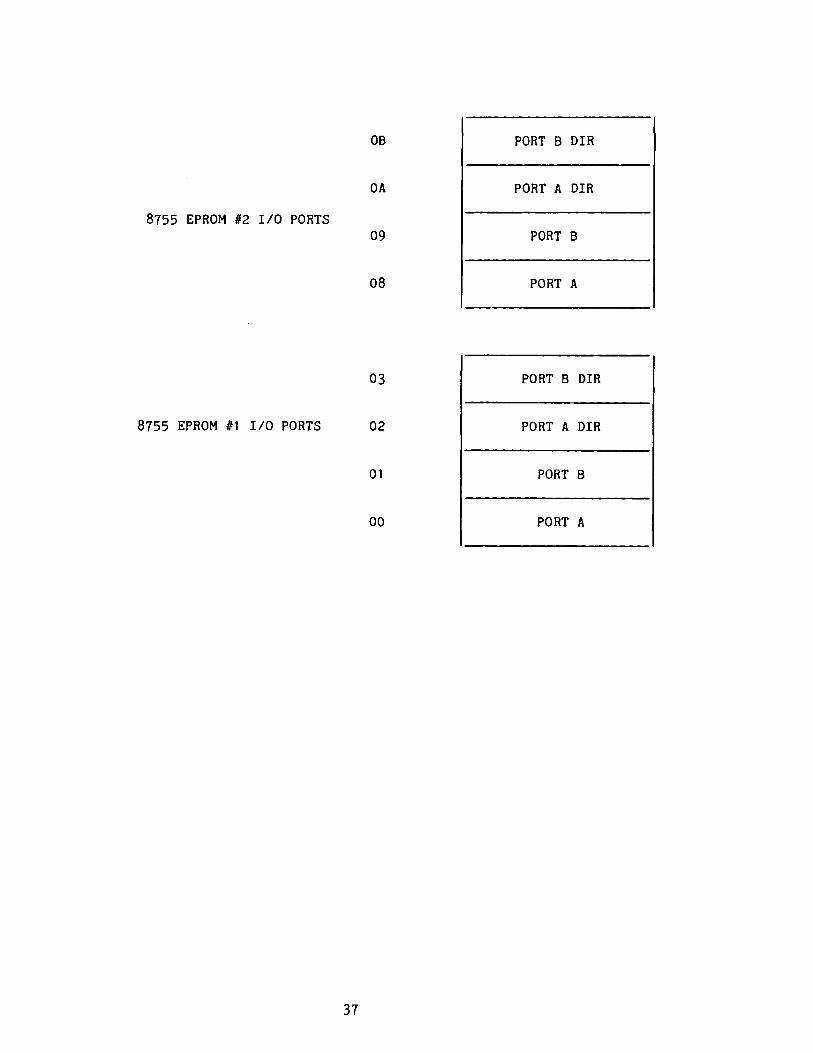
8755 EPROM #2 I/O PORTS
OB PORT B DIR
OA PORT A DIR
09 PORT B
08 PORT A
03 PORT B DIR
8755 EPROM #1 I/O PORTS 02 PORT A DIR
01 PORT B
00 PORT A
37


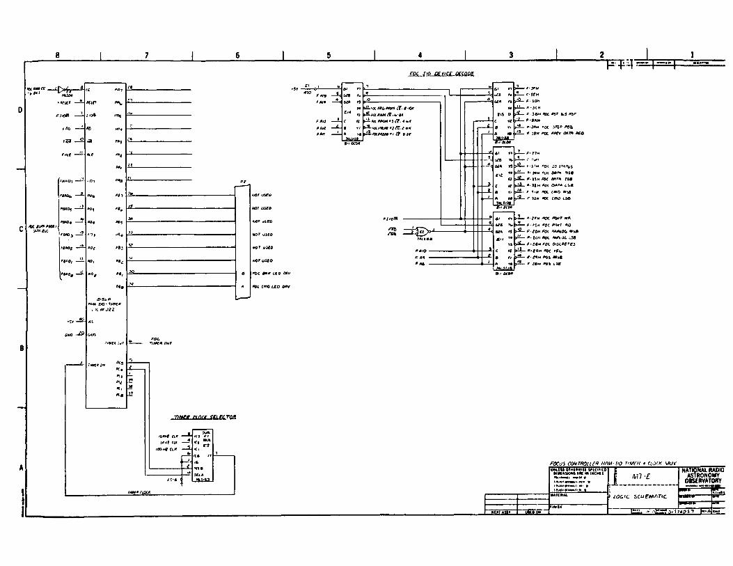
p q z q i--T — F
—4 te « 7
/4UC*
*V icr _*__ n s a
Flfti* — //j* rtrij
ft>Q — «n«
*37® o *& Wl
rm tn
0*t
<H*Ol *•01 **9
*t*b± —*-
'wo5 —^ *01%'*0« - AO4
*flA£>,$ — ‘-1J/«A0* -ii-W/ — 40,
W 0# -* *«#
**m [to ’ 7tmc*i K tP 0 2 2
o'>1/9 — (tit Vu
62» 11
£t* -— — c «
fitut —l - 6 */fAll — L. • >•
XLi/ 8$'• OCO*
—*0C flWW <T. 0 or ►&*«
V T *k ~ n x 9 * 0 M •! I f o z r
«jo r u ! * o
NOT M t o
VC* t/sro
HOT y jU O
¥0* Ut€0
NOT u iC O
*0 t s * r CEO cxv
*©C cm o L E O 0 * v
/ IB
*4/0 <•
^ A »
&*U S
U A /•
M
e»a U
c V*
a V*
A v»
f - J f H
f iow ^♦3CH
f 3 f l « * * « r 4 .9 * a r
* - J A H
*oc *eo,/?• : $ * * x * * f * o a m a t q
A* f t
6^0 %
A2A V5
F ' lM
C V
• V#
A * •
P(OA
¥1
r<m
<WA t s
£< M
V I
C f t
0 t l
A f%M l S U B0 / o t o *
- ? • ? 7 *
. / '•**!
. t I ' H *D<. J J iTATt>$
• »• *«« cue 0 *m * $ 0
> l £ - r - M * * > C £«»•* r s « > j£~ « j i m *©< o * * * t s a
*»« *X £«0 >^2- r M H CMO t i e
5 X «0*»f * A
*0C Pft*T «0 *"■20H *0C AMfeOG
* • t e n A0C W V 0 6 <_S0
***0mf<k OMceea W- »**«h *oc *ri»
r^N pos mvsf *04 1)0
77/Mfif ft flttt SCLKTQ &
fOCUS CQNTROllf* M M VO PMCH * CtdW V*U* uShIU 6IhUWiU shcmib
DiM(MSK)MS AM IN INCHIS
M i r * s s t ufcto on
n it •
I M C I » « M < • «I M l £
> /06/c scur/viric
NATIONAL RADIO ASTRONOMY
OBSERVATORY


m e / )r ,t» LQ * c E O Q P / v C K
if* f - H
N(SO«
-a*0 7
*6* 0<*
W O 5 -
>6*0*
* S f iO j
°6AOe
M * 0 (
*040*
r t PA 1
****>
M S
sfc ™ 4
#k 1 « J
<U£ 0>y
6U 7 1 n/%9
AJto P6 t
eam
Af>4 **r»
j *>0*
P95
AO, «9<r
* u 0 0 6 ,
P69
aa/W
.SC
<‘S & *I t 0 • r /M f«
w o n
*U
'.VO
Time* OUT
* s K 4
A ll
, Ht5)«
« Tsj«
" r jA . - . y —
* <■>:»
- *iW8 = 1 © ' * -
» iS fg
zipy-
«>*«l ft* /*«* f t*
*0 0 * 1 cut
OoAl4 4/ll/»
-*L 6
« i A
P O T L to OEtfiCe D E C O D E
*A>5
/VMM
* A / J
*A /2
«A«
>- wr/ijp6 *0*1 <•£ « • ton
£ 90T *AM C l 4 o t
— fu r/w ** • j ce n <
•—W #0M #* Of ^0«— if»f /*oa» •/ tf. 0
z J « > j
*0 Ci»J<U «"f'dUC> L£P rClVfi
■<i »»!' WWU (CCTTA CT l e p o e r v c
*A<0A m
* V O l/ r / $ * K n o o * *
*<j t c m o L e o o n v
> >6>‘ it#
r «■ .*?</*
#sr itc
o u r
T«*CS« s s s
<o#r
8 ' l GVOTs
f, V i
t *
n
C»3 y«
K»
c a
• *•ve
- — »•2-- « • JfH
£ — R 30M
— » • 3 (H
» j e « »ot *jt <,. j (t »t
« JA*-i
'— » • j n n » o r s r§ p » f o
^5— * *b h « o r v n o « r « n ra
n ►2— J IM
UZt '<• -- ft JfcH
6 /A /S « J fiH # O T ^ i « fATu>
« >ii— *• 34 n / to r o a t a
>-£— i»- 5 3 h a o t o a t* f 3 «
f »/ >- — ^ . J ? H f o r . OAM (.166 r, » • 31H tOT cmo /H56
4 «« >'5-. if. JOH *0T CA*0 ts *
tf-* 0(C<
M >--- 9 t e n *O T ^OAT «TA
>2— * * f n /fo r w r « o
&tA 1* v i f i . 9-SOM POT A^AtO(» « » 6
C l I *• > i i . « se n » o r A «A to& t^ a
vs f l- if lw POf 0»iC»C^¥5
C * t fc ,JAH f fo r /£b
6 ti «•<?<»« ffOT HO iAnsa
A 1$ > iS _ r o t f lo i t^ a
t t l f * ■
R0TA7i0*J C 0U 7H 0LLEK DECODE M V ) L/0 C l O CK M U X a L E O /y?<i/£#S
U N KSS OTHCDWISC S rtC l'K O DIMENSIONS AM IN INCHCt rgm w ctt worn t i f u d N O H u u m * I
Ml • £
LOC/C SCH EM A TIC
NATIONAL RADIO ASTRONOMY
OBSERVATORY
i s n . u i» in g o o s 7 k


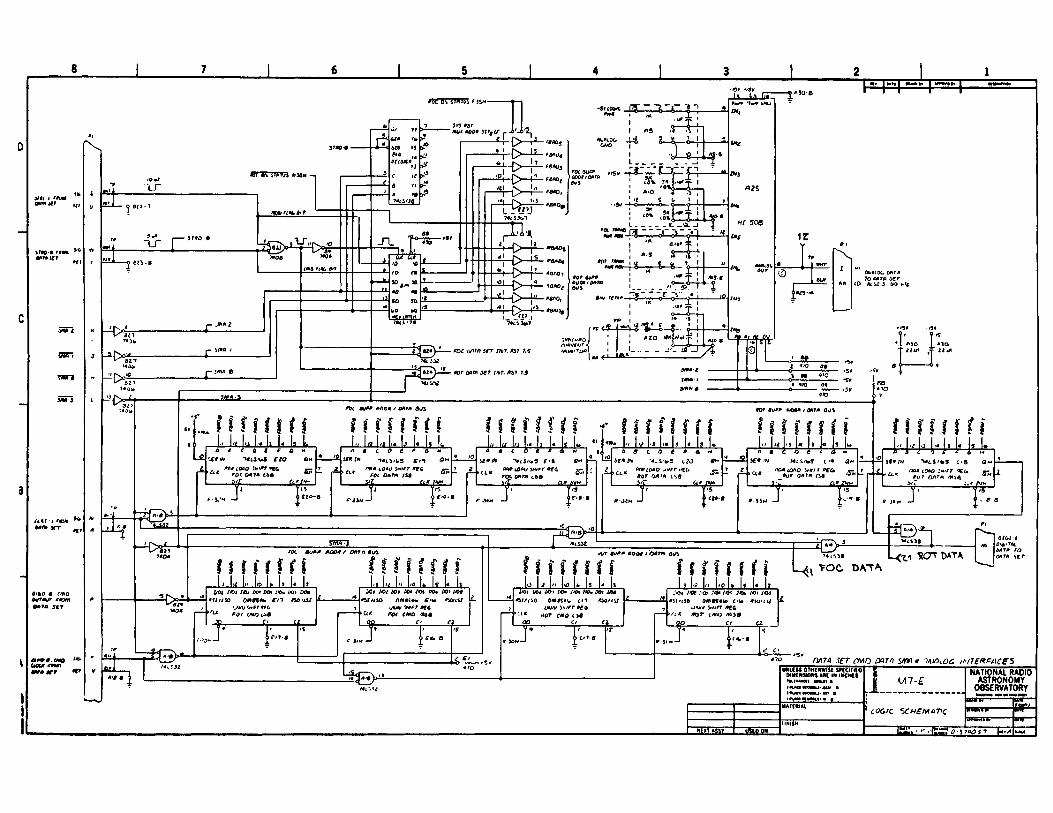
■199 • tS l __.11 .la DTI
<4* r * >-'
3 :
i r
0 '* 0 # c/no W u r **omOATA J t T
M0«
«*o »*r
_ T L
- £ > — i-2— teM>i
Til, FMMB p *
_ £ J _
- £ > — p — * * * ° s
- ^ — l-S — w b a a ,
-0 -T~ <OAOs
- O - t ^
-O-i^ w o ,
- T > — #a/M% V J V l
, *Q t & r *1 c o o * * oath 01/S
5* I # A |*0% j , ■ 5 . . 4
JL _ ' f t . . J
*«*' £ t s - h
t r
< 4 -
*DC O rt/* 3 f T /A ir A5
;w r « * o I
N kiff T o * I
& ’%u-' a to
5*
[No
• « k a«wi je r » r . /»s» 7.5
0 AMlOC OrtTA 70 ^ c rAtGf J . CrO *>*
3 ^ ' S
/VC A/** *00* / 0A1A Q tfl
*% 5 ^
«D r A00« / QATA fltfS
n n u f f i f f U f a t t u f f a • n r m n h i r i mL I.LU I. 1. 1. L, l„ I-1- 1., b I. 1.1
H t S 'U S € ZO £C* fft *>4i5/(»3 k />< # f i* * 10*0 S**fiT * e c -
fO< OATA /S0- S 'S ____________ C L * t w
*
1 4 4 4 *s s * m ~*ist<m9 e » t
r , x » f 4ro c OAT* <.66
1
S/w A -f
fix 4 u *r Ai00* / on? a *us
i f m t aI j I t L< L L l » l« la
t/Oi tfO i t€b I/O* VO\ tiD» ItO* lfO%* ? / / / s o o m § s« (* r / i # w / t i r
>rtx ^ a c c A io t ia
J P 1 - T
i ? t s' f f f iU U l» U L \s l« \i
J C t J/Qt W f t & M X //o* OOt U09 * $ t u s 0 o««<4<* ^sa/c&r
c/am/ # r«► a * CMO >H5B
_ f l p __________________ a
* i o . $ e * t o *4.S '* 3 ( . t o
Pt*LOAO J t f f T tfiG*o r tse
?
A « C O 6 * 6 *
i f * v M i i / f e r f lN
► ct*tXV'O U * F T P Z U
f u r r i « J m
_ _ i ^ — . A?L rvM ..
C 'S
h n 1 i 1 i• o « / » » c o iw /
M J V_ Ifc 1^//Ol IAU tx» VO» r*0i t*>* 00* 1A *
* } t / ( * 0 <9M#S4W C l?
>w t cmo atu *
0 0 _______________ O _________ C l
J p r r
i j r r i t nL U U l J . 1. 1. I.
S'Cn //or .'oo .4,o* /4eh / « » / « j^ 1 ^ 1 0 O « 0 S « (T C<to « W / (U
is I—< 1 DataTOC DATA
0fC »M
0A7A tOo * r * * e r
J
u m k s s o iM c im iic s n c m t oDIMCMSIOMS A * ( IN INCMCSfk iu a e ii MNLit » l*4C« MC«HJ(JUX) ft tm jct NCMUi ati ft
ft
i u7-£NATIONAL RA0I0
ASTRONOMY OBSERVATORY
• ■ n r* r— — m —
k <CCXi/C S C H E M 6 V C I f t W H -----------
HNISHJ J L - - I I I .
t i l l ? AS&V - I M W --------------- E l L r - 1' ■ ■ E a ? o n « o i 2 - 1 - ^ M i


3.0 Ml 1 APEX INTERFACE LOGIC
The Apex Interface contains the logic and conversion equipment to sense conditions in the Apex and serially transmit this data to the F/R Controller upon request. Except for the common time base, analog multiplexer-A/D logic and display logic, the logic is partitioned into two independant, asynchronous sections associated with the Focus and Rotation processors in the F/R Controller.
The Apex Interface logic schematics follow this text.
The Apex Interface is powered by a dedicated power supply in the M8 to isolate all Apex signal lines to the Apex Interface. The links between it and the F/R Controller are isolated by optical isolators to protect the balance of the system from disagreeable phenomena associated with lightning.
The Time base logic on Sheet 1 generates system clocks, scan clocks for the multiplexed front panel numeric display, Sample/Hold & A/D Blank/Convert terms and the multiplexer address terms for the analog multiplexer. The A/D conversion sequence operates continuously at a 10 KHz rate and is initiated by -10 (not 10) term which sets flip flop D17 which in turn sets the S/H to the Hold mode, 10 us later the trailing edge of -10 triggers the second half of D17 which initiates the A/D conversion. The A/D -DRDY (A/D EOC) terra triggers a one-shot delay pair to provide a delay for the A/D bits to settle. The delay pair generates an A/D load strobe which parallel-loads the A/D data into static storage register D22 & D23 and advances the multiplex address counter D28. The leading edge of the 80 term clocks flip flop D17 off to cause the S/H to revert to the Sample mode so the multiplexer has H5 us of settling time before the next Hold command. When the A/D converter is converting Focus or Rotation velocity data, the converted value is strobed into storage register B18/B19 & C18/C19 for subsequent readout.
The Synchro/Digital Readout Control logic for the two axes are identical, so the following description applies to both sets of logic. This logic causes the position values, A/D data and discretes to be sequentially unloaded to the F/R Controller in response to a data request from the controller via the optical isolator B1. The request sets a control flip flop B30 to initiate the readout sequence and if the A/D is not in the process of conversion, the sequencer control flip flop B30 is triggered on by gate B23. If the A/D converter is busy, the trailing edge of -Sample/Hold turns on B30. This action insures that the data is never read out during the A/D conversion process which takes about 35 us. The sequencer control flip flop B30 inhibits the Rotation Synchro to Digital converter to keep it from converting during data readout and enables a train of ones to travel down shift register B29 which is clocked by a 5 MHZ clock. Four clock pulses later, gate B23 generates a the -Rot Data load strobe which parallel-loads registers B22 through B11 with the A/D data, analog mux address, Apex discretes, Rotation velocity and Rotation position data. On the fifth clock pulse, the shift register Q4 term enables the shift counter (B26&B27) to begin counting and also enables shift clocks to be output by gate B23. The shift clock train unloads the Rotation Data register and provides a load clock to the F/R Controller via differential driver B6. The shift counter shuts down the unload sequence at a count of 64 (it was preset to a count of 21) by clocking control flip flop B30. The four B24 inverters provide about 50 ns of delay in the shift clock to prevent a B30,B29 propagation delay glitch from being output with the clocks. One-shot
38
D12 is triggered by the -Rot S/D Inh terra to provide a discrete front panel indication that the Rotation data readout/conversion process is active.
The data unload time is 9.8 microseconds and the unload logic may be delayed by as much as 35 microseconds due to A/D delay so the maximum readout delay after the data request is 45 us and the minimum is 10 us.
Sheets 2 & 3 are the data unload registers, Apex switch inputs and fault logic. Apex discretes are shown at the top of the sheets and drive Schmidt input inverters for enhanced level discrimination. All discretes are sensed via contact closures to ground and sink .5 ma of current during the nonactivated state of the switch. Fault logic senses illegal states such as the concurrent sensing of both Upper and Lower Focus limits or more than one Pin switch. In the event that this sort of immoral (it has happened) behavior is sensed, an alarm term - YOWP! is sent directly to the controller to inhibit all action. Focus and Rotation limits are also sent directly to the controller. Rotation CW/CCW limits are wired in the module and bin inputs but no longer exist in the mount or cabling between the Apex & bin.
Sheet 5 contains the front panel display logic which consists of a 3- line, 10 channel multiplexer to drive the numeric display segment encoder on the display board. The inputs to the multiplexer are the Focus and Rotation position storage registers and the position data is multiplexed by the scan term as a sequence of 10 octal characters. A digit selector, driven by the four bit scan terms enables the cathode of each digit in succession while the anodes are driven by the 7-segment encoder. The Scan counter driven by the 10 KHz scan clock.
All the analog and conversion circuitry is contained on Sheet 4 and consists of an 8-channel single-ended multiplexer, Sample and Hold, A/D Converter and Integrating Synchro to Digital Converters. The operation of these devices is described in the Data Sheet section of this manual so they will not be described here. For an in-depth discussion of the Integrating. Synchro to Digital converter see the DDC "Synchro Conversion Handbook” or the Analog Devices “Synchro & Resolver Conversion" book. The operation of these devices is quite simple and the logic to interact with them was described above. The alignment process for the analog components is quite simple and can be done by removing the front panel adjustment panel cover. The +10 volt reference is set first. A high quality DMM is plugged in to test connector pins 1 & 13 on the front panel connector and pot R2 is adjusted to produce +10 volts +/- 2 mv. Next, momentary switch S1 is actuated down to feed analog ground into the Sample & Hold input to set the A/D zero. Pot R2 is adjusted to produce a 0 volts reading on the Data Tap (set to Mux address 225 or 235, DS#3). Next the switch is actuated up to feed the +10 volt reference voltage into the Sample & Hold input and the A/D gain is adjusted by pot R3 for a +10.000 reading on the Data Tap (addresses 225 & 235). The 10 bit A/D Converter is scaled at 10 mv/bit and is a 10 volt span device so the Data Tap readout will change in steps of 20 mv.
There are no gain or zero adjustments for the S/D converters. Differential amplifiers E15 read out the synchro argument velocity; these should be set for zero output by offset pots El 3 & E14 on the bench when synchros and the 400 Hz inputs are connected to the module.
The F/R Mount temperature is sensed by an AD590 temperature sensor
39

mounted in a metal box bolted to the underside of the F/R Mount gearbox. The temperature verifies the operation of the heaters and is scaled to produce 100 mv/deg C. The scaling and offset resistance values should be set up on the bench before installation in the antenna.
Figure 8 (below) depicts the location of these analog data adjustments and the display messages.
(------------------------------------------ ^FOC ROT
GxDdXS) dOx3©
STATUS
uL
LI
Cw
ccw
|RiR
RE
M1
M2
M4
FA
RA
AA P L C u K X V Z
)
o o
The numeric displays show positions as *1 digit octal values derived from the S/D converter 1H bit straight binary code output; the value may range between 0000 (full D0WN/CCW) and 3777 (full UP/CW). The associated values seen on the Data Tap octal display will be: 2000 and 1777 respectively since the msb is inverted to make the monitor data a 2 fs complement value.
The discretes display indicate the following when illuminated:
UL & LL - Focus Upper or Lower limit switch actuated CW & CCW - Rotation CW or CCW limit switch actuated RR & RE - Ring Retract or Ring Extend switch actuated M1,M2,M3 - Apex Interface analog mux address bits FA - Focus Data readout to controller active RA - Rotation Data readout to controller active AA - A/D Converter activeP,L,C,U,K,X,Y,Z - Band Pin Switch Actuated (not presently used)
40

The test point connector permits observation of the following functions:
PIN FUNCTION PIN FUNCTION
1 A/D align switch output 14 analog spare2 S/H output 15 analog spare3 YOWP! 16 A/D blank/-conv4 S/H state 17 A/D data ready5 -A/D load strobe 18 - 1 0 time base term6 5 MHZ clock 19 80 time base term7 Focus output data stream 20 Rotation output data
stream stream8 Focus unload clocks 21 Rotation unload clocks9 -Focus data load 22 -Rotation data load10 Focus readout enable 23 Rotation readout enable11 Focus readout start 24 Rotation readout start12 Focus readout request 25 Rotation readout reques13 Analog ground
41


2 I »
*5wwf L * v
5{SJ1.
•*V■*&
?•« mi ? *•
J1
Sh a > *• 4 t Ci*% r*««i •»«* (• w<m
• •« | •% * W ( M l A | * »1*
uJutSI OTHCiWiSC VCCititO Ol«(ftSK>MS AM IK INCHESItllUMtl M il ft IfUCtNMMKMS * >*AMttCMUi.*e: fti**a«ca*»’» ft
M I I BNATIONAL RADIO
ASTRONOMY OBSERVATORYvcomo M»«»conw
I LOGIC SCHEMATIC Mwni---- wr—riNiSN
MIST ASST WfPW ■ |P*I. «, f | 2? .)>A740SS KAl


4.0 M8 F/R POWER SUPPLY
The M8 F/R Power Supply contains the system logic +5, + /- 15 volt and Apex Interface +5 and +/- 15 power supplies. This unit also serves as a control/display panel for processor-driven display LEDs to indicate important discrete states such as Command Active, Translator power on, Brake V*I ok, Up drive line pulsing, etc. Figure 9 depicts the M8 panel and the associated states. Manual control switches enable manual slew control of the Focus and Rotation axes at either a 100 Hz stepping rate or by ramping to travel long distances. Band select switches and associated LEDs enable future manual control of an Index Locking Pin if the need should arise. To reduce wire count the 8 band switches are encoded into a 3 bit code by a 74LS148 encoder on the display board. The F/R Power Supply schematic diagrams follow this text.
The number of DC output lines on the module I/O connector exceeds the number of modules presently powered; the extra wire capacity has been installed for future expansion in the event that more modules are to be installed in the bins.
Monitor States & Controls:
UL/LL - Focus limits CW/CCW - Rotation limits UP/DWN -Focus drive dir CW/CCW - Rot drive dir BRK - Brake voltage*amps TRANS - Trans power on CMD - Command active MOT - not used EXT - Ring Extend RET - Ring Retract
P,L,C,U,K Pin select switches & LEDs, not
usedDrive UP/DWN - slew
Focus when depressed Ramp/100 Hz - ramp speed
or drive § 100 Hz Drive CW/CCW - slew
Rot when depressed
Figure 9, M8 Displays & Controls
F/R POWfcR
© ©FOC MONITOR
iVl V? BRK THUS CMOo © © ® ©
© © ! ROT MONITORI| CWI Cw BRK twus o nJ © © © © ®I| CCWL CCf BET MOT EXT
© © © © ©
RET EXT © © ©
42


FRCXYr RftNCL DiSPLflr Aitr.
2 I 1I ■ , ,m n \ m m m ■ - ~ . m | ~ „ I * l < ^ l t ^ u « l > v i w I
• * u a •» h %• a**
_USI£jB!L
umcss otMinwiw incintoOIMCNSMH* M ( IN INC M il mil ft E m o ouc
X - - - ______i POu e f\ s u p p l t1 SCHEMATIC OAC,RAn
NATIONAL RAOK) ASTRONOMY
OBSERVATORYfr~
wmnr
lr_ o i v p s i i F

5.0 M22 F/R SWITCHING MODULE
The switching module contains solid state relays to power the Translators, brakes and Ring actuator, Brake controllers to power the F/R Mount brakes and a 400 Hz Synchro Exciter to power the position readout synchros. The relays are optically (internally) isolated and are driven by providing a current sink from an open collector power nand or open collector buffer gate in the F/R Controller logic. The Brake controller is the standard Warner Electric MCS 805 unit which has been removed from the wall of the Pedestal room and installed in the M22 to make them easier to change in the event of failure. During the installation in M22, the output voltage adjustment pot is removed from the Brake Controller PC board and installed on the M22 front panel with longer wires to enable the brake voltage to be adjusted on the front panel. A manual switch and test points on the panel enable manual actuation and adjustment.
The F/R Switching Module schematics follow this text.
BRAKE CONTROLLER ADJUSTMENT PROCEDUREThe following procedure has been abstracted from the Warner Electric MCS-
805-1 Manual:
"Brake Release Adjustment: Prior to operating the Fail Safe Brake, the proper electrical release adjustment must be made as follows:
With the brake mounted and ready for operation, turn the potentiometer adjustment screw on the MCS-805"1 Power Supply counterclockwise as far as possible. Turn on power to provide AC input to the power supply. Next, slowly turn the adjustment screw clockwise until the Fail Safe Brake armature completely disengages from the magnet. Armature release and engagement must be checked by hand until the autogap adjustment is made. Using a DC voltmeter, note the voltage reading at this point, which is determined the instant the armature disengages. If this point is overshot by two volts or more, reset the potentiometer to its full counterclockwise position and repeat the adjustment procedure. Complete the set point adjustment by turning the adjustment screw to a setting six volts higher than the disengagement voltage. Lock the adjustment screw by tightening the locknut provided on the potentiometer. This adjustment must be made with the brake at room temperature for an expected operating range of -50 deg F to 250 deg F. The MCS-805-1 control output changes to track the brake release point as it varies over the -50 deg F to 250 deg F temperature range."
The bin cooling fans, brake, 400 Hz Synchro Exciter, Translator and Ring Actuator power are fused and distributed from the M22.
The Synchro Exciter is a 400 Hz power oscillator powered by a 12 volt, 8 amp transformer mounted on the Synchro Exciter Chassis. The exciter circuitry is contained on a removeable PC board mounted on the Synchro Exciter chassis. The exciter circuit consists of a bridge rectifier, 723 voltage regulator, 900 HZ oscillator, flip flop and a push pull, class B power amplifier which drives a 400 Hz, 30 VA, 24V CT (primary) to 26 volt secondary transformer. In operation a DC voltage of about +10 volts (set by a front panel 500 ohm pot) is produced by the 723 regulator; this is the power switching voltage. An LM 340T regulator generates +5 volt logic power for the logic on the board. A 555 timer connected as an oscillator generates a 900 Hz (approximatly) clock which toggles a 7474 to generate a square wave 450 Hz signal which in turn drive 7*106 open collector buffers. The 7*J06s drive 2N2219 transistors which
43

A current transformer (the primary is 9 turns of #26 wire through a Magnetico 13960 current transformer) generate a voltage proportional to the synchro load current. This signal is fed to a rectifier/filter in the M7 where it is read as monitor data. The termination circuit in M7 scales the voltage at 1 volt/synchro load thus enabling a confirmation that currents are present in both synchro rotors.
The front panel synchro excitation level should be set to produce about 20 volts peak; it is not at all critical since the Synchro to Digital converters/synchro combination will operate with voltages as low as 5 volts. Bench tests have confirmed this. An adjustable 25 ohm power resistor is installed in the primary of the transformer to reduce the transformer output voltage so as to lower the dissipation in the regulator circuit. This resistor should set to about 10 ohms. Four 4.7 uf, ceramic capacitors across the transformer secondary (roughly) tune the output circuit to about 400 Hz.
A photograph of the 400 Hz waveform at the M22 front panel test points is shown below. The scales are: 10 volts/div and 500 us/div.
in turn drive 2N3055 power transistors to produce the power switching signals.
44

6.0 SYSTEM TROUBLE-SHOOTING
An important system design consideration is the ablity to monitor the conditions in the electronics and the F/R Mount to identify malfunctions and diagnose faults. There are two places in which this is done: locally within the F/R Controller and remotely at the control center via Data Checker and the Operator F/R Overlay. A great deal of diagnostic information is brought back in the Monitor data. This section describes some trouble-shooting guidelines for the system based upon remote observations via the monitor data and direct measurements at the antenna; section 9 describes the usage of the Operator F/R Overlay.
The maintainance technicians credo: THE ESSENCE OF TROUBLE-SHOOTING IS TO OBSERVE THE CONDITIONS OF THE SYSTEM AND RELATE THEM TO THE CONDITIONS WHICH SHOULD EXIST FOR THE MODE OF THE SYSTEM. THIS COMPARISON IS THE ONLY BASIS FOR EFFECTIVE TROUBLE SHOOTING.
A) CHECK COMMUNICATIONS WITH CONTROLLERThis is the most basic aspect of fault isolation.
a. Is analog data present? — look at mux 0 - 7 , power supply voltages,also see MW1.
b. Is analog data within limits? — check for bad power supplies.
c. Is digital data present? -- examine DS #3, 220 - 227,Foe; 230 - 237, Rot. If missing or bad, send a RESET to restart the processor; does the data reappear? If not the controller is bad or is not hearing the Data Set.
d. Is the digital data reasonable? -- evaluate as shown in D.
B) CHECK FAULT & MODE FLAGSAre there fault or mode flags coming back from the controller?
These are major descriptors of the conditions seen by the F/RController.
OPERATOR — the opertor has sent an out of range Foe command.
CONTROLLER — the controller has sensed an illegal condition during program execution.
DRIVE — the mechanism is not driving properly, probably a bad translator, cold sticking, mechanical drag or jam.
TRANSLATOR — translator did not turn on or off within 1 sec.
BRAKE — brake voltage*current bad or did turn on or off within1 sec.
UPPER/LOWER LIMIT — limit switch activated, should never happen under Computer control, result of some malfunction.
TIMEOUT — commanded position has not been attained within
45

allotted time.
APEX INTERFACE DEAD — Apex Interface has not responded to a data request from F/R Controller.
CABLE INTERLOCK — a bin I/O cable is loose or disconnected.
SYSTEM — a system malfunction has been sensed by controller.
RING — 327 MHz ring is not moving.
APEX ANALOG FAULT — one of the Apex Interface signals is out of range.
YOWP! — Some serious fault has been sensed by Apex Interface, all brake, translator & Ring drive is inhibited.
LOCAL mode — the controller will not accept commands in the LOCAL mode, go set the M7 switch to CMP mode.
APEX INTERFACE DEAD — the Apex Interface is not responding to data requests from the F/R Controller
CMD ACTIVE — a position command is being executed
NAP ACTIVE — position and ring commands are being ignored, send a RESET command to clear NAP mode.
C) CHECK COMMAND-F/R RESPONSEThe analysis of the controller response to a command is a very
important aspect of system trouble shooting. The digital monitor data should be examined in these tests as the command and response discretes provide detailed information about what is happening in the system.
a. Send a position command, does ECHO = CMD ?yes: command input logic is working, the controller responded to a CMD from the Data Set, interpreted as it properly & initialized the control program.
— no: command not being heard, may be bad F/R Controller, Data Set, Ant Buffer, IF/LO problem.
b. Does a position command cause any drive movement ?— yes: but slow & with a DRIVE, TRANS or BRAKE fault,
check the digital data for conditions. The drive appears to be sticking, check the translator.
— no: & with DRIVE, TRANS or BRAKE faults, indicates a drive problem, bad translator, stuck drive, check the digital data for conditions. Check the translator, wire a substitute motor into the pedastal room junction box.Will it run in the LOCAL mode? Climb up to F/R Mount & disengage motor from the mount, will it run in the LOCAL mode?
46

c. Will controller accept a NAP command? Test by sending aPOSITION command after a NAP command.
no: F/R Controller is not working properly, NAP command is a very simple command to execute.
d. Will the controller accept a soft reset command? (mux 321 &331). RESET causes Apex data to be all zeros until updated.
— no: F/R Controller is not working properly, a soft RESET is the simplest command to execute.
e. Will the controller respond to a hardware RESET command, MUX337?
— no: F/R Controller is really busted.
D) CHECK MONITOR DATA VALUES AND STATESAll discrete control states, all sensible response states and
analog monitor data from the F/R Controller and Apex Interface are available for fault analysis. Section 5.0 details the data formats. In general any command will activate several of these control and response discretes; if there is a problem these states should be examined on a Data Tap. If a Position command is to be executed, the translator power, brake, steer up/down (cw/ccw) and clock enable control discretes should be 1fs. The clock rate control discretes should sequence through a lot of states if the drive is to be ramped up in speed. The response discretes should show brake V*I,translator power on and drive up/down (cw/ccw) pulsing.
The following analog/digital data values should be examined:
a. Is synchro: = 2 V? — yes: synchro excitor in M22 is ok= 1 V? — yes: one synchro rotor lead open = 0 V? — yes: synchro excitor in M22 bad or
fuse blown
b. Is the position readback stable?— yes: synchro & S/D converter probably working,
drive a little, does the position change?— no: S/D converter bad, no synchro excitation or
a synchro wiring problem.
c. Is mount temp ~ 10 deg above ambient when ambient is <45F?
— yes: heaters & temp probe ok.— no: mount heaters may not be working, is drive
sticking?
d. Is bin temp > 30 deg C?yes: damage can result, go check the fans.
e. Are power supply voltages within tolerance?— no: go fix the problem.
47

7.0 TELESCOPE OPERATOR CRT OVERLAY DESCRIPTIONA replica of the new F/R System Overlay is shown below; all fault flags are
shown.
NEW FOCUS/ROTATION AND (22)
SYSTEM LOCAL TIMED OUT SYSTEM FAULT I/O CABLES YOWP!RINGEXTENDED
FOCUS
NAP
UP TRANSL DRIVE PULSES LOWER LIMIT
BRAKEDRIVETRANSLATORCONTROLLER
ROTATION
NAP
CW TRANSL DRIVE PULSES
BRAKEDRIVETRANSLATORCONTROLLER
APEX INTERFACE MOUNT TEMP 16.900-15 V + 15 V +5 V
+ 10 V FOC VEL ROT VEL GROUND
-15.01015.0205.00510.0000.0000.0000.000
ANALOGS NOT OK INACTIVE
POSITION COMMAND CMD ECHO ERROR
746974697469
0
-3471-3471-3471
0
F/R CONTROLLER +5 V 5.005 +15 V 15.005 -15 V -15.010 FOC TRAN 2.600 ROT TRAN 2.550 SYNCHRO 2.010 BIN TEMP 24.00 GROUND 0.000
F=FOCUS, R=ROTATION, (N=NAP), (RING CMDS) E-EXTEND, W=RETRACT S=STOP, ESC-M=MASTER CLEAR
Section 6.0 of this manual details a fault isolation procedure which be referred to for an expansion of the the information discussed below.
F/R FAULT MESSAGES
SYSTEM FAULT - The F/R Controller has detected a serious system fault.
I/O CABLES - Some bin I/O cable has been disconnected or is loose.
RING FAULT - The 327 MHz ring has not attained the commanded state within the allotted time.
TIMED OUT - The commanded position has not been attained within the allotted time.
BRAKE - The brake V*I has not reached the commanded statewithin 1 second.
TRANSLATOR - The translator has not reached the commanded state
may
48

within 1 second.
LOCAL - Although not a real malfunction the CMP/LOCALswitch was left in LOCAL. CMP should normally be displayed here.
CONTROLLER - CONTROLLER indicates that the controller has sensed a malfunction in its operation.
ANALOGS NOT OK - Indicates that an Apex Analog fault has been reported by the F/R Controller.
INACTIVE - Indicates that the Apex Interface is not responding to data requests from the F/R Controller. This is a major malfunction
F/R DISCRETES DISPLAY
UP TRANSLATOR - The Focus translator is being driven with UP pulses. Down is the complementary case.
CW TRANSLATOR - The Rotation translator is being driven with CW pulses. CCW is the complementary case.
LOWER LIMIT - The Focus drive has driven to a limit switch, this should never happen under central computer control, something is really wrong. UPPER LIMIT is the complementary case.
RING EXTENDED - The 327 MHz Ring has been extended into position and has actuated the position sensing switch.RING RETRACTED is the complementary case. When the Ring is traveling between the two positions neither switch should be actuated; there is no other readout of Ring position.
NAP - NAP indicates that the processor is ignoring position and ring commands. A RESET command clears this mode.
COMMAND/POSITION DATA
POSITION - POSITION is a decimal value which ranges between + 8191 to - 8192. Typical (Ant 20) Rotation command arguments are: L —xxxx; C —zzzz; K — yyyy; U — vvvv; X — tttt.
COMMAND - COMMAND is the decimal value of the position command set point.
COMMAND ECHO - COMMAND ECHO is the command argument heard by the F/R Controller and is returned as monitor data to verify command reception.
49

COMMAND ERROR - The controller calculates the difference between the commanded position and the present position; this is read out as monitor data.
APEX INTERFACE ANALOG DATA
MOUNT TEMPERATURE is the temperature sensed on the middle of the bottom of the gear-box and serves to verify that the gear-box
and platform heaters are working in cold weather. The heater controller switches on when the ambient temperature is below about 45 deg F. The temperature readout is in degrees C and should be about 10 deg C above ambient when the ambient is below *15 F. When the F/R Mount temperature drops below 0 deg, the controller signals an Apex Analog fault.
APEX INTERFACE POWER SUPPLIES indicate the voltages which operate this interface. The +/- 15 volts should be within +/- .3 volts and the +5 volt tolerance is +/- .15 volts. The +10 volt tolerance is +/- 0.0*10 volts. This data has a granularity of .020 volts/bit. Ground is a measure ofA/D zero drift and should be less than +/- 0.0*10 volts. Foe and Rot velocities are a measure of drive velocity and are scaled 13 volts/in/sec for Focus and 5.2volts/deg/sec for Rotation.
F/R CONTROLLER ANALOG DATA
F/R POWER SUPPLIES indicate the voltages which operate the F/R Controller and associated logic. The +/- 15 volts should be within +/- .1 volt and the +5 should be within +/- .2 volts. The translator power should be +2.6 +/- .2 volts. These translator voltages are present only during command execution. The Synchro voltage should read +2 +/- .5 volts. Ground is a measure of the Data Set A/D zero drift and should be less than +/ .010 volts. Bin temperature reads out directly in deg C and should be less than 30 deg.
50

8.0 CONTROL/DATA FORMATS
Mux refers to the multiplex address in octal format, loc denotes the byte symbolic address in RAM memory.
COMMAND FORMATS:
RAM
Mux addr 320/Foc 330/Rot 336/Ring
Ram loc rampas Data null
rampasnull
nonenull
b23 b22 b21 b20 b19 b18 b17 b16
80H 40H 20H 10H 08H 04H 02H 01 H
Ram loc Data
b15 b14 b13 b12 b11 b10 b9 b8
80H 40H 20H 10H 08 H 04H 02H 01H
rampbs Foe arg
002**13,msb 2**12 2**11 2**10 2**9 2**8
rampbs Rot arg
002**13,msb 2**12 2**11 2**10 2**9 2**8
nonenull
00000000
Ram loc Data
b7 80Hb6 40Hb5 20Hb4 10Hb3 08Hb2 04Hb1 02HbO 01H
rampcs Foe arg
2**72**62**52**42**32**22**12**0
rampcs Rot arg
2**72**62**52**42**32**22**12**0
noneRing arg
0000000ext/ret, 1=ext
A SYSTEM RESET command (Mux 337)causes abortion of active commands and re-initiallizes the two processors. A software RESET command (Mux 321 & 331) resets the addressed processor. The control argument is not used in RESET commands.
NAP commands (Mux 322/Foc & 332/Rot) cause all subsequent position commands to be ignored until cancelled by a RESET command. The command argument is not used.
51

DIGITAL MONITOR DATA
Digital monitor data formats are a composite of values and associated discrete or fault data. A 1 in a fault bit denotes a fault state.
Focus Digital Monitor Data:
Mux addr 220/Foc 221/Foe 222/Foc
Ram loc posd+2 erro+2 echo+2Data faults modes null
b23 80H operator 0 0b22 40H controller cmd active 0b21 20H drive nap active 0b20 10H translator timeout 0b19 08H synchro, = 0 Apex Int dead 0bl8 04H brake cable int*lk * 0b17 02H upper lim system * 0b1 6 01H lower lim emp/loe, 0 = loc 0
Ram loc posd+1 erro+1 echo+1Data Foe pos Foe pos error Foe cmd echo
b15 80H 0 0 Cmd bit echoedbl4 MOH 0 0 Cmd bit echoedb13 20H 2**13, msb 2**13, msb 2**13, msbb12 10H 2**12 2**12 2**12b11 08H 2**11 2**11 2**11b10 OMH 2**10 2**10 2**10b9 02H 2**9 2**9 2**9b8 01H 2**8 2**8 2**8
Ram loc posd erro echoData Foe pos Foe pos error Cmd echo
b7 80H 2**7 2**7 2**7b6 MOH 2**6 2**6 2**6b5 20H 2**5 2**5 2**5b4 10H 2 **n 2**n 2**nb3 08H 2**3 2**3 2**3b2 04H 2**2 2**2 2**2b1 02H 2**1 2**1 2**1bO 01H 2**0 2**0 2**0
* 1 = no fault, low true
52

Mux 223/Foc 224/Foc 225/Foc
Ram loc dscr+2 adcr+2 anad+2Data clock control Apex Foe Discr Apex Anlg Faults
b23 80H 2**7,msb 0 gndb22 40H 2**6 0 0b21 20H 2**5 0 foe velb20 10H 2**4 0 +10 voltsb19 08H 2**3 0 +5 voltsb18 04H 2**2 Foe brk V*I +15 voltsb17 02H 2**1 Foe upper lim -15 voltsb1 6 01H 2**0 Foe lower lim mount temp
Ram loc dscr+1 adcr+1 anad+1Data cmd sense Foe vel Apex analog data
b15 80H Foe trans pwr 0 0bl4 40H Foe brake pwr 0 Mux addr 4b13 20H 0 0 Mux addr 2b12 10H 0 0 Mux addr 1b11 08H Foe drv up 2**11,msb 2**11,msbb10 04H Foe drv down 2**10 2**10b9 02H 0 2**9 2**9b8 01H Foe clock en 2**8 2**8
Ram loc dscr adcr anadData activity sense Foe vel Apex analog data
b7 80H motor pulsing,=0 2**7 2**7b6 40H down pulsing 2**6 2**6b5 20H up pulsing 2**5 2**5b4 10H trans pwr mon 2**4,lsb 2**4b3 08H 0 0 2**3b2 04H cable intl’k 0 2**2,lsbb1 02 H Yowp! 0 0bO 01H loc/comp 0 0
53

Rotation Digital Monitor Data:
Mux 230/Rot 231/Rot 232/Rot
Ram loc posd+2Data faults
b23 80H operatorb22 40H controllerb21 20H driveb20 10H translatorb19 08H synchro, =0bl8 04H brakeb17 02H 0bl6 01H 0
Ram loc posd+1Data Rot pos
b15 80H 0bl4 40H 0b13 20H 2**13,msbb12 10H 2**12b11 08H 2**11b10 04H 2**10b9 02H 2**9b8 01H 2**8
Ram loc posdData Rot pos
b7 80H 2**7b6 40H 2**6b5 20H 2**5b4 10H 2**4b3 08H 2**3b2 04H 2**2b1 02H 2**1bO 01H 2**0
erro+2modes
ring active cmd active nap active timeout Apex Int dead cable int*lk * system * cmp/loc, 0=loc
erro+1Rot pos error
002**13,msb 2**12 2**11 2**10 2**9 2**8
erroRot pos error
2**72**62**52**42**32**22**12**0
echo+2 Ring mon
00000ring fault ring retract ring extend
echo+1Rot cmd echo
Cmd bit echoed Cmd bit echoed 2**13,msb 2**12 2**11 2**10 2**9 2**8
echoRot cmd echo
2**72**62**52**42**32**22**12**0
* 1 » no fault, low true
54

Mux 233/Rot 23^/Rot 235/Rot
Ram loc dscr+2 adcr+2 anad+2Data clock control discretes apex an faults
b23 80H 2**7, msb sum pins, =0 gndb22 HOH 2**6 pc4, =0 rot velb21 20H 2**5 pc2 " 0b20 10H 2**4 pel " +10 voltsb19 08H 2**3 0 +5 voltsb18 OHH 2**2 brake V*I +15 voltsb17 02H 2**1 Rot cw lim, =0 -15 voltsb1 6 01 H 2**0 Rot ccw lim, =0 mount temp
Ram loc dscr+1 adcr+1 anad+1Data cmd sense rot vel apex analogs
b15 80H Rot trns pwr 0 0b1 4 MOH Rot brk pwr 0 ana mux 4b13 20H Ring ret pwr 0 ana mux 2b1 2 10H Ring ext pwr 0 ana mux 1b11 08H Rot drv cw 2**12,msb 2**12, msbb10 OUH Rot drv ccw 2**11 2**11b9 02H 0 2**10 2**10b8 01H Rot elk en 2**9 2**9
Ram loc dscr adcr anadData activity sense rot vel apex analogs
b7 80H mot pulsing 2**8 2**8b6 4 OH ccw pulsing 2**7 2**7b5 20H cw pulsing 2**6 2**6b4 10H trans pwr mon 2**5,lsb 2**5b3 08 H 0 0 2**nb2 0*»H cable intl'k 0 2**3b1 02 H Yowp! 0 2**2,lsbbO 01H loc/comp 0 0
ANALOG MONITOR DATA:
Mux Parameter Nominal Value & Tolera
OH 5 logic pwr +5 volts, +/- .2 volts.1H analog gnd 0 volts +/- 10 mv.2H +15 volts/2 +7.5 volts +/- 100 mv.3H -15 volts/2 -7.5 volts +/- 100 mv.4H Foe Trans pwr +2.5 volts +/- .2 volts5H Rot Trans pwr +2.5 volts +/- .2 volts6H Bin Temp .1 volt/deg C7H Synchro current +2.5 volts +/- 1 volt
55

SPECIAL PURPOSE MONITOR DATA
Fault monitor data is a selection of the data listed above which has been formatted to combine all fault data into one single word for convenience in examining fault bits. The F/R Mount temperature data has been put into a dedicated monitor word for convenience in driving a strip chart recorder.
Focus and Rotation Special Purpose Monitor Data
Mux addr 226/Foc 236/Rot 227/Foc
Ram loc faul+2 faul+2 temp+2Data faults faults F/R Mount Temp
b23 80H lab test lab test 0b22 40H lab test lab test 0b21 20H lab test lab test 0b20 10H timeout timeout 0b19 08H Apex Int dead Apex Int dead 0b18 04H cable Int*lk cable Int'lk 0b17 02H system system 0b16 01H Motion Analysis Motion Analsis 0
Ram loc faul+1 faul+1 temp+1Data Apex Analog Apex Analog F/R Mount Temp
b15 80H gnd gnd 0b14 40H 0 0 0b13 20H Foe vel Rot vel 0b12 10H +10 volts +10 volts 0b11 08H +5 volts +5 volts 2**11,msbb10 04H +15 volts +15 volts 2**10b9 02H -15 volts -15 volts 2**9b8 01H mount temp mount temp 2**8
Ram loc faul faul tempData faults faults F/R Mount Temp
b7 80H operator operator 2**7b6 40H controller controller 2**6b5 20H drive drive 2**5b4 10H translator translator 2**4b3 08H synchro, = 0 synchro, - 0 2**3b2 04H brake brake 2**2,lsbb1 02 H upper lim 0 0bO 01H lower lim 0 0
56

9.0 SYSTEM CABLE DRAWINGS, TRANSLATOR SCHEMATICS & MOTOR DRIVE WAVEFORMS
57


' l o M O

r PA:o <-
------- K P <-
— — —f—< J <r ------ <R<-
--------k F <--------- l-<t <r
--------h<S<-b <rA <r
-------- t-<C <■
--------I-<0D«-— — —I—<FF<-
--------f-< E <r--------- 1—CM <r
H <r--------I—<N <r
--------*-<K «■-------- \~CT <-
--- —I—<W <■- - -4-<Y <r
V <- X <r
-------- I-<Z <--------- l-<f <r------(-< e <r
------ k B <-I ------II I/O COMM PLATE
r c " r a c k
"W 2-A" (3S FT)FOC St BLKROT BRAKE SSR RED
FOC S2 BLKn o r x l t r s s * WHT
FOC S3 BLKUMIT SW R E T BRN
FOC UL BLKFOQ LL VEL
SV A ICURO R! BLKSVAICHRQ RZ BUVS
MOUNT T E M P * BLKMOUNT TEMP - OrRN
ROT, s./ _fiULFOC BRAKE SSR GRN
ROT S2 BLKFOC XLTR S&R RED
PO T S 3 BLK6S R + SOURCE NHT
FOC XLTR PULSE UP BLKFOC XLTR PULSE DN _ BRN
3 2 7 Cxr-O UT LIMIT BLK327 *eX.-IN LIMIT
\ * W 2 - B " (35 ft:)
4 i n t e r l o c k JUMPER
t lr\
ROT XLTR PULSE CW BLK pROT XLTR PULSB CCW VEL j I
BLUE
PED.RM. JCT. BOX
«,t b i - IL _ L c T B l-3
*TB<4-3_ * T B I- S_® TB l-7
H8TBI-9-0 TBI- I1
^ T B I-1 3 -® TBI-15
-® TBI-|7 TBI -19
TB4-7
TB2- I -® T B 2 -3
T B 4 -I5 |
IVTB4-I9
-OTB2-9 -O T B 2 -II
^ T B 2 - I3_^TB2*I5
-0TB2-I7-0TB2-I9
T B S -3
se ooif T B B -II
,T B 5-I5
-0TB3-I-« T B 3 -3
,7 6 3 *5»TB3-7
T B 3 '9h» T B 3 -I|
>TBS-I9
^— 1»*
>TB6-3
, T& 6-7
M i-JBB-17StJMPEg A TIM.. 1>7| AT
PEDESTAL ROOM JUNCTION BOX
GUIDESOCKET
2 n r i n n r i1 m 1 1 11 1; 1's' !sl 'So1 W 'h 'Pi Ih>1 1 • 1 1 1 1 p 1L J LJ L J U ' In n n n ^1 1 1 1 1 1 1 11 ,■nI l»nt •os| lr* i -i|dji (c0| IDI IgQl j''11 ] r< I1"! n ;piU LJ L J L J , 1n Tl H f] -I I I M | 1 I•r>* *«o| l<J»l l£fll®l lg< l£l Ifflti1-! r l iHi 11LJ U L J LJ
--------------- f o i - r
r 1
lkJc 1|>A I
IK
NOT£S.*1. 3 Z 7 FEED INSTALLED Z
o n a n 7 : ; 3 , 2.0,<£ z . i _____ONLY.
Z. WIRES MUST 66wtocKTep ypow CABLE ASSY *W2R e ^ lR C R3R S Y O C ^ o
GUIDEPIN
0 0 0
■RN A
LOOKING AT FRONT OF CONNECTOR
n ? 7 BELOEN 8776 OR £QUIV.1—2 6 SHIELDED PAIRS PER CABLE
AMP 50 PIN PLUS (2 R£Q'D)FOIL
PINS201578-1
b l o c k201358-3
^rBa-47 mi^t 01; a,euAlpej> (A p ey Z o T &>x &r f ^ A j p j
B G£d J TBi-17 TiJwre ADPCD>
A. 2-551 | ADDfD >bT& Z
M * M T I | M M U P « m r t «v | m k m m io m
APEX CONTROL SIGNALS5 FR SYSTEM L MODEL "E"'c a b l in gSTRUCTURE
NATIONAL RADIO ASTRONOMY
OBSERVATORY(OCOKKO. D M M»«'CO 17(01
w u n i r | oat IB&.bmu i)
SiwiSvIaiT-
i ± rt,2 o ^ o l^ BI3740WI0

I/O COMM. PLATE-^jJ?. P2p R
- | P <r
- \ r r--pKJ*
M <-I I
Lj
CMD S/6 -H! 3ULCMD StG ~LO REP_
DATA S / 6 - H / GRNDATA S/6 -Z.0 UlHITE
v" W f (32 FTf)
J3
M 8 F/R ------7-POWER SUPPLY
I 7A < - B <— C <r-
"w io 'Y ^ ft )MOT ^ BLKCOM WHT
G -R N
P3 CONNECTOR MS3IO0A-Z4-IOS CABLE CLAMP MS3057A-I6A CABLE IZ AWGr S.O.
| PEDESTAL JUNCTION
RM.BOX
CABLE *W //
-0TB9-9JACK SCREW S 200067-Z^Z C£)
BELDEN *8 723 OR EQOIV. SHIELDED PAIR - 4 CONDUCTOR
mZZ AWG.
-®TB9-II I_®TBI2-I0
_ 0 T B 9 - I3 - ® T B 9 - I5
( )TBl2-l4
Jt'EmSI i®
PI MS 201578-1'
BLOCK (14-PIN) 201355-3
STRAIN! RELIEF NRAO MANUFACTURE CONN. PLATE BI3740MI2 CABLE CLAMP BI3740M28
•OGOLD ©CREW -OLIVER SCREW ■Og-rn SCREW
HUBBLE T/WST LOCK AC CONNECTOR 3 0 A
or connector „,oPow£zc*LeAND CMD/MON LINES
r
\FR SYSTEM iMODELjt'l___________________
NATIONAL RADIO ASTRONOMY
OBSERVATORY• 0 c 0 « * 0 . NIW MIXlOO IT M t
c e-sej 3*Jfl*"Wl' OfiLE i ^nuuiiMvji STRUCTURE o cbo nco t v
9*63OATK
B. mai O ^ A W A V 4 S W / $ E > Af»PftOvCO •» OATI
M V OATt | 0 * * M ( y »PW»VO » * OftCKlPTlOH iruL 3~«!s;r.0 bi374o w i o k SCALC

4 3 2 1
B

B
DATE DRAWN BY | APPWVD BY j DESCRIPTION
"W3B"(35 n) ROT TRANS ( & l o ? ) +
TB-I
BLK ( mot)wktVneut) GRN (GND)'
%( BLUE)
VG735FT)
O R fee'D
0 7 0fl
-0&ND STUD
I 0 20 3 0 4 0 * 0
60
V llO ' BLK n
PED RM JBOX
TB-14
WHT • I r 01
0 7 0q II
REDb l u e ;
2 Qy 4 ^e 0 8 0100IZ
‘WlOB* P3o blk n n
ROT MOTOR
UjJaSHI » ■ WHT • 1 * REDI 1 1 BLUE
S f p 7
rHEd) j BOX
RED UP HIBlk. up retBLK DWN RETw h t d w n h i
/O CONN' PLATE *
< A A « -< C D < -<MM<-<NN<- __ 1
GrRN MOM HIBLK SPARC
-tL.
BLK^MOT) W H T r M E l i f TG R N fGEMfl
V 7 'Y55 FT)
0 7 raetil ■■ . 00 8 20
3 00 6 4 00q 5 0
60
n m s glnauj
RpCx pa J2
I TB-13FOC MOTOR
J BFOC MOTOR
TB-2
O R R E t> I OGtND STUD
cab le ' W6 4 w 7 "R_UQ MS3I06A-I4* 7P^W1X,Y) CABLE CLAMP MS3057A-6A BELDEN 8GI8 OR EQUIV.3 COND. + SHIELD 16 AWG P6 KE/ED STANDARD P7 KEYED "W"
♦ BLUE, d o j o t e s , BLUE t a p e color c diug»,rotW’RED " R E D ........................' , fO t
W3 GABLE ^PS ')b lo ck - amp z o \ s 7-3C*a v\v£)HOOD- AMP 20Z4'M-'\ JACKSC^EW AMP 2 0 0 0 6 7 *2 5HIELD AMP Z.O1046, BElPIWG 8777 th re e tp 2 z awg-
NOTES:ANT.'S I THRU2 0 AFTER SYNCHRO ADDITION.
Z a DENOTES DRAIN WIRE.
NEXT ASSY USED ON
UNLESS OTHERWISE SPECIFIED DIMENSIONS ARE IN INCHESTOLERANCES: ANQLES ±S PLACE OECIMALS (.XXX): ±2 PLACE DECIMALS (.XX): ±1 PLACE DECIMALS (.X): ±
MATERIAL:
FINISH:
P R S Y S T E M
M O D E L
F/R T R A S L A T O I ? SYS.
HTR I500
NATIONAL RADIO ASTRONOMY
OBSERVATORYSOCORRO. NEW M EXICO 87801
DRAWN BY
APPROVED BY
S&tRgQFJO 613740 W\0
da te _ B- Z1-84DATE
DATE
SCALE

4 3 2 1
B
-- 'WA'ttFfSCCMb*^ *<OT BRAKg + BLK
:b <-C4 s
ROT BRAKE - WHT*et>
J5. V jL y 32ri^ ^ ^ R A K C + BLK
M Z Z
A4: b < -
:c<-FOC BRAKE - WHT I
RP!>
J 4 | P 4 V Z - A " £ &**."*—< 2m
—l/o --<_b <—CONN PLATEl
NC
roc u l
ta
BuKLIMIT SW RET BRNroc L L YEL
FQC LL(RED )V SWITCHES 6A <*60 ARE
INSTALLED ON ANT'3 I 2 $ Z O O N LY.
FIG 1
OATE APPRVD BY DESCRIPTION
PED ROOM J BOX
r r os® 7
T&e60 -
00-
7TB5 80
l0|3T E r 1*40-j£0;
-J0i errB6 i6Q~
V / io i"BLUE
• PUR
YELl GRN
013010 1 5
TBI 140-120“
WHT/BLK
BRAKE
BRAKE
FOCUS LIMIT -SWITCH
uH
WHT/BRKl/YEL
j"- 01 5 160 ---------------- 1 WHT7BRN
V 4 1 V 5 ' ' CA SLEPlu g- NS3io6Ai4-7p<v,x,r) CABLE CLAMP MS3057-6A BELDEN “ 8 7 7 0 OR EOUIV.*3 COND + SHIELD *l©AWGr 01 £ J4- ON APEX J BOX COVER ^4" MS2 5 0 4 ^ - ^ 0 CONN. M SBIOZEI'Sfe-10 6
_ 2 £ _____SWITCH ASST. ESONNI HEAD E5QDNI SWITCH E50SNI RECEPTACLE E 5 0 R B LEV ER Z50KLZOO
> a O T - BO X C O N N E C T IO N S
NOTES:I. ALL ANT.S AFTER SYNCHRO ADDITION. Z.P3 IS kEVED'' Y"3. PA IS KEYED "X "*CrRU, DEMOTES CRM TKPE COLOR CODE ROT
*-*ORU, '* ORW " " " FOC
NEXT ASSY USED ON
UNLESS OTHERWISE SPECIFIED DIMENSIONS ARE IN INCHESTOLERANCES: ANGLES ±S PLACE DECIMALS (.XXX): ±2 PLACE DECIMALS (.XX): ±
1 PLACE DECIMALS (.X): ±
MATERIAL:
FINISH:
5 FR SVSTEM I MODEL E
• F/R BRAKE & LIMIT eSWITCHING CONTROL
NATIONAL RADIO ASTRONOMY
OBSERVATORYSOCORRO. NEW MEXICO S7W1
DRAWN BY
DESIGNEO BY
APPROVED BY
ISS,gorio S B ? b i w q v /iq
DATE
OATE
SCALE

4 3 2 1
B
| REV. | DATE | ORAWW BY | APPRVD BY | DESCRIPTION
\AJ l2 .0 '/l<J-5 F T ) _JB 2 _ _LIMIT SW ITCH ,S6
(S E E N O T EZ .\
—C C_<- I
I/O —< If <r COUKJ PL AT El
b l u e :
BRN
0q 100011 1?®
TB I(01
1101w Ht / b r n (e x Y)W H T / S R Y f R E T)
WHT/BRN/YCLfCOMM^I
100120
WHTRED
SEEI APEX/tf BOX LIMIT SW ____ I
viq-Nf ~7 JB>7HOFFMAN A 60G L P EN CLOSUREfcx& x4)KU LKA TYPE £>01-6 TERMINAL BOARDHOFFMAN A 6P6 PA N ELKULKA M 5601-6 MARKER STRIPT £ B B I4 -Z 5 0 A TERM IN AL FEMALE RO*LITTO M -V EA H 16*152. G-ASKET F/*|4 SM ELLjq M S 3 IQ Z A - I4 -2 P CO kJU EC T O RM AULO R.Y PSUZJ730 CAPACITO R *3^0 VAC, Z 7 -3 Z.MALLORV HB4 &RACKET FOR ABOVE CAPMALLORY P LA 6 EWD C A P FOR ABOVE CAP.Ml ACCULATOR P/M 6 K 6 4 0 S -I4 TYPE: F C Z 6 A 3 3 C 5 .5 V
BLK BLK
CABLE^^S"- F 5 M S -5 l0 6 r-|4S - Z P , P LU Gpq M S 'iio e F -K s- z s , p l u gBELD EU 86 2 0 OR EOUIV- 16 AW a A COwfo C A B LE T w r S VBELDE VJ 8 G Z O OR EQ U IV . I£> AWdr 4 COVib.C A B LE1 ' ' v / WP ? M 53I06F- 14 -Z P PLUGJ ? M S“2)IOZA-14-2.5 R EC EPTICA LBELDFW 8 7 7 0 O R EQ U IV 18 AWG» 1E» (UX&S W IT C H S 5 .<? S 6CSOKL-'ZOO U EV ERE50NKII SW ITCH AS*>Y.-C5DMI H EA D -E 5 0 S N BODY - E 5 0 R B R E C E P T IC A L
MFD
EMT1_ e—T7\_
n
^ET *
S5I INDICATOR Sw. '<t»EE NOT E i ’ £ I
MOTES*.I. INDICATOR SWITCH IS INS
T A LLED OM L E F T SIDE, O F 3 Z 7 R IN Q .f LOOKING DOWN)
z . L im it s w i t c h i s i n s t a l l e dON RIGHT fclDE. O F ^ Z 7 RINGr MOUUT. ^LOOKING DOWKj)
^ AKJT-'S 13,Z O ,t 21 O N LY .A S 5 MUST &E S E T TO ACTIVATE
J U S T PRIOR TO 5G IN BOTH DIRECTIONS
UNLESS OTHERWISE SPECIFIED DIMENSIONS ARE IN INCHESTOLERANCES: ANGLES ±
S PLACE DECIMALS (.XXX): ±
2 PLACE OECIMALS (.XX): ±
> PLACE DECIMALS (.X): ±T -
3 F R SYSTEM § M O D EL VEL"
NATIONAL RADIO ASTRONOMY
OBSERVATORYSOCORRO. NEW M EX IC O 87801
; z>*L / ring , p u l .
i RIMGr ACTUATORDRAWN BY W hamMATERIAL: DESIQNEO BY OATE
FINISH:NEXT ASSY USED ON IZ S K S O p k ? REV. SCALE

B
“M
HREV. DRAWN BY
BLK 1-------- 1 BLK 7 HOT') P\ i n i t - - WHT • L 1 1 1 t* r • WHTfNEUT) JNC-VJ 1 — —
ACFT WARkJlNCj UQ\ ORN L_ _ - C R N (GND) !io ' ' APEX
D U PLEXRED (SPARE) ;
CxNJD ■
V E R T EX ROOM POW ER PANEL
'Q "
Vy
■3
___ I B -7_____J! ° BLK B L K
S E T A T 4 6 -# r
C RA CK
I/O couu. ° l a t e :
J4 | P 4 - < D D < -
r
BLkf MOUNT TEMP4-GRM MOUNT T E M P -
HEATERS HI -H 7> tv p . 7 p laces oki
M OVABLE RING
J HEATER 'N1 HEATE.RS H & -H IB
> t v p .€> p l a c e s o mI T O P RlkJOr.
C T E M P S E N S O R
u i - t e m p s e n s o r , l m ^ iihSI-THERMO SW ITCH, P IT ,-IS CHROMM.OXT B I- TERMIkjAL BOARD, T yP E GO 1-6 , M A R K ER ST R IP -M S6O I-6 J B 7 - EN CLO SU REn A 60 4 4 LP J IO .J II-R E C E P T IC L E , M S ^ I0 2 R - l^ - Z P PlO ,Pl|-PLUQ, M S3IO G F-I4-ZS, G A S K E T # |4-|&®!52
*Wia<=T-BELDE!J 8€»18 OR EOUlV. 16 AW G 3 CCMD “W lB a '-B E L D E U ©719 O R EQUIV. 16 A W Q Z COUO Ml T H R U H E A T E R ,* SH 2X1 2-5-1 15 M7 - HEATER^ S>H2X £3X2,5—115 H8 THRU IB- H E A T E R , 5H IX \2.*S- 115 J1Z* M53I0Z. A • 14 • Z.5 P1Z/ MSI06F-14 -Z P P in MS3106F-14- ZST C B ZSZO S TR M U R E L IE FJ 'fcX ^ZE A *
------ 1®2. —32r r[ a p e x J BOX ___
VJOTESR F AMP INSTALLED ON ANT THAT HAS *3 2 7 MHe FEED
NEXT ASSY USED ON
UNLESS OTHERWISE SPECIFIED DIMENSIONS ARE IN INCHESTOLERANCES: ANGLES ±
3 PLACE DECIMALS (.XXX): ±2 PLACE OECIMALS (.XX): ±1 PLACE DECIMALS (.X): ±
MATERIAL:
FINISH:
FR S Y S T E M MODEL * E "
PRIME FEED MOUMT HEATER C O MTROL
<+SENSOR SYSTEM
NATIONAL RADIO ASTRONOMY
OBSERVATORYSOCORRO. NEW MEXICO 87801
DRAWN BY
APPROVED BY
B K g o r \°Z™ Biyyqo w i o REV.
OATE 6 2 0 «
SCALE

4 3 2 1| REV. | DATE | DRAWN BY APPRVO BY DESCRIPTION
J5 ] PS
----<B «— <C<r — < £ < ■
— < r *— <D<- — <H<-
I/O ----< R « ,COUH PL ATE |
“ j i ^ R S ►A>
"w ^b'Y^'ft)(B LU E *)
WHT (C\tj)B L K fCW RCtT BLK /CCW R e n M M
PEP RM J BOX* BLUE
T B Z7 f
r e p Vc c w ^GRK] fMOKfl B L K /SPARET
i xT T
,W6"(B5'FT) B LK ('BLUE'*)
0 8
0 3 2
0lO0 Z 3
MC
AZ-TBIq 0 •BLK I •80
(GT) 70 - J | LGRKI I II W HT 1 II
1 IIRED 1 Hq0Q(7\ 1 B LU E i II
(C 7)7,7, uORM y J •
T B -14
T B -I
► C >
WHTGRKJ OR RED
- 0
HOT£ £ f c l
QMDROT TgASLBTQR
0 1
03OS
Z 04 06 0
0 7
0 q 011
s o
IO 0120
APEX P3
' I BLK
J BOXJ3
t • ' G R U
• i • WHT
i RED» ' I BLUE» i i OPKJ
->A<-->B4-- > C « r
BLKGgfTWHT
- > D « -REDBLUEO R W
T B 1401 200 3 4 0O S 6 0
0 7 00oq 160O il 120
------, '’w 3 Av < =>' f t )
^ l B (,red**)W H T (P * a )M O
WM
y «
Y < a <r
W 4 AA4 DO <r
r o c t r a n s l a t o r* * REP
T B Z . /fe-TBIBLK ( JP REIT) l j ;BLKTDWKJ r e dRED TOP HI) GRKJ fMON HF~
4—L/SA-
BLK /SPARE)Okjg p la te
J7 I p? —< A 4- —< B <-
C < -
"W 7" { S B 'F T ) BLJ£eED* ’*>)
0 80 3 2 .
<H5
OlOOZ'B
q0 8 0 - ^
(cr)7 0
PED RM J BOX APEX J BOX
Al-T B . q o i8 0 ,
for 7 0 -
WMTGRMOK RED
-fO-|0OHOT
COM
— -----1 CABLE *W 3A <>B 1----BLOCK- AMP, 2 0 1 3 5 7 - 3 ( 54 Plkfl HOOD- AMP, 2 0 £ 4 3 4 - 4 JACK SCREW - AMP, Z O O S 6 7 - Z. SH IELD-AM P, Z 0 0 5 7 7 - I BCLD IN G- 8 '77 7 T H R EE T P Z 2 A W G CABLrVte"/"?
■0 GKJD
B LKGRNJ I I I
TB-1331
WHT “Tv, I i
u0 30 5
4 0| 6 O
PZ
b l k
JZ
Ji&LLi i ■WtU-
RE.D . I-BU IE .. . Q B M - 1 .
8 00q IO O011 1 2 0
11! i i R E D
r
->A4-->B«-
BLKG R N J
.WHT
-»D<->E<-- > G <
REDJ ^ L U L
ORM
TB -I3<Si03 qo05 60
07 80oq IOO0IH2O
TffASLATOR A/£A2T8I T V P 2 PL.
AMT.'S 21 THRU ZB A FTER SYMCMRO ADDITIOK)
* BLU E, BLUE TAPE COLO*? CODIUCr EOT <*#• RED , RED " ' ’* FOC
PLU G r, M S3I06 A* I4S- HP(W,X,Y) C A B L E CLAMP, M S 3 0 5 7 A - S A B E L D E N , Q61© O R EQUIV. T H R E P C O W -i-SHIELD 16 AVv** P6 KEYED STANDARD P ? KEYED %<W"__________________________ NEXT ASSY USED ON
UNLESS OTHERWISE SPECIFIED DIMENSIONS ARE IN INCHESTOLERANCES: ANOLES ±
S PLACE DECIMALS (.XXX): ±2 PLACE DECIMALS (.XX): ±1 PLACE DECIMALS (.X): ±
MATERIAL:
FINISH:
FR SYSTEM MOD EL* E*
F/R TRANSLATOR SYSTEM TM60O
NATIONAL RADIO ASTRONOMY
OBSERVATORYSOCORRO. NEW MEXICO 87801
APPROVEO BY
SS^oriO re v .
0AT'e*i i-eDATE
OATE

«H C
X^
O»
*.V
8
PS*» CONNECTORS ON ANT. 20 ONLY
iiijfiH i p
" il
j ? 3 «ft n ■nI 2 < >5 Od c ' -o z .
HS
\*)
X HPf*
>
S IM ?oi 2 mg>5*1
Xu•
»0§scs
*Y<«#c
'c
*

j REV. | DATE | DRAWN BY j APPRVD BY
SP E E DCONT
V IA AN TEN N A U SA G E ONLY
PULSEMONITOR
I20VACIN
KiOTEG*.I. PCR DETAILED 6CM EMATIC REPER TO S U P E R IO R
E L E C T R IC C O . D W G E M I B 5 2 0 1 S l Z C C
NEXT ASSY USED ON
UNLESS OTHERWISE SPECIFIED DIMENSIONS ARE IN INCHESTOLERANCES: ANGLES ±
S PLACE OECIMALS (.XXX): ±2 PLACE DECIMALS (.XX): ±
I PLACE OECIMALS (.X): ±
MATERIAL:
FINISH:
8 FOC/ROT SYSTEM
• HTRI008 TRANSLATOR i HTR1500 TRANSLATOR
SCHEMATICSHEETNUMBER
NATIONAL RADIO ASTRONOMY
OBSERVATORYSOCORRO. NEW MEXICO 87801
APPROVED BY
1 * 3 hKBw B 1 3 7 4 Q S 1
oatc3K1AR7?OATE
DATE
SCALE

EXT. SPEEDCONTROL1
'nR
T> Inis P/0
P5
UOT££>:1.TW9 CKT 'PULI.EQ PROM PCS.
DESIGNATIONS DIPPER PROM MFR.2 .W R T S LOCATION ON OWIQ 013740P I (NRAO).3. ALL D IOO CS IW4UJ0 UNLESS M A R K ED .4.CIRCUIT RIGHTS TO SOPCB»OR ELECTR IC
CO *BR ISTO L, CONN. T H IS OWG M ADE FOR N R A O U S E O N L Y .
SV. U 1K > h O
- 1 2 V
NEXT ASSY USED ON
UNLESS OTHERWISE SPECIFIED DIMENSIONS ARE IN INCHESTOLERANCES: ANGLES ±
3 PLACE OECIMALS (.XXX): ±2 PLACE OECIMALS (.XX): ±
I PLACE OECIMALS (.X): ±
MATERIAL:
FINISH:
SYSTEM
HTR1008 TRANSLATOR SCHEMATIC ASSY A5
NATIONAL RADIO ASTRONOMY
OBSERVATORYSOCORRO, NEW M EXICO 87801
DRAWN BY
DESIGNED BY
APPROVED BY
n ber2 of3 E r°B15740S1 REV.
DATE
OATE
OATE

| REV. | DATE j DRAW BY | a PPRV,P BY | DESCRIPTION
M0TLG*.1.THW CKT "PULLED" CROM P C & . REP DESIG DIFFER P R O M M F R .2 .PARTS L O C A T IO N OM N R A O DWG 61 3 7 4 0 P \ .3. CIRCUIT R IG H T S TO SU P E R IO R ELECTR IC CO., B R IS T O L , COMlsl.
THIS DWG MADE FOR NRAO USE ONLV.4 . ALL U N M A R K ED R E S IS T O R S '/2 W .5. GT3TMRU Qb -O E L C O D TG -240 0 , AVAILABLE P R O M
M S ELE C T R O N IC S . 322 N. ST O N E STREET, RO CK V ILLE,M O 20850 NO KNOWN D IRECT S U B S T IT U T E .
NEXT ASSY USED ON
UNLESS OTHERWISE SPECIFIED DIMENSIONS ARE IN INCHESTOLERANCES: ANGLES ±
3 PLACE OECIMALS (.XXX): ± t PLACE DECIMALS (.XX): ±1 PLACE OECIMALS (.X): ±
MATERIAL:
FINISH:
FOC/ROT SYSTEM
HTR1008 TRANSLATOR SCHEMATIC
DRIVER ASAY AI.A2.A3.A4
NATIONAL RADIO ASTRONOMY
OBSERVATORYSOCORRO. NEW M EXICO 87801
DESIGNED BY
APPROVED BY
SHEETNUMBER g 61*74051
DATEyuiftgitOATE
DATE
SCALE


REV. I OATE I DRAWN BY I APPRVD BY I DESCRIPTION
WOTLG’.1.TH« CKT "PULLED" CROM P C B . REF DESIG DIFFER F R O M M F R .2. PARTS L O C A T IO N ON N R A O DWG © f3 7 4 0 P » .3. CIRCUIT R IG H T S TO SU P E R IO R ELECTRIC CO., BRISTOL, COMM.
THIS DWG MADE FOR NRAO USE ONLN.4. ALL U N M ARKED R E S IS T O R S '/2 w .5. Gtt THRU Qfc - DELCO DT6*2400, AVAILABLE FROM
M S E L E C T R O N IC S . 322 N -ST O N E STREET, RO CK VILLE,M O 20850 MO KNOWN D IR EC T SU B ST IT U T E ..
NEXT ASSY USED ON
UNLESS OTHERWISE SPECIFIED DIMENSIONS ARE IN INCHESTOLERANCES: ANGLES ±3 PLACE OECIMALS (.XXX): ±
2 PLACE DECIMALS (.XX): ±
I PLACE OECIMALS (.X): ±
MATERIAL:
FINISH:
FOC/ROT SYSTEM
HTRI008 TRANSLATOR SCHEMATIC
DRIVER A=>SY AI.A2.A3.A4SHEETNUMBERjo t 3 |
NATIONAL RADIO ASTRONOMY
OBSERVATORYSOCORRO. NEW M EXICO 87801
APPROVED BY
OATEWMAdltOATE


INSTRUCTIONSfor
SLO-SYN® TRANSLATOR Type TM600
INSPECTIONWhen unpacking the SLO-SYN Translator, examine the unit carefully for any shipping damage. The "Damage and Shortage” instruction packed with the unit outlines the procedure to follow if any parts are missing or damaged. Check to see that the following items have been received.
1. SLO-SYN Translator Type TM600.
2. Eight terminals for #14 — #16 wire, Superior Electric part number 8244-009.
3. One terminal for #14 — #16 wire, Superior Electric part number 8244-002.
4. Base speed control potentiometer, 10K ohms, Vi watt, linear taper, Superior Electric part number 144664-004.
5. High speed control potentiometer, 500K ohms, lA watt, CCW audio taper, 10 turn, Superior Electric part number 201893-001.
DESCRIPTIONThe TM600 is an open chassis unit which incorporates a d-c power supply together with the sequencing and switching logic needed for bidirectional control of a SLO-SYN Stepping Motor. It will drive a SLO-SYN motor in either the half-step (0.9° increments) or the full-step (1.8° increments) mode and is intended for base mounting.
The TM600 receives pulses from a minicomputer, microprocessor or similar pulse source and converts the pulses into the switching sequence needed to drive a SLO-SYN motor in steps. The external pulse source controls the step rate, direction, acceleration, deceleration and the number of steps taken. An internal oscillator is also provided for manual or “off-line’' positioning.
t h e SUPERIOR ELECTRIC c o m p a n y
Bristol, C o n n e c t i c u t 0 6 0 1 0


SPECIFICATIONSDimensions (Maximum) length: 15%" (400mm)
width: 13W' (333mm) height: lOVi" (260mm)
Weight (Maximum) 54lbs. (24.5kg)Power Input Requirement 120/220/240 VAC j;
50/60 hertz, 12 amperes maximum
Temperature Range operating: 0°C to+55°C airtemperature at fan intake port storage: —40°C to +85°C
Internal OscillatorRange ................................... base speed: 0 to 1000 pulses
per second (0 to 2000 pulses per second in half-step mode) high speed: 200 to 10,000 pulses per second (400 to20,000 pulses per second in half-step mode)
Stability ............................... ±15% or ±50 pulses persecond, whichever is greater, over stated temperature and voltage ranges
Acceleration and Deceleration Ranges 0.05 to 1.7 seconds,
potentiometer adjustable Base Speed Control 10k ohm, single-turn, linear
taper potentiometer High Speed Control 500k ohm, ten-turn, CCW audio
taper potentiometer
TTL Compatible Input/Output SignalsPulse Output
High Level open collector, rated at 30 VDCLow Level 0 to 0.7 VDCLoading 30mA sink max.Fall Time .......................... 2 microseconds max.,
1000 ohms to +30 VDC max.Rise Time 2 microseconds max.,
1000 ohms to +30 VDC max.Pulse Width 10 to 25 microseconds
Pulse Input TerminalsHigh Level ........................ open circuit, 3 VDC to 6 VDCLow Level ........................... Oto 0.5 VDCLoading 4mA sink max.
Pulse Input RequirementsFall Time 2 microseconds maximumRise Time 2 microseconds maximumPulse Width 10 microseconds min.Trigger Edge 0 to 1 level transition (Trailing
edge) advances motor shaftDirection Control
High Level open circuit, 3.2 VDC to 6 VDCLow Level Oto 0.5 VDCLoading 4mA sink max.
Base Speed and High Speed On/Off ControlsHigh Level open circuit. 3.2 VDC to 6 VDCLow Level Oto 0.5 VDCLoading 4mA sink max.
Half-Step/Full-Step Mode SelectionHigh Level .......................... open circuit, 3.2 VDC to 6 VDCLow Level ........................ 0 to 0.5 VDCLoading .............................. 4mA sink max.
Low Voltage SenseHigh Level .......................... open collector output rated at
30 VDC max.Low Level 0 to 0.7 VDCLoading ............................... 30mA sink max.Fall Time ...................... 2 microseconds max., 1000
ohms to 30 VDC max.Rise Time 2 microseconds max., 1000
ohms to 30 VDC max.Fault Condition ................. motor voltage below 40 VDC
+12 VDC bias voltage below +9.5 VDC —12 VDC bias voltage above —8.5 VDC
High Temperature MonitorHigh Level .......................... open collector output rated at
30 VDC max.Low Level ........................ 0 to 0.7 VDCLoading .......................... 30mA sink max.Fall Time . 2 microseconds max., 1000
ohms to 30 VDC max.Rise Time 2 microseconds max., 1000
ohms to 30 VDC max.Temperature TriggerConditions .......................... logic 1 to logic 0 transition
when heat sink temperature rises to 195°F ± 9°F (90°C ±5°C) logic 0 to logic 1 transition when heat sink temperature drops to 165°F ± 9°F (74°C ±5°C)
RS232C Compatible Input/Output SignalsPulse Output
High Level + 8 VDC to+12 VDCLow Level .......................... - 8 VDC to - 1 2 VDCLoading 3k ohm min.Fall Time* 1 microsecond max.Rise Time* 1 microsecond max.Pulse Width 10 microseconds min.
Pulse Input TerminalsHigh Level + 3 VDC to+25 VDCLow Level - 3 VDC to -2 5 VDCLoading 3k ohm min.
Pulse Input RequirementsFall Time* 3 microseconds max. for
25 VDC inputRise Time* 3 microseconds max. for
25 VDC inputPulse Width 10 microseconds min.Trigger Edge 0 to 1 transition (trailing edge)
advances motor shaftDirection Control
High Level + 3 VDC to +25 VDCLow Level —3 VDC to —25 VDCLoading 3k ohms to 7k ohms

Base Speed and High Speed On/Off Controls High Level + 3 VDC to+25 VDCLow Level ....................... - 3 VDC to -2 5 VDCLoading ............................... 3k ohms to 7k ohms
Half-Step/Full-Step Mode Selection High Level +3 VDC to + 25 VDC Low Level - 3 VDC to -2 5 VDC Loading ............................... 3k ohms to 7k ohms
Low Voltage Sense High Level + 8 VDC to+12 VDCLow Level —8 VDC to —12 VDCLoading ............................... 3k ohms min.Rise Time ............................ 1 microsecond max.Fall Time 1 microsecond max.Fault Condition motor voltage below 40 VDC
+12 VDC bias voltage below +9.5 VDC —12 VDC bias voltage above —8.5 VDC
High Temperature Monitor High Level + 8 VDC to +12 VDCLow Level - 8 VDC to -1 2 VDCLoading 3k ohms min.Rise Time 1 microsecond max.Fall Time 1 microsecond max.Temperature TriggerConditions logic 0 to logic 1 transition
when heat sink temperature rises to 195°F ±9°F (90°C ±5°C) logic 1 to logic 0 transition when heat sink temperature falls below 165°F±9°F (74°C ±5°C)
*The rise or fall time may be calculated as follows:
T rise or T fall — 90% of h'gh level —90% of low levelslope
. . 6 voltswhere slope = --------------------4% of pulse width
for example, if the high level is +12 VDC, low level is— 12 VDC and pulse width is 10 microseconds.
0slope = ----------- — 15 volts/usec.
.04 x 10
T • T , „ (12 X 0 .9 ) - ( - 1 2 X 0.9)T rise or T fall = ---------------------- - ---- - = 1.44 Msec.15
MOUNTINGThe TM600 is an open chassis unit designed for base mounting. Horizontal mounting on the floor of an enclosure is the preferred method due to weight and accessibility considerations. Mounting holes are provided in the flanges at the base of the unit.
clearances required to allow removal of the cover and printed circuit boards. In any case, a minimum clearance of 2 inches must be provided all around the unit to allow proper air circulation. Details on replacing the circuit boards are given in the Service section of this manual.
A kit to allow rack mounting of the TM600 is also available. The kit, part number 207800-001, includes a 19" (483mm) wide by 10V4" (267mm) high panel, two mounting brackets and the necessary hardware.
i|
I
V/sY////////////////////////,3.0
[76.2]IM4.T
'////////////////////////////,
max. Y /
When planning the installation, it is important to allow sufficient room for servicing the unit. Figure 1 shows the minimum
MOUNTING DIMENSIONS FIGURE 1
ELECTRICAL INSTALLATION *The electrical installation consists of three parts: Motor Connections; Control Interface; and AC Input Connections. Figure2 shows a typical installation and identifies the Motor, Control and AC Input wiring.
MOTOR CONNECTIONSSix of the eight terminals for #14 — #16 wire provided with the TM600 should be used for making the motor connections. As shown in the Connection Diagram, Figure 3, one phase of the motor should be connected to terminals 7, 8 and 9 of one motor drive circuit board and the other phase to terminals 7, 8 and 9 of the other motor drive board.
CAUTION: It is extremely important that the motor be connected correctly. Double check the wiring at the motor terminals and at the drive boards before energizing the translator.
The three leads for each motor phase must be twisted together their entire length to avoid stray inductance. For distances up to 15 feet, use #14 wire. For distances between 15 feet and 50 feet use #10 wire. If motor leads longer than 50 feet are necessary, consult the factory for recommendations.
The motor shell must be connected to earth ground by a separate lead or via the machine to which it is attached. The motor leads should be routed along an axis 90° to 180° with respect to the axis along which the power leads are routed
to provide maximum noise immunity and minimum emi (radiated or conducted noise).
INTERFACEThe TM600 uses two distinct interface methods. The first is called negative logic which means that the control will carry out the intended command when that input is at a low voltage level. The requirements of this low level are given in the specification for the respective input terminal. Each terminal is pulled up to -f-12 VDC. Any device which pulls the input to the specified low level, such as an open-collector TTL device, a transistor or a switch is capable of activating the input.
The three recommended interfacing techniques are shown in Figures 4, 5 and 6 using the CCW PULSE input as an example.
The second interface method is one which is compatible with applicable paragraphs of the Electronic Industries Association Standard RS232C. Basically RS232C defines voltage and load requirements for interface circuits. These requirements are reflected in the TM600 specifications for the RS232C I/O terminals. The recommended interfacing technique uses integrated circuits specifically designed to meet RS232C requirements. Using the CCW PU (RS232C) input of the TM600 as an example, Figure 7 shows the recommended interface technique.
WARNING: Voltages required for operation of this unit can cause injury. Therefore, only persons qualified to install and service electronic equipment should perform installation or servicing procedures on this unit.
MOTORWIRING
CONTROLINTERFACEWIRING
TYPICAL INSTALLATION FIGURE 2

s *
WttCD FO*120V. INPUT.
REFER TO MANUAL- FOR OTHER INPUT
VOCTAOCS.
A-Cin p u t '
HOTCOM.
TB1 A1-TB1 A2-TB1
TM600TRANSLATOR
NEGATIVE LOGIC INTERFACE SWITCH CLOSURE TO SIGNAL COMMON
CONNECTION DIAGRAM FIGURE 3
NEGATIVE LOGIC INTERFACE DISCRETE OPEN COLLECTOR
u to t b» p o w w ig n o l M ia lran»M«r ocw m m Un tn m .
SWITCH CLOSURE TO SIGNAL GROUND FIGURE 4
DISCRETE OPEN CONNECTOR FIGURE 5
7406 (ITU CA3061 (CMOS)
NEGATIVE LOGIC INTERFACE TTL Of CMOS
OPEN COLLECTOR INTEGRATED CIRCUIT♦ H urt po i»N » w ic t oct» o» an
___ *CCWPU - - £ > r><&
E IA -R S 2 3 2 C LOGIC INTERFACE♦ Mu» tm w iflo tw i iqw a t u n c i d i» w o c u m an in w r t t r .
-D>—(V
TTL OR CMOS INTEGRATED CIRCUIT INTERFACE FIGURE 6
EIA — RS232C INTERFACE TECHNIQUE FIGURE 7

INTERFACE (Cont'd.)
INTERFACE CONNECTIONSAll interface connections are made to the 36-terminal connector on the Oscillator/Translator board. It is recommended that these connections be made with shielded cable (Alpha Wire Corporation #5313 or #5303; Beldon Corporation #9541 or equivalent). #22 or #24 wire is suggested. The wire need only be stripped and tinned. Connect one end of the shield to signal common (pin 31 or 32 on the connector). Terminal numbers for RS232C connections are given in parentheses.
For the purposes of this discussion, the following terms are defined.
"low level” for negative logic interface 0 to 0.5 VDC "high level”- for negative logic interface 3.2 to 6 VDC "low level” for RS232C —25 to —3 VDC“high level” for RS232C 3 to 25 VDC
For the negative logic interface, the function is activated when the input is at a low level. For RS232C logic, the function is considered activated when the input is at a high level.
Base Speed ControlsThe 10k ohm potentiometer for base speed control should be connected to terminals 6, 23 and 24 as shown in Figure 3. This control adjusts the internal oscillator base frequency within a range of 0 to 1000 full-steps or 0 to 2000 half-steps per second. The oscillator will run at the base frequency setting when the BASE SPEED input, terminal 7 (18) is activated. The translator will drive the motor at base speed whenever the PULSE OUTPUT terminal 22 (26) is connected to the CW PULSE input, terminal 8 (15) or to the CCW PULSE input, terminal 10 (13). The required sequence is to first connect the pulse output terminal to the desired pulse input terminal and then activate the base speed input.
Acceleration and deceleration are not provided in the base speed mode since the base speed, by definition, is a rate at which the motor will start and stop without error. The optimum base speed setting is dependent on motor frame size as well as external frictional and inertial loading.
High Speed ControlConnect the 500k ohm 10-turn potentiometer supplied to terminals 4 and 5 as shown in Figure 3. This control adjusts the high frequency of the oscillator within a range of 200 to10.000 pulses per second in the full-step mode or 400 to20.000 pulses per second in the half-step mode. Changing the setting of the base speed control will affect the high frequency to a small degree. The oscillator will run at the high frequency setting when the HIGH SPEED input, terminal 12 (14) is activated. The correct sequence is to first connect the pulse output terminal to the desired input pulse terminal and then to activate the high speed input. Since the base speed setting will affect the high speed frequency, recheck the high speed after adjusting the base speed.
Acceleration and deceleration are provided when operating in the high speed range. Activating the high speed input will cause the motor to ramp up from the preset base speed to the high frequency setting. When the high speed terminal is deactivated the motor will ramp down and stop.
Direction ControlAs an alternative to supplying pulses to CCW PULSE input, terminal 10 (13), for counterclockwise rotation, the CCW DIRECTION input, terminal 9 (16) can be used to control direction with pulses being supplied only to CW PULSE input, terminal 8 (15). With pulses supplied to the CW PULSE input the motor will turn clockwise (as determined facing the nameplate end of the motor) when CCW DIRECTION is deactivated and counterclockwise when CCW DIRECTION is activated.
Step-Mode SelectionThe translator is normally in the full-step mode. The half-step mode is selected by activating the HALF-STEP input, terminal11 (17). In the full-step mode each input pulse results in a motor step increment of 1.8°. In the half-step mode, the step increment will be 0.9°.
In the full-step mode, the windings are energized in a four- step sequence as shown in the following chart.
SWITCHING SEQUENCE FULL-STEP. TWO WINDINGS ON MODE
SWITCHING STEP t
MOTOR LEAD OR TERMINAL
RED(1 )
WHITE/RED(3)
WHITE/GREEN(4)
GREEN(5)
1 ON OFF OFF ON
2 ON OFF ON OFF
3 OFF ON ON OFF
4 OFF ON OFF ON
1 ON OFF OFF ON
t Provides clockwise shaft rotation as viewed from nameplate end of motor. For counterclockwise rotation, switching steps will be performed in the reverse order.
When the translator is operating in the half-step mode, the windings are energized in an eight-step sequence as shown in the switching sequence chart for half-stepping.
HALF STEP MODE
SWITCHING STEP t
MOTOR LEAD OR TERMINAL
REO(1 )
WHITE/RED(3)
WHITE/GREEN(4)
GREEN(5)
1 OFF OFF OFF ON
2 ON OFF OFF ON
3 ON OFF OFF OFF
4 ON OFF ON OFF
5 OFF OFF ON OFF
6 OFF ON ON OFF
7 OFF ON OFF OFF
8 OFF ON OFF ON
1 OFF OFF OFF ON
t Provides clockwise shaft rotation as viewed from nameplate end of motor. For counterclockwise rotation, switching steps will be performed in the reverse order.
Use of the half step operating mode provides greater positioning resolution together with a lessening of the effect of primary motor resonance.
Since mode selection must not be switched w.'.ile the motor is stepping, it is suggested that this function be hard wired. For half-step mode selection, connect the HALF-STEP input terminal 11 to Vo terminal 31. or connect the RS232C HALFSTEP input terminal (17) to -f- 12V, terminal 23.

External Pulse InputsAs mentioned previously, pulses must be supplied to the CW PULSE input, terminal 8 (15), for clockwise rotation of the motor shaft and to CCW PULSE input, terminal 10 (13), for counterclockwise rotation. Input pulse requirements are given in the specifications section.
Pulse OutputPulse output of the internal oscillator is available on PULSE OUT, terminal 22 (26).
Low Voltage MonitorThis function monitors the various internal voltage supplies and is activated when these voltages go below a safe operating level. The signal itself is labeled FAULT and is brought out on terminal 20 (27). Whenever a low voltage condition exists the Fault signal will latch even though the actual condition may be momentary.
High Temperature MonitorThis signal is activated by a thermostatic switch mounted on one of the drive board heat sinks. The HIGH TEMPERATURE output is on terminal 21 (25). The temperature switching levels are defined in the specifications.
INPUT VOLTAGE CONNECTION WARNING: Voltages required for operation of this unit can
cause injury. Therefore, only persons qualified to install and service electronic equipment should perform installation or servicing procedures on this unit.
The TM600 is wired at the factory for operation from a 120 volt + }°*, 50/60 hertz, power source capable of providing up to 12 amperes. The unit can also be operated from 220 or 240 volt a-c, 50/60 hertz sources by making the proper wiring changes to the primary of the power transformer. These changes are made at terminal strip TB1 and are shown in the TM600 Schematic Diagram, Figure 13.
Once the transformer primary connections have been matched to the voltage of the power source, the input power connections can be made to terminal strip TB1 as shown in Figure 3.
Be sure to connect the chassis grounding stud to a suitable ground. Terminal lugs are provided for making these connections. Use two smaller lugs for the a-c input connections and the larger lug for connecting to the grounding stud. It is recommended that #14 wire be used for the power connections.
The a-c input leads should be routed along an axis 90° to 180° with respect to the path of the motor leads.
Check for proper a-c input and transformer primary connections before energizing the translator. Energize the unit and check to see that there is full supply voltage between the hot and common leads and between the hot lead and the chassis. There should be zero volts between the common lead and the chassis.
OPERATIONThe functions of the controls for the TM600 are as follows:
Base Speed ControlThis control adjusts the internal oscillator base speed within a 0 to 1000 pulse per second range in the full-step mode and
a 0 to 2000 pulse per second range in the half-step mode. Acceleration and deceleration are not provided since the base speed, by definition, is a rate at which the motor will start and stop without error. The optimum base speed setting is dependent on motor frame size as well as on external frictional and inertial loading.
Recommended maximum base speeds for each motor type are given in the table.
RECOMMENDED MAXIMUM BASE SPEED
MOTORTYPE
MAXIMUM BASE SPEED, NO LOAD
(STEPS PER SECOND)
M092-FD-310 550
M093-FD-301 475
M112-FJ-326 350
M172-FD-306 2 1 0
M172FD-308 175
High Speed ControlThis control adjusts the oscillator high frequency within a 200 to 10,000 step per second range in the full-step mode and within a 400 to 20,000 step per second range in the half-step mode. Since the base speed setting will affect the high speed frequency output, the high speed setting should be rechecked, whenever the base speed is readjusted.
Base Speed/High Speed SwitchThe translator will drive the motor in the base speed mode when the base speed terminal is activated and in the high speed mode when the high speed terminal is activated. A direction must be selected before actuating the base speed or the high speed.
Direction SwitchThis function selects either the clockwise or the counterclockwise direction of motor shaft rotation (facing nameplate end of motor). When operating from the internal oscillator, the direction must be selected before activating the base speed or high speed.
Half-Step ControlThis function determines whether the motor will be driven in the half-step or the full-step mode. The motor will take 0.9° steps in the half-step mode and 1.8° steps in the full-step mode. The stepping mode must not be changed while the motor is stepping. Therefore, it is recommended that this be a hard wired function.
SEQUENCE OF OPERATION Operating From The Internal OscillatorThe Connection Diagram, Figure 3, shows a recommended method of using toggle switches to operate the translator from the internal oscillator. Proceed as follows:
a. Select the half-step or the full-step mode of operation. The mode selection should be hard wired.
b. Place the Direction switch in the CW or the CCW position.
c. Place the Base Speed/High Speed switch in the Base Speed position. The Translator will drive the motor at the base speed. Start and stop the motor by moving the switch between Base Speed and Off.
7
SEQUENCE OF OPERATION (Cont'd.)
d. Adjust the Base Speed control to select the fastest rate at which the translator will reliably start and stop the motor. Then decrease the base speed by 20 steps or 10%, whichever is greater, to provide a safety margin. It is recommended that a larger safety margin be provided if load variations are anticipated or if a very low base speed is used. The base speed should be adjusted above the range shown with a dotted line in the performance curve for the motor used. If it is necessary to operate the motor in the dotted area of the speed range, refer to the discussion of resonance control in the performance section.
e. To operate in the high speed range place the Base Speed/High Speed switch in the High Speed position. The oscillator will accelerate the motor from base speed up to the selected high speed and will decelerate the motor when the switch is moved to the Off position.
Acceleration and deceleration are factory adjusted to their maximum settings. In many applications these ramps can be reduced, depending on the combination of motor and load. Refer to “Adjusting Acceleration and Deceleration” for instructions on changing the ramp times.
Operating From External Pulse InputTo operate the TM600 from an external pulse source, proceed as follows:
a. Select the half-step or the full-step mode. This should be a hard-wired function since the stepping mode must not be changed while the translator is driving the motor.
b. Apply pulses to terminal 8 (15) for CW rotation (facing nameplate end of motor) or to terminal 10 (13) for CCW rotation. Pulses must meet the Pulse Input Requirements given in the Specifications section. Since the motor cannot instantaneously follow a pulse train at a frequency higher than its maximum base speed, the pulse rate must be accelerated and decelerated at rates compatible with the specific motor frame size and the load characteristics.
Adjusting Acceleration and DecelerationCAUTION: Voltages are present on this unit which can cause
injury. Therefore, only persons qualified to service electronic equipment should perform adjustments or servicing procedures on this unit.
Note: The Base Speed adjustment must be completed before adjusting acceleration and deceleration.
To adjust the ramps, connect an oscilloscope probe to TP12 on the Oscillator/Translator circuit board (see Figure 11).Connect the scope probe common to TP7 and trigger the scope externally using the HIGH SPEED INPUT. TERMINAL 12. When the Base Speed/High Speed switch is placed in the High Speed position, the voltage on TP10 will rise from 4 volts to a nominal of 11 volts. The time required for this voltage rise to occur is the acceleration time. Conversely, the time re
quired for the voltage to drop from 11 volts to 4 volts when the switch is moved from High Speed to Off is the deceleration time. The acceleration or deceleration time may be changed by adjusting the appropriate potentiometer on the Oscillator/Translator circuit board (Figure 11). Turn the potentiometers clockwise (facing screw end) to increase the ramp times or counterclockwise to reduce the times. Adjust R36 to change acceleration and R24 to change deceleration.
Recommended minimum acceleration times for each motor are listed in the chart.
RECOMMENDED MINIMUM ACCELERATION TIMES
MOTORTYPE
ROTORINERTIA,LB-IN»(kgcm2)
INITIAL VELOCITY,
(FULL STEPS PER SECOND)
FINAL VELOCITY.
(FULL STEPS PER SECONO)
MINIMUMACCELERATION
TIME.(SECONOS)
M092-FD-310 0.42(123)
550 10,000 0.164
M093-F0-301 0.64(1.87)
475 10,000 0.252
M112-FJ-326 2.75(8.05)
350 10,000 0.372
M172-FD-306 21(61)
210 6,000 0.766
M172FD-308 21(61)
175 5,500 1.132
PERFORMANCE CHARACTERISTICSPerformance characteristics for motors compatible with the TM600 are given in the performance curves.
The part of each speed vs. torque curve represented with a dotted line is an area of possible resonance. Depending on the amount of friction and inertia in the system. The motor may not operate satisfactorily at the speeds shown in the dotted area. Operating in the half-step mode may provide satisfactory operation in this range, but again this is dependent on the load characteristics.
Pulse Position ControlAn alternate method of controlling this motor characteristic is a feature of the TM600 called "Pulse Positioning” . This technique utilizes a form of electronic damping to virtually eliminate motor resonance. The "One Winding On” mode is used as the braking mode for this technique, so there will be some loss of motor torque.
For example, the full-step torque shown in the performance curves is based on the fact that each winding (A, A', B, B') is on 50% of the time and off 50% of the time. This timing is commonly known as a 50/50 translator duty cycle. When pulse positioning is used the 50% on time will decrease, thus lowering motor torque when compared with the full-step mode. The curve in Figure 8 indicates approximate toraue loss when the Pulse Position control is fully counterclockwise.
The following technique can be used to calculate torque loss at a given speed with any adjustment of the Pulse Position Control. Connect a scope probe to R83, R84. R85 or R35 on the Oscillator/Translator circuit board (Figure 11) and connect the scope probe ground to Vo (terminal 31 or 32). The translator waveform shown on the oscilloscope will allow calculation of the percentage of “on” time which is necessary in order to determine torque loss.

Figure 9 represents a typical translator logic waveform. The “on time” is designated "t on” and the amount of "on time” lost because of the Pulse Position control adjustment is designated "t one on” . The ratio of t one on/t on is the percentage of on time lost due to the Pulse Position control adjustment. Subtract this percentage from 100% and use the resulting number to determine actual torque loss from the curve in Figure 10.
In Figure 9, t one on is one division and t on is five divisions, therefore the ratio of t one on to t on is 20%. Subtracting 20% from 100% gives a Percentage Of Translator On Time value of 80%. Figure 10 shows that 75% of full-step torque is available at this setting of the Pulse Position control.
TIM E-----► —• * - to n » on
TRANSLATOR LOGIC WAVEFORM
TYPICAL TRANSLATOR LOGIC WAVEFORM FIGURE 9
TYPICAL PERFORMANCE CHAP: TTERISTICS
APPROXIMATE TORQUE LOSS WITH PULSE POSITION CONTROL FULLY COUNTERCLOCKWISE
FIGURE 8
TYPICAL PERFORMANCE CHARACTERISTICS
PERCENT TORQUE VS. TRANSLATOR ON TIME FIGURE 10
TYPICAL PERFORMANCE CHARACTERISTICS
7 s
outJTt*l
.................... ... «
• « ewtei M m i-
__pomcxT F lu . *re w
4
/
<TO*
(HMJ■ s W '
/
r
SPEED (S T E P S PEW SECONO)
M092-FD310 t k o q - iz o v o l u »-c - «o>*
cuawcwT
M093-FD301
nwoue rTFUu $w
1il
l i!r "t“" V j -
(7U.L *ft*1
// I
TON
1 1ii
SPEED (S T E P S PEW SECONO)
M 1 7 2 -F D 3 Q 6 nwoo - yoMx.rs - x x3— r .m m i r
M172-FD308
UJJ
tiiiwo
dJM
Od

PERFORMANCE CHARACTERISTICS (Cont'd.)
Mid-Range Stability ControlAll stepping motors exhibit an instability in speeds ranging upward from 1000 steps per second which can result in “ holes” in the speed-vs. torque curves due to loss of synchronization or rotor velocity modulation. The TM600 is equipped with a Stability Control which utilizes velocity information obtained from the electronics to compensate for rotor velocity modulation. Since each motor requires a different amount of stabilization, a 4-position DIP switch (SW1) is provided on the Oscillator/Translator board (Figure 11) to allow the circuit to be adjusted for each motor. The switch positions for each motor are listed in the chart.
CAUTION: Voltages are present on this unit which can cause injury. Therefore, only persons qualified to service electronic equipment should perform adjustments or servicing procedures on this unit
MOTOR POSITION 1 POSITION 2 POSITION 3 POSITION 4
M172FD-306 OFF OFF OFF OFF
M172-FD-308 OFF OFF OFF ON
M U2FJ-326 OFF OFF OFF ON
M093-FD-301 OFF OFF ON OFF
M092-F0-310 OFF ON OFF OFF
Due to their larger size, Ml 12 and M172 motors must be run at a higher current level. A DIP switch on each motor drive board (Figure 12) provides this increase. The unit is adjusted for 4 amperes per phase. To change the level to 5 amperes per phase for M112 and M172 motors, set positions 1 and 2 of SW1 on the motor drive board to OFF. The power must be off when making this change.
Duty CycleIt is difficult to specify a meaningful Duty cycle rating for each motor because of the variety of mounting configurations, speeds and loads encountered in each possible application. None of the motors specified foMhis drive will operate continuously under all speed and load conditions without adequate heat sinking. The limiting factor, in any case, is the maximum motor shell temperature which must not exceed 90°C.
INITIAL INSTALLATION CHECKOUTIf the Installation and Operation instructions have been followed carefully, the TM600 translator should operate properly with no further adjustments. Should the unit fail to step the motor properly, perform the following checks.
CAUTION: Voltages are present on this unit which can cause injury. Therefore, only persons qualified to service electronic equipment should perform adjustments or servicing procedures on this unit.
1. Check all installation wiring carefully for wiring errors or poor connections.
2. Check to see that the correct a-c power level is being supplied to the translator and that the power transformer primary connections are correct for the input voltage.
3. Be sure that the SLO-SYN motor is a correct model for use with the TM600 translator.
4. Be sure that the proper procedure is being used in operating the translator.
5. Check to see that triggering pulses are being received at terminal 8 (15) for clockwise motion. For CW motion, pulses must be received at terminal 10 (13) or, alternately, a CCW Direction signal must be present on terminal 9 (16). Pulses must not be present on Terminals 8 (15) and 10 (13) simultaneously.
6. With an oscilloscope, check the collector to emitter waveform (Vce) of the power output transistors to see that the motor windings are being energized in the proper sequence. Connect the probe ground to terminal 5 of either Motor Drive circuit board. Connect the scope probe to terminals 8 and 9 on each Motor Drive Board one at a time and check the waveform. A typical waveform is shown in Figure 16. Each division on the vertical scale equals 50 volts.
TYPICAL WAVEFORM FI6URE 16
7. If the motor will not drive the load at the desired speed and the preceding checks indicate the translator is operating correctly, the combination of friction load and inertia may be too great for the motor to overcome. This situation can usually be overcome by reducing the operating speed. In severe cases, it may be necessary to use a motor having a higher torque rating or to drive the load through a speed reduction gear train.
SERVICEIf a problem develops with a circuit board, the board should be removed and returned to the factory for service. Consult the factory if a malfunction occurs that cannot be cured by the preceding checks. To remove the circuit boards proceed as follows:
CAUTION: Voltages are present on this unit which can cause injury. Therefore, only persons qualified to service electronic equipment should perform adjustments or servicing procedures on this unit
1. Turn off the a-c power to the translator and wait 30 seconds for the d-c power supply to discharge.
2. Remove four screws in the top cover and remove the cover.

R24 (DECEL. ADJUST.) R36 (ACCEL. ADJUST.) R35
OSCILLATOR/TRANSLATOR CIRCUIT BOARD FIGURE 11
DIP SWITCH
MOTOR DRIVE CIRCUIT BOARD FIGURE 12

SERVICE (Cont'd.)
3. To remove either Motor Drive circuit board, proceed asfollows:
a. Disconnect the flat cable connector at the top of the board.
b. Disconnect the motor and power supply leads from the terminal strip mounted at the rear of the board.
c. Remove the screw which fastens the “U” channel heat sink at the lower part of the board to the chassis.
d. Slide the board approximately Vi inch rearward to clear the mounting slot. Then either lift straight up or remove the board toward the rear of the unit
4. To remove the Oscillator/Translator circuit board, proceedas follows:
a. Disconnect the flat cable connector at the top of the circuit board.
b. Remove the two screws holding the interface connector in place and remove the connector by sliding it to the right to clear the mounting bracket.
c. Grasp the board firmly and remove the 36-position connector from the board.
d. Remove the board toward the rear of the unit to clear the mounting spaces at the front of the board.
If any unusual problems are encountered in the installation or operation of the SLO-SYN Translator, contact the factory or the nearest Superior Electric sales office.
SCHEMATIC DIAGRAM TM600 TRANSLATOR
FI6URE 13

SCHEMATIC
DIA6RAM
MOTOR
DRIVE CIRCUIT
BOARD
V-L£HUm4(G1)/ TB1-9 1 IW ) Tbl * MSt6l|
CJ

SCHEMATIC
0IA6RA
M
OSCILLATO
R/TRANSLATOR
CIRCUIT BO
ARD
vvti CM- i - t -
I ? ? 4 .n 5 f HQm f
55V T £ c '
r C27-52 C1-?1,T3 C29.26
\
:*>»F « 20V
> \
' 01»F « 90V
) >
» 22*f 50V
)
CMOft
CftROft
(T T L ) CCW O iR C C T lO N ® -
< * « » > CCW O M C C TIO N 0--------V°
CW P U .K 0 -
(T TU CCW PUIS£ @ -
(O S J J J I CCW PULSC (J5>-
( t t l i high s p u d ® — • --------- H -
high i n t o ( 5 ) -
(T T L I h a l f STEP ( J j ) — * — — w -
< *S 2 U ) HALF STEP © -
| 9
BA SC S *t£D ( g ) --------* *
p u ls c o u t m z m
lK fi.se OUT (T T L )
CMooi*rSOv

TB13-9, Blue, Q ui es c e n t Drive
50 V/DIV, 5 ms/DIVTB13-9, 100 pps Drive
50 V/DIV, 5 m s / D I VTB13-9, 500 pps Drive
50 V/DIV, 1 m s/D I V
FIGURE 33a: T M-0 00 T R A N S L A T O R D RIV E W A V E F O R M S IN P E D E S T A L ROOM J U N C T I O N BOX, A NT E N N A 21 T H RO UG H 28

TB13-9 100 pps Drive TB13-9 500 pns Drive10 V/cm, 5 ms/cm 10 v/cm> 5 ms/cm
HTR-1008/1500 Drive Pulses TJ1-600 Drive Pulsesat F/R Control TP-14 at F/R control TP-14500 pps, 5 V/cm, 1 ms/cm S00 pps, 2 V/cm, 1 ms/cm
FIG URE 32b: HTR-1008/1500 TRANSLATOR DRIVE WAVEFORMS, AfJTErifJA 1 THROUGH 20

10.0 SYSTEM FUNCTIONAL SPECIFICATIONS
SUBREFLECTOR POSITION EFFECTS ON ANTENNA POINTING ERROR
The following specifications were abstracted from a note by Peter Napier, 20/2/81 and are the design criteria for the F/R Controller and F/R Mount. These specifications are adequate for 22 GHz normal operation, or very high dynamic range observations at 1.5 and 5 GHz. The specifications result in some loss of performance if the VLA is used at GHz.
Definitions:
_0 = pointing error on skyX = movement of subreflector transverse to main reflector axis
__<> = tilt of subreflector orthogonal to main reflector axis__0 = rotation of subreflector around main reflector axisF = focal length of main reflectorM = cassegrain magnificationR = feed circle radius
Subreflector Transverse Movement Sensitivity:
_0 = _X/F for _0 = 5 arc-sec, _X = 0.009 in.
Subreflector Tilt Sensitivity:
_0 = 2*_o /M for _0 = 5 arc-sec, _o = 20 arc-sec.
Subreflector Rotation Sensitivity:
_0 = _0*R/M*F for _0 = 5 arc-sec,__0 = 6.8 arc-min
Focus Position Sensitivity:
A 0.20 wavelength position error causes a 5% gain loss. At awavelength of 1.2 cm, _Z = 0.09 in, 2.25 mm.
Barry Clark says _Z should be less than 0.01 in, 0.25mm.
These last two parameters are associated with the two drive motions.
58

F/R CONTROL SYSTEM SPECIFICATIONS — The F/R Control System design shall be sufficiently general so as to enable alteration of the control algorithms by changes to the control firmware and (if necessary), minor alteration of the hardware.
The controller shall be designed such that the F/R Mount hardware is given maximum protection from damaging conditions such as over-drive into the stops, sensing of dragging or stuck drives etc.
The controller shall be capable of concurrent, asynchronous control of two subreflector axes and ring position. There shall be two commands for each Subreflector axis: a 1 4 bit, 2's complement, right justified POSITION command (Mux 320/Focus, Mux 330/Rot) and a NAP command (Mux 322/Foc, 332/Rot) to cause position commands to be ignored until cleared by a RESET command. The SYSTEM RESET command (Mux 337) aborts active commands in both processors and reinitializes the programs. A software RESET command (Mux 321 & 331) performs the same functions in the addressed processor without affecting the other one. The Ring command (Mux 336/Rot) argument shall be a right justified (lsb) single bit arguement of 1 to EXTEND the ring and a 0 to RETRACT the Ring.
The controller shall be capable of accepting over-riding commands during command execution. If the over-riding command is to a different set point than the command in execution, the controller shall first slow the drive to a stop and then initiate execution of the new command.
The controller shall have both COMPUTER (ie central control computer) and LOCAL manual modes to permit manual slew of the drives from the local control panel. In the LOCAL mode, all components are driven under processor control to provide fault sensing and protection to the F/R Mount.
Zot-Box provisions shall be made to permit manual control of the drives from both the Apex and Pedestal Room.
Position Readout resolution shall be 14 bit. One lsb = 1.318 arc-min in Rotation and 0.0007324 inches (0.0188 mm) in Focus.
Position Readout repeatability of the synchro/converter combination shall be +/- 1 count.
Linearity of the synchro/converter combination shall be 10 arc-min or less, rms, (principally determined by the synchro linearity)
Common-mode noise rejection of Synchro-to-Digital Converters shall be >80 db.
Position Readout transducers shall be size 15, 400 Hz, 26 VRMS, (rotor voltage) synchro transmitters.
The controller position servo control repeatability shall be +/- 1 count (mechanism slop not included in this spec.)
The controller shall continuously sense all limit sensor states and hardware-inhibit further drive into the limit (but not out of the limit) in the event that these limits are reached.
59

The Apex Interface shall continuously sense obviously erroneous fault conditions (such as sensing concurrent limits, multiple pin switch actuation, etc). In the event that such conditions occur all drive outputs shall be inhibited.
The controller shall be protected from lightning effects by the use of an Apex Interface Unit which presents position and discrete data to the F/R Controller via optically-isolated lines. Lightning mitigating surge arrestors shall be used in all lines to the Apex.
Mechanism motion shall start at 100 Hz and the controller shall ramp the Rotation drive rate to 1000 Hz in 50 HZ steps. After ramp up, the drive shall move at 1000 Hz until a calculated ramp-down point is reached at which time the drives shall be ramped down to 100 Hz for convergence to the commanded set point. The ramp up duration is 5.1 seconds and the ramp down period is 2.5 seconds.
The Focus ramp up duration is 3.9 seconds and the ramp down period is 1.8 seconds.
The controller shall continuously analyze drive motion to sense motor torque breakage with a 50% motion analysis tolerance. In the event that torque breakage is detected, the controller shall reduce the drive rate to 100 Hz and attempt to complete the commanded motion by ramping drives up to 250 Hz (peak torque speed for these motors). In the event that the torque breaks again, the command shall be aborted. If torque breakage occurs, a fault flag shall be sent to the central control computers via Monitor Data.
In executing a position command, the controller shall determine that the Translator and brake are activated when commanded on and that the Translator voltage and Brake voltage and current are above test thresholds. In the event that these conditions are not met the controller shall set a fault flag for the central computers.
The controller shall continuously monitor analog voltages in the Apex Interface and shall set a fault flag in the event that any values are out of tolerance. Mechanism drive velocities shall be read out as Monitor Data.
The controller shall test the state of the Ring position discrete sensors when a Ring position command is in process. In the event that the sensors do not signal attainment of the commanded state within 16 seconds after command initiation, a fault flag shall be set. The state of the Ring position sensors shall be read out as monitor data.
The controller shall monitor the *100 Hz synchro excitor current load as an analog signal.
The controller shall have provisions to sense Antenna ID number to use as an address for antenna-peculiar control arguments.
The controller shall have up to 6k of control program memory EPROM sockets wired for each axis, (present usage is less than 2k).
The controller shall have provisions for each processor to pass arguments to the other. An example of a possible use is for the Rotation Controller to
60

pass position arguments to the Focus Controller to inhibit Focus drive when the Rotation drive is in a certain region.
The Apex Interface shall display the position of both axes in octal numeric displays and the state of Apex discretes on an LED array.
The M8 Power Supply shall have an LED display to indicate the state of processor functions such as Command Active, Translator power sensed, Brake voltage and current sensed, drive pulses present on the UP or Down etc lines to the Translators, etc.
The M8 Power Supply shall have hardware provisions to permit manual command of 8 wavelength Index Locking locations and display the PIN IN/OUT states and actuation of the 8 socket switches. These features shall also be capable of central computer control by modification of the Rotation Controller firmware, (not presently installed).
The Apex Interface shall sense and read out the temperature of the F/R Mount gear box to verify operation of the gear box heaters in cold weather.
When the controller receives a Focus command it shall test the argument against software limits and if found to be outside these limits the command shall be rejected. The purpose of this test is to prevent the Focus drive from being driven into the limits under computer control.
The controller shall contain a background timer to shut down the drives and abort the command in the event that a command is taking too long to execute. A time-out flag shall be set in the Monitor Data.
The controller shall have protective logic on multiple-line drive outputs in which there could be potentially damaging conditions resulting from more than one output being active at any given time. This is a protective feature to protect the mechanical hardware from the inadverdant effects of noise glitches etc. Examples of such devices are the Ring motor in which the Ring Extend And Ring Retract command outputs should not be concurrent.
A connector interlock line shall sense that any Bin I/O cable has been disconnected; in this event all drive outputs shall be inhibited.
61

11 APPENDIXRotation and Ring Control Program Focus Control Program List of related drawingsM7, M11, M8, M22 Assembly Drawings, IC location maps Bin Wire listSpecial Function Module Data Sheets: 8085, 8156, 8755, A/D, S/H,
+10 reference, S/D Converter, temperature sensors, analog multiplexer
62


t-R MDlE-t COZE FOR fvCliS HAY 33. i?S5
ilMnIE'6
m i -- PIP74; E M HH :F.'.'jH I. rjPJ .4mt -- PiPJB: E M an it rvkl 3m 2 = Ft m : EM 22H :?R0H I. PCPJ A SIR
*m - PiddB: E M Ml t?m i, m i s dotdelS -- P2PTA: E M m fPROH 2, P M 7 ji•.V?? -- P2P 7 a; E M an I p m 2, PJP7 j•.’JsM - r25i!*: E M ua ;?m 2. PORT h dlK
= P2udoi E M hh i?m 2 , pain s m&?lS * tc mi E M m ;RA» CHd/STAT fES M R
M I A : E M m ;d*H P H 7 A-- RXF73: E M iAtt :RAH FOR7 S
V'*i8 = RHPTC: E M m ;;?Hn PORI C-.Til - 71*L0: E M 1CH ;7IHER LSB
= 7 mm: E M ihH i J i m HSh-}*2$ = poSL: EQL: 2SH :P06 LS3
r*2? - POSH: E M 2?p :P0S mv02A = fELt E M 2 AH : VELOCITY
■?i'2B -- AruCP: E M 2SH ;h PE\ d l KRET S
AHAL: E M 2Cn :APEX ;.HA LSE;t'd -- AH AH: E M 2dX -,APEX AHA iiSSif M = OSCEL: E M m :BS CUD LSB
:-0u -- DSCdfi: E M 31H id: W uss
^ 1 2 - 9*1*7 1: E M m iSS uA7A LSEj'fc’ j- ir HS672: E M m ii$ I*fi.71
i;s;i 4 - cSd73i E M 34 a :*$ 0A7A *SS
m i -- S H E k E M m iSHA E/EH7
v'tUS = A1PT: i M 3c H ;APEa dAJA REQ
#r33 = REibji E M 38H ;RS1 6.5 RESE7-* RHODE: E M 4FH iRAH HOSE PORI: A , V A C 0V7
*irr = Pxjiil: E M ifFH iPROH P0R7 GU7PH7*iW# -- PRlHi E M M H iPROH PORT IHFiiT■hti9 = RS7EX: E M m ;S!H tm, DISABLE 5.5m i -- FALSE: EQU 6
t'eFF = IKiiE: E M fFFH
:dA7A SET 7ASLE
i itfi? jtz ima i SI ART OF RAH t E i i W
POSv: SS ] : M 220 - POSlIiOfi * STA70S SI7Svm E k :• J : L* C’ j i i21 ~ i CH'-PoSl * *TA7ii$i:H ECHO: ['3 ;• ; 22: - C*d ECHOicp l' :• C t : 3 ; 22 3 - ktSPOHtS & i ’td SE/iSE, ClX
H’ih: i ; 224 - APE>: N S C F E 7 S & \’ELCCI7Yi *:• ; _ AH Aid': t Ah tl'i h ifOLlAOES.’ l i F.VJi: !}S •j 22oi ?i> hu2: Pi i :m 227
:*AL:JiS I ARv<Jcr-EH73
* -v, n* 310 r J-i T.V ■J i iPOSUlQH, uHSlOHEd

tsiA LSTFOS: OS 2 :LAS7 POSITION
I Sic C m * ? : dS '£ •JIHPARARY C MIS1E ATVCHD: US I :ACTIVE C Mm i FI PAST: 25 1 i E P m PORI IHASE1821 P1PSST: VS i , .v c a
1822 M P A S : DS 4 :RAH PORT IHASE1923 P.UPBS: DS 1 . * r
i m M F C S : 25 i : " "1825 80770*: 25 l :HOT K M ANALYSIS COUNTER1826 RnPTO: 25 1 iRAHP 10 THIS STEP<32? STEP: DS 1 i C m E H l RAH? STEP1828 TRAP: DS 2 ;ADDRESS OF EURO C M182 A M M X : DS 1 ;A?EX m CHIP.1S2E APAPTR: DS 1 ;APEa m P O W E R182C M A T AS: DS 16 ;APEa ANALOG STORAGE TABL
FLAcS:
isic RESCHD: DS 1 iRESEl REQUEST1S39 URVATV: DS 1 ;DRIVE AC11VEib3E HAPATV: DS 1 :HAP ACTIVE183F 3FJXE6: DS 1 :DRIVE REQUEST184* *h Pr EQ: DS i •JAP REQUEST1341 ACCEL: DS i :0K TO ACCELERATE1&42 FAHPiiP: DS 1 :RAH? UP STAGE1343 SAIN: DS l :HAIH DRIVE STAGE2 £&4 RAflPDH: DS 1 ;RAHP Du *N STAGE1845 cams: os l iCOffVERGANCE STAGE284 6 W P i S : DS l ;41H DRIVE PiiLSE OCCUREBi 347 DIR: DS 1 :CURRENT DIRECTION1848 LD1R: DS i :LAST DIRECTION184? 9.AHP: DS 1 •JAHPED HP OR HOTi s i a »£T17: DS i :6ET IT THERE SuHEHON2S4E = • EHDFLG: Edit :EHP OF FLAGS
/RESET 4 INTERlfPT
uR6 §
F3 D1$$§1 C 3 4 & H JnP m i ;GET THINGS ORGANIZE!}
et?24 GRG 24H :TRA? SERVICEAU 4 F3 D1i W i C3§2§6 M P BLAP -.STOP, NHAT'S NRONG
me Gk$ 2CH ;RST 5.5me f s EiH 2 D C? RET ffiOT USED
m 4 ORG 34H :RST 6.5 SEVICEj‘}34 f 3 Dl
m s C 3 2 1 U JnP 7F.Pf: ;ACK CLUS
t»t’3S OF: 6 38 H ;GuT-[‘F-EdiiNDSm s F3 Dlvi*3? C340&& JtP i n n
m e ORG 3CH ;RST 7.5 SERVICEm e F3 :>iN 3 D C377§6 J.1P S-JRP ;SERVICE D.S. REQ
flHITIALUATlOH
3343 GR6 43H
1H1T:3343 3 13319
6343 3E4F
m s mis3347 3EFF
3349 93iU
m s o m3349 3E33
334F u r n
3351 9338
3353 AF 335 4 m ?
3356 031A3350 831B
M S A 9333
t?5C 533i
335E 2-3313
i:361 4 7
3362 773363 23
h H 4 35
3365 £26239
3368 D33B
336A 3Ei? 33tC 1$3360 F3
LOOP:
LXJ S?.1?S0H:SET STACKHVI A.RHODE
m R M ;SET RAH FORTS FOR OUTPUTm A'PROWOUT PI 09 A t’StJ PROH PORTS FOR OUT H I
OUT PIDvBif n A,PR1H
m P29DA iSET P P M PORTS FOR IHPOT
OUT R2DDBt.RA A
6 if 7 RHPTA ;2ER0 PORTS
OUT RHPTBOUT RHPTCOUT P1PTA
m P1PTSL U H.1S33H
m s,.4:CLEAR HEHORY
m k,am h
DCS 2m l o o p
iM RES65 ;SETUP IHTERROPTSHVI A,RSTEH
SS 13H ;Sln El
fS tM tk M ttn M k i* * * * * * * * * * * * * * * * * * * * * * * * ; SfSTEH HAH9LIHS
BOSS:m E CDF934 CALL dSTOR ;6AT HER 9ATAS&71 3A3513 L9A ERRO+23374 E m AH I m ;CHECK IF APEX OK3376 C21D31 JHl RSCHD iRESET Si ST EH IF HOT3i7 9 i m s IH P2PTA3378 E631 AH I 31H ;CHECK FOR LOCAL H09E3379 CAC232 n LOCAL
3383 3A3C13 L9A RESCHDm 3 37 ORA A ;CHECK FOR SOFT RESETe m e m u 3 HI c a mm ? >A3dl$ LiiA DRV AT Vm * 87 ORA A ;CHECK FOR DRIVE ACTIVE3388 C23S31 JH2 c a m vU S E 3A3E1S LLA H A? ATI!v»?l Bt ORA A ;CHECK FOR HAP .4CTJr£iii92 C2AE33 3H1 APAOK ilF YES, IOHOR R E V E S T S
3#ii 3/ijFi3 LU m m3398 S7 ORA 4 ;DRIVE REQUEST33*9 C25591 m m m339C 3A401S LcA HAPREi}W F 57 ORA A :HAP REQUEST43Ai CAAE33 32 APAOK33A3 323EIS ST A HAPATV :SET ACTIVE

t m i m t s LDA ERR8*2M A 9 F620 m 2§H :SHOH ACTIVEU A B 32&51S S7A
.4 PAOK:ERRO+2
fCHECK APEX VOLTAGESM A E li2B18 LdA APAP7R ;GET m P O W E Rm i K m A :HEXT AHALOG TO LOOK .47im 2 E637 AH I 07 H ; HOD Sm * 322BIS STA APAPTR lSAVE HEH VALUE FOR HEXT PASSM S 7 F5 PUSH p s a fSAVE FOR FURTHER USEm s i>7 RiC ;SHI FT LEFT FOR HORd IHuEXIHG§ m 4F m C,A iSAVE IH CM B A §7 RLC ;SHI FT AGA1H FOR 2 *0R2 W E U H Gm s 5F H8V E.A iSAVE !H Em e 21F F H LX1 K fA M T A B t m 7 A 6 E RAH6ESM B F 1 6 M m M iSET BE FOR 1HDEXIHGm i 19 m l> :POIHT TO * SET LOU LIHIT IH BEM C I 51 H8V Mm 3 h m H00C4 56 m B.HM C 5 23 m H
d K 6 f5 PUSH H :$A¥E POIHTERi K 7 212CIS L i I H.APATAB:APEX AHALOG STORAGEM C A HVI B J :SET SCi’K C t? m S :FQRH 1HDEXm o 4t m C.H ;GET ADJUSTED VALUE 1HT0 HLm i 23 m HH C F li HOY A'Km § E6»F m »FH tHASK UHSED BITSm 2 ttvs m m ; F H P SIGH BIT
t m 67 m H tAm s 69 w L>CH > H E5 PUSH H ; 5/llft AHALOGm 7 e m u CALL RAH8ER ; CHECK L M LI HITm > A di POP P ;GET AHALOGm s ei PSP H ;GET POIHTERm e 79 m A,Cm & si QUA A ;IF OHT-QF-RAHGE, SET FAULT
m E C 2 E S H m AHAFLT
m i 7e m A,H ; GET HIGH LIHITm 2 23 m H
m 3 66 H8V U,tm 4 6F HOt LfA
m s C$9304 CALL
AHAFLT:
R A W E R iCHECK HIGH LIHIT
m s Fi POP PSH ;GET HiiX POIHTER BACKH E 9 47 m B.Am . A 34 m 8
M E B 3ESv HVIFLISfT:
A ' S M ;BIT HASK
m o *7 r.LC :ROTATE BIT TO POSITION
m E -35 K R 5
m F C 2 E M M l FL7SFTm 2 57 M V O . H tdR HASKm 3 2F C ? .A
m 4 5F m E.A ;AHD HASKm s j? m A.Cm b S7 Or A A ;HAVE A FAULTm 7 3.41 iiS l j A AhAD+2m A C 2 H 9 1 m iETFLTm u ,4-3 AHA E ;RESET BIT

m i e m u
9191 82
9192 321119
d m m m9198 Cl6E99
SETFl T:
STRFl T :
JHP
ORA
STA
STA
JHP
STRFLT
;SET 8!J
a h a b +2
F A U L H J A B B E D FOR HbX 226 BOSS
CHDR3:919B AF
9l9C 123218
Jl9F 221213
9112 129518
9115 3A1413
9118 E6E9
9 H A 321418
3119 lift 19
9U i CDE494
3121 CD At 92
9126 €80291 9129 213C13
912C 969F
912E AF
912F 77
9119 21 ill1 95
9132 C22F91
9135 C16E99
RSCHD:
CLRLF:
mST A
S7A
SI A
IDA
mi ST A
LX1
CALL
CALl
CALL
Li IMiXRA
h o y
i hx
BCR
mJHP
} * A M O FOR MiX 226
AF O S d u
FAIiL
£RR0+2
FAUL+2 :*ADDEB FOR MIX 2269E9H
FAiiL+2
SPf1999H TSTOP
DRYSTP TRHSF
H,FLASS
S, (EHDFLG-FLASS) A M 255
MH
•f RESET STACK POIHTER
C U L P
BOSS
;*************************************** ; COHHAHB POSITION HANDLER
cukdry:3118 1A1F18 LB A DRYREd913B 87 ORA A ;B0 HE HAVE A HEH CHB?913C CA1992 n BP.VTST fIF HuT, HORK OH dLB CHB91 IF 2A1C1S LHLB CHDTHP ilEHPARAY CHB9142 IB XCH69i43 2A1E18 LHLB ATYCHB :S£T ACTIVE CHD9146 CD9B94 CALL RAHSER ;CHECK IF /HEH-OLB/ ( 39149 CDB594 CALL CLOSE
914C BA9C92 JC CLRREQ fIF YES, CLEAR REQUEST914F CUE494 CALL TSTOP iSTQP TIHER t DRIVE9152 CBAE92 CALL
BRYlHTs
BRVSTP
915 5 AF XRA A :CLEAR REQUESTS, FLA6S, I9156 324A13 ST A GETIT9159 129218 STA FQSD+2915C 321213 ST A FAUL ;*ABBEB FOR HUX 226915F 122718 DRV INi: STA STEP91f>2 12 IF 13 STA D P M E O9165 3241 IS ‘jj A ACCEL9168 329518 STA ERRO+29168 122518 STA m m ilHIT HOT I OH COUNTER916E 3*1413 LuA FAUL+2 i*ADDED FOR HUX 22o9171 £o£9 AH I 9E9H9173 321418 STA FAUL+29176 2A1C18 LriiO CHDTHP

§179 CDBC24 CALL CMDCHK
il7C D 2 8 D H JHC CMdOKH 7 F 3AS218 IDA F8SB+2m 2 F6S0 o n 8iH0134 322218 ST A PQSD+2#287 321218 ST A FAuLU S A C 3 6 E M
CHDOK:JKP BOSS
M S B 22IEi8 SHLD ATVCHBW e C 3 F 9 H CALL BSTOR§193 3A4718 LdA QiR0196 324818 ST A LBIR0199 2A1S1S LULU PQSTH01?C 221A18 SHLB LSJPOSdl9F 2A$3l8 LHlB E M OdlA2 0535*4 CALL CLOSE$2.45 M 6 E e * JC BOSStl A3 iiADFF LXI 9,-8301 AS iitt If if I 3.8■JIAO 3A4A13 Li} A SET IT
El ORA AtiBi c m§ t J l OIVi l M U§5
Bit:
M i 8,5
3EFF
W i :
Mil A,-I AM
0138 3C m Am i i9 HAD 0H B A MHH ■JC PI VI3180 85 CMP tt2BE DtC3iu JC AOK■slCI £5 OCR 3^02 73
ASK:M3V A. 3
clC3 322618 ST A M P T 901C6 87 ORA A
§tC7 CAD2&1 n HORMPdiCA 3EFF MVl A,TRUEH C C 324118 31A ACCELilCF 324218
HORMP:ST A RAMPUP
H B 2 2F CMAi m 324518 STA CuHVRSi l U CBF593 CALL SRKOHi M CDAF&3 CALL TRHOH§IDC AF u a Aeldd 32*B18 sra DSCR+2JiEi 9391 OUT PIPJB■sill 3,44728 LDA DIRiUE5 87 ORA A* H 6 3AiAl3 l OA p$cx+ii’i£9 C2Flei JH I W HH E C Fo$9 Of I xv<hvlEE C3F3&1
dOHHi
JMP MOV IT
s i r ! F6i5
HQVIT:m i «?5 H
fir J J 2 M S STA dScR+1*1F6 03»i OUT PIPTAH F 8 2ib8i4 LXI H.tdRV
‘.CHECK COMMAHB FdR 0UT-8F-B0UHdS
lIF- MOT, SET OPERATOR FAULT
;*added for a m 226
{MAKE I M F CUD THE ACTIVE C M
{SETUP LAST DIRECTION
iSETUP LAST POSIT ISH
{ERRS < 3
{IF ;ES, HOT DO AMtTMIMo
{FIHd STEP IS F;AHP TOO
{SET IT THERE SOMEHOH?
;If HOT
; A HILL COUTI AM STEP TO RAMP TOO
iif A>B WH A-B-l
iSAVE RESULT
{IF A=i 00ti'T RAMP
{SETUP FOR RAMP
1BISEX6ASE BRAKE * jiCTIIWE TRAHSLATOR
fUPDATE CLK IMAOE
{SET I H H 2
{HHICH DIRECT1QH?
{OEI COHTRQL IMAOE
-.DRIVE UP
iDRIVE m ii
{UPDATE IMAOE ;SEHD IT
H F B 222818 SHLu TRAP :SETuP ERROR HAHOLER
iift 21?a 3 LXl .if 15000 ;1j 0 SECii
$231 C8C8&4 CALL T W E R
s2$4 3EFF HVI A,TRUE
0206 3230J 8 ST.4 M v A T V :SET BRIVE ACTIVE
0239 C36E00 38? BQaS
4 2 K AFCLRRES:
/. d .4 A
0200 323F18 STA ORVREQ :CLEAR CHO REQUEST
m i S T :
0210 COF904 CALL iiSTOR (SET LATEST BATA
0213 l'E22 IH APOCR#215 £604 AH I 04H ;CHECK FOR BRAHE OISEHOAl
*217 CA5394 32 ESSK ;BRAKE ERROR HAHOLIHS
021A i A 4 H 8 LdA ACCEL
$210 37 QUA A ;CHECK FOR ACCELERATION
22it CA3t>02 JZ P l OO lit HOT. P lOO AL0H6
§221 3A4218 LUA RAHPUP§224 87 ORA A :IH R A M UP
#225 C24902 3 He 21 PUP ;1F YES, RAH? uP
2228 3,44313 LdA HA1H
0228 57 ORA A ;1H HAIH ORIVE
022C C25802 3 HI HAIHCK :IF YES, CHECK HtiEH TO R>
022F 3A4418 LB A i'AHPOH
2232 87 ORA A ;IH R A M OOHH
0233 C27402 3 HI I ltd* ;IF YES , RAHP OOHH
FiOD:
3236 3A4518 LOA c s h v r q
623? 87 uRA A fCdHVERSiHS?
023A C28202 3HI HQVIH ;IF YES. HOVE IH
£232 C H 4 0 4 CAl L TSTuP {STOP u mt>240 CBAE02 CALL ORVSTP sSTOP DRIVE0243 C[>[>203 CALL TRHOF ; T M H OFF TRAHSLATOR
0246 C36E00 JHP BdSS fSEE M A T ' S HEXT
u m :024? 3A2613 LdA RHPTO ;SET STEP TO RAHP TO024C 4F m C,A0248 C94O03 CALL RHPii? ;RAHP TO IT0250 AF m A iRAHPUP TO HAIH0251 324218 STA RAHPiiP0254 2F C M
0/5j 3243i3 STA HAIH0258 C 3 6 E M 3 HP BOSS
HAIHCK:
0258 2A03i8 LHLB ERRQi)25E H 8 703 IX i 0,0087 H
0261 C59804 CALL RAWER :AT THE RAHP OOHH POIHT?
>?2t‘4 7? m A,C
0/65 S7 OKA A
026o CA6E00 31 SC'SS ;HOT YET
026? AF m ft ;IF YES, HAIH TO RAHPOH
02t>A 32431$ STA HAIH0260 2F CKA02oE 3+4418 STA RAKPvN
0271 C36E00 3HP BOSS
21P0H:

11274 CD7603 CALL RHPOH ;RMIP DONN FRO* CURRENT STi0277 AF XRA A ;SET RAHP3H TO CONVERSEe278 324418 STA RANPDN#278 2F CNA§27C 324518 STA CQHVRS027F C U E i i JHP
W i n :
BOSS
i2S2 2A0318 LULU ERRO0285 COS504 CALL CLOSE ;N!THIN 3 COUNTS
?;53 029202 JNC NOVI
SIS3 /If m A fIF YES, SET FOR SNUTDONNS25C 324518 SJA CONVRS
02SF C 3 6 E M JHP
m i :
BOSS
$2)2 3.44713 LOA 01k iCURRENT d l R E C T m
2275 4F HOV C,A
0296 iA48I8 LOA LOIR iLAST DIRECT ION
0299 B9 CUP C ;THE SANE?
029A CA6E00 Jl BOSS
0290 79 m A.C ;IF NOT, CHANGE DIRECTIONS029E 324818 STA LOIR :LAST 01R = CURRENT SIR
02A1 3A0A18 LOA DSCR+l02A4 m e m 0CH ‘.FLIP DIRECTION BITS02A6 32iA18 STA DSCR+l
02A9 M i ililT PiPTA :CHANGE DIRECTION
22*5 CJ6£M JHP
DRVSTP:
BOSS
§2At CO7603 CALL RHPOH ;NAKE SORE RAnPED DONN
m i af H A A :CLEAR DRIVE ACTIVEm 2 323013 STA DRrATV
2285 3A0A18 LOA DSCR+l
$288 E6F2 A M 0F2H ;SH07 DONN CLKS * DIR02EA 320A18 STA DSCR+l02BD 0300 OUT PIPTA
02SF C31804 JHP BRKOF ;EHGASE BRAKE
; LOCAL DRIVE HANDLER
LOCAL:02C2 CDAF03 CALL TRNON ;TRANSLATOR ON NHILE .
02C5 AF XRA A02C6 320B18 STA DSCR+202C? 03§1 OUT
LCL1:
PIPTB :SET FOR 100HZ DRIVE
02CB COF904 CALL OSTOR ;GET DATA32CE 3A0S18 LOA ERRO+2*201 E6vS AN I m •JPEX FAULT
$203 C 2 1 M 1 JNZ RbinO ;1F YES, RESET SYSTtn
0206 0509 !ii P2PTB ;SET DIRECTIONjJOS i(>$b Ahi 6
J2DA FE04 CPI •f02DC CAF102 Jl LilP •JOVE UP&2DF FE02 CP! 2
0211 CA17S3 Jl LDk'N iSOVt DONN02E4 OS03 IH P2PTA02E6 Ec-01 ANI 01H :3T1LL IN LOCAL?
02E8 CACB02 JZ LCL1

92EB CBB293 CALL TRh'OF ;IF HOT, TRAHSLATOR OFl
92Et C U M
LUP:
JHP RSCHB ;RESET SYSTEM
02FI CUF503 CALL BRKuH ;BISEHSA6E SHAKE
92F4 3A9A18 LBA B S C R H
32F7 F609 uRl Q ;SETUP iiP B1R92F9 3 2 d m ST A BSCR+1
m e COT PI FT A
92FE 5209 in P2PT8
$3vi E601 Alii I ;RAHP?
§332 CA9AQ3 j z UJPI9305 iE07 M l C,7 :IF YES, RAHP TO 499HZ
9397 C54B93
UJPi:
CALL RHPliP
930A CDF994 CALL L'STOR :SET BATA
939B D399 IH P2PTS
939F £692 A M 2 ;STILL m m UP
$3It CA9A93 JZ LilPl$3t4 C33A93
L bit H:
JHP LSTQP ;IF HOT, SHUT BQHH
5J17 m m CALL Br.f-OH iBISEfio'ASE BRAKE
031A 3A9AIS LDA USCRti
93lB Foi5 OR I c ;SET UP BOHH BRIi/E
83IF 329At3 STA uSCR+l
0322 P399 OUT PI FT A
0324 B899 IH P2PT8
t*32fc Ebvi AH I 1 ;RAHP?
0323 CA3993 J2 LBHHi
0328 $E§7 a n C,7 ;IF YES, RAHP TO 499HZ
0320 CB4B93
LviiHi:
CALL RHPliP
0330 CBF994 CALL BST8R
0333 BB99 IH P2P1B
$335 E604 AHI 4 :STILL dQVIHS BQHH
0337 CA3993 JZ LBHHi
LSTQP: ;IF HOT, SHUT BQHH
033A CB7693 CALL RHPDH ;RAHP BOHH
933B 3A9Ai8 IDA BSCRtl
0349 E6F2 AHI 9F2H ;TURH OFF CLKS $ DIR9342 329A18 STA BSCR+t
$345 1?399 OUT PIPTA
9347 CB1894 CALL 8RKQF iEHGAGE BRAKE
034A C3C292 JHP LOCAL
; RAHP UP 4 I>dHH;EHTER a n a isSTEP T3 AT , 1=199HZ >> 7:499HZ
RHPUP:\J3rO j H4? lb LBA 8 JMPt?3;& c7 ORA A :RAHPEB UP0
■jT'jI i9 m i R E T U H IF P.AHPED UP
a- CnA
5353 324’riS STA RAHP :SET TRUE0356 2 H F 9 7 L XI H,CKi99 :START RAHP TABLE■*3C’9 .4?
m p i :nP.A A iCLEAR RAHP STEP
#35d 322713 STA STEP fSAVE LATEST iTEP

0351t 9619 a n 8,25 :NAI7 100 ORIVE P U S E S035F 7E itOI/ M :ZE1 STEP FREQUENCY$36$ 320B1S STA OSCR+20363 m i uiil
RPUP2;PiPJS :EXE£JTE IT
0365 c m n CALL NT65 :NAIT FOR WTERUP T*36* 05 OCR 30J&9 C26503 m RPUP2&36C 23 lit a a ;NEXT FREQUENCYli60 3A271S LDA STEP0370 3C IHR A i'HEXT STEP037i S9 £HP £ ;HAn OONE H m E R OF STEPS?§372 C25A03 JNl RPilPi0375 £9 REJ ;!F YES
RSFBH:
0376 3A4918 LOA RAiiP0379 37 ORA A iRAHPEO BONN?037A CS Rl iRETURN IF RAr.PEO B O M$378 AF XRA A037C 324918 S7/1 RAHP ;SET RAHP FALSE037F H l F i 7 LXl O . C K M :POINT TO RAHP TABLE0332 3A271S LOA STEP ;6ET STEP COUNT03S5 6F m L.A0336 2600 M l M03SS 19 m U ;FORH POIHTER0339 3C IHR A033A 4F m C,A W U H B E R OF STEPS TO RAHP OOHH
RPOHl:0388 060C HVI 8,12 ;*AIT 43 PULSES0380 7E m A,H ;OET FREQUENCY03SE 320813 STA DS£R*20391 03il OUT P1PT5 :SET IT
RP0H2:
0393 C M 0 0 3 CALL NT6 5 ;NAIT FOR INERUPT0396 05 OCR 8
0397 C29303 m RP0H2039A 2B OCX N ;NEXT FREQUENCY0398 SO OCR £ :OONE STEPPING?039C £23303 m RPOHl039F £9 RET fIF YES
NT 65:
03A0 C D F 9 H CALL OSTOR ;5ET OATAv3A3 3A461S LOA DRVPLS43A6 87 ORA A •tlNTERUPT?03A7 CAA003 Jl NT 6503AA AF XRA A fIF YES, £LEAR FiAO h RETURN33A8 324613 STA DRVPLS03AE C9 RET
: TRANSLATOR h BRAKE CONTROL
TRUOh':&3AF 211304 IX! H,ETRH0332 2 ’23i8 SHLD TRAPa s s 21c404 LXl ti.lM :ONE SEC0383 C0C844 CALL T W E R0333 3A0A18 LOA OSCR+l

033E F680 a n 30H
n e t m m STA DSCR+l£3C3 P300
TROH:OUT PIPTA
$ K 5 CDF904 CALL DSTOR03C8 m s !ii P2PTA33CA £610 Ahl 10H
§3CC CAC503 Jl TRSH?3CF C3E404
TfHOF:
JHP TSTOP
§332 213E04 LXI H.ETRHm 5 222318 '% H 1 D TRAP£328 21646$ Lkl H,100
»3dB C3C304 CALL TIHER
eSPc 3 M A 1 8 LOA O'dCR+l03E1 £67F AH I 7FH
03E3 J20A18 STA DSCR+l03E6 E>3i§
TRQFF:
OUT PIPTA
03E8 C&F994 CALL 3ST0R
03EB D8i9 !n P2PTA03EO £610 AH I 10H§3EF C2E303 JHZ TRQFF03F2 C3E404
BRKOH:
JHP TSTOP
03F5 215304 LXI H.EBRK03F8 222818 said TRAP03FB 216400 LXI H t10093FE CDC804 CALL TIHER0401 3A0A18 LDA DSCR+l0404 F640 OR I 40H0496 320A18 STA OSCR+1040? U3§0
BR.K01:
OUT PiPTA
0408 CDF904 CALL USTOR040E 0828 IH APdCR0410 t604 AH I 40412 CA0B04 JZ 3RKS10415 C3E404
BRKQF:
JHP TSTOP
0418 215304 LX! H,£BRK0413 222818 SHLS TRAP041E 216400 LXI H, 1000421 CSC804 CALL TIHER0424 3A M 8 LDA L>SCR+i0427 Et>BF AH I 0SFH
0429 320A18 STA DSCR+lv42C 0300
cRKFl:
OUT PiPTA
242E CcF'?04 CALL OSTOR
H i l id2B Hi A P K R£433 to£4 AH I 4#4 55 C22ES4 JtiZ 3RKF10438 C3E404 JHP TSTOP

ETRK:
043B 3A0A18 LOA OSCR+1
043E E67F AHI 7FH0440 320A18 SIA DSCR+l0443 m t OUT P1PTA$445 3A0218 LOA P6S0t2$448 File OP, I ISH§44A 320218 STA P0S0t2
0440 321213 STA FAi/L ; W m FOR rfaX 2260450 C3lddl j u p RSChO
ESRK:
§453 SAiAtS id A OSCR+10456 E6SF AHI 0SFH
$458 320A18 SIA OSCR+l0458 0300 OUT P1PTAM 5 0 I M 2 18 LOA PQSO+2H 6 0 *634 Oil 04H
0462 320218 STA P0S0+2
0465 321218 STA FAUL ;*AOOEO FOR M X 226i*68 £31001 JHP RSCHO
EORY:046S 21001? ill *,1?00H fRESET STACK046E 3AI418 LOA FAifL+2 ;*ABOEO FOR M X 2260471 F6vt OKI i0473 321418 SIA FAliL+20476 3A2718 LOA STEP
0479 FE04 CPI 4
047B IA8O04 K EORYi047E 3LFF HYI A,TRUE0 4 M 324.413 STA S E T H iSET GET IT THERE SOHEHOH«433 C0E4&4 CALL TS70P ;ST9P T W E R AHO 0R1YE
0486 COAE02 CALL 0RVS1P0489 AF m A iCLEAR ACC FOR ENTRY048A C35F0I JHP 0RYIH1 ;1HT0 DR'r'IHT
E0RY1:
0480 3A0218 LOA P0S0t2 ;SET 0R1YE FAULT0490 F620 OR! 20H0492 320218 STA POSB+2
04^5 321213 STA FAUL ;*AOOEO FOR M X 2260498 C 3 1 U H U P RSCHO ;S)'STEH RESET
RAUSER: ;HL=iHi-dEi049B 70 m y A,L049C 93 Slid E0490 6F M Y L.A
049E 7C M Y A,H
049F ?A SE8 V
04A0 67 M Y a. a04 A 1 0E0i M I i,0 ;C -} +v4A3 F 2 A A H Jr PHSR104A6 03 OCR C04A7 C D A M 4 CALL CHPHL
PndRl:H A A 70 M Y A,L04AS 84 ORA h ilERO FLA6 SET04AC C9 P.ET :C=i +D1R

CHPHL:
H A D 7c m A,HM A E 2F CHA§4AF 67 m H,A§48§ 70 HOY A,L§481 2F CHA0482 6F m I, A$483 23 m H§484 C? RET
CLOSE:§485 7C lid* A,H§486 87 QRA A§487 C§ m§488 79 HOY A,L§489 FE§2 CPi§488 t9 RET
CliDCfiK:§48C 7C W A,H§489 FE3A CPI 3AH§4HF 9AC4§4 i1 w HiuK§4C2 37 src§4C3 £? RET
HI OK:§4C4 FE§Z CP! §5 a§4C6 OS f'C§4C7 3F CHC§4C8 CS U§4C9 3F CHC§4CA C9 RET
TIHEst:§4C8 3ECF HV1 A,§CFH§4C9 3318 OUT RCH9§4CF 79 m A,L§49i 031C OUT T M O§492 7C HOY A.H§493 E63F AH! 3FH§495 F68§ OR! SiH§497 9319 OUT i m i■3499 3A2418 LOA RHPCS§49C F61§ OR! 1§H
§49E 322418 STA RHPCS04E1 9318 GUT SHPTCt’4£3 C? RET
TSTOP:t4E4 j/i2418 LDA RHPCS§4E7 E6CF AH! iCFH§4E? 322418 STA RHPCS§4tC 9313 CUT P.HPTCN i l 3E4F m i A,4FH
§4F§ 9313 OUT RC8D§4F2 2i4§§§ u.i h'.IUlT§4F5 222818 SHL9 TRAP§4tS C9 RET
•fEHA8LE TIHER AFTER CQiitiT LOADED
fHL CSHTAIH TIHER PERIOD
;STOP OH TERH1HAL C8UHT
:SET FOR t m i U K
;START IT
;TilRH U K OFF
:STOP COilHTER
:SH\j uL9 TRAP HAPPEH

BSJQRs$4F? F5 PUSH94FA C5 POSH34FB 05 PUSHM FC E5 POSH94FB AF XRA94FE 0338 OUT*5 M t6£A M l
J 21 •
tm 2 B82? IS*594 E6C2 AH I2506 FE W CPI§5iS CA2495 n2520 £5 OCRm e u r n s m252F U ? 5 l2 LOA0512 h §3 QR1*514 320518 STA2517 E61E AH!55i? 47 m051A 3A141S LOA
■15id M BRA251E 3214IS SJA
>3521 C3C305 m
LP2t$524 3A$518 LdA0527 E6F7 AHI352? 322518 37 A052C 3A1418 LdA■352F EoF7 A M
25 3 i 321418 ST A
*534 dB23 182536 6r m*537 0*2? i a$53? E63F AH!253S 67 m253C 221818 SHLB253F EE29 XRl9541 67 W§542 222919 SHLBi*545 EE28 XRl2547 57 m2548 59 m5549 2A1E18 LHLB254C 0)9394 CALL254F 220318 SHLO§552 7? m•3553 324718 STA
$556 032A 18
5558 EE82 XRl555/1 6F K8V2558 2oM m
£550 29 BAB§55£ 29 DAD*55F 2'? CAB25t9 2j BAB■3561 22 SC 12 SHLD£564 032B IX
p s h
5
BHA
A1PT
8,ii
POSH
§mSSH
LP2S
LPi
ERRO+2 mm mItH ; * . W £ D FOR HOX 226
B,A
F M + 2
S
FAilL+2
LP3
EkRQ+2 iIF7H ERRQi-2
FAiiL+2 ;*AOBEd FOR M X 226
vF7H
FAiJL+2
PdSL
L JPOSH
3FH
ft, AP0ST8
20HMPdSB
2§H
d,A
Z'LATYC8BR A W E RERROA,C
DIR
VEL
mi.A
H,rftHHHABCRAPBCR
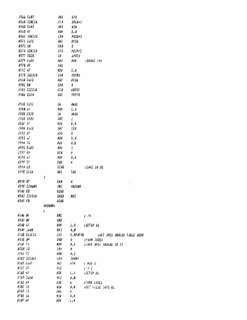
0566 E607 A H 07 H0568 320E18 S7A AdCR+2056 E E603 ASI 01H0569 47 m B,A056E 3A0218 LDA FQSO+20571 E6FC AH I iFCH0573 E0 QRA E0574 320218 jlIA PdSS+20577 [>328 IH APOCR057? £604 AH1 04H057B if RRC
0570 47 Hu¥ 3. A057d 3A2318 LDA RHPBS0580 E6FD m 0FSH§582 S0 QRA B0533 322318 SJA RHPBS
d m Q31A OUT P.HPTB
0 5 8 81m e IH A HAL058A 6F m L.A0582 dE2d IH AH An1580 EE02 m 2058F 47 a di/ B,AJ590 E61E AHI ita0592 37 Add A0593 67 HOY H.A0594 78 HOH A,B0595 Etii AHI 30597 s4 QRA H0598 67 i1QV H.A0599 29 l>AU H059A EB X C M059 B E638 AH! 13H
90590 37 QRA A059E C2A685 m A t o m05A1 EB XCHS
05A2 221518 SHLS Hil205A5 EB a CHS
m m ;
05A6 0F RRC ; t*05A7 §F RRC05A8 6F HOY L.A tSETUP HL95A9 2600 m Hfi05AB H 2 C 1 3 LXI E.APATAB iSEJ APE a AHALQS05AE 09 9AS E iFORH IHOEa05AF 73 HOY H.E tSti'E APEX AHALOS In IT05S0 23 IHX H
m i 72 h o y H.d05E2 3A2AIS LDA AHAHX0535 i6il A H t"7H ; m 305E7 07 HLC ; * 2*5BS 6F m L.A i8ETUP riL
25S9 26fi m i M0533 09 dAd s : f m IHDEa053C 7E HOY A,H :6ET VALUE IHTO HL05SP 23 m H05BE 66 *QV h.HJ58F 6F HOY L.A

$5C$ 220F18LP3:
SHLD AHAB
$5C3 3.43518 LDA DRY AT 1/05C6 S7 ORA A$5C7 3A2318 LDA SHPBS$5CA CAB425 JZ LP4$5CD F601 ORl $1Hi?t*Cf &E4$ M l C,4$ii$581 C 'idSi 5
LP4:JHP LP5
$5D4 E6FE AH! 9FEHc'jdo L’E$$
LP5:M l C.0
$5D8 122118 STA RHPBS
$558 011A OUT RHPTB$5DQ US$8 IK P2PTA$'j BF 420918 STA DSCR$5E2 S6$7 AM $7 H$5E4 EE$7 XP,l 07H$5E6 47 hoy B,A$5E7 3A§518 LDA ERRQ+2$5EA EoE‘8 AM $38H25EC 8$ ORA S$'j£l> S I ORA i$5EE 320518 STA ERR0t2$5F I L61E AM I EH$5F3 47 HOY E,A$5F4 3Al41d L3A FAHL+2$5F7 E6B9 AM §q9}}$5F9 Z$ ORA 5$5FA 321418 STA FAliL+2$5FD E l POP H$5FE 01 POP n
VJft Cl POP n0$6$i F i $6$i C'?
POPRET
PSU
;SJuRE IT FOR OUT A SET
:*ADDED FOR HiiX 226
; . m UPDATE I UFO
I****************************************
SLAP:
$6$ 5
$i$8
$699
U i C $o$F
$611 0614 H i ? $il9
StlC
$6 it $62$ {’Oilft- ">■} i'O i t
JIfl 2A2818 £5
C5E404
W 5 1 8F61$
120518
3A1418F6l$321418
t'JJSJ El?10re
LXl SP.1999H
LHLD TRAP
PL'SH a
CALL TSTOPLDA ERRO+2OR I H H
S7 ERR0+2
LdA FAiIL+2 {*ADDED FOR HiiX 226OR! t$H
STA F . m + 2ZiiT RtSb5
HVI A.RSTEH ;RESET 7.5, DISABLEOS j$H ;hlnr t C i
RET ;00T0 ERROR KAHdLEf.
$62] £333 $625 FS $c26 F5
TRPR:OUT
ElPUSH
HES65 iPE SET 6.5
PSii

i 627 C5 PUSH 30628 95 PUSH 9£62? E5 PUSH HU 2 A JE FF m A,TRUEU 2 C 324618 STA D R m sS62F 9B$8 IH P2PJA ; IH LOCAL?2631 E6 H AM anp 633 CA6E*6 JZ 1RPRI*636 3MA18 LBA BSCR+iH 39 E6$C AHI mH 3 S m m JZ TRPRi§63E 3.425IS L9A mien0641 3C IHR A0642 FE1? CPI 25
§644 C26F06 JH2 7RPR2i 647 2A1A18 LHL9 LSTPOSi64A £3 KHG0648 2A1818 LHL9 PQSTti064E 221A13 SHLB LS7P0S*65i 3A4A1S LBA QETIT : W SET IT0654 37 ORA A3655 C260U JHZ TRPRv ; I F l i 6 i:0658 3A2718 LBA STEP :GET STEPU S B FE»2 CPI '£*655 9A6ES6 JC TRPRi
JhPR0:J66§ i39804 CALL RAHGER$663 7C HOV U5664 87 OPA AH 6 5 C268S4 JHZ EuM iERRBR IH HOil OHvo b i 79 m A,Lh-69 FE28 CPI 43?668 PA68&4 JC EBR\I ; ERROR IH HOTISH
JRPR1:U 6 E AF U A A
TRPR2:J66F 322518 SJA m m0672 £1 POP H&673 01 POP 00674 Cl POP *$675 F I POP PSHf6 76 C? RET
S U P :$677 F 5 POSH PSH$67S C5 PUSH S
H 7 'f 95 PUSH 9*b7A E5 PUSH H
*678 9335 IH SHAEV ;REAB SHA-EM iT RE6th79 47 m 5, ArC.'t lz>$7 AM t i aHM 4F m C.A~:681 78 . M A. 8i’sSi t6Jj AH I 3SH
FE2s C r! 23HCA?Ci6 JZ CMMQ
$t69 FE1s? Crl 1* HC.i&F$6 l‘ L uJARQ
HzE <A*2i3 L'JA PQSO+2i'b'?l F64i 0*1 4*H :SET COHIRi/LLtR FniJi

3693 320218 STA
0696 321213 S H
0699 CIF 906
C&Oibii
M P
pc?C B830 IH
06?E 6r mL-sJl IH
H A i tl m
l*3F A H
0*A4 EE2§ m06A6 57 m
H A ? 53 m.56,43 U F F M l
&6AA 79 md6AS Z? m06AC CAC306 j i
Z-6AF F E U CPI06E1 tAdlii ji
0*84 it02 CPI
0686 CAD806 JlH h 9 <21518 SHLd06BC 79 mH a d 311718 STA06Ci C3F906
M U M :
JnP
h C 3 220618 SHLO06C6 EB a CHSjoC7 221 Cl!} SHLIi
06CA 78 m
06C8 323F18 STA
06Cc v3F9$6CHORST:
JHP
$651 76 m3652 323C18 STA
M S C3F906
HAPSET:
JHP
06t>8 78 m06S9 324018 STA
06DC C3F906
dTARU:
JHP
068F 79 m
06E0 FE05 CPIH E 2 C2E906 JX2
§6E5 212A18 LXI06it 34
uP.Ql:I HR
H E ? 07 RLC06EA 31 420i'biE of m06EC 2613 M l
H i t 7£
061F m i ObT
H F l 23 i*y*t>F2 7E miaF's £33.3 Oul0tf5 23 w:06F6 7i m06F7 5334
ikiPiOUT
06F9 El POP
fOSdtl
fAI/L :*W cC> FOR MIX 226:> i\ 1 ?
m ml .aoSCuiiM3Fn
20“
D.A
t'LB,TRUE A,CAm mic m s T2HAPSETM 2
A'6
Mi2*2SKIP
ECHO
C M H PA.S
i m mS U P
A,S
RESCHSSK IP
A ,tHAPREQSKIP
A,C5
MQ1H,AHAXX iP Q U l 70 C O M E R H s i K R E m i PdlHTER
s., .4a, 188A.A
WTlaAJ•}3DT2HA.HZS2T3
n

96FA PI 96FB Ci 96FC F i U FO F3 H F £ C?
POP POP POP EI RE1
uSPSH
:nHALSO 7ASLE LG HIAHA7AB:
ihFF EA97FE9B PH 97EAH.9BF£ii : H 9 W TEiiPS793 FC942895 OK 94 FCHJ528H ;-15/49797 m m e s an 9AP8HJS94H ;tl5f4979S 369SFE9S PH 9386H,9SF£H :r 5979F E49SEC9B on m 4 H M E C H i*lii29713 9999FF9F PH M 9 H J F F F H :FOC VEL27H 9999FF9F Da i>999H,9FFFH ;R07 m*7IB k§79498 Oh 97 FCHJ 894H :6 HO
;»AHP 7ASLE
97 IF 99 a m : OS C9H9729 34 CK159: PS 14 a972i 59 P3 5 iH9722 69 IS 6 9ti9723 67 PS 67H97 24 7i PS 71 a9725 75 CK499: 08 75«
9726 78 PS 78#
9727 89 PB 89H9723 82 PS 82 H972? 83 PS 83H972A 85 PS 85H072B 86 OB 86 K972C 87 PS 87 H9720 88 PS 88H972E 89 PS 8?ii972F 99 CKI999: 08 m
;*******
■3739 BP i


F/R NODLE-E CODE FOR ROTATION HAY 30, 1985
[EQUATES
m § -- P i n At EQii m iPROH I, PORT Ai m -- PiPTi: E M H i ; PRO if 1, PORT 8§H2 = P t m : E M i2H iPROH 1, PORT A VIRilw3 = rlddS: EQii $3H i P P M i, PORT 3 DIRi$*8 -- P2PJA: E M m ;PRON 2. PORT AW 9 = P2P1B: E M i?H iPROH 2, PORT B
- P2DDA: E M m iPROH 2. PORT A DIR?<5?B -* P2D5B: EQii m iPROH 2, PORT 8 91Rm s } P.CHdi EQii isa :RAH CHD/STAT REG ADDRM l ?-*' RHPTA: EQil m ;RAH PORT Ai ) m - a m 8: E M m :PJH PORT 3j?t*J3 = kUPTC: E M m ;kAH PORT CM C -- J1HLQ: EQii iCH :T!HER LS3M D = TiHHl: E M M :T!HER HSBj«?2S = f'JSL: E M m fPOS LSB?i>2? = POSH: E M 29 N iPQS HSBm h -- etL: £ M 2 AH VE LOCI TYs m = ArDCR: E M 25N :APEX 91SCRETSs?i?2C - ANAL: E M 2CH ;APEX AHA LSB5*22 -- AH AH: E M 2DH ;APEX AHA USB§*3$ = DSCDL: E M 3 M ;DS CHD LS3m i -- DSCLH: E M 31 n ;t’S CHD HSB2032 = DSDT1: E M 32H ;DS DATA LSBm 3 -- USDT2: E M 33 a ;DS DATAm i -- DSDT3: EQii 34H :DS DATA HSB^35 = s u m : EQii 35H tSHA E n N TtfJS = AIPT: E M 3SH ;APEX DATA REQM38 = RES65: EQii 3BH :RST 6.5 RESET
-- RHODE: EQii 4FH :RAH HODE PORT: A,8 A C OUT*WF = PRO ill: EQii &FFH iPROH PORT OUTPUTitf#* * PRIH: E M m :PRQH PORT INPUTrtf 2 9 = R S U H : EQii iy a f S W HASK, DISABLE 5.5 ONLY
-- FALSE: EQii 0
ifiFF -- TRUE: EQii 3FFH
:DATA SET TABLE
: M S i m a :START OF RAH HENDRY
iSJj PC 3D: j S 3 : m 239 - POSITION 4 STATUS BITS1 on 3 Irb'o: l> 3 3 : 2Ji - CHD-POS i STATUS SITS
ECHO: 3 I 132 - CHD ECHOHjiR: i/S 3 i 2:3 - RES PONES & C M SENSE, C lK
i jK AtiR: SS i ; 2:4 - A? EX DISC RETS -1 ifELQClTYi'/r M A D : 5$ j : 215 - Al o v F . W i i m i A S t S• i 1 FVJL: ['$ j : 236H i 5 HU2: 53 J iHi'X 237
n ' A t m i SHMENENTS
1 c I i POST it: •Ji 2 :POSIT ION, UNSIGNED

i s i a LSTFOS: OS 2 ;LAST P O S I T Miisic C M H P : OS l ;TEHPARARY CHD181E ATYCUD: OS 2 iACTIVE C M182i H i 1 AST: OS l fEPRQR 1HA6Emi FlPBST: OS 1 itPROH IHASE1822 M P A S : DS 1 ;RAif IHASE1823 RHPSS: OS l :RAH IHASE1824 M F C S : OS 1 ;RAH IHASE1325 m m : OS 1 iHOTlOH AHA LYSIS CQUHTER1826 STEF: US 1 ;FREQUENCY STEP FOR RAHP1327 RHPTQ: PS ; •tRAHP TO THIS SPEED1828 TRAP: f'S 2 :ADDRESS OF ERRO CODE132 A AH ASX: OS i :APEX M X CHTRii>28 APAPTR: OS t iAPEX M X P O W E R1S2C APATA3: OS it iAPEX ANALOG STORAGE
tiASS:
133C FESCHO: OS i ; RESET C Mim IW A T V : OS i :DkltE ACTIVE
m e HAPATY: OS i :HAr ACTIVEm f M V k E Q : OS i :OR!YE REQUEST1349 HAPREQ: OS i :HAP REQUESTiS4i ACCti: OS i tOK TO ACCELERATE1842 MHPiiP: OS i :RAHP UP STASE1343 H A M : OS i fXAlH DRIVE STASE1844 SAHPUH: OS i :RAHP OOHH STASElb 45 CQHVRS: OS i iCOHYERSAHCE STASE1346 ORYPLS: OS i ;4TH DRIVE PULSE QCCliRED1847 DIR: OS i :CSRREHT DlHECTIOH1S43 LOIR: OS i ;LAST DIRECTICH184? R A M : OS 1 ;RAHPED UP OR HOT184 A SET IT: OS t :SET IT THERE SQHEHQH
H i S R M C H D : OS i ;HAITI US R1HS COHHAHD134C EXT ELS: OS i ;RIHS EXTEnd FLAGlc-i> = E W L 5 : EQii $ ‘tEHD OF FLASS
:RESET 4 1HTERMPT
0m ORS §
w * F i 01
m i c u m JHP IHIT ;SET THIHSS 0RSAH12ED
0024 ORS 24 H iTRAP SERVICEM 2 4 F3 01m 5 C313S7 JHP SLAP }ST3P, M A T ' S HRQHS
m e ORS 2CH ;RST 5.5me FS El
C? n J : M T OSEO
m 4 •jRS 14H :RST 6.5 Str'ICtM 3 4 rJ ul
C3i4i?/ 'HP 1RFH ;ACkHQLEDSE DRIVE PULSES
M 3 8 ORS 33 ti ; M - O F - B M H D Si f IS F3 01
C 3 4 m JHP IHIT
3CH ;kST 7.5 SERVICE

me F34439 C388i7 JHP di)RP SE R V I C E B.S. REQ
01
ilHlTlALIUiluH
m * m 4?H
i n n sm t 3 i m ? La ! SP,i9MH:SET STACK0043 3E4F nvi A.RHOBE4445 9313 m m o ;s e t r a h m n f u r jm i 3EFF M I A . P R M T4449 9342 m Pi OB A :SET PROU PORTS FORM 4 B 9343 OUT PIUBS4445 3£44 HVI A,PR1H444f 03iA OUT P29BA :SET PSOH PORTS FORm i m s OUT P200Bm 3 *f H A A4454 D3l? CUT a m A :IERO PORTS
H 5 6 031A OUT RHPTB4458 9325 OUT U PTC
445/5 U3di OUT PiPTAm e o u t W P1PTS445£ 2ir4/8 LXl H . 1 8 M Hieol 47 m S,A
LOOP: ; CLEAR HEHORY4462 77 m a. A
4463 23 m a4464 45 OCR 84465 C 2 6 2 H Jft'Z LOOP4468 9338 OUT RES65 ;$ETUP 1HTERR0PTS446* 3E1? svi A.RSTEH44&C 34 98 3iH ;S1Hm o FB Ei
; SYSTEH HAHBLIHG
BOSS:me csFEffj cm447 I 3M S I 8 L9A
4474 £648 AK1
H 1 6 C22591 JHI447? m s m
m E m a m
447B CA8642 Jl
M 8 i 3A3C18 LBAm 3 h7 ORAm* a im mm i 3A30i8 LOAM S A SI ORA
*•*38 C24441 JH2
m t 3 A M 8 LOA
te9i E M m
4493 C 2 8 W ,'U
44?c 3 A 3 H H LOAW ? 67 ORA
M A C 2 M * JHc3A3F18 Lt'A
4irAi H7 ORA
dSTOR ;6 AT HER BATAER9M2m ;CHECK APEX iHTERFACE iRSCHO ;RESET SYSTEH IF HOTP2PTAm ; CHECK FOR LOCAL HOSELOCALRESCHOA -.CHECK FOR SOFT RESETCH9RSMVATVA ; CHECK ORIVE ACTIVEc a m *ERR0t28 M : CHECK m as ACTIVECHKRH6HAP ATHA iCHECK HAP ACTIVEtFAdK i i M J R REQUESTSO&VREQ.4 ;DR1VE REQUEST

m t C25u&t j'tii BRVIHTM A 4 3.4401S LdA 8APREQm 7 57 t m A ;HAP REQUESTm s c a s s m Jl nPAOKm s 323E1S STA HAPATV ;SET ACTIVEm a e W 5 i $ LDA ERRO+2m i F620 SRI 2$ti ;SHOH ACTIVEm 3 32$5l$ STA
A r M :ERP.8+2
:CHECK APEX VOLTAGESi m 3A2B18 id A APAPTR ‘.GET HiiX POIHTERm ? 3c IHR A :HEXT AHALOG TO LOOK AT* m E6»? AM 91$ : Mi) 800SC 322EIS STA APAPTR :SAVE HEX VALUE FOR HEXT PASSM B F - F S POSH PSH fSAVE FOR FURTHER USEM C $ 01 RLC ;SHIFT LEFT FOR HORS IHSEXIHGM C I 4r m C,A iSAVE IH Cm 2 i7 RLC ;SHIFT AGAIH FOR 2 HORS IHSEXIHGm 3 Sf m £.A •.SAVE !H EM C 4 218308 LXl H,AHATA8:V0LTAGl RAHGESm i u m m M iSET HE FOR IHSEXIHGt W J l? SAd 0 sPOlHT TO i GET LOH LIHIT IH uEM C A 5£ m t.HM C B 23 m tim c c eji m MM C U 23 IHX HM C £ £5 PUSH H ‘.SAVE POIHTERM C F 212C18 LXl H,h PATAB:APEX AHALOG STORAGEM u 2 h M HVI S J :SET SCM S 4 69 OAO 8 ;FQRH IHDEXM S 5 4£ m C,H '.GET ADJUSTES VALUE W O HLi m 23 m HM ? 7 7£ m A, aM S S £6iF A M §FHM M EE 03 M l m
m s c 67 m V,Atim t? HOV L,Cm i £5 PUSH h :SAVE AHALOGiiSF CDAFiS CALL RAHGER iCHECK LOH L i M T00E2 01 PSP 0 ‘.GET AHALOGM E 3 £1 PGP H ;SET POIHTERM E 4 79 m A,CM £ 5 27 ORA A fIF OOT-OF-RAHGE. GO SET FAULTM E 6 C2F000 m AHAFLTM E ? IE mv A,H :GET HIGH LIHITM I A 23 m a
M E 8 66 M V H.K
M E C 6F m MM E d CSAFi5 CALL
AHAFLT:R A W E R ;CHECK HIGH LIMT
M F i Fi POP PSK ;6£T HiiX POIHTER BACKM F i 41 m 3, A
?*F2 r4 m SM F I U M M l
fiJSfT:A, Si?H :3iT HASK
M F 5 RLC iROTATE SIT TO POSlTiuHM t 6 tf5 OCR S
/ i.tF'Z'v? JHL FLTSFT
M F A 57 m d,A ;0R HASKM t S IF CHAM F C ZF m E.A ;AHD HASK

M FD 7? noy A,CM E E l QUA A ;HAVE <4 FAULT§0FF 3AH 13 LDA AHAD+20102 C20901 M l SETFLT0105 43 AHA £ fRESET B IT0106 CM A il JHP STRFLT
5ETFLT:i’j#? 82 ORA if :SET S IT
S fR F iT iM i A 321 U S STA AH AD*2ilQ d U i i i S S I A FAiiL+1 :*ADDED FOR HuX 23601l§ £3o£00 JHP BOSS
CHDRS:0113 4f H A A ; CLEAR FAULTS0114 322213 STA PuSB+29117 321218 STA FAUL : * ADDED FOR HUX 236§11A 320518 STA ERRO+201 ID 3di4iS LDA FAUL+2 i*ADDED FOR HUX 236H 2 9 E6E0 AHI iE0 S0122 32141S
Q £),
STA F Ail Li-2
9125 31vB19 LXI S P t l?00HtRESET STACK0128 CDE905 CALL TSTOP iSTQP TIHER ft DRIVE*128 CDA202 CALL DRV STP8 l2E CDCE04 CALL TRHOF ;TURH OFF TRAHSLATuR0131 213C13 L'i I H,FLAGS0134 0611 H VI 8 , (EHDFLG-FLAGS) AHD 2550136 AF XRA A
CLh'LP: iCLEAR FLAG TABLE0137 77 HOV H.A013$ 23 1HX H013* 05 DCR 8013A £23701 JH2 U R L ?013D C36E00 JHP 88SS
•*»#**##*#******#**####*******#**##**#*#
; COHHAHD P0SIT10H HANDLER
0140 3A3F13 LDA DRVREQ0143 37 GRA A0144 CAs402 JI DRVTSI0147 2A1C1S LHL3 CHDTHPH i A EB
0148 2A1E18aCHG
LHLD ATVCHD014E CD9705 CALL VECTORrJ 5i CSC905 CALL CLOSE0:54 DA0902 JC CLRREQ0157 CBE905 CALL TSTOP015A CD A202 CALL DRV ST?
015D AFDRVIHT:
a RA A?ij£ i24AlS SI A SET IT
eidl 320218 SI A POSD+201o4 32l2i8 STA FAUL0ii7 322616 DR VI M i /* r »
Oi n STEP016A 323F13 STA SRVP.Ei01t>D 324118 STA ACCEL0170 320513 STA E P M + 2
;Du HE HAVE A HEH CUD
‘.CLEAR REQUESTS,FLAv$. And FAULTS
;*ADDED FOR rfUX 236

§173 322518 STA NOTION0176 3/11418 LOA FAUL+2$179 E6ti AHI 0E0H$178 321418 STA FAUL+2017E 2A1C18 LHLd CHOTHP
01SI 221E1S SHLD ATVCHO
0184 CDFE05 CALL 9ST OR$187 3,44718 LOA 01Rdid A 12481$ ST.4 LOIR0180 2A181B LHLd POSTN0190 221 Alb SHL9 LSTPOS0193 2A6318 LHLD ERROH 9 6 C9C905 CALL CLOSE0199 OA6E00 JC 8 OSS
019C 11SEFF LXI 0,-114019F 0612 HVI 8,18
01*1 ZMtiS lDA GET IT01 44 37 ORA A145 CMMf 31 OIV
'51.48 §6059IV:
HVI 3,5
i.4.4 3EFF31V1:
HVI .4,-1 ,4/f'i
01 AC 3C I HR A
01 AO 19 9 AO V
J1AE 9AAC01 JC m iU S ! SS CHP 50182 9AS701 JC m0185 05 OCR 3
0186 13
A&K:m A,8
0187 322713 STA kHPTQ
018A 87 ORA A
0188 CAC601 n HORHP
01 BE 3EFF m A,TRUE
01C0 324118 $TA ACCEL01C3 324218
HOPSP:
STA RANPUP
01C6 2F CHA
0iC7 32451S STA m m
QIC A CDF 104 CALL SRKON
01 CD C9A804 CALL TRNON0100 AF m A0idl 220818 STA DSCR+2vli)4 0301 OUT P1PT80106 3A4718 LOA M R0109 87 ORA A
Jit)A 3A0A18 LOA OSCR+10iOO C2E501 m CCH
01E0 tbii OR! 09 H
01E2 C3E7S1
CCH:
M P W I T
'lit; Fc0 j
W I T :OR! 05 H
01E7 320A!8 i r*i 2 S C R H0l£A 0300 OUT PiPTAJltC 216705 uZ H.EDRV0iEF 222318 InLi) TRAP01F2 219S3A i\l H.1500001F5 COO005 CALL TIHER
(INITIALIZE HOTIOH COUNTER ;*A99E9 FOR HUX 236
•fU U TEH? CHS THE ACTIVE CH9
•.SETUP LAST OIRECTIJN
;SETUP LAST FOSTiCii
:ERRO ( 4
flF CLOSE DON'T M ANYTHING
;FlNO STEP TO RAHP TO
tSET. IT THERE SOHEHOH?
ilF HOT
255 ,\h HILL CONTAIN STEP TO RAHP T8
;!F A>8 THEN A=3-l
iSAVE RESULT ;if A=0 DON'T RAHP
fSETUP FOR RAHP
;ACTIVATE 8RAKE I TRANSLATOR
:UP9ATE IHA6E :$ET FOR 10»H2
;HHICH OIRECTON
:6ET IHASE
;DRIVE ca
:DRIVE CCH
;UPdATE IHASE iSEHD IT
;SETUP ERROR HANDLER
;I5 SECS TO SET THERE

01F9 3EFF M l A,TRUEU F A 323$ 18 STA :SET uRivE ACTIVE§1FD C H E M JHP LOSS
0200 AFCLRREQ:
m Am i 323FJ8 SI A DRVREQ :CLEAR REQUEST
§204 CUFE05DRVTST:
c a l l BSJOR ;6ET LAJES1 DATA02$7 DS2S IN nPOCF'§209 E6i4 M l 04fi ;CHECK FOR BRAKE DISENGAGED020S CA4F05 Jl EBRK :IF HOT, J M P 78 ERROR ROUTINE02§E 3A4118 LOA ACCEL0211 B7 GRA A .‘CHECK FOR ACCELERATION0212 CA2A02 JI PiOd ;1F NOT, PLOD ALONG0215 3A4218 LDA k AHPUP32IS 87 ORA A :1N RAH? UP*21? £23002 m imp :!F YES, UP02ic - m m LdA HAIR$2tF 57 ORA A :IN If AIN DRIVE§220 C24F02 m HA1HCK :1F YES, CHECK M E N 70 RAHP BONN0223 3A44i3 l d a R A M O N0226 87 ORA A • M N P DONH?3227 C26302 m U P O N ilF YES, 50 IT
022A 3.445i 8
PiOd:
LdA C O M R G0229 87 ORA A ;CON VERGING?022E C27602 m m m :1F YES, CONVERGE023i CDE905 CALL JSJOP :SJOP 71 HERm * CDA292 CALL 5RVSJP ;STOP DRIVE0237 CDCE04 CALL urn ;TiiP,N OFF TRANSLATOR023A C36E00 JHP BOSS fSEE M A T ' S NEXT
023!) 3A2718HPiiP:
LdA RHPJO iGEJ STEP TO RANP JO0240 4F HQV C.A0241 CO4904 CALL RHPOP ‘M N P 70 IT0244 Af m A ; RAHPliP TO HA1N0245 324218 SJA RAHPliP0248 2F
0249 324318CHA
SJA HAiH024C C36E00 JHP BOSS
024F 2.40313liAlNCK:
M L S ERROs?i'j2 il;602 L U D,i276HJ255 CBAF05 CALL R A W E R :A7 THE RAHP BONN POINT?0258 79 m A,C0259 87 ORA A025A CA6E00 Jl ms025d AF m A :IF YES, HAiN TO RANPDN025E 324318 SJA HAiH*2*1 J
ii(,2 U 4 4 1 8CHA
STA s a n p d n
0265 C 3 6 E H JHP i m s
0263 CS720421PLH:
CALL RHPSN ;RANP DGNN FROii CURRENT STEP*2bS AF X RA A :SET RANPDN TO CONVERGE026C 324418 SJA S4KPDN

m F 2F
§21i 324518
CHA
STA corns0273 C 3 6 E U JHP BOSS
i276 2A0318
m i H :
t m ERRO§279 CDC905 CALL CLOSE ;h i t h i h 4 cornsv27C D?$i$2 JHC m i*27F .■;? m A :1F YES, 60 SHiiTdOHH DRIVEi28i 324513 S7A c e n m02H3 C 3 6 E M JHP BOSS
?2S6 3A471Sm i :
LdA DIR iCiiRREHT DIRECT10Hs2S9 4F m C.AZ23A 3*4313 LDA Id Ik (LAST DIRECT18H02SD 8? CUP C :THE SAHE?
m i CA6EM n 80SSm i -9 M V A,C ;IF HO, CHAHSE DIRECTluHSm 2 324818 STA LOIR iHAKE LAST DIR THE CilRPEHT DIRM 5 3AiAl3 ISA SSCR+1t298 E E K XRl Eli :FL!P DIRECT OH BITSill A 321A1S STA 5SCR+1m d 2 3 H M T Pi FT Am F £3iEi$ JHP BOSS
v2A2 CD72i4
DkVSTP:CALL RHPVH ;HAKE SORE RAHPED BOHH
£52/55 AF m A :CLEAR DRIVE ACTIVE*2A6 32 3d IS STA M V A T Vt2A9 ZAiAh i LdA DSCR+te2AC E6F2 A M i?F2H fSHOT DOHH CLKS I DIRECTluHi2AE 320AI3 STA DSCR+lm i m § OUT P1PTA?233 C31425 JHP s a w
ft**************************************
e2Td6 CDA8&4
; LOCAL DRIVE
LOCAL:
CALL
HAHSLER
TRHOH ;TRAHSLATQR OH M IL E IH LOCALi259 AF XRA A
§28A 32*818 STA DSCRt2
m d 93st OUT P1PTS :SET FOR M M
023F CDfESSLCil:
CALL OSTdR :6ET DATAc2C2 3A*518 LDA Ef.Rd+2?2C5 E6dS AH I m iA P E i FAULT}2C7 C225H m RSCHD } I F YES, RESET SYSTEH12CA D8S9 IH P2PT8 :OET DIRECT10Hs?2CC £606 A M 6$2CE FE34 CPI 4
} 2 M L A 2 7 M JZ LCH ;HOVE CHU D i FE62 CPI 2*205 CA4!/i.s JZ LCCU ; W E CCH“238 0S69 IH P2PTS :6ET EAHD SHiiOA £6?i A M i FSH ;STR1P EXTRANEOUSm e 47 m B.AU M E6i§ A M m iSHlTCH M rm F CAiBil JZ LCL4 ilF HOTe2E2 2iit ay i L.l :ASSUHE EXTEND

22E4 73 m A.B22E5 FE19 CPI 10H$2£7 C A F M 2 32 LCL2 :IF E U E H P22EA 20 SCR L {SET RETRACT22EB F E U CPI 3JH22 ED c i m i 3 HI LCL4 ilF SGHE OTHER SHJCti
LCL2:
22F0 CDF507 CALL E X 7 R M22F3 75 m A.L :GET FLAG22F4 57 ORA A02F5 3E32 ay i A , m : SET EXTEH9 LIGHT22F7 0E9F a n C.2FH fSLT LIGHT BL1HKS2F9 C2FF&2 m LCL3 {IF HOT E U E H D02FC 3E42 a n A,42H :SET RETRACT LIGHT22FE §9 OCR i :SET HEH LIGHT 8L1HX22FF [>319 iCL2: m u r n a :LIGHT OH2331 1424 IS L2A RHPCS2324 31 QUA C2305 322413 STA RHPCS* m D31B m RHPTC ;START IT SL1HX1HG222A CJS-3i?3 3HP C H M H G
LCi4:
222D AF A? A A*3'Jt $319 GuT M P T A :CLEAR LIGHT22li 2A2418 LSA RHPCS2213 £*32 AH! 32 a ; STRIP ELIHK2315 222418 S7A RHPCS$318 S3 IS OuT RHPTCit31A BB28 IH P2PTA23 iC E 6 H AHI 2i a :STILL IH LOCAL?22IE CABF92 31 LCL13-i2i CSCE94 CALL TRHOF ;!F HOT, TRAHSLATOR OFFJ324 C32521 3 HP RSCHD :RESET SYSTEM
LCii:2327 CDFI24 CALL BRK3H {UISEHGAGE BRAKE232A 3A0A18 LSA B S C R H222d F629 0R1 9 ;SETUP CH DIR232F 322A13 SJA DSCP.+l2332 v320 g o t P1PTA2234 DES9 IH P2PTB2256 u i i AHI i ;RAHP?2338 C A 4 M 3 31 L C M23 3B O E U m C,17 •AF ft S. RAHP TO m m2320 C M 9 2 4 CALL RHPilP
L C M :
2242 CPFE25 CALL JSTOR {GET DATA224} l’d29 i :i rtPih22*5 tDin IN I 2 ;STILL HOVIHG CH?i-}4: £A4$'f3 3i LCH!224A ; 37222 3 nr LSI CP {IF HOT. SHOT DGHH
tCvti:
c o F i M Cm LL sRiiGH U'lEitGAGt c:\nkt22:2 3 M A 1 S L3h dsca+i.•351 ft25 8 U 5 iiilOP CCH DIR
j.7.428 s :a &5CR+1225$ 1122 i-ji FiPJAJ-35.4 2S*9 Li P2PJS23'jC io2i AH! I :RAHP?

*35E CA66i?3 32 LCCHI*361 n i l m C,17 :!F YES. RAnP TO i***H2^ 6 3 CB49»4 CALL RHPUP
LCCHI:
*366 C9FE*5 CALL DSTOR :OET BATA
*369 M W IH P2PT8H 6 3 E604 A HI 4 :STILL m m CCHjJoO CA6t-*3 Jl l c c h i
LSI OP: ;IF HOT, SHUT 01M£972*4 CALL RHPSH
*373 3 A*At 8 LDA OSCR+i?376 E:-F2 AHI *F2H :TiiP,H OFF CLKS i H R*37$ 32&A18 STA DSCR+l
till m i CUT PIPTA
i370 £914*5 CALL 8RK0F :EHSASE ORAXE■j3S* £386$2 J/fi3 LOCAL
‘It*************************************; ms c h e c k status ;
yJS3 iA4Cl8 ( m m : iPAi3$b 572337 £A4l*4 Jl
v33A 3A0818 LdA2339 E 6 i i AHI*38F 114**6 CHKRH1: LX I3392 CA9F*3 Jl*395 U 2 C * l LX I*3 ?s o m IH*39A E6*l . AHIm e CAAF*3 Jl
Q39F 21AFS3 PHSHIT: LX I*3A2 22:918 SHLO
£3 XCHGH A6 c o o m CALL33A? C9FE05 RHSHI1: CALLm e C3A9*3 JHP*3AF 3AS518 RHSH12: LDA*382 EoEF AHI*384 320518 STA*337 3A I4 I8 LOA*3SA E6EF AHIm C 321413 STA338F 3A4C18 LBA•3C2 57 ORA
03C3 3AS8I8 LOA
*306 CAE 3*3 Jl
J3C9 E6*l AH!
H C 3 ft *3 CP!
J1CD CAFF$3 Jl
Etti AHI*302 CAFFH3 ■■I
£305 32*318 STA
J393 3A1418 ISA
{'138 to Of AHI
*199 321413 STA
H E * C 3 1 M 4 JHP
*i£3 t6*3 F.HSHH: AH!
*3£5 F£*3 CPI
EXTFLS :IH M H S EXTtHO?
AChURET
tCHu+2 ;<jET M H S STATiiS
1 ;THERE YET?0,16** :16 SEC HAITm a n0,3** :3 SEC H I T PIPTAtin :STILL !H LOCAL?mni2nfm*i2TRAP :SET TRAP POIHT
TIHERUSTOR
RHSH1 1 iHAlT liHTIL TIHEOOT ERRQ+2 ;RESET TIHEOUT FAULT
*EFH Em+2FAUL+2 ;*A9DE9 FOR MIX 236
*EFH
FAiiL+2EXTFLS :6ET EXTEND FLAS A
E C M + 2m a n :if h o t e x t e u p
3
iPH8HI4
1PHGHI4ECHO+2
FA&L*2 ;*AOOEO FOR HliX 236M F H.-AilL+2CHKRH2
3J

93£7 CAFF93 J2 RUSH 14
93EA £6*2 AH I
93EC CAFF93 \!L m a i 4
93£F 3E92 ?m A,2
93F1 52*818 81A £ C m 2
93F4 3.41418 LdA FAUL+2 }*X)dt& FOR m 23693F7 E60F AH I 9SFH
e3F9 3214*3 ST,4 FAiiL*2
J3FC C31994 JHP CHKRH2
zifF Fid* R H S M 4 : 081 4
M i 32*818 STA ECH0?2
9494 JA141S LOA FA8L+2 ;*,4'>s/£D FQR HiiX 2360497 F629 GUI 29H
s4i>? 321418 ST 4 FAUL+2
m e AF IRA A
v'4y? 3i4oJ*3 ST.4 m mj 4 U AF CHKRH2: M A 43411 12401$ ST,4 EZTFLS {CLEAR FLAOS
$414 3A951S LDA ERRO+2
3417 £67F m 7FH
9419 320518 ST 4 ERP8+2 (CLEAR ACTIVE
941C 3A9A1S LOA 8SCR+1
$4 IF E6CF AH! K F H
H 2 1 329A18 STA dSCRtl fTiSRH OFF
$424 0399 OUT P1PTA
9426 5A4818 Lj A m e m ;PENDING R1HS CCHKHAHU?
£42? B7 ORA A
H 2 A CA&E99 JZ 3 OSS i!F HOT
i428 3A9518 LUA ERRQ+2
9439 F e w Oh I S$H
9432 322518 STA E P M + 2 :RESTORE ACTIVE
H I 5 3.44523 L8A RHSCHd
sM33 toil AH! 1
94-lA F5 POSH >S*
H J B C5 PUSH 8
J43C U5 POSH 0
9438 E5 POSH H iSET STACK UP
9431 C31198 JHP EXT FT 1
9441 3A9818 CHKRET: LUA ECH8+2 (SET HI US STATUS
9444 E6v2 AH! 2 }THERE YET?
H 4 6 C38F93 JHP CHKRH1
: R W UP & D m
(EHTER HITH C=STEP TO STOP .47, l = i m Z TO i ? = l $ m i
mu?:i44■? W * 1 9 LdA RAHP
S44C 87 ORA A (RAtlPEd UP?jt-ii' C$ RHl ;RETURH IF kAHPtD UP■J44E 2F CHA
S44F 324919 STA RAHP ;SET TRUE
$452 2iA398 H I H,CK199 (START SF RAHP TABLE: .♦ r c »«• ft-J-j nr XRA A fCLR RAHP STEP
PrJPi:$45c 322*18 STA s t e p ;SAV£ LATEST STEP$459 h 19 ■it I 5,25 i*AlT 199 PULSES<■456 7E H 9V A, II :ST£P SPEED945C 32cB18 STA OSCR+2

045F 0301 buT PiPT s •.EXECUTE IT
W P 2 :0461 CD9C94 CALI HT65 ;*AIT FOR IHTERiiPT0464 05 OCR 30465 C26104 JH2 RPUP2
0468 23 m H ;HEXT FREQUEHCY0469 3A2618 LOA STEP046C 3C m A iiitXT STEP§4*0 89 CUP C idOHE THE Hi/HSER OF STEPS h046E C256S4 JHZ RPI/P1
047! 09 RET :1F YES
RHPDH:
0472 3A4918 LdA RAHP
0475 57 ORA A ;RAHPEd BOHH?0476 C3 RZ ;RETilRH IF RAHPEd DOHH0477 AF m A
0473 :24n s STA RAHP ;SET RAH? FALSE0478 11A398 LXI d,CK199 sPOlHT Td RAHP TABLE
047E 3,42613 LdA STEP i SET STEP COiiHT*431 6F m L.A
0482 2*00 m H. 3
0484 v< dAO 3 iFQRH P O W E R£435 K m A
0436 4F w C.A iHUHBER OF STEPS TO RAHP dSi
m a u
0437 0o0C HVI S. 12 • M I T 4S P U S E S0*61 7£ m A,H :QET FREQUENCY
t-48A 320313 STA DSCR+2
0485 m i OUT PIPTB ; START IT
RPSH2:
043F C d ' K M CALL HT65 M I T FOR IHERvPT; m 05 OCR 304*3 :23F04 m RP0H2
i4'i6 23 sex h ;HEXT FREQUENCYt-iy? 00 OCR C ;dOHE STEPP1HS?0498 C28794 m RP0H1049S C9 RET i l F YES
*765;
049C C0FE95 CALL DSTOR :5ET DATA049F 3A4618 LdA m P L S3iA2 37 ORA A ; IHTERiiPT?94A3 CA9C94 JZ HT6504A6 AF XRA A ;1F YES , CLR FLAG * RETilRH04 .47 324618 STA M ¥ P L S04AA C9 RET
* TRAHSLATOR * BRAKE COHTROL
Tf.HOH:94AS 211705 l a ! H.tTRH •.TRAHSLATOR ERp.OR04AE 222313 SHlS TRAP0431 216499 l K i H .19 0 iOHE SEC0434 C W 9 9 5 CALL TIHER •.START T1HER2437 3A0A18 ISA I’SCRrl043A Fo30 OR I 30H :SET TRAHS OH SITJ4BC 320A18 STA USCR+l ;UPDATE IHA6E04SF 0309 OUT PIPTA ;00 IT

TP.SH:
h c i c d f e 05
04C4 ms04C6 E6!«
04C8 CAC124
04C8 CIE905
04CE 213705
04DI 222S18
J4D4 2i6400
m c m *504 DA 3 M A I 9
2 4 M E67F
* m m mH12 £3*0
94E4 CDFE05
i417 D808
J4E9 E610
24EB C2E404
04EE C3E905
IMOF:
TROFF;
CALL
IH
mjiJHP
LXI
SHLS
LXI
CALL
LDA
AHI
STA
OUT
CALI
IH
mmJHP
DSTOR
P2PTA
10H :IS IT Off YET
T P M
TSTOP ilF YES. STOP TIHER $ RETiiRH
H,ETRH
TRAP
H , i M :OHE SEC
TIHER
DSCR+l
7 FH
DSCR+l
PIPTA :TliRH OFF
;RESET TRAHS POHER BIT
DSTOR
P2PTA
10H flS IT OFF YET
TROFF
TSTOP slF YES. STOP TIHER i RETiiRH
3RK0H:
04Fi 214F05
04F4 222818
i4F7 216400
i4FA cams 04FD W A i 8
05## F640
0502 320A18
0505 D300
d5i7 CDFE05
050A D82S
« 5 K E604
&5§E CA0705
i5Ii C3E905
s'R KOI:
LXI H . E M K {BRAKE ERROR HAHDLIH6 ADDR
SHLD TRAP
L U H,iii :Oiit SEC
CALL TIHER
LDA DSCR+i
OR I 40H :SET BRAKE DISEH5A3E SIT
STA ISCR+i
OUT PIPTA iDiSEHOAQt
CALL DSTOR
IH APDCR
AHI 4 ;READY YET
Jl SRKOl
JHP TSTOP iYES. ST8P TIHER 4 RET
SRKGF:
0514 2 14F§5
0517 222S13
051A 216400
05ID CDD005
:*52# U 9 A I 8
*523 £6of
y525 U i A l S
D30S
*524 CDFE05
?52D Da23
i‘52i £604
0511 C22A05
2534 C3E?05
SFKF1:
LXI
SHLD
LXI
CALL
LDA
AHI
STA
OUT
CALL
IH
InimJHP
H,E8RK ;ERROR ADDR
TRAP
H,100 ;0HE SEC
TIHER
DSCR+l
08FH ;RESET SIT
DSCR+i
PIPTA tEHSASE BRAKE
DSTOR
APDCR
4
BRKFl
TS'iuP
ithOAGED YET
; i f m H A H D U H 6 r o u t m s
0517 J.4*>USETRHs ;TRANSLATOR
LDA DSCR+l

953A £67F AM 7FH (RESET POHER S IT#53C 32iMlS STA dSCR+l253F 33it GUT P1PTA (TURN OFF#541 21*218 LdA POSD+2i544 F612 OKI m (SET FAULT S IT#546 32$218 STA POSD+2&54? 321218 STA FAi/L : * ADDED FOR HUX 236354C C325M JHP rschd ( k ESET SYSTEii
ESRK: (BRAKE*54F 3A$Ai8 LUA d sc r+i#552 E68F AM 0BFH (RESET S IT0554 32m S STA DSCRH0557 0 3H OUT P1PTA (EUGAGE BRAKE#559 3Ai218 l DA PGSbr2#55C F634 CM *4H (SET FAULT BIT#55E 32*218 STA POSD+2mi hi2is STA FAi/L ; * ADDED FOR HUX 236#564 C325s i JHP RSCHD ; RESET SYSTEii
EdRVi (DRIVE#567 31H19 L U S P , i ? m (RESET STACK#56* 3A1413 LdA FAH 1*2 ; * ADDED FOR MIX 236#5tD F6ffl m j« (SET DRIVE FAULT B IT#56F 321413 STA FAliL+2#572 3A2old LvA STEP#575 FF J4 C f l 4 (CHECK RAHP STEP#577 W5?#5 JC EDRV1 (STEP < 3 M H Z , SYSTEii RESET
j£ff HVI A 'iR iiE (dTHERMSE TRY RAHPIHG TO 250H557C 324.428 STA GET IT (SET GET IT THERE SOHEHON#57f C5£?#5 CALL TSTOP (STOP TIHER AND DRIVE5532 C#*2#2 CALL MVSTP#555 AF uRA A (CLEAR ACC FOR ENTRYiK36 C36701 JHP m i n i ( M T U DRV INT
smi:J5S9 W 2 1 8 LdA PCSD*2 (SET DRIVE FAULT05SC F62i GUI 28 H
#5SE 329218 STA PQS0*20591 321218 STA FAUL ( * ADDED FGR M X 2369594 C32591 JHP RSCHD
; SUBROUTINES
VECTOR: iHL-BESTlHATlQH3597 C3AF*5 CALL RANGER (DEPOSITION
3:?A C8 RZ (IF HL=i
J59S U M E 4 LXl s . - 2 m n359 E i? DAD d
#5*f M A M S JHC VEC1
j$A2 7;5 aov A.C
i'5A3 CHA (CHANGE DIRECTION
:<jA4 •F HO V C.A
#5*5 CPU 05 CALL c n m
iHCl:
#•;.« u c m L U D . 2 9 m
eiAB r? DAD 0
*5 AC 7D m v A,L :tiL=HlHlHUH SAGNITUBE
#54P 3 4 ORA (C=L>tktCT10Hf i IS POSITIVE#5.4£ C9 RET :2ERQ FLAG SET FOR HL=i

RAHGER:
55/if 73 HOY A.L
m t ?3 SS 3 t§531 6F •10 V L> A
5532 K HOY u5533 ? A SE3 I1
5534 &7 HOY H.A
5585 $ E U HVI 0*i?t'jal t Jstdj Jp RHdRl
555.4 23 OCR C
CdClfo CALL CHPHL
555E 7u HOY A.L
tfBF S4 QRA iiS,rj>Jj i"? RET
CHPHL:
05C1 7 C HO if A,H
vjC2 /f CHA
55c3 67 HOY a, a
v'/C4 75 HOY A.L
•jjC-5 - f CHA
# K 6 6F HOY L.A
55C7 23 I H/( H
t5C8 C9 RET
CLOSE:
55a 7C HOY A.ti
55CA B7 ORA A
55CS Ci nHZ
55CC 7d HOY A.L
?5C3 FE& 3 CPI 3
i’SCF C9 RET
TIHER:
5535 3ECF HVI A,SCFH
5532 0318 OUT RCHB0554 73 HOY A,L5535 031C OUT TIHLO
$537 7C HOY A,H053S E63F AHI 3FH
*5?A F63* Jjpil 85K*5PC 0313 OUT TIHHI
55BE 3A2413 L3A RHPCS55El F61i 0R1 15#55E3 32241$ STA RHPCSS'jEb 031S OUT RHPTC55£8 C? RET
TSTOP:55£? 3A241S LPA RHPCSJ5£c E6CF AHI dCFH55££ J2i 4i i ; H ilH^CS55fi 5318 >M IH PTC
55f3 3E4F Hi I A,4FH
05F5 03IS OUT RCHB
i5F7 214555 iXI IHIl
55^ 2228i3 'SUL d TRAP#5FD C9 RET
:C ^
{IERO Ft<40 SET IF Hi-0 ;C:0 -> tMR
iJiid'S C0HPL1HEHT HL
{Hi < 4
;CARRY SET IF LESS Th'Ati 4
{ENABLE TIHER AFTER CdiiHT LOABEB
}RL COHTAIH T W E R PER10B
{STOP OH TERHIHAL CdiiHT
{SET FOR Jm i CLK
{START IT
{THRU CLK OFF
{STOP CQiiHTER
iSHQULO TRAP HAPPEi»

; APEX * CdHT ROLLER 9 AT A GATHER! US ft FO PMTT IHG
DSTOR:
05 FI F5 p m PSH lSAVE REGISTERS
ii5FF C5 PUSH Eh 0» 95 PUSH 9
m i 15 PUSH a
tic #2 AF a a a A
0b03 933$ o u t AiPT {REQUEST APEX DATA ft CLEAR SHIFT REGISTERS0605 060A HVI B ,10 {DATA SHOULD SHGU UP IH TEH LOOPS
LPl:
0607 0329 IH POSH
0o09 E6Ci AHI 0C0H it1ASK
0603 FESi C?l S0H :L00K FOR THIS PATTERN
0t09 CA290b jl L?2
0610 95 VCR B
H i l C20706 M LPl
0614 3A051S LDA ERRO+2
0617 Fes'S SRI 0SH /SET APEX FAULT SIT
0619 32051$ STA E P M +2
H i C E61E AHI I EH (*A99E9 FOR M X 236
H I E 47 m E,AH i F 2A 1413 L9A FAiiL+2
0*22 50 QRA 8
So23 321418 STA FAiiLt2
0626 C39406 JHP LP3 : SKIP APEX SATA GATHERINGLP2 :
0o29 3A0513 LDA ERRQ+2
0t2C E6F7 AfII 0F7H ; RESET FAULT SIT3b2t 320513 STA i R R M
0t.ll 3A1418 L9A F A U r 2 f*ADDED FOR M X 236
0634 E6F7 AHI 0F 7H
ibii 321413 STA FAifL+2
0639 9323 IH POSL ;POSITION LOU BYTE0638 6F m L.A0o 3C 5F m E,A
0639 9329 IH POSH {POSITION HIGH BYTE
0b3F E63F AHI 3FH :KASX FOR 14 SIT
064! 67 m ' H.A
0t42 57 W 9 . A
0643 221313 SHLS p o s t a {STORE UNSIGNED POSITION
0*46 EE23 m 20H {FLIP SIGN BIT
0648 67 w H fA
0z4? 220318 SHLS POSS {STORE SIGNED P3STI0N
0c4C 2A1E18 LtiLS A W N S {GET ACTIVE COHNAND
064F CO97»5 CALL VECTOR {DISTANCE FRON CURRENT TO HEN POSITION
0*52 220313 SHLD E m ;SH0N DISTANCE
fo-55 79 m A.C
0656 324713 STA dlR {STORE HEN dlRiCTIOS
065* C22.4 IH vEL iGET VELOCITY DATA
s?c:»s £c5» m c0H {FLIP SIGH SIT
r&5i' of NOV L.A :HOVE 1HTO HL
0c:>i iotfg M l M*664 29 d a d H ;SHIFT 4* TO FOR.N 12 SIT ANALOG
DAD n0b61 29 DAD H

"663 29 DAD n
06b4 22SC18 3HLS A5CR ;SH3» RESULT
0667 [>B2S IH APDCR ;GET APEX DISCRETES
d669 £607 M i 07 a :NASK tJHUSEv BITS
0b63 -320E 13 SI A AlKF+2 iSHOH THE if
066E £603 Alt I 03n ;HASK LI HITS
$672 47 m 3,4
0671 340218 LdA POSd+2 ;G£T M A G E
(>674 c6fC M l tiFCH ;RESET Lir.lTS
.'676 M QUA S sfGRH HEH M A G E
H 77 320218 $7 A POSD+2 iSHSH IT
U 7A UB2B IH APDCR
H 7C it04 AHI 04H ;BRAKE i*£
067£ §F RAC ;SHIFT FOR DISPLAY
U 7f 47 m 3 ,A
*680 w m LuA M P 3S }5ET M A G E
Loti AHI 0FlH ;RESET SIT
0635 50 ORA B iFQRH HEH IK AGE
M 36 47 m M
0637 0320 IH AN AH ;G£T RING INFO
SoS? £EC0 XR1 0C0H ;FLIP BITS
0683 E6C0 AN I 0CtH :STRIP
i-639 07 RLC
H S E 07 R lC
968F 4F m C.A
0690 3.403IS LOA ECHQ+2
0693 £604 AHI 4
0695 Si dRA C fHERGE PQS A M FAULT
H 96 320818 SI A ECHO+2
0699 79 m A,C
0694 07 RLC
069B 07 RLC
tt>9C B0 ORA a06n 322318 STA RiiPBS
0640 t*Ji .4 OUT RNPTB DI S P L A Y OH H8
0642 m e IH AHAL ;APEX AHALQG LOH BYTE
$6b4 tF H3V L,A
06.45 OS 2D IH AHAH sAPEX AHALOG HIGH BYTE
0c47 EE02 XR1 2 ;FLIP SIGH SIT
0649 47 m y 3 , A ; S m RESuLT IH B
it.Mi E6 i£ Afil I EH ;HASf. HilX & SIGH BIT
46 AC 87 •.450 4 lSHIFT LEFT ONCE
06.4D 67 m HfA ; S A H IH H
06AE 73 m A ,3 ;G£T B SACK
06 Af i H 3 A/ii 3 it ASK OUT M
063i 34 QP.A H :F9R8 HEH HIGH BYTE H 1TH EXTENDED SIGH
H 32 67 m a, a •'PUT IT IH H
0633 29 040 H iSHlFT QHCE H6RE TO FOR/i 12 SIT AHALOG
0634 £3 K H 6 iSAifE IH DE
0635 £638 AHI 3SH ; if ASK THE HilX
rod? 0F RRC ; / 4
eo38 0F RRC
fiB9 of iiOV L J iSETUP HL
0634 2600 M I H,i
0i3C J12C18 LXI 3 ,APATA3 ;GET APEX AHALB3 TABLE A M R
063F 09 PAD 3 ;FORft INDEX06Ci 73 m ri.E :SA¥E APEX AHALOG IN IT
H C t 23 I fiX H
06C2 72 rid if *,9

HC3 3A2A18 LOA AHAHXZ6C6 E601 AH I 07 HU CS §7 RLC06C9 6F mv L.AMCA 2600 HVI MHCC $9 1>AB 3HCO IE HOV A,HUCi 23 m nf6CF 66 HOV H,HhB0 6F HOV L,Av6Bl 220F1S
LP3:SHLD ARAB
z634 3A3018 LB A BRVATVH V I S I ORA Ai>6B8 3A2318 LdA RHPBSH dS CAE506 U IP 4vsdE F.t>01 QRI 01Hi t i s k j9 HVI C.40HHE2 C3E906
LP4:JHP LP5
p 6E5 i6 F i AH1 iFEHM l OEM
Lr5:HVI C,§
UE9 322318 STA RHPBSibEC WA OUT RHPTBh e e m s IH P2PTA26Fi 320918 STA OSCRi6F3 E6t1 AST m
HF5 E E t l XRl mHF1 41 HOV S,A06F8 3A0518 LUA ER9.G+206FS E6SS AH I $ m■J6F0 80 ORA 3raft 31 ORA CM F 322513 STA ERRO+2H62 E61E AM 1EH0704 41 HOV B,A#705 M141S LOA FAU*2m s ESS? AHl m uJJ0A 3d ORA 8070B 321418 STA FAULt2d in El POP H070F 01 JP8P 00110 Cl POP S97t i FI POP PSHi l l 2 C9 RET
;c£i HM COUHTER: m s ; * 2 (SETUP Hi
(FORH M E *:6ET U L U t IHTO Hi
(STORE IT FOR BATA SET
( IS DRIVE ACTIVE ;OET *8 DISPLAY 1HA6E
; IF ) t S f SET BITS
( IF HOT, RESET SITS
(SAVE MAGE (DISPLAY OH US;6ET PEDESTAL ROM dISCRETES ;SHOH‘EH(HASK COHPfYOnP, * CABLE IHTERL1HK; FL IP THE SITS(SAVE IH 3,-j ET IHA6EtRESET THESE BITS: SRI HO IH THESE SITS(BRIHO IH DRIVE ACTIVEiSHSH RESULT(*A9DEB FOR HUX 236
; STRIP OLB IHFQ (UF9ATE I UFO
; BRIHS BACK REGISTERS
*****************************************i 1ST ERUPT RQUTIHES
SLAP:m 3 n m 9 lxi
r*7 i' 6 i.42eJS LHLd
■:7i9 fc? PUSH11tA Col?ft CALLt*7/3 5Art 18 LdA
>::■$ Fbii o ri
H 21 320518 STA
0725 3A 1413 LSA
*723 E613 AH I
iTRAP IHTERUPT SP .m iH iR ESET STACK TRAP ;6tT ERROR HAMLWS A m H (OH STACK FOR RET TSTOP ; STOP TIHER ERRQ+210H (SET TIHE-GUT FAULT SIT EkRQ+2 t s m IT FAitL+2 :*ABBED FOR HUX 236 ISH

*72k 321418 STA FAUL+2
4723 D33B 331 RES65 ;RESET 6.5472F J£l? M l fiJSTEH {RESET 7.5. DISABLE 5.5$731 34 VB 34H iSIH, SETUP i S T E R M S
4712 FS E!
4733 C? RET : W 3 ERROR HAHDLER
TRPRi io.5 IHTERUPT
0734 0338 o u t RES65 iRESET 6.52736 FS a iEHABLE 1HTERUPTS F8R iRTR 7.5
4737 F5 p m PSIi i S A U REGISTERS
•3* *-*!
Cm CO <*) <-*1 p m 3
#7.3? 55 PUSH P
7-3/! £5 POSH «473B 3EFF a n A.TRUE*730 324618 STA dRVPLS sSHOH W E R U P T QCCUktd
4744 PE48 IH P2PTA
4742 tifl m i 4lH
4744 CA7F47 ji TRPRI i S U P IF IH LOCAL4747 3A i m LdA DSCR+l
§74* E64C M l 4CH iLOOK AT v l R E C T m SITS474C CA7F47 Ji IRPRl : S U P IF HO DIRECTI0H474F 3.4251S LDA HOT 1 OR iJET m m CSUHTER
*752 3C 1HR H
753 Fit? CPI if 5 {IS IT 254755 C22t 7 m TRPR2 ilF HOT. SKIP HOT I OH AHALYSIS
475S 2A1A18 LHLB LSIPOS .-SET LAST POS IT ISH
475S £3 iCHGt75C 2/?lSi6 LHLB P3STH {GET CURREHT P Q S I T W
#75F 221M 8 SHLd LSTP3S :UPDATE LAST P0SITI3H
4762 3A4AI8 LOA SET IT ilH GET IT THERE?
4765 57 QRA H
#766 C27147 JHl TRPR4 {IF IH SET IT
4769 3A261S IDA STEP {IH1T1AL STEP"
476C FE42 CPI 2476c HA7F47 J C TRPRI {IF BELCH STEP 2
TRPR4:4771 C W 745 CALL VECTOR {SET THE SELTA
4774 7C ft 3V A, it
4775 57 3RA A {IS IT 4#776 C26745 JHl EDRV {IF HOT, ERROR IH DRIVE
4779 73 HOV A,L
477A FE3C CPI 64 sLESS Th'AH 64
477C DA6745 JC E W {IF YES, ERROR IH DRIVE
TRPRI:
477F AF U A A
TRPR2:4784 *22518 STA HOT 1 OH {UPDATE HOT I OH CQUHTER4783 El PSP ri iRESTORE REGISTERS4784 31 PdP V4 785 Cl POP 34736 FI PCP fSH4737 C? RET
m p i {7.5 IHERUPT4788 f5 p s u {SAVE REGISTERS478? C5 ? m a478A 05 PUSH 0S73E £5 POSH ti078C 3535 IH SHAEV {READ SHA-Ei’EHT RES

$78E 47 NOV B, A078F E607 AN I 07H
0791 4F NOV C,A
0792 78 m 4,34793 £ftJ3 AN I 38 H
$795 FE28 CPI 23N
0197 CAASi7 32 CHORQ
$79* Ft IS CPI ISH
m e CA&3& 31 uTARQ
079F 3A§2 i8 LDA POSD+2
37A2 to4$ OKI 40H
47A4 320218 STA POSO+2
07A? 321218 STA FAUL
97AA C37D08 JNP
c h o r q s
ShlP
07Ad 0830 IN LiSChL
07AF 6F m L J
0730 6331 IN DSCDN
0782 67 NOV H,A
0783 E63F AHI 3Fn
£735 EE24 XRI 2§H
0787 57 NOV If,A
0788 50 NOV E.L
2739 S6FF HVI 8 JP.UE
0738 79 NOV A.C
073C 87 M A A
078D CAO907 n OP. VC HO
07C0 FEvl CPI 1
07£2 CAE707 31 CNORST
07C5 FE02 CPI £
07C7 CAEE07 31 HAPSET
07CA FE06 CPI 6
■J7CC CAF907 31 EXT PTC
i7CF 221518 SHLD HU2
$782 79 NOV A.C
0783 321718 STA HU2+2
07D6 C37O08 JNP
DRVCND:
SKIP
07D9 220618 SHLD ECHO
&7dC E8 XCHS
07dd 22K 18 SNLD CN9THP
07E0 78 NOV A,B
07El 323F 18 STA ORVREQ
07E4 £37008 JNP
CHORSTs
SKI?
07E 7 78 NOV A ,3
i?7ES 521C 18 STA RESCHO
$ 7Es £37208 3NP
HAPSET:
SKIP
Of EE 7S m A .8
47EF 32401$ SJA NAPf.EQ
07F2 C378S8 JNP
I X T R M i
SKIP
07F5 F5 PUSH PS a
07F6 C5 PUSH 3
07F 7 05 P-J-H 307F8 E5 r'JSH
u T P J C :
s'
07F? 3A4di$ l j A NAPREQ
*7FC 37 ORA A
;3/5H IH 3
?ilASK SNA
{SAVE I#t C
{SET 8 BACK
;HASK 7f?£ Gr Stfiif£S7
;,4 COHHAHO REQUEST
iA DATA REQUEST
;SET CONTROLLER FAULT
{*ADDED FOR HOX 236
;ERROR
:COHNAND LOU 3YTE
:CONHAND H1SH BYTE
;HASK FOR 14 SIT
:FLl? SION BIT
;j E £ CRT AIN UNSIGNED COHNAND
i SET m
{HER POSITION CONNAND
iSYSTEN RESET
SNAP REQUEST
{RING EXTEND/RETRACT
fSTORE URUSED COHHAHO IN SIT BUCKET
{AND LEAVE
{SHOii RECEIVED COHNAND
{UPDATE TEHPARARY COHNAND
;POSITION REQUEST ACTIVE
;RESET SYSTEN REQUEST
{HAP REQUEST
;HAP NODE?

H F D C27D08 j n z SKIP
i8§i 3A0513 LDA ERRO+2$8§3 47 HOV 3,4
m < E68i AH I t0H
»8*6 C24F&8 JNZ EXTRT20309 78 NOV A. 8i?8iA F i M OR! S0Nm C 320518 STA ERR6+2080F 70 HOV A,Lt m i Ei ORA Am i C.4J2«S EXTRT1: J2 RETRCT0814 3Aid 18 LDA ECHO+20S17 E 6 H AN I ii U 9 3EFF HVI A J F F H0818 324C1S STA EXTFLGm E C27D08 JHZ SKIP0821 W A 1 8 LDA DSCR+i0324 F 6 H OR! ISH0826 321*18 STA OSCR+l3829 0 3 H OUT PIPTAm s AF XRA A
S82C 324518 STA RNSCHDm F C31DiS JHP Skip0832 3AI/81S RETRCT: LDA ECHG+20835 E662 AN I 20337 3E00 HVI A,i0839 324C18 STA EXTFLSic3C C27D08 JHZ SK IP081F 324318 STA RNSCHDJ842 3A0A18 LDA dSCR+tS845 F620 OR! 20H0347 320A18 STA DSCRH084A 0 3 i i OUT PIPTA
084C C37D08 JHP SK IP084F 3A4C18 EXTRT2 i LDA EXTFLS0352 E m AN! 10854 BD CHP L0855 CA7di8 JZ SK IP0858 70 HOV A,L0359 F6§2 OR! 2
085B E603 AN! 3085D 324818 STA RNSCHD0860 C37P08 JHP SKIP
0863 79DTARQ:
HOV A,C0864 FE05 CPI 5
08tt C26i'0o JHZ 0RQ1
0369 2i2A18 L U H,ANAHX0H C 34 INK H
■08tD 07
036E 81
DdZLi
RLCADD c
jo6F of HOV L • n087i 2618 M I H , m
0S72 7E HOV A,H
0373 0332 OUT OSDTl0375 23 lax V
0876 7£ HOV A,H
0877 0333 OUT 0SDT2
{IF iff HAFT lift
;f. I Hi: CQHHAHD ACTIVE?
{SAVI IN B
(IF ACTIVE
{RESTORE A {SET R1HS ACTIVE
;6ET LSS
{EXTEND?
;if HOT DETRACT
:QET POSITION
{THERE?
{SET EXTEND FLAS
{SET DISCRETES
{UPDATE DISCRETES
{START HOTOR AGAIN
{Cl e a r s e c o n d c o h n a n d f l a s
{SET POSITION
{SET RETRACT FLAS
{CLEAR SECOND COHHAND FLAS
{Se t D i s c r e t e s
{UPDATE DISCRETES
;ST ART HuTOR AGAIN
;SET LSS
{SET FLAS
{SET SECOND COHN AND FLAG
{SET HiiX ADDR
i!F NOT, SKIP THE FOLLUklHG
{POINT TO m COUNTER
ilNCREHEHT COUHTER
(SETUP FOR 1NDEXIH6. 3 * A
{Hi POINTS TO VALUE
iSET OP THE THREE BYTES FOR OUTPUT

W 9 23 M HM7A 71 m A,H0878 0334 Ui/T 03013
SKIP!
iS70 Ei POP H ;x£S76Z£ P.E6ISTESS
W E 01 POP 0087F Cl POP 8
m s FI POP PSH
mi Fti E!t>$82 C? RET
}*****************************»*********
iAHALM TABLE LO HI; -5.12 (- 5.11. 4teri -> SFEH; 2243 + TRM C i V * 2M }AHATAB:
m 3 t w i n s M 97EAH JBFEH ;n d m TEHP. j« *> 124 Fm 7 F l§ 4 2 m OH 04FCHJ528H :-15 l4m E o - m m s OH 6AD 3H .M 4ii 1+15/4m f E6M FE0S OH m t i i . i B F E H }* 5f S ? 3 E4i8EC$B on 0BE4HJ8ECH ; ? l t ! 2v$?7 M t f i i F on M M ii J F F F H ;FOC VEL339B m iF F e F I'd m m j F F F H ikQT if EL*S9F FC 0 7 W 8 0» $7 FC H .M 4 H
;.iAHP TABLE
m 3 m CX1M : 08 m i l i i H liEA4 14 CK15&: OB 34 b' : J 5 iJS45 5 i 03 5#tf :200{>SA6 6tf 03 ivh ;25 ti8A7 &7 OS 67h ;3 S i£-8.48 71 OS 7 IH s35»s W 75 OS 75H :4 Hm A 73 OB 75 H ;4 50i8AB S i 08 SiH ;5 Mm e si OB 89H - , m
mo sj 08 83H ; 6 H;?3.4£ 85 03 85H ;650m F S6 08 86 H ;7 MM i o 7 OS 87 H ;75§m i 83 OS 3SH i85 ?98B2 89 03 39 S :9i»vSSJ 9# C K l i i l i 03 ?SH i i t m i
d384 EHO i

LIST OF RELATED DRAWINGS
M7, Model E F/R Controller
A137*10208 Top Bill of MaterielsD1371I0P16 Top Assembly DrawingD13740S07 Logic SchematicA13740W06 Master Wire ListA 1 3 7 W 0 7 Hand Wire ListA137^0W08 Machine Wire ListA137*I0W09 Connector Wire ListA137U0P12 IC Module Ass'y (IC location matrix)C137^0M07 Front PanelC13740AA09 Front Panel Silk Screen ArtworkC137H0M21 Rear PanelC13720M53 16 Pin Logic Connector BoardC13720M5*! Universal Logic Connector BoardB13050M03 Support Bar, Top & BottomB13720M15-1,-2 Rail Modification, Top & BottomC13720M17 Insulated SpacerB13720MJI9 Side Panel InsulationC13720M50 Modified Side PanelC13050M22-1 Perforated CoverB13050M04 Guide Block
M08 Model C, F/R Power Supply
A137^0211 Top Bill of MaterielsD137^0P18 Top Assembly DrawingA13740W11 Wire ListD13740S11 Schematic DiagramC137H0M35 Front PanelC137MOM36 Rear PanelC13740M37 Mounting Bars, Top & BottomB13740P19 Front Panel PCB Assembly DwgA137*J0Z12 Front Panel PCB Bill of MaterielsB1371!0AB02 Front Panel Display PCB ArtworkC1371»0M26 Front Panel PCB Drill DwgB137^0M38 PS2 Mounting Bracket, Version 1B137^0M39 PS2 Mounting Bracket, Version 2, for LND-Z-152
C137^0AA02 Front Panel Silkscreen ArtworkC137^0AA03 Rear Panel Silkscreen ArtworkB13050M0H Guide Block
M11 Model B, Apex Interface Unit
A13740Z09 Top Bill Of MaterielsD137^0P15 Top Assembly DrawingA1371I0W02 Master Wire ListA137M0W03 Hand Wire ListA137110W01J Machine Wire ListA13740W05 Connector Wire ListD13740S08 Logic SchematicC137^0M23 Logic Connector Board ModificationC13720M53 Logic Connector Board
63

A13740P11 IC Module Ass'y (IC Location Matrix)C13740P13 Front Panel PCB AssemblyA13740Z06 Front Panel PCB Bill of MaterielsB13740AB01 Front Panel Display PCB ArtworkA13740M24 Front Panel PCB Drill DrawingD13740M06 Front PanelC13740AA07 Front Panel Silk Screen ArtworkC13740M40 Rear PanelC13740P17 S/D Converter PCB AssemblyC13740AB04 S/D Converter ArtworkC13740M31 S/D Converter Drill DrawingC13740M17 Insulated SpacerC13050M03 Support Bar, Top & BottomB13720M15-1,2 Rail Modification, Top & BottomC13050M22-1 Perforated CoverC13720M50 Side CoverC13720M49 Side Cover InsulationB13722M05 Display Filter & Polarized ScreenA13740AD03 Front Panel Display LegendB13050M04 Guide Block
M22 Model B, F/R Switching Module
A13740Z13 D13740P20 C13740S10 A13740W12 C13740M41 C137MOM32 C1 3740AA04 C13740M29 C13740M33 C13740M34 D13740AB06 D13740M43 D13740P21
Bin Assembly
A137M0W10 A13740Z15 D13050M08 B13050M59 B13050M26 C13740M04 D13740D01 C137M0M16 C13740M15 C1371»0M17 C13740M14 C13740M11 B13740M28 C13050M54 B13050M47 B13740M1Z
Top Bill Of MaterielsTop Assembly DrawingF/R Switching Module Schematic DiagramF/R Switching Wire ListSupport Bar, Top & BottomFront PanelFront Panel Silkscreen Artwork Rear PanelSynchro Excitor ChassisBrake Controller Mounting BracketSynchro Excitor PCB ArtworkSynchro Excitor PCB Drill Drill DrawingSynchro Excitor PCB Assembly Drawing
F/R System E, Bin Assembly & Wire ListF/R System E, Bin Assembly Top Bill of MaterielsBin Assembly42/34 Bin Rear Panel42 (single conn only) Bin Rear PanelFan Mounting BracketF/R Bin Wiring GeometryBin W I/O Panel Mtg Brkt, LeftBin W I/O Panel Mtg Brkt, RightBin W Rear Protective ShieldBin W Top Protective ShieldBin W I/O PanelCable Clamp, Cmd/Data I/O Conn Bin Rear Filler Panel Bin Front Filler Panel, 2 - 4 Wide Connector Lock Plate
64

F/R System Cabling
B137lJOW10 F/R System Model E, Cabling StructureB137M0P22 F/R Mount Temp Probe AssemblyB137^0P1I2 F/R Mount Temp Probe Base PlateD137M0S16 Wiring Diagram Prime Focus Box, Ant 12 OnlyD13740S17 Wiring Diagram Prime Focus Bos, Ant 20-UpB137^0W10 Simplified Wiring Diagram Prime Focus Box, Ant 20D9890062 Anemometer System
- Up
Translator Drawings
B13740S01
206031Diagram
EM185201
Superior Electric HTR1008 & HTR 1500 Translator SchematicSuperior Electric HTR1008 Schematic & Connection
Superior Electric HTR1500 Schematic & Connection Diagram
D13740P02 TM600 Translator Slide Assembly A137^0Z01 TM600 Translator Slide Ass'y Bill of Materiels D137^0M02 TM600 Mounting Frame D13740M03 TM600 Front Panel
F/R Mount Mechanical Drawings
C137^0M93 Weber’s Funny Bracket, Focus Synchro Gearbox SDJJ601 Sterling-Detroit Focusing Feed Mount Mech Drawings
65


R E V I S I O N S
R EV DATE DRAWN BY A P P R V ‘0 BY D E S C R IP T IO N
DRAWN BY
DESIGNED BY
APPROVED BY
DATE
DATE
DATE NEXT ASSY USED ON
NATIONAL RADIO ASTRONOMYOBSERVATORY
SOCORRO, NEW M EX IC O 87801
VLA
PROJECT
t i t l e C o N T 'g O J L
dnwqg A/3y<ft>P/2. S H E E T / OP

LOCation F
a b c d e f g h jf a i f d i r m
00
VINlio
roiyQ_
N
ELO O |\ C£CO CL
LA
4 1
Ek?oo>
^ OD\k W
O 0/ 00 CL
* /
<in
63
s - y / w
“ I
rH27n-^-i
6 fO\n
FH35
U)Si/)-j
zS
Z l
36
y*41
43
*7
5 D
Special sub ass'y Item Bom # Dwo a
“NOTES- -____I NUMBERS LIKE (FG,\) INDICATE
BOARD LOCATION £ PIN I LOCATION.
NATIONAL RAIDIO ASTRONOMY OBSERVATORY
Socorro, New Mexico 87801
P r n i p r t • M - 7 E .
Dwa. M0.AI374OPr2. Sheet Z o f 7

L o C SPECIAL SUB ASSY'S
ITEM BOM # DWG #
N O T E S :PULL UP RESISTOR DIP NETWORK} BOURNS **41 H R - 00 '2^.-47Q^._A7Q__ru
N A T I O N A L R A D IO A S T R O N O M YO B S E R V A T O R Y
SOCORRO, NEW M EXICO 87801
VLA
PAOJCCT
T IT L E
D W G A .-a,A 13740 P/7- OF
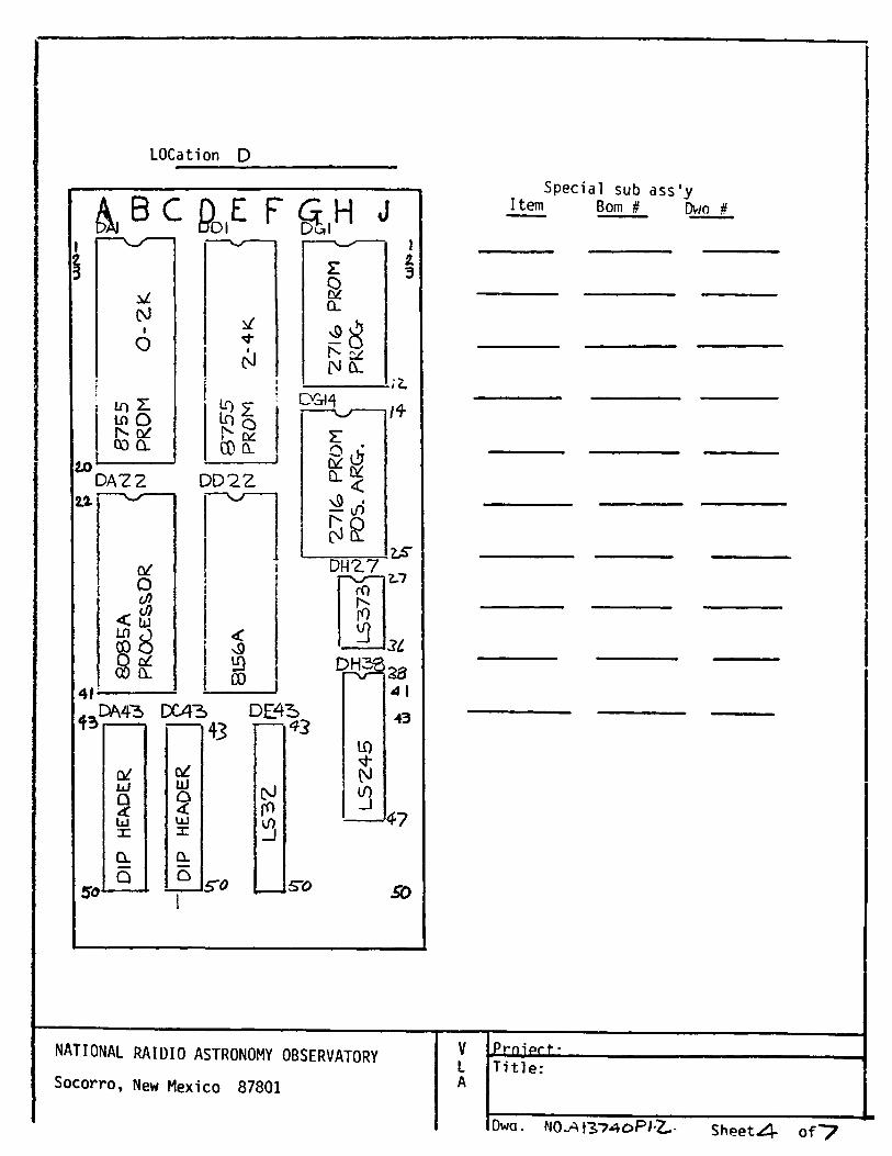
LOCation D
U
NiO
Lo 21 til O N CZ 03 CL
2X>DA22
4 1
0o</>
^ U)< LJLT) o8QCDCL
CO OL
DD2Z
<v9aCO
z
gCL
I£3
r- ^ [M CL
DGrH
D A « 1X43 D£4S
50
■v r—
EO w
s |
S ' *0*
14
DMZ7
rO
fi
DH33
10
Ni/>_i
I S
zr?
2 i
23 A I
43
4 7
SO
Special sub ass'y Item Bom # Dwo_i
NATIONAL RAIDIO ASTRONOMY OBSERVATORY
Socorro, New Mexico 87801
V -Erniprf. L A
Dwa. H0^\2>74oPhZ*^ Sheets of "7

SPECIAL SUB ASSY'S
ITEM BOM # DWG #
N o r g r
|. PULL UP RESISTOR__D IP . NETW ORK
BOURNS °4 114 Rr.OO2.-470, 4 7 0 JX^
N A T IO N A L RADIO ASTRONOM YO B S E R V A T O R Y
S O C O R R O , NEW M E X I C O 8 7 8 0 1
VLA
P R O J E C T
T IT L E
owe A i s y ^ o •«:wrrT,V 7 o-

oLoC________ £
oSPECIAL SUB ASSY'S
ITEM BOM # DWG #
s
3.csQxQ .Q
ozQHG LQ
s»&0
9
E: *
joftV) $
10
o> o
r* i t
I*c
MJN
J a
7 -c£Q
Cl
Q
1 5
s£
1 4
$[ 0
!3
1 3 12
cO
a r
il
oJOvOcr
20
Ov&^ r1 ^
1 9% r
!3'sT1 ^
1 8
00o3£
1 7(VOiX
D
&*S—
1 6Oc'QX
0 -a
2 5
ov £^ rr -
2 4
O
2 3
00o
22
oJovDcr
21
COo
3 0 2 9
<3-o
2 8
(YaaraQ
2 7
H
2 6
dJ
'Tr *
:ov O I g n d O
O O
/ v t o / z v
< 5 ^ x f / t / y * r & / / ¥ g - a a 2 -
N A T IO N A L RADIO ASTRONOM YO B S E R V A T O R Y
S O C O R R O , NEW M E X I C O 8 7 8 0 1
PR O JC C T
V T IT L E
LA
Dw-G 'P >!'~ 7 r w r r T ^ / 7 m

L o C A SPECIAL SUB ASSY'S
ITEM DWG #
M 0 7 S ,
^ A k s / s T Z e
N A T I O N A L R A D I O A S T R O N O M Y vpnojtCT
O B S E R V A T O R YVI
title
SOCORRO, NEW M EXICO S 7 8 0 IL_A
Dw-G P / Z . ■CMFfT Of


•F * O M T PMJCL
© • * ' S K l O U * €• • s• an o h o
« . - , 5 *t , « T# 0
vicui I H >
jjart •f j l * T P i,« > ,« AAC &i *CK.IPl.AM Df AM OAV *< ,V T P * A ftp S AAf M D , * *0 O A M ( 't u O H ,
P I •« ^fC TO * * * * 1 . * 5, AMO 7 A AC no^iNTAAjr toccl( ^mTc«e v <o * ♦HOM O*I n c ^ V i t A* f
S '* U f *X K f * VAC.V C t h V )W ,(oi*.No«ie - o * Y
poj IQ WQLA/r P » TD fH t WQcX^lNO «\*Tf
U uM 4 40 V :*C w * C S * . t m C MCLWT'nQ H o a s Z7.S01A I 0®q OCCP
g ) 1'* t u t W I« C .ow Z f lo w s o r %W(TCHC«
S E C T IO N A -A
-(C) 6 "Wo
H i wn ■Mi •« lH W lf m mA O J 1 **>£{> K io rc t Z <
m v d E m i u o * C « a u «
SECTION 0 —(»
unicss othipw isc SPccmtoDIMCNSIONS A»( IN INCH($ HMftAMCtt « w « a )MCI NCWkl> *»•' t l*WCIMCMU<U< 1
\J \l noot l c
4 " 8N A T I O N A L R A D IO
A S T R O N O M Y O B S E R V A T O R Y
• m o d u l e A i« > r .i D R A U IIN C
• M l *htigiTO--------- P T
flNlSHN(X1 ASS* USfD ON Il’Iil.Za 'fc ISS?0'M<k/ »■» | * ,A « * j

d e t a il i_______BUS W IR E L O O P FBI
VIEW I l - I i
tm* I* INC M^uNTiNC V 'tH TQ*st LAh6o* two-2* >S2
rR0«T P*hCl O '^ L A * bO*AD mac re^mn4Tu>fi
d e t a i l I* *5 VOiT flQuC* » U * * .T
OwTPuT Tt^niNAT.c;N5
- to rfcour p**ec
u n i css oiHtftwisc sttcincoDlM(NSlON$ ARC IN IMCMISfMIIMUt MMifl t 1 PlACt MCMMO1 IU> ±
V P t^ODCC C N A T I O N A L R A D IO A S T R O N O M Y
O B S E R V A T O R Y____________; MOOULC a s a v1 f\M1 MCWid •' * (M il*
MAICftUl 1 DRAWING BWW E H -----
MNlSH </>AiNUT ASST ..._VHD<M _.. K T T o - i m o *’ 1* t»» «

A niS'NG . J O * * 3 * S 'j - r i C i E N T ■JLkj^T.i -D A._3« f u i -^ 3 vjT < 1ZK1 3 e .'t ;L S t o &» 'O 'wOEO' v a wrn^f r . ° p d v v . o .
(5] T w i \ NA_X, ■MI'VJT JASNE S V ' U S ' 'T E M rv ,
P t a - J R 6 0 D W G 0 3 7 2 0 -,uT 1 ) S TO B E
R O lT E O a lO N C j T u t lO W E R R tt iy . ' iT£»A 'to) » N O
ALL OTmE<^ : o W iR.NC j S t o 8 1 ROOTTD A LO N G
T*E JP P E Q P /VL. ( 1TCM 7 )
0 w ic q c fv vQ w a ^ m = r:> M T E M '/ I > A3J a E O jiR E D
o.ttCE O NE U'JOEU TmE SCREW HE.&0 AND T u t CUmCR
q i ’ / v t 'M t u \ g u id e >>T£t* m s i t j e R t& a .
P M l t L I 'T t* * >M
(|] O j . O ’-R ' - . O . IE P l U i 'T t«A 4 J 1 T O C B O JM D
p l a n e " iv io p l a c e j n d e * s c r ; w u e i o a p p r o *
A S S U O W M .
m
JS ® iTEfA 2 6 TO rERNViMATE lE C 'D a t p i - 6 ,-C AnO -HH
S O : D E R 6 M 0 T E R M IN A L M T £ m a z ) t o t , K J i ) N 3
plan e , i component s id e oc it e m 's i . a a n d <? i5 0 L 0 E R P W R T E Q K A lK J ^ l ITE M 41 I T O P W R
PLA N E . i W iR E - W B fcP S IQ E O P -.Te^S 7 . 8 AM D 9 ).
H 'E P w r « 6 N 0 B L ft W IR IN G S w A L - BE O n T u E
W IR E -W R A P t e r m S iO E O P ■ T E M i'i 1 8 ANO M .
T h E KAO TO N T A P E < IT E M 5 7 1 5 -i Al L ^ U N t h e
P U u L u E M G T u O F 1 V »e R A i l S ( IT E M S lio « 'T>.
VOO'FiEO LOGIC CONNECTOR BOARD ( C i 3 1 C O M 2 l )
Shall 3E iN5TAaED IN LOCATION) "E" ONL'f.LOCATIONS *6* THRU "O ' A R E T O U S E STAN D AR D C in ^ O M S J .
J S E TEV\ 4 "HD IN S T A L L I.C 3 iT E * A S S.
b o m - A i 5 7 < a 0 2 9
Ai WoZ9 '1 »IMI HC«*4l>
M il
F/R APEX WTERFACe MODULE
N A T I O N A L R A D IO A S T R O N O M Y
O B S E R V A T O R Y
lsk~ issfpisMap I-


DISPLAY PLACEM ENT
DETAIL ’ B*
I2)FR0MT PANEL-
o u t l i n e . o f c l e a r PiAvnc filter akjd RE P POL. ^ C R tE - M
(i t e m * . @ e
O U T L I k l t O F F R O U 1
PAKjE i. D ib P L A V W IU P O W C U T - O W T
O U T L IN E . OF t!l$PlAV LbSEAJO P lL M (|TE M (7«1
FOC ROT
S3©®®;____§TAI_US______
:MK|i
7-SEG I ED'S / U lO , Ul I
BAR - GRAPH , l^LED'S U8,U9
5 5 H * S « H - S r w -
SPECIAL A66E M f r L V IMSTRUfT lQMS ( U l l F R O U T P A t o t L P l ' j P L A Y )
(J] APPiY W H ITE H T T t n M S , '/»" m &w e on " t o e , *ROT* An jP " S t a t u V t o r e d
BO IAR1Z 1U& M R E E k J , 4 C E F A C lS JG O U T , u V M S R u ft- O P f LE T T E R S OB SCRE.EU PR O C ESS. 4 l'6 > 0 L E T T E R S TO D IS P LA Y O E V 1C E 6 U8 - U I I A% S H O U U 110 D E -TA il '& • fcv MAK'-*o6 A P (? t - A M E U & I .7 OF C i lT E R ,
4CRE.EO 4*jO A'b'bf-X&LE-ti C-SH.AV P.C. BOARtJ O T E M C} TO COHRESPOojO iMS U O LVT tlO G VuO <3 CKi tR C K >T P A v jE L .
B J m o u u t » ' I T I « • % CRtEv; f ' T . J b i i* . 2'6) TO TwREACEO V r u o S OVj PROUT P A u C l U*I1JS V . V I M l louTfe f l T t i j 7 1 V
(J) UOuU-r L X G tM O IuEOAT-uE f 'L M 4 T H IP ( IT E M 2 2 ) TO IN S ID E PACEOF R E D Po l. SCBfc-EVj u ‘ ji>jC. TO AM ^PAR EK JT t a p e . A L I6KJ L E T T E R IN G* ok e x a c t w y . r f T io » j,io<j v u tw i> o ~me. l e d , ' l l u m iw a t e j e>An \n u e m
P lS P lA V p.c. b O A K O i«, t-ROCEPLY m O l»o~ E O . EK lbuKE •U l. " IS 1N S 1DE t t r r - H 0 * ) T LR> 6 A « . 6E.E. D E T A IL " V . T u ,«i A L lG M u e u T a C R IT IC A L /
LED DISPLAY WINDOW ASSEMBLY
DETAIL "A"
(7] PER M A ME KIT LV U O U U T 5 ' iP lA v P.C. IbO A R Q TO F R f'IO T P A M E l U-WVJIi TUREAOEO STuOS, TU READED tV A C t.9% f i ’ t u fc.2 ) A-oo lu iACu -.E itWEvO^i ( ITE M «,%).
(H E M b uR E . L E.D. O i^ P lA V DEVICES ARE P L U tu A6 Ai«vli>T r.LTfc R < *>CP{ E M ACTER w o u M T im g D i y ’ iA '/ P.C. boA<?t> fC R k jA y U u w p.yVA-v \ 'iie > n .n '/ . IL IU M IU A T E L 6.D*» T o CHECK c , ^ l A L 'S k jm £ io T Of A u . CO M Po iufeM Tfc.
(3) E u i u R t PRd/PfcR C LEA RANC E. tSfcTo jtt>v) R E m o vA & cE 6ufe • P A n E l TO TU£ POT*, A k jI) <,VAJITcu OkJ 0>*»PCAV T>.C. e oA U O .
COMPONENT h h in c , VltW
-MSa t
Hi— 1*-1-
U k i l i - h n l ,
aaufl
rsi-iQ Q 0
f S i0 U 0
Fti-M U D
U N K S S O THCftW iSC S ^ C C ifiC O D IM EN S IO N S A M IN IN C H (S
O V 4 0 P 1 S F P P C & A V i Y W AT( H * K
HN l$MN ( & t 4SST . . V H P on
I M il - F/R APEX INTERFACE MDL
A S S E f^ b L YD W C -
N A T I O N A L R A D IO A S T R O N O M Y
O B S E R V A T O R Y

8_______ |_______ 7_______ |_______ 6_______ |_______ 5
50 pos. * rn coc,tc com to Tvp t c.( 0fo* Pin imcinc SCt 0*<* #OUOf'5>♦ f . A
i ' i \ l \ ! 3i : * • i * i : V X j . i j. J_ i_ I| xeos | T *
(SapiC aI
• -*-• * V t
■ »H - t! I
r; T'llTj’TI't Ji6i jo' jit; jmj '»[
r*T--I I
- - 4 - H - — ■
A
itI.
•0----------- 1--------- E------------- 1-------- F------------ 1
— * tr:
*iOC' t o *> <4Pi* .OC'C 'O n h bO A f>scr o*<. •c«a»«OM2><* t *L X> I t---------f
(h o t u s to ')
fR O N T PHWCl.
('SEC D C T A I L -C ON Sm£ t T
•- ♦* -JU?
I
raonT o a k tl
U N IC S S O l H ( * w i S C S P C C i fK O 0 1M (N $ I0 N S M ( IN IN C H C S»eii«MCii « % n s IMC(MCWil<lUi S
X■»UKIMC«UI>li t
VIA
M ilN A T I O N A L R A O IO
A S T R O N O M Y O B S E R V A T O R YWWO • * « • * • «
; t/M A rt* l/VJthrJKEMODULC UT^mih' - W1
fIN lS H v Vft (X T AS$V usto O N

V I S I O N S
REV DATE DRAWN BY A P P R V D BY D E S C R IP T IO N
DRAWN BY DATE
DESIGNED BY DATE
APPROVED BY DATEN E X T A S S Y U S E D O N
N A T IO N A L RADIO ASTRONOMYOBSERVATORY
SOCORRO, NEW ME XICO 8 7 8 0 1
VLA
P R O J E C T_____________M I L ____________________
T,TLE F / R A P E X . I N T E R F A C E
1 C r / l D D L i i f i L O C A T I O N
DWGNO. M / 5 ^ ^ 0 - l L SHEET OF d


lo c a - z : c > i m L £ 7' E C I 7* L S U B A S S Y ’ S
O O
-5
Nj
$
QS*-
4|i
•Vt*Jaa
&CIS
G>3Ns r-
10
s3ro
ft
JPe
o<>
sj*Tv~+-
a s
8
QNr
C-j
O
vf-l\
15.o °o
Cl
14
•a'Wr
13
O52"Tf\
5t> 1 2
in3-
o II->rO•>yn-JS3-h-
o
2 0
NO<3
19
o gc•3 QCj s
Q)
18
Mav33-
17
Ki cc
- £ £ I
16
NOv9vT
0
25
*rf
,y-r .
2 4 <9
N •i.V
rrt
2 3
OQ
22avS
£
2 1
a'3\
r-
o
3 0ror*~!
£
a28
!y$
27N■N
v3
263
IE9~rF~\iT
/
fQJr . :o v O g n d O
O
ITEM BOM H DWG
N A T I O N A L R A D IO A S T R O N O M Y0 3 S E R V A T O R Y
SOCORRO, NEW M E X IC O 67 801
PROJECT________ / M i l ______________
I,TLt F / R A P E X : ; J T E .? ~= l-£I C M O D U L E L O C - I ~ ! Q :\j
DWG Na P. I3 7 C Q P i L SHEET or

^ D - m m c a SPECI7*L SUB ASSY’S
ITEM BOM H DWG ft
N A T IO N A L R AD IO A S T R O N O M YO B S E R V A T O R Y
S O C O R R O , N E W M E X I C O 8 7 8 0 1
VLA
P H O J C C T
fYil L
T I T L E7P, I N T E R F P . - Z I
S C / V U u L LE L O C F lT IZ NDWG
^ . A / Z 7 ^ 0 : J1 L S H E E T <dl OF

8___________ |____________ 7____________|____________ 6____________ |____________ 5____________|____________4____________ |____________ 3____________1____________ 2 I 1----------- ------------------------------------------------------------------------------------ 1 ■ - ..................................... 1-------------------------------------------- - t -s : Z S T B S ’S - « m > r ----------------- = S 5 -----------" 1
1 « H c « « m o « o n t
1 6• ■ / « | A C O f i O £ 2
a * * ( o j 4£>j
©-•© ®*“ (§) © * * '<X.A*4+C *&r6A4A*
0
• c
*oo v Ctc/t © ■ * ® - ~ "
rrx. m m 400*1 Aor&*+
® ® ® - ® ® (ED?oc (*/\ Aor /4*in
D A
f f i w r p a w l v tew
tore*I. ntONT AND tf M 't/St &C C O ' BdNO
» t » M . s o * T Q T h C Sioc f O * C C C i S T 0 t h i C O np 0 N t N f S A N O T D C N A ft L C fM C * 0 P A » O * 0 r r 0 M sc tc iN c o v c v s t o hi S c io in p i* c c .
X « u 30LDC* r o 6 C COVCRCOW/J* H(.*T 5MRMV4
[31 0*4*r j*& Ai y»?M V
i:
£ /U (?/" nATlPlAJL5 "Z)'37SOU'S
I m z
r / R 3 u fro //m t r f o a j L C i
N A T I O N A L R A D IO A S T R O N O M Y
O B S E R V A T O R Y
FS#T
T ar35

8 7 6 5
seer*)" A -Atow.
0 r* rl,r* *«o *f i A~*,iSt> * t* r> W » '< A*o '* + *f 9 * » * iL * o l t / W j . 0 ^ 2 A C ^ « « V 6l*C* . Z>?/ ***>5* m / ww/tf o Q*ie*.
iii
IT la) l ~ g£
UNKSS OtHCRwiSC SPCCiriCOdimensions a m in incmis
IAXIN(WHI>Ui< S l*UXIMCMM> 1
” 11N A T I O N A L R A D IO
A S T R O N O M Y O B S E R V A T O R Y
; r/R t>WJ rCH'MCr* i'iqoule A ar.
DA IVJNC,
kmtm *» « A 0 ***»»•••« snr
»INISH jjrwmi*W-iL
NUT ASST USIO ON Im u i - - « '4 E S ? 5 '» * « > * ® H , a

rvrar,
D
«$von / «*•/ .* mrrM> 'Act v«w
*aren4r**o**o m c a *w fc w•UVtM, Ct#*tQO*Ar/0*.
w*c 70 r»Q*T mm 6***c
4o$t*
VIEW I S - I B a a p O " ( »
PS! / PSl T€**N H . * * w i i
uNicii 6Mifc»isi URE?ifpO lM f N S lO M t M IC IN I W C H tt i w i m c i i m u ft itiA C t MCafttl< u i i ft I n M M M M I l U ' ft 1 r u t l M M H l i h : ft
M A IC R M l
F IN IS HNCK? ASSY U S t O O N


R E V I S I O N S
REV DATE DRAWN BY A PPRV 'D BY DE SCRIPT ION
\
6 - 8 3 NE.W P/R. SVSTG M MODEL- E- O E.S I6M .SvaT "A-1" T£> "A -& “ FOR PI CTO R A t
OF TMIS C O A f IGORAT\OM
I A7 / t f / r t
/i//^yuy' OO i/2. / -* ^ ds-r- ^ ^ ^/£T^ 2s» ~fo iWA STjr-s/"-!?-** }
S fr/w/s? Ca> <Lit. •>' t r <JT- /a»/S- uo‘
c . S'/*A^o.r-^ /2(? r ^ssz t>£.tirc J a io u g *iEoT* ss-e T>e»o&. ~T7> u ) - b r i - > t Pa ^ s-s A r r * c . T e . * • 7 ** , *«3 ^
D !0/O//8<! CV ^ M C cSO &4 £ 7 A/O .X F O Z //o CO aJ/U. P A \ J€ C SA/egy- A - S '
£ 1 ~Z/tiA O D ^ C fir^f mor>)*T£r $r*rr\ j j o - 7 Z 1
0$!* ^ r- ‘ VI *//- Hif/'to £,',j Vum/tf/" f**,“lx,3o 71, SH____&DQ-c£ M irs ct *-t pt.-L- Vf| ' J
t/ ~ C C F<KArf\C G v J t. u r t r c -T r a m I'D & /£
r^ovrcL A ^ G > z - l- '~ - P i-G T -j& ,27,15* 7-
G 5 / £/ &>
................ .........—
R \r * * J_ <r -11 5 o rr\ S?
F f : i , * , I*w r / 2 z / t s £ C //w / w r c i i A-P* x. 5 5 <e t>«.*w£. /=©<_
t i tt£ s £ * '5 4 . r "
*
DRAWN BY DATEB / / / / 0 3
DESIGNED BY DATE
APPROVED BY DATES / l t 1 * * NEXT ASSY USED ON
NATIONAL RADIO ASTRONOMYOBSERVATORY
SOCORRO, NEW ME XICO 8 7 8 0 1LA
V« . O J E C T _ p ^ r g j S Y S X E j y ' _ M - 2 P i k M
r iT L t ftC» RACK LAVOUTand WIRE. L IS T
dno6 A13740W IO SHEET or SO
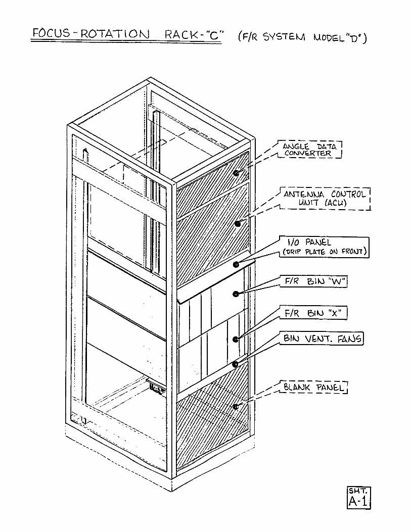
FOCUS - ROTATIQKJ RACK-"C" (f/q. SYSTEM Uodel'V )
„ ^ A K i G t e . ■data-1
1/ ^l _ c£ ^ Ei5.T^:R _l
/ A N T t W U A c o n t r o l " 1
^ ____ UfJJ2r_fACU _!
I/O PA.KJ&L(•DR\? PL&Tt OK) FI?0(Jt )
; m &1KJ "W "
F /* 51U "X"
B I M VfcMT. BV k K >
6 L M O K _ f A M t C ]
SHT.
A -l

I
I/O C0MU&CTOR PAM£L
SEE SHT. A -5
6 I N - 7 0 - 0 J N
m ^ R C o u w e c r
r iuM. ViAlfP
AMGL& ‘DATA COiO'JOT&R
P/R E>IU “W*
["b Tm “ASSV | | ^PJSp^aMOSj !
6 £ t S M T . A - ^ A - 4 ^
P / R B I N ) X
j“ i t 7 j _ASSY j
l P I ^ ^ o m o S j
SEE SMT. A-3, A-4
S im f a k j a s s y
^ M T S . BRACKET
5 E E S H T . A - S
SMT.
A-2

APLXIMTE-I?'FACE.
f t W )
M
13STA66T
(lW>
Ml
IB
Cm d /m o m
INWFACfc
ftw)
F/R 09nrn?it)L.
few-)
M " 7 &
•DATA TAP7
kkj)
M 2 B
B L A sjK
f - / ^ E L f e C T W M I ^ f c l f O eV l t V ) )
F/R'povoe,^
“5 U P P L V
£4<*j)
M 8 < ?
F /R
M w )
H 2 1 A 1
M 0 P U L 6 . L 0 £ A T I 0 M S 4 ^ f c W ^ W . A ^ A t O ^ G M t t O T
6 H T .
A-3

COK)M£CTOft 7LAT6.Jl J2 JS J4 J5
i
i
i
V J l R E U S T SH EETS < £ 0 - 4 &
ZOT &0X JUMPERS CMO/MON A.ft. “DATA ^ SPARE \PED.RM JUNCTION 80X r - - TRANSLATORS [
Jfe SPARE J l SPARE
J7 JG JS J4 JS J2 Jl
5 0 PIN 3 4 P I MWW
SO PIN ww
r&H pin
ww
/
M 8 Power SupPiV
-J
k
P S S Y S T E M A C P O W E R r _ 1 M P U T ( I 2 0 V A C ) j
jj>4 F ^ _ s w r T C H & D _ A c
r
iM22 F/R ^VinCHlMG “ I
PZ 9VancM6D AC INPUT 1 P S & R A K E D C P4 FaC. BRAKg DC P5 P> e»A>f MOTOR AC P6 ROT TRAMS. AC P7 POC TRAMS. AC P8 CPARt
L P9 £AkJ__AC___________|
® iNTERCONMtGTfMG WIUINJ& PANELS
M 80234PIN
CR
Jl
® ©
60PIN
CR
M 2 2
P9) (p i)
P 7 ) ( P 3
Jl
© ©
50PfM
J?.
34WM
WV,
Jl5 0PIM
&
M I
Jl42PIM
WW
J234PIN
WvJ
Jl5 0PIN
CR
M7
J2 Jl5 0Pli4
WW
5 0PIN
WfcJ
Ml
M \0J2
3 4PIM
WW
Jl50PIM
\N*/
SLOT P 0 5 .^> I 12 I Tl 1 10 I 9 I 8 1 7 I 6 I 5 | 4 1
J234PIN
Wvi
J l
5 0PIM
m j
M l
J2S4p in
ww
Jl42PIM
m
IRACK "C"
B IN W
WIRE LIST SHEETS 2-19
BIN XWIRE LIST SWEETS 2 0 - 2 9
F/R ELECTRONIC B'MS( R E A R V IE V O )
SHT.
A-4

I/O c o m k ie c t o r p a n e l
[ S 'F O C / R O T
I ip o c /R O T ,T t? A K i< > -
I C M P / m o w | i
I m (MU» 1 MDKi I I I I
P E D E S T A LR O O M
J U M C T IO M
B O X
I I| j P A T A
I (SET S(SPAfcC. j C M O /
I I W T AI I
j TRAhVSPDSt I MATRIX 4I -20T b O X
I P L U G I
o • 0w u fiy
0 • idHH$ • NN e
• • A• |R« • ♦A • •A
\ j r \J6* \J5* ,#J4“ "jy *J2" "Jl*
PACT SVM J\ J2-JS J 4 JS J6 J7fcU>CK TYPk 10 4 -PiM M'PlM 50-PlW 34-PlU CM“D
<UJ2<
-D
<0123
610CK P/ai 20(OS7~l 201298-3 200277-4 2000 8 - 3
PIN) HW NOT US£0. ^•rvscft 202579-2 201350-26UIT7B. PIUS o 201046-2 202514-1 2003?A'4 20O8S3-4Gum soo& tz • 201047-2 202512- 1 20S9fc4-fc 20S9&4-6Comtact sockets
JACK €Cg£U> (MAL£) --------- 20087 / -2 ---------- ►•
SIM VEkm LftTlOM FAK)S
BDVkR PAM M0f7BL W £ 2 l o 7 £ L
(OR s i k a . )
2>~ R e o ' o
B I M WFAtO M O U IO l lN iG
U K A C K C T
(Vi. A- <bK-2£>8)
SHT.A-5

WIRE LISTR A C K : C 1 B I N : W S L O T : » - T / M O D U L E : M u > ^£ X /r* | T Y P E : 6 ”o P,-o
L I S T B Y : j W I R E B Y :
C O N N ! E C T O R T Y P E : z o o 2 7 7 - H ( C O N N E C T O R P A G r . /
P I N F U N C T I O N T Y P E F R O M T O
A A p e x ' I V j t * + i£~ 0 ^ 2 0 i&13
T2> A- j i rs. x . t - 1/ t o — <1 J l - F
C A f i i x X ^ T" + • 6 "tt. ,Qe.a+j£,e. )t> W - < * J - / - B
£ f « c^t?.
e ; X T - — / ^ - ^ u u — ^ J - l — £ *
P F o C ^ t T / o S \ - T B l
H I^ O T " ^ 1 X / o — X I - z ?
J P o c_ S t X / o - X l -
k o r ^ 2 . T / o - S i - * & V
L F o e . ^ * * X / o - X I - B / J
M E o t - s * 4? C 1 h i CP
c
N E y c ]£i u j U t t 2.c. , Tp * \ Z U> - 8 X 2 L - S
P
R S' f * j c i+fcc t x c i 2 2, .jT T P ^ i zi
u » - e T 2 . - U
T Fee- u p p t f /2. L m
*•i
£ioM
O 12-OT C UJ L 1 /Ul ^ ( L a > S £ r / o - X I - A C
V F o e Loe*>G-G. t i h ^ G L v J S t . x/ o - I I - A - A
W 2Lo r * C C u J £. /MA s*£ - J l - f l - M
x 1 1 *
Y
? P » o 0 j r " £ e .* -> s»s. T /o - J l -
c u
P \ ^ t . £1 x / o - x i - 4 x
C L V ^ i ? / j s f x /e> - x \ - A W
/o C \ £ c ^ 5 S L
>«*i
i
h1
/» \<L U \ ^ ~ S € V o - r 1 - 4 U
i I c V S c l /-» s £
fe1\n1i?
\ C g v j s * : % — J 1 "B e .•
V V ^ e aj s 'E ~ / o - S \ - B D
N A T i O N A L R A D I O A S T R O N O M Y C 3 S E R V A T 0 R Y P R O J : I D A T E : J l i M
T I T L E : F / t f S Y S T 6 * 4 I R E V :
1 D W G N O . Al ’b l Q O U i O S H E E T *2. 0 F 4 T 3
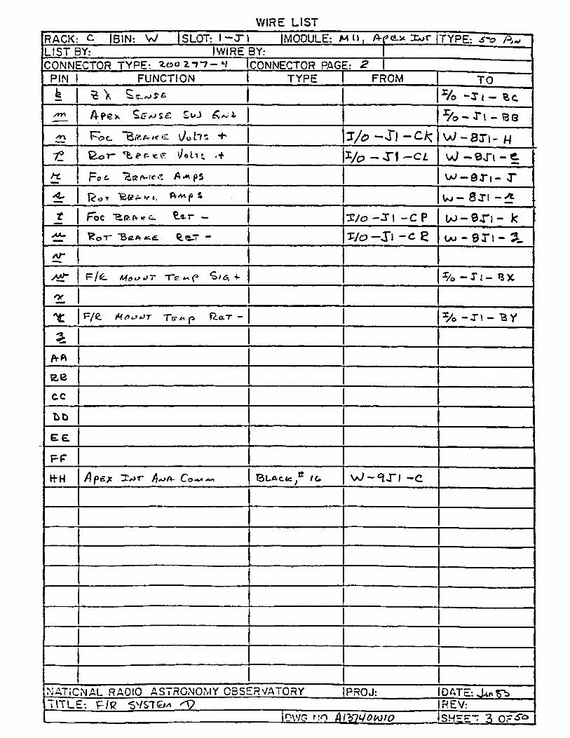
WIRE LISTRACK: c. IBIN: W |SLOT: l - T I IMODULE: M U , A i»a.x. l o r ITYPE: A -
LIST BY: IWIRE BY:
CONNECTOR TYPE-. » o o iT 7 - H ICONNECTOR PAGE: 2PIN 1 FUNCTION 1 TYPE 1 FROM TO
k ^ \ ^ C_ aJ S' £• x/o - J l - Be
/TY\ /J S cl ^ o - J"l - Be
Pt>C "B/V-A-K'C \A>lfS +» i / o - J l - c * W - 8 T 1- H
t l l/elu. i/c? - . r i - c i uJ - e j* t - e.
H. po t TEcz/v/cit w - 0 j-|. r
U>- 8 J l
£ Foe £*-7“ — X/o - J l -C P i/ o - e n - k
^ \?oT " B Q . ( * T - i io - i\ - c e o« - 9 D - 3L
AT
F/iL Mo<-> Tcm(* ^/6, 4* % - X l - U X
21*£ F/fc Tir*«p fea-T - % - x i - B y
3:
/Vft
C C
L&
£ £
FF
H-H /I p I / J t * ^a A- Co*k BLAcic;tt /c. W - ^ X I - c
NATIONAL RAOIO ASTRONOMY OBSERVATORY IPROJ: 1 DATE: J*n £"bT ITLE : P/E «SVS7£m ^9 IREV:
(DWG NO AfbltJOto/O IsH-” 3 OF^>

WIRE LISTRACK: C |BIN: W SLOT: 1 - ^ 2: IMODULE: M il , & *. I*o7” (TYPE: ^LIST BY: IWIRE BY:CONNECTOR TYPE: Z o o 0 3 0 - ^ (CONNECTOR PAGE: /
PIN 1 FUNCTION TYPE FROM TO
A- Foe. Isr q — bJk^Zc- “TVS to -EJJ - l~"
T3 "B.OT- 'iA-TA- — S/G, Uok TP** to - I f l - A/-
C Foe 'T>a-ta- <2cr — ^crr- UJ— SJ*I
X> — ' t 4-‘TA- ^S7" BLt ^26 3 TP^Z. u> - J l — oc
e Foe Ar£ CLle. — UjU *■*.*. rp*-3 UJ - *2nTl- -1
F JZor— AX Ctlc - S/Cj TP^V uj - i« n - 7 i
H Foe. /)-r CLlc - *£e.r TP4**3 uo — 3 J-/ - /m
T ^o-r AX a i c - l ic e ^ c .TT^Y w - U l -
\< Fi>c. A-X id , TP*V ^ - 3 X I- i.
L ■OT— A"X U k * 1 *^TP*£ to — 3J“1 — /TV
Fc»C. A~X rt-TA- — 12*“ 7" BLfc4, 2.6; T p V to — 2, S i— k
/O 9*07” A-X --R.S7" V L<. * 2.6 3 TP**£ \aJ - 'S'Tl - £:
P
s
T
0 Foe 0^^^. Li^i Xajw W - 3>J~I- 5:
V * «»T 0 tO L i aa, W \aJ -3>Tl- £
w Foe i2<2. L. i *>
X I2o r c c w L im IT*_m W -3T I - cJ
Y V o w p> ^ " f — S/c, U> - 3J“ t - £
2
/9-A L i^ iv i / j t f — &1.7- to — 3 X I ■“ £
E E
CC
PP
tf H
NATIONAL RADIO ASTRONOMY OBSERVATORY PROJ: lDATE:J*rfJ!>T ITLE: P i# 'D REV:
iDWG NO An iL/O to/O IS H E " 4 O r-^

WIRE LISTRACK: C B IN : W |SLOT:l-.T* |MODULE:Mil, A-P*x X - t ItYPE: 3 g P...
LIST BY: IWIRE BY: 1
CONNECTOR TYPE: 0 3 ICONNECTOR PAG!Z - 1
PIM 1 FUNCTION 1 TYPE FROM | j o
feK"
L L
M M
WAI
NATIONAL RADIO ASTRONOMY C3SERVAT0RY PROJ: ID A T E :Jh n «TITLE-. P/R -S'/sTtM IREV:
iDWG •‘■0 ISHEE" 5 OF^P

WIRE LISTRACK: C BIN: W 1 SLOT: 3 - J"| MODULE: M 7.t F/<t Co^r IT Y P E :^ / ^LIST BY: IWIRE BY:CONNECTOR TYPE: 2»o Z7■?-•/ CONNECTOR PAGE: /PIN 1 FUNCTION TYPE I FROM TO
A 4 >S-\) E e i , * 20
B (sjnI w B^cic 3 1 £» u j — ^«r( - w
C Cfi/LAsJ e J tt /6 W -9X1 - £.
..... . ..
G — 1 v/ Y'2.LLu w 4 ^ UJ- n T l - A A
P t~p C KOo!c ^ ~ ! f f 'f \rt
0-.1
H <£>aa<v - 1 6 £ V ) u j - 0 X z — H •
J ^ m A — | ( V '^ U) - B X z - T
X w c\- — i ( *t") Uj - £ 1 ^ - K
L S m A- - > (_ V ' ) U) -Z>T?--l-
W - 0J2- - /f/)
rJ C L k X - i S./r, * i t , n vaj - 8 T z- L L
P fcis, o — (p C/e, U>-gT2--£C.
R CL IcJ - 1 £<z.r ■BLIC Z- jT|* **17 U i- <&S'L-/U/J
S CdT - 1 Tints' UU - ©12. — £ £
T C L k O — C/g, U>\ j *2fr,TP**1 UJ — B *T ‘Z — F F
O ^ T fc r - i Belt *L.c * 2fc , T P V 0 - SJ-Z. -H-H
V C L ie a - <f> o.'3-t - i/o —0 'T^p *rj"
v / ^ (L O - (f> S t^ UJk }T ?*20 uj - £»Tz-'fct>
X £*Mhy Tfi ’DrvTA-S<s*r — C/6, W / v ^ ^ T P v ? U) - 0J Z - M
Y S»rc o - <p R e r T3LK)e ia J’T rzo iaj — aT'Z.-BE
/M To 'b/i-'TA- £<sl~t — Pi? 7* T^Lkr* Zfc ,Tf*2.7 VAJ - @T Z - A/
Cl- Foe Vff»« «*. L,<H *>14 vyO — 1 J* 1 — U
W Pft c> L«>I-- ? L im T <0 \sJ - I Xz. - Vv/
C Eo r* C (*-> £- 1 3"*•> H to - 1 J z - V/
rl_ P r - cc.us Li«< ~J2 >h+- u j — IT 2. - X
cl L / ^ i r IT j m- — 12-c.r VaJ ~ I Jz. -/fAr'•T Voi^ P ® -L /O Uf (yJ- )JZ - V
h Foe /)r ^A~-r A - £/ iotv,tt *-c. ,t p V UJ — l>T2L- Ic
<TL Foe. A~r CLc>c.t< — S /&,u til
\*Jk , 2(• J-T/® 3 to - 1 J i - e
NATIONAL RADIO ASTRONOMY OBSERVATORY PROJ: DATE: J u nT ITLE : F/f? 15 IREV:
I IOWG MO. AlZlLlOM tO ISHEE”

WIRE LISTR ACK: C BIN: v7 I SLOT: 3 - ^ 1 1 MODULE: A* 1 , <=/£ TYPE: SbLIST BY: |WIRE BY: 1
CONNECTOR TYPE: ICONNECTOR PAGE: 2. |PIN 1 FUNCTION 1 TYPE FROM TO
k F o e A 3 : "t>A-T-/v - /T p V 1>U- 1 T z - A l
y*n_ A X CL.CC K — 12 -rT Uj - l> T2 ~ H-
/n f?o*r A x 'b/KT'A- - STi<^ zc^TPa d U> — 1 T 2. - £
n 2ot- A t CLocie - S/6) Ujk * ZC } TPU*/ U J- /TZ - F
tL 72.0r- A - r t)ft-TA — 'Ear fcue ***■*» t P ^ L J - U 2 - A /
A. £oT* A l CLoc/c — Q.tz.r 'BLki >T(>\ Uu> - 1 T2-- J*
t C o a V <J ^ ^ (S’, J £ »S. a
F « * t LA-Tf- ^ s e ? Uk^'z.c -jTP^l uJ-JTZ.-/}
cS 12e»T“ "&/V-T/V- 'EiS.c — £/£> UJk^Zt. , TTfr2 U> - | J“2. - 8
M S F“» C. "D -VA- £»“ <3 *“ K.GLT T Lk. *2.6, TP1*/ uJ — 1 T 2. — C
E . o r "W rA ,- - e.ST BLK rp tt2. UJ - I T * . - ! *
A L & Z - 0 S ' r t f / w i -np^ 't v J —
t o r ”B c ? - SS£. "D£toe x/o - r / - C/v]
fVA A l & £ ■— £ S Juo
BE f ttJ T f i - it- +
C C A / O T P — S
A - H
E E . ft+JTA - 2
F F - 1
H H A ft L C l -«*- A*. O sJ ^ L A t f t * 2.0 W - ^ J " ! - 4
^ Tt »t- TT'f'^e’-
T r
■poQ. A <.o«i ,t r . t /)/<>T
M '•
w VF£.o a ~'*j ^ ■= I
NATIONAL RADIO ASTRONOMY OBSERVATORY PROJ: IDATE: Jwrt 7^.ITLE : £IQ ^VST^A/I *D IREV:
(DWG NO a m V O U o lo IS H - " 7 0.-6*

WIRE LISTRACK: C |BIN: W SLOT: X IMODULE: M 7 , F/ze. JTYPE*LIST BY: I WIRE BY:CONNECTOR TYPE: io o 2 7 7 - V ICONNECTOR PAGE: '
PIN 1 FUNCTION I TYPE 1 FROM TO
P-© c C.** ti Lc-'fc ^ i/ v J - *1X 2.- E.
Foe. 11 " W - ^ X z - c
C Po c ft •• w
T> F C. LouJ&G-. L.*a. K «* W — °i X 2 - F
S J F*>c. s it u W — X 2 - D
p 1 R ,„ . Z + f c j l •• •• w - ^ X z - 7C
?4- | F*c PuLscls up •< u l / J - ^ X i- 3
X Poc PuLS ri ii '» U J- ^ X 2 - H
K £©t- u \»
Im 1?©7 Bfe* ( P , . j OoT ll •• U»—^X'z.- p
lA^-nxz- y
f j | CUJ L,4v a . t, •• W - ^ 1 *2.- A?
P CCuJ £.»<ui " UJ —*112 - T
Rt»r- "TrtA^c Puje. • i •#u j - ^ t 2 . - 8
S Mfi'i e> cl foLvrs it i« U) - X*2L -W
T ^oT PjtS'^S CtO | , ii W — X Z. — A/
U P.CTT Put SITS CC*J Ii •» i/ j — X 2 - (;
\/ P \ !• “ u » - ° iX l- r
W L V\ u «* 1/J — t f z - Z
X G V n " to -^X*i-A-A
Y U h »» tA i- ^ X 2 - B e
e \< X K *» v j — X2_- CC
a. X ^ u ii 10 — °lXT .“
V X u ir u ^ - n r z - e. e
c T*- V •' It VO - J 2 -PF
s( Poc. rko ** + Pots/2. *->P kA; } Tpe3c/ X/6?- X I - P
c FrtC_ P /lSC. WKj * 2(, ^TP ss* ^/o —X \ S
f Pc c. £e.Tfc fP to jy
litk^ 2.(» t 7-p# 25- /o — 3“ \ ^
A Poe. <£sfc- r/o - x i - ^
*L Ft=»c- *& &-/**.€. SS/2- D£i/ I / o - X l— ^
NATIONAL RADIO ASTRONOMY OBSERVATORY IPROJ: IDATE* Jwn f iilT LE : P/t? <N<rrtM /D IREV:
in\VG riO A ltn U d te fo IS H ^ " S>0,-613 |
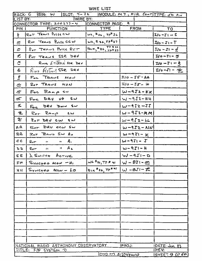
WIRE LISTRACK: c. BIN: Wl ISLOT: S - I t MODULE: M 1 , P 1R. Co~rITYPE: P,.,LIST BY: IWIRE BY:CONNECTOR TYPE: 2.007.1 1 - 1 ICONNECTOR PAG :. Z
PIN I FUNCTION 1 TYPE FROM 1 TO
k (2.0 T* Teo^S PjLM CvJ UJ k Tf»tt36 I/O -X I - S
A* R.o-r PoLS*£. C C U> WK, tt-7.o^rf>Jt3 7 jy© - x 1 - T
Ay f o-r PuUc. Re.'r_ Tf' *31
r / 0 - x i - i
Per T e ^ s SS& Tsai/ r/o - x i - 2?
n JE.'iTkfi/cL Ss*. Ibc ✓ I/O - X I — £
A.tf.*f f i t T r r A ^ ^ r/o - x i - ^
1—0 c. "" I £ M © aJ I / o - TS“-AA
]ZaT *T)6-A-/ S He /J x/o - 15“- W-
Ai? Foe R a ^ ^ U J-^ J2.- kK
^ P o c UP VO - ‘U l- U W
/£ t>£\/ 'duoaj I"2. —XT
/eL l OT- S»U-> UJ - ^4 “2-“ M M
^ r P-O T 'bA J CbJ uJ l l
fVA ^.oT- £>£a/ ecoJ Sw U>-°lX?_- WA/
j^OT ' A-A>4i S l»J /) 0 to —®lTl - fc
c c 2oT «< •» u j- ^ n - x
"bli £o r n " A t w - ^ x i - 14
GE X S c O » T C ^ A- C T i v j g . W l - 0
FF ^ Y aJCH-IZO *4o*> H-I uJA i 2 JT ii >*‘ V/ vJ — £ X I - CH
H H ^ Y A - > C f t < ? .o A4b*-» — jL© Buie TP* *** u j — 0J” / — -pi
NATIONAL RADIO ASTRONOMY OBSERVATORY IPROJ: 1 DATE: JimTITLE : Fir? SV S'TQ fr 'V IREV:
dwg mo tuym otM to i s h - " <2 o .- ^

WIRE LISTRACK-. C | B IN: W S L O T : 7 — J"* (M O D U L E : M 7. , ^ a-^a- t- ^ j t y p E: * 2 P,+j
L I S T BY: |W IR E 9 Y : I
C O N N E C T O R T Y P E : 2^*2. i T / 4 , - 3 (C O N N E C T O R PAGE : 1
PIN F U N C T I O N T Y P E F R O M 1 T O
1 C L o c i c Co i- fe. B U r t c ic ^ -2-Z UJ - 7J 1 — 2
2 C L o c i c Co<o— C /c. ^ 2-*- U J - 1 S I - i
Z
H
Sc
cc 1
1C
1ZH
8
e)
\o -t*<T C *Pu>C2_ o « -< w ^ e . ^ i t U > - T J l - M
I f
u
iz
I f
u - N S ~ v / t/j — ^ J “ i — A
n - / r ' J Y e LL o v~> * 2 z1 Co -—
1 8
2 o
Z I
7. ~L~
Z Li
7.L C m d I b f iT G - T o 'b'T" ^ La.) U , i t | Tp 3 (5 — 0 J* 1— f\-
2 7 C/x.o / TJA-t a . -T o 'trr - e c r va) — 8 J* l - c |
NATiC-NAL R A D IO A S T R O N O M Y O B S E R V A T O R Y IPR O J : D A T E :4 u n B
T I T L E : f l P W S 7 £ a a T> R E V :
iDW G N O Ql'blVOvolO I S H E " lO O rS o
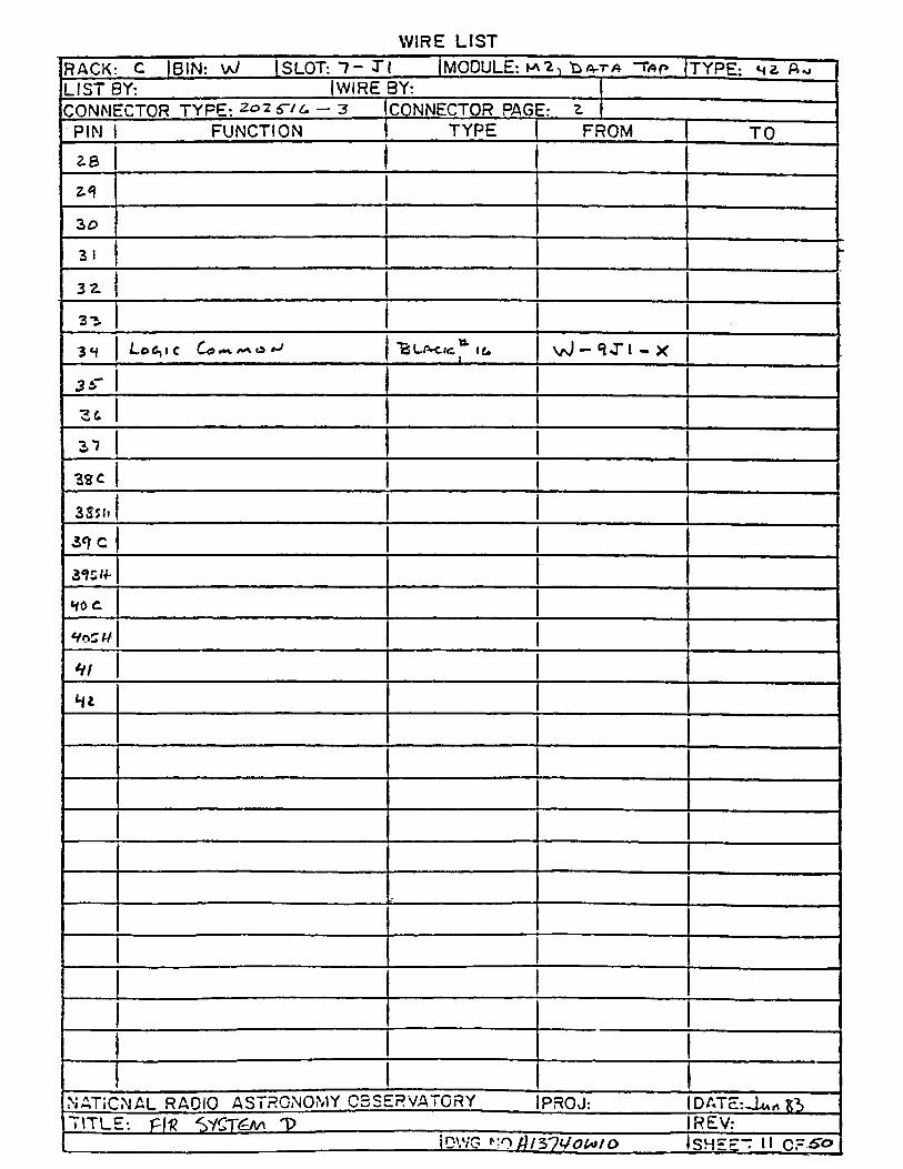
WIRE LISTRACK: C j B I N : W SL0T:~7-T| MODULE: t> A -T A “fop TYPE: H i f U
LIST BY: IWIRE BY: 1
CONNECTOR TYPE: 2025"/^ - 3 ICONNECTOR PAG E: ^ I
PIN I FUNCTION 1 TYPE FROM TO
3 8
3 0
3 1
3 2 .
3*2.
3 tf LoCylC Co •>*.**. ‘BL/vc.icJ4, Id. v J - ‘I J ’ l - X
3 ^
3*7
3 3 C
3 Ssfi
3 < 7 c*
3^SW-
HbC.
H i
INATIONAL RADIO ASTRONOMY C3SERVATORY IPROJ: IDATE:J * . „ toT ITLE : PIC <y/£T£/H T> IREV:
iD'.VO "-O D/syt/OWtO ISHE"~ II C r S o

WIRE LISTRAC K: C (BIN: VJ ISLOT: © — TI I MODULE: / e ^ €. ITYPE-LIST BY: IWIREBY: I
CONNECTOR TYPE: ICONNECTOR PAGE: /PIN 1 FUNCTION | TYPE 1 FROM | TO
A C/^i^ j'Data- T o - S/t uJU 2.6. ^TP^o U) - *7X / - 2 ^
B - S'/e UJ Kj -2.6 , TP *70- -Tl - F
C / D a ta- T o 'h7~_ S e r 2 (>jT(***ZO U J-"7 j I - 27
T> C/t* ^ T ^ p ^ r — Cer r/o - -t -j. - t
E XX/ 7“ t~ re I / o —J"/ - CS
F- tATft. Sa-r 't>Arfi-'To " p *37 r / o - J*2 - X
N- Foe *E2a tcC a l ■ - * W — 1 J" 1 — ^
J” Pa c. A **v ^ UJ - iT l
k Fftt. ><-C. \Jo(.TS w - i n - r
L liA Ti*- Ser ~Da 7«- 7e -fe&r B£ fc., &iu >^*39 3/0 - J z -
M
fJ + <2T V/ ^ Pd>e x< / ■) 0£fWtf,e. *= IC. UJ — J| — /J
P *f6 \/ (_ fi- Uto^ O/2-A/Oce. ^ / 4 oo - ‘IJ-/ -P
ft
s
T
U ft\Jz rr c r/' *"• — ? •. 5//? ?/!■-/? 4 ,i~ f "ur, JT r- ,T / - 6
\J }' r/r r*'<> Yr- - ■ ' rt-* ^ S / q : 4 . i!PA s / o - v t - A
vJ £ >/<-/.•• » • f i' r f r lk ^ 2 < ^ r 4i-'3 Z / o - T t- £
y ~f>~ f'< y. • * . •'••'' * Ret .. p— s *"
Y Lcx i C Co««<mo*J ( Mi^ "BLAck, * u> - ^ x i - r
? Lo^ i t Ci3 »ia (W Fo <2_ M io) B lA tic . ^ » U UJ- 3 X 1 - £
k
£
c/
e t>oT + 'oJ- 1 J i - 71
** 1A
£ -b>.*rv/ Pot M R^-C J ^ 2.0 v .o - 0 X l - ^2
NATiCNAL RADIO ASTRONOMY OBSERVATORY IPROJ: (DATE* ^unX3. ITLE: P/P SYSTEM 9 IREV-"
IDWG NO /)/37V<**o/0 |s h -” 12-0,-^

WIRE LISTRACK: C IBIN: W SLOT: 0 - X i IMODULE: TYPE:LIST BY: IWIRE BY: I
CONNECTOR TYPE: 2 0 0 2 7-?-*/ ICONNECTOR PAGE: *
PIN 1 FUNCTION 1 TYPE FROM TO
£ ■f l tT vJ (_ Fore. uj - 1 - fc.
/n\ M<9*J —- H1 uJk , *2*. vaJ — J 2 — F F
sn.
r- SyVjCH-^O //Ir> -» - Lo B U ^ Z^TP ^ H I - HH
Jx. 0r~ A<»i> s \yJ — I J“ I — /z
± 1 1
| /\+jaL&g, Gt/S1) (_f=oe.A41) ! *JLC? L O - ^ X l- t
-fcLAC/t 2.0 U>-*t <Tl - XA-
AT
*3t/Z 2ot- ViolT* fceir - 6a>- 1 J l-
A A
cc ■— l£ V ^Fo«- Av ''fei.LO-J 2D UJ-^t 1- CC
DTD — | l/ ( &R- T e u u ^ ^ 10 UJ —®t T l -■&&
FF
H w
NATiCNAL RADIO ASTRONOMY OBSERVATORY IPROJ: iDATc.: «Jun 55T ITLE : P lR <'/<7£^ IREV:
i DWG NO ttm tJo iA ito ISHEE~ I2> OF**®
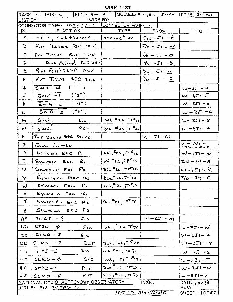
WIRE LISTRACK: <=■ IBIN: vO ISLOT: 0-J^ MODULE: IH i-j TYPE:LIST BY: IWIRE BY: ICONNECTOR TYPE: 200828-3 ICONNECTOR PAGE: ' I
PIN 1 FUNCTION 1 TYPE | FROM 1 TO
A 4* £* re. 0 / & c _ * 2.0
S-l1h1oB
B F*cJC K.1L. <2. ”D<2 l/ - T\ - ^
C Fo t T/efl,JS £S fd ^£ll/
£ •yT*'rs —XI - ^
— X l -^l.
F | R er “TiSa^ >if> >/
*1Ihi
H- S mA- — <2 ( “i" 1 Caj -3J"/ - H
X S m ( V - I ( " a " ) to - i n - f
k 6 m (v - 2 r ' n " ^ U) - 3J“i - k
1. s X T a - 3 ("* " ') UJ — L
UJ- 3T/ - if
AJ (ZiLr ^26. ,TPtt« | UJ - 3 J I -
P ^oT <=3<5e ~OG.'UtSj. | % - r i -cw
R dry jJ .JX» T“ L ic.| i/j ~ —j l /L/*-*>ifi & A n
S E / C ujA ^ zg. ^Tp^iz. W — )J"I- A/
T ^ Y-> CHG’.y E-* C- £ / u A ^ jTP^ ia x /o - J 4/ - A
U S V a J c r^ Fx C -a. ’B>LlC*2.<. ,^*12. i/sj — i >r i -
V ^ r ^ e h c o IEXC. BLui^ ^ jTP0!! x /o - 3 « 1 - C
w *5 *frjcu-rx> ELX d ^ / Vdk*ZL
X* S Y ajci+co EXC 12.»
Y S y ^ c it^ o l= > c. 'Rz- K L ^ z c ^ r r^ ii
2 S^ei-n-a ex c. 'Rz
AA 1 - 1 s/g, tO — S J“| - /UJ
t>D c , re o —^ U)K 3tt2LC,TP^ (v-*3Tl - W
cc 'Dl'S.O to- Tl - P
B E S T f?-0 — 0 EclT" ELk-,^65Tpt ZO u - a n - v
rr l/> n! H 1
-i
77> If- UJ - 33* \ - S
F F CLl<LO — 4> S* 6, (yOA. , 2.6jT<M9 U-> — 3 J 1 —T
H w S ”T ^ r - i £ e r - ’fcu* ^ ZC. ; T“P-;^ u j - ^>Tl — o
J* J C L I c O — # ^ 7 " T 3 L .^ , * 2 ^ } T r * / 9 uo - 3 T I - V
NATIONAL RADIO ASTRONOMY OBSERVATORY IPROJ: I DATE: vlu* K3TITLE : F/f? 5,'K'T£A/' <9 IREV:
I DWG NO A m V d lv lO IS H "~ M C F ^ >

WIRE LISTRACK: c IBIN: VJ Is LOT: f r- T * |MODULE: (TYPE:LIST BY: (WIRE 3Y:
CONNECTOR TYPE: ICONNECTOR PAGE: *PIN 1 FUNCTION 1 TYPE 1 FROM TO
kr fcr UJ--5X1- 'Sr
L L cLi<Li:-3 - £oA it, U> - "SvTl - AJ
MM AL&E - 0 C c t / / 0 TP IG U» - V T l -A-fl-
A) /O CUlcT — 1 - 3-7- TT t? U) - 5 X I- S
NATIONAL RADIO ASTRONOMY OBSERVATORY IPROJ: IDATE: Ju*T ITLE : P/K SVST^m D IREV:
iOWG .NO A/TilUoUt/O ISHEE~ |6 OF.ro

WIRE LISTR A C K : 1B 1 Nr ^ iS L O T : °[ - X i IM O D U L E : M. & \ p=7<2 IT Y P E : S ' oL I S T BY: 1 W IR E BY : 1
C O N N E C T O R T Y P E : 2 o o 2.-7 7 - *y IC O N N E C T O R PAGE: 1 1
PIN 1 F U N C T I O N I T Y P E F R O M 1 T O
Ar 1 T ^ r A - i S ' V ^ < 3 . ^ ^ 1 0 W - I T 1 - A
A ^ e x . 3V» r v; ogja^ o Iaj — IvTl — C
C A-p'?X 2V»r* BLACfc /£---------- j-----Ui — I J* 1 — i f H
'b \ S»uj*rcu Pv t T * 0 ci W J - j j z - £ £ :
E Af>e.fc IT/or — / 6* 1/ Yi?lco 20 UJ ■*■ 1 J”l “ EL*
P AfO.sx ZT/Ot- s ' U U a c ic ^ id
U p , « j s o j A z l/V- D b ■
J P„j £ t o A ., U-> - *1X 2. - C C
£u> /10 Ia » - H n - B 8
L + ^ “ 1/ | o e A ^ s - ^ i c vaJ - 3 X 1 - C
M l l *'<- u J- 7 v T l- /O
10 * 1 6 t o — 8 x 1 - a /
p w - 8X1 - P
K + $v> rd % S R . * / 2 0 | *£/& — x i — ? :
S
rJ
u 1
Vtt .
Ofe.rWG>£ 1 6
w lsO(^ 1 C Co**v M.d J 'UV.A C»C ^ | W - 3 X 1 - B
X 1 to -"1X1
r 1/ j - a r i - y
? w - 0 1 1 - 2
a.
b
c. \1 4
Lofi^ 1 c C o m ^ Yi> cic^ 1 (f r\ /* ) r f - r - r r «* ■-?/■./-/
e. £p *■&.'£.
f 1 | -f / S" J * 2 0 \ J - 3 X 1 - A
A U J - 7 X 1 - I L
* 1 ' f If to - S X 1 ~ ^
N A T i C N A L R A D IO A S T R O N O M Y O B S E R V A T O R Y IPR O J : ID A T E : J u * 5 1
T I T L E : P/<? < V S T 6 M *D IP E V :
iDW G ^TO A l ^ n ^ O l M l O I S H E E ~

WIRE LISTRACK: C BINt'aJ SLOT: *1-X I |MODULE: M&, F id TYPE: 4~o P.-LIST BY: IWIRE BY: 1CONNECTOR TYPE: zoo 2 7 7 - * ICONNECTOR PAGE: 1
PIN 1 FUNCTION 1 TYPE 1 FROM TO
*b lS~ \J £g ^ 2.0 uj — a n — fc
/m
✓n J f
e + I £~\J
/t- ^ |3 a-<z.e.
c> L» (-f-j ±^ *Blac< La W -3 S t-H H
t w _ 8X1- c
A*- l/J ””0 J 1
2L ' i
'Q. I A-^<vLoc, ( t ' f ) ‘BLAtcJ
»-
— iC \J Vtteu«9«-j * zo | u> - s r j -e.
BG 1 i 1 (aJ - ' iT l- 17
CC 1 u> - 8 J \ - c c
'bO k) -8TI-t>fc
£ £
F F f
HH — l£ “\/ YeLLou)^ 2.0
1NATIONAL RADIO ASTRONOMY OBSERVATORY IPROJ: IDATE: J m* S*>T ITLE : PIR SV<TfcM <0 IREV:
I DWG NO AlZlc/O toJO I SHEET \1 OFS&
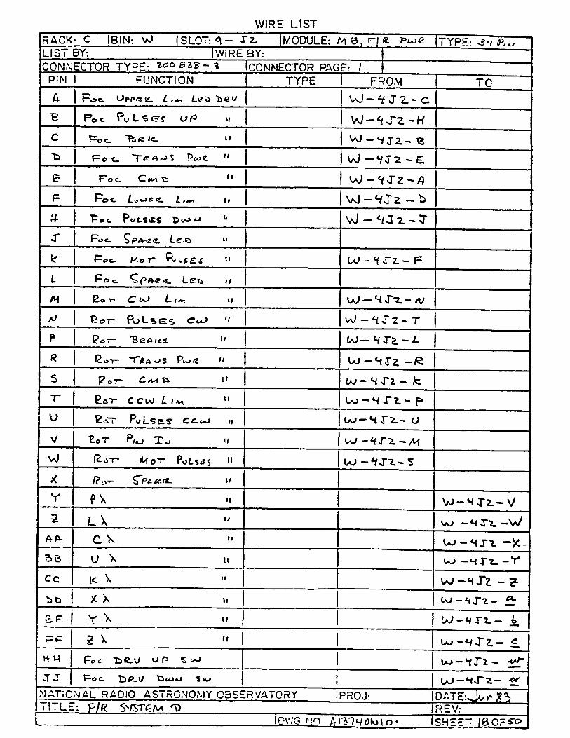
WIRE LISTRACK: C (BIN: <aJ ISLOT-.q-Tz. MODULE: M 0, a Pw? TYPE- -Sv f t u 'LIST BY: IWIRE 9Y: 1
CONNECTOR TYPE: zao s z s - 3 (CONNECTOR RAGE: / 1
PIN 1 FUNCTION | TYPE 1 FROM TO
a F«=»c. Z. v J - ^ J z - c
B P e c P u U e f U /0 m W — ^ J~Z - H
C P o c. ^ Ic. * * VaJ - w J 2L- is
t i F o C_ TVfc <=Va-> S Pw £ n V / J - V J Z - E
e F o c. C *uv Vi 1 * W - ^ X Z - / )
P Poc. Uu*e«. ti W - ^ T z - b
r/- Poe. PuCS»SS ^ v J - < * / J z - J
J" Foc_ £ p a -<z »z_ Lc_e> “
k' Poc. M o r ^ c s £ . r 11 CJ - U l - F
L F o e »/
M e o r L , - , II W — ^ X x - /V
9 o r - P v j^ ses c w *f T
p 2 o T“ *B/2 A-/C6L I* U J - W X z
R C o r "T”£ A <«-> S P«o<2 U J - H X z - f c
5 J ? o r C /m ^ tf t / J - S >T2 -
~ r £a*p c c w L i ~\ 11 l o - S T Z - p
u £ o T P u L s a r c c . u j u i *j — h x t - u
V ^ o T P/«j »f t o - ‘‘f X Z - /M
w R o t- #UfoT PoLsss » t o - ^ X Z - s
X R.O"T~ ^~PAe?.fZL 1/
Y P X U W - H X Z - V
2 l X u W - H T i. —V /
A-fc- C X •' U > - M X ^ — X-
5 0 U X tt U-» - H X Z .- V
c c lc X “ W - H T l - ?
b u X X ». u j - ^ x z - f r
E E Y X if u j - h t -l - i .
P P £ \ " U i ^
H U Pt»c ‘Dfc.U t> f* S l o - ^ X z - ± £
J J P o e £) P_l/ "Duoaj S k> U U - H v T Z -
N A T IO N A L R A D IO A S T R O N O M Y O B S E R V A T O R Y IPRO J* ID A T E - J u * *?>i l T L E : P l R 5V S T G M IR E V :
iPWG A tV ? » V fllo lo - IS H E E ~ I g C r f Q

WIRE LISTRACK: C tBIN: W SLOT: MODULE: ^ 6 , e. TYPE:LIST BY: IWIRE 9Y:CONNECTOR TYPE: 2 ^ e ? 2 £ — 3 ICONNECTOR PAGE: *
PIN i FUNCTION 1 TYPE FROM TO
K K P o t S uJ
L L c « o S U
M M ^ o r S uj UJ - H T z -
^ O 1- 'bft-O Oc WJ Sco U J - V T i - A / 5
1
NATiCNAL RADIO ASTRONOMY OBSERVATORY PROJ: IDATE:Jm *T ITLE : P/P <NS7£M 'D IREV:
i DWG HO A liltfO h ll0 IS H E " I9CFS&

WIRE LISTRACK: 0 BIN: X ISLOT: t — 1 MODULE: 'D/v'ta- Si.~r TYPE: ^LIST BY: |WIRE BY:CONNECTOR TYPE: Zo?. S'i c> - ? IcONNECTOR PAGE: 1
PIN | FUNCTION 1 TYPE FROM 1 TO
I
Z
z
1 Cn"l “ ^ ^e-rx - I T l - M X - l J"! — 26
S'C
£“S W
6 c
6SW 1
1 C P f r r . v ^ £ S,z \\ak¥?t r f c ^ 3 %.-??%- UL
7sw £ rc> v rr ~ , -.>• rV. 2 v?.< t p ^ ’31 $ c ri - a y
8 C»»A.O / A-T"A- Tc» V T - Sf6f ) Cok^ J TPte2£ X- 6 T /- A
9 Caa j/ kA-TA- To V T — “Se.7* ,Tp*Zfc X- 8J"i — C
to ^ /£> X — S J l — A*
II K 1 1
U
IS f\ I- Q> x. ~~ c> S/* w/, #%& , ^ r- % - h v 2 - K K
i r ou>|* u r T> - lAt uA, , T-pi, X - 84"l~ F
u + ir\ J E e t.; » X - ©J"l -
n - /^\/ Y C . L L O w - > J tt /2c? X - S J " / - £ C
H
zz
2.1
Z2-
j
^Y
2 6' Cm u TV>p »7“ ~~ Q /&, X - 0 T I - R
2.L Z T T v f - — feaT- •r c i c j ' S c , t p * * * x - © X l - c>
2 7 o i y r p j r - To - 2<?r X - 9T\ — L
NATiCNAL RADIO ASTRONOMY OBSERVATORY IPROJ: IDATE: Jem fT ITLE : F/je WSTO/1 IREV:
I DWG NO k ibm b te li) ISHEET 'ZOOr ^

WIRE LISTRACK: C |B!N: X |SLOT:!-J“ i |MODULE: M i - j y PE. <tlmLIS I BY: 1 WIRE BY: |
CONNECTOR TYPE: (CONNECTOR PAGE: z.PIM 1 FUNCTION | TYPE FROM T O19 ( V ) * - i J l ~ *y
zo
3 * f - : G T - C % - g j' - /r, rn
*» \ fir..... i •' £••'* t - z v i - \/
LoG,iC Co~ o*-> 'Bcrvc »«. ** i t* X-.PJ-I ~ Y
26
S7
\Z'SH
>0 c
3«*s H
HO c
‘fOSU ________ 1
Lit /} >/ *>r.c ^ > *. C L k .n ? < ■ '* ? '% i - s t f ^ - i - .
M2. A /O A- L t? C 1 O <m. o < ^ ' S L A C . c ^ I t 3 X - 8 T I - ?
NATIONAL RADIO ASTRONOMY OBSERVATORY IPROJ: iDATr-Ju*J3» ITLE: SVS7 a/ IREV:
iDV/G NO 4 l B > > / 0 i / u / o IS H -~ 2 / O r5*0

WIRE LISTRACK: C IBIN: X ISLOT: I - X l IMODULE: |TYPE: 3h
LIST BY: IW IRE3Y:CONNECTOR TYPE: Zoo&Z¥- ^ ICONNECTOR PAGE: / 1
PIN 1 FUNCTION 1 TYPE 1 FROM TO
A b 1 &>C —
B
C b l 6, 0 - 4 x - e x z - c c
“
£ C L It o — cfi T BZ./C, ^TP*23 X - 9 X Z - X X
P
W C L K a - 0 t p 23 x - S nT i - f /5, :
X
k | O — <7< fccatf fTp*2i X - 8 X 2 - £ 6
L
/u, S t R.O~Q$ ^ '5 X - 0 X * ~ &£>
p
p - 4 s/^ X - 8 X 2 -/*A
S
T t* / r - t fccx
o
\) C L lc I- 1 Si«, u^Kj * 2.C.
VJ
X C t f c l - 1 'Ee.r f i t* ,*■ 1*1 X - 0 J " Z —//A/
Y
2 £ T P - r- d ^ k j^ Z C j'T f4 25" X - 8 X z - e e
AA-
12. «.T R.T — 1 C fT-
-B^,dr^ ) Tp*2*~ X - 6 T z - tfH
c c
2>/-v A — 2. £ t a X - B P *zl — K
?! CT ^ A- —- <D ^ i Q x - s n - h
P r
H- H
J J ^ /3~ — "3 S / CjNATIONAL RADIO ASTRONOMY C3 SERVATORY IPRO-J: IDATt:TITLE: P/P S\£T£a/> D IHEVr
tC".V5 f-:0 d l V W O W I O I S H E " T.IC rS 'o

WIRE LIST

WIRE LISTRACK: c jBINt X ISLOT: 8 - ^ * 1 IMODULE: TW/e,o uyp t:. ^ 'LIS i BY: IW IRE3Y: 1
CONNECTOR TYPE: ICONNECTOR PAGE- 1 1
PIN 1 FUNCTION i TYPE 1 FROM I JO
A- CMQ/t3ftTA- To *OT- S/fi, vJk, * | X - 1 - Q
3 C« 6 -S .,5x - i x i - z r
C Cmh/do-iH. To t>T- ’fcpr 'B(.t;)’t 2 t1 TP*t2© | X - t T l- ?
T> £ */v j 2a_> p o~r — e.r- 2 t , X-|J-|- 26
| +j t L< i . X - & S 2.- R .
P J *D A-TA- XiA-TA To g/ uJk J •J ^ _ | J“| — J J-
H- "F&C |_/v -
X F*c ^ ft'r- a X — ^ ^
f“oc. f ix e ^oLts £is.7"-» j ^
L | ^*>r BCfc*»fc ^Tf^fo X — | J | — 27
_M_ |
AJ -f 2T^ f Fc»«- ©e./w^£ ^ /£ X —JJl-/t>
P 1 -t-SW ( F<=>«- MrO^
« 1s I
T I
O / : , , , , _ ... .-*.... # 9 . S,i - A ^ rp a H ? . i . - in i. - 7 oV | " #_£ u # ? L i r s H3- 'K - t J f - 3 *
^ 1 " /? r; B ik ^ h irffU H S 7- - 171 - ?*/y ■^•2 \dLKini .Tf’^ri^i. TC-XJX - h i
r Lo A) 1 c. C ‘r £- ”BLrvc<c_ ((•---------------------------s----- X —. I I I — 34
? Loo* t c C1)*1 h« CP fe.m<o LPVc.«. ^IC.
5*
i ,£
14 1
? 1 £o r t-Si A /cr- \JoLrS + X - ^vTl —'lb
f
_K
-♦cr ■f »4 v/ £ pdfe-A* 1 ^ 10 X - lT l - /i.
NA iiCNAL HAOiO ASTRONOMY C3SER7ATORY IPROJ- IDATE- ~luntbi lT L E : p/p <^ST6m "D PEV- "
... lows *!0 Ai%-7uomio iSH ---ag r- ,rB

WIRE LISTRACK: C. |BIN: X ISLOT: 0 - T i IMODULE: /<*'*•> ITYPE- VoLIST BY: IWIRE BY: I
CONNECTOR TYPE: ICONNECTOR PAGE: *■
PIN 1 FUNCTION 1 TYPE 1 FROM 1 TO
4-/<TV C O«-M»0 j
/ r f \ StaJciv/?0 /ks/J -HI j uo k J * 2.4 jTf *HO X - <*J\- f
/y\.
'H. Moa>-Lo 2>Lte:)*'Z£j T( *fO x - U i - A* u.
x - < u v
4 i
| fa-tJM-O6)C~£- M (j 'ZO x - i i i - ' j a
/ifr' 1 /U>ft-Ld6,/d/0 (f=CS-M,Q\ j
*• j
-tfs.
l£o.r- Vocrs fc&T - X- ‘iX i- H lf
A-fl |
"BE |
C c ^ pore. vfelLo.-> 4 lo X - t T l - 17
T>fc — l£~yj £ <=0(2. /A *6)
e&
FF
H H
1NATiCMAL RAQIO ASTRONOMY OBSERVATORY IPROJ: IDATE* i un^i lT L E : F/R S V S T £ / U ^ IREV:
iDWG MO A»'S7Uouoio ISHE“ ZS C.-^O

WIRE LISTRACK: IB IN: X SLOT: g-0"?. IMODULE: |TYPE: 3*y P.«LIST BY: IWIRE BY: I
CONNECTOR TYPE: 20 0 8 28 - Z ICONNECTOR RAGE: 1 1PIM 1 FUNCTION 1 TYPE 1 FROM 1 TO
A 4* J + ^oo«*f «. G(Z*5*i6,e~ ?d X - q J l — A-
& P®«. * r«> a K»r. GL "to £ X - !iJ\ - 2C Foe. csca. 'be/ X-«tT\ - £
1 £,~JC, sac. fc/i 1/ X - etX\ - H
III1G*1V
P | Cot- T ita n s S se . — Is
H A —<P X - lT 'Z . - E E•
X - 1 vT x - Kk.
*r C'V'N X- i X Z - t>0
L S /^ a- - i C V " ) | x — H-Z.-TT
M 5/C. Ulk^J-c. JTP®zt| X- IJ l- M M
AJ fc'Sr- BLk|tt 16- ,7P*«1 x - X77.-A/JU
P po-r SSfc. 'tzcitoz. X — D
R C9*S T L /c X — 9T\— e.
S Sy/JCH#,) EXC Rt tJK jS t.TTP*^ X - ° l J l —S
T E > t 6 ; U3A,*2.6. .TT*^ | x - *? J l —T
U ^y/OCH Prt F-XC. @1 ' )TP*& X - l v T l - U
V %'r*JC\4:e* E.XC zl^ zc. T p ^ X - ' K T I - V
w ^ c H <9 C> £?T X C £./J *
Uk ,H*. , TP /o X - 'U ' i - v7
X Sy/ocw/?*> e x c £/ , Tf 01 u X — J~l - X
Y 15Jc C ^z. BLk , '*■!£• ,7>*/o X — “W l — Y
2 SY^^*+r<> rTyc ^ 2. Zlic , *■ 2.6 , Tpfct/ x - ^ J " l - 2-
/VP "D lAT - 1 S'/Cf X - 1J 2 - R
S T e o —96 S /£, Wl>, , T P * I( X - 1J 2 -
c c I 6* O — ^ x - I j z - C
fcE S.TC O - y t£GLT tei-K * 16 , TP*2./ X — 1 X 2. - |<
£GT S T R t - 1 t o ^ ^ 2.c,Tp^z| X - f JZ.- ?•
F~ C Lk .0 — $> jTt^zsl X - I T 1 - ^
f4* S.T-e.X - 1 fc-iS/T fcLK :)TP£‘Z-* X. - 1T2.- BS
T J CL k o —0 (eer tt2c. j ^ ^ 3 x - 1 J -*-- e |NATiCMAL RADIO ASTRONOMY OBSERVATORY IPROJ: I DATE: IT ITLE: f lu SVSTfeAA t> IREV:
iD'.vg f;o A i y 7 ^ o \ ^ n o _______i s H " ~ 2 k c . ~ .fPl

WIRE LISTRACK: C |BIN: X ISLOT: 8 - -X t- IMODULE: /B.-o -r«,»e ITYPE- 3^ ('.«<
LIST BY: |WIRE BY: ICONNECTOR TYPE: iooSri£---«. ICONNECTCR PAGE: * 1
PIN 1 FUNCTION 1 TYPE 1 FROM | TO
K K ALS,x-jZ> £»<*/«. ^Tp'SsT X - l4 " l-HOC
UL S/d tA)k x - I J Z — V
M M r\ .LC ,t-0 e*T )Lo J* «• i V V X — I T l- 'fOStf
W tJ C L l e - t - i E t > X |
1
1
NATIONAL RAOJO AS i RONOMY OBSERVATORY IPROJ- IDATE-i IT L E : P/ft S'/ST£A/l *T) IREV:
|n\VG f!0 A»V7t/diAjtO ISH -" 27CF-TO

WIRE LISTRACK: C (BIN: y ISLOT: - T i IMODULE: f/ « Stores ITYPE: So f'tMLIST BY: IWIRE BY: I
CONNECTOR TYPE: 2-°on?-M ICONNECTOR PAGE: ' 1
PIN i FUNCTION 1 TYPE 1 FROM 1 TO
A + < * ^orci. y __ £
B Hoc. "'Bj2. /0£ S's /'cL ^
C Poe. sse. T5e^ y __ — c
t l oT- SS(2_ X>6-\) - j C - g J - Z - P
P R)f/+ f\<-frr>'‘T -c X - 0.T2-E
P ^ 0r ^ X - 0 Xt - P
H Cj S'lCjlcfyJ) SSe. X — ffSZ, —J
ki
toAJ
p
5 S Y*JC.U.£o C xc wk, *tfc Tp*8 X - ? T t - s
X Sy^jcueo Ex c, £( Tpd?| x - e . r z . - T
U S tajcii « o ej<c BUc^ ) Tptt9 x - s ri-i/
V S r^JCH Exc. -2. Tit.t,1*■26 .TP*, X _ 8 J Z - v
W Syv*»ct4&o ISxc £1 WJ>, - 8.T 2 - W
X Sr-JCM(fd e ye. fcl lo Z G ,TPttf j y - 9 J - 1 - X
r S*c. £2- Bi-k^zc. jT p V x - m - Y
2 SyejpH'f?!) E/c. Et £ B L K ^ a t jT P lf X - 0X2. - €co
b
-c
Io
e.
2 y /J f K(?o Mr>*J — f41"tt __
u)k, ze.} TP vo X - S J l -A
•3^
— lL ^c y, <? <3 Af Oa/ — /.O <P *fO x - ff J l- fL
NATIONAL RADIO ASTRONOMY OBSERVATORY IPROJ: IDATE- X*2*>»ITLE: P/Q S'/CT£M *0 IREV:
iCWG A '^M ou jio !S H E "2 S C FSt>

WIRE LISTR A C K : C | B IN : X IS L O T : — O H IM O D U L E : M z "L , S w T tH| T Y P E : *To P..,
L I S T B Y : I W I R E B Y : I
C O N N E C T O R T Y P E : <10 0 t.*? ? — M IC O N N E C T O R P A G E : ^ 1
P IM 1 F U N C T IO N 1 T Y P E 1 F R O M 1 T O
AA
72..
A.
/L
t •
JU-
0£T j P<9C. SS-fir*C\'z, UtsLr- S *-S\ Tl-H-
ASS'
dL F o e "B p . CIS. A X - ^ T i - T
P o t ’"Efs.flfce. -peT — X - SJ-1 - k
*9
A A
cc
b li Eot* 'Sc? a/cg. O&Lt Z + X- 9J-I- £
El E
F F E a r ’B<?.d«;r: A * (»S x - ©J " i- j2
H H 120—- j ” — X — S T l - 3 t _
_
NATiCNAL RADIO ASTRONOMY OBSERVATORY IPROJ: IDATE:T I T L E : P / g 6 V S T 6 M <T> I R E V :
iCWG m ArV7Mov^io ISHEE~ If lC r& O
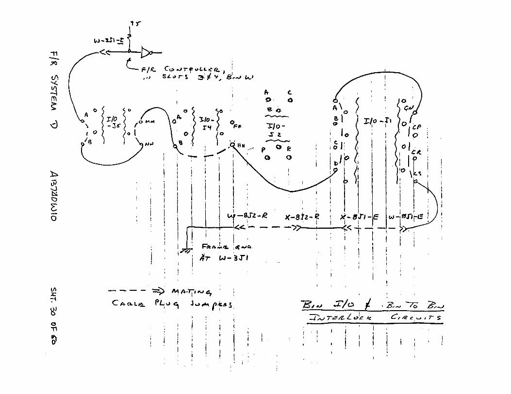
F/ft SysTG
M
V A
teldPU
HO
SHT-
3o OF
Cb
t r
£ i — P/£_ Co*w»rf wtctrft. }, , , S£ <> r s 3 .7 ^ & « j U J
. < < «. I ----------------
-------------------- A l /V-7p + J C i
Cao.Ii*. P L o c j J o a* >.5-/15

C m ft
sj L - O t to / & A-T-fi- U T / o
Po^atL TStoc/c —I M P <a) j S & <=. c/* r s
/V
O
L o
o
F/fc 5 V S T £ M A 1*3740 M o SWT, 31 £>P £“o

( 7 o f t r S T r r \ o f i r c T t r ' J D v ^ ( / f ~ s S / ^ * s j g / . s
$ rt£ m o r r i c ' f c r ' & l H /
( ^ r J z * * 9 * * 3 H i
h
t t f V Z m o m z f t r £ r 2 /?cT
j v r j*i v m c T i r i f 1.n e t
f* n M e L B L o c / ^ — S o l a 9 B ~ 3
/V p m S r>c/C‘zV~
A i o t c '
a.) / v o t % £ c O r J / K / T k r ' L o t k . S y f 7 z~-,
F / ft. S y s f zC«-1 F J/f / j ? H p u> / /
^>57" 3 1 A e f- S jif

/U 0 C S 'L 'pyaC v ' T / D
^ I f , 0
S k c ,p. -*r z
7 / z * l & l /bus
P 2 ( R E A R V I E W )
P 2PIN FUNCTION WIRE COLOR PIN FUNCTION WIRE COLORA r » e . «Jf* L «** l*6X. V l£©7“ <P,o cs&B Fo * DfcV o|i M W Ro r Wcsr n •1C IS&A-/<.£ II II X ^ot- p<qc?c. u M
0 »—1> e ~Te~r**s \ o It Y P* u . * * •I
E P o e . C L * «5» It II Z L\ U tv «»
F Fet L. O W* £. iMTy It If AA C X U It If
H Po.c O 'twJ *1 II BB L> X M *1 M
J t~e>c. 'iipCi P It M CC k X «i IV • *
K r^c M T It 1. 0 0 y V *« if It
L l"oC- Sp C? . f ♦ »/ EE V > “ • t 1 I
M i? OT C<.> u •t II FF ?r \ «c u l»
N P-o“ ~De.yJ C UJ t• ‘i HH f*e»t l/ c. 6 0
P i? •■*>- "E, <?. a ir -r M JJ f—O c . 1' D k ) U «
R ^ o T T i? a <j 5 ft 11 KK M ^7 ttS r-T r>~T C <** ri • f LL ■^*7- C t<j «r
T V-»r c r u> C .. »• MM R o t ‘ f
U O t * C * L U c c «o u NN o r cf C.C.UJ •/
P/1? SVSTgm T) 4 I V 7 4 Q U ) I q SMT. 3 2 D P 6~Z>

U l
J l J
M B c Pow jfrts.^ 'TTjo
S ' 11 /S &- T - (
'7/ze>/8l]'r^uj
SINGLE WIDE MODULE ( R E AR VIEW) PI ( R E A R VIEW)
p IPIN FUNCTION | W IRE COLOR PI Nl FUNCTION WIRE COLOR
A iAp«c k j ’X»T *+■ f«£T \J R/z-t> c) L .O C * 1 C U / U .O * ^ *3cAc<cB ! n >( e tE> p «v<Tvr_C | Aa> Co m m ^»L#vcfc f +0 I S i J i T c f r A‘c r* 0 £ h 1E ! n u — ivv/ L Low* j 1F I 11 *• $J“ U CiD« A* Tit-ftck. kH j ^u^iTf w 2-i m jJ i n «f A I n r rK : t( " A o P + isTvl RiS_|>L • +5" U o L r i o £A iO<% rM s /\oALor, Ci'/iO C o * * * C»C.N 1• t 1P I u fR j VS 1 wT » i X V yU 1 ii y C e i i T ' in ^iLA vr.V t r i e> I r ^ •<D r? fz. zw LorT/c. C o W / ^ i O aJ 'CiL/>f f*. AA — / jT t/ Vc* L L O u J
X I BBY ; CC t ;
z i DD t ia ! E E 1 ib * F F V Vc HH — t zT yj 'Yiz l l o »->
* INDICATES A FUNCTION NOT FOUND IN THIS MODULEF /S SVSTPAA t > Ai37 4 o u to SWT. S S & >

/ V / / - (3, m2X>T£JtjrA«'LC o ^ ^ B i c T~£><2. P I
rt-SS / ^ a J <*nr~»7“£
y/t't/e i/
^ v ci. d r I
J l J
SINGLE WIDE MODULE ( R E A R VIEW) PI ( R E A R VIEW)
p 1PIN FUNCTION I WI RE COLOR PIN FUNCTION WIRE COLOR
A , 4 t S v>o(-t-s E ib d C V S e-o s.i. St*/B ! L o G\ r C ^ AJ > r^trtcic e \ j \ S.3aJ.S<£ Sue?C j -V i \J t>Lr% oe»k«/^ u, f l<,_ Xi S i / J S i S u>0 ! h X X ’Sr/OSfi- ‘S ujE i — l><r V e U o w j y X S e ^ s c Sew/F ! S 1 k ^ X Si^usj* Su;H | Ro t S I m ‘Ss’ jsd- Suj ^/JOJ 1 P~ c. 7. n Foe. TSiefl««x t/otT5K 1 R or* S2L P E*?r- i/^trsL 1 t—©c_ S S r PocM R r>T~ ^ "b s R i5T“ 13c a,i<«s_ /)-**«N Sv»-»ci+i?ft P« 1 t Po C B £A k ?. /•'tP u jl2or Co**+*R S xr’**Jr. tJ e o \?2. VS w t—7 /2, ~r~7~fO •+T Poc °PP»a«. L/« S*r*»stf. XU 0OT C UJ L » Sj-a 5d y P/<€. t Jc> VKn~ ir « • —V Foe L O •>** f ft l- <0 G"r7*>S ft zw (ri T CCcJ L i m a AAX X j “iuJ BBY CCz Pi O OOT~ DOa E Eb P ’k S g #.»S/< F Fc \ S f « ) S c S<*J HH AaI A U C
* IN D IC A T E S A FU N C T IO N NOT FOUND^ V ^ T c:a>» *1)
IN T H IS M O D U LE ^ Afltt740mc>

jP t f i - B J f i 'T '+ j t f j s . r r t
^ s s / ^ ^ A t / r ^ - ; ~7 j * & j j t>u>
*S H tv. r> T z
P
p + • !
© ^ ® ^
® © s ©
© x © x
® 0 © ®
® 0 ® ©
® @ © @
s © @ @© /-N © / - \
© 0 © @
GNO
© + » J
2 ( R E A R V I E ^
1i
!
w )
P2PIN F U N C T I O N W I R E C O L O R P I N F U N C T I O N W I R E C O L O R
A >-»-«. w (ft-rA- fcc o) — S / *4 V Eo 7- C ( j Z» • <*•
B i'f jr Da-t-r - C e p — S//S, W p o c L i« i JEXJtj*
C R , c 'D<v*r*- X PoT" CC t*J Lm . X j h
D 12.0T £»?r Y V t ) w P j S>t&iJau
E Poe Loau Clt»e.if - S'<w Z YtkwJ PI t £*>H- £6LT*
F EoT“ L«>A,W f t iK K - A AH Fj»c, C.L&etr- B B
J K r* <r 7 C CK fo e 5V ♦£ 'hA~TA. «■* 0 0
L ---C»/L E EM P<»r tiA7 P* — f crT- F FN 2-.r- ^P“A - ^ *T HHP JJR KKS LLT MMU Pr> c uppc^ ITaJ ty NN
f / K S y s 7 £ A / r D A i 3 7 4 ^ u i f o S i r r 3* 0 o p
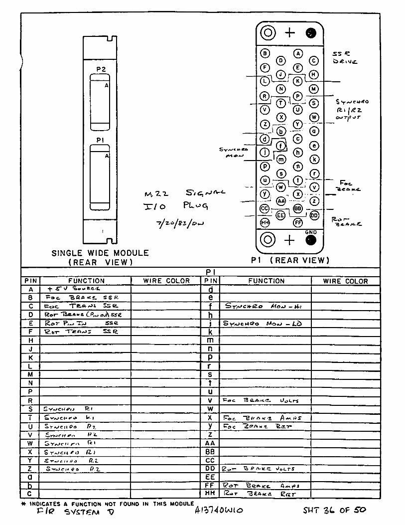
U l
j t J
+
® r \ ® r \ W (y) © ®
r s i © ^ © © V T ® 4 = : ~ ® ~ ® ® , - ? c - i ©
SvK/tifeft
M , 2 .7 .
X / O
^ © ,lX r © ® X ® X © ® © § - P S -1 ® % ®
i f ® !7 = r ® ^ ®© r \ © r \
® r § i ® , ' 0
; ©
$ Y^ew-^O
o~>~rp«->r
-fjT-ojZZ j Dy*J
(AA](CC)— T-1 CBB)
J &(HH) (Fr
P»c.
R .* .-
+6N0
SINGLE WIDE MODULE (REAR VIEW) PI (REAR VIEW)
p 1PIN FUNCTION WIRE COLOR PIN FUNCTION WIRE COLORA *)• -£~ v/ w* fee. iJC. dB ro c. ”BCA 5 S A’. eC Cot TK-CVaJS Sscl f Stwch-<2o Mo+> - j4>i0 Ror* Tie.Air a CP«o £S£ hE Ror P,_ Tuj ssa i S^<c>c»4<?o Mo<j — L 6F V_0T~ T£A/^J SS kH mJ nK PL rM sN tP uR V Poc 13 £.£»/«.>£. L Cr-SS G v»/cn <”(> l i wT 1 X f^c. “Bff A l f lU S y a S C U O O f? 7. y Co C ”2 A « .« "&E.T*V Srwr/f #»<» 2. zw jY/^r M R * AAX S r/ocu ^ f Z 1 BBY £ *r< e.nt 'ta R- 2. CCz S 'r’oJ a * e o (? “L DOa EEb FF Bcrvjctc HH (2ar ”i3feA-««£ SfST"
* INDICATES A FUNCTION NOT FOUND IN THIS MODULEP/<? SV£T£AA *9 /MV7400010 SWT 34> OF 5*0

f i T T S l"h / iZ. T 2 - O S X / o
P n .x i'^L Cc> ^ t J ' . r 7 * a.
• j i “ T o Fe>e. £
£ o t - i <c.a*j J Lf\'T“a 0’S
P2 (REAR VIEW)
P2PIN F U N C T I O N W I R E C O L O R P I N F U N C T I O N W I R E C O L O R
A a - J T L < w i « J C . VB ~~r>TT- 1 L.IC L . W Foe. Pu>LSt£- OP — H-rC P . iL S - i Ct~> - H i X Fo e , P o L Z SL "Do0 !2.*r- Po«-Sc. CCU3— 141 Y F o e P^Lse u p —
E *2 or- C u > - E s r Z P«»c- Po Ls«. ^0vJ a*_(2«T"F S ot- Pt>Ls*s. CCiO — Car A A P o c . TV2./9-*>S
H (?o^, P ia>P B BJ C CK 00L E EM F FN HHP JJR KKS L LT MMU NN
F/K S y S T £ M * D Al2>740tMio SMT-1>7 OF S~&
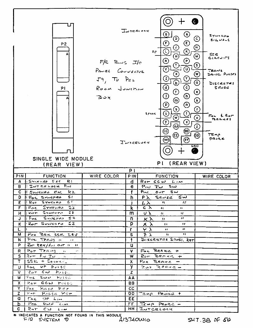
( R E A R V I E W ) P I ( R E A R V I E W )
p 1PIN FUNCTION WIRE COLOR PIN FUNCTION WIRE COLOR
A i S v» c « 1(0 C-'-Jf c e i d R o r C C u-> L i * *
B • Xr-»T R-flt U-OC-IC e TV->C 1 Pxr_ k 2. f P#«u> © <->T" Sc-OD 1 HoC S»y CM-<£o S I h P X S
E I 12©t S YV^Ct. fi»e? ^ i j / -A “F I P o t S V'< r f* G\> c. v k C X M <•
H | S T ^ f W t' : 2 m U \ ( t u
J i P f * c < V. n K X n “
K ' 2 » r * S C !- r o P X X »• "
L l r y x •• “M F o e L S (?- t ,e v / s X “ "N P o e . T>*/5/02 m 11 t ^ 1 S C ( t r=.TiS S S ~A>Sf . (kL^T
P ? ® r o u r a i i u
R ■Pt>T f ; »% »> * 11 V K o c. fe<lAfc.i2L. ■+■
S P /O „ W B o r ~%.f? n k rz. - h
T SSfc- 4* -O Ot- r ,: _ X F«i c <zrt-if i* —U ~ C»C UP p vt CC y T?. C* T ~t I? tt if i? —V r C I s j K» L ; z
w f~r> C t u ) j v-„> i : AAX ? s r C C U K ' i . s c BBY t~n c Vr <? r CCz V ->r • R > L : « r V - ■: 7- DD Pfi ta r * c f. ) P L , m E Eb r - o c t> 1—> *J L / AX» F F T t - M p p P o a . z . —
c C VJ i_ 1 HH X * j T C ^ L o c i <
* INCICATES A FUNCTION NOT FOUND IN THIS MODULEP/D SVSTGM V Al'5'740U>(o S U T .3 a

A t 7 - £ j C o / o T ^ Pi Ca+JtJecroQ-X /O ^ 4 , ^ 6 * - I Po<~J'TJZ
]\ t & aJ m
%/n / ? j / o w
< IV lol S T “ I
W I D E M O D U L E
( R E A R V I E W ) P I ( R E A R V I E W )
p 1P I N F U N C T I O N I W I R E C O L O R P IN F U N C T I O N W I R E C O L O R
A 1 / 6”” ^ o L r~Z d 1 C C U > L .>*• I v h
B L o & i C £ * j c> l i t A C ( C e L i * * X /01+- (Zi3- r -
C +■ 6 " \ J o i r s t£- f Y o u p /
0 h ■p4»c ‘i j t 'b/KTA ^
E — t S T \) o L T Z Y <£LLo i~» j R » c. L o a d C L ocjc S/<*
F k R > c S i?c£_ j C<2.r
H A----<f> m F d t L<**y> C lo c t c , fc'CT
J ^ A *0 ~ — 1 n 12.o7- S e * . S i c ,
K S m a — z . P R o t- U o a-o CLt»ei<. S <£,
L s ** « — 3 r K o r - "b(VrA N e c r
M 'fci c , r — 4 s CY .«?cr, T2<s.r
N C L K r - 1 , t CdA/«J 'T ajT iI ic
P l i i 6, O — & 6, u h o t ft Q y S *
R C L i c X — 3 ■> V E © T ~b A-TP- £fc £? , £ / 6,
S ‘C r f c . r - 1 . w F o e 'b<vr£. Q ^ Q x i?6 'T
T C L te O — O , ‘S>/< X R«>r 't> a ta - (?cc? , R & T
U 't 'T f'T . - i , P l - T y A L C ,r - 1 c , ,u / a+ i
V c i k o - f j f t , rc-.-'T z S & r '£ & / ** c t s i
w $ t ( ? o — 0 S»r» A A A l G » t - ' i ^ c , / i o
X I S' /^U-. T » X a t c C c - I <rT B B - ic .
Y } S T e f l —#> , P ; . r C C A - -O T A — S
z S u h n ~r» Xzo.Tfi Sc~r^ 'TZj .t D O A <or A _ H
a (-'«> C. P p fr C L «M ~ i f > M E E A a j~ A----- -2.
b »“o t LoiO '-p_ F F A — *2
c K o r C UJ L /+* Ht-> U H H A-^ A -L^ C | 'B^ .rv c » c j
* IN D IC A T E S A FU N C TIO N NOT FOUND IN T H IS M O D U LE tT t P -?T fT Asy "D •Sj+'Sc t 3 9
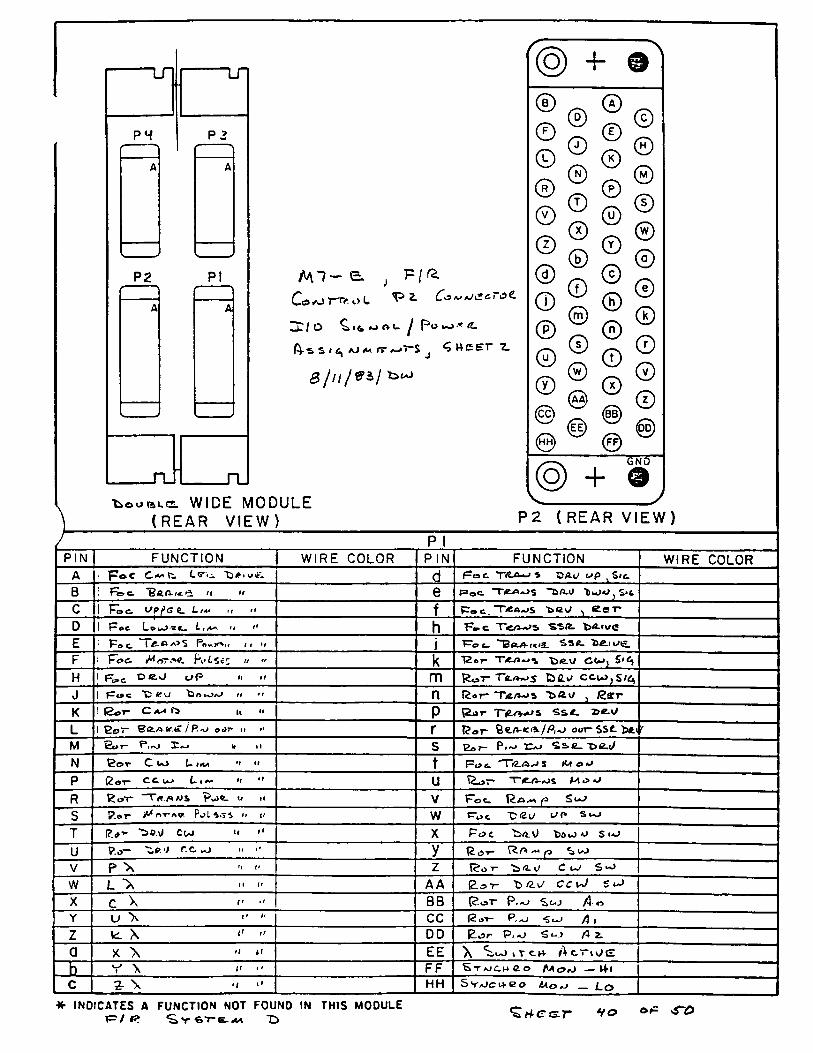
u L I
P S P 2
A A
P 2 P I
A A
n n
M l — 'E. j F /
i t / o y P o io »<l
s / 6j aj «** r> o-* “S j ^ w c e r 2.
a / n / c & i ^
U a BLG WIDE MODULE( R E A R V I E W ) P Z ( R E A R V I E W )
/ P lPIN FUNCTION 1 WI RE COLOR P IN FUNCTION WIRE COLOR
A poC C.** fi. d f^cs C 'T~(ZJi+J S TSP.U u»p S*tB f"te> c. "B ft fl- 'i n >• e Foe. TiM o s ~fcA-0 '*wl>0)S.cC I (~oc. yp^G t. L/*» n " f p o c 'T/e «.os 'bcv e e rD i P«c L«»oj-s«_ L,*~. a •' h F» c T</WS SS(tE p# J, j t f l A>S It 'I j l—o c- ld«-A- r< i lF ! F o e . tM rSTQ- PvtS6£ It " k T2o7~ Cbij S«£)H 1 Frt>c Oe.O uP »< •• m R o r T«-/ws E>fiv ccu)jS/fi)J | PtJC t *“ VJ b(>K>fc» '' n feor Ti2./ -j4 5 /2srrK ! |2oT* C*-* fi u 11 P \2air- "T^>v^s Ss«- X>e.v/L I EoT ®K./a / R-v» 001* it •» r I?«r- /P,-o oor-$S£fc«.< rM E or >»o £«j it 11 s e^r- P.~> s> c_ x><2-i>N Cot C IO L iM '• " t F w c. ‘Tte.A^s *ct 0 *P (2of cc i*> L> i« *• 11 u *>r> T ^ a-ajs M «> *>R Koi” “ T(?./ a)& Pv*)C_ u 11 V Foe. p St^S P.©r t* o'r/x?. P Ls.Ti i* i' w r» S uj
T ^O.J C J ** »* X FoC 'b/i.O bOuJO S<oU ?.i5~ f.C’ vO •> <’ y l5T" U*JV P X " " z l? o r C uJ S w L *>\ " " AA (2. ,-r t> G-'J CC U 5X C X »* •' BB [2oT P . -\J S J /I- 0Y u \ " CC (2»t- P,-o 4 1Z k. \ <' " DD |2.or P, -> S«-J A 2.a X \ " EE X <.oO»tc.i+ A t r i j eb V \ <' •* FF S *r aJCM (2.0 — M-lc 2- \ -i •< HH Sy/oci+eo to.o+j _ L0
* IN D IC A T ES A FU N C TIO N NOT FOUNO IN TH IS M O D U LE T=*/ #? v €>'T-e_x* "D

? o r 'feax
M t > b e 1
/MoCiiZ-
o &______T o J 1/ J r v / * ""T "iC -A ~ ' S L/»Tt><Z
fi-pSA.O ^ ^ P o tS * i
f oe Fc*^
FIR SVSTSM T) A l ^ 7 4 o w i o SMT. **» o f

WIRE LISTRAC K : C IBIN:-*-’/ / SLO n lT/o — J" I IMODULE: ir/o Pa~> g l J “ i ITYPE*L IS i BY: IW IRE BY: | 2«>t 'Bak / j-o +*<oe.CONNECTOR T Y P E : ICONNECTOR PAGE: I 1
PIN 1 FUNCTION I T Y P E 1 FROM 1 TO
(2-o a/ u T/d — J \ — C aJ
TE
cb- C o*j *> ^ c j y L k. x / c -
B A-Pex Pe»c ^olsc. - or* t / o - z h - u
¥= Fee oL s<£.~ * b 6 ^ T /o - TV — W
M A p ‘. x i^or PolS'T — C i^ ■37 c? - T * i - V •
J j (\qc* y 1?gv- ^R;Lsc=l — C C i^ | l / e - X Y - X
Ic f~oc_ “T<?«~>s P o Lse - U p * j i , t t c s * | % - j - ^ —vvy
L Foe I M 'J S Po l SiZ_ WK J T P * 3 i | Jy'a — X5* — X
M 'Ro-r'T'/e^/os. (?aLS£. - C u J WA **6, ^ * 2 0 T/ o —XiT — C
AJ £o t- 'Tern*.s P u L ic .- e c u ) UjA j T P*3/ t / 0 —J~2f~- ^
P M l Poc ^ L s i* — wfR W fv j^ ltjT P ^ S V | \aJ - HvT2. - J
1? M 7 t-oc P jL SC uj - H X I - e
S M ”i "Por- H>tsc. ~ C ui U>k, ^Z«.,Tptt36, | UJ - H ' T z - ' k
T / • * 7 'So'T- ^ j l s c - C C t J Iv J — V J*2. — rZZb
U 4-p£x. T- c P 0 C.S1? ^»r-r J / o - J Y - V
V Apt?x £ o t PoLs& K c r I/o - T V - €
w
tf
Y F\>c. “ T e r t is (poise. X/o — >T!T - V XVo -
2 ^ o t P^Lsa ^ s r tfe TP *30 T&Kj Z£ j TP*HX / o - J * ^ - S. T /o - J T - F
a, A-p c x o “ j - ty ~~ i
b---------------------—----------------
ur u. c s r i f- £*■( s - s - e x z - / 9 *
o<c. fs-KI 'O SS (L (Di5.^£. k J- S’T Z - ^
jb, I l\ f> X FV»c. l«r ZZ r<Z. u*-J 37 ? —T V - Ai
f)pr~y r~r»c T>*vjr -SP2. i<Cv/ O o - S H - AJ
F*£ . CZ<e -h £ ir©c rwc e , 2-o VaJ - R
k M‘7 £/*->$ UJ — */>T7. - £3-NATiCN AL RADIO ASTRONOMY 0 5 SEPVATO RY IPRO J: IDATE*» \ ;L E : P/t? SV.<T^j .a V IREV*
in\v? v o A l^ T M a u n o iSH -~ ~ 42 2 7 ^ 0 \
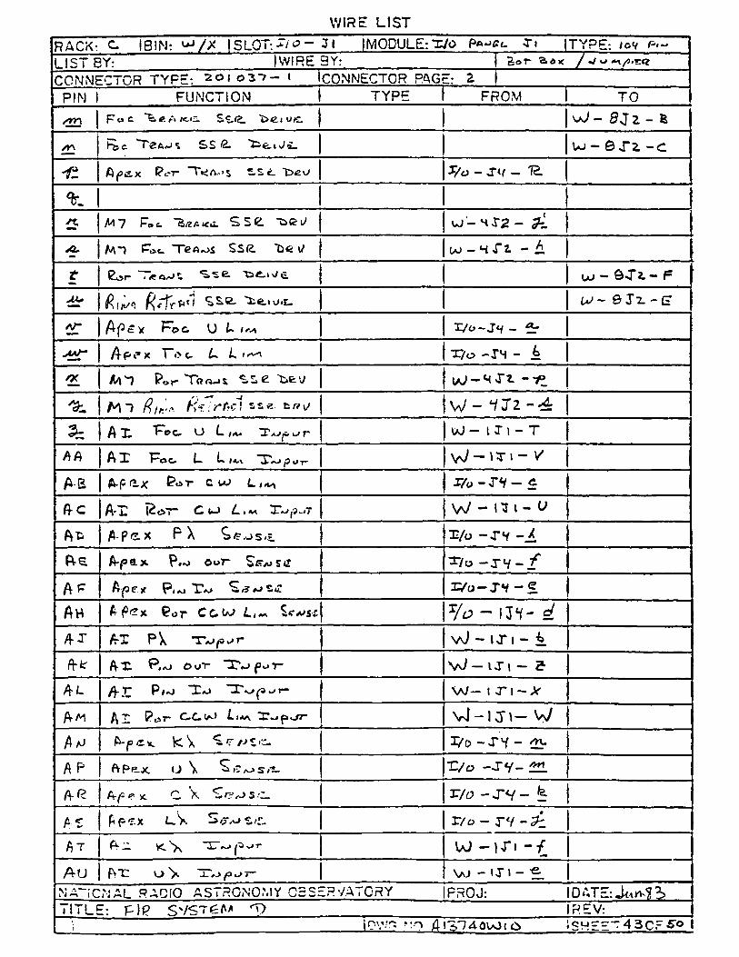
WIRE LISTRACK: c IB IN: <*»/* ! S LOT: T/ c? — J l |MODULE:T/o Pa* cu Ti TYPE: io4/ P*LIST BY: IWIRE 3Y: So d < / <J +\/1>T.CZCONNECTOR TYPE: 2 0 1 0 3 -7- 1 ICONNECTOR RQG*~ 2 1
PIM 1 FUNCTION 1 TYPE FROM 1 TO/rr\ - 5* J z - E
{Cl c T0a#j SS S. i J<L. Uj — B T z - c
i t ftfizx. Pcr7- ~T* /v»s - - c "Det/ Z/o - T</ — 12.
%st, M7 Foe. 'Hizaku. S S £. uj — H X 2 -
XL. M”l PUe. TeA/os "be i/ uo - 4 T i - A
t 1 uj — S T z. — F
* 1 1 SkC- CLt vJ*£» - 0 j l - £
*£ J A ? ~ o c . U U ir* X/o~J«Y -
Api*x T o c U L T/o -IH - £
*2i M l Pot- T ro-jS "bev/ U J -M T i
M l /?//*.’A fe i r f i c l see. w - */72 - 4
AX. Toe. U L T ^ p . ^ r \>J- H i - T
A A A I F*li C- L L IM jO u T" W — IT I - /
A-B A-p fix 1?or c uj X / o -T V - £
fi-c A~ i 1 C>7* C uJ iL i m i<J p »<T W - 17 1 - o
A t A p ex P X
^1I:*-*-/11
G-S A-pO-X P«o Oo7~ Sffyosd ■Vo - J H - f
A P Ape* p(<o X*/o /?#*»s£ r/o -J*y - £
A h A P^x 9or C c t f j L,~ $c*»s£ r/<? - I3*f- sf
4 t /rX PK | v J - IT 1 - i
frfcr A-X Pi/o o^r "X\~> (3 7- \rJ - \ J \ - ?
At- /}-£ P|*>J "Xa> TT^^^r- Sa/— i T i - * ' j
PcM T (P r* C-C. > io*A 3T*j pvjr* V s l- I J \ — W
^ <r a> t »— T/c> - T V - 22*
f\ P fVPe-X (j \ T / o - T V - ITL
A-fc A- e x. C X e\-> sc . r / 6> - j “v - ^
AS £ P •?. x L V S /jr.o s /r- r/o - r 1/ - z L
fiT f1 — K. vL A _» r v j - \ r \ - /
A u fVTI O V 1 f J u> 5 I Vo - IX » - 1NA'iC ,\‘AL RADIO ASTRONOMY CSS:: r v a t o r y PROJ: IDATE:Ji*r^2>T IT L E : P IP <WST£A* *T> IREV:
; | r\v-7 ?:o A liTM O U)^ «SHEE~4 3Cr 5*° 1

WIRE LISTRACK: C IB IN t W X I SLOT: T /o - X I |MODULE: ^/O Pa-j c l . «T i (T Y P E : U s ^L IS T BY: IW IRE 3Y: j *^oT ^ o x / J o <M.(9rtS/CONNECTOR T Y P E : 2 0 1 0 -3 - ? - i ICONNECTOR PAGE: 3 1
PIN 1 FUNCTION 1 T Y P E FROM TO
A V A-X c X V j — l J I - 0/
h V J fix i* X "3^ p«-,r* W — 1 X l -
A X A p r x t /o - x y — *
A-T 1 A^S-X Vs. S s?-aJS*Z- T/0 — TH -
A 2 I A p g -x Y V r/o - r v - / t
t A ! A p s * X \ S/sv->s*- x:Y o - S H - r t
■bE A-TT v j — 1 J" J — rtf\ •
B C . A I X 'X'A-.purr W - i x i - fe
t u A L V ^ *l^ pu> r u> - 1 J \ - ^
1 /VX / ^ XW» Po-r- W - i x i -
E P frjO#r *- lr“c»c. — 1 x/t? -r^ i —b
'EM A p e jc F o e S 2 -P'o — T V - J*
■E«T /}-(5f3s. X F^e. & i J^O “ J 'V - P
I k f\-pe < 1- ^ I r /o - j s - S’
B L /&-X Ft>c ^ I UJ - 10"! — F
'Qm /4-E S Z X3u|Ovr W - l X l -X "
A"X. *Pdc. ^ "i. W - I X l - ^
A-~r ' E d r S i *->|0jr W - 1 X 1 - H
t e AP*?/. ^OT“ £ 2 I/o - X S - K
l i S A-p<**. S 3 I / o - X q - <
*ET ApS-iC P/2o<a/T- +• V o - 3 V -
A p e * . ~ThM.fr Ppu/^cz. —• . _i— r /o - X 4/ - F F
e V XI £t>T" ^2. ! ia> — iX l - k
~EvJ /vc Q«>r c *3 r ^ p ^ r u > - 1J 1- y\
T “T"B M. 'i 5 •> *2. +• Ta> 07 v / - * x 1 - ^ i r
£~H >"*. ••' — v J - ' J i - ' & l
p 9 ^^uC .11 C: 0 E x C 1 (JK ^ 2.6-j tt t\2. S /o - X V - A
^w/.JCJrt'O "R2. U k S i r p ^ r / o - T 4 - C
C 2 1c c \ f- y y. y t ■3*7 K. . '< — k- J J l l/ o - lH - pyyx«^
NATiC rJAL R AQiO ASTRONOMY CSSERVATO RY PRO J : IDATc.: ^Iviinb"T\TL5£: F / R SYSTEM T> IR EV :
iDV-f/? >:n a i^ ^ o iA i io • SH EE~ *iH.C~£~0

WIRE LISTRACK: C !B IN :W /tf | S LOT.x/0 — 0“ I |M0DULE:X/o ~ 1 ITYPP*- ros rt+jLIST BY: IWIRE BY: | ^oT 13o k /CONNECTOR TYPE: 2 0 1 0 ^ 7 - 1 ICONNECTOR PAGE: H 1
PIN 1 FUNCTION I TYPE FROM TOCXi
c z
C F
CM (2-c~ >£2.1° ic>3. Ss. r?_ W - SM“ 2. - P
C J
C K f~oc ^c.a-u:<£ l/oLrs *f* I vJ — 13” 1— dL?r
C L ’fco'T C^PricC i7o Ltc +
C(^ Cor Sse . t>ew/i= W — 3-Tl-
CA j C&*j T~> r L !c
C P *:<£. Uo Lt <> — |v j — / T I” .2l
Cfc £ot~ ^2C2-A ic r£_ (Jo Lt £ — | VJ - | J" \
C l */ t* l —0 X ! —
1
£ M"? Foe PuC$c ^xr-r r r * ir vaJ-HJ'z.- f
®[ Al “1 fH{j t Pw»L £ 12“ V S w - v >T2. -
1NATIONAL RADIO ASTRONOMY OBSERVATORY IPROJ: IDATE*ilT L E : F/R £VST£/V/ T> IREV:
iCV"? no A i^ ^ O i^ co I S H - ” ^OrSTo

WIRE LISTRACK: C IBIN: “V * 1S L O T : 1 MODULE: T/o <T z. ITYPE-. ^LIST BY: IWIRE 3Y: I C~* P / £> A 7-A- X/o S*t*iA4.{.CONNECTOR TYPE*. s ICONNECTOR PAGE: 1
PIN 1 FUNCTION 1 TYPE FROM I TO
A
B o u ^ r n 2. -t" x/o - J z - M I
C
b £ ** t- ”X »pw>7~ T“ tLt *2.^ "rp%^ T/O — J ~L — Ai uJ - SXI - b
E r>v-'7“ cv ©oT"pv«>T j V o - J z - J
P £ *-t SV' jU)k * it J T p I r/o -Tz — L oo — 8TI - B>
a 1
T 1 "Li A T A- Ou) I »-»T' £ /£J U;k, *-2.6, T/O^Sf vJ — &J* | — F r/o - J 2 - E.
K 1
L C aaT, 'XVJf^T- >/6» r / o - j 2 — f
M •si fiYfV- t3u>7|0jr ficr- fcLfe: Tf>*3? u> - 8 J i - i X/o —*12.— 3
yy1
H S 1 1° \ a
P
r<
NATiCNAL RACiO ASTRONOMY OBSERVATORY IPROJ: ID ATE: J n *
TITU E: PI1? SVST£*A T> IREV:|r.\V 7 n o A i ^ ? 4 o U i t o i S H E E _C1 c C r S“o

WIRE LIST
RACK: ^ IB 1N : W X |SL0T : - / O - X ^ IMODULE: Xio j-y ITYPE: .st> ft-,L IST BY: I WIRE BY: I 4owerCONNECTOR TYPE: 2 o o Z 7 7 - v ICONNECTOR PAGE: » 1
PIN 1 FUNCTION 1 TYPE 1 FROM 1 TOA E y e 12-1 o J - S T ' i - T r/o - r / - s 3-
L *> e. ic. 1/0 - l i ' - W M
C C r y e . £.2 T P 4n VaJ — # X 2 —V x/o —0“I - c a
^O C ^ *7'/v-> c »i-<2 o ^ ) x/o - Jl - B r
E R la r SJ J /o — X I - te /<f Fr> c. — \<<?o S r/o - x i - B J R ot- SyAjei+e»o ^ 2 x/0 - x i - B e
X Roc SyVJCN-fto ^ ~2~ X/o —XI — BH
(c! r- ^ yA ;cn?t) S I/o - J l - J3S
L
M P© c. ”" 6£ Pk L. (eL '■/ 1 r/o - Xi - L.
/J Foe u «i t / o S l - * 'f» P ot- Tb(?/a<8. SS<£. "P » \/ £.' 37c> -X I - CCCl T£o *r "Te.cw^ Ji «» Vo - X I - ■£
T (2_ 4- S o u e c / i % . - r i - 2 -
| A/°e.x F»c. PoL<zc. - iJP X / y - J i - £V $■(>(?¥ K o r Pu>i-S l - c w x / o - x i - H
W V—oc- PoLs£- — bow/^ I / o - J I - F
X A (3(? R ot- Pulse.- iC o - j i - Xr A^ex, F o e Pot sh*.- T/o - X I- O? J STT- PcJIS t — <SLT~ E / o - X l- V/£*- h-oc Up L / m */o - J l - Af -
^OC. J L l<M X/o - J| -AJJ"]<? o T C. U-> L / * \ x/ o - X l-
ri l/ (j 7"“ C C !iO L i X/o - r i - Affo r> — *r r # r ' J ' - l*J x/o - 11- A-£ /O Ou7~ S r/c?“X l - A E) P ^ ^!!:^S£ C oJ V o -X i - Ab
■rf*<r; Z- V. M «• | |T/o-X l - A sNATIONAL RACiO ASTRONOMY OBSERVATORY IPROJ: I DATE-»ITLE: P/£ D IREV:
ir.v;? r;o A-I VMO Wu l«?H-"-H7 C F ^

WIRE LISTRACK: C IBIN: m / X ISLOT.zr/o - jV |MODULE:J/o >JV ITYPE: S oLIST BY: IWIRE BY: j^ so J"w trCONNECTOR TYPE: * *>*? -v ICONNECTOR P4GE: Z 1
PIN 1 FUNCTION 1 TYPE 1 FROM 1 TOI/ o - X I - ftR
/7A U \ n '* C 1 1 T>
/n- \ M " % - JT| -
£: x V *< " ^ 0 ~“3 \ — BA't Vv H “ 3 0 - T l - f i i
* r ? X i« •' V o - X I - /if£ \ . i : r . r 2> Setose. Gst- J/o ~T/ — A X
or | |
>1±Tr*_
*£ |
A A
•SB
CC
t> ti ~Te ** (O t-> c</r. -+* zr/o - r i -
F F T e ^ p P<>ofKC — J / o - X I - 3 0
Hh rt C/C X /o-X / - o
_
----------------------------------------------------------- . . —
NATIONAL RADIO ASTRONOMY OBSERVATORY IPROJ: IDATE:T ITLE ; P|t< IREV:
jr-W'? -:o Al^74ov^3»o {SHr ” *«0 CF^*>

WIRE LISTRACK: C |BIN:t-»/X |SLOT: X /o —i s - |MODULE: Z7o TYPE: 3*LIST BY: |WIRE BY: j poc t PoT~ T«/9«v>$ 'bfiuc.CONNECTOR TYPE: - 3 ICONNECTOR PAGE: 1
PIN 1 FUNCTION TYPE FROM TOA T aJT C Ic L (I. UJ - 3 J 1 - £
B I / j r ' iK - L. o.w x/o - cns~- /jaj
C . 7“ P«-»LS/i. t u - Hi & utk , zc , «P -so r/o — J I - /v\
t> T" Pu S £. CCw — UJ u)k )tt-2.& rpd:3/ X/o - T l - A/
E £ot- PuLi& C uj - SLl t B t** 2- jTP^a % —s i - ?
E £ o-r- Pu> L S-2_ e c u — £<2-7“ 'E>Uc'± 26, j r/o - X I - *
4 i?(5r Tp.AWS Pw«->C2_ Aa(5< Va
r
K
LfA
tJ
P
eC“
T
U
Vw ri>c Pu»L i£. uP — HX ’Te^z? X/0--T| - |<
y Pt> c P j t S E ^ 0 uJ — Hi TP^32 */o - T l - L
Y (—c> c- PuL S £L fc/3-7 jT>A32- r /o - J I - Y
? Fee- P^LS/£_ -Q n T TbUc*** j TP^3 - T \ - Y
£ A I ( j c . I (5 a/ u j - H Z z - - t .
c c
L. W*T rT
r-r
*r v s
NATIONAL RADIO ASTRONOMY OBSERVATORY PROJ: ID ATE: -Uitf 25TITLE: f i & S^ST£M V REV:
I DWG fiO X l^TTdavjOiO S H E " ‘<‘» Cr-fp

WIRE LISTRACK: C. BIN: 'w/X I SLOT: ~ / o - J f MODULE: - / O J i_ TYPE: S *LIST BY: IWIRE BY: f—O t fZeT TJKWjS U/£_CONNECTOR TYPE: z - o o e i r - i CONNECTOR PAGE: z
PIN 1 FUNCTION 1 TYPE 1 FROM TOK K
L L
fA M T / o - J S - B
N 0 I / o r ' L t Lt~jtz 'X/o — T £T — u
•
-
NATiC.NAL RADIO ASTRONOMY O BSERVATORY iPRO J: IDATE: Jt.n 82>T I T L E : XS/i? SVST^/U V IR E V :
1DWG r !0 A IPTM & ooi 1SH E E ” C F ^ o

!*ACK- c S3L0f j / o - ,T X MOO-JLE:r/a P * » tL !7 A ITYPE- /v />,iL is r-f lV r- [wi^TBY: "s r n M M - r T n p t y p c - 1 0 <?'- ? I m M A iP r T n p '
PIN 1 FUNCTION I WIRE TYP E FROM 1 TO
a :ir*x rAtniTFr- -It- H, . Tr> *n\ -z~2- V j t/o- ,76 - f-e ,3 fitm o-t*>tT<~r~r -L /•/, >//, #XS . %f u/ - 2*2 - V. jT/o -76 - 77c AScvmrfrr-i? 1. £<ry\6!X43i~fi ^-r:ir'L-'X- tyo-TS- 1*-0 i 1 ! • ! 1£• ! Afi'Co-rtv m< /try jJ-j &T\2LK,dh& '2-Tl- LJ \Z/o-T6- J
f t ! ! i u i ! i i
7 | A- M t^m r^Or -i£- Z /? r? 0s
.1 >*
A 1
K
)
m fi v*?o w i r 7 r V = ^ 3 . /V , .r / o - r z - r i
i ^ V *! 0 r**» <* / -r* r - ‘ ’•i,“ ^ X n z / 0 -Ti>~ 6
ft A */ r n c f~--tr -r J2 H t ~r f — jl_/-r» —v o / t .
11
|1
! fi
---------
N*AT!OMAL RACIO ASTRONOMY OBSERVATORY TITLE:
PROJ:
DWG. NO.
IDATF:IREV:_____________ISHcETjT/ OF o'/
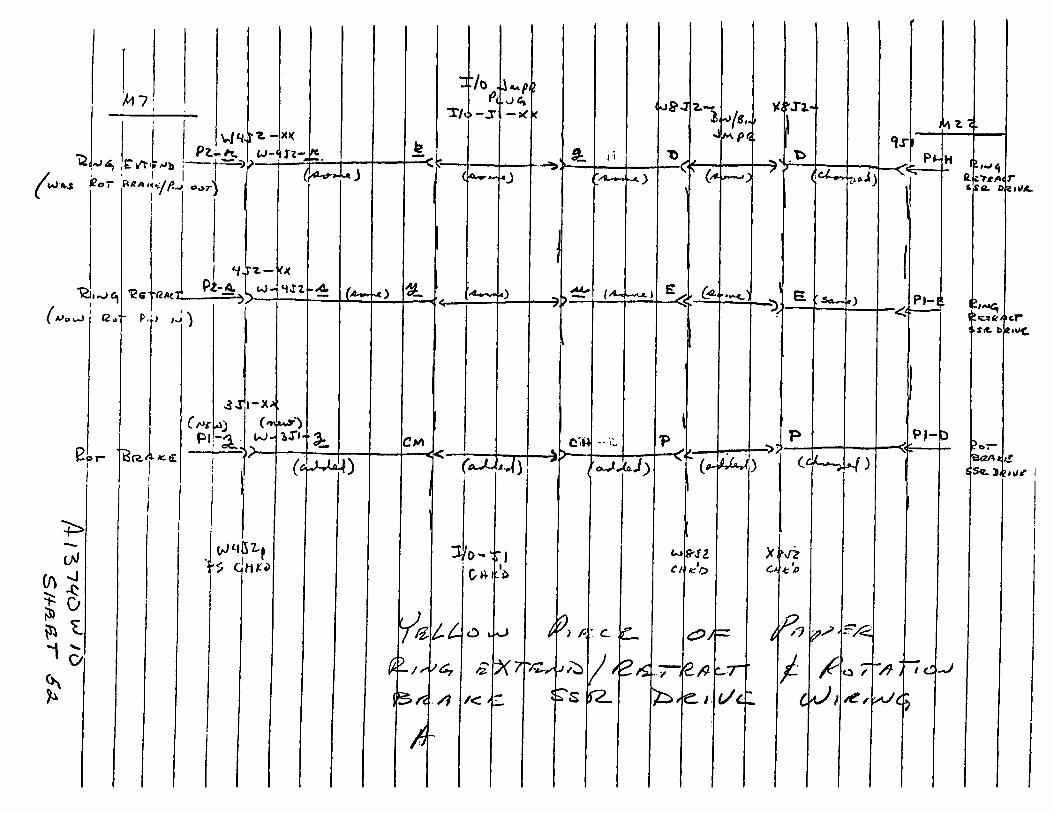
hi
*fc,
A>p u J G o -
E o p
•2. - xk
(J-MX2-J5
* A t . - <X
*c£
>
C M
t on )
• c
>0
* 1O
C A>»" *0
i-x> :(/vyu^^
UJ-
?»
iT>- “k .
(4». vt )
IrJLtblf H CjHk*>
W - j “ X
• ^ c tQ c u r ,
1 L'«<-
Cv»« -
(aJU
j i
f r y
( S / J
/ "
3 / 0 - * ; i C m
L C
'Y<Z?
A
O i J
* X
/ < c .
j )
2L
•*?
ii
(ofrj
c w
" 1
< *
A ) f*\
j r s
■C-
r 2 .
&
xfcra.-
■*>
, i
UiC/ JCO
&JZ
~ z # —7~"
c / c l .
CAkO
t e
/ /
d J
y e ]
o 7
* e ,
I s IMz < .
Pi- m
-<<r
f>/ U Cf
cTrA so. t>
p » - i i>
p j - b
> / e
<r*»t//C
* ^! . S ( t t>
?&T“
$S«. J/t
t r«»wc
r• UiT

in t e l
8085A/8085A-2 S IN G L E C H IP 8-BIT N-CHANNEL M IC R O P R O C ESSO R S
Single +5V Power Supply100% Software Compatible with 8080A1.3 n* Instruction Cycle (808SA);0.8 »t (8085A-2)On-Chip Clock Generator (with External Crystal, LC or RC Network)On-Chip System Controller; Advanced Cycle Status Information Available for Large System Control
Four Vectored Interrupt Inputs (One || Non-Maskable) Plus an 8080A- Compatible Interrupt
Serial In/Serlal Out Port
Decimal, Binary and Double Precision Arithmetic
Direct Addressing Capability to 64k Bytes of Memory
The Intel* aoaSA It • compute 8 bit parallel Central Processing Unit (CPU). It* Instruction aet la 100% software compstiui with the 8080A microprocessor. and It 1a designed to improve the present 8060A's performance by higher system spetg Its high level ot system integration allows a minimum system of three IC’s 16085A (CPU). 8156 f RAM/IOi and83S5/875Sa I ROM/PROM/iO) | while maintaining total system expandability. The 8085A-2 Is a faster version of the 8085A The 8085A incorporates all of the features that the 8224 fdock generator) and 8228 (aystem controller) provided fortr* 8080A, thereby ottering a high level of system integration.
The 808SA uses a multiplexed data bus. The address it split between the 8 bit address bus and the 8 bit data bus Th, 1 on-chip address latches of 8155/8156/83S5/8755A memory products allow a direct interface with the 8085A I
c 1 40 3 v «*1 C a m 3 HOkO
M IST OUt C 1 M 3 Mio*too c « » 3 C i i wHO C 1 K 3 M INI*
TAA* C 1 » 3 M ttfftSTM C » U 3 *0*m t m c 1 » 3 UM T t t C • M 3 #5
M»TA C >o It 3 w il* fA C 11 JO 3 AHAOo C n n 3 toAO, C i) n 3 * *AO* C 14 V 3AO) C i i n 3 AHA04 C M 3 * i lAO* C « J4 3 *uAOf C 11 it 3AOt C 1* » 3 M
C M 11 3 *o
Figure 2. SM SAPIn Configuration
6-10 AFfrfiMS
808SA/8085A-2
Symbol
A»*A1S
AOo_7
Sg. S|.andlO/B
ST
Table 1. Pin DescriptionName and Function
Address Bus: Th* most significant 8 bits ot the memory address or th* 6 bits ot th* I/O addratt. 3-ttated during Hold and Halt mod** and during RESETMultiplexed Addr*ss/Oata Bus: Lower 8 bits ot th* memory address (or I/O addrass) app*ar on th* bus during th* first clock cyci* (Tstat*) ot a machin* cycle. It then becomes th* data but dunng th* tacond and third clock cyclas.Addraae Latch Enable: it occur* during th* first dock tfat* of a machine eye l» and *nabi*t th* addratt to g*t latched into th* on-chip latch ot p*riph*rais. Th* falling *dg* of ALE it t*t to guarant** t*tup and hold tlm*t tor th* address information. Th* tailing *dg* of ALE can alto b* ut*d to ttrob* th* ttttut informttion. ALE it n*v*r 3-stat*dMachin* Cycle Stetu*:
KVB Si So Stetue0 0 1 Memory write0 1 0 Memory read1 0 1 I/O writat 1 0 I/O read0 1 t Opcode fetch1 1 t Opcode letcht 1 t Interrupt
Acknowledge• 0 0 Halt
X X HoldX X React
’ ■ 3-ttat* (high impadance)X - untp*cifi*d
Si can b* ut*d at an advanced R/W status lO/fl. So and St bacom* valid at th* bsgmning of a machin* cycl* and remain ttabi* throughout th* cycl*. Th* falling adg* of ALE may b* ut«d to latch th* ttat* of that* lin*a.R**d Control: A low l*v*l on R5 Indicatas th* t*l*ct*d memory or I/O davic* it to b* retd and thtt tna Oata But it tvailabl* for th* data trantter. 3-ttat»d during Hold and Halt mod** and dunng RESETWrite Control: A low level on w?5 indicates the data on the Oata But it to be written into the selected memory or I/O locttion. Otta it t*t up at the trailing edge ot WS J . ttated durmg Hold and Halt modet and during RESET
Symbol Type Neme end Function
READY 1 Reedy: If REAOY it high during a read or write cycle, it mdicatet that the memory or penpheral it retdy to tend or receive data It REAOY it low. Ihe cpu will wtit an integral number of clock cycles tor READY to go high before completing the r*ad or writa cycle. READY mutt conform to specified setup and hold tim*t
HOLD 1 Hold: Indicates that another matter it requesting th* use ot th* addrns and data butet. The cpu. upon receiving the hold request, will relinquith the ute of the but at toon at the completion of the current but trantfer Internal proceta- ing can continue. The processor can regain the but only after the HOLD it removed. When the HOLD It acknowledged, the Addrett. Otta SB. wS. and IOiM line* ar* 3-stated
HLOA 0 Hold Acknowledge: indicates that the cpu has r*c*iv*d th* HOLO request and that it will relinquish the bua in the next clock cycle. HLOA goes low altar the Hold request is removed The cpu takes the but one half clock cycl* after HLOA go** low.
INTR 1 Interrupt Request: It utad tt * general purpote interrupt. It it tampled only during th* n*xt to th* last clock cycl* of an instruction snd during Hold tnd Halt ttatet If it it tctiv*. th* Program Counter (PC) will b* Inhibited from incrementing and an INTA wiH b* issu*d. During this cycl* * RESTART or CALL in- ttruction can b* inserted to lump to the Interrupt tervice routine. The INTR it entbl*d tnd ditabled by software It it ditabted by Ratal and immediately after an interrupt it accepted
ffTtt 0 Interrupt Acknowledge: It uted instead of (tnd haa the tam* timing aa) RB during the Inttruction cycle after an INTR it tccepted It can be uted to eclivata an 82S9A interrupt chip or tome other interrupt port
RST 5 S RST 6 $ RST 7S
1 Reatart Intarrupta: Thete thre* in* puts have the tame timing at INTR except they caute an internal RESTART to ba automatically insertedThe priority of thet* interrupt! is ordered t t thown in Ttble 2 Thet* interrupt* have a higher priority than INTR In addition, they may b* individually masked out utmg th* SIM instruction
6-11

intef 8085A/808SA-2
Table 1. Pin Description (Continued)Symbol TfP* Name and Function
TRAP 1 Trap: Trap interrupt Is a nonmaskable RESTART interrupt. It Is recognized at the same time as INTR 01 RST 5 5-7 5 It 1* unaffected by any mask or interrupt Enable. It has the highest prtonty of any interrupt (See Table 2)
RESETIN 1 fteaet In: Seta the Program Counter to zero and resets the Interrupt Enable and HLDA flip-flops The data and address buses and the control lines are 3-stated during RESET and because of the asynchronous nature of RESET, the processor's internal registers and flags may be altered by RESET with unpredictable results RESET IN Is a Schmitt-triggered input, allowing connection to an R-C network tor power-on RESET delay. The cpu la held in the reset condition as long as RESET IN is applied.
Symbol iypa Name and Function v
RESET OUT O React Out: Reset Out indicate^''' is being reset. Can be as a system reset. The Signal synchronized to the Proce»tj| clock and laeta an integral nun^ ol clock periods
X ,.X 2 1 Xi and X?: Are connected'ioT' crystal. LC. or RC network to 0,^ the internal clock generator x, c«, alao be an external clock input irg* a logic gate The input frequency 4 divided by 2 to give the proceator( Internal operating frequency
CLK 0 Clock: Clock output for uae at a iJJ' tem dock The period of CLk ,, twice the X ,. X* input period
SlO 1 Serial Input Oata Une: Thedata*" this line is loaded into accumulate bit 7 whenever a RIM inatruction * executed
SOD 0 Serial Output Oata Une: The ovT put SOO is sat or reset as specify by the SIM instruction.
Vcc Power: ♦ 6 volt supply ~
V*S Ground: Reference. '
Teble 2. Interrupt Priority, Raetart Address, and Sanaltlvlty
Name PriorityAddress Branched To (1) When Interrupt Occurs Type Trigger
TRAP 1 24H Riaing edge AND high level until sampledRST 7 5 2 3CH Rising edge (latched).RST 6 5 3 34H High level until aampied.RST 5 5 4 2CH High level until sampled.INTR 5 See Note (2). High level until sampled.
NOTES:1 . The processor pushes the PC on the stack before branching to the indicated address2. Tn* address branched to depend* on the instruction provided to the cpu whan tha Interrupt la acknowledged.
6 - 1 2
intef 8085A/8085A-2
FUNCTIONAL DESCRIPTIONThe 8085A is a complete 8-bit parallel central processor. It is designed with N-channel depletion loads and requires a single +5 volt supply Its basic clock speed is 3 MHz 808SA i or S MHz 18085A-2). thus improvmgon the present
8080A's performance with higher system speed. Also it is designed to lit into a minimum system ol three IC's: The cpu 18O8SA). a RAM/IO18156). and a ROM or EPROM/IO cr.ip .8355 or 8755A).
The 8085A has twelve addressable 8-bit registers Four ol them can lunction only as two 16-bit register pairs Six others can be used interchangeably as 8-b>t registers or as 16-bit register pairs. The 8085A register set isas follows: Mnemonic R agister ContentsACC or A Accumulator 8 bitsPC Program Counter 16-bit addressBC.DE.HL General-Purpose 8 bits x 6 or
Registers; data 16 bits x 3 pointer iHL)
SP Stack Pointer 16-bit addreaaflags or F Flag Register 5llags(6-bltapace)
The 8085A uses a multiplexed Data Bus. The address is split between the higher 8-bit Address Bus and the lower 8-bit Address/Data Bus. During the first T state (clock cycle, ol a machine cycle the low order address is sent out on the Address/Data bua. These lower 8 bita may be latched externally by the Address Latch Enable aignal ALE ■ During the rest ol the machine cycle the data bus is
used lor memory or I/O data.Tha 8085A providaa KB, WR, S0, S ,. and 10/ffl signals lor bus control. An Interrupt Acknowledge aignal (INTA) la also provided. HOLD and all Interrupts are aynchronlzed with the processor's Internal clock. The 8085A also provides Serial Input Oata (SID) and Serial Output Data (SOD) lines lor simple aerial Interlace.In addition to these features, the 8085A has three maskable. vector interrupt pins and- one nonmaskable TRAP interrupt
•n ter r u p t ano SERIAL I/OThe 8085A has 5 interrupt inputa: INTR. RST 5 5. RST 6 5. ■’ ST 7 5. and TRAP. INTR ia identical in function to the 8080A in t Each ol the three RESTART inputs. 5 5. 6 5. •"0 7 5. haa a programmable mask TRAP is also a c S T a rt interrupt but It is nonmaskable
Th» three maskable interrupts cause the internal ••ecution ol RESTART (saving the program counter In the "•** and branching to the RESTARTaddress) II the inters 'uPts are enabled and il the interrupt mask ia not set. The "o''-maskable TRAP causea the internal execution ol a
'S t a r t vector independent ol the atata ol tha interrupt •°»bie or maaka (See Table 2 )rTh*'e ®r« two dillerent typea ol inputs in tha restart inter-into 5 ® an<1 ® * * r* h' h l9v* l' senMlv* like
!*nd INT on the 8080) and are recognized with the *m® hming as INTR RST 7.5 is rising edge-aensitive
f®r RST 7 5. only a pulse is required 10 set an internal ’P-tiop which generates the internal interrupt request.
Section 5 2 7 The RST 7 5 request liip-llop remains
aet until the request is serviced. Then it is reset automatically This llip-llop may also be reset by using the SIM instruction or by issuing a AESET IN to the 8085A. The RST 7 5 Internal llip-llop will be set by a pulse on the RST 7 5 pm even when the RST 7.5 interrupt is masked out. The status ol the three RST interrupt masks can only be aflected by the SIM instruction and RESEit IN lSee SIM. Chapter 5.
The interrupts are arranged in a fixed priority that determines which interrupt is to be recognized il more than one is pending as lollows: TRAP — highest priority. RST 7 5. RST 6.5. RST 5 5. INTR — lowest priority This priority scheme does not take into account the priority ol a routine that was started by a higher priority interrupt RST 5.5 can interrupt an RST 7.5 routine if the mterrupta are re-enabled belore the end ol the RST 7 5 routine. The TRAP interrupt is uselul lor catastrophic events such as power lailure or bus error The TRAP input is recognized just as any other interrupt but has the highest priority. It is not allected by any Hag or mask. The TRAP Input is both edge end level sensitive The TRAP input must go high and remain high until it is acknowledged. It will not be recognized again unlil it goea low. then high again This avoida any lalse triggering due to noise or logic glitches. Figure 3 illustrates the TRAP interrupt request circuitry within the 8085A Note that the aervicmg Ol any interrupt (TRAP. RST 7.5. RST 6 5. RST 5 5 INTR) disables all luture interrupts (except TRAPsi until an El instruction is executed.
ip —.
ACKNOWltOOt
Figure 3. TRAP and RESET IN CircuitThe TRAP interrupt is special in that it disables interrupts, but preserves the previous interrupt enable status Performing the first RIM instruction following a TRAP interrupt allows you to determine whether interrupts were enabled or disabled prior to the TRAP All subsequent RIM instructions provide current interrupt enable status Perlormmg a RIM instruction following INTR. or RST 5 5-7 5 will provide Current Interrupt Enable status, revealing that Interrupts are disabled See the description ol the RIM instruction In Chapter 5 The serial I/O system is also controlled by the RIM and SIM instructions SlO is read by RIM. and SIM sets the SOD data
6-13 V IK I IW t

8085A/8085A-2
DRIVING THE Xi AND X2 INPUTSYou may drive th* clock inputs ol the 8085A or 8085A-2 with • crystal, an LC tuned circuit, an RC network, or an external clock source The driving frequency mutt be at least 1 MHz. and must be twice the desired internal clock frequency, hence, the 6065A it operated with a 6 MHz crystal 1 for 3 MHi clock . and the 808SA-2 can be operated witha 10MHz crystal.for 5 MHz clock'.If a crystal is used, it must have the following characteristics Parallel resonance at twice the clock frequency desired C l'load capacitance < 30 pf C« <shunt capacitance < 7 pf R« (equivalent shunt resistance; S 75 Ohms Drive level. 10 mWFrequency tolerance +.005% .suggested)Note the use of me 20pF capacitor between X , and ground. This capacitor is required with crystal frequencies below 4 MHz to assure oscillator startup at the correct frequency. A parallel-resonant LC circuit may be used as the frequency-determining network for the 8085A. providing that its frequency tolerance of approximately 1 10% is acceptable. The components are chosen from the formula:
____ 1 -
To minimize variations in frequency, it is recommend,. that you choose a value tor C«»t that is at least twice th„ of Cmt. or 30 pF. The use of an LC circuit is not rtct**. mended for frequencies higher than approximately 5 mh, An RC circuit may be used aa the frequency-determnw network for the 8085A if maintaining a precise clock tr* quency is of no importance. Variations in the on-Ch,, timing generation can cause a wide variation in frequent when using the RC mode. Its advantage is its low com! ponent cost. The driving frequency generated by circuit shown is approximately 3 MHz. It is not rtcom. mended that frequencies greatly higher or lower than th,, be attempted.Figure 4 shows the recommended clock driver circuit, Note m O and E that pullup resistors are required to astur, that the high level voltage of the input is at least 4 v
For driving frequencies up to and Including 6 MHz may supply the driving signal to Xi end leave X ; optn. circuited iFigue 4D). If the driving frequency is from 6 MHi to 10 MHz. stability of the clock generetor will be improve by driving both Xi end X ; with a push-pull source iFigU(| 4Ei. To prevent sell-oscillation of the 8085A. be surt Xz is not coupled beck to Xt through the driving circuit
2ir\/LiC«»t + Cmt)
ra. Quartz Crystal Clock Drlvar
b. LC Tuned Circuit Clock Drlvar
c. RC Circuit Clock Drlvar
d. 1*6 MHx Input Frequency External Clock Drlvar Circuit
Low lim* > 40 m
a. 1*10 MHz Input Fraquancy Extarnal Clock Drlvar Circuit
Figure 4. Clock Drlvar Circulta 6-14 unuxtvt
8085A78085A-2
GENERATING AN 808SA WAIT STATEif your system requirements are such that slow memories or peripheral devices ate being used, the circuit shown in Figure 5 may be used to insert one WAIT state in each 8085A machine cycle
The D flip-flops should be chosen so that* CLK is rising edge-triggered* CLEAR is low-level active.
Flgura S. Generation ot a Walt Stata lor 8085ACPU
As in the 8080. the READY line is used to extend the read and write pulse lengths so that the 808SA can be used with slow memory. HOLD causes the cpu to relinquish the bus when it Is through with it by floating the Address and Data Buses.
SYSTEM IN TERFACEThe 8085A family includes memory components, which are directly compatible to the 8085A cpu For example, a system consisting of the three chips. 8085A. 8158. and 8355 will have the following features:
• 2K Bytes ROM
• 256 Bytes RAM• 1 Timer/Counter• 4 8-bit I/O Ports• 1 6-bit I/O Port• 4 interrupt Levels• Serial In/Serial Out Ports
This minimum system, using the standard I/O technique 'S as shown In Figure 6.
In addition to standard I/O. the memory mapped I/O oilers an efficient I/O addressing technique. With this technique, an area of memory address space is assigned for I/O address, thereby, using the memory address for I'O manipulation Figure 7 shows the system configura- I'on of Memory Mapped I/O using 8085A
The 8085A cpu can also interface with the standard memory that does not have the multiplexed address/data bus. It will require a simple 621218-bit latch) as shown in Figure 8.
Flgura 6. 808SA Minimum Syatam (Standard I/O Tachnlqua)
6-15

8085A/808SA-2
Figure 7. MCS-85"* Minimum System (Memory Mapped I/O)
Figure S. MCS-SS'" System (Using Standard Memories)
6-16
8085A/808SA-2
BASIC SYSTEM TIMINGThe 8085A has a multiplexed Data Bus ALE is used as a strobe to sample the lower B-bits of address on the Data 8us Figure 9 shows an instruction fetch, memory read and I/O write cycle (as would occur during processing of me OUT instruction). Note that during the I/O write and read cycle that the I/O port address is copied on both the upper and lower hall ot the address.There are seven possible types of machine cycles. Which of these seven takes place is defined by the status of the three status lines ilO/M. S i. Soi and the three control signals (RO. WB. and INTA). (See Table 3.) The status lines can be used as advanced controls (for device selection. lor example:, since they become active at the Ti •late, at the outset ot each machine cycle Control lines So and WH become active later, at the time when the transfer of data is to take place, so are used as command linesA machine cycle normally consists of three T states, with the exception of OPCODE FETCH, which normally has either four or six T states i unless WAIT or HOLD states •re lorced by tne receipt of READY or HOLD inputs*. Any Tstate must be one of ten possible states, shown in Table4.
Table 3. 808SA Machine Cycle Chart
MACHINE CYClE STATUS C0NTR0T O Wio/H SI so
OFCOOE FETCH (OF) 0 t 1 0 1 iM6M0AV AEAO (MR) 0 1 0 1 iMEMO** WRITE IMW) 0 0 1 1 0I/O READ (lORl 1 1 0 i iI/O WRITE HOW) 1 0 1 1 0 iACKNOWLEDGEOF INTR 4INA) 1 1 1 1 1 06USI0 1 C ten oao
ACK OF AST TRAP
0 1
1
* 1 1
HALT TS 0 0 TS TS 1
Table 4. 808SA Machine State ChartSutut & 0vM< Control
MidtimSti«« SI.SO io/ffi * | - * t | AOq»AD> flO.WA INTA ALE
T, X X X X t 1 1*
T j X X X X X X 0
Twait X X X X X X 0
T j X X X X X X 0
t 4 1 0* X TS 1 1 0
U t O' X TS 1 1 0
u 0* X TS 1 1 0
Tr CICT X TS TS TS TS 1 0
Tmalt 0 TS TS TS TS 1 0
t mOl O X TS TS TS TS 1 0
* T* • Mt*A impede***1 • • f X • UAW*Clf*0
* AlI >voi f*fte«Me0 2nd e*d 3rdmecn<ft« e»c(m«f 0*0* tO*M • » »l IN* cvf*
6-17

8085A/8085A-2
ABSOLUTE MAXIMUM RATINGS*
Ambient Temper«tuie Under Bias........................O'C to 70 CStorage Temperature.......................................-65°C to tlSO'CVoltage on Any Pm
With Respect 10 Ground................................. -0 5V to *7VPower Dissipation.................................................. 1.5 Witt
"NOTICE: Stressas above those listed under ~Absofa Meximum Rstings" mey cease permenent dtmtge to device. This is $ stress reting only end functions! tion ot the device et these or eny other conditions a60, , those indiceted in the operetionel sections of n speci/lcetion is not implied. Exposure to ebsoiui, meximum reting conditions tor extended periods effect device relieblllty.
D.C. CHARACTERISTICS (TA - O’C to 70“C. v Cc - ov t5% . v Ss - ov; unless otherwise specified)
Symbol Parameter Min. Max. Units Ten Conditions ^
V ,L Input Low Voltage •0.5 +0.8 V
V,M Input High Voltage 2.0 Vcc+0.5 V
V0 L Output Low Voltage 0.45 V l0L "
VOH Output High Voltage 2.4 V •oh " -400mA
'cc Power Supply Current 170 mA
'.L Input Leakage 110 tiA 0« VIN «VCC
' lo Output Leakage 110 liA 0.45V < V,,,,, < VCC
v . l b Input Low Level. RESET -0.5 ♦0.8 V
V|HR Input High Level. RESET 2.4 vcc +0-5 V
VMy Hysteresis. RESET 0.25 V
6-18
8085A/8085A-2
A.C. CHARACTERISTICS <t a - ( r c to 70*c. v Cc - ov ±5%. v S8 - oV)
Symbol Parameter 8085A,2) 80eSA-2ffl UnitsMin. Max. Min. Max.
'CYC CLK Cycl* Period 320 2000 200 2000 nsCLK Low Tima (Standard CLK Loading) 80 40 ns
CLK High Tima (Standard CLK Loading) 120 70 ns
CLK Rise and Fall Tima 30 30 ns'xKR X , Rising lo CLK Rising 31) 1£0 30 100 ns
X . RIsIno to &LK Falllna 30 150 30 110 ns'*C is Valid to Leading Edge of Control'1' 270 115 nsl*CL Ao.r Valid to Leading Edge of Control 240 115 ns
h ’*0 ' V , , Valid to Valid Data In i 7 i ns'aFR Address float After Leading Edge of
REEffilNTX) 0 0 ns_ _ 'AL A s.» Valid Before Trailing Edge of ALE'1' 115 50 ns 'all Aq. , 'V alid Before Trailing Edge of ALE t t 50 ns
'arv READ?Vsira"from AjaFesrValld - j j 0- - 100 nsr- <r* Address {A*.n) Valid After control 120 to ns
•cc Width of Control Low (Rb, WR. INT A) Edoe of ALE 400 230 ns
lCl Trailing Edge of Control to Leading Edge of ALE 50 25 ns
'ow Oata Valid to Trailing Edge of WRITE 420 230 ns___ JhabE HLbA to Bus Enable i id iW nsp H A R f Bus Float After HLOA 210 150 ns
[mack HLOA Valid to Trailing Edge of CLK 110 40 nsi- !mDh HOLD Hold Time 0 0 ns
HOLD Setup Time to Trailing Edge of Cl K " W 120 ns
r~ ,NHINTR Hold Time 0 0 ns
l»N$ INTR, RST, and TftAP Setup Time to Falling Edge of CLK 160 150 ns
1— ,L* Address Hold Time After ALE 100 50 ns•ic Trailing Edge of ALE to Leading Edge
of Control 130 60 ns---- *LCK ALE Low During CLK High 100 50 ns— Jlor ALE to Valid Data During Read 460 i n ns- (low ALE to Valid Data During Write 200 150 nsjn n ' ALE Width ■ ------- 140 to ns
ALE to READY Stable 110 36 ns
6-19 AFH41»*2«

8085A/8085A-2
A.C. CHARACTERISTICS (Continued)
Symbol Parameter sossam •oesA-jffl Unit*Min. Max. Min. Max.
*RAE Trailing Edge ol READ to Re-Enabling ol Address
150 90 ns
'RD bEAO (or INTA) to Valid Data 300 150 ns'rv Control Trailing Edge to Leading Edge
ol Next Control400 220 ng
' rd h Data Hold Time Alter R I a5 iNTA>7' 0 0 ns•r yh READY Hold Time 0 0 ns
' r y s READY Setup Time to Leading Edge ol CLK
110 100 ns
'WD Data Valid Alter Trailing Edge ol WRITE 100 60 ns
*WDL LEA0ING Edge ol WRITE to Data Valid 40 20 ns
NOTIS:1 Ag-A|} adore** Specs apply lo IO/U. So. end Si encepl Ag-A ate undefined during T4-Tg ol OF cycle
where** IQiH. S®. andS( are *l*bl*2 l i i l condition* lCYC « 320ns (808SAI/200 ns (808SA-2). Ct • 1S0pF.3 For all oulpul timing where CL « 1S0pF use the following correction (actor*:
25pF < CL < ISOpF. -0 lOns/pF150pF< Ct < 300pF: + 0 30ns/pF
4 Output timing* are measured with purely capacilive load5 All timing* at* meaiured at output votage vL «08v. VH > 2 OV. and 1 5V with 20n* n*e and l*il time on Input*, t To calculate timing specification* al other value* of iCYC u*e Table 7.7 Data hold time is guaranteed under all loading condition*
A C. TESTING INPUT. OUTPUT WAVEFORM A.C. TESTING LOAD CIRCUIT
6-20 U T M IW I
8085A/8085A-2
Table S. Bua Timing Specification aa a TCyc Oependent
| 8085A
I *AL - (1/2) T -45 MIN
J l a - (1/2) T - 60 MIN
* LL - (1/2) T - 20 MIN
’ l c k - (1/2) T - 60 MIN
. ' l c - (1/2) T - 30 MIN
_ ' a o - (5/2 ♦ N) T - 225 MAX
_ ' r d - (3/2 ♦ N) T - 180 MAX' r a e - (1/2) T - 10 MIN
•c a - (1/2) T - 40 MIN
'ow - (3/2 ♦ N) T - 60 MIN
'WD - (1/21 T - 60 MIN
. 'cc - (3/2 ♦ N) T - 80 MIN
' c l - (1/2) T - 110 MIN
_ . ' a r y - (3/2) T - 260 MAX
' h a c k - (1/2) T - 50 MIN•h a b p - (1/2) T + 50 MAX
_ ' h a b e - (1/2) T + 50 MAX
. *AC - (2/2) T - 50 MIN
k - - '- (1/2) T - 80 MIN
[— *2 - (1/2) T - 40 MIN
L ' r v - (3/2) T - 80 MIN' l o r - (4/2) T - 180 MAX
NOTE N ii aqua I to th« total W AIT stattt
T • IC YC
8085A-2
*A L - (1/2) T - 50 MIN
• l a - (1/2)T - 50 MIN
' l l - (1/2) T - 20 MIN‘ l c k - (1/2) T - 50 MIN
*LC - (1/2) T - 40 MIN
*AD - (5/2 ♦ N IT -150 MAX! RD - (3/2 + N) T - 150 MAX•r a e - (1/2) T - 10 MIN
*CA - (1/2) T - 40 MIN
*ow - (3/2 ♦ N) T - 70 MIN
*WD - (1/2) T - 40 MIN
'cc - (3/2 ♦ N) T - 70 MIN
' c l - (1/2) T - 75 MIN
*A RY - (3/2) T - 200 MAX
' m a c k - (1/2) T - 60 MIN• h a b f - (1/2) T ♦ 50 MAX* h a b e - (1/2) T ♦ 60 MAX
*AC - (2/2) T - 85 MINt , - (1/2) T - 60 MIN
*2 - (1/2) T - 30 MIN
*RV (3/2) T - 80 MIN'LO R (4/2) T - 130 MAX
NOTE N i« *qu«l to th# total WAIT tu tu .
T • ICYC
WAVEFORMS
4FM 4l}4!t

808SA/8085A-2
WAVEFORMS (Continued)READ
“A /— Sc. -
\ r " \ __r v- 'e« —
AUORtU ¥
ADOAftt — w m k "5— i—
- J . V = f - ---------- ■* - " - " i —
*0 «•» A If— 'iC ■ ■ y 1
WRITEI ’» I ’» I », I »,
____/— \____/— \____,S -* » X »oo»«« !(
| (— S o .-----
*V *o , "J u m i h OAfAOUt ) f
■« • r -------------------------- W ---------------------- *| — J
MJ jr»- V —»
-
— *o —
READ OPERATION WITH WAIT CYCLE (TYPICAL) - SAME READY TIMING APPUES TO WRITE
V . . / \ >' \ 1 a r ~\______ ,h— H
X *<»••“ I X— I•iX
w ; " '////At «*— -----[
- — Sm ..................... I—**— [/-------««t>------ — = T "1
--------.v -----------/ i "------•«—— T-!
\ ■ m nih«01| I
6 - 2 2 V M 1 M I
8085A/8085A-2
WAVEFORMS (Continued)

8085A/8085A-2
Tabic 6. Instruction Sot Summary
taetructton Cod* O ptrtllO A iMnemonic Dy 0 | O5 O4 O3 0 } 0 Oc Description
MOVE. L0AO . AND STO RE
MOVfl f2 0 1 0 0 D s s s Move register to registerMOV M t 0 1 0 s s s Move register to memoryMOV rM 0 1 0 0 0 t 0 Mo* memory to regiSterMVI r 0 0 0 0 0 1 0 Move immMnti registerMVIM 0 0 0 0 Mow immed-et* memoryLXl B 0 0 0 0 0 0 0 Load immediet* register
Pur BSCu u o 0 0 0 0 0 0 Load immediate register
PS.r 0 A EU0H 0 0 0 0 0 0 Load immediete register
to " HALS1AXB 0 0 0 0 0 0 0 Store A indirectSTAX 0 0 0 0 0 0 0 8tore A indirectLDAX 8 0 0 0 0 0 0 Loed A indirectLDAX O 0 0 0 0 0 Load A indirectSTA 0 0 0 0 0 Stort A directLOA 0 0 0 0 Lo*d A directSHLO 0 0 0 0 0 0 Store HAL directLHLO 0 0 0 0 0 Load HAL directXCHO 1 0 0 1 Exchange 0 A E. H A L
Register*STACK 0^ 9PUSH B 1 0 0 0 0 1 Push register tor B A
Con tuckPUSHO 1 0 0 0 1 Push register feir 0 A
E on st*ckPUSH H 1 0 0 0 1 Push register feir h A
Lon stockPUSHPSW 1 1 0 0 1 Push A and Flags
on stackPOPS 1 0 0 0 0 0 1 Pop register RWr B A
C off stackPOPO 1 0 1 0 0 0 1 Pop register to ir 0 A
E off stackPOP H 1 0 0 0 0 1 Pop register t a r H A
Lo tt stackPOPPSW 1 1 0 0 0 1 Pop A and Flags
off s t ic kJCTML 1 0 0 0 1 Exchange top of
stsck. HALSPHL 1 1 1 0 0 1 H A L to stack pointerLXl SP 0 0 1 0 0 0 1 Losd immediats stack
pointerin x s p 0 0 1 1 0 0 1 1 increment stack pointerOCXSP 0 0 1 1 0 1 1 Decrement stack
pointerj Um »JMP 1 0 0 0 0 1 1 Jump unconditionalX t 0 1 1 0 1 0 Jump on carryJNC 1 0 1 0 0 1 0 Jump on no carryJZ 1 0 0 1 0 1 0 Jump on teroJHZ 1 0 0 0 0 1 0 Jump on no tereJP 1 1 1 0 0 1 0 Jump on positiveJM 1 1 1 1 0 1 0 Jump on minusJPE 1 1 0 1 0 1 0 Jump on parity evenJPO 1 t 0 0 0 1 0 Jump on parity oddPCHL 1 1 0 1 c 0 1 H A I to program
counterCALLCALL 1 0 0 1 1 0 1 C a i unconditionalCC 1 0 1 1 1 0 0 Cad on carryCMC 1 0 1 0 1 0 0 CaK on no carry
Inarwclter Code Operation*Mnemonic O7 0« 0 ) O4 0 ) 0 } 0 Ofl Description
CZ 1 0 0 1 1 0 0 Can on teroCHZ 1 0 0 0 0 0 Csu on no tereCP 1 1 1 0 1 0 0 Can on positiveCM 1 t 1 1 1 0 0 Call on minusCPE 1 1 0 1 1 0 0 Can on penty evenCPO 1 1 0 0 0 Q Call on oaritv oddRETURNRET 1 0 0 0 0 ReturnRC 1 0 0 0 0 Return on carryRNC 1 0 0 0 0 0 Return on no carryR2 1 0 0 0 0 0 Return on teroRN2 1 0 0 0 0 0 0 Return on no teroRP 1 1 0 0 0 0 Return on positiveRM 1 1 0 0 0 Return on minusRPE 1 0 0 0 0 Return on panty evenRPO 1 0 0 0 0 0 Return on parity oddMtTMTRSTINPUT/OUTPUTIN 1 0 0 inputOUT 1 0 0 0 OutputINCREMENT AND DECREMENTMR r 0 0 0 0 0 0 0 increment registerOCR r 0 0 0 0 0 0 Oecrement registerINRM 0 0 0 0 0 Increment memoryOCR M 0 0 0 0 Decrement memoryMX B 0 0 0 0 0 0 1 increment B A C
registersMX 0 0 0 0 0 0 1 increment 0 A E
register*MX H 0 0 0 0 0 1 increment H A L
register*OCX B 0 0 0 0 0 1 Decrement B A Cocxo 0 0 0 0 1 0*crem *nt D A EOCX H 0 0 0 0 1 Oecrement H A LADOAOOr 0 0 0 0 8 8 8 Add register to AADC r 0 0 0 8 8 8 Add register to A
with carryAOOM 10 c 0 0 1 1 0 Add memory to AADC M 1 0 0 0 1 1 1 0 Add memory to A
with carryADI t 0 0 0 1 1 0 Add immediate to AACI 1 0 0 1 1 1 0 Add immediate to A
with carryO ADB 0 0 0 0 1 0 0 1 Add 8 A C to H A LDADO 0 0 0 1 1 0 0 1 A d d O A E t o H A LDAD H 0 0 1 0 1 0 0 1 A d d H A l t o H A LQA0 8P 0 0 1 1 1 0 0 1 Add stack pomt*r to
H A LSUBTRACTSUB r 1 0 0 1 0 8 8 8 Subtract register
from AS B B r 1 0 0 1 1 8 8 8 Subtree! register from
A with borrow8U8 M 1 0 0 1 0 1 1 0 Subtract memory
from AS B B M 1 0 0 1 1 1 1 0 Subtree! memory from
A with borrowsm 1 1 0 10 1 1 0 Subtrsct immediate from Asai 1 10 1 1 1 1 0 Subtract immediate from A with borrow
6-24 AFN41MI
8085A/8085A-2
Tabla 6-1. Instruction Sot Summary (Cont'd)
rr -...t Instruction Cod*0 ? 0 $ 0 $ O4 03 O j Ot Oq
OperationsDescription
SPEC IA LSCMA
STCCMC
OAA
0 0 1 0 1 1 1 1
0 0 1 1 0 1 1 1 0 0 1 1 1 1 1 1
0 0 1 0 0 1 1 1
ComplementASet carryComplementcarryDecimal ediust A
CONTROLE l01NOPHLT
1 1 1 1 1 0 1 1 1 1 1 1 0 0 1 1 0 0 0 0 0 0 0 0 0 1 1 1 0 1 1 0
Enabl* Interrupts Disable interrupt N o*p*rstion Han
NEW SOSSARtMSIM
NSTRUCTION80 0 1 0 0 0 0 0 0 0 1 1 0 0 0 0
Read Interrupt Mask Set Interrupt Mask
Cod* Operation*Mnereont* 0? 0 | 0$ 0« 0 ) 0} 0 i 0o Description
LOGICALANAr 1 0 1 0 0 8 8 8 And register with AXRA r 1 0 1 0 1 8 8 8 Exclusive OR register
with AO R A r 1 0 1 1 0 8 8 8 OR register with ACMP r 1 0 1 1 1 8 8 8 Compare register with AANAM 1 0 1 0 0 1 1 0 And memory with AXRAM 1 0 1 0 1 1 1 0 Exclusive OR memory
with AORAM 1 0 1 1 0 1 1 0 OR memory with ACMPM 1 0 1 1 1 1 1 0 Compere
memory with AAM 1 1 1 0 0 1 1 0 And immediate with AXRl 1 1 1 0 1 1 1 0 Exclusive OR immediate
with AORI 1 1 1 1 0 1 1 0 OR immediate with ACPI 1 1 1 1 1 1 1 0 Compere immediate
with AROTATVRLC 0 0 0 0 0 1 1 1 Rotate A i*ftRRC 0 0 0 0 1 1 1 Rotate A rightr a l 0 0 0 0 1 1 1 Rotate A left through
carryRAR 0 0 0 1 1 1 Rotate A right through
carry
NOTES:1 OOSor SSS: B 000. C 001. 0 0 )0. E011. H 100. L 101. Memory 110. A 111.I IWo possible cycl* time* (6/12) Indicate instruction cycles d*p*nd*nt on condition flags.
*AH mnemonic* copyrighted <£)int*l Corporation 1976.
M S

8155/8156/8155-2/8156-2 2048 B IT STA TIC MOS RAM WITH I/O P O R TS AND TIM ER
i n y
256 Word x 8 Bits ■ Single +5V Power Supply ■ Completely Static Operation a Internal Address Latch a
2 Programmable 8 Bit I/O Ports ■
1 Programmable 6-Blt I/O PortProgrammable 14-Blt Binary Counter/ TimerCompatible with 808SA and 8088 CPU Multiplexed Address and Data Bus 40 Pin DIP
Th* 8155 and 8156 are RAM and I/O chips to be uaed In the 8085A and 8088 mlcroproceaaor systems. Tha RAM portion la daalgned with 2048 atatlc cell* organized aa 256 x 8. They have a maximum access time ol 400 na to permit u*e with no welt states In 8085A CPU. The 8155-2 and 8156-2 have maximum acce** time* ol 330 ns for u** with th* 8085A-2 and th* lull sp**d 5 MHz 8088 CPU.
The I/O portion consists ol thr** general purpoa* I/O porta. One ol th* three porta can be programmed to be atatus pins, thus allowing the other two port* to operate in handahake mode.
A 14-blt programmable counter/timer Is also Included on chip to provide either a square wave or terminal count pula* for the CPU aystem depending on timer mode.
• < = > M MSTATICMAM
| i
TlM(A C lK - flMCR OUT «
* 61S&'6166 2 • C€ 6 iM '8 i$ 0 2 • C6
* . c 1 40 3 vccC 30 3
TIMER IN C 1 3* 3 « ,M SCT C 4 27 3
• 96 3 " ,TiM Hi'GuT C • 36 3 " .
•0/0 C 7 94 3 " .£ t o « c i * C • 99 3 f t .
« C • 32 3* * c 10 •196/
• IM 31 3 » ,A l t C 11 • IM 2/ 90 3 m ,
*> • C 12 •1M 2 29 3 " .AO, C 19 26 3 ^
*> 7 C 14 27 3 " sAO) C IS 26 3 ' SAD , C 1* 26AO , C 17 24 3 ►*,**>• c 11 29 3AO , C I t 22 □ ►*,
C 90 21 D 'N
Figure 1. Block Dlegrem Figure 2. Pin Configuration
6-30
8155/8156/8155-2/8156-2
Table 1. Pin DeacrlptlonSymbol TVP* Name snd Function
BESET 1 Reset: Pulse provided by th* 8065A lo initialize the system (connect to SOSSA RESET OUT). Input high on this line resets the chip end Initializes the three VO ports to Input mod*. The width ol RESET puis* should typically b* two 6085A clock cycl* times.
*Dj .7 I/O Addr**s/0*ta: 3-stst* Addr*ss/Oata lines that intsrtsc* with th* CPU lower S-blt Address/Oats Bus. The 8-bit address is istched Into the address Istch m«ide the 8155/86 on the tailing edge ol ALE The sddress can be either for th* memory section or the VO section depending on th* IO/KI input Th* 8-bit dat* is *ither written into the chip or reed from the chip, depending on the WR or HD input signal
CEorCE 1 Chip En*M*: On th* 8155. this pin Is Cfc and is ACTIVE LOW On th* 8156. this pm Is CE snd is ACTIVE HIQH.
55 1 Reed Control: Input low on this lln* with the Chip Enable active enablas snd AOo-y buffer* ll 10/Ei pin is low. th* RAM content will b* r**d out to th* AO but. Otharwis* th* contant ol th* s*l*ct*d VO port or commsnd/ttstus registers will be read to the AO but.
wH 1 Writ* Control: Input low on thit lln* with th* Chip Enabl* activ* c*ut*t th* dat* on th* Addr**vDtts bus to b* written to the RAM or VO ports snd commend/ststus r*gist*r, d*p*ndlng on 10/(3
ALE 1 Addr*** Latch Enable: This control signal latches both th* *ddr*ts on the AOo-y lln** tnd th* ttst* of th* Chip Entbl* snd 10/fl into th* chip at th* lading *dg* of ALE
iof!i 1 I/O M*mory: Sclects memory il low and VO and command/ttatut r*gitl*rt If high.P*0-7l«l VO Port A: The** 8 pint ere general purpote VO pins. The in/out direction It selected by programming
th* command registerpBo-7iei I/O Port B: These 6 pint era general purpose VO pins. Th* in/out direction I* t*l*ct*d by programming
th* command registerpCo-j(6) VO Port C: That* 6 p»n* can function at either input port, output port, or at control tlgnals lor PA and PB
Programming Is done through the command register When PC^, ar* us*d as control signal* they will provide the following:PCo — A INTR (Port A Interrupt)PC, — ABF (Port A Buffer Full)PC} — A STB (Port A Strob*)PCj — B INTR (Port B Interrupt)PC* — B BF (Port B Buffer FuH)PCs — B STB (Port B Strob*)-___
_ T'M£R in 1 Tlm*r Input: Input to th* count*r-llm*r.f'UtHOUT 0 Tlm*r Output: Thit output can b* either * tquar* wav* or * puls*. d*p*nding on th* timer mod*
_ vcc Voltage: + 5 volt supply''ss Ground: Ground r*f*r*nc*.
K .1 1
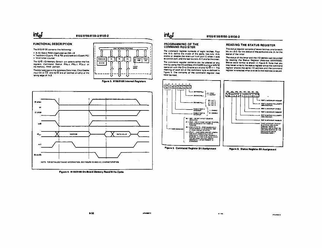
8155/8156/8155-2/8156-2
FUNCTIONAL DESCRIPTION
The 8155/8156 contains the following:• 2k Bit Static RAM organized as 256 x 8• Two8-bit I/O porta iPA& PBiandone6-bitl/Oport(PCi• 14-bit timer-counterThe lO/M 110/Memory Select' pm selects either the five registers i Command. Status. PAo-7. PBo-7. PCo-s1 or the memory i RAM portion
The 8-bit address on the Address/Data lines. Chip Enable input CE or CE. and lO/M are all latched on-chip at the falling edge of ALE
Figure 3. 8165/8156 Internal Register*
Figure 4. 8155/8156 On-Board Memory Read/Write Cycle
6-32 awhcooic
8155/8156/8155-2/8156-2
PROGRAMMING OF THE COMMAND REGISTERThe command register consists of eight latches. Four bits '0-3i define the mode of the ports, two bits (4-5) enable or disable the interrupt from port C when it acts as control port, and the last two bits l6-71 are for the timer. The command register contents can be altered at any time by using the I/O address XXXXXOOO during a WRITE operation with the Chip Enable active and 10/BI = 1 The meaning of each bit of the command byte is defined in Figure 5. The contents of the command register may never be read.
1I
1—» O tF IK M M *, 1L 0 - KlfUT
---------- OO lN ti ►«., J ’•°UT'UTT oo • a i t i
o in N c ir c , . , J|_ 10 • A l l <«NT|RRU*T 1 1 • CNAtlC 1 (h A iL C N M rt lo « o a A A L « 11
—* t im m commano
• iNrtRRyPT J
00 • NO* - 00 MOT AMCCT COUNT!AO l Nation
01 • r ro f - NO* IF TlMCft NAS NOT tTADTCO.n o * COUNTING 1* TMC nut!A It RUNNiNO
10 • STO* A*f |A TC - (TO* IMMtOlATItVAF HA *RCS€NT TC If RfACHfO (NO*IF TIM|A NAS NOT fTARTCOl
11 • fTART - IOAO MOOC ANO CNT ICNOTMANO START IMMCOIATUY AFTCR lOAOlNO IlF TlMfR IS NOT *RCStNTlV RUNNING) IF TiMCA i$ RUNNING START ThI Ntw MOOC ANO CNT kiNQTH IMMtOlATClV AM IR *R|S(NT IC It RIACHIO
Figure 5. Command Register Bit Assignment
READING THE STATUS REGISTERThe status register consists of seven latches, one for each bit: six (0-51 for the status of the ports and one (6i for the status of the timer.
The status ot the timer and the I/O section can be polled by reading the Status Register (Address XXXXXOOO). Status word format is shown in Figure 6. Note that you may never write to the status register since the command register shares the same I/O address and the command register is selected when a write to that address is issued.
A*»MW90ie

8155/8156/8155-2/8156-2
INPUT/OUTPUT SECTIONThe I/O Mction ol the 81SS/81S6 consists of live register*:(See Figure 7.)
• Commend/Statue Register (C/8) — Both registers are assigned the address XXXXXOOO The C/S address serves the dual purpose
When the C/S registers are selected during WRITE operation, a command is written into the command register. The contents ol this register are not accessible through the pins
When the C/S (XXXXXOOO 1 is selected during a READ operation, the status information ol the I/O ports and the timer becomes available on the ADo-r lines.
• PA Register — This register can be programmed to be either input or output ports depending on the status ol the contents ol the C/S Register. Also depending on the command, this port can operate in either the basic mode or the strobed mode 1 See timing diagram j. The I/O pins assigned in relation to this register are PA0-7 The address ol this register is XXXXX001.
• PB Register — This register functions the same as PA Register. The I/O pins assigned are PB0-7. The address ol this register is XXXXX010.
• PC Register — This register has the address XXXXX011 and contains only 6 bits. The 6 bits can be programmed to be either input ports, output ports or as control signals lor PA and PB by properly programming the ADj and AO] bits ol the C/S register
When PC0-8 is used as a control port. 3 bits are assigned lor Port A and 3 lor Port B The lirst bit is an interrupt that the 8155 sends out. The second is an output signal indicating whether the butter is lull or empty, and the third is an input pin to accept a strobe for the strobed Input mode. (See Thble 2 )
When the 'C' port is programmed to either ALT3 or ALT4.the control signals lor PA and PB are initialized as lollows:
CONTROL INPUT MOOE OUTPUT MOOEBF Low Low
INTR Low HighSTB Input Control Input Control
I/O ADO Itttt*U ltC T IO N
A t M At A4 A ) At A1 AO
* ft X X X 0 0 0 Ifttrvftl Comm»*a SlCtwt A*e>«l«'* X * X X 0 0 1 O t w t i PurpoM I/O Port A* X X X X 0 1 0 Oow ftl Pw*pO$# I/O Port 8* X * X X 0 1 1 Po*l C - Otn«r«l Pw'pos* 1 0 O' Co*lro>* X * X X 1 0 0 lOw-Ortf*' 6 tH« O' Timtr COu*t
*X
*X X 1 0 1 High 6 t><u ol Timor Co«m «no 2 6>tl
ol Tii««» MoOt
1 Oonl Car*» "O A00TM* M Qu«iHi«C fry CC • 1 'tlM'OrCt*Oi|lM>*ft0>O/M*linoro»
Figure 7. I/O Port and Timor Addraaalng Schama
Figure 8 shows how I/O PORTS A and B are structured within the 8155 and 8156:
/S\ OUTPUT . LATCH
c ik CD
6
0 —---------- t
OUTPUTtN Aftll
> .
W*ITtPOUT
, * » o _u Z JJ j
1MOOfM
RtAOPOMT
iATCM 0 0
CLK1J 1
NOT t i ll) output moot *Ol SlMPtt INPUT <* motto INPUT .
- H § )
Figure a. 8155/8156 Port Functlona
6-34 V M x a o tc
8155/8156/8155-2/8156-2
Tabla 2. Port Control Aaalgnment
Pin ALT 1 ALT 2 A LTS ALT 4PCOPC1PC2PC3PC4PCS
Input Port Input Port Input Port Input Port Input Port Input Port
Output Port Output Port Output Port Output Port Output Port Output Port
A INTR (Port A Interrupt) A BF (Port A Bulfer Full) A STB (Port A Strobe)
Output Port Output Port Output Port
A INTR (Port A Interrupt) A BF (Port A Buffer Full) A STB (Port A Strobe)
B INTR (Port 8 Interrupt) B BF (Port B Buffer Full) B STB (Port B Strobe)
Note in the diagram that when the I/O ports are programmed to be output ports, the contents ol the output ports can still be read by a REAO operation when appropriately addressed.
The outputs ol the 8155/8156 are “glitch-free" meaning ■hat you can write a "1" to a bit position that was previously “1" and the level at the output pin will not change. Note also that the output latch is cleared when the port enters the input mode. The output latch cannot be loaded by writing to the port il the port is in the input mode. The '•suit is that each time a port mode is changed Irom input to output, the output pins will go low. When the 6155/56 is RESET, the output latches are all cleared and all 3 ports
• snter the input mode.When in the ALT 1 or ALT 2 modes, the bits ol PORT C are structured like the diagram above in the simple input or output mode, respectively.Reading Irom an input port with nothing connected to the Pms will provide unpredictable results.F'gure 9 shows how the 6155/8156 I/O porta might be contigured in a typical MCS-85 system.
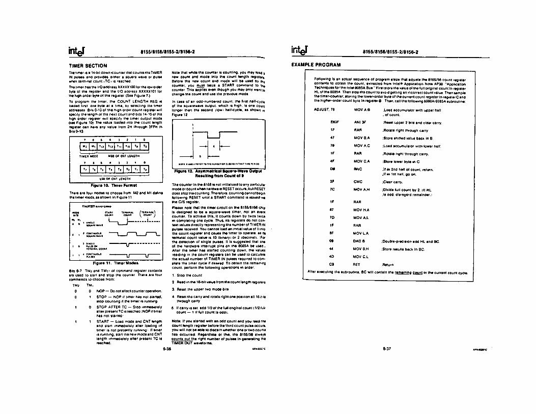
in te f 8155/8156/8155-2/8156-2
TIMER SECTIONThe timer isa 14-bit down-counter mat counts theTlMER IN pulses and provides either a square wave or pulse when terminal count 1T C 1 is reached.The timer nas the I/O address XXXXXlOOtor the low order byte ot the register and the I/O address XXXXX101 tor the high order byte ot the register (See Figure 7.)To program the timer, the COUNT LENGTH REG is loaded first one byte at a time, by selecting the timer sddresses Bits 0-13 of the high order count register will specily the length ol the next count and bits 14-15 ot the high order register will specify the timer output mode (see Figure 10) The value loaded into the count length register can have any value from 2H through 3FFH in Bits 0-13.
There are four modes to choose from: M2 and Ml define the timer mode, as shown In Figure 11.
Bits 6-7 TM; and TM ii of command register contents are used to start and stop tne counter. There are four commands to choose from:
0 NOP — Do not atfect counter operation. STOP — NOP if timer has not started; stop counting if the timer is running.
STOP AFTER TC — Stop immediately after present TC is reached i NOP if timer has not started'START — Load mode and CNT length and start immediately after loading ;lf timer is not presently running .. It timer is running, start the new mode and CNT length immediately after present TC is reached.
TM* TM
0 00 1
1 0
Note that while the counter Is counting, you may load t new count and mode Into the count length registers Before the new count and mode will be used by th« counter, you must Issue a START command to the counter This applies even though you may only want to change the count and use the previous mode.
in case of an odd-numbered count, the first half-cycl« ot the squarewave output, which is high, is one count longer than the second ilowi half-cycle, as shown m Figure 12
The counter in the 8155 Is not initialized to any particular mode or count when hardware RESET occurs, but RESET does stop the counting Therefore, counting cannot begin following RESET until a START command is issued vis the C/S register.Please note that the timer circuit on the 8155/8156 chip is designed to be a square-wave timer, not en event counter. To achieve this, it counts down by twos twics in completing one cycle. Thus. Its registers do not contain values directly representing the number of TIMER IN pulses received You cannot load an initial value of 1 into the count register and cause the timer to operate, as its terminal count value is 10 (binary) or 2 (decimal). iFor the detection of single pulses, it is suggested that one ot the hardware interrupt pins on the 8085A be used, After the timer has started counting down, the values residing in the count registers can be used to calculate the actual number of TIMER IN pulses required to complete the timer cycle if desired. To obtain the remaining count, perform the following operations in order:
1. Stop the count
2. Read in the 16-bit value from the count length registers
3. Reset the upper two mode bits
4. Reset the carry and rotate right one position all 16 bits tnrough carry
5. If carry is set. add 1/2 of the full original count (1/2 full count — 1 if full count is odd).
Note: If you started with an odd count and you read ths count length register before the third count pulse occurs, you will not be eble to discern whether one or two counts has occurred. Regardleas ot this, the 8155/56 always counts out the right number of pulses in generating the TIMER OUT waveforma.
6-36 <mt-ooacnc
8155/8156/8155-2/8156-2
EXAMPLE PROGRAM
Following is an actual sequence of program steps that adiusts the 8155/56 count register contents to obtain the count, extracted from Intel* Application Note AP38. "Application Techniques for the Intel 8085A Bus " First store the value of the full original count in register HL of the 8085A Then stop the count to avo.d getting an incorrect count value Then sample the timer-counter, storing the lower-order byte of the current count register in registerC and the higher-order count byte in register B. Then, call the following 6080A/8085A subroutine:
ADJUST. 78 MOV A.B ;Load accumulator with upper half ; of count.
E63F ANI 3F iReset upper 2 bits and clear carry.
IF RAR :Rotate right through carry.
47 MOV B.A ;Store shifted value back in B.
79 MOV A.C ;Loed accumulator with lower half.
1F RAR .Rotate right through carry.
4F MOV C.A :Store lower byte in C.
D» RNC .If in 2nd half of count, return. ;lf in 1st half, go on.
3F CMC .Clear carry.
7C MOV A.H ;Dlvlde full count by 2. (If HL :1s odd. disregsrd remainder.)
1F RAR
67 MOV H.A
7D MOV A.L
1F RAR
6F MOV L.A
09 DAO B iDoubie-prectaion add HL and BC.
44 MOV B.H ;Store results back in BC.
4D MOV C.L
C9 RET :Return.
After executing the subroutine. BC will contain the remainino counj in the currant muni <-y/-i«
6-37 AFN4H01C

8155/8156/8155-2/8156-2
8085A MINIMUM SYSTEM CONFIGURATION
Figure 13* shows • minimum system using three chips, containing:
• 256 Bytes RAM• 2K Bytes ROM• 38 I/O Pms• 1 Interval T imer• 4 Interrupt Levels
6-36 A»*S«0<
8155/8156/8155-2/8156-2
8088 FIVE CHIP SYSTEMFigure 13b shows a five chip system containing:• 126K Bytes RAM
• 2K Bytea ROM
• 38 I/O Pina
• 1 1nterval Timer
• 2 Interrupt Levela
Flgura 13b. 10(1 Five Chip System Configuration
6-39 A n *o u o ic

8155/8156/8155-2/8156-2
ABSOLUTE MAXIMUM RATINGS*
Temperature Under Bias .................................. 0°Cto*70*CStorage Temperature ................................ -65*Cto*150'CVoltage on Any Pm
With Respect to Ground ................................ -0 5VIO+7VPower Dissipation ............................................................... i 5W
•NOTICE: Stresses above those listen under Absolut, Maximum Ratings'' may cause permanent damage to th, device This is a stress reting only and functional opart, tion ot the device at these or any other conditions abov, those indicated in the operational sections of t/>,, specification is not implied. Exposure to absolute man. mum rating conditions tor extended periods mey aliac, device reliability.
D.C. CHARACTERISTICS CTa * 0°C to 70°C. Vcc - 6V t 5%)
SYMBOL PARAMETER MIN. MAX. UNITS TEST CONDITIONSVil Input Low Voltage -0 6 0.8 V
V,M Input High Voltage 20 Vcc *05 V HM x Output Low Voltage 0.45 V Iol ” 2mAM3H Output High Voltage 2.4 V Ioh ■ -400»iA<IL Input Leakage 110 j<A 0V « V,N « VCC■lo Output Leakage Current ±10 **A 0.45V < Vout ^ Vcc•cc Vcc Supply Current 180 mA
■ i l (CE) Chip Enable Leakage 8t55 8166
♦ 100 -100
**A»*A
ov « V,N « Vcc
6-40 AfHOOJOK
8155/8156/8155-2/8156-2
A.C. CHARACTERISTICS crA - o°c to 70*C; vcc • sv i s%)8165/8156 8165-2/8156-2
SYMBOL PARAMETER MIN. MAX. MIN. MAX. UNITS
U l Address to Latch Set Up Tim* 60 30 ns
' la Address Hold Time after Latch 80 30 ns
■lC Latch to READ/WRITE Control 100 40 ns
'ro Valid Oata Out Delay from READ Control 170 140 ns
■*0 Address Stable to Data Out Valid 400 330 ns
■lL Latch Enable Width 100 70 ns■nor Data 8us Float After READ 0 100 0 80 ns>CL READ/WRITE Control to Latch Enable 20 10 ns■cc READ/WRITE Control Width 250 200 ns*0W Data In to WRITE Set Up Time 150 100 ns■wo Data In Hold Time After WRITE 0 0 ns■rv Recovery Time Between Controls 300 200 nsW WRITE to Port Output 400 300 ns
Port Input Setup Time 70 60 ns■n» Port Input Hold Time 50 10 ns
. 'SSf Strobe to Buffer Full 400 300 ns_ *ss Strobe Width 200 150 nsL '"BE READ to Buffer Empty 400 300_ 'si Strobe to INTR On 400 300.. '"Ol READ to INTR Off 400 300 ns
'►ss Port Setup Time to Strobe Strobe 50 0 ns_ !»mS Port Hold Time After Strobe 120 100 ns
'm i Strobe to Buffer Empty 400 300_ '«0f WRITE to Buffer Full 400 300_ 'wt WRITE to INTR Off 400 300. _ l fL TIMER IN to TIMER OUT Low 400 300 ns
'T* TIM ERIN to TIMER-OUT High 400 300 ns__l*0E Data But Enable from READ Control 10 10 ns— ' TIMER-IN Low Time 80 40 ns
TIMER IN High Time 120 70 ni
* C TESTING INPUT. OUTPUT WAVEFORM A.C. TESTING LOAD CIRCUIT
6-41 **%-owo»c

in te f 815S/8156/8155*2/8156-2
WAVEFORMS
READ CYCLE
_____
- i --------
■ N _____
\m-- --
/ -------t i
JLIt :
z
< x
A .
n .
J - c
WRITE CYCLE
6-42 AMMUOlC
8155/8156/8155-2/8156-2
WAVEFORMS (Continued)
STROBED INPUT MODE
STROBED OUTPUT MODE
6-43 vtomoic
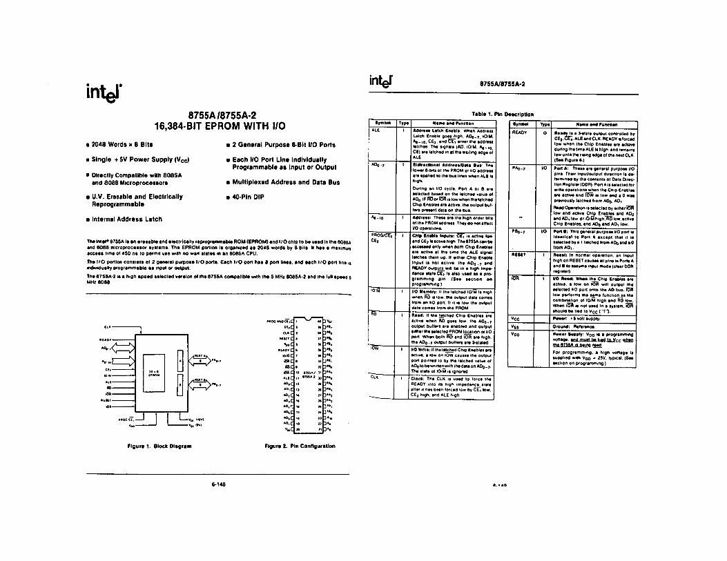
in y8755A/8755A-2
16,384-BIT EPROM WITH I/O
■ 2048 Words x 8 Bits
■ Single + 5V Power Supply (VCc)
■ Directly Compatible with 8085A and 8088 Microprocessors
■ U.V. Erasable and Electrically Reprogrammable
■ Internal Address Latch
■ 2 General Purpose 8-Bit I/O Ports
■ Each I/O Port Line Individually Programmable as Input or Output
e Multiplexed Address and Oata Bus
■ 40-Pin DIP
Th* Intel* 876SA it en erasable and electrically reprogrammable ROM (EPROM) and I/O chip to be used in the 808SA and BOBS microprocessor systems. The EPROM portion is organized as 2048 words by 8 bits. It has a maximum access time ol 450 ns to permit use with no wait atstes in an 8085A CPU.
The I/O portion consiats of 2 general purpose I/O ports. Each I/O port has 8 port line*, and each I/O port line is individually programmable as input or output.
The 87SSA-2 is a high apeed selected version ol the 87SSA compatible with the 6 MHz 8086A-2 and the lull speed 5 MHz 6088.
MOO ANOCl.C , <0M.C I » 3 " .
cm C ) It D-*.■cu t c < » D " .
'fcoC ( » 3 " .fttADvC • » !•*%
■0/AC 7 M 3 " .e t c 1 u*6C • » 3 " .
« * C to S7U A / 1< 3 « »*11 c n s t m a i K 3« .* ° .c u » 3 « .« ,c i) n ] « ,
*0, C i« V 3 « »A0,C it i t 3 »»»» ° . r <• n*°»c n N 3 ’N“ .C is 11*°.c tt 1> D SS*C X )1
Figure 1. Block Diagram Figure 2. Pin Configuration
6-148
87S5A/87SSA-2
Table 1. Pin DescriptionSymbol Type
a l e I Addreaa Latch Ena bit: Whan Address Latch Enable goes high. A D q-t. tO/M. A ^ .io , C £ j. and C E i enter the addreaa latches The signals (AO. IO/M. A*»io. CE) are latched in at the trailing edge of ALE
ADo-r Ilower 0*bits of the PROM or I/O address are applied to the bus lines when ALE Is high.
During en I/O cycle. Port A or 8 are selected based on the latched value of A00 IF RB or IOR is low when the latched Chip Enables are active, the output buffers present data on the bus.
*S -I0 Addreaa: These are the high order bits of the PROM address. They do not effect I/O operetions.
PROG/CF,C E ,
I Chip Enable Inputs: is active low and CE2 fa active high The 87SSA can be accessed only when both Chip Enables •re active at the time the ALE signal latchaa them up. if either Chip Enable input is not active, the A O g .y and REAOY outputs^will be in a high impe> dance atate C E i is also used as a programming pm. (See section on programming)
I0 M i I/O Mejnory: if the letched IO/M is high when RO is low. the output data comes from en I/O port if it is low the output dete comes from ihe PROM
RD i Read: if the latched Chip Enables are active when RO goes low. the A Do-r output buffers are enabled and output either the selected PROM location or I/O port When both RO and IOR are high, the ADo r output buffers are 3-stated
‘Ow i I/O Write: if the latched Chip Enables are active, e low on IOW causes the output port pointed to by the latched value of AOq to be wnttenwith the data on AOo - 7 The state of lO/M is ignored
CLK
-
i Clock: The CLK is used to force the REAOY into its high impedance stete after it has been forced low by C E i low. CE} high, and ALE high
Symbol Type Name end Function
REAOY 0 Reedy I* • 3-state output controlled by CE j . . ALE end CLK. REAOV Is forced low when the Chip Enables ere ectove during the time ALE Is high, snd remains low until the rising edge of the next CLK. (See Figure 6.)
PA0-7 I/O Port A: These ere generel purpose I/O pine Their Input/Output direction is determined by Ihe content* of Del* Direction Register (ODR) Port A is selected for write operetions when the Chip Enables ere sctlve end IOW le low and s 0 wes previously letched from AOo. AD|.
Resd Operation is selected by either iS R low and ective Chip Enables snd AOo snd AD j low. or iO/M high. RO low. sctlve Chip Enables, end AOo snd AD! low.
P0O-7 I/O Port 8: This general purpose I/O port is Identical to Port A except thet it la eelected by a 1 latched from ADo *nd a 0 from AO|.
RESET 1 Reeet: tn normal operetlon. en input high on RESET ceuses ell pins mi Ports A and B to aaeume Input mode (cleer OOR register).
1 I/O Reed: When the Chip Eneblee ere active, e low on IOR will output the eelected I/O port onto the AO bus. ICR low performs Ihe same function es the combination ol IO/M high and RO low. When IOR le not used In e eystsm. IOR should be tied lo Vq c ('1")
V c c Power: ♦ 6 volt supply.
Vss Oround: Reference
Voo Power Supply: Voo <s s programming voltaoe. and must be tied to V<-<- when the 07SSA 1a Deina rpat?
For programming, a high voltage Is supplied with Vqo * 2SV. typical (See section on programming.)
C . H O

67S5A/875SA-2
FUNCTIONAL DESCRIPTION PROM SectionThe 8755A contains an 8-bit address latch which allows It to mtarface directly to MCS-48. MCS-85 and iAPX 88/10 Microcomputer* without additional hardware
The PROM section ol the chip it addressed by the 11-bit address and CE The address CE> and CE? are latched mto tne address latches on the tailing edge ot a le it the latcned Chip Enables are active and 10 M is low when RD goes low the contents ot tne PROW location addressed by the latched address are put out on the AD0.7 lines (provided that Voo •* tied to V cc )
I/O SectionThe I/O section ot the chip is addressed by the latched value ot AOo-t Two 8-bit Data Direction Registers .DDR- m 87S6A determine the mput'Outpjt status ot each pm in the corresponding ports A 0 m a particular bit position ot a DDR signifies that the corresponding I/O port bit is m the input mode A "1" m a particular bit position signifies that the corresponding I/O port bit is m the output mode In this manner the I/O ports ot tne 875SA are bit-by- bit programmable as inputs or outputs The table summarizes port and DDR designation DDR's cannot be read
AOi AOo Selection0 0 Port A0 1 Port B1 0 Port A Data Direction Register DOR Ai1 1 Port B Data Direction Register DDR Bi
When lOW goes low and the Chip Enables are active, the data on the AD is written into I/O port selected by the latched value of AD0-1 During this operation all I/O bits ol the selected port are effected, regardless ol their I/O mode and the state ot lO/M The actual output level does not change until IOW returns high iglitch iree output 1 A port can be readout when the latched Chip Enables are aclive and either RD goes low with lO/M high, or lOR goes low Both input and output mode bits ot a selected port will appear on lines ADo-rTo clarity the function ot the I'O Ports and Data Direction Registers, the following diagram shows the configuration ot one bit ot PORT A and DDR A The same logic applies to PORT B and DDR B
0*1 *11 O* W»» * A«0 00* *
M U M - t[i i« 0 .li .c « 6 .|i| .ii li< .| ..C « » |« » » U » *C I'» li- i« 0 » l* *0 0 « IU |l ,ic., .M il m i l l ►» a not tllMKKC l« Itw
Note that hardware RESET or writing a zero to the 00ft latch will cause the output latch's output butter to t* disabled, preventing the data in the Output Laich ir0n being passed through to the pm. This is equivalent i0 putting the port in the input mode Note also that the aata can be written to the Output Latch even though the Outp„- Butter has been disabled. This enables a port to be ir tialized with a value prior to enabling the output The diagram also shows that the contents of PORT A 1 - PORT B can be read even when the ports are contigu „ as outputa.
TABLE 1. S75SA PROGRAMMING MODULE CROSS REFERENCE
MOOULE NAME USE WITH
UPP 955 UPPi4|UPP UP2(2i UPP 855PROMPT 975 PROMPT 80/85(3)PROMPT 475 PROMPT 48i 11NOTES
1 Described on p 13-34 ol 1978 Data Catalog2 Special adaptor socket.3 Descnbed on p 13-39 ol 1978 Data Catalog4 Descnbed on p 13-71 of 1978 Data Catalog
6-150 t f M W I I
intef 8755A/8755A-2
ERASURE CH A R A CTER ISTICSThe erasure characteristics of the 87SSA are such that erasure begins to occur when exposed to light with wavelengths shorter than approximately 4000 Angstroms A it should be noted that sunlight and certain types of
fluorescent tamps have wavelengths in the 3000-4000A range Data show that constant exposure to room level fluorescent lighting could erase the typical 87S5A m approximately 3 years while it would take approximately 1 week to cause erasure when exposed to direct sunlight, it the 87SSA is to be exposed to these types of lighting conditions tor extended periods of time, opaque labels are available from Intel which should be placed over the 8755 window to prevent unintentional erasure.The recommended erasure procedure tor the 87SSA is •xposure to shortwave ultraviolet light which has a wavelength ot 2537 Angstroms 1A 1 The integrated dose (i.e.. UV intensity X exposure timei for erasure should be a minimum of 15W-sec/cmJ The erasure time with this dosage is approximately 15 to 20 minutes using an ultraviolet lamp with a 12000,*W/cm* power rating. The 8755A should be placed witnm one inch from the lamp •ubes during erasure Some lamps have a filter on their tubes and this filter should be removed belore erasure.
p r o g r a m m in g
Initially, and after each erasure, all bits of the EPROM Mrtions ol the 8755A are in the ” 1" state Information is 'ntroduced by selectively programming "0" into the flesireo bit locations A programmed "0“ can only be changed to a 'T ' by UV erasure
!*e 8755A can be programmed on the Intel* Universal ROM Programmer i UPP). and the PROMPT- 80/85 and
T OMPT-48'* design aids. The appropriate programming oduies and adapters tor use in programming both 55a $ and 8755's are shown in Table 1.
Program mode itself consists ol programming e n9'e address at a time, giving a single 50 msec pulse ' every address Generally, it is desirable to have a *' y cycle alter a program cycle lor the same address
• ,sh° wn ln the attached timing diagram in the verify .-^1—' e normal memory read cycle 1 Voo' should •.-.at -5\j ------------------
^eiimmary timing diagrams and parameter values per- 1 »"!? 10 8755A programming operation are con-
ed m Figure 7 .
SYSTEM APPLICATION S System Interface with 8085A and 8088A system using the 8755A can use either one of the two I/O Interface techniques:
• Standard I/O
• Memory Mapped I/O
If a standard I/O technique is used, the system can use the feature of both CE3 and CE |. By using a combinationol unused addreaa lines A , , . l( and the Chip Enable inputa. the 808SA system can use up to 5 each 8755A’s without requiring a CE decoder. See Figure 2a and 2b. If a memory mapped I/O approach Is used the 8755A will be selected by the combination of both the Chip Enables and 10/M using the AOs-15 address lines. See Figure 1.
(Memory-Mapped I/O)
«-151

intef 8755A/8755A-2
IAPX 88 FIVE CHIP SYSTEM
Figure 4 snows a five chip system containing:
• 1 25K Bytes RAM• 2K Bytes ROM• 38 10 Pins• 1 interval Timer• 2 Interrupt Levels
Figure 4. IAPX 88 Flv* Chip System Configuration
6-152
8755A/8755A-2
Figure S. 87S5A In 8085A System (Standard I/O)
6-153

in te l 87SSA/87SSA2
ABSOLUTE MAXIMUM RATINGS*
Temperature under Bias . Storage Temperature voltage on Any Pin
Witn Respect to Ground Power Dissipation .
. O 'C U W O X -65JCto *150°C
-0 5V to +7V ..............1 5W
‘ NOTICE: Stresses above those listed under 'Absoiutt Minimum Ratings" may csuse permenent damage to thf device. This is a stress rating only and lunctional opera. tion o l the device at these or any other conditions abo*e those indicated in the operational sections ol this speo/i. cation is not Implied. Exposure to absolute maximum rating conditions lor extended periods may allect devict reliability.
O.C. CHARACTERISTICS o> - o*c to 7<r. v Cc - v 0o - sv ± 5%;Vcc - Voo - 5V 110 % tor 87SSA-2)
SYMBOL PARAMETER MIN. MAX. UNITS TEST CONDITIONS
Vll Input Low Voltage -OS 0.8 V Vcc * 5.0V
VlH Input High Voltage 2.0 Vcc *0.5 V Vcc • 5.0V "H
^ L Output Low Voltage 0.45 V Io l ■ 2mA
Msh Output High Voltage 2.4 V lOH " -400*iA
'IL Input Leakage 10 pA VSS * VIN * VCCko Output Leakage Current 110 HA V s s * 0.45V * VOOT s Vcc
•cc Vqc Supply Current 180 mA
'do Voo Supply Current 30 mA VDo “ VccC|N Capacitance of Input Buffer 10 pF fc - V H iCl/D Capacitance of I/O Buffer 1S PF fc - 1<iHz
O.C. CHARACTERISTICS— PROGRAMMING (Ta ” 0*Cto70*. vCc - sv * 5%. vss - ov. vDD - 2sv :iv.V cc “ Voo - 5V 110% for 87SSA-2)
Symbol Parameter Min. Typ. Mai. UnitVoo Programming Voltage (during Write
to EPROM) 24 25 26 Vloo Prog Supply Current IS 30 mA
6-154 AF*0l*4ie
8755A/875SA-2
A.C. CHARACTERISTICS (t a - o*c to 70*. v Cc - sv s 5%;Vcc - V DD " SV 1 10% for 87SSA-2)
| Symbol Parameter87SSA SftSA-2
(Preliminary)Min. Mai. Min. Mai. Unit*
1 !C»C Clock Cycle Time 320 200 ns1 T, CLK Pulse Width 80 40 ns1 T? CLK Pulse Width 120 70 ns; !■ t. CLK Rise and Fail Time 30 30 nsi l*L Address to Latch Set Up Time 50 30 ns
t.A Address Hold Time alter Latch 80 45 nsKc Latch to REAO/WRITE Control 100 40 nstno Valid Oata Out Delay from READ Control 170’ 140* ns
' 1*0 Address Stable to Data Out Valid 450 330 ns111 Latch Enable Width 100 70 nstno* Oata Bus Float after READ 0 100 0 85 ns
. 'CL READ/WRITE Control to Latch Enable 20 10 nstcc REAO/WRITE Control Width 2S0 200 nstow Oata In to Write Set Up Time 150 150 nstrtO Data in Hold Time After WRITE 30 10 nstwp WRITE to Port Output 400 300 nstPR Port Input Set Up Time 50 50 nstop Port Input Hold Time to Control 50 SO nst«YH READY HOLD Time to Control 0 160 0 t60 nsIaAv ADDRESS CE to READY 160 160 nstav Recovery Time Between Controls 300 200 ns'ROE READ Control to Data Bus Enable 10 10 ns
_ '>-0 ALE to Data Out Valid 350 270 ns
NOTl:“.3»o • ISOpF
T*o - (Tm ♦ Ttc). whichever is greater
* C. CHARACTERISTICS— PROGRAMMING (Ta - o*c to 70’ . vcc - sv ± s%. v Ss - ov.v00 - 25V iiv ;V cc * Voo “ 5V 2 10% for 8755A-2)
Symbol Parameter Min. Typ. Max. Unit___'PS Data Setup Time 10 ns__ !<>o Data Hold Time 0 ns
»s Prog Pulse Setup Time 2 »sIh Prog Pulse Hold Time 2 M*
~^JPR Prog Pulse Rise Time 001 2 »sProg Pulse Fall Time 001 2 **»
- .___'PRO Prog Pulse Width 45 50 msec
C IC C

i n t ^ 8755A/8755A-2
A.C. TESTING INPUT. OUTPUT WAVEFORM A.C. TESTING LOAD CIRCUIT
i e a *
^ TU T W iM t» < ^
• I 01
AC ’ (StiNG <»**u»SA«t 0«vCMAt ?4y»OR*lOC'C ' AND0**vrOA 0 t.MNG Mi AS<iA(MI m s *«£ MAOl At *Ov A lOG'C I
ANO 0$v FQA A lOG'C 0
r
WAVEFORMS
CLOCK SPECIFICATION FOR 87SSA
6-156 «FN 4i*>a
in y 8755A/B755A-2
WAVEFORMS (Continued)

8755A/8755A-2
WAVEFORMS (Continued)
I7SSA PROGRAM MODE
/ A
_x y~>r"'1DATA TOM PftOOAAMMtO;o g ex z :*po-•D O C ^>C7X“
// \
\*n —*% ——*♦II «M «•- —► «PBC *
V /"*v|Al»v CYCll It A ftlQUlAft MCMOAV MAO CVClt IVMTH Vqo * *0* iTMAl
6*158
□ANALOG DEVICES
Integrated Circuit 10-Bit Analog-to- Digital Converter
AD571FEATURESCompl«t« A/D Convartar with R if ir in c i tnd Qock Fast Suoctuivt Approximation Conversion - 2Sja No Mining Codas Ovar Tamparatura
0 to +70° C — AOS71K -6S*C to +125*0 - A0671S Digital Multiplexing - 3 Stata Outputs
18-Pin Carsmic DIP Low Coit Monolithic Construction
PRODUCT DESCRIPTIONThe AD57I is a 10-bit successive approximation A/D converter consisting of a OAC. voltage reference, clock, comparator, successive approximation register and output buffers - all fabricated on a single chip No external components are required to perform a full accuracy 10-bit conversion in 2Sps.
The ADS71 incorporates the most advanced integrated circuit design and processing technology available today. It is the first complete converter to employ I1 L (integrated injection logic) processing in the fabrication of the SAR function. Laser trimming of the high stability SiCr thin film resistor ladder network at the wafer stage (LW T) insure* high accuracy, which is maintained with a temperature compensated, subsurface Zener reference.
Operating on supplies of *SV to + I5 V and -15V, the ADS71 will accept analog inputs of 0 to ♦10V. unipolar or tSV bipolar, externally selectable. As the BLANK and CONVtRT input is driven low, the three state outputs will be open and a conversion will commence. Upon completion of the conversion, the DATA READ Y line will go low and the datawill appear at the output. Pulling the BLANK and CQN- V E R T input high blanks the outputs and readies the device for th next conversion The ADS71 executes a true 10-bit conversion with no missing codes in approximately lifts .
The AD571 is available in two versions for the 0 to ♦70°C temperature range, theADS71J and K The AD571Sguarantees 10-bit accuracy and no missing codes from -55°C to »125°C.
*G ovm d by fu m t No*. ) ,M ,? (O i 4 ,2 IJ ,M M i4 ,li6 ,J49 .
A D J7 ! FUNCTIONAL BLOCK DIAGRAM
IPRODUCT HIGHUCHTS1. The AD571 is a complete 10-bit A/D converter. No
external components are required to perform a conversion. Full scale calibration accuracy of 10.3% is achieved without external trims.
2. The AD571 is a single chip device employing the most advanced IC processing techniques. Thus, the user has at his disposal a truly precision component with the reliability and low cost inherent in monolithic construction.
3. The AD371 accepts either unipolar (0 to ♦lOV) or bipolar (- JV to *5 V) analog inputs by simply grounding or opening a single pin.
4. The device offers true 10-bit accuracy and exhibits no missing codes over its entire operating temperature range.
5. Operation is guaranteed with -15V and *5V to *15V supplies. The device will also operate with a -12V supply.
A N u n f i . m . n m i T A i m v i / r o T r o c u n > < k
SPECIFICATIONSADS7IJ AD57IK AD57IS
Min Typ Mat Min Typ Mai UnitaRESOLUTION 10 10 10 BitsRELATIVE ACCURACY. T„' *1 * 1 4 *1 LSB
TM toTM *1 * 1 4 *1 LSBFULL SCALE CALIBRATION' z l z l 2 2 LSBUNIPOLAR OFFSET *1 2 1 2 x l LSBBIPOLAR OFFSET *1 *1 LSBDIFFERENTIAL NONLINEARITY.Ta IB 10 10 BitsTomIoTm, • 10 10 BitsTEMPERATURE RANGE 0 ♦ 70 0 ♦ 70 -5 5 * 125 •cTEMPERATURE COEFFICIENTS
Unipolar Offeet *2 <1Bipolar Offset *2 <1Full Scale Calibration1 *4 *2 * 5 LSB
POWER SUPPLY REJECTIONCMOS Positive Supply
♦ 1 J.SVsV ♦ s ♦ 16.5V - *1 _TTL Poauive Supply
♦ 4 ,J V s V t* O J V * 1 *1 * 2 LSBNegative Supply
- 16 OVsV - * - II. 5V * 2 *1 *2 LSBANALOG INPUT IMPEDANCE I B 5 0 7.0 J O 5 0 7.0 1.0 5 0 7.0 kftANALOG INPUT RANGES
Unipolar 0 +10 0 *10Bipolar - 5 ♦ 5 - 5 *5 - 5 *5 V
OUTPUTCODINGUnipolar PositiveTn* Binary Positive True Binary Positive T rue BinaryBipolar Positive True Offset Binary Positive True Offset Binary
LOGIC OUTPUT Output Sink Current
(Vovr • 0.4 V m as.T__to T ^ .) 1.2 1.2 1.2Output Source Current*
( V d t ' 2 4 V mai. Tm to T _ ) 0.5 OS 0.5Output Lenkngr * 4 i *40 *40 *A
LOGIC INPUTSInput Current * 100 *100 *100 l*ALogic *1** 2.B 2.0 2.0 VLogic **0“ I I 1.1 0.1 V
CONVERSION TIME. T* tod -T „»toT «« IS 25 40 IS 2) 40 15 25 40 ¥*
POWER SUPPLYV* ♦ 4.5 *5.0 + 7.0 ♦ 4.5 ♦ 5.0 +14.5 ♦ 4.5 +5.0 +7.0 VV - -U .B - I S -16 .5 -1 2 .0 -1 5 -16 .5 -1 2 0 -1 5 -16 .5 V
OPERATINGCURRENTV* 15 2S 15 25 15 25 mAV - 9 15 9 15 9 15 mA
PACKAGE*Ceramic DIP DIIA DlSA DIIAPlastic DIP N1IA NIIA
NOTES‘Relative accuracy i» defined as the deviation of th* code traautioa poum from tbc ideal titot/er pomi oe • straight Um from the «rt> to the lull scale of the drvtce
’Full scale cnlibratioo i» guaranteed tnaaable to aero with en oternaJ 500 potentiometer id place ol the I50 feed m u tor.FuH scale » defined as 10 volts mums I LSB, oe * WO voto. ____________
Tike data output linn hen active pull-ups to source 0 5mA Tbe OATA REAOY line is opts coltectoe with a Mutual tkll internal pull-up resistor.
*S«e Section 19 (or pscki|« outline information Specifications subject to change without noticeSpecifications shown m boldface art tested on all production uwts at final efcctncal teat Results (ran thoae teats are used to calculate outgoing qunbty levels. All am tod m i specdkauoos are guaranteed, although only thoee shows « boldface m tested on all production unci.
VOL i. 10-32 ANALOG- TO-DtGlTAL CONVERTERS

ABSOLUTE MAXIMUM RATINGSV» to Digital Common AD571J, S ...................................0 to +7V
AD571K................................0 to *16.JVV- to Digital Common........................................................0 to -16.0VAnalog Common to Digital Common............................................ t lVAnalog Input to Analog Common..............................................115VControl Inputs..............................................................................0 to V*Digital Outputs (Blank Mode)....................................................0 to V+Power Dissipation...........................................................................SOOmW
B
ANALOG-TO-OIGITAL CONVERTERS VOL. /. 10-33
CIRCUIT DESCRIPTIONThe AD57I is a complete 10-bit A/D converter which requires no external components to provide the complete successive* approximation analog-to-digital conversion function. A block diagram of the AQ571 is shown in Figure 1. Upon receipt of the CONVERT command, the internal 10-bit current output DAC is sequenced by the I* L successive-approximation register (SAR) from its most-significant bit (MSB) to least- significant bit (LSB ) to provide an output current which accurately balances the input signal current through the Skft input resistor. The comparator determines whether the addition of each successively-weighted bit current causes the DAC current sum to be greater or less than the input current; if the sum is less the bit is left on, if more, the bit is turned off. After testing all the bits, the SAR contains a 10-bit binary code which accurately represents the input signal to within 1MLSB (005%).
Figure 1. AD571 Function*/ Block Diagram
Upon completion of the sequence, the SAR sends out a B a T a READV signal (active low), which also brings the three-state buffers out of their "open" state, making the bit output lines become active high or low, depending on the code in the SAK When the BLANK and CONVERT line is brought high, the output buffers again go "open*', and the SAR is prepared for another conversion cycle. Details of the timing are given further.
The temperature compensated buried Zener reference provides the primary voltage reference to the DAC and guarantees excellent stability with both time and temperature. The bipolar offset input controls a switch which allows the positive bipolar offset current (exactly equal to the value of the MSB less ViLSB) to be injected into the summing (♦) node of the comparator to offset the DAC output. Thus the nominal
0 to ♦ 10V unipolar input range become*a-5V to *$V range. The 5kft thin film input resistor is trimmed so that with a full scale input signal, an input current will be generated which exactly matches the DAC output with all bits on. (The input resistor is trimmed slightly low to facilitate user trimming, as discussed on the next page.)
POWER SUPPLY SELECTIONThe AD57I is designed for optimum performance using a ♦SV and -15V supply, for which the ADS7IJ and AD57IS are specified. AD571K will also operate with up to a *1SV supply, which allows direct interface to CMOS logic The input logic threshold is a function of V* as shown in Figure 2. The supply current drawn by the device is a function of both \ * and the operating mode (BLANK or CONVERT). These supply current variations are shown in Figure J . The supply currents change only moderately over temperature as shown in Figure 7.
Figure 2. Logic Threshold (ADS71K Only)
VOL. /, 10-34 ANALOG-TO-DIGITAL CONVERTERS

Applying the A0571CONNECTING THE AD571 FOR STANDARD OPERATION The ADS71 contains all the activc components required to perform a complete A/D conversion. Thus, for most situations. all that is necessary is connection of the power supply (♦} and -15). the analog input, and the conversion stan pulse But. there are some features and special connections which should be considered for achieving opomum performance. The functional pin-out it shown in Figure 4.
FULL SCALE CALIBRATIONThe Skft thin-film input resistor is laser trimmed to produce a current which matches the full scale current of the internal DAC-plus about 0.3%-when a full scale analog input voltage of 9.WO volts <10 volts - 1 LSB) is applied at the input. The input resistor is trimmed in this way so that if a fine trimming potentiometer is inserted in scries with the input signal, the input current at the full scale input voltage can be trimmed down to match the DAC fu ll scale current as precisely as desired However, for many applications the nominal 9 99 volt full scale can be achieved to sufficient accuracy by simply inserting a 1511 resistor in senes with the analog input to pin 13. Typical full Kale calibration error will then be about 12LSB or 10.2%. If the more precise calibration is desired, a 50(} trimmer should be used instead. Set the analog input at 9.990 volts, and set the trimmer to that the output code isjustat the transition between 1111111110 and 1111111 H I . Each LSB will then have a weight of 9.766mV. If a nominal full tcale of 10.24 volts is desired (which makes the LSB have '►eight of exactly lO.OOmV), a 100ft resistor in series with a 100(1 trimmer (or a 200ft trimmer with good resolution) should be used. Of course, larger full scale ranges can be arranged by using a laiger input resistor, but linearity and full scale temperature coefficient may be compromised if the external resistor becomes a sizeable percentage of 5kn.
BIPOLAR OPERATIONThe standard unipolar 0 to ♦ 10V range is obtained by shorting the bipolar offset control pin to digital common. If the pin is left open, the bipolar offset current will be twitched into the comparator summing node, giving a -5V to +5V range with an offset binary output code. (-5.00 volts in will give a 10-bit code of 0000000000, an input of 0.00 volts results in an output code of 1000000000 and 4.99 volts at the input yeilds the 1111111111 code). The bipolar offset control input is not di- rectly TTL compatible, but a T T L interface for logic control can be constructed as shown in Figure 6.
Figure 6. Bipoltr Offmt Controlled by Logic Ga»
Gate Outputm 1 Unipolar 0 - 10V Input Range Gat* Output * 0 Bipolar ±5V Input Range
COMMON MODE RANCEThe AD371 provides separate Analog and Digital Common connections. The circuit will operate properly with as much as 1200mV of common mode range between the two commons. This permits more flexible control of system common bussing and digital and analog returns.In normal operation the Analog Common terminal may generate transient currents of up to 2mA during a conversion. In addition, a static current of about 2mA will flow into Analog Common in the unipolar mode after a conversion it complete. An additional 1mA will flow in during a blank interval with zero analog input. The Analog Common current will be modulated by the variations in input signal.
The absolute maximum voltage rating between the two commons is t l volt. We recommend the connection of a parallel pair of back-to-back protection diodes between the commons if they are not connected locally.
. . d = c =1 . T “ i I
V
! 1
••i
t l1
--------- -
.1 .r r 1
Figure 7. AOS7 1 Power Supply Currant Tampareture
ANAI OGTO-DIGITAt CONVERTERS VOL f. 10-3S
ZERO O FFSETThe apparent lero point of the AD571 can be adjusted by inserting an offset voltage between the Analog Common of the device and the actual signal return or signal common. Figure 8 iOuttratet two mcthodt of providing thit offset. Figure 8A shows how the converter zero may be offset by up to 13 bits to correct the device initial offset and/or input signal offsets. As shown, the circuit gives approximately symmetrical adjustment in unipolar mode. In bipolar mode R2 should be omitted to obtain a symmetrical range.
ZM O OFFSET A M i ] BIT HANOI
Figure 8. (A)
FiguraS. (B)
Figure 9 shows the nominal transfer curve near zero for an AD571 in unipolar mode. The code transitions are at the edges of the nominal bit weights. In tome applicationt it will be preferable to offset the code transitions so that they fall between the nominal bit weights, as shown in the offset characteristics. This offset can easily be accomplished as shown in Figure 8B. At balance (after a conversion) approximately 2mA flows into the Analog Common terminal. A 2.7ft resistor in series with this terminal will result in approximately the desired V* bit offset of the transfer characteristics. The nominal 2mA Analog Common current is not closely controlled in manufacture. If high accuracy is required, a 5ft potentiometer (connected at a rheostat) can be used as R I . Additional negative offset range may be obtained by using larger values of R 1. Of course, if the zero transition point is changed, the full scale transition point will also move. Thus, if an offset of VtLSB is introduced, full tcale trimming as descnbed on previous page should be done with an analog input of 9.985 volts.
NOTE: During a conversion transient currents from the Analog Common terminal will disturb the offset voltage. Capacitive decoupling should not be used around the offset network. These transients will settle as appropriate during a conversion. Capacitive decoupling will “ pump up” and fail to settle resulting in conversion errors. Power supply decoupling which returns to analog signal common, should go to the signal input tide of the resistive offset network.
NOM.NM• (((• • to 10 AfcAiOG COMMON
OMSK CHMUCtlKitTIC* " l,M > m n illn n m iiH an a too commow
Figure 9. A D S7 I Transfer Curve - Unipolar Operation IApproximate Bit Weights Shown tor Illustration. Nominal Bit Weights ~9.766m VI
BIPOLAR CONNECTIONTo obtain the bipolar -5V to *5V range with an offset binary output code the bipolar offset control pin is left open.
A -5.0 volt signal will give a 10-bit code of 00000000 00; an input of 0.00 volts results in an output code of 10000000 00 and +4.99 volts at the input yields the 11111111 11 code. The nominal transfer curve is shown in Figure 10.
Figure 10. AD671 Transfer Curve — Bipolar Operation
V O U 10-36 ANALOG-TO-DIGITAL CONVERTERS

Control and Timing of the AD571CONTROL AND TIMING OF TH E ADS71 There tre several unporttnt liming and control features on the AD57I which must be understood precisely to allow optimal interfacing to microprocessor or other types of control systems. A ll of these features are shown in the timing diagram in Figure 11.
The normal stand-by situation is shown at the left end of the drawing. The BLANK and CONVERT (B k C ) line ia held high, the output lines will be "open", and the DATA READV (DR) line will be high. This mode is the lowest power state of the device (typically 1SOmW). When the ( B l i C ) line is brought low, the conversion cycle is initiated! but the £)R and Dttt lines do not change state. When the conversion cycle is complete (typically 2$us). the I>R line goes low. and within 500ns, the Data lines become active with the new data.
About I .Sms after the B & C line is again brought high, the DR line will go high and the Data lines will go open. When the B k £ line is again brought low, a new conversion will begin. The minimum pulse width for the B k C line to blank previous data and start a new conversion is 2ms. If the B & C line is broufht high during a conversion, the conversion will stop, and the DR and Data lines will not change. If a 2fis or longer pulse is applied to the B fc C line during a conversion, the converter will clear and start a new conversion cycle.
conversion, which U indicated by DATA READ Y going low, the conversion result will be present at the outputs. When this data has been read from the 10*bit bus, BLANK and CONVERT is restored to the blank mode to clear the data bus for other converters. When several ADS71‘s are multiplexed in sequence, a new conversion may be starred in one AD571 while data is being read from another. As long as the data is read and the first ADS71 is cleared within 1 5 after the start of conversion of the second AD571, no data overlap will occur.
-zsassa:Figure 12. Convert Pu t* Mode
figure 11. ADS71 Timing end Control Sequence*
CONTROL MOOES WITH BLAN K AND CONVEftf The timing sequence of the AD571 discussed above allows the device to be easily operated in a variety of systems with differ ■ng control modes. ITie two most common control modes, the Convert Pulse Mode, and the Multiplex Mode, are illustrated here.Concert fu Is* M odt - In this mode, data is present at the output of the converter at all times except when conversion is taking place Figure 11 illustrates the timing of this mode. The BLANK and CONVERT line is normally low and conversions •re triggered by a positive pulse. A typical application for this timing mode is shown in Figure 15 in which n f bus interfacing is easily accomplished with three-state buffers.
V*lnpltx Mode - In this mode the outputs are blanked except when the device is selected for conversion and readuut; this timing is shown in Figure 13. A typical AD571 multiplexing spplication is shown m Figure 16.
Thu operating mode allows multiple AP571 devices to drive tommon data lines. All BLANK and CONVERT lines are held high to keep the outputs blanked. A single ADS71 is selected, its BLANK and CONVERT line is driven low and at the end of
— mwrMZEnrnxxm iFigure 13. Multiplex Mode
SAMPLE-HOLO AM PLIFIER CONNECTION TO THE AD571 Many situations in high-speed acquisition systems or digitising of rapidly changing signals require a sample-hold amplifier (SHA) in front of the A-D converter. The SHA can acquire and hold a signal faster than the converter can perform a conversion. A SHA can also be used to accurately define the exact point in time at which the signal is sampled. For the AD571, a SHA can also serve as a high input impedance buffer.Figure 14 shows the AD571 connected to the ADS82 monolithic SHA for high speed signal acquisition. In this configuration the AD582 will acquire a 10 volt signal in less than IOjis with a droop rate less than 100jiV/ms. The control signals are arranged so that when the control line goes low. the ADS82 is put into the "hold" mode, and the AD571 will begin its conversion cycle. (The AD582 settles to final value well in advance of the
first comparator decision inside the AD57I) The DATA fc |A b Y line is fed back to the other side of the differential input control gate so that the AD582 cannot come out of the "hold" mode during the conversion cycle. At the end of the conversion cycle, the DATA READY line goes low, automatically placing the ADS82 back into the sample mode.This feature allows simple control of both the SHA and the A-D converter with a single line. Observe carefully the ground, supply, and bypass capacitor connections between the two devices. This will minimize ground noise and interference during the conversion cycle to give the most accurate measurements.
INTERFACING THE AD571 TO A MICROPROCESSOR The AD57I can easily be arranged to be driven from standard microprocessor control lines and to present data to any standard microprocessor bus (4-, 8-, 12-or 16-bit) with a minimum of additional control components. The configuration shown in Figure 15 is designed to operate with 8-bit bus and standard 8080 control signals.The input control circuitry shown is required to insure that the AD571 receives a sufficiently long B & C input pulse. Wherwhe converter is ready to start a new conversion, the B & C line is low, and DR is low. To command a conversion, the start address decode line goes low, followed by WR. The B k C line will now go high, followed about 1 .5 j js later by I)R Thu resets the external flip-flop and brings B & C back to low, which initiates the conversion cycle. At the end of the conversion cycle, the DR line goes low, the data outputs'will become active with the new data and the control lines will return to the stand-by state. The new data will remain active until a new conversion is commanded. The self pulsing nature of this circuit guarantees a sufficient convert pulse width.
This new data can now be presented to the data bus by enabling the three-state buffers when desired. A data word (8-bit or 2-bit) is loaded onto the bus when its decoded address goes low and the RD line goes low. This arrangement presents data to the bus “ left-justified," with highest bits in the 8-bit word; a "right-justified" data arrangement can be set
Figure IS . Interfecing AD S7I to an 8-bit But (8080 Control Structure)
up by a simple re-wiring. Polling the converter to determine if conversion is complete can be done by addressing the gate which buffers the DR line, as shown. In this configuration, there is no need for additional buffer register storage since the data can be held indefinitely in the AD571, since the B k C line is continually held low.
BUS INTERFACING WITH A PERIPHERAL IN TERFACE CIRCUITAn improved technique for interfacing to a /iP bus involves the use of special peripheral interfacing circuits (or I/O devices), such as the MC6821 Peripheral Interface Adapter (P1A).Shown in Figure 16 is a straighforward application of a PI A to multiplex up to 8 AD57I circuits. The ADS71 has 3-state outputs, hence the data bit outputs can be paralleled, provided that only one converter at a time is permitted to be the active state. The DATA READY output of the AD571 is an open collector with resistor pull-up, thus several DR lines can be wire-ored to allow indication of the status of the selected device One of the 8-bit ports of the PIA is combined with 2-bits from the other port and programmed as a 10-bit mput port. The remaining 6-bits of the second port are programmed as outputs and along with the 2 control bits (which act as outputs), are used to control the 8 ADS71‘s. When a control line is in the "1 " or high state, the ADC will be automatically blanked. That is, its outputs will be in the inactive open state. If a single control line is switched low, its ADC will convert and the outputs will automatically go active when the conversion is complete The result can be read from the two peripheral ports, when the next conversion is desired, a different control line can be switched to zero, blanking the previously active port at the same time. Subsequently, this second device can be read by the microprocessor, and so-forth. The status lines are wire-ored in 2 groups and connected to the two remaining control pins. This allows a conversion status check to be made after a convert command, if necessary. The ADC's are divided into two groups to minimize the loading effect of the internal pull-up resistors on the DATA READY buffers. See the Motorola MC6821 data sheet for more application detail.
Figure 16. Multiplexing 8 A D S7U Uting Single PIA for pP Interiece. No Other Logic Required (6800 Control Structure).
VOL. 1.10-38 ANALOG-TO-DIGITAL CONVERTERS

□ANALOG DEVICES
Low Cost Sample/Hold Amplifier
AD582FEATU RESSuitabla for 12-Bit Application*High Sampfe/Hold Current Ratio: 10’ low Acquiiition Time 6*4* to 0.1%Low Charge Transfer: <2pC High Input Impadanc* in Sample and Hold Mod** Connect in Any Op Amp Configuration Differential Logic Input*
ADJ82 PIN CONFIGURATION AND FUNCTIONAL BLOCK DIAGRAM
IOGJC IOOIC
—0 — >—
10-PIN TO-IOO TOP VIEW
14-PIN TO-116 TOP VIEW
PRODUCT DESCRIPTIONThe ADS82 i t a low com integrated circuit sample and hold amplifier consisting of t high performance operational amplifier. a low leakage analog switch and a JF E T integrating amplifier - all fabricated on a single monolithic chip. An external holding capacitor, connected to the device, completet the tam- ple and hold function.
With the analog switch doted, the AD582 function! like a standard op amp; any feedback network may be connected around the device to control gain and frequency response With the twitch open, the capacitor holds the output at its last level, regardless of input voltage
Typical application! for the AD382 include tampled data tyt- terns, D/A deglitchers. analog de-multiplexeri, auto null tyttemt, strobed meaturement systems and A/D speed enhancement.
The device is available in two versions: the " K " specified for operation over the 0 to «70°C commercial temperature range and the "S " specified over the extended temperature range,-53 C to ♦ 125 C All version! may be obtained in either the hermetic sealed. TO 100 can or the TO-116 DIP.
PRODUCT H ICHLICHTS1. The specially designed input stage presents a high impedance
to the tignal source in both tample and hold mode! (up to 112V). Even with iignal levels up to iV s . no undesirable tignal inversion, peaking or loss of hold voltage occur*.
2. The AD582 may be connected in any standard op amp configuration to control gam or frequency responie and provide iignal invenion. etc.
) . The AD582 offers a high, tample-to-hold current ratio: 10' The ratio of the available charging current to the holding leakage current it often used as a figure of merit for a sample and hold circuit.
4. The ADS82 has a typical charge transfer less than 2pC. A low charge trantfer producet leu offset error and permitt the use of smaller hold capacitort for fatter tignal acquuition.
5. The AD582 provide! teparate analog and digital groundt, thut improving the device't immunity to ground and twitching trantientt.
(typical •♦25*C, V$“ t15V tnd Ch ■ 1000pF, A* +1 unltnothtrwitttptcifild)
MOOCi AD$I2K AOSI2S
SAMPLE WOLD CHARACTERISTICSAcquisition Time. 10V Step to 0.1%.
Cm • JOUpFAcquisition Time. 10V Step to 0 01%.
C« • lOOOpF 2SjitAperture Tune. 20V p-p Input.
Hold 0V 200nsAperture Jitter. 20V p-p Input,
Hold 0V ISnsSettling Time. 20V p-p Input.
Hold 0 V .to 0 0 l% 0 ) m>Droop Current. Steady Stitt. MOVour lOOpA maxDroop Current. TaM to Tmtt InA 1 SOnA nuxChir|f Trmtltr JpC mat (1 ipC typ)Sample to Hold Offaet 0 JmVfeedthrough C ipM itiK t
20V p p. lOkHt Input OOSpF
TRA N SFIR CHARACTERISTICSOpen Loop Gam
V o i* r « t O V p p .R t . ! k H k mm (50k typ)Common Mode Rejetnon
Vcm • 20V p p 60dB oun (?0dt typ)Smwl Signal Gam Bandwidth
Vo v t * lOUmV p-p. C h • )00pP 1 SMHiFull Power Bandwidth
voirr • *ov P t* c h • TOhHiSlew Rate
Vq vt • 20V p-p. C h • lOOpF |V/|«Output RmttuiM
Hold Mode. lovT • u nLtneanry
VouT • *>V p * . R l • 2k tO 01%Output Short Circuit Current t2)mA
ANALOG INPUT CHARACTERISTICSOffiet Voliage 6mV mas (2mV typ)Offiet Voltage. Ta k to Tmw 4mV •mV max (SmV typ)I im Current )mA max (1 i$iA typ)Offiet Curvtnt )00nA mat (7$nA typ)Offiet Current. TMto to T^^ lOOnA 400nA mas (lOOnA typ)Input Capacitance. f • IMHt t , tInput Resistance. Sample or Hold
20V p-p Input. A • ♦! I0MOAbsolute Max Diff Input Voltage 10VAbsolute Mas Input Voltage. Cither Input ‘ V ,
DIGITAL INPUT CHARACTERISTICS•Logic Input Voltage
Hold Mode. l mm to T ^ . Log* • 0V ♦ 2V mmSample Mode. T ^ , to Tr | f . Loex # 0V ♦0IV max
♦Logic Input CurrentHold Mode. • Logic • »3V. -Logie 1 0V 1 SjiASample Mode. • Logic # OV. -Logic # 0V InA
•Logie Input CurrentHold Mode. • Logic • *>V. -Logic • OV 24|iASample Mode. • Log* 9 0V. -Logic # 0V 4mA
Absolute Msa Diff Input Voltage. «L to *L • 1JV/-*VAbsolute Mat Input VoH«|e. Either Input I V ,
POWER SUPPLY CHARACTERISTICSOperating Voltage Range i* V to * l» v 19V to t22VSupply Current. R^ • «• 4 $mA max OmA typ)Power Supply Rejection.
AV* • JV Sample Mode (see neit page) 60dB nun (7SdB typ)
TEMPERATURE RANGESpecified Performance 0 to *70*C • ii * C to ♦I2J*COperating •2$*C to ♦IS*C •Jf*C to «I2 I*CStorage -*J*C to * IJ0*CLead Temperature (Soldering, t ) sec) ♦ J00*C
PACKAGE OPTION1*'H“ Package TOIOO ADSI2KH ADSS2SH“ O'' Package TO U 6 Style (DMA) A 05 IJK 0 ADSB2SD
NOTES•S p n ta n M i a m » ADMiK ' tM iftDM I* (0» outline UlsnwunIffCTrtcaiwi to dtMft without ootfc*.
VOL I. 14-24 SAMPLE/TRACKHOLD AMPLIFIERS

Applying the AD582APPLYING THE ADS82Both the inverting and non-inverting inputt are brought out to allow op amp type versatility in connecting and using the ADJ82. Figure 1 shows the basic non-inverting unity gain connection requiring only an external hold capacitor and the utual power supply bypass capacitors. An offset null pot can be added for more critical applications
Figure 2 shows a non-inverting configuration where voltage gain, Ay, is set by a pair of external resistors. Frequency shaping or non-linear networks can also be used for special applications.
The hold capacitor, C || , should be a high quality polystyrene (for temperatures below ♦85°C) or Teflon type with low dielectric absorption. For high speed, limited accuracy applications. capacitors as small as lOOpF may be used. Larger values are required for accuracies of 12 bits and above in order to mimmiie feedthrough, sample to hold offset and droop errors (see Figure 6). Care should be taken in the circuit layout to minimize coupling between the hold capacitor and the digital or signal inputs.
In the hold mode, the output voltage will follow any change in the -Vs supply. Consequently, this supply should be well regulated and filtered.
Biasing the ♦ Logic Input anywhere between -4V to *0.8V with respect to the -Logic will set the sample mode. The hold mode will result from any bias between *2 OV and (*V S - )V ). The sample and hold modes will be controlled differentially with the absolute voltage at either logic input ranging from - V j to within JV of * V j (V j - JV ). Figure j illustrates some examples of the flexibility of this feature.
Figure 3A. Standard Logie Connection
Figure 38. Inverted Logic Senm Connection
E
Figure 3C. High Threthold Logic Connection
U U K r a u r r w v n m w i m m im i . . . >r
DEFINITION OF TERMSFigure 4 illustrates various dynamic characteristic* of the ADJ82
Figure 4. Pictorial Showing Veriout S/H Character it tict
Aperture Tim* is the time required after the "hold" command until the switch is fully open and produces a delay in the effective sample timing. Figure 5 is a plot giving the maximum frequency at which the ADS82 can sample an input with a given accuracy (lower curve).Aperture Jitter is the uncertainty in Aperture Time. If the Aperture Time is “ tuned out" by advancing the sample-to-hold command 200ns with respect to the input signal, the Aperture jitter now determines the maximum sampling frequency (upper curve of Figure J).
Acquisition Time is the time required by the device to reach its final value within a given error band after the sample command has been given. This includes switch delay time, slewing time and settling time for a given output voltage change.
Droop is the change in the output voltage from the "held” value as a result of device leakage. In the AD582. droop can be in either the positive or negative direction. Droop rate may be calculated from droop current using the following formula;
— (Volts/sec) •AT C „ (p F )
(See also Figure 6.)
Feedthrough is that component of the output which follow* the input signal after the switch is open. As a percentage of the input, feedthrough is determined as the ratio of the feedthrough capacitance to the hold capacitance (Cp/Cn)
Charge Ttansfer is the charge transferred to the holding capacitor from the interelectrode capacitance of the switch when the unit is switched to the hold mode. The charge transfer generates a sample-to-hold offset where:
S/H Offset (V ) - - h lt*e (PC>CH<pF)
(See also Figure 6.)
SampletoHold Offset is that component of O.C. offset independent of Ch (see Figure 6). This offset may be nulled using a null pot, however, the offset will then appear during the sampling mode.
SMUIOtOAl l*#UT *MOU«*CV - H<
Figure S. Maximum Frequency o f Input Signal for HLS8 Sampling Accuracy
Figure $. Sampl*-and-Hold Performance at a Function of Hold Capacitance
Figure 7. Droop Current v t Temperature
VOL. I, 14-26 SAMPLE/TRACKHOLD AMPLIFIERS
0 3 H A R R I S HI-508/HI-509Single 8/Differential
4 Channel CMOS Analog Multiplexer
ftATUBiS OiSCRIPTION
• FAST ACCESS 220nt
• FAST SETTLING (0.01%) 600ns
• low r0n iso u
• BREAK-8EF0AE-MAKE SWITCHING
• NOLATCH-UP
• TTL/CMOSCOMPATIBLE 2.4V (LO G IC 'T1
APPLICATIONS
PRECISION INSTRUMENTS
OATA ACQUISITION SYSTEMS
TELEMETRY
Thasa monoMh« CMOS muitipia«an aach mciwda an away of «ighi analog switchas. a dacoda circuit fpi Channai traction. • <rO»tagt rafaranca tot log* trwnholdi. and an ENABLE input for davca satacnon whan **v*ral mwhi- pi«a«r« <ra pratam
Tha 0>aH(i«<( isoiaiion I0 » procasi usad <n fabrication el thaw davicas atimm- atas tha p'obiam ol latch-up Also. Ol oftari much low* substrata laakaga and parasitic capaotanca than conventional lunci'Onnsoiaiad CMOS (saa Application Note S2ll Combmad with tha low ON rat'Stance UtOtt typical, thaw benaMs allow low tu iic error. taai chennai switching tales. and last tattling
Switcha* ara gwerantaed to break -balora -maka. to that two chenneft ara ntwar •honed 109a that
Tha twitching thrathold for each d<gMe* input is estabirthad by an mtarnal *SV ralaranca. prodding a guaranteed mtmm«m } 4 V lor ” 1" and Mattmum O lV for U " This ar'ows d<»att >ntarlate without pull-up rauttors 10 signals Irom mo»t log* famiiiai CMOS. T T l. O K endtoma PMOS f or piotection agamst itansiant overvoltage tha d>g>ta> inputt include a tenet 200it rasistor and a d>o0a damp to e*ch supply
Tha HI-SOI is an a>ght channal tingle-ended mgitiplaaer. and tha HI-509 U a four chaAnai 4<(la/ani>ai ve«t'0« Tha racommanded supply vouege is t 1SV. however. raatonab'a pariormanca ■$ available down to I JV Each device is packaged «n a 16 pm OiP
Tha HI S0t'SO9 * oHarad >n both tommarc>a> a*d moitaiy giedet for edd'i’on • aJ hi-Rei screening >ncigd>ng 160 hour bumm tpecity tha " • !" s«M.» For lurthar inio(mat<on saa Application Notes S20 e«d S21
PINOUTS FUNCTIONAL DIAGRAMS
HI*508
IMAM
V$U»l*
— *1
— *7
— CNO
— *V$UWl V— IN S
H1-508
-w - flu ; : :U _j
HI-509
t*MUvsu*o
— A|— GKO
— •vSuPPit— »N 1|— 'H it
— IN 30
— i*«e— O u f l
J*
4-25
IIOLT
FIEX
ERS
SPECIFIC A TIONS
ABSOLUTE MAXIMUM RATINGS (Not* II
^Supply**'10 ^Supply*'*
VSuppty^ 10 GNO VSuppiy(*) ^ GNO
0 191 til Input Overvoitigo:
»«•«*Analog Input Ovetvoltag* INole $):
Vn Vs • fVSupply! , 1l\ VSUpp|y*'l
72V 22V
+4V-tv
Powtr Oiuiptdon *
Opitatmg Temperature Ranges: HIS08/S09-2. -8 HI-508/509-5.HI■608/509 -1
Storage Temperature Range
-55»C 10 «t JS°C 0°C 10 750C
-S5°C 10 *200°C
*0«ai« 9 6mW/°C ibovt T * * 95°C
ELECTRICAL CHARACTERISTICS Unlns oiherantt ip«cili«d Supplies * 1 I5 V , GNO ■ OV
HI.SOI'NI »»•? ««C |««1?S«C
HI.SOI HI-S09 %0#c «0»>0»C
»ANAM(ttftANALOG CHANNU CHARAC!(Rt$TlCSVj An«ioa S<tn«i Ranf* • IS OS •IS • IS VMON. 0* Rasdtanca *?y»c
♦ vHISO730
300400
110230
400soo n
nARON Aa* foro Chamait •nn %•SiOMj OM iaowi iaa»a«a Cw»ant INata n •?s»c
f«H 003 toSO
003 soaA
•OtOSft OM Ouipwi ia*k«9i Cv««m HI SOI MliO$
FwHfiiN
030) 1
8 0303
200100mA
*0l0N» 0" Chamw i««kaa* Curiant Ml 401 Ml-M*
fvlltvft
10to
?ootoo
10to
700too
aAnA1O1M OiMarantiai OH Owtpvi laahaaaCvnant
(NI-M9 0«i»i•«»Cfvll 1
Msso
aA«A
OlGltAl INUT CHARACTERISTICSthiatftoM f„n 14 24 V
VAl -lft* FiHi 01 01 VIA *«P«< Cwnani IH<gh m Iftwl IN«» )1 *«• 1 tSWITCHING CHARACTERISTICS(A. Atta«lf’an»H«n| T>«ta ♦?S*C m soo
1000220 1000 z
>0f N Inianral •?s*c tt to 2S 10 m•ONtCNI JnaRNTutn.On. c
fulljio soo
>000210
<000 m'OMIINI t«abiaTw»»-OM •»*c
(•IIISO soo
toooISO
tooo•s
i Uki.aiTm* ia6tSlaOOlH
•«»c•?s«t
360100
ISOtoo z
Oh iMUiioo iNaraat •?S*C SO SI SO II 41CuOMi Channaimpwi Capacnanca •;s*c s »lC0<0Hi CKannai 0«*pvi Caaacnaflca •?S»C i\ 21Ca 0 i« lAOut Caoaciianct •;s*c 3 3 P*COSIOH lA*v> r« Ovi»u< Ca»ac>tanca •?J*C 00 01 0ffo*f«niQui«(»(>itsI* f«»ln«W|l| C«'<«AI iNllfV F«ll ? 7 mA• N*o»*w* Swppi* Cw»raAt(N«i« SI full t 1 mA0 0«a>paii»A 4S as m»
N0T($ f Abtofcita iMumum labngs ara lurtiimf valuas.appi«o in wiOuaiiv. btvond «*hich Hia tarvica* abiMv ot tna ciitvit may ba imp«ir*a functional •oataiion unoir anv »i thaia cond'hor* is n»t nacaaariiy unpiiaa
J Ian Aanoamps« tha practical iim<t tor high seaaa -o tna ptoouction tattan»rfanmant A<t«#n*. i j lottl is Mow 100pA tor aosi oavtat 11
3 Oigitai input ia«*ap n pnmafiiy dua to tha clamp diodasttaaSchamatic) Typicaiiaakagaai«« than IaA at H H
4 tfmV(M*0V6t$V AIIVa*0 ll an ovar»«itaga condition u antic<pataO (analog mpui aacaatfs powa* »«ao'» •onagal. tha HARRIS HI &MA/SOSA mwii.plaia>i ara
TRUTH TABLES
A7 A0 (NON
CHANNlvX X X I HOHV'*I I I HL L H 2I H I H 1I H H 4H I H sH I H $H H I H 7H H M H 1
A | *0 INON*
CHANNClX X I N6^tL I H 1L M H 2H I H 3M ** 4
4-26

PERFORMANCE CHARACTERISTICS AND TEST CIRCUITS
Unlta Othtrwitt Specified. Ta ■ 25°C. V$upp|y • 115V. v a h * 2 « v . v a c - 0 8v
TEST CIRCUIT NO. 1
ON RESISTANCE vi. ANALOG INPUT VOLTAGE. TEMPERATURE
N0RMALI2E0 ON RESISTANCE « SUPPLY VOLTAGE
P-is::
"■■■ 1 1 1
V Viwovs
tt t* !f UO *H t f | t l ] 1U ! l | twM<V
LEAKAGE CURRENT vt TEMPERATURETEST CIRCUIT
NO. 2*TEST CIRCUIT
NO. 3*
X T
TEST CIRCUIT NO. 4* •Two im w im iiiim par ohtmwl:♦ WV/-10V Md -10V/«WV.
(Two » M« in iw m i p « d nlM tot IDIOFFI:♦ 10V/-10V Md -10V/* 10V J
FEN .
(*)'■>
a ILOGIC THRESHOLO
vt POWER SUPPLY VOLTAGE
1
ol I 1 1 1 1 —I—% ta MO -1} *14 fit Ml r?o
POWER SUPPLY CURRENT vt TEMPERATURE
OFF ISOLATION vs. FREQUENCY
4-27
HI-
50
8/5
09
PERFORMANCE CHARACTERISTICS AND TEST CIRCUITS {continued)
ON CHANNEL CURRENT vt VOLTAGE
TEST CIRCUIT NO. 6
SUPPLY CURRENT vl TOGGLE FREQUENCY
TEST CIRCUIT
ACCESS TIME vi. LOGIC LEVEL (HIGH)
TEST CIRCUIT
SWITCHING WAVEFORMS
♦)0V I
~ ! ~ v *
3 Sv AOORESS ORlVt IVAI
OV
OUTPUT
— -I0v
•I fA |«4-28

SWITCHING WAVEFORMS (continued)
TEST CIRCUIT NO. 8
BREAK-BEFORE MAKE OELAYIiq pen I
AOORESS DRIVE
J l »CJMSS |o » 'V t i v A.
BREAK-BEFORE-MAKE
O E IA Y ( io p e n )
ENABLE ORIVE
>o\ ------ 1
TEST CIRCUIT NO. 9
ENABLE OELAYItoN(EN). «OFF(ENI>
OU»*Ut A
i— 1 'Off 1
ENABLEOEIAY
<»ON(EN) «OFF(EN)>
tQ«-v(
1 i I :f- " z z r
1 1»V o
1 11
SCHEMATIC DIAGRAMS
AOORESS OECOOER
’ .^ r~ ------,-p
i ■ "VJ t? " ’| — 't-; [ I-*;;
___I
OELETE I * } OR A 2) INPUT FOR HI-S09
AOORESS INPUT BUFFER LEVER SHIFTER
All N-Ch*nntl Boditt to V-All P-Ch«nntl Bodi«l lo V* Unlwi OthtrwiM Indictttd.
SCHEMATIC DIAGRAMS (continued)
TTL REFERENCE CIRCUIT MULTIPLEX SWITCH
APPLICATIONS__________________________________________________________
32 CHANNEL BUFFERED MULTIPLEXER
CHANNEL
. Ap A) A2_________ A3 SYSTEM ENABLE
CHANNEL SELECT ‘ Optional. Provide* Gruttr Isolation tor AC Sipult.

APPLICATIONS (continued)
ONE OF 8 DECODER
ACTIVE HIGH
DIE CHARACTERISTICS
Trantntor Count 243On S>t< 86 > 79 miltThnm»l Contunti * * 92«C/W
370C/WT il Subltratt to: •VSuppIvPioctn: CMOS • 01
4-31
HI-
50
8/5
09

5 3 H A R R I S HA-1608+10V Adjustable Voltage
Reference
FEATURES
• MONOLITHIC CONSTRUCTION
• INITIAL ACCURACY ♦ 10V 10 010V
• OUTPUT VOLTAGE ERROR.TOTAL 11/4 LSB
• LOW NOISE 20*i Vp.p
• WI0E INPUT RANGE 12V TO 30V
• LOW POWER DISSIPATION 30mW
• OUTPUT SHORT CIRCUIT PROTECTION
• ADJUSTABLE OUTPUT
DESCRIPTION
APPLICATIONS
• AN ECONOMICAL EXTERNAL REFERENCE FOR: HI-S608; OACOS; AO 1408. A0S59
• VOLTAGE REGULATOR REFERENCE
• PORTABLE 8ATTERY OPERATEO EQUIPMENT
• NEGATIVE 10V REFERENCE
HA-1E08 it • monolithic +10V adiustabl* voltage reference laaturmj accuracy and tampatatura stability specificitioni detailed exclusively lot 8 bit data conversion systems. A stable +10V output is providtd by• reference tener and buHat amplifier coupled with lasat trimmed laid- back and taner bias risistors. Long term stability is ansund through ■Migration ol all reference components into a monolithic design. Fla>- ibility of HA-1608 is providad through an external trim control which allows tha usar to adjust the output voltage for binary or BCD applications without alfacting overall performance.
Thasa devicet provide a total output voltagt error of i . 1/4 LSB for 8 bit O/A or A/O conveners Low standby powar (0 3mW) makes HA- 1608 • natural salaction for portabla battery operated aquipmant. comparator rafarancis. and reference stacking circuits. These davicit can also ba usad on -10V raferancas.
HA-1608 is packaged in 8 pm matal cans (TO-991 and th i pinout is arranged for convtnunt raplacamant ot otmr lass accurate regulators in applications demanding minimal change with temperature and tima. HA-1608-2 is specified for -55°C to ♦I25°C operation while tha HA-1608-5 operates from 0°C to ♦76°C.
PINOUT FUNCTIONAL SCHEMATIC
2-20
SPECIFICATIONS
ABSOLUTE MAXIMUM RATINGS (Non II
Input Voltage
Output Short Circuit Ouration
Powar Dissipation
Storage Tamparatura Ranga -6S°C to * 150°C
<X
40V Operating Temperature Rang*
Indefinitely HA-1608-2 -65#C to »125«C
SOOmW HA-1608-5 0«C to *75®C
ELECTRICAL CHARACTERISTICS (Note2) (Vin • *I5V , I I * 0mA.unlissotherwisespecified)
PARAMETER
HA-1608-2 -SS«C to * 12S°C
HA-1608-6 0«C to*75«C
TEMP MIN TYP MAX MIN TYP MAX UNITS
POWER INPUT CHARACTERISTICS
Input Voltag* Rang*. V in Full 12 IS 30 12 IS 30 V
Quieicent Current, Iq 2S°CFull
1.93.0
1.930 mA
REGULATEO OUTPUT CHARA.'S
Output Volt*g*. Vo 2$°C 8.990 10.00 10.010 9.990 1000 10.010 V
Output Load Currant. 1 Full 10 20 10 20 mA
Lin* Rigulttion (V|N * 12V to 30V) 2S°CFull
0.0060.01S
0.0060.01 s %/V
Load Regulation (11_ • Open to 10mA) 25®CFull
0.0060015
0.0060.015 %/mA
Output Voltage Error Total lL • 0mA(Ralttivt to 8-bit accuracy, s** 0*1 inmon 7 3)
Full 11/41SB 11/4 LSB
Output Nois* Voltage. EN O.lHt to lOHt
Full 3S 36 «Vp-p
Oynamic Load Settling Tima to -0 1% to i 0 01%
25°C25°C
2.5S
2.6S vt
Warm-up Tima (to — 0.01X1 25°CFull
13
13
uc
NOTES1. Abtolut* maximum rating) »rt limiting values twvond which
th# MfvKMbility of th# circuit m«v b* impaired. Functional o p w tio n gnd*r tny of thtt* condition* »« not n#c««Mriiy implied.
2. Th* tp«cif*d «itctnc«l ch«r«ct*rittict tPOiy to tu09«$t*d hook-up only.
2 - 2 1
OPA
MPC
OM
P CO
NTRO
L FU
NCT

DEFINITIONS
1. Output Noiit Voltage - the output none voltage m a specified frequency band
2 Quiescent Current. I q • the current required Irom the supply to operate the device ai no load condition edit the device it warmed-up.
3 Output Voltage Error Total - Include! effects ol Noise Voltage, line Regulation, and A V qTC relative to 8-bil 110V output) resolution where I LSB • one part in 2S6 or 39mV lor a♦ 10V output.
4. line Regulation IK/VI - the ratio ot the change in output
voltage to the change in line voltage producing it. line rtg. ulanon (%/VI • l<4V0/10V) > 1001/AV|N.
load Regulation 1%/mA) - the ratio ol the change in output voltage to the chengc in load current producing it. loed rig . ulanon IS/mA) • |(AV(|/10VI « 1001/AmA
6 Dynamic load Settling Time - the time required lor the outpuilo settle to withm the specified error band lor a change ,r the load current of 1mA.
PERFORMANCE CURVES
OUTPUI mOIMNO NO'U Vt iANOWlOtM
OUTPUT WIDEBAND NOISE VS. BANDWIDTH OUTPUT VOLTAGE TRIM VS. Us
OUTPUT NOISE I0.1H* TO lOHt)
APPLICATIONS
TYPICAL HOOK-UP WITH NEGATIVE 10 VOLT REFERENCE ilOV REFERENCEOUTPUT TRIM
•NOTE: Rf potMtiomilit v i I im c m bi *NOTE: The vilut ol R m«y nduet Hit 10K to lOOK R2 c m rang* Irom 10K outpui current i v t i l ib l i to low than that to 2M aptcif imJ on th« d«U
2 - 2 2

□ANALOG Two-Terminal 1CDEVICES Temperature Transducer
AD590FEATURESLinear Currant Output: I jjA/KWida Rang*: -55°C to +160°CProto* Compatibl* Caramic Stnsor PackagaTwo-Tarminal Davica: Voltaga In/Currant OutLatar Trimmtd to t0.6*C Calibration Accuracy (AD590M)Excallant Linaarity: ±0.3°c0«ar Full Ranga (A0690M)Wlda Powtr Supply Ranga: +4V to +30VSansor Isolation from Casa
ADS90 FUNCTIONAL BLOCK DIACRAM
TO-52 BOTTOM VIEW
PRODUCT DESCRIPTIONThe ADS90 it a two-terminal integrated circuit temperature transducer which produces an output current proportional to absolute temperature. For supply voltages between *4V and ♦)0V the device acts as a high impedance, constant current regulator passing IpA/K. Laser trimming of the chip's rhin film resistors is used to calibrate the device to 298.2uA output at 298.2K (*25°C).
The ADS90 sho-jld be used in any temperature sensing application below *150 C in which conventional electrical temperature sensors are currently employed. The inherent low cost of a monolithic integrated circuit combined with the elimination of support circuitry makes the ADS90 an attractive alternative for many temperature measurement situations. Linearization circuitry, precision voltage amplifiers, resistance measuring circuitry and cold junction compensation arc not needed in applying the ADS90.
In addition to temperature measurement, applications include temperature compensation or correction of discrete components. biasing proportional to absolute temperature, flow rate measurement, level detection of fluids and anemometry. I'he AD590 is available in chip form making it suitable for hybrid circuits and fast temperature measurements in protected environments
The AD590 is particularly useful in remote sensing applications. The device is insensitive to voltage drops over long lines due to its high impedance current output. Any well-insulated twisted pair is sufficient for operation hundreds of feet from the receiving circuitry The output characteristics also make the AD590 easy to multiplex the current can be switched by a CMOS multiplexer or the supply voltage can be switched by* logic gate output
* Covered by tau nt N«. 4 .1 2 ) . * 9 *
PRODUCT HIGHLICHTS1. The ADJ90 is a calibrated two terminal temperature sensor
requiring only a dc voltage supply (+4V to ♦JOV). Costly transmitters, filters, lead wire compensation and linearization circuits are all unnecessary in applying the device.
2. State-of-the-art laser trimming at the wafer level in conjunction with extensive final testing insures that ADS90 units are easily interchangeable.
3. Superior interference rejection results from the output being a current rather than a voltage. In addition, power requirements are low (I.SmW's @ SV ® ♦2J°C). These features make (he AD590 easy to apply as a remote sensor.
4. The high output impedance (> lOMfl) provides excellent rejection of supply voltage drift and ripple. For instance, changing the power supply from SV to 10V results in only a lfiA maximum current change, or 1 C equivalent error.
5. The ADS90 is electrically durable: it wiU withstand a forward voltage up to 44V and a reverse voltage of 20V. Hence, supply irregularities or pin reversal will not damage the device.
TEMPERA TURE MEASUREM ENT COMPONENTS VOL I. B- IS
SPECIFICATIONS «jn + 2$*C <nd Vt =SV urtm rthenme noted)Mpihf AD590I AD590J AD590K
Mia Typ M ai Mia Typ Mas Mia Typ Mas Uaka
AB SO LU TE M AXIMUM RATIN G SForward Voluge (E ♦ to E - ) ♦ 44 ♦ 44 ♦ 44 VoltaRcvtne Volume (E + toE - ) -20 -20 - 20 VoluBreakdown Voltage (Case to E ♦ o rE * ) s 200 s 200 £200 VoUsRated Performance Temperature Range' - S J *1)0 -55 + 150 -5 5 +150 xStonge Temperature Range1 -65 O S S -65 4 1)5 - 65 + 155 xLead Temperature (Soldering. lOaec) « HO * M0 * 300 x
F O Y E R SU PPLYOperating Voltage Range *4 ♦ JO ♦ 4 *10 ♦ 4 + J0 Volu
OU TPUTNominal Current Output (o *2 S X (2 9 t2 K ) 291 2 2912 299 2 l*ANominal Temperature Coefficient 1 1 1 i*A/KCalibration Error (<j ♦ 2SX ±10 tS O *2 .5 XAbaolute Error (over rated performance
temperature range)Without Ettemal Calibration Adiustmeni ±20 * 10 *5 .5 XWith *• 25X Calibration Error Set to Zero xS.S *1 .0 *2 .0 XNonUneanty s l O * 15 *o .s XRepeatabibty* : 0 1 = 0 1 sO 1 XLong Term Onto* 20 1 2 0 1 20 1 X
Current Noue 40 40 40 pA/VHiPower Supply Roecuoo
♦ « V *V t s +JV 0 ) 0 5 0 5 |lA/V« S V sV s* + ISV 02 0.2 0.2 *A/V♦ IJ V s V s * ♦ JOV 0.1 0 1 0 1 l AAT
Case Isolation to Either Lead * 10'* 10'* I0 ,# nEffective Shunt Capacitance 100 100 100 PFElectncal Turn-On Tune 20 20 20 t *Reverse Bias Leakage Current*
(Reverae Voltage* 10V) 10 10 10 pA
PACKAGE OPTION*"H " Package T O S2 ADS901H ADS90JH AD590KH"F" Package Flat Pack (F2A) AD590IF AD590JF ADS90KF
NOTES'The ADS90 hai been uied •> - lOOt and ♦ 200X fat ihori perm of m m ifiw iM with ao phywcal damage to the device However, (fee absolute (non specified apply to only the rated performance temperature w ife.
'Maaiaum deviation between * 2SX readmit after temperature cyckA| between - 55*C and * ISOX. guaranteed not tewed
'Conditions: constant ♦SV, constant ♦ U S X . guarantord.
'Leakage current double* every 10X*See Section 19 for package outline information.Specification! tubitci to change without notice.Specifications sbowo in boldface arc tested on all production units at final electncal teat Result* from thoae tests are uaed to calculate outgoing quality levels All mm and max specifications are guaranteed, although only tbaec shown in boldface are tested on all production units.
hjVrVi j r i T i ] i i u p l i
200*! *900*rv
; ; -too j r »•
TEM PERATURE SCALE CONVERSION EQUATIONS
SC . y T F - 3 2 )
*F « -?-*C +32
K - C +273.15
* R * #F +459.7
VOL I. 8-16 TEMPERA TURE M EASUREM ENT COMPONENTS

Model A D S H L M il T jp Mas
ADStOM Mia Tjrp M u Unite
ABSOLUTE MAXIMU M RATINGSForward Volume i E ♦ 10E - ) ♦ 44 ♦ 44 VoltsReverse Voltage (£ ♦ toE -) -20 -2 0 VolteBreakdown Voltage (Case io E ♦ o r E - ) *200 x200 VoltsRated Performance Temperature Range1 - SS ♦ ISO -5 5 ♦ 150 *CStorage Temperature Range1 -65 ♦ 155 -6 5 ♦ 155 •cLead Temperature (Soldering, lOtec) ♦ )00 ♦ M0 •c
POWER SUPPLYOperating Voltage Range ♦4 4)0 ♦4 ♦IO Volta
OUTPUTNominal Current Output in ♦ 2S*C(299 2K) 2912 2912 »ANominal Temperature Coefficient 1 1 itA/KCalibration trror (a ♦ 25*C ±1.0 *0.5 •cAbsolute Error (over rated performance
temperature ring*)Without fctiemal Calibration Adiusunent *s .o *CWith *2S*C Calibration Error Set toZero t l i *1.0 •cNonlineaniy *1 .3 KRepeatability* *0 1 *0.1 •cLong Term Dnft* *01 *0.1 •c
Currem Noise 40 40 pAVftxPower Supply Retcctsoo
♦ 4 V sV ,s ♦ $V 0.5 0.5 »tA/V♦ JVsV*< ♦ ISV 0.2 0.2 nAAt• ISViVsS ♦ 30V 0 1 01 m-A/V
Cm Isolation to Either Lead IO1* 10’* nEffective Sbunt Capacitance 100 100 pFElectrical Turn-On Tune 20 20Reverie Bias Leakage Currem*
'Reverse Voltage - 10V) 10 10 pAPACKAGEOPTION'
H" Package TO 52 ADS90LH ADS90MHF"Package Flat Pack(FM) ADS90LF ADS90MF
CIRCUIT DESCRIPTION'The AD590 use* * fundimenul property of (he silicon transistors from which it is made to realize its temperature proportional characteristic: if two identical transistors are operated at a constant ratio of collector current densities, r, then the difference in their base-emitter voltages will be (kT/q>(ln r). Since both k. Boluman's constant and q, the charge of an electron, are constant, the resulting voltage it directly propor- •‘onal to absolute temperature (PTAT).
•* the ADS90. this PTAT voltage is converted to a PTAT current by low temperature coefficient thin film resistors. The total current of the device is then forced to be a multiple of
this PTAT current. Referring to Figure 1. the schematic diagram of the AD590, Q8 and Q11 are the transistors that produce the PTAT voltage. R5 and R6 convert the voltage to current. QIO, whose collector current tracks the collector currents in Q9 and Q U , supplies all the bias and substrate leakage current for the rest of the circuit, forcing the total current to be PTAT. R5 and R6 are laser trimmed on the wafer to calibrate the device at ♦25°C.
Figure 2 shows the typical V - l characteristic of the circuit at +25 C and the temperature extremes.
SUPPLY VCM.TAOI
Figure 2. V - l Plot1 Poe a more detalltd circuit description t n M.P. Tlmko. “A Two- Terminal IC Temperature Transducer." IEEE J . Solid S u n Circuita, Vol. SC I 1. p. 7S4-7M , Dec. >97«.
TEMPERATURE M EASUREM ENT COMPONENTS VOl I. 8-1?
EXPLANATION OF TEM PERATURE SENSOR SPECIFICATIONSThe way in which the AD590 is specified makes it easy to apply in a wide variety of different applications. It is important to understand the meaning of the various specifications and the effects of supply voltage and thermal environment on accuracy.
The A0590 is basically a PTAT (proportional to absolute temperature)1 current regulator. That is, the output current is equal to a scale factor times the temperature of the sensor in degrees Kelvin. This scale factor is trimmed to IpA/Kat the factory, by adjusting the indicated temperature (i.e. the output current) to agree with the actual temperature. This is done with 5V across the device at a temperature within a few degrees of 25*C (298.2K). The device is (hen packaged and tested for accuracy over (emperarure.
CALIBRATION ERRORAt final factory test the difference between the indicated tem- peramre and the actual temperature is called (he calibration error. Since this is a scale factor error, its contribution to the total error of the device is PTAT. For example, the effect of (he I C specified maximum error of (he AD590L varies from 0.7}°C at -55°C to 1.42°C at 150°C. Figure J shows how an exaggera(ed calibration error would vary from (he ideal over tempera(ure.
Figure I Calibretion Error v t Temperature
The calibration error is a primary contributor to maximum total error in all AD590 grades. However, since i( is a scale fac(or error, i( is particularly easy to trim. Figure 4 shows (he most elementary way*of accomplishing this. To (rim (his circuit (he temperature of the AD590 is measured by a reference (cmpera(urc sensor and R is (rimmed so tha( VT • Im V/K at (ha( temperature Note that when (his error is trimmed ou( at one temperature, its effect is lero over the entire (emperanire range. In mos( applications (here is a current (o voltage conversion resistor (or, as wi(h a current input ADC. a reference) that can be (rimmed for tcale fac(or adjustment.
JL?
Figure 4. One Temperature Trim
1 T(*C) »T(K> -2 7 1 .2 . Zero on (he Kelvin scale is "absolute aero" there is no lower temperature.
ERRO R VERSUS TEM PERATUREi WITH CALIBRATION ERROR TRIMMED OUTEach AD590 is also tested for error over (he temperature range with the calibration error trimmed out. This specification could also be called the “variance from PTAT" since it is the maximum difference between the actual current over temperature and a PTAT multiplication of the actual current at 25°C. This error consists of a slope error and some curvature, mosdy a( the temperature extremes. Figure 5 shows a typical AD590K temperature curve befotc and after calibradon error (rimming.
Figure 5. Effect ot Scsle Fee tor Trim on Accuracy
ERROR VERSUS TEM PERATUREi NO USER TRIMS Using (he AD590 by simply measuring the current, (he (oul error is (he "variance from PTAT" described above plus the effect of the calibration error over temperanire. For example (he AD590L maximum toul error varies from 2 ) I* C at -55°C (o J.02°C at 150°C. For simplicity, only the larger figure is shown on (he specificabon page.
NON LIN EA R ITYNonlinearity as i( applies (o the AD590 is the maximum deviation of current over (emperanire from a best-fit straight line. The nonlincanty of (he AD590 over the -5 5°C to ♦ 150°C range is superior (o all conventional elecrrical (emperanire sensors such as thermocouples. RTD's and thermistors. Figure 6 shows the nonlinearity of the typical AD590K from Figure 5.
Figure 6. Nonlineerity
Figure 7A shows a circuit in which the nonlinearity is the major contributor (o error over (emperanire. The circuK is trimmed by adjusting R , for a OV ou(pu( with (he AD590 a( 0 C. R j is then adjus(ed for 10V ou( with the sensor at 100 C. Other pairs of temperatures may be used with (his procedure as long as they are measured accurately by a reference sensor. Now that for *15V outpu( (150*C) the V * of (he op amp mus( be grea(er (han 17V. Also no(e that V - should be at least -4V: if V- is ground (here is no voltage applied across the device.
VOL I. 9-18 TEMPERATURE M EASUREM ENT COMPONENTS

Understanding the AD590 Specifications
• •V
Figurt 7A. Two Ttmperetvrt Trim
Figurt 78. Typictl Two-Trim Accurtcy
VOLTAGE AND THERMAL ENVIRONMENT EFFECTS
The power supply rejection specifications show the maximum expected change in output current versus input voltage changes. The insensitivity of the output 10 input voltage allows the use of unregulated supplies. It also means that hundreds of ohms of resistance (such ts a CMOS multiplexer) can be tolerated ■n series with the device.
Ii is important to note that using a supply voltage other than SV docs not change the PTAT nature of the AD590. In other words, this change is equivalent to a calibration error and can be removed by the K a le factor trim (see previous page).
The AD590 specifications are guaranteed for use in a low thermal resistance environment with JV across the sensor. Urge changes in the thermal resistance of the sensor's environment will change the amount of self-heating and result u> changes in the output which are predictable but not neces- 1»«ly desirable.
The thermal environment in which the AD590 is used determines two important characteristics: the effect of self heating tnd the response of (he sensor with time.
T j * jc Tc ®CA
’ U j T " y C c T y 00 ( j ) T*
Figurt 8. Thtrmtl Circuit Modtl
■gure 8 is a model of the ADJ90 which demonstrates these characteristics As >n example, for the TO-52 package, Ojc »s '*** thermal resistance between the chip and the case, about
26*C/watt. Oca “ the thermal resistance between the case and its surroundings and is determined by the characteristics of the thermal connection. Power source P represents the power dissipated on the chip. The rise of the junction temperature.T j, above the ambient temperature Ta is:
T , - T a - P < V « C A > - Eq .»
Table I gives the sum of 9jc and flcA f° r **veral common thermal media for both the "H " and " F " packages. The heatsink used was a common clip-on. Using Equation 1, the temperature rise of an AD590 "H " package in a stirred bath at ♦25°C, when driven with a JV supply, will be 0.06*C. However, for the same conditions in still air the temperature rise is 0.72 C. For a given supply voltage, the temperature rise varies with the current and is PTAT. Therefore, if an application circuit is trimmed with the sensor in the same thermal environment in which it will be used, the scale factor trim compensates for I this effect over the entire temperature range.
MEDIUM S ir ♦8r*(°C/watt) I |
a E H. £
Aluminum Block 30 10 0.6 0.1Stirred Oil1 42 60 1.4 0.6Moving Air
With Heat Sink 45 — SO —Without Heat Sink U J 190 11.5 10.0
Still AirWith Heat Sink 191 - 108 —Without Heat Sink 480 6J0 60 30
1 Notti t U dependent upoo velocity of oili avetaft of several velocities tirad above.
'A ir velocity » 9ft/sec.•The lime constant is defined as the time required to fetch 61.2% of an instantaneous temperature change.
Ttble I. Thtrmtl Rttitttncet The lime response of the ADJ90 to a step change in temperature is determined by the thermal resistances and the thermal capacities of the chip. Pen. and the case. C -. is about0 04 watt-sec/*C for the ADJ90. C - varies with the measured medium since it includes anything that is in direct thermal contact with the case. In most cases, the single tune constant exponential curve of Figure 9 is sufficient to describe the time response, T (t). Table I shows the effective time constant, r . for several media.
Figurt 9. Tim* Httponm C u n t
T F M P M T tIR F MFASURFMFNTCOMPONENTS VOL. I. 8-19
G EN ER A L APPLICATIONS
Figure 10 demonstrates the use of a low-cost Digital Panel Meter for the display o f temperature on either the Kelvin, Celsius or Fahrenheit scales. For Kelvin temperature Pins 9,4 and 2 are grounded; and for Fahrenheit temperature Pins 4 and 2 are left open.
The above configuration yields a J digit display with l ' c or1 F resolution, in addition to an absolute accuracy of *2.0* C over the -J J C to *125*0 temperature range if a one-temperature calibration is performed on an ADJ90K, L , or M.
Figurt 11. Series & P trtllt l Connection
Connecting several ADJ90 units in series as shown in Figure11 allows the minimum of all the sensed temperatures to be indicated. In contrast, using the sensors in parallel yields the average of the sensed temperatures.
The circuit of Figure 12 demonstrates one method by which differential temperature measurements can be made. R t and R j can be used to trim the output of the op amp to indicate
Figurt 12. Dif/artntitl Mttsurtmtntt
a desired temperature difference. For example, the inherent offset between the two devices can be trimmed in. If V* and V- are radically different, then the difference in internal dissipation will cause a differential internal temperature rise. This effect can be used to measure the ambient thermal resistance seen by the sensors in applications such as fluid level detectors or anemometry.
Figurt 13. Cold Junction Compensation Circuit for Typ eJ Thermocouple
Figure U is an example of a cold junction compensation circuit for a Type J Thermocouple using the ADJ90 to monitor the reference junction temperature. This circuit replaces an ice-bath as the thermocouple reference for ambient temperatures between +1J C and ♦ IJ°C . The circuit is calibrated by adjust* ing R j for a proper meter reading with the measuring junction at a known reference temperature and the circuit near ♦2J*C. Using components with the T .C .’s as specified in Figure 13. compensation accuracy will be within 10 J°C for circuit temperatures between *1 J*C and ♦JS°C. Other thermocouple types can be accommodated with different resistor values. Note that the T .C .'s of the voltage reference and the resistors are the primary contributors to error.
VOL. I, 9-20 TEMPERATURE MEASUREM ENT COMPONENTS
Applying the AD590
Figurt 14. 4 to 20mA Current Transmitterfigure 14 is in example of a current transmillet designed to be •led with 40V, 1 k f l systems: it uses its full current range of ♦mA to 20mA for a narrow span of measured temperatures.I« (his example the l*iA/K output of the ADS90 is amplified to lmA/<C and offset so that 4mA is equivalent to 17 C and MmA is equivalent to }J°C . R T is trimmed for proper reading « <n intermediate reference temperature. With a suitable fkoice of resistors, any temperature range within the operating lunm of the AD590 may be chosen.
F<xrt 15 is an example of a variable temperature control cir- 0,11 'thermostat) using the AD590. RH and R L are selected to * ' the high and low limits for RSET. RSET could be a simple **'■» calibrated multi-turn pot or a switched resistive divider.
•f'mg the ADS 90 from the 10V reference isolates the *DJ9o from supply variations while maintaining a reasonable v°*«ge ('•7V) across it. Capacitor C , is often needed to filter '•'faneous noise from remote sensors. RB is determined by
of the power transistor and the current requirements of
j* *1* shows how the ADS90 can be configured with an 8-1 “ AC to produce a digitally controlled set point. This
particular circuit operates from 0 (all inputs high) to +S1°C (all inputs low) in 0.2°C steps. The comparator is shown with 1*C hysteresis which is usually necessary to guard-band for extraneous noise; omitting the S .IM fl resistor results in no hysteresis.
The voltage compliance and the reverse blocking characteristic of the AD590 allows it to be powered directly from »5 V CMOS logic. This permits easy multiplexing, switching or pulsing for minimum internal heat dissipation. In Figure 17 any ADS90 connected to a logic high will pass a signal current through the current measuring circuitry while those connected to a logic tero will pass insignificant current. The outputs used to drive the ADS90‘s may be employed for other purposes, but the additional capacitance due to the ADS90 should be taken into account.
TEMPERATURE MEASUREMENT COMPONENTS VOL /. 9-11
CMOS Analog Multiplexers can also be used to switch AD590 current. Due to the AD590's current mode, the resistance of such switches is unimportant as long as 4V is maintained across the transducer. Figure 18 shows a circuit which combines the principal demonstrated in Figure 17 with an 8 channel CMOS Multiplexer. The resulting circuit can select one of eighty sensors over only 18 wires with a 7 bit binary word. The inhibit input on the multiplexer turns all sensors off for mini- mum dissipttion while idling.
Figurt 19. 8-Chennel Multiplexer
Figure 19 demonstrates a method of multiplexing the AD590 in the two-trim mode (Figure 7). Additional ADS90's and their associated resistors can be added to multiplex up to 8 channels of *0.5 C absolute accuracy over the temperature range of -55 C to *125 C. The high temperature restriction of +125°C is due to the output range of the op amps; output to ♦ISO'C can be achieved by using a +20V supply for the op amp.
VOL I. 8-22 TEMPERA TURE MEASUREMENT COMPONENTS