
Vital Signs Acquisition and Communication System Board ...
85
Vital Signs Acquisition and Communication System Board Implementation Awet Yemane Weldezion Master of Science Thesis Stockholm, Sweden, 2007 KTH/ICT/ECS-2007-142
-
Upload
khangminh22 -
Category
Documents
-
view
2 -
download
0
Transcript of Vital Signs Acquisition and Communication System Board ...

Vital Signs Acquisition and Communication
System Board Implementation
Awet Yemane Weldezion
Master of Science Thesis
Stockholm, Sweden, 2007
KTH/ICT/ECS-2007-142


Vital Signs Acquisition and Communication
System Board Implementation
Master of Science Thesis
In Electronic System Design
By
Awet Yemane Weldezion
Department of Electronics, Computer and Software Systems (ECS),
School of Information and Communication Technology (ICT),
Royal Institute of Technology (KTH)
Stockholm, Sweden, 12/2007
Supervisor: Mr. Said Zainali, Frame Access AB, Stockholm, Sweden.
Examiner: Prof. Axel Jantsch, KTH – ICT – ECS, Kista, Sweden


I
Vital Signs Acquisition and Communication
System board implementation
Master of Science Thesis In System-on-Chip Design
By
Awet Yemane Weldezion
Department of Electronics, Computer and Software Systems (ECS), School of Information and Communication Technology (ICT),
Royal Institute of Technology (KTH) Stockholm, Sweden, 12/2007
Supervisor: Mr. Said Zainali, Frame Access AB, Stockholm, Sweden. Examiner: Prof. Axel Jantsch, KTH – ICT – ECS, Kista, Sweden

II

III
Acknowledgments
I would like to thank Professor Axel Jantsch for allowing me to work under his guidance and Mr. Said Zainali, CEO of Frame Access AB for his commitment to initiate the project and let me work under his supervision by providing the material resources for this project.
This thesis project is one part of a team project which involved six students including me. Thus, the works done and reported in this document are the summary of team discussions and collaborative tasks. I would also like to thank my team collegues in alphabetical order, Chaluvadi Karthik, Garikipati Rajesh, Pendem Anand, Talasila Indira Priyadarshini and Vendra Naresh for their overall commitment to keep the team sprit up!

IV

V
Abstract
The evolution of analog and digital reconfigurable devices such as FPAAs and FPGAs are driving system designers to evaluate the traditional design techniques in order to exploit the programmability feature of the devices for better performance and higher quality. Moreover, with such reconfigurable devices the design complexity and design time of mixed signal circuits can be significantly reduced. The migration from the traditional design techniques to the reconfigurable one is affecting different sectors of the electronics design industry. Amongst them, the bio-medical equipments design industry is one the forefront targets of such migration. In this report, we propose a reconfigurable bio-medical platform. This platform, Vital Signs Acquisition and Communication System (VACS), is a bio-signal processing platform. It consists of vital signs inputs, signal conditioning circuit board with its combined hardware and software components and a display unit for data presentation. The platform is used to monitor at least five vital signs: heart performance (ECG), blood pressure, respiration, temperature, and blood oxygen levels. The target of the project is to design reconfigurable VACS on FPGA/FPAA and different hardware and software modules are implemented. In particular, in this report, the VACS platform board implementation is presented. The implementation requires thorough understanding and analysis of reconfigurable hardware and software co-design, proper component selection and interfacing based on specification set for the project. The board implementation work mainly focuses on ECG signal processing and makes some basic investigations on the remaining vital signs. Though specific to ECG, however, the overall platform is designed by considering the other different types of vital sign inputs.

VI

VII
Abstrakt (swedish)
Utvecklingen av analoga och digitala rekonfiguratibla anordningar så som FPAAs och FPGAs driver systemutvecklare att utvärdera de traditionella teknikerna för design för att utforska programmerbara egenskaper av produkterna för ökad prestation och högre kvalitet. Dessutom kan tiden att designa och komplexiteten i designen av blandsignal kretsar minskas avsevärt med dessa rekonfigurabla anordningar. Övergången från traditionella designtekniker till rekonfigurabla sådana påverkar olika sektor i den elektroniska designindustrin. Bland dessa är designindustrin för biomedicin utrustning ett av de främsta målen för en sådan övergång.
I denna rapport föreslår vi en rekonfigurabel plattform för biomedicin. Denna plattform, Vital Signs Aquisition and Communication System (VACS), är en bio-signal processplattform. Den består av vitala signal ingångsdata, en signal tillståndskrets med kombinerade hård och mjukvarukomponenter och en displayenhet för presentation av data. Plattformen används för att övervaka som minst fem vitala tecken; hjärtrytm (EKG), blodtryck, andning, temperatur och syresättning i blodet. Målet med projektet är att designa rekonfigurabla VACS på FPGA/FPAA och olika hårdvaru- och mjukvarumoduler är implementerade.
I denna rapport presenteras i synnerhet implementeringen av VACS plattformen. Implementation kräver djup förståelse och noggrann analys av rekonfigurabel hårdvaru och mjukvaru samdesign, rätt valda komponenter och interfacing baserad på specifikationen gjord för detta projekt. Arbetet med skivans implementering fokuserar främst processhantering av ECG signal och gör några grundläggande undersökningar för övriga vitala signaler. Även om den är specifik för ECG så är den totala plattformen designad med hänsyn till de övriga vitala signalinmatningarna.

VIII

IX
Table of Contents
About this Report
Acknowledgments III Abstract V Abstrakt (Swedish) VII Table of Contents IX Abbreviations XI List of Figures XII List of Tables XIII
Chapter 1 – Introduction to VACS Project
1.1 VACS Platform 1 1.2 System level description 3 1.3 Organization of VACS project 5 1.4 Why design a board? 5 1.5 Board implementation flow 7
Chapter 2 – Reconfigurable hardware
2.1 Reconfigurable hardware 9 2.2 Field Programmable Gate Array - FPGA 9 2.3 Soft Processors 11 2.4 Field Programmable Analog Array - FPAA 13 2.5 Flash Memory 14
Chapter 3 Bio-Signal Processing
3.1 Bio-signals 19 3.2 Focus on ECG signals 19 3.3 Bioelectric potential 21 3.4 Bio-potential electrodes 24 3.5 Lead systems 27 3.6 Amplifier 29 3.7 ADC 29 3.8 Filters 31 3.9 Display 31 3.10 Types of ECG 31
Chapter 4 – VACS board components
4.1 Component selection requirement 33 4.2 FPGA 34 4.3 SRAM 39 4.4 FPAA 40 4.5 Clock generation 46 4.6 Buzzer 47 4.7 LED indicators 48

X
4.8 Button switches 48 4.9 RS232 Port 48 4.10 JTAG port 49 4.11 Flash PROM 49 4.12 MMC 52 4.13 RTC 54 4.14 Power Supply 54
Chapter 5 – VACS board implementation
5.1 VACS Board prototoyping 57 5.2 Cadence tool 58 5.3 Bill of Materials 63 5.4 IP-Cores & Software Integration 63 5.5 Power Consumption estimation 64 5.6 Conclusion 65
References 67

XI
Abbreviations A/D – Analog to digital ASIC – Application Specific Integrated Circuit aVF – Augmented unipolar left leg aVL - Augmented unipolar left arm aVR - Augmented unipolar right arm CAB – Configurable Analog Block CAM – Configurable Analog Module CMRR – Common Mode Rejection Ration CPU – Computer Processing Unit DCM – Digital Clock Manager DDR – Double Data Rate dpASP – Dynamically Programmable Analog Signal Processor ECG / EKG – Electrocardiograph EMG – Electromyogram FAT – File Allocation Table FFS – Flash File System FPAA – Field Programmable Analog Array FPGA – Field Programmable Gate Array FTL – File transition layer GUI – Graphical user interface I/O - Input Output JTAG – Joint Test Action Group LUT – Look up table MMC – Multimedia Card MOSFET – Metal Oxide silicon field effect transistor PCB – Printed Circuit Board PCMCIA - Personal Computer Memory Card International Association PROM – Programmable Read Only Memory RISC – Reduced Instruction Set Computer SAR - Successive approximation register S/C – Switching capacitor SDR – Single Data Rate SMD – Surface Mound Device SOC – System-On-Chip SPI – Serial Peripheral Interface SRAM – Static Random Access Memory SSI – Serial Synchronous Interface VACS – Vital Signs Acquisition and Communication System VMR – Voltage Mid-Rail
XII
List of Figures
Figure Description Page
1.1 Block Diagram: The Ideal VACS platform 2 1.2 An electrocardiograph (ECG or EKG) records the electrical
activity of the heart. 3
2.1 An FPGA chip – Spartan from Xilinx 9 2.2 Logic block 10 2.3 Logic Block Pin Locations 10 2.4 MicroBlaze Core Block Diagram 12 2.5 Overview of a Configurable Analog Block from Anadigm 13 2.6 A USB Flash Memory Device 15 3.1 Bio signal processing flow 20 3.2 Bio-potential waveform 21 3.3 Neutral Electrode Model Circuit 26 3.4 The Limb Lead system 27 3.5 The chest leads look at the transverse plane: 28 3.6 Augmented unipolar limb lead system 28 3.7 Classical first order delta sigma ADC 30 4.1 Proposed VACS platform board 34 4.2 TQ144 Package Footprint (top view). 36 4.3 SRAM Input Output data flow 39 4.4 A Configurable Input / Output Cell, 43 4.5 Input / Output Cell with a 4:1 Input Pair Multiplexer 44 4.6 Voltage Reference and Bias Current Generation 44 4.7 Clock Features and Clock Domains 45 4.8 Configuring Multiple Devices from a Host Processor 46 4.9 Oscillator Interface 47 4.10 SMD buzzer to FPGA device Interface 48 4.11 RS232 Interface 49 4.12 PROM Input Output data flow 50 4.13 Serial PROM-FPGA interface 51 4.14 SPI-MMC FPGA 53 4.15 Power supply unit for the VACS platform 55 5.1 Schematic design of FPAA – Power Section 60 5.2 Schematic design of FPGA – SRAM Section 61 5.3 Component placement on 16cm X 10cm board 62

XIII
List of Tables Table Description Page
4.1 TQ144 Package Pinout 37 4.2 SRAM Memory Interface Signal Descriptions 39 4.3 AN221E04 FPAA With Enhanced I/O PINOUT 42 4.4 Oscillator PAD Connection 47 4.5 XCF04S Pin Names and Descriptions 51 4.6 MMC interface pin description 53 4.7 SPI interface pin description 53 5.1 Bill Of Materials 63

XIV

1
Chapter 1 Introduction to the VACS project
1.1 VACS platform In Bio-medical field, vital signs are measures of various physiological statistics often
taken by health professionals in order to assess the most basic body functions. There are
five vital signs variables which are standard in most medical settings; temperature, blood
pressure, ECG, respiration rate and blood oxygen level. For each of the vital signs
variables, there are non-electrical and electrical methods measurement. Examples of non-
electrical methods are simple observation, touching, feeling etc … and examples of
electrical methods involve the use of devices such as, digital thermometer for
temperature, automatic sphygmomanometer for blood pressure, ECG equipment for heart
activity, spiro-meter for respiration and pulse-Oximeter for blood oxygen level
measurement. Since the focus of concern of this thesis is on the electrical methods, we
analyze these methods briefly.
Medical devices take continuous or sampled input on a frequent schedule. In common
usage, a single device is dedicated for one type of measurement; nevertheless, there are
also many devices that take multi-variable measurements. One example is ECG
equipment which also combines a pulse-oximeter. The measurements are then displayed
in human readable format for further analysis. This process of acquisition and
presentation of vital sign variables is basically bio-signal processing which involves
mixed-signal conditioning and filtering.
Bio-signal processing involves analog and mixed signal. In the traditional design
technique, the circuits are made to do only specific functions and also need periodic
calibration. Thus in practical usage, in order to diagnose one patient and extract many
variables, a medical doctor needs to prepare devices that measure each of the different
variables. Furthermore, since these devices may not be synchronized to work together, an
additional patient monitoring systems may be required to integrate the results for better
and accurate analysis. This way has been the tradition in use for so long time as the best
alternative.
Nowadays, with the development of reconfigurable systems in both analog and digital
systems, new ways of design and implementation of systems are taking place. Digital
devices are replacing the bulky analog hardware. Moreover, new devices are
implemented using programmable blocks like FPGAs and are made more reconfigurable,
robust, accurate, and miniaturized by designing most part of the systems on a chip (SoC).
Also, with the introduction of programmable analog blocks called FPAAs, the migration
of designs is made to move towards a reconfigurable mixed signal design which is made
by combining the FPAAs with the FPGAs. The programmability feature of these
reconfigurable systems has opened a window of opportunities in re-defining the
conventional ways of implementation. Designers are migrating from the traditional fixed
system design to the more advanced reconfigurable system design for the use of many
applications including bio-medical equipments.

2
In light of the above introduction, thus the Vital Signs acquisition and communication
system (VACS) can be defined a reconfigurable and multi-functional platform for bio-
signal processing implemented on FPGA/FPAA.
1.2 System Level description Before going to the details of the VACS platform, in order to grasp the concept behind
the project, let’s start by defining how the ideal VACS platform looks from the birds eye
view.
Fig. 1.1 Block Diagram: The VACS platform
1.2.1 Inputs Ideally the VACS platform inputs consist of five Vital Sign variable inputs as bio-signals.
The following is the brief introduction of each input type.
ECG: Electrocardiography is the procedure by which a doctor obtains a tracing of the
electrical activity of the heart. This technique is used to record the electrical impulses
which immediately precede the contractions of the heart muscle. When using this
technique electrodes are connected to the chest, wrist and ankles that are connected to a
recording device. [4] This machine will display the electrical activity in the heart as a
trace on a screen. This record is called an electrocardiogram, or ECG or EKG for short.
The ECG is often helpful in showing the cause of an abnormal heart rhythm or an
evolving heart attack.

3
Fig. 1.2 An electrocardiograph (ECG or EKG) records the electrical activity of the heart.
The VACS platform described in this paper mainly focuses on the ECG signal
processing. One full chapter, (chapter 3) is dedicated in this report for detailed discussion
and explanation of this ECG signal processing.
Pulse oximetry: Oxygen saturation of blood haemoglobin can be determined using
transmission or reflection Pulse Oximetry. This technique monitors oxygen saturation of
the blood hemoglobin by looking at optical transmission or reflection changes of tissue in
the red and near infrared portions of the spectrum. Also by measuring the peaks of the
pulsing waveforms, the heart rate per minute can be determined. The pulse-Oximeter, the
device, when in use, it is normally clipped on our index finger or earlobe.
Blood Pressure measurement: As one of the Vital Signs that can be quite readily
measured, blood pressure is considered a good indicator of the status of the patient’s
condition. Non Invasive technique is the most common one in use for blood pressure
measurement and the meter known as sphygmomanometer which consists of an inflatable
pressure cuff, a pressure transducer and a pump with control valve. The cuff consists of a
rubber bladder inside an inelastic fabric covering that can be wrapped around the upper
arm and fastened with either hooks or a Velcro fastener. The cuff is inflated with a pump
and deflated slowly through a valve.
Spiro meter: The Spiro meter measures the amount of Air we inhale of exhale. The
equipment can be used for diagnosis purpose or in emergency cases. It consists of a
mouthpiece, which is a respirator with extended tube that is used by the patient to inhale
and exhale air, a reservoir, which could be an oxygen cylinder or open air input to get
sufficient air during inhalation and at the same time the exhaled air is disposed through
this opening, an airflow-measuring unit, which senses and outputs an electric signal
proportional to the amount of air inhaled and exhaled.
Temperature measurement: There are two temperature readings: room and body. Any
analog or digital thermometer output can be tied up with the VACS platform to take
temperature readings.
o Room temperature Range: Accuracy: -20 to +70 oC
o Body temperature Range: Accuracy: +34 to +43 oC
P
Q
R
S
T

4
1.2.2 Device This report focuses on the implementation of the device. The device refers basically to
the board used in processing the input signals. The board on the device contains of
dynamically reconfigurable mixed-signal circuit built using the new technology of Field
Programmable Analog Arrays (FPAA) combined with existing well established
technology of Field Programmable Gate Arrays (FPGA). An FPAA can be used to build
filters for analog signals as well as other kinds of analog applications implemented in
switched capacitor technology (S/C-technology). The experiment described in this paper
takes advantage of performance and programmability of the FPAA for amplification,
filtering and quantization of an analog signal controlled by a digital system. On the
device, there is also Flash memory unit which is basically used to store configuration files
for both FPAA and FPGA and input data upon configuration. The device can be powered
directly from AC input or with battery.
1.2.3 Computer This unit has dual functionality. Firstly it is used to interface the device and collect
processed data for further analysis or for backup. This is done by installing software
module specifically designed for the VACS platform. This application software includes
a GUI and a database management system. The data fetched from the device processing
unit are stored in a database and retrieve to the GUI in graphical or tabular format for
further analysis.
Secondly, the computer is used to interface the board with design software tools to
download and simulate all reconfigurable blocks from the tools to the reconfigurable
blocks.
The communication link between the Computer and the board is made through cable –
with RS232 serial communication or wireless- with Bluetooth communication
1.3 Organization of VACS project The VACS platform is organized into four tasks. Each task was done as thesis work and
has a thesis report. The four tasks are briefly explained as follows.
1. Implementation of Re-configurable Analog Circuitry on Field Programmable Analog
Array for Vital Signs Acquisition and Communication System (VACS) platform
In this work, analog parts of the VACS system are developed. These parts include
differential amplifier, high pass filter and over sampling delta sigma modulator. Field
programmable analog arrays, Anadigm FPAAs are used as reconfigurable hardware for
the implementation of these analog circuits [1].
2. Decimation Filter for VACS Platform
In this task, digital CIC decimation block is designed as an IP core using VHDL
supported by synthesis tools. The decimator is used to filter quantization noise and to

5
down sample quantized signals from the delta sigma modulator. The block is developed
on Spartan 3 FPGA [2].
3. Digital Filters for VACS Platform
There are two filter blocks built as IP-cores. The noise signals mixed with the main bio-
signal input is filtered on these filters. Spartan 3 FPGAs are used to implement these
filters [3].
4. Implementation of Board for VACS platform
In order to run and use the whole VACS system, all the reconfigurable analog and digital
blocks have to be integrated into one platform. The board refers to the device [Fig. 1.1]
designed using reconfigurable hardware components like FPGA and FPAA intended for a
general purpose usage in VACS platform.
Task 4 is the task which is done and documented in this report. Since all tasks refer to the
same platform, the first few chapters of the reports describe, more or less, similar topics.
The last chapters of the reports show the specific results of each corresponding tasks. So,
here in our report on Task 4, we start with general topics on the first three chapters and
the last of chapters 4 & 5 describe the specific results of the task.
1.4 Why design a board? The thesis discusses mainly the design of the device part of the platform in one board.
The reconfigurable analog cores on FPAA and digital IP cores on FPGA are developed,
simulated and tested separately. This is done on Anadigm FPAA development kits and
Spartan 3 FPGA starter kit.
Naturally, the next step is to work in the integration of these separately simulated blocks
into one functional system. This is necessary because primarily the project goal is to
integrate all these blocks into one in order to simulate fully functional VACS platform.
However, there is no development kit that can accommodate the integration and
simulation of the blocks. Hence, the VACS board is needed to be implemented in order to
simulate fully functional VACS platform where all the reconfigurable blocks are
integrated into one working device. Other wise, it is not possible to get the desired VACS
project goal. Thus when we discuss about VACS board implementation, in other words it
means we are discussing about VACS integration. In short, the board consists of FPGAs
and FPAAs can be considered as a development kit for mixed signal reconfigurable
system.
By exploiting the programmability of FPGAs and FPAAs, the design complexity and
design time of mixed signal circuits can be significantly reduced. So the design,
development, implementation and verification of this reconfigurable hardware/software
platform will be the focus of the project.

6
The Bio-signal processing is mixed signal processing. On the input side there are analog
signals and on the output side there are digital signals. In between, there is a medium that
interfaces the input side with that of output, that is to say, there is an A/D converter.
For the analog processing FPAAs are selected as reconfigurable hardware components.
Specifically, the dynamically programmable analog signal processors dpASP from
Anadigm have been tested to be efficient for this project. The analog components mainly
face the input side of the system. The input bio-signals are very weak signals in
amplitude range of 1mv-4mv. Given this strength, it is a must to have analog signal
amplifiers with high gain.
In this project, the VACS platform is made on FPGA/FPAA to add re-configurability and
flexibility on the existing features while reducing circuit area and power consumption.
This means the platform can be used to monitor one or more vital signs at anytime
according to the need. For example, the platform can be set to work as a general purpose
monitoring device which measures all the five vital signs simultaneously or the same
platform can be reconfigured to work for a specific vital sign variable. Also for a given
vital sign (e.g. ECG electrodes) inputs we can add any type of electrode and easily
process its signal using only software configuration without changing any hardware in the
platform.
This project mainly focuses on ECG signal processing and makes some basic
investigations on the remaining vital signs. Though specific to ECG, however, the overall
project is designed by considering there are more than five different types of vital sign
inputs.
The analysis and design explained in this paper is only the physical hardware part of the
whole system which includes the following features.
• Fully programmable and reconfigurable.
• Many types of equipments as reconfigurable blocks in a unified platform working as
Patient monitoring solution.
• Battery operated when there is no electricity.
• Lightweight and hand held.
• Fitted with memory storage of recording data of several hours.
• Continuous Real time monitoring of Vital Signs.
• Platform is protected against high-voltage defibrillator pulses and shielded from
typical radio frequency interference.
• No cable is needed because it is wireless.
There are unique benefits that are gained from this reconfigurable design VACS platform
when implemented as a data acquisition device compared to similar devices. Some of the
benefits can be listed as follows.
• The power consumption by the VACS platform is less when compared to other
devices with equivalent functional systems.

7
• The speed of circuit reconfiguration, calibration and input scanning is made in
optimized way with in milliseconds.
• The VACS platform board needs very small area to accommodate and process all
types of vital sign inputs.
• Patient monitoring systems will be easier to manage in a unified and integrated
system,
• The device adjusts itself to works every where, in remote area, at home, clinics,
hospitals, surgical rooms, in ambulances etc…
The concept and analysis made in this paper focus mainly on one channel ECG design as
a reconfigurable solution. But the targeted prototype consists of all the needed
configurable and programmable blocks like FPAA, FPGA, Flash Card and
communication module in a way that it can be reconfigured to the ideal system with all
inputs including multi channel ECG. It is believed that, starting with one-channel ECG
way of analysis helps the project to lay the foundation of the platform and on the future,
based in this foundation all the remaining inputs and reconfigurable blocks can be added
with a slight adjustment.
1.5 Board implementation flow To realize the VACS platform board from idea to a prototype, there are four steps that are
done and explained in this report.
1. Understand the concept behind the different reconfigurable hardware components.
Chapter two of this report is dedicated for this topic.
2. Understand bio-signal processing stages with special focus on ECG. Chapter three
describes this part.
3. Setting board design requirements, analysis and component selection. Chapter
four of this report contains results of details of each of the components used on
the board.
4. Designing and prototyping the board. Chapter five contains the schematic diagram
of the board, the overview of the PCB and analysis is done.

8

9
Chapter 2 – Reconfigurable Hardware
2.1 Reconfigurable Hardware VACS platform is a fully reconfigurable application. In order to design any
reconfigurable application, it is important to understand the concept behind such
applications which are only recent development. With the introduction of programmable
logic gates, digital designers were able to process complex systems in short time while
keeping the performance high. Nevertheless, analog designers had yet to design circuits
through the traditional technique. Now with the introduction of programmable analog
devices, new trends of design techniques are on their way. By combining and using the
digital and analog reconfigurable hardware devices, designers have now flexibility and
short design time to market since the functionality of the devices is customizable at run-
time.
The main ingredient used in building today's reconfigurable hardware fabrics is the
memory cell. Memories are used as look-up tables to implement the universal gates, and
are used to control the configuration of the switches in the interconnection network. The
program that indicates the functionality of each gate and the switch state is called a
configuration.
There are three basic reconfigurable components that are built with memory cells which
define the reconfigurable hardware as described in this report. These are FPGA, FPAA
and Flash Memory.
2.2 Field-programmable gate array - FPGA
The most common type of reconfigurable hardware device is an FPGA, or Field
Programmable Gate Array. A field programmable gate array (FPGA) is a semiconductor
device containing programmable logic components and programmable interconnects.
Figure 2.1 An FPGA chip – Spartan from Xilinx.

10
The programmable logic components can be programmed to duplicate the functionality of
basic logic gates such as AND, OR, XOR, NOT or more complex combinational
functions such as decoders or simple math functions. In most FPGAs, these
programmable logic components (or logic blocks, in FPGA parlance) also include
memory elements, which may be simple flip-flops or more complete blocks of memories.
A hierarchy of programmable interconnects allows the logic blocks of an FPGA to be
interconnected as needed by the system designer, somewhat like a one-chip
programmable breadboard. These logic blocks and interconnects can be programmed
after the manufacturing process by the customer/designer (hence the term "field
programmable") so that the FPGA can perform whatever logical function is needed.
The typical basic architecture consists of an array of configurable logic blocks (CLBs)
and routing channels. Multiple I/O pads may fit into the height of one row or the width of
one column. Generally, all the routing channels have the same width (number of wires).
An application circuit must be mapped into an FPGA with adequate resources.
The typical FPGA logic block consists of a 4-input lookup table (LUT), and a flip-flop, as
shown below.
Figure 2.2 Logic block
There is only one output, which can be either the registered or the unregistered LUT
output. The logic block has four inputs for the LUT and a clock input. Since clock signals
(and often other high-fanout signals) are normally routed via special-purpose dedicated
routing networks in commercial FPGAs, they and other signals are separately managed.
For this example architecture, the locations of the FPGA logic block pins are shown
below in Figure 2.3.
Figure 2.3 Logic Block Pin Locations

11
Each input is accessible from one side of the logic block, while the output pin can
connect to routing wires in both the channel to the right and the channel below the logic
block.
Each logic block output pin can connect to any of the wiring segments in the channels
adjacent to it.
Similarly, an I/O pad can connect to any one of the wiring segments in the channel
adjacent to it. For example, an I/O pad at the top of the chip can connect to any of the W
wires (where W is the channel width) in the horizontal channel immediately below it.
Modern FPGA families expand upon the above capabilities to include higher level
functionality fixed into the silicon. Having these common functions embedded into the
silicon reduces the area required and gives those functions increased speed compared to
building them from primitives. Examples of these include multipliers, generic DSP
blocks, embedded processors, high speed IO logic and embedded memories.
FPGAs are also widely used for systems validation including pre-silicon validation, post-
silicon validation, and firmware development. This allows chip companies to validate
their design before the chip is produced in the factory, reducing the time to market.
2.3 Soft-Processors
A recent trend has been to take the coarse-grained architectural approach a step further by
combining the logic blocks and interconnects of traditional FPGAs with embedded
microprocessors and related peripherals to form a complete "system on a programmable
chip". Examples of such hybrid technologies can be found in the Xilinx Virtex-II PRO
and Virtex-4 devices, which include one or more PowerPC processors embedded within
the FPGA's logic fabric. The Atmel FPSLIC is another such device, which uses an AVR
processor in combination with Atmel's programmable logic architecture. An alternate
approach is to make use of "soft" processor cores that are implemented within the FPGA
logic. These cores include the Xilinx MicroBlaze and PicoBlaze, the Altera Nios and
Nios II processors, and the open source LatticeMico32 and LatticeMico8, as well as
third-party (either commercial or free) processor cores.
MicroBlaze
MicroBlaze embedded processor soft core is one of the popular soft processor
architectures widely in use for reconfigurable applications. The core is a reduced
instruction set computer (RISC) optimized for implementation in Xilinx field
programmable gate arrays (FPGAs). Figure 2.4 shows a functional block diagram of the
MicroBlaze core.

12
Figure 2.4: MicroBlaze Core Block Diagram
Features
The MicroBlaze soft core processor is highly configurable, allowing users to select a
specific set of features required by their design.
The processor’s fixed feature set includes:
• Thirty-two 32-bit general purpose registers
• 32-bit instruction word with three operands and two addressing modes
• 32-bit address bus
• Single issue pipeline
In addition to these fixed features the MicroBlaze processor is parametrized to allow
selective enabling of additional functionality. The number of MicroBlaze processors on a
single FPGA is only limited by the size of the FPGA. With the MicroBlaze Debug
Module (MDM), you can debug eight MicroBlaze processors simultaneously.
The MicroBlaze core is organized as a Harvard architecture with separate bus interface
units for data accesses and instruction accesses. The following three memory interfaces
are supported: Local Memory Bus (LMB), IBM’s On-chip Peripheral Bus (OPB), and
Xilinx CacheLink (XCL). The LMB provides single-cycle access to on-chip dual-port
block RAM.
The OPB interface provides a connection to both on-chip and off-chip peripherals and
memory. The CacheLink interface is intended for use with specialized external memory
controllers. MicroBlaze also supports up to 8 Fast Simplex Link (FSL) ports, each with
one master and one slave FSL interface. The MicroBlaze standard peripheral set includes
SDR, DDR, DDR2, SRAM and Flash controllers.
Finally, The MicroBlaze soft processor provides an optional IEEE-754 compatible single-
precision Floating-Point Unit (FPU). The tightly integrated design combines

13
performance, low latency, and low cost. Many embedded processing applications are
floating point intensive. For such applications, executing floating point operations in
software is expensive. Using the MicroBlaze FPU for such applications provides a huge
boost in performance (in some cases up to 40x speedup over software floating-point).
2.4 Field Programmable Analog Array - FPAA
A Field-programmable analog array (FPAA) is an integrated circuit which can be
configured to implement various analog functions [9]. The most important elements in a
FPAA are the Configurable Analogue Blocks (CAB) which manipulates the signals and
the interconnecting routing network. The analogue functions to be implemented are
defined by a set of configuration bits loaded into an on-board shift register. The analogue
blocks have parameters that can be programmed to accommodate the application. More-
over, the routing network has programmable switching facilities to connect the signals
and the blocks. Each CAB can implement a number of analog signal processing functions
such as amplification, integration, differentiation, addition, subtraction, multiplication,
comparison, log, and exponential. The interconnection network routes the signals from
one CAB to another, and to and from the I/O blocks.
Figure 2.5 – Overview of a Configurable Analog Block from Anadigm
Among the many analog switches within the CAB, some are static and determine things
like the general CAB circuit connections, capacitor values, and which input is active.
Other switches are dynamic and can change under control of the analog input signal, the
phase of the clock selected, and the SAR logic. Whether static or dynamic, all of the
switches are controlled by the Configuration SRAM [12].
As part of the power-on reset sequence, SRAM is cleared to a known (safe) state. It is the
job of the configuration logic to transfer data from the outside world into the Shadow
SRAM and from there, copy it into the Configuration SRAM. The dynamic FPAA

14
devices, such as AN221E04 from Anadigm, allow reconfiguration. While an AN221E04
device is operating, the Shadow SRAM can be reloaded with values that will sometime
later be used to update the Configuration SRAM. In this fashion, the FPAA can be
reprogrammed on-the-fly, accomplishing anything from minor changes in circuit
characteristics to complete functional context switches, instantaneously and without
interrupting the signal path. The AN121E04 device must be reset between complete
configuration loads and does not accept partial reconfigurations.
Analog signals route in from the cell’s nearest neighbors using local routing resources.
These input signals connect up to a first bank of analog switches. Feedback from the
CAB’s two internal opamps and single comparator also route back into this input switch
matrix.
Next is a bank of 8 programmable capacitors. Each of these 8 capacitors is actually a very
large bank of very small but equally sized capacitors. Each of these 8 programmable
capacitors can take on a relative value between 0 and 255 units of capacitance. There is a
second switch matrix to further establish the circuit topology and make the appropriate
connections. There are two opamps and a single comparator at the heart of the CAB.
Outputs of these active devices are routed back into the first switch matrix so feedback
circuits can be constructed. These outputs also go to neighboring CABs.
Signal processing within the CAB is usually handled with a switched capacitor circuit.
Switched capacitor circuits need non-overlapping (NOL) clocks in order to function
correctly. The NOL Clock Generator portion of the CAB takes one of the four available
analog clocks and generates all the non-overlapping clocks the CAB requires.
There is Successive Approximation Register (SAR) logic that, when enabled, uses the
comparator within the CAB to implement an 8 bit Analog to Digital Converter (ADC).
Routing the SAR-ADC’s output back into its own CAB or to the Look Up Table enables
the creation of non-linear analog functions like voltage multiplication, compounding,
linearization and automatic gain control.
With the CABs as building blocks of the FPAA, there are numerous engineering
applications that can be implemented with this technology like electrical signal filtering,
construction of controllers and phase correctors for continuous and sampled data
feedback systems, conditioning of sensor signals and signal generation. The power of the
FPAA is that it can be reconfigured “on the fly” to implement different device or
parameter settings and that’s why the chip is so suitable for dynamic reconfiguration as it
is demonstrated in the experimental investigations done in the VACS project.
2.5 Flash memory
Flash memory is a form of non-volatile memory that can be electrically erased and
reprogrammed [21]. Unlike EEPROM, it is erased and programmed in blocks consisting
of multiple locations. Flash memory costs far less than EEPROM and therefore has
become the dominant technology wherever a significant amount of non-volatile, solid-

15
state storage is needed. Examples of applications include digital audio players, digital
cameras and mobile phones. Flash memory is also used in USB flash drives, which are
used for general storage and transfer of data between computers. It has also gained some
popularity in the gaming market, where it is often used instead of EEPROMs or battery-
powered SRAM for game save data.
Figure 2.6 A USB Flash Memory Device.
Flash memory is non-volatile, which means that it does not need power to maintain the
information stored in the chip. In addition, flash memory offers fast read access times
(though not as fast as volatile DRAM memory) and better kinetic shock resistance than
hard disks. These characteristics explain the popularity of flash memory for applications
such as storage on battery-powered devices. Another allure of flash memory is that when
packaged in a 'memory card', it is nearly indestructible by ordinary physical means, being
able to withstand intense pressure and boiling water1.
Flash memory stores information in an array of floating gate transistors, called "cells",
each of which traditionally stores one bit of information. Newer flash memory devices,
sometimes referred to as multi-level cell devices, can store more than 1 bit per cell, by
using more than two levels of electrical charge, placed on the floating gate of a cell.
In NOR flash, each cell looks similar to a standard MOSFET, except that it has two gates
instead of just one where as NAND Flash uses tunnel injection for writing and tunnel
release for erasing. NAND flash memory forms the core of the removable USB interface
storage devices known as USB flash drives.
As manufacturers increase the density of flash devices, individual cells shrink and the
number of electrons in any cell becomes very small. Coupling between adjacent floating
gates can change the cell write characteristics. New designs, such as charge trap flash,
attempt to provide better isolation between adjacent cells.

16
Limitations
One limitation of flash memory is that although it can be read or programmed a byte or a
word at a time in a random access fashion, it must be erased a "block" at a time. This
generally sets all bits in the block to 1. Starting with a freshly erased block, any location
within that block can be programmed. However, once a bit has been set to 0, it can only
be changed to 1 again when the entire block is erased. In other words, flash memory
(specifically NOR flash) offers random-access read and programming operations, but
cannot offer arbitrary random-access rewrite or erase operations. A location can,
however, be rewritten as long as the new value's 0 bits are a superset of the over-written
value's. For example, a nibble value may be erased to 1111, then written as 1110.
Successive writes to that nibble can change it to 1010, then 0010, and finally 0000.
Although data structures in flash memory can not be updated in completely general ways,
this allows members to be "removed" by marking them as invalid. This technique must be
modified somewhat for multi-level devices, where one memory cell holds more than one
bit.
Flash file systems
Because of the particular characteristics of flash memory, it is best used with specifically
designed file systems which neither spread writes over the media and deal with the long
erase times of NOR flash blocks. The basic concept behind flash file systems is: When
the flash store is to be updated, the file system will write a new copy of the changed data
over to a fresh block, remap the file pointers, then erase the old block later when it has
time. One of the earliest flash file systems was Microsoft's FFS2 (presumably preceded
by FFS1), for use with MS-DOS in the early 1990s. Around 1994, the PCMCIA industry
group approved the FTL (Flash Translation Layer) specification, which allowed a flash
device to look like a FAT disk, but still have effective wear levelling. Other commercial
systems such as FlashFX by Datalight were created to avoid patent concerns with FTL.
Capacity
Common flash memory parts (individual internal components or "chips") range widely in
capacity from kibibits to several gibibits each. The chips are often assembled together to
achieve higher capacities for use in devices such as the iPod nano or SanDisk Sansa e200.
The capacity of flash chips follows Moore's law because they are produced with the same
processes used to manufacture other integrated circuits. However, there have also been
jumps beyond Moore's law due to innovations in technology.
For some flash memory products such as memory cards and USB-memories, as of mid
2006, 256 MiB and smaller devices have been largely discontinued. 1 GiB capacity flash
memory has become the normal storage space for people who do not extensively use
flash memory, while more and more consumers are adopting 2 GiB or 4 GiB flash drives.
Hitachi (formerly the Hard disk unit of IBM) has a competing hard-drive mechanism, the
Microdrive, that can fit inside the shell of a CompactFlash card. It has a capacity up to 8
GiB. BiTMicro offers a 155 GB 3.5" Solid-State disk named the "Edisk".

17
Speed
Flash memory cards are available in different speeds. Some are specified the aproximate
transfer rate of the card such as 2MB per second, 12MB per second, etc. However, other
cards are simply rated 100x, 130x, 200x, etc. For these cards the base assumption is that
1x is equal to 150 kilobytes per second. This was the speed at which the first CD drives
could transfer information, which was adopted as the reference speed for flash memory
cards. Thus, when comparing a 100x card to a card capable of 12MB per scond the
following calculations are useful:
150KB x 100 = 15000KB per second
To convert Kilobytes into Megabytes divide by 1024.
15000KB / 1024 = 14.65MB per second.
Therefore, the 100x card is 2.65 MB per second faster than the card that is measured at 12
MB per second.
Data Corruption & Recovery
The most common cause of data corruption is removal of the flash memory device while
data is being written to it. The situation is aggravated by the usage of unsuitable file
systems that are not designed for removable devices, or that are mounted async (where
there is data still waiting to write when the device is removed).
Data recovery from flash memory devices can be achieved in some cases. Heuristic and
Brute Force methods are examples of recovery that may yield results for general data on a
compact flash card.

18

19
Chapter 3 - Bio-Signal Processing
3.1 Bio-Signals
Bio-signal processing technique is a mixed signal. On the input side there are analog
signals and on the output side there are digital signals. In between, there is a medium that
interfaces the input side with that of output, that is to say, there is an A/D converter.
For the analog processing FPAAs are selected as reconfigurable hardware components.
Specifically, the dynamically programmable analog signal processors dpASP from
Anadigm have been tested to be efficient for this project. The analog components mainly
face the input side of the system. The input bio-signals are very weak signals in
amplitude range of 1mv-4mv. Given this strength, it is a must to have analog signal
amplifiers with high gain.
In this project, the VACS platform is made on FPGA/FPAA to add re-configurability and
flexibility on the existing features while reducing circuit area and power consumption.
This means the platform can be used to monitor one or more vital signs at anytime
according to the need. For example, the platform can be set to work as a general purpose
monitoring device which measures all the five vital signs simultaneously or the same
platform can be reconfigured to work for a specific vital sign variable. Also for a given
vital sign (e.g. ECG electrodes) inputs we can add any type of electrode and easily
process its signal using only software configuration without changing any hardware in the
platform.
This project mainly focuses on ECG signal processing and makes some basic
investigations on the remaining vital signs. Though specific to ECG, however, the overall
project is designed by considering there are more than five different types of vital sign
inputs. The whole VACS platform consists of five different inputs as explained in the
introduction part of this report. On implementation of the project, the input is made
limited to ECG signals for practical reasons of time and resources.
In order to process an ECG signal, it is important to grasp the concept on how the signals
are generated and their characteristics and signal representations on the input and the
output side of the system. This chapter is dedicated for the concept and details by
defining what ECG is, how it works by relating it with the VACS platform [7].
3.2 Focus on ECG signals
In order to process any ECG signal, at first, we need to understand the characteristics of
the main signal that we receive and the noise signals that we want to remove. Typical
flow of modern ECG Signal Process is shown in figure 3.1.
ECG signal processing starts by picking bio-potential signals from our body using
transducers called electrodes. The bio-potential signals are naturally analog, very weak
and corrupted by other noise signals which are larger in amplitude. For this reason we

20
need to amplify the ECG signal and filter out the noise signals. There are several
techniques of amplifying an ECG signal. The common one is to put an amplifier with
fixed gain of several hundred. Also, to further process ECG signal using the latest digital
processing techniques, we have to sample it with AD converters and get the digitized
signal ready for storage or display. According to the information presented on a display,
the analysis and diagnosis is made by concerned medical professionals. This signal flow
is basically the flow which is commonly implemented for any continues data acquisition
system. The main problem when sampling continuously over long periods of time is the
necessity to store data immediately on memory or send it to the computer on real time
basis.
Fig. 3.1 Bio signal processing flow
Like any data acquisition system, the VACS platform basically samples and stores data.
In order to describe and design the VACS platform properly, we define the demands for
the system as follows.
A. It should be able to sample continuously over long periods of time, so that
registrations of long stretches of on-going heart activity can be carried out.
B. The number of channels to be sampled should be high enough to allow for
simultaneously recording of multi-channel ECG.
C. The sampling rate should be at least 1 KHz.
D. The system should be processor based so that in future it can be expanded easily.
Differential Amplifier
ADC Digital Filters
Display Unit
ECG Display
Flash Memory
0.5Hz-250 Hz 1mV-4mV

21
3.3 Bioelectric potential
I Electrophysiology of the heart
In carrying out their various functions, certain systems of the body generate their own
monitoring signals, which convey useful information about the functions they represent.
These signals are the bioelectric potentials associated with nerve conduction, brain
activity, heartbeat, muscle activity, and so on. Bioelectric potentials are actually ionic
voltages produced as a result of the electrochemical activity of certain special types of
cells.
II Resting and action potential
Certain types of cells within the body, such as nerve and muscle cells are encased in a
semi permeable membrane that permits some substances to pass through the membrane
while others are kept out. Neither the exact structure of the membrane nor the mechanism
by which its permeability controlled is known, but the substances involved have been
identified through experimentation [4].
Surrounding the cells of the body are body fluids. These fluids are conductive solutions
containing charged atoms known as ions. The principal ions are sodium (Na+), Potassium
ion (K+), and chloride (C-). The membrane of excitable cells readily permits entry of
potassium and chloride ions but effectively blocks the entry of sodium ions, since the
various ions seek a balance between the inside of the cell and the outside both according
to concentration and electric charge, the inability of the sodium to penetrate the
membrane results in two conditions. First, the concentration of sodium ions inside the cell
becomes much lower than in the intercellular fluid outside. Since the sodium ions are
positive, this would tend to make the outside of the cell more positive than the inside.
Second, in an attempt to balance the electric charge, additional potassium ions, which are
also positive, enter the cell, causing a higher concentration of potassium on the inside that
on the outside. This charge balance cannot be achieved however, because of the
concentration imbalance of potassium ions. Equilibrium is reached with potential
difference across the membrane negative on the inside and positive on the outside.
This membrane potential is called the resting potential of the cell and is maintained until
some kind of disturbance upsets the equilibrium. Since measurement of the membrane
potential is generally made from inside the cell with respect to the body fluids, the resting
potential of the cell is given as negative. Research investigators have reported measuring
membrane potentials in various cells ranging from –60 to –100 mV. A cell in resting state
is said to be polarized.
When a section of the cell membrane is excited by the flow of ionic current by some form
of externally applied energy, the membrane changes its characteristics and begins to
allow some of the sodium ions to enter. This movement of sodium ions into the cell
constitutes an ionic current flow that further reduces the barrier of the membrane to
sodium ions. The net result is an avalanche effect in which sodium ions literally rush into
the cell to try to reach a balance with the ions outside, at the same time potassium ions,
which were in higher concentration inside the cell during their resting state, try to leave

22
the cell but are unable to move as rapidly as the sodium ions. As a result, the cell has a
slightly positive potential on the inside due to the imbalance of potassium ions, this
potential is known as the action potential and is approximately +20 mV. A cell that has
been exited and that displays an action potential is said to be depolarized; the process of
changing from the resting state to the action potential is called depolarization.
Once the rush of sodium ions through the cell membrane has stopped (a new state of
equilibrium is reached), the ionic currents that lowered the barrier sodium ions are no
longer present and the membrane reverts back to its original, selectively permeable
condition, wherein the passage of sodium ions from the outside to the inside of the cell is
again blocked. Were these the only effect, however, it would take a long time for a
resting potential to develop again. But such is not the case. By an active process, called a
sodium pump, the sodium ions are quickly transported to the outside of the cell. And the
cell again becomes polarized and assumes its resting potential. This process is called
repolarization. Although little is know of the exact chemical steps involved in the sodium
pump, it is quite generally believed that sodium is withdrawn against both charge and
concentration gradients supported by some form of high – energy phosphate compound.
The rate of pumping is directly proportional to the sodium concentration in the cell. It is
also believed that the operation of this pump is linked with the influx of potassium into
the cell, as if a cyclic process involving an exchange of sodium for potassium existed.
Figure 3.2. Bio-potential waveform
The above fig shows a typical action –potential waveform, beginning at the resting
potential, depolarizing, and returning to the resting potential after repolarization. The
0
Resting
Potential
Depolarization Repolarization
Action
Potential
-70 mV
20 mV
t

23
time scale for the action potential depends on the type of cell producing the potential. In
nerve and muscle cells, repolarization occurs so rapidly following depolarization that the
action potential appears as spike of as little as 1msec total duration. Heart muscle on the
other hand, depolarizes much more slowly, with the action potential for heart muscle
usually lasting from 150 to 300 msec.
Regardless of the method by which a cell is excited or the intensity of the stimulus
(provided it is sufficient to activate the cell), the action potential is always the same for
any given cell. This is known as the all- or- nothing law. The net height of the action
potential is defined as the difference between the potential of the depolarized membrane
at the peak of the action potential and the resting potential.
Following the generation of action potential, there is a brief period of time during which
the cell cannot respond to any new stimulus. This period, called the absolute refractory
period lasts about 1 msec in nerve cells. Following the absolute refractory period, there
occurs a relative refractory period, during which another action potential can be triggered
but a much stronger stimulation is required, in nerve cells, the relative refractory period
lasts several milliseconds. These refractory periods are believed to be the result of after-
potentials that follow an action potential.
III Propagation of action potentials
When a cell is exited and generates an action potential ionic currents begin to flow. This
process can, in turn, excite neighboring cells or adjacent areas of the same cell. In the
case of a nerve cell with a long fiber, the action potential is generated over a very small
segment of the fiber’s length but is propagated in both directions from the original point
of excitation. In nature, nerve cells are excited only near their ‘ input end’. As the action
potential travels down the fiber, it cannot reexcite the portion of the fiber immediately
upstream, because of the refractory period that follows the action potential.
The rate at which an action potential moves down a fiber or is propagated from cell to
cell is called the propagation rate. In nerve fibers the propagation rate is also called the
nerve conduction rate, or conduction velocity. This velocity varies widely, depending on
the type and diameter of the nerve fiber. The usual velocity range in nerves is from 20 to
140 meters per second. Propagation through heart muscle is slower, with an average rate
of 0.2 to 0.4 m/sec. Special time delay fiber between the atria and ventricles of the heart
cause action potentials to propagate at an even slower rate, 0.03 to 0.05 m/sec.
IV Flow of electrical currents around the heart in the chest
The heart is suspended in a conductive medium. When one portion is electronegative
with respect to the remainder, electrical current flows from the depolarized area to the
polarized area in large circuitous routes. The flow of this current is around the ventricle
along elliptical paths. If one algebraically averages all the lines of current flow (the
elliptical lines), one finds that the average current flow is from the base of the heart
toward the apex. During most of the remainder of the depolarization process, the current
continues to flow in this direction as the depolarization wave spreads from the endocrinal
surface outward through the ventricular muscle. However, immediately before the

24
depolarization wave has completed its course through the ventricles, the direction of
current flow reverses for about 1/100 second, flowing then from the apex toward the base
because the very last part of the heart to become depolarized is the outer walls of the
ventricles near the base of the heart.
Thus, in the normal heart it may be considered that current flows primarily in the
direction from the base toward the apex during almost the entire cycle of the
depolarization except at the very end. Therefore, if a meter is connected to the surface of
the body, the electrode nearer to the base will be negative with respect to the electrode
nearer the apex, and the recording meter will show a slight positive potential between the
tow electrodes. In making electrocardiographic recordings, various standard positions for
polarity of the recording during each cardiac cycle is positive or negative is determined
by the orientation of electrodes with respect to the current flow in the heart.
3.4 Bio-potential electrodes
In observing the measurement of the electrocardiogram (ECG) or the result of some other
form of bioelectric potentials a conclusion could be reached that the measurement
electrodes are simply electrical terminals contact points from which voltages can be
obtained at the surface of the body. Also, the purpose of the electrolyte paste or jelly
often used in such measurements might be assumed to be only the reduction of skin
impedance in order to lower the overall input impedance of the system. These
conclusions, however, are incorrect and do not satisfy the theory that explains the origin
of bioelectric potentials. It must be realized that the bioelectric potentials generated in the
body are ionic potentials, produced by ion current flow, efficient measure of these ionic
potentials requires that they be converted into electronic potentials before they can be
measured by conventional methods, it was the realization this fact that led to the
development of the modern noise free, stable measuring devices now available. Devices
that convert ionic potential to electronic potential are called electrodes. In electrodes used
for the measurement of bioelectric potentials, the electrode potential occurs at the
interface of the metal and an electrolyte.
A wide variety of electrodes can be used to measure bioelectric events, but nearly all can
be classified as belonging to one of three basic types.
• Microelectrodes: Electrodes used to measure bioelectric potentials near or within
a single cell.
• Skin surface electrodes: Electrodes used to measure ECG, EEG, and EMG
potentials from the surface of skin.
• Needle electrodes: Electrodes used to penetrate the skin to record EEG potentials
from a local region of the brain or EMG potentials from a specific group of
muscles.
All the three types of bio-potential electrodes have a metal-electrode interface. In each
case the electrode potential is developed across the interface, proportional to the
exchange of the ions between the metal and the electrolytes of the body. The double layer
of charge at the interface acts as a capacitor. Thus, the equivalent circuit of the bio-

25
potential electrode in contact with the body consists of voltage in series with a resistance-
capacitance network.
Since measurement of bioelectric potentials requires two electrodes, the voltage measured
is really the difference between the instantaneous potential of the two electrodes. If the
two electrodes are of the same type, the difference is usually small and depends
essentially on the actual difference of ionic potential between the two points of the body
from which measurements are being taken. If the two electrodes are different, however,
they may produce a significant dc voltage that can cause current to flow through both
electrodes as well as through the input circuit of the amplifier to which they are
connected. The dc voltage due the difference in electrode potentials is called the
electrode-offset voltage. The resulting current is often mistaken for a true physiological
event. Even two electrodes of the same material may produce a small electrode offset
voltage.
In addition to the electrode-offset voltage, experiments have shown that the chemical
activity that takes place within an electrode can cause voltage fluctuations to appear
without any physiological input. Such variations may appear as noise on a bioelectric dc
signal. This noise can be reduced by proper choice of materials or, in most cases, by
special treatment, such as coating the electrodes by some electrolytic method to improve
stability. It has been found that, electrochemically; the silver-silver chloride electrode is
very stable. This type of electrode is prepared by electrolytically coating a piece of pure
silver with silver chloride. Placing a cleaned piece of silver into a bromide-free sodium
chloride solution normally does the coating. A second piece of silver is also placed in the
solution, and the two connected to a voltage source such that the electrode to be chlorided
is made positive with respect to the other, the silver ions combine with the chloride ions
from the salt to produce neutral silver chloride molecules that coat the silver electrode.
Some variation in the process is used to produce electrodes with specific characteristics.
The resistance–capacitance networks represent the impedance of the electrodes (one of
their most important characteristics) as fixed values of resistance and capacitance.
Unfortunately impedance is not constant. The impedance is frequency dependent because
of the effect of capacitance. Furthermore, both the electrode potential and the impedance
are varied by an effect called polarization.
Polarization is the effect of direct current passing through the metal electrolyte interface.
The effect is much like that of charging a battery with the polarity of the charge opposing
the flow of current that generates the charge. Some electrodes are designed to avoid or
reduce polarization. If the amplifier to which the electrodes are connected has extremely
high input impedance, the effect of polarization or any other change in electrode
impedance is minimized.
Size and type of electrode are also important in determining the electrode impedance.
Larger electrodes tend to have lower impedances. Surface electrodes generally have
impedances of 2 to 10 K ohm, whereas small needle electrodes and microelectrodes have
much higher impedances. For best results in reading or recording the potentials measured

26
by electrodes, the input impedance of the amplifier must be several times that of the
electrodes
For the VACS platform, surface electrodes are used. The electronic potential is basically
represented as analog voltage peaks and has DC and AC components with some
capacitive and resistive impedance created when the electrodes come into contact with
the body surface. The overall equivalent circuit for the electrode input can be modeled as
follows.
Figure 3.3 Neutral surface electrode circuit model.
The peak AC value of the voltage output from the electrode is typically around 1 mV –
4mV and DC value of 200 mV. Thus amplification is required in order to increase the
signal amplitude for further processing. During the amplification, our signal of interest is
the AC component. In order to remove the DC component, differential amplifier is used.
Moreover, the AC component is not alone; it is accompanied with interference signal that
we get at output of the electrode. One major source of interference is the electrical power
system 50 Hz noise. Capacitance between power lines in the wall, floor and ceiling and
nearby equipment couples current into the body, wires and machine. This current flows
through the skin electrode impedances on the way to ground.
The key to extracting the desired ECG signal from the 50Hz noise is the fact that the
ECG signal is the difference in potential between a pair of electrodes, i.e. a differential
voltage. On the other hand, the 50Hz noise voltage is common to each electrode.
Rejection of mains interference therefore depends on the use of a differential amplifier in
the input stage of the ECG machine, the amount of rejection depending on the ability of
the amplifier to reject common mode voltages. Typical common-mode rejection ration
(CMRR) for ECG signals is > 60 db.
The other problem with the electrode signals is the source impedance unbalance. If there
is a severe unbalance in the electrode-skin interface impedances, the body’s common-
mode potential will be higher at one input than at the other. Hence a fraction of the
27
common-mode voltage will be seen as a differential voltage and will be amplified by the
amplifier.
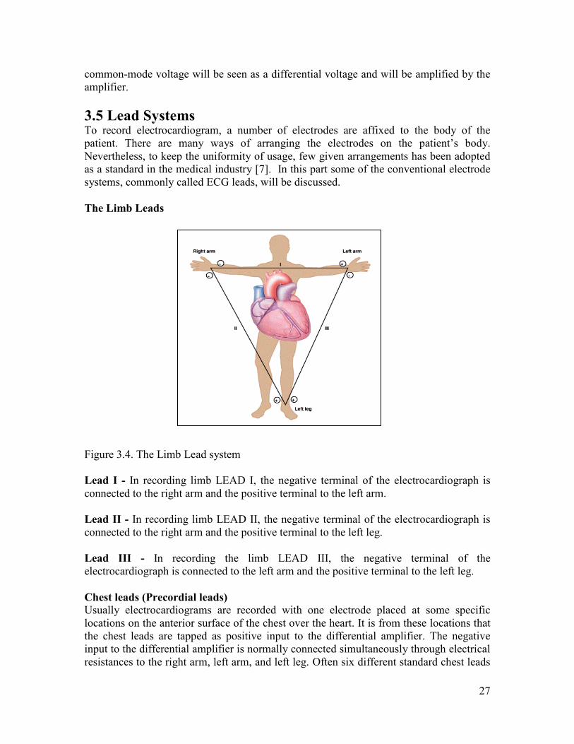
3.5 Lead Systems To record electrocardiogram, a number of electrodes are affixed to the body of the
patient. There are many ways of arranging the electrodes on the patient’s body.
Nevertheless, to keep the uniformity of usage, few given arrangements has been adopted
as a standard in the medical industry [7]. In this part some of the conventional electrode
systems, commonly called ECG leads, will be discussed.
The Limb Leads
Figure 3.4. The Limb Lead system
Lead I - In recording limb LEAD I, the negative terminal of the electrocardiograph is
connected to the right arm and the positive terminal to the left arm.
Lead II - In recording limb LEAD II, the negative terminal of the electrocardiograph is
connected to the right arm and the positive terminal to the left leg.
Lead III - In recording the limb LEAD III, the negative terminal of the
electrocardiograph is connected to the left arm and the positive terminal to the left leg.
Chest leads (Precordial leads)
Usually electrocardiograms are recorded with one electrode placed at some specific
locations on the anterior surface of the chest over the heart. It is from these locations that
the chest leads are tapped as positive input to the differential amplifier. The negative
input to the differential amplifier is normally connected simultaneously through electrical
resistances to the right arm, left arm, and left leg. Often six different standard chest leads

28
are recorded from the anterior chest wall, the chest electrode being placed respectively at
the six points of interest. The recorded potentials are conventionally referred as V1-V6.
Figure 3.5. The chest leads look at the transverse plane:
Because the heart surfaces are close to the chest wall, each chest lead records mainly the
electrical potential of the cardiac musculature immediately beneath the electrode.
Therefore, relatively minute abnormalities in the ventricles, particularly in the anterior
ventricular wall, frequently cause marked changes in the electrocardiograms recorded
from the chest leads.
Augmented unipolar limb leads
Another system of leads in wide use is the augmented unipolar limb lead. In this type of
recording two of the limbs are connected through electrical resistances to the negative
terminal of the electrocardiograph while the third limb is connected to the positive
terminal. When the positive terminal is on the right hand the lead is known as aVR; when
on the left arm, the aVL lead; and when on the left leg, the aVF lead.
Figure 3.6 Augmented unipolar limb lead system
Each augmented unipolar limb lead records the potential of the heart on the side nearest
to the respective limb. Thus, when the recording in the aVR lead is negative, this means
that the side of the heart nearest to the right arm is negative in relation to the remainder of

29
the heart; when the recording in the aVF lead is positive, this means that the apex of the
heart, which is the part of the heart nearest the foot, is positive with respect to the
remainder of the heart.
Standard 12 Lead System
This is the most widely used lead system. It is made by combining the above Systems,
Lead I, II, III,
The augmented unipolar leads, aVR, aVL and aVF
Chest leads, V1, V2, V3, V4, V5 and V6.
The number of electrodes in one ECG is around 12. In our project these 12 input
electrodes are handled by Multiplexing, filtering, digitizing and De-Multiplexing one by
one.
3.6 Amplifier Bio-potential signals are very weak signals. Even the strongest ECG signal has a
magnitude of less than 10 mV. The peak AC value of the voltage output from the
electrode is typically 1mV-4 mV. Furthermore, ECG signals have very low drive, i.e.
source has very high output impedance. Therefore, an ECG amplifier is usually required
to have the following properties:
1. Capability to sense low amplitude signals in the range of 0.1 - 10 mV,
2. Very high input impedance, usually more than 5 Mega-Ohms,
3. Very low input leakage current, 1 micro-Amps or below,
4. Flat frequency response of 0.1 - 1000 Hz,
5. A high common mode rejection ratio (CMMR > 120 db). The common-mode rejection
ratio (CMRR) of an amplifier measures the tendency of the device to reject input signals
common to both input leads.
Input leakage current is defined as the current an amplifier sends to the unit (human body
in our case) connected to its input terminals. Differential amplifiers are a useful in
reducing noise because of their good CMRR since they measure the difference in voltage
between two differential inputs. This has been the choice of design in the VACS
platform.
3.7 ADC A key component of any modern ECG signal processing is the analog-to-digital (A/D)
converter [1]. The A/D converter translates the analog electrical signals into binary form
that is suitable for subsequent processing by digital equipment. In most digital data
acquisition systems a single A/D converter is used for several data channels through the
use of a multiplexer. The rate at which the multiplexer channel switches are opened and
closed determines the sampling rates for the channels – all channels need not be sampled
at the same frequency or time. There are several techniques of sampling and conversion
of analog signal to digital. The requirements for selecting a converter for ECG signal
processing are as follows.

30
1. High resolution – ECG signals contain sensitive information as it is in the most of
life supporting design, the converter must have high resolution which is 16 bit or
more.
2. Medium Speed – the ECG signals are in very low frequency range. Thus it is not
required to use high speed converters. However, with multiple channel inputs, it is
better to use a converter with speed that can accommodate the switching speed of
all the channels.
There are several types of converters that fulfill the above requirements such as Flash and
delta-sigma. Here, for the VACS project we use the delta-sigma ADC because of its
performance and ease of implementation [1].
A delta sigma ADC consists of a delta sigma modulator which produces the bitstream and
a low pass filter. The modulator and the filter are implemented through analogue
technique in case of an analogue signal source.
The bitstream is a one-bit serial signal with a bit rate much higher than the data rate of the
ADC. Its major property is that its average level represents the average input signal level.
A digital "high" represents the highest and a "low" represents the lowest possible output
value.
The low pass filter at the output is required, because you have to gain the average signal
level out of the bitstream. You can regard the bitstream as a signal with its information in
the lower frequency band and lots of noise above it.
The average level of this bitstream represents the input signal level. A simple analogue
first order delta sigma modulator block diagram is shown in Figure 3.6.
Figure 3.7. Classical first order delta sigma ADC
Finally there is a digital decimation Comb filter that converts the high speed one bit
streams output of the Sigma Delta modulator to the desired speed 18 bit parallel digital

31
bits output. In this project all the decimation comb filter is developed as soft IP blocks for
the VACS platform [2].
3.8 Filters The noise in an ECG signal can be larger than the actual ECG signal itself, depending on
the surrounding environment [2]. Therefore, it is necessary to identify the possible noise
signals and design an appropriate filter to eliminate them. For the ECG signal processing
in the VACS platform, the following signals have been identified as a main source of
noise.
1. Power line interference
2. Electrode contact noise.
3. Motion artifacts.
4. Muscle contraction.
5. Base line drifts with respiration.
6. Instrumentation noise generated by electronic devices.
7. Electrosurgical noise.
There are different ways of eliminating these noise signals. The most effective way is to
digitally design FIR filters that are included as IP-cores on an FPGA which is already
implemented for the VACS platform [3]. The other way is to design filters as
configurable analog modules (CAMs) that can be downloaded to an FPAA. More over, as
described in the amplifier section of this chapter, a differencial amplifier can be used for
the purpose of filtering some noises like power line interference.
3.9 Display On the VACS platform a GUI is used to display the output of the vital signs in graphical,
tabular and audio format. A database is developed to record all input data and to easily
retrieve it for further analysis. The software which combines the GUI and database
module is provided as a package with the VACS platform solution. Since this software
package is the end product which interacts the user with the VACS platforms, it is made
to be as user-friendly as possible. Several modules can be developed to enhance the
presentation of the output in Graphical, tabular and audio formats. Also, an analyzer
module that supports the interpretation of the signal outputs can be developed. The
software package will have a User Manual, Technical Specification and online help
tutorial to meet user requirements.
3.10 Types of ECG In order to build the reconfigurable blocks, it is important to classify the ECG equipment
based on functionality and usage. These types of ECG will then be implemented as soft
IP cores and are used whenever they are configured properly.
3.10.1 Based on Functionality The three major types of ECG by functionality include:

32
• Resting ECG –the patient lies down. No movement is allowed during this time, as
electrical impulses generated by other muscles may interfere with those generated by
your heart. This type of ECG usually takes five to 10 minutes.
• Ambulatory ECG - an ambulatory ECG is performed using a portable device that is
worn for at least 24 hours. The patient is free to move around normally while the
monitor is attached. This variety of ECG is used for patients whose symptoms are
intermittent and may not appear during a resting ECG. People recovering from heart
attack may be monitored in this way to ensure proper heart function. The patient
usually records any symptoms in a diary, noting the time so that their own experience
can be compared with the ECG.
• Stress test ECG - this type of ECG is used to analyze a patient's heart function
during exercise. The patient is required to ride an exercise bike or walk on a treadmill
as the activity of the heart is recorded. This type of ECG takes about 15 to 30 minutes
to complete. In VACS platform, the stress ECG is configured by adding filter blocks
to remove additional signals caused by motion during the exercise.
• Fetal ECG – is used to extract bio-signals of unborn infant contained inside its
mother womb. Such type of ECG need a filtering circuit that extract the infant signal
which comes combined with that of the maternal signal. The VACS platform, because
of its inherent design of reconfigurability, can support Fetal ECG signals by re-
adjusting the inputs in proper way to fit the extraction of this signal.
3.10.2 Based on Application usage • Real time – This type of ECG is the common type that we see in hospitals which has
continuous monitoring display where the signals are presented on real time basis. The
output can also be a printer with roll paper. Resting, Stress and fetal ECG signals are
processed mostly based on real time.
• Holter – These types of ECG have a memory unit to record the ECG signals
periodically. Ambulatory ECGs are basically Holter type. Most of holter ECGs store
data of 24 hours or more. In VACS platform, a memory storage unit is designed for
the purpose of supporting this functionality.

33
Chapter 4 VACS Board components
4.1 Component selection requirements This chapter deals with the first results of the board implementation. After grasping the
basic concept behind the VACS platform, bio-signal processing and reconfigurable
hardware, this chapter deals with the selection of components contained on the board.
The component selection is made based on the following requirements set for the board.
• Accommodate software blocks efficiently
• Consider many inputs from other instruments
• Keep simplicity –no limit to reconfigurability
• Component
o Miniaturized size
o Low power consumption
o Surface mount type packaging
o Readily available in the market
o Low cost
o Usable in life supporting applications
Based on these requirements, various components were searched and reviewed based on
their functionality. It would not be practically possible to report all the rejected
components in this report. We will only present the selected ones. The following sections
dealt with each of component features, its use on the board.
4.1.1 Overview
The VACS platform board provides a reconfigurable solution for processing bio-signals
and providing output with many features. The platform is made by exploiting the
programmability of the FPGAs for digital systems and FPAAs for analog and mixed
signals. The platform consists of high density memory storage and battery – operated
power supply which makes the platform portable every where. Also available an RS232
port, which is used to connect the platform with a computer through cable or through
wireless Bluetooth connectivity. A JTAG I/O port is available for downloading FPGA
configuration files from a computer.
The VACS platform utilizes a Xilinx Spartan 3 device (FPGA - XC2S400-4TQ144) in
the 144 TQ quad package [8] and three Anadigm dynamically configurable analog
system processor devices (FPAA – AN221E04) each with 44 TQ package[9]. Also, as a
support to the FPGAs efficiency, the platform board includes a 256 byte x 16 bit SRAM
and surrounding circuits.
The Spartan 3 FPGA family has the advanced features needed to fit demanding, high
performance applications. The VACS board provides a platform to explore ways of
building a reconfigurable mixed signal processing system quickly and efficiently.

34
4.1.2 VACS System Board Description The VACS Board provides FPAAs, an FPGA and support circuits and I/O ports.
A high-level block diagram of the VACS platform board is shown in Figure 2 followed
by a brief description of each sub-section.
Figure 4.1 – Proposed VACS platform board
4.2 FPGA The VACS platform board utilizes the Xilinx Spartan 3 XC3S400 TQ144 FPGA [8]. The
Spartan 3 family of Field-Programmable Gate Arrays is specifically designed to meet the
needs of high volume, cost-sensitive consumer electronic applications. The Spartan-3
family builds on the success of the earlier Spartan-IIE family by increasing the amount of
logic resources, the capacity of internal RAM, the total number of I/Os, and the overall
level of performance as well as by improving clock management functions. Numerous
enhancements derive from state-of-the-art Spartan 3 technology. These Spartan-3
enhancements, combined with advanced process technology, deliver more functionality
and bandwidth per dollar than was previously possible, setting new standards in the
programmable logic industry. Because of their exceptionally low cost, Spartan-3 FPGAs
are ideally suited to a wide range of consumer electronics applications; including
broadband access, home networking, display/projection and digital television equipment.
TxRx
FPGA
POWER
UNIT
INPUT – OUTPUT CONNECTOR
FPAA
MEMORY CARD

35
FPGAs avoid the high initial cost, the lengthy development cycles, and the inherent
inflexibility of conventional ASICs. Also, FPGA programmability permits design
upgrades in the field with no hardware replacement necessary, an impossibility with
ASICs.
Features
• Low-cost, high-performance logic solution for high-volume, applications
• 622 Mb/s data transfer rate per I/O
• Termination by Digitally Controlled Impedance
• Signal swing ranging from 1.14V to 3.45V
• Logic resources
• Wide, fast multiplexers
• Fast look-ahead carry logic
• Dedicated 18 x 18 multipliers
• JTAG logic compatible with IEEE 1149.1/1532
• Up to 1,872 Kbits of total block RAM
• Up to 520 Kbits of total distributed RAM
• Digital Clock Manager (up to four DCMs) Frequency synthesis
• Eight global clock lines and abundant routing
• Fully supported by Xilinx ISE and WebPACK development systems
• MicroBlaze™ and PicoBlaze™ processor, and other IP cores
• Pb-free packaging options
TQ144: 144-lead Thin Quad Flat Package
The XC3S50, the XC3S200, and the XC3S400 are available in the 144-lead thin quad flat
package, TQ144. Consequently, there is only one footprint for this package as shown in
Figure 4.2 and Table 4.1. The TQ144 package only has four separate Vcco, unlike the
other packages, which have eight separate Vcco inputs. The TQ144 package has a
separate Vcco input for the top, bottom, left, and right. However, there are still eight
separate I/O banks, as shown in Table 4.1 and Figure 4.2. Banks 0 and 1 share the
VCCO_TOP input, Banks 2 and 3 share the VCCO_RIGHT input, Banks 4 and 5 share
the VCCO_BOTTOM input, and Banks 6 and 7 share the VCCO_LEFT input. All the
package pins appear in Table 3.1 and are sorted by bank number, then by pin name. Pairs
of pins that form a differential I/O pair appear together in the table. The table also shows
the pin number for each pin and the pin type, as defined earlier.

36
Fig. 4.2, TQ144 Package Footprint (top view). Note pin 1 indicator in top-left corner and
logo orientation.

37
Table 4.1: TQ144 XC3S400 Package Pinout Bank XC3S400 Pin Name TQ144 Pin Number Type
0 IO_L01N_0/VRP_0 P141 DCI
0 IO_L01P_0/VRN_0 P140 DCI
0 IO_L27N_0 P137 I/O
0 IO_L27P_0 P135 I/O
0 IO_L30N_0 P132 I/O
0 IO_L30P_0 P131 I/O
0 IO_L31N_0 P130 I/O
0 IO_L31P_0/VREF_0 P129 VREF
0 IO_L32N_0/GCLK7 P128 GCLK
0 IO_L32P_0/GCLK6 P127 GCLK
1 IO P116 I/O
1 IO_L01N_1/VRP_1 P113 DCI
1 IO_L01P_1/VRN_1 P112 DCI
1 IO_L28N_1 P119 I/O
1 IO_L28P_1 P118 I/O
1 IO_L31N_1/VREF_1 P123 VREF
1 IO_L31P_1 P122 I/O
1 IO_L32N_1/GCLK5 P125 GCLK
1 IO_L32P_1/GCLK4 P124 GCLK
2 IO_L01N_2/VRP_2 P108 DCI
2 IO_L01P_2/VRN_2 P107 DCI
2 IO_L20N_2 P105 I/O
2 IO_L20P_2 P104 I/O
2 IO_L21N_2 P103 I/O
2 IO_L21P_2 P102 I/O
2 IO_L22N_2 P100 I/O
2 IO_L22P_2 P99 I/O
2 IO_L23N_2/VREF_2 P98 VREF
2 IO_L23P_2 P97 I/O
2 IO_L24N_2 P96 I/O
2 IO_L24P_2 P95 I/O
2 IO_L40N_2 P93 I/O
2 IO_L40P_2/VREF_2 P92 VREF
3 IO P76 I/O
3 IO_L01N_3/VRP_3 P74 DCI
3 IO_L01P_3/VRN_3 P73 DCI
3 IO_L20N_3 P78 I/O
3 IO_L20P_3 P77 I/O
3 IO_L21N_3 P80 I/O
3 IO_L21P_3 P79 I/O
3 IO_L22N_3 P83 I/O
3 IO_L22P_3 P82 I/O
3 IO_L23N_3 P85 I/O
3 IO_L23P_3/VREF_3 P84 VREF
3 IO_L24N_3 P87 I/O
3 IO_L24P_3 P86 I/O
3 IO_L40N_3/VREF_3 P90 VREF
3 IO_L40P_3 P89 I/O
4 IO/VREF_4 P70 VREF
4 IO_L01N_4/VRP_4 P69 DCI
4 IO_L01P_4/VRN_4 P68 DCI
4 IO_L27N_4/DIN/D0 P65 DUAL
4 IO_L27P_4/D1 P63 DUAL
4 IO_L30N_4/D2 P60 DUAL
4 IO_L30P_4/D3 P59 DUAL
4 IO_L31N_4/INIT_B P58 DUAL
4 IO_L31P_4/DOUT/BUSY P57 DUAL
4 IO_L32N_4/GCLK1 P56 GCLK
4 IO_L32P_4/GCLK0 P55 GCLK
5 IO/VREF_5 P44 VREF
5 IO_L01N_5/RDWR_B P41 DUAL
5 IO_L01P_5/CS_B P40 DUAL
5 IO_L28N_5/D6 P47 DUAL
5 IO_L28P_5/D7 P46 DUAL
5 IO_L31N_5/D4 P51 DUAL
5 IO_L31P_5/D5 P50 DUAL
5 IO_L32N_5/GCLK3 P53 GCLK
5 IO_L32P_5/GCLK2 P52 GCLK
6 IO_L01N_6/VRP_6 P36 DCI
6 IO_L01P_6/VRN_6 P35 DCI
6 IO_L20N_6 P33 I/O
6 IO_L20P_6 P32 I/O
6 IO_L21N_6 P31 I/O

38
6 IO_L21P_6 P30 I/O
6 IO_L22N_6 P28 I/O
6 IO_L22P_6 P27 I/O
6 IO_L23N_6 P26 I/O
6 IO_L23P_6 P25 I/O
6 IO_L24N_6/VREF_6 P24 VREF
6 IO_L24P_6 P23 I/O
6 IO_L40N_6 P21 I/O
6 IO_L40P_6/VREF_6 P20 VREF
7 IO/VREF_7 P4 VREF
7 IO_L01N_7/VRP_7 P2 DCI
7 IO_L01P_7/VRN_7 P1 DCI
7 IO_L20N_7 P6 I/O
7 IO_L20P_7 P5 I/O
7 IO_L21N_7 P8 I/O
7 IO_L21P_7 P7 I/O
7 IO_L22N_7 P11 I/O
7 IO_L22P_7 P10 I/O
7 IO_L23N_7 P13 I/O
7 IO_L23P_7 P12 I/O
7 IO_L24N_7 P15 I/O
7 IO_L24P_7 P14 I/O
7 IO_L40N_7/VREF_7 P18 VREF
7 IO_L40P_7 P17 I/O
0,1 VCCO_TOP P126 VCCO
0,1 VCCO_TOP P138 VCCO
0,1 VCCO_TOP P115 VCCO
2,3 VCCO_RIGHT P106 VCCO
2,3 VCCO_RIGHT P75 VCCO
2,3 VCCO_RIGHT P91 VCCO
4,5 VCCO_BOTTOM P54 VCCO
4,5 VCCO_BOTTOM P43 VCCO
4,5 VCCO_BOTTOM P66 VCCO
6,7 VCCO_LEFT P19 VCCO
6,7 VCCO_LEFT P34 VCCO
6,7 VCCO_LEFT P3 VCCO
N/A GND P136 GND
N/A GND P139 GND
N/A GND P114 GND
N/A GND P117 GND
N/A GND P94 GND
N/A GND P101 GND
N/A GND P81 GND
N/A GND P88 GND
N/A GND P64 GND
N/A GND P67 GND
N/A GND P42 GND
N/A GND P45 GND
N/A GND P22 GND
N/A GND P29 GND
N/A GND P9 GND
N/A GND P16 GND
N/A VCCAUX P134 VCCAUX
N/A VCCAUX P120 VCCAUX
N/A VCCAUX P62 VCCAUX
N/A VCCAUX P48 VCCAUX
N/A VCCINT P133 VCCINT
N/A VCCINT P121 VCCINT
N/A VCCINT P61 VCCINT
N/A VCCINT P49 VCCINT
VCCAUX CCLK P72 CONFIG
VCCAUX DONE P71 CONFIG
VCCAUX HSWAP_EN P142 CONFIG
VCCAUX M0 P38 CONFIG
VCCAUX M1 P37 CONFIG
VCCAUX M2 P39 CONFIG
VCCAUX PROG_B P143 CONFIG
VCCAUX TCK P110 JTAG
VCCAUX TDI P144 JTAG
VCCAUX TDO P109 JTAG
VCCAUX TMS P111 JTAG

39
4.3 SRAM The VACS platform board provides 4MB of SRAM memory on the system [10]. This
memory is implemented using two ISSI IS61LV25616AL high speed asynchronous
SRAM devices with 3.3V supply. The main purpose of the SRAMs is to serve as a
temporary storage for instruction codes running on the Microblaze softprocessor core.
[11] A high-level block diagram of the SRAM interface is shown below followed by a
table describing the SRAM memory interface signals.
Figure 4.3 SRAM Input Output Interface data flow
The pins are mapped to the FPGA User I/O pins (See schematics on the next chapter). As
it is seen, on the figure the SRAM has many I/O lines to be interfaced with the FPGA. In
fact, the SRAM interface consumes almost two third of the available FPGA IO pins. In
order to configure the SRAM with the processor, a readily made SRAM IP core is
available within the Xilinx IP component library.
Table 4.2 - SRAM Memory Interface Signal Descriptions
A0-A17 Address Inputs
I/O0-I/O15 Data Inputs/Outputs
CE Chip Enable Input
OE Output Enable Input
WE Write Enable Input
LB Lower-byte Control (I/O0-I/O7)
UB Upper-byte Control (I/O8-I/O15)
NC No Connection
VDD Power
GND Ground
40
4.4 FPAA
The VACS board includes three AN221E04 FPAA devices from Anadigm, built in
CMOS technology, contains uncommitted operational amplifiers, switches, and banks of
programmable switched capacitors (S/C) and can be used to build filters for analog
signals as well as a large number of diverse analog applications. The parameters of a
given application, such as a filter, are functions of the capacitor values. The chip is
divided into 20 identical, configurable analog blocks (CABs), each composed of an
operational amplifier, five capacitor banks, and switches that can be used to interconnect
the cell components and determine their operation. There are both static and dynamic
CMOS switches. The static switches are used to determine the configuration of cell
components and inter-cell connections. These switch settings are determined once during
the programming phase of an application after which they remain unchanged. The
dynamic switches are associated with capacitors and are switched periodically during the
circuit operation changing the effective function of capacitors as typically exploited in
switched capacitor (S/C) circuits. Both static and dynamic switches are electronically
controlled and thus the functionality of each CAB, the capacitor sizes, and the
interconnections between CABs are programmable. As a result many diverse circuit
architectures can be implemented.
4.4.1 Architecture Overview
The AN221E04 device [9] consists of a 2x2 matrix of fully Configurable Analog Blocks
(CABs), surrounded by a fabric of programmable interconnect resources. Configuration
data is stored in an on-chip SRAM configuration memory. Compared with the first-
generation FPAAs, the Anadigmvortex architecture provides a significantly improved
signal-to-noise ratio as well as higher bandwidth. These devices also accommodate
nonlinear functions such as sensor response linearization and arbitrary waveform
synthesis.
The AN221E04 device features an advanced input/output structure that allows the FPAA
to be programmed with up to six outputs – or triple the number provided by the
ANx20E04 devices. The AN221E04 devices have four configurable I/O cells and two
dedicated output cells. For I/O-intensive applications, this means a single FPAA can now
be used to process multiple channels of analog signals where two or more such devices
were previously needed. In addition, the AN221E04 devices allow designers to
implement an integrated 8-bit analog-to-digital converter on the FPAA, eliminating the
potential need for an external converter. Using this new device, designers can route the
digital output of the A/D converter off-chip using one of the dedicated output cells.
The AN221E04 device is dynamically reconfigurable. This device is optimized so that it
can be updated partially or completely while operating. Dynamic Reconfiguration
available on the AN221E04 device, allows the host processor to send new configuration
data to the FPAA while the old configuration is active and running. Once the new data
load is complete, the transfer to the new analog configuration happens in a single clock
cycle.
41
Dynamic Reconfiguration in the AN221E04 device allows the user to develop innovative
analog systems that can be updated (fully or partially) in real-time. The Field
Programmable Analog Array (FPAA) contains 4 Configurable Analog Blocks (CABs) in
its core. Most of the analog signal processing occurs within these CABs and is done with
fully differential circuitry. The four CABs have access to a single Look Up Table (LUT)
which offers a new method of adjusting any programmable element within the device in
response to a signal or time base. It can be used to implement arbitrary input-to-output
transfer functions (companding, sensor linearization), generate arbitrary signals, even
perform voltage dependent filtering. A Voltage Reference Generator supplies reference
voltages to each of the CABs within the device and has external pins for the connection
of filtering capacitors.
4.4.2 Configuration Interface
The configuration interface provides a flexible solution for transferring configuration data
into the configuration memory of the AN221E04 devices [11][12]. The interface supports
automatic standalone configuration from EPROM, with both SPI and FPGA serial
EPROMS supported. The interface also supports configuration from an intelligent host
via a standard SPI or SSI interface or via a typical microprocessor bus interface. Selection
between these two configuration modes is accomplished with the MODE pin.
Configuration speeds of up to 40MHz are supported. Configuration from either a host or
EPROM as above is possible. The AN221E04 also offers the additional feature of
allowing reconfiguration of the device via the host. This feature allows the
reconfiguration of all or any part of the device repeatedly and at will using the
reconfiguration protocol. Thus the FPAA’s behavior can be adjusted onthe- fly to meet
the dynamic requirements of the application. The configuration data is stored in SRAM
based configuration memory distributed throughout the FPAA. There are two SRAM
memories on the chip: Shadow SRAM and Configuration SRAM. Configuration data is
first loaded into Shadow SRAM, and then on a single user-controllable clock edge, is
loaded into Configuration SRAM. The device’s analog functionality behaves according to
the data in Configuration SRAM. This method allows configuration data to be loaded into
the device in the background and take effect instantly when required. ‘Read out’ and
‘Read back’ of the Configuration SRAM is supported allowing users to check data
integrity if required.
The device also features a Look-up Table (LUT). The LUT exists as part of the
Configuration SRAM and can be read and written to as normal, but Shadow SRAM for
the LUT is not supported. Thus data written to the LUT becomes effective as it is written.
On power up, internal power on reset circuitry is activated which resets the device’s
Configuration SRAM and prepares the device for a first or Primary Configuration.
Primary Configuration then proceeds according to the protocol described later in this
document. Once completed, reconfigurations can be executed as described above.
Multiple device systems are supported through a daisy chain connection of configuration
interface signals, and logical addressing via the host using the reconfiguration protocol.
Devices can be reconfigured concurrently or singly. Thus groups of devices can be

42
updated together or devices can be updated separately using exactly the same connections
to the host.
Table 4.3 - AN221E04 FPAA with enhanced I/O PINOUT
1 I4PA Analog IN+
2 I4NA Analog IN-
3 O1P Analog OUT+
4 O1N Analog OUT-
5 AVSS Analog Vss
6 AVDD Analog Vdd
7 O2P Analog OUT
8 O2N Analog OUT
9 I1P Analog IN+
10 I1N Analog IN-
11 I2P Analog IN+
12 I2N Analog IN-
13 SHIELD Analog Vdd Low noise Vdd bias for capacitor array n-wells
14 AVDD2 Analog Vdd Analog power
15 VREFMC Vref Attach filter capacitor for VREF-
16 VREFPC Vref Attach filter capacitor for VREF+
17 VMRC Vref Attach filter capacitor for VMR(Voltage Main Reference)
18 BVDD Analog Vdd Analog power for bandgap Vref Generators
19 BVSS Analog Vss Analog ground for bandgap Vref Generators
20 CFGFLGb Digital IN In multi-device systems...
0, Ignore incoming data (unless currently addressed)
1, Pay attention to incoming data (watching for address)
Digital OUT 0, Device is being configured
Z, Device is not being configured (if internal pullup is selected)
21 CS2b Digital IN 0, Chip is selected
1, Chip is not selected
22 CS1b Digital IN
(during config)
0, Allow configuration to proceed
1, Hold off configuration
Digital IN
(after config)_ Passes read-back data through to LCC_B pin
23 DCLK Digital IN
24 SVSS Digital Vss Digital ground - substrate tie
25 MODE Digital IN 0, Synchronous serial interface
1, SPI EPROM Interface
26 ACLK/ SPIP Digital IN MODE = 0, analog clock < 40 MHz
Digital OUT MODE = 1, SPI EPROM or serial EPROM clock
27 OUTCLK/SPIMEM
Digital OUT During power-up, sources SPI EPROM initialization command string
Digital OUT After power-up, sources any of the four internal analog clocks
28 DVDD Digital Vdd
29 DVSS Digital Vss
30 DIN Digital IN Serial configuration data input
31 LCCb Digital OUT 1, Local configuration is needed. Once configuration is completed, it
is a registered version of
CS1b or if the device is addressed for read, it serves as serial data out
port
32 ERRb Digital IN
(monitored OUT)
0, Initiate reset
1, No action
Digital OUT
0, Error condition
Z, No error condition (external pullup required)
33 ACTIVATE Digital IN 0, Hold off completion of configuration
Rising Edge, Allow completion of configuration
O.D. Output 0, device has not yet completed primary configuration
Z, Device has completed primary configuration (if internal pullup is
selected)
34 DOUTCLK/TEST
Digital OUT A buffered version of DCLK.
Digital IN (Factory reserved test input. Float if unused)
35 PORb Digital IN 0, Chip held in reset state
Rising edge, re-initiates power on reset sequence
To initiate a POR reset cycle, the minimum pulse width required on
the PORb pin is 25ns.
36 EXECUTE Digital IN 0, No action
1, Transfer shadow RAM into configuration RAM
37 I3P Analog IN+
38 I3N Analog IN-
39 I4PD Analog IN+ Analog multiplexer input signals.
The multiplexer can accept 4 differential inputs or 8 single ended
inputs
40 I4ND Analog IN-
41 I4PC Analog IN+
42 I4NC Analog IN-
43 I4PB Analog IN+
44 I4NB Analog IN

43
4.4.3 Configurable Input / Output Cell
Each Configurable Input / Output Cell contains a collection of resources which allow for
high fidelity connections to and from the outside world with no need for additional
external components. In order to maximize signal fidelity, all signals routing and
processing within the device is fully differential. Accordingly each Input /Output Cell
accepts or sources a differential signal. A single ended signal can be used as an input to
the cell. If a single ended source is attached, an internal switch will connect the negative
side of the internal differential signal pair to Voltage Main Reference (VMR is the
reference point for all internal signal processing and is set at 2.0 V above AVSS).
Figure 4.4 – A Configurable Input / Output Cell
As with any sampled data system, it may sometimes be necessary to low pass filter the
incoming signal to prevent aliasing artefacts. The input path of the cell contains a second
order programmable anti-aliasing filter. The filter may be bypassed, or set to selected
corner frequencies.
When using the anti-aliasing filter, Anadigm recommends that the ratio of filter corner
frequency to maximum signal frequency should be at least 30. These filters are a useful,
integrated feature for low-frequency signals (signals with frequency up to 15kHz) only;
and if high-order anti-aliasing is required. Where input signal frequencies are higher,
Anadigm does recommend the use of external anti-aliasing.
A second unique input resource available within each Input / Output Cell is an amplifier
with programmable gain and optional chopper stabilizing circuitry. The chopper
stabilized amplifier greatly reduces the input offset voltage normally associated with op-
amps. This can be very useful for applications where the incoming signal is very weak
and requires a high gain amplifier at the input. The programmable gain of the amplifier
can be set to 2n where n = 4 through 7. The output of the amplifier can be routed through
the programmable anti-aliasing input filter, or directly into the interior of the array (into a
Configurable Analog Block, CAB). Single-ended input signals must use either the
amplifier or the anti-alias filter in order to get the required single to differential
conversion. The programmable gain amplifier, the chopper stabilized amplifier and the
programmable antialiasing filter are all resources available only on the input signal path.

44
When the Input / Output Cell is used as an output, the connection is a direct, unbuffered
connection of an internally sourced signal. There are no active circuit elements available
in the Input / Output cell when it is configured as an output.
4.4.4 Muxed Analog Input / Output
There is a bidirectional multiplexer available in front of one of the Input / Output Cells.
This allows the physical connection of 4 single ended or 4 differential pair input sources
or 4 differential pair output loads at once, though only one source or load at a time can be
processed by the FPAA. As with the regular Input / Output Cells, the optimal input
connection is from a differential signal source. If a single ended connection is
programmed, the negative side of the internal differential pair will be connected to
Voltage Main Reference.
Figure 4 .5– Input / Output Cell with a 4:1 Input Pair Multiplexer
4.4.5 Voltage Reference and IBIAS Generators
Analog signal processing within the device is done with respect to Voltage Main
Reference (VMR) which is nominally 2.0 V. The VMR signal is derived from a high
precision, temperature compensated bandgap reference source. In addition to VMR,
VREF+ (1.5 V above VMR), and VREF- (1.5 V below VMR) signals are also generated
for the device as shown in the figure below.
Figure 4.6 – Voltage Reference and Bias Current Generation

45
There are two versions of VMR routed to the CABs. VMR is the node onto which all
switched capacitor charges get dumped and can be relatively noisy. VMRclean is also
routed to the opamps within the CABs. This quiet version of VMR is used by the opamps
as the ground reference in order to improve their settling times. It is required that external
filtering caps be provided on VREFPC, VMRC, and VREFMC to ensure optimal chip
performance. The recommended value for each is 75 to 100 nF. Higher values will have
an adverse affect on settling time, lower values will reduce node stability. For highest
possible performance, capacitors with a low series inductance, such as Tantalum, should
be used. In most cases however, standard ceramic capacitors will be sufficient. VREF+
and VREF- are most often used by CAMs which utilize the comparator. In particular,
these signals bound the recommended input range of SAR conversion CAMs.
4.4.6 System Clocks
Figure 4.7 provides a good high level overview of the various clock features and clock
domains of the device. Not all of the features shown in this diagram are available in
configuration MODE 1. The clock going to the configuration logic is always sourced at
the DCLK pin. The DCLK pin may have an external clock applied to it up to 40 MHz.
The DCLK pin may otherwise be connected to a series resonant crystal, in which case
special circuitry takes over to form a crystal controlled oscillator. No programming is
required. Connection of a crystal will result in a spontaneously oscillating DCLK.
Figure 4.7 – Clock Features and Clock Domains
The analog clock domains are all sourced from a single master clock, either ACLK or
DCLK. The device configuration determines which clock input will be used as the master
clock. This master clock is divided into 5 unique domains. The first domain sources only
the chopper stabilized amplifiers within the Input / Output Cells. The other four domains
are sourced by a user programmable prescaler feeding four user programmable dividers.
Each of these domains can be used to drive either the SAR logic of a CAB, or the
switched capacitor circuitry within the CAB itself. The clock generation circuitry ensures
that all clocks derived from a single master clock signal will synchronize their rising

46
edges (so that there is never any skew between 2 clocks of the same frequency).
Importantly, this holds true for all clocks in a multi-device system as well.
4.4.7 Booting from a processor
In the VACS platform, the FPAAs are initiated and controlled by the micro-blaze
processor on the Spartan 3 FPGA. This processor performs the calculation of new circuit
values, assemble these new values into a configuration data block and transfer that data
block into the FPAA. The FPAA device’s flexible configuration interface is designed to
accept input from either serial memories or any of three major processor interface types:
First there is a multiplexing functionality on each chip. But this functionality only
receives not more than four inputs for each chip. In order to accommodate an ECG signal
processing with 12 lead systems we need to have a total of three chips on board.
Figure 4.8 – Configuring Multiple Devices from a Host Processor
The other reason is the resource limitation. As it is explained earlier, the FPAA chip
consists of Four CABs and for each analog design downloaded from the CAD tool, these
caps are used as resources to build the design. If the resourses available within one FPAA
are consumed totally, then we need to add more FPAA devices in order to accommodate
other designs with resources.
4.5 Clock generation The system board provides two on-board oscillators running at 50Mhz (CLK) and 39.768
KHz (CLK) [13][14]. The 50 MHz oscillator is used as Master clock feeding to the
FPGA and FPAA devices. The FPAA normally gets 25-40 MHz clock input. So, we can
use the DCM of the FPGA to generate this clock internally and feed the FPAAs through
one of the DCM pins. The flash PROM also gets its clock input from the FPGA. The
39.768 KHz. Oscillator is a separate clock for the Real Time Clock which has a separate
power supply (battery). This makes it work even when the system is down in order to
keep RTC functioning. There is a backup battery which supplies power to the 39.768
KHz Oscillator together with the RTC clock. The following table provides a brief
description of these clock signals.

47
Figure 4.9 – Oscillator Interface
Table 4.4 Oscillator PAD Connection
4.6 Buzzer This part of the system is mainly applicable when the device is used for monitoring
patients. Whenever the presented acceptable conditions are violated, alarm will go off.
This shows that the physician should not attend the patient being monitored continuously
once he has set the tolerable limits. In short the purpose of the alarm control is to monitor
the patient for preset conditions and warn acoustically.
In general, the alarm is a surface mount type from Sonitron Multi-Application (SMA -
17) series of buzzers and produce highly reliable audible signals, giving an extremely
clear penetrating or soft sound output. It has only two interfacing pins; one is grounded
and the other is directly connected to the FPGA. On the FPGA side, there is a small
hardware interface (VHDL defined core) which generates frequency in range between 2
KHz and 3 KHz which enables the buzzer to generate audible sound.
These are some conditions that make the alarm to trigger. For example for ECG signals if
the R-R length is below or above a given duration, if the R waveform amplitude is lower
than a given reference or for Pulse Oximeter if the Oxygen level is below the limited
percentage etc…. can trigger the indicators. As any medical equipment, the VACS
platform follows the standards that are applicable for these audio signals. The buzzer
sinks current between 0.4mA and 9mA for voltage supply of 1.5 – 24 Vdc. The Spartan 3
1. Enable/Disable No connection or
High = Enable.
Low = Disable
2. Gnd Ground
3. Output Output
4. +Vs 3.3v supply
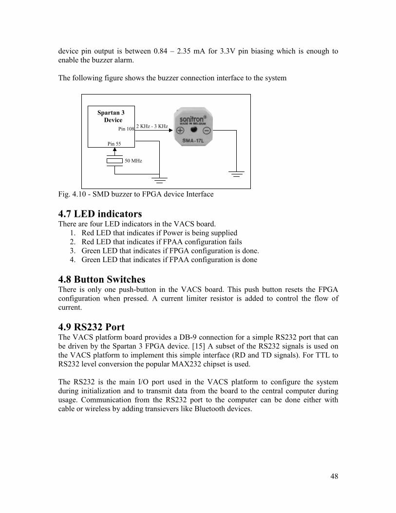
48
device pin output is between 0.84 – 2.35 mA for 3.3V pin biasing which is enough to
enable the buzzer alarm.
The following figure shows the buzzer connection interface to the system
Fig. 4.10 - SMD buzzer to FPGA device Interface
4.7 LED indicators
There are four LED indicators in the VACS board.
1. Red LED that indicates if Power is being supplied
2. Red LED that indicates if FPAA configuration fails
3. Green LED that indicates if FPGA configuration is done.
4. Green LED that indicates if FPAA configuration is done
4.8 Button Switches There is only one push-button in the VACS board. This push button resets the FPGA
configuration when pressed. A current limiter resistor is added to control the flow of
current.
4.9 RS232 Port The VACS platform board provides a DB-9 connection for a simple RS232 port that can
be driven by the Spartan 3 FPGA device. [15] A subset of the RS232 signals is used on
the VACS platform to implement this simple interface (RD and TD signals). For TTL to
RS232 level conversion the popular MAX232 chipset is used.
The RS232 is the main I/O port used in the VACS platform to configure the system
during initialization and to transmit data from the board to the central computer during
usage. Communication from the RS232 port to the computer can be done either with
cable or wireless by adding transievers like Bluetooth devices.
50 MHz
Spartan 3
Device
2 KHz - 3 KHz Pin 108
Pin 55

49
Figure 4.11 – RS232 Interface
4.10 JTAG Port The JTAG port is mainly used to send configuration bitstreams from the computer to the
FPGA or Flash PROM. It consists of 4 signals: TDI, TDO, TMS and TCK. A fifth pin,
TRST, is optional. A single JTAG port can connect to one or several devices (other
FPGAs or other JTAG-aware parts). The TMS and TCK are tied to all the devices
directly, but the TDI and TDO form a chain: TDO from one device goes to TDI of the
next one in the chain. The master controlling the chain (a computer for example) closes
the chain.
TCK is the clock, TMS is used to send commands to the devices, and TDI/TDO are used
to send and receive data. Each device in the chain has an ID, so the computer controling
the JTAG chain can figure out which devices are present. Standard JTAG commands can
be used to take control of each pin of the devices in the chain. FPGAs add the ability to
be configured through the chain, and PROMs the ability to be programmed/erased
through the chain.The JTAG port ends up being complex to control. Hopefully FPGA
software contain the code required to configure FPGAs through JTAG.
4.11 Flash PROM In VACS platform board uses XCF04S Flash PROM from Xilinx [16]. The PROM is
used to store configuration files. The interface is a simple one-bit data/clock interface. It
is synchronous and provides one bit at a time to the FPGA device.
Xilinx produces the Platform Flash series of in-system programmable configuration
PROMs provide an easy-to-use, cost-effective, and reprogrammable method for storing
large Xilinx FPGA configuration bitstreams. The Platform Flash PROM series includes
both the 3.3V XCFxxS PROM and the 1.8V XCFxxP PROM. The XCFxxS version
includes 4-Mbit, 2-Mbit, and 1-Mbit PROMs that support Master Serial and Slave Serial
FPGA configuration modes. The XCFxxP version includes 32-Mbit, 16-Mbit, and 8-Mbit
FPGA

50
PROMs that support Master Serial, Slave Serial, Master SelectMAP, and Slave
SelectMAP FPGA configuration modes.
Figure 4.12 PROM Input Output data flow
When the FPGA is in Slave Serial mode, the PROM and the FPGA are both clocked by
an external clock source, or optionally, for the XCFxxP PROM only, the PROM can be
used to drive the FPGA’s configuration clock. The XCFxxP version of the Platform Flash
PROM also supports Master SelectMAP and Slave SelectMAP (or Slave Parallel) FPGA
configuration modes. When the FPGA is in Master SelectMAP mode, the FPGA
generates a configuration clock that drives the PROM.
The VACS board is implemented based on Master serial mode; i.e., when the FPGA is in
Master Serial mode, it generates a configuration clock that drives the PROM. With CF
High, a short access time after CE and OE are enabled, data is available on the PROM
DATA (D0) pin that is connected to the FPGA DIN pin. New data is available a short
access time after each rising clock edge. The FPGA generates the appropriate number of
clock pulses to complete the configuration.

51
Figure 4.13 Serial PROM-FPGA interface
Table 4.5 XCF04S Pin Names and Descriptions
Pin Name Bound
ary
Scan
Functi
on
Pin Description 20-pin
TSSOP
(VO20/V
OG20)
TDI Data
In
JTAG Serial Data Input. This pin is the serial input to
all JTAG instruction and data registers. TDI has an
internal 50K resistive pull-up to VCCJ to provide a
logic "1" to the device if the pin is not driven.
4
TDO Data
Out
JTAG Serial Data Output. This pin is the serial
output for all JTAG instruction and data registers.
TDO has an internal 50Kresistive pull-up to VCCJ
to provide a logic "1" to the system if the pin is not
driven.
17
VCCINT
+3.3V Supply. Positive 3.3V supply voltage for
internal logic.
18
VCCO
+3.3V, 2.5V, or 1.8V I/O Supply. Positive 3.3V,
2.5V, or 1.8V supply voltage connected to the output
voltage drivers and input buffers.
19
VCCJ
+3.3V or 2.5V JTAG I/O Supply. Positive 3.3V,
2.5V, or 1.8V
20

52
supply voltage connected to the TDO output voltage
driver
and TCK, TMS, and TDI input buffers.
GND Ground 11
DNC
Do not connect. (These pins must be left
unconnected.)
2, 9, 12,
14, 15, 16
4.12 MMC
The VACS platform board utilizes a removable MMC memory card with its connector.
The card is basically used for two purposes.
During the configuration mode of the platform, it is used to store all the configuration
files for the analog memory unit in binary format. When the system is initialized, first the
Spartan 3 FPGA device is automatically configured from a Flash PROM, which all bit
files including that of Microblaze soft processor is loaded to the device. When this is
done, the Microblaze initializes FPAA configuration files loading from the MMC card to
the FPAA devices.
During the user mode the memory is used to store incoming data from the input side of
the system. When the system is not transmitting in real-time basis, it has to keep its data
in the memory, which is later on retrieved and dumped to the computer. Medical
equipments, such as Holter ECG, make use of such technique to record all incoming data
on the memory unit.
The unit can record data depending on the pre-programmed time by the user. Such feature
is set on the computer-software (GUI) side of the VACS platform. Normally we can find
units with storing capability of 24 hrs data for such application. The availability of this
much amount of data helps to analyze the patient’s status. Also, if some compression
techniques are implemented, we can record data of longer periods. Low cost high density
Flash cards like MMC are now available in the market. Most of these cards use popular
interfacing protocol such as SPI for hand shaking. This means an SPI interfacing module
in form of software component (with C++) or hardware IP component (with VHDL) is
included within the VACS system.
Serial Peripheral Interface (SPI) is a common serial communications protocol used for
interfacing between digital blocks and other serial digital input/output devices like
Bluetooth module. SPI can be run in Master or Slave mode and uses the following
interfaces CLK, DIN, DOUT, and GND.
When in Master mode, data is sent serially from the output pin. When this is occurring,
the SPI_CLK also toggles to provide the Slave SPI device to synchronize the data. The
Slave SPI device cannot send data to the Master SPI. In addition, the Master can’t receive
data unless the Master provides SPI_CLK. That is, the Master device determines the bit
rate and when it can receive data in order for the slave device to send synchronized data.

53
Fig. 4.14, SPI-MMC FPGA
Table 4.6 MMC interface pin description
Table 4.7 SPI interface pin description
Pin # Name Type
1 CS I Chip Select (Active Low)
2 DI I/PP Data In
3 VSS S Supply Voltage Ground
4 VDD S Supply voltage
5 CLK I Clock
6 VSS S Supply Voltage Ground
7 DO O/PP Data out
Pin # Name Type
1 RSV NC Reserved for future use
2 CMD In/out: OD/PP Data In
3 VSS S Supply Voltage Ground
4 VDD S Supply voltage
5 CLK I Clock
6 VSS S Supply Voltage Ground
7 DAT In/Out: PP Data
50 MHz Oscillator
Spartan 3
Device
Vcco
Data out
Clock Data in
Chip select

54
the Slave Serial configuration mode, a bit of configuration data is loaded into the FPGA
during each CCLK clock cycle. In this mode, an external source places the most
significant bit of each byte on the DIN pin first and then drives the CCLK clock to store
data into the FPGA. The following figure shows the Slave Serial configuration mode
interface to the Spartan 3FPGA.
4.13 RTC VACS board utitilez DS1302 real time clock - RTC [17]. The real-time clock works as a
clock calendar register and has a special feature, programmable time alarms. These
programmable time alarms can be continuous for specific intervals, for instance, every
minute, every hour or for a determined time. This saves space in the FPGA, because the
FPGA does not work on measuring time. The integrated circuit allows the user to set
sampling time intervals of 1 s or longer. The FPGA sends sampling and current time to
the monitoring system or stores into the memory unit. An alarm interruption programmed
on the real-time clock marks the beginning of the measurements. In addition, a pin-out of
the real-time clock provides a 1-Hz signal used by the monitoring system to measure
frequency. The RTC needs an oscillator working at 39.768 KHz as it is described in
section 4.5 of this chapter.
4.14 Power Supply
The power to the VACS platform board is designed to operate from two power sources.
The first one is that it can operate from dc supply extracted form the power line or any
other source that could provide the system sufficient power. The other alternative source
is a rechargeable battery in the absence of the electricity. When the unit is operating from
a main power supply, the battery will charge itself. To avoid bulkiness an external
AC/DC adapter will be used for the main power supply rather than incorporating the
transformer-rectifier set with our system.
The peak regulated voltage input to the system is + 5 V. The FPAA devices consume this
5V directly as their biasing voltage. But the Spartan 3 device can be operated with lower
and multi-level voltage supply. These are, for the configuration subsystem and I/O pins
2.5V supply, for the user I/O pins 3.3V supply and for the internal FPGA primitives
operations 1.2V supply is required.
FPGAs usually require 2 voltages to operate: a "core voltage" and an "IO voltage". Each
voltage is provided through separate power pins. The internal core voltage ("VCC"), is
used to power the logic gates and flipflops inside the FPGA. The voltage can range from
5V for older FPGA generations, to 3.3V, 2.5V, 1.8V, 1.5V and even lower for the latest
devices! The core voltage is fixed. The IO voltage "VCCO" is used to power the I/O
blocks (= pins) of the FPGA. That voltage should match what the other devices
connected to the FPGA which is 3.3V. The IO voltage is named "VCCO".
Actually, FPGA devices themselves don't prevent VCC and VCCO to be the same (i.e.
the VCC and VCCO pins could be connected together). But since FPGAs tend to use
low-voltage cores, the two voltages are usually different.
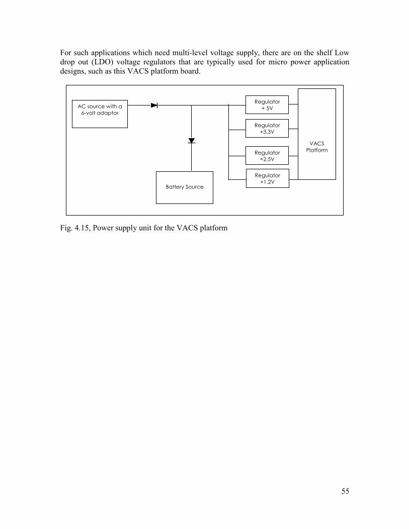
55
For such applications which need multi-level voltage supply, there are on the shelf Low
drop out (LDO) voltage regulators that are typically used for micro power application
designs, such as this VACS platform board.
Fig. 4.15, Power supply unit for the VACS platform
Battery Source
AC source with a
6-volt adaptor
Regulator
+ 5V
Regulator
+3.3V
Regulator
+2.5V
Regulator
+1.2V
VACS
Platform

56
57
Chapter 5 VACS Board Implementation
5.1 VACS Board prototyping
For the VACS board implementation, after the component selection is made, the next step
is to design a schematic diagram and finally produce PCB. This chapter describes the
prototyping of the board. Also, as the last chapter of the report, we would summarize and
make conclusion.
The works and results of this thesis can be summarized as follows.
1. Component selection - We believe the challenging part of the board
implementation was the component selection part which is described in the
previous chapter. The list of materials needed including the selected components
for the board is included in this chapter as bill of materials - BOM.
2. Schematic diagram: This part was challenging and time consuming. This is
because each IO pin specification of the selected components is studied one by
one and in detail in order to decide what type of circuit should be implemented to
make off-chip interfacing. During the process of schematic diagramming, some
tests were done on breadboard level by connecting the output of Anadigm FPAA
board to the input of Spartan 3 starter kit and Anadigm FPAA board. The digital
modules such as filters and decimators loaded on the FPGA and analog modules
on FPAA are made to function at the same time. The final schematic diagrams are
included in this chapter.
3. PCB layout: The remaining works for this task are mainly layout works on
Cadence software tool. The initial PCB layout to estimate the board area is
included in this chapter. Some power estimation calculation is also done based on
the power consumption data found from the analog and digital modules running
separately. Once the requested materials are at hand, the layout can be prototyped
quickly.
When implementing, the following points where considered as important factors.
• The board has to accommodate software blocks efficiently. This means, to keep
the reconfigurability of the system, enough space should be allocated within the
hardware. For example, at first the high-pass filter was planned to be built as a
digital block on the FPGA. However, due to its need to large amount of resources,
it was decided to place it in the analog (FPAA) [1] [3].
• The board has to consider many inputs from different instruments. For example, if
the ECG is not in use, other inputs from other instruments such as pulse-oximeter
should be able to share the same input without any additional component.
• The board has to keep its simplicity. This helps to limit the number of components
that are added on the board. A great care has been taken not to include inputs such
as buttons on the board. Also, outputs such as LED indicators are only few. This
is mainly because of the emphasis given to keep the re configurability of the
system. In true reconfigurable system, inputs and outputs are software oriented.

58
The hardware is used only as a medium to contain the software. Physical buttons
and LEDs are eliminated.
Approaches: there are two approaches raised on the implementation process. Since there
are blocks such as filters that can be implemented on the FPAA as analog block or on the
FPGA as a digital IP core, we made the schematic diagram to be flexible and
reconfigurable enough to accommodate all approaches possible.
Decoupling capacitors: In order to remove AC component from the power supply Vdd
pins, we have included several decoupling capacitors on implementation. As a design rule
of thumb, it is advisable to add as many capacitors as possible, keep capacitors close to
the Voltage supply pins and follow datasheets and application notes of each device.
Pull up/Pull down resistors: These resistors validate floating pins with unknown state. We
have followed datasheet values of the devices set as current limiter resistors.
As shown in the previous chapter, while selecting the components, we have tried to verify
the interfacing circuits for each component are up to the standard by referring the
datasheet indicating the electrical specification of each component. Also, we have studied
different application notes showing how to use each component [8] [9] [10] [12] [13] [14]
[15] [16] [17]. Finally, on the schematic diagram, we have made comparison of some
parts of the circuits which are already implemented on the Spartan 3 starter kit and on the
FPAA development board; we used to test the system [11][22].
The PCB is considered to be functionally ready when
1. VACS PCB designed on Cadence Orcad layout plus is prototyped and all the
components are soldered.
2. Software testing is done to check the functionality of the hardware. The software
test shall address each and individual component and finally the whole system from input
to the output.
3. Finally the whole VACS platform integration and Hardware/Software co
simulation and testing is done.
5.2 Cadence tool
For the Schematic design of the Cadence OrCAD tool has been chosen partially because
it was the only available tool at hand in the KTH- laboratory and partially because it is a
tool capable of handling designs such as this VACS platform.
Cadence OrCAD has cross functionality of combining Schematic and PCB design in the
same platform [23]. The VACS platform is implemented in the Schematic entry part of
Cadence called OrCAD Capture. OrCAD capture is a complete solution for design
creation, management, and reuse. Its ease-of-use allows designers to focus their creativity

59
on design development rather than tool operation. The hierarchical Schematic Page
Editor combines a Windows user interface with functionality and features specifically for
design entry tasks and for publishing design data.
There are many web resources that give basic tutorials of Cadence OrCAD that were
helpful during the implementation of the VACS platform. But in general the Cadence
environment allows access to libraries containing icons of basic circuit components and
the ability to place and connect theses devices into the form of a circuit within a
schematic editor. In addition, the default values of the properties of the various elements
can be edited and altered to fit the requirements of the actual system under design. Files
can then be extracted from the graphical circuits into forms compatible with Spectra or
Spice circuit simulators [23].
The simulators can then be called to compute and plot the various waveform results.
Once the designer is satisfied with the operation of the circuit, the schematic can then be
put into the form of a symbol and used as a component in higher-level circuits. Finally, at
this higher level, the overall design can be simulated and the results plotted. If it is found
that the simulated results do not meet the technical requirements, it is possible to go back
through various layers of the design and alter properties at each stage before continuing
additional simulations. This iterative interaction is a powerful tool that helps the circuit
designer to quickly test design concepts and debug circuits.
The footprint of each component selected for the VACS board was designed and placed
in the library. Then on the Cadence editor all the connections and bill generation is made
and accordingly the following designs are produced. The first two figures (4.1 & 4.2) are
schematic designes and figure 4.3 is the PCB placement design in 16cm x 10cm board.

60
Fig
ure
5.1
Sch
emat
ic d
esig
n o
f F
PA
A –
Pow
er S
ecti
on

61
Fig
ure
5.2
Sch
emat
ic d
esig
n o
f F
PG
A –
SR
AM
– R
S232 -
MM
C S
ecti
on

62
Fig
ure
5.3
Com
ponen
ts p
lace
men
t on 1
6cm
X 1
0cm
boar
d
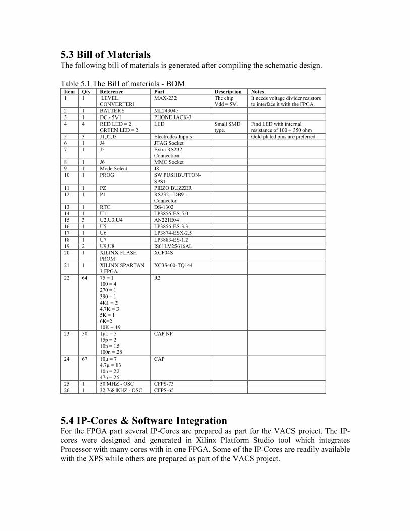
5.3 Bill of Materials The following bill of materials is generated after compiling the schematic design.
Table 5.1 The Bill of materials - BOM Item Qty Reference Part Description Notes
1 1 LEVEL
CONVERTER1
MAX-232 The chip
Vdd = 5V.
It needs voltage divider resistors
to interface it with the FPGA.
2 1 BATTERY ML243045
3 1 DC - 5V1 PHONE JACK-3
4 4 RED LED = 2
GREEN LED = 2
LED Small SMD
type.
Find LED with internal
resistance of 100 – 350 ohm
5 3 J1,J2,J3 Electrodes Inputs Gold plated pins are preferred
6 1 J4 JTAG Socket
7 1 J5 Extra RS232 Connection
8 1 J6 MMC Socket
9 1 Mode Select J8
10 1 PROG SW PUSHBUTTON-SPST
11 1 PZ PIEZO BUZZER
12 1 P1 RS232 - DB9 -
Connector
13 1 RTC DS-1302
14 1 U1 LP3856-ES-5.0
15 3 U2,U3,U4 AN221E04
16 1 U5 LP3856-ES-3.3
17 1 U6 LP3874-ESX-2.5
18 1 U7 LP3883-ES-1.2
19 2 U9,U8 IS61LV25616AL
20 1 XILINX FLASH
PROM
XCF04S
21 1 XILINX SPARTAN 3 FPGA
XC3S400-TQ144
22 64 75 = 1
100 = 4
270 = 1 390 = 1
4K1 = 2
4.7K = 3 5K = 1
6K=2
10K = 49
R2
23 50 1µ1 = 5
15p = 2
10n = 15 100n = 28
CAP NP
24 67 10µ = 7
4.7µ = 13
10n = 22 47n = 25
CAP
25 1 50 MHZ - OSC CFPS-73
26 1 32.768 KHZ - OSC CFPS-65
5.4 IP-Cores & Software Integration For the FPGA part several IP-Cores are prepared as part for the VACS project. The IP-
cores were designed and generated in Xilinx Platform Studio tool which integrates
Processor with many cores with in one FPGA. Some of the IP-Cores are readily available
with the XPS while others are prepared as part of the VACS project.

64
1. Micro-blaze – [18][19] The MicroBlaze embedded processor soft core is a ready made
IP-core delivered with the Spartan 3 starter kit.
2. Filters - There are two filter cores designed for the VACS platform; Low-Pass Filter
(LPF) to reject high frequency noise signals and Notch Filter to reject powerline noise
signals. According to the specification set for the filters, these cores were designed for the
VACS platform.
3. Decimator – The decimation core provides two functionalities namely filtering
quantization noise and down-sampling of delta-sigma modulated outputs.
5.5 Power Consumption estimation
Power is one of the factors that are primarily considered during board design
implementation. Most of the components selected were chosen primarily because of their
low power consumption during operation. The IC chips like LDO regulators have most of
the time fixed and very low power dissipation and so the total power consumption of such
chips is easily found by combined sum of each component’s power dissipation. However
their dissipation is insignificant when compared with the overall total consumption. For
the reconfigurable chips like FPAA and FPGA the power consumption varies according
to what system is running inside each of them. For example, the FPGA chip, when it is
loaded with IP-core made by our VACS team consumes more power than the IP-core
generated by CoreGenerator. In such cases, the best way to estimate the total power is to
for component selection and the simplest power supplier is the battery. So for every
design step made, it is critical to analyze each step in terms of Power to save energy.
From the reconfigurable blocks we have the following consumption
• Analog reconfigurable blocks [1]
∆∑ = 58 ± 17mW
Differential amplifier = 74 ± 22mW
HPF = 63 ± 19mW
Total (max) = 253mW
• Digital reconfigurable blocks [2] [3]
Decimation block = 61.5mW
Notch = 37.5mW
LPF = 62mW
Total = 161mW
The total board power consumption
Total => 253mW + 161mW = 414mW (0.5W)
Here the approximation to 0.5W is made by considering the power dissipation on the
board wiring and other chips. The other chips like PROM are active only for a very short
period of time during System boot up. For the rest of the operation, it is passive with
almost no dissipation.
The total consumption can be calculated in terms of battery life. Here lets assume a
lithium battery with 9V and 1200 mah (milli-ampere hours).
� 1200 mah / (0.5W/9V) = 21.6 hours

65
This means the lithium battery can continuously run the VACS board for more 20 hours.
This is by any standard equivalent to the existing handheld medical devices available in
the market; i.e., for example, the VACS board is capable of working as a Holter type
ECG effectively.
Here we can also use some power saving techniques to prolong the battery life.
• Optimize component power consumption using low power modes.
Components such as the Spartan 3 FPGA are designed for low power applications and
usually offer low power modes that are easy to use and put the device in sleep mode or
lower standby power mode. The characteristics of each mode are device-dependent, as
are the method and timing required to enter or exit the power mode. Some powers saving
modes require board considerations for implementation, so the design should be able to
accommodate them.
• Optimize component power consumption with design techniques.
On the digital part the filters, the decimators and other IP cores use clocks, RAM and
I/Os. When operational the sum of power consumed by all the cores can be high. Since
the system is reconfigurable, we can switch off some of the cores in they are not in use.
This requires a design where the processor has full control over the different IP cores.
Also, when creating clock regions using local or regional clock resources, use "enabled"
logic to disable clock transitions in the system. User static RAM can sink excessive
power; therefore, look for techniques to minimize RAM usage. I/Os can also sink a great
deal of board power. Try to use LVTTL/LVCMOS standards and lower I/O voltages.
Check whether the soft-cores can be integrated or functionality minimized to save even
more on power. Chip-to-chip communication can significantly increase system power
consumption due to large capacitive loads on PCB traces. So, use some high speed
techniques while making the layout of the PCB.
5.6 Conclusion The VACS board implementation refers to the hardware part of the platform which
contains the software blocks. For reconfigurable systems, the hardware is designed in
such a way that it contains the most optimized reconfigurable blocks with less power,
high speed and less memory size. As with every system implementation, we had to
overcome some challenges that we faced during the VACS board implementation.
• The VACS platform is hand held type that effectively work even on field where there is
no Electricity. In such cases the most widely used and the simplest power source is the
battery. So for every implementation step, it was critical to analyze the step in terms of
power to save energy.
• Mixed signal design, multi-disciplinary system. The VACS board consists of analog,
digital, software modules combined in one system. This means designing such modules
requires a good team with knowledge of all related fields which can handle such complex
design.
• Flexible and reconfigurable system. The VACS platform contains circuits as
reconfigurable blocks. Also, when any given block is loaded, the system is supposed to

66
work effectively in optimized way. Hence, in our design, we considered a general
purpose VACS platform that can accommodate and run the blocks.
• Multi – IP blocks integration. The reconfigurable blocks are, at first, designed
separately as independent modules. When it comes into integrating each block to the
system, there are certain interfacing rules that we have to follow. Otherwise, the blocks
will not work as expected.
• Intensive analysis, design and testing. The VACS platform is a Medical system which
concerns life safety. As like in all VACS on FPGA/FPAA medical systems, the VACS
platform has followed certain design standards and testing steps.
The VACS board implementation provided in this document is set by considering
advantage of reconfigurable and flexibility of the FPGA/FPAA. To keep this advantage,
most of the responsibility of controlling the VACS system is assumed to be done on the
software side.
The VACS board can be considered as many instruments in one platform. Even
instruments other than bio-signal processing devices can be efficiently designed in this
board. In the future, with the integration of analog and digital reconfigurable hardware, a
single chip such as FPMA, Field programmable Mixed Array, can replace the
components in this board. In this way further size and power reduction can be achieved.
Once board is prototyped, with this platform it becomes easy to design systems in
software terms.

67
References
1. Talasila Indira Priyadarshini, “Implementation of Re-configurable Analog
Circuitry on Field Programmable Analog Array for Vital Signs Acquisition and
Communication System (VACS) platform”, Master Thesis, KTH/ICT/ECS-2007-
32, November 2006.
2. Naresh Vendra & Karthik Chaluvadi, “Decimation Filter for VACS Platform”,
Master Thesis Submitted, IMIT/ECS-2006-132, November 2006.
3. Anand Pendem & Rajesh Garikipati, “Digital Filters for Bio-Signal Processing in
the VACS Platform VACS board Implementation”, Master thesis,
KTH/IMIT/ECS-2006-126, 2006 November.
4. Aston, Richard. Principles of Biomedical Instrumentation and Measurements
5. Donald Christiansen, Electronics Engineers’ Handbook, 1975 The McGraw Hill
companies, Inc.
6. Guyton, Text Book Of Medical Physiology, 1981 by W.B. Saunders Company
7. Leslie Cromwell, Fred J. Weibell, and Erich A. Pfeiffer, Biomedical
Instrumentation and Measurements”, 1980 Prentice-Hall, Inc., Englewood Cliff,
New Jersey 07632
8. Spartan-3 FPGA Family: Complete Data Sheet, Xilinx publications, DS099 April
26, 2006.
9. Dynamically Reconfigurable With Enhanced I/O, AN221E04 Datasheet,
Anadigm Publications, DS030100-U006a, Copyright © 2003 Anadigm, Inc.
10. IS61LV256, 32K x 8 LOW VOLTAGE CMOS STATIC RAM datasheet, ISSI,
Integrated Silicon Solution, Inc. — 1-800-379-4774 Rev. I, October 1999.
11. AN221K04. Anadigmvortex Development Board User Manual, Anadigm
Publications, UM030900-U010e, Copyright © 2003 Anadigm, Inc.
12. AN121E04 AN221E04 Field Programmable Analog Arrays - User Manual,
Anadigm Publications, UM021200-U007g, Copyright © 2003 Anadigm, Inc.
13. CFPS-65 datasheet, CMAC micro technology, Issue 3; 19 October 2004
14. CFPS-72, -73 datasheet, CMAC micro technology, ISSUE 2; 1 September 2001.
15. MAX232 datasheet, Multi-channel RS-232 Drivers/Receivers, Maxim Dallas
Semiconductor 19-4323; Rev 11; 2/03, © 2003 Maxim Integrated Products.
16. Platform Flash In-System Programmable Configuration PROMS, Xilinx
publications, DS123 (v2.9) May 09, 2006.
17. DS1302 Trickle-Charge Timekeeping Chip datasheet, Maxim Dallas
Semiconductor, REV: 110805, © 2005 Maxim Integrated Products.
18. MicroBlaze Processor Reference Guide, Xilinx Publications, UG081 (v6.0) June
1, 2006.
19. MicroBlaze RISC 32-Bit Soft Processor, Xilinx Product Brief publication, August
21, 2002.
20. Microsoft® Encarta® Encyclopaedia 2001, © 1993-2000 Microsoft Corporation.
21. Flash Memory, www.wikipedia.com, December 2006
22. Sparta-3 starter kit board user guide, Xilinx publications, UG130 (v1.1) May 13,
2005
23. An OrCAD Tutorial for ELEC 424 High-Speed Systems Design, Revision 1.0 -
Spring 2002, www.iweil.com/orcad/orcad_tutor.doc, December 2006