
VHDL modeling and design of an asynchronous version of the ...
216
Rochester Institute of Technology RIT Scholar Works eses esis/Dissertation Collections 2-1-1994 VHDL modeling and design of an asynchronous version of the MIPS R30000 microprocessor Paul Fanelli Follow this and additional works at: hp://scholarworks.rit.edu/theses is esis is brought to you for free and open access by the esis/Dissertation Collections at RIT Scholar Works. It has been accepted for inclusion in eses by an authorized administrator of RIT Scholar Works. For more information, please contact [email protected]. Recommended Citation Fanelli, Paul, "VHDL modeling and design of an asynchronous version of the MIPS R30000 microprocessor" (1994). esis. Rochester Institute of Technology. Accessed from
-
Upload
khangminh22 -
Category
Documents
-
view
0 -
download
0
Transcript of VHDL modeling and design of an asynchronous version of the ...
Rochester Institute of TechnologyRIT Scholar Works
Theses Thesis/Dissertation Collections
2-1-1994
VHDL modeling and design of an asynchronousversion of the MIPS R30000 microprocessorPaul Fanelli
Follow this and additional works at: http://scholarworks.rit.edu/theses
This Thesis is brought to you for free and open access by the Thesis/Dissertation Collections at RIT Scholar Works. It has been accepted for inclusionin Theses by an authorized administrator of RIT Scholar Works. For more information, please contact [email protected].
Recommended CitationFanelli, Paul, "VHDL modeling and design of an asynchronous version of the MIPS R30000 microprocessor" (1994). Thesis.Rochester Institute of Technology. Accessed from

VHDL MODELING AND DESIGN OF ANASYNCHRONOUS VERSION OF THE MIPS
R3000 MICROPROCESSOR
by
Paul Fanelli
A Thesis SubmittedIn
Partial Fulfillment of theRequirements for the Degree of
MASTER OF SCIENCEIn
Computer Engineering
Approved by:Graduate Advisor - Prof. George A. Brown
Department Chairman - Dr. Roy Czernikowski
Reader - Dr. Tony Chang
DEPARTMENT OF COMPUTER ENGINEERINGCOLLEGE OF ENGINEERING
ROCHESTER INSTITUTE OF TECHNOLOGYROCHESTER, NEW YORK
FEBRUARY, 1994
THESIS RELEASE PERMISSION FORM
ROCHESTER INSTITUTE OF TECHNOLOGYCOLLEGE OF ENGINEERING
Title: VHDL Modeling and Design of an Asynchronous Version of the MIPS R3000Microprocessor.
I, Paul Fanelli, hereby deny pennission to the Wallace Memorial Library of RIT toreproduce my thesis in whole or in part
Date: _---...:2~/t..-%-I-/~7i~__-
ii
ABSTRACT
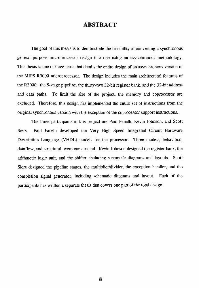
The goal of this thesis is to demonstrate the feasibility of converting a synchronous
general purpose microprocessor design into one using an asynchronous methodology.
This thesis is one of three parts that details the entire design of an asynchronous version of
the MIPS R3000 microprocessor. The design includes the main architectural features of
the R3000: the 5-stage pipeline, the thirty-two 32-bit register bank, and the 32-bit address
and data paths. To limit the size of the project, the memory and coprocessor are
excluded. Therefore, this design has implemented the entire set of instructions from the
original synchronous version with the exception of the coprocessor support instructions.
The three participants in this project are Paul Fanelli, Kevin Johnson, and Scott
Siers. Paul Fanelli developed the Very High Speed Integrated Circuit Hardware
Description Language (VHDL) models for the processor. Three models, behavioral,
dataflow, and structural, were constructed. Kevin Johnson designed the register bank, the
arithmetic logic unit, and the shifter, including schematic diagrams and layouts. Scott
Siers designed the pipeline stages, the multiplier/divider, the exception handler, and the
completion signal generator, including schematic diagrams and layout. Each of the
participants has written a separate thesis that covers one part of the total design.
111
TABLE OF CONTENTS
ABSTRACT iii
LIST OF FIGURES vi
LIST OF TABLES x
GLOSSARY OF TERMS xi
1.0 INTRODUCTION 1
2.0 CONCEPTS 6
2.1 ASYNCHRONOUS DESIGN 6
2.2 HANDSHAKING CONTROL CIRCUIT 7
2.3 VHDL 11
2.4 TOP DOWN DESIGN 12
2.5 DATATYPES 15
3.0 BEHAVIORALMODEL 17
3.1 INSTRUCTION FETCH 21
3.2 INSTRUCTION DECODE 23
3.3 INSTRUCTION EXECUTION 35
4.0 DATAFLOW MODEL 43
4.1 INSTRUCTION FETCH STAGE 46
4.2 INSTRUCTION DECODE STAGE 50
4.3 ARITHMETIC LOGIC UNIT STAGE 66
4.4 MEMORY STAGE 68
4.5 WRITEBACK STAGE 72
4.6 BUS CONTROL UNIT 74
IV
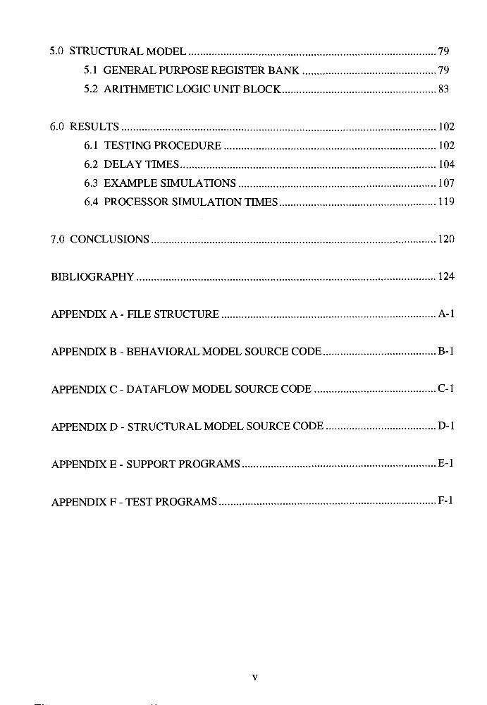
5.0 STRUCTURALMODEL 79
5.1 GENERAL PURPOSE REGISTER BANK 79
5.2 ARITHMETIC LOGIC UNIT BLOCK 83
6.0 RESULTS 102
6.1 TESTING PROCEDURE 102
6.2 DELAY TIMES 104
6.3 EXAMPLE SIMULATIONS 107
6.4 PROCESSOR SIMULATION TIMES 119
7.0 CONCLUSIONS 120
BIBLIOGRAPHY 124
APPENDIX A - RLE STRUCTURE A-l
APPENDDC B - BEHAVIORALMODEL SOURCE CODE B-l
APPENDIX C - DATAFLOWMODEL SOURCE CODE C-l
APPENDDC D - STRUCTURAL MODEL SOURCE CODE D-l
APPEuNDIX E - SUPPORT PROGRAMS E-l
APPENDIX F - TEST PROGRAMS F-l

LIST OF FIGURES
Figure 1-1. Test Bench BlockDiagram 3
Figure 2-1. HCC Architectural Organization 7
Figure 2-2. HCC Component Block Diagram 8
Figure 2-3 . Handshaking Control Circuit (HCC) Schematic Diagram 9
Figure 2-4. HCCWaveforms 10
Figure 3-1. Behavioral Model TestBench 17
Figure 3-2. The Body Outline of the Processor Process 19
Figure 3-3. Load Mode 20
Figure 3-4. RunModeWhile-Loop Shell 20
Figure 3-5. Instruction Fetch 21
Figure 3-6. Memory Read Procedure in Processor Process 22
Figure 3-7. R3000 Instruction Formats 23
Figure 3-8. Extracting the Op-code from the Instruction 26
Figure 3-9. IF-ELSIF-ELSE Statement used for Instruction Decode 27
Figure 3-10. Special Instruction Branch of IF-ELSIF-ELSE Statement 28
Figure 3-11. Bcond Instruction Branch of IF-ELSIF-ELSE Statement 29
Figure 3-12. Jump Instruction Branch of IF-ELSIF-ELSE Statement 30
Figure 3-13. Branch Instruction Branch of IF-ELSIF-ELSE Statement 31
Figure 3-14. ALU Immediate Instruction Branch of IF-ELSIF-ELSE Statement 32
Figure 3-15. Load and Store Instruction Branch of IF-ELSIF-ELSE Statement 33
Figure 3-16. Halt Instruction Branch of IF-ELSIF-ELSE Statement 33
Figure 3-17. Not Implemented Instruction Branch of IF-ELSIF-ELSE Statement 34
vi

Figure 3-18. Reserved Instruction Branch of IF-ELSIF-ELSE Statement 34
Figure 3-19. The Shift Left Logical Instruction 36
Figure 3-20 The Jump Register Instruction 36
Figure 3-21. TheMultiply Instruction 37
Figure 3-22. The Add Instruction 38
Figure 3-23. The Branch on Less Than Zero Instruction 39
Figure 3-24. The Jump Instruction..... 40
Figure 3-25. The Branch on Equal Instruction 40
Figure 3-26. The Add Immediate Instruction 41
Figure 3-27. The Load Byte Instruction 42
Figure 4-1. Dataflow Model TestBench 43
Figure 4-2. Dataflow Model CPU Component 45
Figure 4-3. Schematic of IF Stage 48
Figure 4-4. Waveforms of IF Stage 49
Figure 4-5. Instruction Decoder Component 50
Figure 4-6. Schematic Diagram of ID Stage 51
Figure 4-7. Code Excerpt of the ID Stage Instruction Decoder Architecture 54
Figure 4-8. Address Adder (AA) Component 55
Figure 4-9. Code Excerpt of the Address Adder Architecture 56
Figure 4-10. Branch and Jump (BJBOX) Component 56
Figure 4-1 1. Code Excerpt of the BJBOX Architecture 57
Figure 4-12. Schematic Diagram ofBJBOX 58
Figure 4-13. Data Dependency Example 59
Figure 4-14. The Dirty Box (DBOX) Component 60
Figure 4-15. Target Register Dirty Select (TRDS) Component 61
vn
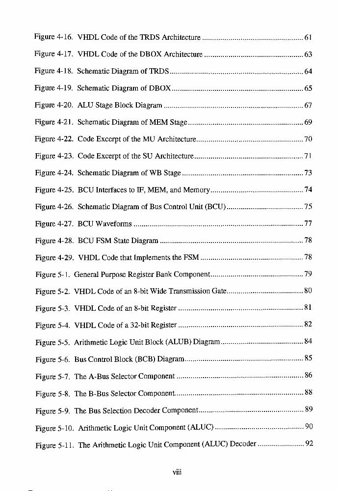
Figure 4-16. VHDL Code of the TRDS Architecture 61
Figure 4-17. VHDL Code of the DBOX Architecture 63
Figure 4-18. Schematic Diagram ofTRDS 64
Figure 4-19. Schematic Diagram ofDBOX 65
Figure 4-20. ALU Stage Block Diagram 67
Figure 4-21. Schematic Diagram ofMEM Stage 69
Figure 4-22. Code Excerpt of the MU Architecture 70
Figure 4-23. Code Excerpt of the SU Architecture 71
Figure 4-24. Schematic Diagram ofWB Stage 73
Figure 4-25. BCU Interfaces to IF, MEM, andMemory 74
Figure 4-26. Schematic Diagram ofBus Control Unit (BCU) 75
Figure 4-27. BCUWaveforms 77
Figure 4-28. BCU FSM State Diagram 78
Figure 4-29. VHDL Code that Implements the FSM 78
Figure 5-1. General Purpose Register Bank Component 79
Figure 5-2. VHDL Code of an 8-bitWide Transmission Gate 80
Figure 5-3. VHDL Code of an 8-bit Register 81
Figure 5-4. VHDL Code of a 32-bit Register 82
Figure 5-5. Arithmetic Logic Unit Block (ALUB) Diagram 84
Figure 5-6. Bus Control Block (BCB) Diagram 85
Figure 5-7. The A-Bus Selector Component 86
Figure 5-8. The B-Bus Selector Component 88
Figure 5-9. The Bus Selection Decoder Component 89
Figure 5-10. Arithmetic Logic Unit Component (ALUC) 90
Figure 5-11. The Arithmetic Logic Unit Component (ALUC) Decoder 92
viii
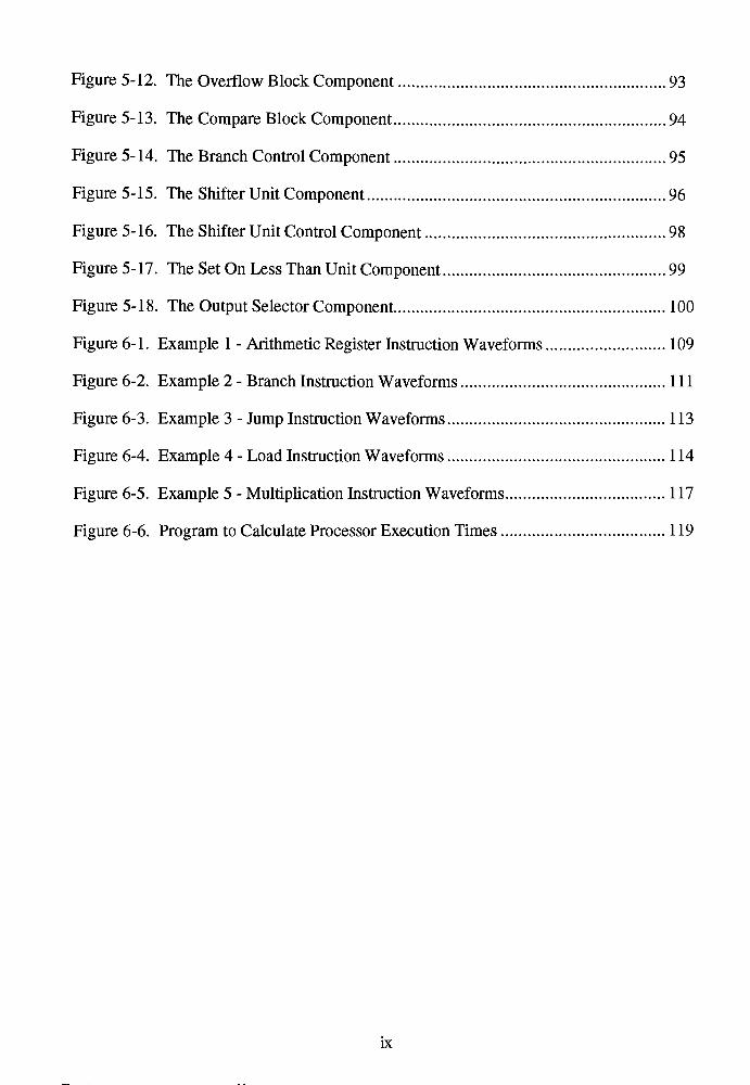
Figure 5-12. The Overflow Block Component 93
Figure 5-13. The Compare Block Component 94
Figure 5-14. The Branch Control Component 95
Figure 5-15. The Shifter Unit Component 96
Figure 5-16. The Shifter Unit Control Component 98
Figure 5-17. The Set On Less Than Unit Component 99
Figure 5-18. The Output Selector Component 100
Figure 6- 1 . Example 1 - Arithmetic Register Instruction Waveforms 109
Figure 6-2. Example 2 - Branch Instruction Waveforms 1 1 1
Figure 6-3. Example 3 -
Jump InstructionWaveforms 113
Figure 6-4. Example 4 - Load InstructionWaveforms 1 14
Figure 6-5. Example 5 - Multiplication InstructionWaveforms 1 17
Figure 6-6. Program to Calculate Processor Execution Times 1 19
IX
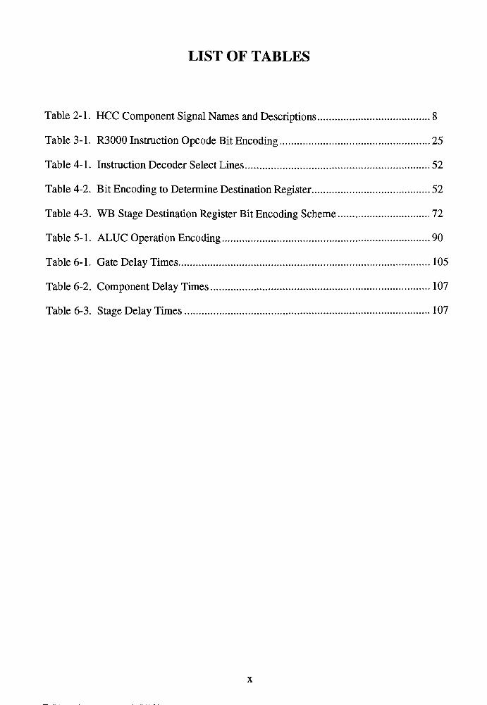
LIST OF TABLES
Table 2-1. HCC Component Signal Names and Descriptions 8
Table 3-1. R3000 Instruction Opcode Bit Encoding 25
Table 4-1. Instruction Decoder Select Lines 52
Table 4-2. Bit Encoding to Determine Destination Register 52
Table 4-3. WB Stage Destination Register Bit Encoding Scheme 72
Table 5-1. ALUC Operation Encoding 90
Table 6-1. Gate Delay Times 105
Table 6-2. Component Delay Times 107
Table 6-3. Stage Delay Times 107
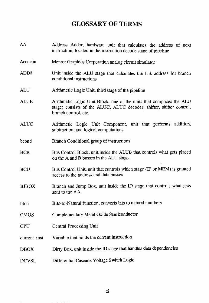
GLOSSARY OF TERMS
AA Address Adder, hardware unit that calculates the address of next
instruction, located in the instruction decode stage of pipeline
Accusim MentorGraphics Corporation analog circuit simulator
ADD8 Unit inside the ALU stage that calculates the link address for branch
conditional instructions
ALU Arithmetic Logic Unit, third stage of the pipeline
ALUB Arithmetic Logic Unit Block, one of the units that comprises the ALU
stage; consists of the ALUC, ALUC decoder, shifter, shifter control,
branch control, etc.
ALUC Arithmetic Logic Unit Component, unit that performs addition,
subtraction, and logical computations
bcond Branch Conditional group of instructions
BCB Bus Control Block, unit inside the ALUB that controls what gets placed
on the A and B busses in the ALU stage
BCU Bus Control Unit, unit that controls which stage (IF or MEM) is granted
access to the address and data busses
BJBOX Branch and Jump Box, unit inside the ID stage that controls what gets
sent to the AA
bton Bits-to-Natural function, converts bits to natural numbers
CMOS ComplementaryMetal Oxide Semiconductor
CPU Central Processing Unit
current_inst Variable that holds the current instruction
DBOX Dirty Box, unit inside the ID stage that handles data dependencies
DCVSL Differential Cascade Voltage Switch Logic
xt
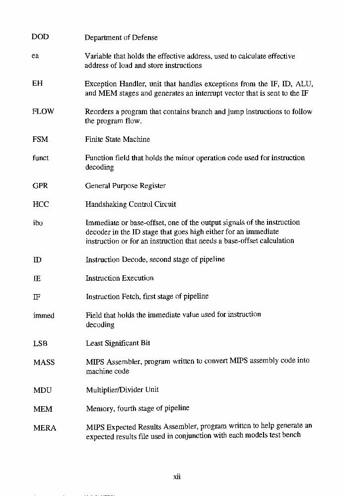
DOD Department ofDefense
ea Variable that holds the effective address, used to calculate effective
address of load and store instructions
EH Exception Handler, unit that handles exceptions from the IF, ID, ALU,
andMEM stages and generates an interrupt vector that is sent to the IF
FLOW Reorders a program that contains branch and jump instructions to follow
the program flow.
FSM Finite State Machine
funct Function field that holds the minor operation code used for instruction
decoding
GPR General Purpose Register
HCC Handshaking Control Circuit
ibo Immediate or base-offset, one of the output signals of the instruction
decoder in the ID stage that goes high either for an immediate
instruction or for an instruction that needs a base-offset calculation
ID Instruction Decode, second stage of pipeline
IE Instruction Execution
IF Instruction Fetch, first stage of pipeline
immed Field that holds the immediate value used for instruction
decoding
LSB Least Significant Bit
MASS MIPS Assembler, program written to convertMIPS assembly code into
machine code
MDU Multiplier/Divider Unit
MEM Memory, fourth stage of pipeline
MERA MIPS Expected Results Assembler, program written to help generate an
expected results file used in conjunction with each models test bench
xu
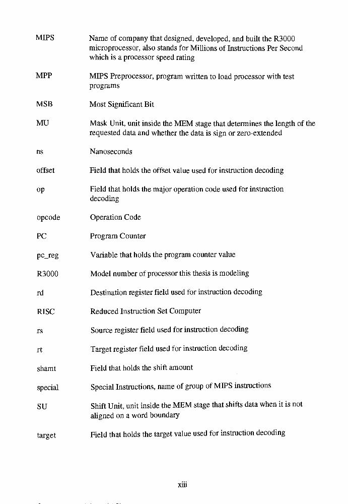
MIPS
MPP
MSB
MU
ns
offset
op
opcode
PC
pc_reg
R3000
rd
RISC
rs
rt
shamt
special
SU
target
Name of company that designed, developed, and built the R3000
microprocessor, also stands for Millions of Instructions Per Second
which is a processor speed rating
MIPS Preprocessor, program written to load processor with test
programs
Most SignificantBit
Mask Unit, unit inside the MEM stage that determines the length of the
requested data and whether the data is sign or zero-extended
Nanoseconds
Field that holds the offset value used for instruction decoding
Field that holds the major operation code used for instruction
decoding
Operation Code
Program Counter
Variable that holds the program counter value
Model number of processor this thesis is modeling
Destination register field used for instruction decoding
Reduced Instruction Set Computer
Source register field used for instruction decoding
Target register field used for instruction decoding
Field that holds the shift amount
Special Instructions, name of group ofMIPS instructions
Shift Unit, unit inside the MEM stage that shifts data when it is not
aligned on a word boundary
Field that holds the target value used for instruction decoding
xui
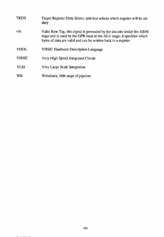
TRDS Target RegisterDirty Select, unit that selects which register will be set
dirty
vbt Valid Byte Tag, this signal is generated by the decoder inside the MEM
stage and is used by the GPR bank in the ALU stage; it specifies which
bytes of data are valid and can be written back to a register
VHDL VHSIC Hardware Description Language
VHSIC Very High Speed Integrated Circuit
VLSI Very Large Scale Integration
WB Writeback, fifth stage of pipeline
xtv
1.0 INTRODUCTION
This thesis is one of three parts encompassing the modeling, design, and
implementation of an asynchronous microprocessor. This project was performed
cooperatively by Scott Siers, Kevin Johnson, and this author. The project has been
divided so that each part forms a separate master's thesis. This paper discusses the Very
High Speed Integrated Circuit Hardware Description Language (VHDL) modeling of this
processor. The asynchronous processor uses most of the R3000's instruction set and
architectural features but differs in implementation. Three models, behavioral, dataflow,
and structural, are constructed. The behavioral model describes the functionality of the
R3000 without regard to implementation. The dataflow model represents the pipeline of
the processor. It models the data flowing through the pipeline stages. The structural
model represents the processor at the gate or structural level. The dataflow and structural
model delay times were back annotated from circuit simulation runs. Each model is tested
using a VHDL test bench to verify correct operation. Kevin Johnson and Scott Siers were
responsible for the Very Large Scale Integration (VLSI) design and implementation.
Kevin Johnson designed the register bank, the arithmetic logic unit (ALU), and the shifter.
Scott Siers designed the bus control logic, the multiplier/divider unit (MDU), and the
pipeline structure. This author also participated in the design of the asynchronous
processor from a modeling perspective. The hardware designs were changed or
completely redone depending upon the results of the VHDL modeling.
The main purpose of this project was to investigate the feasibility of converting an
existing synchronous processor design to an asynchronous design. The MIPS R3000 was
chosen for this task for numerous reasons. The R3000 has the best combination of
instruction set size, architectural features, and system complexity to fully exploit the
differences between synchronous and asynchronous design. The R3000 was one of the
first reduced instruction set computer (RISC) processors and is a very simplistic, concise,
and elegant architecture. The number of instructions is minimal and there are only three
addressing modes. For a 32-bit machine it has a small architecture and hence makes an
ideal processor for thesis work. There is an abundance of literature written on the MIPS
R3000. For example, the paper written by Asada, Okura, and Cho in 1992 [1] discusses
the design of an asynchronous implementation of the MIPS data path. Another paper by
Ginosar and Michell [2] discusses converting the MIPS pipeline using an asynchronous
design methodology. Also, the book MIPS RISC Architecture [3] gives extremelylow-
level details of the synchronous version of the processor. These features make the R3000
an ideal processor to model.
The MIPS R3000 is a general purpose microprocessor that includes a 32-bit data
path with thirty-two 32-bit general purpose registers. The R3000 has a 5-stage pipeline.
The five stages are instruction fetch (IF), instruction decode (ID), arithmetic logic unit
(ALU), memory (MEM), and register writeback (WB). The three main addressing modes
are register, immediate, and jump. The R3000 is a reduced instruction set computer
(RISC). One characteristic of a RISC based architecture is that it is a register based
design. The processor only works on data contained in the registers. The order of
operations is that data is loaded from memory into the registers, the processor works on
the data in the registers, the result is stored back into a register, and finally the result is put
back into memory. The advantage of this architecture is that the instruction set is smaller
(reduced) and consists of simpler instructions. This allows the cycle time for each
instruction to be short. All of the R3000's instructions are 32 bits in length. This is
another advantage of RISC machines. The complexity of the instruction decoder is
minimal and the instruction set size is limited.
Before any modeling was done, certain issues had to be considered. What
architectural features were to be modeled? Which instructions were to be modeled? How
many specific models should be designed and at what level of detail? During preliminary
discussions on this thesis topic it was decided that the main architectural features of the

R3000 would be modeled: the 5-stage pipeline, the thirty-two 32-bit register bank, the
hi/lo registers, and the 32-bit address and data paths. The features that would be left out
are the coprocessor and coprocessor support, the cache for memory and instruction fetch,
and the memory management. Since it was decided that memory would not be modeled,
memory management would not be implemented. The coprocessor and memory
management instructions were left out. Due to these architectural decisions and to limit
the size of this thesis, the asynchronous processor instruction set was reduced.
The VHDL modeling in this thesis consists of the following three models:
behavioral, dataflow, and structural. All models consist of three modules: memory,
central processing unit (CPU), and compare. These three modules when put together with
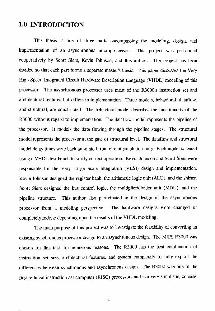
the test program and the expected results file create a complete test bench. Figure 1-1
shows the test bench setup. Each model will use the test bench along with test programs
to verify correct operation. The memory and compare modules are relatively similar for
all three models. The memory module is used as the main memory storage for the
BEHAVIORuAL
MDATAFLOW
MSTRUCTURAL
M
O
D
E
L
?c
K
expected
results
file
VCOMPARE
CPUs
Figure 1 -1. Test Bench BlockDiagram
processor and holds the test program used in the test bench. The compare module is used
to test the state of the processor after each instruction is executed and holds the expected
results file. The CPU module corresponds to one of the three models.
Software was written for this thesis to assist in testing the models. An assembler,
called MIPS Assembler (MASS), was written to convert MIPS assembly code into
machine code that the models can understand. Also, an expected results program was
written. This program, called MIPS Expected Results Assembler (MERA), allows the
user to input the expected results data into a file. This file is loaded into the compare
module and is tested against the state of the model after each instruction is executed.
Another program was written for branch and jump instructions. This program, called
FLOW, takes a program that contains branch and jump instructions and reorders the
instructions to follow the program flow. The last program is called MIPS Preprocessor
(MPP). This program takes the files created by MASS and MERA and copies them into
two files that are used by the models. These two files,"machine"
and "expected", are
loaded by the memory and compare modules, respectively.
Six test programs were written for the models. Each of these tests correspond to a
set of instructions. The program"ai.test"
tests immediate arithmetic instructions,"ar.test"
tests register arithmetic instructions. The third program, "jb.test", is used for jump and
branch instructions. The program"ls.test"
is used to test load and store instructions. The
fifth test, "md.test", checks the multiplication and division instructions along with the
move to and from the hi/lo registers. The last test file, "s.test", is used for the shift
instructions.
The software tools used in this project are from Mentor Graphics Corporation and
run on HP/Apollo Workstations. Five software tools were used: Design Architect,
System-1076 (VHDL) editor and compiler, Quicksim II, Accusim, and IC Station. Design
Architect is a schematic capture tool. The VHDL editor and compiler is incorporated into
Design Architect. The digital simulator is Quicksim II. The VHDL simulator is
embedded into Quicksim II. Accusim is the analog circuit simulator. Finally, the mask
layout editor is called IC Station.

2.0 CONCEPTS
One major feature of synchronous design is the use of a global clock. The very
nature of synchronous design is to control all events based on this clock. Multiple events
can happen but they will not be triggered until the next clock pulse. The order of events is
of no concern. On the other hand, asynchronous design avoids the use of a global clock.
Therefore, there is no convenient way to synchronize events. Here, the order of events is
very important. A controller can be used between logic blocks as a communication
device. The controller uses start and done signals as handshake signals. When one logic
block is finished, it sends the controller a done signal. The controller can now send the
next logic block a start signal. With synchronous design, the logic blocks can be tuned to
start at a certain time based on the clock phase. However, the exact time at which a
specific event starts or ends is not known in asynchronous design. This is why a controller
is needed. It coordinates the timing of events through the use of handshaking signals.
2.1 ASYNCHRONOUS DESIGN
An asynchronous design approach was chosen over a synchronous one for many
reasons. As transistor sizes in VLSI keep getting smaller, the major drawbacks to
synchronous design become more apparent and difficult to tolerate. Two major
disadvantages are the skew associated with a global clock and the increasing line delay
that occurs when a signal is routed across a VLSI chip. One of the major design goals in
synchronous design is to increase the performance of the processor by reducing the clock
period. However, as the reduction in scale of VLSI systems continues, more and more of
the clock period is used to account for clock skew. Global clock lines become more
sensitive to loading and it becomes increasingly difficult to keep the various clock line
signals in phase. The second issue involves line delay. In the past, the major delay in
circuit design was the transistor gate. Today, the line delay in signal routing is a major
concern. To obtain substantial increases in performance, new architectures will have to be
used to reduce the need for long metal lines. Circuit modules will have to be linked only
by local interconnections and the modules will then communicate via self-timed
handshaking schemes. The asynchronous design that eliminates the global clock and
reduces the need and effects of long signal lines is an attractive solution in modern VLSI
implementation.
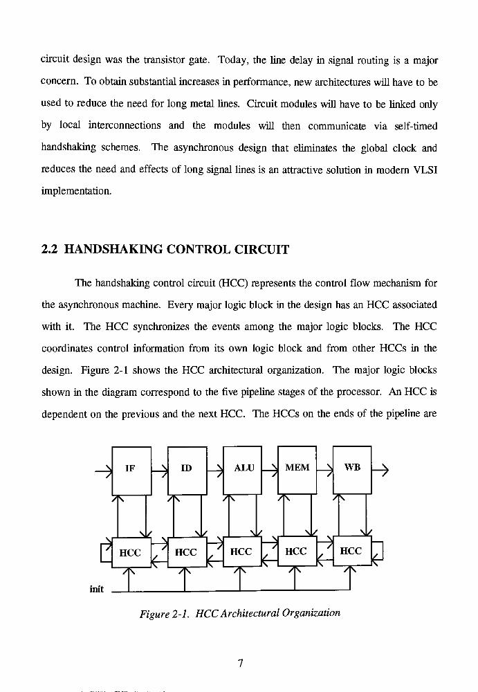
2.2 HANDSHAKING CONTROL CIRCUIT
The handshaking control circuit (HCC) represents the control flow mechanism for
the asynchronous machine. Every major logic block in the design has an HCC associated
with it. The HCC synchronizes the events among the major logic blocks. The HCC
coordinates control information from its own logic block and from other HCCs in the
design. Figure 2-1 shows the HCC architectural organization. The major logic blocks
shown in the diagram correspond to the five pipeline stages of the processor. An HCC is
dependent on the previous and the next HCC. The HCCs on the ends of the pipeline are
init
Figure 2-1. HCCArchitectural Organization
only dependent on its one neighbor. For example, the ALU HCC is dependent on the ID
and MEM HCCs. The.ALU stage cannot begin operation until the ID stage is finished
and the MEM stage has latched the previous data from the ALU stage. The HCC
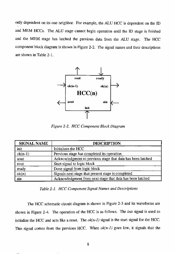
component block diagram is shown in Figure 2-2. The signal names and their descriptions
are shown in Table 2-1.
Figure 2-2. HCC ComponentBlockDiagram
SIGNAL NAME DESCRIPTION
init Initializes the HCC
ok(n-l) Previous stage has completed its operation
aout Acknowledgment to previous stage that data has been latched
rout Start signal to logic block
ready Done signal from logic block
ok(n) Signals next stage that present stage is completed
ain Acknowledgment from next stage that data has been latched
Table 2-1. HCC Component SignalNames andDescriptions
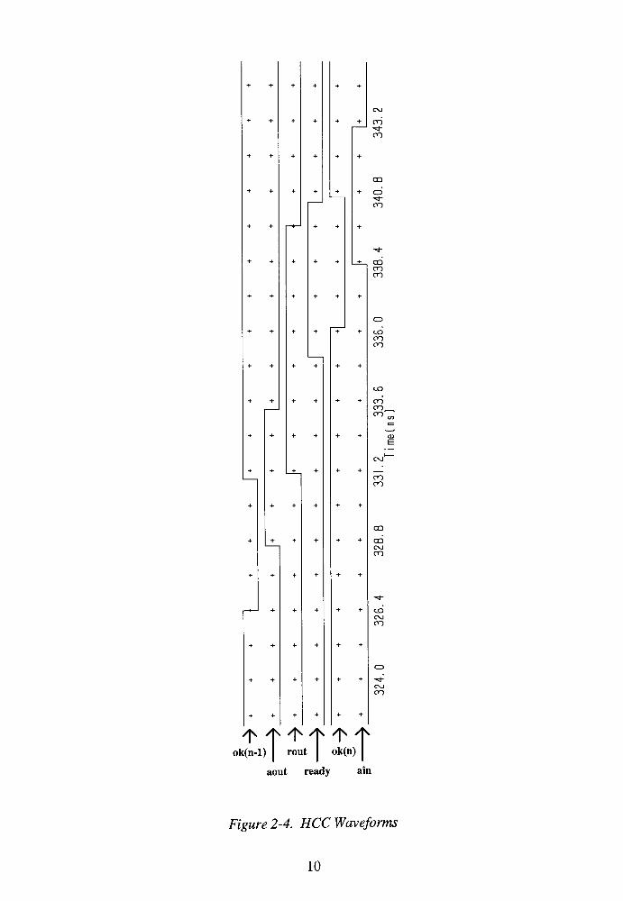
The HCC schematic circuit diagram is shown in Figure 2-3 and its waveforms are
shown in Figure 2-4. The operation of the HCC is as follows. The init signal is used to
initialize the HCC and acts like a reset. The ok(n-l) signal is the start signal for the HCC.
This signal comes from the previous HCC. When ok(n-l) goes low, it signals that the
8
cj
CJ
o
c
CJ
o
c
o
CJ
CD
jv:
CD
_CI
CO
n^
CZ
CO
AAA~3> <Z -j * -^^
~TJ"
CO CO CZ
CD' ~ a
L-
o
Figure 2-3. Handshaking Control Circuit (HCC) Schematic Diagram
cn
cn
*t-
cn
co
cn
cn
LO
cn
cn
cn
cn.
cn
cn
co
cn
to
CXJ
cn
cn
/N /N /|\ A\ /J\ ff\
ok(n-l) | rout | ok(n) |aout ready ain
Figure 2-4. HCCWaveforms
10
previous stage has valid data. The HCC sends the acknowledgment signal aout high when
rout and ready are both low. When aout is high and ain is low, rout goes high, rout is the
start signal to the HCCs logic block. The HCC now waits for the completion of the logic
block. This is signified by the ready line going high. Once ready is high, the HCC sends
ok(n) low. This signals to the next HCC that the logic block has valid data. The HCC
now waits for ain to go high which is an acknowledgment from the next HCC. ain going
high causes rout to go low and ok(n) to go high. When rout goes low, ready goes low.
The cycle then repeats itself.
2.3 VHDL
VHDL stands for VHSIC Hardware Description Language. VHSIC stands for
Very High Speed Integrated Circuit. The Department of Defense (DOD) initiated the
VHSIC program. The DOD also initiated VHDL to create a hardware description
language that all VHSIC contractors could use to specify their designs. More importantly,
this would allow designs to be transferred from one company to another and be totally
independent of the tools and the platforms they run on.
VHDL is a high level language. High level constructs are important for design
specification (behavioral model) and testing. VHDL allows the user to concentrate on the
behavioral aspects of the design and forget the low level details during the beginning
stages of design. VHDL is an IEEE standard formalized in specification 1076-1987 and
updated in specification 1076-1992. Writing in VHDL allows the user to port the source
code over to another hardware platform with ease. All that needs to be done is to
recompile the source code on the new platform and to run the new platform's simulator.
VHDL is a programming language that can simulate concurrent events. This
allows the user to specify multiple events at the same simulation time. VHDL uses the
11

concept of delta delay, which is an infinitesimally small delay, to order events that occur at
the same simulation time. VHDL software tools incorporate a simulator to test the
design, and a test bench can be used to simplify the testing process. Also, VHDL has
packages specifically designed to model hardware at different stages of design.
2.4 TOP DOWN DESIGN
Top down design is a popular design methodology. It guides a design from a high
level to a low level of abstraction. The system's functionality is described at a high level of
abstraction. Implementation of this functionality is not an issue at this level. On the
contrary, the system's low level details are only considered at a low level of abstraction.
The low level describes the gate level implementation. As the design progresses from one
level of abstraction to the next, functionality of the design is completed and set at the
higher levels and then the implementation of this functionality is created at the lower
levels. This thesis uses this concept by using the three different models. Each model is
another level of abstraction.
A behavioral model is a model that describes the behavior of the hardware entity
under test. An entity is a hardware unit that can be as simple as a gate or ascomplex as an
entire electronic system. A behavioral model does not explicitly specify the structure of
the entity but specifies its functionality. Another way of looking at the behavioral style of
modeling is the well known "blackbox"
approach. The hardware unit is described in
terms of its input-output mapping without specifying the model's technology, components,
or dataflow.
A behavioral model projects a very high level of abstraction. At the first stages of
design, the behavioral model relieves the user of the low-level details of the design and
implementation of the entity. This frees the designer and/or user to concentrate on the
12
behavior of the system in question. Overall, the behavioral model provides a means to
better understand the functionality of the entity. Finally, due to the high level of
abstraction, the behavioral model executes much faster than other modeling schemes. This
is advantageous at the beginning stages of a design when many simulations need to be
done.
The behavioral modeling technique was used to model the functionality of the
R3000 without regard to hardware implementation. The behavioral model was used to
understand the operation of every instruction that was implemented. The entire behavioral
model is actually one VHDL PROCESS statement. All instructions in a PROCESS
statement are executed sequentially. Therefore, the pipeline was modeled in a sequential
fashion. An instruction is fetched, decoded, executed, stored, and tested all within one
cycle of the PROCESS statement. The next instruction is not worked on until the first
instruction is finished. The data type used in this model is the BIT VECTOR. This choice
is discussed in section 2.4. The computation instructions are implemented using functions
and procedures since this model is only concerned with the operation of the processor and
not on how it is implemented. These functions and procedures are located in a VHDL
PACKAGE.
A dataflow model describes the behavior of the hardware entity just like the
behavioral model but in more detail. Dataflow modeling involves some implementation
details since it is concerned with the flow of data from one part to another. The dataflow
model starts to break the functionality of the behavioral model down into compartments.
An example of this is the breakdown of the pipeline. Each stage of the pipeline performs a
different function. The dataflow model specifies how the data will flow from one section
to another.
Dataflow modeling is similar to behavioral modeling since there are no gates to
specify low level implementation, but it is also similar to structural modeling because of
the use of components (even though the components are written using the dataflow style).
13
The dataflow model uses the same data types and package of declarations, functions, and
procedures as the behavioral model. This was done to simplify the model. The main
focus of attention was to get the pipeline stages talking to each other and to assure that
each stage was decoding and working on the proper instruction. Also, to keep the
dataflow model simple, only two logic states (0 and 1) were used to describe and simulate
the model.
The dataflow model provided the next level of abstraction by modeling the pipeline
stages concurrently. This model is used to design the handshaking interface protocol
between the pipeline stages. The main objective of this model was to establish proper and
efficient communication between the pipeline stages. A rough protocol would be designed
and then tested using the dataflow model. Using the simulation waveform outputs of the
model, the protocol was modified to improve the design. Also, design errors were
corrected using the dataflow output waveforms. This continued throughout the entire
design cycle of the asynchronous processor.
The dataflow model is largely a hierarchical structure of dataflow components.
The top level component is the CPU. The CPU is then broken up into eight unique
components: the five pipeline stages, the HCC, the bus controller (BC), and the exception
handler (EH). Each stage of the pipeline has an HCC associated with it. Each of these
components are made of other smaller components and primitives. Examples of the
primitives are multiplexers, latches, and edge detectors. The components were used to
speed up the model building process. When a particular component is needed, the proper
code is called through use of the VHDL COMPONENT instantiation and PORT MAP
statements.
The original dataflow model was constructed using arbitrary delay times just to get
the model working. Back annotation was used once the model was completed, tested, and
verified for correct operation. The new delay times were obtained from Accusim
simulation runs of circuit descriptions of the various components and pipeline stages.
14

These simulations were performed and discussed in ScottSiers'
thesis and Kevin Johnson's
thesis "Design and Implementation of an Asynchronous Version of the MIPS R3000
Microprocessor"
[10,19].
The structural model represents the processor at its gate or structural level. This is
the lowest form of abstraction. It is the lowest and most detailed level of description. The
structural model uses a set of components connected by signals. With the structural
model, the behavior of the entity is not apparent from the model. This is unlike the
behavioral model where the behavior or functionality is readily apparent. Component
instantiation is the major VHDL device that facilitates a structural or gate level nature.
2.5 DATATYPES
Originally, integers were chosen as the main modeling data type. However, this
presented some problems. The representation of data by integers appears to be ideal but
instructions need a more robust data type. Different pieces of the instruction represent
different aspects and conditions of the computer. An instruction holds operation, register
operand, and memory address information. Also, depending on the addressing mode, an
instruction holds different types and amounts of information. A composite type called a
record was considered in order to hold all the different fields of information contained in
an instruction. However, Mentor Graphic's version of VHDL now in use (version 8.1)
does not support records.
At this time, a decision was made to use a data type called a bit vector. Bit vectors
are ideal to use because they represent the language that the computer understands. Bit
vectors can be manipulated using two methods. Using the first method, the bit vector is
converted to an integer, the integer is operated on, and then the integer is converted back
to a bit vector. This method is faster to execute but involves much conversion. The
15
second method is to manipulate the individual bits. These bit manipulations are handled by
procedures and functions. An example of this is adding two bit vectors together. The two
bit vectors are passed to the overloaded"+"
function. The"+"
function adds the
individual bits together and returns a bit vector result. These specialized functions add
complexity and slow execution time.
16
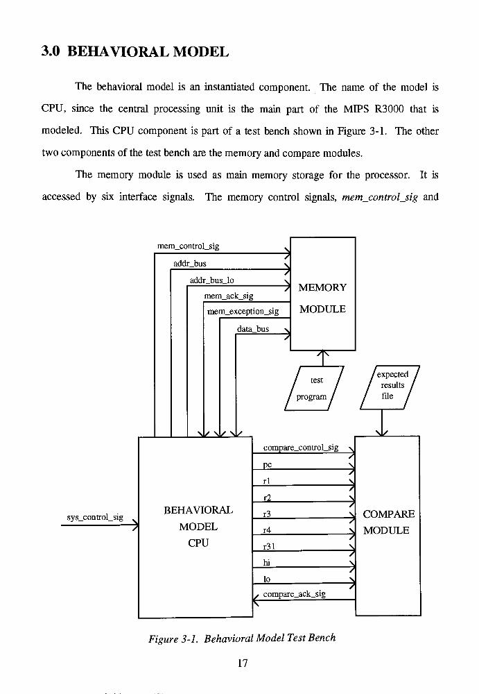
3.0 BEHAVIORALMODEL
The behavioral model is an instantiated component. The name of the model is
CPU, since the central processing unit is the main part of the MIPS R3000 that is
modeled. This CPU component is part of a test bench shown in Figure 3-1. The other
two components of the test bench are the memory and compare modules.
The memory module is used as main memory storage for the processor. It is
accessed by six interface signals. The memory control signals, mem_control_sig and
mem_control_sig
sys_control_sig
addr bus
addr bus lo
"}
mem_ack_sig
mem_exception_sig
data bus
\I/\I/mV
BEHAVIORAL
MODEL
CPU
MEMORY
MODULE
/"^
compare_control_sig^
pc
^
rl
r2
r3
"}
r4
r31
hi
lo
compare_ack_sig
COMPARE
MODULE
Figure 3-1. BehavioralModel Test Bench
17
mem_ack_sig, provide a fully interlocked handshaking protocol between the CPU
component and the memory component. The address bus is broken into two separate
signals: addrjbus and addr_bus_lo. Addrjbus provides the upper 30 bits (bits 2 through
31) of the 32 bit address bus, which accesses a word ofmemory (a word of memory is 32
bits wide). Addrjbusjo provides the lower two bits (bits 0 and 1) of the address bus,
which accesses a byte ofmemory (a byte ofmemory is 8 bits wide). The datajbus is a32-
bit bi-directional bus. It is used to transfer data between the CPU and the memory
module. Finally, the exception control signal, mem_exception_sig, is activated when a
memory exception occurs.
The compare module tests the state of the processor after each instruction is
executed. It is accessed by ten interface signals. The compare control signals,
compare_control_sig
and compare_ack_sig,
provide the handshaking between the CPU
and the compare module. The pc signal monitors the CPU program counter. Signals rl,
r2, r3, r4, and r31 monitor the contents of the specified registers. The hi and lo signals
monitor the multiplication and division storage registers.
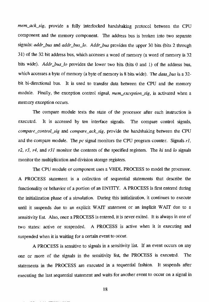
The CPU module or component uses a VHDL PROCESS to model the processor.
A PROCESS statement is a collection of sequential statements that describe the
functionality or behavior of a portion of an ENTITY. A PROCESS is first entered during
the initialization phase of a simulation. During this initialization, it continues to execute
until it suspends due to an explicit WATT statement or an implicit WATT due to a
sensitivity list. Also, once a PROCESS is entered, it is never exited. It is always in one of
two states: active or suspended. A PROCESS is active when it is executing and
suspended when it is waiting for a certain event to occur.
A PROCESS is sensitive to signals in a sensitivity list. If an event occurs on any
one or more of the signals in the sensitivity list, the PROCESS is executed. The
statements in the PROCESS are executed in a sequential fashion. It suspends after
executing the last sequential statement andwaits for another event to occur on a signal in
18
the sensitivity list. A WATT statement can be used in place of a sensitivity list. A
PROCESS executes until a WATT statement is reached. The PROCESS is suspended
until an event occurs on the signal in theWAIT statement.
The body outline of the PROCESS used in this model is shown in Figure 3-2. It is
sensitive to the sys_control_sig signal using a WATT statement. The process is broken
down, using a VHDL CASE statement, into four sections each corresponding to the four
modes of operation: stop, reset, load, and run.
processor* PROCESS
-- process declarations
BEGIN
WAIT ON sys_control_Bigj
CASE ays_control_sig IS
stop =>
WHEN reset =>
WHEN load =>
WHBS run ->
E8D CASE;
END PROCESS processor.
Figure 3-2. The Body Outline of the Processor Process
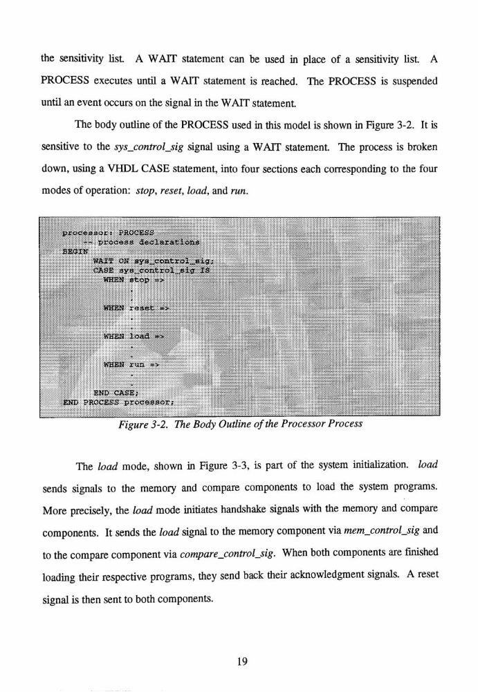
The load mode, shown in Figure 3-3, is part of the system initialization, load
sends signals to the memory and compare components to load the system programs.
More precisely, the load mode initiates handshake signalswith the memory and compare
components. It sends the load signal to the memory component via mem_control_sig and
to the compare component via compare When both components are finished
loading their respective programs, they send back their acknowledgment signals. A reset
signal is then sent to both components.
19
WHEN load =>
run_mode_flag := no;
meH_control_flig <- load AF7BR delay
WAIT UNTIL mem_ack_sig = yes;
mem_cont.rol_sig <= reset AFTER delay;
WAIT writ. amackslg * no;
campara_corit.rol_si.cr <= load JVFTER delay/ -::
WAIT XTtJTIIi compare_ack_sig = yes;
comparecontrol_jsAg <* reset AFTER delay;
WAIT tJNTII. compare_ack_sig - no;
Figure 3-3. Load Mode
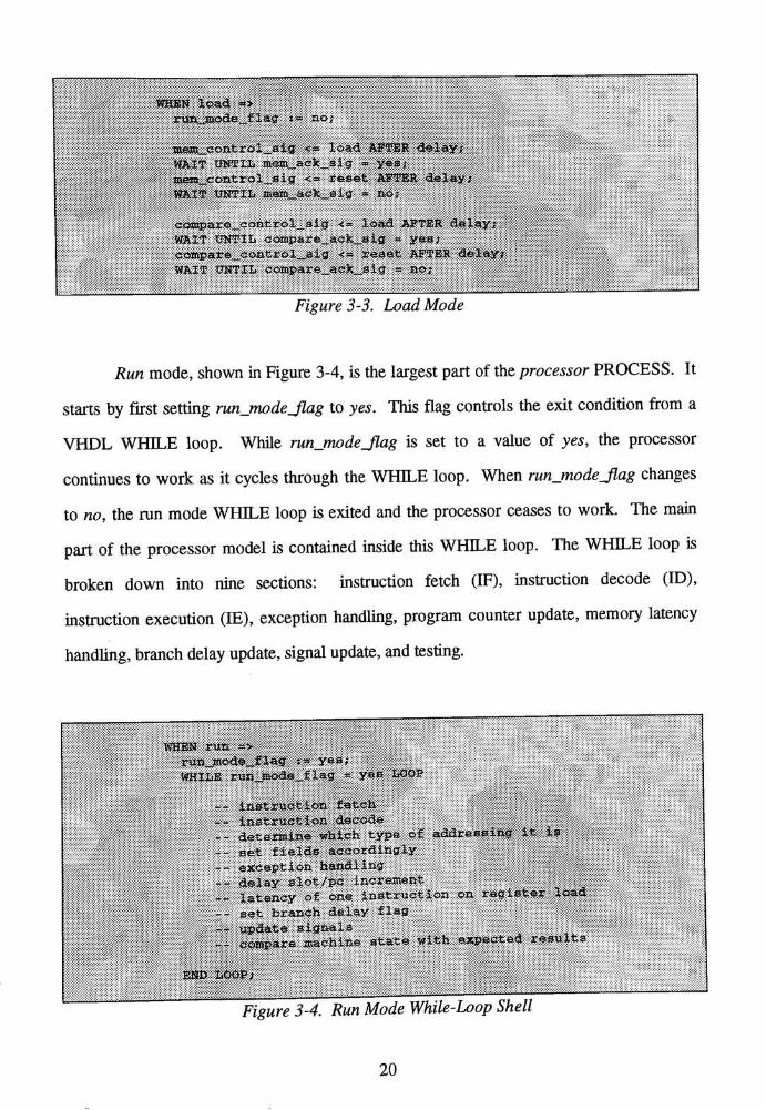
Run mode, shown in Figure 3-4, is the largest part of the processor PROCESS. It
starts by first setting run_modeJlag to yes. This flag controls the exit condition from a
VHDL WHILE loop. While run_modeJlag is set to a value of yes, the processor
continues to work as it cycles through the WHILE loop. When runjnodejlag changes
to no, the run mode WHILE loop is exited and the processor ceases to work. The main
part of the processor model is contained inside this WHILE loop. The WHILE loop is
broken down into nine sections: instruction fetch (IF), instruction decode (ID),
instruction execution (IE), exception handling, program counter update, memory latency
handling, branch delay update, signal update, and testing.
WHE8 run ~4
r_^ode_flag;,**
yea,-
-..
WHILE run_mode_,filag= yes LOOP
instruction fetcfa
instruction :decode
-- determine which type of addressingit- is
set fields accordingly
exception hand-ins
-- delay slot/po increment
latency of one instruction on register load
~~ set branch delay flag
update signals:"
oostpare machine state with expected results
E8D :00P;
Figure 3-4. Run Mode While-Loop Shell
20

3.1 INSTRUCTION FETCH
The instruction fetch portion of the code is very simple; it is only one line and can
be seen in Figure 3-5. Instruction fetch is accomplished by calling the memjread
procedure. The memjread procedure is discussed in the next section. The two arguments
needed to do a memory read are the starting address of the data to read and the size of the
data. The value in the program counter register (pc_reg) gives the starting address and
the value word gives the data size. The data size is of type word since all instructions are
32-bits long. The procedure result is placed in current_inst,
a 32-bit variable which stands
for current instruction.
-- fetch
mem_read {
next instruction
pc_reg, word, current_inst ) ;
Figure 3-5. Instruction Fetch
memjread, shown in Figure 3-6, takes two arguments, the memory address and
the memory size, and returns the result from the data bus. memjread first sets up the
address bus signals, addrjbus and addrjbusjo, from the value passed to it. Depending
upon what type of memory operation is to be performed, it selects from the size variable
what value to assign to mem_control_sig. It now waits for the memory component to
send back the memory acknowledge signal, memjjckjsig. The data from the memory is
now ready to be transferred to result, memjread now sends a reset signal to the memory
and waits again for an acknowledgment. This completes the fully interlocked handshaking
scheme. Finally, the mem_exception_sig is checked to see if a memory exception has
occurred.
21
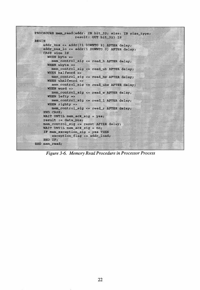
PROCEDURE memjread (addr: IN hit_32; size: IN size_type;
results OUT bit_32} IS
BEGIN
addr_bus - addr (31 DOWNTO 2 J AFTER delay;addrbusla <= addr(i DOWNTO 0) AFTER delay;CASE size IS
WHEN byte ->
memcontol_sig _ readja AFTER delay;WHEN ubyte =>
iaem_control_sig <= read_ub AFTER delay;
WHEN halfword >
ajeitiL.control_sig<-
read_hw AFTER dslay;WHEN uhalfword =>
mem_control_sig <= read_ubw AFTER delay;
word >
roecontrol_sig<_
readw AFTER delay;
WHEN lefty <=>
mem_co_trol_sig <= read_l AFTER delay;
WHEN righty =>
eiti_controlsig <& readr AFTER delay;END CASE;
WAIT UNTIL mem_ack_sig = yes;
result s* data_bus;
maro_control_sig <_= reset AFTER delay;
WAIT UNTIL mem_ack_sig no;
TF mein_exception_3ig = yes THEN
exception. flag := addr_load;
IF;
END mem read;
Figure 3-6. Memory Read Procedure in Processor Process
22
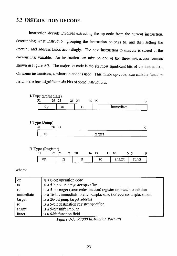
3.2 INSTRUCTION DECODE
Instruction decode involves extracting the op-code from the current instruction,
determining what instruction grouping the instruction belongs to, and then setting the
operand and address fields accordingly. The next instruction to execute is stored in the
currentjnst variable. An instruction can take on one of the three instruction formats
shown in Figure 3-7. The major op-code is the six most significant bits of the instruction.
On some instructions, a minor op-code is used. This minor op-code, also called a function
field, is the least significant six bits of some instructions.
I-Type (Immediate)31 26 25 21 20 16 15
op rs rt immediate
J-Type (Jump)31 26 25
OP target
R-Type (Register)31 26 25 21 20 16 15 11 10 6 5
op rs rt rd shamt funct
where:
op
rs
rt
immediate
target
rd
shamt
funct
is a 6-bit operation code
is a 5-bit source register specifier
is a 5-bit target (source/destination) register or branch condition
is a 16-bit immediate, branch displacement or address displacement
is a 26-bit jump target address
is a 5-bit destination register specifier
is a 5-bit shift amount
is a 6-bit function field
Figure 3-7. R3000 Instruction Formats
23
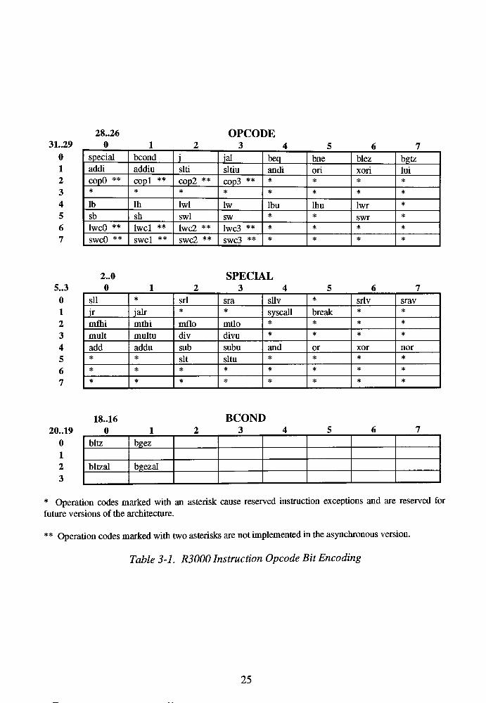
To understand instruction decoding, the R3000 instruction op-code bit encoding
needs to be addressed. This bit encoding is shown in Table 3-1. Table 3-1 is composed of
three tables: opcode, special, and bcond. The opcode table displays all the possible bit
combinations of the major op-code. The rows of the opcode table represent the three
most significant bits of the major op-code field. The columns represent the three least
significant bits. When the major op-code of an instruction is equal to 00 octal, then the
instruction is a special instruction. The special instructions are shown in the special table.
The special instructions are encoded through the minor op-code field variable called funct
(function field). The special table displays all the possible combinations of the special
instructions. The rows of the special table represent the three most significant bits of
funct. The columns represent the three least significant bits. When the major op-code is
equal to 01 octal, then the instruction is a branch conditional (bcond) instruction. The
branch conditional instructions are shown in the bcond table of Table 3-1. These
instructions are encoded through a bcond field variable called regjunct which is a five bit
field. The rows of the bcond table represent the two most significant bits of the regjunct
field. The columns represent the three least significant bits of regjunct.
24
31..29
0
1
2
3
4
5
6
7
28..26
0 1 2
OPCODE
3 4 5 6 7
special bcond.i
ial beq bne blez bgtz
addi addiu slti sltiu andi ori xori lui
copO**
copl**
cop2**
cop3** * * * *
* * * * * * * *
lb lh lwl lw lbu lhu lwr *
sb sh swl SW* *
swr*
lwcO ** lwcl ** lwc2 ** lwc3 ** * * * *
swcO**
swcl**
swc2**
swc3** * * * *
5..3
0
1
2
3
4
5
6
7
2..0
0 1 2
SPECIAL
3 4 5 6 7
sll*
srl sra sllv*
srlv srav
if jalr * *syscall break * *
mfhi mthi mflo mdo* * * *
mult multu div divu * * * *
add addu sub subu and or xor nor
* *sit situ
* * * *
* * * * * * * *
* * * * * * * *
20..19
0
18..16
0 1
BCOND
3
bltz bgez
bltzal bgezal
* Operation codes marked with an asterisk cause reserved instruction exceptions and are reserved for
future versions of the architecture.
** Operation codes marked with two asterisks are not implemented in the asynchronous version.
Table 3-1. R3000 Instruction Opcode Bit Encoding
25
The op-code is extracted from currentJnst by using a bit-vector array range, as
shown in Figure 3-8. The top six bits of current_inst is extracted and stored in a variable
called opcode using an array range (abit-vector is an array of bits) from bit 31 down to bit
26. The op-code is further broken down by extracting a segment of the variable opcode.
This is stored in a variable called opcodejseg. Opcode_seg
is the three most significant
bits of opcode and is used to determine the instruction grouping.
opcode t- current_inst(31 I8WNTO 26};
opcodeseg ** opcode (5 BOWNTO 3);
Figure 3-8. Extracting the Op-code from the Instruction
After the op-code is extracted from the current instruction, the instruction
grouping is determined. The major op-code instructions are broken up into the following
groups: special, bcond, jump, branch, immediate, load, and store instructions. A VHDL
IF-ELSIF-ELSE statement, shown in Figure 3-9, is used to direct the program flow to the
correct instruction grouping. All instructions are named the same as the R3000 instruction
set except for the addition of the letter"i"
and an underscore bar ("i_"). The R3000 major
op-code instruction special is called i_special, for example. All the instructions are
defined in a VHDL PACKAGE as constants to improve code readability and debugging.
The i_special instruction is defined as a constant bit value of "000000", for example.
The IF-ELSIF-ELSE statement is broken up into nine branches. When the major
op-code is equal to the constant ijspecial then the first branch is taken. This first branch
handles all the R3000 special instructions. The second branch handles the four branch
conditional instructions. This occurs when the major op-code is equal to the constant
ijbcond. The two jump instructions, ij and ijal, are found in the third branch. The
fourth branch holds the branch instructions and is taken when opcodejseg is equal to
"000". The fifth branch holds the ALU immediate instructions and is taken when
26
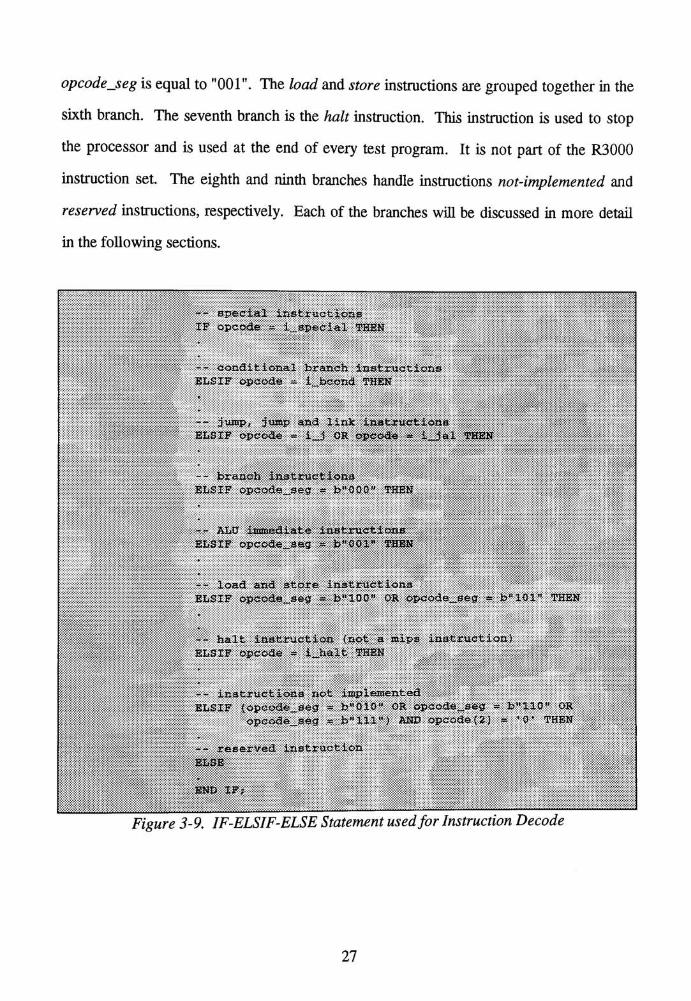
opcodejseg is equal to "001". The load and store instructions are grouped together in the
sixth branch. The seventh branch is the halt instruction. This instruction is used to stop
the processor and is used at the end of every test program. It is not part of the R3000
instruction set. The eighth and ninth branches handle instructions not-implemented and
reserved instructions, respectively. Each of the branches will be discussed in more detail
in the following sections.
special instructions
IF opcode - i_special THEN
-- conditional branch instructions
ELSIF opcode - ibcond THEN
-- jump, jump and link instructions
ELSXF opcode = i_j OR opcode * i_Jal
-- branch instructions
ELSIF opcodese<3 -
b"000"THEN
-- ALU immediate instructions
ELSIF opcodeseg ~
b"001"
-- load and store instructions
ELSIF opcode_seb"100" OR opcodeseg -
b"101"THEN
-- halt instruction (not a mips instruction}
ELSIF opcode * i_halt THEN
-- instructions not implemented
ELS IF {opcodesesf -
b"0_0"OR opcode_se<3 -
b"110"OR
opcodeseg _ b"lll") AND opcode {2 J ="q*
THEN
reserved instruction
END IF;
Figure 3-9. IF-ELSIF-ELSE Statement usedfor Instruction Decode
27
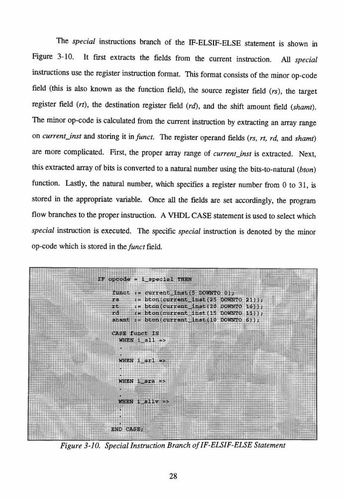
The special instructions branch of the IF-ELSIF-ELSE statement is shown in
Figure 3-10. It first extracts the fields from the current instruction. All special
instructions use the register instruction format. This format consists of the minor op-code
field (this is also known as the function field), the source register field (rs), the target
register field (rt), the destination register field (rd), and the shift amount field (shamt).
The minor op-code is calculated from the current instruction by extracting an array range
on currentJnst and storing it in funct. The register operand fields (rs, rt, rd, and shamt)
are more complicated. First, the proper array range of currentJnst is extracted. Next,
this extracted array of bits is converted to a natural number using the bits-to-natural (bton)
function. Lastly, the natural number, which specifies a register number from 0 to 31, is
stored in the appropriate variable. Once all the fields are set accordingly, the program
flow branches to the proper instruction. A VHDL CASE statement is used to select which
special instruction is executed. The specific special instruction is denoted by the minor
op-code which is stored in the funct field.
IP opcode = i_special THEN
funct = current^lnstCS DOWNTO 0) ;
rs :a bton (currentJins't{25 DQWNTO 21)};rt := bton (current^Jnst (;2ft DOWNTO 16});
rd *= bton(nurrent_inst{15 DOWNTO 11});
snarat s bton (current_instf
10 DOWNTO 6)};
CASE funct IS
WHEN i_sll =>
:;:::::::::::::::-::-:-::::::-:-:-:-:?::-:-:-:-:::-
WHEN i_s
ill
MM
ra
sIS:
E|E;^-h^^^^^^ii:^:|jg:F:j^:::5:!:;-:.:;v;::;
WHEN ;H
isllv ->
END CASE;
Figure 3-10. Special Instruction Branch ofIF-ELSIF-ELSE Statement
28
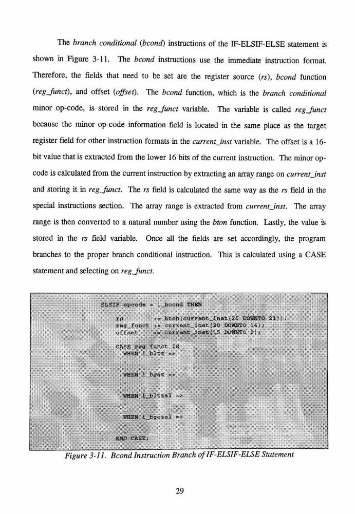
The branch conditional (bcond) instructions of the IF-ELSIF-ELSE statement is
shown in Figure 3-11. The bcond instructions use the immediate instruction format.
Therefore, the fields that need to be set are the register source (rs), bcond function
(regjunct), and offset (offset). The bcond function, which is the branch conditional
minor op-code, is stored in the regjunct variable. The variable is called regjunct
because the minor op-code information field is located in the same place as the target
register field for other instruction formats in the currentJnst variable. The offset is a 16-
bit value that is extracted from the lower 16 bits of the current instruction. The minor op
code is calculated from the current instruction by extracting an array range on currentJnst
and storing it in regjunct. The rs field is calculated the same way as the rs field in the
special instructions section. The array range is extracted from currentJnst. The array
range is then converted to a natural number using the bton function. Lastly, the value is
stored in the rs field variable. Once all the fields are set accordingly, the program
branches to the proper branch conditional instruction. This is calculated using a CASE
statement and selecting on regjunct.
ELSIF opcode = i_bcond THEN
rs : bton(current_inst{2 DOWNTO 21));
rg_unct := current_inst (20 DOWNTO 16);
offset .*= current_inst(15 DOWNTO 0);
CASE reg_funct is
WHEN i bltz =>
i_bge
ij.ltsal ->
WHEN i_bgezal =>
END CASE;
Figure 3-11. Bcond Instruction Branch ofIF-ELSIF-ELSE Statement
29
Tht jump instructions branch of the IF-ELSIF-ELSE statement is shown in Figure
3-12. The jump instructions use the jump instruction format. This format uses a target
field. The target field is a 26-bit jump target address and is extracted from the lower 26
bits of currentJnst. Once the target field is set, the program branches to the proper jump
instruction. This is calculated by using a CASE statement and selecting on opcode.
ELSIF opcode * i_J OR opcode * i_Jal THEN
target s= current_inst{25 DOWNTO 0);
CASE opcode IS
WHEN i_j[ =>
WHEN i_Jal >
::::: :: :: :r : : : : ;: :::'
:r':^
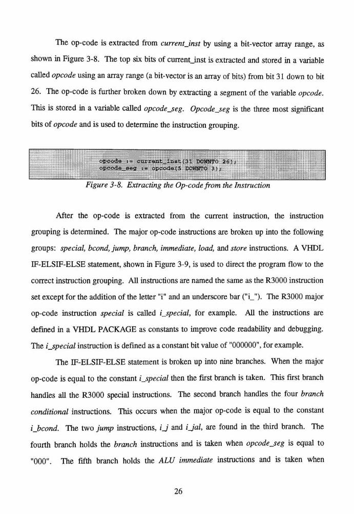
END CASE;
Figure 3-12. Jump Instruction Branch ofIF-ELSIF-ELSE Statement
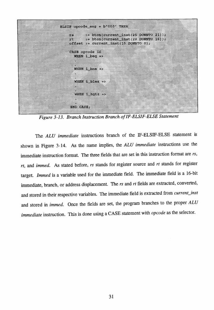
The branch instructions branch of the IF-ELSIF-ELSE statement is shown in
Figure 3-13. The branch instructions use the immediate instruction format. Therefore,
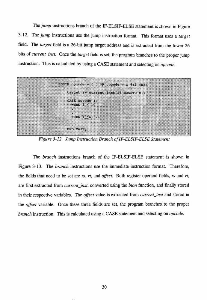
the fields that need to be set are rs, rt, and offset. Both register operand fields, rs and rt,
are first extracted from currentJnst, converted using the bton function, and finally stored
in their respective variables. The offset value is extracted from currentJnst and stored in
the offset variable. Once these three fields are set, the program branches to the proper
branch instruction. This is calculated using a CASE statement and selecting on opcode.
30
ELSIF opcodeseg =b"{3Q0"
THEN
re s bton{currentinet(2S DOWNTO 21));
rt is bton{current_inst(2 0 DOWNTO 1<5J);
offset f* currentinst{15 DOWNTO 0);
dASE opcode IS
WHEN ijaeg ->
WHEN ijane ->
WHEN i_blez =>
WHEN i_bgtz =>
END CASE;
Figure 3-13. Branch Instruction Branch ofIF-ELSIF-ELSE Statement
The ALU immediate instructions branch of the IF-ELSIF-ELSE statement is
shown in Figure 3-14. As the name implies, the ALU immediate instructions use the
immediate instruction format. The three fields that are set in thisinstruction format are rs,
rt, and immed. As stated before, rs stands for register source and rt stands for register
target. Immed is a variable used for the immediate field. The immediate field is a 16-bit
immediate, branch, or address displacement. The rs and rt fields are extracted, converted,
and stored in their respective variables. The immediatefield is extracted from currentJnst
and stored in immed. Once the fields are set, the program branches to the proper ALU
immediate instruction. This is done using a CASEstatement with opcode as the selector.
31

ELSIF opcode seg =b"001"
THEN
rs r= bton f current inst (as downto 21)),-
rt := bton(current_inat(20 DOWNTO 16));
immed := current_inst (15 DOWNTO t ;
CASE Opcode IS
WHEN i addi =>
WHEN i_addiu _>
islti ->
END CASE;
Figure 3-14. ALU Immediate Instruction Branch ofIF-ELSIF-ELSE Statement
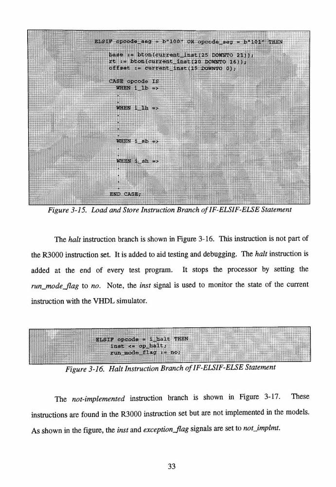
The load and store instructions branch of the IF-ELSIF-ELSE statement is shown
in Figure 3-15. The load and store instructions use the immediate instruction format with
the following three fields: rt, base, and offset, rt stands for the target register, base is an
alias for the rs field, and offset is an alias for the immediate field. Once all the fields are
extracted, converted, and stored, the program branches to the proper load or store
instruction depending on the value of opcode.
32
ELSIF apeode_seg =b"loO"
OR opaode_seg =b"lOl"
THEN
base ss btcn(CUtrentinst (25 DOWNTO 21)};rt ;= bton{eurrent_inst(20 DOWNTO 16));offset *4 current_inst(15 DOWNTO 0);
CASE opcode IS
WHEN i_lb =s>
WHEN ilh *>
i_sb >
i_sh =>
END CASE;
Figure 3-15. Load and Store Instruction Branch ofIF-ELSIF-ELSE Statement
The halt instruction branch is shown in Figure 3-16. This instruction is not part of
the R3000 instruction set. It is added to aid testing and debugging. The halt instruction is
added at the end of every test program. It stops the processor by setting the
runjnodejlag to no. Note, the inst signal is used to monitor the state of the current
instruction with the VHDL simulator.
Figure 3-16. Halt Instruction Branch ofIF-ELSIF-ELSE Statement
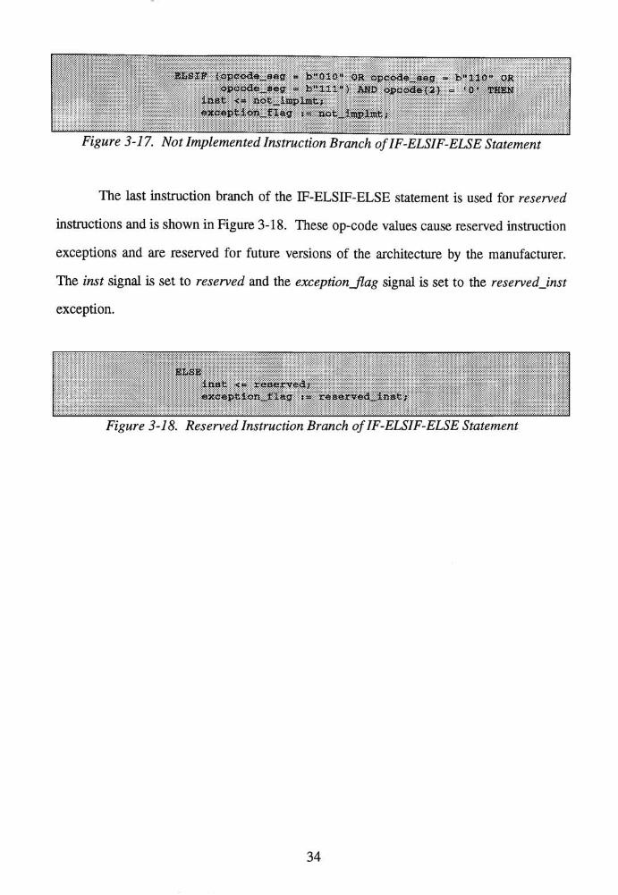
The not-implemented instruction branch is shown in Figure 3-17. These
instructions are found in the R3000 instruction set but are notimplemented in the models.
As shown in the figure, the inst and exceptionJlag signals are set to notjmplmt.
33
ELSIF *.opeode_segVOlO"
OR opcode_seg =>b"110"
OR
opoode_seg = b"lll") AND opaodeU) -'O' THEN
inst <* not_irapUftt;
exception_f leg s* not_implnrt:;
Figure 3-1 7. Not Implemented Instruction Branch ofIF-ELSIF-ELSE Statement
The last instruction branch of the IF-ELSIF-ELSE statement is used for reserved
instructions and is shown in Figure 3-18. These op-code values cause reserved instruction
exceptions and are reserved for future versions of the architecture by the manufacturer.
The inst signal is set to reserved and the exceptionjlag signal is set to the reservedjnst
exception.
ELSE
inst <= reserved;
exceptionflag :- reserved_inst;
Figure 3-18. Reserved Instruction Branch ofIF-ELSIF-ELSE Statement
34

3.3 INSTRUCTION EXECUTION
The instructions are divided into the following six groups: special, branch
conditional, jump, branch, ALU immediate, and load/store instructions. The groups are
discussed separately with a few examples for each group. This instruction grouping
follows the instruction op-code bit encoding chart previously shown in Table 3-1. Note,
every instruction uses the inst signal to display which instruction is currently being
executed. Also, since register 0 (rO) is hard wired to the value zero, every instruction that
stores a value in a register has to check that the destination register is not zero. If the
destination register is zero, then the instruction is ignored. Lastly, many instructions
perform their operations by calling a function that is located in a VHDL PACKAGE.
SPECIAL INSTRUCTIONS
The special instructions are further divided into the following groups: shift, jump
register, special, multiply/divide, and 3-operand register instructions. There are six shift
instructions: shift-left logical (sll), shift-right logical (srl), shift-right arithmetic (sra),
shift-left logical variable (sllv), shift-right logical variable (srlv), and shift-right
arithmetic variable (srav). The logical shift instructions insert zeroes into the vacant bit
positions. If the shift is to the left, zeroes are inserted into the low order bits. A right shift
inserts zeroes into the high order bits. An arithmetic shift uses sign extension when
inserting values into the vacant bit positions. The arithmetic shift is only used on a right
shift. Therefore when a right arithmetic shift is performed, the high order bits are sign
extended. A variable shift gets its shift amount from the contents of a register. More
precisely, the low order 5 bits of register rs specify the number of bits to shift. If the shift
is not variable, then the shift amount is held in the shamt field of those particular shift
instructions. As an example, the sll instruction is shown in Figure 3-19. sll performs the
35

shift by calling the shiftJI function. ShiftJI takes two arguments: a 32-bit value to shift
and the shift amount, shiftJI returns a 32-bit shifted value. More precisely, sll shifts the
contents of register rt left by shamt bits, inserting zeroes into the low order bits. It then
places the 32-bit result in register rd.
WHEN i_sll =>
inst <- op_sll;
IF rd /= 0 THEN
reg(rd) t= shiftll (reg(rt) , shamt);
END IF;
Figure 3-1 9. The Shift Left Logical Instruction
There are two jump register instructions: jump register (jr) and jump and link
register (jalr). Both instructions jump to an address contained in register rs with a one
instruction delay. The jalr instruction also places the address of instruction following the
delay slot in register rd. As an example, the jr instruction is shown in Figure 3-20. The
address that is stored in register rs is the location to which the program jumps after a delay
of one instruction. Since the instruction in the delay slot needs to be executed before the
jump is executed, the address is stored in a temporary variable called pcjemp. At the
proper time, the program counter (PC) is loaded with the value in pcjemp. The
delay_slotJlag controls when PC is loaded with pcjemp.
WHEN i_jr =>
intft <- op_jr;
pc_temp s- X0S{XB)t
<3eley_slot_flag t* set;
Figure 3-20. The Jump Register Instruction
There are two special instructions: syscall and break, syscall initiates a system
call trap and immediately transfers control to the exception handler, break initiates a
36

breakpoint trap and also immediately transfers control to the exception handler. Since an
operating system will not be modeled, these instructions are"dummy"
instructions and do
not do anything useful. However, since the exception handling is modeled, syscall and
break cause an exception which halts the processor.
There are eight multiply/divide instructions: move from hi (mjhi), move to hi
(mthi), move from lo (mflo), move to lo (mtlo), multiply (mult), multiply unsigned (multu),
divide (div), and divide unsigned (divu). The first four instructions move data to and from
the hijreg and lojreg registers. The hijreg and lojreg registers hold results of integer
multiplication and division operations. As an example, the mult instruction is shown in
Figure 3-21. The mult instruction multiplies the contents of registers rs and rt as two's
complement values. The mult function returns a value that is placed in a temporary 64-bit
variable multjemp. multjemp is divided into two 32-bit values representing the most
and least significant 32 bits. The most significant 32 bits are stored in hijreg. The least
significant 32 bits are stored in loj-eg.
WHEN i_JJUlt ->
inst <= op_mult;
mult_temp s= mult (reg(rs) , reg(rt));
lo_reg ;* multterop(31 DOWNTO 0);
hi_reg * mult_temp(63 DOWNTO 32};
Figure 3-21. The Multiply Instruction
There are ten 3-operand register instructions: add (add), add unsigned (addu),
subtract (sub), subtract unsigned (subu), AND (and), OR (or), XOR (xor), NOR (nor), set
on less than (sit), and set on less than unsigned (situ). All ten instructions perform their
operations on the 3-operand registers: rs, rt, and rd. The two operands are stored in the
rs and rt registers. The results of the operation is stored in rd. The first four instructions
are arithmetic instructions. The next four instructions perform logical operations. The
37
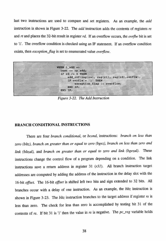
last two instructions are used to compare and set registers. As an example, the add
instruction is shown in Figure 3-22. The add instruction adds the contents of registers rs
and rt and places the 32-bit result in register rd. If an overflow occurs, the ovrflw bit is set
to T. The overflow condition is checked using an IF statement. If an overflow condition
exists, then exceptionJlag is set to enumerated value overflow.
WHEN l_add ->
inst <= op_add;
IF xd /- 0 THEN
add_ovf (reg(ra), reg(rt), reg(rd) , ovrflw) ;
IF ovrflw~ '1*
THEN
exception_lag $*= overflow;
END IF;
END IF;
Figure 3-22. TheAdd Instruction
BRANCH CONDITIONAL INSTRUCTIONS
There are four branch conditional, or bcond, instructions: branch on less than
zero (bltz), branch on greater than or equal to zero (bgez), branch on less than zero and
link (bltzal), and branch on greater than or equal to zero and link (bgezal). These
instructions change the control flow of a program depending on a condition. The link
instructions save a return address in register 31 (r31). All branch instruction target
addresses are computed by adding the address of the instructionin the delay slot with the
16-bit offset. The 16-bit offset is shifted left two bits and sign extended to 32 bits. All
branches occur with a delay of one instruction. As an example, the bltz instruction is
shown in Figure 3-23. The bltz instruction branches to the target address if register rs is
less than zero. The check for less than zero is accomplished by testing bit 31 of the
contents of rs. If bit 31 is'1'
then the value in rs is negative. The pcjeg variable holds
38

the address of present instruction, the bltz instruction. The address of the instruction in
the delay slot is computed by adding four to pc_reg. The 16-bit offset is manipulated by
first sign-extending it to 32 bits and then shifting it left by two bits. Finally, the target
address is computed by adding the modified offset to the modified program counter. The
target address is placed in a temporary program counter (pcjemp) since all branch
instructions have a delay of one instruction. If the branch is to be taken, at the proper
time, pcjreg is updated with pcjemp. delayjslotjlag is the variable that controls when
pcjreg is updated.
WHEN l_bltz =>.
'
inst <-. opbltz;
IF reg(rs)Ol) ='!
THEN
po_temp := pc_reg + x"0000_0004";
pctemp t- pc_temp +
shift_ll (eel6to32 (offset) , 2 ) ;
delay_slot_flag :** set?
END IF;
Figure 3-23. The Branch on Less Than Zero Instruction
JUMP INSTRUCTIONS
There are two jump instructions: jump (j) and jump and link (jal). Both
instructions jump to an address contained in the target field. More precisely, the 26-bit
target address is shifted left two bits and combined with the high-order 4 bits of the
program counter. The program jumps to the address with a one instruction delay. The jal
instruction also places the address of instruction following the delay slot in the link
register, r31. As an example,they'
instruction is shown in Figure 3-24.
39
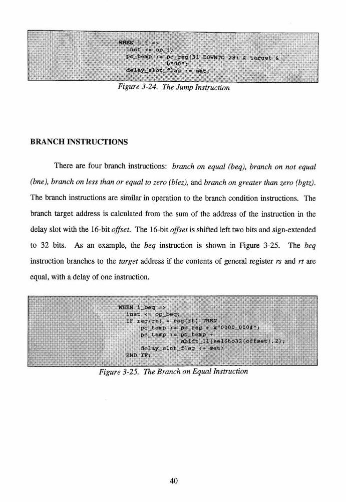
Iinst
pc_temp
delay
>
op_3 ;
- pcreg(31 DOWNTO 28) & target &
slotmflag := set;
Figure 3-24. The Jump Instruction
BRANCH INSTRUCTIONS
There are four branch instructions: branch on equal (beq), branch on not equal
(bne), branch on less than or equal to zero (blez), and branch on greater than zero (bgtz).
The branch instructions are similar in operation to the branch condition instructions. The
branch target address is calculated from the sum of the address of the instruction in the
delay slot with the 16-bit offset. The 16-bit offset is shifted left two bits and sign-extended
to 32 bits. As an example, the beq instruction is shown in Figure 3-25. The beq
instruction branches to the target address if the contents of general register rs and rt are
equal, with a delay of one instruction.
ijaect ->
inst <_ op_beq;
IF reg(rs)= reg(rt) THEN
pc_temp t=> pc_reg + x"0000_00Q4M;
pcteinp t pc_temp+
shift_lIteel6to32 (offset ) , 2 ) ;
delayslot_flag t= set;
END IF;
Figure 3-25. The Branch on Equal Instruction
40

ALU IMMEDIATE INSTRUCTIONS
There are eight ALU immediate instructions: add immediate (addi), add
immediate unsigned (addiu), set on less than immediate (slti), set on less than immediate
unsigned (sltiu), AND immediate (andi), OR immediate (ori), XOR immediate (xori), and
load upper immediate (lui). All eight instructions perform their operations using the two
operand registers rs and rt, and an 16-bit immediate field. The first four instructions sign-
extend the immediate field. The last four instructions zero-extend the immediate field. As
an example, the addi instruction is shown in Figure 3-26. The addi instruction adds the
sign-extended immediate field to the contents of general register rs to form a 32-bit result.
This result is stored in general register rt. An overflow exception occurs if the two highest
order carry-out bits differ. This is known as two's complement overflow.
WHEN ._addi =>
inst < op^addi;
IF rt /_ 0 THEN
add_ovf (reg(re) r bel6toJ2 (immed), reg(rt) f;:>::v:v:
iMslWmM^M III!*! uf
^ItMe^'"":::IF:-:OVu*f:l^:*:
exception.Jirlag t overflow;
END
btftli J.r ;
IF;
Figure 3-26. The Add Immediate Instruction
LOAD/STORE INSTRUCTIONS
There are seven load instructions: load byte (lb), load halfword (Ih), load word
left (Iwl), load word (lw), load byte unsigned (Ibu), load halfword unsigned (Ihu), and
load word right (Iwr). There are five store instructions: store byte (sb), store halfword
(sh), store word left (swl), store word (sw), and store word right (swr). All twelve
load/store instructions calculate the effective address (ea) by sign-extending the 16-bit
41

offset and adding it to the contents of general register base. The contents of the memory
location are sign-extended when the signed load instructions are used. When the unsigned
load instructions are used, the contents are zero-extended. As an example, the lb
instruction is shown in Figure 3-27. The ea is calculated by sign-extending the offset
using the sel6to32 function and adding it to the contents of the base register. The
memory is accessed by the memjread procedure. This procedure passes the ea and the
type of data to be read (byte) asits'
arguments.
IJLb ->
inst <- op_lb;IF rt /= 0 THEN
ea *= selto32{offset) + reg(base);
weiHuread(ea, byte, temp_reg_yall) ?
teropreg_num_l -~ rt;
lateney_lag i= set;
END IF;
Figure 3-27. The Load Byte Instruction
42

4.0 DATAFLOWMODEL
The dataflow model is a hierarchical structure of other dataflow components. The
top level of the model consists of three components: the CPU, the memory, and the
compare module. These three parts comprise the dataflow test bench as shown in Figure
4-1.
memoiy_load
sys_control_sig
memory_req
memoiy_w
memoiy_opcode
memory_ack
1
memory_load_ack
addr bus
\lV \i> six njV
data bus
MEMORY
MODULE
DATAFLOW
MODEL
CPU
compare
compare_load
pc_test
"^
rl test
r2 test
r3 test
r4 test
r31 test
hi test
lo test
compare_ack
$compare_load_ack
COMPARE
MODULE
Figure 4-1. DataflowModel Test Bench
43
The memory module is accessed by eight interface signals. The memoryJoad and
memoryJoadjack signals provide the handshaking necessary to load the memory with the
test program. This is done when the asynchronous processor is initialized. The
memoryj-eq and memoryjjck signals provide the handshaking necessary to read and write
data between the CPU and memory module. The memory and memory signals
are used in conjunction with a memory write. The last two signals, addrJus and
datajbus, correspond to the address bus and data bus, respectively. All these signals are
discussed in more detail in the following sections.
The compare module is accessed by 12 interface signals. The compareJoad and
compareJoad_ack signals provide the handshaking to load the compare module with the
expected results file during system initialization. The compare and comparejick signals
provide the handshaking to test the state of the processor after each instruction. The
remaining eight signals, pcjest through lojest, monitor the contents of the specified
registers.
The CPU module, shown in Figure 4-2, is composed of eight unique dataflow
components. The pipeline is made up of five of these components. The pipeline stages
are: instruction fetch (IF), instruction decode (ID), arithmetic logic unit (ALU), memory
(MEM), and writeback (WB). Each stage of the pipeline has a handshaking control circuit
(HCC) associated with it. The HCC controls the operation of the specific stage. The bus
control unit (BCU) acts as a high speed polling device between the IF and MEM stages.
It grants access to the address and data busses. The last component is the exception
handler (EH). It sends an interrupt request and vector to the IF stage when an exception
occurs from either the IF, ID, ALU, orMEM stages.
44
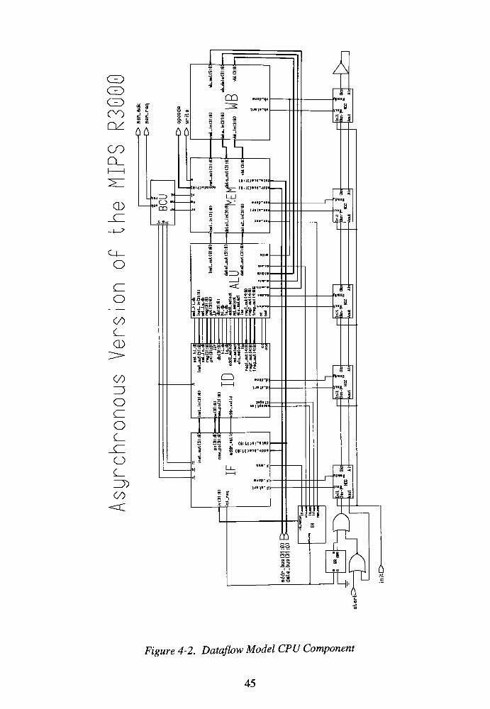
CUD
CD
CO
LZV.
CO
CD
O
o
CO
CD
CO
ZJ
o
d
o
c_
00
o
cz
CO
00
.CJ
'
'CD .
n
CQ uop-qn
qjtv)i-qn
ffi(BlLE)i>T1l
ci;iE>4nq-jppi
luep-i
s -ts
1 1i ?
<C .B..
unv
4 n4S ~ "TSS 44-
uj ,-SS K43flJl>( Jdji-i",
I.SlflijSuiijlTJv???! 8l
JLUflSflraS^raflflg^
' g. So coca o j
3^ !! JJJ
8IpMl
|noj_
8
|noj_
lpMjj
|nJL
=1 I
Fz'gwre 4-2. DataflowModel CPU Component
45
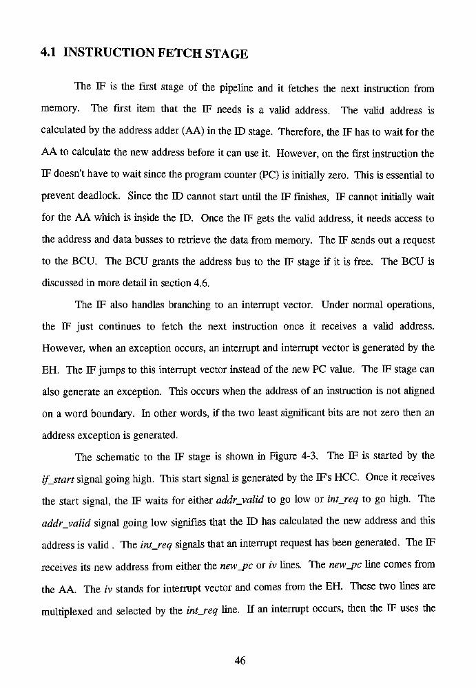
4.1 INSTRUCTION FETCH STAGE
The IF is the first stage of the pipeline and it fetches the next instruction from
memory. The first item that the IF needs is a valid address. The valid address is
calculated by the address adder (AA) in the ID stage. Therefore, the IF has to wait for the
AA to calculate the new address before it can use it. However, on the first instruction the
IF doesn't have to wait since the program counter (PC) is initially zero. This is essential to
prevent deadlock. Since the ID cannot start until the IF finishes, IF cannot initially wait
for the AA which is inside the ID. Once the IF gets the valid address, it needs access to
the address and data busses to retrieve the data from memory. The IF sends out a request
to the BCU. The BCU grants the address bus to the IF stage if it is free. The BCU is
discussed in more detail in section 4.6.
The IF also handles branching to an interrupt vector. Under normal operations,
the IF just continues to fetch the next instruction once it receives a valid address.
However, when an exception occurs, an interrupt and interrupt vector is generated by the
EH. The IF jumps to this interrupt vector instead of the new PC value. The IF stage can
also generate an exception. This occurs when the address of an instruction is not aligned
on a word boundary. In other words, if the two least significant bits are not zero then an
address exception is generated.
The schematic to the IF stage is shown in Figure 4-3. The IF is started by the
ifjstart signal going high. This start signal isgenerated by the IF's HCC. Once it receives
the start signal, the IF waits for either addr_valid to go low or intjreq to go high. The
addrjvalid signal going low signifies that the ID has calculated the new address and this
address is valid . The intjreq signals that an interrupt request has been generated. The IF
receives its new address from either the newjpc or iv lines. The newjpc line comes from
the AA. The iv stands for interrupt vector and comes from the EH. These two lines are
multiplexed and selected by the intjreq line. If an interrupt occurs, then the IF uses the
46
interrupt vector (iv) value. On the other hand, if the IF is in normal operation then the
new PC value (newjjc) is used.
When addr_valid goes low, the IF sends a bus request (ir) to the BCU. This
signal is also used to latch the address that comes from the AA. The IF now waits until
the BCU sets ia high. The ia signal going high is an acknowledgment from the BCU that
the IF has been granted access to the address bus. When ia goes high, it enables the tri-
state buffer, placing the address on the address bus. This ia acknowledgment signal is
needed to allow the address to be setup on the address bus before the memory read. Now
the IF sends the BCU the il line high signaling that the address has been loaded on the
address bus. The BCU can now initiate the memory request. The IF waits until ia goes
low signaling that the data bus now contains a valid instruction. The ia line going low
causes the instruction on the data bus to be latched and resets the ir and il signals.
Resetting the ir line signals to the BCU that the IF is finished with the address bus. The
waveforms showing the IF operation are shown in Figure 4-4.
47

CO
o
Figure 4-3. Schematic ofIF Stage
48
uX
CD
CVJ
CD
CP<ZD
CD
CD
CNJ
CO
CJ3
CD
CD
CD
CD
CD
CB
CD
CD
CD
CD
CD
CD
CD
CB
CD
CD
CB
CD
CD
CD
CD
CD
CD
CD
CB
L&
CO
GO
CD
CD
CD
CD
CD
CD
CD
CD
CD
CD
CO
en
ro
CD
cdr
co
CD"
CuO m
ro <=
CNJ
ro
^J-
CNJ
co
CD
CD
O CDCD
vSRJ LSD
<S CD
CO
CD
CD
CO
CO
COCNJ
cn
a -aCD
I Io CD
3 4-1
3 4, CNJ
Fj^wrf? 4-4. Waveforms ofIF Stage
49
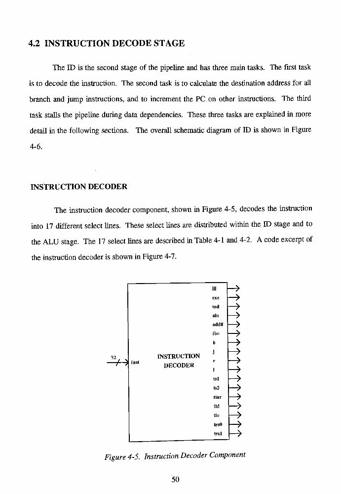
4.2 INSTRUCTION DECODE STAGE
The ID is the second stage of the pipeline and has three main tasks. The first task
is to decode the instruction. The second task is to calculate the destination address for all
branch and jump instructions, and to increment the PC on other instructions. The third
task stalls the pipeline during data dependencies. These three tasks are explained in more
detail in the following sections. The overall schematic diagram of ID is shown in Figure
4-6.
INSTRUCTION DECODER
The instruction decoder component, shown in Figure 4-5, decodes the instruction
into 17 different select lines. These select lines are distributed within the ID stage and to
the ALU stage. The 17 select lines are described in Table 4-1 and 4-2. A code excerpt of
the instruction decoder is shown in Figure 4-7.
ill
exc ->
md ->
alu ->
add8 ->
ibo ->
b >
32/ .
INSTRUCTION
mst
DECODER
j
r
1
>/ ?
>tsl ->
ts2
ttar ->
thi ->
tlo ~>
trsO ->
trsl ->
Figure 4-5. Instruction DecoderComponent
50
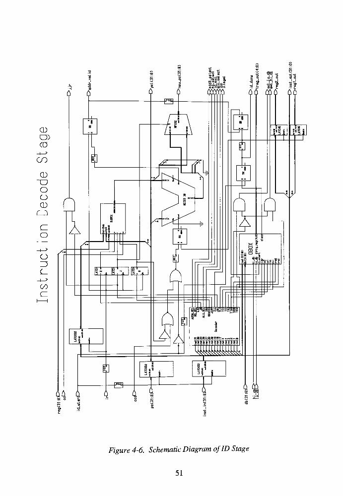
CD
D)
CO
CO
CO
"O
o
o
CD
CD
O
o
ZJ
c_
CO
6.4 &
Figure 4-6. Schematic Diagram ofID Stage
51
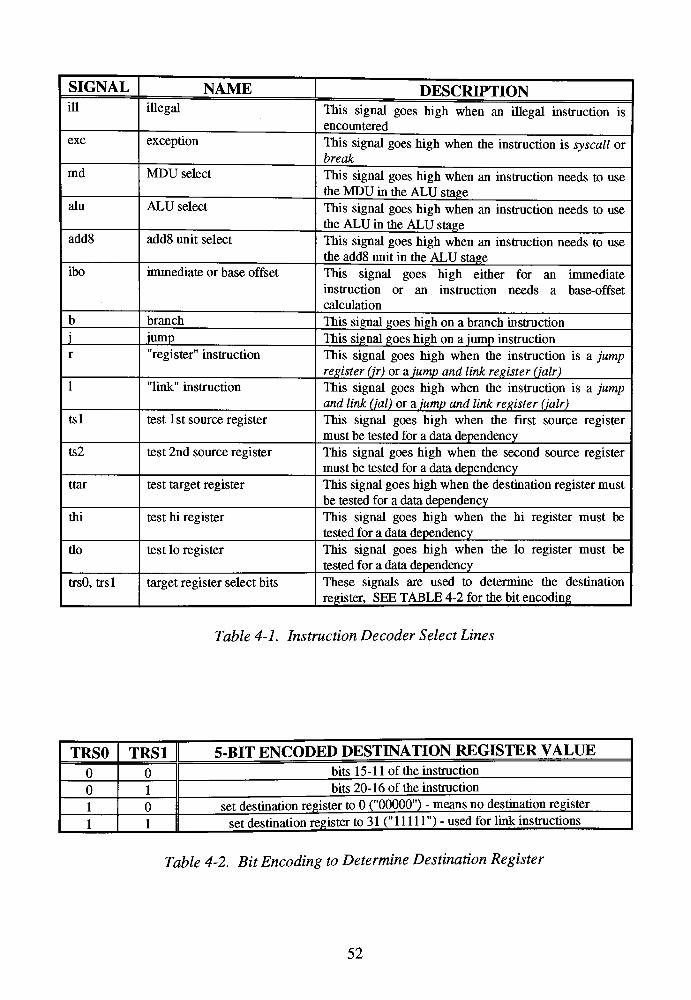
SIGNAL NAME DESCRIPTION
ill illegal This signal goes high when an illegal instruction is
encountered
exc exception This signal goes high when the instruction is syscall or
break
md MDU select This signal goes high when an instruction needs to use
the MDU in the ALU stage
alu ALU select This signal goes high when an instruction needs to use
the ALU in the ALU stage
add8 add8 unit select This signal goes high when an instruction needs to use
the add8 unit in the ALU stage
ibo immediate or base offset This signal goes high either for an immediate
instruction or an instruction needs a base-offset
calculation
b branch This signal goes high on a branch instruction
i jump This signal goes high on a jump instruction
r"register"
instruction This signal goes high when the instruction is a jumpregister (jr) or a jump and link register (fair)
1"link"
instruction This signal goes high when the instruction is a jumpand link (jal) or a jump and link register (jalr)
tsl test 1st source register This signal goes high when the first source register
must be tested for a data dependency
ts2 test 2nd source register This signal goes high when the second source register
must be tested for a data dependency
ttar test target register This signal goes high when the destination register must
be tested for a data dependency
thi test hi register This signal goes high when the hi register must be
tested for a data dependency
do test lo register This signal goes high when the lo register must be
tested for a data dependency
trsO, trsl target register select bits These signals are used to determine the destination
register, SEE TABLE 4-2 for the bit encoding
Table 4-1. Instruction Decoder Select Lines
TRSO TRS1 5-BIT ENCODED DESTINATION REGISTER VALUE
0 0 bits 15-11 of the instruction
0 1 bits 20-16 of the instruction
1 0 set destination register to 0 ("00000") - means no destination register
1 1 set destination register to 31 ("1 1 111") - used for link instructions
Table 4-2. Bit Encoding to Determine Destination Register
52
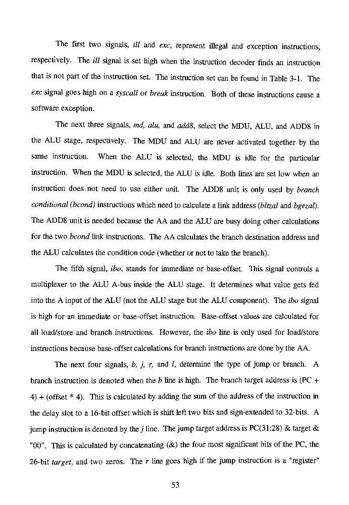
The first two signals, ill and exc, represent illegal and exception instructions,
respectively. The ill signal is set high when the instruction decoder finds an instruction
that is not part of the instruction set. The instruction set can be found in Table 3-1. The
exc signal goes high on a syscall or break instruction. Both of these instructions cause a
software exception.
The next three signals, md, alu, and add8, select the MDU, ALU, and ADD8 in
the ALU stage, respectively. The MDU and ALU are never activated together by the
same instruction. When the ALU is selected, the MDU is idle for the particular
instruction. When the MDU is selected, the ALU is idle. Both lines are set low when an
instruction does not need to use either unit. The ADD8 unit is only used by branch
conditional (bcond) instructions which need to calculate a link address (bltzal and bgezal).
The ADD8 unit is needed because the AA and the ALU are busy doing other calculations
for the two bcond link instructions. The AA calculates the branch destination address and
the ALU calculates the condition code (whether or not to take the branch).
The fifth signal, ibo, stands for immediate or base-offset. This signal controls a
multiplexer to the ALU A-bus inside the ALU stage. It determines what value gets fed
into the A input of the ALU (not the ALU stage but the ALU component). The ibo signal
is high for an immediate or base-offset instruction. Base-offset values are calculated for
all load/store and branch instructions. However, the ibo line is only used for load/store
instructions because base-offset calculations for branch instructions are done by the AA.
The next four signals, b, j, r, and /, determine the type of jump or branch. A
branch instruction is denoted when the b line is high. The branch target address is (PC +
4) + (offset * 4). This is calculated by adding the sum of the address of the instruction in
the delay slot to a 16-bit offset which is shift left two bits and sign-extended to 32-bits. A
jump instruction is denoted by the; line. The jump target address is PC(31:28) & target &
"00". This is calculated by concatenating (&) the four most significant bits of the PC, the
26-bit target, and two zeros. The r line goes high if the jump instruction is a"register"
53

ARCHXTl&CTURB dfinstdee^a OF dfinstdec.IS
SSd- <*4l AFEBB 4,4 ns WHEW al5
(i<31) =*0'
AND
i<29 COWNTO 26) ="0000" KSD \
1<4 DOWSuWJ 3 J * "|1") ELSE
'0* AFTER 4,4 ns,-
END dfinstdec_a;
Figure 4-7. Code Excerpt of the ID Stage InstructionDecoderArchitecture
instruction. Jump register (jr) and jump and link register (jalr) are the two"register"
instructions. This r line is needed because a jump register instructions get their jump
target address from the contents of a register. The / line goes high on a jump and link
instruction. The two jump and link instructions art jump and link (jal) and jump andlink
register (jalr). For these instructions, the ID must give the ADD8 unit in the ALU stage
the PC to calculate the link address of (PC + 8).
The next five signals, tsl, ts2, ttar, thi, and tlo,are for data dependency checking.
Each of these signals, when set high, tests to see if respective register is dirty. IF a
register is dirty then the ID is stalled until the previous instruction writes its data to this
register. Data dependency is discussed in moredetail in a later section.
The last two signals, trsO and trsl, are used together to determine where in the
instruction to get the destination registervalue. The four choices are shown in Table 4-2.
When trsO and trsl equal"00"
then the destination registervalue is found at bits 15-11 of
the instruction. This choice is used for allspecial instructions. When trsO and trsl equal
"01"
then the destination is found at bits20-16 of the instruction. This choice is used for
loads and immediate instructions. These instructions use a 16-bit offset or immediate
value located at bits 15-0 of the instruction. Therefore the destination bit location is
54
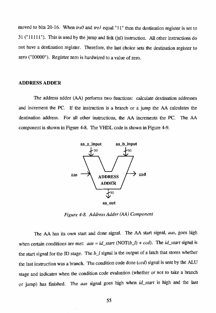
moved to bits 20-16. When trsO and trsl equal"11"
then the destination register is set to
31 ("111 11")- This is used by the jump and link (jal) instruction. All other instructions do
not have a destination register. Therefore, the last choice sets the destination register to
zero ("00000"). Register zero is hardwired to a value of zero.
ADDRESS ADDER
The address adder (AA) performs two functions: calculate destination addresses
and increment the PC. If the instruction is a branch or a jump the AA calculates the
destination address. For all other instructions, the AA increments the PC. The AA
component is shown in Figure 4-8. The VHDL code is shown in Figure 4-9.
aa_a_input aa_b_input
aas AADDRESS
/
7 aad
ADDER
aa_out
Figure 4-8. AddressAdder (AA) Component
The AA has its own start and done signal. The AA start signal, aas, goes high
when certain conditions are met: aas = idjstart (NOT(b_l) + ccd). The idjstart signal is
the start signal for the ID stage. The bj signal is the output of a latch that stores whether
the last instruction was a branch. The condition code done (ccd) signal is sent by the ALU
stage and indicates when the condition code evaluation(whether or not to take a branch
or jump) has finished. The aas signal goes high when idjstart is high and the last
55
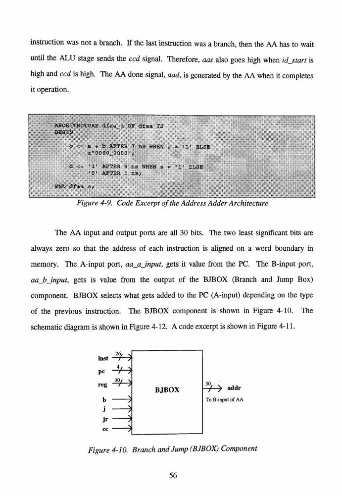
instruction was not a branch. If the last instruction was a branch, then the AA has to wait
until the ALU stage sends the ccd signal. Therefore, aas also goes high when idjstart is
high and ccd is high. The AA done signal, aad, is generated by the AA when it completes
it operation.
ARCKXTBCTtTRE dfa_a OF dfa*
BEGIN
*iiS::::
o <~ 9. + b AFTER 7 Xta WHE8 a ~
!ELSE
X"0000_DOO0;
d <='1'
ASTER 8 as
'0'ASTER 1 US;:
WHEN
||!||j||iiiiai?i;:;|:
s ='1'
ELSE
Figure 4-9. Code Excerpt of theAddressAdderArchitecture
The AA input and output ports are all 30 bits. The two least significant bits are
always zero so that the address of each instruction is aligned on a word boundary in
memory. The A-input port, aajxjnput, gets it value from the PC. The B-input port,
aajbjnput, gets is value from the output of the BJBOX (Branch and Jump Box)
component. BJBOX selects what gets added to the PC (A-input) depending on the type
of the previous instruction. The BJBOX component is shown in Figure 4-10. The
schematic diagram is shown in Figure 4-12. A code excerpt is shown in Figure 4-11.
26, ^inst f 7
pc
reg
b
j
cc
^30,SH>
^
BJBOX
30
-^->addr
To B-input of AA
Figure 4-10. Branch and Jump (BJBOX) Component
56

The inst signal provides the lower 26 bits of the instruction. A jump instruction
uses all 26 bits and is called the target value. A branch instruction uses only the lower 16
bits and is called an offset value. When the condition code, cc, is high then the branch is
taken. The pc signal provides the upper four bits of the PC. This is needed to calculate
the jump target address. The reg signal is used with the register jump instructions. This
signal is the register jump target address. The b, j, and jr signals correspond to a branch,
jump, and register jump instructions, respectively. The addr signal is the BJBOX output
and is the address that is passed to the AA.
ARCHITECTURE dfbjbo:xa OF dfbjbox. IS
component and signal declarations
BEGIN
seb <= inat2&(15};
Seb4 <- Seb & ssb & Seb & S6fe;
sabio <=; seb & aeb & &eb4 & sebAf
muxl: d4te>lmux4
PORT W&{Hr reg(29 DOWNTO 25), pc4, seb4, SO, si, ail);
rnuxZ : df41imuxl&
PORT M&{310, reg [25 DOWNTO 1), inst2(2S DOWNTO 16), aeblO,
AO, si,
mnx^ t d4 to lumxl6
PORT KAPCiv, reg(15 DOWNTO 0), inst2fS(15 DOWNTO 0),
i_urt.26(15 DOWNTO OJ , SO, si, J)f
addx30 < ml & m2 fi m3;
BO <* NOT {X AND y) AFTER 0.7 ns;
Bl < NOT (X AND Z) AFTBR 0.7 a,-
x <= NOT (cc AND b} ASTER 0.7 ne^
y <- NOT }x AFTER 0.3 lis;
z < NOT ..iyAND .)
AFTER 0,7 ns;
END dfbjbox_a;
Figure 4-77. Code Excerpt of the BJBOXArchitecture
BJBOX has to handle four different instruction cases: branches, jumps, register
jumps, and all other instructions. For the branch instruction case, BJBOX sign-extends
57
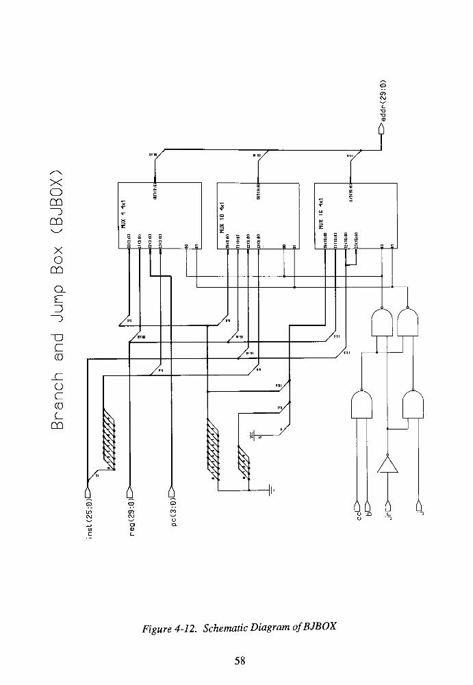
X
o
CQ
~>
CQ
OD
OJ
0
X
o
CQ
Q.
Z5
>
TJ
C
(0
O
c
(0
(_
CQ
^1
h A 6Q o
LO
OJ
CO
OJ
CO
u
41 OJ
CD
a
-4-i
ll
y
O uO f- ~>
o ->
Figure 4-72. Schematic Diagram ofBJBOX
58
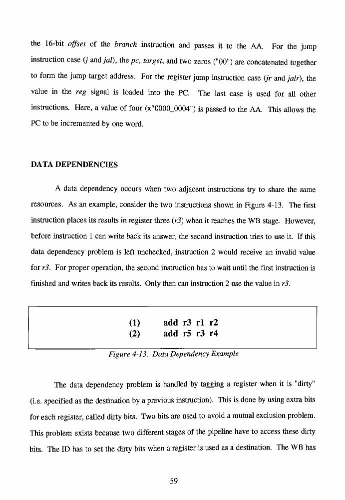
the 16-bit offset of the branch instruction and passes it to the AA. For the jump
instruction case (j and jal), the pc, target, and two zeros ("00") are concatenated together
to form the jump target address. For the register jump instruction case (jr and jalr), the
value in the reg signal is loaded into the PC. The last case is used for all other
instructions. Here, a value of four (x"0000_0004") is passed to the AA. This allows the
PC to be incremented by one word.
DATA DEPENDENCIES
A data dependency occurs when two adjacent instructions try to share the same
resources. As an example, consider the two instructions shown in Figure 4-13. The first
instruction places its results in register three (r3) when it reaches the WB stage. However,
before instruction 1 can write back its answer, the second instruction tries to use it. If this
data dependency problem is left unchecked, instruction 2 would receive an invalid value
for r3. For proper operation, the second instruction has to wait until the first instruction is
finished and writes back its results. Only then can instruction 2 use the value in r3.
(1) add r3 rl r2
(2) add r5 r3 r4
Figure 4-13. Data Dependency Example
The data dependency problem is handled by tagging a register when it is"dirty"
(i.e. specified as the destination by a previous instruction). This is done by using extra bits
for each register, called dirty bits. Two bits are used to avoid a mutual exclusion problem.
This problem exists because two different stages of the pipeline have to access these dirty
bits. The ID has to set the dirty bits when a register is used as a destination. The WB has
59
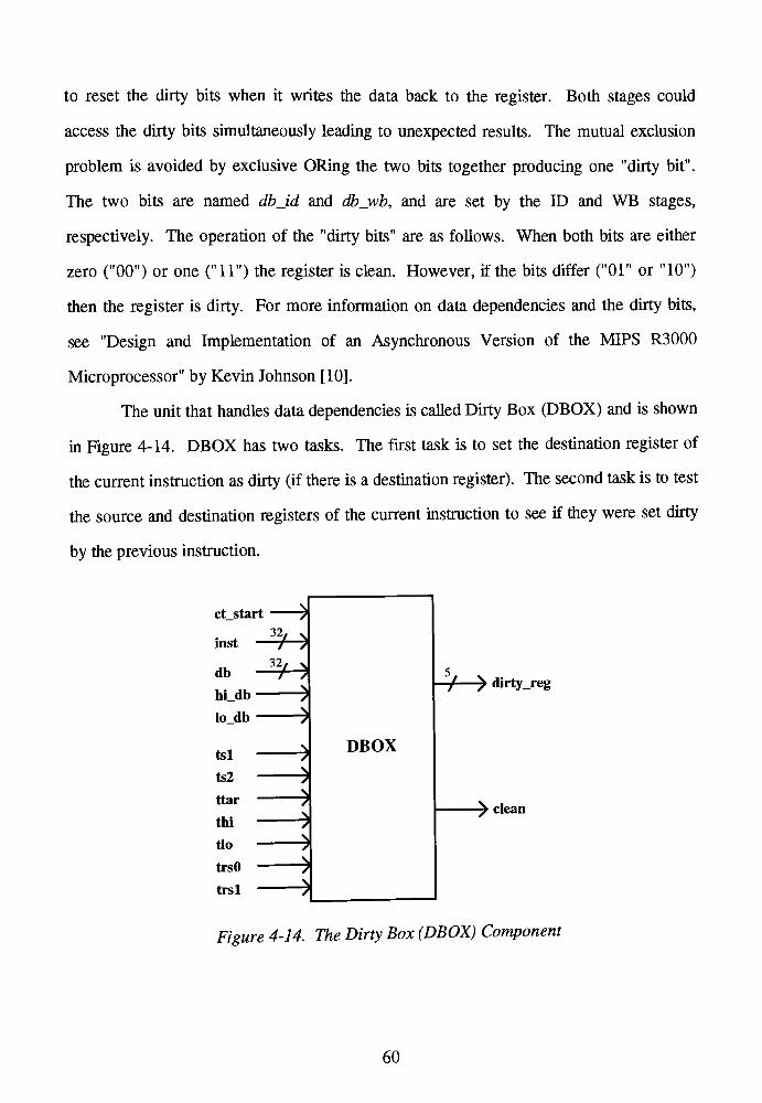
to reset the dirty bits when it writes the data back to the register. Both stages could
access the dirty bits simultaneously leading to unexpected results. The mutual exclusion
problem is avoided by exclusive ORing the two bits together producing one "dirty bit".
The two bits are named dbjd and dbjwb, and are set by the ID and WB stages,
respectively. The operation of the "dirtybits"
are as follows. When both bits are either
zero ("00") or one ("11") the register is clean. However, if the bits differ("01"
or "10")
then the register is dirty. For more information on data dependencies and the dirty bits,
see "Design and Implementation of an Asynchronous Version of the MIPS R3000
Microprocessor"
by Kevin Johnson [10].
The unit that handles data dependencies is called Dirty Box (DBOX) and is shown
in Figure 4-14. DBOX has two tasks. The first task is to set the destination register of
the current instruction as dirty (if there is a destination register). The second task is to test
the source and destination registers of the current instruction to see if they were set dirty
by the previous instruction.
ct start
-f- > dirty_reg
\\S clean
Figure 4-14. The Dirty Box (DBOX) Component
60

The first task is implemented by a unit inside DBOX called Target Register Dirty
Select (TRDS), shown in Figure 4-15. TRDS selects which register will be set dirty.
TRDS input ports are inst, trsO, and trsl. The inst signal is needed to determine which
register is the destination. The trsO and trsl signals specify where to find the destination
register. These two signals are discussed in instruction decoder section and can be found
in Tables 4-1 and 4-2. The schematic diagram of TRDS is shown in Figure 4-18. The
VHDL code of the TRDS architecture is shown in Figure 4-16.
Figure 4-15. TargetRegisterDirty Select (TRDS) Component
ARC_rtTECTtiRB dtrda_a or dftrds IS
BEGIN
sag = inst {15 DOWNTO 11) AETER 0.4 ns WHEN
trsO _
'0'AND trsl ~
' 0'ELSE
ilist(20 DOWNTO 16} AFTER 0.4 ns WHEN
tret) ='01
AHD tral =!
ELSE
b"lllll" AFTER 0.4 as WHEN
trsO =' 1* AND trsl -
' 1*ELSE
b"O0QOQHAFTER 0.4 ns;
EHD dftrds a;
special
- iana or load
--jal
Figure 4-16. VHDL Code of the TRDSArchitecture
The second task is handled by DBOX and the schematic diagram is shown in
Figure 4-19. The dirty bit signals, db, hijib, and lojdb, comefrom the register banks in
the ALU stage and are used for dirty bit testing. The db signal is a 32-bit line, each line
61
representing one dirty bit of the 32 general purpose registers. The hijib and lo_db signals
represent the hi and lo register dirty bits, respectively. The ctjstart line starts the dirty bit
testing. When this line is low, the dirty bit testing is valid. The five signals, tsl, ts2, ttar,
thi, and tlo, determine which registers to test. These signals are generated by the
instruction decoder and are discussed in the instruction decoder section. Tables 4- 1 and
4-2 give a brief description of each signal. The dirtyjeg signal is five bits wide and is the
TRDS output. It specifies which destination register will be set dirty. If there is no
destination register for the current instruction, then register zero is specified. The last
signal, clean, stalls the ID stage when there is a data dependency. The VHDL code of the
DBOX architecture is shown in Figure 4-17.
62
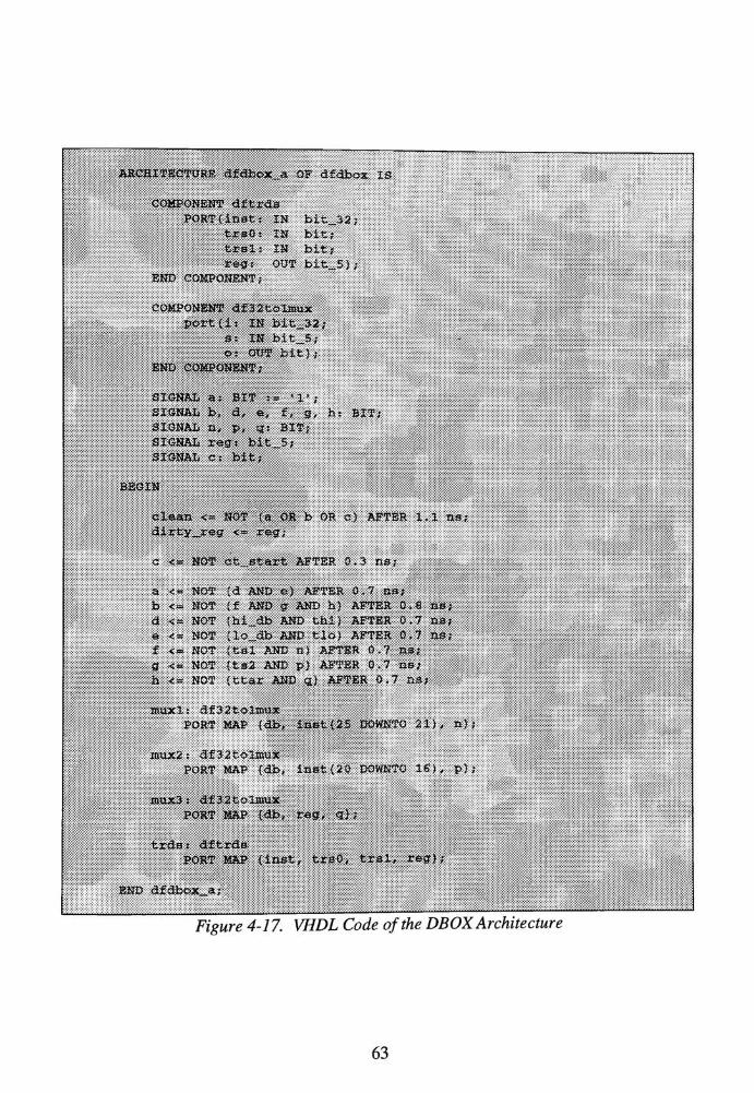
ARCHITECTURE dfdbox a OF dfdbox IS
COMPONENT dftrda
PORT (inst*
fcrsOi
l:|i:|i:|ii|i=;?|;|||:jil|i!i;^ji4^:::WlWyWI&rW,WM&i
END COMPONENT;
<mr ;
IN bit32 ;
$:., bit?IN*:: bit;
OUT blt_5) ;
COMPONENT df32tolinu3C
port (is IN bit_32;
9: IN Mt_5;Oi OUT bit);
-"mmmmmm-
?J
SIGNAL a; BIT -.-
'1';
SIGNAL b, dr e, f, g,
SIGNAL n, p, q: BIT;
SIGNAL reg bit. 5;
SIGNAL c: bit;
h: BIT/
BEGIN
c&aan < NOT (a OR b or c) AFTER i,l na;
dlrty_reg <= rag;
C <- NOT Ct_Staxt .AFTER 0.3 lis;
a <= NOT (d AND e) AFTER 0.7 ns;
b <= NOT (f AND g AND h) AFTER 0.8 ns;
d <= NOT (hi_db AND thi) AFTER 0.7 ns;
&<- NOT lo_db AND tla) AFTER 0,7 lis;
f <=> NOT (tal AND n) AFTER 0,7 lis;
g <= NOT (ts2 AND p) AFTER 0.7 ns;
Ii <* NOT (ttar AND a) AFTER 0.7 n*;
xtmxl: df32tolmux
PORT MAP (db, Inst {25 DOWNTO 21 ), 11} ;
mux2; d432tolnwx
PORT MAP (db, inst {20 DOWNTO 16) , p) ;
JBUX3j d32fcoDBUX
PORT MAP (db, res, 'J?
trdst dftrds
PORT MAP (ittst, feesO, trsl, r_g>;
END dfdbox a;
Figure 4-17. VHDL Code of the DBOXArchitecture
63
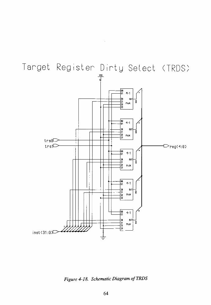
Target Register Dirty Select (TRDS
trsQO-
trslO"
vcc
s
inst(31:0)O" WM?7
1-1
OUT
nux
1-1
OUT
1-1
OUT10
11
12 nux
13
/
SO
si 1-1
10
11
K
13
OUT'
-OregM:0)
1-1
OUT
nux
Figure 4-18. SchematicDiagram ofTRDS
64
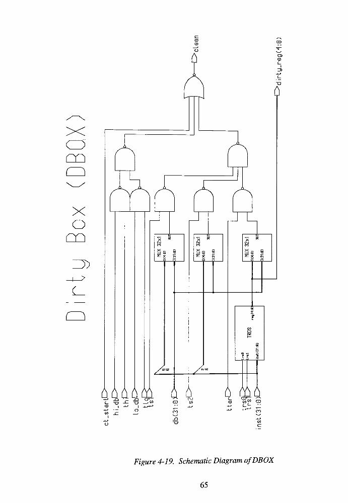
CC
X
o
CO
CO
-+^
(
r ^
AAAAiYl L\ 0 o mo4^ r-i i-i c~>
^-. C\J
L_ TJ ._ TJ V> o CA
> -^j-
1 i >
LJ
V>
1LJ
f )
_JZ
OCO
JD
TJ
MW CD
C
Figure 4-79. Schematic Diagram ofDBOX
65

4.3 ARITHMETIC LOGIC UNIT STAGE
The ALU is the third stage of the pipeline and has three units running in parallel.
They are the Arithmetic Logic Unit Block (ALUB), the Multiplier/Divider Unit (MDU),
and the ADD8 unit. The ALU stage is responsible for all arithmetic calculations. The
ALUB handles addition, subtraction, shifting, comparing, and logical operations. The
MDU handles multiplication and division operations. The ADD8 unit is responsible for
calculating link addresses for branch conditional instructions. The ALU stage also
contains the general register bank and the hi/lo register bank. The ALU diagram is shown
in Figure 4-20.
The MDU and ADD8 were designed by Scott Siers and are discussed in "Design
and Implementation of an Asynchronous Version of the MIPS R3000Microprocessor"
[19]. The ALUB and register banks are discussed in section 5.
66

Figure 4-20. ALU Stage BlockDiagram
67

4.4 MEMORY STAGE
The MEM is the fourth stage of the pipeline and handles all accesses to memory.
This stage is very similar to the IF stage with the following exceptions. The MEM stage
only accesses memory on load and store instructions while the IF does so for every
instruction. MEM accesses memory by reading and writing while IF only reads. The final
difference is that MEM needs to filter data read from memory. The schematic drawing is
shown in Figure 4-21.
When MEM encounters a non load or store instruction, it passes the instruction on
to the next stage. However, when the instruction is a load or store, the MEM stage has to
gain access to the busses to carry out the instruction. MEM sends a bus request to the
BCU. Once the address and data busses are free, The BCU grants them to MEM. The
BCU is discussed in more detail in section 4.6.
Part of the MEM-to-memory interface involves the write and opcode signals. The
write signal specifies whether the memory access will be a read or write. When write is
high the access is a write. MEM has a write signal because it is the only stage that writes
to memory (the IF stage only has to read instructions from memory). The opcode signal
specifies the type of store instruction. The five choices are store byte (sb), store halfword
(sh), store word left (swl), store word (sw), and store word right (swr). The write and
opcode signals are set to default values to allow proper operation of the IF stage. The
write signal is set to'0'
to specify a read operation. The opcode signal is set to"Oil"
to
specify a word.
The MEM stage consists of three main units. They are the memory decoder, the
mask unit (MU), and the shift unit (SU). The memory decoder provides necessary
instruction decoding used by MEM and WB. The decoder select lines include vbt, load,
store, susO-3, and musO-3. The valid byte tag (vbt) signal is used by the register bank in
the ALU stage. It specifies which bytes of data are valid. Only a valid byte is written
68
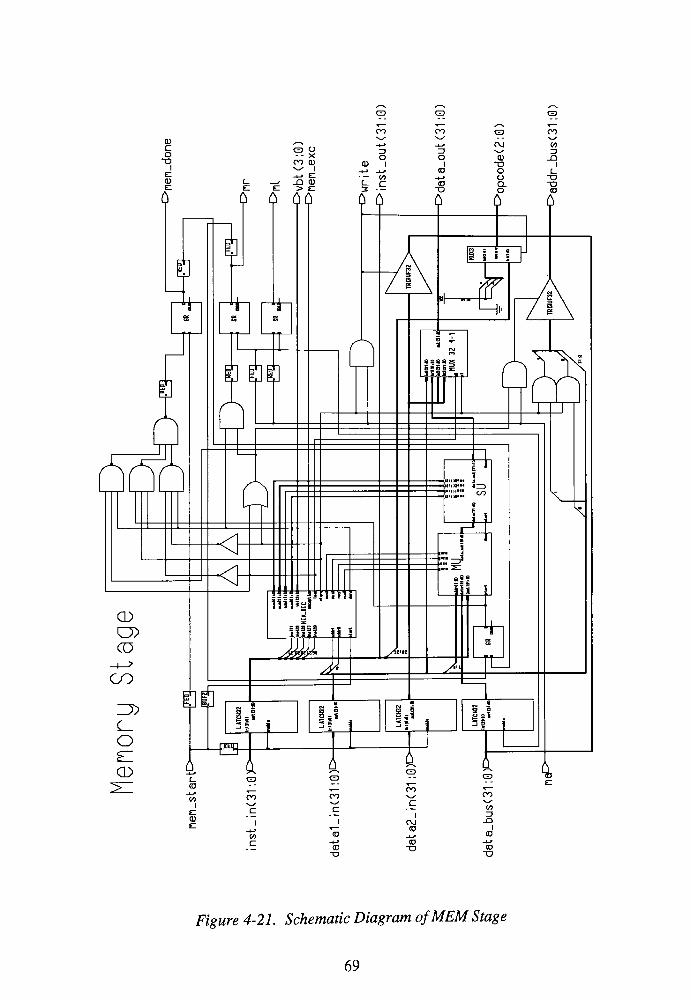
CDLZ
o
TJ
OJE
CD O-- X
CO <u
-^ JD CD
0 0 00
cEO
CD
CD
CO
z
c_
o
EI
CD
*_-
a
<
<:Ilia
0 0
o o LTD
4-
4N ,
oo co CZ> OO*s ^u*
-u -u CVI wz< ZJ - ZJ
o1
o
1CDTJ
JD
1-u CO O [_</> i
- O TJ
<z (D Q. TJTJ O (D
Q
Jliini
111! ii j
BO
31-.a
>i
R
j
^i
s" 3 1
TTT1L- o (ZJ
(0^ , CO
4
W CO oo
c c
1
1
CO
ZJ
JD
-4^
"ro(0^u.
1CD
-l- CO -4^
(0
TJTJ CD
TJ
\
Figure 4-21. Schematic Diagram ofMEM Stage
69
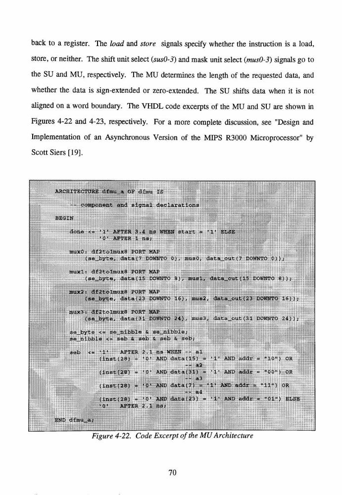
back to a register. The load and store signals specify whether the instruction is a load,
store, or neither. The shift unit select (susO-3) and mask unit select (musO-3) signals go to
the SU and MU, respectively. The MU determines the length of the requested data, and
whether the data is sign-extended or zero-extended. The SU shifts data when it is not
aligned on a word boundary. The VHDL code excerpts of the MU and SU are shown in
Figures 4-22 and 4-23, respectively. For a more complete discussion, see "Design and
Implementation of an Asynchronous Version of the MIPS R3000Microprocessor"
by
Scott Siers [19].
ARCHITECTDRE dfmu_a OP dftnu XS
-- corojKinant and signal declarations
BEGIN
*H*,<::;done <_'i<
AFTER 3.4 ns WHEW start - '10*
AFTER 1 ns;
muxO; df2tOlmux8 PORT M>AP
{&6jz>yt<z, data {7 DOWNTO 0) , rousQ, dataout<7 DOWNTO 0));
muxls d2tolniux8 PORT MAP
(sejbyte, data{15 DOWNTO B), musl, dafca_out(15 DOWNTO 8});
nmx2j df2t.olmux.i3 PORT HAP
(sejbyte, data{23 DOWNTO lfi), mus2, data_out(23 DOWNTO 16));
:'i:
jnux3t d2tolmux8 PORT MAP
(sejbyte, data(31 DOWNTO 24}, musa, data_out(31 DOWNTO 24));
aebyte <- sejaibble fc aeaibbla;
s<anibb_5 <_ seb & s<ab & seb 4 seb;
ssb <='1* AFTER 2.1 ns WREN al
(inst (28) -
"0* AND data (IS) -
'1'AND addr - "10") OR
-- a2
(inst (283 <='0*
AND data (31) ='l'
AND addr "00") OR
3
(inst (28) *0< AND data (7) *
*_' AND addr = "ll") OR
Tllllllll:^
;::T:;|;lllliilll|llp
END dfimi_af
Figure 4-22. Code Excerpt of theMUArchitecture
70
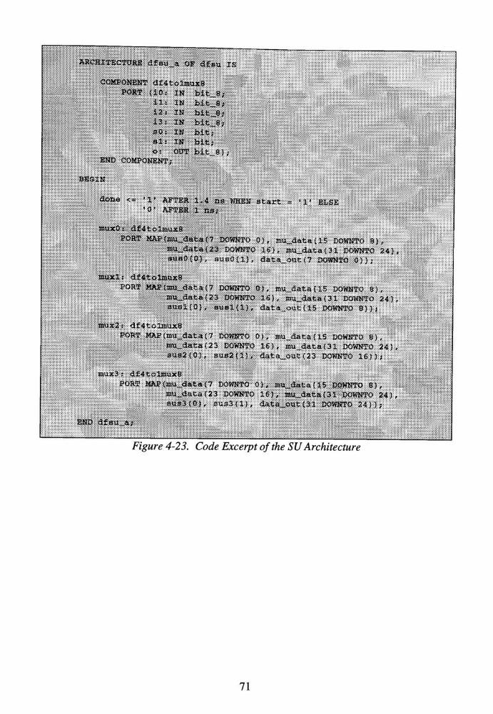
ARCHITECTURE dfsu_a OF dfsu IS
: COMPONENT dfi4toUttUx8
FO&T (iOf IN Mt_8;ill IN hit-Jitlit 2N bit_8;i3s IN bit^S*SOt IN Mt;'alt IN-
bit*os ODT bit_8);
END COMPONENT;
BEGIN
dona <= <i<AFTER 1,4 ns WHEN start -
i<ELSE
"0*
AFTER:l'"n9f
-
rouxO >..: df4tolmux8
PORT MAP(mo_ata{7 DOWNTO 0), mudata(15 DOWNTO 8),JdUdata(23 DOWNTO IS), udata(31 DOWNTO 24),
saa&iO}, susO{l), dataout(7 DOWNTO 0));
auixls df4tol_auc8
PORT MAPXmu_data(7 DOWNTO Q>, m_data(l$ DOWNTO 8),
nmdata(23 DOWNTO 16), roudata(31 DOWNTO 24),
ausKO}, jsmsl{l), data_out(lS DOWNTO 8});
mux2r df4tolmux8
FORT MAF(mu_data(7 DOWNTO 0), imidata(lS DOWNTO 8),
rau_data(23 DOWNTO 16), inu_data(31 DOWNTO 24),
aus2(0), sus2{l), dataout{23 DOWNTO 16));
mux3 t d4tarauxB
PORT MAP(mu_data(7 DOWNTO 0), mu_data(lS DOWNTO 8),inudata{23 DOWNTO 16), DOWNTO 24),
SUS3(0), SU33 (1), data_OUt(31 DOWNTO 24));
dfs_aji
Figure 4-23. Code Excerpt of the SUArchitecture
71

4.5 WRITEBACK STAGE
The WB is the fifth and final stage of the pipeline. It writes the results back into
the general purpose register bank or into the hiflo register bank, depending on the
instruction. The schematic diagram is shown in Figure 4-24. WB consists mainly of the
decoder unit, another TRDS unit, and an encoder. The decoder unit decodes the trsO and
trsl select lines used by the TRDS unit. The TRDS unit specifies which of the general
purpose registers is the destination (if there is one). A six-bit encoding scheme, shown in
Table 4-3, is used to determine the destination register. If the most significant bit (MSB)
is '0', the least significant five bits selects one of the general purpose registers as the
destination. If the MSB is T, then the least significant bit (LSB) selects the hi/lo register.
If the LSB is'0'
then the destination is the hi register. The LSB equal to'1'
specifies the lo
register.
BITS 5-0 DESTINATION REGISTER
Orrrrr general purpose register"rrrrr"
lxxxxO hi register
lxxxxl lo register
note:"rrrrr"
= 5 bits to select which GPR'x'
= don't care
Table 4-3. WB Stage Destination RegisterBit Encoding Scheme
72

CD
O)
CO
CO
JdZ
o
CO
JZu
CD
C_
Figure 4-24. Schematic Diagram ofWB Stage
73
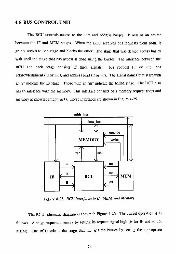
4.6 BUS CONTROL UNIT
The BCU controls access to the data and address busses. It acts as an arbiter
between the IF and MEM stages. When the BCU receives bus requests from both, it
grants access to one stage and blocks the other. The stage that was denied access has to
wait until the stage that has access is done using the busses. The interface between the
BCU and each stage consists of three signals: bus request (ir or mr), bus
acknowledgment (ia or ma), and address load (il or ml). The signal names that start with
an"i"
indicate the IF stage. Those with an"m"
indicate the MEM stage. The BCU also
has to interface with the memory. This interface consists of a memory request (req) and
memory acknowledgment (ack). These interfaces are shown in Figure 4-25.
addr bus
data bus
MEMORY
<r
7fr
req
IF
ir
fia
^
opcode
write
ack
JLdL
(r
BCU
mr
ma
fml
^K
MEM
Figure 4-25. BCU Interfaces to IF, MEM, andMemory
The BCU schematic diagram is shown in Figure 4-26. The circuit operation is as
follows. A stage requests memory by setting its request signal high (ir forIF and mr for
MEM). The BCU selects the stage that will get the busses by setting the appropriate
74
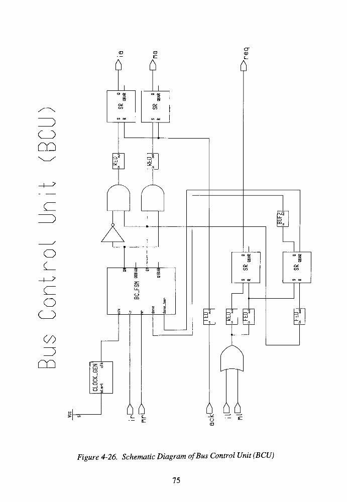
CD
CO
CO
cc
o
o
CO
o
cc
0 0
ZJ"
Jj
DX
CJ
CD ~
A
AJg
=3
33c
CO
66
CO
6 66o
CD
Figure 4-26. Schematic Diagram ofBus Control Unit (BCU)
75
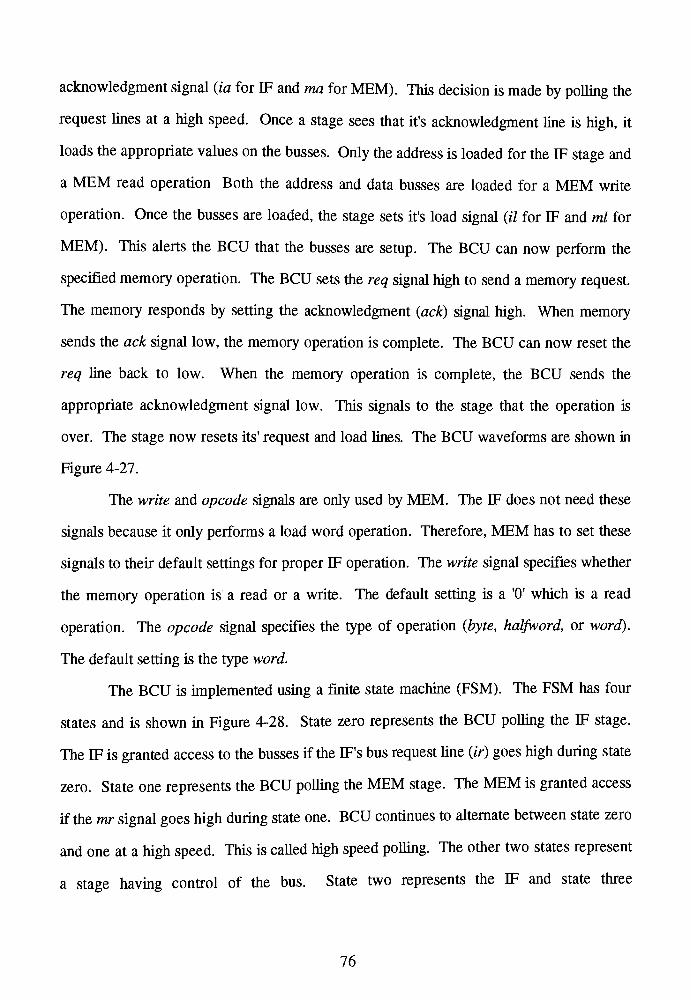
acknowledgment signal (ia for IF and ma forMEM). This decision is made by polling the
request lines at a high speed. Once a stage sees that it's acknowledgment line is high, it
loads the appropriate values on the busses. Only the address is loaded for the IF stage and
a MEM read operation Both the address and data busses are loaded for a MEM write
operation. Once the busses are loaded, the stage sets it's load signal (il for IF and ml for
MEM). This alerts the BCU that the busses are setup. The BCU can now perform the
specified memory operation. The BCU sets the req signal high to send a memory request.
The memory responds by setting the acknowledgment (ack) signal high. When memory
sends the ack signal low, the memory operation is complete. The BCU can now reset the
req line back to low. When the memory operation is complete, the BCU sends the
appropriate acknowledgment signal low. This signals to the stage that the operation is
over. The stage now resetsits'
request and load lines. The BCU waveforms are shown in
Figure 4-27.
The write and opcode signals are only used by MEM. The IF does not need these
signals because it only performs a load word operation. Therefore, MEM has to set these
signals to their default settings for proper IF operation. The write signal specifies whether
the memory operation is a read or a write. The default setting is a'0'
which is a read
operation. The opcode signal specifies the type of operation (byte, halfword, or word).
The default setting is the type word.
The BCU is implemented using a finite state machine (FSM). The FSM has four
states and is shown in Figure 4-28. State zero represents the BCU polling the IF stage.
The IF is granted access to the busses if the IF's bus request line (ir) goes high during state
zero. State one represents the BCU polling the MEM stage. The MEM is granted access
if the mr signal goes high during state one. BCU continues to alternate between state zero
and one at a high speed. This is called high speed polling. The other two states represent
a stage having control of the bus. State two represents the IF and state three
76
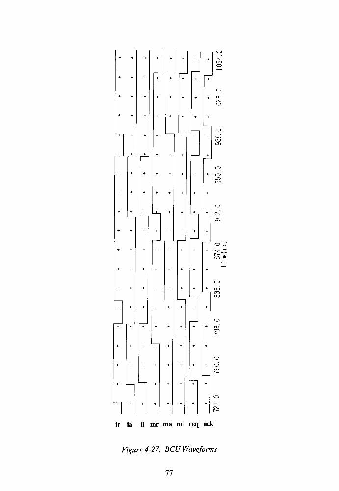
CD
LZD
CO
OJ
LZD
CO
COCT)
LZD
CT>
LZD
OJ
CD
LZD
r~~
CO
CD
cn
co
coCT)
+ CD
CD
CNJ
ir ia il mr ma ml req ack
Figure 4-27. BCUWaveforms
77
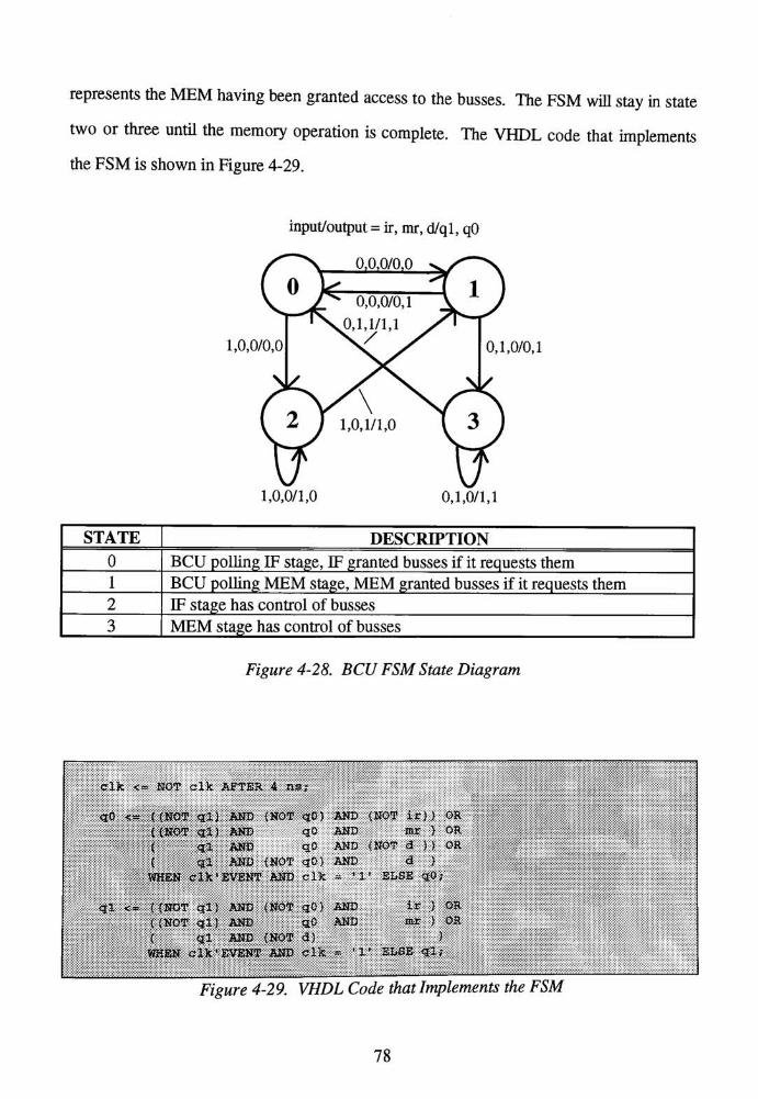
represents theMEM having been granted access to the busses. The FSM will stay in state
two or three until the memory operation is complete. The VHDL code that implements
the FSM is shown in Figure 4-29.
input/output = ir, mr, d/ql, qO
1,0,0/0,0 0,1,0/0,1
1,0,0/1,0 0,1,0/1,1
STATE DESCRIPTION
0 BCU polling IF stage, IF granted busses if it requests them
1 BCU polling MEM stage, MEM granted busses if it requests them
2 IF stage has control of busses
3 MEM stage has control of busses
Figure 4-28. BCU FSM State Diagram
elk < NOT elk AFTER 4 as.,-
qQ <* ({NOT ql] AND (NOT <j0) AND (NOT lr)> OR
((NOT ql) AND qO AND Sir } OR
;'( ql AND qO AND (NOT d )) OR|
( ql AND (NOT qO) AND d )
T WHEN elk 'EVENT AND elk -
' I' EDSE qO;
ql - ( (SOT ql) AND (NOT qO) AND ir } OR
( (NOT ql) AND qO AND mr ) OR
{ ql AND (NOT d) )
\ WHEN elk 'EVENT AND elk *'1' B&SB ql;
Figure 4-29. VHDL Code that Implements the FSM
78

5.0 STRUCTURALMODEL
The structural model builds on the previous dataflow model. It uses the same
dataflow test bench and top level components (memory module, compare module, and
CPU component). The only modifications are to the ALU stage of the CPU component.
The two units that are modeled at the structural level are the general register bank and the
arithmetic logic unit block (ALUB), located in the ALU stage.
5.1 GENERAL PURPOSE REGISTER BANK
The general purpose register (GPR) bank is composed of thirty-two 32-bit general
registers used by the processor for temporary storage for operands and results. The dirty
bits for each register are also found in the GPR bank. The GPR bank component is shown
in Figure 5-1. The start signal is generated from the alujstart signal in the ALU stage. It
is only used to signal when to set the dirty bits. The dbjsel signal is a 5-bit line that
selects which register is to be set dirty. This signal comes from the ID stage. The write
signal comes from theWB stage and signals when to write back the result to a register. It
also signals when to clear the dirty bits. The regjsel signal is a 5-bit line that selects
start
write
vbt
data
*->32
l-Hf
reg_sel r~~7
db_sel V )
a_sel
b sel
^
^
GENERAL
PURPOSE
REGISTER
BANK
32
7^ db
32
9~> a
32,~^ b
Figure 5-1. General Purpose RegisterBank Component
79
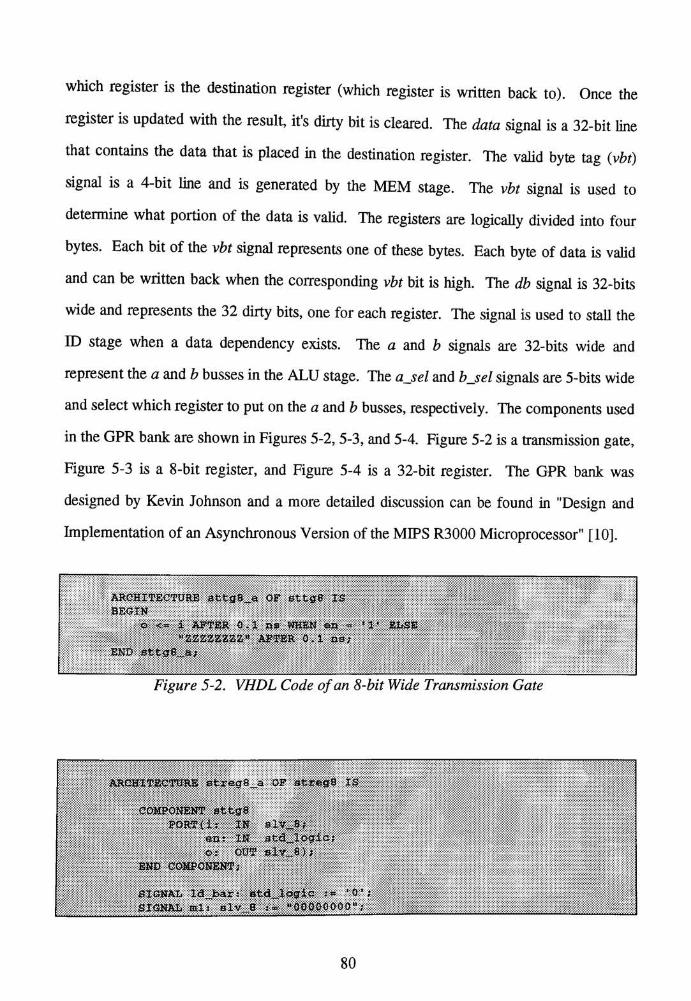
which register is the destination register (which register is written back to). Once the
register is updated with the result, it's dirty bit is cleared. The data signal is a 32-bit line
that contains the data that is placed in the destination register. The valid byte tag (vbt)
signal is a 4-bit line and is generated by the MEM stage. The vbt signal is used to
determine what portion of the data is valid. The registers are logically divided into four
bytes. Each bit of the vbt signal represents one of these bytes. Each byte of data is valid
and can be written back when the corresponding vbt bit is high. The db signal is 32-bits
wide and represents the 32 dirty bits, one for each register. The signal is used to stall the
ID stage when a data dependency exists. The a and b signals are 32-bits wide and
represent the a and b busses in the ALU stage. The ajsel and bjsel signals are 5-bits wide
and select which register to put on the a and b busses, respectively. The components used
in the GPR bank are shown in Figures 5-2, 5-3, and 5-4. Figure 5-2 is a transmission gate,
Figure 5-3 is a 8-bit register, and Figure 5-4 is a 32-bit register. The GPR bank was
designed by Kevin Johnson and a more detailed discussion can be found in "Design and
Implementation of an Asynchronous Version of theMIPS R3000Microprocessor"
[10].
ARCHITECTURE SttjjSa OF StCS* IS
BEGIN
o <= i AFTER 0 . 1 ns WHEN en -
'1
'ELSE
"ZZZZZZZZ"AFTER 0.1 db;
END sttg8_a;
Figure 5-2. VHDL Code ofan 8-bitWide Transmission Gate
ARCHITECTURE streg8a OP streg8 IS
COMPONENT 8ttg8
PORT(i; IN slv_8;
enr IN std_logia;
oj OUT slv_8)j
END COMPONENT;
SIGNAL ldbars fifcdlogie := '0';
SIGNAL mlT b1v_8 *- "OOOOOOOO";
80

SIGNAL 1*2: slv_8 j=''OOOOOOOO"
SIGNAL m3: alv8 t= "00000000";
BEGXN
ld^bar <= NOT Id;
_put_tg!Sttg.S
PORT MAPU, id, ml);
to2 <= NOT ml AFTER 0.3 ns;
m3 < NOT m2 AFTER 0.3 ns;
feedback tg:Bttg6
FORT MAP(m3, ld_bar, ml);
a_,bua_tg :attg8
PORT MAP(m3, as, a);
b_bua_tg:sttg8
PORT MAP (m3 , bs , b ) ;
p < Jn3j
END streg8_a;
Figure 5-3. VHDL Code ofan 8-bitRegister
ARCSXtfECTORE &txeg32_a OP streg3.2 IS
COMPONENT stragB
PORT(ii IN slv_8;
Id* IN std_logio;
as: IN Std_logiC;
bs: IN st4_logtc;
as OUT slv_8;
b: OUT lv_>
p OUT SlVji)}
END COMPONENT;
SIGNAL d0, dl, da/dSi elvjij
SIGNAL ISO, Idl, ld2, 1<33 . stdlogic;
SIGNAL ao, al, a2, a3; alv_8;
SIGNAL bO, bl, b2, b3s slv_8;
SIGNAL dbid, dtawbi std_logic t- '0*;
SIGNAL pO, pi* P_, P3i slv8>
BEGIN
do <- data{7 DOWNTO 0) )
dl <t* datattS DOWNTO $),
d2 < data(23 POWNTO 16);
d3 <=. data{31 DOWNTO 24);
IdO < rbt(0) AND Id AFTER 1ns,-
Idl <= vbt(l) AND Id AFTER 1 aa;
81

Id2 <* vbt (2) AND Id AFTER 1 ns,-
ld3 <= vbt{3) AND Id AFTER 1 ns;
reg-bytaO* strag8
PORT AP(dO, Ido, as, ba, aO, bo, pO) ;
reg_bytelt stregB
PORT MAP (dl, ldl, as, ba, al, bl, pi);
reg_bytei : stregB
PORT MAP (d2, ld2, as, bs, a2, b2, p2 ) ;
reg_byte3 : atregB
PORT JMAP(d3, Id3,, as, bs, a3>, b3, p3 ) ;
a <a a3 & a2 & al & aO;
b <- b3 & b fi bx ft bo?
p <= p3 & p2 & pi & pO?
dbid_
dbid XOR>l-
AFTER 1 ns
WHEN db_set 'EVENT AND dbmset =
'1
'
ELSE dbid;
dbwb <* dbwb XOR"l*
AFTER 1 na
WHENId"
EVENT AND Id'1
'
ELSE dbwb;
db <- dbid XOR dbwb AFTER ins;
streg32_a;
Figure 5-4. VHDL Code ofa 32-bitRegister
82
5.2 ARITHMETIC LOGIC UNIT BLOCK
The ALUB consists of ten components: bus control block (BCB), arithmetic logic
unit component (ALUC), ALUC decoder, overflow block, compare block, branch control,
shifter unit, shifter unit control, set-on-less-than (SLT) unit, and output selector. The
ALUB block diagram is shown in Figure 5-5.
BUS CONTROL BLOCK
The BCB, shown in Figure 5-6, controls what is placed on the a and b busses in
the ALUB. These busses are fed into the ALUC. The BCB consists of the A-bus
selector, the B-bus selector, and the bus selection decoder.
The A-bus selector, shown in Figure 5-7, consists of a 32-bit 4-to-l multiplexer.
This multiplexer selects from the following three input values: a, pel, and the constant of
zero. The a signal comes from the a output of the GPR bank. This signal is used when
the instruction needs a value for the first source field (bits 25-21 of the instruction). The a
output of the GPR bank supplies this first source field. The pel signal is the current value
of the PC and comes from the ID stage. This signal is used for jump-and-link instructions.
It is used to calculate the link address that is stored in the link register (the bcond link
instructions use the ADD8 unit to calculate the link address). The constant value of zero
is needed for shift instructions. Shift instructions utilize the shifter unit and do not use the
ALUC. Therefore, the data that is operated on has to be passed to the shifter unit
unchanged. This data is stored in the general registers and is supplied on the b output of
the GPR bank. The a input to the ALUC has to be zero so that when it is added to the b
input it does not change. Tmjump (j) and shift (s) signals select which multiplexer input
to use.
83
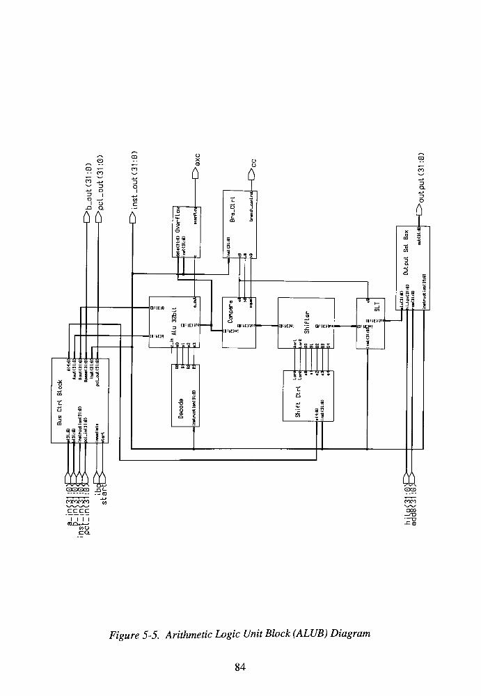
CD
--
n
44 O=> Io -^
I u
31111
s?
44 U 0a a p c
[m_M
cccc
I I I I
MO
CQ.
0
00 0 . 1
:iE>a *.
V1*
f f f
o
C"5
z>
Q.
o
1Z 1
Cll)U|--
(Olie)in'
*1t* t *>.*i
3 S3
cn 3 ")j
18 I
(IIM!
ffl
OOO
TD
Figure 5-5. Arithmetic Logic Unit Block (ALUB) Diagram
84
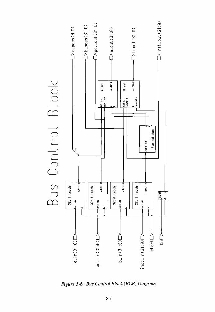
AZ
O
O/
O
o
CO
(/)
o
cc
CZ>
CO
CO
(0
Q.
CO
CO
CO
CS.I
00
ZJ
o
CZ)
oo
ZJ
o
0 0 6 0
CD
O0
zj
o
0
<z>
00
ZJ
o
CO
c
0
0 0 0 0 0 0S-
v ?~s. s~^ ^^L _4_> o
CD o cz> o c_ nCD -
T * X ^|4
OO oo oo oo COv_^- Nw* V.4^ I'
c c CZ fZ-
"~"
CDoQ.
_Q
CO
cz
Figure 5-6. Bus Control Block (BCB) Diagram
85
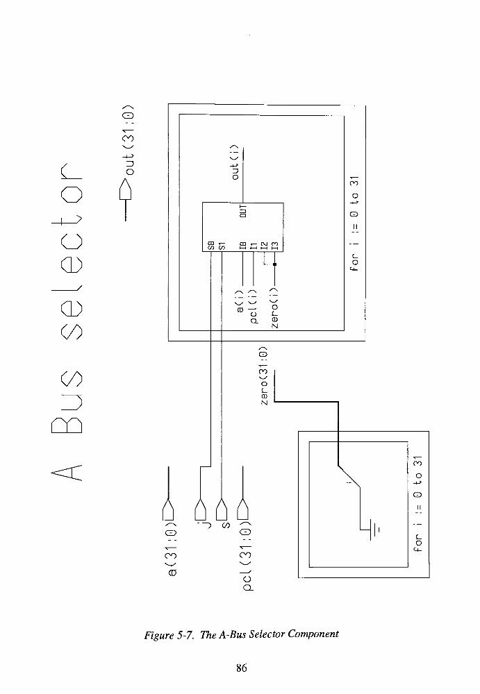
O
O
CD
s
ao
oo
CQ
co
ZJ
o
CD 4-
o ,- (\J ty)cn LO l-H I I I I l-H
CD_^ O
OCD
N
OO\s
O
C
0)
N
6 606
CO
~> COCD
c?0
O
Q.
00
o-4>
G5
II
o
\
1 1
00
o
-4>
CD
II
o
<-L-
Figure 5-7. The A-Bus Selector Component
86
The B-bus selector, shown in Figure 5-8, also consists of a 32-bit 4-to-l
multiplexer and logic for immediate or base-offset instructions, sign-extension, and zero-
extension. This multiplexer selects from the following three input values: b, immed, and
the constant of eight. The b signal comes from the b output of the GPR bank. This signal
is used when the instruction needs a value for the second source field (bits 20-16 of the
instruction). The b output of the GPR bank supplies this second source field. The immed
signal is the immediate field of the instruction (bits 15-0 of the instruction) that is sign or
zero-extended to 32 bits. The immediate instructions that need to be sign-extended are
addi, addiu, slti, and sltiu. The immediate instructions that need to be zero-extended are
andi, ori, and xori. The immed input is chosen for an immediate instruction or for a base-
offset calculation (here, the immed signal is the offset). The load and store instructions
need the base-offset calculations. The constant value of eight is needed for link
instructions. The link address is found by adding the value eight to the PC. The A-bus
selector provides the PC to the a input of the ALUC. The B-bus selector provides the
constant eight. The jump (j) and ibo signals selectwhich multiplexer input to use.
The bus selection decoder, shown in Figure 5-9, provides the A-bus and B-bus
selectors with the multiplexer select lines. The bus selection decoder generates the; select
line when the instruction is either a jump and link (jal) or jump and link register (jalr). It
also generates the s select line for all shift instructions.
ARITHMETIC LOGIC UNIT COMPONENT
The ALUC, is the component that does the addition, subtraction, and logical
calculations. The ALUC also does base-offset address calculations. The component,
shown in Figure 5-10, consists of eight ports. The a and b ports are 32 bits wide and
correspond to the a and b outputs of the BCB. The four select lines, sO through s3,
87

o
C_
O
o
CD
CD
CO
CO
ZD
OO
OO
CO
F/gwre 5-8. The B-Bus Selector Component
88

o
1 '
o
CD* c_
CD CD
CO U
o
00 o
13 CD
m m
CO
Figure 5-9. The Bus Selection Decoder Component
89

control what operation the ALUC performs. Table 5-1 lists these operations. The out
signal is the output of the ALUC. The last port, c_out, is the carry output of the ALUC.
The ALUC for the asynchronous version could not be modeled exactly after the R3000's
ALUC. This was due to a lack of information on the R3000's internal gate design.
However, a suitable design was found in the Fairchild Advanced Schottkv TTL Data
Book. More details can be found in Kevin Johnson's thesis [10].
^ c_out
Figure 5-10. Arithmetic Logic Unit Component
(ALUC)
OPERATION SO SI S2 S3
aMINUS b 0 1 0 0
a PLUS b 1 1 0 0
aXORb 0 0 1 0
aORb 1 0 1 0
aANDb 0 1 1 0
aNORb 0 1 1 1
Table 5-1. ALUC Operation Encoding
90
ALUC DECODER
Since the details of the synchronous R3000's ALUC were not known, the
asynchronous version ALUC control signals do not match the instruction encoding
inherent in the R3000. The ALUC decoder is a circuit that is required to decode the
instruction before the ALUC can operate on it. This circuit is shown in Figure 5-11. A
more detailed discussion on the ALUC decoder can be found in [10].
OVERFLOW BLOCK
The overflow block component, shown in Figure 5-12, detects an overflow
condition from the ALUC. The three instructions that check for an overflow condition are
addi, add, and sub. The carry signal, c, from the ALUC is XORed with the bit 31 of the
data signal. The data signal is the output of the ALUC.
COMPARE BLOCK
The compare block component, shown in Figure 5-13, compares the output of the
ALUC with the value of zero. It is used in conjunction with the branch control unit,
discussed in the next section. The three output ports, Itz, gtz, and eqz, correspond to the
three conditions: less than zero, greater than zero, and equal to zero.
BRANCH CONTROL
The branch control component, shown in Figure 5-14, determines if a branch is
taken. The three inputs Itz, eqz, and gtz, are generated by the compare component
discussed above. The inst input is used to determine the branch instruction type. The four
91

Anithnetic Logic Unit Conponent Decoder
inst(3U0)C>-
I
fe^ 4>r
^fa*r
4>
*
E
^=i?>Q
O
B^Lbr
i8p~i1
'>f
>r
4>r- O
Q
to.Oi
iUT'-J
-t=>SG
r^_ci *
iTv'i I
* U^T^sIl
CV1^
C>S1
OS2
>S3
Figure 5-11. TheArithmetic Logic Unit Component (ALUC) Decoder
92
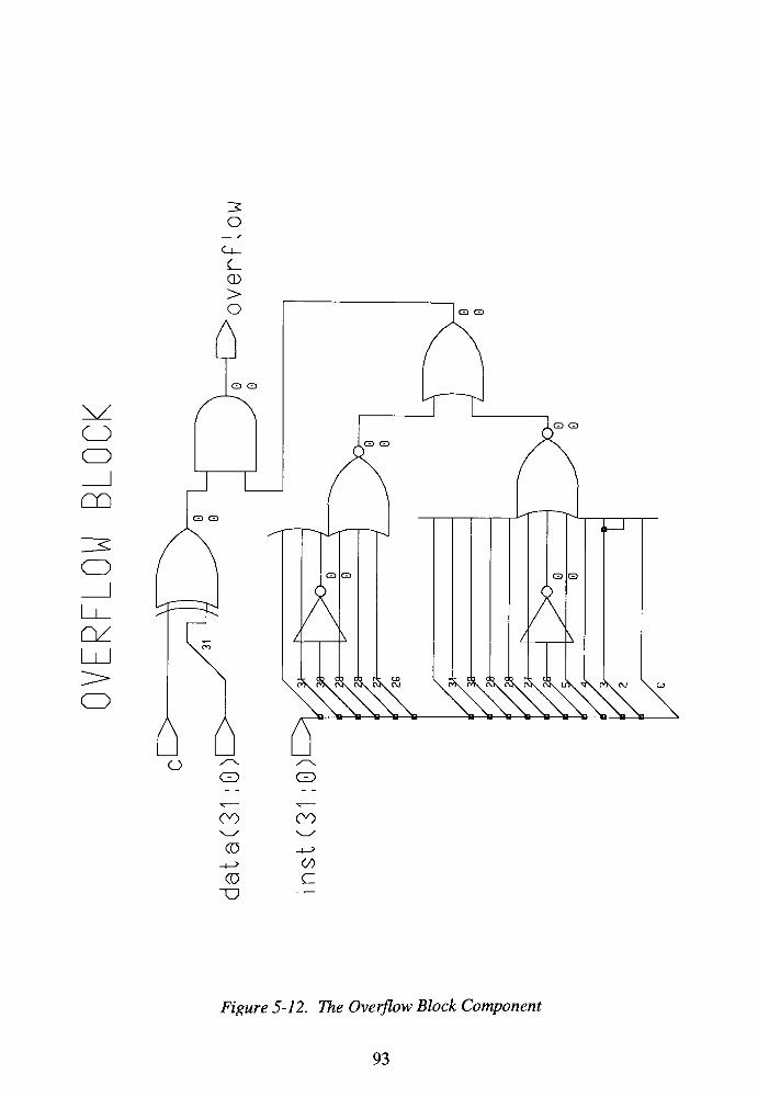
CD
CD
CD
rv
CD
Figure 5-12. The Overflow Block Component
93

N N
C3>
CD
L_
CO
Q.
EI
O
0
INI
NO"
CD
N
cr
0CZ)
CO
cz
Figure 5-13. The Compare Block Component
CZ)
CO
Z5
o
0 6
94
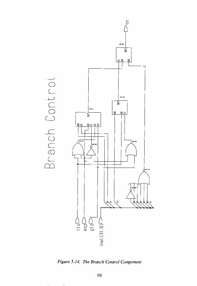
o
-4>
o
c^
o
d
CD
C_
6 6lT6N N N-u_> CT 4-> CD
' CD D) ^00
V)
Figure 5-14. The Branch Control Component
95
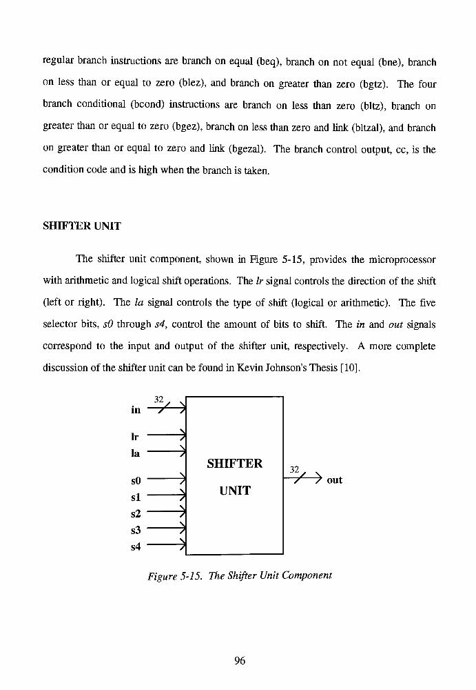
regular branch instructions are branch on equal (beq), branch on not equal (bne), branch
on less than or equal to zero (blez), and branch on greater than zero (bgtz). The four
branch conditional (bcond) instructions are branch on less than zero (bltz), branch on
greater than or equal to zero (bgez), branch on less than zero and link (bltzal), and branch
on greater than or equal to zero and link (bgezal). The branch control output, cc, is the
condition code and is high when the branch is taken.
SHIFTER UNIT
The shifter unit component, shown in Figure 5-15, provides the microprocessor
with arithmetic and logical shift operations. The Ir signal controls the direction of the shift
(left or right). The la signal controls the type of shift (logical or arithmetic). The five
selector bits, sO through s4, control the amount of bits to shift. The in and out signals
correspond to the input and output of the shifter unit, respectively. A more complete
discussion of the shifter unit can be found in Kevin Johnson's Thesis [10].
in
lr
la
sO
si
s2
s3
s4
^
"^
SHIFTER
UNIT
32
/ ) out
Figure 5-15. The Shifter Unit Component
96
SHIFTER UNIT CONTROL
The shifter unit control component, shown in Figure 5-16, provides the necessary
signal inputs to the shifter. It generates the Ir, la, and the five shift amount select lines (sO
through s4). The a input is used in conjunction with the variable shifting instructions, shift
left logical variable (sllv), shift right logical variable (srlv), and shift right arithmetic
variable (srav). The variable instructions have their variable shift field in bits 25-21 of the
instruction. This shift field is placed on the A-bus. The a input is the lower five bits of the
A-bus from the BCB.
SET ON LESS THAN UNIT
The set on less than unit component, shown in Figure 5-17, implements the four
instructions, set on less than (sit), set on less than unsigned (situ), set on less than
immediate (slti), and set on less than immediate unsigned (sltiu). It consists of a 1-bit
multiplexer, a 31-bit tri-state buffer, and decoding logic. All sit instructions output a value
of one when the first source register (rs) is less than the second source register (rt).
Otherwise they output a zero. For a sit instruction, the tri-state buffers are activated and
the top 31 bits are set to zero. Bit zero is determined by the less than zero (Itz) signal.
For non sit instructions, the tri-state buffers are deactivated and the input (in) passes to
the output (out) unchanged.
OUTPUT SELECTOR
The output selector component, shown in Figure 5-18, is the final component in
the ALUB. Its task is to route the proper lines to the ALUB output port. The output
selector chooses from the following three inputs: alu, hilo, or add8. The alu signal input
97
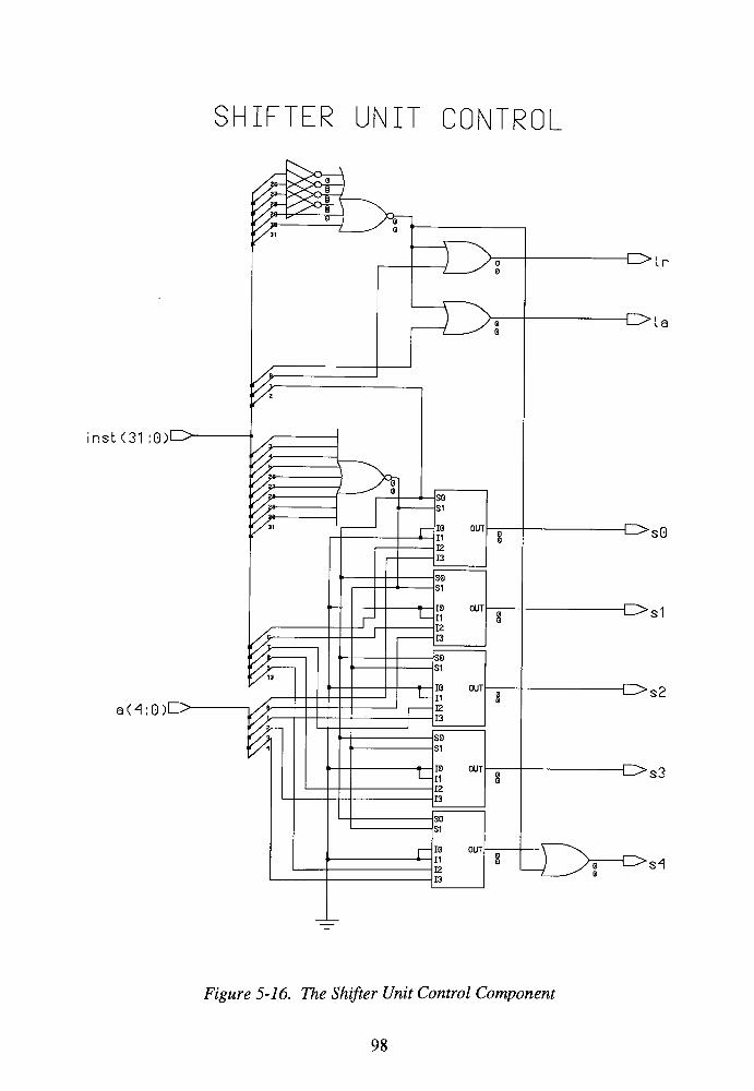
SHIFTER UNIT CONTROL
inst C31 :0)IZ>
a ( -1:0)0
Figure 5-16. The Shifter Unit Control Component
98
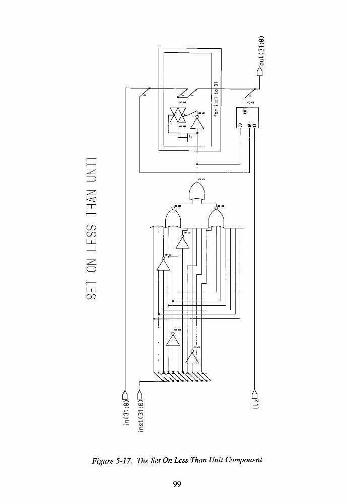
<c
CO
CO
CD
UJ
CO
tZ -t->
- CO
C
Ffgwre 5-i7. 77je Sef On Less Than Unit Component
99
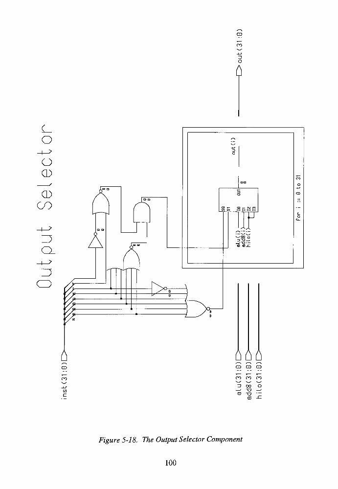
CD
00
ZJ
o
o
o
O)
cd
CO
4^
Q_
4-^
CD
%
i
6CD
OO
CO
c
t^5"
ET
co co.c
000.- * y-^. *-\
CD CD CD
00 00 00v_^ ^^ ^^.
D 00 O' TD >
<D TD'
Figure 5-18. The Output Selector Component
100
comes from the output of the component chain in the ALUB. The hilo signal is used for
the move from hi (mfhi) and move from lo (mflo) instructions. The add8 signal is used for
the two branch conditional link instructions, branch on less than zero and link (bltzal)
and branch on greater than or equal to zero and link (bgezal).
101
6.0 RESULTS
All three models were tested using a VHDL test bench. The test bench setup is
shown in Figure 1-1. The behavioral model used the test bench shown in Figure 3-1. The
dataflow and structural models used the test bench shown in Figure 4-1. Both test
benches consists of three modules, CPU, memory, and compare. The memory module
stores the test program used in the test bench. The compare module stores the expected
results file. The output of the CPU module is compared against the expected results file
after each instruction is executed.
6.1 TESTING PROCEDURE
The testing process consists of writing the test program, assembling the test
program, generating an expected results file, processing the expected results file,
preprocessing the test program and expected results file, loading the model into the digital
simulator, and running the model. The model runs to completion if there are no
discrepancies between the model and expected results. However, the user is warned if a
discrepancy exists.
The test program can be written using any text editor. The programs are written in
a pseudo MIPS assembly language. The program is saved with a"test"
extension. An
example of a filename is "filename.test"
wherefilename is the name of the file.
The test program is assembled by the MIPS assembler (MASS) program, found in
Appendix D. This assembler generates the machine code that the model can understand.
The generated file is saved with a"m"
extension which stands for the word machine. An
example of this is"
filename.m"
where filename is the same name used as above.
The expected results file is generated using the MIPS expected results assembler
(MERA) program, found in Appendix D. The user inputs the expected state of the
102

processor after every instruction into the assembler. This file is then used by the compare
module. The file is saved with an"e"
extension which stands for the word expected. An
example of this is"
filename.e".
The expected results file has to be modified for test programs with branches and
jumps. The FLOW program was written to reorder such programs to follow the actual
program flow. The instructions in the test program can now be compared to the
reordered expected results file. The reordered expected results file is saved with a"f"
extension. An example of this is'
filename.f". The original expected results file,
'
filename.e", is unchanged.
The test files are preprocessed with the MIPS preprocessor (MPP) program. The
preprocessor prepares the test files so the model can use them. The MPP program copies
the appropriate test files to two files that the model opens. These two files are called
"machine"
and"expected"
which represent the machine code file loaded into the memory
module and the expected results file loaded into the compare module, respectively. The
MPP program copies"filename.m"
to"machine"
and"filename.e"
to "expected".
The model is loaded into the digital simulator. The name of the digital simulator is
Quicksim and is manufactured by Mentor Graphics Corporation. The two test files,
"machine"
and "expected", need to be in the same directory as the model's design file.
Quicksim is also invoked from this directory.
Running the model in Quicksim consists of setting up the simulator, setting some
signal values, and running the simulator for some set time. Setting up the simulator
involves opening the VHDL code windows, tracing pertinent signals, and opening list and
monitor windows. When the signals are forced to specific values, they can be traced on
the screen. The sys_control_sig signal is used to control the model. This signal is forced
to a value of load for 100 nanoseconds (ns) and then forced to a value of run. The load
value mode signals the test bench to load the test program("machine"
file) into the
103

memory module and the expected results file("expected"
file) into the compare module.
The run value mode signals to the test bench to run the model for testing.
The models use VHDL ASSERT statements to alert the user if there is a problem
with the simulation. If there are no problems and the state of the processor matches the
expected results, then the model will run to completion. The user is only warned when an
error or discrepancy exists.
The test benches were used throughout the entire design process. During the
behavioral modeling as the instructions were coded, the test bench was used to test
whether the model was performing up to specifications. During the dataflow modeling,
the test bench was used first to verify the arbitrary simulation times and then used again
for the back annotated times from the Accusim circuit simulation runs. All models were
verified using their appropriate test benches.
6.2 DELAY TIMES
This section shows the gate, component and stage delay times that were back
annotated into the model from Accusim circuit simulations. These times were taken from
Kevin Johnson's thesis [10] and ScottSiers'
thesis [19]. These circuit simulations are
found in their separate documents.
GATE DELAY TIMES
Circuit simulations were performed on the individual gates. Table 6-1 shows these
times. Delay times of complex circuits that are made up of these gates were calculated by
determining the critical path and then adding upthe times.
104
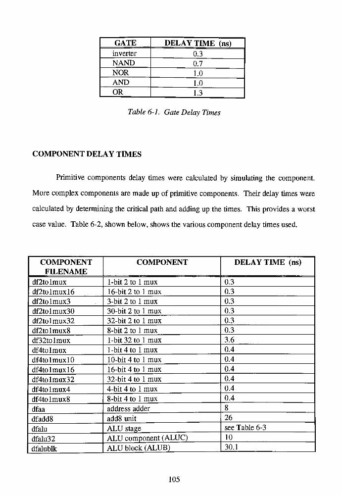
GATE DELAY TIME (ns)
inverter 0.3
NAND 0.7
NOR 1.0
AND 1.0
OR 1.3
Table 6-1. Gate Delay Times
COMPONENT DELAY TIMES
Primitive components delay times were calculated by simulating the component.
More complex components are made up of primitive components. Their delay times were
calculated by determining the critical path and adding up the times. This provides a worst
case value. Table 6-2, shown below, shows the various component delay times used.
COMPONENT
FILENAME
COMPONENT DELAY TIME (ns)
df2tolmux 1-bit 2 to 1 mux 0.3
df2tolmuxl6 16-bit 2 to 1 mux 0.3
df2tolmux3 3-bit 2 to 1 mux 0.3
df2tolmux30 30-bit 2 to 1 mux 0.3
df2tolmux32 32-bit 2 to 1 mux 0.3
df2tolmux8 8-bit 2 to 1 mux 0.3
df32tolmux 1-bit 32 to 1 mux 3.6
df4tolmux 1-bit 4 to 1 mux 0.4
df4tolmuxl0 10-bit 4 to 1 mux 0.4
df4tolmuxl6 16-bit 4 to 1 mux 0.4
df4tolmux32 32-bit 4 to 1 mux 0.4
df4tolmux4 4-bit 4 to 1 mux 0.4
df4tolmux8 8-bit 4 to 1 mux 0.4
dfaa address adder 8
dfadd8 add8 unit 26
dfalu ALU stage see Table 6-3
dfalu32 ALU component (ALUC) 10
dfalublk ALU block (ALUB) 30.1
105
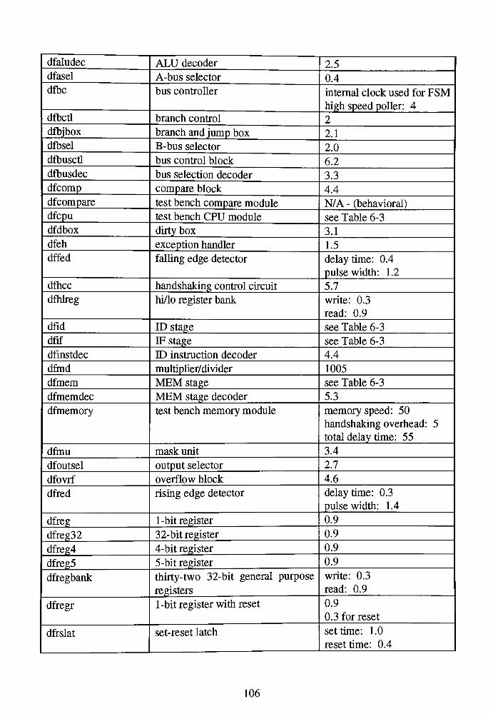
dfaludec ALU decoder 2.5
dfasel A-bus selector 0.4
dfbc bus controller internal clock used for FSM
high speed poller: 4
dfbctl branch control 2
dfbjbox branch and jump box 2.1
dfbsel B-bus selector 2.0
dfbuscfl bus control block 6.2
dfbusdec bus selection decoder 3.3
dfcomp compare block 4.4
dfcompare test bench compare module N/A - (behavioral)
dfcpu test bench CPU module see Table 6-3
dfdbox dirty box 3.1
dfeh exception handler 1.5
dffed falling edge detector delay time: 0.4
pulse width: 1.2
dfhcc handshaking control circuit 5.7
dfhlreg hi/lo register bank write: 0.3
read: 0.9
dfid ID stage see Table 6-3
dfif IF stage see Table 6-3
dfinstdec ID instruction decoder 4.4
dfmd multiplier/divider 1005
dfmem MEM stage see Table 6-3
dfmemdec MEM stage decoder 5.3
dfmemory test bench memory module memory speed: 50
handshaking overhead: 5
total delay time: 55
dfmu mask unit 3.4
dfoutsel output selector 2.7
dfovrf overflow block 4.6
dfred rising edge detector delay time: 0.3
pulse width: 1.4
dfreg 1 -bit register 0.9
dfreg32 32-bit register 0.9
dfreg4 4-bit register 0.9
dfreg5 5-bit register 0.9
dfregbank thirty-two 32-bit general purpose
registers
write: 0.3
read: 0.9
dfregr 1-bit register with reset 0.9
0.3 for reset
dfrslat set-reset latch set time: 1.0
reset time: 0.4
106
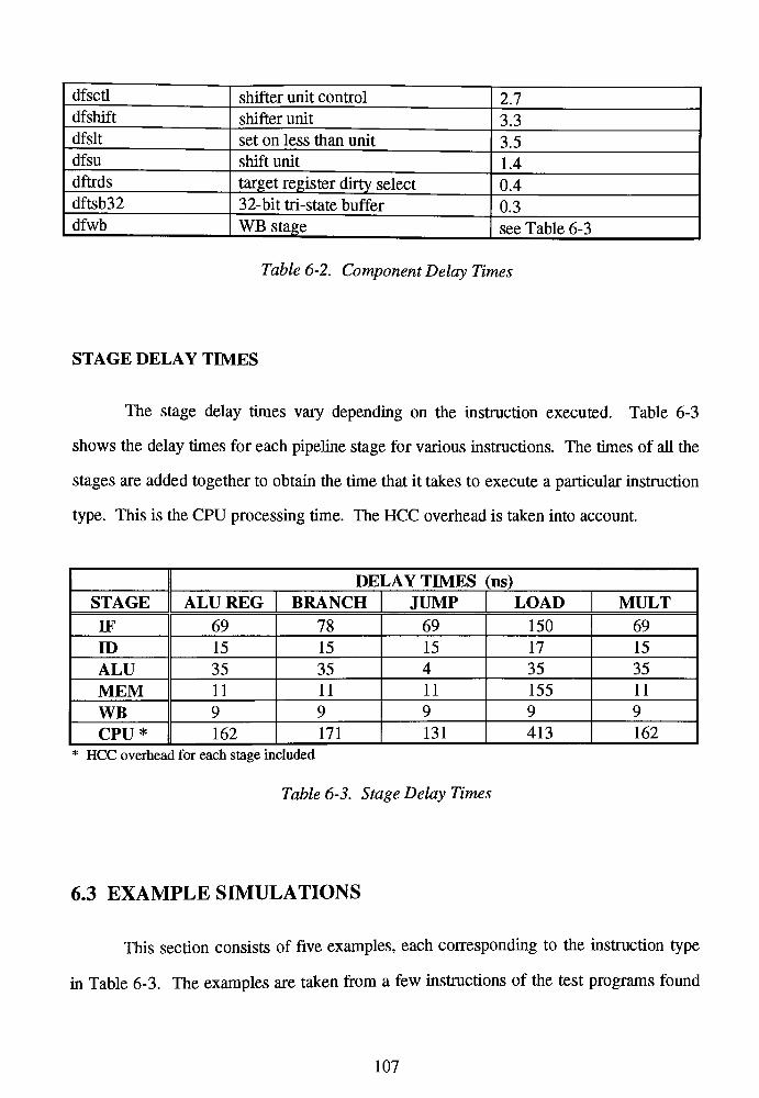
dfsctl shifter unit control 2.7
dfshift shifter unit 3.3
dfslt set on less than unit 3.5
dfsu shift unit 1.4
dftrds target register dirty select 0.4
dftsb32 32-bit tri-state buffer 0.3
dfwb WB stage see Table 6-3
Table 6-2. Component Delay Times
STAGE DELAY TIMES
The stage delay times vary depending on the instruction executed. Table 6-3
shows the delay times for each pipeline stage for various instructions. The times of all the
stages are added together to obtain the time that it takes to execute a particular instruction
type. This is the CPU processing time. The HCC overhead is taken into account.
DELAY TIMES (ns)
STAGE ALU REG BRANCH JUMP LOAD MULT
IF 69 78 69 150 69
ID 15 15 15 17 15
ALU 35 35 4 35 35
MEM 11 11 11 155 11
WB 9 9 9 9 9
CPU* 162 171 131 413 162
* HCC overhead for each stage included
Table 6-3. Stage Delay Times
6.3 EXAMPLE SIMULATIONS
This section consists of five examples, each corresponding to the instruction type
in Table 6-3. The examples are taken from a few instructions of the test programs found
107

in Appendix E. The times shown in Table 6-3 came from these example simulations. The
five instruction groups are as follows: ALU register, branch, jump, load, and
multiplication.
The first example is taken from instructions 4, 5, and 6 of the arithmetic register
test program ("ar.test"). Instruction 4 (PC equal to 'OC') loads register 1 with the value
'A'. Instruction 5 loads register 2 with the value '5'. Instruction 6 adds registers 1 and 2
together and then places the result in register 3. The waveforms are shown in Figure 6-1.
The second example is taken from instructions 38, 39, and 40 of the jump and
branch test program ("jb.test"). Instruction 38 (PC equal to '94') loads register 2 with the
value 'ABCD'. Instruction 39 loads register 3 with the value 'ABCD'. Instruction 40
compares instructions 38 and 39, and branches to the destination address (5 instructions
after the delay slot) if they are equal. The waveforms are shown in Figure 6-2.
The third example is taken from the first instruction of the jump and branch test
program ("jb.test"). Instruction 1 (PC equal to '00') jumps to the destination address
unconditionally with a delay of one instruction. The destination address is calculated by
shifting the 26-bit target address left two bits and combining it with the high order 4 bits
of the PC. The waveforms are shown in Figure 6-3.
The fourth example is taken from instruction 21 of the load and store test program
("ls.test"). Instruction 21 (PC equal to '50') loads register three with the contents of
memory location '4000'. This value will be available for use after a delay of one
instruction. The waveforms are shown in Figure 6-4.
The fifth and final example is taken from instructions 1, 2, and 3 of the
multiplication and division test program ("md.test"). Instruction 1 (PC equal to '00') loads
register 1 with the value '8'. Instruction 2 loads register 2 with the value '9'. Instruction 3
multiplies register 1 and 2 together and places the results in the hi and lo registers. The
waveforms are shown in Figure 6-5.
108

r^
LZD
LZD
UoCD
LZD
CZD
CZD
O
<ZD
CZD
LZD
CO
LZD
CZD
CZD
CZD
CZD
CZD
CD
CZD
CZD
LZD
CZD
CZD
CZD
CP
OJ
CVJ
CZD
CZD
CZD
CZD
CZD
LZD
CQ
LZD
n
LO
o
CPLZD
OJ
CZD
LZD
CZD
CPCP
CP
CP
CP
&
5JL
J^JUd
nf
r
c *
n
r
r
re ?
r
CP
OJ
CP
en
LO
LZD
CO
CQ
CP
CO
CD
CPCP"
CO
CP
CP
I
LD
CP
LO
CP
CP
LO
CP
CO
CP
LO
Figure 6-1. Example 1 - Arithmetic Register Instruction Waveforms
109
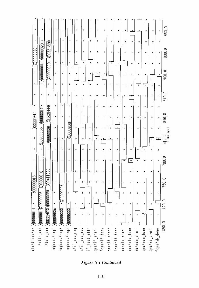
CJ
CP
CP
CP
CP
CP
CB
CP
CP
^
CP
OJ
LZD
CP
CP
CP
OJ
CO
OJ
Cfcj
CP
CP
CP
CP
CP
o CPCP LcPu
co
cp
cb
cp
cp
CP
cp
CP
CP
CP
CP
CD
cp
U
CP
cb
CP
cp
cp
cb
CP
CP
CP
CB
CP
:8:
CDCP
CP
CP
CP
g
LZD
cb
CP
CP
CP
s
CB
CP
CD
CP
CP
CP
CP
cp
o
OJ
CD
OJ
o
z&i
tfi
LZD
LZD
cb
cp
LZD
LZD
CP
CP
CP
CP
CP
cb
CP
LZD
LZD
$kOJ
c
Ll+ +
rCP
CD
cn
CP
CO
cn
cJ
C
<ZD
LZD
cn
it
re
^r
CP
CPI
co
CD
CO
cn
r
"TlZ
f
CP cu
. IE
-J-nCP--
CO
CP
CO
CP
LO
CPOJ
CP
CT)
CO
Figure 6-1 Continued
110
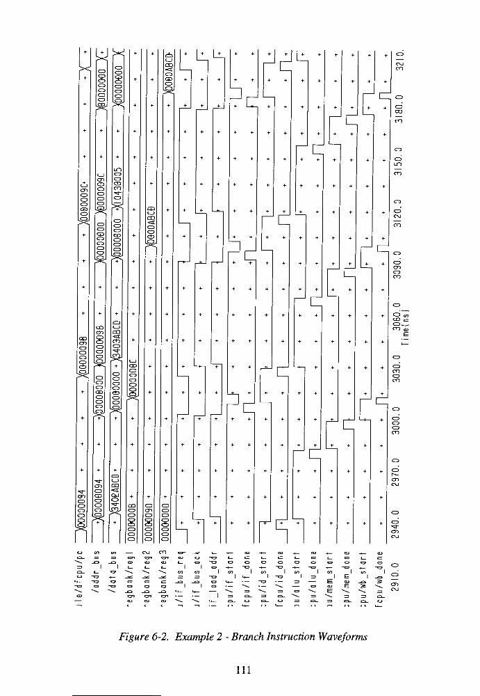
WMX
CP
CP
CPCP
CP
CP
CP
cp
CP
CZD
L-D
CO
<=c
cp
CBCP
md
ee
OJ
CO
CP
CO
r
CT)
CP
CP
cp
CQ
CP
<_1
cn
cbCP
CP
CP
cp
LcpJ
cp
CP
cpcp
CP
CP
cp
LO
cp
cp
CO
CO
X
LZD
CP
CP
CB
CP
CP
CP
cpL->
CO
cp
CP
CD
c
c
LZD
LO
CP
OJ
CP
cn
CP
co
cocn
oocn
cp
cpCP
cp
CP
CP
=3
CD
CP
^ CP
CP
CP
CP
cb
cp
cp
C_J
CB
CP
CP
CP
CP
M^c
r
CP
CD
CP..
CO
CP
co
CP
co
CP
cp
CP
co
IDT,
CP
CP
cp
cn
cp
CD
cp
CP
CP
co
S
h
ca
cp
cp
scp
cp
CP
CPcn
CP
CP
CP
cp
cp
cp
CP
CP
CP
o i
CPr-
cn
OJ
CP
OJ
oj co
en en
czn cn
o CT
cn
OJ
Figure 6-2. Example 2 - Branch Instruction Waveforms
111

co
ca
CP
cp
cp
CB
CP
CP
CP
CP
8
x
CP
cs
CP
CP
cp
cp
cp
CP
CP
^1-
CQ
CP
CPCP
CD
cp
CP
CP
CP
CP
X
cp
cb
CP
CP
CP
CP
cp
cp
CP
cp
cp
CP
-=c
CP
cp
cpCP
CP
CP
-*t
CP
cp
cp
CP
CP
CZD
CZD
CP
Q
cp
CBCZD
CP
CP
CP
CP
CP
CP
cp
CP
CP
CP
CP
en
cb
CP
CP
CP
CP
LO
CPCP
CB
ro-tf-
CP
CJ
CDCP
CP
CP
CP
CD
<=t
CP
CP
+ *
+ 4-
+ +
+ +
+ *-
+ t-
+ t-
+ +
+ +
+ +
+ *
+ -*-
____
m
<o
CD
(-
4- -t-
4- *
+ +
CP
CPCP
CP
CP
CP
^C
rr
r
cF
^c
F
+
+
1+
4
+
+
+
+
l_+
+
+
+
+
L+
+
+
4-
*
+
+
+
+
+
+
+
-1
1
+
+
+
*-
CP
cn
co
CO
CP
CO
co
CO
CP
CO
CO
CO
CP
cp
co
co
CP
OJ
co
CP tz
CP cu-**-
EOJ.
COi
CP
cp
OJ
CO
CP
CO
CP
LO
cp
OJ
OJ
tzn
co
cn
O CJ
I CO I Co
I -a I
o
CJ =3
CP
cn
CP
co
Figure 6-2 Continued
112
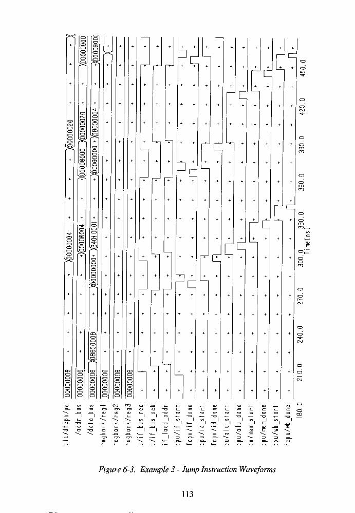
X CP
CP
cpcp
CP
cp
cp
CP
CP
CB
CP
cp
cp
.3,
JF
CP
LO
F
CDOJ
CP
CP
CP
^
CP
OJ
cp
CP
CP
cp
CP
CP
ec
cp
CPCP
CP
CP
cp
co
jZD,
LZD
LZD
LZD
CZD
cb
CP
CP bc
CP
OJ
cp
cn
co
CP
CD
co
LTD
LZD
CP
CP
CP
cp
cp
CP
CD
CP
CP
CP
CP.
CP
cp
CP
^J-
CP
cp
cp
cp
CZD
F
^r
cp
CO
CO,
CP
CP
CO
CP
CP
OJ
CB
CP
CP
CP
CP
CB
CP
CP
CP
CP
cb
CP
CP
CP
CP
CB
CO
z
CB
cp
cp
cp
cp
CB
cp
CP
CP
CP
CB
CP
CP
CP
CP
CB
CP
CP
CP
CP
CPM-
OJ
cp
CP
OJ
CP CP |cp CP CP
oj co
Icu CD cu
I I
CP
CO
o
cn cn
Figure 6-3. Example 3 - Jump Instruction Waveforms
113
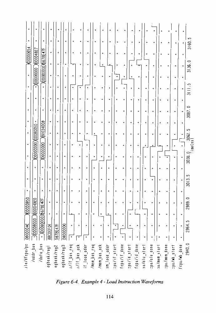
LO
cpCP
CPCP
CP
I
OJ
eo
cp
CP
CP
^CP
CP
CP
cpcp
CP
CP
CP
CP
CP
CP
cpcp
CP
CP
CD
CD
CO
CP
LO
CPcp
<BCP
CP
CP
CP
cpCP
CO
CP
CP-^-
CO
gCPcp
CP
CP
CP
LO
eoCP
CP
cpCP
CP
CPcp
CPCB
CP
CP
cp
CP
CP
CPCP
CP
eo
<p
CP
CP
LXJ
COr--
cjp
cp
CPcp
CPeo
LZ>
CP
fl r
COCP
ro
LO
dOJ
CO
o_CO ,
CO
rocp
ro
LO
no
LZD
ro
LTD
CO
en
OJ
CD
cn
oj
cj eo eo
OJ
aj
COC3T.
CU
_
CD
CZT _^ { c_r ^e l_ -t- CU ^_ CU -1 CU _,_ CO , cu<Z5
C_T><U
_
c_>
O ~CD
cu CJ
CD
"CD
"CD
t_
o o
_
o o CD oCO
co
OJ
s_1
CO
1CO 1
1CO
1 CD
1 CO 1 CO 1 CO
~CD
1 CO
"CD
1 CO "l
a a(4
1
"CD
o
E EE
CD
O
-4
-Z3
"CD 1
CD
ZZ3
a
1Ecu
E
CU
E
1_CD
3--
c=n C3>
CU
. . 1 tn CU 1 ^ Q_ 3 Q_ ""v. ID \ i } *"
CU^** "^ <^ E E E - CJ ea- CJ r3 Q_ => =- C^ CJ
Figure 6-4. Example 4 - Load Instruction Waveforms
114
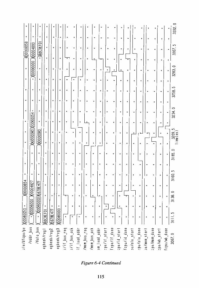
OJ
ro
ro
ro
co
LO
ep
CP
CP
ft
cp
CP
CP
CP
CP
CP
CP
CP
CP
CP
CD
2
CProro
ro
co
OJ
ro
co
LO
oj
ro
LO
CP
CP
ro
OJ
ro
CP
ftCPCO
CPCP
<ZD
CP
4- 4-
LZ>
eo
oCP
CP
CP
LO
cn eo
CP E=
OJ- '
ro cu
)><.
cp
CO
LO
CDCP
cpCP
CP
OJ
eo
CP
CP
CP
CP
LO
CP
CP
CO
CP
CP
CP
CP
CP
CP
CP
CO
CuO
UcJ
CPCP
CP
cp
><. ><
LTD
CP
CP
CP
CP
CO
CP
ep
D~D-
^<JP
ro
cnCD-
_ac ICD-
_ac
eu CJ "CD CU CJ
cu cu CD
t_ t
^s_-4= fc3= CO
\ CP
= ro
Figure 6-4 Continued
115

L-D
LCD
CPeo
cp
CP
CP
<*>
LO
CP
CP
CP
CP
co
CPCP
CPCP
COCP
CP
CPCP
CPcp
eocp
COLO
CPCP
o
ft
sCP
CP
CP
CP
<p
cbCP"=J-
ro
CP
CfJ
$kcp
CPGO
CP
CP
CPcp
CP
CP
cp-^-
CP
CP
CP
LZD
CP
CP
sCP
CP
ep
CP
cp
CD
CO
+ + 4- I 4-+
* + 4-
Li J\ Jj
'
OJ COCJ-
jc
I cn en cn<" "
I oj cu cu -i ai._!__
' '
^ ^^ ^^ CO eo
en
LO
ro
CP
ro
coro
co
CD
LO
CO1"
OJ
COro
ro
<ZD
COro
ro
coOJ
ro
oo
LO
OJ
ro
O CJ a cj
eo co
I I
CD CU CD
E E
I CD CU
CJ Z3ro
OJ
Figure 6-4 Continued
116
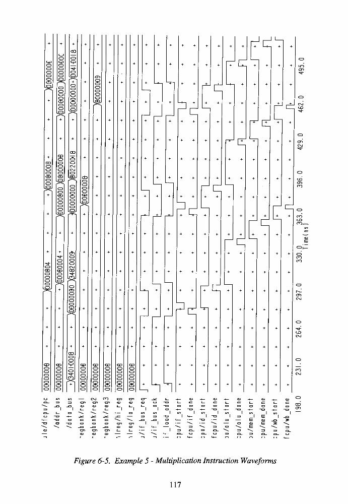
Vd
CP
CP
cp
cp
^
CP
CDCP
CP
cp
cp
iSc
CP
CDCP
CP
cb
CP
CP
CP
cp
^J-
CP
ft4-CP
CZD
LZD
CP
CP
+ I + - + +
sCP
CP
CP
CP
^r
LO
cn^J-
OJ
cx>
CO
CP
CP
CP
CD
CP
CP
CP
CP
CP
CP
CO
i_cCP
CPeo
oCP
CP
CP
CO
5CP
OJ
OJ
CP
k
CP
cp
CP
CP
CP
ft
cb
CP
CP
ep
cp
CD
CP
^C
cn
OJ
CJD
cn
ro
ro
CD
ro.
CB
CP
CP
CP
CP
CP
CP
CP
CO
cp
CP
cp.
eh
CP
CP
CP
OJ
CP
CD
CP
CP
CP
CP
ft
re 4.
FF
CP
ro
ro
en
OJ
CJD
OJ
COcp
CP
CP
CP
CB
CP
CP
CP
CP
CO
CP
CP
<-?
\j7Q)
n
CB
CP
CPcp
CP
CBCP
CP
CP
CP
CB
CP
CP
CP
CZD
CB
CP
CP
CP
CP
CB
CP
CP
CP
<ZZ>
ro
OJ
11
O
O CD O CDCOCT)
ECD CU
Figure 6-5. Example 5 - Multiplication Instruction Waveforms
111

Figure 6-5 Continued
118
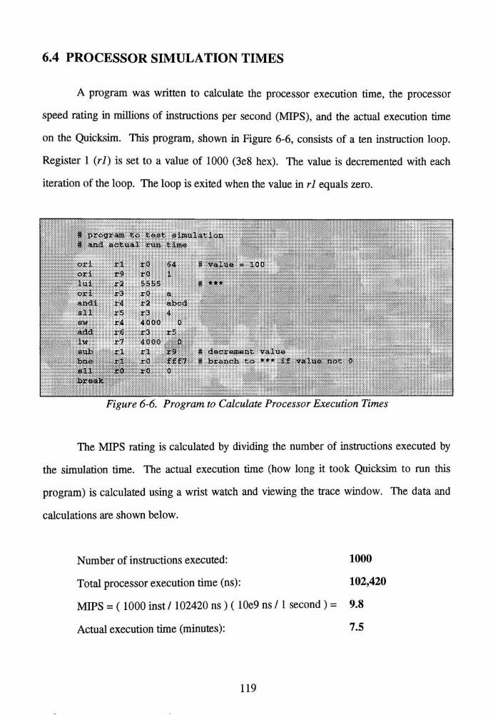
6.4 PROCESSOR SIMULATION TIMES
A program was written to calculate the processor execution time, the processor
speed rating in millions of instructions per second (MIPS), and the actual execution time
on the Quicksim. This program, shown in Figure 6-6, consists of a ten instruction loop.
Register 1 (rl) is set to a value of 1000 (3e8 hex). The value is decremented with each
iteration of the loop. The loop is exited when the value in rl equals zero.
# program to test stmulation
# and actual run time
ori nni ro 64 tt value = 100
ori 111; ro 1
:i:ift|||||| 111 !;:5:iT:il!i!:i: # ***
ori WiW. rO a
andi II:;:::: X2 abcci
sll wm: |:*3;:s:::;:::::::::4|:::::||il4000 0:BWW>ftS:S5; ir-::-::
Mmiaittilisi:: r3 r5
|w . w% 4000 ,:;:::;p
sub rl rl-IflP-# decrettw-rtt valu
bne rl r0 fff7 # branch to *** if value not 0
ell rO rO 0
break
Figure 6-6. Program to Calculate Processor Execution Times
The MIPS rating is calculated by dividing the number of instructions executed by
the simulation time. The actual execution time (how long it took Quicksim to run this
program) is calculated using a wrist watch and viewing the trace window. The data and
calculations are shown below.
Number of instructions executed: 1000
Total processor execution time (ns): 102,420
MIPS = ( 1000 inst / 102420 ns ) ( 10e9 ns / 1 second ) = 9.8
Actual execution time (minutes): 7.5
119

7.0 CONCLUSIONS
This thesis has shown that an asynchronous design of a microprocessor is a viable
alternative to synchronous design. It has also shown that a VHDL top down design
methodology is an effective approach to modern circuit design. Conclusions can also be
drawn from the results of the model testing.
The VHDL dataflow model achieved an average speed rating of 9.8 MIPS, as
shown in section 6.4. Any comparisons to the synchronous version are difficult to make
due mainly to two reasons. First, the actual speed of the asynchronous processor is
variable and depends on which instructions are executed. Secondly, the memory was not
implemented in the asynchronous version.
The testing procedure using the VHDL test bench is easy to use and provides a
fast, accurate, and efficient means to test the processor. Back annotating delay times from
Accusim circuit simulations proved an effective way to design. It was easy to modify the
design by changing the delay times and recompiling the source code. If a problem
occurred during execution then the code could be stepped through with the VHDL
debugger. Lastly, the example simulations proved that the models worked and that the
asynchronous processor was designed and working to specifications.
The first advantage of the asynchronous design methodology is the elimination of
the global clock. In synchronous design, the global clock is routed to all areas of the chip.
This is done to synchronize all the circuit modules. These metal clock lines become very
long since they are routed from one side of the chip to the other. Due to the different
lengths of metal lines and different capacitive loads, one area of the chip may receive the
clock signal earlier or later than another area, creating clock skew. Clock skew becomes
more of a problem with this type of design as circuits become more dense. This is not a
problem in asynchronous design because the global clock is eliminated.
120
The second advantage of asynchronous design is that every module can operate at
maximum speed. In synchronous design, the clock cycle time is dictated by the slowest
module or the longest instruction. The synchronous processor has to be designed to
handle the worst case operation. This causes most instructions to use only part of the
clock cycle. This leads to long periods of idle time for the processor. This is not the case
in asynchronous design. Since this type of design is based on events, when a stage or
module is complete it signals the next module which reduces or eliminates idle time
between modules. A module can go as fast as a previous module can send data and the
next module can receive data.
The third advantage of asynchronous design is that every component is modular in
construction and use. Start and completion signals are inherent in asynchronous design.
A start signal is sent to the module to begin processing. When a module is finished it
sends a completion signal to the next module. This allows every component or module to
be replaced and/or redesigned at any time. The only requirement is that input and output
signals match (i.e. the "blackbox"
approach). This modular concept is most helpful for
specifying memory requirements. Memory of any speed can be used in asynchronous
design. The memory interface will wait until the memory sends an acknowledgment that it
is finished.
One disadvantage of asynchronous design is that events cannot be predicted.
Asynchronous design is well suited for system designs that only require connections
between adjacent modules. However, multi-connection modules are more difficult to
coordinate and circuit complexity is increased. An example that makes this apparent is a
branch instruction. Three stages of the pipeline (IF, ID, and ALU) need to be coordinated
to execute a branch instruction. The IF stage has to know which instruction to execute
next (i.e. whether or not the branch is taken). The ID stage has to calculate the branch
destination address. The ALU stage determines whether or not the branch is taken. The
synchronous version implements these tasks by using a two-phase clock. The IF can wait
121
until the second phase of the clock to perform an instruction fetch. This allows the ID to
determine the state of the branch. However, in the asynchronous version, the IF has to
stall until the other stages have done their tasks. Since every action is event based and not
time based, it is not known when these tasks will start and finish. Controlling circuitry has
to be added to the design to enforce an order of operations.
Another disadvantage of asynchronous design occurs when a completion signal is
generated. The two methods used are dummy delay and differential cascade voltage
switch logic (DCVSL). These issues are discussed in Kevin Johnson's thesis [10] and
ScottSiers'
thesis [19].
The flexibility of VHDL allows a seamless transition through different levels of
abstraction. VHDL provides the designer a way of writing different model abstractions
with the same familiar constructs. The high level constructs allow describing the behavior
or function of a system and is very much like a typical programming language. It also
provides a means of writing a test bench. The low level constructs allow the structure or
gate level of a system to be modeled with precise timing information. If no particular type
ofmodel is adequate, VHDL allows the designer to mix different types ofmodeling styles.
Top down design provides the designer with a method to guide a design through
all levels of abstraction. A behavioral model, which projects a high level of abstraction,
frees the designer of implementation details and allows for concentration on the basic
system functionality. Once the behavior is defined, then more precise models can be
written describing lower level details. As timing information is annotated into the models,
the models are verified for correct operation. A test bench provides a fast, accurate, and
efficient means to accomplish verification. This constant switching between designing and
testing allows the designer to progress at a reasonable fashion without going too far with a
bad design. The designer is alerted to a possible design flaw in the early stages of design.
At this point the designer could even go back to the behavioral model and reassess its
122
functionality. The actual board or component is not produced until the design process is
complete, which saves time and money.
One general problem with this thesis was the decision to take a synchronous
processor and convert it to an asynchronous design. Some of the instructions in the
R3000's instruction set were not well suited to an asynchronous approach. As an example
consider the two branch and link instructions. These instructions were very complicated
because they have to do all the tasks associated with a branch (branch address calculation
and branch determination) and also store a return address in the link register. Since both
adders are busy (the AA is busy calculating the branch address and the ALUC determines
if the branch is taken), another adder (add8) was designed to handle the link address
calculation. All these tasks are done in parallel to prevent the pipeline from stalling. It
would have been better to design a processor to match the strengths of asynchronous
design.
The requirement that each thesis be an independent work was a major
disadvantage to the concept of a team project. Unfortunately, the team members divided
the project in a manner which created separate pieces that were difficult to work on
concurrently. This ultimately limited the effectiveness of the team concept. All VHDL
modeling should have been done before any circuit design and layout was attempted.
Throughout the entire design cycle, the VHDL modeling and simulation caught many
design errors that were not apparent at first to the individual designers. These design
errors were substantial enough to force complete redesigns which cost the designers a
great deal of time and effort.
Overall, this thesis was a tremendous learning experience. The team concept
provided the vehicle to tackle this large project. This thesis has shown the benefits of
asynchronous and top down design methodologies. VHDL has proved to be an
indispensable tool for design and development of an electronic system.
123
BIBLIOGRAPHY
[1] Asada, Kunihiro, Okura Kazama, and Kyoung-rok Cho, "Design of a Self-timedData Path for a Fully Asynchronous Microprocessor", International WorkshopSASIMI'92, Kobe, Japan, 1992.
[2] Ashenden, Peter J., "The VHDL Cookbook", First Edition, Department of
Computer Science, University ofAdelaide, South Australia, July 1990.
[3] Bhasker, Jayaram, A VHDL Primer. Prentice-Hall, New Jersey, 1992.
[4] Dewilde, Prof. Dr. Ir. P. M., Dr. Ir. R. Nouta, and Ir. M. Sim,"
A Self-Timed
Handshake-Scheme Applied to a Bit-SerialMultiplier", Technical Report 91-107,Delft University of Technology, June 1991.
[5] Ginosar, Ran, and Nick Mitchell, "On the Potential of Asynchronous Pipelined
Processors", ComputerArchitecture News, Vol. 18, No. 4, December 1990.
[6] Goeke, James A., "Design of a Hardware Efficient Key Generation Algorithm
with a VHDL Implementation", Rochester Institute of Technology, May 1993.
[7] Hayes, John P., Computer Architecture and Organization. McGraw-Hill, New
York, 1988.
[8] Dana, David, Ran Ginosar, Michael Yeoli, "An Efficient Implementation of
Boolean Functions as Self-Timed Circuits", IEEE Transactions on Computers,
Vol. 41, No. 1, January 1992.
[9] Jacobs, Gordon M., and Robert Brodersen, "A Fully Asynchronous Digital Signal
Processor Using Self-Timed Circuits", IEEE Journal ofSolid-State Circuits, Vol.
25, No. 6, December 1990.
[10] Johnson, Kevin C, "Design and Implementation of an Asynchronous Version of
the MIPS R3000 Microprocessor", Rochester Institute of Technology, January1994.
[1 1] Kane, Gerry, MIPS RISC Architecture. Prentice-Hall, New Jersey, 1988.
[12] Kane, Gerry, and Joe Heinrich, MIPS RISC Architecture. Prentice-Hall, New
Jersey, 1992.
124
[13] Mano, M. Morris, Computer Engineering Hardware Design. Prentice-Hall, New
Jersey, 1988.
[14] McAuley, Anthony J., "Four State Asynchronous Architectures", IEEE
Transactions on Computers, Vol. 41, No. 2, February 1992.
[15] McCluskey, Edward J., Logic Design Principles. Prentice-Hall, New Jersey,
1986.
[16] Mukherjee, Amar, Introduction to nMOS and CMOS VLSI Systems Design.
Prentice-Hall, New Jersey, 1986.
[17] Navabi, Zainalabedin, VHDL Analysis and Modeling of Digital Systems.
McGraw-Hill, New York, 1993.
[18] Nouta, R., M. Sim, and Gunawan, "Two Self-Timed Handshake Controllers for
High Speed Applications", IEEE, 1992.
[19] Siers, Scott E., "Design and Implementation of an Asynchronous Version of the
MIPS R3000 Microprocessor", Rochester Institute of Technology, November
1993.
[20] Seitz, Charles I., "Self-Timed VLSI Systems", CalTech Conference on VLSI,
January 1979.
[21] Tan, Y. K., and Y. C. Lim, "Self-Timed System Design Technique", Electronic
Letters, Vol. 26, No. 5, March 1990.
125

APPENDIX A - FILE STRUCTURE
bhpack
dfpack
stpack
behavioral
components
dataflow
components
structural
components
behavioral model
test bench
dataflowmodel
test bench
behavioral
package
dataflow
package
structural
package
stmi ^structural model
p-/ test bench
maps.lmf
filename.e
MASS
MERA
FLOW
MPP
logical mappingfile
filename,test/ test program
filename.m machine code
file
expected results
file
MIPS Assembler
MIPS Expected
Results Assembler
Flow Control
Program
MIPS Preprocessor
LEGEND: DIRECTORY
DESIGN OR PACKAGE
TEXT FILE
PROGRAM
A-l

APPENDIX B - BEHAVIORALMODEL SOURCE CODE
COMPONENT;
lfLOAMKs.
DESCRIPTION*
OTSJ&VHDI.
Ttsf luiufe far behavioral model of
ft-Yntitnjiti.ii-. version vf Mil's
-- library and use clauses
library ingc_portable, leoe;
use mgc_portable.qsim_logic.all;
use mqc portable . qsim_relations.all;
use leee.std_logic_1164.all;
--use std . teztlo . all ;
library my__packages;
use my packages.package._l .all;
library my_components;
use my_components.cpu.all;
use my_componenta.memory.all;
use my_components .compare.all;
entity mips is
end mips;
epc: in bit_32;
cause : In bit_32;
compare_ack_sig: out question_type
end component ;
signal sys_control_sig: sys_control_type ;
signal _em_control_slg:mem_control_type;
signal mem_ack_sig: question_type;
signal -em_e_eeptlon_sig : question_type;
signal addr bus: bit_3 0 ;
signal addr_bus_lo : bit_2;
signal data bus: bus_bit_32 bus;
signalcompare_control_sig- compare_control_type ;
signal pc: blt_32;
signal rl: bit_32;
signal r2: bit_32;
signal r3: bit_32
signal lit bit_32
signal r31: bit_32
signal hi: bit_32
signal lo: bit_32
signal epc: bit_32
signal cause : blt_32
signal compare_ack_sig: quest! 3n_type ;
begin
COMMAliM:
FtLENAMEt
DKSCRIPTION:
MIPS
]!alP_i_A.V_ll>L
Test bencfe fwli^aytoral nw<td oC
asynchronous vetstoui of M_PS
H30Q& iwctflpro'eessor
tturtMhtdsaPibarchitecture mips_a of mips is
component memory
port (mem_control_slg :
addr_bus :
addr_bus_lo:
mem_ack_sig :
mem_exception_slg : out
in mem control_type
in bit_30;
in bit 2;
out question_type;
out question_type;
data_bus :
end component;
component cpu
port (sys_control_sig:
sys_control_type ;
mem_ack_sig :
_em_e_ception_sig :
mem
mem_control_type;
lnout bus_bit_32 bus);
in
in question_type;
in question_type;
out
addr_bus out bit_3 0;
addr_bus out bit_2;
data_bua inout bus_bit_.32 bus
conpare^control. eig: out
compare_control_type;
PO! out bit_32;
rls out bit_32;
r2: out bit_32;
r3: out bit_32;
rl: out bit_32;
r31s out bit_32;
hi-. out bit_32;
lO! out bit_32;
epc: out bit_32;
cause : out bit_32;
compare_ack_sig in quest ion_type)
end component;
component compare
port {eompare_control. in
eo_pare_control_type ;
pc: in bit_32;
rl: in blt_32;
r2i in Mt_32;
r3: in bit_32;
r4: in bit_32;
r31: in blt_32;
hi: in bit_32;
lo: in bit_32;
mem : memory
port map(menl_eontrol_sig, addr_bus,
addr_bus_lo,
men_ac>:_Big, mem_e_ception_sig,
data_bus ) ;
proc : cpu
port map(sys_control_sig, mem_ack_sig,
mem_exceptlon_sig,
_em_control_sig, addr_bus,
addr_bus_lo, data_bus,
compare_control_sig, pc, rl, r2, r3,
rl, r31, hi,
lo, epc, cause, compare_ack_sig) ;
comp : compare
port map(compare_control_sig, pc, rl, r2, r3,
rl, r-31, hi,
lo, epc, cause, compare_ack_sig) ;
end mlps_a;
i'OMVONFM. cm
Ml gTsAML: VFUJ&vmh
DESCRIPIIOV Centra- l^acsssing: ttoit (CPU)
samp<M)t f betoviat!-! *o*a
(estbench<enty>
library and use clauses
library mgc_portable, ieee;
use mgc_portable.qsim_logic.all;
use mgc_portable . qsim_relations . all ;
use ieee. std_logic_1164.all;
use std . textlo . all ;
library my_packages;
use my packages.package_l.all;
entity cpu is
port (sys_control_sig :
mem ack sig:
In
in
sys_control_type
guestion_type ;
mem_exceptlon_sig :
mem control sig:
in
out
question_type ;
_en_control_type
addr bus: out bit_3 0 ;
addr bus lo: out blt_2;
data bus: lnout bus_bit_32 bus;
compare_control_sig : out
compare_control_type;
pc: out bit_32;
rl: out bit_32;
r2: out bit_32;
r3: out bit_32;
B-l

end
ri:
r31t
hi i
lo:
epc:
cause :
compare_ack_sig :
out bit_32;
out bit_32;
out bit_32;
out bit_32;
out bit_32;
out bit_32;
in question_type) ;
variable pc_reg: bit_32;
variable pc_temp: blt_32;
variable hl_reg: bit_32;
variable lo_reg: bit_32;
type reg_array is array (bit_5_range) of
variable reg: reg_array;
Cmil'ONKNT <jpu
FILKNaMKi mL^VHBL
OKSfRUIION: Cbtit&l FltM^SSftK Wit (CPii)tttmpaneitt of behavior model
test y$m& (architecture)architecture cpu_a of cpu is
signals for processor
signal Inst : inst_type;
--signal pc: blt_32;
signal rO: bit_32
--signal rl : bit_32;
--signal r2 : bit_32;
--signal r3 : bit_32;
--signal rl : bit_32;
signal r5: bit_32
signal r6: blt_32
signal r7: bit_32
signal r8: bit_32
signal r9: bit_32;
signal rlO: bit_32
signal rll: blt_32
signal rl2: bit_32
signal rl3: bit_32
signal rll: bit_32
signal rl5: bit_32
signal rl6: bit_32
signal rl7: bit_32
signal rl8: bit_32
signal rl9: bit_32
signal r20: bit_32
signal r21: bit_32
signal r22: bit_32
signal r23: bit_32
signal r21: bit_32
signal r25: blt_32
signal r26: bit_32
signal r27: bit_32
signal r28: bit_32
signal r29: bit_32
signal r30: bit_32
--signal r31: bit_ !2;
-- instruction mneumonic
-- program counter
-- registers rO thru r31
16);
--signal hi: bit_32;
used for mult and div
--signal lo: bit_32;
signal exception_sig:
--signal epc: bit_32;
--signal cause: bit_32;
begin
processor: process
hi, lo registers
exception_type ;
-- exception handling
variables for decoding Instructions
variable current inst bit 32;
variable opcode : bit_6;
variable funct : bit 6;
variable opcode_seg: bit_3 ;
variable code: bit 20;
variable rs: bit 5 range
variable rt: bit_5_range
variable rd: bit_5_range
variable shamt: bit_5_range
variable base; bit_5_range
variable immed: bit 16;
variable offset: bit_16;
variable target : bit_26;
variable reg_funct : blt_5;
-temporary working variables
variable ea:
variable amt:
variable mult_temp:
variable ui :
bit_32;
bit_5_range;
bit_64;
bit_veetor (31 downto
variable temp: bit_32;
variable temp_reg_val_l: bit_32;
variable temp_reg_val_2 : blt_32;
variable temp_reg_num_l: bit_5_range;
variable temp_reg_num_2 : bit_5_range;
variable temp_addr_l: bit_2;
variable temp_addr_2 : bit_2;
-variables for exception handling
variable epc_reg: bit_32;
variable cause_reg: bit_32;
variable ovrflw: bit;
-procedures.
procedure mem_read(addr: in bit_32; size: in
size_type;
result: out bit_32) is
begin
addr_bus <= addr(31 downto 2) after delay;
addr_bus_lo <= addr(l downto 0) after
delay;
-variables for control delay;
variable run_mode_flags
variable delay_slot_flag:
variable latency_flag:
variable left_flag:
variable right_flag:
variable exception_flag:
variable bd_flag:
quest ion_type;
delay_slot_type;
delay_slot_type;
delay_slot_type;
delay_slot_type;
exception_type;
questlon_type;
-variables for storage
case size is
when byte =>
mem_control_sig <= read_b after delay;
when ubyte =>
mem_control_slg <= read_ub after delay;
when halfword =>
mem_control_sig <= read_hw after delay;
when uhalfword =>
mem_control_sig <= read_uhw after
when word =>
mem_control_sig <= read_w after delay;
when lefty =>
me__control_sig <= read_l after delay;
when righty =>
mem_control_sig <= read_r after delay;
end case;
wait until mem_ack_sig = yes;
result := data_bus;
mem_control_sig <= reset after delay;
wait until mem_ack_sig = no;
if mem_exeeption_sig = yes then
exception_flag := addr_load;
B-2

end if;end em_read;
procedure mem_write (addr: in bit_32; size: in
slze_type;
data: in bit_32) is
begin
addr_bus <= addr (31 downto 2) after delay;
addr_bus_lo <= addr(l downto 0) after
delay;
delay;
delay;
delay;
delay;
delay;
data_bus <= data after delay;
case size is
when byte =>
mem_control_sig <= write_b after
when halfword =>
mem_control_sig <= write_hw after
when word =>
mem_control_sig <= write_w after
when lefty =>
mem_control_sig<-
write_l after
when righty =>
mem_control_sig <= write_r after
when others =>
null;
end case;
wait until mem_ack_sig = yes;
-en_control_slg <= reset after delay;
wait until mem_ack_sig = no;
data_bus <= null after delay;
if mem_exception_sig = yes then
exception_flag := addr_store;
end if;
end men_write;
reg (7)
reg(8)
reg(9)
reg (10)
reg(ll)
reg (12)
reg (13)
reg ( 14 )
reg (15)
reg (16)
reg (17)
reg ( 16 )
reg (19)
reg(20)
reg (21)
reg(22)
reg (23)
reg(24)
reg(25)
reg (26)
reg (27)
reg(28)
reg(29)
reg (3 0)
reg(31)
epc_reg
cause_reg
x"0000_0000";
x"0000_0000";
x"0000_0000";
= x"000O_00Q0";
= x"0000_0000";
= x"0000_0000";
= x"0000_0000"
= x"0000_0000"
= x"0000_0000"
= x"0000_0000"
= x"0000_0000"
= x"0000_0000"
=x"0000_0000"
=x"0000_0000"
= x"0000_0000"
= x"0000_0000"
=x"0000_0000"
= x"0000_0000",
=x"0000_0000"
= x"0000_0000"
=x"0000_0000"
=x"0000_0000"
=x"0000_0000"
=x"0000_0000"
=x"0000_0000"
:= x"0000_0000";
:= x"0000_0000";
load program into memory
begin
wait on sys_control_sig;
processor process
case sys_control_sig is
entry into
when load =>
run_mode_flag := no;
mem_control_slg <= load after delay;
memory handshake
wait until mem_ack_sig = yes;
mem_control_sig <= reset after delay;
wait until mem_ack_sig = no;
compare_control_sig <= load after delay;-- compare handshake
wait until compare_ack_sig = yes;
compare_control_slg <= reset after delay;
wait until compare_ack_sig = no;
--
stop processor (variable used to stop
process immediately)
run processor
when stop =>
run_mode_flag := no;
reset signals and variables
when reset =>
me__control_sig<-
reset;
control signals
compare_control_sig <= reset;
run_mode_flag : = no;
control variables
delay_slot_flag := ignore;
latency_flag := ignore;
left_flag := ignore;
right_flag := ignore;
exception_flag := idle;
bd_flag := no;
data_bus <= null;
address signals
inst <= nop;
addr_bus <=
b" 0 0_0 0 0 0_0 0 0 0_0 0 00_0 0 0 0_0 0 0 0_0 0 00_0000";
addr_bus_lo <= b"00";
pc <= x"0000_0000";
pc_reg
storage variables
reg(0)
reg(l)
reg (2)
reg (3)
reg (4)
reg(5)
reg(6)
:=x"0000_0000"
:=x"0000_0000"
x"0000_0000"
x"0000_0000"
x,l0000_0000"
x"0000_0000"
x"0000_0000"
x"0000_0000"
when run =>
run_mode_flag := yes;
while run_mode_flag = yes loop
-- fetch next instruction
mem_read(pc_reg, word, current_inst ) ;
-- decode opcode of instruction
-- determine which type of addressing
-- set fields accordingly
opcode := current_inst (31 downto 26);
opcode_seg : = opcode ( 5 downto 3 ) ;
special instructions
format
func)
instruction
0);
21));
16));
ID);
downto 6 ) } ;
if opcode = i_special then
-- use register Instruction
-- (special, rs, rt, rd, shamt,
-- except for break and syscall
funct : = current_inst (5 downto
rs := bton(current_inst (25 downto
rt := bton(current_lnst (20 downto
rd := bton(current_inst (15 downto
shamt := bton(current_lnst (10
B-3
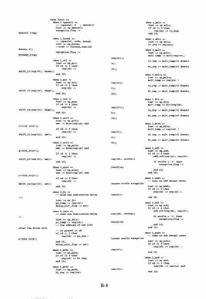
syscall_trap;
downto 6 ) ;
breakpt_trap ;
case funct is
when i_syscall =>
-- (special , 0 , syscall )
inst <= op_syscall;
exception_flag : =
when i_break =>
-- (special, code, break)
inst <= op_break;
--code := current_inst (25
shift_ll(reg(rt), shamt);
except ion_flag
when i_sll =>
inst <= op_sll;
if rd /= 0 then
reg(rd) :=
shi ft_rl ( reg ( rt ) , shamt ) ;
end if;
when i_srl =>
inst <= op_srl;
If rd /= 0 then
reg{rd) :=
end if;
when i_sra =>
inst <= op_sra;
if rd /= 0 then
reg(rd) :=
shift_ra(reg(rt) , shamt) ;
end if;
when i_sllv =>
inst <= op_sllv;
amt := bton ( reg (rs) and
x"0000_001f");
shift_ll(reg(rt), amt);
x"0000_001f");
if rd /= 0 then
reg(rd) :=
end if;
when l_srlv =>
inst <= op_srlv;
amt := bton ( reg (rs) and
if rd /= 0 then
reg(rd) :=
shift_rl(reg(rt), amt);
x"0000_001f");
shi ft_ra ( reg (rt ) , amt ) ;
after the delay slot
x"0000_0008";
end if;
when i_srav =>
Inst <= op_srav;
amt := bton ( reg (rs) and
if rd /= 0 then
reg(rd) :=
when i_jr =>
-- need one instruction delay
Inst <= op_jr;
pc_temp : = reg (ra);
delay_slot_flag := Bet;
when i_jalr =>
-- need one instruction delay
inst <= op_jalr;
pc_temp : = reg ( rs ) ;-- the address of the inst
-- is placed in rd
if rd /= 0 then
reg(rd) := pc_reg +
end if;
delay_slot_flag := set;
when i_mfhi =>
inst <= op_mfhi;
if rd /= 0 then
reg(rd) := hi_reg;
end If;
when i_mthi =>
inst <= op_mthi;
hi_reg := reg(rs);
reg(rt));
0);
32);
reg(rt);
0);
32);
32);
reg(rt) ;
0);
32);
reg(rd) , ovrflw) ;
overflow;
causes ovrflw exception
when i_mflo =>
inst <= op_mflo ;
If rd /= 0 then
reg(rd) := lo_reg;end If;
when i_mtlo =>
inst <= op_mtlo;
lo_reg := reg(rs);
when i_mult =>
inst <= op_mult;
mult_temp := mult (reg (rs) ,
lo_reg := mult_temp(31 downto
hi_reg := mult_temp(63 downto
when i_multu =>
inst <= op_multu;
mult_temp := reg (rs)*
lo_reg := mult_temp(31 downto
hi_reg := mult_temp(63 downto
when i_dlv =>
Inst <= op_div;
mult_temp := dlv{reg(rs),
lo_reg := mult_temp(3l downto
hi_reg := mult_temp(63 downto
when i_divu =>
inst <= op_divu;
mult_temp := reg(rs) /
lo_reg := mult_temp(31 downto
hi_reg := mult_temp(63 downto
when i_add =>
inst <= op_add;
if rd /= 0 then
add_ovf ( reg { rs ) , reg (rt )
if ovrflw =1'
then
exception_flag : =
end if;
end if;
when i_addu =>
-- same as add except never
inst <= op_addu;
if rd /= 0 then
reg(rd) := reg(rs) +
reg(rt);
reg ( rd ) , ovrflw) ;
causes ovrflw exception
reg(rt) ;
reg(rt);
end if;
when i_sub =>
inst <= op_sub;
lf rd /= 0 then
sub_ovf ( reg (rs ) , reg (rt ) ,
if ovrflw =' 1* then
exception_flag : =
end if;
end if;
when i_subu =>
-- same as sub except never
inst <= op_subu;
if rd /= 0 then
reg(rd) := reg(rs)-
end if;
when i_and =>
inst <= op_and;
if rd /= 0 then
reg(rd) := reg(rs) and
end if;
B-4
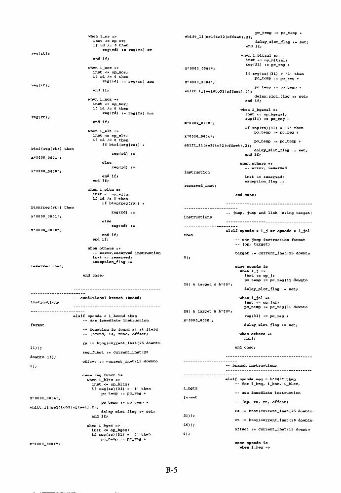
reg(rt);
reg(rt);
btoi(reg(rt)) then
x"0Q00_0001";
x"0000_0000";
bton ( reg (rt ) } then
x"0000_0001";
x"0000_0000";
when i_or =>
inst <= op_or;
if rd /= 0 then
reg(rd) := reg(rs) or
end if;
when i_xor =>
inst <= op_xor;
if rd /= 0 then
reg(rd) := reg(rs) xor
end if;
when i_nor =>
inst <= op_nor;
if rd /= 0 then
reg(rd) := reg(rs) nor
end if;
when i_slt =>
inst <= op_slt;
if rd /= 0 then
if btoi(regfrs)) <
reg(rd) :=
reg(rd) :=
end if;
end if;
when i_sltu =>
inst <= op_sltu;
if rd /= 0 then
i f bton ( reg ( rs ) ) <
reg(rd) :=
reg(rd) :=
end if;
end if;
when others =>
- -
error, reserved instruction
inst <= reserved;
exception_flag :=
reserved_inst;
conditional branch (bcond)
1nstruet1ons
21));
downto 16);
0);
"0000_0004";
elsif opcode = i_bcond then
-- use immediate instruction
-- function is found at rt field
-- (bcond, rs, func, offset)
rs := bton(current_inst (25 downto
reg_funct := current_inst (20
offset := current_inst (15 downto
case reg_funct is
when i_bltz =>
inst <= op_bltz;
if reg(rs)(31) ='1' then
pc_temp := pc_reg +
pe_te_p : = pc_temp +
shift_ll (sel6to32 (offset ) , 2) ;
delay_slot_flag : = set
end if;
when i_bgez =>
inst <= op_bgez;
if reg(rs)(31) ='0' then
pc_temp := pc_reg +
x"0000 0004";
pc_temp := pc_temp +
shift_ll(sel6to32 (offset), 2);
delay_slot_flag := set;
end if;
when i_bltzal =>
inst <= op_bltzal;
reg (31) := pc_reg +
x"0000_0008";
x"0000_0004"
if reg(rs) (31) ='1'
then
pc_temp := pc_reg +
pc_temp := pc_temp +
shift_ll (sel6to32 (offset) , 2) ;
delay_slot_flag := set;
end if;
when i_bgezal =>
inst <= op_bgezal;
reg (31) := pc_reg +
x"0000_0008";
if reg(rs)(31) ='0'
then
pc_temp := pc_reg +
x"0000_0004";
pe_temp := pc_temp +
shift_ll (sel6to32 (offset) , 2) ;
delay_slot_flag := set;
end if;
when otherB =>
--
error, reserved
instruction
reserved_inst ;
inst <= reserved;
exception_flag :=
instructions
jump, jump and link (using target)
0);
28) & target & b"00";
28) & target & b"00";
x"0000_0008";
elsif opcode = i_j or opcode = i_jal
use jump instruction format
(op, target)
target := current_inst (25 downto
case opcode is
when i_j =>
inst <= op_j;
pc_temp := pc_reg(31 downto
delay_slot_flag := set;
when i_jal =>
inst <= op_jal;
pc_temp := pc_reg(31 downto
reg (31) := pc_reg +
delay_slot_flag := set;
when others =>
null;
branch instructions
i_bgtz
format
21));
16));
0);
elslf opcode_seg =b"000" then
-- for i_beq, i_bne, i_blez,
-- use immediate instruction
-- (op, rs, rt, offset)
rs := bton(current_inst (25 downto
rt := bton (current_inst {20 downto
offset := current_inst (15 downto
case opcode is
when l_beq =>
B-5

inst <= op_beq ;
if reg(rs) = reg(rt) then
pc_temp := pc_reg +
x"0000_0004";
pc_temp := pc_temp +
shift_ll(sel6to32 (offset) ,2);
delay_slot_flag := set;
end If;
when i_bne =>
inst <= op_bne;
if reg(rs) /= reg(rt) then
pc_temp := pc_reg +
x"0000_0004";
pc_temp := pc_temp +
shift_ll (sel6to32 (offset), 2) ;
delay_slot_flag := set;
end if;
when i_blez =>
inst <= op_blez;
if reg(rs) (31) =!
or
reg(rs) = reg(O) then
x"0000_0004";
shift_ll(sel6to32(offset),2);
pc_temp := pc_reg +
pc_temp := pc_temp +
reg(rs) /= reg(O) then
x"0000_0004";
shift_ll(sel6to32 (offset), 2);
delay_slot_flag := set;
end if;
when i_bgtz =>
inst <= op_bgtz;
if reg(rs) (31) = '0'and
pc_temp : = pc__reg +
pc_temp : = pc_temp +
delay_slot_flag := set;
end if;
when others =>
null ;
end if;
end if;
when i_sltiu =>
inst <= op_sltlu;
if rt /_ 0 then
if bton ( reg ( rs ) ) <
bton(sel6to32 (immed) ) then
reg(rt) :=
x"0000_0001";
else
reg(rt) :=
x"0000_0000";
end if;
end if;
when i_andi =>
inst <= op_andi;
if rt /= 0 then
reg(rt) :=(x"0000"
&
end if;
when i_ori =>
inst <= op_ori;
if rt /= 0 then
reg(rt) :=(x"0000" &
immed) and reg(rs);
immed) or reg(rs) ;
immed) xor reg(rs);
end if;
when i_xori =>
inst <= op_xori;
if rt /= 0 then
reg(rt) := (x"0000" &
end lf;
when i_lui =>
inst <= op_lul;
if rt /= 0 then
ui := immed;
reg(rt) := ui & x"000 0";
end if;
end case; when others =>
null;
end case;
21));
16));
0);
-- ALU immediate instructions
elsif opcode_seg =b"001"
then
-- use immediate instruction
-- (op, rs, rt, immediate)
rs := bton(current_inst (25 downto
rt := bton(current_inst (20 downto
immed := current_lnst (15 downto
case opcode is
when i_addi =>
inst <= op_addi;
if rt /= 0 then
add_ovf (reg(rs) ,
sel6to32 (immed) , reg(rt) , ovrflw) ;
if ovrflw ='1' then
exception_flag :=
overflow;
end if;
end if;
when i_addiu =>
inst <= op_addlu;
if rt /= 0 then
reg(rt) := reg(rs) +
sel6to32 (immed) ;
end if;
when i_slti =>
inst <= op_sltl;
if rt /= 0 then
if btoi(reg(rs) ) <
btoi (sel6to32 (immed) ) then
reg (rt ) : =
x"0000_0001";
else
reg(rt) :=
x"0000__0000";
load and store instructions
elsif opcode_seg = b"10 0 " or
opcode_seg =b" 1 0 1 " then
-- use Immediate instruction
format
-- (op, base, rt, offset)
downto 21) ) ;
16));
0);
reg(base) ;
temp_reg_val_l) ;
reg (base) ;
temp_reg_val_l) ;
base := bton(current_inst (25
rt := bton(current_inst (20 downto
offset := current_lnst (15 downto
case opcode is
when l_lb =>
inst <= op_lb;
if rt /= 0 then
ea := sel6to32 (offset) +
mem_read (ea, byte,
temp_reg_num_l := rt;
latency_flag := set;
end if;
when i_lh =>
inst <= op_lh;
if rt /= 0 then
ea := sel6to32 (offset) +
mem_read(ea, halfword,
temp_reg_num_l := rt;
latency_flag : = set ;
end If;
when i_lwl =>
inst <= op_lwl;
B-6

reg (base) ;
temp_reg_val_l) ;
downto 0 )
reg (base) ;
temp_reg_val_l) ;
reg (base) ;
temp_reg_val_l) ;
reg (base) ;
temp_reg_val_l )
reg (base) ;
temp_reg_val_l) ;
downto 0 ) ;
reg (base) ;
reg (base) ;
reg(rt));
reg(base) ;
reg(rt));
reg(base) ;
reg (base) ;
reg(rt));
if rt /= 0 then
ea := sel6to32 (offset) +
mem_read(ea, lefty,
temp_reg_num_l : = rt ;
temp_addr_l : = ea ( 1
latency_flag := set;
left_flag := set;
end if;
when i_lw =>
inst <= op_lw;
if rt /= 0 then
ea := sel6to32 (offset ) +
mem_read(ea, word,
temp_reg_num_l : = rt ;
latency_flag := set;
end if;
when l_lbu =>
inst <= op_lbu;
if rt /= 0 then
ea := sel6to32 (offset) +
mem_read(ea, ubyte,
temp_reg_num_l := rt;
latency_flag := set;
end if;
when i_lhu =>
inst <= op_lhu;
if rt /= 0 then
ea := sel6to32 (offset ) +
mem_read (ea, uhal fword ,
temp_reg_num_l : = rt;
latency_flag := set;
end if;
when i_lwr =>
Inst <= op_lwr;
if rt /= 0 then
ea : = sel6to32 (offset) +
mem_read (ea, righty,
temp_reg_num_l := rt;
temp_addr_l := ea(l
latency_flag := set;
right_flag := set;
end if;
when i_sb =>
inst <= op_sb;
ea := sel6to32 (offset) +
mem_write(ea, byte, reg(rt) ) ;
when i_sh =>
inst <= op_sh;
ea := sel6to32 (offset ) +
merc_write(ea, halfword.
when i_swl =>
inst <= op_swl;
ea : = sel6to32 (offset ) +
mem_write(ea, lefty.
when i_sw =>
inst <= op_sw;
ea := sel6to32 (offset ) +
mem_wrlte (ea, word, reg(rt) ) ;
when i_swr =>
inst <= op_swr;
ea := sel6to32 (offset) +
mem_write (ea, righty.
when others =>
instruction
reserved_inst;
- -
error, reserved
inst <= reserved;
exceptlon_flag : =
instruction)
halt instruction (not a mips
elsif opcode = i_halt then
inst <= op_halt;
run_mode_flag := no;
instructions not implemented
elsif (opcode_seg =b"010"
or
opcode_seg = b"110"or
opcode_seg = b"lll") and
opcode ( 2 ) =' 0 ' then
inst <= not_implmt;
exception_flag := not_implmt;
x"0000_0004";
reserved instructions
inst <= reserved;
except ion_flag := reserved_inst;
end if;
exception handling
if exception_flag /= idle then
if bd_flag = yes then
cause_reg(31) := *1';
epc_reg := pc_reg-
else
cause_reg (31) : =' 0 '
;
epc_reg := pc_reg;
end if;
case exception_flag is
when reset => null;
when breakpt_trap =>
cause_reg(5 downto 2) := bp;
when syscall_trap =>
cause_reg(5 downto 2) := sys;
when overflow =>
cause_reg ( 5 downto 2 ) : = ovf ;
when addr_load =>
cause_reg(5 downto 2) :=
when addr_store =>
cause_reg(5 downto 2) :=
when bus_inst => null;
when bus_data => null;
when reserved_inst =>
cause_reg(5 downto 2)
when ext_int =>
cause_reg(5 downto 2)
when not_implmt =>
cause_reg(5 downto 2)
when others =>
rl;
B-7

delay_slot;
x"0000_0004";
end case;
run_mode_flag := no;
temp_reg_val_2 (31 downto 8);
:= temp_reg_val_2;
delay slot temp_reg_val_2 ;
if delay_slot_flag /= ignore then
if delay_slot_flag = set then
delay_slot_flag :=
-- increment pc
pc_reg := pc_reg +
delay_slot_flag := ignore;
pc_reg := pc_temp;
end if;
else
-- increment pc
pc_reg := pc_reg +x"0000_0004"
end if;
whenb"ll"
=>
reg (temp_reg_num_2 )
end case;
right_flag := ignore;
reg ( temp_reg_num_2 )
end if;
lateney_flag := ignore;
end if;
end if;
set branch delay flag
if delay_slot_flag = delay_slot then
bd_flag := yes;
else
bd_flag := no;
end if;
end if;
-- latency of one instruction on
memory to register loads
update signals
temp_reg_val_l ;
temp_reg_nu__l ;
ternp_addr_l ;
temp_addr_l;
if latency_flag /= ignore then
if latency_flag = set then
temp_reg_val_2 :=
temp_reg_num_2 :=
if left_flag = set then
temp_addr_2 : =
left_flag := delay_slot;
end if;
if right_flag = set then
temp_addr_2 : =
right_flag := delay_slot;
end if;
latency_flag := delay_slot;
else
if left_flag = delay_slot
case temp_addr_2 is
whenb"00"
=>
reg (temp_reg_num_2 )
:= temp_reg_val_2;
whenb"01"
=>
reg(temp_reg_num_2) (31 downto 8) :=
temp_reg_val_2 (23 downto 0);
whenb"10"
=>
reg(temp_reg_num_2) (31 downto 16) :=
temp_reg_val_2 (15 downto 0 ) ;
whenb"ll"
=>
reg(temp_reg_num_2) (31 downto 24) :=
downto 0 ) ;
temp_reg_val_2 (7
rO <= reg ( 0 )
thru r31
rl <= reg(l);
r2 <= reg(2)
r3 <= reg(3)
rl <= reg(l)
r5 <= reg{5)
r6 <= reg(6)
r7 <= reg (7)
r8 <= reg(8)
r9 <- reg(9)
rlO <= reg (10),
rll <= reg(ll);
rl2 <-- reg(12);
rl3 <= reg(13);
rll < == reg(ll);
rl5 <= reg (15);
rl6 <== reg(16);
rl7 <--= reg(17);
rl8 <== reg(18);
rl9 <== reg(19);
r2 0 <== reg (20);
r21 <== reg (21);
r22 <== reg(22);
r23 <== reg(23);
r21 <.= reg(21);
r25<
= reg(25);
r26 <-= reg (26);
r27 <.= reg(27);
r28 < = reg(28);
r29 < = reg(29),
r30 < = reg (30);
r31 < = reg(31).
hi <= hl_reg;
registers for mult and div
lo <= lo_reg
end case;
left_flag := Ignore;
elslf right_flag- delay_slot
then
case temp_addr_2 is
whenb"00"
=>
reg(temp_reg_num_2) (7
downto 0 ) : =
temp_reg_val_2 ( 3 1 downto 21);
whenb"01"
=>
reg(temp_reg_num42) (15 downto 0) :=
temp_reg_val_2 ( 3 1 downto 16);
whenb"10"
=>
reg(temp_reg_num_2) (23 downto 0) :=
epc <= epc_reg;
registers rO
-- exception
handling
expected results
cause <= cause_reg;
exception_sig <= exception_flag;
- - compare machine state with
compare_control_sig <= test;
wait until compare_aak_sig = yes;
compare_control_sig <= reset;
wait until compare_ack_sig = no;
end loop;
when others =>
-- end while run_mode_flag
B-8
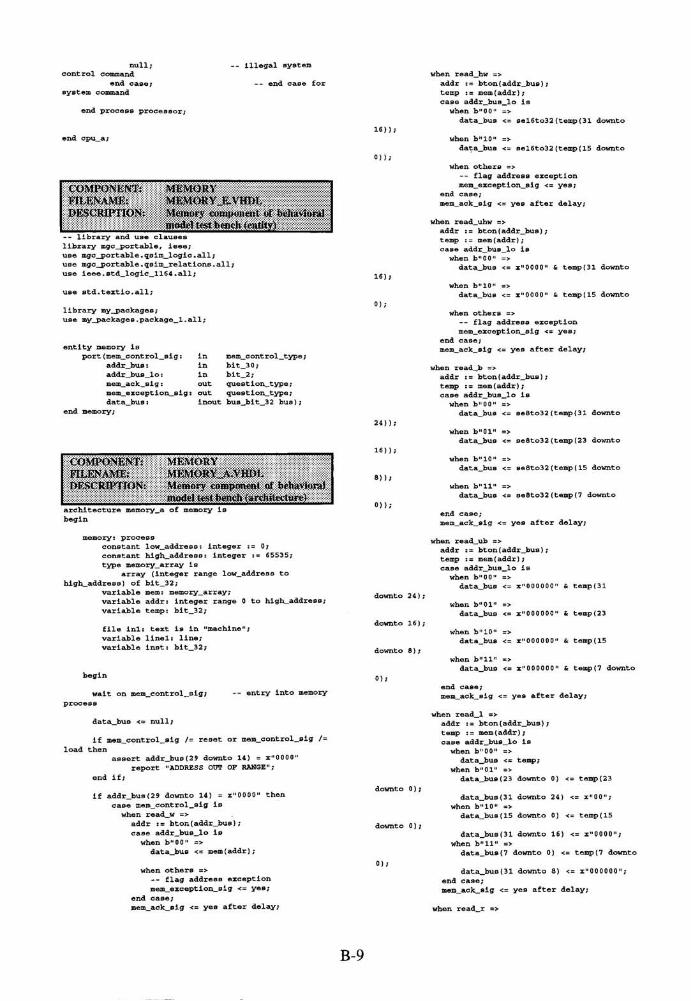
null;
control command
end case;
system command
end process processor;
end cpu_a;
illegal system
-- end case for
t'OMl'ONCNT; MEMORY
NLKNAMK: MlM-OftY E.V_tL
DESCRIPTION; Mentor; component of frehavjoralmoidel testbench (entity)
library and use clauses
library mgc_portable, ieee;
use mgc_portable.qsim_logic.all;
use mgc_portable.qsim_relatlons.all;
use ieee . std_logic_1164 .all ;
use std . textio . all ;
library my.packages;
use my packages ,package_l.all;
entity memory is
port (mem_control_sig: in mem_control_type ;
addr bus: in bit 30;
addr bus_lo: in bit_2;
mem_ack_sig : out question_type;
mem_exception_sig: out question_type ;
data bus : lnout bus_bit_3 2 bus ) ;
end memory;
C()MPIIM\T: M1.MORY
IILJ:>AMK: M1.MORYJV.VHUI.
DKsrknniuN: Memory ci.n_|irmoi_l til iwh_rviui_l
| model test bench (archilgcttire.
architecture memory_a of memory is
begin
memory: process
constant low_address: integer := 0;
constant high_address : integer : = 65535;
type memory_array is
array (integer range low_address to
high_address) of bit_32;
variable mem: memory_array;
variable addr: integer range 0 to high_address
variable temp: bit_32;
file inl: text is in "machine";
variable linel: line;
variable inst: bit_32;
begin
wait on mem_control_sig;--
entry into memory
process
data_bus <= null;
if mem_control_sig /= reset or mem_control_sig/=
load then
assert addr_bus(29 downto 14) =x"0000"
report "ADDRESS OUT OF RANGE";
end if;
if addr_bus(29 downto 14)- x"0000" then
case mem_control_sig is
when read_w =>
addr := bton(addr_bus) ;
case addr_bus_lo is
whenb"00"
=>
data_bus <= mem(addr);
when others =>
-- flag address exception
mem_exception_sig <= yes;
end case;
mem_ack_slg <= yes after delay;
16));
16);
0)>;
downto 2 4 )
downto 16);
downto 8 ) ;
downto 0 ) ;
when read_hw =>
addr := bton(addr_bus) ;
temp := mem (addr);
case addr_bus_lo is
whenb"00"
=>
data_bus <= sel6to32 (temp (31 downto
whenb"10"
=>
data_bus <= sel6to32 (temp(15 downto
when others =>
-- flag address exception
mem_exception_sig <= yes;
end case;
mem_ack_slg <= yes after delay;
when read_uhw =>
addr := bton(addr_bus) ;
temp := mem (addr) ;
case addr_bus_lo is
whenb"00"
=>
data_bus <=x"0000" & temp(31 downto
whenb"10"
=>
data_bus <=x"0000" & temp(15 downto
when others =>
-- flag address exception
mem_exception_sig <= yes;
end case;
mem_ack_slg <= yes after delay;
when read_b =>
addr := bton(addr_buB) ;
temp := mem (addr);
case addr_bus_lo is
whenb" 0 0" =>
data_bus <= se8to32 (temp(31 downto
whenb"01"
=>
data_bus <= se8to32 (temp (23 downto
whenb"10"
=>
data_bus <= se8to32 (temp (15 downto
whenb"ll"
=>
data_bus <= se8to32 (temp(7 downto
end case;
mem_ack_sig <= yes after delay;
when read_ub =>
addr := bton(addr_bus) ;
temp : = mem (addr ) ;
case addr_bus_lo is
whenb"00"
=>
data_bus <=x"000000" & temp(31
whenb"01"
=>
data_bus <=x"000000"
& temp(23
whenb"10"
=>
data_bus <=x"000000"
& temp(15
whenb"!!"
=>
data_bus <=x"000000M temp(7 downto
end case;
mem_ack_slg <= yes after delay;
when read_l =>
addr := bton(addr_bus) ;
temp := mem(addr);
case addr_bus_lo is
whenb"00"
=>
data_bus <= temp;
whenb"01"
=>
data_bus(23 downto 0) <= temp(23
data_bus(31 downto 24) <= x"00"
;
whenb"10"
=>
data_bus(15 downto 0) <= temp (15
data_bus(31 downto 16) <= x"0000";
whenb"ll"
=>
data_bus(7 downto 0) <= temp (7 downto
data_bus(31 downto 8) <= x"000000";
end case;
mem_ack_sig <= yes after delay;
when read_r =>
B-9
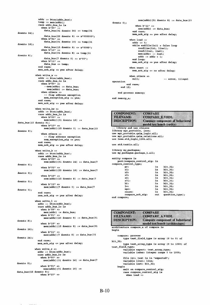
downto 24) ;
downto 16);
addr := bton(addr_bus) ;temp := mem (addr);case addr_bus_lo is
when b"00"=>
data_bus(31 downto 24) <= temp(31
data_bus(23 downto 0) <= x"000000";
when b"01"=>
data_bus(31 downto 16) <= temp (31
data_bus(15 downto 0) <= x"0000";
whenb"10"
=>
data_bus{31 downto 8) <= temp (31
data_bus(7 downto 0) <= x"00";
whenb"ll"
=>
data_bus <= temp;
end case;
mem_ack_slg <= yes after delay;
when wrlte_w =>
addr := bton(addr_bus) ;case addr_bus_lo is
whenb"00"
=>
--mem (addr) := data_bus;mem (addr) := data__bus;
when others =>
-- flag address exception
_em_exception_sig<= yes;
end case;
mem_ack_sig <= yes after delay;
downto 0 ) ;
mem(addr) (31 downto 8) := data_bus(23
whenb"ll"
=>
mem (addr) := data_bus;
end case;
mem_ack_sig <= yes after delay;
when load =>
addr : = 0 ;
while endfile(inl) = false loop
readline(inl, linel);
read(linel, inst) ;
mem(addr) := inst;
addr := addr + 1;
end loop;
mem_ack_sig <= yes after delay;
when reset =>
mem_ack_sig <= no after delay;
when others =>
null;
operation
end case;
end if;
end process memory;
end memory_a;
error, illegal
when wrlte_hw =>
addr := bton(addr_bus) ;case addr_bus_lo is
whenb" 00"
=>
mem(addr) (31 downto 16) :=
data_bus (15 downto 0 ) ;
whenb"10"
=>
mem(addr) (15 downto 0) := data_bus{15
downto 0 ) ;
when others =>
-- flag address exception
mem_exception_sig <= yes;
end case;
mem_ack_sig <= yes after delay;
when write_b =>
addr : = bton(addr_bus) ;
case addr_bus_lo is
whenb" 00"
=>
mem (addr) (31 downto 24) := data_bus(7
downto 0 ) ;
downto 0 ) ;
downto 0 ) ;
downto 0 ) ;
whenb"01"
=>
mem(addr) (23 downto 16) : = data_bus(7
whenb"10"
=>
mem (addr) (15 downto 8) data_bus(7
downto 8);
downto 16);
downto 24) ;
when^'11"
=>
mem (addr) (7 downto 0) := data_bus(7
end case;
mem_ack_sig <= yes after delay;
when write_l =>
addr : = bton (addr_bus ) ;
case addr_bus_lo is
whenb"00"
=>
mem(addr) := data_bus;
whenb"01"
=>
mem(addr) (23 downto 0) := data_bus(31
whenb"10"
=>
mem (addr) (15 downto 0) := data_bus(31
whenb"ll"
=>
mem (addr) (7 downto 0) := data_bus(31
end case;
mem_ack_slg <= yes after delay;
when write_r =>
addr : = bton (addr_bus ) ;
case addr_bus_lo is
whenb"00"
=>
mem(addr)(31 downto 24) := data_bus(7
downto 0 ) ;
data_bus(15
whenb"01"
=>
mem(addr)(31 downto 16)
downto 0 ) ;
whenb"10"
=>
(.OMPONLNf- COMPAJtE
FUuENAMK: C0-4-,A_HE_e.VI_0L
i-KSCRimK*,; Cosripare <inpoiijlT behavioral
model testbench (entity)-- library and use clauses
library mgc_portable, ieee;
use mgc_portable.qsim_logic.all;
use mgc_portable.qsim_relations.all ;
use ieee.std_logic_1164.all;
use std . textio . all ;
library my_packages;
use my_packages.package_l.all;
entity compare is
port (compare_control_sig: in
compare_control_type;
pc: in bit_32;
rl: in bit_32;
r2: in bit_32;
r3: in bit_32;
r4: in bit_32;
r31: in bit_32;
hi: in blt_32;
lo: in bit_32;epc: in blt_32;
cause: in bit_32;
compare_ack_sig: out question_type)
end compare;
IH.FAAMKS
DESCRHTfON;
COMl*AUK
CNfV\ftK AAH1H
CMiiparv coiiipuni-fil of hchaviuml
modrf test bench <rtrtvhttoitttrf )
architecture compare_a of compare is
begin
compare : process
type test_field_type is array (0 to 9) of
bit_32;
type test_array_type is array (0 to 1000) of
test_field_type;
variable expect: test_array_type;
variable index: integer range 0 to 1000;
file inl: text is in "expected";
variable linel: line;
variable inst: bit_32;
begin
wait on compare_control_sig;
case eompare_control_sig is
when load =>
B-10

index := 0;
while endfile(lnl) = false loop
for 1 in 0 to 9 loopif endflle(inl) = false then
readline(inl, linel) ;
read (linel, inst) ;
expect (index) (i) := inst;
end if;
end loop;
index := index + 1;
end loop;
index : = 0 ;
compare_ack_sig <= yes after delay;
when test =>
assert pc = expect (index) (0)report "PC REGISTER ERROR"
severity warning;
assert rl = expect (Index) (1)
report "REGISTER 1 ERROR"
severity warning;
assert r2 = expect (index) (2)report "REGISTER 2 ERROR"
severity warning;
assert r3 = expect (index) (3)
report "REGISTER 3 ERROR"
severity warning;
assert r4 = expect (index) (4 )
report "REGISTER 4 ERROR"
severity warning;
assert r31 = expect (index) (5)
report "REGISTER 31 ERROR"
severity warning;
assert hi = expect (index) (6)
report "REGISTER HI ERROR"
severity warning;
assert lo = expect (index) (7)
report "REGISTER LO ERROR"
severity warning;
assert epc = expect (index) (8)
report "EPC REGISTER ERROR"
severity warning;
assert cause = expect (index) (9)
report "CAUSE REGISTER ERROR"
severity warning;
index := index + 1;
comparemack_sig <= yes after delay;
when reset =>
compare_ack_sig <= no after delay;
--when stop => null;
--when error => null;
end case;
end process compare;
end compare_a;
COMPONENT! i\< ka<;i: t
PILltttAMIb PACKAGE. 1. ILVHU1.
1H-.SCRH'TION ! Bi-tinvinratmndrl pMlcage lhrutfrr
package package_l is
constant delay: time := 10 ns;
subtype bit_2 is bit_vector (1 downto 0);
subtype bit_3 is bit_vector (2 downto 0)
subtype bit_4 is bit_vector (3 downto 0)
subtype bit_5 is bit_vector (4 downto 0)
subtype bit_6 is bit_vector (5 downto 0)
subtype bit_8 is bit_vector(7 downto 0);
subtype blt_16 is bit_vector (15 downto 0);
subtype bit_20 is bit_vector (19 downto 0);
subtype bit_24 is bit_vector(23 downto 0) ;
subtype bit_26 is blt_vector (25 downto 0);
subtype bit_30 is bit_vector (29 downto 0);
subtype bit_32 is bit_vector (31 downto 0);
subtype bit_64 is bit_vector(63 downto 0 ;
subtype bit_5_range is integer range 0 to 31;
subtype bit_16_range is integer range -32768 to
32767;
subtype bit_26_range is integer range -67108864 to
67108863;
type bit_32_array is array (integer range <>) of
bit_32;
function wired_or (driver: bit_32_array) return
bit_32;
subtype bus_bit_32 is wired_or blt__32;
type sys_control_type is (stop, run, load, reset);
type mem_control_type is (reset, read_b, read_ub,
read_hw, read_uhw,
read_w, read_l, read_r,
write_b, write_hw,
write_w, write_l,
wrlte_r, load) ;
type question_type is (no, yes);
type delay_slot_type is (ignore, delay_slot, set);
type inst_type is (nop, not_implmt, reserved,
op_halt, op_add, op_addi,
op_addiu, op_addu, op_and,
op_andi , op_beq, op_bgez ,
op_bgezal , op_bgtz , op_blez ,
op_bltz, op_bltzal, op_bne,
op_break, op_div, op_divu, op_j ,
op_jal, op_jalr, op_jr,
op_lb, op_lbu, op_lh, op_lhu,
op_lul , op_lw, op_lwl ,
op_lwr, op_mfhl, op_mflo,
op_mthi, op_mtlo, op_mult,
op_multu, op_nor, op_or, op_ori,
op_sb, op_sh, op_sll,
op_sllv, op_slt, op_slti,
op_sltiu, op_sltu, op_sra,
op_srav, op_srl, op_srlv,
op_sub, op_subu, op_sw, op_swl,
op_swr , op_syscall , op_xor ,
op_xori ) ;
type size_type is (byte, ubyte, halfword,
uhalfword, word, lefty, righty);
type compare_control_type is (reset, load, test);
constants for implemented instructions
constant i_special : bit_6 = o 00
constant i_bcond : bit_6 = o"01
constant l_j = bit_6 = o 02
constant i___al: bit_6 = o 03
constant i_beq : bit_6 = o 04
constant i_bne : bit_6 = o 05
constant i_blez: bit_6 = o 06
constant i_bgtz: bit_6 = o 07
constant i_addi : bit_6 = o 10
constant i_addiu: bit_6 = o 11
constant l_slti: blt_6 = o 12
constant i_sltiu: blt_6 = o 13
constant i_andi : bit_6 = o"14
constant i_ori : bit_6 = o 15
constant i_xori : bit_6 = o"16
constant i_lui : blt_6 = o 17
constant l_lb: bit_6 _ o 40
constant i_lh: bit_6 = o 41
constant i_lwl : blt_6 = o 42
constant i_lw: bit_6 = o"43
constant i_lbu: bit_6 = o 44
constant i_lhu : bit_6 = o 45
constant i_lwr : bit_6 = o 46
constant i_sb: bit_6 = o 50
constant i_sh: bit_6 = o 51
constant i_swl : bit_6 = o 52
constant i_sw: bit_6 = o 53
constant i_swr : bit_6 = o 56
constant i_sll: bit_6 = o 00
constant i_srl : blt_6 = o 02
constant i_sra: bit_6 = o 03
constant i_sllv: bit_6 = o 04
constant i_srlv: bit_6 = o 06
constant i_srav: bit_6 = o 07
constant i_jr: bit_6 = o '10
constant i_jalr: blt_6 = o 11
constant i_syscall bit_6 = o '14
constant i_break : bit_6 = o 15
constant l_mfhi : bit_6 : = o '20
constant l_mthl : bit_6 : = o '21
constant i_mflo: bit_6 := o '22
constant i_mtlo: bit_6 : = o 23
constant i_mult:
B-ll
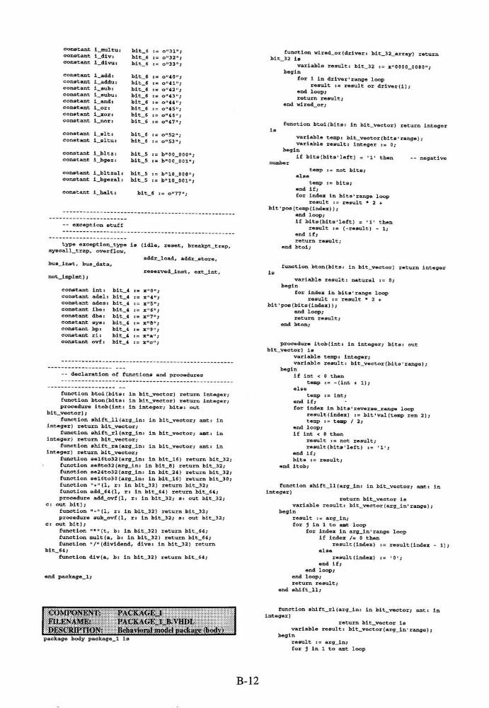
constant i_multu:
constant l_div:
constant i_divu:
bit_6 := o"31";
bit_6 := o"32";
bit_6 := o"33";
constant i_add : bit 6 _ o"40"
constant i_addu: bit 6 = o"41";constant i_sub: bit 6 = o"42"j
constant i_subu : bit 6 = o"43";
constant i_and : bit 6 = o"44"
constant i_or: bit 6 = o"45"
constant i_xor : bit 6 - o"46"
constant i_nor : bit_6 = o"47"
constant i_slt: bit 6 _
o"52";
constant i_sltu: bit_6 = o"53";
constant l_bltz: bit 5 _
b"00 000
constant i_bgez: bit_5 = b"00 001
constant i_bltzal:
constant i_bgezal :
constant i_halt:
bit_5 := b"10_000"
bit_5 := b"10_001"
exception stuff
type exception_type is (idle, reset, breakpt_trap,syscall_trap, overflow,
addr_load, addr_store,bus_inst , bus_data,
reserved_inst, ext_int,not_implmt ) ;
constant int: bit 4 : = X 0";constant adel : bit 4 : = X 4";constant ades: bit 4 : = X 5";
constant ibe: bit 4 .= X 6";constant dbe: bit 4 : = X 7";constant sys: bit 4 : = X 8";constant bp: bit 4 ; = X 9";constant rl: bit 4 : = X a";
constant ovf : bit 4 : = X c";
declaration of functions and procedures
function btoi(bits: in bit_vector) return integer;function bton(bits: in bit_vector) return integer;procedure itob(int: in integer; bits: out
bit_vector) ;function shift_ll (arg_in: in bit_vector; amt: in
integer) return bit_vector;
function shift_rl(arg_in: in bit_vector; amt: in
integer) return bit_vector;
function shift_ra(arg_in: in bit_vector; amt: in
integer) return bit_vector;
function sel6to32 (arg_in: in bit_16) return bit_32;function se8to32(arg_in: in bit_8) return bit_32;function se24to32(arg_ln: in bit_24) return bit_32;function sel6to3 0 (arg_in: in bit_16) return bit_30;function "+"(1, r: in bit_32) return bit_32;
function add_64(l, r: in bit_64) return bit_64;
procedure add_ovf (1, r: in bit_32; s: out bit_32;c: out bit);
function "-"(1, r: in bit_32) return bit_32;
procedure sub_ovf (1, r: in bit_32; s: out bit_32;
c: out bit);
function "*"(t, b: in bit_32) return blt_64;
function mult (a, b: in bit_32) return bit_64;
function "/"(dividend, divs: in bit_32) return
bit_64;
function div(a, b: in bit_32) return bit_64;
end package_l;
function wired_or(driver: bit_32_array) return
bit_32 is
variable result: bit_32 := x"0000_0000";begin
for 1 in driver'range loop
result := result or driver(i);end loop;
return result;
end wired_or;
is
function btoi(bits: in bit_vector) return integer
--
negative
variable temp: bit_vector (bits '
range) ;
variable result: integer := 0;begin
if bits (bits 'left) = '1' then
number
temp := not bits;else
temp := bits;end if;
for index in bits' range loopresult := result * 2 +
bit 'pos (temp (index) ) ;
end loop;
If bits (bits' left) ='1'
then
result := (-result) - 1;
end if;
return result;
end btoi;
function bton(bits: in blt_vector) return integer
variable result: natural := 0;begin
for index in bits 'range loopresult := result
* 2 +
bit-pos (bits (index) );
end loop;
return result;
end bton;
procedure itob(int: in integer; bits: out
bit_vector) is
variable temp: integer;variable result: bit_vector (bits '
range) ;
begin
if int < 0 then
temp := - (int + 1) ;
else
temp := int;
end if;
for index in bits 'reverse_range loop
result(index) := bit'val(temp rem 2);
temp := temp / 2;
end loop;
if int < 0 then
result := not result;
result (bits 'left) := '1';end if;
bits := result;
end ltob;
function shift_ll(arg_in: in Mt_vector; amt: in
integer)
return bit_vector is
variable result: bit_vector (arg_in' range) ;begin
result := arg_in;
for j in 1 to amt loop
for index in arg_in'range loop
if index /= 0 then
result (index) := result (Index - 1) ;else
result (index) := ' 0 ';
end if;
end loop;
end loop;
return result;
end shift_ll;
eoMi-oNKvn
ni-l-,MMK:
DESCRIPTION:
package body package_l is
p\cka(.f:ji\rM.;F_ij4,vHl>i
function shlft_rl(arg_ln: in bit_vector; amt: in
integer)
return bit_vector is
variable result: bit_vector (arg_in' range) ;begin
result : = arg_in;
for j in 1 to amt loop
B-12

for index in arg_in'reverse_range loop
if Index /= arg_in'high then
result (index) := result (index + 1);
else
result(index) := '0';
end if;end loop;
end loop;
return result;end shift_rl;
function shift_ra(arg_in: in bit_vector; amt: in
integer)
return blt_vector is
.variable result: blt_vector(arg_ln' range) ;
begin
result := arg_in;
if arg_in(arg_in'left) ='1'
then
for j in 1 to sunt loopfor index in arg_in'
reverse_range loopif index /= arg_in'high then
result (index) := result (index +
D;
else
result (index) :=' 1'
;
end if;
end loop;
end loop;else
for j in 1 to amt loopfor index in arg_ln'
reverse_range loopif index /= arg_in'hlgh then
result (Index) := result(index +
else
result (index) := ' 0 ';
end If;
end loop;
end loop;
end if;
return result;
end shift_ra;
function sel6to32(arg__in: in bit_16) return bit_32
variable result: bit_32;begin
if arg_in(arg_in'left) ='1'
then
result :=x"ffff"
& arg_in;
else
result := x"0000" & arg_in;
end if;
return result;
end sel6to32;
function se8to32 (arg_in: in bit_8) return bit_32 is
variable result: bit_32;
begin
if arg_in(arg_in' left) ='1' then
result :=b"llll_llll_llll_llll_llll_llll"
& arg_in;
else
result :=b"0000_0000_0000_0000_0000_0000"
& arg_in;
end if;
return result;
end se8to32;
function se24to32 (arg_ln: in blt_24) return bit_32
result := b"00_0000_0000_0000" & arg_in;
end if;
return result;
end sel6to30;
function "+"(1, r: in bit_32) return bit_32 is
variable carry: bit := '0';
variable sum: bit_32;begin
for i in 0 to 31 loopif carry =
' 0 'then
carry := 1 (i) and r(i);
sum(i) := l(i) xor r(i);
else
carry := 1(1) or r(i);
sum(i) := not { l(i) xor r(i) ) ;end if;
end loop;
return sum;
end"+"
;
function add_64(l, r: in bit_64) return bit_64 is
variable carry: bit := '0';
variable sum: bit_64;
begin
for i in 0 to 63 loopif carry =
' 0 'then
carry := l(i) and r(l);
sum(i) := 1(1) xor r(i);
else
1(1) or r(i);
= not( 1(1) xor r(l)),-
carry
sum(i;
end if;
end loop;
return sum;
end add_64;
procedure add_ovf(l, r: in bit_32; s: out bit_32;c: out bit) is
variable sum: bit_32;
variable carry: bit;
variable carry30: bit;
variable carry31: bit;
begin
for 1 In 0 to 31 loopif carry =
'0' then
carry := 1(1) and r(i);
sum(i) := 1(1) xor r(i);
else
carry := l(i) or r(i);
sum(i) := not( 1(1) xor r(i) );end if;
if i = 30 then
carry3 0 := carry;
elsif i = 31 then
carry31 := carry;
end if;
end loop;
c := carry30 xor carry31;
s := sum;
end add_ovf;
function "-"(1, r: in bit_32) return bit_32 is
variable temp, result: bit_32;begin
temp := (not r) + x"0000_0001";
result : = 1 + temp;
return result;
end"
-";
variable result: blt_32;
begin
If arg_in(arg_in' left) ='1' then
result :=b"llll_llll"
& arg_ln;
else
result :=b"0000_0000" & arg_in;
end if;
return result;
end se24to32;
function sel6to30 (arg_in: in bit_16) return bit_30
variable result: bit_30;
begin
if arg_in(arg_in' left) ='1' then
result :=b"ll_llll_llll_llll" & arg_ln;
else
procedure sub_ovf(l, r: in bit_32; s: out bit_32;
c: out bit) is
variable temp, result: bit_32;begin
temp := (not r) + x"0000_0001";
add_ovf ( 1 , temp , s , c ) ;
end sub_ovf ;
function "*"(t, b: in bit_32) return bit_64 is
type mult_array is array (0 to 31) of bit_64;variable ma: mult_array;
variable carry: bit :=' 0 '
;
begin
for bot in 0 to 31 loopif b(bot) =
'0'then
ma(bot) := x"0000_0000_0000_0000";
else
B-13
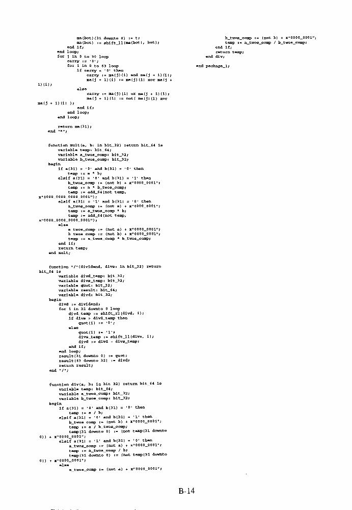
ma(bot) (31 downto 0) := t;
ma(bot) := shift_ll (ma(bot) , bot);
end if;
end loop;
for j in 0 to 30 loop
carry : =' 0 '
;
for i in 0 to 63 loop
if carry ='0'
then
carry : = ma ( j ) ( i ) and ma ( j + 1 ) ( i ) ;
ma(j + 1) (i) :=ma(j)(i) xorma(j +
1) (D;
else
carry := ma(j)(i) or ma(j + l)(i);
ma(j + l)(i) := not ( ma(j)(i) xor
ma(j + 1) (1) );
end if;
end loop;
end loop;
temp :
end if;
return temp
end div;
b_twos_comp := (not b) +x"0000_0001"
_twos_comp/ b_twos_comp;
end package_l;
return ma (31);
end "*";
function mult(a, b: in bit_32) return bit_64 is
variable temp: bit_64;
variable a_twos_comp: bit_32;
variable b_twos_comp: bit_32;
begin
if a(31) ='0'
and b(31) ='0'
then
temp : = a* b;
elsif a(31) ='0'
and b(31) ='1' then
b_twos_comp := (not b) + x"0000_0001";
temp := a* b_twos_comp;
temp := add_64 (not temp,
x"00 0 0_0 00 0_0000_0 0 01") ;
elsif a(31) ='1'
and b(31) ='0' then
a_twos_comp := (not a) + x"0000_0001";
temp := a_twos_comp* b;
temp := add_64 (not temp,
x"0000_0000_0000_0001");
else
a_twos_comp := (not a) + x"0000_0001";
b_twos_comp := (not b) + x"0000_0001";
temp := a_twos_comp* b_twos_comp;
end if;
return temp;
end mult;
function "/"(dividend, divs: in bit_32) return
bit_64 is
variable divd_temp: bit_32;
variable dlvs_temp: bit_32;
variable quot: bit_32;
variable result: bit_64;
variable divd: bit_32;
begin
divd := dividend;
for i in 31 downto 0 loop
divd_temp : = shift_rl (divd, i);
if divs > dlvd_temp then
quot(i) := '0';
else
quot(i) := '1';
divs_temp := shift_ll (divs, 1);
divd := divd - dlvs_temp;
end if;
end loop;
result (31 downto 0) := quot;
result (63 downto 32) := divd;
return result;
end "/";
function div(a, b: in blt_32) return blt_64 is
variable temp: bit_64;
variable a_twos_comp: bit_32;
variable b_twos_comp: bit_32;
begin
if a(31) ='0'
and b(31) ='0' then
temp := a / b;
elsif a(31) ='0'
and b(31) ='1' then
b_twos_comp := (not b) + x"0000_0001";
temp : = a / b_twos_comp;
temp(31 downto 0) := (not temp(31 downto
0) ) + x"0000_0001";
elsif a(31) ='1'
and b(31) ='0' then
a_twos_comp:= (not a) +
x"0000_0001"
;
temp := a_twos_comp / b;
temp (31 downto 0) := (not temp (31 downto
0)) + x"0000_0001";
else
a_twos_comp := (not a) +x" 0000_0001"
;
B-14
APPENDIX C - DATAFLOWMODEL SOURCE CODE
tmimsEivr-t mmm
IflLENAMlw DFMJPS^VISJL
1>1-.S(HH*TlON; Test hatch for dataflow nuadel ai
asyndironoirs version of MIPS
JC300&mterapraeessor{entity]!library my_packages;
use my_packages.package_l.all;
use my_packages.dfpack.all;
signal memory_opcode : bit_3;
signal addr_bus, data_bus: bus_bit_32;
signal compare_ack, compare_load_ack:
question_type;
signal compare, compare_load: question_type;
signal pc_test, rl_test, r2_test, r3_test : bit_32;
signal r4_test, r31_test, hi_test, lo_test : bit_32;
begin
library df_comp;
use df_comp
. dfopu . all ;
use df_comp.dfmemory.all;
use df_comp.dfcompare.all;
entity dfmips is
end dfmips;
cpu_module : dfcpu
port map (sys_control , memory_ack,
memory_load_ack, compare_ack,
compare_load_ack, addr_bus, data_bus,
memory_req,
memory_w, memory , memory_load,
compare,
compare_load, pc_test, rl_test,
r2_test , r3_test ,
r4_test, r31_test, hi_test, lo_test);
COMPONENT: IJFMIPS
FILENAME: mMmjA,vmxi
i>icription. Test bench for dataflow model ttt
a$yttthraioa$ ***$toM of MIPS
RJOCrtS imcrepracesscir
iartiimtim&iltecture dfmips_a of dfmips is
component dfcpu
port (sys_control_sig in sys_control_type
memory_ack : in bit;
memory_load_ack in quest ion_type;
compare_ack : in guestion_type;
compare_load_ack: in quest ion_type;
addr bus: lnout bus bit__32 bus;
data bus: inout bus_bit_32 bus;memo
y_req : out bit;
memory_w: out bit;
memory_opcode : out bit_3;
memory_load s out question_type;
compare : out questlon_type;
compare_load : out guestion_type ;
pc test: out blt_32
rl test: out bit_32
r2 test: out bit_32
r3 test: out bit_32
r4 test: out bit_32;
r31 test: out bit_32;
hi test: out bit_32;
lo test: OUt bit_32);
end component;
component dfmemory
port (load: in question_type ;
req: in bit;
w: in bit;
opcode : in blt_3 ;
ack : out bit;
load_ack: out question_type ;
memory_module : dfmemory
port map (memory_load,memory_req, memory_w,
memory_opcode ,
memory_ack, memory_load_ack, addr_bus,
data_bus ) ;
compare_module : dfcompare
port map(compare, compare_load, po_test,
rl_test, r2_test;
r3_test, r4_test, r31_test, hi_test,
lo_test,
compare_ack, compare_load_ack) j
end dfmips_a;
DFPACK
DFPACKH.VHttL
Dataflowmodel package (header)
COMPONENT:
FILENAME:
DESCRIPTION;
library my_packages;
use my_paekages.package_l.all;
package dfpaek is
subtype bit_10 is bit_vector (9 downto 0);
addr_bus: inout bus_bit_32 bus;
data_bus: inout bus_bit_32 bus);
end component;
constant m lb: bit_3 = o"0
constant m lh: blt_3 = o"l
constant m lwl: bit 3 = o"2
constant m lw: bit_3 = o"3
constant m lbu: bit_3 = o"4
constant n_lhu: bit 3 = o"5
constant m_lwr : bit_3 = o"6
constant m sb: bit_3 = o"0
constant m_sh: bit_3 = o"l
constant m_swl : bit 3 = o"2
constant m sw: bit_3 = o"3
constant m_swr : bit 3 = o"6
dfpaek;
component dfcompare
port (compare : in question_type;
compare load: in gueation_type ;
pc test : in bit_32
rl test: in bit_32
r2 test: In bit_32
r3 test: in bit_32
r4 test: in bit_32
r31 test: in bit_32
hi test: in bit_32;
lo test: in blt_32;
compare ack: out question__type ;
compare_load_ack : out question_type )
end component;
signal Sj/s_control: sys_oontrol_type;
signal memory_load, memory_load_aclc : question_type;
signal memory_req, memory_ack, memory_w: bit;
COMPONENT; DATAFLOW COMPONENTS
FILENAME: r*?_.VHDL for entity and
..?_A.yHDL tor architecture
DESCRIPTION; Alt components used in dataflow
model follow (entity shown firet)
Mmww>X:
entity df2tolmux Is
porttiO: in bit;
Hi in bit;
s: in bit;
C-l
o: out bit);end df2tolmux;
architecture df2tolmux_a of df2tolmux Is
begin
o <= 10 after 0.3 ns when s ='0'
else
11 after 0.3 ns;
end df2tolmux_a;
mmmmmeM^i^mfi
library my_packages;
use my_packages.package_l.all;
entity df2tolmuxl6 is
port (10: in bit_16;il: in bit_16;
s: in bit;
o: out bit_16);
end df2tolmuxl6;
DF2TO1MUX8
library my_packages;
use my_packages.package_l.all;
entity df2tolmux8 is
port (10: In bit_8;
il: in bit_8;
s: in bit;o: out bit_8) ;
end df2tolmux8;
architecture df2tolmux8_a of df2tolmux8 is
begin
o <= 10 after 0.3 ns when s ='0'
else
il after 0.3 ns;
end df2tolmux8_a;
architecture df2tolmuxl6_a of df2tolmuxl6 is
begin
o <= 10 after 0.3 ns when s = '0'else
il after 0.3 ns;
end df2tolmuxl6_a;
DF32T01MUX
DF2T01MUX3
library my_packages;
use my__packages.package_l.all;
entity df2tolmux3 is
port (10: in bit_3;
11: in bit_3;
S: in bit;
o: out bit_3);
end df2tolmux3;
architecture df2tolmux3_a of df2tolmux3 is
begin
o <= 10 after 0.3 ns when s ='0'
else
il after 0.3 ns;
end df2tolmux3_a;
library my__packages;
use my_packages.package_l.all;
entity df32tolmux is
port (it in bit_32;
s: in bit_5;
o: out bit);
end df32tolmux;
architecture df32tolmux_a of df32tolmux is
signal t:
begin
IMttlOlMlVMi
library my_packages;
use my_packages.package_l.all;
entity df2tolmux30 is
port (10: in blt_30;
11: in bit_30;
s: in bit;
o: out bit_30);
end df2tolmux3 0;
architecture df2tolmux30_a of df2tolmux30 is
begin
o <= 10 after 0.3 ns when a ='0'
else
11 after 0.3 ns;
end df2tolmux30_a;
<= i(0) after 3.6 ns when s
i(l) after 3.6 ns when s
=b*'00000"
=b"00001"
1(2) after 3.6 ns when e =b"00010"
i(3) after 3.6 ns when s =b"00011"
1(4) after 3.6 ns when s =b"00100"
1(5) after 3.6 ns when a =b"00101"
i(6) after 3.6 ns when s =b" 0 0 110"
i(7) after 3.6 ns when s =b"00111"
else
else
else
else
else
else
else
else
1(8) after
1(9) after
i(10) after
1(11) after
1(12) after
1(13) after
1(14) after
1(15) after
1(16) after
1(17) after
1(18) after
1(19) after
1(20) after
1(21) after
1(22) after
1(23) after
3.6 ns when
ns when ;
ns when ;
ns when ;
ns when
ns when :
ns when
ns when
ns when
ns when
ns when
ns when
ns when :
ns when
ns when :
ns when :
b"01000"else
b"01001"else
b"01010"else
b"01011"else
b"01100"else
b"01101"else
b"01110"else
b"01111"else
b"10000"
b"10001"
b"10010"
b"10011"
b"10100"
b"10101"
b"10110"
b"10111"
i(24) after 3 . 6 ns when s
1(25) after 3.6 ns when s
1(26) after 3.6 ns when s
1(27) after 3.6 ns when s
i(28) after 3.6 ns when s
i(29) after 3.6 ns when s
1(30) after 3.6 ns when s
i(31) after 3.6 ns when s
else
else
else
else
else
else
else
else
b"11000"else
b"11001"else
b"11010"
b"11011"
b"11100"else
b"11101"else
b"11110"
b"lllll"
else
else
else
else
DF-TOIML'X:*-o <= t;
end df32tolmux_a;
library my_packages;
use my_packages.package_l.all;
entity df2tolmux32 is
port(10: in blt_32;
11: in blt_32;
s: in bit;
o: out bit_32);
end df2tolmux32;
architecture df2tolmux32_a of df2tolmux32 is
begin
o <= 10 after 0.3 ns when s ='0'
else
il after 0.3 ns;
end df2tolmux32_a;
mmffimum
entity df4tolmui is
port (10: in bit;
il: in bit;
12: in bit;
13: in bit;
SO: in bit;
si: in bit;
o: out bit)
end df4tolmux;
C-2
0 and sO =' 0 '
0 'and s 0 =
' 1 '
architecture df4tolmux_a of df4tolmux is
begin
o <= 10 after 0.4 ns when si =
else
il after 0.4 ns when si =
else
12 after 0.4 ns when si ='1'
and sO =' 0
else
i3 after 0.4 ns;
end df4tolmux_a;
DMTOIMUXIO
library my_packages;
use my_packages.package_l.all;
use my_packages.dfpaek.all;
entity df4tolmuxl0 is
port (10: in blt_10
il: in blt_10
12: in blt_10
13: in bit_10
sO: in bit;
si: In bit;
o: out bit_10)end df4tolmuxl0;
architecture df4tolmuxl0_a of df4tolmuxl0 Is
begin
o <= 10 after 0.4 ns when si ='0'
and sO ='0'
else
11 after 0.4 ns when si ='0'
and sO ='1'
else
12 after 0.4 ns when si ='1'
and sO ='0'
else
13 after 0.4 ns;
end df4tolmuxl0_a;
Dwroiviixu.
library my packages;
use my_packages.package_l.all;
entity df4tolmuxl6 is
port (10: in bit_16;
11: in bit_16;
12: in bit_16;
13: in blt_16;
sO: in bit;
si: in blt;
o: out blt_16);
end df4tolmuxl6;
architecture df4tolmuxl6_a of df4tolmuxl6 is
begin
o <= 10 after 0.4 ns when si ='0'
and sO ='0'
else
11 after 0.4 ns when si ='0'
and sO ='1'
else
12 after 0 . 4 ns when si ='1'
and sO ='0'
else
13 after 0.4 ns;
end df4tolmuxl6_a;
il after 0.4 ns when si
else
12 after 0 . 4 ns when si
else
13 after 0.4 ns;
end df4tolmux32_a;
' 0 'and s 0 =
' 1 '
' 1'and sO =
' 0 '
DF4T01MUX4
library my_packages;
use my_packages.package_l.all;
entity df4tolmux4 is
port (10: in bit_4;11: in bit_4;
12: in bit_4;
13: in bit_4;
sO: in bit;
si: in bit;
o: out bit_4) ;
end df4tolmux4;
architecture df4tolmux4_a of df4tolmux4 Is
begin
o <= 10 after 0.4 ns when si = '0'and sO
else
il after 0.4 ns when si ='0'
and sO
else
12 after 0.4 ns when si ='1*
and sO
else
13 after 0.4 ns;
end df4tolmux4_a;
DUTOIMUXS
library my_packages;
use my packages.package 1 .all;
entity df4tolmux8 is
port (10: in bit_8;
il: in bit_8;
12: in bit_8;
13: in bit_8;
sO: in bit;
si: in bit;
o: out bit_8);
end df4tolmux8;
architecture df4tolmux8_a of df4tolmux8 is
begin
o <= 10 after 0.4 ns when si ='0'
and sO
else
11 after 0.4 ns when el ='0'
and sO
else
12 after 0.4 ns when si ='1'
and sO
else
13 after 0.4 ns;
end df4tolmux8_a;
iliJirDFAA-
library my_packages;
use my_packages.package_l.all;
l&li^iMSE^S:
library my_paekages;
use my_packages.package_l.all;
entity df4tolmux32 is
port(i0: in bit_32;
11: in bit_32;
12: in bit_32;
13: in bit_32;
sO: in bit;
si: in bit;
o: out bit_32);
end df4tolmux32;
architecture df4tolmux32_a of df4tolmux32 is
begin
o <= 10 after 0.4 ns when si =
else
entity dfaa is
port(a: in bit_32;
b: in blt_32;
s: in bit;
o: out bit_32;
d: out bit);
end dfaa;
architecture dfaa_a of dfaa is
begin
o <= a + b after 7 ns when s ='1'
else
x"0000_0000";
d <='1'
after 8 ns when s ='1'
else
' 0 'after 1 ns;
end dfaa_a;
and sO =' 0
'
C-3

[ DFADP&
library my_packages;use
my_paekages.package_l.all;
entity dfaddS is
port(i: in bit_32;start: in bit;o: out bit_32;done: out bit);
end dfaddS ;
architecture dfadd8_a of dfaddS is
signal temp: bit_32;signal dummy, done_temp: bit;
begin
temp <= i +x"0000_0008"
after 25 ns when start =
'1'else
temp;
o <= temp;
dummy <= 1'when start =
'1'else
'0'when done_temp =
'1'else
dummy;
done_temp <=' 1'
after 26 ns when dummy =1'
else
'
0';
done <= done_temp;
end dfadd8_a;
DFALl
library my_packages;
use my_paekages.package_l.all;
library df_comp;
use df_comp.dfreg32.all;use df_comip.dfregr.all;
use df_comp.dfred.all;
use df_comp.dffed.all;
use df_comp.dfrslat.all;
use df_comp.df2tolmux32.all;
use df_comp.dfregbank.all;
use df_comp.dfalublk.all;
use df_comp.dfmd.all;
use df_comp.dfhlreg.all;
use df_comp.dfadd8.all;
entity dfalu is
port (alu_start : in bit;
ibo: in bit;
alu^select : in bit;
_d_select: in bit;
addB_select . in bit;
regl_out : in bit_5;
reg2_out : in bit_5;
treg_out : in bit_5;
pel: in bit_32;
inst_ln: in bit_32;
wb_data: in bit_32;
wb_sel : in bit_6;
vbt: in bit_4;
write : in bit;
jjr: in bit;
set_hi_db: in bit;
set_lo_db: in bit;
cc: out bit;
hi_db: out bit;
lo_db: out bit;
db: out blt_32;
reg: out bit_32;
alu_exc : out bit;
inst_out : out bit_32;
datal_out : out bit_32;
data2_out : out bit_32;
ccd: out bit;
rl_test: out bit_32;
r2_test: out bit_32;
r3_test : out bit_32;
r4_test : out bit_32;
r31_test: out bit_32;
hi_test : out bit_32;
lo_test : out blt_32;
alu_done : out bit);
architecture dfalu_a of dfalu is
component dfreg32
port (d: in bit_32;
c: in bit;
q: out bit_32);
end component;
component dfregr
port(d: in bit;
c: in bit;
r: in bit;
q: out bit);
end component;
component dfred
port(i: in bit;
o: out bit);
end component;
component dffed
port (1: in bit;
o: out bit);
end component;
component dfrslat
port(s: in bit;
r: in bit;
q: out bit);
end component;
component df2tolmux32
port (10: in bit_32;
il: in blt_32;
s: in bit;
o: out bit_32);
end component;
component dfregbank
port (data: in bit_32 ;
reg_sel : in bit_5;
a_sel : in blt_5;
b_sel : in bit_5;
db_sel : in bit_5;
write: in bit;
start : in bit;
vbt: in bit_4;
a: out bit_32
b: out bit_32
db: out bit_32
rl_test : out bit_32
r2_test : out blt_32
r3_test : out bit_32
r4_test : out bit_32
r31_test: out bit_32)
end component;
component dfalublk
port (a_in: in bit_32
b_in: in bit_32
inst_in: in bit_32
pcl_in: in bit_32
ibo: in bit;
start : in bit;
lat_inst : In bit;
hllo: in bit_32
addS: in bit_32
exc: out bit;
cc: out bit;
b_out : out bit_32
output : out bit_32
inst_out : out bit_32
pcl^out: out blt_32
alub_done out bit);
end component;
component dfmd
port (start: in bit
xi in bit_32;
y: in bit_32;
sign: in bit
divd: in bit
hi: out bit_32;
lo: out bit_32;
donel: out bit ;
done2: out bit);
end component;
component dfhlreg
port (start: in bit;
C-4
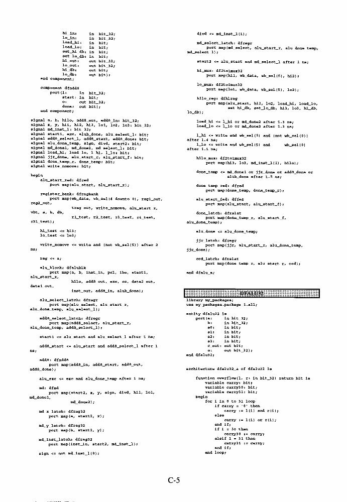
hi_in: in bit_32;lo_in: in bit_32;load_hi: in bit;load_lo: in bit;
set_hi_db: in bit;
set_lo_db: In bit;hi_out: out bit_32;
lo_out: out blt_32;hi_db: out bit;
lo__db: out blt);end component;
component dfaddS
port(i: ln bit_32;start: in bit;o: out bit_32;
done: out bit) ;end component;
signal a, b, hilo, add8_out, add8_in: bit_32;signal x, y, hil, hi2, hi3, lol, lo2, lo3: bit_32;signal md_inst_l : bit_32;
signal startl, exc, alub_done, alu_select_l : bit;signal add8_select_l, add8_start, add8_done: bit;signal alu_done_temp, sign, divd, start2 : bit;signal md_donel, md_done2, md_select_l : bit;signal load_hi, load_lo, l_hi, l_lo: bit;signal j j r_done , alu_start_r , alu_start_f : bit ;
signal done_temp_r , done_temp: bit;
signal write_nomove : bit;
begin
alu_start_red : dfred
port map(alu_start, alu_start_r) ;
register_bank: dfregbank
port map(wb_data, wb_sel(4 downto 0), regl_out,
reg2_out,
treg_out, write_nomove, alu_start_r,
vbt, a, b, db,
rl_test, r2_test, r3_test, r4_test,
r31_test);
hi_test <= hi3;
lo_test <= lo3;
write_nomove <= write and (not wb_sel(5)) after 2
divd <= md_inst_l(l) ;
md_select_latch: dfregr
port map (md_select, alu_start_r, alu_done_temp,
md_select_l) ;
start2 <= alu_start and md_select_l after 1 ns;
hi_mux : df2tolmux32
port map(hil, wb_data, wb_sel(5), hl2);
lo_mux: df2tolmux32
port map(lol, wb_data, wb_sel (5) , lo2) ;
hi1o_reg : dfhireg
port map(alu_start, hi2, lo2, load_hi, load_lo,
set_hi_db, set_lo_db, hi3, lo3, hi_db,
lo_db) ;
load_hl <= l_hi or md_done2 after 1.3 ns;
load_lo <= l_lo or md_done2 after 1.3 ns;
l__hi <= write and wb_sel{5) and (not wb_sel(0))
after 1.4 ns;
l_lo <= write and wb_sel(5) and wb_sel(0)
after 1.1 ns;
hilo_mux: df2tolmux32
port map(hi3, lo3, md_inst_l (1) , hilo) ;
done_temp <= md_donel or jjr_done or add8_done or
alub_done after 1.5 ns;
done_temp_red: dfred
port map (done_temp, done_terop_r) ;
alu_start_fed : dffed
port map(alu_start, alu_start_f ) ;
done_latch: dfrslat
port map (done_temp_r, alu_start_f,
alu_done_temp) ;
alu_done <= alu_done_temp;
j j r_latch: dfregr
port mapfjjr, alu_start_r, alu_done_temp,
j jr_done) ;
alu_block: dfalublk
port map(a, b, inst_in, pel, ibo, startl,
alu_start_r,
datal_out.
hilo, add8_out, exc, cc, data2_out,
inst_out, add8_in, alub_done);
alu_select_latch: dfregr
port map(alu_seleet, alu_start_r,
alu_done_temp, alu_select_l ) ;
add8_select_latch. dfregr
port map (add8_select, alu_start_r,
alu_done_temp, add8_select_l ) ;
startl <= alu_start and alu_select_l after 1 ns;
add8_start <= alu_start and add8_select_l after 1
addS: dfaddS
port map (add8_in, add8_start, add8_out,
add8_done ) ;
ccd_latch: dfrslat
port map(done_temp_r, alu_start_r, ccd);
end dfalu_a;
DFALU32
library my_packages;
use my_packages.package_l.all;
entity dfalu32 is
port (a: in bit_32;
b: in bit 32;
SO: in bit;
si: in bit;
32: in bit;
S3: in bit;
c out: out bit;
o: out bit_32);
end dalu32;
architecture dfalu32_a of dfalu32 is
alu_exc <= exc and alu_done_temp after 1 ns;
md: dfmd
port map(start2, x, y, sign, divd, nil, lol,
md_donel,
md_done2 ) ;
md_x_latch: dfreg32
port map (a, start2, x) ;
md__y_latch: dfreg32
port map(b, start2, y) ;
md_inst_latch: dfreg32
port map(inst_in, start2, md_inst_l);
sign <= not md_inst_l ( 0 } ;
function overflow(l, r: in bit_32) return bit is
variable carry: bit;
variable carry3 0 : bit;
variable carry3 1 : bit ;
begin
for i in 0 to 31 loopif carry =
'0'then
carry := 1(1) and r(i);
else
carry := 1(1) or r(i);
end if;
if i = 30 then
carrySO := carry;
elsif i = 31 then
earrySl := carry;
end If;
end loop;
C-5
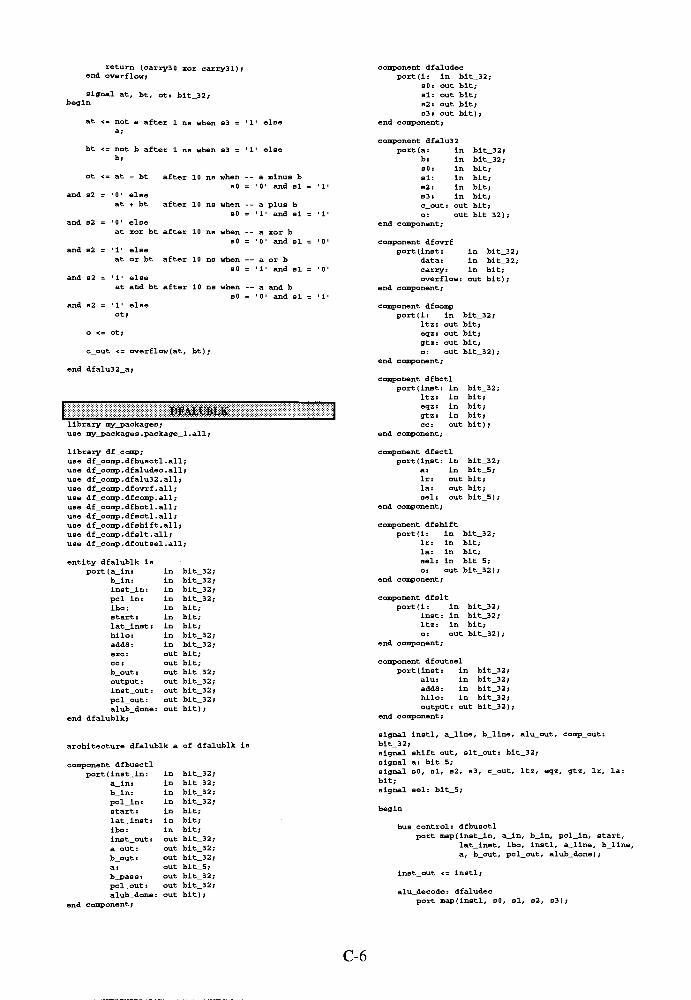
begin
return (carry30 xor carry31);
end overflow;
signal at, bt, ot: bit_32;
at <= not a after 1 ns when s3 ='1'
else
component dfaludec
port(i: in bit_32;sO: out bit;
si: out bit;
s2: out bit;
S3: out bit);
end component;
bt <= not b after 1 ns when s3 ='1'
b;
ot <= at - bt after 10 ns when --
sO =
and s2 = 0 'else
at + bt after 10 ns when --
sO =
and s2 =' 0 '
else
at xor bt after 10 ns when --
sO =
and s2 ='1'
else
at or bt after 10 ns when --
sO =
and s2 ='1'
else
at and bt after 10 ns when --
80 =
and s2 ='1'
else
ot;
o <= ot;
c_out <= overflow(at, bt);
end dfalu32_a;
component dfalu32
a minus b
0 'and si
a plus b
1 'and s 1
a xor b
0'and si
a or b
1 'and si
a and b
0 'and si
DtAlXKI k
library my_packages;
use my packages package_l . all ;
library df_>
use df_compuse df_comp
use df_comp
use df_comp
use df_compuse df_compuse df_comp
use df_comp
use df_compuse df_comp
.comp;
p.dfbusctl.all;
i . dfaludec . al1 ;
.dfalu32.all;
i.dfovrf .all;
.dfcomp.all;
.dfbctl.all;
.dfsctl.all;
.dfshift.all;
.dfslt.all;
,dfoutsel.all;
entity dfalublk is
port (a_in: in bit_32
b_in: in bit_32
inst_in: in bit_32
pcl_in : in bit_32 ;
Ibo: in bit;
start: in bit;
lat_inst: in bit;
hilo: In bit_32;
addS: in bit_32;
exc: out bit;
cc: out bit;
b_out: out bit_32
output: out bit_32
inst_out: out bit_32
pcl_out: out bit_32
alub_done: out bit);
end dfalublk;
architecture dfalublk_a of dfalublk is
component dfbusctl
port ( inst_in :
a_in:
b_in:
pcl_in:
start :
lat_inst :
ibo:
inst_out :
a_out :
b_out :
a:
b_pass :
pcl_out :
alub__done :
end component;
in
in
in
in
in
in
in
bit.
bit.
bit.
bit.
bit;
bit;
bit;
out blt_32
out bit_32
out bit_32
out bit_5;
out bit_32
out bit_32
out bit ) ;
port (a : in bit_32;b: in bit 32;
SO: in bit;
si: in bit;
s2: in bit;
S3: in bit;
c_out : out bit;
o: OUt bit_32);
end component;
component dfovrf
port(inst: in bit_32;
data: in bit_32;
carry: in bit;
overflow: out bit) ;
end component;
component dfcompport(i:
Itz:
eqz:
gtz:
o:
end component;
in bit_32;
out bit;
out bit;
out bit;
out blt_32);
component dfbctl
port (inst in bit_32;
Itz: in bit;
eqz: in bit;
gtz: in bit;
cc: out bit);
end component
component dfsctl
port (inst in bit_32;
a: in bit_5;
lr: out bit;
la: out bit;
sel : out bit_5);
end component
component dfshift
port(i: in bit_32;
lr: in bit;
la: in bit;
sel : in bit_5;
o: out bit_32);
end component;
component dfslt
port(i: in bit_32;
inst: in bit_32;
ltz: in bit;
o: out bit_32) ;
end component;
component dfoutsel
port (inst:
alu:
add8:
hilo:
output :
end component;
in blt_32;
in bit_32;
in bit_32;
in bit_32;
out bit_32);
signal instl, a_line, b_line, alu_out, comp_out:
bit_32;
signal shift_out, slt_out: bit_32;
signal a: bit_5;
signal sO, si, s2, s3, c_out, Itz, eqz, gtz, lr, la:
bit;
signal sel: bit_5;
begin
bus_control : dfbusctl
port map(inBt_ln, a_in, b_in, pcl_in, start,
lat_inst, ibo, instl, a_line, b_line,
a, b_out, pcl_out, alub_done);
inst_out <= instl;
alu_decode : dfaludec
port map(instl, sO, si, s2, s3);
C-6

alu: dfalu32
port map(a_line, b_line, sO, si,
s2, s3, c_out, alu_out);
ovrf: dfovrf
port map (instl, alu_out, c_out, exc);
compare j dfcomp
port map(alu_out, Itz, eqz, gtz, comp_out) ;
branch_ctl: dfbctl
port map(instl, Itz, eqz, gtz, cc);
shlft_ctl: dfsctl
port map(instl, a, lr, la, sel);
shifter: dfshift
port map(comp_out, lr, la, sel, shlft_out) ;
slt_box: dfslt
port map(shift_out, inBtl, Itz, slt_out) ;
output_selector : dfoutsel
port map (instl, slt_out, adds, hilo, output);
end dfalublk_a;
DFALUDEC
library my_packages;
use my_packages.package_l.all;
entity dfaludec is
port(i: in bit_32;SO: out bit;
si: out bit;
s2: out bit;
S3: out bit)
end dfaludec
architecture daludec_a of dfaludec is
begin
sO <='1'
after 2.5 ns when -- c
(1(31) ='0'
and
b"1101") or
1(29 downto 26)
-- e
(1(29 downto 28) -
b"00"
b"llll"or
1(29 downto 26) =
(1(29) ='0'
and
1(1 downto 0) = b"00")
(1(29 downto 28) =b"00"
i(26) ='0'
and
1(5) ='0'
) or
--
P
(1(29) ='0'
and
1(3) = '1') or
--
q
(1(29) ='0'
and
1(2) - '0') or
(1(29) ='0'
1(26) ='1'
and
i(29 downto 28) =
-- t
1(29 downto 28) =
-- u
1(31) ='1'
else
after 2.5 ns;
b"1101") or
'1'after 2.5 ns when -- b
(1(31) ='0'
and
1(29 downto 28) =
i(26) = '0'and
1(5) ='1'
and
1(3 downto 2) =b"
-- c
(1(31) ='0'
and
1(29 downto 26) =
--
g
(1(31) ='0'
and
1(29 downto 28) =
1(26) = '0') else
after 2.5 ns;
after 2.5 ns when --a
(1(31) ='0'
and
1(29 downto 28) =
1(26) ='0'
and
1(1 downto 0) =b"01"
1(26) =' 0 i
and
1(5) =' 1 '
and
1(3 downto 0) =b"
(1(29 downto 28) =b"00"
after 2.5 ns;
i(26) ='0'
and
1(2 downto 1) = b"00")
end dfaludec_a;
b"llll"or
-- h
1(29 downto 26) =
1(29 downto 27) =b"100"
DI'ASEL
library my_packages;
use my_packages.package_l.all;
(1(29 downto 28) =b"00"
library df_comp;
use df_comp.df4tolmux32.all;
1(26) ='0'
and
1(5) = '0') or
1(29 downto 27) =b"001"
-- u
i(31) ='1'
else
entity dfasel is
port (a_in: in bit 32
pel: in bit 32
i> in bit;
s: in bit;
a out: out blt_32
end dfasel;
1 0 'after 2.5 ns;
si <='1'
after 2.5 ns when -- a
(1(31) ='0'
and
1(29 downto 28) =b"00"
1(26) ='0'
and
1(5) ='1'
and
1(3 downto 0) = b"0111")
(1(29) ='1'
and
1(27 downto 26) = b"00")
architecture dfasel_a of dfasel is
component df4tolmux32
port (10: in bit_32;
il: in bit 32;
12: in bit 32;
13: in bit 32;
B0: in bit;
si: in bit;
o: out bit_32);
end component;
constant zero32: bit_32 : =_"0000_0000";
C-7
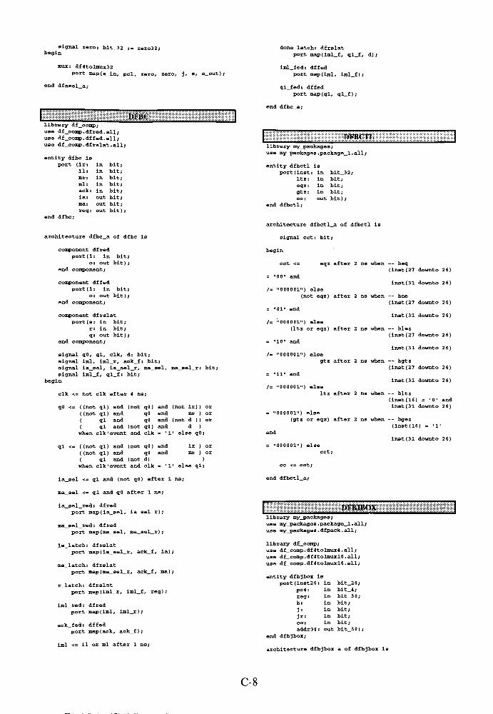
signal zero: bit_32 := zero32;
begin
mux: df4tolmux32
port map(a_ln, pel, zero, zero, j,
end dfasel_a;
library df_comp;use df_comp.dfred.all;
use df_eo-p.dffed.all;
use df_comp.dfrslat .all;
entity dfbc is
port (ir: in bit;
lit In bit;
mr: in bit;
ml: in bit;
ack: in bit;
ia: out bit;
ma: out bit;
mite
req: out bit) ;
end dfbc;
architecture dfbc_a of dfbc is
component dfred
port(i: in bit;
o: out bit);
end component;
component dffed
port(i: in bit;
o: out bit);
end component ;
component dfrslat
port(s: in bit;
r: in bit;
q: out bit);
end component;
signal qO, ql, elk, d: bit;
signal iml, iml_r, ack_f: bit;
signal ia_sel, ia_sel_r, ma_sel, ma_sel_r: bit;
signal iml_f, ql_f: bit;
begin
elk <= not elk after 4 ns;
qO <= ((not ql) and (not qO) and (not ir) ) or
( (not ql) and qO and mr ) or
( ql and qO and (not d ) ) or
( ql and (not qO) and d )
when elk 'event and elk ='1'
else qO;
ql <= ((not ql) and (not qO) and ir ) or
((not ql) and qO and mr ) or
{ ql and (not d) )
when elk'event and elk ='1'
else ql;
ia_sel <= ql and (not qO) after 1 ns;
ma_sel <= ql and qO after 1 ns;
ia_sel_red: dfred
port map(ia_sel, ia_sel_r);
ma_sel_red: dfred
port map(ma_sel, ma_sel_r);
la_latch: dfrslat
port map{ia_sel_r, ack_f, ia);
ma_latch: dfrslat
port map(ma_sel_r, ack_f, ma);
r_latch: dfrslat
port map(iml_r, iml_f, req);
lml_red: dfred
port map (iml, iml_r) ;
ack_fed: dffed
port map (ack, aek_f);
iml <= 11 or ml after 1 ns;
done_latch: dfrslat
port map(iml_f, ql_f, d) ;
lml_fed: dffed
port map(iml, iml_f);
ql_fed: dffed
port map(ql, ql_f ) ;
end dfbc_a;
DFBCTL
library my_packages;
use my_packages.package_l.ally-
entity dfbctl is
port(inst: in bit_32;
Itz: in bit;
eqz: in bit;
gtz: in bit;
ce: out bit) ;
end dfbctl;
architecture dfbotl_a of dfbctl is
signal cct: bit;
begin
cct <= eqz after 2 ns when
="00"
and
/= "000001") else
(not eqz) after 2 ns when
/= "000001") else
(Itz or eqz) after 2 ns when
="10"
and
/= "000001") else
gtz after 2 ns when
="11"
and
/= "000001") else
Itz after 2 ns when
= "000001") else
(gtz or eqz) after 2 ns when
and
= "000001") else
cct;
cc <= cct;
end dfbctl_a;
-- beq(inst (27 downto 26)
inst (31 downto 26)
-- bne
(inst (27 downto 26)
inst (31 downto 26)
-- blez
(inst(27 downto 26)
inst (31 downto 26)
-- bgtz
(inst (27 downto 26)
inst (31 downto 26)
-- bltz
(inst(16) ='0'
and
inst (31 downto 26)
-- bgez
(inst(16) ='I1
inst (31 downto 26)
DHU*W>\
library my_packages;
use my_packages.package_l.all;
use my_packages.dfpaek.all;
library df_comp;
use df_comp.df4tolmux4.all;
use df_comp.df4tolmuxl0.all;
use df_comp.df4tolmuxl6 .all;
entity dfbjbox is
port(inst26: in bit_26;
pc4 : in bit_4;
reg: in bit_30;
b: in bit;
) in bit;
jr: in bit;
cc: in bit;
addr30: out bit_30);
end dfbjbox;
architecture dfbjbox_a of dfbjbox is
C-8
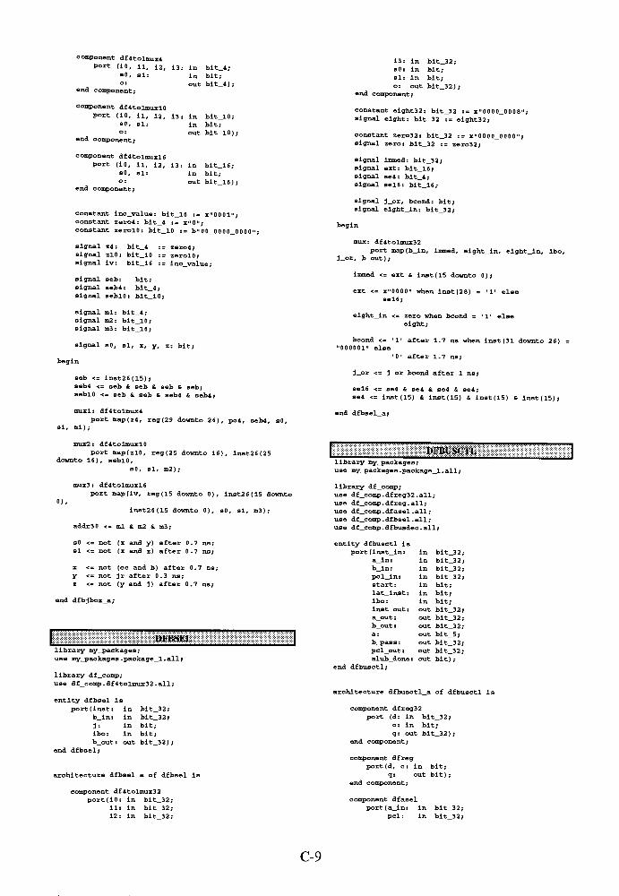
component df4tolmux4port (10, il, 12, 13: in bit_4;
s<>. -1: in bit;- out blt_4);
end component;
component df4tolmuxl0port (10, il, i2, 13: in blt_10;
sO, si: in bit;i out blt_10);
end component;
component df4tolmuxl6
port (10, il, 12, 13: in bit_16;0, si: in bit;o: out bit_16);
end component ;
constant inc_value: bit_16 := x"0001";constant zero4 : bit_4 := x"0";
constant zerolO : bit_10 : =b" 00_0 0 0 0_0000";
signal z4 : blt_4 := zero4;
signal zlO: bit_10 := zerolO;
signal iv: bit_16 := lnc_value;
signal seb: bit;signal seb. : bit_4;
signal seblO: bit_10;
signal ml: bit_4;signal m2 : bit_10;signal m3 : bit_16;
signal sO, si, x, y, z: bit;
begin
seb <= inst26(15);seb4 <= seb seb seb seb;
seblO <= seb seb seb4 seb4;
muxl: df4tolmux4
port map(z4, reg(29 downto 26), pc4, seb4, sO,
si, ml);
13: in bit_32;
sO: in bit;
si: in bit;
o: out bit_32);end component;
constant eight32: bit_32 := x"0000_0008";
signal eight: blt_32 := eight32;
constant zero32: blt_32 := x"0000_0000"
;
signal zero: bit_32 := zero32;
signal immed: blt_32;signal ext: bit_16;signal se4 : bit_4;
signal sel6: bit_16;
signal j_or, bcond: bit;signal elght_in: bit_32;
begin
mux: df4tolmux32
port map(b_in, immed, eight_in, eight_in, ibo,j_or, b_out) ;
immed <= ext & inst (15 downto 0);
ext <= x"0000"when inst(28) =
'1'else
sel6;
eight_in <= zero when bcond ='1'
else
eight;
bcond <='1'
after 1.7 ns when inst(31 downto 26) :
"000001"else
' 0 after 1.7 ns;
j_or <= j or bcond after 1 ns
sel6 <= se4 se4 se4 & se4;
se4 <= inst(15) inst(15) inst(15) lnst(15);
end dfbsel_a;
mux2: df4tolmuxl0
port mapfzlO, reg(25 downto 16), inst26(25
downto 16), seblO,
sO, si, m2);
mux3 : df4tolmuxl6
port map(iv, reg(15 downto 0), inst26(15 downto
0),
inst26(15 downto 0), sO, si, m3);
addr3 0 <= ml _2 & m3;
DFBliSCTL
library my_packages;
use my_packages.package_l.all;
library df_comp;use df_comp.dfreg32. ally-
use df_comp.dfreg.ally-
use df_comp.dfasel.all;
use df_comp.dfbsel.all;use df_comp.dfbusdec.all;
sO <= not (x and y) after 0.7 ns;
si <= not (x and z) after 0.7 ns;
x <= not (cc and b) after 0.7 ns;
y <= not jr after 0.3 ns;
z <= not (y and j) after 0.7 ns;
end dfbjbox_a;
lUHShl.
library my_packages;
use my_packages.package_l.all;
library df_comp;use df_comp.df4tolmux32.all;
entity dfbsel is
port (inst: in bit_32;
b_in: in bit_32;
j: in bit;
ibo: In bit;
b_out: out bit_32);
end dfbsel;
architecture dfbsel_a of dfbsel is
component df4tolmux32
portfiOi in bit_32;
il: in blt_32;
12: in bit_32;
entity dfbusctl is
port (inst_in: in bit_32;
a in: in bit 32;
b in: in bit 32;
pcl_in: in bit 32;
start : in bit;
lat_inst : in bit;
ibo: in bit;
inst out: out bit 32;
a out: out bit 32;
b_out : out bit 32;
a: out bit 5;
bypass : out bit 32;
pcl_out : out blt_32;alub done : out bit ) ;
end dfbusctl;
architecture dfbusctl_a of dfbusctl is
component dfreg3 2
port (d: in bit_32;
c: in bit;
q: out bit_32);
end component;
component dfreg
port(d, c: in bit;q: out bit);
end component;
component dfasel
port(a_ln: in bit_32;
pcl: in blt_32;
C-9

j: in bit;bs in bit;
a_out: out bit_32);end component;
component dfbsel
port(inst: in bit_32;
b_in: in bit_32;
j : in bit;
ibo: in bit;
b_out: out bit_32);end component ;
component dfbusdeo
port(inst: in bit_32;
j: out bit;s: out bit);
end component;
signal a_lat, b_lat, pcl_lat, lnst_lat: bit_32;signal immed, j, s: bit;signal dummy, done_temp: bit;
begin
"000000"and
"0001") else' 0 '
after 3.6 ns;
(inst (31 downto 26)
inst (5 downto 2) =
end dfbusdec_a;
DFCOMP
library my_paekages;
use my_packages.package_l.all;
entity dfcomp is
port(i: in bit_32;
Itz: out bit;eqz: out bit;
gtz: out bit;
o: out bit_32);end dfcomp;
a_in_latch: dfreg32
port map(a_in, start, a_lat);
pcl_latch: dfreg32
port map(pcl_in, start, pcl_lat) ;
architecture dfcomp_a of dfcomp is
begin
o <= i;
Itz <= 1(31);
pcl_out <= pcl_lat;
b_in_latch: dfreg32
port map(b_in, start, b_lat);
inst_latch: dfreg32
port map(inst_in, lat_inst, inst_lat);
ibo_lateh: dfregport map(ibo, start, immed);
gtz <='1'
after 4.4 ns when 1(31) ='0'
and 1 /=
x"0000_0000"
else
'0';
eqz <= '1'after 3.1 ns when 1 =
x"0000_0000"
else
'0';
end dfcomp_a;
a <= a_lat(4 downto 0);
b_pass <= b_lat;
a_bus_selector: dfasel
port map(a_lat, pcl_lat, j.
dkomviri
library my_packages;
use my_packages.package_l.all;
use std.textio.all;
b_bus_selector : dfbsel
port map(inst_lat, b_lat, j, Immed, b_out);
bus_select_decoder: dfbusdec
port map(inst_lat, j, s);
inst_out <= inst_lat;
dummy <='1'
when start ='1'
else
'0'when done_temp =
'1'else
dummy;
done_temp <='1*
after 30 ns when dummy ='1'
el
1 0 'after 1 ns;
entity dfcompare is
port ( compare :
compare_load :
pc_test :
rl_test:
r2_test :
r3_test :
r4_test i
r31_test:
hi_test :
lo_test :
compare_ack :
compare_load_
end dfcompare;
question_type;
question_type ;
bit_32;
ln
in
in
in bit_32;
in bit_32;
in l>it_32;
in bit_32;
in bit_32;
ln bit_32;
in bit_32;
out question_type;
ack: out question_type) ;
alub_done <= done_temp;
end dfbusctl_a;
architecture dfcompare_a of dfcompare is
begin
DFBUSDEC
library myjpackages;
use my_packages.package_l.all;
entity dfbusdec is
port(inst: in blt_32;
j: out bit;
s : out bit ) ;
end dfbusdec;
architecture dfbusdec_a of dfbusdec is
begin
j <='1'
after 3.7 ns when -- jal or jalr
(inst (31 downto 26)
"000011") or
(lnst(31 downto 26)
"000000" and
inst (5 downto 0) =
"001001") else
' 0 'after 3.7 ns;
b <='1' after 3.6 ns when -- sXXv
compare_block: process
type testfield_type is array (0 to 9) of
bit_32;
type test_array_type is array (0 to 1000) of
test_field_type;
variable expect: test_array_type;
variable index: integer range 0 to 1000;
file inl: text is in "expected";
variable linel: line;
variable inst: bit_32;
variable skip: question_type;
begin
wait on compare, compare_load;
if skip = no then
if compare_load = yes then
index := 0;
while endfile(inl) = false loopfor i in 0 to 9 loop
if endfile(lnl) = false then
readline(inl, linel) ;read (linel, inst) ;
expect(index) (1) := inst;end if;
end loop;
C-10

index + 1;index : =
end loop;index := 0;
skip := yes;
compare_load_ack <= yes after delay;
end if;else
if compare = yes then
assert pc_test = expect (index) ( 0)
report "PC REGISTERERROR"
severity warning;
assert rl_test = expect (index) (1)
report "REGISTER 1 ERROR"
severity warning;
assert r2_test = expect (index) (2)
report "REGISTER 2 ERROR"
severity warning;
assert r3_test = expect (index) (3 )
report "REGISTER 3 ERROR"
severity warning;
assert r4_test = expect (index) (4 )
report "REGISTER 4 ERROR"
severity warning;
assert r31_test = expect (index) (5)
report "REGISTER 31 ERROR"
severity warnlng;
assert hi_test = expect (index) (6)
report "REGISTER HI ERROR"
severity warning;
assert lo_test = expect (index) (7)report "REGISTER LO ERROR"
severity warning;
index := index + 1;
compare_ack <= yes after delay;else
compare_ack <= no after delay;
end if; -- if compare. . .
end if; -- if skip. . .
end process compare_block;
end dfcompare_a;
I DFCPU
library my_packages;
use my_packages.package_l.all;
library df_comp;
use df_comp.dfhcc.all;
use df_comp.dfif .ally-
use df_comp.dfid.all;
use df_comp.dfalu.all;
use df_comp.dfmem.all;
use df_comp
. dfwb . al 1 ;
use df_comp.dfeh.all;
use df_comp
. dfbc . all ;
use df_comp.dfrslat .all;
use df_comp.dfreg32 .all;
entity dfcpu is
port (sys_control_sig: in sys_control_type
memory_ack : in bit;
memory_load_ack : in question_type;
compare_ack : in questlon_type;
compare_load_ack : in question_type ;
addr_bus : inout bus_bit_32 bus;
data_bus : inout bus_bit_32 bus;
memory_req : out bit;
memory_w: out bit;
memory_opcode : out bit_3 ;
memory_load : out question_type ;
compare : out question_type;
compare_load: out ques11on_type ;
pc_test : out bit_32;
rl_test : out bit_32;
r2_test : out bit_32;
r3_test: out bit_32;
r4_test : out bit_32;
r31_test: out bit_32;
hi_test: out bit_32;
lo_test : out bit_32);
end dfcpu;
architecture dfcpu_a of dfcpu is
-- component declarations
component dfhoc
port (init: in bit;
prev_ok: in bit;
ready: in bit;
ain: in bit ;
aout: out bit ;
rout: out bit ;
ok: out bit);
end component;
component dfif
port (if_start: in bit;
ia: in bit;
int_req: in bit;
addrvalid: in bit;
iv: in bit_32;
new_pc : in blt_32;
addr_bus : inout bus_bit_32
data_bus : inout bus_bit_32
lr: out bit;
11: out bit;
inst: out bit_32;
pc: out bit_32;
if_exe: out bit;
i f_done: out bit);
end component ;
component dfid
port (id_start: In bit;
hi_db: in bit;
lo_db: in bit;
db: in bit_32;
inst_ln: in bit_32;
cc: in bit;
ccd: in bit;
pc: In bit_32;
ir: in bit;
reg: in bit_32;
illegal: out bit;
id_exc : out bit;
ibo: out bit;
alu_select : out bit;
md_select : out bit;
add8_select out bit;
regl_out : out bit_5;
reg2_out : out bit_5;
treg_out : out bit_5;
addr_valid: out bit;
new pc : out bit_32;
pel: out bit_32;
inst_out : out bit_32;
set_hi_db : out bit;
set_lo_db: out bit;
jjr: out bit;
id_done : out bit);
end component;
component dfalu
port (alu_start: in bit;
ibo: in bit;
alu_select : in bit;
md_select : in bit;
add8_select in bit;
regl_out : in blt_5;
reg2_out : in bit_5;
treg_out : in bit_5;
pel : in bit_32;
inst_in: in blt_32;
wb_data: in bit_32;
wb_sel : in blt_6;
vbt: in bit_4;
write : in bit;
jjr: in bit;
set_hl_db: in bit;
set_lo_db: in bit;
cc: out bit;
hi_db: out bit;
lo_db: out bit;
db: out bit_32;
reg: out bit_32;
alu_exc : out bit;
inst_out : out bit_32
datal_out : OUt bit_32
data2_out : OUt bit_32
ccd: OUt bit;
rl_test: out bit_32
r2_test : out bit_32
r3_test: out bit_32
r4_test : out bit_32
r31_test: out bit_32
hi_test : out bit_32
lo_test : out bit_32
alu__done : out bit);
end component;
component dfmem
port (mem_start : in bit;
C-ll
bit;
blt_32;
bit_32;
bit_32;
bus_bit_32;
bus_bit_32;
bit;
blt;
bit;
bit;
bit_3;
blt_32;
bit_32;
bit_4 ;
bit);
bitj
bit.
bit.
bit.
ma: in
inst_in: in
datal_ln: in
data2_in: in
addr_bus: inout
data_bus : inout
mem_exc : out
mr : out
ml : out
w: out
opcode : out
inst_out : out
data_out : out
vbt : out
mem_done : out
end component;
component dfwb
port (wb_start : in
inst_ln: in
data_in: in
vbt_in: in
wb_data: out bit_3
wb_sel: out bit_6
vbt: out bit_4
wb_done : out bit ) ;end component ;
component dfeh
port (illegal: in bit;if_exc: in bit;
id_exc: in bit;
alu_exc: in bit;mem_exc: in bit;lnt_req: out bit;
int_vector: out bit_32)end component;
component dfbc
port (ir: in bit
ill In bit
mr: in bit
ml: In bit
ack: in bit
ia: out bit
ma: out bit
req: out bit
end component;
component dfrslat
port(s: in bit;
r: in bit;
q: out bit);
end component ;
component dfreg32
port (d: in bit_32;
c: In bit;
q: out bit_32);end component;
--
system control
signal start: bit;
signal begin_in: bit;
-- pipeline handshake
signal begin_ok, if_ok, id_ok, alu_ok, mem_ok,
wb_ok: bit := '1';
signal if_ack, id_ack, alu_ack, mem_ack, wb_ack,
end_ack: bit;
signal if_start, id_start, alu_start, mem_start,
wb_start: bit;
signal if_done, id_done, alu_done, mem_done,
wb_done: bit;
signal init: bit;
-- interrupt/exception control
signal if_exc, id_exc, alu_exc, mem_exc: bit;
signal Illegal, int_req: bit;
signal int_vector: bit_32;
signal lnt_latch_q: bit;
constant zero_constant : bit :=' 0 '
;
signal lnt_reset: bit := zero_constant;
signal lnst_ifid, pc, new_pc : bit_32;signal addr_valid: bit;
signal cc, hi_db, lo_db: bit;signal db, reg: bit_32;signal ibo, alu_select, md_select, adds select:
bit;
signal regl_out, reg2_out, treg_outi bit_5;signal pel, inst_idalu: bit_32;signal set_hi_db, set_lo_db, jjr: bit;
signal wb_data, datal_out, data2_out, inst_alume>-:
blt_32;
signal wb_sel : bit_6;signal vbt: bit_4;
signal inst_memwb, data_memwb: bit_32;signal vbt_memwb: bit_4;
signal ccd: bit;
-- signals for test bench
signal pc_alumem, pc_memwb: bit_32;signal test_mode, wb_done2 : bit;
begin
system: process
begin
wait on sys_control_sig;
case sys_control_sig is
when stop =>
start <=' 0 '
;
when reset =>
null;
when load =>
memory_load <= yes after delay;wait until memory_load_ack = yes;
if test_mode ='1'
then
compare_load <= yes after delay;wait until compare_load_ack = yes;
end if;
when run =>
start <= ' 1 ';
end case;
end process system;
int_latch: dfrslat
port map(int_req, int_reset, int_latch_q) ;
bus_control : dfbc
port map(if_bus_req, if_load_addr, mem_bus_req,mem_load_addr ,
memory_ack, i f_bus_ack, mem_bus_ack.
memory_req) ;
exception_handler: dfeh
port map (illegal, if_exc, id_exc, alu_exc,mem_exc, lnt_req, int_vector) ;
begin_in <= not (if_ack or start) after 1 ns;
begin_ok <= begin_in or int_latch_q after 1.3 ns;
if_hcc: dfhec
port map(init, begin_ok, if_done, id_ack,
if_ack, if_start, if_ok) ;
id_hcc : dfhce
port map (init, if_ok, id_done, alu_ack,
id_ack, id_start, id_ok);
alu_hcc: dfhec
port map (init, id_ok, alu_done, mem_ack,
alu_ack, alu_start, alu_ok) ;
mem_hcc : dfhec
port map (init, alu_ok, mem_done, wb_ack,
mem_ack, mem_start, mem_ok) ;
wb_hcc: dfhec
port map (init, mem_ok, wb_done2, end_ack,
wb_ack, wb_start, wb_ok) ;
-- bus control
signal if_bus_req, mem_bus_req: bit;
signal if_bus_ack, mem_bus_ack: bit;
signal i f_load_addr, mem_load_addr : bit ;
-- data, control
end_ack <= not wb_ok after 0.3 ns;
if_stage: dfif
port map(if_start, if_bus_ack, int_req,addr_valid.
C-12
lnt_vector, new_pc, addr_bus,
data_bus, if_bus_req,
if_Load_addr, inst_ifid, pc, if_exc,i f_done) ;
id_stage: dfid
port map(id_start, hi_db, lo_db, db, inst_ifid,cc, ccd,
pc, if_bus_req, reg, illegal, id_exc,ibo, alu_select,
md_select, add8_select, regl_out,
reg2_out , treg_out ,
addr_valid, new_pc, pel, inst_idalu,set_hi_db,
set_lo_db, j jr, id_done) ;
alu_stage: dfalu
port map(alu_start, ibo, alu_select, md_select,add8_select,
regl_out, reg2_out, treg_out, pel,inst_idalu, wb_data,
wb_sel , vbt , wb_done, j jr , set_hi_db,
cc, hi_db, lo_db, db, reg, alu_exc,
datal_out , data2_out , ccd, rl_test ,
r4_test, r31_test, hi_test, lo_test.
set_lo_db,
inst_alumem,
r2_test , r3__test
alu_done ) ;
mem_stage : dfmem
port map(mem_start, mem_bus_ack, inst_alumem,datal_out,
data2_out, addr_bus, data_bus,mem_exc , mem_bus_req ,
mem_load_addr , memory_w,
memory_opcode, inst_memwb,
data_memwb, vbt_memwb, mem_done) ;
wb_stage : dfwb
port map(wb_start, inst_memwb, data_memwb,vbt_memwb,
wb_data, wb_sel, vbt, wb_done) ;
alu_pc_latch: dfreg32
port map (pel, alu_start, pc_alumem) ;
mem_pc_latch: dfreg32
port map (pc_alumem, mem_start, pc_memwb) ;
wb_pc_latch : dfreg32
port map(pe_memwb, wb_start, pc_test);
hcc_tb_control : process
begin
wait on wb_done;
if test_mode ='0' then
if wb_done ='1'
then
wb_done2 <=' 1 '
;
else
wb_done2 <=' 0 '
;
end if;
else
i f wb_done =' 1 ' then
compare <= yes after delay;
wait until compare_ack = yes;
compare <= no after 1 ns;
wait until compare_ack = no;
wb_done2 <=' 1 '
;
else
wb_done2 <=' 0 '
;
end if;
end if;
end process hcc_tb_control;
end dfcpu_a;
DFDBOX
library my_packages;
use my_packages.package_l.all;
library df_comp;
use df_comp
. dftrds . all ;
use df_comp.df32tolmux.all;
lo_db: In bit;
ct_start: in bit;
tsl: In blt;
ts2: in bit;ttar: in bit;thl: in bit;
tlo: in bit;
trsO: in bit;
trsl: in bit;clean: out bit;
dirty_reg: out bit_5) ;end dfdbox;
architecture dfdbox_a of dfdbox is
component dftrds
port (inst: in bit_32;
trsO: in bit;
trsl: in bit;
reg: out bit_5) ;end component;
component df32tolmux
port(i: in blt_32;
s: in bit_5;
o: out bit) ;
end component;
signal a: bit := '1';
signal b, d, e, f, g, h: bit;
signal n, p, q: bit;
Blgnal reg: bit_5;signal c: bit;
begin
clean <= not (a or b or c) after 1.1 ns;
dirty_reg <= reg;
c <= not ct_start after 0.3 ns;
a <= not (d and e) after 0.7 ns;
b <= not (f and g and h) after 0.8 ns;
d <= not (hi_db and thi) after 0.7 ns;
e <= not (lo_db and tlo) after 0.7 ns;
f <= not (tsl and n) after 0.7 ns;
g <= not (ts2 and p) after 0.7 ns;
h <= not (ttar and q) after 0.7 ns;
muxl: df32tolmux
port map (db, lnst(25 downto 21), n) ;
mux2 : df32tolmux
port map (db, inst (20 downto 16), p) ;
mux3 : df32tolmux
port map (db, reg, q);
trds: dftrds
port map (inst, trsO, trsl, reg);
end dfdbox_a;
DFEH
library my packages;
use my_packages.package_l.all;
entity dfeh is
port (illegal: In bit;
if exc: in bit;
id exc: in bit;
alu_exc : in bit;
mem exc : in bit;int_req: out bit;
int vector out bit 32)
end dfeh;
architecture dfeh a of dfeh is
begin
entity dfdbox is
port (inst:
db:
hi_db:
in bit_32;
in bit_32;
In bit;
int_req <= illegal or if_exc or id_exc or
alu_exc or mem_exc after 1.5 ns;
int_veetor <= x"0000_fff0";
end dfeh_a;
C-13
entity dffed is
port(i: in bit;o: out bit);
end dffed;
DFFEDlo_reg <= lo_in after 0.3 ns when
load_lo'event and
load_lo ='1
'else
lo_reg;
hi_out <= hi_reg after 0.6 ns;
lo_out <= lo_reg after 0.6 ns;
architecture dffed_a of dffed is
signal temp: bit;begin
temp <= '1-after 0.4 ns when 1 '
event and i ='0'
else
'0'after 1.2 ns when temp =
'1'else
temp;
o <= temp;
end dffed_a;
hi_dbl <= hi_dbl xor '1' after 1 ns when
start'event and
start =' 1 '
and
set_hi_db = 1 '
e
hi_dbl;
lo_dbl <= lo_dbl xor ' 1 'after 1 ns when
start'event and
start ='1
'and
set_lo_db =' 1 '
hii^^P;:lj^Pi:iiii44,^^^^^i^iii:s^;|entity dfhec is
port (init: in bit;
prev_ok : in bit;
ready : in bit;
ain: in bit;
aout: out bit;rout: out bit;
ok: out bit);end dfhec ;
lo_dbl;
hi_db2 <= hi_db2 xor' 1 after 1 ns when
load_hi 'event
load_hi =' 1 '
lo_db2 <= lo_db2 xor' 1 '
after 1 ns when
load_lo 'event
rout_temp =' 0 '
architecture dfhcc_a of dfhec is
signal aout_temp, rout_temp, ok_temp: bit;begin
aout_temp <= '1'after 2.2 ns when prev_ok = '0'
and
and
and
else
and
ready =
after 2.2 ns when prev_ok
else
rout_temp =' 1 '
aout_temp;
aout <= aout_temp;
rout_temp <='1*
after 2.5 ns when aout_temp = '1'
ain =' 0 '
else
'0'after 1.3 ns when ain =
'1'else
rout_temp;
rout <= rout_temp;
ok_temp <= '1'after 1 ns when rout_temp =
'0'else
' 0 'after 1 ns when rout_temp =
' 1 'and
ready ='1'
else
ok_temp;
ok <= ok_temp;
end dfhcc_a;
hi_db <= hl_dbl xor hi_db2 after 1 ns;
lo_db <= lo_dbl xor lo_db2 after 1 ns;
end dfhlreg_a;
IDFIBi_____^_
library my packages;
use my_packages.package_l.all;
library df_comp;
use df_comp.dfrslat.all;
use df_comp.dfred.all;
use df_comp.dffed.all;
use df_comp.dfreg32.all;
use df_comp.dfreg5.all;use df_comp.dfreg.all;
use df_comp.dfaa.all;
use df_comp.dfinstdec.all;use df_comp.df32tolmux.all;
use df_comp.df2tolmux30 .all;
use df_comp.dfbjbox.all;
use df_comp . dfdbox.all ;
DFHLREG
library my_packages;
use my packages.package l.all;
entity dfhlreg is
port (start: in bit;
hi in: in bit 32
lo in: in bit 32
load hi: in bit;
load lo: in bit;
set hi db: in bit;
set_lo_db: in bit;
hi_out : OUt bit_32
logout : out bit_32
hi db: out bit;
lo db: out bit);
end dfhlreg;
architecture dfhlreg_a of dfhlreg is
signal hi_reg, lo_reg: bit_32;
signal hi_dbl, hl_db2 : bit;
signal lo_dbl, lo_db2: bit;
begin
hi_reg <= hi_in after 0.3 ns when load_hi 'event and
load_hi ='1'
else
hi_reg;
entity dfid is
port (id_start: in bit;
hi db: in bit;
lo_db: in bit;db: in bit 32;
inst in: in bit 32;
cc: in bit;
ccd: in bit;
pc: in bit_32;
ir: in bit;
reg: in bit 32;
illegal: out bit;
id exc: OUt bit;
ibo: out bit;
alu select: out bit;md select: out bit;
add8_select out bit;
regl_out : out bit 5;
reg2_out : OUt bit_5;
treg_out : out bit 5;
addr_valid: out bit;
new_pc : out blt_32;pel: out bit_32;
inst out: out bit 32;
set hi db: out bit;
set lo db: out bit;
jjr: out bit;
id done: out bit);
end dfid;
C-14

architecture dfid_a of dfid is
component dfred
port(i: In bit;
o: out bit);end component;
component dffed
port(i: in bit;
o: out bit);end component;
component dfrslat
port (s: in bit;r: in bit;
q: out bit) ;end component;
component dfreg32
port (d: in bit_32;
c: In bit;
q: out bit_32);end component;
component dfreg5
port (d: in bit_5;
c: in bit;
q: out bit_5);
end component;
component dfregport(d: in bit;
c: in bit;
q: out bit);
end component;
component dfaa
port (a: in bit_32;
b: in bit_32;
s: in bit;
o: out bit_32;d: out bit);
end component;
component dfinstdec
in bit
out bit
out bit
out bit
out bit
out bit
out bit
out bit
out bit
port(i:
md:
alu
ibo
b:
)
ill
tsl
ts2
ttar: out bit
thi: out bit
tlo: out bit
exc: out bit
r: out bit
li out bit
trsO: out bit
trsl: out bit
addS: out bit)
end component;
component df32tolmux
port(i: in bit_32;
s: in bit_5;
o: out bit);
end component;
component df2tolmux30
port (10: in bit_30;
Hi in bit_30;
s: in bit;
o: out bit_30);
end component;
component dfbjbox
port(inst26: in bit_26;
pc4 : in bit_4;
reg: in blt_3 0;
b: in bit;
ji in bit;
jr: in bit;
cc: in bit;
addr30: out bit_30);
end component;
component dfdbox
port (inst: in bit_32;
db: in bit_32;
hi_db. in bit
lo_db: in bit
et_start : in bit
tsl: in bit
ts2: in bit
ttar: in bit
thi: in bit
tlo: in bit
trsO: in bit
trsl: in bit
clean: out bit
dirty_reg: out blt_5 ) ;
end component;
signal instl: bit_32;
signal by j, ttar, tsl, ts2, thi, tlo, r, 1, trsO,trsl: bit;
signal last_inst: bit_32;
signal ct_start, clean: bit;signal id_done_out, id_done_r: bit;
signal id_start_r, id_start_f: bit;
signal av, av_f: bit;
signal aas, aad, aad_r: bit;
signal ir_f: bit;
signal b_sel, j_sel, r_sel : bit;
signal bi, a, c: bit;
signal addr30, aa_mux_out: bit_30;
signal aa_a_input, aa_b_input, aa_out: bit_32;
signal pc_l: bit_32;
signal regl, reg2 : bit_5;
signal aas_r, aas_l: bit;
begin
lnst_decoder : dfinstdec
port map ( instl , md_select , alu_select , ibo, b,
j, illegal,
tsl, ts2, ttar, thi, tlo, id_exc, r,
1, trsO, trsl,
add8_select) ;
dirty_box: dfdbox
port map(instl, db, hl_db, lo_db, ct_start,
tsl, ts2, ttar, thi, tlo,
trsO, trsl, clean, treg_out);
regl <= Instl (25 downto 21);
reg2 <= instl (20 downto 16);
inst_out <= instl;
regl_latch : dfreg5
port map (regl, id_done_r, regl_out);
reg2_latch: dfreg5
port map(reg2, id_done_r, reg2_out);
ct_latch: dfrslat
port map(av_f, id_done_r, ct_start);
id_done_latch: dfrslat
port map (clean, id_start_f , id_done_out) ;
id_done <= id_done_out;
id_done_red : dfred
port map(id_done_out, id_done_r);
av_latch: dfrslat
port map(ir_f, aad_r, av) ;
addr_valid <= av;
av_feds dffed
port map(av, av_f ) ;
ir_fed: dffed
port map(ir, ir_f);
id_start_fed: dffed
port map(id_start, id_start_f);
id_start_red: dfred
port map(id_start, id_start_r) ,-
branch_latch: dfreg
port map(b, ir_f, b_sel);
jump_latch: dfreg
port map(j, ir_f, j_sel);
jump_reg_latch: dfregport map(r, ir_f, r_sel);
C-15
inst_latch: dfreg32port map(inst_in, id_start_r, instl) ;
last_lnst_latch: dfreg32
port map (instl, ir_f, last_inst);
aas <= not (a or c) after 1 ns;bi <= not b_sel after 0.3 ns;
a <= not (bi or ccd) after 1 ns;c <= not ld_start after 0.3 ns;
aad_red: dfred
port map(aad, aad_r) ;
aa_b_input <= addr30 b"00";aa_a_input <= pc_l(31 downto 2) b"00";
pc_latch: dfreg32
port map(pc, ld_start_r, pc_l);
pel <= pc_l;
aas_red: dfred
port map (aas , aas_r ) ;
aas_latch: dfrslat
port map(aas_r, ld_done_r, aas_l);
address_adder: dfaa
port map(aa_a_input, aa_b_input, aas_l, aa_out,aad) ;
aa_mux: df2tolmux30
port map(aa_out(31 downto 2), addr3 0, j_sel,aa_mux_out ) ;
new_pc <= aa_mux_out b"00";
bjbox: dfbjbox
port map(last_inst (25 downto 0), pc_l(31 downto
28),
reg (31 downto 2), b_sel, j_sel,r_sel, cc, addr30);
jjr <= '1'after 1.3 ns when j = '1'
and 1 = '0'
else
'0'after 1.3 ns;
set_lo_db <= '1'after 1.3 ns when tlo =
'1'and
ttar ='0'
else
' 0'after 1.3 ns;
set_hi_db <='1'
after 1.3 ns when thi ='1'
and
ttar =' 0 '
else
1 0 'after 1.3 ns;
end dfid_a;
wmmlibrary my_packages;
use my_packages.package_l.ally-
library df_comp;use df_comp.dfred. ally-
use df_comp.dffed.all;
use df_comp.dfrslat.all;
use df_comp.dfreg32.ally-
use df_aomp.dftsb32.all;use df_comp.df2tolmux32.all;
1
entity dfif is
port (if_start: in bit;
ia: in bit;
int_req: in bit;
addr_valid: in bit;iv: in bit_32;
new_pc : in bit_32;
addr_bus : inout bus_bit_32
data_bus : inout bus_bit_32
ir: out bit;ill out bit;
inst: out bit_32;
pc: out bit_32;
i f_erc: out blt;i f_done: out bit);
end dfif;
component dfred
port(i: in bit;o: out bit) ;
end component;
component dffed
port(i: in bit;o: out bit) ;
end component;
component dfrslat
port(s: in bit;r: in bit;q: out bit);
end component;
component dfreg32
port (d: in bit_32;
c: in bit;q: out bit_32);
end component;
component dftsb32
port(i: in bit_32;e: in bit;
o: out bit_32);end component;
component df2tolmux32
port{10: in bit_32;11: in bit_32;s: in bit;
o: out bit_32);end component;
signal start_r, ia_f, a, b, c, start: bit;signal ia_r, ilq: bit;signal ilq_f, if_start_f: bit;signal mux_out, mux_latch_out : bit_32;
begin
ir_latch: dfrslat
port map(start_r, ia_f, ir) ;
start <= not (a or c) after 1 ns;
a <= not (int_req or b) after 1 ns;
b <= not addr_valid after 0.3 ns;
c <= not if_start after 0.3 ns;
start_red : dfred
port map (start, start_r) ;
ia_fed: dffed
port map(ia, ia_f ) ;
il_latch: dfrslat
port map(ia_r, la_f, ilq);
ia_red: dfred
port map(ia, ia_r) ;
11 <= ilq;
done_latch: dfrslat
port map(ilq_f, if_start_f, if_done);
ilq_fed: dffed
port map(ilq, ilq_f);
if_start_fed: dffed
port map ( i f_start, i f_start_f) ;
addr_mux: df2tolmux32
port map(new_pc, iv, int_req, mux_out);
mux_latch: dfreg32
port map(mux_out, start_r, mux_latch_out) ;
pc <= mux_latch_out;
tsb: dftsb32
port map(mux_latch_out, ia, addr_bus) ;
db_latch: dfreg32
port map(data_bus, ia_f, inst);
if_exc <= ia and (mux_latch_out (0) or
mux_latch_out ( 1 ) ) after 2.6 ns;
architecture dfif_a of dfif is
end dfif_a;
C-16
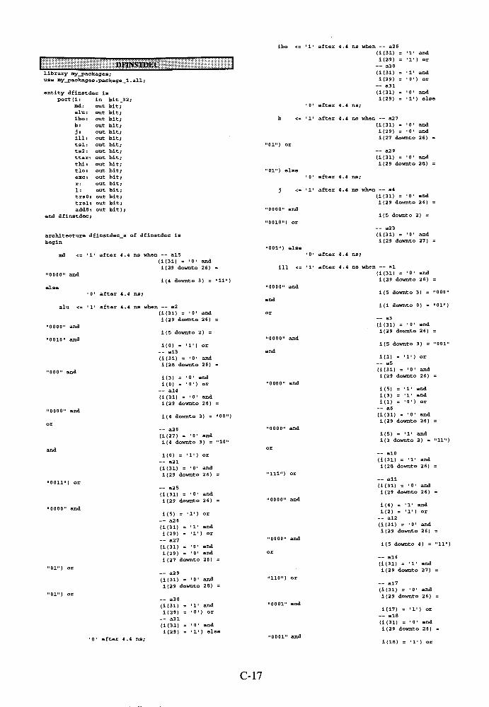
liiissiiBiiiiilibrary my_packages;
use my_packages.package_l.all;
entity dfinstdec is
port(l: in btt_32
md: out bit;
alu: out bit;
Ibo: out bit;
b: out bit;
j = out bit;
ill: out bit;
tsl: out bit;
ts2: out bit;
ttar: out bit;
thi: out bit;
tlo: out bit;
exc: out bit;
r: out bit;
1: out bit;
trsO: out bit;
trsl out bit;
adds out bit);
end dfinstdec.
architecture dfinstdec_a
begin
md <=
"0000"and
else
alu <=
"0000"and
"0010"and
"000"and
"0000"and
'1'after 4.4 ns when -- al5
(1(31) ='0'
and
i (29 downto 26)
i ( 4 downto 3 )
' 0'after 4.4 ns;
' 1 'after 4.4 ns when
(1(31) ='0'
and
1(29 downto 26) =
1 ( 5 downto 2 ) =
1(0) =' 1 '
) or
-- al3
(1(31) ='0'
and
1(28 downto 26) =
i(3) ='0'
and
1(0) =' 0'
) or
-- al4
(1(31) ='0'
and
1(29 downto 26) =
1(4 downto 3) = "0
-- a20
(1(27) ='0'
and
1(4 downto 3) = "1
1(0) = '1') or
-- a21
(1(31) ='0'
and
i(29 downto 26) =
"0011") or
"0000"and
a25
(1(31) ='0'
and
1(29 downto 26) =
1(5) = '1') or
-- a26
(1(31) ='1'
and
1(29) ='1' ) or
-- a27
(1(31) ='0'
and
1(29) ='0'
and
1(27 downto 26) =
a29
(1(31) ='0'
and
1(29 downto 28) =
-- a30
(1(31)
1(29)-- a31
(1(31)
1(29)
' 1'and
' 0 ') or
1 0 ' and
1 1' ) else
'1'after 4.4 ns when -- a26
(i(31) ='1'
and
1(29) = '1') or
-- a3 0
(1(31) ='1'
and
1(29) = '0') or
-- a31
(1(31) ='0'
and
1(29) = '1') else
1 0 'after 4.4 ns;
'1'after 4.4 ns when a27
(1(31) ='0'
and
1(29) ='0'
and
1(27 downto 26) =
"01") or
"01") else
j <=
"0000"and
"0010") or
"001") else
ill <=
"0000"and
and
or
"0000"and
and
"0000"and
"0000"and
"111") or
"0000"and
-- a29
(1(31) ='0'
and
i(29 downto 28)
' 0'after 4.4 ns;
'1'after 4.4 ns when -- a4
(1(31) ='0'
and
1(29 downto 26) =
i ( 5 downto 2 ) =
-- a23
(1(31) ='0'
and
1(29 downto 27) =
'0'after 4.4 ns;
'1'after 4.4 ns when -- al
after 4.4 ns;
"0001"and
"0001"and
(1(31) ='0'
and
1(29 downto 26) =
1(5 downto 3) ='
i (1 downto 0) ='
-- a3
(1(31) ='0'
and
1(29 downto 26) =
1(5 downto 3) ='
1(1) = '1') or
-- a5
(1(31) ='0'
and
1(29 downto 26) .
1(5) -
'1'and
1(3) ='1'
and
1 ( 1 ) - 0 ') or
-- a6
(1(31) ='0'
and
1(29 downto 26) :
1(5) ='1'
and
1(3 downto 2) =
-- alO
(1(31) -
'1'and
1(28 downto 26)
-- all
(1(31) ='0'
and
1(29 downto 26)
1(4) ='1'
and
1(2) = '1') or
-- al2
(1(31) ='0'
and
1(29 downto 26)
1 ( 5 downto 4 ) =
(i(31) -
'1'and
1(29 downto 27) :
-- al7
(1(31) ='0'
and
1(29 downto 26)
i(17) - '1') or
-- al8
(1(31) -
'0'and
1(29 downto 26)
000"
'01")
1(18)1 1 '
) or
C-17

"0001"and
tsl <=
"0000"and
"0010") or
-- al9
(1(31) ='0'
and
1 (29 downto 26) =
i(19) = '1') or
a28
1(30) ='1'
else
' 0 'after 4.4 ns;
'1 'after 4.4 ns when
"0000"and
" 0000"and
"0000"and
"0000"and
after 4.4 ns;
a4
(1(31) = '0'and
1(29 downto 26) =
1(5 downto 2) =
-- al5
(1(31) = '0'and
1(29 downto 26) =
1(4 downto 3) = "11")
--
a20
(1(27) = '0'and
1(4 downto 3) = "10"
1(0) = '1') or
--
a22
(1(27) ='0'
and
i ( 3 downto 2 ) = "01")
-- a25
(1(31) ='0'
and
1(29 downto 26) =
1(5) = '1') or
--
a26
(1(31) ='1'
and
1(29) = '1') or
--
a27
(1(31) ='0'
and
1(29) = '0'and
i(27 downto 26) =
-- a29
(1(31) ='0'
and
1(29 downto 28) =
--
a30
(1(31) = '1'and
1(29) = '0') or
-- a31
(1(31) ='0'
and
1(29) = '1') else
'1'after 4.4 ns when -- al4
(1(31) ='0'
and
1(29 downto 26)
i ( 4 downto 3 ) = "00")
-- al5
(1(31) -
'0'and
1(29 downto 26) =
1 ( 4 downto 3 )
-- a24
(1(31) ='0'
and
1(29 downto 27) =
-- a25
(1(31) ='0'
and
1(29 downto 26) =
1(5) = '1') or
-- a26
(1(31) ='1'
and
1(29) = '1') else
"11")
'0'after 4.4 ns;
1 1 'after 4.4 ns when
"0000"and
"0010"and
a2
(1(31) ='0'
and
1(29 downto 26) =
1(5 downto 2) =
1(0) = '1') or
al3
(1(31) ='0'
and
1(28 downto 26) =
"0000"and
"0011") or
"0000"and
after 4.4 ns;
after 4.4 ns when
1(0) = '0') or
-- al4
(1(31) = '0'and
1(29 downto 26)
i ( 4 downto 3 ) =
-- a21
(1(31) = '0'and
1(29 downto 26) =
--
a25
(1(31) = '0 and
1(29 downto 26) =
1(5) = '1') or
--
a30
(1(31) ='l'
and
1(29) = '0') or
--
a31
(1(31) ='0'
and
1(29) = '1') else
"00")
"0000"and
"0000"and
else
"0000"and
"0000"and
else
1 0
exc <= '1
"0000"and
else
0'
r <= '1'
"0000"and
"0010") else
'0'
1 <='1'
"0000"and
"0010"and
(1(31) ='0'
and
1 (29 downto 26)
i(4) ='1'
and
1(1) = '0') or
-- al5
(1(31) ='0'
and
1(29 downto 26)
1 (4 downto 3) =
after 4.4 ns;
after 4.4 ns when -- a7
(i(31) = '0 and
1(29 downto 26)
1(4) ='1'
and
1(1) = '1') or
-- al5
(1(31) ='0'
and
1 (29 downto 26)
1(4 downto 3 )
after 4.4 ns;
after 4.4 ns when
(1(31) ='0'
and
1(29 downto 26) =
i ( 3 downto 2 ) = "11")
after 4.4 ns;
after 4.4 ns when -- a4
(i(31) ='0'
and
1(29 downto 26) =
1(5 downto 2) =
after 4.4 ns;
"0011") elBe
after 4.4 ns when --
a2
(1(31) ='0'
and
i(29 downto 26) =
i(5 downto 2) =
1(0) = '1') or
-- a21
(1(31) ='0'
and
1(29 downto 26) =
i(3) -
1 0 'after 4.4 ns;
trsO <=' 1'
after 4.4 ns when -- a23
(1(31) = '0'and
1(29 downto 27) =
1") or
-- a26
(1(31) = '1'and
1(29) = '1') or
-- a27
(1(31) ='0'
and
1(29) ='0'
and
1(27 downto 26) =
and
C-18
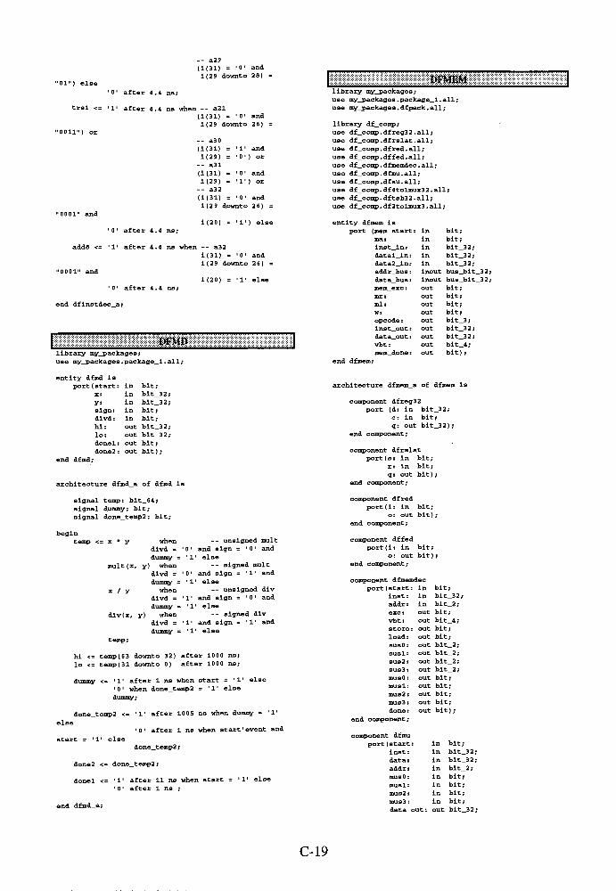
"01") else
"0011") or
-- a29
(1(31) ='0'
and
1(29 downto 28)
after 4.4 ns;
after 4.4 ns when -- a21
(1(31) ='0'
and
1(29 downto 26) =
-- a30
(1(31) ='1'
and
1(29) _ '0') or
-- a31
(1(31) ='0'
and
1(29) = '1') or
-- a32
(1(31) ='0'
and
1(29 downto 26) =
"0001"and
"0001"and
1(20) '1') else
after 4.4 ns;
after 4.4 ns when a32
1(31) ='0'
and
1(29 downto 26) =
i(20) _
!else
after 4.4 ns;
end dflnstdec_a;
DFMEM
mm
library my_packages;
use my_packages.package_l.all;
library my packages;
use my_packages.package_l.all;
use my_packages.dfpaek.all;
library df_comp;
use df_comp.dfreg32.all;
use df_comp.dfrslat .all;
use df_comp.dfred. ally-
use df_comp.dffed.all;
use df_comp.dfmemdec.all;use df
_comp. dfmu . all ;
use df_comp.dfsu.all;use df_comp.df4tolmux32.all;
use df_comp.dftsb32.all;
use df_comp.df2tolmux3.all;
entity dfmem is
port (mem_start : in bit;
ma: in bit;
inst in: in bit_32;
datal in: in bit 32;
data2 in: In bit 32;
addr bus: lnout bus bit 32;
data_bus : inout bus bit.32;
mem exc : out bit;
mr: out bit;
ml: out bit;
w: out bit;
opcode : out bit_3 ;
inst out: out bit_32;
data out : out bit_32;
vbt: out bit_4 ;
mem done: out bit);
end dfmem;
entity dfmd is
port (start: in bit;
x: in bit_32;
y= in bit 32;
sign: in bit;
divd: in bit;
hi: out bit_32;
lo: out bit_32;
done 1 : out bit;
done2 : out bit);
end dfmd;
architecture dfmd_a of dfmd is
signal temp: bit_64;
signal dummy: bit;
signal done_temp2: bit;
begin
temp <= x*y when
divd =
dummy =
mult (x, y) when
divd =
dummy =
x / y when
-- unsigned mult
0 'and sign =
' 0 'and
1"else
-- signed mult
0'and sign =
' 1'and
'1'else
-- unsigned div
divd =1'
and sign ='0'
and
dummy ='1'
else
div(x, y) when-- signed div
divd ='1
'and sign =
' 1 'and
dummy =' 1' else
temp;
hi <= temp(63 downto 32) after 1000 ns;
lo <= temp (31 downto 0) after 100 0 ns;
dummy <=' 1'
after 1 ns when start ='1'
else
'0'when done_temp2 =
' 1*else
dummy;
else
start
done_temp2 <='1'
after 1005 ns when dummy =' 1'
1 0 'after 1 ns when start
'event and
done_temp2 ;
done2 <= done_temp2;
'1'else
donel <=
end dfmd_a;
after 11 ns when start
after 1 ns ;
else
architecture dfmem_a of dfmem is
component dfreg32
port (d: in blt_32;
c: in bit;
q: out bit_32);
end component;
component dfrslat
port (s: In bit;
r: in bit;
q: out bit) ;
end component ;
component dfred
port(i: in bit;
o: out bit);
end component;
component dffed
port(i: in bit;
o: out bit);
end component;
component dfmemdec
port (start: in bit;inst: in bit_32;
addr: In bit_2 ;
exc: out bit;
vbt: out bit_4 ;
store: out blt;
load: out blt;
susO : out bit_2 ;
susl: out bit_2;
sus2: out bit_2 ;
sus3: out bit_2;
musO : out bit;
musl: out bit;
mus2: out bit;
mus3: out bit;
done: out bit);
end component;
component dfmu
port (start: in bit;
inst: in bit_32
data: in bit_32
addr: in bit_2 ;
musO: in bit;
musl: in bit;
mus2: in blt;
mus3: in bit;
data_out: out bit_32;
C-19

done: out bit ) ;end component ;
component dfsu
port (start: in bit;
mu_data : in bit 3
susO: in bit 2
susl: in bit 2
sus2: in bit 2
sus3: in bit 2
data_out : out bit 3
done: out bit);end component;
component df4tolmux32
port(iO: in bit_32;
ill in bit_32;
12: in bit_32;
13: in bit_32;sO: in bit;
alt in bit;
o: out bit_32);
end component;
component dftsb32
port(l: in bit_32;
e: in bit;
o: out bit_32);
end component;
component df2tolmux3
port (iO: in blt_3;
il: in bit_3;s: in bit;
o: out bit_3);
end component;
signal mem_start_r , mem_start_f : bit ;
signal inst_l, datal_l, data2_l : bit_32;signal st. Id, pass, stld, stld_r: bit;signal dummy_delay, memdec_done, store, load: bit;signal susO, susl, sus2, sus3 : bit_2;signal musO, musl, mus2, mus3 : bit;
signal mr_start, mr_start_r: bit;
signal su_start , su_done : bit ;
signal mu_start: bit;
signal su_data, mu_data: bit_32;
signal db_tsb_en, ab_tsb_en: bit;
signal mrq, mrq f , ma_r, ma_f, lors: bit;
signal default_rd_type: bit_3 := "Oil";
signal done, done_r: bit;
signal data_bus_l, tsb_in: bit_32;
signal tsb_inO, tsb_inl: bit;
begin
inst_latch: dfreg32
port map(inst_in, mem_start_r, inst_l);
inst_out <= lnst_l;
datal_latch: dfreg32
port map (datal_ln, mem_start_r, datal_l ) ;
data2_latch: dfreg32
port map(data2_in, mem_start_r, data2_l);
mem_start_red : dfred
port map(mem_start, mem_start_r) ;
mem_start_fed: dffed
port map(mem_start, mem_start_f ) ;
done_latch: dfrslat
port map(stld_r, mem_start_f , done) ;
mem_done <= done;
mem_done_red : dfred
port map (done, done_r);
dummy_delay <='1'
after 2 ns when mem_start ='1'
else
' 0 'after 1 ns;
memory_decoder : dfmemdec
port map (dummy_delay, inst_l , datal_l ( 1 downto
0) , mem_exc,
vbt, store, load, susO, susl, sus2,
sus3,
musO, musl, mus2, mus3, memdec_done) ;
mr_start <= memdec_done and (store or load) after
2.3 ns;
mr_start_red : dfred
port map(mr_start, mr_start_r) ;
stld <= st or Id or pass after 1.4 ns;
stld_red: dfred
port map(stld, stld_r) ;
st <= memdec_done and store and mu_start after 1.1
Id <= memdee_done and load and su_done after 1.1
pass <= memdec_done and (not load) and (not store)
after 1.4 ns;
mu_start_latch: dfrslat
port map(mrq_f, done_r, mu_start);
mu_data_latch: dfreg32
port map(data_bus, ma_f, data_bus_l) ;
mask_unit : dfmu
port map (mu_start , inst_l , data_bus_l ,
datal_l(l downto 0),
musO, musl, mus2, mus3, mudata,
su_start) ;
shift_unit: dfsu
port map(su_start, mu_data, susO, susl,
bus2, sus3, su_data, su_done);
data_mux: df4tolmux32
port map(datal_l, su_data, data2_l, data2_l,
load, store, data_out);
data_bus_tsb: dftsb32
port map(data2_l, db_tsb_en, data_bus);
addr_bus_tsb: dftsb32
port map(tsb_in, ab_tsb_en, addr_bus) ;
tsb_in <= datal_l(31 downto 2) tsb_inl & tsb_ln0;
tsb_in0 <= datal_l(0) and store;
tsb_inl <= datal_l(l) and store;
db_tsb_en <= store and ma after 1 ns;
ab_tsb_en <= lors and ma after 1 ns;
lors <= load or store after 1.3 ns;
ma_red: dfred
port map (ma, ma_r) ;
ma_fed: dffed
port map(ma, ma_f ) ;
mr_latch: dfrslat
port map(mr_start_r, ma_f, mrq) ;
mr <= mrq;
mrq_fed: dffed
port map (mrq, mrg f ) ;
ml_latch: dfrslat
port map (ma_r, ma_f, ml);
w <= store and ma;
type_mux: df2tolmux3
port map(default_rd_type, inst_l(28 downto 26),
db_tsb_en, opcode) ;
end dfmem_a;
library my_packages;
use my packages.package l.all;
entity dfmemdec is
port (start: in bit;
inst: in bit_32;
addr: in bit_2;
exc: out bit;
C-20

vbt: out bit_4;store : out bit;load: out bit;susO : out bit_2;susl: out bit_2;sus2: out bit_2;bus3: out bit_2;
musO : out bit;musl: out bit;
mus2: out bit;mus3 : out bit;
done: out bit);end dfmemdec;
1 1'after 4.3 ns when -- al3
(inst(31) -
'liand
inst (29 downto 27)
addr = "01") or
-- a23
(inst (28 downto 27)
addr = "00") or
-- al5
(inst (31) ='1'
and
inst (28 downto 27)
architecture dfmemdec_a of dfmemdec is
signal vbto, vbtl, vbt2, vbt3: bit;
signal susOO, susOl, suslO, susll: bit;
signal sus20, sus21, bus30# sus31: bit;
begin
done <=' 1
0
exc <=' 1 '
after 5.3 ns when start ='1'
else
after 1 ns;
after 4.3 ns when -- a3
(inst(31) ='1'
and
inst (29) ='0'
and
inst (27 downto 26)
addr(l)' 1 ' ) or
(inst(31) ='1'
and
inst (27 downto 26)
addr ( 0 ) =' 1 '
) or
-- alO
(inst (31) =1'
and
inst (29) ='0'
and
inst(26) ='1'
and
addr ( 0 ) =' 1 )
else
after 4.3 ns;
'1'after 4.3 ns when -- a9
(inst (31)1and
inst (29 downto 27) =
addr - "00") or
-- al3
(inst (31) -
'1'and
lnst(29 downto 27) =
addr = "01") or
-- a23
(lnst(28 downto 27) :
addr = "00") or
-- al9
(inst (31) -
1'and
inst (29 downto 27) :
addr = "10") or
-- al7
(inst(31) =' I1
and
inst(29) ='0'
and
inst(27) ='0'
and
addr = "10") or
-- al8
(inst(31) ='1'
and
inst (29) ='0'
and
inst (27) ='0'
and
addr = "01") or
-- a21
(lnst(31) _
' 1'and
inst (29) ='0' and
inst (27) ='0'
and
addr = "11") or
-- a22
(inst (31) ='1'
and
inst(29) ='0'
and
inst (27) ='0'
and
addr = "00") or
-- a24
(inst (31) -
'1'and
Inst (29 downto 27)
addr = "11") or
-- a25
(inst (31) = '0')
addr = "01") or
-- al9
(lnst(31) ='1'
and
inst(29 downto 27)
addr ="10"
) or
-- al7
(inst (31) =1 1 '
and
inst (29) =' 0 '
and
inst(27) =1 0 '
and
addr ="10"
) or
-- ale
(lnatOD =' 1 i
and
inst (29) =1 0 '
and
inst (27) = 0 'and
addr ="01"
) or
-. a21
(inst(31) =1 1
'and
inst(29) =1 0 '
and
inst (27) =' 0 '
and
addr = "11") or
-- a22
(inst(31) ='1'
and
Inst (29) ='0'
and
inst (27) ='0'
and
addr = "00") or
-- a24
(inst (31) ='1'
and
lnst(29 downto 27)
addr = "11") or
-- a25
(inst(31) - '0')
vbt2 <=
"01"and
else
1 0 'after 4 .3 ns;
1 1 'after 4.3 ns when -- all
(inst (28 downto 27) =
addr ( 0 ) =' 0 '
) or
-- al5
(inst (31) ='1'
and
inst (28 downto 27) =
addr = "01") or
-- al9
(inst (31) ='1'
and
inst (29 downto 27) =
addr = "10") or
-- al7
(Inst (31) ='1'
and
lnst(29) ='0'
and
inst (27) ='0'
and
addr = "10") or
-- alB
(inst (31) -
'1'and
lnst(29) ='0'
and
inst(27) -
'0'and
addr = "01") or
-- a21
(inst (31) ='1'
and
inst (29) ='0'
and
inst (27) ='0'
and
addr _ "11") or
-- a22
(inst(31) ='1'
and
Inst (29) ='0'
and
inst (27) ='0'
and
addr = "00") or
-- a24
(inst(31) ='1'
and
inst(29 downto 27)
addr = "11") or
-- a25
(lnst(31) = '0')
after 4.3 ns;after 4.3 ns;
C-21
1 1'after 4.3 ns when
-- al2
(inst (31) ='1'
and
inst (29 downto 27)
-- al7
(inst (31) =
inst(29) =
inst(27) =
addr ="10"
-- aia
(inst(31) =
inst (29) =
inBt(27) =
addr ="01"
-- a21
(inst(31) =
inst(29) =
inst(27) =
and
and
and
and
and
and
and
and
and
inst (27 downto 26)
addr = "10") or
-- al9
(inst (31) ='1'
and
inst (29 downto 27)
addr = "10") or
-- a9
(inst(31) ='1'
and
inst (29 downto 27)
addr = "00") or
-- al7
(inst (31) ='1'
and
inst (29) ='0'
and
inst (27 downto 26)
"011"and
addr = "11") or
-- a22
(inst (31) ='1'
and
lnst(29) = '0'and
inst (27) ='0'
and
addr = "00") or
-- a24
(inst(31) ='1'
and
inst(29 downto 27)
addr - "11") or
-- a25
(lnst(31) = '0')
addr = "00")
else
after 4.3 ns;
susOl <='1'
after 4.3 ns when -- al3
(inst(31) ='1'
and
inst (29 downto 27)
addr = "01") or
-- al7
(inst(31) ='1'
and
Inst (29) ='0'
and
inst(27 downto 26)
addr "00") or
after 4.3 ns;
(inst (31) ='1'
and
inst (29 downto 27) =
store <='1'
after 4.3 ns when -- al4
(inst (31) =
inst (29) =
else
'0'after 4.3 ns;
l1after 4.3 ns when -- a9
(inst(31) = 1'and
Inst (29 downto 27) ;
addr = "00") or
-- al2
(inst (31) ='1'
and
inst (29 downto 27) ;
-- al3
(inst (31) ='1'
and
inst (29 downto 27) :
addr = "01") or
-- al7
(inst (31) ='1'
and
inst (29) ='0'
and
inst (27) ='0'
and
addr = "10") or
-- al8
(inst (31) ='1'
and
inst (29) ='0'
and
inst(27) ='0'
and
addr = "01") or
-- al9
(inst (31) ='1'
and
inst (29 downto 27)
addr = "10") or
-- a21
(inst (31) ='1'
and
inst(29) ='0'
and
inst(27) ='0'
and
addr - "11") or
-- a22
(inst (31) ='1'
and
inst(29) ='0'
and
inst(27) ='0'
and
addr = "00") or
-- a24
(lnst(31) ='1'
and
inst (29 downto 27)
addr = "11")
addr = "00") or
-- a22
(inst(31) ='1'
and
lnst(29) ='0'
and
inst(27 downto 26)
addr(l) ='
-- al8
(lnst(31) =
lnBt(29) =
inst (27) =
addr ="01"
0')
'1'
0'
'0'
)
or
and
and
and
.fter 4
else
.3 ns;
SUS10 <='1'
after 4.3 ns when -- a22
(inst (31) ='1'
and
inst (29) ='0'
and
inst (27 downto 26)
addr(l) = '0') or
-- a23
(inst(31) _
'1'and
inst (29) ='0'
and
inst (26) -
' 1'and
addr(l) = '1') or
-- a24
(inst(31) ='1'
and
inst (29 downto 27)
addr = "11") or
-- a25
(inst (31) ='0'
) or
-- al3
(inst (31) ='1'
and
inst (29 downto 27)
else
after 4.3 ns;
after 4.3 ns when -- al2
(inst (31) =._.
and
inst(29) ='0'
and
addr = "01") or
-- al6
(inst (28 downto 27) :
addr = "00") or
-- al7
(inBt(31) ='1'
and
inst (29) ='0'
and
inst (27 downto 26) '
addr = "00") or
-- a21
(inst(31) ='I1
and
inst(29) ='0'
and
Inst (27) ='0'
and
addr = "11")
else
after 4.3 ns;
C-22
'1'after 4.3 ns when -- al9
(inst(31) ='1'
and
inst (29 downto 27)
addr = "10") or
-- al3
(inst (31) ='1'
and
inst (29 downto 27)
addr = "01") or
-- a22
(inst (31) _
'1'and
inst (29) = '0'and
inst(27 downto 26)
else
after 4.3 ns;
addr(l) = '0')
after 4.3 ns when -- all
(inst (31) = '1'and
inst (28 downto 27)
addr = "01") or
--
al7
(inst (31) = '1'and
inst(29) = '0'and
inst (27 downto 26)
addr = "00") or
--
al9
(inst (31) ='1'
and
inst (29 downto 27)
addr ="10"
') or
-- a23
(inst (31) = ' 1 'and
inst (29) = 0 'and
inst(26) =1 1 '
and
addr(l) ='1') or
-- a21
(inst (31) =11 '
and
inst(29) ='0 '
and
inst(27) = 1 0 'and
addr ="11"
)
else
0'after 4.3 ns;
sus21 <='1'
after 4.3 ns when -- al9
(inst(31) =1 1 '
and
inst(29 downto 27)011"
and
addr ="10"
) or
-- al6
(inst (28 downto 27)
addr = "00") or
-- a24
(inst (31) ='1'
and
inst (29 downto 27)
"11") or
' 0 ') or
addr =
a25
(inst(31)-- a23
(inst(31) ='1'
and
inst (29) ='0'
and
lnst(26) ='1'
and
addr(l) = '1')
after 4.3 ns;
sus3 0 <=
"01"and
after 4.3 ns when -- a20
(inst (28 downto 27)
addr ( 0 ) =' 0 '
) or
-- a21
(inst (31) ='1'
and
inst (29) ='0'
and
inst (27) ='0'
and
addr = "11") or
-- a23
(instOl) ='1'
and
inst (29) ='0'
and
lnst(26) ='1'
and
addr(l) = '1') or
-- al7-
(inst(31) ='1'
and
inst(29) ='0'
and
inst (27 downto 26)
sus31 <= 'l'
"01"and
mus3 <=' 1 '
(inst (31) = '1'and
inst (29 downto 27) .
addr = "11") or
-- a25-
(inst(31) = '0')
else
after 4.3 ns;
after 4.3 ns when -- al6
(inst (28 downto 27) =
addr = "00") or
-- all
(inst (31) ='1'
and
inst(28 downto 27) =
addr = "01") or
-- a23
(inBt(31) ='1'
and
inst(29) ='0'
and
inst (2 6) ='1'
and
addr(l) = '1') or
-- a24
(inst(31) ='1'
and
inst(29 downto 27) =
addr = "11") or
-- a25
(inst (31) = '0')
else
after 4.3 ns;
after 4.3 ns when -- a22
(inst (31) ='1'
and
inst (29) -
'0'and
inst (27) ='0'
and
addr = "00") or
-- a24
(inst(31) ='1'
and
Inst (29 downto 27) =
addr = "11") or
-- a25
(inst (31) = '0') or
-- al7
(inst(31) _
'1'and
inst (29) ='0'
and
inst (27 downto 26) =
addr = "00") or
-- al9
(inst (31) ='1'
and
inst(29 downto 27) =
addr = "10") or
-- al3
(inst(31) ='1'
and
inst (29 downto 27) =
addr = "01") or
-- al6
(inst(28 downto 27) =
addr = "00") or
--
a9
(inst (31) ='1'
and
inst (29 downto 27) =
addr "00")
else
after 4.3 ns;
mus2 <=' 1 '
addr =
-- a24-
"00") or
after 4.3 ns when -- all
(inst(31) ='1'
and
inst(28 downto 27)
addr = "01") or
-- al3
(inst (31) ='1'
and
inst (29 downto 27)
addr = "01") or
-- al8
(lnst(31) ='1'
and
inst (29) ='0'
and
inst (27) ='0'
and
addr = "01") or
-- al9
(lnst(31) = '1'and
inst (29 downto 27)
addr = "10") or
C-23

-- a22
(instOD ='1'
and
inst(29) ='0'
and
inBt(27) ='0'
and
addr = "00") or
-- a24
(inst (31) ='1'
and
inst (29 downto 27)
addr = "11") or
-- a25
(Inst (31) = '0') or
-- al6
(inst (28 downto 27)
DFMEMORY
else
after 4.3 ns;
addr = "00")
musl <= '1'
musO <='1'
after 4.3 ns when -- all
(Inst (31) ='1'
and
inst (28 downto 27)
addr = "01") or
-- al2
(inst (31) ='1'
and
inst (29) = '0'and
inst (27 downto 26)
addr = "10") or
-- a20
(inst (28 downto 27)
addr ( 0 ) =' 0 '
) or
-- al9
(inst (31) = '1'and
inst (29 downto 27)
addr = "10") or
-- a23
(inst (31) ='1'
and
inst (29) ='0'
and
inst (26) ='1'
and
addr(l) ='1'
) or
-- a24
(inst (31) ='1'
and
inst (29 downto 27)
addr = "11") or
-- a25
(inst(31) = '0')
else
after 4.3 ns;
after 4.3 ns when -- al5
(inst(31) ='1'
and
inst (29 downto 27)
-- a21
(inst (31) ='1'
and
inst (29) ='0'
and
inst (27) ='0'
and
addr = "11") or
-- a23
(lnst(31) ='1'
and
inst (29) ='0'
and
inst (26) ='1'
and
addr(l) = '1') or
-- a24
(inst(31) ='1'
and
Inst (29 downto 27)
addr = "11") or
-- a25
(inst(31) = '0')
else
after 4.3 ns;
vbt <= vbt3 &
susO <= susOl
susl <= susll
SUS2 <= SUS21
sus3 <= sus31
end dfmemdec_a;
Vbt2 & vbtl & vbtO;
& susOO;
& suslO;
& sus20;
& SU83 0;
use std.textio.all;
library my_packages;
use my_packages.package_l.all;
use my_packages.dfpaek.all;
entity dfmemory is
[load: in question_type ;
req: in bit;
w: in bit;
opcode : in bit 3;
ack: out bit;
load_ack: out question_type;
addr_bus: inout bus_bit_32 bus;
data_bus: inout bus_bit_32 bus);
end dfmemory;
architecture dfmemory_a of dfmemory is
signal ack_temp: bit;
signal addr_temp: integer;
signal m4000, m4004, m4008, m400c, m4010: bit_32;
signal m4014, m4018, m401c, m4020, m4024: bit_32;
begin
memory: process
constant low_address : integer : = 0 ;
constant high_address: integer := 65535;
type memory_array is
array (integer range low_address to
hlgh_address) of bit_32;
variable mem: memory_array;
variable addr: integer range 0 to high_address;
variable temp: bit_32;
file inl: text is in "machine";
variable linel: line;
variable inst: bit_32;
variable skip: question_type;
variable addr_word: blt_30;
variable addr_byte: bit_2;
begin
wait on req, load;
if skip = no then
if load = yes then
addr : = 0 ;
while endfile(lnl) = false loop
readline(inl, linel) ;
read (linel, inst)
mem(addr) := inst;
addr : = addr + 1;
end loop;
skip := yes;
load_ack <= yes after delay;
end If;
else
if req ='1' then
data_bus <= null;
addr_word := addr_bus(31 downto 2);
addr_byte := addr_bus(l downto 0) ,-
controller
downto 24) ) ;
downto 16));
send acknowledge signal to bus
ack <='1'
after 5 ns;
ack_temp <='1'
after 5 ns;
assert addr_word(29 downto 14) = x"0000"
report ".ADDRESS OUT OP RANGE";
if addr_word(29 downto 14) =x"0000" then
if w =' 0 ' then
addr := bton(addr_word) ;
temp := mem (addr);
-- read operations
if opcode = m_lb then
case addr_byte is
whenb"00"
=>
data_bus <= se8to32 (temp(31
whenb"01"
=>
data_bus <= se8to32 (temp(23
whenb"10"
=>
C-24
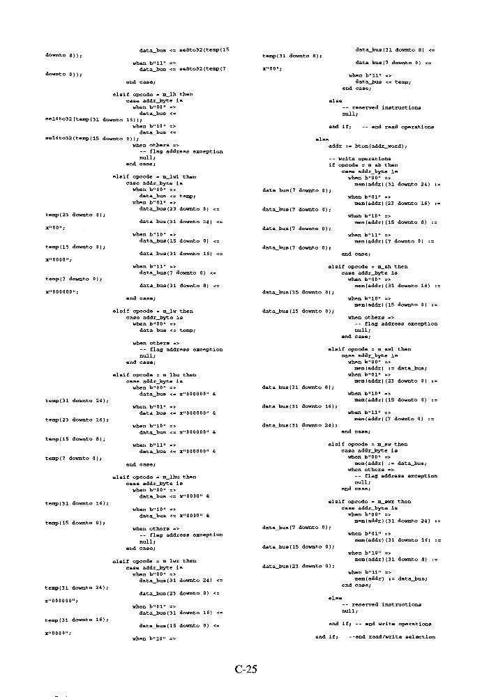
downto 8) ) ;
downto 0 ) ) ;
data_bus <= se8to32 (temp (15
whenb"ll"
=>
data_bus <= se8to32 (temp(7
temp ( 3 1 downto 8 ) ;
data_bus(31 downto 8) <=
data_bus(7 downto 0) <=
end case;
elsif opcode = m_lh then
case addr_byte is
whenb"00"
=>
data_bus <=
sel6to32 (tempOl downto 16));
whenb"10"
=>
data_bus <=
sel6to32(temp(15 downto 0));
when others =>
-- flag address exception
null;
end case;
elsif opcode = m_lwl then
case addr_byte is
whenb"00"
=>
data_bus <= temp;
whenb"01"
=>
data_bus(23 downto 0) <=
temp(23 downto 0);
x"00";
temp (15 downto 0 ) ;
x"0000";
temp ( 7 downto 0 ) ;
x"
000000";
temp ( 3 1 downto 24);
temp(23 downto 16);
temp(15 downto Sly-
temp ( 7 downto 0 ) ;
temp(31 downto 16);
temp (15 downto 0);
temp(31 downto 24);
x"000000";
temp(31 downto 16);
x"0000";
data_bus(31 downto 24) <=
whenb"10"
=>
data_bus(15 downto 0) <=
data_bus(31 downto 16) <=
whenb"ll"
=>
data_bus(7 downto 0) <=
data_bus(31 downto 8) <=
end case;
elsif opcode = m_lw then
case addr_byte is
whenb"00"
=>
data_bus <= temp;
when others =>
-- flag address exception
null;
end case;
elsif opcode = m_lbu then
case addr_byte is
whenb"00"
=>
data_bus <=x"000000"
whenb"01"
=>
data_bus <=x"000000"
whenb"10"
=>
data_bus <=x"000000"
whenb"ll"
=>
data_bus <=x"000000"
end case;
elsif opcode = m_lhu then
case addr_byte is
whenb"00"
=>
data_bus <=x"0000" fi
whenb"10"
=>
data_bus <=x"0000"
when others =>
-- flag address exception
null;
end case;
elsif opcode = m_lwr then
case addr_byte is
whenb"00"
=>
data_bus{31 downto 24) <=
data_bus(23 downto 0) <=
whenb"01"
=>
data_bus(31 downto 16) <=
data_bus(15 downto 0) <=
whenb"10"
=>
data_bus (7 downto 0 ) ;
whenb"ll"
=>
data_bus <= temp ;
end case;
-- reserved instructions
null;
end if; -- end read operations
addr := bton(addr_word) ;
-- write operations
if opcode = m_sb then
case addr_byte is
whenb"00"
=>
mem(addr) (31 downto 24) :=
whenb"01"
=>
mem (addr) (23 downto 16) :=
data_bus ( 7 downto 0 ) ;
data_bus ( 7 downto 0 ) ;
data_bus (7 downto 0 ) ;
whenb"10"
=>
-em(addr) (15 downto 8)
whenb"ll"
=>
mem(addr) (7 downto 0) :=
end case;
elsif opcode = m_sh then
case addr_byte is
whenb"00"
=>
mem(addr) (31 downto 16) :=
data_bus(15 downto 0);
whenb"10"
=>
mem (addr) (15 downto 0) :=
data_bus ( 15 downto 0 ) ;
when others =>
-- flag address exception
null;
end case;
elsif opcode = m_swl then
case addr_byte is
whenb"00"
=>
mem (addr) : = data_bus;
whenb"01"
=>
mem(addr) (23 downto 0) :=
data_bus ( 3 1 downto 8 ) ;
whenb"10"
=>
mem(addr) (15 downto 0) :=
data_bus ( 3 1 downto 16);
whenb"ll"
=>
mem (addr) (7 downto 0) :=
data_bus(31 downto 24);
end case;
elsif opcode = m_sw then
case addr_byte is
whenb"00"
=>
mem (addr) := data_bus;
when others =>
-- flag address exception
null;
end case;
elsif opcode = m_swr then
case addr_byte is
whenb"00"
=>
mem(addr) (31 downto 24) :=
data_bus(7 downto 0);
whenb"01"
=>
mem(addr) (31 downto 16) :=
data_bus(15 downto 0);
whenb"10"
=>
mem(addr) (31 downto 8) :=
data_bus(23 downto 0);
whenb"ll"
=>
mem (addr) := data_bus;end case;
else
reserved instructions
null;
end if; -- end write operations
end if; --end read/write selection
C-25
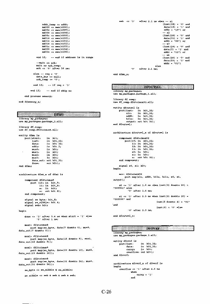
addr_temp <= addr;
m4000 <= mem (4096)
m4004 <= mem(4097)
m4008 <= mem(4098)
m400c <= mem (4099)
m4010 <= mem (4100)
m4014 <= mem (4101)
m4018 <= mem (4102)
m401c <= mem (4103)
m4020 <= mem (4104)
m4024 <= mem(4105)
end if; end if address is in range
--wait on ack;
wait on ack_temp;
aak <= '0'after 50 ns;
else --
req =' 0
'
data_bus <= null;
ack_temp <=' 0 '
;
after 2.1 ns when --
al
(inst (28) ='0'
and
data(15) ='1'
and
addr = "10") or
-- a2
(inst (28) ='0'
and
data(31) ='1'
and
addr = "00") or
-- a3
(inst (28) ='0'
and
data ( 7 ) =' 1 '
and
addr ="11"
) or
-- a4
(inst (28) ='0'
and
data(23) ='1'
and
addr = "01")
else
after 2.1 ns;
end dfmu_a;
end if; -- if req = '1'
end if; -- end if skip no
end process memory;
end dfnemory_a;
DFOUTSEL
library my_packages;
use my_packages.package_l.all;
library df_comp;
use df_comp.df4tolmux32.all;
DFMU
library my_packages;
use my_packages.package_l.all;
library df_comp;
use df_comp.df2tolmux8.all;
entity dfmu is
port (start :
inst:
data:
addr:
musO :
musl:
mus2:
mus3 :
in bit;
in bit_32;
in bit_32;
in bit_2;
In bit;
in bit;
in bit;
in bit;
data_out: out bit_32;
done: out bit);
entity dfoutsel is
port (inst: in blt_32;
alu: in bit_32;
addS: in bit_32;
hilo: in bit_32;
output : out bi t_32 ) ;
end dfoutsel;
architecture dfoutsel_a of dfoutsel is
component df4 tolmux32
port(iO: in bit_32;
11: in bit_32;
12: in bit_32;
13: in bit_32;
sO : in bit;
si: in bit;
o: out bit_32) ;
end component;
signal sO, si: bit;
begin
architecture dfmu_a of dfmu is
component df2tolmux8
port (10: in bit_S;
il: in bit_8;
s: in bit;
o: out bit_8);
end component;
signal se_byte: bit_8;
signal se_nibble : bit_4;
signal seb: bit;
begin
done <='1'
after 3.4 ns when start ='1'
else
'0
'after 1 ns;
mux: df4tolmux32
port map(alu, adds, hilo, hilo, sO, si,
output ) ;
sO <='1'
after 1.6 ns when inst(31 downto 26) =
"000001"else
' 0 'after 1. 6 ns;
si <='1'
after 2.3 ns when inst(31 downto 26) =
"000000"and
inst (5 downto 4) ="01"
~and
inst (0) =' 0 '
else
' 0'after 2.3 ns;
end dfoutsel_a;
muxO : df2tolmux8
port map(se_byte, data{7 downto 0), musO,
data_out{7 downto 0));
muxl: df2tolmux8
port map(se_byte, data(15 downto 8), musl,
data_out(15 downto 8));
mux2 : df2tolmux8
port map(se_byte, data (23 downto 16), mus2,
data_out(23 downto 16));
mux3: df2tolmux8
port map ( se_byte , data(31 downto 24), mus3,
data_out(31 downto 24));
se_byte <- se_nibble se_nibble;
se_nibble <= seb seb seb & seb;
DFOVRF
library my_packages;
use my_packages.package_l.ally-
entity dfovrf is
port (inst: in bit_32;
data: in bit_32;
carry: in bit;
overflow: out bit) ;
end dfovrf;
architecture dfovrf_a of dfovrf is
begin
overflow <=' 1 '
after 4.6 ns
when
carry ='1'
and
C-26
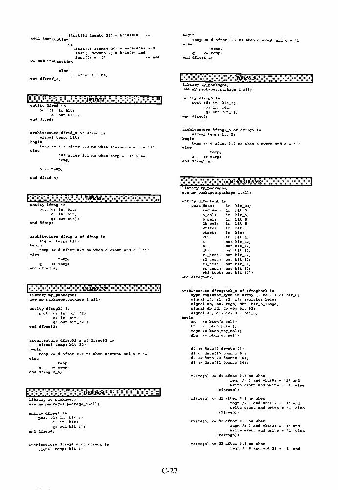
addi instruction(inst(31 downto 26) =
b"001000"
or sub instruction
)
(lnst(31 downto 26) =b"000000"
and
inst(5 downto 2) =b"1000"
and
inst(O) ='0'
) -- add
begin
temp <= d after 0.9 ns whenc'
event and c ='1'
else
temp;
q <= temp;
end dfreg4_a;
end dfovrf_a;
' 0 'after 4.6 ns;
in urn
entity dfred is
port (1: in bit;
o: out bit);end dfred;
DFREC5
library my_packages;
use my_packages.package_l.all;
entity dfregS is
port (d: in bit_5;c: in bit;
q: out blt_5);end dfreg5;
architecture dfred_a of dfred is
signal temp: bit;
begin
temp <= !' after 0.3 ns when 1 'event and i = '1'
else
'0'after 1.1 ns when temp =
'1'else
temp;
o <= temp;
end dfred_a;
DFREG
entity dfreg is
port(d: in bit;
c: in bit;
q: out bit);end dfreg;
architecture dfreg_a of dfreg is
signal temp: bit;
begin
temp <= d after 0.9 ns when c'event and c =
' 1 '
else
temp;
q <= temp;
end dfreg_a;
architecture dfreg5_a of dfreg5 is
signal temp: bit_5;
begin
temp <= d after 0.9 ns when c'event and c =
' 1
else
temp;
q <= temp;
end dfreg5_a;
OI'REGHANK
library my_packages;
use my_packages.package_l.all;
entity dfregbank Ls
port (data: in blt_32.
reg_sel : in bit 5;
a_eel : in bit 5;
b_sel : in bit 5;
db_sel: in bit 5;
write: In bit;
start: in bit;
vbt: In bit 4;
a: out bit 32,
b: out bit 32,
db: out bit 32,
rl test: out bit_32.
r2 test: out bit_32;
r3_test: out bit 32;
r4 test: out bit_32;
r31_test out bit 32)
end dfregbank;
DPREG32
library my packages;
use my_packages.package_l.all;
entity dfreg32 is
port (d: in bit_32;
c: in bit;
q: out bit_32);end dfreg32;
architecture dfreg32_a of dfreg32 is
signal temp: bit_32;
begin
temp <= d after 0.9 ns when c'event and c
else
temp;
q <= temp;
end dfreg32_a;
DFREG4
library my_packages;
use my_packages.package_l.all;
entity dfreg4 is
port (d: in bit_4;
c: in bit;
q: out bit_4) ;
end dfreg4;
architecture dfregbank_a of dfregbank is
type register_byte is array (0 to 31) of bit_
signal rO, rl, r2, r3: register_byte;
signal an, bn, regn, dbn: bit_5_range;
signal db_id, db_wb: bit_32;
signal dO, dl, d2, d3 : bit_8;
begin
an <= bton(a_sel);
bn <= bton(b_sel);
regn <= bton(reg_sel) ;
dbn <= bton(db_sel) ;
dO <= data(7 downto 0);
dl <= data(15 downto 8);
d2 <= data(23 downto 16);
d3 <= data(31 downto 24);
rO (regn) <= dO after 0.3 ns when
regn /= 0 and vbt(0) ='1'
and
write 'event and write ='1'
else
rO (regn) ;
rl(regn) <= dl after 0.3 ns when
regn /= 0 and vbt(l) ='1'
and
write'event and write =
' 1 'else
rl(regn) ;
r2(regn) <= d2 after 0.3 ns when
regn /= 0 and vbt (2) ='1'
and
write 'event and write ='1'
else
r2 (regn) ;
architecture dfreg4_a of dfreg4 is
signal temp: bit_4;
r3(regn) <= d3 after 0.3 ns when
regn /= 0 and vbt (3) ='l'
and
C-27
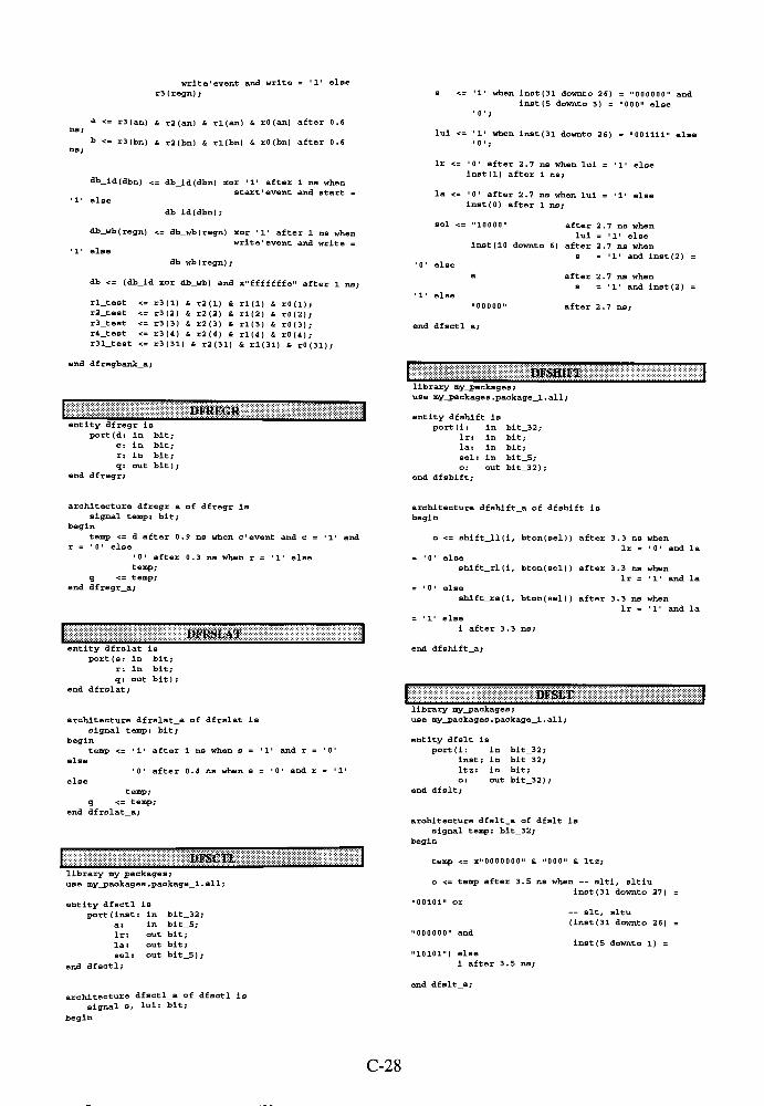
write'event and write
r3 (regn) ;
a <= r3(an) & r2 (an) rl(an) rO (an) after 0.6
b <=r3(bn) r2 (bn) & rl(bn) rO (bn) after 0.6
s <= 1'when inst (31 downto 26) =
"000000"and
inst(5 downto 3) = "000"else
'0';
lui <= '1'when inst(31 downto 26) = "001111"
else
'0';
<ib_id(dbn) <= db_ld(dbn) xor'1'
after 1 ns when
start'event and start =
'1'else
db_id(dbn);
db_wb(regn) <= db_wb(regn) xor'1'
after 1 ns when
write 'event and write =
'1'else
db_wb(regn) ;
db <= (db_id xor db_wb) and x"fffffffe" after 1 ns;
rl_test <= r3(l) r2(l) rl(l) r0(l);
r2_test <= r3(2) r2(2) rl(2) r0(2);
r3_test <= r3(3) r2(3) rl(3) r0(3);
r4_test <= r3(4) r2(4) rl{4) r0(4);
r31_test <= r3(31) r2(31) rl(31) & r0(31);
end dfregbank_a;
DFREGR
entity dfregr is
port(d: in bit;
c: in bit;
r: in bit;
q: out bit);
end dfregr;
lr <='0'
after 2.7 ns when lul ='1'
else
inst(l) after 1 ns;
la <= '0'after 2.7 ns when lui =
'1'else
inst (0) after 1 ns;
sel <= "10 000" after 2.7 ns when
lui ='1'
else
inst(10 downto 6) after 2.7 ns when
s =' 1'
and inst (2) =
else
a after 2.7 ns when
s =' 1'
and inst (2) =
'1'else
"00000"
end dfsctl_a;
after 2.7 ns;
wmsmmmmm
library my_packages;
use my_packages.package_l.all;
entity dfshift is
port(l: in bit_32;
lr: in bit;
la: in bit;
sel: in bit_5;
o: out bit_32);
end dfshift;
architecture dfregr_a of dfregr is
signal temp: bit;
begin
temp <= d after 0.9 ns when c'event and c =
r =' 0 '
else
'0'after 0.3 ns when r =
'1'else
temp;
q <= temp;
end dfregr_a;
I>I-K,S1,AT
entity dfrslat is
port (s: in bit;
r: in bit;
q: out bit);
end dfrslat;
architecture dfrslat_a of dfrslat is
signal temp: bit;
begin
temp <='1'
after 1 ns when s ='1'
and r ='0'
else
' 0 'after 0.4 ns when s =
' 0 'and r =
'
else
temp;
q <= temp;
end dfrslat a;
DFSCTL
library my_packages;
use my_packages.package_l.all;
entity dfsctl is
port(inst: in bit_32;
a: in bit_5;
lr: out bit;
la: out bit;
sel: out bit_5);
end dfsctl;
architecture dfsctl_a of dfsctl 1b
signal s, lui: bit;
begin
architecture dfshift_a of dfshift is
begin
o <= shift_ll(i, bton(sel)} after 3.3 ns when
lr =' 0 '
and
='0'
else
shift_rl(i, bton (sel)) after 3.3 ns when
lr ='1'
and
=' 0 '
else
shift_ra(i, bton(sel)) after 3.3 ns when
lr ='1'
and
='1'
else
1 after 3.3 ns;
end dfshift_a;
DFSI.T
library my_packages;
use my_packages.package_l.all;
entity dfslt is
port(i: in bit_32;
inst: In bit_32;
ltz: in bit;
o: out bit_32);
end dfslt;
architecture dfslt_a of dfslt is
signal temp: bit_32;
begin
temp <=x"0000000" "000"
Itz;
o <= temp after 3.5 ns when --
slti, sltlu
inst (31 downto 27) =
"00101"or
--
sit, situ
(inst (31 downto 26) =
"000000"
and
inst (5 downto 1) =
"10101") else
i after 3.5 ns;
end dfslt_a;
"13
C-28
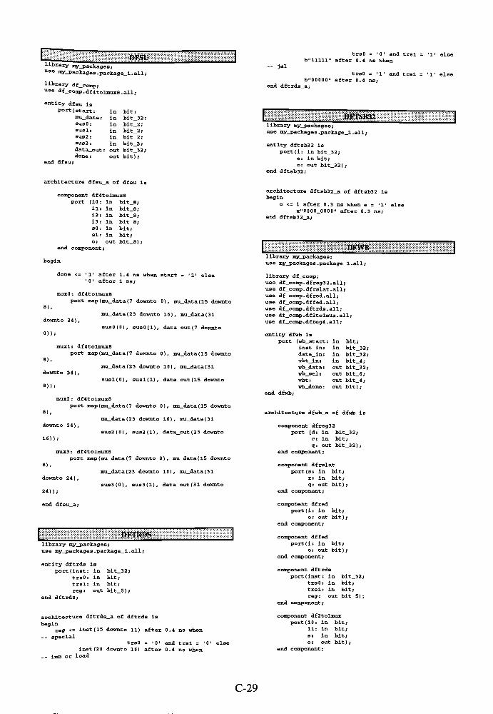
mmlibrary my_packages;use
my_packages.package_l.all;
library df_comp;use df_comp.df4tolmux8.all;
entity dfsu is
port (start: in bit;
mu_data : in bit 32
susO: in bit 2;
susl:
SU82 :
sus3:
in
in
in
bit_2;
bit_2;
bit 2;
data_out :
done:
end dfsu;
OUt
out
blt_32
bit);
architecture dfsu_a of dfsu is
component df4tolmux8
port (10 in bit 8
il in bit 8
12 in bit 8
13 in bit 8
SO in bit;si in bit;
o: out bit_8) ;end component;
begin
done <=' 1'
after 1.4 ns when start ='1'
els
'0 after 1 ns;
9).
muxO: df4tolmux8
port map(mu_data(7 downto 0), mu_data(15 downto
downto 24) ,
0));
mu_data(23 downto 16), mu_data(31
susO(O), susO(l), data_out(7 downto
muxl : df4tolmux8
port map(mu_data(7 downto 0), mu_data(15 downto
8),
downto 24) ,
8));
mu_data(23 downto 16), mu_data(31
susl(O), susl(l), data_out(15 downto
mux2 : df4tolmux8
port map(mu_data(7 downto 0), mu_data(15 downto
B),
downto 24) ,
16));
mu_data(23 downto 16), mu_data(31
sus2(0), sus2(l), data_out(23 downto
mux3 : df4tolmux8
port map (mu_data ( 7 downto 0), mu_data(15 downto
8),
downto 24) ,
24));
end dfsu_a;
mu_data(23 downto 16), mudata(31
sus3(0), sus3(l), data_out(31 downto
DFTRDS
library my_packages;
use my_packages.package_l.all;
entity dftrds is
port(inst: in bit_32;
trsO: in bit;
trsl: in bit;
reg: out bit_5) ;
end dftrds;
architecture dftrds_a of dftrds is
begin
reg <= lnst(15 downto 11) after 0.4 ns when
-- special
trsO ='0'
and trsl ='0'
else
inst (2 0 downto 16) after 0.4 ns when
__ imm or load
trsO ='0'
and trsl = '1'else
b"lllll"after 0.4 ns when
jal
trsO ='1'
and trsl ='1'
els
b"00000"after 0.4 ns;
end dftrds_a;
DFTSM2
library my_packages;
use my_packages.package_l.all;
entity dftsb32 is
port(i: in bit_32;
e: in bit;
o: out bit_32);end dftsb32;
architecture dftsb32_a of dftsb32 is
begin
o <= 1 after 0.3 ns when e ='1'
else
x"0000_0000"
after 0.3 ns;
end dftsb32_a;
mmmlibrary my_paekages;
use my_packages.package_l.all;
library df_comp;
use df_comp.dfreg32.all;use df_comp.dfrslat.all;
use df_comp.dfred.ally-
use df_comp.dffed.all;
use df_comp.dftrds.all;
use df_comp.df2tolmux.all;use df_comp.dfreg4.all;
entity dfwb is
port (wb_start in bit;
inst in: in bit 32
data in: in bit 32
vbt in: in bit 4;
wb_data : out bit 32
wb sel : out bit 6;
vbt: out bit 4;
wb done: out bit);
end dfwb;
architecture dfwb_a of dfwb is
component dfreg32
port (d: in bit_32;
c: in bit;
q: out bit_32);
end component;
component dfrslat
port(s: in bit;
r: in bit;
q: out bit);
end component;
component dfred
port(l: In bit;
o: out bit);
end component;
component dffed
port(i: in bit;
o: out bit);
end component ;
component dftrds
portdnst: in bit_32;
trsO: in bit;
trsl: in bit;
reg: out bit_5) ;
end component ;
component df2tolmux
portUO: in bit;11: in bit;
s: in bit;o: out bit);
end component;
C-29

component dfreg4 end dfwb_a;
port (d: in bit_4;
c: in bit;
q : out bit_4 ) ;end component;
signal wb_start_r, wb_start_f, dummy_r, dummy: bit;
signal trsO, trsl: bit;
signal instl: bit_32;signal reg: bit_5;signal moveto_sel, hilo_sel: bit;
signal count: integer :=0;
begin
inst_latch: dfreg32
port map(inst_in, wb_start_r, instl) ;
data_latch: dfreg32
port map(data_in, wb_start_r, wb_data) ;
vbt_latch: dfreg4
port map(vbt_in, wb_start_r, vbt);
wb_start_red : dfred
port map(wb_start, wb_start_r);
wb_start_fed: dffed
port map(wb_start, wb_start_f);
done_latch : dfrslat
port map(dummy_r, wb_start_f, wb_done);
dummy <=' 1 '
after 8 ns when wb_start'event and
wb_start =' 1 '
else
' 0 'after 1 ns;
dummy_red: dfred
port map (dummy, dummy_r);
trds: dftrds
port map (instl, trsO, trsl, reg);
trsO <='1'
after 4.4 ns when -- a23
(instl (31) ='0'
and
instl (29 downto 27) =
"001") or
-- a26
(instl (31) ='1'
and
instl(29) = '1') or
-- a27
(instl (31) ='0'
and
instl (29) ='0'
and
instl (27 downto 26) =
"01") or
-- a29
(Instl (31) ='0'
and
instl (29 downto 28) =
"01") else
' 0 'after 4.4 ns;
trsl <='1'
after 4.4 ns when -- a21
(instl (31) ='0'
and
instl (29 downto 26) =
"0011") or
-- a30
(instl (31) ='1'
and
instl (29) = '0') or
-- a31
(instl (31) ='0'
and
instl (29) = '1') or
-- a32
(instl (31) ='0'
and
instl (29 downto 26) =
"0001"and
instl(20) = '1') else
' 0 'after 4.4 ns;
wb_sel <= moveto_sel reg (4 downto 1) hllo_sel;
moveto_sel <='1*
after 2.6 ns when-- special and
move to instr.
instl (31 downto 26) =
"000000"and
instl (5 downto 4) ="01"
and
instl (0) ='1'
else
' 0 'after 2. 6 ns;
wb_sel_mux: df2tolmux
port map (reg (0), instl (1), moveto_sel,
hilo_sel);
count <= count + 1 when (wb_start 'event and
wb_start- 'I') else count;
C-30
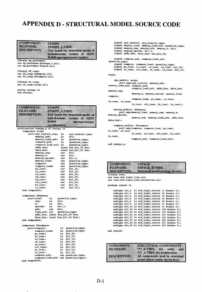
APPENDIX D - STRUCTURALMODEL SOURCE CODE
lOWfoNtYr-
IILKNVME-
DESCftttllOV
library my_packages;use my_packages.package_l.all
use my_packages.dfpaek.ally-
library df_comp;
use df_comp
. dfmemory . al1 ;
use df_comp. dfcompare.all;
library st_comp;
use st_comp . stcpu . al1 ;
entity stmips is
end stmips;
MMIPS
yi.MH%J'VHl>l.
lest hrncb lor strmlfiral vantM oi
asymJtroiiotts version Mil's!te4MH)0mtfr<ipMiecsOTr(<'imtv)
COMPONEM: w^^MsmmmMMmmmmm
IH-KNAME: STMIPS_A.VHD1,
DESCRIPTION; T*$t teach fwr sectoral i&otfel of
asjfukr{>ium& versfon of MIPS
R3DW MtWrM#)$6f<archfte_tn3re)i
architecture stmips_a of stmips is
component stcpu
port (sys_control_sig : in sys_control_type
memory_ack : in bit;memory_load_ack : in question_type;
compare_ack : in question_type ;
compare_load_ack: in questlon_type;
addr_bus : inout bus_bit_32 bus;
data_bus : inout bus_bit_32 bus;
memory_req: out bit;
memory_w : out bit;
memory_opcode : out bit_3;
memory_load : out question_type;
compare : out quest ion_type;
compare_load : out question_type ;
pc_test : out bit_32
rl_test: out bit_32
r2_test: out bit_32
r3_test : out bit_32
r4_test: out bit_32
r31_test: out bit_32
hl_test : out bit_32
lo_test: out bit_32);
end component;
component dfmemory
port (load: in question_type;
req: in bit;
w: in bit;
opcode : in bit_3 ;
ack: out bit;
load_ack: out question_type ;
addr_bus: inout bus_bit_32 bus;
data_bus: inout bus_bit_32 bus);
end component;
component dfcompare
port (compare : in_uestion_type;
compare_load : in question_type;
pc test : in bit_32;
rl test: in bit_32;
r2 test: in bit_32;
r3 test: in bit_32;
r4_test: in bit_32;
r31 test: in bit 32;
hi_test: in bit_32;
lo_test : in bit_32;
compare_ack : out_uestion_type;
compare_load_ack : out )
end component ;
signal sys_control : sys_control_type;signal memory_load, memory_load_ack: question_type;signal memory_req, memory_ack, memory_w: bit;signal memory_opcode : bit_3;signal addr_bus, data_bus: bus_blt_32;
signal compare_ack, compare_load_ack :
quest ion_type;
signal compare, compare_load: question_type;
signal pc_testy rl_test, r2_test, r3_test : bit_32;signal r4_test, r31_test, hi_test, lo_test : bit_32;
begin
cpu_module: stcpu
port map(sys_control, memory_ack,
memo3ry_load_ack, compare_ack,
compare_load_ack, addr_bus, data_bus,
memory_req,
memory_w, memory_opcode , memory_load,
compare,
compare_load, pc_test, rl_test,
r2_test, r3_test,
r4_test, r31_test, hl_test, lo_test);
memory_module : dfmemoryport map (memory_load, memory_req, memory_w,
memory_opcode ,
memory_ack, memory_load_ack, addr_bus ,
data_bus) ;
compare_module : dfcompare
port map(compare, compare_load, pc_test,
rl_test, r2_test,
r3_test , r4_test , r3 l_test , hi_test ,
lo_test,
compare_ack, compare_load_ack) ;
end stmips_a;
c<)\iP>M:NTt mi:k
ULENAMlv: S n*ACK_H.VHI>L
DFISCRIPIlOiNi; iStmctormodel
library ieee;
use ieee . std_logic_1164 .all;
use ieee.std_logic_1164_extensions.all;
package stpack is
subtype slv 2 is std_logic_vector ( 1 downto 0 ) ;
subtype slv_3 is std_logic_vector (2 downto 0) ;
subtype slv 4 is std_logic_vector ( 3 downto 0 ) ;
subtype slv 5 is std_logic_vector (4 downto 0);
subtype slv_6 is std_logic_vector (5 downto 0) ;
subtype slv 8 is std_loglc_vector ( 7 downto 0 ) ;
subtype slv 10 is std_logic_vector { 9 downto 0 ) ;
subtype slv 16 is std_logic_vector (15 downto 0)
subtype slv 20 is std_logic_vector (19 downto 0) ;
subtype slv 24 is std_logic_vector (23 downto 0);
subtype slv_26 is std_logic_vector (25 downto 0) ;
subtype slv_3 0 is std_loglc_vector ( 2 9 downto 0 ) ;
subtype slv_32 is std_logic_vector (31 downto 0) ;
subtype slv_64 is std_logic_vector (63 downto 0) ;
end stpack;
COMPONENT;
Fltl.NAME:
l>lM;fctVllO\!
STRl'CTl RAl COMPONENTS
??.'J-_Vm>L fr cnllty aiut
???_A.VH I>l . Iwr archiln tun
All rmn))<inriit<; usiid in strurtruol
model follow (entityshw"
first)
D-l

STALU32
library ieee;use ieee. std_logic_H64.all;use Ieee. std_logic_1164_extensiona.all;
library my_packages;use my_packages. stpack. ally-
library st_comp;
use st_comp.stalu4 .all;
use st_comp.stcgen.all;
entity stalu32 is
port (a: in slv 32;
b: in slv 32;
SO: in std_logic;
si: in std_logic;
s2: in std_logic;
S3: in std_logic;
cout out std_logic;
o: out slv_32);
end stalu32;
architecture stalu32_a of stalu32 is
component stalu4
port (aO: in std_logic;
al: in std logic;a2: in std logic;
a3: in std_logic;
bO: in std_logic;
bl: in std logic;b2: in std logic;
b3: in std_logic;
cin: in std_logic;
sO: in std logic;si: in std_logic;
82: in std_logic;
S3: in std_logic;
fO: out std_logic;
fl: out std logic;
f2: out std_logic;
f3: out std_logic;
g: out std_logic;
p: out std_logic;
cout: out std_logic)
end component;
component stcgen
port (c: in std_logic;
gO : in std_logic;
pO: in std_logic;
gl: in std_logic;
pi: in std_logic;
g2: in std_loglc;
p2 : in std_logic;
cl: out std_logic;
c2 : out std_logic ) ;
end component;
signal cin: std_logic;
signal gO, gl, g2, g3, g4, g5, g6, g7 : std_logle;
signal pO, pi, p2, p3, p4, p5, p6, p7 : std_logic;
signal coutO, coutl, cout2, cout3, cout4, cout5,
cout6: std_logic;
signal cgenl_cl, cgenl_c2, cgen2_cl, cgen2_c2:
std_logic;
begin
alu0to3: stalu4
port map (a(0), a(l), a(2), a(3), b(0), b(l),
b(2), b(3),
cin, sO, si, s2, s3, o(0), o(l), o(2),
o(3),
gO, pO, coutO) ;
alul2tol5: stalu4
port map {a (12), a(13), a(14), a(15), b(12),
b(13), b(14), b(15),
cgenl_c2, sO, si, s2, s3, o(12) ,
o(13), o(14), o(15),
g3, p3, cout3) ;
alul6tol9: stalu4
port map (a (16), a(17), a(18), a(19), b(16),
b(17), b(lS), b(19),
cout3, sO, si, s2, s3, o(16), o(17),
o(18), o(19),
g4, p4r cout4);
alu20to23 : stalu4
port map(a(20), a(21), a(22), a{23), b(20),
b(21), b{22), b(23),
cgen2_cl, sO, si, s2, s3, o(20),
o(21), o(22), o(23),
g5, p5, cout5);
alu24to27: stalu4
port map(a(24), a(25), a(26), a(27), b(24),
b(25), b(26), b(27),
cgen2_c2, sO, si, s2, s3y o(24),
o(25), o(26), o(27),
g6, p6, cout6) ;
alu28to31: Btalu4
port map(a(28), a(29), a(30), a(31), b(28),
b(29), b(30), b(31),
cout6, sO, si, s2, s3, o(28), o(29),
o(30), o(31),
g7, p7, cout) ;
cgenl: stcgen
port map(cin, gO, pO, gl, pi, g2, p2, cgenl_cl,
cgenl_c2) ;
cgen2 : stcgen
port map(cgenl_c2, g3, p3, g4, p4, g5, p5,
cgen2_cl, cgen2_c2) ;
end stalu32_a;
mmmmmmrrmm
library ieee;
use ieee.std_logic_1164 .all;
use ieee. std_logic_1164_extensions.ally-
library my_packages;
use my_packages. stpack.all;
entity stalu4 is
port (aO in std_logic;
al in std_logic;
a2 in std_logic;
a3 in std_logic;
bO in std_logic;
bl in std logic;
b2 in std logic;b3 in std_logic;
cin: in std_loglc;
sO in std_logic;
si in std_logic;
s2 in std_logic;
S3 in std_logic;
fO out std_logic;
fl out std_logic;
f2 out std_logic;
f3 out std_logic;
g: out std_logic;
P: out std_logic;
COIit : out Btd_logic)
end stalu4;
alu4to7 : stalu4
port map(a(4), a(5), a(6), a(7), b(4), b(5),
b(6), b(7),
coutO, sO, si, s2, s3, o(4), o(5),
o(6), o(7),
gl, pi, coutl);
aluStoll: Stalu4
port map(a(8), a(9), a(10), a(ll), b(8), b(9),
b(10), b(ll),
cgenl_cl, sO, si, b2, s3, o{8), o(9),
o(10), o(ll),
g2, p2, cout2) ;
architecture stalu4_a of stalu4 Is
signal nl, n2, n3, n4, n5, n6, n7, nS, n9, nlO:
std_logle;
signal nil, nl2, nl3, nl4, nl5, nl6, nl7, nlS, nl9,
n20: std_logic;
signal n21, n22, n23, n24, n25, n26, n27, n28, n29,
n30: std_logic;
signal n31, n32, n33, n34, n35, n36, n37, n38, n39,
n40 : std_loglc;
signal n41, n42, n43, n44, n45, n46, n47, n48, n49,
n50: std_logic;
D-2
signal n51, n52, n53, n54, n55, n56, n57, n58, n59,
n60: std_logic;
signal n61, n62, n63, n64, n65, n66, n67, n68, n69,
n70: std_logic;
signal n71, n72, n73, n74, n75, n76, n77, n78, n79,
n80: std_logic;
signal n81, n82, n83, n84, n85, g_temp: std_logic;
begin
nl <=
n2 <=
n3 <=
n4 <=
n5 <=
n6 <=
n7 <=
n8 <=
n9 <=
nlO <=
nil <=
nl2 <=
nl3 <=
nl4 <=
nl5 <=
nl6 <=
nl7 <=
nlS <=
nl9 <=
n20 <=
n21 <=
n22 <=
n23 <=
n24 <=
n25 <=
n26 <=
n27 <=
n28 <=
n29 <=
n30 <=
n31 <=
n32 <=
n33 <=
n34 <=
n35 <=
n3 6 <=
n37 <=
n38 <=
n39 <=
n4 0 <=
n41 <=
n42 <=
n43 <=
n44 <=
n45 <=
n4 6 <=
n47 <=
n48 <=
n49 <=
n50 <=
n51 <=
n52 <=
n53 <=
n54 <=
n55 <=
n56 <=
n57 <=
nSS <=
n59 <=
n60 <=
n61 <=
n62 <=
n63 <=
n64 <=
n65 <=
n6 6 <=
n67 <=
n66 <=
n69 <=
n70 <=
n71 <=
n72 <=
n73 <=
2 ns;
2 ns;
2 ns;
2 ns;
2 ns;
2 ns;
bO xor s3 after
aO xor s3 after
bl xor s3 after
al xor s3 after
b2 xor s3 after
a2 xor s3 after
b3 xor s3 after 2 ns;
a3 xor s3 after 2 ns;
not nl after 0.3 ns;
not n2 after 0.3 ns;
not n3 after 0.3 ns;
not n4 after 0.3 ns;
not n5 after 0.3 ns;
not n6 after 0.3 ns;
not n7 after 0.3 ns;
not nS after 0.3 ns;
not sO after 0.3 ns;
not si after 0.3 ns;
not s2 after 0.3 ns;
not nl7 after 0.3 ns;
not nl8 after 0.3 ns;
not nl9 after 0.3 ns;
nl7 nand nlS after 0.7 ns;
nl8 nand nl9 after 0.7 ns;
nl7 nand n21 after 0.7 ns;
not (nl9 and n20 and n21) after 0.7 ns;
nl8 and n22 after 1 ns;
nl7 and n22 after 1 ns;
n27 nor n28 after 1 ns;
n9 and nlO and n24 and n25 after 1 ns;
n2 and n9 and n23 and n25 and n26 after 1
nl and nlO and n24 and n2 6 after 1 ns;
n9 and nlO and n23 and n26 and n29 after 1
n2 and n9 and n24 and n25 after 1 ns;
nl and nlO and n24 and n25 after 1 ns;
nl and n2 and n23 and n26 after 1 ns;
nil and nl2 and n24 and n25 after 1 ns;
n4 and nil and n22 and n25 and n26 after 1
n3 and nl2 and n24 and n26 after 1 ns;
nil and nl2 and n23 and n26 and n29 after 1
n4 and nil and n24 and n25 after 1 ns;
n3 and nl2 and n24 and n25 after 1 ns;
n3 and n4 and n23 and n26 after 1 ns;
nl3 and nl4 and n24 and n25 after 1 ns;
n6 and nl3 and n23 and n25 and n26 after 1
n5 and nl4 and n24 and n2 6 after 1 ns;
nl3 and nl4 and n23 and n26 and n29 after 1
n6 and nl3 and n24 and n25 after 1 ns;
n5 and nl4 and n24 and n25 after 1 ns;
n5 and n6 and n23 and n26 after 1 ns;
nl5 and nl6 and n24 and n25 after 1 ns;
n8 and nl5 and n23 and n25 and n26 after 1
n7 and nl6 and n24 and n26 after 1 ns;
nl5 and nl6 and n23 and n26 and n29 after 1
n8 and nl5 and n24 and n25 after 1 ns;
n7 and nl6 and n24 and n25 after 1 ns;
n7 and n8 and n23 and n26 after 1 ns;
nl7 and nl8 after 1 ns;
not (n30 or n31 or n32) after 1 ns;
not (n33 or n34 or n35 or n36) after 1 ns;
not (n37 or n38 or n39) after 1 ns;
not (n40 or n41 or n42 or n43) after 1 ns;
not (n44 or n45 or n46) after 1 ns;
not (n47 or n48 or n49 or n50) after 1 ns;
not (n51 or n52 or n53) after 1 ns;
not (n54 or n55 or n56 or n57) after 1 ns;
n22 nor n58 after 1 ns;
cin and n59 and n67 after 1 ns;
n59 and n60 and n67 after 1 ns;
cin and n59 and n61 and n67 after 1 ns;
n59 and n60 and n61 and n67 after 1 ns;
n61 and n62 and n67 after 1 ns;
cin and n59 and n61 and n63 and n67 after 1
n74 <= n59 and n60 and n61 and n63 and n67 after 1
ns;
n75 <= n61 and n62 and n63 and n67 after 1 ns;
n76 <= n63 and n64 and n67 after 1 ns;
n77 <= cin nand n67 after 0.7 ns;
n78 <= n66 nor n69 after 1 ns;
n79 <= not (n70 or n71 or n72) after 1 ns;
n80 <= not (n73 or n74 or n75 or n76) after 1 ns;
nSl <= n59 and n60 and n61 and n63 and n65 after 3.
ns;
n82 <= n61 and n62 and n63 and n65 after 1 ns;
n83 <= n63 and n64 and n65 after 1 ns;
n84 <= n65 and n66 after 1 ns;
n85 <= not (cin and n59 and n61 and n63 and n65)
after 0.7 ns;
fO <= n60 xor n77 after 2 ns;
fl <= n62 xor n7S after 2 ns;
f2 <= n64 xor n79 after 2 ns;
f3 <= n6 6 xor n80 after 2 ns;
P <= not (n59 and n61 and n63 and n65) after 0.7
ns;
g_temp <= not (nSl or n82 or n83 or n84) after 1
ns;
g <= g_temp;
cout <= g_temp nand nS5 after 0.7 ns;
end stalu4_a;
STALL'
library mgc_portable;
use mgc_portable.qsim_tc.all;
library ieee;
use ieee.std_logic_1164 .all;
use ieee. std_logic_1164_extenslons.all;
library my_packages;
use my_packages.package_l.all;
use my_packages. stpack.all;
library df_comp;
use df_comp.dfreg32 .all;
use df_comp.dfregr.all;
use df_comp.dfred.all;
use df_comp.dffed.all;
use df_comp
. dfrslat . all ;
use df_comp.df2tolmux32.all;
use df_comp.dfmd.all;
use df_comp.dfhlreg.ally-
use df_comp.dfaddS.all;
library at_comp;
use st_comp . stregbank .all ;
use st_comp . stalublk . al1 ;
entity stalu is
port (alu_start: in bit;
ibo: in bit;
alu_select : In bit;
md_select : in bit;
add8_select : in bit;
regl_out: in bit_5;
reg2_out : in bit_5;
treg_out : in bit_5;
pel: in bit_32;
lnst_in: in blt_32;
wb_data: in bit_32;
wb_sel : in bit_6;
vbt: in bit_4;
write : in bit;
dJr: in bit;
set_hi_db: in bit;
set_lo_db: in bit;
cc: out bit;
hl_db: out bit;
lo_db: out bit;
db: out bit_32;
reg: out bit_32;
alu_exc : out bit;
inst_out : out bit_32;
datal_out : out bit_32;
data2_out : out bit_32;
ccd: out bit;
rl_test: out bit_32;
r2_test : out bit_32;
r3_test : out blt_32;
r4_test : out bit_32;
r31_test: out bit_32;
hi_test : out bit_32;
lo_test: out bit_32;
D-3
end stalu;
alu_done : out bit);
architecture stalu_a of stalu is
component dfreg32
port (d: in bit_32;c: in bit;q: out bit_32);
end component;
component dfregr
port(d: in bit;c: in bit;r: In bit;q: out blt);
end component;
component dfred
port(i: in bit;
o: out bit) ;
end component;
component dffed
port(i: in bit;
o: out bit) ;
end component;
component dfrslat
port(s: in bit;
r: in bit;
q: out bit);
end component;
component df2tolmux32
port(iO: In bit_32;
ill In blt_32;
s: in bit;
o: out bit_32);
end component;
component stregbank
port (data: in slv_32;
reg_sel : in slv_5;
a_sel : in slv_5;
b_sel : in slv_5;
db_sel: in slv_5;
write : in std_logic
start : in std_loglc
vbt: in slv_4 ;
a: out slv_32;
b: out slv_32;
db: out slv_32;
rl_test : out slv_32;
r2_test : OUt slv_32;
r3_test: out slv_32;
r4_test : out slv_32;
r31_test: OUt slv_32);
end component;
component stalublk
port (a_in: in bit_32
b_in: in bit_32
lnst_in: in bit_32
pcl_in: in bit_32
ibo: in bit;
start : in bit;
lat_inst: in bit;
hilo: in bit_32;
adds: in bit_32;
exc: out bit;
cc: out bit;
b_out : out bit_32
output : out bit_32
inst_out : out bit_32
pcl_out : out blt_32
alub_done out bit);
end component;
component dfmd
port (start: in bit ;
xi in bit_32;
y: in bit_32;
sign: in bit
divd: in bit ;
hi: out bit_32;
lo: out bit_32;
donel: out bit
done2: out bit) ;
end component;
port {start : in bit;
hl_ln: in bit_32;lo_in: in bit_32;
load_hi : in bit;
load_lo: in bit;
set_hl_db: in bit;
set_lo_db : in bit;
hi_out : out bit_32;
lo_out : out bit_32;
hi_db: out bit;
lo_db: out bit);end component;
component dfadd8
port(i: in bit..32;start: in bit
o: out bit..32;
done : out bit ;
end component;
signal a, b, hilo, add8_out, add8_in: bit_32;signal x, y, hil, hi2, hi3, lol, lo2, lo3 : bit_32;signal md_inst_l: bit_32;
signal startl, exc, alub_done, alu_select_l : bit;
signal add8_select_l, add8_start, add8_done: bit;
signal alu_done_temp, sign, divd, start2 : bit;
signal md_donel, md_done2, md_select_l: bit;
signal load_hi, load_lo, l_hi, l_lo: bit;
signal j jr_done, alu_start_r, alu_start_f : bit;
slgnal done_temp_r, done_temp: bit;
signal write_nomove : bit;
signal Cwb_data, Ca, Cb, Cdb: slv_32;
signal Cwb_sel, Cregl_out, Creg2_out, Ctreg_out : slv_5;
signal Cwrite_nomove, Calu_start_r : std_logic;
signal Cvbt: slv_4;
signal Crl_test, Cr2_test, Cr3_test, Cr4_test,
Cr31_test: slv_32;
begin
alu_start_red : dfred
port map(alu_start, alu_start_r) ;
Cwb_data <= To_StdLogicVector (wb_data) ;
Cwb_sel <= To_StdLogicVector (wb_sel (4 downto 0));
Cregl_out <= To_StdLoglcVector (regl_out) ;
Creg2_out <= To_StdLogicVector (reg2_out) ;
Ctreg_out <= To_StdLoglcVector (treg_out ) ;
Cwrite_nomove <=To_Std
Logic (write_nomove) ;
Calu_start_r <= To_StdULogic(alu_start_r) ;
Cvbt <= To_StdLogicVector (vbt) ;
a <= To_bitvector (Ca) ;
b <= To_bitvector (Cb) ;
db <= To_bitvector (Cdb) ;
rl_test <= To_bitveetor (Crl_test) ;
r2_test <= To_bitvector (Cr2_test) ;
r3_test <= To_bitvector (Cr3_test) ;
r4_test <= To_bitvector (Cr4_test) ;
r31_test <= To_bitvector(Cr31_test) ;
register_bank: stregbank
port map(Cwb_data, Cwb_sel, Cregl_out,
Creg2_out,
Ctreg_out, Cwrite_nomove,
Calu_start_r, Cvbt, Ca, Cb, Cdb,
Crl_test, Cr2_test, Cr3_test,
Cr4_test , Cr3 l_test ) ;
hl_test <= hi3;
lo_test <= lo3;
write_nomove <= write and (not wb_sel(5)) after 2
reg <= a;
alu_block : stalublk
port map(a, b, inst_in, pel, ibo, startl,
alu_start_r,
hilo, add8_out , exc , cc , data2_out ,
datal_out,
lnst_out, add8_in, alub_done);
alu_select_latch: dfregr
port map(alu_selectr alu_start_r,
alu_done_temp, alu_select_l ) ;
add8_select_latch: dfregr
port map(add8_select, alu_start_r,
alu_done_temp, add8_select_l ) ;
component dfhlreg
D-4
startl <=alu_start and alu_seleet_l after 1 ns;
add8_start <= alu_start and add8_select_l after 1
adds: dfaddS
... ,
port~P(da_ln, adds start, add8_out,
add8_done);_
alu_exc <= exc and alu_done_temp after 1 ns;
md : dfmd
portmap(start2, x, y, sign, divd, hil, lol,
md_donel,
md_done2) ;
md_x_latch: dfreg32
port map(a, start2, x) ;
md_y_latch: dfreg32
port map(b, start2, y) ;
md_inst_latch: dfreg32
port map(inst_in, start2, md_inst_l);
sign <= not md_inst_l (0 ) ;
divd <= md_lnst_l(l);
md_select_latch: dfregr
port map(md_select, alu_start_r, alu_done_temp,md_select_l ) ;
start2 <= alu_start and md_select_l after 1 ns;
hl_mux: df2tolmux32
port map (hil. wb_data, wb_sel(5), hi2);
lo_mux: df2tolmux32
port map (lol. wb_data, wb_sel (5) , lo2);
hilo_reg: dfhlregport map(alu_start, hi2, lo2, load_hi, load_lo,
set_hi_db, set_lo_db, hi3, lo3, hi_db,lo_db) ;
load_hi <= l_hi or md_done2 after 1.3 ns;load_lo <= l_lo or md_done2 after 1.3 ns;
l_hi <= write and wb_sel(5) and (not wb_sel(0))after 1.4 ns;
l_lo <= write and wb_sel(5) and wb_sel(0)after 1.1 ns;
hilo_mux: df2tolmux32
port map(hi3, lo3, md_inst_l (1) , hilo);
done_temp <= md_donel or jjr_done or add8_done or
alub_done after 1.5 ns;
done_temp_red: dfred
port map(done_temp, done_temp_r) ;
alu_start_fed: dffed
port map(alu_start, alu_start_f ) ;
done_latch: dfrslat
port map(done_temp_r, alu_start_f,
alu_done_temp) ;
alu_done <= alu_done_temp;
jjr_latch: dfregr
port map( j jr, alu_start_r, alu_done_temp,
j j r_done ) ;
ccd_latch: dfrslat
port map(done_temp_r, alu_start_r, ccd) ;
end stalu_a;
STALUBLK
library ieee;
use ieee. std_logic_1164 .all;
use ieee. std_logic_1164_extensions.all;
library my_packages;
use my packages.package_l.all;
use my_packages. stpack.all;
library df_comp;
use df_eomp.dfbusctl.all;
use df_comp.dfaludec.ally-
use df_comp.dfovrf .all;
use df_comp.dfcomp.all;
use df_comp.dfbctl. ally-
use df_comp.dfsctl.all;
use df_comp.dfshift.ally-
use df_comp.dfslt.all;use df_comp.dfoutBel.ally-
libra
y st_comp;
use st_comp.stalu32.all;
entity stalublk is
port(a_in:
b_in:
inst_in:
pcl_in:
ibo:
start :
lat_inst:
hilo:
addS:
exc:
cc :
b_out :
output :
inst_out :
pcl_out :
alub_done :
end stalublk;
In
in
in
in
in
in
in
in
in
out
out
out
out
out
out
out
blt_32;
bit_32;
bit_32;
bit_32;
bit;
bit;
bit;
bit_32;
bit_32;
bit;
bit;
bit_32
bit_32
bit_32
bit_32;
bit);
architecture stalublk_a of stalublk is
component dfbusctl
port (inst_in: in bit_32
a_in: in bit_32
b_in: in bit_32
pcl_in: in bit_32
start: in bit;
lat_inst : in bit;
ibo: in bit;
inst_out: out bit_32
a_out : out bit_32
b_out : out bit_32
a: out bit_5;b_pass: out bit_3 2
pcl_out : out bit_32
alub_done: out bit);end component;
component dfaludec
port(i: in bit_32;
sO: out bit;
si: out bit;
s2: out bit;
s3 : out bit) ;end component;
component stalu32
port (a: ii
b: ii
SO: il
si: ii
s2: ii
S3 : ii
cout
in slv_32;
in slv_32;
in std_logic;
in std_logic;
in std_logic;
in std_logic;
out std_logic;
out slv_32) ;
end component;
component dfovrf
port (inst: in bit_32;
data: in bit_32;carry: in bit;
overflow: out bit) ;
end component ;
component dfcompport (i:
Itz:
eqz:
gtz :
o:
end component;
in bit_32;
out bit;out bit;
out bit;out bit_32)
component dfbctl
port (inst: in bit_32;Itz: in bit;
eqz: in bit;
gtz: in bit;cc: out bit) ;
D-5
end component;
component dfsctlPort (inst: in bit_32;
a: in bit_5;lr: out bit;la: out bit;sel: out bit_5) ;
end component ;
component dfshift
port(i: in bit_32;lr: in bit;la: in bit;sel: in bit_5;o: out bit_32) ;
end component;
component dfslt
port(i: in bit_32;inst: in bit_32;Itz: in bit;
o: out bit_32) ;
end component;
component dfoutsel
port (inst: in bit_32
alu: in bit_32
add8: in bit_32
hilo: in bit_32
output: out bit_32)
end component;
signal instl, a_line, b_line, alu_out, comp_out:
bit_32;
signal shift_out, slt_out: bit_32;
signal a: bit_5;
signal sO, si, s2, s3 , c_out, Itz, eqz, gtz, lr, la
bit;
signal sel : bit_5;
signal Ca_line, Cb_line, Calu_out : slv_32;
signal CsO, Csl, Cs2, Cs3, Ccout: std_logic;
begin
wmsmm
library ieee;
use ieee. std_logic_1164.all;
use ieee. std_logic_1164_extensions.all ;
library my_packages;
use my_packages. stpack.all;
entity stcgen is
port(c: in
gO : in
pO: in
gl: in
pi: in
g2: in
p2: in
std_logic;
std_logic;
std_logic;
std_logic;
std_logic;
std_logic;
std_logic;
cl: out std_logic;
c2: out std_logic);
end stcgen;
architecture stcgen_a of stcgen is
signal a, b, d, e, f, g, h, c_bar: std_logic;
begin
c_bar <= not c after 0.3 ns;
a <= g2 and gl and gO and c_bar after 1 e
b <= pO and g2 and gl and gO after 1 ns;
d <= pi and g2 and gl after 1 ns;
e <= p2 and g2 after 1 ns;
f <= gl and gO and c_bar after 1 ns;
g <= pO and gl and gO after 1 ns;
h <= pi and gl after 1 ns;
c2 <= a or b or d or e after 1.3 ns;
cl f or g or h after ns;
end stcgen_a;
STCPl!
bus_control: dfbusctl
port map(inst_in, a_in, b_in, pcl_in, start,
lat_inst, ibo, instl, a_line, b_line,
a, b_out, pcl_out, alub_done) ;
inst_out <= instl;
alu_decode: dfaludec
port map (instl, sO, si, s2, s3);
Ca_line <= To_StdLogicVector (a_line) ;
Cb_line <= To_StdLogicVector (b_line) ;
CsO <= To_StdULogic(sO) ;
Csl <= To_StdULogic(sl) ;
Cs2 <= To_StdULogic(s2) ;
Cs3 <= To_StdULogic(s3) ;
c_out <= To_bit (Ccout) ;
alu_out <= To_bitvector(Calu_out) ;
alu: stalu32
port map(Ca_line, Cb_line, CsO, Csl,
Cs2, Cs3, Ccout, Calu_out) ;
ovrf : dfovrf
port map (instl, alu_out, c_out, exc);
compare: dfcompport map(alu_out , Itz , eqz, gtz, comp_out) ;
branch_ctl : dfbctl
port map(instl, Itz, eqz, gtz, cc) ;
shift_ctl: dfsctl
port map(instl, a, lr, la, sel);
shifter: dfshift
port map(comp_out, lr, la, sel, shift_out);
slt_box: dfslt
port map (shift_out, instl, Itz, slt_out) ;
output_selector: dfoutsel
port map (instl, slt_out, add8, hilo, output) ;
end stalublk_a;
library my_packages;
use my packages.package l.all;
library df_c
use df_comp.
use df_comp.
use df_comp,
use df_comp,
use df_comp.
use df_comp.
use df_comp.
use df_comp.
use df_comp,
dfhec.all;
dfif.all i
dfid.all;
dfmem.all;
dfwb.all;
dfeh.all;
dfbc.all;
dfrslat.all;
dfreg32
library st_comp;
use st_comp . stalu .all;
entity stcpu is
port (sys_control_sig: in sys_contro1_type
memory_ack : in bit;
memory_load_ack : in question_type;
compare_ack: in question_type ;
compare_load__ack:In question_type;
addr_bus : inout bus_bit_32 bus;
data_bus : inout bus_bit_32 bus;
memory_req : out bit;
memory_w: out blt;
memory_opcode : out blt_3;
memory_load : out question_type ;
compare : out quest ion_type;
compare_load out quest ion_type;
pc_test : out bit_32;
rl_test : out bit32;
r2_teat : out blt_32;
r3_test: out bit_32;
r4_test: out bit_32;
r3 l_test : out bit_32;
hi_test: out bit_32;
lo_test : out bit_32);
end stcpu;
architecture stepu_a of stcpu is
-- component declarations
component dfhec
port (init: in bit;
D-6
prev_ok: in bit
ready: in bit
ain: in bit
aout: out bit
rout: out bit
ok: out bit ;
end component ;
component dfif
port (if_start: in bit;la: In bit;int_req: in bit;
addr_valid: in bit;iv: in bit_32;new_pc : in bit_32;addr_bus : lnout bus_bit_32
data bus: inout bus_bit_32
ir: out bit;ili out bit;inst: out bit_32;pc: out bit_32;if_exc: out bit;1 f_done: out bit);
end component;
component dfid
port (id_start: in bit;hi_db: in bit;
lo_db: in bit;db: in bit_32;inst_in: in blt_32;cc : in bit;ccd: In bit;pc: in bit_32;ir: in bit;reg: in blt_32;illegal : out bit;
id_exc : out bit;
ibo: out bit;
alu_select: out bit;md_select : out bit;
add8_select out bit;
regl_out : out bit_5;
reg2_out : out bit_5;
treg_out : out bit_5;
addr_valid: out bit;
new_pc : out blt_32;pel: out bit_32;inst_out : out bit_32;
set_hl_db: out bit;
set lo db: out bit;
jjr: out bit;
id_done : out bit ) ;
end component ;
component stalu
port (alu_start : in bit;
ibo: in bit;
alu_select: in bit;
md_select : in bit;
add8_select in bit;
regl_out : in bit_5;
reg2_out : in bit_5;
treg_out: in bit_5;
pel : in bit_32;
inst_in: in bit_32;
wb_data : In bit_32;
wb_sel : in bit_6;
vbt: in bit_4;
write: in bit;
jjr: in bit;
set_hi_db: in blt;
set_lo_db : in bit;
cc: out bit;
hl_db: out bit;
lo_db: out bit;
db: out bit_32;
reg: out bit_32;
alu_exc : out bit;
inst_out : out bit_32;
datal_out : out bit_32;
data2_out : out bit_32;cad: out bit;rl_test : out bit_32;
r2_test : out bit_32;r3_test : OUt bit_32;r4_test : out bit_32;
r31_test: out bit_32;
hi_test: out bit_32;lo_test : out blt_32;
alu_done : out bit);
end component;
component dfmem
port (mem_start: in bit;
ma: in bit;
inst_in: in bit_32;
datal_in : in bit_32;
data2_in * in bit_32;
addr_bus inout bus_bit_32
data_bus lnout bus_bit_32
mem_exc : out bit;
mr: out bit;
ml: out bit;
w: out bit;
opcode : out bit_3;
inst_out out bit_32;
data_out out bit_32;
vbt: out bit_4;
mem_done out bit);
end component;
component dfwb
port (wb_start in bit;
inst_ln: in bit_32;
data_ln: in bit_32;
vbt_in: in bit_4 ;
wb_data : out bit_32;
wb_sel : out bit_6;
vbt: out bit_4;
wb_done : out bit ) ;
end component;
component dfeh
port (illegal: in bit;
1 f_exc: in bit;
id_exc : in bit;
alu_exc : in bit;
mem_exc : in bit;
int_req: out bit;
int_vector: out bit_32);
end component;
component dfbc
port (ir: in blt;
il: in bit;
mr: in bit;
ml: in bit;
ack: in bit;
ia: out bit;
ma : out bit;
req : out bit);
end component;
component dfrslat
port(s: in bit;
r: in bit;
q: out bit);
end component;
component dfreg32
port (d: in bit_32;
c: in bit;
q: out bit_32);
end component;
-- system control
signal start: bit;
signal begin_in: bit;
-- pipeline handshake
signal begin_oky if_ok, id_oky alu_ok, mem_ok,
wb_ok: bit :='1'
;
signal if_ack, id_ack, alu_ack, mem_ack, wb_ack,
end_ack: bit;
signal lf_start, id_start, alu_start, mem_start,
wb_start: bit;
signal lf_done, id_done, alu_done, mem_done,
wb_done : bit;
signal init: bit;
-- interrupt/exception control
signal if_exc, id_exc, alu_exc, mem_exc: bit;
signal illegal, int_req: bit;
signal int_vector: bit_32;
signal int_latch_q: bit;
constant zero_constant i bit :=' 0 '
;
signal int_reset: bit := zero_constant;
-- bus control
signal if_bus_req, mem_bus_req: bit;
signal if_bus_ack, mem_bus_ack: bit;
signal if_load_addr, mem_load_addr: bit;
D-7
--
data, controlsignal inst_ifid, pc, new_pc: bit_32;signal addr_valid: bit;
signal cc, hi_db, lo_db: bit;signal db, reg: bit_32;signal ibo, alu_select, md_select, add8 select:
bit;
signal regl_out, reg2_out, treg_out: bit_5;signal pel, inst_idalu: bit_32;signal set_hi_db, set_lo_db, jjr: bit;
signal wb_data, datal_out, data2 out, Inst alumem:
bit_32;
signal wb_sel : Mt_6;signal vbt: bit_4;
signal lnst_memwb, data_memwb: bit_32;signal vbt_memwb: bit_4;
signal ccd: bit;
--
signals for test bench
signal pc_alumem, pc_memwb: blt_32;signal test_mode, wb_done2 : bit;
begin
system: process
begin
wait on sys_control_sig;case sys_co_trol_sig is
when stop =>
start <=* 0 '
;
when reset =>
null;
when load =>
memory_load <= yes after delay;wait until
memo
y_load_ack = yes;
if test_mode = '1'then
compare_load <= yes after delay;wait until compare_load_ack = yes;
end if;
when run =>
start <=' 1'
;
end case;
end process system;
int_latch: dfrslat
port map(int_req, int_reset, int_latch_q) ;
bus_control : dfbc
port map(if_bus_req, if_load_addr, mem_bus_req,
mem_load_addr ,
memory_ack/ if_bus_ack, mem_bus_ack,
memory_req) ;
exception_handler : dfeh
port map ( illegal , i f_exc, id_exc , alu_exc,
mem_exc, int_req, int_vector) ;
begin_in <= not (if_ack or start) after 1 ns;
begin_ok <= begin_in or int_latch_q after 1.3 ns;
if_hce: dfhec
port map (init, begin_ok, if_done, id_ack,
if_ack, if_start, if_ok);
id_hcc: dfhec
port map (init, if_ok, id_done, alu_ack,
id_ack, id_start, id_ok) ;
alu_hcc : dfhec
port map (init, id_ok, alu_done, mem_ack,
alu_ack, alu_start, alu_ok) ;
port map(if_start, if_bUB_ack, int_req,
addr_valld,
int_vector, new_pc, addr_bus,
data_bus, if_bus_req,
if_load_addr, inst_ifid, pc, if_exc,
1 f_done) ;
id_stage: dfid
port map(id_start, hi_db, lo_db, db, inst_ifid,
cc, ccd,
pc, if_bus_req, reg, illegal, id_exc,
ibo, alu_select,
md_8elect, add8_select, regl_out,
reg2_out , treg_out ,
addr_valid, new_pc, pel, inst_idalu,
set_hi_db,
set_lo_db, jjr, id_done);
alu_stage: stalu
port map(alu_atart, ibo, alu_select, md_select,
add8_select ,
regl_out, reg2_out, treg_out, pel,
inst_idalu, wb_data,
wb_sel, vbt, wb_done, jjr, set_hi_db,
set_lo_db,
cc, hl_db, lo_db, db, reg, alu_exc,
inst_alumem,
datal_out, data2_out, ccd, rl_teat,
r2_test, r3_test,
r4_test, r31_test, hi_test, lo_test,
alu_done ) ;
mem_stage : dfmem
port map (mem_start , mem_bus_ack, inst_alumem,
datal_out,
data2_out , addr_bus , data_bus ,
mem_exc , mem_bus_req,
mem_load_addr, memory_w,
memory_opcode , inst_memwb,
data_memwb, vbt_memwb, mem_done) ;
wb_stage: dfwb
port map(wb_start, inst_memwb, data_memwb,
vbt_memwb,
wb_data, wb_sel, vbt, wb_done);
alu_pc_latch: dfreg32
port map(pcl, alu_start, pc_alumem) ;
mem_pc_latch: dfreg32
port map(pc_alumem, mem_start, pc_memwb);
wb_pc_latch: dfreg32
port map(pc_memwb, wb_start, pc_test);
hcc_tb_control : process
begin
wait on wb_done;
if test_mode ='0'
then
if wb_done =1* then
wb_done2 <=' 1 '
;
else
wb_done2 <=' 0 '
;
end if;
else
if wb_done =' 1' then
compare <= yes after delay;wait until compare_ack = yes;
compare <= no after 1 ns;
wait until compare_ack = no;
wb_done2 <=' 1 '
;
else
wb_done2 <= '0';
end if;
end if;
end process hcc_tb_control;
end stcpu_a;
mem_hcc : dfhec
port map (init, alu_ok, mem_done, wb_ack,
mem_ack, mem_start, mem_ok) ;
wb_hcc: dfhec
port map ( init , mem_ok, wb_done2 , end_ack,
wb_ack, wb_start, wb_ok) ;
end_ack <= not wb_ok after 0.3 ns;
mmmmmlibrary ieee;
use ieee .std_logic_1164 .all;
use ieee. std_logic_1164_extensions.all;
library my_packages;
use my_packages. stpack.all;
if_stage: dfifentity stdec32 is
port ( i : in slv_5 ;
D-8
oO: out std_loglc
ol : out std_logic;02 : out std_logic
o3: out std_logic
o4: out std_logic
o5: out std_logic
06: out std_logic
o7: out std_logic
08: out std_logic;o9: OUt std_logic
olO: out std_logic
oil: out std_logic
012 : out std_logic
ol3 : out std_logic
ol4: out std_logic
ol5: out std_logic
0I6: OUt std_logic
ol7: out std_logic;0I8: out std_logic
ol9: out std_loglc
o20 : out std_logic
o21 : out std_logic
o22 : out std_logic
o23: out std_loglc
o24: out std_logic
o25: out std_logic
o26: out std_logic
o27: OUt std_logic
o28: out std_logic
o2 9: out std_logic
o3 0: out std_logic
o31: out std_logic ;
end stdec32;
architecture Btdec32_a of s1-dec32 is
begin
oO <= '1 after 0.3 ns when 1 _'00000"
else '0
ol <= '1 after 0.3 ns when 1 _
'00001"else '0
o2 <= '1 after 0.3 ns when 1 = 00010"else
1 0
o3 <= '1 after 0.3 ns when i = 00011"else
1 0
o4 <= '1 after 0.3 ns when i = 00100"else '0
o5 <= '1 after 0.3 ns when 1 = 00101"else '0
06 <= '1 after 0.3 ns when i =00110"
else '0
o7 <= '1 after 0.3 ns when i = 00111"else '0
08 <= '1 after 0.3 ns when 1 = 01000"else '0
o9 <= '1 after 0.3 ns when i = 01001"else '0
olO <= '1 after 0.3 ns when 1 =01010"
else '0
oil <= '1 after 0.3 ns when i = 01011"else '0
ol2 <= '1 after 0.3 ns when 1 =01100"
else '0
ol3 <= '1 after 0.3 ns when i = 01101"else '0
ol4 <- '1 after 0.3 ns when 1 =OHIO"
else '0
ol5 <= '1 after 0.3 ns when i = 01111"else '0
0I6 <= '1 aft er 0.3 ns when 1 =10000"
elBe '0
ol7 <= '1 after 0.3 ns when i =10001"
else '0
0I8 <= '1 after 0.3 ns when i = 10010"else '0
ol9 <= '1 after 0.3 ns when i =10011"
else '0
o20 <= '1 after 0.3 ns when 1 = 10100"else '0
o21 <= '1 after 0.3 ns when i =10101"
else '0
o22 <= '1 after 0.3 ns when 1 =10110"
else '0
o23 <= '1 after 0.3 ns when i =10111"
else '0
o24 <= '1 after 0.3 ns when 1 =11000"
else '0
o25 <= '1 after 0.3 ns when i =11001"
else '0
o2 6 <- '1 after 0.3 ns when 1 =11010"
else '0
o27 <= '1 after 0.3 ns when i =11011"
else '0
o28 <= '1 after 0.3 ns when 1 = 1110 0" else '0
o29 <= '1 after 0.3 ns when i =11101"
else '0
o30 <= '1 after 0.3 ns when i =11110"
else '0
o31 <= '1 after 0.3 ns when i =11111"
else '0
end stdec32_a;
STOECE32
library ieee;
use ieee.std_logic_1164 .all;
use ieee . std_loglc_ll64_extensions . al 1 ;
library _oy_packages;
use y_packages.stpack.all;
entity stdece32 is
portfi: in slv_5;
e: in std_logic;
oO : out std_logic;
ol: out std_logic;
o2: out std_logic;
o3: out std_logic;
o4: out std_logie;
o5: out std_logic;
06: out std_logie;
o7 : out etd_logic;
08: out std_logic;
o9: out std_loglc;
olO: out std_logic;
oil: out std_logic;
ol2: out std_logic;
ol3: out std_logic;
ol4: out std_logic;
ol5: out std_loglc;
0I6: out std_logic;
ol7: out std_logie;
0I8: out std_logic;
ol9: out std_logic;
o20: out std_logie;
o21: out std_logic;
o22: out std_logic;
o23: out std_logic;
o24: out std_logic;
o25: out std_logic;
o2 6: out std_logic;
o27: out std_logic;
o28: out std_logic;
o29: out std_loglc ;
o30: out std_logic;
o31: out std_logle)
nd stdece32;
architecture stdece32_a of stdece32 is
begin
oO <= 1 after 0.3 ns when i = "00000'and
e event and e ='1'
else 0 ;
ol <= 1 after 0.3 ns when 1 = "00001 1and
e event and e ='1'
else '0 ;
o2 <= 1 after 0.3 ns when i = "00010 1and
e event and e ='1'
else '0 ;
o3 <= 1 after 0.3 ns when i = "00011 1and
e event and e = '1'else 0 ;
o4 <= 1 after 0.3 ns when i = "00100 1and
e event and e ='1'
else 0 ;
o5 <= 1 after 0.3 ns when 1 = "00101 'and
e event and e ='1'
else 0 ;
06 <= 1 after 0.3 ns when i = "001101and
e event and e ='1'
else 0 ;
o7 <= 1 after 0.3 ns when 1 = "001111and
e event and e ='1'
else 0 ;
08 <= 1 after 0.3 ns when i = "01000 'and
e event and e ='1'
else '0 ;
o9 <= 1 after 0.3 ns when i = "01001 'and
e event and e =' 1 '
else 0 ;
olO <= 1 after 0.3 ns when 1 = "01010 and
e event and e ='1'
else 0 y"
oil <= 1 after 0.3 ns when i = "01011 and
e event and e ='1'
else 0 ;
ol2 <= 1 after 0.3 ns when 1 = "01100 and
e event and e ='1'
else 0 ;
ol3 <= 1 after 0.3 ns when i = "01101 and
e event and e ='1'
else 0 ;
ol4 <= 1 after 0.3 ns when i = "OHIO and
e event and e ='1'
else '0 ;
ol5 <= 1 after 0.3 ns when i = "01111 and
e event and e ='1'
else 0 ;
0I6 <= 1 after 0.3 ns when i = "10000 and
e event and e ='1'
else '0 ;
ol7 <= 1 after 0.3 ns when i = "10001 and
e event and e ='1'
else '0 ;
0I8 <= 1 after 0.3 ns when i = "10010 and
e event and e ='1'
else '0 ;
ol9 <= 1 after 0.3 ns when i = "10011 and
e event and e ='1'
else 0 ;
o20 <= 1 after 0.3 ns when i = "10100 and
e event and e ='1'
else 0 ;
o21 <= 1 after 0.3 ns when 1 = "10101 and
e event and e ='1'
else 0 ;
o22 <= 1 after 0.3 ns when i = "10110 1and
e event and e ='1'
else '0 ;
o23 <= 1 after 0.3 ns when i = "10111 'and
e event and e- ' 1 else 0 ;
o24 <= 1 after 0.3 ns when i = "11000 1and
e event and e ='1'
else '0 ;
o25 <= 1 after 0.3 ns when i = "11001 'and
e event and e ='1'
else 0 ;
o2 6 <= 1 after 0.3 ns when 1 = "11010 1and
e event and e ='1'
else '0 ;
o27 <= 1 after 0.3 ns when 1 = "11011 1and
e event and e =' 1 '
else 0 ;
o28 <= 1 after 0.3 ns when i = "11100 'and
e event and e =' 1 '
else 0 ;
o29 <= 1 after 0.3 ns when i = "11101 1and
e event and e =' 1'
else '0 ;
o3 0 <= 1 after 0.3 ns when i = "11110 1and
e event and e =' 1'
else '0 ;
o31 <= 1 after 0.3 ns when i = "11111 1and
e event and e =' l1
else '0 ;
D-9
end stdece32_a;
STREC32
library ieee;use ieee. std_logic_1164.ally-
use ieee.std_logic_1164_extensions.all;
library my_packages;
use my_packages. stpack.all;
library st_comp;
use st_comp . stregS . all ;
entity streg32 _ 8
port (data: in slv 32;Id: in std_logic;
as: in std_logic;
bs: In std_logic;
vbt: in slv 4;
db_set : in std_logic;
a: out slv 32;
b: out slv 32;
db: out std_logic;
p: out slv 32);
end streg32;
architecture streg32_a of streg32 is
component stregS
port(i: in slv_8;
Id: In std_logic
as: in std_loglc
bs: in std_logic
a: out slv 8;
b: out slv_8;
p: out slv_8);
end component;
signal dO, dl, d2, d3 : slv_8;
signal IdO, ldl, ld2, ld3: std_logic;
signal aO, al, a2, a3 : slv_S;
signal bO, bl, b2, b3 : slv_8;
signal dbid, dbwb: std_logic :=' 0 '
;
signal pO, pi, p2, p3 : slv_8;
begin
dO <= data (7 downto 0);
dl <= data(15 downto 8) ;
d2 <= data (23 downto 16);
d3 <= data(31 downto 24);
ldO <= vbt(O) and Id after 1 ns;
ldl <= vbt(l) and Id after 1 ns;
ld2 <= vbt (2) and Id after 1 ns;
ld3 <= vbt (3) and Id after 1 ns;
library ieee;
use ieee . std_logic_116 4 . all ;
use ieee . std_logic_l 1 64_extensions . all ;
library my_packages;
use my_packages. stpack.all;
library st_comp;
use st_comp.sttg8.all;
entity stregS is
port(i: in slv_8;
Id: in std_logic;
as: in std_logic;
bs: in std_loglc;
a: out slv_8;
b: out slv_8;
p: out slv_8) ;
end stregS;
architecture stregS_a of stregS is
component sttgS
port(i: in slv_8;
en : in 8td_logic ;
o: out slv_8);
end component;
signal ld_bar: std_logic := '0';
signal ml: slv_8 := "OOOOOOOO";
signal m2: slv_8 := "OOOOOOOO";
signal m3 : slv_8 := "OOOOOOOO";
begin
ld_bar <= not Id;
input_tg
: sttgS
port map(i. Id, ml);
m2 <= not ml after 0.3 ns;
m3 <= not m2 after 0.3 ns;
feedback_tg: sttgS
port map(m3, ld_bar, ml);
a_bus_tg: sttgS
port map(m3, as, a);
b_bus_tg:sttg8
port map(m3, bs, b) ;
p <= m3;
end streg8_a;
reg_byteO: stregS
port map(dO, IdO, as, bs, aO, bO, pO);
reg_bytel: stregS
port map(dl, ldl, as, bs, al, bl, pi);
reg_byte2 : stregS
port map(d2, ld2, as, bs, a2, b2, p2);
reg_byte3: stregS
port map(d3, ld3, as, bs, a3, b3, p3);
a <= a3 & a2 & al & aO;
b <= b3 & b2 - bl & bO;
p <= p3 & p2 & pi & pO;
dbid <= dbid xor'1'
after 1 ns
when db_set 'event and db_set =
' 1 '
else dbid;
dbwb <= dbwb xor'1'
after 1 ns
when Id 'event and Id ='1'
else dbwb;
db <= dbid xor dbwb after 1 ns;
end streg32_a;
STREGBANK
library ieee;
use ieee. std_logic_1164.all;
use ieee. std_logic_1164_extensions.all;
library my_packages;
use my_packages. stpack.all;
library st_comp;
use st_comp . streg32 . al1 ,-
use st_comp.stdec32 .all;
use st_comp.stdece32 .all;
entity stregbank is
port (data: in slv_32;
reg_sel : in slv_5;
a sel: in slv_5;
b sel: in slv 5;
db sel: in slv_5;
write: in std_logic
start : in std_logic
vbt: in slv_4;
a: out slv_32;
b: out slv_32;
db: out slv_32;
rl test: out slv_32;
r2 test: out slv_32;
r3 test: out slv_32;
r4 test: out slv_32;
r31_test: out slv_32);
D-10
end stregbank;signal zero32: slv_32 := zero32_constant;
architecture stregbank_a of stregbank is
component streg32
port (data : in slv_32;Id: Ln std_logic;as: Ln std_logic;bs: Ln std_loglc;vbt: in slv_4;
db_set : in std_logic;a: out slv_32;
b: out slv_32;db: out std_logic;P: out slv_32);
end component
component stdec32
port(i: In slv_5;
oO: out std_logic;
ol: out std_logic;
o2: out std_logic;
o3: out std_logic;
o4: out 8td_logic;
o5: out std_logic;
06: out std_logic;
o7: out std_logic
08: out std_logic
o9: out std_logic
olO: out std_logic
oil: out std_logic
ol2: out std_logic
ol3: out std_logic
ol4: out std_logic
ol5: out std_logic
0I6: out std_logic
ol7: out std_logic
olS: out std_logic
ol9: out std_logic
o2 0: out std_logic
o21: out std_logic
o22 : out std_logic
o23: out std_logic
o24: out std_logic
o25: out std_logic
o26: out std_logic
o27: out std_logic
o28: out std_logic
o29: out std_logic
o30: out std_logic
o31: out std_logic) ;
end component '
component stdece32
portfi: in slv_5;
e: in std_logic
oO: out std_logic
ol: out std_logic
o2: out std_logic
o3: out std_logic
o4: out std_logic
o5: out std_logic
06: out std_logic
o7: out std_logic
08: out std_logic
o9: out std_logic
OlO: out std_logic;
oil: out std_logic
ol2: out std_logic
ol3: out std_logic
ol4: out std_logic
ol5: out std_logic
0I6: out std_logic
ol7: out std_logic
0I8: out std_loglc
ol9: out std_logic
o20: out std_logiCy
o21: out std_logiCy
o22 : out std_loglc.
o23: out std_logic
o24: out std_logic
o25: out std_logic.
o26: out std_logie.
o27: out std_logic.
o28: out std_logic
o29: out std_loglc
o3 0: out std_logic.
o31: out std_logic) ;
end component
constant zero32_constant : slv_32
"00000000000000000000000000000000";
signal IdO, ldl, ld2, ld3, ld4, ld5, ld6, ld7 :
std_logic;
signal ld8, ld9, ldlO, Idll, ldl2, ldl3, ldl4,
ldl5: std_logic;
signal ldl6, ldl7, ldlS, ldl9, ld20, ld21, ld22,
ld23: std_logic;
signal ld24, ld25, ld26, ld27, ld28, ld29, ld30,
ld31: std_logic;
signal asO, asl, as2, as3, as4, as5, as6, as7 :
std_logic;
signal as8, as9, aslO, asll, asl2, asl3, asl4,
asl5: std_loglc;
signal asl6, asl7, as18, asl9, as20, as21, as22,
as23 : std_logic;
signal as24, as25, as26, as27, as28, as2 9, as3 0,
as31: std_loglc;
signal bsO, bsl, bs2, bs3, bs4, bs5, bs6, bs7 :
std_logic;
signal bsS, bs9, bslO, ball, bsl2, bsl3, bsl4,
bsl5: std_logic;
signal bBl6, bsl7, bslS, bsl9, bs20, bs21, bs22,
bs23 : std_logic;
signal bs24, bs25, bs26, bs27, bs28, bs29, bs30,
bs31: std_logic;
signal dbsO, dbsl, dbs2, dbs3, dbs4, dbs5, dbs6,
dbs7 : std_logic;
signal dbsS, dbs9, dbslO, dbsll, dbsl2, dbsl3,
dbsl4, dbsl5: std_logic;
signal dbsl6, dbsl7, dbsl8, dbsl9, dbs20, dbs21,
dbs22, dbs23: std_logic;
signal dbs24, dbs25, dbs26, dbs27, dbs28, dbs29,
dbs30, dbs31: std_logic;
signal dbO, dbl, db2, db3, db4, db5, db6, db7 :
std_logic;
signal db8, db9, dblO, dbll, dbl2, dbl3, dbl4,
dbl5: std_logic;
signal dbl6, dbl7, dbl8, dbl9, db20, db21, db22,
db23: std_loglc;
signal db24, db25, db26, db27, db2S, db29, db30,
db31: std_logic;
signal pO, p5, p6, p7 : slv_32;
signal p8, p9, plO, pll, pl2, pl3, pl4, pl5:
slv_32;
signal pl6, pl7, pl8, pl9, p20, p21, p22, p23:
slv_32;
signal p24, p25, p26, p27, p28, p29, p30 : slv_32;
begin
reg_sel_dec : stdece3 2
port map ( reg_sel, write, IdO , ldl, ld2 , ld3,
ld4, ld5, ld6, ld7,
ld8, ld9, ldlO, ldll, ldl2, ldl3,
ldl4, ldl5,
ldl6, ldl7, ldlS, ldl9, ld20, ld21,
ld22, ld23,
ld24, ld25, ld26, ld27, ld28, ld29,
ld30, ld31);
a_sel_dec : stdec32
port map (a_sel, asO, asl, as2, as3, as4, as5,
as6, as7,
as8, as9, aslO, asll, asl2, asl3,
asl4, asl5,
asl6, asl7, aslS, asl9, as20, as21,
as22f as23,
as24, as25, as26, as27, as28, as29,
as30, as31);
b_sel_dec: stdec32
port map(b_sel, bsO, bsl, bs2, bs3, bs4, bs5,
bs6, bs7,
bsS, bs9, bslO, ball, bsl2, bsl3,
bsl4, bsl5,
bsl6, bsl7, bslS, bsl9, bs20, bs21,
bs22, bs23,
bs24, bs25, bs26, bs27, bs28, bs29,
bs30, bs31);
db_sel_dec : Btdece32
port map(db_sel, start, dbsO, dbsl, dbs2, dbs3,
dbs4, dbs5, dbs6, dbs7,
dbsSy dbs9, dbslO, dbsll, dbsl2,
dbsl3, dbsl4, dbs!5,
dbsl6, dbsl7, dbslS, dbsl9, dbs20,
dbs21, dbs22, dbs23.
D-ll
dbs24, dbs25, dbs26, dbs27, dbs28,dbs29, dbs30, dbs31);
regO: streg32
port map(zero32, IdO, asO,
bsO, vbt, dbsO, a, b, dbO, pO);
regl; streg32
port map(data, ldl, asl, bsl, vbt, dbsl, a,dbl, rl_test);
reg2: streg32
port map(data, ld2, as2, bs2, vbt, dbs2, a,db2, r2_test);
reg3: streg32
port map(data, ld3, as3, bs3, vbt, dbs3, a,db3, r3_test);
reg4: streg32
port map(data, ld4, as4, bs4, vbt, dbs4, a,db4, r4_test) ;
reg5: streg32
port map (data, ld5, as5, bs5, vbt, dbs5, a,db5, p5);
reg6 : streg32
port map(data, ld6, as6, bs6, vbt, dbs6, a,db6, p6);
reg7: streg32
port map(data, ld7, as7, bs7, vbt, dbs7, a,
db7, p7);
port map(data, ld22, as22, bs22, vbt, dbs22, a,
b, db22, p22);
reg23: streg32
port map(data, ld23, as23, bs23, vbt, dbs23, a,
b, db23, p23);
reg24: streg32
port map(data, ld24, as24, bs24, vbt, dbs24, a,
b, db24, p24);
reg25: streg32
port map(data, ld25, as25, bs25, vbt, dbs25, a,
b, db25y p25);
reg26: streg32
port map (data, ld2 6 , as2 6 , bs2 6 , vbt, dbs2 6 , a,
b, db26, p26);
reg27: streg32
port map (data, ld27, as27, bs27, vbt, dbs27, a,
b, db27, p27);
reg28: streg32
port map (data, ld28, as28, bs28, vbt, dbs28, a,
b, db28, p28);
reg2 9 : streg32
port map(data, ld29, as29, bs29, vbt, dbs29, a,
b, db29, p29);
reg3 0: streg32
port map(data, ld30, as30, bs30, vbt, dbs30, a,
b, db30, p30);
regS: streg32
port map(data, ld8, as8, bsS, vbt, dbs8, a,
dbS, p8);
reg31: streg32
port map (data, ld31, as31, bs31, vbt, dbs31, a,
b, db31, r31_test);
reg9 : streg32
port map(data, ld9, as9, bs9, vbt, dbs9, a,
db9, p9);
reglO: streg32
port map (data, ldlO, aslO, bslO, vbt, dbslO,
b, dblO, plO);
db <= db31 & db30 & db29 & db28 & db27 & db26 &
db25 & db24 &
db23 & db22 & db21 & db20 & dbl9 & dblS &
dbl7 & dbl6 &
dbl5 & dbl4 & dbl3 & dbl2 & dbll & dblO & db9
& dbS &
db7 & db6 & db5 & db4 & db3 & db2 & dbl &
regll: streg32
port map (data, ldll, asll, ball, vbt, dbsll,
b, dbll, pll);
end stregbank_a;
regl2: streg32
port map (data, ldl2, asl2, bsl2, vbt, dbsl2,
b, dbl2, pl2);
regl3: streg32
port map (data, ldl3, asl3, bsl3, vbt, dbsl3,
b, dbl3, pl3);
reg14 : streg32
port map (data, ldl4, asl4, bsl4, vbt, dbsl4,
b, dbl4, pl4);
regl5 : streg32
port map(data, ldl5, asl5, bsl5, vbt, dbsl5,
b, dbl5, pl5);
STTGS
library ieee;
use ieee.std_logic_1164 .all;
use ieee . std_logic_ll 64_extensions . all ;
library my_packages;
use my_packageB. stpack.all;
entity sttgS is
port(i: in slv_8;
en: in std_loglc;
o: out slv_8) ;
end sttgS;
regl6: streg32
port map (data, ldl6, asl6, bsl6, vbt, dbsl6,
b, dbl6, pl6);
regl7 : streg32
port map(data, ldl7, asl7, bsl7, vbt, dbsl7,
b, dbl7, pl7);
architecture sttg8_a of sttgS is
begin
o <= 1 after 0.1ns when en ='1'
else
"ZZZZZZZZ"after 0.1 ns;
end sttg8_a;
regis : streg32
port map (data, ldlS, aslS, bslS, vbt, dbslS,
b, dblS, pl8);
regl9: streg32
port map(data, ldl9, asl9, bsl9, vbt, dbsl9,
b, dbl9, pl9);
reg2 0 : streg32
port map(data, ld20, as20, bs20, vbt, dbs20,
b, db2 0, p20);
reg21: streg32
port map(data, ld21, as21, bs21, vbt, dbs21,
b, db21, p21);
reg22: streg32
D-12
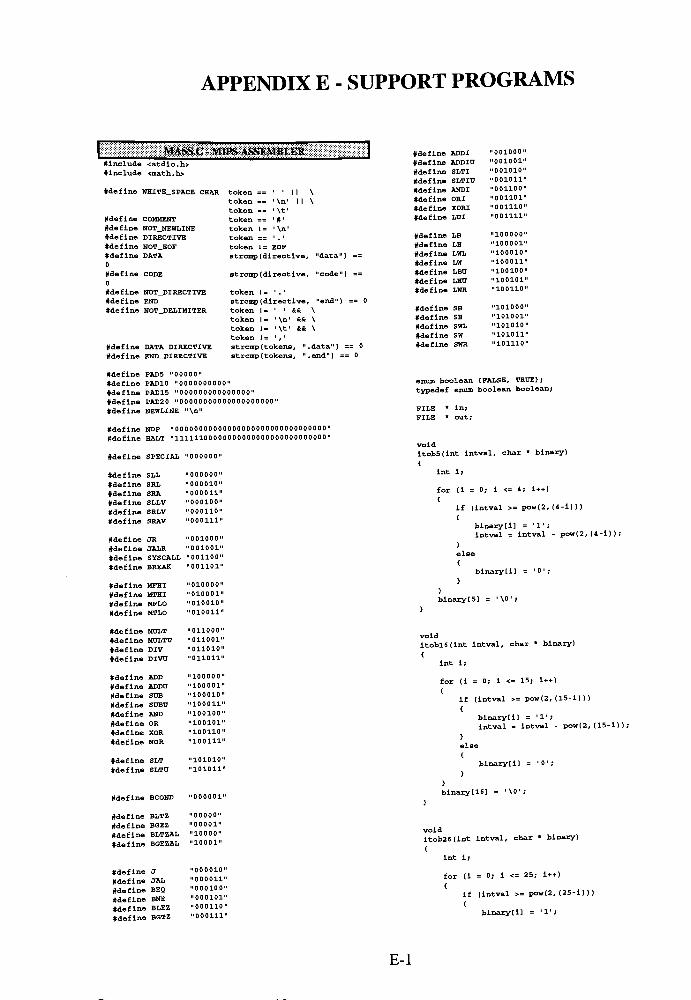
APPENDIX E - SUPPORT PROGRAMS
NUSS.C - MIPS ASVKMRI.ER
#include <stdio.h>
tinclude <math.h>
#define WHITE_SPACE_CHAR
#deflne COMMENT
#define NOT_NEWLINE
#define DIRECTIVE
#define NOT_EOF
tdefine DATA
0
Kdefine CODE
0
#define NOT_DIRECTIVE
#define END
#define NOT_DELIMITER
#define DATA_DIRECTIVE
#define END_DIRECTIVE
token ==' ' I I \
token ==' \n' II \
token ==' \t '
token =='#'
token 1 =' \n '
token =='
.
'
token 1 = EOF
strcmp (directive, "data") ==
strcmp (directive, "code") =-
token 1 = '.
'
strcmp (directive, "end") == 0
token !=''&& \
token 1= '\n' S=& \
token 1 = ' \t ' && \
token I = ,'
strcmp (tokens, ".data") == 0
strcmp(tokens, ".end") == 0
(define ADDI"001000"
(define ADDIU"001001"
(define SLTI"001010"
(define SLTIU"001011"
(define ANDI"001100"
(define OBI"001101"
(define XORI"001110"
(define LUI"001111"
(define LB"100000"
(define LH"100001"
(define LWL"100010'
(define LW"100011'
(define LBU"100100'
(define LHD"100101'
(define LWR"100110'
(define SB"101000'
(define SH"101001'
(define SWL"1010101
(define SW"1010111
(define SWH"1011101
(define PAD5"00000"
(define PAD10"0000000000"
(define PAD15"000000000000000"
(define PAD20"00000000000000000000"
(define NEWLINE"\n"
(define NOP"00000000000000000000000000000000"
(define HALT"11111100000000000000000000000000"
(define SPECIAL"000000"
(define SLL
(define SRL
(define SRA
(define SLLV
(define SRLV
(define SRAV
"000000"
"000010"
"000011"
"000100"
"000110"
"000111"
(define JR"001000"
(define JALR"001001"
(define SYSCALL"001100"
(define BREAK"001101"
(define MFHI"010000"
(define HTHI"010001"
(define HFLO"010010"
(define MTLO"010011"
(define MOLT"011000"
(define MULTU"011001"
(define DIV"011010"
(define DIVU"011011"
(define ADD"100000"
(define ADDD"100001"
(define SOB"100010"
(define SUBU"100011"
(define AND"100100"
(define OR"100101"
(define XOR"100110"
(define NOR"100111"
(define SLT"101010"
(define SLTn"101011"
(define BCOND"000001"
(define BLTZ"00000"
(define BGEZ"00001"
(define BLTZAL"10000"
(define BOEZAL"10001"
(define J"000010'
(define JAL"000011'
(define BEQ"0001001
(define BNE"0001011
(define BLEZ"000110'
(define BOTZ "000111
enum boolean {FALSE, TRUE) ;
typedef enum boolean boolean;
PILE " ln;
FILE*out;
void
itob5(lnt lntval, char* binary)
{
int i;
for (1 = 0; 1 <= 4; 14-+)
{
if (intval >= pow(2, (4-1)))
{
binary [i] = '1';
intval = intval - pow(2, (4-1) ) ;
)
else
<
binary [i] = '0';
)
)
binary [51 = '\0';
void
itobl6(int intval, char* binary)
{
int i;
for (i = 0; i <= 15; 1+ 4-)
(
if (intval >= pow(2, (15-1)))
C
binary [i] = '1';
Intval = intval - pow(2, (15-1) ) j
)
else
(
binary [i] = '0';
)
}
binary[16] = '\0';
void
itob26(int intval, char* binary)
{
int i;
for (1 = 0; 1 <= 25; 14-+)
(
if (Intval >= pow(2, (25-1)))
{
binaryll] = '1';
E-l
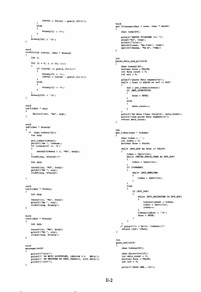
)
else
{
>
intval = intval -
pow{2, (25-i) ) ;
binary [i] = c ;
binary[26] = '\0'
ltob32(int intval, char *binary)
int i;
for (1 = 0; i <= 31-i++)
{
if (intval >= pow(2, (31-1)))
(
blnary[i] = '1';
intval = Intval -
pow(2, (31-i) ) ;)
else
(
blnary[i] = '0';
)
)
binary[32] = '\0';
void
outf(char*arg)
void
get_filename (char *name, char
*mname)
{
char temp [20] ;
printf ("ENTER FILENAME <== ");
scanf("%b"
, temp) ;
printf ("\n\n");
sprintf (name, "%s.test"y temp) ;
sprintf (mname, "%s.m", temp);
int
parBe_data_seg_pl (void)
{
char tokens [40];
boolean done = FALSE;
int data_count = 0;
int eof = 0;
printf ("parse data segment\n"
) ;
while ( done == FALSE && eof 1= EOF)
{
eof = get_token (tokens) ;
if (END_DIRECTIVE)
done = TRUE;
}
else
{
data_count++
fprintf(out, "Sss", arg); printf ("%d data lines found\n", data_count);
printf ("end parse data segment\n"
) ;
return data_count;
void
ln5(char *binary)
{/*
char tokens [10];
int arg;
get_token(tokens) ;
printf ( "%s"
, tokens) ;
if (tokens [0] == $')
sscanf (tokens + 1,"%d"
{
}
itob5(arg, binary) ;*/
int arg;
fscanf (in, "%d", fiarg) ;
printf ("%d ", arg);
itob5 (arg, binary) ;
void
inl6(char * binary)
{
int arg;
fscanf(in, "%x", &arg);
printf ("%x ", arg);
itobl6 (arg, binary) ;
int
get_token(char*tokens)
{
char token =' '
;
int index =0;
boolean done = FALSE;
While (NOT_EOF && done == FALSE)
(
token = fgetc(in);
While (WHITE_SPACE_CHAR && NOT_EOF)
{
token = fgetc(in);
>
if (COMMENT)
(
while (NOT.NEWLINE)
{
token := fgetc(in)
)
)
else
(
if (NOT_EOF)
(
While (NOT_DELIMITER && NOT_EOF)
{
tokens [index] = token;
token = fgetc(in);
lndex++;
void
ln26(char * binary)
tokens [index]
done = TRUE;
1\0';
int arg;
fscanf (in, "%x", &arg) ;
printf ("%x ", arg) ;
itob26 (arg, binary) ;
/*printf ("t = %s\n", tokens);*/
return ( int ) token;
void
message (void)
{
printf ("\n\n") ;printf(" ## MIPS ASSEMBLER, VERSION 1.0 ##\n");
printf(" ## WRITTEN BY PAUL FANELLI, 1993 ##\n");
printf ("\n\n");
int
pass_one (void)
{
char tokens[40];
char directive[10] ;
int data_count =0;
boolean done = FALSE;
int eof = 0;
printf("PASS 0NE...\n");
E-2

FALSE ts eof I:while (done
<
eof =
get_token(tokens);if (DATA_DIRECTIVE)
printf ("found data segment\n");
data_oount = parse_data_seg_pl ( )printf ( "%d\n" , data_count) ;done = TRUE;
)
)
if (data_count == 0)(
printf ("no data segment foundXn");
return data_count;
/*srl rd, rt, shamt */
else if (strcmp(op, "srl")
{
outf (SPECIAL) ;
outf (PAD5);
in5(rd);
in5(rt);
in5 (shamt) ;
outf (rt);
/
outf (rd);
outf (shamt) ;
outf (SRL);
outf (NEWLINE);
== 0)
/*opcode special
/*pad /
/* get fields
/*write fields
/* function */
void
parse_data_seg_p2 ( )
(
char tokens [40];
boolean done = FALSE;int dat;
char blnary[33] ;int eof = 0;
printf ("parse data segmentNn");
while (done == FALSE S.S eof 1 =
{
eof = get_token ( tokens ) ;if (END_DIRECTIVE)
done = TRUE;
)
else
{
binary) ;
sscanf (tokens, "%i", &dat);
itob32(dat, binary);outf (binary) ;
outf (NEWLINE) ;
printf("%x, %&, %a\n", tokens, dat,
printf("end parse data segmentNn") ;
void
code (void)
(
char op [ 7 ] ;
char rs[6];
char rt[6];
char rd[6J;
char shamt [ 6 ] ;
char base [6];
char offset[17];
char immed[17];
char target [27];
char token;
while (get_token(op) 1= EOF)
printf ("%s op) ;
"nop") == 0)
to file */
/*nop */
if (strcmp(op
{
outf (NOP);
outf (NEWLINE)
}
/*sll rd, rt, shamt /
else if (strcmp(op, "sll")
{
outf (SPECIAL);
outf (PAD5);
in5(rd);
in5(rt);
inS (shamt) ;
outf (rt);
outf (rd);
outf (shamt) ;
outf (SLL);
outf (NEWLINE);
/* opcode special
pad */
get fields
/*write fields
/* function */
to file */
/*sra rd, rt, shamt */
else if (strcmp(op, "sra") :
<
outf (SPECIAL) ,
outf (PAD5);
ln5(rd);
in5(rt);
in5 (shamt) ;
outf (rt) ;
*/
outf (rd);
outf (shamt) ;
outf (SRA) ;
outf (NEWLINE );
)
/*sllv rd, rt, rs */
else if (strcmp (op, "sllv")
<
outf (SPECIAL);
in5(rd);
in5(rt);
in5(rs);
outf (rs) ;
outf (rt);
outf (rd);
outf (PAD5);
outf(SLLVl.-
outf (NEWLINE);
to file */
/*srlv rd, rt, rs
else if (strcmp(op,
{
outf (SPECIAL);
in5(rd);
in5(rt);
in5(rs);
outf (rs) ;
*/
outf (rt);
outf (rd) ;
outf (PAD5);
outf (SRLV) ;
outf (NEWLINE) ;
/*srav rd, rt, rs */
else if (strcmp(op,"srav"
outf (SPECIAL);
ln5(rd);
in5(rt);
in5(rs);
outf (rs) ;
outf (rt);
outf (rd);
outf (PAD5);
outf (SRAV) ;
outf (NEWLINE);
== 0)
/*opcode special
/*pad */
/ get fields
/*write fields
/* function */
== 0)
/* opcode special
/get fields
/write fields
/*pad */
/* function */
== 0)
/*opcode special
/*get fields
/*write fields
/*pad /
/* function */
== 0)
/*opcode special
/*get fields
/*write fields
/pad */
/* function */
/ jr rs /
else if (strcmp(op, "jr")
E-3
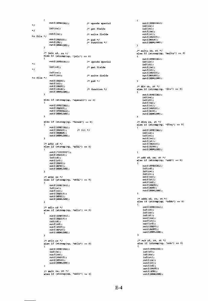
*/
/
to file */
/
*/
to file
outf (SPECIAL) ;
ln5(rs);
outf (ra);
outf (PAD15);outf (JR);
outf (NEWLINE) ;
/* jalr rd, rs ?/
else if (strcmp(op,<
outf (SPECIAL);
in5(rd);
in5(rs);outf (rs) ;
outf (PAD5);
outf (rd);
outf (PAD5);
outf (JALR),-
outf (NEWLINE) ;
/*opcode special
/ get fields
/*write fields
/* pad /
/* function /
"jalr") == 0)
/*opcode special
/*get fields
/write fields
/pad */
/* function */
else if (strcmp(op, "sysaall") == 0)
{
outf (SPECIAL) ;
outf (PAD20);
outf (SYSCALL) ;
outf (NEWLINE) ;
outf (SPECIAL) ;
in5(rs);
in5(rt);
outf (rs) ;
outf (rt);
outf (PAD10);
outf (MOLT);
outf (NEWLINE) ;
/* multu rs, rt */
else if (strcmp(op,
(
outf (SPECIAL);
in5(rs) ;
in5(rt);
outf (rs) ;
outf (rt);
outf (PAD10);
outf (MUI");
outf (NEWLINE);
/ div rs, rt "/
else if (strcmp(op,
{
outf (SPECIAL);
in5(rs);
in5(rt);
outf (rs) ;
outf (rt);
outf (PAD10);
outf (DIV);
outf (NEWLINE) ;
"multu") == 0)
"div") == 0)
else if (strcmp(op,
(
outf (SPECIAL) ,-
outf (PAD20);
outf (BREAK) ;
outf (NEWLINE);
/mfhi rd */
else if (strcmp (op,
<
outf ("000000"),-
outf (PAD10);
in5(rd);
outf (rd);
outf (PAD5) ;
outf (MFHI);
outf (NEWLINE) ;
)
/*mthi rs /
else if (strcmp (op,
(
outf (SPECIAL) ,-
in5(rs) ;
outf (rs) ;
outf (PAD15);
outf (MTHI),
outf (NEWLINE);
)
/ mflo rd /
else if (strcmp (op,
<
outf (SPECIAL) ;
outf (PAD10);
in5 (rd) ;
outf (rd);
outf (PADS ),-
outf (MFLO) ;
outf (NEWLINE);
"break") == 0)
/* ??? */
"mthi") =- 0)
/ divu rs, rt' I
else if (strcmp(op, "divu") == 0)
{
outf (SPECIAL);
in5(rs);
in5(rt);
out f ( rs ) ;
outf (rt);
outf (PAD10);
outf (DIVU) ;
outf (NEWLINE);
)
/*add rd, rs, rt */
else if (strcmp(op, "add") == 0)
{
outf (SPECIAL ) ;
in5(rd);
in5(rs);
in5(rt);
outf (rs) ;
outf (rt);
outf (rd);
outf (PAD5);
outf (ADD),
outf (NEWLINE);
)
/*addu rd, rs, rt */
else if (strcmp(op, "addu") == 0)
<
outf (SPECIAL);
in5(rd);
in5(rs);
in5(rt);
outf(rs);
outf (rt);
outf (rd) ;
outf (PAD5);
outf (ADDU) ;
outf (NEWLINE);
/ mtlo rs */
else if (strcmp(op,
{
outf (SPECIAL) ;
in5(rs);
outf (rs) ;
outf (PAD15);
outf (MTLO);
outf (NEWLINE);
/* mult rs, rt */
else if (strcmp(op,
"mtlo") == 0)
"mult") == 0)
/*sub rd, rs, rt */
else If (strcmp(op, "sub") == 0)
{
outf (SPECIAL);
in5(rd);
in5(rs);
in5(rt);
outf (rs) ;
outf (rt);
outf (rd) ;
outf (PAD5);
outf (SUB);
outf (NEWLINE);
E-4
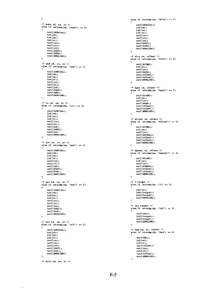
/*subu rd, rs, rt */
else If (strcmp(op, "subu") == 0)(
outf (SPECIAL);ln5(rd);in5 ( rs ) ;
in5(rt);outf (rs) ;
outf (rt);
outf (rd);
outf (PAD5);outf (SUBU);outf (NEWLINE);
/*and rd, rs, rt */
else if (strcmp(op, "and"){
outf (SPECIAL) ;
in5(rd);
in5(rs);
in5(rt);
outf (rs) ;
outf (rt) ;
outf (rd);
outf (PAD5);
outf (AND);
outf (NEWLINE) ;
/*or rd, rs, rt */
else if (strcmp(op, "or") ==
{
outf (SPECIAL);
ln5(rd);
in5 (rs) ;
in5(rt);
outf (rs) ;
outf (rt);
outf (rd);
outf (PAD5);
outf (OR) ;
outf (NEWLINE) ,-
/*xor rd, rs, rt */
else if (strcmp(op, "xor") == 0)
else if (strcmp(op, "situ") == 0)
{
outf (SPECIAL) ;
in5(rd);
in5(rs);
in5(rt);
outf (rs) ;
outf (rt);
outf (rd);
outf (PAD5);
outf (SLTU);
outf (NEWLINE) ;
"bltz") == 0)
"bgez") == 0)
bltz rs, offset
se if (strcmp(op,
outf (BCOND );
in5(rs);
out f ( rs ) ;
outf (BLTZ) ;
inl6 (offset) ;
outf (offset) ;
outf (NEWLINE) ;
/* bgez rs, offset
else if (Btrcmp(op,
{
outf (BCOND);
ln5(rs);
outf (rs) ;
outf (BGEZ);
lnl6 (offset) ;
outf (offset) ;
outf (NEWLINE) ;
/* bltzal rs, offset */
else if (strcmp(op, "bltzal") == 0)
{
outf (BCOND);
ln5(rs) ;
out f ( rs ) ;
outf (BLTZAL ) ;
inl6 (offset) ;
outf (offset);
outf (NEWLINE) ;
outf (SPECIAL);
in5(rd);
in5(rs);
in5(rt);
outf (rs) ;
outf (rt);
outf (rd) ;
outf (PAD5);
outf (XOR) ;
outf (NEWLINE) ;
bgezal rs, offset */
se if (strcmp(op, "bgezal") == 0)
outf (BCOND) ;
in5(rs);
outf (rs) ;
outf (B3EZAL) ;
inl6(offset);
outf (offset);
outf (NEWLINE);
/*nor rd, rs, rt */
else if (strcmp(op, "nor") == 0)
/j target */
else if (strcmp (op. "j") == 0)
outf (SPECIAL);
in5(rd);
in5(rs);
in5(rt);
out f ( rs ) ;
outf (rt);
outf (rd);
outf (PAD5);
outf (NOR) ;
outf (NEWLINE) ;
/*sit rd, rs, rt /
else if (strcmp(op, "sit")
(
outf (SPECIAL);
in5 (rd) ;
in5(rs);
in5(rt);
outf (rs) ;
outf (rt);
outf (rd);
outf (PADS);
OUtf(SLT);
outf (NEWLINE);
== 0)
outf (J);
ln26 (target) ;
out f ( target ) ;
outf (NEWLINE);
/* jal target */
else if (strcmp(op,"jal"
{
outf (JAL);
in26 (target) ;
outf (target) ;
outf (NEWLINE);
/* beq rs, rt, offset */
else if (strcmp(op, "beq") == 0)
(
outf (BEQ) i
in5(rs);
ln5(rt);
lnl6(offset);
outf (rs) ;
outf (rt);
outf (offset);
outf (NEWLINE) ;
/* situ rd, rs, rt */
E-5

/* bne rs, rt, offset */else if (strcmp(op, "bne") == 0){
outf (BNE);in5(rs),
in5(rt),
inl6 (offset) ;outf (rs);
outf (rt);
outf (offset);outf (NEWLINE);
/* blez rs, offset */else If (strompfop, "blez")(
outf (BLEZ);
in5(rs);inl6 (offset);out f ( rs ) ;
outf (PAD5);outf (offset) ;outf (NEWLINE) ;
/* bgtz rs, offset */
else if (stremp(op, "bgtz") == 0)
{
outf (BGTZ) ;
in5(rs);lnl6 (offset) ;outf (rs) ;
outf (PADSl.-
outf (offset) ;
outf (NEWLINE) ;
/*addi rt, rs, immediate */
else if (strcmp (op, "addi") == 0)
{
outf (ADDI) ;
in5(rt);
in5(rs);
inl6 (immed) ;
out f ( rs ) ;
outf (rt);
outf (immed);
outf (NEWLINE) ;
)
in5(rt);
in5(rs);
inl6 (immed) ;
outf (rs) ;
outf (rt);
outf (immed) ;
outf (NEWLINE);
/*ori rt, rs, immediate */
else if (strcmp(op, "ori") == 0)
(
outf (ORI);
in5(rt);
in5(rs);
lnl6 (immed) ;
outf (rs) ;
outf (rt);
outf (immed) ;
outf (NEWLINE) I
/* xori rt, rs. Immediate */
else If (strcmp(op, "xori") == 0)
<
outf (XORI);
in5(rt);
in5(rs);
inl6 (immed) ;
outf (rs) ;
outf (rt);
outf (immed) ;
outf (NEWLINE);
/* lui rt, immediate */
else if (strcmp(op,"lui"
(
outf (LUI) ;
in5(rt);
lnl6 (immed) ;
outf (PAD5);
outf (rt);
outf (immed) ;
outf (NEWLINE);
/* lb rt, offset(base) */
else if (strcmp(op, "lb") == 0)
/*addiu rt, rs, immediate */
else if (strcmp(op, "addiu") == 0)
(
outf (ADDIU) ;
in5(rt);
in5(rs);
inl6 (immed) ;
out f ( rs ) ;
outf (rt);
outf (immed) ;
outf (NEWLINE);
)
outf (LB) ;
inS(rt);
lnl6 (offset);
in5 (base) ;
outf (base) ;
outf (rt);
outf (offset) ;
outf (NEWLINE);
/* lh rt, offset (base) */
else if (strcmp(op, "lh")
/*slti rt, rs, immediate */
else if (strcmp(op, "slti") == 0)
(
outf (SLTI);
in5(rt);
in5(rs);
lnl6 (immed) ;
out f ( rs ) ;
outf (rt);
outf (immed) ;
outf (NEWLINE)
/*sltiu rt, rs, immediate */
else if (strcmp(op, "sltiu") == 0)
outf (SLTIU) ,
in5(rt);
in5(rs);
inl6 (immed) ;
outf (rs) ;
outf (rt);
outf (immed) ;
outf (NEWLINE);
/* andi rt, rs, immediate */
else if (strcmp(op, "andi") == 0)
outf (LH) ;
ln5(rt);
inl6 (offset) ;
in5 (base) ;
outf (base) ;
outf (rt);
outf (offset) ;
outf (NEWLINE) ;
>
/* lwl rt, offset (base) /
else if (strcmp(op, "lwl") == 0)
{
outf (LWL) ;
in5(rt);
inl6 (offset) ;
in5(base) ;
outf (base) ;
outf (rt);
outf (offset) ;
outf (NEWLINE);
)
outf (ANDI ) ;
/* lw rt, offset(base) */
else if (strcmp (op, "lw")
{
outf (LW);
in5(rt);
inl6 (offset) ;
in5(base) ;
:= 0)
E-6
outf (base) ;outf (rt);
outf (offset)
outf (NEWLINE)
/* Ibu rt, offset (base) */else if (strcmp(op, "lbu") == 0){
outf (LBUJy-
inSfrtK-
inietoffaet);in5 (base) ;
outf (base);outf (rt);
outf (offset) ;OUtf (NEWLINE);
/* lhu rt, offset(base) */
else if (strcmp (op, "lhu")
{
outf (LHU) ;
in5(rt);inl6 (offset) ,
ln5(base) ;outf (base) ;
outf (rtjy-
outf (offset) ;
outf (NEWLINE);
/* lwr rt, offset (base) */
else if (strcmp(op, "lwr") == 0)
outf (offset) ;
outf (NEWLINE);
/*swr rt, offset (base) */
else if (strcmp (op, "swr") ==
{
OUtf (SWR) ;
in5(rt);
lnl6 (offset);
in5(base) ;
outf (base) ;
outf (rt);
outf (offset-
outf (NEWLINE);
/* halt instruction */
else if (strcmp(op, "halt") == 0)
outf (HALT) ;
outf (NEWLINE)
else
printf ("\nERROR: UNKNOWN COMMAND");
printf ("\n") ;
) /* END WHILE FSCANF 1=
} /* END CODE FUNCTION */
outf (LWR) ;
in5(rt);inl6 (offset) ;
ln5 (base) ;
outf (base) ;
outf (rt);
outf (offset) ;
OUtf (NEWLINE) ;
void
pass_two ( int data_count )
{
char binary [33];
char tokens [40];
boolean done = FALSE;
int eof = 0;
/*sb rt, offset (base) */
else if (strcmp(op, "sb") ==
(
outf (SB) ;
in5(rt);
inl6 (offset);
in5 (base) ;
outf (base)
outf (rt);
outf (offset);
outf (NEWLINE);
/*sh rt, offset (base) */
else if (strcmp(op, "sh") ==
{
outf (SH);
in5(rt);
inl6 (offset) ;
in5(base) ;
outf (base) ;
outf (rt);
outf (offset) ;
outf (NEWLINE) ;
printf ("PASS TWO...\n");
if (data_count 1= 0)
{/* ADD JUMP INSTRUCTION TO JUMP OVER DATA
MENT */
outf (J) ;
itob26 (data_count + 2, binary);
outf (binary) ;
outf (NEWLINE);/* ADD NOP TO FILL DELAY SLOT */
outf (NOP) ;
outf (NEWLINE) ;/* GET DATA SEGMENT */
while (done == FALSE && eof 1= EOF)
{
eof = get_token(tokens) ;
if (DATA_DIRECTIVE)
parse_data_seg_p2 ( )
done = TRUE;
code ( ) ;
/*swl rt, offset (base) */
else if (strcmp(op, "swl") == 0)
{
outf (SWL) ;
in5(rt);
inl6 (offset);
in5 (base) ;
outf (base) ;
outf (rt);
outf (offset) jr
outf (NEWLINE) ;
}
/*sw rt, offset (base) */
else if (strcmp(op, "sw") == 0)
(
outf (SW);
in5(rt);
inl6 (offset);
ln5(base) ;
outf (base) ;
outf (rt);
int
main (void)
{
char name [20] ;
char mname [20];
int data_count;
message ( ) ;
get_filename (name, mname) ;
in = fopen(name, "r");
data_count = pass_one ( ) ;
fclose(in) ;
in = fopen(name, "r");out = fopen (mname ,
"w") ;
pass_two(data_count) ;
fclose(in) ;
fclose(out) ;
printf ("CONVERSION DONE\n") ;
E-7

return 0;
# include <stdio.h>
# include <math.h>
#define WHITE_SPACE_CHAR token ==' ' | | \
token == '\n' I I \
token =='\t '
#define COMMENT token ==#'
#define NOT_EOF token 1= EOF
#define NOT_DELIMITER token 1= '#'&& token 1= ' \n'
#define NOT_NEWLINE token 1= ' \n'
enum boolean {FALSE, TRUE);typedef enum boolean boolean;
FILE
FILE
in = NULL;
out = NULL;
char assem[1000] [80] ;int expect[1000] [10];
char modify[1000] [10] ;
int num_of_inst =0;
Int index =0;
boolean p_mode;
void
itob32(int integer, char * bits)
nt 1;
nt temp;
f (integer < 0)
temp = -(integer + 1) ;
ilse
temp = integer;
for (i = 0; i <= 31; i++)
if ((temp % 2) == 1)
{
bits[31-i] = '1';
)
else
{
bits [31-1] = '0';
)
temp = temp / 2;
)
if (integer < 0)
{
for (1 = 0; 1 <= 31; 1++)
{
if (bitsti] == '0')
{
bits[i] = '1';
)
else
{
bitsti] = '0';
)
)
)
bits [32 = '\0';
int
power2 (int x)
{
if (x == 0) return 1;
else return 2 *power2(x-l);
}
int
btoi32(char* bits)
f
int i;
int result =0;
boolean negative;
negative = (bitstO] == '1');
for (i = 0; i <= 31; i++)
{
if (negative)
{
if (bitsUJ == '0')
{
result = result - power2 (31-1) ;
}
}
else
{
if (blts[i] == '1')
(
result = result + power2 (31-i ) ;
}
if (negative)
return --result;
lse
return result ;
void
message (void)
{
printf ("\n\n");
printf("
##################################################\n"
) ;
printf(" ## MIPS EXPECTED RESULTS ASSEMBLER,
VERSION 1.1 ##\n");
printf(" ## WRITTEN BY PAUL FANELLI, 1993
##\n");
printf("
#############tt####################################\n"
) ;
printf ("\n\n") ;
}
void
help_message(void)
{
printf ("===> USE THE (?) KEY FOR HELP AT THE MENU
PROMPTS\n") ;
printf ("===> USE THE (RETURN) KEY RETURN FROM
MENU\n") ;
printf ("\n\n");
>
void
command_help (void)
(n)ew
(o)ld
printf("****************'
*********************** \nn j
printf('
file\n");
printf('
file\n");
printf (" (a) ssemble
menu\n") ;
printf(" (c)lear
(set to zero)\n");
printf("
(v) lew
expected values\n");
printf(" (s)ave
expected file\n" ) ;
printf(" (q)uit
printf("
(?)help
listing\n");
printf("*********************
***************** \_ ) ;
printf ("\n");
)
void
assemble_help(void)
{
printf("*****************
********************** *\n" ) ;
printf(" STATE:
\n") ;
printf(" (p)c
register in hex\n");
******* COMMAND MENU
assemble new expected
assemble old expected
return to assemble
clear all array values
view assembly code and
save expected values to
quit out ofprogram\n"
) ;
print out this help
********************
ASSEMBLE MENU
enter in value for pc
E-8

printf!"
r(l)
register\n") ;printf!"
r(2)
register\n");printf("
r(3)
register\n");printff"
r(4)
register\n");printf("
(r)31
(link) register\n");printf (" (h)i
register\n");
printf (" (l)0
register\n");
printf (" (e)pc
registerVn");printf("
(clausecause reglsterXn");
printf("
CONTROL :\n"),printf (" (b)ackward
(propagation off ) \n" ) ;printf("
(f)orward
instruction (propagation off) \n'printf("
(i)nstruction -
printf (" (n)extinstruction\n"
) ;printff"
(s)tate
enter in value for rl
enter in value for r2
enter in value for r3
enter in value for r4
enter in value for r31
enter in value for hi
enter in value for lo
enter in value for epc
enter in value for
printf ("
contents\n") ;
printf ("
menu\n") ;
printf("
listing\n");
(v)iew
(return)
(?)help
go back one instruction
go forward one
);
goto instruction\n") ;go on to next
view present state \n");
view present
return from assemble
print out this help
printf ("*5d*c *5d%c ", expect [i] [4] ,
modlfyli] [4], expect [i] [5] , modifyli] [5] ) ;
printf ( "*5d%c 9s5d%c ", expect [i] [6] ,
modifyli] [6] , expect [i] [7] , modifyli] [7] ) ;
printf ("%8x%c %8x%c", expect [i] [8] ,
modifyli] [8], expect [1] [9] , modifytl] [9] ) ;
printf ("\n") ;
)
printf ("\n");
void
view_state(int modify_flag)
static char pc ='
static char rl ='
static char r2 ='
static char r3 = '
static char r4 ='
statia ahar r5 ='
static char hi ='
static char lo ='
static char epc =
static ahar cause
int i;
i = index;
if (modi fy_flag =- 0)
else if (modi fy_flag
printf ("************************
*****************^nn i .
printf ("\n") ;
)
else if (modify_flag == 2)
r2
int
command_menu (void)
{
int ch;
printf ("COMMAND(n,o,a,c,v,s,q, ?) <== ")ch = getehar();
if (ch == '\n')
[
ch = getchar ( ) ;
else if (modlfy_flag == 3)
{
r3 =' * '
;
)
else if (modify_flag == 4)
)
else if (modify_flag == 5)
printf <"\n")
return ch; else if (modify_flag == 6)
int
assemble_menu (void)
(
int ch;
printf ( "ASSEMBLE ( STATE [p, 1, 2 , 3, 4 , r, h, 1, e, c]
CONTR0L[b,f,i,n,s,v,return,?] ) <== ");
ch = getchar ( ) ;
if (ch =='
\n')
(
ch = getchar ( ) ;
}
printf ("\n");
return ch;
)
else if (modify_flag
<
else if (modify_flag ==
else if (modi fy_flag == 9)
cause =
else if (modi fy_flag 10)
void
view (void)
{
int 1;
printf ("**************************************
ASSEMBLY CODE and EXPECTED VALUES .************");
printf ("**************\n\n");prlntf!"
INST PC
Rl R2 R3 R4 R31 HI ");printf ("LO EPC CAUSEXn");printf
("
");printf
("
\n");for (i = 0; i < num_of_inst; i++)
{
printf ("( %3d => %-20s ", i+1, assem[i]);printf ("%8x%c %5d9&c ", expect [i] [0] ,
modifyli] [0], erpect[i] [1], modify [i] [1] ) ,printf ("%5d%c %5d%c ", expect [i] [2] ,
modifyli] [2], expect[l] [3], modifyli] [3] ) ;
pc =
rl =
r2 =
r3 =
r4 =
r5 =
hi =
lo =
epc =
cause =' '
;
)
else
{
)printf(" INST
Rl%c R2%c ", pc, rl, r2);
printf ("R39SC R4%c R31%c HI%C
r5, hi);
printf ("L09sc EPC%o CAUSE%c \n"
cause ) ;
printf("
PC%c
", r3, r4,
lo, epc.
");printfl"
-\n"),
E-9

printf ("( %3d => %-20s ", i+l, assemli]);printf ("%8x 9s5d %5d %5d ", expect [1] [0] ,
erpectli] [1], expect [1] [2] , expect [1] [3] ) ;printf ("%5d *5d %5d %5d ", expect [i] [41 ,
expect[i] [5], expect [i] [6] , expect [i] [7] ) ;printf ("%8x *8x", expect [i] [8], expect [11 [9] ) ;printf ("\n\n);
int
modify[0] [i] =
load_assem_flie (void)(
char token = ';
char tokens [80] ;int i = 0;
int j = 0;
boolean done = FALSE;
while (NOT_EOF)(
while (NOT_EOF && done == FALSE)
{
token = fgetc(in);while (WHITE_SPACE_CHAR && NOT_EOF)
token = fgeto(in);if (COMMENT)
(
>
else
(
while (NOT_NEWLINE)token = fgete(in);
if (NOT_EOF)
(
while (NOT_NEWLINE -& NOT_EOF)
<
tokens [ j ] = token;
token = fgetc(in);
if (COMMENT)
while (NOT_NEWLINE)
token = fgetc(in);
j++;
tokens[j] = '\0';
printf ("inst = %s\n", tokens
strcpy(assem[i] , tokens) ;
done = TRUE;
j= 0;
i++;
)
)
)
done =
)
printf ("\n
FALSE;
);
return i;
void
load_expected_flie (void)
{
int j;
Int i;
char binary [33];
for (j = 0;
{
for (i
{
fscanf (in,"%a"
, binary);
expect[J][l] = btoi32 (binary) ;
j < num_of_inst; j++)
= 0; 1 <= 9; i++)
)
else
{
)
modlfylOHi] =
)
else
{
if (expeot[j] [i] == expect[J-l] [1] )
(
modifylj] [1]
)
else
(
modifylj] [i]
)
initialize (void)
{
int 1;
Int j;
for (j = 0; j <= 999 J + 4-)
{
for (i = 0; 1 <= 9; i++
(
expect[j] [i] = 0;
modify[j] [i] =' '
;
)
)
boolean
get_filename(char*name, char
*ename)
{
char temp [20] ;
int ch;
printf ("ENTER FILENAME (q to quit) <==") ;
scanf ("%s", temp) ;
printf ("\n\n") ;
if (stremp(temp, "q") == 0)
return TRUE;
else
{
printf ("IS THE TEST FILE FOR BRANCH/JUMP
(y, [n]) <== ");
ch = getchar ();
if (ch ==' \n'
)
ch = getchar () ;
printf ("\n") ;
if (ch == 'y')
sprintf (name, "%s.f", temp);
e
sprintf (name, "%s.test", temp);
sprintf (ename, "%s.e", temp);
return FALSE;
>
void
change_pc (void)
void
bulld_modify_array(void)
{
int j;
int i;
for (j = 0; j < num_of_inst; j++)
{
for (i = 0; 1 <= 9; i++)
{
if U == o)
(
If (expect[0] [1] == 0)
{
char input[33];
int temp;
printf ("OLD PC VALUE (HEX) = %x\n",
expect [index] [0]);
printf ("NEW PC VALUE (HEX) - use (i) to increment
by 4 <==") ;
scanf ("%s", input) ;
printf ("\n") ;
if (input[0] == 'i')
{
expect [index] [0] = expect [index] [0] + 4;
}
else
E-10

)
sscanf (input, "%x", ..temp)
,-
expect [index] [0] =temp;
view_state(0) ;
int
get_input (void)(
char input [33] ;Int temp;
scanf ("9_S", input);printf ("\n") ;if [input[0] == h'){
sscanf (input+1, "%x, _temp)
else
{
sscanf (input, "%d", &temp) ,-
return temp;
void
change_rl (void)
{
printf ("OLD Rl VALUE = %d\n", expect [index] [1] ) ;printf ("NEW Rl VALUE -
use (h) for hex <== ");
expect[index] [1] = get_input();
view_state (1) ;
expect [index] [6] = get_input();
view_state ( 6 ) ;
void
change_lo (void)
int input;
printf ("OLD LO VALUE = %d\n", expect [index] [7] ) ;
printf ("NEW LO VALUE - use (h) for hex <== ");
expect [index] [7] = get_input();
vlew_state (7) ;
void
change_epc (void)
(
int input;
printf ("OLD EPC VALUE (HEX) =
expect [index] [8] ) ;
printf ("NEW EPC VALUE (HEX) <=
scanf ("%x"
, -input) ;
printf ("\n") ;
expect [index] [8] = input;
view_state ( 8 ) ;
)
void
change_cause (void)
int input;
void
change_r2 (void)
int input;
printf ("OLD R2 VALUE = %d\n", expect [index] [2] ) ;printf ("NEW R2 VALUE - use (h) for hex <== ");expect [index] [2] = get_input();
view_state ( 2 ) ;
void
change_r3 (void)
{
int input;
printf ("OLD R3 VALUE =%d\n"
, expect [index] [3] )
printf ("NEW R3 VALUE - use (h) for hex <== ");
expect [index] [3] = get_input();
vlew_state (3) ;
printf ("OLD CAUSE VALUE (HEX) = %x\n",
expect [index] [9]);
printf ("NEW CAUSE VALUE (HEX) <== ");
scanf ("%x", -input) ;
printf ("\n") ;
expect [index] [9] = input;
view_state ( 9 ) ;
boolean
query_new_state (void)
(
int selector;
boolean done = FALSE;
boolean next = FALSE;
int 1;
while (done == FALSE && next == FALSE)
{
selector = assemble_menu( ) ;
switch (selector)
void
change_r4 (void)
int input;
printf("OLD R4 VALUE- %d\n"
, expect [index] [4] ) ;
printf ("NEW R4 VALUE - use (h) for hex <==") ;
expect [index] [4] = get_input();
view_state{4) ;
void
change_r3 1 (void)
{
int input;
printf ("OLD R31 VALUE = %d\n", expect [index] [5] ) ;printf ("NEW R31 VALUE - use (h) for hex <== ");
expect [index] [5] = get_input();
view_state(5) ;
void
change_hi (void)
{
int input;
printf ("OLD HI VALUE = %d\n", expect [Index] [ 6] ) ;printf ("NEW HI VALUE - use (h) for hex <== ");
case' p'
:
change_pc ( ) ;
break;case
' 1 ':
change_rl ( ) ;
break;
case' 2 '
:
change_r2 ( ) ;
break;
case' 3 '
:
change_r3 ( ) ;
break;
case' 4 '
:
change_r4 ( ) ;
break;
case'r
':
change_r31{) ;
break;
case'h'
:
change_hi ( ) ;
break;
case' l1
:
change_lo() ;
break;
case'e
':
change_epc ( ) ;
break;
case'c
':
change_cause ( ) ;
break;
case' b '
:
index = index - 1;
next = TRUE;
E-ll
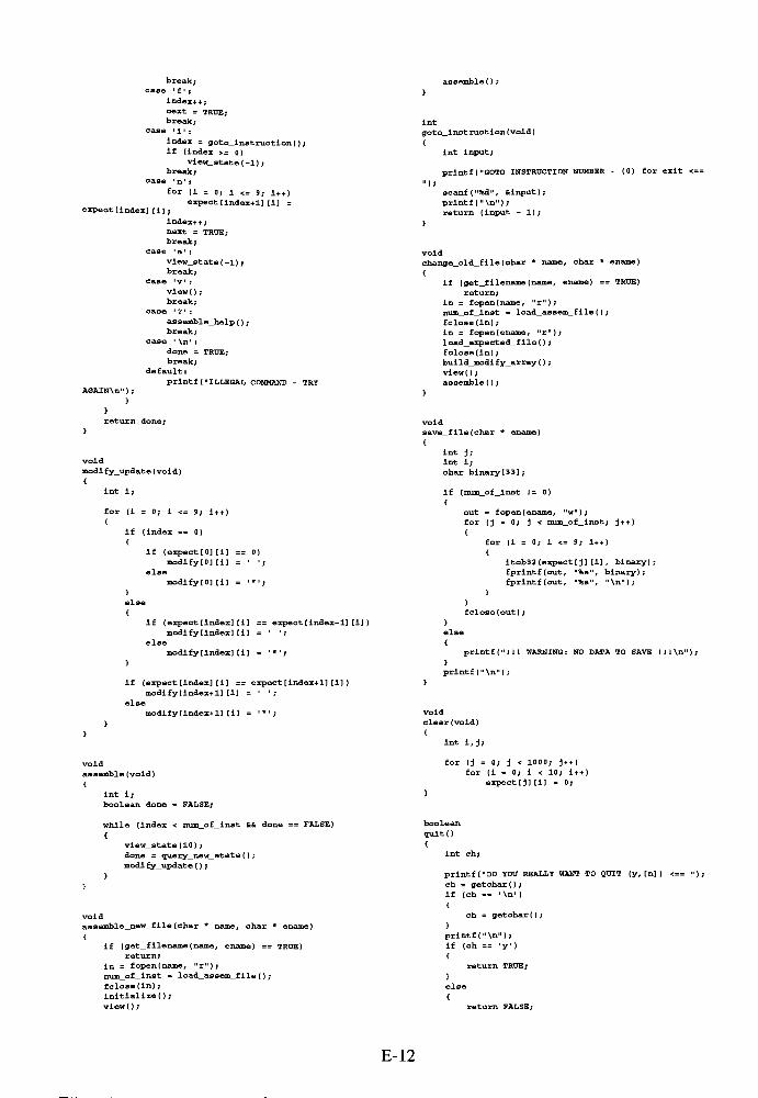
break;case
' f ':
index*+;
next s TRUE;
break;case ' 1 '
:
index = goto_instructlon();if (index >= 0)
view_state(-l);
break;case
' n1:
for (i = 0; 1 <= 9; i++)
expect[index+l] [1] =
expect [index] [i] ;
index++;next = TRUE;
break;case
's
':
view_state(-l);
break ;
case 'v':
view() ;
break;case
'? '
:
assemble_help ( ) ;
break;case
' \n':
done = TRUE;
break ;
default:
printf ("ILLEGAL COMMAND - TRYAGAIN\n"
) ;
>
}
return done;
}
assemble ( ) ;
int
goto_lnstruction(void)
{
int input;
printf ("GOTO INSTRUCTION NUMBER - (0) for exit <=
scanf ("%d", -input);
printf ("\n");
return (input - 1);
void
change_old_flie (char *name, char
*ename)
(
if (get_filename(name, ename) == TRUE)
return;
in = fopen(name, "r");
num_of_inst = load_assem_flie ( ) ;
fclose (in) ;
in = fopen(ename, "r");
load_expected_flie ( ) ;
fclose (in) ;
build_modlfy_array () ;
view() ;
assemble () ;
void
save_file(char*ename)
void
modify_update (void)
int j;
int i;
char binary[33];
int 1;
for (i = 0; 1 <= 9; i++)
{
if (index == 0)
{
if (expect[0] [i] == 0)
modify[0] [1] =';
else
modify[0] [1] = '*';
)
else
{
if (expect [index] [1] == expect [index- 1] [i])
modify [index] [1] ='';
elBe
modify [index] [1] = '*';
}
if (expect [index] [1] == expect [index+1] [i] )
modify[index+l] [i] ='';
else
modify[index+l] [i] = '*';
i f (num_of_inst 1 = 0 )
(
out = fopen(ename, "w");
for (j = 0; j < num_of_inst; j++)
{
for (1 = 0; i <= 9; i++)
(
itob32 (expect [j] [i], binary);
fprintf(out,"%a"
, binary);
fprintf(out, "%s", "\n");
)
}
fclose (out) ;
)
else
{
>
printf ("\n"),
print ("111 WARNING: NO DATA TO SAVE 1 1 I\n"
void
clear (void)
void
assemble (void)
int i;
boolean done = FALSE;
int i,j;
for (j = 0; j < 1000; j++)
for (i = 0; 1 < 10; 1++)
expecttj] [i] = 0;
while (index < num_of_inst && done == FALSE)
{
view_state (10);
done = query_new_state ( ) ;
modi fy_update ( ) ;
void
assemble_new_flie (char *name, char
*ename)
{
if (get_filename(name, ename) == TRUE)
return;
in = fopen(name, "r");
n__m_of_inst = load_assem_file { ) ;
fclose (in);
initial! ze();
view ( ) ;
boolean
quit()
{
Int ch;
printf ("DO YOU REALLY WANT TO QUIT (y, [n] ) <=
ch = getchar () ;
if (ch == 'Vn')
{
ch = getchar () ;
}
printf ("\n") ;
if (ch == -y')
(
return TRUE;
)
else
{
return FALSE;
E-12
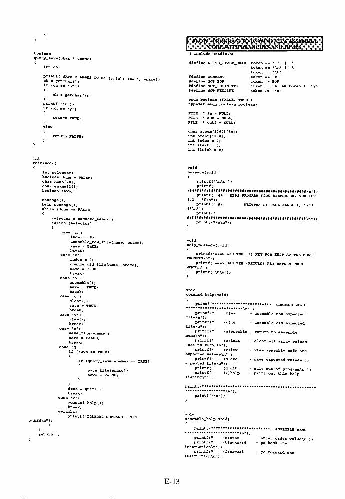
boolean
luery_save(char *
ename)(
int ch;
printf ("SAVE CHANGES TO %s (y, [n] )ch = getchar ( ) ;if (ch _= '\n')
ch = getchar ( ) ;
ename ) ;
printf ("\n"),if (ch == iyi
)
return TRUE;
return FALSE;
VUiW 4 PROGRAM TO I SWIM)MIISASSRMitl.1
< OJ>F. WITH BRAiNCHKSAMI JUMPS
# include <stdio.h>
#define WHITE_SPACE_CHAR token ==' ' I I \
token =='\n' I I \
#define COMMENT
#deflne NOT_EOF
#define NOT_DELIMITER
#define NOT_NEWLINE
token ==' \t '
token == #
token 1 = EOF
token 1= '#' && token 1= '\n'
token 1= ' \n'
enum boolean {FALSE, TRUE) ;
typedef enum boolean boolean;
FILE * in = NULL;
FILE *out = NULL;
FILE *out2 = NULL;
char assem[1000] [80] ;
int order[1000];
int index = 0;
int start = 0;
int finish = 0;
int
main (void){
int selector;
boolean done = FALSE;char name [20];char ename [20];boolean save;
message ( ) ;
help_message ( ) ;
while (done == FALSE){
selector = command_menu ( ) ;switch (selector){
case'n
':
index = 0;
assemble_new_file (name, ename) ;save = TRUE;
break;case
' o1:
index = 0;
change_old_flie (name, ename) ;
save = TRUE;
break;case
'a
':
assemble () ;
save = TRUE;
break;case
'c
':
clear () ;
save = TRUE;
break;case
'v':
view() ;
break ;
case's
':
save_file (ename) ;
save = FALSE;
break;case
'q':
if (save == TRUE)
(
if (query_save (ename) == TRUE)
{
save_flie (ename) ;
save = FALSE;
AGAINVn" ) ;
done = quit () ;
break;
case ?':
command_help ( ) ;
break;default:
printf ("ILLEGAL COMMAND - TRY
void
message (void)
{
printf ("\n\n");
printf("
printf("
## MIPS PROGRAM FLOW ASSEMBLER, VERSION
1.1 ##\n");
printf (" ## WRITTEN BY PAUL FANELLI, 1993
##\n");
printf("
##################################################Vn..);printf ("\n\n") ;
}
void
help_i_.essage (void)
{
printf ("===> USE THE (7) KEY FOR HELP AT THE MENU
PROMPTS\n");
printf ("===> USE THE (RETURN) KEY RETURN FROMMENU\n"
) ;
printf ("\n\n") ;
)
void
command_help (void)
printf ("****************
-***_*********** * ** ** ^n,
printf(" (n)ew
flle\n");printf("
(o)ld
file\n");
printf("
(a)ssemble -
menu\n"
) ;
printf(" (c)lear
(set to zero)\n");
printf("
(v)iew
expected values\n");
printf("
(s)ave
expected file\n");printf("
(q)uit
printf("
(?)help
listing\n");
printf ("*********************
***************_ynnj .
printf ("\n") ;
}
void
assemble_help (void)
(
printf ("****************
************_ ********* \nu \ .
printf("
(e)nter
printf {"
(b) ackward
instructlon\n") ;
printf ("
( f ) orwardinstruction\n"
) ;
********COMMAND MENU
assemble new expected
assemble old expected
return to assemble
clear all array values
view assembly code and
save expected values to
quit out of program\n" ) ;print out this help
*******ASSEMBLE MENU
-
enter order value\n");- go back one
- go forward one
E-13
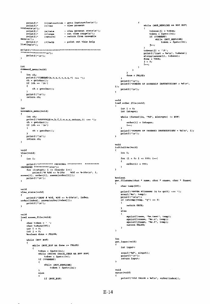
printf (" (i)nstru
printf (" (v) lew
contents\n") ;
printf (" (s)tate
printf (" (r)ange
printf (" (return)
menu\n") ;printf("
(7) help
listing \n");
printf ("*******.........
***************:**\n");
printf ("\n"
)
);
int
command_menu (void)
(i)nstruction - goto instructionVn") ;
- view present
view present state\n");
set view range\n");
return from assemble
print out this help
while (NOT_NEWLINE && NOT_EOF)
(
tokens[j] = token;
token = fgetc(ln);
if (COMMENT)
while (NOT_NEWLINE)
token = fgate (in);
)
tokens [ j ] =' \ 0 '
;
printf ("inst = %s\n", tokens);
strcpy(assem[i] , tokens) ;
done = TRUE;
j= 0;
i++;
int ch;
printf ("COMMAND (n,o, a,c,v, s,q, ?) <== ") ;
ch = getchar ( ) ;
if (ch == ' \n')
{
ch = getchar () ;
)
printf ("\n") ;
return ch;
done = FALSE;
printf("\n"
);
printf ("NUMBER OF ASSEMBLY INSTRUCTIONS = %d\n".
1);
printf ("\n") ;
void
load_order_flie (void)
int
assemble_menu (void)
int i = 0;
int integer;
int ch;
printf ( "ASSEMBLE (e,b, f , i,v, s, r, return, ?) <==
ch = getchar () ;
if (eh == '\n')
(
ch = getchar ( ) ;
>
printf ("\n") ;
return ch;
while (fscanf(in, "%d, -integer) 1= EOF)
(
order [1] = integer;
i++;
)
printf ("NUMBER OF ORDERED INSTRUCTIONS = %d\n", i);
printf ("\n"),
void
view (void)
{
int i;
printf(********** ORIGINAL
********** *****
ORDERDED********** \n\n"
) ;
for (i=start; i <= finish; i++)
printf("# %3d => %-20s %3d =>%-20s\n"
assem[l] , order[i] , assem[order [1] ] ) ;
printf ("\n");
)
void
initialize (void)
int i;
for (1 = 0; i <= 999; i++)
{
orderti] = 999;
)
boolean
get_filename (char *name, char
*oname, char
void
view_state (void)
{
printf ("INST # %3d, %3d => %-20s\n", index,
order[index] , assem[order [index] ] ) ;
printf ("\n");
)
void
load_assem_flie (void)
{
char token =' '
;
char tokens [80];
int i = 0;
int j = 0;
boolean done = FALSE;
while (NOT_EOF)
(
while (NOT_EOF && done FALSE)
{
token = fgetc(in);
while (WHITE_SPACE_CHAR && NOT_EOF)
token = fgetc(in);
if (COMMENT)
{
while (NOT_NEWLINE)
token = fgetc(in);
)
else
(
if (NOT_EOF)
char temp [20] ;
printf ("ENTER FILENAME (q to quit) <== ");
scanf("%a"
, temp) ;
printf ("\n\n") ;
if (stremp(temp, "q") == 0)
return TRUE;
}
else
{
sprintf (name, "%s.test", temp);
sprintf (oname, "%s.o", temp);
sprintf (fname, "%s.f", temp);
return FALSE;
int
get_input (void)
{
int input;
scanf ("%d", -input) ;
printf ("\n") ;
return input;
void
enter (void)
{
printf ("OLD value = %d\n", order [index] ) ;
E-14

printf ( "NEW VALUE <=="
) ;
order[index] = get_input();
printf ("\n") ;
void
set_view_range (void)
printf ("ENTER VIEW RANGE (LO,HI) <== ");
scanf ("%d,%d", fistart, ftfinish) ;
printf ("\n") ;
change_old_flie (char *name, char
*oname, char
*
fname)
{
if (get_fllename(name, oname, fname) == TRUE)
return;
in = fopen(name, "r");
load_assem_flie ( ) ;
fclose (in) ;
in = fopen(oname, "r");
initializeO;
load_order_file ( ) ;
fclose (in) ;
view() ;
assemble () ;
void
assemble (void)
{
int selector;
boolean done = FALSE;
int i;
while (done == FALSE)
{
view_state ( ) ;
selector = assemble_menu( ) ;
switch (selector)
C
case e':
enter () ;
index++;
break;
case' b '
:
index--;
break;
case' f '
:
lndex++;
break;
case' i '
:
index = goto_instruction() ;
break;
case'v'
:
view ( ) ;
break;
case's
':
break;
case'r
':
set_view_range ( ) ;
break;
case' ?
':
assemble_help ( ) ;
break;
case' \n'
:
done = TRUE;
break;
default :
printf ("ILLEGAL COMMAND - TRY
AGAIN\n");
)
}
)
void
save_file (char *oname, char
* fname)
{
int j;
if (index 1= 0)
(
out = fopen( fname,"w"
) ;
out2 = fopen(oname, "w");
for (j = 0; j < index; j++)
{
fprintf (out,"%a"
, assem [order [ j] ] ) ;
fprintf (out,"%a"
," \n"
) ;
fprlntf (out2, "%d\n", order[j]);
}
fclose (out) ;
fclose (out2) ;
)
else
(
printf ("I 11 WARNING: NO DATA TO SAVE 1 I I \n" ) ;
printf ("\n");
void
clear (void)
(
int i;
for (i = 0; i < 1000; i++)
order[i] = 999;
boolean
quit{)
{
int ch;
printf ("DO YOU REALLY WANT TO QUIT (y, [n] ) <== ");
ch = getchar () ;
if (ch ==' \n'
)
ch = getchar();
assemble_new_file (char*name, char
*oname, char
fname)
if (get_file-ame(name, oname, fname) == TRUE)
return;
in = fopen(name, "r");
load_assem_fHe ( ) ;
fclose (In);
printf ("\n") ;
If (ch == 'y')
(
return TRUE;
}
{
return FALSE;
initializeO;
view ( ) ;
assemble ( ) ;boolean
query_save(ehar*oname)
int
goto_instruetlon(void)
(
int input;
printf ("GOTOINSTRUCTION NUMBER <== ");
scanf("%d"/ -input);
printf ("Xn");
return input;
void
int ch;
printf ("SAVE CHANGES TO %a (y, [n] ) <==
ch = getchar ( ) ;
if (ch =='\n'
)
(
ch = getchar () ;
}
printf ("\n") ;
if (ch =='y'
)
{
return TRUE;
)
else
E-15
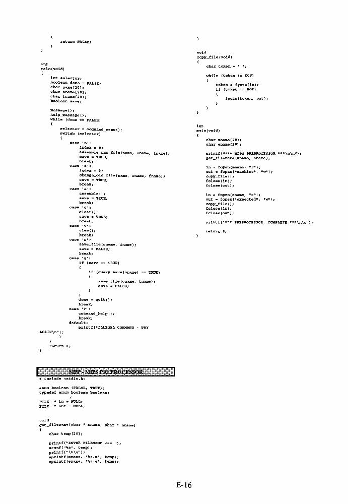
return FALSE;
int
main (void)
{
int selector;
boolean done = FALSE;char name [20];char oname [20] ;char fname [20] ;
boolean save;
message ( ) ;
help_message ( ) ;while (done == FALSE){
selector =command_menu() ;
switch (selector)(
case' n1
:
index = 0;
assemble_new_flie (name, oname, fname)save = TRUE;
break;case 'o'i
index =0;
change_old_file (name, oname, fname) ;save = TRUE;
break;case
' a1:
assemble ( ) ;
save = TRUE;
break;case 'a1!
clear() ;
save = TRUE;
break;
case 'v'i
view() ;
break;case s :
save_file (oname, fname) ;save = FALSE;
break;case
'q1:
if (save == TRUE)
(
if (guery_save (oname) == TRUE)
(
save_file (oname. fname)
save = FALSE;
}
)
done = quit () ;
break;
case'? '
:
eommand_help ( ) ;
break;
default:
printf ("ILLEGAL COMMAND - TRY
:N\n");
}
)
return 0;
WW- MIPS PKiP^eESS3;;;
# include <stdlo.h>
enum boolean {FALSE, TRUE);
typedef enum boolean boolean;
void
copy_file (void)
char token =
while (token 1= EOF)
{
token = fgetc(in);
if (token 1= EOF)
{
fputc (token, out);
}
int
main (void)
{
char mname [20] ;
char ename [20];
printf("*** MIPS PREPROCESSOR ***\n\n");
get_filename (mname, ename) ;
in = fopen(mname, "r");
out = fopen( "machine", "w") ;
copy_file() ;
fclose (in) ;
fclose (out) ;
in = fopen(ename, "r");
out = fopen( "expected", "w");
copy_file () ;
fclose (in) ;
fclose (out) ;
printft"*** PREPROCESSOR COMPLETE ***\n\n"};
FILE
FILE
in = NULL;
out = NULL;
void
get_f ilename (char*mname, char *
ename)
{
char temp [20],-
printf ("ENTER FILENAME <== ");
scanf ("%s", temp) ;
printf ("\n\n");
sprintf (mname, "%s.m", temp)
sprintf (ename, "%s.e", temp);
E-16

APPENDIX F - TEST PROGRAMS
\ AVXmy.&WWMmV&Z 1 | A.TEST-ALUltEOISTER |
# test file for alu immediate
arithmetic instructions
# test file for arithmetic
instructions
# 3 operand, register type
# lui - load upper immediate
lui 1 0 # add - add
lui 1 1 ori 10 0
lui 1 a ori 2 0 0
lui 1 f add 3 12
lui 1 ffff
ori 10a
# ori - or immediate ori 2 0 5
ori 10 0 add 3 12
ori 2 15 add 3 2 1
ori 1 2 f
lui 1 5555 addi 2 0 fffb
ori 1 1 5555 add 3 12
ori 2 10 add 3 2 1
ori 2 11
ori 2 12 addi 1 0 fffe
ori 2 1 ffff add 3 12
add 3 2 1
# andi - and immediate
andi 2 10 ori 2 0 5
andi 2 11 add 3 12
andi 2 12 add 3 2 1
andi 2 1 ffff
ori 1 0 64
# xori - exclusive or immediate ori 2 0 c8
xori 2 10 add 3 12
xori 2 11
xori 2 12 # addu - add unsigned
xori 2 1 ffff ori 10 0
ori 2 0 0
# addi- add immediate addu 3 12
ori 2 0 0
ori 10 0 ori 10a
addi 2 10 ori 2 0 5
ori 10a addu 3 12
addi 2 15 addu 3 2 1
addi 2 1 fffb
lui 1 ffff addi 2 0 fffb
ori 1 1 fff6 addu 3 12
addi 2 15 addu 3 2 1
addi 2 1 fffb
addi 1 0 fff6
# addiu - add immediate unsigned addu 3 12
ori 10 0 addu 3 2 1
addiu 2 1 ffff
addiu 12 1 ori 2 0 5
lui 1 7fff addu 3 12
ori 1 1 ffff addu 3 2 1
addiu 2 11
addiu 1 2 ffff ori 1 0 64
ori 2 0 c8
# slti - set on less than addu 3 12
immediate
ori 1 0 2 # sub- subtract
slti 2 1 ffff ori 10 0
slti 2 10ori 2 0 0
slti 2 11sub 3 12
slti 2 12
slti 2 13ori 10a
addi 1 0 fffeori 2 0 5
slti 2 1 fffdsub 3 12
slti 2 1 fffesub 3 2 1
slti 2 1 ffff
slti 2 10addi 2 0 fffb
slti 2 11sub 3 1 2
sub 3 2 1
# sltiu - set on less than
immediate unsignedaddi 1 0 fff6
ori 1 0 2sub 3 12
sltiu 2 10sub 3 2 1
sltiu 2 11
sltiu 2 12 ori 2 0 5
sltiu 2 13sub 3 12
haltsub 3 2 1
ori 1 0 64
ori 2 0 e8
sub 3 12
sub 3 2 1
# subu - subtract unsigned
ori 10 0
ori 2 0 0
subu 3 12
ori 10a
ori 2 0 5
subu 3 12
subu 3 2 1
addi 2 0 fffb
subu 3 12
subu 3 2 1
addi 1 0 fff6
subu 3 12
subu 3 2 1
ori 2 0 5
subu 3 12
subu 3 2 1
ori 1 0 64
ori 2 0 c8
subu 3 12
subu 3 2 1
# sit - set on less than
ori 10 2
addi 2 0 ffff
sit 3 12
ori 2 0 0
sit 3 12
ori 2 0 1
sit 3 12
ori 2 0 2
sit 3 12
ori 2 0 3
sit 3 12
addi 1 0 fffe
addi 2 0 fffd
sit 3 12
addi 2 0 fffe
sit 3 12
addi 2 0 ffff
sit 3 12
ori 2 0 0
sit 3 12
ori 2 0 1
sit 3 12 # run for 6300
# situ - set on less than
unsigned
ori 10 2
ori 2 0 0
situ 3 12
ori 2 0 1
situ 3 12
ori 2 0 2
situ 3 12
ori 2 0 3
situ 3 12 # run for 6900
# and - and
lui 1 5555
ori 1 1 5555
ori 2 0 0
and 3 12
ori 2 0 1
and 3 12
ori 2 0 2
and 3 12
ori 2 0 ffff
and 3 12
# or - or
ori 2 0 0
or 3 1 2
ori 2 0 1
or 3 1 2
ori 2 0 2
or 3 1 2
ori 2 0 ffff
F-l
# xor -
exclusive or
ori 2 0 0
xor 3 1 2
ori 2 0 1
xor 3 1 2
ori 2 0 2
xor 3 1 2
ori 2 0 ffff
xor 3 1 2
# nor _ nor
or! 2 0 0
nor 3 1 2
ori 2 0 1
nor 3 1 2
ori 2 0 2
nor 3 1 2
ori 2 0 ffff
nor 3 1 2 # run for 89 0 0
addi 3 3 1
nop
bne 2 3
nop
fffd
# run for 3300
| jiuTiST-Kra^AN^BMycin
# test file for jump and branch
instructions
# j - jump
J 8 #0h
ori 1 0 1
ori 1 0 2
nop
j 9 tlOh
ori 1 0 4
nop
nop
j 4 #2Oh
ori 1 0 3
jal _ jump and link
Jal 10
ori 1 0 5
ori 1 0 6 #30h
jal 11
nop
nop
jal c #40h
ori 1 0 7
# jr lump register
ori 2 0 60
jr 2
ori 1 0 8 #50h
ori 2 0 6c
jr 2
nop
ori 1 0 9 #60h
ori 2 0 54
jr 2
ori 1 0 a
nop #70h
# jalr -
jump and link register
ori 2 0 90
jalr : 2
ori 1 0 b
nop #80h
nop
nop
nop
ori 1 0 c #90h
# beq - branch on equal
ori 2 0 abed
ori 3 0 abed
beq 2 3 5
ori 1 0 d #aOh
ori 1 0 e
ori 1 0 f
ori 1 0 10
ori 1 0 11 #b0h
ori 1 0 12
ori 3 0 abeb
beq 2 3 fffb
# blez - branch on less than or
equal to zero
addi 2 0 fffe
addi 2 2 1
blez 2 fffe
nop
# bgtz - branah on greater than
zero
ori 2 0 3
addi 2 2 ffff
bgtz 2 fffe
nop
# bltz - branch on less than zero
addi 2 0 fffd
addi 2 2 1
bltz 2 fffe
nop # run for 50 0 0
# bgez - branch on greater than
or equal to zero
ori 2 0 2
addi 2 2 ffff
bgez 2 fffe
nop
# bltzal - branah on less than
zero and link
addi 2 0 fffd
addi 2 2 1
bltzal 2 fffe
nop # run for 6200
# bgezal - branch on greater than
or equal to zero and link
ori 2 0 2
addi 2 2 ffff
bgezal 2 fffe
nop # run for 6800
halt
| %&T^-l&m&m STORE |
# test file for load and store
instructions
lui 1 abed
lui 2 5678
ori 1 1 efOl
ori 2 e47f
sw 1 4000 0
sh 1 4004 0
sb 1 4006 0
sb 2 4007 0
sb 0 4008 0
awl 2 4009 0
swr 2 4 0 0c 0
sb 0 400d 0
sh 0 400e 0
sh 0 4010 0
swl
swr
swl
swr
swl
swr
#
lw 3
nop
lw 3
4012 0
4015 0
401b 0
401e 0
4020 0
4027 0
4000 0
4004 0
# bne - branch on not equal
nop
nop
nop
lw 3
nop
lw 3
nop
lw 3
nop
lw 3
nop
lw 3
nop
lw 3 4 01c
nop
4008
400c
4014
4018
lw 3 4020 0
nop
lw 3 4024 0
nop
#
lb 3 4000 0
nop
lb 3 4001 0
nop
lb 3 4002 0
nop
lb 3 4003 0
nop
lbu 3 4000 0
nop
lbu 3 4001 0
nop
lbu 3 4002 0
nop
lbu 3 4 0 03 0
nop
lh 3 4004 0
nop
lh 3 4006 0
nop
lhu 3 4004 0
nop
lhu 3 4006 0
nop
#
ori 3 0 0
lwl 3 4021 0
nop
lwr 3 4 024 0
nop
#
ori 3 0 0
lwl 3 4022 0
nop
lwr 3 4025 0
nop
*
ori 3 0 0
lwl 3 4023 0
nop
lwr 3 4026 0
nop
#
lwl 3 4020 0
nop
lwr 3 4023 0
nop
halt
MTXTEST- MULTIPLICATION
ANDDIVISION
# test file for multiply and
divide instructions
# mult -
multiply
ori 10 8
ori 2 0 9
mult 12 # 89
mult 2 1
addi 2 0 fff7
mult 12 # 8-9
mult 2 1
addi 1 0 fffB
mult 12 # -8*-9
mult 2 1
ori 2 0 9
mult 12 # -8*9
mult 2 1
ori 10 0
ori 2 0 0
mult 12 # 00
ori 10a
mult 1 2 # 0*a
lui 1 7fff
ori 1 1 ffff
ori 2 0 0
mult 12 # 7fff_ffff
F-2

ori 2 0 1
mult 12 # 7fff_ffff 1
ori 2 0 10
mult 12 # 7fff_ffff lOh
lui 1 8000
ori 2 0 0
mult 12 # 8000_0000 * 0
ori 2 0 1
mult 12 # 8000_0000 * 1
ori 2 0 10
mult 12 # 8000_0000 * lOh
addi 1 0 ffff
ori 2 0 0
mult 12 # ffff_ffff o
ori 2 0 1
mult 12 # ffff_ffff * l
ori 2 0 10
mult 12 # ffff_ffff * lOh
addi 2 0 ffff
mult 12 # ffff_ffff *
ffff_ffff
# multu -
multiply unsigned
ori 10 8
ori 2 0 9
multu 12 #8*9
multu 2 1
addi 2 0 fff7
multu 12 # 8*-9
multu 2 1
addi 1 0 fffS
multu 12 # -8*-9
multu 2 1
ori 2 0 9
multu 12 # -8*9
multu 2 1
ori 10 0
ori 2 0 0
multu 12 # 0*0
ori 10a
multu 12 # 0*a
addi 1 0 ffff
ori 2 0 0
multu 12 # ffff_ffff * 0
ori 2 0 1
multu 12 # ffff_ffff * 1
ori 2 0 10
multu 12 # ffff_ffff * 16
(10h)
ori 2 0 40
multu 12 # ffff_ffff* 64
(40h)
ori 2 0 100
multu 12 # ffff_ffff* 256
(100b)
ori 1 0 49
ori 2 0 9
div 1 2
addi 2 0 fff7
div 1 2
addi 1 0 ffb7
div 1 2
ori 2 0 9
div 1 2
# divu - divide unsigned
ori 1 0 48
ori 2 0 9
divu 12 # 72d/9d
addi 2 0 fff7
divu 12 # 72d/-9d
addi 1 0 ffba
divu 12 # -72d/-9d
ori 2 0 9
divu 12 # -72d/9d
*
ori 1 0 4b
ori 2 0 9
divu 1 2
addi 2 0 fff7
divu 1 2
addi 1 0 ffb5
divu 1 2
ori 2 0 9
divu 1 2 # run for 6000
lui 1 acef
lui 2 48a2
ori 1 1 52ac
ori 2 2 9165
divu 12 * run for 7200
# mfhi - move from hi
mfhi 3
# mthl - move to hi
ori 3 0 abed
mthl 3
# mflo - move from lo
mflo 3
# mtlo - move to lo
ori 3 0 1234
mtlo 3
halt
MV.l KST - MOV V. TO/*ROM
UVUt RKWSTKKS
lui 3 abed
ori 3 3 1234
# mthi - move to hi
mthi 3
# sll - shift left logical
sll 0 0 0
sll 0 0 4
sll 1 0 0
sll 1 0 4
sll 0 1 0
sll 0 1 4
sll 2 1 0
sll 2 1 4
ori 1 0 1
sll 2 1 1
sll 2 1 2
sll 2 1 3
sll 2 1 4
sll 2 1 8
sll 2 1 16
sll 2 1 30
sll 2 1 31 # run for 1300
# srl _ shift right logical
srl 1 2 1
srl 1 2 2
srl 1 2 3
srl 1 2 4
srl 1 2 8
srl 1 2 16
srl 1 2 30
srl 1 2 31
# sra _ shift right arithmetic
sra 0 0 0
sra 0 0 8
lui 1 8000
ori 1 1 1
sra 2 1 1
lui 1 2222
ori 1 1 2222
sra 2 1 1
lui 1 4444
ori 1 1 4444
sra 2 1 2
lui 1 8888
ori 1 1 8888
sra 2 1 1
sra 2 1 2
sra 2 1 4 # run for 2800
# sllv shift left logical
variable
ori 2 0 0
ori 1 0 f
ori 3 0 4
sllv 2 13
ori 3 0 10
sllv 2 13
# srlv - shift right logical
variable
ori 2 0 0
lui 1 fOOO
ori 1 1 f
ori 3 0 2
srlv 2 13
# srav -
shift right arithmetic
variable
ori 2 0 0
lui 1 8888
ori 1 1 8888
ori 3 0 4
srav 2 L 3
halt
addi 2 0 ffff
multu 12 # ffff_ffff*
ffff_ffff
# div - divide
ori 1 0 48
ori 2 0 9
div 12 # 72d/9d
addi 2 0 fff7
div 12 # 72d/-9d
# mfhi- move from hi
mfhi 4
# mtlo - move to lo
mtlo 3
# mflo - move from lo
mflo 5
NOTE: ONLY BEHAVIORAL
MODEL TEST PROGRAMS USE
THE HALT INSTRUCTION.
HALT IS REPLACED WITH THE
BREAK INSTRUCTION FOR
DATAFLOW AND STRUCTURAL
MODELS .
addi 1 0 ffb8
div 12 # -72d/-9d
S.TEST- SHIFT
ori 2 0 9
div 12 # -72d/9d
# test file for shift functions
F-3