
A VHDL-based approach for power estimation of embedded systems
24
1 A VHDL-Based Approach for Power Estimation of Embedded Systems William Fornaciari ^, Paolo Gubian *, Donatella Sciuto ^, Cristina Silvano * (^) Politecnico di Milano, Dipartimento di Elettronica e Informazione, P.zza L.Da Vinci, 32 - 20133 Milano, Italy, e-mail: {fornacia, sciuto}@elet.polimi.it, Fax:+39-2-2399 3411 (*) Univ. degli Studi di Brescia, Dip. di Elettronica per l’Automazione, Via Branze, 38 - 25123 Brescia, Italy, e-mail: {gubian, silvano}@bsing.ing.unibs.it, Fax: +39-30-380014 Keywords: Embedded Systems, Low Power Design, Power Estimation, VHDL, VLSI circuits. Contact author: William Fornaciari Abstract Power dissipation has become one of the main constraints during the design of embedded systems and VLSI circuits in the recent years, due to the continuous increase of the integration level and the operating frequency. The aim of this paper is to present an innovative conceptual framework suitable for achieving accurate and efficient estimation of power dissipation for embedded systems described in VHDL at the behavioral and Register Transfer levels. The goal is to provide the designer with the capability of analyzing and comparing different solutions in the architectural design space, before the synthesis. The analytical power model is hierarchical, considering the different parts of the target system architecture, mainly the data-path, the memory, the control logic and the embedded core processor. Experimental results have been obtained by applying the proposed power model to benchmark circuits. 1. Introduction An increasing number of applications in several fields like automotive, telecommunication, consumer electronics, etc. is recently being implemented by using embedded systems. These systems have become broadly used in the most recent years, due to the wide diffusion on the market of standard processors characterized by high performances and reasonable prices. We refer to embedded systems as those dedicated computing and control systems designed for specific target applications [28, 6], where dedicated software routines are provided with the system to respond to specific requirements. In general, the functionality of an embedded system is constituted by a fixed number of operating ways and it is determined by the interaction between the system and the environment. According to the particular application class for which the system is dedicated, the embedded systems can be classified as data or control dominated systems [28]. In both cases, the target system architecture is composed of an hardware and a software part. The software part is typically constituted by a set of application specific software routines running on a dedicated processor or ASIP (Application Specific Instruction Processor), while the hardware part consists usually of one or more ASICs (Application Specific ICs). Due to the heterogeneous nature of the hardware and software parts of the embedded system, innovative co-design techniques have been proposed in the recent past, the goal being to meet the system-level requirements by using a concurrent design and validation approach, thus exploiting the synergism of the hardware and the software parts [6]. Several design aspects are involved in the co-design process at the system-level, including the system modeling, the capture of the functional specifications in a high-level language (co-specification), the analysis and validation of the specifications, the exploration and evaluation of the different
Transcript of A VHDL-based approach for power estimation of embedded systems
1
A VHDL-Based Approach for Power Estimationof Embedded Systems
William Fornaciari ^, Paolo Gubian *, Donatella Sciuto ^, Cristina Silvano *
(^) Politecnico di Milano, Dipartimento di Elettronica e Informazione, P.zza L.Da Vinci, 32 - 20133Milano, Italy, e-mail: {fornacia, sciuto}@elet.polimi.it, Fax:+39-2-2399 3411
(*) Univ. degli Studi di Brescia, Dip. di Elettronica per l’Automazione, Via Branze, 38 - 25123 Brescia,Italy, e-mail: {gubian, silvano}@bsing.ing.unibs.it, Fax: +39-30-380014
Keywords: Embedded Systems, Low Power Design, Power Estimation, VHDL, VLSIcircuits.Contact author: William Fornaciari
AbstractPower dissipation has become one of the main constraints during the design of embeddedsystems and VLSI circuits in the recent years, due to the continuous increase of the integrationlevel and the operating frequency. The aim of this paper is to present an innovative conceptualframework suitable for achieving accurate and efficient estimation of power dissipation forembedded systems described in VHDL at the behavioral and Register Transfer levels. The goalis to provide the designer with the capability of analyzing and comparing different solutions inthe architectural design space, before the synthesis. The analytical power model is hierarchical,considering the different parts of the target system architecture, mainly the data-path, thememory, the control logic and the embedded core processor. Experimental results have beenobtained by applying the proposed power model to benchmark circuits.
1. IntroductionAn increasing number of applications in several fields like automotive, telecommunication,consumer electronics, etc. is recently being implemented by using embedded systems. Thesesystems have become broadly used in the most recent years, due to the wide diffusion on themarket of standard processors characterized by high performances and reasonable prices.We refer to embedded systems as those dedicated computing and control systems designed forspecific target applications [28, 6], where dedicated software routines are provided with thesystem to respond to specific requirements. In general, the functionality of an embeddedsystem is constituted by a fixed number of operating ways and it is determined by theinteraction between the system and the environment. According to the particular applicationclass for which the system is dedicated, the embedded systems can be classified as data orcontrol dominated systems [28]. In both cases, the target system architecture is composed of anhardware and a software part. The software part is typically constituted by a set of applicationspecific software routines running on a dedicated processor or ASIP (Application SpecificInstruction Processor), while the hardware part consists usually of one or more ASICs(Application Specific ICs).Due to the heterogeneous nature of the hardware and software parts of the embedded system,innovative co-design techniques have been proposed in the recent past, the goal being to meetthe system-level requirements by using a concurrent design and validation approach, thusexploiting the synergism of the hardware and the software parts [6]. Several design aspects areinvolved in the co-design process at the system-level, including the system modeling, thecapture of the functional specifications in a high-level language (co-specification), the analysisand validation of the specifications, the exploration and evaluation of the different

2
architectures with respect to some design metrics, the system-level partitioning, the co-synthesis and co-simulation.The availability of an appropriate co-design methodology, covering all these design phases, ismandatory during the design of embedded systems in order to meet the system-levelrequirements. These requirements are typically defined in terms of some design constraints likeperformance, area, power dissipation, cost, reliability, testability and development time. Inparticular, the technological trends toward smaller geometry and the increasing performancelevels lead to high-level integration, high clock frequencies and high power dissipation. Suchaspects, combined with the growing demand of battery-powered portable systems, contributedto increase the importance of the power issues during the design of embedded systems.Therefore, co-design techniques for low power dissipation and EDA tools for accurate powerestimation have become a critical factor for embedded systems and IC designers, in order tosatisfy the power constraints, without reducing the global performance significantly. Designtechniques targeting low power dissipation and power estimation methodologies should beprovided at several abstraction levels. In fact, circuit and logic-level power estimationtechniques are no more sufficient, due to the high complexity and high integration levels of theembedded systems. Accurate low-level estimation techniques present some limitations due tothe need to cope with circuit complexity in an acceptable design time. Moreover, low-levelestimation techniques can be applied only during the last design phases, when a circuit orlogic-level description is already available. However, a re-design process at these levels couldbe very expensive and time consuming.Hence, high-level power estimation is a key issue in the early determination of the powerbudget for embedded systems, being unfeasible to synthesize every design solution down tothe gate, circuit and layout levels in a reasonable time. The goal is to respect the design turn-around time, while exploring the architectural design space widely, and to early re-target thearchitectural design choices. Accuracy and efficiency of a high-level analysis should contributeto meet the power requirements, avoiding a costly re-design process. In general, the relativeaccuracy in high-level power estimation is considered much more important than the absoluteaccuracy, the main objective being the comparison of different design alternatives [10].High-level power estimation tools are usually based on high-level descriptions. Up to now,most of embedded system descriptions are specified in a hardware description language, suchas Verilog or VHDL, along with other graphical formalisms suitable for describing thefunctional behavior at the system-level, such as temporal diagrams, State Transition Graphsfor Finite State Machines, Statecharts, etc. [9, 18]. In particular, VHDL has become the de-facto standard in the European design community for the hardware description and for themost part of the commercial design entry, synthesis and simulation tools.The main advantage of VHDL is related to the possibility of specifying the system behavior byusing a mixed description [18] at different abstraction levels: behavioral, Register-Transfer andstructural. Therefore, VHDL provides high flexibility during both the design description andthe simulation phases. Furthermore, VHDL supports a hierarchical design approach, where thedescription of the elements composing the hierarchy, properly connected, perform the globalfunctionality. The hierarchical approach provides also the possibility to use a mixed descriptioncomposed of behavioral, Register-Transfer and structural parts at the different hierarchicallevels.Other advantages of VHDL are related to the possibility of easily specifying both the data-pathand the control-path of the system and to support the modular design approach. Hence,VHDL allows the designer to re-use existing components. In fact, VHDL supports thedefinition of functions and procedures, to decompose a complex description into smaller andsimpler functional units. These functional units can be organized as independent files, that can

3
be compiled and verified separately, thus supporting the definition of a library of re-usablecells and macro-cells. Finally, VHDL provides also the complete independence with respect tothe technology used and the mapping between a given entity and different architectures,through the configuration approach.The aim of this paper is to provide a conceptual analysis framework for accurate and efficientestimation of power dissipation in embedded systems and VLSI circuits at the architecturaland RT levels. The availability of a power analysis tool at these levels of abstraction is ofparamount importance to early obtain estimation results, while maintaining an acceptableaccuracy. In fact, the architectural and RT-level descriptions, based on VHDL, are the designentry point for the majority of embedded systems and IC designs.In the proposed approach, the analysis is based on a probabilistic estimation of the switchingactivity. The proposed model accurately accounts for both the switching activity and thephysical capacitance [8] for all the parts composing the embedded system architecture.The paper is organized as follows. The discussion starts by presenting the most significantresearch works related to high-level power estimation in Section 2. Then the target systemarchitecture of embedded systems, we are focusing on, is introduced in Section 3, whileSection 4 contains the foundations and notations, constituting the basis of the proposedanalysis. Then, the proposed power estimation model is detailed in Sections 5-10 while someexperimental results obtained from benchmark circuits are reported in Section 11, which alsooutlines the future developments of our investigations.
2. Previous Work on High-Level Power EstimationGeneral surveys of power estimation techniques at different abstraction levels can be found in[7, 20, 5, 24]. While several power estimation techniques have been proposed in the literatureat the gate, circuit and layout levels, a few papers have been published addressing the powerestimation problem at high-level until recently [7, 10], despite of the increasing interest in thesystem and behavioral levels design.A state-of-the-art survey of the high-level power estimation has been presented in [10].According to this survey, high-level power estimation techniques can be classified dependingon their abstraction level. At the architectural or RT levels, there are two classes oftechniques: the analytical and the empirical techniques.The analytical methods aim at relating the power consumption to the capacitances and theswitching activities of the design nets. These techniques are composed of complexity-basedmodels and activity-based models. The former considers the design complexity of each part ofthe design, in terms of equivalent gates, as a measure of the capacitance, while the latter usesthe concept of entropy, derived from the information theory, as a measure of the averagetransition activity in a circuit. More specifically, in the complexity-based models, first thenumber n of equivalent gates contained in each design function is specified in a macro-modulelibrary; then, the power estimates are obtained by multiplying n by the average powerconsumed by each equivalent gate. In the activity-based models, the average power isestimated as the product of the area, considered as a measure of the average nodescapacitance, and the entropy, considered as a measure of the activity.The empirical methods are based on the power measures of existing implementations, then amacro-modeling approach is used to derive models from these measurements. The empiricalmethods can be sub-divided into fixed-activity models and activity-sensitive models. Theformer models disregard the influence of data-activity on power, while the latter consider theeffects of statistics related to data and instructions activity on power.Moving up in the abstraction levels, the behavioral methods are based on static and dynamicactivity prediction. The goal of the static activity prediction is the estimation of the access

4
frequency of different hardware resources, by analyzing statically the behavioral description ofthe functions to be implemented. The dynamic activity prediction is based on a dynamicprofiling to determine the activation frequencies of various resources and the memoryaccesses.Finally, power exploration tools at the instruction and system levels can be used to identifypower metrics to guide the system-level partitioning.A common characteristic of power estimation at the different abstraction levels is that theaverage power is strongly related to the switching activity of the circuit nodes. Such a fact hasbeen indicated in [20] as stating that power estimation is a pattern-dependent process. Inparticular, the input pattern-dependency of the power estimation approaches can be classifiedas strong or weak pattern-dependency [20].The typical methods for power estimation based on extensive circuit simulation have beenindicated in [20] as strongly pattern-dependent process. Main advantages of these simulationtechniques derive from its accuracy and wide applicability. However, to obtain a complete andaccurate power estimation, the designer should provide a comprehensive amount of inputpatterns to be simulated, thus making this approach very time consuming and computationallyvery costly. Therefore the simulation approach is almost impossible to apply to most of thedesigns, due to their increasing complexity.To avoid the need of a large amount of input patterns, the weakly pattern-dependentapproaches [20] require input probabilities. In this case, the estimation results will depend onthe probabilities supplied by the designer, reflecting the typical behavior of the input signals.Both probabilistic techniques and statistical techniques are presented in [20]. Probabilistictechniques suitable for combinational circuits have been illustrated, requiring user-suppliedinput probabilities to solve the pattern dependency problem. Statistical techniques userandomly generated input patterns to simulate the circuit repeatedly, then using statisticalmean estimation techniques to stop simulation following a criterion to determine the closenessto the average power.Analytical and stochastic power estimation techniques at the behavioral-level have beenproposed in [16], targeting real time DSP applications on ASIC architectures. The powerdissipated by some ASIC components, such as data-path components, have been analyticallyestimated from the Control Data Flow Graph (CDFG) representing the design. For otherASIC components, such as interconnects and controllers, for which the power informationavailable at the behavioral-level is not sufficient, statistical models were built to estimatepower based on a stochastic study on several ASICs. However, the proposed models do notaccount for the power consumed by multiplexers and memories. The estimation techniqueshave been included into an exploration tool that, given a CDFG description of an algorithmand a library of hardware modules, explores the space of the available solutions for differentvalues of clock periods and supply voltages. The results have been compared with anarchitectural-level power estimator, called Stochastical Power Analysis (SPA) and proposed in[11], on 23 different chips, showing an average error of approximately 20%.Other power estimation techniques based on high-level descriptions have been proposed in[11, 12, 13]. The techniques described in [11], targeting data-path architectures, derivestochastic models of busses and internal modules from the statistical behavior of inputs. In[12], a power estimation model for data-path architectures operating at the RT-level isdescribed. The model accounts for the switching activity by using the Dual Bit Type (DBT)method, considering two input bit types rather than one: the random activity of the leastsignificant bits (LSB’s) and the correlated activity of the most significant bits (MSB’s). Anarchitectural model for the power consumption of the control paths, called Activity-BasedControl (ABC) model, has been presented in [13], using three implementation styles: a ROM-

5
based controller, a PLA-based controller and a random logic controller.Nevertheless, the methods proposed for high-level power estimation have not yet achieved thematurity necessary to enable their use within current industrial CAD environments. Our workis an attempt to fill such a gap, aiming at providing an high-level power model, based onVHDL descriptions, to cover the different parts composing the basic architecture of embeddedsystems.
3. The Target System ArchitectureThe target system architecture of the embedded system is implemented into a single ASIC,including both the software and the hardware bound parts, described at the behavioral/RTlevels. The target system architecture is depicted in Figure 1 and it is quite similar to thoseproposed in [16, 17].
Registerfiles
crossbar network
MUX MUX
Register-x Register-n
MUX
MUX
Register-1
MUX
functional units
datapath control lines
MUX
MUX
Memory
Data INRegister
Data OUTRegister
Embedded Processor(core cell)
ProcessorMemory
DATAPATH
R/WAddress
MEMORY
EMBEDDED SOFTWARE
CONTROL UNIT
CLK
CLOCK DISTRIBUTION (balanced tree)
PRIMARY I/Os
next stateregister
controllogic
stateregister
Figure 1: The target system architecture at the RT-level.
The ASIC architecture is defined at a pre-synthesis RT-level and consists of the followingcomponents:• the data-path, composed of storage units, functional units and multiplexers. The storage
units consist of registers and register files, while functional units can include a wide set ofunits such as adders, multipliers, and so on. A two-level multiplexer structure is consideredfor the interconnection among storage and functional units. The typical operation along thedata-path implies a register-to-register transfer, consisting of the operands read from theinput registers, an operation performed on the operands and the results stored in the output

6
registers [17];• the main memory, based on a memory hierarchy, that can be constituted by single or multi-
port memories, cache memories, TLBs, FIFOs, LIFOs, etc.. We assume that all read/writeaccesses to the memory will be performed through input/output registers;
• the control unit, implemented as a set of Finite State Machines and generating the controllines for the data-path components and the memory;
• the embedded core processor, such as a standard processor, a microcontroller, a DSP, etc.,with its memory (even if part of the memory can be external) implementing the SW boundpart;
• the clock distribution logic, including the buffers of the distribution network, organized forexample as a balanced clock tree;
• the crossbar network, to interface the architectural units by using a communicationprotocol at the system-level. The interconnection power of the crossbar network is includedin the power dissipated by the outputs of data-path, memory and control logic;
• the primary I/O pads.
4. Foundation of the Power EstimationPower dissipation in CMOS circuits can be considered as composed of both a static and adynamic component. Static power dissipation is mainly due to the leakage current of thereverse-biased diodes and the sub-threshold transistor conduction. However, in CMOSdevices, static power dissipation can be considered insignificant in most designs [4].The dominant part of the power dissipation in CMOS circuits is thus the dynamic component,which is composed of two terms [7]. The first term, indicated as the switching activity power,is due to the charge and discharge of the circuit node capacitances at the output of each logicgate. The second term, indicated as short-circuit power, represents the short-circuit currentfrom the supply voltage to ground during the output transitions.The switching activity power PSW can be expressed as in [4]:
PSW= V2DD fCLK CEFF
where VDD is the supply voltage, fCLK is the system clock frequency and CEFF is the effectiveswitched capacitance, that is the product of the total physical capacitance CLi of each node in
the circuit and the switching activity factor αi of each node (defined below) summed over allthe N nodes in the circuit:
CEFF = ∑i=1
Nαi CLi .
The short-circuit power is due to the fact that, during a transition of a CMOS gate, both p andn channel devices may conduct simultaneously, briefly establishing a flow of current from thesupply to ground. The short-circuit power PSH can be expressed as in [7]:
PSH= QSC VDD fCLK α
where QSC represents the quantity of charges carried by the short-circuit current per transition
and α is the global switching activity factor, i.e. the number of gate output transitions perclock cycle.Anyway, in CMOS devices, the short-circuit current typically dissipates a small fraction of thedynamic power (in the order of 5÷10 % as reported in [4], so it can be ignored. Usually, inproperly designed circuits, switching activity power accounts for over 90% of the total power

7
dissipation, as reported in [7].The switching activity of each signal (being a primary I/O or an internal signal), is fullycharacterized by the following two components [5]:• a static component, taking into account the static probability of a signal;• a dynamic component, taking into account the timing behavior of the circuit.The static component can be expressed in terms of the static signal probability of each noden, that is the probability of the node to be at one:
pn1 = lim
N→∞ ( ∑k=1
Nin(k)) / N
where:in(k) = value of in at the clock cycle k (i.e. 0 or 1)N = number of clock cycles.From the above definition, it derives that: pn
1 ≤ 1 and pn0 = 1 - pn
1. A signal is calledequiprobable when it has an uniform distribution of high and low levels: pn
1 = pn0 = 0.5. The
transition probability pn01 is the probability of a zero to one transition at node n:
pn01 = lim
N→∞ ( ∑k=1
N i—
n(k) in (k+1)) / N
The other transition probabilities (pn10, pn
00, pn11) are defined similarly, while the following
equations hold: pn0 = pn
00 + pn01 and pn
1 = pn10 + pn
11.In the spatial and temporal independence assumption [20], the transition probability pn
01 isgiven by the probability that the current state is zero times the probability that the next state isone: pn
01 = pn0 pn
1 = (1 - pn1)pn
1. Under the same assumption, the switching activity factor of anode n, indicated as αn (or Esw(n)), is: αn = pn
01 + pn10 = 2 pn
1(1 - pn1). Given the switching
activity factor αn of a node n, the corresponding toggle rate can be defined as TRn= αn fCLK ,where fCLK is the system clock frequency. Considering a N-bit bus, the bus switching activityfactor, indicated as αBUS, is defined as
aBUS = ( ∑n=1
Nαn) / N
where αn is the switching activity factor of the n-th bit of the bus. The corresponding bustoggle rate can be defined as: TRBUS= αBUS fCLK.
5. The Power Estimation ModelThe proposed estimation approach is based on the VHDL description of the ASIC model atthe behavioral/RT levels. The entire analysis is based on the probabilistic estimation of thenodes switching activity. The inputs for the estimation are:• the ASIC specification, consisting of a hierarchical VHDL description implementing the
target system architecture depicted in Figure 1;• the allocation library, composed of the available components implementing the macro-
modules (such as adders, multipliers, etc.) and the basic modules (such as registers,multiplexers, logic gates, I/O pads, etc.). Every component model includes the descriptionof the logic behavior, the input capacitance, the area and the power characteristics;
• the technological parameters such as frequency, power supply, derating factors(accounting for the variations in process, voltage and temperature), etc.;
• the switching behavior of the ASIC primary I/Os.

8
The proposed model is based on the following assumptions:− the supply and ground voltage levels in the ASIC are fixed, although it is worth noting the
impact of supply voltage reduction on power;− the design style is based on synchronous sequential circuits;− the data transfer occurs at the register-to-register level;− a Zero Delay Model (ZDM) has been used, thus ignoring the contribution of glitches and
hazards to power.The power model is an analytical model, that attempts to relate the average power dissipationof the VHDL descriptions to the physical capacitance and the switching activity of the designnets.The estimation approach is hierarchical, in fact we propose an ad-hoc analytical power modelfor each part of the target system architecture, at the highest hierarchical level; these modelsare based on a macro-module library, at the lowest hierarchical levels.Furthermore, to avoid the need of a huge amount of input patterns, our approach is weaklypattern-dependent, requiring user-supplied input probabilities, reflecting the typical inputbehavior, that are derived from the system-level specification.In the proposed single ASIC architecture, the total average power dissipated, PAVE, is givenby:
PAVE=PIO+PCORE
where PIO and PCORE are the average power dissipated by the I/O nets and the core internalnets, respectively. The value of PAVE can be multiplied by the derating factor, δ, taking intoaccount the effects of the variations of the fabrication process and the operating conditions(voltage and temperature) on the power values contained in the target library.The power model of the core logic is based on the models of the different components of thetarget system architecture, therefore the PCORE term can be detailed as:
PCORE= PDP + PMEM + PCNTR + PPROC where the single terms represent the average power dissipated by the data-path, the memory,the control logic and the embedded core processor. The power models related to the singleterms in the above equations will be detailed in the following sections.
6. PIO EstimationAlthough a pre-synthesis analysis is performed, we assume the knowledge of the ASICinterface in terms of primary I/O pads characteristics and related switching activity from thesystem-level specifications. The set S of input, output and bi-directional nets of the ASIC canbe partitioned into N sets, such as: S= {s1,s2, ..., sk, ..., sN}, where the k-th set sk is composedof the same type tk of I/O pads. Considering for example a set of output pads, the averagepower of the set sk can be estimated as:
P s
k = ∑
i=1
nk Pi (Ci) TRi
where:nk is the number of output pads in the set sk;Pi(Ci) is the average power consumption per MHz of the i-th output pad in sk. The value of Pi
is computed as a function of the output load Ci at a given reference frequency f0. This value istabulated in the selected library (such as in [14] as (Pf0 / f0) expressed in [µW/MHz] as afunction of Ci expressed in [pF]; Ci is the output load of the i-th output pad expressed in [pF],derived from the system-level specifications. Note that the previous equation is valid in a rangeof f0;

9
TRi is the toggle rate of the i-th output pad, derived from the system-level specifications.Similarly, the average power of the input pads can be computed, depending on the estimatedinternal standard loads and input ramptime.
7. PDP EstimationThe average power dissipated by the data-path can be expressed as:
PDP= PREG + PMUX + PFU
where the single terms represent the average power dissipated by the registers, themultiplexers and the functional units.
7.1. PREG EstimationThe live variable analysis [17] has been applied to the behavioral-level VHDL code toestimate the number of required registers and the maximum switching activity of each register.The preliminary step is the estimation of the number of required registers and, consequently,the values of the toggle rate TRi for each of them. According to the abstraction level, such dataare directly available from the RT-level description or the live variable analysis can be appliedto the behavioral-level specifications.The algorithm examines the life of a variable over a set of VHDL code statements and it issimilar to the one proposed in [17], for the computation of the lifetime of a variable in terms ofits definition and use over a selected set of VHDL code statements. New passes have beenadded to the algorithm proposed in [17], to obtain information concerning the registersswitching activity. The proposed algorithm [8] can be summarized as follows:
1. compute the lifetimes of all the variables in the given VHDL code, composed of Sstatements. A variable vj is said to live over a set of sequential code statements {i, i+1, i+2,..., i+n}, when the variable is written in statement i and it is last accessed in statement(i+n). When a variable is written in a statement (i+k) in the set, but last used in the samestatement (i+k) of the next iteration, it is assumed to live over the entire set;
2. represent the lifetime of each variable as a vertical line from statement i through statement(i+n) in the column j reserved for the corresponding variable vj;
3. determine the maximum number N of overlapping lifetimes, computing the maximumnumber of vertical lines intersecting with any horizontal cut-line;
4. estimate the minimum number N of set of registers necessary to implement the code byusing register sharing. Register sharing has to be applied whenever a group of variables,with the same bit-width bi, can be mapped to the same register. The total number of
registers is given by ∑i=1
Nbi ;
5. select a possible mapping of variables into registers by using registers sharing;
6. compute the number wi of write to the variables mapped to the same set of registers;
7. estimate αi of each set of registers dividing wi by the number of statements S:αi= wi / S; hence, TRi = αi fCLK.
Figure 2 shows an application example of this algorithm, representing the differential equationexample reported in [17]. The bold dotted line at statement 7 represents the horizontal cut-linewith the maximum number (N = 9) of vertical lines reaching or crossing it. Thus, using registersharing, the VHDL statements can be implemented with a minimum of 9 registers. A possiblemapping of variables into registers is shown in Table 1.

10
u1 u2 u3 u4 u5 u6 u x y y1 dx a1. while (x<a) loop
2. u1 :=u*dx
4. u3 := 3*y
3. u2 := 5*x
5. y1 :=i*dx
7. u4 := u1*u2
6. x := x+dx
8. u5 := dx * u3
10. u6 := u-u4
9. y := y+y1
11. u :=u6-u5
12 end loop
Figure 2: Live variable analysis for power estimation
Registerri
Variablesmapped to ri
Write numberwi
Switching act.αi
Bit-widthbi
r1 u1, u4 2 1/6 1
r2 u2, u5 2 1/6 1
r3 u3 1 1/12 1
r4 u6, y1 2 1/6 1
r5 u 1 1/12 1
r6 x 1 1/12 1
r7 y 1 1/12 1
r8 dx 1 1/12 1
r9 a 1 1/12 1
Table 1: Results of live variable analysis applied to the differential equation example
Regarding PREG, it is worth noting that the power of latches and flip/flops is consumed not onlyduring output transitions, but also during all clock edges by the internal clock buffers, depictedin Figure 3, even though the data stored in the register does not change. Thus, our analyticalmodel of registers takes into account both the switching and non-switching power, the latterdue to internal clock buffers. The non-switching power dissipated by internal clock buffersaccounts for approximately the 30% of the average power of the registers, as for example in[14] for a cell-based CMOS 3.3V technology. Note that, as depicted in Figure 3, the internalclock buffers are independent of the output load, thus the non-switching power of latches andflip/flops is load-independent, but dependent on the clock input ramptime.
D
CP
Q
D
CP
Q
Figure 3: The latch and D flip/flop models for power estimation

11
Let the set of registers, S, be composed of N sets, such as: S= {s1,s2, ..., sk, ..., sN}, where thek-th set sk is composed of the same type tk of registers. Globally, the average power of theregisters can be estimated as:
PREG = ∑k=1
N
(Psk + PNsk)
where Psk is the average power of each set sk and PNSk is the average non-switching powerdissipated by the internal clock buffers of the registers in the set sk,, that is the average powerdissipated by the internal clock buffers when there are no output transitions.Note that the measured average power Psk, tabulated in the target library, includes also thepower dissipated by the internal clock buffers during clock edges corresponding to outputtransitions. Hence the estimated value of Psk should account for a toggle rate given by theTRsk, while the estimated values of the PNSk should consider a toggle rate of (fCLK - TRsk).The estimated values of Psk and PNsk , for the k-th set sk , are respectively given by:
P s
k = ∑
i=1
nk Pi (Ci) TRi
P Ns
k = P0k ∑
i=1
nk (fCLK - TRi)
where:nk is the estimated number of registers in the set sk;Pi (Ci) is the average power consumption per MHz of the i-th register in sk. The value of Pi
has been computed running SPICE simulations, at a given reference frequency f0, for differentoutput standard loads (representing both load cells and interconnections) and clock inputramptime. Thus the value of Pi is given as a function of the output load Ci and the inputramptime and it is tabulated in our allocation library in [µW/MHz] as a function of Ci,expressed in equivalent standard load and input ramptime expressed in [nsec];P0k is the non-switching power consumption per MHz of a single register of type tk. The valueof P0k expressed in [µW/MHz] has been computed running SPICE simulations, at a givenreference frequency f0, as a function of the clock input ramptime;Ci is the estimated output load of the i-th register in the set sk expressed in equivalent standardloads;TRi is the estimated toggle rate of the i-th register in the set sk, obtained by using the livevariable analysis.
7.2. PMUX EstimationTo estimate the size and number of multiplexers from the VHDL code, it is necessary todetermine the number of paths in the data-path. The approach is also based on the definition ofthe power model of a 2-input non-inverting multiplexer, based on both static signal probabilityof the selection net and the switching activities of the input nets.The analysis of the design paths and the related notations are similar to those performed in[17], however in the proposed approach we consider also the paths from primary inputs tointernal registers and from internal registers to primary outputs. A path from the sourcecomponent S to the target component T is represented as T < S. Note that all memoryaccesses require the use of intermediate registers.Given the target architecture represented in Figure 1, the possible paths can be classified in thefollowing categories:1. primary input to register (R < I);

12
2. register to primary output (O < R);3. register to register (R < R);4. register to functional unit (U < R);5. functional unit to register (R < U);6. register to memory (M < R);7. memory to register (R < M).The algorithm used to determine the possible paths in the data-path could be easily derivedfrom the algorithm described in [17], but considering also the possible paths of the categories1 and 2.
A
B
S
Z
Figure 4: The 2-input non-inverting multiplexer model for power estimation.
Once the size and number of multiplexers has been computed, we derive the switching activityof the output node of each multiplexer, given the model of the two-input non-invertingmultiplexer depicted in Figure 4. A simplified model for the maximum switching activity of theoutput Z of a 2-input non-inverting multiplexer is:
αΖ = αA (1 - pS1)+ αB pS
1
where:αA is the switching activity of input A;αB is the switching activity of input B;ps
1 is the static signal probability of the selection net S.Globally, the average power dissipated by the multiplexers can be estimated as:
PMUX = ∑i=1
N
Pi
where N is the estimated number of multiplexers and Pi is the average power of eachmultiplexer.The value of Pi for the i-th multiplexer is given by: Pi = Pti (Ci) TRi , where Pti is the averagepower consumption per MHz of a 2-input non-inverting multiplexer and TRi is the toggle rateof the output of the i-th multiplexer.
7.3. PFU EstimationFor the estimation of the average power of the functional units, we use complexity-basedanalytical models [10], where the complexity of each functional unit is described in terms ofequivalent gates. For the estimation of the number of equivalent gates necessary to implementa given function of the data-path, we use a library of macro-modules such as adders,multipliers, etc.. The library should include the estimated number of logic gates for eachmacro-module, depending on the number of operands and the bit-width of each operand. Oncethe number of equivalent gates for each macro-function has been evaluated, the estimatedpower dissipated by the functional units can be expressed as:
PFU = ∑i=1
N
Pi
where N is the number of macro-modules, and Pi is the power of the i-th macro-module given

13
by:Pi = ni PTECH TRi
where PTECH is a technological parameter expressed in [µW/(gate MHz)]; ni is the estimatednumber of logic gates in the i-th macro-function; TRi is the toggle rate of the output net of thei-th macro-module.
8. PMEM EstimationA power dissipation model for a memory cell, at a low-level of abstraction, has been proposedin [25], being:
Pmemcell = 2k/2 ( cint lcolumn + 2n-k Ctr)Vdd Vswing fclk
where 2k is the number of cells in a row, cint is the wire capacitance per unit length, lcolumn is thememory column length, 2n-k is the number of cells in a column, Ctr is the minimum size draincapacitance, and Vswing is the bitline voltage swing.Considering a fully CMOS single port static RAM, at a high-level of abstraction, we assume tohave in the target library the information related to the power consumption of a single memorycell Pcell and of a single memory output buffer.The average power dissipation during a read access to a single row of the array, composed ofn rows and m columns, is proportional to the inverse of the read access time ta and to the sumof the average power dissipated by the following blocks: the row decoder, the m memory cellscomposing the i-th row and the output buffers.In particular, the power dissipated by the row decoder can be estimated with a complexity-based model, where the number of equivalent gates is proportional to the product (n X lg2n)and the load capacitance is the word line capacitance.
9. PCNTR Estimation
The proposed model for power dissipation of a Finite State Machine (FSM) is a probabilisticmodel, where we approximate the average switching activities of the FSM nodes by using theswitching probabilities (or transition probabilities) derived by modeling the FSM as a Markovchain [22]. Given a typical implementation of a FSM, composed of a combinational circuit anda set of state registers, as depicted in Figure 5, we consider the different contributions to theglobal average power:
PCNTR= PIN + PSTATE_REG+ PCOMB +POUT
where:PIN is the average power dissipated by the primary inputs PI;PSTATE_REG is the average power dissipated by the state registers;PCOMB is the average power dissipated by the combinational logic;POUT is the average power dissipated by the primary outputs.

14
PrimaryInputs
nI PrimaryOutputs
State BitLines
StateRegisters
CombinationalLogic
nI
nvar nvar
nO
Figure 5: The Finite State Machine model for power estimation.
The power estimation models dealing with each term of the above equation are described inthe following, along with some concepts and notations related to FSMs. As basic assumptions,we assume to have the FSM description available in the form of a State Transition Graph(STG), where each state is represented symbolically and nothing is known on the structure ofthe combinational logic implementing the next state and output functions. The input staticsignal probabilities and the input switching activity factors are supposed to be given from thesystem-level specifications, being derived by simulating the FSM at a high abstraction level orby direct knowledge of the typical input behavior.Furthermore, we assume to use a Zero Delay Model for the logic gates and synchronousprimary inputs. Under these assumptions, we can ignore the effects of glitches and hazards onthe state bit lines, therefore the switching activity of the present and next state bit lines areequal.
9.1. Estimation of Total State Transition ProbabilitiesGiven the FSM description and the input probabilities, the first step of our estimation consistsof the computation of the total state transition probabilities for each edge in the graph, bymodeling the FSM as a Markov chain and following the same method shown in [3, 15, 22].Let the FSM, composed of ns states, described by using a STG composed of ns vertexes,corresponding to the states in the set S = {s1, s2, ..., snS}, and the related directed edges. Theedges are labeled with the set of input configurations that cause a transition from the sourcestate to the destination state. Considering a transition from state si to state sj, we can computethe factor pij, called conditional state transition probability, that represents the conditionalprobability of the transition from state si to state sj, given that the FSM was in state si [3]:
pij = Prob (Next = sj | Present = si).The computation of the pij’s can be carried out as in [15], assuming totally independentprimary inputs PI ={x1, x2, ... xk, ..., xnI} and being pxk the static signal probability of input xk.Let fij (x1, x2, ..., xk, ..., xnI) be the Boolean function assuming the value one when a transitionfrom state si to state sj occurs and let cl (x1, x2, ..., xk, ..., xnI ) be the l-th cube in the cover of fij.The values of pij ’s can be expressed as:
pij = ∑cl
∏xk ∈ cl
Qxk
where:pxk if xk appears with positive phase in cl
Qxk = 1 - pxk if xk appears with negative phase in cl
1 if xk does not appear in cl

15
Even if the conditional state transition probabilities can be considered as an approximation ofthe total state transition probabilities, the steady-state probabilities should be taken intoaccount.The steady-state probability Pi of a state si is defined as the probability to be in the state si inan arbitrarily long random sequence [27]. Computing the Pi’s implies solving the systemcomposed of the Chapman-Kolmogorov equations [22] and the equation representing thenormality condition:
PT = PT p
∑i=1
ns
Pi = 1
where PT = (P1, ...., Pk, ..., Pns) is the row vector of the steady-state probabilities and p is thematrix of the conditional state transition probabilities pij. Note that the above system has (ns
+1) equations and ns unknowns, thus one of the Chapman-Kolmogorov equations can bedropped [15].Given the state probabilities Pi’s and the conditional state transition probabilities pij’s, the totalstate transition probabilities Pij between the two states si and sj can be expressed as [3]:
Pij = pij Pi .
9.2. State Encoding AlgorithmsThe second step consists of finding a state assignment that minimizes the power dissipation.Given the STG, the problem can be formulated as determining a state encoding so as tominimize a given cost function, C, that takes into account the number of state variabletransitions between two consecutive clock cycles. The main goal is to minimize the switchingactivity associated with the state registers that, if combined with an appropriate combinationallogic implementation, can lead to a global power minimization. Several solutions to the stateencoding problem have been presented in literature [15].Specific solutions can be applied for particular classes of STGs, such as the Gray encoding forSTG representing structures such as counters. For a STG of generic structure, the One-Hotencoding guarantees exactly two state bit transitions for each clock cycle, however it requiresa number of state variables exactly equal to the number of states (nvar = ns), while in generallg2 ns ≤ nvar ≤ ns. Other coding techniques [27, 3, 15] can lead to a single state bit transitionfor each clock cycle.In general, the cost function C should take into account the Hamming distance H(si, sj)between the binary codes of state si and sj among which a state transition can occur [15]:
C = ∑i, j
H(si, sj)
However, a more accurate cost function should consider weight factors taking into accountthe probability of the state transitions:
C = ∑i, j
Wij H(si, sj)
where Wij is the weight assigned to the edge from state si to state sj in the STG.The Syclop method, proposed in [23], considers the conditional state transition probabilities pij
as the Wij coefficients in the cost function C and uses the minimum possible number of statebits (lg2 ns).The state assignment algorithm POW3, proposed in [3], considers the total state transitionprobabilities Pij to be included in the cost function C as weight coefficients.Other state encoding algorithms are the Galops algorithm proposed in [21], which uses the

16
same cost function as POW3, and the LPSA algorithm, proposed in [27], that addresses thestate assignment problem for both the two-level and the multi-level implementations of thenext state and output logic, accounting the loading factors and the switching activities of thepresent state inputs. A related power cost model to guide the state assignment has also beenproposed in [27].
9.3. Estimation of the Switching Activity of the State Bit LinesThe switching activity of the state bit lines, depends on both the state encoding and the totalstate transition probabilities between each pair of states in the STG [27].Let us generalize the concept of state transition probability to transitions occurring betweentwo distinct sub-sets of disjoint states, Si and Sj, contained in the set of states S = {s1, s2, ...,sns}, as defined in [27]:
TP (Si ↔ Sj) = ∑si∈ Si
∑
sj∈ Sj
(Pij + Pji )
Being bi the i-th bit (1 ≤ i ≤ nvar) of the state code (called state bit) and nvar the number of statebits (lg2 ns ≤ nvar ≤ ns), we consider the two sets of sub-states in which the i-th state bitassumes the value one and zero respectively. The switching activity αb
i of the state bit line bi isgiven by [27]:
αbi = TP (States(bi =1) ↔ States(bi = 0))
9.4. Estimation of the Switching Activity of the Primary OutputsConsidering a Moore-type FSM, the switching activity of the primary outputs can be definedsimilarly to the switching activity of the state bit lines, depending on both the given outputencoding and the total state transition probabilities. In fact, in a Moore-type FSM, the totalstate transition probabilities Pij between the two states si and sj are equal to the total transitionprobabilities between the corresponding outputs oi and oj, where the output row vector oi (i =1, 2, ..., ns.) is composed of the nO primary outputs: (y1
i, ..., yli, ..., y
nOi).
Let us define the transition probability of the transitions occurring between two distinct sub-sets of disjoint outputs, Oi and Oj, contained in the set of the outputs O = {o1, o2, ..., ons}, as:
TP (Oi ↔ Oj) = ∑oi∈ Oi
∑
oj∈ Oj
(Pij + Pji )
Being ym the m-th output bit (1 ≤ m ≤ nO) and nO the number of primary outputs, we considerthe two sets of outputs in which the m-th output bit assumes the value one and zerorespectively. The switching activity αym of the primary outputs ym is given by:
αym = TP (Outputs(ym =1) ↔ Outputs(ym = 0))
9.5. PIN EstimationAs mentioned before, let us assume that the input static signal probabilities and the inputswitching activity factors are given from the system-level specifications.The average power dissipated by the k-th primary input belonging to the set PI ={x1, x2, ... xk,..., xnI} depends on the switching activity factors αxk and the input load capacitance Cxk, thelatter being proportional to the number of literals, nlitxk, that the k-th primary input is driving inthe combinational part, and the estimated capacitance Clit due to each literal [27]. Therefore,the average power PIN can be estimated as:

17
PIN = ∑xk ∈ PI
Pxk (Cxk) TRxk
where: Cxk = nlitxk Clit; TRxk = αxk fCLK and Pxk(Cxk) is the average power consumption per MHzof the cell driving the k-th input.
9.6. PSTATE_REG EstimationThe average power dissipated by the state registers, PSTATE_REG, can be derived by using theswitching activity αbi of the i-th state bit line bi, where 1 ≤ i ≤ nvar and the correspondingtoggle rate is TRbi = αbi fCLK. The term PSTATE_REG accounts for the switching and non-switching power of the state registers:
PSTATE_REG = ∑i=1
nvar
(Pi + PNSi )
where nvar is the number of state registers and Pi and PNSi are the average switching and non-switching power dissipated by each state register. As before, the switching power Pi includesalso the power dissipated by the internal clock buffers, during clock edges corresponding tooutput transitions. Hence the terms Pi should account for a toggle rate given by TRbi, while theterms PNSi should consider a toggle rate of (fCLK - TRbi).The estimated values of Pi and PNSi are respectively given by:
Pi = Pti (Ci) TRbi
andPNSi = P0i (fCLK -TRbi )
where:Pti is the average power consumption per MHz of the i-th register of type ti as a function of theload capacitance Ci and the input ramptime;P0i is the non-switching power consumption per MHz of a single register of type ti;Ci = nlitbi Clit is proportional to the number of literals, nlitbi , that the i-th state bit line is drivingin the combinational part, and the estimated capacitance Clit due to each literal, expressed inequivalent standard loads.
9.7. PCOMB EstimationThe average power dissipated by the combinational logic PCOMB has been estimated byconsidering a two-level logic implementation, before the minimization step. The i-th state bitline bi (where 1 ≤ i ≤ nvar) can be expressed by using the canonical form as the sum of Nbi
minterms (Nbi ≤ 2nlit where nlit is the number of literals and 2nlit is the maximum number ofminterms). Similarly, the m-th output bit ym (1 ≤ m ≤ nO) can be expressed in the canonicalform as the sum of Nym minterms (Nym ≤ 2nlit).Let us assume to use a single AND gate to represent the generic minterm, hence the maximumnumber of AND gates in the AND-plane is 2nlit, while in general nAND≤ 2nlit. Given theprobabilistic model of the switching activity of the generic nlit-input AND gate, we can derivean upper bound for the estimated power of the AND-plane:
PCOMB = ∑ i=1
nAND
Pi (Ci) TRi
where:Pi (Ci) is the average power consumption per MHz of the i-th nlit-input AND gate;Ci is the capacitance driven by the i-th nlit-input AND gate;

18
TRi = αi fCLK is the toggle rate of the i-th nlit-input AND gate (derived by using the switchingactivity model of the nlit-input AND gate).
9.8. POUT EstimationPOUT is the average power dissipated by the OR-plane, that is composed of nvar Nbi-input ORgates corresponding to the state bit lines, driving the input capacitance of the state registers,and nO Nym-input OR gates corresponding to the primary outputs, driving the output loadcapacitances.Therefore, the upper bound for the power of the OR-plane is composed of two terms. Thefirst term is thus proportional to the switching activity factors αbi of the state bit line bi, whilethe second term is proportional to the switching activity factors αyi of the primary outputs:
POUT = ∑ i=1
nvar
Pi (CIN_REG) TRbi + ∑i=1
nO
Pi (Cyi) TRyi
where:Pi (CIN_REG) is the average power consumption per MHz of the i-th Nbi-input OR gate drivingthe i-th state bit line;CIN_REG is the input capacitance of each state register;TRbi = αbi fCLK is the toggle rate of the i-th state bit line bi;Pi(Cyi) is the average power consumption per MHz of the i-th Nyi-input OR gate driving the i-th primary output;Cyi is the output load capacitance of the i-th primary output;TRyi = αyi fCLK is the toggle rate of the i-th primary output.
10. PPROC estimationA methodology to measure the power cost of embedded software, at the instruction-level, hasbeen proposed in [26]. The current drawn by each processor instruction has been measured,during the execution of instruction sequences composed of the same instruction. The powercontributions due to the inter-instruction effects have also been considered, along with theeffects of resource constraints leading to stalls, such as pipeline and write buffer stalls, as wellas the effects of cache misses, causing power penalties.Considering the embedded core processor in our target system architecture, the proposedestimation is carried out at the instruction-level, by considering the average powerconsumption during the execution of a given program. We assume the knowledge on detailedpower information provided by the embedded core supplier, in terms of the power dissipatedby each type of instruction in the instruction-set. Based on this information, a power tableshould be derived for a dedicated processor, reporting the power consumption for eachinstruction in the instruction-set and for all the possible addressing mode for a giveninstruction type.
11. Experimental results and concluding remarksThe proposed power estimation method has been implemented and applied to both data-pathand FSM circuits. The measures have been derived by using the HCMOS6 technology,featuring 0.35µm and 3.3 V, supplied by SGS-Thomson Microelectronics at the targetoperating frequency of 100 MHz.The architecture of the data-path ASIC, reported in Figure 6, contains registers, a 64-bitadder, I/O pads, a set of 64 multiplexers and a clock distribution tree. The VHDL model of theASIC, reported in the figures 7 and 8, has been synthesized by using the Synopsys

19
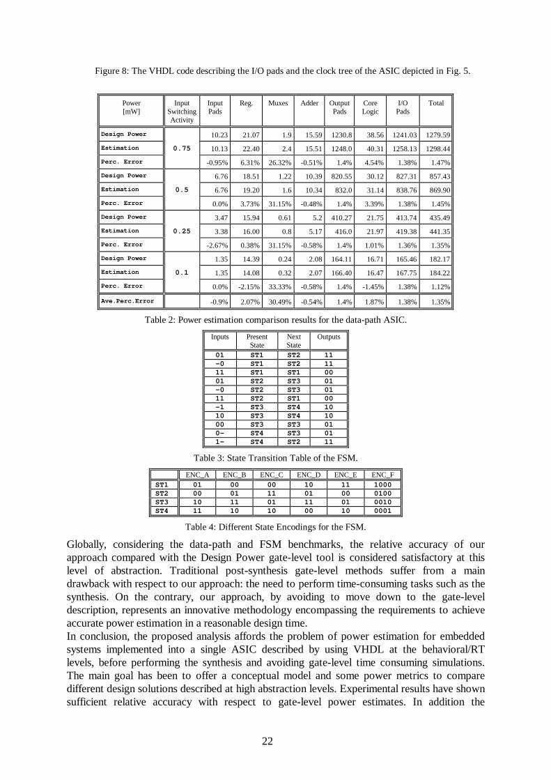
Design Compiler tool with the HCMOS6 technology.Experimental results are reported in Table 2, in terms of the average power dissipated by thedifferent parts of the ASIC, by considering several input switching activities: 0.75, 0.5, 0.25and 0.1. The results obtained by the proposed methodology have been compared to the resultsobtained through the Synopsys Design Power tool, based on the gate-level netlist. Note thatboth the estimation methods are based on a Zero Delay Model. As far the global power isconcerned, the proposed method provides a good approximation: the percentage error belongsto the range 1.12%-1.47% with respect to the Synopsys estimates. However, being theswitched capacitance of I/O nodes usually larger than the switched capacitance of the internalnodes up to three orders of magnitude, the major contribution to the global power isconstituted by the I/O power. In the benchmark, the I/O power represents the 94.83%, onaverage, of the total power, due to the reduced size of the core logic. Furthermore, the I/Opower estimates are very close to the gate-level estimates (1.38% on average), due to thesimple model used. Thus, to verify the accuracy of the proposed model, a more realisticmeasure is represented by the comparison of the core power: the model provides an estimationerror below 4.54%. In particular, the results show an average percentage error of 2.07% forthe registers, 30.49% for the multiplexers and -0.54% for the adder.
R_I2
64 MUX 2:1
R_AR_A R_A
0 1
ADDER
A B
R_I1
R_RES
A I1 I2
RES
RES
R_CMD
CMD
64 64 64 1
64
64
1
64
CLK IN_CLK
IN_CLK IN_CLK IN_CLK
IN_CLK
64 64
Figure 6: The ASIC architecture of the power estimation benchmark.
To show the validity of the proposed FSM power model, we consider the same Moore-typeFSM used in [3]. The State Transition Table of the four-states and two-inputs FSM isreported in Table 3, with an arbitrary output encoding. Several state encodings have been

20
applied to the FSM (see Table 4), to evaluate the effects of the state encoding on the powerestimates. In particular, we derived the ENC_A state encoding to minimize power, ENC_B isthe state encoding proposed in [3], ENC_C has been derived by using NOVA to minimize thearea, ENC_D and ENC_E are randomly generated encodings and ENC_F is an example of theOne-Hot encoding. As before, the results obtained by the proposed model have beencompared to the results obtained by the Design Power tool on the gate-level netlist (see Table5).Considering the effects of the different encoding algorithms on the global power estimates, asimilar trend can be observed both for Design Power and the proposed model. As expected,the Design Power measurements show a growing power dissipation from ENC_A to ENC_F.Our measurements, as reported in Table 5, show a rather similar behavior.Considering the global power, the proposed model shows an average percentage error of -2.31% (ranging from -8.68% to 3.0%) with respect to the Design Power estimates. However,there is an over-estimation of the power of the state-registers of 27.9%, on average.

21
OLEUDU\ ,(((�XVH ,(((�VWGBORJLFB�����DOO�XVH ,(((�VWGBORJLFBDULWK�DOO�XVH ,(((�VWGBORJLFBXQVLJQHG�DOO�
HQWLW\ &25( LV3RUW � &/. � ,Q VWGBORJLF�
$ � ,Q VWGBORJLFBYHFWRU �� WR ����,� � ,Q VWGBORJLFBYHFWRU �� WR ����,� � ,Q VWGBORJLFBYHFWRU �� WR ����&0' � ,Q VWGBORJLF�5(6 � 2XW VWGBORJLFBYHFWRU �� WR ��� ��
HQG &25(�DUFKLWHFWXUH %(+$9,25$/ RI &25( LVVLJQDO VB$ � VWGBORJLFBYHFWRU�� WR ����VLJQDO VB,� � VWGBORJLFBYHFWRU�� WR ����VLJQDO VB,� � VWGBORJLFBYHFWRU�� WR ����VLJQDO VB&0' � VWGBORJLF�VLJQDO PX[BRXW � VWGBORJLFBYHFWRU�� WR ����VLJQDO DGGBRXW � VWGBORJLFBYHFWRU�� WR ����VLJQDO FPGBSL � VWGBORJLF�VLJQDO FPGBSR � VWGBORJLF�VLJQDO FONBSL � VWGBORJLF�VLJQDO FONBSR � VWGBORJLF�VLJQDO DBSL � VWGBORJLFBYHFWRU�� WR ����VLJQDO DBSR � VWGBORJLFBYHFWRU�� WR ����
FRQVWDQW ]HUR � VWGBORJLF � ��FRQVWDQW RQH � VWGBORJLF � ��EHJLQIUHHBUHJV�SURFHVVEHJLQZDLW XQWLO &/.HYHQW DQG &/. ��
VB$ � $�VB,� � ,��VB,� � ,��VB&0' � &0'�5(6 � DGGBRXW�
HQG SURFHVV�PXOWLSOH[RU�SURFHVV�VB,��VB,��VB&0'�EHJLQLI �VB&0' ]HUR� WKHQ
PX[BRXW � VB,� �HOVH
PX[BRXW � VB,� �HQG LI�
HQG SURFHVV�DGGHU�SURFHVV�VB$�PX[BRXW�EHJLQ
DGGBRXW � VB$ � PX[BRXW�HQG SURFHVV�HQG %(+$9,25$/�
Figure 7: The VHDL code describing the core of the ASIC depicted in Fig.5.
OLEUDU\ ,(((�XVH ,(((�VWGBORJLFB�����DOO�XVH ,(((�VWGBORJLFBDULWK�DOO�XVH ,(((�VWGBORJLFBXQVLJQHG�DOO�
HQWLW\ 3(% LV3RUW � &/. � ,Q VWGBORJLF�
$ � ,Q VWGBORJLFBYHFWRU �� WR ����,� � ,Q VWGBORJLFBYHFWRU �� WR ����,� � ,Q VWGBORJLFBYHFWRU �� WR ����&0' � ,Q VWGBORJLF�5(6 � 2XW VWGBORJLFBYHFWRU �� WR ��� ��
HQG 3(%�DUFKLWHFWXUH %(+$9,25$/ RI 3(% LVVLJQDO LQB$ � VWGBORJLFBYHFWRU�� WR ����VLJQDO LQB,� � VWGBORJLFBYHFWRU�� WR ����VLJQDO LQB,� � VWGBORJLFBYHFWRU�� WR ����VLJQDO LQB&0' � VWGBORJLF�VLJQDO LQB&/. � VWGBORJLF�VLJQDO VBRXW � VWGBORJLFBYHFWRU�� WR ����VLJQDO FPGBSL� VWGBORJLF�VLJQDO FPGBSR� VWGBORJLF�VLJQDO FONBSL� VWGBORJLF�VLJQDO FONBSR� VWGBORJLF�VLJQDO DBSL � VWGBORJLFBYHFWRU�� WR ����VLJQDO DBSR � VWGBORJLFBYHFWRU�� WR ����VLJQDO L�BSL � VWGBORJLFBYHFWRU�� WR ����VLJQDO L�BSR � VWGBORJLFBYHFWRU�� WR ����VLJQDO L�BSL � VWGBORJLFBYHFWRU�� WR ����VLJQDO L�BSR � VWGBORJLFBYHFWRU�� WR ����FRQVWDQW ]HUR � VWGBORJLF � ��FRQVWDQW RQH � VWGBORJLF � ��FRPSRQHQW '59&�)
3RUW � $ � ,Q VWGBORJLF�3, � ,Q VWGBORJLF�32 � 2XW VWGBORJLF�= � 2XW VWGBORJLF ��
HQG FRPSRQHQW�FRPSRQHQW ,%8))
3RUW � $ � ,Q VWGBORJLF�3, � ,Q VWGBORJLF�32 � 2XW VWGBORJLF�= � 2XW VWGBORJLF ��
HQG FRPSRQHQW�FRPSRQHQW %�
3RUW � $ � ,Q VWGBORJLF�= � 2XW VWGBORJLF ��
HQG FRPSRQHQW�FRPSRQHQW &25(
3RUW � &/. � ,Q VWGBORJLF�$ � ,Q VWGBORJLFBYHFWRU �� WR ����,� � ,Q VWGBORJLFBYHFWRU �� WR ����,� � ,Q VWGBORJLFBYHFWRU �� WR ����&0' � ,Q VWGBORJLF�5(6 � 2XW VWGBORJLFBYHFWRU �� WR ��� ��
HQG FRPSRQHQW���EHJLQ&25(B/2*,& � &25( 3RUW 0DS �&/. !LQB&/.�
$ !LQB$�,� !LQB,��,� !LQB,��&0' !LQB&0'�5(6 !VBRXW ��
%B&/. � '59&�) 3RUW 0DS � $ ! &/.� = ! LQB&/.� 3, ! FONBSL�32 ! FONBSR ��%B&0' � ,%8)) 3RUW 0DS � $ ! &0'� = ! LQB&0'� 3, ! FPGBSL�32 ! FPGBSR ��JEXIIB$ � IRU L LQ $UDQJH JHQHUDWH%B$ � ,%8))
3RUW 0DS � $ ! $�L�� = ! LQB$�L�� 3, ! DBSL�L�� 32 ! DBSR�L� ��HQG JHQHUDWH�JEXIIB,� �IRU L LQ ,�UDQJH JHQHUDWH%B,� � ,%8))
3RUW 0DS � $ ! ,��L�� = ! LQB,��L�� 3, ! L�BSL�L�� 32 ! L�BSR�L� ��HQG JHQHUDWH�JEXIIB,� � IRU L LQ ,�UDQJH JHQHUDWH%B,� � ,%8))
3RUW 0DS � $ ! ,��L�� = ! LQB,��L�� 3, ! L�BSL�L�� 32 ! L�BSR�L� ��HQG JHQHUDWH�JEXIIB5(6 � IRU L LQ 5(6UDQJH JHQHUDWH%B5(6 � %�
3RUW 0DS � $ ! VBRXW�L�� = ! 5(6�L� ��HQG JHQHUDWH�HQG %(+$9,25$/�
22
Figure 8: The VHDL code describing the I/O pads and the clock tree of the ASIC depicted in Fig. 5.
Power[mW]
InputSwitchingActivity
InputPads
Reg. Muxes Adder OutputPads
CoreLogic
I/OPads
Total
Design Power 10.23 21.07 1.9 15.59 1230.8 38.56 1241.03 1279.59
Estimation 0.75 10.13 22.40 2.4 15.51 1248.0 40.31 1258.13 1298.44
Perc. Error -0.95% 6.31% 26.32% -0.51% 1.4% 4.54% 1.38% 1.47%
Design Power 6.76 18.51 1.22 10.39 820.55 30.12 827.31 857.43
Estimation 0.5 6.76 19.20 1.6 10.34 832.0 31.14 838.76 869.90
Perc. Error 0.0% 3.73% 31.15% -0.48% 1.4% 3.39% 1.38% 1.45%
Design Power 3.47 15.94 0.61 5.2 410.27 21.75 413.74 435.49
Estimation 0.25 3.38 16.00 0.8 5.17 416.0 21.97 419.38 441.35
Perc. Error -2.67% 0.38% 31.15% -0.58% 1.4% 1.01% 1.36% 1.35%
Design Power 1.35 14.39 0.24 2.08 164.11 16.71 165.46 182.17
Estimation 0.1 1.35 14.08 0.32 2.07 166.40 16.47 167.75 184.22
Perc. Error 0.0% -2.15% 33.33% -0.58% 1.4% -1.45% 1.38% 1.12%
Ave.Perc.Error -0.9% 2.07% 30.49% -0.54% 1.4% 1.87% 1.38% 1.35%
Table 2: Power estimation comparison results for the data-path ASIC.
Inputs PresentState
NextState
Outputs
01 ST1 ST2 11-0 ST1 ST2 1111 ST1 ST1 0001 ST2 ST3 01-0 ST2 ST3 0111 ST2 ST1 00-1 ST3 ST4 1010 ST3 ST4 1000 ST3 ST3 010- ST4 ST3 011- ST4 ST2 11
Table 3: State Transition Table of the FSM.
ENC_A ENC_B ENC_C ENC_D ENC_E ENC_FST1 01 00 00 10 11 1000ST2 00 01 11 01 00 0100ST3 10 11 01 11 01 0010ST4 11 10 10 00 10 0001
Table 4: Different State Encodings for the FSM.
Globally, considering the data-path and FSM benchmarks, the relative accuracy of ourapproach compared with the Design Power gate-level tool is considered satisfactory at thislevel of abstraction. Traditional post-synthesis gate-level methods suffer from a maindrawback with respect to our approach: the need to perform time-consuming tasks such as thesynthesis. On the contrary, our approach, by avoiding to move down to the gate-leveldescription, represents an innovative methodology encompassing the requirements to achieveaccurate power estimation in a reasonable design time.In conclusion, the proposed analysis affords the problem of power estimation for embeddedsystems implemented into a single ASIC described by using VHDL at the behavioral/RTlevels, before performing the synthesis and avoiding gate-level time consuming simulations.The main goal has been to offer a conceptual model and some power metrics to comparedifferent design solutions described at high abstraction levels. Experimental results have shownsufficient relative accuracy with respect to gate-level power estimates. In addition the

23
proposed estimation procedure is not time consuming. Finally, work is in progress aiming atintegrating the proposed conceptual framework and the related power metrics to guide thepartitioning task of a more general hardware-software co-design environment for embeddedsystems [2].
Power[µW]
EncodingType
StateReg.
Total
Design Power 134 419.77
Estimation ENC_A 169.31 432.39
Perc. Error 26.35% 3.00%
Design Power 133 439.5
Estimation ENC_B 169.31 432.39
Perc. Error 27.3% -1.62%
Design Power 156 470.45
Estimation ENC_C 197.03 483.62
Perc. Error 26.3% 2.8%
Design Power 154 516.99
Estimation ENC_D 197.03 483.93
Perc. Error 27.94% -6.39%
Design Power 155 529.57
Estimation ENC_E 197.03 483.62
Perc. Error 27.12% -8.68%
Design Power 240 584.6
Estimation ENC_F 317.83 567.34
Perc. Error 32.43% -2.95%
Ave. Perc.Error 27.9% -2.31%
Table 5: Power estimation comparison results for the FSM.
12. References[1] A.V. Aho, R. Sethi, J.D. Ullman, Compilers: Principles, Techniques, and Tools, (Addison-Wesley, 1986).[2] A. Balboni, W. Fornaciari, D. Sciuto, TOSCA: a pragmatic approach to co-designautomation of control dominated systems, Hardware/Software Co-design, NATO ASI Series,Series E: Applied Sciences, Vol. 310 (Kluwer Academic Publisher, 1996) 265-294.[3] L. Benini and G. De Micheli, State Assignment for Low Power Dissipation, IEEE Journalof Solid State Circuits, 30 (3) (1995) 258-268.[4] T.D. Burd and R.W. Brodersen, Energy Efficient CMOS Microprocessor Design, in: Proc.28th Hawaii International Conference on System Sciences, (Hawaii, 1995).[5] A. P. Chandrakasan and R. W. Brodersen, Minimizing Power Consumption in DigitalCMOS Circuits, Proceedings of the IEEE, 83 (4) (1995) 498-523.[6] G. De Micheli, Hardware/Software Co-Design: Application Domains and DesignTechnologies, Hardware/Software Co-design, NATO ASI Series, Series E: Applied Sciences,Vol. 310 (Kluwer Academic Publisher, 1996).[7] S. Devadas and S. Malik, A Survey of Optimization Techniques Targeting Low PowerVLSI Circuits, in: Proc. 32nd IEEE Design Automation Conference, (1995).[8] W. Fornaciari, P. Gubian, D. Sciuto, C. Silvano, A conceptual analysis framework for lowpower design of embedded systems, in: Proc. IEEE International Conference InnovativeSystem In Silicon, (Austin, TX, 1996).

24
[9] D. Harel et al., STATEMATE: A Working Environment for the Development of ComplexReactive Systems, IEEE Trans. on Software Engineering, 16(4) (1990) 403-414.[10] P. Landman, High-Level Power Estimation, in: Proc. ISLPED'96, InternationalSymposium on Low Power Electronics and Design, (Monterey, CA, 1996) 29-35.[11] P.E. Landman and J.M. Rabaey, Power Estimation for High-Level Synthesis, in: Proc.EDAC-EUROASIC '93 European Design Automation Conference, (Paris, 1993) 361-366.[12] P.E. Landman and J.M. Rabaey, Architectural Power Analysis: The Dual Bit TypeMethod, Trans. on Very Large Scale Integration (VLSI) Systems, 3(2) (1995).[13] P.E.Landman and J.M. Rabaey, Activity-Sensitive Architectural Power Analysis, IEEETrans. on Computer-Aided Design of Integrated Circuits and Systems, 15(6) (1996) 571-587.[14] LCB500K, Cell-Based ASIC Design Manual, (LSI Logic Corporation, June 1995).[15] E. Macii, Sequential Synthesis and Optimization for Low Power, Notes of the NATO-ASI Course on Low Power in Deep Submicron Electronics, (Kluwer Academic Publisher,1996).[16] R. Mehra and J. Rabaey, Behavioral Level Power Estimation and Exploration, in: Proc.First International Workshop on Low Power Design, (Napa Valley, CA, 1994) 197-202.[17] S. Narayan and D.D. Gajski, Area and Performance Estimation from System-LevelSpecifications, Technical Report ICS-92-16, Dept. of Information and Computer Science,University of California, Irvine, December 20, 1992.[18] V. Nagasamy, N. Berry and C. Dangelo, Specification, Planning, and Synthesis in aVHDL Design Environment, IEEE Design & Test of Computers, (1992) 58-68.[19] F.N. Najm, R. Burch, P. Yang and I.N. Hajj, Probabilistic Simulation for ReliabilityAnalysis of CMOS VLSI Circuits, IEEE Trans. on Computer-Aided Design, 9(4) (1990) 439-450, (Errata in July 1990).[20] F.N. Najm, A Survey of Power Estimation Techniques in VLSI Circuits, IEEE Trans. onVery Large Scale Integration (VLSI) Systems, 2(4) (1994) 446-455.[21] E. Olson and S.M. Kang, Low-Power State Assignment for Finite State Machines, in:Proc. IWLPD'94: ACM/IEEE International Workshop on Low Power Design, (Napa Valley,CA, 1994) 63-68.[22] A. Papoulis, Probability, Random Variables and Stochastic Processes,( McGraw-Hill,1984).[23] K. Roy and S.C. Prasad, Syclop: Synthesis of CMOS Logic for Low Power Application,in: Proc. ICCD'92 IEEE International Conference on Computer Design, (1992) 464-467.[24] D. Singh, J. Rabaey, M. Pedram, F. Catthoor, S. Rajgopal, N. Sehgal, T. Mozdzen,Power Conscious CAD Tools and Methodologies: A Perspective, Proceedings of the IEEE,83(4) (1995) 570-594.[25] C. Svensson and D. Liu, A Power Estimation Tool and Prospects of Power Savings inCMOS VLSI Chips, in: Proc. First Int. Workshop on Low Power Design, (Napa Valley, CA,1994) 171-176. [26] V. Tiwari, S. Malik and A. Wolfe, Power Analysis of Embedded Software: a First Steptowards Software Power Minimization, IEEE Trans. on VLSI Systems, (1994).[27] C.Y. Tsui, M. Pedram, C.A. Chen and A.M. Despain, Low Power State AssignmentTargeting Two- and Multi-Level Logic Implementations, in: Proc. ICCAD'1994: IEEE/ACMInternational Conference on Computer Aided Design, (1994) 82-87.[28] W.H. Wolf, Hardware-Software Co-design of Embedded Systems, Proceedings of theIEEE, 82(7) (1994) 967-989.