Versatile surface functionalization of cyclic olefin copolymer (COC) with sputtered SiO2 thin film...
10
Journals Journal of Materials Chemistry Advance Articles DOI: 10.1039/b904663a J. Mater. Chem., 2009 DOI: 10.1039/b904663a Paper Journal of Materials Chemistry Versatile surface functionalization of cyclic olefin copolymer (COC) with sputtered SiO2 thin film for potential BioMEMS applications Kuo-Sheng Ma , Faisal Reza , Ishtiaq Saaem and Jingdong Tian * Department of Biomedical Engineering and the Institute for Genome Sciences and Policy, Duke University, 36 Hudson Hall, Box 90281, Durham, NC 27708-0281, USA. E-mail: [email protected] Received 6th March 2009 , Accepted 12th August 2009 First published on the web 9th September 2009 Cyclic olefin copolymer (COC) is a new class of thermoplastic polymers used for a variety of applications ranging from bio-sensing to optics. However, lack of functional groups and intense surface hydrophobicity hamper further development and application of this material. Here, we describe fabrication and characterization of SiO2–COC hybrid material (oxCOC), which provides a desirable substrate for microfluidic devices and subsequent surface modifications. The deposited SiO2 thin film on COC surface was characterized by X-ray photoelectron spectroscopy and Fourier transform infrared spectroscopy. The new SiO2–COC hybrid was found to have similar high optical transmission properties as that of pristine COC. Profilometric and AFM analysis revealed no dramatic change in morphology or surface roughness of functionalized COC. The SiO2–COC hybrid appeared to be stable in most of the solvents evaluated and could be further modified by other compounds, such as 3-aminopropyltriethoxy silane (APTES). The new SiO2–COC hybrid material and the robust fabrication method are expected to enable a variety of BioMEMS applications. 1. Introduction With emerging interest in novel materials for microfabrication, polymers have gained significant attention as promising materials for rapid prototyping. Various polymers with diverse properties provide practical, versatile and cost-effective alternatives to the inorganic substrates (i.e. silicon or glass) for micro-devices fabrication. Recently, a new class of thermoplastic polymer, cyclic olefin copolymer, has attracted special attention due to its desirable properties such as low auto-fluorescence, low density, low moisture adsorption, excellent optical and UV transparency, high stiffness, and resistance to organic solvents. 1 Products composed of COC exhibit a glass transition temperature (Tg) ranging from 70 °C to 180 °C. 2 COC has been utilized in micro-electrical-mechanical systems (MEMS) 3–5 and micro total analysis systems ( TAS). 6–8 Inexpensive and easily replicable fabrication techniques such as injection molding 9 and hot embossing 10 have been used extensively and successfully on COC. For most microfluidic lab-on-a-chip bio-sensing and bio-analytical applications, it is desirable to have a hydrophilic surface with appropriate functional groups for biomolecular conjugation. However, like most commodity polymers used in microfabrications, COC presents a chemically inert and highly hydrophobic surface. The hydrophobic surface will create significant difficulties for liquid injection and flow control in microfluidic channels. The lack of functional surface groups for immobilizing biomolecules poses an additional hindrance for potential applications of COC in biomolecular recognition and analysis. A number of methods have been developed to mitigate such problems. Photografting has been developed as a technique for surface modifications of synthetic polymers used for microfabrication. This technique has been extended for COC microfluidic device fabrication. Different types of monomers, such as acrylamide and methyl acrylate, have been successfully grafted on the surface of COC to generate various functional groups. 9,11–13 The UV-initiated and benzophenone-mediated photografting process generates branched and cross-linked polymer architecture on the substrate surface. The process could also lead to formation of ungrafted polymer suspended in the reaction solution, which may deplete free monomers for surface grafting and may clog the microfluidic channels. 14 Solutions to reduce hydrophobicity include activation of the polymer surface by hydrophilizing treatments, such as plasma, 15,16 UV/ozone, 17,18 and corona discharge treatment. 19 Drawbacks of such treatments may include polymer surface damage or treatment degradation during time of usage. 20 SiO2 thin films have been broadly used in integrated circuits (ICs) and microfabrication techniques. 21 They can serve as the insulating material to block the interconnection between two devices; or they can provide chemical functional groups or linkers to bind a plethora of compounds to the substrate surface. In addition, their hydrophilic characteristics in aqueous solutions can significantly mitigate surface problems of polymers in chemical and biological sensing applications. It was reasoned that by depositing an SiO2 thin film on the surface of COC structures, the hybrid will take advantage of both materials: the unique properties and fast and inexpensive prototyping capability of COC,
-
Upload
independent -
Category
Documents
-
view
2 -
download
0
Transcript of Versatile surface functionalization of cyclic olefin copolymer (COC) with sputtered SiO2 thin film...
Journals Journal of Materials Chemistry Advance Articles DOI: 10.1039/b904663a
J. Mater. Chem., 2009 DOI: 10.1039/b904663a Paper
Journal of Materials Chemistry
Versatile surface functionalization of cyclic olefin copolymer (COC)with sputtered SiO2 thin film for potential BioMEMS applicationsKuo-Sheng Ma , Faisal Reza , Ishtiaq Saaem and Jingdong Tian *Department of Biomedical Engineering and the Institute for Genome Sciences and Policy, Duke University, 36 HudsonHall, Box 90281, Durham, NC 27708-0281, USA. E-mail: [email protected]
Received 6th March 2009 , Accepted 12th August 2009
First published on the web 9th September 2009
Cyclic olefin copolymer (COC) is a new class of thermoplastic polymers used for a variety of applications ranging frombio-sensing to optics. However, lack of functional groups and intense surface hydrophobicity hamper furtherdevelopment and application of this material. Here, we describe fabrication and characterization of SiO2–COC hybridmaterial (oxCOC), which provides a desirable substrate for microfluidic devices and subsequent surface modifications.The deposited SiO2 thin film on COC surface was characterized by X-ray photoelectron spectroscopy and Fouriertransform infrared spectroscopy. The new SiO2–COC hybrid was found to have similar high optical transmissionproperties as that of pristine COC. Profilometric and AFM analysis revealed no dramatic change in morphology orsurface roughness of functionalized COC. The SiO2–COC hybrid appeared to be stable in most of the solventsevaluated and could be further modified by other compounds, such as 3-aminopropyltriethoxy silane (APTES). Thenew SiO2–COC hybrid material and the robust fabrication method are expected to enable a variety of BioMEMSapplications.
1. Introduction
With emerging interest in novel materials for microfabrication, polymers have gained significant attention aspromising materials for rapid prototyping. Various polymers with diverse properties provide practical, versatile andcost-effective alternatives to the inorganic substrates (i.e. silicon or glass) for micro-devices fabrication. Recently, anew class of thermoplastic polymer, cyclic olefin copolymer, has attracted special attention due to its desirableproperties such as low auto-fluorescence, low density, low moisture adsorption, excellent optical and UV transparency,high stiffness, and resistance to organic solvents.1 Products composed of COC exhibit a glass transition temperature(Tg) ranging from 70 °C to 180 °C.2 COC has been utilized in micro-electrical-mechanical systems (MEMS)3–5 andmicro total analysis systems ( TAS).6–8 Inexpensive and easily replicable fabrication techniques such as injectionmolding9 and hot embossing10 have been used extensively and successfully on COC.
For most microfluidic lab-on-a-chip bio-sensing and bio-analytical applications, it is desirable to have ahydrophilic surface with appropriate functional groups for biomolecular conjugation. However, like most commoditypolymers used in microfabrications, COC presents a chemically inert and highly hydrophobic surface. The hydrophobicsurface will create significant difficulties for liquid injection and flow control in microfluidic channels. The lack offunctional surface groups for immobilizing biomolecules poses an additional hindrance for potential applications ofCOC in biomolecular recognition and analysis.
A number of methods have been developed to mitigate such problems. Photografting has been developed as atechnique for surface modifications of synthetic polymers used for microfabrication. This technique has been extendedfor COC microfluidic device fabrication. Different types of monomers, such as acrylamide and methyl acrylate, havebeen successfully grafted on the surface of COC to generate various functional groups.9,11–13 The UV-initiated andbenzophenone-mediated photografting process generates branched and cross-linked polymer architecture on thesubstrate surface. The process could also lead to formation of ungrafted polymer suspended in the reaction solution,which may deplete free monomers for surface grafting and may clog the microfluidic channels.14 Solutions to reducehydrophobicity include activation of the polymer surface by hydrophilizing treatments, such as plasma,15,16
UV/ozone,17,18 and corona discharge treatment.19 Drawbacks of such treatments may include polymer surface damageor treatment degradation during time of usage.20
SiO2 thin films have been broadly used in integrated circuits (ICs) and microfabrication techniques.21 They canserve as the insulating material to block the interconnection between two devices; or they can provide chemicalfunctional groups or linkers to bind a plethora of compounds to the substrate surface. In addition, their hydrophiliccharacteristics in aqueous solutions can significantly mitigate surface problems of polymers in chemical and biologicalsensing applications. It was reasoned that by depositing an SiO2 thin film on the surface of COC structures, the hybridwill take advantage of both materials: the unique properties and fast and inexpensive prototyping capability of COC,
and the well established surface chemistry of SiO2 thin films. In addition, SiO2 thin films are less likely to affect theoptical properties of COC.
In the current report we describe a method of depositing SiO2 thin films on a COC surface using a low-temperaturesputtering technique. We further describe the characterization of the deposited SiO2 thin film and the physical,optical, and chemical properties of the SiO2–COC hybrid material. Finally, we show that this method and theresulting hybrid material are well suited for microfabrication purposes and for subsequent surface functionalizations.
2. Experimental
All chemicals were purchased and used as received without further purification. Acetone, isopropyl alcohol (IPA),ethanol, methanol, methylene chloride, tetrahydrofuran (THF), and acetonitrile (ACN) were purchased from VWR.Hydrochloric acid, sulfuric acid, sodium hydroxide, NH4OH, phosphate buffered saline solution, Tris-EDTA bufferwere purchased from Sigma and diluted with dI H2O.
COC plates (Topas 6015, 6 × 6 ) were purchased from Topas (Florence, KY). A plate was cut into small pieceswith desired dimensions to fit into different characterization tools. Samples were cleaned in a clean-roomenvironment by the RCA method (NH4OH–H2O2–dIH2O = 1 : 1 : 5) at 80 °C for 15 min and dried by a stream ofnitrogen. Samples were baked in a vacuum oven at 110 °C for 1 h before film deposition.
Silicon dioxide films were deposited by using a Kurt Lesker PVD 75 (Kurt J. Lesker Company, Pittsburgh, PA) RFmagnetron sputtering system. A 3 SiO2 sputtering target (99.995% purity) was used. Substrates were fixed on aholder on top of the target and the holder rotated at constant speed for uniform deposition. The chamber was pumpeddown to 5.0 × 10⁻⁶ Torr and gases were purged into chamber by opening the gas valve. High-purity Ar and O2 weremixed by pre-set program MODE 2 and were introduced to the chamber to reach the desired gas pressure andstabilize. RF power was gradually increased to the desired level with the shutter closed at a ramp rate of 10 W min−1.The shutter was opened at the desired RF power level and deposition was timed.
The deposited film thickness was measured with an optical interferometer, Nanometrics 210 (NanometricsIncorporated, CA). A 10× objective lens for small spot size focus and the standard Oxide on Silicon thicknessmeasurement program were employed. A total of five points for each sample were randomly chosen for measurement.The average deposition rate was calculated by dividing the total film thickness by the total deposition time. Due to theclose refractive indices between SiO2 film and the COC substrate, and the fact that both layers are transparent, thefilm thickness could not be directly measured by most optical techniques. Therefore, a small piece of silicon wafer wasput into the deposition chamber along with the COC substrate for total film thickness measurements.
Infrared absorption spectra were collected on a Thermo Electron Nicolet 8700 FTIR spectrometer equipped withthe Vectra-Piezo interferometer. A smart Orbit ATR module accessory with a Ge crystal as an internal reflectionelement was used. For background and sample, 32 scans at 2 cm−1 resolution were collected.
Chemical binding energy analyses of the film were performed using a Kratos Analytical Axis Ultra X-rayphotoelectron spectrometer (Kratos Analytical Inc, New York) with a monochromatic Al KR X-ray source radiation at1486.6 eV. The survey spectrum was an average of ten sweeps at pass energy of 160 eV, 1 eV per step resolution and200 ms dwell time. For high-resolution regions spectra of C1s, O1s, and Si1 p were an average of ten sweeps at passenergy of 20 eV, 1 eV per step resolution and 200 ms dwell time.
UV-vis spectra were collected on a Shimadzu UV-3600. The transmittance percentage was measured from 250 to700 nm with sampling interval of 1 nm. Slit width was 2 nm and each sample was single scan. The resulting spectrawere analyzed and reported by the software UVProbe .
Atomic force microscope images were collected in tapping mode using a Digital Instruments Dimension 3100produced by Veeco Instruments Inc. (Plainview, NY). 3-aminopropyl triethoxy silane (APTES) was used tofunctionalize the COC–SiO2 surface. The silanes were dissolved at 1% (v/v) concentration in a solvent of 95%methanol and 5% dIH2O. Samples were incubated in the solution at room temperature for 15 h. The samples werewashed with original solvent and dried with a nitrogen stream. The samples were then baked in an oven at 120 °C for2 h.
3. Results and discussion
3.1. Fabrication of SiO2–COC hybrid
In order to select a suitable method for binding SiO2 thin film on COC, we evaluated potential deposition methods,including chemical vapor deposition (CVD)22 and physical vapor deposition (PVD).23 In CVD, the reactants areabsorbed on the hot substrate surface where film-forming reaction occurs. Since the substrate must be heated to ahigh temperature (typically higher than 300 °C), this approach is not practical for COC. PVD can be done at lowertemperatures and therefore maybe suitable. In PVD, we preferred sputtering over evaporation due to excellent filmadhesion, improved film uniformity control, and step coverage.24 Apart from surface self-heating by target atom energydissipation, sputtering is considered a low-temperature process. Nowadays, sputtering techniques have been broadlyemployed in applying films to computer disks, compact discs (CDs), liquid crystal displays, and so on. Therefore, wedecided to test sputtering for deposition of SiO2 thin film onto COC.
The deposition rate was the first parameter to be tuned in order to control the thickness of thin film deposition. Ina sputtering system, the film deposition rate is influenced by the anode-to-cathode distance, gas pressure, and RF
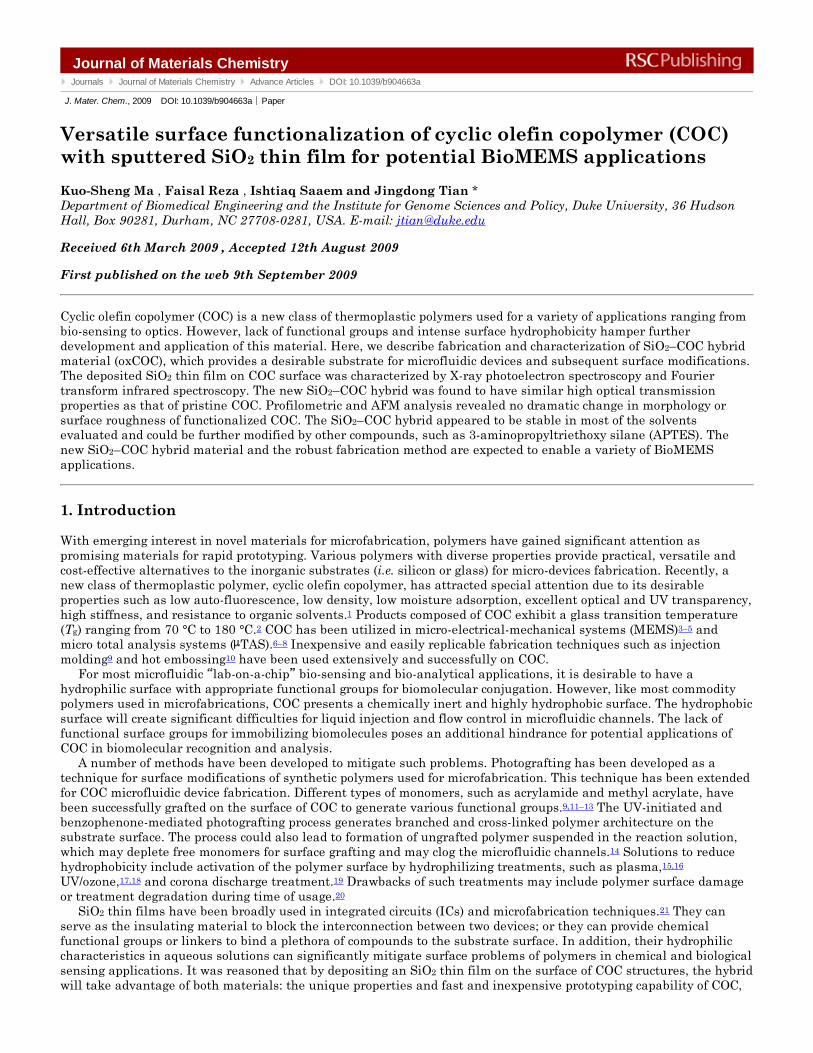
power. Since the anode-to-cathode distance was kept constant in this study, only the gas pressure and the power wereadjusted. As shown in Fig. 1, decreasing gas pressure or increasing power will increase the deposition rate. This canbe explained by the kinetic molecular theory, which states that the mean-free-path of a sputtered atom is inverselyproportional to the total gas pressure in the chamber.25 In our study, a maximum rate of 16.5 nm per min wasachieved at a setting of 300 W and 5 mTorr.
Fig. 1 Deposition rates of SiO2 thin film at differentsputtering powers and pressures.
3.2. Characterization of the deposited thin film
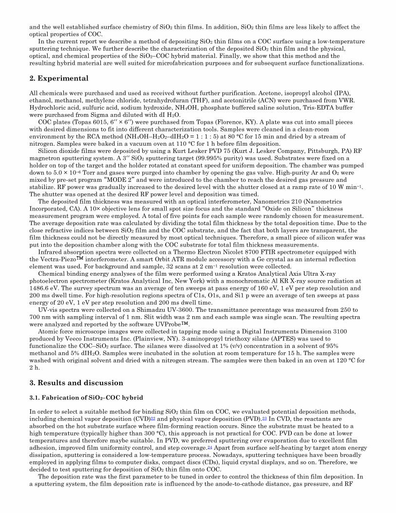
To investigate the chemical bonding structure of the deposited thin film, we used Fourier transform infraredspectroscopy (FTIR). The spectra were recorded using a Thermo Electron Nicolet 8700 FTIR spectrometer. Anattenuated total reflection (ATR) sampling module with Smart Orbit accessory and a germanium crystal plate wereutilized to analyze the thin oxide film on the substrate. The measurements were taken over wave numbers rangingfrom 4000 cm−1 to 500 cm−1 at a resolution of 2 cm−1. It was acknowledged that the optical setups were different in theATR and the transmission experiments. Thus, when comparing the transmissions, the relative peaks in the ATRspectrum showed distortions in relative intensities and shifted to lower frequencies. To eliminate these distortions, acorrection algorithm introduced in software package OMNIC 6.2 (Thermo Scientific Nicolet ) was applied to allobtained spectra. The corrected spectra of different ATR samples are shown in Fig. 2. The spectrum of the sample withRF sputtered thin film shows two intense bands at 809 cm−1 and 1071 cm−1, corresponding to the Si–O–Si bending andstretching modes, respectively (Fig. 2b), which have been reported in the literature.26,27 However, since the lowerdetection wave number limit was determined by the internal reflection element (IRE) and that the limit of the IREused in our system was approximately 600 cm−1 (Ge),28 the third band corresponding to the rocking modes ( 1) atapproximately 450 cm−1 was out of range in our spectrum. The two absorption bands at 1196 cm−1 and 1071 cm−1 wereboth assigned to the asymmetric Si–O–Si vibration mode, where oxygen atoms move back and forth along the axis lineof the silicon atoms. By comparison, these bands did not appear in the spectrum of the untreated COC sample (Fig.2a). In both spectra, the absorption at 2950 cm−1 − 2850 cm−1 region was assigned to the carbon/hydrogen stretchingvibration modes of –CH2 and –CH3. Additionally, the peak around 1453 cm−1 represents the wagging mode of –CH3 inthe polymer backbone. These peaks were significantly smaller in Fig. 2b, which indicated the covering of the polymersurface. The broad absorption beak around 3400 cm−1 in Fig. 2b was assigned to the hydroxyl group stretching, whichwas related to the presence of Si–OH vibration. It is believed that the –OH group on deposited SiO2 film is formed byinteraction between SiO2 and moisture in ambient air.29 This band was absent in the spectrum of untreated sample(Fig. 2a), which further indicated successful deposition of the SiO2 film.
Fig. 2 Infrared spectra of COC samples. (a) Without SiO2deposition. (b) With SiO2 deposition.
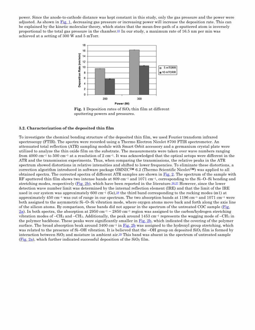
X-Ray photoelectron spectroscopy (XPS) analysis was used to further characterize the sputtered SiO2 on the COCsurface (Fig. 3). A representative survey spectra collected from untreated COC indicated typical C(1s) peak (284.5 eV),O(1s) peak (529.5 eV) and O KLL peaks (973.5 eV) (Fig. 3a). The survey spectra of SiO2 sputtered COC showeddramatic increase in O(1s) intensity and equally dramatic decrease in C(1s) intensity (Fig. 3b). In addition, the twoprominent peaks at 153.6 eV (Si 2s) and 102.6 eV (Si 2 p) agreed well with the reported binding energies of SiO2,30
which further confirmed the presence of SiO2 film on the polymer surface (Fig. 3b). Concentrations of carbon, oxygenand silicon atoms on both sample surfaces were estimated from peak areas. Ratios of oxygen-to-carbon (O/C) andsilicon-to-carbon (Si/C) were calculated using atomic percentage in spectra and the results for both samples are listedin Table 1. Comparing the modified with the bare surface, the average O/C ratios changed from 0.047 to 8.68, whilethe average Si/C ratios for 0 to 3.86. This result was consistent with the expected surface modification. A reduction inC(1s) intensity was expected when the surface was coated by SiO2. In addition, the incorporation of oxygen and siliconatoms was also expected to increase the ratios of O/C and Si/C. The high ratios of O/C and Si/C on coated sampledemonstrated the high efficiency of the sputtering process.
Table 1 XPS compositional analysis of COC samples with and without SiO2 film deposition.a
Atomic concentration (%)
XC XO XSi XO/XC XSi/XC
COC 95.52 4.48 —a 0.0469 —a
COC/SiO2 7.38 64.09 28.53 8.6842 3.8658a Element not present.
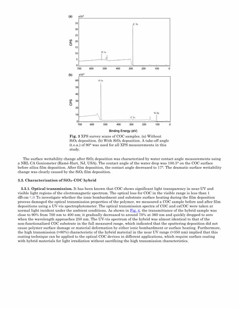
Fig. 3 XPS survey scans of COC samples. (a) WithoutSiO2 deposition. (b) With SiO2 deposition. A take-off angle(t.o.a.) of 90° was used for all XPS measurements in thisstudy.
The surface wettability change after SiO2 deposition was characterized by water contact angle measurements usinga NRL CA Goniometer (Ramé-Hart, NJ, USA). The contact angle of the water drop was 100.5° on the COC surfacebefore silica film deposition. After film deposition, the contact angle decreased to 17°. The dramatic surface wettabilitychange was clearly caused by the SiO2 film deposition.
3.3. Characterization of SiO2–COC hybrid
3.3.1. Optical transmission. It has been known that COC shows significant light transparency in near-UV andvisible light regions of the electromagnetic spectrum. The optical loss for COC in the visible range is less than 1dB-cm−1.31 To investigate whether the ionic bombardment and substrate surface heating during the film depositionprocess damaged the optical transmission properties of the polymer, we measured a COC sample before and after filmdepositions using a UV-vis spectrophotometer. The optical transmission spectra of COC and oxCOC were taken atnormal light incident under the ambient conditions. As shown in Fig. 4, the transmittance of the hybrid sample wasclose to 90% from 700 nm to 400 nm; it gradually decreased to around 70% at 360 nm and quickly dropped to zerowhen the wavelength approaches 250 nm. The UV-vis spectrum of the hybrid was almost identical to that of thenon-functionalized COC substrate in the full measured range, which indicated that the sputtering deposition did notcause polymer surface damage or material deformation by either ionic bombardment or surface heating. Furthermore,the high transmission (>80%) characteristic of the hybrid material in the near UV range (>350 nm) implied that thiscoating technique can be applied to the optical COC devices in different applications, which require surface coatingwith hybrid materials for light irradiation without sacrificing the high transmission characteristics.
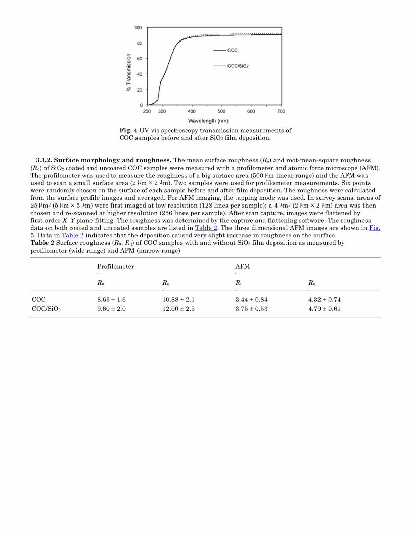
Fig. 4 UV-vis spectroscopy transmission measurements ofCOC samples before and after SiO2 film deposition.
3.3.2. Surface morphology and roughness. The mean surface roughness (Ra) and root-mean-square roughness(Rq) of SiO2 coated and uncoated COC samples were measured with a profilometer and atomic force microscope (AFM).The profilometer was used to measure the roughness of a big surface area (500 m linear range) and the AFM wasused to scan a small surface area (2 m × 2 m). Two samples were used for profilometer measurements. Six pointswere randomly chosen on the surface of each sample before and after film deposition. The roughness were calculatedfrom the surface profile images and averaged. For AFM imaging, the tapping mode was used. In survey scans, areas of25 m2 (5 m × 5 m) were first imaged at low resolution (128 lines per sample); a 4 m2 (2 m × 2 m) area was thenchosen and re-scanned at higher resolution (256 lines per sample). After scan capture, images were flattened byfirst-order X–Y plane-fitting. The roughness was determined by the capture and flattening software. The roughnessdata on both coated and uncoated samples are listed in Table 2. The three dimensional AFM images are shown in Fig.5. Data in Table 2 indicates that the deposition caused very slight increase in roughness on the surface.Table 2 Surface roughness (Ra, Rq) of COC samples with and without SiO2 film deposition as measured byprofilometer (wide range) and AFM (narrow range)
Profilometer AFM
Ra Rq Ra Rq
COC 8.63 ± 1.6 10.88 ± 2.1 3.44 ± 0.84 4.32 ± 0.74COC/SiO2 9.60 ± 2.0 12.00 ± 2.5 3.75 ± 0.53 4.79 ± 0.61
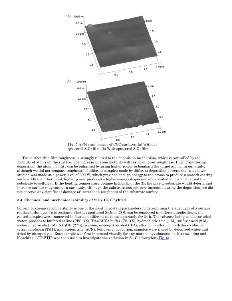
Fig. 5 AFM scan images of COC surfaces. (a) Withoutsputtered SiO2 film. (b) With sputtered SiO2 film.
The surface thin film roughness is strongly related to the deposition mechanism, which is controlled by themobility of atoms on the surface. The increase in atom mobility will result in lower roughness. During sputteringdeposition, the atom mobility can be enhanced by using higher power to bombard the target atoms. In our study,although we did not compare roughness of different samples made by different deposition powers, the sample westudied was made at a power level of 300 W, which provided enough energy to the atoms to produce a smooth coatingsurface. On the other hand, higher power produced a higher-energy dispersion of deposited atoms and caused thesubstrate to self-heat. If the heating temperature became higher than the Tg, the plastic substrate would deform andincrease surface roughness. In our study, although the substrate temperature increased during the deposition, we didnot observe any significant damage or increase in roughness of the substrate surface.
3.4. Chemical and mechanical stability of SiO2–COC hybrid
Solvent or chemical compatibility is one of the most important parameters in determining the adequacy of a surfacecoating technique. To investigate whether sputtered SiO2 on COC can be employed in different applications, thecoated samples were immersed in fourteen different solvents separately for 24 h. The solvents being tested includedwater, phosphate buffered saline (PBS, 1X), Tris-EDTA buffer (TE, 1X), hydrochloric acid (1 M), sulfuric acid (2 M),sodium hydroxide (1 M), NH4OH (27%), acetone, isopropyl alcohol (IPA), ethanol, methanol, methylene chloride,tetrahydrofuran (THF), and acetonitrile (ACN). Following incubation, samples were rinsed by deionized water anddried by nitrogen gas. Each sample was first inspected visually for any morphology changes, such as swelling andbleaching. ATR-FTIR was then used to investigate the variation in Si–O adsorption (Fig. 6).
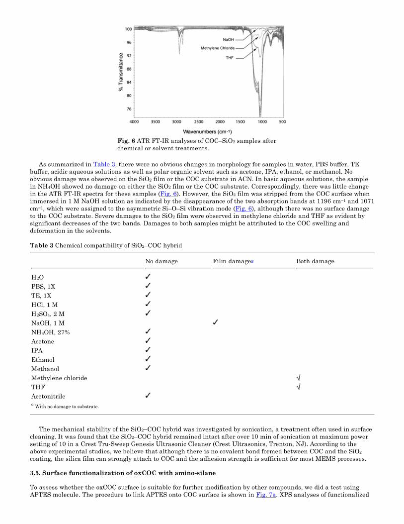
Fig. 6 ATR FT-IR analyses of COC–SiO2 samples afterchemical or solvent treatments.
As summarized in Table 3, there were no obvious changes in morphology for samples in water, PBS buffer, TEbuffer, acidic aqueous solutions as well as polar organic solvent such as acetone, IPA, ethanol, or methanol. Noobvious damage was observed on the SiO2 film or the COC substrate in ACN. In basic aqueous solutions, the samplein NH4OH showed no damage on either the SiO2 film or the COC substrate. Correspondingly, there was little changein the ATR FT-IR spectra for these samples (Fig. 6). However, the SiO2 film was stripped from the COC surface whenimmersed in 1 M NaOH solution as indicated by the disappearance of the two absorption bands at 1196 cm−1 and 1071cm−1, which were assigned to the asymmetric Si–O–Si vibration mode (Fig. 6), although there was no surface damageto the COC substrate. Severe damages to the SiO2 film were observed in methylene chloride and THF as evident bysignificant decreases of the two bands. Damages to both samples might be attributed to the COC swelling anddeformation in the solvents.
Table 3 Chemical compatibility of SiO2–COC hybrid
No damage Film damagea Both damage
H2OPBS, 1XTE, 1XHCl, 1 MH2SO4, 2 MNaOH, 1 MNH4OH, 27%AcetoneIPAEthanolMethanolMethylene chlorideTHFAcetonitrilea With no damage to substrate.
The mechanical stability of the SiO2–COC hybrid was investigated by sonication, a treatment often used in surfacecleaning. It was found that the SiO2–COC hybrid remained intact after over 10 min of sonication at maximum powersetting of 10 in a Crest Tru-Sweep Genesis Ultrasonic Cleaner (Crest Ultrasonics, Trenton, NJ). According to theabove experimental studies, we believe that although there is no covalent bond formed between COC and the SiO2coating, the silica film can strongly attach to COC and the adhesion strength is sufficient for most MEMS processes.
3.5. Surface functionalization of oxCOC with amino-silane
To assess whether the oxCOC surface is suitable for further modification by other compounds, we did a test usingAPTES molecule. The procedure to link APTES onto COC surface is shown in Fig. 7a. XPS analyses of functionalized
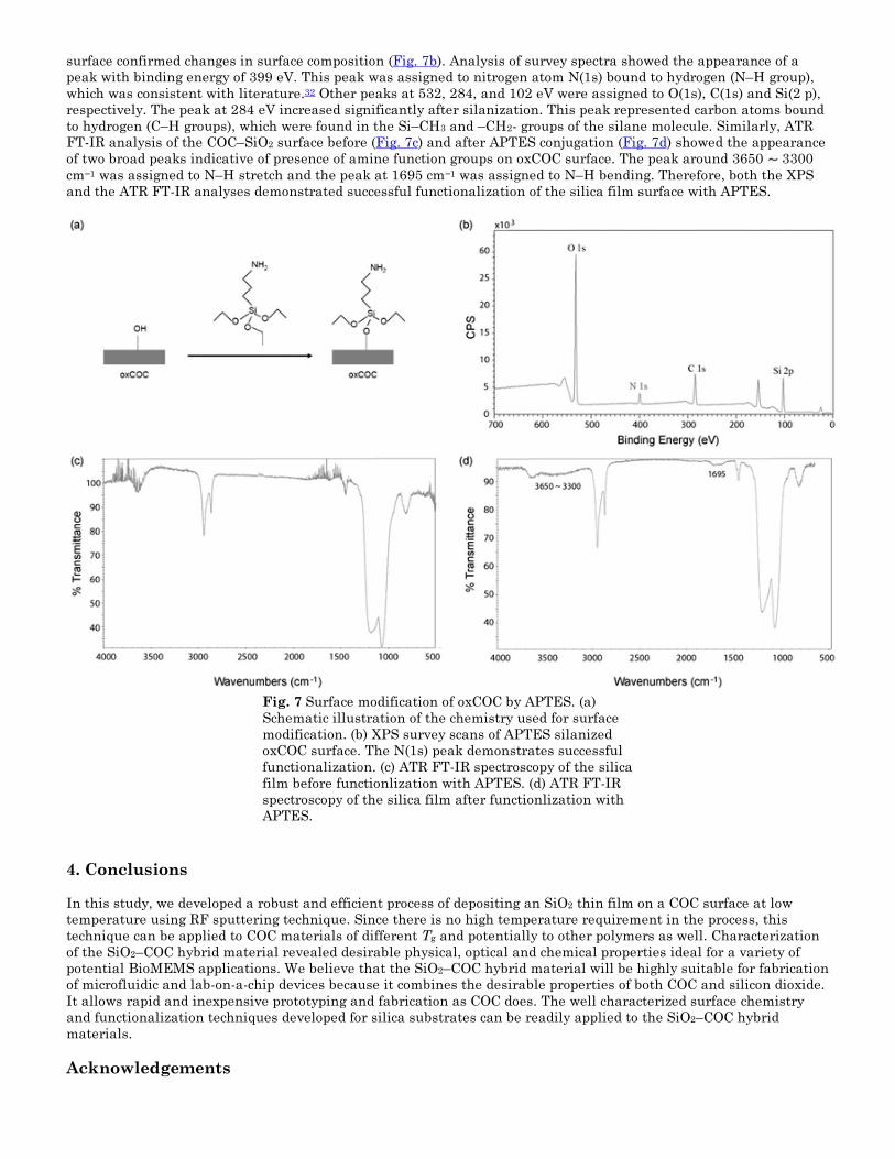
surface confirmed changes in surface composition (Fig. 7b). Analysis of survey spectra showed the appearance of apeak with binding energy of 399 eV. This peak was assigned to nitrogen atom N(1s) bound to hydrogen (N–H group),which was consistent with literature.32 Other peaks at 532, 284, and 102 eV were assigned to O(1s), C(1s) and Si(2 p),respectively. The peak at 284 eV increased significantly after silanization. This peak represented carbon atoms boundto hydrogen (C–H groups), which were found in the Si–CH3 and –CH2- groups of the silane molecule. Similarly, ATRFT-IR analysis of the COC–SiO2 surface before (Fig. 7c) and after APTES conjugation (Fig. 7d) showed the appearanceof two broad peaks indicative of presence of amine function groups on oxCOC surface. The peak around 3650 3300cm−1 was assigned to N–H stretch and the peak at 1695 cm−1 was assigned to N–H bending. Therefore, both the XPSand the ATR FT-IR analyses demonstrated successful functionalization of the silica film surface with APTES.
Fig. 7 Surface modification of oxCOC by APTES. (a)Schematic illustration of the chemistry used for surfacemodification. (b) XPS survey scans of APTES silanizedoxCOC surface. The N(1s) peak demonstrates successfulfunctionalization. (c) ATR FT-IR spectroscopy of the silicafilm before functionlization with APTES. (d) ATR FT-IRspectroscopy of the silica film after functionlization withAPTES.
4. Conclusions
In this study, we developed a robust and efficient process of depositing an SiO2 thin film on a COC surface at lowtemperature using RF sputtering technique. Since there is no high temperature requirement in the process, thistechnique can be applied to COC materials of different Tg and potentially to other polymers as well. Characterizationof the SiO2–COC hybrid material revealed desirable physical, optical and chemical properties ideal for a variety ofpotential BioMEMS applications. We believe that the SiO2–COC hybrid material will be highly suitable for fabricationof microfluidic and lab-on-a-chip devices because it combines the desirable properties of both COC and silicon dioxide.It allows rapid and inexpensive prototyping and fabrication as COC does. The well characterized surface chemistryand functionalization techniques developed for silica substrates can be readily applied to the SiO2–COC hybridmaterials.
Acknowledgements

We thank Dr Mark Walters for helpful discussions. J. T. is a Beckman Young Investigator and a recipient of aHartwell Individual Biomedical Research Award.
References
1 R. R. Lamonte and D. McNally, Plast. Eng., 2000, 56, 51.2 R. R. Lamonte and D. McNally, Adv. Mater. Process., 2001, 159, 33–36.3 M. B. Hochrein, C. Reich, B. Krause, J. O. Radler and B. Nickel, Langmuir, 2006, 22, 538–545 [Links].4 H. D. Bauer, W. Ehrfeld, J. Hossfeld and T. Paatzsch, Opt. Fabrication Testing, 1999, 3739, 224–229.5 H. D. Bauer, W. Ehrfeld, M. Harder, T. Paatzsch, M. Popp and I. Smaglinski, Synth. Met., 2000, 115, 13–20.6 C. Li, Y. N. Yang, H. G. Craighead and K. H. Lee, Electrophoresis, 2005, 26, 1800–1806 [Links].7 D. Nilsson, S. Balslev and A. Kristensen, J. Micromech. Microeng., 2005, 15, 296–300 [Links].8 D. S. Kim, S. H. Lee, C. H. Ahn, J. Y. Lee and T. H. Kwon, Lab Chip, 2006, 6, 794–802 [Links].9 D. A. Mair, E. Geiger, A. P. Pisano, J. M. J. Frechet and F. Svec, Lab Chip, 2006, 6, 1346–1354 [Links].
10 J. Steigert, S. Haeberle, T. Brenner, C. Muller, C. P. Steinert, P. Koltay, N. Gottschlich, H. Reinecke, J. Ruhe, R.Zengerle and J. Ducree, J. Micromech. Microeng., 2007, 17, 333–341 [Links].
11 M. F. Bedair and R. D. Oleschuk, Anal. Chem., 2006, 78, 1130–1138 [Links].12 Q. S. Pu, O. Oyesanya, B. Thompson, S. T. Liu and J. C. Alvarez, Langmuir, 2007, 23, 1577–1583 [Links].13 T. Rohr, D. F. Ogletree, F. Svec and J. M. J. Frechet, Adv. Funct. Mater., 2003, 13, 264–270 [Links].14 S. W. Hu, X. Q. Ren, M. Bachman, C. E. Sims, G. P. Li and N. L. Allbritton, Anal. Chem., 2004, 76, 1865–1870
[Links].15 D. Nikolova, E. Dayss, G. Leps and A. Wutzler, Surf. Interface Anal., 2004, 36, 689–693 [Links].16 S. Laib and B. D. MacCraith, Anal. Chem., 2007, 79, 6264–6270 [Links].17 G. A. Diaz-Quijada, R. Peytavi, A. Nantel, E. Roy, M. G. Bergeron, M. M. Dumoulin and T. Veres, Lab Chip, 2007,
7, 856–862 [Links].18 C. W. Tsao, L. Hromada, J. Liu, P. Kumar and D. L. DeVoe, Lab Chip, 2007, 7, 499–505 [Links].19 Q. C. Sun, D. D. Zhang and L. C. Wadsworth, Tappi J., 1998, 81, 177–183.20 J. Gaudioso and H. G. Craighead, J. Chromatogr., A, 2002, 971, 249–253 [Links].21 D. A. Buchanan, IBM J. Res. Dev., 1999, 43, 245–264 [Links].22 S. Taylor, J. F. Zhang and W. Eccleston, Semicond. Sci. Technol., 1993, 8, 1426–1433.23 R. F. Bunshah and C. V. Deshpandey, J. Vac. Sci. Technol., A, 1985, 3, 553–560.24 S. Schiller, K. Goedicke, J. Reschke, V. Kirchhoff, S. Schneider and F. Milde, Elsevier Science, Lausanne, 1993,
pp. 331–337.25 J. H. Keller and R. G. Simmons, IBM J. Res. Dev., 1979, 23, 24–32.26 W. A. Pliskin and H. S. Lehman, J. Electrochem. Soc., 1965, 112, 1013 [Links].27 G. Lucovsky, M. J. Manitini, J. K. Srivastava and E. A. Irene, J. Vac. Sci. Technol., B, 1987, 5, 530–537.28 H. Hosono, J. Appl. Phys., 1991, 69, 8079–8082.29 C. C. Perry and X. C. Li, J. Chem. Soc., Faraday Trans., 1991, 87, 761–766 [Links].30 W. J. Coleman, Appl. Opt., 1974, 13, 946–951.31 G. Khanarian and H. Celanese, Opt. Eng., 2001, 40, 1024–1029.32 A. A. Vaidya and M. L. Norton, Langmuir, 2004, 20, 11100–11107 [Links].
This journal is © The Royal Society of Chemistry 2009