Monopoles, Duality and Chiral Symmetry Breaking in N=2 Supersymmetric QCD
2242 IEEE TRANSACTIONS ON ANTENNAS AND PROPAGATION, VOL. 57, NO. 8, AUGUST 2009
UWB Elliptical Monopoles With a ReconfigurableBand Notch Using MEMS Switches Actuated
Without Bias LinesSymeon Nikolaou, Member, IEEE, Nickolas D. Kingsley, Member, IEEE, George E. Ponchak, Senior Member, IEEE,
John Papapolymerou, Senior Member, IEEE, and Manos M. Tentzeris, Senior Member, IEEE
Abstract—Two CPW-fed elliptical monopoles were fabricatedon liquid crystal polymer (LCP) with reconfigurable rejectionband (band-notch) characteristics in the frequency range between5 and 6 GHz. The first antenna uses a � long, U-shaped slotand the second antenna uses two symmetrically placed �
long, inverted L-shaped stubs as resonating elements. Microelec-tromechanical system (MEMS) switches are used to activate anddeactivate the resonating elements without the need of dc biaslines due to a novel design of the switch geometry. Transmissionline models and surface current distributions are used to explainthe effect of the added resonating elements. Reflection coefficientradiation pattern and gain measurements are presented to verifythe design concepts featuring a very satisfactory performance.
Index Terms—Band-notch, microelectromechanical system(MEMS), reconfigurable, ultrawideband (UWB) .
I. INTRODUCTION
T HE rapidly increasing number of wireless applications hasled to a very heavy congestion in the available RF and
wireless spectrum, causing significant interference among thedifferent users and degrading the performance of the affectedradios. To overcome this problem in an opportunistic way, agileradios are required [1] that demand the use of “smart,” reconfig-urable antennas capable of canceling in-band interference. Sincethe ultrawideband (UWB) radios share part of the spectrum withthe HIPERLAN/2 applications (5.15–5.35 GHz, 5.470–5.725GHz) and the wireless local area network (WLAN) applicationsusing the IEEE 802.1la (5.15–5.35 GHz, 5.725–5.825 GHz)protocol, an UWB antenna with reconfigurable band-rejectioncharacteristic at the WLAN frequencies is highly desirable.
Several designs of UWB antennas with band rejection char-acteristics have been investigated and successfully implemented
Manuscript received October 25, 2007; revised July 21, 2008. First publishedJune 05, 2009; current version published August 05, 2009. This work was sup-ported in part by the Army Research Office under Grant W911NF-06-1-0362.
S. Nikolaou is with Frederick University, Nicosia 1036, Cyprus (e-mail:[email protected]; [email protected]).
N. D. Kingsley is with Auriga Measurement Systems, Lowell, MA 01854USA.
G. E. Ponchak is with the NASA - Glenn Research Center, Cleveland, OHUSA.
J. Papapolymerou and M. M. Tentzeris are with the Electrical and ComputerEngineering Department, Georgia Institute of Technology, Atlanta, GA 30308USA.
Color versions of one or more of the figures in this paper are available onlineat http://ieeexplore.ieee.org.
Digital Object Identifier 10.1109/TAP.2009.2024450
in the past. Two parasitic patches were used in [2], two linearslots were used for the Vivaldi antenna presented in [3] andthe printed log-periodic antenna presented in [4], while a splitring resonator (SRR) was added on the microstrip-fed monopolesuggested in [5]. However none of those antennas had reconfig-urable band-notch characteristics. Some antennas with endoge-nous band-notch characteristics were also introduced, like thecombined monopoles [6], the monopole with the integratedfilter [7], the sail-boat antenna presented in [8] and the fractalantenna proposed in [9]. Two open-circuit stubs were used in[10], in an approach similar to one of the two solutions sug-gested in the present paper. However, the technique that wasadopted by most researchers was the integration of a U-shapedslot on a monopole [11]–[14] or the integration of stubs withthe monopole [15]. Numerous researchers have integrated mi-croelectromechanical system (MEMS) switches and antennas todevelop frequency [16], [17] or radiation pattern [18] reconfig-urable antennas. In all those cases, the MEMS switches wereactuated using dc bias lines.
In this paper, two UWB monopole antennas with an inte-grated MEMS switch that can be actuated to place a stopbandat the HIPERLAN/2 and WLAN frequencies are demonstratedfor the first time. The MEMS switches are designed so that theydo not require extra bias lines; the bias is applied to the RFsignal line. The lack of bias lines for the MEMS switches inthe proposed topologies makes the fabrication easier and im-proves the radiation performance of the antenna since there isno coupling or leakage from the bias lines. For the first antenna,a U-shaped slot is placed within the monopole and a MEMSswitch is used to short the resonant slot when the band rejectionis not required. For the second antenna, two inverted L-shapedopen circuit stubs are symmetrically placed near the ellipticalradiator and MEMS switches connect them to the radiator whenthe band rejection is required. In the following sections, the an-tennas design is given first, then their operation and design areconfirmed through simulations and experimental characteriza-tion.
II. ANTENNA DESIGN
The UWB antenna used for the integration of the reconfig-urable “band-notch rejecting” elements is a CPW-fed ellipticalmonopole fabricated on 100 thick liquid crystal polymer
0018-926X/$26.00 © 2009 IEEE
NIKOLAOU et al.: UWB ELLIPTICAL MONOPOLES WITH A RECONFIGURABLE BAND NOTCH 2243
(LCP) ( , ). The LCP samples were pol-ished to reduce the surface roughness and allow for the MEMSswitch fabrication.
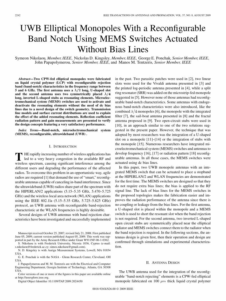
The elliptical radiator has a major axis and asecondary axis . Fig. 1 presents the details ofthe schematic design and its dimensions are summarized inTable I. The overall width of the antenna, , is 26.88 mmand the ground length is . A CPW feed line withcentral conductor width and ground-signal gap
is used, resulting in a characteristic impedanceof 50 Ohms. In order to use 850 pitch probes for
measurements, the CPW line is linearly tapered down to anarrower CPW line with 50 Ohm characteristic impedance( and ) that had length only
. A customized transition from the standard CPWline ( , ) to the ellipse was used to improve the matching.The matching improvement can be seen in Fig. 2 where the inputimpedance of two antennas, one referred to as “Standard CPW”and one referred to as “Reference” are presented on a Smithchart. The “Standard CPW” does not use any CPW-radiatortransition; a standard, uniform width CPW line with the abovementioned geometrical characteristics ( , ) is terminatedwith the elliptical radiator. The “Reference” is identical with theantenna presented in Fig. 1 without the slot or the two open stubs.It is referred to as “Reference” because it will be compared tothe antennas with the reconfigurable resonating elements. Fig. 2shows that a uniform CPW line cannot establish good matchingfor this elliptical monopole, but the use of an appropriate CPWto radiator transition can achieve a SWR less than 2 acrossthe whole UWB range. The two lines represent measurementstaken between 2–12 GHz. The segment of the “Reference”line that falls outside the circle corresponds tothe frequency range from 2–3 GHz, which is not part of theUWB frequency range.
Two different approaches (a U-shaped slot and two invertedL-shaped open stubs) are demonstrated to achieve a reconfig-urable band notch between 5.2 and 6 GHz. The U-shaped slotis presented in Fig. 1(a). It consists of two parallel segments oflength and a third segment with length
that is positioned from the nearestground edge. In the middle of this third edge and along thesymmetry plane of the antenna, a MEMS switch is integratedto selectively short the 0.2 mm wide slot. Another very thin slot(only 3 wide) is created parallel to the third segment at adistance from it. Therefore an isolated rectan-gular segment is defined which serves as the floating dc ground,which is necessary for the MEMS switch actuation. For the de-sign shown in Fig. 1(b), two inverted L open stubs with width
and total length 10.41 mmcause the band notch. Both stubs are placed at a distance
from the top point of the ellipse. Two MEMS switchesare used to electrically connect and disconnect the two stubs tothe elliptical radiator. The switches are positioned 0.4 mm fromthe ellipse. Bias lines are not needed in neither the slot nor thestubs case for the MEMS switch actuation because of the switchtopology [21].
Fig. 1. Antenna schematic (a) U-shaped slot and (b) L-shaped stubs.
TABLE IANTENNA SCHEMATIC DIMENSIONS
Fig. 2. Input impedance for “Standard CPW” and “Reference” antennas onSmith chart.

2244 IEEE TRANSACTIONS ON ANTENNAS AND PROPAGATION, VOL. 57, NO. 8, AUGUST 2009
Fig. 3. Field distribution (a) open slot at 5.8 GHz, (b) shorted slot at 5.8 GHz, (c) open slot at 8 GHz, (d) shorted stubs at 5.8 GHz, (e) open stubs at 5.8 GHz, (f)shorted stubs at 8 GHz.
III. OPERATION PRINCIPLES
For both antennas, the reconfigurability relies on the sameconcept of adding or removing a resonating structure. For theU-shaped slot antenna, the total length of the slot is approxi-mately at the frequency at which the rejection band is de-sired if the MEMS switch is up or open, and the MEMS switchshorts the slot at the center, which eliminates the resonancearound 5 GHz. For the open stubs antenna, the two L-shaped,open circuit terminated stubs have a length approximatelyat 5.8 GHz resulting in resonating elements that prevent radia-tion if the MEMS switches are down or closed, which connectsthe stub to the monopole.
A. Theory
The U-shaped slot resonates and therefore creates a bandnotch at the frequency that is related to its geometry dimensionsas defined by: where cis the speed of light [19]. The surface current distributionpresented in Fig. 3(a) shows how the U-shaped slot resonatesat 5.8 GHz and how this behavior is cancelled when the slot isshorted [Fig. 3(b), or at a different frequency (8 GHz currentdistribution is presented in Fig. 3(c)]. The directions of thecurrent in the inner and outer side of the slot are opposite and
they cancel each other as explained in detail in [14], [19].As a result, the antenna does not radiate at that frequencyand a frequency notch is created around the frequency of5.8 GHz. When the slot is shorted at its center point by theMEMS switch, the total length of the slot is divided in twoand, consequently, it cannot support the resonating currents;thus, radiation occurs as if the slot was not present. A simpletransmission line model, similar to the approach introducedin [19], is presented in Fig. 4 that explains the slot effect. Thepresence of the slot is modeled as a long, short circuitterminated series stub, which is similar to a spurline filter.The MEMS switch is across the input to the series stub. Ifthe switch is up, [Fig. 4(a)] the spurline filter is in the circuit,and at the stub resonant frequency, there is an equivalentseries open circuit that reflects the signal. However, if theswitch is down, the spurline filter is shorted [Fig. 4(b)], ornot in the circuit. Thus, radiation occurs at all frequencies.
Similarly the inverted L-shaped, open circuit terminated stubsresonate approximately at a frequency defined by:
where again c is the speed of light. Fig. 3(d)shows how the two stubs resonate at 5.8 GHz. When the twostubs are not connected to the elliptical radiator no currents flowthrough the stubs [Fig. 3(e)] but even when they are connected

NIKOLAOU et al.: UWB ELLIPTICAL MONOPOLES WITH A RECONFIGURABLE BAND NOTCH 2245
Fig. 4. Transmission line model for (a) U-shaped slot with MEMS up, (b) U shaped slot with MEMS down, (c) inverted L stubs with MEMS up, (d) inverted Lstubs with MEMS down.
they do not resonate at a different frequency (8 GHz current dis-tribution is presented in Fig. 3(f)). At the resonance frequency,the direction of the currents on the inverted L stub and the cur-rent along the nearby edge of the radiator are opposite to eachother as presented in [20]. Therefore they cancel and the antennadoes not radiate. Again a transmission line model is used to in-terpret the inverted L stubs effect on the radiation mechanism,where the presence of the two stubs is modeled as a longstub. When the MEMS are in the “up” position, the stub is dis-connected from the primary transmission line [Fig. 4(c)] and ithas no effect on the incident power, which is radiated from theload (“antenna”). When the MEMS are in the “down” positionthe open stub appears as ideal short on the transmission line andthe incident power is reflected as appears in Fig. 4(d).
B. Parametric Study
There is an inverse proportional relationship between the fre-quency of the band notch and the total length of the resonatingelements as can be deduced from the approximate formulas pre-sented in the previous section. This trend is verified numeri-cally from the simulations presented in Fig. 5. Fig. 5(a) showsthe simulation results when varies for an antenna with aU-shaped slot when the additional thin slot (3 wide) is notpresent. This example is referred to as “Simple Slot”. When itis compared with the antenna that uses the additional thin slot(similar to the schematic in Fig. 1) to create the isolated floatingground, which is referred to as “Thin Slot”, it can be seen that
longer length is required to have the frequency notch be-tween 5 and 6 GHz [Fig. 5(b)] when the thin slot is present.Specifically for the “Simple Slot,” is requiredfor a stopband at 5.8 GHz, whereas for the “Thin Slot,” a littlelonger length of is needed to cause a band notch inthe same frequency range. Additionally, when the same length
is used for “Thin Slot”, the band notch shifts higherto approximately 6.0 GHz as can be seen in Fig. 5(b). Similarbehavior is observed for the length of the inverted L stubs, whichis presented in Fig. 5(c). The longer the length is, the lowerthe frequency of the band notch shifts. In each of the above sim-ulations, all of the other dimensions are kept constant.
Simulations show that another important parameter is the po-sition of the resonating element, especially for the U-shapedslot. Fig. 6 shows the simulated reflection coefficient for thetwo antennas as a function of the resonating element location.Fig. 6(a) shows that the stopband frequency varies by 1.5 GHzif is varied by 1 mm. Furthermore, the magnitude of the re-flection coefficient is seen to be dependent on the slot position,with a smaller reflection if is large. The large dependenceon slot position is due to the strong currents at the elliptical ra-diator feed point, which couple strongly to the U-shaped slot.On the contrary, a small variation on the distance of the twoL-shaped stubs from the top point of the ellipse does not seemto affect the band notch significantly. Fig. 6(b) shows that a 1mm variation in stub location only causes a 750 MHz variationin stopband frequency. It is also noted that the magnitude of the

2246 IEEE TRANSACTIONS ON ANTENNAS AND PROPAGATION, VOL. 57, NO. 8, AUGUST 2009
Fig. 5. Slot/stub length effect on return loss (a) simple slot, (b) thin slot, (c)stubs.
reflection coefficient does not appear to be dependent on the stublocation.
IV. MEMS SWITCHES OPERATION AND INTEGRATION
A. MEMS Switch Operation
MEMS switches were chosen for this application because oftheir low loss, excellent isolation, and wide-band response. The
Fig. 6. (a) Slot position effect, (b) stub position effect.
challenge with any switch integration in an antenna system iswith biasing the switches without affecting the radiation char-acteristics. To avoid this issue, the biasing technique recentlyintroduced in [21] was implemented. The major advantage ofthe suggested MEMS switches is that they do not require dcbias lines in order to be actuated. For this technique to work,there must be a dc short between the signal line input (centerpin on the CPW antenna feed) and the posts of the MEMSswitches. This method also requires that the MEMS are Ohmicand single-supported.
The dc actuation voltage is applied directly to the CPW centerpin through a dc bias on the vector network analyzer. When novoltage is applied, the switches are in the up position and theantenna exhibits one behavior. When a voltage is applied, anelectrostatic force pulls down the MEMS switches and sincethey are Ohmic, they create a dc and RF short at the contactpoint. The antenna now exhibits a different behavior.
Since there is a dc short between the signal line input and theposts of the MEMS switches, no additional metal lines are re-quired to apply the actuation voltage. To avoid the addition of dcground lines, a floating ground is used. In this method, a metalpad beneath the switch is not shorted to anything. It does not rep-resent a true ground, but it is sufficient to provide a foundationfor electrostatic force generation. The pad is isolated from di-rect contact with the switch membrane by a thin layer of silicon
NIKOLAOU et al.: UWB ELLIPTICAL MONOPOLES WITH A RECONFIGURABLE BAND NOTCH 2247
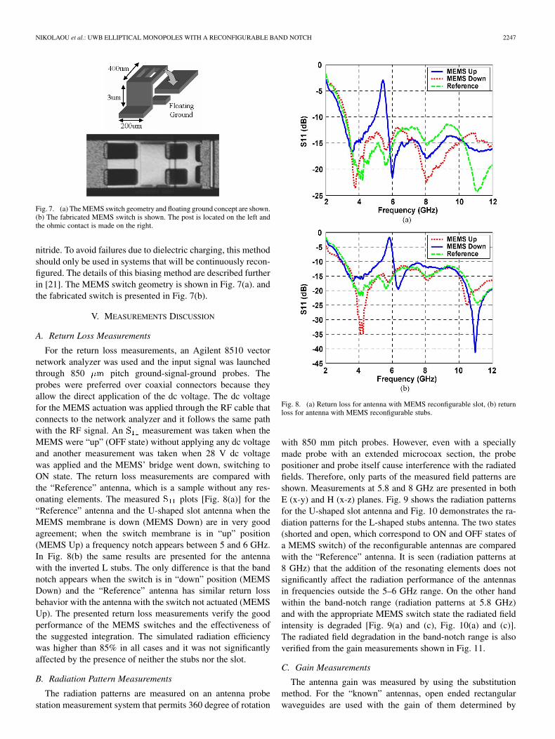
Fig. 7. (a) The MEMS switch geometry and floating ground concept are shown.(b) The fabricated MEMS switch is shown. The post is located on the left andthe ohmic contact is made on the right.
nitride. To avoid failures due to dielectric charging, this methodshould only be used in systems that will be continuously recon-figured. The details of this biasing method are described furtherin [21]. The MEMS switch geometry is shown in Fig. 7(a). andthe fabricated switch is presented in Fig. 7(b).
V. MEASUREMENTS DISCUSSION
A. Return Loss Measurements
For the return loss measurements, an Agilent 8510 vectornetwork analyzer was used and the input signal was launchedthrough 850 pitch ground-signal-ground probes. Theprobes were preferred over coaxial connectors because theyallow the direct application of the dc voltage. The dc voltagefor the MEMS actuation was applied through the RF cable thatconnects to the network analyzer and it follows the same pathwith the RF signal. An measurement was taken when theMEMS were “up” (OFF state) without applying any dc voltageand another measurement was taken when 28 V dc voltagewas applied and the MEMS’ bridge went down, switching toON state. The return loss measurements are compared withthe “Reference” antenna, which is a sample without any res-onating elements. The measured plots [Fig. 8(a)] for the“Reference” antenna and the U-shaped slot antenna when theMEMS membrane is down (MEMS Down) are in very goodagreement; when the switch membrane is in “up” position(MEMS Up) a frequency notch appears between 5 and 6 GHz.In Fig. 8(b) the same results are presented for the antennawith the inverted L stubs. The only difference is that the bandnotch appears when the switch is in “down” position (MEMSDown) and the “Reference” antenna has similar return lossbehavior with the antenna with the switch not actuated (MEMSUp). The presented return loss measurements verify the goodperformance of the MEMS switches and the effectiveness ofthe suggested integration. The simulated radiation efficiencywas higher than 85% in all cases and it was not significantlyaffected by the presence of neither the stubs nor the slot.
B. Radiation Pattern Measurements
The radiation patterns are measured on an antenna probestation measurement system that permits 360 degree of rotation
Fig. 8. (a) Return loss for antenna with MEMS reconfigurable slot, (b) returnloss for antenna with MEMS reconfigurable stubs.
with 850 mm pitch probes. However, even with a speciallymade probe with an extended microcoax section, the probepositioner and probe itself cause interference with the radiatedfields. Therefore, only parts of the measured field patterns areshown. Measurements at 5.8 and 8 GHz are presented in bothE (x-y) and H (x-z) planes. Fig. 9 shows the radiation patternsfor the U-shaped slot antenna and Fig. 10 demonstrates the ra-diation patterns for the L-shaped stubs antenna. The two states(shorted and open, which correspond to ON and OFF states ofa MEMS switch) of the reconfigurable antennas are comparedwith the “Reference” antenna. It is seen (radiation patterns at8 GHz) that the addition of the resonating elements does notsignificantly affect the radiation performance of the antennasin frequencies outside the 5–6 GHz range. On the other handwithin the band-notch range (radiation patterns at 5.8 GHz)and with the appropriate MEMS switch state the radiated fieldintensity is degraded [Fig. 9(a) and (c), Fig. 10(a) and (c)].The radiated field degradation in the band-notch range is alsoverified from the gain measurements shown in Fig. 11.
C. Gain Measurements
The antenna gain was measured by using the substitutionmethod. For the “known” antennas, open ended rectangularwaveguides are used with the gain of them determined by

2248 IEEE TRANSACTIONS ON ANTENNAS AND PROPAGATION, VOL. 57, NO. 8, AUGUST 2009
Fig. 9. U-shaped slot radiation pattern measurements and simulations, (a) E plane at 5.8 GHz (b) E plane at 8 GHz, (c) H plane at 5.8 GHz (d) H plane at 8 GHz.
[22]. The gain measurements shown in Fig. 11 were takenin the directivity direction which coincides with the z axisdirection as it is defined in Fig. 1. As can be seen, the presenceof the resonating elements and the frequency mismatch causea significant degradation on the gain value at the frequencyband to be rejected in a reconfiguring way. The antenna gain issuppressed by over 10 dB for the slot resonator and 6 dB forthe stub resonator. The gain behavior over the remainder of thefrequency band is similar for all three cases as can be verifiedfrom Fig 11.
VI. CONCLUSION
The use of resonating elements integrated with MEMSswitches has been exploited to implement two UWB monopoleswith reconfigurable band notch in the wireless LAN frequencyrange (5.150–5.825 GHz). The basic antenna design is anelliptical radiator fed with CPW line, fabricated on thin organicmaterial. In the first case a U-shaped slot of approximate
length causes the frequency notch and its effect can bedynamically cancelled by a MEMS switch that shorts the slot.The antenna with the shorted slot has the same response withan antenna without any slot, and consequently the state ofthe single switch defines the presence or not of the rejectionband. In the second case, two inverted L-shaped open stubsare used and two MEMS switches are used to connect anddisconnect the stubs with the elliptical radiator. The electricalconnection of the stubs with the radiator causes the creationof the rejection band and, apparently, when the stubs are notelectrically connected, the antenna operates as a typical UWBradiator with radiation band that covers the whole UWB range(3.1–10.6 GHz). Reconfigurability is achieved with MEMSswitches that are actuated through the RF signal path, withoutthe need of dc bias lines, that could potentially complicate theswitch fabrication and integration process, while degradingthe radiation performance of any antenna and especially ofa broadband antenna because RF leakage through the bias

NIKOLAOU et al.: UWB ELLIPTICAL MONOPOLES WITH A RECONFIGURABLE BAND NOTCH 2249
Fig. 10. L-shaped stubs radiation pattern measurements and simulations (a) E plane at 5.8 GHz, (b) E plane at 8 GHz, (c) H plane at 5.8 GHz, (d) H plane at 8GHz.
Fig. 11. Gain measurements.
lines cannot be avoided. Numerical results, transmission linemodels and eventually measurements verify the very satisfac-tory performance of the proposed antennas which can be good
candidates for next generation, high performance and highversatility cognitive radios.
REFERENCES
[1] S. Haykin, “Cognitive radio: Brain-empowered wireless communica-tions,” IEEE J. Select. Areas Comm., vol. 23, pp. 201–220, Feb. 2005.
[2] K.-H. Kim, Y.-J. Cho, S.-P. Hwang, and S.-O. Park, “Band-notchedUWB planar monopole antenna with two parasitic patches,” Electron.Lett., vol. 41, no. 14, pp. 783–785, Jul. 7, 2005.
[3] I.-J. Yoon, H. Kim, and Y. J. Yoon, “UWB RF receiver front-end withband-notch characteristic of 5 GHz WLAN,” in IEEE Int. AntennaPropag. Symp. Digest, Jul. 2006, pp. 1303–1306.
[4] S.-Y. Chen, P.-H. Wang, and P. Hsu, “Uniplanar log-periodic slot an-tenna fed by a CPW for UWB applications,” IEEE Antenna WirelessPropag. Lett., vol. 5, no. 1, pp. 256–259, Dec. 2006.
[5] J. Kim, C. S. Cho, and J. W. Lee, “5.2 GHz notched ultra-wideband an-tenna using slot-type SRR,” Electron. Lett., vol. 42, no. 6, pp. 315–316,Mar. 16, 2006.
[6] K. Chang, H. Kim, and Y. J. Yoon, “Multi-resonance UWB antennawith improved band notch characteristics,” in IEEE Int. AntennaPropag. Symp. Digest, Jul. 2005, vol. 3A, pp. 516–519.
[7] S.-W. Qu, J.-L. Li, and Q. Xue, “A band-notched ultrawideband printedmonopole antenna,” IEEE Antenna Wireless Propag. Lett., vol. 5, no.1, pp. 495–498, Dec. 2006.

2250 IEEE TRANSACTIONS ON ANTENNAS AND PROPAGATION, VOL. 57, NO. 8, AUGUST 2009
[8] S.-Y. Suh, W. L. Stutzman, W. A. Davis, A. E. Waltho, K. W. Skeba,and J. L. Schiffer, “A UWB antenna with a stop-band notch in the5-GHz WLAN band,” in Proc. IEEE ACES, Apr. 2005, pp. 203–207.
[9] W. J. Lui, C. H. Cheng, and H. B. Zhu, “Compact frequency notchedultra-wideband fractal printed slot antenna,” IEEE Microw. WirelessComp. Lett., vol. 16, no. 4, pp. 224–226, Apr. 2006.
[10] W. J. Lui, C. H. Cheng, and H. B. Zhu, “Frequency notched printedslot antenna with parasitic open-circuit stub,” Electron. Lett., vol. 41,no. 20, pp. 1094–1095, Sep. 29, 2005.
[11] T. Dissanayake and K. P. Esselle, “Design of slot loaded band-notchedUWB antennas,” in IEEE Int. Antenna Propag. Symp. Digest, Jul. 2005,vol. 1B, pp. 545–548.
[12] A. J. Kerkhoff and L. Hao, “Design of a band-notched planar monopoleantenna using genetic algorithm optimization,” IEEE Trans. AntennasPropag., vol. 55, no. 3, pt. 1, pp. 604–610, Mar. 2007.
[13] K. Chung, J. Kim, and J. Choi, “Wideband microstrip-fed monopoleantenna having frequency band-notch function,” IEEE Microw. Wire-less Comp. Lett., vol. 15, no. 11, pp. 766–768, Nov. 2005.
[14] Y. J. Cho, K. H. Kim, D. H. Choi, S. S. Lee, and S.-O. Park, “A minia-ture UWB planar monopole antenna with 5-GHz band-rejection filterand the time-domain characteristics,” IEEE Trans. Antennas Propag.,vol. 54, no. 5, pp. 1453–1460, May 2006.
[15] Y.-C. Lin and K.-J. Hung, “Compact ultrawideband rectangularaperture antenna and band-notched designs,” IEEE Trans. AntennasPropag., vol. 54, no. 11, pt. 1, pp. 3075–3081, Nov. 2006.
[16] D. E. Anagnostou, G. Zheng, M. T. Chryssomallis, J. C. Lyke, G. E.Ponchak, J. Papapolymerou, and C. G. Christodoulou, “Design, fabri-cation, and measurements of an RF-MEMS-based self-similar recon-figurable antenna,” IEEE Trans. Antennas Propag., vol. 54, no. 2, pt.1, pp. 422–432, Feb. 2006, J..
[17] A. C. K. Mak, C. R. Rowell, R. D. Murch, and C. L. Mak, “Recon-figurable multiband antenna designs for wireless communication de-vices,” IEEE Trans. Antennas Propag., vol. 55, no. 7, pp. 1919–1928,Jul. 2007.
[18] C. W. Jung, M.-J. Lee, G. P. Li, and F. De Flaviis, “Reconfigurablescan-beam single-arm spiral antenna integrated with RF-MEMSswitches,” IEEE Trans. Antennas Propag., vol. 54, no. 2, pt. 1, pp.455–463, Feb. 2006.
[19] W.-S. Lee, D.-Z. Kim, K.-J. Kim, and J. W. Yu, “Wideband planarmonopole antennas with dual band-notched characteristics,” IEEETrans. Microw. Theory Tech., vol. 54, no. 6, pt. 2, pp. 2800–2806, Jun.2006.
[20] B. Kim, S. Nikolaou, D. E. Anagnostou, Y. S. Kim, M. M. Tentzeris,and J. Papapolymerou, “A conformal L-shaped antenna on liquidcrystal polymer substrate for ultra-wideband systems with WLANband-stop characteristics,” IEEE Trans. Antennas Propag., submittedfor publication.
[21] N. Kingsley, D. E. Anagnostou, M. M. Tentzeris, and J. Papapoly-merou, “RF MEMS sequentially-reconfigurable Sierpinski antenna ona flexible, organic substrate without the need for dc bias lines,” IEEETrans. Antennas Propag., submitted for publication.
[22] A. D. Yaghjian, “Approximate formulas for the far field and gain ofopen-ended rectangular waveguide,” IEEE Trans. Antennas Propag.,vol. AP-32, no. 4, pp. 378–384, Apr. 1984.
Symeon (Simos) Nikolaou (M’08) received theB.S.E.C.E. degree from the National TechnicalUniversity of Greece (NTUA) Athens, Greece, in2003 and the M.S.E.C.E. and Ph.D. degrees from theGeorgia Institute of Technology (GaTech), Atlanta,in 2005 and 2007, respectively.
Since September 2007, he has been a Lecturerat Frederick University, Nicosia Cyprus. He hasauthored or coauthored more than 25 publications inpeer reviewed journals and conferences. His researchinterests include the design of UWB, conformal and
reconfigurable antennas, compact RFIDs and reconfigurable filters on organicmaterials.
Nickolas D. Kingsley (M’07) received the Ph.D. de-gree from the Georgia Institute of Technology, At-lanta, in May 2007.
His research interests included the design, minia-turization, fabrication, packaging, and testing ofRF MEMS multilayer front ends. During his Ph.D.studies, he focused on novel technologies usingliquid crystal polymer (LCP) substrate. He hasfiled four invention disclosures related to LCPinnovations, has published over a dozen papers inpeer reviewed journals and conferences, and has a
published book chapter on RF MEMS devices. He joined Auriga MeasurementSystems, Lowell, MA, in June 2007 as a Principal Engineer in the Measure-ment, Modeling, and Design Group. He is currently working on ultrahighefficiency power amplifier and module designs.
Dr. Kingsley is a member of the IEEE Antennas and Propagation Society, theIEEE Microwave Theory and Techniques Society, and the Order of the Engi-neer. He is serving on the 2009 International Microwave Symposium SteeringCommittee and Technical Program Committee.
George E. Ponchak (S’82–M’83–SM’97–F’08) re-ceived the B.E.E. degree from Cleveland State Uni-versity, Cleveland, OH, in 1983, the M.S.E.E. degreefrom Case Western Reserve University, Cleveland,OH, in 1987, and the Ph.D. in electrical engineeringfrom the University of Michigan, Ann Arbor, in 1997.
He joined the staff of the Communication Tech-nology Division at NASA Glenn Research Center,Cleveland, in 1983 where he is now a Senior Re-search Engineer. In 1997–1998 and in 2000–2001,he was a Visiting Professor at Case Western Reserve
University. He has authored and coauthored over 150 papers in refereed jour-nals and symposia proceedings. His research interests include the developmentand characterization of microwave and millimeter-wave printed transmissionlines and passive circuits, multilayer interconnects, uniplanar circuits, Si andSiC radio frequency integrated circuits, and microwave packaging.
Dr. Ponchak is a Fellow of the IEEE and an Associate Member of theEuropean Microwave Association. Dr. Ponchak is Editor-in-Chief of the IEEEMICROWAVE AND WIRELESS COMPONENTS LETTERS, and he was Editor ofa special issue of the IEEE TRANSACTIONS ON MICROWAVE THEORY AND
TECHNIQUES on Si MMICs. He founded the IEEE Topical Meeting on SiliconMonolithic Integrated Circuits in RF Systems and served as its Chair in 1998,2001, and 2006. He served as Chair of the Cleveland MTT-S/AP-S Chapter(2004–2006), and he has chaired many symposium workshops and specialsessions. He is a member of the IEEE International Microwave SymposiumTechnical Program Committee on Transmission Line Elements and served asits Chair in 2003–2005 and a member of the IEEE MTT-S Technical Com-mittee 12 on Microwave and Millimeter-Wave Packaging and Manufacturing.He served on the IEEE MTT-S AdCom Membership Services Committee(2003–2005). He received the Best Paper of the ISHM’97 30th InternationalSymposium on Microelectronics Award.
John Papapolymerou (S’90–M’99–SM’04) re-ceived the B.S.E.E. degree from the NationalTechnical University of Athens, Athens, Greece, in1993 and the M.S.E.E. and Ph.D. degrees from theUniversity of Michigan, Ann Arbor, in 1994 and1999, respectively.
From 1999–2001 he was an Assistant Professorat the Department of Electrical and Computer En-gineering, University of Arizona, Tucson. In 2001,he joined the School of Electrical and ComputerEngineering, Georgia Institute of Technology, where
he is currently an Associate Professor. He has authored or coauthored over240 publications in peer reviewed journals and conferences. His researchinterests include the implementation of micromachining techniques andMEMS devices in microwave, millimeter-wave and THz circuits and thedevelopment of both passive and active planar circuits on semiconductor(Si/SiGe, GaAs) and organic substrates (LCP, LTCC) for System-on-a-Chip(SOC)/System-on-a-Package (SOP) RF front ends.
Dr. Papapolymerou is the Chair for Commission D of the US Na-tional Committee of URSI and currently serves as an Associate Editor for
NIKOLAOU et al.: UWB ELLIPTICAL MONOPOLES WITH A RECONFIGURABLE BAND NOTCH 2251
IEEE MICROWAVE AND WIRELESS COMPONENT LETTERS and the IEEETRANSACTIONS ON ANTENNAS AND PROPAGATION. During 2004 he was theChair of the IEEE MTT/AP Atlanta Chapter. He was the recipient of the2004 Army Research Office (ARO) Young Investigator Award, the 2002National Science Foundation (NSF) CAREER award, the best paper award atthe 3rd IEEE International Conference on Microwave and Millimeter-WaveTechnology (ICMMT2002), Beijing, China and the 1997 Outstanding GraduateStudent Instructional Assistant Award presented by the American Societyfor Engineering Education (ASEE), The University of Michigan Chapter.His students have also been recipients of several awards including the BestStudent Paper award of the 2004 IEEE Topical Meeting on Silicon MonolithicIntegrated Circuits in RF Systems, the 2007 IEEE MTT graduate fellowshipand the 2007–2008 IEEE MTT undergraduate scholarship/fellowship.
Manos M. Tentzeris received the Diploma Degree(magna cum laude) in electrical and computer en-gineering from the National Technical University ofAthens, Athens, Greece and the M.S. and Ph.D. de-grees in electrical engineering and computer sciencefrom the University of Michigan, Ann Arbor, MI.
He is currently an Associate Professor withSchool of Electrical and Computer Engineering,Georgia Tech, Atlanta. He has published more than310 papers in refereed journals and conferenceproceedings, three books and 15 book chapters.
He has helped develop academic programs in highly integrated/multilayerpackaging for RF and wireless applications using ceramic and organic flexiblematerials, paper-based RFIDs, power scavengers and sensors, MicrowaveMEM’s, SOP-integrated (UWB, multiband, conformal) antennas and AdaptiveNumerical Electromagnetics (FDTD, multiresolution algorithms) and headsthe ATHENA research group (20 researchers). He is the Georgia Electronic
Design Center Associate Director for RFID/sensors research, and he has beenthe Georgia Tech NSF-Packaging Research Center Associate Director for RFresearch and the RF Alliance Leader from 2003–2006. He is also the leader ofthe RFID Research Group of the Georgia Electronic Design Center (GEDC) ofthe State of Georgia. He was a Visiting Professor with the Technical Universityof Munich, Germany for summer 2002, where he introduced a course in thearea of high-frequency packaging.
Prof. Tentzeris is a member of URSI Commission D, a member of MTT-15committee, an Associate Member of EuMA, a Fellow of the ElectromagneticAcademy and a member of the Technical Chamber of Greece. He was therecipient/co-recipient of the 2007 IEEE APS Symposium Best Student PaperAward, the 2007 IEEE IMS Third Best Student Paper Award, the 2007 ISAP2007 Poster Presentation Award, the 2006 IEEE MTT Outstanding Young En-gineer Award, the 2006 Asian-Pacific Microwave Conference Award, the 2004IEEE TRANSACTIONS ON ADVANCED PACKAGING Commendable Paper Award,the 2003 NASA Godfrey “Art” Anzic Collaborative Distinguished PublicationAward, the 2003 IBC International Educator of the Year Award, the 2003 IEEECPMT Outstanding Young Engineer Award, the 2002 International Conferenceon Microwave and Millimeter-Wave Technology Best Paper Award (Beijing,China), the 2002 Georgia Tech-ECE Outstanding Junior Faculty Award, the2001 ACES Conference Best Paper Award and the 2000 NSF CAREER Awardand the 1997 Best Paper Award of the International Hybrid Microelectronicsand Packaging Society. He was the TPC Chair for IEEE IMS 2008 Symposiumand the Chair of the 2005 IEEE CEM-TD Workshop and he is the Vice-Chairof the RF Technical Committee (TC16) of the IEEE CPMT Society. He hasorganized various sessions and workshops on RF/Wireless Packaging andIntegration, RFID’s, Numerical Techniques/Wavelets, in IEEE ECTC, IMS,VTC and APS Symposia in all of which he is a member of the TechnicalProgram Committee in the area of “Components and RF.” He is the AssociateEditor of the IEEE TRANSACTIONS ON MICROWAVE THEORY AND TECHNIQUES,IEEE TRANSACTIONS ON ADVANCED PACKAGING and the International Journalon Antennas and Propagation. He has given more than 50 invited talks in thesame area to various universities and companies in Europe, Asia and America.
Copyright © 2022 FDOKUMEN