
Using the UCD3138HSFBEVM-029 - User's Guide - Texas ...
70
Using the UCD3138HSFBEVM-029 User's Guide Literature Number: SLUUA95A April 2013 – Revised September 2019
-
Upload
khangminh22 -
Category
Documents
-
view
3 -
download
0
Transcript of Using the UCD3138HSFBEVM-029 - User's Guide - Texas ...

Using the UCD3138HSFBEVM-029
User's Guide
Literature Number: SLUUA95AApril 2013–Revised September 2019

2 SLUUA95A–April 2013–Revised September 2019Submit Documentation Feedback
Copyright © 2013–2019, Texas Instruments Incorporated
WARNING
Always follow TI’s set-up and applicationinstructions, including use of all interfacecomponents within their recommended electricalrated voltage and power limits. Always useelectrical safety precautions to help ensure yourpersonal safety and the safety of those workingaround you. Contact TI’s Product InformationCenter http://support/ti./com for furtherinformation.
Save all warnings and instructions for futurereference.Failure to follow warnings and instructionsmay result in personal injury, propertydamage, or death due to electrical shockand/or burn hazards.The term TI HV EVM refers to an electronicdevice typically provided as an open framed,unenclosed printed circuit board assembly. It isintended strictly for use in developmentlaboratory environments, solely for qualifiedprofessional users having training, expertise,and knowledge of electrical safety risks indevelopment and application of high-voltageelectrical circuits. Any other use and/orapplication are strictly prohibited by TexasInstruments. If you are not suitably qualified,you should immediately stop from further use ofthe HV EVM.1. Work Area Safety:
1. Keep work area clean and orderly.2. Qualified observer(s) must be present
anytime circuits are energized.3. Effective barriers and signage must be
present in the area where the TI HVEVM and its interface electronics areenergized, indicating operation ofaccessible high voltages may be
present, for the purpose of protectinginadvertent access.
4. All interface circuits, power supplies,evaluation modules, instruments,meters, scopes and other relatedapparatus used in a developmentenvironment exceeding 50 VRMS/75 VDCmust be electrically located within aprotected Emergency Power Off (EPO)protected power strip.
5. Use a stable and non-conductive worksurface.
6. Use adequately insulated clamps andwires to attach measurement probesand instruments. No freehand testingwhenever possible.
2. Electrical Safety:1. De-energize the TI HV EVM and all its
inputs, outputs, and electrical loadsbefore performing any electrical or otherdiagnostic measurements. Revalidatethat TI HV EVM power has been safelyde-energized.
2. With the EVM confirmed de-energized,proceed with required electrical circuitconfigurations, wiring, measurementequipment hook-ups and otherapplication needs, while still assumingthe EVM circuit and measuringinstruments are electrically live.
3. Once EVM readiness is complete,energize the EVM as intended.
WARNING: while the EVM is energized,never touch the EVM or its electricalcircuits as they could be at high voltagescapable of causing electrical shockhazard.
3. Personal Safety:1. Wear personal protective equipment e.g.
latex gloves and/or safety glasses withside shields or protect EVM in anadequate lucent plastic box withinterlocks from accidental touch.
4. Limitation for Safe Use:1. EVMs are not to be used as all or part of
a production unit.

3SLUUA95A–April 2013–Revised September 2019Submit Documentation Feedback
Copyright © 2013–2019, Texas Instruments Incorporated
Digitally Controlled Hard-Switching Full-Bridge DC-DC Converter
User's GuideSLUUA95A–April 2013–Revised September 2019
Digitally Controlled Hard-Switching Full-BridgeDC-DC Converter
1 IntroductionThis EVM, UCD3138HSFBEVM-029 is to help evaluate the UCD3138RHA 40-pin digital control device ina 48-V telecom power conversion application and then to aid in UCD3138 design. The EVM is astandalone symmetrical Hard-Switching Full-Bridge (HSFB) DC-DC power converter.
The UCD3138HSFBEVM-029 can be used as it is delivered without additional work, from either hardwareor firmware, to evaluate a hard-switching symmetrical full-bridge DC-DC converter. This EVM allows forsome of its design parameters to be re-tuned using a GUI based tool, called Texas Instruments FusionDigital Power Designer. It is also possible to load custom firmware with user’s own definition anddevelopment.
This user’s guide provides basic evaluation instruction from a viewpoint of system operation in astandalone symmetrical HSFB DC-DC power converter.
WARNINGHigh voltages are present on this evaluation module duringoperation and for a while even after power off. This module shouldonly be tested by skilled personnel in a controlled laboratoryenvironment.High temperature exceeding 60°C may be found during EVMoperation and for a while even after power off.This EVM’s purpose is to facilitate the evaluation of digital controlin a hard-switching full-bridge DC converter using the UCD3138,and cannot be tested and treated as a final product.Read and understand this user’s guide thoroughly before startingany physical evaluation.

Description www.ti.com
4 SLUUA95A–April 2013–Revised September 2019Submit Documentation Feedback
Copyright © 2013–2019, Texas Instruments Incorporated
Digitally Controlled Hard-Switching Full-Bridge DC-DC Converter
2 DescriptionThe UCD3138HSFBEVM-029 demonstrates a symmetrical hard-switching full-bridge DC-DC powerconverter with digital control using the UCD3138RHA 40-pin device. This EVM includes preloadedfirmware providing required control functions for an HSFB converter. For details of the firmware pleasecontact TI. UCD3138HSFBEVM-029 accepts a DC input from 36 VDC to 72 VDC, and outputs a nominal 12VDC with full output load power 360 W, or full output current 30 A.
2.1 Typical Applications• 48-V Telecom DC-DC Power Conversion• Servers• Telecommunication Systems
2.2 Features• Digitally Controlled and Standalone Hard Switching Full-Bridge DC-DC Power Conversion• Voltage Mode Control• Secondary Side Control• DC Input from 36 VDC to 72 VDC
• 12 VDC Regulated Output from No Load to Full Load• Full-Load Power 360 W, or Full-Load Current 30 A• High Efficiency• Constant Soft-Start Time• Protection: Over Voltage, Under Voltage, Over Current, and Over Temperature• Constant Current and Constant Power• Input Voltage Feed Forward Control• PMBus Communications• Test Points to Facilitate Device and Topology Evaluation

www.ti.com Performance Specifications
5SLUUA95A–April 2013–Revised September 2019Submit Documentation Feedback
Copyright © 2013–2019, Texas Instruments Incorporated
Digitally Controlled Hard-Switching Full-Bridge DC-DC Converter
3 Performance Specifications
Table 1. UCD3138HSFBEVM-029 Specifications
PARAMETER TEST CONDITIONS MIN TYP MAX UNITSInput CharacteristicsVoltage operation range 36 72 VDC
Input UVLO On 35Input UVLO Off 32Input current Input = 36 VDC, full load = 30 A 11 AInput current Input = 48 VDC, full load = 30 A 9Input current Input = 72 VDC, full load = 30 A 6Output CharacteristicsOutput voltage, VOUT No Load to full load 12 VDC
Output load current, IOUT 36 to 72 VDC 30 AOutput voltage ripple 48 VDC and full load = 30 A 30 mVppSystems CharacteristicsSwitching frequency 200 kHzPeak efficiency 48 VDC, load = 20 A 94.5%Full load efficiency 48 VDC, full load = 30 A 93.5%Operating temperature Typical 400 LFM forced air flow 25 ºC
Input
Sourc
e C
onnection a
nd F
ilte
r
Isola
tion B
oundary
Prim
ary
Secondary
Prim
ary
Curr
ent
Sense
+ 4
8V I
nput
48V R
etu
rn
+Vout
Vout
Retu
rn
5V P
rim
ary
sid
e lin
ear
regula
tor
Prim
ary
Secondary
21V
at
Vin
=75
Scale
d :
0 t
o 7
5V I
nput
= 0
to 2
V o
utp
ut
Vin
sam
ple
and h
old V
inscale
d I
nvert
ing A
mplifier
R93 a
nd R
79 s
et
scale
facto
r
3.3
V S
econdary
sid
e lin
ear
regula
tor
1 1
1
1
11
1
1Part
s n
ot
used
5:2
:2
12V /
30A
Input
Voltage =
36V t
o 7
2V D
C
Input
Curr
ent
Max =
12A
Max O
utp
ut
Pow
er
= 3
60W
EN
A
OU
TA
VD
D
OU
TB P
WPD
INB
GN
D
INA
EN
B
R15
15.0
R16
15.0
R26
R8
10.0
k
R10
1.0
0
R11
1.0
0C6
1uF
C1
47uF
C2
47uF
C3
47uF C37
C38
R92
2.4
9k
R106
10.0
C28
1nF
TP1
TP2
TP44
TP3
873 1
T1
100:1
R9
1.0
0k
TP16
L1
2.2
uH
R95
10.0
R18
10.0
k
R28
10.0
k
R1
10.0
k
R2
10.0
R5
10.0
k
R30
10.0
R40
10.0
k
R52
10.0
D1
MM
BD
914
TP10
D11
MBR0540
D18
MBR0540
D16
MBR0540
D15
MBR0540
C53
1000pF
C54
1000pF
TP17
TP13
TP12
TP14
TP18
TP19
TP20
TP21
TP22
TP23
TP25
F1
15A 8
6V
1 2 3
P2
R17
C60
1uF
C61
1uF
1 2 3 45678
9
U3
UCC27524
1VCC1
2G
ND
1
3IN
A
4IN
B
5IN
C
6IN
D
7D
ISABLE
8G
ND
19
GN
D2
10
CTRL
11
OU
TD
12
OU
TC
13
OU
TB
14
OU
TA
15
GN
D2
16
VCC2
U5
ISO
7240CF
R3
200
R21
6.4
9k
C17
1uF
C18
1uF
C35
10nF
1VD
D
2H
B
3H
O
4H
S5
HI
6LI
7VSS
8LO
U7
UCC27211
1VD
D
2H
B
3H
O
4H
S5
HI
6LI
7VSS
8LO
U12
UCC27211
R4
1.0
0
R23
1.0
0
C9
2.2
uF
C12
2.2
uF
C24
2.2
uF
C40
2.2
uF
C51
2.2
uF
Q10
MM
BT3904
D6
BZX84C5V6
C8
47uF
C10
47uF
R47
15.0
k
R48
22.1
k
R49
4.9
9k
R50
33.2
R53
22.1
k
1CO
MP
2FB
3CS
4RC
5G
ND
6O
UT
7VCC
8REF
U8
UCC3813D
-1
D17
BAW
56
C36
47pF
C41
330pF
C43
220pF
C46
2.2
uF
C57
47pF
C63
4.7
uF
R59
3.0
1
R60
750
R69
90.9
k
C65
1uF
R71
1.0
0k
R72
10.0
C70
47pF
R79
150k
R82
49.9
k
Q9
FD
S2670
U11
TLV2371 R
93
20.0
k
D8
SS24
C5 2.2
uF
TP15
J1
R14
20.0
R74
20.0
L2
470nH
C27
2.2
uF
TP9
TP11
R31
1.0
0k
R76
50.0
k
C49
100pF
R107
1.0
0
R108
1.0
0
D7
MM
BD
7000
D5
MM
BD
914
C26
0.1
uF
C30
0.1
uF
C45
10nF
C42
0.1
uF
C44
0.1
uF
C62
0.1
uF
C64
1uF
C71
10nF
C73
0.1
uF
D3
SS24
R38
R45
1IN
2N
C
3N
C
4G
ND
5FB/N
C
6N
C
7N
C
8O
UT
9
PW
PD
U9
TPS715A33
R101
1.0
0
C86
1uF
C85
10uF
Q1
Q2
Q3
Q_T2
Q_B1
Q_T1
Q_B2
Q4
Q5
Q6
+C75
1000uF
J3 J4
R73 0
C80
2.2
uF
1 8
17
16
12
11
T3
C79
47uF
C82
47uF
C55
2.2
uF
C78
1uF
1 4 2 37685
T2
540 u
H
TP6
TP4
R94R
97
220
DRVQ
_SYN
1 DRVQ
_SYN
2
DRVQ
_T2
-RS+RS
DRVQ
_T1
AD
04
3.3
VD
BU
S_IT
RAN
BU
S_IT
RAN
+VO
+RS
-RS
ISH
ARE
+VIN
+VIN
DRVQ
_B2
DRVQ
_B1
VAU
XPRI
6V_U
R
VIN
SCALED
VIN
_CT
CS-
CS+
IS-
6V_U
R
3.3
V_EXT
+VIN
3.3
V_EXT
5V_PRI
5V_PRI
BU
S+
BU
S+
VAU
XPRI
VAU
XPRI
VAU
XPRI
VAU
XS
VAU
XS
-VO
+VO
-VO
Schematics www.ti.com
6 SLUUA95A–April 2013–Revised September 2019Submit Documentation Feedback
Copyright © 2013–2019, Texas Instruments Incorporated
Digitally Controlled Hard-Switching Full-Bridge DC-DC Converter
4 Schematics
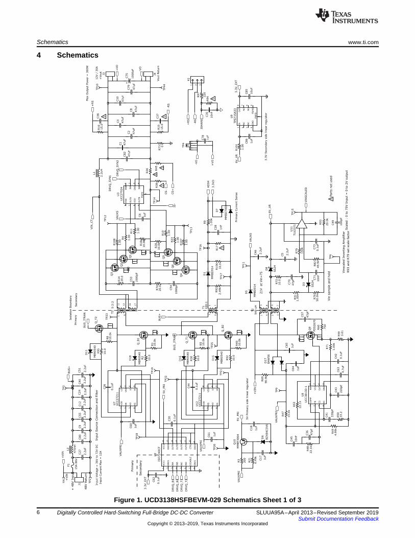
Figure 1. UCD3138HSFBEVM-029 Schematics Sheet 1 of 3
Tem
p =
0.4
24 +
.00625*T
0.1
01 x
Vout
0.0
5 x
Iout
V=
1.2
V a
t 12V input
Curr
ent
Sense A
mplifier
(Low
Offset/
X50)
Serial U
ART I
nte
rface
ON
/OFF M
anual Sw
itchin
g a
nd n
ois
e c
onditio
nin
g
Tem
pera
ture
sensor
LED
Sta
tus indic
ato
rs
Outp
ut
voltage d
ivid
er
and n
ois
e filte
r
EM
I Contr
ol
ISEC I
nte
rface t
o E
AD
C2
I2C C
onnecto
r
0.0
333 x
Iout
JTAG
Connecto
r
Share
Bus D
iffe
rence A
mplifier
Exte
rnal Bia
s I
nput
AD
02 c
onnect
ISH
ARE
Vin
= 3
6V-1
00V
0.5
4V-1
.52V
INPU
T V
OLT
SEN
SIN
G
DPW
M -
FET I
nte
rconnect
Matr
ix
Opt1
: O
pen J
5,
Use J
2 for
DPW
M0-3
Opt2
: Con J
5,
use D
PW
M0,
DPW
M1
11
1
1
1
11
11
11
11
11
1
11
1
1Part
s n
ot
used
1+
VS
3
GN
D
2VO
UT
U6
LM
60C
TP32
TP33
C84
1uF
C83
1uF
C16
10nF
R13
499
R24
10.0
k
C72
10nF
C81
4.7
nF
S1
R33
1.7
4k
R35
16.2
k
R36
1.6
2k
R41
1.0
0k
R43
1.0
0k
C33
0.1
uF
C34
47pF
Q8
MM
BT3904
R55
499
R56
3.3
2k
4 31
2
5
U10
OPA344
R61
137k
R6
10.0
k
Q7
MM
BT3904
R7
499
R34
3.3
2k
D2
RED
R64
10.0
k
Q11
MM
BT3904
R57
499
R58
3.3
2k
D13
RED
R68
10.0
k
R70
1.0
0k
R80
1.1
8k
R84
1.8
2k
R85
16.2
k
1EN
2C1+
3V+
4C1-
5C2+
6C2-
7V-
8RIN
9RO
UT
10
INVALID
11
DIN
12
FO
RCEO
N
13
DO
UT
14
GN
D
15
VCC
16
FO
RCEO
FF
U4
SN
65C3221
C29
0.1
uF
C31
0.1
uF
C32
0.1
uF
C47
0.1
uF
C48
0.1
uF
TP27
1
2
3
P1
R42
3.0
9kT
P5
1 2 3 4 5 6 7 8 9 10
J6
R98
33.2
R99
33.2
R100
33.2
R102
33.2
D4
SM
05
D10
SM
05
1 2 3 4 5 6 7 8 9 10
11
12
13
14
J7
R62
10.0
k
R63
10.0
kR96
10.0
kR103
10.0
k
D19
GREEN
R105
0
D9
MM
BD
7000
R104
10.0
k
R20
1.0
0kR32
49.9
k
C7
10nF
C14
R22
0
C19
4700pF
R44
R27
C23
0.1
uF
R25
49.9
k R29
2.0
0k
C67
10pF
D12
MM
BD
7000
R37
1.0
0k
C68
10pF
TP45
C69
100pF
R19
10.0
k
R12
1.0
0k
R54
1.5
0k
TP29
TP41
TP40
TP42
TP34
TP26
TP38
TP36
TP24
TP28
TP37
TP39
TP43
TP35
TP31
TP30
1 2 3 4 5 6 7 8 9 10
11
12
J5
1 2 3 4 5 6 7 8910
11
12
14
13
15
16
J2
1 2 3 4 56 7 8 9
10
11
J8
EN
ABLE
+RS
-RS
EAP0
EAN
0
P_G
OO
DFAIL
URE
VIN
OK
AD
01
VIN
SCALED
ISEC
CS+
+VO
AD
03
3.3
V_EXT
SCI_
RX
SCI_
TX
PM
_CTRL
PM
_CLK
PM
_ALERT
PM
_D
ATA
TM
S
TD
I
TD
O
TCK
3.3
VD
ISEC
AD
02
AD
13
ISH
ARE
VIN
_CT
EAP2
PW
M0
IS-
AD
06
IS-
3.3
V_EXT
3.3
V_EXT
3.3
V_EXT
3.3
V_EXT
3.3
V_EXT
3.3
V_EXT
3.3
VD
3.3
V_EXT
3.3
VD
6V_U
RIS
EC
-VO
DRVQ
_B2
DRVQ
_B1
DPW
M0A
DRVQ
_T1
DPW
M1A
DRVQ
_T2
DPW
M_0B
DPW
M_1B
DPW
M_2A
DPW
M_2B
DPW
M_3A
DPW
M_3B
DPW
M_0A
DPW
M_1A
DRVQ
_SYN
1
DRVQ
_SYN
2
DRVQ
_B1
DRVQ
_T2
DRVQ
_T1
DRVQ
_B2
DPW
M0A
DPW
M1A
-VO
www.ti.com Schematics
7SLUUA95A–April 2013–Revised September 2019Submit Documentation Feedback
Copyright © 2013–2019, Texas Instruments Incorporated
Digitally Controlled Hard-Switching Full-Bridge DC-DC Converter
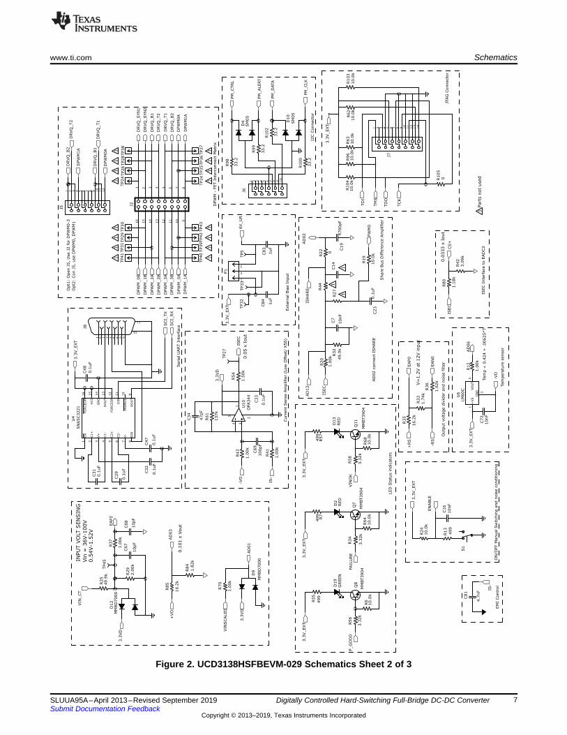
Figure 2. UCD3138HSFBEVM-029 Schematics Sheet 2 of 3

Schematics www.ti.com
8 SLUUA95A–April 2013–Revised September 2019Submit Documentation Feedback
Copyright © 2013–2019, Texas Instruments Incorporated
Digitally Controlled Hard-Switching Full-Bridge DC-DC Converter
Figure 3. UCD3138HSFBEVM-029 Schematics Sheet 3 of 3

J6
1
-L
oad
+
UART0 (J8)
D14
Reset
-V
IN+
J3
J4J1
S1
TP10
TP44TP1 TP2
1 16
2 15
8 9
7 10
1 12
2 11
6 7
5 8
J5 J2
D19
S2
Forced Air Flow Direction
400LFM
www.ti.com Test Setup
9SLUUA95A–April 2013–Revised September 2019Submit Documentation Feedback
Copyright © 2013–2019, Texas Instruments Incorporated
Digitally Controlled Hard-Switching Full-Bridge DC-DC Converter
5 Test Setup
5.1 Test EquipmentDC Voltage Source: capable of 36 VDC to 72 VDC, adjustable, with minimum power rating of 400 W, orcurrent rating not less than 12 A, with current limit function.
DC Multi-meter: 1 unit capable of 0 VDC to 75 VDC input range, four digits display preferred; and one unitcapable of 0 VDC to 15 VDC input range, four digits display preferred.
Output Load: DC load capable of receiving 0 VDC to 15 VDC, 0 A to 30 A, and 0 W to 360 W or greater,with display such as load current and load power.
Current-meter, DC, optional in case the load has no display, one unit, capable of 0 A to 30 A. A low ohmicshunt and a DMM is recommended.
Oscilloscope: capable of 500-MHz full bandwidth, digital or analog, if digital 5Gs/s or better.
Fan: 400 LFM forced air cooling.
Recommended Wire Gauge: capable of 30 A, or better than #14 AWG, with the total length of wire lessthan 8 feet (4 feet input and 4 feet return).
5.2 Recommended Test Setup
Figure 4. UCD3138FBHSEVM-029 Recommended Test Set Up

Test Setup www.ti.com
10 SLUUA95A–April 2013–Revised September 2019Submit Documentation Feedback
Copyright © 2013–2019, Texas Instruments Incorporated
Digitally Controlled Hard-Switching Full-Bridge DC-DC Converter
Figure 5. UCD3138HSFBEVM-029 Board Outlook

www.ti.com List of Test Points
11SLUUA95A–April 2013–Revised September 2019Submit Documentation Feedback
Copyright © 2013–2019, Texas Instruments Incorporated
Digitally Controlled Hard-Switching Full-Bridge DC-DC Converter
6 List of Test Points
Table 2. UCD3138HSFBEVM-029 List of Test Points
TEST POINTS NAME DESCRIPTIONTP1 +VIN Input Voltage positiveTP2 PWRGND Input Voltage negativeTP3 +BUS Input voltage after filterTP4 Voripple BNC Vo rippleTP5 6V UR Bias Secondary Bias 6V_URTP6 PGND Secondary bias GNDTP7 3.3VD 3.3VDTP8 AGND UCD3138 AGNDTP9 VAUXPRI Primary side bias voltageTP10 +Vo +Vout testTP11 VAUXS Secondary side bias voltageTP12 SR_Drive1 Drive to FET Q1, 2 and Q3TP13 SR_Drive2 Drive to FET Q4, 5 and Q6TP14 IS- Secondary side current sense negativeTP15 VINSCALED VIN monitoring sense on secondary sideTP16 I_Pri Primary side current sense transformer output on secondary sideTP17 PGND Secondary bias GNDTP18 DRV_QT2_iso Q_T2TP19 DRV_QB1_iso Q_B1TP20 PWRGND Input Voltage negativeTP21 DRV_QT1_iso Q_T1TP22 DRV_QB2_iso Q_B2TP23 T3-1 Transformer T3 pin 1TP24 Not UsedTP25 SW1 Switch node of Q_T1 and Q_B2TP26 Not UsedTP27 ISEC Secondary side current copper sensing after conditioningTP28 Not UsedTP29 Not UsedTP30 Not UsedTP31 Not UsedTP32 3.3VEXT 3.3V_EXTTP33 PGND Secondary bias GNDTP34 Not Used
TP35-43 Not UsedTP44 -VO -Vout testTP45 EAP2 EAP2TP46 SYNC UCD3138 SYNC

List of Terminals www.ti.com
12 SLUUA95A–April 2013–Revised September 2019Submit Documentation Feedback
Copyright © 2013–2019, Texas Instruments Incorporated
Digitally Controlled Hard-Switching Full-Bridge DC-DC Converter
7 List of Terminals
Table 3. UCD3138HSFBEVM-029 List of Terminals
TERMINAL NAME DESCRIPTIONJ1 VIN Input 2-pin, input voltage, 36 VDC to 72 VDC
J2 Driver-A 16-pin header, DPWM to driver configurationJ3 +VO 2-pin, output power positiveJ4 -Vo 2-pin, output power negativeJ5 Driver-B 12-pin header, DPWM to driver configurationJ6 PMBus 10-pin PMBus connectionJ7 JTAG 14-pin JTAG connectionJ8 UART0 Standard UART connection, RS232, 9-pin femaleP1 Bias External bias terminal for firmware debugging without power stage onP2 ISHARE ISHARE and load current sense

www.ti.com Test Procedure
13SLUUA95A–April 2013–Revised September 2019Submit Documentation Feedback
Copyright © 2013–2019, Texas Instruments Incorporated
Digitally Controlled Hard-Switching Full-Bridge DC-DC Converter
8 Test Procedure
8.1 Efficiency Measurement Procedure
WARNINGDanger of electrical shock. High voltage present during themeasurement.Do not leave EVM powered when unattended.Danger of heat burn from high temperature.
1. Refer to Figure 4 for basic set up to measure power conversion efficiency. The required equipment forthis measurement is listed in Section 5.1.
2. Before making electrical connections, visually check the boards to make sure no shipping damageoccurred.
3. In this EVM package, two EVMs are included, UCD3138HSFBEVM-029, and USB-TO-GPIO. For thismeasurement, the UCD3138HSFBEVM-029 board is needed.
4. Connect the DC voltage source to J1-1 (+) and J1-2 (-). Set up the DC output voltage in the rangespecified in Table 1, between 36 VDC and 72 VDC; set up the DC source current limit 12 A.
5. Connect an electronic load with either constant-current mode or constant-resistance mode. The loadrange is from 0 A to 30 A.
6. Check and make sure the jumpers are installed correctly on J2 and J5.1. J2 should be jumped across to connect its 1-16, 2-15, 7-10, and 8-9.2. J5 should be jumped across to connect its 1-12, 2-11, 5-8, and 6-7.
WARNINGFollow the connections correctly to avoid possible damages.
7. It is recommended to use the switch S1 to turn on the board output after the input voltage is applied tothe board. Before applying input voltage, make sure the switch, S1, is in the “OFF” position.
8. If the load does not have a current or a power display, a current meter or low ohmic shunt and DMM isneeded between the load and the board for current measurements.
9. Connect a volt-meter across the output connector and set the volt-meter scale 0 V to 15 V on itsvoltage, DC.
10. Turn on the DC voltage source output, flip S1 to “ON” and vary the load. Record output voltage andcurrent measurements.
8.2 Equipment Shutdown1. Shut down the DC voltage source.2. Shut down the electronic load.
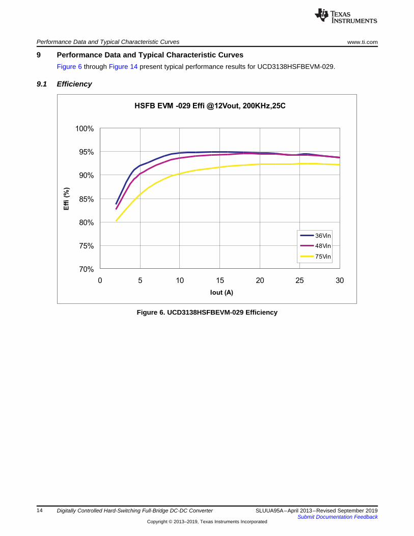
HSFB EVM -029 Effi @12Vout, 200KHz,25C
70%
75%
80%
85%
90%
95%
100%
0 5 10 15 20 25 30
Iout (A)
Eff
i(%
)
36Vin
48Vin
75Vin
Performance Data and Typical Characteristic Curves www.ti.com
14 SLUUA95A–April 2013–Revised September 2019Submit Documentation Feedback
Copyright © 2013–2019, Texas Instruments Incorporated
Digitally Controlled Hard-Switching Full-Bridge DC-DC Converter
9 Performance Data and Typical Characteristic CurvesFigure 6 through Figure 14 present typical performance results for UCD3138HSFBEVM-029.
9.1 Efficiency
Figure 6. UCD3138HSFBEVM-029 Efficiency

HSFB EVM -029 Line Regulation
12.02
12.025
12.03
12.035
12.04
12.045
12.05
36 39 42 45 48 51 54 57 60 63 66 69 72 75
Vin (V)
Vo
ut
(V)
Iout=0A
Iout=15A
Iout=30A
HSFB EVM -029 load regulation
12.02
12.025
12.03
12.035
12.04
12.045
12.05
0 5 10 15 20 25 30
Iout (A)
Vo
ut
(V)
36Vin
48Vin
75Vin
www.ti.com Performance Data and Typical Characteristic Curves
15SLUUA95A–April 2013–Revised September 2019Submit Documentation Feedback
Copyright © 2013–2019, Texas Instruments Incorporated
Digitally Controlled Hard-Switching Full-Bridge DC-DC Converter
9.2 Load Regulation
Figure 7. UCD3138HSFBEVM-029 Load Regulation
9.3 Line Regulation
Figure 8. UCD3138HSFBEVM-029 Line Regulation

Performance Data and Typical Characteristic Curves www.ti.com
16 SLUUA95A–April 2013–Revised September 2019Submit Documentation Feedback
Copyright © 2013–2019, Texas Instruments Incorporated
Digitally Controlled Hard-Switching Full-Bridge DC-DC Converter
9.4 Constant Power Constant Current (CPCC)
Figure 9. Constant Power Constant Current
9.5 Output Voltage Ripple
Figure 10. Output Voltage Ripple at 48 VDC and Half Load, 27.2 mV

www.ti.com Performance Data and Typical Characteristic Curves
17SLUUA95A–April 2013–Revised September 2019Submit Documentation Feedback
Copyright © 2013–2019, Texas Instruments Incorporated
Digitally Controlled Hard-Switching Full-Bridge DC-DC Converter
9.6 Output Turn On
Figure 11. Output Turn On 48 VDC with Load Range(Ch 1 = VO, Ch 3 = DPWM1B, Ch 4 = VCT, Load = 1 A)
Figure 12. Output Turn On 48 VDC with 6-V Prebias
Performance Data and Typical Characteristic Curves www.ti.com
18 SLUUA95A–April 2013–Revised September 2019Submit Documentation Feedback
Copyright © 2013–2019, Texas Instruments Incorporated
Digitally Controlled Hard-Switching Full-Bridge DC-DC Converter
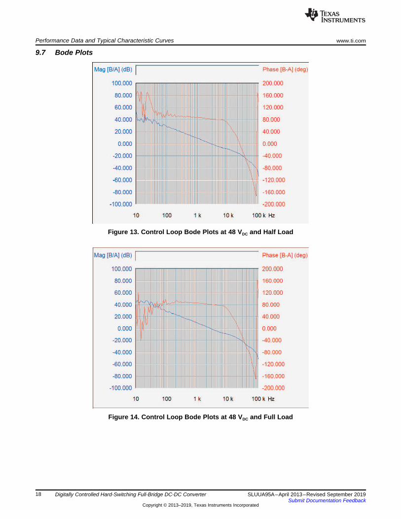
9.7 Bode Plots
Figure 13. Control Loop Bode Plots at 48 VDC and Half Load
Figure 14. Control Loop Bode Plots at 48 VDC and Full Load

www.ti.com EVM Assembly Drawing and PCB Layout
19SLUUA95A–April 2013–Revised September 2019Submit Documentation Feedback
Copyright © 2013–2019, Texas Instruments Incorporated
Digitally Controlled Hard-Switching Full-Bridge DC-DC Converter
10 EVM Assembly Drawing and PCB LayoutThe following figures (Figure 15 through Figure 20) show the design of the UCD3138HSFBEVM-029printed circuit board. PCB dimensions: L x W = 4.5 inch x 4.0 inch, PCB material: FR4 or compatible, fourlayers and 2-oz copper on each layer.
Figure 15. UCD3138HSFBEVM-029 Top Layer Assembly Drawing (top view)
Figure 16. UCD3138HSFBEVM-029 Bottom Assembly Drawing (bottom view)

EVM Assembly Drawing and PCB Layout www.ti.com
20 SLUUA95A–April 2013–Revised September 2019Submit Documentation Feedback
Copyright © 2013–2019, Texas Instruments Incorporated
Digitally Controlled Hard-Switching Full-Bridge DC-DC Converter
Figure 17. UCD3138HSFBEVM-029 Top Copper (top view)
Figure 18. UCD3138HSFBEVM-029 Internal Layer 1 (top view)

www.ti.com EVM Assembly Drawing and PCB Layout
21SLUUA95A–April 2013–Revised September 2019Submit Documentation Feedback
Copyright © 2013–2019, Texas Instruments Incorporated
Digitally Controlled Hard-Switching Full-Bridge DC-DC Converter
Figure 19. UCD3138HSFBEVM-029 Internal Layer 2 (top view)
Figure 20. UCD3138HSFBEVM-029 Bottom Copper (top view)
List of Materials www.ti.com
22 SLUUA95A–April 2013–Revised September 2019Submit Documentation Feedback
Copyright © 2013–2019, Texas Instruments Incorporated
Digitally Controlled Hard-Switching Full-Bridge DC-DC Converter
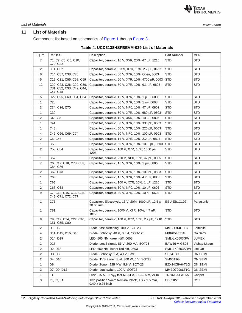
11 List of MaterialsComponent list based on schematics of Figure 1 though Figure 3.
Table 4. UCD3138HSFBEVM-029 List of Materials
QTY RefDes Description Part Number MFR7 C1, C2, C3, C8, C10,
C79, C82Capacitor, ceramic, 16 V, X5R, 20%, 47 µF, 1210 STD STD
2 C11, C52 Capacitor, ceramic, 6.3 V, X7R, 10%, 2.2 µF, 0603 STD STD0 C14, C37, C38, C76 Capacitor, ceramic, 50 V, X7R, 10%, Open, 0603 STD STD5 C19, C21, C56, C58, C59 Capacitor, ceramic, 50 V, X7R, 10%, 4700 pF, 0603 STD STD12 C20, C23, C26, C29, C30,
C31, C32, C33, C42, C44,C47, C48
Capacitor, ceramic, 50 V, X7R, 10%, 0.1 µF, 0603 STD STD
5 C22, C25, C60, C61, C64 Capacitor, ceramic, 16 V, X7R, 10%, 1 µF, 0603 STD STD1 C28 Capacitor, ceramic, 50 V, X7R, 10%, 1 nF, 0603 STD STD3 C34, C36, C70 Capacitor, ceramic, 50 V, NP0, 10%, 47 pF, 0603 STD STD1 C39 Capacitor, ceramic, 50 V, X7R, 10%, 680 pF, 0603 STD STD2 C4, C85 Capacitor, ceramic, 10 V, X5R, 10%, 10 µF, 0805 STD STD1 C41 Capacitor, ceramic, 50 V, X7R, 10%, 330 pF, 0603 STD STD1 C43 Capacitor, ceramic, 50 V, X7R, 10%, 220 pF, 0603 STD STD4 C49, C66, C69, C74 Capacitor, ceramic, 50 V, NP0, 10%, 100 pF, 0603 STD STD2 C5, C46 Capacitor, ceramic, 16 V, X7R, 10%, 2.2 µF, 0805 STD STD1 C50 Capacitor, ceramic, 50 V, X7R, 10%, 1000 pF, 0603 STD STD2 C53, C54 Capacitor, ceramic, 100 V, X7R, 10%, 1000 pF,
1206STD STD
1 C57 Capacitor, ceramic, 200 V, NP0, 10%, 47 pF, 0805 STD STD7 C6, C17, C18, C78, C83,
C84, C86Capacitor, ceramic, 16 V, X7R, 10%, 1 µF, 0805 STD STD
2 C62, C73 Capacitor, ceramic, 16 V, X7R, 10%, 100 nF, 0603 STD STD1 C63 Capacitor, ceramic, 16 V, X7R, 10%, 4.7 µF, 0805 STD STD1 C65 Capacitor, ceramic, 100 V, X7R, 10%, 1 µF, 1210 STD STD2 C67, C68 Capacitor, ceramic, 50 V, NP0, 10%, 10 pF, 0603 STD STD9 C7, C13, C15, C16, C35,
C45, C71, C72, C77Capacitor, ceramic, 50 V, X7R, 10%, 10 nF, 0603 STD STD
1 C75 Capacitor, Electrolytic, 16 V, 20%, 1000 µF, 12.5 x20.00 mm
EEU-EB1C102 Panasonic
1 C81 Capacitor, ceramic, 2000 V, X7R, 10%, 4.7 nF,1812
STD STD
8 C9, C12, C24, C27, C40,C51, C55, C80
Capacitor, ceramic, 100 V, X7R, 10%, 2.2 µF, 1210 STD STD
2 D1, D5 Diode, fast switching, 100 V, SOT23 MMBD914LT1G Fairchild4 D11, D15, D16, D18 Diode, Schottky, 40 V, 0.5 A, SOD-123 MBR0540T1G On Semi2 D14, D19 LED, 565 NM, green diff, 0603 SML-LX0603GW LUMEX1 D17 Diode, small-signal, 85 V, 200 MA, SOT23 BAW56-V-GS08 Vishay-Liteon2 D2, D13 LED, 660 NM, super red diff, 0603 SML-LX0603SRW Lite On2 D3, D8 Diode, Schottky, 2 A, 40 V, SMB SS24T3G ON SEMI2 D4, D10 Diode, TVS Zener dual, 300 W, 5 V, SOT23 SM05T1G ON SEMI1 D6 Diode, Zener, 225 MW, 5.6 V, SOT-23 BZX84C5V6-T1G ON SEMI3 D7, D9, D12 Diode, dual switch, 100 V, SOT23 MMBD7000LT1G ON SEMI1 F1 Fuse, 15 A, 86 VDC fast 6125FA, 15 A 86 V, 2410 TR2/6125FA15A Cooper3 J1, J3, J4 Two position 5-mm terminal block, TB 2 x 5 mm,
0.40 x 0.35 inchED350/2 OST

www.ti.com List of Materials
23SLUUA95A–April 2013–Revised September 2019Submit Documentation Feedback
Copyright © 2013–2019, Texas Instruments Incorporated
Digitally Controlled Hard-Switching Full-Bridge DC-DC Converter
Table 4. UCD3138HSFBEVM-029 List of Materials (continued)1 J2 Header 16 position 2 mm, header 2 mm 16 pos PRPN062PAEN-
RCSullins
1 J5 Header 12 position 100 mil, header 0.1 12 pos",0.100 inch x 2 x 6
PEC06DAAN Sullins
1 J6 Shrouded header 10 pos straight, header 100-2x5shrouded header 100-2x5 shrouded 0.100 inch x 5x 2
N2510-6002-RB Sullins
0 J7 Connector hdr dual 14pos .100 SRT AU, open,0.100 inch x 2 x 7
PEC07DAAN Sullins
1 J8 Connector, 9 pin D, right angle, female, 1.213 x0.510
182-009-213R171 Norcomp
1 L1 Inductor, power, 35 A, 2.2 µH, 1.100 x 1.100 inch SER2814H-222KL Coilcraft1 L2 Inductor, power, 16 A, 470 nH, 0.255 x 0.270 inch IHLP2525CZERR
47M01Vishay
2 P1, P2 Conn header 3 position 0.100 vert tin, 3-pinpolarized header, 0.100 inch x 3
22-27-2031 Molex
4 Q_B1, Q_B2, Q_T1,Q_T2
MOSFET, N-channel, 100 V, 60 A, 8 mΩ, QFN FDMS86101 Fairchild
6 Q1, Q2, Q3, Q4, Q5, Q6 MOSFET, N-channel, 100 V, 60 A, 8 mΩ, QFN FDMS86101 Fairchild4 Q7, Q8, Q10, Q11 Transistor, NPN, 350 mW, 200 mA, 40 V, SOT23 MMBT3904 FAIRCHILD1 Q9 MOSFET, N-channel, 200 V, 3 A, S08 FDS2670 Fairchild16 R1, R5, R6, R8, R18,
R19, R24, R28, R40, R62,R63, R64, R68, R96,R103, R104
Resistor, chip, 1/10 W, 1%, 10.0 kΩ, 0603 STD STD
1 R101 Resistor, chip, 1/10 W, 1%, 1 Ω, 0603 STD STD2 R14, R74 Resistor, chip, 1/3 W, 1%, 20 Ω, 1210 STD STD2 R15, R16 Resistor, chip, 1/8 W, 1%, 15 Ω, 0805 STD STD0 R17 Resistor, chip, 1/8 W, 1%, Open, 0805 STD STD5 R2, R30, R52, R95, R106 Resistor, chip, 1/8 W, 1%, 10 Ω, 0805 STD STD1 R21 Resistor, chip, 1/10 W, 1%, 6.49 kΩ, 0603 STD STD4 R22, R46, R51, R105 Resistor, chip, 1/10 W, 0 Ω, 0603 STD STD1 R91 Resistor, chip, 1/10 W, 3 Ω, 0603 STD STD4 R25,R32,R76,R82 Resistor, chip, 1/10 W, 1%, 49.9 kΩ, 0603 STD STD0 R26 Resistor, current sense , 3 W, 1%, open, 0.394 x
0.205 inchBVS-M-R001-1.0 Isotek
0 R27, R38, R39, R44, R45,R66, R75, R78, R81, R83,R86, R88, R89, R90, R94
Resistor, chip, 1/10 W, 1%, open, 0603 STD STD
1 R29 Resistor, chip, 1/10 W, 1%, 2.00 kΩ, 0603 STD STD1 R3 Resistor, chip, 1/8 W, 1%, 200 Ω, 0805 STD STD1 R31 Resistor, chip, 1/8 W, 1%, 1.00 kΩ, 0805 STD STD1 R33 Resistor, chip, 1/10 W, 1%, 1.74 kΩ, 0603 STD STD3 R34, R56, R58 Resistor, chip, 1/10 W, 1%, 3.32 kΩ, 0603 STD STD2 R35, R85 Resistor, chip, 1/10 W, 1%, 16.2 kΩ, 0603 STD STD1 R36 Resistor, chip, 1/10 W, 1%, 1.62 kΩ, 0603 STD STD6 R4, R10, R11, R23, R107,
R108Resistor, chip, 1/8 W, 1%, 1 Ω, 0805 STD STD
1 R42 Resistor, chip, 1/10 W, 1%, 3.09 kΩ, 0603 STD STD1 R47 Resistor, chip, 1/10 W, 1%, 15.0 kΩ, 0603 STD STD2 R48, R53 Resistor, chip, 1/10 W, 1%, 22.1 kΩ, 0603 STD STD1 R49 Resistor, chip, 1/10 W, 1%, 4.99 kΩ, 0603 STD STD5 R50, R98, R99, R100,
R102Resistor, chip, 1/10 W, 1%, 33.2 Ω, 0603 STD STD

List of Materials www.ti.com
24 SLUUA95A–April 2013–Revised September 2019Submit Documentation Feedback
Copyright © 2013–2019, Texas Instruments Incorporated
Digitally Controlled Hard-Switching Full-Bridge DC-DC Converter
Table 4. UCD3138HSFBEVM-029 List of Materials (continued)1 R54 Resistor, chip, 1/10 W, 1%, 1.50 kΩ, 0603 STD STD1 R59 Resistor, chip, 1/8 W, 1%, 3.01 Ω, 0805 STD STD1 R60 Resistor, chip, 1/8 W, 1%, 750 Ω, 0805 STD STD1 R61 Resistor, chip, 1/10 W, 1%, 137 kΩ, 0603 STD STD1 R65 Resistor, chip, 1/8 W, 1%, 1.65 kΩ, 0805 STD STD1 R67 Resistor, chip, 1/10 W, 1%, 51.1 kΩ, 0603 STD STD1 R69 Resistor, chip, 1/8 W, 1%, 90.9 kΩ, 0805 STD STD4 R7, R13, R55, R57 Resistor, chip, 1/10 W, 1%, 499 Ω, 0603 STD STD1 R72 Resistor, chip, 1/10 W, 1%, 10 Ω, 0603 STD STD1 R73 Resistor, chip, 1/8 W, 0 Ω, 0805 STD STD1 R77 Resistor, chip, 1/10 W, 1%, 0.47 Ω, 0603 STD STD1 R79 Resistor, chip, 1/10 W, 1%, 150 kΩ, 0603 STD STD1 R80 Resistor, chip, 1/10 W, 1%, 1.18 kΩ, 0603 STD STD1 R84 Resistor, chip, 1/10 W, 1%, 1.82 kΩ, 0603 STD STD1 R87 Resistor, Chip, 1/10 W, 1%, 301 Ω, 0603 STD STD8 R9, R12, R20, R37, R41,
R43, R70, R71Resistor, chip, 1/10 W, 1%, 1.00 kΩ, 0603 STD STD
1 R92 Resistor, chip, 1/10 W, 1%, 2.49 kΩ, 0603 STD STD1 R93 Resistor, chip, 1/10 W, 1%, 20.0 kΩ, 0603 STD STD1 R97 Resistor, chip, 1/10 W, 1%, 220 Ω, 0603 STD STD1 S1 Switch, on-on mini toggle, SPDT 28 V 0.4 A, 0.28 x
0.18 inchG12AP NKK
1 S2 Switch, SPST, PB momentary, sealed washable,0.245 X 0.251
KT11P2JM34LFS C & K
1 T1 SMT 100:1 current sense XFMR, 100:01:00, 0.284x 0.330 inch
PA1005.100 Pulse
1 T2 Transformer, aux. flyback ±10%, 540 µH, 0.400 x0.480 inch
031-00019 XFMRS Inc
1 T3 Power XFMR 400 W 5:2:2, 26x29.5 mm 755044 Payton29 TP1, TP2, TP3, TP5, TP6,
TP7, TP8, TP9, TP10,TP11, TP12, TP13, TP14,TP15, TP16, TP17, TP18,TP19, TP20, TP21, TP22,TP23, TP25, TP27, TP32,TP33, TP44, TP45, TP46
Test point, white, thru hole, 5012, 0.125 x 0.125inch
5012 Keystone
1 TP4 Adaptor, 3.5-mm probe clip (or 131-5031-00), 0.200inch
131-4244-00 Tektronix
1 U1 UCD3138RHA, Digital Power Controllers, QFN UCD3138RHA TI1 U10 OPA344, Mic op amp RRIO, SOT23-5 OPA344NA/250 TI1 U11 TLV2371, op amp 3 MHZ RRIO, SOT23-5 TLV2371IDBVR TI2 U2, U9 TPS715A33, LDO reg, QFN-8 TPS715A33DRBT TI1 U3 UCC27524, Dual HS MOSFET Driver, 5 A,
HTSSOPUCC27524DGN TI
1 U4 SN65C3221, Line DRVR/RCVR 1 channel, TSSOP-16
SN65C3221PWR TI
1 U5 QISO7240CF, UAD channel 25 MBPS digitalisolator, SO-16
ISO7240CFDWR TI
1 U6 LM60C, temp sensor, SOT-23 LM60CIM3X TI2 U7, U12 UCC27211, high/low-side driver, 4 A, SO8 UCC27211D TI1 U8 UCC3813D-1, low-pwr current-mode PWM, SO8 UCC3813D-1 TI

Q T1
Q B2
ISO
72
40
UC
C27
524
CO
PP
E
RS
NS
ING
VO
UT
UC D
313
8
T3
T3
VIN
Q T2
Q B1
L1
Q4
RL
C O
R_c
op
per
Q1
UA
R
T
UCC27211
UCC27211
DP
W
M0A
(QT
1a
nd
QB
1)
DP
W
M1AD
PW
M0B
(Q1
)
DP
W
M1B
VIN
_S
NS
VO
UT _
SN
S
EA
D
C1
EA
D
C2
EA
D
C0
FF
CL
A1
CL
A0
(PID
) AR
M7
I_P
RI
RS T
I_P
RI
TE
MP
(U6
)
JT
AG
Me
mo
ry
OS
C
O N/
OF F
PM
Bu
s
DP
W
M0
A
AD
02/
CM P
0
AD
13
/C
M P4
AD
06
/C
M P5
AD
04
/C
M P3
AD
03/
CM P
1 ,2
AD
01
AD
00
CO
PP
E
RS
NS
ING
PW M
1
CA P
PO
R
GP
IO0
GP
IO2
GP
IO1
AG
N
DD
GN
D
3.3
VS
3.3
V D
ILI
M
+V
O
AD
DR
SY
NC
SY
NC
X
LE
D
s
OV P
T1
C
IOU
T
ISH
AR
E
DP
W
M0
B
DP
W
M3
A
DP
W
M1
A
DP
W
M1
B
DP
W
M2
A
DP
W
M2
B
DP
W
M3
B
DA
TA
BU
S
(U1
0C
ond
itio
nin
g)
U1
0C
on
ditio
nin
gO
CP
(AD
04
)
Se
con
da
ry
Bia
s
VIN
Mo
nitor
(AD
01
)
T2
Pri
ma
ryB
ias
UCC3813
VIN
Mo
nit
ori
ng
(VIN
_C
T)
(QT
2a
nd
QB
2)
(Q4
)
R8
5
R84
R16
R15
R35
R33
25SLUUA95A–April 2013–Revised September 2019Submit Documentation Feedback
Copyright © 2013–2019, Texas Instruments Incorporated
12 Digital Full-Bridge Converter Description
Appendix ASLUUA95A–April 2013–Revised September 2019
12 Digital Full-Bridge Converter Description
A.1 Converter Block DiagramFigure 21 shows the converter block diagram used in the EVM. The signals used for control and fordetection are also defined in Figure 21 in connection to the UCD3138 pins which are listed in Section A.2and Figure 22 as well.
Figure 21. Converter Block Diagram and Pin Definitions

Front End 0
Analog
Comparators
Power
and
1.8 V
Voltage
Regulator
AD07
AD06
AD04
V33DIO /RESET
AGND
V33D
VREG
DGND
DPWM1B
DPWM1A
DPWM0B
DPWM0AEAP0
EAN0
EAP1
EAN1
V33A
AD00
AD01
AD02
AD13
DAC0
EADC
Soft Start Control
PID
Filter 0DPWM0
DPWM1
DPWM2
DPWM3
PID
Filter 1
PID
Filter 2
ADC12
ADC12 Control
Sequencing, Averaging,
Digital Compare, Dual
Sample and hold
A
B
C
D
E
F
G
Current Share
Analog, Average, Master/Slave
AD03
AD02
AD13AGND
PMBus
Timers
4 – 16 bit (PWM)
1 – 24 bit
UART0
GPIO
Control
JTAG
ARM7TDMI-S
32 bit, 31.25 MHz
Memory
PFLASH 32 kB
DFLASH 2 kB
RAM 4 kB
ROM 4 kB
Power On Reset
Brown Out Detection
Oscillator
Internal Temperature
Sensor
Advanced Power Control
Mode Switching, Burst Mode, IDE,
Synchronous Rectification soft on & off
Front End
1
Front End
2
Filter 1 or 2 (Loop Nesting)
CPCC Module
Constant Power Constant
Current
Input Voltage Feed Forward
Front End Averaging
Digital Comparators
Fault MUX &
Control
Cycle by Cycle
Current Limit
Digital
Comparators
Vout
Feedback
Load
Current
Primary FET
SR FET
TEMP
ISHARE
VIN Sense Optional
I_PRI
IOUT
+VO
AD00
AD01
AD02
AD03
AD04
AD06
AD13
EAP2VIN Monitor
VFF Sense
PMBus ADDR
Primary FET
SR FET
UCD3138 Pin Definition www.ti.com
26 SLUUA95A–April 2013–Revised September 2019Submit Documentation Feedback
Copyright © 2013–2019, Texas Instruments Incorporated
12 Digital Full-Bridge Converter Description
A.2 UCD3138 Pin DefinitionThe definition of each UCD3138 pin is defined in Figure 21. The definitions shown in Figure 22 are forthese pins used in the EVM to make full-bridge converter control. It can be found in Figure 21 how thesignals on these pins are used in the converter in this EVM.
Figure 22. UCD3138 Pin Definition in Hard Switching Full-Bridge Control

www.ti.com EVM Hardware – Introduction
27SLUUA95A–April 2013–Revised September 2019Submit Documentation Feedback
Copyright © 2013–2019, Texas Instruments Incorporated
12 Digital Full-Bridge Converter Description
A.3 EVM Hardware – IntroductionThis section describes the EVM hardware functions.
A.3.1 Power StageThis EVM implements a traditional symmetrical hard-switching full-bridge dc-dc converter topology. Thepower stage circuit is shown in Figure 23. The complete schematics are shown in Figure 1 throughFigure 3. The main power components on the primary side, Q_T1, Q_T2, Q_B1, and Q_B2 form theMOSFET full-bridge converter. These four FETs are controlled by the UCD3138 DPWM module 0(DPWM0A) and module 1(DPWM1A). The controller, UCD3138, is located on the secondary side. Thedriver signals to these four FETs are through digital isolator U5 to transmit from the secondary side to theprimary side. The synchronous rectifiers are shown on the same page and are labeled as Q1 to Q3 andQ4 to Q6. They are controlled by DPWM module 0 (DPWM0B) and DPWM module 1 (DPWM1B). Pleaserefer to Figure 22 for DPWM module 0 and 1. The main power transformer is T3. T1 is the currenttransformer used to sense the primary-side current and feed into the secondary-side UCD3138 controllerthrough AD04.

EVM Hardware – Introduction www.ti.com
28 SLUUA95A–April 2013–Revised September 2019Submit Documentation Feedback
Copyright © 2013–2019, Texas Instruments Incorporated
12 Digital Full-Bridge Converter Description
Figure 23. Full-Bridge Converter Power Stage

www.ti.com EVM Hardware – Introduction
29SLUUA95A–April 2013–Revised September 2019Submit Documentation Feedback
Copyright © 2013–2019, Texas Instruments Incorporated
12 Digital Full-Bridge Converter Description
A.3.2 Bias Power SupplyThe main bias supply is a flyback converter using the UCC3813 controller from Texas Instruments. Thebias circuit is shown in Figure 24.
In this circuit, one output (VAUXPRI) is on the primary side and two outputs (VAUXS and 6V_UR) are onthe secondary side. The feedback signal is taken from VAUXPRI. The secondary-side controller needs 3.3V, which is derived from 6V_UR by a regulator (U2) to supply UCD3138 and by a regulator (U9) to supplydigital isolator (U5), external temperature sensor (U6) and UART controller (U4). On the primary side a5V-LDO is to supply the digital isolator to transmit drive signals from the secondary side to the primaryside. The three LDO associated bias circuits are shown in Figure 25.
Figure 24. Main Bias Circuit and Input Voltage Optional Monitoring
Figure 25. LDO Bias Circuits

EVM Hardware – Introduction www.ti.com
30 SLUUA95A–April 2013–Revised September 2019Submit Documentation Feedback
Copyright © 2013–2019, Texas Instruments Incorporated
12 Digital Full-Bridge Converter Description
A.3.3 Input Voltage Sensing Using Bias TransformerAs the controller is located on the secondary side, special approaches are required to obtain the inputvoltage information from the primary side for control needs. One approach is to use the main bias powersupply transformer winding.
As shown in Figure 24, a sample-and-hold circuit is on the secondary side to sense the primary voltage.When switch Q9 turns on, D3 turns on by the negative voltage from divider R31 and R76. The voltage onthe winding (6, 7) of bias transformer T2 charges capacitor (C71) to a negative voltage equal to VIN/Ntimes the attenuator ratio of R31 and R76, (N is turns ratio of T2). When Q9 is turned off, D3 is turned off,and the voltage on C71 is held until next switching period. The voltage on C71 is proportional to the inputvoltage. U11 is used to invert the input negative voltage to positive output voltage scaled by R93 and R79.This input voltage monitoring approach is an optional for potential applications while not enabled in theEVM firmware.
A.3.4 Input Voltage Sensing Using Main TransformerThe sensing approach described in Section Section A.3.3 is good to use in steady-state but not capable offast transient sensing. This approach presents slow detection and slow response. Its advantage is lessnoise sensitive.
To improve input voltage sensing speed in real time, the main power transformer can be used. As shownin Figure 26, the approach takes the input voltage signal (VIN_CT) from the center tap of the maintransformer secondary side windings, then scaling the signal to feed into UCD3138 EADC02. This EVMuses this sense structure when the converter is in startup, in steady-state, as well as in input voltage feedforward control. Particularly when use this structure for converter startup, the approach is called single-frame input voltage sensing. Single-frame here means one switching cycle. More details on how the maintransformer is used to make input voltage sense can be found in Section A.3.5.
Figure 26. Input Voltage Sensing Using Main Transformer

www.ti.com EVM Hardware – Introduction
31SLUUA95A–April 2013–Revised September 2019Submit Documentation Feedback
Copyright © 2013–2019, Texas Instruments Incorporated
12 Digital Full-Bridge Converter Description
A.3.5 Load Current Sensing by PCB CopperTo utilize the board area, this EVM uses copper trace (R26) to sense the output load current. The coppersensing related circuit is shown in Figure 27. R41 and R43 are installed to feed the sensing signal to thecurrent amplifier U10. With a low pass filter (C7, R54 and R20), the output voltage of the amplifier is of DCvoltage in nature. The signal is then fed to AD13 of the controller. The amplifier gain can be set to 137 bychoosing R41 =R43 =1k, R61 =137k.
AD13 is used to sense the load current , then the processor utilize the information for many applications,such as reporting the current to the host, calculating output power, implementing current sharing and overcurrent protection.
The accuracy of sensing current with a copper trace is usually poor because the resistance of coppertrace depends not only on the base copper thickness and plating, but also on the temperature of thecopper. The base copper has a temperature coefficient of about 4000 PPM per degree °C. Fortunately,the resistance can be measured and stored during manufacturing, and the temperature of the coppertrace can be measured to compensate for temperature drift. The temperature of the copper trace ismeasured by a temperature sensor U11 (LM60C) then feed into UCD3138 through AD06. Please refer toSection A.6.7 for temperature sensing.
Figure 27. Load Current Sensing by PCB Copper

EVM Hardware – Introduction www.ti.com
32 SLUUA95A–April 2013–Revised September 2019Submit Documentation Feedback
Copyright © 2013–2019, Texas Instruments Incorporated
12 Digital Full-Bridge Converter Description
A.3.6 Load Current SharingUCD3138 supports three major current sharing techniques:1. Average current sharing, or pwm bus current sharing.2. Master/slave current sharing.3. Droop mode current sharing, or analog bus current sharing.
This EVM uses the average current sharing. If interested in the other two sharing techniques, pleasecontact TI for further assistance.
The average current sharing technique uses a share bus to balance and evenly distribute current on eachparalleled converter. The share bus is called ISHARE in this EVM design. Hence, when making loadcurrent sharing, ISHARE from each board requires connecting together. ISHARE connection is located onP2 terminal pin 3 on the EVM board.
Figure 28 shows the load sharing module inside UCD3138. When enable the average current sharing,SW1 turns on. The ISHARE bus is on AD02 output which generates a voltage corresponding to the loadcurrent of that board. As all boards in share connected together by each of their own ISHARE, the voltageon EXT CAP (C19) is an averaged value representing a targeted sharing value for each converter outputcurrent. AD13, is used to measure the load current of each board in voltage, then compare to the voltageon ISHARE to adjust one’s own output current level to match the targeted ISHARE value by DPWM dutycycle control.
Figure 28. UCD3138 Load Sharing Module

www.ti.com EVM Hardware – Introduction
33SLUUA95A–April 2013–Revised September 2019Submit Documentation Feedback
Copyright © 2013–2019, Texas Instruments Incorporated
12 Digital Full-Bridge Converter Description
A.3.7 Serial Port InterfaceThe schematic of the interface for the serial port (UART) is shown in Figure 29. The UART is able toprovide real time debug and subsequently reduce code development time. It can also be used as amonitor for fast changing internal variables. The UART is not enabled in delivered EVM boards. Pleasecontact TI to find how to enable this function.
Figure 29. Serial Port Interface in the Converter
A.3.8 LED Indicators
Table 5. LED Status Lights
REF DES SILK SCREENTEXT FUNCTION
D14 This light is on in green when 3.3VD is present on UCD3138.D13 VIN_OK This light is on in red when input voltage ok.D2 FAILURE This light is on in red when latch-off fault(s) present, currently OVP only.
D19 P_GOOD This light is on in green when the output voltage is within the thresholds defined byPMBUS_CMD_POWER_GOOD_ON and PMBUS_CMD_POWER_GOOD_OFF

4 Switching
Cycle
Background
Loop
FIQ
IRQ
4 Switching
Cycle FIQ
Complete
100µs
Timer
IRQ
Complete
FIQ
Complete
EVM Firmware – Introduction www.ti.com
34 SLUUA95A–April 2013–Revised September 2019Submit Documentation Feedback
Copyright © 2013–2019, Texas Instruments Incorporated
12 Digital Full-Bridge Converter Description
A.4 EVM Firmware – IntroductionThe reference firmware provided along with the EVM is only intended to demonstrate basic HSFBconverter control functionality as well as basic PMBus communication. The firmware can be used as aninitial platform for particular applications. A brief introduction to the firmware is provided in this section.
A.4.1 Firmware Infrastructure OverviewThe firmware includes one startup routine and three program threads. The startup routine is to makeinitialization to set up the controller to the targeted operation functions or status. Please contact TI toobtain the detailed initialization information.
The three program threads are (a) the Fast Interrupt (FIQ); (b) the Standard Interrupt (IRQ); and (c) theBackground Loop, as shown in Figure 30.• Fast Interrupt (FIQ): Critical or time sensitive tasks are within the FIQ. Functionally, FIQ events are
the highest priority and are addressed as soon as possible. It occurs every four switching cycles, setby DPWM interrupt.
• Standard Interrupt (IRQ): The majority of the firmware tasks occur during the IRQ. IRQ events occursynchronously every 100 µs set by timer.
• Background Loop: Non time sensitive tasks are implemented in background loop. Background Loopitems are addressed whenever FIQ and IRQ events are not handled.
Figure 30. Firmware Structure Overview

IdleMonitoring
Vin
PSONON
PSON
OFF
Vout prebias
calculation
Ramp up
NoFaults
LatchOVP
Wait for PSON
Toggle
SYNFETRamp up
Ramp up Voutcomplete
OVP
Feedforward
Enable
Vin Under
Voltage
Regulated
Ramp up
Over
FF Initialization
Done
OVP
OVP
No
Faults &
PSON
Hiccup
OCP,
OTP
OCP,
OTP
OCP,
OTP
OCP,
OTP
Power off for 1s
www.ti.com EVM Firmware – Introduction
35SLUUA95A–April 2013–Revised September 2019Submit Documentation Feedback
Copyright © 2013–2019, Texas Instruments Incorporated
12 Digital Full-Bridge Converter Description
A.4.2 Tasks within FIQThe FIQ events are with the highest priority and are addressed as soon as possible. Critical or timesensitive tasks are in the FIQ. In the firmware uploaded into the EVM, the function called by the FIQ isconstant power and constant current function.
There are two control loops in the EVM. Voltage loop for VOUT regulation; and current loop for constantcurrent protection. Front end 0 and filter 0 are for the voltage loop, front end 1 and filter 1 are for thecurrent loop. In FIQ, the filter output of the two loops is compared. The loop takes control of the powerstage is decided base on the larger output of the two filter-outputs.
The FIQ gets called to response every four-switching cycles.
Figure 31. State Machine

EVM Firmware – Introduction www.ti.com
36 SLUUA95A–April 2013–Revised September 2019Submit Documentation Feedback
Copyright © 2013–2019, Texas Instruments Incorporated
12 Digital Full-Bridge Converter Description
A.4.3 Tasks within IRQ State MachineAlmost all firmware tasks occur during the IRQ. The only exceptions are the serial interface and PMBustasks, which occur in the background loop; and the over current protection (OCP), which is handled by theFIQ. The IRQ is called to response every 100 µs.
At the heart of the IRQ function is the power supply state machine implemented with “switch” command.The state machine has its structure as shown in Figure 31. At a higher level, this state machine allows thedigital controller to optimize the performance of the power supply, based on exactly what it is doing.
A.4.4 Tasks within Background LoopThe background loop handles all PMBus communication as well as process and transmit data through theUART. The data flash is managed with a dual-bank approach. This provides redundancy in the event of apower interruption during the programming of data flash. Once new data flash values have been written, afunction called erase_task() is initiated in the background loop to erase the old values. The erase_task()continues to get called until all of the old DFLASH segments are erased. Erasing the data flash insegments allows the processor in the controller to handle other tasks instead of waiting for the entire dataflash to be erased before doing anything else.

www.ti.com System Normal Operation
37SLUUA95A–April 2013–Revised September 2019Submit Documentation Feedback
Copyright © 2013–2019, Texas Instruments Incorporated
12 Digital Full-Bridge Converter Description
A.5 System Normal OperationThe EVM is designed to operate in PWM hard switching mode in normal operation conditions. At very lightload condition, if needed, the burst operation can be enabled for EVM operation. Please contact TI to findhow to enable this function.
On the other end of the operation, if the load power keeps increasing beyond the rated value, then an overload condition occurs. In such a case, the system enters protection operation, first entering constantpower constant current mode, then if load power still keeps increasing, this triggers cycle-by-cycle currentlimit. Please refer to Section A.6 to learn more about these protection functions.
The converter of this EVM is designed to work in the following manner.• When VIN reaches above 22 V, the auxiliary power supply turns on. The UCD3138 starts and uses the
single-frame approach to check if VIN reaches 36 V if S1 is on. If VIN reaches 36 V or above, operationstarts.
• The converter is in normal operation to regulate the output voltage at 12 V nominally. As shown inFigure 32, Ch1 = TP13, Ch2 = TP25, Ch3 = TP23, and Ch4 = TP12, all referenced to the primary-sideground.
• When the load current reaches such a level to have full power as specified in a pre-determinedconstant power setting, say 360 W, the output voltage to be regulated reduced, the higher the loadcurrent, the lower the output voltage regulation point, in this way, the constant power operation isachieved.
• The converter is controlled to keep operating in constant power mode until the load current reaches apre-determined level, say 36 A, then the operation enters the constant current mode. In this mode,frond end 1 and filter 1 takes control of the power stage and maintains the output current at the settingpoint 36A. If the controller sees a large current on the primary side, say over 14 A, hardware cycle-by-cycle current limit function becomes active.
• Further increase load current shifts the primary-side current peak value higher. When the peak valuesreaches a pre-determined level, the operation is in short circuit protection mode.
Figure 32. Normal Operation Switching Waveforms

DPWM0A
DPWM1A
DPWM0B
DPWM1B
Transformer CT
Vout
Td
EADC
sampling
0V
Single frame mode Start up
Primary
Secondary
System Normal Operation www.ti.com
38 SLUUA95A–April 2013–Revised September 2019Submit Documentation Feedback
Copyright © 2013–2019, Texas Instruments Incorporated
12 Digital Full-Bridge Converter Description
A.5.1 Start-Up with Single-Frame Input Voltage SensingBefore start up, the EVM uses a different way to sense the primary side voltage. It is called single-frameVIN sensing. In idle mode, two sets of single DPWM frames with 800 ns width are sent, EADC2 are usedto catch the second pulse from secondary and input voltage is determined. The sensing point can beprogrammed to get the best noise performance. The single-frame VIN sensing scheme is illustrated inFigure 33. Figure 34 shows test waveforms, where the green and the blue are two primary DPWM; theorange is VIN_SNS feed to EADC2. The purple is the transformer CT.
Figure 33. Input Voltage Sensing Using EADC2
Figure 34. Single-Frame Approach Test
In normal operation control, the sensing hardware connection also serves the input voltage feed forwardcontrol, refer to Section A.5.2.
A.5.2 Prebias Load and Load Synchronous StartupWhen start a converter into pre-biased load condition, or start with two or more converters in parallel,special techniques are required since even a small difference from each output voltage may causereverse current flow. The special technique, called synchronous startup, is used to enhance the parallelstartup performance of UCD3138 controlled converters. This technique uses a GPIO pin as sync-pinwhich connects each board together to start at the same time then the output voltage difference fromdifferent converter is minimized.

Iout1AD13
AD13
Ishare
Bus
ISHARE
1
ISHARE
2
AD02 AD02
Iout2
PS1 PS2
www.ti.com System Normal Operation
39SLUUA95A–April 2013–Revised September 2019Submit Documentation Feedback
Copyright © 2013–2019, Texas Instruments Incorporated
12 Digital Full-Bridge Converter Description
A.5.3 Current Sharing OperationTo make two boards in current sharing operation, P2 pin 3 of each board is required to connect togetheras shown in Figure 35. P2 pin 3 serves as an “ISAHRE” connection, refer to Section A.3.6. Figure 36provides a test result, the yellow is output voltage, the other two channels are output currents from twoparalleled EVM boards. The test was made with total load current change from 3 A to 60 A. The currentsharing ratio in steady state at 60-A load is nearly perfect, that is as close to 50%-50%. In the transient,the sharing difference is about 9.8 A with settle down time about 560 µs. With the 95% load step change,the VO overshoot and undershoot is about 0.4 V on 12 V, or about 3.5%
The current sharing operation is made possible in the steady-state. To share the load current in soft starttime, it is recommended to use Synchronous Startup technique as described in Section A.5.2. With thistechnique, the load current can still be shared to some degree since CPCC allows completing the softstart without shut down even if one converter in slight over load condition. Please contact TI to find how toset up synchronous startup.
Figure 35. Current Sharing Operation
Figure 36. Current Sharing Test
OUT
IN
Vd
V=
System Normal Operation www.ti.com
40 SLUUA95A–April 2013–Revised September 2019Submit Documentation Feedback
Copyright © 2013–2019, Texas Instruments Incorporated
12 Digital Full-Bridge Converter Description
A.5.4 Input Voltage Feed Forward ControlThe input voltage feed forward control employed in the power converter control is to help to maintainoutput voltage regulation during input voltage high transient time. This technique can adjust the neededfinal duty cycle right with the input voltage change without go through normal feedback loop which usuallyhas much longer timer delay in order to correct the output voltage error from input voltage transient. Byignoring the various losses, assuming output voltage 12 V and unity transformer turns ratio, and assumingthe converter secondary-side in CCM (as SR is in place), the relationship between input and output in aDC-DC forward type of converter, can be described by the duty cycle,
(1)
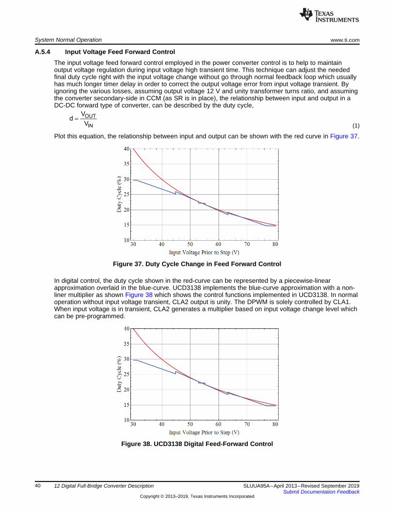
Plot this equation, the relationship between input and output can be shown with the red curve in Figure 37.
Figure 37. Duty Cycle Change in Feed Forward Control
In digital control, the duty cycle shown in the red-curve can be represented by a piecewise-linearapproximation overlaid in the blue-curve. UCD3138 implements the blue-curve approximation with a non-liner multiplier as shown Figure 38 which shows the control functions implemented in UCD3138. In normaloperation without input voltage transient, CLA2 output is unity. The DPWM is solely controlled by CLA1.When input voltage is in transient, CLA2 generates a multiplier based on input voltage change level whichcan be pre-programmed.
Figure 38. UCD3138 Digital Feed-Forward Control

( )C P in _ senseGain K K VDAC V= + ´ -
www.ti.com System Normal Operation
41SLUUA95A–April 2013–Revised September 2019Submit Documentation Feedback
Copyright © 2013–2019, Texas Instruments Incorporated
12 Digital Full-Bridge Converter Description
On the control used in this EVM, the input voltage sense value is compared with VREF2, their difference, Vth,will set up the multiplier from CLA2 to CLA1 as below.• If -Vth1 < Vth < Vth1, CLA2 = Gain0, or KP0
• If -Vth2 < Vth < –Vth1, or, Vth1 < Vth < Vth2, CLA2 = Gain1, or KP1
• If -Vth2 > Vth or Vth2 < Vth, CLA2 = Gain2, or KP2
The above can be expressed as,
(2)
In steady-state, Gain0 = KC, where KC can be described as a unity number although in practice it may bedesigned differently to match other scaled values.
During the input voltage transient, nonlinear gain is generated to achieve desired duty cycle by feedforward control approximation.
As the control algorithm is of symmetrical characteristics from ±Vth1 and ±Vth2, an equilibrium point isrequired to be established. From practice such as in 48-V telecom application, this point may be initiallyselected at VIN0 = 48 V. During the operation with different input voltage, a new equilibrium point will bere-established corresponding to that input voltage.
In this EVM design, Vin_sense signal is from VIN_CT as shown in Figure 26 and its relationship to VIN isexpressed as,
Vin_sense = (VIN/N) x R29 / (R25 + R29) = k x VIN, where k = 0.0154, and N is the turns ratio of transformerT3.

System Normal Operation www.ti.com
42 SLUUA95A–April 2013–Revised September 2019Submit Documentation Feedback
Copyright © 2013–2019, Texas Instruments Incorporated
12 Digital Full-Bridge Converter Description
A.5.5 Feed Forward Function TestLoad = 1 A, VIN from 40 V to 58 V, VIN slew rate 20 V/us, VO maximum shift 0.68 V, recovery time 50 µs. InFigure 39, the purple is VOUT and the yellow is VIN. In Figure 40, the green is primary side DPWM and theyellow is VIN.
Figure 39. VO Change from Digital Feed Forward Control
Figure 40. Duty Cycle Change from Digital Feed Forward Control

www.ti.com System Normal Operation
43SLUUA95A–April 2013–Revised September 2019Submit Documentation Feedback
Copyright © 2013–2019, Texas Instruments Incorporated
12 Digital Full-Bridge Converter Description
A.5.6 Light Load OperationAt light load, the burst operation can be enabled when the switching duty cycle is small. The significantbenefit from this operation is the reduction of the power losses. The associated disadvantage is of higheroutput voltage ripple in steady-state and of larger output voltage dip in load demanding transient. But thehigher ripple and the larger dip can be solved especially with digital control of its convenience andflexibility. For example, non-linear control from digital control can solve the large dip during load transient.The higher ripple can also be reduced by narrowed duty cycle on/off limit for burst operation control.
Figure 41 shows the burst operation timing diagram with UCD3138. When the controller detected lightload condition, the operation is enabled into Light Load Enable (LLE) by firmware. When load condition ischanged to heavy, CLA can generate a large gain to adapt the load change and minimize the outputvoltage drop although the operation is still in LLE mode. If the load keeps heavy for certain time, light loadwill be terminated by the firmware.
The burst operation mode is disabled in the EVM. Please contact TI to know how to enable this feature.
Figure 41. Burst Operation Timing Diagram

System Operation in Protection www.ti.com
44 SLUUA95A–April 2013–Revised September 2019Submit Documentation Feedback
Copyright © 2013–2019, Texas Instruments Incorporated
12 Digital Full-Bridge Converter Description
A.6 System Operation in Protection
A.6.1 Faults and WarningsThe system comes equipped with a variety of programmable fault and warning options. In section 12.3.8,Table 5 lists the LEDs used to indicate a fault. Table 6 below shows the basic faults and warningsavailable in the EVM along with the corresponding action taken by these events. Each of theseparameters can be modified through the GUI.
Table 6. Faults and Warnings
SIGNAL TYPE WARNING FAULT RESPONSEVOUT Over Report Report & Latch off
Under Report ReportVIN Over Report Report & Latch off
Under Report Report & Latch offIOUT Over Report Report & Latch offIIN Over Report Cycle by cycle limiting
Temperature Over Report Report and Latch off
The GUI reporting includes appropriate setting of the PMBus alert line, status byte and status word. Faultsand warnings can be reset by toggling the unit off and then on. Alternatively, as long as the system doesnot latch off, the “Clear Faults” button can also be used to clear any faults or warnings. Refer to Figure 42which is from the Designer GUI Monitor tab. More details can be found in Section A.8.
Figure 42. Faults and Warnings

CPCC @Vin=48V
0
2
4
6
8
10
12
14
0 5 10 15 20 25 30 35 40
Iout (A)
Vo
ut
(V)
w Fan
w/o Fan
www.ti.com System Operation in Protection
45SLUUA95A–April 2013–Revised September 2019Submit Documentation Feedback
Copyright © 2013–2019, Texas Instruments Incorporated
12 Digital Full-Bridge Converter Description
A.6.2 Constant Power Constant Current OperationBoth hardware and firmware in this EVM supports Constant Power Constant Current, or CPCC operation.Figure 43 illustrates the behavior of the output voltage and output current (V¬OUT vs. IOUT). However,the EVM comes pre-programmed with a constant power threshold of 360 W and a constant currentthreshold of 36 A. Some of the limits are adjustable through the GUI and new setting can be saved to dataflash. The maximum hardware capability is to limit the current within 36 A. Figure 44 shows the GUIinterface to these controls with the default values. The CPCC can be enabled or disabled through GUI.Details can be found in Section A.4.2.
After the output power reaches the set point, VOUT starts to drop while the power keeps the same whichmeans the current may increase. The power stage stays on and it will not enter latch mode. When thecurrent loop filter output (Front End 1 and Filter 1) is larger than the voltage loop filter output (Front End 0and Filter 0), the current loop takes control of the power stage and output voltage starts in hiccupoperation state. In hiccup state, the power stage stays on for 1s, and then goes to idle state and try to turnon again. If the load is reduced, the power stage will go to regulated state. If the load current is still high,the output voltage goes to hiccup state again. Only OVP will take the power stage to latch-off state. OTP,OCP, and constant current will take the power state to hiccup state. In hiccup state, the power state turnson automatically. In latch state, toggle off the PSON switch is needed or recycle the input power.
Figure 43. Constant Power Constatnt Current Operation
Figure 44. CPCC Default Values and Adjustable through GUI

System Operation in Protection www.ti.com
46 SLUUA95A–April 2013–Revised September 2019Submit Documentation Feedback
Copyright © 2013–2019, Texas Instruments Incorporated
12 Digital Full-Bridge Converter Description
A.6.3 Cycle-By-Cycle Current LimitCycle-by-cycle current limit is made to the primary-side input current. The current is sensed by currenttransformer T1. The sensing circuit is shown in Figure 45; also refer to full schematics of Figure 1 andpower stage Figure 23. The current signal is fed into AD04 and compared to a programmable threshold ona cycle-by-cycle basis. Whenever this current exceeds the threshold the active DPWM waveforms aretruncated. The cycle-by-cycle current limit is mainly used to the primary current to limit its peak within pre-determined value, default as 16 A.
As AD04 is a simple voltage comparator, external current slope compensation circuit may be needed inorder to minimize the sub-harmonics normally existing in peak current mode control including cycle-by-cycle current limit. An example circuit is shown in Figure 46. More detail on this circuit can be found in“Modeling, Analysis and Compensation of the Current-Mode Converter”, (TI Literature Number SLUA101).
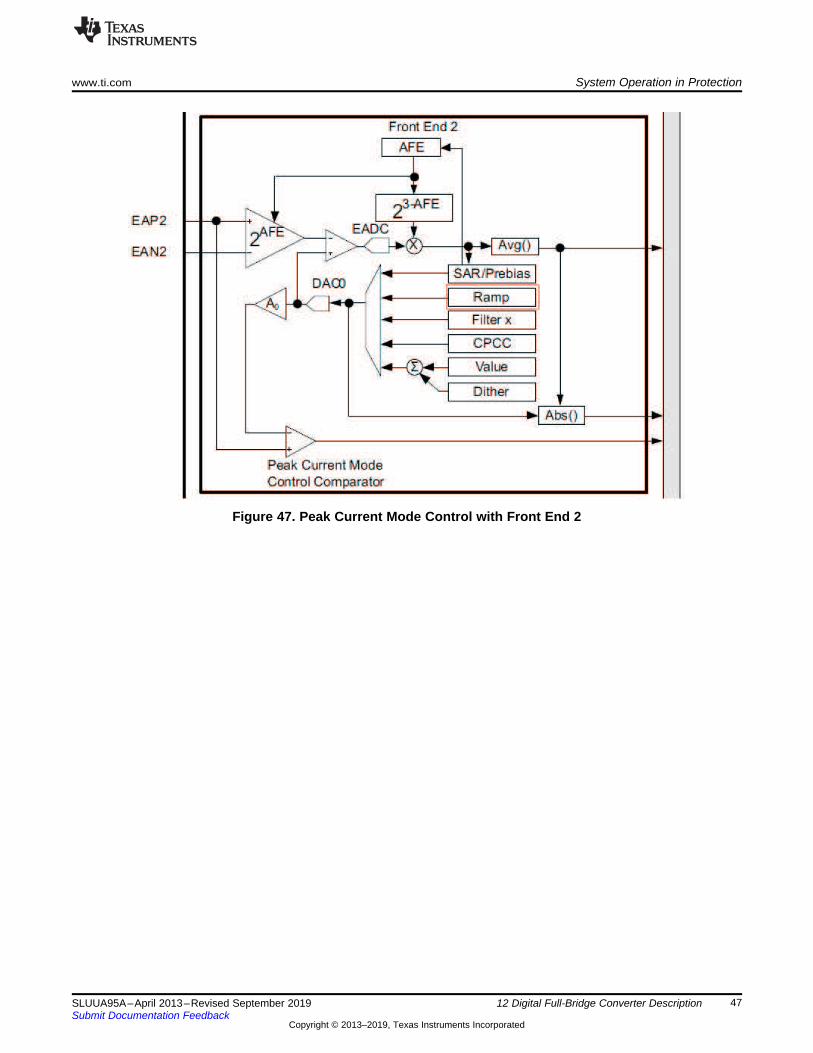
In case the peak current mode control is employed in an application, the peak current mode control shouldbe made through Front End 2 (EADC2) instead of using AD04. Frond End 2 has build-in current slopecompensation (RAMP) as shown in Figure 47 which does not require external slope compensation.
UCD3138 can balance two pulses in a switching cycle with the same width. In UCD3138RHA, this featureexists in the DPWM module on its two outputs, for example between DPWM0A and 0B, but not availableon the interconnection matrix. Then this EVM is not able to balance the pulse width in a switching cycle. Ifthis feature is preferred, please contact TI for technical assistance.
Figure 45. Cycle-by-Cycle Current Limit Sensing Circuit
Figure 46. An Example of External Slope Compensation
www.ti.com System Operation in Protection
47SLUUA95A–April 2013–Revised September 2019Submit Documentation Feedback
Copyright © 2013–2019, Texas Instruments Incorporated
12 Digital Full-Bridge Converter Description
Figure 47. Peak Current Mode Control with Front End 2

System Operation in Protection www.ti.com
48 SLUUA95A–April 2013–Revised September 2019Submit Documentation Feedback
Copyright © 2013–2019, Texas Instruments Incorporated
12 Digital Full-Bridge Converter Description
A.6.4 Short Circuit ProtectionLoad short circuit protection is mainly based on the secondary-side current sensing when the load currentis beyond a 36 A by default. In short circuit protection the output voltage is in hiccup state.
Figure 48 shows a test results with the conditions: short circuit test at 30-A load, VOUT (Ch1), IPRI (Ch 2),and VIN (Ch 3).
Figure 48. Short Circuit Protection Test
A.6.5 Output Over VoltageOutput over voltage detection and protection is through AD03, refer to Figure 1 and Figure 23. Whenoutput over voltage is detected, the switching pulses will be disabled and the board will be in latch-off untilrecycle the input power or toggle the switch S1.
A.6.6 Input Over VoltageThe input over voltage is detected based on the main power transformer winding as described inSection A.3.4. Currently in the EVM delivered, input voltage is detected and the firmware provides warningto the Designer GUI. Please contact TI if need OVP protection.
A.6.7 Over TemperatureOver temperature includes UCD3138 internal temperature sensing and external added temperaturesensing. The external over temperature condition is determined by a temperature sensing element onU13, LM60C. The temperature signal is fed into the controller through AD06. U13 is located on board topside next to the current sensing copper. Then it is sensing the temperature of secondary-side boardtemperature. In addition to the over temperature protection, this temperature information is used tocompensate the copper current sensing.
Figure 49. Temperature Detection Circuit

Q 0.5£
z1 z2
z1 z2
Qw ´ w
=
w + w
r z1 z2w = w ´ w
2rz1, z2 1 j 4 Q 1 and j 1
2 Q
w æ öw = ± ´ - = -ç ÷´ è ø
2
2rr
cz 0
p1
s s1
QG (s) K
ss 1
æ öç ÷+ +ç ÷´ wwè ø=
æ ö+ç ÷
ç ÷wè ø
z1 z2cz 0
p1
s s1 1
G (s) Ks
s 1
æ öæ ö+ +ç ÷ç ÷
w wè øè ø=æ ö
+ç ÷ç ÷wè ø
1 1
c P I D1 1
1 z 1 zG (z) K K K
1 z 1 z
- -
- -
+ -= + +
- - a´
www.ti.com Loop Compensation Using PID Control
49SLUUA95A–April 2013–Revised September 2019Submit Documentation Feedback
Copyright © 2013–2019, Texas Instruments Incorporated
12 Digital Full-Bridge Converter Description
A.7 Loop Compensation Using PID ControlPID control is usually used in the feedback loop compensation in digitally controlled power converters. Wewill describe several aspects how to use PID control.
A.7.1 Digital PID Coefficients Transfermation to Poles and Zeros in s-DomainPID control in UCD3138 CLA for control loop is formed in the following equation in z-domain:
(3)
If Equation 3 is converted to the s-domain equivalent using the bilinear transform, the result has twoforms. One is with two real zeros and one real pole:
(4)
K0 is the gain of the frequency domain pole at origin, and K0 is also represented as the angular frequencywhen the integrator Bode plot gain crosses over with 0-dB. By the way, K0 can be used as a method forinitially designing the feedback loop compensation, refer to for more details.
The second way is when the two zeros are possibly presented with complex conjugates and in such acase,
(5)
Two complex conjugate zeros are expressed as,
(6)
(7)
(8)
The factor of Q is in the range of 0 to infinite. The two complex conjugate zeros become the two real zeroswhen Q is not greater than 0.5.
(9)

1 1SC 19
p i d1 8 1 4
1 z 1 z 11000 K K K 2 KCOMP 2
1 z 1 2 z 2 (PRD 1)
- -- -
- - -
æ ö+ -´ + ´ + ´ ´ ´ ´ ´ç ÷
ç ÷- - a ´ ´ ´ +è ø
z1 z2
0 p
s s1 1
2 f 2 f
s s1
2 K 2 f
æ ö æ ö+ ´ +ç ÷ ç ÷
´ p ´ ´ p ´è ø è ø
æ ö´ +ç ÷
ç ÷´ p ´ ´ p ´è ø
2
2z zz
0 p
s s1
2 f Q(2 f )
s s1
2 K 2 f
+ +´ p ´ ´´ p ´
æ ö´ +ç ÷
ç ÷´ p ´ ´ p ´è ø
s p1
s p1
2 T
2 T
- ´ w
a =
+ ´ w
( ) ( )( )
0 p1 z1 p1 z2
D
p1 z1 z2 s p1
2 KK
T 2
´ ´ w - w ´ w - w=
w ´ w ´ w ´ w +
0 sI
K TK
2
´
=
( )0 p1 z1 p1 z2 z1 z2
Pp1 z1 z2
KK
´ w ´ w + w ´ w - w ´ w=
w ´ w ´ w
s CT 0.05 T£ ´
M PIDcs
M PID cs
G (s) G (s)G (s)
1 G (s) G (s) H (s)
´
=
+ ´ ´
cs cs
pcs
1H (s) K
s1
=
+
w
Loop Compensation Using PID Control www.ti.com
50 SLUUA95A–April 2013–Revised September 2019Submit Documentation Feedback
Copyright © 2013–2019, Texas Instruments Incorporated
12 Digital Full-Bridge Converter Description
Hence, Equation 4 is actually a special form of Equation 5. In this sense, Equation 5 can be used in eithercase across the range of Q.
A low pass filter usually exists in a control loop of its feedback path. The low pass filter adds a pole to theloop,
(10)
The close loop transfer function is then shown as below:
(11)
where GM(s) is the control plant transfer function. For example, GM(s) can be the transfer functionassociated to the modulator in an HSFB converter.
The parameters can be calculated with the assumption of sensor sampling cycle TS much smaller than thecorresponding time constant of the voltage loop bandwidth, TC. A rule of thumb is to choose the samplingfrequency to meet
(12)
When the above assumption is true, the delay effect from the sampling (usually with zero order hold orZOH) can be ignored and the parameters can be determined after we know where the poles and zerosshould be positioned. Table 7 summarizes the poles and zeros in a form to relate z-domain to s-domain.
(13)
(14)
(15)
(16)
Table 7. Poles and Zeros from PID Coefficients
System Name Transfer FunctionsComplex Zeros(K0, fZ, QZ, fP)
Real Zeros(K0, fZ1, fZ2, fP)
Device PID(Kp, Ki, KD, α)

www.ti.com Loop Compensation Using PID Control
51SLUUA95A–April 2013–Revised September 2019Submit Documentation Feedback
Copyright © 2013–2019, Texas Instruments Incorporated
12 Digital Full-Bridge Converter Description
A.7.2 Tuning PID Coefficients for Loop CompensationWhen making fine-tune adjustments to the feedback control loop, one would like to know each parameterin PID how to affect the control loop characteristics without going through complicated description of theabove equations. Table 8 below helps this and visually shown in Figure 50.
Table 8. Tuning PID Coefficients
CONTROL PARAMETERS IMPACT ON BODE PLOTKP Increasing KP
Pushes up the minimum gain between the two zeros.Moves the two zeros apart.
KI Increasing KIPushes up integration curve at low frequencies.Gives a higher low-frequency gain.Moves the first zero to the right.
KD Increasing KDShifts the second zero left.Doesn’t impact the second pole.
α Increasing α
Shifts the second pole to the right.Shifts the second zero to the right.
TS = 1 / fS Increasing the sampling frequency fS :Causes the whole Bode plot to shift to right.
Figure 50. Tuning PID Parameters
A.7.3 Measuring the Control LoopThe control loop measurement can be made by injecting frequency sweep signal across R16. Theconnections can take advantage of P2 pin 1 and TP10.

Evaluating the EVM with GUI www.ti.com
52 SLUUA95A–April 2013–Revised September 2019Submit Documentation Feedback
Copyright © 2013–2019, Texas Instruments Incorporated
12 Digital Full-Bridge Converter Description
A.8 Evaluating the EVM with GUICollectively, the GUI is called Texas Instruments Fusion Digital Power Designer. The GUI serves theinterface for several families of TI digital control IC’s including the family of UCD31xx, that is the UCD3138as its one member. The GUI can be divided into two main categories, Designer GUI and Device GUI. Inthe family of UCD31xx, each EVM is related to a particular Designer GUI to allow users to re-tune/re-configure a particular EVM in that regarding with existing hardware and firmware. Device GUI is related toa particular device to access its internal registers and memory cells.
UCD3138HSFBEVM-029 is a standalone board where UCD3138RGH 40-pin device is placed. Thefirmware to control this converter is downloaded into this board through Device GUI. How to install the GUIis described in the user’s guide “Using the UCD3138CC64EVM-030 (TI Lit#, SLUU886)”. The designerGUI is installed at the same time when installing the Device GUI.
A.8.1 Graphical User Interface (GUI)As mentioned above, there are two types of graphical user interfaces (GUI), one is Device GUI, and theother is Designer GUI. The Device GUI is sometimes called low level GUI. From the Device GUI, device’sregisters are accessed if the device is in the ROM mode and the PMBus communication is established.This GUI should be used to download the code when the device is blank at the first programming. Also, atthe flash mode, a customer can send PMBus commands to read or write the data. The Designer GUI is aninterface between a host and a user’s board. It supports some of PMBus commands for configuration,monitoring and design such as loop compensator built in the UCD3138 digital controller.

J6
1
-L
oa
d+
UART0 (J8)
D14
Reset
-V
IN+
J3
J4J1
S1
TP10
TP44TP1 TP2
1 16
2 15
8 9
7 10
1 12
2 11
6 7
5 8
J5 J2
D19
S2
Forced Air Flow Direction
400LFM
USB-to-GPIO
www.ti.com Evaluating the EVM with GUI
53SLUUA95A–April 2013–Revised September 2019Submit Documentation Feedback
Copyright © 2013–2019, Texas Instruments Incorporated
12 Digital Full-Bridge Converter Description
A.8.1.1 Hardware SetupThe board hardware connection is overall the same as shown in Section 5.2 and Figure 4 while shown inFigure 51 again. The addition to the setup is to connect USB-to-GPIO to the board. The ribbon cableconnects to J6 and the USB cabled connects to a host PC computer. The remaining connections aredescribed again in the below.
Figure 51. Test Setup

Evaluating the EVM with GUI www.ti.com
54 SLUUA95A–April 2013–Revised September 2019Submit Documentation Feedback
Copyright © 2013–2019, Texas Instruments Incorporated
12 Digital Full-Bridge Converter Description
• Refer to Figure 51 for basic hardware connections. The required equipment is listed in Section 5.1.• Before making electrical connections, visually check the boards to make sure no shipping damage
occurred.• Connect the DC voltage source to J1-1 (+) and J1-2 (-). Set up the DC output voltage in the range
specified in Table 1, between 36 VDC and 72 VDC; set up the DC source current limit 12 A.• Connect an electronic load with either constant current mode or constant resistance mode. The load
range is from zero to 30 A.• Connect USB-to-GPIO ribbon cable to J6 and connect USB-to-GPIO USB cable to a host PC
computer.• Check and make sure the jumpers are installed correctly on J2 and J5.
– J2 should be jumped across to connect its 1-16, 2-15, 7-10, and 8-9.– J5 should be jumped across to connect its 1-12, 2-11, 5-8, and 6-7.
WARNINGFollow the connections correctly to avoid possible damages
• It is recommended to use the switch S1 to turn on the board output after the input voltage is applied tothe board. Before applying input voltage, make sure the switch, S1, is in the “OFF” position.
• If the load does not have a current or a power display, a current meter or low ohmic shunt and DMMwill be needed between the load and the board for current measurements.
• Connect a volt-meter across the output connector and set the volt-meter scale 0 V to 15 V on itsvoltage, DC.

www.ti.com Evaluating the EVM with GUI
55SLUUA95A–April 2013–Revised September 2019Submit Documentation Feedback
Copyright © 2013–2019, Texas Instruments Incorporated
12 Digital Full-Bridge Converter Description
A.8.1.2 GUI InstallationGUI software can be downloaded from the TI website, www.ti.com. The software should be installed in thehost PC before it is executed. More details about the TI GUI, which is called TI Fusion Digital PowerDesigner (DFPD), can be found in its user’s guide/manual. Please contact TI to get this user’sguide/manual. After the GUI installation, the Guide can be found in the Designer GUI of its real time“Help”.
“Help” > “Documentation & Help Center” > “UCD3138”
Copy the TI Fusion Digital Power Designer zip file and unzip the file TI-Fusion-Digital-Power-Designer-xx.zip to get installer TI-Fusion-Digital-Power-Designer-xxx.exe. The xxx in the file name refers to the GUIrelease version.
Double click the installer TI-Fusion-Digital-Power-Designer-xxx.exe and follow the straight forwardinstructions to finish the installation. Normally, you need accept all the installation defaults. In order to getall GUI functions, all boxes under Select Additional Tasks should be checked, shown in Figure 52.
Figure 52. GUI Installation
After the installation, a quick launch button is created next to the start menu which contains shortcuts tocommonly used applications. Figure 53 shows the icon of TI DFPD after the installation. Some other iconssuch as UCD3K Device GUI are also displayed on the desktop. For more information on the GUIinstallation, one can refer to UCD3138CC64EVM-030 user’s guide.
Figure 53. GUI Shortcut Location

Evaluating the EVM with GUI www.ti.com
56 SLUUA95A–April 2013–Revised September 2019Submit Documentation Feedback
Copyright © 2013–2019, Texas Instruments Incorporated
12 Digital Full-Bridge Converter Description
A.8.1.3 USB-to-GPIO Adaptor Connection
CAUTIONShut off DC power source before connection to avoid electrical shock!
Connect one end of the ribbon cable to the module, and connect the other end to the USB-to-GPIO(HPA172) interface adapter. Connect the Mini connector of the USB cable to the USB interface adapter,and connect the other end to the USB port of the host computer.
A.8.1.4 Launch the Designer GUIClick the Quick Launch Shortcut icon located next to the start menu. The GUI starts to look for theattached device attached to the PMBus. If the device is found and the communication is establishedsuccessfully, one should see a screen that looks similar to Figure 54. In the following we will describe howto use the GUI to evaluate the module.
Figure 54. Designer GUI Overview

www.ti.com Evaluating the EVM with GUI
57SLUUA95A–April 2013–Revised September 2019Submit Documentation Feedback
Copyright © 2013–2019, Texas Instruments Incorporated
12 Digital Full-Bridge Converter Description
A.8.1.5 Designer GUI OverviewThe Designer GUI has four tabs, as shown in Figure 54, namely, Configure, Design, Monitor, and Status.After launch the GUI, its default tab is Monitor. To go to the other three tabs, simply click the tab youwould like to go.
In the GUI used with this EVM, Configure is used to configure the EVM settings through PMBuscommands. Design is mainly used to make tuning control loop parameters and to set up the Feed-Forward control non-linear gains. Monitor is used to monitor the board operation. Status is mainly used toshow fault and/or warnings.
A.8.2 Operation MonitoringAfter the designer GUI launched, the Monitor tab is presented by default as shown in Figure 54. This tabprovides a quick overview of operation status with some settings changeable as well. This tab alsoprovides oscilloscope type of plot view in real time operation. The number of scope windows can beadjusted by check or un-check upper left square boxes to show or to hide these scope plot windows.
Figure 55. Designer GUI Status

Evaluating the EVM with GUI www.ti.com
58 SLUUA95A–April 2013–Revised September 2019Submit Documentation Feedback
Copyright © 2013–2019, Texas Instruments Incorporated
12 Digital Full-Bridge Converter Description
A.8.3 Operation StatusAfter click the Status tab as shown in Figure 54, the EVM operation status is shown as in Figure 55. Allgrayed entries are candidates that can be implemented. Those in black are showing current operationstatus which helps to indicate potential operation issues with warning or fault indications. If a faultoccurred, the corresponding entry is highlighted in red. Warnings are not a fault while may remind the userthat those might need attention.
A.8.4 Configuring EVMConfigure tab can help to adjust the EVM feature setup conveniently without directly accessing thefirmware code. Also, it helps to navigate through the various features of the converter through the GUI.
Figure 56. GUI Supported PMBus Commands

www.ti.com Evaluating the EVM with GUI
59SLUUA95A–April 2013–Revised September 2019Submit Documentation Feedback
Copyright © 2013–2019, Texas Instruments Incorporated
12 Digital Full-Bridge Converter Description
A.8.4.1 GUI Supported PMBus CommandsFigure 56 displays the various GUI based PMBus commands supported by the current version of thefirmware. Adding additional standard commands is easy to do with the built in “Isolated Bit Mask”generator. This tool creates a coded index that the GUI reads from the device to determine what PMBuscommands are supported. To add a standard command simply modify the bit mask and the GUI willautomatically display the new command. Please contact Texas Instruments for details on the use of thistool.
A.8.4.2 Configuring EVM with GUIIn the Configure tab, change configuration is made simple. For example, to configure CPCC, the CPCCcontrol can be accessed by clicking the drop down arrow next to the Value/Edit box on the CPCC[MFR36] line as shown in Figure 57. As we mentioned before, maximum current 36A and maximum power 360W. Please consult Texas Instruments if there is any uncertainty to be resolved.
Figure 57. Configure CPCC
As one more example, in the following, we will describe how to configure the dead time. Configuring otherfunctions is made in the similar way. Again, please consult Texas Instruments if there is any uncertainty tobe resolved before making your configuration.

Evaluating the EVM with GUI www.ti.com
60 SLUUA95A–April 2013–Revised September 2019Submit Documentation Feedback
Copyright © 2013–2019, Texas Instruments Incorporated
12 Digital Full-Bridge Converter Description
A.8.4.3 Configuring Dead TimeClick the drop down arrow next to the Value/Edit box on the DEADBAND_CONFIG [MFR 26] line, adialogue box of Figure 58 is present to allow configuring the dead time.
Figure 58. Configuring Dead Time

SsTz e=
1 1 SC 19
p i d1 8 1 4
1 z 1 z 2 PRD 21000 K K K
1 z 1 2 z 2 (PRD 1)
- - - -
- - -
æ ö+ - ´ ´´ + ´ + ´ ´ç ÷
ç ÷- - a ´ ´ ´ +è ø
s DPWMT 16 (PRD 1) T= ´ + ´
1 1SC 19
p i d1 8 1 4
1 z 1 z 11000 K K K 2 KCOMP 2
1 z 1 2 z 2 (PRD 1)
- -- -
- - -
æ ö+ -´ + ´ + ´ ´ ´ ´ ´ç ÷
ç ÷- - a ´ ´ ´ +è ø
2
2z zz
0 p
s s1
2 f Q(2 f )
s s1
2 K 2 f
+ +´ p ´ ´´ p ´
æ ö´ +ç ÷
ç ÷´ p ´ ´ p ´è ø
2
2z zz
0 p
s s1
2 f Q(2 f )
s s1
2 K 2 f
+ +´ p ´ ´´ p ´
æ ö´ +ç ÷
ç ÷´ p ´ ´ p ´è ø
www.ti.com Evaluating the EVM with GUI
61SLUUA95A–April 2013–Revised September 2019Submit Documentation Feedback
Copyright © 2013–2019, Texas Instruments Incorporated
12 Digital Full-Bridge Converter Description
A.8.5 Tuning Control Loop Using GUI Design
A.8.5.1 Options to Program Digital Control LoopThe GUI comes equipped with 3 different ways to program the UCD3138 digital control loop compensator.Table 9 lists the three options, (a) using K0, fZ, QZ, and fP; (b) using K0, fZ1, fZ2, and fP; (c) using KP, Ki, Kd,and α.
In option (c), the compensator is described by Device PID. In this context, Kp, Ki, Kd and α are the rawregister values used to configure the positions of the poles and zeros of the compensator. SC is a gainscaling term. Although it is normally set to zero it provides additional gain for situations where the powerstage gain may be low. PRD is used to configure the minimum operating period and KCOMP is used toconfigure the maximum operating period. In the context of the compensator they are simply gain termsthat modify the overall transfer function by a fixed value. It is important to be aware that the proper way toconfigure PRD and KCOMP varies based on the control topology implemented.
Table 9. Programming Digital Control Loop
SYSTEM NAME TRANSFER FUNCTIONSComplex Zeros(K0, fz, Qz, fp)
Real Zeros(K0, fz1, fz2, fp)
Device PID(Kp, Ki, Kd, α)
The compensator of this EVM is configured to acquire one sample per switching cycle, TS, as defined byEquation 17 where TDPWM = 250 ps,
(17)
When the converter operates in PWM mode KCOMP = PRD and the “Device PID” option in Table 9 isexpressed in Equation 16 which correctly describes the behavior of the compensator. For clarityEquation 18 displays the exact transfer function used in PWM mode operation.
(18)
Equation 18 is based on a fixed sample rate. This means Equation 18 is assumed with one switchingfrequency. The value of that frequency is inside the variable z;
(19)
where TS is the switching period, that is the reciprocal of the switching frequency. In PWM mode, theswitching frequency is fixed at 200 kHz such that TS is fixed and the only value. Figure 59 shows anexample of Bode plot outputs from the GUI. Figure 60 shows the PID coefficients used. Figure 61 showsthe schematics used to obtain the Bode Plots in Figure 59 with the PID coefficients shown in Figure 60.

Evaluating the EVM with GUI www.ti.com
62 SLUUA95A–April 2013–Revised September 2019Submit Documentation Feedback
Copyright © 2013–2019, Texas Instruments Incorporated
12 Digital Full-Bridge Converter Description
Figure 59. Bode Plots from GUI

www.ti.com Evaluating the EVM with GUI
63SLUUA95A–April 2013–Revised September 2019Submit Documentation Feedback
Copyright © 2013–2019, Texas Instruments Incorporated
12 Digital Full-Bridge Converter Description
Figure 60. PID Coefficients Used in Voltage Loop
Figure 61. Bode Plots Calculation
NOTE: The above Figure 61 schematic was used in the bode plots calculation.

Firmware Development for HSFB Power Converter www.ti.com
64 SLUUA95A–April 2013–Revised September 2019Submit Documentation Feedback
Copyright © 2013–2019, Texas Instruments Incorporated
Revision History
A.9 Firmware Development for HSFB Power ConverterPlease contact TI for additional information regarding UCD3138 digital HSFB firmware development.
A.10 References1. UCD3138 Datasheet, Highly Integrated Digital Controller for Isolated Power, (Texas Instruments,
Literature Number SLUSAP2), 20122. UCD3138CC64EVM-030 Evaluation Module and User’s Guide, Programmable Digital Power Controller
Control Card Evaluation Module, (Texas Instruments Literature Number SLUU886), 20123. TI Application Manual, UCD3138 Digital Power Peripherals Programmer’s Manual, (Texas Instruments
Literature Number SLUU995)4. TI Application Manual, UCD3138 Monitoring and Communications Programmer’s Manual, (Texas
Instruments Literature Number SLUU996)5. TI Application Manual, UCD3138 ARM and Digital System Programmer’s Manual, (Texas Instruments
Literature Number SLUU994)6. User Guide, UCD3138 Isolated Power Fusion GUI, (please contact TI). Note this User Guide is also
available in the GUI after installation.
Revision HistoryNOTE: Page numbers for previous revisions may differ from page numbers in the current version.
Changes from Original (April 2013) to A Revision .......................................................................................................... Page
• changed R91 from 0 Ohm to 3 Ohm (schematic)..................................................................................... 8• changed R91 from 0 Ohm to 3 Ohm (list of materials) ............................................................................. 22

STANDARD TERMS FOR EVALUATION MODULES1. Delivery: TI delivers TI evaluation boards, kits, or modules, including any accompanying demonstration software, components, and/or
documentation which may be provided together or separately (collectively, an “EVM” or “EVMs”) to the User (“User”) in accordancewith the terms set forth herein. User's acceptance of the EVM is expressly subject to the following terms.1.1 EVMs are intended solely for product or software developers for use in a research and development setting to facilitate feasibility
evaluation, experimentation, or scientific analysis of TI semiconductors products. EVMs have no direct function and are notfinished products. EVMs shall not be directly or indirectly assembled as a part or subassembly in any finished product. Forclarification, any software or software tools provided with the EVM (“Software”) shall not be subject to the terms and conditionsset forth herein but rather shall be subject to the applicable terms that accompany such Software
1.2 EVMs are not intended for consumer or household use. EVMs may not be sold, sublicensed, leased, rented, loaned, assigned,or otherwise distributed for commercial purposes by Users, in whole or in part, or used in any finished product or productionsystem.
2 Limited Warranty and Related Remedies/Disclaimers:2.1 These terms do not apply to Software. The warranty, if any, for Software is covered in the applicable Software License
Agreement.2.2 TI warrants that the TI EVM will conform to TI's published specifications for ninety (90) days after the date TI delivers such EVM
to User. Notwithstanding the foregoing, TI shall not be liable for a nonconforming EVM if (a) the nonconformity was caused byneglect, misuse or mistreatment by an entity other than TI, including improper installation or testing, or for any EVMs that havebeen altered or modified in any way by an entity other than TI, (b) the nonconformity resulted from User's design, specificationsor instructions for such EVMs or improper system design, or (c) User has not paid on time. Testing and other quality controltechniques are used to the extent TI deems necessary. TI does not test all parameters of each EVM.User's claims against TI under this Section 2 are void if User fails to notify TI of any apparent defects in the EVMs within ten (10)business days after delivery, or of any hidden defects with ten (10) business days after the defect has been detected.
2.3 TI's sole liability shall be at its option to repair or replace EVMs that fail to conform to the warranty set forth above, or creditUser's account for such EVM. TI's liability under this warranty shall be limited to EVMs that are returned during the warrantyperiod to the address designated by TI and that are determined by TI not to conform to such warranty. If TI elects to repair orreplace such EVM, TI shall have a reasonable time to repair such EVM or provide replacements. Repaired EVMs shall bewarranted for the remainder of the original warranty period. Replaced EVMs shall be warranted for a new full ninety (90) daywarranty period.
WARNINGEvaluation Kits are intended solely for use by technically qualified,professional electronics experts who are familiar with the dangersand application risks associated with handling electrical mechanicalcomponents, systems, and subsystems.User shall operate the Evaluation Kit within TI’s recommendedguidelines and any applicable legal or environmental requirementsas well as reasonable and customary safeguards. Failure to set upand/or operate the Evaluation Kit within TI’s recommendedguidelines may result in personal injury or death or propertydamage. Proper set up entails following TI’s instructions forelectrical ratings of interface circuits such as input, output andelectrical loads.
NOTE:EXPOSURE TO ELECTROSTATIC DISCHARGE (ESD) MAY CAUSE DEGREDATION OR FAILURE OF THE EVALUATIONKIT; TI RECOMMENDS STORAGE OF THE EVALUATION KIT IN A PROTECTIVE ESD BAG.

Revision History www.ti.com
66 SLUUA95A–April 2013–Revised September 2019Submit Documentation Feedback
Copyright © 2013–2019, Texas Instruments Incorporated
Revision History
3 Regulatory Notices:3.1 United States
3.1.1 Notice applicable to EVMs not FCC-Approved:FCC NOTICE: This kit is designed to allow product developers to evaluate electronic components, circuitry, or softwareassociated with the kit to determine whether to incorporate such items in a finished product and software developers to writesoftware applications for use with the end product. This kit is not a finished product and when assembled may not be resold orotherwise marketed unless all required FCC equipment authorizations are first obtained. Operation is subject to the conditionthat this product not cause harmful interference to licensed radio stations and that this product accept harmful interference.Unless the assembled kit is designed to operate under part 15, part 18 or part 95 of this chapter, the operator of the kit mustoperate under the authority of an FCC license holder or must secure an experimental authorization under part 5 of this chapter.3.1.2 For EVMs annotated as FCC – FEDERAL COMMUNICATIONS COMMISSION Part 15 Compliant:
CAUTIONThis device complies with part 15 of the FCC Rules. Operation is subject to the following two conditions: (1) This device may notcause harmful interference, and (2) this device must accept any interference received, including interference that may causeundesired operation.Changes or modifications not expressly approved by the party responsible for compliance could void the user's authority tooperate the equipment.
FCC Interference Statement for Class A EVM devicesNOTE: This equipment has been tested and found to comply with the limits for a Class A digital device, pursuant to part 15 ofthe FCC Rules. These limits are designed to provide reasonable protection against harmful interference when the equipment isoperated in a commercial environment. This equipment generates, uses, and can radiate radio frequency energy and, if notinstalled and used in accordance with the instruction manual, may cause harmful interference to radio communications.Operation of this equipment in a residential area is likely to cause harmful interference in which case the user will be required tocorrect the interference at his own expense.
FCC Interference Statement for Class B EVM devicesNOTE: This equipment has been tested and found to comply with the limits for a Class B digital device, pursuant to part 15 ofthe FCC Rules. These limits are designed to provide reasonable protection against harmful interference in a residentialinstallation. This equipment generates, uses and can radiate radio frequency energy and, if not installed and used in accordancewith the instructions, may cause harmful interference to radio communications. However, there is no guarantee that interferencewill not occur in a particular installation. If this equipment does cause harmful interference to radio or television reception, whichcan be determined by turning the equipment off and on, the user is encouraged to try to correct the interference by one or moreof the following measures:
• Reorient or relocate the receiving antenna.• Increase the separation between the equipment and receiver.• Connect the equipment into an outlet on a circuit different from that to which the receiver is connected.• Consult the dealer or an experienced radio/TV technician for help.
3.2 Canada3.2.1 For EVMs issued with an Industry Canada Certificate of Conformance to RSS-210 or RSS-247
Concerning EVMs Including Radio Transmitters:This device complies with Industry Canada license-exempt RSSs. Operation is subject to the following two conditions:(1) this device may not cause interference, and (2) this device must accept any interference, including interference that maycause undesired operation of the device.
Concernant les EVMs avec appareils radio:Le présent appareil est conforme aux CNR d'Industrie Canada applicables aux appareils radio exempts de licence. L'exploitationest autorisée aux deux conditions suivantes: (1) l'appareil ne doit pas produire de brouillage, et (2) l'utilisateur de l'appareil doitaccepter tout brouillage radioélectrique subi, même si le brouillage est susceptible d'en compromettre le fonctionnement.
Concerning EVMs Including Detachable Antennas:Under Industry Canada regulations, this radio transmitter may only operate using an antenna of a type and maximum (or lesser)gain approved for the transmitter by Industry Canada. To reduce potential radio interference to other users, the antenna typeand its gain should be so chosen that the equivalent isotropically radiated power (e.i.r.p.) is not more than that necessary forsuccessful communication. This radio transmitter has been approved by Industry Canada to operate with the antenna typeslisted in the user guide with the maximum permissible gain and required antenna impedance for each antenna type indicated.Antenna types not included in this list, having a gain greater than the maximum gain indicated for that type, are strictly prohibitedfor use with this device.

www.ti.com Revision History
67SLUUA95A–April 2013–Revised September 2019Submit Documentation Feedback
Copyright © 2013–2019, Texas Instruments Incorporated
Revision History
Concernant les EVMs avec antennes détachablesConformément à la réglementation d'Industrie Canada, le présent émetteur radio peut fonctionner avec une antenne d'un type etd'un gain maximal (ou inférieur) approuvé pour l'émetteur par Industrie Canada. Dans le but de réduire les risques de brouillageradioélectrique à l'intention des autres utilisateurs, il faut choisir le type d'antenne et son gain de sorte que la puissance isotroperayonnée équivalente (p.i.r.e.) ne dépasse pas l'intensité nécessaire à l'établissement d'une communication satisfaisante. Leprésent émetteur radio a été approuvé par Industrie Canada pour fonctionner avec les types d'antenne énumérés dans lemanuel d’usage et ayant un gain admissible maximal et l'impédance requise pour chaque type d'antenne. Les types d'antennenon inclus dans cette liste, ou dont le gain est supérieur au gain maximal indiqué, sont strictement interdits pour l'exploitation del'émetteur
3.3 Japan3.3.1 Notice for EVMs delivered in Japan: Please see http://www.tij.co.jp/lsds/ti_ja/general/eStore/notice_01.page 日本国内に
輸入される評価用キット、ボードについては、次のところをご覧ください。http://www.tij.co.jp/lsds/ti_ja/general/eStore/notice_01.page
3.3.2 Notice for Users of EVMs Considered “Radio Frequency Products” in Japan: EVMs entering Japan may not be certifiedby TI as conforming to Technical Regulations of Radio Law of Japan.
If User uses EVMs in Japan, not certified to Technical Regulations of Radio Law of Japan, User is required to follow theinstructions set forth by Radio Law of Japan, which includes, but is not limited to, the instructions below with respect to EVMs(which for the avoidance of doubt are stated strictly for convenience and should be verified by User):1. Use EVMs in a shielded room or any other test facility as defined in the notification #173 issued by Ministry of Internal
Affairs and Communications on March 28, 2006, based on Sub-section 1.1 of Article 6 of the Ministry’s Rule forEnforcement of Radio Law of Japan,
2. Use EVMs only after User obtains the license of Test Radio Station as provided in Radio Law of Japan with respect toEVMs, or
3. Use of EVMs only after User obtains the Technical Regulations Conformity Certification as provided in Radio Law of Japanwith respect to EVMs. Also, do not transfer EVMs, unless User gives the same notice above to the transferee. Please notethat if User does not follow the instructions above, User will be subject to penalties of Radio Law of Japan.
【無線電波を送信する製品の開発キットをお使いになる際の注意事項】 開発キットの中には技術基準適合証明を受けていないものがあります。 技術適合証明を受けていないもののご使用に際しては、電波法遵守のため、以下のいずれかの措置を取っていただく必要がありますのでご注意ください。1. 電波法施行規則第6条第1項第1号に基づく平成18年3月28日総務省告示第173号で定められた電波暗室等の試験設備でご使用
いただく。2. 実験局の免許を取得後ご使用いただく。3. 技術基準適合証明を取得後ご使用いただく。
なお、本製品は、上記の「ご使用にあたっての注意」を譲渡先、移転先に通知しない限り、譲渡、移転できないものとします。上記を遵守頂けない場合は、電波法の罰則が適用される可能性があることをご留意ください。 日本テキサス・イ
ンスツルメンツ株式会社東京都新宿区西新宿6丁目24番1号西新宿三井ビル
3.3.3 Notice for EVMs for Power Line Communication: Please see http://www.tij.co.jp/lsds/ti_ja/general/eStore/notice_02.page電力線搬送波通信についての開発キットをお使いになる際の注意事項については、次のところをご覧ください。http://www.tij.co.jp/lsds/ti_ja/general/eStore/notice_02.page
3.4 European Union3.4.1 For EVMs subject to EU Directive 2014/30/EU (Electromagnetic Compatibility Directive):
This is a class A product intended for use in environments other than domestic environments that are connected to alow-voltage power-supply network that supplies buildings used for domestic purposes. In a domestic environment thisproduct may cause radio interference in which case the user may be required to take adequate measures.
Revision History www.ti.com
68 SLUUA95A–April 2013–Revised September 2019Submit Documentation Feedback
Copyright © 2013–2019, Texas Instruments Incorporated
Revision History
4 EVM Use Restrictions and Warnings:4.1 EVMS ARE NOT FOR USE IN FUNCTIONAL SAFETY AND/OR SAFETY CRITICAL EVALUATIONS, INCLUDING BUT NOT
LIMITED TO EVALUATIONS OF LIFE SUPPORT APPLICATIONS.4.2 User must read and apply the user guide and other available documentation provided by TI regarding the EVM prior to handling
or using the EVM, including without limitation any warning or restriction notices. The notices contain important safety informationrelated to, for example, temperatures and voltages.
4.3 Safety-Related Warnings and Restrictions:4.3.1 User shall operate the EVM within TI’s recommended specifications and environmental considerations stated in the user
guide, other available documentation provided by TI, and any other applicable requirements and employ reasonable andcustomary safeguards. Exceeding the specified performance ratings and specifications (including but not limited to inputand output voltage, current, power, and environmental ranges) for the EVM may cause personal injury or death, orproperty damage. If there are questions concerning performance ratings and specifications, User should contact a TIfield representative prior to connecting interface electronics including input power and intended loads. Any loads appliedoutside of the specified output range may also result in unintended and/or inaccurate operation and/or possiblepermanent damage to the EVM and/or interface electronics. Please consult the EVM user guide prior to connecting anyload to the EVM output. If there is uncertainty as to the load specification, please contact a TI field representative.During normal operation, even with the inputs and outputs kept within the specified allowable ranges, some circuitcomponents may have elevated case temperatures. These components include but are not limited to linear regulators,switching transistors, pass transistors, current sense resistors, and heat sinks, which can be identified using theinformation in the associated documentation. When working with the EVM, please be aware that the EVM may becomevery warm.
4.3.2 EVMs are intended solely for use by technically qualified, professional electronics experts who are familiar with thedangers and application risks associated with handling electrical mechanical components, systems, and subsystems.User assumes all responsibility and liability for proper and safe handling and use of the EVM by User or its employees,affiliates, contractors or designees. User assumes all responsibility and liability to ensure that any interfaces (electronicand/or mechanical) between the EVM and any human body are designed with suitable isolation and means to safelylimit accessible leakage currents to minimize the risk of electrical shock hazard. User assumes all responsibility andliability for any improper or unsafe handling or use of the EVM by User or its employees, affiliates, contractors ordesignees.
4.4 User assumes all responsibility and liability to determine whether the EVM is subject to any applicable international, federal,state, or local laws and regulations related to User’s handling and use of the EVM and, if applicable, User assumes allresponsibility and liability for compliance in all respects with such laws and regulations. User assumes all responsibility andliability for proper disposal and recycling of the EVM consistent with all applicable international, federal, state, and localrequirements.
5. Accuracy of Information: To the extent TI provides information on the availability and function of EVMs, TI attempts to be as accurateas possible. However, TI does not warrant the accuracy of EVM descriptions, EVM availability or other information on its websites asaccurate, complete, reliable, current, or error-free.
6. Disclaimers:6.1 EXCEPT AS SET FORTH ABOVE, EVMS AND ANY MATERIALS PROVIDED WITH THE EVM (INCLUDING, BUT NOT
LIMITED TO, REFERENCE DESIGNS AND THE DESIGN OF THE EVM ITSELF) ARE PROVIDED "AS IS" AND "WITH ALLFAULTS." TI DISCLAIMS ALL OTHER WARRANTIES, EXPRESS OR IMPLIED, REGARDING SUCH ITEMS, INCLUDING BUTNOT LIMITED TO ANY EPIDEMIC FAILURE WARRANTY OR IMPLIED WARRANTIES OF MERCHANTABILITY OR FITNESSFOR A PARTICULAR PURPOSE OR NON-INFRINGEMENT OF ANY THIRD PARTY PATENTS, COPYRIGHTS, TRADESECRETS OR OTHER INTELLECTUAL PROPERTY RIGHTS.
6.2 EXCEPT FOR THE LIMITED RIGHT TO USE THE EVM SET FORTH HEREIN, NOTHING IN THESE TERMS SHALL BECONSTRUED AS GRANTING OR CONFERRING ANY RIGHTS BY LICENSE, PATENT, OR ANY OTHER INDUSTRIAL ORINTELLECTUAL PROPERTY RIGHT OF TI, ITS SUPPLIERS/LICENSORS OR ANY OTHER THIRD PARTY, TO USE THEEVM IN ANY FINISHED END-USER OR READY-TO-USE FINAL PRODUCT, OR FOR ANY INVENTION, DISCOVERY ORIMPROVEMENT, REGARDLESS OF WHEN MADE, CONCEIVED OR ACQUIRED.
7. USER'S INDEMNITY OBLIGATIONS AND REPRESENTATIONS. USER WILL DEFEND, INDEMNIFY AND HOLD TI, ITSLICENSORS AND THEIR REPRESENTATIVES HARMLESS FROM AND AGAINST ANY AND ALL CLAIMS, DAMAGES, LOSSES,EXPENSES, COSTS AND LIABILITIES (COLLECTIVELY, "CLAIMS") ARISING OUT OF OR IN CONNECTION WITH ANYHANDLING OR USE OF THE EVM THAT IS NOT IN ACCORDANCE WITH THESE TERMS. THIS OBLIGATION SHALL APPLYWHETHER CLAIMS ARISE UNDER STATUTE, REGULATION, OR THE LAW OF TORT, CONTRACT OR ANY OTHER LEGALTHEORY, AND EVEN IF THE EVM FAILS TO PERFORM AS DESCRIBED OR EXPECTED.

www.ti.com Revision History
69SLUUA95A–April 2013–Revised September 2019Submit Documentation Feedback
Copyright © 2013–2019, Texas Instruments Incorporated
Revision History
8. Limitations on Damages and Liability:8.1 General Limitations. IN NO EVENT SHALL TI BE LIABLE FOR ANY SPECIAL, COLLATERAL, INDIRECT, PUNITIVE,
INCIDENTAL, CONSEQUENTIAL, OR EXEMPLARY DAMAGES IN CONNECTION WITH OR ARISING OUT OF THESETERMS OR THE USE OF THE EVMS , REGARDLESS OF WHETHER TI HAS BEEN ADVISED OF THE POSSIBILITY OFSUCH DAMAGES. EXCLUDED DAMAGES INCLUDE, BUT ARE NOT LIMITED TO, COST OF REMOVAL ORREINSTALLATION, ANCILLARY COSTS TO THE PROCUREMENT OF SUBSTITUTE GOODS OR SERVICES, RETESTING,OUTSIDE COMPUTER TIME, LABOR COSTS, LOSS OF GOODWILL, LOSS OF PROFITS, LOSS OF SAVINGS, LOSS OFUSE, LOSS OF DATA, OR BUSINESS INTERRUPTION. NO CLAIM, SUIT OR ACTION SHALL BE BROUGHT AGAINST TIMORE THAN TWELVE (12) MONTHS AFTER THE EVENT THAT GAVE RISE TO THE CAUSE OF ACTION HASOCCURRED.
8.2 Specific Limitations. IN NO EVENT SHALL TI'S AGGREGATE LIABILITY FROM ANY USE OF AN EVM PROVIDEDHEREUNDER, INCLUDING FROM ANY WARRANTY, INDEMITY OR OTHER OBLIGATION ARISING OUT OF OR INCONNECTION WITH THESE TERMS, , EXCEED THE TOTAL AMOUNT PAID TO TI BY USER FOR THE PARTICULAREVM(S) AT ISSUE DURING THE PRIOR TWELVE (12) MONTHS WITH RESPECT TO WHICH LOSSES OR DAMAGES ARECLAIMED. THE EXISTENCE OF MORE THAN ONE CLAIM SHALL NOT ENLARGE OR EXTEND THIS LIMIT.
9. Return Policy. Except as otherwise provided, TI does not offer any refunds, returns, or exchanges. Furthermore, no return of EVM(s)will be accepted if the package has been opened and no return of the EVM(s) will be accepted if they are damaged or otherwise not ina resalable condition. If User feels it has been incorrectly charged for the EVM(s) it ordered or that delivery violates the applicableorder, User should contact TI. All refunds will be made in full within thirty (30) working days from the return of the components(s),excluding any postage or packaging costs.
10. Governing Law: These terms and conditions shall be governed by and interpreted in accordance with the laws of the State of Texas,without reference to conflict-of-laws principles. User agrees that non-exclusive jurisdiction for any dispute arising out of or relating tothese terms and conditions lies within courts located in the State of Texas and consents to venue in Dallas County, Texas.Notwithstanding the foregoing, any judgment may be enforced in any United States or foreign court, and TI may seek injunctive reliefin any United States or foreign court.
Mailing Address: Texas Instruments, Post Office Box 655303, Dallas, Texas 75265Copyright © 2019, Texas Instruments Incorporated

IMPORTANT NOTICE AND DISCLAIMER
TI PROVIDES TECHNICAL AND RELIABILITY DATA (INCLUDING DATASHEETS), DESIGN RESOURCES (INCLUDING REFERENCEDESIGNS), APPLICATION OR OTHER DESIGN ADVICE, WEB TOOLS, SAFETY INFORMATION, AND OTHER RESOURCES “AS IS”AND WITH ALL FAULTS, AND DISCLAIMS ALL WARRANTIES, EXPRESS AND IMPLIED, INCLUDING WITHOUT LIMITATION ANYIMPLIED WARRANTIES OF MERCHANTABILITY, FITNESS FOR A PARTICULAR PURPOSE OR NON-INFRINGEMENT OF THIRDPARTY INTELLECTUAL PROPERTY RIGHTS.These resources are intended for skilled developers designing with TI products. You are solely responsible for (1) selecting the appropriateTI products for your application, (2) designing, validating and testing your application, and (3) ensuring your application meets applicablestandards, and any other safety, security, or other requirements. These resources are subject to change without notice. TI grants youpermission to use these resources only for development of an application that uses the TI products described in the resource. Otherreproduction and display of these resources is prohibited. No license is granted to any other TI intellectual property right or to any thirdparty intellectual property right. TI disclaims responsibility for, and you will fully indemnify TI and its representatives against, any claims,damages, costs, losses, and liabilities arising out of your use of these resources.TI’s products are provided subject to TI’s Terms of Sale (www.ti.com/legal/termsofsale.html) or other applicable terms available either onti.com or provided in conjunction with such TI products. TI’s provision of these resources does not expand or otherwise alter TI’s applicablewarranties or warranty disclaimers for TI products.
Mailing Address: Texas Instruments, Post Office Box 655303, Dallas, Texas 75265Copyright © 2019, Texas Instruments Incorporated