
Untitled - KU Leuven
270
-
Upload
khangminh22 -
Category
Documents
-
view
0 -
download
0
Transcript of Untitled - KU Leuven


© Katholieke Universiteit Leuven – Faculteit Toegepaste WetenschappenArenbergkasteel, B-3001 Heverlee (Belgium)
Alle rechten voorbehouden. Niets uit deze uitgave mag worden vermenigvuldigd en/ofopenbaar gemaakt worden door middel van druk, fotocopie, microfilm, elektronischof op welke andere wijze ook zonder voorafgaandelijke schriftelijke toestemming vande uitgever.
All rights reserved. No part of the publication may be reproduced in any form by
print, photoprint, microfilm or any other means without written permission from the
publisher.
D/2003/7515/9
ISBN 90-5682-398-1

Voorwoord
Op deze eerste bladzijden wil ik een woord van dank richten aan de mensendie rechtstreeks of onrechtstreeks hebben bijgedragen aan dit doctoraatswerk.Eerst en vooral wil ik mijn promotoren, professor Reynaerts en professor VanBrussel, bedanken voor het opstarten van de onderzoeksgroep micro- en preci-siemechanica en specifiek het onderzoek over microvonkerosie. Zij hebben mijsteeds vrij gelaten om mijn interesses uit te diepen. Ik dank professor Rey-naerts voor de jarenlange samenwerking, het vele werk dat hij verricht voor demicro- en precisiegroep en voor de talrijke publicaties over dit onderzoekswerk.Professor Van Brussel wil ik bedanken voor zijn steeds positieve ingesteldheidover dit doctoraatswerk. Tevens ben ik blij dat ik zijn gedetailleerde en volle-dige kennis over wereldwijd wetenschappelijk onderzoek kon raadplegen.Mijn dank gaat ook uit naar de leden van het leescomite. Professor Kruth dankik voor zijn kritische opmerkingen op deze tekst die duidelijk positief hebbenbijgedragen tot het eindresultaat. Professor Kruth was trouwens de eerste diemij in contact bracht met vonkerosie. Professor Puers wil ik bedanken voorhet kritisch nalezen van deze tekst en voor de leerrijke discussies tijdens deIUAP-vergaderingen waarbij ik ondervonden heb dat elektronici en mechanicieen heel andere kijk hebben op microsysteemtechnologie.Tevens dank ik professor Aernoudt voor het voorzitten van de jury en professorVan Humbeeck en professor Langen om er deel van uit te maken.Het I.W.T. dank ik voor de toekenning van de 4-jarige specialisatiebeurs.I would like to thank Xiaozhong Song as he was one of the major players inmicro-EDM when he was staying at our department. It is my honour to incor-porate his work into this thesis.Mijn dank gaat uit naar Annick Verbruggen, waarmee ik samen het microvonk-avontuur startte in het kader van ons eindwerk. Verder wil ik de thesisstudentenJoeri Clijnen, Sven Somers, Karen Plessers, Raf Simons, Vincent Dierickx enWalter Driesen bedanken voor hun bijdrage, inzet en interesse voor het vonk-werk. Na hun thesis werden Joeri, Sven en Walter aangename collega’s. Ookmijn andere bureaugenoten Michael De Volder, Steven Devos, Peter Vleugels,Dries Hemschoote, Jun Qian, Jan Peirs, Istvan Nemeth, Stijn Steegen, BertHouben, Mark Versteyhe, Rob Siaens, Ivo Luyckx en Paul-Henry ’s Heerendank ik voor de positieve werksfeer. Michael wil ik speciaal bedanken voor zijngoedlachsheid en het overnemen van het microvonkwerk tijdens de voorbije
I

II Voorwoord
maanden.De micromechanici van het departement elektrotechniek, Steve Reyntjens enDirk Debruyker, met wie we tijdens de IUAP projecten steeds aan hetzelfdeeind probeerden te trekken en van wie ik veel geleerd heb over de praktischezaken in verband met fotolithografie. Steve wil ik tevens bedanken voor al deonconventionele microstructuren die hij voor mij heeft geanalyseerd en in beeldgebracht met de FIB. Zonder Steve zou er geen sprake geweest zijn van de uni-axiale inclinometer en het onderzoek naar de combinatie van microvonkerosieen fotolithografie.Voor de hulp bij het identificeren van de silicium-kristalrichtingen dank ik JokeDe Messemaeker.Ik dank de vonkers ’van de gele trap’, Philip Bleys en Benny Schacht, waarmeeik vele discussies heb gevoerd en dikwijls tot de conclusie ben gekomen dat nogveel onderzoek op vonkerosie moet gebeuren alvorens we de zaak volledig ondercontrole hebben.De mensen van het secretariaat, de diensten informatica en elektronica en vande werkplaats wil ik bedanken voor hun spontaneıteit, ondersteuning en be-reidwilligheid.Robert Overmeer dank ik voor het punctueel nalezen van de tekst.Mijn moeder, broers en familie wil ik bedanken voor de gezellige sfeer die zesteeds creeren en hun interesse in de vorderingen van dit werk.Kathleen dank ik voor de boeiende tijd die we samen beleven en dat deze noglang mag duren samen met de kinderen.
Boechout, april 2003

Abstract
In this thesis, micro-electro-discharge machining (micro-EDM) is studied as amicromachining technique for the production of three-dimensional microstruc-tures. The statistical response-surface method is proposed for the modelling ofthe micro-EDM technology. Furthermore, a study is performed on the influenceof the micro-EDM process on the surface quality and on the loading capacityof machined microstructures. Specific micro-EDM equipment is discussed andmachining strategies are developed in order to improve the machining accu-racy by means of tool-wear compensation. The three-dimensional machiningcapabilities of the developed micro-EDM technology are illustrated by a num-ber of examples and applications such as micromoulds and microsensors. Inaddition, the compatibility between micro-EDM and the established photoli-thographic micromachining techniques is demonstrated, resulting in a hybridmicromachining technology. The developed micro-EDM technology is imple-mented in a computer-aided design and manufacturing tool with the aim tomake micro-EDM more accessible for microsystem designers.
Nederlands:
In deze thesis wordt microvonkerosie bestudeerd als bewerkingstechniek voorde productie van driedimensionale microstructuren. Een statistische modele-ringstechniek is voorgesteld voor de opbouw van een technologiemodel voormicrovonkerosie. Verder is een studie uitgevoerd naar de oppervlaktekwali-teit van bewerkt silicium en naar de invloed van de oppervlaktekwaliteit opde belastbaarheid van dergelijke microstructuren. De specifieke uitrustingvoor microvonkerosie wordt besproken alsook bewerkingsstrategieen om de be-werkingsnauwkeurigheid te verbeteren door middel van sleetcompensatie. Debewerkingsmogelijkheden van de opgebouwde microvonkerosietechnologie zijnaangetoond aan de hand van verscheidene voorbeelden en toepassingen waar-onder micromatrijzen en microsensoren. Daarenboven is de compatibiliteit vanmicrovonkerosie met de gevestigde fotolithografische microfabricagetechniekenaangetoond, wat leidt tot een hybride bewerkingstechnologie. De ontwikkeldemicrovonkerosietechnologie is geımplementeerd in een computerondersteundeontwerp- en productie-omgeving met als doel microvonkerosie toegankelijker temaken voor ontwerpers van microsystemen.
III


Symbols
EDM technology
Symbol Unit Meaningtd µs, s Ignition delaytr µs, s Discharge-current rise timetf µs, s Discharge-current fall timete µs, s Discharge durationti µs, s Pulse durationt0 µs, s Pulse interval timetp µs, s Pulse cycle timeτ Duty factor (ti/tp)fp Hz Pulse frequency (1/tp)We µJ , J Discharge energyPe µW , W Discharge poweru V Voltage between tool and workpieceui V Open-circuit voltageue V Discharge voltageue V Average discharge voltagei A Current through tool and workpieceie A Discharge currentie A Average discharge currentEc µJ , J Capacitor energyb µm, m Undersizes µm, m Size of the working gapC F CapacitanceVc V Capacitor voltageL H InductanceZ Ω Impedance
V

VI List of symbols
AGIE Compact 1 Machine Settings
Symbol Unit MeaningU Open circuit voltage ui
I Discharge current ieT Pulse duration tiP Pulse interval time t0Comp Compression of the working gap,
(reference value of the servo system)Gain Gain factor of the servo systemS − box Erosion mode and setting of the relaxation
capacitance
Tool wear
Symbol Unit MeaningVW µm3/s, m3/s Removal rate on the workpieceVE µm3/s, m3/s Removal rate on the toolϑ Volumetric relative electrode wear (VE/VW )Ve µm3, m3 Tool volumeVw µm3, m3 Workpiece volumeAe µm2, m2 Tool surfaceAw µm2, m2 Workpiece surfacewe µm, m Linear tool removalww µm, m Linear workpiece removalf µm, m tool feedκ µm−1, m−1 CurvatureR µm, m Tool radiusR0 µm, m Initial tool radiusα rad Slot angletan(δ) Feed slopey µm, m Electrode profileyk µm, m Slot profile after k identical tool electrodesLm µm, m Layer thicknessLw µm, m Worn electrode lengthC µm−1, m−1 C = 2(R+s)
πR2
D µm, m Depth of slotL µm, m Length of slot∆ µm, m Desired machining toleranceTd s Time to dress and to shape the tool electrode
by WEDGV olj µm3, m3 Removed workpiece material with jth
tool electrode

List of symbols VII
Material characteristics
Symbol Unit Meaningρ kg/m3 Mass densityE GPa, Pa Young’s modulusν Poisson ratioα Thermal expansion coefficientKIc MPa · mm1/2 Fracture toughnessσb MPa, Pa Tensile Strengthλ W/(m · K) Heat conductivityc J/(kg · K) Specific heatTm K Melting temperatureCm J2/(m4 · s) Erosion resistance index
Statistics
Symbol Unit Meaningσ Standard deviationH0 Null hypothesisα Significance levelp The probability of observing an effect at least
as contradictory to H0 as the actual measuredeffect
L12 Designed array for 12 experiments
Structural analysis
Symbol Unit MeaningF N ForceM Nm Bending momentσ MPa, Pa Tensile stressy µm, m Half height of beam structureI µm4, m4 Geometrical moment of inertia
Positioning and dimensionning
Symbol Unit Meaningα, β rad Inclination anglesW µm, m WidthL µm, m LengthH µm, m Height or depth

VIII List of symbols
Manufacturing characteristics
Symbol Unit MeaningRa µm Average roughness (or arithmetic average,
centre-line average, arithmetical mean devia-tion of the profile)
Rp µm The height of the highest peak in the rough-ness profile over the evaluation length
Rv µm The depth of the deepest valley in the rough-ness profile over the evaluation length
Rt µm Peak to peak distance Rt = Rp + Rv
Rti µm Peak to peak distance per sample length (i.e.cut-off length)
Rmax µm Maximum value of Rti within the evaluationlength
Rz(ISO) µm The average of the height of the five highestpeaks plus the depth of the five deepest valleysover the evaluation length
Technology modelling
Symbol Unit MeaningAr Technology matrix (6×6) for the removal rateAs Technology matrix (6× 6) for the surface
roughnessAw Technology matrix (6× 6) for the relative
electrode wearx Matrix (1×6) with the adjustable parameters

Abbreviations
Abbreviation, acronym Meaning2D Two-dimensional2½D Two-and-a-half-dimensional, prismatic3D Three-dimensional
A AC Alternating CurrentAR Aspect Ratio
C CAD Computer-Aided DesignCAE Computer-Aided EngineeringCAM Computer-Aided ManufacturingCAPP Computer-Aided Process PlanningCCD Charge-Coupled DeviceCIM Computer-Integrated ManufacturingCMOS Complementary Metal-Oxide SemiconductorCNC Computerized Numerical ControlCVD Chemical Vapour Deposition
D DC Direct CurrentDOE Design Of ExperimentsDRC Design Rule CheckDRIE Deep Reactive Ion Etching
E EDM Electro-Discharge Machining, ElectricalDischarge Machining or spark erosion
EPDM Enterprise Product Data ManagementERC Electrical Rule CheckERP Enterprise Resource Planning
F FEA Finite-Element AnalysisFEM Finite-Element MethodFIB Focussed Ion Beam
H H0 Null hypothesisHDL Hardware Description Language
I IC Integrated CircuitIR Infra Red
K KOH Potassium Hydroxide
IX

X List of abbreviations
Abbreviation, acronym MeaningL L12 Designed array for 12 experiments
LED Light-Emitting DiodeLCVD Laser assisted Chemical Vapour DepositionLIGA Lithographie (lithography), Galvanoformung
(Electroplating), Abformung (Moulding)M MEDM Micro-Electro-Discharge Machining
MOEMS Micro-Opto-ElectroMechanical SystemsMEMS Micro-ElectroMechanical SystemsMicro-EDM Micro-Electro-Discharge MachiningMST Microsystem Technology
N NC Numerical Control(ed)O OIM Orientation Imaging MicroscopeP PLM Product Lifecycle Management
PMMA PolyMethyl MethAcrylatePSD Position Sensitive Device
R RIE Reactive Ion EtchingS SEM Scanning Electron Microscope
SMA Shape Memory AlloyT TCAD Technology Computer-Aided DesignU UV Ultra VioletV VLSI Very-Large Scale IntegrationW WEDG Wire Electro-Discharge MachiningY YAG Yttrium Aluminium Garnet

Table of contents
Voorwoord I
Abstract III
Symbols V
Abbreviations IX
Table of contents XI
1 Introduction and outline 11.1 Situation . . . . . . . . . . . . . . . . . . . . . . . . . . . . . 11.2 Aim of this research work . . . . . . . . . . . . . . . . . . . . 21.3 Chapter overview . . . . . . . . . . . . . . . . . . . . . . . . . 3
2 Micro-electro-discharge machining as microfabricationtechnique 52.1 Introduction . . . . . . . . . . . . . . . . . . . . . . . . . . . . 52.2 Microfabrication technologies . . . . . . . . . . . . . . . . . . 6
2.2.1 Introduction . . . . . . . . . . . . . . . . . . . . . . . 62.2.2 Micro-electro-discharge machining . . . . . . . . . . . 82.2.3 Photolithography . . . . . . . . . . . . . . . . . . . . . 92.2.4 Micromachining by cutting . . . . . . . . . . . . . . . 142.2.5 Laser micromachining . . . . . . . . . . . . . . . . . . 152.2.6 Focussed ion beam machining . . . . . . . . . . . . . . 172.2.7 Powder blasting . . . . . . . . . . . . . . . . . . . . . 182.2.8 Microstereolithography . . . . . . . . . . . . . . . . . . 192.2.9 Moulding techniques . . . . . . . . . . . . . . . . . . . 202.2.10 Conclusions . . . . . . . . . . . . . . . . . . . . . . . . 20
2.3 Electro-discharge machining . . . . . . . . . . . . . . . . . . . 212.3.1 Introduction . . . . . . . . . . . . . . . . . . . . . . . 212.3.2 Electro-discharge machining process . . . . . . . . . . 212.3.3 Electro-discharge machining equipment . . . . . . . . 222.3.4 Electrode materials . . . . . . . . . . . . . . . . . . . . 24
XI

XII Table of contents
2.4 EDM miniaturizes to micro-EDM . . . . . . . . . . . . . . . . 262.4.1 Introduction . . . . . . . . . . . . . . . . . . . . . . . 262.4.2 From the birth of micro-EDM to the establishment of
a micromachining technology . . . . . . . . . . . . . . 262.4.3 General requirements for micro-EDM . . . . . . . . . 32
2.5 Specific equipment and techniques for micro-EDM . . . . . . 342.5.1 Introduction . . . . . . . . . . . . . . . . . . . . . . . 342.5.2 Micro-EDM generators . . . . . . . . . . . . . . . . . . 342.5.3 Polarity settings . . . . . . . . . . . . . . . . . . . . . 382.5.4 Dielectric medium . . . . . . . . . . . . . . . . . . . . 392.5.5 Wire Electro-Discharge Grinding . . . . . . . . . . . . 402.5.6 Tool clamping . . . . . . . . . . . . . . . . . . . . . . 412.5.7 Infrastructure used in this work . . . . . . . . . . . . . 43
2.6 Electrode wear . . . . . . . . . . . . . . . . . . . . . . . . . . 492.6.1 Introduction . . . . . . . . . . . . . . . . . . . . . . . 492.6.2 Electrode-wear prediction . . . . . . . . . . . . . . . . 512.6.3 Wear compensation . . . . . . . . . . . . . . . . . . . 602.6.4 Future implementation of the
multiple-electrode method . . . . . . . . . . . . . . . . 662.6.5 Estimation of the required number of tool
electrodes for the multiple-electrode method . . . . . . 672.6.6 Summary . . . . . . . . . . . . . . . . . . . . . . . . . 70
2.7 Three-dimensional machining . . . . . . . . . . . . . . . . . . 702.7.1 Introduction . . . . . . . . . . . . . . . . . . . . . . . 702.7.2 Conical holes . . . . . . . . . . . . . . . . . . . . . . . 702.7.3 Spring structure . . . . . . . . . . . . . . . . . . . . . 722.7.4 Membranes and inclined planes . . . . . . . . . . . . . 732.7.5 Spur and bevel gears . . . . . . . . . . . . . . . . . . . 752.7.6 Microdie . . . . . . . . . . . . . . . . . . . . . . . . . . 762.7.7 Microsuspensions . . . . . . . . . . . . . . . . . . . . . 782.7.8 Force-sensing gripper . . . . . . . . . . . . . . . . . . . 812.7.9 Propellers made by reverse EDM . . . . . . . . . . . . 822.7.10 Single-stage axial turbine . . . . . . . . . . . . . . . . 832.7.11 Tips and tricks . . . . . . . . . . . . . . . . . . . . . . 83
2.8 Summary . . . . . . . . . . . . . . . . . . . . . . . . . . . . . 852.9 Application: micromoulds by micro-EDM . . . . . . . . . . . 86
2.9.1 Basic shapes . . . . . . . . . . . . . . . . . . . . . . . 862.9.2 Spherical micromoulds . . . . . . . . . . . . . . . . . . 862.9.3 Cylindrical micromoulds . . . . . . . . . . . . . . . . . 882.9.4 Rectangular micromoulds . . . . . . . . . . . . . . . . 892.9.5 Temple Structure . . . . . . . . . . . . . . . . . . . . . 912.9.6 Conclusions . . . . . . . . . . . . . . . . . . . . . . . . 92
2.10 Application: design and fabrication ofa bi-axial inclination sensor using micro-EDM . . . . . . . . . 922.10.1 Sensor principle . . . . . . . . . . . . . . . . . . . . . . 92

Table of contents XIII
2.10.2 Design Aspects . . . . . . . . . . . . . . . . . . . . . . 922.10.3 Production of the inclination sensor . . . . . . . . . . 942.10.4 Test results . . . . . . . . . . . . . . . . . . . . . . . . 952.10.5 Conclusions . . . . . . . . . . . . . . . . . . . . . . . . 96
3 Silicon micro-EDM technology 973.1 Introduction . . . . . . . . . . . . . . . . . . . . . . . . . . . . 973.2 Silicon as workpiece material . . . . . . . . . . . . . . . . . . 98
3.2.1 Monocrystalline silicon . . . . . . . . . . . . . . . . . . 983.2.2 Silicon micromachining . . . . . . . . . . . . . . . . . 100
3.3 Silicon micro-EDM . . . . . . . . . . . . . . . . . . . . . . . . 1013.3.1 EDM meets silicon . . . . . . . . . . . . . . . . . . . . 1013.3.2 EDM of semiconducting materials . . . . . . . . . . . 1033.3.3 Silicon versus steel micro-EDM . . . . . . . . . . . . . 1053.3.4 Conclusions of the initial silicon micro-EDM
experiments . . . . . . . . . . . . . . . . . . . . . . . . 1123.4 Tungsten-silicon micro-EDM technology . . . . . . . . . . . . 112
3.4.1 EDM technology . . . . . . . . . . . . . . . . . . . . . 1123.4.2 Screening experiment . . . . . . . . . . . . . . . . . . 1163.4.3 Modelling experiment . . . . . . . . . . . . . . . . . . 1183.4.4 Technology model usage . . . . . . . . . . . . . . . . . 1193.4.5 Conclusions and remarks . . . . . . . . . . . . . . . . 122
3.5 Surface quality . . . . . . . . . . . . . . . . . . . . . . . . . . 1243.5.1 Introduction . . . . . . . . . . . . . . . . . . . . . . . 1243.5.2 Surface roughness . . . . . . . . . . . . . . . . . . . . 1243.5.3 Silicon crystal orientation in the heat-affected zone . . 1253.5.4 Thermally induced microcracks . . . . . . . . . . . . . 1273.5.5 Additional chemical-polishing step as post-EDM
treatment . . . . . . . . . . . . . . . . . . . . . . . . . 1303.5.6 Mechanical loading experiments . . . . . . . . . . . . . 1323.5.7 Conclusions on the surface quality . . . . . . . . . . . 136
3.6 Process compatibility . . . . . . . . . . . . . . . . . . . . . . . 1363.6.1 Introduction . . . . . . . . . . . . . . . . . . . . . . . 1363.6.2 Micro-EDM meets photolithography . . . . . . . . . . 1373.6.3 Conclusions on the compatibility study . . . . . . . . 139
3.7 Summary . . . . . . . . . . . . . . . . . . . . . . . . . . . . . 1403.8 Uni-axial inclination sensor . . . . . . . . . . . . . . . . . . . 141
3.8.1 Introduction . . . . . . . . . . . . . . . . . . . . . . . 1413.8.2 Mechanical design . . . . . . . . . . . . . . . . . . . . 1413.8.3 Sensor readout . . . . . . . . . . . . . . . . . . . . . . 1423.8.4 Process sequence . . . . . . . . . . . . . . . . . . . . . 1443.8.5 Sensor fabrication . . . . . . . . . . . . . . . . . . . . 1453.8.6 Conclusions . . . . . . . . . . . . . . . . . . . . . . . . 149

XIV Table of contents
4 A computer-aided design and manufacturing environmentfor micromechanical structures based on micro-EDM 1514.1 Introduction . . . . . . . . . . . . . . . . . . . . . . . . . . . . 1514.2 Microsystem design . . . . . . . . . . . . . . . . . . . . . . . . 152
4.2.1 Design of integrated micro-electronic circuits . . . . . 1524.2.2 Design of mechanical components . . . . . . . . . . . . 1534.2.3 Design of micromechanical systems . . . . . . . . . . . 154
4.3 Feature-based computer-aided design and manufacturing en-vironment for microsystems . . . . . . . . . . . . . . . . . . . 1574.3.1 Introduction . . . . . . . . . . . . . . . . . . . . . . . 1574.3.2 A design and manufacturing environment for
microsystems based on manufacturing features . . . . 1584.3.3 A design environment based on the micro-EDM
technology . . . . . . . . . . . . . . . . . . . . . . . . 1604.4 Manufacturing features for micro-EDM . . . . . . . . . . . . . 161
4.4.1 Standard manufacturing features . . . . . . . . . . . . 1614.4.2 User-defined manufacturing features . . . . . . . . . . 163
4.5 User-defined manufacturing features for micro-EDM . . . . . 1644.5.1 Feature design . . . . . . . . . . . . . . . . . . . . . . 1644.5.2 Geometry check . . . . . . . . . . . . . . . . . . . . . 1644.5.3 Strength check . . . . . . . . . . . . . . . . . . . . . . 1674.5.4 Applying user-defined features . . . . . . . . . . . . . 170
4.6 Microsystem simulation . . . . . . . . . . . . . . . . . . . . . 1714.6.1 Tolerance simulation . . . . . . . . . . . . . . . . . . . 172
4.7 Process planner and tool path generator . . . . . . . . . . . . 1774.8 Wear compensation . . . . . . . . . . . . . . . . . . . . . . . . 1784.9 Technology settings optimization . . . . . . . . . . . . . . . . 1794.10 Producibility check . . . . . . . . . . . . . . . . . . . . . . . . 180
4.10.1 Comment . . . . . . . . . . . . . . . . . . . . . . . . . 1814.11 Machining code generation . . . . . . . . . . . . . . . . . . . . 1824.12 Examples . . . . . . . . . . . . . . . . . . . . . . . . . . . . . 1834.13 Summary and conclusions . . . . . . . . . . . . . . . . . . . . 184
5 General conclusions and directions for future work 1875.1 Microsystem technology . . . . . . . . . . . . . . . . . . . . . 1875.2 Micro-electro-discharge machining as
microfabrication technology . . . . . . . . . . . . . . . . . . . 187
Publications 203
Biography 207

Table of contents XV
A AGIE Compact 1 parameter settings 209A.1 Introduction . . . . . . . . . . . . . . . . . . . . . . . . . . . . 209A.2 Process parameters . . . . . . . . . . . . . . . . . . . . . . . . 210A.3 Stable machining . . . . . . . . . . . . . . . . . . . . . . . . . 215
B Tungsten-silicon micro-EDM technology modelling 219B.1 Introduction . . . . . . . . . . . . . . . . . . . . . . . . . . . . 219B.2 Screening . . . . . . . . . . . . . . . . . . . . . . . . . . . . . 219
B.2.1 A glimpse at the theory . . . . . . . . . . . . . . . . . 219B.2.2 Screening experiment . . . . . . . . . . . . . . . . . . 220B.2.3 Conclusion . . . . . . . . . . . . . . . . . . . . . . . . 222
B.3 Modelling . . . . . . . . . . . . . . . . . . . . . . . . . . . . . 223B.3.1 A glimpse at the theory . . . . . . . . . . . . . . . . . 223B.3.2 Tungsten-silicon micro-EDM technology modelling . . 224B.3.3 Conclusion . . . . . . . . . . . . . . . . . . . . . . . . 225
Nederlandse samenvatting: Microvonkerosie: Technolo-gie, Computerondersteunde Ontwikkeling & Productie enToepassingen 229I Inleiding en doelstellingen . . . . . . . . . . . . . . . . . . . . 229
I.1 Algemene inleiding . . . . . . . . . . . . . . . . . . . . 229I.2 Doelstellingen van dit onderzoek . . . . . . . . . . . . 230I.3 Opbouw van de nederlandse samenvatting . . . . . . . 231
II Microvonkerosie als microfabricagetechniek . . . . . . . . . . 231II.1 Inleiding . . . . . . . . . . . . . . . . . . . . . . . . . . 231II.2 Microvonkerosie . . . . . . . . . . . . . . . . . . . . . 231II.3 Technieken om de slijtage van de gereedschapselek-
trode te compenseren . . . . . . . . . . . . . . . . . . 233II.4 De bewerkingsvrijheid van microvonkerosie . . . . . . 235II.5 Toepassingen van microvonkerosie . . . . . . . . . . . 236II.6 Besluit . . . . . . . . . . . . . . . . . . . . . . . . . . . 240
III Microvonkerosietechnologie voor silicium . . . . . . . . . . . . 240III.1 Inleiding . . . . . . . . . . . . . . . . . . . . . . . . . . 240III.2 Het bewerken van silicium met microvonkerosie . . . . 241III.3 Opbouw van een model van de
microvonkerosietechnologie . . . . . . . . . . . . . . . 242III.4 Oppervlaktekwaliteit van gevonkte structuren . . . . . 243III.5 Ontwerp en fabricatie van een uni-axiale hellingssensor 244III.6 Besluit . . . . . . . . . . . . . . . . . . . . . . . . . . . 245
IV CAD&CAM voor microvonkerosie . . . . . . . . . . . . . . . 245IV.1 Inleiding . . . . . . . . . . . . . . . . . . . . . . . . . . 245IV.2 Een computerondersteunde ontwerp- en productie-
omgeving op basis van productie-georienteerde vormele-menten . . . . . . . . . . . . . . . . . . . . . . . . . . 246
IV.3 Voorgedefinieerde en aanvullende vormelementen . . . 247

XVI Table of contents
IV.4 Simulatie van microsystemen . . . . . . . . . . . . . . 249IV.5 Controle van de produceerbaarheid . . . . . . . . . . . 249IV.6 Generatie van de gereedschapsbanen, sleetcompensatie
en optimalisatie van de machineparameters . . . . . . 250IV.7 Toepassingsvoorbeeld . . . . . . . . . . . . . . . . . . 250IV.8 Besluit . . . . . . . . . . . . . . . . . . . . . . . . . . . 252
V Algemeen besluit . . . . . . . . . . . . . . . . . . . . . . . . . 252

Chapter 1
Introduction and outline
1.1 Situation
It is in the nature of mankind (and hopefully not only driven by economicbenefits) to design new artifacts in order to study unexplored domains or to re-engineer existing artifacts in order to improve their performance. One directionof scientific progress is the miniaturization of products and tools, even to sizesthat man cannot hold or distinguish from dust particles. A well-known exampleis the fast-evolving miniaturization of electronic circuits. When the first digitalcomputer, ENIAC, was built in the 1940’s, it was an extensive combination ofwires and vacuum tubes occupying more than 150 m2 and weighing approxima-tely 50 tons. The ENIAC was so power-consuming that legend tells the lightsof all Philadelphia dimmed when the ENIAC was first turned on. Within afew decades of time, the transistor made it possible to produce electronic de-vices several orders of magnitude smaller and the subsequent development ofintegrated circuits further enhanced the degree of miniaturization. Today, toyswith an electronic music chip inside have about as much computing power asthe ENIAC and a laptop computer has more power than the combined power ofall the computers in the world 50 years ago. Another example is the miniatu-rization of surgical tools in biomedical applications. Through miniaturization,it is possible to perform many diagnostic and therapeutic procedures using mi-nimally invasive techniques. For example, minimally invasive heart surgery isa surgical operation consisting of small incisions in the patient’s chest throughwhich the heart can be reached by miniaturized surgery tools. This techniqueis preferred to the traditional, consisting of splitting the chest bone. Although,the surgical results are the same as for open surgery, the need for pain medi-cation is reduced and the time to return to normal activities is significantlyshorter when minimally invasive surgery is applied. Both examples proof thatminiaturization offers many benefits (e.g. reduction in power consumption,elevated operation speed, reduction in space consumption) and that we shouldstrive to further miniaturization. But before we are able to turn science-fiction
1

2 1.2. AIM OF THIS RESEARCH WORK
into science and let microrobots travel through our veins in order to performsurgery, still some decades of intensive research are required.Although maniaturization of mechanical systems has been going on for centu-ries, an increase of interest was noticed when micro-electronics engineers startedto create micromechanical structures applying the same processing techniquesthey had been using in micro-electronics manufacturing. From then on, theterminology changed from ’small’ and ’miniaturized’ to ’micro’ (micrometer =10−6 m) and even to ’nano’ (nanometer = 10−9 m). Miniaturized systemswith micrometer features are designated as MEMS (micro-electro-mechanicalsystems) or MOEMS (micro-opto-electro-mechanical systems). When the bor-der of the micron (or micrometer) is reached and as we are heading towardssystems with features within nanometer range, physical phenomena which arenegligible in traditional mechanical engineering significantly gain importance.For instance, the electrostatic attraction force which is negligible at traditionalsizes, becomes the main actuation force in micro-actuators and micromotors.This new microsystem technology (MST) evolved to a specific engineering dis-cipline, covering many engineering domains such as process development, actu-ation and sensing technology, electronics, fluidics and optics. As microsystemshave a broad application field (e.g. biomedical, automotive, aerospace, infor-mation and communication technology), microsystem technology is heading fora prosperous future.
1.2 Aim of this research work
Microsystem pioneers were micro-electronics engineers who applied well-developed photolithographic techniques, inherited from integrated-circuits fa-brication technologies. These techniques are silicon-oriented and principal-ly two-dimensional. When other materials are considered or when free-formmicrostructures are required, other fabrication techniques are to be applied.One of these machining techniques is micro-electro-discharge machining (micro-EDM). EDM or spark erosion is an electro-thermal machining process in whichmaterial is removed by the erosive action of sparks. In this work, micro-EDMis studied as a fabrication technique to machine three-dimensional microstruc-tures. The aim of this research is the development of a mature micro-EDMtechnology which comprises:
. a study of the effect of the process-control parameters on the micro-EDMprocess and the realization of a micro-EDM-technology model containingthe built-up know-how,
. a thorough study of the effect of the EDM process on the surface qua-lity of machined microstructures dealing with material integrity, surfaceroughness, load and fatigue resistance.
. the development of dedicated machining equipment which allows a flexi-ble production of miniaturized three-dimensional components with highdimensional and geometrical accuracy,

CHAPTER 1. INTRODUCTION AND OUTLINE 3
. the development of machining strategies, offering manufacturing rules tocreate complex microstructures with high machining accuracy,
. a compatibility study of the micro-EDM process with other microma-chining techniques and especially with the established photolithographictechniques.
Microstructures with different shapes and in different workpiece materials mustbe produced in order to have a clear view on the machining capabilities of themicro-EDM technology. The aim of this work goes further than technologydevelopment. A user-friendly computer-aided design tool, in which the ma-chining capabilities of micro-EDM are shown to full advantage, enables thespread of EDM as microfabrication technique more rapidly. Therefore, anadditional objective in this work is the implementation of the built-up micro-EDM technology into a computer-aided design tool which should be accessibleby microsystem designers who are not necessarily experienced with the EDMprocess.
1.3 Chapter overview
Chapter 2 introduces electro-discharge machining as microfabrication tech-nique to machine three-dimensional microstructures. Specific micro-EDMequipment and machining strategies are discussed as well as a variety of three-dimensional microcomponents and microsystems. At the end of this chaptertwo applications are highlighted namely micromould fabrication and sensorfabrication by micro-EDM.
Chapter 3 focusses on technology building and surface integrity. Silicon isintroduced as workpiece material because of its use in the established photo-lithographic processing techniques. As silicon is an unexplored workpiece ma-terial in EDM, the effect of the process-control parameters on the machiningperformances is examined. A statistical modelling technique is used to genera-te a mathematical model of the machining process. This mathematical modelis applied to optimize the process parameters taking the predefined machiningspecifications into account. This chapter also presents a thorough study on thesurface quality of machined microstructures and the corresponding effect ontheir mechanical loading capacity. As silicon is specifically applied in photo-lithography, the process compatibility of the micro-EDM technique with thephotolithographic techniques is examined and a hybrid production technologyis developed. This chapter ends with a case study of a silicon inclination sensor,fabricated by applying the developed hybrid micromachining technology.
Chapter 4 discusses the implementation of the built-up technology into acomputer-aided design and manufacturing tool. The basic elements in the de-sign environment are manufacturing features, which contain geometrical data

4 1.3. CHAPTER OVERVIEW
and information on machining strategies. For each feature, the process parame-ters and the machining strategy are automatically optimized in order to obtainthe predefined geometrical and dimensional accuracy. Except for a library withstandard features, the designer is able to create user-defined features. Theseuser-defined features are automatically checked on their producibility in orderto guarantee the producibility of all available features within the design en-vironment. In addition, a microsystem simulation module is implemented inwhich the effect of geometrical machining variations can be assessed.
Chapter 5 lists the main conclusions of this work and highlights some topicsfor further research.

Chapter 2
Micro-electro-dischargemachining asmicrofabrication technique
2.1 Introduction
This chapter introduces Electro-Discharge Machining (EDM) as a versatile pro-duction process for micromechanical components. After a short comparativestudy between the most frequently applied micromachining technologies, thebasics of the EDM process and the recent history of micro-EDM is presented.Micro-EDM which arose from conventional EDM, progressively developed itsproper equipment and techniques with the aim to reduce the size of the pro-ducts and to increase the machining accuracy. Micro-EDM is a direct writetechnique (i.e. a technique which processes a single point or a small area atthe time) which offers three-dimensional and flexible machining of electricallyconductive materials. The three-dimensional machining capabilities of micro-EDM are demonstrated by a set microcomponents such as miniaturized springs,gearwheels, propellers and turbines. At the end of this chapter two applicationsof micro-EDM are discussed in detail. In a first application, micro-EDM is stu-died as a fabrication technique for micromoulds. Several moulds are producedand replicated. In a second application, micro-EDM is applied for the fabri-cation of mechanical structures for sensors. Particularly, a bi-axial inclinationsensor is designed and produced.
5

6 2.2. MICROFABRICATION TECHNOLOGIES
2.2 Microfabrication technologies
2.2.1 Introduction
Presently, a broad palette of micromachining technologies is available. Manyauthors divide these technologies into two major categories namely technologiesinherited from micro-electronics technologies and micromachining technologieswhich have another origin. Micromachining technologies rooting from micro-electronics, are well-understood and are used for large-scale microsystem fabri-cation. The other micromachining techniques usually distinguish themselvesfrom micro-electronics techniques by specific production characteristics suchas three-dimensional machining freedom, flexible machining capabilities, price-effective machining for small series and/or low investment cost. Detailed dis-cussions on micromachining technology are published by Peirs [1], Madou [2]and Menz et al. [3]. Peirs presented a decision tree to facilitate the selection ofan appropriate machining technique, given the specifications of the desired mi-crostructure (i.e. size, geometrical details, allowable machining tolerance andproduction quantity) [1]. Figure 2.1 shows a reduced version of this decisiontree in which only specifications on size and accuracy remain. It should be no-ted that the decision tree is only based on geometrical specifications and thatthere is no information available on compatibility between techniques, invest-ment and production cost. Nevertheless, this tree is a nice tool to locate themicro-EDM technology as microfabrication technique. When the decision treeis read in reverse direction, it is found that micro-EDM is a three-dimensionalmachining technique which is based on a traditional production technique andwhich is suitable for the machining of millimeter-size components with micro-meter accuracy.Further in this section, the most frequently applied micromachining techniquesare briefly discussed as well as the techniques which are, in some way, relatedto the research topics on micro-EDM presented in this work. All informati-on concerning these micromachining technologies is gathered from, previouslymentioned, publications by Peirs [1], Madou [2] and Menz et al. [3], unlessstated otherwise. For each micromachining technique a summarizing profile isgiven, having the following legend:
A subtractive machining method is a machining method which removesmaterial, while an additive method adds material.
A direct write method is a machining method which applies a tool (e.g.electrode, focussed beam) which processes one point or small area at thetime, while a mask-based method machines the entire mask-free surfacesimultaneously. A mask-based machining method enables the productionof a set of microsystems at the same time. Such a techniques is designatedas batch-running method.
A three-dimensional (3D) machining technique allows the fabricationof complex shaped surfaces. However, when the machining freedom

CHAPTER 2. MICRO-EDM AS MICROFABRICATION TECHNIQUE 7
Start
Size
Accuracy
< 1 mm 1-10 mm > 10 mm
< 0.1 µm > 0.1 µm > 1 µm < 1 µm > 1 µm < 1 µm
Focussedion beam
Lithography Traditional techniques
Precisionmachining
Replication techniques :
TurningDrillingPowder blasting
Micro-EDMMillingLaser ablationStereolithography
Lithographictool
Traditionaltool
Injection mouldingHot embossing
LIGAWet etchingDry etchingThin film techniques
2D 3D2D
3D
Figuur 2.1: Micromachining decision tree, adapted from [1]
is restricted to the extrusion of two-dimensional patterns, the machi-ning technique is designated as two-dimensional (2D) or two-and-a-half-dimensional (2½D) machining technique. Also, when the machining free-dom is restricted by certain material properties (e.g. by the crystal orien-tation) or process properties (e.g. by the wire geometry in wire EDM),the techniques are designed as 2D. Some 3D techniques use a 2D layer-by-layer strategy (subtractive or additive) to realize the desired structuregeometry. Such technique is considered a 3D technique if it is able to cre-ate a high layer density with variable layer patterns, while it is considereda 2D technique if the total number of layers is strictly limited.

8 2.2. MICROFABRICATION TECHNOLOGIES
The aspect ratio is a frequently applied characteristic to quantify themachinability of the third dimension with respect to the lateral machiningresolution. For cylindrical microholes the aspect ratio is defined as theratio of the depth to the diameter of the hole.
In order to make a comparative study between the micro-EDM technology andthe other micromachining technologies, micro-EDM is first briefly discussed.
2.2.2 Micro-electro-discharge machining
Micro-electro-discharge machining (micro-EDM) is an electro-thermal micro-machining technique by which material is removed by successive electrical di-scharges between a workpiece and a tool electrode. The discharges heat theelectrodes locally which causes the material to be evaporated. Both electrodesare immersed in a dielectric medium which cools the electrodes and removesthe debris. Complex three-dimensional shapes can be machined in all electri-cally conductive materials independent of their hardness or brittleness. Thetool electrode can be:
an unwinding metal wire which is fed through the workpiece in order tocreate ruled surfaces (wire-EDM configuration),
a shaped tool electrode which gradually sinks into the workpiece in orderto create a negative geometry of the tool shape (sinking-EDM configura-tion),
a simple-shaped tool which follows a predefined tool path through theworkpiece in order to create complex shaped structures (milling-EDMconfiguration). The tool electrodes can be shaped on the EDM machineitself, which eliminates (re-)clamping errors.
Although the tool electrode wears due to the discharges, machining strategiesare developed to minimize the effect of this tool wear. Since EDM is a ther-mal process, a heat-affected zone is present in the top layer of the machinedstructures. When very smooth or stress-free surfaces are required, a chemicalpolishing process is applied to remove the heat-affected zone. The machiningaccuracy of micro-EDM is 1 − 5 µm, and an aspect ratio of approximately 20(depending on the tool size) is common. Figure 2.2 shows a steel micropropel-lor and a silicon micromould machined by micro-EDM.
Technology profileof micro-EDM :
Materials : Electrically conductive materialsMachining method : Subtractive and direct write technologyMachining freedom : Three-dimensional machining freedom

CHAPTER 2. MICRO-EDM AS MICROFABRICATION TECHNIQUE 9
(a) Steel micropropeller withan outer diameter of 1 mm
(b) Silicon micromould
Figuur 2.2: Microstructures by micro-EDM
2.2.3 Photolithography
The photolithographic process is the most important technology in micro-electronics and is the most applied technology in microsystem technology [2, 3].The majority of commercially available microsystems (e.g. accelerometers, in-clination sensors, gyroscopes) are fabricated using photolithographic processes.In photolithography, the substrate material is usually silicon and the photoli-thographic process is applied to structure the silicon substrate (i.e. bulk mi-cromachining) or a thin layer which is deposited on the substrate (i.e. surfacemicromachining). The substrate (or the layer on top of the substrate) is co-vered with a thin layer of an organic and photosensitive polymer (photoresist)by spin-coating. In spin-coating, a drop of liquid photoresist is dispensed inthe centre of a substrate after which the substrate starts rotating. Due to thecentrifugal force, the coating is spread evenly on the substrate surface. Afterspinning, the photoresist is soft baked (pre-baked) to remove solvents and topromote adhesion. Subsequently, the photosensitive layer is exposed to a ra-diation source (usually UV light) through a patterned mask (figure 2.3). Thepenetrating radiation induces a chemical reaction which changes the solubilityof the exposed photoresist. In the subsequent development step, the expo-sed areas are dissolved (for ’positive’ resists), whereas the non-exposed areasremain untouched. When a ’negative’ photoresist is applied, the exposed arearemains and the non-exposed dissolves. The remaining resist is hard baked(post-baked) in order to remove the residual solvents and to anneal the resistlayer. Now the substrate is ready to be processed using one of the followingprocessing techniques.
An etching process is applied to remove material by chemical or physicalmeans. Material which is not covered by the resist will gradually be

10 2.2. MICROFABRICATION TECHNOLOGIES
Mask
Resist
Substrate
Exposure Developed resist Processing
Deposition
Etching
Modification
Figuur 2.3: Photolithography
removed. In micromachining, etching is used to shape the geometry ofthe microsystems.
A deposition process is applied to add material. Material can be selective-ly deposited at unmasked areas (e.g. electroplating) or can be depositedon the entire surface of the substrate (e.g. chemical vapour deposition).By removing the resist layer, the deposited material which may be pre-sent on top of the resist layer, will be removed as well. This depositiontechnique is known as ’lift off’ technique and is preferentially applied forthe deposition of noble metals.
A material modification process changes the material properties of theunmasked areas. These modification processes apply accelerated ions inorder to implant impurities or apply reactive gases in order to induce achemical reaction. With these implantations for instance, stress-sensitiveareas are created which are used for local stress measurement.
By applying these photolithographic process successively with appropriatemask patterns, sophisticated and low-cost microsystems are created. Figu-re 2.4(a) shows a microchain produced by surface micromachining and figure2.4(b) shows the mechanical structure of a silicon acceleration sensor producedby bulk micromachining and wafer bonding. Hereunder, an overview is given ofthe etching processes and LIGA. LIGA is a photolithographic technique whichis developed to fabricate microstructures with high aspect ratios and high pre-cision. Deposition and modification techniques are not further discussed.

CHAPTER 2. MICRO-EDM AS MICROFABRICATION TECHNIQUE 11
(a) Microchain by Sandia Na-tional Laboratories, picturefrom company website
(b) Structure for an acceleration
sensor [4]
Figuur 2.4: Microstructures by photolithographic techniques
Etching
In an etching step, material is removed by physical or chemical means. For asuccessful etch, the etchant should be sufficiently selective in order to create adesired shape or to remove a desired material. The material removal in siliconmicromachining is realized by means of wet and dry etching.In wet etching techniques, material is removed by a liquid reactive etchant. Forsilicon bulk micromachining, isotropic and anisotropic wet etchants are applied.The removal rate of isotropic etchants, such as ’poly-etch’ HNA (i.e. a mixtureof hydrofluoric acid (HF ), nitric acid (HNO3) and acetic acid (CH3COOH)),is uniformly in all directions. Wet isotropic etching is applied for the removalof damaged surfaces, rounding of sharp corners and patterning or removing ofthin layers. For anisotropic etchants, such as potassium hydroxide (KOH),the etch rate is highly dependent on the crystallographic orientation of themonocrystalline silicon. For monocrystalline silicon, 1001 and 110 latticeplanes are etched significantly faster than 111 lattice planes. The anisotropyratio can be 400 for a KOH solution. Wet anisotropic etching is applied forstructuring the silicon bulk material. Common structures are V-shaped groo-ves, membranes and structures for inertial sensors.In dry etching techniques, reactant gases are applied in a low pressure plasma.Chemically reactive neutrals (radicals) and ions are accelerated towards thesubstrate. When the etch process is purely chemical, powered by the reactionof radicals, the process is designated as plasma etching (i.e. an isotropic etchingtechnique). When the etch process is purely physical, powered by the highlyenergetic but chemically inert ions, the process is designated as sputter etching(i.e. an anisotropic etching technique in the direction of the bombarding ions).
1Miller-index notation [2]

12 2.2. MICROFABRICATION TECHNOLOGIES
In general, dry etching processes (e.g. Reactive Ion Etching) make use of bothchemical and physical etching. Conventional dry etch processes are used foretching of polysilicon in surface micromachining and for the etching of shallowcavities in bulk micromachining. Deep Reactive Ion Etching (DRIE), however,is a recently developed dry etching technique which combines good selectivi-ty, high aspect ratios and high etch rates. These performances are obtainedby alternately executing of two sub-processes namely etching and passivation.DRIE is applied to create deep anisotropic trenches and patterns with verticalsidewalls.
Technology profile :
Materials : Particularly silicon orientedMachining method : Subtractive and batch-running technologyMachining freedom : Two-dimensional machining freedomEtchingand micro-EDM :
. Micro-EDM offers a three-dimensional machining freedom, while etchingtechniques are two-dimensional.
. The affected zone for etching techniques is negligible compared to theheat-affected zone observed in micro-EDM.
. The surface roughness is significantly lower for etching compared tomicro-EDM.
. Consequently, etching techniques (e.g. isotropic wet etching) can be ap-plied to remove the undesired heat-affected zone and to smooth the surfa-ce of micro-EDMed structures.
LIGA
LIGA is developed as a micromachining technology to create microstructureswith high aspect ratios and with sub-micron scale precision. LIGA is an acro-nym of the German words Lithographie, Galvanoformung and Abformung. Ina first step, a thick layer of photoresist (usually polymethyl methacrylate (PM-MA)) is exposed to X-rays through a patterned mask (i.e. X-ray lithography).Due to the short wavelength, the reduced scattering and the high degree ofparallelness of the X-rays, high-aspect-ratio microstructures are obtained withsub-micron scale precision (figure 2.5 (a)). Using electroplating, a metal (usu-ally copper or nickel) structure is grown, having a complementary geometry ofthe PMMA structure. Subsequently, the PMMA is removed and a metal mi-crostructure remains (figure 2.5 (b)). This structure is the secondary structureand is designated as the ’mother’ mould. Because the high fabrication expen-ses of the ’mother’ mould, this mould is not applied for mass replication. Onlya number of polymer replicates (ternary structures) are fabricated, which areon their turn applied to create the final moulds (quaternary structures) usingelectroplating. The metal micromoulds are applied in micro-injection moulding

CHAPTER 2. MICRO-EDM AS MICROFABRICATION TECHNIQUE 13
or micro hot embossing to produce the microstructures in mass.
Technology profile :
Materials : PMMA as photoresist and copper or nickel as elec-troplating materials
Machining method : Subtractive (lithography) and additive (electropla-ting) technology
Machining freedom : Two-dimensional machining freedom. A small de-gree of three-dimensionality is obtained by succes-sive illumination using different mask patterns orby changing the illumination angle.
LIGAand micro-EDM :
. Compared to micro-EDM, LIGA is very precise but very expensive. Theproduction cost for LIGA is high due to the use of synchrotron radiationand the use of masks which are patterned with gold.
. LIGA is applied to produce accurate tool electrodes for micro-EDM [5].
Figuur 2.5: LIGA process: a) Structures in PMMA, after X-ray exposureand development (primary structure), b) Electroplated nickelmould (secondary structure), c) Replicated polymer structure(ternary structure), d) Electroplated nickel mould (quaternarystructure) [3]

14 2.2. MICROFABRICATION TECHNOLOGIES
2.2.4 Micromachining by cutting
Cutting processes are well-known as traditional machining techniques. Forprecision purposes, dedicated machining equipment is developed that produ-ces meter-size mirrors with nanometer roughness and an accuracy of a few tennanometer [2]. In order to reach these high accuracies, the production ma-chines have a very stiff construction which makes them big in volume. Theapplied cutting tool is usually a single-crystal diamond (e.g. single-point dia-mond turning). When microstructures are considered, the microtool as well asthe tool holder should be miniaturized which reduces the operational stiffness.Although sub-micrometer accuracy is reached with high-precision equipment,most of the microcutting techniques offer a machining accuracy of a few micron.The most familiar microcutting techniques are micromilling, microdrilling andmicroturning. In cutting (microcutting and precision cutting), ductile as wellas brittle materials are machined. When the depth of cut is small (smallerthan 1 µm), brittle materials deform plastically which makes them machinableby cutting. In general, microcutting is applied to fabricate micromoulds orapplication-specific components. Figure 2.6 shows a miniaturized tool tip anda grooved PMMA structure.
Technology profile :
Materials : Form-stable materialsMachining method : Subtractive and direct write technologyMachining freedom : Three-dimensional machining freedom for milling
Two-dimensional for turningOne-dimensional for drilling
Microcuttingand micro-EDM :
. Micro-EDM machines solely electrically conductive materials, while inmicrocutting all materials are more or less structurable.
. With respect to cutting techniques, the machining force in micro-EDM isnegligible. For mircocutting, a minimal cutting force is required in orderto remove workpiece material. Due to reduced force on the tool, theobtainable aspect ratio in micro-EDM is an order of magnitude higherthan in microcutting.
. Tools for microcutting must have sharp cutting edges, while for micro-EDM no cutting edges are required.
. In cutting, stress is induced in the plastically deformed top layer of theworkpiece. In micro-EDM, stress is induced by the thermal removal me-chanism of micro-EDM. This stress is however from a different nature.
. Comparable surface roughness is reached for both processes.

CHAPTER 2. MICRO-EDM AS MICROFABRICATION TECHNIQUE 15
(a) Diamond tool tip (b) Trenches in PMMA
Figuur 2.6: microcutting
2.2.5 Laser micromachining
In micromachining, lasers are applied to remove material and to assist locali-zed material deposition [2]. Both laser techniques use the high power density(up to 50 MW ) of a continuous or pulsed laser beam. Three types of lasers,available in several power and energy ranges, are commonly used for laser mi-cromachining: excimer lasers, Nd : Y AG lasers and CO2 lasers. The choiceof the optimum laser type and wavelength is influenced by the minimum fea-ture size and the optical absorption characteristics of the workpiece materialor deposition material. When material removal is considered, absorption of la-ser energy evaporates the surface material by either thermal or photochemicalmeans. Material removal is realized by scanning the laser along a predefinedpath or by illumination through a mask. Almost all laser ablation results insome localized heating of the illuminated area. If the duration of the laserpulse is long and the substrate is a good thermal conductor, heat spreads intothe surrounding region and causes a heat-affected zone. The size of this heat-affected zone typically ranges from less than one micron to tens of microns.Walls of laser machined holes and slots normally exhibit a slight taper fromtop to bottom. Taper angles of 1 to 3 degrees are typical and the amount oftaper is influenced by choice of wavelength, energy density and beam deliveryoptics. Debris from the vapour plume may fall back onto the surface to form aloosely-adherent film. A secondary cleaning process may be required in orderto remove the debris. Optimization of laser parameters and use of assistinggases can minimize burrs and recast. Laser ablation is applied to create mi-croholes, deep trenches and complex-shaped microstructures in a wide varietyof materials. Figure 2.7 shows three-dimensional nozzles machined by laserablation.For laser chemical vapour deposition (LCVD), the intense energy of the focus-sed laser beam thermally cracks an organometallic precursor gas, resulting in alocalized material deposition. By scanning the laser beam, three-dimensional

16 2.2. MICROFABRICATION TECHNOLOGIES
microstructures are created.
Technology profile :
Materials : Almost all materials, when an appropriate type oflaser is applied
Machining method : Subtractive (laser ablation), additive (LCVD) anddirect write technology
Machining freedom : Three-dimensional machining freedomLaser ablationand micro-EDM :
. Laser machining is able to machine all kinds of material, while micro-EDM solely machines electrically conductive materials.
. Both techniques have a heat-affected zone of which the depth depends onthe energy input of the laser pulses or discharges respectively.
. The surface roughness for both techniques is comparable.
. In laser ablation, it is hard to control the removed layer thickness (depen-ding on parameter settings, material absorption and reflection characte-ristics).
. In laser ablation, reflections of the laser beam (e.g. in microholes) gene-rate undesired material removal.
. For laser ablation, no tools are required which facilitate the machining ofmicrometer details.
. A specifically shaped tool electrode in micro-EDM makes it possible toremove workpiece material which is not situated in the line of sight.
Figuur 2.7: Micromachined nozzles [6]
CHAPTER 2. MICRO-EDM AS MICROFABRICATION TECHNIQUE 17
2.2.6 Focussed ion beam machining
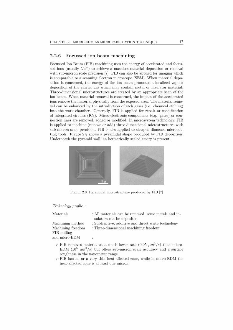
Focussed Ion Beam (FIB) machining uses the energy of accelerated and focus-sed ions (usually Ga+) to achieve a maskless material deposition or removalwith sub-micron scale precision [7]. FIB can also be applied for imaging whichis comparable to a scanning electron microscope (SEM). When material depo-sition is concerned, the energy of the ion beam promotes a localized vapourdeposition of the carrier gas which may contain metal or insulator material.Three-dimensional microstructures are created by an appropriate scan of theion beam. When material removal is concerned, the impact of the acceleratedions remove the material physically from the exposed area. The material remo-val can be enhanced by the introduction of etch gases (i.e. chemical etching)into the work chamber. Generally, FIB is applied for repair or modificationof integrated circuits (ICs). Micro-electronic components (e.g. gates) or con-nection lines are removed, added or modified. In microsystem technology, FIBis applied to machine (remove or add) three-dimensional microstructures withsub-micron scale precision. FIB is also applied to sharpen diamond microcut-ting tools. Figure 2.8 shows a pyramidal shape produced by FIB deposition.Underneath the pyramid wall, an hermetically sealed cavity is present.
Figuur 2.8: Pyramidal microstructure produced by FIB [7]
Technology profile :
Materials : All materials can be removed, some metals and in-sulators can be deposited
Machining method : Subtractive, additive and direct write technologyMachining freedom : Three-dimensional machining freedomFIB millingand micro-EDM :
. FIB removes material at a much lower rate (0.05 µm3/s) than micro-EDM (105 µm3/s) but offers sub-micron scale accuracy and a surfaceroughness in the nanometer range.
. FIB has no or a very thin heat-affected zone, while in micro-EDM theheat-affected zone is at least one micron.

18 2.2. MICROFABRICATION TECHNOLOGIES
. FIB can be used to examine the surface quality of EDMed surfaces. Tren-ches with very smooth sidewalls are milled into the surface, which makesexamination of the heat-affected zone possible.
2.2.7 Powder blasting
In powder blasting, a jet stream of abrasive micrometer particles (e.g. Al2O3)is directed towards the workpiece [1]. Powder blasting is applied for structuringof brittle materials such as glass, silicon and alumina. The impact force of thefast-moving particles results in material removal due to brittle fracture. Thepowder blasting technique can be applied as a direct write technique or as ascanning technique in which the substrate is covered by a patterned protectivemask. Figure 2.9 shows a structure for a micro inertial sensor made in Pyrexglass by sand blasting.
Technology profile :
Materials : Brittle materialsMachining method : Subtractive and direct write technologyMachining freedom : Two-dimensional machining technique due to the
limited aspect ratioPowder blastingand micro-EDM :
. Surface roughness depends on the impact energy and values between 0.1and 10 µm Ra are obtained which is comparable to micro-EDM.
. In powder blasting, no heat affected zone is present, but a damaged toplayer is observed.
. In powder blasting, it is hard to control the uniformity of the jet streamas well as the depth of cut.
. In powder blasting, an aspect ratio of 1 or 2 is common.
Figuur 2.9: Inertial sensor structure in Pyrex [8]

CHAPTER 2. MICRO-EDM AS MICROFABRICATION TECHNIQUE 19
2.2.8 Microstereolithography
In stereolithography, a photosensitive liquid polymer is illuminated by a laserbeam (typically a He − Cd laser) which solidifies the exposed photopolymer[1]. A free-form three-dimensional structure is created layer by layer by addingeach time a new layer of photopolymer and solidifying it selectively. Stereoli-thography is mainly applied for industrial prototyping having an accuracy ofapproximately 50 − 100 µm. In microstereolithography, a voxel size (i.e. thevolumetric resolution) of 5µm× 5µm× 3µm can be realizable. The laser beamis usually scanned on the resin surface, but stereolithography techniques existswhich expose a large beam through a mask. The mask is a liquid crystal dis-play (LCD) of which the transparent pattern can dynamically be altered [9].Figure 2.10 shows a set of micropropellors fabricated by microstereolithography.
Technology profile :
Materials : PhotopolymersMachining method : Additive and direct write technologyMachining freedom : Three-dimensional machining freedomMicrostereolithographyand micro-EDM :
. Micro-EDM is a subtractive prototyping technique using conductive ma-terials, while microstereolithography is an additive prototyping techniqueusing photopolymers.
Figuur 2.10: Micropropellors fabricated by microTEC

20 2.2. MICROFABRICATION TECHNOLOGIES
2.2.9 Moulding techniques
Micromoulding allows mass production of complex products by replication ofthe mould geometry [1][10]. Micromoulds are fabricated using micromachiningtechniques such as micro-EDM, microcutting, LIGA and silicon bulk micro-machining. The most frequently applied micromoulding techniques are microinjection moulding and micro hot embossing. In micro injection moulding, themicromould is filled with a melted polymer at high pressure. In order to avoidinsufficient filling, the air is evacuated from the mould and the mould is pre-heated to avoid instantaneous solidification. After filling, the mould is cooledand the microstructure is released. In micro hot embossing, a heated mould ispressed into a polymer substrate. The temperature of the mould exceeds theglass transition temperature (but not the melting temperature) which weakensthe polymer and makes the substrate deformable. The result is a polymer sub-strate containing microstructures at its top surface. With moulding techniques,structural details of 0.2 µm can be replicated and aspect ratios up to 30 arereached. In polymer moulding processes, the difference in thermal expansioncoefficient between mould (e.g. for steel, α = 12.10−6) and polymer (e.g. forPMMA, α = 50.10−6-100.10−6) may lead to dimensional errors (i.e. shrinkage)and additionally induced stresses in the polymer microcomponents.
Technology profile :
Materials : Usually polymers (for micro injection moulding andmicro hot embossing)
Machining method : Replication technologyMachining freedom : Depending on the mould geometryMicromouldingand micro-EDM :
. Micro-EDM is applied to manufacture three-dimensional micromoulds inheat- and wear-resistant metals.
2.2.10 Conclusions
Micro-EDM is a direct write technique which is suitable to machine three-dimen-sional and millimeter-size components in electrically conductive mate-rials with micrometer accuracy. From the short comparative study, it shouldbe concluded that micromachining technologies should not be seen as separa-te competing processes, but that synergy between these techniques broadensthe machining capabilities in the field of machining accuracy, surface quali-ty, three-dimensionality, machining flexibility, mass production and fabricationcost reduction.

CHAPTER 2. MICRO-EDM AS MICROFABRICATION TECHNIQUE 21
2.3 Electro-discharge machining
2.3.1 Introduction
Electro-Discharge Machining (EDM), or spark erosion, is a mature machiningprocess in the tool making industry, and is especially applied for the machiningof hard materials which are difficult to machine with conventional manufac-turing techniques. Accordingly, EDM developed itself into one of the majorproduction techniques for mould and die making. Some types of EDM ma-chines are indicated as die-sinking-EDM machines while they are applied fora broader range of applications. By the development of new machine configu-rations, such as wire EDM, EDM became an economical production techniqueto machine complex components out of any electrically conductive engineeringmaterial.
2.3.2 Electro-discharge machining process
Electro-discharge machining is an electro-thermal machining process which re-moves workpiece material by the erosive action of electric discharges. The di-scharges are created between a tool electrode and a workpiece electrode. Bothelectrodes are immersed in a dielectric fluid2 and separated by a small workinggap. When a voltage is applied between the electrodes and the correspon-ding electric field in the working gap exceeds the dielectric breakdown level, adischarge is created. The applied voltage is generally pulsed at a predefinedfrequency, creating successive discharges. Each discharge melts and evaporatesa small amount of material on both tool and workpiece electrodes. The evapo-rated material and a portion of the melted material is removed by the dielectricfluid. The remaining material resolidifies and creates a crater-like surface onboth electrodes. By applying a large number of sparks, large material volumescan be removed. The material removal on the tool electrode can be kept anorder of magnitude lower than the material removal on the workpiece by anappropriate selection of electrode materials and by appropriate machining set-tings.Figure 2.11 shows principally the three main phases of a discharge. The firstphase is the preparation phase of the discharge channel which is initiated atthe moment the generator applies the necessary voltage between the electrodes.When a critical electric field is exceeded between a spot on the tool and a spoton the workpiece, conduction paths grow at microsecond speeds through thedielectric fluid, in the form of branched trees, called streamers. These strea-mers are precursors of the effective dielectric breakdown. In a second phase theelectrodes are locally melted by the discharging spark. The discharge consistof a plasma channel surrounded by a gaseous mantle. The plasma channel,consisting of free electrons and positively charged ions, is characterized by high
2resistivity of approximately 106 Ω · cm for deionized water and 1015 Ω · cm for oil-baseddielectrics [11]

22 2.3. ELECTRO-DISCHARGE MACHINING
Figuur 2.11: Three main phases of a discharge, derived from [12]
pressure and high temperature. The free electrons accelerate towards the ano-de and heat up the anode during impact, while the ions strike and heat up thecathode. On both electrodes, material is melted and evaporated by the highpower concentration of the plasma channel. It is found that the diameter of theplasma channel at the cathode side remains constant, while the plasma channelenlarges at the anode side. This means that the current density at the cathodeside remains constant, while the current density at the anode side decreases.When the generator cuts the electric current at the end of the discharge pulse,the plasma channel disappears and the corresponding pressure drop causes asudden and intense boiling locally on the electrodes. At this time a part ofthe melted electrode material is ejected into the surrounding dielectric fluid.With this action the cycle of a single discharge is finished. When the dielectricis sufficiently deionized, another pulse can be applied in order to produce thenext discharge. For more detailed reading on the EDM process, the reader isreferred to dedicated literature [13, 14, 15, 16].In contrast to conventional cutting processes where only the cutting edges canbe applied to remove material, the entire surface of the tool electrode can beutilized to remove workpiece material in the EDM case. Additionally, almostno forces are generated during machining, while a cutting force is necessary toremove workpiece material in conventional cutting processes.
2.3.3 Electro-discharge machining equipment
Presently, a wide range of EDM machines is available on the market, varying inconfiguration, size and performances. In the early days (1950’s) only sinking-EDM machines were available. Figure 2.12 shows a schematic representation ofa sinking-EDM machine. A shaped tool electrode literally sinks into the work-piece, leaving the complementary shape of the electrode into the workpiece. Asmachining continues, the working gap between the tool electrode and the work-piece enlarges, due to the act of material removal. A tool-feed servo system isrequired to sink into the workpiece, maintaining a suitable working gap. Whenthe working gap is too large, no discharges occur because the electric field in theworking gap will not cause a dielectric breakdown. On the other hand, whenthe working gap is too small, short circuits occur which do not contribute to

CHAPTER 2. MICRO-EDM AS MICROFABRICATION TECHNIQUE 23
servo
tool electrode
working gap
workpiece electrode
pulsegeneratordielectric
conditioningunit
z
Figuur 2.12: Sinking EDM, derived from [12]
the material removal. Between the two extreme pulse shapes (i.e. open andshort circuits), a number of distinguishable pulse shapes can be observed. Athorough study on the effect of the pulse shape on the machining performancesis executed by Dauw [17]. The dielectric fluid which cools the electrodes andtransports the debris out of the working gap, gets contaminated by the debrisand consequently loses its dielectric properties. To condition the dielectric, thedebris is removed by filtering and a deionization device controls its electricalconductivity. The pulse generator which supplies the discharge energy, hasconsiderably evolved over time. Due to the progress in power electronics, theinitial ’relaxation’ generators were replaced by sophisticated generators basedon high-frequency switching devices. The basic concepts of EDM generatorsare published by Kruth [18]. Detailed information on generators of commer-cially available EDM machines is hard to get, because machine manufacturersare very reserved to reveal the circuitry of the ’heart’ of their EDM machines.In order to improve the surface quality and the debris removal in sinking-EDM,planetary EDM was introduced. In planetary EDM the tool electrode is givenan additional but limited movement perpendicular to the downward feedingdirection. By the introduction of computerized numerical control (CNC), thenumber of servo-controlled axes increased to typically four independently con-trollable axes (X,Y,Z and C, with C a rotational axis around the Z-axis). Whenthe tool makes a multi-axial movement, the term contouring EDM is used in-stead of sinking-EDM. Most of the currently-available so-called sinking-EDMmachines are actually contouring-EDM machines. When on top of the C-axis, or instead of the C-axis, a high speed non-indexable spindle is mounted,a milling-EDM configuration is realized (figure 2.13(a)). The use of simple-shaped tool electrodes, as for instance cylindrical or tubular tool electrodes,makes of milling EDM a flexible and economical way to machine complex ge-ometries. In contrast to the high production cost of shaped tool electrodes forsinking EDM, the simple-shaped tool electrodes for milling EDM are commer-cially available. Another EDM configuration is realized in wire EDM. A conti-

24 2.3. ELECTRO-DISCHARGE MACHINING
XY
ZC
(a) Milling EDM
Y X
UV
Z
(b) Wire EDM
Figuur 2.13: Principal schemes of (a) milling EDM and (b) wire EDM
nuously unwinding metal wire, usually with a diameter of 100 µm to 250 µm,is used as tool electrode (figure 2.13(b)). The wire is guided by two positioningheads which enable the fabrication of complex shapes. For further reading onspecified EDM machines is referred to documentation distributed by machi-ne manufacturers such as AGIE, CHARMILLES, SODICK, MITSUBISHIand ONA.
2.3.4 Electrode materials
In order to make the EDM process possible, both workpiece and tool shouldbe electrically conductive. The electrical discharges remove material from theworkpiece as well as from the tool electrode. Material removal from the work-piece material is evidently desired, while material removal from the tool elec-trode should be reduced as much as possible. Material removal from the tool,also indicated as tool wear or tool consumption, changes the geometry of thetool electrode, leading to undesired machining inaccuracies. In wire EDM, thedrawback of tool wear is solved by continuous renewal of the wire so that virtu-ally no tool wear is encountered. However, for other EDM configurations, suchas sinking EDM several tool electrodes should be sequentially applied in orderto obtain an adequate accuracy. In addition, EDM-resistant materials are usedas tool material in order to minimize tool wear. Due to the electro-thermal re-moval mechanism of EDM, the resistance to material removal mainly dependson the thermal properties of the material. In general, the erosion resistanceindex Cm is used to characterize the resistance to material removal by EDM

CHAPTER 2. MICRO-EDM AS MICROFABRICATION TECHNIQUE 25
[19]. The erosion resistance index Cm is defined by:
Cm = λ · ρ · c · Tm2 (2.1)
with Cm : Erosion resistance index [J2/(m4 · s)]λ : Heat conductivity [W/(m ·K)]ρ : Mass density [kg/m3]c : Specific heat [J/(kg ·K)]Tm : Melting temperature [K]
It should be noted that the erosion resistance index is an empirical formulati-on which obeys the general tendencies but which is not physically corrobora-ted. Table 2.1 lists the erosion resistance index Cm for a number of materials.Materials with a high erosion resistance index, such as tungsten, molybdenum,
λ ρ c Tm Cm
[W/(m ·K)] [kg/m3] [J/(kg ·K)] [K] [×1013 J2/(m4 · s)]
tungsten (W) 178 19300 133 3673 616molybdenum (Mo) 140 10220 251 2897 301copper (Cu) 398 8960 385 1357 253graphite 46-114 1700-1900 750 3875 115-347hard metal (WC-Co) 67 14300 209 3023 182silicon (si) 150 2330 710 1687 71steel (C45) 52 7800 490 1670 55aluminium (Al) 237 2700 900 933 50
material properties gathered from [20, 3, 21]
Tabel 2.1: Erosion resistance index Cm for a number of materials
graphite and copper are usually applied as tool material.As the erosion resistance index Cm takes the thermal characteristics of theelectrode material into account, it does not cover all influencing parameters.For electrically resistive materials, the resistance to EDM does not only de-pend on the heat flux of the plasma channel but also on the Joule heating inthe electrodes [22]. Saeki calculated that the voltage drop is considerable inthe vicinity of the discharge spot when highly resistive materials are machined.From computed temperature distributions it is found that for highly resisti-ve materials, Joule heating causes a temperature rise which is comparable towhat is generated by the discharging spark and which is favourable for materialremoval.

26 2.4. EDM MINIATURIZES TO MICRO-EDM
2.4 EDM miniaturizes to micro-EDM
2.4.1 Introduction
Micro-EDM (MEDM, µ-EDM) refers to the manufacturing of miniaturizedcomponents by the EDM process. Sometimes micro-EDM only refers to themachining of high-quality and precise surfaces, but in this work focus is put onthe use of the EDM process as a micromachining technique, which inherentlycomprises a fine and precise surface finish.
2.4.2 From the birth of micro-EDM to the establishmentof a micromachining technology
Micro-EDM as machining technique for microholes
Micro-EDM saw light as a manufacturing process for small holes in metalsheets. For holes with a diameter larger than 200 µm, tubular electrodes areused through which dielectric fluid is pumped or even pulsed to enhance theflushing of the working gap. However, when smaller holes are required, thetool electrodes are usually straightened wires made of tungsten or tungsten-carbide. First experiments on the miniaturization of hole-drilling by EDMhave been performed at Philips Research Lab in The Netherlands in themid 1960’s. In 1965 Osenbruggen reported on a precision EDM machine toobtain dimensional tolerances as low as 1 µm [23]. Figure 2.14 shows one ofthe first microholes machined by micro-EDM for the use as a diaphragm of anelectron microscope. Shortly afterwards, Kurafuji and Masuzawa reported on
Figuur 2.14: Objective diaphragm for an electron microscope with a dia-meter of 20 µm in a 20 µm thick metal sheet [23]
EDM of microholes in cemented carbide alloys [24]. After this pioneering workthe interest in micro-EDM was fading until, in the late 1980’s, the Japanese re-discovered this technique. In 1985 Masuzawa introduced wire electro-dischargegrinding (WEDG) to shape the tool electrodes with the view to create verythin electrodes (which will be discussed in paragraph 2.5.5). The thin electro-des are used as micropins or as tool electrodes to produce microholes (figure2.15). The WEDG technique developed quickly and record breaking dimensi-ons could be reached, resulting in cylindrical tool electrodes with a diameter

CHAPTER 2. MICRO-EDM AS MICROFABRICATION TECHNIQUE 27
Figuur 2.15: Tungsten-cabide micropins made by WEDG [25]
less than 3 µm and microholes with a diameter less than 5 µm as shown infigure 2.16 [26]. A first application of micro-EDMed microholes in metal sheets
(a) Cylindrical toolelectrode
(b) Microholes (Matsushita
Electric Industrial Co, Ltd.)
Figuur 2.16: WEDG applications [26]
is the production of nozzles in ink-jet printer-heads [27]. Sato et al. repor-ted on the development of a micro-EDM machine dedicated for the machiningof microholes. EDM-drilled microholes with a diameter of 300 µm down to15 µm, a roundness accuracy of 0.5 µm or better, and a surface roughnessof 0.1 µm Rmax were obtained [28]. In 1986, Kagaya et al. reported on themanufacturing of microholes with a diameter of 170 µm and an aspect ratioup to 17 [29]. Masuzawa et al. presented in 1989 an EDM machine for drillingdeep microholes [30]. The EDM machine consists of a horizontal spindle and aWEDG unit to shape the tool electrode as depicted in figure 2.17. The spindleis horizontally mounted so that the debris, of which the mass density is higherthan the mass density of the dielectric, can easily be flushed out of the hole.Masuzawa reached aspect ratios up to 10 for tool electrodes with a diameterlarger than 50 µm. Additional flushing of the working gap can be obtained byintermittent vibration of the workpiece or tool electrode which is presented bythe same research group in 1997 [31]. Microholes were obtained with a depth of
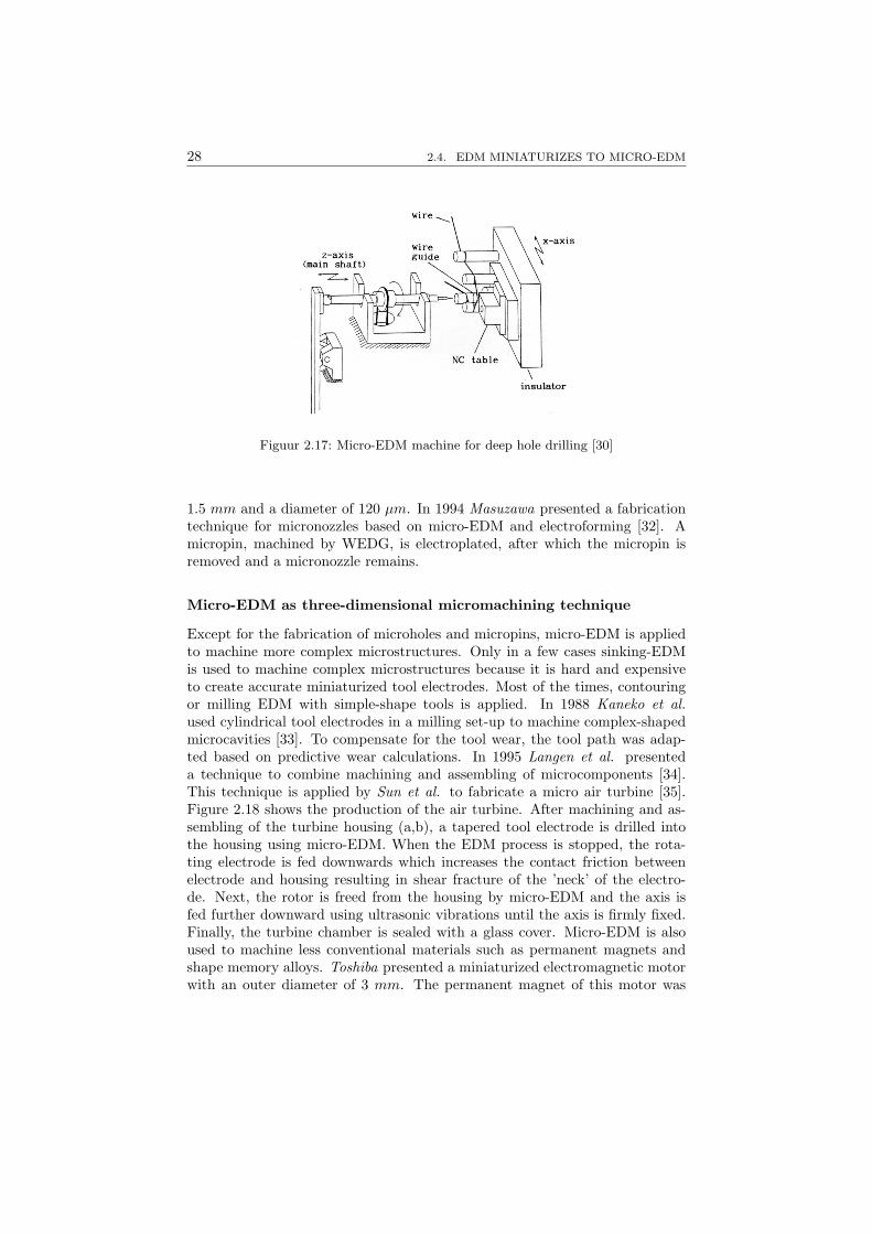
28 2.4. EDM MINIATURIZES TO MICRO-EDM
Figuur 2.17: Micro-EDM machine for deep hole drilling [30]
1.5 mm and a diameter of 120 µm. In 1994 Masuzawa presented a fabricationtechnique for micronozzles based on micro-EDM and electroforming [32]. Amicropin, machined by WEDG, is electroplated, after which the micropin isremoved and a micronozzle remains.
Micro-EDM as three-dimensional micromachining technique
Except for the fabrication of microholes and micropins, micro-EDM is appliedto machine more complex microstructures. Only in a few cases sinking-EDMis used to machine complex microstructures because it is hard and expensiveto create accurate miniaturized tool electrodes. Most of the times, contouringor milling EDM with simple-shape tools is applied. In 1988 Kaneko et al.used cylindrical tool electrodes in a milling set-up to machine complex-shapedmicrocavities [33]. To compensate for the tool wear, the tool path was adap-ted based on predictive wear calculations. In 1995 Langen et al. presenteda technique to combine machining and assembling of microcomponents [34].This technique is applied by Sun et al. to fabricate a micro air turbine [35].Figure 2.18 shows the production of the air turbine. After machining and as-sembling of the turbine housing (a,b), a tapered tool electrode is drilled intothe housing using micro-EDM. When the EDM process is stopped, the rota-ting electrode is fed downwards which increases the contact friction betweenelectrode and housing resulting in shear fracture of the ’neck’ of the electro-de. Next, the rotor is freed from the housing by micro-EDM and the axis isfed further downward using ultrasonic vibrations until the axis is firmly fixed.Finally, the turbine chamber is sealed with a glass cover. Micro-EDM is alsoused to machine less conventional materials such as permanent magnets andshape memory alloys. Toshiba presented a miniaturized electromagnetic motorwith an outer diameter of 3 mm. The permanent magnet of this motor was

CHAPTER 2. MICRO-EDM AS MICROFABRICATION TECHNIQUE 29
Figuur 2.18: Micro air turbine [35]
structured by micro-EDM. Another application on micromotors is found in theUnited States, where Jacobsen et al. used micro-EDM to produce a microsco-pic wobble motor [36]. In Japan as well, micro-EDM is applied to fabricatean electrostatic wobble motor [37]. Furthermore, micro-EDM has been usedto manufacture shape-memory-alloy-based micro-actuators. It concerns micro-instruments for endoscopic surgery and several other components intended forthe use in minimally invasive surgery [38, 39].

30 2.4. EDM MINIATURIZES TO MICRO-EDM
Micro-EDM technology
The fact that EDM is a direct write technique (contrary to photolithography)and therefore not suited for batch production, is an eye-catching disadvantage.This argument however is too easily overstated. In 1969, Gieles et al. from Phi-lips Research Lab reported on a miniature silicon pressure sensor, producedby electrochemical etching and micro-EDM. Large tool electrodes were develo-ped with which several sensors could be machined simultaneously. It should benoted that Philips sold these pressure sensors for more than 10 years (1975-1989). Later on, several authors addressed EDM with multiple tool electrodesand automated tool-feeding systems in order to improve machining efficiencyand reduce machining time. Higuchi et al. developed a pocket-size electrode-feeding system by applying an impact drive mechanism [40]. The size of theelectrode-feeding mechanism was miniaturized to 14 mm × 18 mm × 68 mmand enables simultaneous machining. Another miniaturized EDM-drilling de-vice was developed by Mohri et al. [41]. In this device, the electrode is drivenby piezoelectric elements. The same research group which is active at theToyota Technological Institute also proposed a dot-matrix electrical dischar-ge machining device [42]. In this device six tool electrodes are arranged in acircle. The separate tool electrodes have a diameter of 0.4 mm and are spa-ced 0.76 mm apart. The multi-electrode EDM machine for the fabricationof microholes was, on a theoretical basis, also addressed by Allen et al. [43].Another approach to batch production is presented by Popovic et al. [44, 45].They use conventional wire EDM to produce a matrix of needle-shaped toolelectrodes. Takahata et al. created an array of electrodes by the LIGA pro-cess [5]. This multiple electrode is applied in a sinking-EDM process with theaim to structure metal sheets (figure 2.19). Comparable to this approach is
Figuur 2.19: Combining LIGA and micro-EDM to manufacture a largenumber of microholes simultaneously [5]
the process used at Stanford University [46]. A bulk-micromachined siliconstructure is used as a mould for electroplating of copper or for hot-pressing ofan alloy of silver and tungsten (figure 2.20). After removal of the silicon, thecopper or silver-tungsten structure is used as tool electrode for sinking-EDM

CHAPTER 2. MICRO-EDM AS MICROFABRICATION TECHNIQUE 31
Figuur 2.20: Combining plasma-etching and micro-EDM: plasma-etched si-licon mould, electroplated copper electrode and structured me-tal film [46]
applications. Another argument in this discussion on batch production is thatmicro-EDM is capable of machining geometries that are simply impossible tomachine by the present batch production technologies. The designer shoulddecide if a complex part has enough added value to allow a part-by-part pro-duction. The use of micro-EDM to create moulds for a production based onmicromoulding, as presented by Dunkel et al., can also favourably influencethe designers decision towards the use of EDM [47]. Another example of ageometry that can only be achieved by micro-EDM is presented by Kamperfrom the same research group [48]. In this case, a microreactor required theuse of an inert material like stainless steel. As this material is not machinableby microfabrication technologies as photolithography, micro-EDM was used tocreate the microchannels of the reactor. The group of Ehrfeld at the Instituteof Microtechnology (IMM) presented several other examples of micro-EDM likemicrogears, microreactors and micropunching tools [49].
Silicon micro-EDM
Silicon which is the most used material for the production of microstructures,can also be machined by micro-EDM. In this work silicon micro-EDM is ex-tensively studied in chapter 3 where also a summary of the state of the art ispresented.
Extraordinary micro-EDM
The electro-thermal machining process of EDM offers opportunities for extra-ordinary experiments. The following EDM applications are not thoroughlydeveloped and should be seen as one-time experiments.In 2001 Hayakawa et al. presented the fabrication of microstructures usingEDM deposition [50]. A mild steel cylinder with a diameter of 0.1 mm and amild steel solid substrate are used as electrode materials. The tool electrode

32 2.4. EDM MINIATURIZES TO MICRO-EDM
and the workpiece are connected as anode and cathode, respectively. The EDMprocess is carried out in air in order to avoid the removal effect of the dielectricliquid. Material from the tool electrode is deposited on the substrate when themachining settings are appropriately tuned. A controlled scanning movementmakes the production of three-dimensional structures feasible.Another extraordinary application of micro-EDM is presented by Takezawa etal. in 2001 [51]. A thin tungsten wire of 100 µm is transformed to a needle-shaped electrode using a highly energetic single discharge. The elevated energydissipation in the tool electrode results in excessive melting at the tip of theelectrode. Under certain conditions the electrode resolidifies in the desiredneedle shape. Although this method creates needle-shaped tool electrodes in aflash, the repeatability is poor and only needle shapes are produced.
2.4.3 General requirements for micro-EDM
To manufacture microstructures with a sufficient dimensional accuracy andsurface finish, there is need for high precision machines and machining processeswith a small machining unit [52]. A machining unit is defined as smallestamount of workpiece material which can be removed (or added for some specificprocesses such as stereolithography) in a controllable way. A small machiningunit is only feasible when low removal forces are involved. The EDM processfulfils the requirement on low machining forces and a small machining unit. Incontrast to conventional cutting processes where a cutting force is necessary toremove material, the minor machining forces in EDM are mainly originatingfrom dielectric flow, electrostatic attraction forces between the electrodes andfrom generated damp bubbles in the working gap. Although all EDM machinesapply the same machining process, the following requirements must be met toenjoy micro-EDM [26, 53].
The size of the crater produced by a single discharge must be small tofulfil the requirement of a small machining unit. The size of the crateris mainly determined by the energy which is dissipated in the discharge.Accordingly, this requirement on a small machining unit restricts theamount of discharge energy (for micro-EDM, 10 nJ up to 10 µJ). Inorder to have an idea of the order of magnitude, Nothe measured thedimensions of the discharge craters which were 3 µm in diameter and0.2 µm in depth when a discharge energy of 0.9 µJ was applied [53]. Itshould be noted that the necessary low discharge energies lead to lowmaterial removal which contradicts the desire for high productivity.
The working gap must be small in order to avoid dimensional and geo-metrical inaccuracies. At least one-tenth of the average gap-size distancemust be considered as potential error caused by gap size deviation. Thegap size depends on the type of the dielectric, the uniformity of the dielec-tric, the electrode materials and last but not least the machining settings.With low energy discharge pulses, the erosion gap may be sub-micron

CHAPTER 2. MICRO-EDM AS MICROFABRICATION TECHNIQUE 33
scale. Small working gaps, however, complicate the debris removal whichmay lead to unstable sparking or even to welding of both electrodes. Agood compromise between gap size and adequate flushing conditions isrequired. Therefore, the working gap in micro-EDM is usually between1 and 5 µm.
In micro-EDM machines, high-performance gap control systems are re-quired. Instead of the tens of micrometer gap size in conventional EDM,the working gap size in micro-EDM is usually smaller than 5 µm. The-refore, the control system should be accurate and fast-reacting in orderto avoid electrode collision and to maintain an appropriate gap size al-lowing discharge repetition. Mechanical contact between the electrodesmust be avoided because the mechanical loading capacity of miniaturizedtools and workpieces is low. A collision of the electrodes may lead totool fracture or even worse to workpiece fracture. In micro-EDM, thedischarge energy is low which lead to noise-like current pulses. Due tothe irregular shape and small magnitude of the discharge pulses it is hardto develop well-performing control systems. It is still an issue for futurework to improve the current gap control systems.Presently, when electrode collisions should be avoided, two extreme stra-tegies can be applied. First, one can set the reference size of the workinggap at a high level. This means that the servo system keeps the size of theworking gap larger than usual. Consequently, less discharges occur whichdecreases the sparking efficiency3. A second strategy to avoid undesiredelectrode collision is to limit the proceeding speed of the tool electrode.When the proceeding speed is set low enough (i.e. when the removalspeed is higher than the proceeding speed), no collisions are encountered.Unfortunately, the sparking efficiency is low as well.
The thermal loading capacity of miniaturized tool electrodes and minia-turized workpieces is limited. The low thermal loading capacity restrictsthe discharge energy which is in line with the requirement on a small ma-chining unit. Figure 2.21 shows a tungsten tool electrode with an originaldiameter of 150 µm, which is exploded due to thermal overloading.
Figuur 2.21: Thermally overloaded tool electrode
3The sparking or erosion efficiency is defined as the ratio of the actual sparking time tothe total pulse time.

34 2.5. SPECIFIC EQUIPMENT AND TECHNIQUES FOR MICRO-EDM
The positioning accuracy of the electrodes should be high to manufacturehighly precise microstructures. This requirement comprises the positio-ning accuracy of the EDM machine as well as the clamping accuracy ofthe tool electrode. In order to make an optimal use of the EDM techni-que, the total positioning accuracy must be better than the EDM processaccuracy which is sub-micron scale.
2.5 Specific equipment and techniques formicro-EDM
2.5.1 Introduction
Initially, micro-EDM experiments were executed using sinking-EDM techni-ques and equipment. However progressively the techniques and equipmentevolved to a specific micro-EDM technology. EDM generators with minimi-zed discharge energy are developed as well as precise tool clamping and toolshaping techniques. Manufacturers, such as Panasonic and Sarix, developedspecific table-top micro-EDM machines.
2.5.2 Micro-EDM generators
The pulse generator is the unit in the EDM machine which supplies the electricenergy to maintain the erosion process. At the start of each pulse, the generatorapplies a voltage over the electrodes. After dielectric breakdown, the generatorsupplies the necessary electric energy to maintain the discharge until the endof the pulse. The discharge energy We induced in the working gap during onepulse is defined by equation:
We =∫ ti
0
ue(t) · ie(t) · dt (2.2)
with We : Discharge energy [J ]ti : Pulse duration [s]ue : Discharge voltage over the working gap [V ]ie : Discharge current [A]
In 2001, Masuzawa presented the basic theory on micro-EDM generators [26].As for micro-EDM the discharge energy must be as low as possible in order toobtain a small machining unit, the characteristics ti, ue and ie should be aslow as possible. During a discharge, the gap discharge voltage ue is, however,uncontrollable and lies between 10 V and 40 V depending on the electrodematerials, the dielectric fluid and the discharge current waveform. Therefore,characteristics ti and ie should be reduced in order to obtain small dischargeenergies. However, a small discharge current ie is not practical because aneffective discharge cannot be maintained when the current is not sufficiently

CHAPTER 2. MICRO-EDM AS MICROFABRICATION TECHNIQUE 35
large. Consequently, the main effort must be put in reducing the pulse time tiin order to obtain suitable discharge energies for micro-EDM. The same pro-blem was encountered in wire EDM, in which short and low energy pulses areapplied in order to avoid wire rupture. High energy pulses overload the wirethermally which leads to failure of the preloaded wire. For micro-EDM, evenshorter pulses have to be applied with the aim to minimize the discharge ener-gy.Static pulse generators and relaxation generators, which originate from sinking-EDM and wire-EDM applications, are as well applied in micro-EDM machines.Figure 2.22(a) shows an elementary scheme of a static pulse generator. The ge-
S
Z
-
+
ui^
(a) Static pulse generator
S
C
Zc
Zd
-
+
ui^
(b) Relaxation generator
Figuur 2.22: Simplified generator schemes
nerator consists of a power source and a switching device S. The power sourceusually consists of a voltage and current source (not presented on the schematicfigure). The voltage source supplies the initial voltage between the electrodes,while the current source is switched on at the moment the dielectric breaksdown. The electrical impedance Z is the impedance of the entire discharge cir-cuit. The impedance of a discharge itself is non-linear and is characterized bya constant gap voltage independent of the gap current. The switching device Sis used to create the individual pulses. In commercially available EDM machi-nes the generator is more sophisticated and complex waveforms are generatedwith the aim to optimize the machining performance. The smallest availabledischarge energy is approximately 1 µJ when these static pulse generators areapplied [26].A second type of generator is the so-called relaxation generator (figure 2.22(b)).The first generators used for EDM purposes were of the relaxation type. Thegenerator consists of a charging and discharging circuit, characterized by theirrespective impedances Zc and Zd. In addition, the non-linear impedance ofthe discharge should be taken into account in the discharging circuit. In a first

36 2.5. SPECIFIC EQUIPMENT AND TECHNIQUES FOR MICRO-EDM
step, the relaxation capacitor C is charged by closing switch S. CapacitanceC is mainly determined by the adjustable capacitor in the EDM generator butis also influenced by additional parasitic capacitances such as the capacitancebetween tool and workpiece electrodes. The relaxation capacitor which makespart of both the charging and discharging circuit is sometimes confusingly ter-med as charge or discharge capacitor. The voltage over the working gap equalsthe voltage over the relaxation capacitor during charging. When the dielectricbreaks down, the charged relaxation capacitor discharges over the working gap,dissipating its energy. It should be noted that original relaxation generators(RC-generators) were switch-less. The charging impedance Zc was made high-ly resistive so that the capacitor is slowly charged. The discharge impedanceZd should have a low resistance and low inductance, so that the capacitor willdischarge quickly and entirely over the working gap when a breakdown occurs.Although switch S is not essential to the process, the machining process can betuned by setting appropriate switching times. In an RC-circuit the dischargeenergy can be reduced by reducing the capacitance of the relaxation capacitor.The electric energy Wc stored in the capacitor depends on the capacitance Cand on the voltage Vc over the capacitor, as shown by:
Wc =12CV 2
c (2.3)
with Wc : Energy within the relaxation capacitor [J ]C : Capacitance of the relaxation capacitor [F ]Vc : Voltage over the relaxation capacitor [V ]
When the capacitor is entirely charged, voltage Vc equals the charging voltageui supplied by the generator source. Figure 2.23 shows a simplified equivalentscheme of the relaxation generator in order to explain the pulse shapes. Thedischarge is represented by a switch which closes when a discharge occurs anda constant voltage source providing the average discharge voltage ue. Ld isthe total inductance in the discharge circuit, principally determined by theinductance of the lead wires which connect the capacitor to both electrodes.The resistance in the discharge circuit is negligible when metal electrodes areused and the energy dissipation occurs mainly in the discharging spark. Thewaveform of the gap voltage u, the voltage Vc over the capacitor and dischargecurrent ie are roughly illustrated on figure 2.23. As explained above, the gapvoltage and the capacitor voltage increase equally, until the dielectric breaksdown. The charging waveform depends on the impedance of the charging circuitZc and the capacitance of the relaxation capacitor. At breakdown, the chargingstops (opening of switch S) and the gap voltage u falls down to the dischargevoltage ue (closing of the discharging switch). As the relaxation generatordischarges, the capacitor voltage Vc gradually decreases. At the end of thedischarge the capacitor is reversely polarized, which means that a part of theenergy is still on the capacitor.
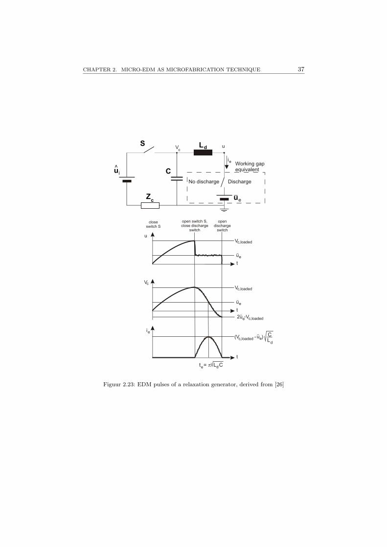
CHAPTER 2. MICRO-EDM AS MICROFABRICATION TECHNIQUE 37
u
L
u
t
e
e
ue
Vc
2 V-
ie
ie
Vc,loaded
S
C
Zc
d
ui^
uVc
Working gap equivalent
No discharge Discharge
u
t
e
uVc,loaded
t
t = p L Cde
(V - )LC
d
close switch S
open switch S,close discharge
switch
opendischarge
switch
ue
c,loaded
c,loaded
Figuur 2.23: EDM pulses of a relaxation generator, derived from [26]

38 2.5. SPECIFIC EQUIPMENT AND TECHNIQUES FOR MICRO-EDM
The effective discharge energy We dissipated in the working gap is formulatedby:
We = 2Cue(Vc,loaded − ue) [26] (2.4)
with We : Discharge energy [J ]C : Capacitance of the relaxation capacitor [F ]Vc,loaded : Capacitor voltage at breakdown [V ]ue : Average gap voltage during discharge [V ]
When the capacitor voltage Vc,loaded equals two times the average dischargevoltage ue, all the capacitor energy is dissipated by the discharge. In order toobtain small discharge energies (sub-µJ range), capacitance C is made small(less than 1 nF ) in micro-EDM generators. The micro-EDM machine mustbe designed so that the discharge capacitance is not dominated by the uncon-trollable and variable stray capacitance. Therefore the stray capacitance mustbe negligible with respect to the adjustable capacitor in the EDM generator.The discharge duration te can roughly be estimated by:
te = π√
LdC [26] (2.5)
with te : Discharge duration [s]Ld : Inductance of the entire discharge circuit [H]C : Capacitance of the relaxation capacitor [F ]
In order to obtain short discharge times, for a given capacitance C, Ld should beas small as possible. This requirement can be met when locating the generatorclose to the working area so that short lead wires can be used to supply thedischarge energy. Masuzawa reported that for stable machining with a chargecapacitor of 2 pF , it is necessary to have lead wires with a maximal totallength of 20 mm. With a charge voltage of 60 V a discharge energy of 3.5 nJis obtained, which is much less than the discharge energies obtainable withstatic pulse generators. This is the main reason why micro-EDM machines areprovided with relaxation generators. It should be noted that for a cylindricaltool electrode with a diameter of 150 µm (used in this thesis) and a workinggap of 10 µm, the parasitic capacitance is already 2.5 pF .
2.5.3 Polarity settings
An important parameter of the EDM process is the electrode polarity. Insinking-EDM, the tool electrode is generally positively charged with respectto the workpiece electrode. Long discharge pulses are used to maximize thematerial removal rate. During discharge, the plasma channel at the anode sideenlarges which results in a decreasing current density (i.e. less efficient heating),while the plasma channel at the cathode side remains constant maintaining thehigh current density. So, when long discharge pulses are applied, the averageefficiency of melting and evaporating is higher at the cathodic workpiece thanat the anodic tool electrode. The major disadvantage is that no fine surface

CHAPTER 2. MICRO-EDM AS MICROFABRICATION TECHNIQUE 39
finish can be obtained using these long discharge pulses. When low surfaceroughnesses are required, short pulses have to be applied and the polarity ofthe tool electrode is set negative. The difference in anode and cathode removalrate is explained by the difference in inertia of the free electrons and ions in theplasma. Due to the low inertia of the electrons, electrons will strike the anodebefore the ions strike the cathode. When the discharge pulse is cut shortly afterthe electrons hit the anode, the heating of the anodic workpiece has been moreintense than the heating of the cathode. The short bombardment of the anodicworkpiece by the electrons leaves a smooth machined surface. Additionally, thelimited material removal on the tool electrode reduces the tool consumption.However low material removal rates are achieved by these generator settings.In micro-EDM, generally, the tool electrode is assigned negative polarity inorder to obtain a fine surface finish.
2.5.4 Dielectric medium
The presence of a dielectric medium, between tool and workpiece electrode, isessential to enable the sparking process and to ensure stable sparking. Oneimportant function of the dielectric is the insulation of the workpiece from thetool. The spark is initiated when the dielectric breaks down and from thenthe dielectric will constrict the plasma channel which results in a high energydensity. After the discharge, the spark path should be deionized quickly andthe electrodes should be cooled sufficiently so that the next discharge can beprepared. The dielectric also removes the melted and evaporated debris out ofthe contaminated discharge gap in order to avoid unstable sparking conditions.As for wire EDM, micro-EDM uses a water-based dielectric while conventionalsinking-EDM uses oil-based dielectrics [11, 54, 55, 56]. Osenbruggen, one ofthe pioneers in micro-EDM, investigated both water-based and oil-based die-lectrics for micro-EDM [19]. He concluded that the use of deionized water asdielectric, increased the removal rate. Higher pulse frequencies can be set forwater dielectrics due to a shorter ignition delay and faster deionization timeafter the discharge. In addition, higher current densities are observed in waterdielectrics due to a better discharge-channel restriction. Another advantageof water dielectrics is that the low viscosity of water is favourable for flushingand that no carbon is deposited on the electrodes while it is the case whenoil-based dielectrics are applied. On the other hand, oil-based dielectrics allowmore accurate machining (i.e. smaller working gap) and preserves for instancesteel from oxidation.

40 2.5. SPECIFIC EQUIPMENT AND TECHNIQUES FOR MICRO-EDM
2.5.5 Wire Electro-Discharge Grinding
Since tool electrodes in micro-EDM are small and tool positioning is impor-tant, the transporting of coordinate information from the tool making stage tothe actual machining stage must be considered carefully [57]. Masuzawa et al.introduced in 1985 an on-the-machine tool making device which was baptizedWire Electro-Discharge Grinding (WEDG) [25]. The work table coordinatesare identical for tool making and actual micromachining so that potential posi-tioning errors during clamping are avoided. As depicted in figure 2.24, a WEDGunit consists of a grooved wire guide which positions an unwinding metal wire.Similar to wire EDM, the wire movement makes the process virtually free from
Figuur 2.24: Principle sketch of a WEDG unit [58]
tool wear. WEDG is applied to dress and shape tool electrodes. The dressingaction comprises the removal of the worn part from the tool electrode. Whenlong cylindrical tool electrodes are used, usually only the bottom end of thetool is used for machining. In this case, WEDG is applied to cut the wornbottom part of the tool electrode. After dressing, the tool electrode can beshaped according to the desired geometry. By rotational and/or translationalfeeding of the tool electrode, a wide variety of shaped tool electrodes can bemachined. Figure 2.25(a) shows a number of obtainable tool geometries [57].Micropins with a diameter less than 5 µm can be obtained (figure 2.25(b)). In2001 Sheu et al. presented a WEDG tool with the aim to speed up the manu-facturing of microholes (figure 2.26(a)) [59]. A twin WEDG machining systemis designed consisting out of two WEDG units; one for rough machining andone for finishing of the tool electrode. The twin WEDG system is mountedon a micro-EDM machine in such a way that drilling and tool shaping occurssimultaneously. In order to make large series of microholes, an automated fee-ding mechanism is developed to compensate for the tool consumption. Figure2.26(b) shows an array of 400 microholes with a diameter of 60 µm which ismachined in a 50 µm thick stainless-steel plate.

CHAPTER 2. MICRO-EDM AS MICROFABRICATION TECHNIQUE 41
(a) (b)
Figuur 2.25: Shaped tool electrodes by WEDG [57]
(a) Tandem wedg unit (b) Microhole array
Figuur 2.26: Tandem set-up to increase microhole production speed [59]
2.5.6 Tool clamping
In micro-EDM, generally cylindrical tool electrodes are applied in a milling-EDM set-up. The tool electrodes are usually long so that they can be dressedand shaped several times without the necessity of reclamping or changing thetool. The straightened wires (i.e. the long cylindrical tool electrodes) are madeof tungsten or tungsten alloys and have a diameter below 1 mm. In order toposition the tool electrode accurately, the tool should be firmly clamped and

42 2.5. SPECIFIC EQUIPMENT AND TECHNIQUES FOR MICRO-EDM
the length of the cantilevering tool should be as short as possible to avoid un-desired tool deflection. Thin tool electrodes with a diameter of 500 µm downto 150 µm can be clamped in a conventional jaw clamp (rotational or fixed)and guided by a passive guide which is positioned near the machining locationas depicted on figure 2.27. The guide is usually made of a ceramic material be-cause of its high resistance to abrasion. By feeding the tool electrode throughthe guide, the consumption of the tool can be compensated. In order to avoid
Z
workpiece tool guide
clamp
tool electrode
X,Y
Figuur 2.27: Conventional clamping device
elevated friction in the guide, dielectric fluid and a functional gap of a few mi-cron between tool and guide are required. The small gap leads to an uncertainand uncontrollable position of the tool within the guide. But by the presenceof dielectric fluid, the rotation of the tool will create a pressure distributionwhich tends to centre the tool into the guide.When more rigid electrodes are applied (> 500 µm in diameter) and when thecantilevering is small (few mm), no tool guide is necessary. Masuzawa makesuse of straight electrodes with a thick shank which are shaped on the EDMmachine itself using a WEDG unit. The tool is machined in such a way thatonly the tool tip is miniaturized [26]. Each time the tip is worn, the electrode isreshaped. Unfortunately, when the short shank is consumed, the tool electrodemust be renewed. In order to avoid tool change and the corresponding ma-chining overhead, many kinds of tool driving mechanisms have been developed[40, 60, 61, 42, 62]. The majority of the tool driving mechanisms use piezoe-lectric actuators for driving and are applied for microhole-drilling applications.Furutani and Mohri developed several kinds of tool direct-drive devices withcreeping mechanisms as illustrated in figure 2.28. Two parallel tool electro-des can be independently fed or retracted by a general pusher actuator andindividual clamping actuators. When several tool electrodes are mounted inan array, a dot-matrix mechanism (name inherited from dot-matrix printers) isrealized in which the length of all tool electrodes can individually be controlled.This dot-matrix mechanism does not only allow tool-wear compensation butalso allows the machining of complex-shaped cavities by controlling the lengthof the individual tools when the dot-matrix mechanism scans the surface.

CHAPTER 2. MICRO-EDM AS MICROFABRICATION TECHNIQUE 43
Figuur 2.28: Creeping mechanism for dot-matrix method [42]
Range of X-axis 250 mmRange of Y-axis 160 mmRange of Z-axis 250 mmAbsolute accuracy (3σ) Pa of X,Y,Z-axis 10 µmRepeatability (3σ) Ps of X,Y,Z-axis 3 µmBacklash U of X,Y,Z-axis 2 µmResolution of X,Y,Z-axis 1 µmAbsolute accuracy (3σ) Pa of C-axis 0.004
Repeatability (3σ) Ps of C-axis 0.003
Backlash U of C-axis 0.002
Resolution of C-axis 0.001
Precision of C-axis 0.004
Max. angular speed of C-axis 40 rpm
Tabel 2.2: Specifications of AGIE Compact 1, according VDI/DGQ-3441
2.5.7 Infrastructure used in this work
Micro-EDM equipment
All experiments described in this work are machined on a AGIE Compact 1sinking-EDM machine. The AGIE Compact 1 is a conventional sinking-EDMmachine and is slightly modified to machine microcomponents. The Compactfamily is a series of four-axes NC-controlled EDM machines. The Compact1 is the smallest model of this family. All machines come equipped with anintegrated oil dielectric and a 30 A generator. Table 2.2 shows the technical spe-cifications concerning the positioning capabilities of the Compact 1 accordingto the user’s manual. Figure 2.29 shows the AGIE Compact 1 sinking-EDMmachine and peripherals. The Compact 1 is equipped with a microgeneratorwhich is an option of all AGIE sinking-EDM machines. The microgenerator isa relaxation generator which is controlled by the S-box parameter. For a detai-

44 2.5. SPECIFIC EQUIPMENT AND TECHNIQUES FOR MICRO-EDM
Figuur 2.29: AGIE Compact 1 and peripherals
led overview of the machining settings of the AGIE Compact 1, the reader isreferred to appendix A. The internal oil-based dielectric unit is replaced by aseparate dielectric unit using deionized water. The electrical resistivity of thewater is controlled at a level of 200 kΩ · cm. On top of the original worktable,an additional stainless steel worktable is mounted in order to prevent corrosionof the original worktable due to the aqueous environment. In order to keep aclose eye on the machined microstructure and to make visual alignment possi-ble a Leica MS 5 optical microscope is installed with a magnification rangingfrom 25 to 160 and a focal length of 300 mm.Figure 2.30 shows the worktable of the AGIE Compact. The worktable canbe positioned along the X- and Y-axis. The workpiece is clamped in a stainlesssteel clamp which can be fixed on the worktable. For the tool electrode, longcylindrical straightened tungsten wires with a diameter of 150 µm are applied.

CHAPTER 2. MICRO-EDM AS MICROFABRICATION TECHNIQUE 45
(a) Worktable
(b) Close-up of clampedtool electrode
Figuur 2.30: Worktable on the AGIE Compact 1

46 2.5. SPECIFIC EQUIPMENT AND TECHNIQUES FOR MICRO-EDM
The tool electrodes are fixed in the clamp of a rotating spindle of which theangular speed can be set from 0 up to 3000 rpm. The rotating spindle is onits turn clamped on the machine head of the AGIE Compact 1 using anEROWA clamping system. Except for positioning in the Z-axis, a controllablerotational degree of freedom (C-axis) is available on the machine head. Thetool electrode is guided by a stationary ceramic guide in order to increase thepositioning accuracy of the tool tip. The tip of the tool electrode which issituated below the guide, is used for machining. The tool electrode can bedressed and shaped by a WEDG system which is installed on the worktable.The wire supply of the WEDG unit is managed by a separate bobbin systemsituated above the worktable. The worktable itself is a small basin so thatthe workpiece electrode, the tip of the tool electrode and the WEDG wire arecontinuously immersed in the dielectric fluid.
Comments
For accurate machining, the positioning accuracy of the AGIE Compact 1is insufficient (3σ = 10µm) due to the indirect position measurement system.The angular position of the driving actuators are measured instead of the actualposition of the worktable. Play and friction in the transmission components (inthe gear train; lead screw and lead nut) lead to accuracy loss. The positioningaccuracy should be sub-micron scale to exploit the micro-EDM capabilities.However, the machining repeatability of the AGIE Compact 1 is 3 µm (3σ)which is acceptable when structures are considered with features of at least50 µm.
WEDG unit
The WEDG unit used on the AGIE Compact 1 is developed in this thesis.On the WEDG unit, the positioning of the wire is realized by guiding the wi-re along four ceramic cylinders; one pair of cylinders guarantees the verticalposition while the other cylinder pair assures the horizontal position (figure2.31(a)). Both horizontal cylinders can be individually positioned in verti-cal direction. The vertical cylinders can also be positioned independently foralignment purposes. The machining of the tool electrode occurs between thetwo horizontal cylinders where the wire is accurately positioned. It should benoted that the unguided distance of the wire should be as small as possible toavoid wire deflection and vibration. Also, the diameters of the guiding cylindersshould be large enough to avoid plastic deformation of the wire when the wireis bent over the cylinders. The WEDG wire is pulled through the WEDG unitand a passive force adjusting system provides the necessary wire tension. Inorder to make machining feasible, the moving wire is electrically connected tothe worktable by a sliding contact. On the WEDG unit commercially availablewires are applied with a diameter of 30 µm, 50 µm and 70 µm (MicroCutfrom Berkenhoff). The unwinding of the WEDG wire can be started and

CHAPTER 2. MICRO-EDM AS MICROFABRICATION TECHNIQUE 47
(a) WEDG unit design (b) WEDG unit
Figuur 2.31: Developed WEDG unit
(a) Flattened tool electrode
(b) Conical drill-shaped tool electrode
Figuur 2.32: Shaped electrodes
stopped by a relais contant which is controlled an input-output interface ofthe AGIE Compact 1. Figure 2.32 shows two tool electrodes shaped on theWEDG unit. The first electrode is a cylindrical tool which is flattened. Thesecond electrode has a drill-shaped tool in order to enhance the debris removalduring microhole drilling. Besides the shaping of tool electrodes, the WEDGunit is applied as miniaturized wire-EDM unit. Therefore the workpiece has

48 2.5. SPECIFIC EQUIPMENT AND TECHNIQUES FOR MICRO-EDM
to be mounted in the head of the EDM machine. Figure 2.33 shows a 45 µmwide meander-shaped slot machined with a wire of 30 µm in a silicon waferwith a thickness of 650 µm. This means that the sum of the working gap andthe amplitude of a probable vibration of the WEDG wire during machining is7.5 µm.
Figuur 2.33: Meander-shaped slot in silicon having a width of 45 µm, ma-chined with a WEDG wire of 30 µm
Mitutoyo’s Quick Vision
The Quick Vision Pro 202 is a NC three-dimensional optical measurementsystem which is applied to measure and verify the fabricated microcomponents(figure 2.34). The machine consists of a CCD camera, mounted on a vertical
Figuur 2.34: Quick Vision Pro 202

CHAPTER 2. MICRO-EDM AS MICROFABRICATION TECHNIQUE 49
Range of X-axis 200 mmRange of Y-axis 200 mmRange of Z-axis 150 mmResolution of X,Y,Z-axis 0.5 µmPrecision of X,Y,Z-axis 4 + 5L/1000 µm, where L is in mmMax. workpiece mass 10 kg
Tabel 2.3: Specifications of Quick Vision Pro 202
axis under which the stage can be positioned along X- and Y-axis. The opticalsystem offers 9 magnification settings covering a range from ×30 (resolution9.8 µm) up ×150 (resolution 2.0 µm) by means of three manually changeablelenses and an intern revolving turret containing three lenses. The object can beilluminated by three different lighting systems. A stage light system provides adiffuse light upwards through the glass stage. A coaxial light system provideslight through the lens system and a ringlight system provides light concentricwith the lens. The intensity of all light systems can be individually controlled.Table 2.3 shows the main technical specifications of the Quick Vision accor-ding to the user’s manual.Characteristics of geometric features such as lines and circles can automaticallybe determined by an edge-recognition tool. Feature characteristics are calcula-ted by least-square. Three-dimensional measurements are executed using theautofocus function which is able to determine the Z-coordinate automatically.All machine functions can be performed manually or can be programmed inorder to execute automated measurements.
2.6 Electrode wear
2.6.1 Introduction
The machining accuracy of micro-EDM does not only depend on the positioningaccuracy of the tool with respect to the workpiece, but is also affected bytool wear and uneven gap sizes. Debris in the working gap locally affect thebreak down conditions and consequently cause uneven gap sizes. The debrisremoval can be improved by electrode rotation, planetary motion and jumpflushing4. However, tool wear is the main cause of dimensional and geometricalinaccuracies in the EDM process and especially in micro-EDM. Experimentsconfirm that tool wear becomes large for thin tool electrodes and particularlyat locations of high curvature which is known as ’area effect’ [63]. The increasein tool wear for thin tool electrodes is caused by the difficulty to withdrawthe discharge heat from the tool. The small section of the tool decreases the
4In jump flushing, the tool electrode is (at discrete points in time) rapidly retracted,generating additional flushing

50 2.6. ELECTRODE WEAR
heat conduction capacity. In order to characterize the tool wear, the relativeelectrode wear ϑ is defined as the ratio of the material removal rate on the toolelectrode to the material removal rate on the workpiece, as shown by:
ϑ =VE
VW(2.6)
with ϑ : Relative electrode wearVE : Material removal rate on the tool electrode [µm3/s]VW : Material removal rate on the workpiece electrode [µm3/s]
The relative electrode wear depends on the electrode materials, dielectric fluid,machining settings and electrode shapes and is consequently hard to quanti-fy for general purpose. Therefore ϑ is experimentally determined for specificmachining operations. Usually, the relative electrode wear is measured off-lineby weight comparison of both electrodes or by measurement of the shorteningof the tool when thin tool electrodes are considered. Figure 2.35 shows therelative electrode wear ϑ (for hole drilling) as a function of the tool diameterfor a set of electrode materials. The relative electrode wear ϑ increases consi-derably when the diameter of the tool becomes smaller than 50 µm. In order
Figuur 2.35: The influence of the tool diameter on the relative electrodewear ϑ, for a discharge energy of 0.5 µJ [63]
to reduce the effect of the undesired tool wear, wear reduction measures andwear-compensation strategies are applied. First of all, a wear resistant tool ma-terial should be selected to minimize the tool wear, as explained in paragraph2.3.4. Secondly, the machining settings which influence the tool consumpti-on should be set to minimize the wear. Unfortunately, settings for low toolwear do generally not correspond with settings to obtain high surface quality.Consequently, other strategies are developed to improve the dimensional andgeometrical accuracy so that machining settings to obtain high surface quality

CHAPTER 2. MICRO-EDM AS MICROFABRICATION TECHNIQUE 51
can be maintained. In this section calculation methods to predict the tool wearas well as a number of wear compensation strategies are discussed.
2.6.2 Electrode-wear prediction
Techniques to predict tool wear are applied to have an idea of the shape trans-formation of the tool electrode during machining. The relative electrode wearϑ is the main input parameter of these wear-prediction tools. In some casesreal-time wear sensors are developed to predict ϑ on-line. In 1986 Dauw et al.reported on a real-time wear sensor based on pulse-shape analysis [64]. Theelectron current density, the current rise time and the discharge duration arethe main characteristics which are observed by the wear sensor. The actualtool wear is not measured, however the wear sensor gives a reliable estimate ofthe material removal rate on the tool electrode. The location of the wear onthe tool electrode cannot be predicted and consequently no estimations can bemade of the shape transformation of the tool electrode. In 1988 Dauw and Tri-carico reported on a simulation technique to predict the shape transformationof the electrodes during sinking EDM [65]. The backbone of the simulation toolis a model which predicts the material removal rate on both tool and workpie-ce as function of the working gap size. Three-dimensional tool electrodes andworkpieces which can be transformed into two-dimensional geometries, i.e. axi-symmetric and 2½D geometries, can be treated. The models consist of a largenumber of boundary points which gradually displace in order to simulate thematerial removal on both tool and workpiece. However, when small workinggaps and certain geometrical shapes are considered the algorithm may lead tounstable simulations. Figure 2.36 shows a simulation of a 2½D tool electrodewhich sinks into a workpiece.
(a) Tool wear simulation (b) Tool and workpiece removal simulati-on
Figuur 2.36: Geometrical tool-wear simulation [65]

52 2.6. ELECTRODE WEAR
In 1995 Kunieda improved the wear calculation algorithm of Dauw by incor-porating the effect of the size of the working gap, the distribution of dischargelocations and the distribution of debris concentration [66, 67].
Analytical wear models
In this work a set of analytical formulas is worked out to predict the geo-metrical changes of tool and workpiece electrodes during EDM. A number ofassumptions are made in order to reduce the complexity of the wear model.
The influence of the thermal behaviour of the electrodes on the wearphenomenon is not taken into account. The wear model is solely basedon geometrical information.
For a set of machining settings, the size of the working gap and the valueof the relative electrode wear ϑ are considered constant.
The tool and workpiece geometry are assumed to be smooth. Accordingly,the surface topography which consists of discharge craters is not takeninto account.
Figure 2.37 shows the physical basis from which the analytical wear model isderived. For each infinitesimal area dAe on the tool electrode which is situatedin the working gap, a corresponding infinitesimal area dAw on the workpieceexists. Between these two areas, dAe and dAw, discharges occur. Accordingly,material on both tool and workpiece electrode will be removed. The dot pro-duct of the material removal vector ~dwe and the surface vector ~dAe representsthe removed material volume dVe on the tool, while the dot product of ~dww
and ~dAw determines dVw on the workpiece electrode. The orientation of vec-tors ~dwe and ~dww is free to choose but should point into the electrode material.Sometimes the material removal vectors are set perpendicular to the electrodesurface, as in figure 2.37 or parallel to the feed direction in order to facilitate thecalculations. As mentioned above, the material volume dVe is responsible forthe removal of material volume dVw. The ratio of these volumes is determinedby the relative electrode wear ϑ, shown by:
ϑ =VE
VW=
dVe
dtdVw
dt
=dVe
dVw=
~dAe · ~dwe
~dAw · ~dww
(2.7)
It is assumed that the relative electrode wear ϑ is constant in time and spacewhen constant machining conditions are present. When the size of the workinggap is assumed to be constant in time and space, vectors ~dAe and ~dAw areparallel as expressed by:
~dAw
‖ ~dAw‖= −
~dAe
‖ ~dAe‖(2.8)

CHAPTER 2. MICRO-EDM AS MICROFABRICATION TECHNIQUE 53
df
dAdA e
w
dVe
dVw
dwe
dw
tool
workpiece
working gap
t+dtt
t+dtt
w
with ~df : Tool feed [µm]dVe : Material volume on tool [µm3]dVw : Material volume on workpiece [µm3]~dAe : Surface vector on tool [µm],
perpendicular to the tool surface~dAw : Surface vector on workpiece [µm],
perpendicular to the workpiece surface~dwe : Material removal vector on tool [µm]~dww : Material removal vector on workpiece [µm] of which the
orientation is free but the vector should obey equationdVw = ~dAw · ~dww
~dwe : Material removal vector on tool [µm] of which the orienta-tion is free but the vector should obey equationdVe = ~dAe · ~dwe
Figuur 2.37: Wear model

54 2.6. ELECTRODE WEAR
Furthermore, a relation between the material removal vectors ~dwe and ~dww andthe tool feed vector ~df exists, assuming that the working gap size is constantduring machining. When the direction of the tool feed is parallel to the surfacevector the material removal is maximal. On the other hand, when the feeddirection is perpendicular to the surface vector no material is removed. Boththese ideas are expressed by:
~dAe
‖ ~dAe‖~df +
~dAe
‖ ~dAe‖~dwe +
~dAw
‖ ~dAw‖~dww = 0 (2.9)
or
~dAe
‖ ~dAe‖(~df + ~dwe − ~dww) = 0
From equation 2.7 and 2.9, the individual formulas for dVe, dVw, ‖ ~dwe‖ and‖ ~dww‖ as a function of the tool feed can be derived, as shown by:
dVe = ~dwe · ~dAe = −
ϑ
ϑ + ‖ ~dAe‖‖ ~dAw‖
· ~dAe · ~df (2.10)
dVw = ~dww · ~dAw = −
1
ϑ + ‖ ~dAe‖‖ ~dAw‖
· ~dAe · ~df (2.11)
~‖dwe‖ = −
ϑ
ϑ + ‖ ~dAe‖‖ ~dAw‖
·
cos(α ~df, ~dAe)
‖︷ ︸︸ ︷[~df
‖~df‖·
~dAe
‖ ~dAe‖
][
~dwe
‖ ~dwe‖·
~dAe
‖ ~dAe‖
]︸ ︷︷ ︸
‖cos(α ~dwe, ~dAe
)
· ~‖df‖ (2.12)
~‖dww‖ = −
‖ ~dAe‖‖ ~dAw‖
ϑ + ‖ ~dAe‖‖ ~dAw‖
·
[~df
‖~df‖· ~dAe
‖ ~dAe‖
][
~dww
‖ ~dww‖· ~dAw
‖ ~dAw‖
] · ~‖df‖ (2.13)
All equations mainly consist of two factors. The first factor depends on therelative electrode wear ϑ and on the ratio of the electrode surfaces ‖ ~dAe‖ and‖ ~dAw‖. It should be noted that the tool wear ~dwe increases when the ratioof ‖ ~dAe‖ to ‖ ~dAw‖ decreases, which is known as the ’area effect’. The secondfactor depends on the orientation of the tool feed ~df and the material remo-val vectors ~dwe and ~dww with respect to the surface vectors ~dAe and ~dAw.

CHAPTER 2. MICRO-EDM AS MICROFABRICATION TECHNIQUE 55
Furthermore, the ratio of ‖ ~dAe‖ to ‖ ~dAw‖ can be written as function of theworking gap size s and the principal surface curvatures κ1 and κ2, as shownby:
‖ ~dAe‖‖ ~dAw‖
= (1 + |κ1| · s)m · (1 + |κ2| · s)n (2.14)
m,n =1 concave tool
−1 convex tool
with s : Size of the working gap [µm]κ1, κ2 : Principal surface curvatures [µm−1]
When the curvature of a convex electrode is high, the ratio of ‖ ~dAe‖ to ‖ ~dAw‖will be small. As mentioned above, the tool wear will increase when the ratioof ‖ ~dAe‖ to ‖ ~dAw‖ decreases, which emphasizes the ’area effect’. This is themain reason why sharp convex edges on tool electrodes are directly worn off.
Modelling of the wear in a through slot
The general set of analytical equations, elaborated above, are used to predictthe tool wear for a given tool and workpiece geometry. As an example, thegeometry of a through slot is calculated. First, a through slot is machinedwith a rotating cylindrical tool electrode into a silicon wafer with a thicknessof 360 µm. Figure 2.38 shows three cross-sections of the through slot. Eachcross-section is spaced at a distance of 3 mm along the slot. Although the slot
Figuur 2.38: Cross-sections of a through slot
width decreases due to electrode wear, the geometry of the cross-section staysrectangular. Consequently the wear can be calculated as a two-dimensionalwear problem.

56 2.6. ELECTRODE WEAR
Figure 2.39 shows a top view of both the cylindrical tool and the throughslot as well as the infinitesimal material volumes dVe and dVw. Starting from
dVedVw
dwwR
df
s
dw =dRe
Figuur 2.39: Wear simulation of a through slot
basic equation 2.15, a relation between the tool radius R and the tool feed fis derived as shown by.
dVe = ϑ · dVw (2.15)−2πRdR = ϑ(2R + 2s)dww
−2πRdR = ϑ(2R + 2s)(df − dR)
df = (1− πR
ϑ(R + s))dR∫ f
0
dτ =∫ R
R0
(1− πτ
ϑ(τ + s))dτ
f = (π
ϑ− 1)(R0 −R) +
πs
ϑln
R + s
R0 + s(2.16)
Figure 2.40 plots the relation between tool radius and tool feed for an initialtool diameter of 150 µm, a relative electrode wear ϑ of 2 % and a working gap of5 µm. The solid line represents the tool radius along the slot as it is expressedby formula 2.16. The dashed line shows the linear term of equation 2.16. Whenthe tool diameter is still large (R > 50 µm), the slot width decreases linearlywith respect to the slot length and the non-linear term is negligible. When thetool size decreases the ’area effect’ becomes important and the tool diameterdecreases fast. To quantify the reduction of the slot width, the angle α isdefined as the angle between the converging side walls of the slot (figure 2.40).An approximate relation between α and the relative tool wear ϑ can be derived

CHAPTER 2. MICRO-EDM AS MICROFABRICATION TECHNIQUE 57
Figuur 2.40: Wear simulation of a through slot
for electrodes with a diameter larger than 50 µm, as shown by:
tanα
2≈ 1(π
ϑ
)︸︷︷︸1
−1(2.17)
α ≈ 2ϑ
π(2.18)
Consequently, equation 2.18 can be applied to determine the relative electrodewear ϑ experimentally by making through slots. Figure 2.41 shows the width ofa through slot machined in silicon. All data points are measured using Mitu-toyo’s Quick Vision. The slot walls converge linearly and are characterizedby an angle α of 0.0067 rad which corresponds with a relative electrode wearϑ of approximately 1 %.
Through slot dimension
-0.12
-0.08
-0.04
0
0.04
0.08
0.12
0 2 4 6 8 10 12
slot length (mm)
slot
wid
th (m
m)
Figuur 2.41: Dimensions of a machined through slot

58 2.6. ELECTRODE WEAR
Steady-state geometries
Another application of the wear model is the prediction of the steady-stategeometry of the tool electrode. The steady-state geometry is the invariabletool geometry when the tool is fed into the workpiece in an invariable direc-tion. Although the tool is consumed and workpiece material is removed, thegeometry of the tool will not change when steady-state is assumed. In 2000Sato et al. presented a wear calculation method to predict the steady-stategeometry for a non-rotating tool electrode as well as for a rotating cylindricaltool electrode. Sato assumed that no working gap is present which facilitatesthe wear calculations.
with tanγ : Derivative of the workpiece (and tool) profile, dydR
Figuur 2.42: Steady state wear for rotating electrode
In this work, the steady-state geometry of a rotating axisymmetric tool elec-trode is predicted taking the working gap into account. Figure 2.42 shows arotating tool electrode which gradually sinks into a flat workpiece with a slopetan δ. When steady state is assumed, the tool electrode is consumed at thesame rate as the tool is moving downwards and workpiece material is removedat the same rate the tool is proceeding, as shown by:
tan δ =‖ ~dwe‖‖ ~dww‖
(2.19)

CHAPTER 2. MICRO-EDM AS MICROFABRICATION TECHNIQUE 59
Making use of equations 2.10 and 2.11 a non-linear differential equation in Rand y can be derived, shown by:
tan δ =‖ ~dwe‖‖ ~dww‖
(2.20)
=dVe
‖ ~dAe‖·cos(γ)
dVw
‖ ~dAw‖·cos( π2−γ)
=
−12πRdR ·
(ϑ
ϑ+‖ ~dAe‖‖ ~dAw‖
)· ~dAe · ~df
−12(R+s·sin γ)dy ·
(1
ϑ+‖ ~dAe‖‖ ~dAw‖
)· ~dAe · ~df
= ϑ ·(
R + s · sin γ
πR
)· dy
dR
= ϑ ·
R + s ·dydR√
1+( dydR )2
πR
· dy
dR(2.21)
When the gap size s is assumed to be zero, the equation is linear and can besolved analytically. The analytic solution is represented by:
y =π · tan δ
ϑ·R + Cte when s = 0 (2.22)
This result is identical to what Sato derived in his study [68]. When the non-linear term is taken into account the electrode gets a ball-pointed top instead ofa conical top as predicted by Sato. An application of the steady-state geometryis the determination of the relative electrode wear ϑ. For a given feed slopeand gap size, the steady-state geometry only depends on the relative electrodewear. Figure 2.43 shows steady state geometries for a number of values of therelative electrode wear (feed slope of 1 µm/100 µm, gap size of 10 µm). Whenthe relative wear is to be determined, the steady-state geometry is measuredand plotted on the chart. As an example, the steady-state profile of a toolelectrode is measured by means of Quick Vision and plotted on figure 2.43.The ball-pointed profile is clearly visible near the electrode top. In this case,the relative electrode wear ϑ is close to 1.5 %. This method to determine therelative electrode wear ϑ is only economical when the steady state geometry issettled quickly. For thin tool electrodes the steady-state geometry is alreadysettled after a few mm of machining.

60 2.6. ELECTRODE WEAR
-60 -40 -20 0 20 40 60
-20
0
20
40
60
80
1%
1.5%
2%
2.5%
slope = 1µm/100µmgap = 10µm measured profile
Tool profile
µm
µm
Figuur 2.43: Steady-state tool profiles of rotating tool electrodes; simulatedand measured
Comments
Analytic and iterative wear models can be applied to predict the tool andthe workpiece geometry during EDM. When complex-shaped tool or workpie-ce geometries have to be simulated, a lot of computing power is required andsometimes the calculations become unstable leading to incorrect results. Alt-hough wear simulation tools are useful to predict tool wear, they are not ableto recover the original tool shape. Therefore wear-compensation techniquesare developed to improve the machining accuracy. However, some of thesecompensation techniques make use of tool-wear prediction.
2.6.3 Wear compensation
Wear-compensation techniques have been applied ever since EDM exists. Inconventional sinking EDM, a tool electrode for roughing is succeeded by anew tool electrode for finishing. Because of the difference in working gap sizethe tool electrode for finishing is slightly bigger than the tool electrode forroughing. Due to the difference in tool sizes, the production cost for the toolsis a considerable portion of the total production cost. By the introduction ofplanetary EDM, identical tool electrodes for both roughing and finishing canbe used which lowers the tool cost.When micro-EDM is considered, or generally milling EDM, several new wear-

CHAPTER 2. MICRO-EDM AS MICROFABRICATION TECHNIQUE 61
compensation strategies are developed. The applicability of these compensationstrategies mainly depends on the shape of the tool electrodes. Here, two typesof electrode shapes are discussed namely three-dimensional tool electrodes andlong wire-like prismatic electrodes. Prismatic electrodes have an identical cross-section along the length of the electrode.
Long prismatic tool electrodes
The most frequently used prismatic electrodes are cylindrical electrodes in amilling-EDM set-up. In milling EDM, usually, only the tool tip is used formachining so that tool consumption is assumed to be preferentially in longi-tudinal direction (i.e. shortening of the tool). Accordingly, the shortening ofthe tool electrode is a measure for the tool wear. The tool length can be me-asured by touching the tool on a reference surface each time a measurementis to be executed. After each measurement the tool path is corrected in or-der to compensate for the tool consumption. Usually this compensation onlyconsists of a one-time additional feed (per measurement) of the tool electrode.The measurement of the tool is off-line and is executed at discrete momentsin time. Each measurement results in an improvement of the machining accu-racy but increases the machining time as well. Consequently, the number ofmeasurements should be selected with the aim to have a good balance betweenmachining accuracy and machining time. In 1989 Kaneko et al. presented amethod to compensate the tool wear of a rotating axisymmetrical tool electrodewhen layer-by-layer milling EDM is applied [69]. The deformation of the toolelectrode is predicted and the tool path is automatically adapted to compen-sate for the wear. The compensation values are experimentally determined.In 1992 Kaneko improved the compensation technique by mounting a CCDcamera on the EDM set-up to capture the actual shape of the tool electrode(figure 2.44). The tool shape is measured off-line at discrete points in time.After each tool measurement, the tool path is adapted in order to improve thedimensional and geometrical machining accuracy. This technique can be seenas a three-dimensional compensation technique because not only the length ofthe tool is taken into account but also the geometry of the axisymmetric tool.In 1998 Yu et al. introduced the Uniform Wear Method (UWM) to compensatethe tool wear in layer-by-layer milling EDM [71, 72, 73]. By applying very thinlayers (less than 30 µm), the original cylindrical shape of the tool is maintai-ned and only a shortening of the tool electrode is observed. This means thatthree-dimensional tool wear is converted into one-dimensional tool wear. Toenjoy this uniform tool wear, the following requirements should be met:
Only the bottom part of the tool electrode is used to machine thin layers.In order to obtain uniform wear, downward tool feed is only given at thestart of each layer and the electrode should be worn off at the end of themachined layer.
Each layer is machined several times with different tool paths. Tool path overlap is necessary to avoid irregular machined surfaces.

62 2.6. ELECTRODE WEAR
The inner part and the outline of the targeted area must be machinedalternatively.
The amount of tool wear for each layer is predicted based on the layer’s mate-rial volume and on the relative electrode wear ϑ. After each layer the tool wearis compensated by extra tool feeding. Figure 2.45 shows a cross-like cavity anda ’car’ mould, both machined by the UWM. The quality of the wear compen-sation is evaluated by verifying the cross-sectional views of the microstructures[72].In this thesis, a comparative study is performed between the multiple-electrodestrategy and an anticipating wear-compensation strategy [74]. The anticipatingwear-compensation method uses a layer-by-layer cutting strategy and compen-
(a) Schematic set-up (b) Captured image
Figuur 2.44: Schematic representation of optical measurement system [70]
(a) Cross-like cavity (b) Car mould
Figuur 2.45: Structures machined by the uniform wear method [71]

CHAPTER 2. MICRO-EDM AS MICROFABRICATION TECHNIQUE 63
sates the tool wear by continuously feeding of the tool electrode. The downwardfeeding is calculated beforehand and is based on the value of the relative elec-trode wear ϑ and on the material to be removed. This method is closely relatedto the uniform wear method presented by Yu and assumes only tool wear atthe bottom of the tool electrode. The second method, the multiple-electrodemethod, machines directly to full depth and compensates the tool wear byapplying several consecutive identically shaped tool electrodes. The tool elec-trodes are (re-)shaped using WEDG. As mentioned above, this multiple toolstrategy has been inherited from conventional sinking EDM. Both compensa-tion methods have been analyzed and compared using a silicon test structurewith the shape of a heat sink.In a first experiment, the anticipating wear-compensation strategy is investiga-ted. The layer thickness is set to 10 µm and the total depth of cut is 400 µm.Figure 2.46 shows the machined silicon structure. The slots have a width of
(a) Optical picture (b) SEM picture
Figuur 2.46: Layer-by-layer strategy with anticipating tool-wear compensa-tion
170 µm and the ribs have a width of 70 µm. The tool wear for each layer ispredicted based on the removed workpiece volume for that layer and on therelative electrode wear ϑ which is known from previous experiments. Duringmachining the tool electrode gradually sinks into the workpiece at a feed slopetan δ and it is assumed that only shortening of the tool electrode occurs, asdepicted on figure 2.47.
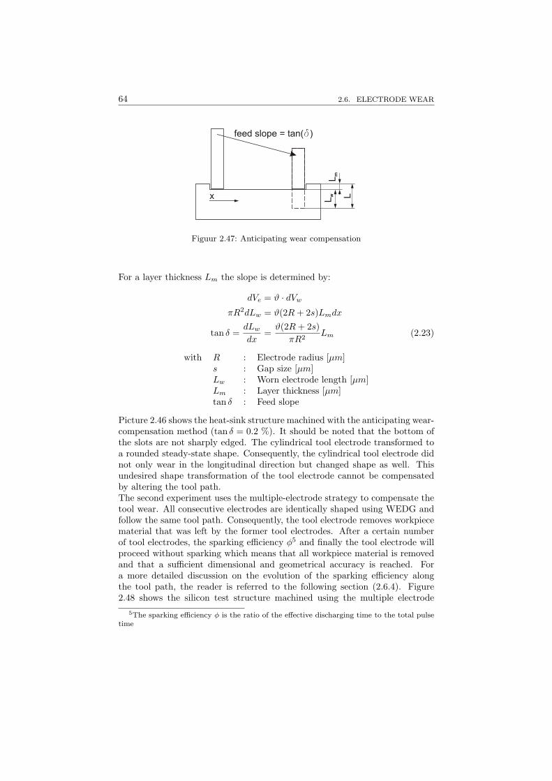
64 2.6. ELECTRODE WEAR
feed slope = tan(d)
Lw
Lm
Lx
Figuur 2.47: Anticipating wear compensation
For a layer thickness Lm the slope is determined by:
dVe = ϑ · dVw
πR2dLw = ϑ(2R + 2s)Lmdx
tan δ =dLw
dx=
ϑ(2R + 2s)πR2
Lm (2.23)
with R : Electrode radius [µm]s : Gap size [µm]Lw : Worn electrode length [µm]Lm : Layer thickness [µm]tan δ : Feed slope
Picture 2.46 shows the heat-sink structure machined with the anticipating wear-compensation method (tan δ = 0.2 %). It should be noted that the bottom ofthe slots are not sharply edged. The cylindrical tool electrode transformed toa rounded steady-state shape. Consequently, the cylindrical tool electrode didnot only wear in the longitudinal direction but changed shape as well. Thisundesired shape transformation of the tool electrode cannot be compensatedby altering the tool path.The second experiment uses the multiple-electrode strategy to compensate thetool wear. All consecutive electrodes are identically shaped using WEDG andfollow the same tool path. Consequently, the tool electrode removes workpiecematerial that was left by the former tool electrodes. After a certain numberof tool electrodes, the sparking efficiency φ5 and finally the tool electrode willproceed without sparking which means that all workpiece material is removedand that a sufficient dimensional and geometrical accuracy is reached. Fora more detailed discussion on the evolution of the sparking efficiency alongthe tool path, the reader is referred to the following section (2.6.4). Figure2.48 shows the silicon test structure machined using the multiple electrode
5The sparking efficiency φ is the ratio of the effective discharging time to the total pulsetime

CHAPTER 2. MICRO-EDM AS MICROFABRICATION TECHNIQUE 65
(a) Optical picture (b) SEM picture
Figuur 2.48: Multiple-electrode method
strategy. The slots have a rectangular shape and no signs of tool wear isobserved. It is clear that the additional dressing time and the time intervals inwhich the sparking efficiency is low increase the total machining time takingthe machining time of the anticipated compensation strategy as reference.In 2002 Bleys et al. published on real-time wear compensation in milling EDM[75]. The workpiece removal is not simulated beforehand but sensed real-timeby means of the efficiency factor φ. After each layer the length of the tool ismeasured to correct the compensation characteristics. One of the advantages ofthis technique is that layers with constant thickness can be machined withoutprior knowledge of the workpiece geometry.
Three-dimensional tool electrodes
When three-dimensional tool electrodes are required, only the multiple-electrode strategy is able to compensate for the tool consumption. A three-dimensional tool will be consumed in a three-dimensional way and the toolwear is consequently not compensable by tool path correction. Therefore, thetool path should be identical for the successive tool electrodes. The necessarynumber of electrodes is hard to predict and can therefore better be determinedduring machining by observing the sparking efficiency along the tool path. Alow value of the sparking efficiency refers to low material removal and conse-quently to a finished workpiece.
Summary and conclusions
Table 2.4 summarizes the wear-compensation techniques and highlights themain characteristics. Some of these compensation techniques use wear predic-tion to anticipate the tool-shape transformation by continuously adjustment

66 2.6. ELECTRODE WEAR
of the tool path. However, when three-dimensional tools are used, the onlyway to compensate for tool wear is the use of the traditional multiple-electrodemethod.
3D tool electrodes
Multiple-electrode method Always applicable.
Long prismatic tool electrodes
Uniform wear method Applicable when the layer area is large with respect toelectrode section. Otherwise no uniform wear will beobserved. Needs very thin layers to be scanned severaltimes, hence time consuming.
Anticipated wear compensation Wear is continuously compensated in one direction.However, the tool geometry transforms which cannotbe compensated by tool path adaptation.
In-process wear measurement The tool wear is measured continuously by means ofanalyzing the pulse shapes. This method detects vari-ations in tool wear immediately and is able to correctthe tool path simultaneously. It should be noted thatthe tool wear is not measured directly but that anadequate relation between tool wear and pulse-shapecharacteristics must be available.
Wear measurement Exact prediction of the tool wear (e.g. in the anticipa-ted wear compensation technique and in the in-processwear measurement technique) is not feasible and usu-ally the predictions drift away from the actual values.Each wear measurement resets this drift, but raisesthe production time.
Tabel 2.4: Wear-compensations methods
2.6.4 Future implementation of themultiple-electrode method
The multiple-electrode method uses a number of consecutive tool electrodes tocompensate the tool wear. However, the required number of tool electrodes ishard to predict. The ideal solution to check if further machining is required ison-line measuring of the sparking efficiency. Figure 2.49 shows three phases inthe sparking efficiency (or intensity) along the tool path. In the first part ofthe tool path, the efficiency is quite low because the preceding tool electrodesalready removed the majority of workpiece material. The tool electrode willproceed fast and most of the generator pulses will be identified as open-circuitpulses, resulting in a low sparking efficiency. In this phase a finishing regimeshould be set so that the few discharging sparks have a smoothing effect. Whenthe sparking efficiency increases the EDM-process removes workpiece materialin an efficient way. High removal rates are observed in this second phase. Ina third phase the intensity is going down because the tool electrode is totally

CHAPTER 2. MICRO-EDM AS MICROFABRICATION TECHNIQUE 67
Spark
ing in
tensit
y
Distance along tool path
1 2 3
Figuur 2.49: Sparking intensity (or sparking efficiency) phases along thetool path
worn off and the tool electrode proceeds fast along the tool path. It shouldbe mentioned that not all tool electrodes observe the three phases discussedabove. The first electrode for example starts directly in phase two becausethere were no preceding tool electrodes. The final electrode should experienceonly phase one and will finish the workpiece. When the tool path is short nothird phase will be observed because no entirely worn tools will be encountered.In order to optimize the machining time, the first part of the first phase andthe last part of the third phase can be omitted, because no efficient materialremoval is present. Accordingly, the tool electrode should only machines alongthe ’efficient’ part of the tool path and should not scan the entire tool path eachtime. When the entire part, or sub-part, is finished , no more tool electrodesare required. Unfortunately, present EDM-machines do not offer this flexiblemachining so that the number of required tool electrodes should be estimatedin advance.
2.6.5 Estimation of the required number of toolelectrodes for the multiple-electrode method
In this thesis, an upper limit for the required number of tool electrodes is pre-dicted for a slot which is machined with a cylindrical tool electrode (figure2.50). The tool electrode sinks to the depth of cut D, after which the toolmoves along the X-axis to create a slot with length L. Each successive toolelectrode follows an identical tool path removing a part of the remaining work-piece material. In this model the tool wear is assumed to occur only at thebottom of the tool electrode (dVe), which is not the case during real machiningwhere wear is observed on the whole electrode surface. This means that theactual wear at the bottom of the electrode will be lower than the predictedvolume dVe. Consequently, the shortening of the simulated electrode will belarger than the shortening of a real tool electrode. In addition, the diameter
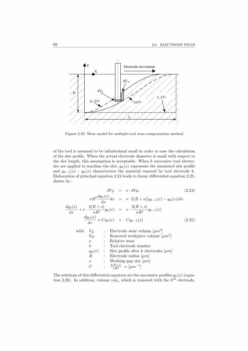
68 2.6. ELECTRODE WEAR
yk-1(x) yk(x)
dVe
dVw
Electrode movementX
Y
y∞(x)D
L
Figuur 2.50: Wear model for multiple-tool wear-compensation method
of the tool is assumed to be infinitesimal small in order to ease the calculationof the slot profile. When the actual electrode diameter is small with respect tothe slot length, this assumption is acceptable. When k successive tool electro-des are applied to machine the slot, yk(x) represents the simulated slot profileand yk−1(x) − yk(x) characterizes the material removal by tool electrode k.Elaboration of principal equation 2.24 leads to linear differential equation 2.25,shown by:
dVE = ν · dVW (2.24)
πR2 dyk(x)dx
dx = ν · 2(R + s)(yk−1(x)− yk(x))dx
dyk(x)dx
+ ν · 2(R + s)πR2
yk(x) = ν · 2(R + s)πR2
yk−1(x)
dyk(x)dx
+ Cyk(x) = Cyk−1(x) (2.25)
with VE : Electrode wear volume [µm3]VW : Removed workpiece volume [µm3]ν : Relative weark : Tool electrode numberyk(x) : Slot profile after k electrodes [µm]R : Electrode radius [µm]s : Working gap size [µm]C : 2(R+s)
πR2 · ν [µm−1]
The solutions of this differential equation are the successive profiles yk(x) (equa-tion 2.26). In addition, volume volk, which is removed with the kth electrode,

CHAPTER 2. MICRO-EDM AS MICROFABRICATION TECHNIQUE 69
is given by equation 2.27.
y0(x) = 0y1(x) = −De−Cx
...
yk(x) = yk−1(x)−D(Cx)k−1
(k − 1)!e−Cx or
yk(x) = −De−Cxk−1∑i=0
(Cx)i
i!(2.26)
volk = 2(R + s)∫ L
0
(yk−1(x)− yk(x))dx
eq. 2.25= 2(R + s)
∫ L
0
1C
dyk(x)dx
dx
=2(R + s)
C(yk(L)− yk(0))
=2(R + s)
C(yk(L) + D) (2.27)
with D : Designed slot depth [µm]L : Length of slot [µm]
When the machining accuracy is set to be ∆, the required number of toolelectrodes can be predicted. At the end of the slot, at location L, the remainingmaterial should be smaller than the desired machining tolerance ∆, as shownby:
∆ < yk(L) + D (2.28)
< D · (1− e−CLk−1∑i=0
(CL)i
i!) (2.29)
with ∆ : Dimensional tolerance [µm]
The required number of electrodes k is determined by selecting the lowest valueof k so that the inequality of equation 2.29 is fulfilled.
Comments
It should be emphasised that this calculated number of required toolelectrodes is an upper limit because of the assumption that the wear onthe tool electrode only occurs at the bottom part. Consequently, a higheraccuracy is reached compared to the desired machining accuracy ∆.
It should be noted that ∆ is limited by the obtainable process and posi-tioning accuracies, even if high values of k predict better accuracies.

70 2.7. THREE-DIMENSIONAL MACHINING
This calculation method is only applicable for the machining of blind slotsusing cylindrical tool electrodes. For other geometries, the calculation isfar more difficult. Usually, the best fitting slot geometry is applied inorder to approximate the wear behaviour of more complex shapes.
The actual slot geometry is not measured in this research work. However,an identical model for slot-geometry prediction is successfully applied byBleys who simulates slot geometries for successive tool electrodes in orderto create an anticipating wear-compensation strategy [75]. Bleys appliesmilling EDM with tubular tool electrodes with an outer diameter of 3 mmand an inner diameter of 1.8 mm.
2.6.6 Summary
In EDM, tool wear is one of the major factors which influences the dimensionaland geometrical machining accuracy. Much effort is put in the developmentof wear-prediction and wear-compensation techniques. For each EDM confi-guration (sinking EDM, milling EDM), individual compensation strategies aredeveloped of which the multiple-electrode method is always applicable. The-refore, a calculation method is proposed to estimate the required number ofsuccessive electrodes which have to be applied in order to obtain a desiredmachining accuracy for the machining of a slot geometry.
2.7 Three-dimensional machining
2.7.1 Introduction
In this section the three-dimensional machining capabilities of micro-EDM aredemonstrated by producing several miniaturized mechanical components andsystems. All components are machined on the AGIE Compact 1 EDM machi-ne. The tool consumption is generally compensated by the multiple-electrodemethod and the developed WEDG unit is applied to dress and shape the toolelectrodes. This section ends with a number of practical tips and tricks toenhance the machining performances of micro-EDM
2.7.2 Conical holes
Today, microhole drilling is one of the main application areas of micro-EDM.The development of WEDG increased the repeatability and accuracy of toolshaping, which resulted in smaller and more accurate microholes. In this workemphasis is not put on the technology of microhole machining but one specificapplication is highlighted. The final aim of the study is to maximize the sen-sitive area on the illuminated side of a silicon solar cell by putting the powertransmission lines on the back side of the cell. Micro-EDM is studied as a tech-nique to machine through holes in a silicon wafer in order to enable interfacial

CHAPTER 2. MICRO-EDM AS MICROFABRICATION TECHNIQUE 71
contacts between the illuminated side and the back side of the photovoltaic cell.The electrical connection is realized by a conductive paste, which is screenprin-ted on the back side of the silicon wafer, filling the holes. A number of throughholes are machined in a silicon wafer to investigate the connection capabilities.Figure 2.51(a) and 2.51(b) show respectively a conical tool electrode and twoconical holes in a silicon test wafer. The holes are made conically to improve
(a) Conical electrode (b) Conical holes
(c) Cylindrical hole filled withconductive paste
(d) Conical hole filled with con-ductive paste
Figuur 2.51: Conical through holes
the filling with conductive paste. Experiments proved that conical holes leadto better inter-connection results than cylindrical holes. The individual holescan be machined in less than one minute. In order to realize a high productionthroughput, several parallel and individually controlled tool electrodes shouldbe used in order to machine an entire wafer in less than one minute. This studyhas been executed in the scope of a European Non-Nuclear Energy JOULE IIIproject (JOR3-CT98-0223).

72 2.7. THREE-DIMENSIONAL MACHINING
2.7.3 Spring structure
In 1993 Staufert et al. presented a measurement system to perform one-dimensional measurements [76]. The heart of the measurement system is asilicon spring of which the deflection is measured capacitively. By applying alarge number of parallel one-dimensional miniaturized measuring units, a pro-filometer can be realized which immediately measures an entire profile (e.g. forshaft geometry measurements). All springs are individually compressed, cor-responding to the shape of the sample, enabling simultaneous read-out. Thespring was made by EDM and a finishing chemical polishing step was appliedto remove the affected top layer.In this work, a similar silicon spring is machined to show the contouring ca-pabilities of micro-EDM. The spring contour is designed in AutoCAD andconverted to the specific CNC-code of the AGIE Compact 1. During conver-sion the tool diameter and the size of the working gap are taken into account.Figure 2.52 shows a silicon spring on top of a Belgian Franc coin. The spring
Figuur 2.52: Microspring on a pre-Euro Belgian Franc (φ 18 mm)
is machined in a 350 µm thick silicon wafer and measures 7 mm by 4 mm.During machining the diameter of the tool electrode reduces continuously dueto tool wear. The multiple electrode method is used to compensate the toolwear. Another issue is workpiece fixation during machining. The majority ofmicrostructures is fabricated out of a large material stock. The material whichsurrounds the microstructure serves as frame which can easily be manipula-ted and clamped. However when the microstructure is to be released fromthe frame, it should be supported or clamped. Without proper handling, themicrostructure will break from the frame at the moment the structure is closeto be released because the remaining supporting material is not able to carrythe weight of the microstructure. In order to avoid this breaking phenomenona few measures can be taken. When the machining is halfway finished, themicrostructure can be glued to the frame at spots where machining is com-pleted. Accordingly, the microstructure will not break off when the machiningof the entire structure is finished. The glue should be removable in order torelease the microstructure. It should also be electrically conductive in order tomake EDM feasible. Another method to clamp the microstructure is the use

CHAPTER 2. MICRO-EDM AS MICROFABRICATION TECHNIQUE 73
of manipulation grippers. The microstructure is clamped by a gripper duringmachining. When workpiece material has to be removed near the gripper jaws,the microstructure must be switched to a second gripper. Both grippers mustbe accurately aligned in order to avoid loss in positioning accuracy and to avoidelevated gripping forces during switching. As for the glue, the gripper must beelectrically conductive to make machining feasible. Figure 2.53 shows one ofthe microgrippers on the worktable of the EDM machine. The gripper can be
Figuur 2.53: Manipulation gripper
rotated and positioned in vertical direction in order to make alignment possi-ble. The gripper itself consists of two jaws which move parallel by means of aplayless mechanism, based on flexible hinges. An initial tension on the jaws issupplied by a tension spring. The jaws can be opened manually by means of acam system.
2.7.4 Membranes and inclined planes
Except for contouring, the micro-EDM set-up allows three-dimensional mil-ling. Inclined planes and membranes are machined into a silicon wafer. Theinclination angle can be designed freely and does not depend on the crystallo-graphic orientation of the monocrystalline silicon. In anisotropic wet etchingfor example, the producible angles are fixed and depend on the crystal orienta-tion of the silicon (54.7 for a (100)6-wafer). Figure 2.54(a) shows schematicallya structure consisting of a 50 µm thick membrane between two inclined planes.Figure 2.54(b) shows the same structure machined in a silicon wafer having asurface roughness of 0.2 µm Ra. Figure 2.54(c) shows an inclined plane withan inclination of 45 in a 650 µm thick silicon wafer. The inclined planes aremachined by milling EDM with a standard tool electrode having a diameter of
6Miller indices [2]

74 2.7. THREE-DIMENSIONAL MACHINING
1500 µm
thickness 50 µm
45
360 µm
o
(a) (b) (c)
Figuur 2.54: Silicon 45 mirrors
150 µm. The applied milling strategy affects the geometrical accuracy of themachined planes. A good tool path overlap (> 80 %) and crossing tool-pathsreduce the size of the scallops on the machined surface. Bleys et al. presentedtool-path strategies to minimize the scallop size in milling EDM [77].Mirror planes machined by micro-EDM is discussed by ’s Heeren et al. [78].An optical chip-to-chip interconnection is realized with a combination of KOH-etching and micro-EDM. V-grooves (serving as fibre guides) were machinedin silicon using KOH-etching, after which micro-EDM was used to create 45
reflection planes. After micro-EDM, a chemical polishing step is applied tosmoothen the surface down to a surface roughness of 0.21 µm Ra.
(a) (b)
Figuur 2.55: Engaging spur gears (the field of view of the camera is smallerthan the size of the engaging gears for both pictures)

CHAPTER 2. MICRO-EDM AS MICROFABRICATION TECHNIQUE 75
2.7.5 Spur and bevel gears
In order to demonstrate the three-dimensional machining capabilities of micro-EDM, more complex microstructures are produced namely miniaturized gears.Firstly, spur gears are machined using contouring EDM. The spur gears haveinvolute shaped teeth to guarantee a constant speed transmission and to avoidslip of both engaging gear teeth. After machining of the hub, the contour ofthe gear is realized. Figure 2.55 shows engaging spur gears, fabricated out of asilicon wafer with a thickness of 360 µm. Silicon is used as workpiece materialin order to show the orientation independency of micro-EDM of silicon. Bothgears are mounted on micromachined steel axes with a diameter of 1 mm. Themachined gears still have a diameter of 3 mm which is rather large compared tospur gears which are for instance used in wristwatches. The gears are designedso that a standard tool electrode with a diameter of 150 µm fits between twoneighbouring gear teeth. Further miniaturization of the gears requires thinnertool electrodes which can be realized using WEDG. Secondly, bevel gears are
(a) (b)
(c) (d)
Figuur 2.56: Silicon bevel gears

76 2.7. THREE-DIMENSIONAL MACHINING
machined using milling EDM. A three-dimensional tool path is generated witha tool path overlap of 80 %. Figure 2.56(a) and 2.56(b) show two silicon bevelgears. The engaging angle of the bevel gears is 90 and is demonstrated onfigure 2.56(c) and 2.56(d) where two bevel gears are mounted on steel axes ofwhich one is driven by an electro-motor. Both steel axes are carried by twominiaturized roller bearings. As for the spur gears, the minimal size of thebevel gears depends on the diameter of the cylindrical tool electrode.
2.7.6 Microdie
For micromachining, the fabrication accuracy does not only depend on theprocess tolerances and positioning accuracy of the EDM equipment but is alsoinfluenced by alignment and (re-)clamping inaccuracies. A microdie is selectedas case-study to demonstrate the importance of accurate alignment and clam-ping. Figure 2.57 shows the manufacturing sequence of the die which has tobe machined on its six faces. The fabrication starts with the machining (using
(a) (b) (c)
(d) (e) (f)
Figuur 2.57: Die fabrication scheme
micro-EDM) of a cubic microstructure which is still fixed to the surroundingmaterial with one face. To avoid several reclamping operations, as many facesas possible are machined in a single set-up. Firstly, the left, front and right faceof the die are machined by eroding respectively four, six and three spots (figure2.57(a)). The spots are cylindrical holes with their centre axes perpendicularto the axis of the tool electrode on the EDM machine. Therefore a special-ly shaped tool electrode is used to machine the spots on the vertical faces ofthe die. A small hole is machined in a copper block using drilling EDM ((1)

CHAPTER 2. MICRO-EDM AS MICROFABRICATION TECHNIQUE 77
on figure 2.58(a)). Then the block is rotated over 90 (2) so that the eroded
1 2 3
(a) (b)
Figuur 2.58: Tool electrode to machine the spots on vertical faces
microhole can be used to shape the non-rotating tool electrode (3). Figure2.58(b) shows a used tool electrode with the remnant of the cylindrical feature.This example shows that complex tools can be produced using simply shapedcounter-electrodes. After the machining of the vertical faces, the electrode isdressed and shaped to machine the two spots on the top face (figure 2.57(b)).Then the structure is turned upside down and reclamped. The conventionalalignment procedure, which makes use of electrical contact between tool andworkpiece, could not be applied because of the low electrical conductivity of theworkpiece material. The structure was aligned visually using an optical micro-scope. Subsequently the face with five spots is machined (figure 2.57(c)). Theremaining single spot on the sixth face requires a special machining procedure.A through cavity is machined just behind the die (figure 2.57(d)). The cavityallows the entry of the tool electrode to machine the final spot. In the end,the die is cut loose from the surrounding material (figure 2.57(e) and 2.57(f)).Figure 2.59 shows the individual faces of a 360 µm× 360 µm× 360 µm siliconmicrodie. The spots have a diameter of approximately 45 µm. As can be seen,the spots are not exactly centred on the faces and the structure is not exactlycubic. These machining inaccuracies are caused by an inadequate alignmentafter the reclamping operation caused by reference points which were too closeto each other, promoting angular misalignment. The final face, having one sin-gle spot, has one rough edge. The rough edge originates from breaking whenthe die was released from the surrounding material. At a certain point duringreleasing, the remaining material is not strong enough to carry the structureand breaks. Such a breaking phenomenon can be avoided by using additio-nal clamping devices to support the microstructure, as presented in paragraph2.7.3.

78 2.7. THREE-DIMENSIONAL MACHINING
(a) (b) (c)
(d) (e) (f)
Figuur 2.59: Microdie
2.7.7 Microsuspensions
Inertial sensors are used to measure acceleration, inclination or angular speed.The majority of these inertial sensors consist of a suspended mass of which thedisplacement or vibration is measured. A number of suspensions are machinedto demonstrate the machining capabilities of micro-EDM. Figure 2.60(a) showsan inertial mass suspended by two leaf springs. The mass measures 2 mm ×2 mm × 650 µm and the leaf springs have a length of 2 mm and a section of60 µm × 650 µm. Another and more complex suspension is shown on figure2.60(b) where the inertial mass is asymmetrically suspended by six microbeams.Each beam has a section of 40 µm×40 µm. Such a configuration can be used inresonant beam accelerometers in which the resonant frequency of the beam isa measure for the acceleration. An acceleration will cause tension in the beamsresulting in a shift in resonance frequency. The resonating beams are usuallyparallel to the suspension beams and carry only a small fraction of the load.Besides the two examples above, a wide variety of microsuspensions can be
fabricated. All presented suspensions are fabricated out of silicon and have asurface roughness of approximately 0.2 µm Ra. The machining time for eachsuspension was approximately 30 minutes.
Figure 2.61 shows a wave-like suspension machined in a silicon waferwith a thickness of 650 µm. The suspension is machined with a standard

CHAPTER 2. MICRO-EDM AS MICROFABRICATION TECHNIQUE 79
(a) (b)
Figuur 2.60: Sensor suspensions
(a) (b)
Figuur 2.61: Silicon wave-shaped suspension beam
tungsten tool electrode having a diameter of 150 µm. The section of thesuspension is 50 µm× 650 µm.
A more complex suspension is shown on figure 2.62(b) where an S-shapedsuspension is machined in a silicon wafer. The S-shape is situated in aplane perpendicular to the top surface of the wafer. It is eroded using adisc-shaped tool electrode produced by WEDG.
Figure 2.63 shows a parallel beam suspension. The beams can be realizedwith a disc tool electrode similar to the tool electrode for the S-shapedbeam. However, the beams can be realized in one single fabrication stepwhen a specifically shaped tool is applied as depicted on figure 2.63(a) and2.63(d). The parallel beams on figure 2.63(c) have a section of 50 µm ×50 µm and a length of 2 mm.
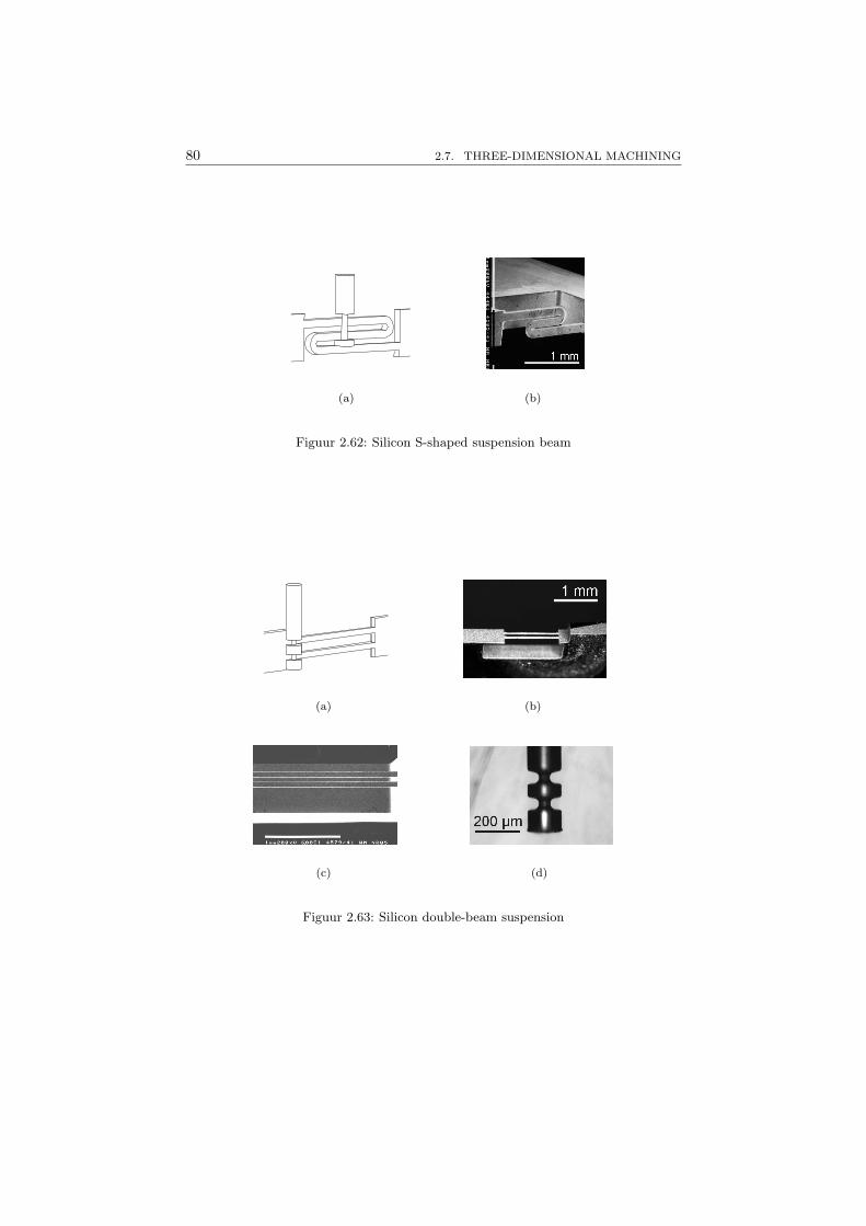
80 2.7. THREE-DIMENSIONAL MACHINING
(a) (b)
Figuur 2.62: Silicon S-shaped suspension beam
(a) (b)
(c) (d)
Figuur 2.63: Silicon double-beam suspension

CHAPTER 2. MICRO-EDM AS MICROFABRICATION TECHNIQUE 81
This set of machined suspension geometries shows the variety of shapes whichcan be obtained using quite simple tool electrodes. However, no experimentson the performances of the suspensions were executed.
2.7.8 Force-sensing gripper
In order to illustrate the role of micro-EDM as a manufacturing techniquefor the production of miniaturized instruments, a miniaturized force-sensinggripper is designed and fabricated using the micro-EDM technology. The grip-per consists of two force-sensitive gripper fingers. The force is measured in aflexible part of the finger where the local strain is measured by strain gauges(figure 2.64(a)). The use of silicon as gripper material makes implantation of
(a) Gripper design (b) Stress analysis
(c) Single gripper finger (d) Gripper assembly
Figuur 2.64: Microgripper

82 2.7. THREE-DIMENSIONAL MACHINING
strain gauges possible using ion-implantation. The areas of maximal stress andstrain are found by FEM-analysis of the finger structure (figure 2.64(b)). Fi-gure 2.64(c) shows a Scanning Electron Microscope (SEM) picture of a singlegripper finger machined in a silicon wafer. Figure 2.64(d) shows an assembledgripper with two fingers which are mounted on leaf springs. The deflection ofthe leaf springs is controlled by a cam system, driven by an electromagneticmotor. Unfortunately, only the mechanical components are realized and nostrain gauges were implanted.
2.7.9 Propellers made by reverse EDM
Reverse EDM is applied to machine miniaturized propeller-shapes. ReverseEDM is, in this work, used to indicate that the workpiece is clamped into theconventional tool clamp of the EDM machine and that the tool electrode isfixed on the worktable. The term ’reverse EDM’ is also used in traditionalEDM to indicate a reverse polarity during machining. For traditional sinkingEDM for instance, reverse polarity means that the tool electrode is negativewhile it is generally positive.In our set-up, the WEDG unit (mounted on the worktable) is not used toshape the tool electrode but is used to machine the workpiece directly. Figure2.65 shows schematically the fabrication of a miniaturized propeller by meansof reverse EDM. The WEDG wire is mounted on the worktable at a certain
ZC
XY
WEDG-wire
Figuur 2.65: Workpiece in tool holder
inclination and is used to machine the individual propeller blades. A combinedmovement of the translating and rotating axes is necessary to machine theblades properly. Figure 2.66 shows various propellers with different sizes andgeometries.
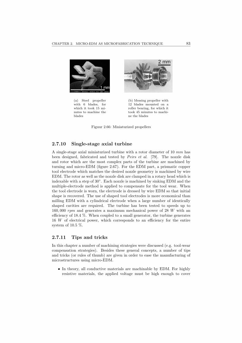
CHAPTER 2. MICRO-EDM AS MICROFABRICATION TECHNIQUE 83
(a) Steel propellerwith 6 blades, forwhich it took 15 mi-nutes to machine theblades
(b) Messing propeller with12 blades mounted on aroller bearing, for which ittook 45 minutes to machi-ne the blades
Figuur 2.66: Miniaturized propellers
2.7.10 Single-stage axial turbine
A single-stage axial miniaturized turbine with a rotor diameter of 10 mm hasbeen designed, fabricated and tested by Peirs et al. [79]. The nozzle diskand rotor which are the most complex parts of the turbine are machined byturning and micro-EDM (figure 2.67). For the EDM part, a prismatic coppertool electrode which matches the desired nozzle geometry is machined by wireEDM. The rotor as well as the nozzle disk are clamped in a rotary head which isindexable with a step of 30. Each nozzle is machined by sinking EDM and themultiple-electrode method is applied to compensate for the tool wear. Whenthe tool electrode is worn, the electrode is dressed by wire EDM so that initialshape is recovered. The use of shaped tool electrodes is more economical thanmilling EDM with a cylindrical electrode when a large number of identicallyshaped cavities are required. The turbine has been tested to speeds up to160, 000 rpm and generates a maximum mechanical power of 28 W with anefficiency of 18.4 %. When coupled to a small generator, the turbine generates16 W of electrical power, which corresponds to an efficiency for the entiresystem of 10.5 %.
2.7.11 Tips and tricks
In this chapter a number of machining strategies were discussed (e.g. tool-wearcompensation strategies). Besides these general concepts, a number of tipsand tricks (or rules of thumb) are given in order to ease the manufacturing ofmicrostructures using micro-EDM.
In theory, all conductive materials are machinable by EDM. For highlyresistive materials, the applied voltage must be high enough to cover

84 2.7. THREE-DIMENSIONAL MACHINING
(a) Single-stage axial turbine
(b) Machining of the rotor (c) Assembled rotor andnozzle disk
Figuur 2.67: Miniaturized turbine [79]
the voltage drop over the workpiece as well as the voltage drop over thedischarging channel during the spark. When the voltage drop over thedischarging gap is too low, no discharges will occur.In micro-EDM, the applied voltage should be low in order to have lowdischarge energies. From the built-up machining experience, it can besaid that for silicon workpiece materials, the electrical resistivity shouldbe lower than 1 Ω · cm in order to be easily machined by micro-EDM.
When thick layers of workpiece material are to be removed with a thintool electrode, machining may become unstable and workpiece materialis removed excessively near the layer top. This irregular material removalphenomenon results in low dimensional and geometrical accuracy. Expe-rience offers a rule of thumb which says that the depth of cut should be
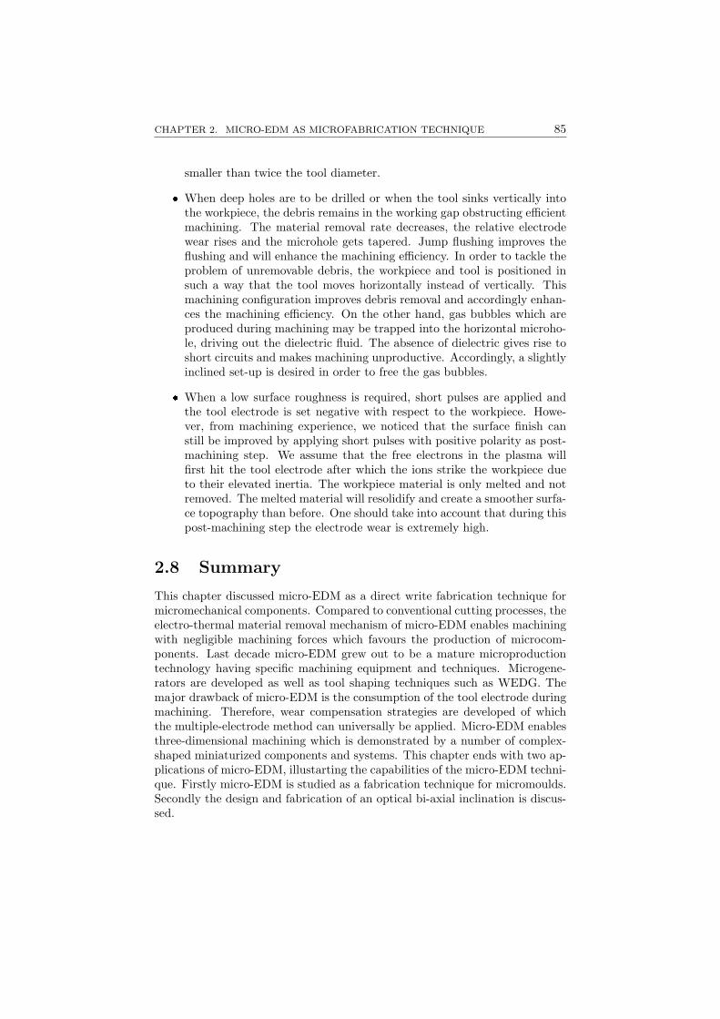
CHAPTER 2. MICRO-EDM AS MICROFABRICATION TECHNIQUE 85
smaller than twice the tool diameter.
When deep holes are to be drilled or when the tool sinks vertically intothe workpiece, the debris remains in the working gap obstructing efficientmachining. The material removal rate decreases, the relative electrodewear rises and the microhole gets tapered. Jump flushing improves theflushing and will enhance the machining efficiency. In order to tackle theproblem of unremovable debris, the workpiece and tool is positioned insuch a way that the tool moves horizontally instead of vertically. Thismachining configuration improves debris removal and accordingly enhan-ces the machining efficiency. On the other hand, gas bubbles which areproduced during machining may be trapped into the horizontal microho-le, driving out the dielectric fluid. The absence of dielectric gives rise toshort circuits and makes machining unproductive. Accordingly, a slightlyinclined set-up is desired in order to free the gas bubbles.
When a low surface roughness is required, short pulses are applied andthe tool electrode is set negative with respect to the workpiece. Howe-ver, from machining experience, we noticed that the surface finish canstill be improved by applying short pulses with positive polarity as post-machining step. We assume that the free electrons in the plasma willfirst hit the tool electrode after which the ions strike the workpiece dueto their elevated inertia. The workpiece material is only melted and notremoved. The melted material will resolidify and create a smoother surfa-ce topography than before. One should take into account that during thispost-machining step the electrode wear is extremely high.
2.8 Summary
This chapter discussed micro-EDM as a direct write fabrication technique formicromechanical components. Compared to conventional cutting processes, theelectro-thermal material removal mechanism of micro-EDM enables machiningwith negligible machining forces which favours the production of microcom-ponents. Last decade micro-EDM grew out to be a mature microproductiontechnology having specific machining equipment and techniques. Microgene-rators are developed as well as tool shaping techniques such as WEDG. Themajor drawback of micro-EDM is the consumption of the tool electrode duringmachining. Therefore, wear compensation strategies are developed of whichthe multiple-electrode method can universally be applied. Micro-EDM enablesthree-dimensional machining which is demonstrated by a number of complex-shaped miniaturized components and systems. This chapter ends with two ap-plications of micro-EDM, illustarting the capabilities of the micro-EDM techni-que. Firstly micro-EDM is studied as a fabrication technique for micromoulds.Secondly the design and fabrication of an optical bi-axial inclination is discus-sed.
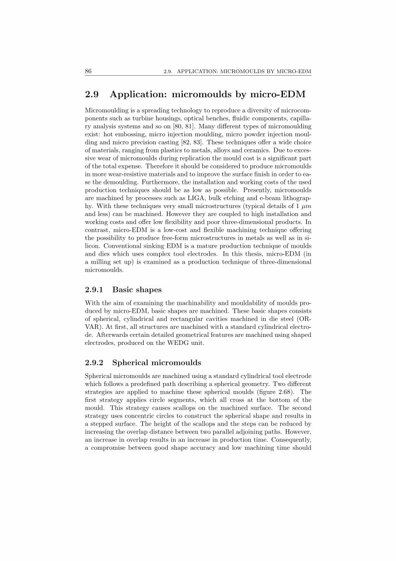
86 2.9. APPLICATION: MICROMOULDS BY MICRO-EDM
2.9 Application: micromoulds by micro-EDM
Micromoulding is a spreading technology to reproduce a diversity of microcom-ponents such as turbine housings, optical benches, fluidic components, capilla-ry analysis systems and so on [80, 81]. Many different types of micromouldingexist: hot embossing, micro injection moulding, micro powder injection moul-ding and micro precision casting [82, 83]. These techniques offer a wide choiceof materials, ranging from plastics to metals, alloys and ceramics. Due to exces-sive wear of micromoulds during replication the mould cost is a significant partof the total expense. Therefore it should be considered to produce micromouldsin more wear-resistive materials and to improve the surface finish in order to ea-se the demoulding. Furthermore, the installation and working costs of the usedproduction techniques should be as low as possible. Presently, micromouldsare machined by processes such as LIGA, bulk etching and e-beam lithograp-hy. With these techniques very small microstructures (typical details of 1 µmand less) can be machined. However they are coupled to high installation andworking costs and offer low flexibility and poor three-dimensional products. Incontrast, micro-EDM is a low-cost and flexible machining technique offeringthe possibility to produce free-form microstructures in metals as well as in si-licon. Conventional sinking EDM is a mature production technique of mouldsand dies which uses complex tool electrodes. In this thesis, micro-EDM (ina milling set up) is examined as a production technique of three-dimensionalmicromoulds.
2.9.1 Basic shapes
With the aim of examining the machinability and mouldability of moulds pro-duced by micro-EDM, basic shapes are machined. These basic shapes consistsof spherical, cylindrical and rectangular cavities machined in die steel (OR-VAR). At first, all structures are machined with a standard cylindrical electro-de. Afterwards certain detailed geometrical features are machined using shapedelectrodes, produced on the WEDG unit.
2.9.2 Spherical micromoulds
Spherical micromoulds are machined using a standard cylindrical tool electrodewhich follows a predefined path describing a spherical geometry. Two differentstrategies are applied to machine these spherical moulds (figure 2.68). Thefirst strategy applies circle segments, which all cross at the bottom of themould. This strategy causes scallops on the machined surface. The secondstrategy uses concentric circles to construct the spherical shape and results ina stepped surface. The height of the scallops and the steps can be reduced byincreasing the overlap distance between two parallel adjoining paths. However,an increase in overlap results in an increase in production time. Consequently,a compromise between good shape accuracy and low machining time should

CHAPTER 2. MICRO-EDM AS MICROFABRICATION TECHNIQUE 87
(a) Strategy I: Circle seg-ments which cross at thebottom of the sphere
(b) Strategy II: Concentriccircles creating the sphereshape
Figuur 2.68: Machining strategies for spherical moulds
be taken. Additionally, the cylindrical shape of the tool electrode and thedimension of the discharge gap are taken into account, because not the bottomtip of the tool serves as machining point but a point on the electrode mantleserve as actual machining point, as shown on figure 2.69. The resulting toolelectrode path is shown for the machining of a circle in a vertical plane. It
Figuur 2.69: Tool path correction
should be noted that it is impossible to create an exact spherical shape with acylindrical tool. At the bottom point of the sphere, a small planar surface willbe remained, approximating the bottom section of the tool. Figure 2.70 showspictures of the machined micromoulds with a radius of 500 µm. The black spotson the pictures are particles which remained on the die surface after moulding.

88 2.9. APPLICATION: MICROMOULDS BY MICRO-EDM
(a) Strategy I, machining time of mould: 2h7min
(b) Strategy II, machining time of mould: 2h53min
Figuur 2.70: Spherical micromoulds and replicates
On both mould surfaces, depending of the used strategy for electrode pathgeneration, either scallops or steps are visible. Figure 2.70 presents as well thereplicated PMMA structures using a hot embossing set-up. Both structuresare well reproduced. Even the scallops or steps and the surface texture of themoulds are visible on the replicated structures.
2.9.3 Cylindrical micromoulds
Cylindrical moulds are easy to machine using cylindrical tool electrodes. Byusing WEDG the diameter of the tool electrode can be reduced from 150 µmdown to 20 µm in a repeatable way. Figure 2.71(a) illustrates a mould withan array of machined microholes. The microholes have a cylindrical shapeand are not tapered. The diameters of the holes range from 150 µm downto 35 µm. The depth of the holes vary from 100 µm to 500 µm deep, whichresults in aspect ratios up to 14 (i.e. diameter 30 µm and depth 500 µm).The depth of the holes vary with respect to the row in the array, so that allmicroholes in one column have different aspect ratios. The mould is replicated
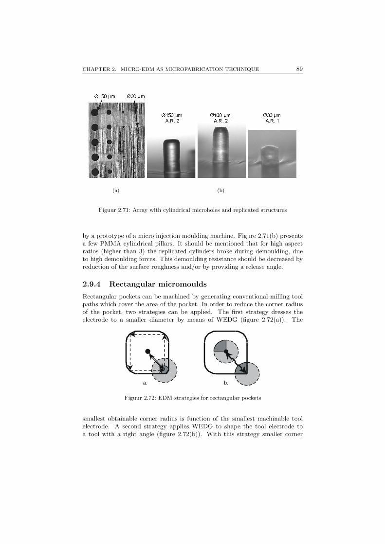
CHAPTER 2. MICRO-EDM AS MICROFABRICATION TECHNIQUE 89
(a) (b)
Figuur 2.71: Array with cylindrical microholes and replicated structures
by a prototype of a micro injection moulding machine. Figure 2.71(b) presentsa few PMMA cylindrical pillars. It should be mentioned that for high aspectratios (higher than 3) the replicated cylinders broke during demoulding, dueto high demoulding forces. This demoulding resistance should be decreased byreduction of the surface roughness and/or by providing a release angle.
2.9.4 Rectangular micromoulds
Rectangular pockets can be machined by generating conventional milling toolpaths which cover the area of the pocket. In order to reduce the corner radiusof the pocket, two strategies can be applied. The first strategy dresses theelectrode to a smaller diameter by means of WEDG (figure 2.72(a)). The
a. b.
Figuur 2.72: EDM strategies for rectangular pockets
smallest obtainable corner radius is function of the smallest machinable toolelectrode. A second strategy applies WEDG to shape the tool electrode toa tool with a right angle (figure 2.72(b)). With this strategy smaller corner

90 2.9. APPLICATION: MICROMOULDS BY MICRO-EDM
(a) Right-angled tool electrode
(b) Drillingtests
(c) Rectangularmould
Figuur 2.73: Shaped tool electrode and rectangular mould
radii can be obtained than with the first strategy. During machining with theright-angled tool electrode, the tool electrode is evidently not rotated, whichdecreases the flushing conditions in the erosion gap. An insufficiently flushedgap may result in an unpredictable gap dimensions and in unstable machining.However, non of these potential problems were observed during machining.Figure 2.73(b) shows an array of cavities machined by shaped tool electrodes.Each column is machined by a separate tool. The size of the tool decreases fromleft to right. Figure 2.73(c) shows a rectangular pocket of which two cornersare finished at half height with the right-angled tool electrodes. The obtainedcorner radius is 15 µm. Although an identical result can be obtained applyinga cylindrical tool electrode with a diameter of 20 µm (taking the working gapinto account), the application of the right-angled tool electrode is beneficialbecause of its larger section, resulting in a higher mechanical strength of thetool.

CHAPTER 2. MICRO-EDM AS MICROFABRICATION TECHNIQUE 91
2.9.5 Temple Structure
To combine all these basic shapes into one single structure, a temple shapedmould has been machined (figure 2.74). The structure consists of a rectangular
Figuur 2.74: Temple mould
base and a sphere on top. At the crest of this temple shape there is a cylindricalfeature. In front of the temple, the abbreviation of our division ’PMA’ is writtenwith a tool electrode of 30 µm diameter. The temple is surrounded by fourpillars with a diameter of 40 µm and a height of 400 µm. The machiningtook place in a single set-up and without operator interventions, illustratingthe flexibility of the micro-EDM technology. The machining ran overnightand took 8 hours of machining time. Due to tool wear, the individual letters of’PMA’ do not reach an equal depth. The multiple tool electrode method shouldbe applied to avoid this intrinsic wear problem. Figure 2.75 shows the injection
Figuur 2.75: Moulded temple
moulded temple. Although the dimensions of the pillars fulfil the dimensionalrequirements for micro injection moulding set by Piotter et al. [84], the fillingof the pillars was insufficient due to insufficient injection pressure near the pillarcavities.

92 2.10. APPLICATION: BI-AXIAL INCLINATION SENSOR
2.9.6 Conclusions
These results prove that micro-EDM is a proper and flexible technology tomachine free-form three-dimensional micromoulds. The usage of the WEDGunit makes it viable to produce flexibly shaped electrodes for machining ofsmall and specific features. Basic structures such as spheres, cylinders andpockets were machined in die steel. The microstructures were moulded using ahot-embossing and injection moulding set-up. Although there were no taperedwalls, the PMMA structures could be demoulded. Because of poor temperaturecontrol and insufficient injection pressure in the vicinity of the holes, no satis-factory filling could be realized for deep cylindrical holes with an aspect ratiowhich exceeds 5. By and large, micro-EDM is a well suited and economicalproduction technique to machine complex three-dimensional micromoulds.
2.10 Application: design and fabrication ofa bi-axial inclination sensor usingmicro-EDM
An optical bi-axial inclination sensor is designed, fabricated and tested to de-monstrate the flexible machining capabilities of micro-EDM. Inclination sensorsare widely used in industry to measure the inclination of a body with respect tothe field of gravity. The inclination sensor is intentionally designed to measurethe inclination of a computer pen [85]. The computer pen with the look andfeel of an ordinary pen, converts handwriting to computer data. To integratethe sensor in the pen, the total size of the sensor is restricted to 1 cm3. Further,an operation range of −50 to 50 is specified. The bandwidth is set to 10 Hzwhich is sufficient to register handwriting.
2.10.1 Sensor principle
Figure 2.76 shows the principle of the optical bi-axial miniature inclinationsensor. An inertial mass is suspended by a thin micromachined beam. Whenthe sensor is inclined, the beam will bend under the influence of the weight ofthe mass. The movement of the mass is measured optically by means of a LEDand PSD (Position Sensitive Device). The light of the LED is lead through achannel (or hole) in the mass and creates a spot on the PSD. When the sensoris inclined the spot will displace corresponding the inclination angle. The PSDmeasures the position of the spot in two dimensions and is consequently ableto measure two perpendicular angles.
2.10.2 Design Aspects
As explained in previous section, the mechanical structure consists of a masssuspended by a micromachined beam. The structural dimensions of the sensor

CHAPTER 2. MICRO-EDM AS MICROFABRICATION TECHNIQUE 93
(a) (b)
Figuur 2.76: Principle of miniaturized bi-axial inclination sensor
are optimized to maximize the sensitivity, resulting in a mass of 5.3 mm ×5.3 mm × 3.5 mm and a beam of 3.45 mm × 0.165 mm × 0.165 mm. Figure2.77 shows the design, consisting of the micromechanical structure in a housingand a cover containing the PSD. The shape of the housing is determined by
CoverPSD
HousingBeam
Mass
(a) Assembly
HOOFDSTUK VIII:BESCHRIJVING VAN DE TECHNISCHE REALISATIE VAN DE INCLINOMETER
VIII-65
VIII. Beschrijving van de technische realisatie van deinclinometer
In overeenstemming met het concrete ontwerp uit hetvoorgaande hoofdstuk, licht dit deel de gevolgdewerkwijze tijdens de realisatie toe. Het betreft hier inde eerste plaats de verschillende fabricagestappenvoor de micromechanische structuur en het deksel. Totslot vormt de specifieke montagemethode eenbelangrijk aandachtspunt.
VIII.1. Fabricage van de micromechanische structuur in de behuizing
VIII.1.1. Overzicht van de verschillende fabricagestappen
Ter herinnering beeldt figuur VIII.1 de gewenste micromechanische structuur met behuizing af.De fabricageprocedure vertaalt zich in een opeenvolging van verschillende stappen, waarvanonderstaande paragrafen de inhoud en de achtergrond toelichten.
Figuur VIIII.1, ontwerp van de micromechanische structuur in de behuizing.
Vooraleer echter een gedetailleerde beschrijving te leveren van de specifieke fabricagestappen,is het nuttig om kort een overzicht te schetsen van hun volgorde en herkomst. Een belangrijkaspect hierbij bestaat in de herkenning van de elementen die een hoge nauwkeurigheid vereisen,daar dit een belangrijke rol speelt in de keuze van de techniek en het regime. Voor demicromechanische structuur betekent dit dat enkel de vervaardiging van het balkje, demassastops en de doorgaande boring kritische factoren vormen, die een aangepasteproductiemethode vergen. De overige elementen voldoen reeds aan hun functionaliteiten bijgebruik van snellere en ruwere methoden, hetgeen de productietijd aanzienlijk kan verkorten.
Uit bovenstaande redenering onstaat de volgende opsplitsing van het totale fabricageproces:- vervaardigen van de grove structuur met behulp van draadvonkerosie in een ruw regime,- vervaardigen van het balkje met behulp van microvonkerosie met koperelektroden in een
fijn regime,
Emergency stop
Blind hole
Through hole
LED insertion hole
(b) Cross-section
Figuur 2.77: Design of the bi-axial inclination sensor

94 2.10. APPLICATION: BI-AXIAL INCLINATION SENSOR
the production process which will be clarified in the next paragraph. In themass a through hole is machined to guide the light from the LED to the PSD.This hole affects the symmetry of the structure. To maintain the symmetry,three additional blind holes are made. The holes are blind in order to preventundesired light spots corrupting the measurement. The LED is fixed in thebase plate near the beam and the PSD is positioned above the through holein the mass. The micromechanical structure of the sensor has to be integratedinto a housing in order to protect the fragile beam structure. In addition, thesensor needs to be protected from overloading. This is realized by integratingemergency stops into the housing. The stops block the movement of the massand avoid plastic deformation of the microbeam. The emergency stops blockthe mass at 170 µm, while plastic deformation starts at a deflection of 192 µm.
2.10.3 Production of the inclination sensor
Making use of conventional wire EDM and micro-EDM it is possible to producethe sensor structure and the housing as a monolithic part. This avoids assemblyerrors as well as fragile interconnections.In order to reduce the machining time, wire EDM is applied to shape the sensorstructure roughly because the removal rate of conventional wire EDM is at leastan order of magnitude higher than the removal rate of micro-EDM. Before wireEDM can be applied, starting holes have to be drilled through which the wirehas to be tightened. Figure 2.78(a) illustrates the clamped stock which is beingmachined by wire EDM. In the intermediate structure (figure 2.78(b)), the massis still fixed to the housing and the size of the suspension beam is still too large.The mass is fixed because the beam has to be miniaturized in a later stageand the fixation will prevent the mass from vibrating during micromachining.
HOOFDSTUK VIII:BESCHRIJVING VAN DE TECHNISCHE REALISATIE VAN DE INCLINOMETER
VIII-66
- vervaardigen van de doorgaande boring met behulp van microvonkerosie met standaardwolfraamelektroden in een fijn regime,
- vervaardigen van de niet doorgaande boringen en de boring voor bevestiging van de LEDmet behulp van microvonkerosie met dikkere elektroden in een ruw regime,
- vervaardigen van de massastops met behulp van microvonkerosie met standaardwolfraamelektroden in een fijn regime.
VIII.1.2. Vervaardiging van de grove structuur
De uitwendige vorm van de micromechanische structuur bestaat uit een prisma met afmetingen9x9x8 mm3, waarvoor enkel de eis van loodrechtheid van de vlakken ten opzichte van elkaargeldt. De oppervlaktekwaliteit van de vlakken is daarentegen van ondergeschikt belang. Daarbovendien deze vorm volledig uit regeloppervlakken opgebouwd is, bestaat de mogelijkheid omdeze te realiseren met behulp van draadvonkerosie, op voorwaarde dat er voldoende aandachtuitgaat naar de uitlijning van het werkstuk.De machine die hiervoor ter beschikking staat is van het type ROBOFIL 2000 van CharmillesTechnologies en gebruikt een draad met diameter 250 µm. Daarnaast biedt zij een vollediggamma van voorgeprogrammeerde vonkregimes aan, op basis van het te bewerken materiaal ende gewenste oppervlaktekwaliteit. Voor de specifieke toepassing van de inclinometer wordthieruit een ruw regime voor roestvast staal geselecteerd.
Figuur VIII.2 geeft de grove structuur van de sensor weer. Deze omvat reeds de geleidingsgleufen de kraag aan de buitenzijde, de globale vorm van de massa en een vergrote versie van hetuiteindelijke balkje. De grondgedachte hierbij baseert zich op het feit dat enerzijds de kraag, degeleidingsgleuf en de massa geen nauwkeurigheden vereisen die buiten de mogelijkheden vande beschikbare draadvonkmachine vallen. Daarnaast is de hoeveelheid te verwijderen materiaalin het midden van de structuur aanzienlijk groot, zodat de verwijdering op basis van hetmicrovonkproces zeer lange bewerkingstijden zou vragen. Hieruit ontstaat de beslissing om hetgros aan materiaal reeds met draadvonkerosie weg te halen, zonder echter de nauwkeurigheidvan het uiteindelijke balkje in het gedrang te brengen. Dit laatste geschiedt door het respecterenvan een aanzienlijke veiligheidsafstand, hetgeen concreet betekent dat het ‘balkje’ na hetdraadvonken nog 1 mm meet.
Figuur VIII.2, de grove sensorstructuur, na bewerking op basis van draadvonkerosie.
De realisatie van deze structuur geschiedt in twee fasen, waartussen een heropspanning endraaiing van het werkstuk over 90° plaatsvindt. Door echter beroep te doen op de functionaliteitvan de machine, die het mogelijk maakt om het stuk automatisch uit te lijnen ten opzichte vande machine-assen met behulp van een hoekcorrectie, veroorzaakt deze heropspanning geenbedreiging voor de nauwkeurigheid van het stuk. Het basismateriaal voor de grove structuur iseen vierkante staaf roestvast staal met een doorsnede van 9x9 mm2.De opspanning gebeurt metbehulp van een bankschroef, die de lange basisstaaf aan zijn zijvlakken klemt, zodanig dat delengte-as een loodrechte hoek vormt met de vonkdraad, hetgeen figuur VIII.3 illustreert.
Stock
Clamp
Wire
Mass
Mass-frame fixation
Suspension beam
(a) Wire EDM
Mass-frame fixation
Suspension beam
(b) Intermediate result
Figuur 2.78: First step: wire EDM

CHAPTER 2. MICRO-EDM AS MICROFABRICATION TECHNIQUE 95
Micro-EDM is applied to reduce the size of the suspensions beam as depictedon figure 2.79(a). Before reaching the actual suspension beam, a part of thehousing is removed (compare the housing on figure 2.78(b) and 2.77(a)) using acopper cylindrical tool electrode with diameter 2 mm. Finally the microholesare machined in the mass and subsequently the mass is loosened from thehousing using a tungsten tool electrode (diameter 150 µm). The small distancebetween mass and housing at the position of the earlier fixations limit the massof overloading (i.e. the required emergency stop). The cover which contains the
HOOFDSTUK VIII:BESCHRIJVING VAN DE TECHNISCHE REALISATIE VAN DE INCLINOMETER
VIII-68
Tenslotte blijkt uit het eerdere uitgevoerde experiment, dat de teststructuur uit hoofdstuk Vvervaardigt, dat de dimensionale nauwkeurigheid van het balkje met koperelektroden geenprobleem mag zijn.
Uit bovenstaande beschouwingen resulteert de gebruikte werkingsmethode op basis vankoperelektroden, die steunt op de herhaling van één enkele basisprocedure voor de vier zijdenvan het balkje. Figuur VIII.5 geeft schematisch het principe weer. Dit houdt tevens in dat tussende verschillende bewerkingsstappen de structuur vier maal geroteerd en opnieuw ingespannendient te worden. Vermits echter voor deze inklemming voornamelijk de evenwijdigheid van deas van het balkje met het horizontaal vlak van de machine een belangrijke factor vormt, brengendeze heropspanningen de nauwkeurigheid van de totale structuur nauwelijks in gevaar. Dezijvlakken van de behuizing en de inklemming, die als referentie dienen tijdens deheropspanning, zijn immers vervaardigd in één enkele opstelling, hetgeen respectievelijk hunevenwijdigheid en loodrechtheid garandeert.
Figuur VIII.5, principeschets van de procedure voor de verdunning van het balkje op basis van microvonkerosie.
De basisprocedure zelf bestaat in een eenvoudig vonkpad voor de koperelektroden, dat per zijdetweemaal uitgevoerd wordt, telkens met een nieuwe elektrode, teneinde de sleet tecompenseren. Hierbij beschrijft de elektrode ter hoogte van het te verdunnen balkelement eenrechthoek volgens figuur VIII.6, om over het volledige balkoppervlak een dun laagje materiaalte verwijderen. Door herhaling van deze kringloop op verschillende dieptes, totdat de top vande elektrode het gewenste balkoppervlak bereikt heeft, verkrijgt het balkje de afmetingen, zoalsdie in het ontwerp zijn vastgelegd.
Figuur VIII.6, vonkpad van de koperelektrode tijdens de verdunning van het balkje op basis van microvonkerosie.
Om bovendien de afmetingen van het balkje te kunnen vervaardigen, gaat telkens een manuelemeetprocedure het vonken vooraf, die de indringdiepte van de elektrode bepaalt. Deze
reeds bestaandestructuur
uiterste rand vande elektrode
vonkpad
Tool electrode Sensorstructure
Clamp device
(a) Miniaturizing the suspension beam
HOOFDSTUK VIII:BESCHRIJVING VAN DE TECHNISCHE REALISATIE VAN DE INCLINOMETER
VIII-69
resulteert uit de combinatie van een gekende afstand tussen een referentiepunt en het gewenstebalkoppervlak enerzijds, en de positie van de elektrode ten opzichte van hetzelfdereferentiepunt anderzijds. In de inclinometer wordt als referentiepunt voor elke balkzijde hetovereenkomstige zijvlak van de behuizing genomen, daar dit gemakkelijk voor de elektrodetoegankelijk is. Dit is belangrijk omdat de positie van het bovenoppervlak opgemeten wordtmet de kortsluitdetectie van de machine.
De parameterinstellingen, die overeenkomen met een fijn regime op basis van koperelektroden,zijn weergegeven in appendix D.
Nameten van de afmetingen van het balkje, geeft een breedte van 160 µm. Doorrekening vandeze wijziging naar de nieuwe resonantiefrequentie levert een waarde van 93 Hz op. Demaximale uitwijking waarbij vloeien optreedt in de buitenste vezels van het balkje bedraagt nu192 µm.
VIII.1.4. Vervaardiging van de boringen
Op het gebied van de boringen bestaat een onderscheid volgens de vereiste graad vannauwkeurigheid tussen de doorgaande boring die verantwoordelijk is voor de vorming van delichtspot enerzijds, en de niet doorgaande boringen in de massa en de boring voor debevestiging van de LED anderzijds. Daar het eerst vernoemde element een wezenlijk onderdeeluitmaakt van de meettechniek, en als dusdanig mee de resolutie bepaalt, vereist dit een betereafwerking dan de overige. De drie niet doorgaande gaten in de massa zijn immers enkel uitsymmetrie-overwegingen noodzakelijk, en stellen bijgevolg geen verdere eisen. Ook de ruimtevoor de LED vormt geen kritische factor, op de uitlijning onder de doorgaande boring na.Hieruit resulteert de beslissing om de uitlijning van de vijf ontworpen gaten met dezelfdenauwkeurigheid uit te voeren, doch op gebied van het vonkproces de elementen opverschillende wijze te realiseren.
Vooraleer het effectieve vonkproces aan te kunnen vatten, treedt het probleem op van decorrecte uitlijning van de structuur en de te bewerken elementen ten opzichte van de machineen van elkaar. Dankzij de ligging van de vier gaten in de massa, kunnen deze in één opspanningbewerkt worden, zodanig dat voor deze vier elementen de uitlijning zich reduceert tot debepaling van één referentiepunt en een hoekcompensatie op de assen van de machine. Om desymmetrische ligging van de gaten ten opzichte van elkaar eenvoudig te kunnen garanderen,valt de logische keuze voor een referentiepunt op het centrum van de massa. De metingen terbepaling van dit punt geschieden door het aan weerszijden aanraken van de massa in de door dedraadvonker gerealiseerde gleuven en het centreren van deze coördinaten.De uitlijning van de ruimte voor de LED resulteert uit het opmeten van de ligging van dedoorgaande boring in het bovenoppervlak ten opzichte van de zijvlakken van de sensor. Doorna het omkeren van de structuur de elektrode volgens de opgemeten afstanden tot dezelfdezijvlakken te positioneren, valt de aslijn van de LED met voldoende nauwkeurigheid samen metdie van de boring in de massa.
Om voor de doorgaande boring een voldoende nauwkeurigheid te behalen, bestaat de logischekeuze erin om deze te vonken met een standaard wolfraamelektrode in een fijn regime, volgensde parameterinstelling van appendix D, en de configuratie van figuur VIII.7.
Tool electrode
(b) Creating the holes and theemergency stops
Figuur 2.79: Second step: micro-EDM
PSD is machined by wire EDM. The final assembly of the bi-axial inclinationsensor is shown in figure 2.80 and measures 9 mm× 9 mm× 11.5 mm.
2.10.4 Test results
The performance of the inclination sensor is investigated by comparing the sen-sor readings with an external reference. The sensor is positioned on a platformwith two rotational degrees of freedom (first rotation α, second rotation β),as shown on figure 2.81(a). A first test is executed with the inclination angleβ fixed at 0, while the inclination angle α changes from −30 to 30. Theslope of the characteristic is 9.3 mV/. In the range of ±30, the resolutionis 0.1, the accuracy ±0.5 for α and ±2 for β. The considerable differencebetween accuracy and resolution is caused by an alignment error of the PSDwith respect to the suspended mass and by cross-sensitivity between both axesof the PSD. Further improvements on device accuracy are possible by errormapping which takes the measured inaccuracies into account (figure 2.81(b)).

96 2.10. APPLICATION: BI-AXIAL INCLINATION SENSOR
Figuur 2.80: Final bi-axial inclination sensor
(a) Inclination measurement (b) Error map
Figuur 2.81: Measurements on the bi-axial inclination sensor
2.10.5 Conclusions
The bi-axial inclination sensor demonstrates the flexible machining capabilitiesof wire EDM and micro-EDM. The sensor is based on a real three-dimensionalstructure which is hard to machine with other production technologies. Themain benefit of this sensor is that the inertial mass, the suspension beam andthe housing are monolithic so that micro-assembly is avoided.

Chapter 3
Silicon micro-EDMtechnology
3.1 Introduction
Micro-EDM has proved to be a versatile production technique for the machiningof micromechanical structures in a variety of electrically conductive materials.Currently, the majority of commercially available microsystems are fabrica-ted in monocrystalline silicon. Silicon is a strong, but brittle material, whichbecame widespread by its application in the fast-growing micro-electronics in-dustry. As a lot of micromachining technologies originate from existing micro-electronics technologies, silicon was inherited as main substrate material. Thischapter focusses specifically on the machining of silicon by micro-EDM. A stu-dy on the electrical behaviour of semiconductor micro-EDM and a first set ofmachining experiments, bring the particular machining characteristics of siliconmicro-EDM to light. To gain more insight on silicon micro-EDM, a technologymodel is created based on a designed experiment, allowing a systematic andunbiased approach to model building. The technology model is a mathema-tical model, which is used to optimize the machining settings for a particularEDM job. Furthermore, the machined silicon surface is thoroughly studiedand measures are proposed to enhance the quality of the surface. Finally, thecompatibility of the silicon micro-EDM technology with the established siliconmicromachining techniques is explored, resulting in a hybrid micromachiningtechnology. A case study, specifically on the design and fabrication of an uni-axial inclination sensor, is used to build up this hybrid technology.
97

98 3.2. SILICON AS WORKPIECE MATERIAL
3.2 Silicon as workpiece material
3.2.1 Monocrystalline silicon
Silicon is by far the most applied substrate material in micro-electronics. Sincemicrosystem fabrication adopted the well developed micro-electronic techno-logies, monocrystalline silicon, or single-crystal silicon, is also the most usedmaterial in microstructure and microsystem fabrication. Silicon is an intrinsicsemiconductor of which the electrical properties can be modified by appropri-ate doping. The addition of donor elements, which are pentavalent elementssuch as phosphorous, arsenic or antimony, lead to n-type silicon, while the ad-dition of acceptor elements, which are trivalent elements such as boron, leadto p-type silicon. Figure 3.1 shows the electrical resistivity for silicon and gal-lium arsenide as a function of the dopant concentration and indicates, in themeantime, the specific type and resistivity of the silicon mainly used in thiswork, which is a boron doped silicon with a resistivity of 0.02 Ω · cm. For
Figuur 3.1: Electrical resistivity in function of the dopant concentration forSi and GaAs [86]
detailed information on the electrical properties of silicon and on its applica-bility in micro-electronics, the reader is referred to dedicated literature [86].On top of the extraordinary electrical properties, silicon has good mechanicalproperties too. Table 3.1 compares the physical and mechanical properties ofsilicon and steel C45 (DIN material number 1.0503). Silicon has a diamond-like crystal structure with covalent bonding of the atoms whereas carbon steel

CHAPTER 3. SILICON MICRO-EDM 99
Silicon Steel (C45)Lattice type diamond cubic-body centered
Bond type covalent metallic
Lattice constant [m] 5.43× 10⁻¹⁰ 2.87× 10⁻¹⁰
Density ρ [kg · m−3] 2330 7800Young’s modulus E [GPa] 130− 185∗ 210Poisson ratio ν 0.28 0.28Thermal expansion α [K−1] 3× 10⁻⁶ 12× 10−6
Melting point Tm [K] 1687 1670Fracture toughness KIc [MPa · mm1/2] 15 1200Tensile strength σb [MPa] 2800− 6800 310− 560Vickers hardness [HV ] 1000 200
* The Young’s modulus of monocrystalline silicon is orientation dependent [2]
Tabel 3.1: Material properties of silicon and steel C45 [2, 3, 20]
is cubic body-centred with metallic bonding, resulting in an entirely differentstrain-stress behaviour. Silicon fails by brittle fracture after elastic deformati-on, while steel is able to dissipate more energy during its plastic deformationphase. This is reflected in a considerable difference in fracture toughness. Des-pite its low fracture toughness, monocrystalline silicon has a high hardnessand a high tensile strength compared to steel. For silicon, tensile or fracturestrength, instead of yield strength for most metals, becomes the design para-meter that limits the maximum load a structural component can carry. Thefracture strength is mainly affected by the density, size and geometry of defectsin the material. When microcracks are initiated in brittle materials, for instan-ce by machining operations, the elevated mechanical stress in the vicinity of thecrack tip cannot be distributed by plastic deformation, leading to failure of thestructure at low mechanical loads. Microcracks in monocrystalline silicon tendto propagate along the crystallographic planes, cleaving the lattice in such away that the fracture energy is minimized. Because of the non-existing ductiledeformation, the fracture appears suddenly without any ’warning’ or ’delay’.However silicon microstructures on which stress concentration is avoided andwhich are machined flawlessly with respect to microcracks, have a long lifetimeand can be used in extremely harsh conditions.Because of the high demand of highly-purified monocrystalline silicon for theuse in micro-electronics, the production technologies for silicon are well de-veloped and industrialized. After purification of silicon raw material, mono-crystalline silicon rods, or ingots, are grown using the Czochralski or float zonemethod [3]. The silicon rods, having a cylindrical shape and a typical lengthsof more than one meter, are sliced into thin disc shapes, or wafers, by inner-diameter cut-off grinding or multiple wire sawing. Due to the high hardness of

100 3.2. SILICON AS WORKPIECE MATERIAL
silicon, all cutting tools are coated with an abrasive diamond layer. To ensu-re precise thickness, flatness and parallellism the wafers have to be lapped orground. The unavoidably damaged layer caused by these processes, has to beremoved by chemical polishing. Subsequently, the wafers are polished on oneside to a mirror-like finish. At this stage the wafers are applied as substratesfor Very-Large-Scale Integrated (VLSI) devices or for microsystem devices.
3.2.2 Silicon micromachining
Micromachining did not only inherit the monocrystalline silicon material fromthe micro-electronic industry, but also the well-developed techniques of depo-sition, etching and doping. In recent years, these photolithographic techniquesare adapted and fine-tuned with the aim to create complex silicon microstruc-tures. Section 2.2 in chapter 1 gave a general overview on the most frequentlyapplied micromachining techniques. In this paragraph, solely micromachiningtechniques for silicon machining are summarized and their specific capabilitiesare discussed. For further reading and detailed information on silicon microma-chining technologies, the reader is referred to literature [1, 2, 3]. Two familiesof silicon micromachining can be identified, namely surface micromachiningand bulk micromachining. Surface micromachining processes produce micro-structures from thin films deposited onto the substrate’s surface. By removingsacrificial layers from beneath thin-film structures, free-standing mechanicalstructures are created. In contrast with bulk micromachining, surface micro-machining leaves the silicon substrate intact or machines only the top 10 µmat most. Although surface micromachining processes are very promising andhave already been applied to produce commercially available microstructures,these techniques are not discussed here because they do not machine the mo-nocrystalline silicon itself. On the other hand, bulk micromachining processesmachine the silicon itself and etch deeply into the substrate. Common bulk mi-cromachining techniques are anisotropic wet etching and dry etching, which areboth batch technologies and are both using photolithography-defined masks.Anisotropic wet etching uses alkaline etchants to remove silicon bulk materialat typical rates of 1 µm/min. The anisotropy of alkaline etching depends onthe crystal orientation of silicon, for instance resulting in pyramidal cavities ina 100-oriented wafer. Dry etching techniques machine silicon in a gaseousenvironment. The removal mechanism is physical when the high energetic ionsbombard the substrate, or is chemical when a plasma or ion beam assists thereactive etching. Most of the times, a combination of physical and chemicaletching is applied, generally denoted as Reactive Ion Etching (RIE). Recent de-velopments in the area of RIE enables etching with high etch rates, high aspectratios and good anisotropy. Deep Reactive Ion Etching (DRIE) for instanceenables the fabrication of cavities and trenches of hundreds of micrometersdeep. Except for wet and dry etching, table 3.2 lists a number of other sili-con micromachining technologies, collected from extended tables published byPeirs [1] and Madou [2]. Anisotropic wet and dry etching are indicated to be

CHAPTER 3. SILICON MICRO-EDM 101
Machining method Type 2D/3DWet etching batch 2½DDry etching batch 2½DFocused ion beam milling serial 3DLaser machining serial 3DMicro-EDM serial 3D
Tabel 3.2: Silicon micromachining techniques [1, 2]
2½D technologies because these techniques are limited by respectively the latti-ce orientation of the silicon and the angle of incidence of the etching medium.Focused ion beam (FIB) and laser micromachining are direct-write (or serial)techniques using respectively ions and photons to remove material. FIB hasa higher resolution than laser micromachining, but on the other hand a lowerremoval rate. Consequently, FIB is applied to create complex submicron struc-tures or to tune microstructures by making precise structural modifications[87]. Laser micromachining and micro-EDM are occasionally used to machinemonocrystalline silicon. Examples are the fabrication of microholes with highaspect ratios deep into or through the silicon wafer. Nevertheless, laser micro-machining and micro-EDM are also able to create free-form silicon structuresin a repeatable and flexible way.
3.3 Silicon micro-EDM
3.3.1 EDM meets silicon
Although silicon is a hard, strong and brittle material, the electro-thermal re-moval mechanism of EDM makes machining possible. The application of siliconas workpiece material or even as tool electrode material is not new. In 1969Gieles reported on the production of a miniaturized silicon pressure sensor ofwhich the mechanical structure is produced by a combination of micro-EDMand electrochemical etching [88]. In 1988 Mohri et al. reported on the use ofsilicon tool electrodes and silicon-powder suspended dielectrics to improve themachined surface quality [89]. Silicon powder, in a hydrocarbon dielectric, iseffective to disperse the electrical discharge energy. A uniform and fine surfacecan be obtained even when copper electrodes are used. Silicon is applied astool electrode material in order to tackle the problem of large inter-electrodecapacitances, which occurs when large area electrodes are used. The extra anduncontrollable amount of electrical energy, stored in the inter-electrode capaci-tor, leads to high discharge currents, making a fine surface finish unrealizable.By the use of electrically divided electrodes and especially by silicon tool elec-trodes, which are considered to be infinitely divided, mirror-like and uniformsurfaces are achieved. In the same year, 1988, Konig et al. reported on the

102 3.3. SILICON MICRO-EDM
use of EDM to machine silicon based ceramics. Engineering ceramics, such asSi3N4 + TiC and Si + SiC, were successfully machined when the electricalresistivity was below 100 Ω · cm. In 1990 Masaki et al. introduced siliconmicro-EDM in a water-based dielectric. Microholes with a diameter down to50 µm as well as complex-shaped microcavities were machined in a 330 µmthick silicon wafer with a resistivity between 10 and 100 Ω · cm. Figure 3.2shows such a complex cavity machined in p-type silicon. Masaki found that
Figuur 3.2: Cavity in p-type silicon machined by micro-EDM
the machining speed of silicon was almost twice that of stainless steel, and thatthe electrode wear was lower for the machining of microholes in silicon. 1992Luo et al. reported on wafering of silicon ingots by wire EDM using molybdeni-um wires with a diameter from 140 down to 50 µm [90, 91]. In this application,EDM is not used as a micromachining technique, but as a production techniqueto manufacture silicon wafers. Luo developed an electric equivalent model ofsilicon EDM, comprising the rectifying behaviour (i.e. diode effect) in siliconEDM. In 1997, Kunieda et al. enhanced the equivalent model of Luo with theaim to improve the machining performances of silicon EDM. In 1993 Masakipresented a silicon microstructure consisting of an inertial mass suspended attwo leaf springs. The width of the leaf springs was 20 µm. Another interestingrealization is a silicon spring, fabricated by wire EDM published by Staufertet al. in 1993 [76]. Staufert used a thermal annealing step and an isotropicetching step to restore the crystalline structure at the machined surface of thespring. The spring was exposed to 3 million cycles without detecting any fa-tigue. After these research activities in the early 1990’s, silicon micro-EDMwas put on the shelf until Reynaerts et al. reopened the case in 1997 by apublication on the theoretical background of silicon micro-EDM [92], closelyfollowed by a publication on the potential applications of silicon micro-EDM[78]. From then on the latter research group focused on the production ofthree-dimensional microcomponents, on the influence of the EDM-process onthe virginal silicon material and on the compatibility of silicon micro-EDMwith other silicon microtechnologies. The majority of these topics is discussed

CHAPTER 3. SILICON MICRO-EDM 103
in this work. In 1998 Hirata et al. presented a one-dimensional long-strokepneumatic actuator fabricated by combining several micromachining techno-logies such as micro-EDM, isotropic wet etching and anisotropic wet etching[93]. Figure 3.3 shows the stator of the pneumatic actuator. The inclined slits,made by micro-EDM, can alternatively be pressurized in order to carry and todrive a moving platform on top of the stator.
Figuur 3.3: Stator of pneumatic actuator
3.3.2 EDM of semiconducting materials
The semiconductive nature of silicon requires some specific measures to be ta-ken in order to make silicon EDM possible. Based on research by Luo et al. andKunieda et al. and on own experience, the electrical behaviour of silicon EDMis discussed [90, 94]. During machining, it turns out that the actual electricalresistance is much higher than the bulk resistance of the silicon. Concentrati-on of the current density and the surface potential barriers, arising from thecontact between the metal wafer clamp and the silicon wafer itself, are foundto be responsible for the unusually high resistance. The concentration of thecurrent is caused by the limited area of contact between the metal clamp andthe silicon wafer. Although both surfaces are flat, the actual contact surface isnarrow. Consequently, the current density is concentrated on these local spots,increasing the contact resistance. An additional resistance is caused by thesurface potential barriers, originating from a difference in work function1 andfrom the surface states2 of the silicon. The barrier due to the difference in workfunction demonstrates the rectifying nature of the contact, which is a metal-semiconductor contact or Schottky contact. The barrier due to the surface
1The work function is a statistical concept and represents a weighted average of theenergies, which are necessary to remove an electron from the valence band or conductionband to the outside of the surface, or the so-called vacuum level [95].
2Surface energetic states arise because the surface of the crystal interrupts the perfectperiodicity of the crystal lattice [95].

104 3.3. SILICON MICRO-EDM
states behaves as a thin highly-resistive layer. Furthermore, an insulating layeris present on both contact surfaces, caused by oxidation in the ambient air.When the oxide layers are thin enough (1 nm− 2 nm) the electrons can easilytunnel through the barrier, which is the case when combining a stainless steelclamp and a silicon wafer. Besides the tunneling effect, the thin silicon-oxidelayer breaks down when the electric field exceeds 1× 10⁷ V/cm which alreadyoccurs at a voltage of approximately 2 V . In the electrical system of siliconEDM, there are three main conductors (with exclusion of the EDM-generator),namely the metal clamp, the silicon bulk material and the discharge channel.Figure 3.4 illustrates these conductors and their critical contacts. The resisti-
Generator+-
n-typesilicon R b
R cpZ d
Generator+- clamp
R cs
R sp
R s
Figuur 3.4: Equivalent electric scheme for EDM of silicon
vity of the silicon bulk material, the non-linear impedance of the dischargingspark and the remaining impedance of the discharge circuit are representedrespectively by Rb, Rs and Zd. In addition, the mutual contacts between theconductors are characterized by diode contacts which are discussed below.
Silicon-clamp contact
As mentioned above, the contact between the metal clamp and the silicon waferis a diode contact. Resistor Rcs represents the contact resistance caused by thesurface states of the silicon, the concentration of the current and the nativeoxide layers. The diode and the parallel resistor Rcp represent the rectifyingeffect. For n-type silicon, the barrier is forwardly biased (i.e. conducting diode)when the tool electrode is negatively charged with respect to the silicon wafer.When machining p-type silicon, the tool electrode should be positive to avoida reversely biased contact.

CHAPTER 3. SILICON MICRO-EDM 105
Silicon-discharge contact
Luo proved that the contact between the discharge channel and the silicon isa diode contact as well. In view of this diode contact and in order to allowsilicon EDM, the tool electrode should be positively charged with respect to an-type silicon workpiece, while the tool electrode should be negative to machinep-type silicon.
Requirements allowing machining
Unfortunately both diodes, clamp-silicon contact and silicon-discharge contact,conduct in the opposite direction making machining difficult. Machining can beenhanced by reducing appropriate resistances in the circuit. When the contactbarrier between clamp and silicon is too high, it can be overcome by chemicalplating of the silicon contact surface. Kunieda and Luo proposed nickel or alu-minum plating for p-type silicon, and nickel or gold-antimony for n-type silicon.After plating, the diode and highly resistive contact turns into an ohmic contactwith low resistivity. Consequently, only the diode contact between dischargechannel and silicon workpiece remains. Both Luo and Kunieda conclude thatp-type silicon should be machined using a negatively charged tool electrode,while the tool electrode should be charged positively to machine n-type silicon.Besides plating of the silicon, the diode effect decreases when the resistivityof the silicon decreases. From experience obtained in this thesis, it is knownthat silicon with a resistivity up to 1 Ω · cm can easily be machined withoutchemical plating. In this work p-type silicon with low electrical resistivity (i.e.0.02 Ω · cm) is used as workpiece material for two reasons. Firstly, the lowresistivity is chosen because the corresponding potential barriers and the effectof the diode clamp-silicon contact are low. Consequently no chemical platingis required to machine this low-resistivity silicon. Secondly, p-type silicon ischosen in order to obtain a good surface finish. It is known that micro-EDMwith a negatively charged tool electrode offers a better surface quality thaneroding with a positively charged tool electrode (paragraph 2.5.3). For allexperiments, described in this text, boron-doped silicon with an electrical re-sistivity of 0.02 Ω · cm is used as workpiece material. The reader should bearin mind that every time ’silicon’ is read, ’boron-doped monocrystalline siliconwith an electrical resistivity of 0.02 Ω · cm’ is meant, unless stated otherwise.
3.3.3 Silicon versus steel micro-EDM
In this paragraph, the main characteristics of silicon micro-EDM are stu-died and quantified. The removal mechanism, removal rate, obtained surfaceroughness and relative electrode wear of silicon micro-EDM are compared tosteel micro-EDM. The reference material is a highly-alloyed steel, in particularX155CrMoV 12 1.

106 3.3. SILICON MICRO-EDM
Material removal mechanism
Surfaces machined by EDM are characterized by closely linked craters, ori-ginating from the abundance of discharges. The size of the sparking cratersprincipally depends on the discharge energy. Low discharge energies lead tosmooth surfaces, but as expected offer low material removal rates. For siliconmicro-EDM, the crater shapes appear in regular circular shapes when the ap-plied discharge energy is less or equal to 1.8 µJ . The regular crater landscapeis a result of the EDM removal mechanism, consisting of melting and evapora-tion of the upper surface layer. Both silicon and steel machined surfaces showthe same smooth surface topology at low discharge energies. When the appliedenergy is increased, for example to 16 µJ , the shape of the machined siliconwafer differs significantly from the machined stainless steel wafer. ScanningElectron Microscope (SEM) pictures of both a silicon and a stainless steel ma-chined surface are shown on figure 3.5. When the discharge energy is increased,the crater shape on the silicon surface shows more irregular and sharp edgesthan the crater shape on the steel surface, for identical machining settings.The sparked surface topology mainly depends on the material removal mecha-nism, which can be studied by examination of the sparked debris. Typically,the material is completely removed by melting and evaporation and the debrisexperience a transformation from the liquid state to the solid state. This pro-cess takes place in the dielectric environment. Consequently, the melted debrishave the tendency to contract in the cooling water to form a spherical surfacein order to minimize the surface energy. This makes the debris unlikely to havesharp and irregular shapes. The topography of steel micro-EDM is smoothand the examined debris have spherical shapes, indicating that the removalmechanism mainly consists of melting and evaporation. On the other hand,the topography of silicon is irregularly shaped and sharply edged debris arefound in the dielectric, meaning that some direct mechanical material-damagemechanism is present. These shapes of debris are generated when the materialis directly spalled from the wafer without having been melted. To confirm thishypothesis, silicon debris are collected and examined with a SEM. Figure 3.6shows spherical steel debris (from conventional sinking EDM) as well as sharpsilicon debris. Figure 3.6(b) shows a SEM picture of a large spalled fragmentwith sharp edges containing a few resolidified spheres. It should be noted thatthe spalled fragments have larger dimensions compared to the resolidified de-bris dimensions. Thermal spallation is usually identified as local mechanicalfailure due to the existence of internal stresses which initiate and propagatemicrocracks. This phenomenon occurs as material is subjected to high thermalgradients, resulting in elevated thermal extension forces, which are sufficient tocause tension or shear failure. The EDM-process inherently causes such ther-mal cycles, each time a discharge strikes the silicon. A complex temperaturegradient is established in the silicon, determined by the discharge propertiesand the heat dissipation in both the electrodes and the cooling dielectric. Mo-reover, monocrystalline silicon tends to cleave along the crystallographic planes

CHAPTER 3. SILICON MICRO-EDM 107
(a) Machined steel surface (b) Machined silicon surface
(c) Magnification of machined silicon surface
Figuur 3.5: Machined steel and silicon surfaces (discharge energy 16 µJ)
when an external force or the internal stress exceeds a certain threshold level.This is probably the main reason why thermal spallation occurs during micro-EDM of silicon. Experiments confirm that when the discharge energy is lowerthan 5 µJ , the material removal mechanism is only dominated by melting andevaporation. The spalling phenomenon becomes significant when the dischargeenergy exceeds this energy level. According to the analysis above, it is assumed,that for silicon the material removal mechanism not only depends on meltingand evaporation, but also on direct spallation due to thermal induced stress.The contribution of spallation in the total removal mechanism increases when

108 3.3. SILICON MICRO-EDM
(a) Spherical debris of conventional
steel EDM [96]
(b) Sharp debris of silicon micro-EDM
Figuur 3.6: Workpiece debris
the discharge energy is increased.According to the laws of precision machining, the production of high-qualityand highly precise surfaces require the minimization of the machining unit. Aperfectly sparked silicon microcomponent should mainly be produced by mel-ting and evaporation, reducing the contribution of spalling as much as possible.In order to meet this requirement, the discharge energy must be set as low aspossible. Due to the reduction in discharge energy, the removal rate will de-crease as well. Reasonable machining settings should be set in order to obtainan adequate surface quality and a removal rate within acceptable limits (e.g.1.8 µJ and 2.104µm3/s).
Material removal rate
The EDM removal rate is measured during the machining of slots (or trenches)of a certain depth, into both a silicon and steel wafer. The removal rate iscalculated by means of the machining speed and the geometry of the erodedslot. Figure 3.7 depicts the comparison between the material removal rate ofsilicon and steel micro-EDM. The experimental results indicate that the remo-val rate increases for both silicon and stainless steel machining by increasingthe discharge energy. For the same energy level the removal rate of silicon issignificantly higher than the removal rate of steel when elevated energy levelsare applied. However, the erosion resistance index, which indicates the resis-tance to material removal by EDM (see paragraph 2.3.4), of silicon and steelare close to equal (table 3.3). Although it is assumed that both materials canbe machined with nearly the same effort, the removal rate of silicon is enhancedby thermal spalling, which consumes nearly no additional energy. In general, itcan be stated that the removal rate of silicon micro-EDM is considerably higher

CHAPTER 3. SILICON MICRO-EDM 109
1.8 0.5 0.55 4 216 12 5
Removal Rate
0 2 4 6 8 10 12 14
1.8
5
16D
isch
arge
ene
rgy
(µJ)
Removal rate (105 µm3/s)
SteelSilicon
Figuur 3.7: Material removal rate of silicon and steel micro-EDM
silicon steelMelting point Tm [K] 1687 1670Thermal conductivity λ [W/(K · m)] 150 52Specific heat c [J/(kg · K)] 710 490Density ρ [kg/m3] 2330 7800Erosion resistance index Cm [J2/(m4 · s)] 7× 10¹⁴ 5.5× 10¹⁴
Tabel 3.3: Thermal properties and the erosion resistance index of siliconand steel [3, 20, 21]
than the removal rate of steel micro-EDM at elevated discharge energies.
Surface roughness
As micro-EDM is a direct write microtechnology, it is mainly used to machinemicromoulds and complex miniaturized prototypes. For micromould purpo-ses, the quality and lifetime mainly depend on the surface quality. The Ra
value (arithmetic mean parameter of roughness) is used to assess the surfa-ce roughness quantitatively. Steel and silicon samples are machined and thesurface roughness is measured by means of a Talysurf instrument of TaylorHobson. The surface profiles are filtered with a cut-off length of 0.8 mm toexclude the waviness of the surface. The Ra value is calculated as the averageof five independent readings in order to obtain more accurate results. Figu-re 3.8 shows the roughness parameter Ra in function of the charge voltage forboth silicon and steel micro-EDM. It should be noted that the discharge energyusing a relaxation generator, is directly related to the charge voltage (parag-raph 2.5.2). During the experiments, the relaxation capacitor was fixed (1 nF )and the charge voltage is used to set the discharge energy. As expected, themeasurement results show an increasing surface roughness when increasing thecharge voltage. These conclusions are in agreement with the machining per-formances in conventional EDM; a higher sparking energy results in a rougher

110 3.3. SILICON MICRO-EDM
Sheet1
Surface Roughness
00.10.20.30.40.50.60.70.8
0 50 100 150 200 250 300
Charge voltage ui (V)
Ra
(µm
)silicon
steel
Page 3
Figuur 3.8: Surface roughness of silicon and steel micro-EDM
surface. In the performed machining experiments on silicon, the surface roug-hness ranged from 0.2 µm Ra up to 0.8 µm Ra. These roughness values aremore than twice the corresponding Ra-values of steel micro-EDM. The siliconsurface roughness increases faster than the stainless steel surface roughness infunction of the charge voltage. In general, the surface roughness is related tothe size and shape of the craters on the machined surface. The larger and moreirregular the crater, the rougher is the machined surface. The additional spal-ling mechanism in silicon micro-EDM generates craters with irregular shapes,resulting in increased values of the surface roughness.
Relative electrode wear
When components are being machined using micro-EDM, the wear of the toolelectrode causes inaccurate component dimensions. Therefore, tool wear shouldbe minimized in order to improve the dimensional and geometrical accuracy.To determine the relative electrode wear experimentally, slots were machined ina steel and silicon wafer. After machining, the shortening of the tool electrodeis measured, which is a measure for the tool wear. The relative electrode wearis calculated as the ratio of the removed tool volume to the removed workpiecevolume. Figure 3.9 depicts a bar chart with the relative electrode wear calcu-lated from the performed experiments. The chart indicates that for stainlesssteel, the electrode wear rises when the the charge voltage increases. This isexplained by the small size of the tool electrode. The small section of the toolelectrode restricts the thermal conduction capacity, resulting in a considerablerise of the mean temperature in the tool electrode. Higher electrode tempera-tures lead to an increase in tool wear. In the silicon-machining case, however,the electrode wear is relatively low and remains even constant in the specifiedvoltage range. The electrode wear is approximately 2 % when silicon is ma-chined, while the lowest electrode wear of steel micro-EDM is 8.5 %. The low

CHAPTER 3. SILICON MICRO-EDM 111
Sheet1
electrode wear ratio in relative volume (%)voltage Silicon Silicon-SboSteel
80 2.29 2.16 8.49100 2.19 2.02 10.19120 2.14 1.96 11.43150 2.06 1.96 12.95160 2.07 1.94 13.88180 1.98 1.91 14.95250 1.94 1.82 18.98
Relative Electrode Wear
0
4
8
12
16
20
80 100 120 150 160 180 250
Charge voltage ui (V)
Rel
ativ
e el
ectr
ode
wea
r (%
)
Silicon Steel
Page 1
Figuur 3.9: Comparison of relative electrode wear
and constant electrode wear in silicon machining is explained by the additionalspalling effect. Thermal spallation enhances the material removal, keeping therelative wear low at higher levels of the discharge energy. The low electrodewear enables the fabrication of silicon microcomponents using a small numberof tool electrodes, making silicon micro-EDM more economical.
Size of the working gap
The size of the working gap is an important characteristic which determines,together with the shape of the tool electrode, the geometry and the dimensionsof the workpiece. The gap size depends on the type of the dielectric, theuniformity of the dielectric, the electrode materials and last but not least themachining settings. It is generally known that the size of the lateral gap sL
(i.e. the minimum distance between the tool and the workpiece, measurednormal to the feed direction) and the size of the frontal gap sF (i.e. theminimum distance between the tool and the workpiece, measured normal tothe workpiece surface in the direction of the feed) are not equal. It is even sothat sL (and also sF ) differs over the surface of the tool electrode. Although allthe space-depending and time-depending variations of the gap size, a generalvalue is used in this thesis. From experience it is known that a silicon slotmachined with a standard cylindrical tool of φ 150 µm and a discharge energyof approximately 5 µJ , results in a slot width of 170 µm. This means that thesum of two times the working gap and the eccentricity of the tool electrode(i.e. eccentric rotation the tool in the guide) is 20 µm. However no dedicatedstudy is performed on the actual size of the working gap and on the influenceof the silicon workpiece material and machine parameters on the gap size.

112 3.4. TUNGSTEN-SILICON MICRO-EDM TECHNOLOGY
3.3.4 Conclusions of the initial silicon micro-EDMexperiments
Due to the semiconductive nature of silicon, the polarity of the EDM processshould be properly set in order to avoid reversely biased diode contacts. Whenlow electrical resistive silicon is used, the electrical barriers are low and nospecific measures have to be taken. The first results on silicon micro-EDM givean overview of the specific removal mechanism and machining characteristicsof silicon micro-EDM. Steel micro-EDM is taken as a reference to assess themachining characteristics of silicon micro-EDM. The silicon material removalmechanism is not only covered by melting and evaporation but also by thermalspalling. Thermal spalling leads to higher removal rates, lower electrode wearbut unfortunately also to a higher surface roughness.
3.4 Tungsten-silicon micro-EDM technology
3.4.1 EDM technology
Although the machining characteristics have been examined for a number ofmachining settings in the previous section, no real silicon micro-EDM tech-nology is available. A machining technology is a set of handling operationsand machine settings to fabricate components or systems which meet predefi-ned specifications. In practice, the term ’machining technology’ is used in arestricted way, only referring to a set of useful machine settings and their corres-ponding machining characteristics. In this work, the micro-EDM technology isbuilt up for tungsten tool electrodes and silicon workpieces in a deionized-waterdielectric. Before actually starting with the experimental part, the methods forcreating machining technologies (physical modelling, empirical modelling andtechnology tabling) are briefly discussed as well as the state of the art of theusage of EDM technologies on commercially available EDM machines.
Physical modelling
Physical modelling starts from the fundamental physics of the machining pro-cess with the aim to create detailed process models. These models offer a fullprocess insight and allow to simulate process characteristics and machiningperformances. Due to the complex material removal mechanism of EDM, it ishard to create accurate physical models. In 1973, pioneer Van Dijck made aphysico-mathematical analysis of the EDM-process in his dissertation [15]. Un-fortunately, no complete physical model exists of the EDM-process to predictthe machining performances in a sufficiently accurate way. Still a lot of scien-tific effort is required to create reliable models. Although physical models arescientifically superior, the research and application cost is very high, so thatother less-performing techniques, such as empirical modelling or technologytabling, are used to set up machining technologies.

CHAPTER 3. SILICON MICRO-EDM 113
Empirical modelling
Most of the time, empirical models are mathematical regression functions, fittedon a set of experimental measurements. Empirical models are able to predictthe machining performances, even for parameter combinations which were notincluded in the experiments. The predictions are reliable when the parametercombination is situated within the operation space of the model and when theprocess is smoothly varying in function of the adjustable parameters. Off-lineperformance optimizations can be conducted over the entire modelled parame-ter space. An empirical model does not contain physical process information,however, valuable process information such as the process sensitivity can becalculated. One of the empirical modelling techniques is based on the statisti-cal design of experiments, which comprises a group of statistical techniques forempirical model building and model exploitation. By careful design and ana-lysis of experiments, a mathematical relation between the process parametersand the machining performances is generated. It should be noted that effects ofthe machining parameters on the machining performances not only depend onthe machining process, but on the machining equipment as well. Consequently,both the machining process and the machining equipment are indistinguishablymodelled, making the model machine-dependent.
Technology tabling and charting
A technology table, or technology chart, offers a number of useful machiningconditions and their corresponding parameter settings. Although the tabledparameter settings are reliable, slight changes in parameter settings result inunpredictable changes of the machining performance. Most EDM-machine ma-nufacturers offer technology tables, which are composed by skilled techniciansapplying their individual EDM-experience to find suitable machining settings.Although technology tabling gives no process insight and is machine-dependent,tabling is preferentially used by EDM-machine manufacturers because of itsaccurate prediction of the machining performance at the tabled settings andmainly because technology tabling is more economical than technology model-ling.A short example is given to show the use of a technology table. Table 3.4shows a copper-steel technology table of the AGIE Compact I die-sinkingmachine. The input of the table is the projected frontal discharge area Fp onthe tool electrode. For example, if a rectangular pocket with a bottom area of4.5 mm2 is desired with a surface finish of 2 µm Ra, the tabled process para-meters of pulse number 1061 have to be set for the roughing step. The pulsenumbers are not standardized and have consequently no universal meaning.The undersize M and the distance of two times the working gap, 2 Gap, arerequired values to calculate the tool electrode size and the amplitude of theplanetary movement. The undersize, conventionally indicated by the symbolb, is the required difference between the nominal size of the workpiece and thesize of the tool electrode in case of a cylindrical bore. The difference between

114 3.4. TUNGSTEN-SILICON MICRO-EDM TECHNOLOGY
Tabel 3.4: Technology table of the AGIE Compact 1
M and 2 Gap is the remaining material stock which has to be removed by thesucceeding machining steps. Machining with pulse number 1061 results in afrontal surface roughness of 12 µm Ra which does not satisfy the specification.The recommended pulse number for semi-finishing is 1090, which delivers asurface roughness of 8.6 µm Ra. Extra finishing, using for example pulse num-bers 1040 and 1030, is required to reach the desired surface finish. It should benoted that although a technology table provides a limited number of machineregimes, the majority of EDM-jobs can be accomplished successfully.
State of the art in setting and optimizing EDM-process parameters
Currently, EDM-process parameters are still set according to technology tablesor technology charts offered by the EDM-machine manufacturers. The techno-logy tables are stored on a hard-disc on the EDM-machines, where they can beaddressed in a user-friendly way. These EDM-machines are able to generateinteractively a sequence of machining steps to obtain a desired surface qualityand machining accuracy. Some machines allow on-line adaptive control of cer-tain process parameters to optimize the machining speed. The most importanton-line control parameters are servo reference voltage, pulse interval time, die-lectric flow rate and servo controller gain. These parameters have almost noinfluence on the surface roughness. However, their influence on the materialremoval rate and tool electrode wear is important. Implemented control algo-rithms optimize a predefined efficiency factor and use the sectioning strategy,

CHAPTER 3. SILICON MICRO-EDM 115
the steepest-ascent strategy, fuzzy-logic or neural networks to maximize thematerial removal rate on-line [97, 98].
Creating the tungsten-silicon micro-EDM technology applying de-sign of experiments
New EDM-technologies for unexplored electrode combinations are created bytechnology tabling or charting. In this work empirical modelling based on de-sign of experiments is applied to set up the tungsten-silicon micro-EDM tech-nology. The theoretical background on design of experiments is extensivelydescribed in literature [99, 100]. When modelling is concerned the responsesurface methodology is used to fit a regression function through a set of ma-chining data obtained from the designed experiment. Design of experimentsallows the planning of all experimental runs systematically in order to achievethe best fitting conditions from a statistical point of view. The finally obtainedmathematical model is used to predict the machining behaviour and perfor-mances within the operation space of the model.The experimental part consists of a screening and a modelling experiment.The screening experiment identifies the parameters which actually influencethe machining performance. The modelling experiment creates the mathema-tical equations of the technology model. Until now, design of experiments isonly applied for screening and optimizing the EDM process [101, 102], butnot for modelling yet. In this thesis, three main machining characteristics aremodelled: the removal rate, the obtained surface roughness and the relativeelectrode wear. The input parameters of the model are the machine settings ofthe AGIE Compact I as well as a few additional settings, all described lateron. First of all, the parameter space of the EDM-machine is reduced to a sub-space in which silicon micro-EDM is feasible (figure 3.10). Parameter settings
All possible parameter settings
Parameter settingsfor which silicon micro-EDM is possible
Operation space of the empirical model
(1)(2)(3)
Figuur 3.10: Operation space of an empirical model
outside this subspace do not offer satisfying sparking conditions, which meansthat no sparking occurs or that the sparking process is too intense caused by an’overdose’ of discharge energy. Very high discharge energies lead to high cur-rent densities, which are unbearable for both the thin tungsten tool electrodeand the silicon microstructures. Within the bounded parameter space (space2) the experimental design is set up. Unfortunately, the operation space of themodel (space 3) is always smaller than the available bounded parameter space

116 3.4. TUNGSTEN-SILICON MICRO-EDM TECHNOLOGY
(space 2) and accordingly, does not cover all useful parameter settings.For each parameter combination of the screening and modelling experiment athrough slot is machined in a silicon wafer. Figure 3.11(a) shows a schematictop view of the through slot on which the machining characteristics are mea-sured. The wear of the tool electrode continuously reduces the tool diameter,
α Ra
5 mm
(a) (b)
Figuur 3.11: Experiment to determine the machining performance
resulting in a decrease of the slot width. The slot width reduction is obser-ved by the angle α between the two side walls of the slot. Consequently, therelative electrode wear is reflected by the angle α, which is measured usingMitutoyo’s optical measuring system Quick Vision. The relative electro-de wear ϑ is function of α and can be derived using formula 3.1, discussed inparagraph 2.6.2 on tool-wear modelling.
ϑ =π
2α (3.1)
The removal rate is calculated as the ratio of the removed material volume tothe machining time for the first 5 mm of the slot. The removed material vo-lume is calculated taking the wafer thickness and the slot shape into account.Finally, the surface roughness is measured on the side wall of the slot usingthe Talysurf measurement machine. Figure 3.11(b) shows, for example, twothrough slots in silicon on which a smooth and rough machining regime is used.Hereafter, the performed screening and the modelling experiments are discus-sed, which were executed in order to construct the tungsten-silicon technologymodel.
3.4.2 Screening experiment
In screening experiments the most influencing process settings are identified outof a large group of process parameters. When developing EDM-technologies,the screening experiment is generally omitted because new technologies areusually quite similar to earlier developed technologies. Consequently, the set

CHAPTER 3. SILICON MICRO-EDM 117
Parameter Retained1 Open-circuit voltage ui ∗2 Discharge current ie ∗3 Pulse duration ti ∗4 Pulse interval time t0 ∗5 Servo reference setting ∗6 Servo gain setting7 Dielectric resistivity8 Electrode rotation speed
Tabel 3.5: Screening experiment of silicon machining
of influencing process parameters is already known and will, with a high de-gree of probability, not modify when only slight changes in the compositionof the electrodes or the composition of the dielectric are present. Moreover,it is known from Van Dijck ’s physical models [15] and many years of EDM-experience that certain parameters have well-known effects on the machiningperformances. Aside from this high amount of accessible and valuable infor-mation, a screening experiment is executed. The dominating process parame-ters for the tungsten-silicon micro-EDM technology will be identified becauseof the lack of knowledge on the behaviour of semiconductor material on theEDM-performances. A set of eight parameters which affect or may affect theEDM-performance is selected, as shown in table 3.5. The first four parametersare generator settings: open-circuit voltage (1), discharge current (2), pulseduration (3) and pulse interval time (4). The next two parameters control themachining servo system: servo reference (5) and servo gain (6). The list endswith the dielectric conductivity (7) and the rotation speed of the tool electrode(8). It should be noted that a number of important parameters are missing,which certainly influence the machining performance:
The dopant concentration and type of the silicon are not included, becau-se all experiments are executed on boron-doped silicon with an electricalresistivity of 0.02 Ω · cm.
The electrode polarity is also not included in the experiment. The pola-rity is fixed for all experiments. The tool electrode is always negativelycharged with respect to the workpiece electrode, due to the rectifying na-ture of silicon EDM, which is described in paragraph 3.3.2. Furthermore,it is known that the polarity strongly influences the machined surfaceroughness. Accordingly, a negatively charged tool electrode is a goodchoice to obtain a good surface finish when short pulse durations areapplied.
The relaxation capacitor value, which directly influences the dischargeenergy, is not included in the parameter list. In all experiments the

118 3.4. TUNGSTEN-SILICON MICRO-EDM TECHNOLOGY
relaxation capacitor is fixed to its lowest setting. Micro-EDM requireslow-energy discharges (1 to 0.1 µJ [103]), which can only be producedusing low-capacitance relaxation capacitors. The AGIE Compact I isa conventional sinking-EDM machine, offering a wide range of relaxationcapacitors. Although the relaxation capacitor can be set, the smallestcapacitor is selected due its already high value. With this capacitor set-ting, discharge energies down to approximately 1.8 µJ (with relaxationcapacitor value 1 nF and open circuit voltage 60 V ) are obtained.
In the screening experiment the initial set of eight process parameters is redu-ced to a subset of five significant parameters, indicated as ’retained’ in table 3.5.The experimental runs and the analysis of the screening experiment are fullydescribed in appendix B. The servo gain setting, the dielectric conductivityand the electrode rotation speed did not pass the screening test. Although, theservo gain setting directly influences the speed and performance of the servoloop, no significant difference is noticed at the two predefined levels. Probably,the servo gain will influence the removal rate at high-energy machining regimesand not at the experimented low discharge energies. The dielectric resistivitylevels are set at 100 kΩ · cm and 200 kΩ · cm. No significant differences inmachining performances are observed within the experimentation interval. Ina fundamental study on steel EDM in deionized water by Uno et al., it wasfound that the effect of the dielectric resistivity on the machining characteris-tics was minor when the resistivity exceeds 100 kΩ · cm [104]. However, lowdielectric resistivities, below 1 kΩ · cm, lead to a rise in undesired electroly-sis. Another discarded parameter is the rotation speed of the tool electrode.Although the rotation enhances the flushing of the working gap, no significantdifference in machining performance is noticed at the two experimented levels(500 rpm− 1500 rpm). When lowering the rotation speed below 300 rpm (i.e.a tangential speed of 2.4 mm/s), the machined surface roughness increases andthe removal rate decreases drastically because of contamination of the workinggap due to a lack of flushing. The five retained parameters (i.e. open-circuitvoltage, discharge current, pulse duration, pulse interval time and servo refe-rence setting) which passed the screening test are used as input parameter forthe construction of the technology model.
3.4.3 Modelling experiment
Design of experiments, or specifically the response surface method, is applied tomodel the tungsten-silicon micro-EDM technology. The modelling experimentcreates a full response surface on the experimental data. Full response surfaceexperiments typically use full quadratic models, containing linear terms, qua-dratic terms and the first order interactions between parameters. Although itis unlikely that a polynomial model will approximate the true technology surfa-ce with a high accuracy, the model will provide valuable information on themachining performances and on the main tendencies. The model coefficientscan be estimated most efficiently and accurately if proper experimental designs

CHAPTER 3. SILICON MICRO-EDM 119
are used to collect the data. Designs for fitting response surfaces are calledresponse surface designs and specifically a central composite design is used tomodel the tungsten-silicon micro-EDM technology. Firstly, a central compositedesign is set up for five input parameters, also termed factors in experimentaldesigns. The five individual machine parameters which passed the screeningexperiment, are used as factors of the model. A total number of 52 predefinedexperimental runs have to be executed in order to obtain an accurate fit of thequadratic polynomial. For each run a slot is machined and the correspondingmachining performances are measured. After collection of the data, least squa-res is used to fit the coefficients of the regression polynomials. Equations 3.2,3.3 and 3.4 represent the models of the individual machining characteristics:
Removal rate (ui, ie, ti, t0, comp) = xArxT [µm3/s] (3.2)
Surface roughness (ui, ie, ti, t0, comp) = xAsxT [µm Ra] (3.3)
Relative electrode wear(ui, ie, ti, t0, comp) = xAwxT [%] (3.4)
with:x =
[ui ie ti t0 comp 1
](3.5)
A =
aui
2 aui,ieaui,ti
aui,t0 aui,comp aui
0 aie2 aie,ti aie,t0 aie,comp aie
0 0 ati2 ati,t0 ati,comp ati
0 0 0 at02 at0,comp at0
0 0 0 0 acomp2 acomp
0 0 0 0 0 acte
(3.6)
Vector x contains the factors of the model and matrices Ar, As and Aw containthe coefficients of the quadratic model, respectively for the removal rate, surfa-ce roughness and relative electrode wear. The experiments in the compositedesign, the analysis, and the final numerical values are described in appendixB.
3.4.4 Technology model usage
Prediction
The major benefit of an empirical technology model is the possibility to pre-dict the machining performances at any parameter setting within the operationspace of the model. The evaluation of the model is straightforward due to therepresentation of the model by a polynomial function. Table 3.6 shows esti-mated and measured machining characteristics for three samples. Each samplecorresponds with an arbitrary parameter setting within the operation space ofthe technology model. All predicted values correspond rather well with the ex-perimental verifications when taking the standard deviation into account. Thestandard deviation is determined by means of eight slots, all machined withidentical machining settings. Besides predicting machining characteristics, themathematical model allows the calculation of the sensitivity of the machining

120 3.4. TUNGSTEN-SILICON MICRO-EDM TECHNOLOGY
Sample 1 Sample 2 sample 3ui = 120V ui = 150V ui = 180V
ie = 1.8A ie = 1.4A ie = 4A
ti = 1.8µs ti = 7.5µs ti = 7.5µs
t0 = 32µs t0 = 42µs t0 = 32µs
Comp = 19% Comp = 30% Comp = 30%
Removal rate (×105 µm3/s)estimated 6 20 28experimental (σ = 1 × 105µm3/s) 6 22 26
Surface roughness Ra (µm)estimated 0.50 1.45 2.07experimental (σ = 0.13 µm) 0.46 1.45 1.96
Relative electrode wear (%)estimated 1.6 0.8 0.8experimental (σ = 0.1 %) 1.5 0.9 0.8
Tabel 3.6: Prediction of machining characteristics
characteristics in function of tunable machine parameters. The process sensiti-vity is calculated by differentiation of the polynomial model to the individualmodel factors.
Extreme machining performances
Extreme machining performances are found by exploring the mathematical mo-del. The extreme values are found as a maximum or minimum of the regressionfunctions within the operation space. The removal rate, the surface roughnessand the relative electrode wear are individually optimized. Table 3.7 shows thepredicted extreme machining performances and the actually obtained values.The extreme values are easy to determine and are situated at the boundaries of
Maximal Minimal Minimalremoval rate surface roughness electrode wear
ui = 180V ui = 120V ui = 150V
ie = 2.4A ie = 2.4A ie = 4A
ti = 7.5µs ti = 1.8µs ti = 7.5µs
t0 = 32µs t0 = 56µs t0 = 56µs
Comp = 30% Comp = 22% Comp = 30%
estimated 2.7× 106µm3/s 0.49 µm Ra 0.8%experimental 2.6× 106µm3/s 0.46 µm Ra 0.8%
(σ = 1.1 × 105µm3/s) (σ = 0.13µm) (σ = 0.1%)
Tabel 3.7: Extreme machining performances

CHAPTER 3. SILICON MICRO-EDM 121
the operation space of the model. Probably, the true extremes are found at theboundaries of the actual machining capabilities (space 2 in figure 3.10) outsidethe operation space of the model (space 3). Consequently, empirical modellingis not able to find the extreme values of the machining characteristics due tothe limited operation space of the model. To represent extreme machining va-lues, technology tabling is a good alternative. In order to obtain the lowestsurface roughness, for instance, the empirical model suggests a parameter set-ting which offers a surface roughness of 0.49 µm Ra. But it is experimentallyverified that a surface roughness of 0.2 µm Ra can be obtained with parametersettings outside the operation space of the model.
Process planning optimization
Process planning algorithms minimize the production cost or time by approp-riate setting of the machining sequence and machining parameters. Usually,process planning uses technology tables for optimization. The predictive ca-pabilities of the technology model makes optimization possible over the entireoperation space of the model, in contrast to the restricted number of settingsin a technology table. On the other hand, the technology model operates in alimited parameter space, which excludes the extreme machining performances.Consequently, a combination of both technology representations would be ide-al to embody an entire machining technology and accordingly to optimize theEDM process plans.
Performance setting
Conventional EDM-machines allow to set process parameters individually orto select machining regimes from a technology table. More user-friendly wouldbe to set the machining performance directly on the EDM-machine instead ofsetting process parameters. Making use of the particular technology models,the EDM-machine is able to calculate the corresponding process parameters.However the set machining performances will never be exactly the same asthe actual performances due to lack of fit of the model and due to intrinsicperformance variations of the EDM-process. The same phenomenon is alsoencountered using the technology tables, where the actual machining perfor-mance never exactly meets the tabled values. To implement this technique, itis necessary that the process parameters can be set continuously, so that forcontinuously varying machining performances a solution can be calculated. Itis clear that although a lot of machining-characteristic combinations can be set,not all combinations are feasible. Very high removal rates together with a high-quality surface finish are for example not possible. The performance settings,for which no corresponding process parameters are found, should be indica-ted as ’not available’. Another issue is that not for every electrode materialcombination a technology model exists, so that a direct access to the processparameters still should be available to create new models or to improve existing

122 3.4. TUNGSTEN-SILICON MICRO-EDM TECHNOLOGY
technology models. Fundamentally, the EDM-machine and its controller willnot change except that an additional software interface is required between thedesired machining performances and the adjustable process parameters.
3.4.5 Conclusions and remarks
The use of design of experiments is introduced to describe the tungsten-siliconmicro-EDM technology with a mathematical model. Although physical modelsoffer more insight on the actual process, empirical modelling is fast and costefficient in the short run. The empirical model is used to predict the machiningperformances at any parameter combination within the operation space. Con-sequently, process parameters are optimized to minimize the total machiningtime, and in the meantime fulfilling the required machining specifications ontool wear and surface finish. Beneath, a number of remarks are listed regardingthe executed experiments and the applied modelling technique.
Through slot machining
For each experimental run a through slot is machined in a silicon wafer. Therepeatability of making identical slots is high because the flushing conditionsare equal for every slot. But when other geometries are machined using themachining parameters for the slots, the machining performance are unlikelythe same due to different flushing conditions in the working gap. This problemcould be solved by adding the flushing condition as an input parameter to themodel, but unfortunately the exact state of the working gap is hard to quantify.CAD-models of the intermediate workpiece geometry at every moment in timeand fluidic simulations of the dielectric flow can be used to predict the workinggap condition but the current computing power is still not sufficient to makethis high amount of intensive calculations applicable.
Screening experiment
The screening experiment for the tungsten-silicon technology did not reveal anyunexpected process parameters which became significantly important. The setof important process parameters for silicon machining is equal to the parameterset for steel EDM. In future experimental modelling no screening experimentsare necessary to develop new micro-EDM technologies which are closely relatedto the tungsten-silicon micro-EDM technology.
Modelling
One way to make technology tabling or modelling redundant, is to measure themachining performances on-line. Unfortunately, no actual on-line measuringtechnique is able to measure continuously the surface roughness, the removalrate, the relative electrode wear and the working gap on milling EDM-machines.If these measurements are feasible in future, it will still be impossible to change

CHAPTER 3. SILICON MICRO-EDM 123
the actual geometry of the tool electrode in order to compensate for the varyingworking gap sizes. Therefore, an estimate of the gap size, from technologymodelling or tabling, is required at the moment of tool fabrication.
A priori knowledge in modelling
In traditional experimentation, assumptions and a priori knowledge are madeimplicitly and can consequently not be verified explicitly in the model. In adesigned experiment, the assumptions are not taken into account and once themodels are generated, these assumptions can be tested against the result. Inthis way the quality of the model is assessed. When the a priori knowledgeis not observed in the model, the model or modelling technique is deficient.When the modelling technique is assessed to be good, a priory knowledge canbe incorporated in order to reduce for example the lack of fit of the model byapplying other regression functions.For the created tungsten-silicon technology, no prior knowledge on the shape ofthe technology surface was available, so that a quadratic model was taken forfitting. The already known tendencies of silicon micro-EDM are observed inthe model: the surface roughness increases when the charge voltage increases,the electrode wear is insensible for a change in charge voltage and the removalrate increases sharply when the charge voltage is increased.
Technology modelling versus technology tabling
As mentioned before, technology tabling is the most frequently used techni-que to represent machining technologies. The tables are generated by skilledoperators, and are consequently developer dependent. When the number ofmachining parameters is high (higher than 3) and when the interactions bet-ween the parameters are important, it is hard to setup a proper technologytable without using a trial-and-error strategy. In contrast, designed modellingtechniques are based on systematically generated experiments, which give re-peatable results. A modelled technology enables the prediction of machiningcharacteristics within the operation space of the model and makes evaluationstraightforward by the analytic formulation of the model. The major disad-vantage of an empirical model is its limited operation space, which does notreach the far boundaries of the technology, where the best obtainable machi-ning characteristics may be situated. On the other hand, the tabling techniqueenables the listing of these extreme machining characteristics and their corres-ponding machining parameters. A hybrid technology representation would bea reasonable solution to obtain the benefits of both representation techniques.
Future tungsten-silicon technology models
The tungsten-silicon technology model created in this work is still small in size.New designs should comprise more machining parameters and more machiningcharacteristics. The polarity, the capacitance of the relaxation capacitor and

124 3.5. SURFACE QUALITY
the silicon resistivity were not included in the screening and modelling expe-riment, however they influence the machining performance significantly. Newmodelling experiments should include these parameters to quantify their in-fluences. The three modelled machining characteristics (removal rate, surfaceroughness and relative electrode wear) do not entirely cover the machiningperformance. The size of the working gap, frontal and lateral, is a requiredcharacteristic to determine the obtainable machining accuracy. The size of theworking gap is not modelled in this study and is considered to be constant,having a value of approximately 5 µm. Although design of experiments mi-nimizes the experimental effort, the size of the designed experiment increasesdrastically when more factors are used, so that automation of the experimentalruns is necessary to keep the modelling experiment economical.
3.5 Surface quality
3.5.1 Introduction
As for every machining technique, micro-EDM leaves its specific traces on themachined surfaces. The discharges heat the workpiece material locally up tohigh temperatures, which exceed the melting temperature. The temperaturecycles result in a transient and complex temperature distribution, generatingconsiderable thermal stresses in the top layer of the workpiece. The machinedsurface has a crater-like topography, determining the roughness of the surface.Although the surface roughness is an important characteristic, it is not the on-ly characteristic to specify the quality of the surface. The micro-EDM surfacequality mainly depends on the properties of the Heat-Affected Zone (HAZ),which is situated beneath the machined surface and of which the propertiesare affected by the EDM process. When high discharge energies are applied,the HAZ penetrates deeper into the surface. The induced thermal stresses, atthe moment of cool down (i.e. contraction), may exceed the material strengthresulting in undesired microcracks. The strength of microstructures scales con-siderably down when microcracks are present. An additional chemical polishingstep is proposed to remove the damaged layer and to improve the surface roug-hness. In the end of this section, the effect of the HAZ on the static anddynamic loading capacity of microstructures is experimentally examined onmicro-EDM samples as well as on samples which experienced an additionalchemical polishing step.
3.5.2 Surface roughness
The obtainable surface roughness on silicon, using micro-EDM, is approxima-tely 0.2 µm Ra, which is satisfactory for the majority of micro-applications.However, when for instance microfluidic channels or micromoulds are con-cerned, an improved surface roughness is desired. Smooth fluidic channelshave a low resistance against fluid flow, reducing the required pumping power.

CHAPTER 3. SILICON MICRO-EDM 125
For micromoulds a smooth surface eases the demoulding and lengthens the li-fetime of the mould. The surface roughness of silicon microstructures can beenhanced by a chemical polishing step which will be discussed in paragraph3.5.5. Surface roughnesses down to 0.1 µm Ra are obtainable.
3.5.3 Silicon crystal orientation in the heat-affected zone
Every effective discharge melts material locally on the workpiece. The size ofthe melted volume depends on the discharge energy, the distribution of thisenergy and on the thermal properties of the workpiece material. Although alot of efforts are taken to simulate the temperature distribution in the work-piece material, the size of the melted volume is hard to predict. When thedischarge terminates and the debris are removed, the remaining part of themelt resolidifies, defining the machined top layer. When monocrystalline si-licon is machined, it is still unknown if the microstructure of the resolidifiedsilicon is identical to crystalline microstructure in the bulk of the silicon wa-fer. Therefore, experiments were carried out to examine the crystal orientationin the top layer of machined silicon, using the facilities at the department ofmetallurgy and materials engineering at K.U.Leuven. A sample was machinedwith a discharge energy of 5 µJ and was subsequently cross-sectioned and po-lished to have a clear view on the heat-affected zone (figure 3.12). The samplewas analyzed using Orientation Imaging Microscopy (OIM), which will brieflybe introduced. When a beam of a Scanning Electron Microscope (SEM) strikesa crystalline material which is mounted at an inclination of approximately 70,the electrons disperse beneath the surface and diffract among the crystallograp-
(a) Sample preparation (b) Area of investigation
Figuur 3.12: Silicon sample for OIM

126 3.5. SURFACE QUALITY
hic planes. The diffracted beam produces a pattern composed of intersectingbands, termed backscatter patterns. The observed bands in the pattern aredirectly related to the lattice orientation on the spot where the electron beamstrikes the sample. When no crystalline structure is present, no bands arevisible. After a Hough transformation, the backscatter bands in the patterncan properly be identified by automated image-analysis techniques. Once thebands have been identified, they are compared with theoretical values recordedin reference tables, leading to the determination of the lattice orientation. Fordetailed information on backscatter patterns, the Hough transformation andon indexation of the crystal lattice, the reader is referred to dedicated litera-ture [105]. By scanning the area of interest and by subsequently determiningthe lattice orientation at each point of a predefined grid, a map of the latticeorientation can be generated. Figure 3.13 shows the indexation map of thesilicon sample shown in figure 3.12(b). The lattice orientation in the bulk areaof the monocrystalline silicon is, as expected, identical and indexed as a 101surface. Even the lattice orientation near the machined surface could be me-asured with a high confidence index and is identical to the lattice orientation
Figuur 3.13: Indexation of the crystal orientation

CHAPTER 3. SILICON MICRO-EDM 127
in the bulk. The confidence index is a measure which indicates the reliabilityof the measured orientation. At the top layer itself, which is less than 0.5 µmfrom the machined surface, no reliable measurements could be obtained due tothe small but disturbing radius at the edge of the prepared sample. At the lefthand side of the machined top surface, no material was in focus and accordin-gly no proper indexation could be performed, which results in a quite randomindexation pattern having a very low confidence index. Conclusions on the lat-tice orientation in the heat-affected zone can clearly be drawn. Except for thefirst 0.5 µm, on which no reliable measurements are available, the orientationof the silicon lattice is not affected by micro-EDM. This shows that even in thecase if the melt penetrates deeper than 0.5 µm into the surface, the resolidifiedsilicon lattice grows on the bulk crystal, inheriting its orientation.
3.5.4 Thermally induced microcracks
The presence of microcracks reduces drastically the lifetime of micromechanicalsystems. Microcracks in mechanically loaded components propagate fast withcomponent failure as result. Figures 3.14 and 3.15 present Scanning ElectronMicroscope (SEM) pictures of respectively machined silicon 110 and 100surfaces. In order to examine the induced microcracks with a SEM, all thesparked surfaces are chemically polished3 to remove the recast top layer, whichcovers the microcracks. The microcracks are clearly visible, due to the accen-tuation of the cracks by the etching process. An hypothesis is that the etchspeed is elevated near the cracks caused by high internal mechanical stresses inthe vicinity of the cracks, which may result in these trench-shaped topography.The microcrack size and density at the machined surface significantly increasewhen the applied discharge energy is increased. This phenomenon is observedon both the 100 and 110 surfaces. When the discharge energy is set at1.8 µJ , no microcracks have been observed on the machined surfaces. If thesparking energy is set in the range from 1.8 µJ to 3.2 µJ , some microcracksappear on both the 100 and 110 surfaces. When the energy exceeds 3.2 µJ ,both size and density of the microcracks increase quickly. According to thisanalysis, microcrack generation is unavoidable when a critical sparking energyis exceeded. The results of the performed machining experiments show thatwhen the discharge energy is lower than 3.2 µJ , the micro crack density onboth 110 and 100 surfaces is low. The effect of microcracks is not onlydepending on the crack density but also on the crack geometry. When thetip radius of the crack is small, stress concentration in the vicinity of the tipleads to crack propagation and failure at moderate load of the microstructure.Additionally, the oxidation of the silicon crack surface causes extra internalstresses caused by the diffusing of oxygen molecules creating silicon-oxide. Theknowledge of the depth of the microcracks is useful to set up an additionaletching step in order to remove the cracked layer. To examine the crack geo-
3etch solution: 75 vol. parts 70% HNO3, 25 vol. parts 99-100% Acetic Acid(CH3COOH), 40 vol. parts 50% HF

128 3.5. SURFACE QUALITY
(a) Discharge energy: 1.8 µJ (b) Discharge energy: 3.2 µJ
(c) Discharge energy: 5 µJ (d) Discharge energy: 16 µJ
Figuur 3.14: Topographic SEM-pictures of micro-EDM machined silicon110 surfaces at different energy levels
metry and depth, the silicon material perpendicular to a crack is removed bya Focused Ion Beam (FIB). Figure 3.16 shows a cross section of a microcrack,penetrating approximately 3 µm into the silicon surface, which was machinedwith a discharge energy of 5 µJ . For a discharge energy from 5 µJ to 16 µJ ,crack depths of respectively 3 µm to 8 µm are observed. The crack penetratesinto the bulk material as a thin line, ending with a small radius. Unfortunately,these small radii lead to high local stresses.
Microcrack patterns
The SEM pictures on figure 3.14(c) and 3.15(b) show that microcracks tendto align along a fixed pattern. Most of the microcracks on the 100 surfaceshow an aligned square pattern taking the 〈110〉 direction as a reference. Whi-le on the 110 surface the cracks are ordered in a diamond pattern having

CHAPTER 3. SILICON MICRO-EDM 129
(a) Discharge energy: 3.2 µJ (b) Discharge energy: 5 µJ
Figuur 3.15: Topographic SEM-pictures of micro-EDM machined silicon100 surfaces at different energy levels
Figuur 3.16: Microcracks in the silicon heat-affected zone
an angle of 54.7 to the 〈110〉 direction. This phenomenon implies that thesethermally induced microcracks may have a certain relationship with the siliconlattice orientation. Relevant investigations already indicated that silicon has atendency to cleave along its crystal planes, namely the 111, 110 and 100crystal planes [106]. Cleaving occurs due to concentrated mechanical stresswhich can be caused by mechanical loading or by thermal extension forces dueto abrupt temperature changes. During the micro-EDM process, quick tem-perature changes introduce high stress concentrations in all orientations of thematerial, which may result in the generation of microcracks along the weakest

130 3.5. SURFACE QUALITY
crystal planes. These aligned cracks create a structured crack pattern on themachined surfaces. As already mentioned, a rectangular and a diamond-likecrack pattern are observed on respectively 100 and 110 machined surfaces.Hereunder, a hypothesis is offered to clarifying the relation between the crackpatterns and the silicon crystal lattice. The 110 and 111 planes both in-tersect the 100 planes along the 〈110〉 directions, clarifying the rectangularpattern of the microcracks on the 100 planes (figure 3.17(a)). It should be
100
110
111
<110>
100
110
111
<110>
35.3o
54.7o
90o
` (a) Intersections with 100 planes
100
110
111
<110>
100
110
111
<110>
35.3o
54.7o
90o
(b) Intersections with 110 planes
Figuur 3.17: Intersecting crystallographic planes in the silicon lattice
noted that the 100 family intersects itself along the 〈100〉 directions. Theseintersections are, however, not considered because of the high fracture tough-ness of the 100, not tending to contribute to crack generation. Similarly, the111 planes intersect the 110 planes along the 〈112〉 and 〈110〉 directionsand the 110 planes have internal intersections along the 〈111〉 directions (fi-gure 3.17(b)). Microcracks oriented along the 〈112〉, 〈110〉 and 〈111〉 result ina diamond-like crack pattern on machined 111 planes.
3.5.5 Additional chemical-polishing step as post-EDMtreatment
From the executed experiments, it is made clear that crack-free machining isachievable by applying a discharge energy below 3.2 µJ . Since this energylevel is very low, resulting in a very low machining rate, it is only used du-ring finishing of the components and is not used to remove bulky volumes ofworkpiece material. In order to improve the sparked surfaces, an additionalchemical polishing treatment is applied to enhance the surface quality of the

CHAPTER 3. SILICON MICRO-EDM 131
microcomponents. The aim is both to remove the damaged top layer and tosmoothen the machined surface. Figure 3.18 shows a silicon slot on which anisotropic etching step of 50 seconds is performed as a finishing step to enhancethe surface quality. An acid polishing solution4 is utilized consisting of nitric
A
B
C
D E
F
G
A=170 umB=125 umC=1000 umD=2000 umE=1700 umF=250 umG=280 um
(a) Slot dimensions (b) Silicon slot
(c) Surface after che-mical polishing
(d) Surface profile
Figuur 3.18: Chemical polishing of silicon slots
acid, hydrofluoric acid and acetic acid. No microcracks or irregular shapes arelocated on the etched surface as they were present on the sparked surface (fi-gure 3.18(c)). The surface roughness obtained after etching was 0.11 µm Ra,which is close to mirror quality and is half of the initial roughness of the ma-chined slot. Although, etching removes the damaged layer and improves thesurface roughness, it reduces the dimensional accuracy of the microcomponentsdue to the material removal by the etchant. In future research, the amount ofremoved material by the etching treatment can be estimated in advance and
4etch solution: 75 vol. parts 70% HNO3, 25 vol. parts 99-100% Acetic Acid(CH3COOH), 40 vol. parts 50% HF

132 3.5. SURFACE QUALITY
Tensile strength (MPa)Sample Pulling Three point bending experiment
experiment w = 670 µmh = 500 µm h = 800 µm h = 1000 µm
1 111 130 143 1422 120 135 145 1413 112 137 157 1494 116 139 1565 111 1466 136 1577 121 1428 136 1539 118 170
Mean 120 145 150 144σn−1 10 13 7 4
Tabel 3.8: Tensile strength of machined silicon microstructures
the dimensions of the microstuctures, to be machined by micro-EDM, can beenlarged to compensate for the removed volume.
3.5.6 Mechanical loading experiments
The static and dynamic loading capacity of silicon microstructures are expe-rimentally determined with the aim to investigate the influence of the surfacequality on the strength of the machined microstructures. Samples, eroded witha discharge energy of 5 µJ , are pulled on a pulling set-up shown in figure3.19(a). The samples have the same shape as a normalized tensile test bar, butdue to the low material removal rate of micro-EDM, the samples are miniatu-rized to gain machining time. The silicon samples are pulled by two thin metalwires, lead through pulling holes in the sample, assuring a correct alignment ofthe sample. The silicon samples are designed in such a way that failing occursin the bar of the sample and not near the pulling holes. Figure 3.19(c) showsthe simulated von Mises stress in the sample, pulled with a load of 1 N . In or-der to eliminate undesired bending moments due to uneven pulling forces, themetal wires are connected to rotative elements to balance the force in the wire.The pulling force is supplied by an electromagnetic actuator and is measuredby a force sensor based on strain gauges. Figure 3.19(b) shows the fracturesection of a pulled bar. No ductile area is observed due to the brittle nature ofsilicon. The tensile stress is calculated as a ratio of the applied force and thearea of the pulling bar. A set of 9 samples is pulled and failed at a tensile stressof 120 MPa with a standard deviation of 10 MPa (pulling experiment in table3.8). This value is far beneath the tensile strength of monocrystalline silicon

CHAPTER 3. SILICON MICRO-EDM 133
(a) Tensile test set-up (b) Failure section
(c) Von Mises stress in loaded sample
Figuur 3.19: Pulling test
(2800 MPa−6800 MPa), listed in table 3.1. This strength degradation is cau-sed by the presence of microcracks in the heat-affected zone. When the stressnear the crack tip reaches the material resistance, the crack propagates quick-ly, resulting in failure of the microstructure. With some other micromachiningtechniques (e.g. wet etching, FIB) nearly crack-free surfaces can be machined.Using these techniques, maximum stress levels of 500 MPa are allowed in thedesigned microstructure [7]. In order to test the resistance against fatigue, a

134 3.5. SURFACE QUALITY
dynamic load is applied on sparked samples. By feedback of the force measure-ment to the electromagnetic actuator, a controllable dynamic load is applied tothe samples (figure 3.20). This force consists out of a sinusoidal-varying force
PI poweramplifier actuator
sampleforcesensor
-
+Fref
t
60 MPa90 Mpa
Figuur 3.20: Dynamic loading
on top of a constant force, which results in a varying tensile stress ranging from30 MPa to 90 MPa. All tested samples had an ’infinite’ life span which is,in general, defined as ’withstanding at least 107 cycles’. No significant fatiguephenomenon is detected for a set of 5 samples. This can be explained by theabsence of crack initiation and propagation. The microcracks have no initiationphase, because they already exist in the machined silicon top layer. Neitherdoes a crack propagation phase exist, because a growing crack will immediate-ly cause failure. Furthermore, no grain boundaries or precipitates are presentin monocrystalline silicon to block moving dislocations. When the maximumlevel of the dynamic load was increased and exceeded the static strength, thesamples, as expected, failed immediately.In order to verify the results of the loading tests, an additional three-pointbending test is applied. Beam-shaped samples with a length of 20 mm aresupported at the two ends and loaded by a velocity-controlled ram, shown infigure 3.21. At least the top and the bottom surface of each sample were ma-chined, because they are subjected to the highest stresses. The force in theram is measured with a capacitive force cell. The stress in the loaded sample iscalculated using the bending formula of Navier (σ = M ·y
I , with σ the maximaltensile stress, M the bending moment, y half the height of the beam and I thegeometrical moment of inertia). The bending of a first set of 9 samples (beamwidth = 670 µm and beam height = 500 µm) resulted in a tensile strength of145 MPa with a standard deviation of 13 MPa. Although there seems to bea significant difference between the tensile strength of ’pulled’ samples versus’bent’ samples, no meaningful conclusion can be taken because the actual stressin the loaded samples is not measured but calculated. Both applied formulas,for pulling and bending, give a good approximation of the stress as a functionof both the sample geometry and the loading force for ideal beam geometrieswith a perfect surface quality. Consequently, it can be concluded that no sig-nificant difference between both measuring set-ups can be distinguished. In

CHAPTER 3. SILICON MICRO-EDM 135
Velocity-controlled ram
Machined surfacew
h
(a) (b)
Figuur 3.21: Three-point bending set-up
order to determine a potential relation between the dimensions of the sectionand the failure stress, different sample sections were examined (table 3.8). Thewidth of the sample is always 670 µm, which equals the thickness of the siliconwafer. Although the areal ratio of affected to virginal material differs for allthe samples, no significant relation was distinguished.In order to examine the effect of the heat-affected zone on the structure’sstrength, an additional chemical polishing treatment is applied to remove thecrack-contaminated layer. A fast etching isotropic solution5 is used based onnitric acid, hydrofluoric acid and acetic acid. After 15 sec the etchant removedthe top layer of 5 µm from the samples. The dimensional changes are measu-red using Mitutoyo’s optical measuring system Quick Vision. Subsequent-ly, the samples are loaded on the three-point bending set-up. The strength ofthe samples increased significantly. All samples carried the maximum allowableload of the force cell (5 N), which corresponds with a tensile stress of 900 MPa.This means that the tensile stress can be increased by more than a factor 6 byan additional etching. This proves the benefit of a chemical polishing treatmenton the load capacity of sparked microstructures.
5etch solution: 75 vol. parts 70% HNO3, 25 vol. parts 99-100% Acetic Acid(CH3COOH), 40 vol. parts 50% HF

136 3.6. PROCESS COMPATIBILITY
3.5.7 Conclusions on the surface quality
The quality of the surface mainly depends on the discharge energy. Low di-scharge energies below 3.2 µJ , offer smooth surfaces with an intact heat-affectedzone. For discharge energies up to 5 µJ no change in crystal orientation is de-tected in the top layer of the machined silicon. When the discharge energyis increased the surface roughness increases and microcracks appear in theheat-affected zone. The microcracks tend to align along the weakest crystal-lographic planes in the lattice, leaving an ordered crack pattern. Due to theelevated internal stresses, the undesired microcracks decrease drastically theloading capacity of micromechanical structures. However, an additional chemi-cal polishing step considerably improves the surface quality (with a factor 2)and the loading capacity (at least with a factor 6) of microstructures machinedby micro-EDM. Consequently, for heavily loaded silicon microstructures che-mical polishing is required. An isotropic etchant removes the top layer of themicrostructure, but reduces the dimensional and geometrical accuracy of thestructure. This extra material removal can be compensated by a proper design,which leaves an additional material stock on the structure during micro-EDM.However, this technique is not applicable when fine details and sharp edges arerequired.
3.6 Process compatibility
3.6.1 Introduction
The impact and the growing capabilities of a new microproduction technolo-gy is not only related to the machining quality or economical benefits, butdepends foremost on the compatibility of this upcoming technique with the es-tablished microproduction technologies. Currently, the established techniquesare the silicon-based photolythographic techniques. It is clear that micro-EDMis complementary to photolithography, because of its capabilities to machinesilicon material in a threedimensional way. In this section the compatibilityof the micro-EDM technique with the photolithographic techniques is studied.Aspects as process interference and inter-process alignment are experimentallyexamined in order to build up a hybrid micromachining technology.The main part of this research is conducted in the framework of the IUAPcollaboration6 between the departments of mechanical and electrical enginee-ring at K.U.Leuven. In order to study the compatibility of the micro-EDMtechnology and the photolithographic techniques and to identify the benefitsof this hybrid technology, a prototype of an inclination sensor is designed andfabricated within this framework. Both the design and the fabrication of thesensor are discussed in paragraph 3.8.
6Belgian programme on Inter-University Poles of Attraction (IUAP P4-24) was initiatedby the Belgian State, Prime Minister’s Office, Science Policy Programming

CHAPTER 3. SILICON MICRO-EDM 137
3.6.2 Micro-EDM meets photolithography
From a historical point of view, photolithographic micromachining and micro-EDM originate from a totally different environment, having their own per-ception on product handling and contamination-avoidance strategies. Photo-lithographic micromachining evolved in the highly purified clean-rooms wheremicro-electronics are processed. Where micro-EDM originates from the con-ventional EDM-technology, applied in many mechanical workshops. The com-patibility study of both micromachining technologies is a research area wheretwo worlds meet. The applied lithographic processing units in this research aresituated in a clean-room at the department of electrical engineering, while themicro-EDM machine is located in a temperature stabilized room situated atthe department of mechanical engineering. In order to avoid contamination,delicate areas on the wafer are covered with a thin protecting layer (usually pho-toresist), each time the wafer leaves the clean-room. Although, this protectinglayer is not electrically conductive, the micro-EDM tool electrode penetrateseasily through this layer to machines the workpiece material beneath. Theunmachined area on the wafer stays covered and protected. When the waferreturns to the clean-room, for further processing, the protecting layer is strip-ped and subsequently the wafer is rinsed and cleaned. All contamination on theprotecting layer is removed in the meantime and the clean wafer surface is pre-served. It should be noted that areas on the wafer which have to be machinedusing micro-EDM, must be freed from insulating layers to assure an electricalconductive path between tool electrode and the worktable through the bulk ofthe silicon. Therefore, layers such as silicon-oxide and silicon-nitride should beremoved in advance inside the clean-room.In contrast to the batch-running lithographic processes, micro-EDM is a directwrite technology. Consequently, the processing time using lithography is nearlyindependent of the wafer area, where the machining time using micro-EDM isrelated to the number of microstructures on the wafer. Wafers are continuouslyincreasing in size in order to increase product throughput and consequently tocut production cost. This up-scaling of the wafer size will not drastically reducemicro-EDM production cost due to its serial production method. In the future,the micro-EDM speed may be increased by allowing parallel-moving tool elec-trodes, machining several microstructures simultaneously. However, particularproblems concerning tool wear and parallel discharge circuits should be solved.In general, micro-EDM is used to machine free-form details on microstructuresor to machine entire microstructures with high added value.
Inter-process alignment
An important requirement for compatible processes is inter-process alignment.The photolithographic technology aligns successive masks on optical markson the substrate. The marks are patterned onto the wafer. In the EDM-technology, alignment is achieved by means of electrical contact between tooland workpiece electrode. The workpiece position and orientation is retrieved by

138 3.6. PROCESS COMPATIBILITY
touching several points on the structure’s geometry. A new alignment methodis developed to align both the photolithographic and EDM process. Initial-ly, a set of blind reference microholes are machined at predefined locationson the wafer using micro-EDM. The holes are not drilled through the waferin order to avoid liquid leakage through the wafer when the wafer is fixed ona vacuum chuck during processing. Two reference microholes are required todetermine the position and the orientation of the wafer. In practice, four re-ference microholes are machined on each wafer to provide some redundancy.The photolithographic techniques align visually by matching an optical refe-rence pattern onto the reference microhole. The optical pattern consists outof concentric circles to ease the positioning on the reference microhole. TheEDM-technique itself aligns by touching a number of points on the inner wallof the reference holes to determine the centre of the reference hole. To do so,an electrically conductive path should exist from the tool electrode, throughthe workpiece to the worktable of the EDM-machine. Consequently, all insu-lating layers near the reference holes should be removed to make alignment bymicro-EDM possible. Figure 3.22 shows an alignment hole with a diameter of200 µm as well as the optical alignment pattern.
Figuur 3.22: Optical alignment mark on a reference hole
Micro-EDM and CMOS
In order to increase microsystem performances and to reduce production cost,both micromechanical structures and conditioning electronics are produced onthe same substrate [107, 108]. However, some researchers claim that separa-tion of the mechanical structure and the controlling electronics leads to moreprofitable systems, because both parts can be machined using non-compatiblemicromachining technologies. However, this discussion falls outside the scopeof this work. In this work, the compatibility of Complementary Metal OxideSemiconductor electronics, or CMOS-electronics, and micro-EDM is examined.First, a wafer with CMOS memory-arrays was processed at the technical uni-versity of Dortmund. In order to avoid contamination of the electronic circuit,the wafer was covered with a protecting layer (i.e. photoresist). Subsequent-

CHAPTER 3. SILICON MICRO-EDM 139
ly, microholes were machined on a number of marked spots, in the vicinity(±1 mm) of the memory-arrays. Figure 3.23 shows the CMOS-circuits andone of the machined microholes on a marked location (black marking lines).Even though the wafer was subjected to high current pulses during EDM, non
Figuur 3.23: A through hole machined by micro-EDM near CMOS memory
of the memory-arrays was damaged as measured at the technical university ofDortmund. This primary result offers perspectives to create micromechanicalstructures on wafers, which already have been processed using IC-technology.
3.6.3 Conclusions on the compatibility study
Although the silicon micro-EDM technology and the photolithographic proces-sing technologies originate from an entirely different world, the compatibilityof both technologies is demonstrated. To avoid contamination of the waferoutside the clean-room, the wafer is covered with a protecting layer (i.e. pho-toresist). This layer avoids debris particles damaging critical parts on thewafer during micro-EDM. The inter-process alignment is realized by referenceholes machined by micro-EDM, of which the position is detectable by both themicro-EDM and the photolithographic technique. In the end, the interferenceof micro-EDM and CMOS-circuitry is experimentally examined. No damagedCMOS-circuits were detected after erosion of microholes into the wafer. Thebuilt-up hybrid technology offers the opportunity to create three-dimensionalmicrostructures in silicon wafers, which have been already processed by photo-lithographic processes. When mass production is concerned, one should takeinto account that micro-EDM is a serial production technique (i.e. a directwrite technique), so that the production cost is not scaling down by wafer sizeenlargement. The hybrid technology should be used when flexible machiningor when complex microstructure geometries are required.
140 3.7. SUMMARY
3.7 Summary
In this chapter, the silicon micro-EDM technology is discussed, startingfrom the first machining experiments to the development of a hybridphotolithography-EDM technology. When micro-EDM is concerned, some spe-cific measures have to be taken into account to overcome diode effects which arecaused by the semiconductive nature of silicon. By appropriate setting of thepolarity, machining of silicon is feasible. Silicon is a hard, strong, but brittlematerial, which reflects in the machining characteristics of silicon micro-EDM.Silicon micro-EDM has a high removal rate, low relative electrode wear butcreates relatively rough surfaces when steel micro-EDM is taken as reference.When elevated discharge energies are applied, the machining characteristicsare mainly determined by thermal spallation. Thermal spallation is a specificremoval mechanism which is caused by the brittle nature of silicon.After the initial experiments, an extended technology is built-up making useof design of experiments. The generated silicon micro-EDM technology mo-del is a quadratic polynomial function, allowing the estimation of machiningcharacteristics within the operation space of the model. Furthermore, processsensitivity calculations and process planning optimizations can be performedusing the mathematical technology model.Because of the major influence of the surface quality on the lifetime and theloading capacity of microstructures, machined surfaces are thoroughly inves-tigated. When the discharge level exceeds 3.2 µJ , microcracks are observedin the heat-affected top layer. The microcracks are aligned to the weakestcrystallographic planes in the lattice, resulting in crack patterns. The presen-ce of microcracks considerably decreases both the static and dynamic loadingcapacity of machined microstructures. An additional chemical polishing stepremoves the damaged top layer, leading to an improved surface roughness anda significant rise in tensile strength. The only disadvantage of the chemicalpolishing treatment is a loss in dimensional and shape accuracy.Finally, the compatibility of the micro-EDM technology with the photolitho-graphic techniques is discussed. The main conditions to create a hybrid tech-nology such as inter-process alignment and process interference are examined.The hybrid technology allows the fabrication of complex-shaped silicon micro-systems. But due to the serial production character of micro-EDM, the hybridtechnology should be applied when small badges, flexible machining or complexmicrostructure geometries are required. Otherwise, no economical productionis achievable at this moment. The hybrid technology was built up during thedesign and the realization of an inclination sensor, which will be discussed asan applicable illustration in next section.

CHAPTER 3. SILICON MICRO-EDM 141
3.8 Application: design and fabrication of auni-axial inclination sensor
3.8.1 Introduction
In order to illustrate the compatibility of the micro-EDM technology and photo-lithography, an inclination sensor is designed and machined using the hybridtechnology. This work is conducted in the framework of the IUAP-collaborationbetween the department of mechanical and electrical engineering of K.U.Leuven[109, 110, 111, 112]. The aim of the cooperation is to set up a hybrid technolo-gy which inherits the particular benefits of micro-EDM and photolithography.The inclination sensor is used as a case study to create this integrated techno-logy and to exploit the benefits of such an integration. After an introductorypart on the design of the sensor, this section focusses on technological issues.
3.8.2 Mechanical design
The proposed inclination sensor measures the angle of the sensor with respect tothe vector of gravity. The sensor is specified to fit in a 10 mm×10 mm×2 mmvolume and must be able to measure inclinations ranging from −60 to 60
at frequencies up to 10 Hz. The design consists of an inertial mass which issuspended by two double-folded leaf springs depicted in figure 3.24. To in-
Mass
Double folded beams
with flexible hinges
1 mm
45µm
60µm
ZZ
X
Figuur 3.24: Uni-axial inclination sensor
crease the sensor’s sensitivity, the compliance of the suspension in x-directionis increased by introducing additional flexible hinges. The suspension beamshave a length of 9 mm and a width of 60 µm, which is reduced to 45 µm atthe flexible hinges. The height of the suspension and the mass is equal to thethickness of the wafer, that is 650 µm. The sensor is designed as an uni-axialinclination sensor, measuring the rotation around the sensor’s y-axis. Conse-quently, the sensor has to be mounted in such a way that the vector of gravity

142 3.8. UNI-AXIAL INCLINATION SENSOR
x-axis 180000 µm/Ny-axis 12000 µm/Nz-axis 500 µm/N
Tabel 3.9: Compliance of sensor suspension
is always perpendicular to the sensor’s y-axis. When the sensor is inclined,the leaf springs allow the mass to displace which is caused by the changingorientation of the vector of gravity with respect to the sensor’s frame. Table3.9 shows the compliance of the suspension, which is calculated using the finiteelement model of the mechanical structure. Since the compliance in z-directionis only 0.3 % of the compliance in x-direction, the mass will predominantlydisplace along the x-axis, making an approximately linear movement. This li-near movement will be used as a measure for the inclination. The mechanicalsensitivity of the sensor is designed to be 15 µm/g (g = 9.81 m/s2), which re-sults in a total displacement of 30 µm when inclining the sensor from −90 to90. The dynamic behaviour of the suspended mass is simulated and depictedin figure 3.25. Due to the high compliance of the suspension in the measuring
Figuur 3.25: Eigenmodes of sensor structure; (a) 130Hz, (b) 490Hz and (c)570Hz
direction, the first structural mode (130 Hz) consists of an in-plane movementof the mass along the measuring direction. All eigenfrequencies are situated farabove the specified measuring frequency of 10 Hz. Consequently, high-frequentdisturbances on the output signal can be suppressed by appropriate low-passfiltering.
3.8.3 Sensor readout
The linear movement of the mass is measured capacitively. Figure 3.26(a)shows three capacitor plates; one is located on the suspended mass (3) andthe other two are comb-shaped and located on a glass substrate (1,2). Eachcapacitor plate is an interconnection of numerous small and long plates. Theglass plate has to be mounted on top of the silicon wafer, fixed to the frame

CHAPTER 3. SILICON MICRO-EDM 143
(a)
1
2
C32
C131 2
3Suspended mass
Glass substrate
Extreme positionsmaximal capacitance at an inclination of 90°
inclination of 0°minimal capacitance at an inclination of -90°
3
(b)
Figuur 3.26: Capacitive displacement measurement
of the sensor. The capacitor plate on the mass and the plates on the glassare separated by a small capacitor gap of 2.8 µm. Figure 3.26(b) is a cross-sectional view of figure 3.26(a), clarifying the measuring configuration. Thecapacitance between the plates on the glass (1,2) reflects the displacement ofthe mass and respectively the inclination of the sensor. This capacitance ispredominantly determined by the capacitance (C13) between plate 1 and 3and by the capacitance between plate 3 and 2 (C32). When the suspendedmass moves, the overlap between plate 3 and 2 changes, which changes theoutput capacitance between plate 1 and 2 as well. The main advantage of this

144 3.8. UNI-AXIAL INCLINATION SENSOR
configuration is that the capacitor plate on the suspended mass does not needto be contacted. This avoids technologically difficult ’feedthrough’ contactsfrom silicon to glass and prevents the metal connection on the thin suspensionbeams to be destroyed during micro-EDM. The configuration and the size of theplates are optimized to maximize the capacity variation within the measuringrange. The designed capacity variation is 20 pF . Detailed calculations arepublished by the IUAP-team [112].
3.8.4 Process sequence
The aim of the fabrication of the inclination sensor is to investigate the com-patibility of the micro-EDM technique with the photolithographic techniques.Figure 3.27 shows a hybrid process sequence to fabricate the proposed incli-nation sensor. The sensor is machined in a boron-doped silicon wafer with aresistivity of 0.02 Ω·cm and a thickness of 650 µm. To assure that the wafer fits
1. wafer cleaning after machining alignment holes
2. dry etching of capacitor gap
3. wet oxidation
4. selective metallisation of capacitor plates
5. selective removal of the oxide and spinning of the protective layer
6. machining of the suspensions by EDM
7. metallisation on the glass cover plate
8. anodic or flip-chip bonding
9. wire bonding
Figuur 3.27: Process sequence [112]
on all available processing units, the original 6”wafer is cut into two 3”wafersby laser cutting. Before the laser operation is executed, the wafer is coveredwith a protecting layer to avoid contamination. The use of a protecting layerfacilitates the removal of the undesired particles on the wafer surface, which isdescribed in paragraph 3.6.2. The actual process sequence starts with micro-EDM of alignment (i.e. reference holes) into the wafer making inter-processalignment possible. The use of alignment holes is described in paragraph 3.6.2.Figure 3.28 shows the wafer layout, consisting out of an array of 9 sensor struc-tures and 4 reference holes at the corners of the array. After micro-EDM of

CHAPTER 3. SILICON MICRO-EDM 145
Figuur 3.28: Wafer layout
the reference holes, photolithography is applied to machine the capacitor gapand to deposit the capacitor plate on the silicon substrate. When the waferis brought into the clean-room, the protecting layer is stripped and the wa-fer is thoroughly rinsed and cleaned. All photolithograpic masks are alignedusing optical marks, which are positioned on the alignment holes. After themachining of the capacitor gap using Reactive Ion Etching (RIE), an insulatingsilicon-oxide layer is grown using wet oxidation. On top of the silicon-oxide,the aluminium capacitor plate is deposited. The wafer is now covered with aprotecting layer to shield the aluminium capacitor plate during micro-EDM.Parallel to the processing of the silicon wafer, the capacitor plates on the glasssubstrate are deposited. Next, the silicon wafer leaves the clean-room and isstructured using micro-EDM. The suspension is created and the mass is nowfreely moving. The area on the silicon wafer where the bondpads are situatedis cleared by micro-EDM as well. The wafer returns to the clean-room, wherethe protecting layer is removed. Anodic bonding or flip-chip bonding is usedto firmly fix the processed wafer to the glass substrate. Finally, the capacitorplates are wire-bonded to make a read-out possible.
3.8.5 Sensor fabrication
In this paragraph focus is put on the machining of the suspension and theinertial mass of the inclination sensor by micro-EDM. Figure 3.29(a) showsthe tungsten tool electrode beneath the ceramic guide machining a silicon wa-fer. On figure 3.29(b) the ceramic guide reflects on the aluminium capacitorplate, accentuating the geometry of the capacitor plate. These pictures arenot taken in action, because the presence of dielectric would have troubled thepictures. The machining of the suspension and the release of the mass tookapproximately 10 hours of micro-EDM in which the tool electrode is 20 timesdressed. Figure 3.30 shows Scanning Electron Microscope (SEM) pictures ofthe entire silicon structure as well as detailed views on the flexible hinges of thesuspension. The mechanical sensitivity of the sensor is experimentally deter-mined using a Focused Ion Beam (FIB) system. The FIB is applied to etch a

146 3.8. UNI-AXIAL INCLINATION SENSOR
(a) (b)
Figuur 3.29: Machining of the inclination sensor by micro-EDM
Figuur 3.30: Machined inclination sensor [112]
small measurement scale on the frame and a reference marker on the suspendedmass. Figure 3.30 shows the microscale, having line widths of 1 µm which arespaced at a distance of 1 µm. The sensor structure is tilted on the five-axispositioning table within the vacuum chamber of the FIB unit to conduct themeasurements. By inclination of the sensor structure, the mass displaces withrespect to the frame. The displacement is measured visually by means of themicroscale. Figure 3.31 shows the measurement results of 3 samples. One sam-ple is tilted from −60 to 60 while the other are inclined from 0 to 60. Thedisplacement curves of all samples are close to equal, proving the repeatablemachining capabilities of micro-EDM. The average mechanical sensitivity ofthe three samples is 13 µm/g which is near the designed value of 15 µm/g.An important aspect for process integration is the obtainable surface quality
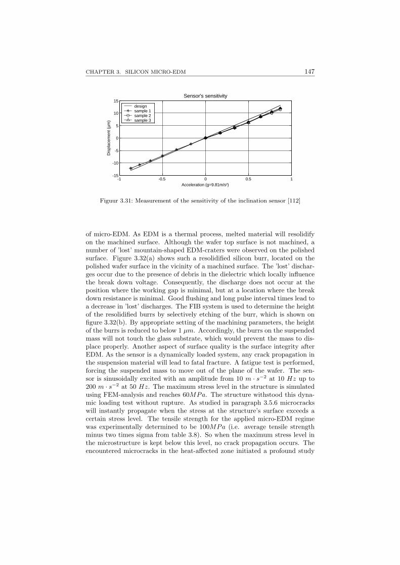
CHAPTER 3. SILICON MICRO-EDM 147
-1 -0.5 0 0.5 1-15
-10
-5
0
5
10
15Sensor's sensitivity
Acceleration (g=9.81m/s²)
Disp
lacem
ent (µ
m)designsample 1sample 2sample 3
Figuur 3.31: Measurement of the sensitivity of the inclination sensor [112]
of micro-EDM. As EDM is a thermal process, melted material will resolidifyon the machined surface. Although the wafer top surface is not machined, anumber of ’lost’ mountain-shaped EDM-craters were observed on the polishedsurface. Figure 3.32(a) shows such a resolidified silicon burr, located on thepolished wafer surface in the vicinity of a machined surface. The ’lost’ dischar-ges occur due to the presence of debris in the dielectric which locally influencethe break down voltage. Consequently, the discharge does not occur at theposition where the working gap is minimal, but at a location where the breakdown resistance is minimal. Good flushing and long pulse interval times lead toa decrease in ’lost’ discharges. The FIB system is used to determine the heightof the resolidified burrs by selectively etching of the burr, which is shown onfigure 3.32(b). By appropriate setting of the machining parameters, the heightof the burrs is reduced to below 1 µm. Accordingly, the burrs on the suspendedmass will not touch the glass substrate, which would prevent the mass to dis-place properly. Another aspect of surface quality is the surface integrity afterEDM. As the sensor is a dynamically loaded system, any crack propagation inthe suspension material will lead to fatal fracture. A fatigue test is performed,forcing the suspended mass to move out of the plane of the wafer. The sen-sor is sinusoidally excited with an amplitude from 10 m · s−2 at 10 Hz up to200 m · s−2 at 50 Hz. The maximum stress level in the structure is simulatedusing FEM-analysis and reaches 60MPa. The structure withstood this dyna-mic loading test without rupture. As studied in paragraph 3.5.6 microcrackswill instantly propagate when the stress at the structure’s surface exceeds acertain stress level. The tensile strength for the applied micro-EDM regimewas experimentally determined to be 100MPa (i.e. average tensile strengthminus two times sigma from table 3.8). So when the maximum stress level inthe microstructure is kept below this level, no crack propagation occurs. Theencountered microcracks in the heat-affected zone initiated a profound study

148 3.8. UNI-AXIAL INCLINATION SENSOR
(a) Burr (b) Burr examination
(c) Post-etched surface (d) Rectangular trenchesin post-etched surface
Figuur 3.32: Surface quality of silicon micro-EDM [112]
on the surface quality of silicon micro-EDM. In the beginning, the machinedsurface of the inclination sensor was examined. Figure 3.32(c) and 3.32(d)show a detail of the sensor’s suspension which was etched for 10 minutes withpoly-etch. The surface shows a regular pattern of rectangular-shaped trenches.A more detailed research on the crack geometry, crack pattern and on methodsto remove the damaged layer are discussed in section 3.5. Figure 3.33 shows aprototype of a fabricated inclination sensor, mounted on a ceramic substrate.Unfortunately, no final measurements are performed on the uni-axial inclinati-on sensor.

CHAPTER 3. SILICON MICRO-EDM 149
Figuur 3.33: Inclination sensor
3.8.6 Conclusions
The fabrication of the uni-axial inclination sensor proved that the combinationof the micro-EDM technology and the photolithographic technologies is feasi-ble. This study did not focus on the inclination sensor itself, but rather onthe particular aspects of integrating both technologies. Profound studies oninter-process alignment, on contamination-free wafer transport and on surfacequality of silicon micro-EDM, originate from the specific problems encounteredduring the design and fabrication of the inclination sensor. By offering valu-able solutions for these encountered problems, a hybrid technology has beenestablished.


Chapter 4
A computer-aided designand manufacturingenvironment formicromechanical structuresbased on micro-EDM
4.1 Introduction
The development of micromechanical systems by microfabrication techniqueswhich are not originating from the micro-electronics technologies such as micro-EDM, is hampered by the need for design aids. The majority of existing designenvironments for microsystems is solely based on the established photolitho-graphic machining technologies. The design is based on the creation of maskpatterns which are applied during exposure of the photosensitive layers (resistlayers). For micro-EDM, however, two-dimensional mask features do not coverthe entire machining space due to the three-dimensional machining freedom ofmicro-EDM. In this thesis, a first step is taken towards a three-dimensionalexpert system for design, verification and production of micromechanical sys-tems with micro-EDM as core fabrication technique. The built-up machiningexperience and machining technology, which are discussed in previous chapters,are bundled and translated into software code.
151

152 4.2. MICROSYSTEM DESIGN
4.2 Microsystem design
Microsystem technology originates from two different worlds. Systems havebeen miniaturized using traditional production techniques such as milling. Forthese micromachining techniques software tools are used as they are being usedin ’macro’ mechanical design. When photolithographic technologies are appliedto produce microsystems, micro-electronics-like software tools are utilized. Re-cently, dedicated software tools for microsystems are developed making use ofthe best of both worlds. In this section, a short introduction is given on thedesign process in traditional mechanical engineering, in micro-electronics en-gineering and in the recently developed micro-electromechanical engineering.Abstraction is made of initial market prospects, product performance specifi-cations, packaging and final product distribution.
4.2.1 Design of integrated micro-electronic circuits
The development process of integrated circuits (IC’s) is well developed and ad-vanced computer-aided tools are available. This development process consistsof a design phase in which the circuit is conceived and a layout phase in whichthe actual circuit is realized. The layout of integrated circuits can be performedat three different levels.
In a first level, which is situated closely to the processing technology, thecircuit layout is directly created. The geometrical shapes of the produc-tion masks for all separate components (transistors, resistors and capaci-tors) from the devised circuit, are designed as well as the mask hierarchy.At this level, the designer should be a technological expert and needs aprofound knowledge of the required layout rules. This direct-layout pro-cess is slow and is inconvenient when large circuits are concerned. Onthe other hand, direct layout-creation offers often the best circuit per-formances when speed or compactness are concerned. In order to assiststhe designer, design rule check (DRC) software is developed which checksthe geometrical shapes (e.g. width, length, spacing, overlap) on the masklayouts. Even extracting tools exist which extract an electric model (e.g.transistors, connections, capacitances, resistances) from the circuit lay-out. These models can be used to simulate the behaviour of the designedcircuit.
In a second level, the layout is realized by connecting building blocks ina two-dimensional sketching space. The building blocks can be separatetransistors, boolean-logic elements or even blocks with more intelligencesuch as multiplexers and mathematical operators. The designer shouldnot be a technological expert, but should still have a good knowledge ofanalog and/or logic design. Electrical rule check (ERC) tools exist whichcheck for instance the unconnected inputs, shorted outputs and groundconnections.
CHAPTER 4. MICRO-EDM-BASED CAD&CAM ENVIRONMENT 153
At a third level, a top-down strategy is applied and is particularly dedi-cated for the design of digital circuits. The input-output relation as wellas the behaviour of the system is formulated in a hardware descriptionlanguage (HDL), after which the programming code can be automati-cally synthesized into a layout of electronic components. Most of theHDL-tools (e.g. VHDL, Verilog) offer a graphical block diagram ofthe compiled circuit. With a HDL, large and complex circuits can easilybe designed without having experience with the required production tech-nologies. This top-down design strategy is by far the most easy to use.The high level of user-friendliness of these hardware description languagesis the major reason of the broad application field of IC-technology.
After design (using electronic building blocks or a HDL), the circuit is realizedby automatic placing and routing of the separate electronic components ona circuit layout. The operation performances of IC’s with sub-micron scaletransistors are to a large extent determined by place and route. Therefore,final circuit simulations are executed to verify the performances of the circuit.Complete technology computer-aided design (TCAD) environments to designand simulate integrated circuits are commercially available and made the fastbreakthrough of micro-electronics possible (e.g. Cadence, Mentor).
4.2.2 Design of mechanical components
In traditional mechanical manufacturing, the number of machining techniquesis much larger than in micro-electronics manufacturing. Each production tech-nique is characterized by its proper machining capabilities which may differfor instance in obtainable surface quality, in machining speed or in handlea-ble workpiece materials and geometries. For the majority of mechanical com-ponents, the initial material stock is subjected to a sequence of machiningtechnologies in order to produce the desired mechanical part. This machiningsequence is considerably different for different mechanical parts, so that nouniversal production sequence can be found as for micro-electronics producti-on exists.Mechanical designers used to design freely without many design constraints.Subsequently, the designs were evaluated by specialized process planners andmanufacturing experts who advised the designers to improve the manufactura-bility of the design or to reduce its production cost. Consequently, the designwas returned to the designer’s office to be tuned. This iterative process wascontinued until a sufficient degree of satisfaction was reached between all par-ticipating parties or until the design iteration was ended by an unovercomingdeadline. Last decades, the design cycle time has been reduced considerablydue to economic reasons which forced the sequential design process to becomea concurrent design process. In a concurrent design process, the mechanicaldesigner as well as the process planner and the manufacturing experts are invol-ved in the design process from the very start. Consequently, time-consumingdesign iterations are avoided in order to cut design time and production cost.

154 4.2. MICROSYSTEM DESIGN
For both designers and manufacturing specialists dedicated software tools arecommercially available. The designers make use of computer-aided design(CAD) and computer-aided engineering (CAE) tools. The designers createthe desired geometry of the individual parts in a three-dimensional space usingsolid models and connect these parts to create a virtual assembly. Separateparts or entire assemblies are analyzed using simulation software. Most fami-liar simulation tools are collision detection tools for assemblies with movable’limbs’ (e.g. robot configurations), tools to simulate kinematic and dynamicbehaviour of mechanisms, tools to analyze both static and dynamic mechani-cal stress and deformation due to a mechanical or thermal stimuli and tools toquantify the natural frequencies and deformation modes of mechanical parts.When the design is transferred to the manufacturing experts, the individualparts are analyzed on their producibility and appropriate machining sequencesare generated using computer-aided process planning (CAPP) and computer-aided manufacturing (CAM) tools. The most familiar CAM tools are interacti-ve tool path generators for milling, turning and wire-EDM operations. Specificprocess simulation tools are developed to predict the process behaviour (e.g.material flow in moulds during injection) or to verify the machining result (e.g.calculation of the rest material after a milling process). For further reading onCAD/CAM, the reader is referred to dedicated literature [113, 114, 115].In mechanical design and manufacturing, the first commercial computer toolswere introduced in the late 1950’s. Nowadays, more than 45 years of researchand development later, many CAD, CAM, CAE and CAPP software tools exist.Some design tools are developed for particular use, for example finite elementanalysis (FEA) tools (e.g. Ansys, Nastran, Ideas). Other design tools aredeveloped for general use (e.g. Unigraphics, Pro/ENGINEER, Catia) andincorporate tools for design, analysis, manufacturing, product lifecycle mana-gement (PLM), enterprise product data management (EPDM) and enterpriseresource planning (ERP).
4.2.3 Design of micromechanical systems
The design process of microsystems is a child of both the micro-electronics andthe traditional mechanics design process [116]. Pioneers in microsystem designhave micro-electronics roots and seized to familiar micro-electronics productionprocesses and to corresponding software tools. All available design environ-ments for microsystems are process driven and based on the photolithographicprocessing technologies inherited from micro-electronics, enlarged with somespecific technologies such as anisotropic wet etching.For microsystem design, no standardized high-level hardware description langu-ages exist yet. The number of basic system components in microsystems is lar-ge, covering different physical domains and are, in addition, three-dimensionalwhich complicates the development of general modelling languages with a highlevel of abstraction. For single microstructures, efforts are being made to de-velop hardware description languages and synthesis tools, with the aim to ease

CHAPTER 4. MICRO-EDM-BASED CAD&CAM ENVIRONMENT 155
and to speed up the design cycle [117, 118, 119].Generally, the design of a microsystem is a bottom-up design sequence andstarts with the design of the two-dimensional mask layouts which are appliedin the photolithographic processes. As the design is process driven, the designeris restricted to the processing techniques available in the design environment.Figure 4.1(a) and table 4.1(b) show respectively the processing masks and theprocess sequence for the fabrication of a microbeam structure. First, a siliconground plane is overlaid with a nitride layer which serves as insulation layer.A sacrificial layer of BPSG (boron phospho-silicate glass) is deposited on thenitride layer. It is etched (mask SP2) to define the areas where the beam willbe anchored to the nitride layer. The BPSG thickness sets the separation bet-ween the nitride layer and the thin aluminum beam to be built on top. Afterthe entire wafer is deposited with aluminum, a selective etch (mask SP1) de-fines the actual beam dimensions. After process design, a three-dimensionalsolid model is generated based on the designed masks and on the implementedprocess simulation tools. Figure 4.1(c) depicts a solid model of the microbeam,from which the sacrificial BPSG still has to be removed in order to create afree-standing beam. Subsequently, the model is simulated using for examplefinite element analysis (FEA). Examples of simulation types are stationary ortransient structure analysis, electrostatic analysis, thermal analysis and all pos-sible combinations thereof (coupled analysis). Recently, efforts are put in thedevelopment of simulation tools to quantify testability and reliability of micro-systems [120, 121, 122]. For further reading on microsystem design, the readeris referred to dedicated literature [123, 124, 125] and overview papers [126].Computer-aided tools dedicated for the design of microsystems are commerci-ally available offering design tools for layout, solid modelling and simulation(e.g. CoventorWare, MEMSCAP, IntelliSense).

156 4.2. MICROSYSTEM DESIGN
(a) Mask layout
(b) Process sequence
(c) Solid model
Figuur 4.1: Design of micromechanical structure, example from the manualof CoventorWare Version 2001

CHAPTER 4. MICRO-EDM-BASED CAD&CAM ENVIRONMENT 157
4.3 Feature-based computer-aided design andmanufacturing environmentfor microsystems
4.3.1 Introduction
The ultimate aim of a design and manufacturing environment is that for eachdesigned system, the production sequence, the machining code and the corres-ponding machining settings are automatically generated. This means that theentire know-how of all machining technologies and all know-how concerningprocess planning should be embedded. It is clear that such an ideal designenvironment is for the far future or that it is maybe not feasible to realize atall.As previously explained, all present design environments for microsystems arebased on the photolithographic techniques and are process driven. The designeris not free to design and is restricted to create microsystems in a process-relatedway. The benefit of such a system is that all designed structures are produci-ble taking the machining tolerances into account. On the other hand, designenvironments for general purposes (e.g. Unigraphics, Pro/ENGINEER,Catia) are not process driven but design driven. All kinds of geometries canbe designed even if the designs are not manufacturable. Afterwards, a ma-nufacturing module is applied to process the design interactively in order tocreate an appropriate fabrication sequence.Nowadays all design environments, design driven and process driven, arefeature-based. A feature is a physical entity (e.g. pocket, shaft) containinggeometrical information and data which has engineering significance. Featu-res are parametric which means that numerical parameters are used to drivethe design geometry. As for design environments, a distinction can be madebetween design-driven and process-driven features. When the features havesolely a design purpose they are called design features. Features that con-tain manufacturing information (e.g. manufacturing quality, manufacturingstrategy) are called manufacturing features. Design features offer more de-sign freedom than manufacturing features because they are not restricted tothe limitations of manufacturing processes. Manufacturing features are usuallymaterial-removing entities because of the material-removing characteristics ofthe machining processes (except for manufacturing processes such as stereo-lithography and material deposition techniques). The main disadvantage ofmanufacturing features is that the designer must create his systems only usingmaterial-removing entities which is, in some cases, an unnatural way of design.For instance, a rib is not created by addition of a rib element but by removal ofworkpiece material on both sides of the rib. Efforts have been taken to trans-fer the design features into manufacturing features using feature mapping andfeature recognition [127, 128, 129, 130, 131, 132, 133]. However, when overlap-ping (or intersecting, or interacting) features are present in the design, none

158 4.3. FEATURE-BASED CAD&CAM ENVIRONMENT
of these transferring techniques offer satisfactory results so far. For this rea-son, we opted for a design environment based on manufacturing features. Themanufacturing features must be three-dimensional and the producibility of thefeatures must be guaranteed. The manufacturing features can be automaticallytranslated into processing code, making an entirely automated manufacturingof the designed structure possible.
4.3.2 A design and manufacturing environment for micro-systems based on manufacturing features
Figure 4.2 gives a general overview of a multi-processes design and manufac-turing environment based on manufacturing features. The general structure
Process I Process II Process III
Featurelibrary
Featurelibrary
Featurelibrary
Microsystemdesign
Producibility check
Microsystemsimulation
CAPP
Process I Process II Process III
Machiningcode
Machiningcode
Machiningcode
Machiningcode generation
Machiningcode generation
Machiningcode generation
Figuur 4.2: General structure of a feature-based hybrid design environment
of the environment allows the implementation of several processing techniqueswhich can be used to develop the desired microsystems. Corresponding to theaccessible processing techniques for the fabrication of microsystems, plug-and-play expert modules of these processing techniques should be loaded withinthe design environment. By adding and removing of technology modules, acustomized design environment can be created. The major parts of this hybriddesign environment are briefly explained below.

CHAPTER 4. MICRO-EDM-BASED CAD&CAM ENVIRONMENT 159
Microsystem design environment
The microsystem design environment is an interactive engineering platform tocreate microsystems. The designer makes use of process-related manufacturingfeatures to construct the desired microsystems. During design, the microsystemor subsystems can be simulated in order to verify their performances. Theproducibility of the microstructure, for instance the compatibility conditionsof the successive process techniques, is verified before the final process sequenceand the specific manufacturing data are generated.
Process-related feature library
For each manufacturing process a feature library is developed. The process-related manufacturing features contain, except for the geometry, all necessarymanufacturing strategies and process data.
Microsystem simulation
In a simulation module the behaviour of the designed microsystem is comparedwith the predefined system specifications. After selecting the proper physicalmodels and defining the operation conditions, the operational behaviour isstudied by numerical simulations of which the Finite Element Method (FEM)is mostly applied.
Producibility check
All manufacturing features offered by the feature libraries are individually pro-ducible. However, when intersecting features are present or when successivelyseveral production processes are applied, the producibility of the entire micro-system is not guaranteed. The producibility check, which guarantees the pro-ducibility of the entire microsystem, is the most complex module in the designenvironment when full automation is required. This module contains speci-fic process-related design rules as well as compatibility verification data (e.g.material compatibility, process compatibility).
Computer-aided process planning (CAPP)
A process plan for the designed microsystem is generated based on the availa-bility of processing units and on the constraints set by the producibility check.
Machining code generation
For each machining step the individual processing data are generated.

160 4.3. FEATURE-BASED CAD&CAM ENVIRONMENT
4.3.3 A design environment based on the micro-EDMtechnology
The implementation of the EDM technique into design environments is notnew. Most of the commercial design environments offer a manufacturing mo-dule for wire EDM in which the wire tool path is generated for roughing aswell as for finishing. The implementation of a computer-aided process planningand manufacturing frame for contouring EDM was studied by Lauwers [134].For micro-EDM, however, little research is done on technology implementation.Rajurkar applied a conventional computer-aided tool for milling to generate thetool path of a miniaturized cylindrical or spherical tool electrode [135].In this thesis, the micro-EDM technology is implemented in such a way that thethree-dimensional machining freedom of micro-EDM is emphasized. In additi-on the micro-EDM design and manufacturing modules fit into the frameworkof the proposed hybrid design environment (figure 4.3). The feature libraryconsists of a set of manufacturing features which is predefined (standard fea-tures) and a set of manufacturing features which can be created on the spot(user-defined features). The user-defined features are created in the design spa-
Micro-EDM process
Featurelibrary
Standardfeature lib.
User-definedfeature lib.
Microsystemdesign
Producibility check
Microsystemsimulation
CAPP
EDM processmodel
Process parameteroptimization and
wear compensation
AGIE Compactmachining code
User-defined feature design
Producibility check
Tool path generation
Micro-EDM machining code generation
Figuur 4.3: Micro-EDM based design environment

CHAPTER 4. MICRO-EDM-BASED CAD&CAM ENVIRONMENT 161
ce itself and are automatically verified on their producibility. In addition, aproducibility check for the entire designed microstructure is implemented. Thisproducibility check is able to handle interfering features. In the simulation toolthe behaviour of the microstructure is verified using commercially availablesimulation software. An additional tolerance module is created in which theeffect of dimensional uncertainties on the microsystem’s behaviour is simulated.When the microsystem is designed and verified, all process data are generatedin order to produce the designed microsystem. After the generation of the toolpath, the process parameters are optimized and the tool wear is compensated.Subsequently, the machining code can be read by the micro-EDM machinewhich is then ready to start the fabrication of the designed microstructure.
Implementation
For the implementation of a first version of this design environment for mi-cromechanical structures based on micro-EDM, Unigraphics of EDS is usedas base CAD-environment. Unigraphics is chosen as implementation frame,because of its large function library (Application Programming Interface) thatallows access to the Unigraphics graphics terminal, file manager and databa-se. All additional software functions and libraries are written in ANSI C code.For matrix calculations and optimization MATLAB of The MathWorks isutilized.In this text, no detailed explanation is given concerning the software architec-ture of the implemented design tool. Nevertheless, the mathematical ground onwhich the implementation is based is thoroughly explained so that the proposedideas can be translated into any available software language.
4.4 Manufacturing features for micro-EDM
4.4.1 Standard manufacturing features
A feature library is developed containing a limited number of standard ma-nufacturing features. All standard features are fully parametric which impliesthat design changes can easily be performed. A design of a microstructurestarts with the selection of a base feature, or substrate feature, which is amaterial-addition feature. This base feature is the workpiece stock which willbe clamped on the worktable of the EDM machine. A rectangular and a cy-lindrical base feature are available in the standard library. Except for the basefeatures, the standard library contains a set of material-removal features. Figu-re 4.4 presents the top views of the available geometries. These features have acertain depth or penetrate through the base material. For the ’through’ featu-res, the inner material is cut away as in wire EDM where only the contour of thefeature is followed, while for the other features the inner material is removedas in milling EDM where the tool scans the bottom surface of the feature. The

162 4.4. MANUFACTURING FEATURES FOR MICRO-EDM
LengthW
idth
Corner radius
Length 1
Length
2
Angle
Corner radius
Length
Wid
th
Angle 1 Angle 2
Corner radius
Figuur 4.4: Standard feature shapes
dimensions of each feature can be set as well as the required machining accura-cy and surface finish. All features have rounded corners which is related to thesize of the working gap and the radius of the cylindrical tool electrode. Whenthe corner radius is set smaller than the radius of the standard tool electrode,the tool size is reduced by WEDG (see section 2.5.5 for detailed information onWEDG). The minimal applicable tool diameter depends on the depth of thefeature; shallow features may have a smaller corner radius than features whichpenetrate deeply into the base material. Figure 4.5(a) shows, as example, themechanical part of an inertial sensor which consists of a mass suspended by athin beam. The necessary pocket features to create this structure are drawnabove. Each feature is placed on the top face of the base feature and is positi-oned with respect to the base feature or to previously inserted features (figure4.5(b)). After positioning of the feature, the corresponding delta volume is
(a) Inertial sensor (b) Positioning of new pocket
Figuur 4.5: Application of standard features
created. The delta volume refers to the material-removal volume of a feature.It is clear that with this limited standard library it is not possible to span alldesign geometries. The library should be enlarged with for example cylindricaland free-form features in order to increase the coverage. Instead of enlarging

CHAPTER 4. MICRO-EDM-BASED CAD&CAM ENVIRONMENT 163
the library, effort is put in the development of a design module for user-definedmanufacturing features.
4.4.2 User-defined manufacturing features
It is known that feature modelling will never cover 100 % of all design geome-tries. One way to deal with particular shapes, geometrical details and free-formsurfaces is the generation of these particular features at the moment the needarises. The ability to create user-defined features increases the design flexibi-lity considerably. The particular requirement of a user-defined manufacturingfeature is that it must be producible. In micro-EDM, all features must beproducible by a standard tool electrode or by a tool electrode which is shapedby WEDG. Therefore, all user-defined features are based on the geometry of ashaped tool electrode which is producible by WEDG.Figure 4.6 shows an inertial sensor in which the inertial mass is suspended bytwo thin parallel beams. In order to remove the workpiece material between
Figuur 4.6: User-defined manufacturing features
the thin beams, a shaped tool electrode is required. The feature shape whichconsists of the electrode shape plus the working gap can be designed as a newuser-defined feature. By defining appropriate tool paths for this newly desig-ned feature, desired material removal can be achieved. Figure 4.6 also shows amagnification of the connection of the beams to the mass, showing the detailedrepresentation of the remaining structure after machining.

164 4.5. USER-DEFINED MICRO-EDM FEATURES
4.5 User-defined manufacturing features formicro-EDM
This section deals with the design and verification of user-defined machiningfeatures (figure 4.7). After the design of a user-defined feature, the producibility
Figuur 4.7: User-defined feature expert-system
of the proposed user-defined feature is examined. The geometry as well as thestrength of the corresponding tool electrode are verified. When the featurepasses the producibility check, the feature is added to the user-defined featurelibrary.
4.5.1 Feature design
The creation of a user-defined feature starts with a proposal of an axisymmetricshape. The designer makes use of lines and arcs to design the contour of a desi-red feature. Figure 4.8 depicts a design of a ball-shaped user-defined feature.The design module adds automatically a shaft on top of the designed feature.The diameter of the shaft equals the diameter of a standard cylindrical toolelectrode plus the size of the working gap on both sides of the electrode. Thelength of the shaft corresponds to the distance between the ceramic electrodeguide and the workpiece. The total length of the feature approximates thecantilevering distance of the tool electrode.
4.5.2 Geometry check
The proposed feature shape will be machined by an axisymmetric tool elec-trode which is shaped by WEDG. The production by WEDG imposes somegeometrical limitations on the tool shape. Figure 4.9 shows for example a desi-red tool shape as well as the realizable tool shape. The geometric limitationsdepend on the size of the working gap and the diameter of the WEDG wire.The WEDG tool path is calculated as the position of the centre of a ball whichrolls over the desired geometry. The radius of the ball equals the sum of theradius of the WEDG wire and the size of the working gap. When further inthe text ’offset’ is applied the algorithm of the rolling ball is applied, havingeach time its particular ’ball’ radius.

CHAPTER 4. MICRO-EDM-BASED CAD&CAM ENVIRONMENT 165
Figuur 4.8: Creation of a user-defined manufacturing feature
Wire
WEDGtool path
De
sire
d to
ol
Re
aliz
ed
to
ol
Working gap
Figuur 4.9: Geometrical limitations

166 4.5. USER-DEFINED MICRO-EDM FEATURES
The aim of the geometry check is to generate a tool electrode with which theproposed user-defined feature is approximated as accurate as possible. To doso, additional axisymmetric features are sequentially generated making use ofthe ’offset’ algorithm (figure 4.10). The first generated feature is a first esti-
12 23
3' 34 4 5 5
6
a. b. c. d. e.
a. First estimation of the tool shapeb. Generation of WEDG pathc. Generation of producible tool shaped. Generation of feature shapee. Generation of ’waterfall’ shape
Figuur 4.10: Geometrical check of a user-defined feature
mation of the tool shape (contour 2). This feature is generated by offsettingthe proposed user-defined feature (contour 1) by the size of the working gapbetween tool and workpiece electrode. Machining with this tool electrode willapproximate the proposed user-defined feature as accurate as possible. In asecond step, the tool path of the WEDG wire is generated both for roughing(curve 3’) and for finishing (curve 3). Both curves are based on the first ap-proximation of the tool electrode (contour 2), the radius of the WEDG wireand the respective sizes of the working gap. It is clear that the size of theworking gap is larger for roughing than for finishing. The WEDG path is atwo dimensional curve, starting from the bottom of the electrode and ending atthe shaft of the tool. Due to rotation of the tool electrode during shaping, anaxisymmetric tool is created. When the WEDG path is defined, a produciblegeometry of the tool electrode (contour 4) can be generated based on the toolpath of the wire, the wire radius and the size of the working gap. It should benoted that the geometry of the preliminary approximation of the tool electrode

CHAPTER 4. MICRO-EDM-BASED CAD&CAM ENVIRONMENT 167
(contour 2) and the producible tool electrode (contour 4) are not identical dueto the physical limitations of the WEDG technology. Finally, the contour of theuser-defined feature is calculated by offsetting the contour of the tool electrodeby the distance of the erosion gap (contour 5). The shape of this user-definedfeature can be machined with a tool electrode which is shaped by WEDG. Thisfinal user-defined feature has never sharp edges and is usually more roundedthan the proposed feature.In the geometry check, an additional feature is generated for drawing purpo-ses. When the tool sinks into the workpiece, the obtained workpiece shapecan be represented as a ’waterfall’ shape, considering that the water falls fromthe bottom of the electrode towards the shaft (contour 6). In this case, the’waterfall’ shape is a cylinder with a spherical tip.
Important note
All calculations, stated above, assume that the size of the working gap is known.However, the actual size of the working gap depends on the machining settingswhich are in the design state not yet defined. Therefore an average size of theworking gap (7 µm) is applied for the calculations. When the final machiningparameters and the according working gap size are known (i.e. after computer-aided manufacturing), the geometry of the user-defined features should be re-calculated. Due to the small variations in gap size, the geometry of the toolelectrode will only change slightly (i.e. only a few micrometer).
4.5.3 Strength check
In the geometry check, the shape of the tool electrode is determined (figure4.10, contour 4). Additionally, the strength of this tool electrode must beverified so that it can withstand the acting forces during sparking. In orderto calculate the required strength of the tool electrode, the acting forces onthe electrode should be known. The forces acting on the stiff tungsten toolelectrode are assumed to be similar to the forces occurring during conventionalwire EDM. Therefore, the forces on the thin tool electrode are not measuredbut gathered from literature concerning wire EDM [136, 137, 138]. The mainphenomena causing forces in the wire-EDM process are forces due to flushing,electrostatic forces, electromagnetic forces and forces due to the discharges.
In wire EDM, the flushing force is caused by forced flushing of the die-lectric fluid through the erosion gap. In micro-EDM, the flushing of thegap is realised by rotation of the tool electrode. This movement does notgenerate significant pressure difference in the fluid so that the flushingforces are negligible.
Fluctuating electrostatic forces, between the two electrodes, exist due tothe changing electrostatic field in the erosion gap. In a first phase the

168 4.5. USER-DEFINED MICRO-EDM FEATURES
generator applies a voltage between the two electrodes resulting in an elec-trostatic attraction force. In the next phase, when the dielectric breaksdown, the voltage difference between the electrodes decreases, resulting ina fall of the attraction force. Panshow calculated the electrostatic forcesin wire EDM by means of a two-dimensional model [137]. Based on thesecalculations, the maximum electrostatic force in micro-EDM is estima-ted to be 6 N/m. This value is significantly higher than in conventionalwire EDM (0.5 N/m) due to the small erosion gap. It should be notedthat the electrostatic force is highly dynamic with components into themega-Herz range.
The electromagnetic force is generated by the flow of current, which isalways accompanied by an electromagnetic field. Consequently, forces areinduced between two current conductors or between a conductor and aferro-magnetic material. Dekeyser calculated that, the electromagneticload on the electrode was calculated to be approximately 0.3 to 0.4 N/m[138].
The forces due to discharges are caused by breakdown of the dielectric,creating a plasma channel between the two electrodes. Vapour bubblesarise which grow simultaneously with the plasma channel. When the di-scharge current is cut, a violent collapse of the plasma channel occurs.This causes superheated molten electrode material to explode in the die-lectric fluid. All these discharge forces load the tool electrode with afluctuating force approximating 1.5 N/m [138] .
In micro-EDM, three additional forces should be considered. The firstforce is a mechanical force which occurs when the tool welds to the work-piece due to a small and badly-flushed working gap. The ejected materialwelds the two electrodes before it resolidifies and is carried away by thedielectric. These forces should be avoided because they may lead to toolor workpiece rupture. Appropriate machining settings, concerning con-trol of the working gap size, must avoid this welding problem. Anotheradditional force is the mechanical impact force of the electrodes duringshort circuits. This force is also hard to quantify and depends on theparameter settings and on the performance of the servo system of theEDM machine. Machining parameters should be set so that short cir-cuits are minimized, avoiding these destructive impact forces. The lastadditional force is a force caused by an eccentric rotation of the tool elec-trode. This force depends on the eccentricity and on the angular speedof the tool electrode. The angular speed of the tool electrode approxi-mates 2000 rev/min on the applied set-up, leading to eccentricity forcesof 0.6 N/m for a tungsten cylindrical tool electrode with a diameter of150 µm, taking an eccentricity of 5 µm into account.
The sum of all these loads represents the machining forces on the tool electro-de. Weld forces and impact during short circuits are not taken into account,

CHAPTER 4. MICRO-EDM-BASED CAD&CAM ENVIRONMENT 169
because they should be avoided by setting appropriate servo parameters for gapsize control (see paragraph 2.4.3 on the requirements of appropriate workinggap settings).In the strength check, the tool electrode is subjected to the machining forcein order to simulate the internal mechanical stress. The strength of the toolelectrode does not only depend on the machining forces and the mechanical ma-terial properties of the tool material but also on the quality of the tool surfaceand on the temperature distribution in the tool. In this thesis, a first strengthcheck for tool electrodes is implemented having the following characteristics:
Although the acting load on the electrode is highly dynamic and hardto quantify, a static distributed load is applied on the tool electrode.The amplitudes of the previously enumerated machining forces are addtogether and result in a distributed load of 8 N/m. Additionally theinertial forces due to eccentric rotation (depending on the geometry ofthe tool) are added for a rotation speed of 2000 rpm.
The effect of the surface quality and the temperature distribution are nottaken into account.
The tool electrode is considered as a cantilever, clamped at the pointwhere the tool electrode leaves the ceramic guide. Successively, the shearforce and the bending moment on the tool are calculated.
The stress calculation is based on the formula of Navier (σ = M ·RI , with
σ the maximal tensile stress, M the bending moment, R the tool radiusand I the geometrical moment of inertia) which formulates the tensilestress in smoothly varying beam-like structures.
Figure 4.11 shows the dialogue box, presenting the strength calculations. Inthe result window the calculated quantity is plotted as abscissa value. In thepresented example the maximum stress reaches 37 MPa. It should be noticedthat the electrode is machined by WEDG, leaving a heat-affected top layeron the electrode. This heat-affected material might cover small microcracks,which lead to fracture due to the highly dynamic mechanical and thermal loadduring machining. The built-up experience in tool shaping leads to a rule ofthumb which says that the stress should not exceed 60 MPa when this kindof verification algorithm is applied. When the simulated stress exceeds thethreshold value, the tool electrode does not pass the strength check and thedesign of the user-defined feature should be adapted. Considering passing, theuser-defined feature is added to the feature library and can be applied in themicrosystem design environment.
Comment
The implemented strength check is a first prototype. In order to improve thestrength check, experimental data should be collected concerning the actual

170 4.5. USER-DEFINED MICRO-EDM FEATURES
Figuur 4.11: Strength check
machining forces and the actual strength of tool electrodes so that a corrobo-rated implementation can be realized.
4.5.4 Applying user-defined features
When a user-defined feature is applied, the designer inputs the required toolpath, machining accuracy and surface finish. In the implemented design envi-ronment, the user-defined feature sinks into the workpiece to a desired depth,after which it follows an in-plane tool path consisting of straight lines. Atthe end of the tool path, the tool electrode retracts. Figure 4.12(a) shows anexample of such a tool path as well as the generated solid model. Firstly, thetool sinks into the workpiece which is represented by the ’waterfall’ featurewhich was created during the geometry check. Then the tool follows a straightline which is represented by an extrusion of the feature contour along this li-ne. At points where the tool path changes direction, the axisymmetric shapeof the feature is inserted. At the end of the tool path, the tool electrode re-tracts which is again represented by a ’waterfall’ feature. The union of all thesefeatures represents the delta volume as depicted on figure 4.12(b). When anuser-defined feature is applied, the material removal volume is generated, afterwhich this volume is subtracted from the base feature as shown on figure 4.13.As for standard manufacturing features, user-defined features are positionedon the top plane of the base feature and the tool path is fully parametric sothat designs can easily be altered.

CHAPTER 4. MICRO-EDM-BASED CAD&CAM ENVIRONMENT 171
(a) Composing a user-defined feature (b) A user-defined manufacturing feature
Figuur 4.12: Generation of a user-defined manufacturing feature
Figuur 4.13: Application of a user-defined feature
4.6 Microsystem simulation
In the simulation module, the performances of the designed microstructuresare verified. Most of the simulation tools make use of the Finite Element Me-thod (FEM) to simulate the stationary and transient behaviour of the micro-system. In this thesis, the mechanical behaviour of the microsystems is simu-lated using MSC.Patran from MSC.Software for pre and post processingand MSC.Nastran as solver software. The solid models of the microsystemswhich are designed in the Unigraphics environment can easily be importedinto the MSC software.

172 4.6. MICROSYSTEM SIMULATION
4.6.1 Tolerance simulation
This work focuses on the simulation of the effect of machining tolerances on theperformances of the microstructures. During fabrication, positioning inaccur-acies and variations in process conditions lead to dimensional variations of themachined microstructures. Typical uncertainties are for instance unpredictableworking gap dimensions, eccentric rotation of the tool electrode, positioning in-accuracies and thermal deformation of both the machining equipment and theelectrodes. Although the tool wear is compensated, small geometrical and di-mensional inaccuracies occur due to wrong estimations of the tool wear whichcan be seen as dimensional and geometrical uncertainties. These undesired va-riations may even result in improper behaviour of the microsystem. In order tosimulate the effect of dimensional variations, a Monte Carlo simulation tool isimplemented. A probability distribution function is added to all dimensions of
with L = 1000 µmW = 1000 µmL = 400 µmσL,W,H = 5 µm
(a) Rectangular pocket
Cumulative Distribution Function
0
0.2
0.4
0.6
0.8
1
64.588 64.593 64.598 64.603 64.608 64.613 64.618
Volume (mm³)
Theoritical function
theoretical: simulated:
mean volume = 64.6025 mm3 mean volume = 64.6029 mm3
σ = 0.00575 mm3 σ = 0.00572 mm3
(b) Cumulative distribution function of the pocket’s volume
Figuur 4.14: Simulation of the volumetric variation of a rectangular pocket

CHAPTER 4. MICRO-EDM-BASED CAD&CAM ENVIRONMENT 173
the microstructure. The probability function may have a normal or rectangulardistribution which can be set for all individual dimensions. When accurate si-mulation results are required, the machining performance of the applied EDMequipment must be well-known so that proper distribution shapes and para-meters can be set.The calculation algorithm of the tolerance simulation module is tested using asimple structure (figure 4.14(a)). The volume variation of a rectangular poc-ket is simulated assuming that each dimension is normally distributed having astandard deviation of 5 µm, which is a bit more than the accuracy of the AGIECompact 1 (according to table 2.2, Pa (3σ) = 10 µm). Because of the simplegeometry of the pocket, the theoretical probability distribution function caneasily be calculated by hand. Figure 4.14(b) shows the cumulative distributi-on function of the simulated volume on top of the theoretical function. Eachdatum point represents a single simulation run of the Monte Carlo simulation.Both curves, simulated and theoretical, fit well.In a second simulation the variation in natural frequency of a microstructureis examined. The structure consists of a mass (2.5 mm× 2.5 mm× 0.65 mm)which is suspended by a thin beam (2.5 mm × 0.1 mm × 0.65 mm). Figu-re 4.15(a) shows the simulated mode shape at the first natural frequency ofthe structure. In order to have an idea of the variance on the first natural
(a) First bending mo-de
(b) Measurement set-up
Figuur 4.15: Dynamic behaviour of microstructure
frequency, a simulation is executed. The probability distribution function forall feature dimensions is supposed to be normally distributed with a standarddeviation of 5 µm. In order to verify the simulation results a set of 9 structuresis machined of which the first natural frequency is measured. A capacitive pro-be is positioned in such a way that the first bending mode is observed (figure

174 4.6. MICROSYSTEM SIMULATION
4.15(b)). The structure is excited with a hammer pulse on the clamp. Thecorresponding frequency response of the displacement of the mass is shown onfigure 4.16. The frequency response of the probe holder is determined as well in
Figuur 4.16: Frequency response function
order to distinguish the natural frequencies of the microstructure and the mea-suring set-up. It is clear that the first natural frequency of the microstructureis situated at 223 Hz and that a natural frequency of the set-up is situated near60 Hz. Figure 4.17 shows the cumulative distribution functions of both thesimulated and the measured frequencies. The data points are the individualsimulations or measurements, while the solid curves represent the respectivefitted cumulative distribution. The labels near the measured data points cor-respond with the machining sequence of the microstructures. The simulatedfrequency is situated far beneath the measured frequency and the distributionfunction of the simulation is more spread than the distribution function of themeasurements. The following reasons may have caused such a discrepancy.
The material characteristics of the simulated model do not correspondwith the actual properties of the silicon base material. An increase in thevalue of the Young’s modulus in the model for example will augment themean value of the simulated structure. In this case, however, the Young’smodulus is set to be 170 MPa which is certainly not too low, taking thevalues in literature into account which ranges from 130MPa to 185MPa

CHAPTER 4. MICRO-EDM-BASED CAD&CAM ENVIRONMENT 175
00.10.20.30.40.50.60.70.80.9
1
100 150 200 250 300Frequency (Hz)
Cum
ulat
ive
prob
abili
ty MeasuredSimulated
1
5876
2439mean = 203 Hz
stdev. = 15 Hzmean = 243 Hzstdev. = 2.9 Hz
Figuur 4.17: Simulation and experimental results
depending on the crystallographic orientation shown in table 3.1 in theprevious chapter. Due to the anisotropy of silicon, it is important tohave an idea of the crystal orientation with respect the geometry of thestructure in order to make accurate simulations.
The type of elements and the element density in the FEM model areimportant. A lack of degrees of freedom will increase the stiffness of thestructure and will consequently lead to an increase in natural frequency.However, the created models have a sufficient number of degrees of free-dom.Additionally, the use of tetrahedral elements makes the model more stiffthan the actual structure. The use of isometric elements reduce the un-desired effect of additional stiffness. Unfortunately, the present automa-ted element-mesh generators are only able to create volumetric mesheswith tetrahedral elements.
The discrepancy of the results may have been caused by an appropriateselection of the probability distribution function of the model dimensi-ons. Therefore, the beam thickness of the structure is measured with theQuick Vision in order to verify the distribution. Figure 4.18 shows thecumulative distribution of the beam thickness.
The beam thickness of the first machined structure is clearly less than the thick-ness of the other beams. This is caused by the fact that the AGIE Compact1 was not yet thermally stabilized at the moment the first structure was ma-chined. The other data points are close together and have a standard deviation

176 4.6. MICROSYSTEM SIMULATION
Measured beam thickness
00.10.20.30.40.50.60.70.80.9
1
0.09 0.095 0.1 0.105 0.11 0.115 0.12 0.125
Beam thickness (mm)
Cum
ulat
ive
prob
abili
ty
1
24
37
985
6
mean = 114 µmstdev. = 2.2 µm
Figuur 4.18: Beam width measurement
of only 2.2 µm which is less than the proposed 5 µm. This is the reason whythe standard deviation on the simulated natural frequencies is larger than thedeviation on the measured natural frequencies. Not only the deviation on thebeam thickness differs but the mean value differs as well. The measured meanvalue is 114 µm which is significantly larger than the desired 100 µm. Thereasons for this discrepancy may origin from inaccurate positioning, uncertain-ties on the tool dimension, eccentric rotation of the tool and/or uncertainty onthe dimension of the gap size. When an identical structure with a beam thick-ness of 114 µm is analysed with FEA, the first natural frequency is situatedat 255 Hz, which is above the mean of the measured frequencies (243 Hz). Acorrect match of the first natural frequency of the simulated structure and themeasurements is realized when the Young’s modulus is set to 154 MPa insteadof 170 MPa. Due to wide range of the silicon Young’s modulus (130MPa to185MPa) and the uncertainty of the orientation of the silicon lattice with res-pect to the fabricated sensor structure, the assumption of a Young’s modulusof approximately 150 MPa is acceptable. For future experiments, one shouldbe aware of the enormous influence of the crystal orientation on the stiffnesscharacteristics of silicon microstructures.Although, the actual orientation of the microstructure is not known, the maindiscrepancy in natural frequency between the simulated and fabricated struc-ture is caused by the systematic positioning error of the machining equipment.A tolerance simulation, such as performed above, does not only offer insighton the performances of the microstructures but reflects as well the machiningcapabilities of the production equipment. The absolute positioning accuracy ofthe AGIE Compact 1 is insufficient to guarantee accurate structure dimensions

CHAPTER 4. MICRO-EDM-BASED CAD&CAM ENVIRONMENT 177
(3σ = 10 µm). Systematic machine errors should be compensated before satis-fying tolerance simulations can be performed, because the tolerance simulationsonly take the random error into account.
4.7 Process planner and tool path generator
Both standard and user-defined features in the design environment are manu-facturing features. Consequently, a predefined and optimized tool path strategycan be applied to machine each feature. All features are individually machinedand the machining sequence can be set in the process planner. Additionally, forthe standard features, which are machined layer-by-layer, the layer thicknessas well as the tool-path overlap are set. Figure 4.19(a) shows the machiningsequence of 3 features. For main cavity 2 the overlap is set to be 80 % and thelayer depth to be 200 µm. The implemented environment does not make useof the general CAM-module of Unigraphics. Each standard feature containsa parametric tool path which is adjusted according the dimensions, the shape,the layer depth and the overlap of the specific feature. Figure 4.19(b) shows forexample the tool path to machine a pocket feature, containing two layers. Foruser-defined features, the tool path for shaping the tool electrode is determinedduring the geometry check (paragraph 4.5.2) and the tool path to create thedesired geometry on the workpiece is determined by the designer during the
(a) Machining sequen-ce
Toolelectrode
Pocket geometryTool path
(b) Tool path generation
Figuur 4.19: Process planning and tool path generation

178 4.8. WEAR COMPENSATION
design process (paragraph 4.5.4).
4.8 Wear compensation
Wear-compensation techniques should be applied to compensate for the toolconsumption. For each standard feature, a specific compensation strategy canbe developed which is based on the specific geometry and machining strate-gy. However, in this thesis a general compensation strategy is applied whichis suited for both standard and user-defined features. Because of the three-dimensional shapes of the user-defined features, the multiple-electrode wear-compensation method is applied (paragraph 2.6.3). For a simple slot geometry(length L, depth D, width 2R + 2s) and a specified accuracy ∆, an upperlimit for the required number of tool electrodes k is calculated by equation(elaborated in paragraph 2.6.5):
∆D
< (1− e−CLk−1∑i=0
(CL)i
i!) (4.1)
with:ϑ = Relative electrode wearR = Electrode radius [µm]s = Working gap size [µm]C = 2(R+s)
πR2 · ϑ [µm−1]D = Designed slot depth [µm]L = Length of slot [µm]∆ = Dimensional tolerance [µm]k = Number of electrodes
The benefit of this formula is that the wear compensation is easy to calculateand to implement without the need of time-consuming wear simulations. Inorder to evaluate this equation, R, D and L must be known. Therefore, for eachstandard and user-defined features, an equivalent slot geometry is proposed.For standard features the depth of the slot is equal to the layer depth andlength of the slot is equal to the non-overlapping (tool-path overlap = 0 %)tool-path length. For user-defined features, the depth of the slot is equal to thedepth op cut and the length of the slot is equal to the length of the tool path.Because the shaped tool electrodes are three-dimensional, the electrode radiusR must be calculated as the radius of an equivalent cylindrical tool electrodehaving the same volume as the shaped tool electrode.In order to evaluate formula 4.1, the value of the relative tool wear ϑ and thegap size s, which depend on the process settings, must be known. Therefore,the actual calculation of the number of required tool electrodes k is executedsimultaneously with the optimization of the technology settings, discussed inthe following section.
CHAPTER 4. MICRO-EDM-BASED CAD&CAM ENVIRONMENT 179
4.9 Technology settings optimization
For each machining feature, optimized machining settings are determined ta-king the predefined specifications into account. The machining specificationsinclude surface quality and machining accuracy. For each feature the followingoptimization sequence is executed.
For all possible machining settings, the obtainable surface roughness isestimated using the quadratic technology model (tungsten-silicon techno-logy) described in section 3.4. A subspace of machining settings is createdcontaining parameter settings which offer a surface roughness at least asgood as the specified value.
For all parameter settings in the subspace, the required number of toolelectrodes k, in order to fulfil the accuracy specification, is predicted usingformula 4.1. Each parameter combination offers different values for therelative electrode wear ϑ which results in different values of k.
Finally, the total machining time is predicted for each parameter settingtaking the required number of tool electrodes k, the specific removal rateVW , the workpiece material to be removed V olj and the time to dressand shape the electrode Td into account (equation 4.2). The parametercombination offering the shortest machining time is selected to machinethe feature.
Total machining time =k∑
j=1
(V oljVW
+ Td) (4.2)
with:k : Number of electrodesV olj : Removed workpiece material
with the jth electrode [µm3]VW : Removal rate [µm3/s]Td : Time to dress and shape the tool electrode [s]
This way of optimizing the process parameters is easy to automate, and isimplemented into the micro-EDM design environment. Figure 4.20 shows thedialogue window presenting the optimized machining settings for each feature.Besides the optimized machining settings, the predictions of the machiningperformances are displayed in the same dialogue box.

180 4.10. PRODUCIBILITY CHECK
Figuur 4.20: Technology optimization dialogue window
4.10 Producibility check
A general producibility check guaranties the producibility of the entire desig-ned microstructure before the final machining code is generated. This generalproducibility check takes the machining characteristics into account and shouldtherefore be performed at the end of the design sequence.When the final machining parameters for each feature are determined, the ac-tual size of the working gap is known as well. For standard features, a changein working gap will cause a slight change in the tool path. For user-definedfeatures, a new tool geometry is calculated taking the new working gap parame-ters into account. In practice, this means that the geometry check (paragraph4.5.2) and eventual the strength check (paragraph 4.5.3) must be re-executed.Subsequently, the tool path for shaping the tool electrode will slightly be chan-ged.In addition, the composition of the features should be examined in order toguaranty the producibility of the designed microstructure. Although all theapplied manufacturing features can individually be produced, the entire desig-ned microstructure might not be realizable. When for example a thin beamis designed, two pockets are positioned closely together as depicted in figu-re 4.21(a). However, when the distance between the two pockets decreases,the beam will become too small to be machined. The minimal beam width isdetermined by the machining quality which comprises the depth of the heat-

CHAPTER 4. MICRO-EDM-BASED CAD&CAM ENVIRONMENT 181
(a) Thin microbeam
Pocket geometry
Boundary safety-volume
(b) Safety volumesfor a number of poc-ket surfaces
(c) Weak-area indication
Figuur 4.21: Producibility check
affected zone and the presence of microcracks. Therefore, the producibilitycheck must verify if all machined surfaces are strong, or thick, enough to with-stand machining. The producibility check will verify if the machined surfacesare sufficiently backed up with enough workpiece material so that the strengthof these surfaces is assured. For each surface of the designed microstructure, asafety backup volume is automatically generated. This safety volume should beentirely situated into the workpiece material in order to assure producibility.Figure 4.21(b) shows a rectangular pocket and a number of safety volumes.The thickness of the safety layer depends on the surface area, the surface ge-ometry and on the machining settings which determine the thickness of theheat-affected layer. It is clear that large surface areas require more backup ma-terial. However, in this thesis, no study is performed to model the sensitivityof the machining parameters on the safety depth. Therefore, in the implemen-ted environment, the safety depth is set to 60 µm (obtained from machiningexperience) independent of the machining parameters. Figure 4.21(c) shows adesign of a microbeam and indicates as well the volumes of deficient workpiecematerial. During fabrication of this microstructure, fracture of the microbeammay occur.
4.10.1 Comment
It should be noted that the proposed synthesis sequence for manufacturingfeatures (i.e. tool-path generation, wear compensation, technology settings op-timization and final producibility check) must not be seen as a separate block,as it is implemented in this thesis (dashed box on figure 4.3 in paragraph 4.3.3).For future implementation, tool-path generation, wear compensation, techno-logy optimization and even the producibility check, can be performed eachmoment a new feature is created and positioned in the design environment.

182 4.11. MACHINING CODE GENERATION
After the design, only process planning should be considered. And subsequent-ly, the machining code is generated as depicted on the general structure of ahybrid design environment (figure 4.2 in paragraph 4.3.2).
4.11 Machining code generation
All processing data are automatically translated into the specific machiningcode of the AGIE Compact 1. The machining code is generated successive-ly for all features in the process sequence list. Figure 4.22 presents the codegeneration algorithm for a single feature. Firstly, the machining code and the
Machining of feature iwith optimized
technology settings
Required number of electrodes
is applied
Dressing and shapingof tool for feature i
Dressing and shapingof tool for feature i
Fe
atu
re i
yes
no
Figuur 4.22: Machining code generation algorithm
corresponding technology settings to dress and shape the tool electrode is gene-rated. For standard features, the shaping process consists solely of a reductionof the tool diameter in order to realize the desired corner radii of the features.However for user-defined features, the specific tool path of the WEDG-wire isgenerated in order to produce the desired tool shape. The generated machiningcode for dressing and shaping is embedded in a subroutine. Subsequently, themachining code for the creation of the feature is generated making use of theoptimized machining settings of the tungsten-silicon technology. For standardfeatures, the overlap of the tool electrode and the layer depth are taken intoaccount to realize the tool path. For user-defined features, the tool path isdescribed by the designer during the design phase. The machining code to re-alize the feature structure is also embedded in a subroutine. The dimensionaland geometrical accuracy of the machined feature is guaranteed by applyingthe multiple-electrode wear-compensation method. Both shaping of the tooland machining of the feature is repeated until the required number of tool

CHAPTER 4. MICRO-EDM-BASED CAD&CAM ENVIRONMENT 183
electrodes is applied. This repetition is realized by successively calling of theappropriate subroutines. The entire machining code is a sequence of the in-dividual machining codes for the specific features. The code can be read bythe AGIE Compact 1 EDM machine, which can produce the microstructurewithout operator interventions.
4.12 Examples
The design and machining procedure of the implemented design environmentis verified with a few examples, which are machined in a p-doped silicon wafer.The examples demonstrate in particular the fabrication of user-defined featu-res. In a first example a channel is designed using a ball-shaped user-definedfeature. These microchannels can be useful to position optical fibres in the bulkof a silicon wafer. Because this feature is not a standard feature, a user-definedfeature has to be created. Figure 4.23(a) shows the design of a short channel.After the design process, all machine dependent data are created containingNC-code and process parameters (figure 4.23(b)). Figure 4.23(c) shows theshaped tool electrode and the machined slot. A second microfeature is a dove-
(a) Design (b) Machining code (c) Shaped tool electrode andmachined structure
Figuur 4.23: Design and manufacturing of a microchannel
tail slot. Although dovetails are familiar in conventional machine design, theyhaven not been introduced in micromechanics yet. Figure 4.24(a) shows theresults of the shaped tool electrode and the machined dovetail slot. It should

184 4.13. SUMMARY AND CONCLUSIONS
be mentioned that the black spots near the dovetail are dirt particles whichremained on the microstructure. A third example is the previously discusseddouble beam suspension (paragraph 2.7.7). Figure 4.24(b) shows a tool elec-trode carrying a disc shape at its very end. With this disc material is removedbetween the two suspension beams. Figure 4.24(b) shows, as well, the twobeams on top of each other, machined out of the bulk of a silicon wafer. Theseexamples illustrate the variety of three-dimensional micromechanical structureswhich can easily be designed and prepared for fabrication in the micro-EDMdesign environment.
(a) Microdovetail (b) Double beam suspension
Figuur 4.24: Examples of user-defined features
4.13 Summary and conclusions
Summary
A design environment is created in which microstructures are designed andprepared for fabrication using the built-up micro-EDM technology. The imple-mented modules fit in the concept of the proposed hybrid design environment.In this work, focus is put on design and verification of user-defined machi-ning features, on producibility checks, on tolerance modelling and on process-optimization and wear-compensation algorithms.

CHAPTER 4. MICRO-EDM-BASED CAD&CAM ENVIRONMENT 185
Conclusions
The use of manufacturing features avoids the tough conversion step fromdesign to manufacturing data. On the other hand, manufacturing featu-res restrict the design freedom. Therefore, the designer should be ableto create user-defined features in order to broaden her/his design possi-bilities. Each newly created user-defined feature must be checked on itsproducibility to guarantee its manufacturability.
The entire microstructure must be checked on its producibility taking thecompatibility constraints of the applied machining processes into account.Even if only one machining technology is applied, a producibility checkof the entire microsystem is necessary. For micro-EDM, the ’backup’material is verified in order to guarantee that each machined surface isable to withstand the micro-EDM process.
Except for the nominal behaviour of the microsystem, the variations onthese nominal values are of great importance. In this work, a tolerancemodule is implemented in order to quantify the effect of random machi-ning inaccuracies on the behaviour of the designed microstructure. In-accuracies which originate from systematic errors must be compensatedbeforehand so that tolerance simulation tools offer satisfactory results.
In the implemented process optimization tool, the micro-EDM machi-ning settings are optimized with the aim to minimize the machining time.Machining characteristics as machining speed, machining accuracy andrequired surface finish are taken into account. Both the machining speedand required surface finish are predicted applying the quadratic techno-logy model which is developed using design of experiments (section 3.4).The machining accuracy is related to the tool-wear compensation whichis therefore simultaneously calculated.
The application of manufacturing features allows automatic generation ofthe tool paths. Each feature contains information concerning machiningstrategies which are optimized for each individual feature. Consequently,all machining data, process settings and tool paths, are available so thatthe entire machining code can automatically generated.
The number of examples shown in this thesis, concerning the implementedcomputer-aided design and manufacturing environment, is small and theexamples have a relatively low complexity. In future work, new structuresshould be designed and produced in order to fine-tune the environmentand to gain more insight in automated design environments which willcertainly lead to extra functionality.


Chapter 5
General conclusions anddirections for future work
5.1 Microsystem technology
Microsystem engineering is a young engineering discipline which is mainly con-structed on fabrication processes and design tools which are inherited from theestablished micro-electronics technology. Other micromachining processes aretraditional production techniques which are adapted in order to machine mini-aturized structures. Gradually, new machining techniques are developed whichprimarily strive to more flexible (i.e. geometrical flexibility and material flexi-bility) and three-dimensional machining. Micro-electro-discharge machining(Micro-EDM), rooting from conventional EDM, is such a versatile micromachi-ning technique which is discussed into detail in this thesis.
5.2 Micro-electro-discharge machining asmicrofabrication technology
This part of the conclusions summarizes briefly the obtained results in thisthesis (marked by .) and proposes some directions for future work. The thesisfocusses on micro-electro-discharge machining (micro-EDM) as a microfabrica-tion technology.
Micro-EDM equipment
In this thesis, a milling-EDM configuration is applied with a straightened tung-sten tool electrode which is positioned by a ceramic guide. The milling configu-ration (i.e. a direct write technique) allows the machining of complex-shapedstructures using simple-shaped tool electrodes. The tool electrode is dres-
187

188 5.2. MICRO-EDM
sed and shaped using a wire-electro-discharge grinding (WEDG) unit whichis mounted on the EDM machined itself.
. The WEDG unit, designed and produced in this thesis, has a high wire-positioning accuracy near the point of machining and is able to machinewith wires down to 20 µm in diameter. The wire can be positioned in or-der to allow proper alignment. The WEDG unit augments the machiningflexibility and avoids (re-)clamping errors of the tool electrode.
When conventional EDM machines are applied for micro-EDM purposes, spe-cial care must be taken concerning the EDM generator (which should allowdischarge energies below 1 µJ), the gap-control system and the positioningaccuracy.
Micro-EDM technology
A machining technology comprises a thorough knowledge of the process beha-viour as well as a set of machining strategies in order to fabricate the desiredcomponents, obeying the predefined specifications. In this thesis, the processbehaviour of micro-EDM is studied and machining strategies are developed.
. In order to characterize the process behaviour, a mathematical second-order model is experimentally determined using the statistical ’designof experiments’ modelling method. The model estimates the machiningperformances for a given set of process parameters. Additionally, themathematical model allows optimization of the process parameters takingthe required machining specifications into account.
. Besides process modelling, machining strategies are developed in orderto reduce the effect of tool wear on the machining accuracy. Tool wear-prediction models are developed which are applied in the tool wear-compensation methods. In micro-EDM, tool-wear compensation is neces-sary due to the elevated material removal rate on the tool. It is concludedthat for three-dimensional tool electrodes, the multiple-electrode methodmust be applied.
In order to explore the machining capabilities of micro-EDM, several three-dimensional microstructures are fabricated. Miniaturized structures such asspur and bevel gears, suspensions for inertial sensors, propellers, grippers andturbines are realized. Special emphasis is put on micromould fabrication andthe design and production of a bi-axial inclination sensor.
Silicon micro-EDM
Monocrystalline silicon is the most frequently applied material in microsystemtechnology and is inherited from the micro-electronics technology.
. In this thesis, a thorough study on silicon micro-EDM is performed. Themachining performances are studied as well as the surface integrity of

CHAPTER 5. CONCLUSIONS 189
silicon micro-EDM. Highly-doped monocrystalline silicon can easily bemachined by micro-EDM and remains its original crystallographic orien-tation near the heat-affected zone. However, microcracks may be obser-ved in the machined top layer. The microcracks preferentially orientatealong the crystallographic planes of the silicon. An additional chemicalpolishing treatment is applied in order to remove the damaged layer andto smooth the surface, resulting in a considerable increase in mechanicalloading capacity of the microcomponents.
. In addition, a first step is set towards a hybrid fabrication technologyconsisting of the micro-EDM technology and the photolithographic pro-cessing techniques. A number of procedures are developed in order tomake both worlds meet. This hybrid technology is developed on the ba-sis of the design and fabrication of a silicon uni-axial inclination sensor.
Computer-aided design and manufacturing for micro-EDM
The growing-power of a machining technology is not only depending on itsmachining capabilities or processing cost but also on its availability and ac-cessibility. The accessibility mainly depends on the degree of user-friendliness.Easy-to-use computer-aided tools should be developed which comprise designrules and in which the machining capabilities are shown to full advantage.
. In this thesis, a prototype of a computer-aided design and manufactu-ring environment is implemented for the built-up micro-EDM technology.The computer-aided tool covers three-dimensional feature-based design,user-defined-feature design and verification, system simulation, tool-wearcompensation, technology setting optimization and machining code ge-neration.
The ultimate, and probably utopian, aim is to provide computer-aided toolswhich comprise all micromachining know-how and enables the user to optimizethe designed structure based on the available machining technologies.
Micro-EDM as microfabrication technology
Micro-EDM is a direct write technique which is applied to machine millimeter-size three-dimensional components in electrically conductive materials withmicrometer accuracy. As micro-EDM is a direct write machining techniqueoffering a high degree of three-dimensional machining freedom, micro-EDM isespecially suited for prototyping and the production of microstructures withhigh added value. Therefore, micro-EDM is applied for the production of mi-cromoulds in various engineering materials (e.g. highly alloyed metals, silicon).The obtainable machining accuracy of micro-EDM depends on the geometri-cal accuracy of the tool electrode, the positioning accuracy of the machiningequipment and the variations in working-gap size. At this moment, an abso-lute sub-micrometer-scale accuracy is not realizable for EDM machines with

190 5.2. MICRO-EDM
at least three-axes. The size of the smallest realizable feature by micro-EDMmainly depends on the size of the tool electrode (or on the size of the featureson the tool electrode) and on the size of the working gap. Tool sizes less than10 µm (i.e. tool diameter) are realizable using accurate WEDG systems, butsizes of 20 µm are more common. For the working gap, sizes of approxima-tely 5 µm should be taken into account. When further reduction in size andimprovement in accuracy is desired, in particular hardware performances mustbe improved including; a reduction of the discharge energy, an improvement ofthe positioning accuracy of the machining equipment and the development ofan accurate gap-control system.In general, it is concluded that micro-EDM must not be seen as a separate com-peting micromachining technology, but as a complementary technique whichshould be applied for dedicated micromachining applications.

References
[1] J.Peirs. Design of micromechatronic systems: scale laws, technologies andmedical applications. PhD thesis, Department of mechanical engineeringK.U.Leuven, 2001.
[2] M.Madou. Fundamentals of microfabrication. CRC-Press LLC, 1997.
[3] W.Menz, J.Mohr, and O.Paul. Microsystem technology. Wiley-VCG,2001.
[4] E.Peeters, S.Vergote, B.Puers, and W.Sansen. A highly symmetricalcapacitive micro- accelerometer with single degree of freedom response.Journal of Micromechanics and Microengineering, pages 104–112, 1992.
[5] K.Takahata and Y.B.Gianchandani. Batch mode micro-EDM for high-density and high-throughput micromachining. In 14th IEEE Internatio-nal Conference on Micro Electro Mechanical Systems, pages 72–75, 2001.
[6] S.Bednarczyk. Laser micromachining is key to cutting small objects ac-curately. Opto & Laser Europe, 71, February 2000.
[7] S.Reyntjens. Three-dimensional micromachining for microelectromecha-nical systems (MEMS). PhD thesis, Department of electrical engineeringK.U.Leuven, 2002.
[8] E.Belloy, E.Walckiers, A.Sayah, and M.A.M.Gijs. Powder blasting as anew technology for inertial sensor fabrication. In 13th European Con-ference on Solid-State Transducers (EUROSENSORS XIII), pages 827–830, 1999.
[9] S.Monneret, V.Loubere, and S.Corbel. Microstereolithography using adynamic mask generator and a non-coherent visible light source. In Proc.SPIE, Symposium on Design, Test, and Microfabrication of MEMS andMOEMS, volume 3680, pages 553–561, 1999.
[10] M.Geiger, M.Kleiner, R.Eckstein, N.Tiesler, and U.Engel. Microforming.In Annals of the CIRP, volume 50(2), pages 1–18, 2001.
191
192 References
[11] B.Schacht and J.-P.Kruth. Influence of oil and water dielectrics on elec-trical discharge machined surfaces. In Int. Conf. on Competitive Manu-facturing, pages 409–416, 2001.
[12] J.P.Kruth. Niet conventionele bewerkingsmethoden deel I (in Dutch).Vlaams Technische Kring Leuven, 1993.
[13] B.N.Zolotyck. Physikalische Grundlagen der Elektrofunkenarbeitung vonMetallen. PhD thesis, VEB Berlin, 1955.
[14] B.Schumacher. Das Leistungsverhalten und der Werkzeugverschleiss beider funkerosiven Bearbeitung van Stahl mit Speicher- und Impulsgenera-toren. PhD thesis, RWTH Aachen, 1966.
[15] F.Van Dijck. Physico-mathematical analysis of the electro dischargemachining process. PhD thesis, Department of mechanical engineeringK.U.Leuven, 1973.
[16] A.Miernikiewicz. Plasma channel of an electro discharge (PCED) underconditions of the electrical-discharge machining (EDM). In Proceedingsof the 2de International Conference on Machining and Measurements ofSculped Surfaces, pages 355–364, 2000.
[17] D.F.Dauw. On-line identification and optimization of electro-dischargemachining. PhD thesis, Department of mechanical engineeringK.U.Leuven, 1985.
[18] J.P.Kruth. EDM machines and generators. Proc. Seminar Teknik Pem-buatan Cetakan dan Electro-Discharge Machining, Bandung, 1980.
[19] C.Osenbruggen. Micro spark erosion (in dutch). In Philips TechnischTijdschrift, pages 200–213, 1969.
[20] H.K.Tonshoff, W.Schmieden, I.Inasaki, W.Konig, and G.Spur. Abrasivemachining of silicon. In Annals of the CIRP, volume 39(2), pages 621–635, 1990.
[21] R.E.Bolz and G.L.Tuve. Handbook of tables for applied engineering sci-ence. The Chemical Robber Co. Cleveland, 1970.
[22] T.Saeki, M.Kunieda, M.Ueki, and Y.Sato. Transient workpiece tempe-rature analysis in the EDM process of high electric resistance materialsconsidering joule heating. Journal of Japanese Society of Precision En-gineering, pages 443–447, 1996.
[23] C.V. Osenbruggen, G.Luimes, A.V.Dijck, and J.Siekman. Micro sparkerosion as a technique in microminiaturization. In IFAC-IFIP Symposiumon microminiaturisatie, 1965.
References 193
[24] H.Kurafuji and T.Masuzawa. EDM of microholes in cemented carbidealloys (in japanese). In proc.of Annual Autumn Assembly of JSPE, pages77–78, 1967.
[25] T.Masuzawa, M.Fujino, and K.Kobayashi. Wire electro-discharge grin-ding for micro-machining. In Annals of the CIRP, volume 34(1), pages431–434, 1985.
[26] T.Masuzawa. Micro-EDM. In Proc. of the 13th Int. Symp. for Electro-machining, pages 3–19, 2001.
[27] D.M.Allen and A.Lecheheb. Micro electro-discharge machining of inkt jetnozzles: optimum selection of material and machining parameters. IEEEJournal of Materials Processing Technology, pages 53–66, 1996.
[28] T.Sato, T.Mizutani, K.Yonemochi, and K.Kawata. The development ofan electrodischarge machine for micro-hole boring. Precision Engineering,pages 163–168, 1986.
[29] K.Kagaya, Y.Oishi, and K.Yada. Micro-electrodischarge machining usingwater as a working fluid -I: micro-hole drilling. Precision Engineering,pages 157–162, 1986.
[30] T.Masuzawa, J.Tsukamoto, and M.Fujino. Drilling of deep microholesby EDM. In Annals of the CIRP, volume 38(1), pages 195–198, 1989.
[31] D.Y.Sheu, T.Masuzawa, and M.Fujino. Machining of deep microholes byEDM. Int. Conf. on Precision Engineering, pages 593–596, 1997.
[32] T.Masuzawa, C.L.Kuo, and M.Fujino. A combined electrical machiningprocess for micronozzle fabrication. In Annals of the CIRP, volume 43(1),pages 189–192, 1994.
[33] T.Kaneko and M.Tsuchiya. Three-dimensional numerically controlledcontouring by electric discharge machining with compensation for thedeformation of cylindrical tool electrodes. Precision Engineering, pages157–163, 1988.
[34] H.H.Langen, T.Masuzawa, and M.Fujino. Modular method for micro-parts machining and assembly with self-alignment. In Annals of theCIRP, volume 44(1), pages 173–176, 1995.
[35] X.Q.Sun, T.Masuzawa, and M.Fujino. Micro ultrasonic machining andits applications in mems. IEEE Sensors and Actuators, pages 159–164,1996.
[36] S.C.Jacobsen, R.H.Price, J.H.Wood, T.H.Rytting, and M.Rafaelof. Thewobble motor; design, fabrication and testing of an eccentric-motion elec-trostatic microactuator. In Proc.IEEE Int.Conf.on Robotics and Auto-mation, pages 1536–1545, 1989.

194 References
[37] K.Suzumori and K.Hori. Micro electrostatic wobble motor with toothedelectrodes. In Proc.IEEE Micro Electro Mechanical Systems, pages 227–232, 1997.
[38] D.Reynaerts, J.Peirs, and H.Van Brussel. Desgn of a shape memoryactuated gastro-intestinal intervention system. In proc.of Annual AutumnAssembly of JSPE, pages 409–412, 1996.
[39] J.Peirs, D.Reynaerts, and H.Van Brussel. Shape memory micro-mechanisms for medical applications. In Proc.8th Int.Conf.on AdvancedRobotics, pages 155–160, 1997.
[40] T.Higuchi, K.Furutani, Y.Yamagata, and A.Takeuchi. Development ofpocket-size electro-discharge machine. In Annals of the CIRP, volume40(1), pages 203–205, 1991.
[41] N.Mohri, H.Morati, and N.Saito. Development of an electrical dischargedrilling device by using a new method for direct drive electrode (in japa-nese). Journal of the Japanese Society of Precision Engineering, pages2063–2068, 1992.
[42] K.Furutani, M.Urushibata, T.Enami, and N.Mohri. A linear drive me-chanism for dot-matrix electrical discharge machining. In Proc. of the4th Japan- France Conference on Mechtronics, pages 96–101, 1998.
[43] D.M.Allen and S.X.Huang. An investigation into the multi-electrodeelectro-discharge machining of micro-holes. In Proc.11th InternationalSymposium on Electro-Machining, pages 383–398, 1995.
[44] G.Popovic, A.Wolf, D.Petrovic, W.Brenner, A.Vujanic, and P.Herbst.Micro-EDM potentials in fabrication of microcomponents and mold in-serts. In Proc. 6th Int. Conf. on Micro System Technologies, pages 349–354, 1998.
[45] D.Petrovic, G.Popovic, W.Brenner, E.Charzitheodoridis, P.Herbst, andA.Vujanic. Microtools and microactuators processed with micro-EDM.In Proc. of the Micro-Mechanics Europe Workshop, pages 244–247, 1998.
[46] J.Stampfl, R.Leitgeb, Y.L.Cheng, and F.B.Prinz. Electro-disharge ma-chining of mesoscopic parts with electroplated copper and hot-pressedsilver tungsten electrodes. Journal of Micromechanics and Microenginee-ring, 10:1–6, 2000.
[47] K.Dunkel, H.D.Bauer, W.Ehrfeld, J.Hossfeld, L.Weber, G.Horcher, andG.Muller. Injection-moulded fibre ribbon connectors for parallel opticallinks fabricated by the LIGA technique. Journal of Micromechanics andMicroengineering, pages 301–306, 1998.

References 195
[48] K.P.Kamper, W.Ehrfeld, J.Dopper, V.Hessel, H.Lehr, H.Lowe,T.Richter, and A.Wolf. Microfluidic components for biological and che-mical microreactors. In Proc.IEEE Micro Electro Mechanical Systems,pages 338–343, 1997.
[49] W.Ehrfeld, H.Lehr, F.Michel, A.Wolf, and H.P.Gruber. Micro electrodischarge machining a technology in micromachining. In Proc.SPIESymp.on Micromachining and Microfabrication, pages 332–337, 1996.
[50] S.Hayakawa, R.I.Ori, F.Itoigawa, T.Nakamura, and T.Matsubara. Fabri-cation of microstructure using EDM deposition. In Proc. of the 13th Int.Symp. for Electromachining, pages 783–793, 2001.
[51] H.Takezawa, Y.Ito, and N.Mohri. The behavior of thin electrode wearin electrical discharge machining. In Proc. of the 13th Int. Symp. forElectromachining, pages 727–735, 2001.
[52] H.Nakazawa. Principles of Precision Engineering. Oxford UniversityPress, 1994.
[53] T.Nothe. Funkenerosive Mikroarbeitung von Stahl und Hartmetall durchSchneiden mit dunnen Drahten. PhD thesis, RWTH Aachen, 2001.
[54] G.Dunnebacke. High performance electrical discharge machining using awater-based dielectric. In Proc. of the 10th Int. Symp. For Electromachi-ning, pages 170–182, 1992.
[55] T.Masuzawa, K.Tanaka, and Y.Nakamura. Water-based dielectric solu-tion for EDM. In Annals of the CIRP, volume 32(1), pages 119–122,1983.
[56] W.Konig and L.Jorres. Aqueous solutions of organic compounds as die-lectrics for EDM sinking. In Annals of the CIRP, volume 36(1), pages105–109, 1987.
[57] T.Masuzawa and H.K.Tonshoff. Three-dimensional micromachining bymachine tools. In Annals of the CIRP, volume 46(2), pages 621–628,1997.
[58] N.Nebashi, K.Wakabayashi, M.Yamada, and T.Masuzawa. Large areaprecision machining by wire electrodischarge grinding method (first re-port) ¡fundamental maching characteristics of brass¿. Int. Journal ofElectrical Machining, 1:35–40, 1996.
[59] D.Y.Sheu and T.Masuzawa. Development of large-scale production ofmicroholes by EDM. In Proc. of the 13th Int. Symp. for Electromachining,pages 747–759, 2001.

196 References
[60] N.Mohri, K.Furutani, K.Shirai, and T.Enami. Forced discharge dispersi-on by dot-matrix method. In Annals of the CIRP, volume 46(1), pages139–142, 1997.
[61] K.Furutani, T.Enami, and N.Mohri. Three dimensional shaping by dot-matrix electrical discharge machining. Precision Engineering, pages 65–71, 1997.
[62] W.Zhao, Z.Wang, X.Zuo, and W.Li. Improved driving method for smallhole EDM device with creeping mechanism. In Proc. of the 13th Int.Symp. for Electromachining, pages 615–624, 2001.
[63] Y.Y.Tsai, T.Masuzawa, and M.Fujino. Investigations on electrode wearin micro-edm. In Proc. of the 13th Int. Symp. for Electromachining, pages719–726, 2001.
[64] D.F.Dauw and R.Snoeys. On the derivation and application of a real-time tool wear sensor in EDM. In Annals of the CIRP, volume 35(1),pages 111–116, 1986.
[65] C.Tricarico, R.Delpretti, and D.F.Dauw. Geometrical simulation of theEDM die sinking process. In Annals of the CIRP, volume 37(1), pages191–196, 1988.
[66] M.Kunieda and M.Mohri. Simulation of machining accuracy in die-sinking EDM. In Proc. of the 11th Int. Symp. for Electromachining,pages 315–325, 1995.
[67] M.Kunieda and M.Kiyohara. Simulation of die-sinking EDM by dischargelocation searching algorithm. Int. J. of Electrical Machining, 3:79–85,1998.
[68] T.Sato, Y.Imai, A.Goto, T.Magara, A.Takeuchi, and K.Watanabe. Anew grooving method based on steady wear model in EDM. Int. J. ofElectrical Machining, 5:41–49, 2000.
[69] T.Kaneko, M.Tsuchiya, and T.Fukushima. Improvement of 3D NC con-touring EDM using cylindrical electrodes. In Proc. of the 9th Int. Symp.for Electromachining, pages 49–52, 1989.
[70] T.Kaneko, M.Tsuchiya, and Kazama. Improvement of 3D NC contouringEDM using cylindrical electrodes - optical measurement of electrode de-formation and machining of free-curves. In Proc. of the 10th Int. Symp.for Electromachining, pages 364–367, 1992.
[71] Z.Y.Yu, T.Masuzawa, and M.Fujino. Micro-EDM for three-dimensionalcavities - development of uniform wear method. Annals of the CIRP,47(1):169–172, 1998.

References 197
[72] Z.Y.Yu, T.Masuzawa, and M.Fujino. 3D micro-EDM with simple shapeelectrode, part 1: Machining of cavities with sharp corners and electrodewear compensation. Int. J. of Electrical Machining, 3:7–12, 1998.
[73] Z.Y.Yu, T.Masuzawa, and M.Fujino. 3D micro-EDM with simple shapeelectrode, part 2: Machining and error analysis of conical and sphericalcavities. Int. J. of Electrical Machining, 3:71–78, 1998.
[74] D.Reynaerts, X.Song, W.Meeusen, and H.Van Brussel. Silicon bulk mi-cromachining by micro-EDM milling with electrode compensation. InProc. of Int. Congress for Sensors, Transducers & Systems, pages 249–254, 1999.
[75] P.Bleys, J.P.Kruth, B.Lauwers, A.Zryd, R.Delpretti, and C.Tricarico.Real-time tool wear compensation in milling edm. In Annals of the CIRP,volume 51(1), pages 157–160, 2002.
[76] G.Staufert, A.Dommann, and D.Lauger. Behaviour of a silicon spring fa-bricated by wire electro discharge machining. Journal of Micromechanicsand Microengineering, 3:232–235, 1993.
[77] P.Bleys, J.P.Kruth, and B.Lauwers. Milling EDM of 3D shapes withtubular electrodes. In Proc. of the 13th Int. Symp. for Electromachining,pages 555–567, 2001.
[78] P.-H.’s Heeren, D.Reynaerts, H.Van Brussel, C.Beuret, O.Larsson, andA.Bertholds. Microstructuring of silicon by electro-discharge machining(EDM) - part II: applications. Sensors and actuators, 61:379–386, 1997.
[79] J.Peirs, D.Reynaerts, F.Verplaetsen, M.Poesen, and P.Renier. A micro-turbine made by micro-electro-discharge machining. In Eurosensors XVI,pages 790–793, 2002.
[80] V.Piotter, T.Benzler, T.Hanemann, R.Ruprecht, H.Woellmer, andJ.Hausselt. Manufacturing of micro parts by micro molding techniques.In Proc. of the 1 st. european society for precision engineering and nano-technology Int. Conf., pages 494–497, 1999.
[81] M.Niggemann, W.Ehrfeld, L.Weber, R.Gunther, and O.Sollbohmer. Mi-niaturized plastic micro plates for applications in HTS. MicrosystemTechnologies, pages 48–53, 1999.
[82] H.Becker and W.Dietz. Microfluidic devices for micro-TAS applicationsfabricated by polymer hot embossing. In Proc. SPIE, Microfluidic Devi-ces and Systems, volume 3515, pages 177–182, 1998.
[83] M.Heckele, W.Bacher, and K.D.Muller. Hot embossing - the moldingtechnique for plastic microstructures. Microsystem Technologies, pages122–124, 1998.
198 References
[84] V.Piotter, T.Benzler, T.Hanemann, H.Wollmer, R.Ruprecht, andJ.Hausselt. Innovative molding technologies for the fabrication of compo-nents for microsystems. In Proc. SPIE, Symposium on Design, Test, andMicrofabrication of MEMS and MOEMS, volume 3680, pages 456–463,1999.
[85] D.Reynaerts and H.Van Brussel. Design of an advanced computer writingtool. In Proc.6th Int.Symp.on Micro Machine and Human Science, pages229–234, 1995.
[86] S.M.Sze. Semiconductor Devices Physics and Technology. John Wiley &Sons, 1985.
[87] S.Reyntjens and R.Puers. Focused ion beam applications in microsystemtechnology. In Proc. of the Micro-Mechanics Europe Workshop, pages87–96, 2000.
[88] A.C.M.Gieles. Subminiature silicon pressure transducer. In IEEE Inter-national Solid-State Circuits Conference, pages 108–109, 1969.
[89] N.Mohri, N.Saito, M.Suzuki, T.Takahashi, and K.Kobayashi. Surfacemodification by EDM - an innovation in EDM with semi-conductive elec-trodes. In The Winter Annual Meeting of the American Society of Me-chanical Engineers, volume 34, pages 21–30, 1988.
[90] Y.F.Luo, Chen C.G., and Tong Z.F. Slicing thin silicon wafers by wireEDM cutting. In Proc.of the 10th Int.Symp.For Electromachining, pages287–294, 1992.
[91] Y.F.Luo, Chen C.G., and Tong Z.F. Investigation of silicon wafering bywire EDM. Journal of Material Science, pages 5805–5810, 1992.
[92] D.Reynaerts, P.-H.s Heeren, and H.Van Brussel. Microstructuring ofsilicon by electro-discharge machining (EDM) - part I: theory. Sensorsand actuators, 60:212–218, 1997.
[93] T.Hirata, T.Akashi, A.Bertholds, H.P.Gruber, A.Schmid, M.A.Gretillat,O.T.Guenat, and N.F.de Rooij. A novel pneumatic actuator system reali-sed by microelectro-discharge machining. IEEE publication 0-7803-4412,pages 160–165, 1998.
[94] M.Kunieda and S.Ojima. Improvement of EDM efficiency of silicon singlecrystal through ohmic contact. Int. Conf. on Precision Engineering, pages665–670, 1997.
[95] E.H.Rhoderick. Metal-semiconductor contacts. Clarendorn Press, 1980.
[96] L.Stevens. Improvement of surface quality in die-sinking EDM. PhDthesis, Department of mechanical engineering K.U.Leuven, 1998.

References 199
[97] J.P.Kruth. Adaptive control optimization of electro-discharge machining.PhD thesis, Department of mechanical engineering K.U.Leuven, 1979.
[98] J.P.Kruth and B.Van Coppenolle. New trends in automatic control ofelectro-discharge machining. In Advances in Technology of machines andmechanical equipment, pages 43–62, 1996.
[99] D.C.Montgomery. Design and analysis of experiments. John Wiley &Sons, 1991.
[100] G.E.P.Box and N.R.Draper. Emperical model-building and responsesurfaces. John Wiley & Sons, 1987.
[101] E.Capello, L.Filice, F.Micari, and M.Vedani. Surface integrity and qua-lity induced by EDM processes. In Proc. of the 13th Int. Symp. forElectromachining, pages 701–715, 2001.
[102] J.P.Yur and C.C.Chang. Characteristic analysis of the EDMed surfa-ce of tungsten carbide using Taguchi method. Int. Conf. on PrecisionEngineering, pages 657–663, 1997.
[103] T.Masaki, K.Kawata, T.Sato, T.Mizutani, K.Yonemoti, A.Shibuya, andT.Masuzawa. Micro electro-discharge machining. In Proc. of the 9th Int.Symp. for Electromachining, pages 26–29, 1989.
[104] Y.Uno and T.Nakajima. Fundamental study on electrical discharge ma-chining in deionized water. EDM Technology Transfer, 1:3–11, 1993.
[105] A.J.Schwartz. Electron backscatter diffraction in materials science. Klu-wer New York, 2000.
[106] D.Broek. Elementary engineering fracture mechanics. Stijthoff & Noord-hoff Int. Publ., 1978.
[107] J.I.Seeger, X.Jiang, M.Kraft, and B.E.Boser. Sense finger dynamics in asigma-delta force-feedback gyroscope. In Technical Digest of Solid-StateSensor and Actuator Workshop, pages 296–299, 2000.
[108] D.Lapadatu, S.Habibi, B.Reppen, G.Salomonsen, and T.Kvisteroy. Dual-axes capacitive inclinometer / low-g accelerometer for automotive appli-cations. In 14th IEEE Int. Conf. on Micro Electro Mechanical Systems,pages 34–37, 2001.
[109] D.Reynaerts, W.Meeusen, and H.Van Brussel. Production of seismicmass suspensions in silicon by electro-discharge machining. In Proc. ofthe Micro-Mechanics Europe Workshop, pages 252–255, 1998.
[110] D.Reynaerts, W.Meeusen, H.Van Brussel, S.Reyntjens, and R.Puers.Production of seismic mass suspensions in silicon by electro-dischargemachining. Journal of Micromechanics and Microengineering, pages 206–210, 1999.
200 References
[111] D.Reynaerts, W.Meeusen, X.Song, H.Van Brussel, S.Reyntjens, andR.Puers. Integrating electro-discharge machining and photolithography:work in progress. In MME 1999, pages 188–191, 1999.
[112] D.Reynaerts, W.Meeusen, X.Song, H.Van Brussel, S.Reyntjens, D.DeBruyker, and R.Puers. Integrating electro-discharge machining andphotolithography. Journal of Micromechanics and Microengineering, pa-ges 189–195, 2000.
[113] I.Zeid. CAD/CAM Theory and Practice. McGraw-Hill, New York, 1991.
[114] K.Lee. Principles of CAD/CAM/CAE systems. Addison Wesley long-man,Inc., 1999.
[115] D.D.Bedworth, M.R.Henderson, and P.M.Wolfe. Computer-integrated de-sign and manufacturing. McGraw-Hill, 1991.
[116] S.D.Senturia. Cad challanges for microsensors, microactuators, andmicrosystems. In Proceedings of the IEEE, vol. 86, no. 8, pages 1611–1626, 1998.
[117] M.Carmona, S.marco, J.Sieiro, O.Ruiz, J.M.Gomez-Cama, andJ.Samitier. Modelling of microsystems with analog hardware descriptionlanguages. Sensors and actuators, pages 32–42, 1999.
[118] K.Liateni, G.Thomas, C.Hui Bon Hoa, and D.Bensaude. Standardizingthe microsystems technology description. In Design, Test, Integration,and Packaging of MEMS/MOEMS, pages 163–170, 2002.
[119] J.H.Lee, H.C.Wu, W.T.Lee, and C.W.Cheng. An application of XML togeometric modeling of MEMS. In Design, Test, Integration, and Packa-ging of MEMS/MOEMS, pages 183–190, 2002.
[120] R.Rosing, A.M.Richardson, and A.P.Dorey. A fault simulation methodfor MEMS. In Design, Automation and Test in Europe, 2000.
[121] N.Deb, S.V.Iyer, T.Mukherjee, and R.D.Blanton. MEMS resonator syn-thesis for testability. In Proc. SPIE, Symposium on Design, Test, and Mi-crofabrication of MEMS and MOEMS, volume 3680, pages 58–69, 1999.
[122] C.Germer, U.Hansen, and H.-J.Franke. Tolerance analysis and synthe-sis in micro systems. In Proc. SPIE, Symposium on Design, Test, andMicrofabrication of MEMS and MOEMS, volume 4755, pages 355–364,2002.
[123] S.D.Senturia. Microsystem design. Kluwer Academic Publishers, 2001.
[124] T.-R.Hsu. MEMS & microsystems design and manufacture. McGraw-Hill, 2002.

References 201
[125] N.Maluf. An introduction to microelectromechanical systems engineering.Artech House, 2000.
[126] B.F.Romanowicz, M.H.Zaman, S.F.Bart, V.L.Rabnovich, I.Tcherkov,S.Zhang, M.G.da Silva, M.Deshpande, J.R.Gilbert, and S.Cunningham.A methodology and associated CAD tools for support of concurrent de-sign of MEMS. Computer Modeling in Engineering Sciences, pages 45–63,2000.
[127] A.Shirur, J.J.Shah, and K.Hirode. Machining algebra for mapping volu-mes to machining operations for developing extensible generative capp.Journal of Manufacturing Systems, pages 167–182, 1998.
[128] G.Little, D.E.R.Clark, J.R.Corney, and J.R.Tuttle. Delta-volume de-composition for multi-sided components. Computer-Aided Design, pages695–705, 1998.
[129] E.Wang and Y.S.Kim. Form feature recognition using convex decom-position:results presented at the 1997 ASME CIE feature panal session.Computer-Aided Design, pages 983–989, 1998.
[130] S.Gao and J.J.Shah. Automatic recognition of interacting machiningfeatures based on minimal condition subgraph. Computer-Aided Design,pages 727–739, 1998.
[131] R.Ganesan and V.Devarajan. Intersecting features extraction from 2Dorthographic projections. Computer-Aided Design, pages 863–873, 1998.
[132] J.Y.Lee and K.Kim. A feature-based approach to extracting machiningfeatures. Computer-Aided Design, pages 1019–1035, 1998.
[133] W.D.Li, S.K.Ong, and A.Y.C.Nee. an incremental interacting featurerecognition approach based on design-by-feature. In Proceedings of the33th International MATADOR Conference, pages 101–106, 2000.
[134] B.Lauwers. Computer aided process planning and manufacturing for elec-trical discharge machining. PhD thesis, Department of mechanical engi-neering K.U.Leuven, 1993.
[135] K.P.Rajurkar and Z.Y.Yu. 3D micro-EDM using CAD/CAM. In Annalsof the CIRP, volume 49(1), pages 127–130, 2000.
[136] G.Hensgen. Werkzeugspezifische Einflusse beim funkenerosiven Schnei-den mit ablaufender Drahtelektrode. PhD thesis, RWTH Aachen, 1984.
[137] R.Panshow. Uber die Krafte und ihre Wirkungen beim elektroerosivenSchneiden mit Drahtelektrode. PhD thesis, TU Hannover, 1974.
[138] W.Dekeyser. Kwoledge-based system for wire-EDM. PhD thesis, Depart-ment of mechanical engineering K.U.Leuven, 1988.


List of publications
Journals
1. D. Reynaerts, W. Meeusen, H. Van Brussel, ”Machining of three-dimensional microstructures in silicon by EDM”, Sensors and ActuatorsA, Vol. 67, 1998, pages 159-165.
2. D. Reynaerts, W. Meeusen, H. Van Brussel, S. Reyntjens, B. Puers, ”Pro-duction of seismic mass suspensions in silicon by electro-discharge machi-ning”, Journal of Micromechanics and Microengineering, Vol. 9, 1999,pages 206-210.
3. D. Reynaerts, W. Meeusen, X. Song, H. Van Brussel, S. Reyntjens, R.Puers, ”Integrating electro-discharge machining and photolithography”,Journal of Micromechanics and Microengineering, Vol. 10, 2000, pages189-195.
4. W. Meeusen, H. Van Brussel, D. Reynaerts, ”Fabricagetechnieken voormicromechanische componenten (in Dutch)”, MB-dossier, 66(7/8), 2000,pages 4-9.
5. X. Song, D. Reynaerts, W. Meeusen, H. Van Brussel, ”A study on theelimination of microcracks in a sparked silicon surface”, Sensors and Ac-tuators A, Vol. 92, 2001, pages 286-291.
6. W. Meeusen, J. Clijnen, D. Reynaerts, H. Van Brussel, R. Puers,”Micro-electro-discharge machining as microsensor fabrication technolo-gy”, IEEE Sensors Journal, to be published in 2003.
Proceedings of conferences and workshops
1. W. Meeusen, D. Reynaerts, H. Van Brussel, ”Micro-EDM : een veelzijdigetechnologie voor het bewerken van silicium (in Dutch)”, Proc. Studie-dag Mikrocentrum : De kracht van de precision- en micro-engineering,Eindhoven, 1997.
203

204 List of publications
2. D. Reynaerts, W. Meeusen, H. Van Brussel, S. Reyntjens, R. Puers, ”Pro-duction of seismic mass suspensions in silicon by electro-discharge machi-ning”, Proc. of MicroMechanics Europe, Ulvik, 1998, pages 252-255.
3. D. Reynaerts, W. Meeusen, X. Song, H. Van Brussel, ”Microvonken:mogelijkheden en perspectieven (in Dutch)”, Proc. Studiedag Mikrocen-trum: De kracht van de moderne precisietechnologie, Eindhoven, 1999.
4. X. Song, D. Reynaerts, W. Meeusen, H. Van Brussel, ”Investigation ofmicro-EDM for silicon microstructure fabrication”, Proc. of SPIE Sym-posium on Micromachining and Microfabrication, Paris, 1999, pages 792-799.
5. X. Song, D. Reynaerts, W. Meeusen, H. Van Brussel, ”Silicon bulk micro-machining by micro-EDM milling with electrode compensation”, Proc. ofInt. Congress for Sensors Transducers & Systems, Sensor ’99, Nurnberg,1999, pages 249-254.
6. D. Reynaerts, W. Meeusen, X. Song, H. Van Brussel, ”A review on Micro-Electro Discharge Machining of metal and silicon”, Proc. of 1st Internati-onal Conference for Precision Engineering and Nanotechnology, Bremen,1999, pages 24-31.
7. D. Reynaerts, W. Meeusen, X. Song, H. Van Brussel, S. Reyntjens, R.Puers, ”Integrating electro-discharge machining and photolithography:work in progress”, Proc. of MicroMechanics Europe, Paris, 1999, pages188-191.
8. X. Song, D. Reynaerts, W. Meeusen, H. Van Brussel, ”A study on the eli-mination of microcracks in a sparked silicon surface”, Proc. EurosensorsXIV Conf., Copenhagen, 2000, pages 471-474.
9. X. Song, W. Meeusen, D. Reynaerts, H. Van Brussel, ”Experimentalstudy of micro-EDM machining performances on silicon wafer”, Proc. ofSPIE’s 2000 Symposium on Micromachining and Microfabrication, SantaClara, 17-20 September 2000, pages 331-339.
10. W. Meeusen, D. Reynaerts, J. Peirs, H. Van Brussel, V. Dierickx, W.Driesen, ”The machining of freeform micro moulds by micro EDM; workin progress”, Proc. of 12th Micromechanics Europe Workshop MME2001, Cork, 16-18 September 2001, pages 46-49.
11. W. Meeusen, D. Reynaerts, H. Van Brussel, ”A CAD tool for the designand manufacturing of microstructures based on the micro-EDM techno-logy”, Proc.of 3rd International Conference of the European Society forPrecision Engineering and Nanotechnology, Eindhoven, 26-30 May 2002,pages 447-450.

List of publications 205
12. W. Meeusen, D. Reynaerts, H. Van Brussel, ”A CAD tool for the designand manufacturing of freeform micro-EDM electrodes”, Proc. of Sym-posium on Design, Test, Integration and Packaging of MEMS/MOEMS,Cannes, 5-8 May 2002, pages 105-113.
13. J. Clijnen, W. Meeusen, D. Reynaerts, H. Van Brussel, R. Simons, K.Plessors, ”Design and realisation of an optical bi-axial miniature inclina-tion sensor”, Proc. of IEEE Sensor 2002 Conference, 14-22 June, Orlando,2002, pages 870-873.
Article in book
1. D. Reynaerts, H. Van Brussel W. Meeusen, W. Driesen, V. Dierickx,”Micro-Electro Discharge Machining: Review and applications”, Proac-tive Strategies of Efficient Production Technology (Ed. R. Neugebauer),Verlag Wissenschaftliche Scripten, 2001, pages 107-122.
Master theses on micro-EDM (in Dutch)
1. C.Holemans, ”Microvonkerosief bewerken van silicium”, Department ofmechanical engineering K.U.Leuven, 96EP22, 1996.
2. A.Verbruggen, W.Meeusen, ”Studie van een procestechnologie voor hetvervaardigen van drie-dimensionele micromechanische componenten in si-licium door middel van vonkerosief verspanen”, Department of mechani-cal engineering K.U.Leuven, 97EP9, 1997.
3. J.Clijnen, S.Somers,”Verbetering van de procesnauwkeurigheid bij hetmicro-vonken in silicium”, Department of mechanical engineeringK.U.Leuven, 98EP4, 1998.
4. K.Plessers, R.Simons, ”Ontwerp en realisatie van een biaxiale minia-tuur inclinometer”, Department of mechanical engineering K.U.Leuven,99EP19, 1999.
5. V.Dierickx, W.Driesen, ”Studie van het microvonkfrezen voor de produc-tie van 3D-micromatrijzen voor hot-embossing”, Department of mecha-nical engineering K.U.Leuven, 01EP18, 2001.


Biography
Wim Meeusen, born in Brecht, Belgium on February 18, 1974, obtained thedegree of mechanical engineering, option mechatronics, from the KatholiekeUniversiteit Leuven in 1997. From then he joined the micro and precisiongroup at the department of mechanical engineering at K.U.Leuven under su-pervision of prof. H. Van Brussel and prof. D. Reynaerts, where he starteda PhD in engineering on the fabrication of three-dimensional microstructuresby micro-EDM. For his research, he received a four-year doctoral scholarshipfrom the Flemish Institute for the Promotion of Scientific-Technological Re-search in Industry (IWT). During his PhD research, he contributed to theBelgian programme on Inter-University Poles of Attraction (IUAP P4-24) onIntelligent Mechatronic Sytems. His current research interests are in design,computer-aided engineering, metrology and fabrication technologies.
207

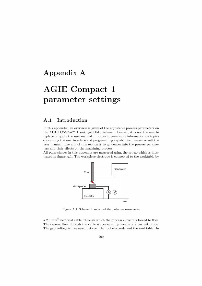
Appendix A
AGIE Compact 1parameter settings
A.1 Introduction
In this appendix, an overview is given of the adjustable process parameters onthe AGIE Compact 1 sinking-EDM machine. However, it is not the aim toreplace or quote the user manual. In order to gain more information on topicsconcerning the user interface and programming capabilities, please consult theuser manual. The aim of this section is to go deeper into the process parame-ters and their effects on the machining process.All pulse shapes in this appendix are measured using the set-up which is illus-trated in figure A.1. The workpiece electrode is connected to the worktable by
Tool
Insulator
Workpiece
Generator
A V
Figure A.1: Schematic set-up of the pulse measurements
a 2.5 mm2 electrical cable, through which the process current is forced to flow.The current flow through the cable is measured by means of a current probe.The gap voltage is measured between the tool electrode and the worktable. In
209

210 A.2. PROCESS PARAMETERS
order to avoid undesired voltage drops, the electrodes are made of copper andthe electric cable between workpiece and worktable is highly conductive. Inaddition, the cable should be as short as possible in order to avoid an increaseof the inductance of the discharge circuit. Both current and voltage probe areread by a digital oscilloscope (Tektronix TDS 754A).
A.2 Process parameters
The process parameters which are adjustable on the AGIE Compact 1sinking-EDM machine can be divided into two groups namely the pulse pa-rameters and the servo-controller parameters. The pulse parameters controlthe pulse generator which supplies the discharge energy. Figure A.2 shows themain characteristics of EDM pulses. The upper curve is a measurement of the
Figure A.2: EDM pulses and pulse characteristics (channel 1: gap voltage,channel 2: gap current), machining settings: ui = 100 V , ie =3.2 A, ti = 18 µs, t0 = 56 µs
gap voltage, while the lower curve is the corresponding current which flowsfrom the workpiece to the worktable.
At the start of each pulse, the voltage between the electrodes is set to ui
(i.e. the open circuit voltage).
The elapsed time between the initiation of the pulse and the effectivebreakdown is designated as ignition delay td. The length of the ignitiondelay mainly depends on the gap size. When there is no gap between

APPENDIX A. AGIE COMPACT 1 211
the electrodes or when the gap is nearly zero, there is no ignition delayand accordingly the gap voltage will not reach the desired open circuitvoltage. Such pulses are designated as short circuits or arcs respectively.These arcs and short circuits do not remove material effectively. On theother hand, when the gap is too large, the dielectric will not break down.These pulses have no erosive effect at all and are designated as opencircuit pulses. Pulses with an ignition delay between these two extremesproduce effective discharges.
When the dielectric breaks down, the voltage between the electrodes de-creases to the discharge voltage ue and the discharge current ie flows. Thedischarge voltage is about constant and mainly depends on the electrodematerials and the dielectric fluid. The discharging current is controlledby the generator. The discharge current is usually supplied by a separatecurrent source which is switched on at the moment the dielectric breaksdown.
At the end of the pulse, the generator cuts the current flow which ter-minates the discharge. The entire pulse length is designated as pulseduration ti which equals the sum of the discharge delay td and dischargeduration te. After the pulse, the generator keeps a mean voltage ofapproximately 20 V for which the purpose is unknown by the author.
After an interval t0 (i.e. pulse interval time) a new pulse is initiated.This makes the pulse cycle time tp to be the sum of the pulse duration tiand pulse interval time t0.
Besides the pulse parameters, servo-controller parameters are available. Theaim of the servo-system is to maintain a suitable gap size. However, the actualgap size is hard to measure. Because of the relation between the ignition delaytd and the gap size (assuming a homogeneous dielectric), some EDM machinesuse the measurement of td as a measure for the gap size. Other machines usethe average gap voltage as gap size measure. When the gap size changes, boththe ignition delay and the average gap voltage will change. The servo-systemis controlled by two parameters namely a reference value and a feedback gain.The reference value of the servo-system is a measure of the desired gap size.The gain factor of the servo system controls the proceeding and retractionperformances of the tool electrode. A good setting of the reference value andthe gain factor is necessary to attain effective and stable machining conditions.Further in this appendix some strategies are introduced to set these parametersin in order to enhance the EDM performances.Table A.1 summarizes the adjustable parameters on the AGIE Compact 1.The shape of the generator pulses is controlled by the electrode polarity, theopen circuit voltage ui, the discharge current ie, the pulse duration ti and thepulse interval time t0. Table A.2 lists the possible settings of these parameters.All combinations of U , I, T and P can be set (e.g. U = +2, I = 5, T = 10 and

212 A.2. PROCESS PARAMETERS
AGIE Standard Descriptionparameter symbol
U ui Open circuit voltageI ie Discharge currentT ti Pulse durationP t0 Pulse interval time
S − box Setting of the discharge mode and the valueof the relaxation capacitor
Comp Reference value of the servo-controllerGain Gain setting of the servo-controller
Table A.1: AGIE Compact 1 parameter settings
P = 20 results in ui = +100 V , ie = 3.2 A, ti = 18 µs and t0 = 320 µs). Anadditional parameter, S − box, controls the discharge mode and the value ofthe relaxation capacitor. The AGIE Compact 1 offers three discharge modes:fine fishing, micro-erosion with minimal wear and micro-erosion with minimalroughness (table A.3). In this work only micro-erosion with minimal rough-
(a) Without relaxation capacitor, ma-chining settings: U=+2, I=5, T=10,S-box=0, P=20, Comp=20, Gain=5
(b) With relaxation capacitor, ma-chining settings: U=+2, I=5, T=5, S-box=15, P=20, Comp=20, Gain=5
Figure A.3: Charging and discharging without and with a relaxation capac-itor

APPENDIX A. AGIE COMPACT 1 213
ness is applied in order to obtain smooth surfaces. The elevated tool wear iseliminated by the application of appropriate tool wear-compensation strategieswhich are discussed in section 2.6. The machining settings within a certaindischarge mode are related to the capacitance of the relaxation capacitor. Norelaxation capacitor is present for the first settings (i.e. 0, 20, 40), while alarge relaxation capacitor (approximately 100 nF ) is present for the last set-tings (i.e. 15, 35, 55). In order to clarify the effect of the S− box parameter onthe discharge pulses, a short study is performed. Figure A.3(a) shows a singlepulse, when no relaxation capacitor is connected. The voltage increases fast tothe selected open circuit voltage. When the discharge occurs, the voltage dropsto the discharge voltage and discharge current is quite constant. Figure A.3(b)shows a discharge when a relaxation capacitor is applied (’fine finish’ dischargemode). In a first phase, the generator charges the relaxation capacitor until thevoltage reaches the desired open circuit voltage. When the dielectric breaksdown, the relaxation capacitor discharges over the working gap. It should benoted that the current is fast rising and fast falling (depending on the induc-tance of the discharge circuit), which makes it possible to dissipate the chargedenergy in a short period of time. The discharge energy is mainly determined bythe energy in relaxation capacitor. When the pulse duration is increased, twodischarge phenomena may occur. In a first place, the discharge may be long
(a) Long discharge, machining set-tings: U=+2, I=5, T=10, S-box=15,P=20, Comp=20, Gain=5
(b) Double discharge, machining set-tings: U=+2, I=5, T=10, S-box=15,P=20, Comp=20, Gain=5
Figure A.4: Long pulses using a relaxation capacitor

214 A.2. PROCESS PARAMETERS
as illustrated on figure A.4(a). When the relaxation capacitor is discharged,the generator will maintain the discharge. The source current supplies a con-stant current on which an alternating current is superposed by the oscillatingaction of the relaxation capacitor and the inductance of the discharge circuit.It is clear that the dissipated energy is larger than the energy within the re-laxation capacitor. In a second case, the discharge ends at the moment therelaxation capacitor released its energy and the voltage will rise again until anew discharge appears (figure A.4(b)). Within one pulse, two separated dis-charges occur with approximately the same energy content. In micro-EDM,it is important to control the discharge energy because it directly affects thesurface quality and the dimensional accuracy. Therefore, only short pulses andlow capacitor values are applied in order to obtain smooth surfaces. In thiswork, the S − box parameter is usually set to be 41 which corresponds with acapacitor value of approximately 1 nF in the ’minimal roughness’ mode. Fig-ure A.5 shows these discharge pulses and illustrates the effect of the dischargemode ’micro-erosion with minimal roughness’. At the moment the dielectric
Figure A.5: Pulse of the microgenerator, machining settings: U=+2, I=1,T=1, S-box=41, P=20, Comp=20, Gain=5
breaks down, the capacitor discharges and the current source is activated. Thedischarging current is low and the discharge is short due to the limited energyin the relaxation capacitor. The current source supplies a chopped currentprofile with a cycle time of approximately 80 ns. This chopped current flowwill not maintain the discharge, but will gradually charge the capacitor again.At this moment, the discharge channel is not yet entirely deionized and allowssome current to flow which is observed in figure A.5. It should be noted that

APPENDIX A. AGIE COMPACT 1 215
within this pulse only two effective discharges are present. It can be concludedthat the chopping action of the current source guaranties the creation of shortdischarge pulses which is desirable in micro-EDM.
Remarks:
Although I is marked as discharge current, the discharge current doesnot equal the set value when a relaxation capacitor is applied. Whena relaxation capacitor is applied, the peek current is mainly determinedby the energy within the capacitor and the inductance of the lead wires.A more theoretic approach on energy and discharge length is given insection 2.5.2 concerning micro-EDM generators.
In the AGIE Compact 1, the pulse duration starts at the moment thatthe voltage reaches the selected open circuit voltage or when a dischargeoccur. The initial loading time of the relaxation capacitor is not includedinto the pulse duration.
A.3 Stable machining
A stable machining process is characterized by continuous material removalwithout too many short circuits. Some parameters influence the machiningstability without affecting the surface quality. Beneath, the effect of threesimilar parameters is discussed. However, no ideal parameter setting existswhich offers stable, fast, accurate and smooth machining.
Comp is the reference value of the servo-system. Comp refers to ’compres-sion’ of the working gap and can be set between 0 and 50. High values of compstrive to small working gaps which promotes the machining accuracy. However,small working gaps prevent an optimal flushing and lead to an increase in shortcircuits.
P is the pulse interval time. Between two discharge pulses, the working gapshould be sufficiently deionized and the debris has to be removed from theworking gap. Short pulse interval times increase the removal rate, but increasethe number of arcs and short circuits as well. Arcs and short circuits occur whenthe working gap is insufficiently flushed at the moment of the next discharge.
Gain controls the gain factor of the servo loop. High gain settings increasethe reaction speed when short circuits occur. However, high gain values makethe machine to react nervously which introduces undesired vibrations and dis-turb the machining stability.

216 A.3. STABLE MACHINING
Code U[V ] I[A] T[µs] P[µs]0 60 0 1 11 80 0.8 1.3 1.32 100 1.4 1.8 1.83 120 1.8 2.4 2.44 150 2.4 3.2 3.25 160 3.2 4.2 4.26 180 4.0 5.6 5.67 250 5.6 7.5 7.58 9.3 10 109 10.8 13 1310 14.8 18 1811 18.3 24 2412 24.8 32 3213 37.1 42 4214 49.8 56 5615 63.8 75 7516 100 10017 130 13018 190 19019 240 24020 320 32021 420 42022 560 56023 750 75024 1000 100025 1300 130026 1800 180027 2400 240028 3200 320029 4200 420030 5600 560031 7500 7500
Table A.2: Impulse parameters and their values

APPENDIX A. AGIE COMPACT 1 217
fine finishing micro-erosion, micro-erosion,minimal wear minimal roughness
0 20 401 21 412 22 423 23 434 24 445 25 456 26 467 27 478 28 489 29 4910 30 5011 31 5112 32 5213 33 5314 34 5415 35 55
Table A.3: S-box settings


Appendix B
Tungsten-siliconmicro-EDM technologymodelling
B.1 Introduction
The tungsten-silicon micro-EDM technology is modelled using design of exper-iments. After a screening test, which identifies the most influencing processparameters, a modelling experiment is executed based on the response surfacemethodology. The model consists of a full quadratic polynomial, which is fit-ted on the experimental data. The tungsten-silicon technology is described bythree quadratic models, representing the removal rate, surface roughness andrelative electrode wear. Standard works by Montgomery and Box are referredto for detailed reading on design of experiments and response surface modeling[99, 100].
B.2 Screening
B.2.1 A glimpse at the theory
A screening experiment calculates the global effect of a factor on the outputsignal. When the global effect does not significantly exceed the noise level in theprocess, it is concluded that the factor has no global effect on the process. Onorder to determine global effects, generally linear models are used. Most of thetimes, it is reasonable to assume that high-order interactions can be neglected.Information on the main effects and low-order interactions can be obtained byrunning only a fraction of a full factorial experiment. When eventually onlymain effects are considered, the design is reduced to a saturated fractional fac-
219

220 B.2. SCREENING
Parameter Levels1. Open circuit voltage ui [V ] 120 - 1802. Discharge current ie [A] 0.8 - 43. Pulse duration ti [µs] 1 - 104. Pulse interval time t0 [µs] 18 - 1005. Servo reference setting 2 - 406. Servo gain setting 2 - 107. Dielectric conductivity [kΩ · cm] 100 - 2008. Electrode rotation speed [rpm] 500 - 1500
Table B.1: Screening experiment of silicon micro-EDM
torial design, requiring considerably fewer experimental runs. An importantadvantage is that saturated fractional factorial designs allow to obtain almostthe same amount of effective information about the main effects as could beobtained with a full factorial design. However, all valuable information con-cerning the effects of the factor interactions is lost due to the confounding of theinteractions. Some saturated fractional factorial design arrays are developedto minimize the experimental runs and to optimize the statistical behaviour ofthe results. The L12(211) experimental array, which is a saturated orthogonalfractional factorial design with 12 runs to investigate 11 factors at 2 levels, isused for this screening experiment. The L12 is a special array, in which allinteractions are distributed to all columns, more or less uniformly. The advan-tage of a uniform distribution is that it allows to investigate 11 main effectswithout worrying about confounding of the interactions in particular columns.Consequently, all interactions are measured and treated as experimental noise.For each experimental run, the factors must be set according to their levels asspecified in the designed array. When all the experimental runs are executed,the data is processed to quantify the significance of the global effect for eachfactor. Analysis of variance, or briefly ANOVA, is applied to compare the effectof a factor with the background variation or noise. By means of null hypothesis(H0) testing, ANOVA enables the calculation of the probability of the factorhaving genuine effect. H0 assumes no effect, which means that the estimation ofthe factor’s contribution is an estimation of the experimental noise. By meansof the F distribution the probability of accepting H0 is quantified. Factors, forwhich H0 is rejected, will significantly affect the investigated output signal andwill pass the screening experiment.
B.2.2 Screening experiment
In the screening experiment for tungsten-silicon micro-EDM, an initial set ofeight process parameters is reduced to a subset of which each parameter signif-icantly affect the micro-EDM performance. It should be noted that the term’factor’ is used in experimental design to address the machining parameters and

APPENDIX B. TECHNOLOGY MODELLING 221
Obs
erva
tion
Die
lect
ric
resi
stiv
ity
[kΩ·c
m]
Ope
nci
rcui
tvo
ltag
e[V
]
Dis
char
gecu
rren
t[A
]
Pul
sedu
rati
on[µ
s]
Pul
sein
terv
alti
me
[µs]
Serv
ore
fere
nce
sett
ing
Serv
oga
in
Ele
ctro
dero
tati
onsp
eed
[rpm
]
Rem
oval
rate
[mm
3/s
]
Surf
ace
roug
hnes
s[µ
mR
a]
Rel
ativ
eel
ectr
ode
wea
r[%
]
1 100 120 0.8 1 18 2 2 500 0.000661 0.57 1.622 100 120 0.8 1 18 40 10 1500 0.001307 0.59 1.623 100 120 0.4 10 100 2 2 500 0.000974 4.27 0.734 100 180 0.8 10 100 2 10 1500 0.000261 2.40 1.245 100 180 0.4 1 100 40 2 1500 0.002878 1.33 1.356 100 180 0.4 10 18 40 10 500 0.011426 4.02 0.727 200 120 0.4 10 18 2 10 1500 0.002193 4.35 0.798 200 120 0.4 1 100 40 10 500 0.001015 1.03 1.759 200 120 0.8 10 100 40 2 1500 0.001550 2.65 0.910 200 180 0.4 1 18 2 2 1500 0.004309 0.97 1.2011 200 180 0.8 10 18 40 2 500 0.002557 2.59 1.3612 200 180 0.8 1 100 2 10 500 0.000339 0.72 1.51
Table B.2: Screening experiment
’response variables’ to address the machining characteristics. Table B.1 showsthe initial set of individually controllable factors and their factor levels. Thefactor levels are chosen so that they cover the most important area of the entireparameter space. The first four parameters are generator settings: open circuitvoltage, discharge current, pulse duration and pulse interval time. The nexttwo parameters control the machining servo system: servo reference and servogain. The last two parameters are the dielectric conductivity and the rotationspeed of the tool electrode. The experimental array is constructed by assigningthe factors to the columns of the L12 array and by filling the predefined arraywith the specific values of the levels, shown in table B.2. Although the L12
is able to investigate 11 independent factors, all predefined experimental runshave to be executed to obtain reliable results for the 8 investigated factors. Ex-cept for the experimental array, table B.2 shows the measured responses for themachined surface roughness, removal rate and relative electrode wear. Theseresponse variables are measured on a machined through slot, which is discussedin paragraph 3.4.1. Analysis of variance is applied to identify the significantfactors. The null hypothesis, H0, assumes that no effects are present, which

222 B.2. SCREENING
Rem
oval
rate
Surf
ace
roug
hnes
s
real
tive
elec
trod
ew
ear
Parameter p-value p-value p-value Retained1. Open circuit voltage ui 0.23 0.47 0.98 ∗2. Discharge current ie 0.18 0.03 0.19 ∗3. Pulse duration ti 0.43 0.01 0.05 ∗4. Pulse interval time t0 0.20 0.72 0.86 ∗5. Servo reference setting 0.29 0.58 0.58 ∗6. Servo gain setting 0.72 0.70 0.687. Dielectric conductivity 0.59 0.65 0.848. Electrode rotation speed 0.66 0.64 0.60
Table B.3: First screening experiment
means that all observed effects are estimates of the noise in the experiment.Table B.3 shows the observed significance levels, or p-values. A p-value is theprobability of observing a factor effect, which is at least as contradictory to H0
as the actual measured factor effect. Large p-values are in favour of H0, whilesmall p-values are in favour to reject H0. The level at which H0 is rejected iscalled the significance level α. The aim of a screening experiment is to identifyall important factors. Consequently, it is better to identify an unimportantfactor than to reject an important factor. Therefore, α is set to 50 %. Thismeans that if a factor has no significant effect, there is a probability of 50 %that the factor will pass the screening test. On the other hand, the probabilityof rejecting an important factor is small as well. In table B.3 the factors whopassed the screening test are indicated as ’retained’ factors.
B.2.3 Conclusion
The aim of this concluding paragraph is not to summarize the applied calcu-lation method, but is aimed to give a few remarks for future use of saturatedfractional factorial designs for screening usage.
The choice of the factor levels is very important. When the two factor lev-els are close to each other, no significant change in response is measured.However, the rejected factor may be of great importance. Therefore, thefactor levels should broadly cover the area of interest. A significant fac-tor can also be rejected when the values of the response variable at the

APPENDIX B. TECHNOLOGY MODELLING 223
two predefined factor levels are close to equal. However, the response inbetween the two levels may be considerably varying. Unfortunately thesefactors will be rejected.
A saturated fractional factorial design is based on a minimized set ofexperimental runs. This is a fast tool to screen a lot of parameters usinga small amount of experimental runs. However, the corresponding resultshave a low statistical quality. Replicating the experimental runs willin great extend improve the statistical quality. Accordingly, a smallervalue of the significance level can be applied and more accurate decisionscan be taken. When the number of experimental runs increases, theexperimental cost increases as well, which is usually not permitted forscreening experiments.
In saturated fractional factorial designs all effects caused by factor in-teractions are assumed to be negligible. The effects of the interactionsare incorporated in the estimation of the experimental noise. However,when the effect of one or more interactions is significant, these particularinteractions can not be detected. On top of that, the noise level increasesdue to the effect of the interactions, obstructing accurate identificationof the main effects.
B.3 Modelling
B.3.1 A glimpse at the theory
Designs to analyze or to model the behaviour of a response variable are calledresponse surface designs. A second order design is a design that allows fittingof the response surface by a full quadratic model. Frequently-applied second-order designs are central composite designs, face-centred cube designs and Box-Behnken designs. For the modelling of the silicon micro-EDM technology acentral composite design is applied. A central composite design uses five factorlevels, instead of three factor levels in the other designs, allowing a bettermodelling accuracy. Figure B.1 shows schematically all experimental runs fora central composite design with three factors. The cube points represent a two-level full or fractional factorial design, which allows the estimation of all first-order and two-factor interaction terms. The additional star and centre pointsallow the estimation of the quadratic effects. The distances between the pointshave to be optimized to minimize the statistical error and to allow accuratefitting of the quadratic model to the response surface. The methodology toset-up and analyze these quadratic designs is studied by Montgomery and Box[99, 100]. As in the screening experiment an analysis of variance is performed toidentify all significant terms in the quadratic formula and finally the numericalvalues are calculated by a least square calculation.

224 B.3. MODELLING
cube points
star points
centre point
Figure B.1: Central composite design
B.3.2 Tungsten-silicon micro-EDM technology modelling
The array of the executed central composite design, containing all the experi-mental runs, is shown in table B.4. The experiment consists of 52 experimentalruns divided over 32 cube points, 10 star points and 10 centre points. The 32cube points represent a full factorial design for 5 factors at two levels. Thespace between the cube points is equal to the operation space of the finalmodel. Within the operation space, the model should give reliable estimations.The 10 runs at the centre point allow accurate fitting at the centre of the model,which is also the centre of the operation space. The centre points also provideessential information on the experimental noise. The full factorial, the runs atthe centre point and the runs at the star points allow to fit a full quadraticmodel onto the experimental data. As in the screening experiment, the sig-nificant factors, square of factors and all first-order interactions are identifiedusing ANOVA. Then the model is fit on the response surface in function of allsignificant factors, square of factors and first order interactions. The model ofthe tungsten-silicon technology is symbolically represented by equations B.1,B.2 and B.3 referring to respectively a mathematical model for the removalrate, surface roughness and relative electrode wear.
Removal rate (ui, ie, ti, t0, comp) = xArxT [µm3/s] (B.1)
Surface roughness (ui, ie, ti, t0, comp) = xAsxT [µm Ra] (B.2)
Relative electrode wear(ui, ie, ti, t0, comp) = xAwxT [%] (B.3)
with:
x =[
ui[V ] ie[A] ti[µs] t0[µs] comp 1]
(B.4)

APPENDIX B. TECHNOLOGY MODELLING 225
A =
aui
2 aui,ieaui,ti
aui,t0 aui,comp aui
0 aie2 aie,ti
aie,t0 aie,comp aie
0 0 ati2 ati,t0 ati,comp ati
0 0 0 at02 at0,comp at0
0 0 0 0 acomp2 acomp
0 0 0 0 0 acte
(B.5)
The numerical values of the technology matrices are shown in equation B.6,B.7 and B.8. It should be noted that all coefficients in the matrices have units,while they are not displayed to keep the matrices compact and readable.
Ar =
0 0 859 −81.4 466 00 0 0 0 0 00 0 −13500 0 5900 00 0 0 83.7 −462 00 0 0 0 0 −367000 0 0 0 0 401000
(B.6)
As =
0 0 0.00141 0 0.000116 00 0 0 0 0 00 0 −0.00387 0 0.00162 −0.07060 0 0 0 0 00 0 0 0 0.000305 −0.03030 0 0 0 0 0.443
(B.7)
Aw =
2.35× 10⁻⁵ 0 8.72× 10⁻⁴ 0 1.07× 10⁻⁴ −0.016
0 0 6.85× 10⁻⁵ 0 3.07× 10⁻⁴ 00 0 0.0203 0 0.00119 −0.4470 0 0 0 0 00 0 0 0 0 −0.02570 0 0 0 0 3.975
(B.8)
B.3.3 Conclusion
Below a number of remarks are summarized concerning the use of central com-posite designs to model a machining technology.
A central composite design makes it possible to initially create a lin-ear model by a fractional factorial design at the cube points. When aquadratic design is required, the star and centre points can easily beadded. This property makes central composite designs a flexible tool tocreate quadratic models starting from an already existing linear model.
The prediction accuracy of a central composite design can generally be in-creased by replication of the experimental runs. However, after a certainnumber of replicates, the model quality will not further increase becausethe quadratic model is not able to reproduce the exact shape of the re-sponse surface. Other mathematical fitting functions have to be used inorder to reduce the lack of fit.

226 B.3. MODELLING
A central composite design is an accurate tool to model a smooth varyingresponse surface, due to its five levels and due to its beneficial statisti-cal characteristics. Although, a central composite design has excellentproperties, it requires star points which are situated outside the opera-tion space of the model. This means that it is impossible to model theentire parameter space. A Box-Behnken design only requires three fac-tor levels, having its operation space between the outer experimentationpoints. This means that a Box-Behnken design can be used to have abetter coverage of the parameter space. However, one should take intoaccount that no modelling technique exists, which is able to cover theentire useful parameter space due to its irregular boundaries.

APPENDIX B. TECHNOLOGY MODELLING 227
Obs
erva
tion
Ope
nci
rcui
tvo
ltag
e[V
]
Dis
char
gecu
rren
t[A
]
Pul
sedu
rati
on[µ
s]
Pul
sein
terv
alti
me
[µs]
Serv
ore
fere
nce
sett
ing
Rem
oval
rate
[mm
3/s
]
Surf
ace
roug
hnes
s[µ
mR
a]
rela
tive
elec
trod
ew
ear
[%]
1 120 4 7.5 75 30 0.001078 1.17 0.862 150 2.4 4.2 56 20 0.000926 1.02 1.033 180 4 7.5 75 10 0.000763 1.64 0.894 150 2.4 4.2 56 20 0.000936 0.98 1.035 120 1.4 7.5 32 30 0.001552 1.06 0.806 150 5.6 4.2 56 20 0.000878 1.05 0.937 180 1.4 1.8 32 30 0.001368 0.76 1.298 150 2.4 4.2 56 20 0.000881 1.01 1.039 150 2.4 4.2 100 20 0.000530 1.03 1.0410 120 1.4 1.8 75 10 0.000161 0.49 1.7711 150 0.8 4.2 56 20 0.000819 1.03 0.6312 180 4 7.5 32 30 0.002979 1.95 0.8213 150 2.4 4.2 56 40 0.001486 1.29 0.8914 120 4 1.8 32 10 0.000380 0.49 1.7015 120 1.4 7.5 75 10 0.000380 1.03 0.9516 120 4 7.5 75 10 0.000402 1.04 0.8817 100 2.4 4.2 56 20 0.000457 0.60 1.0818 180 4 1.8 32 10 0.000735 0.84 1.1919 180 4 1.8 32 30 0.001610 0.84 1.1820 250 2.4 4.2 56 20 0.001772 1.88 0.9121 180 4 1.8 75 30 0.000751 1.84 1.2122 120 4 1.8 75 30 0.000412 0.48 1.4623 150 2.4 10 56 20 0.001409 1.63 0.8324 120 1.4 1.8 32 30 0.000703 0.48 1.4525 120 4 7.5 32 10 0.000669 0.97 0.8626 180 1.4 7.5 75 10 0.000689 1.71 1.75
Table B.4: Modelling experiment
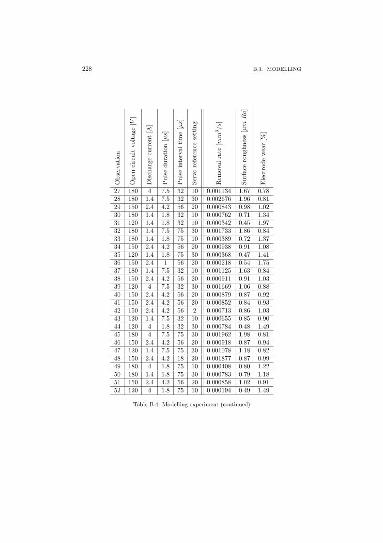
228 B.3. MODELLING
Obs
erva
tion
Ope
nci
rcui
tvo
ltag
e[V
]
Dis
char
gecu
rren
t[A
]
Pul
sedu
rati
on[µ
s]
Pul
sein
terv
alti
me
[µs]
Serv
ore
fere
nce
sett
ing
Rem
oval
rate
[mm
3/s
]
Surf
ace
roug
hnes
s[µ
mR
a]
Ele
ctro
dew
ear
[%]
27 180 4 7.5 32 10 0.001134 1.67 0.7828 180 1.4 7.5 32 30 0.002676 1.96 0.8129 150 2.4 4.2 56 20 0.000843 0.98 1.0230 180 1.4 1.8 32 10 0.000762 0.71 1.3431 120 1.4 1.8 32 10 0.000342 0.45 1.9732 180 1.4 7.5 75 30 0.001733 1.86 0.8433 180 1.4 1.8 75 10 0.000389 0.72 1.3734 150 2.4 4.2 56 20 0.000938 0.91 1.0835 120 1.4 1.8 75 30 0.000368 0.47 1.4136 150 2.4 1 56 20 0.000218 0.54 1.7537 180 1.4 7.5 32 10 0.001125 1.63 0.8438 150 2.4 4.2 56 20 0.000911 0.91 1.0339 120 4 7.5 32 30 0.001669 1.06 0.8840 150 2.4 4.2 56 20 0.000879 0.87 0.9241 150 2.4 4.2 56 20 0.000852 0.84 0.9342 150 2.4 4.2 56 2 0.000713 0.86 1.0343 120 1.4 7.5 32 10 0.000655 0.85 0.9044 120 4 1.8 32 30 0.000784 0.48 1.4945 180 4 7.5 75 30 0.001962 1.98 0.8146 150 2.4 4.2 56 20 0.000918 0.87 0.9447 120 1.4 7.5 75 30 0.001078 1.18 0.8248 150 2.4 4.2 18 20 0.001877 0.87 0.9949 180 4 1.8 75 10 0.000408 0.80 1.2250 180 1.4 1.8 75 30 0.000783 0.79 1.1851 150 2.4 4.2 56 20 0.000858 1.02 0.9152 120 4 1.8 75 10 0.000194 0.49 1.49
Table B.4: Modelling experiment (continued)

Microvonkerosie:Technologie,ComputerondersteundeOntwikkeling & Productieen Toepassingen
Nederlandse samenvatting
I Inleiding en doelstellingen
I.1 Algemene inleiding
Het ligt in de natuur van de mens om steeds nieuwe en meer performante syste-men te ontwikkelen met het oog op het verbeteren van onze levensstandaard ofhet exploreren van onontgonnen kennisdomeinen. Een richting van wetenschap-pelijke vooruitgang met een groot wetenschappelijk en economisch potentieelis de miniaturisering van systemen. Een gekend voorbeeld is de snel evolueren-de miniaturisering van computercomponenten waardoor zowel de rekenkrachtals de rekensnelheid sterk zijn toegenomen. Een ander sprekend voorbeeld isde miniaturisering van chirurgische instrumenten waardoor de afmetingen vaninsnijdingen drastisch zijn verkleind met als gevolg een snellere recuperatietijdvan de patient. Het is duidelijk dat miniaturisering vele voordelen biedt, zoalsruimtebesparing, verhoogde werkingssnelheid en verlaagd energieverbruik, endat we moeten streven naar een doorgedreven miniaturisering. Maar vooral-eer we sciencefiction in wetenschap kunnen omgezetten en microrobotten dooronze aders laten voortbewegen om operaties uit te voeren, is er nog een langeweg af te leggen.
229

230 I. INLEIDING EN DOELSTELLINGEN
Alhoewel de miniaturisering van mechanische systemen al een lange geschiede-nis achter de rug heeft, is een verhoogde interesse merkbaar wanneer micro-elektronici startten met het ontwikkelen van micromechanische structuren.Vanaf toen veranderde de terminologie van ’klein’ en ’geminiaturiseerd’ in ’mi-cro’ (micrometer = 10−6 m) en zelfs in ’nano’ (nanometer = 10−9 m). Dezenieuwe microsysteemtechnologie (MST) is aan het uitgroeien tot een specifiekeonderzoeksdiscipline die een brede waaier van ingenieursdomeinen overspant.Door het brede toepassingsgebied van microsystemen is voor de microsysteem-technologie een mooie toekomst weggelegd.
I.2 Doelstellingen van dit onderzoek
De oorspronkelijke microsysteempioniers waren micro-elektronici die de goedontwikkelde fotolithografische technieken, overgeerfd van de micro-elektronica,aanwendden om microstructuren te produceren. Deze productietechnieken ge-bruiken silicium als basismateriaal en produceren voornamelijk tweedimensio-nale microstructuren. Wanneer andere basismaterialen vereist zijn of wanneerdriedimensionale structuren gewenst zijn, moeten andere productietechnolo-gieen aangewend worden. Een van deze productietechnologieen is vonkerosie,specifiek microvonkerosie. Vonkerosie is een elektrothermisch productieproceswaarbij materiaal verwijderd wordt door de erosieve actie van doorslaande von-ken. Microvonkerosie wordt aangewend voor de productie van driedimensionalemicrostructuren. Het hoofddoel van dit onderzoek is de ontwikkeling van eenmicrovonktechnologie waarin de volgende deeldoelstellingen vervat zijn:
. een studie van de invloed van de instelbare machineparameters op hetvonkerosieproces en het creeren van een technologiemodel dat optimali-satie van het proces toelaat,
. een studie van de invloed van het vonkerosieproces op de oppervlakte-kwaliteit van bewerkte microstructuren,
. de ontwikkeling van bewerkingsgereedschappen en -instrumenten die hetmogelijk maken om nauwkeurige driedimensionale microstructuren te ver-vaardigen op een flexibele wijze,
. de ontwikkeling van bewerkingsstrategieen met het oog op de productievan complexe microstructuren met een hoge bewerkingsnauwkeurigheid,
. een compatibiliteitsstudie van de microvonktechnologie met andere mi-crofabricagetechnologieen.
De productiemogelijkheden van de microvonktechnologie worden onderzocht entevens aangetoond aan de hand van de productie van driedimensionale micro-structuren en -systemen. De objectieven van deze thesis reiken echter verderdan de ontwikkeling van de microvonktechnologie. Een gebruiksvriendelijkecomputerondersteunde ontwerpomgeving waarin de bewerkingsmogelijkhedenvan microvonkerosie ten volle tot uiting komen, zal de verspreiding van micro-vonkerosie bevorderen. Daarom bestaat een aanvullend objectief erin om de
Nederlandse samenvatting 231
ontwikkelde technologie te implementeren in een computerondersteunde ont-werpomgeving die toegankelijk is voor ontwerpers die niet noodzakelijk eenexpertise hebben opgebouwd aangaande microvonkerosie.
I.3 Opbouw van de nederlandse samenvatting
Net zoals de uitgebreide engelstalige tekst bestaat deze nederlandstalige sa-menvatting uit drie grote delen. Het eerste deel gaat in op de techniek van mi-crovonkerosie en toont de bewerkingsmogelijkheden van microvonkerosie aanaan de hand van enkele voorbeelden en toepassingen. Het tweede deel be-spreekt de technologie-opbouw voor het bewerken van silicium met microvon-kerosie en bevat tevens een studie over oppervlaktekwaliteit. In het derde deelwordt de implementatie besproken van een computerondersteunde ontwerp- enproductie-omgeving voor microsystemen met microvonkerosie als bewerkings-techniek. Deze samenvatting wordt afgesloten met een algemeen besluit.Wegens de beperkte lengte van deze samenvatting worden slechts enkele delenvan het onderzoek toegelicht en is er geen literatuuroverzicht. Voor een dieper-gaande bespreking en verwijzigingen naar de literatuur wordt verwezen naarde engelstalige tekst.
II Microvonkerosie als microfabricagetechniek
II.1 Inleiding
Dit deel van de thesis bespreekt vonkerosie als een productieproces voor micro-mechanische componenten. De gebruikte bewerkingsapparatuur en -techniekenkomen aan bod alsook een brede waaier van voorbeelden die de driedimensio-nale bewerkingsmogelijkheden van microvonkerosie aantonen.
II.2 Microvonkerosie
Vonkerosie is een elektrothermisch verspaningsproces voor de bewerking vanelektrisch geleidende materialen. Verspaning wordt hierbij gerealiseerd doormiddel van doorslaande vonken tussen een gereedschapselektrode en een werk-stukelektrode. Beide elektroden bevinden zich op een kleine afstand van elkaar(d.i. de vonkspleet) en worden gescheiden door een dielektrische vloeistof. Eengenerator brengt een elektrische spanning aan waardoor een elektrisch veldwordt opgebouwd in de vonkspleet. Wanneer de veldsterkte de doorslagspan-ning van het dielektricum overschrijdt, ontstaat een vonk die voor materiaal-afname zorgt door smelten en verdampen van elektrodemateriaal. Door hetinstellen van gepaste machineparameters en het gebruik van erosiebestendiggereedschapsmateriaal is de ongewenste materiaalafname op de gereedschaps-elektrode significant lager dan de gewenste materiaalafname op de werkstuke-lektrode. Klassieke materialen voor de gereedschapselektrode zijn koper, wol-fraam en grafiet.

232 II. MICROVONKEROSIE ALS MICROFABRICAGETECHNIEK
Voor alle experimenten in deze thesis wordt een commerciele vonkerosiemachi-ne, AGIE Compact 1, gebruikt. Deze machine is een vierassige numeriek ge-stuurde vonkmachine, uitgerust met een dielektricumcircuit met gedeıoniseerdwater en met een microvonkgenerator.
(a) Werktafel
(b) Gereedschapselektro-de
(c) Microdraadvonkmodule (WEDG)
Figuur 1: Werktafel van de AGIE Compact 1

Nederlandse samenvatting 233
Figuur 1(a) toont de werktafel van de AGIE Compact 1 vonkmachine. Hetwerkstuk wordt ingeklemd in de werkstukhouder die opgesteld staat op de werk-tafel. De gereedschapselektrode, of kortweg elektrode, is een stijve wolfraamdraad met een diameter van 0.15 mm die ingeklemd wordt in een roterendeklemkop (figuur 1(b)). De rotatie van de elektrode zorgt voor een goede spoe-ling van de vonkspleet. Om de stabiliteit van de elektrode te garanderen wordtze geleid in een keramische geleiding. Tijdens het verspanen beschrijft de ge-reedschapselektrode een pad doorheen het werkstukmateriaal om de gewenstewerkstukgeometrie te bekomen. De vorm van de gereedschapselektrode kangewijzigd worden om specifieke geometrieen te realiseren. Hiervoor wordt deelektrode bewerkt met behulp van een microdraadvonkmodule (figuur 1(c)).Deze draadvonkmodule of WEDG-eenheid (Wire Electro-Discharge Grindingeenheid) bestaat uit een nauwkeurig gepositioneerde afwikkelende draad diedienst doet als tegenelektrode.
II.3 Technieken om de slijtage van de gereedschapselek-trode te compenseren
De slijtage van de gereedschapselektrode is een belangrijk nadeel van vonkero-sie. De vormverandering van de gereedschapselektrode reflecteert rechtstreeksin maat- en vormonnauwkeurigheden op het werkstuk. In deze thesis zijn sleet-compensatietechnieken onderzocht waarvan er twee nader worden toegelicht indeze samenvatting.In een eerste compensatiestrategie wordt de cilindrische gereedschapselektrode,die vooral verkort door slijtage, extra gevoed om deze verkorting te compense-ren. Door een goede schatting van de elektrodeslijtage kan de sleet in rekeninggebracht worden tijdens de generatie van de gereedschapsbaan (d.i. een anti-ciperende compensatiestrategie). Figuur 2 toont een structuur bestaande uit
(a) Optisch beeld, (het
lichte deel is het werkstuk)
(b) SEM beeld
Figuur 2: Ribbenstructuur vervaardigd met de anticiperende compensatie-strategie

234 II. MICROVONKEROSIE ALS MICROFABRICAGETECHNIEK
een reeks van ribben, vervaardigd met deze anticiperende compensatiestrategie.Alhoewel het werkstukmateriaal tot op de vooropgestelde diepte is verwijderd,is de vorm van de gereedschapselektrode lichtjes afgerond wat zichtbaar is aande voet van de ribben. Deze vormverandering is niet compenseerbaar met eenwijziging van de gereedschapsbaan en is dus een inherent nadeel van deze com-pensatiestrategie.In een tweede compensatiestrategie worden achtereenvolgens identieke gereed-schapselektroden gebruikt. Door een voldoende aantal gereedschapselektrodendezelfde gereedschapsbaan te laten volgen, zal het werkstukmateriaal gradueelverwijderd worden en zal de slijtage aan opeenvolgende elektroden verminderen.De identieke gereedschapselektroden worden aangemaakt met de ontwikkeldemicrodraadvonkmodule. Voor de schatting van het noodzakelijk aantal elek-troden met het oog op het behalen van de vooropgestelde nauwkeurigheid is indeze thesis een berekeningsmodel opgebouwd, maar zal in deze samenvattingniet besproken worden. Figuur 3 toont een ribbenstructuur vervaardigd meteen reeks van identieke gereedschapselektroden. De ribben hebben duidelijk eenrechte basis (ten opzichte van een breder wordende basis bij de anticiperendecompensatiemethode) wat duidt op een geringe slijtage van de laatstgebruiktegereedschapselektrode. Alhoewel deze techniek in het algemeen een langerebewerkingstijd vraagt dan de anticiperende techniek heeft ze als voordeel datze zowel bruikbaar is voor cilindrische als voor gevormde gereedschapselektro-den. Dit is de voornaamste reden waarom de techniek met de meervoudigeelektroden als standaard compensatiestrategie aangewend wordt in deze thesis.
(a) Optisch beeld (b) SEM (Scanning
Electron Microscope)beeld
Figuur 3: Ribbenstructuur vervaardigd met de compensatiestrategie metmeervoudige gereedschapselektroden

Nederlandse samenvatting 235
II.4 De bewerkingsvrijheid van microvonkerosie
De driedimensionale bewerkingsvrijheid is een belangrijk voordeel van micro-vonkerosie. Verschillende bewerkingsmethoden worden geıllustreerd met voor-beelden, allen vervaardigd op de AGIE Compact 1 microvonkmachine.
Microvonksnijden
In microvonksnijden wordt de mantel van de cilindervormige gereedschapselek-trode gebruikt voor het ’uitsnijden’ van componenten. Hierdoor bekomt menzogeheten 2½D structuren. Figuur 4 illustreert het microvonksnijden aan dehand van een geminiaturiseerde veer en een tandwielpaar. Figuur 4(a) toonteen geminiaturiseerde veer vervaardigd uit silicium, afgebeeld op een oude Bel-gische Frank (φ 18 mm). Figuur 4(b) beeldt twee ingrijpende silicium tandwie-len af. Beide tandwielen hebben een evolvente vertanding en zijn gemonteerdop een stalen as met een diameter van 1 mm.
(a) Microveer (b) Microtandwielen
Figuur 4: 2½D microstructuren vervaardigd met microvonksnijden
Microvonkfrezen
Bij vonkenfrezen wordt het gewenste volume werkstukmateriaal voornamelijkverwijderd met de top van de gereedschapselektrode. Vonkfrezen is een flexibelebewerkingstechniek waarbij complexe geometrieen vervaardigd kunnen wordenmet behulp van gereedschapselektroden met een eenvoudige vorm. Figuur 5(a)illustreert het resultaat van vonkfrezen aan de hand van een kegeltandwiel.Het gewenste oppervlak wordt bekomen door het definieren van naast elkaarliggende gereedschapsbanen net zoals bij conventionele freesbewerkingen. Wan-neer de overlapping tussen twee naast elkaar liggende gereedschapsbanen wordtverhoogd, verhoogt de bewerkingsnauwkeurigheid maar ook de bewerkingstijd.Daardoor dient een gepaste afschatting gemaakt te worden tussen bewerkings-

236 II. MICROVONKEROSIE ALS MICROFABRICAGETECHNIEK
tijd en afwerkingsnauwkeurigheid. Figuur 5(b) toont twee ingrijpende kegel-tandwielen beide gemonteerd op een stalen as.
(a) Uitvergroting kegel-tandwiel
(b) Ingrijpende kegel-tandwielen
Figuur 5: Geminiaturiseerde structuren vervaardigd met microvonkfrezen
Gevormde gereedschapselektroden
De bewerkingsmogelijkheden van microvonkerosie gaan verder dan louter vonk-snijden en vonkfrezen. Wanneer de complexiteit van de microstructuren debewerkingsmogelijkheden van vonksnijden en vonkfrezen overschrijdt, kan devorm van de gereedschapselektrode aangepast worden om de gewenste struc-tuur te realiseren. De gereedschapselektrode wordt hiertoe bewerkt met demicrodraadvonkmodule (zie paragraaf II.2). Figuur 6(a) illustreert dit aan dehand van de structuur van een inertiele sensor. De sensor bestaat uit een massadie opgehangen is aan microbalken (4 bovenaan en 2 onderaan). Het materiaaltussen twee microbalken kan niet door een standaard cilindrische elektrode meteen drie-assige bewerkingsvrijheid verwijderd worden. Daarom werd de vormvan de gereedschapselektrode aangepast zoals afgebeeld in figuur 6(b). Metdeze vorm worden zowel de microbalken als de uitsparingen simultaan vervaar-digd. Als tweede voorbeeld, toont figuur 6(c) een geminiaturiseerde dobbelsteenmet een zijde van 360 µm. Elk vlak van de dobbelsteen werd voorzien van hetgepaste aantal ogen in twee opspanningen. Om een groot aantal opspanningente vermijden, was een gevormde gereedschapselektrode noodzakelijk om in eenenkele opspanning meerdere vlakken van ogen te voorzien.
II.5 Toepassingen van microvonkerosie
Enkele toepassingen worden bestudeerd waarin microvonkerosie een bijdra-ge levert in de productie van microsystemen. Alle voorbeelden doen dienstals gevallenstudies voor de opbouw van de microvonkerosietechnologie. Naastmicrovonkerosie worden technieken toegepast zoals fotolithografie, draaien enspuitgieten.

Nederlandse samenvatting 237
(a) Microsensor (b) Bewerkte gereed-schapselektrode
(c) Microdobbelsteen
Figuur 6: Bewerkte gereedschapselektroden met voorbeelden van werkstuk-structuren
Miniatuurgrijper
Een krachtgecontroleerde miniatuurgrijper is ontwikkeld op basis van siliciumgrijpervingers (figuur 7(a)). Silicium is als werkstukmateriaal gekozen omdatsilicium toelaat op een eenvoudige wijze piezoresitieve zones te implanteren. Indeze piezoresistive zones wordt de materiaalrek gemeten die een maat is voorde lokale materiaalspanning. Microvonkerosie is aangewend voor de productievan de individuele grijpervingers zoals afgebeeld op figuur 7(b).
(a) Ontwerp (b) SEM foto grijpervinger
Figuur 7: Miniatuurgrijper

238 II. MICROVONKEROSIE ALS MICROFABRICAGETECHNIEK
Miniatuurpropeller en -turbine
Microvonkerosie laat toe om complexe componenten te produceren. Als voor-beeld toont figuur 8 een miniatuurpropellor en een miniatuurturbine, beidevervaardigd uit staal. De miniatuurpropellor is geproduceerd met behulp vande microdraadvonkmodule op de werktafel van de AGIE Compact 1. Dedraad werd onder een helling geplaatst waarna de individuele schoepen ver-vaardigd werden. Voor de microturbine werden de individuele schoepen vande stator en de rotor geproduceerd met een geprofileerde elektrode. De mini-atuurturbine haalt een toerental van 160000 toeren per minuut en levert eenmechanische vermogen van 28 W .
(a) Miniatuurpropeller (b) Miniatuurturbine
Figuur 8: Miniatuurpropeller en -turbine
Miniatuurmatrijzen
Omdat microvonkerosie een flexibele bewerkingstechniek is en omdat zeer har-de materialen kunnen bewerkt worden, is microvonkerosie een gepaste pro-ductietechnologie voor het vervaardigen van miniatuurmatrijzen uit slijtvastematerialen. Figuur 9(a) toont een miniatuurmatrijs in de vorm van een tempelmet de initialen van onze afdeling1. Figuur 9(b) illustreert een reproductie vandeze miniatuurmatrijs. De reproductie werd gerealiseerd met een prototypevan in-huis ontwikkelde spuitgietmachine. Door een onvoldoende drukopbouwis de matrijs niet volledig gevuld wat resulteert in de afwezigheid van de dun-ne pilaren rondom de afgevormde tempelstructuur. Door gereedschapsslijtagetijdens de matrijsproductie hebben de letters PMA een ongelijke diepte. Om
1PMA: Productie, Machinebouw en Automatisering

Nederlandse samenvatting 239
een uniforme diepte van alle letters te garanderen, is de toepassing van eensleetcompensatietechniek noodzakelijk.
(a) Miniatuurmatrijs
(b) Reproducties
Figuur 9: Miniatuurmatrijzen en reproducties
Miniatuursensoren
Een miniatuur bi-axiale hellingssensor is ontwikkeld en geproduceerd. Figuur10(a) toont het basisprincipe van de sensor. De sensor bestaat uit een massadie opgehangen is aan een dunne balk. De massa scheidt een lichtgevoeligesensor van een lichtbron. De sensor, een PSD (Position Sensitive Device), meetde positie van een lichtpunt op het sensoroppervlak. Een lichtdoorgang in demassa creeert een lichtpunt op de PSD. Wanneer de hellingssensor kantelt, zalde massa en tevens het lichtpunt op de PSD zich verplaatsen door de relatieverichtingsverandering van het gravitatieveld. De verplaatsing van het lichtpunt,gemeten door de PSD, is een maat voor de helling. De structuur van de sensoris vervaardigd met draadvonkerosie en microvonkerosie. Draadvonkerosie isgebruikt omwille van het hogere verspaningsdebiet en zorgt voor de ruwe vormvan de sensor. Voor de afwerking van de sensor (o.a. de miniaturisering vande microbalk) wordt gebruik gemaakt van microvonkerosie. Figuur 10(b) toont

240 III. MICROVONKEROSIETECHNOLOGIE VOOR SILICIUM
de afgewerkte bi-axiale hellingssensor. De hellingssensor heeft een gevoeligheidvan 9.3 mV/ en een resolutie van 0.1.
(a) (b)
Figuur 10: Bi-axiale hellingssensor
II.6 Besluit
Microvonkerosie is een elektrothermische verspaningstechniek voor het produ-ceren van microstructuren in elektrisch geleidende werkstukmaterialen. Demicrovonkerosietechniek werd besproken met zijn specifieke onderdelen alsookbewerkingsstrategieen om de slijtage aan de gereedschapselektrode te compen-seren. Voorbeelden en toepassingen tonen de flexibele en driedimensionalebewerkingsmogelijkheden van microvonkerosie aan.
III Opbouw van een microvonkerosietechnolo-gie voor de bewerking van silicium
III.1 Inleiding
Momenteel wordt het overgrote deel van de commercieel beschikbare micro-componenten vervaardigd uit silicium. Silicium als basis werkstukmateriaalwerd, net zoals de fotolithografische technieken, overgeerfd van de productie-technologieen voor micro-elektronische componenten. In deze thesis wordt debewerkbaarheid van silicium door microvonkerosie onderzocht alsook de invloedvan het vonkproces op de oppervlaktekwaliteit. Bovendien wordt een empirischmodel opgesteld dat een verband uitdrukt tussen de instelbare machinepara-meters en de bewerkingskarakteristieken (spaandebiet, oppervlakteruwheid en
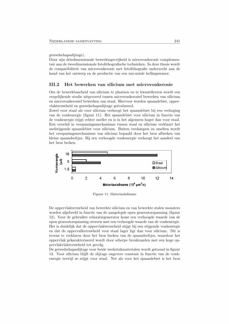
Nederlandse samenvatting 241
gereedschapsslijtage).Door zijn driedimensionale bewerkingsvrijheid is microvonkerosie complemen-tair aan de tweedimensionale fotolithografische technieken. In deze thesis wordtde compatibiliteit van microvonkerosie met fotolithografie onderzocht aan dehand van het ontwerp en de productie van een uni-axiale hellingssensor.
III.2 Het bewerken van silicium met microvonkerosie
Om de bewerkbaarheid van silicium te plaatsen en te kwantificeren wordt eenvergelijkende studie uitgevoerd tussen microvonkerosief bewerken van siliciumen microvonkerosief bewerken van staal. Hiervoor worden spaandebiet, opper-vlakteruwheid en gereedschapsslijtage geevalueerd.Zowel voor staal als voor silicium verhoogt het spaandebiet bij een verhogingvan de vonkenergie (figuur 11). Het spaandebiet voor silicium in functie vande vonkenergie stijgt echter sneller en is in het algemeen hoger dan voor staal.Een verschil in verspaningsmechanisme tussen staal en silicium verklaart hetsnelstijgende spaandebiet voor silicium. Buiten verdampen en smelten wordthet verspaningsmechanisme van silicium bepaald door het bros afbreken vankleine spaandeeltjes. Bij een verhoogde vonkenergie verhoogt het aandeel vanhet bros breken.
Figuur 11: Materiaalafname
De oppervlakteruwheid van bewerkte silicium en van bewerkte stalen monstersworden afgebeeld in functie van de aangelegde open generatorspanning (figuur12). Voor de gebruikte relaxatiegenerator komt een verhoogde waarde van deopen generatorspanning overeen met een verhoogde waarde van de vonkenergie.Het is duidelijk dat de oppervlakteruwheid stijgt bij een stijgende vonkenergieen dat de oppervalkteruwheid voor staal lager ligt dan voor silicium. Dit istevens te verklaren door het bros breken van de spaandeeltjes, waardoor hetoppervlak gekarakteriseerd wordt door scherpe breukranden met een hoge op-pervlakvlakteruwheid tot gevolg.De gereedschapsslijtage voor beide werkstukmaterialen wordt getoond in figuur13. Voor silicium blijft de slijtage ongeveer constant in functie van de vonk-energie terwijl ze stijgt voor staal. Net als voor het spaandebiet is het bros

242 III. MICROVONKEROSIETECHNOLOGIE VOOR SILICIUM
Figuur 12: Oppervlakteruwheid
Figuur 13: Relatieve elektrode sleet
breken van de spaandeeltjes voordelig voor de gereedschapsslijtage.
III.3 Opbouw van een model van demicrovonkerosietechnologie
De bewerkingskarakteristieken van microvonkerosie, zoals beschreven in vorigeparagraaf, zijn niet enkel afhankelijk van de vonkenergie. In microvonkerosieworden de bewerkingskarakteristieken beınvloed door vele factoren waaronderde pulsparameters van de vonkgenerator (die tevens de vonkenergie bepalen),de controleparameters van het servosysteem, het materiaal van de elektrodenen de eigenschappen van het dielektricum. Om de invloed van al deze para-meters op het vonkerosief bewerken van silicium te bepalen, is een experimen-

Nederlandse samenvatting 243
tenprogramma opgesteld (design of experiments) dat individuele invloeden enkruisgevoeligheden kwantificeert. Dit model wordt wiskundig hier voorgestelddoor een kwadratische functie. Met dit model kunnen de bewerkingskarakte-ristieken geschat worden voor parameterinstellingen binnen het modelbereik.Tevens kunnen de bewerkingskarakteristieken geoptimaliseerd worden gegevende vereiste bewerkingsspecificaties.
III.4 Oppervlaktekwaliteit van gevonkte structuren
De toplaag van vonkerosief bewerkte structuren is sterk beınvloed door hetthermische karakter van vonkerosie met name het cyclisch smelten en stollenvan de oppervlaktelaag. De kwaliteit van deze warmte-beınvloede toplaag be-paalt in grote mate de weerstand van de structuren tegen zowel statische alsdynamische belastingen. Een studie is verricht naar de oppervlaktekwaliteit
(a) Vonkenergie: 1.8 µJ (b) Vonkenergie: 3.2 µJ
(c) Vonkenergie: 5 µJ (d) Vonkenergie: 16 µJ
Figuur 14: Topografie van vonkerosief bewerkte silicium oppervlakken,110, op verschillende energieniveaus

244 III. MICROVONKEROSIETECHNOLOGIE VOOR SILICIUM
van gevonkte silicium oppervlakken. Als voorbeeld toont figuur 14 een aan-tal gevonkte silicium oppervlakken. De oppervlakken zijn nabehandeld meteen isotroop etsmiddel om de aanwezigheid van microscheuren te accentueren.Naarmate de vonkernergie stijgt, neemt niet enkel de oppervlakteruwheid toe(figuur 12 in paragraaf III.2) maar tevens de scheurdensiteit in de bewerktetoplaag. Opmerkelijk is dat de scheuren gealigneerd zijn volgens een bepaaldpatroon dat overeenkomt met de zwakste kristalrichtingen in het rooster vanhet monokristallijn silicium. De scheurvorming verlaagt de belastbaarheid vande bewerkte microstructuren drastisch. In deze thesis wordt een aanvullendebewerkingsstap (d.i. een etsstap) aanbevolen om de zowel de oppervlakteruw-heid als de belastbaarheid van de structuren te verbeteren.
III.5 Ontwerp en fabricatie van een uni-axiale hellings-sensor
De compatibiliteit van de microvonkerosietechnologie met fotolithografie tech-nologieen is onderzocht aan de hand van het ontwerp en de productie van eenuni-axiale hellingssensor. De hellingssensor bestaat uit een massa die opge-hangen is aan twee dubbelgevouwen microbalken, zoals geıllustreerd op figuur15. Om de soepelheid van de ophanging te verhogen zijn aanvullende gat-
1 mm
45µm
60µm
ZZ
X
Figuur 15: Uni-axiale hellingssensor
scharnieren voorzien. Wanneer de sensor roteert, verplaatst de massa zich tenopzichte van het huis. De verplaatsing van de massa wordt opgemeten metbehulp van een variabele capaciteit, waarbij de capaciteitswaarde een maat isvoor de helling van de sensor. De structuur van de hellingssensor wordt ver-vaardigd met microvonkerosie en de capaciteitsplaten worden aangebracht metfotolithografie. Figuur 16 toont SEM opnames van de mechanische structuurvan de hellingssensor. Een productieplanning en een uitlijningsprocedure zijnuitgewerkt om de sensor te realiseren gebruik makend van de twee bewerkings-technologieen (microvonkerosie-fotolithografie), waaruit een set van algemene
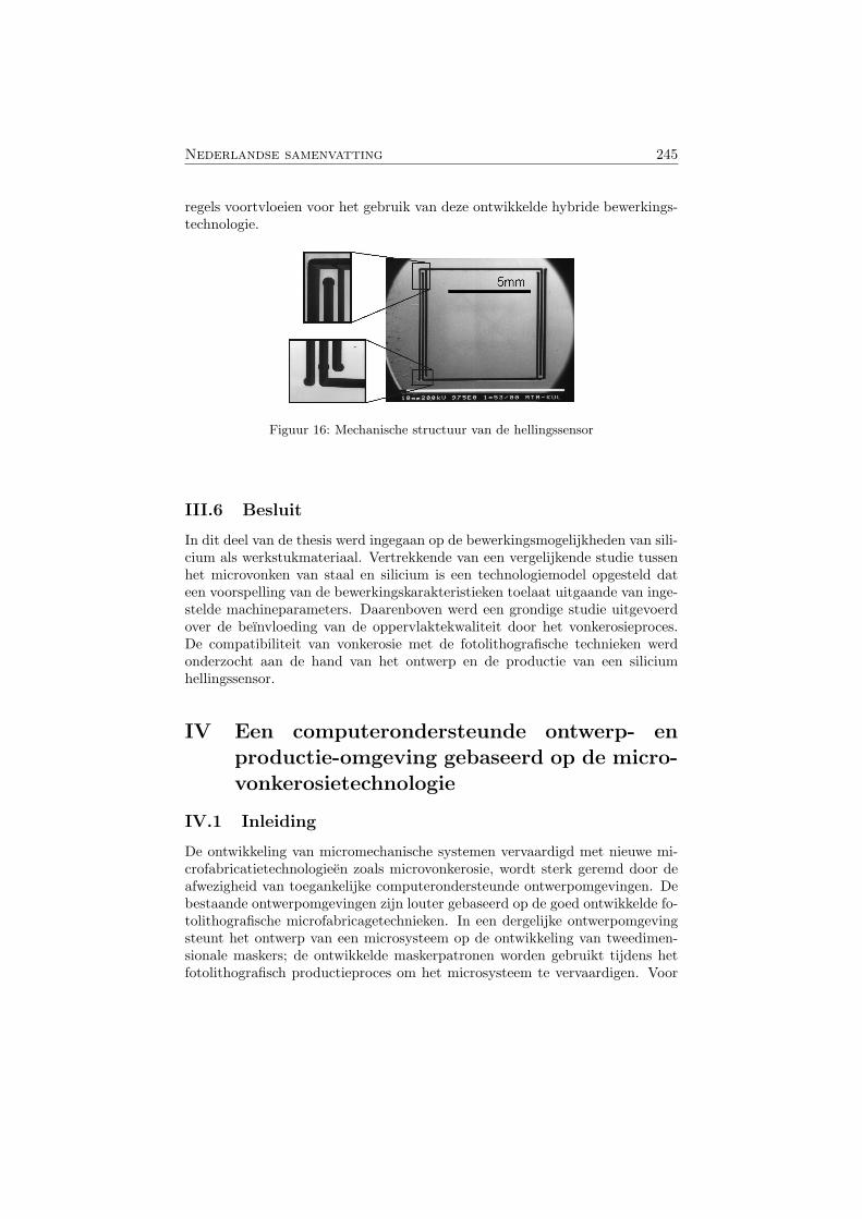
Nederlandse samenvatting 245
regels voortvloeien voor het gebruik van deze ontwikkelde hybride bewerkings-technologie.
Figuur 16: Mechanische structuur van de hellingssensor
III.6 Besluit
In dit deel van de thesis werd ingegaan op de bewerkingsmogelijkheden van sili-cium als werkstukmateriaal. Vertrekkende van een vergelijkende studie tussenhet microvonken van staal en silicium is een technologiemodel opgesteld dateen voorspelling van de bewerkingskarakteristieken toelaat uitgaande van inge-stelde machineparameters. Daarenboven werd een grondige studie uitgevoerdover de beınvloeding van de oppervlaktekwaliteit door het vonkerosieproces.De compatibiliteit van vonkerosie met de fotolithografische technieken werdonderzocht aan de hand van het ontwerp en de productie van een siliciumhellingssensor.
IV Een computerondersteunde ontwerp- enproductie-omgeving gebaseerd op de micro-vonkerosietechnologie
IV.1 Inleiding
De ontwikkeling van micromechanische systemen vervaardigd met nieuwe mi-crofabricatietechnologieen zoals microvonkerosie, wordt sterk geremd door deafwezigheid van toegankelijke computerondersteunde ontwerpomgevingen. Debestaande ontwerpomgevingen zijn louter gebaseerd op de goed ontwikkelde fo-tolithografische microfabricagetechnieken. In een dergelijke ontwerpomgevingsteunt het ontwerp van een microsysteem op de ontwikkeling van tweedimen-sionale maskers; de ontwikkelde maskerpatronen worden gebruikt tijdens hetfotolithografisch productieproces om het microsysteem te vervaardigen. Voor

246 IV. CAD&CAM VOOR MICROVONKEROSIE
microvonkerosie zou het gebruik van tweedimensionale patronen, de driedimen-sionale bewerkingsvrijheid van vonkerosie niet tot zijn recht laten komen. Indeze thesis wordt de eerste aanzet gegeven voor de ontwikkeling van een com-puterondersteunde omgeving voor het ontwerp, de verificatie en de productievan driedimensionale microsystemen met microvonkerosie als basis productie-techniek.
IV.2 Een computerondersteunde ontwerp- en productie-omgeving op basis van productie-georienteerde vor-melementen
De voorgestelde computerondersteunde ontwerp- en productieomgeving heeftvormelementen als bouwblokken. Vormelementen hebben een bepaalde fysi-sche betekenis en bevatten zowel geometrische als technologische (vb. ruw-heid, toleranties) informatie. De geometrie van een vormelement wordt ge-dreven door parameters waarvan de numerieke waarden tijdens het ontwerp-proces gewijzigd kunnen worden zodat het ontwerp eenvoudig te wijzigen is.Bekende voorbeelden van vormelementen zijn spiegleuven en getapte gaten.Twee belangrijke groepen van vormelementen zijn te onderscheiden, namelijkontwerp-georienteerde en productie-georienteerde vormelementen. Ontwerp-georienteerde vormelementen bevatten geen informatie over bewerkingsopera-ties en kunnen zowel materiaaltoevoegend als materiaalverwijderend zijn. Dezevormelementen leggen weinig ontwerpbeperkingen op en men kan op eenvoudigewijze bijkomende ontwerp-georienteerde vormelementen aanmaken. Het nadeelvan de ontwerp-georienteerde vormelementen is dat het mogelijk is om struc-turen te ontwerpen die in werkelijkheid niet produceerbaar zijn. Productie-georienteerde vormelementen daarentegen, bevatten buiten de geometrische in-formatie ook informatie over de specifieke productiestrategieen. Het voordeelvan productie-georienteerde vormelementen is dat elk vormelement vervaardig-baar is. Het nadeel van deze vormelementen is dat ze gerelateerd zijn aanbewerkingsoperaties wat soms een hinderpaal is voor de ontwerpvrijheid.In deze thesis wordt geopteerd voor productie-georienteerde vormelementenuit het oogpunt van de produceerbaarheidsgarantie. Wanneer de produceer-baarheid van een ontwerp gegarandeerd is, kunnen de gereedschapsbanen voorelk vormelement automatisch gegenereerd worden en kan tevens de bewer-kingsstrategie geoptimaliseerd worden. Figuur 17 toont een algemeen sche-ma van de geımplementeerde computerondersteunende ontwerp- en productie-omgeving met microvonkerosie als basis productietechnologie. Het gebruikvan een beperkte bibliotheek met voorgedefinieerde vormelementen beperktde ontwerpvrijheid. Om de bewerkingsvrijheid van vonkerosie te reflecterenin de geımplementeerde ontwerpomgeving, laat deze ontwerpomgeving de ont-wikkeling van nieuwe productie-georienteerde vormelementen toe. De ontwer-pomgeving bevat een module voor de ontwikkeling van aanvullende vormele-menten waarin de produceerbaarheid van de nieuw-ontwikkelde vormelemen-ten geevalueerd wordt. Verder bevat de ontwerpomgeving een module voor

Nederlandse samenvatting 247
Microvonkerosie
Bibliotheekmet vorm-elementen
Voorgedefi-nieerde elem.
Extraelementen
Microsysteem-ontwerp
Produceerbaar-heidscontrole
Microsysteem-simulatie
Procesplanning
Microvonkero-sietechnologie
Procesparameter-optimalisatie en
sleetcompensatie
AGIE Compactmachinecode
Ontwikkeling vanextra vormelem.
Produceerbaar- heidscontrole
Gereedschapsbaan- generatie
Generatie van demachinecode
Figuur 17: Algemene structuur van de voorgestelde computerondersteun-de ontwerp- en productie-omgeving voor microstructuren metmicrovonkerosie als basis productietechnologie
systeemsimulatie. Wanneer het ontwerp voldoet aan de vooropgestelde specifi-caties, gaat het ontwerp door naar de procesplanning die een optimale bewer-kingsstrategie bepaalt. In de laatste fase wordt de gereedschapsbaan gecreeerd,de elektrodeslijtage gecompenseerd en de procesparameters geoptimaliseerd.
IV.3 Voorgedefinieerde en aanvullende vormelementen
Door het beperkte aanbod aan voorgedefinieerde vormelementen is het somsniet mogelijk de gewenste geometrie te ontwerpen. Omdat microvonkerosieeen grotere bewerkingsvrijhheid toelaat dan met de voorgedefinieerde vorm-elementen realiseerbaar, maakt de ontwikkelde ontwerpomgeving het mogelijkom aanvullende vormelementen te definieren. Figuur 18 toont de mechani-sche structuur van een inertiele sensor, waarbij de massa is opgehangen aaneen dunne balk. Deze structuur kan worden opgebouwd met voorgedefinieerdevormelementen zoals afgebeeld in figuur 18(a). De vormelementen worden ge-positioneerd ten opzichte van het basis vormelement of ten opzichte van vooraf

248 IV. CAD&CAM VOOR MICROVONKEROSIE
(a) Voorgedefinieerde vormelementen (b) Positionering van vormelementen
Figuur 18: Structuur van een inertiele sensor ontworpen met voorgedefini-eerde vormelementen
gepositioneerde vormelementen (figuur 18(b)). Wanneer de ophanging echteruit twee microbalken zou bestaan zoals geıllustreerd op figuur 19, vereist degeometrie een aanvullend vormelement. Een aanvullend vormelement wordt
Figuur 19: Aanvullende vormelementen
gecreeerd op basis van een standaard cilindrische elektrode die vervolgens be-werkt wordt met de microdraadvonkmodule. Met een gepaste gereedschaps-baan voor deze gereedschapselektrode bekomt men de gewenste geometrie. Inde ontwerpomgeving wordt de produceerbaarheid van aanvullende vormelemen-ten geverifieerd alvorens ze definitief kunnen gebruikt worden in een ontwerp.

Nederlandse samenvatting 249
IV.4 Simulatie van microsystemen
De functionaliteit van het ontworpen microsysteem wordt gesimuleerd om devooropgestelde specificaties virtueel te verifieren. Huidige simulatiepakkettenstaan sterk op het gebied van statische en dynamische structurele analyse,elektrostatische analyse, thermische analyse en alle combinaties daarvan (d.i.gekoppelde analyse). In deze thesis wordt vooral aandacht besteed aan de ont-wikkeling van een simulatiemodule waarin het effect van de bewerkingstoleran-ties op het werkingsgedrag van de ontworpen componenten geverifieerd worden.Door aan de geometrie van alle vormelementen een bewerkingstolerantie toe tekennen, kan het effect op bijvoorbeeld de spreiding van een eigenfrekwentiegesimuleerd worden.
IV.5 Controle van de produceerbaarheid
Een algemene produceerbaarheidscontrole garandeert de produceerbaarheidvan de ontworpen microstructuur. Alhoewel alle vormelementen productie-georienteerde vormelementen zijn die per definitie produceerbaar zijn, is eenalgemene produceerbaarheidscontrole noodzakelijk. Bij het ontwerp van bij-voorbeeld een dunne balkvormige structuur, worden twee doorgaande vorm-elementen naast elkaar geplaatst zoals geıllustreerd op figuur 20(a). Wanneer
Doorgaande vormelementen
(a) Dunne microbalk
VormelementVeiligheids- volume
(b) Veiligheidsvolume voorenkele vlakken van de cavi-teit
(c) Indicatie van degevarenzone
Figuur 20: Produceerbaarheidscontrole
de vormelementen, die individueel produceerbaar zijn, dichter bij elkaar wor-den geplaatst, zal in bepaalde omstandigheden de dunne balk de vonkerosievebewerking niet meer weerstaan, wat leidt tot breuk. Daarom wordt vooropge-steld dat elk oppervlak in de ontworpen microstructuur voldoende sterk moetzijn. In de geımplementeerde ontwerpomgeving wordt voor elk oppervlak nage-gaan of achter dit oppervlak voldoende materiaal aanwezig is om de sterkte tegaranderen. Voor elk oppervlak wordt een veiligheidsvolume gegenereerd dat

250 IV. CAD&CAM VOOR MICROVONKEROSIE
volledig in de ontworpen structuur dient te liggen om de produceerbaarheidte garanderen (figuur 20(b)). Figuur 20(c) toont een dunne balk waarvan deveiligheidsvolumes niet in de structuur liggen, waardoor de produceerbaarheidvan deze balk niet gegarandeerd is.Er moet opgemerkt worden dat de voorgestelde veiligheidsvolumes afhankelijkmoeten zijn van de procesparameters. Een hoge vonkenergie zal een diepere pe-netratie van de warmte-beınvloede zone veroorzaken zodat een ruimere margeop de veiligheidsvolumes moet genomen worden. Daarom is het noodzakelijkdat deze test herhaald wordt wanneer alle procesparameters bepaald zijn.
IV.6 Generatie van de gereedschapsbanen, sleetcompen-satie en optimalisatie van de machineparameters
Wanneer de structuur ontworpen is en wanneer ook de produceerbaarheid ge-garandeerd is, worden de gereedschapsbanen gegenereerd voor de individuelevormelementen. Door het gebruik van productie-georienteerde vormelementenkan de productiestrategie geoptimaliseerd worden voor elk vormelement uit-gaande van zijn afmetingen en gewenste afwerkingsnauwkeurigheid. Figuur21(a) toont als voorbeeld van een gereedschapsbaan bestaande uit twee be-werkingslagen. De slijtage van de gereedschapselektrode wordt gecompenseerddoor gebruik te maken van achtereenvolgende identieke elektrodevormen zoalsbeschreven in paragraaf II.3. Ook worden de instelbare machineparametersvan de AGIE Compact 1 geoptimaliseerd gebruikmakend van het microvon-kerosietechnologiemodel besproken in paragraaf III.3. De parameters wordengeoptimaliseerd met het oog op een maximalisatie van het spaandebiet rekeninghoudend met de gewenste oppervlakteruwheid en een geringe slijtage aan degereedschapselektrode. Figuur 21(b) toont een dialoogvenster met geoptima-liseerde machineparameters en een schatting van de bewerkingsprestaties vooreen bepaald vormelement uit het ontwerp.
IV.7 Toepassingsvoorbeeld
De werking van de ontwikkelde computerondersteunde ontwerpomgeving wordtaan de hand van een voorbeeld aangetoond. Figuur 22 toont enkele stappenvan het ontwerpproces van een kort microkanaal. De vorm van het kanaalis niet realiseerbaar met voorgedefinieerde vormelementen zodat het ontwerpvan een aanvullend vormelement noodzakelijk is. Wanneer het kanaal ontwor-pen is en de produceerbaarheid gecontroleerd, genereert de ontwerpomgevingde machinecode en de daarbijhorende machineparameters. Vervolgens kan demicrovonkmachine de opeenvolgende bewerkingen uitvoeren zonder operatorin-terventies. Eerst wordt de gereedschapselektrode aangemaakt met behulp vande microdraadvonkmodule waarna het kanaal in het werkstuk wordt aange-bracht. Figuur 22 toont een microkanaal en de gereedschapselektrode.
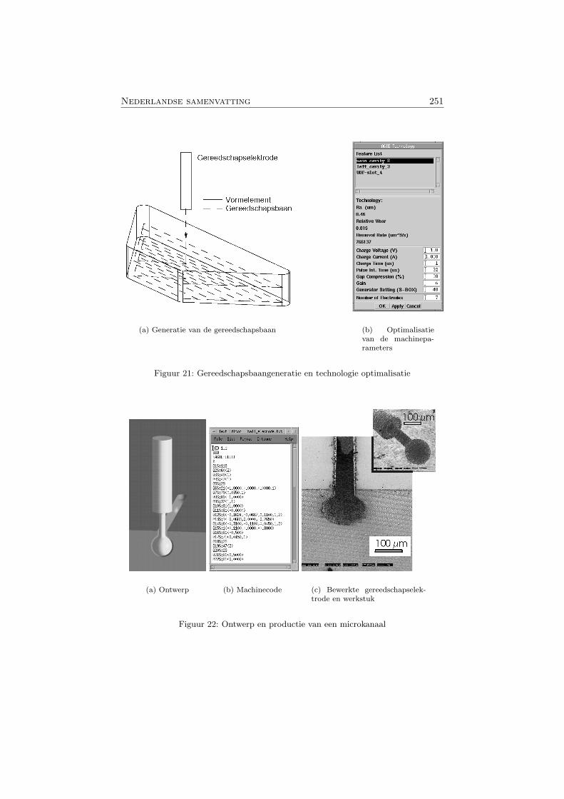
Nederlandse samenvatting 251
(a) Generatie van de gereedschapsbaan (b) Optimalisatievan de machinepa-rameters
Figuur 21: Gereedschapsbaangeneratie en technologie optimalisatie
(a) Ontwerp (b) Machinecode (c) Bewerkte gereedschapselek-trode en werkstuk
Figuur 22: Ontwerp en productie van een microkanaal

252 V. ALGEMEEN BESLUIT
IV.8 Besluit
In dit deel van de thesis werd dieper ingegaan op de ontwikkeling van eencomputerondersteunde ontwerp- en productie-omgeving voor driedimensiona-le microstructuren met microvonkerosie als basis bewerkingstechnologie. Debouwelementen van de ontwerpomgeving zijn productie-geortienteerde vorm-elementen, opgesplitst in voorgedefinieerde en aanvullende elementen. Voorde aanvullende vormelementen is een controlemodule geımplementeerd die deproduceerbaarheid van de nieuwe vormelementen garandeert. Verder wordende gereedschapsbanen automatisch gecreeerd rekening houdend met de slijta-ge van een gereedschapselektrode en worden de instelbare machineparametersgeoptimaliseerd.
V Algemeen besluit
Deze thesis behandelt de opbouw van een bewerkingstechnologie voor de pro-ductie van driedimensionale microstructuren met behulp van microvonkerosie.Aandacht werd besteed aan de ontwikkeling van een microdraadvonkmodule diehet mogelijk maakt de gereedschapselektrode vorm te geven. Op technologischvlak zijn bewerkingsstrategieen ontwikkeld om slijtage aan de gereedschaps-elektrode te compenseren en is een statistische modeleringstechniek voorge-steld voor de opbouw van het microvonkerosietechnologiemodel. Daarenbovenis een grondige studie uitgevoerd naar de oppervlaktekwaliteit van bewerktecomponenten en naar de invloed van de oppervlaktekwaliteit op de belastbaar-heid van de microstructuren. De bewerkingsmogelijkheden van de opgebouwdemicrovonkerosietechnologie werden aangetoond aan de hand van verscheidenevoorbeelden en toepassingen. In de laatste fase van het doctoraatswerk is eenontwerp- en productie-omgeving gerealiseerd die de bewerkingsvrijheid van mi-crovonkerosie reflecteert. Op basis van productie-georienteerde vormelementenkan een microstructuur worden opgebouwd waarna gepaste gereedschapsbanenen machineparameters automatisch worden gegenereerd.