UNIVERSITA' DEGLI STUDI DI PADOVA - Padua@Research
182
UNIVERSITA' DEGLI STUDI DI PADOVA Sede Amministrativa: Università degli Studi di Padova Dipartimento di Scienze Chimiche SCUOLA DI DOTTORATO IN SCIENZA ED INGEGNERIA DEI MATERIALI CICLO XXI Tesi di Dottorato SMALL CRYSTAL MODELS FOR THE ELECTRONIC PROPERTIES OF CARBON NANOTUBES Direttore della Scuola : Prof. GAETANO GRANOZZI Supervisore : Prof. MORENO MENEGHETTI Dottoranda : JESSICA ALFONSI Matricola: 964499-DR 31 Dicembre 2008
-
Upload
khangminh22 -
Category
Documents
-
view
2 -
download
0
Transcript of UNIVERSITA' DEGLI STUDI DI PADOVA - Padua@Research

UNIVERSITA' DEGLI STUDI DI PADOVASede Amministrativa: Università degli Studi di Padova
Dipartimento di Scienze Chimiche
SCUOLA DI DOTTORATO IN SCIENZA ED INGEGNERIA DEI MATERIALI
CICLO XXI
Tesi di Dottorato
SMALL CRYSTAL MODELS FOR
THE ELECTRONIC PROPERTIES OF CARBON NANOTUBES
Direttore della Scuola : Prof. GAETANO GRANOZZI
Supervisore : Prof. MORENO MENEGHETTI
Dottoranda : JESSICA ALFONSI
Matricola: 964499DR
31 Dicembre 2008


Meglio soli che male accompagnati, ma . . .. . . l’unione fa la forza !


i
Riassunto
Questa tesi sviluppa gli aspetti teorici basilari delle proprieta elettroniche dei nanotubidi carbonio che sono necessari per una comprensione dettagliata delle misure di carat-terizzazione ottica tramite fotoluminescenza e spettroscopia Raman. Nella prima partedi questo lavoro vengono introdotte le nozioni generali suinanotubi di carbonio, la lorostruttura geometrica e i fondamenti delle proprieta elettroniche ed ottiche. Queste pro-prieta sono state descritte sulla base di un calcolo tight-binding svolto in spazio reciproco,noto anche come schemazone-folding, che e stato ampiamente utilizzato negli studiteorici sulla struttura elettronica dei nanotubi. In particolare, si e posta grande attenzioneai punti speciali della zona di Brillouin che giocano un ruolo critico nella densita deglistati e negli elementi di matrice elettrone-fotone dei nanotubi a parete singola, dandocosı il contributo essenziale dominante agli spettri di assorbimento ottico di questi sis-temi. La conoscenza dei vettori d’onda critici nella zona diBrillouin e di fondamentaleimportanza per un’applicazione saggia dell’approccio delcristallo piccolo (small crystalapproach), che costituisce il contributo originale di questa tesi e che viene introdotto nelCap. 4. Partendo da una porzione finita del reticolo reale opportunamente scelta con con-dizioni periodiche al contorno appropriate, l’approcciosmall crystalconsente di trovarel’insieme piu piccolo di punti della zona di Brillouin che sono sufficienti per calcolareil profilo essenziale degli spettri ottici di sistemi periodici, come i nanotubi a parete sin-gola. Il Cap. 4 stabilisce l’equivalenza completa tra i metodi di tipo small crystale zonefolding, applicati ai calcoli tight-binding della struttura elettronica per semplici sistemimodello e nanotubi a parete singola. La visione in spazio reale presente nell’approcciodel cristallo piccolo consente di superare le limitazioni inerenti ai metodi in spazio re-ciproco, quando si debbano considerare effetti di rottura locale di simmetria nella strutturaelettronica dei nanotubi di carbonio, come interazioni elettrone-elettrone, difetti puntu-ali e interazioni intertubo dipendenti dall’orientazionedei tubi costituenti, quest’ultimonel caso particolare dei nanotubi a parete doppia. I Capp. 5 e6 mostrano l’applicazionedell’approccio small crystal a questi problemi e i risultati ottenuti vengono discussi inrelazione alle attuali conoscenze sperimentali e teoriche. In particolare, i nanotubi aparete doppia sono ampiamente studiati per le promettenti applicazioni biologiche e na-noelettromeccaniche. Un’adeguata modellizzazione dell’accoppiamento intertubo dipen-dente dall’orientazione delle pareti costituenti questi sistemi e necessaria per interpretarele caratterizzazioni sperimentali Raman di questi sistemi. Data la sua formulazione inspazio reale, l’approccio small crystal offre la flessibilita di variare l’orientazione mu-tua delle pareti costituenti e i parametri che descrivono l’intensita dell’interazione inter-tubo. I nostri calcoli mostrano variazioni importanti negli spettri di assorbimento otticidei nanotubi a parete doppia, che rendono conto delle difficolta solitamente riscontratenell’assegnazione dei picchi Raman ai diametri e chiralit`a dei tubi costituenti. Infine,le proprieta eccitoniche dei nanotubi costituiscono forse la questione piu discussa nellascienza dei nanotubi, sia teorica che sperimentale. Il Cap.6 prende in rassegna re-

ii
centi calcoli presenti in letteratura su questo problema e mostra l’applicazione ultimadell’approccio small crystal per introdurre gli effetti dicorrelazione coulombiana nelladescrizione di particella singola, secondo il modello di Hubbard. Selezionando unaporzione sufficientemente piccola del reticolo reale con opportune condizioni periodicheal contorno, si puo impostare un calcolo many-body completo che consente di ottenereuna descrizione qualitativa delle proprieta elettroniche dei nanotubi a parete singola cherisulta essere consistente con l’attuale descrizione dei livelli eccitonici di questi sistemifornita dalle tecnicheab initio. Anche se limitata da stringenti requisiti computazionalisulla dimensione dei sistemi trattati, che potranno esseresuperati con tutta probabilitausando algoritmi piu raffinati, la semplice implementazione fornita in questa tesi con-ferma che per questo metodo si possono certamente prospettare interessanti sviluppi perlo studio delle proprieta di stato eccitato di tubi a diametro grande e per la trattazionedell’inclusione di difetti puntuali in questi sistemi.
iii
Abstract
This thesis develops the basic theoretical aspects of the electronic properties of carbonnanotubes which are necessary for a detailed understandingof optical characterizationmeasurements by photoluminescence and Raman spectroscopy. In the first part of thiswork I introduced the general facts about carbon nanotubes,their geometrical structureand the fundamentals of their electronic and optical properties. These properties havebeen described on the basis of a tight-binding calculation scheme carried in reciprocalspace, also calledzone-foldingscheme, which has been widely adopted in theoretical in-vestigations on nanotube electronic structure. In particular, great attention has been paidto the special Brillouin zone points which play a critical role in the density of states andelectron-photon matrix elements of single-walled nanotubes, thus giving the essentialdominant contribution to the optical absorption spectra ofthese systems. The knowl-edge of the critical wavevectors in the Brillouin zone is of fundamental importance fora wise application of thesmall crystal approach, which constitutes the original contri-bution of this thesis and is introduced in Chapt. 4. Startingfrom a wisely chosen finiteportion of the real lattice with proper boundary conditions, the small crystal approachallows to find the minimal set of Brillouin zone points, whichare sufficient for comput-ing the essential features of the optical spectra of periodic systems, such as single-wallednanotubes. Chapt. 4 establishes the full equivalence between small crystal and zone fold-ing methods applied to tight-binding electronic structurecalculations for simple modelsystems and single-walled nanotubes. The real space visionembedded in small crystalapproach allows to overcome some limitations inherent to reciprocal space based meth-ods, when dealing with local symmetry breaking effects in the electronic structure ofcarbon nanotubes, such as electron-electron interactions, point-defects and orientation-dependent intertube interactions, the last one in the particular case of double-walled nan-otubes. Chapters 5 and 6 show the application of small crystal approach to these issuesand discuss the obtained results with respect to the currently available experimental andtheoretical findings. In particular, double-walled nanotubes are widely investigated dueto promising biological and nanoelectromechanical applications. An adequate modelingof the orientation dependent interwall coupling effects onthe optical spectra is neces-sary for interpreting experimental Raman characterizations of these systems. Given itsreal space formulation, the small crystal approach offers the flexibility of changing themutual orientation of the constituent walls and the parameters describing the strengthof the interwall interaction. Our calculations show that important changes occur in theoptical absorption spectra of double-walled nanotubes which can account for the usualdifficulty in assigning experimental Raman features to the diameters and chiralities of theconstituent tubes. Finally, excitonic properties of single-walled nanotubes are perhapsthe most debated issues both in experimental and theoretical nanotube science. Chapt. 6reviews recent literature many-body calculations on this subject and shows the ultimateapplication of small crystal approach for introducing Coulomb correlation effects in the
iv
single-particle picture, according to the Hubbard model. By selecting a sufficiently smallportion of the real lattice with suitable boundary conditions, a full many-body calculationcan be set up which allow to obtain a qualitative descriptionof the electronic propertiesof single-walled nanotubes, which is found to be consistentwith the current picture ofexcitonic levels for these systems provided byab initio techniques. Although limited bystrict computational requirements on the system size, which are likely to be overcomeby using more refined algorithms, the simple implementationprovided in this thesis con-firms that interesting developments can be certainly prospected for this method, in orderto investigate excited state properties of larger diametertubes and treating the inclusionof point defects in these systems.
Publications
Related papers and conference participations during my PhDare listed in the following.
Papers J. Alfonsi and M. Meneghetti,Small crystal approach for the electronic proper-ties of double-wall carbon nanotubes(under review, submitted toNew Journal of Physics)
J. Alfonsi and M. Meneghetti,Small crystal Hubbard model for the excitonic proper-ties of zigzag single wall carbon nanotubes(in preparation)
Posters J. Alfonsi and M. Meneghetti,Small crystal approach for studying the elec-tronic spectra of carbon nanotubes, 213th Meeting of the ElectroChemical Society, 18-22 May 2008 , Phoenix (Arizona), U.S.
J. Alfonsi and M. Meneghetti,Small crystal approach for the optical properties of carbonnanotubes, TransAlpNano 2008, 27-29 Octorber 2008, Lyon (France)
Other papers F. G. Brunetti, M. A. Herrero, J. de M. Munoz, A. Daz-Ortiz,J. Alfonsi,M. Meneghetti, M. Prato and E. Vaazquez,Microwave-Induced Multiple Functionaliza-tion of Carbon Nanotubes, J. Am. Chem. Soc.30, n. 20, 40
S. Giordani, J-F. Colomer, F. Cattaruzza, J. Alfonsi, M. Meneghetti, M. Prato, D. Boni-fazi, Multifunctional hybrid materials composed of [60]fullerene- based functionalized-single-walled carbon nanotubes, Carbon, (in press)
v
Foreword
The present thesis is submitted in candidacy for the Ph.D. degree within thePhD Schoolin Materials Science and Engineeringat the University of Padua. The thesis describesparts of the work that I have carried out under supervision ofProf. Moreno Meneghettifrom Nanophotonics Laboratory in the Department of Chemical Sciences, University ofPadua. I thank him for kindly introducing me to small crystalmodeling of Hubbard chainsand for supporting me in the preparation of article manuscripts and poster presentations.Technical support for Linux and LICC cluster by Ing. G. Sellaand M. Furlan is alsogratefully acknowledged. I also would like to thank Google,Wolfram Research, Ubuntuand, in general, the whole Open Source Community for providing me a wonderful mineof information and formidable pieces of software.During my research I have benefitted from correspondance with physicists from widelyrecognized international research groups. In particular,I’d like to mention A. Gruneis,G. Ge. Samsonidze and N. Nemec for their extremely helpful correspondence. Also, I’dlike to thank Dr. A. Thumiger from Prof. Zanotti’s group for helping me with practicalissues in working with Discrete Fourier Transform.Last but not least important, this thesis is dedicated to my parents, family and all thosepeople who have always been extremely supporting and who canrecognize themselvesin this acknowledgment words.
Padua, 31 December, 2008
Jessica Alfonsi
Document typeset in LATEX 2ε
Contents
1 Introduction 11.1 Carbon and its allotropic forms . . . . . . . . . . . . . . . . . . . . .. . 1
1.1.1 Hybridization of carbon orbitals . . . . . . . . . . . . . . . . .. 11.1.2 Graphite . . . . . . . . . . . . . . . . . . . . . . . . . . . . . . . 41.1.3 Graphene . . . . . . . . . . . . . . . . . . . . . . . . . . . . . . 51.1.4 Fullerene . . . . . . . . . . . . . . . . . . . . . . . . . . . . . . 61.1.5 Single-wall and multi-wall nanotubes . . . . . . . . . . . . .. . 71.1.6 Other graphitic nanostructures . . . . . . . . . . . . . . . . . .. 10
1.2 Nanotube characterization techniques . . . . . . . . . . . . . .. . . . . 111.2.1 Characterization techniques . . . . . . . . . . . . . . . . . . . .111.2.2 Photoluminescence and optical absorption measurements . . . . . 121.2.3 Resonant Raman spectroscopy . . . . . . . . . . . . . . . . . . . 13
1.3 Electronic structure computational methods . . . . . . . . .. . . . . . . 171.4 Summary . . . . . . . . . . . . . . . . . . . . . . . . . . . . . . . . . . 20
2 Geometry of single-wall carbon nanotubes 232.1 Graphene lattice in real and reciprocal space . . . . . . . . .. . . . . . . 232.2 Nanotube unit cell in real space . . . . . . . . . . . . . . . . . . . . .. . 242.3 Nanotube reciprocal space: the cutting lines . . . . . . . . .. . . . . . . 262.4 Generating coordinates of SWNTs . . . . . . . . . . . . . . . . . . . .. 29
2.4.1 Saito and Dresselhaus’ convention . . . . . . . . . . . . . . . .. 292.4.2 Nemec and Cuniberti’s convention . . . . . . . . . . . . . . . . .312.4.3 Damnjanovic’s convention . . . . . . . . . . . . . . . . . . . . . 32
2.5 Symmetry of SWNTs . . . . . . . . . . . . . . . . . . . . . . . . . . . . 332.6 Summary . . . . . . . . . . . . . . . . . . . . . . . . . . . . . . . . . . 35
3 The zone folding method 373.1 Electronic structure of a graphene sheet . . . . . . . . . . . . .. . . . . 37
3.1.1 Schrodinger equation within the tight-binding framework . . . . . 383.1.2 Graphene electronic hamiltonian forπ-electrons . . . . . . . . . 413.1.3 Graphene electronic band structure forπ-electrons . . . . . . . . 43
vi
CONTENTS vii
3.2 Electronic structure of SWNTs . . . . . . . . . . . . . . . . . . . . . .. 443.2.1 Metallicity condition for SWNTs . . . . . . . . . . . . . . . . . 463.2.2 Critical k-points giving van Hove singularities . . . .. . . . . . 493.2.3 Density of electronic states . . . . . . . . . . . . . . . . . . . . .50
3.3 Optical properties of graphene and SWNTs . . . . . . . . . . . . .. . . 523.3.1 Electron-photon interaction and dipole approximation . . . . . . 523.3.2 Dipole vector in graphene . . . . . . . . . . . . . . . . . . . . . 543.3.3 Dipole vector in SWNTs . . . . . . . . . . . . . . . . . . . . . . 573.3.4 Dipole selection rules in SWNTs . . . . . . . . . . . . . . . . . . 573.3.5 SWNT optical matrix elements and critical wavevectors . . . . . 59
3.4 Summary . . . . . . . . . . . . . . . . . . . . . . . . . . . . . . . . . . 64
4 Small crystal approach 654.1 Basic facts behind the Small Crystal Approch . . . . . . . . . .. . . . . 654.2 SC approach applied to simple 1D and 2D models . . . . . . . . . .. . . 67
4.2.1 Reciprocal space diagonalization . . . . . . . . . . . . . . . .. . 674.2.2 Real space diagonalization . . . . . . . . . . . . . . . . . . . . . 70
4.3 SC approach for one unit cell SWNT clusters . . . . . . . . . . . .. . . 724.3.1 Choice of the cluster and hamiltonian diagonalization . . . . . . . 744.3.2 Symmetry analysis of the sampled eigenstates . . . . . . .. . . . 75
4.4 SC approach using supercells . . . . . . . . . . . . . . . . . . . . . . .. 764.4.1 Choice of the cluster . . . . . . . . . . . . . . . . . . . . . . . . 774.4.2 Symmetry analysis of the eigenstates . . . . . . . . . . . . . .. 78
4.5 SC approach with a Bloch phase factor . . . . . . . . . . . . . . . . .. . 794.6 SC optical absorption matrix elements and spectra . . . . .. . . . . . . . 804.7 Summary . . . . . . . . . . . . . . . . . . . . . . . . . . . . . . . . . . 85
5 Double-wall carbon nanotubes 875.1 Introductory remarks . . . . . . . . . . . . . . . . . . . . . . . . . . . . 875.2 Structure and symmetry properties . . . . . . . . . . . . . . . . . .. . . 885.3 Small crystal approach for the electronic structure of DWNTs . . . . . . . 91
5.3.1 Electronic band structure and stable configurations .. . . . . . . 925.3.2 Optical properties . . . . . . . . . . . . . . . . . . . . . . . . . . 955.3.3 Conclusions, summary and future perspectives . . . . . .. . . . 98
6 Electronic correlation effects 1016.1 Many-body effects and electronic correlations in SWNTs. . . . . . . . . 101
6.1.1 Experimental evidence for the limits of tight-binding . . . . . . . 1016.1.2 Theoretical investigations of exciton photophysicsin SWNTs . . 103
6.2 Hubbard model and SC approach . . . . . . . . . . . . . . . . . . . . . . 1076.2.1 The physics of the Hubbard model . . . . . . . . . . . . . . . . . 108

viii CONTENTS
6.2.2 The Hubbard model for a periodic M-site chain . . . . . . . .. . 1116.2.3 Reduction of the basis size and application to small clusters . . . 113
6.3 Computational details . . . . . . . . . . . . . . . . . . . . . . . . . . . .1166.4 Results . . . . . . . . . . . . . . . . . . . . . . . . . . . . . . . . . . . . 1216.5 Other applications: doping and defects . . . . . . . . . . . . . .. . . . . 1306.6 Conclusions, summary and future perspectives . . . . . . . .. . . . . . . 133
7 Summary and Conclusions 137
A 141A.1 Velocity operator for a periodic Hubbard chain . . . . . . . .. . . . . . 141A.2 Velocity operator generalized to two-dimensional systems . . . . . . . . . 142
B 145B.1 Cluster (4,0) with4 n sites . . . . . . . . . . . . . . . . . . . . . . . . . 145B.2 Cluster (5,0) with4 n sites . . . . . . . . . . . . . . . . . . . . . . . . . 146B.3 Cluster (4,0) with2n sites . . . . . . . . . . . . . . . . . . . . . . . . . . 148B.4 Cluster (5,0) with2n sites . . . . . . . . . . . . . . . . . . . . . . . . . . 149
Chapter 1
Introduction
In this chapter we give a general overview aboutsp2-hybridized carbon materials. Inparticular, we focus on nanotube structural properties, preparation and characterizationtechniques. In the final section, we provide a general classification of the main compu-tational methods, which are heavily adopted in computational materials science for theinvestigation the electronic properties of these systems.
1.1 Carbon and its allotropic forms
Carbon is one of the most abundant chemical species in the universe and the fundamentalbuilding block of all organic structures and living organisms, together with hydrogen,oxygen and nitrogen. This is mainly due to the special position occupied by this elementin the periodic table, which allows a single C atom to form up to four covalent bondsto its neighboring atoms. Until the Eighties, it was believed that the only crystallineallotropic forms were diamond and graphite. This picture started to change in 1985 withthe discovery of fullerenes [1], when it became clear that carbon can form other stablecrystalline forms. After the identification of carbon nanotubes in 1991 by Iijima [11], thelist of observed and hypothetically proposed carbon nanostructures started to grow soon,including double- and multi-shell fullerenes and nanotubes and many other structures,some of which will be presented in the final part of this section.
1.1.1 Hybridization of carbon orbitals
The electronic configuration of a free carbon atom is1s22s22p2. The electrons in the1s orbitals are the core electrons, while the remaining four electrons in the 2s and 2porbitals are the valence electrons and are available to formchemical bonds. We recall thatthe electronic wavefunction of an atom can be obtained as an eigenstate of the angularmomentum operator. The 2p degenerate orbitals have identical geometrical shape forthe three different orientations, as shown in Fig. 1.1. Although the 2s are filled in the
1

2 CHAPTER 1. INTRODUCTION
ground state by two electrons, the energy difference between 2sand the three degenerate2p orbitals is small enough, that hybridization of these orbitals occurs in several ways.Depending on the hybridization, different structures can be obtained, since a differentnumber of nearest neighbour atoms are required.
• Hybridization of the2s with one2p orbital gives a set of twosporbitals in diamet-rically opposed directions.
|2spa〉 =1√2
(|2s〉+|2py〉) (1.1)
|2spb〉 =1√2
(|2s〉−|2py〉)
This is the so calledsp-hybridization(n = 1), which is relevant for organic molecules(acetylene), but not for crystalline carbon structures.
• Hybridization of the2s with two 2p orbital results in three equivalentsp2 orbitalsarranged in plane and pointing each at an angle of120o from one another:
|2sp2a〉 =
1√3
(|2s〉+
√2|2px〉
)(1.2)
|2sp2b〉 =
1√3
(|2s〉 − |2px〉√
2+
√3|2py〉√
2
)
|2sp2c〉 =
1√3
(|2s〉 − |2px〉√
2−√
3|2py〉√2
)
These orbitals can form strong covalentσ bonds with neighboring carbon atomsgiving rise to planar crystalline structures. The remaining unhybridizedpz orbitalis perpendicular to the plane and forms the so called valenceπ orbitals with otherparallelpz orbitals of neighboring atoms. Valenceπ orbitals are strongly delocal-ized, therefore they are responsible for the electronic andoptical properties of thesp2 structures in the visible range (1-3 eV), as it happens with graphite.
• Hybridization of the2s with all three2p orbital results in four equivalentsp3 or-bitals in a tetrahedral arrangement at an angle of109.5o (tetrahedral angle):
|2sp3a〉 =
1
2(|2s〉+|2px〉+|2py〉+|2pz〉) (1.3)
|2sp3b〉 =
1
2(|2s〉+|2px〉−|2py〉−|2pz〉)
|2sp3c〉 =
1
2(|2s〉−|2px〉+|2py〉−|2pz〉)
|2sp3d〉 =
1
2(|2s〉−|2px〉−|2py〉+|2pz〉)
1.1. CARBON AND ITS ALLOTROPIC FORMS 3
These orbitals form four strong covalentσ bonds with the neighboring carbonatoms but are electronically inactive because of their low energy. Hence the result-ing material will have very stiff geometry and insulating properties, as for instancediamond.
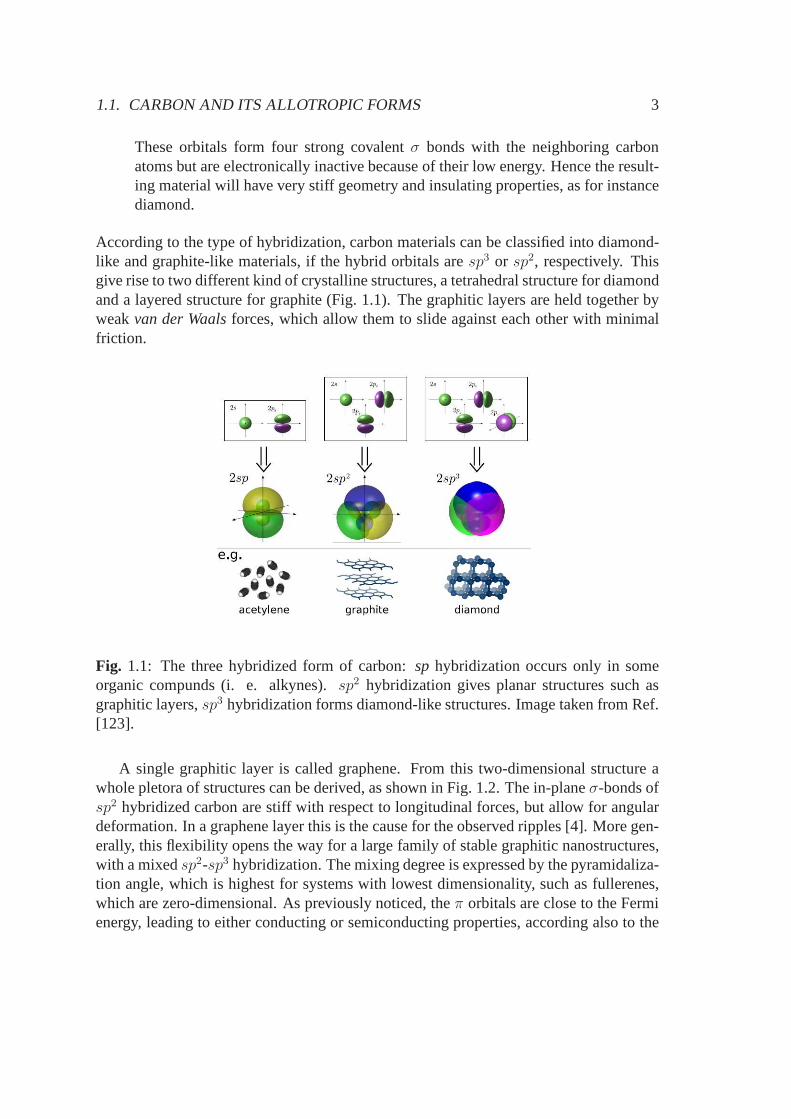
According to the type of hybridization, carbon materials can be classified into diamond-like and graphite-like materials, if the hybrid orbitals are sp3 or sp2, respectively. Thisgive rise to two different kind of crystalline structures, atetrahedral structure for diamondand a layered structure for graphite (Fig. 1.1). The graphitic layers are held together byweakvan der Waalsforces, which allow them to slide against each other with minimalfriction.
Fig. 1.1: The three hybridized form of carbon:sp hybridization occurs only in someorganic compunds (i. e. alkynes).sp2 hybridization gives planar structures such asgraphitic layers,sp3 hybridization forms diamond-like structures. Image takenfrom Ref.[123].
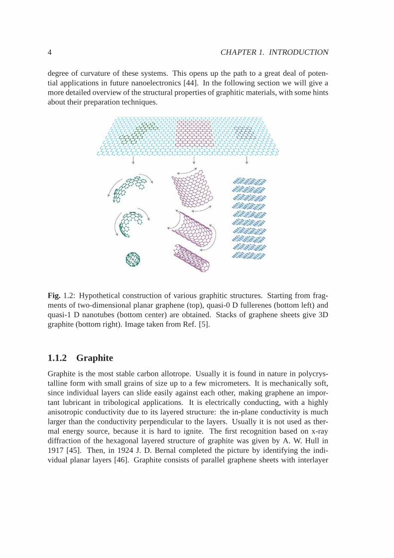
A single graphitic layer is called graphene. From this two-dimensional structure awhole pletora of structures can be derived, as shown in Fig. 1.2. The in-planeσ-bonds ofsp2 hybridized carbon are stiff with respect to longitudinal forces, but allow for angulardeformation. In a graphene layer this is the cause for the observed ripples [4]. More gen-erally, this flexibility opens the way for a large family of stable graphitic nanostructures,with a mixedsp2-sp3 hybridization. The mixing degree is expressed by the pyramidaliza-tion angle, which is highest for systems with lowest dimensionality, such as fullerenes,which are zero-dimensional. As previously noticed, theπ orbitals are close to the Fermienergy, leading to either conducting or semiconducting properties, according also to the
4 CHAPTER 1. INTRODUCTION
degree of curvature of these systems. This opens up the path to a great deal of poten-tial applications in future nanoelectronics [44]. In the following section we will give amore detailed overview of the structural properties of graphitic materials, with some hintsabout their preparation techniques.
Fig. 1.2: Hypothetical construction of various graphitic structures. Starting from frag-ments of two-dimensional planar graphene (top), quasi-0 D fullerenes (bottom left) andquasi-1 D nanotubes (bottom center) are obtained. Stacks ofgraphene sheets give 3Dgraphite (bottom right). Image taken from Ref. [5].
1.1.2 Graphite
Graphite is the most stable carbon allotrope. Usually it is found in nature in polycrys-talline form with small grains of size up to a few micrometers. It is mechanically soft,since individual layers can slide easily against each other, making graphene an impor-tant lubricant in tribological applications. It is electrically conducting, with a highlyanisotropic conductivity due to its layered structure: thein-plane conductivity is muchlarger than the conductivity perpendicular to the layers. Usually it is not used as ther-mal energy source, because it is hard to ignite. The first recognition based on x-raydiffraction of the hexagonal layered structure of graphitewas given by A. W. Hull in1917 [45]. Then, in 1924 J. D. Bernal completed the picture byidentifying the indi-vidual planar layers [46]. Graphite consists of parallel graphene sheets with interlayer

1.1. CARBON AND ITS ALLOTROPIC FORMS 5
spacingdinterlayer = 3.34 A. There are two possible stackings of the layered structure:the Bernal stackingwith alternation ABAB and therhombohedral stackingwith alter-nation ABCABC. Although the latter form has never been isolated, it has been shownthat natural graphite often contains a certain amount of rhombohedral stacking, whichhas been explained as an intermediate state in the transition from graphite to diamond.A further modification isturbostratic graphite, which has the individual layers rotatedby random angles againts each other. In this case the system can be considered a sort ofquasi-crystalline structure.
1.1.3 Graphene
Single layer graphene was discovered experimentally only in 2004 and is actually thebasic building block for the theoretical understanding of all other sp2-hybridized car-bon structures, such as graphite, fullerenes and nanotubes. According to the theoreticalprediction by Mermin and Peierls [47, 48], two-dimensionalsystems with long-rangeorder cannot exist in nature, because of the logarithmic divergence associated with thequantum-mechanical fluctuations of the atomic displacements. Only in three dimensionsthe displacements would converge with the distance, allowing the formation of a stablecrystal. However, this theoretical argument does not prevent freely suspended graphenesheets to exist, since the structure can be stabilized in thethird dimension by ripples,which were actually observed by electron diffraction [4] (see Fig. 1.3). Thus graphenecan be considered effectively as a truly two-dimensional crystal. It is characterized by ahoneycomb structure, with the distance between neighboring atoms beingdCC = 1.42 Aand the lattice constanta =
√3dCC ≈ 2.46 A. For further details about the graphene
structure both in real and reciprocal space, the reader is advised to consult Sect. 2.1 in thefollowing chapter. Graphene crystals can break at crystal edges in two ways, by formingeither a zigzag edge, which runs parallel to a graphene lattice vector, or an armchair edge,which runs parallel to the carbon bonds (see Fig. 1.4). The edge states are especially rel-evant for finite width graphene nanoribbons, as we will see inthe dedicated subsection.
Synthesis Historically, it took a long time before the first successfulisolation of singlegraphene layers [2]. However, this fact is even more surprising if we consider the simpleapproach that led to success: the exfoliation method. In this method, a scotch tape is usedrepeatedly to peel off flakes from pyrolytic graphite that become thinner with each stepuntil finally, there is a single layer left that can be placed on a clean surface for furtherhandling [3, 4]. The main difficulty with this technique is that such thin structures aregenerally invisible by optical means and, consequently, there is no electronic signaturethat would simplify the search. Thus samples have to be screened tediously via atomicforce microscopy (AFM). An alternative way to exfoliate graphene can be achieved bywet chemistry [6], which has started to show promising results. Besides exfoliation,

6 CHAPTER 1. INTRODUCTION
Fig. 1.3: Illustration of the rippled structure of a suspended graphene sheet (left) andTEM-image of a few-layer graphene membrane near its edge (right). The out-of-planefluctuations are supposed to be necessary for the stabilization of the 2D structure. Imagetaken from Ref. [4].
Fig. 1.4: STM image of an exfoliated graphene monolayer. The crystal edges have eitherzigzag (blue) or armchair (red) edges. Image taken from Ref.[5].
which is a top-down process, one can prepare graphene by bottom-up techniques, suchas epitaxial growth. Actually, this procedure has been applied to graphite already 40years ago, by using pyrolisis of methane on Ni crystals [7]. The technique has beenrefined to produce graphene sheets on various crystal surfaces and ribbons of well definedwidth (1.3 nm) [8]. Alternatively, epitaxial growth of graphene can also been achieved bysegregation of C atoms from inside a substrate (Pd, Ni, Pt, SiC) to its surface [9, 10]. Ingeneral, with these epitaxial growth methods, very high crystal qualities can be obtained,sometimes pseudomorphically with respect to the substratelattice constant. Successfulattempts to lift off epitaxially grown graphene from the surface are not known at themoment, but there isn’t any fundamental obstacle preventing to reach this in the future.
1.1.4 Fullerene
Fullerenes were discovered in 1985 by the team of H. W. Kroto,J. R. Heath, S. C.OBrien, R. F. Curl, and R. E. Smalley [1] and named after the geodesic domes by archi-tect R. Buckminster Fuller. Fullerenes are zero-dimensional nanostructures. They consist
1.1. CARBON AND ITS ALLOTROPIC FORMS 7
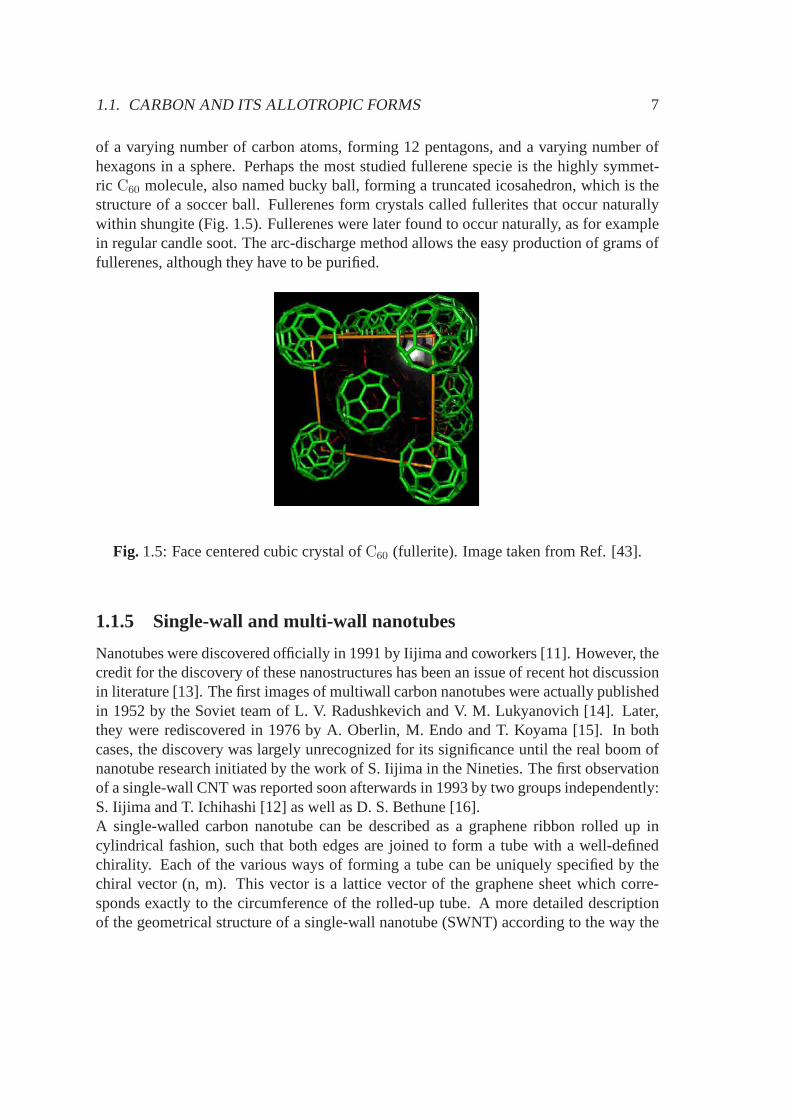
of a varying number of carbon atoms, forming 12 pentagons, and a varying number ofhexagons in a sphere. Perhaps the most studied fullerene specie is the highly symmet-ric C60 molecule, also named bucky ball, forming a truncated icosahedron, which is thestructure of a soccer ball. Fullerenes form crystals calledfullerites that occur naturallywithin shungite (Fig. 1.5). Fullerenes were later found to occur naturally, as for examplein regular candle soot. The arc-discharge method allows theeasy production of grams offullerenes, although they have to be purified.
Fig. 1.5: Face centered cubic crystal ofC60 (fullerite). Image taken from Ref. [43].
1.1.5 Single-wall and multi-wall nanotubes
Nanotubes were discovered officially in 1991 by Iijima and coworkers [11]. However, thecredit for the discovery of these nanostructures has been anissue of recent hot discussionin literature [13]. The first images of multiwall carbon nanotubes were actually publishedin 1952 by the Soviet team of L. V. Radushkevich and V. M. Lukyanovich [14]. Later,they were rediscovered in 1976 by A. Oberlin, M. Endo and T. Koyama [15]. In bothcases, the discovery was largely unrecognized for its significance until the real boom ofnanotube research initiated by the work of S. Iijima in the Nineties. The first observationof a single-wall CNT was reported soon afterwards in 1993 by two groups independently:S. Iijima and T. Ichihashi [12] as well as D. S. Bethune [16].A single-walled carbon nanotube can be described as a graphene ribbon rolled up incylindrical fashion, such that both edges are joined to forma tube with a well-definedchirality. Each of the various ways of forming a tube can be uniquely specified by thechiral vector (n, m). This vector is a lattice vector of the graphene sheet which corre-sponds exactly to the circumference of the rolled-up tube. Amore detailed descriptionof the geometrical structure of a single-wall nanotube (SWNT) according to the way the

8 CHAPTER 1. INTRODUCTION
graphene sheet is wrapped up is given in Chapt. 2. If more cylindrical shells are nestedinto one another, then the structure is a multiwall nanotube(MWNT), where the interwalldistance is similar to the interlayer distance of graphitedinterwall ≈ 3.34 A. The simplestcarbon MWNT is a double-walled carbon nanotube (DWCNT), which will be consideredin detail in Chapt. 5. This kind of structure is the reason behind the extreme mechanicalstrength in longitudinal direction, which even exceeds that of diamond: for instance, thepredicted value of the Young’s modulus (1 TPa) is the highestknown among all materials[89, 44]. This theoretical property alone has inspired a multitude of potential applica-tions ranging from ultra-strong textiles and compound materials to the famous idea of thespace-elevator. Besides, the main reason for this tremendous interest in carbon nanotubereserach is related to their unique electronic properties.They can be semiconducting ormetallic according to their geometrical structure, which is basically specified by diameterand chirality. The understanding of these aspects will be a fundamental step towards theadvent of an all-carbon-based nanoelectronics. Recent reviews about CNTs electronicand transport properties and their applications can be found in Refs. [44, 49].The smallest freestanding SWCNTs typically observed in experiment have a diameter of0.7 nm, corresponding to aC60 molecule [17]. However, smaller tubes down to 0.4 nmhave been observed either as innermost shell of MWCNTs [18, 19] or embedded inporous crystals such as zeolite [20]. The largest observed SWCNT have a diameter ofup to 7 nm [21], even though their section is no longer circular but elliptical, as they havethe tendency to collapse.As stated above, MWCNTs were experimentally discovered earlier than SWNTs. Due totheir greater abundance, larger diameter and the consequently easier handling, far moreexperimental results are available for MWNTs than SWNTs. Yet on the theoretical side,much effort has been devoted to the investigation of SWNTs, whereas due to the greatercomplexity of MWNTs, the theoretical understanding of the effects of the combinationof several walls still remains an open issue [176].
Synthesis It is generally believed that CNTs exist only as a synthetic material. How-ever, there are also indications that natural carbon soot contains certain amounts of thesestructures mixed in with all other forms of amorphous carbon. Recently, it has been foundthat nanotube synthesis may actually have been accessible in medieval times already, eventhough the producers of the legendary Damascus sabers [22] were certainly not aware ofthe nanosized structures embedded in their manufacts. In the following, we will brieflydescribe the three major methods adopted for nanotube production: arc discharge, laserablation, chemical vapour deposition. The arc discharge methodconsists in driving a100 A DC current through graphite electrodes immersed in He atmosphere at 400 mbar.Anyway, the production can be done in open air, as well. It’s the method originally usedin 1991 by S. Iijima [11], who discovered carbon nanotubes inthe soot. Later, the ef-ficiency of the method was improved to yield macroscopic quantities of nanotubes [23].Although the method is easy to set up, it provides very limited control over the production
1.1. CARBON AND ITS ALLOTROPIC FORMS 9
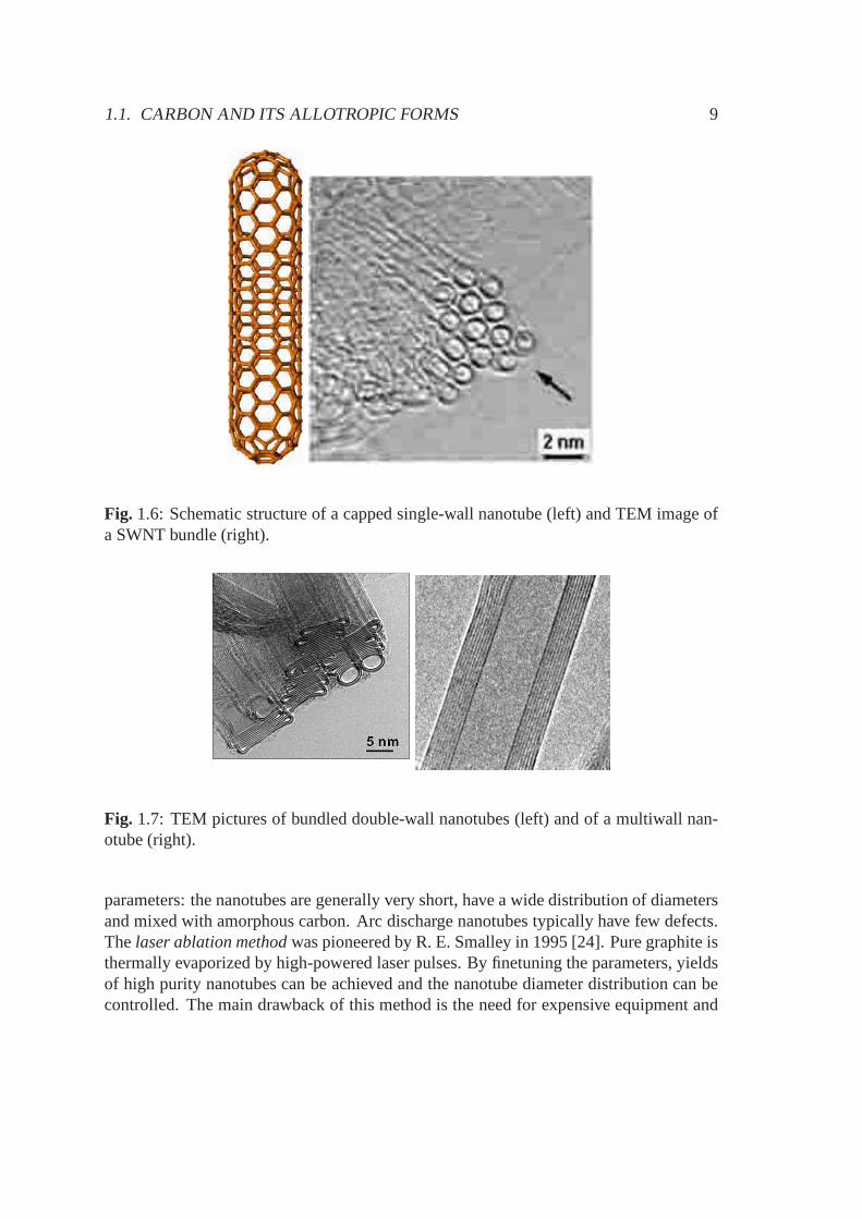
Fig. 1.6: Schematic structure of a capped single-wall nanotube (left) and TEM image ofa SWNT bundle (right).
Fig. 1.7: TEM pictures of bundled double-wall nanotubes (left) and of a multiwall nan-otube (right).
parameters: the nanotubes are generally very short, have a wide distribution of diametersand mixed with amorphous carbon. Arc discharge nanotubes typically have few defects.Thelaser ablation methodwas pioneered by R. E. Smalley in 1995 [24]. Pure graphite isthermally evaporized by high-powered laser pulses. By finetuning the parameters, yieldsof high purity nanotubes can be achieved and the nanotube diameter distribution can becontrolled. The main drawback of this method is the need for expensive equipment and

10 CHAPTER 1. INTRODUCTION
high power laser sources. Thechemical vapor deposition method(CVD) is the mostcommonly used low-cost method for the growth of carbon nanotubes. Indeed, this is themethod that was used by A. Oberlin and M. Endo for their first observation of carbonnanotubes in 1976 [15]. Generally, this method is based on the thermal decomposition ofhydrocarbons species such asCH4 (methane),C2H5OH ethanol,CH3OH methanol, intoatomic carbon from a chemical compound and depositing it on acatalytic surface wherenanotube can then grow in very controlled ways. The type and quality of the grown nan-otubes depends delicately on the growth parameters. It is possible to selectively grow anarrow diameter range of single-wall tubes [25] or double-wall tubes [26], control the di-rection of growth [27] or grow highly aligned arrays of tubes[28]. A common drawbackof CVD methods is the contamination by catalyst particles and the relatively high defectrate.
1.1.6 Other graphitic nanostructures
In the final part of this section we will provide a brief overview of the three most studiednew graphitic nanostructures which are closely related to carbon nanotubes. Other newinteresting carbon nanostructures can be found in general reviews, such as Refs. [35, 42,43].
Graphene nanoribbons (GNRs) were initially considered as a theoretical toy modelfor studying the electronic and phononic edge states in graphene, without much concern-ing about how such structures could realistically be produced [30]. In 2002, however,before the first successfull graphene isolation by exfoliation, T. Tanakaet al. indeedmanaged to grow well-defined, narrow GNRs on a TiC surface andmeasured its phononicedge modes [29]. Soon after the graphene boom, both theoretical and experimental inter-est in GNRs began to rise, since ribbons are nowadays considered as a serious alternativeto carbon nanotubes (CNTs) as quantum wires and devices [31].
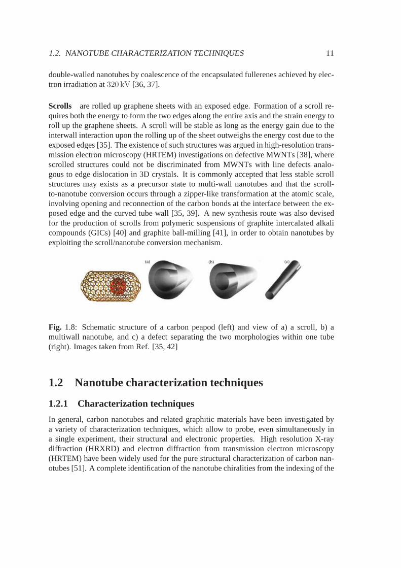
Peapods are hybrid hierarchical structures, which consist in fullerenes encased in single-walled nanotubes. They were discovered in 1998 by Luzziet al. in a sample of acid-purified nanotubes [32]. The material is calledpeapod, because its structure resemblesminiature peas in a pod. A total energy electronic structurecalculation [33, 34] showedthat the encased fullerene molecules are energetically very stable, since an energy gain of≈ 0.5 eV is involved during peapod formation, while when theC60 molecule physisorbson the outer surface of the tube, the energy gain is only≈ 0.09 eV. As for the formationmechanism, the general consensus, also supported by molecular dynamic simulations, isthat fullerenes enter the nanotubes through the open ends. Potential use of nano-peapodsrange from nanometer-sized containers for chemical reactions to nanoscale autoclaves,data storage and possibly high-temperature superconductors (see Ref. [42] and refer-ences therein). As an interesting application, peapods canbe turned into high-purity
1.2. NANOTUBE CHARACTERIZATION TECHNIQUES 11
double-walled nanotubes by coalescence of the encapsulated fullerenes achieved by elec-tron irradiation at320 kV [36, 37].
Scrolls are rolled up graphene sheets with an exposed edge. Formation of a scroll re-quires both the energy to form the two edges along the entire axis and the strain energy toroll up the graphene sheets. A scroll will be stable as long asthe energy gain due to theinterwall interaction upon the rolling up of the sheet outweighs the energy cost due to theexposed edges [35]. The existence of such structures was argued in high-resolution trans-mission electron microscopy (HRTEM) investigations on defective MWNTs [38], wherescrolled structures could not be discriminated from MWNTs with line defects analo-gous to edge dislocation in 3D crystals. It is commonly accepted that less stable scrollstructures may exists as a precursor state to multi-wall nanotubes and that the scroll-to-nanotube conversion occurs through a zipper-like transformation at the atomic scale,involving opening and reconnection of the carbon bonds at the interface between the ex-posed edge and the curved tube wall [35, 39]. A new synthesis route was also devisedfor the production of scrolls from polymeric suspensions ofgraphite intercalated alkalicompounds (GICs) [40] and graphite ball-milling [41], in order to obtain nanotubes byexploiting the scroll/nanotube conversion mechanism.
Fig. 1.8: Schematic structure of a carbon peapod (left) and view of a) a scroll, b) amultiwall nanotube, and c) a defect separating the two morphologies within one tube(right). Images taken from Ref. [35, 42]
1.2 Nanotube characterization techniques
1.2.1 Characterization techniques
In general, carbon nanotubes and related graphitic materials have been investigated bya variety of characterization techniques, which allow to probe, even simultaneously ina single experiment, their structural and electronic properties. High resolution X-raydiffraction (HRXRD) and electron diffraction from transmission electron microscopy(HRTEM) have been widely used for the pure structural characterization of carbon nan-otubes [51]. A complete identification of the nanotube chiralities from the indexing of the

12 CHAPTER 1. INTRODUCTION
diffraction patterns could be achieved on the basis of simulations of the x-ray intensitydiffraction patterns for systems with helical symmetry [50, 52]. While diffraction-basedtechniques provide a reciprocal space picture of carbon nanotube structure, scanning tun-neling microscopy (STM) provides direct access to the localatomic structure of the side-wall, thanks to the reconstruction of maps of the electroniccharge density of the tubesurface in real space [53, 54]. Moreover, if scanning tunneling spectroscopy (STS) is per-formed by measurement of current-voltage characteristics, one can also probe the localelectronic density of states at a given location, thus allowing to obtain a direct corre-lation between electronic and structural information. Scanning tunneling spectroscopymeasurements were performed in 1998 by Odom and Lieber on single-walled nanotubes,which proved the electronic one-dimensionality of these systems [55]. Despite the high-resolution structural information provided by these characterization techniques, howevertheir use for routine characterization work is quite impracticable for several reasons,mainly the need of ultra-high vacuum operation conditions and experimental apparatuscosts. Moreover, in the case of STM, in order to obtain electronic structure informa-tion, STS can be performed exclusively on an isolated tube. Therefore, less expensiveand non-destructive analysis techniques, such as optical spectroscopical techniques, be-come preferable when probing electronic and structural properties on statistical nanotubesamples in an unique experiment. In the following we will review the basics of the twomain optical characterization techniques used in nanotuberesearch, namely photolumi-nescence (PL) and resonance Raman spectroscopy.
1.2.2 Photoluminescence and optical absorption measurements
As stated previously, SWNTs can be either metallic or semiconducting, depending ontheir geometrical structure. In the case of semiconductingtubes, the energy gap is ap-proximately proportional to the inverse of the tube diameter and photoluminescence (PL)from the recombination of electron-hole pairs at the band-gap can be expected, accord-ing to the usual band picture for semiconducting materials (Fig. 1.9). The discovery ofband-gap fluorescence by M. O’Connellet al. occurred on acqueous micelle-like sus-pension of SWNTs [56]. Thus, spectrofluorimetric measurements are a valid and not soexpensive experimental tool for extracting nanotube specific electronic properties frombulk measurements and correlate them to their chirality [57]. However, nanotubes aregenerally bundled because of the van der Waals interactionsand normally contain bothmetallic and semiconducting species. Metallic SWNTs act asnon-radiative channels forthe luminescence of semiconducting tubes. Therefore, it may often occur that no PL sig-nal is observed for SWNT bundles. In order to observe PL, the bundles must be separatedinto individual tubes. In order to achieve this separation,several techniques have beendeveloped: ultrasonication treatment of the nanotubes with surfactants (e.g. sodium do-decyl sulfate or SDS) in acqueous suspensions, growth of individual tubes in channelsof zeolite, alternating current dielectrophoresis of the sonicated suspensions and other

1.2. NANOTUBE CHARACTERIZATION TECHNIQUES 13
techniques based on chemical functionalization for separating metallic and semicon-ducting tubes [59]. Spectroscopic measurements are performed with spectrofluoremeterequipped with InGaAs near-infrared detector cooled by liquid nitrogen. Emission inten-sity is measured as a function of both excitation wavelength(from 300 to 900 nm) andemission wavelength (from 810 to 1550 nm), to give the results shown in the contourplot of Fig. 1.9. The different intensities in Fig. 1.9 come from the chiral and diame-ter dependent distribution of SWNTs in the sample and/or related electron-photon andelectron-phonon interaction strengths. On the other hand,measurements of the optical
Fig. 1.9: Photoluminescence mechanism in a SWNT according to theband picture (left)and contour plot (right) of the fluorescence emission energyvs the excitation energy foracqueous suspended SWNTs. Pictures taken from Bachiloet al. [57]
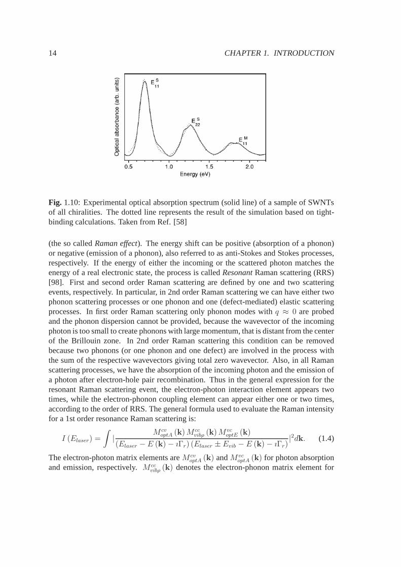
absorption of bundled SWNTs in trasmission or reflection geometry show the presenceof the spectral features of both metallic and semiconducting tubes. In Fig. 1.10 a typicalabsorption spectrum of SWNT bundles is shown, taken from Ref. [58]. Three peaks canbe seen, which are attributed to the van Hove singularities in the joint density of states(see Chapt. 3). Tight-binding calculations suggest that the two lower peaks can be at-tributed to SWNTs with transition energiesES
11 andES22, while the third peak originates
from metallic nanotubes with transition energyEM11 .
1.2.3 Resonant Raman spectroscopy
This is one of the most powerful tools for characterizing nanotubes and other graphiticmaterials, since it doesn’t require sample preparation anda fast non-destructive analysisis possible. Unlikely PL, metallic nanotubes can also be observed. For general reviewsabout this technique applied to carbon nanotubes in the lastten years see Refs. [119, 120].Raman spectroscopy allows to probe the vibrational properties of a material by measuringthe energy shift of the inelastically scattered radiation from the energy of the incident light
14 CHAPTER 1. INTRODUCTION
Fig. 1.10: Experimental optical absorption spectrum (solid line) of a sample of SWNTsof all chiralities. The dotted line represents the result ofthe simulation based on tight-binding calculations. Taken from Ref. [58]
(the so calledRaman effect). The energy shift can be positive (absorption of a phonon)or negative (emission of a phonon), also referred to as anti-Stokes and Stokes processes,respectively. If the energy of either the incoming or the scattered photon matches theenergy of a real electronic state, the process is calledResonantRaman scattering (RRS)[98]. First and second order Raman scattering are defined by one and two scatteringevents, respectively. In particular, in 2nd order Raman scattering we can have either twophonon scattering processes or one phonon and one (defect-mediated) elastic scatteringprocesses. In first order Raman scattering only phonon modeswith q ≈ 0 are probedand the phonon dispersion cannot be provided, because the wavevector of the incomingphoton is too small to create phonons with large momentum, that is distant from the centerof the Brillouin zone. In 2nd order Raman scattering this condition can be removedbecause two phonons (or one phonon and one defect) are involved in the process withthe sum of the respective wavevectors giving total zero wavevector. Also, in all Ramanscattering processes, we have the absorption of the incoming photon and the emission ofa photon after electron-hole pair recombination. Thus in the general expression for theresonant Raman scattering event, the electron-photon interaction element appears twotimes, while the electron-phonon coupling element can appear either one or two times,according to the order of RRS. The general formula used to evaluate the Raman intensityfor a 1st order resonance Raman scattering is:
I (Elaser) =
∫|
M cvoptA (k)M cc
vibρ (k)MvcoptE (k)
(Elaser −E (k)− ıΓr) (Elaser ± Evib − E (k)− ıΓr)|2dk. (1.4)
The electron-photon matrix elements areM cvoptA (k) andMvc
optA (k) for photon absorptionand emission, respectively.M cc
vibρ (k) denotes the electron-phonon matrix element for

1.2. NANOTUBE CHARACTERIZATION TECHNIQUES 15
Fig. 1.11: a) Non-resonant, b) single- and c) double-resonant Raman scattering. Solidlines are real electronic states, dashed lines represent virtual electronic states (i. e. theyare not eigenstates of the system). In the non-resonant process (a), both intermediateelectronic states are virtual. If the laser energy matches areal electronic transition [firststep in (b)], the Raman process is single resonant. If the special condition (c) is met, i.e.,in addition to (b) another electronic transition matches the phonon energy, a double- ortriple-resonance occurs. Taken from Ref. [90].
a photoexcited electron in the conduction band. For phonon absorption (anti-Stokes)we haveρ = A, for phonon emission (Stokes) we haveρ = E. The factors in thedenominator describe the resonance energy difference between incident and scatteredlight, where the+ (−) sign applies to the anti-Stokes (Stokes) process for a phonon ofenergyEvib. Γr gives the inverse lifetime for the scattering process. In Fig. 1.12 a Ramanspectrum obtained from a SWNT sample is reported. The first order spectral features ofa SWNT consist of only two strong bands, the radial breathingmode (RBM) at about200 cm−1 and the graphite derived tangential mode or G band at about1580 cm−1. Atypical second order spectral feature is the D band at about1350 cm−1 for 2.41 eV laserenergy and theG′ band at2700 cm−1. Two relevant characteristics of the D band arethat (1) the intensity of the D band depends on the defect concentration in SWNTs and(2) its frequency increases with increasing laser energy [90].On the other hand, theG′
band intensity is independent on defect concentration and is comparable to the G bandintensity. The radial breathing mode is perhaps the most interesting phonon mode usedfor nanotube characterization [126], since it depends on the nanotube diameter throughthe relation
ωRBM =A
dt+B (1.5)
whereA andB parameters are determined experimentally. Note that this relation is notvalid for nanotube diameters below1 nm, for which a chirality dependence ofωRBM ap-pears due to the distorsion of the nanotube lattice. For example, for an isolated SWNT onSi/SiO2 substrate the experimental value of A is found to be248 cm−1 andB = 0 cm−1

16 CHAPTER 1. INTRODUCTION
[128]. Furthermore environmental effects due to temperature, surfactant, bundling and/orintertube interactions in DWNTs and MWNTs causes a frequency modification of theRBM mode [131]. By plotting the measured transition energy obtained from PL or RRSat different laser excitation energies versus the SWNT diameter the so-called Katauraplots are obtained [127], which are widely adopted for the experimental investigation ofthe properties of these systems [129, 153]. These plots can also be obtained from theo-retical calculations, so that chirality assignment of diameters and transition energies canbe performed through the comparison with experimental results [132, 133] (Fig. 1.13).
Fig. 1.12: Raman spectrum of single-walled nanotubes (left) andradial breathing mode(RBM) (right). Taken from Ref. [59].
Fig. 1.13: Kataura plot for metallic and semiconducting SWNTs (taken from Ref. [132]).

1.3. ELECTRONIC STRUCTURE COMPUTATIONAL METHODS 17
1.3 Electronic structure computational methods
The role of computational materials science has become of fundamental importance notonly for the advancement of basic research but also in the applied field of nanotech-nology. Theoretical modeling and computer simulations candirectly access with highaccuracy the shortest length and time scales of nanoscopic systems and phenomenons.Boosted by the rapidly increasing computing power, nanoscale simulations have thus be-come a predictive tool for the design of novel devices and nowmodelling is an integralpart of interdisciplinary materials research. In order to study the electronic behaviour ofcarbon materials, one has to solve the basic equation of quantum mechanics, the many-electron Schrodinger equation. However, in spite of the impressive computer power atour disposal, solving this equation remains a difficult taskand requires a deep physicaland chemical understanding of many-electrons systems. Combining these notions withmodern mathematical concepts leads to algorithms that exploit the characteristics of theelectronic systems under investigation to provide powerful new electronic structure meth-ods. Adapting these methods for modern computer architectures will result in powerfulprograms which aid the research of many systems. A wide rangeof computational meth-ods is available for the theoretical modeling and simulation of carbon materials proper-ties. These methods are actually based on approximations atvarious level of detail ofthe complicate many-body problem, thus they can be considered a compromise betweenefficiency and accuracy. In general, they can be classified into three groups:ab initio,semi-empirical, tight-binding and effective methods. In the following, we will brieflyoutline a general overview of the methods used in electronicstructure calculations to-gether with the respective advantages/disadvantages, without going into technical detailsfor which the reader can consult more specific references, such as Ref. [93].
Ab initio methods allow the computation of materials properties from first principles,without the need of parameters to be adjusted or fitted to experimental input data, apartfrom the fundamental physical constants and atomic masses.The general advantage ofabinitio methods is the high accuracy of the quantitative results. The main disadvantages arerepresented by the high computational cost and the difficulty of getting a deeper under-standing of the calculated phenomena. They can be further classified intowavefunctionmethodsanddensity functional methods(see for example Ref. [60]).Wavefunction methods solve self-consistently, in a mean-field approximation, the many-electron Schrodinger equation by expanding the many-electron antisymmetrized wave-function in Slater determinants, formed by a set of orthonormal one-electrons orbitalsφi (r). This constitutes the basics of Hartree-Fock (HF) method. Configuration interac-tion (CI) and coupled-cluster methods (CC) go beyond this level of approximation andhave been widely used in quantum chemistry for treating electronic correlations, but alsoimplementations for periodic systems (oxides and crystalsof small organic molecules)have been set up. HF theory is less appropriate for systems with high electron density

18 CHAPTER 1. INTRODUCTION
such as transition metal systems or with highly delocalizedstates and fails completely toaccount for the collective Coulomb screening in a perfect metal. Inclusion of correlationeffects reduces the system size accessible to calculation to few hundred atoms, dependingon the level of theory. The most accurate correlated methodsare restricted to moleculeswith just a few atoms and are also too slow for performing dynamical simulations evenfor small molecules and time-scales in the pico-second range.
Density functional theory(DFT) is another independent-particle method, whose basicswere formulated in two fundamental papers, the first published in 1964 by P. Hohenbergand W. Kohn [61], and the second in 1965 by W. Kohn and J. L. Sham[62]. The basicidea behind these works is that the ground-state electronicenergy (and therefore all otherrelated ground-state properties) is a functional of the electronic density. Then a set ofsingle-particle equations, the so called Kohn-Sham equations, are derived by applyinga variational principle to the electronic energy. Electron-electron interactions are againtreated in an average way according to several available approximations to the functionaldependence of the exchange-correlation energy on density,which actually constitutes themain source of variations in DFT calculations. Actually, the Hohenberg-Kohn theoremdoesn’t specify the form of the functional to be used, but just confirms that it exists.Starting from a trial density given by the square modulus of guessed wavefunctions, theenergy functional of the Kohn-Sham hamiltonian is obtainedand then minimized untilself-consistency is reached for the input and output groundstate charge densities. DFTcalculations can be considered the workhorse of allab initio methods, as they can pro-vide accurate predictions of structural, electronic, vibrational and magnetic properties fora wide range of systems, from molecules and clusters to periodic and amorphous solids,either metals, semiconductors or insulators. Density functional calculations are possiblefor systems of the order of 100 atoms, but by exploiting symmetry also calculations forclusters of over 1000 atoms can be performed [63]. Although DFT is computationallyless demanding than HF methods, it has to be pointed out that in DFT calculations thenumber of variational parameters needed for the expansion of the wavefunction adoptedfor constructing the trial ground-state density is quite large, thus other methods are re-quired for achieving more efficient calculations and treating systems with larger size.Soon after the discovery of carbon nanotubes in 1991, the electronic properties of single-walled nanotubes were investigated by density functional methods [64, 65], before theelectronic density of states could be actually measured by STS in 1998 by Odom. Thesecalculations also showed that important hybridization effects of theσ∗ andπ∗ orbitalscould occurr in small radius carbon nanotubes, which could be relevant for the predictionof metallicity in these systems [66]. Subsequently, calculations were performed also formore complex systems such as double- and multi-wall nanotubes, bundles of single-wallnanotubes and carbon peapods [67, 68, 69].

1.3. ELECTRONIC STRUCTURE COMPUTATIONAL METHODS 19
Semiempirical methods comprise a wide class of self-consistent field HF methodswhich take into account again Coulomb repulsion, exchange interaction and the fullatomic structure of the system, but make use of fewer variational parameters if com-pared to HF and DFT and not all the integrals needed to set up the Hamiltonian matrixare calculated. Instead they are parametrized according toexperimental data. Accordingto the exact number of neglected integrals and the kind of parametrization used, differentscheme of semi-emprical calculations have been developed,most based on the modifiedneglect of diatomic overlap (MNDO) (for an extensive treatment of the derived methodssee Ref. [93] or other quantum chemistry books). Clearly, the reasons behind the develop-ment of these methods is the need of finding a compromise between computational effi-ciency and the physical correctness of the adopted approximations. A quantum-chemicalsemi-empirical electronic structure calculation on nanotube fragments can be found forinstance in Ref. [134].
Tight-binding methods make use of a parametric Hamiltonian with a minimum setof parameters, which is parametrized with respect to the atomic positions and solve theSchrodinger equation in an atomic-like basis set. In this sense, they’re similar to semi-empirical methods, yet they are not self-consistent. Usually the values for the chosenparameters are obtained from fitting calculations to experimental orab initiodensity func-tional results (DFTB) [71]. A small number of basis functions are used, which roughlycorrespond to the atomic orbitals in the energy range of interest. Therefore, comparedwith the ab initio techniques, these atomistic models can be generally handled with farless computational effort and the general understanding ofthe underlying physics andsymmetry properties is facilitated. However, the quantitative results always depend on theparameters needed as input and obviously, due to the reducednumber of variational pa-rameters and exact integral evaluations, the accuracy is reduced if compared withab initiocalculations. Parametrized models like TB methods can be adopted both for the treatmentof electronic and vibrational properties of solids. For thedescription of mechanical andvibrational properties, the most common TB-like methods are force-constant models, de-scribing the mechanical forces between neighboring atoms in a harmonic approximation[72]. Several works concerning the vibrational propertiesof graphene and nanotubes cal-culated with this approach have been published (for a recentcomprehensive list of refer-ences see Ref. [73]). For the atomistic description of the electronic structure, the conceptof the linear combination of atomic orbitals(LCAO) is adopted within the TB scheme.This independent-particle method was introduced by Slaterand Koster [74], and is todayused for efficient, flexible and fairly accurate computations of both model and real sys-tems (for a general review see for instance [75]). Another important parametrized modelused for treating strongly correlated electrons in condensed matter is the Hubbard model,which is indeed a many-body model developed in order to account for Coulomb repul-sion between electrons. The Hubbard model is presented morein detail in Chapt. 6 of
20 CHAPTER 1. INTRODUCTION
this thesis. TB calculations with different level of approximations have been widely usedfor exploring the electronic properties of graphite and itscrystalline modifications: withBernal stacking (Weiss and Slonczewski, 1958 [77]), rhombohedral stacking (McClure,1957 [78]), simple hexagonal and turbostratic graphite (Charlier, 1991 [79, 80]). Soon af-ter the nanotube discovery by Iijima, the first tight-binding calculations on single-wallednanotubes focused on the folding of the electronic dispersion bands of graphene over thenanotube reciprocal space [81]. Later more refined and general analytical expressions forelectronic dispersion for graphene and SWNTs of any given chirality were obtained bySaito and Dresselhaus [89, 90], as shown more in detail in Chapt 3. Symmetry-adaptedTB schemes have also been successfully applied by Popov [84]and Damnjanovicet al.[85] for addressing curvature and hybridization effects insmall diameter single-wall nan-otubes of any chirality. Tight-binding methods were also applied to the investigation ofthe electron-photon and electron-phonon coupling strength for understanding resonanceRaman spectral features in SWNTs [141, 146]. There have beenalso early studies con-cerning the electronic structure of double-walled nanotubes [155, 169], although theseattempts were strongly limited by the selected geometries and hamiltonian parametriza-tions (see the related Chapter in this thesis). After the excitonic nature of optical transi-tions in SWNTs was experimentally established in 2003 by Wang and Dukovic [197], theband picture provided by TB calculations turned out to be essentially incorrect. Noneth-less still many experimental results, such as Kataura plots, can be interpreted through TBcalculations, with adequate modifications of the calculation parameters [204, 205].
Effective models represent another class of methods which do not take into accountthe detailed atomic structure, but give a simple, although approximate, description of theelectronic structure and optical properties. This often allows the advantage of an analyt-ical treatment of the physical problems, which can imply a deeper understanding of theresults than provided by purely numerical methods. Effective models have been recentlyused for the investigation of the electronic structure of graphene [5], where electronscan be described as massless relativistic particles, and also in several works by T. Andowithin thek · p scheme about carbon nanotubes electronic properties with and withoutcorrelations and disorder effects (for a comprehensive review see Ref. [86]).
1.4 Summary
In this chapter, starting from the hybridization of carbon orbitals, we gave a general sum-mary of the most studied graphitic materials, which will be the potential building-blocksof an all-carbon based nanoelectronics in forthcoming years. In particular, we focusedon single and multiwall carbon nanotubes, for which a more detailed description of syn-thesis and characterization techniques was provided. Optical spectroscopic techniques,such as Photoluminescence and Resonant Raman Spectroscopyhave shown to be capa-

1.4. SUMMARY 21
ble of providing chirality and diameter specific information about the electronic structureof individual single-walled nanotubes in bundled bulk samples, without the need of aparticularly expensive laboratory or separation treatments. In the final part, a generalclassification scheme for computational electronic structure methods was presented, to-gether with the historically most relevant bibliographic references about the calculationof electronic properties of nanotubes and related structures.


Chapter 2
Geometry of single-wall carbonnanotubes
A single-wall carbon nanotube (SWNT) can be considered as a graphene sheet (a singlelayer of graphite, with a 2D hexagonal lattice) which can be rolled up with any given ori-entation into a seamless cylinder with a diameter of a few nanometers and a macroscopiclength of several micrometers. The electronic properties of SWNTs, as well as any otherphysical property, are deeply related to their geometricalstructure, which can be definedin terms of diameter, wrapping angle of the graphene sheet and number of atoms con-tained in the unit cell.In this chapter, starting from the graphene sheet, we show the basic definitions for charac-terizing the geometry of a SWNT, in real and reciprocal space. A review of the differentalgorithms presented in literature for determining the coordinates of the atoms in the unitcell, both in 2D and 3D, is also given together with a general overview of the symmetryclassifications based on group theory for these systems. Formost conventions we followthose used in Saito’s and Dresselhaus’ works (see for instance Ref. [89]), except whereexplicitly stated for different choices.
2.1 Graphene lattice in real and reciprocal space
The honeycomb geometry of a graphene sheet can be described by considering an idealinfinite 2D hexagonal Bravais lattice. The lattice unit vectors are defined by
a1 =
√3a
2x +
a
2y, (2.1)
a2 =
√3a
2x− a
2y.
wherea =√
3aCC = 0.246 nm = |a1| = |a2| is the lattice constant of the graphenesheet,aCC = 0.142 nm is the carbon-carbon bond length and(x, y) are the unitary ba-
23
24 CHAPTER 2. GEOMETRY OF SINGLE-WALL CARBON NANOTUBES
sis vectors of the Cartesian coordinate system. Using the lattice vectorsa1 anda2, thegraphene unit cell can be obtained. The unit vectors defined as above make an angle of60o. The unit cell can be chosen in several ways, a possible choice is a rhombus thatcontains twoinequivalentatoms from the sublattices of A- and B-type as shown in grayin Fig. 2.1(left). By using the terminequivalentone means that the A and B sites in theunit cell cannot be connected by unit vectorsa1 anda2. In the graphene lattice each atomof type A is surrounded by three nearest neighbor atoms of type B and viceversa. Thereciprocal lattice of the graphene sheet is defined by the unit vectorsb1 andb2, whichare related to the real lattice unit vectorsa1 anda2 by the standard definition:
ai · bj = 2πδi,j, (2.2)
whereδi,j is the Kronecker delta function. By substituting Eq. (2.1) into Eq. (2.2), thereciprocal lattice unit vectorsb1 andb2 are otained:
b1 =2π√3a
x +2π
ay, (2.3)
b2 =2π√3a
x− 2π
ay.
The unit vectorsb1 andb2 make an angle of120o and define the graphene first Brillouinzone (BZ). The BZ has the same hexagonal shape as the hexagonswhich tile the realspace, but is rotated ofπ/6. Consequently, the armchair direction in real space, whichruns parallel to the carbon bond, corresponds to the zigzag direction in reciprocal space.Vice versa, the zigzag direction in real space, which pointsat π/6 from the armchairone, corresponds to the armchair direction in reciprocal space (see Fig. 2.2). The high-symmetry points in the graphene BZ are the center of the hexagonΓ = (0, 0), the cornersK =
(2π/
√3a, 2π/a
)and the midpoint of the hexagonal edgeM =
(2π/
√3a, 0
).
Notice that there are twoinequivalentK points in the BZ which are denoted byK andK′. As always, equivalent points are obtained by translationsof integer multiples of theunit vectorsb1 andb2. In the next chapter about the electronic structure of graphene, wewill show that these points correspond to the Fermi surface points, which are responsiblefor the metallic character of the system.
2.2 Nanotube unit cell in real space
There are many possible ways of rolling up a graphene sheet into a cylinder, so thatnanotubes with quite different structures can be obtained.The geometry of a SWNT canbe uniquely specified by introducing the chiral indices(n,m), which are integer multiplesof the real space unit vectorsa1 anda2. In this way the circumferential or chiral vectorCh is defined as:
Ch = na1 +ma2 = (n,m) . (2.4)

2.2. NANOTUBE UNIT CELL IN REAL SPACE 25
x
y
a1
a2
A BO
G
K
K'
K
K'
K
K'
M
MM
M
M Mb1
b2
Fig. 2.1: Graphene unit cell (left) and first Brillouin zone (right). The shaded rhombuswith the two sites A and B is the unit cell of graphene, the hexagonal lattice is definedby the unit vectorsa1 anda2. The reciprocal space is defined by the unit vectorsb1 andb2. The center of the BZ is theΓ point and the corners are theK andK′ points. Themidpoints are theM points. Equivalent k-points are connected to each other by reciprocallattice vectors.
The chiral vector defines the translational azimuthal periodicity along the circumferenceof the graphene cylinder. Moreover, every other nanotube geometric quantities can bespecified starting from these indices, as it will be shown in the following. The circum-ference length is given byL =
√Ch ·Ch and the nanotube diameter isdt = L/π =
a
π
√n2 + nm+m2. The chiral angleθ is defined as the angle between the chiral vector
Ch and the unit vectora1 and can be obtained with the aid of Eq. (2.4), that is
θ = arccosCh · a1
|Ch||a1|= arccos
2n+m
2√n2 +m2 + nm
. (2.5)
For the special casesθ = 0 andθ = π/6 the tubes are referred to aszigzagandarmchair,respectively. Zigzag tubes havem = 0, whereas armchair tubes havem = n. Becauseof their mirror symmetry along the tube axis, they are also called achiral tubes. In orderto avoid confusion related to the handedness of the rolling up of the graphene sheet intwo opposite directions (for a detailed discussion see Ref.[141]), the structural indicescan be defined in the range0 ≤ m ≤ n and the chiral angle in the range0 ≤ θ ≤ 30o.Obviously achiral SWNTs have no handedness, implying that in a sample the amount ofchiral SWNTs for each(n,m) pair is twice the amount of achiral ones. An alternative

26 CHAPTER 2. GEOMETRY OF SINGLE-WALL CARBON NANOTUBES
way to Eq. (2.5) for defining the chiral angleθ, one can consider the angleθ′ = π/6− θbetween the chiral vectorCh and the closest of the three armchair chains in the graphenesheet of Fig. 2.2. The translational periodicity along the axis of an ideal infinitely longSWNT is given by the translational vectorT, which is orthogonal toCh and is defined as
T = t1a1 + t2a2 =2m+ n
dRa1 −
2n+m
dRa2 (2.6)
wheredR = gcd (2n+m, 2m+ n), the functiongcd (i, j) denotes the greatest commondivisor of the two integersi andj and the integer coefficientst1 andt2 for the componentsof T have been found using the orthogonality relationCh · T = 0. The division bythe integerdR ensures that the shortest lattice vector along the SWNT axial direction ischosen. Additionally, if we define the integerd = gcd (n,m) and apply Euclid’s law1 todR, the following relations are obtained
dR = d if mod (n−m, 3d) 6= 0 (2.7)
dR = 3d if mod (n−m, 3d) = 0.
In the above equation the modulo function gives the remainder of an integer division. TheSWNT unit cell is spanned by the real space vectorsCh andT and can be obtained bythe cross product|T×Ch| = | (t1m− t2n) (a1 × a2) |. Dividing the area of the SWNTcell by the area of the biatomic graphene unit cell|a1 × a2|, one gets the numberN ofgraphene unit cells inside the SWNT unit cell
N = t1m− t2n =2 (n2 + nm+m2)
dR(2.8)
Note thatN is an even number and that zigzag and armchair SWNTs have small unit cellsif compared to chiral SWNTs with approximately the same diameter. In fact, for pairs oftype(n, 0) and(n, n) there are2n graphene cells in the nanotube unit cell, therefore4ncarbon atoms.Finally, substituting the above expression forN the relations for the circumference lengthL and the length of the unit cell along the tube axisT =
√T ·T can be rewritten as
L = a
√dRN
2and T = a
√3N
2dR=
√3L
dR. (2.9)
2.3 Nanotube reciprocal space: the cutting lines
As shown in Section 2.1, again with the aid of Eq. (2.2), one can still construct recipro-cal lattice vectors which can be conveniently used in a cylindrical reference frame, i.e.
1Euclid’s law state thatgcd (i, j) = gcd (i− j, j)
2.3. NANOTUBE RECIPROCAL SPACE: THE CUTTING LINES 27
x
y
ZIGZAG
ARMCHAIRa1
a2
RT
Θ¢
ΘCh
A B
Fig. 2.2: Graphene lattice with armchair and zigzag directions highlighted and geometryof a(4, 2) single-walled nanotube. The large shaded cell is the SWNT unit cell, defined bythe chiral vectorCh and the axial vectorT, with N atoms of type A (B). The symmetryvectorR is also shown (see Sect. 2.4.1). The chiral angleθ is the angle between thearmchair direction and the chiral vectorCh. All vectors are expressed in multiples ofa1
anda2.
along the circumferential and axial direction of the nanotube, respectively. Therefore, inSWNTs the chiral vectorCh and the axial vectorT play the role of graphene real spaceunit vectorsa1 anda2, whereas the nanotube reciprocal space vectorsK1 andK2 playthe role of graphene reciprocal space unit vectorsb1 andb2. The new reciprocal vectorsK1 andK2 are defined as follows:
K1 ·T = 0, K1 ·Ch = 2π, K2 ·T = 2π, K2 ·Ch = 0. (2.10)
Using the definitions given in Eq. 2.4 and Eq. 2.6, one obtains
K1 =t1b2 − t2b1
N(2.11)
K2 =mb1 − nb2
N
from which it can be verified thatK1 is perpendicular toT and parallel toCh, whereasK2 is parallel toT and perpendicular toCh. The lengths ofK1 andK2 are given by
|K1| =2π
L=
2
dtand |K2| =
2π
T. (2.12)
28 CHAPTER 2. GEOMETRY OF SINGLE-WALL CARBON NANOTUBES
According to the first equation of (2.11), two vectors which differ byNK1 are equivalent,as this corresponds to a reciprocal lattice vector of graphene. ThereforeN wavevectorsof typeµK1 with µ = 0, 1, . . . , N−1 will give rise toN discrete lines of length|K2| andspacing|K1|, in the graphene BZ. Therefore, one can think of the nanotubereciprocalspace as the result of sectioning the graphene BZ into a set ofN 1D BZs orcutting lines(see Ref. [116] for a general review), such that the possiblek values in the SWNT BZ aregiven by
k = µK1 + kzK2
|K2|with µ = 0, . . . , N − 1 and − π
T≤ kz <
π
T. (2.13)
For any givenk the following relation also holds
k ·Ch = 2πµ (2.14)
which represents the periodic boundary condition of quantum confinement around thetube circumference. This means that only stationary stateshaving an integer numberµof wavelengths with periodk = 2π/λ are allowed around the circumferential direction.Moreover, from the definition of Eq. (2.13), the possible values for the azimuthal quantumnumberµ are discrete, whereas the linear momentumkz changes continuously along thecutting lines as a consequence of the translational periodic boundary conditions along thetube axis.
G
Μ=0Μ=14
Μ=-13
b1
b2
kx
ky
K1
K2
Fig. 2.3: The first Brillouin zone of (4, 2) SWNT is given by a set ofN = 28 cuttinglines of nanotube superimposed on the extended graphene BZ.The origin at theΓ pointis marked by a dot. Nanotube reciprocal lattice vectorsK1 andK2, whose norm givethe spacing between cutting line and the length of each cutting line, respectively, are alsoshown. The borders of the SWNT BZ are the cutting lines with indicesµ = −13 andµ = 14.
2.4. GENERATING COORDINATES OF SWNTS 29
2.4 Generating coordinates of SWNTs
The task of generating the coordinates of any(n,m) SWNT unit cell is a complex one,because of the high degree of symmetry of the nanotube system(i. e. large number ofsymmetry elements), as it will be shown in the last section ofthis chapter. In literatureseveral different algorithms for calculating the atomic coordinates both in the 2D unrolledand 3D unit cell can be found, which rely on different choicesfor the symmetry vectorsgenerating the whole cell. The purpose of this section is notonly intended as avade-mecumfor practical use in the computations, but aims also at giving an insight into thethree most cited (and documented) geometrical conventionsin nanotube science. Morespecifically, we will overview first the convention used in the works by the Saito andDresselhaus’ group [89, 141], then the convention used by Nemec and Cuniberti’s group[123] and finally the one by Damnjanovic’s group [90], whichwill be helpful for intro-ducing symmetry elements in nanotubes in the next section. As nanotube literature is nowquite vast, also different recipes by other authors can be easily found out, however mostof the times they’re limited to achiral SWNTs or not explicitly set up into integer-basedformulas to be tried straightforwardly. Thus it has been decided not to take into accountthese cases.
2.4.1 Saito and Dresselhaus’ convention
In order to generate coordinates of SWNTs, Saito introducesthe symmetry vectorR withindices(p, q), which satisfies the three following conditions:
(a) R = pa1 + qa2, (b)R ·Ch
L=L
N, (c)
1
N≤ R ·T
T ·T ≤ 1. (2.15)
Condition (a) means thatR is a real-space lattice vector, whose component alongCh isequal toL/N according to condition (b), and it’s inside the unit cell according to condi-tion (c) . Making the appropriate substitutions into conditions (b) and (c) of Eq. (2.15),the (p, q) indices of vectorR can be completely determined by solving the followingsystem:
qt1 − pt2 = 1 and 1 ≤ mp− nq ≤ N. (2.16)
By translating a graphene unit cell byiR with i = 0, . . . , N − 1 we go over all grapheneunit cells inside the 2D unrolled nanotube unit cell, that istwo atoms in a graphenesheet are equivalent if they’re connected by a translation of NR. In a 3D rolled upSWNT, applying the symmetry vectorR means moving around the tube axis in spiral-like fashion. The pitchτ and the angleψ of the spiral are given by the following crossproducts:
τ =|R×Ch|
L=
(mp− nq)T
N(2.17)
ψ =|T×R|
T
2π
L=
2π
N

30 CHAPTER 2. GEOMETRY OF SINGLE-WALL CARBON NANOTUBES
Additionally, the symmetry vectorR appliedN times can be related to translations byinteger multiples of the axial vectorT, according to the following relation:
NR = Ch +MT with M ≡ mp− nq. (2.18)
Now we have all the necessary elements for generating any(n,m) SWNT unit cell,both in 2D and 3D. In a rigth-handed Cartesianxyz−coordinate system, we choose thegraphene layer to lie in thexy plane. The coordinates of the atomic sites of the 2Dunrolled nanotube unit cell are then obtained as follows:
Ruh,s = uT + hR− [hM/N ]T− r1
s/2 (2.19)
where theu-th unit cell, theh-th graphene biatomic cell and thes-th atomic site (A or B)inside each graphene cell are labelled by the correspondingsubscripts. By the notation[ξ] we mean the integer part of the argumentξ andr1
s is a vector pointing from a givens-site (e. g. A) to its first nearest-neighbors′ (e. g. B). In order to obtain the coordinatesof the SWNT in 3D, the above 2D unit cell needs to be rolled up byaligning the tubealong thez axis. This is done through the rotation operatorsΩα (α = x, y, z) about theCartesian principal axes:
Ω = Ωz (Θϕh,s)Ωy
(π6− θ)
Ωx
(π2
)(2.20)
The rotation operatorΩx
(π2
)is applied to align the cylinder along thez axis, then the
graphene layer in thexz plane is rotated byΩy
(π6− θ)
to account for the SWNT chi-
rality. Finally the rolling up of the graphene layer is obtained by placing the atomic sitesaround thez axis of the cylinder by the operatorΩz (Θϕh,s), whereϕh,s is the angularcoordinate of the atomic siteRu
h,s on the cylindrical surface of the nanotube andΘ isrelated to the handedness of the rolling up done to the graphene layer, from the front tothe back(Θ = +1) or from the back to the front(Θ = −1). The angular coordinates ofthe atomic sitesϕh,s are given by:
ϕh,s =2
dt
[Ωy
(π6− θ)
Ωx
(π2
)Ru
h,s
]· x = 2πh/N − ϕ1
s/2 (2.21)
with ϕ1A = −ϕ1
B =(2a/
√3dt
)cos (π/6− θ).
where the angular shiftsϕls on the cylindrical surface between nearest-neighbor carbon
atoms have been introduced. The general expression for these is given by
ϕls =
2
dt
[Ωy
(π6− θ)
Ωx
(π2
)rl
s
]· x (2.22)
These formulas can be straightforwardly implemented in computer programs for calcu-lating any set of atomic coordinates of a given(n,m) SWNT. The above described pro-cedure is found in Ref. [141] and is far more elegant than the one proposed in the sample

2.4. GENERATING COORDINATES OF SWNTS 31
code shown in the appendix of Saito’s book [89], which is completely based on floating-point arithmetic, therefore bearing the risk of rounding errors. However, apart from theprocedure, the main point to remember is that in both references the symmetry vectorRis used for generating atomic coordinates of a SWNT.
2.4.2 Nemec and Cuniberti’s convention
Nemec and Cuniberti’s pure integer-based procedure [123],clearly steers away from in-troducing any additional symmetry vector, and focuses on labelling the graphene unitcells inside the unrolled nanotube unit cell. By indexing a graphene cell or plaquette bya pair of indices(l1, l2), each cell around the tube is uniquely identified by the condition0 ≤ l1 + l2 < n+m. New indices for the coordinates are introduced as
[i, j] = [l1 + l2, l1] with 0 ≤ i < n+m (2.23)
Now the only fundamental step to generate the coordinates isthat each plaquette is partof the unit cell if the following condition holds:
0 ≤ l1m− l2n < t1m− t2n (2.24)
0 ≤ jm− (i− j)n < t1m− t2n (2.25)
in ≤ j (n+m) < in+ (t1m− t2n)
For everyi we have the following condition forj:
in
n +m≤ j <
in + t1m− t2n
n +m(2.26)
Finally the plane coordinates of all atoms can be computed exactly with pure integeroperations counting over the indices[i, j] as follows:
r±[i,j] = je1 + (i− j) e2 ± (e1 + e2) /6 (2.27)
In the above equation the lattice vectorse1 ande2 are expressed in cylindrical coordinatesas:
e1 = (2πt2,−mT ) / (t2n− t1m) (2.28)
e2 = (2πt1,−nT ) / (t1m− nt2) .
where the following identities are verified
ne1 +me2 = (2π, 0) (2.29)
t1e1 + t2e2 = (0, T ) .
Thus expressions for the cylindrical coordinates(ϕ, z)[i,j] are obtained, which can be usedtogether with the tube radiusρ = L/2π to derive the 3D Cartesian atomic coordinates.

32 CHAPTER 2. GEOMETRY OF SINGLE-WALL CARBON NANOTUBES
2.4.3 Damnjanovic’s convention
In the previous sections, we saw that the minimum number of starting atoms needed togenerate the SWNT can be at most 2, the number of atoms in the graphene unit cell.However, Damnjanovcet al. [90, 124] pointed out that these two atoms are actuallymapped onto each other by a rotation by180o around an axisU perpendicular to the tubeaxis. Therefore, only one atom is needed to generate the whole tube, which is referredto asorbit, and carbon nanotubes are defined assingle orbit systems. Thus, unlikely theprevious methods, Damnjanovicet al. obtain the full set of coordinates starting from asingle atom and applying to it the symmetry operators of the line group of the SWNT,which will be described in detail in the next section. For themoment, it’s sufficient to saythat these operators are the screw roto-translation generator
(Cw
N |TdN
), the pure-rotations
operatorCd and the above mentioned rotation of180o around the horizontal axisU. Bycovention, theU axis is chosen to coincide with thex axis. We recall that, within thenotation of this thesis,d is the greatest common divisor of the SWNT chiral indices(n,m), N is the number of graphene cells inside the unit cell andT is the norm of thetube axial vectorT, which is quite different from the notation used in Damnjanovic’swork (n, q, a, respectively, for a given SWNT pair indicesn1, n2). The parameterwwhich appears in the screw operator is given by:
w = N/d Fr
[d
NdR/d
(3− 2
n−m
n
)+d
m
(n−m
d
)ϕ(n/d)−1]
(2.30)
whereFr is the fractional part of a rational number andϕ (m) is the Euler function2. Incylindrical coordinates the position of the starting atom is given by
r000 = (ρ,Φ0, Z0) =
(ρ, 2π
(n+m
2 (n2 + nm+m2)
),
n−m
2√
3 (n2 + nm+m2)a
).
(2.31)
and by acting on it with the compound operator
(Cwt
N CsdU
u|tdTN
)the new atomic posi-
tion is obtained at:
rtsu =
[ρ, (−1)u Φ0 + 2π
(wt
N+s
d
), (−1)u Z0 +
td
NT
](2.32)
where the indicestsu are defined asu = 0, 1, s = 0, 1, . . . , d− 1, andt = 0,±1,±2, . . ..Thus counting over the indicest, s andu, with the help of Eq. (2.32), any single-wallednanotube can be constructed.
2Eulerϕ (m) gives the number of positive integers less than or equal tomwhich are relatively prime tom.
2.5. SYMMETRY OF SWNTS 33
2.5 Symmetry of SWNTs
The symmetry of systems which exhibit translational periodicity in one dimension, suchas carbon nanotubes and stereoregular polymers have been described by the so calledlinegroups, which were introduced by Damnjanovicet al. [124] and later adopted by Thom-sen and Reich [90] for the investigation of second-order resonance Raman scattering onSWNTs. Line groups are the full space group of one-dimensional systems. In additionto point-group symmetries like rotations and reflections, they include pure translationsand screw operations. In Sect. 2.4.3 it was shown that, starting from a single atom, thewhole tube could be obtained by repeatedly applying the symmetry operations of the linegroup. In this section we will briefly review the basics of thesymmetry of a SWNT froma crystallographic point of view. For further details aboutgroup symmetry applied toSWNTs the reader is referred to the above mentioned references by Damnjanovic andReich and to the comprehensive review of Ref. [118]. In orderto find the symmetrygroups of carbon nanotubes, one has to look for the symmetry operations of the graphenesheet which are preserved when the layer is rolled up into a cylinder. Namely, transla-tions by multiples of the axial translational periodT of the graphene sheet parallel toTremain translations of the nanotube parallel to the tube axis. They form a subgroupTcontaining the pure translations of the system. Translation parallel to the chiral vectorCh become pure rotations of the nanotube about its axis. If we considerd lattice pointsbelonging toCh , the nanotube can be rotated by multiples of2π/d. Thus the SWNT hasd pure rotations in its symmetry group which are denoted byCs
n with s = 0, 1, . . . , d− 1.The pure rotations form again a subgroupCn of the full line group. Translations of thegraphene sheet along any other direction are combinations of translations alongT andCh. Therefore, when the graphene sheet is rolled up, they result in translations combinedwith rotations about the nanotube axis, hence the helical symmetry of carbon nanotubes,due to the presence of screw operators. On the unrolled graphene sheet this correspondsto primitive translations of typew/NCh+d/NT. The order of these screw axis operatorsis equal to the number of graphene cellsN inside the nanotube unit cell. Therefore, asshown in the previous section, we denote the screw operatorsby (Cw
N |dT/N)t with theparameterw defined as in Eq. (2.30). Moreover, by considering the form ofEq. (2.8) andthe ratioN/d which is always≥ 2, it can be shown that the nanotube line group alwayscontain the screw axis. In achiral tubesN/d = 2 andw = 1, so the screw axis operationconsists of a rotation byπ/d followed by a translation byT. Also, one can observe thatfrom the six-fold rotation of the hexagon about its center point only the two-fold rotationis preserved as a symmetry operation in carbon nanotubes. This is actually the two foldrotational axis, previously denoted asU, which is perpendicular to the tube axis and ispresent both in chiral and achiral nanotubes. TheU-axis points through the midpoint of ahexagon, perpendicularly to the cylinder surface, the other equivalent two-fold axisU ′ isfound at the midpoint of a bond between two carbon atoms. Mirror planes perpendicularto the graphene sheets must either contain the tube axis or beperpendicular to it. Thus

34 CHAPTER 2. GEOMETRY OF SINGLE-WALL CARBON NANOTUBES
Fig. 2.4: Symmetry elements in a SWNT according to Damnjanovicet al. Taken fromRef. [124].
we have vertical mirror planes denoted byσv3 and horizontal mirror planesσh. However,
both kinds of planes are present only in achiral tubes. Note thatσh = Uσv. They containthe center points of the graphene hexagons. Additionally, vertical and horizontal mir-ror planes through the midpoints of the covalent bonds form vertical glide planes(σv′)and horizontal rotoreflection planes(σh′) (Fig. 2.4). The general element for any carbonnanotube line group can be written as
l (t, u, s, ν) =
(Cw
N |Td
N
)t
CsdU
u, σνv (2.33)
with the values forw, d,N given in the previous equations and the indicest, u, s, ν de-fined as
t = 0,±1, . . . , (2.34)
u = 0, 1;
s = 0, 1, . . . , d− 1;
ν =
0, 1 achiral0 chiral
The elements in Eq. (2.33) form the line groupsL, which are generally given by theproduct of a point group and an axial group. More specifically, for achiral and chiral
3Sometimes in the papers by Damnjanovicet al. this can be found denoted asσx.
2.6. SUMMARY 35
tubes we have the following line groups:
LA,Z = T12dDdh achiral tubes (2.35)
LC = TwNDd chiral tubes.
Note that, since carbon nanotubes line groups always contain the screw axis, they arenon-symmorphicgroups and the isogonal point group (i. e. a point group with the same orderof the principal rotational axis, where the rotations include the screw-axis operations) isnot a subgroup of the full symmetry group. The point groups isogonal to the respectivenanotube line groups are given by
DN for chiral tubes (2.36)
D2dh for achiral tubes
We conclude this section by reminding that for most applications of symmetry in nan-otube science, such as optical spectroscopy or first-order Raman scattering, where onlythe center of the Brillouin zone is probed, it’s sufficient towork with the (isogonal) pointgroup. This can be done safely because electronic and vibrational eigenfunctions at theΓ point always transform as irreducible representations of the isogonal point group.
2.6 Summary
In this chapter the geometry of a single-walled carbon nanotube was completely definedboth in real and reciprocal space, starting from the rollingup of a graphene sheet. TheBrillouin zone was indexed in terms of a set of discrete azimuthal quantum numbersµand continuous wavevectorskz, which give rise to a set of so calledcutting linesin k-space. It was also shown how the atomic structure could be completely derived froma given chiral vector(n,m) according to three different symmetry choices. Finally, forcompleteness, a list of the symmetry elements which are present in carbon nanotube wasgiven and related to the full symmetry line group classification for these systems.

Chapter 3
The zone folding method
This chapter introduces the simplest models for describingthe electronic and opticalproperties of single-walled carbon nanotubes within reasonable approximations. It’s es-sential to understand the development of this thesis and thereasons behind the choiceswe will perform in the following chapters. First we review the derivation of a simpleanalytical expression for the electronic structure of graphene, based on the tight-bindingapproximation for crystalline solids andπ-electrons. On the basis of the nanotube Bril-louin zone construction of the previous chapter, the zone-folding method is applied tothe graphene band structure, in order to obtain a general expression for calculating theelectronic structure of SWNTs of any chirality. We also showhow optical matrix ele-ments for interband transitions and dipole selection rulescan be obtained from grapheneeigenvectors in order to compute the tight-binding opticalabsorption spectra of SWNTs.This chapter covers mainly literature materials from Refs.[89, 141, 142, 144, 145].
3.1 Electronic structure of a graphene sheet
As stated in the first chapter, the tight-binding approximation (TBA) gives a simplified butrather good and efficient description of the electronic bandstructure of covalent solids,such as for instance 3D inorganic semiconductors (C, Si, SiC, GaAs), organic molecules(butadiene, polyacetylene, etc.) and transition 3d-band metals. In the TB method a set oflocalized atomic orbitals is adopted as basis for expandingthe crystal wavefunctions andthe exact many-body hamiltonian operator is replaced with aparametrized hamiltonianmatrix. Actually, the use of the termtight-bindingis related to the atomic-like wavefunc-tions, which aretightly boundto the atoms. In general, only a small number of basisfunctions are used, which approximately correspond to the atomic orbitals in the energyrange of interest. For instance, when modelling covalentlybond carbon based materials,such as diamond and graphitic derivatives, the 1satomic orbitals related to the core elec-trons can be reasonably neglected and only 2sand the three2px, 2py, 2pz orbitals for eachof the four valence electrons can be safely taken into account.
37
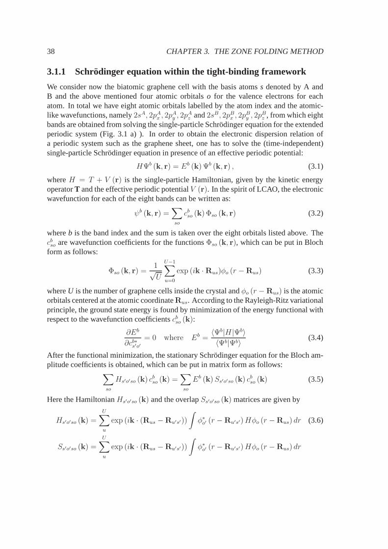
38 CHAPTER 3. THE ZONE FOLDING METHOD
3.1.1 Schrodinger equation within the tight-binding framework
We consider now the biatomic graphene cell with the basis atoms s denoted by A andB and the above mentioned four atomic orbitalso for the valence electrons for eachatom. In total we have eight atomic orbitals labelled by the atom index and the atomic-like wavefunctions, namely2sA, 2pA
x , 2pAy , 2p
Az and2sB, 2pB
x , 2pBy , 2p
Bz , from which eight
bands are obtained from solving the single-particle Schrodinger equation for the extendedperiodic system (Fig. 3.1 a) ). In order to obtain the electronic dispersion relation ofa periodic system such as the graphene sheet, one has to solvethe (time-independent)single-particle Schrodinger equation in presence of an effective periodic potential:
HΨb (k, r) = Eb (k) Ψb (k, r) , (3.1)
whereH = T + V (r) is the single-particle Hamiltonian, given by the kinetic energyoperatorT and the effective periodic potentialV (r). In the spirit of LCAO, the electronicwavefunction for each of the eight bands can be written as:
ψb (k, r) =∑
so
cbso (k) Φso (k, r) (3.2)
whereb is the band index and the sum is taken over the eight orbitals listed above. Thecbso are wavefunction coefficients for the functionsΦso (k, r), which can be put in Blochform as follows:
Φso (k, r) =1√U
U−1∑
u=0
exp (ik ·Rus)φo (r −Rus) (3.3)
whereU is the number of graphene cells inside the crystal andφo (r −Rus) is the atomicorbitals centered at the atomic coordinateRus. According to the Rayleigh-Ritz variationalprinciple, the ground state energy is found by minimizationof the energy functional withrespect to the wavefunction coefficientscbso (k):
∂Eb
∂cb∗s′o′= 0 where Eb =
〈Ψb|H|Ψb〉〈Ψb|Ψb〉 (3.4)
After the functional minimization, the stationary Schrodinger equation for the Bloch am-plitude coefficients is obtained, which can be put in matrix form as follows:
∑
so
Hs′o′so (k) cbso (k) =∑
so
Eb (k)Ss′o′so (k) cbso (k) (3.5)
Here the HamiltonianHs′o′so (k) and the overlapSs′o′so (k) matrices are given by
Hs′o′so (k) =
U∑
u
exp (ik · (Rus −Ru′s′))
∫φ∗o′ (r −Ru′s′)Hφo (r −Rus) dr (3.6)
Ss′o′so (k) =U∑
u
exp (ik · (Rus −Ru′s′))
∫φ∗o′ (r −Ru′s′)Hφo (r −Rus) dr

3.1. ELECTRONIC STRUCTURE OF A GRAPHENE SHEET 39
The orthonormality condition for the electron wavefunction of Eq. (3.2) becomes∫
Ψb′∗ (k, r)Ψb (k, r) dr =∑
s′o′
∑
so
cb′∗
s′o′ (k)Ss′o′so (k) cbso (k) = δb′b (3.7)
whereδb,b′ is the Kronecker delta function. Before solving the matrix problem of Eq. (3.5),the integrals of Eq. (3.6) need to be parametrized as functions of the interatomic vectorR = Ru′s′−Rus and the symmetry and relative orientation of the involved orbitalsφ∗o′ (r)andφo (r):
εo =
∫φ∗o (r)Hφo (r) dr (3.8)
too′ (R) =
∫φ∗o (r)Hφo′ (r −R) dr
soo′ (R) =
∫φ∗o (r)φo (r −R) dr
Now we can find the eigenvalues ofH (k) by solving the secular equation for the8 × 8hamiltonian matrixHs′o′so (k) and the overlap matrixSs′o′so (k)
det[Hs′o′so (k)− Eb (k)Ss′o′so (k)
]= 0. (3.9)
Before proceeding with the solution of the secular equationin the next subsection, wehave to consider in detail the dependence on the symmetry andorientation of the atomicorbitals of the transfertoo′ (R) and the overlapsoo′ (R) integrals. We recall that ingraphene the 2s atomic orbitals mix with the2px and2py orbitals to form the hybridizedσ molecular orbitals, which in turn give the covalent bonds ofthe hexagonal lattice. The2pz atomic orbitals form theπ-molecular orbitals which point normal to the grapheneplane and are uncoupled from theσ molecular orbitals. Unlikely the2s atomic orbital,which is spherically symmetric, the2p atomic orbital has the symmetry of the sphericalharmonicY21 (θ, φ), so it can be decomposed along two mutually orthogonal directions,namely perpendicular and parallel to the interatomic vector R. These directions are againreferred to asπ andσ, respectively. From this point on, the2s orbital will be simplydenoted for brevity ass. To determine the hoppingtoo′ (R) and the overlapsoo′ (R) in-tegrals, one has to consider first all the possible pairs between theo′ = s, σ, π and theo = s, σ, π orbitals, which amount to nine possible pairs, as we can see in Fig. 3.1 c).Among these, four(o′o = sπ, πs, σπ, πσ) give transfer and overlap integral identicallyzero by simmetry requirements. For the remaning five pairs(oo′ = ss, sσ, σs, σσ, ππ),the two pairsoo′ = sσ andσs give transfer and overlap integrals of opposite signs andsame magnitude. Therefore there are only four independent pairs(oo′ = ss, sσ, σσ, ππ)and the total number of tight-binding parameters is ten: thetwo atomic orbital ener-gies(ε2s, ε2p), the four hopping integralstss (R) , tsσ (R) , tσσ (R) , tππ (R) and the four

40 CHAPTER 3. THE ZONE FOLDING METHOD
Fig. 3.1: a) Schematic of the1s, 2s, 2px, 2py, and2pz atomic orbitals of the carbonatom. b) Theσ andπ projections of the2p atomic orbital. c) (left) The five molecularorbital configurationso′o = ss, sσ, σs, σσ, ππ that give nonvanishing transferto′o (R) andoverlap integralsso′o (R). The two configurationso′o = sσ, σs connected by a dashedline yield the transfer and overlap integrals of equivalentmagnitudes and opposite signs.c) (right) The remaining four configurationso′o = sπ, πs, σπ, πσ for which the transferand overlap integrals are identically zero by symmetry requirements. The dashed linesconnect the equivalent configurations. Taken from Ref. [122]

3.1. ELECTRONIC STRUCTURE OF A GRAPHENE SHEET 41
overlap integralssss (R) , ssσ (R) , sσσ (R) , sππ (R). Additionally, we note that withinthe orthogonal tight-binding model the parameterssoo′ (R) are set to zero. Usually thenumerical values for the tight-binding parameters are obtained from a fit to anab initiocalculation or experimental measurements. Because theσ andπ molecular orbitals aredecoupled, as noted previously, the8 × 8 HamiltonianHs′o′so (k) and overlap matricesSs′o′so (k) are decomposed into a6 × 6 and a2 × 2 for theσ andπ molecular orbitals,respectively. For graphitic materials, the electronic andoptical properties are determinedby theπ energy bands, which lie near the Fermi level on the energy scale (see Fig. 3.3),thus it’s sufficient to take into account only the2 × 2 subblock for the solution of thesecular determinant.
Fig. 3.2: Electronic dispersion relation for graphene along theK − Γ−M −K lines ofthe 2D BZ. Taken from Ref. [89]
3.1.2 Graphene electronic hamiltonian forπ-electrons
Now we can solve the secular equation within the framework ofthe tight-binding modelfor π electrons in the biatomic graphene cell, in order to obtain asimple analytical ex-pression for the electronic dispersion of graphene over the2D BZ. Additionally, onlynearest-neighbor interactions(R = aCC) are taken into account in the Bloch phase fac-tors of Eq. (3.6), so any atom of a given type (A or B) has three nearest neighbors of theopposite type. Obviously, within the same A (or B) sublattice the nearest neighbor inter-actions are absent and the diagonal hamiltonian and overlapmatrix element are simply:
HAπAπ = HBπBπ = ε (3.10)
SAπAπ = SBπBπ = 1

42 CHAPTER 3. THE ZONE FOLDING METHOD
For theHAπBπ andSAπBπ matrix elements, first the interatomic vectorsrls = rl
A = −rlB
from one atom A to its three nearest neighbors (or viceversa)must be explicitly writtendown and substituted into the above cited Bloch exponentialphase factors, as follows:
r1A = (a1 + a2) /3 r2
A = (a1 − 2a2) /3 r3A = (−2a1 + a2) /3. (3.11)
Thus we obtain for the off-diagonal hamiltonian and overlapmatrix elements:
HAπBπ = tf (k) and HBπAπ = tf ∗ (k) (3.12)
SAπBπ = sf (k) and SBπAπ = sf ∗ (k) ,
wheref (k) is the sum of the phase factors over the three nearest neighbors given by:
f (k) = exp
(ikxa√
3
)+ exp
(−i kxa
2√
3+ i
kya
2
)+ exp
(−i kxa
2√
3− i
kya
2
). (3.13)
We note that the hamiltonian and overlap matrices are hermitian. The Schrodinger equa-tion in matrix form becomes:(
ε tf (k)tf ∗ (k) ε
)(Cb
Aπ (k)Cb
Bπ (k)
)= Eb (k)
(1 sf (k)
sf ∗ (k) 1
)(Cb
Aπ (k)Cb
Bπ (k)
)
(3.14)Solving the secular equatio yields the energy dispersion relation for graphene valence andconduction bands :
Ev,c (k) =ε± tw (k)
1± sw (k)with (+) ⇒ v, (−) ⇒ c (3.15)
wherev andc indicate the valence and conduction bands fort < 0, respectively.w (k) isthe absolute value of the phase factorf (k), that is:
w (k) =√f ∗ (k) f (k) =
√
1 + 4 cos
√3kxa
2cos
kya
2+ 4 cos2
kya
2. (3.16)
We must point out that the on-site energy parameterε is an arbitrary reference energypoint for the Fermi level, in the orthogonal tight-binding model it is set equal to0 eVtogether with the parameters, which is set to zero and quantifies the degree of asimmetryof the valence and conduction bands with respect to the Fermilevel. Therefore, in theπ orthogonal tight-binding model, the analytic expression for the graphene electronicdispersion reduces to a simpler form
Ev,c (k) = ±tw (k) = ±t√f ∗ (k) f (k) =
√
1 + 4 cos
√3kxa
2cos
kya
2+ 4 cos2
kya
2.
(3.17)
3.1. ELECTRONIC STRUCTURE OF A GRAPHENE SHEET 43
Substituting the energy eigenvaluesEb (k) of Eq. (3.15) into Eq. (3.14) yields BlochamplitudesCb
Aπ (k) andCbAπ (k) for each atomic site in the graphene unit cell. For the
wavefunction of the valence and conduction bands of each site we get the followingrelations:
CvAπ = +
√f (k)
2w (k) (1 + sw (k))Cv
Bπ = +
√f ∗ (k)
2w (k) (1 + sw (k)), (3.18)
CcAπ = +
√f (k)
2w (k) (1− sw (k)), Cc
Bπ = −√
f ∗ (k)
2w (k) (1− sw (k)).
As shown in the final sections of this chapter, these Bloch wavefunction amplitudes playan important role for the calculation of the optical spectraof SWNTs, because they enterdirectly into the calculation of the graphene and SWNT transition dipole matrix elements.At the Γ point, wherek = 0, the amplitudes for the valence band becomeCv
Aπ = CvBπ,
while for the conduction band we haveCcAπ = −Cc
Bπ. Thus the valence band wave-function isΨv ∝ ΦAπ + ΦBπ and the correspondingπ molecular orbital has bondingcharacter, while the conduction band wavefunction isΨc ∝ ΦAπ − ΦBπ and the corre-spondingπ∗ molecular orbital has antibonding character. Obviously, for anyk 6= Γ, theBloch wavefunctions of Eq. (3.3) have, in general, different phase factors for both A andB sublattices.
3.1.3 Graphene electronic band structure forπ-electrons
As shown in Fig. 3.3, the valence and conduction bands touch each other at the cornersKandK′ of the 2D hexagonal Brillouin zone, also called Dirac points. The touching pointsare called Fermi points and denoted askF andk′F. They are defined by the setting thephase factorf (k) = 0. Also the Fermi level passes through the Fermi points, becausein the orthogonal TB model the on-site energy is set asε = 0 eV. This property arisesbecause in the unit cell there are two carbon atoms and the on-site energy parameter isthe same for both A and B sites. If there were two different atomic species, such as inthe case of hexagonal BN, which has the same crystal structure of graphite, a gap wouldoccur since the secular equation at the BZ cornersK andK′ would be
det
(εAπAπ − E (K) 0
0 εBπBπ − E (K)
)= 0 (3.19)
with the corresponding eigenvaluesE (K) = εAπAπ andE (K) = εBπBπ.By inspection of Fig. 3.3, the density of the electronic states (DOS) goes to zero at theFermi level, thus graphene is a zero-gap semiconductor. Another interesting character-istic of graphene is its linear dispersion relation around the Dirac pointsK andK′. Bymaking an expansion around these points in power series of∆kxa and∆kya up to the
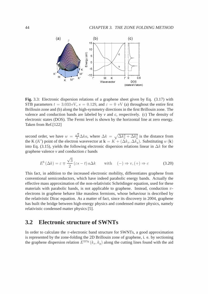
44 CHAPTER 3. THE ZONE FOLDING METHOD
Fig. 3.3: Electronic dispersion relations of a graphene sheet given by Eq. (3.17) withSTB parameterst = 3.033 eV, s = 0.129, andε = 0 eV (a) throughout the entire firstBrillouin zone and (b) along the high-symmetry directions in the first Brillouin zone. Thevalence and conduction bands are labeled byv andc, respectively. (c) The density ofelectronic states (DOS). The Fermi level is shown by the horizontal line at zero energy.Taken from Ref.[122]
second order, we havew =√
32
∆ka, where∆k =√
∆k2x + ∆k2
y is the distance fromthe K (K ′) point of the electron wavevector atk = K + (∆kx,∆ky). Substitutingw (k)into Eq. (3.15), yields the following electronic dispersion relations linear in∆k for thegraphene valencev and conductionc bands
Eb (∆k) = ε∓√
3
2(εs− t) a∆k with (−) ⇒ v, (+) ⇒ c (3.20)
This fact, in addition to the increased electronic mobility, differentiates graphene fromconventional semiconductors, which have indeed parabolicenergy bands. Actually theeffective mass approximation of the non-relativistic Schrodinger equation, used for thesematerials with parabolic bands, is not applicable to graphene. Instead, conductionπ-electrons in graphene behave like massless fermions, whosebehaviour is described bythe relativistic Dirac equation. As a matter of fact, since its discovery in 2004, graphenehas built the bridge between high-energy physics and condensed matter physics, namelyrelativistic condensed matter physics [5].
3.2 Electronic structure of SWNTs
In order to calculate theπ-electronic band structure for SWNTs, a good approximationis represented by the zone-folding the 2D Brillouin zone of graphene, i. e. by sectioningthe graphene dispersion relationE2Dg (kx, ky) along the cutting lines found with the aid
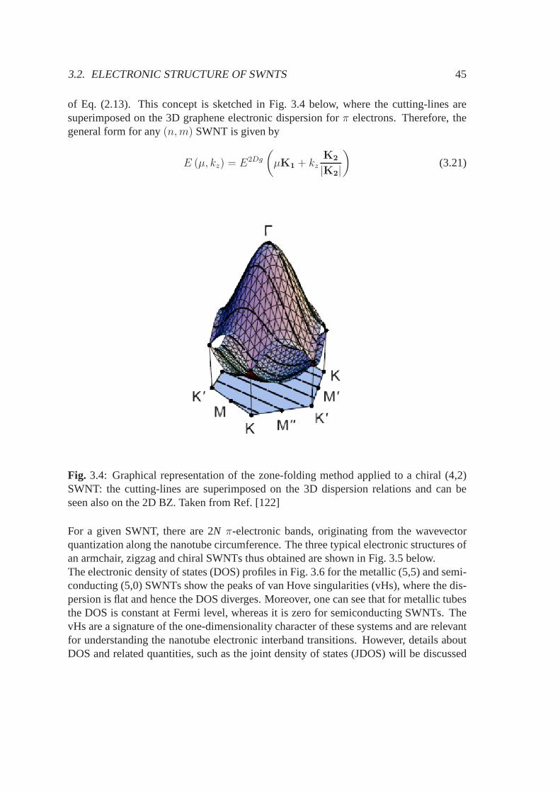
3.2. ELECTRONIC STRUCTURE OF SWNTS 45
of Eq. (2.13). This concept is sketched in Fig. 3.4 below, where the cutting-lines aresuperimposed on the 3D graphene electronic dispersion forπ electrons. Therefore, thegeneral form for any(n,m) SWNT is given by
E (µ, kz) = E2Dg
(µK1 + kz
K2
|K2|
)(3.21)
Fig. 3.4: Graphical representation of the zone-folding method applied to a chiral (4,2)SWNT: the cutting-lines are superimposed on the 3D dispersion relations and can beseen also on the 2D BZ. Taken from Ref. [122]
For a given SWNT, there are 2N π-electronic bands, originating from the wavevectorquantization along the nanotube circumference. The three typical electronic structures ofan armchair, zigzag and chiral SWNTs thus obtained are shownin Fig. 3.5 below.The electronic density of states (DOS) profiles in Fig. 3.6 for the metallic (5,5) and semi-conducting (5,0) SWNTs show the peaks of van Hove singularities (vHs), where the dis-persion is flat and hence the DOS diverges. Moreover, one can see that for metallic tubesthe DOS is constant at Fermi level, whereas it is zero for semiconducting SWNTs. ThevHs are a signature of the one-dimensionality character of these systems and are relevantfor understanding the nanotube electronic interband transitions. However, details aboutDOS and related quantities, such as the joint density of states (JDOS) will be discussed

46 CHAPTER 3. THE ZONE FOLDING METHOD
-ΠT -Π2T 0 Π2T ΠT-9
-6
-3
0
3
6
9-ΠT -Π2T 0 Π2T ΠT
-9
-6
-3
0
3
6
9
kz
EHe
VL
-ΠT -Π2T 0 Π2T ΠT-9
-6
-3
0
3
6
9-ΠT -Π2T 0 Π2T ΠT
-9
-6
-3
0
3
6
9
kz
EHe
VL
-ΠT -Π2T 0 Π2T ΠT-9
-6
-3
0
3
6
9-ΠT -Π2T 0 Π2T ΠT
-9
-6
-3
0
3
6
9
kz
EHe
VL
Fig. 3.5: Electronic band structures of SWNTs for the three representatives geometriesobtained by zone-folding method: armchair (5,5) (left upper), zigzag (5,0) (upper right)and chiral (4,2) (bottom). Calculations reproduced from Ref. [89] with TB parameterstπ = 2.9 eV, s = 0, andεπ = 0 eV.
in the third subsection, while in the next two subsections, we will consider in detail themetallicity condition for SWNTs and the important k-pointsbelonging to the cutting linesnear the Fermi energy, where the vHs in the DOS, important forthe optical spectra, arefound. Moreover, it will be shown that a particular nanotubeclassification arises fromthis cutting line analysis which relates the SWNT geometrical structure to these specialBZ points [125, 122, 121].
3.2.1 Metallicity condition for SWNTs
By inspection of Fig. 3.7 (left), clearly a SWNT is metallic if a cutting line passes througha Dirac pointK or K′. In other words, the SWNT is metallic if its circumference iscom-mensurate with the metallic wavefunction of graphene. Mathematically, for any SWNTchiral pair indices(n,m), this is expressed again by the condition of periodicity aroundthe tube circumference of Eq. (2.14)
K ·Ch = 2πµ, (µ integer) (3.22)

3.2. ELECTRONIC STRUCTURE OF SWNTS 47
-3 -2 -1 0 1 2 30
2
4
6
8
10
12
14
Energy HeVL
DO
SHs
tate
seV*at
omL
-3 -2 -1 0 1 2 30
5
10
15
20
25
Energy HeVL
DO
SHs
tate
seV*at
omL
Fig. 3.6: Density of electronic states for a semiconducting (5,0) (left) and metallic (5,5)SWNT (right) calculated by zone-folding method.
where now the coordinates of the Dirac point have been substituted as
K =2b1 + b2
3. (3.23)
Using the geometrical definitions for the real an reciprocallattice vectors of Chapter 2,one obtains the important result
2n+m = 3µ, (3.24)
which can also be expressed in the form
n−m = 3µ, (3.25)
if we consider that(2n+m)− (2m+ n) = n−m. Moreover, calculation of the normaldistance from theµ = 0 cutting line (i. e. the one which crosses theΓ point) to theKpoint in units ofK1 gives
K ·K1
K1 ·K1
=2n+m
3(3.26)
which confirms Eq. (3.24). Thus, ifn−m is multiple of 3 the SWNT is metallic, other-wise it’s semiconducting. In the latter case, Eq. (3.26), the normal distances from cuttingline µ = 0 to the cutting lines closest toK are found, as follows
K ·K1
K1 ·K1
= mod (2n+m, 3) = 1 (S1) or mod (2n+m, 3) = 2 (S2) (3.27)
from which the classification of semiconducting SWNTs into type 1 or type 2 is derived.Note that if the conventionmod(2m+ n, 3) or mod(n−m, 3) is used, the aboveS1andS2 definitions are swapped, i. e. a former S1 SWNT would be an S2 tube and so on.In the following, we will always stick with the defintion of S1and S2 types according tothe values ofmod (2n+m, 3).

48 CHAPTER 3. THE ZONE FOLDING METHOD
Fig. 3.7: Three possible configurations of the cutting lines in the vicinity of the Diracpoints depending on the value ofmod (2n+m, 3). The dashed lines indicate the KMdirections which are the boundaries of the first Brillouin zone. Taken from Ref. [122].
The values of constant2n + m are also used in optical experiments to identify familiesof SWNTs of approximately the same diameter, which share a similar behavior in photo-luminescence spectra. By plotting the SWNT chiral indices onto the graphene lattice, wecould actually identify each family with a straight line joining chiral indices of the same2n + m = const . The above condition also implies that the number of semiconductingSWNTs is twice as the amount of metalllic tubes, which is as well useful in photolu-minescence experiments. To summarize, a SWNT is metallic ifmod (2n+m, 3) = 0and semiconducting ifmod (2n+m, 3) = 1 or 2. In the nowadays accepted nan-otube classification, these three types are referred to as M0, S1 and S2, respectively. InFig. 3.7, the three different configurations of the cutting lines near the Dirac pointsKandK′ are shown, together with the corresponding value ofmod (2n+m, 3). On thebasis of other geometrical relations, this classification was further developed into severalsubtypes, namely M1+, M1-, M2+, M2-, S1+, S1-, S2+, S2-, as explained in the nextsubsection. However, only SWNTs of type M0, S1 and S2 have shown distinct opticalproperties in various spectroscopic measurements, while there was no experimental evi-dence of any difference among the above mentioned subtypes.So for practical purposes,it’s sufficient to keep in mind only types M0, S1 and S2.
3.2. ELECTRONIC STRUCTURE OF SWNTS 49
3.2.2 Critical k-points giving van Hove singularities
The purpose of this subsection is to make clear which k-points belonging to the cuttinglines near the Fermi energy of SWNTs give van Hove singularities in the density of states,according to the specific geometry of a nanotube. This is extremely important for under-standing which k-points dominates the optical spectra of these systems and it will be thesubject of the next chapters of this thesis. We recall that inChapter 2, SWNTs were classi-fied into two categories:dR = 3d if mod (n−m, 3d) = 0 anddR = d in all other cases.For M0 SWNTs, eitherdR = 3d or dR = d (metallic zigzag SWNTs) can always besatisfied, because the conditionmod (n−m, 3d) = 0 implies alsomod (n−m, 3) = 0.Instead, for S1 and S2 SWNTs the conditiondR = d is always mantained. Thus, M0SWNTs divide into subtypes M1 and M2, for whichdR = d and dR = 3d, respec-tively. Metallic zigzag SWNTs are always of subtype M1, while armchair belong to M2subtype. Furthermore, M1 SWNTs can be classified as M1+ or M1-depending uponmod ((2n+m) /d, 3) = 1 or 2 and M2 SWNTs can be either M2+ or M2- according towhethermod (3m/dR, 3) = 1 or 2. Finally, SWNTs of type S1 (S2) divide into S1+ andS1- (S2+ and S2-) subtypes for whichmod (N, 3) = 1 or 2. As stated in the previoussubsection, these further classification did not show experimental relevance. However,there exists a significative difference between zigzag SWNTs of types M1, S1, S2 andarmchair M2 tubes, concerning the critical wavevectors giving vHs in the DOS, and thiswill be discussed in the following. For zigzag nanotubes, the critical wavevectorskb
i atwhich the vHs at energyEb
i are found always at the center of the 1D Brillouin zone ofthe(n, 0) SWNT. For metallic zigzag tubes(3n, 0) also the Fermi pointkF appears at thezone center, hencekF = 0. Formally, this can be obtained by evaluating the projectionof ΓK ontoK2, which gives(ΓK ·K2) / (K2 ·K2) = m/dR. Since for M1, S1 and S2dR = d, the ratiom/dR is an integer and the Fermi points appear at the center of the 1DBZ. Moreover, the critical wavevectors for these SWNTs, as well as the Fermi points, aredoubly degenerate, that iskb
i = kb′
i = 0 andkF = k′F = 0, since the electronic disper-sion relations around the Dirac pointsK andK′ are isotropic. For M2 SWNTs, whichinclude armchair nanotubes, we havedR = 3d, which impliesmod (m, dR) = 1 or 2.The Fermi wavevectorskF thus appear at two-third of the distance from the center to theedge of the 1D Brillouin zone,±K2/3, which stems from the shortening in real space ofthe length of the translational vector T by a factor of 3. It follows thatkF = +K2/3 andk′F = −K2/3 for M2+ SWNTs, whilekF = −K2/3 andk′F = +K2/3 for M2- SWNTs.In general, for a given(n,m) nanotube the condition for the critical Fermi wavevectorskF = 0 or kF = ±K2/3 are not mantained. Moreover, note that the degeneracy of thecritical wavevectors,kb
i andkb′
i , holds only for achiral single-walled nanotubes due tothe presence of a horizontal mirror plane [118]. For chiral SWNTs, the anisotropy ofthe electronic dispersion relation around the Dirac pointsK andK′, which is neglectedby the linear approximation showed in Eq. (3.20), lifts the degeneracykb
i = −kb′
i 6= 0.Moreover, the critical points for M2 SWNTs are shiftedkb
i = −kb′
i 6= ±K2/3. This

50 CHAPTER 3. THE ZONE FOLDING METHOD
anisotropy is also calledtrigonal warping effectand is intrinsic to the complete TB or-thogonal model [135]. To understand the trigonal warping effect, it’s sufficient to lookat the equi-energy contours around theK point, which are actually not circular but showa triangular distortion. Let’s consider also the two cutting lines closest to theK point ina (chiral) metallic nanotube, as shown in Fig. 3.8. Though the cutting lines occur at thesame distance fromK , however the two points contributing to the lowest vHs,k1 andk′1,lie on different equi-energy contour. As a consequence, thetrigonal warping effect in-duces a small splitting in the vHs peaks. The splitting is largest for zigzag nanotubes andequal to zero for armchair nanotubes, where the cutting lines are parallel to the verticalK −M line and the energies atk1 andk′1 are actually equal. The origin of the triangulardistortion beyond the linear approximation of Eq. (3.20) can be understood by expandingw (k) of Eq. (3.16) up to the second order around theK point
w =
√3
2a∆k +
1
8a2
∆k3y − 3∆kx∆k
2y
∆k=
√3
2a∆k +
1
8cos 3ϕa2∆k2. (3.28)
whereϕ is the angle between(∆kx,∆ky) and the directionΓK, ∆kx = ∆k sinϕ and∆ky = ∆k cosϕ. Thus, the triangular symmetry of the equi-energy contoursaround theK point is explained with the factorcos 3ϕ in the expansion above.
Fig. 3.8: Difference of the position of the touching pointsk1 andk2 of the cutting lineswith the equienergy contour lines in semiconducting type I and II and metallic SWNTs.In semiconducting type S1 (S2) theES
22 occurs outside (inside) the first 2D BZ. In metallicSWNTs,EM
11 is split due to the trigonal warping effect, since touching points belongingto cutting lines equidistant lie on different equienergy contours. Taken from Ref. [121].
3.2.3 Density of electronic states
As introduced in the beginning of this section, the flat regions of the electronic bandsgive rise to spikes in the electronic density of states, which are known as van Hove singu-
3.2. ELECTRONIC STRUCTURE OF SWNTS 51
larities (vHs). The vHs dominate the density of electronic states (DOS) of 1D-systems.Moreover, in the next section we will see that, if a given interband transition is allowedby dipole selection rules, the profile of the optical absorption spectra of SWNTs is alsodominated by the joint density of states (JDOS) between valence and conduction bands,which is a DOS-related quantity. In general, in order to obtain the DOS of a solid as afunction of the energyg (E), one needs to scan the whole energy range into small inter-vals of finite amplitudedE, counting all over the states within each interval[E,E + dE].Thus the general profile of the DOS as a function of energy for a1D crystal with volumeV is obtained as
g (E) = 1/V∑
σ
∑
b,k
2δ(E − Eb
k
), (3.29)
whereb is the usual band index,k the wavevector index in the BZ and the sum overσaccounts for the spin degeneracy, that is at most two electrons with opposite spin can beaccomodated in each k-state. Then, the full DOS profile for the SWNT is obtained fromintegrating the zone-folding band structure of Eq. (3.21) over each 1D BZ and summingover the bands, as follows
g (E) = 1/ (2π)∑
σ
∑
b=v,c
N−1∑
µ=0
∫ π/T
−π/T
dkzδ(E − Eb (µ, kz)
)(3.30)
Similarly, for the JDOS between valence and conduction states
gJ (E) = 1/V∑
σ
∑
k,k′
δ (E − (Eck′ − Ev
k)), (3.31)
which can be expressed for SWNTs as
gJ (E) = 1/ (2π)∑
σ
N−1∑
µ,µ′=0
∫ π/T
−π/T
dkzδ (E − (Ec (µ′, kz)− Ev (µ, kz))). (3.32)
For numerical evaluations, the delta functions in Eqq. (3.30) and (3.32) can be moreconveniently expressed in the form of a Lorentzian function(see for example AppendixG.5.1 in Ref. [94]) with broadening parameterβ
δ (E − E ′) = limβ→0
(1
π
β
(E − E ′)2 + β2
)(3.33)
In the next section, it will be shown that, according to the calculations of Refs. [139, 141],for light polarization parallel to the tube axis optical transitions occur between vHs ofvalence and conduction bands havingµ = µ′, whereas for perpendicular polarization theselection rule isµ′ = µ ± 1. If the energy of an incoming photon matches the energydifference between two vHs, in the conduction and in the valence band, respectively, the

52 CHAPTER 3. THE ZONE FOLDING METHOD
optical absorption is largely enhanced due to the high number of electronic states. Thusit is possible to observe from an isolated SWNT and even picking up resonant signalfrom only a few specific SWNTs in a sample with many different(n,m) chiralities. Bychanging the laser energy different SWNTs chiralities can be selectively probed. Forelectronic states near the Dirac pointsK andK′, Mintmire and White [65, 137] havederived very simple scaling relations for the lowest transition energiesπ → π∗ at the vHswith index i, both for metallic and semiconducting nanotubes:
ESii =
2atπi√3dt
and EMii =
2√
3atπi
dt
, (i = 1, 2, 3) . (3.34)
It is clear that the energy gap at the vHs with indexi is inversely proportional to the SWNTdiameterdt and that the first metallic transition occurs at three times the energy of asemiconducting SWNT. More accurate predictions for these transitions have been derivedby Reichet al. taking into account the trigonal warping effect into the k-expansion of theenergy dispersion around theK point [138]. We conclude this panoramic discussionabout DOS and related quantities by pointing out that that there are other techniques(e.g. therecursion method[76, 80]) which allow to obtain the density of states evenwithout the need of having at disposal the complete bandstructure. This can be the casefor instance of non-periodic systems or with open boundary conditions. In literatureabout transport properties of carbon nanotubes, these techniques take advantage of thecalculation of the local density of states (LDOS) for each atom from the Green’s functionfor the hamiltonian, which is often found formulated in realspace representation. In thiscase, the fundamental relation between LDOS and Green’s function is [95, 149, 150]
gLDOS (E) = −1
πIm [G (E)ii] (3.35)
from which several interesting quantities for transport properties, such as transmission,can be derived.
3.3 Optical properties of graphene and SWNTs
In this section the matrix elements for the electron-photoninteraction for graphene andsingle-walled carbon nanotubes are derived from first orderperturbation theory [96]. Asanticipated, these elements together with the joint density of states are used for the cal-culation of the absorption spectra for the optically allowed transitions in the visible rangewhich occur between theπ bonding and theπ∗ antibonding molecular orbitals.
3.3.1 Electron-photon interaction and dipole approximation
The general form for the hamiltonian of a particle with charge e and massm in an elec-tromagnetic field with time-dependent vector potentialA (t) and an external potentialV,

3.3. OPTICAL PROPERTIES OF GRAPHENE AND SWNTS 53
such as the periodic crystal potentialV (r) is given by [121, 96]
H =1
2m[−ı~∇− eA (t)]2 + V (r) . (3.36)
In the above expression the vector potential associated with the electomagnetic field actsas a time-dependent perturbation upon the eigenfunctionsΨi (k) of the unperturbed crys-tal HamiltonianH0 = − ~2
2m+V (r). Neglecting the quadratic terms inA (t)2 and using
the gauge∇ ·A (t) = 0 in the expansion of Eq. (3.36), the perturbative term actingonthe electron and causing its transition from valence to conduction band is
Hλpert =
ıe~
mAλ (t) · ∇ . (3.37)
The vector potential associated with the quantized electromagnetic field can be expressedin second quantization formalism as [122]
Aλ (κ, r, t) =
√~
2κκ0V ω (κ)
(√nλ (κ) exp (+ıκr− ıω (κ) t)Pλ (3.38)
+√nλ (κ) + 1 exp (−ıκr + ıω (κ) t)Pλ∗
),
whereκ is the dielectric constant of the material,κ0 is the vacuum dielectric permit-tivity, V is the quantization volume for the electromagnetic field,nλ (κ) andω (κ) arethe photon occupation number and the photon frequency for wavevectorκ, respectively,andPλ is the photon polarization vector. The ”+ (−)” sign in the frequency phase fac-tors in Eq. (3.38) corresponds to the emission (absorption)of a photon with frequencyω. Within first-order perturbation theory, the general form for the matrix element for anoptical transition from an initial statei atki to a final statef atkf is obtained as
Mfλipert (kf ,κ,ki) = 〈Ψf (kf , r, t) |Hλ
pert|Ψi (ki, r, t)〉 (3.39)
= 〈Ψf (kf , r, t) |ıe~
mAλ (κ, r, t) · ∇|Ψi (ki, r, t)〉
The spatial part of the above integral is expressed by the dipole vector
Dfλi (kf ,±κ,ki) = 〈Ψf (kf , r) |ıe~
mexp (±ıκr)∇|Ψi (ki, r)〉. (3.40)
In the dipole approximation,κ is neglected and is setκ = 0, and the optical dipoletransitions are vertical,ki ≡ kf ≡ k. Therefore, the optical dipole transition matrixelements for the light absorption (A) and spontaneous emission (E) processes can beexpressed as
Mfλi (kf ,ki) = ıe~
mω
√I
2√κκ0c
Pλ ·Dfλi (kf ,ki) , (3.41)
54 CHAPTER 3. THE ZONE FOLDING METHOD
where I is the radiant flux density of the light beam. Fermi’s Golden Rule gives thetransition probability between the initial statei and the final statef for the electron-photoninteraction timeτ of the perturbation
W fλi (kf ,ki) =1
~2τ|∫ τ
0
dtMfλi (kf ,ki) |2 ∝ (3.42)
∝ |P ·Dfλi (kf ,ki) |2sin2
[(Ef (kf)− Ei (ki)± Eλ
)τ2~
]
(Ef (kf )− Ei (ki)±Eλ)2 .
For long interaction timeτ →∞ thesincfunction sin2 (αt)πα2t
→ δ (α). Therefore Eq. (3.42)expresses the energy conservationEf (kf ) − Ei (ki) ± Eλ = 0. In the following twosections we will show the expressions obtained in Refs. [122, 141, 121, 142, 144, 145]for the dipole vector of a graphene sheet and SWNTs, respectively. Also, we discuss thek-points in the BZ which are relevant for the optical absorption of these systems.
3.3.2 Dipole vector in graphene
As stated in the first part of this chapter, the features of theoptoelectronic spectra ofgraphitic systems around the Fermi level are dominated by electrons withπ character.Accordingly, the optical dipole transitions in the visiblerange occur between theπ bond-ing and theπ∗ antibonding molecular orbitals. The dipole selection rules prohibit anoptical transition within a2pz orbital at the same carbon atom, because of the odd sym-metry of the transition dipoleDfi in x, yandz, whereas it is allowed between2pz orbitalson adjacent carbon atoms in graphene and SWNTs. Furthermore, even in the case oftransition between nearest neighbor atoms, thez-component ofDfi is zero for all atomicmatrix elements, since thez-component ofDfi has odd symmetry. Substituting theπ-wavefunctions of Eq. (3.2) for valence and conduction bands, we get
Dcvπ (kf ,ki) = 〈Ψc (kf) |∇|Ψi (ki)〉 = (3.43)
= cc∗B (kf ) cvA (ki) 〈ΦB (kf , r) |∇|ΦA (ki, r)〉+ cc∗A (kf ) c
vB (ki) 〈ΦA (kf , r) |∇|ΦB (ki, r)〉.
Expressing the Bloch sums for the 2pz orbitals centered at A and B sites as in Eq. (3.3)and splitting the coordinates of all atoms over the A and B sublattices, we obtain
Dcvπ (kc,kv) =
1
U
U−1∑
i=0
3∑
l=1
[cc∗B (kf ) c
vA (ki) exp
[ı (ki − kf ) ·Ri
A
]× (3.44)
× exp(−ıkf · rl
A
)〈ϕ(r− rl
A
)|∇|ϕ (r)〉 +
+ cc∗A (kf ) cvB (ki) exp
[ı (ki − kf ) ·Ri
B
]exp
(−ıkf · rl
B
)〈ϕ(r− rl
B
)|∇|ϕ (r)〉
]
where we have introduced the vectorrlA
(rl
B
), which connects nearest neighbour atoms
starting from an A (B) atom and defined as
RiA = Ri
B + rlB, Ri
B = RiA + rl
A, (l = 1, 2, 3) . (3.45)
3.3. OPTICAL PROPERTIES OF GRAPHENE AND SWNTS 55
For vertical transitions the selection ruleki ≡ kf ≡ k, so the exponential phase factorsexp [ı (ki − kf) ·Ri
B] are equal to one and Eq. (3.44) is simply given by
Dcv (k) = 〈Ψc (k) |∇|Ψv (k)〉. (3.46)
The atomic dipole vectors for thes = A,B sublattices are defined as [141, 121, 122]
drls
=
∫ϕ∗(r− rl
s
)∇ϕ (r) dr = −moptr
ls
|rls|
. (3.47)
For dipole transitions involving only first nearest neighbor interactions|rls| = a/
√3. An
important consequence of the assumption introduced with Eq. (3.47) is that the contri-bution to the susceptibility coming from two orbitals placed on the same atom can beneglected [101]. This is a reasonable approximation because the polarisability of a freeatom is much smaller than that of the corresponding material. Since Eq. (3.47) involvesthe product between localized atomic wavefunctions and itsderivative, which decreasesquickly with increasing distance between atoms, it’s sufficient considering only nearestneighbour coupling, as already assumed for the electronic dispersion relation.mopt is theatomic matrix element for nearest neighbour carbon pairs and is defined as
mopt = 〈ϕ(r− rl
s
)| ∂∂x|ϕ (r)〉. (3.48)
Usually, the value ofmopt is obtained analytically from Gaussian functions fitted to the2pz wavefunctions previously obtained by a LDA calculation [121, 140]. The estimateobtained in Ref. [121] givesmopt = 0.21 [a.u.]−1 (1 atomic unit is0.529 A). Other esti-mates obtained in Refs. [122, 152] give similar values. However, it’s not particularly rel-evant to know the exact value of this parameter, as it can be considered simply a constantto normalize the resulting values of the dipole matrix elements [151]. Thus the graphenedipole vector of Eq. (3.44) for vertical transitions and nearest neighbour coupling can bewritten in extended form as
Dcv (k) = −√
3mopt
a
[cc∗B c
vA
3∑
l
exp(ık · rl
A
)rl
A + cc∗A cvB
3∑
l
exp(ık · rl
B
)rl
B
](3.49)
= cc∗B cvAdA (k) + cc∗A c
vBdB (k) .
By simmetry considerations upon the sign of the wavefunctions coefficients, it followsthatcc∗A c
vB = − (cc∗B c
vA)∗. Moreover, the following relation for the atomic dipole vectors
holds:dA (k)∗ = −dB (k). Therefore, Eq. (3.49) can be cast in the following shortenedform:
Dcv (k) = −2√
3mopt
aRe
[cc∗B (k) cvA (k)
3∑
l
exp(ık · rl
A
)rl
A
](3.50)
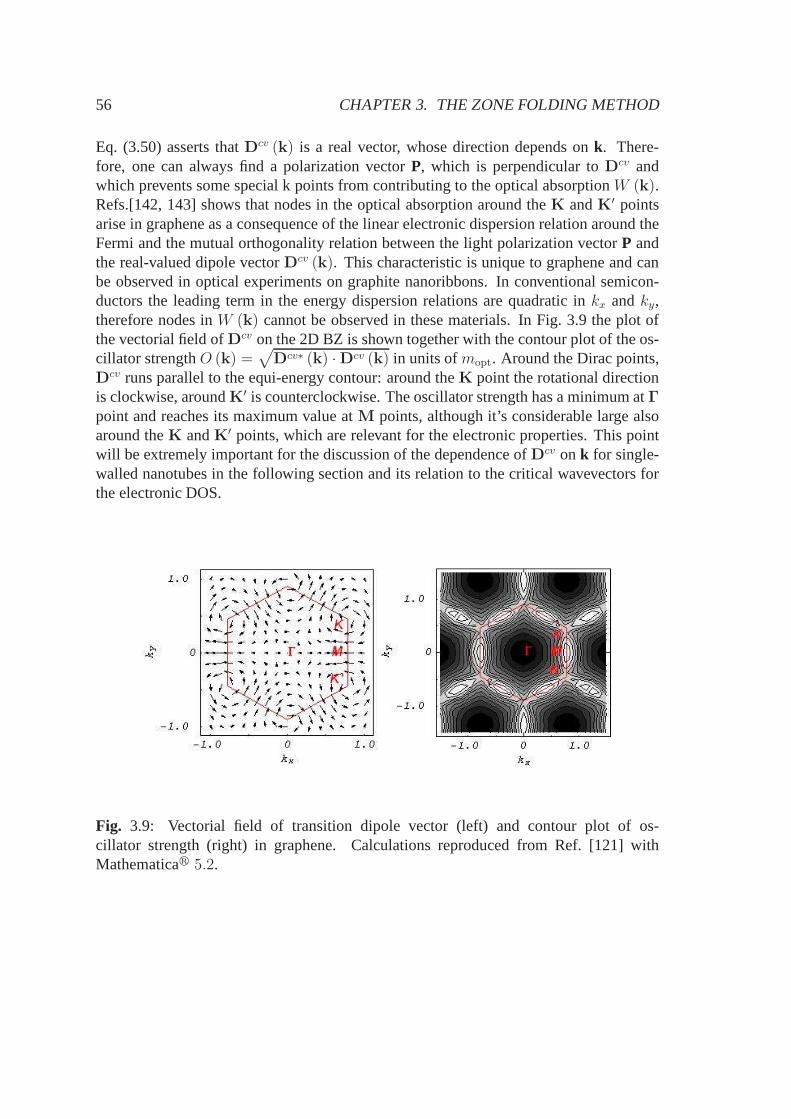
56 CHAPTER 3. THE ZONE FOLDING METHOD
Eq. (3.50) asserts thatDcv (k) is a real vector, whose direction depends onk. There-fore, one can always find a polarization vectorP, which is perpendicular toDcv andwhich prevents some special k points from contributing to the optical absorptionW (k).Refs.[142, 143] shows that nodes in the optical absorption around theK andK′ pointsarise in graphene as a consequence of the linear electronic dispersion relation around theFermi and the mutual orthogonality relation between the light polarization vectorP andthe real-valued dipole vectorDcv (k). This characteristic is unique to graphene and canbe observed in optical experiments on graphite nanoribbons. In conventional semicon-ductors the leading term in the energy dispersion relationsare quadratic inkx andky,therefore nodes inW (k) cannot be observed in these materials. In Fig. 3.9 the plot ofthe vectorial field ofDcv on the 2D BZ is shown together with the contour plot of the os-cillator strengthO (k) =
√Dcv∗ (k) ·Dcv (k) in units ofmopt. Around the Dirac points,
Dcv runs parallel to the equi-energy contour: around theK point the rotational directionis clockwise, aroundK′ is counterclockwise. The oscillator strength has a minimumatΓpoint and reaches its maximum value atM points, although it’s considerable large alsoaround theK andK′ points, which are relevant for the electronic properties. This pointwill be extremely important for the discussion of the dependence ofDcv on k for single-walled nanotubes in the following section and its relation to the critical wavevectors forthe electronic DOS.
Fig. 3.9: Vectorial field of transition dipole vector (left) and contour plot of os-cillator strength (right) in graphene. Calculations reproduced from Ref. [121] withMathematicar 5.2.

3.3. OPTICAL PROPERTIES OF GRAPHENE AND SWNTS 57
3.3.3 Dipole vector in SWNTs
In order to obtain the optical dipole matrix element for SWNTs one can follow a treat-ment similar to that delined for graphene, as explained in Refs. [141, 143]. In this case,one needs to place the atomic dipole vectorsds (k) on the cylindrical surface of thenanotube sidewall. This task can be accomplished by applying to the nearest-neighborinteratomic vectorsrl
s of ds the rotation operatorsΩ of Eq. (2.20), introduced in Chap-ter 2.4.1. Actually, the operatorΩ cannot be applied to the nearest-neighbor vectorsrl
s ofthe exponential phase factors of Eq. (3.49), since they are multiplied by the wavevectorskf andki of the 2D reciprocal space of the unrolled graphene layer, according to the zonefolding scheme. Moreover, curvature effects on the atomic dipole matrix element due tothe cylindrical sidewall of the nanotube are neglected and the factormopt is the same usedfor graphene. Therefore, we have
Dcv (k) =
√3mopt
aNU
[cc∗B c
vA
U∑
u=1
N∑
h=1
eı(ki−kf)·Ruh,AdhA + cc∗A c
vB
U∑
u=1
N∑
h=1
eı(ki−kf)·Ruh,BdhB
]
(3.51)wheredhA anddhB are the rotated atomic dipole vectors for optical transitions from theA atom in thehth hexagon to its neighboringB atoms, and from theB atom in thehthhexagon to its neighboringA atoms, respectively. The general expressions for the rotatetdatomic dipole vectorsdh,s (h = 1, . . . , N and s = A,B) are
dhs = Ωz (Θϕh,s)ds, (3.52)
ds =
3∑
l=1
exp(−ıkf · rl
s
)Ωy
(π6− θ)
Ωx
(π2
)rl
s,
where forϕh,s we have used the expression given in Eq. (2.21).ds (s = A,B) are theatomic dipole vectors in the unrolled graphene layer and canbe written explicitly as
dA = (dx, 0, dz) and dB = (−d∗x, 0,−d∗z) . (3.53)
According to Eq. (3.52), the explicit expressions fordhA anddhB then become
dhA = (cos (ϕhA)dx,Θ sin (ϕhA)dx, dz) (3.54)
dhB = (− cos (ϕhB)d∗x,−Θ sin (ϕhB)d∗x,−d∗z)
3.3.4 Dipole selection rules in SWNTs
Now we discuss the selection rules for general transitions involving valence and conduc-tion bands within the zone-folding scheme applied to SWNTs.Even including curvatureeffects, these selection rules aren’t affected in any way. First we define the change inazimuthal index (cutting-line)∆µ = µf −µi and axial wavevector∆kz = kzf − kzi. The

58 CHAPTER 3. THE ZONE FOLDING METHOD
change in total wavevector is thuski − kf = −∆µK1 −∆kzK2/U . Thenki − kf andRu
hs as given in Eq. (2.19) are substituted into Eq. (3.51). The summation over the SWNTunit cellsu can be factored out in the form
∑Uu=1 exp [−ı (∆µK1 + ∆kzK2/U) · uT].
By using the relations between nanotube real and reciprocallattice vectors as given inEq. (2.10), the previous sum overu becomes
∑Uu=1 exp [−ı (2πu/U)∆kz], which is
equal to zero except for∆kz = 0, where in such case the sum givesU. Thus the firstselection rule for the electronic wavevector along the SWNTaxis is obtained as∆kz = 0.In order to obtain the selection rule for the cutting line indexµ, a more involved proce-dure is necessary. First we have to perform the summation over the graphene unit cellsinside the SWNT unit cell, labelled by the indexh. The phase factors of Eq. (3.51)can be simplified to the formexp [−ı∆µK1 · (hR− r1
s/2)]. Substituting the symme-try vectorNR = Ch + MT and using again the relations of Eq. (2.10), we obtainexp [−ı∆µ2πh/N + ı∆µK1 · r1
s/2], whereK1 · r1s = ϕ1
s. By writing thecos (ϕhs) andsin (ϕhs) terms of Eq. (3.54) into sums and differences of complex exponentials, the gen-eral expressions for thex, y, zcomponents of the nanotube dipole vectorD can be obtainedas
Dx =1
2(C+1S+1 + C−1S−1) , (3.55)
Dy = Θ1
2ı(C+1S+1 − C−1S−1) ,
Dz = C0S0 ,
where the termsSl, C0, C±1 are defined as in the following:
Sl =1
N
N∑
h=1
exp−ı (∆µ− l) 2πh/N (3.56)
C0 =
√3mopt
a
[cf∗B c
iAdzξ0 − cf∗A c
iBd
∗zξ∗0
]
C±1 =
√3mopt
a
[cf∗B c
iAdxξ±1 − cf∗A c
iBd
∗xξ
∗±1
]
ξl = exp ı (∆µ − l)ϕ1A/2
We recall that the optical matrix element, as defined in Eq. (3.41), is proportional to thescalar product of the light polarization vectorPρ (ρ = A,E) and the dipole vector givenby Eq. (3.55). From this equation one can see that the light polarized parallel to theSWNT axis(Pρ = z) selects the termS0 in the matrix element, while the light polarizedperpendicular to the SWNT axis(Pρ = x or y) selects the termsS+1 andS−1. Thepresence of the termSl (l = 0,±1) implies the azimuthal optical selection rule∆µ = l,which can also be expressed explicitly asµ → µ + l. Thus the dipole selection rules for
3.3. OPTICAL PROPERTIES OF GRAPHENE AND SWNTS 59
interband optical transitions in SWNTs and linearly polarized light are:
∆µ = 0 for parallel polarization P‖z (3.57)
∆µ = ±1 for perpendicular polarizationP‖x or y.
These rules were formerly derived by Ajiki and Ando [139], who additionally discussedthe role of depolarization effects in suppressing almost completely the perpendicular po-larized component in real optical absorption experiments due to self-consistent screeningeffects. Therefore, in order to analize the optical absorption spectra of SWNTs one isusually interested into the selection rules for light polarized parallel to the SWNT axisand optical dipole vector between initial statei and final statef is found expressed withthez-component highlighted as
Dfi (kf ,ki) = 〈Ψf (kf ) |∇z|Ψi (kf )〉 (3.58)
Actually for our purposes in the following chapter, we will take into account only thiscomponent. However, in spite of the depolarization effects, the predicted selection rulescould be confirmed experimentally by Resonance Raman Spectroscopy studies on iso-lated SWNTs when changing the light polarization vector [153]. Selection rules for cir-cularly polarized were also obtained [141], which are important for understanding othereffects such as circular dichroism and birefringence in chiral SWNTs, but they will notbe considered in this thesis.
3.3.5 SWNT optical matrix elements and critical wavevectors
In order to study the profile of the optical dipole matrix elements over the SWNT Bril-louin zone and extract information about general trends fordifferent chiralities and spe-cial k wavevectors, analytical expression for these matrixelements have also been derivedby several authors, which are actually easier to evaluate and plot than Eq. (3.51). Here,for consistency with the previous notation, we consider theanalytical expression obtainedin the work of J. Jiang, A. Gruneiset al. [144] for thez-component of the optical matrixelement for a single-walled nanotube of any(m,n) chirality. Similar results and conclu-sions follow also from other authors [145, 148]. In order to obtain this expression withinthe zone-folding scheme from the expression for graphene dipole vector of Eq. (3.49),one has to consider that:
• all A (B) atoms have the samezcomponent of the atomic dipole vectorsdgA (dgB),
• each of the three nearest-neighbor atoms has the same relative coordinate from theoriginal atoms,
• the directions of these nearest-neighbor atoms are determined only by the chiralangleθ by which the graphene sheet is wrapped into a SWNT (see Fig. 3.10).

60 CHAPTER 3. THE ZONE FOLDING METHOD
Fig. 3.10: The positions for an A atom at the origin and its three nearest neighbor B atoms.The angles between these bonds and the chiral vectorCh and translationT vectors arealso shown. Picture taken from Ref. [144].
As a consequence, the functionsdAg,z anddB
g,z are dependent only on the projection angleϑl (θ),
dAg,z (θ) =
3∑
l=1
exp(ık · rl
A
)rlϑl =
a√3
[− exp
(ıkxa√
3
)sin(π
6− θ)
(3.59)
+ exp
(− ıkxa
2√
3+ıkya
2
)cos θ − exp
(− ıkxa
2√
3− ıkya
2
)cos(π
3− θ)]
,
dBg,z (θ) = −dA∗
g,z (θ) .
Substituting the expressions given in Eq. (3.59) together with the eigenvectors of Eq. (3.18)into Eq. (3.50), thez component of the dipole vector for the unrolled nanotube unit cellon the 2D BZ of graphene is given in analytical form by
Dz (k) =moptδkz,k′zδµ,µ′
2w (k)
[sin(π
6− θ)×
cos kya− coskya
2cos
√3kxa
2
(3.60)
+√
3 cos(π
6− θ)
sin
√3kxa
2sin
kya
2
]
One can see that this expression includes the dependence of the dipole vector on bothkwavevector and chiral angleθ in addition to the selection rules for parallel polarization ofthe light. One can see immediately from Eq. (3.60) thatDz = 0 at theΓ point and at theDirac pointsK andK′. In Fig. 3.11 contour plots ofDz (k), over the 2D hexagonal BZ

3.3. OPTICAL PROPERTIES OF GRAPHENE AND SWNTS 61
Fig. 3.11: Contour plot over the 2D BZ of the value of the dipole vector parallel to theSWNT axis for an armchair (left) and zigzag (right) SWNT.Dz is zero at the cornersof the BZ. White and black colours mean (strongly) positive and negative values ofDz,respectively, while an intermediate gray level means that asign change inDz occurs.Calculations reproduced from Ref. [144] with Mathematicar 5.2.
are shown for zigzag and armchair nanotubes, respectively.By superimposing the cutting lines on these contour plots, with the aid of Eq. (2.13), oneobtains the dependence ofDz over the 1D nanotube BZ for a given band or cutting lineµ, as shown in Fig. 3.12. For armchair SWNTs, Eq. (3.60) givesDz = 0 for kx = 0or ky = 0. Moreover, for all interband transitionsDz = 0 at kz = 0. Also, Dz = 0for all kz values for the two optical transition connecting non-degenerate A-symmetrybands(0 → 0) and(5 → 5). Note that in(n, n) SWNTs, the cutting lines (which are alsoparallel toky andK2) with indexµ = n always cross theK or K′ point. Actually, thesecutting-lines are parallel to theK−M−K′ edge of the hexagonal 2D BZ. Thus, we candraw the conclusion that at the Fermi levelDz = 0 for armchair nanotubes. For zigzagmetallic nanotubes, the situation is similar, withDz = 0 at the Fermi level and closeto zero in the proximity, whereas for semiconducting zigzagnanotubesDz 6= 0. Thereasons whyDz is vanishing near the Fermi level for metallic nanotubes areas follows.We recall that for graphite, around the Dirac pointsK andK′ of the 2D BZ, there arenodes in the optical absorption, which lie one a line crossing the Dirac point and parallelto the light polarization direction. When the graphene layer is rolled up into a nanotube,the nanotube axis is parallel to the cutting lines. Thus, forlight polarization parallelto the nanotube axis, if there is a cutting line crossing theK point, as it happens with

62 CHAPTER 3. THE ZONE FOLDING METHOD
Fig. 3.12: Dependence of the dipole vector componentDz and energy E on the 1D wavevectorkz for an armchair (5,5) (left) and a zigzag (6, 0) nanotube (right) for variousinterband optical transitions for parallel polarization of the light. Taken from Ref. [144].
metallic nanotubes, then there is no optical absorption forthe involved k-point. For thepurposes of this thesis, however, it is important to notice that in zigzag nanotubesDz hasmaximum absolute values atkz values of the 1D wavevector of eachµ-th band wherevan Hove singularities occur, that is the critical wavevector (µ, kz = 0). Thus, one drawsthe conclusion that the strong optical absorption in zigzagSWNTs is due not only to asingularity in the joint density of states but also to the maximum matrix element valueat the same vHs. The 2D contour plots ofDz of Fig. 3.11 show also other interestingfeatures. For all nanotube geometries except the armchair one, it is seen that, for vHsaway from theK point,|Dz| values at the vHs decrease inside the BZ and increase outside(Fig. 3.11 right). For armchair nanotubes, Fig. 3.11 (left)shows that|Dz| has a mirrorsimmetry with respect to theK−M−K′ line. Thus,|Dz| values near a vHs awayfrom the K point will increase as we move away from the vHs on both sides of thesingularity. In Fig. 3.13 values of|Dz| calculated at the first, second, third vHs (the socalledE11, E22, E33) are shown for semiconducting nanotubes as a function of thechiral
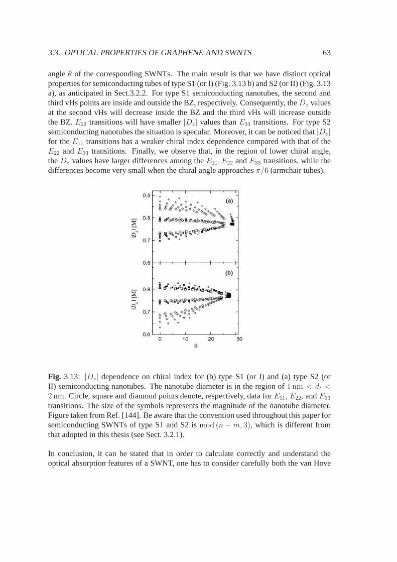
3.3. OPTICAL PROPERTIES OF GRAPHENE AND SWNTS 63
angleθ of the corresponding SWNTs. The main result is that we have distinct opticalproperties for semiconducting tubes of type S1 (or I) (Fig. 3.13 b) and S2 (or II) (Fig. 3.13a), as anticipated in Sect.3.2.2. For type S1 semiconducting nanotubes, the second andthird vHs points are inside and outside the BZ, respectively. Consequently, theDz valuesat the second vHs will decrease inside the BZ and the third vHswill increase outsidethe BZ.E22 transitions will have smaller|Dz| values thanE33 transitions. For type S2semiconducting nanotubes the situation is specular. Moreover, it can be noticed that|Dz|for theE11 transitions has a weaker chiral index dependence compared with that of theE22 andE33 transitions. Finally, we observe that, in the region of lower chiral angle,theDz values have larger differences among theE11, E22 andE33 transitions, while thedifferences become very small when the chiral angle approachesπ/6 (armchair tubes).
Fig. 3.13: |Dz| dependence on chiral index for (b) type S1 (or I) and (a) type S2 (orII) semiconducting nanotubes. The nanotube diameter is in the region of1 nm < dt <2 nm. Circle, square and diamond points denote, respectively, data forE11, E22, andE33
transitions. The size of the symbols represents the magnitude of the nanotube diameter.Figure taken from Ref. [144]. Be aware that the convention used throughout this paper forsemiconducting SWNTs of type S1 and S2 ismod (n−m, 3), which is different fromthat adopted in this thesis (see Sect. 3.2.1).
In conclusion, it can be stated that in order to calculate correctly and understand theoptical absorption features of a SWNT, one has to consider carefully both the van Hove
64 CHAPTER 3. THE ZONE FOLDING METHOD
singularities in the joint density of states and the behaviour of the optical absorptionmatrix elements at the critical wavevectors which give vHs.If the optical dipole matrixelement at the critical k point is zero, the transition will be forbidden and therefore thecontribution of the vHs to the absorption spectrum will be suppressed; otherwise, thetransition will be dipole-allowed and the intensity of the optical absorption peak will beproportional to the absolute square of the respective optical matrix element.
3.4 Summary
In this section a general review of the zone-folding method applied to the tight-bindingcalculation of the electronic and optical properties of single-walled nanotubes was given,according to the most relevant scientific results publishedin nanotube literature. Par-ticular attention was dedicated to the analysis of the Brillouin zone for understandingthe relevant k-points which determines the basic features of the SWNT optoelectronicspectra, according to the different SWNT chiralities. The result recalled in this analysiswill be of fundamental importance for understanding the choices made in the followingchapters, which present the original work developed in thisthesis.

Chapter 4
Small crystal approach
In the previous chapter the general principles behind the tight-binding framework and thezone-folding technique were introduced for calculating the electronic and optical prop-erties of graphene and single-walled carbon nanotubes froma reciprocal space point ofview. In this section we re-obtain those properties from a real space point of view byapplying the so called small crystal approach to SWNTs. Thenwe show how several is-sues of actual interest both in experimental and theoretical nanotube science can be easilytreated by this method. Note that the validity of the theoretical treatment presented in thischapter is quite general and can be applied to nanotubes of any chiralities. The examplesand calculations presented in the present chapter and in thechapter about DWNTs arereferred to zigzag nanotubes just for convenience reasons,but can be as well extended toother nanotube geometries. The importance of the choice of zigzag geometry is essentialfor the developments shown in the chapter about many-body effects, where the choice iscrucial both for the computational feasibility of the problem with our computer resources.
4.1 Basic facts behind the Small Crystal Approch
Many calculations in solid state physics, either by perturbative techniques or variationalapproach, involve the averaging over the Brillouin zone of aperiodic function. Such cal-culations are often very complicated and computationally demanding, as they require inprinciple the knowledge of the value of the function at each k-point in the Brillouin zone.In practice the functional values are known or determined over a set of points in the zoneand the values at the other points are found by using various type of approximations andinterpolation methods. To obtain sufficient accuracy in these calculations, it is necessaryin general to know the functional values over a large set of points. Thus the choice of thesampling grid of the first Brillouin zone of a periodic systemis extremely important forthe accurate prediction of the electronic and vibrational properties of the system. On theother hand, the computational effort in memory and time increases as the spacing of thesampling grid is reduced. However, it has to be pointed out that not all the k-points chosen
65
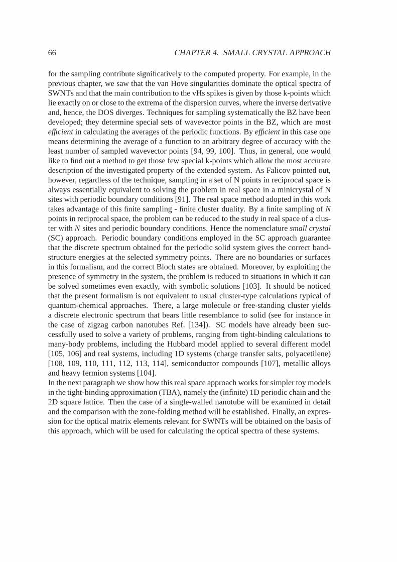
66 CHAPTER 4. SMALL CRYSTAL APPROACH
for the sampling contribute significatively to the computedproperty. For example, in theprevious chapter, we saw that the van Hove singularities dominate the optical spectra ofSWNTs and that the main contribution to the vHs spikes is given by those k-points whichlie exactly on or close to the extrema of the dispersion curves, where the inverse derivativeand, hence, the DOS diverges. Techniques for sampling systematically the BZ have beendeveloped; they determine special sets of wavevector points in the BZ, which are mostefficientin calculating the averages of the periodic functions. Byefficientin this case onemeans determining the average of a function to an arbitrary degree of accuracy with theleast number of sampled wavevector points [94, 99, 100]. Thus, in general, one wouldlike to find out a method to get those few special k-points which allow the most accuratedescription of the investigated property of the extended system. As Falicov pointed out,however, regardless of the technique, sampling in a set of N points in reciprocal space isalways essentially equivalent to solving the problem in real space in a minicrystal of Nsites with periodic boundary conditions [91]. The real space method adopted in this worktakes advantage of this finite sampling - finite cluster duality. By a finite sampling ofNpoints in reciprocal space, the problem can be reduced to thestudy in real space of a clus-ter withN sites and periodic boundary conditions. Hence the nomenclaturesmall crystal(SC) approach. Periodic boundary conditions employed in the SC approach guaranteethat the discrete spectrum obtained for the periodic solid system gives the correct band-structure energies at the selected symmetry points. There are no boundaries or surfacesin this formalism, and the correct Bloch states are obtained. Moreover, by exploiting thepresence of symmetry in the system, the problem is reduced tosituations in which it canbe solved sometimes even exactly, with symbolic solutions [103]. It should be noticedthat the present formalism is not equivalent to usual cluster-type calculations typical ofquantum-chemical approaches. There, a large molecule or free-standing cluster yieldsa discrete electronic spectrum that bears little resemblance to solid (see for instance inthe case of zigzag carbon nanotubes Ref. [134]). SC models have already been suc-cessfully used to solve a variety of problems, ranging from tight-binding calculations tomany-body problems, including the Hubbard model applied toseveral different model[105, 106] and real systems, including 1D systems (charge transfer salts, polyacetilene)[108, 109, 110, 111, 112, 113, 114], semiconductor compounds [107], metallic alloysand heavy fermion systems [104].In the next paragraph we show how this real space approach works for simpler toy modelsin the tight-binding approximation (TBA), namely the (infinite) 1D periodic chain and the2D square lattice. Then the case of a single-walled nanotubewill be examined in detailand the comparison with the zone-folding method will be established. Finally, an expres-sion for the optical matrix elements relevant for SWNTs willbe obtained on the basis ofthis approach, which will be used for calculating the optical spectra of these systems.

4.2. SC APPROACH APPLIED TO SIMPLE 1D AND 2D MODELS 67
4.2 SC approach applied to simple 1D and 2D models
In Chapter 3 we introduced for SWNTs the general theory of theso called Tight-BindingApproximation (TBA). We recall here that the basic assumption in TBA is the use ofatomic-like orbitals as basis for expanding the crystal wavefunctions. Now, to understandhow to apply the SC approach to carbon nanotubes in TBA approximation, we considerfirst the simplest possible case, a linear periodic chain of atoms. First we will derive thethe electronic energy band dispersion for this system from areciprocal-space diagonaliza-tion of the TB hamiltonian. Then, the generalization to a two-dimensional square latticewill be performed. We follow the usual treatment reported inmost theoretical solid-statetextbooks, such as Ref. [94]. Finally, the real-space diagonalization of the hamiltonian,put in real-space form, will be performed for these systems and the connection betweenboth approaches will be established.
Fig. 4.1: Periodic linear chain (left) and square lattice (right).
4.2.1 Reciprocal space diagonalization
In the simplest approximation, we assume that the linear chain has only one type of atomand only one orbital associated with each atom. The first stepis the construction of thecrystal wavefunctions as done for the general case of Chapter 3. Because of the simplicityof the model, there are no summations over the orbital type indicesl (i.e. there is onlyone type of orbital for each atom indexed asl) and over atoms per unit cell indicesi (i.e.there is only one atom per unit cell). The basis for the crystal wavefunctions in this casewill be
χk,l (x) =∞∑
n=−∞eikxφl (x− na) (4.1)
where the notation has been further simplified since we are dealing with a 1D example:the position vectorr has been set equal to the positionx on the 1D axis, the reciprocal-space vectork has been set equal tok, while the lattice vectorsR are given byna, with a
68 CHAPTER 4. SMALL CRYSTAL APPROACH
lattice constant andn integer number [94]. The atomic wavefunctionsφl (x) have eithers-like or p-like character. With these states the matrix elements can be calculated as well asthe band structure for this model. The TBA with an orthogonalbasis and nearest neighborinteractions implies that the overlap matrix elements are non-zero only for orbitalsφl onthe same atom, that is
〈φl (x) |φl (x− na)〉 = δn0. (4.2)
Similarly, nearest neighbor interactions require that thehamiltonian matrix elements arenon-zero only for orbitals that are on the same or neighboring atoms. If the orbitals areon the same atom, the hamiltonian matrix element is defined as
〈φl (x) |Hsp|φl (x− na)〉 = εlδn0, (4.3)
if they are on neighboring atoms, that isn = ±1, we have
〈φl (x) |Hsp|φl (x− na)〉 = tlδn±1, (4.4)
whereε andtl are the on-site hamiltonian matrix element and the hopping matrix element,respectively. The crystal wavefunctions are obtained fromthe general expression for thewavefunctions, already found in Chapter 3, that is
ψk (x) = ckχkl (x) . (4.5)
where only the indexk has survived due to the simplicity of the model. Inserting thewavefunctions into the secular equations of Eq. (3.9), we find that we have to solve a1× 1 matrix, because we have only one atom per unit cell and one orbital per atom. Withthe above definitions for the matrix elements between atomicorbitalsφl, we obtain
[〈φl (x) |Hsp|φl (x)〉 − εk〈χkl (x) |χkl (x) ck] = 0 (4.6)
⇒∑
n
eikna〈φl (x) |Hsp|φl (x− na)〉 = εk
∑
n
eikna〈φl (x) |φl (x− na)〉
⇒∑
n
eiknaεlδn0 + tlδn±1 = εk
∑
n
eiknaδn0
The solution to the last equation is straightforward, giving the electronic energy band forthe monoatomic periodic linear chain
εk = εl + 2tl cos ka. (4.7)
The energy eigenvalues for the two-dimensional square lattice with either ones-like oronep-like orbital per atom and one atom per unit cell are given in similar fashion by
εk = εl + 2tl cos (kxa+ kya) (4.8)
where now we are dealing with a two-dimensional wavevectork = kxx+ kyy. We make
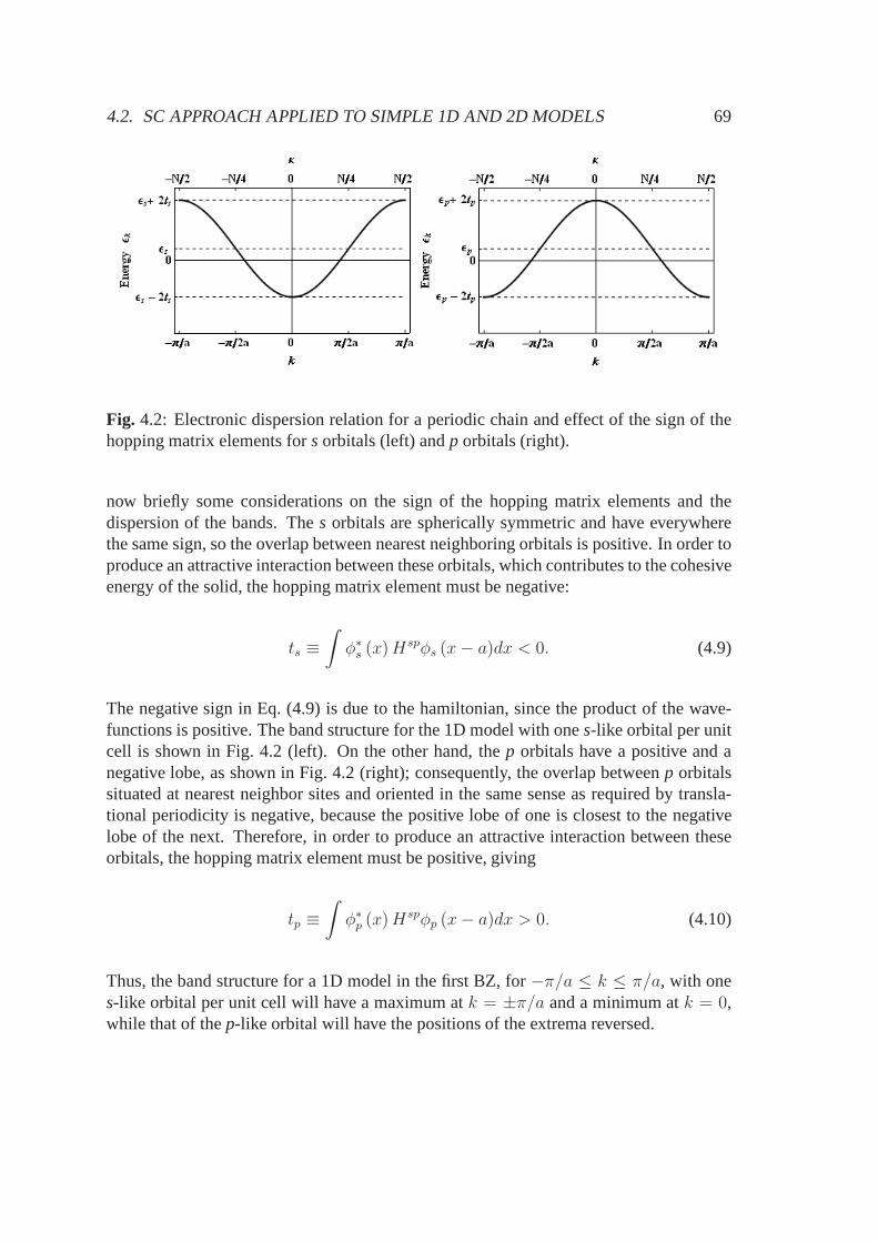
4.2. SC APPROACH APPLIED TO SIMPLE 1D AND 2D MODELS 69
Fig. 4.2: Electronic dispersion relation for a periodic chain and effect of the sign of thehopping matrix elements forsorbitals (left) andp orbitals (right).
now briefly some considerations on the sign of the hopping matrix elements and thedispersion of the bands. Thes orbitals are spherically symmetric and have everywherethe same sign, so the overlap between nearest neighboring orbitals is positive. In order toproduce an attractive interaction between these orbitals,which contributes to the cohesiveenergy of the solid, the hopping matrix element must be negative:
ts ≡∫φ∗s (x)Hspφs (x− a)dx < 0. (4.9)
The negative sign in Eq. (4.9) is due to the hamiltonian, since the product of the wave-functions is positive. The band structure for the 1D model with ones-like orbital per unitcell is shown in Fig. 4.2 (left). On the other hand, thep orbitals have a positive and anegative lobe, as shown in Fig. 4.2 (right); consequently, the overlap betweenp orbitalssituated at nearest neighbor sites and oriented in the same sense as required by transla-tional periodicity is negative, because the positive lobe of one is closest to the negativelobe of the next. Therefore, in order to produce an attractive interaction between theseorbitals, the hopping matrix element must be positive, giving
tp ≡∫φ∗p (x)Hspφp (x− a)dx > 0. (4.10)
Thus, the band structure for a 1D model in the first BZ, for−π/a ≤ k ≤ π/a, with ones-like orbital per unit cell will have a maximum atk = ±π/a and a minimum atk = 0,while that of thep-like orbital will have the positions of the extrema reversed.
70 CHAPTER 4. SMALL CRYSTAL APPROACH
4.2.2 Real space diagonalization
In order to deal with a real space representation of the TB hamiltonian for the 1D system,it’s more convenient to turn it into second-quantized form
Hband = εl
∑
i,σ=↑,↓c†i,σci,σ + 2tl
∑
i,σ=↑,↓
(c†i,σci±1,σ + c†i±1,σci,σ
)(4.11)
where the indexi labels the unit cells or the sites in the linear crystal,σ is the indexfor spin up and spin down electrons,c† andc are the fermionic creation and annihilationoperators, respectively, which act on the many-particle states of this half-filled system(remember that each site is occupied by one electron on average). Let’s make somefurther elaboration on the dispersion relation of the previous paragraph. This will behelpful for establishing the link between the real- and the reciprocal-space approach.Let’s assume that the 1D crystal is composed of a finite numberof equivalent translationalunit cells, that is, we are dealing with a periodic linear chain of N atoms. We shall alsoassume for convenience thatN is even. The translation operations are given in terms ofthe translation vectors
tm = ma with m = 1, 2, . . . , N (4.12)
while the k-vectorsk can be expressed in terms of the reciprocal-space lattice unit vectora∗ and the translational quantum numberκ
k = κa∗/N with κ = 1, 2, . . . , N (4.13)
Because of the periodicity inN of κ, we can use different equivalent choices of intervalsfor it. For instance, in addition to the one in the previous equation, we can choose asymmetric interval
κ = −N2
+ 1,−N2
+ 2, . . . ,N
2(4.14)
or another non-symmetric one
κ = 0, 1, 2, . . . , N − 1. (4.15)
Remembering thata · a∗ = 2π and substituting Eq. (4.13) into Eq. (4.7), the dispersionrelation for the periodic chain ofN atoms becomes
εk = εl + 2tl cos (2πκ/N). (4.16)
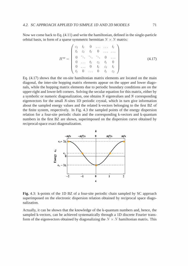
4.2. SC APPROACH APPLIED TO SIMPLE 1D AND 2D MODELS 71
Now we come back to Eq. (4.11) and write the hamiltonian, defined in the single-particleorbital basis, in form of a sparse symmetric hermitianN ×N matrix:
Hsp =
εl tl 0 . . . . . . tltl εl tl 0 . . . . . .
0. . . . . . . . . 0 . . .
0 . . . tl εl tl 00 . . . 0 tl εl tltl 0 . . . 0 tl εl
(4.17)
Eq. (4.17) shows that the on-site hamiltonian matrix elements are located on the maindiagonal, the inter-site hopping matrix elements appear onthe upper and lower diago-nals, while the hopping matrix elements due to periodic boundary conditions are on theupper-right and lower-left corners. Solving the secular equation for this matrix, either bya symbolic or numeric diagonalization, one obtainsN eigenvalues andN correspondingeigenvectors for the smallN-sites 1D periodic crystal, which in turn give informationabout the sampled energy values and the related k-vectors belonging to the first BZ ofthe finite system, respectively. In Fig. 4.3 the sampled points of the energy dispersionrelation for a four-site periodic chain and the corresponding k-vectors and k-quantumnumbers in the first BZ are shown, superimposed on the dispersion curve obtained byreciprocal-space exact diagonalization.
Fig. 4.3: k-points of the 1D BZ of a four-site periodic chain sampled by SC approachsuperimposed on the electronic dispersion relation obtained by reciprocal space diago-nalization.
Actually, it can be shown that the knowledge of the k-quantumnumbers and, hence, thesampled k-vectors, can be achieved systematically througha 1D discrete Fourier trans-form of the eigenvectors obtained by diagonalizing theN ×N hamiltonian matrix. This
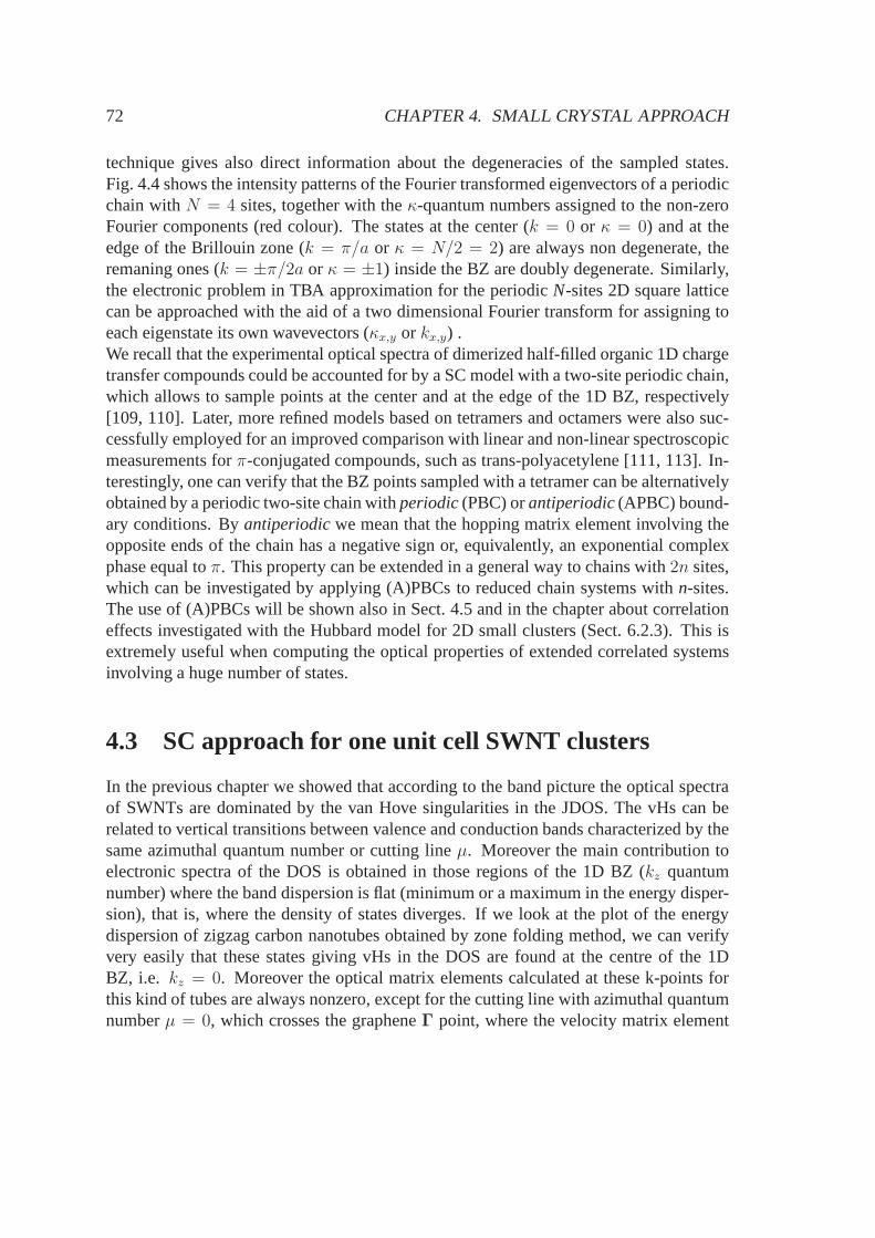
72 CHAPTER 4. SMALL CRYSTAL APPROACH
technique gives also direct information about the degeneracies of the sampled states.Fig. 4.4 shows the intensity patterns of the Fourier transformed eigenvectors of a periodicchain withN = 4 sites, together with theκ-quantum numbers assigned to the non-zeroFourier components (red colour). The states at the center (k = 0 or κ = 0) and at theedge of the Brillouin zone (k = π/a or κ = N/2 = 2) are always non degenerate, theremaning ones (k = ±π/2a or κ = ±1) inside the BZ are doubly degenerate. Similarly,the electronic problem in TBA approximation for the periodic N-sites 2D square latticecan be approached with the aid of a two dimensional Fourier transform for assigning toeach eigenstate its own wavevectors (κx,y or kx,y) .We recall that the experimental optical spectra of dimerized half-filled organic 1D chargetransfer compounds could be accounted for by a SC model with atwo-site periodic chain,which allows to sample points at the center and at the edge of the 1D BZ, respectively[109, 110]. Later, more refined models based on tetramers andoctamers were also suc-cessfully employed for an improved comparison with linear and non-linear spectroscopicmeasurements forπ-conjugated compounds, such as trans-polyacetylene [111,113]. In-terestingly, one can verify that the BZ points sampled with atetramer can be alternativelyobtained by a periodic two-site chain withperiodic(PBC) orantiperiodic(APBC) bound-ary conditions. Byantiperiodicwe mean that the hopping matrix element involving theopposite ends of the chain has a negative sign or, equivalently, an exponential complexphase equal toπ. This property can be extended in a general way to chains with2n sites,which can be investigated by applying (A)PBCs to reduced chain systems withn-sites.The use of (A)PBCs will be shown also in Sect. 4.5 and in the chapter about correlationeffects investigated with the Hubbard model for 2D small clusters (Sect. 6.2.3). This isextremely useful when computing the optical properties of extended correlated systemsinvolving a huge number of states.
4.3 SC approach for one unit cell SWNT clusters
In the previous chapter we showed that according to the band picture the optical spectraof SWNTs are dominated by the van Hove singularities in the JDOS. The vHs can berelated to vertical transitions between valence and conduction bands characterized by thesame azimuthal quantum number or cutting lineµ. Moreover the main contribution toelectronic spectra of the DOS is obtained in those regions ofthe 1D BZ (kz quantumnumber) where the band dispersion is flat (minimum or a maximum in the energy disper-sion), that is, where the density of states diverges. If we look at the plot of the energydispersion of zigzag carbon nanotubes obtained by zone folding method, we can verifyvery easily that these states giving vHs in the DOS are found at the centre of the 1DBZ, i.e. kz = 0. Moreover the optical matrix elements calculated at these k-points forthis kind of tubes are always nonzero, except for the cuttingline with azimuthal quantumnumberµ = 0, which crosses the grapheneΓ point, where the velocity matrix element
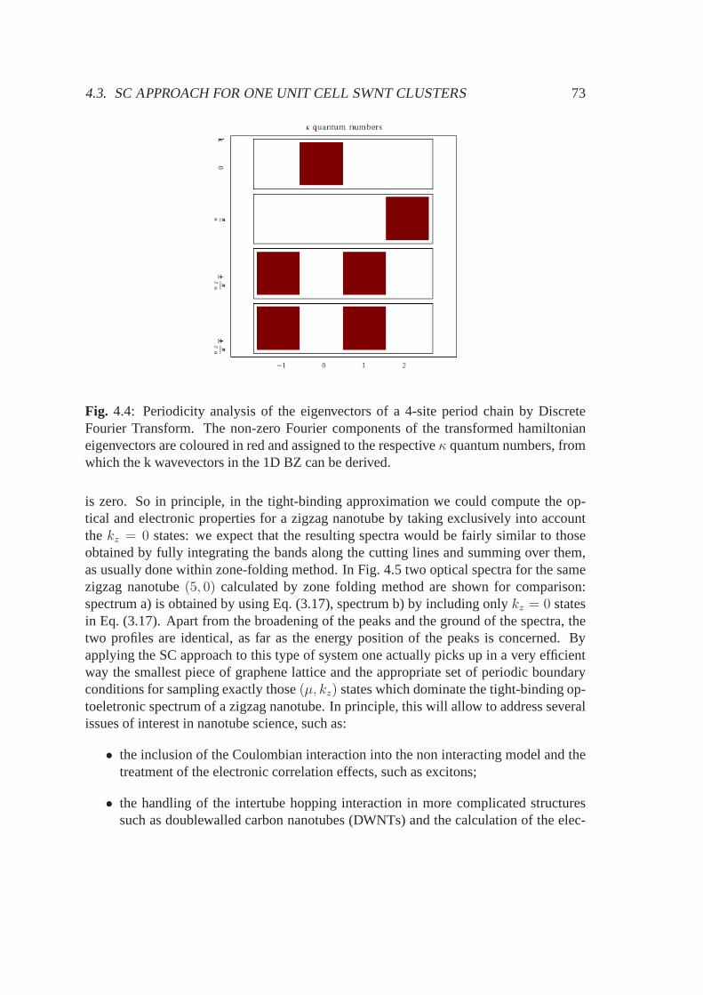
4.3. SC APPROACH FOR ONE UNIT CELL SWNT CLUSTERS 73
Fig. 4.4: Periodicity analysis of the eigenvectors of a 4-site period chain by DiscreteFourier Transform. The non-zero Fourier components of the transformed hamiltonianeigenvectors are coloured in red and assigned to the respectiveκ quantum numbers, fromwhich the k wavevectors in the 1D BZ can be derived.
is zero. So in principle, in the tight-binding approximation we could compute the op-tical and electronic properties for a zigzag nanotube by taking exclusively into accountthekz = 0 states: we expect that the resulting spectra would be fairlysimilar to thoseobtained by fully integrating the bands along the cutting lines and summing over them,as usually done within zone-folding method. In Fig. 4.5 two optical spectra for the samezigzag nanotube(5, 0) calculated by zone folding method are shown for comparison:spectrum a) is obtained by using Eq. (3.17), spectrum b) by including onlykz = 0 statesin Eq. (3.17). Apart from the broadening of the peaks and the ground of the spectra, thetwo profiles are identical, as far as the energy position of the peaks is concerned. Byapplying the SC approach to this type of system one actually picks up in a very efficientway the smallest piece of graphene lattice and the appropriate set of periodic boundaryconditions for sampling exactly those(µ, kz) states which dominate the tight-binding op-toeletronic spectrum of a zigzag nanotube. In principle, this will allow to address severalissues of interest in nanotube science, such as:
• the inclusion of the Coulombian interaction into the non interacting model and thetreatment of the electronic correlation effects, such as excitons;
• the handling of the intertube hopping interaction in more complicated structuressuch as doublewalled carbon nanotubes (DWNTs) and the calculation of the elec-
74 CHAPTER 4. SMALL CRYSTAL APPROACH
Fig. 4.5: Optical absorption intensity of (5, 0) tube calculatedby a) zone-folding methodincluding onlykz = 0 points and by b) full BZ integration of the dispersion relation.
tronic spectra for these systems;
• the treatment of doping and of the local breaking of the translational periodicity indisordered SWNTs.
4.3.1 Choice of the cluster and hamiltonian diagonalization
After determining the k-wavevectors related to the nanotube geometry we are interestedin, the further step is to select the appropriate subset of graphene lattice points orclusterfrom the infinite ideal graphene sheet. As stated previously, a convenient choice to startwith is the zigzag unit cell, shown in Fig. 4.6 for the tube(5, 0). Here we recall thata zigzag(n, 0) cluster contains4n sites and2n biatomic graphene cells. The grapheneribbon is rolled up along the circumferential direction andperiodic boundary conditionsare applied along the axial direction to account for the translational periodicity. Thusthe(4n× 4n) real space tight-binding hamiltonian matrix in single particle orbital basiscan be obtained in a straightforward manner similar to that of the periodic 1D chain orthe 2D square lattice. As done in Chapter 3, we choose onepz orbital per carbon atomand consider only nearest-neighbor interactions. The chosen tight-binding parameters areεπ = 0 eV for the on-site energy integral andtπ = −2.9 eV for the nearest neighborhopping integral, respectively [89, 90]. By diagonalization of the real symmetric hamil-tonian matrix, we see that the obtained set of4n eigenvalues correspond exactly to thezone-folding energies evaluated atkz = 0, for each of the2n bands labelled byµ, asshown in Fig. 4.6 (right).
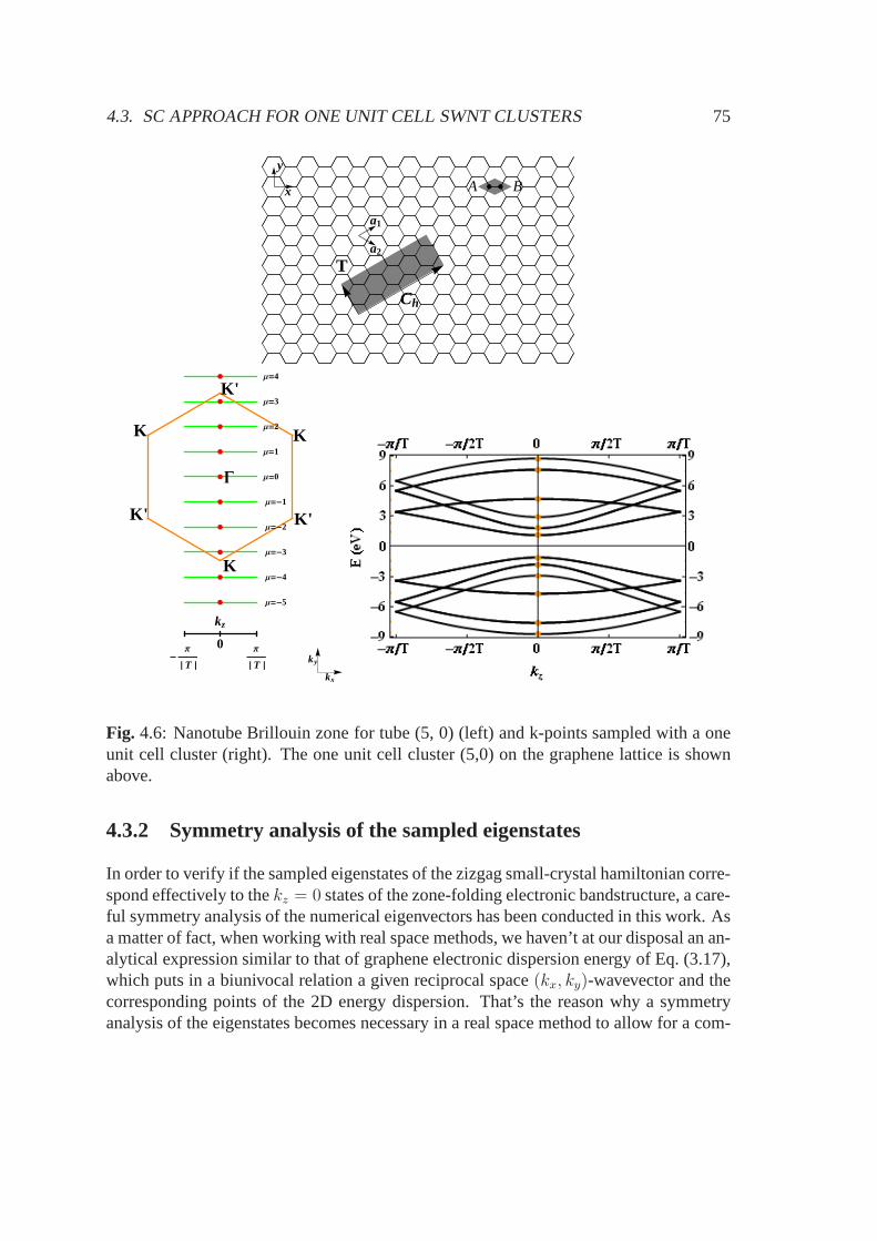
4.3. SC APPROACH FOR ONE UNIT CELL SWNT CLUSTERS 75
x
y
a1
a2
T
Ch
A B
kx
ky
Μ=0
Μ=1
Μ=2
Μ=3
Μ=4
Μ=-1
Μ=-2
Μ=-3
Μ=-4
Μ=-5
G
K
K'
K
K'
K
K'
0
kz
Π
È T È-Π
È T È
Fig. 4.6: Nanotube Brillouin zone for tube (5, 0) (left) and k-points sampled with a oneunit cell cluster (right). The one unit cell cluster (5,0) onthe graphene lattice is shownabove.
4.3.2 Symmetry analysis of the sampled eigenstates
In order to verify if the sampled eigenstates of the zizgag small-crystal hamiltonian corre-spond effectively to thekz = 0 states of the zone-folding electronic bandstructure, a care-ful symmetry analysis of the numerical eigenvectors has been conducted in this work. Asa matter of fact, when working with real space methods, we haven’t at our disposal an an-alytical expression similar to that of graphene electronicdispersion energy of Eq. (3.17),which puts in a biunivocal relation a given reciprocal space(kx, ky)-wavevector and thecorresponding points of the 2D energy dispersion. That’s the reason why a symmetryanalysis of the eigenstates becomes necessary in a real space method to allow for a com-

76 CHAPTER 4. SMALL CRYSTAL APPROACH
plete identification and classification of the quantum numbers (µ, kz) associated with theenergy eigenstates of the nanotube SC hamiltonian. Two wayshave been individuated:the first is based on the form of the Bloch wavefunction of Eq. (3.3) for carbon nanotubes,the second relies upon the application of the two-dimensional Discrete Fourier Transform(DiFT) to the numerical eigenvectors. In the following bothmethods will be described indetail. By using the tight-binding expression for the nanotube wavefunction of Eq. (3.3)for carbon nanotubes, we insert into this the quantum numbers (µ, kz = 0), (guessed bycomparison of the sampled energy eigenvalues with those atkz = 0 of the zone foldingmethod), and combine the traveling waves in form of sin- and cos-like stationary waves.At this point one can already verify that the obtained Bloch coefficients have the sameFourier transform intensity pattern and the same azimuthalperiodicity as the eigenvectorsof the4n × 4n real space hamiltonian. Alternatively, the azimuthal quantum numberµof the obtained eigenstates can be derived by fitting the Bloch coefficients of these clus-ter eigenvectors as a function of the azimuthal coordinateφi of the corresponding siteslabelled byi (Fig. 4.7). The functional form used for the fitting is a sinusoide with am-plitudeA equal to the inverse square root of4n (i.e. number of sites), azimuthal periodµand a generic phase∆ (this one is just an adjustable fitting parameter):
ci =1√4n
[sin (µφi + ∆) + cos (µφi + ∆)] for i = 1, 2, . . . , 2n (4.18)
The resulting periodicity of the fitted stationary wave gives the integer number of wave-lengths by which a period of2π around the nanotube is covered (up to multiple integers of2π). Note that the actual number of Bloch coefficients to be fitted is2n and not4n becauseof the higher symmetry implied bykz = 0 states, that is, eigenvector coefficients referringto the same cylindrical coordinate but different axial coordinates, have the same value.Moreover, Fig. 4.7 shows how the azimuthal Fourier components µ = 0, 1, . . . , 2n − 1are in relation with the2n-graphene unit cells inside the cluster unit cell. By applying theDiFT procedure, after appropriately indexing the obtainednon-zero Fourier coefficients,the eigenvectors can be straightforwardly assigned to theµ azimuthal quantum numbers.From the above analysis, one can conclude that the eigenstates individuated by the peri-odic SC approach describe correctly the symmetry of thekz = 0 states giving van Hovesingularities in the density of states for a zigzag nanotube.
4.4 SC approach using supercells
In this section we will see how it’s possible to explore more other points inside the 1DBZ with clusters, in addiction to the previously foundkz = 0 states. Finally, in thesecond part of this section we will show the complete two-dimensional Fourier analysisdeveloped for a full classification of the(µ, kz = 0) quantum numbers associated withthe cluster eigenstates.
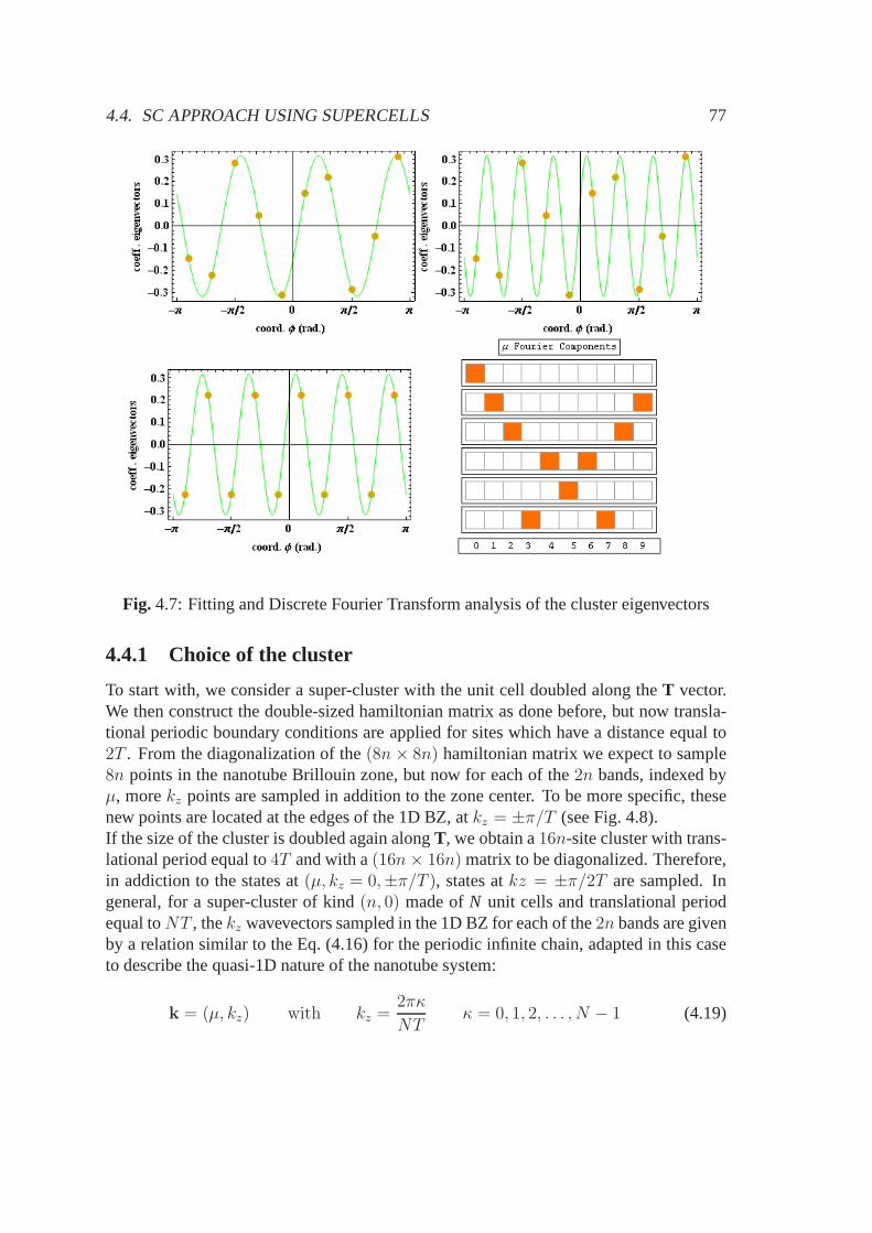
4.4. SC APPROACH USING SUPERCELLS 77
Fig. 4.7: Fitting and Discrete Fourier Transform analysis of thecluster eigenvectors
4.4.1 Choice of the cluster
To start with, we consider a super-cluster with the unit celldoubled along theT vector.We then construct the double-sized hamiltonian matrix as done before, but now transla-tional periodic boundary conditions are applied for sites which have a distance equal to2T . From the diagonalization of the(8n× 8n) hamiltonian matrix we expect to sample8n points in the nanotube Brillouin zone, but now for each of the2n bands, indexed byµ, morekz points are sampled in addition to the zone center. To be more specific, thesenew points are located at the edges of the 1D BZ, atkz = ±π/T (see Fig. 4.8).If the size of the cluster is doubled again alongT, we obtain a16n-site cluster with trans-lational period equal to4T and with a(16n× 16n) matrix to be diagonalized. Therefore,in addiction to the states at(µ, kz = 0,±π/T ), states atkz = ±π/2T are sampled. Ingeneral, for a super-cluster of kind(n, 0) made ofN unit cells and translational periodequal toNT , thekz wavevectors sampled in the 1D BZ for each of the2n bands are givenby a relation similar to the Eq. (4.16) for the periodic infinite chain, adapted in this caseto describe the quasi-1D nature of the nanotube system:
k = (µ, kz) with kz =2πκ
NTκ = 0, 1, 2, . . . , N − 1 (4.19)
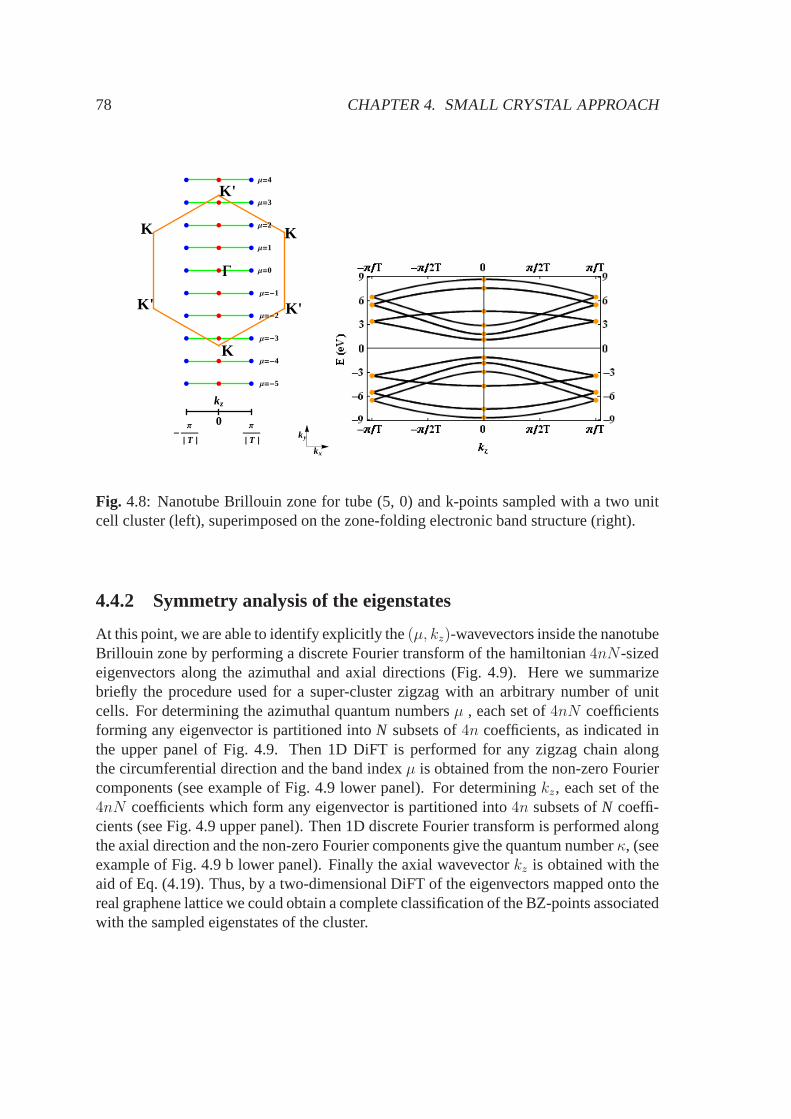
78 CHAPTER 4. SMALL CRYSTAL APPROACH
kx
ky
Μ=0
Μ=1
Μ=2
Μ=3
Μ=4
Μ=-1
Μ=-2
Μ=-3
Μ=-4
Μ=-5
G
K
K'
K
K'
K
K'
0
kz
Π
È T È-Π
È T È
Fig. 4.8: Nanotube Brillouin zone for tube (5, 0) and k-points sampled with a two unitcell cluster (left), superimposed on the zone-folding electronic band structure (right).
4.4.2 Symmetry analysis of the eigenstates
At this point, we are able to identify explicitly the(µ, kz)-wavevectors inside the nanotubeBrillouin zone by performing a discrete Fourier transform of the hamiltonian4nN-sizedeigenvectors along the azimuthal and axial directions (Fig. 4.9). Here we summarizebriefly the procedure used for a super-cluster zigzag with anarbitrary number of unitcells. For determining the azimuthal quantum numbersµ , each set of4nN coefficientsforming any eigenvector is partitioned intoN subsets of4n coefficients, as indicated inthe upper panel of Fig. 4.9. Then 1D DiFT is performed for any zigzag chain alongthe circumferential direction and the band indexµ is obtained from the non-zero Fouriercomponents (see example of Fig. 4.9 lower panel). For determining kz, each set of the4nN coefficients which form any eigenvector is partitioned into4n subsets ofN coeffi-cients (see Fig. 4.9 upper panel). Then 1D discrete Fourier transform is performed alongthe axial direction and the non-zero Fourier components give the quantum numberκ, (seeexample of Fig. 4.9 b lower panel). Finally the axial wavevector kz is obtained with theaid of Eq. (4.19). Thus, by a two-dimensional DiFT of the eigenvectors mapped onto thereal graphene lattice we could obtain a complete classification of the BZ-points associatedwith the sampled eigenstates of the cluster.
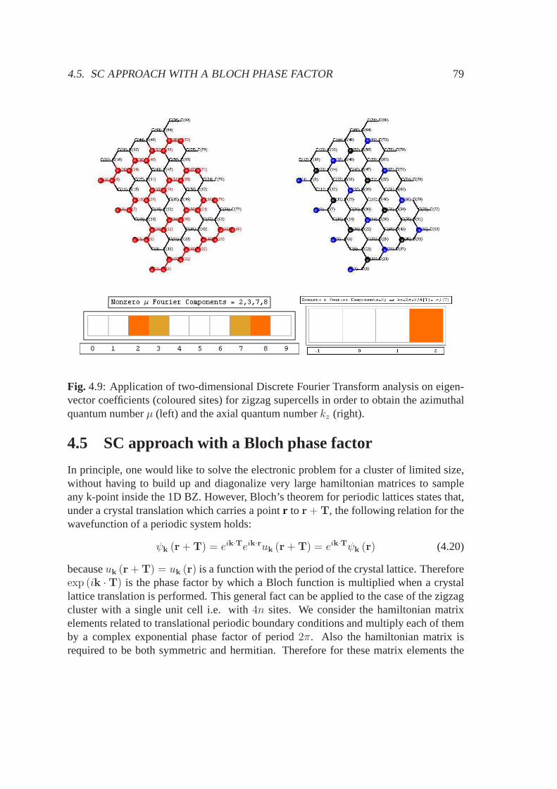
4.5. SC APPROACH WITH A BLOCH PHASE FACTOR 79
Fig. 4.9: Application of two-dimensional Discrete Fourier Transform analysis on eigen-vector coefficients (coloured sites) for zigzag supercellsin order to obtain the azimuthalquantum numberµ (left) and the axial quantum numberkz (right).
4.5 SC approach with a Bloch phase factor
In principle, one would like to solve the electronic problemfor a cluster of limited size,without having to build up and diagonalize very large hamiltonian matrices to sampleany k-point inside the 1D BZ. However, Bloch’s theorem for periodic lattices states that,under a crystal translation which carries a pointr to r + T, the following relation for thewavefunction of a periodic system holds:
ψk (r + T) = eik·Teik·ruk (r + T) = eik·Tψk (r) (4.20)
becauseuk (r + T) = uk (r) is a function with the period of the crystal lattice. Thereforeexp (ik ·T) is the phase factor by which a Bloch function is multiplied when a crystallattice translation is performed. This general fact can be applied to the case of the zigzagcluster with a single unit cell i.e. with4n sites. We consider the hamiltonian matrixelements related to translational periodic boundary conditions and multiply each of themby a complex exponential phase factor of period2π. Also the hamiltonian matrix isrequired to be both symmetric and hermitian. Therefore for these matrix elements the
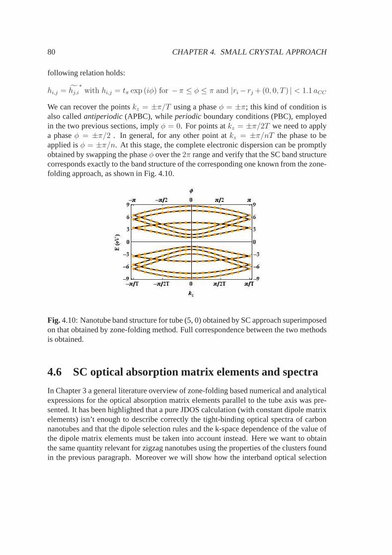
80 CHAPTER 4. SMALL CRYSTAL APPROACH
following relation holds:
hi,j = hj,i
∗with hi,j = tπ exp (iφ) for −π ≤ φ ≤ π and |ri− rj +(0, 0, T ) | < 1.1 aCC
We can recover the pointskz = ±π/T using a phaseφ = ±π; this kind of condition isalso calledantiperiodic(APBC), whileperiodicboundary conditions (PBC), employedin the two previous sections, implyφ = 0. For points atkz = ±π/2T we need to applya phaseφ = ±π/2 . In general, for any other point atkz = ±π/nT the phase to beapplied isφ = ±π/n. At this stage, the complete electronic dispersion can be promptlyobtained by swapping the phaseφ over the2π range and verify that the SC band structurecorresponds exactly to the band structure of the corresponding one known from the zone-folding approach, as shown in Fig. 4.10.
Fig. 4.10: Nanotube band structure for tube (5, 0) obtained by SC approach superimposedon that obtained by zone-folding method. Full correspondence between the two methodsis obtained.
4.6 SC optical absorption matrix elements and spectra
In Chapter 3 a general literature overview of zone-folding based numerical and analyticalexpressions for the optical absorption matrix elements parallel to the tube axis was pre-sented. It has been highlighted that a pure JDOS calculation(with constant dipole matrixelements) isn’t enough to describe correctly the tight-binding optical spectra of carbonnanotubes and that the dipole selection rules and the k-space dependence of the value ofthe dipole matrix elements must be taken into account instead. Here we want to obtainthe same quantity relevant for zigzag nanotubes using the properties of the clusters foundin the previous paragraph. Moreover we will show how the interband optical selection

4.6. SC OPTICAL ABSORPTION MATRIX ELEMENTS AND SPECTRA 81
rules follow straightforwardly from the use of the appropriate cluster and periodic bound-ary conditions, which allow the sampling of correct k-states. We recall here that, in orderto obtain the optical matrix element of Eq. (3.58) within theSC approach, we need tocalculate the transition dipole vectorD, defined by [122, 141, 121, 142, 144, 145]
Dfi = 〈Ψf |∇z|Ψi〉 (4.21)
which in turns requires the knowledge of the electronic wavefunctionsΨj, wherej labelsa generic valencev or conduction statec. In the SC approach these wavefunctions arethe eigenfunctions of the hamiltonian which, according to our previous choice for zigzagnanotubes, selects all thekz = 0 points, which are those relevant both for the JDOS andthe z-component of the dipole matrix elements of these systems. In the TB approximation(LCAO) the nanotube wavefunctions are actually linear combination of thepz orbitalsweighted by the real space eigenvector coefficients obtained from the SC hamiltoniandiagonalization; clearly these can be related to the atomicsites in the cluster unit cell,as shown in the Fourier analysis of the wavefunctions of Sects. 4.3 and 4.4. In whatfollows, we will label the real space eigenvector coefficientsci referring to the coordinatesof the atomic sites of the one unit cell cluster(n, 0), according to the convention ofSect. 2.4.1. Therefore,u = 0, . . . U−1 denotes the nanotube unit cells inside the clusters,h = 0, ...N−1 the biatomic graphene unit cells within a nanotube unit cell, ands = A,Bthe atomic sites within each graphene unit cell. Inside the cluster lattice, each site of typeA (B) is surrounded by three nearest neighbour sites of type B(A), as usual. In the LCAOAnsatz the cluster eigenfunctions for valence or conduction band states are written as
Ψv,c =U−1∑
u=0
N−1∑
h=0
∑
s=A,B
cuh,sφz(r − Ruh,s), (4.22)
where the correct k-point dependence is included thanks to the SC sampling, unlikely inEq. (3.2) and Eq. (3.3), where we needed the Bloch phase factor to express the k-spacedependence. We assume as done in Chapter 3 that the interbandoptical transition isvertical, that is∆kz = 0. Substituting Eq. (4.22) into Eq. (4.21), we get in principle
Dcv =U−1∑
u′=0
N−1∑
h′=0
∑
s′=A,B
c∗u′
h′,s′
U−1∑
u=0
N−1∑
h=0
∑
s=A,B
cuh,s〈φ|z(r − Ru′
h,′s′)∇z|φ〉z(r −Ruh,s), (4.23)
which can be simplified by first dropping the summations over the indicesu, u′, if wework with a one unit cell cluster. We also assume that only nearest neighbour interactionsare relevant for these matrix elements; thus we can get rid ofthe sum overh′ and maintainonly the sum overh by introducing the indexl = 1, 2, 3, which labels the interatomicvectorsrl
h,s = Rl,s′ − Rh,s pointing from one site A (B) in theh-th graphene cell to eachof the three nearest neighbors B (A). Then we get
〈Ψc|∇z|Ψv〉 =
N−1∑
h=0
∑
l=1,3
∑
s′=A,B
c∗l,s′∑
s=A,B
ch,s〈φz(r − Rul,s′)|∇z|φz(r − Ru
h,s)〉.
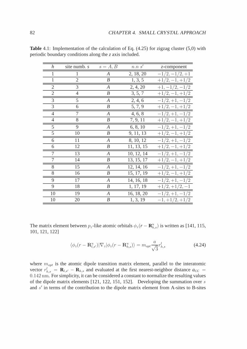
82 CHAPTER 4. SMALL CRYSTAL APPROACH
Table 4.1: Implementation of the calculation of Eq. (4.25) for zigzag cluster (5,0) withperiodic boundary conditions along thezaxis included.
h site numb.s s = A,B n.n s′ z-component
1 1 A 2, 18, 20 −1/2,−1/2,+11 2 B 1, 3, 5 +1/2,−1,+1/2
2 3 A 2, 4, 20 +1,−1/2,−1/22 4 B 3, 5, 7 +1/2,−1,+1/2
3 5 A 2, 4, 6 −1/2,+1,−1/23 6 B 5, 7, 9 +1/2,−1,+1/2
4 7 A 4, 6, 8 −1/2,+1,−1/24 8 B 7, 9, 11 +1/2,−1,+1/2
5 9 A 6, 8, 10 −1/2,+1,−1/25 10 B 9, 11, 13 +1/2,−1,+1/2
6 11 A 8, 10, 12 −1/2,+1,−1/26 12 B 11, 13, 15 +1/2,−1,+1/2
7 13 A 10, 12, 14 −1/2,+1,−1/27 14 B 13, 15, 17 +1/2,−1,+1/2
8 15 A 12, 14, 16 −1/2,+1,−1/28 16 B 15, 17, 19 +1/2,−1,+1/2
9 17 A 14, 16, 18 −1/2,+1,−1/29 18 B 1, 17, 19 +1/2,+1/2,−1
10 19 A 16, 18, 20 −1/2,+1,−1/210 20 B 1, 3, 19 −1,+1/2,+1/2
The matrix element betweenpz-like atomic orbitalsφz(r − Ruh,s) is written as [141, 115,
101, 121, 122]
〈φz(r −Rul,s′)|∇z|φz(r −Ru
h,s)〉 = mopta√3rlh,s (4.24)
wheremopt is the atomic dipole transition matrix element, parallel tothe interatomicvector rl
h,s = Rl,s′ − Rh,s and evaluated at the first nearest-neighbor distanceaCC =0.142 nm. For simplicity, it can be considered a constant to normalize the resulting valuesof the dipole matrix elements [121, 122, 151, 152]. Developing the summation oversands
′ in terms of the contribution to the dipole matrix element from A-sites to B-sites

4.6. SC OPTICAL ABSORPTION MATRIX ELEMENTS AND SPECTRA 83
and viceversa, we obtain
Dcv = 〈φz(r −Rul,s′)|∇z|φz(r −Ru
h,s)〉 = (4.25)
mopta
2√
3
[N−1∑
h=0
∑
l=1,3
c∗l,Bch,A
(rlh,A
)z+
N−1∑
h=0
∑
l=1,3
c∗l,Ach,B
(rlh,B
)z
]
where the projection along the tube axiszhas been considered. Again, periodic boundaryconditions along the nanotube axis must be included when performing the summationin Eq. (4.25), as indicated in Table 4.6, which shows an example implementation. Theselection rules for vertical transitions involving a given(µ, kz = 0) valence band state andanother(µ′, kz = 0) conduction band state are automatically obtained through Eq. (4.25),in full accord with the zone-folding selection rules [121, 122, 141, 142] :
δµ,µ′ = 0 =⇒ Dz = 0 (4.26)
δµ,µ′ = 1 ∧ (µ, µ′ 6= 0) =⇒ Dz 6= 0.
The exception case in the second selection rule involves vertical transitions between non-degenerate states lying exactly at grapheneΓ point, (i. e. (µ = 0, kz = 0) in the frameof nanotube BZ), where one can verify that the dipole matrix element is exactly zero, asseen in Chapter 3. We will see in the following chapters, thatthe symmetry-breakingeffect due to the intertube hopping interactions in double-walled nanotubes (DWNTs)or the presence of defects will affect these rules, so that they will no longer hold, as adirect consequence of the mixing of the states related to theinner and outer shells inDWNTs and the lifting of the band degeneracies both in DWNTs and defected SWNTs.The following symmetry relation between the two terms contributing to Eq. (4.25) holds:
N−1∑
h=0
∑
l=1,3
c∗l,Bch,A
(rlh,A
)z
=N−1∑
h=0
∑
l=1,3
c∗l,Ach,B
(rlh,B
)z. (4.27)
This follows from the fact that 1) conduction band states areactually antisymmetric linearcombinations of atomic orbitals, unlikely valence band states which are fully symmetric,and that 2) the following relation between nearest neighborvectors joining A sites to Bsites and viceversa holds: (
rlh,A
)z
= −(rlh,B
)z. (4.28)
Before comparing the numerical values for the dipole matrixelements obtained fromEq. (4.25) with those from zone-folding method, it has to be pointed out that an equivalentresult could be obtained using the axial component of the velocity operator written insecond-quantization formalism [92, 102, 110], instead of Eq. (4.25), which still involvesthe position of the atomic orbitals. In this case, the expression for thez-component of thedipole matrix element is:
〈Ψc|∇z|Ψv〉 = 〈Ψc|vz|Ψv〉 (4.29)

84 CHAPTER 4. SMALL CRYSTAL APPROACH
where the velocity operator is written as:
vz = − ıtπ~
∑
〈i,j〉,σ
[c†i,σcj,σ − c†j,σci,σ
]z. (4.30)
This form will also be used in the last chapter about the calculation of the optical spec-tra of the periodic cluster with the inclusion of the Columbian correlation effects in aHubbard-like fashion. The quantum-mechanical derivationof the form of Eq. (4.30)from the commutator[H, r]z of the hamiltonian and the position operator is shown inAppendix. Within this formalism, this operator is no longerdependent on the choiceof the origin of the system reference frame and, therefore, it’s more appropriate for thedescription of the optical properties of a periodic cluster[110]. For this reason the nu-merical values of the dipole matrix element involving either the position as in Eq. (4.25)or the velocity operator as in Eq. (4.30) cannot be expected to be the same. However, theoptical selection rules reported previously, can still be verified for both approaches. Forthe case ofkz = 0 states of a zigzag cluster, one can recover the same numerical valuesof thez-component of the dipole matrix elements from both approaches, as explained inthe following. The eigenfunctions we are dealing with at(µ, kz = 0) have pure rotationalsymmetry. In other words, the eigenvector coefficients along the tube axis are all con-stant, thus their 1D Fourier transform gives zero. Therefore, Eq. (4.25) has to be put in acondition independent of the choice of origin of the system reference frame, taking intoaccount the rotational symmetry of the zigzag system. The summation of Eq. (4.25) mustbe evaluated for every rotationally equivalent assignmentof the conduction band eigen-vector coefficients to the cluster sites, while keeping fixedthe assignment of the valenceband coefficients to the underlying lattice. Practically, for a zigzag cluster of one unit cell,this is simply obtained by a ciclic permutation within every2π/N radians of the sequenceof coefficients which form each eigenvector. For every ciclic permutation, Eq. (4.25) isevaluated and a value for the dipole matrix element is obtained, which always involves avertical transition betweenµ, kz = 0 states. Finally, theN collected values of the dipolematrix element are fitted by a sinusoidal function of the azimuthal shift of2π/N :
di = A [sin (µφi + ∆) + cos (µφi + ∆)] with i = 1, 2, . . . , N. (4.31)
where the amplitudeA gives the value of the dipole matrix element we wished to ob-tain (the same as that obtained by the velocity operator),µ is the azimuthal period ofthe stationary wave and thus the band quantum number,∆ is as always an adjustablefitting parameter. In Table 4.6 we compare the absolute values of the dipole matrix ele-ments calculated by Eq. (4.25) with the above described procedure with those obtainedby the zone-folding scheme of Refs. [142, 144, 141, 145]. Thevalues show a very goodcorrespondence beyond the numerical accuracy due to the direct diagonalization and thefitting procedure routine employed in the SC approach. Moreover all the symmetry prop-erties, such as degeneracies and values at special k-points(grapheneΓ point), are verified.
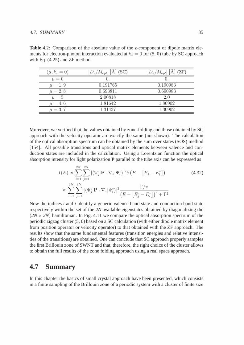
4.7. SUMMARY 85
Table 4.2: Comparison of the absolute value of the z-component of dipole matrix ele-ments for electron-photon interaction evaluated atkz = 0 for (5, 0) tube by SC approachwith Eq. (4.25) and ZF method.
(µ, kz = 0) |Dz/Mopt|[A]
(SC) |Dz/Mopt|[A]
(ZF)
µ = 0 0. 0.µ = 1, 9 0.191765 0.190983µ = 2, 8 0.693811 0.690983µ = 5 2.00818 2.0µ = 4, 6 1.81642 1.80902µ = 3, 7 1.31437 1.30902
Moreover, we verified that the values obtained by zone-folding and those obtained by SCapproach with the velocity operator are exactly the same (not shown). The calculationof the optical absorption spectrum can be obtained by the sumover states (SOS) method[154]. All possible transitions and optical matrix elements between valence and con-duction states are included in the calculation. Using a Lorentzian function the opticalabsorption intensity for light polarizationP parallel to the tube axis can be expressed as
I(E) ∝2N∑
i=1
2N∑
j=1
|〈Ψcj|P · ∇z|Ψv
i 〉|2δ(E −
[Ec
j − Evi
])(4.32)
≈2N∑
i=1
2N∑
j=1
|〈Ψcj|P · ∇z|Ψv
i 〉|2Γ/π
(E −
[Ec
j −Evi
])2+ Γ2
Now the indicesi and j identify a generic valence band state and conduction band staterespectively within the set of the2N available eigenstates obtained by diagonalizing the(2N× 2N) hamiltonian. In Fig. 4.11 we compare the optical absorptionspectrum of theperiodic zigzag cluster (5, 0) based on a SC calculation (with either dipole matrix elementfrom position operator or velocity operator) to that obtained with the ZF approach. Theresults show that the same fundamental features (transition energies and relative intensi-ties of the transitions) are obtained. One can conclude thatSC approach properly samplesthe first Brillouin zone of SWNT and that, therefore, the right choice of the cluster allowsto obtain the full results of the zone folding approach usinga real space approach.
4.7 Summary
In this chapter the basics of small crystal approach have been presented, which consistsin a finite sampling of the Brillouin zone of a periodic systemwith a cluster of finite size

86 CHAPTER 4. SMALL CRYSTAL APPROACH
Fig. 4.11: Optical absorption intensity of (5, 0) tube calculated by a) SC approach includ-ing onlykz = 0 points and by b) full BZ integration of ZF dispersion relation.
and suitable periodic boundary conditions. First the method has been applied to an-siteperiodic chain, then to a single-walled nanotube. The special case of zigzag clusters hasbeen considered for which it’s simpler to sample the critical k-points which give the vanHove singularities in the density of states and nonzero optical matrix elements. By aminimal calculation based on few k-points, we have shown that all the important featuresof the optical spectra, known by reciprocal space based method such as zone folding,could be completely recovered by this method.
Chapter 5
Double-wall carbon nanotubes
In this section the small-crystal approach is applied to double-walled nanotubes for thetight-binding calculation of their electronic dispersionrelation and optical spectra. Wewill also show that the SC provides the flexibility of changing the orientation of theconstituent walls, unlikely other reciprocal space-basedmethods, which cannot include ina general way the local symmetry breaking due to a non-negligible intertube interaction.As a consequence, the dependence of the optical properties on the geometric correlationbetween the walls can be investigated in a simpler way. The calculations show how theresulting optical spectra are visibly affected by these effects with the appearing of newtransitions and suggest a revision of the Kataura plots usedfor the interpretation of theRaman spectra of DWNTs.
5.1 Introductory remarks
Double-wall carbon nanotubes (DWNTs) can be considered thesimplest form of multi-wall nanotubes (MWNTs), as they consist of two coaxial graphene cylinders with veryweak van der Waals type interaction between the two walls, yet with strong covalentbonds between atoms within each constituent tube. According to the commonly adoptedgeometrical convention, the geometrical structure of a DWNT is specified by the notation(n,m) @ (n′, m′), which means that the constituent inner tube with chiral indices(n,m)is inserted into the outer wall with indices(n′, m′). Recently, much theoretical and exper-imental interest has been generated for DWNTs, since they would play an essential rolein future nanoelectronic device applications and biological applications [44, 157, 160].From a physicist’s standpoint, they can be considered molecular analogues to coaxialcables. Actually, a metallic@semiconducting (M@S) or a semiconducting@metallic(S@M) DWNT can be, respectively, a molecular conductive wire covered by an insu-lator or a molecular capacitor in a device [155]. It is believed that these structures wouldexhibit enhanced field emission, mechanical and thermal properties when compared toSWNTs [156]. Some examples of DWNT-based nanometer-scale electromechanical mo-
87
88 CHAPTER 5. DOUBLE-WALL CARBON NANOTUBES
tors (NEMS) have recently been proposed in two theoretical papers, namely a molecularmotor driven by temperature variation [158] and carbon nanotube electron windmills,which exploit the torque generated by applying a potential difference to the outer tube,causing the inner tube to rotate if the generated torque is enough to overcome the fric-tional forces existing between the walls of the DWNT [159]. From a chemist’s pointof view, the structure of a DWNT can be considered that of a SWNT protected by theexternal SWNT on which functionalization can be operated without affecting the prop-erties of the internal tube [160]. This opens the route to novel preparation techniqueswhich allow the solubilization of the outer SWNT system in different environments (e.g.cell membranes) without affecting the properties of the inner shell. Therefore, in re-cent years the production and characterization of DWNTs have drawn the attention ofnumerous scientists. As explained in the introductory chapter of this thesis, DWNTscan be produced by several techniques: the arc discharge method, the catalytic chemicalvapour deposition method and the fusion of fullerenes enclosed in peapods by TEM irra-diation or temperature. The last method [37] provides a DWNTyield greater than 95%and high-quality samples. The two constituent tubes of the DWNT can be characterizedby Raman spectroscopy [161, 162] and high-resolution transmission electron microscopy(HRTEM) [163], since the atomic positions in a DWNT cannot bemeasured by STM/STSdirectly, as only the outermost nanotube contributes to thetunneling conductance. Asusual, in Raman measurements the indices of the two coaxial layers of a DWNT canbe assigned based on the respective radial breathing mode frequencies [165, 166] of thenon-interacting constituent SWNTs. It was shown experimentally by optical absorptionand PL measurements that the interaction between the constituent layers influences theoptical transitions of the inner and outer tubules [164]. Aswe will see in the following,understanding the role and magnitude of the interlayer interaction and its relation withthe geometry of the constituent walls is one of the most relevant issues concerning inparticular the modeling of DWNT electronic properties.
5.2 Structure and symmetry properties
DWNTs can be commensurate (C) or incommensurate (I) if the ratio of the translationalperiods of the constituent SWNTs is a rational or irrationalnumber, respectively. Ac-cording to this definition, DWNTs with both armchair or zigzag nanotubes are alwayscommensurate, while a DWNT with a zigzag tube inserted into an armchair one is in-commensurate
(TZ/TA =
√3). Experimentally, it has been found, that DWCNTs pro-
duced by arc discharge show no correlation in the chiralities of the walls [163], so bothcommensurate and incommensurate combinations are equallypossible. In DWNTs theexperimental interlayer spacing has been found ranging from 3.4A (the interlayer spac-ing of graphite) to 4.1A [167]. A complete treatment of the symmetries in DWNTs andMWNTs was presented by Damnjanovicet al. [124], based on the line group classifi-

5.2. STRUCTURE AND SYMMETRY PROPERTIES 89
cation scheme already applied to SWNTs (see Sect. 2.5). However, a specific study ofthe symmetry in commensurate DWNTs (CDWNT) can be found in another paper bythe same authors [177], which also considered the geometry-dependent symmetry break-ing effect due to the interaction between the walls. Here we just summarize the mainresults of these papers, which will be useful for understanding the choices operated inthe SC calculations presented in the following. In this workthey consider a sample of1280 carbon SWNTs with diameter range2.8 A 6 dt 6 50 A and right-handed chiral-ity. For each tube taken as innermost wall, all possible outer tubes are searched suchthat the intertube spacing
(dOUT
t − dINt
)/2 differs from the graphite interlayer spacing
∆ = 3.44 A by at most0.2 A. It turns out that among the selected 1280 tubes which giverise to 42236 possible pairs, there are only 318 pairs with commensurate walls, whichcan give CDWNTs (less than 1%). In general, the symmetry group of a double-wall (andeven multi-wall) nanotube (W@W′) can be found as intersection of the symmetry groupsof the constituent SWNTs:LWW ′ = LW ∩ LW ′. Therefore, any geometrical transfor-mation common to both walls leaves the DWNT system invariant. The specific form ofa DWNT group depends on the relative position of the walls: even when the constituenttubes are coaxial, there are special high symmetry positions, determined by the relativecylindrical coordinates(Φ, Z), which specify the azimuthal and translational shift of theouter wall with respect to the inner shell. However, this case refers only to some specialsymmetry elements, calledparities, which are determined by the coincidence of hori-zontal axes (U,U ′) and (in achiral pairs) mirror, glide or roto-reflection planes. Instead,the roto-translational symmetries symmetries are the samefor all coaxial positions. Forthe specific formulas defining the roto-translational groupof CDWNTs the reader is ad-vised to consult Ref. [177], since for the purposes of this thesis it’s actually more relevantconsidering the high-symmetry positions(Φ, Z) at which these parities occur. In theirworks, Damnjanovicet al. pointed out that, according to the topological analysis ofthe symmetry breaking developed by Abud and Sartori [179], the most stable configura-tions (corresponding to the minima of the invariant interatomic pairwise Lennard-Jonespotential) occur at the positions with maximal symmetry. This topological argument isextremely powerful, since it allows to determine the stableposition of the walls by a sym-metry analysis without the need to specify the pairwise interaction potential between thewalls and finding its minima. In order to find these special high symmetry positions, theso calledsymmetry breaking grouphas to be found out which actually contains the sym-metry of the interaction potential. The breaking group describes the maximal symmetryof the interaction potential. This can be understood by the following considerations. Theinteraction potential between the walls is
V (R,R′) = V (Φ, Z) =∑
tsu
∑
t′,s′,u′
v (rtsu, r′t′s′u′) (5.1)
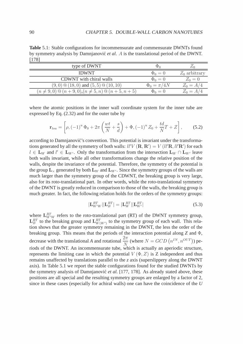
90 CHAPTER 5. DOUBLE-WALL CARBON NANOTUBES
Table 5.1: Stable configurations for incommensurate and commensurate DWNTs foundby symmetry analysis by Damnjanovicet al. A is the translational period of the DWNT.[178]
type of DWNT Φ0 Z0
IDWNT Φ0 = 0 Z0 arbitraryCDWNT with chiral walls Φ0 = 0 Z0 = 0
(9, 0)@ (18, 0) and(5, 5)@ (10, 10) Φ0 = π/4N Z0 = A/4(n 6= 9, 0)@ (n+ 9, 0),(n 6= 5, n)@ (n+ 5, n+ 5) Φ0 = 0 Z0 = A/4
where the atomic positions in the inner wall coordinate system for the inner tube areexpressed by Eq. (2.32) and for the outer tube by
rtsu =
[ρ, (−1)u Φ0 + 2π
(wt
N+s
d
)+ Φ, (−1)u Z0 +
td
NT + Z
], (5.2)
according to Damnjanovic’s convention. This potential isinvariant under the transforma-tions generated by all the symmetry of both walls:ll′V (R,R′) = V (ll′R, ll′R′) for eachl ∈ LW and l′ ∈ LW ′. Only the transformation from the intersectionLW ∩ LW ′ leaveboth walls invariant, while all other transformations change the relative position of thewalls, despite the invariance of the potential. Therefore,the symmetry of the potential isthe groupL× generated by bothLW andLW ′ . Since the symmetry groups of the walls aremuch larger than the symmetry group of the CDWNT, the breaking group is very large,also for its roto-translational part. In other words, whilethe roto-translational symmetryof the DWNT is greatly reduced in comparison to those of the walls, the breaking group ismuch greater. In fact, the following relation holds for the orders of the symmetry groups:
|LRTW ′W ||LRT
B | = |LRTW ||LRT
W ′ | (5.3)
whereLRTW ′W refers to the roto-translational part (RT) of the DWNT symmetry group,
LRTB to the breaking group andLRT
W (W ′) to the symmetry group of each wall. This rela-tion shows that the greater symmetry remaining in the DWNT, the less the order of thebreaking group. This means that the periods of the interaction potential alongZ andΦ,
decrease with the translationalA and rotational2π
N(whereN = GCD
(nIN , nOUT
)) pe-
riods of the DWNT. An incommensurate tube, which is actuallyan aperiodic structure,represents the limiting case in which the potentialV (Φ, Z) is Z independent and thusremains unaffected by translations parallel to thez axis (superslippery along the DWNTaxis). In Table 5.1 we report the stable configurations foundfor the studied DWNTs bythe symmetry analysis of Damnjanovicet al. [177, 178]. As already stated above, thesepositions are all special and the resulting symmetry groupsare enlarged by a factor of 2,since in these cases (especially for achiral walls) one can have the coincidence of theU

5.3. SMALL CRYSTAL APPROACH FOR THE ELECTRONIC STRUCTURE OFDWNTS91
axes which implies the coincidence of vertical or horizontal mirror planes with other mir-ror or glide planes. These predictions, although based on pure symmetry arguments andnot on total energy calculations, can be helpful when considering total electronic energyprofiles before computing optical spectra for some selectedmutual configurations of theconstituent walls.
5.3 Small crystal approach for the electronic structure ofDWNTs
In Chapt. 3 we saw how the TB zone-folding method can provide asimple but power-ful insight into the electronic structure of ideal single-wall carbon nanotubes. By takinginto account theσ orbitals in the hamiltonian, this method can also be extended to in-clude curvature effects, which play a significant role in theelectronic structure of smalldiameter nanotubes (dt < 0.7 A ), since Eq. (3.21) overestimates the respective bandgaps [83, 84]. A reciprocal space approach like this, however, finds difficulties for prob-lems in which a local symmetry is broken like in the case of functionalization, dopingand other disorder effects, such as orientation-dependentinteractions among nanotubesand with the surrounding environment. This is the case with some attempts present inliterature to solve the TB hamiltonian in reciprocal space for DWNTs, which could beobtained however only for a very restricted number of nanotube geometries with highersymmetry [155, 169, 168]. Formulating the single-particleelectronic hamiltonian in realspace representation can be an appropriate way to allow for the treatment of symmetrybreaking effects due to the geometry-dependent interwall interaction. In some cases, areal space approach was tried [170], which had also been previously adopted for single-wall nanotubes as well [149], but poor attention was paid to the infinite translationalperiodicity of the nanotube: instead, a sufficiently long portion of the graphene cylinderis selected, such that boundary effects could be disregarded within reasonable approxi-mations. This is usually done for investigating the transport properties of finite-lengthsingle and double-wall nanotubes [175]. Moreover, a detailed analysis of variations onthe electronic structure and optical absorption features due to any change in the relativepositions of the constituent walls is lacking in DWNT literature, except for some limitedconfigurations presented in two papers by Lambinet al. [169] and Hoet al. [172, 174].However, in these papers, the choice of the selected configurations was not supported bytotal electronic energy calculations or topological symmetry-based arguments, like thoseformulated by Damnjanovic. In this section we show how the SC approach can be appliedto double-wall nanotube with the possibility of addressingall the previously mentionedissues, with the flexibility of changing the mutual orientations of the constituent walls inany(Φ, Z) position.
92 CHAPTER 5. DOUBLE-WALL CARBON NANOTUBES
5.3.1 Electronic band structure and stable configurations
We consider CDWNTs obtained with zig-zag nanotubes for which the cluster and theboundary conditions to study the relevant electronic states are simpler, as recalled inChapt. 4, but the calculations can be done for all other type of nanotubes as well. Fur-thermore, among all possible ways to combine SWNTs into DWNTs, we consider thosewith an interlayer distance between0.334 nm (graphite interlayer spacing) and0.360 nm,as it was experimentally found recently [163]. For zigzag DWNTs, we find in this in-terval all combinations of type(n, 0)@(n′, 0) such thatn − n′ = 9 which have an in-terlayer of0.352 nm, for CC bond-length of0.142 nm. We consider in our examplesa semiconductor-semiconductor (S-S) DWNT, such as (5, 0)@(14, 0) and a metallic-metallic (M-M) one, such as (9, 0)@(18, 0). The TB hamiltonian for a DWNT can bewritten as a sum of the TB hamiltonians corresponding to the inner and outer nanotubesplus a perturbative termHinter for the electronic hopping from a sitel on the inner tubeto another sitem on the outer tube.
HDWNT = Hin +Hout +Hinter with (5.4)
Hin(out) =∑
t=IN,OUT
∑
σ=↑,↓επ
2Nt∑
i=1
c†i,σci,σ + tπ
2Nt∑
i=1
∑
j∈n.n
(c†i,σcj,σ + ci,σc
†j,σ
)(5.5)
The intertube interaction is considered to decay exponentially with the distancedl,m be-tween the sites according to:
HINTER = βπ
out,in∑
〈l,m〉,σcos θl,m exp [(dl,m −∆) /δπ]
(c†l,σcm,σ + cl,σc
†m,σ
)(5.6)
In the above expression forHINTER, ∆ is the interlayer spacing (semidifference be-tween diameters),δπ is the decay constant forπ orbitals,θl,m is the angle betweenπorbitals pointing perpendicularly to the tubes’ surface,βπis the intertube hopping ampli-tude integral. According to literature, values forβπ can range fromtπ/8 to 1.0 eV andδπ = 0.045 nm [171, 180, 181]. We recall that the intertube hopping interaction dependson the mutual orientation of the constituent coaxial SWNTs,namely on the azimuthalangle∆Φ and the translation∆Z parallel to the tube axis. Therefore, we can write:
θl,m ≡ θl,m (∆Φ) dl,m ≡ dl,m (∆Φ,∆Z) (5.7)
When setting up the periodic SC hamiltonian, one has to be careful that no intertube ma-trix elements are dropped by restricting the length cutoff of interwall coupling only tofirst or second nearest neighbouring atoms. In this case, we imposed no restrictions onthe interatomic distance between atoms on different tubes,instead a cutoff limit was seton the energy value of intertube matrix elements to be storedin memory for the diagonal-ization: HINTER (l,m) > 10−3 eV. No significative difference was found between the

5.3. SMALL CRYSTAL APPROACH FOR THE ELECTRONIC STRUCTURE OFDWNTS93
eigenvalues computed by storing the full intertube off-diagonal block matrix and the onewith the cutoff.
-Π -Π2 0 Π2 Π
-9
-6
-3
0
3
6
9-ΠÈTÈ -Π2ÈTÈ 0 Π2ÈTÈ ΠÈTÈ
-9
-6
-3
0
3
6
9
ΦEHe
VL
kz
EHe
VL
Fig. 5.1: Electronic band structure of (5, 0)@(14, 0) (left) and (5, 5)@(10, 10) (right)DWNT at default configuration(φ = 0,∆Z = 0) with non interacting costituent SWNTs(left panel) and with intertube hopping (right panel,βπ = 1.0 eV). Color legend for(5,0)@(14,0): black (inner SWNT), red (outer SWNT), green (DWNT with interactionon). Color legend for (5,5)@(10,10): green (outer SWNT), inner SWNT not shown forclarity (coincidence with some bands of outer SWNT), orange(DWNT with interactionon)
In Fig. 5.1 (left) the electronic dispersion relation obtained from diagonalization of thehamiltonian block matrix for DWNT (5,0)@(14,0) is shown forthe default configura-tion (∆Φ = 0,∆Z = 0) usingβπ = 1.0 eV. The main effect ofHINTER is the liftingof the doubly degenerate bands and the breaking of the symmetry of valence and con-duction bands with respect to the Fermi level. This is more evident far from Fermi leveland stronger for valence bands, rather than conduction bands. This effect is also calledelectron-hole asymmetry. A tiny gap of the order of the meV isalso opened in metal-lic (9,0)@(18,0) DWNT, due to the degeneracy splitting of the bands, as predicted inRef. [68], but it has not been reported here since it is difficult to notice in the picture.However it can be more easily seen in the DOS profile (Fig. 5.3), which will be discussedin the following. Early tight-binding investigations of commensurate DWNTs overlookedthis asymmetry due to an over-simplified modeling of the interwall coupling [155], whilefor more recent models and parametrizations which adopt theform of Eq. (5.6) this fea-ture is already included [171, 175]. Unlikely in armchair DWNTs (see Fig. 5.1 right), theband structure of the zigzag systems remains almost unperturbed near the Fermi energy.The explanation can be found by considering that the discrete angular momentum asso-

94 CHAPTER 5. DOUBLE-WALL CARBON NANOTUBES
ciated with these states depends on the tube circumference and the rotational symmetryof each of the constituent shells. Thus, in principle, bandsrelated to different walls havedifferent rotational symmetry and in general the combined DWNT system does not sharethe rotational symmetry of the individual shells (see for instance the case in which theorders of the principal rotational axes of the walls have no common divisor except unity).As long as the interwall coupling is sufficiently weak and smooth, one can reasonablyexpect that the original symmetry will be preserved and the hybridization between statesbelonging to inner and outer wall will be minimal. We can now consider how the to-tal π electronic energy varies as a function of the orientationalparameters, namely theazimuthal shift∆Φ and the translational shift∆Z. As noted in the previous section,Damnjanovicet al. [177] found, by symmetry arguments, a minimum in total energy at∆Φ = π/36 and∆Z = A/4 for (9, 0)@(18, 0), and at∆Φ = 0 and∆Z = A/4 for(5, 0)@(14, 0) (in zigzag nanotubesA = |T | = 0.426 nm).
Fig. 5.2: (Color online) Dependence of totalπ electronic energy atkz = 0 on a,b) azimuthal∆Φ and c, d) translational∆Z for DWNTs (5, 0)@ (14, 0) (left) and(9, 0)@ (18, 0) (right) with βπ = 1.0 eV (blue color). Energy data are normalized to ab-solute values of the totalπ electronic energy of the respective non-interacting constituentSWNTs (purple color).
Figg. 5.2 (a-d) shows some of our results summing to convergence theπ electronic en-ergy eigenvalues of the valence states obtained by changingthe phase of the boundary

5.3. SMALL CRYSTAL APPROACH FOR THE ELECTRONIC STRUCTURE OFDWNTS95
condition. According to Damnjanovicet al. one observes in Figg. 5.2 c) and d) that thedependence on∆Z has two minima around±A/4 using∆Φ = 0 for (5, 0)@(14, 0) and∆Φ = π/36 for (9, 0)@(18, 0). On the other hand, the dependence on∆Φ, at∆Z = A/4(Figg. 5.2 a) and b), shows a periodic oscillatory behaviour, with an energy minimumlocated at∆Φ = π/36, only for (9, 0)@(18, 0). Similar plots for the dependence of thetotalπ electronic energy on(∆Φ,∆Z) have been obtained by considering only thekz = 0states in the 1D BZ, which therefore represent the leading contribution to the total energyprofile. In the following calculations of DOS and optical absorption spectra we will use∆Z = A/4 for both DWNTs and∆Φ = 0 andπ/36 for (5, 0)@(14, 0) and(9, 0)@(18, 0),respectively. Interestingly, in this case the electronically most stable configurations arefound to coincide with the most stable configurations from a crystallographic point ofview, reported in Table 5.1.
5.3.2 Optical properties
By inspection of the electronic band structure of Fig. 5.1, one can see that the lowest en-ergy vHs for zigzag DWNTs are still determined by thekz = 0 states in the 1D BZ. Thisfact allows us to compute the optical spectra with minimal effort by including only thisk-points into the JDOS and the optical matrix elements with the sum over states method,as done in Sect. 4.6. Instead, in armchair DWNTs, the extremaof valence and conductionband giving vHs do not occur at the same k-point, because of the stronger distorsion atFermi level introduced by the interlayer coupling. This would require to include morek-points from the 1D BZ, in particular a more refined samplingaroundφ = 2π/3, wherekF occurs for the unperturbed armchair SWNTs. However, this issue will be addressedin future work, since we have chosen to focus mainly on zigzagspecies, in order to intro-duce electronic correlation effects (see next chapter) into the tight-binding hamiltonian.By comparing DOS profiles for the chosen(Φ, Z) configurations for both DWNT ge-ometries, one can observe that the azimuthal shift doesn’t affect the DOS structure (notshown), while the translational shift alters considerablythe spectra for both geometrieswith respect to the default configuration at∆Z = 0. Fig. 5.3 reports the DOS by chang-ing ∆Z from 0 to A/4 together with the DOS spectra of the constituent non-interactingSWNTs. One can see important variations, also at low energies, for both type of DWNTssuggesting that also the optical spectra will have new features with respect to that ofthe constituent SWNTs. In particular one observes that alsothe DOS at the Fermi levelE = 0, which is constant in the case of the metallic tubes and is calculated as a peak inour calculation for (9,0)@(18,0) due to the finite sampling of the Brillouin zone, suffersimportant changes.Now, we consider the inclusion of the optical matrix elementinto the JDOS spectrumfor the zigzag DWNTs for determining the SC absorption spectrum for these systems.Starting from the DWNT eigenvectors, in which the inner and outer tube wavefunctionelectron characters are mixed due toHINTER, the dipole matrix elements for z-polarized
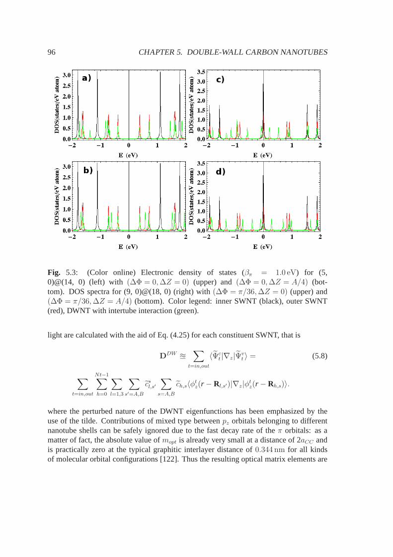
96 CHAPTER 5. DOUBLE-WALL CARBON NANOTUBES
Fig. 5.3: (Color online) Electronic density of states (βπ = 1.0 eV) for (5,0)@(14, 0) (left) with (∆Φ = 0,∆Z = 0) (upper) and(∆Φ = 0,∆Z = A/4) (bot-tom). DOS spectra for (9, 0)@(18, 0) (right) with(∆Φ = π/36,∆Z = 0) (upper) and(∆Φ = π/36,∆Z = A/4) (bottom). Color legend: inner SWNT (black), outer SWNT(red), DWNT with intertube interaction (green).
light are calculated with the aid of Eq. (4.25) for each constituent SWNT, that is
DDW≅
∑
t=in,out
〈Ψct |∇z|Ψv
t 〉 = (5.8)
∑
t=in,out
Nt−1∑
h=0
∑
l=1,3
∑
s′=A,B
c∗l,s′∑
s=A,B
ch,s〈φtz(r − Rl,s′)|∇z|φt
z(r −Rh,s)〉.
where the perturbed nature of the DWNT eigenfunctions has been emphasized by theuse of the tilde. Contributions of mixed type betweenpz orbitals belonging to differentnanotube shells can be safely ignored due to the fast decay rate of theπ orbitals: as amatter of fact, the absolute value ofmopt is already very small at a distance of 2aCC andis practically zero at the typical graphitic interlayer distance of0.344 nm for all kindsof molecular orbital configurations [122]. Thus the resulting optical matrix elements are
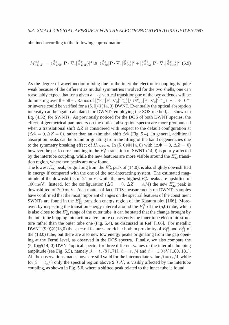
5.3. SMALL CRYSTAL APPROACH FOR THE ELECTRONIC STRUCTURE OFDWNTS97
obtained according to the following approximation
Moptz DW = |〈Ψc
DW |P · ∇z|ΨvDW 〉|2 ≅ |〈Ψc
in|P · ∇z|Ψvin〉|2 + |〈Ψc
out|P · ∇z|Ψvout〉|2 (5.9)
As the degree of wavefunction mixing due to the intertube electronic coupling is quiteweak because of the different azimuthal symmetries involved for the two shells, one canreasonably expect that for a givenv → c vertical transition one of the two addends will bedominating over the other. Ratios of|〈Ψc
in|P ·∇z|Ψvin〉|/|〈Ψc
out|P ·∇z|Ψvout〉| ∼ 1÷10−4
or inverse could be verified for a(5, 0)@(14, 0) DWNT. Eventually the optical absorptionintensity can be again calculated for DWNTs employing the SOS method, as shown inEq. (4.32) for SWNTs. As previously noticed for the DOS of both DWNT species, theeffect of geometrical parameters on the optical absorptionspectra are more pronouncedwhen a translational shift∆Z is considered with respect to the default configuration at(∆Φ = 0,∆Z = 0), rather than an azimuthal shift∆Φ (Fig. 5.4). In general, additionalabsorption peaks can be found originating from the lifting of the band degeneracies dueto the symmetry breaking effect ofHINTER. In (5, 0)@(14, 0) with (∆Φ = 0, ∆Z = 0)however the peak corresponding to theES
11 transition of SWNT (14,0) is poorly affectedby the intertube coupling, while the new features are more visible around theES
22 transi-tion region, where two peaks are now found.The lowestES
22 peak, originating from theES22 peak of (14,0), is also slightly downshifted
in energy if compared with the one of the non-interacting system. The estimated mag-nitude of the downshift is of25 meV, while the new highestES
22 peaks are upshifted of100 meV. Instead, for the configuration (∆Φ = 0, ∆Z = A/4) the newES
22 peak isdownshifted of200 meV. As a matter of fact, RRS measurements on DWNTs sampleshave confirmed that the most important changes on the spectral features of the constituentSWNTs are found in theES
22 transition energy region of the Kataura plot [166]. More-over, by inspecting the transition energy interval around theES
11 of the (5,0) tube, whichis also close to theES
22 range of the outer tube, it can be stated that the change brought bythe intertube hopping interaction alters more consistently the inner tube electronic struc-ture rather than the outer tube one (Fig. 5.4), as discussed in Ref. [166]. For metallicDWNT (9,0)@(18,0) the spectral features are richer both in proximity of EM
11 andEM22 of
the (18,0) tube, but there are also new low energy peaks originating from the gap open-ing at the Fermi level, as observed in the DOS spectra. Finally, we also compare the(5, 0)@(14, 0) DWNT optical spectra for three different values of the intertube hoppingamplitude (see Fig. 5.5), namelyβ = tπ/8 [171], β = tπ/4 andβ = 1.0 eV [180, 181].All the observations made above are still valid for the intermediate valueβ = tπ/4, whilefor β = tπ/8 only the spectral region above2.0 eV, is visibly affected by the intertubecoupling, as shown in Fig. 5.6, where a shifted peak related to the inner tube is found.

98 CHAPTER 5. DOUBLE-WALL CARBON NANOTUBES
Fig. 5.4: (Color online) Absorption spectra (βπ = 1.0 eV) for (5, 0)@(14, 0)(left) with (∆Φ = 0,∆Z = 0) (upper) and(∆Φ = 0,∆Z = A/4) (bottom). Ab-sorption spectra for (9, 0)@(18, 0) (right) with(∆Φ = π/36,∆Z = 0) (upper) and(∆Φ = π/36,∆Z = A/4) (bottom). Intensity is given in arbitrary units. Color legend:inner SWNT (black), outer SWNT (red), DWNT with intertube interaction (green).
5.3.3 Conclusions, summary and future perspectives
As recalled in the introduction, besides Photoluminescence, Resonance Raman spec-troscopy allows to characterize the nanotubes present in a sample by assigning their ra-dial breathing modes (RBM). The assignment is based on calculated Kataura plots [127]which correlate SWNT electronic excitations with their diameters. A similar route wasalso attempted, with less success, for DWNTs [166], with thebasic assumption that thesesystems can be modelled as two almost non-interacting SWNTs. Based on this assump-tion, the electronic structure of a DWNT is simply the sum of the electronic structuresof the constituent tubes. Perturbative effects due to weak intertube electronic couplingare considered negligible or at least responsible for a slight shift on the single-particletransition energies around Fermi level. By applying the SC approach to DWNTs, wehave shown that this picture is only partially correct and that new transitions can be ex-
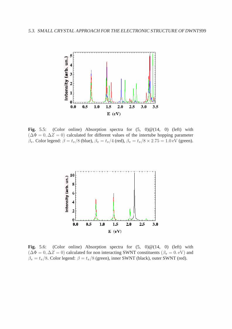
5.3. SMALL CRYSTAL APPROACH FOR THE ELECTRONIC STRUCTURE OFDWNTS99
Fig. 5.5: (Color online) Absorption spectra for (5, 0)@(14, 0) (left) with(∆Φ = 0,∆Z = 0) calculated for different values of the intertube hopping parameterβπ. Color legend:β = tπ/8 (blue),βπ = tπ/4 (red),βπ = tπ/8× 2.75 = 1.0 eV (green).
Fig. 5.6: (Color online) Absorption spectra for (5, 0)@(14, 0) (left) with(∆Φ = 0,∆Z = 0) calculated for non interacting SWNT constituents(βπ = 0. eV) andβπ = tπ/8. Color legend:β = tπ/8 (green), inner SWNT (black), outer SWNT (red).

100 CHAPTER 5. DOUBLE-WALL CARBON NANOTUBES
pected originating from the symmetry breaking of the band degeneracies in particular inthe visible range. The optical spectral features have been shown to be strongly affected bythe orientational configuration of the constituent tubes, particularly by the translationalshift parallel to the DWNT axis. The results allow to understand the usual difficulties inassigning the Resonance Raman spectra of double wall nanotubes since important varia-tions of the electronic spectra of these carbon nanotubes are found with respect to thoseof the constituent single wall nanotubes. Moreover, although variations of the spectracan be found for all the values of the intertube hopping parameters found in literature(Fig. 5.5), a careful evaluation of this parameter must be obtained for an appropriate elec-tronic structure calculation for DWNTs. As a matter of fact,the widely used value of theintertube hopping parameterβ = tπ/8 adopted since the work by Rocheet al. [171], wasintroduced ten years earlier by Lambinet al. [169], who in turn obtained it from fittingabinitio calculations for turbostratic graphite [79, 80], which well reproduced experimentalresults for this system. In other cases, such asβ = 1.0 eV by M. Grifoni and S. Wang[180, 181], the reasons behind the choice have not been made clear at all. Several fullabinitio calculations of the electronic properties of double-wall nanotubes have also beendone [182, 183, 176, 184], although they’re notoriously difficult because of the large unitcells involved in the computation, but still a well- documented tight-binding parametriza-tion from fitting DFT calculations for the interlayer coupling in DWNTs could not befound. Finally, we point out that the experimental Raman measurements on DWNTs ac-tually provide averaged electronic spectra of these systems, since each wall can assumein principle any orientation with respect to the other shell. This holds in particular for in-commensurate DWNT pairs, for which geometric correlation is poor and frictionless dy-namics has been predicted [185] and experimentally verified[186]. On the other hand, fordeep minima in total energy, which occur prevalently in commensurate DWNTs, one canreasonably expect that the corresponding geometric configurations will play a dominantrole in determining the resulting spectral profile, since the constituent walls will hardlychange their mutual positions, because of the higher optential energy barrier. Thereforemore accurate molecular dynamics calculations which take into account also this aspectneed to be performed in the future in order to obtain reliableKataura plots for thesesystems.

Chapter 6
Electronic correlation effects
In this chapter, starting from experimental evidence, we will introduce the issue of theelectronic correlation effects in single-walled nanotubes, which are reflected in the ex-citonic nature of their optical spectral features. The treatment of many-body effects inthese systems requires the necessity of going beyond the single-particle approximation oftight-binding methods. The first section presents a brief overview of the main theoreticalapproaches developed in order to treat excitonic effects inSWNTs, together with a discus-sion of their most relevant results and drawbacks of the respective methods. In the secondsection we will present the method developed in this thesis,which combines the simplebut powerful description of the Hubbard model for correlated fermionic systems with thefeatures of the small crystal approach for the treatment of extended periodic systems. Awhole section has also been devoted to the description of thecomputational implemen-tation and issues behind the method. In the final part the results of the calculations forsmall-size systems are presented and discussed in relationto the most relevant literatureworks. Then, future work directions are suggested for further research developments.
6.1 Many-body effects and electronic correlations in SWNTs
6.1.1 Experimental evidence for the limits of tight-binding
In Chapt. 3 the tight-binding method was introduced in orderto provide a simple butrealistic description of the optical properties of SWNTs. In the introductory chapterwe highlighted the importance of tight-binding methods in supporting the interpretationof experimental Kataura plots obtained by Raman and photoluminescence spectroscopy.We recall that these tools are widely used in nanotube science for assigning the spec-tral features (i.e. the measured transition energies) to the respective SWNT diametersand chiralities. Early Raman studies on SWNTs were interpreted in terms of the sim-ple tight-binding (STB) scheme forπ-electrons according to the zone-folding methodapplied to the graphene sheet, as presented in Chapt. 3. Thisscheme however doesn’t
101

102 CHAPTER 6. ELECTRONIC CORRELATION EFFECTS
take into account long-range interactions, curvature effects andσ-π rehybridization ef-fects, which cannot be neglected in small diameter nanotubes. As a consequence, morerefined tight-binding based methods have been developed, inorder to provide accurateand reliable interpretations of the experimental Kataura plots also in the small diameterrange. In particular, we mention the symmetry-adapted non-orthogonal TB method by V.N. Popov [84], which takes into account nanotube curvature and structural optimizationeffects in the electronic hamiltonian. Soon afterwards, a similar approach was followedby Saito’s group [122, 132], with the so-calledextended tight-bindingmethod (ETB).Within this framework, they use the tight-binding parametrization for carbon determinedfrom density-functional theory with local density approximation and a local orbital ba-sis set [70, 71]. Then they include curvature-induced rehybridization by alignment ofthe atomic orbitals along directions normal and tangentialto the SWNT sidewall. Sub-sequently, geometrical structure optimization is performed by minimization of the totalenergy of the system with respect to the atomic degrees of freedom. In general, theconstructed ETB Kataura plot showed a good agreement both with first principles cal-culations (long-range interactions are taken into account) and with experimental PL andRRS Kataura plots, in particular for the spreads of the SWNT families of constant2n+m(Fig. 6.1). This experimental family spread is attributed to the relaxation of the geomet-rical structures of the SWNTs [122, 132].
Fig. 6.1: Experimental Kataura plots derived from PL (upper left) and RRS (upper right)measurements on HiPCO SWNTs suspended by SDS surfactant in acqueous solution.The numbers show the families of constant2n+m. ETB Kataura plot (bottom) as a func-tion the inverse diameter1/dt: long-range atomic interactions, curvature effects and geo-metrical optimizations are taken into account in the calculation. Taken from Ref. [122].
However, in spite of a good agreement in the family spread, both PL and RRS exper-imental Kataura plots exhibit an overall blueshift of the transition energies by about200 − 300 meV from the ETB Kataura plot. Moreover, theES
22 to ES11 ratio in the ex-
perimental Kataura plots tends to1.8 in the large diameterdt limit (where the family

6.1. MANY-BODY EFFECTS AND ELECTRONIC CORRELATIONS IN SWNTS103
spread is small), while in the ETB predicted Kataura plot theES22/E
S11 ratio for largedt
tends to2. These can be considered the two main effects of the many-body Coulombinteractions on the single-particle transition energiesEii, which cannot be accounted byETB method.
6.1.2 Theoretical investigations of exciton photophysicsin SWNTs
Although many-body were already investigated in 1997 in a theoretical work by T. Andobased on the effective-mass approximation [194], only in 2004 it became definitely clearthat electron interactions play an important role in determining the optical transition en-ergies in these systems [197]. As previously explained, this happened because the ex-periments were always interpreted in the framework of simple non-interacting models,such as tight-binding calculations. Because of the spatialconfinement of electrons inthe quasi-one dimensional structure of the SWNTs and, consequently, the poor dielectricscreening, the Coulomb interactions between photoexcitedelectrons and electrons in theground state are strongly enhanced if compared to bulk semiconductors [187]. As pointedout in the pionieristic work by Ando, the electron-electron(e-e) interactions lead to twocompeting opposite effects: a) the increase of the single-particle transition energy by thequasi-particle self-energy and b) the binding of photoexcited electrons and photogener-ated holes (e-h) into excitons whose binding energies are comparable but slightly smallerthan the quasi-particle self-energies. The resulting effect is thus a moderate blueshift ofthe single-particle transition energies due to the Coulombe-e interactions and the exci-ton e-h attraction, together referred to as the many-body interactions. A more detailedanalysis of the many-body effects was conducted in a seminalpaper by Kane and Mele[196], starting from an effective-mass theory for statically screened interacting electronsin graphene. In this work they examine the many-body interactions separately: a) onscales larger than the tube circumferenceπdt, where bothe-eande-h Coulomb inter-actions have 1D long-range character; b) on length scale smaller thanπdt, where themany-body interactions have 2D short-range character. Therefore, in principle one canwrite for the transition energyEii including many-body effects:
Eii = Eeii + E2Dee
ii + E1Deeii − E2Deh
ii −E1Dehii , (6.1)
whereEeii is the single-particle transition energy,Eee
ii is the quasiparticle self-energy andEeh
ii is the binding energy of the lowest bright exciton. As explained above, bothEeeii
andEehii in Eq. (6.1) are split into two terms competing to short-range (2D) and long-
range (1D) interactions, respectively. TheE2Deeii self-energy is given by the logarithmic
correction term [196, 122]
E2Deeii =
√3
2(εs− t) ∆kia
g
4ln
Λ
∆ki, (6.2)
104 CHAPTER 6. ELECTRONIC CORRELATION EFFECTS
where (ε = 5.372 eV, s = 0.151, t = 3.370 eV) are the values for the ETB parametersused in Saito’s papers [122],g is the Coulomb interaction parameter, andΛ is an ultra-violet interaction cutoff, all of which depend on the dielectric constantκ of the SWNTenvironment, and∆ki is the critical wavevector measured from the K point in the 2DBril-louin zone. The latter is given by∆kS
1 = 2/(3dt), ∆kS2 = 4/(3dt), and∆kM
1 = 6/(3dt)for theES
11, ES22, andEM
11 transition energies, respectively. TheE2Dehii binding energy
in Eq. (6.1) vanishes due to the absence of excitons in the graphene sheet. TheE1Deeii
andE1Dehii terms scale with the SWNT diameterdt, the reduced mass of the excitonµii
(which is diameter and chirality dependent), and the dielectric constantκ of the SWNTenvironment. Thus, theE1Dee
ii andE1Dehii energies develop family patterns. In small di-
ameter SWNTs, theE1Deeii andE1Deh
ii terms significantly exceed theE2Deeii self-energy
of Eq. (6.1) due to a strong spatial confinement of the Coulombinteraction. Neverthless,as shown by Kane and Mele,E1Dee
ii andE1Dehii nearly perfectly cancel each other. If
we assume that that these energy terms completely cancel out, which is actually a goodapproximation, then Eq. (6.1) becomesEii = Ee
ii + E2Deeii and the resulting values for
the transition energies are moderately blueshifted from the ETB single-particle values,as found experimentally. The difference between the experimentalEii and the ETBEe
ii
transition energies as a function of the wavevector∆ki with the to the functional form ofEq. (6.2). This yields the following values for the fitting parameters, which are reportedin Saito’s papers:g = 1.7 andΛ = 3.5 nm−1 [122], in good agreement with Kane andMele’s values [196]. SinceE2Dee
ii only depends ondt and is independent ofθ, Saito andDresselhaus in their work again interpret the experimentalKataura plots of SWNTs (andDWNTs as well) on the basis of ETB calculations: the single-particle transition energiesare simply shifted by200 − 300 meV to account for the logarithmicκ-dependent (ac-cording to the environment) correction of theE2Dee
ii term [132, 204, 205, 166].However, besides Ando’s effective-mass approximation method [194, 86, 211], in theseyears several other theoretical studies were carried out inorder to explore the photo-physics of excitons in SWNTs. Among first-principles methods, two different classes ofcalculation scheme for excitons can be found in nanotube literature: density-functionalcalculations with Dyson’s equation for self-energy and Bethe-Salpeter equation (BSE)for the electron-hole correlation, performed by the groupsheaded by S.G. Louie [199]and E. Molinari [200, 203], respectively; Hartree-Fock Configuration Interaction withsingle-excited basis set, performed by the group headed by S. Mazumdar [208, 210]. Ad-ditionally, other schemes were adopted first by Pedersen [201] (a variational approach,in which a Gaussian trial wavefunction is used to estimate excitonic binding energies)and later by Perebeinoset al. [202] (a semi-empirical excitonic calculation based on atight-binding modeling of quasi-particle energies and an Ohno potential for electron-holeinteraction) for determining exciton scaling relations inthese systems. Later, ETB calcu-lations with BSE were also performed by the group of Saito andDresselhaus [204, 205].In the following we will overview only first-principles calculations, since at the momentonly these methods are capable of providing a reasonably accurate description of the rich
6.1. MANY-BODY EFFECTS AND ELECTRONIC CORRELATIONS IN SWNTS105
excitonic structure in SWNTs.
BSE-based schemes In the ab-initio calculations performed by Louie [199] the opticalabsorption spectra with electron-hole excitations are calculated in three steps: (i) theelectronic ground state is obtained via pseudopotential density-functional theory withinlocal density approaximation (LDA) and with a plane-wave basis set; (ii) the quasiparticleenergiesEnk are obtained within theGW approximation for the electron self-energyΣby solving the Dyson equation
[−∇
2
2+ Vion + VHartree + Σ (Enk)
]Ψnk = EnkΨnk (6.3)
and finally (iii) the coupled electron-hole excitation energiesΩS and relative spectrum arecalculated by solving the Bethe-Salpeter equation of the two-particle Green’s function
(Eck − Evk)ASvck +
∑
k′v′c′
〈vck|Keh|v′c′k′〉ASv′c′k′ = ΩSAS
vck, (6.4)
whereASvck is the exciton amplitude,Keh is the electron-hole interaction kernel, and|ck〉
and|vk〉 are the quasi-electron and quasi-hole states, respectively. This method can ac-count for the ratio problem, the large self-energy corrections (∼ 20% of the single-particlegap) and exciton binding energies (0.1 − 1.0 eV) found in photophysics experiments onSWNTs [197, 198]. Although very accurate, BSE-based methods are computationallyvery intensive, since they scale as the number of atoms to the4th power. As a matter offact, Louieet al. reported that the calculation for the (8,0) tube (with 32 atoms in theunit cell) was very challenging, as well as (4,2) tube (with 56 atoms), which was far moredifficult.Soon later, a more efficient BSE-based scheme was proposed bythe group headed byE. Molinari [200, 203] to handle the computation of (4,2) and(6,4) tubes. They used asymmetrized basis set taking advantage of the screw symmetry of nanotube systems. Thisapproach also allows for a better physical understanding ofthe problem, since it allows tocharacterize the symmetry of excitonic wavefunctions and which transitions are allowedor forbidden by certain selection rules [198].Neverthless, the calculations reported until now by these research groups have been per-formed just for very few tubes: this points out that the solution of the Bethe-Salpeterequation for larger diameter SWNTs byab initio techniques is still a formidable task,even by exploiting helical symmetries in SWNTs. Additionally, although Bethe-Salpetermethods attempt to go beyond mean-field approximation, theyare limited to consideronly single-excitation (1e-1h) bounded excitons, making a full many-body calculation forall excitations still impracticable for these systems. Moreover, from these calculations it’snotoriously difficult to extract an effective estimate of the strength of the electron-electron
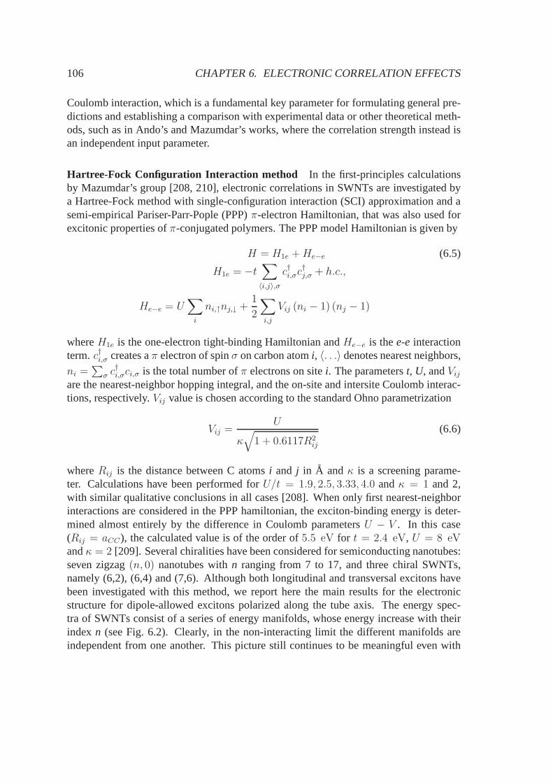
106 CHAPTER 6. ELECTRONIC CORRELATION EFFECTS
Coulomb interaction, which is a fundamental key parameter for formulating general pre-dictions and establishing a comparison with experimental data or other theoretical meth-ods, such as in Ando’s and Mazumdar’s works, where the correlation strength instead isan independent input parameter.
Hartree-Fock Configuration Interaction method In the first-principles calculationsby Mazumdar’s group [208, 210], electronic correlations inSWNTs are investigated bya Hartree-Fock method with single-configuration interaction (SCI) approximation and asemi-empirical Pariser-Parr-Pople (PPP)π-electron Hamiltonian, that was also used forexcitonic properties ofπ-conjugated polymers. The PPP model Hamiltonian is given by
H = H1e +He−e (6.5)
H1e = −t∑
〈i,j〉,σc†i,σc
†j,σ + h.c.,
He−e = U∑
i
ni,↑nj,↓ +1
2
∑
i,j
Vij (ni − 1) (nj − 1)
whereH1e is the one-electron tight-binding Hamiltonian andHe−e is thee-einteractionterm.c†i,σ creates aπ electron of spinσ on carbon atomi, 〈. . .〉 denotes nearest neighbors,
ni =∑
σ c†i,σci,σ is the total number ofπ electrons on sitei. The parameterst, U, andVij
are the nearest-neighbor hopping integral, and the on-siteand intersite Coulomb interac-tions, respectively.Vij value is chosen according to the standard Ohno parametrization
Vij =U
κ√
1 + 0.6117R2ij
(6.6)
whereRij is the distance between C atomsi and j in A and κ is a screening parame-ter. Calculations have been performed forU/t = 1.9, 2.5, 3.33, 4.0 andκ = 1 and 2,with similar qualitative conclusions in all cases [208]. When only first nearest-neighborinteractions are considered in the PPP hamiltonian, the exciton-binding energy is deter-mined almost entirely by the difference in Coulomb parameters U − V . In this case(Rij = aCC), the calculated value is of the order of5.5 eV for t = 2.4 eV, U = 8 eVandκ = 2 [209]. Several chiralities have been considered for semiconducting nanotubes:seven zigzag(n, 0) nanotubes withn ranging from 7 to 17, and three chiral SWNTs,namely (6,2), (6,4) and (7,6). Although both longitudinal and transversal excitons havebeen investigated with this method, we report here the main results for the electronicstructure for dipole-allowed excitons polarized along thetube axis. The energy spec-tra of SWNTs consist of a series of energy manifolds, whose energy increase with theirindex n (see Fig. 6.2). Clearly, in the non-interacting limit the different manifolds areindependent from one another. This picture still continuesto be meaningful even with
6.2. HUBBARD MODEL AND SC APPROACH 107
non-zeroHe−e, because of the relatively weak mixing between the different n excitationmanifolds. Within each energy manifold, the single optically-allowed (bright) excitonand several dark excitons occur, as well as a continuum band separated from the opticalexciton by a characteristic exciton binding energy, as shown in Fig. 6.2. Interestingly,according to these calculations, the highest state in the first excited manifold is strongly-dipole allowed, while all the remaining states underneath are dark (dipole-forbidden).Due to the non-zero value ofHe−e the four-degenerate optically-allowed single-particleexcitations between the highest occupied and lowest unoccupied one-electron levels aresplit into a series of levels, with the highest one collecting almost all the oscillator strength[208], as sketched in Fig. 6.9. The calculated exciton binding-energies for large diameterSWNTs compare well with the experimental spectrofluorimetric measurements by Wangand Dukovic [197], whereas a large disagreement is found fordt < 0.75 nm, due tothe breakdown of theπ-electron approximation. Also, disagreements between calculatedand experimentalE22 are larger, since it should be necessary to include higher order CIin order to achieve greater precision. Actually, SCI approximation works best for lowerenergy regions; as the energy increases higher order excitations contribute more to thewavefunctions. This requires at least double excited CI, hence more computationally in-tensive calculations which are beyond todays capabilitiesfor such extended systems. Thesplitting between bright and dark excitons inn = 1 manifold has also been considered, invirtue of several recents experimental measurements whichclaimed values between fewmillielectronvolts and0.14 eV (see [210] and references therein). Anyway, a theoreticalestimation was difficult to be obtained within HF-SCI because of convergence problemsdue to the small-size of the bright-dark exciton gap.In conclusion, unlikely BSE-basedab initio calculations, the HF-SCI method adoptedby Mazumdar allows the understanding of some important features of the excitonic elec-tronic structure for a larger set of SWNTs. Moreover, this method can account for thelarge exciton binding energies in these systems on the basisof a simple parametrizationfor π-electrons and a semi-empirical hamiltonian (appropriatefor large diameter tubes),already applied successfully toπ-conjugated polymers. By including higher orders con-figuration interaction terms more reliable results could certainly be obtained, althoughthis implies prohibitively increasing the computational complexity of the problem.Clearly, for a proper treatment of many-body effects other theoretical models are needed,which allow both to go beyond mean-field approximation and for a full inclusion of allpossible correlation excitations in the single-particle hamiltonian.
6.2 Hubbard model and SC approach
In the previous section, we saw that in SWNTs the many-body corrections to the mea-sured single-particle transition energies are actually determined by the short-range electron-electron interactions, since the electron-hole Coulomb interaction and the long-range con-

108 CHAPTER 6. ELECTRONIC CORRELATION EFFECTS
Fig. 6.2: Schematic of the excitonic electronic structure of a semiconductor SWNT forn = 1 andn = 2 manifolds. Exn and Dn are dipole-allowed and -forbidden excitons,respectively. Shaded areas indicate continuum band for each manifold. Note that alllevels of then = 2 manifold should be buried in then = 1 continuum band; however forclarity then = 1 continuum band end is represented below D2. Taken from Ref. [209,210].
tribution to the self-energy cancel perfectly. In this section we will show that the Hubbardmodel [188], although in somewhat oversimplified manner, includes all the necessary fea-tures for describing electronic correlation effects in a quantum lattice system and goingbeyond mean-field approximation. Moreover, given the real-space formulation of theHubbard model, the small crystal approch can be appropriately used to investigate theproblem of the many-body electronic correlation effects onthe optical spectra of periodicsystems such as SWNTs.
6.2.1 The physics of the Hubbard model
The model introduced by J. Hubbard [188] in 1963 is perhaps one of the simplest yetphysically powerful descriptions of the many-body effectsin quantum mechanical sys-tems. For this reason since its formulation it has been one ofthe most extensively studiedmicroscopic models for correlated electron systems, such as for instance high-TC su-perconductors [189], transition metal oxides displaying Mott insulator transition [190],organic one-dimensional conductors [210] and recently also low dimensional systems in-cluding quantum dots [191, 192]. Unfortunately the exact solution is not known asidefrom the ground state in the one dimensional model [193], hence we depend on approx-imations and/or computer simulations for investigating more complex systems. The richphysics of the Hubbard model is determined by the interplay between the kinetic and

6.2. HUBBARD MODEL AND SC APPROACH 109
potential energy of the electrons in the system lattice, which is captured by the followingHamiltonian:
H = −t∑
〈i,j〉,σ
(c†i,σcj,σ + h.c
)+ U
∑
i
ni,↑ni,↓, (6.7)
wherei andj are site indices,〈i, j〉 are all pairs of nearest neighbor sites,ni,σ = c†i,σci,σ is
the number of electrons on sitei with spinσ, c†i,σ andci,σ are electron creation and annihi-lation operators, andt andU are positive interaction constants. Thet-term describes thehopping process of electrons localized on atomic-like orbitals between nearest neighborsites and models the kinetic energy of the system. This part is derived from the tight-binding approximation, which was extensively treated in the previous chapters: since itis an independent particle theory, it contains no many-bodyfeatures. TheU-term mod-els the Coulomb repulsion between two electrons with opposite spin in the same orbital,hence it gives a potential energy contribution to the hamiltonian. Whereas other methodsbased on mean-field approximations (such as density functional theory) replace this in-teraction with an average one, retaining an effective single-particle picture, the Hubbardmodel incorporates the Coulomb potential as a pair interaction, which effectively allowsto include all the relevant many-body features in the hamiltonian. The potential energyterm is diagonal in real space and tends to immobilize the electrons at certain positionsof minimum energy, whereas the kinetic energy term is diagonal in momentum space andtries to move around the electrons. The basic formulation ofthe Hubbard hamiltonian inEq. (6.7) can be extended in several ways, which have been widely discussed in litera-ture. The most natural are the introduction of an off-site Coulomb interaction betweennearest-neighbor orbitals
HV = V∑
〈i,j〉ninj (6.8)
and/or the addition of hopping terms beyond first nearest neighbor sites, such as secondnearest neighbor hopping
Ht′ = −t′∑
〈〈i,j〉〉,σ
(c†i,σcj,σ + h.c
)(6.9)
where〈〈i, j〉〉 are all pairs of second nearest neighbor sites. However we will not discussthese terms.Since the Hubbard model describes the interplay of potential and kinetic energy, depend-ing on the ratio ofU/t either the Coulomb interaction or the kinetic energy dominates. Incase ofU/t ≪ 1 and systems of dimensionn > 1 we retain the results of the TBA forindependent particles with small corrections and thus the well-known cosine band pre-sented in Chapt. 4. The system therefore is metallic unless the band is completely filled.Electrons are delocalized all over the system and their wavefunctions can to good ap-proximation be written as Slater determinants. IfU/t ' 1 the movement of one electron

110 CHAPTER 6. ELECTRONIC CORRELATION EFFECTS
is influenced by the locations of all other electrons in the system since double occupa-tion of a site is energetically expensive and thus they try toavoid each other. Hence theindependent-electron approximation cannot be used and analytical solution of the prob-lem cannot be easily found out. Usually wave functions for those systems generally haveto be computed numerically. This regime is said to becorrelated. If the ratioU/t ≫ 1it is even calledstrongly correlated. Electrons try to distribute themselves as uniformlyas possible on the sites in order to minimize the Coulomb energy. At half-filling, i.e.at a mean electron density of one electron per site, the competition between kinetic andpotential energy has particularly interesting considerations: because of the strong on-siteCoulomb repulsion, the simultaneous occupation of a site bytwo electrons is stronglydisfavored, thus each site will be occupied exactly by one electron. In other words, everyhopping process of a single electron implies a large energy costU for the system; there-fore, all the electrons are localized and the system is in an insulating state, generated bypure electron-electron interactions, namely it is aMott-Hubbard insulator.In summary, the Hubbard model and its other numerous derivatives and counterparts(e.g. Heisenberg model for ferromagnetic systems), although with a rather simple formu-lation, provide all the necessary features to treat the electronic correlations of quantum-mechanical many-body systems, such as an electron gas in a crystal lattice; hence thenomenclaturequantum lattice model, often used referring to these methods.In principle, in order to treat the quantum mechanics of interacting electrons, which areactually indistinguishable particles, one has to construct the multiparticle states by su-perpositions of products of single-particle states, taking into account the Pauli exclusionprinciple (Slater determinants). In the Hubbard model the single-particle states are elec-tron wavefunctions localized at lattice sites. However, the second quantization formalism,which has already been implicitly introduced in Eq. (6.7), provides us with a suitable ba-sis for dealing with the problem without the explicit specification of the wavefunctiondeterminant. This basis in the Hilbert space is orthonormaland is calledoccupation num-ber basis(or Fock space). This set includes states describing all possible distributions ofN electrons overM lattice sites. There are 4 possible electron occupancies ateach site(unoccupied, singly occupied either for spin up or down, doubly occupied with one spinup and one spin down). Since the possible configurations of upspins are independent ofthe configurations of the down spin, theHHubbard space of all possible configurations isjust the direct product of the Hilbert space of down spinsH↑ and that of up-spinsH↓:
HHubbard = H↑ ⊗H↓. (6.10)
A convenient way to represent and generate these multiparticle states is to keep the spinup and spin down configurations separately by assigning eachlattice site a 1 if the siteis occupied or zero if it is not (bit-string coding). In this way, every multiparticle stateis described by the occupancy numbers of the single-particle states for a given spin. Forexample, a generic state in this basis having 5 electrons on an 8 site lattice with 3 up and
6.2. HUBBARD MODEL AND SC APPROACH 111
2 down spin is coded as|00101010〉|00100100〉, (6.11)
where the spin up electrons are found at sites 3, 5, 7, the downspin electrons are found atsites 3 and 6 and the remaining sites are unoccupied. Formally, these states can be gener-ated by applying second quantization creation and annihilation operators to the vacuum|0〉
c†k1ck2
. . . c†kN|0〉 etc., (6.12)
where(k1, k2 . . . kN) is an orderedN-tuple of indices andki is the index of the corre-sponding single-particle state. The antisymmetry of the fermionic states is taken intoaccount via the operator algebra expressed by the followinganticommutation rules
[cl, c
†m
]= δl,m, (6.13)[
c†l , c†m
]= 0,
[cl, cm] = 0.
The operatorc†k generates a single-particle wavefunctionϕk (r) within the multiparticlestate if that wavefunction is not present yet; otherwise, the result is 0. The adjoint operatorck annihilates the single-particle wavefunction if present;otherwise it returns 0. The Pauliexclusion principle follows fromc†kc
†k = 0. Since the Hubbard Hamiltonian is represented
by non-commutative products of creation and destruction fermionic operators as well,one can reasonably expect that the corresponding Hamiltonian matrix can be constructedalgebraically. In the following section we will show how to build up the Hamiltonianmatrix for the one-dimensional Hubbard model applied to a working example, namelya chain withM sites and periodic boundary conditions. This will help in understandingthe construction of the working code developed in this thesis for small periodic clusters,presented in Sect. 6.3.
6.2.2 The Hubbard model for a periodic M-site chain
The Hubbard Hamiltonian for a chain withM sites and periodic boundary conditions is
H = −tM∑
i=1
∑
σ
(c†i,σci+1,σ + c†i+1,σci,σ
)+ U
M∑
i=1
ni,↑ni,↓ (6.14)
with the periodic boundary conditions expressed byc†M+1,σ = c†1,σ andcM+1,σ = c1,σ.
Here,ni,σ ≡ c†i,σci,σ yields the value 1, if an electron with spinσ is located at the sitei,otherwiseni,σ yields the value 0. Now the basis set in the occupation numberformalismhas to be constructed. First, however, one has to label the single-particle states upon
112 CHAPTER 6. ELECTRONIC CORRELATION EFFECTS
which constructing the multi-particle states and define their order. For the order of thesingle-particle states, we choose the following convention [219]
1 ↑, 2 ↑, . . . ,M ↑ , 1 ↓, 2 ↓, . . . ,M ↓ . (6.15)
Thus, the generic multiparticle state in the example of Eq. (6.11) in second quantizationis written as
| 00101010 , 00100100〉 = c†3,↑c†5,↑c
†7,↑c
†3,↓c
†6,↓|0〉. (6.16)
If the operatorc†l,σ is applied to a multiparticle state, then one has to swap thisoperator
with the operatorsc†m,σ′ using the algebra of Eq. (6.13), until the sequence is recovered inthe correct order as in Eq. (6.15). By this procedure one alsoobtains the sign of the state.For example, we get
cM,↓| 1, 0, . . . , 0 , 0, . . . , 0, 1〉 = cM↓c†1↑c
†M↓|0〉 (6.17)
= −c†1↑cM↓c†M↓|0〉
= −c†1↑|0〉+ c†1↑c†M↓cM↓|0〉= −c†1↑|0〉
= −| 1, 0, . . . , 0 , 0, . . . , 0〉
Generally, when applyingc†l,σ or cl,σ to a state|n〉 = | n1↑, . . . , nM↑ , n1↓, . . . , nM↓〉,the number of particles to the left oflσ determines the sign. Therefore, one can definethe sign function in the following way:
sign (lσ,n) = (−1)δσ↓
PMi=1
ni↑ (−1)Pl−1
j=1njσ (6.18)
This function produces as many factors -1 as there are non-zero entries inn in front ofthe positionl, σ. This fact allows us to write the effect of the creation operator as
c†lσ|n〉 = (1− nlσ) sign (lσ,n) | n1,↑, . . . , 1, . . . , nM↓〉, (6.19)
where the number 1 is at the positionlσ and the factor(1− nlσ) ensures that there is nodouble occupancy of the same state. On the other hand, for thedestruction operator weget
clσ|n〉 = nlσsign (lσ,n) | n1↑, . . . , 0, . . . , nM↓〉, (6.20)
which annihilates the statelσ. In order to obtain the Hamiltonian matrix, one needs toobtain the scalar product between any multiparticle state of the Fock space〈ni| withH|nj〉. In general, the Hubbard matrix is mostly filled with zeros and the on-diagonalelements can be obtained in a very straightforward manner byinspecting the number ofdoubly-occupied sites in each multiparticle state and multiplying this double-occupancynumber byU, the Coulomb repulsion energy. If two states|ni〉 and 〈nj | differ by the

6.2. HUBBARD MODEL AND SC APPROACH 113
hopping of one electron from a given site to its nearest neighbour, then the correspondingoff-diagonal matrix element ist, with the sign determined by the chosen convention forthe hopping. In the computer program presented in Ref. [219], the following rule wasadopted for the sign of the off-diagonalt matrix elements: if the hopping involves justnearest neighbor sites which are not related by periodic boundary conditions (unlikelythose at the opposite ends of the chain), then the matrix element is set equal to−t, oth-erwise it is set equal to+t. However, other conventions can be adopted as well, withoutaffecting the resulting eigenvalues obtained from the matrix diagonalization. Similarly,one can construct the matrix for the velocity operatorv1D (or correspondingly the currentoperator), needed for the calculation of the optical matrixelement between the groundstate|ψ0〉 and any other eigenstate〈ψm| of the Hubbard matrix. For a chain withM sitesand periodic boundary conditions this operator is defined as[92, 215, 216]
v1D = − ıt~
M∑
i=1
∑
σ
(c†i,σci+1,σ − c†i+1,σci,σ
)(6.21)
This allows us to compute the intensity of the optical absorption spectrum for the Hubbardchain with the SOS method as a spectral function
I(E) =∑
m
|〈ψm|v1D|ψ0〉|2δ (E + E0 − Em) = (6.22)
= limΓ→0+
∑
m
|〈ψm|v1D|ψ0〉|2Γ
Γ2 + (E + E0 − Em)2,
whereE0 is the ground-state energy of the system andEm the energy of any other eigen-state|ψm〉 obtained from exact diagonalization (ED) of the hamiltonian. This generalprocedure can be extended as well to higher-dimensional systems, although it is ratherunpracticable from a computational point of view, since thenumber of states in the basisto be stored grows exponentially with the number of sites in the systems, as discussed inthe following section.
6.2.3 Reduction of the basis size and application to small clusters
As stated previously, every site of the HubbardM-site chain has four possible states:empty, singly occupied by either one spin up or spin down electron, or doubly occupiedwith electrons having opposite spins. Thus there are altogether 4M multiparticle statesin the occupation number basis and the Hamiltonian is therefore a4M × 4M matrix. Forinstance, forM = 16 there are4 294 967 296 states in this basis and the Hamiltonian ma-trix has over1.8× 1019 elements. Although Hubbard matrices are generally very sparse,clearly the number of nonzero elements is still very large and their storage in a computermemory is well beyond what is possible, even with today’s capabilities. In order to make
114 CHAPTER 6. ELECTRONIC CORRELATION EFFECTS
the problem more tractable, one can use symmetries to block-diagonalize the Hamilto-nian in smaller submatrices along the diagonal. If we need tofind the ground state energy,we can simply find the smallest eigenvalue from each of these smaller submatrices. Ingeneral, for quantum many-body lattice models in condensedmatter physics, such as theHubbard model, the following symmetries are considered: the conservation of the totalnumber of electronsN, the conservation of the number of electrons with a particular spinNσ, the quantum number of total spin and eventually spatial symmetries. In this way thesize of the Hilbert space for the occupation number basis is greatly reduced, hence thematrices to diagonalize turn out to be smaller. In the following we will always considerhalf-filled systems, for which the number of electronsN is fixed and equal to the numberof sitesMin the system, i.e. averagely one electron per site. Moreover, the conserva-tion of Nσ is also required, such thatN↑ = N↓ = N/2. Thus the size of the obtainedHamiltonian block is given by
∏
σ
N !
Nσ! (N −Nσ)!=
(N !
N↑!N↓!
)2
with N↑ = N↓ =N
2. (6.23)
Again, for a half-filled system withM = 16 sites, the size of the Hamiltonian block todiagonalize is165 636 900 , which is still a very large number to be handled by today’s or-dinary personal computer. Remember that 16 is the number of atoms inside the unit-cellof the (4,0) nanotube, which still remains experimentally unidentified up to date, becauseof the very small diameter and high curvature which are highly unfavourable for the en-ergetic stability of the system.At this point the use of spatial symmetries plays a fundamental role for further reducingthe number of sites and, consequently, the basis size. Clearly, however, the huge num-ber of states restricts our choice to small lattice clusters, i. e. withM ≤ 12 sites. Inorder to avoid problems due to finite size effects, a good choice is to take advantage ofthe lattice periodicity and other symmetries, so that the properties of the infinite systemcan be extrapolated from that of the finite system with reasonably good approximations.Usually in exact diagonalization studies, in order to simulate the infinite number of sitesin the crystalperiodic(PBC) orantiperiodic boundary conditions(APBC) are introduced,by connecting the left boundary of the finite lattice to its right-boundary (as in a chain)and/or its lower edge to its upper edge, as already explainedin Chapt. 4.In the case of zigzag clusters the number of sites needed to sample correctly the(µ, kz = 0)BZ points (which are relevant for the optical properties) can be reduced from4n to 2n,as depicted in Fig. 6.3, thus allowing us to perform exact diagonalization studies for half-filled systems with 8 sites for a (4,0) SWNT and with 10 sites for a (5,0) SWNT on anordinary PC. This fact can be explained with the presence of an order-two rotation axis(U andU ′ axis according to Damnjanovic symmetry classification of Sect. 2.5), perpen-dicular to the tube axis and centered on a C-C bond or a graphene hexagon for (4,0) and(5,0) SWNTs, respectively.
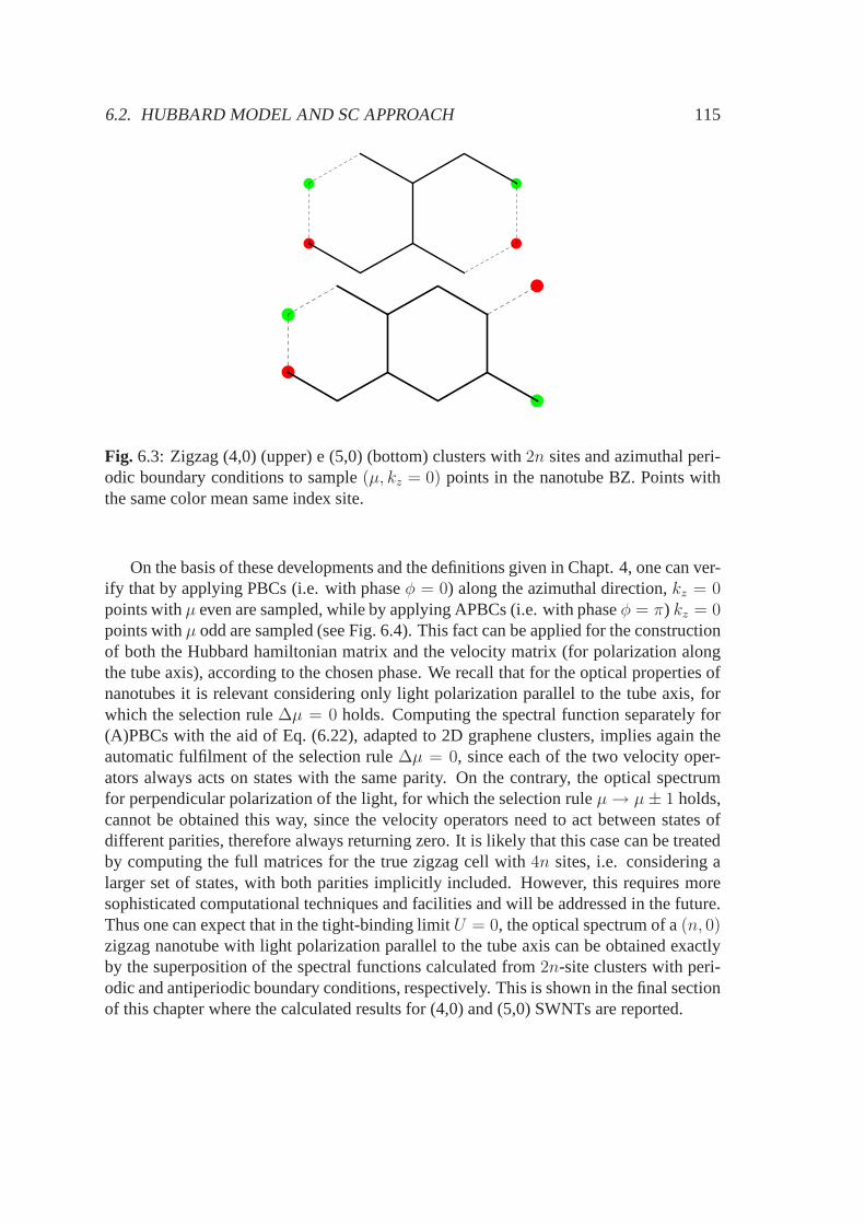
6.2. HUBBARD MODEL AND SC APPROACH 115
Fig. 6.3: Zigzag (4,0) (upper) e (5,0) (bottom) clusters with2n sites and azimuthal peri-odic boundary conditions to sample(µ, kz = 0) points in the nanotube BZ. Points withthe same color mean same index site.
On the basis of these developments and the definitions given in Chapt. 4, one can ver-ify that by applying PBCs (i.e. with phaseφ = 0) along the azimuthal direction,kz = 0points withµ even are sampled, while by applying APBCs (i.e. with phaseφ = π) kz = 0points withµ odd are sampled (see Fig. 6.4). This fact can be applied for the constructionof both the Hubbard hamiltonian matrix and the velocity matrix (for polarization alongthe tube axis), according to the chosen phase. We recall thatfor the optical properties ofnanotubes it is relevant considering only light polarization parallel to the tube axis, forwhich the selection rule∆µ = 0 holds. Computing the spectral function separately for(A)PBCs with the aid of Eq. (6.22), adapted to 2D graphene clusters, implies again theautomatic fulfilment of the selection rule∆µ = 0, since each of the two velocity oper-ators always acts on states with the same parity. On the contrary, the optical spectrumfor perpendicular polarization of the light, for which the selection ruleµ→ µ± 1 holds,cannot be obtained this way, since the velocity operators need to act between states ofdifferent parities, therefore always returning zero. It islikely that this case can be treatedby computing the full matrices for the true zigzag cell with4n sites, i.e. considering alarger set of states, with both parities implicitly included. However, this requires moresophisticated computational techniques and facilities and will be addressed in the future.Thus one can expect that in the tight-binding limitU = 0, the optical spectrum of a(n, 0)zigzag nanotube with light polarization parallel to the tube axis can be obtained exactlyby the superposition of the spectral functions calculated from 2n-site clusters with peri-odic and antiperiodic boundary conditions, respectively.This is shown in the final sectionof this chapter where the calculated results for (4,0) and (5,0) SWNTs are reported.

116 CHAPTER 6. ELECTRONIC CORRELATION EFFECTS
Fig. 6.4: BZ sampling with a2n-site zigzag(n, 0) cluster: by applying azimuthalPBCs,(µ even, kz = 0) points (purple color) are sampled, by applying azimuthal AP-BCs(µ odd, kz = 0) points (blue color) are sampled.
6.3 Computational details
In this section we show the computer algebra implementationof the exact diagonaliza-tion technique for the Hubbard model applied to small clusters with periodic boundarycondition. The algorithm was developed for the computer algebra systemMathematicar
[218] and is taken from Ref. [219]. Another more complete andversatile package basedon similar principles is the SNEG library [220], a Mathematica package developed in theLjubljana University, which provides a framework for performing calculations using theoperators of the second quantization with an emphasis on theanti-commuting fermionicoperators in the context of solid-state and atomic physics.Mathematicar is particularlysuitable for formulating the representation of the operator algebra of Eq. (6.13) accordingto Eqq. (6.19-6.20). As a working example we consider again the Hubbard chain withMsites and periodic boundary conditions. InMathematicathe multiparticle states can bedefined by using the headers, instead of the ket symbol| . . .〉, as in the following:
s [arg], where arg = n1↑, . . . , nM↑ , n1↓, . . . , nM↓ and nlσ ∈ 0, 1 .
6.3. COMPUTATIONAL DETAILS 117
We need the headers because we have to perform the addition and multiplication of thestates by scalars by manipulating the argument ofs. If we were to perform these op-erations on the listarg itself, we would get incorrect results. For example, accordingto Mathematicaconventions for lists, one obtainsnlσ from arg [[sigma, l]] with l = l,sigma = 1 andsigma = 2 respectively, forσ =↑ andσ =↓.After specifying the numbers of sitesM, spin-upN↑ and spin-downN↓ electrons, we canuse the functionsPermutations [. . .] andTable [. . .] to generate the listindex, whichcontains all possible multiparticle states, coded in binary form. This procedure can beimplemented as in the following code lines, for spin-up and spin-down particles.
(* Left (spin up particles) *)left = Permutations[ Table[ If[ j <= spinup, 1, 0], j, 1, sites]];
(* Right (spin down particles) *)right = Permutations[ Table[ If[ j <= spindown, 1, 0], j, 1, sites]];
(* Left and Right (spin up and down particles) *)index = Flatten[ Table[ left[[i]], right[[j]] , i, 1, Length[left], j, 1, Length[right]], 1];
The operatorc†lσ has to generate a 1 in the right location specified byl andsigmain the argument ofs. This is done by the functionplus. Correspondingly, the functionminus generates a 0.
plus[k ,sigma ][arg ]:= ReplacePart[arg, 1,sigma, k]minus[k ,sigma ][arg ]:= ReplacePart[arg, 0,sigma, k]
Using the sign function introduced in Eq. (6.18), we can now define in a functional formthe second quantization operatorsc†lσ andclσ, which are going to act on the states as inEq. (6.19) and Eq. (6.20).
sign[l ,sigma ,arg ] := (-1) ∧ (spinup* (sigma-1)) *(-1)∧(Sum[ arg [[sigma,j]], j, 1, l-1])
cdagger[l , sigma ][factor .* s[arg ]]:= factor*(1 - arg[[sigma,l]])*sign[l, sigma, arg]*s[plus[l, sigma][arg]]
c[l , sigma ][factor .* s[arg ]]:= factor*arg[[sigma,l]]*sign[l, sigma, arg]*s[minus[l,sigma][arg ]]
The parameterfactor . is set by default to the value 1 inMathematica, if the state

118 CHAPTER 6. ELECTRONIC CORRELATION EFFECTS
does not have an additional factor. Since these operators can always generate the value 0(e.g. c†1↑| 1, . . . , . . .〉 = 0), cdagger andc have to be defined for the number 0 aswell:
cdagger[l , sigma ][0]:= 0c[l , sigma ][0]:= 0
Additionally, we still need the operatornlσ:
n[l ,sigma ][0]:= 0n[l ,sigma ][factor .*s[arg ]]:= factor*arg[[sigma,l]]*s[arg]
Periodic boundary conditions for the chain can be expressedas :
cdagger[sites+1,sigma ][any ]:=cdagger[1,sigma ][any ]c[sites+1,sigma ][any ]:=c[1,sigma ][any ]
Eventually, the Hamiltonian (Eq. 6.14) of the Hubbard chaincan simply be written as:
H[vector ]=Expand[-t*Sum[cdagger[l,sigma][c[l+1,sigma][vector]] +cdagger[l+1,sigma][c[l,sigma][vector]],l,1,sites,sigma,1,2] +u*Sum[n[l,1][n[l,2][vector]],l,1,sites]]
More complicated Hamiltonians, such as those considered inthis work for the zigzagclusters with2n sites can be expressed in a similar way, by writing explicitly the siteindex needed for the nearest neighbor hopping terms with thecorrect translational andazimuthal periodic boundary conditions included. In orderto obtain the Hamiltonian ma-trix, we need to compute the scalar products〈ni|H|nj〉 of each state|ni〉 with H|nj〉.Since the multiparticle states are already orthonormal, weonly need to define the linear-ity of the scalar product:
scalarproduct[a , 0]:= 0scalarproduct[a , b + c ]:=scalarproduct[a,b] +scalarproduct[a,c]scalarproduct[s[arg1 ],factor .s[arg2 ]]:=factor*If[arg1==arg2,1,0]
where the comparison of two states, which is expressed by thecomparison of two nested
6.3. COMPUTATIONAL DETAILS 119
lists, is written in a very compact manner by usingarg1==arg2.The desired Hamiltonian matrix〈ni|H|nj〉 can be computed by first defining the follow-ing table:
hlist=Table[H[s[index[[j]]]], j, 1, end];
and then setting up in the sparse matrix as with the help ofSparseArray as in thefollowing lines:
h=SparseArray[i ,j 7→ scalarproduct[s[index[[j]]],hlist[[j]]],end,end]
The upper limit for the loop indices, which also provides thesize of the basis or thenumber of multiparticle states can be determined viaend = Length[index], soonafter the construction of the basis set listindex. The computed matrices are Hermitianand symmetric, thus their eigenvalues are real and only the upper-diagonal part needs tobe computed and stored. One can choose among several file formats suitable for sparsematrix storage on the hard-disk, such as the NIST MatrixMarket format (∗.mtx) [221],which allows to specify the non-zero entries for the matrix elements and its transpositionrules (Hermitian, symmetric, skew-symmetric or general).When the∗.mtx file is im-ported and the diagonalization method (see the commandsEigensystem for obtainingthe eigenvalue-eigenvector pair) is called by the system,Mathematicadetects automati-cally the (hermitian symmetric) structure of the matrix andswitches to the most efficientroutine for the numerical diagonalization. In order to perform the sparse matrix numeri-cal diagonalization within theMathematicasystem [218], one can choose between eitherLAPACK [222] or Arnoldi (also known as ARPACK or Lanczos [223]) algorithms. TheLapack is the default method for accurately computing the entire set of eigenvalues andeigenvectors and works well when the order of the matrix sizeis at maximum between104 and105. In this work it was used for the diagonalization of4900×4900 matrices for aperiodic 8-sites half-filled zigzag (4,0) cluster, since the memory requirements for storingon disk the full eigenvector set (needed by the velocity operator) were not prohibitive atall (500 MBs). The Arnoldi method is an iterative method, usually suitable for sparsematrices, used for finding a few eigenvalues of a large matrix. Since in our case we needto find only the lowest eigenpairs of the Hubbard matrix (their number should usuallybe less than20% of the matrix size) for calculating the low energy optical spectrum, thismethod can be applied to the periodic 10-sites half-filled zigzag (5,0) cluster, whose ma-trix dimensions are63504× 63504. In Mathematicathis task can be accomplished in thefollowing way:1
1Unfortunately, theMathematicadocumentation on this subject is very sparse and not very detailed, sothese lines are intended as a short tutorial on the matter forhelping in reproducing calculations
120 CHAPTER 6. ELECTRONIC CORRELATION EFFECTS
eigenvalues,eigenvectors=-Eigensystem[-hubmatrix,200,Method 7→ Arnoldi, MaxIterations 7→ 10∧5,Criteria 7→ RealPart]
As shown in the code lines above,Mathematicahas the ARPACK library built in andall the options for that library apply, which are passed by the commandMethod. Sincewe know that our matrix is Hermitian and that the eigenvaluesare all real, one can usethe real part as a criterion for computing the smallest eigenvalue. Moreover, with theabove instructions, one can see that the (200) largest eigenvalues of-hubmatrix (byreal part) correspond to the (200) smallest eigenvalues ofhubmatrix. This allows toavoid Mathematicadefault setting, which always computes the smallest eigenvalues inabsolute value, consequently with a large waste of computational resources.To summarize, in this section we have shown how to implement the exact diagonalizationmethod for the Hubbard model on ordinary personal computersfor periodic clusters with8 and 10 sites with the aid ofMathematica, a system which is suitable mainly for com-puter algebra but also for numerical computing. The most intensive and time-consumingpart of the computational procedure is represented by the construction of the Hubbardand velocity matrices: for a 10 sites periodic cluster it took five days to write the upper-diagonal part of the63504 × 63504 matrix on an ordinary personal computer. This ispartly due to the fact thatMathematicais based on an interpreted language, which is100-200 slower than compiled languages like Fortran or C++.However, the main advan-tages of choosing an interpreted system likeMathematicafor treating small clusters arerepresented by a gain in user productivity, i.e. a large amount of time spared in codingthe algorithms and a minimized risk of programming errors, if compared with low-levellanguages usually adopted in scientific computation (Fortran and C/C++). Clearly, in or-der to cope with systems with larger size we have to depart from interpreted languagesand look for other implementation techniques. Expression templates for quantum me-chanical operators have already been implemented in specialized C++ libraries to alloweven non-expert users to define and use easily Hamiltonians and other operators in sec-ond quantization formalism, so that matrix elements can be computed more efficientlywith less programming effort by the user [224]. Additionally, one has to face the prob-lem of storing on disk huge matrices, from which the diagonalization routines read theneeded elements. Sometimes, even if the matrix can be storedon computers with fastand capable hard disks, the difficulty is that the I/O speed isstill too slow compared tothe computational speed. To avoid these problems with the storage, the matrix elementshave to be calculated efficientlyon the flyat each Lanczos iteration. These algorithms arealso suitable for parallelization techniques and have already been implemented efficientlyfor exact diagonalization on strongly correlated quantum systems with up to 36 sites (seePALM++). Recently, the international open-source project ALPS (Algorithms and Li-braries for Physics Simulations, http://alps.comp-phys.org [225, 226]) was establishedwith the purpose of developing and merging also several existing different algorithms(such as PALM++) and libraries for simulating the properties of strongly correlated
6.4. RESULTS 121
systems within a wide range of theoretical approaches, exact diagonalization included.Certainly, the ALPS libraries will be a very interesting anduseful tool for applying theideas presented in this thesis to larger zigzag clusters (e.g. a (7,0) cluster with 14 sites)and it is likely that exact diagonalization calculations could be carried out on full zigzagunit cells with parallel and/or supercomputing facilities.
6.4 Results
In this section we present the results of the application of the Hubbard model combinedwith the small crystal approach for the investigation of theoptical spectra of zigzagSWNTs, according to the choices for the clusters formulatedin the previous sections:a (4,0) zigzag cluster with 8 sites and a (5,0) cluster with 10sites, with translational pe-riodic boundary conditions and (anti)periodic azimuthal boundary conditions to samplenanotube BZ points atkz = 0 andµ even (odd), respectively.SC calculations were all performed based on the simplest formulation of the Hubbardmodel hamiltonian of Eq. (6.7), that is, with only first nearest-neighbor hopping interac-tionst and on-site Coulomb repulsionU.In order to test the correctness of the developed computer programs, we first performedexact diagonalization (ED) calculations for both clustersin the noninteracting limitU = 0and compare the resulting transition energies in the optical spectra (for light polariza-tion parallel to the tube axis) to those obtained according to the classical tight-binding(LCAO) formulation, by either the zone-folding (Chapt. 3) or the real space SC approach(Chapt. 4). In Fig. 6.5 we report the (4,0) and (5,0) optical spectra computed with theSOS method (Eq. (6.22)) after ED of the Hubbard matrices obtained by switching alter-natively between periodic and antiperiodic boundary conditions to sample even or oddazimuthal band quantum numbers. Additionally, the full absorption spectra calculatedas explained in Chapt. 4 (LCAO scheme) are shown for comparison. One can see thatthe absorption profiles of the full LCAO calculation are completely recovered by the EDspectra with APBCs and PBCs considered together. In Table 6.1, we compare the numer-ical values of the interband transition energies for both zigzag systems calculated fromED withU = 0 and classical TB method (ZF or SC) with the same value of hopping pa-rametertπ = 2.9 eV and verify the perfect matching of the energy values for the differentµ, kz = 0 BZ points involved in the interband transitions.Having tested the validity of our ED method in the non-interacting limit, we can include
the electronic correlations by settingU 6= 0 for the on-site screened Coulomb repul-sion term in the Hubbard Hamiltonian. In Fig. 6.6 the opticalspectra for both clustergeometries are reported, where the Hubbard parameters obtained in the work by Cinietal [212] have been used. These parameters were deduced from fitting calculations onthe experimental Auger spectra of graphite and carbon nanotubes. For carbon nanotubesthe obtained parameter values aretπ = 2.6 eV andU = 4.6 eV. It has to be stressed
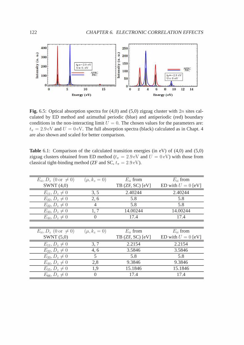
122 CHAPTER 6. ELECTRONIC CORRELATION EFFECTS
Fig. 6.5: Optical absorption spectra for (4,0) and (5,0) zigzag cluster with2n sites cal-culated by ED method and azimuthal periodic (blue) and antiperiodic (red) boundaryconditions in the non-interacting limitU = 0. The chosen values for the parameters are:tπ = 2.9 eV andU = 0 eV. The full absorption spectra (black) calculated as in Chapt. 4are also shown and scaled for better comparison.
Table 6.1: Comparison of the calculated transition energies (in eV) of (4,0) and (5,0)zigzag clusters obtained from ED method (tπ = 2.9 eV andU = 0 eV) with those fromclassical tight-binding method (ZF and SC,tπ = 2.9 eV).
Eii, Dz (0 or 6= 0) (µ, kz = 0) Eii from Eii fromSWNT (4,0) TB (ZF, SC) [eV] ED withU = 0 [eV]
E11, Dz 6= 0 3, 5 2.40244 2.40244E22, Dz 6= 0 2, 6 5.8 5.8E22, Dz 6= 0 4 5.8 5.8E33, Dz 6= 0 1, 7 14.00244 14.00244E44, Dz 6= 0 0 17.4 17.4
Eii, Dz (0 or 6= 0) (µ, kz = 0) Eii from Eii fromSWNT (5,0) TB (ZF, SC) [eV] ED withU = 0 [eV]
E11, Dz 6= 0 3, 7 2.2154 2.2154E22, Dz 6= 0 4, 6 3.5846 3.5846E33, Dz 6= 0 5 5.8 5.8E44, Dz 6= 0 2,8 9.3846 9.3846E55, Dz 6= 0 1,9 15.1846 15.1846E66, Dz 6= 0 0 17.4 17.4

6.4. RESULTS 123
out that Cini has verified a very small dependence of the correlation parameterU onnanotube diameter: no substantial changes were found in thetheoretical Auger spectraof (10,10) and (20,20) SWNTs, and by comparing the experimental Auger spectra ofSWNTs with average diameter of2 nm with the theoretical ones for tubes with averagediameter of1.3 nm. We note that the value for the screened Coulomb interactionstrengthis well above the perturbative ones used in the effective-mass approximation calculationsby Ando (0.1 − 0.2 eV) [211]. Moreover, the values of the bare (unscreened) CoulombinteractionU used by Cini (U b
ππππ = 14.6 eV) [213] have magnitude comparable to thoseused by Sørensen [214] for the Hubbard ED studies onC20 isomers, in particular car-bon rings (tπ = 2.36 eV, U = 10.1 eV) and nanobowls (tπ = 3.16 eV, U = 10.3 eV),which have degree of curvature similar to nanotube walls. From our calculated opticalspectra of Fig. 6.6, we can see that the inclusion of the on-site electron-electron Coulombinteractions produces an evident blueshift of all the optical transition peaks with respectto those obtained in the tight-binding limit. This is consistent with both experimental[195, 196] and theoretical findings [194]. One can also notice that the blueshift affectsmore considerably theE11 transition energy rather than theE22 transition energy: thisfact is particularly evident in the spectral profile of (4,0)cluster.
Intensity (arb. un.)
0
50
100
150
200
250
Energy (eV)0 2 4 6 8 10 12 14
(4,0) zigzag cluster
Hubbard parameters taken
from M. Cini et al. (2008)
t=2.6 eV U=0 eV
t=2.6 eV U=4.6 eV
Intensity (arb. un.)
0
50
100
150
200
250
Energy (eV)0 1 2 3 4 5 6 7 8 9 10
(5,0) zigzag cluster
Hubbard parameters taken
from M. Cini et al. (2008)
t=2.6 eV U=0 eV
t=2.6 eV U=4.6 eV
Fig. 6.6: Optical absorption spectra for cluster (4,0) (left) and (5,0) (right) from EDwith (anti)periodic BCs in the non-interacting limitU = 0 (black) and for the valueU = 4.6 eV for the Hubbard correlation parameter obtained by M. Ciniet al.(red) [212].
In order to study the dependence of the allowedES11 andES
22 on the electron correlationstrengthU/t, we performed several ED calculations for differentU values of the on-siteCoulomb interaction, whose results are presented in Fig. 6.7. In the case of (4,0) geom-etry, one can actually see that in intermediate-low coupling regime (U/t < 2) theE11
transition energies increase faster thanE22s, which have almost a constant trend. On theother hand, for cluster (5,0) in the same coupling regime, the slopes of bothE11 andE22
curves are similar. This can be explained by considering theinverse proportionality re-lation between energy gap and diameter in SWNTs, as discussed in TB approximation:(5,0) cluster describes a SWNT having a larger diameter than(4,0), hence more values

124 CHAPTER 6. ELECTRONIC CORRELATION EFFECTSTransition energy (eV)
0
2
4
6
8
10
12
14
16
18
U/t (eV)0 1 2 3 4 5 6 7 8 9
(4,0) cluster
APBC
PBC
nearest neighbor
hopping parameter
tπ=2.9 eV
Transition energy (eV)
0
5
10
15
U/t (eV)0 2 4 6 8 10
(5,0) cluster
APBC
PBC
nearest neighbor
hopping parameter
tπ=2.6 eV
Fig. 6.7: Dependence on the correlation strengthU/t of ES11 andES
22 transition energiesfor (4,0) (left) and (5,0) (right) zigzag2n-site clusters obtained from ED method withazimuthal APBCs (red) and PBCs (black).
for the azimuthal quantum number are allowed and the absolute energy difference be-tween bands with different indexµ are lower than in small diameter tubes. However, ifwe consider a wider range in coupling strength (U/t < 5), the same general behaviourof cluster (4,0) is found also for (5,0) geometry, i.e. theES
22 trend increases at a slowerrate thanES
11. In this regime one can verify that the ratioES22/E
S11 is actually lower than
2, therefore it’s consistent with the previously summarized experimental and theoreticalfindings about theratio problemin correlated SWNTs, although these actually refer tolarge diameter nanotubes.In general, in the low-coupling regime the use of APBCs provides always lower valuesof the transition energies than PBCs do. This fact can be understood by consideringthat in the TB limit, the use of azimuthal APBCs allows to sample Brillouin points with(µ odd, kz = 0) and that the azimuthal quantum number of the energy gap bands(ES
11) isactually always odd in semiconducting zigzag tubes (see Ref. [117]).Looking at the plots of Fig. 6.7, one can also observe that an inversion occurs atU/t ≃ 4for the transition energies of both geometries: the transition energies obtained from EDwith APBC, which were formerly labelled byES
11, become larger in magnitude than theformerES
22 obtained from ED with PBCs. Thus, in strong coupling regime the rolesplayed by APBCs and PBCs forES
11 andES22 are exchanged.
In order to compare the structure of the lowest excited energy levels obtained from theSC-ED method developed in this thesis with the excitonic levels obtained by Mazumdar[210, 206], it’s interesting to look at the energy scale plotof the calculated eigenvaluesin the very low coupling regimeU/t < 0.4 (with APBCs) for cluster (4,0), which isshown in Fig. 6.8. We set the ground state energy to zero on theplot ordinata, so all thereported energy data are relative to the ground state energy. The ground state is alwaysnon-degenerate for all values of the correlation coupling strength. In the noninteractinglimit U = 0, the excited levels are grouped on the energy scale and multiply degener-

6.4. RESULTS 125
Fig. 6.8: Excited energy levels as a function of the correlation couplingU/t in the limit ofvery low coupling strength for cluster (4,0) and APBCs. Several manifolds are obtainedwhose bandwidth increase with coupling strength. The highest excited level of the low-est manifold starting from the ground state is always brightfor one photon absorption,therefore providing the optical transition energyES
11.
Fig. 6.9: Schematic structure of the lowest excited manifold in semiconducting zigzagnanotubes in very low coupling limit (U/t = 0.04) obtained in this work (left) and inMazumdar’s work (right)[208]: the manifold obtained from our ED comprises eight ex-cited states. With increasingU/t the level spacings change and degeneracies of levelsformerly at nearly the same energy are eventually lifted to give eight distinct states.

126 CHAPTER 6. ELECTRONIC CORRELATION EFFECTS
ate, in particular the lowest excited energy level includeseight degenerate states, whichare all optically active (bright) for one photon absorption. This fact can be verified alsofor (5,0) cluster and can be explained as it follows. The gap states of semiconductingzigzag nanotubes are always doubly-degenerate. Thus interband single-excitation elec-tronic transitions are allowed between each of the two valence band states and each of thetwo conduction band states. Since each band can be filled withat most two electrons withopposite spin, by taking into account spin degeneracy, we have (2× 2)× 2 = 4× 2 = 8states, as found in our calculations. This degeneracy is actually lifted off by switching onthe Coulomb interaction withU > 0.In general, one can observe for eachU/t > 0 the appearence of several distinct en-ergy level manifolds, whose energy bandwidth becomes larger with increasing couplingstrength (Fig. 6.8). ForU/t > 1 the higher energy manifolds are mixed with the lowerenergy ones and cannot be distinguished anylonger. Interestingly, one can verify that foreach value of the correlation coupling strengthU/t in the very low regimeU/t ≪ 1 thehighest energy level belonging to the lowest excited energymanifold is always bright andnon-degenerate. The same result could be verified for cluster (5,0) andU/t = 0.4. Thisresult actually gives a similar picture of the lowest excitonic manifold given by Zhao andMazumdar in Ref. [208] and reported in Fig. 6.9, together with a schematic representa-tion of the energy level structure obtained in this work.In order to get a deeper understanding of the correlated structure of these eigenstates,a charge distribution analysis over the cluster sites was performed for the ground state,the bright state and the dark states belonging to the manifold. We considered whichoccupation number basis states are related to the largest (in absolute value) eigenstatecoefficients. Although this method could seem rather rough,it actually provides an es-sentially correct picture, which is also confirmed by a more formal method involving thecalculation of the charge density correlation function fora given eigenstate, as we willsee in the following. In general, we observed that the groundstate and the remaining darkstates in this manifold have uniform charge distribution for anyU/t in low-intermediatecoupling regime. On the other hand, the optically active state has a strongly non-uniformcharge distribution over the cluster sites: the occupationnumber states giving the domi-nating contribution are actually represented by doubly-occupied sites regularly alternatedwith empty sites, as sketched schematically in Fig. 6.10 forcluster (4,0). This is actuallythe pattern of a charge-density wave (CDW).As stated above, the peculiarity of this bright state is reflected in particular in the valuesof the charge-density correlation function and in the double-empty site correlation func-tion calculated for a given eigenstate. The general expression for a correlation functionis [217]
〈O〉 =〈ψi|O|ψi〉〈ψi|ψi〉
(6.24)

6.4. RESULTS 127
Empty siteHholeL
Double occupancyL HUL
Fig. 6.10: Schematic representation of the charge distributionfor the optically active stategiving theES
11 transition: doubly occupied sites alternate regularly with empty sites.
whereψi is any eigenstate wavefunction andO is a generic quantum mechanical oper-ator. For charge density wave correlation functions between sites of separationj, O isexpressed by
ˆOCDW =1
L
∑
i
(ni,↑ + ni,↓) (ni+j,↑ + ni+j,↓) , (6.25)
whereL is the number of sites in the system. Similarly, we can define other useful cor-relation functions, such as the doubly occupied correlation function 2, the empty sitecorrelation function3, the spinSz correlation function4 and the above mentioned double-empty correlation function, which is expressed by
Oed =1
L
∑
i
(1− ni,↑) (1− ni,↓)ni+j,↑ni+j,↓. (6.26)
In Fig. 6.11 we report the values for the charge and the empty-double correlation func-tions calculated forj = 1 (i.e. considering only nearest neighbor sites) for each eigenstateof the lowest excited manifold of cluster (4,0) obtained from ED with APBCs. For theHubbard parameters we used those computed by Ciniet al., hence we are in an interme-diate coupling regime. However, we verified that the situation is similar also for othervalues ofU/t in low-intermediate coupling (not shown). The light bulb symbol is used tohighlight the bright state. One can see a strong deviation ofthe value related to the opti-cally active state from the average of the other dark states for both correlation functions.The energy spacings between the bright state in this manifold and the immediately twounderlying dark states have been also considered for both clusters with PBCs and APBCsand compared with some recently available experimental measurements by photolumi-nescence microscopy reported in Ref. [206]. The measured values found in this exper-imental paper are reported in Fig. 6.12, together with the results from our ED: the two
2Od = 1
L
∑i ni,↑ni,↓ni+j,↑ni+j,↓
3Oe = 1
L
∑i (1− ni,↑) (1− ni,↓) (1− ni+j,↑) (1− ni+j,↓)
4 ˆOSDW = 1
L
∑i (ni,↑ − ni,↓) (ni+j,↑ − ni+j,↓)
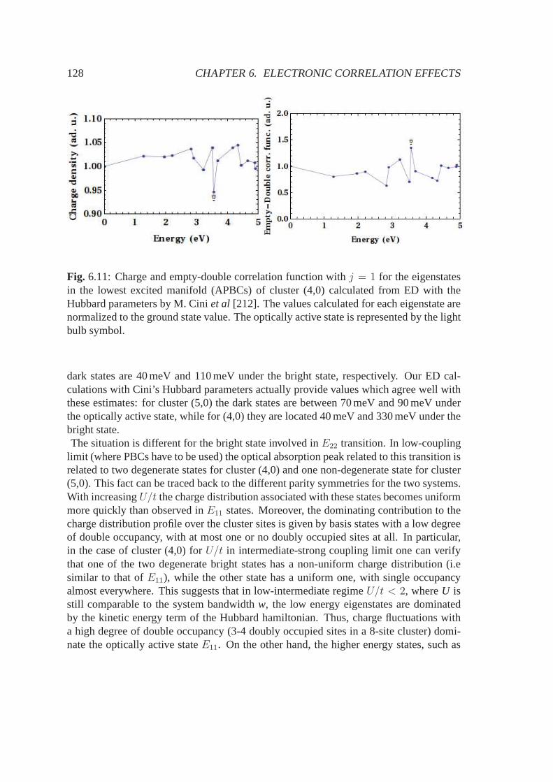
128 CHAPTER 6. ELECTRONIC CORRELATION EFFECTS
Fig. 6.11: Charge and empty-double correlation function withj = 1 for the eigenstatesin the lowest excited manifold (APBCs) of cluster (4,0) calculated from ED with theHubbard parameters by M. Ciniet al [212]. The values calculated for each eigenstate arenormalized to the ground state value. The optically active state is represented by the lightbulb symbol.
dark states are 40 meV and 110 meV under the bright state, respectively. Our ED cal-culations with Cini’s Hubbard parameters actually providevalues which agree well withthese estimates: for cluster (5,0) the dark states are between 70 meV and 90 meV underthe optically active state, while for (4,0) they are located40 meV and 330 meV under thebright state.The situation is different for the bright state involved inE22 transition. In low-coupling
limit (where PBCs have to be used) the optical absorption peak related to this transition isrelated to two degenerate states for cluster (4,0) and one non-degenerate state for cluster(5,0). This fact can be traced back to the different parity symmetries for the two systems.With increasingU/t the charge distribution associated with these states becomes uniformmore quickly than observed inE11 states. Moreover, the dominating contribution to thecharge distribution profile over the cluster sites is given by basis states with a low degreeof double occupancy, with at most one or no doubly occupied sites at all. In particular,in the case of cluster (4,0) forU/t in intermediate-strong coupling limit one can verifythat one of the two degenerate bright states has a non-uniform charge distribution (i.esimilar to that ofE11), while the other state has a uniform one, with single occupancyalmost everywhere. This suggests that in low-intermediateregimeU/t < 2, whereU isstill comparable to the system bandwidthw, the low energy eigenstates are dominatedby the kinetic energy term of the Hubbard hamiltonian. Thus,charge fluctuations witha high degree of double occupancy (3-4 doubly occupied sitesin a 8-site cluster) domi-nate the optically active stateE11. On the other hand, the higher energy states, such as
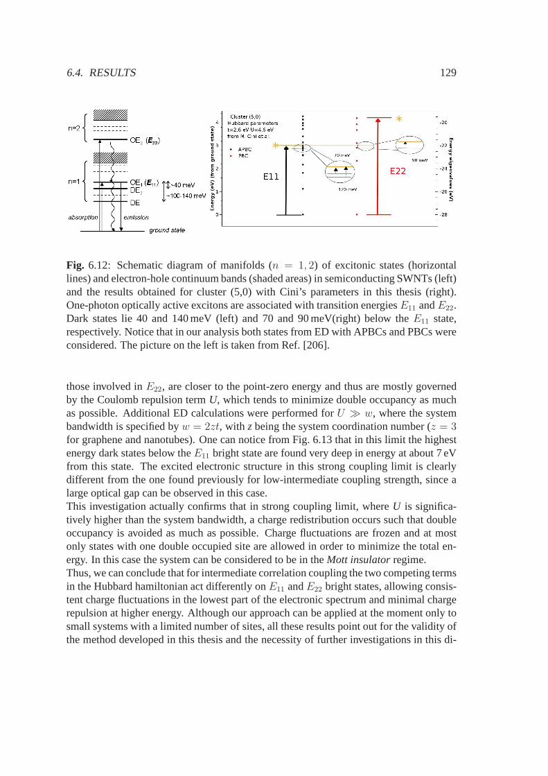
6.4. RESULTS 129
Fig. 6.12: Schematic diagram of manifolds (n = 1, 2) of excitonic states (horizontallines) and electron-hole continuum bands (shaded areas) insemiconducting SWNTs (left)and the results obtained for cluster (5,0) with Cini’s parameters in this thesis (right).One-photon optically active excitons are associated with transition energiesE11 andE22.Dark states lie 40 and 140 meV (left) and 70 and 90 meV(right) below theE11 state,respectively. Notice that in our analysis both states from ED with APBCs and PBCs wereconsidered. The picture on the left is taken from Ref. [206].
those involved inE22, are closer to the point-zero energy and thus are mostly governedby the Coulomb repulsion termU, which tends to minimize double occupancy as muchas possible. Additional ED calculations were performed forU ≫ w, where the systembandwidth is specified byw = 2zt, with z being the system coordination number (z = 3for graphene and nanotubes). One can notice from Fig. 6.13 that in this limit the highestenergy dark states below theE11 bright state are found very deep in energy at about 7 eVfrom this state. The excited electronic structure in this strong coupling limit is clearlydifferent from the one found previously for low-intermediate coupling strength, since alarge optical gap can be observed in this case.This investigation actually confirms that in strong coupling limit, whereU is significa-tively higher than the system bandwidth, a charge redistribution occurs such that doubleoccupancy is avoided as much as possible. Charge fluctuations are frozen and at mostonly states with one double occupied site are allowed in order to minimize the total en-ergy. In this case the system can be considered to be in theMott insulatorregime.Thus, we can conclude that for intermediate correlation coupling the two competing termsin the Hubbard hamiltonian act differently onE11 andE22 bright states, allowing consis-tent charge fluctuations in the lowest part of the electronicspectrum and minimal chargerepulsion at higher energy. Although our approach can be applied at the moment only tosmall systems with a limited number of sites, all these results point out for the validity ofthe method developed in this thesis and the necessity of further investigations in this di-
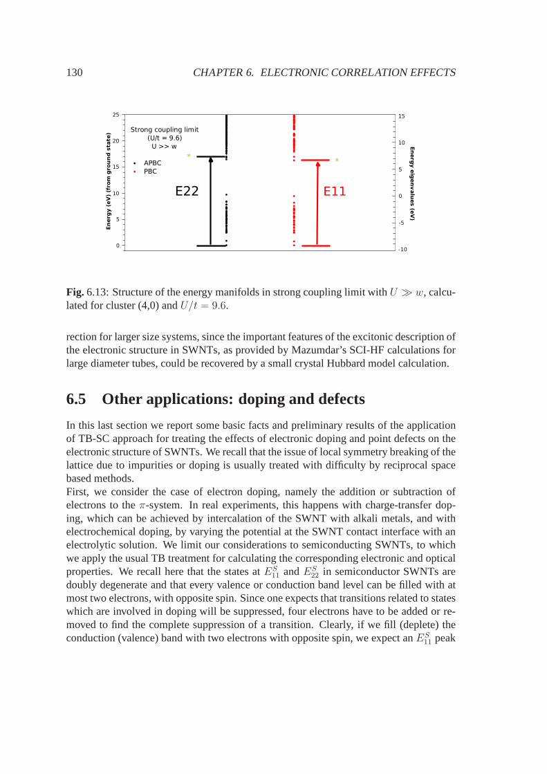
130 CHAPTER 6. ELECTRONIC CORRELATION EFFECTS
Energy (eV) (from ground state)
0
5
10
15
20
25
Energy eigenvalues (e
V)
-10
-5
0
5
10
15
Strong coupling limit
(U/t = 9.6)
U >> w
APBC
PBC
**
E11E22
Fig. 6.13: Structure of the energy manifolds in strong coupling limit with U ≫ w, calcu-lated for cluster (4,0) andU/t = 9.6.
rection for larger size systems, since the important features of the excitonic description ofthe electronic structure in SWNTs, as provided by Mazumdar’s SCI-HF calculations forlarge diameter tubes, could be recovered by a small crystal Hubbard model calculation.
6.5 Other applications: doping and defects
In this last section we report some basic facts and preliminary results of the applicationof TB-SC approach for treating the effects of electronic doping and point defects on theelectronic structure of SWNTs. We recall that the issue of local symmetry breaking of thelattice due to impurities or doping is usually treated with difficulty by reciprocal spacebased methods.First, we consider the case of electron doping, namely the addition or subtraction ofelectrons to theπ-system. In real experiments, this happens with charge-transfer dop-ing, which can be achieved by intercalation of the SWNT with alkali metals, and withelectrochemical doping, by varying the potential at the SWNT contact interface with anelectrolytic solution. We limit our considerations to semiconducting SWNTs, to whichwe apply the usual TB treatment for calculating the corresponding electronic and opticalproperties. We recall here that the states atES
11 andES22 in semiconductor SWNTs are
doubly degenerate and that every valence or conduction bandlevel can be filled with atmost two electrons, with opposite spin. Since one expects that transitions related to stateswhich are involved in doping will be suppressed, four electrons have to be added or re-moved to find the complete suppression of a transition. Clearly, if we fill (deplete) theconduction (valence) band with two electrons with oppositespin, we expect anES
11 peak
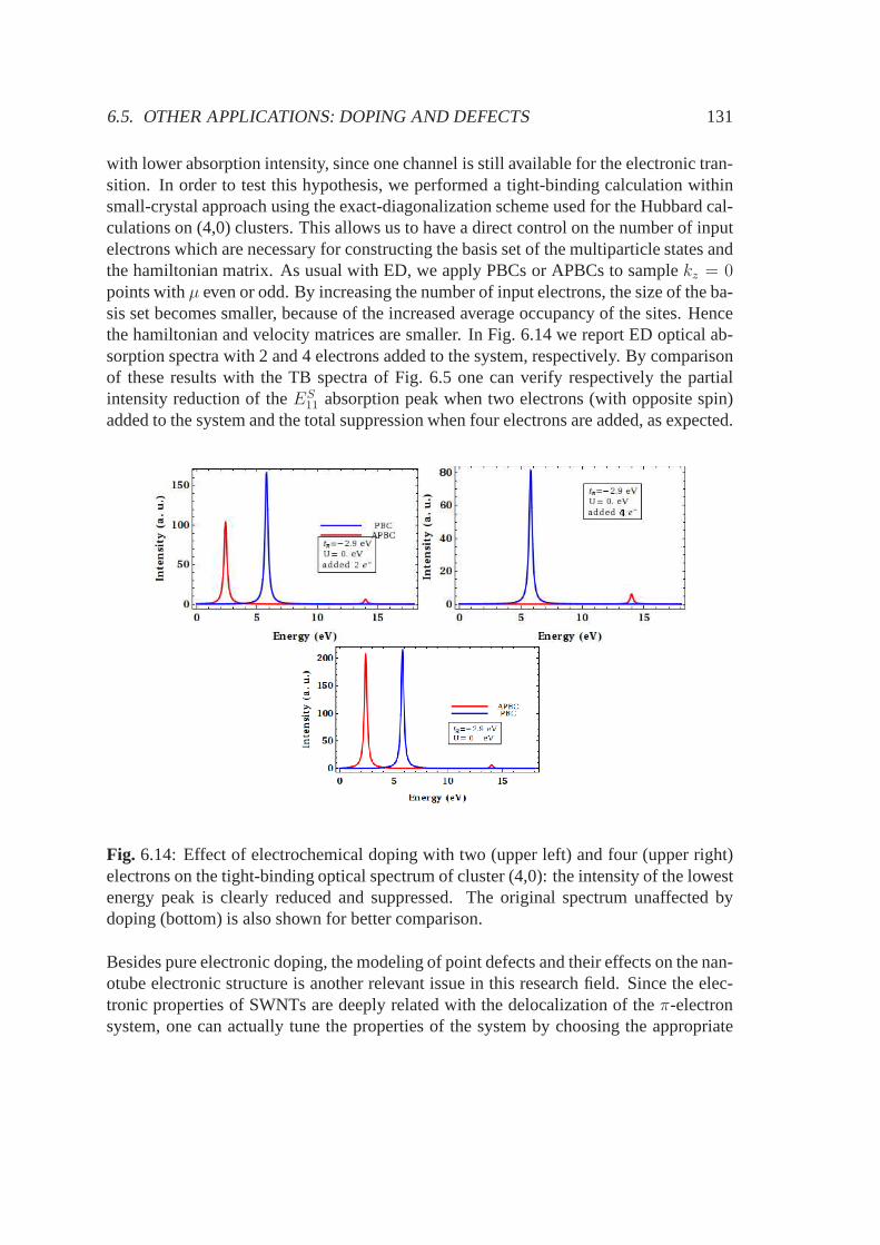
6.5. OTHER APPLICATIONS: DOPING AND DEFECTS 131
with lower absorption intensity, since one channel is stillavailable for the electronic tran-sition. In order to test this hypothesis, we performed a tight-binding calculation withinsmall-crystal approach using the exact-diagonalization scheme used for the Hubbard cal-culations on (4,0) clusters. This allows us to have a direct control on the number of inputelectrons which are necessary for constructing the basis set of the multiparticle states andthe hamiltonian matrix. As usual with ED, we apply PBCs or APBCs to samplekz = 0points withµ even or odd. By increasing the number of input electrons, thesize of the ba-sis set becomes smaller, because of the increased average occupancy of the sites. Hencethe hamiltonian and velocity matrices are smaller. In Fig. 6.14 we report ED optical ab-sorption spectra with 2 and 4 electrons added to the system, respectively. By comparisonof these results with the TB spectra of Fig. 6.5 one can verifyrespectively the partialintensity reduction of theES
11 absorption peak when two electrons (with opposite spin)added to the system and the total suppression when four electrons are added, as expected.
Fig. 6.14: Effect of electrochemical doping with two (upper left) and four (upper right)electrons on the tight-binding optical spectrum of cluster(4,0): the intensity of the lowestenergy peak is clearly reduced and suppressed. The originalspectrum unaffected bydoping (bottom) is also shown for better comparison.
Besides pure electronic doping, the modeling of point defects and their effects on the nan-otube electronic structure is another relevant issue in this research field. Since the elec-tronic properties of SWNTs are deeply related with the delocalization of theπ-electronsystem, one can actually tune the properties of the system bychoosing the appropriate

132 CHAPTER 6. ELECTRONIC CORRELATION EFFECTS
type of modification affecting theπ system delocalization. Several characterizations ofnanotube point-defects have been performed experimentally and theoretical calculationshave confirmed that vacancies, topological defects such as heptagon-pentagon pairs, sub-stitutional impurities like B or N and lattice deformationsdue tosp3 hybridized carbonatoms saturated with hydrogen or oxygen can substantially modify the electronic densityof states of the system. For example, nitrogen-doped SWNTs are particularly interestingin nanotube chemistry, as they can be synthesized in large amount and because less dras-tic reaction conditions can be adopted for the sidewall functionalization [228]. Moreoversince their first discovery they have been the subject of several theoretical investigationconcerning nanotube transport properties both byab initioand tight-binding methods (see[229] and references therein).In TBA, a point defect can be modeled by assigning to a particular site a value of the on-site energyεdef which differs significatively from the values of other sites, which are setby default to the same value (e.g. for SWNTsεC = 0 eV) [227]. In this work we appliedthe periodic SC approach both to N- and B-substituted zigzagclusters. When replacing aC atom, B or N not only act as hole or electron dopants, respectively, but also introducelattice distortions due to deviations of their atomic radius and atomic number from thoseof the C atom. This fact has to be carefully considered when choosing the appropriateTB parametrization for the defect site. The effect of a different on-site energy has beenstudied in the past [229], but only recently the effect of a different hopping has been takeninto account [230]. However, we considered in ourπ-TB calculations only the change inon-site energyεdef related to the N (B) impurity. Assuming C on-site energy to bezero,the local energy of a N occupied site should be modeled as negative, because of the largeratomic number of N if compared with C. On the contrary, for a B-substitution, the on-siteenergy is positive. The following values have been used for the TB parametrization ofthe substitutional impurity:επ−π
N/B = ∓0.525|tπ−πC | [230], that isεπ−π
N/B = ∓1.5225 eV for|tπ−π
C | = 2.9 eV. The SC approach can be applied either via the classical LCAOscheme,as explained in Chapt.4, or the more computationally expensive ED method, describedin the previous sections of this chapter. Experimentally a normal atomic impurity con-centration is estimated to be about1%, very high concentrations are above10%. Forinstance, in (5,0) SWNT with one unit cell cluster with one N (B) atom every 20 sites,we get an impurity concentration of5%, a quite strong doping condition. The electronicband structures in Fig. 6.15 show clearly a weak overall lifting of the band degeneraciesdue to the symmetry breaking of the lattice. These plots showthat even for this stronglydoped system the electronic properties are dominated againby kz = 0 states. Usually,one of the main effects of the substitution of a C atom by atomic species with a differentnumber of valence electrons is the introduction in the DOS ofadditional states. This canbe clearly seen for the nitrogen substitution in the DOS histogram superimposed on theplot for the perfect tube: the nitrogen state is located approximately 150 to200 meV be-low the first van Hove singularity in the conduction band of the undoped tube. Thus Nacts as a donor impurity and if ionization occurs such semiconducting tubes are defined

6.6. CONCLUSIONS, SUMMARY AND FUTURE PERSPECTIVES 133
asn-type. For the B substitution, the situation is symmetrical, as the acceptor level is lo-cated one hundred meV above the first vHS in the valence band and if the empty B statesare occupied holes are created at the edge of the valence bandand the semiconductingtube isp-type (Fig. 6.16). This suggests that the SC optical spectrafor the chosen clusterare virtually the same for both heteroatoms. The exact position of the nitrogen or boronstates depends in general on the diameter, helicity and number of heteroatoms incorpo-rated in the SWNT. The optical spectra for this system can be obtained by applying theSOS method within one of the two methods described previously (LCAO or ED scheme).The optical absorption spectrum reported for cluster (4,0)with a B impurity is reported inFig. 6.17, where one can recognize the appearance of additional transition peaks aroundthe transition energy peak of the perfect tube. Because of the use of periodic boundaryconditions and the use of cluster of different size, the SC approach allow us to calculatethe electronic density of states by properly tuning the defect concentration. In Fig. 6.18the linear dependence on the impurity concentration of the energy position of the donor(acceptor) state with respect to the conduction (valence) is plotted for a (5,0) superclusterwith a number of unit cells between 1 and 10. The intercept gives the conduction (va-lence) band energy for the tube without impurity. Although SC-TB calculations providean oversimplified picture of the effects of defects on the electronic structure of SWNTs,they can be useful for a basic interpretation of electrochemical spectra of substitution-ally doped or functionalized nanotubes. Clearly,ab initio calculations provide a moreaccurate and realistic treatment of electronic charge density distribution and structuraldeformation around the defected sites and are necessary fora more specific parametriza-tion of the on-site energies for heteroatoms of different chemical species. Moreover, theinclusion of electronic correlation effects according to the Hubbard model, will allow tointerpret the effects of the breaking of the lattice periodicity in the framework of the ex-citonic picture for SWNTs. This will be however the subject of future investigations withmore refined theoretical and computational tools.
6.6 Conclusions, summary and future perspectives
In this chapter we presented the main experimental facts which point out for the presenceof relevant excitonic correlation effects in the optical spectral features of single-wallednanotubes. First the basic features, results and limitations of the currently available the-oretical methods for treating excitonic effects in these systems have been reviewed anddiscussed. Where possible, attention was also paid to the different parametrizations ofthe Coulomb correlation strength adopted in these methods,as this is a key parameterfor the comparison between experimental data and the considered calculations. In orderto overcome the limitations inherent to the currently available theoretical methods, weconsidered the Hubbard model, one of the simplest and yet most powerful methods fortreating full many-body hamiltonians beyond mean field approximation. In the central

134 CHAPTER 6. ELECTRONIC CORRELATION EFFECTS
Fig. 6.15: Introduction of a point defect in zigzag cluster (5,0)with one unit cell(left: substitutional B atom withεB = 1.52 eV,right: substitutional N atom withεN = −1.52 eV) and its effects on the TB electronic band structure. The overall lift-ing of the doubly-degenerate effects can be observed.
Fig. 6.16: Introduction of a point defect in zigzag cluster (5,0)with one unit cell(left: substitutional B atom withεB = 1.52 eV; right: substitutional N atom withεN = −1.52 eV) and its effects on the TB electronic density of states (bluehistogram)compared to the DOS of the ideal tube (orange histogram).
part of this chapter we have showed how to apply the small crystal approach to zigzagclusters with a small number of sites (8 and 10 sites for (4,0)and (5,0) SWNTs) for theexact diagonalization of the Hubbard hamiltonian and the computation of the one-photonoptical spectra for the relevant(µ, kz = 0) points. Although our small crystal Hubbardmodel was applied to such small test systems, for which non-negligible curvature effectswere not taken into account, we could verify that the outcoming description of the ex-cited electronic energy levels is consistent with the SCI-HF results obtained by Mazum-dar for large diameter tubes. In particular, we were able to verify two main effects of theintroduction of the Coulomb correlations: the expected blueshift of the single-particle
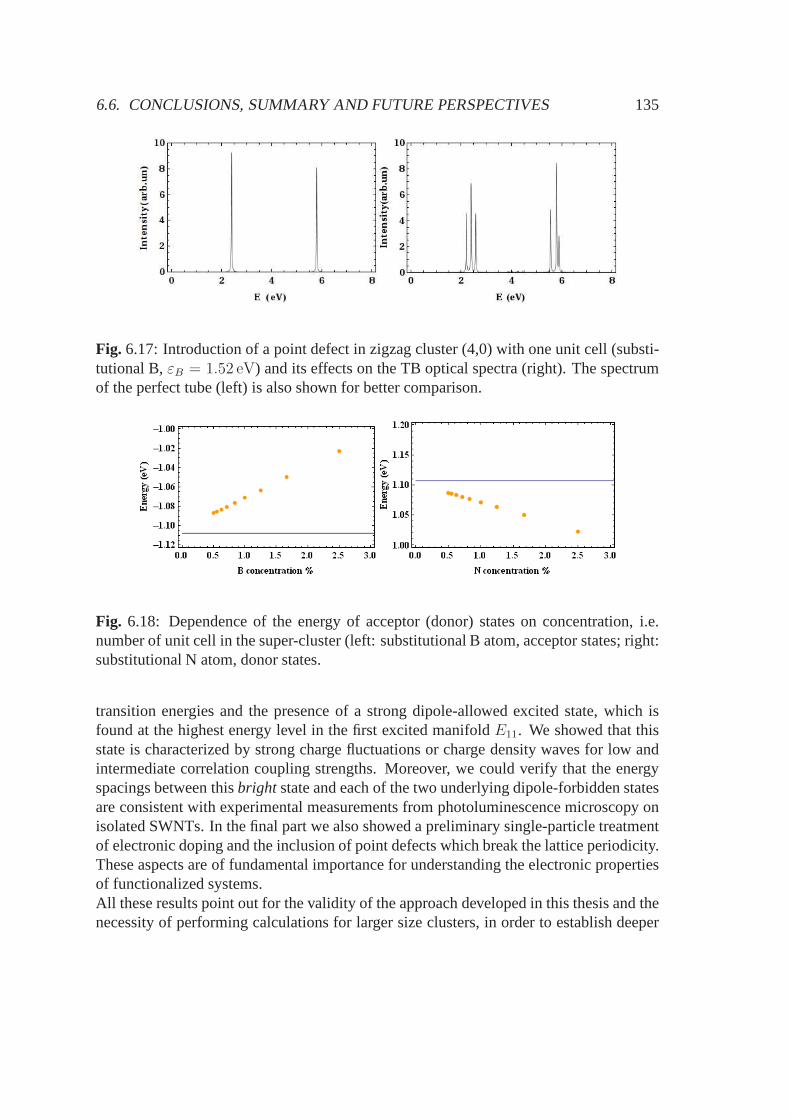
6.6. CONCLUSIONS, SUMMARY AND FUTURE PERSPECTIVES 135
Fig. 6.17: Introduction of a point defect in zigzag cluster (4,0)with one unit cell (substi-tutional B,εB = 1.52 eV) and its effects on the TB optical spectra (right). The spectrumof the perfect tube (left) is also shown for better comparison.
Fig. 6.18: Dependence of the energy of acceptor (donor) states onconcentration, i.e.number of unit cell in the super-cluster (left: substitutional B atom, acceptor states; right:substitutional N atom, donor states.
transition energies and the presence of a strong dipole-allowed excited state, which isfound at the highest energy level in the first excited manifold E11. We showed that thisstate is characterized by strong charge fluctuations or charge density waves for low andintermediate correlation coupling strengths. Moreover, we could verify that the energyspacings between thisbright state and each of the two underlying dipole-forbidden statesare consistent with experimental measurements from photoluminescence microscopy onisolated SWNTs. In the final part we also showed a preliminarysingle-particle treatmentof electronic doping and the inclusion of point defects which break the lattice periodicity.These aspects are of fundamental importance for understanding the electronic propertiesof functionalized systems.All these results point out for the validity of the approach developed in this thesis and thenecessity of performing calculations for larger size clusters, in order to establish deeper

136 CHAPTER 6. ELECTRONIC CORRELATION EFFECTS
and more accurate comparisons with experimental results for larger diameter tubes. Thisopens up the way for other interesting extensions and applications, such as the treatmentof more complicated many body hamiltonians, including for instance an electron-phononcoupling term, triplet excitations, point defects and the computation of two-photon opticalabsorption spectra, for both parallel and transversal polarization of the light. Certainly,all these developments would allow for an overall deeper understanding of the excitonicproperties of these systems.

Chapter 7
Summary and Conclusions
This thesis examined the theoretical aspects of the electronic properties of carbon nan-otubes which are necessary for a detailed understanding of the experimental optical fea-tures of these systems and the relation with their geometrical structure. A real spacebased method, calledsmall crystal(SC) approach, has been introduced for carrying onelectronic structure calculations with a minimal samplingstrategy of reciprocal spacepoints. In this way, local symmetry breaking effects which are usually difficult to con-sider in reciprocal space can be handled more easily. Two main applications of thismethod were shown in this thesis: orientation dependent intertube interactions in double-walled nanotubes and Coulomb electron-electron correlations. Doping and point defects,which break the lattice periodicity of the nanotube, were also considered as additionalapplications. In the following we summarize the key points and the main conclusions ofthis thesis and suggest future directions for further developments.In the first part of this work we introduced basic notions about carbon nanotubes andrelated graphitic nanostructures, including a general overview of the most used experi-mental characterization techniques and theoretical methods for electronic structure calcu-lations and a whole chapter dedicated to nanotube geometry in real and reciprocal space(Chap. 1-2). From a theoretical point of view, nanotube electronic structure in its simplestapproximation can be described on the basis of tight-binding calculation scheme carriedin reciprocal space, also called zone-folding scheme, which was reviewed in detail inChapt. 3. Matrix elements for electron-photon coupling canbe obtained in this way, thusallowing to simulate the optical absorption spectra of single-walled nanotubes (SWNTs).By comparing experimental and theoretical Kataura plots, which show family patterns ofmeasured/calculated transition energies with nanotube diameter, a structural assignmentof nanotube chiralities to their optical signatures can be attempted. More refined tight-binding methods which include curvature effects and take into account optimized geome-tries can actually improve the agreement between theoretical and experimental Katauraplots of SWNTs of a wide diameter range.However, in Chapt. 4 we pointed out that tight-binding calculations carried in recip-
137

138 CHAPTER 7. SUMMARY AND CONCLUSIONS
rocal space usually find difficulties when considering localsymmetry breaking in theelectronic structure. This is the case with orientation dependent intertube interactionsin double-walled nanotubes and, more generally, Coulomb electron-electron correlations(as treated in the Hubbard model) and point defects in real nanotube systems, for which areal space approach can accomplish these tasks more flexibly. Thesmall crystal approachallows to sample a finite set ofn relevant Brillouin zone points in reciprocal space start-ing from a finite lattice ofn sites (cluster) with appropriate periodic boundary conditions,which ensure that the obtained energy eigenvalues and eigenstates of the correspondingHamiltonian describe correctly the properties of an infinite system with translational pe-riodicity. After describing the SC approach applied to periodic chains withn sites, weturned to finite-size graphene cluster in order to re-obtainthe electronic band structureof SWNTs according to the tight-binding scheme. A full correspondence between smallcrystal approach and zone-folding method could be established in a general way. Westressed the special case of zigzag nanotubes, in which the critical wavectors in the 1DBZ giving both van Hove singularities and maximum absolute values of the optical matrixelements are always found at the centre of the 1D BZ (kz = 0). This is a particularly con-venient choice for performing hamiltonian diagonalizations with minimal computationaleffort, both in the case of double-walled nanotubes and Hubbard treatment of many-bodyeffects, because of the relatively small number of sites in the unit cell, due to the highsymmetry in geometrical structure. As a main result of Chapt. 4, the optical absorptionprofiles of a zigzag SWNT calculated from a full BZ sampling with zone-folding methodand with onlykz = 0 points considered by SC approach are actually the same, as far asthe energy position and relative intensity absorption of the transition peaks are concerned.In Chapt. 5 we showed the application of SC approach to the TB electronic structure cal-culation of zigzag double-walled nanotubes (DWNTs), with the possibility of changingthe mutual orientation of the walls along the azimuthal and axial directions (∆Φ,∆Z).The orientational effects on the DWNT electronic structurehave never been fully takeninto account in previous TB calculations for these systems.The pairs (5,0)@(14,0) and(9,0)@(18,0) were selected, for which the highest symmetrypositions giving the moststable geometrical configurations were considered, according to both a symmetry-basedanalysis and a totalπ electronic energy calculation performed by SC approach. The elec-tronic density of states and optical absorption profiles were calculated for these (∆Φ,∆Z)positions and compared to those at default positions (∆Φ = 0,∆Z = 0). Significativechanges in the spectral profiles were found, in particular when a translational shift parallelto the tube axis was considered. Calculations were also performed for different values ofthe intertube hopping strength, which all affected the resulting sprectra, although in dif-ferent manner. The changes affected mostly the energy rangeinvolving theE22
S transitionenergy for the outer tube and theE11
S transition energy for the inner tube. The appearanceof additional spectral features besides those recognizable from the constituent SWNTsis explained with the lifiting of the band degeneracies due tothe intertube hopping in-teraction, which mixes inner and outer tube wavefunctions.In light of these results the
139
DWNT optical spectra cannot be simply considered the sum of the optical spectra of theconstituents, because of relevant effects related to the intertube hopping strength and ge-ometric correlations between the constituent walls. Thus we point out the necessity ofrevising Kataura plots of DWNTs, which have been constructed until now on the basis ofthe hypothesis of negligible intertube interactions. However, this step will require a moreaccurate parametrization of the intertube hopping strength, which has not been obtainedyet by density functional methods, and the averaging of the optical absorption intensityover all geometrical configurations, each with its own energy probability weight.In Chapt. 6 the issue of the electronic correlation effects in SWNTs was introduced onthe basis of the most relevant literature experimental findings: ratio problem and blueshiftof the single-particle transition energies. We also summarized the current theoretical ad-vances towards a deeper understanding of the excitonic picture for these systems andhighlighted the limitations ofab initio methods in providing a full many-particle descrip-tion of the problem. The Hubbard model was introduced with the purpose of performinga full many-body calculation on SWNTs, for which it was confirmed that short-rangeelectron-electron repulsions play a dominant role in determining the optical features ofthese systems. By choosing appropriate zigzag lattice clusters with a sufficiently smallnumber of sites (less than a dozen) and applying (anti)periodic azimuthal boundary con-ditions, we showed how the small crystal approach allows to set up the Hubbard hamilto-nian matrix for the usual selectedkz = 0 critical points, including the Coulombian effectsas an effective pair interaction in real space. The SC optical absorption spectra with themany-body Coulomb interaction could then be obtained by computing the optical matrixelement from the velocity operator between the Hubbard groundstate and each of the low-est energy eigenstates. We showed that this simple model canaccount for the blueshiftof the single-particle transition energies and more notably could reproduce the manifoldstructure of the excited electronic states, as found in the HF-SCI calculations by Mazum-dar. Results for theE11 andE22 dipole-allowed states were shown for several values ofthe Coulomb interaction strength. In particular, our calculation confirmed that the lowestoptically allowed state (bright) is found at the highest excited energy level in the first man-ifold starting from the ground state, as in Mazumdar’s papers. Moreover, the calculatedenergy spacings of the two underlying dark states from theE11 bright state were foundto be consistent with the measured PL values reported in a recent experimental paperby Kiowski. The different correlation regimes were finally discussed for supporting thecharge density wave pattern of theE11 bright state and the all-singly occupied structureof theE22 bright state. We pointed out the severe limitations imposedto computer mem-ory requirements needed for treating larger systems withinthe Hubbard model, due to theexponential increase of the multiparticle basis size with the number of sites in the sys-tem. This limited our computer algebra implementation of the exact diagonalization (ED)method to consider periodic clusters with 8 and 10 sites, for(4,0) and (5,0) tubes. Furtheradvances towards a better and wider comparison with experimental and theoretical resultswill be certainly possible if also larger diameter tubes canbe treated with more powerful

140 CHAPTER 7. SUMMARY AND CONCLUSIONS
algorithms and computer architectures. Besides exact diagonalization for a larger set oftubes, calculations can also be performed for other relevant physical observables, suchas two-photon absorption spectra, ED with triplet excited states and one-photon opticalabsorption spectra for transversal polarization of the light. In the last section of Chapt.6, we also reported some preliminary results of the application of the TB-SC approach tothe investigation of doping effects on the electronic structure of SWNTs, which will behelpful for the interpretation of electrochemical spectraof defected and/or functionalizednanotubes.In conclusion, on the basis of the present work we prospect for the small crystal approacha wide range of promising developments in the field of theoretical nanotube science.

Appendix A
Here we show how to obtain the form of the velocity operator for expressing the opticalmatrix elements of a periodic Hubbard chain withl sites in second quantization formal-ism. Then the derivation will be extended to two-dimensional periodic clusters, as thoseconsidered in this work.
A.1 Velocity operator for a periodic Hubbard chain
Recall that the real part of the optical conductivityσ (ω) is directly proportional to the lin-ear optical absorption coefficientα (ω), hence it gives the optical absorption spectrum ofthe system. Standard time-dependent perturbation theory gives the Kubo formula for theoptical conductivity which is related to the equilibrium current-current correlation func-tion χ (ω) by the fluctuation-dissipation theorem. Here we omit for brevity the deriva-tion procedure, which is reported in standard many-body solid-state textbooks, such as[92, 97]. Here we just outline the fundamental steps in orderto arrive at the definitionsof the current and velocity operator, as in Ref. [215, 216]. The retarded current-currentcorrelation function is defined by
χ (ω) ∝ ı
∫ ∞
0
dteiωt〈[j (t) , j (0)
]−〉 (A.1)
where ˆj (t) is the Heisenberg current operator for the unperturbed system. The current-current correlation function can be spectrally decomposedin terms of exact eigenstates|n〉 and energy levelsEn of the Hubbard hamiltonian.
χ (ω) ∝∑
n
|〈n|j|0〉|2[
1
ω + (En −E0) + ıγ− 1
ω − (En − E0) + ıγ
](A.2)
As usual|0〉 andE0 denote the ground-state and the ground-state energy, respectively. γ isa phenomenological positive broadening parameter of the resonances atω = ± (En − E0).
141

142 APPENDIX A.
The real part of the conductivity is thus given by
Re σ (ω) =Im χ (ω)
ω∝∑
n
|〈n|j|0〉|2 [δ (ω − (En −E0))− δ (ω + (En −E0))]
(A.3)which is positive for allω.With the aid of Heisenberg equation of motion, the current operatorj can be expressedin terms of the following commutator1
j =∂P
∂t=ı
~
[P , H
], (A.4)
where we have introduced the polarization operatorP = −e∑
l,σ Rlc†l,σcl,σ. In a periodic
linear chain withl sites and lattice spacing we haveRl+1 − Rl = a, thus we can writeRl = la and the polarization operator becomesP = −ea∑l,σ lc
†l,σcl,σ.
The velocity operator is simply given byj/e, thus by developing the commutator in Eq.A.4 for the Hubbard chain we obtain
v =ı
~
[P /e,H
]= (A.5)
ı
[−a∑
l,σ
lc†l,σcl,σ,−t∑
l,σ
(c†l+1,σcl,σ + c†l,σcl+1,σ
)+ U
∑
l
nl,↑nl,↓
]=
− ı
~at∑
l,σ
(c†l+1,σcl,σ − c†l,σcl+1,σ
)
Clearly, only the first term of the Hubbard hamiltonian contributes to the velocity (cur-rent) operator, since it describes a hopping from one site toits nearest neighbor. TheUterm contains only the position operatorni,σ, which clearly commutes with itself, so itscontribution to the velocity operator is zero.
A.2 Velocity operator generalized to two-dimensional sys-tems
Consider a general 2D infinite lattice specified bya andb directions where~i,~j are theunit vectors andaa andab be the lattice parameters along these directions, respectively.The position vector of any site in the 2D lattice is defined asRla,lb = (laaa)~i + (lbab)~j.Thus the polarization vector can be written as
P = −ea∑
la,lb,σ
c†la,lb,σcla,lb,σ
[~i (laaa) +~j (lbab)
]. (A.6)
1We note that elsewhere the current operator can be found expressed in equivalent form with the com-mutator of the hamiltonian and the position operatorr = nl,σ = c
†l,σcl,σ, as in Ref.[215]
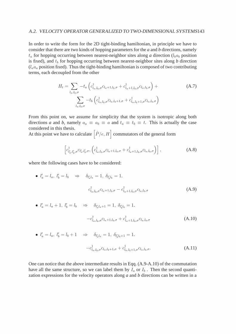
A.2. VELOCITY OPERATOR GENERALIZED TO TWO-DIMENSIONAL SYSTEMS143
In order to write the form for the 2D tight-binding hamiltonian, in principle we have toconsider that there are two kinds of hopping parameters for thea andb directions, namelyta for hopping occurring between nearest-neighbor sites along a direction (lbab positionis fixed), andtb for hopping occurring between nearest-neighbor sites along b direction(laaa position fixed). Thus the tight-binding hamiltonian is composed of two contributingterms, each decoupled from the other
Ht =∑
la,lb,σ
−ta(c†la,lb,σ
cla+1,lb,σ + c†la+1,lb,σcla,lb,σ
)+ (A.7)
∑
la,lb,σ
−tb(c†la,lb,σ
cla,lb+1,σ + c†la,lb+1,σcla,lb,σ
)
From this point on, we assume for simplicity that the system is isotropic along bothdirectionsa andb, namelyaa ≡ ab ≡ a and ta ≡ tb ≡ t. This is actually the caseconsidered in this thesis.At this point we have to calculate
[P /e,H
]commutators of the general form
[c†l′a,l′
b,σcl′a,l′
b,σ,(c†la,lb,σcla+1,lb,σ + c†la+1,lb,σcla,lb,σ
)], (A.8)
where the following cases have to be considered:
• l′a = la, l′b = lb ⇒ δl′ala = 1, δl′
blb = 1.
c†la,lb,σcla+1,lb,σ − c†la+1,lb,σ
cla,lb,σ (A.9)
• l′a = la + 1, l′b = lb ⇒ δl′ala+1 = 1, δl′blb = 1.
−c†la,lb,σcla+1,lb,σ + c†la+1,lb,σ
cla,lb,σ (A.10)
• l′a = la, l′b = lb + 1 ⇒ δl′ala = 1, δl′
blb+1 = 1.
−c†la,lb,σcla,lb+1,σ + c†la,lb+1,σcla,lb,σ. (A.11)
One can notice that the above intermediate results in Eqq. (A.9-A.10) of the commutationhave all the same structure, so we can label them byIa or Ib . Then the second quanti-zation expressions for the velocity operators alonga andb directions can be written in a

144 APPENDIX A.
more compact form as:
va =ı
~ta∑
la,lb,σ
l′aIa(δl′alaδl′blb − δl′ala+1δl′
blb
)=ı
~ta∑
la,lb,σ
Ia (la − la − 1) = (A.12)
= − ı
~ta∑
la,lb,σ
c†la,lb,σcla+1,lb,σ − c†la+1,lb,σ
cla,lb,σ
vb =ı
~ta∑
la,lb,σ
l′bIb(δl′alaδl′blb − δl′alaδl′blb+1
)=ı
~ta∑
la,lb,σ
Ib (lb − lb − 1) = (A.13)
= − ı
~ta∑
la,lb,σ
(c†la,lb,σ
cla,lb+1,σ − c†la,lb+1,σcla,lb,σ
)
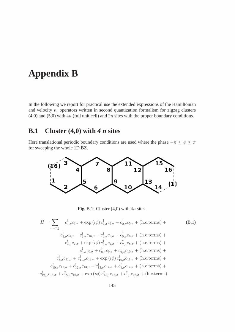
Appendix B
In the following we report for practical use the extended expressions of the Hamiltonianand velocityvz operators written in second quantization formalism for zigzag clusters(4,0) and (5,0) with4n (full unit cell) and2n sites with the proper boundary conditions.
B.1 Cluster (4,0) with4 n sites
Here translational periodic boundary conditions are used where the phase−π ≤ φ ≤ πfor sweeping the whole 1D BZ.
Fig. B.1: Cluster (4,0) with4n sites.
H =∑
σ=↑,↓c†1,σc2,σ + exp (ıφ) c†2,σc3,σ + c†2,σc5,σ + (h.c.terms) + (B.1)
c†3,σc4,σ + c†3,σc16,σ + c†4,σc5,σ + c†5,σc6,σ + (h.c.terms) +
c†4,σc7,σ + exp (ıφ) c†6,σc7,σ + c†7,σc8,σ + (h.c.terms) +
c†6,σc9,σ + c†8,σc9,σ + c†9,σc10,σ + (h.c.terms) +
c†8,σc11,σ + c†11,σc12,σ + exp (ıφ) c†10,σc11,σ + (h.c.terms) +
c†10,σc13,σ + c†12,σc13,σ + c†13,σc14,σ + c†1,σc14,σ + (h.c.terms) +
c†12,σc15,σ + c†15,σc16,σ + exp (ıφ) c†14,σc15,σ + c†1,σc16,σ + (h.c.terms)
145
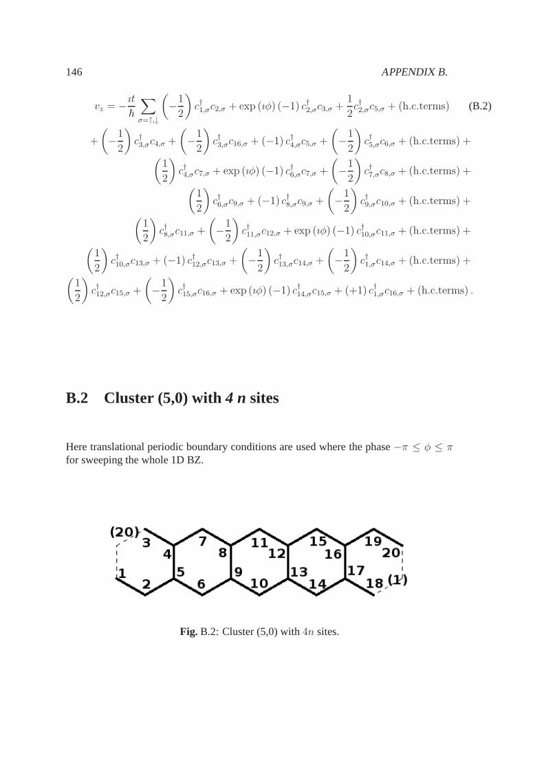
146 APPENDIX B.
vz = − ıt~
∑
σ=↑,↓
(−1
2
)c†1,σc2,σ + exp (ıφ) (−1) c†2,σc3,σ +
1
2c†2,σc5,σ + (h.c.terms) (B.2)
+
(−1
2
)c†3,σc4,σ +
(−1
2
)c†3,σc16,σ + (−1) c†4,σc5,σ +
(−1
2
)c†5,σc6,σ + (h.c.terms) +
(1
2
)c†4,σc7,σ + exp (ıφ) (−1) c†6,σc7,σ +
(−1
2
)c†7,σc8,σ + (h.c.terms) +
(1
2
)c†6,σc9,σ + (−1) c†8,σc9,σ +
(−1
2
)c†9,σc10,σ + (h.c.terms) +
(1
2
)c†8,σc11,σ +
(−1
2
)c†11,σc12,σ + exp (ıφ) (−1) c†10,σc11,σ + (h.c.terms) +
(1
2
)c†10,σc13,σ + (−1) c†12,σc13,σ +
(−1
2
)c†13,σc14,σ +
(−1
2
)c†1,σc14,σ + (h.c.terms) +
(1
2
)c†12,σc15,σ +
(−1
2
)c†15,σc16,σ + exp (ıφ) (−1) c†14,σc15,σ + (+1) c†1,σc16,σ + (h.c.terms) .
B.2 Cluster (5,0) with4 n sites
Here translational periodic boundary conditions are used where the phase−π ≤ φ ≤ πfor sweeping the whole 1D BZ.
Fig. B.2: Cluster (5,0) with4n sites.
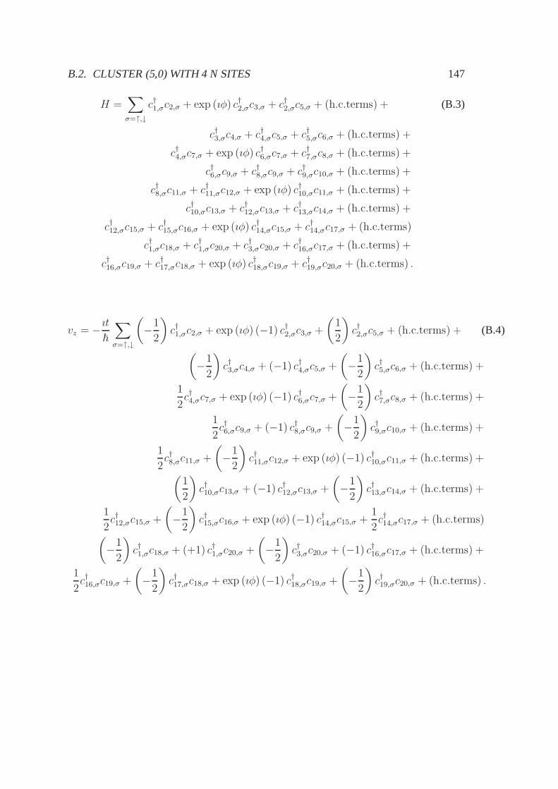
B.2. CLUSTER (5,0) WITH4 NSITES 147
H =∑
σ=↑,↓c†1,σc2,σ + exp (ıφ) c†2,σc3,σ + c†2,σc5,σ + (h.c.terms) + (B.3)
c†3,σc4,σ + c†4,σc5,σ + c†5,σc6,σ + (h.c.terms) +
c†4,σc7,σ + exp (ıφ) c†6,σc7,σ + c†7,σc8,σ + (h.c.terms) +
c†6,σc9,σ + c†8,σc9,σ + c†9,σc10,σ + (h.c.terms) +
c†8,σc11,σ + c†11,σc12,σ + exp (ıφ) c†10,σc11,σ + (h.c.terms) +
c†10,σc13,σ + c†12,σc13,σ + c†13,σc14,σ + (h.c.terms) +
c†12,σc15,σ + c†15,σc16,σ + exp (ıφ) c†14,σc15,σ + c†14,σc17,σ + (h.c.terms)
c†1,σc18,σ + c†1,σc20,σ + c†3,σc20,σ + c†16,σc17,σ + (h.c.terms) +
c†16,σc19,σ + c†17,σc18,σ + exp (ıφ) c†18,σc19,σ + c†19,σc20,σ + (h.c.terms) .
vz = − ıt~
∑
σ=↑,↓
(−1
2
)c†1,σc2,σ + exp (ıφ) (−1) c†2,σc3,σ +
(1
2
)c†2,σc5,σ + (h.c.terms) + (B.4)
(−1
2
)c†3,σc4,σ + (−1) c†4,σc5,σ +
(−1
2
)c†5,σc6,σ + (h.c.terms) +
1
2c†4,σc7,σ + exp (ıφ) (−1) c†6,σc7,σ +
(−1
2
)c†7,σc8,σ + (h.c.terms) +
1
2c†6,σc9,σ + (−1) c†8,σc9,σ +
(−1
2
)c†9,σc10,σ + (h.c.terms) +
1
2c†8,σc11,σ +
(−1
2
)c†11,σc12,σ + exp (ıφ) (−1) c†10,σc11,σ + (h.c.terms) +
(1
2
)c†10,σc13,σ + (−1) c†12,σc13,σ +
(−1
2
)c†13,σc14,σ + (h.c.terms) +
1
2c†12,σc15,σ +
(−1
2
)c†15,σc16,σ + exp (ıφ) (−1) c†14,σc15,σ +
1
2c†14,σc17,σ + (h.c.terms)
(−1
2
)c†1,σc18,σ + (+1) c†1,σc20,σ +
(−1
2
)c†3,σc20,σ + (−1) c†16,σc17,σ + (h.c.terms) +
1
2c†16,σc19,σ +
(−1
2
)c†17,σc18,σ + exp (ıφ) (−1) c†18,σc19,σ +
(−1
2
)c†19,σc20,σ + (h.c.terms) .
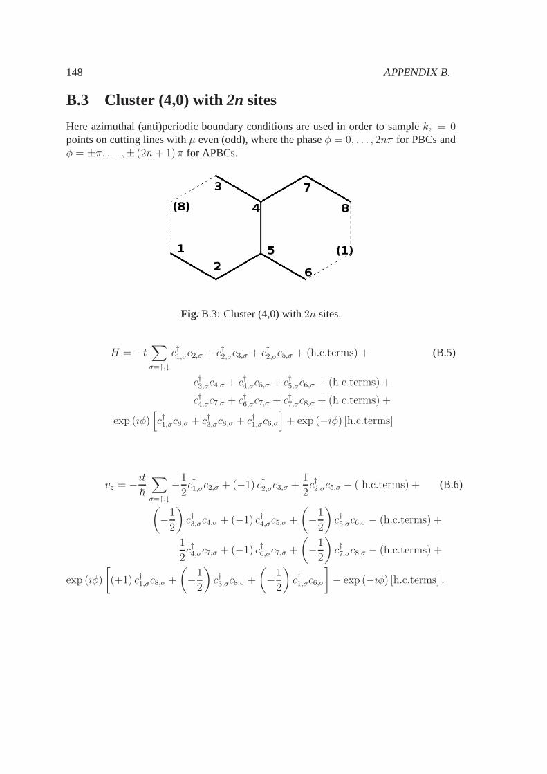
148 APPENDIX B.
B.3 Cluster (4,0) with2n sites
Here azimuthal (anti)periodic boundary conditions are used in order to samplekz = 0points on cutting lines withµ even (odd), where the phaseφ = 0, . . . , 2nπ for PBCs andφ = ±π, . . . ,± (2n+ 1)π for APBCs.
Fig. B.3: Cluster (4,0) with2n sites.
H = −t∑
σ=↑,↓c†1,σc2,σ + c†2,σc3,σ + c†2,σc5,σ + (h.c.terms) + (B.5)
c†3,σc4,σ + c†4,σc5,σ + c†5,σc6,σ + (h.c.terms) +
c†4,σc7,σ + c†6,σc7,σ + c†7,σc8,σ + (h.c.terms) +
exp (ıφ)[c†1,σc8,σ + c†3,σc8,σ + c†1,σc6,σ
]+ exp (−ıφ) [h.c.terms]
vz = − ıt~
∑
σ=↑,↓−1
2c†1,σc2,σ + (−1) c†2,σc3,σ +
1
2c†2,σc5,σ − ( h.c.terms) + (B.6)
(−1
2
)c†3,σc4,σ + (−1) c†4,σc5,σ +
(−1
2
)c†5,σc6,σ − (h.c.terms) +
1
2c†4,σc7,σ + (−1) c†6,σc7,σ +
(−1
2
)c†7,σc8,σ − (h.c.terms) +
exp (ıφ)
[(+1) c†1,σc8,σ +
(−1
2
)c†3,σc8,σ +
(−1
2
)c†1,σc6,σ
]− exp (−ıφ) [h.c.terms] .
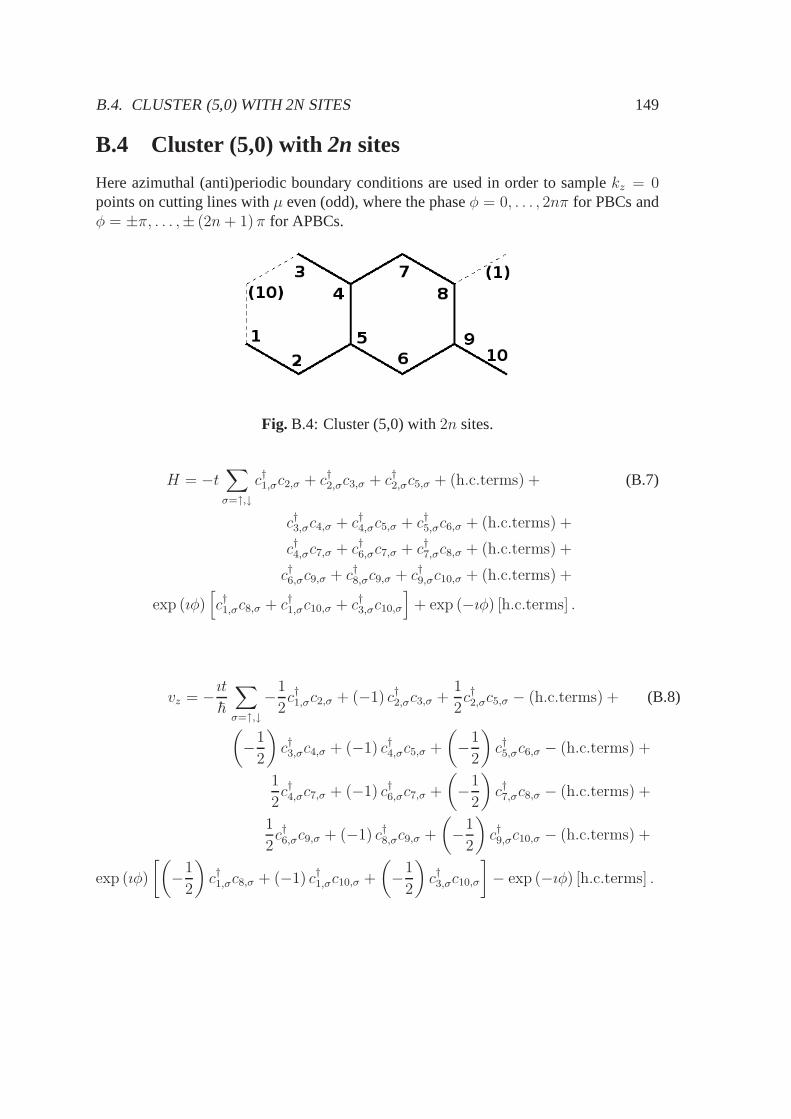
B.4. CLUSTER (5,0) WITH2NSITES 149
B.4 Cluster (5,0) with2n sites
Here azimuthal (anti)periodic boundary conditions are used in order to samplekz = 0points on cutting lines withµ even (odd), where the phaseφ = 0, . . . , 2nπ for PBCs andφ = ±π, . . . ,± (2n+ 1)π for APBCs.
Fig. B.4: Cluster (5,0) with2n sites.
H = −t∑
σ=↑,↓c†1,σc2,σ + c†2,σc3,σ + c†2,σc5,σ + (h.c.terms) + (B.7)
c†3,σc4,σ + c†4,σc5,σ + c†5,σc6,σ + (h.c.terms) +
c†4,σc7,σ + c†6,σc7,σ + c†7,σc8,σ + (h.c.terms) +
c†6,σc9,σ + c†8,σc9,σ + c†9,σc10,σ + (h.c.terms) +
exp (ıφ)[c†1,σc8,σ + c†1,σc10,σ + c†3,σc10,σ
]+ exp (−ıφ) [h.c.terms] .
vz = − ıt~
∑
σ=↑,↓−1
2c†1,σc2,σ + (−1) c†2,σc3,σ +
1
2c†2,σc5,σ − (h.c.terms) + (B.8)
(−1
2
)c†3,σc4,σ + (−1) c†4,σc5,σ +
(−1
2
)c†5,σc6,σ − (h.c.terms) +
1
2c†4,σc7,σ + (−1) c†6,σc7,σ +
(−1
2
)c†7,σc8,σ − (h.c.terms) +
1
2c†6,σc9,σ + (−1) c†8,σc9,σ +
(−1
2
)c†9,σc10,σ − (h.c.terms) +
exp (ıφ)
[(−1
2
)c†1,σc8,σ + (−1) c†1,σc10,σ +
(−1
2
)c†3,σc10,σ
]− exp (−ıφ) [h.c.terms] .

Bibliography
[1] H. W. Kroto, J. R. Heath, S. C. O’ Brien, R. F. Curl, and R. E.Smalley.C60: Buckminsterfullerene. Nature318, 162 (1985).
[2] K. S. Novoselov, A. K. Geim, S. V. Morozov, D. Jiang, Y. Zhang, S. V.Dubonos, I. V. Grigorieva, and A. A. Firsov.Electric field effect in atomi-cally thin carbon films. Science306, 666 (2004).
[3] K. S. Novoselov, D. Jiang, F. Schedin, T. J. Booth, V. V. Khotkevich, S. V.Morozov, and A. K. Geim.Two-dimensional atomic crystals. Proc. Natl.Acad. Sci.102, 10451 (2005).
[4] J. C. Meyer, A. K. Geim, M. I. Katsnelson, K. S. Novoselov,T. J. Booth,and S. Roth.The structure of suspended graphene sheets. Nature446, 60(2007).
[5] A. K. Geim and K. S. Novoselov.The rise of graphene. Nature Materials6, 183 (2007).
[6] S. Stankovich, R. D. Piner, X. Chen, N. Wu, S. T. Nguyen, and R. S.Ruoff. Stable aqueous dispersions of graphitic nanoplatelets viathe re-duction of exfoliated graphite oxide in the presence of poly(sodium 4-styrenesulfonate). J. Mater. Chem.16, 155 (2006).
[7] A. E. Karu and M. Beer.Pyrolytic formation of highly crystalline graphitefilms. J. Appl. Phys.37, 2179 (1966).
[8] C. Oshima and A. Nagashima.Ultra-thin epitaxial films of graphite andhexagonal boron nitride on solid surfaces. J. Phys.: Cond. Matter9,1(1997).
[9] L. C. Isett and J. M. Blakely.Segregation isosteres for carbon at the (100)surface of nickel. Surf. Sci.58, 397 (1976).
[10] J. C. Hamilton and J. M. Blakely.Carbon segregation to single crystalsurfaces of Pt, Pd and Co. Surf. Sci.91, 199 (1980).
151
152 BIBLIOGRAPHY
[11] S. Iijima.Helical microtubules of graphitic carbon. Nature354, 56 (1991).
[12] S. Iijima and T. Ichihashi.Single-shell carbon nanotubes of 1-nm diameter.Nature363, 603 (1993).
[13] M. Monthioux and V. L. Kuznetsov.Who should be given the credit for thediscovery of carbon nanotubes?Carbon44, 1621 (2006).
[14] L. V. Radushkevich and V. M. Lukyanovich.O strukture ugleroda, obrazu-jucegosja pri termiceskom razlozenii okisi ugleroda na zeleznom kontakte.Zurn. Fisic. Chim.26, 88 (1952).
[15] A. Oberlin, M. Endo, and T. Koyama.Filamentous growth of carbonthrough benzene decomposition. J. Cryst. Growth32, 335 (1976).
[16] D. Bethune, C. Klang, M. de Vries, G. Gorman, R. Savoy, J.Vazquez,and R. Beyers.Cobalt-catalysed growth of carbon nanotubes with single-atomic-layer walls. Nature363, 605 (1993).
[17] P. M. Ajayan and S. Iijima.Smallest carbon nanotube. Nature358, 23(1992).
[18] L.-C. Qin, X. Zhao, K. Hirahara, Y. Miyamoto, Y. Ando, and S. Iijima.Thesmallest carbon nanotube. Nature408, 50 (2000).
[19] L. F. Sun, S. S. Xie, W. Liu, W. Y. Zhou, Z. Q. Liu, D. S. Tang, G. Wang,and L. X. Qian.Creating the narrowest carbon nanotubes. Nature403, 384(2000).
[20] N. Wang, Z. K. Tang, G. D. Li, and J. S. Chen. Materials science:Single-walled 4A carbon nanotube arrays. Nature408, 50 (2000).
[21] C.-H. Kiang.Growth of large-diameter single-walled carbon nanotubes. J.Phys. Chem. A104, 2454 (2000).
[22] M. Reibold, P. Paufler, A. A. Levin, W. Kochmann, N. Ptzke, and D. C.Meyer.Materials: Carbon nanotubes in an ancient Damascus sabre. Na-ture444, 286 (2006).
[23] T. W. Ebbesen and P. M. Ajayan.Large-scale synthesis of carbon nan-otubes. Nature358, 220 (1992).
[24] T. Guo, P. Nikolaev, A. Thess, D. T. Colbert, and R. E. Smalley. Catalyticgrowth of single-walled manotubes by laser vaporization. Chem. Phys.Lett. 243, 49 (1995).

BIBLIOGRAPHY 153
[25] Y. Li,W. Kim, Y. Zhang, M. Rolandi, D.Wang, and H. Dai.Growth ofsingle-walled carbon nanotubes from discrete catalytic nanoparticles ofvarious sizes. J. Phys. Chem. B105, 11424 (2001).
[26] L. Ci, Z. Zhou, X. Yan, D. Liu, H. Yuan, L. Song, J.Wang, Y.Gao, J.Zhou,W. Zhou, G.Wang, and S. Xie.Raman characterization and tun-able growth of double-wall carbon nanotubes. J. Phys. Chem. B107, 8760(2003).
[27] A. M. Cassell, N. R. Franklin, T. W. Tombler, E. M. Chan, J. Han, and H.Dai. Directed growth of free-standing single-walled carbon nanotubes. J.Am. Chem. Soc.121, 7975 (1999).
[28] W. A. de Heer, W. S. Bacsa, A. Chatelain, T. Gerfin, R. Humphrey-Baker,L. Forro, and D. Ugarte.Aligned carbon nanotube films: production andoptical and electronic properties. Science268, 845 (1995).
[29] T. Tanaka, A. Tajima, R. Moriizumi, M. Hosoda, R. Ohno, E. Rokuta, C.Oshima, and S. Otani.Carbon nano-ribbons and their edge phonons. SolidState Comm.123, 33 (2002).
[30] K. Nakada, M. Fujita, G. Dresselhaus, and M. S. Dresselhaus.Edge statein graphene ribbons: nanometer size effect and edge shape dependence.Phys. Rev. B54, 17954 (1996).
[31] Y. Ouyang, Y. Yoon, J. K. Fodor, and J. Guo.Comparison of performancelimits for carbon nanoribbon and carbon nanotube transistors. Appl. Phys.Lett. 89, 203107 (2006).
[32] B. W. Smith, M. Monthioux, and D. E. Luzzi.EncapsulatedC60 in carbonnanotubes. Nature396, 323 (1998).
[33] S. Okada, S. Saito, and A. Oshiyama.Energetics and electronics struc-tures of encapsulatedC60 in a carbon nanotube. Phys. Rev. Lett.86, 3835(2001).
[34] S. Berber, Y.-K. Kwon, and David Tomanek.Microscopic FormationMechanism of Nanotube Peapods. Phys. Rev. Lett.88, 185502 (2002).
[35] D. Tomanek. Mesoscopic origami with graphite: scrolls, nanotube,peapods. Physica B323, 86 (2002).
[36] B. W. Smith, M. Monthioux, and D. E. Luzzi.Carbon nanotube encap-sulated fullerenes: a unique class of hybrid materials. Chemical PhysicsLetters315, 31 (1999).

154 BIBLIOGRAPHY
[37] S. Bandow, K. Hirahara, T. Hiraoka, G. Chen, P. C. Eklund, and S.Iijima. Turning peapods into double-walled carbon nanotubes. MRS Bul-lettin/April 2004, 260 (2004).
[38] J. G. Lavin, S. Subramoney, R. S. Ruoff, S. Berber, and D.Tomanek.Scrolls and nested tubes in multiwall carbon nanotubes. Carbon40, 1123(2002).
[39] S. Berber and D. Tomanek.Stability differences and conversion mechanismbetween nanotube and scrolls. Phys. Rev. B69, 233404 (2004).
[40] H. Shioyama and T. Akita.A new route to carbon nanotubes. Carbon41,179 (2003).
[41] J. L. Li, Q. S. Peng, G. Z. Bai, and W. Jiang.Carbon scrolls produced byhigh energy ball milling of graphite. Carbon43, 2817 (2005).
[42] D. Tomanek.Carbon-based nanotechnology on a supercomputer. J. Phys.:Condens. Matter17, R413-R459 (2005).
[43] H. Terrones and M. Terrones.Curved nanostructured materials. NewJourn. Phys.5, 126 (2003).
[44] M. P. Anantram and F. Leonard.Physics of carbon nanotube electronicdevices. Rep. Prog. Phys.69, 507 (2006).
[45] A. W. Hull. A new method of X-Ray crystal analysis. Phys. Rev.10, 661(1917).
[46] J. D. Bernal.The structure of graphite. Proc. R. Soc. London, Ser. A106,749 (1924).
[47] R. E. Peierls.Bemerkungenuber Umwandlungstemperaturen. Helv. Phys.Acta7, 81 (1934).
[48] N. D. Mermin.Crystalline order in two dimensions. Phys. Rev.176, 250(1968).
[49] J.-C. Charlier, X. Blase, and S. Roche.Electronic and transport propertiesof nanotubes. Rev. Mod. Phys.79, 677 (2007).
[50] A. A. Lucas, V. Bruyninckx, and P. Lambin.Calculating the diffraction ofelectrons or X-rays by carbon nanotubes. Europhys. Lett.35, 355 (1996).
BIBLIOGRAPHY 155
[51] M. Kociak, K. Hirahara, K. Suenaga, and S. Iijima.How accurate can thedetermination of chiral indices of carbon nanotubes be ?Eur. Phys. J. B32, 457 (2003).
[52] Lu-Chang Qin.Electron diffraction from carbon nanotubes. Rep. Prog.Phys.69, 2761 (2006).
[53] S. G. Lemay, J. W. Janssen, M. van den Hout, M. Mooij, M. J.Bronikowski,P. A. Willis, R. E. Smalley, L. P. Kouwenhoven, and C. Dekker.Two-dimensional imaging of electronic wavefunctions in carbonnanotubes. Na-ture412, 617 (2001)
[54] P. Lambin, G. I. Mark, V. Meunier, and L. P. Biro.Computation of STMimages of carbon nanotubes. Int. Journ. Qua. Chem.95, 493 (2003).
[55] T. W. Odom, J.-L. Huang, P. Kim, and C. M. Lieber.Atomic structure andelectronic properties of single-walled carbon nanotubes. Nature391, 62(1998).
[56] M. O’Connell, S. M. Bachilo, X. B. Huffman, V. C. Moore, M. S. Strano,E. H. Haroz, K. L. Rialon, P. J. Boul, W. H. Noon, C. Kittrell, J. Ma, R.H. Hauge, R. B. Weisman, and R. E. Smalley.Band gap fluorescence fromindividual single-walled nanotubes, Science297, 593 (2002).
[57] S. M. Bachilo, M. S. Strano, C. Kittrell, R. H. Hauge, R. E. Smalley, andR. B. Weisman.Structure-assigned optical spectra of single-walled carbonnanotubes, Science298, 2361 (2002).
[58] X. Liu, T. Pichler, M. Knupfer, M. S. Golden, J. Fink, H. Kataura, and Y.Achiba.Detailed analysis of the mean diameter and diameter distributionof single-wall carbon nanotubes from their optical response. Phys. Rev. B66, 45411 (2002).
[59] T. Belin and F. Epron.Characterization methods of carbon nanotubes: areview. Mat. Sci. Eng. B119, 105 (2005).
[60] S. Goedecker and G. E. Scuseria.Linear scaling electronic structure meth-ods in chemistry and physics. Computing in Science and Engineering5,July/August 2003, 14 (2003).
[61] P. Hohenberg and W. Kohn.Inhomogeneous electron gas. Phys. Rev.136,B864 (1964).
[62] W. Kohn and L. J. Sham.Self-consistent equations including exchange andcorrelation effects. Phys. Rev.140, A1133 (1965).
156 BIBLIOGRAPHY
[63] J. M. Soler, E. Artacho, J. D. Gale, A. Garcıa, J. Junquera, P. Ordejon,and D. Sanchez-Portal.The SIESTA method for ab initio order-N materialssimulation. J. Phys.: Cond. Matter14, 2475 (2002).
[64] J. W. Mintmire, B. I. Dunlap, and C. T. White.Are fullerene tubules metal-lic ? Phys. Rev. Lett.68, 631 (1992).
[65] J. W. Mintmire and C. T. White.First-principles band structures of arm-chair nanotubes. Appl. Phys. A67, 65 (1998).
[66] X. Blase, L. X. Benedict, E. L. Shirley, and S. G. Louie.Hybridizationeffects and metallicity in small radius carbon nanotubes. Phys. Rev. Lett.72, 1878 (1994).
[67] D. Ostling, D. Tomanek, and A. Rosen.Electronic structure of single-wall,multiwall, and filled carbon nanotubes. Phys. Rev. B55, 13980 (1997).
[68] Y.-K. Kwon and D. Tomanek.Electronic and structural properties of mul-tiwall carbon nanotubes. Phys. Rev. B58, R16001 (1998).
[69] O. Dubay and G. Kresse.Density functional calculations forC60 peapods.Phys. Rev. B70, 165424 (2004).
[70] D. Porezag, Th. Frauenheim, Th. Kohler, G. Seifert, and R. Kaschner.Con-struction of tight-binding-like potentials on the basis ofdensity functionaltheory:application to carbon. Phys. Rev. B51, 12947 (1995).
[71] T. Frauenheim, G. Seifert, M. Elstner, T. Niehaus, C. K¨ohler, M. Amkreutz,M. Sternberg, Z. Hajnal, A. Di Carlo, and S. Suhai.Atomistic simulationsof complex materials: ground-state and excited-state properties. J. Phys.:Condens. Matter14, 3015 (2002).
[72] M. Born and K. Huang.Dynamical Theory of Crystal Lattices(OxfordUniversity Press, Oxford, 1954).
[73] B. S. Kandemir and M. Keskin.Analytical approach to phonons andelectron-phonon interactions in single-walled zigzag carbon nanotubes. J.Phys.: Condens. Matter20, 325222 (2008).
[74] J. C. Slater and G. F. Koster.Simplified LCAO Method for the PeriodicPotential Problem. Phys. Rev.94, 1498 (1954).
[75] C. M. Goringe, D. R. Bowler, and E. Hernandez.Tight-binding modellingof materials. Rep. Prog. Phys.60, 1447 (1997).
BIBLIOGRAPHY 157
[76] R. Haydock, V. Heine, and M. J. Kelly.Electronic structure based on thelocal atomic environment for tight-binding bands. J. Phys. C: Solid StatePhys.5, 2845 (1972).
[77] J. C. Slonczewski and P. R. Weiss.Band structure of graphite. Phys. Rev.109, 272 (1958).
[78] J. W. McClure.Band structure of graphite and de Haas-van Alphen Effect.Phys. Rev.108, 612 (1957).
[79] J.-C. Charlier, J. P. Michenaud, X. Gonze, and J.-P. Vigneron.Tight-bindingmodel for the electronic properties of simple hexagonal graphite. Phys.Rev. B44, 13237 (1991).
[80] J.-C. Charlier, J. P. Michenaud, and Ph. Lambin.Tight-binding density ofelectronic states of pregraphitic carbon. Phys. Rev. B46, 4540 (1992).
[81] N. Hamada, S. Sawada, and A. Oshiyama.New one-dimensional conduc-tors: graphitic microtubules. Phys. Rev. Lett.68, 1579 (1992).
[82] C. T. White, D. H. Robertson, and J. W. Mintmire.Helical and rotationalsymmetries of nanoscale graphitic tubules. Phys. Rev. B47, 5485 (1993).
[83] J. W. Mintmire and C. T. White.Electronic and structural properties ofcarbon nanotubes. Carbon33, 893 (1995).
[84] V. N. Popov.Curvature effects on the structural, electronic and opticalproperties of isolated single-walled carbon nanotubes within a symmetry-adapted non-orthogonal tight-binding model. New J. Phys.6 1 (2004).
[85] M. Damnjanovic, T. Vukovic, and I. Milosevic.Modified group projectors:tight-binding method. J. Phys. A: Math. and Gen.336561 (2000).
[86] T. Ando.Theory of electronic states and transport in carbon nanotubes. J.Phys. Soc. Jpn.74, No.3 (2001).
[87] D. Tomanek, W. Zhong, and E. Krastev.Stability of multishell fullerene.Phys. Rev. B 48, 15461 (1993).
[88] D. Kahn, K. W. Kim, and M. A. Stroscio.Quantized vibrational modes ofnanospheres and nanotubes in the elastic continuum model. J. Appl. Phys.89, 5107 (2001).
[89] R. Saito, G. Dresselhaus and M. S. Dresselhaus.Physical Properties ofCarbon Nanotubes(Imperial College Press, London, 1998).
158 BIBLIOGRAPHY
[90] S. Reich, C. Thomsen and J. Maultzsch.Carbon nanotubes: basic conceptsand physical properties(Wiley, 2004).
[91] L. M. Falicov. Recent Progress in Many-Body Theories,1, 275, (Plenum,New York, 1988) and references therein.
[92] G. D. Mahan.Many-Particle Physics(Plenum Press, New York, 1990).
[93] F. Jensen.Introduction to Computational Chemistry(John Wiley & Sons,1999)
[94] E. Kaxiras.Atomic and Electronic Structure of Solids(Cambridge Univer-sity Press, 2003).
[95] E. N. Economou.Green’s Functions in Quantum Physics(Springer-VerlagBerlin Heidelberg New York 1979).
[96] L. I. Schiff. Quantum Mechanics, 3rd edition, (McGraw-Hill, New York,1968).
[97] R. F. Wallis and M. Balkanski.Many-Body Aspects of Solid State Spec-troscopy(North-Holland Amsterdam Oxford NewYork Tokyo, 1986).
[98] R. M. Martin and L. M. Falicov.Resonant Raman Scattering, in Light Scat-tering in Solids I: edited by M. Cardona, 70-145, (Springer-Verlag, Berlin,1983), Vol. 8. Chapter 3, Topics in Applied Physics.
[99] D. J. Chadi and M. L. Cohen.Special points in the Brillouin zone. Phys.Rev. B8, 5747 (1973).
[100] S. L. Cunningham.Special points in the two-dimensional Brillouin zone.Phys. Rev. B10, 4988 (1974).
[101] L. Brey and C. Tejedor.Raman tensor of covalent semiconductors. SolidState Commun.48, 403 (1983).
[102] L. C. Lew Yan Voon and L. R. Ram-Mohan.Tight-binding representationof the optical matrix elements: Theory and applications. Phys. Rev. B47,15500 (1993).
[103] J. Yepez.A symbolic solution of the Hubbard model for small clusters. Ad-vanced Exam in Physics, PhD program, (Brandeis University,Massachus-sets, 1991). Available at: http://xyz.plh.af.mil/Papers/pdf/ae91.pdf
BIBLIOGRAPHY 159
[104] J. Callaway, D. P. Chen, and R. Tang.Ground state and thermodynamicproperties of the Hubbard model applied to small custers. Phys. Rev. B35,3705 (1987).
[105] L. Milans del Bosch and L. M. Falicov.Extended one-dimensional Hub-bard model: A small-cluster approach. Phys. Rev. B37, 6073 (1988).
[106] C. R. Proetto and L. M. Falicov.Exact solution of a quantum electron-phonon system for a two-site periodic cluster. Phys. Rev. B39, 7545(1989).
[107] B. Koiller, M. A. M. Davidovich and L. M. Falicov.Small-crystal approachto ordered semiconductor compounds. Phys. Rev. B41, 3670 (1990).
[108] M. Meneghetti and C. Pecile.Vibrational and electronic spectra of one-dimensional organic charge-transfer crystals: Model for atetramerizedcluster structure. Phys. Rev. B40, 12187 (1989).
[109] M. Meneghetti and C. Pecile.Periodic-dimer-cluster models for the studyof the optical properties of dimerized half-filled organic charge-transfercrystals. Phys. Rev. B42, 1605 (1990).
[110] M. Meneghetti.Optical properties of organic conductor and semiconduc-tor crystals: Model for a half-filled dimerized chain. Phys. Rev. B44, 8554(1991).
[111] M. Meneghetti.Model for the linear and nonlinear optical propertiesof one-dimensional organicπ-conjugated compounds. Phys. Rev. B47,13151 (1993).
[112] M. Meneghetti. Optical properties of one-dimensionalπ-conjugatedcompounds: Study of the pressure-dependent linear properties of K-tetracyanoquinodimethane. Phys. Rev. B50, 16899 (1994).
[113] M. Meneghetti and L. Feltre.Electronic and vibronic excitations ofquarter-filled periodic octamer. Synthetic Metals85, 1629 (1997).
[114] M. Meneghetti.Dynamic modulation of electron correlation by intramolec-ular modes in charge-transfer compounds. Phys. Rev. B60, 15472 (1999).
[115] B. Koiller, R. Oso rio and L. M. Falicov.Gap properties ofAlnGa8−nAs8.Phys. Rev. B43, 4170 (1991).
[116] G. G. Samsonidze, R. Saito, A. Jorio, M. A. Pimenta, A. G. Souza Filho, A.Grueneis, G. Dresselhaus, and M. S. Dresselhaus.The concept of cuttinglines in carbon nanotube science. J. Nanosci. Nanotech.3, (2003).
160 BIBLIOGRAPHY
[117] R.Saito, K. Sato, Y. Oyama, J. Jiang, Ge. G. Samsonidze, G. Dresselhaus,and M. S. Dresselhaus.Cutting-lines near the Fermi energy of single-wallcarbon nanotubes, Phys. Rev. B72, 153413 (2005).
[118] E. B. Barros, A. Jorio, G. G. Samsonidze, R. B. Capaz, A.G. Souza Filho,J. Mendez Filho, G. Dresselhaus, and M. S. Dresselhaus.Review on thesymmetry-related properties of carbon nanotubes. Phys. Reports,431, 261,(2006).
[119] M. S. Dresselhaus, G. Dresselhaus, R. Saito, and A. Jorio. Raman spec-troscopy of carbon nanotubes. Phys. Reports,409, 47 (2005).
[120] M. S. Dresselhaus, G. Dresselhaus, and A. Jorio.Raman spectroscopy ofcarbon nanotubes in 1997 and 2007. J. Phys. Chem. C,111, 17887 (2007).
[121] A. Grueneis.Resonance Raman spectroscopy of single wall carbon nan-otubes. Ph.D. Thesis, (University of Tokyo, 2004).
[122] Ge. G. Samsonidze.Photophysics of carbon nanotubes. Ph.D. Thesis (MIT,Boston, 2007).
[123] N. Nemec.Quantum transport in carbon-based nanostructures. Ph.D. The-sis (University of Regensburg, 2007).
[124] M. Damnjanovic, I. Milosevic, T. Vukovic and R. Sredanovic.Full symme-try, optical activity, and potentials of single-wall and multiwall nanotubes.Phys. Rev. B,60, 2728 (1999) and references therein.
[125] R. Saito, K. Sato, Y. Oyama, J. Jiang, G. G. Samsonidze,G. Dresselhaus,and M. S. Dresselhaus.Cutting-lines near the Fermi-energy of single-wallcarbon nanotubes. Phys. Rev. B72, 153413, (2005).
[126] A. M. Rao, E. Richter, S. Bandow, B. Chase, P. C. Eklund,K. W. Williams,S. Fang, K. R. Subbaswamy, M. Menon, A. Thess, R. E. Smalley, G. Dres-selhaus, and M. S. Dresselhaus.Diameter-selective Raman scattering fromvibrational modes in carbon nanotubes. Science275, 187 (1997).
[127] H. Kataura, Y. Kumazawa, Y. Maniwa, I. Umezu, S. Suzuki, Y. Ohtsuka,and Y. Achiba.Optical properties of single-wall carbon nanotubes. Synth.Metals,103, 2555 (1999).
[128] A. Jorio, R. Saito, J. H. Hafner, C. M. Lieber, M. Hunter, T. McClure,G. Dresselhaus, and M. S. Dresselhaus.Structural (n,m) determination ofisolated single-wall carbon nanotubes by resonant Raman scattering. Phys.Rev. Lett.86, 1181 (2001).

BIBLIOGRAPHY 161
[129] R. B. Weisman and S. M. Bachilo.Dependence of optical transition ener-gies on structure for single-walled carbon nanotubes in acqueous suspen-sion: an empirical Kataura plot. Nanoletters3, 1235 (2003).
[130] A. Jorio, M. A. Pimenta, A.G. Souza Filho, R. Saito, G. Dresselhaus, andM. S. Dresselhaus.Characterizing carbon nanotube samples with reso-nance Raman scattering. New J. Phys.5, 1 (2003).
[131] C. Fantini, A. Jorio, M. Souza, M. S. Strano, M. S. Dresselhaus, and M. A.Pimenta.Optical transition energies for carbon nanotubes from ResonantRaman Spectroscopy: Environment and Temperature Effects. Phys. Rev.Lett. 93, 147406 (2004).
[132] G. G. Samsonidze, R. Saito, N. Kobayashi, A. Gruneis,J. Jiang, A. Jorio,S. G. Chou, G. Dresselhaus, and M. S. Dresselhaus.Family behaviour ofthe optical transition energies in single-wall carbon nanotubes of smallerdiameters. Appl. Phys. Lett.85, 5703 (2004).
[133] J. Maultzsch, H. Telg, S. Reich, and C. Thomsen.Radial breathing modeof single-walled carbon nanotubes: optical transition energies and chiral-index assignment. Phys. Rev. B72, 205438 (2005).
[134] L. G. Bulusheva, A. V. Okotrub, D. A. Romanov, and D. Tomanek.Elec-tronic structure of (n,0) zigzag carbon nanotubes: clusterand crystal ap-proach. J. Phys. Chem. A102, 975 (1997).
[135] R. Saito, G. Dresselhaus, and M. S. Dresselhaus.Trigonal warping effectof carbon nanotubes. Phys. Rev. B61, 2981 (2000).
[136] J. W. Mintmire and C. T. White.Universal density of states for carbonnanotubes. Phys. Rev. Letter81, 2506 (1998).
[137] C. T. White and J. W. Mintmire.Density of states reflects diameter in nan-otubes. Nature394, 29 (1998).
[138] S. Reich and C. Thomsen.Chirality dependence of the density-of-statessingularities in carbon nanotubes. Phys. Rev. B62, 4273 (2000).
[139] H. Ajiki and T. Ando.Aharonov-Bohm effect in carbon nanotubes. PhysicaB Condensed Matter201, 349 (1994).
[140] S. Tasaki, K. Maekawa and T. Yamabe.π-band contribution to the opticalproperties of carbon nanotubes: effects of chirality. Phys. Rev. B57, 9301(1998).
162 BIBLIOGRAPHY
[141] Ge. G. Samsonidze, A. Gruneis, R. Saito, A. Jorio, A. G. Souza Filho, G.Dresselhaus, and M. S. Dresselhaus.Interband optical transitions in left-and righthanded single-wall carbon nanotubes. Phys. Rev. B69, 205402(2004).
[142] A. Gruneis, R. Saito, G. G. Samsonidze, T. Kimura, M. A. Pimenta, A.Jorio, A. G. Souza Filho, G. Dresselhaus, and M. S. Dresselhaus. Inho-mogeneous optical absorption around the K point in graphiteand carbonnanotubes. Phys. Rev. B67, 165402 (2003).
[143] R. Saito, A. Grueneis, Ge. G. Samsonidze, G. Dresselhaus, M. S. Dressel-haus, A. Jorio, L. G. Cancado, M. A. Pimenta, and A. G. Souza.Opticalabsorption of graphite and single-wall carbon nanotubes. Appl. Phys. A78, 1099 (2004).
[144] J. Jiang, R. Saito, A. Grueneis, G. Dresselhaus, and M.S. Dresselhaus.Op-tical absorption matrix elements in single-wall carbon nanotubes. Carbon42, 3169 (2004).
[145] E. Malic, M. Hirtschulz, F. Milde, A. Knorr, and S. Reich. Analytical ap-proach to optical absorption in carbon nanotubes. Phys. Rev. B74, 195431(2006).
[146] J. Jiang, R. Saito, A. Gruneis, S. G. Chou, Ge. G. Samsonidze, A. Jorio, G.Dresselhaus, and M. S. Dresselhaus.Intensity of the resonance Raman ex-citation spectra of single-wall carbon nanotubes. Phys. Rev. B71, 205420(2005).
[147] L. G. Johnson and G. Dresselhaus.Optical properties of graphite. Phys.Rev. B7, 2275 (1973).
[148] A. Zarifi and T. G. Pedersen.Analytic approach to the linear susceptibilityof zigzag carbon nanotubes. Phys. Rev. B74, 155434 (2006).
[149] J. C. Charlier, T. W. Ebbesen, and Ph. Lambin.Structural and electronicproperties of pentagon-heptagon pair defects in carbon nanotubes. Phys.Rev. B53, 11108, (1996).
[150] N. Nemec and G. Cuniberti.Hofstadter butterflies of carbon nanotubes:pseudofractality of the magnetoelectronic spectrum. Phys. Rev. B74,165411 (2006).
[151] H. Hsu and L. E. Reichl.Selection rule for the optical absorption ofgraphene nanoribbons. Phys. Rev. B76, 045418 (2007).
BIBLIOGRAPHY 163
[152] A. K. Gupta, O. Alon, and N. Moiseyev.Generation and control of high-order harmonics by the interaction of an infrared laser witha thin graphitelayer. Phys. Rev. B68, 205101 (2003).
[153] A. Jorio, M. A. Pimenta, A. G. Souza Filho, Ge. G. Samsonidze, A. K.Swan, M. S.Unlu, B. B. Goldberg, R. Saito, G. Dresselhaus, and M.S. Dresselhaus.Resonance Raman spectra of carbon nanotubes by cross-polarized light. Phys. Rev. Lett.90, 107403 (2003).
[154] X. P. Yang, J. W. Chen, H. Jiang, and J. M. Dong.Chiral symmetry ofdouble-walled carbon nanotubes detected in first-principles optical ab-sorption spectra. Phys. Rev. B69, 193401 (2004).
[155] R. Saito, G. Dresselhaus, and M. Dresselhaus.Electronic structure ofdouble-layer graphene tubules. J. Appl. Phys.73, 494 (1993).
[156] Y. A. Kim, H. Muramatsu, T. Hayashi, M. Endo, M. Terrones, and M.S. Dresselhaus.Thermal stability and structural changes of double-walledcarbon nanotubes by heat treatment. Chem. Phys. Lett.398, 87 (2004).
[157] Y. E. Lozovik and A. M. Popov.Properties and nanotechnological appli-cations of nanotubes. Physics-Uspekhi50, 749 (2007)
[158] Z. C. Tu and Z. C. Ou-Yang.A molecular motor constructed froma double-walled carbon nanotube driven by temperature variation. J.Phys.:Condens. Matter16, 1287 (2004).
[159] S. W. D. Bailey, I. Amanatidis, and C. J. Lambert.Carbon nanotube elec-tron windmills: a novel design for nanomotors. Phys. Rev. Lett.100,256802 (2008).
[160] G. Marcolongo, G. Ruaro, M. Gobbo, and M. Meneghetti.Amino acidfunctionalization of double-wall carbon nanotubes studied by Raman spec-troscopy. Chem. Comm.46, 4925 (2007).
[161] S. Bandow, G. Chen, G. U. Sumanasekera, R. Gupta, M. Yudasaka, S.Iijima, and P. C. Eklund.Diameter-selective resonant Raman scattering indouble-wall carbon nanotubes. Phys. Rev. B66, 075416 (2002).
[162] W. Ren, F. Li, P. Tan, and H.-M. Cheng.Raman evidence for atomic cor-relation between the constituent tubes in double-walled carbon nanotubes.Phys. Rev. B73, 115430 (2006).
164 BIBLIOGRAPHY
[163] A. Hashimoto, K. Suenaga, K. Urita, T. Shimada, T. Sugai, S. Bandow, H.Shinohara, and S. Iijima.Atomic correlation between adjacent graphenelayers in double-walled carbon nanotubes. Phys. Rev. Lett.94, 045504(2005).
[164] T. Hertel, A. Hagen, V. Talalaev, K. Arnold, F. Hennrich, M. Kappes, S.Rosenthal, and J. McBride.Spectroscopy of single- and double-wall carbonnanotubes in different environments. NanoLett.5, 511 (2005).
[165] R. Pfeiffer, F. Simon, H. Kuzmany, and V. N. Popov.Fine structure of theradial breathing mode of double-wall carbon nanotubes, Phys. Rev. B72,161404(R) (2005).
[166] E. B. Barros, H. Son, Ge. G. Samsonidze, A. G. Souza Filho, R. Saito, Y.A. Kim, H. Muramatsu, T. Hayashi, M. Endo, J. Kong, and M.S. Dressel-haus.Raman spectroscopy of double-walled carbon nanotubes treated withH2SO4. Phys. Rev. B76, 045425 (2007).
[167] F. Li, S. G. Chou, W. Ren, J. A. Gardecki, A. K. Swan, B. B.Goldberg, andM. S. Dresselhaus.Identification of the constituents of double-walled car-bon nanotubes using Raman spectra taken with different laser-excitationenergies. J. Mater. Res.18, 1251 (2003).
[168] Shi-Dong Liang.Intrinsic properties of electronic structure in commensu-rate double-wall carbon nanotubes. Physica B352, 305 (2004).
[169] Ph. Lambin, L. Philippe, J. C. Charlier, and J. Michenaud.Electronic bandstructure of multilayered carbon tubules. Comput. Mat. Sci.2, 350 (1994).
[170] Ph. Lambin, V. Meunier, and A. Rubio.Electronic structure of polychiralcarbon nanotubes. Phys. Rev. B62, 5129 (2000).
[171] S. Roche, F. Triozon, A. Rubio, and D. Mayou.Conduction mechanismsand magnetotransport in multiwalled carbon nanotubes. Phys. Rev. B64,121401(R) (2001).
[172] Y. H. Ho, C. P. Chang, F. L. Shyu, R. B. Chen, S. C. Chen, and M. F.Lin. Electronic and optical properties of double-walled armchair carbonnanotubes. Carbon42, 3159 (2004).
[173] Y. H. Ho, G. W. Ho, S. J. Wu, and M. F. Lin.Band structures of double-walled carbon nanotubes. J. Vac. Sci. Technol. B24, 1098 (2006).

BIBLIOGRAPHY 165
[174] Y. H. Ho, G. W. Ho, S. C. Chen, J. H. Ho, and M. F. Lin.Low-frequencyexcitation spectra in double-walled armchair carbon nanotubes. Phys. Rev.B 76, 115422 (2007).
[175] S. Uryu and T. Ando.Electronic intertube transfer in double-wall carbonnanotubes. Phys. Rev. B72, 245403 (2005).
[176] V. Zolyomi, A. Rusznyak, J. Kurti,A. Gali, F. Simon, H. Kuzmany,A.Szabados, and P. R. Surjan.Semiconductor-to-metal transition of doublewalled carbon nanotubes induced by intershell interaction. Phys. StatusSolidi B 243, 3476 (2006).
[177] M. Damnjanovic, I. Milosevic, E. Dobardzic, T. Vukovic, and B. Nikolic.Symmetry of commensurate double-wall carbon nanotubes. J. Phys. A:Math. Gen.36, 10349 (2003).
[178] M. Damnjanovic, E. Dobardzic, I. Milosevic, T. Vukovic, and B. Nikolic.Lattice dynamics and symmetry of double wall carbon nanotubes. N. J.Phys.5, 148 (2003).
[179] H. Abud and G. Sartori.The geometry of spontaneous symmetry breaking.Annals of Physics (NY)150, 307 (1983).
[180] Shidong Wang and Milena Grifoni.Helicity and electron-correlation ef-fects on transport properties of double-walled carbon nanotubes. Phys.Rev. Lett.95, 266802 (2005).
[181] Jie Lu and Shidong Wang.Tight-binding investigation of the metallic prox-imity effect of semiconductor-metal double-wall carbon nanotubes. Phys.Rev. B76, 233103 (2007).
[182] J.-C. Charlier and J.-P. Michenaud.Energetics of multilayered carbontubules. Phys. Rev. Lett.70, 1858 (1993).
[183] S. Okada and A. Oshiyama.Curvature-induced metallization of double-walled semiconducting zigzag carbon nanotubes. Phys. Rev. Lett.91,216801 (2003).
[184] P. N. D’yachkov and D. V. Makaev.Linear augmented cylindrical wavefor calculating the electronic structure of double-wall carbon nanotubes.Phys. Rev. B74, 155442 (2006).
[185] M. Damnjanovic.Super-slippery carbon nanotubes: symmetry breakingbreaks friction. Eur. Phys. Journ. B25, 131 (2002).

166 BIBLIOGRAPHY
[186] J. Cumings and A. Zettl.Low-friction nanoscale linear bearing realizedfrom multiwall carbon nanotubes. Science289, 602 (2000).
[187] R. Loudon.One-dimensional hydrogen atom. Am. J. Phys.27, 649 (1959).
[188] J. Hubbard.Electron correlations in narrow energy bands. Proc. Roy. Soc.London A276, 238 (1963); ibid277, 237 (1964); ibid281, 401 (1965).
[189] E. Dagotto.Correlated electrons in high-temperature superconductors.Rev. Mod. Phys.66, 763 (1994).
[190] N. F. Mott and Z. Zinamon.The metal-nonmetal transition. Rep. Prog.Phys.33, 881 (1970).
[191] I. Baldea and L. Cederbaum.Unusual scarcity in the optical absorptionof metallic quantum-dot nanorings described by the extended Hubbardmodel. Phys. Rev. B77, 165339 (2008).
[192] J.-P. Nikkarila, M. Koskinen, and M. Manninen.Magnetism of quantumdot clusters: a Hubbard model study. Eur. Phys. J. B64, 95 (2008).
[193] E. H. Lieb and F. Y. Wu.Absence of Mott transition in an exact solution ofthe short-range, one-band model in one dimension. Phys. Rev. Lett.20,1445(1968).
[194] Tsuneya Ando.Excitons in carbon nanotubes. Journ. Phys. Soc. Japan66,1066 (1997).
[195] C. L. Kane and E. J. Mele.Ratio problem in single carbon nanotube fluo-rescence spectroscopy. Phys. Rev. Lett.90, 207401 (2003).
[196] C. L. Kane and E. J. Mele.Electron Interactions and scaling relationsfor optical excitations in carbon nanotubes. Phys. Rev. Lett.93, 197402(2004).
[197] F. Wang, G.Dukovic, L.E. Brus, and T. F. Heinz.The optical resonances incarbon nanotubes arise from excitons. Science308, 5723 (2005).
[198] J. Maultzsch, R. Pomraenke, S. Reich, E. Chang, D. Prezzi, A. Ruini, E.Molinari, M. S. Strano, C. Thomsen, and C. Lienau.Exciton binding ener-gies in carbon nanotubes from two-photon photoluminescence. Phys. Rev.B 72, 241402 (2005).
[199] C. D. Spataru, S. Ismail-Beigi, L. X. Benedict, and S. G. Louie.Excitoniceffects and optical spectra of single-walled carbon nanotubes. Phys. Rev.Lett. 92, 077402 (2004).

BIBLIOGRAPHY 167
[200] E. Chang, G. Bussi, A. Ruini, and E. Molinari.Excitons in carbon nan-otubes: an ab initio symmetry-based approach. Phys. Rev. Lett.92, 196401(2004).
[201] T. G. Pedersen.Variational approach to excitons in carbon nanotubes.Phys. Rev. B67, 073401 (2003).
[202] V. Perebeinos, J. Tersoff, and P. Avouris.Scaling of excitons in carbonnanotubes. Phys. Rev. Lett.92, 257402 (2004).
[203] E. Chang, G. Bussi, A. Ruini, and E. Molinari.First-principles approachfor the calculation of optical properties of one-dimensional systems withhelical symmetry: the case of carbon nanotubes. Phys. Rev. B72, 195423(2005).
[204] J. Jiang, R. Saito, K. Sato, J. S. Park, Ge. G. Samsonidze, A. Jorio, G. Dres-selhaus, and M. S. Dresselhaus.Exciton-photon, exciton-phonon matrix el-ements, and resonant Raman intensity of single-wall carbonnanotubes.Phys. Rev. B75, 035405 (2007).
[205] J. Jiang, R. Saito, Ge. G. Samsonidze, A. Jorio, G. Dresselhaus, and M. S.Dresselhaus.Chirality dependence of exciton effects in single-wall carbonnanotubes: tight-binding model. Phys. Rev. B75, 035407 (2007).
[206] O. Kiowski, K. Arnold, S. Lebedkin, F. Hennrich, and M.Kappes.Directobservation of deep excitonic states in the photoluminescence spectra ofsingle-walled carbon nanotubes. Phys. Rev. Lett.99, 237402 (2007).
[207] R. Matsunaga, K. Matsuda, and Y. Kanemitsu.Evidence for dark excitonsin a single carbon nanotube due to the Aharonov-Bohm effect. Phys. Rev.Lett. 101, 147404 (2008).
[208] H. Zhao and S. Mazumdar.Electron-electron interaction effects on the op-tical excitations of semiconducting single-walled carbonnanotubes. Phys.Rev. Lett.93, 157402 (2004).
[209] Z. Wang, H. Zhao, and S. Mazumdar.Quantitative calculations of the ex-citonic energy spectra of semiconductig single-walled carbon nanotubeswithin aπ-electron model. Phys. Rev. B74, 195406 (2006).
[210] S. Mazumdar, Z. Wang, and H. Zhao.Universality in the photophysics ofπ-conjugated polymers and single-walled carbon nanotubesin Ultrafast dy-namics and laser action of organic semiconductors(2008) and referencestherein, arXiv.org: 0809.2119.

168 BIBLIOGRAPHY
[211] S. Uryu, H. Ajiki, and T. Ando.Excitonic two-photon absorption insemiconducting carbon nanotubes within an effective-massapproximation.Phys. Rev. B78, 115414 (2008).
[212] E. Perfetto, M. Cini, S. Ugenti, P. Castrucci, M. Scarselli, M. De Crescenzi,F. Rosei, and M. A. El Khakani.Experimental and theoretical study ofelectronic correlations in carbon nanotubes and graphite from Auger spec-troscopy. Journ. Phys.: Conference Series100, 052082 (2008).
[213] E. Perfetto, M. Cini, S. Ugenti, P. Castrucci, M. Scarselli, M. De Crescenzi,F. Rosei, and M. A. El Khakani.Electronic correlations in carbon nan-otubes and graphite from Auger spectroscopy. arXiv:0710.3721 [cond-mat.str-el] (2008).
[214] F. Lin and E. S. Sørensen.Estimates of effective Hubbard model parametersfor C20 isomers. Phys. Rev. B78, 085435 (2008).
[215] P. F. Maldague.Optical spectrum of a Hubbard chain. Phys. Rev. B16,2437 (1977).
[216] F. Gebhard.Optical absorption of non-interacting tight-binding electronsin a Peierls-distorted chain at half band-filling. Phil. Mag. B 75, pp. 1-12(1997), also available from arXiv:cond-mat/9609089v1 (1996).
[217] H. Q. Lin and J. E. Gubernatis.Exact diagonalization method for quantumsystems. Computers in Physics7, 400 (1993).
[218] http://www.wolfram.com
[219] W. Kinzel and G. Reents.Physics by Computer: Programming PhysicalProblems using Mathematica and C. (Springer, 1998).
[220] Rok Zitko. The SNEG Ljubljana Library v. 1.161 (2008).Available fromhttp://nrgljubljana.ijs.si/sneg/
[221] http://math.nist.gov/MatrixMarket/formats.html
[222] http://math-atlas.sourceforge.net/
[223] http://www.caam.rice.edu/software/ARPACK/
[224] M. Troyer. Are generic parallel algorithms feasible for quantum latticemodels ?Proceedings of ISCOPE ’ 99, Lecture Notes in Computer Science1732, 164, (1999), Springer-Verlag Berlin Heidelberg (1999).

BIBLIOGRAPHY 169
[225] F. Alet, P. Dayal, A. Grzesik, A. Honecker, M. Korner,A. Lauchli, S.R. Manmana, I. P. McCulloch, F. Michel, R. M. Noack, G. Schmid, U.Schollwock, F. Stockli, S. Todo, S. Trebst, M. Troyer, P. Werner, and S.Wessel.The ALPS project: open source software for strongly correlatedsystems. J.Phys. Soc. Jpn74, Suppl. , 30 (2005).
[226] A. F. Albuquerque, F. Alet, P. Corboz, P. Dayal, A. Feiguin, S. Fuchs,L. Gamper, E. Gull, S. Gurtler, A. Honecker, R. Igarashi, M.Korner, A.Kozhevnikov, A. Lauchli, S. R. Manmana, M. Matsumoto, I. P.McCul-loch, F. Michel, R. M. Noack, G. Pawłowski, L. Pollet, T. Pruschke, U.Schollwock, S. Todo, S. Trebst, M. Troyer, P. Werner, and S.Wessel.TheALPS project release 1.3: open-source software for strongly correlated sys-tems. J. Magn. Magn. Mater.310, 1187 (2007).
[227] L. Salem.The Molecular Orbital Theory of Conjugated Systems,W.A. Ben-jamin, Inc., New York, 1966, par.1-10, p. 43.
[228] M. Glerup, V. Krstic, C. Ewels, M. Holzinger, and G. VanLier, Dopingof Carbon Nanotubesin Doped Nanomaterials and Nanodevices, Ed. WeiChen (2007) and references therein.
[229] S. Latil, S. Roche, D. Mayou, and J.-C. Charlier,Mesoscopic transport inchemically doped carbon nanotubes, Phys. Rev. Lett.92, 256805 (2004).
[230] N. M. Peres, F. D. Klironomos, S.-W. Tsai, J. R. Santos,J. M. B. Lopes dosSantos, and A. H. Castro Neto,Electron waves in chemically substitutedgraphene, arXiv:0705.3040v1 [cond-mat], (2007).


![Un'esperienza etimologica veneta. Per la storia di 'mona', Padova, Esedra, 2011 [pp. 116]](https://static.fdokumen.com/doc/165x107/63141b0cfc260b71020f6789/unesperienza-etimologica-veneta-per-la-storia-di-mona-padova-esedra-2011.jpg)