
UNIT IV INVERTERS
40
UNIT IV INVERTERS ➢ Single phase and three phase voltage source Inverters(both120 0 modeand180 0 mode) ➢ Voltage&harmonic control ➢ PWM techniques: Sinusoidal PWM ➢ Modified sinusoidal PWM ➢ Multiple PWM ➢ Introduction to space vector modulation ➢ Current source inverter.
-
Upload
khangminh22 -
Category
Documents
-
view
4 -
download
0
Transcript of UNIT IV INVERTERS

UNIT IV
INVERTERS
➢ Single phase and three phase voltage source Inverters(both1200modeand1800mode)
➢ Voltage&harmonic control
➢ PWM techniques: Sinusoidal PWM
➢ Modified sinusoidal PWM
➢ Multiple PWM
➢ Introduction to space vector modulation
➢ Current source inverter.

Single-phase voltage source inverter
A single-phase square wave type voltage source inverter produces square shaped output voltage for a single-phase load. Such inverters have very simple control logic and the power switches need to operate at much lower frequencies compared to switches in some other types of inverters, discussed in later lessons. The first generation inverters, using thyristor switches, were almost invariably square wave inverters because thyristor switches could be switched on and off only a few hundred times in a second. In contrast, the present day switches like IGBTs are much faster and used at switching frequencies of several kilohertz. Power circuits of these topologies are redrawn in Figs. (a) and (b) for further discussions.
Accordingly, it is assumed that the input dc voltage (Edc) is constant and the switches are
lossless. In half bridge topology the input dc voltage is split in two equal parts through an ideal and loss-less capacitive potential divider. The half bridge topology consists of one leg (one pole) of switches whereas the full bridge topology has two such legs. Each leg of the inverter consists of two series connected electronic switches shown within dotted lines in the figures. Each of these switches consists of an IGBT type controlled switch across which an uncontrolled diode is put in anti-parallel manner. These switches are capable of conducting bi-directional current but they need to block only one polarity of voltage. The junction point of the switches in each leg of the inverter serves as one output point for the load.
In half bridge topology the single-phase load is connected between the mid-point of the input dc supply and the junction point of the two switches (in Fig. 34.1(a) these points are marked as ‘O’ and ‘A’ respectively).
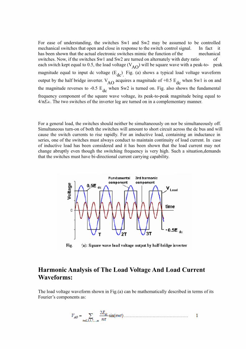
For ease of understanding, the switches Sw1 and Sw2 may be assumed to be controlled mechanical switches that open and close in response to the switch control signal. In fact it has been shown that the actual electronic switches mimic the function of the mechanical switches. Now, if the switches Sw1 and Sw2 are turned on alternately with duty ratio of each switch kept equal to 0.5, the load voltage (VAO) will be square wave with a peak-to- peak
magnitude equal to input dc voltage (Edc). Fig. (a) shows a typical load voltage waveform
output by the half bridge inverter. VAO acquires a magnitude of +0.5 Edc when Sw1 is on and
the magnitude reverses to -0.5 Edc when Sw2 is turned on. Fig. also shows the fundamental
frequency component of the square wave voltage, its peak-to-peak magnitude being equal to 4/πEdc. The two switches of the inverter leg are turned on in a complementary manner.
For a general load, the switches should neither be simultaneously on nor be simultaneously off. Simultaneous turn-on of both the switches will amount to short circuit across the dc bus and will cause the switch currents to rise rapidly. For an inductive load, containing an inductance in series, one of the switches must always conduct to maintain continuity of load current. In case of inductive load has been considered and it has been shown that the load current may not change abruptly even though the switching frequency is very high. Such a situation,demands that the switches must have bi-directional current carrying capability.
Harmonic Analysis of The Load Voltage And Load Current Waveforms:
The load voltage waveform shown in Fig.(a) can be mathematically described in terms of its Fourier’s components as:

where ‘n’ is the harmonic order and 2wπ is the frequency (‘f’) of the square wave. ‘f’ also happens to be the switching frequency of the inverter switches. As can be seen from the expression of Eqn. , the square wave load voltage consists of all the odd harmonics and their magnitudes are inversely proportional to their harmonic order.
Accordingly, the fundamental frequency component has a peak magnitude of 2/πEdc and the nth harmonic voltage (n being odd integer) has a peak magnitude of 2/πEdc . The magnitudes of very high order harmonic voltages become negligibly small. In most applications, only the fundamental component in load voltage is of practical use and the other higher order harmonics are undesirable distortions. Many of the practical loads are inductive with inherent low pass filter type characteristics. The current waveforms in such loads have less higher order harmonic distortion than the corresponding distortion in the square-wave voltage waveform. A simple time domain analysis of the load current for a series connected R-L load has been presented below to corroborate this fact. Later, for comparison, frequency domain analysis of the same load current has also been done.
Time Domain Analysis
The time domain analysis of the steady state current waveform for a R-L load has been presented here. Under steady state the load current waveform in a particular output cycle will repeat in successive cycles and hence only one square wave period has been considered. Let t=0 be the instant when the positive half cycle of the square wave starts and let I0 be the load current
at this instant. The negative half cycle of square wave starts at t=0.5T and extends up to T. The circuit equation valid during the positive half cycle of voltage can be written as below:
Similarly the equation for the negative half cycle can be written as

The instantaneous current ‘i’ during the first half of square wave may be obtained by solving Eqn..2 and putting the initial value of current as I0.
The current at the end of the positive half cycle becomes the starting current for the negative half cycle.
Simplifying the above equation one gets:
Under steady state, the instantaneous magnitude of inductive load current at the end of a periodic cycle must equal the current at the start of the cycle. Thus putting t=T in Eqn. (5), one gets the expression for I0 as,

Substituting the above expression for I0 in Eqn.4 one gets,
It may be noted from Eqn. (7) that the load current at the end of the positive half cycle of square wave (at t=0.5T) simply turns out to be –I0. This is expected from the symmetry of the load
voltage waveform. Load current expression for the negative half cycle of square wave can similarly be calculated by substituting for I0 in Eqn. (5). Accordingly,

The current expressions given by Eqns. (7) and (8) have been plotted in Figs.(b) to (e) for different time constants of the R-L load. The current waveforms have been normalized against a base current of 0.5Edc. The square wave voltage waveform, normalized against a base voltage of has also been plotted together with the current waveforms. It can be seen that the load current waveform repeats at fundamental frequency and the higher order harmonic distortions reduce as
the load becomes more inductive. For L/R ratio of 2, the 30.5dcErd order harmonic distortion in the load current together with its fundamental component has been shown in Fig. (e). In this case, it can be seen that the relative harmonic distortion in load current waveform is much lower than that of the voltage waveform shown in Fig. (a). The basis for calculating the magnitude of different harmonic components of load current waveform has been shown in the next subsection that deals with frequency domain analysis.
Frequency Domain Analysis
The square shape load voltage may be taken as superposition of different harmonic voltages described by Eqn.1. The load current may similarly be taken as superposition of harmonic currents produced by the different harmonic voltages. The load current may be expressed in terms of these harmonic currents. To illustrate this the series connected R-L load has once again been considered here. First the expressions for different harmonic components of load current are calculated in terms of load parameters: R and L/R (or τ) and inverter parameters: dc link voltage (Edc) and time period of square wave (T).
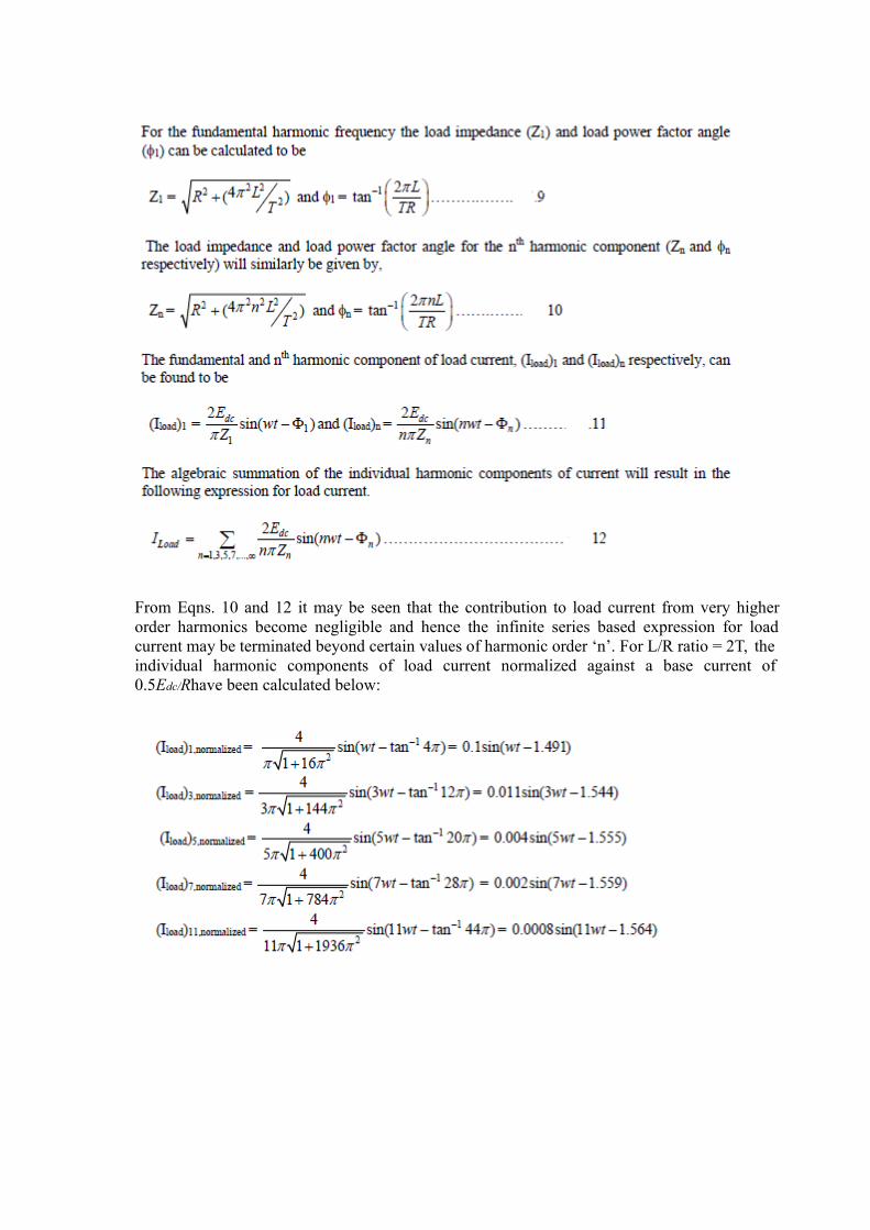
From Eqns. 10 and 12 it may be seen that the contribution to load current from very higher order harmonics become negligible and hence the infinite series based expression for load current may be terminated beyond certain values of harmonic order ‘n’. For L/R ratio = 2T, the individual harmonic components of load current normalized against a base current of 0.5Edc/Rhave been calculated below:
It may be concluded that for L/R = 2T, the contribution to load current from 13 th and higher order harmonics are less than 1% of the fundamental component and hence they may be neglected without any significant loss of accuracy.
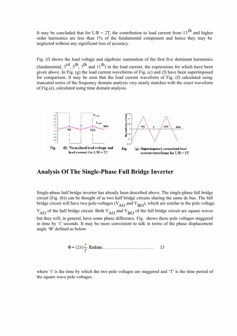
Fig. (f) shows the load voltage and algebraic summation of the first five dominant harmonics
(fundamental, 3rd, 5th, 7th and 11th) in the load current, the expressions for which have been given above. In Fig. (g) the load current waveforms of Fig. (e) and (f) have been superimposed for comparison. It may be seen that the load current waveform of Fig. (f) calculated using truncated series of the frequency domain analysis very nearly matches with the exact waveform of Fig.(e), calculated using time domain analysis.
Analysis Of The Single-Phase Full Bridge Inverter
Single-phase half bridge inverter has already been described above. The single-phase full bridge circuit (Fig. (b)) can be thought of as two half bridge circuits sharing the same dc bus. The full bridge circuit will have two pole-voltages (VAO and VBO), which are similar to the pole voltage
VAO of the half bridge circuit. Both VAO and VBO of the full bridge circuit are square waves
but they will, in general, have some phase difference. Fig. shows these pole voltages staggered in time by ‘t’ seconds. It may be more convenient to talk in terms of the phase displacement angle ‘Φ’ defined as below:
where ‘t’ is the time by which the two pole voltages are staggered and ‘T’ is the time period of the square wave pole voltages.
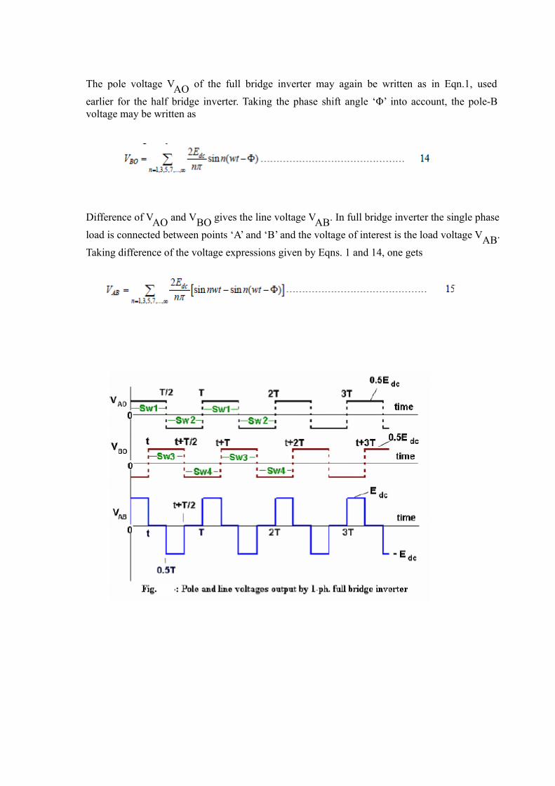
The pole voltage VAO of the full bridge inverter may again be written as in Eqn.1, used
earlier for the half bridge inverter. Taking the phase shift angle ‘Φ’ into account, the pole-B voltage may be written as
Difference of VAO and VBO gives the line voltage VAB. In full bridge inverter the single phase
load is connected between points ‘A’ and ‘B’ and the voltage of interest is the load voltage VAB.
Taking difference of the voltage expressions given by Eqns. 1 and 14, one gets

The rms magnitude of load voltage can be changed from zero to a peak magnitude of . The peak load voltage magnitude corresponds to Φ = 180 degrees and the load voltage will be zero for Φ = 00.9Edc. For Φ = 180 degrees, the load voltage waveform is once again square wave of time period T and instantaneous magnitude E.
As the phase shift angle changes from zero to 1800 the width of voltage pulse in the load voltage waveform increases. Thus the fundamental voltage magnitude is controlled by pulse-width modulation. Also, from Eqns. 17 and 1 it may be seen that the line voltage distortion due to
higher order harmonics for pulse width modulated waveform (except for Φ = 1800) is less than the corresponding distortion in the square wave pole voltage. In fact, for some values of phase shift angle (Φ) many of the harmonic voltage magnitudes will drastically reduce or may even get
eliminated from the load voltage. For example, for Φ = 600 the load voltage will be free from
3rd and multiples of third harmonic.
Three-phase voltage source inverter
In this lesson a 3-phase bridge type VSI with square wave pole voltages has been considered. The output from this inverter is to be fed to a 3-phase balanced load. Fig. shows the power circuit of the three-phase inverter. This circuit may be identified as three single-phase half-bridge inverter circuits put across the same dc bus. The individual pole voltages of the 3-phase bridge circuit are identical to the square pole voltages output by single-phase half bridge or full bridge circuits.

The three pole voltages of the 3-phase square wave inverter are shifted in time by one third of the output time period. These pole voltages along with some other relevant waveformshave been plotted in Fig.
The horizontal axis of the waveforms in Fig has been represented in terms of ‘ωt’, where ‘ω’ is the angular frequency (in radians per second) of the undamental component of square pole voltage and ‘t’ stands for time in second. In Fig. the phase sequence of the pole voltages is taken as VAO, VBO and VCO. The numbering of the switches in Fig. has some special
significance vis-à-vis the output phase sequence.
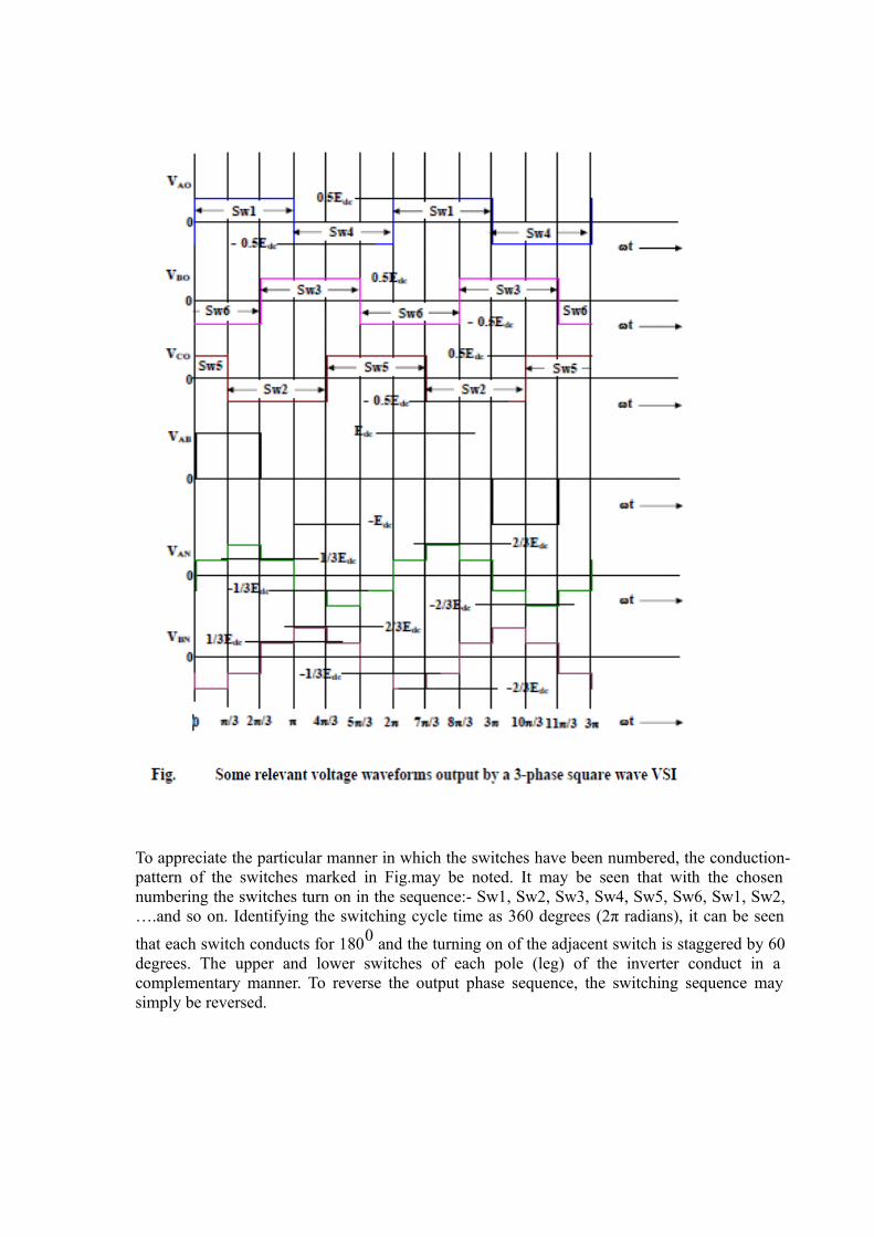
To appreciate the particular manner in which the switches have been numbered, the conduction-pattern of the switches marked in Fig.may be noted. It may be seen that with the chosen numbering the switches turn on in the sequence:- Sw1, Sw2, Sw3, Sw4, Sw5, Sw6, Sw1, Sw2, ….and so on. Identifying the switching cycle time as 360 degrees (2π radians), it can be seen
that each switch conducts for 1800 and the turning on of the adjacent switch is staggered by 60 degrees. The upper and lower switches of each pole (leg) of the inverter conduct in a complementary manner. To reverse the output phase sequence, the switching sequence may simply be reversed.
Considering the symmetry in the switch conduction pattern, it may be found that at any time three switches conduct. It could be two from the upper group of switches, which are connected to positive dc bus, and one from lower group or vice-versa (i.e., one from upper group and two from lower group). According to the conduction pattern indicated in Fig. 2 there are six combinations of conducting switches during an output cycle:- (Sw5, Sw6, Sw1), (Sw6, Sw1, Sw2), (Sw1, Sw2, Sw3), (Sw2, Sw3, Sw4), (Sw3, Sw4, Sw5), (Sw4, Sw5, Sw6). Each of these
combinations of switches conducts for 600 in the sequence mentioned above to produce output phase sequence of A, B, C. As will be shown later the fundamental component of the three output line-voltages will be balanced.
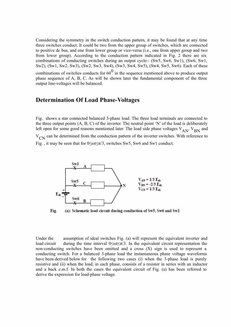
Determination Of Load Phase-Voltages
Fig. shows a star connected balanced 3-phase load. The three load terminals are connected to the three output points (A, B, C) of the inverter. The neutral point ‘N’ of the load is deliberately left open for some good reasons mentioned later. The load side phase voltages VAN, VBN and
VCN can be determined from the conduction pattern of the inverter switches. With reference to
Fig. , it may be seen that for 0≤ωt≤π/3, switches Sw5, Sw6 and Sw1 conduct.
Under the assumption of ideal switches Fig. (a) will represent the equivalent inverter and load circuit during the time interval 0≤ωt≤π/3. In the equivalent circuit representation the non-conducting switches have been omitted and a cross (X) sign is used to represent a conducting switch. For a balanced 3-phase load the instantaneous phase voltage waveforms have been derived below for the following two cases (i) when the 3-phase load is purely resistive and (ii) when the load, in each phase, consists of a resistor in series with an inductor and a back e.m.f. In both the cases the equivalent circuit of Fig. (a) has been referred to derive the expression for load-phase voltage.
For case (i), when the load is a balance resistive load, it is very easy to see that the instantaneous phase voltages, for 0≤ωt≤π/3, will be given by VAN = 1/3 Edc, VBN = -2/3 Edc, VCN = 1/3
Edc.
For case (ii), the following circuit relations hold good.
Thus the instantaneous magnitudes of load phase voltages, in case of a more general (but balanced) R-L-E load are same as in case of a simple balanced resistive load.
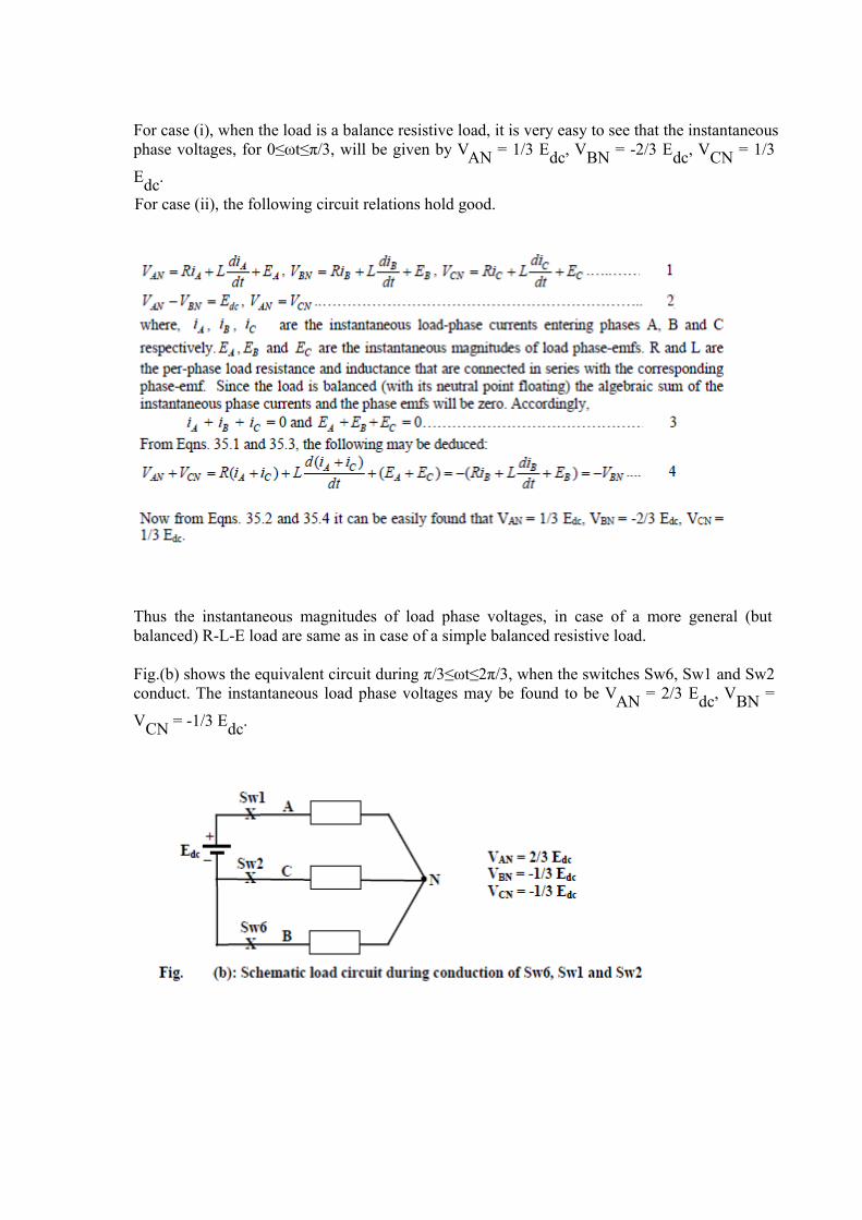
Fig.(b) shows the equivalent circuit during π/3≤ωt≤2π/3, when the switches Sw6, Sw1 and Sw2 conduct. The instantaneous load phase voltages may be found to be VAN = 2/3 Edc, VBN =
VCN = -1/3 Edc.
The load phase voltage waveforms for other switching combinations may be found in a similar manner. Two of the phase voltages,V and V, along with line voltage V have been plotted over two output cycles in Fig. It may be seen that voltage V is similar to V but lags it by one third of the output cycle period. Further, it can be verified that the load phase voltage V also has a waveform identical to the two other phase voltages but time displaced by one third of the output time period. V waveform leads V by 120 degrees in the time (ωt) frame. It should be obvious that the fundamental component of the phase voltage waveforms will constitute a balanced 3-phase voltage having a phase sequence A, B, C. It may also be recalled that by suitably changing the switching sequence the output phase sequence can be changed. The phase voltage waveforms of Fig. show six steps per output cycle and are also referred as the six-stepped waveform. A more detailed analysis of the load voltage waveforms is done in the following section.
Harmonic Analysis Of Load Voltage Waveforms
The individual pole voltage waveforms output by the 3-phase square wave inverter are identical to the output waveform of a single-phase half bridge inverter. For convenience the expressions for pole-A voltage ‘’ and line voltage ‘’ are reproduced below in Eqns.5 and 6. The relevant waveforms are shown in Fig.
Using equations 5 and 6, the expressions for remaining pole and line voltages can be written simply by shifting the time (ωt) origin by the phase shift angle shown in Fig..2. Accordingly the expressions for pole voltage and line voltage are written below in Eqns. 7 and 8 respectively.
It may be verified that difference of and leads to the expression for . The expression for a particular harmonic component in the voltage waveforms is determined simply by substituting ‘n’ in above equations by the harmonic order. Accordingly the fundamental magnitude of line voltages , and can be written as:
The three fundamental line voltages are balanced (have identical magnitudes and are phase apart
by 1200). For most practical loads only the fundamental component of the inverter output voltage is of interest. However the inverter output also contains significant amount of higher order harmonic voltages that cause undesirable distortion of the output waveform. It may,
though, be noted that there are no even harmonics and the line voltages are free from 3rd and
multiples of 3rd order harmonics. Also, as the harmonic order (n) increases their magnitudes decrease inversely with the harmonic order. When expressed as a fraction of fundamental
voltage magnitude, the line voltage distortions are mainly due to 20% of 5 th harmonic, nearly
14% of 7th, nearly 9% of 11th and nearly 8% of 13th harmonic. Since most loads are inductive in nature with a low pass filter type characteristics the effect of very high order harmonics may be neglected.
It may be noted that though the pole voltages have 3rd and multiples of 3rd order harmonic distortions, the line voltages are free from these distortions. Hence the load neutral point, rather than being connected to the mid-potential point of the input dc supply (as in a single-phase half bridge inverter), is deliberately left floating. The floating neutral point does not allow a closed
path for the 3rd and multiples of 3rd harmonic currents to flow (3rd or multiples of 3rd harmonic current, if present in the load phases, have identical instantaneous magnitudes in all the three phases and their algebraic sum needs to flow in or out of the load neutral point). By keeping the load neutral point floating, not only the need for bringing out the mid-potential point of dc supply is done away with, the triplen harmonic distortions of the load current is totally eliminated. Since there are no triplen harmonic currents in the load, the load-phase voltages are also free from triplen harmonic distortions. In fact the six-stepped load-phase voltages shown in Fig. are found to be free from triplen harmonics. It turns out that by removing all triplen harmonics from the square-shaped pole voltage waveform one can arrive at the corresponding load-phase (six-stepped) voltage waveform. Accordingly the load-phase voltages may be expressed in terms of its harmonic contents as shown below.
For a balanced three-phase load, the instantaneous magnitude of any phase current can be determined by superposition of different harmonic currents of the phase. For a simple three-phase R-L load, the phase-A current () expression in terms of resistance (R) and inductance (L) of the load may be written as:
Phase-B and phase-C current expressions can be obtained simply by replacingtωin Eqn.12
PWM techniques: Sinusoidal PWM
In Sine-PWM inverter the widths of the pole-voltage pulses, over the output cycle, vary in a sinusoidal manner. The scheme, in its simplified form, involves comparison of a high frequency triangular carrier voltage with a sinusoidal modulating signal that represents the desired fundamental component of the pole voltage waveform. The peak magnitude of the modulating signal should remain limited to the peak magnitude of the carrier signal.
The comparator output is then used to control the high side and low side switches of the particular pole. Fig. shows an op-amp based comparator output along with representative sinusoidal and triangular signals as inputs. In the comparator shown in Fig. the triangular and sinusoidal signals are fed to the inverting and the non-inverting input terminals respectively and the comparator output magnitudes for high and low levels are assumed to be +VCC and -VCC.

Fig.A schematic circuit for comparison of Modulating and Carrier signals
The comparator output signal ‘Q’ is used to turn-on the high side and low side switches of the inverter pole. When ‘Q’ is high, upper (high side) switch of the particular pole is turned on and when ‘Q’ is low the lower switch is turned on.
The pole voltage, thus obtained is a replica of the comparator output voltage. When ‘Q’= + VCC, the pole voltage (measured with respect to the mid potential point of the dc supply) is
+0.5Edc and when ‘Q’= (-)VCC, the pole voltage becomes (-0.5)Edc. The input dc voltage to
the inverter (Edc) has been assumed to be of constant magnitude. Thus, on a normalized scale,
the harmonic contents in the comparator output voltage and the pole voltage waveforms are identical.
Analysis Of The Pole Voltage Waveform With A Dc Modulating Signal
Before analyzing the sine-modulated pole voltage waveform, it would be revealing to consider a pure dc signal (of constant magnitude) as the modulating wave. The magnitude of the dc modulating signal is constrained to remain between the minimum and maximum magnitudes of the triangular carrier signal. Fig. illustrates one such case where the triangular carrier signal varies between -1.0 and +1.0 units of voltage and the magnitude of the modulating wave is kept at 0.4 unit of voltage.
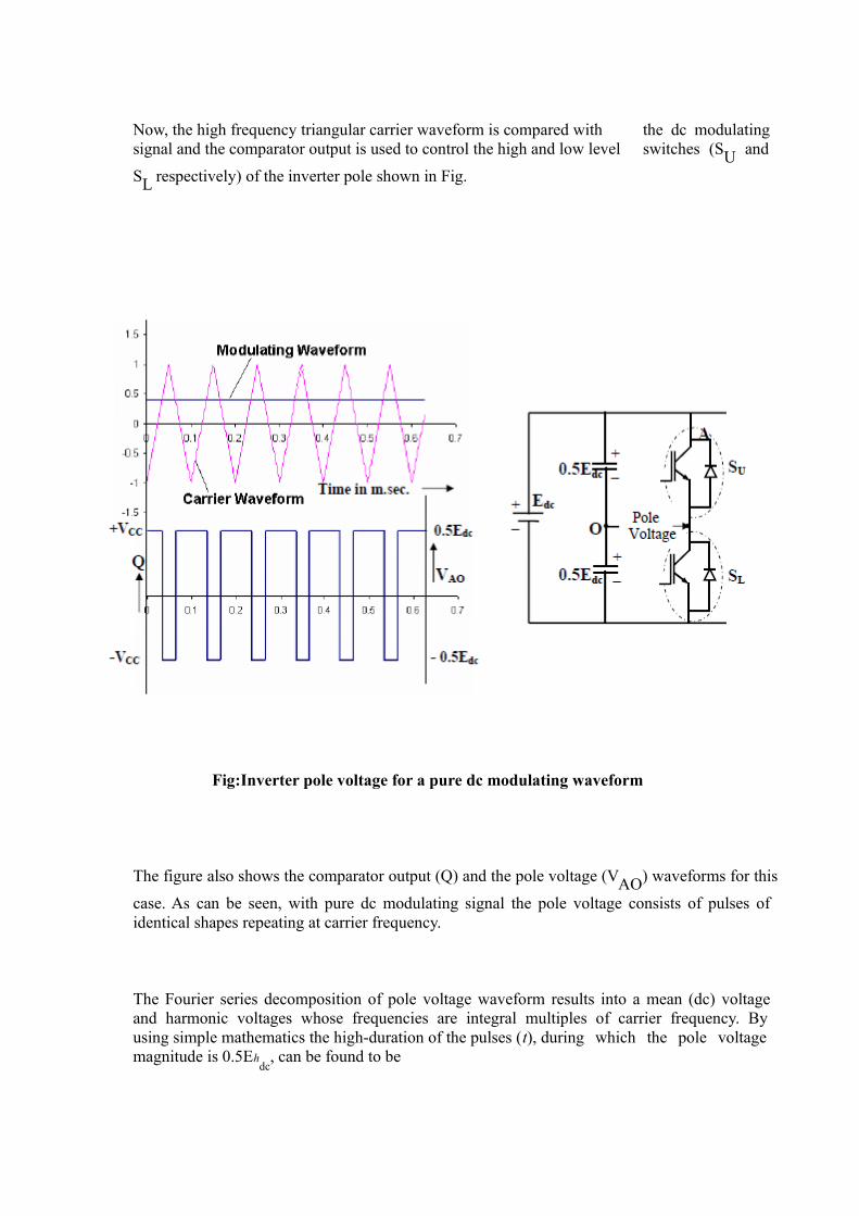
Now, the high frequency triangular carrier waveform is compared with the dc modulating signal and the comparator output is used to control the high and low level switches (SU and
SL respectively) of the inverter pole shown in Fig.
Fig:Inverter pole voltage for a pure dc modulating waveform
The figure also shows the comparator output (Q) and the pole voltage (VAO) waveforms for this
case. As can be seen, with pure dc modulating signal the pole voltage consists of pulses of identical shapes repeating at carrier frequency.
The Fourier series decomposition of pole voltage waveform results into a mean (dc) voltage and harmonic voltages whose frequencies are integral multiples of carrier frequency. By using simple mathematics the high-duration of the pulses (t), during which the pole voltage magnitude is 0.5Eh
dc, can be found to be
The dc modulating signal could acquire any magnitude between +and - cVand accordingly the mean magnitude of pole voltage can vary within +0.5Edc and -0.5Edc. When the modulating
signal magnitude (V) is zero, the high and low durations of the pole output pulses will be identical and the mean pole voltage magnitude will be zero. As mentioned before, apart from the dc component, the pole voltage consists of harmonics of integral multiples of carrier frequency. The lowest order harmonic-frequency being same as the carrier frequency.
What Is Modulation Index?
Modulation index is the ratio of peak magnitudes of the modulating waveform and the carrier waveform. It relates the inverter’s dc-link voltage and the magnitude of pole voltage (fundamental component) output by the inverter. Now let ‘Vm sinωt’ be the modulating signal and let the magnitude of triangular carrier signal vary between the peak magnitudes of +Vcand -Vc. The ratio of the peak magnitudes of modulating wave (Vm) and the carrier wave (Vc) is defined as modulation-index (m).
What Is Over-Modulation?
When the peak magnitude of modulating signal exceeds the peak magnitude of carrier signal (resulting in >1), the PWM inverter operates under over-modulation. During over-modulation the fundamental component of the pole voltage increases slightly with increase in modulation index but the linear relation between them, Also,lower frequency harmonics crop up in the pole-output waveform. It may easily be seen that for ,very high (say = infinity), the pole voltage shape will be identical to the square wave shape Over modulation is generally not preferred because of the introduction of lower frequency harmonics in the output waveform and subsequent distortion of the load current.

1-Phase Sine-PWM Inverter Of H-Bridge Topology
The single-phase full bridge is also called as H-bridge because of its resemblance with the letter ‘H’. [The two legs (poles) of the inverter resemble the two vertical lines of ‘H’ and the horizontal line denotes the load, which is connected to the pole output points.] The switches and the load in a single-phase full bridge PWM inverter are connected exactly as in a square-wave inverter circuit. The difference lies in the conduction pattern of the inverter switches. In the
square-wave inverter the switches conduct continuously for 1800 in each output cycle whereas in PWM inverter large number of switching take place in each output cycle.
Fig: Sine-PWM waveforms for single-phase H-Bridge inverter
The half bridge sine-PWM inverter employing only one leg has already been described in the previous section. The full bridge inverter employs one additional leg but the control signals of the half bridge circuit may still be employed for switches of the other leg. As in the square-wave inverter the diagonal switches of the two legs may be turned on together to produce a load voltage that has double the magnitude of individual pole voltage. The PWM signals for the high and low level switches of one leg (obtained by sine-triangle comparison) may again be used for low and high level switches, respectively, of the other leg.
Alternately, the modulating waveform for the other leg may be inverted (keeping the carrier waveform same). The two inverted modulating waveforms are then compared with the same carrier waveform using two different comparators. The comparator outputs, one for each leg, are then used to switch the high and low level switches as in the half bridge circuit.Fig shows the relevant waveforms that use two inverted sine waves as modulating signals for the two legs of the inverter. For better visibility the ratio between the carrier and modulating wave frequencies has been assumed equal to ‘eight’ (normally carrier frequency is much higher) and circuit waveforms for only part of the modulating wave cycle has been shown. In Fig.37.3, the blue colored modulating wave is used for pole-A of the inverter and the green colored for pole-B. The corresponding pole voltages (VAO, VBO) and the load voltage (VAB) are also shown in the
figure.
The scheme, using two inverted modulating waves, has the following advantages over the one that uses single modulating wave and employs simultaneous switching of the diagonal switches of the two legs:- (i) Overall harmonic distortion of the load voltage waveform is reduced and (ii) the frequency of the ripple voltage in the load waveform doubles. Both these points may be verified by mere inspection of the load voltage waveform shown in Fig. In case of single modulating wave, the instantaneous load voltage has double the amplitude of pole-A voltage and thus the harmonic distortion of the load voltage and pole voltage remains same. It may be noted that the instantaneous magnitude of load voltage, in this case, has two levels (+0.5Edc and -
0.5Edc). In the alternate scheme, using two inverted modulating waves, the load voltage has
double the number of pulses per carrier time period, thus doubling the ripple frequency. Now, higher the frequency of unwanted ripple-voltage, easier it is to filter out the ripple current. Also, the load voltage now has three levels (+0.5Edc, zero, and -0.5Edc). Presence of zero duration
reduces the rms magnitude of the overall load voltage (fundamental component along with harmonics), while keeping the magnitude of fundamental component of load voltage same as in the previous case (the rms of the overall load voltage for the two-level waveform equals Edc).
Thus the overall distortion of the load voltage waveform is less.

Generation Of 3-Phase Sine-PWM Waveform
A three-phase inverter, as discussed in Lessons 36, can be used to output a three-phase sine modulated pole-voltage pulses. Switches in each of the three poles of the inverter are individually controlled as per the technique discussed in the previous section. For a balanced three-phase output voltage from the inverter poles, the three sinusoidal modulating signals (one for each pole) must also be balanced three-phase signals. The carrier waveform for all the three poles may remain identical. The fundamental components of individual pole output voltages (for 0<<1) will thus be proportional to the corresponding modulating signals. For = 1, the rms magnitude of line-to-line voltage (fundamental component) output by the inverter will be equal to 322 Edc (= 0.612Edc). A typical line voltage waveform (difference of two pole voltage
waveforms) will appear similar to the line voltage waveform (V) shown in Fig.
Generating a balanced three phase SINE waveforms of controllable magnitude and frequency is a pretty difficult task for an analog circuit and hence a mixed analog and digital circuit is often preferred. Fig. shows a scheme, in block diagram, where the 3-phase analog SINE waves are generated with the help of EPROMs, D/A converters etc.
Fig.: Schematic circuit for generation of balanced sinusoidal signals

Current Source Inverter (CSI)
Load-Commutated CSI
In the lesson, ASCI mode of operation for a single-phase Current Source Inverter (CSI) was presented. Two commutating capacitors, along with four diodes, are used in the above circuit for commutation from one pair of thyristors to the second pair. Earlier, also in VSI, if the load is capacitive, it was shown that forced commutation may not be needed. The operation of a single-phase CSI with capacitive load is discussed here. It may be noted that the capacitor, C is assumed to be in parallel with resistive load (R). The capacitor, C is used for storing the charge, or voltage, to be used to force-commutate the conducting thyristor pair as will be shown. As was the case in the last lesson, a constant current source, or a voltage source with large inductance, is used as the input to the circuit.
Fig. Load-commuted CSI

Single-phase Current Source Inverter
The circuit of a Single-phase Current Source Inverter (CSI) is shown in Fig. The type of operation is termed as Auto-Sequential Commutated Inverter (ASCI). A constant current source is assumed here, which may be realized by using an inductance of suitable value, which must be high, in series with the current limited dc voltage source. The thyristor pairs, Th1 & Th3, and
Th2 & Th4, are alternatively turned ON to obtain a nearly square wave current waveform. Two
commutating capacitors − C1 in the upper half, and C2 in the lower half, are used. Four diodes,
D1–D4 are connected in series with each thyristor to prevent the commutating capacitors from
discharging into the load. The output frequency of the inverter is controlled in the usual way, i.e., by varying the half time period, (T/2), at which the thyristors in pair are triggered by pulses being fed to the respective gates by the control circuit, to turn them ON, as can be observed from the waveforms . The inductance (L) is taken as the load in this case, the reason(s) for which need not be stated, being well known. The operation is explained by two modes.
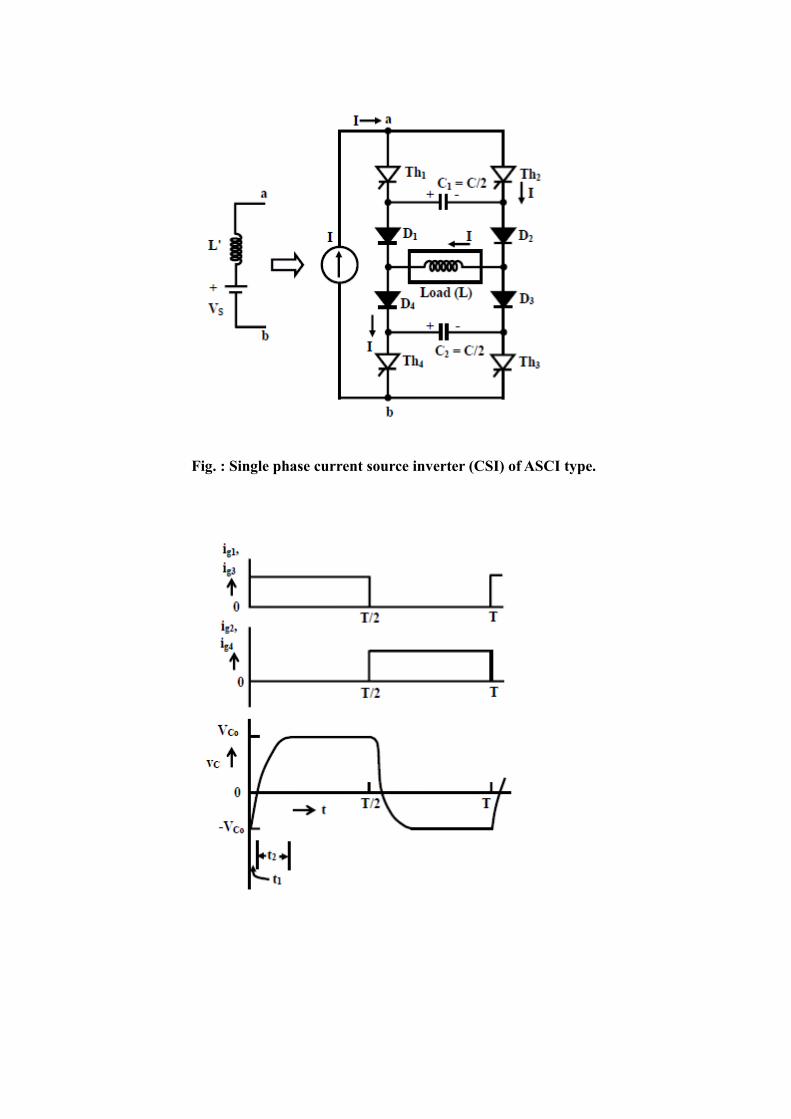
Fig. : Single phase current source inverter (CSI) of ASCI type.

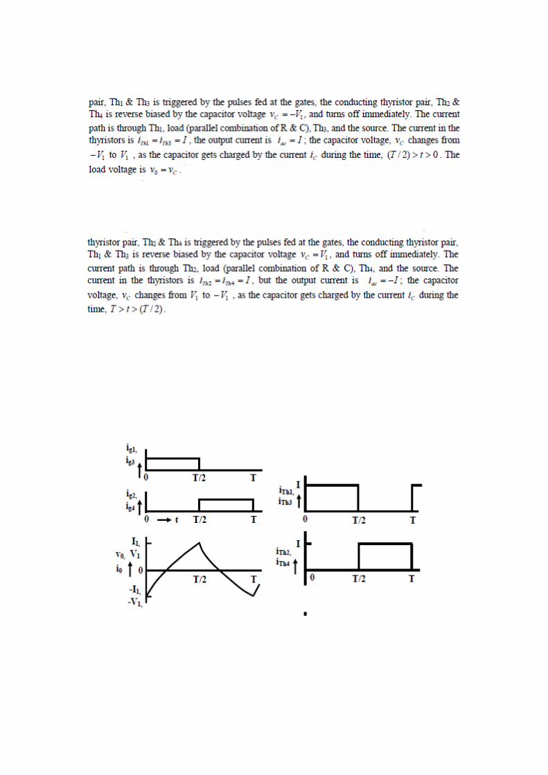
Fig. : Voltage and current waveforms
Mode I: The circuit for this mode is shown in Fig. The following are the assumptions. Starting from the instant,t=0- , the thyristor pair, Th2 & Th4, is conducting (ON), and the current (I)
flows through the path, Th2, D2, load (L), D4, Th4, and source, I. The commutating capacitors
are initially charged equally with the polarity as given, i.e.,vc1= vc2 = -Vc0 . This mans that both capacitors have right hand plate positive and left hand plate negative. If two capacitors are not charged initially, they have to pre-charged.

Fig. : Mode I (1 phase CSI)
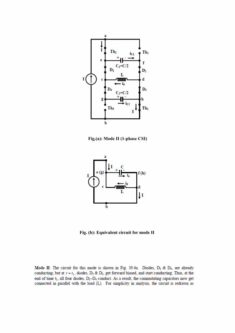
Fig.(a): Mode II (1-phase CSI)
Fig. (b): Equivalent circuit for mode II
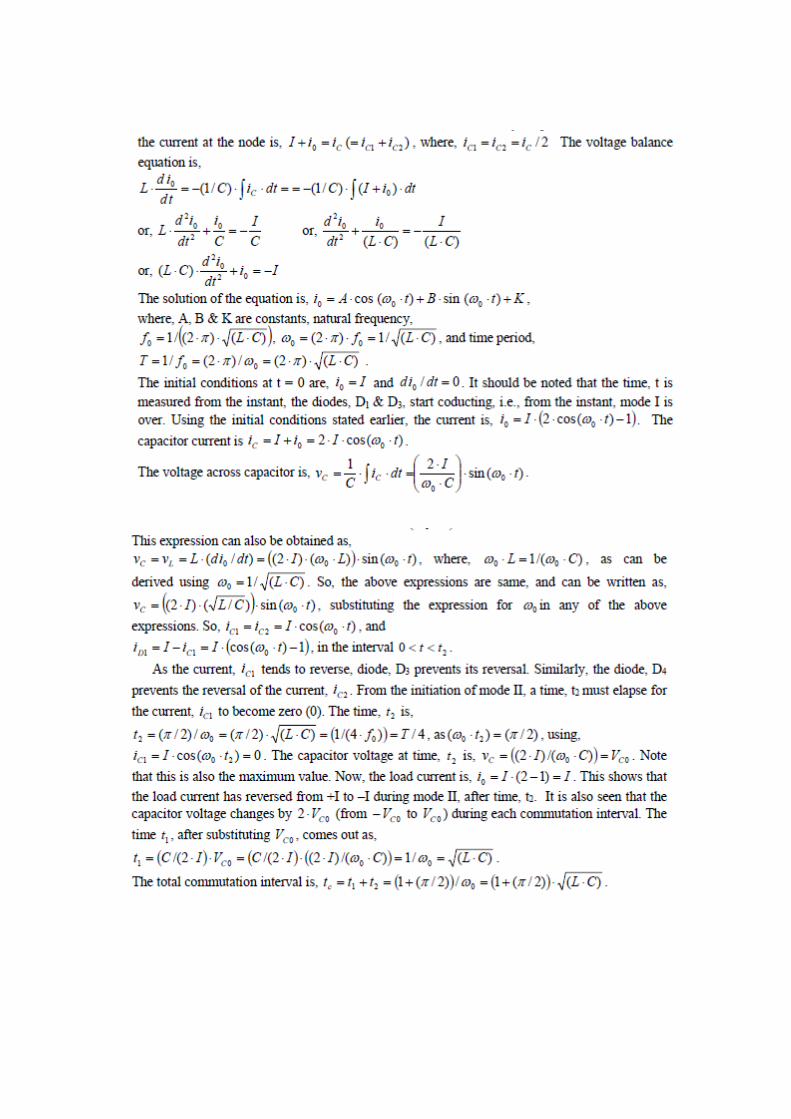
At the end of the process, constant current flows in the path, Th1, D1, load (L), D3, Th3, and
source, I. This continues till the next commutation process is initiated by the triggering of the thyristor pair, Th2 & Th4. The complete commutation process is summarized here. The process
(mode I) starts with the triggering of the thyristor pair, Th1 & Th3. Earlier, the thyristor pair,
Th2 & Th4 were conducting. With the two commutating capacitors charged earlier with the
polarity as shown , the conducting thyristor pair, Th2 & Th4 turns off by the application of
reverse voltage. Then, the voltages across the capacitors decrease to zero at time, (end of mode I), as constant (source) current, I flows in the opposite direction. Mode II now starts , as the diodes, D1t1 & D3, get forward biased, and start conducting. So, all four diodes
D1-D4, conduct, and the load inductance, L is now connected in parallel with the two
commutating capacitors.
The current in the load reverses to the value –I, after time, (end of mode II), and the two
capacitors also are charged to the same voltage in the reverse direction, the magnitude remaining
same, as it was before the start of the process of commutation (t = 0). It may be noted that the
constant current, I flows in the direction as shown, a part of which flows in the two capacitors.
In the above discussion, one form of load, i.e. inductance L only, has been considered. The
procedure remains nearly same, if the load consists of resistance, R only. The procedure in mode
I, is same, but in mode II, the load resistance, R is connected in parallel with the two
commutating capacitors. The direction of the current, I remains same, a part of which flows in
the two capacitors, charging them in the reverse direction, as shown earlier. The derivation,
being simple, is not included here. It is available in books on this subject.
Three-phase Current Source Inverter
The circuit of a Three-phase Current Source Inverter (CSI) is shown in Fig. a. The type of
operation in this case is also same here, i.e. Auto-Sequential Commutated Inverter (ASCI). As in
the circuit of a single-phase CSI, the input is also a constant current source. The output current
(phase) waveforms are shown in Fig. b. In this circuit, six thyristors, two in each of three
arms, are used, as in a three-phase VSI. Also, six diodes, each one in series with the respective
thyristor, are needed here, as used for single-phase CSI.
Six capacitors, three each in two (top and bottom) halves, are used for commutation. It may be
noted that six capacitors are equal, i.e. . The diodes are needed in CSI, so as to prevent the
capacitors from discharging into the load. The numbering scheme for the thyristors and
diodes are same, as used in a three-phase VSI, with the thyristors being triggered in sequence as
per number assigned inFig..
Fig.Three-phase Current Source Inverter (CSI)


The commutation process in a three-phase CSI is described in brief. The circuit, when two
thyristors, Th1 & Th2, and the respective diodes, are conducting, is shown in Fig. a. The current
is flowing in two phases, A & C. The three capacitors in the top half, are charged previously, or
have to pre-charged as shown. But the capacitors in the bottom half are not shown.
Mode I: The commutation process starts, when the thyristor, Th3 in the top half, is triggered, i.e.
pulse is fed at its gate. Immediately after this, the conducting thyristor, Th1 turns off by the
application of reverse voltage of the equivalent capacitor. Mode I (Fig. b) now starts. As the
diode D1 is still conducting, the current path is via Th3, the equivalent capacitor, D1, and the
load in phase A (only in the top half). The other part, i.e. the bottom half and the source, is not
considered here, as the path there remains same.
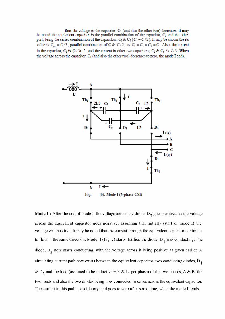
Mode II: After the end of mode I, the voltage across the diode, D3 goes positive, as the voltage
across the equivalent capacitor goes negative, assuming that initially (start of mode I) the
voltage was positive. It may be noted that the current through the equivalent capacitor continues
to flow in the same direction. Mode II (Fig. c) starts. Earlier, the diode, D1 was conducting. The
diode, D3 now starts conducting, with the voltage across it being positive as given earlier. A
circulating current path now exists between the equivalent capacitor, two conducting diodes, D1
& D3 and the load (assumed to be inductive − R & L, per phase) of the two phases, A & B, the
two loads and also the two diodes being now connected in series across the equivalent capacitor.
The current in this path is oscillatory, and goes to zero after some time, when the mode II ends.
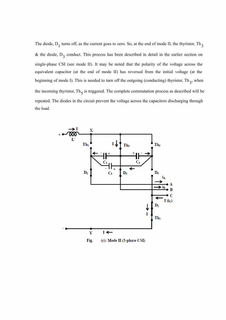
The diode, D1 turns off, as the current goes to zero. So, at the end of mode II, the thyristor, Th3
& the diode, D3 conduct. This process has been described in detail in the earlier section on
single-phase CSI (see mode II). It may be noted that the polarity of the voltage across the
equivalent capacitor (at the end of mode II) has reversed from the initial voltage (at the
beginning of mode I). This is needed to turn off the outgoing (conducting) thyristor, Th3, when
the incoming thyristor, Th5 is triggered. The complete commutation process as described will be
repeated. The diodes in the circuit prevent the voltage across the capacitors discharging through
the load.

The circuit is shown in Fig. d, with two thyristors, Th3 & Th2, and the respective diodes
conducting. The current now flows in two phases, B & C, at the end of the commutation process,
instead of phase A at the beginning (Fig. a). It may be noted the current in the bottom half (phase
C) continues to flow, and also the thyristor, Th2 & the diode, D2 remain in conduction mode.
This, in brief, is the commutation process, when the thyristor, Th3 is triggered and the current is
transferred to the thyristor, Th3 & the diode, D3 (phase B), from the thyristor, Th1 & the diode,
D1 (phase A).