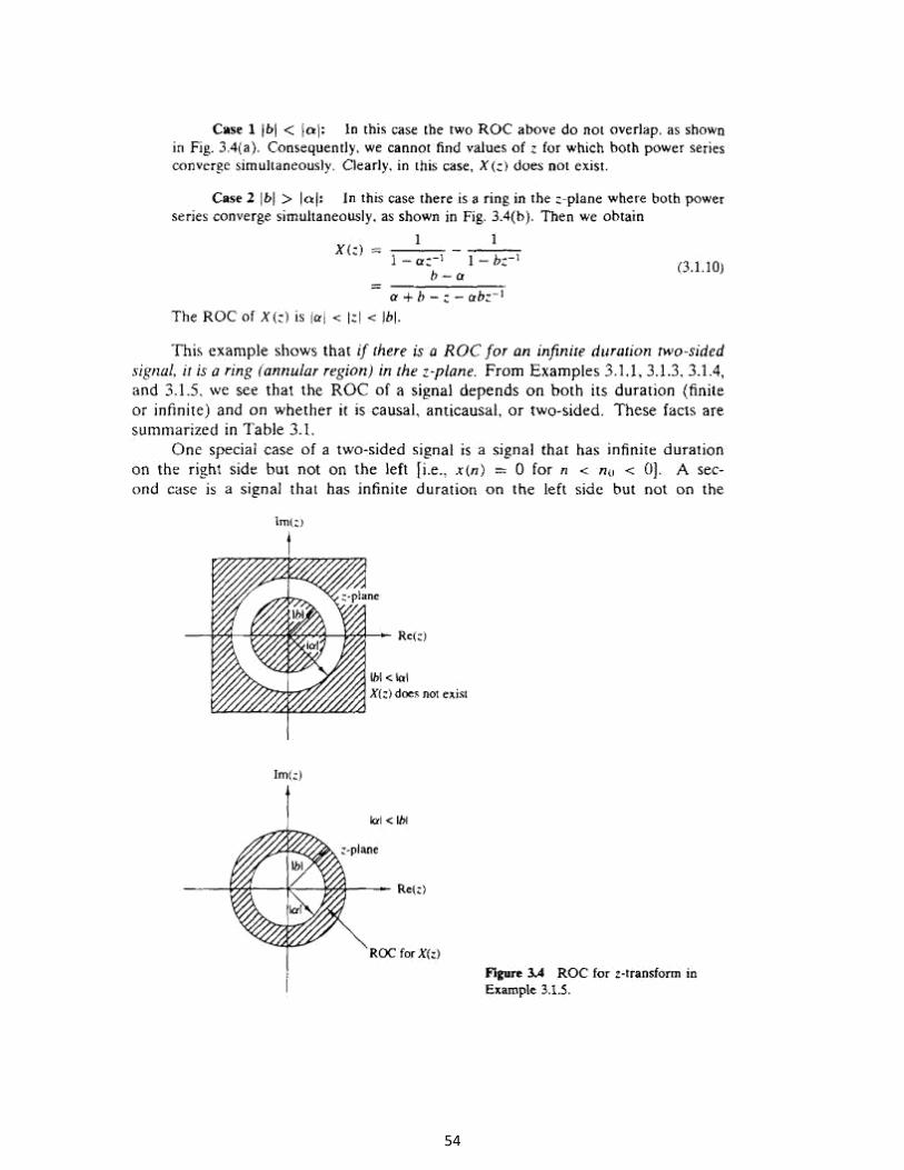
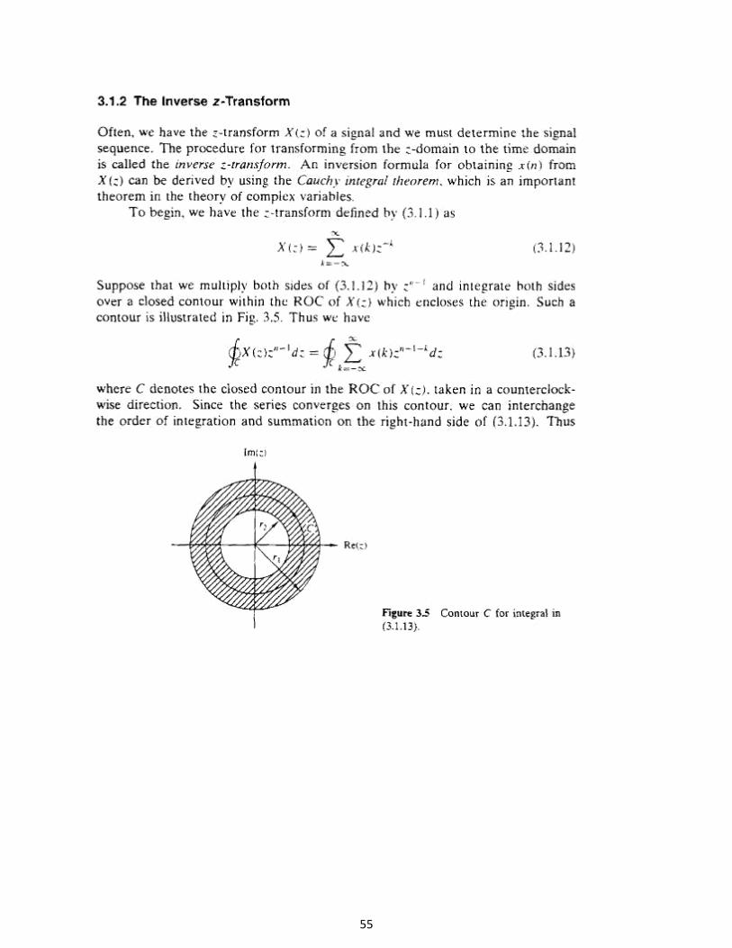
UNIT – I - INTRODUCTION TO DISCRETE TIME SIGNALS ...
175
1 SCHOOL OF ELECTRICAL AND ELECTRONICS DEPARTMENT OF ELECTRICAL AND ELECTRONICS ENGINEERING UNIT – I - INTRODUCTION TO DISCRETE TIME SIGNALS,SYSTEMS AND Z –TRANSFORM– SECA1507
-
Upload
khangminh22 -
Category
Documents
-
view
1 -
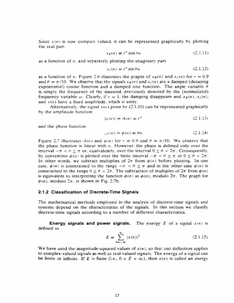
download
0
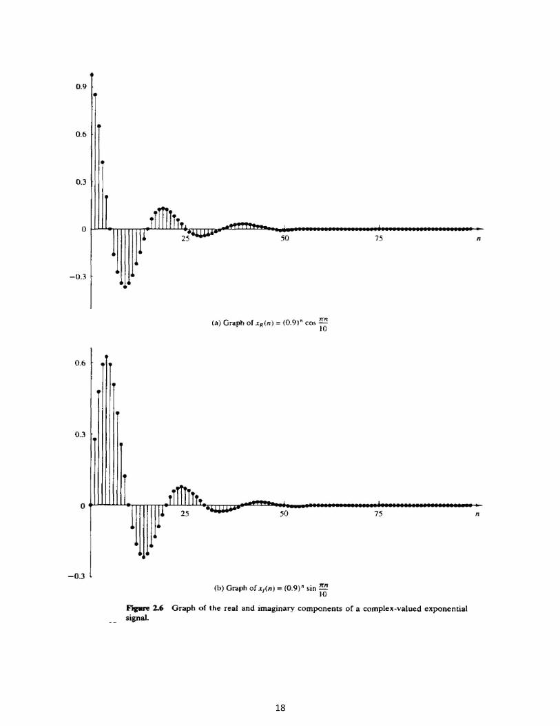
Transcript of UNIT – I - INTRODUCTION TO DISCRETE TIME SIGNALS ...

1
SCHOOL OF ELECTRICAL AND ELECTRONICS
DEPARTMENT OF ELECTRICAL AND ELECTRONICS ENGINEERING
UNIT – I - INTRODUCTION TO DISCRETE TIME SIGNALS,SYSTEMS
AND Z –TRANSFORM– SECA1507
2
SYLLABUS WITH COURSE OBJECTIVES AND COURSE OUTCOMES
DIGITAL SIGNAL PROCESSING AND ITS L T P Credits Total Marks
APPLICATIONS 3 0 0 3 100
COURSE OBJECTIVES
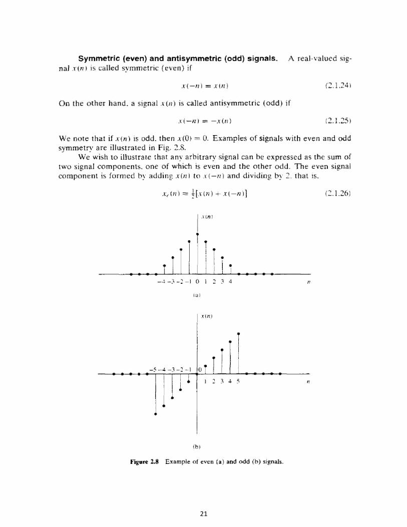
Ø To impart basic ideas in discrete signals and systems.
Ø To gain knowledge of Analog and Digital filter design with various structural realizations.
Ø To learn DSP controller pertaining to Power Electronics via programming.
UNIT 1 INTRODUCTION TO DISCRETE TIME SIGNALS,SYSTEMS AND Z –
TRANSFORM 9 Hrs.
Sampling theorem, Quantization, Quantization error, Aliasing- mathematical representation of
signals, Classifications of Signals and Systems - Review of Z transform & Inverse Z Transform-
ROC–Time response analysis using standard test signals ( step and ramp) – linear convolution-
Correlation.
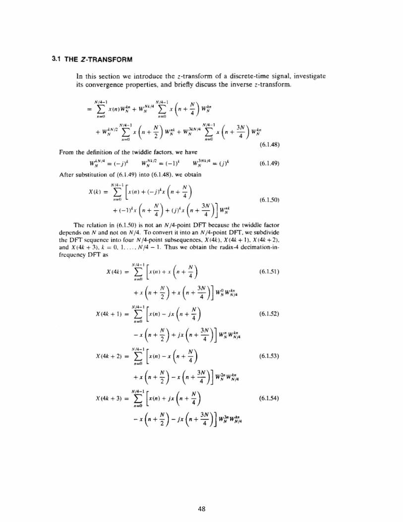
UNIT 2 DISCRETE FOURIER TRANSFORM AND COMPUTATION 9 Hrs.
Discrete Time Fourier Transform analysis(DTFT), Discrete Fourier Transform (DFT)- Properties
of DFT- frequency response analysis-magnitude and phase response, circular convolution, FFT
computations using radix-2 Decimation in Time (DIT) and Decimation in frequency(DIF)
algorithms.
UNIT 3 DESIGN OF INFINITE IMPULSE RESPONSE FILTER (IIR) 9 Hrs.
Design of IIR filters using Impulse invariant and Bilinear transformation method- Prewarping.
Review of Butterworth and Chebyshev approximations- Frequency transformation in analog
domain- Filter design using Butterwoth and Chebyshev- Realization of recursive structures-
Direct form-I-Direct form-II-Cascade-Parallel Forms.
UNIT 4 DESIGN OF FINITE IMPULSE RESPONSE (FIR) FILTER 9 Hrs.
Properties of IIR and FIR filters - Filter design using windowing techniques - Hamming,
Hanning, Blackman, Rectangular, Triangular windows- Digital filter design using Frequency
sampling technique- Realization of Structures for FIR and Linear phase FIR filter- Direct form-
Transposed form- Cascaded form, Elementary Ideas of Finite Word Length effects in Digital
Filters.
UNIT 5 DSP APPLICATIONS USING TMS 320C24X PROCESSOR 9 Hrs.
Nomenclature- TMS 320 family overview -Architectural Overview-Central Processing unit –
Addressing modes- Event Manager- General purpose timers (GPR)- Full compare Unit (FCU)-
Dead band unit- simple programs for PWM generation using GPR and FCU pertaining to Power
Electronic applications. Max. 45 Hrs.
3
COURSE OUTCOMES
On completion of the course, student will be able to
CO1 - Understand classification of signals, systems, Sampling Theorem and Z- transform.
CO2 - Apply Discrete-Fourier Transform and Fast Fourier Transform on DT signals.
CO3 - Design and analyze IIR digital filters.
CO4 - Design and analyze FIR digital filters.
CO5 - Implement digital filters using different realization techniques.
CO6 - Understand and generate PWM pulse using DSP processor (TMS320CX2407).
.
TEXT / REFERENCE BOOKS
1. John G. Proakis & Dimitris G.Manolakis, “Digital Signal Processing - Principles, Algorithms
& Applications”, 4th Edition, Pearson education / Prentice Hall, 2007.
2. Emmanuel C..Ifeachor, & Barrie.W.Jervis, “Digital Signal Processing”, 2nd Edition, Pearson
Education / Prentice Hall, 2002.
3. Alan V.Oppenheim, Ronald W. Schafer & Hohn. R.Back, “Discrete Time Signal Processing”,
Pearson Education, 2nd
Edition, 2005.
4. Andreas Antoniou, “Digital Signal Processing”, Tata McGraw Hill, 2001.
END SEMESTER EXAMINATION QUESTION PAPER PATTERN
Max. Marks: 100 Exam Duration: 3 Hrs.
PART A: 10 Question of 2 marks each – No choice 20 Marks
PART B: 2 Questions from each unit of internal choice; each carrying 16 marks 80 Marks
4
I. SIGNALS, SYSTEMS & TRANSFORMS
1.1 INTRODUCTION
A signal is a function of independent variables such as time, distance, position, temperature and
pressure. A signal carries information, and the objective of signal processing is to extract useful
information carried by the signal.
Signal processing is concerned with the mathematical representation of the signal and the
algorithmic operation carried out on it to extract the information present. For most purposes of
description and analysis, a signal can be defined simply as a mathematical function, y where x is
the independent variable .y = f (x) .e.g.: y=sin(ωt) is a function of a variable in the time domain
and is thus a time signal.X(ω)=1/(-mω2+icω+k) is a frequency domain signal; An image I(x,y) is
in the spatial domain.
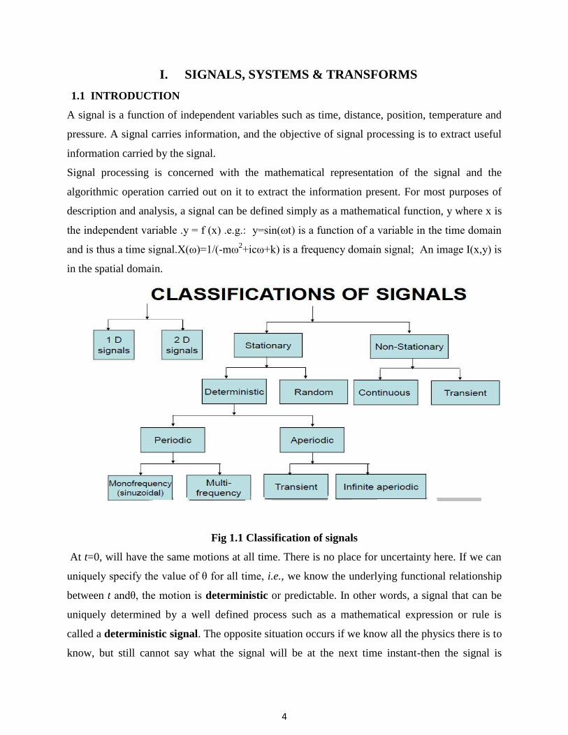
Fig 1.1 Classification of signals
At t=0, will have the same motions at all time. There is no place for uncertainty here. If we can
uniquely specify the value of θ for all time, i.e., we know the underlying functional relationship
between t andθ, the motion is deterministic or predictable. In other words, a signal that can be
uniquely determined by a well defined process such as a mathematical expression or rule is
called a deterministic signal. The opposite situation occurs if we know all the physics there is to
know, but still cannot say what the signal will be at the next time instant-then the signal is
5
random or probabilistic. In other words, a signal that is generated in a random fashion and can
not be predicted ahead of time is called a random signal.
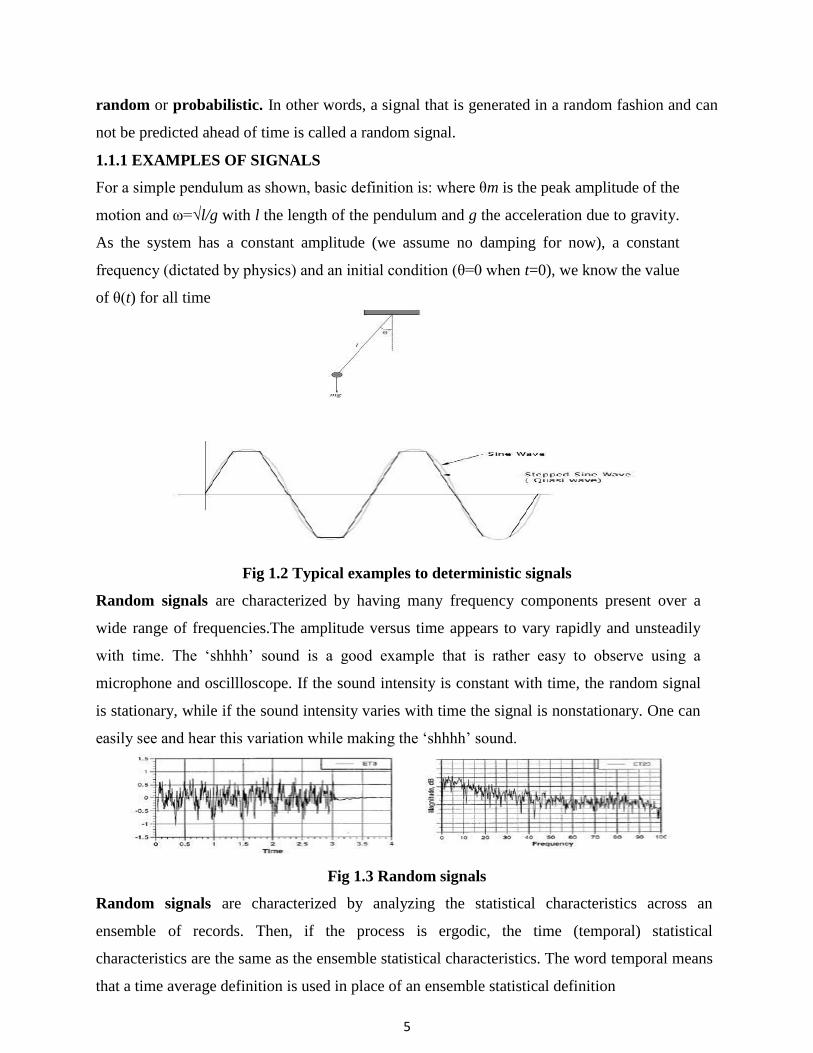
1.1.1 EXAMPLES OF SIGNALS
For a simple pendulum as shown, basic definition is: where θm is the peak amplitude of the
motion and ω=√l/g with l the length of the pendulum and g the acceleration due to gravity.
As the system has a constant amplitude (we assume no damping for now), a constant
frequency (dictated by physics) and an initial condition (θ=0 when t=0), we know the value
of θ(t) for all time
Fig 1.2 Typical examples to deterministic signals
Random signals are characterized by having many frequency components present over a
wide range of frequencies.The amplitude versus time appears to vary rapidly and unsteadily
with time. The „shhhh‟ sound is a good example that is rather easy to observe using a
microphone and oscillloscope. If the sound intensity is constant with time, the random signal
is stationary, while if the sound intensity varies with time the signal is nonstationary. One can
easily see and hear this variation while making the „shhhh‟ sound.
Fig 1.3 Random signals
Random signals are characterized by analyzing the statistical characteristics across an
ensemble of records. Then, if the process is ergodic, the time (temporal) statistical
characteristics are the same as the ensemble statistical characteristics. The word temporal means
that a time average definition is used in place of an ensemble statistical definition
6
Transient signals may be defined as signals that exist for a finite range of time as shown in the
figure. Typical examples are hammer excitation of systems, explosion and shock loading etc. It
should be noted that periodicity does not necessarily mean a sinusoidal signal as shown in the
figure.
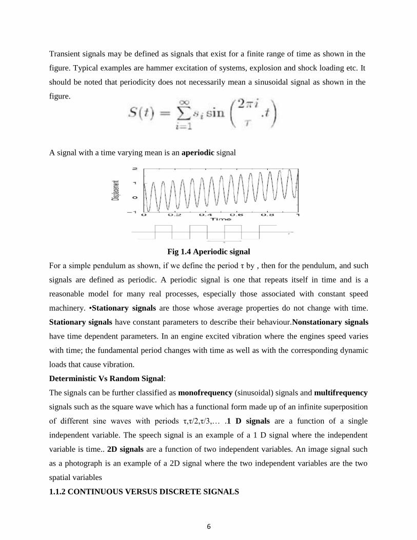
A signal with a time varying mean is an aperiodic signal
Fig 1.4 Aperiodic signal
For a simple pendulum as shown, if we define the period τ by , then for the pendulum, and such
signals are defined as periodic. A periodic signal is one that repeats itself in time and is a
reasonable model for many real processes, especially those associated with constant speed
machinery. •Stationary signals are those whose average properties do not change with time.
Stationary signals have constant parameters to describe their behaviour.Nonstationary signals
have time dependent parameters. In an engine excited vibration where the engines speed varies
with time; the fundamental period changes with time as well as with the corresponding dynamic
loads that cause vibration.
Deterministic Vs Random Signal:
The signals can be further classified as monofrequency (sinusoidal) signals and multifrequency
signals such as the square wave which has a functional form made up of an infinite superposition
of different sine waves with periods τ,τ/2,τ/3,… .1 D signals are a function of a single
independent variable. The speech signal is an example of a 1 D signal where the independent
variable is time.. 2D signals are a function of two independent variables. An image signal such
as a photograph is an example of a 2D signal where the two independent variables are the two
spatial variables
1.1.2 CONTINUOUS VERSUS DISCRETE SIGNALS
7
The value of a signal at a specific value of the independent variable is called its amplitude.The
variation of the amplitude as a function of the independent variable is called its waveform.For a
1 D signal, the independent variable is usually labelled as time. If the independent variable is
continuous, the signal is called a continuous-time signal. A continuous time signal is defined at
every instant of time.If the independent variable is discrete, the signal is called a discrete-time
signal. A discrete time signal takes certain numerical values at specified discrete instants of time,
and between these specified instants of time, the signal is not defined. Hence, a discrete time
signal is basically a sequence of numbers.
1.1.3 ANALOG VERSUS DIGITAL SIGNALS
A continuous-time signal with a continuous amplitude is usually called an analog signal. A
speech signal is an example of an analog signal.
A discrete time signal with discrete valued amplitudes represented by a finite number of digits is
referred to as a digital signal
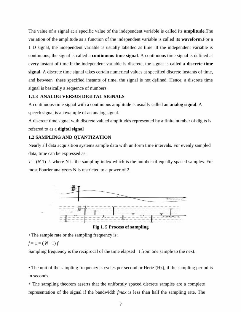
1.2 SAMPLING AND QUANTIZATION
Nearly all data acquisition systems sample data with uniform time intervals. For evenly sampled
data, time can be expressed as:
T = (N 1) t. where N is the sampling index which is the number of equally spaced samples. For
most Fourier analyzers N is restricted to a power of 2.
Fig 1. 5 Process of sampling
• The sample rate or the sampling frequency is:
f = 1 = ( N −1) f
Sampling frequency is the reciprocal of the time elapsed t from one sample to the next.
• The unit of the sampling frequency is cycles per second or Hertz (Hz), if the sampling period is
in seconds.
• The sampling theorem asserts that the uniformly spaced discrete samples are a complete
representation of the signal if the bandwidth fmax is less than half the sampling rate. The
8
sufficient condition for exact reconstructability from samples at a uniform sampling rate fs
(in samples per unit time) (fs≥2fmax).
1.2.1 Aliasing
One problem encountered in A/D conversion is that a high frequency signal can be falsely
confused as a low frequency signal when sufficient precautions have been avoided.This happens
when the sample rate is not fast enough for the signal and one speaks of aliasing.Unfortunately,
this problem can not always be resolved by just sampling faster, the signal‟s frequency content
must also be limited. Furthermore, the costs involved with postprocessing and data analysis
increase with the quantity of data obtained.
Data acquisition systems have finite memory, speed and data storage capabilities. Highly
oversampling a signal can necessitate shorter sample lengths, longer time on test, more storage
medium and increased database management and archiving requirements The central concept to
avoid aliasing is that the sample rate must be at least twice the highest frequency component of
the signal (fs≥2fmax).
We define the Nyquist or cut-off frequency.The concept behind the cut-off frequency is often
referred to as 2 t. Shannon‟s sampling criterion. Signal components with frequency content
above the cut-off frequency are aliased and can not be distinguished from the frequency
components below the cut-off frequency.
Conversion of analog frequency into digital frequency during sampling is shown in the figure.
Continuous signals with a frequency less than one-half of the sampling rate are directly
converted into the corresponding digital frequency. Above one-half of the sampling rate, aliasing
takes place, resulting in the frequency being misrepresented in the digital data. Aliasing always
changes a higher frequency into a lower frequency between 0 and 0.5. In addition, aliasing may
also change the phase of the signal by 180 degrees.
Fig 1.6 Aliasing effect
9
If any energy in the original signal extends beyond the Nyquist frequency, it is folded back into
the Nyquist interval in the spectrum of the sampled signal. This folding is called
aliasing.fs≥2fmax
Fig 1.7 Spectrum of sampled signal
Quantization Quantization is involved to some degree in nearly all digital signal processing, as
the process of representing a signal in digital form ordinarily involves rounding. Quantization
also forms the core of essentially all lossy compression algorithms. The difference between an
input value and its quantized value (such as round-off error) is referred to as quantization error.
A device or algorithmic function that performs quantization is called a quantizer. An analog-to-
digital converter is an example of a quantizer. Because quantization is a many-to-few mapping, it
is an inherently non-linear and irreversible process (i.e., because the same output value is shared
by multiple input values, it is impossible in general to recover the exact input value when given
only the output value). The set of possible input values may be infinitely large, and may possibly
be continuous and therefore uncountable (such as the set of all real numbers, or all real numbers
within some limited range). The set of possible output values may be finite or countably infinite.
The input and output sets involved in quantization can be defined in a rather general way. For
example, vector quantization is the application of quantization to multi-dimensional (vector-
valued) input data.
1.2.2 Quantization Noise
Quantization refers to the process of approximating the continuous set of values in the data with
a finite (preferably small) set of values. The input to a quantizer is the original data, and the
output is always one among a finite number of levels. The quantizer is a function whose set of
output values are discrete, and usually finite. Obviously, this is a process of approximation, and a

10
good quantizer is one which represents the original signal with minimum loss or distortion. The
difference between the actual analog value and quantized digital value due is called
quantization error. This error is due either to rounding or truncation.
Because quantization is a many-to-few mapping, it is an inherently non-linear and irreversible
process (i.e., because the same output value is shared by multiple input values, it is impossible in
general to recover the exact input value when given only the output value).The set of possible
input values may be infinitely large, and may possibly be continuous and therefore uncountable
(such as the set of all real numbers, or all real numbers within some limited range). The set of
possible output values may be finite or countably infinite. The input and output sets involved in
quantization can be defined in a rather general way. For example, vector quantization is the
application of quantization to multi-dimensional (vector-valued) input data.
Quantization noise is a model of quantization error introduced by quantization in the analog-to-
digital conversion (ADC) in telecommunication systems and signal processing. It is a rounding
error between the analog input voltage to the ADC and the output digitized value. The noise is
non-linear and signal-dependent. It can be modelled in several different ways. In an ideal analog-
to-digital converter, where the quantization error is uniformly distributed between −1/2 LSB and
+1/2 LSB, and the signal has a uniform distribution covering all quantization levels, the signal-
to-noise ratio (SNR) can be calculated from
The most common test signals that fulfill this are full amplitude triangle waves and saw tooth
waves. In this case a 16-bit ADC has a maximum signal-to-noise ratio of 6.0206 × 16 = 96.33
dB. When the input signal is a full-amplitude sine wave the distribution of the signal is no longer
uniform, and the corresponding equation is instead Here, the quantization noise is once again
assumed to be uniformly distributed. When the input signal has a high amplitude and a wide
frequency spectrum this is the case. In this case a 16-bit ADC has a maximum signal-to-noise
ratio of 98.09 dB. The 1.761 difference in signal-to-noise only occurs due to the signal being a
full-scale sine wave instead of a triangle/saw tooth.
Truncation Error and Rounding Error:
A round-off error, also called rounding error, is the difference between the calculated
approximation of a number and its exact mathematical value. Numerical analysis specifically
tries to estimate this error when using approximation equations and/or algorithms, especially
11
when using finite digits to represent real numbers (which in theory have infinite digits). This is a
form of quantization error.
Truncation: simply chop off the remaining digits; also called rounding to zero. 0.142857 ≈
0.142 (dropping all significant digits after 3rd) Round to nearest: round to the nearest value,
with ties broken in one of two ways. The result may round up or round down. In mathematics,
truncation is the term for limiting the number of digits right of the decimal point, by discarding
the least significant ones. For example, consider the real numbers 5.6341432543653654
32.438191288 -6.3444444444444 To truncate these numbers to 4 decimal digits, we only
consider the 4 digits to the right of the decimal point. The result would be: 5.6341 32.4381 -
6.3444 Note that in some cases, truncating would yield the same result as rounding, but
truncation does not round up or round down the digits; it merely cuts off at the specified digit.
The truncation error can be twice the maximum error in rounding
1.3 CONCEPTS OF SIGNAL PROCESSING
In the case of analog signals, most signal processing operations are usually carried out in
the time domain.In the case of discrete time signals, both time domain and frequency
domain applications are employed.In either case, the desired operations are implemented by
a combination of some elementary operations such as:
– Simple time domain operations , Filtering , Amplitude modulation
The three most basic time-domain signal operations are:
• Scaling
• Delay
• Addition
Scaling is simply the multiplication of a signal by a positive or a negative constant. In the case
of analog signals, this operation is usually called amplification if the magnitude of the
multiplying constant, called gain, is greater than one. If the magnitude of the multiplying
constant is less than one, the operation is called attenuation. Thus, if x(t) is an analog signal,
the scaling operation generates a signal y(t)=αx(t), where α is the multiplying constant.
Delay operation generates a signal that is delayed replica of the original signal. For an analog
signal x(t), y(t)=x(t-t0) is the signal obtained by delaying x(t) by the amount t0, which is
assumed to be a positive number. If t0 is negative, then it is an advance operation Addition
operation generates a new signal by the addition of signals. For instance, y(t)=x1(t)+x2(t)-x3(t) is
the signal generated by the addition of the three analog signals x1(t), x2(t) and x3(t) .
12
1.4 TYPICAL APPLICATIONS
The main applications of DSP are
AUDIO SIGNAL PROCESSING, sometimes referred to as audio processing, is the intentional
alteration of auditory signals, or sound, often through an audio effect oreffects unit. As audio
signals may be electronically represented in either digital or analog format, signal processing
may occur in either domain. Analog processors operate directly on the electrical signal, while
digital processors operate mathematically on the digital representation of that signal.
AUDIO COMPRESSION, bit-rate reduction involves encoding information using fewer bits
than the original representation.[2]Compression can be either lossy or lossless. Lossless
compression reduces bits by identifying and eliminating statistical redundancy. No information is
lost in lossless compression. Lossy compression reduces bits by identifying unnecessary
information and removing it.[3] The process of reducing the size of a data file is referred to as
data compression. In the context of data transmission, it is called source coding (encoding done
at the source of the data before it is stored or transmitted) in opposition to channel coding.[4]
DIGITAL IMAGE PROCESSING, is the use of computer algorithms to perform image
processing on digital images. As a subcategory or field of digital signal processing, digital image
processing has many advantages over analog image processing. It allows a much wider range of
algorithms to be applied to the input data and can avoid problems such as the build-up of noise
and signal distortion during processing. Since images are defined over two dimensions (perhaps
more) digital image processing may be model in the form of multidimensional systems
SPEECH PROCESSING,s the study of speech signals and the processing methods of these
signals. The signals are usually processed in a digital representation, so speech processing can be
regarded as a special case of digital signal processing, applied to speech signal. Aspects of
speech processing includes the acquisition, manipulation, storage, transfer and output of speech
signals.
SPEECH RECOGNITION, is the inter-disciplinary sub-field of computational linguistics
which incorporates knowledge and research in the linguistics, computer science, and electrical
engineering fields to develop methodologies and technologies that enables the recognition and
translation of spoken language into text by computers and computerized devices such as those
categorized as Smart Technologies and robotics. It is also known as "automatic speech
recognition" (ASR), "computer speech recognition", or just "speech to text" (STT). imaging such
as CAT scans and MRI, MP3 compression, computer graphics, image manipulation, hi-fi
13
loudspeaker rcrossovers and equalization, and audio effects for use with electric guitar
amplifiers.
1.4.1 ADVANTAGES OF DIGITAL SIGNAL PROCESSING COMPARED WITH
ANALOG SIGNAL PROCESSING
Accracy
Implimentation of sophisticated algorithms
Storage
Noise reduction
1.4.2 APPLICATIONS OF SIGNAL PROCESSING IN BIOMEDICAL ENGINEERING
I/0 signal processing – for electrical signals representing sound, such as speech or music ,Speech
signal processing
,Image processing
Video processing – for interpreting moving pictures, ,
Control systems,
Array processing – for processing signals from arrays of sensors,
Seismology,
Financial signal processing – analyzing financial data using signal processing techniques,
especially for prediction purposes.
Feature extraction, such as image understanding and ,
Quality improvement, such as noise reduction,
image enhancement, and
echo cancellation.(Source coding), including audio compression,
image compression, and
video compression
1.5 DISCRETE TIME SIGNALS
A discrete time signal is defined as the one that is defined at distinct time intervals
14
Fig 1.8
15
16
17
18
19
20
21
22
23
24
25
26
27
28
29
30
31
32
33
34
35
36
37
38
39
40
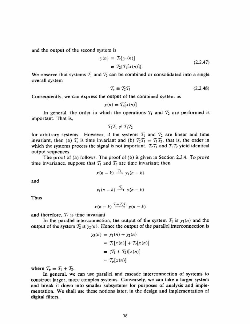
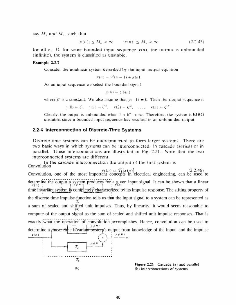
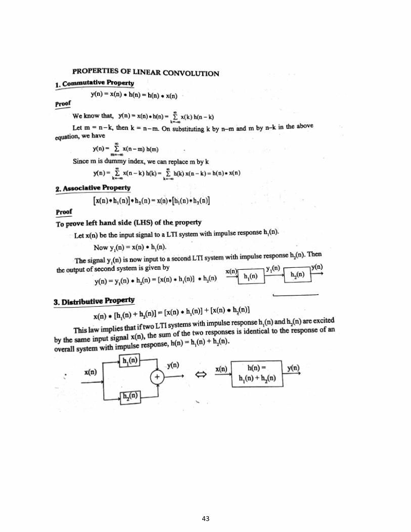
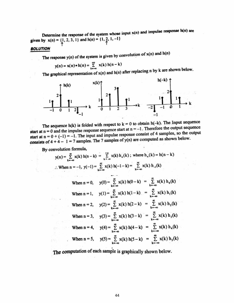
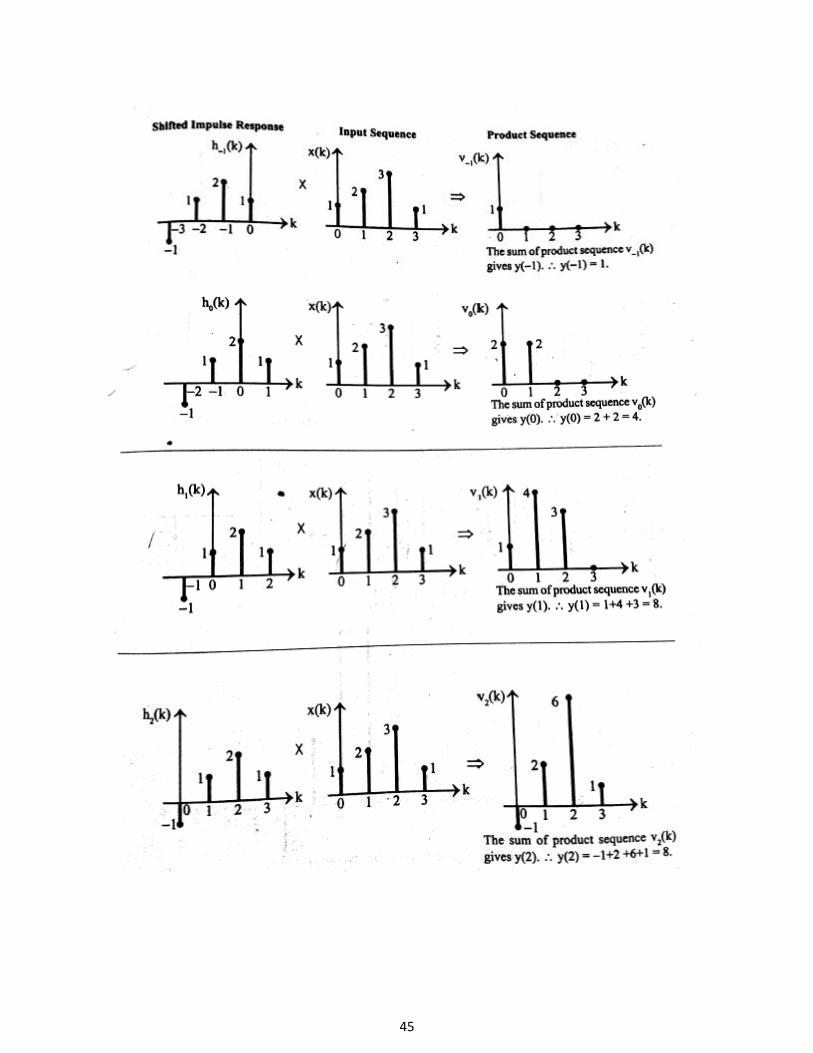
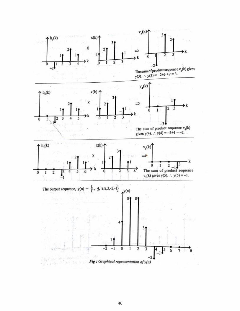
Convolution
Convolution, one of the most important concepts in electrical engineering, can be used to
determine the output a system produces for a given input signal. It can be shown that a linear
time invariant system is completely characterized by its impulse response. The sifting property of
the discrete time impulse function tells us that the input signal to a system can be represented as
a sum of scaled and shifted unit impulses. Thus, by linearity, it would seem reasonable to
compute of the output signal as the sum of scaled and shifted unit impulse responses. That is
exactly what the operation of convolution accomplishes. Hence, convolution can be used to
determine a linear time invariant system's output from knowledge of the input and the impulse
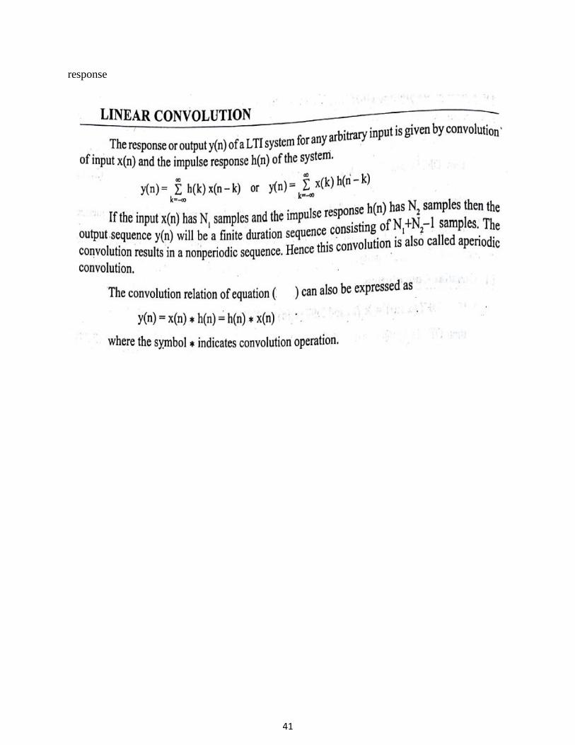
41
response
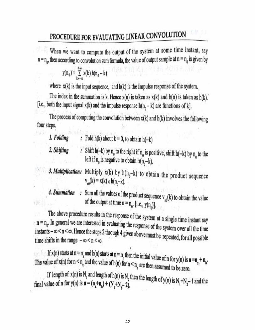
42
.
43
44
45
46
47
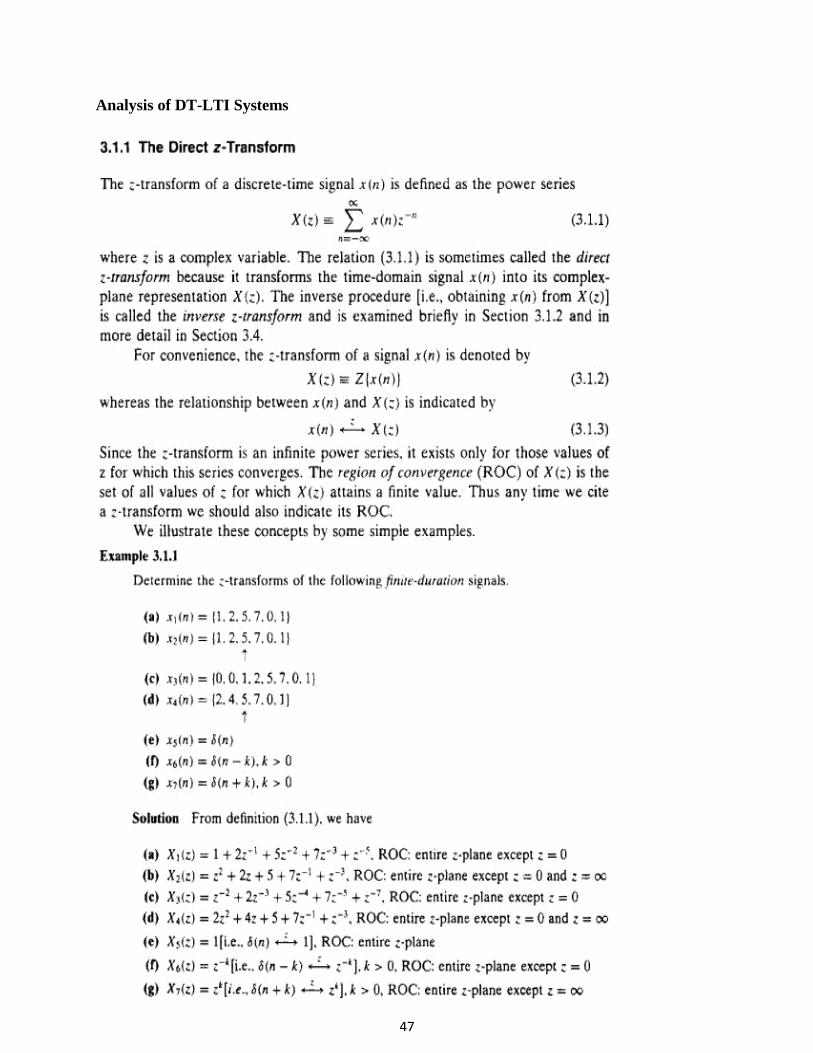
Analysis of DT-LTI Systems
48
49
50

51
52
53
54
55
56
57
58
59
60
61
62
63
64
65
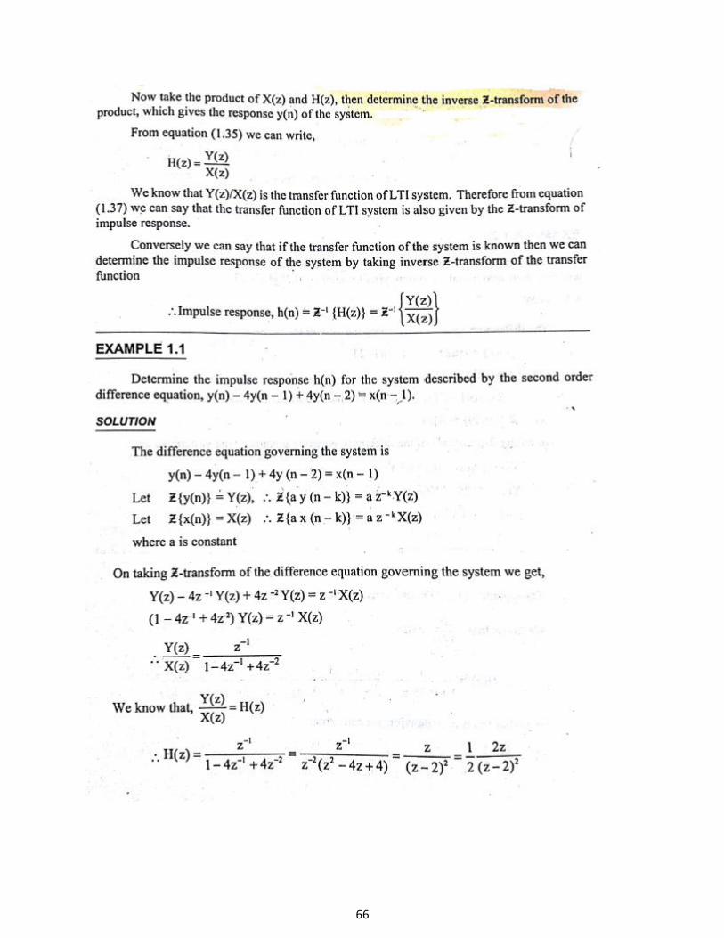
66

67
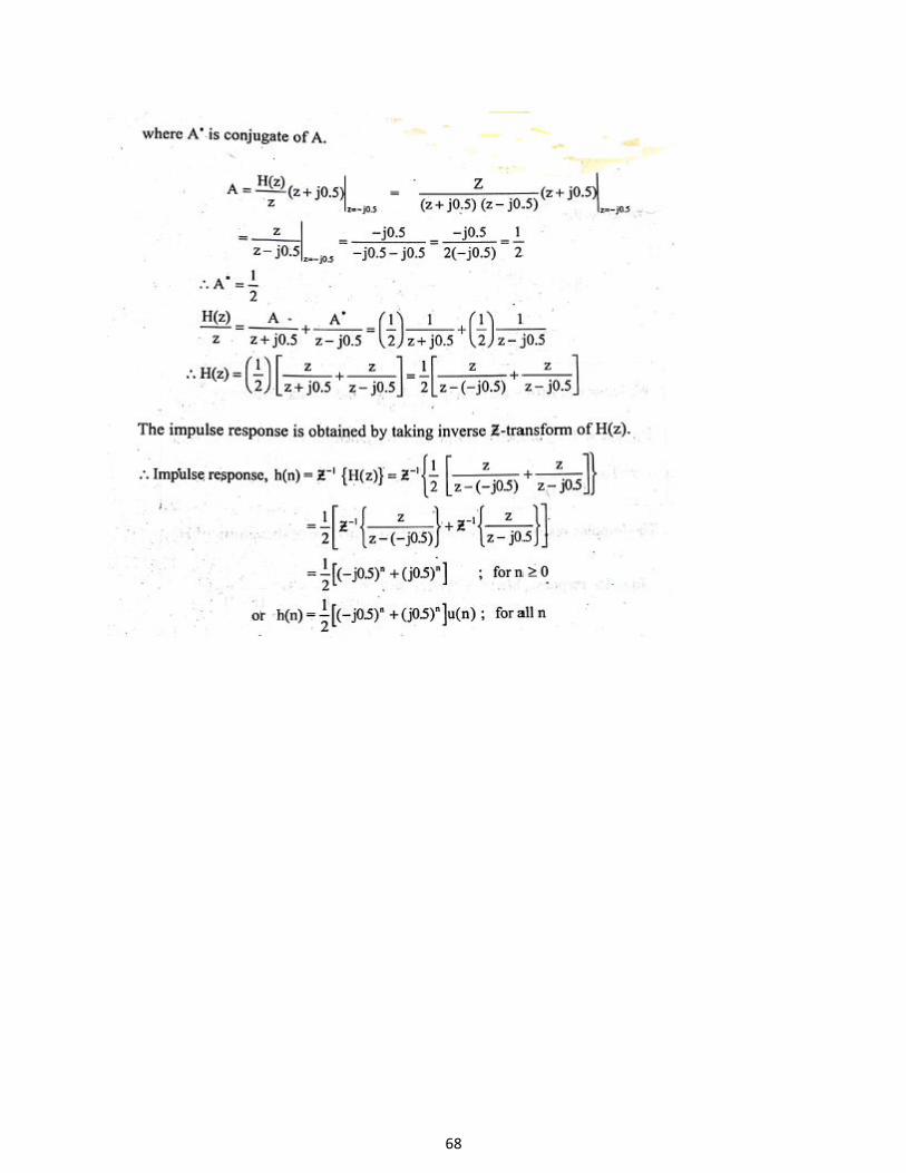
68
69
Part A
1. Define one-sided and two-sided Z-transform.
2. What is region of convergence (ROC)?
3. State the final value theorem with regard to Z-transform.
4. State the initial value theorem with regard to Z-transform.
5. Define Z-transform of unit step signal.
6. Define sampling and aliasing.
7. What is Nyquist rate?
8. State sampling theorem.
9. When a discrete time signal is called periodic?
10. What is linear and nonlinear systems?
Part B
1. a) Consider the analog signal x(t) = 2 sin80pt. If the sampling frequency is 60 Hz, find the sampled
version of discrete time signal x(n). Also find an alias frequency corresponding to Fs = 60 Hz.
b) Consider the analog signals, x (t) 4 cos2 (30t) and x (t) 4 cos (5t). 1 2 = π = 2π Find a sampling
frequency so that 30 Hz signal is an alias of 5 Hz signal.
c) Consider the analog signal, x(t) = 3sin40π t − sin100π t + 2cos 50π t.Determine the minimum
sampling frequency and the sampled version of analog signal at this frequency. Sketch the
waveform and show the sampling points. Comment on the result.
2. Determine the response of an LTI system whose impulse response h(n) and input x(n) are given by
H(n)={1,-1,2,3} x(n)={1,2,3,4}
70
SCHOOL OF ELECTRICAL AND ELECTRONICS
DEPARTMENT OF ELECTRICAL AND ELECTRONICS ENGINEERING
UNIT – II - – DISCRETE FOURIER TRANSFORM AND COMPUTATION-SECA1507
71
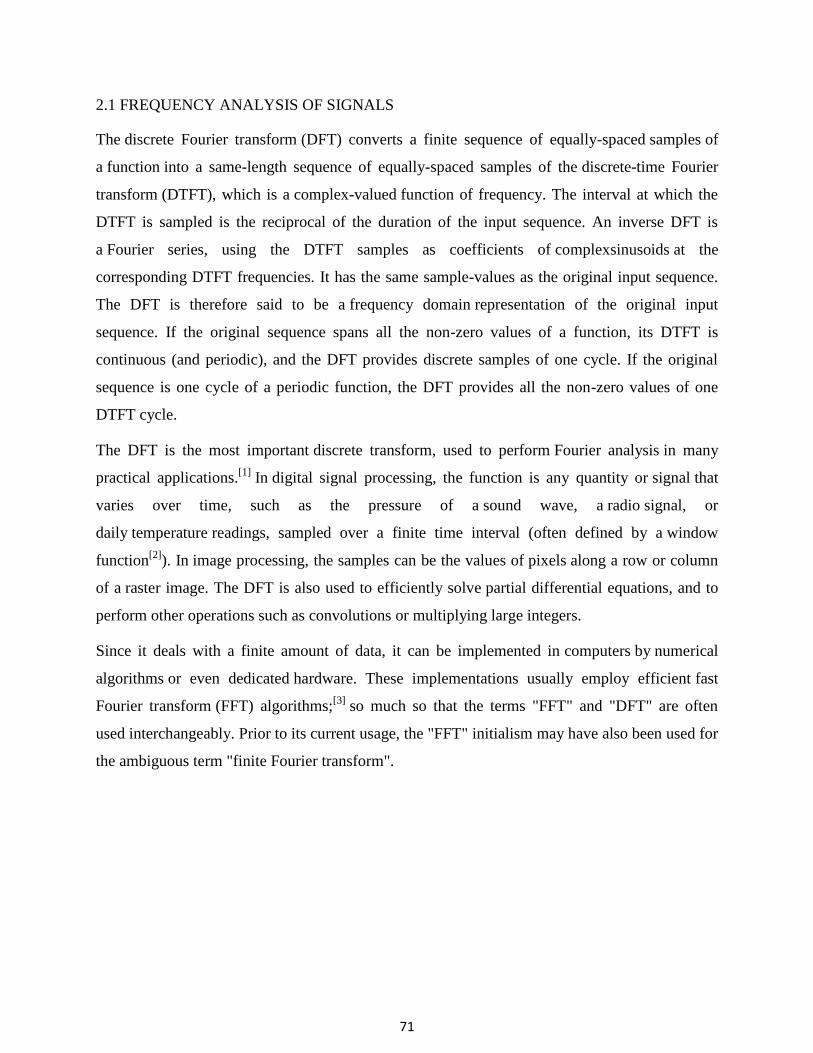
2.1 FREQUENCY ANALYSIS OF SIGNALS
The discrete Fourier transform (DFT) converts a finite sequence of equally-spaced samples of
a function into a same-length sequence of equally-spaced samples of the discrete-time Fourier
transform (DTFT), which is a complex-valued function of frequency. The interval at which the
DTFT is sampled is the reciprocal of the duration of the input sequence. An inverse DFT is
a Fourier series, using the DTFT samples as coefficients of complexsinusoids at the
corresponding DTFT frequencies. It has the same sample-values as the original input sequence.
The DFT is therefore said to be a frequency domain representation of the original input
sequence. If the original sequence spans all the non-zero values of a function, its DTFT is
continuous (and periodic), and the DFT provides discrete samples of one cycle. If the original
sequence is one cycle of a periodic function, the DFT provides all the non-zero values of one
DTFT cycle.
The DFT is the most important discrete transform, used to perform Fourier analysis in many
practical applications.[1]
In digital signal processing, the function is any quantity or signal that
varies over time, such as the pressure of a sound wave, a radio signal, or
daily temperature readings, sampled over a finite time interval (often defined by a window
function[2]
). In image processing, the samples can be the values of pixels along a row or column
of a raster image. The DFT is also used to efficiently solve partial differential equations, and to
perform other operations such as convolutions or multiplying large integers.
Since it deals with a finite amount of data, it can be implemented in computers by numerical
algorithms or even dedicated hardware. These implementations usually employ efficient fast
Fourier transform (FFT) algorithms;[3]
so much so that the terms "FFT" and "DFT" are often
used interchangeably. Prior to its current usage, the "FFT" initialism may have also been used for
the ambiguous term "finite Fourier transform".
72
73
74
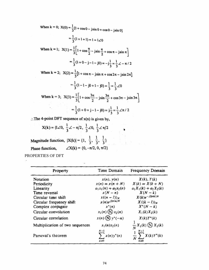
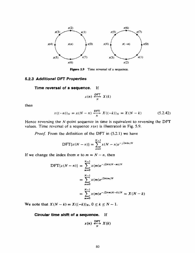
PROPERTIES OF DFT
75

76
77
78
79
80
81
82
83
84
85
86
87
88

89
90
91
92
93
Part A
1. Find the Fourier transform of x(n) = { 2, 1, 2 }.
2. Write the differences between Fourier transform of discrete time signal and continuous time signal.
3. What is the relation between Fourier transform and Z-transform?
4. Compare the DIT and DIF radix-2 FFT.
5. How many multiplications and additions are involved in radix-2 FFT?
6. Draw and explain the basic butterfly diagram or flow graph of DIF radix-2 FFT.
7. What is the relation between DTFT and DFT?
8. What is the drawback in Fourier transform and how is it overcome?
Part B
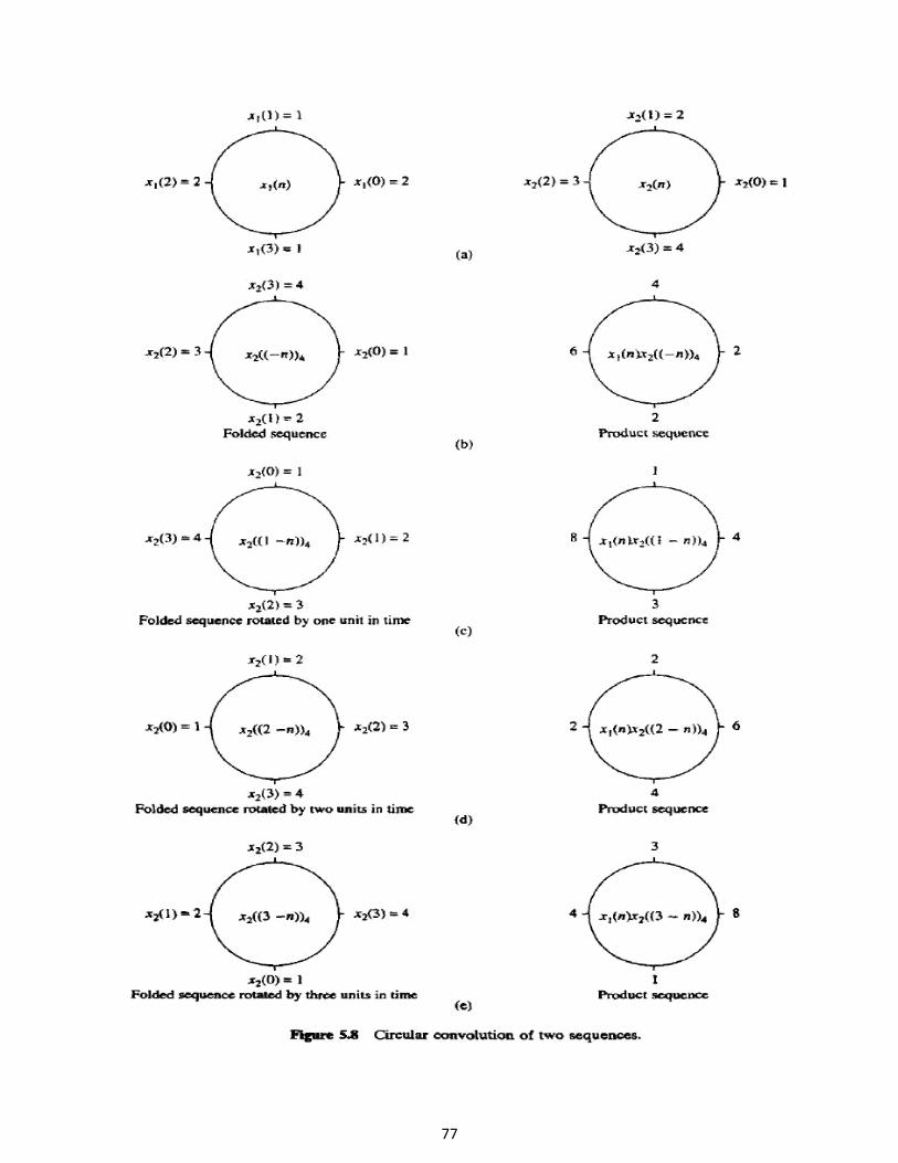
1. Perform circular convolution of the two sequences,X1(N)={1,2,3,4} ,x2(n)={4.5.6.7}
2. Compute 8-point DFT of the discrete time signal, x(n) = l1, 2, 1, 2, 1, 3, 1, 3},
a) using radix-2 DIT FFT and b) using radix-2 DIF FFT. Also sketch the magnitude and phase spectrum.
94
SCHOOL OF ELECTRICAL AND ELECTRONICS
DEPARTMENT OF ELECTRICAL AND ELECTRONICS ENGINEERING
UNIT – III - – DESIGN OF INFINITE IMPULSE RESPONSE FILTER (IIR)-SECA1507
95
3.1 INTRODUCTION
To remove or to reduce strength of unwanted signal like noise and to improve the quality of
required signal filtering process is used. To use the channel full bandwidth we mix up two or
more signals on transmission side and on receiver side we would like to separate it out in
efficient way. Hence filters are used. Thus the digital filters are mostly used in
1. Removal of undesirable noise from the desired signals
2. Equalization of communication channels
3. Signal detection in radar, sonar and communication
4. Performing spectral analysis of signals.
Analog and digital filters
In signal processing, the function of a filter is to remove unwanted parts of the signal, such as
random noise, or to extract useful parts of the signal, such as the components lying within a
certain frequency range. The following block diagram illustrates the basic idea.
There are two main kinds of filter, analog and digital. They are quite different in their physical
makeup and in how they work. An analog filter uses analog electronic circuits made up from
components such as resistors, capacitors and op amps to produce the required filtering effect.
Such filter circuits are widely used in such applications as noise reduction, video signal
enhancement, graphic equalizers in hi-fi systems, and many other areas.
In analog filters the signal being filtered is an electrical voltage or current which is the direct
analogue of the physical quantity (e.g. a sound or video signal or transducer output) involved.
A digital filter uses a digital processor to perform numerical calculations on sampled values of
the signal.
The processor may be a general-purpose computer such as a PC, or a specialized DSP (Digital
Signal Processor) chip. The analog input signal must first be sampled and digitized using an
ADC (analog to digital converter). The resulting binary numbers, representing successive
sampled values of the input signal, are transferred to the processor, which carries out numerical
calculations on them. These calculations typically involve multiplying the input values by
constants and adding the products together. If necessary, the results of these calculations, which
now represent sampled values of the filtered signal, are output through a DAC (digital to analog
converter) to convert the signal back to analog form. In a digital filter, the signal is represented
by a sequence of numbers, rather than a voltage or current.
96
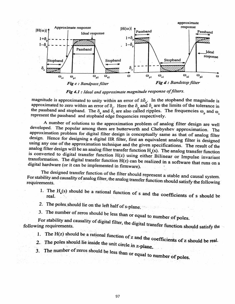
97
98
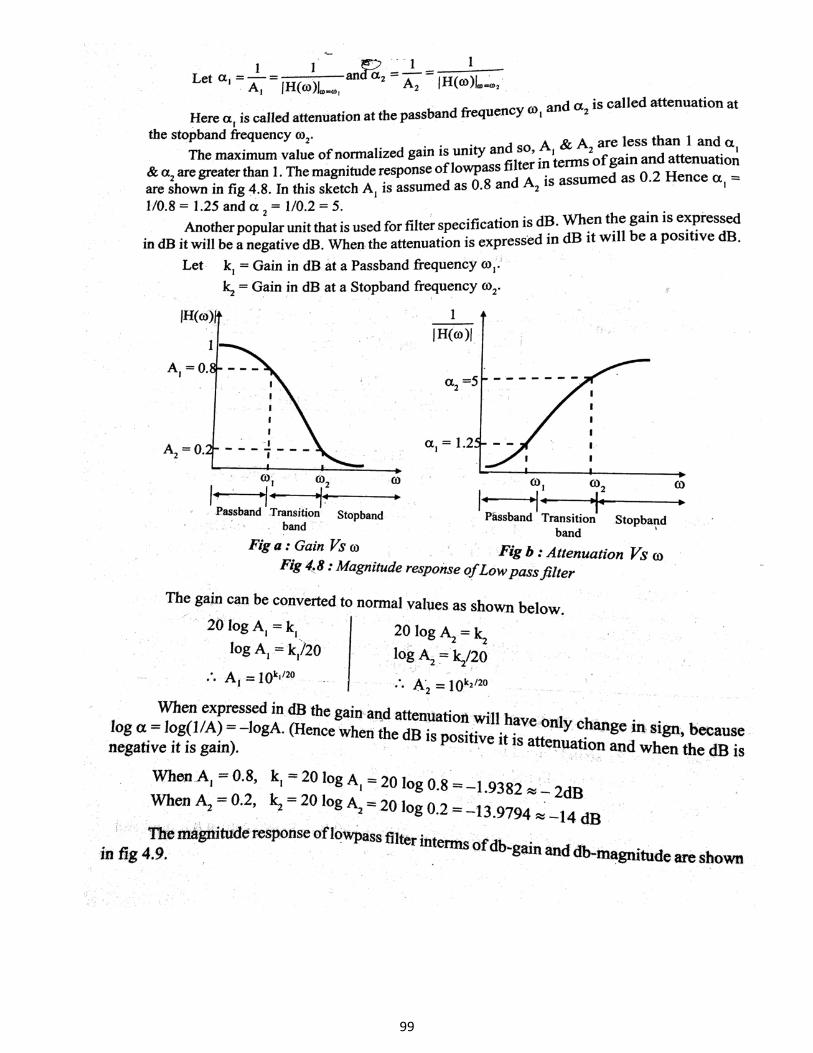
99
100
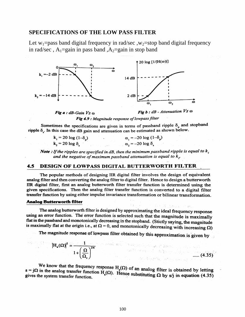
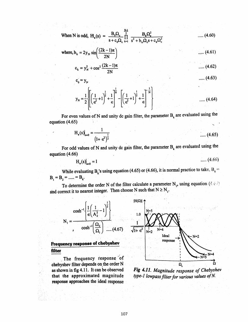
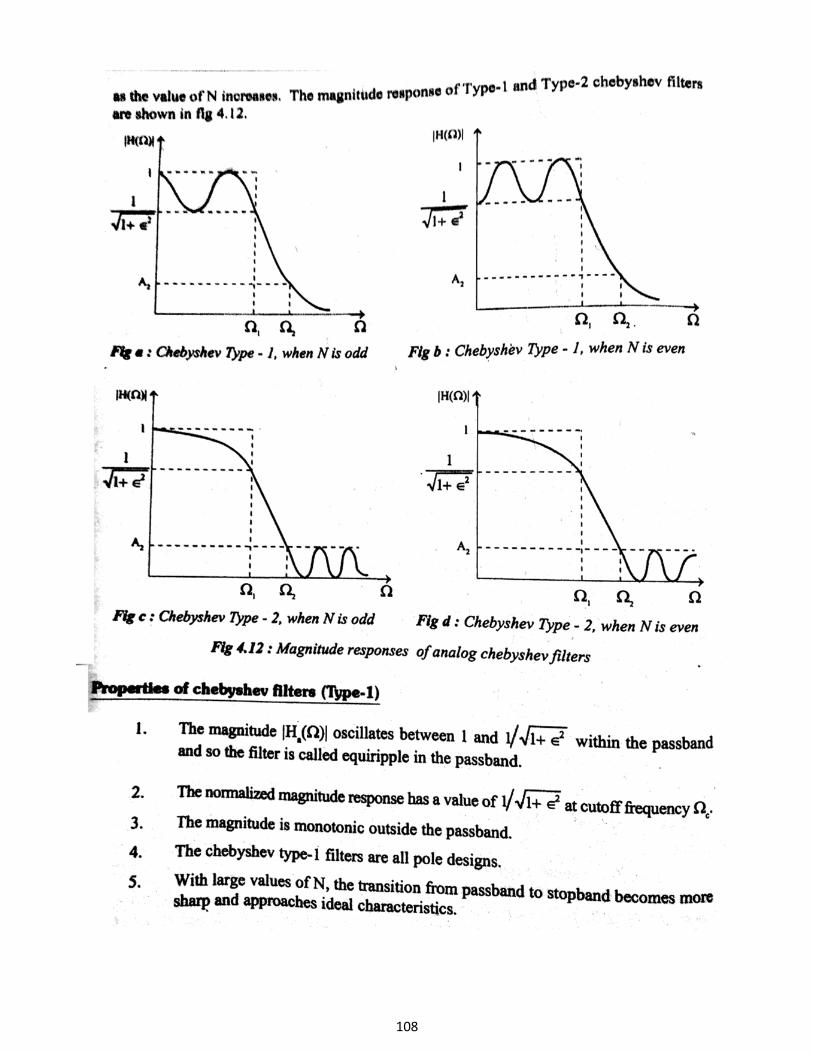
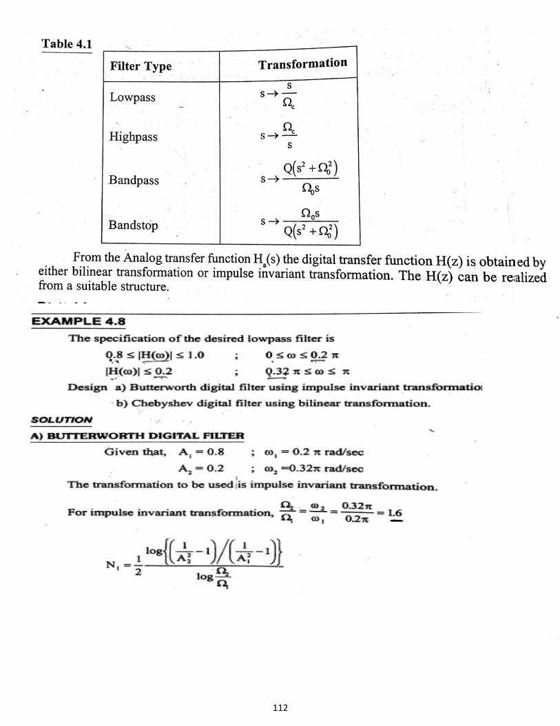
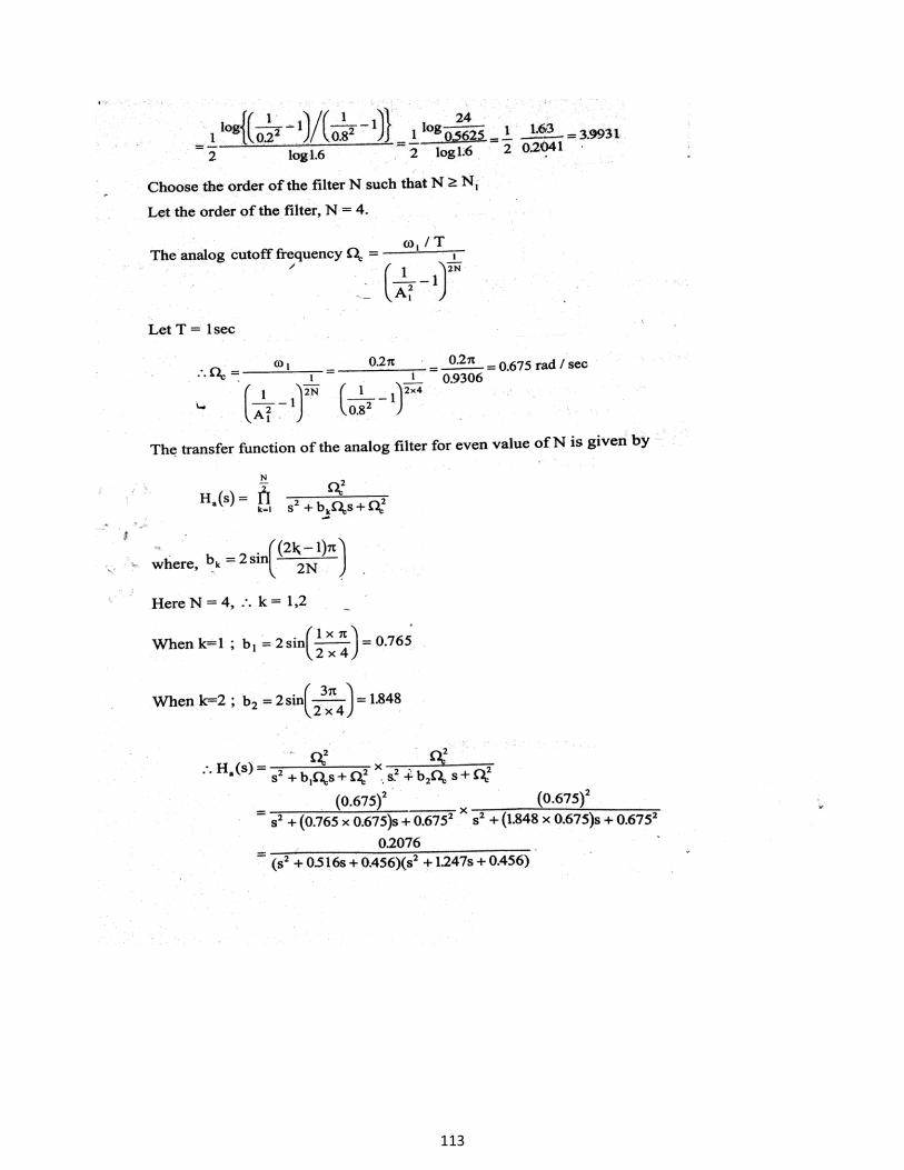
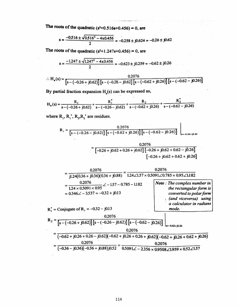
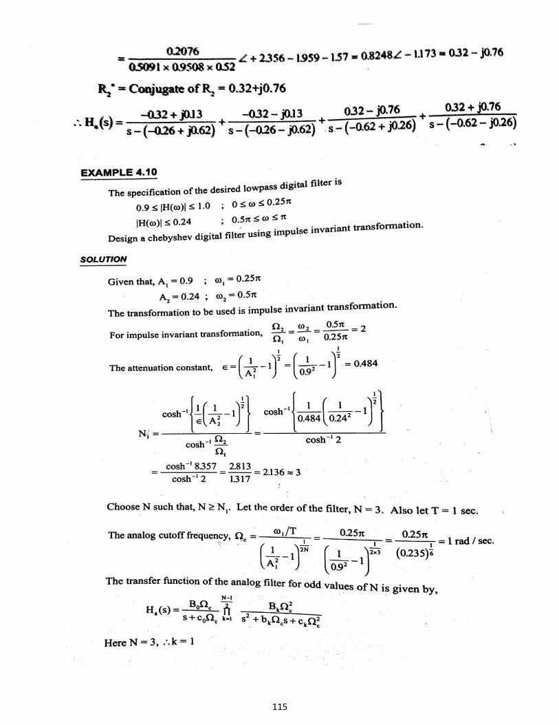
SPECIFICATIONS OF THE LOW PASS FILTER
Let w1=pass band digital frequency in rad/sec ,w2=stop band digital frequency
in rad/sec , A1=gain in pass band ,A2=gain in stop band
101

102
103

104
105
106
107
108
109
110

111
112
113
114
115
116
117
118
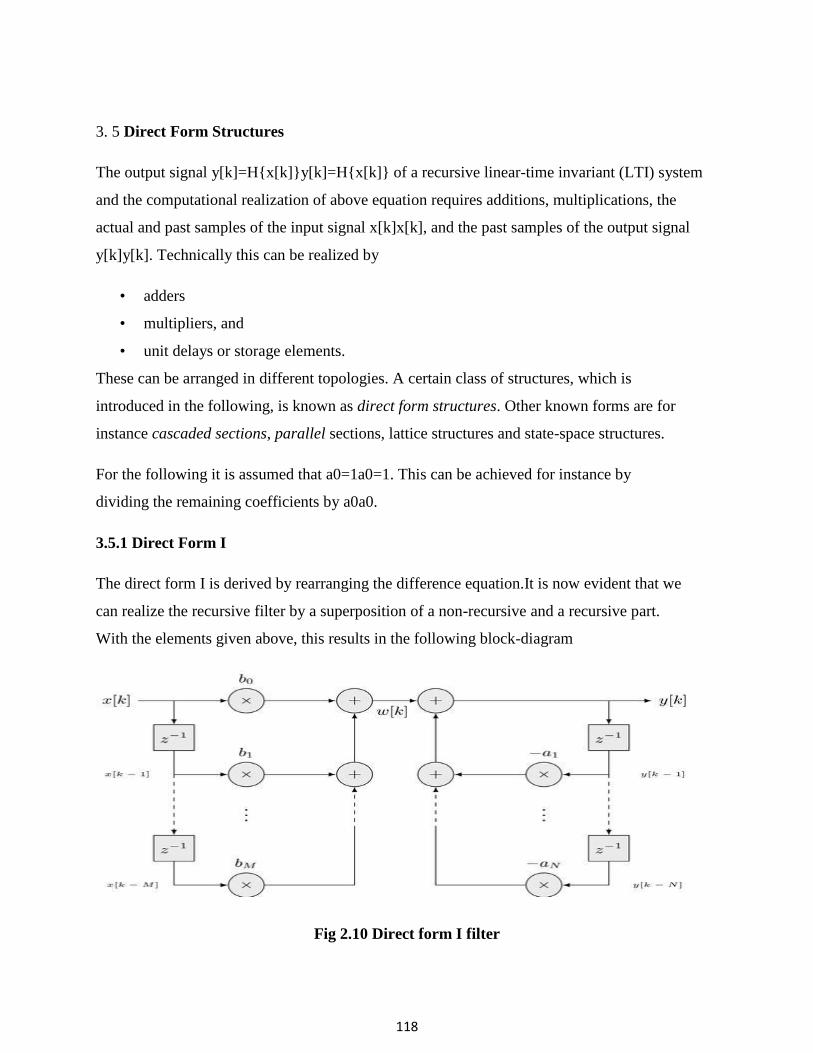
3. 5 Direct Form Structures
The output signal y[k]=H{x[k]}y[k]=H{x[k]} of a recursive linear-time invariant (LTI) system
and the computational realization of above equation requires additions, multiplications, the
actual and past samples of the input signal x[k]x[k], and the past samples of the output signal
y[k]y[k]. Technically this can be realized by
• adders
• multipliers, and
• unit delays or storage elements.
These can be arranged in different topologies. A certain class of structures, which is
introduced in the following, is known as direct form structures. Other known forms are for
instance cascaded sections, parallel sections, lattice structures and state-space structures.
For the following it is assumed that a0=1a0=1. This can be achieved for instance by
dividing the remaining coefficients by a0a0.
3.5.1 Direct Form I
The direct form I is derived by rearranging the difference equation.It is now evident that we
can realize the recursive filter by a superposition of a non-recursive and a recursive part.
With the elements given above, this results in the following block-diagram
Fig 2.10 Direct form I filter
119
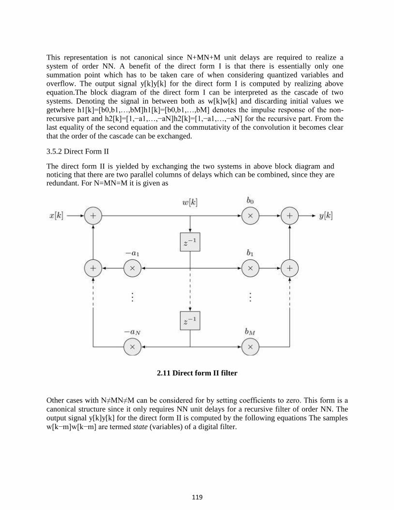
This representation is not canonical since N+MN+M unit delays are required to realize a system of order NN. A benefit of the direct form I is that there is essentially only one summation point which has to be taken care of when considering quantized variables and overflow. The output signal y[k]y[k] for the direct form I is computed by realizing above equation.The block diagram of the direct form I can be interpreted as the cascade of two systems. Denoting the signal in between both as w[k]w[k] and discarding initial values we getwhere h1[k]=[b0,b1,…,bM]h1[k]=[b0,b1,…,bM] denotes the impulse response of the non-recursive part and h2[k]=[1,−a1,…,−aN]h2[k]=[1,−a1,…,−aN] for the recursive part. From the last equality of the second equation and the commutativity of the convolution it becomes clear that the order of the cascade can be exchanged.
3.5.2 Direct Form II
The direct form II is yielded by exchanging the two systems in above block diagram and noticing that there are two parallel columns of delays which can be combined, since they are redundant. For N=MN=M it is given as
2.11 Direct form II filter
Other cases with N≠MN≠M can be considered for by setting coefficients to zero. This form is a
canonical structure since it only requires NN unit delays for a recursive filter of order NN. The
output signal y[k]y[k] for the direct form II is computed by the following equations The samples
w[k−m]w[k−m] are termed state (variables) of a digital filter.
120
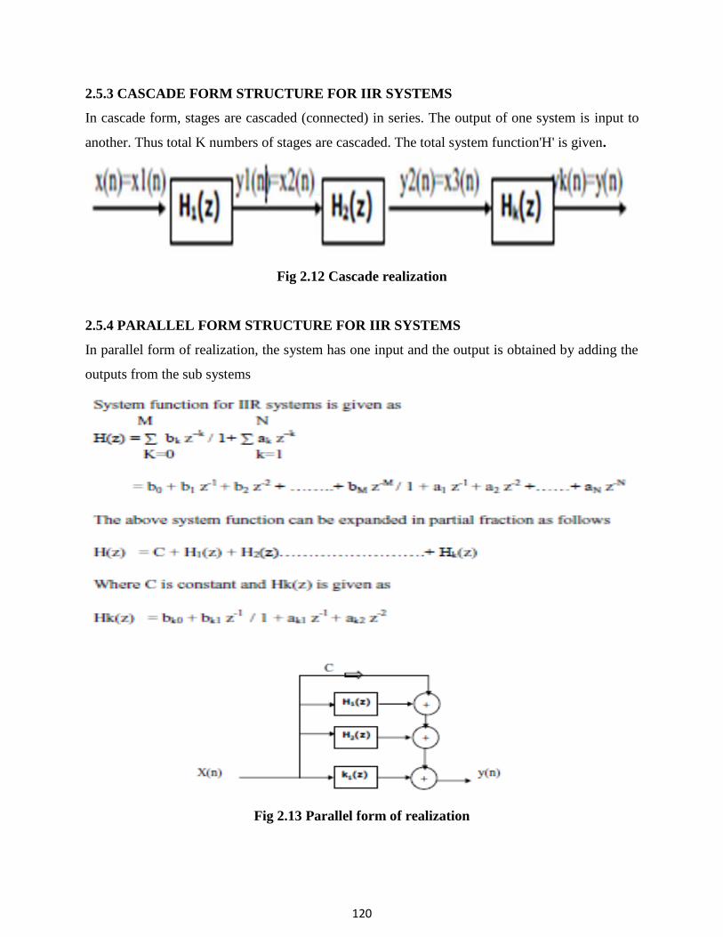
2.5.3 CASCADE FORM STRUCTURE FOR IIR SYSTEMS
In cascade form, stages are cascaded (connected) in series. The output of one system is input to
another. Thus total K numbers of stages are cascaded. The total system function'H' is given.
Fig 2.12 Cascade realization
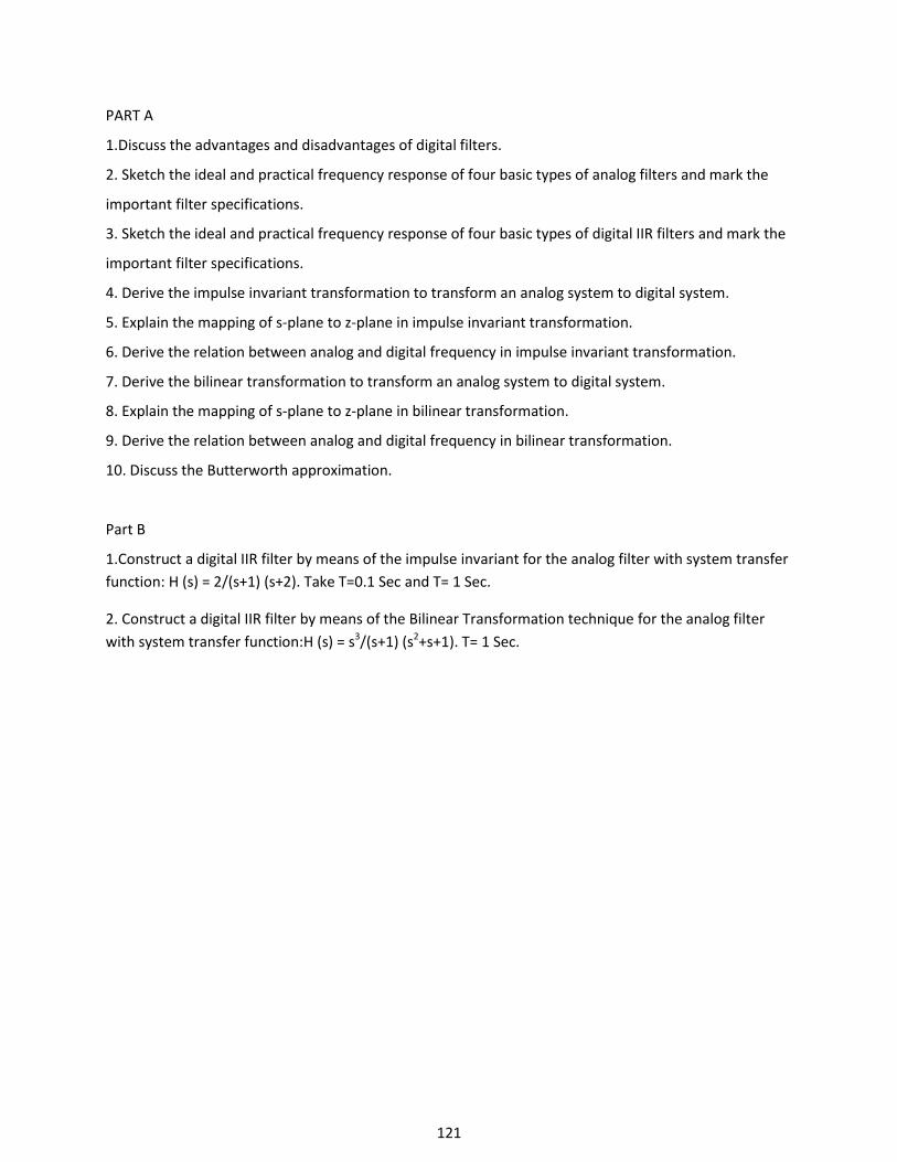
2.5.4 PARALLEL FORM STRUCTURE FOR IIR SYSTEMS
In parallel form of realization, the system has one input and the output is obtained by adding the
outputs from the sub systems
Fig 2.13 Parallel form of realization
121
PART A
1.Discuss the advantages and disadvantages of digital filters.
2. Sketch the ideal and practical frequency response of four basic types of analog filters and mark the
important filter specifications.
3. Sketch the ideal and practical frequency response of four basic types of digital IIR filters and mark the
important filter specifications.
4. Derive the impulse invariant transformation to transform an analog system to digital system.
5. Explain the mapping of s-plane to z-plane in impulse invariant transformation.
6. Derive the relation between analog and digital frequency in impulse invariant transformation.
7. Derive the bilinear transformation to transform an analog system to digital system.
8. Explain the mapping of s-plane to z-plane in bilinear transformation.
9. Derive the relation between analog and digital frequency in bilinear transformation.
10. Discuss the Butterworth approximation.
Part B
1.Construct a digital IIR filter by means of the impulse invariant for the analog filter with system transfer
function: H (s) = 2/(s+1) (s+2). Take T=0.1 Sec and T= 1 Sec.
2. Construct a digital IIR filter by means of the Bilinear Transformation technique for the analog filter
with system transfer function:H (s) = s3/(s+1) (s2+s+1). T= 1 Sec.
122
SCHOOL OF ELECTRICAL AND ELECTRONICS
DEPARTMENT OF ELECTRICAL AND ELECTRONICS ENGINEERING
UNIT – IV - – DESIGN OF FINITE IMPULSE RESPONSE (FIR) FILTER-SECA1507
123
FINITE IMPULSE RESPONSE DIGITAL FILTERS
4.1 Symmetric and Anti symmetric FIR filters
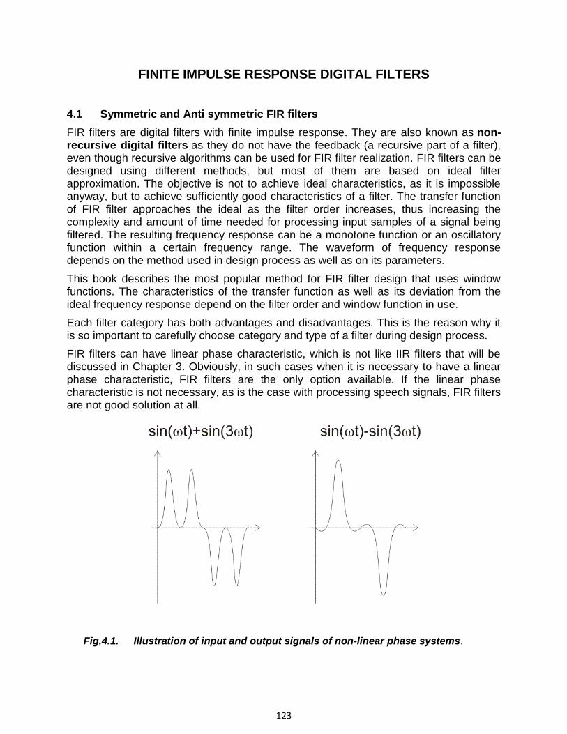
FIR filters are digital filters with finite impulse response. They are also known as non-recursive digital filters as they do not have the feedback (a recursive part of a filter), even though recursive algorithms can be used for FIR filter realization. FIR filters can be designed using different methods, but most of them are based on ideal filter approximation. The objective is not to achieve ideal characteristics, as it is impossible anyway, but to achieve sufficiently good characteristics of a filter. The transfer function of FIR filter approaches the ideal as the filter order increases, thus increasing the complexity and amount of time needed for processing input samples of a signal being filtered. The resulting frequency response can be a monotone function or an oscillatory function within a certain frequency range. The waveform of frequency response depends on the method used in design process as well as on its parameters.
This book describes the most popular method for FIR filter design that uses window functions. The characteristics of the transfer function as well as its deviation from the ideal frequency response depend on the filter order and window function in use.
Each filter category has both advantages and disadvantages. This is the reason why it is so important to carefully choose category and type of a filter during design process.
FIR filters can have linear phase characteristic, which is not like IIR filters that will be discussed in Chapter 3. Obviously, in such cases when it is necessary to have a linear phase characteristic, FIR filters are the only option available. If the linear phase characteristic is not necessary, as is the case with processing speech signals, FIR filters are not good solution at all.
Fig.4.1. Illustration of input and output signals of non-linear phase systems.

124
The system introduces a phase shift of 0 radians at the frequency of ω, and π radians at three times that frequency. Input signal consists of natural frequency ω and one harmonic with the same amplitude at three times that frequency. Figure 2-1-3. shows the block diagram of input signal (left) and output signal (right). It is obvious that these two signals have different waveforms. The power of signals is not changed, nor the amplitudes of harmonics, only the phase of the second harmonic is changed.
If we assume that the input is a speech signal whose phase characteristic is not of the essence, such distortion in the phase of the signal would be unimportant. In this case, the system satisfies all necessary requirements. However, if the phase characteristic is of importance, such a great distortion mustn’t be allowed.
In order that the phase characteristic of a FIR filter is linear, the impulse response must be symmetric or anti-symmetric, which is expressed in the following way:
h[n] = h[N-n-1] ; symmetric impulse response (about its middle element)
h[n] = -h[N-n-1] ; anti-symmetric impulse response (about its middle element)
One of the drawbacks of FIR filters is a high order of designed filter. The order of FIR filter is remarkably higher compared to an IIR filter with the same frequency response. This is the reason why it is so important to use FIR filters only when the linear phase characteristic is very important.
A number of delay lines contained in a filter, i.e. a number of input samples that should be saved for the purpose of computing the output sample, determines the order of a filter. For example, if the filter is assumed to be of order 10, it means that it is necessary to save 10 input samples preceeding the current sample. All eleven samples will affect the output sample of FIR filter.
The transform function of a typical FIR filter can be expressed as a polynomial of a complex variable z-¹. All the poles of the transfer function are located at the origin. For this reason, FIR filters are guaranteed to be stable, whereas IIR filters have potential to become unstable.
4.2 Finite impulse response (FIR) filter design methods
Most FIR filter design methods are based on ideal filter approximation. The resulting filter approximates the ideal characteristic as the filter order increases, thus making the filter and its implementation more complex.
The filter design process starts with specifications and requirements of the desirable FIR filter. Which method is to be used in the filter design process depends on the filter specifications and implementation. This chapter discusses the FIR filter design method using window functions.
Each of the given methods has its advantages and disadvantages. Thus, it is very important to carefully choose the right method for FIR filter design. Due to its simplicity and efficiency, the window method is most commonly used method for designing filters. The sampling frequency method is easy to use, but filters designed this way have small attenuation in the stopband.
125
As we have mentioned above, the design process starts with the specification of desirable FIR
filter.
4.2.1. Basic concepts and FIR filter specification
First of all, it is necessay to learn the basic concepts that will be used further in this book. You
should be aware that without being familiar with these concepts, it is not possible to understand
analyses and synthesis of digital filters.
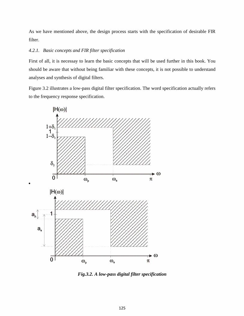
Figure 3.2 illustrates a low-pass digital filter specification. The word specification actually refers
to the frequency response specification.
Fig.3.2. A low-pass digital filter specification
126
ωp – normalized cut-off frequency in the passband;
ωs – normalized cut-off frequency in the stopband;
δ1 – maximum ripples in the passband;
δ2 – minimum attenuation in the stopband [dB];
ap – maximum ripples in the passband; and
as – minimum attenuation in the stopband [dB].
Frequency normalization can be expressed as follows:
where:
fs is a sampling frequency;
f is a frequency to normalize; and
ω is normalized frequency.
127
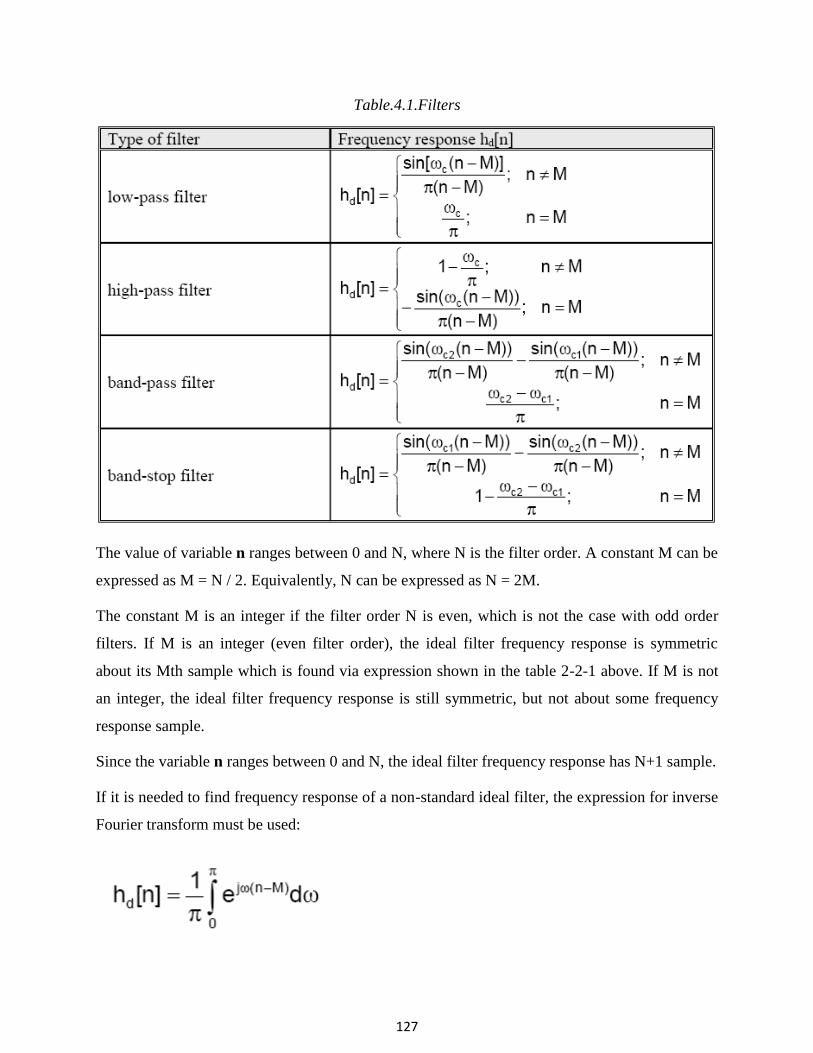
Table.4.1.Filters
The value of variable n ranges between 0 and N, where N is the filter order. A constant M can be
expressed as M = N / 2. Equivalently, N can be expressed as N = 2M.
The constant M is an integer if the filter order N is even, which is not the case with odd order
filters. If M is an integer (even filter order), the ideal filter frequency response is symmetric
about its Mth sample which is found via expression shown in the table 2-2-1 above. If M is not
an integer, the ideal filter frequency response is still symmetric, but not about some frequency
response sample.
Since the variable n ranges between 0 and N, the ideal filter frequency response has N+1 sample.
If it is needed to find frequency response of a non-standard ideal filter, the expression for inverse
Fourier transform must be used:
128
Non-standard filters are rarely used. However, if there is a need to use some of them, the integral
above must be computed via various numerical methodes.
3..3 FIR filter design using window functions
The FIR filter design process via window functions can be split into several steps:
1. Defining filter specifications;
2. Specifying a window function according to the filter specifications;
3. Computing the filter order required for a given set of specifications;
4. Computing the window function coefficients;
5. Computing the ideal filter coefficients according to the filter order;
6. Computing FIR filter coefficients according to the obtained window function and ideal
filter coefficients;
7. If the resulting filter has too wide or too narrow transition region, it is necessary to
change the filter order by increasing or decreasing it according to needs, and after that steps 4, 5
and 6 are iterated as many times as needed.
The final objective of defining filter specifications is to find the desired normalized frequencies
(ωc, ωc1, ωc2), transition width and stopband attenuation. The window function and filter order
are both specified according to these parameters.
Accordingly, the selected window function must satisfy the given specifications. After this step,
that is, when the window function is known, we can compute the filter order required for a given
set of specifications. When both the window function and filter order are known, it is possible to
calculate the window function coefficients w[n] using the formula for the specified window
function.
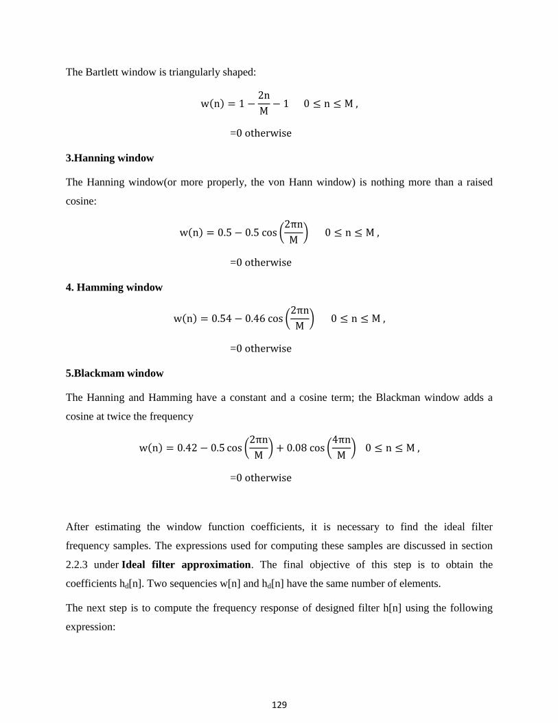
1.Rectangular Window The rectangular window is what you would obtain if you were to
simply segment a finite portion of the impulse response without any shaping in the time domain:
( )
2.Bartlett (or triangular) window
129
The Bartlett window is triangularly shaped:
( )
=
3.Hanning window
The Hanning window(or more properly, the von Hann window) is nothing more than a raised
cosine:
( ) (
)
=
4. Hamming window
( ) (
)
=
5.Blackmam window
The Hanning and Hamming have a constant and a cosine term; the Blackman window adds a
cosine at twice the frequency
( ) (
) (
)
=
After estimating the window function coefficients, it is necessary to find the ideal filter
frequency samples. The expressions used for computing these samples are discussed in section
2.2.3 under Ideal filter approximation. The final objective of this step is to obtain the
coefficients hd[n]. Two sequencies w[n] and hd[n] have the same number of elements.
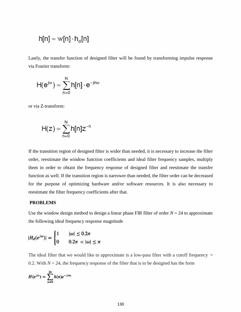
The next step is to compute the frequency response of designed filter h[n] using the following
expression:
130
Lastly, the transfer function of designed filter will be found by transforming impulse response
via Fourier transform:
or via Z-transform:
If the transition region of designed filter is wider than needed, it is necessary to increase the filter
order, reestimate the window function coefficients and ideal filter frequency samples, multiply
them in order to obtain the frequency response of designed filter and reestimate the transfer
function as well. If the transition region is narrower than needed, the filter order can be decreased
for the purpose of optimizing hardware and/or software resources. It is also necessary to
reestimate the filter frequency coefficients after that.
PROBLEMS
Use the window design method to design a linear phase FIR filter of order N = 24 to approximate
the following ideal frequency response magnitude
The ideal filter that we would like to approximate is a low-pass filter with a cutoff frequency =
0.2. With N = 24, the frequency response of the filter that is to be designed has the form
131
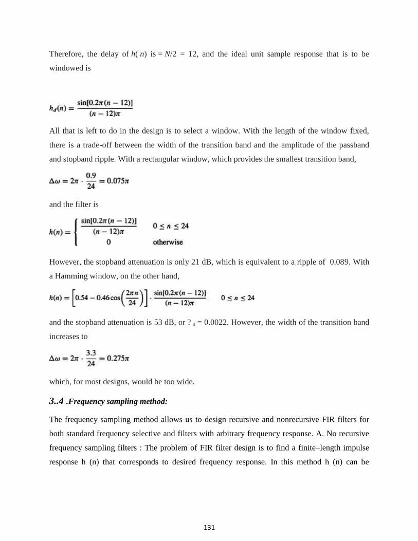
Therefore, the delay of h( n) is = N/2 = 12, and the ideal unit sample response that is to be
windowed is
All that is left to do in the design is to select a window. With the length of the window fixed,
there is a trade-off between the width of the transition band and the amplitude of the passband
and stopband ripple. With a rectangular window, which provides the smallest transition band,
and the filter is
However, the stopband attenuation is only 21 dB, which is equivalent to a ripple of 0.089. With
a Hamming window, on the other hand,
and the stopband attenuation is 53 dB, or ? s = 0.0022. However, the width of the transition band
increases to
which, for most designs, would be too wide.
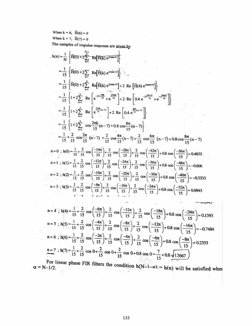
3..4 .Frequency sampling method:
The frequency sampling method allows us to design recursive and nonrecursive FIR filters for
both standard frequency selective and filters with arbitrary frequency response. A. No recursive
frequency sampling filters : The problem of FIR filter design is to find a finite–length impulse
response h (n) that corresponds to desired frequency response. In this method h (n) can be
132
determined by uniformly sampling, the desired frequency response HD (ω) at the N points and
finding its inverse DFT of the frequency samples.
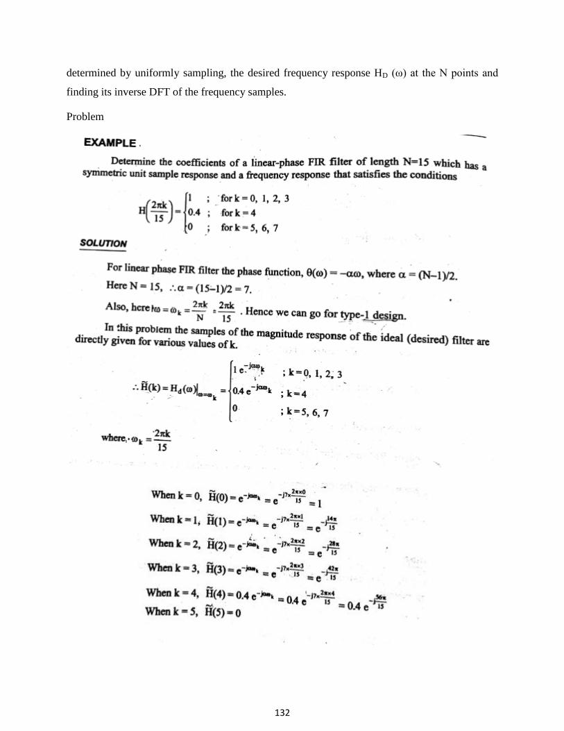
Problem
133
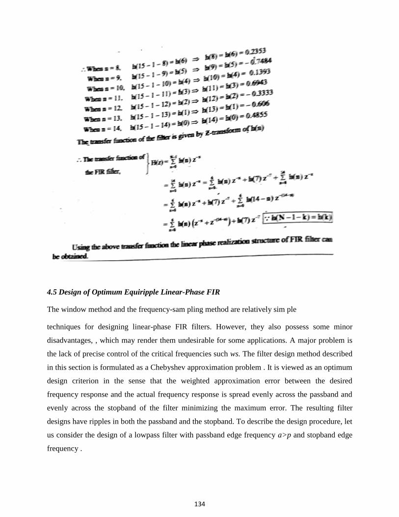
134
4.5 Design of Optimum Equiripple Linear-Phase FIR
The window method and the frequency-sam pling method are relatively sim ple
techniques for designing linear-phase FIR filters. However, they also possess some minor
disadvantages, , which may render them undesirable for some applications. A major problem is
the lack of precise control of the critical frequencies such ws. The filter design method described
in this section is formulated as a Chebyshev approximation problem . It is viewed as an optimum
design criterion in the sense that the weighted approximation error between the desired
frequency response and the actual frequency response is spread evenly across the passband and
evenly across the stopband of the filter minimizing the maximum error. The resulting filter
designs have ripples in both the passband and the stopband. To describe the design procedure, let
us consider the design of a lowpass filter with passband edge frequency a>p and stopband edge
frequency .
135
4..4 Structure realization of FIR Filters
In signal processing, a digital filter is a system that performs mathematical operations on
a sampled, discrete-time signal to reduce or enhance certain aspects of that signal. This is in
contrast to the other major type of electronic filter, the analog filter, which is anelectronic
circuit operating on continuous-time analog signals.
A digital filter system usually consists of an analog-to-digital converter to sample the input
signal, followed by a microprocessor and some peripheral components such as memory to store
data and filter coefficients etc. Finally a digital-to-analog converter to complete the output stage.
Program Instructions (software) running on the microprocessor implement the digital filter by
performing the necessary mathematical operations on the numbers received from the ADC. In
some high performance applications, an FPGA orASIC is used instead of a general purpose
microprocessor, or a specialized DSP with specific paralleled architecture for expediting
operations such as filtering.
Digital filters may be more expensive than an equivalent analog filter due to their increased
complexity, but they make practical many designs that are impractical or impossible as analog
filters. When used in the context of real-time analog systems, digital filters sometimes have
problematic latency (the difference in time between the input and the response) due to the
associated analog-to-digital and digital-to-analog conversions and anti-aliasing filters, or due to
other delays in their implementation.
Digital filters are commonplace and an essential element of everyday electronics such
as radios, cellphones, and AV receivers.
4.6.1 Characterization
A digital filter is characterized by its transfer function, or equivalently, its difference equation.
Mathematical analysis of the transfer function can describe how it will respond to any input. As
such, designing a filter consists of developing specifications appropriate to the problem (for
example, a second-order low pass filter with a specific cut-off frequency), and then producing a
transfer function which meets the specifications.
The transfer function for a linear, time-invariant, digital filter can be expressed as a transfer
function in the Z-domain; if it is causal, then it has the form:
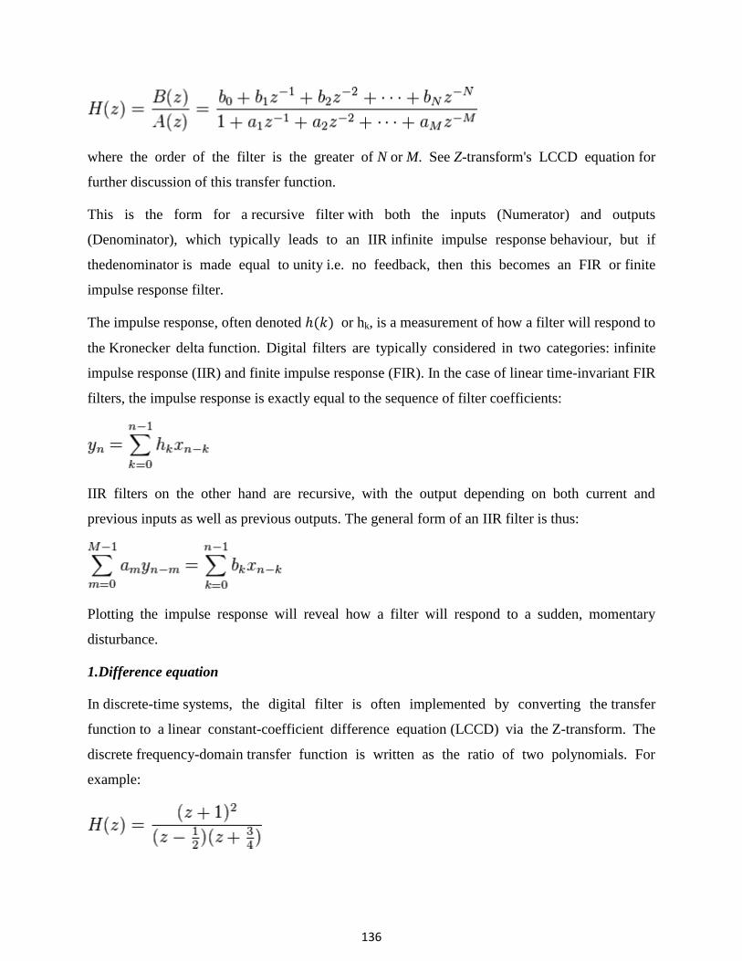
136
where the order of the filter is the greater of N or M. See Z-transform's LCCD equation for
further discussion of this transfer function.
This is the form for a recursive filter with both the inputs (Numerator) and outputs
(Denominator), which typically leads to an IIR infinite impulse response behaviour, but if
thedenominator is made equal to unity i.e. no feedback, then this becomes an FIR or finite
impulse response filter.
The impulse response, often denoted ( ) or hk, is a measurement of how a filter will respond to
the Kronecker delta function. Digital filters are typically considered in two categories: infinite
impulse response (IIR) and finite impulse response (FIR). In the case of linear time-invariant FIR
filters, the impulse response is exactly equal to the sequence of filter coefficients:
IIR filters on the other hand are recursive, with the output depending on both current and
previous inputs as well as previous outputs. The general form of an IIR filter is thus:
Plotting the impulse response will reveal how a filter will respond to a sudden, momentary
disturbance.
1.Difference equation
In discrete-time systems, the digital filter is often implemented by converting the transfer
function to a linear constant-coefficient difference equation (LCCD) via the Z-transform. The
discrete frequency-domain transfer function is written as the ratio of two polynomials. For
example:
137
This is expanded:
and to make the corresponding filter causal, the numerator and denominator are divided by the
highest order of :
The coefficients of the denominator, , are the 'feed-backward' coefficients and the coefficients
of the numerator are the 'feed-forward' coefficients, . The resultant linear difference
equation is:
or, for the example above:
rearranging terms:
then by taking the inverse z-transform:
and finally, by solving for :
This equation shows how to compute the next output sample, , in terms of the past
outputs, , the present input, , and the past inputs, . Applying the filter to

138
an input in this form is equivalent to a Direct Form I or II realization, depending on the exact
order of evaluationAfter a filter is designed, it must be realized by developing a signal flow
diagram that describes the filter in terms of operations on sample sequences.
A given transfer function may be realized in many ways. Consider how a simple expression such
as could be evaluated – one could also compute the equivalent .
In the same way, all realizations may be seen as "factorizations" of the same transfer function,
but different realizations will have different numerical properties. Specifically, some realizations
are more efficient in terms of the number of operations or storage elements required for their
implementation, and others provide advantages such as improved numerical stability and reduced
round-off error. Some structures are better for fixed-point arithmetic and others may be better
for floating-point arithmetic.
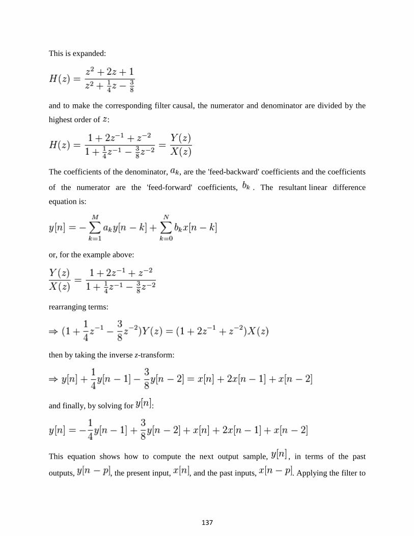
1.Direct Form I
A straightforward approach for IIR filter realization is Direct Form I, where the difference
equation is evaluated directly. This form is practical for small filters, but may be inefficient and
impractical (numerically unstable) for complex designs.[3]
In general, this form requires 2N delay
elements (for both input and output signals) for a filter of order N.
Fig.3.3. Direct form I
2.Direct Form II
The alternate Direct Form II only needs N delay units, where N is the order of the filter –
potentially half as much as Direct Form I. This structure is obtained by reversing the order of the
numerator and denominator sections of Direct Form I, since they are in fact two linear systems,
139
and the commutativity property applies. Then, one will notice that there are two columns of
delays ( ) that tap off the center net, and these can be combined since they are redundant,
yielding the implementation as shown below.
The disadvantage is that Direct Form II increases the possibility of arithmetic overflow for filters
of high Q or resonance.[4]
It has been shown that as Q increases, the round-off noise of both
direct form topologies increases without bounds.[5]
This is because, conceptually, the signal is
first passed through an all-pole filter (which normally boosts gain at the resonant frequencies)
before the result of that is saturated, then passed through an all-zero filter (which often attenuates
much of what the all-pole half amplifies).
Fig.3.4. Direct form II
3.Cascaded second-order sections
A common strategy is to realize a higher-order (greater than 2) digital filter as a cascaded series
of second-order "biquadratric" (or "biquad") sections[6]
(see digital biquad filter). The advantage
of this strategy is that the coefficient range is limited. Cascading direct form II sections results in
N delay elements for filters of order N. Cascading direct form I sections results in N+2 delay
elements since the delay elements of the input of any section (except the first section) are
redundant with the delay elements of the output of the preceding section.
4.Linear-Phase FIR Structures Phase FIR Structures
The symmetry (or antisymmetry) property of a linear-phase FIR filter can be exploited to reduce
the number of multipliers into almost half of that in the direct form implementations •
140
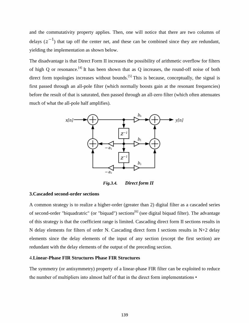
Consider a length-7 Type 1 FIR transfer function with a symmetric impulse response: ( )
( ) ( ) ( ) ( ) ( ) ( ) ( ) .Rearranging, we get
Fig.3.4. Linear phase FIRI
5.Polyphase Polyphase FIR Structures FIR Structures
The polyphase decomposition of H(z) leads to a parallel form structure.
To illustrate this approach, consider a causal FIR transfer function H(z) with N = 8:
( ) ( ) ( ) ( ) ( ) ( ) ( ) ( ) ( )
( )
H(z) can be expressed as a sum of two terms, with one term containing the even indexed
coefficients and the other containing the odd-indexed coefficients:
( ) ( ) ( ) ( ) ( ) ( )
[ ( ) ( ) ( ) ( ) ]
Putting ( ) ( ) (
).
141
The subfilters in the polyphase realization of an FIR transfer function are also FIR filters and can
be realized using any methods. However, to obtain a canonic realization of the overall structure,
the delays in all subfilters must be shared.
Part A
1. What is a high pass filter?
2. Compare analog and digital filters.
3. Name the techniques available for the design of analog filter.
4. Mention the requirement for a digital filter to be stable and causal.
5. What is frequency sampling method
Part B
6. Design a low pass digital filter of order 5 with cut of frequency 0.2 pi using hanning window.
7. An LTI system is described by y (n)+ y(n-1)- 0.25y(n-2)=x(n).Realize in direct form I and
Cascade form.
142
SCHOOL OF ELECTRICAL AND ELECTRONICS
DEPARTMENT OF ELECTRICAL AND ELECTRONICS ENGINEERING
UNIT – V - – DSP APPLICATIONS USING TMS 320C24X PROCESSOR–
SECA1507
143
DIGITAL SIGNAL PROCESSOR
The TMS320C24x is a member of the TMS320 family of digital signal processors(DSPs). The
‟C24x is designed to meet a wide range of digital motor control(DMC) and embedded control
applications.
5.1.TMS320 Family Overview
The TMS320 family consists of fixed-point, floating-point, multiprocessor digital signal
processors (DSPs), and fixed-point DSP controllers. TMS320 DSPs have an architecture
designed specifically for real-time signal processing. The‟C24x series of DSP controllers
combines this real-time processing capability with controller peripherals to create an ideal
solution for control system applications. The following characteristics make the TMS320 family
the right choice for a wide range of processing applications:
1. Very flexible instruction set
2.Inherent operational flexibility
3.High-speed performance
4.Innovative parallel architecture
5.Cost effectiveness
5.2.TMS320C24x Series of DSP Controllers
Designers have recognized the opportunity to redesign existing DMC systems to use advanced
algorithms that yield better performance and reduce system component count. DSPs enable:
1. Design of robust controllers for a new generation of inexpensive motors,such as AC
induction, DC permanent magnet, and switched-reluctance motors.
2. Full variable-speed control of brushless motor types that have lower manufacturing cost
and higher reliability.
144
3. Energy savings through variable-speed control, saving up to 25% of the energy used by
fixed-speed controllers.
4. Increased fuel economy, improved performance, and elimination of hydraulic fluid in
automotive electronic power steering (EPS) systems .
5. Reduced manufacturing and maintenance costs by eliminating hydraulic fluids in
automotive electronic braking systems.
6. More efficient and quieter operation due to less generation of torque ripple, resulting in
less loss of power, lower vibration, and longer life
7. Elimination or reduction of memory lookup tables through real-time polynomial
calculation, thereby reducing system cost.
8. Use of advanced algorithms that can reduce the number of sensors required in a system.
9. Control of power switching inverters, along with control algorithm processing.
10. Single-processor control of multi motor systems
The ‟C24x DSP controllers are designed to meet the needs of control-based applications. By
integrating the high performance of a DSP core and the on-chip peripherals of a microcontroller
into a single-chip solution, the ‟C24x
series yields a device that is an affordable alternative to traditional microcontroller units (MCUs)
and expensive multichip designs. At 20 million instructions per second (MIPS), the ‟C24x DSP
controllers offer significant performance over traditional 16-bit microcontrollers and
microprocessors. Future derivatives of these devices will run at speeds higher than 20 MIPS. The
16-bit, fixed-point DSP core of the ‟C24x device provides analog designers
a digital solution that does not sacrifice the precision and performance of their systems. In fact,
system performance can be enhanced through the use of advanced control algorithms for
techniques such as adaptive control,Kalman filtering, and state control. The ‟C24x DSP
controllers offer reliability and programmability. Analog control systems, on the other hand, are
hardwired solutions and can experience performance degradation due to aging,component
tolerance, and drift.The high-speed central processing unit (CPU) allows the digital designer to
process algorithms in real time rather than approximate results with look-up tables. When the
instruction set of these DSP controllers (which incorporates both signal processing instructions
and general-purpose control functions) is
145
coupled with the extensive development support available for the ‟C24x devices,it reduces
development time and provides the same ease of use as traditional 8- and 16-bit microcontrollers.
The instruction set also allows you to
retain your software investment when moving from other general-purpose TMS320 fixed-point
DSPs. It is source- and object-code compatible with the other members of the ‟C24x generation,
source code compatible with the ‟C2x
generation, and upwardly source code compatible with the ‟C5x generation of DSPs from Texas
Instruments. The ‟C24x architecture is also well-suited for processing control signals. It uses a
16-bit word length along with 32-bit registers for storing intermediate results, and has two
hardware shifters available to scale numbers independently
of the CPU. This combination minimizes quantization and truncation errors, and increases
processing power for additional functions. Two examples of these additional functions are: a
notch filter that cancels mechanical resonances in a system, and an estimation technique that
eliminates state sensors in a system. The ‟C24x DSP controllers take advantage of an existing set
of peripheral functions that allow Texas Instruments to quickly configure various series members
for different price/performance points or for application optimization.
This library of both digital and mixed-signal peripherals includes :
Timers
Serial communications ports (SCI, SPI)
Analog-to-digital converters (ADC)
Event manager
system protection, such as watchdog timers
5.3.Architectural Overview
The ‟C24x DSP uses an advanced, modified Harvard architecture that maximizes processing
power by maintaining separate bus structures for program memory and data memory.
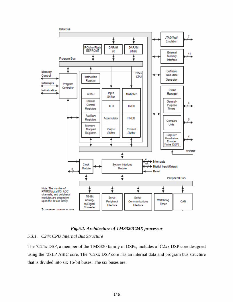
146
Fig.5.1. Architecture of TMS320C24X processor
5.3.1. C24x CPU Internal Bus Structure
The ‟C24x DSP, a member of the TMS320 family of DSPs, includes a ‟C2xx DSP core designed
using the ‟2xLP ASIC core. The ‟C2xx DSP core has an internal data and program bus structure
that is divided into six 16-bit buses. The six buses are:
147
PAB. The program address bus provides addresses for both reads from and writes to program
emory.
DRAB. The data-read address bus provides addresses for reads from data memory.
DWAB. The data-write address bus provides addresses for writes to data memory.
PRDB. The program read bus carries instruction code and immediate operands, as well as table
information, from program memory to the CPU.
DRDB. The data-read bus carries data from data memory to the central arithmetic logic unit
(CALU) and the auxiliary register arithmetic unit (ARAU).
DWEB. The data-write bus carries data to both program memory and data memory. Having
separate address buses for data reads (DRAB) and data writes (DWAB) allows the CPU to read
and write in the same machine cycle.
5.3.2. Memory
The ‟C24x contains the following types of on-chip memory:
Dual-access RAM (DARAM)
Flash EEPROM or ROM (masked)
The ‟C24x memory is organized into four individually-selectable spaces:
Program (64K words)
Local data (64K words)
Global data (32K words)
Input/Output (64K words)
These spaces form an address range of 224K words.
1.On-Chip Dual-Access RAM (DARAM)
The ‟C24x has 544 words of on-chip DARAM, which can be accessed twice per machine cycle.
This memory is primarily intended to hold data, but when needed, can also be used to hold
programs. The memory can be configured in one of two ways, depending on the state of the CNF
bit in status register ST1.

148
When CNF = 0, all 544 words are configured as data memory.
When CNF = 1, 288 words are configured as data memory and 256 words are configured as
program memory.
Because DARAM can be accessed twice per cycle, it improves the speed of the CPU. The CPU
operates within a 4-cycle pipeline. In this pipeline, the CPU reads data on the third cycle and
writes data on the fourth cycle. However, DARAM allows the CPU to write and read in one
cycle; the CPU writes to DARAM on the master phase of the cycle and reads from DARAM on
the slave phase. For example, suppose two instructions, A and B, store the accumulator value to
DARAM and load the accumulator with a new value from DARAM. Instruction A stores the
accumulator value during the master phase of the CPU cycle, and instruction B loads the new
value in the accumulator during the slave phase. Because part of the dual-access operation is a
write, it only applies to RAM.
2.Flash EEPROM
Flash EEPROM provides an attractive alternative to masked program ROM.Like ROM, flash is a
nonvolatile memory type; however, it has the advantage of in-target reprogrammability. The
-bit flash EEPROM module in program space. This type
of memory expands the capabilities of the ‟F24x in the areas of prototyping, early field testing,
and single-chip applications.Unlike most discrete flash memory, the ‟F24x flash does not require
a dedicated state machine because the algorithms for programming and erasing the flash are
executed by the DSP core. This enables several advantages, including reduced chip size and
sophisticated adaptive algorithms. For production programming, the IEEE Standard 1149.1
(JTAG) scan port provides easy access to on-chip RAM for downloading the algorithms and
flash code. Other key features of the flash include zero-wait-state access rate and single 5-V
power supply.An erased bit in the ‟24x flash is read as a logic one, and a programmed bit is read
as a logic zero. The flash requires a block-erase of the entire 16K/8K module; however, any
combination of bits can be programmed. The following four algorithms are required for flash
operations: clear, erase, flash-write, and program. For an explanation of these algorithms and a
complete description of the flash EEPROM, see TMS320F20x/F24x DSPs Embedded Flash
Memory Technical Reference (Literature number SPRU282).
3.Flash Serial Loader
149
Most of the on-chip flash devices are shipped with a serial bootloader code programmed at the
following addresses: 0x0000 – 0x00FFh. All other flash addresses are in an erased state. The
serial bootloader can be used to program the on-chip flash memory with user‟s code. During the
flash programming sequence, the on-chip data RAM is used to load and execute the clear, erase,
and program algorithms.
4.Factory-Masked ROM
For large-volume applications consisting of stable software free of bugs, lowcost, masked ROM
is available and supported up to 16K or 4K words. If you want a custom ROM, you can provide
the code or data to be programmed into the ROM in object-file format, and Texas Instruments
will generate the appropriate process mask to program the ROM. For details, see Appendix B,
Submitting ROM Codes to TI.A small portion of the ROM (128 or 64 words) is reserved by
Texas Instruments for test purposes. These reserved locations are at addresses 0x3F80 or 3FC0
through 0x3FFF. This leaves about 16K words available for your code.
5.External Memory Interface Module
In addition to full, on-chip memory support, some of the ‟C24x devices provide access to
external memory by way of the External Memory Interface Module. This interface provides 16
external address lines, 16 external data lines, and relevant control signals to select data, program,
and I/O spaces. An on-chip
wait-state generator allows interfacing with slower off-chip memory and peripherals.
5.3.3. Central Processing Unit
The ‟C24x is based on TI‟s ‟C2xx CPU. It contains:
A 32-bit central arithmetic logic unit (CALU)
A 32-bit accumulator
Input and output data-scaling shifters for the CALU
A 16-bit
16-bit multiplier
A product-scaling shifter
150
Data-address generation logic, which includes eight auxiliary registers and an auxiliary register
arithmetic unit (ARAU)
Program-address generation logic.
5.3.4. Central Arithmetic Logic Unit (CALU) and Accumulator
The ‟C24x performs 2s-complement arithmetic using the 32-bit CALU. The CALU uses 16-bit
words taken from data memory, derived from an immediate instruction, or from the 32-bit
multiplier result. In addition to arithmetic operations, the CALU can perform Boolean
operations. The accumulator stores the output from the CALU; it can also provide a second input
to the CALU. The accumulator is 32 bits wide and is divided into a highorder word (bits 31
through 16) and a low-order word (bits 15 through 0). Assembly language instructions are
provided for storing the high- and loworder accumulator words to data memory.
1.Scaling Shifters
The ‟C24x has three 32-bit shifters that allow for scaling, bit extraction, extended arithmetic, and
overflow-prevention operations:
a.Input data-scaling shifter (input shifter). This shifter left-shifts 16-bit input data by 0 to 16
bits to align the data to the 32-bit input of the CALU.
b.Output data-scaling shifter (output shifter). This shifter left-shift output from the
accumulator by 0 to 7 bits before the output is stored to data memory. The content of the
accumulator remains unchanged.
c.Product-scaling shifter (product shifter). The product register (PREG) receives the output of
the multiplier. The product shifter shifts the output of the PREG before that output is sent to the
input of the CALU. The product shifter has four product shift modes (no shift, left shift by one
bit, left shift by four bits, and right shift by six bits), which are useful for performing
multiply/accumulate operations, performing fractional arithmetic, or justifying fractional
products.
5.3.5. Multiplier
The on-chip multiplier performs 16- -bit 2s-complement multiplication with a 32-bit
result. In conjunction with the multiplier, the ‟C24x uses the 16-bit temporary register (TREG)
151
and the 32-bit product register (PREG); TREG always supplies one of the values to be
multiplied, and PREG receives the result
of each multiplication. Using the multiplier, TREG, and PREG, the ‟C24x efficiently performs
fundamental
DSP operations such as convolution, correlation, and filtering. The effective execution time of
each multiplication instruction can be as short as one CPU cycle.
5.3.6. Auxiliary Register Arithmetic Unit (ARAU) and Auxiliary Registers
The ARAU generates data memory addresses when an instruction uses indirect addressing to
access data memory.The ARAU is supported by eight auxiliary registers (AR0 through AR7),
each of which can be loaded with a 16-bit value from data memory or directly from an
instruction word. Each auxiliary register value can also be stored in data memory. The auxiliary
registers are referenced by a 3-bit auxiliary register pointer (ARP) embedded in status register
ST0.
5.3.7. Program Control
Several hardware and software mechanisms provide program control: Program control logic
decodes instructions, manages the 4-level pipeline, stores the status of operations, and decodes
conditional operations. Hardware elements included in the program control logic are the program
counter, the status registers, the stack, and the address-generation logic. Software mechanisms
used for program control include branches, calls, conditional instructions, a repeat instruction,
reset, interrupts, and power down modes.
5.3.8. Serial-Scan Emulation
The ‟C24x has seven pins dedicated to the serial scan emulation port (JTAG port). This port
allows for non-intrusive emulation of ‟C24x devices, and is supported by Texas Instruments
emulation tools and by many third party debugger tools.
152
Fig.5.2. TMS320C24X processor nomenclature
Fig.5.3. Bus structure
153
5.4. Memory and I/O Spaces
The ‟C24x has a 16-bit address line that accesses four individually selectable spaces (224K
words total):
A 64K-word program space
A 64K-word local data space
A 32K-word global data space
A 64K-word I/O space
5.4.1. Overview of Memory and I/O Spaces
The ‟C24x design is based on an enhanced Harvard architecture. The ‟C24x has multiple
memory spaces accessible on three parallel buses: a program address bus (PAB), a data-read
address bus (DRAB), and a data-write address bus (DWAB). Each of the three buses access
different memory spaces for different phases of the device‟s operation. Because the bus
operations are independent, it is possible to access both the program and data spaces
simultaneously. Within a given machine cycle, the CALU can execute as many as three
concurrent memory operations. The ‟C24x address map is organized into four individually
selectable spaces:
1.Program memory (64K words) contains the instructions to be executed, as well as data used
during program execution.
2.Data memory (64K words) holds data used by the instructions.
3.Global data memory (32K words) shares data with other devices or serves as additional data
space.
4.Input/output (I/O) space (64K words) interfaces to external peripherals and may contain on-
chip registers.
These spaces provide a total address space of 224K words. The ‟C24x includes on-chip memory
to aid in system performance and integration, and numerous addresses that can be used for
external memory and I/O devices. The advantages of operating from on-chip memory are:
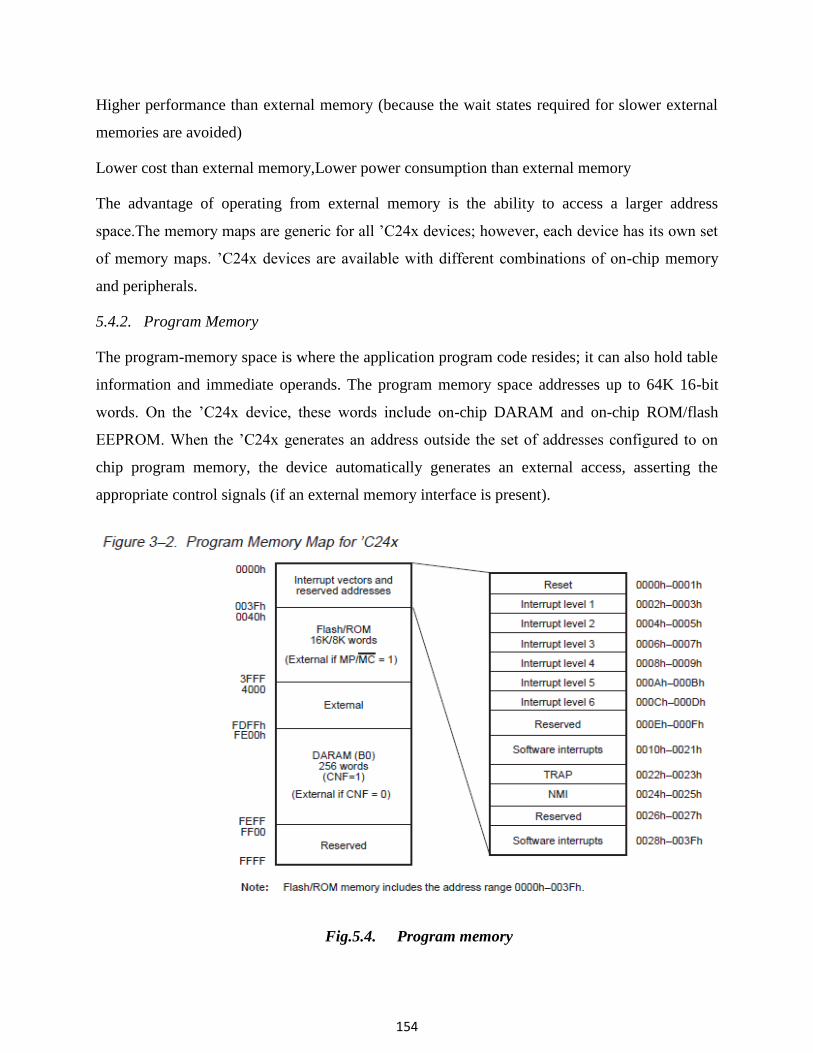
154
Higher performance than external memory (because the wait states required for slower external
memories are avoided)
Lower cost than external memory,Lower power consumption than external memory
The advantage of operating from external memory is the ability to access a larger address
space.The memory maps are generic for all ‟C24x devices; however, each device has its own set
of memory maps. ‟C24x devices are available with different combinations of on-chip memory
and peripherals.
5.4.2. Program Memory
The program-memory space is where the application program code resides; it can also hold table
information and immediate operands. The program memory space addresses up to 64K 16-bit
words. On the ‟C24x device, these words include on-chip DARAM and on-chip ROM/flash
EEPROM. When the ‟C24x generates an address outside the set of addresses configured to on
chip program memory, the device automatically generates an external access, asserting the
appropriate control signals (if an external memory interface is present).
Fig.5.4. Program memory
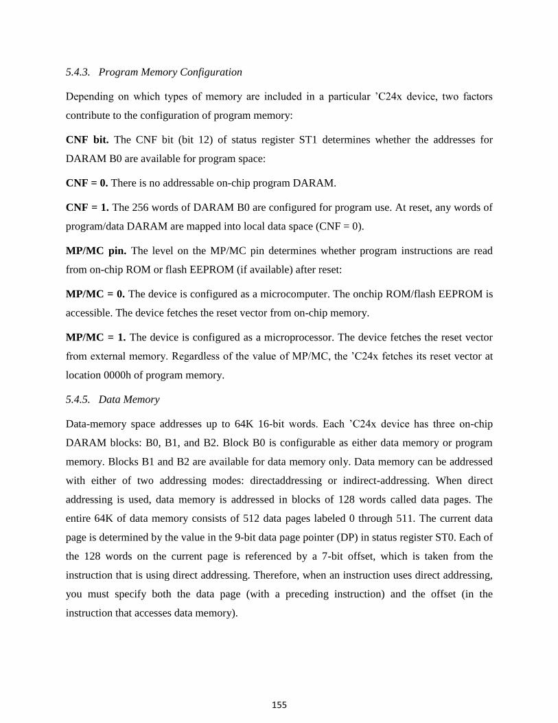
155
5.4.3. Program Memory Configuration
Depending on which types of memory are included in a particular ‟C24x device, two factors
contribute to the configuration of program memory:
CNF bit. The CNF bit (bit 12) of status register ST1 determines whether the addresses for
DARAM B0 are available for program space:
CNF = 0. There is no addressable on-chip program DARAM.
CNF = 1. The 256 words of DARAM B0 are configured for program use. At reset, any words of
program/data DARAM are mapped into local data space (CNF = 0).
MP/MC pin. The level on the MP/MC pin determines whether program instructions are read
from on-chip ROM or flash EEPROM (if available) after reset:
MP/MC = 0. The device is configured as a microcomputer. The onchip ROM/flash EEPROM is
accessible. The device fetches the reset vector from on-chip memory.
MP/MC = 1. The device is configured as a microprocessor. The device fetches the reset vector
from external memory. Regardless of the value of MP/MC, the ‟C24x fetches its reset vector at
location 0000h of program memory.
5.4.5. Data Memory
Data-memory space addresses up to 64K 16-bit words. Each ‟C24x device has three on-chip
DARAM blocks: B0, B1, and B2. Block B0 is configurable as either data memory or program
memory. Blocks B1 and B2 are available for data memory only. Data memory can be addressed
with either of two addressing modes: directaddressing or indirect-addressing. When direct
addressing is used, data memory is addressed in blocks of 128 words called data pages. The
entire 64K of data memory consists of 512 data pages labeled 0 through 511. The current data
page is determined by the value in the 9-bit data page pointer (DP) in status register ST0. Each of
the 128 words on the current page is referenced by a 7-bit offset, which is taken from the
instruction that is using direct addressing. Therefore, when an instruction uses direct addressing,
you must specify both the data page (with a preceding instruction) and the offset (in the
instruction that accesses data memory).
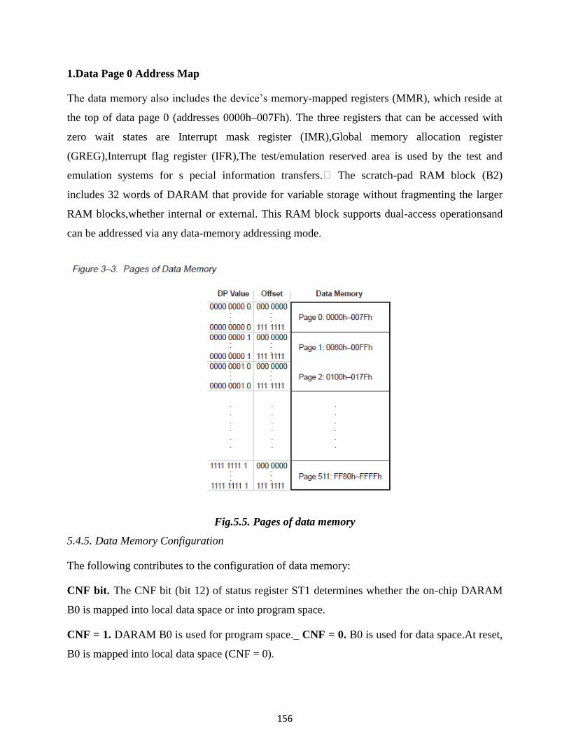
156
1.Data Page 0 Address Map
The data memory also includes the device‟s memory-mapped registers (MMR), which reside at
the top of data page 0 (addresses 0000h–007Fh). The three registers that can be accessed with
zero wait states are Interrupt mask register (IMR),Global memory allocation register
(GREG),Interrupt flag register (IFR),The test/emulation reserved area is used by the test and
emulation systems for s pecial information transfers.� The scratch-pad RAM block (B2)
includes 32 words of DARAM that provide for variable storage without fragmenting the larger
RAM blocks,whether internal or external. This RAM block supports dual-access operationsand
can be addressed via any data-memory addressing mode.
Fig.5.5. Pages of data memory
5.4.5. Data Memory Configuration
The following contributes to the configuration of data memory:
CNF bit. The CNF bit (bit 12) of status register ST1 determines whether the on-chip DARAM
B0 is mapped into local data space or into program space.
CNF = 1. DARAM B0 is used for program space._ CNF = 0. B0 is used for data space.At reset,
B0 is mapped into local data space (CNF = 0).
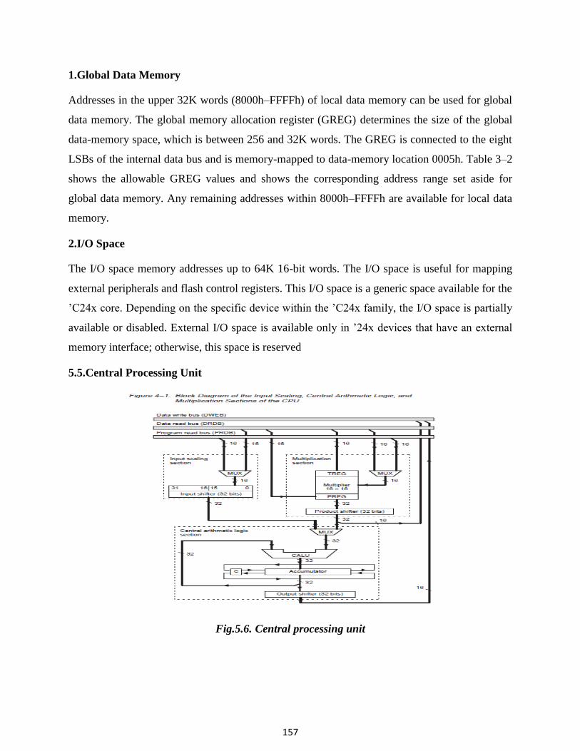
157
1.Global Data Memory
Addresses in the upper 32K words (8000h–FFFFh) of local data memory can be used for global
data memory. The global memory allocation register (GREG) determines the size of the global
data-memory space, which is between 256 and 32K words. The GREG is connected to the eight
LSBs of the internal data bus and is memory-mapped to data-memory location 0005h. Table 3–2
shows the allowable GREG values and shows the corresponding address range set aside for
global data memory. Any remaining addresses within 8000h–FFFFh are available for local data
memory.
2.I/O Space
The I/O space memory addresses up to 64K 16-bit words. The I/O space is useful for mapping
external peripherals and flash control registers. This I/O space is a generic space available for the
‟C24x core. Depending on the specific device within the ‟C24x family, the I/O space is partially
available or disabled. External I/O space is available only in ‟24x devices that have an external
memory interface; otherwise, this space is reserved
5.5.Central Processing Unit
Fig.5.6. Central processing unit
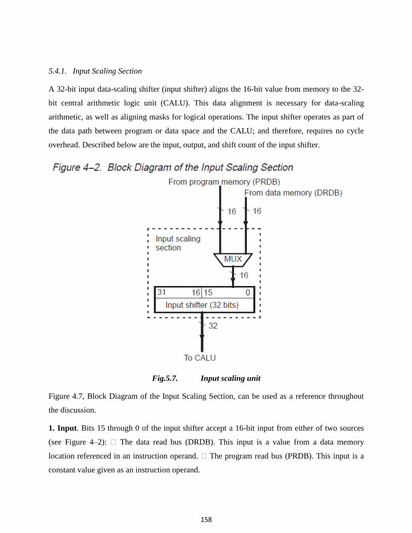
158
5.4.1. Input Scaling Section
A 32-bit input data-scaling shifter (input shifter) aligns the 16-bit value from memory to the 32-
bit central arithmetic logic unit (CALU). This data alignment is necessary for data-scaling
arithmetic, as well as aligning masks for logical operations. The input shifter operates as part of
the data path between program or data space and the CALU; and therefore, requires no cycle
overhead. Described below are the input, output, and shift count of the input shifter.
Fig.5.7. Input scaling unit
Figure 4.7, Block Diagram of the Input Scaling Section, can be used as a reference throughout
the discussion.
1. Input. Bits 15 through 0 of the input shifter accept a 16-bit input from either of two sources
(see Figure 4–2): � The data read bus (DRDB). This input is a value from a data memory
location referenced in an instruction operand. � The program read bus (PRDB). This input is a
constant value given as an instruction operand.
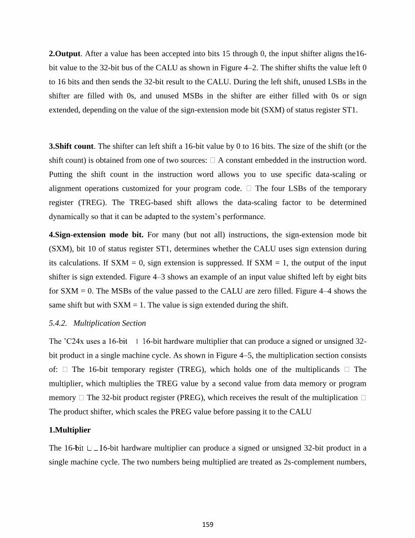
159
2.Output. After a value has been accepted into bits 15 through 0, the input shifter aligns the16-
bit value to the 32-bit bus of the CALU as shown in Figure 4–2. The shifter shifts the value left 0
to 16 bits and then sends the 32-bit result to the CALU. During the left shift, unused LSBs in the
shifter are filled with 0s, and unused MSBs in the shifter are either filled with 0s or sign
extended, depending on the value of the sign-extension mode bit (SXM) of status register ST1.
3.Shift count. The shifter can left shift a 16-bit value by 0 to 16 bits. The size of the shift (or the
shift count) is obtained from one of two sources: � A constant embedded in the instruction word.
Putting the shift count in the instruction word allows you to use specific data-scaling or
alignment operations customized for your program code. � The four LSBs of the temporary
register (TREG). The TREG-based shift allows the data-scaling factor to be determined
dynamically so that it can be adapted to the system‟s performance.
4.Sign-extension mode bit. For many (but not all) instructions, the sign-extension mode bit
(SXM), bit 10 of status register ST1, determines whether the CALU uses sign extension during
its calculations. If SXM = 0, sign extension is suppressed. If SXM = 1, the output of the input
shifter is sign extended. Figure 4–3 shows an example of an input value shifted left by eight bits
for SXM = 0. The MSBs of the value passed to the CALU are zero filled. Figure 4–4 shows the
same shift but with SXM = 1. The value is sign extended during the shift.
5.4.2. Multiplication Section
The ‟C24x uses a 16- -bit hardware multiplier that can produce a signed or unsigned 32-
bit product in a single machine cycle. As shown in Figure 4–5, the multiplication section consists
of: � The 16-bit temporary register (TREG), which holds one of the multiplicands � The
multiplier, which multiplies the TREG value by a second value from data memory or program
memory � The 32-bit product register (PREG), which receives the result of the multiplication �
The product shifter, which scales the PREG value before passing it to the CALU
1.Multiplier
The 16- -bit hardware multiplier can produce a signed or unsigned 32-bit product in a
single machine cycle. The two numbers being multiplied are treated as 2s-complement numbers,
160
except during unsigned multiplication (MPYU instruction). Descriptions of the inputs to, and
output of, the multiplier follow.
a.Inputs. The multiplier accepts two 16-bit inputs:
One input is always from the 16-bit temporary register (TREG). The TREG is loaded before the
multiplication with a data-value from the data read bus (DRDB).The other input is one of the
following:
_ A data-memory value from the data read bus (DRDB)
_ A program memory value from the program read bus (PRDB)
b.Output. After the two 16-bit inputs are multiplied, the 32-bit result is stored in the product
register (PREG). The output of the PREG is connected to the 32-bit product-scaling shifter.
Through this shifter, the product is transferred from the PREG to the CALU or to data memory
(by the SPH and SPL instructions).
Fig.5.8. Multiplier- block diagram
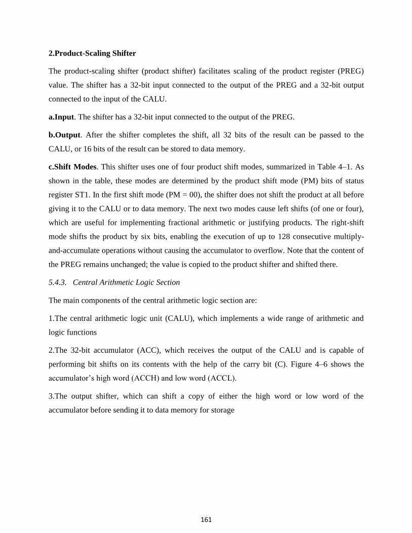
161
2.Product-Scaling Shifter
The product-scaling shifter (product shifter) facilitates scaling of the product register (PREG)
value. The shifter has a 32-bit input connected to the output of the PREG and a 32-bit output
connected to the input of the CALU.
a.Input. The shifter has a 32-bit input connected to the output of the PREG.
b.Output. After the shifter completes the shift, all 32 bits of the result can be passed to the
CALU, or 16 bits of the result can be stored to data memory.
c.Shift Modes. This shifter uses one of four product shift modes, summarized in Table 4–1. As
shown in the table, these modes are determined by the product shift mode (PM) bits of status
register ST1. In the first shift mode (PM = 00), the shifter does not shift the product at all before
giving it to the CALU or to data memory. The next two modes cause left shifts (of one or four),
which are useful for implementing fractional arithmetic or justifying products. The right-shift
mode shifts the product by six bits, enabling the execution of up to 128 consecutive multiply-
and-accumulate operations without causing the accumulator to overflow. Note that the content of
the PREG remains unchanged; the value is copied to the product shifter and shifted there.
5.4.3. Central Arithmetic Logic Section
The main components of the central arithmetic logic section are:
1.The central arithmetic logic unit (CALU), which implements a wide range of arithmetic and
logic functions
2.The 32-bit accumulator (ACC), which receives the output of the CALU and is capable of
performing bit shifts on its contents with the help of the carry bit (C). Figure 4–6 shows the
accumulator‟s high word (ACCH) and low word (ACCL).
3.The output shifter, which can shift a copy of either the high word or low word of the
accumulator before sending it to data memory for storage
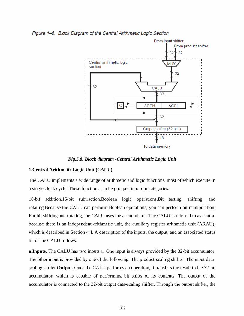
162
Fig.5.8. Block diagram -Central Arithmetic Logic Unit
1.Central Arithmetic Logic Unit (CALU)
The CALU implements a wide range of arithmetic and logic functions, most of which execute in
a single clock cycle. These functions can be grouped into four categories:
16-bit addition,16-bit subtraction,Boolean logic operations,Bit testing, shifting, and
rotating.Because the CALU can perform Boolean operations, you can perform bit manipulation.
For bit shifting and rotating, the CALU uses the accumulator. The CALU is referred to as central
because there is an independent arithmetic unit, the auxiliary register arithmetic unit (ARAU),
which is described in Section 4.4. A description of the inputs, the output, and an associated status
bit of the CALU follows.
a.Inputs. The CALU has two inputs � One input is always provided by the 32-bit accumulator.
The other input is provided by one of the following: The product-scaling shifter The input data-
scaling shifter Output. Once the CALU performs an operation, it transfers the result to the 32-bit
accumulator, which is capable of performing bit shifts of its contents. The output of the
accumulator is connected to the 32-bit output data-scaling shifter. Through the output shifter, the
163
accumulator‟s upper and lower 16-bit words can be individually shifted and stored to data
memory.
c.Sign-extension mode bit. For many but not all instructions, the sign-extension mode bit
(SXM), bit 10 of status register ST1, determines whether the CALU uses sign extension during
its calculations. If SXM = 0, sign extension is suppressed. If SXM = 1, sign extension is enabled.
d.Accumulator
Once the CALU performs an operation, it transfers the result to the 32-bit accumulator, which
can then perform single-bit shifts or rotations on its contents. Each of the accumulator‟s upper
and lower 16-bit words can be passed to the output data-scaling shifter, where it can be shifted
and then stored in data memory. The following describes the status bits and branch instructions
associated with the accumulator.
Status bits. Four status bits are associated with the accumulator:
Carry bit (C). C (bit 9 of status register ST1) is affected during: _ Additions to and subtractions
from the accumulator: C = 0 When the result of a subtraction generates a borrow When the result
of an addition does not generate a carry (Exception: When the ADD instruction is used with a
shift of 16 and no carry is generated, the ADD instruction has no effect on C.) C = 1 When the
result of an addition generates a carryWhen the result of a subtraction does not generate a borrow
(Exception: When the SUB instruction is used with a shift of 16 and no borrow is generated, the
SUB instruction has no effect on C.) Single-bit shifts and rotations of the accumulator value.
During a left shift or rotation, the MSB of the accumulator is passed to C; during a right shift or
rotation, the LSB is passed to C. Overflow mode bit (OVM). OVM (bit 11 of status register ST0)
determines how the accumulator reflects arithmetic overflows. When the processor is in
overflow mode (OVM = 1) and an overflow occurs, the accumulator is filled with one of two
specific values: If the overflow is in the positive direction, the accumulator is filled with its most
positive value (7FFF FFFFh).If the overflow is in the negative direction, the accumulator is filled
with its most negative value (8000 0000h). Overflow flag bit (OV). OV is bit 12 of status register
ST0. When no accumulator overflow is detected, OV is latched at 0. When overflow (positive or
negative) occurs, OV is set to 1 and latched.Test/control flag bit (TC). TC (bit 11 of status
register ST1) is set to 0 or 1 depending on the value of a tested bit. In the case of the NORM
instruction, if the exclusive-OR of the two MSBs of the accumulator is true, TC is set to 1.A
164
number of branch instructions are implemented, based on the status of bits C, OV, and TC, and
on the value in the accumulator (as compared to 0).
e.Output Data-Scaling Shifter
The output data-scaling shifter (output shifter) has a 32-bit input connected to the 32-bit output
of the accumulator and a 16-bit output connected to the data bus. The shifter copies all 32 bits of
the accumulator and then performs a left shift on its content; it can be shifted from zero to seven
bits, as specified in the corresponding store instruction. The upper word (SACH instruction) or
lower
word (SACL instruction) of the shifter is then stored to data memory. The content of the
accumulator remains unchanged. When the output shifter performs the shift, the MSBs are lost
and the LSBs are
zero filled. Figure 4–7 shows an example in which the accumulator value is shifted left by four
bits and the shifted high word is stored to data memory.Figure 4–8 shows the same accumulator
value shifted left by six bits and the shifted low word stored.
5.4.3. Auxiliary Register Arithmetic Unit (ARAU)
The CPU also contains the ARAU, an arithmetic unit independent of the CALU. The main
function of the ARAU is to perform arithmetic operations on eight auxiliary registers (AR7
through AR0) in parallel with operations occurring in the CALU. The eight auxiliary registers
(AR7–AR0) provide flexible and powerful indirect addressing. Any location in the 64K data
memory space can be accessed using a 16-bit address contained in an auxiliary register. To select
a specific auxiliary register, load the 3-bit auxiliary register pointer (ARP) of status register ST0
with a value from 0 through 7. The ARP can be loaded as a primary operation by the MAR
instruction (which only performs modifications to the auxiliary registers and the ARP), or by the
LST instruction (which can load a data-memory value to ST0 by way of the data read bus,
DRDB). The ARP can be loaded as a secondary operation by any instruction that supports
indirect addressing. The register pointed to by the ARP is referred to as the current auxiliary
register or current AR. During the processing of an instruction, the content of the current
auxiliary register is used as the address where the data-memory access will take place. The
ARAU passes this address to the data-read address bus (DRAB) if the instruction requires a read
165
from data memory; or, it passes the address to the data-write address bus (DWAB) if the
instruction requires a write to data memory. After the instruction uses the data value, the contents
of the current auxiliary register can be incremented or decremented by the ARAU, which
implements unsigned 16-bit arithmetic.
1.ARAU Functions
The ARAU performs the following operations:� Increments or decrements an auxiliary register
value by 1 or by an index amount (by way of any instruction that supports indirect addressing) �
Adds a constant value to an auxiliary register value (ADRK instruction) or subtracts a constant
value from an auxiliary register value (SBRK instruction). The constant is an 8-bit value taken
from the eight LSBs of the instruction word.� Compares the content of AR0 with the content of
the current AR and puts the result in the test/control flag bit (TC) of status register ST1 (CMPR
instruction). The result is passed to TC by way of the data write bus (DWEB). Normally, the
ARAU performs its arithmetic operations in the decode phase of the pipeline (when the
instruction specifying the operations is being decoded). This allows the address to be generated
before the decode phase of the next instruction. There is an exception to this rule: During
processing of the NORM instruction, the auxiliary register and/or ARP modification is done
during the execute phase of the pipeline.
2.Auxiliary Register Functions
In addition to using the auxiliary registers to reference data-memory addresses, you can use them
for other purposes. For example, you can: � Use the auxiliary registers to support conditional
branches, calls, and returns by using the CMPR instruction. This instruction compares the
content of AR0 with the content of the current AR and puts the result in the test/control flag bit
(TC) of status register ST1.
� Use the auxiliary registers for temporary storage by using the LAR instruction to load values
into the registers and the SAR instruction to store AR values to data memory � Use the auxiliary
registers as software counters, incrementing or decrementing them as necessary
5.6. Addressing modes
The various addressing modes are
1.Direct addressing mode
166
2.Indirect addressing mode
3.Immediate Addressing Mode
5.6.1. Immediate Addressing Mode
In the immediate addressing mode, the instruction word contains a constant to be manipulated
by the instruction. The two types of immediate addressing modes are:
1.Short-immediate addressing. Instructions that use short-immediate addressing have an 8-bit,
9-bit, or 13-bit constant as an operand. Short-immediate instructions require a single instruction
word, with the constant embedded in that word.
Example:RPT #99 ;Execute the instruction that follows RPT 100 times
1 0 1 1 1 0 1 1 0 1 1 0 0 0 1 1
RPT opcode for immediate addressing 8-bit constant = 99
2.Long-immediate addressing. Instructions that use long-immediate addressing have a 16-bit
constant as an operand and require two instruction words. The constant is sent as the second
instruction word. This 16-bit value can be used as an absolute constant or as a 2s-complement
value. In Example , the immediate operand is contained as a part of the RPT instruction word.
For this RPT instruction, the instruction register will be loaded with the value Immediate
operands are preceded by the symbol #.
Example:ADD #16384,2 ;Shift the value 16384 left by two bits ;and add the result to the
accumulator
5.6.2. Direct Addressing Mode
In the direct addressing mode, data memory is addressed in blocks of 128 words called data
pages. The entire 64K of data memory consists of 512 data pages labeled 0 through 511, as
shown in Figure 6–3. The current data page is determined by the value in the 9-bit data page
pointer (DP) in status register ST0. For example, if the DP value is 0 0000 00002, the current
data page is If the DP value is 0 0000 00102, the current data page is 2. In addition to the data
page, the processor must know the particular word being referenced on that page. This is
determined by a 7-bit offset .The offset is supplied by the seven least significant bits (LSBs) of
the IR register . Instruction Register (IR) Contents in Direct Addressing Mode instruction
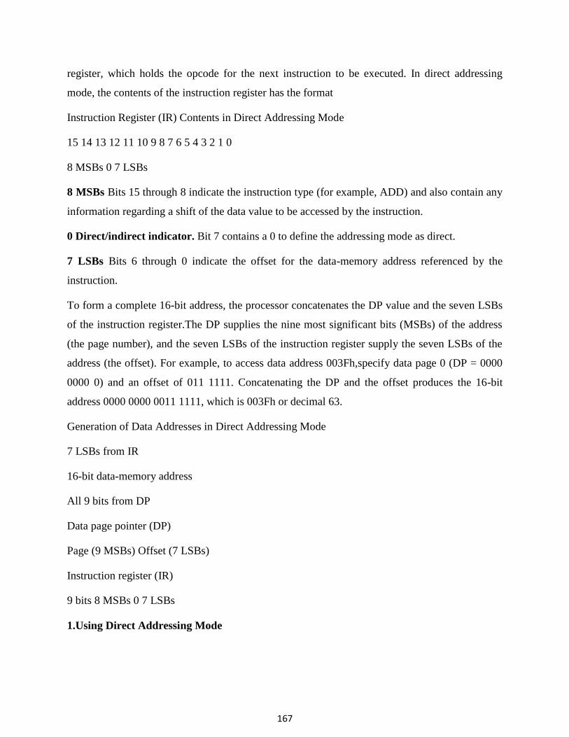
167
register, which holds the opcode for the next instruction to be executed. In direct addressing
mode, the contents of the instruction register has the format
Instruction Register (IR) Contents in Direct Addressing Mode
15 14 13 12 11 10 9 8 7 6 5 4 3 2 1 0
8 MSBs 0 7 LSBs
8 MSBs Bits 15 through 8 indicate the instruction type (for example, ADD) and also contain any
information regarding a shift of the data value to be accessed by the instruction.
0 Direct/indirect indicator. Bit 7 contains a 0 to define the addressing mode as direct.
7 LSBs Bits 6 through 0 indicate the offset for the data-memory address referenced by the
instruction.
To form a complete 16-bit address, the processor concatenates the DP value and the seven LSBs
of the instruction register.The DP supplies the nine most significant bits (MSBs) of the address
(the page number), and the seven LSBs of the instruction register supply the seven LSBs of the
address (the offset). For example, to access data address 003Fh,specify data page 0 (DP = 0000
0000 0) and an offset of 011 1111. Concatenating the DP and the offset produces the 16-bit
address 0000 0000 0011 1111, which is 003Fh or decimal 63.
Generation of Data Addresses in Direct Addressing Mode
7 LSBs from IR
16-bit data-memory address
All 9 bits from DP
Data page pointer (DP)
Page (9 MSBs) Offset (7 LSBs)
Instruction register (IR)
9 bits 8 MSBs 0 7 LSBs
1.Using Direct Addressing Mode

168
When you use direct addressing mode, the processor uses the DP to find the data page and uses
the seven LSBs of the instruction register to find a particular address on that page. Always do the
following:
a. Set the data page. Load the appropriate value (from 0 to 511) into the DP. The DP register
can be loaded by the LDP instruction or by any instruction that can load a value to ST0. The
LDP instruction loads the DP directly without affecting the other bits of ST0, and it clearly
indicates the value loaded into the DP. For example, to set the current data page to 32 (addresses
1000h–107Fh), you can use:
Example:LDP #32 ;Initialize data page pointer
b. Specify the offset. Supply the 7-bit offset as an operand of the instruction. For example, if you
want the ADD instruction to use the value at the second address of the current data page, you
would write:
ADD 1h ;Add to accumulator the value in the current ;data page, offset of 1.
Do not have to set the data page prior to every instruction that uses direct addressing. If all the
instructions in a block of code access the same data page, you can simply load the DP at the front
of the block. However, if various data pages are being accessed throughout the block of code, be
sure the DP is changed whenever a new data page should be accessed.
Examples of Direct Addressing
Example:. Using Direct Addressing with ADD (Shift of 0 to 15)
LDP #4 ;Set data page to 4 (addresses 0200h–027Fh).
ADD 9h,5 ;The contents of data address 0209h are ;left shifted 5 bits and added to the
;contents of the accumulator.
7 LSBs from IR 16-bit data address 0209h
All 9 bits from DP DP = 4 Instruction register (IR)
0 0 0 0 0 0 1 0 0 0 0 1 0 0 0 1 0 0 0 0 0 1 0 0 1
ADD opcode Shift of 5
0 0 0 0 0 0 1 0 0 0 0 0 1 0 0 1 9h
169
In Example the ADD instruction references a data memory address that is generated as shown
following the program code. For any instruction that performs a shift of 16, the shift value is not
embedded directly in the instruction word; instead, all eight MSBs contain an opcode that not
only indicates the instruction type, but also a shift of 16. The eight MSBs of the instruction word
indicate an ADD with a shift of 16.
5.6.3. Indirect Addressing Mode
Eight auxiliary registers (AR0–AR7) provide flexible and powerful indirect addressing. Any
location in the 64K data memory space can be accessed using a 16-bit address contained in an
auxiliary register.
1. Current Auxiliary Register
To select a specific auxiliary register, load the 3-bit auxiliary register pointer (ARP) of status
register ST0 with a value from 0 to 7. The ARP can be loaded as a primary operation by the
MAR instruction or by the LST instruction. The ARP can be loaded as a secondary operation by
any instruction that supports indirect addressing. The register pointed to by the ARP is referred
to as the current auxiliary register or current AR. During the processing of an instruction, the
content of the current auxiliary register is used as the address at which the data-memory access
occurs. The ARAU passes this address to the data-read address bus (DRAB) if the instruction
requires a read from data memory, or it passes the address to the data-write address bus (DWAB)
if the instruction requires a write to data memory. After the instruction uses the data value, the
contents of the current auxiliary register can be incremented or decremented by the ARAU,
which implements unsigned 16-bit arithmetic. Normally, the ARAU performs its arithmetic
operations in the decode phase of the pipeline (when the instruction specifying the operations is
being decoded). This allows the address to be generated before the decode phase of the next
instruction. There is an exception to this rule: during processing of the NORM instruction, the
auxiliary register and/or ARP modification is done during the execute phase of the pipeline.
2. Indirect Addressing Options
The ‟C24x provides four types of indirect addressing options:
170
a.No increment or decrement. The instruction uses the content of the current auxiliary register
as the data memory address but neither increments nor decrements the content of the current
auxiliary register.
b.Increment or decrement by 1. The instruction uses the content of the current auxiliary
register as the data memory address and then increments or decrements the content of the current
auxiliary register by one.
c.Increment or decrement by an index amount. The value in AR0 is the index amount. The
instruction uses the content of the current auxiliary register as the data memory address and then
increments or decrements the content of the current auxiliary register by the index amount.
Indirect Addressing Mode
d.Increment or decrement by an index amount using reverse carry. The value in AR0 is the
index amount. After the instruction uses the content of the current auxiliary register as the data-
memory address, that content is incremented or decremented by the index amount. The addition
and subtraction process is accomplished with the carry propagation reversed for fast Fourier
transforms (FFTs).
e.Operand Option Example
* No increment or decrement LT * loads the temporary register (TREG) with the content of the
data memory address referenced by the current AR.
*+ Increment by 1 LT *+ loads the temporary register (TREG) with the content of the data
memory address referenced by the current AR and then adds 1 to the content of the current AR.
*– Decrement by 1 LT *– loads the temporary register (TREG) with the content of the data
memory address referenced by the current AR and then subtracts 1 from the content of the
current AR.
*0+ Increment by index amount LT *0+ loads the temporary register (TREG) with the content of
the data memory address referenced by the current AR and then adds the content of AR0 to the
content of the current AR.
*0– Decrement by index amount LT *0– loads the temporary register (TREG) with the content
of the data memory address referenced by the current AR and then subtracts the content of AR0
from the content of the current AR.
171
*BR0+ Increment by index amount, adding with reverse carry
LT *BR0+ loads the temporary register (TREG) with the content of the data memory address
referenced by the current AR and then adds the content of AR0 to the content of the current AR,
adding with reverse carry propagation.
*BR0– Decrement by index amount, subtracting with reverse carry
LT *BR0– loads the temporary register (TREG) with the content of the data memory address
referenced by the current AR and then subtracts the content of AR0 from the content of the
current AR, subtracting with bit reverse carry propagation.
All increments or decrements are performed by the auxiliary register arithmetic unit (ARAU) in
the same cycle during which the instruction is being decoded in the pipeline.
The bit-reversed indexed addressing allows efficient I/O operations by resequencing the data
points in a radix-2 FFT program. The direction of carry propagation in the ARAU is reversed
when the address is selected, and AR0 is added to or subtracted from the current auxiliary
register. A typical use of this addressing mode requires that AR0 be set initially to a value
corresponding to half of the array‟s size, and further, that the current AR value be set to the base
address of the data (the first data point).
f. Next Auxiliary Register
In addition to updating the current auxiliary register, a number of instructions can also specify
the next auxiliary register or next AR. This register will be the current auxiliary register when the
instruction execution is complete. The instructions that allow you to specify the next auxiliary
register load the ARP with a new value. When the ARP is loaded with that value, the previous
ARP value is loaded into the auxiliary register pointer buffer (ARB).
Example:MAR*,AR1 ;Load the ARP with 1 to make AR1 the ;current auxiliary register.
LT *+,AR2 ;AR2 is the next auxiliary register ;Load the TREG with the content of the
;address referenced by AR1, add one to ;the content of AR1, then make AR2 the
;current auxiliary register.
MPY* ;Multiply TREG by content of address ;referenced by AR2.
172
5.7. Event Manager
Event Manager (EV) Functional Blocks
All devices of the ‟240x family, with the exception of the ‟2402, have two event each other in
terms of functionality and register mapping/bit definition. For the sake of brevity, only the
functionality of EVA is explained. Minor differences (such as naming conventions and register
addresses) are highlighted as appropriate.
Each EV module in the ‟240x device contains the following functional blocks:
1.Two general-purpose (GP) timers.
2.Three compare units.
3. Pulse-width modulation (PWM) circuits that include space vector PWM circuits, dead-band
generation units, and output logic .
4.Three capture units (described in section 6.8 on page 6-66).
5. Quadrature encoder pulse (QEP) circuit
6.Interrupt logic .
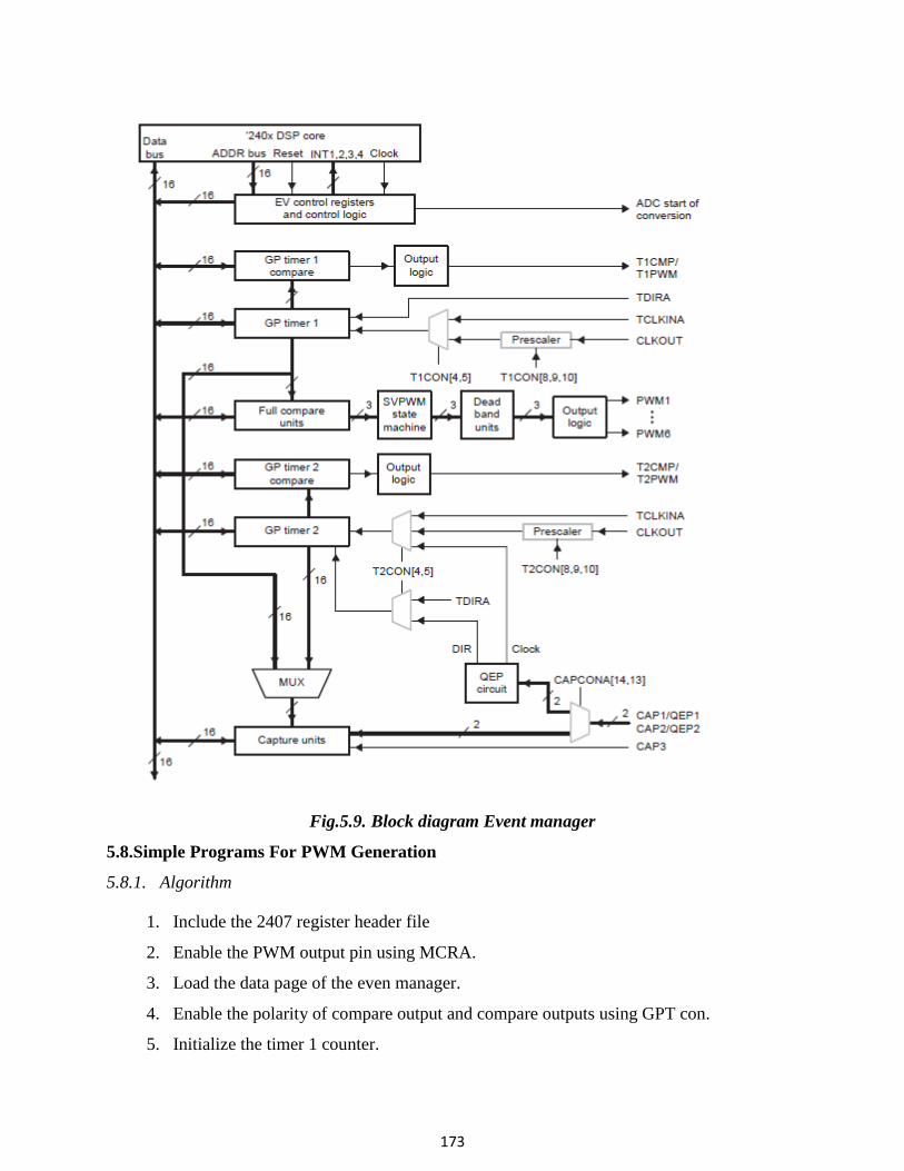
173
Fig.5.9. Block diagram Event manager
5.8.Simple Programs For PWM Generation
5.8.1. Algorithm
1. Include the 2407 register header file
2. Enable the PWM output pin using MCRA.
3. Load the data page of the even manager.
4. Enable the polarity of compare output and compare outputs using GPT con.
5. Initialize the timer 1 counter.
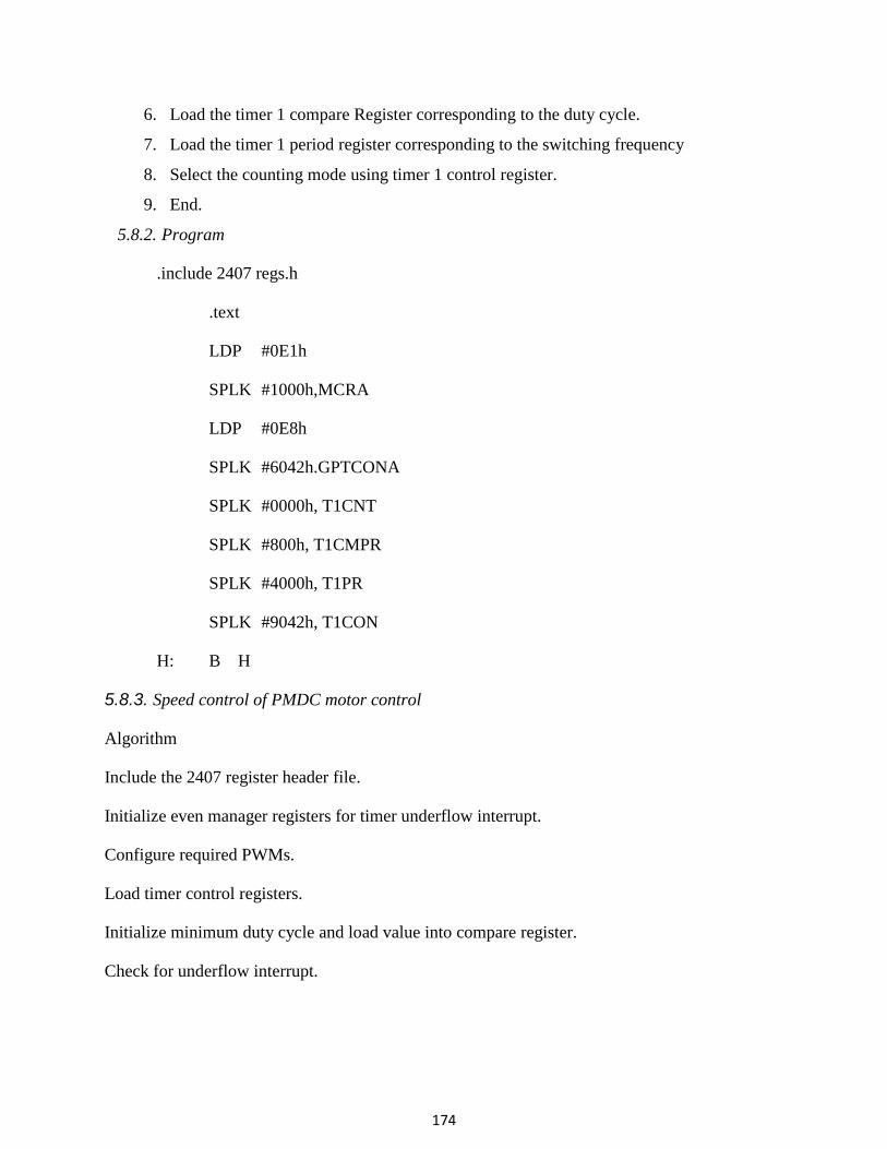
174
6. Load the timer 1 compare Register corresponding to the duty cycle.
7. Load the timer 1 period register corresponding to the switching frequency
8. Select the counting mode using timer 1 control register.
9. End.
5.8.2. Program
.include 2407 regs.h
.text
LDP #0E1h
SPLK #1000h,MCRA
LDP #0E8h
SPLK #6042h.GPTCONA
SPLK #0000h, T1CNT
SPLK #800h, T1CMPR
SPLK #4000h, T1PR
SPLK #9042h, T1CON
H: B H
5.8.3. Speed control of PMDC motor control
Algorithm
Include the 2407 register header file.
Initialize even manager registers for timer underflow interrupt.
Configure required PWMs.
Load timer control registers.
Initialize minimum duty cycle and load value into compare register.
Check for underflow interrupt.
175
Read up button and down button switches.
Increment/decrement the PWM width correspondingly and check for limit.
Load the value to the compare register.
Repeat steps 6 to 9 for continuous variation of PWM.
Give the PWM pulse to the switches.
End.
Part A
1. What are the addressing modes of TMS320C24X processor.
2. What are the types of instructions of TMS320C24X processor.
3. Give 4 salient features of TMS320C24X processor.
4. What is event manager.
5. Give 4 applications of TMS320C24X processor.
Part B
6. Explain the architecture of TMS320C24X processor.
7. Write a simple program to control the speed of PMDC motor using TMS320C24X processor.
8. With a neat block diagram explain about event manager.