
Unification of MOS compact models with the unified regional modeling approach
15
J Comput Electron (2011) 10:121–135 DOI 10.1007/s10825-011-0354-y Unification of MOS compact models with the unified regional modeling approach Xing Zhou · Guojun Zhu · Guan Huei See · Karthik Chandrasekaran · Siau Ben Chiah · Khee Yong Lim Published online: 9 March 2011 © Springer Science+Business Media LLC 2011 Abstract This paper reviews the development of the MOS- FET model (Xsim), for unification of various types of MOS devices, such as bulk, partially/fully-depleted SOI, double- gate (DG) FinFETs and gate-all-around (GAA) silicon- nanowires (SiNWs), based on the unified regional modeling (URM) approach. The complete scaling of body doping and thickness with seamless transitions from one structure to an- other is achieved with the unified regional surface potential, in which other effects (such as those due to poly-gate doping and quantum-mechanical) can be incorporated. The unique features of the Xsim model and the essence of the URM ap- proach are described. Keywords Compact model · MOSFET · Xsim X. Zhou ( ) School of Electrical and Electronic Engineering, Nanyang Technological University, 50 Nanyang Avenue, Singapore 639798, Republic of Singapore e-mail: [email protected] G. Zhu Systems on Silicon Manufacturing Co. Pte. Ltd., 70 Pasir Ris Industrial Drive 1, Singapore 519527, Singapore G.H. See · K.Y. Lim GLOBALFOUNDRIES Singapore Pte. Ltd., 60 Woodlands Industrial Park D Street 2, Singapore 738406, Singapore K. Chandrasekaran GLOBALFOUNDRIES, 2070 Route 52, Hopewell Junction, NY 12533, USA S.B. Chiah ITE College Central, 20 Yishun Avenue 9, Singapore 768892, Singapore 1 Introduction The compact model (CM) has been the essential link be- tween very large scale integrated (VLSI) circuit design and manufacturing in the history of VLSI technology genera- tions. The term “compact model” was probably first used by Gummel and Poon (GP) in 1970 for the GP bipolar junc- tion transistor (BJT) model [1]. In the mainstream comple- mentary metal-oxide-semiconductor (CMOS), generations of MOS field-effect transistor (FET) CMs have been de- veloped, following the 1978 Brews’ charge-sheet approxi- mation (CSA) [2], which are all based on (and still bench- marked to) the 1966 “Pao–Sah double-integral” model [3]. Early MOSFET models include threshold-voltage (V t )- based models; and contemporary models include inversion- charge (Q i )-based and surface-potential (φ s )-based models (see, e.g., a review paper in [4]). In half a century, bulk CMOS technologies have been scaled into nanometer dimensions. Nonclassical CMOS de- vices have emerged, such as ultrathin-body (UTB) SOI, double-gate (DG) FinFETs and gate-all-around (GAA) silicon-nanowire (SiNW) FETs, for which CMs without the CSA are also being developed. Although compared to more rigorous transport solutions, such as first-principle Green’s functions, semiclassical Monte Carlo, or even numerical drift-diffusion (DD) solutions, analytical CMs involve a lot simplifications and approximations, it becomes more and more challenging to develop a core CM that can capture the actual terminal (current and charge) characteristics of nanoscale MOSFETs, including their higher-order deriva- tives, with all major physical effects and scalable over the entire range of operating bias, geometry, temperature, fre- quency, as well as the corresponding noise, variation, and aging behaviors. At the same time, the CM is expected to be very efficient for evaluation in large-scale circuit simula-
Transcript of Unification of MOS compact models with the unified regional modeling approach
J Comput Electron (2011) 10:121–135DOI 10.1007/s10825-011-0354-y
Unification of MOS compact models with the unified regionalmodeling approach
Xing Zhou · Guojun Zhu · Guan Huei See ·Karthik Chandrasekaran · Siau Ben Chiah ·Khee Yong Lim
Published online: 9 March 2011© Springer Science+Business Media LLC 2011
Abstract This paper reviews the development of the MOS-FET model (Xsim), for unification of various types of MOSdevices, such as bulk, partially/fully-depleted SOI, double-gate (DG) FinFETs and gate-all-around (GAA) silicon-nanowires (SiNWs), based on the unified regional modeling(URM) approach. The complete scaling of body doping andthickness with seamless transitions from one structure to an-other is achieved with the unified regional surface potential,in which other effects (such as those due to poly-gate dopingand quantum-mechanical) can be incorporated. The uniquefeatures of the Xsim model and the essence of the URM ap-proach are described.
Keywords Compact model · MOSFET · Xsim
X. Zhou (�)School of Electrical and Electronic Engineering, NanyangTechnological University, 50 Nanyang Avenue,Singapore 639798, Republic of Singaporee-mail: [email protected]
G. ZhuSystems on Silicon Manufacturing Co. Pte. Ltd., 70 Pasir RisIndustrial Drive 1, Singapore 519527, Singapore
G.H. See · K.Y. LimGLOBALFOUNDRIES Singapore Pte. Ltd., 60 WoodlandsIndustrial Park D Street 2, Singapore 738406, Singapore
K. ChandrasekaranGLOBALFOUNDRIES, 2070 Route 52, Hopewell Junction,NY 12533, USA
S.B. ChiahITE College Central, 20 Yishun Avenue 9, Singapore 768892,Singapore
1 Introduction
The compact model (CM) has been the essential link be-tween very large scale integrated (VLSI) circuit design andmanufacturing in the history of VLSI technology genera-tions. The term “compact model” was probably first used byGummel and Poon (GP) in 1970 for the GP bipolar junc-tion transistor (BJT) model [1]. In the mainstream comple-mentary metal-oxide-semiconductor (CMOS), generationsof MOS field-effect transistor (FET) CMs have been de-veloped, following the 1978 Brews’ charge-sheet approxi-mation (CSA) [2], which are all based on (and still bench-marked to) the 1966 “Pao–Sah double-integral” model [3].Early MOSFET models include threshold-voltage (Vt )-based models; and contemporary models include inversion-charge (Qi)-based and surface-potential (φs)-based models(see, e.g., a review paper in [4]).
In half a century, bulk CMOS technologies have beenscaled into nanometer dimensions. Nonclassical CMOS de-vices have emerged, such as ultrathin-body (UTB) SOI,double-gate (DG) FinFETs and gate-all-around (GAA)silicon-nanowire (SiNW) FETs, for which CMs without theCSA are also being developed. Although compared to morerigorous transport solutions, such as first-principle Green’sfunctions, semiclassical Monte Carlo, or even numericaldrift-diffusion (DD) solutions, analytical CMs involve a lotsimplifications and approximations, it becomes more andmore challenging to develop a core CM that can capturethe actual terminal (current and charge) characteristics ofnanoscale MOSFETs, including their higher-order deriva-tives, with all major physical effects and scalable over theentire range of operating bias, geometry, temperature, fre-quency, as well as the corresponding noise, variation, andaging behaviors. At the same time, the CM is expected tobe very efficient for evaluation in large-scale circuit simula-
122 J Comput Electron (2011) 10:121–135
tions. When extending a bulk CM to UTB/DG/GAA MOS-FETs, it is nontrivial to have one core model with full body-doping scalability, since CSA may not be valid and Pois-son’s equation cannot be integrated twice if the doping termis not ignored.
In this paper, we review the development of a core MOS-FET model (called Xsim) based on the unified regional mod-eling (URM) approach over the past 13 years, starting withthe Vt -based model [5], expanding with a “non-pinned” sur-face potential [6], extending to strained-Si and DG [7] andφs -based formalism [8], and unifying with SOI/DG/SiNWincluding Schottky-barrier (SB) MOSFETs [9]. In Sect. 2,we outline MOS CM fundamentals and explain the need forunifying various MOS devices with complete scalability ingeometry and doping. In Sect. 3, we describe the URM ap-proach used in the Xsim model and its unique features dif-ferent from other contemporary models. Section 4 summa-rizes the Xsim model as well as CM needs and future trends.
2 MOS compact modeling fundamentals
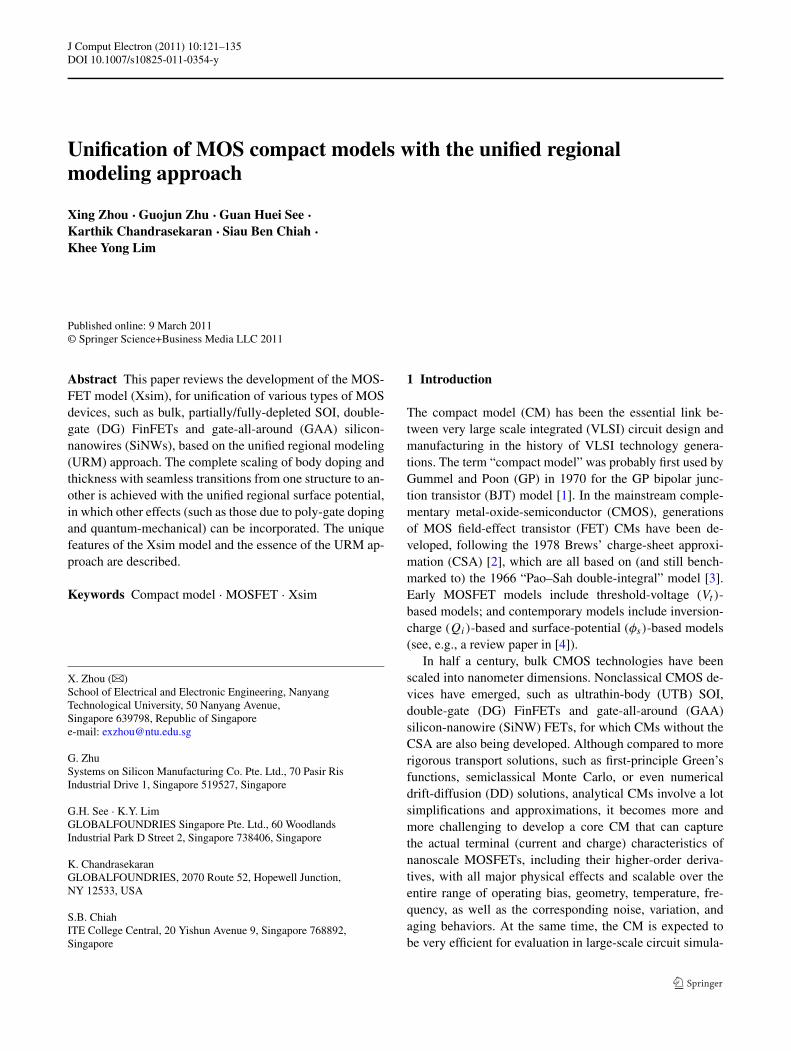
Transport solution to the ideally structured long-channelMOSFET is a 2D problem, which can be solved by numeri-cal solution of the Poisson–Boltzmann (PB) equation in theDD formalism. All CM formulations start by decomposingthe 2D problem into two 1D problems: the electrostatic solu-tion of the PB equation with the Gauss law (input x-voltageequation: electrostatic potential φ [≡ −Ei(x, y)/q] at agiven gate voltage VG) and the transport solution of the DDequation (output y-current equation: drain current IDS at agiven drain–source voltage VDS). A generic 4-terminal idealnMOSFET is shown in Fig. 1, in which the terminal voltages(VS,VD,VB) are applied to the Si body via the source/drain(S/D) pn-junctions and the body contact, while for float-ing body (FB) SOI and DG/GAA devices where there is nobody contact, external voltages are applied to the body viathe S/D (VS,VD).
For bulk nMOS in which body doping (NA) is usuallyhigh and the maximum gate depletion (Xdm) is much smallerthan body thickness (TSi), under nonequilibrium transport(VDS �= 0), the electron quasi-Fermi potential (imref) is de-termined by the S/D terminal voltage difference VDS, whichvaries across the channel as
φFn(y) ≡ −EFn/q = φF + Vc(y), (1)
where Vc [= −Ei(0, y)/q] is the channel voltage and φF (=−EF /q) is the Fermi potential. For CM formulations, anideal long-channel device under the gradual-channel ap-proximation (GCA) is assumed, in which voltage dropsacross the S/D series resistance, pn-junction built-in volt-ages, and those due to longitudinal fields near the S/D junc-tions and velocity saturation in the “pinch-off” region are
Fig. 1 A generic MOSFET with important physical parameters la-beled. The region for CM formulation is shown by the dotted line
all ignored (and modeled separately for short-channel de-vices). In the practical 2D picture of a bulk MOSFET, be-yond the maximum gate depletion in the neutral body, theelectron imref would merge to the (constant) body bias,which implies that φFn(x, y) would be x dependent undernonequilibrium. The x-dependent φFn is due to carrier gen-eration/recombination beyond the depletion region, or theideal ohmic contact (infinite surface recombination velocity)in the absence of carrier generation/recombination, whichmakes the PB equation non-integrable along the x directionand not suitable for CM formulation. Therefore, the regionof CM formulation is defined as from the surface (x = 0)to the “zero-field (ZF) location” (x = Xo) in the Si bodywith strictly x-independent channel voltage Vc(y), and fromsource (y = 0) to drain (y = L) in the “intrinsic linear chan-nel” under the GCA, as shown by the dotted-line box inFig. 1. The boundary voltages (Vs,Vd,Vb) with lower-casesubscripts are used as “terminal” voltages for the “intrin-sic” MOSFET. This picture of the “two 1D problems” forbulk-MOS is consistent for CM formulations, and is alsothe physical picture for UTB-SOI and DG/GAA devices inwhich there is no body contact and the electron imref is in-deed x-independent. Using the ZF location (x = Xo) as theboundary is one key to the extension to, and unification of,all types (bulk/SOI/DG/GAA) of MOS models.
For nMOSFETs, there is essentially no hole injectionfrom the n+ pn-junctions; hence, the hole quasi-Fermi po-tential (imref) is assumed constant (i.e., unipolar device andno hole current). It is given by
φFp ≡ −EFp/q = φF + Vr, (2)
J Comput Electron (2011) 10:121–135 123
where
Vr ={
Vb (body contac)
min(Vs,Vd) (floating body)(3)
is the potential reference at the flatband (Vgr = VFB) andequilibrium (Vds = 0) condition, which can be set to zero(or any arbitrary value). For bulk-MOS with high body dop-ing and body contact, potential in the neutral body is alwaysconstant (“flat”) and is set as the reference: φo = Vr = Vb =0. However, for UTB-SOI and DG/GAA MOSFETs withoutbody contact, there could be only one bias condition (i.e., atthe “flatband”), at which Vr = min(Vs,Vd) is defined as the(zero) potential reference; beyond which, potentials every-where in the body may be nonzero. For all existing CMs,the reference voltage is chosen to be Vb (“bulk-reference”)with body contact or Vs (“source-reference”) for floatingbody; and when Vd < Vs (Vds < 0), the S/D terminals areswapped based on nMOS convention that the drain currentalways flows from “drain” to “source” (which is equivalentto taking the absolute value of the |Vds| term for Vds < 0 inthe model equation). The reference defined in (3) is referredto as “ground-reference” (G-ref) for FB devices, in which Vs
and Vd (instead of Vds) appear in the model equations, andthe transistor “source” and “drain” are defined by the devicelabels (“S/D by label” i.e., by layout).
The electron–hole quasi-Fermi level difference (or “imref-split”) is then given by
φFn(y) − φFp = Vc(y) − Vr = Vcr(y). (4)
The gradient of Vcr(y) along y is the driving force, givingrise to the DD current.
2.1 Input voltage equation: electrostatic solution
In all CM formulations, carrier concentrations are assumedto follow the Boltzmann’s relation
n = nie(φ−φFn)/vth = nie
(φ−φF −Vc)/vth , (5a)
p = nie−(φ−φFp)/vth = nie
−(φ−φF −Vr )/vth , (5b)
in which imrefs are used for the general nonequilibrium con-dition, vth = kT/q is the thermal voltage, and ni is the intrin-sic carrier concentration. The PB equation under the GCAwith complete dopant ionization is given by
d2φ
dx2= − ρ
εSi= −q(p − n + ND − NA)
εSi
= qp0
εSi
[e(φ−2φF −Vc)/vth − e−(φ−Vr )/vth
+ 1 − e−(2φF +Vcr)/vth]
(6)
in which we have used the charge-neutrality condition
NA − ND = p0 − n0 (7)
at the flatband Vgr = VFB, with
n0 ≡ n(φ = Vr) = nie−(φF +Vcr)/vth , (8a)
p0 ≡ p(φ = Vr) = nieφF /vth . (8b)
The first integral of (6) along any y (0 ≤ y ≤ L) can beeasily obtained by integrating from surface (x = 0) to thezero-field location (x = Xo), with the boundary conditions{
φ(0, y) = φs
−φ′(0, y) = Es
{φ(Xo, y) = φo
−φ′(Xo, y) = Eo ≡ 0.(9)
Together with the Gauss law applied to the SiO2/Si interface
Es = (Cox/εSi)(Vgf − φs), (10)
where Cox = εox/Tox is the gate-oxide capacitance (per unitarea), εox and εSi are the SiO2 and Si permittivity, respec-tively, and Vgf ≡ Vg − VFB is defined as the “flatband-shifted” gate voltage, we obtain the (input) voltage equation:
Vgf − φs = sgn(φs − φo)ϒ√
fφ(φs,φo,Vc,Vr) (11)
fφ = e−(2φF +Vcr)/vth[vthe−Vr/vth(eφs/vth − eφo/vth)︸ ︷︷ ︸(n)
− (φs − φo)]︸ ︷︷ ︸(n0)
+vtheVr/vth(e−φs/vth − e−φo/vth)︸ ︷︷ ︸
(p)
+ (φs − φo)︸ ︷︷ ︸(p0)
. (11a)
The “body factor” in (11) is given by
ϒ = √2qεSip0/Cox, (12)
in which the equilibrium (majority) hole concentration isgiven by (8b)
p0 = nieφF /vth = ni exp
[sinh−1
(NA − ND
2ni
)], (13)
with the Fermi potential given by the well-known Kingstonequation [10]
φF = vth sinh−1(
NA − ND
2ni
). (14)
Considering only the p0 (due to NA) term in (6), the “de-pletion width” at a given Vgr can be found as
Xd =√
2εSi(φs − φo)
qp0
124 J Comput Electron (2011) 10:121–135
=√
2εSi
qp0
(−ϒ
2+
√ϒ2
4+ Vgf − φo
). (15)
Under the pinned-φs approximation (high body doping), themaximum depletion width (Xdm) is reached at the onset of“strong inversion” at which φs = 2φF + Vc (φo = Vr), and
Xdm =√
2εSi(2φF + Vcr)
qp0. (16)
For TSi > Xdm, the ZF location is taken as Xo = Xdm, andwe always have φo = Vr where Vr = Vb = 0 for bulk andPD-SOI with body contact, and φo to be modeled for FBPD-SOI and DG/GAA devices. If TSi < Xd , such as UTBFD-SOI and DG/GAA devices (low/undoped body), “fulldepletion” occurs when Xd(Vg,FD) = TSi based on (15)
TSi = Xd(Vg,FD)
=√
2εSi
qp0
(−ϒ
2+
√ϒ2
4+ Vgf ,FD − φo
), (17)
where Vg,FD is the FD voltage and Vgf ,FD ≡ Vg,FD − VFB.The corresponding FD potential is given by
φFD = φs − φo = qp0X2d(Vg,FD)
2εSi
=(
−ϒ
2+
√ϒ2
4+ Vgf ,FD − φo
)2
. (18)
Beyond the FD voltage (Vg > Vg,FD) if strong inversion hasnot been reached, “volume inversion” will occur and the ZFpotential φo needs to be modeled and included in the solu-tion.
Note that in the above equations (6)–(18), p0 (instead ofNA), as defined in (8b) and expressed as (12), is used. This isanother key to complete body doping and thickness scaling,including NA and ND approaching zero (ideal “pure Si”),that is different from “intrinsic Si” as in unintentionally-doped Si, for which φF given in (14) approaches zero (i.e.,EF = Ei ) and p0 approaches ni . For high body doping,p0 ≈ NA and the above equations approach the conventionalexpressions for bulk-MOS, such as φF ≈ vth ln(NA/ni)
for (14) and ϒ ≈ (2qεSiNA)1/2/Cox for (12). It is also thekey to unifying various types of MOSFETs with the URMapproach, which will be detailed in Sect. 3.
2.2 Output current equation: transport solution
All compact Ids current formulations start with the integralof the inversion charge over the channel voltage in the in-trinsic channel, assuming constant mobility:
Ids0 = μ0Z
L
∫ Vd
Vs
(−Qi)dVc, (19)
where Z = W (channel width) for bulk/SOI/DG and Z =2πR (wire radius R) for GAA MOSFETs. The rigoroussolution is given by the original “Pao–Sah double inte-gral” [3]. Depending on the approximations introduced,there are CSA [2] (suitable for high body doping) and non-CSA (suitable for low/undoped body) formulations. In thissub-section, we outline the formulations for bulk-MOS un-der the CSA, which also forms the basis for extension toother types of devices.
According to the intermediate variable introduced, theformulation can be classified into φs -based and Qi -basedmodels:
Ids0 =⎧⎨⎩
−μ0ZL
∫ φs,d
φs,sQi(φs)
dVc
dφsdφs (φs-based)
−μ0ZL
∫ Qi,d
Qi,sQi
dVc
dQidQi (Qi-based)
(20)
in which the integral is evaluated for the φs or Qi at thesource and drain ends, from the respective solutions usuallygoverned by implicit equations for φs or Qi . With the CSA(for bulk-MOS), it is generally recognized that φs -basedmodels have more physical contents since accurate φs canbe obtained from the voltage equation by iterative methods;whereas Qi -based models, although having simpler expres-sions, require a linearization of the inversion charge to ob-tain an implicit equation for the inversion charge in the “uni-fied charge control model” (UCCM). The Vt -based model isa special case for the “pinned-φs” model with a bulk-chargelinearization.
Since the terminal-charge model needs to be derived fromthe corresponding terminal-current model, different model-ing approaches lead to very different charge models. Thesymmetric linearization method [11] has shown much sim-pler charge expressions while retaining the physics in thesurface-potential solutions.
Once the ideal intrinsic-channel current (Ids0) is formu-lated, transverse/longitudinal-field dependent mobilities, ve-locity saturation/overshoot, and S/D series resistance areadded to the core Ids0 model. Vertical/lateral nonuniformdoping can be modeled by the effective doping, poly-gate depletion effect (PDE) and quantum-mechanical effect(QME) can be separately modeled in the surface potential.
3 Xsim: unification of MOS compact models
We first have a brief review on the history of the Xsim modeldevelopment. Although the current core model is a fully φs -based [7–9] model with symmetric charge linearization, ithas been evolved from Vt -based [5] to non-pinned φs -based[6] models, with many specific effects (including the URMapproach) adopted and evolved from the earlier models.
Lim [5] started with Vt modeling for the lateral nonuni-form doping (“halo”) [12, 13], with an effective doping
J Comput Electron (2011) 10:121–135 125
(Neff ) based on two lateral Gaussian profiles characterizedby the Gaussian peak, spread, and centroid [14]. This modelis still used in the charge model, whose parameters can beextracted from a given technology of Vt vs. Lg data, andis the key to physical geometry scaling without too manyempirical fittings. He also developed the mobility model[15], the gate-bias-dependent series resistance model [16],and the velocity-overshoot model [17] based on the energy-balance formalism for the electron-temperature gradient,which have been adapted to the current Xsim model. Theidea of the one-iteration parameter extraction [14, 18] hasalso been a unique feature of the core model.
Chiah [6] developed the unique URM [19], with unifiedregional surface potentials in accumulation (φacc) and deple-tion (φsub) being added (“stitched”) for the solution near theflatband, rather than solving accurate and explicit solutionsthat are being “glued” at the flatband, which established thebasis (and the essence) for unified regional charge modeling[20]. He also developed models for the poly-accumulationeffect (PAE), PDE, and poly-inversion effect (PIE) [21], aswell as the QME [19] in the non-pinned φs -based URM,which has been extended to the current Xsim model.
Chandrasekaran [7] extended the regional φs -based mod-el to strained-Si heterostructure MOSFETs [22–25], furtherdemonstrating the power of the URM approach. He alsostarted regional φs -based modeling with symmetric chargelinearization for doped-body DG FinFETs [26], and intro-duced the idea of the effective drain–source voltage (Vds,eff )
with the “G-ref” [7].See [8] extended the previous models and developed the
φs -based core model, including long/short-channel currentand charge [27] for bulk/SOI/DG in all regions, in bothCSA and non-CSA formulations and with complete dopingscaling [28] and QME [29]. His contribution in the “B-ref”model with “S/D by label” [30] (not by MOS convention),with velocity saturation occurring at the source or drain enddepending on the terminal Vd and Vs , has made it possiblefor complete Gummel symmetry in any higher-order deriva-tives as well as physical modeling of asymmetric S/D de-vices. He also extended the URM for extrinsic charge andcapacitance modeling in the S/D-gate overlap regions, withdetailed one/two-iteration parameter extraction.
Zhu [9] contributed to the unification of MOS mod-els in one core formulation for bulk/SOI and DG/GAAdevices [31] with CSA/non-CSA terminal current/chargeformulations, including PDE/QME [32], as well as SOI-specific effects such as self-heating, kink and parasitic-BJTeffects in FB-SOI devices [9]. He extended the “G-ref”model for three-terminal DG/GAA devices with “S/D bylabel” [33] with a new smoothing function for Vds,eff =Vd,eff − Vs,eff , which satisfies the Gummel symmetry test(GST) for any order. He introduced a “symmetric imref cor-rection” (SIC) [9, 32] for the FB potential φo as Vds → 0,
which physically models the effect due to bipolar (S/D junc-tion) current for Vds ≈ 0, important for higher-order GSTand distortion analysis. He proposed a unique drain-inducedbarrier lowering (DIBL) model [9, 34] based on quasi-2Dsolution that accounts for both DIBL and TSi-dependent sub-threshold slope (flatband voltage). He also developed a com-plete model for SB FinFETs [35, 36], with the URM for φs
in the intrinsic channel and thermionic and tunneling cur-rent, as well as a subcircuit model for dopant-segregatedSchottky (DSS) SiNWs [37, 38], with the unique convexcurvature in the Ids–Vds characteristics at small Vds and largeVgs.
3.1 Bulk model with the URM for the surface potential
φs -based models require the solution of φs at the S/D endsy = (0,L) with Vc = (Vs,Vd). For bulk-MOS in which thevoltage equation is given by (11) with φo = Vb = 0, ex-act iterative solutions are available (including solutions nearthe flatband in which all the charges cannot be ignored).However, such a model cannot be extended to FD-SOI andDG/GAA devices with body doping, in which φo has to bemodeled, since the PB equation cannot be integrated twiceunless the doping term (NA − ND) is ignored.
The essence of the URM approach is to solve “asymp-totic” piecewise regional solutions considering only onedominant charge, and using math smoothing (or transition)functions to obtain unified regional solutions for each pieceand “join” them to form single-piece unified solutions. Forbulk-nMOS, the piecewise solutions to (11) (first integralwith Gauss law) considering only p, NA, and n, respec-tively, are given by⎧⎪⎪⎪⎪⎪⎪⎪⎪⎪⎪⎪⎨⎪⎪⎪⎪⎪⎪⎪⎪⎪⎪⎪⎩
φcc = Vgf + 2vth L{ ϒ2√
vthe−(Vgf −Vr )/2vth}
(Vgr < VFB)
φdd = φo + (−ϒ2 +
√ϒ2
4 + (Vgf − φo))2
(VFB < Vgr < Vt)
φss = Vgf − 2vth L{ ϒ2√
vthe(Vgf −2φF −Vc)/2vth}
(Vgr > Vt)
(21)
where L{W } is the Lambert W function. They are the phys-ical solutions only in the respective regions and approachaccurate solutions asymptotically.
Using the following two “complementary” smoothingfunctions
ϑf {x;σ } = 0.5(x +√
x2 + 4σ), (22a)
ϑr{x;σ } = 0.5(x −√
x2 + 4σ), (22b)
and the following transition function
ϑeff {x, xsat; δ}
126 J Comput Electron (2011) 10:121–135
= xsat − 0.5[xsat − x − δ
+√
(xsat − x − δ)2 + 4δxsat], (23)
the single-piece unified regional solutions are given by
φacc = ϑr(Vgf ;σa) + 2vth L{
ϒ
2√
vthe−(Vgf −Vr )/2vth
}(24a)
φsub = φo +(
−ϒ
2+
√ϒ2
4+ ϑf (Vgf − φo;σf )
)(24b)
φstr = ϑf (Vgf ;σs) − 2vth L{
ϒ
2√
vthe(Vgf −2φF −Vc)/2vth
}(24c)
in which σa , σf , and σs are smoothing parameters for therespective regional solutions. The sum of φacc and φsub,
φsa = φacc + φsub, (25)
gives a single-piece Vc-independent solution valid from ac-cumulation to depletion, in which the φs solution at flatbandis not being solved but “tuned” by the two smoothing param-eters (σa and σf ) for charge neutrality (φs = 0) and smooth-ness at Vgr = VFB.
φds = ϑeff {φsub, φstr; δφ} (26)
gives the single-piece solution valid from depletion to stronginversion (tuned by δφ near Vt ), which is also Vc indepen-dent below Vt and approaches zero below VFB. φds can beadded (“stitched”) with the accumulation piece (φacc) toform a single-piece unified φs solution:
φseff = φacc + φds. (27)
The URM φseff (27) has an overall mV accuracy comparedto the exact iterative solution. However, due to its uniquefeature of Vc-independence below Vt , together with the ef-fective drain–source voltage in the Ids model [see (46) be-low], it does not require very accurate φs solutions, contraryto those iterative/explicit φs -based models. Although thesingle-piece φseff (27) is available, it is not directly used inthe charge modeling; instead, the unified regional solutions(φacc, φds) are used in the URM for terminal charges. Thisis another unique feature of the URM approach, e.g., thesingle-piece bulk charge (Qb,sa = Qb,acc + Qb,sub) acrossthe flatband [19], that is not possible for other modeling ap-proaches.
With the CSA, inversion charge (Qi) can be separatedfrom bulk charge (Qb) as
Qi = −(Qg +Qox)−Qb = −Cox(Vgf −φs −ϒ√
φs − φo).
(28)
Following the idea of symmetric charge linearization [11],i.e., a Taylor expansion of (28) around the “mid-point po-tentials” [average of φs(0) and φs(L)]φs = (φs,s + φs,d)/2, (29a)
φo = (φo,s + φo,d)/2, (29b)
from (19), we obtain the long-channel current [8]
Ids0 = β0(qi + Abvth)�φs, (30)
qi = Vgf − φs − ϒ
√φs − φo, (31)
Ab = 1 + ϒ
2√
φs − φo
, (32)
β0 = μeff 0Cox(Z/L), (33)
μeff 0 = (μeff 0,s + μeff 0,d )/2. (34)
The longitudinal-field dependent mobility is based on thepiecewise velocity–field model [5, 8, 9]
μeff 0,c = μ0
1 + δL(Vc,eff − Vr)/(LEsat)(c = s, d), (35)
where δL is a fitting parameter. The transverse-field depen-dent mobility is given by [5, 15]
μ0 = μ1
1 + (μ1/μ2)E1/3eff + (μ1/μ3)E
νeff
, (36)
in which μ1,μ2,μ3, and ν are fitting parameters. The effec-tive field is given by [8]
Eeff = ζnCox
εSi
(Vgt + ζb
ζn
ϒ
√φs − φo
), (37)
in which ζn and ζb are fitting parameters (ζb = 0 for FBdevice). The mid-point inversion charge (normalized to Cox)
given by
Vgt = (Vgt,s + Vgt,d )/2, (38)
Vgt,c = ϒ
√φs,c − φo + vthe
(φs,c−2φF −Vc)/vth
− ϒ√
φs,c − φo (c = s, d) (39)
is taken from the right-hand side (RHS) of the voltage equa-tion (11), which is another key to not requiring very accurateφs solutions [8].
With the S/D identified by “label” (layout), velocity sat-uration may occur at the drain or source end depending onthe terminal Vd and Vs , given by [30, 33]
Vds,sat = Vgt,sLEsat
Vgt,s + Ab,sLEsat + 2Ab,svth
= Vd,sat − Vs, (40a)
J Comput Electron (2011) 10:121–135 127
Vsd,sat = Vgt,dLEsat
Vgt,d + Ab,dLEsat + 2Ab,dvth
= Vs,sat − Vd, (40b)
in which the derivation includes both drift and diffusion cur-rents. The saturation field is given by
Esat = 2vsat/μ0, (41)
in which the saturation velocity vsat can be specified for dif-ferent values at the S/D for modeling asymmetric S/D de-vices [30]. The transition function for the “G-ref” effectivesaturation voltage is given by [33]
Vc,eff = ϑ{Vc,Vc,sat,Vcc′,sat; δ} (c = s, d; c′ = d, s)
= Vc,sat − 1
2(Vc,sat − Vc
+√
(Vc,sat − Vc)2 + 4δVcc′,sat + δ). (42)
The φs,s and φs,d in the previous equations (29a) and (39)are expressed using φds in (26) as
φs,c = φds(Vc,eff ) (c = s, d). (43)
The �φs in (30) is defined as
�φs = φs,d − φs,s, (44)
which becomes an extremely small value in subthreshold,and it requires highly accurate solutions for evaluation inthe φs -based Ids model (30). From the “pinned-φs” approx-imation, φs = 2φF + Vc , (44) becomes �φs ≈ Vds, and wereplace Vds by the “G-ref” effective drain–source voltage,given by
�φs ≈ Vds,eff = Vd,eff − Vs,eff . (45)
Thus, (30) becomes
Ids0 = β0(qi + Abvth)Vds,eff , (46)
which is an exact odd function of Vds, and it gives the correctsubthreshold slope without requiring accurate φs solutionsand body-bias clipping.
For the short-channel Ids model, a Vg-dependent S/D se-ries resistance model is adapted from [16] to the φs -basedmodel, given as
Rsd = Rs + Rd = Rext + Rint, (47)
Rs = ρS
XjZ+ υ
CoxZ(Vgt + Abvth), Rd : s → d, (47a)
where ρ and υ are fitting parameters. S and Xj are thespacer thickness and junction depth, respectively, which can
be assigned different values for asymmetric S/D devices.The saturation voltage Vds,sat in (40a) with Rsd is rederivedto be
Vds,sat = −bs − √b2s − 4ascs
2as
, (48)
as = vsatZCoxAb,sRs, (48a)
bs = −[Vgt,s + vsatZCoxVgt,s(2Rs + Ab,sRsd)
+ Ab,sEsatL + 2Ab,svth(1 + vsatZCoxRs)],(48b)
cs = Vgt,sEsatL
+ 2vsatZCoxRsdVgt,s(Vgt,s + Ab,svth).(48c)
And Vsd,sat in (40b) with Rsd is given by replacing all thesubscripts “s” by “d” in (48).
Following the energy-balance formalism [17] for velocity-overshoot (VO) modeling, its effect is expressed in the formof an “effective Early voltage,” given in G-ref by
VAeff ,c = LEsat[1 + hc(Vc − Vc,eff )] + δL(Vc,eff − Vr)
δLhc(Vc,eff − Vr),
(49)
hc =ξc
l2[1 +
√1 + (
Vc−Vc,efflEsat
)2]√1 + (
Vc−Vc,efflEsat
)2 − ξc
l2(Vc,eff − Vr)
, (49a)
l = √(εSi/εSi)ToxXo, (49b)
in which ξ is a fitting parameter, Xo = min(Xdm, TSi),and c = 2kT(qτp0/m∗)/d , with τp0 being the low-fieldmomentum-relaxation time and d = 10−8 W for Si.
The final complete symmetric drain–source current isgiven by
Ids = gvoIds0
1 + RsdIds0/Vds,eff, (50)
gvo = (gvo,s + gvo,d)/2, (50a)
gvo,c = 1 +(
Vc − Vc,eff
VAeff ,c
)(c = s, d). (50b)
The aforementioned Ids model is an exact odd function ofVds and satisfies the GST for any higher order [30, 33].
Using (30) and following [11], the terminal-charge mod-els are derived [8], in which the bulk-charge model adoptsthe unique URM based on (25) [19]
Qb = −Cox
[Qb,acc + Qb,sub − (Ab − 1)�φ2
ds
12H
], (51)
Qb,acc = ϑr(Vgf ;σa) − φacc, (51a)
Qb,sub = ϑf (Vgf ;σa) − ϑf (Vgf ;σf )
+ ϒ
√φds − Vb, (51b)
128 J Comput Electron (2011) 10:121–135
in which
�φds = φds,d − φds,s = φds(Vd,eff ) − φds(Vs,eff ), (52a)
φds ≡ (φds,s + φds,d)/2, (52b)
H = (qi/Ab) + vth. (53)
The drain and source terminal charges following theWard–Dutton (WD) partition [39] are given by
Qd = −Cox
2
[qi − Ab�φds
6
(1 − �φds
2H− �φ2
ds
20H 2
)], (54)
Qs = −Cox
2
[qi + Ab�φds
6
(1 + �φds
2H− �φ2
ds
20H 2
)]. (55)
For short-channel charge models, based on (30) for the draincurrent without VO effect, terminal charges are derived [8],having the same expressions as in (51), (54), and (55) byreplacing H in (53) by
H ′ = qi + Abvth
Ab[1 + δLφs
LEsat+ Rsdμ0
ZL(qi + Abvth)]
, (56)
which approaches H when L → ∞.It is worth mentioning that in the above formulations, we
have included the φo term in all the equations for generaliz-ing to FD-SOI/DG/GAA devices (see the next sub-section).For bulk-MOS and PD-SOI in which there is always a neu-tral region in the body, we have φo = Vr , given in (3).
After formulating the long (46) and short (50) channelcore models, other effects, such as poly-gate doping (PAE,PDE, PIE) and QME as well as gate/drain leakage and ex-trinsic charge models, can be added to the core model. Forpoly-doping effects, a similar voltage equation for the sur-face potential (φp) in the poly-gate of doping Ng can bedeveloped [8, 21]. Similar URM for φp in all regions canbe obtained as regional models, replacing subscripts “s” by“p” and treating the Vgf − φs term in φp expressions andthe Vgf − φp term in φs expressions the same way as theVgf term in bulk URM. The regional PAE model is ob-tained from charge balance in accumulation with only thehole term:
φp,cc = −vth ln[(ϒ/ϒp)2e−φcc/vth + 1 − (ϒ/ϒp)2], (57)
ϒp = √2qεSiNg/Cox. (57a)
The QME model adopts the van Dort model [40] for thebandgap widening, given by
�Eg = κqm 3
8
�2
m∗e
(12m∗
eq2
εSi�2
2Cox(Vgf − φs)/q
3
)2/3
, (58)
which modifies ni as
nqmi = nie
(Eqmg −Eg)/2kT = nie
�Eqmg /vth;
�Eqmg ≡ �Eg/2q.
(59)
New voltage equations for φs and φp as well as their URMsolutions can be similarly obtained [6], which are built intothe φs -based model [8].
Intrinsic charge/capacitance models are developed in-cluding effects due to charge sharing, potential-barrierlowering in quasi-2D field, and lateral nonuniform dop-ing [8], similar to the earlier Vt -based model. Extrinsiccharge/capacitance models are also developed [8] in theURM by applying the φs -based formalism to the S/D–gateoverlap regions of length Lov(same role as L for the intrin-sic channel). Detailed formulations and parameter extrac-tions can be found in [8, 27]. Other models, such as gatetunneling current [41], substrate current due to impact ion-ization [42], and gate-induced drain leakage (GIDL) current[37], have also been developed.
3.2 Unification of SOI/DG/GAA models
The aforementioned bulk-MOS models involve only onegate. For UTB FD-SOI and DG/GAA devices, Gauss lawneeds to be applied to two gates (or in cylindrical coordinatefor GAA). However, it is known that the PB equation (6)cannot be integrated twice if the doping term (NA − ND) isnot ignored. On the other hand, if one starts with undopedbody (i.e., zero dopant) for FD-SOI and DG/GAA model-ing, the results cannot be extended to devices with dopedbody (strictly speaking, not even for unintentional dopant inthe body). The motivation for unification of various MOSmodels is to have a core model that is able to capture vari-ous MOS device characteristics with seamless transitions inbody doping and thickness scaling over the entire range. Ithas been shown [8, 9, 27–34] that the URM approach canachieve such a goal, which can be difficult (if not impossi-ble) for other iterative/explicit φs -based models.
The general idea behind the unification of CMs for ageneric MOSFET with two gates is to model each gate sep-arately, with subscripts “1” for gate-1 and “2” for gate-2, asthe complete (bulk) model described in Sect. 3.1, in whichthe ZF location Xo for each gate alone defines a “fictitiousboundary condition” with potential φo and field Eo = 0.A generic DG MOSFET is shown schematically in Fig. 2,in which device parameters associated with gate-1 and gate-2 are labeled respectively.
The key to linking the two sets of equations is the “full-depletion” condition:
Xo1(Vg1,FD) + Xo2(Vg2,FD) = TSi, (60)
J Comput Electron (2011) 10:121–135 129
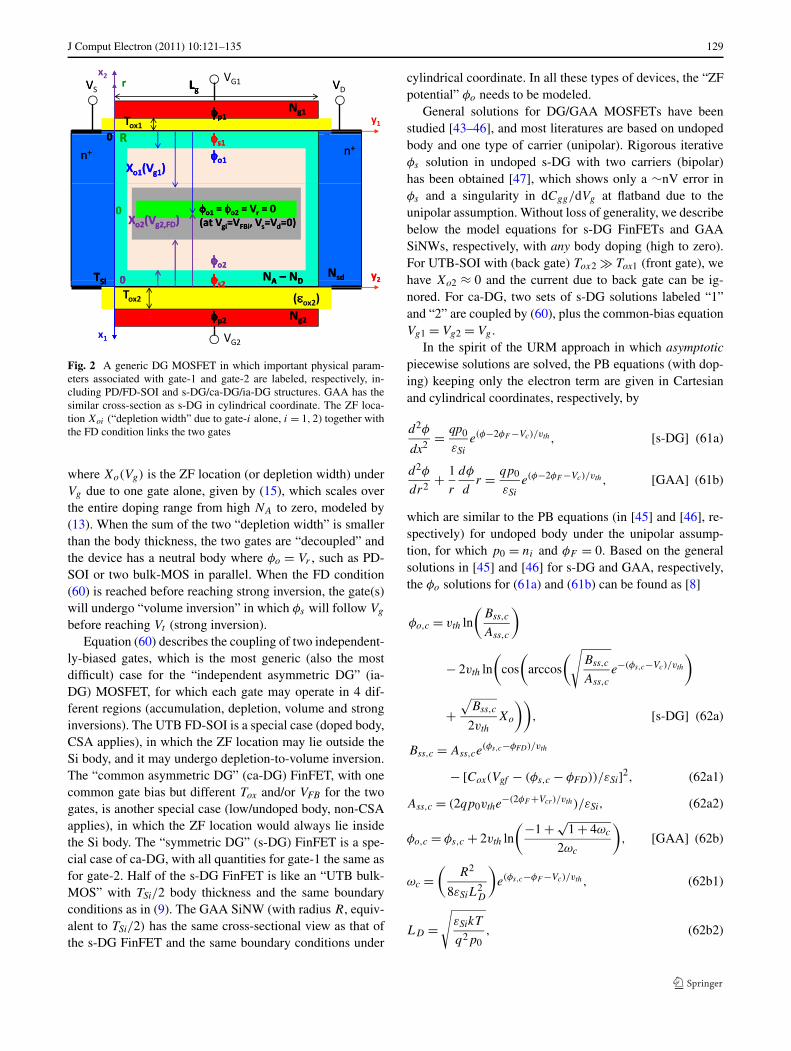
Fig. 2 A generic DG MOSFET in which important physical param-eters associated with gate-1 and gate-2 are labeled, respectively, in-cluding PD/FD-SOI and s-DG/ca-DG/ia-DG structures. GAA has thesimilar cross-section as s-DG in cylindrical coordinate. The ZF loca-tion Xoi (“depletion width” due to gate-i alone, i = 1,2) together withthe FD condition links the two gates
where Xo(Vg) is the ZF location (or depletion width) underVg due to one gate alone, given by (15), which scales overthe entire doping range from high NA to zero, modeled by(13). When the sum of the two “depletion width” is smallerthan the body thickness, the two gates are “decoupled” andthe device has a neutral body where φo = Vr , such as PD-SOI or two bulk-MOS in parallel. When the FD condition(60) is reached before reaching strong inversion, the gate(s)will undergo “volume inversion” in which φs will follow Vg
before reaching Vt (strong inversion).Equation (60) describes the coupling of two independent-
ly-biased gates, which is the most generic (also the mostdifficult) case for the “independent asymmetric DG” (ia-DG) MOSFET, for which each gate may operate in 4 dif-ferent regions (accumulation, depletion, volume and stronginversions). The UTB FD-SOI is a special case (doped body,CSA applies), in which the ZF location may lie outside theSi body, and it may undergo depletion-to-volume inversion.The “common asymmetric DG” (ca-DG) FinFET, with onecommon gate bias but different Tox and/or VFB for the twogates, is another special case (low/undoped body, non-CSAapplies), in which the ZF location would always lie insidethe Si body. The “symmetric DG” (s-DG) FinFET is a spe-cial case of ca-DG, with all quantities for gate-1 the same asfor gate-2. Half of the s-DG FinFET is like an “UTB bulk-MOS” with TSi/2 body thickness and the same boundaryconditions as in (9). The GAA SiNW (with radius R, equiv-alent to TSi/2) has the same cross-sectional view as that ofthe s-DG FinFET and the same boundary conditions under
cylindrical coordinate. In all these types of devices, the “ZFpotential” φo needs to be modeled.
General solutions for DG/GAA MOSFETs have beenstudied [43–46], and most literatures are based on undopedbody and one type of carrier (unipolar). Rigorous iterativeφs solution in undoped s-DG with two carriers (bipolar)has been obtained [47], which shows only a ∼nV error inφs and a singularity in dCgg/dVg at flatband due to theunipolar assumption. Without loss of generality, we describebelow the model equations for s-DG FinFETs and GAASiNWs, respectively, with any body doping (high to zero).For UTB-SOI with (back gate) Tox2 � Tox1 (front gate), wehave Xo2 ≈ 0 and the current due to back gate can be ig-nored. For ca-DG, two sets of s-DG solutions labeled “1”and “2” are coupled by (60), plus the common-bias equationVg1 = Vg2 = Vg .
In the spirit of the URM approach in which asymptoticpiecewise solutions are solved, the PB equations (with dop-ing) keeping only the electron term are given in Cartesianand cylindrical coordinates, respectively, by
d2φ
dx2= qp0
εSie(φ−2φF −Vc)/vth , [s-DG] (61a)
d2φ
dr2+ 1
r
dφ
dr = qp0
εSie(φ−2φF −Vc)/vth , [GAA] (61b)
which are similar to the PB equations (in [45] and [46], re-spectively) for undoped body under the unipolar assump-tion, for which p0 = ni and φF = 0. Based on the generalsolutions in [45] and [46] for s-DG and GAA, respectively,the φo solutions for (61a) and (61b) can be found as [8]
φo,c = vth ln
(Bss,c
Ass,c
)
− 2vth ln
(cos
(arccos
(√Bss,c
Ass,ce−(φs,c−Vc)/vth
)
+√
Bss,c
2vthXo
)), [s-DG] (62a)
Bss,c = Ass,ce(φs,c−φFD)/vth
− [Cox(Vgf − (φs,c − φFD))/εSi]2, (62a1)
Ass,c = (2qp0vthe−(2φF +Vcr)/vth)/εSi, (62a2)
φo,c = φs,c + 2vth ln
(−1 + √1 + 4ωc
2ωc
), [GAA] (62b)
ωc =(
R2
8εSiL2D
)e(φs,c−φF −Vc)/vth , (62b1)
LD =√
εSikT
q2p0, (62b2)
130 J Comput Electron (2011) 10:121–135
in which the subscript “c” stands for “s” and “d” for S/Dat y = 0 and y = L, respectively. The FD potential φFD isgiven by (18), from which the FD voltage (Vg,FD = Vgf ,FD +VFB) can be calculated:
Vgf ,FD =(√
qp0X2d,FD
2εSi+ ϒ
2
)2
− ϒ2
4;
Xd,FD = TSi
2.
[s-DG] (63)
In (62a), Xo = min(Xdm,Xd,FD) where Xdm is from (16).For ca-DG, with (60) at a common gate bias Vg , the com-
mon FD voltage can be derived [8]. The gate oxide capac-itance (per unit area) for bulk/SOI/DG and GAA is given,respectively, by
Cox = εox
Tox, [s-DG] (64a)
Cox = εox
R ln(1 + Tox/R). [GAA] (64b)
The φo,c(y) solution in (62) represents the ZF potential asan explicit function of the surface potential φs,c(y) along thechannel y, which is the exact solution for undoped body [45,46], the approximate solution for low-doping (small φF ) un-der non-CSA, and the asymptotic solution (in strong inver-sion) for high-doping under CSA. It is used in UTB FD-SOI in which the ZF potential is outside the Si body, andin DG/GAA in which the ZF potential is always inside thebody.
The asymptotic piecewise φs solutions in strong inver-sion [and strong accumulation] can be found by solving(61a) and (61b) for s-DG FinFETs and GAA SiNWs, re-spectively, which have the same expressions as φss [andφcc] in (21). The corresponding unified regional solutionsφstr [and φacc] are the same as in (24c) [and (24a)]. ForVFB < Vg < Vg,FD (depletion region), φs follows the deple-tion piece φdd in (21), or its unified regional piece φsub in(24b), until FD is reached at Vg = Vg,FD. This unified re-gional piece is modeled by
φdep = ϑeff (φsub, φFD; δd). (65a)
If strong inversion is not reached beyond Vg > Vg,FD, φs
will follow Vg in the volume inversion, in which the Sibody is fully depleted with a fixed depletion charge Qb =−Coxϒ(φFD)1/2, modeled by
φdv = Vgf − ϒ√
φFD. (65b)
Similar to (26), a single-piece unified regional φds solution,from depletion through volume inversion to strong inver-sion, is given by
φds = ϑeff {φdv,φstr; δφ}. (65c)
The final single-piece unified regional φs solution in all re-gions is given by (27).
The complete URM for φs is summarized below:
φs =
⎧⎪⎪⎪⎪⎪⎪⎪⎪⎪⎪⎪⎪⎪⎪⎪⎨⎪⎪⎪⎪⎪⎪⎪⎪⎪⎪⎪⎪⎪⎪⎪⎩
φacc = ϑr(Vgf ;σa) + 2vth L{ ϒ2√
vthe−(Vgf −Vr )/2vth}
φsub = φo + (−ϒ2 +
√ϒ2
4 + ϑf (Vgf − φo;σf ))2
φdep = ϑeff (φsub, φFD; δd)
φdv = Vgf − ϒ√
φFD
φstr = ϑf (Vgf ;σs)
− 2vth L{ ϒ2√
vthe(Vgf −2φF −Vc)/2vth}
φds = ϑeff (φdv,φstr; δφ)
φseff = φacc + φds
(66)
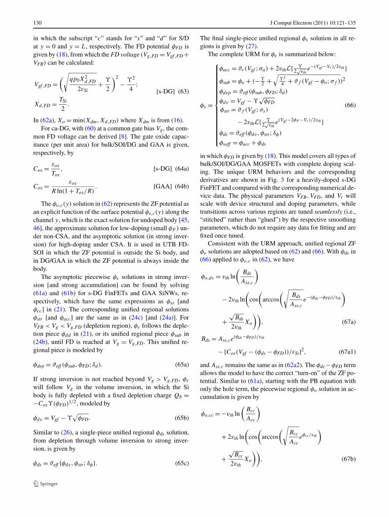
in which φFD is given by (18). This model covers all types ofbulk/SOI/DG/GAA MOSFETs with complete doping scal-ing. The unique URM behaviors and the correspondingderivatives are shown in Fig. 3 for a heavily-doped s-DGFinFET and compared with the corresponding numerical de-vice data. The physical parameters VFB,VFD, and Vt willscale with device structural and doping parameters, whiletransitions across various regions are tuned seamlessly (i.e.,“stitched” rather than “glued”) by the respective smoothingparameters, which do not require any data for fitting and arefixed once tuned.
Consistent with the URM approach, unified regional ZFφo solutions are adopted based on (62) and (66). With φds in(66) applied to φo,c in (62), we have
φo,ds = vth ln
(Bds
Ass,c
)
− 2vth ln
(cos
(arccos
(√Bds
Ass,ce−(φds−φFD)/vth
)
+√
Bds
2vthXo
)), (67a)
Bds = Ass,ce(φds−φFD)/vth
− [Cox(Vgf − (φds − φFD))/εSi]2, (67a1)
and Ass,c remains the same as in (62a2). The φds −φFD termallows the model to have the correct “turn-on” of the ZF po-tential. Similar to (61a), starting with the PB equation withonly the hole term, the piecewise regional φo solution in ac-cumulation is given by
φo,cc = −vth ln
(Bcc
Acc
)
+ 2vth ln
(cos
(arccos
(√Bcc
Acceφcc/vth
)
+√
Bcc
2vthXo
)), (67b)
J Comput Electron (2011) 10:121–135 131
Fig. 3 (a) Unified (smooth) regional surface-potential solutions instrong inversion (φstr), accumulation (φacc), depletion (φdep), deple-tion-to-volume inversion (φdv), depletion-to-strong inversion (φds),and single-piece solution (φseff ), and (b) the corresponding deriva-tives, compared with Medici data (circle) for the s-DG FinFET withTox = 3 nm, TSi = 50 nm, and a heavily-doped body NA = 1018 cm−3
Bcc = Acce−φcc/vth − [Cox(Vgf − φcc)/εSi]2, (67b1)
Acc = 2qp0vth/εSi. (67b2)
The corresponding unified regional φo solution in accumu-lation is given by
φo,acc = −vth ln
(Bacc
Acc
)
+ 2vth ln
(cos
(arccos
(√Bacc
Acceφacc/vth
)
+√
Bacc
2vthXo
)), (67c)
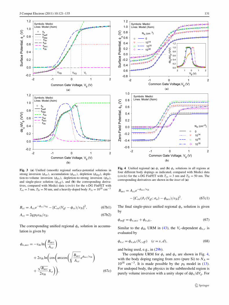
Fig. 4 Unified regional (a) φs and (b) φo solutions in all regions atfour different body dopings as indicated, compared with Medici data(circle) for the s-DG FinFET with Tox = 3 nm and TSi = 50 nm. Thecorresponding derivatives are shown in the inset of (a)
Bacc = Acce−φacc/vth
− [Cox(ϑr(Vgf ;σa) − φacc)/εSi]2. (67c1)
The final single-piece unified regional φo solution is givenby
φoeff = φo,acc + φo,ds . (67)
Similar to the φds URM in (43), the Vc-dependent φo,c isevaluated by
φo,c = φo,ds(Vc,eff ) (c = s, d), (68)
and being used, e.g., in (29b).The complete URM for φs and φo are shown in Fig. 4,
with the body doping ranging from zero (pure Si) to NA =1018 cm−3. It is made possible by the p0 model in (13).For undoped body, the physics in the subthreshold region ispurely volume inversion with a unity slope of dφs/dVg . For
132 J Comput Electron (2011) 10:121–135
low-doping (e.g., 1014 cm−3), a flatband shift is modeledand volume inversion is observed in Fig. 4 due to the thinbody in this example. For extremely thick body (TSi � Xdm,where Xdm can be tens of micrometers at low doping), onewould expect a near-unity slope of dφs/dVg at low doping(and φo ≈ 0), which has different physics from the volumeinversion. This can be modeled by the URM model [34].
With the complete URM for φs and φo, other effectssuch as PDE and QME can be added in a similar way tobulk-MOS formulations for the generic SOI/DG/GAA de-vices [8, 9].
For terminal current/charge models, if the body dopingis high where the CSA is applicable, all the previous equa-tions in Sect. 3.1 can be used with the URM for φs and φo.When the body doping is low where the CSA is not applica-ble, some modifications need to be made under the non-CSAformulations.
Based on (20) with the dVc/dφs term, exact drain-currentexpressions are derived for s-DG FinFETs [8] and GAASiNWs [46], given by
Ids0 = β0[(qi + 2vth)�φs + χ], (69)
χ =
⎧⎪⎪⎪⎪⎪⎨⎪⎪⎪⎪⎪⎩
qvthp0TSi2Cox
(e(φo,d−2φF −Vd)/vth
−e(φo,s−2φF −Vs)/vth) [s-DG]
vthCR ln(
Vgf −φs,d+CR
Vgf −φs,s+CR
),
CR = 4εSivthRCox
.[GAA]
(69a)
Without losing much accuracy, the χ term in (69) can be ig-nored. Following the same approximation as in (45), a singleIds0 model for s-DG/GAA devices is given by
Ids0 = β0(qi + 2vth)Vds,eff , (70)
qi = Vgf − φs, (70a)
β0 ={
2μeff 0Cox(W/L) [s-DG]
μeff 0Cox(2πR/L). [GAA](70b)
For UTB FD-SOI with non-CSA, the pre-factor “2” for s-DG becomes “1” assuming only the front gate conducts thecurrent.
The long-channel saturation voltage is rederived to be
Vds,sat = Vgt,sLEsat
Vgt,s + LEsat + 4vth= Vd,sat − Vs, (71a)
Vsd,sat = Vgt,dLEsat
Vgt,d + LEsat + 4vth= Vs,sat − Vd. (71b)
With the S/D series resistance Rsd,Vds,sat is given by (48),in which [8]
as = vsatZCoxRs, (72a)
bs = −[Vgt,s + vsatZCoxVgt,s(2Rs + Rsd)
+ EsatL + 4vth(1 + vsatZCoxRs)], (72b)
cs = Vgt,sEsatL + 2vsatZCoxRsdVgt,s(Vgt,s + 2vth). (72c)
And Vsd,sat in (71b) with Rsd is given by (48), with all thesubscripts “s” replaced by “d” in (48) and (72). The effec-tive field for FB-SOI and s-DG/GAA devices is given by
Eeff = ζnCox
εSiVgt. (73)
The inversion charge Vgt,c (normalized to Cox) in (39),which is used in Vc,eff and Eeff , is based on the CSA. Undernon-CSA, it is derived from the second integral of the PBequation, given by [8, 9]
Vgt,c =
⎧⎪⎪⎪⎨⎪⎪⎪⎩
(ϒ
√vthe
(φs,c−2φF −Vc)/vth
)× sin
(ϒCoxεSi
TSi4vth
√vthe
(φo,c−2φF −Vc)/vth
)[s-DG]
Rqp02Cox
e(φs,c+φo,c−2φF −2Vc)/2vth (c = s, d) [GAA]
(74)
Equations (70)–(74) are for non-CSA models (low-doping)in place of the corresponding ones for CSA models. Therest of the equations [e.g., (35), (36), (42), (49), (50)] sharethe same expressions for both CSA and non-CSA models.The “switch” between the two types of models is some in-termediate doping level, around which either model wouldbe applicable.
For short-channel and/or thick-body devices, a DIBLmodel is developed based on the quasi-2D solution for thesurface-potential “lowering” [9]
δφs,c(y) = (Vbi,c + Vc − φs)sinh[(L − y)/λ]
sinh(L/λ)
(c = s, d),
(75)
λ = εSi
Cox
Xo
η; Xo = min{Xdm, [(TSi/2);R]}, (75a)
where Vbi,s/d is the S/D–body pn-junction built-in potential.The DIBL model (δφs “lowering” from the long-channel φs)
is included in VFB, where δφs is based on (75) at y = L/2:
δφs ≡ δφs,s(L/2) + δφs,d(L/2)
= (Vbi,s + Vbi,d + αdibl(Vs + Vd) − 2φs)
× 1
2 cosh(L/2λ)(76)
where η and αdibl are fitting parameters.For FB PD-SOI, all the model equations are the same
as for bulk-MOS except that φo is “floating.” Physically,φo ≈ 0 since Si body is partially depleted and φo is always in
J Comput Electron (2011) 10:121–135 133
the neutral body. However, when Vds → 0, due to the unipo-lar assumption (no hole current in nMOS), there would be a“glitch” in the GST higher-order derivatives due to φo in thedepletion piece (φsub), which would lead to inaccurate dis-tortion simulations reflected in the third (and higher) orderharmonics [32]. This problem is solved by the SIC [9] forphysically modeling φo based on balancing the two back-to-back S/D junction diode currents, given by
φo = nvth[ln 2 − ln(e−Vs/nvth + e−Vd/nvth)], (77)
where n is taken as a fitting parameter.The same idea has been extended to model the “kink ef-
fect” in FB-SOI [9], in which φo is modeled by
φo = nvth
[ln
(2 + Iii
Is
)− ln(e−Vs/nvth + e−Vd/nvth)
], (78)
where Iii is the impact-ionization current and Is is the S/Ddiode reverse saturation current. This leads to an explicit CMfor FB effect without the need to introduce an internal circuitnode.
4 Summary and conclusions
In summary, we have presented the general ideas and de-tailed formulations of the MOS core model (Xsim) for uni-fication of various MOS models. Major effects are includedin the φs -based CM. Some unique features that do not ap-pear in other contemporary CMs include: ground-reference(G-ref) for FB-SOI and DG/GAA devices with completesymmetry and physical modeling of asymmetric S/D with-out swapping S/D terminal polarities for Vds changing signs;gate-bias dependent S/D series resistance in all regions;velocity-overshoot modeling with the electron-temperaturegradient term added to the conventional DD formalism; andseamless transition from depletion to volume/strong inver-sion for any body doping and thickness. The Xsim modelhas also been extended to strained-Si/SiGe channel andSB/DSS MOSFETs, as well as physical modeling of inter-face traps for reliability [48, 49] and statistical-CM for vari-ation [50] and mismatch studies. The model has a small setof parameters (<40) that requires minimum data and one ortwo-iteration parameter extraction.
The unique URM approach provides correct asymptoticphysical solutions and approximate ones in seamless transi-tions across different regions of operation for various typesof MOSFETs. This is in line with the essence of com-pact modeling: Correct physical approximations and correctmathematical formulations to emulate ideal device physi-cal behaviors and corroborate with real device characteris-tics. The ultimate goal of the Xsim model is for unificationof MOSFET CMs with various gate, body, as well as S/D
structures and dimensions in one unified core framework forsimulating and designing VLSI circuits in future generationtechnologies, with multilevel modeling and seamless simu-lation [51].
Acknowledgements The Group and the Xsim model developmenthave been supported by Semiconductor Research Corp. (SRC), Char-tered Semiconductor Mfg. (CSM) (now, GLOBALFOUNDRIES Sin-gapore Pte. Ltd.), Atomistix Asia Pacific Pte. Ltd. (AAP), Instituteof Microelectronics (IME), Institute for Sustainable Nanoelectronics(ISNE), and Nanyang Technological University (NTU).
References
1. Gummel, H.K., Poon, H.C.: An integral charge control model ofbipolar transistors. Bell Syst. Tech. J. 49(5), 827–852 (1970)
2. Brews, J.R.: A charge-sheet model of the MOSFET. Solid-StateElectron. 21(2), 345–355 (1978)
3. Pao, H.C., Sah, C.T.: Effects of diffusion current on characteristicsof metal-oxide (insulator)-semiconductor transistors. Solid-StateElectron. 9(10), 927–937 (1966)
4. Watts, J., McAndrew, C., Enz, C., Galup-Montoro, C., Gildenblat,G., Hu, C., van Langevelde, R., Miura-Mattausch, M., Rios, R.,Sah, C.-T.: Advanced compact models for MOSFETs. In: Proc.WCM-Nanotech 2005, Anaheim, CA, May 2005, vol. WCM, pp.3–12 (2005)
5. Lim, K.Y.: Design, modeling, and characterization of submicronMOSFETs. Ph.D. thesis, Nanyang Technological Univ., Singapore(2001)
6. Chiah, S.B.: Unified AC charge and DC current modeling for very-deep-submicron CMOS technology. Ph.D. thesis, Nanyang Tech-nological Univ., Singapore (2007)
7. Chandrasekaran, K.: Nanoscale strained-Si/SiGe and double-gateMOSFET modeling. Ph.D. thesis, Nanyang Technological Univ.,Singapore (2007)
8. See, G.H.: Scalable compact modeling for nanometer CMOS tech-nology. Ph.D. thesis, Nanyang Technological Univ., Singapore(2008)
9. Zhu, G.J.: Compact modeling of non-classical MOSFETs for cir-cuit simulation. Ph.D. thesis, Nanyang Technological Univ., Sin-gapore (2011)
10. Kingston, R.H., Neustadter, S.F.: Calculation of the space charge,electric field, and free carrier concentration at the surface of asemiconductor. J. Appl. Phys. 26(6), 718–720 (1955)
11. Chen, T.L., Gildenblat, G.: Symmetric bulk charge linearizationin charge-sheet MOSFET model. Electron. Lett. 37(12), 791–793(2001)
12. Lim, K.Y., Zhou, X., Lim, D., Zu, Y., Ho, H.M., Loiko, K., Lau,C.K., Tse, M.S., Choo, S.C.: A predictive semi-analytical thresh-old voltage model for deep-submicrometer MOSFET’s. In: Proc.HKEDM98, Hong Kong, Aug. 1998, pp. 114–117 (1998)
13. Zhou, X., Lim, K.Y., Lim, D.: A general approach to compactthreshold voltage formulation based on 2-D numerical simulationand experimental correlation for deep-submicron ULSI technol-ogy development. IEEE Trans. Electron Devices 47(1), 214–221(2000)
14. Lim, K.Y., Zhou, X., Wang, Y.: Modeling of threshold voltagewith reverse short channel effect. In: Proc. MSM2000, San Diego,CA, Mar. 2000, pp. 317–320 (2000)
15. Lim, K.Y., Zhou, X.: A physically-based semi-empirical effectivemobility model for MOSFET compact I–V modeling. Solid-StateElectron. 45(1), 193–197 (2001)
134 J Comput Electron (2011) 10:121–135
16. Lim, K.Y., Zhou, X.: A physically-based semi-empirical seriesresistance model for deep-submicron MOSFET I–V modeling.IEEE Trans. Electron Devices 47(6), 1300–1302 (2000)
17. Lim, K.Y., Zhou, X.: An analytical effective channel-length modu-lation model for velocity overshoot in submicron MOSFETs basedon energy-balance formulation. Microelectron. Reliab. 42(12),1857–1864 (2002)
18. Zhou, X., Lim, K.Y.: Unified MOSFET compact I–V model for-mulation through physics-based effective transformation. IEEETrans. Electron Devices 48(5), 887–896 (2001)
19. Zhou, X., Chiah, S.B., Chandrasekaran, K., See, G.H., Shang-guan, W., Pandey, S.M., Cheng, M., Chu, S., Hsia, L.-C.: Com-parison of unified regional charge-based and surface-potential-based compact modeling approaches. (Invited Paper). In: Proc.Nanotech2005, Anaheim, CA, May 2005, vol. WCM, pp. 25–30(2005)
20. See, G.H., Chiah, S.B., Zhou, X., Chandrasekaran, K., Shangguan,W., Pandey, S.M., Cheng, M., Chu, S., Hsia, L.-C.: Unified re-gional charge-based MOSFET model calibration. In: Proc. Nan-otech2005, Anaheim, CA, May 2005, vol. WCM, pp. 147–150(2005)
21. Chiah, S.B., Zhou, X., Chandrasekaran, K., Shangguan, W.Z., See,G.H., Pandey, S.M.: Single-piece polycrystalline silicon accu-mulation/depletion/inversion model with implicit/explicit surface-potential solutions. Appl. Phys. Lett. 86(20), 202111 (2005)
22. Chandrasekaran, K., Zhou, X., Chiah, S.B., Shangguan, W.Z.,See, G.H.: Physics-based single-piece charge model for strained-Si MOSFETs. IEEE Trans. Electron Devices 52(7), 1555–1562(2005)
23. Chandrasekaran, K., Zhou, X., Chiah, S.B., Shangguan, W.Z., See,G.H., Bera, L.K., Balasubramanian, N., Rustagi, S.C.: Extractionof physical parameters of strained-silicon MOSFETs from C–V
measurement. In: Proc. ESSDERC2005, Grenoble, France, Sep.2005, pp. 521–524 (2005)
24. Chandrasekaran, K., Zhou, X., Chiah, S.B., Shangguan, W.Z.,See, G.H., Bera, L.K., Balasubramanian, N., Rustagi, S.C.: Ef-fect of substrate doping on the capacitance–voltage characteristicsof strained-silicon pMOSFETs. IEEE Electron Device Lett. 27(1),62–64 (2006)
25. Chandrasekaran, K., Zhou, X., Chiah, S.B., See, G.H., Rustagi,S.C.: Implicit analytical surface/interface potential solutions formodeling strained-Si MOSFETs. IEEE Trans. Electron Devices53(12), 3110–3117 (2006)
26. Chandrasekaran, K., Zhu, Z.M., Zhou, X., Shangguan, W.Z., See,G.H., Chiah, S.B., Rustagi, S.C., Singh, N.: Compact modelingof doped symmetric DG MOSFETs with regional approach. In:Proc. Nanotech2006, Boston, MA, May 2006, vol. 3, pp. 792–795(2006)
27. See, G.H., Chiah, S.B., Zhou, X., Chandrasekaran, K., Shangguan,W.Z., Zhu, Z.M., Lim, G.H., Pandey, S.M., Cheng, M., Chu, S.,Hsia, L.-C.: Scalable MOSFET short-channel charge model in allregions. In: Proc. Nanotech2006, Boston, MA, May 2006, vol. 3,pp. 749–752 (2006)
28. See, G.H., Zhou, X., Zhu, G., Zhu, Z., Lin, S., Wei, C., Zhang,J., Srinivas, A.: Unified regional surface potential for modelingcommon-gate symmetric/asymmetric double-gate MOSFETs withany body doping. In: Proc. Nanotech2008, Boston, MA, Jun. 2008,vol. 3, pp. 770–773 (2008)
29. See, G.H., Zhou, X., Zhu, G., Zhu, Z., Lin, S., Wei, C., Zhang,J., Srinivas, A.: Unified regional surface potential for modelingcommon-gate symmetric/asymmetric double-gate MOSFETs withquantum mechanical correction. In: Proc. Nanotech2008, Boston,MA, Jun. 2008, vol. 3, pp. 756–759 (2008)
30. See, G.H., Zhou, X., Chandrasekaran, K., Chiah, S.B., Zhu, Z.M.,Wei, C.Q., Lin, S.H., Zhu, G.J., Lim, G.H.: A compact model
satisfying Gummel symmetry in higher order derivatives and ap-plicable to asymmetric MOSFETs. IEEE Trans. Electron Devices55(2), 616–623 (2008)
31. Zhu, G.J., Zhou, X., See, G.H., Lin, S.H., Wei, C.Q., Zhang, J.B.:A unified compact model for FinFET and silicon nanowire MOS-FETs. In: Proc. Nanotech2009, Houston, TX, May 2009, vol. 3,pp. 588–591 (2009)
32. Zhou, X., Zhu, G.J., Srikanth, M.K., Lin, S.H., Chen, Z.H., Zhang,J.B., Wei, C.Q., Yan, Y.F., Selvakumar, R., Xsim, Z.H. Wang:Benchmark tests for the unified DG/GAA MOSFET compactmodel. In: Proc. Nanotech2010, Anaheim, CA, Jun. 2010, vol. 2,pp. 785–788 (2010)
33. Zhu, G.J., See, G.H., Lin, S.H., Zhou, X.: ‘Ground-referenced’model for three-terminal symmetric double-gate MOSFETs withsource/drain symmetry. IEEE Trans. Electron Devices 55(9),2526–2530 (2008)
34. Zhou, X., Zhu, G.J., Srikanth, M.K., Lin, S.H., Chen, Z.H.,Zhang, J.B., Wei, C.Q.: A unified compact model for emergingDG FinFETs and GAA nanowire MOSFETs including long/short-channel and thin/thick-body effects. (Invited Paper). In: Proc. IC-SICT2010, Shanghai, China, Nov. 2010, pp. 1725–1728 (2010)
35. Zhu, G.J., Zhou, X., Lee, T.S., Ang, L.K., See, G.H., Lin, S.H.,Chin, Y.K., Pey, K.L.: A compact model for undoped silicon-nanowire MOSFETs with Schottky-barrier source/drain. IEEETrans. Electron Devices 56(5), 1100–1109 (2009)
36. Zhu, G.J., Zhou, X., Lee, T.S., Ang, L.K., See, G.H., Lin, S.H.:A compact model for undoped symmetric double-gate MOSFETswith Schottky-barrier source/drain. In: Proc. ESSDERC2008, Ed-inburgh, UK, Sep. 2008, pp. 182–185 (2008)
37. Zhu, G.J., Zhou, X., Chin, Y.K., Pey, K.L., Zhang, J.B., See, G.H.,Lin, S.H., Yan, Y.F., Chen, Z.H.: Subcircuit compact model fordopant-segregated Schottky gate-all-around Si-nanowire MOS-FETs. IEEE Trans. Electron Devices 57(4), 772–781 (2010)
38. Zhu, G.J., Zhou, X., Chin, Y.K., Pey, K.L., See, G.H., Lin, S.H.,Zhang, J.B.: Subcircuit compact model for dopant-segregatedSchottky silicon-manowire MOSFETs. In: Proc. SSDM2009,Sendai, Japan, Oct. 2009, pp. 402–403 (2009)
39. Oh, S.-Y., Ward, D., Dutton, R.: Transient analysis of MOStransistors. IEEE Trans. Electron Devices ED-27(8), 1571–1578(1980)
40. van Dort, M.J., Woerlee, P.H., Walker, A.J.: A simple model forquantization effects in heavily-doped silicon MOSFET’s at inver-sion conditions. Solid-State Electron. 37, 411–414 (1994)
41. Shangguan, W.Z., Zhou, X., Chiah, S.B., See, G.H., Chan-drasekaran, K.: Compact gate-current model based on transfer-matrix method. J. Appl. Phys. 97, 123709 (2005)
42. Wei, C.Q., See, G.H., Zhou, X., Chan, L.: A new impact-ionizationcurrent model applicable to both bulk and SOI MOSFETs by con-sidering self-lattice-heating. IEEE Trans. Electron Devices 55(9),2378–2385 (2008)
43. Taur, Y.: An analytical solution to a double-gate MOSFET withundoped body. IEEE Electron Device Lett. 21(5), 245–247 (2000)
44. Chen, Y., Luo, J.: A comparative study of double-gate andsurrounding-gate MOSFETs in strong inversion and accumulationusing an analytical model. In: Proc. MSM2001, Hilton Head Is-land, SC, Mar. 2001, pp. 546–549 (2001)
45. Shangguan, W.Z., Zhou, X., Chandrasekaran, K., Zhu, Z.M.,Rustagi, S.C., Chiah, S.B., See, G.H.: Surface-potential solutionfor generic undoped MOSFETs with two gates. IEEE Trans. Elec-tron Devices 54(1), 169–172 (2007)
46. Lin, S.H., Zhou, X., Seel, G.H., Zhu, Z.M., Lim, G.H., Wei, C.Q.,Zhu, G.J., Yao, Z.H., Wang, X.F., Yee, M., Zhao, L.N., Hou, Z.F.,Ang, L.K., Lee, T.S., Chandra, W.: A rigorous surface-potential-based I–V model for undoped cylindrical nanowire MOSFETs.In: Proc. IEEE-Nano2007, Hong Kong, Aug. 2007, vol. 3, pp.889–892 (2007)
J Comput Electron (2011) 10:121–135 135
47. Zhou, X., Zhu, Z.M., Rustagi, S.C., See, G.H., Zhu, G.J., Lin,S.H., Wei, C.Q., Lim, G.H.: Rigorous surface-potential solutionfor undoped symmetric double-gate MOSFETs considering bothelectrons and holes at quasi nonequilibrium. IEEE Trans. ElectronDevices 55(2), 616–623 (2008)
48. Chen, Z.H., Zhou, X., Zhu, G.J., Lin, S.H.: Interface-trap mod-eling for silicon-nanowire MOSFETs. In: Proc. IRPS2010, Ana-heim, CA, May 2010, pp. 977–980 (2010)
49. Chen, Z.H., Zhou, X., Hu, Y.Z., Srikanth, M.K. : Neutral interfacetraps for negative bias temperature instability. In: Proc. IRPS2011,Monterey, CA, Apr. (2011, to appear)
50. Zhou, X., Zhu, G.J., Lin, S.H., Chen, Z.H., Srikanth, M.K., Yan,Y.F., Selvakumar, R., Chandra, W., Zhang, J.B., Wei, C.Q., Wang,Z.H., Bathla, P.: Subcircuit approach to inventive compact model-ing for CMOS variability and reliability. In: Proc. ISIC2009, Sin-gapore, Dec. 2009, pp. 133–138 (2009)
51. Zhou, X.: The missing link to seamless simulation (Invited FeatureArticle). IEEE Circuits Devices Mag. 19(3), 9–17 (2003)