
Understanding the Subsynchronous Oscillation ... - NTNU Open
91
NTNU Norwegian University of Science and Technology Faculty of Information Technology and Electrical Engineering Department of Electric Power Engineering Master’s thesis Dan Godhei Understanding the Subsynchronous Oscillation Occurring in Offshore Wind Farm Converters Connected via HVDC Master’s thesis in Electrical Power Engineering Supervisor: Mohammad Amin June 2020
-
Upload
khangminh22 -
Category
Documents
-
view
1 -
download
0
Transcript of Understanding the Subsynchronous Oscillation ... - NTNU Open

NTN
UN
orw
egia
n U
nive
rsity
of S
cien
ce a
nd T
echn
olog
yFa
culty
of I
nfor
mat
ion
Tech
nolo
gy a
nd E
lect
rical
Engi
neer
ing
Dep
artm
ent o
f Ele
ctric
Pow
er E
ngin
eerin
g
Mas
ter’s
thes
is
Dan Godhei
Understanding the SubsynchronousOscillation Occurring in Offshore WindFarm Converters Connected via HVDC
Master’s thesis in Electrical Power Engineering
Supervisor: Mohammad Amin
June 2020


Dan Godhei
Understanding the SubsynchronousOscillation Occurring in Offshore WindFarm Converters Connected via HVDC
Master’s thesis in Electrical Power EngineeringSupervisor: Mohammad AminJune 2020
Norwegian University of Science and TechnologyFaculty of Information Technology and Electrical EngineeringDepartment of Electric Power Engineering


Summary
The need for renewable energy has lead to substantial investment in offshore wind energytechnology. One technology considered to be a viable option for the future is high-voltagedirect current (HVDC) transmission. HVDC transmission revolves around transmittingpower as direct current(dc). Commercial wind turbines (WT) today generate alienatingcurrent(ac). To send ac power as dc power the current must first be converted from ac todc. To convert the power from ac to dc a multi modular converter (MMC) can be used. Oneadvantage of ac power is that the current-voltage(IV) can be changed with a transformer.Transformers are connected between the MMC and the WTs to reduce the voltage acrossthe WT terminal. To control the power produced by a WT can be a complicated task. Tosimplify the power production, the WT can be represented as a constant dc source. Tocontrol how much power the WT delivers to the grid, a 2-level voltage source converter(VSC) is connected to the dc source. The VSC is connected to the WT terminal. Dc powerfrom the turbine is now sent through the converter, where it is converted from dc to ac.The ac power is sent through transformers where the IV ratio changes. The ac power isthen converted to dc in the MMC and delivered to the grid. This is a master thesis thatwill describe this operation in detail and show how the power quality varies when powerdelivered by the WT to the grid change.
In this thesis show how that a VSC converter can be designed to control the power out-put and synchronise to the grid by using a PLL. By analyzing the VSC in a time domain, itis observed harmonic distortion (HD) in the controller, when delivering 50MW and 10MWto the grid. It is also found that the magnitude of these oscillation are not dependent on thepower output as they remain almost the same for 50MW and 10MW. The thesis shows away to control an MMC with and without circulating current control. Tests performed inboth frequency and time domain show that by excluding internal dynamics by removingthe circulating current control is the controller unable to operate in steady state for 50MW.By considering internal dynamics with a circulating current controller is the MMC capa-ble of setting the ac voltage at the WT terminal. This conclusion is drawn after testing theMMC for 50MW and 10MW, connected and disconnected to the VSC. Also, the MMCexperience HD which influences stability. The HDs can be located when the MMC con-nected and disconnected to the VSC. By testing the MMC without connecting it to theVSC, it is proven that some of the HD originates at either the MMC control system orfrom the switching components. When the MMC and VSC become interconnected, theTHD for the whole system increase, it is therefore likely that the controllers influence eachother and make one another more unstable. Passive components in the transformer and thetransmission line can be designed to filter out some HDs.
i

Preface
This is a master thesis written by Dan Godhei. The thesis is submitted to the Departmentof Electrical Power Engineering at the Norwegian University of Science and Technology.It is the final requirement of a two-year master program in power electronics. AssociateProfessor Mohammad Amin has contributed with his time and knowledge and is the su-pervisor for this project. To test an analytical model in a close to realistic environment hasMatlab Simulink been used to build and simulate the model. The master project startedin January of 2020 and ended on June 10. 2020. A prerequisite study on VSC in HVDCsystems were conducted in the fall of 2019 as groundwork for this thesis.
ii

Acknowledgements
You should never take for granted the time and effort other people spend on helping you.From the fall of 2019 to the summer of 2020, Mohammad Amin has shared with me hisknowledge, been patient, and kind. I would, therefore, sincerely thank him for his con-tribution to this thesis. He has pushed me to set higher standards for myself and spentnumerous hours in meeting in person and on Skype. He has been an excellent represen-tative of the higher academic community, and I would not hesitate to say yes if I get anopportunity to work with him again.
Dan GodheiTrondheim, 10.06.2020
iii

Table of Contents
Summary i
Preface ii
Acknowledgements iii
Table of Contents vi
List of Tables vii
List of Figures x
1 Introduction 11.1 Background . . . . . . . . . . . . . . . . . . . . . . . . . . . . . . . . . 11.2 Per Unit System . . . . . . . . . . . . . . . . . . . . . . . . . . . . . . . 21.3 Phase-Phase to Phase-Ground . . . . . . . . . . . . . . . . . . . . . . . 21.4 Harmonics . . . . . . . . . . . . . . . . . . . . . . . . . . . . . . . . . . 31.5 Filters . . . . . . . . . . . . . . . . . . . . . . . . . . . . . . . . . . . . 41.6 General Stability . . . . . . . . . . . . . . . . . . . . . . . . . . . . . . 51.7 State Space Representation . . . . . . . . . . . . . . . . . . . . . . . . . 61.8 Impedance Modeling . . . . . . . . . . . . . . . . . . . . . . . . . . . . 71.9 Nyquist Stability Criterion . . . . . . . . . . . . . . . . . . . . . . . . . 8
2 Wind Energy Conversion System 102.1 Voltage Source Converter Theory . . . . . . . . . . . . . . . . . . . . . . 10
2.1.1 Voltage Source Converter System Equation . . . . . . . . . . . . 112.2 Voltage Source Converter Control . . . . . . . . . . . . . . . . . . . . . 12
2.2.1 Current Controller . . . . . . . . . . . . . . . . . . . . . . . . . 132.2.2 PI Controller . . . . . . . . . . . . . . . . . . . . . . . . . . . . 132.2.3 PWM . . . . . . . . . . . . . . . . . . . . . . . . . . . . . . . . 142.2.4 System Transfer Function . . . . . . . . . . . . . . . . . . . . . 14
iv

2.2.5 Phase Locked Loop . . . . . . . . . . . . . . . . . . . . . . . . . 152.3 Voltage Source Converter Tuning . . . . . . . . . . . . . . . . . . . . . . 16
2.3.1 VSC Tuning Techniques . . . . . . . . . . . . . . . . . . . . . . 172.3.2 PLL Response . . . . . . . . . . . . . . . . . . . . . . . . . . . 19
3 High-Voltage DC Rectifier 213.1 Modular Multi Level Converter Topology . . . . . . . . . . . . . . . . . 223.2 Dynamic Relations of MMC . . . . . . . . . . . . . . . . . . . . . . . . 24
3.2.1 Compensated Modulation . . . . . . . . . . . . . . . . . . . . . 263.2.2 Direct Modulation . . . . . . . . . . . . . . . . . . . . . . . . . 27
3.3 Control Structure . . . . . . . . . . . . . . . . . . . . . . . . . . . . . . 293.3.1 Phase Shift and Level Shifted Modulation . . . . . . . . . . . . . 293.3.2 Proportional Resonant Controller . . . . . . . . . . . . . . . . . 30
3.4 HVDC Tuning . . . . . . . . . . . . . . . . . . . . . . . . . . . . . . . . 31
4 Stability Analysis of Wind Farm-HVDC System 344.1 State Space Representation . . . . . . . . . . . . . . . . . . . . . . . . . 34
4.1.1 Wind Energy Conversion State Space . . . . . . . . . . . . . . . 344.1.2 Modular Multi Level Converter State Space . . . . . . . . . . . . 36
4.2 Impedance Modeling . . . . . . . . . . . . . . . . . . . . . . . . . . . . 374.2.1 Voltage Source Converter Impedance . . . . . . . . . . . . . . . 374.2.2 Modular Multi Level Converter Impedance . . . . . . . . . . . . 394.2.3 Cable and Transformer Impedance . . . . . . . . . . . . . . . . . 454.2.4 Full System Impedance Stability . . . . . . . . . . . . . . . . . . 47
5 Simulation Result of Interconnected Wind Farm-HVDC System 495.1 Case 1: WF Inverter-HVDC Without Circulating Current Control . . . . . 505.2 Case 2: WF Inverter-HVDC With Circulating Current Control . . . . . . 50
5.2.1 Case 2: 50MW Case . . . . . . . . . . . . . . . . . . . . . . . . 515.2.2 Case 2: 10MW Case . . . . . . . . . . . . . . . . . . . . . . . . 53
5.3 Case 3: WF Inverter Isolated Case . . . . . . . . . . . . . . . . . . . . . 555.3.1 Case 3: 50MW Case . . . . . . . . . . . . . . . . . . . . . . . . 565.3.2 Case 3: 10MW Case . . . . . . . . . . . . . . . . . . . . . . . . 57
5.4 Case 4: HVDC Isolated Case . . . . . . . . . . . . . . . . . . . . . . . . 595.4.1 Case 4: 50MW Case . . . . . . . . . . . . . . . . . . . . . . . . 595.4.2 Case 4: 10MW Case . . . . . . . . . . . . . . . . . . . . . . . . 61
5.5 Wind Farm Inverter controller system analysis . . . . . . . . . . . . . . . 625.5.1 Impact of Phase Locked Loop . . . . . . . . . . . . . . . . . . . 625.5.2 Impact of VSC Current Controller . . . . . . . . . . . . . . . . . 63
5.6 HVDC Controller System Analysis . . . . . . . . . . . . . . . . . . . . . 645.6.1 AC Voltage Proportional Resonant Controller . . . . . . . . . . . 645.6.2 Half-bridge Signal and Converter Voltage . . . . . . . . . . . . . 655.6.3 Connecting Wind Farm Inverter and HVDC System . . . . . . . . 66
v

6 Discussion and Conclusion 676.1 Discussion . . . . . . . . . . . . . . . . . . . . . . . . . . . . . . . . . . 676.2 Conclusion . . . . . . . . . . . . . . . . . . . . . . . . . . . . . . . . . 696.3 Future Work . . . . . . . . . . . . . . . . . . . . . . . . . . . . . . . . . 69
Appendix i
vi

List of Tables
1.1 How impedance change for a passive component as a function of frequency 8
2.1 WF Inverter parameters . . . . . . . . . . . . . . . . . . . . . . . . . . . 172.2 VSC and PLL PI parameters . . . . . . . . . . . . . . . . . . . . . . . . 17
3.1 HVDC parameters . . . . . . . . . . . . . . . . . . . . . . . . . . . . . 313.2 MMC PR controller parameters . . . . . . . . . . . . . . . . . . . . . . . 32
vii

List of Figures
1.1 Arbitrary harmonic distortion . . . . . . . . . . . . . . . . . . . . . . . . 41.2 Ac filter where Z1 and Z2 are impedances . . . . . . . . . . . . . . . . . 51.3 Definition of system that is asymptotically stable, stable and unstable . . . 61.4 Feedback control system with disturbance z(t) . . . . . . . . . . . . . . . 71.5 Nyquist diagram . . . . . . . . . . . . . . . . . . . . . . . . . . . . . . . 9
2.1 Wind energy conversion system . . . . . . . . . . . . . . . . . . . . . . 102.2 Two-level voltage source converter . . . . . . . . . . . . . . . . . . . . . 112.3 Two-level voltage source converter connected between an ac and dc grid. 112.4 Wind energy conversion system with current controller and PLL . . . . . 132.5 Current controller control system with Pules width modulator . . . . . . . 132.6 How to exterminate the cross coupling terms for the current controller . . 152.7 PLL block diagram . . . . . . . . . . . . . . . . . . . . . . . . . . . . . 162.8 Current controller bode . . . . . . . . . . . . . . . . . . . . . . . . . . . 182.9 Current controller step response . . . . . . . . . . . . . . . . . . . . . . 192.10 PLL bode plot . . . . . . . . . . . . . . . . . . . . . . . . . . . . . . . . 20
3.1 HVDC converter system . . . . . . . . . . . . . . . . . . . . . . . . . . 213.2 Half-bridge cell for MMC SM . . . . . . . . . . . . . . . . . . . . . . . 223.3 Modular multilevel converter. a) single phase to single phase b) three
phase to single phase, single phase to three phase and c) three phase tothree phase . . . . . . . . . . . . . . . . . . . . . . . . . . . . . . . . . 23
3.4 Modular multilevel converter. Single phase to three phase . . . . . . . . . 243.5 Modular multilevel converter. Single phase equivalent circuit. . . . . . . . 253.6 Pulse width modulation: a) Phase shifted modulation b) Level shifted
modulation . . . . . . . . . . . . . . . . . . . . . . . . . . . . . . . . . 303.7 PR controller with feed forward gain . . . . . . . . . . . . . . . . . . . . 303.8 PR ac voltage controller bode . . . . . . . . . . . . . . . . . . . . . . . . 323.9 PR ac voltage controller step response . . . . . . . . . . . . . . . . . . . 33
4.1 Voltage source inverter wind conversion system . . . . . . . . . . . . . . 35
viii

4.2 System impedance model . . . . . . . . . . . . . . . . . . . . . . . . . . 374.3 VSC impedance model . . . . . . . . . . . . . . . . . . . . . . . . . . . 384.4 VSC frequency response . . . . . . . . . . . . . . . . . . . . . . . . . . 394.5 MMC ac impedance . . . . . . . . . . . . . . . . . . . . . . . . . . . . . 404.6 MMC with compensated modulation control bode plot . . . . . . . . . . 414.7 MMC with compensated modulation control Nyquist plot . . . . . . . . . 414.8 MMC without circulating current control bode plot . . . . . . . . . . . . 434.9 MMC with circulating current control bode plot . . . . . . . . . . . . . . 454.10 Single line diagram of cable passive components with transformers . . . . 454.11 The frequency response of the passive components. . . . . . . . . . . . . 464.12 The frequency response comparison of the VSC, MMC and the passive
RLC components in the ac system for 50MW . . . . . . . . . . . . . . . 474.13 The frequency response comparison of the VSC, MMC and the passive
RLC components in the ac system for 10MW . . . . . . . . . . . . . . . 48
5.1 Three Phase HVDC side voltage and current in pu for MMC without Cir-culating Current Control. a) Voltage and b) Current . . . . . . . . . . . . 50
5.2 Three phase HVDC side voltage and current in pu for MMC with Circu-lating Current Control. a) Voltage and b) Current . . . . . . . . . . . . . 51
5.3 Active and reactive output power for 50MW case . . . . . . . . . . . . . 515.4 For 50MW case. a) WF Inverter voltage b) HVDC voltage c) WF Inverter
current d) HVDC current e) THD HVDC Voltage f) THD HVDC Current 535.5 Active and reactive output power for 10MW case . . . . . . . . . . . . . 545.6 For 10MW case. a) WF Inverter voltage b) HVDC voltage c) WF Inverter
current d) HVDC current e) THD HVDC Voltage f) THD HVDC Current 555.7 Three phase isolated WF Inverter side voltage and current in pu for VSC.
a) Voltage and b) Current . . . . . . . . . . . . . . . . . . . . . . . . . . 555.8 Active and reactive output power for 50MW isolated case . . . . . . . . . 565.9 For isolated 50MW case. a) WF Inverter voltage b) WF Inverter current c)
THD WF Inverter Voltage d) THD WF Inverter Current . . . . . . . . . . 575.10 Active and reactive output power for 10MW isolated case . . . . . . . . . 575.11 For isolated 10MW case. a) WF Inverter voltage b) WF Inverter current c)
THD WF Inverter Voltage d) THD WF Inverter Current . . . . . . . . . . 585.12 WF Inverter current noise for 50MW and 10MW in phase a . . . . . . . . 595.13 Three phase isolated HVDC side voltage and current in pu for MMC. a)
Voltage and b) Current . . . . . . . . . . . . . . . . . . . . . . . . . . . 595.14 Active and reactive output power for 50MW isolated case . . . . . . . . . 605.15 For isolated 50MW case. a) HVDC voltage b) HVDC current c) THD
HVDC Voltage d) THD HVDC Current . . . . . . . . . . . . . . . . . . 615.16 Active and reactive output power for 10MW isolated case . . . . . . . . . 615.17 For isolated 10MW case. a) HVDC voltage b) HVDC current c) THD
HVDC Voltage d) THD HVDC Current . . . . . . . . . . . . . . . . . . 625.18 PLL time response for interconnected system . . . . . . . . . . . . . . . 635.19 PLL time response for isolated case . . . . . . . . . . . . . . . . . . . . 635.20 DQ current in controller for interconnected system . . . . . . . . . . . . 645.21 DQ current in controller for isolated case . . . . . . . . . . . . . . . . . . 64
ix

5.22 Left axis is output voltage reference and output voltage, and right side isPR controller output . . . . . . . . . . . . . . . . . . . . . . . . . . . . . 65
5.23 Sum of switching signals left hand side and insertion index right hand sidein upper arm phase a. . . . . . . . . . . . . . . . . . . . . . . . . . . . . 66
5.24 Voltage across each of the 20 capacitors in upper arm phase a. . . . . . . 66
x

Chapter 1Introduction
This chapter will present specific background knowledge for this thesis, like Per Unitsystem, Phase-Phase to Phase-Ground transformation, harmonics and general stability. Italso specify that renewable energy investment has made wind energy technology popular.
1.1 BackgroundSignificant investments in the renewable energy sector have led to rapid growth of tech-nology. [1] As much of the potential land-based energy sources are either being used, orin places already inhabited by people, many researchers look to the ocean for answers.Installations located on the open sea are often far away from where the power is con-sumed. Additionally are the demand for power increasing as installations are becomingmore abundant. Longer distances and more power being transferred are two main reasonsthat power equipment efficiency is essential for the future. [1]
One way of transferring ac power very long distances is to send it as High Voltage DC(HVDC) power. The advantage of DC power is that it does not produce reactive power, itdoes not require three phases of cable, and it does not need to be synchronized to the grid.[2] This lowers the cost and material usage and is why HVDC is a viable option, and iswhy this thesis will present the possibility of using HVDC to transfer power.
According to [3] wind energy provides 4.8% of the global power production. In 2018,wind energy production grew by 10%, reaching a capacity of 564 GW. In Denmark, morethan 46% of power produced come from the wind energy sector. In Europe, 5047 offshorewind turbines (WT) are connected to the grid across 12 countries. [4] Of these 5047, 502of them were installed from 2018 to 2019. Norway alone were responsible for installingapproximately 10 GW capacity for this period.[4] The market is clearly expanding, andoffshore WTs are one way of extracting these marine energy resources. This is why thisreport will take a look at an offshore wind farm (WF).
1

1.2 Per Unit SystemThere are a lot of values and notations when dealing with complex power systems. Justby looking at a graph, can it be challenging to compare International system of units (SI)units to the reference value. To simplify the analysis of power systems, one can createa set of scalar parameters which are connected and can be used when presenting results.These parameters are called base values. Typical base parameters are apparent power Sb,peak phase to ground voltage Vb, peak current Ib and impedance Zb, where the subscript bindicates that it is a base parameter. What value these parameters have is up to the personperforming calculations. The base values are reliant on each other, meaning that if twoparameters are decided, then the rest of the parameters are set. It can be recommended toset the base values equal to rated values and first to decide apparent power and voltage ismost common in literature. The relationship between the mentioned ac base values are
Ib =2
3
SbVb
(1.1)
Zb =VbIb
(1.2)
Other base parameters often presented in literature are angular frequency ωb, resistanceRb, inductance Lb and capacitance Cb, which can be calculated accordingly
Zb = Rb = ωbLb =1
ωbCb(1.3)
where angular frequency is independent on other values. When an impedance Z ispresented in its original SI unit, one can use the base value Zb to generate the result in perunit Zpu like this
Zpu =Z
Zb(1.4)
A per unit value, in this thesis, is presented with the unit ”pu”. Dc base calculationsare presented in [5]. Voltage is often presented in literature as the RMS line to line voltageVLL and can be transferred to its phase to ground peak base value as follows
Vb =
√2
3VLL (1.5)
1.3 Phase-Phase to Phase-GroundWhen presenting a result most values are presented in per unit unless SI units will helpillustrate a point. Per unit is used as it makes it is easier for the reader to compare the resultto reference values. Furthermore, it is simpler for someone else to recreate the experimentand compare their results to this thesis. This system operates with two sets of base values,WF Inverter base and HVDC base, separated by two transformers. The Simulink model isbuilt as an isolated network. This will prevent the possibility of measuring from phase to
2

ground. Voltages, therefore, have to be measured between phases, so-called phase-phase.Phase-phase voltage can be transformed into phase-ground accordingly [6]
Van =VAB − VCA
3(1.6)
Vbn =VBC − VAB
3(1.7)
Vcn =VCA − VBC
3(1.8)
Where Van, Vbn and Vcn are the phase-ground voltage and VAB , VBC and VCA are thephase-phase voltages.
1.4 HarmonicsAc voltage and current waveforms consist of harmonics, which are those frequencieswhich are integer multiples of a fundamental grid frequency. [7] Harmonic distortionis the effect non-sinusoidal fundamental or higher frequency current and voltage wave-forms have on the fundamental sinusoidal waveform, caused by electrical equipment ormechanical faults. In power electronics are common sources of harmonic distortion, ac-cording to [7], inverters, industrial motor drives, light dimmers and personal computers.Also, insulation failure may cause overheating in transformers and motor drives whichare a common cause of harmonic distortion. Voltage and current can have waveforms withmany frequencies. When found, the magnitude of these other frequencies can be comparedto the magnitude of the fundamental frequency. This will allow us to represent harmonicdistortion as percent, where 100% are the energy of the fundamental frequency. [8]
HDn =|Vn||V1|
(1.9)
where n is the harmonic integer, HDn is the nth harmonic distortion in percent, |V1|is the fundamental frequency voltage magnitude and |Vn| in the nth harmonic voltagemagnitude. Another common way of expressing harmonic distortion in literature [7], isto present the sum of all harmonic distortion as total harmonic distortion (THD). A hightotal harmonic distortion is bad. A popular way of calculating THD is to use Fast Fouriertransform (FFT) analysis. Fourier analysis makes it possible to extract each frequencywaveform component. These frequency components can be expressed as sine and cosinewaveforms.
v(t) =a0
2+
∞∑n=1
(ancos
nπt
F+ bnsin
nπt
F
)(1.10)
where v(t) is the voltage waveform, n = 1 is as that is the fundamental frequencycomponent, F is a half period of the fundamental frequency and an and bn are
an =1
F
∫ 2F
0
v(t)cosnπt
Fdt (1.11)
3

bn =1
F
∫ 2F
0
v(t)sinnπt
Fdt (1.12)
If it is assumed that the ac voltage does not contain a dc component, then a0 = 0. 1.1show an arbitrary harmonic distortion. There it can be seen the first order harmonic isa lot higher compared to the other harmonics. It is also clear that odd harmonics, alsocalled third order harmonics, often are higher than even harmonics. The figure shows thatas the harmonic number increase, the magnitude of the frequency component decreases.This can be seen mathematically performing the integration in 1.11 and 1.12, which willresult in the whole term being divided by the frequency number term n and is why lowerorder harmonics are more impactful than high order harmonics. This can be describedphysically with ohm’s law for reactance X
X = 2πfL (1.13)
where X is resistance, f is frequency and L is inductance. As reactance changes pro-portional to frequency, higher frequencies will have a higher reactance component, whichwill give a lower magnitude.
1 3 5 7 9 11 13 15 17
Har
monic
Dis
tort
ion(%
)
Order Harmonic
0.5
1
1.5
2
2.5
Figure 1.1: Arbitrary harmonic distortion
1.5 FiltersAll ac voltages and currents contain some sort of harmonic distortion. Therefore, filtersare regularly used to reduce these harmonics and make waveforms more sinusoidal. An ac
4

filter consists of impedances in series and parallel. A good filter will reduce higher orderfrequency components without influencing the fundamental frequency. 1.2 show a typicalfilter for reducing harmonics in an ac circuit.
Z1
Z2
V1 V2
Figure 1.2: Ac filter where Z1 and Z2 are impedances
The filter capacitance and inductance directly influence what type of harmonics thefilter is going to reduce. According to [7] are higher frequencies filtered with smaller com-ponents. High switching frequencies are better for system stability for systems controlledby transistors. This is because high switching reduces impactful low order harmonics,but increases high order harmonics. This means that by carefully choosing components,switching frequency can be used to remove lower harmonics, and filters can be imple-mented to remover higher ones. Filter components should not be too large as Ohm’s lawstate that higher impedance results in higher losses P.
P = IZ2 (1.14)
where I is current.
1.6 General StabilityAccording to [9] can a system either be asymptotically stable, stable or unstable. Figure1.3 illustrate the difference between these terms. xo is the condition where the systemstarts. x1 is the equilibrium point where the system will remain constant if not affected bya disturbance, x=constant gives dx/dt=0.
5

Figure 1.3: Definition of system that is asymptotically stable, stable and unstable
If the system over time ends up reaching the equilibrium point, like xa in figure 1.3,the system is defined as Asymptotically stable.
limt→∞
xa(t) = x1 (1.15)
If the system over time does not leave the area defined by the number ε, like xb infigure 1.3, the system is considered stable.
limt→∞
xb(t) < ε (1.16)
If the system, over time, does leave the area defined by the number ε, like xc in figure1.3, the system can be considered unstable
limt→∞
xc(t) > ε (1.17)
1.7 State Space RepresentationIn [9] a system is defined as ”a set of physical elements acting together and realizing acommon goal”. These physical elements are all components necessary to predict how asystem will react. To make these predictions we need, input variables, representing theforce acting on the system, output variables, representing the output from the system andstate variables, describing what conditions the system is operating under. State variableswill have to be linearly independent, meaning they can not be a linear combination ofanother state variable[10]. These system states may be static, i.e. time-invariant, x1, ordynamic i.e. time-dependent, x1(t) [9]. The input, output and states are what makes upthe nonlinear system
x = F (x, u) (1.18)
y = G(x, u) (1.19)
6

Where x is the state equation, y is the output equation, F(x,u) and G(x,u) are vectorsof a nonlinear equations. For a linear system, the state and output equations will be asfollows
x = Ax+Bu (1.20)
y = Cx+Du (1.21)
Where A, B, C and D are matrices derived by derivating F and G with respect to x and u.In other words, 1.18 and 1.19 can be represented as linear equations by approximation [9]
∆x = A∆x+B∆u (1.22)
∆y = C∆x+D∆u (1.23)
For a system to be linear, it has to deliver within the constraints of superposition andhomogeneity. Superposition means that a change in input, u, will result in the same changefor the output, y. I.e., is u increased by 10 then y is increased by 10. Homogeneity meansthat if the input is multiplied by a scalar, the output will yield a response multiplied by thesame scalar. Some systems are linear at a specific range, as an electronic amplifier, butwill become nonlinear at very high voltage inputs due to saturation. Other systems, like anelectrical motor, will have a dead zone, where it does not start to accelerate due to friction,even though it is supplied by a voltage source. [10] Linearization is necessary to study thestability of a dynamic system for small signal stability purposes.
Systems can be affected by external forces, called disturbances (z(t)), which can makea stable system unstable. A representation of a standard feedback system is illustrated infigure1.4
Figure 1.4: Feedback control system with disturbance z(t)
1.8 Impedance ModelingOhm’s law specifies that some components, like a purely resistive element, depend onlyon the amount of current I flowing through it, to decide what the losses R of the resistorwill be.
R = UI (1.24)
Where U is voltage. While other components, like inductors and capacitors, are in-fluenced by the frequency of the current to decide on how well the component conductscurrent.
X = wL (1.25)
7
X =1
wC(1.26)
Where X is the reactance, ω is the frequency times 2π, L is the inductance and C is thecapacitance. Losses are not the only parameter that are influenced by the frequency of acircuit. When studying the impedance Z of the system, where an imaginary j componentis included, it is possible to tell the phase shift φ of the current relative to the voltage.
I∠φ =U∠0
Z(1.27)
Z = R+ jωL+1
jωC(1.28)
By testing a system for a broad frequency specter, it will be possible to say how muchfrequency influences loss and phase shift. Table 1.1 shows how the impedance providedby a resistor, inductor and capacitor change as a function of frequency. For a very highfrequency, an inductor operates as an open circuit and a capacitor as a short circuit. Forlow frequencies, as for example dc, an inductor will operate as a short and a capacitor asan open circuit.
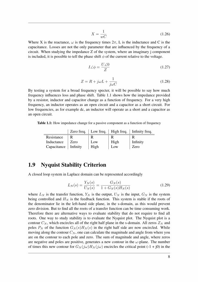
Table 1.1: How impedance change for a passive component as a function of frequency
Zero freq. Low freq. High freq. Infinity freq.Resistance R R R RInductance Zero Low High InfinityCapacitance Infinity High Low Zero
1.9 Nyquist Stability CriterionA closed loop system in Laplace domain can be represented accordingly
LN (s) =YN (s)
UN (s)=
GN (s)
1 +GN (s)HN (s)(1.29)
where LN is the transfer function, YN is the output, UN is the input, GN is the systembeing controlled and HN is the feedback function. This system is stable if the roots ofthe denominator lie in the left-hand side plane, in the s-domain, as this would preventzero division. But to find all the roots of a transfer function can be time consuming work.Therefore there are alternative ways to evaluate stability that do not require to find allroots. One way to study stability is to evaluate the Nyquist plot. The Nyquist plot is acontour CN , which encircles all of the right half plane in the s-domain. All zeros ZN andpoles PN of the function GN (s)HN (s) in the right half side are now encircled. Whilemoving along the contour CN , one can calculate the magnitude and angle from where youare on the contour to each pole and zero. The sum of magnitude and angle, where zerosare negative and poles are positive, generates a new contour in the ω-plane. The numberof times this new contour for GN (jω)HN (jω) encircles the critical point (-1 + j0) in the
8

clockwise direction is given by MN , which is equal to ZN - PN . The system is stable ifthe number of zeros in the right half plane is equal to zero and if M encircles the criticalpoint the same number of times in the counter clockwise directions as there are poles inthe right half plane. [11], [12], [13]
The Nyquist plot can also be used to evaluate stability margins of the system. 1.5 showa figure of a Nyquist diagram. The point where the contour crosses the real axis is calledthe Phase crossover. The distance from the Phase crossover to the critical point is thegain margin, which is how much the system can increase in magnitude before it becomesunstable. The point where the contour crosses the unit circle is called the Gain crossover.The angle of the line from origo to the Gain crossover is called Phase margin, which ishow much the system can be shifted before it reaches the critical point. If the contour doesnot cross the real axis or the unity circle, gain margin and phase margin are infinite. [13]
Unity Circle
GN(j�)HN(j�)
Phase crossover
Phase
margin
Gain
crossover
(-1,0)
Imaginary axis
Real axis
j�
-j�
Figure 1.5: Nyquist diagram
9

Chapter 2Wind Energy Conversion System
This chapter will describe the operation principle and control technique of a WF Inverter.The inverter is controlled with a current controller and a PLL. This chapter also includeparameters that can be used to design a 2-level VSC and the frequency response for acontrol system with those parameters.
2.1 show a WECS with both rectifier and inverter present. To simplify this system thepower produced by the WF and converted in the rectifier is represented by the voltage Vdcacross the capacitor.
+
-
RW LW
VdcCfw
RfwTransformer
WF
Inverter
WF
Rectifier
PCC
Figure 2.1: Wind energy conversion system
2.1 Voltage Source Converter TheoryA power converter is a device that converts power from dc to ac or ac to dc. A converterconsists of transistors which are controlled to generate desired voltage and current wave-forms. [14] VSCs are very common for high power systems as dc power does not producethe reactive power when transferred over long distances, contrary to ac power, accordingto [15]. Another reason for VSCs popularity is their outstanding performance and theirability to control real and reactive power, ac and dc voltage, as well as current.[1] [16]One drawback of VSCs are that they are very vulnerable to dc faults. Faults which canproduce over currents many times the rated current to flow across the transistors.[17] Astandard two-level voltage source converter is illustrated in figure 2.2.
10
Ga
u Gb
u Gc
u
Ga
l Gb
l Gc
l
Ia
Ib
Ic
DC side AC side
Figure 2.2: Two-level voltage source converter
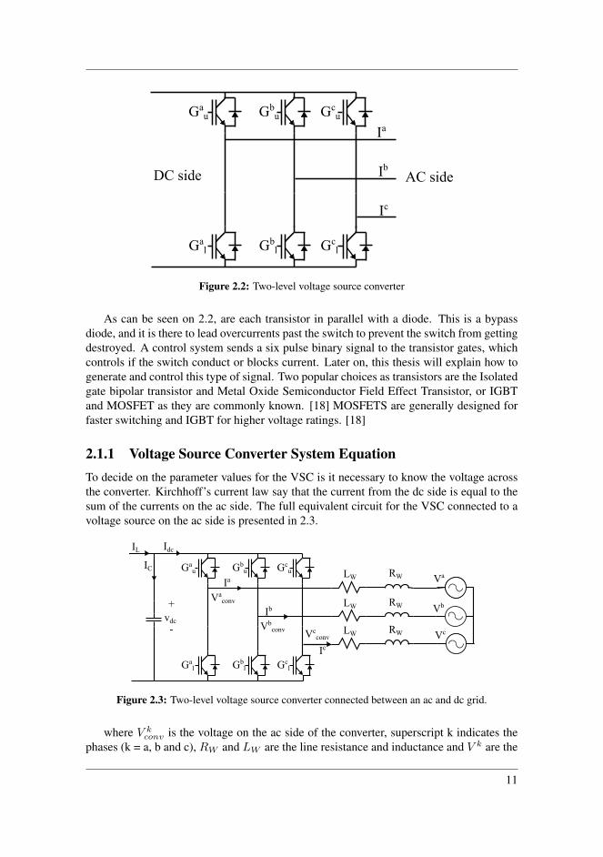
As can be seen on 2.2, are each transistor in parallel with a diode. This is a bypassdiode, and it is there to lead overcurrents past the switch to prevent the switch from gettingdestroyed. A control system sends a six pulse binary signal to the transistor gates, whichcontrols if the switch conduct or blocks current. Later on, this thesis will explain how togenerate and control this type of signal. Two popular choices as transistors are the Isolatedgate bipolar transistor and Metal Oxide Semiconductor Field Effect Transistor, or IGBTand MOSFET as they are commonly known. [18] MOSFETS are generally designed forfaster switching and IGBT for higher voltage ratings. [18]
2.1.1 Voltage Source Converter System EquationTo decide on the parameter values for the VSC is it necessary to know the voltage acrossthe converter. Kirchhoff’s current law say that the current from the dc side is equal to thesum of the currents on the ac side. The full equivalent circuit for the VSC connected to avoltage source on the ac side is presented in 2.3.
Ga
u Gb
u Gc
u
Ga
l Gb
l Gc
l
vdc
RWLW
RWLW
RWLW
Va
Vb
Vc
+
-
IL
IC
Idc
Va
conv
Vb
convVc
conv
Ia
Ib
Ic
Figure 2.3: Two-level voltage source converter connected between an ac and dc grid.
where V kconv is the voltage on the ac side of the converter, superscript k indicates thephases (k = a, b and c), RW and LW are the line resistance and inductance and V k are the
11

grid voltage. This is expressed in the following equation where the voltage drop across thepassive components are impedance times current Ik
V k = RW Ik + LW
d
dtIk + V kconv (2.1)
This equation is used to control the VSC. But when a controller is implemented, thecontroller often takes values in a rotating reference frame as input variables. [1] [19]Variables expressed in the rotating reference frame is noted with d and q superscript. Theprocess of transforming variables from synchronous to rotating reference frame is calledPark’s transformation, and is presented in 2.2. [20]
[xd
xq
]=
2
3
[sin(θt) sin(θt − 2π
3 ) sin(θt − 4π3 )
cos(θt) cos(θt − 2π3 ) cos(θt − 4π
3 )
]xaxbxc
(2.2)
where x represent the parameter which goes through the transformation, and θt is theangle of the rotating reference frame. Why it becomes beneficial to express values in thisform will be described at a later stage. When 2.1 is represented in a dq frame, the derivativeterm for the voltage drop across the inductor will make for an additional term, due to thechain rule.[21][
V d
V q
]= RW
[Id
Iq
]+ LW
d
dt
[Id
Iq
]+ L
[0 −ωω 0
] [Id
Iq
]+
[V dconvV qconv
](2.3)
A step by step calculation of how this additional term is included is presented in Appendix.
2.2 Voltage Source Converter ControlA typical way to control a VSC is with a DC voltage controller, a current controller anda phase locked loop (PLL) control system. [1] How this control can be implementedis illustrated in 2.4. In addition to the control system, the model contains an LC filterwith an inductance Lw and capacitance Cfw. The inductive and capacitive componentsboth contain some parasitic resistive elements Rw and Rfw, respectively. There is also atransformer connected to the inverter side. The inverter delivers current to the low voltageside and the transformer steps up the voltage which is sent to the grid. The voltage andcurrent measurements are taken after the inductor, to let the inductor straighten out theconverter voltage curve. Both the voltage and the current are sent to a component thattransfers the three-phase signals in a stationary reference frame, into a two-phase signalin a rotating reference frame. Subsequently, the voltage signal is sent to the PLL controlsystem to generate a signal synchronized to the grid voltage signal. This signal is used toperform dq transformation of the voltage and current vectors. The dq transformed currentand voltage signal is then sent into the current controller to generate a converter voltagesignal, which will be explained more in the next subsection. The dc voltage controllercontrols the voltage across the dc side capacitor. To simplify the control system, dc voltagecontrol will not be included, and the dc voltage is represented as a constant dc voltagesource.
12

+
-
RWLW
abcdq
abcdq
PLL
+-
+-
xLw
xLw
HCC
HCC+++
++-
abc
dq
PWM
�PLL
Iqref
IdrefId
Iq
Vd
Vq
Vqconv
Vdconv
VdcCfw
Rfw
Gk
mk
Transformer
VSC
HDC +-
Vdc
Vdc,ref
Vdc
Figure 2.4: Wind energy conversion system with current controller and PLL
2.2.1 Current ControllerCurrent controller is a technology for controlling VSC and is very common. [1], [22]-[23]The controller design used in this paper is presented by M.Amin in [1]. This controllermeasures the input current and compares it to a reference signal, which is used to decideon what voltage the converter should produce. By looking closely at 2.1 it becomes clearthat if the grid voltage and passive components remain constant, the current delivered fromthe converter to the grid is only dependent on the converter voltage.
Figure 2.5 shows what operations the current signal is sent through to generate thecurrent reference signal. This block diagram takes in dq reference signals. In steady statedq signals are constant, which is beneficial for PI controllers. [24]
Figure 2.5: Current controller control system with Pules width modulator
2.2.2 PI ControllerThe current and voltage signals are sent into the current controller after transformationfrom abc to dq. There the dq current Idq are compared to the current reference values
13

Idqref to find a current error. This error signal is sent through a PI controller block withproportional and integral parametersKp,cc andKi,cc, respectively. A third parameter, Ti,ccis the time constant of the PI controller, and is calculated accordingly, Ti,cc = Kp,cc/Ki,cc.The transfer function of the PI controller is
Hcc(s) = Kp,cc +Ki,cc
s= Kp,cc
1 + Ti,ccs
Ti,ccs(2.4)
The output voltage V ′dqconv of the PI controller then becomes
V ′conv = (Idqref − Idq)(Kp,cc +
Ki,cc
s) (2.5)
2.2.3 PWMAs can be seen on 2.5 is the converter voltage marked with an apostrophe then put througha pulse width modulator(PWM). This is a triangular wave modulator, which comparesthe voltage waveform to a three-phase triangular signal. This is a popular method forgenerating bipolar signals for many types of switching devices.[25] The output of themodulator is the converter signal. The PWM can be expressed as a time delay. [26]
V dqconv = V ′dqconv
1
1 + sTa(2.6)
Where Ta is average time delay of the converter
Ta =Tsw2
=1
2fsw(2.7)
Where Tsw is the switching time in seconds and fsw is the switching frequency in hertz.
2.2.4 System Transfer FunctionThe purpose of the VSC current controller is to control the output current of the controller.This is done by controlling the converter voltage, which is explained in 2.1. To simplifythe controller, the waveforms are converted to a synchronous reference frame. Dq transfor-mation presented in 2.2 introduces a cross-coupling term, ωlIdq calculated in Appendix.This cross-coupling term can be compensated for by introducing a feed forward term. Thiswill allow for independent dq control. [5]
14

+-
+-
Idref
Iqref Iq
Id
Vd Vd
Vq Vq
V'qconv Vqconv
V'dconv Vdconv
HCC(s)
HCC(s)
-++
-+-
11 + Tas
11 + Tas
-++
-+-
GCC(s)
GCC(s)
LCC
LCC
Figure 2.6: How to exterminate the cross coupling terms for the current controller
Where LCC is the cross coupling term ωgLW , andGCC is the system transfer function
GCC =1
RW
1
1 + sτ(2.8)
where τ is defined as inductance over resistance LW
RW.
2.2.5 Phase Locked LoopThe technique known as phase locked loop was first presented by Appleton in 1923. [27]But was not wildly used in the industry before the 1970s, due to difficulty when imple-menting it into real systems. At that time, it was first introduced by control engineers tocontrol synchronous motors and has been used ever since. [28] The purpose of a PLL isto make one signal trace another. A PLL makes it possible to generate an output signalwhich contains the same phase angle and frequency as a desirable reference signal. Thegeneral requirements for a standard PLL are, according to [28] and [29], a phase detector,loop filter and a voltage control oscillator. The phase detector compares each phase of themeasured input signal. Then generates an error signal which the voltage control oscillatoruses to make the output frequency equal to the input frequency. PLLs have three operatingstates, frequency running, capture and locked state, which are explained in [29]. PLLs op-erate in a feedback loop to reduce error and be able to change in case the system frequencyshould change. [30]
The PLL presented in this paper is connected to the WF Inverter. The reason for thisis that the WF Inverter delivers current to the grid, and to do so will the current phaseangle decide on what type of power the converter delivers. The reference frequency forthe converter is the grid voltage. The grid voltage is measured on and sent to the PLL.Because the WF Inverter operates in a synchronous reference frame are the three-phasegrid voltage signals transformed into a dq signal with an initial phase angle zero. Thepurpose of this PLL is to set the phase angle of the synchronous reference frame equalto the grid phase angle. When synchronization is achieved, the dq voltage signal willbe constants. The angle between the direct and quadrature axis is always 90°. They will
15

always rotate at the same speed, and the direct axis voltage V d can, therefore, be neglected.After the transformation is the quadrature voltage signal V q filtered to remove high orderfrequencies.
GPLL(s) =1
Tf,PLLs+ 1(2.9)
Where GPLL is the filter transfer function in the Laplace domain and Tf,PLL is thefilter break frequency. The reference quadrature voltage signal is set to zero as this willmake the direct voltage signal equal to the three-phase voltage peak phase signal Vg .
V d = Vg and V q = 0 (2.10)
The quadrature reference voltage and real voltage are compared which generated anerror. This error is sent through a PI controller with transfer function HPLL
HPLL = Kp,PLL +Ki,PLL
s(2.11)
where Kp,PLL and Ki,PLL are the proportional and integral terms of the PLL PI con-troller, respectively. The PI controller generates ωerror, which is the angular frequencydifference between the synchronous reference frame ωPLL and the base angular frequencyωb. The rotation speed of the synchronous reference frame can be calculated accordingly
ωPLL = ωb + ωerror (2.12)
The real phase angle θPLL can thereby be calculated by integrating the synchronousreference frame speed.
θPLL =ωPLLs
(2.13)
This reference frame angle is sent back to the beginning of the PLL loop to transformthe three-phase signal into the dq reference frame. The loop is then restarted to producean even smaller phase angle error. The PLL process is illustrated under
abcdq
GPLL(s) HPLL(s)++
1s
�b
�error
�PLL
�PLLVabc Vq
Vd
Vqerror++
Vqref
Vq
Figure 2.7: PLL block diagram
2.3 Voltage Source Converter TuningThe VSC is controlled by a current controller presented in [1]. The current controller getsits reference values from the PLL controller. For weak grids can one power supply, like
16

the wind turbine system presented in this thesis, influence the grid voltage substantially.This can make the input of the PLL oscillating, which can, if not tuned correctly, makethe PLL use a long time to synchronize with a higher margin of error. Which can makethe power output of the inverter oscillate and, in the worst case, make the whole systemunstable. That is why it is important to design a system with substantial transient responseand margins. This section will present a technique on how to tune the PI parameters of thecurrent controller and PLL controller. The WF Inverter parameters are
Table 2.1: WF Inverter parameters
Parameter ValueRated power Sw 50e6 VARated ac voltage Vw 690 VRated dc power Vw,dc 1500 VRated frequency fw 50 HzInverter Resistance Rw 0.003 puInverter Inductance Lw 0.15 puInverter Capacitance Cfw 0.0344 pu
The system parameters of the current controller and the PLL are
Table 2.2: VSC and PLL PI parameters
Parameter ValueVSC CC gain Kp,cc 0.0455VSC CC integral term Ki,cc 4.5487PLL gain Kp,PLL 1PLL integral term Ki,PLL 16.42
2.3.1 VSC Tuning TechniquesThe open loop transfer function of the controller is a low order plant. The system transferfunction is the product of the current controller, PWM and the PLL. [31]
Gcc,ol(s) = Kp,cc(1 + Tccs
Tcc)
1
1 + sTa
1
RW
1
1 + sτ(2.14)
There are two ways to tune the parameters of the current controller. The first is modulusoptimum. Modulus optimum is a way to simplify the system transfer function and, in thatway, tune the current controller. According to [32], is modulus optimum common whentuning analog controllers with low order control plants, that does not contain any timedelays. This controller has a dominant time constant, and additional, but less significant,time constants. With modulus optimum, it will be possible to cancel out these lesserconstants, which gives fewer poles and a less complicated system. The poles are canceledwhen the PI parameters are equal to the current controller parameters, accordingly
17

-20
0
20
40
Mag
nit
ud
e (d
B)
101 102 103-150
-120
-90
Ph
ase
(deg
)
Frequency (Hz)
Figure 2.8: Current controller bode
Tcc = τ (2.15)
Kp,cc =τRW2Ta
(2.16)
When the PI parameters are set to these values the new open loop current controllertransfer function becomes
Gcc,ol(s) =1
2
1
T 2a s
2 + Tas(2.17)
The second way to tune the parameters is according to symmetrical optimum. Sym-metrical optimum is presented in [31]. The main objective of symmetrical optimum is tomaximize phase margin for low frequencies. This will make the system more tolerant todelay. 2.8 shows the frequency response of the current controller. The figure shows thatthe system operates with phase margin of 70° around the operating point(50Hz). The peakphase margin is 80°, which occurs where the magnitude plot crosses 0dB. According tothe bode plot is the current controller stable, with good stability margins.
Next is to analyze the step response of the current controller, which can be found infigure 2.9. The step response can be calculated according to [33]. Rise time is defined ashow long it takes for the system to go from 5% to 95% of its final value. Peak time is atwhat time the first peak value of the response occurs. Maximum overshoot is how high
18

above unity the maximum peak goes; for this case, it is presented in percent. Settling timeis how long time it takes for the system response to reach 98% of unity value, without itdeviate outside of 2% of unity value.
Figure 2.9: Current controller step response
It can be seen that the system transient response isRise time = 1.15e-3 sec (5% to 95%)Peak time = 2.9e-3secMaximum overshoot = 4%Settling time = 4e-3 sec
2.3.2 PLL ResponseAs discussed previously is quadrature voltage filtered and then sent into a PI controller.The output of the PI controller of the PLL is the angular frequency of the rotating referenceframe. This angular frequency is integrated to find the angle of the rotating referenceframe. These calculations are what generates the system transfer function. [34]
GPLL = (Kp,PLL +Ki,PLL
s)1
s
1
Tf,PLLs+ 1(2.18)
The frequency response for the PLL is presented in the 2.10. The figure shows that thecross over point occurs at very low frequency. And if the magnitude of the converter is tobe shifted, the PLL will still operate with decent stability margins around 50Hz.
19

-100
-80
-60
-40
-20
0
Mag
nit
ud
e (d
B)
100 101 102 103-180
-150
-120
-90
Ph
ase
(deg
)
Frequency (Hz)
Figure 2.10: PLL bode plot
20

Chapter 3High-Voltage DC Rectifier
This chapter describes the operating principle and tuning technique of a MMC rectifier in aHVDC system. This chapter will also present the parameters used to control the MMC andthe system frequency response this generates. The MMC is controlled according to threeprinciples, Compensated modulation and Direct modulation with and without circulatingcurrent control. 3.1 show where in a HVDC conversion system the MMC rectifier islocated. In this thesis, when the HVDC system is mentioned it talks about the MMCrectifier.
Modular multilevel converters (MMC) have been accepted in the industry as they areable to produce excellent voltage quality for medium and high voltage. When comparedto a 2-level voltage source converter, an MMC requires less filtering and has lower powersemiconductor losses. [35] Compared to other types of multilevel converters, like a neutralpoint clamped converter (NPC), the MMC is beneficial, as many cells allow it to producevoltages of different levels. [36] Even though it has a large number of cells that require amore complex controller, the simple design of each cell result in a simple structure. This,together with lower filtering requirements, lowers production costs and makes the MMChighly competitive. A type of multilevel converter capable of reaching high voltage levelsis the H-bridge converter. According to [36], do each H-bridge usually require an isolateddc-source, which is often supplied by a multi pulse transformer. MMCs does not requirean input transformer [37] which makes scaleability simple for medium and high powerlevels. [38], [39]
Transformer
PCCRr Lr
Cfr
Rfr
MMC
Rectifier
Grid Side
Inverter
Power
Grid
Figure 3.1: HVDC converter system
21

3.1 Modular Multi Level Converter TopologyAn MMC is a converter consisting of a large number of power cells, connected in se-ries. Each of these power cells, or submodules (SM), consists of some kind of switchingsystem. [40] Typical switching systems are full-bridge converter, half-bridge converter,unidirectional cells, multilevel NPC cell, multilevel flyback capacitor cell, and some otherconverters described by M.A.Perez in [35]. Among these, are full-bridge and half-bridgemost common. A half-bridge SM is only able to generate positive and zero voltage, andwill, therefore, require the power system to be connected to a dc system. The full-bridgeconverter is, on the other hand, able to also generate negative voltage and can, therefore, beused when connected to both full ac and dc systems. The disadvantage of the full-bridgeconverter is that it demands more physical components then a half-bridge cell. A unidi-rectional modular multilevel converter (uMMC) for HVDC subsea system is proposed byG.J.M.de Sousa in [41]. It can be advantageous to other MMCs as it requires only oneswitching device per SM, which can lower cost and increase reliability. The disadvantageof the uMMC is that current can only flow one direction. This prevents the converter frombeing applicable for some popular generator types for wind turbines, like the doubly fedinduction generator, which requires reactive power to induce a magnetic field to producepower. Most of the literature found for this thesis, [35], [36], [38], [41], are on 2-level armconverters (2L), but in [42] E. Solas explains the working principles of 3-level arm convert-ers (3L). For example, can, according to [42], a 3L-NPC converter do approximately thesame job as a 2L converter, with half the SMs, which can make the 3L-NPC more compactthan a 2L converter. But, the 3L NPC and flyback converter will require voltage balancingcontrol for all capacitors of each SM. These extensive measurement requirements, of allcapacitor voltages, increase computational costs, which can be a determining factor whendeciding what type of converter to use.
A half-bridge MMC is illustrated in 3.2. The SM contains two switches and is thereforcapable of operating in three modes.[40]
• Inserted: S1 is open and S2 is closed, the capacitor is charges and discharges.
• Bypassed: S1 is closed and S2 is open, the voltage in the capacitor remains constant.
• Blocked: Both gates are in an open state blocking current from flowing. The voltagefrom the dc voltage source may still charge up the capacitor, but the capacitor maynot discharge.
A
B
SMku,ln
A
BVicu,l
+
-
Cm
S1
S2
Figure 3.2: Half-bridge cell for MMC SM
An MMC can convert power from single phase to single phase, three phase to singlephase, single phase to three phase and three phase to three phase as illustrated in 3.3 [35]
22

a
b
A
B
a)
abc
A
B
b)
a
b
c
A B C
c)
Figure 3.3: Modular multilevel converter. a) single phase to single phase b) three phase to singlephase, single phase to three phase and c) three phase to three phase
The power cells are divided into subgroups called arms, which are connected betweentwo phases(example dc phase and ac phase). For a single-phase to three-phase converters,an arm can be connected in two ways, either to the positive or negative part of the single
23
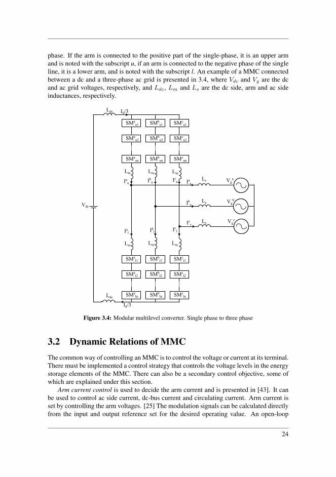
phase. If the arm is connected to the positive part of the single-phase, it is an upper armand is noted with the subscript u, if an arm is connected to the negative phase of the singleline, it is a lower arm, and is noted with the subscript l. An example of a MMC connectedbetween a dc and a three-phase ac grid is presented in 3.4, where Vdc and Vg are the dcand ac grid voltages, respectively, and Ldc, Lm and Ls are the dc side, arm and ac sideinductances, respectively.
SMau1
SMau2
SMaun
SMbu1
SMbu2
SMbun
SMcu1
SMcu2
SMcun
SMal1
SMal2
SMaln
SMbl1
SMbl2
SMbln
SMcl1
SMcl2
SMclnLdc
Vdc
Ldc
Lm Lm Lm
LmLmLm
Ls
Ls
Ls
Iau Ibu Icu
Ial Ibl Icl
Id/3
Id/3
Ias
Ibs
Ics
Vga
Vgb
Vgc
Figure 3.4: Modular multilevel converter. Single phase to three phase
3.2 Dynamic Relations of MMCThe common way of controlling an MMC is to control the voltage or current at its terminal.There must be implemented a control strategy that controls the voltage levels in the energystorage elements of the MMC. There can also be a secondary control objective, some ofwhich are explained under this section.
Arm current control is used to decide the arm current and is presented in [43]. It canbe used to control ac side current, dc-bus current and circulating current. Arm current isset by controlling the arm voltages. [25] The modulation signals can be calculated directlyfrom the input and output reference set for the desired operating value. An open-loop
24

case is presented in [44] where a compensation term is included to eliminate steady stateerror. This strategy is able to produce a stable output in steady state. For the closed loopcase presented in [45] the feedback loop eliminates the steady-state error. These closedloop systems can vary in difficulty, from simple PI controllers to more advanced linear-quadratic regulator controllers.
Capacitor voltage control operates with the purpose of maintaining a set average volt-age reference level. To simplify the calculations for this technique, all SMs are consideredto be a single equivalent capacitance. From [25] the power equation describing the rela-tionship of the capacitance power Pcap, input power Pin, output power Pout and powerloss Ploss across the MMC in steady state is
Pcap = Pin − Pout − Ploss (3.1)
Power across the capacitor is
Pcap =Ceq2
dV 2avg
dt(3.2)
Where Ceq is the equivalent capacitance and Vavg is the average voltage. This meansthat for the energy to stay constant across the equivalent capacitor, the power sent into thesystem must equal the power out plus any losses in the converter, while operating at steadystate.
To study the dynamics of an MMC it can be beneficial to study it as an equivalentcircuit, where the SMs are modeled as a constant voltage source. This allows us to simplifyeach phase of the model substantially, as illustrated in the following figure. [38]
Vdu
Vdl
Rm Lm
Rm Lm
Ik
s
Vk
s
+
-
Ik
c
+
-
Vk
cu
+
-
Vk
cl
+
+
-
-
Id/3
Figure 3.5: Modular multilevel converter. Single phase equivalent circuit.
As for the VSC are each phase expressed by k for a three phase MMC. Where Vdu andVdl are the positive and negative dc voltages, respectively. Where in the case of figure 3.5they will be half of the real dc voltage, presented in 3.3
Vdu = Vdl =Vdc2
(3.3)
The voltages V kcu,l are the voltage representing the capacitors and is where the controlsignal is sent to control the MMC. [38] The resistance Rm are parasitic arm resistance and
25

converter losses, which is often very small and can vary with operating conditions. Theinductance Lm is the arm inductance, which is there to lower the fault current and currentharmonics of each arm. [40] The inductance is also necessary to limit the current thatflows when a switch turns on/off due to the instantaneous difference in voltage across thearm. [35] There are three different currents flowing in the MMC. We assume power flowfrom the dc to the ac side. The current from the dc side is divided equally in each of thethree phases. Therefore, is the current in the upper leg equal to Ikd /3. The output currentflowing on the ac side of the MMC is Iks . At first sight, it can be natural to think that thedc current is equal to the ac current of the MMC. But an important characteristic for theMMC is the upper and lower circulating current Iku,l controls the output current.
Iks = Iku − Ikl (3.4)
Where the circulating currents Ikc is defined as
Ikc =Iku + Ikl
2(3.5)
Kirchhoff’s voltage law can be used to find the dynamic of the equivalent circuit bysumming the voltages across all the components.
Vdu = V kg + V kcu +RmIku + Lm
dIkudt
(3.6)
Vdl = −V kg + V kcl +RmIkl + Lm
dIkldt
(3.7)
Where V kg is the voltage on the ac grid side of the converter. According to [40] is thesum of all the capacitor voltages equal V kcu,l
V kcu = nkuV∑k
cu (3.8)
V kcl = nkl V∑k
cl (3.9)
Where nku,l are the insertion indices in phase k when u and l are upper and lower arm,
respectively. And V∑k
cu,l are the sum of voltages across all capacitors in phase k, for upperand lower arm. [38] represent two techniques for controlling the MMC, compensatedmodulation and direct modulation.
3.2.1 Compensated ModulationCompensated modulation makes it possible to disregard the internal dynamics of theMMC. [38] [40] This makes way for the assumption that the arm voltages are equal tothe voltage control references. This type of control is very difficult to implement in realityas time delays from the voltage measurements will lead to problems.
For compensated modulation the insertion index calculated accordingly
nku =Vdu − V refks
V∑k
cu
(3.10)
26

nkl =Vdl + V refks
V∑k
cl
(3.11)
Where V refks is the desired output voltage in phase k. Subtracting 3.6 and 3.7 gives
Lmd
dt(Iku + Ikl ) +Rm(Iku + Ikl ) + (vkcu + vkcl) = Vdc (3.12)
substituting in 3.5, 3.8-3.11, 3.13 show that the circulating current naturally drops tozero at steady state. This means, that its not necessary to actively suppress the circulatingcurrent. [38]
LmdIkcdt
+RmIkc = 0 (3.13)
Adding 3.6 and 3.7 gives
Lmd
dt(Iku − Ikl ) +Rm(Iku − Ikl ) + (V kcu − V kcl) = V ∆
dc (3.14)
where V ∆kdc is the imbalanced dc bus voltage in phase k
V ∆kdc = V kdu − V kdl (3.15)
which for a three phase system is equal to zero. [38] Substituting 3.4, 3.8-3.11, 3.13into 3.14 gives the dynamic equation describing the output current from the MMC forcompensated modulation mode.
Lm2
dIksdt
= V ks − V kg −Rm2Iks (3.16)
3.2.2 Direct ModulationFor direct modulation mode will the internal dynamics of the MMC have to be considered.By assuming that the capacitance is high enough to maintain a constant voltage across eacharm, the sum of the capacitor voltages is equal to the dc side voltage. The insertion indexfrom 3.10 and 3.11 are used to find the new insertion index nkul for the direct modulationcontroller by taking the circulating current voltage reference V refkc into consideration
nku ≈Vdu − V refks − V refkc
Vd(3.17)
nkl ≈Vdl + V refks − V refkc
Vd(3.18)
The general formula for energy stored in a capacitor is used to find the sum of theenergy in each arm of the converter.
W kul =
Cm2
N∑i=1
(V ikc,ul)2 (3.19)
27

Where Wul is the stored up energy in the capacitor, N is the number of SMs, Cm andV ic is the individual capacitance and capacitor voltage, respectively. It is known that theinput power of an arm at one instant is equal to the time derivative of stored up energy.
dW kul
dt= Cm
N∑i=1
V ikc,uldV ikc,uldt
= V kc,ulIkc,ul (3.20)
Due to the large capacitance of the converter is the change in energy minor, whichallows for the assumption that the individual arm capacitor voltage V ikc,ul is equal to the
sum of the capacitor voltages in either upper or lower arm V∑k
c,ul , divided by the number ofSM in that arm. Or in other words, the arm capacitor voltage is equal to the mean capacitorvoltage.
dW kul
dt= Cm
N∑i=1
V ikc,uldV ikc,uldt
≈ CmN
V∑k
c,ul
N∑i=1
dV ikc,uldt
=Cm2N
d(V∑k
c,ul )2
dt(3.21)
This assumption makes for a new expression for the energy stored per arm
W kul =
Cm2N
(V∑k
c,ul )2 (3.22)
The dynamic equation of the sum of the capacitor voltage can now be derived bysubstituting 3.21 and
V kc,ul = nkulV∑k
c,ul (3.23)
into 3.20. Resulting in
CmN
dV∑k
c,ul
dt= nkulI
kul (3.24)
The converter voltage can be found by substituting upper and lower arm voltage fromthe dc side voltage.
Vc =Vd − nkuV
∑k
cu − nkl V∑k
cl
2(3.25)
Where the sum of the upper and lower converter voltages are, of course, equal to thetotal of the capacitor voltages
V∑k
c = V∑k
cu + V∑k
cl (3.26)
By substituting 3.17, 3.18, 3.25 and 3.26 into 3.24, the first equation describing theinternal dynamics of the MMC is obtained in 3.27.
CmN
dV∑k
c
dt= −V
refks IksVd
+ (1− 2V refkc
Vd)Ikc (3.27)
28

The unbalanced capacitor voltage per phase V ∆kc is the difference between the sum of
the upper and lower capacitor voltages
V ∆kc = V
∑k
cu − V∑k
cl (3.28)
By deviating 3.28 and then substituting in 3.3 - 3.5, 3.17, 3.18, 3.24, the dynamic stateequation for unbalanced capacitor voltage is derived to be
CmN
dV ∆kc
dt= (1− 2V refkc
Vd)Iks2− 2V refks
VdIkc (3.29)
3.16 describes how the circulating current decays for compensated modulation control.This will not be the case for direct modulation as the circulating current does not equalzero. From subtracting 3.8 and 3.9 the new expression for circulating current is derived
LmdIkcdt
= V kc −RmIkc (3.30)
Now, by substituting in 3.3 - 3.5, 3.17, 3.18, 3.25, 3.26 and 3.28 for 3.30 the dynamiccirculating state equation is derived
LdIkcdt
=1
2(Vd −
V∑k
c
2+V refkc V
∑k
c
Vd+V refks V ∆k
c
Vd)−RmIkc (3.31)
3.3 Control Structure
3.3.1 Phase Shift and Level Shifted ModulationPhase shifted and level shifted triangular waveforms are often compared with the referencesignal to generate a switching signal, as illustrated in 3.6a and 3.6b. These techniqueshave, even though they are good, high switching losses compared to other techniques, likefundamental frequency modulation. [25] Level shifted modulation is presented in [46],there it is specified that this technique is very simple, even for a large number of SM perarm. This is not the case for phase shifted modulation as this technique becomes complexas the number of SM per arm increases. [25]
29
(a) (b)
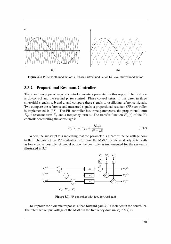
Figure 3.6: Pulse width modulation: a) Phase shifted modulation b) Level shifted modulation
3.3.2 Proportional Resonant ControllerThere are two popular ways to control converters presented in this report. The first oneis dq-control and the second phase control. Phase control takes, in this case, in threesinusoidal signals, a, b and c, and compare these signals to oscillating reference signals.Two compare the reference and measured signals, a proportional-resonant (PR) controlleris implemented in [38]. The PR controller has three parameters, the proportional termKp, a resonant term Kr and a frequency term ω. The transfer function Hv(s) of the PRcontroller controlling the ac voltage is
Hv(s) = Kpv +Krvs
s2 + ω2v
(3.32)
Where the subscript v is indicating that the parameter is a part of the ac voltage con-troller. The goal of the PR controller is to make the MMC operate in steady state, withas low error as possible. A model of how the controller is implemented for the system isillustrated in 3.7
+-
+-
+-
Hv(s)
Hv(s)
Hv(s)
++
Vag Vbg Vcg
Vag Vbg Vcg
++
Vsrefa
Vsrefc
Vsrefb
Vgrefa
Vgrefc
Vgrefb +
+
kf kfkf
Figure 3.7: PR controller with feed forward gain
To improve the dynamic response, a feed forward gain kf is included in the controller.The reference output voltage of the MMC in the frequency domain V refks (s) is
30

V refks (s) = Hv(s)[Vrefkg (s)− V kg (s)] + kfV
kg (s) (3.33)
Where V refkg is the fundamental frequency voltage.In the direct modulation case, as discussed previously, circulating current control has
to be considered, as circulating current is not suppressed naturally for this case. The circu-lating current is controlled by controlling the circulating current voltage. The circulatingcurrent voltage is controlled with a PR controller, accordingly
Hc(s) = Kpc +Krc
s2 + ω2c
(3.34)
Where Hc(s) is the transfer function of the controller, Kpc, and Krc is the con-troller proportional and resonance parameters, respectively, and ω2 is twice the angularfrequency. The PR controller takes in circulating current reference and measures circulat-ing current, which is calculated according to 3.5. The circulating current voltage is givenby
V refkc (s) = Hc(s)[Irefkc (s)− Ikc (s)] +RIrefkc (s) (3.35)
Where the reference circulating current Irefc is equal to the steady state current Ikc0,and resistance times reference current compensates for the voltage drop that occurs due tothe resistive parasitic element in the converter.
3.4 HVDC TuningA frequency and time dependent scenario has to be performed to test the potential stabilityof these components. In order to do so, the parameters have to have some value. Eachvalue for the MMC and its controller is presented in 3.1 and 3.2.
Table 3.1: HVDC parameters
Parameter ValueRated power Sr 50e6 VARated ac voltage Vr 166e3 VRated dc power Vr,dc 400e3 VRated frequency fr 50 HzArm resistance Rm 1.81e-6 puArm inductance Lm 0.057 puSM capacitance Cm 96.95 puRectifier Resistance Rr 0.0011 puRectifier Inductance Lr 0.054 puRectifier Capacitance Cfr 0.2038 pu
31

Table 3.2: MMC PR controller parameters
Parameter ValueAc voltage PR, proportional Kpv 0.5Ac voltage PR Krv 50Circulating current PR controller Kpc 20Circulating current PR controller Krc 1000
3.32 represent the ac voltage controller in open loop. This function can be turned intoclosed loop with 3.36.
Hv,cl(s) =Hv(s)
1 +Hv(s)(3.36)
The result of the previous equation is presented in 3.37
Hc,cl(s) =Kpv(1 + Tpv)
Tpv +Kpv(1 + Tpv)(3.37)
Where Tpv is the resonant time constant given by
Tpv =Kpv
Krv(3.38)
To evaluate stability is it of interest to study the response of the PR ac voltage con-troller. 3.8 show the controller response in a bode plot. The result from the bode plot showthat the controller delivers stable output for normal frequency range.
0
100
200
300
Mag
nit
ud
e (d
B)
101 102 103-90
-45
0
45
90
Ph
ase
(deg
)
Frequency (Hz)
Figure 3.8: PR ac voltage controller bode
32

Figure 3.9: PR ac voltage controller step response
The voltage controller step response is presented in 3.9, and is used to evaluate howlong time the controller will use to produce a stable output.
The figure shows that the settling time is fast with a critically damped response, mean-ing that the system reaches the reference value without any overshoot. The step responsegives the following transient response Rise time = 100e-3 sec (5% to 95%)Settling time = 110e-3 sec
33

Chapter 4Stability Analysis of WindFarm-HVDC System
This chapter show how to calculate various stability models of a VSC and a MMC. It showhow stable the converters should be according to parameters presented in 2.1, 2.2, 3.1 and3.2.
Small-signal stability methods test system stability by injecting a small perturbationcurrent, also called disturbance, into a system. A small perturbation current is in this casea current that still allows the system equations to be linearized for analysis purposes. [47]A system is considered unstable if, by injecting a small disturbance, the system goes fromsynchronized to unsynchronized. In power systems today, lack of system stability is oftendue to insufficient damping of system oscillations. [47] To perform small-signal stabilityanalysis the system has to be linearized, which was explained in 1.7.
4.1 State Space Representation
4.1.1 Wind Energy Conversion State SpaceThis section will present a description of how to generate equations describing all operat-ing conditions for a VSC with current control connected to a grid. 4.1 show the locationof all parameters for the system, except for the controller. To generate the equations toanalyzing the system, fairly simple circuit analysis can be performed. [48]
34

RWLW
Vdc
Cfw
Rfw
Transformer
VSC
Rg Lg
IW I0Ig
VW V0 Vg
Figure 4.1: Voltage source inverter wind conversion system
The dynamic equation of current flowing from the converter IW is decided by thevoltage difference between the converter VW and V0, and the voltage drop across the con-verter resistor RW and inductor LW . The function for the current is presented in 4.1, takenote that the current is transferred to the dq domain, which introduces an additional termcalculated in Appendix.
dIdqWdt
=V dqW − V
dq0 − I
dqWRW
LW± ωgIqdW (4.1)
Where ωg is the grid frequency. Another dynamic equation of grid current Ig is decidedby the the voltage difference between V0 and the grid Vg , and grid resistance Rg andinductance Lg , in 4.2.
dIdqgdt
=V dq0 − V dqg − Idqg Rg
Lg± ωgIqdg (4.2)
4.3 describes V0. It specifies that V0 is equal to the voltage drop across the groundedcapacitor Cfw. It is calculated by analysing the sum of the currents flowing through V0
dV dq0
dt=IdqW − IdqgCfw
± ωgV qd0 (4.3)
Current ControllerThe VSC dynamics are also dependent on the controller parameters. This means that thecurrent controller with the PLL generate reference signals which are used for the VSC.The block diagram of the current controller with a PLL is represented in chapter 2. Theblock diagram is built to emulate 4.4 to calculate the converter voltage Vconv
V dqconv = V dqo +Hcc(Idqcc,ref − I
dqcc )∓ Iqdcc ωPLLLW (4.4)
Where Hcc is the PI regulator with proportional and integral terms Kcc,p and Kcc,i,respectively. Now, auxiliary variables γ can represent the dynamic performance of theintegral term of the PI controller in 4.5.
dγdq
dt= (Idqcc,ref − I
dqcc ) (4.5)
35

PLLThe PLL can be expressed with three dynamic equations describing its operating condi-tions. 4.7 is included do to the low pass filter containing an integral component. Thestandard equation for a signal going through a low pass filter is presented in 4.6
V qPLL = V qωLP
s+ ωLP(4.6)
Where V qPLL is the voltage running through the PLL, ωLP is the cut-off frequency ofthe filter. The dynamic equation of 4.6 is
dV qPLLdt
= V qωLP − V qPLLωLP (4.7)
For steady-state operating conditions, the q component of the converter voltage shouldbe zero. As the q-axis voltage signal is sent through the PLL-PI controller, a new auxiliaryvariable εPLL is introduced do to the integral term of the PI controller.
dεPLLdt
= V q (4.8)
At last, the phase angle δθPLL of the PLL is calculated as V q is used to calculate ωPLLthrough a PI controller. The integral of ωPLL is then taken which gives
dδθPLLdt
= δωPLL = KpPLLVq +KIPLLεPLL (4.9)
Where δωPLL also can be expressed as
δωPLL = ωPLL − ωg (4.10)
4.1.2 Modular Multi Level Converter State SpaceThe dynamic equations describing the operating conditions for the MMC are expressed in3.24, 3.29 and 3.16. To use these equations to analyze the stability of the system, they firsthave to be linearized at a steady state. It may be assumed that the steady state conditionsfor the state variables are
V∑k
c0 = 2Vd (4.11)
V ∆kc0 = 0 (4.12)
Ikc0 =P
3Vd(4.13)
Where the subscript 0 notes the steady-state value and P is transferred power. [38]
36
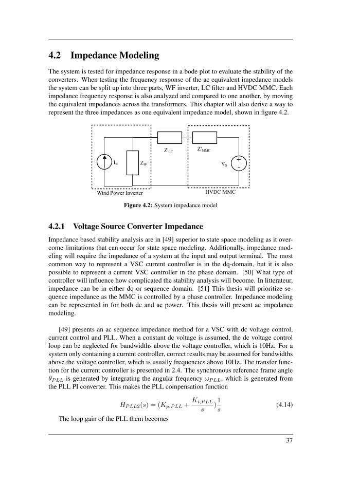
4.2 Impedance ModelingThe system is tested for impedance response in a bode plot to evaluate the stability of theconverters. When testing the frequency response of the ac equivalent impedance modelsthe system can be split up into three parts, WF inverter, LC filter and HVDC MMC. Eachimpedance frequency response is also analyzed and compared to one another, by movingthe equivalent impedances across the transformers. This chapter will also derive a way torepresent the three impedances as one equivalent impedance model, shown in figure 4.2.
+
-
Z'LC
ZW
Z'MMC
Iw VS
Wind Power Inverter HVDC MMC
Figure 4.2: System impedance model
4.2.1 Voltage Source Converter ImpedanceImpedance based stability analysis are in [49] superior to state space modeling as it over-come limitations that can occur for state space modeling. Additionally, impedance mod-eling will require the impedance of a system at the input and output terminal. The mostcommon way to represent a VSC current controller is in the dq-domain, but it is alsopossible to represent a current VSC controller in the phase domain. [50] What type ofcontroller will influence how complicated the stability analysis will become. In litterateur,impedance can be in either dq or sequence domain. [51] This thesis will prioritize se-quence impedance as the MMC is controlled by a phase controller. Impedance modelingcan be represented in for both dc and ac power. This thesis will present ac impedancemodeling.
[49] presents an ac sequence impedance method for a VSC with dc voltage control,current control and PLL. When a constant dc voltage is assumed, the dc voltage controlloop can be neglected for bandwidths above the voltage controller, which is 10Hz. For asystem only containing a current controller, correct results may be assumed for bandwidthsabove the voltage controller, which is usually frequencies above 10Hz. The transfer func-tion for the current controller is presented in 2.4. The synchronous reference frame angleθPLL is generated by integrating the angular frequency ωPLL, which is generated fromthe PLL PI converter. This makes the PLL compensation function
HPLL2(s) = (Kp,PLL +Ki,PLL
s)1
s(4.14)
The loop gain of the PLL them becomes
37

TPLL(s) =VwHPLL2(s)
2(1 + VwHPLL2(s))(4.15)
where Vw is the per unit phase to ground peak ac side voltage magnitude. The relation-ship between the phase voltages abc and the sequence voltages int the time domain can bewritten as
Vwk(t) = Vwcos(2πf1t) + Vpcos(2πfpt+ φvp) + Vncos(2πfnt+ φvn) (4.16)
where k is the phase, fb is the fundamental or in this case the base frequency, Vp isthe positive sequence voltage magnitude with a phase φvp and frequency fp, and Vn isthe negative sequence voltage magnitude with a phase φvn and frequency fn. This can bewritten in the frequency domain as
Va[f ] =
V1 f = fb
Vp f = (fp − fb)Vn f = (fn + fb)
(4.17)
With these functions [49] calculate the positiveZwp and negativeZwn sequence impedanceto be
Zwp =Hcc(s− jωb)V0 + (s− jωb)LW
1− TPLL(s− jωb)[1 +Hcc(s− jωb) IwV0
Vw])
(4.18)
Zwn =Hcc(s+ jωb)V0 + (s+ jωb)LW
1− TPLL(s+ jωb)[1 +Hcc(s+ jωb)IwV0
Vw])
(4.19)
where Iw is the ac side peak current. The input impedances include the output impedanceof the inverter but is excluding the capacitor. Therefore, the capacitor impedance is calcu-lated separately later in this chapter. The following figure shows where on the circuit theac impedance is calculated from
vdc
RW LW
RW LW
RW LW
+
-
IL
IC
Idc
Ia
Ib
Ic
ZW
Rfw
Cfw
Figure 4.3: VSC impedance model
38

The frequency response of ZW , which is equal to Zwp, is presented in 4.4. There, itcan be seen that the impedance margins are really high, which indicates that the VSC isstable for the operating conditions presented in 2.1 and 2.2
-35
-30
-25
-20
-15
-10
Mag
nit
ud
e (d
B)
101 102 103-180
-90
0
90
180
Ph
ase
(deg
)
Frequency (Hz)
Figure 4.4: VSC frequency response
4.2.2 Modular Multi Level Converter ImpedanceThe MMC impedance is calculated as ac impedance from the grid side across the convert-ers. The output impedance as well as the leg impedance is included, which can be seen inthe following figure
39

SMa
u1
SMa
u2
SMa
un
SMb
u1
SMb
u2
SMb
un
SMc
u1
SMc
u2
SMc
un
SMa
l1
SMa
l2
SMa
ln
SMb
l1
SMb
l2
SMb
ln
SMc
l1
SMc
l2
SMc
lnLdc
Vdc
Ldc
Lm Lm Lm
LmLmLm
Ls
Ls
Ls
Id/3
Id/3
ZMMC
Ia
uIb
uIc
u
Ia
lIb
lIc
l
Ia
s
Ib
s
Ic
s
Figure 4.5: MMC ac impedance
Compensated modulation caseTo study the stability for the compensated modulation controller, it is necessary to extractthe impedance model of the MMC when the circulating current decays to become zeroas time progress. The impedance is found by taking 3.33 and putting it into 3.16, thenapplying linearization. The result is
1
2(Lms+Rm)Iks (s) = (kf −Hv(s)− 1)V kg (s) (4.20)
where the tilde is indicating that the variable is linearized. The impedance ZMMC is givenby V kg over −Iks , accordingly
ZMMC(s) = −V kg
Iks=
Lms+Rm2(1− kf +Hv(s))
(4.21)
To evaluate the stability of the compensated modulation controller the bode plot and theNyquist plot in 4.6 and 4.7, respectively. The bode plot shows that the converter is stable,but with a small impedance phase margin, 5.46dB at 50.3Hz. As there is no crossing of the-180° line, the impedance gain margin is assumed infinite. The Nyquist plot also indicatesthat the system is stable as there are no rotations around the critical point.
40
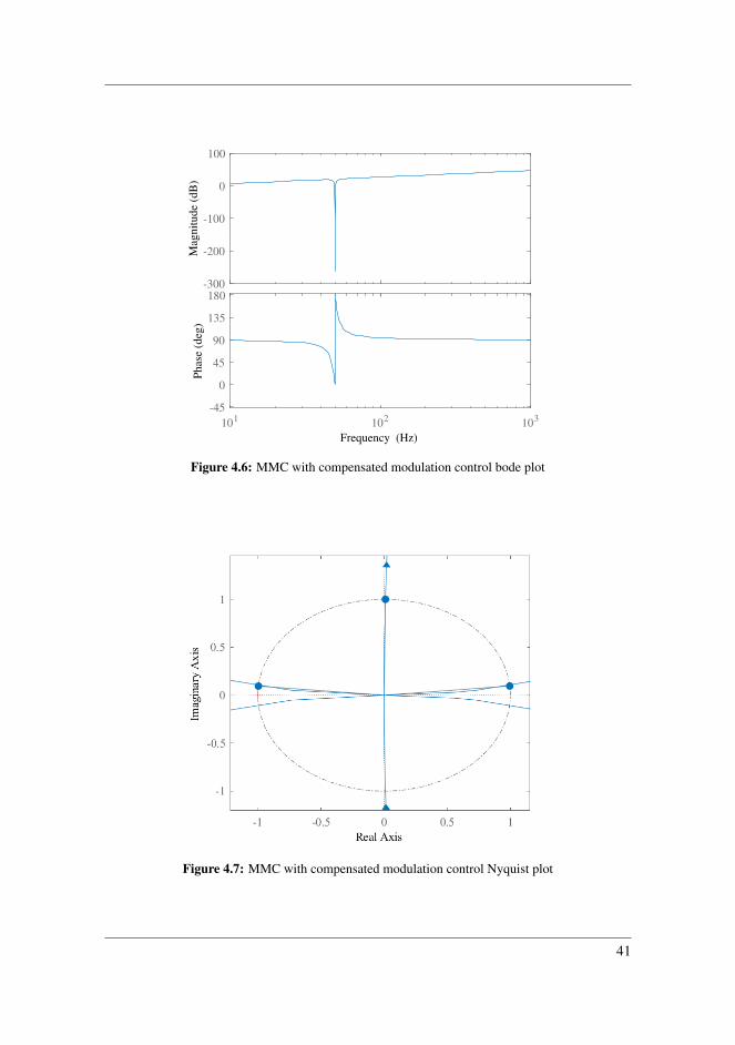
-300
-200
-100
0
100
Mag
nit
ud
e (d
B)
101 102 103-45
0
45
90
135
180
Ph
ase
(deg
)
Frequency (Hz)
Figure 4.6: MMC with compensated modulation control bode plot
Figure 4.7: MMC with compensated modulation control Nyquist plot
41
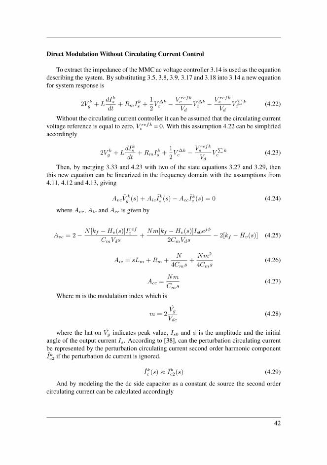
Direct Modulation Without Circulating Current Control
To extract the impedance of the MMC ac voltage controller 3.14 is used as the equationdescribing the system. By substituting 3.5, 3.8, 3.9, 3.17 and 3.18 into 3.14 a new equationfor system response is
2V kg + LdIksdt
+RmIks +
1
2V ∆kc − V refkc
VdV ∆kc − V refks
VdV
∑k
c (4.22)
Without the circulating current controller it can be assumed that the circulating currentvoltage reference is equal to zero, V refkc = 0. With this assumption 4.22 can be simplifiedaccordingly
2V kg + LdIksdt
+RmIks +
1
2V ∆kc − V refks
VdV
∑k
c (4.23)
Then, by merging 3.33 and 4.23 with two of the state equations 3.27 and 3.29, thenthis new equation can be linearized in the frequency domain with the assumptions from4.11, 4.12 and 4.13, giving
AvcVkg (s) +AicI
ks (s)−AccIkc (s) = 0 (4.24)
where Avc, Aic and Acc is given by
Avc = 2− N [kf −Hv(s)]Irefc
CmVds+Nm[kf −Hv(s)]Is0e
jφ
2CmVds− 2[kf −Hv(s)] (4.25)
Aic = sLm +Rm +N
4Cms+Nm2
4Cms(4.26)
Acc =Nm
Cms(4.27)
Where m is the modulation index which is
m = 2VgVdc
(4.28)
where the hat on Vg indicates peak value, Is0 and φ is the amplitude and the initialangle of the output current Is. According to [38], can the perturbation circulating currentbe represented by the perturbation circulating current second order harmonic componentIkc2 if the perturbation dc current is ignored.
Ikc (s) ≈ Ikc2(s) (4.29)
And by modeling the the dc side capacitor as a constant dc source the second ordercirculating current can be calculated accordingly
42

Ikc2(s) ≈ Acc2Ikc (s) ≈3m
8(s−jω)
4Cm
N (2Lm(s− jω) +Rm) + 6+4m2
12(s−jω)
Ikc (s) (4.30)
By substituting the 4.30 into 4.24 the ac side impedance of the HVDC side MMC canbe obtained as
ZMMCc(s) =Aic −AccAcc2
Avc(4.31)
To evaluate the stability of the MMC without circulating current control is the impedancemodel evaluated in a bode plot in 4.8. What is worth noting for this response is that thereare two resonant peaks at 23.8Hz and 76.4Hz. When finding the impedance model phasemargin and gain margin, it is observed that they are located at almost the same frequency,which is the fundamental. And that they are relatively small, 19dB and 19°. It is also noted0dB is crossed several times around where the bode phase plot crosses the 180°-line. Thisindicates that the MMC without circulating current controller is unstable.
-50
0
50
100
150
Mag
nit
ud
e (d
B)
101 102 103-180
-90
0
90
180
Ph
ase
(deg
)
Frequency (Hz)
Figure 4.8: MMC without circulating current control bode plot
Direct Modulation With Circulating Current Control
By substituting 3.27, 3.29, 3.33 and 3.35 into 4.22 for then to apply linearization in thefrequency domain, the result is
43

AvVkg (s) +AiI
ks (s) +AcI
kc (s) = 0 (4.32)
where,
Av = 2− 2N [kf −Hv(s)]Irefc
CmVds(1
2−RmI
refc
Vd)+
Nm[kf −Hv(s)]Is0ejφ
2CmVds−2[kf−Hv(s)]
(4.33)
Ai = sLm +Rm +N
Cms
(1
2− RIrefc
Vd
)2
+Nm2
4Cms(4.34)
Ac =N
Cms
(([Hc(s)−Rm]Is0e
jφ
Vd− 2m)(
1
2− RmI
refc
Vd)−mHc(s)I
refc
Vd
)(4.35)
The purpose of the circulating current controller is to suppress the circulating currentduring steady state. [38] Therefore, can the MMC impedance model be expressed as
ZMMC(s) = −V kg (s)
Iks=AiAv
(4.36)
in the frequency domain. The system impedance response is presented in 4.9. Bycomparing the bode plot of the MMC with circulating current control to the bode plot in4.8, of the MMC without circulating current control, it is clear that the resonant peaks at20 and 70Hz are suppressed due to internal damping provided by the circulating currentcontroller. As this system response does not cross the -180° line, the MMC with currentcontrol is considered stable, but with a low impedance phase margin of 6.3°.
44

-100
-50
0
50
Mag
nit
ud
e (d
B)
101 102 103-180
-90
0
90
180
Ph
ase
(deg
)
Frequency (Hz)
Figure 4.9: MMC with circulating current control bode plot
4.2.3 Cable and Transformer ImpedanceAs a large amount of ac power is transferred from the WF Inverter to the HVDC side willpassive components influence the power. A model of these components is illustrated in4.10. As can be seen, the model is constructed with two transformers. The first transformerT1 increase the voltage from Vw 690V to Vc 50kV and the second T2 from 50kV to Vr166kV. Both of these transformers are implemented with a resistance RTnp,s of 0.005puand inductance LTnp,s of 0.001pu on primary p and secondary s side, where n indicateswhich transformer. These transformer parameters have to be considered when calculatingthe impedance of the system.
ZLC
Ip
T1 T2Cfw
Rfw
LcRc
Cfr
Rfr
Rr Lr
Figure 4.10: Single line diagram of cable passive components with transformers
A small perturbation current is sent from the WF Inverter side. The ac parameters thatinfluence this current are all moved to the low voltage side of the transformers. Trans-former 1 and two turns ratio Ta1 and Ta2, respectively are
45

Ta1 =VcVw
(4.37)
Ta2 =VrVc
(4.38)
The mid voltage impedance Zc can be transferred to the low voltage side in the fre-quency domain accordingly
Z ′c =RT1p + sLT1p +Rc + Lc +RT2s + sLT2s
(Ta1)2(4.39)
Where apostrophe ′ specifies that the impedance is shifted to the secondary side. TheHVDC side impedance Zr of the LC filter becomes
Z ′r =RT2p + sLT2p + (
(Rr+sLr)−1+(Rfr+ 1sCfr
)−1
)−1
(Ta1 + Ta2)2(4.40)
Where the filter impedance is marked with an f. Where the denominator is both trans-former 1 and 2 turns ratio, as the impedance has to be moved across both transformers.The ac impedance on the WF Inverter side ZLC then becomes
Z ′LC =(
(Rfw +1
sCfw)−1 + (RT1s + sLT1s + Z ′c + Z ′r)
−1)−1
(4.41)
The frequency response of the filter is
-60
-40
-20
0
Mag
nit
ud
e (d
B)
101 102 103-90
-45
0
45
90
Ph
ase
(deg
)
Frequency (Hz)
Figure 4.11: The frequency response of the passive components.
46

The frequency response show that the passive components are stable for all suspectedpower outputs.
4.2.4 Full System Impedance StabilityTo analyze if the WF Inverter and HVDC system is stable when connected together, theyare evaluated in an open loop. As there are transformers separating the WF Inverter andHVDC systems, it will be necessary to do a transformation, so the systems operate onthe same side of the transformers. As the resistive components are transferred to the lowvoltage side in the previous section, it is less complicated to also transfer the HVDC to thelow voltage side. This is done by dividing the impedance of the MMC by the turns ratiosquared, accordingly
Z ′MMC =ZMMC
(Ta1 + Ta2)2(4.42)
The bode plot of an interconnected WF Inverter-HVDC system is presented in 4.12.The frequency response of the MMC is a little different than the frequency response in 4.9,due to the change in impedance across transformers. [38] presents the criterion that the in-terconnected system is stable if the WF MMC is always smaller then the VSC impedance.The bode plot confirms that this is the case, which means that for normal operating condi-tions, this interconnected system is stable.
-200
-150
-100
-50
0
Mag
nit
ud
e (d
B)
101 102 103-180
-90
0
90
180
Ph
ase
(deg
)
VSC
MMC
RLC
Frequency (Hz)
Figure 4.12: The frequency response comparison of the VSC, MMC and the passive RLC compo-nents in the ac system for 50MW
47

The total system impedance Ztot is found by combining 4.18, 4.36, 4.37, 4.38 and 4.41in 4.2. Then the total system impedance becomes
Ztot =Z ′MMC
ZW + Z ′LC(4.43)
To evaluate how well the system operates, it has also been tested for 10MW. Firstfrequency response has been tested in 4.13. By comparing the frequency response tothe test for 50 MW in 4.12 show that none of the components are very much influencedby this change. The bode plot also proves according to the assumption from [38], thatinterconnected system is stable for 10MW. The WF Inverter-HVDC system will be testedin the time domain to make sure that the results found in this section are accurate.
-200
-150
-100
-50
0
Mag
nit
ude
(dB
)
101 102 103-180
-90
0
90
180
Phas
e (d
eg)
VSC
MMC
RLC
Frequency (Hz)
Figure 4.13: The frequency response comparison of the VSC, MMC and the passive RLC compo-nents in the ac system for 10MW
48

Chapter 5Simulation Result of InterconnectedWind Farm-HVDC System
This chapter will present the results obtained from Matlab Simulink. The model is, ofcourse, based on theory and values presented in Chapters 2 and 3. The Simulink modelwill be tested for a total of four cases. In the first case, the WF Inverter-HVDC systemis tested to see if its capable of producing 50MW and 10MW when the MMC does notcontain a circulating current controller. In the second case, the system is tested for thesame thing, but this time will the MMC contain a circulating current controller. To estab-lish what is the source of harmonic oscillations in the system, the third and fourth caseare that each converter will be connected in an isolated grid. What this means is, that theWF Inverter will be connected directly to a strong grid, that is not influenced by a singlepower source, as presented in 2.3. This can be done simply in Simulink by connecting theconverter to an ”ac voltage source”-block. Then the converter will be set to deliver 50MWand 10MW. The HVDC system does the job of setting the ac side voltage. Therefore, theMMC is connected to a load that draws 50MW and 10MW. This means that the powerflow happens in the opposite direction, but as discussed in 3 should this not be a problemfor a half-bridge MMC.
The VSC is simulated with the parameters from 2.1 and 2.2. The MMC with andwithout circulating current control is simulated with the parameters from 3.1 and 3.2 Thetests are performed accordingly:
For the first 0.15 seconds, the MMC is turned on alone to generate a stable ac powerthroughout the system. At 0.15 is the PLL turned on to synchronize to the MMC ac volt-age without the VSC influencing the system. At this time, none of the VSC switches areconducting current, and the inverter only delivers power through its diodes. That meansthat the converter operates as a diode inverter, and there is no active control over thecurrent delivered by the WF side. After 0.3 seconds, the VSC current controller is turnedon. This is done by the synchronous reference direct current component being set to 1pu,
49

which makes the VSC deliver 50MW to the grid. 0.1 seconds after the current controlleris turned on, and the inverter delivers a stable output to the grid. The first measurementsof the WF Inverter and HVDC voltage and currents are taken to analyze the result. At 0.6seconds after the MMC is turned on for the first time, and the direct current reference ischanged to 0.2pu. This makes the VSC deliver 10MW to the grid. 0.2 seconds later theoutput is considered stable, and the second measurement is taken to analyze power qualityand stability.
The isolated cases are also set to the same references at the same time to best comparethe connected and isolated cases.
5.1 Case 1: WF Inverter-HVDC Without Circulating Cur-rent Control
The global graph in 5.1a show that the MMC without circulating current control is unableto set a stable ac voltage for zero, 10MW and 50MW. This will not allow the PLL tosynchronize to anything which will make the power flow unstable, which can be seen inthe current flow presented in 5.1b.
(a) (b)
Figure 5.1: Three Phase HVDC side voltage and current in pu for MMC without Circulating CurrentControl. a) Voltage and b) Current
5.2 Case 2: WF Inverter-HVDC With Circulating Cur-rent Control
The time domain response of both the 10MW and 50MW simulation are presented in thefollowing figures. 5.2a and 5.2b show the global voltage and current waveforms on theHVDC side. Just by looking at these figures, it becomes clear that stability has improvedsignificantly. Later, figures will show that the converter system is able to operate in steady
50

state, which agrees with the conclusion from the previous chapter that the system wouldbe stable for both 50MW and 10MW.
(a) (b)
Figure 5.2: Three phase HVDC side voltage and current in pu for MMC with Circulating CurrentControl. a) Voltage and b) Current
5.2.1 Case 2: 50MW CaseThe active and reactive power output of the WF Inverter is shown compared to the ref-erence values in 5.3. The figure shows that the converters are able to deliver the desiredoutput after a couple of milliseconds. As the control systems settle, there is some over-shoot of both active and reactive power. The figure shows that the system delivers a stablepower output after 0.4 seconds, which is why future voltage and current measurements aretaken after 0.4 seconds.
0.3 0.32 0.34 0.36 0.38 0.4 0.42 0.44 0.46 0.48 0.5
Time(s)
-1
0
1
Pow
er(p
u)
P
P Ref.
Q
Q Ref.
Figure 5.3: Active and reactive output power for 50MW case
5.4a to 5.4d shows the voltage and current waveforms on the ac side of the two con-verters. 5.4a and 5.4b show that the ac voltage is a little more than 1pu. The current fromthe WF Inverter to the HVDC side is presented in 5.4c and 5.4d. The second figure showsthat there are some small-signal subsynchronous oscillations in the current. These ripplesare very well documented in the literature and have been observed in real life. [1],[38],
51

[52] According to [1] one reason for these harmonics are interactions between the WFInverter and HVDC controllers and interconnected system impedance. But both [1] and[52] clearly states that the root cause of these oscillations is not clearly understood. Itbecomes clear when studying the power output in 5.3 that there are some oscillations in-fluencing the power quality. Another way of evaluating power quality, than by lookingat the waveforms, is to do an FFT analysis. FFT analysis will generate the THD of awaveform. FFT analysis is easily applied in Simulink by using the integrated FFT analysisin the ”powergui”-block. The result of the FFT analysis for the HVDC side current andvoltage waveform is presented in 5.4e and 5.4f. The figures show what type of HDs thatare influencing the waveforms.
(a) (b)
(c) (d)
52

Fundamental (50Hz) = 1.052 , THD= 1.39%
0 25 50 75 100 125 150 175 200 225 250
Frequency (Hz)
0
0.2
0.4
0.6
0.8
1
Mag
(%
of
Fu
nd
amen
tal)
(e)
Fundamental (50Hz) = 1.042 , THD= 1.25%
0 25 50 75 100 125 150 175 200 225 250
Frequency (Hz)
0
0.2
0.4
0.6
0.8
1
1.2
Mag
(%
of
Fu
nd
amen
tal)
(f)
Figure 5.4: For 50MW case. a) WF Inverter voltage b) HVDC voltage c) WF Inverter current d)HVDC current e) THD HVDC Voltage f) THD HVDC Current
5.2.2 Case 2: 10MW CaseD-reference value is changed to make the VSC deliver less power to the grid. The poweroutput result is presented in 5.5. As the figure shows is there an instantaneous drop to10MW output. 5.6a and 5.6b illustrates that the voltage do not change as the power outputdrops. This means that the MMC, which controls the voltage, is able to set the ac voltageat a node for a large variety of power ratings. 5.6c and 5.6d show that the current outputdecreases to 0.2pu, which means that the output power is controlled only by the currentcontroller. The current controller is more influences by harmonics for ”smaller” poweroutputs (< 10MW). The harmonic distortion in 5.6e and 5.6f shows an increase in THDfor both voltage and current. Of course, it is the current that experiences the biggestincrease, with a new THD of more than 4.5%. It is likely that the large amounts of THDsare the reason why the voltage also experiences harmonic increase. Because the MMCcontrol system is dependent on the circulating current control. For a case where the outputcurrent is unstable, can this influence the circulating current. 5.6f also show that the currentcontains a large amount of dc harmonics.
53

0.6 0.65 0.7 0.75 0.8 0.85 0.9
Time(s)
0
0.5
1P
ow
er(p
u)
P
P Ref.
Q
Q Ref.
Figure 5.5: Active and reactive output power for 10MW case
(a) (b)
(c) (d)
54
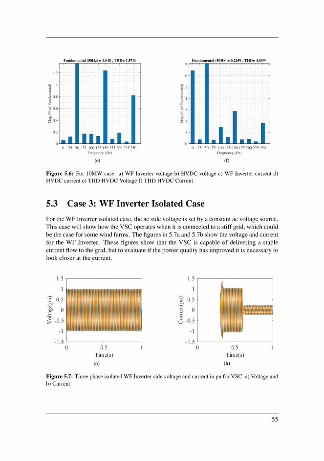
Fundamental (50Hz) = 1.048 , THD= 1.57%
0 25 50 75 100 125 150 175 200 225 250
Frequency (Hz)
0
0.2
0.4
0.6
0.8
1
1.2
Mag
(%
of
Fu
nd
amen
tal)
(e)
Fundamental (50Hz) = 0.2059 , THD= 4.80%
0 25 50 75 100 125 150 175 200 225 250
Frequency (Hz)
0
1
2
3
4
5
6
7
Mag
(%
of
Fu
nd
amen
tal)
(f)
Figure 5.6: For 10MW case. a) WF Inverter voltage b) HVDC voltage c) WF Inverter current d)HVDC current e) THD HVDC Voltage f) THD HVDC Current
5.3 Case 3: WF Inverter Isolated CaseFor the WF Inverter isolated case, the ac side voltage is set by a constant ac voltage source.This case will show how the VSC operates when it is connected to a stiff grid, which couldbe the case for some wind farms. The figures in 5.7a and 5.7b show the voltage and currentfor the WF Inverter. These figures show that the VSC is capable of delivering a stablecurrent flow to the grid, but to evaluate if the power quality has improved it is necessary tolook closer at the current.
(a) (b)
Figure 5.7: Three phase isolated WF Inverter side voltage and current in pu for VSC. a) Voltage andb) Current
55

5.3.1 Case 3: 50MW Case5.8 show the power flow from the WF Inverter to the grid. The result shows that thecurrent controller reaches steady state after approximately 0.06 seconds. The figure alsoshows that the active power output is uncompensated, which, according to [10], can beimproved by changing the PI parameters.
0.3 0.32 0.34 0.36 0.38 0.4 0.42 0.44 0.46 0.48 0.5
Time(s)
0
0.5
1
Pow
er(p
u)
P
P Ref.
Q
Q Ref.
Figure 5.8: Active and reactive output power for 50MW isolated case
5.9a and 5.9c show that the voltage from the ac voltage source is perfectly sinusoidalwithout any harmonics. 5.9b show the current from the delivered to the grid by the VSC.The figure shows that the current delivered is more than what is expected. The currentwaveform also has higher order harmonics, which can be studied closely in the HD figurein 5.9d.
(a) (b)
56

Fundamental (50Hz) = 1 , THD= 0.00%
0 25 50 75 100 125 150 175 200 225 250
Frequency (Hz)
0
0.2
0.4
0.6
0.8
1
Mag
(%
of
Fu
nd
amen
tal)
(c)
Fundamental (50Hz) = 1.047 , THD= 0.85%
0 25 50 75 100 125 150 175 200 225 250
Frequency (Hz)
0
0.05
0.1
0.15
0.2
0.25
0.3
0.35
Mag
(%
of
Fu
nd
amen
tal)
(d)
Figure 5.9: For isolated 50MW case. a) WF Inverter voltage b) WF Inverter current c) THD WFInverter Voltage d) THD WF Inverter Current
5.3.2 Case 3: 10MW CaseNow the reference current has been lowered, and the power output presented in 5.10changes immediately. The converter is able to deliver the required power to the grid with-out much steady state error.
0.6 0.65 0.7 0.75 0.8 0.85 0.9
Time(s)
0
0.5
1
Pow
er(p
u)
P
P Ref.
Q
Q Ref.
Figure 5.10: Active and reactive output power for 10MW isolated case
5.11a and 5.11c again show stable grid voltage. 5.11b show that the
57

(a) (b)
Fundamental (50Hz) = 1 , THD= 0.00%
0 25 50 75 100 125 150 175 200 225 250
Frequency (Hz)
0
0.2
0.4
0.6
0.8
1
Mag
(%
of
Fu
nd
amen
tal)
(c)
Fundamental (50Hz) = 0.2099 , THD= 3.68%
0 25 50 75 100 125 150 175 200 225 250
Frequency (Hz)
0
0.2
0.4
0.6
0.8
1M
ag (
% o
f F
un
dam
enta
l)
(d)
Figure 5.11: For isolated 10MW case. a) WF Inverter voltage b) WF Inverter current c) THD WFInverter Voltage d) THD WF Inverter Current
From the previous cases, it seems as if HD increase as the power output for the VSCdecreases. In 5.12, the fundamental current waveform for 50Hz is subtracted from the out-put current. This is done, so the only frequencies left is that of the HD. What is made clearduring this operation is that the amount of HD in the current waveform almost remainsconstant. And that the HD increase only because of the magnitude of the fundamentalfrequency decrease.
58

0.3 0.4 0.5 0.6 0.7 0.8 0.9 1
Time(s)
-0.02
0
0.02C
urr
ent(
pu)
Figure 5.12: WF Inverter current noise for 50MW and 10MW in phase a
5.4 Case 4: HVDC Isolated Case5.13a and 5.13b show the HVDC side voltage and current, respectively when the HVDCsystem operates as an isolated network. The MMC ac voltage controller decides the acvoltage. A changing load decides the ac current, and its waveform is dependent on the acvoltage. This section will show how the HVDC system operates independently from theWF Inverter.
(a) (b)
Figure 5.13: Three phase isolated HVDC side voltage and current in pu for MMC. a) Voltage andb) Current
5.4.1 Case 4: 50MW CaseFor the 50MW case power is drawn from the dc side to the ac side. Power flow is shownin 5.14 which illustrate that the power is flowing opposite to the other cases. The powerflow figure show that the power delivered to the load has lower overshoot than the othercases and stabilize after 0.05 seconds.
59
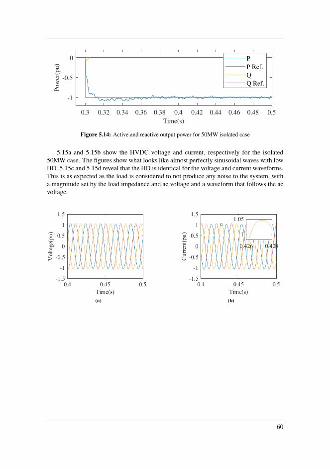
0.3 0.32 0.34 0.36 0.38 0.4 0.42 0.44 0.46 0.48 0.5
Time(s)
-1
-0.5
0P
ow
er(p
u)
P
P Ref.
Q
Q Ref.
Figure 5.14: Active and reactive output power for 50MW isolated case
5.15a and 5.15b show the HVDC voltage and current, respectively for the isolated50MW case. The figures show what looks like almost perfectly sinusoidal waves with lowHD. 5.15c and 5.15d reveal that the HD is identical for the voltage and current waveforms.This is as expected as the load is considered to not produce any noise to the system, witha magnitude set by the load impedance and ac voltage and a waveform that follows the acvoltage.
(a) (b)
60
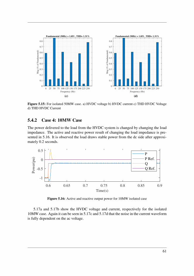
Fundamental (50Hz) = 1.051 , THD= 1.31%
0 25 50 75 100 125 150 175 200 225 250
Frequency (Hz)
0
0.1
0.2
0.3
0.4
0.5
0.6
0.7
0.8
Mag
(%
of
Fu
nd
amen
tal)
(c)
Fundamental (50Hz) = 1.051 , THD= 1.31%
0 25 50 75 100 125 150 175 200 225 250
Frequency (Hz)
0
0.1
0.2
0.3
0.4
0.5
0.6
0.7
0.8
Mag
(%
of
Fu
nd
amen
tal)
(d)
Figure 5.15: For isolated 50MW case. a) HVDC voltage b) HVDC current c) THD HVDC Voltaged) THD HVDC Current
5.4.2 Case 4: 10MW CaseThe power delivered to the load from the HVDC system is changed by changing the loadimpedance. The active and reactive power result of changing the load impedance is pre-sented in 5.16. It is observed the load draws stable power from the dc side after approxi-mately 0.2 seconds.
0.6 0.65 0.7 0.75 0.8 0.85 0.9
Time(s)
-1
-0.5
0
0.5
Pow
er(p
u)
P
P Ref.
Q
Q Ref.
Figure 5.16: Active and reactive output power for 10MW isolated case
5.17a and 5.17b show the HVDC voltage and current, respectively for the isolated10MW case. Again it can be seen in 5.17c and 5.17d that the noise in the current waveformis fully dependent on the ac voltage.
61

(a) (b)
Fundamental (50Hz) = 1.043 , THD= 2.74%
0 25 50 75 100 125 150 175 200 225 250
Frequency (Hz)
0
0.5
1
1.5
2
2.5
Mag
(%
of
Fu
nd
amen
tal)
(c)
Fundamental (50Hz) = 0.2092 , THD= 2.74%
0 25 50 75 100 125 150 175 200 225 250
Frequency (Hz)
0
0.5
1
1.5
2
2.5M
ag (
% o
f F
un
dam
enta
l)
(d)
Figure 5.17: For isolated 10MW case. a) HVDC voltage b) HVDC current c) THD HVDC Voltaged) THD HVDC Current
5.5 Wind Farm Inverter controller system analysis
5.5.1 Impact of Phase Locked LoopThe importance of a good PLL can not be overstressed. The point of the PLL is to obtainthe synchronous frequency, which is used through the whole VSC. 5.18 shows the systemresponse of the PLL for the interconnected system with circulating current control case(case 2). The PLL is turned on after 0.15 seconds. It can be seen that the PLL has anovershoot of more than 100%. As the simulation result shows that the PLL reaches asteady state after 0.05 seconds. When the current controller gets turned on, there is someuncontrollable ripple. But after 0.1 seconds are this ripple turned into a stable output with50±1 Hz, as can be seen in the additional square in 5.18. The PLL simulation responseshows that the PLL is able to reach within 2% of the reference value after 0.1 seconds. It islikely that some of these ripples occur due to the ac voltage ripple. The first order low pass
62

filter of the PLL is set to 500 Hz cut of frequency, which will reduce high order harmonicsin the system.
0.1 0.2 0.3 0.4 0.5 0.6 0.7 0.8 0.9 1
Time(s)
40
60
80
100
120
Fre
quen
cy (
Hz)
0.4 0.5 0.648
50
52
Figure 5.18: PLL time response for interconnected system
5.19 show the PLL time response for the isolated WF Inverter case (case 3). Whatseparates this PLL response from that in case 2 is that the PLL is connected to a stiff grid,that is not influenced by a change in power output. The show that the high overshoot in thestart up for the PLL is a result of the PLL tuning. After the PLL reaches steady-state it willproduce a stable output with no noticeable ripple. 5.19, therefore, proves that the PLL timeresponse noise is due to the PLL voltage reference noise and no noise produced by the PLLcontroller. A conclusion can be drawn that the PLL output will improve automatically ifthe grid voltage becomes stable.
0.1 0.2 0.3 0.4 0.5 0.6 0.7 0.8 0.9 1
Time(s)
40
60
80
100
120
Fre
quen
cy (
Hz)
0.4 0.5 0.648
50
52
Figure 5.19: PLL time response for isolated case
5.5.2 Impact of VSC Current ControllerTo makes sure that the VSC current controller is operating properly, the dq current signalin the control system, for case 2, is measured compared to its reference values. The currentcomponent is presented in per unit and is illustrated from the controller is turned on, untilone second has passed. The result is presented in 5.20. The figure shows that the controllercan generate a fast responding signal with a very small margin of error in steady state. Bychanging the reference value from first a large value to a smaller output, it is proven thatthis type of controller can control the power delivered WF Inverter.
63

0.3 0.4 0.5 0.6 0.7 0.8 0.9 1
Time(s)
-1
0
1C
urr
ent(
pu) D
D Ref.
Q
Q Ref.
Figure 5.20: DQ current in controller for interconnected system
5.21 show the dq current for the case 3. By comparing the dq current from cases 2and 3, it is observed that the improvement by having a stiff grid is minimal. The responseshows that the 50MW power steady state error is between ±1%. This steady state error isclose to what we can observe for the interconnected system in case 2.
0.3 0.4 0.5 0.6 0.7 0.8 0.9 1
Time(s)
-0.5
0
0.5
1
Curr
ent(
pu)
0.4 0.45 0.50.98
1
1.02
Figure 5.21: DQ current in controller for isolated case
5.6 HVDC Controller System Analysis
5.6.1 AC Voltage Proportional Resonant ControllerThe control system consists of two PR controllers, a circulating current controller and anac voltage controller. The circulating current controller takes in a three-phase sinusoidalsignal generated by a Sine Wave block in Simulink. The purpose of the sine waves areto set the reference for the circulating current in each leg. The reference signal is phaseshifted by 120 degrees with a frequency of twice the fundamental angular frequency. Up-per and lower leg current is measured in each of the three phases, then the currents aresummed and divided by two to calculate the phase circulating current. The calculatedcirculating current is compared to its reference value and the error is sent trough the cir-culating current PR controller. A feed forward gain is implemented to compensate for thevoltage drop across the parasitic resistance. The output of the PR controller and the feedforward gained are summed up to produce the voltage inducing the circulating current.
64
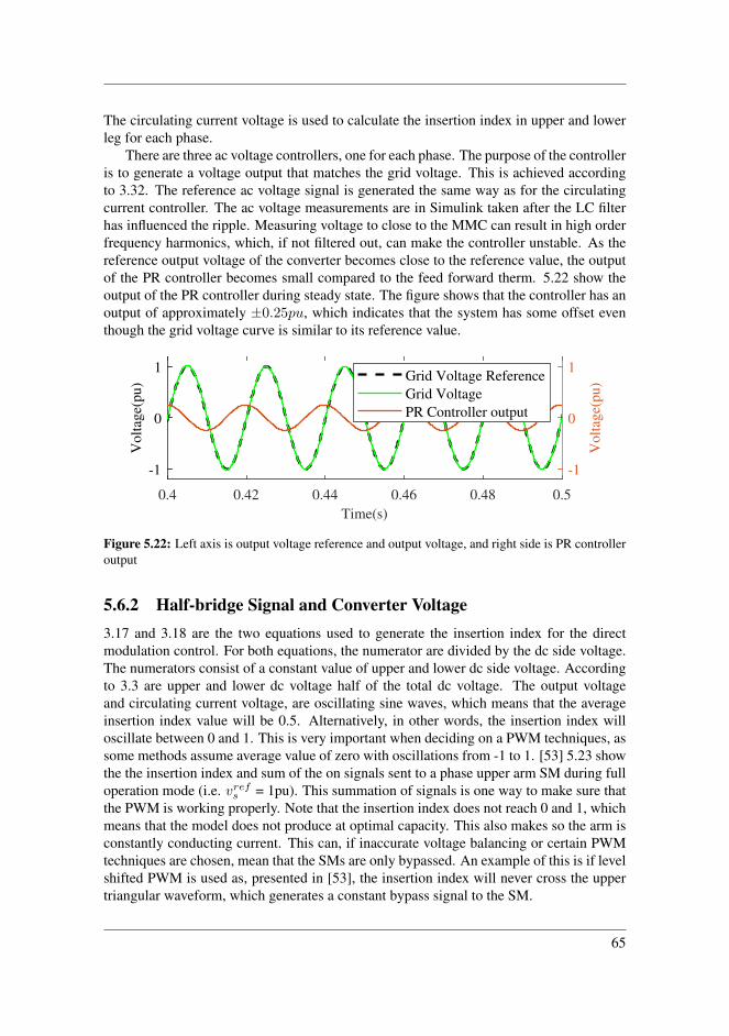
The circulating current voltage is used to calculate the insertion index in upper and lowerleg for each phase.
There are three ac voltage controllers, one for each phase. The purpose of the controlleris to generate a voltage output that matches the grid voltage. This is achieved accordingto 3.32. The reference ac voltage signal is generated the same way as for the circulatingcurrent controller. The ac voltage measurements are in Simulink taken after the LC filterhas influenced the ripple. Measuring voltage to close to the MMC can result in high orderfrequency harmonics, which, if not filtered out, can make the controller unstable. As thereference output voltage of the converter becomes close to the reference value, the outputof the PR controller becomes small compared to the feed forward therm. 5.22 show theoutput of the PR controller during steady state. The figure shows that the controller has anoutput of approximately ±0.25pu, which indicates that the system has some offset eventhough the grid voltage curve is similar to its reference value.
0.4 0.42 0.44 0.46 0.48 0.5
Time(s)
-1
0
1
Volt
age(
pu)
-1
0
1
Volt
age(
pu)
Grid Voltage Reference
Grid Voltage
PR Controller output
Figure 5.22: Left axis is output voltage reference and output voltage, and right side is PR controlleroutput
5.6.2 Half-bridge Signal and Converter Voltage3.17 and 3.18 are the two equations used to generate the insertion index for the directmodulation control. For both equations, the numerator are divided by the dc side voltage.The numerators consist of a constant value of upper and lower dc side voltage. Accordingto 3.3 are upper and lower dc voltage half of the total dc voltage. The output voltageand circulating current voltage, are oscillating sine waves, which means that the averageinsertion index value will be 0.5. Alternatively, in other words, the insertion index willoscillate between 0 and 1. This is very important when deciding on a PWM techniques, assome methods assume average value of zero with oscillations from -1 to 1. [53] 5.23 showthe the insertion index and sum of the on signals sent to a phase upper arm SM during fulloperation mode (i.e. vrefs = 1pu). This summation of signals is one way to make sure thatthe PWM is working properly. Note that the insertion index does not reach 0 and 1, whichmeans that the model does not produce at optimal capacity. This also makes so the arm isconstantly conducting current. This can, if inaccurate voltage balancing or certain PWMtechniques are chosen, mean that the SMs are only bypassed. An example of this is if levelshifted PWM is used as, presented in [53], the insertion index will never cross the uppertriangular waveform, which generates a constant bypass signal to the SM.
65

0.4 0.41 0.42 0.43 0.44 0.45 0.46 0.47 0.48 0.49 0.5
Time(s)
0
10
20S
wit
chin
g l
evel
0
0.5
1
Index
val
ueSum of Switching Signals
Insertion index
Figure 5.23: Sum of switching signals left hand side and insertion index right hand side in upperarm phase a.
Phase shifted triangular waveforms are for this 20 SM MMC phase shifted by 360/N =18°. The phase shifted triangular PWM is implemented for this model as it is a techniquethat divides the on-off time equally among all SM. 5.24 shows that the voltage acrossthe capacitors is approximately equal, which backs up the previous statement. 5.24 alsoshow that the voltage deviation across the capacitors is relatively constant due to the largecapacitance of each capacitor. The voltage sum of these capacitors is equal to the dc sidevoltage.
Figure 5.24: Voltage across each of the 20 capacitors in upper arm phase a.
5.6.3 Connecting Wind Farm Inverter and HVDC SystemTwo transformers are used to change the I-V ratio when transferring power from the WFInverter to the HVDC system. It is assumed that the distance from one transformer stationto the next is 10 kilometers. By increasing voltage and lowering current losses are expectedto drop exponentially according to Ohm’s law P = ZI2. The WF Inverter side transformerincreases the line-line voltage from 575V to 50kV. The HVDC side transformer increasesthe voltage from 50kV to 166kV.
66

Chapter 6Discussion and Conclusion
This chapter will present a discussion around the result, and a final conclusion on WFInverter-HVDC control strategy and harmonic distortion. The last section will present theauthors thought on what can be done to improve the project.
6.1 DiscussionThis thesis has presented a way of controlling an HVDC-WF Inverter conversion system,which is very appropriate today and in the future. The WF Inverter in the thesis is con-trolled with a current controller. It is deemed as unnecessary to us a dc voltage controlleras it is possible to replace it with a constant dc voltage source. However, this is not thecase if the voltage converter were to be implemented in a larger system where the powerwas delivered by turbines. So for an expanded system dc voltage control through the VSCis a viable option. Also, active and reactive power control is something that would beattractive to include, as that is presented frequently in literature. [54], [55] Due to timelimitations an outer control is not included in the VSC.
There are presented three techniques for controlling an MMC, compensated modu-lation, direct modulation without circulating current control, and direct modulation withcirculating current control. MMC with compensated modulation is, according to [38], verydifficult to implement in real life systems, and is therefore only used as an analytical exam-ple. 4.7 show that the MMC will be stable with compensated modulation control, but withvery small margins. The analytical result shows that an MMC can, in theory, be controlledwith a single control loop. Direct modulation without circulating current control is testedfor 50MW to see if the MMC can be controlled in direct modulation by a single controlloop. The controller is tested both analytical in the frequency domain and simulated inthe time domain. The main principle of direct modulation is that the circulating voltageis suppressed. The analytical response for direct modulation without circulating currentcontrol is presented in a bode plot in 4.8. In the bode plot, two resonant peaks for ap-proximately 20Hz and 70Hz are observed. These resonant peaks will mean that noise sentthrough the controller with these frequencies will heavily impact the controller. The phase
67
margin for this controller is also small and is located at the fundamental frequency. Thebode plot indicates that the direct modulation without circulating current control shouldnot be stable at 50MW. To find out if this is indeed true is the MMC simulated in Simulinkwithout circulating current control while connected to the WF Inverter. The time domainsimulation gives the same answers, that for 50MW the MMC will not be able to producea stable output. The time domain test also shows that the interconnected system withoutcirculating current control is not stable for 10MW either.
Analytical and simulation-based tests are performed to study rather or not a circulat-ing current controller can be implemented to improve stability the impedance model of anMMC controlled by direct modulation. The analytical result is presented in a bode plot in4.9. This bode plot also indicates that the impedance model of MMC with voltage controlhas a very low phase margin around the fundamental frequency, which could cause insta-bility. When the system is interconnected in 4.12 and 4.13 it is observed that the impedanceration for the MMC has changed. The interconnected system is considered stable for both50MW and 10MW if each system is stable independently, and if the impedance ration forthe MMC is smaller than the impedance ratio for the VSC at all frequencies. [38] Thelimitations for the analytical analysis in Chapter 4 is that the bode plot does not showstability margins of the interconnected system. To perform a stability margin analysis,the interconnected system could be tested according to the Nyquist criterion. A Nyquistplot would also reveal what HD distortion that could be expected from the converters. Toensure interconnected system stability, the poles of the converters should be mapped andcompared to the result obtained from the Nyquist plots.
The WF Inverter and HVDC system is tested in four time domain cases. The first case,interconnected WF Inverter-HVDC system without circulating current controller, showsthe importance of the internal dynamic control. The time domain results show that thesystem is unable to reach a steady state and produce a stable output. This reflects what isfound in the analytical model.
Cases 3 and 4 show how the converters can be expected to change when the poweroutput is reduced. 5.9d and 5.11d show that the HD is more influential for lower poweroutput. An interesting observation is found in 5.12, which proves that the magnitude ofthe noise in the VSC does not increase when the power output is reduced. Rather, it isonly the fundamental frequency that is lowered and therefore experiences a higher impactfrom the harmonics. For future work, it could be interesting to see the controller could beimproved substantially by implementing specific harmonic order filtering. Now we haveseen what can be expected from the VSC in a best-case scenario, case 4 show the samefor the MMC. HD in the MMC shows that the system harmonic is only influenced by thevoltage waveform. The 50MW case shows that there are some HD produced by the MMC.It is observed in 5.17c that the converter is especially affected by the 5th order harmonic(150Hz).
The second case shows that by implementing a current controller will the stabilitymargins improve significantly for both 50MW and 10MW. The analytical model indicatesthat the converters should produce a stable output. The time domain simulation shows thatthe system indeed produces a stable power output. FFT analysis of the current shows thatdc and third order harmonics are the main sources of harmonic distortion in the waveform.The dc HD magnitude is low for cases 3 and 4, and it can, therefore, be concluded that
68

by connecting the WF Inverter and HVDC dc harmonic increase substantially. When thepower output reference is changed from 50MW to 10MW the voltage HD becomes heavilyinfluenced by the 5th order harmonic originating from the MMC ac voltage controller. Bycomparing cases 2 and 4, it is observed that the THD in the voltage and current is actuallyreduced. Voltage and current HD reduction when connecting the converters could be aresult of filtering due to transformers and line impedance.
The PLL is a vital part of the WF Inverter, as it is the converter that synchronizes therotating reference frame to the HVDC side’s angular frequency. The stability of the PLL ispresented with a bode plot in 2.10. The plot shows that the PLL has good stability marginsfor frequencies in the operating range. That the PLL has good stability margins is provenin a time simulation when the controller is connected to a stiff gird without harmonics incase 3. The time response also shows that the PLL is fast to reach steady state and hasalmost no steady state error. This indicates that in order to improve the VSC output, thecurrent control has to be improved.
6.2 ConclusionIn this thesis, a VSC and an MMC are connected by transformers to represent a WF In-verter connected to an HVDC system. The VSC converter is controlled with a currentcontroller and PLL controller. The MMC is controlled by an ac voltage controller andcirculating current control. Tests performed in frequency and time domain show that aninterconnected WF Inverter-HVDC system can be controlled to produce the desired poweroutput. The test in the time domain shows that triangular phase shifted PWM techniquewill divide the on-off time equally among MMC SMs. The tests in the time domain showthat with high MMC SM capacitance can the voltage across each capacitor be consideredconstant. The test also uncovers that subsynchronous oscillation is of great concern inthis high power system. Literature referenced in this paper indicates that sources of theseoscillations are interaction between WF Inverter and HVDC controllers. Time domaintest indicates that some of the HD originates from the control technique and interactionbetween the controllers can both increase and decrease subsynchronous oscillations. It isshown that the THD can be reduced for an interconnected system due to passive compo-nent impedance. Test results in the frequency domain acknowledge that HD could occurdue to low stability margins.
6.3 Future WorkFuture work should first aim to analyze the interconnected system in the Nyquist diagram.The goal of this should be to find the stability margins, poles and zeros. It would beespecially interesting to see how the stability margins for the VSC current controller wouldchange, as this current controller is considered to be the most significant source of HDfor the system as a whole. By locating the poles and zeros it could be an alternativeto try to actively cancel out certain harmonic orders with a filter in the control system.By improving the control system instead of improving power quality with power gridimpedance and capacitance filters the total efficiency might be higher. During this work
69

the number of SMs has been changed. The number of SMs decide how many voltage levelsthe MMC is able to deliver for. Therefore, by increasing the number of SM HD shouldimprove. But, the VSC has been tested with stiff 50Hz grid without that lowering theTHD bellow 3% for 10MW. That means, even if one implemented a MMC with an infinitenumber of SMs this VSC should not be able to produce bellow 3% THD for 10MW, whichwould require high computing power for relatively high amount of distortion. For thisreason is increasing number of SM not considered a significant improvement alone. VSCouter loop control is frequently carried out in litterateur and is more realistic to include fora real control system. This is because it is, for most cases, more useful to control poweroutput or dc voltage across a converter than direct and quadrature current. If the goal is toanalyse a more complete and realistic converter system, VSC outer loop control should beconsidered.
70
Bibliography
[1] M. Amin and M. Molinas. Understanding the origin of oscillatory phenomena ob-served between wind farms and hvdc systems. IEEE Journal of Emerging and Se-lected Topics in Power Electronics, 5(1):378–392, Mar. 2017.
[2] T.Ackermann N.B.Negra, J.Todorovic. Loss evaluation of hvac and hvdc trans-mission solutions for large offshore wind farms. Electric Power System Research,76(11):916–927, Jul. 2006.
[3] Bp statistical review of world energy. volume 68. BP Statistical Review of WorldEnergy, 2019.
[4] G.Brindley L.Ramırez, D.Fraile. Offshore wind in europe, key trends and statistics2019. WindEurope, Feb. 2019.
[5] J.A.Suul T.Undeland C. Bajracharya, M.Molinas. Understanding of tuning tech-niques of converter controllers for vsc-hvdc, 06 2008.
[6] The Mathworks Inc. Three-phase v-i measurement, May 2020.
[7] A.L.Rogers J.F.Manwell, J.G.Mc.Gowan. Wind Energy Explained - Theory, Designand Application. JOHN WILEY & SONS, INC, 2009.
[8] J.B.Bassett M.Pham A.Arabali, M.Ghofrani. Optimizing in renewable energy sys-tems. Butterworth Heinemann, 2017.
[9] J.R.Bumby J.Machowski, J.W.Bialek. Power System Dynamics Stability and Control.WILEY, 2012.
[10] S.N.Nise. Control System Engineering. WILEY, 2011.
[11] M.Belkhayat. Stability criteria for ac power systems with regulated loads, 1997.
[12] A. G. J. MacFarlane. Complex variable methods for linear multivariable feedbacksystems, 1980.
[13] S.Varma. Internet Congestion Control. Morgan Kaufmann, October 2015.
71

[14] Y. A. Wang, J. T. Boys, and A. P. Hu. Modelling and control of an inverter for vsc-hvdc transmission system with passive load. In 2008 Joint International Conferenceon Power System Technology and IEEE Power India Conference, pages 1–6, Oct.2008.
[15] T.Ackermann N.B.Negra, J.Todorovic. Loss evaluation of hvac and hvdc trans-mission solutions for large offshore wind farms. Electric Power System Research,76(11):916–927, Jul. 2006.
[16] D. Chen, Y. Hu, X. Wang, F. Shen, and Y. Teng. Control strategy of vsc-hvdc invertersupplying power to the isolated grid with induction motor. In 2017 China Interna-tional Electrical and Energy Conference (CIEEC), pages 497–503, Oct. 2017.
[17] M. Spence, A. Plumpton, C. Rout, A. Millington, and R. Keyse. Design and charac-terisation of optimised protective thyristors for vsc systems. In PCIM Europe 2016;International Exhibition and Conference for Power Electronics, Intelligent Motion,Renewable Energy and Energy Management, pages 1–8, May. 2016.
[18] S. Jang, H. Ryoo, G. Goussev, and G. H. Rim. Comparative study of mosfet and igbtfor high repetitive pulsed power modulators. IEEE Transactions on Plasma Science,40(10):2561–2568, Oct. 2012.
[19] Dan Godhei. Prerequisite study for understanding the subsynchronous oscillation inoffshore wind farm connected via hvdc. Project report in TTM4502, Department ofInformation Security and Communication Technology, NTNU – Norwegian Univer-sity of Science and Technology, Dec. 2019.
[20] Navid Zargari Bin Wu, Yongqiang Lang and Samir Kouro. Power Conversion andControl Of Wind Energy Systems. JOHN WILEY & SONS, INC, 2011.
[21] David Lay. Linear Algebra and its Application, volume 4. PEARSON, 2014.
[22] X. Du, S. Gu, G. Wang, P. Sun, H. Tai, and Y. Ji. A simple current control methodfor three-phase vsc in dsrf under unbalanced grid condition. In IECON 2017 - 43rdAnnual Conference of the IEEE Industrial Electronics Society, pages 6841–6846,Oct 2017.
[23] J. Svensson and R. Ottersten. Shunt active filtering of vector current-controlled vscat a moderate switching frequency. IEEE Transactions on Industry Applications,35(5):1083–1090, Sep. 1999.
[24] Guibin Zhang and Zheng Xu. Steady-state model for vsc based hvdc and its con-troller design. In 2001 IEEE Power Engineering Society Winter Meeting. ConferenceProceedings (Cat. No.01CH37194), volume 3, pages 1085–1090 vol.3, 2001.
[25] A. Dekka, B. Wu, R. L. Fuentes, M. Perez, and N. R. Zargari. Evolution of topolo-gies, modeling, control schemes, and applications of modular multilevel converters.IEEE Journal of Emerging and Selected Topics in Power Electronics, 5(4):1631–1656, Dec 2017.
72

[26] C.Bajracharya. Control of vsc-hvdc for wind power. Master’s thesis, NTNU, 2008.
[27] E.V.Appleton. Automatic synchronization of triode oscillators, 1923.
[28] Guan-Chyun Hsieh and J. C. Hung. Phase-locked loop techniques. a survey. IEEETransactions on Industrial Electronics, 43(6):609–615, 1996.
[29] A. Singhal, C. Madhu, and V. Kumar. Designs of all digital phase locked loop. In2014 Recent Advances in Engineering and Computational Sciences (RAECS), pages1–5, 2014.
[30] V. Kaura and V. Blasko. Operation of a phase locked loop system under distortedutility conditions. IEEE Transactions on Industry Applications, 33(1):58–63, 1997.
[31] D. Haribabu, A. Vangari, and J. N. Sakamuri. Dynamics of voltage source converterin a grid connected solar photovoltaic system. In 2015 International Conference onIndustrial Instrumentation and Control (ICIC), pages 360–365, 2015.
[32] J. M. E. Vicente J. A. Cortez P. R. Laurentino A. J. J. Rezek, C. A. D. Coelho. Themodulus optimum (mo) method applied to voltage regulation systems: Modeling,tuning and implementation. June 2001,.
[33] K. Ogata. Modern Control Engineering. Pearson, 2010.
[34] H. Zhang, X. Wang, L. Harnefors, H. Gong, J. Hasler, and H. Nee. Siso transferfunctions for stability analysis of grid-connected voltage-source converters. IEEETransactions on Industry Applications, 55(3):2931–2941, 2019.
[35] M. A. Perez, S. Bernet, J. Rodriguez, S. Kouro, and R. Lizana. Circuit topologies,modeling, control schemes, and applications of modular multilevel converters. IEEETransactions on Power Electronics, 30(1):4–17, Jan 2015.
[36] M. A. Perez and J. Rodrıguez. Generalized modeling and simulation of a modularmultilevel converter. In 2011 IEEE International Symposium on Industrial Electron-ics, pages 1863–1868, June 2011.
[37] M. Malinowski, K. Gopakumar, J. Rodriguez, and M. A. Perez. A survey on cascadedmultilevel inverters. IEEE Transactions on Industrial Electronics, 57(7):2197–2206,July 2010.
[38] J. Lyu, X. Cai, and M. Molinas. Frequency domain stability analysis of mmc-basedhvdc for wind farm integration. IEEE Journal of Emerging and Selected Topics inPower Electronics, 4(1):141–151, March 2016.
[39] M. Hiller, D. Krug, R. Sommer, and S. Rohner. A new highly modular mediumvoltage converter topology for industrial drive applications. In 2009 13th EuropeanConference on Power Electronics and Applications, pages 1–10, Sep. 2009.
[40] Lennart Harnefors, Antonios Antonopoulos, Staffan Norrga, Lennart Aangquist, andH.-P Nee. Dynamic analysis of modular multilevel converters. Industrial Electronics,IEEE Transactions on, 60:2526–2537, 07 2013.
73

[41] G. J. M. de Sousa and M. L. Heldwein. Three-phase unidirectional modular multi-level converter. In 2013 15th European Conference on Power Electronics and Appli-cations (EPE), pages 1–10, Sep. 2013.
[42] E. Solas, G. Abad, J. A. Barrena, S. Aurtenetxea, A. Carcar, and L. Zajac. Modularmultilevel converter with different submodule concepts—part i: Capacitor voltagebalancing method. IEEE Transactions on Industrial Electronics, 60(10):4525–4535,Oct 2013.
[43] L. Danqing, W. Guangzhu, O. Zhujian, and L. Jiaxing. A control strategy of mmcbattery energy storage system based on arm current control. In 2018 InternationalPower Electronics Conference (IPEC-Niigata 2018 -ECCE Asia), pages 1376–1380,2018.
[44] A. Haider, N. Ahmed, L. Angquist, and H. Nee. Open-loop approach for control ofmulti-terminal dc systems based on modular multilevel converters. In Proceedings ofthe 2011 14th European Conference on Power Electronics and Applications, pages1–9, 2011.
[45] A. Lachichi and L. Harnefors. Comparative analysis of control strategies for mod-ular multilevel converters. In 2011 IEEE Ninth International Conference on PowerElectronics and Drive Systems, pages 538–542, 2011.
[46] K. Li and C. Zhao. New technologies of modular multilevel converter for vsc-hvdcapplication. In 2010 Asia-Pacific Power and Energy Engineering Conference, pages1–4, 2010.
[47] P.Kundur. Power system stability and control. McGraw-Hill, Inc., 1994.
[48] M. Amin, J. A. Suul, S. D’Arco, E. Tedeschi, and M. Molinas. Impact of state-space modelling fidelity on the small-signal dynamics of vsc-hvdc systems. In 11thIET International Conference on AC and DC Power Transmission, pages 1–11, Feb2015.
[49] H. Liu and J. Sun. Voltage stability and control of offshore wind farms with accollection and hvdc transmission. IEEE Journal of Emerging and Selected Topics inPower Electronics, 2(4):1181–1189, 2014.
[50] M. Cespedes and J. Sun. Impedance modeling and analysis of grid-connectedvoltage-source converters. IEEE Transactions on Power Electronics, 29(3):1254–1261, 2014.
[51] S. Shah and L. Parsa. Sequence domain transfer matrix model of three-phase volt-age source converters. In 2016 IEEE Power and Energy Society General Meeting(PESGM), pages 1–5, 2016.
[52] J. Lyu, M. Molinas, and X. Cai. Stabilization control methods for enhancing the sta-bility of wind farm integration via an mmc-based hvdc system. In 2017 11th IEEEInternational Conference on Compatibility, Power Electronics and Power Engineer-ing (CPE-POWERENG), pages 324–329, 2017.
74

[53] G. S. Konstantinou, M. Ciobotaru, and V. G. Agelidis. Analysis of multi-carrier pwmmethods for back-to-back hvdc systems based on modular multilevel converters. InIECON 2011 - 37th Annual Conference of the IEEE Industrial Electronics Society,pages 4391–4396, 2011.
[54] C. Zhao and C. Guo. Complete-independent control strategy of active and reactivepower for vsc based hvdc system. In 2009 IEEE Power Energy Society GeneralMeeting, pages 1–6, 2009.
[55] P. Chodura, M. Gibescu, W. L. Kling, and R. A. A. de Graaff. Investigation of theimpact of embedded vsc-hvdc active and reactive power control on power systemstability. In 2015 IEEE Eindhoven PowerTech, pages 1–6, 2015.
75

Appendix
How the cross coupling term is derived in system equation This extraction is pre-sented in [19] by D.Godhei
To transfer abc frame to dq frame, inverse Parks(P−1) can be factorized from the abc-frame accordingly
Xabc = P−1Xdq0 (6.1)
The VSC system equation is as follows
V abc = RIabc + Ld
dtIabc + V abcconv (6.2)
Start off by do the transformation according to equation 6.1
P−1V dq0 = P−1RIdq0 + P−1Ld
dtIdq0 + P−1V dq0conv (6.3)
Multiply the previous equation by a regular park matrix (P)
PP−1V dq0 = PP−1RIdq0 + PLdP−1
dtIdq0 + PP−1L
d
dtIdq0 + PP−1V dq0conv (6.4)
The inductor part of the equation gives the following equation, due to product deriva-tion rule
PP−1Ld
dtIdq0 = PL
dP−1
dtIdq0 + PP−1L
d
dtIdq0 (6.5)
For one part of the equation will the multiplied parks cancel the inverse Parks
PP−1Ld
dtIdq0 = PL
dP−1
dtIdq0 + L
d
dtIdq0 (6.6)
The second part of equation 6.5 yields
PLdP−1
dtIdq0 = L
0 −ω 0ω 0 00 0 0
IdIqI0
(6.7)
On matrix form equation 6.5 then becomes
PP−1Ld
dt
IdIqI0
= L
−ωIqωId
0
+ Ld
dt
IdIqI0
(6.8)
When the previous equation is put into 6.4 and i0 terms are neglected it gives the finalequation [
V d
V q
]=
[Id
Iq
]+ L
d
dt
[Id
Iq
]+ L
−ωIqωId
0
+
[V dconvV qconv
](6.9)
i

NTN
UN
orw
egia
n U
nive
rsity
of S
cien
ce a
nd T
echn
olog
yFa
culty
of I
nfor
mat
ion
Tech
nolo
gy a
nd E
lect
rical
Engi
neer
ing
Dep
artm
ent o
f Ele
ctric
Pow
er E
ngin
eerin
g
Mas
ter’s
thes
is
Dan Godhei
Understanding the SubsynchronousOscillation Occurring in Offshore WindFarm Converters Connected via HVDC
Master’s thesis in Electrical Power Engineering
Supervisor: Mohammad Amin
June 2020