Unconventional digital computing approach: memristive nanodevice platform
8
reprint
Transcript of Unconventional digital computing approach: memristive nanodevice platform

reprint

© 201 WILEY-VCH Verlag GmbH & Co. KGaA, Weinheim
p s scurrent topics in solid state physics
c
statu
s
soli
di
www.pss-c.comph
ysi
ca
Phys. Status Solidi C 12, No. 1–2, 222–228 (201 ) / DOI 10.1002/pssc.201400 69
Unconventional digital computingapproach: memristive nanodeviceplatform
Mahyar Shahsavari*,1, M. Faisal Nadeem 2, S. Arash Ostadzadeh2, Philippe Devienne1, and Pierre Boulet1
1 University of Lille, LIFL, CNRS, UMR 8022, 59650 Villeneuve d’Ascq, France2 Department of Software & Computer Technology, Delft University of Technology, Netherlands
Received 8 May 2014, accepted 22 May 2014Published online
Keywords material implication, nanoscale crossbar, memristor nanodevice, digital computing
∗ Corresponding author: e-mail [email protected], Phone: +33 (0)3 20 33 59 51
Memristor is a two-terminal nanodevice that has recentlyattracted the attention of many researchers. Its simplestructure, non-volatility behavior, high-density integra-tion, and low-power consumption make the memristor apromising candidate to act as a switch in digital gatesfor future high-performance and low-power nanocom-puting applications. In this paper, we model the behaviorof memristor by using Verilog-A. To investigate its char-acteristics in a circuit, we use the HSPICE simulator.
Furthermore, a library of digital gates are provided byusing two approaches to make digital gates: the first oneis based on material implication (IMP) and the secondone is based on crossbar arrays. Finally, we perform acomparison and evaluation between the two methods.
1 Introduction Memristor has recently drawn wideattention of scientists and researchers due to non-volatility,better alignment, and excellent scalability properties [1].Memristor remembers its last state after the last powerplugging and has simple physical structure, high-densityintegration, and low-power consumption. These featuresmake memristor an attractive candidate for building thenext generation non-volatile memories [2]. From high-performance computing point of view, memristor has po-tential capability to conquer the memory bottleneck issue,by utilizing computational unit next to the memory [3].
The logic computing applications of memristor havebeen investigated by several researchers [4–12]. For in-stance, Borghetti et al. [11] used material implication(IMP) logic operation to carry out logic computation byusing memristors. In IMP approach, A IMPB (A→B) op-eration means ‘if A, then B’ and can be read as A impliesB. IMP together with a FALSE gate are able to form afunctionally complete set (any boolean function can be ex-pressed). By applying memristor as a digital switch, a high
memristance (memristor resistance) is considered as logic‘0’ and a low memristance is considered as logic ‘1’. An-other approach to make gates by a two-terminal device asa switch is the programmable crossbar architecture [8,12].The crossbar nanowire array architecture can be used tocompute logic functions by using memristor as a switchbetween two nanowires [4].
The main contributions of this paper are:
–To demonstrate that memristor has appropriate char-acteristics to be applied as a switch in both IMP andcrossbar array methods, we proposed our electricalmodel of the memristor behavior. Modeling is per-formed by using Verilog-A Hardware Description Lan-guage (HDL).
–Material implication (IMP) logic function and crossbararray architecture are investigated as the two novel andmost promising methods for creating logical functionsby memristors.
© 201 WILEY-VCH Verlag GmbH & Co. KGaA, Weinheim
18 November 2014

–The crossbar array architecture approach is developedin the term of using only memristors as switches be-tween nanowires.
The reminder of the paper is organized as follows. Theelectrical model is presented in Section 2. Then, we applyour Verilog-A model in the HSPICE circuit simulator toobserve memristor behavior in the circuits. In Section 3,the stateful logic operations via IMP is described. In Sec-tion 4, the crossbar array architecture is presented by usingmemristor as a junction switch. Evaluations of the two ap-proaches are investigated in Section 5. Section 6 concludesthe paper.
2 Electrical model When an electric field is appliedto the terminals of memristor, the shifting in boundary be-tween its doped and undoped regions leads to variable totalresistance of the device. In Fig. 1a, the electrical behaviorof memristor can be modeled as follows [13]:
v(t) = Rmemi(t) (1)
Rmem = RONw(t)
D+ROFF (1− w(t)
D) (2)
where w(t) is the width of the doped region,D is the over-all thickness of the TiO2 bi-layer, RON is the resistancewhen the active region is completely doped (w = D) andROFF is the resistance, when the TiO2 bi-layer is mostlyundoped (w→ 0).
dw(t)
dt= μv
RONDi(t) (3)
which yields the following formula for w(t):
w(t) = μvRONDq(t) (4)
where μv is the average dopant mobility. By inserting Eq.(4) into Eq. (2) and then into Eq. (1) we obtain the mem-ristance of device, which for RON � ROFF simplifiesto
M(q) = ROFF (1− μvROND2
q(t)) (5)
Equation (5) shows the dopant drift mobility μv and semi-conductor film thicknesses D values, which are two fac-tors with crucial contributions to the memristance magni-tude. Subsequently, we can write Kirchoff’s voltage lawfor memristor given by
v(t) =M(q)i(t) (6)
By using Verilog-A HDL, we simulate the behavior ofmemristor, based on its behavioral equations. To investi-gate the characteristics of memristor in electrical circuits,
Figure 1 Memristor schematic and behavior: (a) the memristorstructure, the difference in applied voltage changes doped and un-doped regions, (b) current versus voltage diagram, which demon-strates hysteresis characteristic of memristor, in the simulationwe apply the sinusoidal input wave with an amplitude of 1.5v,different frequencies, RON = 100Ω,ROFF = 15kΩ,D =10nm, μv = 10−10cm2s−1V −1.
the Verilog-A model of memristor behavior must be ap-plied as a circuit element in the HSPICE netlist. In theHSPICE circuit, we apply a sinusoidal source to observethe memristor reaction in a simple circuit consisting ofmemristor and sinusoidal source. Figure 1b depicts i − vplot of memristor terminals that we measured in our simu-lation. This i− v plot, which is the most significant featureof memristor [14], is namely called “pinched hysteresisloop”. The i−v characteristic demonstrates that memristorcan “remember” the last electric charge flowing across it bychanging its memristance. Therefore, we can use memris-tor as a latch to save data and also as a switch for comput-ing. Moreover, in Fig. 1b, it is depicted that the pinchedhysteresis loop is shrunk by increasing frequency. In fact,when the frequency increases toward infinity, memristorbehaves similar to a linear resistor.
3 Stateful implication logic One of the basic poten-tial applications of memristors is to utilize them in build-ing blocks of logic gates. Therefore, by applying a dig-ital pulse voltage to the memristor terminal, we have aswitch with ON or OFF state. Unlike conventional CMOS,in memristor-based gates, data will be stored as a resis-tance rather than a voltage. In this case, the latches are non-volatile. Thus,RON displays logic ‘1’ which means closedswitch and ROFF displays ‘0’ for presenting open switch.In contrast to the three-terminal CMOS-based transistor asa switch, in a two-terminal switch, there is no terminal tocontrol ON or OFF states of the switch. Consequently, in-stead of conventional boolean logic, we should find othersubstitutes to create a gate and perform computing.
Phys. Status Solidi C (201 )
www.pss-c.com © 201 WILEY-VCH Verlag GmbH & Co. KGaA, Weinheim
Contributed
Article

��
��������
� ��
�
��
�
�
�
�
�
�� �
�
�
�
� ��������� �
Figure 2 Memristor-based IMP: (a) circuit schematic, (b) IMPtruth table.
IMP (Fig. 2a) is a way to use one memristor to controlthe other one. IMP is recognized as a promising methodfor making gates by memristors [9–11]. In IMP structure,memristors have different roles in different stages of thecomputing process: input, output, computational logic ele-ment, and a latch depending upon which write, read, com-puting and storing processes are taking place, respectively.
To figure out how IMP operates, imagine A as a ques-tion and B as the answer to that question. If the questionis wrong, any answer (wrong or correct) makes a true out-put (logic 1), as depicted in Fig. 2b. The only case for thefalse (logic 0) output would be a wrong answer to a correctquestion. So the implication logic is equivalent to func-tion (¬A)∨B. Figure 2a shows the basic circuit of mem-ristors A and B to perform implication logic, which areformed by the vertical nanowire crossing over the hori-zontal nanowire connected to a load resistor RG. Afterthe operation of material implications, the result is storedas the state of switch B (B′) while A is left unchanged.To switch between logic 1 to logic 0 (and vice versa),we need a tri-state voltage driver with a high impedanceoutput state when it is undriven. Vset is a negative volt-age which should be applied to its corresponding tri-statedriver. Vset can switch memristor to conductive state withlow resistance RON . Similarly, the positive voltage Vclearis required to change the memristive switch state to low-conductance (high-resistance) state ROFF . It is importantto mention that the magnitude of Vset and Vclear must belarger than device threshold voltage for switching ON andOFF. In order to remain in a specific state (line 3 in truthtable 2b), the Vcond is applied as a negative voltage with amagnitude smaller than Vset. Consequently, tri-state drive—since is not in high-impedance state— is pulsed by oneof the Vset, Vclear or Vcond. By applying Vcond and Vsetto A and B simultaneously, the memristive IMP operatesproperly. Although the conditional voltage (Vcond) is notnecessary, except for the case AB=‘10’ (third line in thetruth table Fig. 2b), it is possible to either apply Vcondor use high-impedance (HZ) for all other cases. If Vsetis applied to B alone, it would be unconditionally ‘logic1’, nevertheless applying Vcond by itself to A does not
change its state. On the other hand, if both voltages areapplied together, the present state of switch A determinesthe next state of switch B. If A=‘0’, it means memristorA is in high resistance state (ROFF ). Therefore, there isa small voltage drop across RG. In this case, B will beset and A is left unchanged. Alternatively, if present stateof A=‘1’, switch A is in low resistance state and Vconddrops across RG, so both A and B remain unchanged. Itshould be noted that the RG value must be chosen suchthat RON<RG<ROFF , where RON and ROFF are resis-tance states of ‘ON’ and ‘OFF’ switches, respectively.
��
����� �
�
�
��
�
�
�
�
�
�
�
���
�
�
�
��
�
�
�
�
������ ��� ����
�
�
�
�
�
�
�
�
��
�
��
�
�
�� �
�
��
�
�
�
�
�
��
�
���
�
���������������
�
����������������
�� �� ��
� �
� ����
���
���
� �!"
� �!"
#����$�!
�%�
��&'���
��&'���
()%($���&*��"�! �
() ()
()
()
Figure 3 NAND configuration with IMP: (a) circuit schematic,(b) required voltages for controlling the process, (c) sequentialtruth table to obtain NAND.
In boolean logic algebra, a set of logic operations iscalled functionally complete if all other logic functionscan be constructed from combining the members of thisset. The single-element sets NAND (AND, NOT) and NOR(OR, NOT) are functionally complete operations. In addi-tion, it has been demonstrated that all boolean expressionscan then be written in one of the standard normal formsusing only a (IMP) operation and a false (Inverse) opera-tion [10,11]. In fact, to show that the memristive implica-tion logic is a functionally complete operation; the easiestway is to synthesize the NAND function with it.
A circuit with three memristors A, B, and C is illus-trated schematically in Fig. 3a. Assume two implicationoperations being performed subsequently, first A IMP Cand then B IMP C. Hence A and B are inputs and C isoutput. The final output result is represented with variableC′′ in Fig. 3c. Firstly, Vclear should be applied to switchC to create the false operation (C ′ = (C IMP 0)). By ap-plying Vcond and Vset pulses to A and C respectively, thesecond step would be performed. Finally, C ′′ = (B IMPC) is yielded by applying Vcond to VB and Vset to VC (seeFig. 3b and Fig. 3c). In other words, the resulting state ofswitch C can be written as:
C = B IMP (A IMP C) = ¬B ∨ ((¬A) ∨ C)
© 201 WILEY-VCH Verlag GmbH & Co. KGaA, Weinheim www.pss-c.com
ph
ysic
ap s sstat
us
solid
i c
if C = 0 initially then
C = ¬B ∨ ((¬A) ∨ 0) = (¬B) ∨ (¬A)= ¬(A ∧B)
which is a NAND operation. Similarly, we can produceequal IMP structure of other logic operations. In Table 1different boolean logic gates are listed. Obviously, we candemonstrate all logic relations in Table 1, not only by ap-plying boolean logic rules but also by checking the truthtables of both sides of relations.
Table 1 Different logic operations made by IMP operations andthe number of required memristors
Logic Operation Equal IMP functions #DeviceNOT A A IMP 0 3A AND B {A IMP (B IMP 0)} IMP 0 4A NAND B A IMP (B IMP 0) 3A OR B (A IMP 0) IMP B 3A NOR B {(A IMP 0) IMP B} IMP 0 4A XOR B (A IMPB) IMP {(B IMPA) IMP 0} 3
4 Crossbar architecture Programmable crossbar ar-chitectures have been proposed as a promising approachfor future computing architectures because of their sim-plicity of fabrication and high density, which support de-fect tolerance [12,15]. In such architectures, assume thateach junction within the crossbar can be utterly config-ured to activate an electronic device, such as a resistor,diode, transistor, or recently memristor. In fact, attractivefeatures of memristor, such as simple physical structure,non-volatility, high-density, and unlimited endurance makethis nano-device one of the best choices to play a switchrole in the crossbar junctions. The memristive-based cross-bar opens new windows to explore advanced computer ar-chitecture, different from the classical Von Neumann ar-chitecture [15]. On the other hand, in crossbar architec-ture, memory and logic operators are not separated. Thememory can perform logic implementations on the samedevices which store data. This is because during the opera-tion process, control signals determine which elements actas logic gates and which ones act as memory cells.
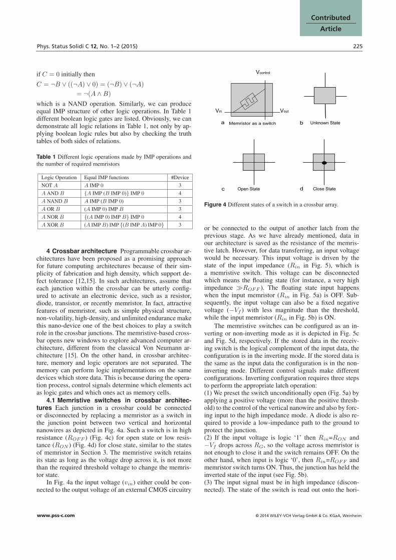
4.1 Memristive switches in crossbar architec-tures Each junction in a crossbar could be connectedor disconnected by replacing a memristor as a switch inthe junction point between two vertical and horizontalnanowires as depicted in Fig. 4a. Such a switch is in highresistance (ROFF ) (Fig. 4c) for open state or low resis-tance (RON ) (Fig. 4d) for close state, similar to the statesof memristor in Section 3. The memristive switch retainsits state as long as the voltage drop across it, is not morethan the required threshold voltage to change the memris-tor state.
In Fig. 4a the input voltage (vin) either could be con-nected to the output voltage of an external CMOS circuitry
��������
�� ���
����� �������
���������� �����������
��������������� ����� �
� �
Figure 4 Different states of a switch in a crossbar array.
or be connected to the output of another latch from theprevious stage. As we have already mentioned, data inour architecture is saved as the resistance of the memris-tive latch. However, for data transferring, an input voltagewould be necessary. This input voltage is driven by thestate of the input impedance (Rin in Fig. 5), which isa memristive switch. This voltage can be disconnectedwhich means the floating state (for instance, a very highimpedance �ROFF ). The floating state input happenswhen the input memristor (Rin in Fig. 5a) is OFF. Sub-sequently, the input voltage can also be a fixed negativevoltage (−Vf ) with less magnitude than the threshold,while the input memristor (Rin in Fig. 5b) is ON.
The memristive switches can be configured as an in-verting or non-inverting mode as it is depicted in Fig. 5cand Fig. 5d, respectively. If the stored data in the receiv-ing switch is the logical complement of the input data, theconfiguration is in the inverting mode. If the stored data isthe same as the input data the configuration is in the non-inverting mode. Different control signals make differentconfigurations. Inverting configuration requires three stepsto perform the appropriate latch operation:(1) We preset the switch unconditionally open (Fig. 5a) byapplying a positive voltage (more than the positive thresh-old) to the control of the vertical nanowire and also by forc-ing input to the high impedance mode. A diode is also re-quired to provide a low-impedance path to the ground toprotect the junction.(2) If the input voltage is logic ‘1’ then Rin=RON and−Vf drops across RG, so the voltage across memristor isnot enough to close it and the switch remains OFF. On theother hand, when input is logic ‘0’, then Rin=ROFF andmemristor switch turns ON. Thus, the junction has held theinverted state of the input (see Fig. 5b).(3) The input signal must be in high impedance (discon-nected). The state of the switch is read out onto the hori-
Phys. Status Solidi C (201 )
www.pss-c.com © 201 WILEY-VCH Verlag GmbH & Co. KGaA, Weinheim
Contributed
Article

�����������
��������� ����
������������������� ��� ���������������������
���������������������������� ������������������������������
�
��
���
��
���
��
��
������������
� ��������!���" �����������!���" ��������!���" �����������!���"
Figure 5 Different states and configurations of the memristiveswitches in a crossbar array.
zontal nanowire. This is accomplished by driving the ver-tical nanowire with a small voltage whose magnitude isless than the threshold control voltage (can not change theswitch state). We call this voltage vR (Read voltage).For non-inverting configuration, as depicted in Fig. 5d, thepull-down resistor RG is not required when writing thestate of the driving switch to the receiving one. The stepsfor appropriate latch operation are the same as the ‘invert-ing configuration’ except grounding the vertical nanowireof the driving switch rather applying a negative voltage inconditionally close step. In this case, by applying negativevoltage to the vertical control line, the receiving switch willbe close if the driving switch is close (low-impedance pathto the ground) and the receiving switch remains open if thedriving switch is open. Thus, the state of the first switch isreplicated in the second switch.
4.2 Configurable crossbar rray logic gates Inthis section, we demonstrate how to make a gate by usingthe crossbar approach. We start using crossbar to make a 3-input AND gates. Figure 6a shows a crossbar array whichconsisting of 8 memristors. We need three inputs A, B, andC, each of which is assumed to be impedance encoded. Ba-sically, various voltages are applied to vertical nanowires tocontrol the memristive switches. The inputs are connectedto the horizontal wires as represented in Fig. 6a. The cross-bar array functions as an AND gate by applying the fol-lowing sequences.
1.All junctions are unconditionally opened by applyinga positive voltage higher than the threshold voltage tothe vin, vand, vout control vertical lines.
2.By driving vin with a negative voltage, the input data(A, B, C) are latched in the input switches. The inputsare in the inverting configuration thus ‘0’ and ‘1’ in-puts, close and open the switches, respectively (Fig.6b).
3.In this step, by driving the vin and K input to theground, as well as vand to the negative voltage (Fig.6c) the input data are latched to the wired-AND junc-tions.
4.In this step, the vertical control lines of the input andoutput (vin, vout) are activated by a negative voltageto capture the result to the output memristor (S8). Thevoltage in point X in Fig. 6d can determine outputswitch state. If there is at least one closed input (alsowired-AND) in the route from vin to the X point, thenegative voltage efficacy causes the output switch tostay open. The reason is that the potential differenceacross the output switch is not enough to close it. Itis noteworthy to mention that the voltage at X point isyielded from the voltages dividing between the resis-tance of switches in the route and S7 that connected tothe ground in the last horizontal nanowire line.
5.By driving a positive voltage to vand, all junctions inthis column will be opened (Fig. 6e).
6.The AND of the three inputs is stored in the outputswitch and is ready to be read out.
If the output switch is at inverse mode (inverting configu-ration), the crossbar array becomes a 3-input NAND gate.Moreover, the crossbar array can also become a 3-inputNOR gate, if RG’s are removed while input data are ap-plied to the circuit (Non-inverting configuration). By in-verting the last output with the recent situation of the in-puts, the crossbar architecture becomes a 3-input OR gate.Consequently, all logic gates are created except XOR andXNOR, which require a little different structures. First, wecreate an exclusive-NOR gate, subsequently, by invertingthe output, XOR is obtained. To implement XNOR, twominterms should be OR’ed together. The crossbar arrayoperation for creating XNOR is similar to AND crossbararray in Fig. 6. However, three additional steps are re-quired. To simplify the crossbar array, we apply two vari-ables A and B (Fig. 7). In the following, we discuss thesesequences step by step.1.All junctions are unconditionally opened by applying apositive voltage to the vin, two vAND’s, and vout con-trol lines.
2.By driving vin with a negative voltage, the input data(A, B, A, B) are latched in the input switches. Theinputs are in the inverting configuration, therefore, ‘0’and ‘1’ inputs close and open the switches, respec-tively.
3.In this step, by driving the vin and K input to theground, and vAND1 to the negative voltage, the inputdata are latched to the wired-AND for the first minterm.
4.In this step, the vertical control lines of input and output(vin, vout) are activated by a negative voltage for firstminterm to capture the result (AB) to the output.
5.By applying the positive voltage to vAND1 (the wired-AND), junctions become open for the first minterm.
6.For the second minterm implementation, step 3 shouldbe repeated by applying a negative voltage to vAND2.
a
© 201 WILEY-VCH Verlag GmbH & Co. KGaA, Weinheim www.pss-c.com
ph
ysic
ap s sstat
us
solid
i c

Figure 6 The crossbar array architecture forAND function with memristor switches: (a) byapplying the positive voltages all switches be-come open (clear), (b) capture data in the in-put latches, (c) transfer data to the wired-ANDswitches, (d) if all inputs are ‘1’ (open) then theX spot is not negative so the output switch hasenough voltage across it to be ON, (e) open allwired-AND switches to be prepared to read out-put, (f) read output.
�
�
�
�
��� ���� ����
����
� ����������
���
�����
� ���
������� �����������
�
�
�
����
�������� � �� ������ �������� ����!��������������
� �
�
��
"�
�������� ������#������ ����� �������� ����!����������� $��%� �����������
&� &'
&(
&)
&*
&+
&, &-
�
%.
/
%.
%.
7.In this step, the control lines of input and output (vin,vout) are activated by a negative voltage for the secondminterm to capture the result (AB) to the output. It isworth to note that performing OR of the two mintermsis sequential rather than concurrent. It means that ifthe output switch is set into the close state by the firstminterm, the value of the second minterm has no ef-fect. Otherwise, changing the state of the output switchis dependent on the second minterm.
8.By applying the positive voltage to the vAND2, thewired-AND junctions become open for the secondminterm.
9.The XNOR of two inputs A and B is stored in the out-put switch and it is ready to be read out.
It is also possible to make other boolean logic functionsby applying NAND combinations. However, it requires alarger number of memristive switches. Furthermore, it nul-lifies the most important capability of memristors, i.e. con-figurability.
5 Evaluation In this section, we present an evalua-tion of both the IMP and crossbar array approaches. Bothapproaches have significant advantages over the CMOS-based logic gates, such as having computing and storingon the same physical unit, non-volatility, and small scal-ability because of the nature of memristive switches. Byapplying the IMP method, the number of memristors tomake a gate can be saved. The less number of memristiveswitches causes less power consumption and cost. Table 2provides the number of memristors required to make vari-ous logic gates in both cases. We note that the number ofmemristors to make gates in the IMP approach in Table1 is different from Table 2. When logic operations listedin Table 1 operate on two variables A and B, the originallogic would be lost during the implication process. For in-stance, in case of NAND, only B is changed and in case of
�
�
�
��� ���� ���
�����
������� �����������
������
�����
��
��
��
�
���
�����
� � ��
� ��Figure 7 Crossbar array architecture for exclusive-NOR func-tion.
Table 2 The number of memristive switches to make logic gatesfor the imp and crossbar array approaches.
Logic Operation #IMP #Crossbar ArrayS ← NOT A 2 3S ← A AND B 4 6S ← A NAND B 3 6S ← A OR B 6 6S ← A NOR B 6 6S ← A XOR B 7 11
XOR both A and B will change. Therefore, to store datawe require additional number of memristive switches. For
Phys. Status Solidi C (201 )
www.pss-c.com © 201 WILEY-VCH Verlag GmbH & Co. KGaA, Weinheim
Contributed
Article

a more detailed explanation see [16]. Despite the overheadintroduced in the crossbar approach in terms of number ofmemristors, it can dynamically adapt its logic function bycontrolling voltages. Therefore, based on the run-time re-quirements, the crossbar array approach is adaptable andreconfigurable.
6 Conclusions In this paper, the electrical model ofthe memristor is represented to show how physical proper-ties of this device can be utilized for digital circuit appli-cations. Memristor is a two-terminal device, therefore, weneed new approaches to apply it to operate as a switch. IMPlogic with memristor is studied as the first method to createdigital gates. We demonstrated that by using IMP and theinverse function (NOT), it is possible to produce all dig-ital boolean functions. In the IMP approach, the numberof memristors to make gates are fewer than the crossbararray approach. We purposed the crossbar array architec-ture as the second novel promising technique for nanocom-puting paradigm. The crossbar array method with memris-tive switches has been investigated comprehensively. Re-configurability is the most significant advantage of usingthe crossbar array architecture. It is interesting to note thatin both computing techniques, the storing and computingunits are physically the same. This property has the poten-tial to overcome the memory bottleneck. For future work,one can organize a Programmable Logic Device (PLA)platform in such a way that the crossbar array operates asa programmable AND array beside IMP as a fixed connec-tion for the OR array.
References
[1] H. (Helen) Li and M. Hu, Compact model of memristorsand its application in computing systems, in: Proc. of theConf. on Design, Automation and Test in Europe (March2010), pp. 673–678.
[2] Y. Ho, G.M. Huang, and P. Li, Nonvolatile memristormemory: device characteristics and design implications, in:Proc. 2009 International Conference on Computer-AidedDesign, ICCAD ’09 (ACM, New York, NY, USA, 2009),pp. 485–490.
[3] M.D. Ventra and Y.V. Pershin, CoRR abs/1211.4487(2012).
[4] T. Raja and S. Mourad, Digital logic implementation inmemristor-based crossbars - a tutorial, in: DELTA (IEEEComputer Society, 2010), pp. 303–309.
[5] J. Borghetti, Z. Li, J. Straznicky, X. Li, D.A.A. Ohlberg,W.Wu, and D. R. Stewart, Proc. Natl. Acad. Sci. USA 106,1699 (2009).
[6] E. Lehtonen, J. Poikonen, and M. Laiho, Implication logicsynthesis methods for memristors, in: 2012 IEEE Inter-national Symposium on Circuits and Systems (ISCAS),pp. 2441–2444.
[7] G. S. Rose, J. Rajendran, H. Manem, R. Karri, and R. E.Pino, Proc. IEEE 100(6), 2033–2049 (2012).
[8] I. Vourkas and G. Sirakoulis, IEEE Trans. Nanotechnology11(6), 1151–1159 (2012).
[9] S. Kvatinsky, A. Kolodny, U. Weiser, and E. Fried-man, Memristor-based imply logic design procedure, in29th IEEE International Conference on Computer Design(2011), pp. 142–147.
[10] E. Lehtonen and M. Laiho, Stateful implication logic withmemristors, in: Proc. 2009 IEEE/ACM International Sym-posium on Nanoscale Architectures, NANOARCH ’09(IEEE Computer Society, Washington, DC, USA, 2009),pp. 33–36.
[11] J. Borghetti, G. S. Snider, P. J. Kuekes, J. J. Yang, D. R.Stewart, and R. S. Williams, Nature 464(7290), 873–876(2010).
[12] P. J. Kuekes, D. R. Stewart, and S. R. Williams, J. Appl.Phys. 97(3), 34301 (2005).
[13] D. B. Strukov, G. S. Snider, D. R. Stewart, and R. S.Williams, Nature 453(7191), 80–83 (2008).
[14] L. Chua and S.M. Kang, Proc. IEEE 64(2), 209–223(1976).
[15] G. Snider, Appl. Phys. A 80, 1165–1172 (2005).[16] K. Bickerstaff and E. Swartzlander, Memristor-based arith-
metic, in: 2010 Conference Record of the Forty FourthAsilomar Conference on Signals, Systems and Computers(ASILOMAR), (Nov. 2010), pp. 1173–1177.
© 201 WILEY-VCH Verlag GmbH & Co. KGaA, Weinheim www.pss-c.com
ph
ysic
ap s sstat
us
solid
i c