![[P][W] T. Ab. Carbajal, Rocío](https://static.fdokumen.com/doc/165x107/633b4a28af88f0efed00e537/pw-t-ab-carbajal-rocio.jpg)
˙ţw w w . D a t a S h e e t 4 U . c o m
106
MSP 34x0G Multistandard Sound Processor Family Edition May 27, 2003 6251-476-1DS DATA SHEET MICRONAS MICRONAS www.DataSheet4U.com
-
Upload
khangminh22 -
Category
Documents
-
view
7 -
download
0
Transcript of ˙ţw w w . D a t a S h e e t 4 U . c o m

MSP 34x0GMultistandardSound Processor Family
Edition May 27, 20036251-476-1DS
DATA SHEET
MICRONAS
MICRONAS
www.DataSheet4U.com

Contents
Page Section Title
MSP 34x0G DATA SHEETwww.DataSheet4U.com
6 1. Introduction7 1.1. Features of the MSP 34x0G Family 7 1.2. MSP 34x0G Version List8 1.3. MSP 34x0G Versions and their Application Fields
9 2. Functional Description10 2.1. Architecture of the MSP 34x0G Family10 2.2. Sound IF Processing10 2.2.1. Analog Sound IF Input10 2.2.2. Demodulator: Standards and Features11 2.2.3. Preprocessing of Demodulator Signals11 2.2.4. Automatic Sound Select11 2.2.5. Manual Mode11 2.3. Preprocessing for SCART and I2S Input Signals13 2.4. Source Selection and Output Channel Matrix13 2.5. Audio Baseband Processing13 2.5.1. SRS WOW 13 2.5.2. BBE High Definition Sound 13 2.5.3. Micronas VOICE 14 2.5.4. Automatic Volume Correction (AVC)14 2.5.5. Loudspeaker and Headphone Outputs14 2.5.6. Subwoofer Output15 2.5.7. Quasi-Peak Detector15 2.5.8. Micronas BASS (MB) 15 2.5.8.1. Dynamic Amplification15 2.5.8.2. Adding Harmonics15 2.5.8.3. Micronas BASS Parameters15 2.6. SCART Signal Routing15 2.6.1. SCART DSP In and SCART Out Select16 2.6.2. Stand-by Mode16 2.7. I2S Bus Interface16 2.8. ADR Bus Interface16 2.9. Digital Control I/O Pins and Status Change Indication16 2.10. Clock PLL Oscillator and Crystal Specifications
17 3. Control Interface17 3.1. I2C Bus Interface17 3.1.1. Internal Hardware Error Handling18 3.1.2. Description of CONTROL Register18 3.1.3. Protocol Description19 3.1.4. Proposals for General MSP 34x0G I2C Telegrams19 3.1.4.1. Symbols19 3.1.4.2. Write Telegrams19 3.1.4.3. Read Telegrams19 3.1.4.4. Examples19 3.2. Start-Up Sequence: Power-Up and I2C-Controlling19 3.3. MSP 34x0G Programming Interface
2 May 27, 2003; 6251-476-1DS Micronas

Contents, continued
Page Section Title
DATA SHEET MSP 34x0Gwww.DataSheet4U.com
19 3.3.1. User Registers Overview23 3.3.2. Description of User Registers24 3.3.2.1. STANDARD SELECT Register24 3.3.2.2. Refresh of STANDARD SELECT Register24 3.3.2.3. STANDARD RESULT Register26 3.3.2.4. Write Registers on I2C Subaddress 10hex
28 3.3.2.5. Read Registers on I2C Subaddress 11hex
29 3.3.2.6. Write Registers on I2C Subaddress 12hex
42 3.3.2.7. Read Registers on I2C Subaddress 13hex
43 3.4. Programming Tips43 3.5. Examples of Minimum Initialization Codes43 3.5.1. B/G-FM (A2 or NICAM)43 3.5.2. BTSC-Stereo43 3.5.3. BTSC-SAP with SAP at Loudspeaker Channel44 3.5.4. FM-Stereo Radio44 3.5.5. Automatic Standard Detection44 3.5.6. Software Flow for Interrupt driven STATUS Check
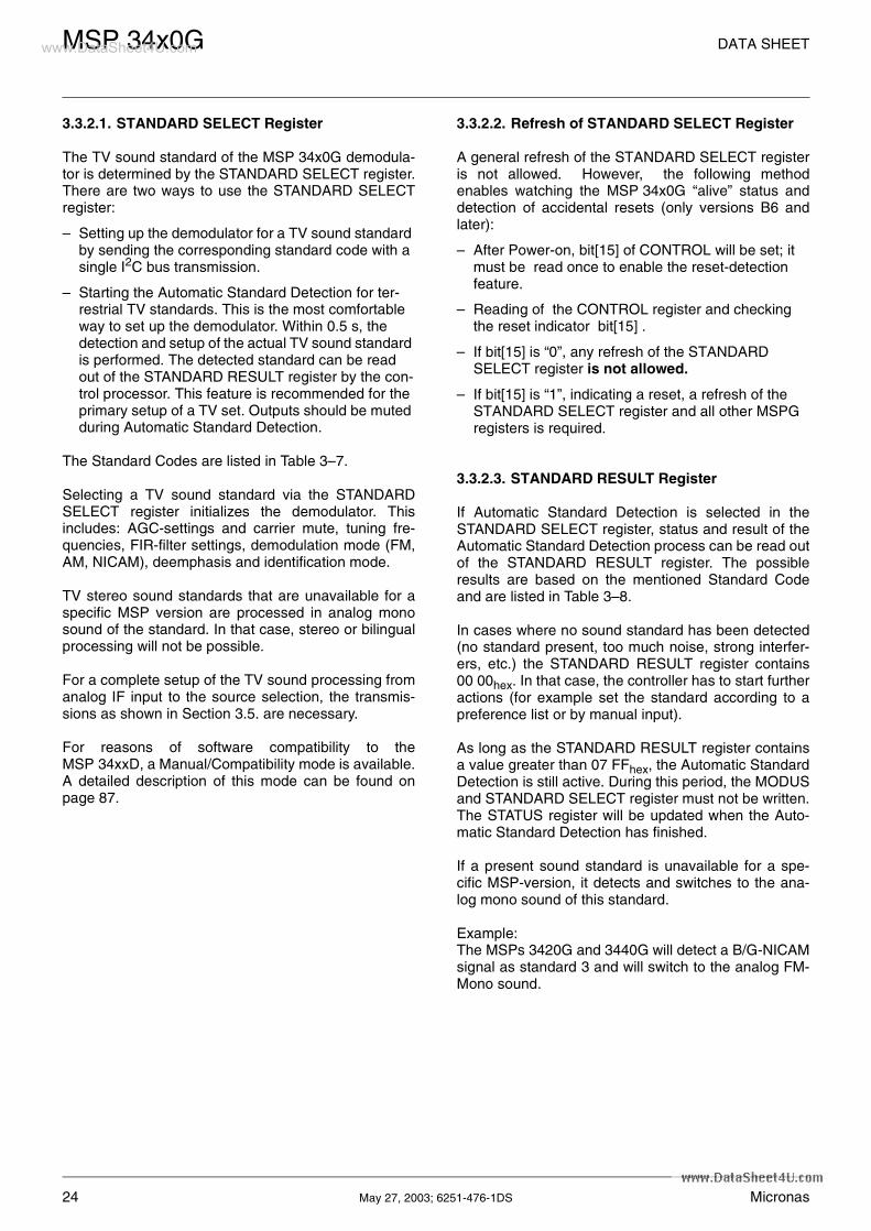
46 4. Specifications46 4.1. Outline Dimensions51 4.2. Pin Connections and Short Descriptions54 4.3. Pin Descriptions57 4.4. Pin Configurations60 4.5. Pin Circuits62 4.6. Electrical Characteristics62 4.6.1. Absolute Maximum Ratings64 4.6.2. Recommended Operating Conditions64 4.6.2.1. General Recommended Operating Conditions65 4.6.2.2. Analog Input and Output Recommendations66 4.6.2.3. Recommendations for Analog Sound IF Input Signal67 4.6.2.4. Crystal Recommendations68 4.6.3. Characteristics68 4.6.3.1. General Characteristics69 4.6.3.2. Digital Inputs, Digital Outputs70 4.6.3.3. Reset Input and Power-Up71 4.6.3.4. I2C-Bus Characteristics72 4.6.3.5. I2S-Bus Characteristics74 4.6.3.6. Analog Baseband Inputs and Outputs, AGNDC75 4.6.3.7. Sound IF Inputs75 4.6.3.8. Power Supply Rejection76 4.6.3.9. Analog Performance79 4.6.3.10. Sound Standard Dependent Characteristics
Micronas May 27, 2003; 6251-476-1DS 3

Contents, continued
Page Section Title
MSP 34x0G DATA SHEETwww.DataSheet4U.com
83 5. Appendix A: Overview of TV-Sound Standards83 5.1. NICAM 72884 5.2. A2-Systems85 5.3. BTSC-Sound System85 5.4. Japanese FM Stereo System (EIA-J)86 5.5. FM Satellite Sound86 5.6. FM-Stereo Radio
87 6. Appendix B: Manual/Compatibility Mode87 6.1. Demodulator Write and Read Registers for Manual/Compatibility Mode 88 6.2. DSP Write and Read Registers for Manual/Compatibility Mode89 6.3. Manual/Compatibility Mode: Description of Demodulator Write Registers89 6.3.1. Automatic Switching between NICAM and Analog Sound89 6.3.1.1. Function in Automatic Sound Select Mode89 6.3.1.2. Function in Manual Mode91 6.3.2. A2 Threshold91 6.3.3. Carrier-Mute Threshold92 6.3.4. Register AD_CV93 6.3.5. Register MODE_REG95 6.3.6. FIR-Parameter, Registers FIR1 and FIR295 6.3.7. DCO-Registers97 6.4. Manual/Compatibility Mode: Description of Demodulator Read Registers97 6.4.1. NICAM Mode Control/Additional Data Bits Register97 6.4.2. Additional Data Bits Register97 6.4.3. CIB Bits Register98 6.4.4. NICAM Error Rate Register98 6.4.5. PLL_CAPS Readback Register98 6.4.6. AGC_GAIN Readback Register98 6.4.7. Automatic Search Function for FM-Carrier Detection in Satellite Mode99 6.5. Manual/Compatibility Mode: Description of DSP Write Registers99 6.5.1. Additional Channel Matrix Modes99 6.5.2. Volume Modes of SCART1/2 Outputs99 6.5.3. FM Fixed Deemphasis99 6.5.4. FM Adaptive Deemphasis100 6.5.5. NICAM Deemphasis100 6.5.6. Identification Mode for A2 Stereo Systems100 6.5.7. FM DC Notch100 6.6. Manual/Compatibility Mode: Description of DSP Read Registers100 6.6.1. Stereo Detection Register for A2 Stereo Systems100 6.6.2. DC Level Register101 6.7. Demodulator Source Channels in Manual Mode101 6.7.1. Terrestric Sound Standards101 6.7.2. SAT Sound Standards101 6.8. Exclusions of Audio Baseband Features101 6.9. Compatibility Restrictions to MSP 34x0D
4 May 27, 2003; 6251-476-1DS Micronas

Contents, continued
Page Section Title
DATA SHEET MSP 34x0Gwww.DataSheet4U.com
103 7. Appendix C: Application Information103 7.1. Phase Relationship of Analog Outputs104 7.2. Application Circuit
105 8. Appendix D: MSP 34x0G Version History
106 9. Data Sheet History
License Notice:
“Dolby Pro Logic” is a trademark of Dolby Laboratories.
Supply of this implementation of Dolby Technology does not convey a license nor imply a right under any patent, or any other industrial or intellec-tual property right of Dolby Laboratories, to use this implementation in any finished end-user or ready-to-use final product. Companies planning touse this implementation in products must obtain a license from Dolby Laboratories Licensing Corporation before designing such products.
Micronas May 27, 2003; 6251-476-1DS 5

MSP 34x0G DATA SHEETwww.DataSheet4U.com
Multistandard Sound Processor Family
Release Note: Revision bars indicate significantchanges to the previous edition. The hardware andsoftware description in this document is valid forthe MSP 34x0G version C12 and following ver-sions.
1. Introduction
The MSP 34x0G family of single-chip MultistandardSound Processors covers the sound processing of allanalog TV-Standards worldwide, as well as the NICAMdigital sound standards. The full TV sound processing,starting with analog sound IF signal-in, down to pro-cessed analog AF-out, is performed on a single chip.Figure 1–1 shows a simplified functional block diagramof the MSP 34x0G.
These TV sound processing ICs now include versionsfor processing the multichannel television sound(MTS) signal conforming to the standard recom-mended by the Broadcast Television Systems Com-mittee (BTSC). The DBX noise reduction, or alterna-tively, Micronas Noise Reduction (MNR) is performedalignment free.
Other processed standards are the Japanese FM-FMmultiplex standard (EIA-J) and the FM Stereo Radiostandard.
Current ICs have to perform adjustment procedures inorder to achieve good stereo separation for BTSC andEIA-J. The MSP 34x0G has optimum stereo perfor-mance without any adjustments.
All MSP 34xxG versions are pin compatible to theMSP 34xxD. Only minor modifications are necessaryto adapt a MSP 34xxD controlling software to theMSP 34xxG. The MSP 34x0G further simplifies con-trolling software. Standard selection requires a singleI2C transmission only.
The MSP 34x0G has built-in automatic functions: TheIC is able to detect the actual sound standard automat-ically (Automatic Standard Detection). Furthermore,pilot levels and identification signals can be evaluatedinternally with subsequent switching between mono/stereo/bilingual; no I2C interaction is necessary (Auto-matic Sound Selection).
The MSP 34x0G can handle very high FM deviationseven in conjunction with NICAM processing. This isespecially important for the introduction of NICAM inChina.
The ICs are produced in submicron CMOS technology.The MSP 34x0G is available in the following pack-ages: PSDIP64-1, PSDIP52-1/-2, PMQFP80-11, andPMQFP64-2.
Fig. 1–1: Simplified functional block diagram of the MSP 34x0G
So
urc
e S
elec
t
Loud-
SCART1
SCART2
SCART1
SCART2
SCART4
SCART3
MONO
De-modulator
HeadphoneHeadphone
I2S
SoundProcessing
speakerSound
Processing
DAC
DAC
ADC
Loud-
DAC
DACADC
Subwoofer
SCARTDSP Input Select
Pre-processing
SCART Output Select
Prescale
PrescaleI2S1
I2S2
Sound IF1
Sound IF2
speaker
6 May 27, 2003; 6251-476-1DS Micronas

DATA SHEET MSP 34x0Gwww.DataSheet4U.com
1.1. Features of the MSP 34x0G Family
1.2. MSP 34x0G Version List
Feature 3400 3410 3420 3440 3450 3460
Standard Selection with single I2C transmission X X X X X X
Automatic Standard Detection of terrestrial TV standards/Automatic Carrier Mute function X X X X X X
Automatic Sound Selection (mono/stereo/bilingual), new registers MODUS, STATUS X X X X X
Two selectable sound IF (SIF) inputs X X X X X X
Automatic Carrier Mute function X X X X X X
Interrupt output programmable (indicating status change) X X X X X X
Loudspeaker / Headphone channel with volume, balance, bass, treble, loudness X X X X X X
AVC: Automatic Volume Correction X X X X X X
Subwoofer output with programmable low-pass and complementary high-pass filter X X X X X X
Micronas BASS (MB) and 5-band graphic equalizer for loudspeaker channel X X X X X X
Spatial effect for loudspeaker channel X X X X X X
Four Stereo SCART (line) inputs, one Mono input; two Stereo SCART outputs X X X X X X
Complete SCART in/out switching matrix X X X X X X
Two I2S inputs; one I2S output X X X X X X
All analog Mono sound carriers including AM-SECAM L X X X X X X
Korean FM-Stereo A2 standard X X X X X
All analog FM-Stereo A2 and satellite standards X X X
Simultaneous demodulation of (very) high-deviation FM-Mono and NICAM X X
Adaptive deemphasis for satellite (Wegener-Panda, acc. to ASTRA specification) X X X X
ASTRA Digital Radio (ADR) together with DRP 3510A X X X X
All NICAM standards X X
Demodulation of the BTSC multiplex signal and the SAP channel X X X
Alignment free digital DBX noise reduction for BTSC Stereo and SAP X X
Alignment free digital Micronas Noise Reduction (MNR) for BTSC Stereo and SAP X
BTSC stereo separation (MSP 3420/40G also EIA-J) significantly better than spec. X X X
SAP and stereo detection for BTSC system X X X
Alignment-free Japanese standard EIA-J X X X
Demodulation of the FM-Radio multiplex signal X X X
Version Status Description
MSP 3400G available FM Stereo (A2) Version
MSP 3410G available NICAM and FM Stereo (A2) Version
MSP 3420G available NTSC Version (A2 Korea, BTSC with Micronas Noise Reduction (MNR), Japanese EIA-J system)
MSP 3440G available NTSC Version (A2 Korea, BTSC with DBX noise reduction, Japanese EIA-J system)
MSP 3450G available Global Version (all sound standards)
MSP 3460G available Global Mono Version (all sound standards)
Micronas May 27, 2003; 6251-476-1DS 7

MSP 34x0G DATA SHEETwww.DataSheet4U.com
1.3. MSP 34x0G Versions and their Application Fields
Table 1–1 provides an overview of TV sound stan-dards that can be processed by the MSP 34x0G fam-ily. In addition, the MSP 34x0G is able to handle theFM-Radio standard. With the MSP 34x0G, a complete
multimedia receiver covering all TV sound standardstogether with terrestrial/cable and satellite radio soundcan be built; even ASTRA Digital Radio can be pro-cessed (with a DRP 3510A coprocessor).
Fig. 1–2: Typical MSP 34x0G application
Table 1–1: TV Stereo Sound Standards covered by the MSP 34x0G IC Family (details see Appendix A)
MSP Version TV-System
Position of Sound Carrier /MHz
Sound Modulation
ColorSystem
Broadcast e.g. in:
3400
341
0
345
0
B/G5.5/5.7421875 FM-Stereo (A2) PAL Germany
5.5/5.85 FM-Mono/NICAM PAL Scandinavia, Spain
L 6.5/5.85 AM-Mono/NICAM SECAM-L France
I 6.0/6.552 FM-Mono/NICAM PAL UK, Hong Kong
3400
D/K
6.5/6.2578125 FM-Stereo (A2, D/K1) SECAM-East Slovak. Rep.
6.5/6.7421875 FM-Stereo (A2, D/K2) PAL currently no broadcast
6.5/5.7421875 FM-Stereo (A2, D/K3) SECAM-East Poland
6.5/5.85 FM-Mono/NICAM (D/K, NICAM) PAL China, Hungary
3400
Satellite
6.57.02/7.27.38/7.56etc.
FM-MonoFM-Stereo
ASTRA Digital Radio (ADR) with DRP 3510A
PAL Europe Sat.ASTRA
3420
, 344
0
M/N
4.5/4.724212 FM-Stereo (A2) NTSC Korea
4.5 FM-FM (EIA-J) NTSC Japan
4.5 BTSC-Stereo + SAP NTSC, PAL USA, Argentina
FM-Radio 10.7 FM-Stereo Radio USA, Europe
3460 all Standards as above but Mono demodulation only.
33 34 39 MHz 4.5 9 MHz
Loudspeaker
Subwoofer
Headphone
SCARTOutputs2
2
SCART2
SCART1
MSP 34x0G
I2S2ADRI2S1
ADR DecoderDRP 3510A
Dolby Pro LogicProcessorDPL 351xA
2
2
2
2SCART1
SCART2
SCART3
SCART4
1Mono
SAW Filter
SoundIFMixer
VisionDemo-dulator
Tuner
SCARTInputsComposite
Video
8 May 27, 2003; 6251-476-1DS Micronas

DA
TA
SH
EE
TM
SP
34x0G
Micronas
May 27, 2003; 6251-476-1D
S9
2. Functional Description
D
A
D
A
DACM_L
DACM_R
DACM_SUB
DACA_L
DACA_R
VolumeBalance
Balance
LevelAdjust
SpatialEffects
UT
ANA_IN1+
_L
_R
_L
_R
AutomaticSound Select
(00hex)
(05hex) (01hex)
S t a n d a r d S e le c t i o n
(2Chex)
(30hex)
Volume
(06hex)
MB
ww
w.D
ata
Sheet4
U.c
om
Fig. 2–1: Signal flow block diagram of the MSP 34x0G (input and output names correspond to pin names)
SC
AR
T D
SP
Inpu
t Sel
ect
A
D
D
A
A
D
SC
AR
T O
utpu
t Sel
ect
Sou
rce
Sel
ect
Comple-mentary
Highpass
Lowpass
Σ
Σ
I2S_DA_O
Beeper
SCART1_L/R
Bass/Treble
orEqualize
Bass/Treble
AVC
Loud-
ChannelMatrix
speaker
I2S Interface
I2SChannelMatrix
I2CRead
Register
Quasi-PeakDetector
Volume
I2S1I2S
Interface
I2C
Stereo or B
Stereo or A
FM/AMFM/AM
Prescale
Prescale
NICAM
ReadRegister
Deemphasis:50/75 µs, J17DBX/MNRPanda1
Standard
DEMODULATOR(incl. Carrier Mute)
Decoded
− NICAM− A2− AM− BTSC− EIA-J− SAT− FM-Radio and Sound
Detection
SC1_IN_R
AGC
ANA_IN2+
SC1_IN_L
SC3_IN_R
SC2_IN_L
SC2_IN_R
SC3_IN_L
MONO_IN
SC4_IN_L
SC4_IN_R
SCART2_L/R
SC1_OUT
SC1_OUT
SC2_OUT
SC2_OUT
SCART1
Standards:Deemphasis
J17
Stereo or A/B
Prescale
HeadphoneChannelMatrix
Quasi-PeakChannel
Loud-
Loudness
ness
Matrix
(08hex)
(0Ahex) (07hex)
(29hex)
(14hex)
(13hex)
(13hex)
(02hex)(03hex)
(04hex)
(16hex)
ADR-BusInterface
(0Ehex)
(10hex)
(0Bhex)
ChannelMatrix
D
A
VolumeSCART2ChannelMatrix
(0Chex)
(41hex) (40hex)
I2S2I2S
InterfacePrescale
(12hex)
SCART
Prescale
(0Dhex)
0.5 (2Dhex)
(2Dhex)
(19hex)
(09hex) (31/32hex) (33hex)
(1Ahex)
0
1
3
4
5
6
2
I2S_DA_IN2
I2S_DA_IN1

MSP 34x0G DATA SHEETwww.DataSheet4U.com
2.1. Architecture of the MSP 34x0G Family
Fig. 2–1 on page 9 shows a simplified block diagram ofthe IC. The block diagram contains all features of theMSP 3450G. Other members of the MSP 34x0G fam-ily do not have the complete set of features: Thedemodulator handles only a subset of the standardspresented in the demodulator block; NICAM process-ing is only possible in the MSP 3410G andMSP 3450G.
2.2. Sound IF Processing
2.2.1. Analog Sound IF Input
The input pins ANA_IN1+, ANA_IN2+, and ANA_IN−offer the possibility to connect two different sound IF(SIF) sources to the MSP 34x0G. The analog-to-digitalconversion of the preselected sound IF signal is doneby an A/D-converter. An analog automatic gain circuit(AGC) allows a wide range of input levels. The high-pass filters formed by the coupling capacitors at pinsANA_IN1+ and ANA_IN2+ see Section 7.2. “Applica-tion Circuit” on page 104 are sufficient in most cases tosuppress video components. Some combinations ofSAW filters and sound IF mixer ICs, however, showlarge picture components on their outputs. In this case,further filtering is recommended.
2.2.2. Demodulator: Standards and Features
The MSP 34x0G is able to demodulate all TV-soundstandards worldwide including the digital NICAM sys-tem. Depending on the MSP 34x0G version, the fol-lowing demodulation modes can be performed:
A2 Systems: Detection and demodulation of two sep-arate FM carriers (FM1 and FM2), demodulation andevaluation of the identification signal of carrier FM2.
NICAM Systems: Demodulation and decoding of theNICAM carrier, detection and demodulation of the ana-log (FM or AM) carrier. For D/K-NICAM, the FM carriermay have a maximum deviation of 384 kHz.
Very high deviation FM-Mono: Detection and robustdemodulation of one FM carrier with a maximum devi-ation of 540 kHz.
BTSC-Stereo: Detection and FM demodulation of theaural carrier resulting in the MTS/MPX signal. Detec-tion and evaluation of the pilot carrier, AM demodula-tion of the (L−R)-carrier and detection of the SAP sub-carrier. Processing of DBX noise reduction or MicronasNoise Reduction (MNR).
BTSC-Mono + SAP: Detection and FM demodulationof the aural carrier resulting in the MTS/MPX signal.Detection and evaluation of the pilot carrier, detectionand FM demodulation of the SAP subcarrier. Process-ing of DBX noise reduction or Micronas Noise Reduc-tion (MNR).
Japan Stereo: Detection and FM demodulation of theaural carrier resulting in the MPX signal. Demodulationand evaluation of the identification signal and FMdemodulation of the (L−R)-carrier.
FM-Satellite Sound: Demodulation of one or two FMcarriers. Processing of high-deviation mono or narrowbandwidth mono, stereo, or bilingual satellite soundaccording to the ASTRA specification.
FM-Stereo-Radio: Detection and FM demodulation ofthe aural carrier resulting in the MPX signal. Detectionand evaluation of the pilot carrier and AM demodula-tion of the (L−R)-carrier.
The demodulator blocks of all MSP 34x0G versionshave identical user interfaces. Even completely differ-ent systems like the BTSC and NICAM systems arecontrolled the same way. Standards are selected bymeans of MSP Standard Codes. Automatic processeshandle standard detection and identification withoutcontroller interaction. The key features of theMSP 34x0G demodulator blocks are:
Standard Selection: The controlling of the demodula-tor is minimized: All parameters, such as tuning fre-quencies or filter bandwidth, are adjusted automati-cally by transmitting one single value to theSTANDARD SELECT register. For all standards, spe-cific MSP standard codes are defined.
Automatic Standard Detection: If the TV sound stan-dard is unknown, the MSP 34x0G can automaticallydetect the actual standard, switch to that standard, andrespond the actual MSP standard code.
Automatic Carrier Mute: To prevent noise effects orFM identification problems in the absence of an FMcarrier, the MSP 34x0G offers a configurable carriermute feature, which is activated automatically if the TVsound standard is selected by means of the STAN-DARD SELECT register. If no FM carrier is detected atone of the two MSP demodulator channels, the corre-sponding demodulator output is muted. This is indi-cated in the STATUS register.
10 May 27, 2003; 6251-476-1DS Micronas

DATA SHEET MSP 34x0Gwww.DataSheet4U.com
2.2.3. Preprocessing of Demodulator Signals
The NICAM signals must be processed by a deempha-sis filter and adjusted in level. The analog demodu-lated signals must be processed by a deemphasis fil-ter, adjusted in level, and dematrixed. The correctdeemphasis filters are already selected by setting thestandard in the STANDARD SELECT register. Thelevel adjustment has to be done by means of the FM/AM and NICAM prescale registers. The necessarydematrix function depends on the selected sound stan-dard and the actual broadcasted sound mode (mono,stereo, or bilingual). It can be manually set by the FMMatrix Mode register or automatically by the AutomaticSound Selection.
2.2.4. Automatic Sound Select
In the Automatic Sound Select mode, the dematrixfunction is automatically selected based on the identifi-cation information in the STATUS register. No I2Cinteraction is necessary when the broadcasted soundmode changes (e.g. from mono to stereo).
The demodulator supports the identification check byswitching between mono-compatible standards (stan-dards that have the same FM-Mono carrier) automati-cally and non-audible. If B/G-FM or B/G-NICAM isselected, the MSP will switch between these stan-dards. The same action is performed for the stan-dards: D/K1-FM, D/K2-FM, D/K3-FM and D/K-NICAM.Switching is only done in the absence of any stereo orbilingual identification. If identification is found, theMSP keeps the detected standard.
In case of high bit-error rates, the MSP 34x0G auto-matically falls back from digital NICAM sound to ana-log FM or AM mono.
Table 2–1 summarizes all actions that take place whenAutomatic Sound Select is switched on.
To provide more flexibility, the Automatic Sound Selectblock prepares four different source channels ofdemodulated sound (Fig. 2–2). By choosing one of thefour demodulator channels, the preferred sound modecan be selected for each of the output channels (loud-speaker, headphone, etc.). This is done by means ofthe Source Select registers.
The following source channels of demodulated soundare defined:
– “FM/AM” channel: Analog mono sound, stereo if available. In case of NICAM, analog mono only (FM or AM mono).
– “Stereo or A/B” channel: Analog or digital mono sound, stereo if available. In case of bilingual broad-cast, it contains both languages A (left) and B (right).
– “Stereo or A” channel: Analog or digital mono sound, stereo if available. In case of bilingual broad-cast, it contains language A (on left and right).
– “Stereo or B” channel: Analog or digital mono sound, stereo if available. In case of bilingual broad-cast, it contains language B (on left and right).
Fig. 2–2 and Table 2–2 show the source channelassignment of the demodulated signals in case ofAutomatic Sound Select mode for all sound standards.
Note: The analog primary input channel contains thesignal of the mono FM/AM carrier or the L+R signal ofthe MPX carrier. The secondary input channel containsthe signal of the 2nd FM carrier, the L-R signal of theMPX carrier, or the SAP signal.
Fig. 2–2: Source channel assignment of demodulated signals in Automatic Sound Select Mode
2.2.5. Manual Mode
Fig. 2–3 shows the source channel assignment ofdemodulated signals in case of manual mode. If man-ual mode is required, more information can be found inSection 6.7. “Demodulator Source Channels in ManualMode” on page 101.
Fig. 2–3: Source channel assignment of demodulated signals in Manual Mode
2.3. Preprocessing for SCART and I2S Input Signals
The SCART and I2S inputs need only be adjusted inlevel by means of the SCART and I2S prescale regis-ters.
Sou
rce
Sel
ect
FM/AM
Stereo or A/B
Stereo or A
Stereo or B
0
1
3
4
primaryFM/AM
Prescale
NICAM
Prescale
AutomaticSoundSelect
channel
secondarychannel
NICAM A
NICAM B
LS Ch.Matrix
Output-Ch.matricesmust be setonce tostereo.
Sou
rce
Sel
ect
FM/AM
(Stereo or A/B)
0
1
primaryFM/AM
Prescale
NICAM
Prescale
FM-Matrixchannel
secondarychannel
NICAM A
NICAM B
LS Ch.Matrix
Output-Ch.matricesmust be setaccording tothe standard.NICAM
Micronas May 27, 2003; 6251-476-1DS 11

MSP 34x0G DATA SHEETwww.DataSheet4U.com
Table 2–1: Performed actions of the Automatic Sound Selection
Selected TV Sound Standard Performed Actions
B/G-FM, D/K-FM, M-Korea, and M-Japan
Evaluation of the identification signal and automatic switching to mono, stereo, or bilingual. Preparing four demodulator source channels according to Table 2–2.
B/G-NICAM, L-NICAM, I-NICAM, D/K-NICAM
Evaluation of NICAM-C-bits and automatic switching to mono, stereo, or bilingual. Preparing four demodulator source channels according to Table 2–2.
In case of bad or no NICAM reception, the MSP switches automatically to FM/AM mono and switches back to NICAM if possible. A hysteresis prevents periodical switching.
B/G-FM, B/G-NICAM
or
D/K1-FM, D/K2-FM, D/K3-FM, and D/K-NICAM
Automatic searching for stereo/bilingual-identification in case of mono transmission. Automatic and non-audible changes between Dual-FM and FM-NICAM standards while listening to the basic FM-mono sound carrier. Example: If starting with B/G-FM-Stereo, there will be a periodical alternation to B/G-NICAM in the absence of FM-Stereo/Bilingual or NICAM-identification. Once an identification is detected, the MSP keeps the corresponding standard.
BTSC-STEREO, FM Radio Evaluation of the pilot signal and automatic switching to mono or stereo. Preparing four demodulator source channels according to Table 2–2. Detection of the SAP carrier.
M-BTSC-SAP In the absence of SAP, the MSP switches to BTSC-stereo if available. If SAP is detected, the MSP switches automatically to SAP (see Table 2–2).
Table 2–2: Sound modes for the demodulator source channels with Automatic Sound Select
Source Channels in Automatic Sound Select Mode
Broadcasted Sound Standard
Selected MSP Standard Code3)
Broadcasted Sound Mode
FM/AM(source select: 0)
Stereo or A/B(source select: 1)
Stereo or A(source select: 3)
Stereo or B(source select: 4)
M-KoreaB/G-FMD/K-FMM-Japan
0203, 081)
04, 05, 07, 0B1)
30
MONO Mono Mono Mono Mono
STEREO Stereo Stereo Stereo Stereo
BILINGUAL: Languages A and B
Left = ARight = B
Left = ARight = B
A B
B/G-NICAML-NICAMI-NICAMD/K-NICAMD/K-NICAM (with high deviation FM)
08, 032)
090A0B, 042), 052)
0C, 0D
NICAM not available or error rate too high
analog Mono analog Mono analog Mono analog Mono
MONO analog Mono NICAM Mono NICAM Mono NICAM Mono
STEREO analog Mono NICAM Stereo NICAM Stereo NICAM Stereo
BILINGUAL: Languages A and B
analog Mono Left = NICAM ARight = NICAM B
NICAM A NICAM B
BTSC
20, 21 MONO Mono Mono Mono Mono
STEREO Stereo Stereo Stereo Stereo
20 MONO + SAP Mono Mono Mono Mono
STEREO + SAP Stereo Stereo Stereo Stereo
21 MONO + SAP Left = MonoRight = SAP
Left = MonoRight = SAP
Mono SAP
STEREO + SAP Left = MonoRight = SAP
Left = MonoRight = SAP
Mono SAP
FM Radio 40 MONO Mono Mono Mono Mono
STEREO Stereo Stereo Stereo Stereo
1) The Automatic Sound Select process will automatically switch to the mono compatible analog standard.2) The Automatic Sound Select process will automatically switch to the mono compatible digital standard.3) The MSP Standard Codes are defined in (see Table 3–7 on page 23).
12 May 27, 2003; 6251-476-1DS Micronas

DATA SHEET MSP 34x0Gwww.DataSheet4U.com
2.4. Source Selection and Output Channel Matrix
The Source Selector makes it possible to distribute allsource signals (one of the demodulator source chan-nels, SCART, or I2S input) to the desired output chan-nels (loudspeaker, headphone, etc.). All input and out-put signals can be processed simultaneously. Eachsource channel is identified by a unique sourceaddress.
For each output channel, the sound mode can be setto sound A, sound B, stereo, or mono by means of theoutput channel matrix.
If Automatic Sound Select is on, the output channelmatrix can stay fixed to stereo (transparent) fordemodulated signals.
2.5. Audio Baseband Processing
2.5.1. SRS WOW
License Notice: SRS, SRS WOW, and the SRS Logoare trademarks of SRS Labs, Inc. A license from SRSLabs, Inc. is required before an SRS-version of theMSP 34x0G can be purchased.
SRS Labs’ WOW technology enlarges the soundimage field and improves the bass performance oftelevision speakers. Manufacturers can save costs bylicensing WOW while utilizing smaller speakers andstill provide a higher quality audio experience.
WOW consists of three sections:
– Clarity Improvement,
– 3D-Audio (SRS, Sound Retrieval System), and
– Bass Enhancement (TruBass).
Key features of WOW include:
– Wider and taller sound image field
– Larger sweet spot
– Deep, rich bass tones
– Quality improvements to audio listening experience
– Improved clarity of speech
All MSP 34x0G are shipped without SRS except other-wise ordered. When an SRS-version of MSP 34x0G isordered, it carries a special marking on the chip foridentification. The SRS WOW functionality must beenabled by writing a "license key" into theMSP 34x0G. For information on how to obtain thislicense key from Micronas, please contact your Micro-nas sales representative.
2.5.2. BBE High Definition Sound
License Notice: BBE is a registered trademark ofBBE Sound Inc., the BBE Logo is a trademark of BBESound Inc. A license from BBE Sound Inc. is requiredbefore a BBE-version of the MSP 34x0G can be pur-chased.
BBE High Definition Sound or, also called, Sonic Maxi-mizer technology improves the clarity of music whenplayed back via loudspeakers. A more “life like” feelingis created by BBE. The BBE-approved Micronasimplementation works in the digital domain and thusneeds no external components and does not sufferfrom tolerances and aging effects.
All MSP 34x0G are shipped without BBE except other-wise ordered. When a BBE-version of the MSP 34x0Gis ordered, it carries a special marking on the chip foridentification. The BBE Sonic Maximizer functionalitymust be enabled by writing a "license key" into theMSP 34x0G. For information on how to obtain thislicense key from Micronas, please contact your Micro-nas sales representative.
2.5.3. Micronas VOICE
Micronas VOICE was developed to add the followingimprovements to speech signals:
– Increase speech signal over background noise to increase intelligibility in noisy environments
– Move voice to the foreground, closer to the listener, while other sounds are moved to the back
– Improve voices that are hard to understand, leave clear voices largely undisturbed
Micronas VOICE dynamically enhances those portionsof speech that are important for intelligibility while atthe same time decreasing portions of the signal thatdisturb intelligibility. The average amplitude of the sig-nal is not changed.
According to speech theory, there are two main effectsthat affect the intelligibility of speech. Micronas VOICEcombines both effects to achieve a maximumenhancement of intelligibility.
– Forward and backward masking: For intelligibility, consonants are more important than vowels, but the amplitude of consonants is much lower than that of vowels. The consonants are masked by the vowels. Therefore, the amplitude of consonants is increased and the amplitude of vowels decreased.
– Phonemes and formants: Most important for intelli-gibility are the second to fourth formants of speech. These formants are detected and increased, while other parts of the signal are decreased.
Micronas May 27, 2003; 6251-476-1DS 13

MSP 34x0G DATA SHEETwww.DataSheet4U.com
All MSP 34x0G are shipped without Micronas VOICEexcept otherwise ordered. When a Micronas VOICE -version of the MSP 34x0G is ordered, it carries a spe-cial marking on the chip for identification. The Micro-nas VOICE functionality must be enabled by writing a"license key" into the MSP 34x0G. For information onhow to obtain this license key from Micronas, pleasecontact your Micronas sales representative.
2.5.4. Automatic Volume Correction (AVC)
Different sound sources (e.g. terrestrial channels, SATchannels, or SCART) fairly often do not have the samevolume level. Advertisements during movies usuallyhave a higher volume level than the movie itself. Thisresults in annoying volume changes. The AutomaticVolume Correction (AVC) solves this problem byequalizing the volume level.
To prevent clipping, the AVC’s gain decreases quicklyin dynamic boost conditions. To suppress oscillationeffects, the gain increases rather slowly for low levelinputs. The decay time is programmable by means ofthe AVC register (see page 33).
For input signals ranging from −24 dBr to 0 dBr, theAVC maintains a fixed output level of −18 dBr. Fig. 2–4shows the AVC output level versus its input level. Forprescale and volume registers set to 0 dB, a level of0 dBr corresponds to full scale input/output. This is
– SCART input/output 0 dBr = 2.0 Vrms
– Loudspeaker and Aux output 0 dBr = 1.4 Vrms
Fig. 2–4: Simplified AVC characteristics
2.5.5. Loudspeaker and Headphone Outputs
The following baseband features are implemented inthe loudspeaker and headphone output channels:bass/treble, loudness, balance, and volume. A squarewave beeper can be added to the loudspeaker andheadphone channel. The loudspeaker channel addi-tionally performs: equalizer (not simultaneously withbass/treble), spatial effects, and a subwoofer cross-over filter.
2.5.6. Subwoofer Output
The subwoofer signal is created by combining the leftand right channels directly behind the loudness blockusing the formula (L+R)/2. Due to the division by 2, theD/A converter will not be overloaded, even with fullscale input signals. The subwoofer signal is filtered bya third-order low-pass with programmable corner fre-quency followed by a level adjustment. At the loud-speaker channels, a complementary high-pass filtercan be switched on. Subwoofer and loudspeaker out-put use the same volume (Loudspeaker Volume Reg-ister).
Fig. 2–5: Frequency response of subwoofer filter0: sharp edge1: medium edge2: soft edge3: very soft edge
−30 −24 −18 −12 −6
input level
−18
−24
output level
0 [dBr]
[dBr]
200 2000f
−25
−20
−15
−10
−5
0
51 0
2
3
Hz
dB Amplitude @dBD
14 May 27, 2003; 6251-476-1DS Micronas

DATA SHEET MSP 34x0Gwww.DataSheet4U.com
2.5.7. Quasi-Peak Detector
The quasi-peak readout register can be used to readout the quasi-peak level of any input source. The fea-ture is based on following filter time constants:
attack time: 1.3 msdecay time: 37 ms
2.5.8. Micronas BASS (MB)
The Micronas Bass system extends the frequencyrange of loudspeakers or headphones.
After the adaption of MB to the loudspeakers and thecabinet, further customizing of MB allows individualfine tuning of the sound.
Micronas BASS is placed in the subwoofer path. Forapplications without a subwoofer, the enhanced basssignal can be added back onto the Left/Right channels(see Fig. 2–1 on page 9). MB combines two effects:dynamic amplification and adding harmonics.
2.5.8.1. Dynamic Amplification
Low frequency signals can be boosted while the outputsignal amplitude is measured. If the amplitude comesclose to a definable limit, the gain is reduced automati-cally in dynamic Volume mode. Therefore, the systemadapts to the signal amplitude which is really presentat the output of the MSP device. Clipping effects areavoided.
Fig. 2–6: Dynamic amplification
2.5.8.2. Adding Harmonics
Micronas BASS exploits the psychoacoustic phenome-non of the ‘missing fundamental’. Adding harmonics ofthe frequency components below the cutoff frequencygives the impression of actually hearing the low fre-quency fundamental. In other words: The listener hasthe impression that a loudspeaker system seems toreproduce frequencies although physically not possi-ble.
Fig. 2–7: Adding harmonics
2.5.8.3. Micronas BASS Parameters
Several parameters allow tuning the characteristics ofMicronas BASS according to the TV loudspeaker, thecabinet, and personal preferences (see Table 3–11).For more detailed information on how to set up MB,please refer to the corresponding application note.
2.6. SCART Signal Routing
2.6.1. SCART DSP In and SCART Out Select
The SCART DSP Input Select and SCART OutputSelect blocks include full matrix switching facilities. Todesign a TV set with four pairs of SCART-inputs andtwo pairs of SCART-outputs, no external switchinghardware is required. The switches are controlled bythe ACB user register (see page 41).
Frequency
MB_LIMIT
MB_HP MB_LP
Sig
nal L
evel
Am
plitu
de
SUBW_FREQ
(db)
FrequencyMB_HP
Am
plitu
de (
db)
Micronas May 27, 2003; 6251-476-1DS 15

MSP 34x0G DATA SHEETwww.DataSheet4U.com
2.6.2. Stand-by Mode
If the MSP 34x0G is switched off by first pullingSTANDBYQ low and then (after >1 µs delay) switchingoff DVSUP and AVSUP, but keeping AHVSUP(‘Stand-by’-mode), the SCART switches maintaintheir position and function. This allows the copyingfrom SCART-input to SCART-output in the TV set’sstand-by mode.
In case of power on or starting from stand-by (switch-ing on the DVSUP and AVSUP, RESETQ going high2 ms later), all internal registers except the ACB regis-ter (see page 41) are reset to the default configuration(see Table 3–5 on page 20). The reset position of theACB register becomes active after the first I2C trans-mission into the Baseband Processing part. By trans-mitting the ACB register first, the reset state can beredefined.
2.7. I2S Bus Interface
The MSP 34x0G has a synchronous master/slaveinput/output interface running on 32 kHz.
The interface accepts two formats:
1. I2S_WS changes at the word boundary
2. I2S_WS changes one I2S-clock period before the word boundaries.
All I2S options are set by means of the MODUS andthe I2S_CONFIGURATION registers.
The I2S bus interface consists of five pins:
– I2S_DA_IN1, I2S_DA_IN2: I2S serial data input: 16, 18....32 bits per sample
– I2S_DA_OUT: I2S serial data output: 16, 18...32 bits per sample
– I2S_CL: I2S serial clock
– I2S_WS: I2S word strobe signal defines the left and right sample
If the MSP 34x0G serves as the master on the I2Sinterface, the clock and word strobe lines are driven bythe IC. In this mode, only 16 or 32 bits per sample canbe selected. In slave mode, these lines are input to theIC and the MSP clock is synchronized to 576 times theI2S_WS rate (32 kHz). NICAM operation is not possi-ble in slave mode.
An I2S timing diagram is shown in Fig. 4–27 onpage 73.
2.8. ADR Bus Interface
For the ASTRA Digital Radio System (ADR), theMSP 3400G, MSP 3410G, and MSP 3450G performspreprocessing such as carrier selection and filtering.Via the 3-line ADR-bus, the resulting signals are trans-ferred to the DRP 3510A coprocessor, where thesource decoding is performed. To be prepared for anupgrade to ADR with an additional DRP board, the fol-lowing lines of MSP 34x0G should be provided on afeature connector:
– AUD_CL_OUT
– I2S_DA_IN1 or I2S_DA_IN2
– I2S_DA_OUT
– I2S_WS
– I2S_CL
– ADR_CL, ADR_WS, ADR_DA
For more details, please refer to the DRP 3510A datasheet.
2.9. Digital Control I/O Pins and Status Change Indication
The static level of the digital input/output pinsD_CTR_I/O_0/1 is switchable between HIGH andLOW via the I2C-bus by means of the ACB register(see page 41). This enables the controlling of externalhardware switches or other devices via I2C-bus.
The digital input/output pins can be set to high imped-ance by means of the MODUS register (see page 26).In this mode, the pins can be used as input. The cur-rent state can be read out of the STATUS register (seepage 28).
Optionally, the pin D_CTR_I/O_1 can be used as aninterrupt request signal to the controller, indicating anychanges in the read register STATUS. This makes poll-ing unnecessary, I2C bus interactions are reduced to aminimum (see STATUS register on page 28 andMODUS register on page 26).
2.10. Clock PLL Oscillator and Crystal Specifications
The MSP 34x0G derives all internal system clocksfrom the 18.432 MHz oscillator. In NICAM or in I2S-Slave mode, the clock is phase-locked to the corre-sponding source. Therefore, it is not possible to useNICAM and I2S-Slave mode at the same time.
For proper performance, the MSP clock oscillatorrequires a 18.432 MHz crystal. Note that for thephase-locked modes (NICAM, I2S-Slave), crystals withtighter tolerance are required.
16 May 27, 2003; 6251-476-1DS Micronas

DATA SHEET MSP 34x0Gwww.DataSheet4U.com
3. Control Interface
3.1. I2C Bus Interface
The MSP 34x0G is controlled via the I2C bus slaveinterface.
The IC is selected by transmitting one of theMSP 34x0G device addresses. In order to allow up tothree MSP ICs to be connected to a single bus, anaddress select pin (ADR_SEL) has been implemented.With ADR_SEL pulled to high, low, or left open, theMSP 34x0G responds to different device addresses. Adevice address pair is defined as a write address anda read address (see Table 3–1).
Writing is done by sending the write device address,followed by the subaddress byte, two address bytes,and two data bytes.
Reading is done by sending the write device address,followed by the subaddress byte and two addressbytes. Without sending a stop condition, reading of theaddressed data is completed by sending the deviceread address and reading two bytes of data.
Refer to Section 3.1.3. for the I2C bus protocol and toSection 3.4. “Programming Tips” on page 43 for pro-posals of MSP 34x0G I2C telegrams. See Table 3–2for a list of available subaddresses.
Besides the possibility of hardware reset, the MSP canalso be reset by means of the RESET bit in the CON-TROL register by the controller via I2C bus.
Due to the architecture of the MSP 34x0G, the IC can-not react immediately to an I2C request. The typical
response time is about 0.3 ms. If the MSP cannotaccept another byte of data (e.g. while servicing aninternal interrupt), it holds the clock line I2C_CL low toforce the transmitter into a wait state. The I2C BusMaster must read back the clock line to detect whenthe MSP is ready to receive the next I2C transmission.The positions within a transmission where this mayhappen are indicated by ’Wait’ in Section 3.1.3. Themaximum wait period of the MSP during normal opera-tion mode is less than 1 ms.
3.1.1. Internal Hardware Error Handling
In case of any hardware problems (e.g. interruption ofthe power supply of the MSP), the MSP’s wait period isextended to 1.8 ms. After this time period elapses, theMSP releases data and clock lines.
Indication and solving the error status:
To indicate the error status, the remaining acknowl-edge bits of the actual I2C-protocol will be left high.Additionally, bit[14] of CONTROL is set to one. TheMSP can then be reset via the I2C bus by transmittingthe RESET condition to CONTROL.
Indication of reset:
Any reset, even caused by an unstable reset line etc.,is indicated in bit[15] of CONTROL.
A general timing diagram of the I2C bus is shown inFig. 4–25 on page 71.
Table 3–1: I2C Bus Device Addresses
ADR_SEL Low(connected to DVSS)
High(connected to DVSUP)
Left Open
Mode Write Read Write Read Write Read
MSP device address 80hex 81hex 84hex 85hex 88hex 89hex
Table 3–2: I2C Bus Subaddresses
Name Binary Value Hex Value Mode Function
CONTROL 0000 0000 00 Read/Write Write: Software reset of MSP (see Table 3–3)Read: Hardware error status of MSP
WR_DEM 0001 0000 10 Write write address demodulator
RD_DEM 0001 0001 11 Write read address demodulator
WR_DSP 0001 0010 12 Write write address DSP
RD_DSP 0001 0011 13 Write read address DSP
Micronas May 27, 2003; 6251-476-1DS 17

MSP 34x0G DATA SHEETwww.DataSheet4U.com
3.1.2. Description of CONTROL Register
3.1.3. Protocol Description
Write to DSP or Demodulator
Read from DSP or Demodulator
Write to Control Register
Read from Control Register
Note: S = I2C-Bus Start Condition from masterP = I2C-Bus Stop Condition from masterACK = Acknowledge-Bit: LOW on I2C_DA from slave (= MSP, light gray) or master (= controller, dark gray)NAK = Not Acknowledge-Bit: HIGH on I2C_DA from master (dark gray) to indicate ‘End of Read’
or from MSP indicating internal error stateWait = I2C-Clock line is held low, while the MSP is processing the I2C command.
This waiting time is max. 1 ms
Table 3–3: CONTROL as a Write Register
Name Subaddress Bit[15] (MSB) Bits[14:0]
CONTROL 00hex 1 : RESET0 : normal
0
Table 3–4: CONTROL as a Read Register
Name Subaddress Bit Bit
CONTROL 00hex RESET status after last reading of CONTROL:
0 : no reset occured1 : reset occured
Internal hardware status:0 : no error occured1 : internal error occured
not of interest
Reading of CONTROL will reset the bits[15,14] of CONTROL. After Power-on, bit[15] of CONTROL will be set; it must be read once to be reset.
S writedevice
address
Wait ACK sub-addr ACK addr-byte high
ACK addr-byte low
ACK data-byte high
ACK data-byte low
ACK P
S writedevice
address
Wait ACK sub-addr ACK addr-byte high
ACK addr-byte low
ACK S readdevice
address
Wait ACK data-byte-high
ACK data-byte low
NAK P
S writedevice
address
Wait ACK sub-addr ACK data-byte high
ACK data-byte low
ACK P
S writedevice
address
Wait ACK 00hex ACK S readdevice
address
Wait ACK data-byte-high
ACK data-byte low
NAK P
18 May 27, 2003; 6251-476-1DS Micronas

DATA SHEET MSP 34x0Gwww.DataSheet4U.com
Fig. 3–1: I2C bus protocol (MSB first; data must be stable while clock is high)
3.1.4. Proposals for General MSP 34x0GI2C Telegrams
3.1.4.1. Symbols
daw write device address (80hex, 84hex or 88hex)dar read device address (81hex, 85hex or 89hex)< Start Condition> Stop Conditionaa Address Bytedd Data Byte
3.1.4.2. Write Telegrams
<daw 00 d0 00> write to CONTROL register<daw 10 aa aa dd dd> write data into demodulator<daw 12 aa aa dd dd> write data into DSP
3.1.4.3. Read Telegrams
<daw 00 <dar dd dd> read data from CONTROL register
<daw 11 aa aa <dar dd dd> read data from demodulator<daw 13 aa aa <dar dd dd> read data from DSP
3.1.4.4. Examples
<80 00 80 00> RESET MSP statically<80 00 00 00> Clear RESET<80 10 00 30 00 01> Automatic Sound Select = ON<80 10 00 20 00 03> Set demodulator to stand. 03hex<80 11 02 00 <81 dd dd> Read STATUS<80 12 00 08 01 20> Set loudspeaker channel
source to Stereo or A/B and Matrix to Stereo (transparent mode)
More examples of typical application protocols arelisted in Section 3.4. “Programming Tips” on page 43.
3.2. Start-Up Sequence: Power-Up and I2C-Controlling
After POWER-ON or RESET (see Fig. 4–24), the IC isin an inactive state. All registers are in the Reset posi-tion (see Table 3–5 and Table 3–6), the analog out-puts are muted. The controller has to initialize all regis-ters for which a non-default setting is necessary.
3.3. MSP 34x0G Programming Interface
3.3.1. User Registers Overview
The MSP 34x0G is controlled by means of user regis-ters. The complete list of all user registers are given inTable 3–5 and Table 3–6. The registers are partitionedinto the Demodulator section (Subaddress 10hex forwriting, 11hex for reading) and the Baseband Process-ing sections (Subaddress 12hex for writing, 13hex forreading).
Write and read registers are 16 bit wide, whereby theMSB is denoted bit[15]. Transmissions via I2C bushave to take place in 16-bit words (two byte transfers, withthe most significant byte transferred first). All write regis-ters, except the demodulator write registers are readable.
Unused parts of the 16-bit write registers must be zero.Addresses not given in this table must not beaccessed.
For reasons of software compatibility to theMSP 34xxD, a Manual/Compatibility Mode is available.More read and write registers together with a detaileddescription can be found in “Appendix B: Manual/Com-patibility Mode” on page 87.
10
S P
I2C_DA
I2C_CL
Micronas May 27, 2003; 6251-476-1DS 19

MSP 34x0G DATA SHEETwww.DataSheet4U.com
Table 3–5: List of MSP 34x0G Write Registers
Write Register Address(hex)
Bits Description and Adjustable Range Reset See Page
I2C Subaddress = 10hex ; Registers are not readable
STANDARD SELECT 00 20 [15:0] Initial Programming of the Demodulator 00 00 24
MODUS 00 30 [15:0] Demodulator, Automatic and I2S options 00 00 26
I2S CONFIGURATION 00 40 [15:0] Configuration of I2S options 00 00 27
I2C Subaddress = 12hex ; Registers are all readable by using I2C Subaddress = 13hex
Volume loudspeaker channel 00 00 [15:8] [+12 dB ... −114 dB, MUTE] MUTE 32
Volume / Mode loudspeaker channel [7:0] 1/8 dB Steps, Reduce Volume / Tone Control / Compromise/Dynamic
00hex
Balance loudspeaker channel [L/R] 00 01 [15:8] [0...100 / 100% and 100 / 0...100%][−127...0 / 0 dB and 0 / −128...0 dB]
100%/100% 33
Balance mode loudspeaker [7:0] [Linear / logarithmic mode] linear mode
Bass loudspeaker channel 00 02 [15:8] [+20 dB ... −12 dB] 0 dB 34
Treble loudspeaker channel 00 03 [15:8] [+15 dB ... −12 dB] 0 dB 35
Loudness loudspeaker channel 00 04 [15:8] [0 dB ... +17 dB] 0 dB 36
Loudness filter characteristic [7:0] [NORMAL, SUPER_BASS] NORMAL
Spatial effect strength loudspeaker ch. 00 05 [15:8] [−100%...OFF...+100%] OFF 37
Spatial effect mode/customize [7:0] [SBE, SBE+PSE] SBE+PSE
Volume headphone channel 00 06 [15:8] [+12 dB ... −114 dB, MUTE] MUTE 32
Volume / Mode headphone channel [7:0] 1/8 dB Steps, Reduce Volume / Tone Control / Compromise/Dynamic
00hex
Volume SCART1 output channel 00 07 [15:8] [+12 dB ... −114 dB, MUTE] MUTE 40
Loudspeaker source select 00 08 [15:8] [FM/AM, NICAM, SCART, I2S1, I2S2] FM/AM 31
Loudspeaker channel matrix [7:0] [SOUNDA, SOUNDB, STEREO, MONO...] SOUNDA 31
Headphone source select 00 09 [15:8] [FM/AM, NICAM, SCART, I2S1, I2S2] FM/AM 31
Headphone channel matrix [7:0] [SOUNDA, SOUNDB, STEREO, MONO...] SOUNDA 31
SCART1 source select 00 0A [15:8] [FM/AM, NICAM, SCART, I2S1, I2S2] FM/AM 31
SCART1 channel matrix [7:0] [SOUNDA, SOUNDB, STEREO, MONO...] SOUNDA 31
I2S source select 00 0B [15:8] [FM/AM, NICAM, SCART, I2S1, I2S2] FM/AM 31
I2S channel matrix [7:0] [SOUNDA, SOUNDB, STEREO, MONO...] SOUNDA 31
Quasi-peak detector source select 00 0C [15:8] [FM/AM, NICAM, SCART, I2S1, I2S2] FM/AM 31
Quasi-peak detector matrix [7:0] [SOUNDA, SOUNDB, STEREO, MONO...] SOUNDA 31
Prescale SCART input 00 0D [15:8] [00hex ... 7Fhex] 00hex 30
Prescale FM/AM 00 0E [15:8] [00hex ... 7Fhex] 00hex 29
FM matrix [7:0] [NO_MAT, GSTEREO, KSTEREO] NO_MAT 30
Prescale NICAM 00 10 [15:8] [00hex ... 7Fhex] (MSP 3410G, MSP 3450G only) 00hex 30
Prescale I2S2 00 12 [15:8] [00hex ... 7Fhex] 10hex 30
ACB : SCART Switches a. D_CTR_I/O 00 13 [15:0] Bits [15..0] 00hex 41
Beeper 00 14 [15:0] [00hex ... 7Fhex]/[00hex ... 7Fhex] 00/00hex 41
20 May 27, 2003; 6251-476-1DS Micronas

DATA SHEET MSP 34x0Gwww.DataSheet4U.com
Prescale I2S1 00 16 [15:8] [00hex ... 7Fhex] 10hex 30
Tone control mode 00 20 [15:8] [Bass/Treble, Equalizer] Bass/Treble 34
Equalizer loudspeaker ch. band 1 00 21 [15:8] [+12 dB ... −12 dB] 0 dB 35
Equalizer loudspeaker ch. band 2 00 22 [15:8] [+12 dB ... −12 dB] 0 dB 35
Equalizer loudspeaker ch. band 3 00 23 [15:8] [+12 dB ... −12 dB] 0 dB 35
Equalizer loudspeaker ch. band 4 00 24 [15:8] [+12 dB ... −12 dB] 0 dB 35
Equalizer loudspeaker ch. band 5 00 25 [15:8] [+12 dB ... −12 dB] 0 dB 35
Automatic Volume Correction 00 29 [15:12] [off, on] off 33
[11:8] [decay time] 00hex
Subwoofer level adjust 00 2C [15:8] [+12 dB ... −30 dB, mute] 0 dB 38
Subwoofer corner frequency 00 2D [15:8] [50 Hz ... 400 Hz] 00hex 38
Subwoofer characteristics [7:4] [sharp, medium, soft, very soft] sharp 38
Subwoofer complementary high-pass [3:0] [off, on, Micronas BASS to Main] off 38
Balance headphone channel [L/R] 00 30 [15:8] [0...100 / 100% and 100 / 0...100%][−127...0 / 0 dB and 0 / −128...0 dB]]
100 %/100 % 33
Balance mode headphone [7:0] [Linear mode / logarithmic mode] linear mode
Bass headphone channel 00 31 [15:8] [+20 dB ... −12 dB] 0 dB 34
Treble headphone channel 00 32 [15:8] [+15 dB ... −12 dB] 0 dB 35
Loudness headphone channel 00 33 [15:8] [0 dB ... +17 dB] 0 dB 36
Loudness filter characteristic [7:0] [NORMAL, SUPER_BASS] NORMAL
Volume SCART2 output channel 00 40 [15:8] [+12 dB ... −114 dB, MUTE] 00hex 40
SCART2 source select 00 41 [15:8] [FM, NICAM, SCART, I2S1, I2S2] FM 31
SCART2 channel matrix [7:0] [SOUNDA, SOUNDB, STEREO, MONO...] SOUNDA 31
Micronas BASS Effect Strength 00 68 [15:8] [0 dB ... 127 dB, off] off 38
Micronas BASS Amplitude Limit 00 69 [15:8] [0 dBFS... –32 dBFS] 0 dBFS 39
Micronas BASS Harmonic Content 00 6A [15:8] [0% ... 100%] 0% 39
Micronas BASS Low Pass Corner Frequency
00 6B [15:8] [50 Hz ... 300 Hz] 0 Hz 39
Micronas BASS High Pass Corner Frequency
00 6C [15:8] [20 Hz ... 300 Hz] 0 Hz 39
Table 3–5: List of MSP 34x0G Write Registers, continued
Write Register Address(hex)
Bits Description and Adjustable Range Reset See Page
Micronas May 27, 2003; 6251-476-1DS 21

MSP 34x0G DATA SHEETw w w . D a t a S h e e t 4 U . c o m
Table 3–6: List of MSP 34x0G Read Registers
Read Register Address(hex)
Bits Description and Adjustable Range See Page
I2C Subaddress = 11hex ; Registers are not writable
STANDARD RESULT 00 7E [15:0] Result of Automatic Standard Detection (see Table 3–8 on page 25) 28
STATUS 02 00 [15:0] Monitoring of internal settings e.g. Stereo, Mono, Mute etc. . 28
I2C Subaddress = 13hex ; Registers are not writable
Quasi peak readout left 00 19 [15:0] [00hex ... 7FFFhex]16 bit two’s complement 42
Quasi peak readout right 00 1A [15:0] [00hex ... 7FFFhex]16 bit two’s complement 42
MSP hardware version code 00 1E [15:8] [00hex ... FFhex] 42
MSP major revision code [7:0] [00hex ... FFhex] 42
MSP product code 00 1F [15:8] [00hex ... FFhex] 42
MSP ROM version code [7:0] [00hex ... FFhex] 42
22 May 27, 2003; 6251-476-1DS Micronas

DATA SHEET MSP 34x0Gwww.DataSheet4U.com
3.3.2. Description of User Registers
Table 3–7: Standard Codes for STANDARD SELECT register
MSP Standard Code(Data in hex)
TV Sound Standard Sound Carrier Frequencies in MHz
MSP 34x0G Version
Automatic Standard Detection
00 01 Start Automatic Standard Detection andsets detected standards
all
Standard Selection
00 02 M-Dual FM-Stereo 4.5/4.724212 3400, -10, -20, -40, -50
00 03 B/G -Dual FM-Stereo1) 5.5/5.7421875 3400, -10, -50
00 04 D/K1-Dual FM-Stereo2) 6.5/6.2578125
00 05 D/K2-Dual FM-Stereo2) 6.5/6.7421875
00 06 D/K -FM-Mono with HDEV33), not detectable by Automatic Standard Detection, HDEV33) SAT-Mono (i.e. Eutelsat, s. Table 6–18)
6.5
00 07 D/K3-Dual FM-Stereo 6.5/5.7421875
00 08 B/G -NICAM-FM1) 5.5/5.85 3410, -50
00 09 L -NICAM-AM 6.5/5.85
00 0A I -NICAM-FM 6.0/6.552
00 0B D/K -NICAM-FM2) 6.5/5.85
00 0C D/K -NICAM-FM with HDEV24), not detectable by Automatic Standard Detection, for China
6.5/5.85
00 0D D/K -NICAM-FM with HDEV33), not detectable by Automatic Standard Detection, for China
6.5/5.85
00 20 BTSC-Stereo 4.5 3420, -40, -50
00 21 BTSC-Mono + SAP
00 30 M-EIA-J Japan Stereo 4.5
00 40 FM-Stereo Radio with 75 µs Deemphasis 10.7
00 50 SAT-Mono (s. Table 6–18) 6.5 3400, -10, -50
00 51 SAT-Stereo (s. Table 6–18) 7.02/7.20
00 60 SAT ADR (Astra Digital Radio) 6.12
1) In case of Automatic Sound Select, the B/G-codes 3hex and 8hex are equivalent.2) In case of Automatic Sound Select, the D/K-codes 4hex, 5hex, 7hex and Bhex are equivalent.3) HDEV3: Max. FM deviation must not exceed 540 kHz4) HDEV2: Max. FM deviation must not exceed 360 kHz
Micronas May 27, 2003; 6251-476-1DS 23
MSP 34x0G DATA SHEETwww.DataSheet4U.com
3.3.2.1. STANDARD SELECT Register
The TV sound standard of the MSP 34x0G demodula-tor is determined by the STANDARD SELECT register.There are two ways to use the STANDARD SELECTregister:
– Setting up the demodulator for a TV sound standard by sending the corresponding standard code with a single I2C bus transmission.
– Starting the Automatic Standard Detection for ter-restrial TV standards. This is the most comfortable way to set up the demodulator. Within 0.5 s, the detection and setup of the actual TV sound standard is performed. The detected standard can be read out of the STANDARD RESULT register by the con-trol processor. This feature is recommended for the primary setup of a TV set. Outputs should be muted during Automatic Standard Detection.
The Standard Codes are listed in Table 3–7.
Selecting a TV sound standard via the STANDARDSELECT register initializes the demodulator. Thisincludes: AGC-settings and carrier mute, tuning fre-quencies, FIR-filter settings, demodulation mode (FM,AM, NICAM), deemphasis and identification mode.
TV stereo sound standards that are unavailable for aspecific MSP version are processed in analog monosound of the standard. In that case, stereo or bilingualprocessing will not be possible.
For a complete setup of the TV sound processing fromanalog IF input to the source selection, the transmis-sions as shown in Section 3.5. are necessary.
For reasons of software compatibility to theMSP 34xxD, a Manual/Compatibility mode is available.A detailed description of this mode can be found onpage 87.
3.3.2.2. Refresh of STANDARD SELECT Register
A general refresh of the STANDARD SELECT registeris not allowed. However, the following methodenables watching the MSP 34x0G “alive” status anddetection of accidental resets (only versions B6 andlater):
– After Power-on, bit[15] of CONTROL will be set; it must be read once to enable the reset-detection feature.
– Reading of the CONTROL register and checking the reset indicator bit[15] .
– If bit[15] is “0”, any refresh of the STANDARD SELECT register is not allowed.
– If bit[15] is “1”, indicating a reset, a refresh of the STANDARD SELECT register and all other MSPG registers is required.
3.3.2.3. STANDARD RESULT Register
If Automatic Standard Detection is selected in theSTANDARD SELECT register, status and result of theAutomatic Standard Detection process can be read outof the STANDARD RESULT register. The possibleresults are based on the mentioned Standard Codeand are listed in Table 3–8.
In cases where no sound standard has been detected(no standard present, too much noise, strong interfer-ers, etc.) the STANDARD RESULT register contains00 00hex. In that case, the controller has to start furtheractions (for example set the standard according to apreference list or by manual input).
As long as the STANDARD RESULT register containsa value greater than 07 FFhex, the Automatic StandardDetection is still active. During this period, the MODUSand STANDARD SELECT register must not be written.The STATUS register will be updated when the Auto-matic Standard Detection has finished.
If a present sound standard is unavailable for a spe-cific MSP-version, it detects and switches to the ana-log mono sound of this standard.
Example: The MSPs 3420G and 3440G will detect a B/G-NICAMsignal as standard 3 and will switch to the analog FM-Mono sound.
24 May 27, 2003; 6251-476-1DS Micronas

DATA SHEET MSP 34x0Gwww.DataSheet4U.com
Table 3–8: Results of the Automatic Standard Detection
Broadcasted Sound Standard
STANDARD RESULT RegisterRead 007Ehex
Automatic Standard Detection could not find a sound standard
0000hex
B/G-FM 0003hex
B/G-NICAM 0008hex
I 000Ahex
FM-Radio 0040hex
M-KoreaM-JapanM-BTSC
0002hex (if MODUS[14,13]=00)
0020hex (if MODUS[14,13]=01)
0030hex (if MODUS[14,13]=10)
L-AMD/K1D/K2D/K3
0009hex (if MODUS[12]=0)
0004hex (if MODUS[12]=1)
L-NICAMD/K-NICAM
0009hex (if MODUS[12]=0)
000Bhex (if MODUS[12]=1)
Automatic Standard Detection still active
>07FFhex
Micronas May 27, 2003; 6251-476-1DS 25

MSP 34x0G DATA SHEETwww.DataSheet4U.com
3.3.2.4. Write Registers on I2C Subaddress 10hex
Table 3–9: Write registers on I2C subaddress 10hex
RegisterAddress
Function Name
00 20hex STANDARD SELECTION Register
Defines TV-Sound or FM-Radio Standard
bit[15:0] 00 01hex start Automatic Standard Detection00 02hex MSP Standard Codes (see Table 3–7)...00 60hex
STANDARD_SEL
00 30hex MODUS Register
Preference in Automatic Standard Detection:
bit[15] 0 undefined, must be 0
bit[14:13] detected 4.5 MHz carrier is interpreted as:1)
0 standard M (Korea)1 standard M (BTSC)2 standard M (Japan)3 chroma carrier (M/N standards are ignored)
bit[12] detected 6.5 MHz carrier is interpreted as:1)
0 standard L (SECAM)1 standard D/K1, D/K2, D/K3, or D/K NICAM
General MSP 34x0G Options
bit[11:9] 0 undefined, must be 0
bit[8] 0/1 ANA_IN1+/ANA_IN2+; select analog sound IF input pin
bit[7] 0/1 active/tristate state of audio clock output pinAUD_CL_OUT
bit[6] I2S word strobe alignment0 WS changes at data word boundary1 WS changes one clock cycle in advance
bit[5] 0/1 master/slave mode of I2S interface (must be set to 0 (= Master) in case of NICAM mode)
bit[4] 0/1 active/tristate state of I2S output pins
bit[3] state of digital output pins D_CTR_I/O_0 and _10 active: D_CTR_I/O_0 and _1 are output pins
(can be set by means of the ACB register. see also: MODUS[1])
1 tristate: D_CTR_I/O_0 and _1 are input pins (level can be read out of STATUS[4,3])
bit[2] 0 undefined, must be 0
bit[1] 0/1 disable/enable STATUS change indication by means ofthe digital I/O pin D_CTR_I/O_1Necessary condition: MODUS[3] = 0 (active)
bit[0] 0/1 off/on: Automatic Sound Select
MODUS
1) Valid at the next start of Automatic Standard Detection.
26 May 27, 2003; 6251-476-1DS Micronas

DATA SHEET MSP 34x0Gwww.DataSheet4U.com
00 40hex I2S CONFIGURATION Register
bit[15:1] 0 not used, must be set to “0”
bit[0] I2S_CL frequency and I2S data sample length for master mode
0 2 x 16 bit (1.024 MHz)1 2 x 32 bit (2.048 MHz)
I2S_CONFIG
Table 3–9: Write registers on I2C subaddress 10hex, continued
RegisterAddress
Function Name
Micronas May 27, 2003; 6251-476-1DS 27

MSP 34x0G DATA SHEETwww.DataSheet4U.com
3.3.2.5. Read Registers on I2C Subaddress 11hex
Table 3–10: Read Registers on I2C Subaddress 11hex
RegisterAddress
Function Name
00 7Ehex STANDARD RESULT Register
Readback of the detected TV sound or FM-Radio Standard
bit[15:0] 00 00hex Automatic Standard Detection could not finda sound standard
00 02hex MSP Standard Codes (see Table 3–8 on page 25)...00 40hex
>07 FFhex Automatic Standard Detection still active
STANDARD_RES
02 00hex STATUS Register
Contains all user relevant internal information about the status of the MSP
bit[15:10] undefined
bit[8] 0/1 “1” indicates bilingual sound mode or SAP present(internally evaluated from received analog or digital identification signals)
bit[7] 0/1 “1” indicates independent mono sound (only for NICAM)
bit[6] 0/1 mono/stereo indication(internally evaluated from received analog or digital identification signals)
bit[5,9] 00 analog sound standard (FM or AM) active01 this pattern will not occur10 digital sound (NICAM) available11 bad reception condition of digital sound (NICAM) due
to:a. high error rateb. unimplemented sound codec. data transmission only
bit[4] 0/1 low/high level of digital I/O pin D_CTR_I/O_1
bit[3] 0/1 low/high level of digital I/O pin D_CTR_I/O_0
bit[2] 0 detected secondary carrier (2nd A2 or SAP sub-carrier)1 no secondary carrier detected
bit[1] 0 detected primary carrier (Mono or MPX carrier)1 no primary carrier detected
bit[0] undefined
If STATUS change indication is activated by means of MODUS[1]: Eachchange in the STATUS register sets the digital I/O pin D_CTR_I/O_1 to highlevel. Reading the STATUS register resets D_CTR_I/O_1.
STATUS
28 May 27, 2003; 6251-476-1DS Micronas

DATA SHEET MSP 34x0G
Micronas May 27, 2003; 6251-476-1DS 29
3.3.2.6. Write Registers on I2C Subaddress 12hex
Table 3–11: Write Registers on I2C Subaddress 12hex
RegisterAddress
Function Name
PREPROCESSING
00 0Ehex FM/AM Prescale
bit[15:8] 00hex Defines the input prescale gain for the demodulated... FM or AM signal7Fhex00hex off (RESET condition)
For all FM modes except satellite FM and AM-mode, the combinations of pres-cale value and FM deviation listed below lead to internal full scale with 1 kHztest signal and 50 µs emphasis.
FM mode
bit[15:8] 7Fhex 28 kHz FM deviation48hex 50 kHz FM deviation30hex 75 kHz FM deviation24hex 100 kHz FM deviation18hex 150 kHz FM deviation13hex 180 kHz FM deviation (limit)
FM high deviation mode (HDEV2, MSP Standard Code = Chex)
bit[15:8] 30hex 150 kHz FM deviation14hex 360 kHz FM deviation (limit)
FM very high deviation mode (HDEV3, MSP Standard Code = 6 and Dhex)
bit[15:8] 20hex 450 kHz FM deviation1Ahex 540 kHz FM deviation (limit)
Satellite FM with adaptive deemphasis
bit[15:8] 10hex recommendation
AM mode (MSP Standard Code = 9)
bit[15:8] 7Chex recommendation for SIF input levels from 0.1 Vpp to 0.8 Vpp
(Due to the AGC being switched on, the AM-output level remains stable and independent of the actual SIF-level in the mentioned input range)
PRE_FM
www.DataSheet4U.com

MSP 34x0G DATA SHEETwww.DataSheet4U.com
(continued)
00 0Ehex
FM Matrix Modes
Defines the dematrix function for the demodulated FM signal
bit[7:0] 00hex no matrix (used for bilingual and unmatrixed stereo sound)01hex German stereo (Standard B/G)02hex Korean stereo (also used for BTSC, EIA-J and FM Radio)03hex sound A mono (left and right channel contain the mono
sound of the FM/AM mono carrier)04hex sound B mono
In case of Automatic Sound Select = on, the FM Matrix Mode is set automati-cally. Writing to the FM/AM prescale register (00 0Ehex high part) is still allowed.In order not to disturb the automatic process, the low part of any I2C transmis-sion to this register is ignored. Therefore, any FM-Matrix readback values maydiffer from data written previously.
In case of Automatic Sound Select = off, the FM Matrix Mode must be set asshown in Table 6–17 of Appendix B.
To enable a Forced Mono Mode set A2 THRESHOLD as described in Section 6.3.2.on page 91
FM_MATRIX
00 10hex NICAM Prescale
Defines the input prescale value for the digital NICAM signal
bit[15:8] 00hex ... 7Fhex prescale gain
examples:00hex off20hex 0 dB gain5Ahex 9 dB gain (recommendation)7Fhex +12 dB gain (maximum gain)
PRE_NICAM
00 16hex00 12hex
I2S1 PrescaleI2S2 Prescale
Defines the input prescale value for digital I2S input signals
bit[15:8] 00hex ... 7Fhex prescale gain
examples:00hex off10hex 0 dB gain (recommendation)7Fhex +18 dB gain (maximum gain)
PRE_I2S1PRE_I2S2
00 0Dhex SCART Input Prescale
Defines the input prescale value for the analog SCART input signal
bit[15:8] 00hex ... 7Fhex prescale gain
examples:00hex off19hex 0 dB gain (2 VRMS input leads to digital full scale)7Fhex +14 dB gain (400 mVRMS input leads to digital full scale)
PRE_SCART
Table 3–11: Write Registers on I2C Subaddress 12hex, continued
RegisterAddress
Function Name
30 May 27, 2003; 6251-476-1DS Micronas

DATA SHEET MSP 34x0Gwww.DataSheet4U.com
SOURCE SELECT AND OUTPUT CHANNEL MATRIX
00 08hex00 09hex00 0Ahex00 41hex00 0Bhex00 0Chex
Source for:Loudspeaker OutputHeadphone OutputSCART1 DA OutputSCART2 DA OutputI2S OutputQuasi-Peak Detector
bit[15:8] 00hex “FM/AM”: demodulated FM or AM mono signal
01hex “Stereo or A/B”: demodulator Stereo or A/B signal(in manual mode, this source is identical to the NICAM source in the MSP 3410D)
03hex “Stereo or A”: demodulator Stereo Sound or Language A (only defined for Automatic Sound Select)
04hex “Stereo or B”: demodulator Stereo Sound or Language B (only defined for Automatic Sound Select)
02hex SCART input
05hex I2S1 input
06hex I2S2 input
For demodulator sources, see Table 2–2.
SRC_MAINSRC_AUXSRC_SCART1SRC_SCART2SRC_I2SSRC_QPEAK
00 08hex00 09hex00 0Ahex00 41hex00 0Bhex00 0Chex
Matrix Mode for:Loudspeaker OutputHeadphone OutputSCART1 DA OutputSCART2 DA OutputI2S OutputQuasi-Peak Detector
bit[7:0] 00hex Sound A Mono (or Left Mono)10hex Sound B Mono (or Right Mono)20hex Stereo (transparent mode)30hex Mono (sum of left and right inputs divided by 2)special modes are available (see Section 6.5.1. on page 99)
In Automatic Sound Select mode, the demodulator source channels are setaccording to Table 2–2. Therefore, the matrix modes of the corresponding out-put channels should be set to “Stereo” (transparent).
MAT_MAINMAT_AUXMAT_SCART1MAT_SCART2MAT_I2SMAT_QPEAK
Table 3–11: Write Registers on I2C Subaddress 12hex, continued
RegisterAddress
Function Name
Micronas May 27, 2003; 6251-476-1DS 31

MSP 34x0G DATA SHEETwww.DataSheet4U.com
LOUDSPEAKER AND HEADPHONE PROCESSING
00 00hex00 06hex
Volume LoudspeakerVolume Headphone
bit[15:8] volume table with 1 dB step size7Fhex +12 dB (maximum volume)7Ehex +11 dB...74hex +1 dB73hex 0 dB72hex −1 dB...02hex −113 dB01hex −114 dB00hex Mute (reset condition)FFhex Fast Mute (needs about 75 ms until the signal is
completely ramped down)
bit[7:5] higher resolution volume table0 +0 dB1 +0.125 dB increase in addition to the volume table...7 +0.875 dB increase in addition to the volume table
bit[4] 0 must be set to 0
bit[3:0] clipping mode0 reduce volume1 reduce tone control2 compromise3 dynamic
With large scale input signals, positive volume settings may lead to signal clip-ping.
The MSP 34x0G loudspeaker and headphone volume function is divided into adigital and an analog section. With Fast Mute, volume is reduced to mute posi-tion by digital volume only. Analog volume is not changed. This reduces anyaudible DC plops. To turn volume on again, the volume step that has been usedbefore Fast Mute was activated must be transmitted.
If the clipping mode is set to “reduce volume”, the following rule is used: Toprevent severe clipping effects with bass, treble, or equalizer boosts, the inter-nal volume is automatically limited to a level where, in combination with eitherbass, treble, or equalizer setting, the amplification does not exceed 12 dB.
If the clipping mode is “reduce tone control”, the bass or treble value isreduced if amplification exceeds 12 dB. If the equalizer is switched on, the gainof those bands is reduced, where amplification together with volume exceeds12 dB.
If the clipping mode is “compromise”, the bass or treble value and volume arereduced half and half if amplification exceeds 12 dB. If the equalizer is switchedon, the gain of those bands is reduced half and half, where amplificationtogether with volume exceeds 12 dB.
If the clipping mode is “dynamic”, volume is reduced automatically if the signalamplitudes would exceed −2 dBFS within the IC. For operation of MicronasBASS, dynamic mode must be switched on.
VOL_MAINVOL_AUX
Table 3–11: Write Registers on I2C Subaddress 12hex, continued
RegisterAddress
Function Name
32 May 27, 2003; 6251-476-1DS Micronas

DATA SHEET MSP 34x0Gwww.DataSheet4U.com
00 29hex Automatic Volume Correction (AVC) Loudspeaker Channel
bit[15:12] 00hex AVC off (and reset internal variables)08hex AVC on
bit[11:8] 08hex 8 sec decay time04hex 4 sec decay time02hex 2 sec decay time01hex 20 ms decay time (should be used for approx. 100 ms
after channel change)
Note: AVC should not be used in any Dolby Prologic mode (with DPL 35xx),except in PANORAMA or 3D-PANORAMA mode, when only the loudspeakeroutput is active.
AVC
00 01hex00 30hex
Balance Loudspeaker ChannelBalance Headphone Channel
bit[15:8] Linear Mode7Fhex Left muted, Right 100%7Ehex Left 0.8%, Right 100%...01hex Left 99.2%, Right 100%00hex Left 100%, Right 100%FFhex Left 100%, Right 99.2%...82hex Left 100%, Right 0.8%81hex Left 100%, Right muted
bit[15:8] Logarithmic Mode7Fhex Left −127 dB, Right 0 dB7Ehex Left −126 dB, Right 0 dB...01hex Left −1 dB, Right 0 dB00hex Left 0 dB, Right 0 dBFFhex Left 0 dB, Right −1 dB...81hex Left 0 dB, Right −127 dB80hex Left 0 dB, Right −128 dB
bit[7:0] Balance Mode00hex linear01hex logarithmic
Positive balance settings reduce the left channel without affecting the rightchannel; negative settings reduce the right channel leaving the left channelunaffected.
BAL_MAINBAL_AUX
Table 3–11: Write Registers on I2C Subaddress 12hex, continued
RegisterAddress
Function Name
Micronas May 27, 2003; 6251-476-1DS 33

MSP 34x0G DATA SHEETwww.DataSheet4U.com
00 20hex Tone Control Mode Loudspeaker Channel
bit[15:8] 00hex bass and treble is activeFFhex equalizer is active
Defines whether Bass/Treble or Equalizer is activated for the loudspeaker chan-nel. Bass and Equalizer cannot work simultaneously. If Equalizer is used, Bass,and Treble coefficients must be set to zero and vice versa.
TONE_MODE
00 02hex00 31hex
Bass Loudspeaker ChannelBass Headphone Channel
bit[15:8] extended range7Fhex +20 dB78hex +18 dB70hex +16 dB68hex +14 dB
normal range60hex +12 dB58hex +11 dB...08hex +1 dB00hex 0 dBF8hex −1 dB...A8hex −11 dBA0hex −12 dB
Higher resolution is possible: an LSB step in the normal range results in a gainstep of about 1/8 dB, in the extended range about 1/4 dB.
With positive bass settings, internal clipping may occur even with overall volumeless than 0 dB. This will lead to a clipped output signal. Therefore, it is not rec-ommended to set bass to a value that, in conjunction with volume, would resultin an overall positive gain.
BASS_MAINBASS_AUX
Table 3–11: Write Registers on I2C Subaddress 12hex, continued
RegisterAddress
Function Name
34 May 27, 2003; 6251-476-1DS Micronas

DATA SHEET MSP 34x0Gwww.DataSheet4U.com
00 03hex00 32hex
Treble Loudspeaker ChannelTreble Headphone Channel
bit[15:8] 78hex +15 dB70hex +14 dB...08hex +1 dB00hex 0 dBF8hex −1 dB...A8hex −11 dBA0hex −12 dB
Higher resolution is possible: an LSB step results in a gain step of about 1/8 dB.
With positive treble settings, internal clipping may occur even with overall vol-ume less than 0 dB. This will lead to a clipped output signal. Therefore, it is notrecommended to set treble to a value that, in conjunction with volume, wouldresult in an overall positive gain.
TREB_MAINTREB_AUX
00 21hex00 22hex00 23hex00 24hex00 25hex
Equalizer Loudspeaker Channel Band 1 (below 120 Hz)Equalizer Loudspeaker Channel Band 2 (center: 500 Hz)Equalizer Loudspeaker Channel Band 3 (center: 1.5 kHz)Equalizer Loudspeaker Channel Band 4 (center: 5 kHz)Equalizer Loudspeaker Channel Band 5 (above: 10 kHz)
bit[15:8] 60hex +12 dB58hex +11 dB...08hex +1 dB00hex 0 dBF8hex −1 dB...A8hex −11 dBA0hex −12 dB
Higher resolution is possible: an LSB step results in a gain step of about 1/8 dB.
With positive equalizer settings, internal clipping may occur even with overallvolume less than 0 dB. This will lead to a clipped output signal. Therefore, it isnot recommended to set equalizer bands to a value that, in conjunction with vol-ume, would result in an overall positive gain.
EQUAL_BAND1EQUAL_BAND2EQUAL_BAND3EQUAL_BAND4EQUAL_BAND5
Table 3–11: Write Registers on I2C Subaddress 12hex, continued
RegisterAddress
Function Name
Micronas May 27, 2003; 6251-476-1DS 35

MSP 34x0G DATA SHEETwww.DataSheet4U.com
00 04hex00 33hex
Loudness Loudspeaker ChannelLoudness Headphone Channel
bit[15:8] Loudness Gain44hex +17 dB40hex +16 dB...04hex +1 dB03hex +0.75 dB02hex +0.5 dB01hex +0.25 dB00hex 0 dB
bit[7:0] Loudness Mode00hex normal (constant volume at 1 kHz)04hex Super Bass (constant volume at 2 kHz)
Higher resolution of Loudness Gain is possible: An LSB step results in a gainstep of about 1/4 dB.
Loudness increases the volume of low- and high-frequency signals, while keep-ing the amplitude of the reference frequency constant. The intended loudnesshas to be set according to the actual volume setting. Because loudness intro-duces gain, it is not recommended to set loudness to a value that, in conjunctionwith volume, would result in an overall positive gain.
The corner frequency for bass amplification can be set to two different values. InSuper Bass mode, the corner frequency is shifted up. The point of constant vol-ume is shifted from 1 kHz to 2 kHz.
LOUD_MAINLOUD_AUX
Table 3–11: Write Registers on I2C Subaddress 12hex, continued
RegisterAddress
Function Name
36 May 27, 2003; 6251-476-1DS Micronas

DATA SHEET MSP 34x0Gwww.DataSheet4U.com
00 05hex Spatial Effects Loudspeaker Channel
bit[15:8] Effect Strength7Fhex Enlargement 100%3Fhex Enlargement 50%...01hex Enlargement 0.78%00hex Effect offFFhex reduction 0.78%...C0hex reduction 50%80hex reduction 100%
bit[7:4] Spatial Effect Mode0hex Stereo Basewidth Enlargement (SBE) and
Pseudo Stereo Effect (PSE). (Mode A)2hex Stereo Basewidth Enlargement (SBE) only. (Mode B)
bit[3:0] Spatial Effect High-Pass Gain0hex max. high-pass gain2hex 2/3 high-pass gain4hex 1/3 high-pass gain6hex min. high-pass gain8hex automatic
There are several spatial effect modes available:
In mode A (low byte = 00hex), the spatial effect depends on the source mode. Ifthe incoming signal is mono, Pseudo Stereo Effect is active; for stereo signals,Pseudo Stereo Effect and Stereo Basewidth Enlargement is effective. Thestrength of the effect is controllable by the upper byte. A negative value reducesthe stereo image. A strong spatial effect is recommended for small TV setswhere loudspeaker spacing is rather close. For large screen TV sets, a moremoderate spatial effect is recommended.
In mode B, only Stereo Basewidth Enlargement is effective. For mono input sig-nals, the Pseudo Stereo Effect has to be switched on.
It is worth mentioning, that all spatial effects affect amplitude and phaseresponse. With the lower 4 bits, the frequency response can be customized. Avalue of 0hex yields a flat response for center signals (L = R), but a high-passfunction for L or R only signals. A value of 6hex has a flat response for L or Ronly signals, but a low-pass function for center signals. By using 8hex, the fre-quency response is automatically adapted to the sound material by choosing anoptimal high-pass gain.
SPAT_MAIN
Table 3–11: Write Registers on I2C Subaddress 12hex, continued
RegisterAddress
Function Name
Micronas May 27, 2003; 6251-476-1DS 37

MSP 34x0G DATA SHEETwww.DataSheet4U.com
SUBWOOFER OUTPUT CHANNEL
00 2Chex Subwoofer Level Adjustment
bit[15:8] 0Chex +12 dB...01hex +1 dB00hex 0 dB (default)FFhex −1 dB...E3hex −29 dBE2hex −30 dB...80hex Mute
bit[7:0] 00hex must be zero
If Micronas BASS is added onto the main channel, this register should be set to00hex
SUBW_LEVEL
00 2Dhex Subwoofer Corner Frequency
bit[15:8] 5...40dec corner frequency in 10 Hz steps(range: 50...400 Hz)
If Micronas BASS is active, SUBW_FREQ must be set to a value higher thanthe MB Lowpass Frequency (MB_LP). Choosing the corner frequency of thesubwoofer closer to MB_LP results in a narrower MB frequency range. Recom-mended value: 1.5×MB_LP
Subwoofer Characteristics
bit[7:4] 0hex sharp edge Subwoofer characteristics (default)1hex medium edge Subwoofer characteristics2hex soft edge Subwoofer characteristics3hex very soft edge Subwoofer characteristics
An adjustable subwoofer filter characterisitic with four different filter sets can beselected. Due to the complementary filter design, the output of high- and low-pass filter add up to 0db at the crossover region for all filter sets.
Subwoofer Complementary High-Pass Filter
bit[3:0] 0hex loudspeaker channel unfiltered1hex a complementary high-pass is processed in the loud-
speaker output channel2hex Micronas BASS added onto main channel
SUBW_FREQ
SUBW_CHAR
SUBW_HP
MICRONAS BASS (MB) CONTROL REGISTERS
00 68hex Micronas BASS Effect Strength
bit[15:8] 00hex Micronas BASS OFF (default)7Fhex maximum Micronas BASS
bit[7:0] 00hex must be zero
The Micronas BASS effect strength can be adjusted in 1dB steps. A value of44hex will yield a medium Micronas BASS effect.
MB_STR
Table 3–11: Write Registers on I2C Subaddress 12hex, continued
RegisterAddress
Function Name
38 May 27, 2003; 6251-476-1DS Micronas

DATA SHEET MSP 34x0Gwww.DataSheet4U.com
00 69hex Micronas BASS Amplitude Limit
bit[15:8] 00hex 0 dBFS (default limitation)FFhex −1 dBFS...E0hex −32 dBFS
bit[7:0] 00hex must be zero
The Micronas BASS Amplitude Limit defines the maximum allowed amplitude atthe output of the MB relative to 0 dbFS. If the amplitude exceeds MB_LIM, thegain of the MB is automatically reduced. Note that the Volume Clipping Modemust be set to “dynamic” (see page 32).
MB_LIM
00 6Ahex Micronas BASS Harmonic Content
bit[15:8] 00hex no harmonics are added (default)3Fhex 50% fundamentals + 50% harmonics7Fhex 100% harmonics
bit[7:0] 00hex must be zero
MB creates harmonics of the frequencies below the MB highpass frequency(MB_HP). The variable MB_HMC describes the ratio of the harmonics towardsthe original signal.
MB_HMC
00 6Bhex Micronas BASS Low Pass Corner Frequency
bit[15:8] 5dec 50 Hz6dec 60 Hz...30dec 300 Hz
bit[7:0] 00dec must be zero
The MB lowpass corner frequency (range 50...300 Hz) defines the upper cornerfrequency of the MB bandpass filter. Recommended values are the same as forthe MB highpass corner frequency (MB_HP).
MB_LP
00 6Chex Micronas BASS High Pass Corner Frequency
bit[15:8] 3dec 30 Hz4dec 40 Hz...30dec 300 Hz
bit[7:0] 00hex must be zero
The MB highpass corner frequency defines the lower corner frequency of theMB bandpass filter. The highpass filter avoids loading the loudspeakers with lowfrequency components that are below the speakers’ cut off frequency. Recom-mended values for subwoofer systems are around 5dec (=50 Hz), for regular TVsets around 10dec (=100 Hz).
MB_HP
Table 3–11: Write Registers on I2C Subaddress 12hex, continued
RegisterAddress
Function Name
Micronas May 27, 2003; 6251-476-1DS 39

MSP 34x0G DATA SHEETwww.DataSheet4U.com
SCART OUTPUT CHANNEL
00 07hex00 40hex
Volume SCART1 Output ChannelVolume SCART2 Output Channel
bit[15:8] volume table with 1 dB step size7Fhex +12 dB (maximum volume)7Ehex +11 dB...74hex +1 dB73hex 0 dB72hex −1 dB...02hex −113 dB01hex −114 dB00hex Mute (reset condition)
bit[7:5] higher resolution volume table0 +0 dB1 +0.125 dB increase in addition to the volume table...7 +0.875 dB increase in addition to the volume table
bit[4:0] 01hex this must be 01hex
VOL_SCART1VOL_SCART2
Table 3–11: Write Registers on I2C Subaddress 12hex, continued
RegisterAddress
Function Name
40 May 27, 2003; 6251-476-1DS Micronas

DATA SHEET MSP 34x0Gwww.DataSheet4U.com
SCART SWITCHES AND DIGITAL I/O PINS
00 13hex ACB Register
Defines the level of the digital output pins and the position of the SCARTswitches
bit[15] 0/1 low/high of digital output pin D_CTR_I/O_1 (MODUS[3]=0)
bit[14] 0/1 low/high of digital output pin D_CTR_I/O_0 (MODUS[3]=0)
bit[13:5] SCART DSP Input Selectxxxx00xx0 SCART1 to DSP input (RESET position)xxxx01xx0 MONO to DSP input (set Sound A Mono in the channel
matrix mode for the corresponding output channels)xxxx10xx0 SCART2 to DSP inputxxxx11xx0 SCART3 to DSP inputxxxx00xx1 SCART4 to DSP inputxxxx11xx1 mute DSP input
bit[13:5] SCART1 Output Selectxx00xxx0x SCART3 input to SCART1 output (RESET position)xx01xxx0x SCART2 input to SCART1 outputxx10xxx0x MONO input to SCART1 outputxx11xxx0x SCART1 DA to SCART1 outputxx00xxx1x SCART2 DA to SCART1 outputxx01xxx1x SCART1 input to SCART1 outputxx10xxx1x SCART4 input to SCART1 outputxx11xxx1x mute SCART1 output
bit[13:5] SCART2 Output Select00xxxx0xx SCART1 DA to SCART2 output (RESET position)01xxxx0xx SCART1 input to SCART2 output10xxxx0xx MONO input to SCART2 output00xxxx1xx SCART2 DA to SCART2 output01xxxx1xx SCART2 input to SCART2 output10xxxx1xx SCART3 input to SCART2 output11xxxx1xx SCART4 input to SCART2 output11xxxx0xx mute SCART2 output
bit[4:0] must be zero
The RESET position becomes active at the time of the first write transmissionon the control bus to the audio processing part. By writing to the ACB registerfirst, the RESET state can be redefined.
ACB_REG
BEEPER
00 14hex Beeper Volume and Frequency
bit[15:8] Beeper Volume00hex off7Fhex maximum volume
bit[7:0] Beeper Frequency01hex 16 Hz (lowest)40hex 1 kHzFFhex 4 kHz
BEEPER
Table 3–11: Write Registers on I2C Subaddress 12hex, continued
RegisterAddress
Function Name
Micronas May 27, 2003; 6251-476-1DS 41

MSP 34x0G DATA SHEETwww.DataSheet4U.com
3.3.2.7. Read Registers on I2C Subaddress 13hex
Table 3–12: Read Registers on I2C Subaddress 13hex
RegisterAddress
Function Name
QUASI-PEAK DETECTOR READOUT
00 19hex00 1Ahex
Quasi-Peak Detector Readout LeftQuasi-Peak Detector Readout Right
bit[15:0] 0hex... 7FFFhex
Values are 16 bit two’s complement (only positive). A value of 4000hex corre-sponds to internal full scale.
QPEAK_LQPEAK_R
MSP 34x0G VERSION READOUT Registers
00 1Ehex MSP Hardware Version Code
bit[15:8] 03hex MSP 34x0G - C12
A change in the hardware version code defines hardware optimizations thatmay have influence on the chip’s behavior. The readout of this register is iden-tical to the hardware version code in the chip’s imprint.
MSP Major Revision Code
bit[7:0] 07hex MSP 34x1G - C12
The major revision code of the MSP 34x0G is 7.
MSP_HARD
MSP_REVISION
00 1Fhex MSP Product Code
bit[15:8] 00hex MSP 3400G - C120Ahex MSP 3410G - C1214hex MSP 3420G - C1228hex MSP 3440G - C1232hex MSP 3450G - C123Chex MSP 3460G - C12
By means of the MSP-Product Code, the control processor is able to decidewhich TV sound standards have to be considered.
MSP ROM Version Code
bit[7:0] 4Chex MSP 34x0G - C12
A change in the ROM version code defines internal software optimizations,that may have influence on the chip’s behavior, e.g. new features may havebeen included. While a software change is intended to create no compatibilityproblems, customers that want to use the new functions can identify newMSP 34x0G versions according to this number.
To avoid compatibility problems with MSP 3410B and MSP 34x0D, an offset of40hex is added to the ROM version code of the chip’s imprint.
MSP_PRODUCT
MSP_ROM
42 May 27, 2003; 6251-476-1DS Micronas

DATA SHEET MSP 34x0Gwww.DataSheet4U.com
3.4. Programming Tips
This section describes the preferred method for initial-izing the MSP 34x0G. The initialization is grouped intofour sections:
– SCART Signal Path (analog signal path)
– Demodulator
– SCART and I2S Inputs
– Output Channels
See Fig. 2–1 on page 9 for a complete signal flow.
SCART Signal Path
1. Select analog input for the SCART baseband pro-cessing (SCART DSP Input Select) by means of the ACB register.
2. Select the source for each analog SCART output (SCART Output Select) by means of the ACB regis-ter.
Demodulator
For a complete setup of the TV sound processing fromanalog IF input to the source selection, the followingsteps must be performed:
1. Set MODUS register to the preferred mode and Sound IF input.
2. Choose preferred prescale (FM and NICAM) values.
3. Write STANDARD SELECT register.
4. If Automatic Sound Select is not active:Choose FM matrix repeatedly according to the sound mode indicated in the STATUS register.
SCART and I2S Inputs
1. Select preferred prescale for SCART.
2. Select preferred prescale for I2S inputs (set to 0 dB after RESET).
Output Channels
1. Select the source channel and matrix for each out-put channel.
2. Set audio baseband processing.
3. Select volume for each output channel.
3.5. Examples of Minimum Initialization Codes
Initialization of the MSP 34x0G according to these list-ings reproduces sound of the selected standard on theloudspeaker output. All numbers are hexadecimal. Theexamples have the following structure:
1. Perform an I2C controlled reset of the IC.
2. Write MODUS register (with Automatic Sound Select).
3. Set Source Selection for loudspeaker channel (with matrix set to STEREO).
4. Set Prescale (FM and/or NICAM and dummy FM matrix).
5. Write STANDARD SELECT register.
6. Set Volume loudspeaker channel to 0 dB.
3.5.1. B/G-FM (A2 or NICAM)<80 00 80 00> // Softreset
<80 00 00 00>
<80 10 00 30 20 03> // MODUS-Register: Automatic = on
<80 12 00 08 03 20> // Source Sel. = (St or A) & Ch. Matr. = St
<80 12 00 0E 24 03> // FM/AM-Prescale = 24hex, FM-Matrix = MONO/SOUNDA
<80 12 00 10 5A 00> // NICAM-Prescale = 5Ahex
<80 10 00 20 00 03> // Standard Select: A2 B/G or NICAM B/Gor
<80 10 00 20 00 08>
<80 12 00 00 73 00> // Loudspeaker Volume 0 dB
3.5.2. BTSC-Stereo<80 00 80 00> // Softreset
<80 00 00 00>
<80 10 00 30 20 03> // MODUS-Register: Automatic = on
<80 12 00 08 03 20> // Source Sel. = (St or A) & Ch. Matr. = St
<80 12 00 0E 24 03> // FM/AM-Prescale = 24hex, FM-Matrix = Sound A Mono
<80 10 00 20 00 20> // Standard Select: BTSC-STEREO
<80 12 00 00 73 00> // Loudspeaker Volume 0 dB
3.5.3. BTSC-SAP with SAP at Loudspeaker Channel<80 00 80 00> // Softreset
<80 00 00 00>
<80 10 00 30 20 03> // MODUS-Register: Automatic = on
<80 12 00 08 04 20> // Source Sel. = (St or B) & Ch. Matr. = St
<80 12 00 0E 24 03> // FM/AM-Prescale = 24hex, FM-Matrix = Sound A Mono
<80 10 00 20 00 21> // Standard Select: BTSC-SAP
<80 12 00 00 73 00> // Loudspeaker Volume 0 dB
Micronas May 27, 2003; 6251-476-1DS 43

MSP 34x0G DATA SHEETwww.DataSheet4U.com
3.5.4. FM-Stereo Radio<80 00 80 00> // Softreset
<80 00 00 00>
<80 10 00 30 20 03> // MODUS-Register: Automatic = on
<80 12 00 08 03 20> // Source Sel. = (St or A) & Ch. Matr. = St
<80 12 00 0E 24 03> // FM/AM-Prescale = 24hex, FM-Matrix = Sound A Mono
<80 10 00 20 00 40> // Standard Select: FM-STEREO-RADIO
<80 12 00 00 73 00> // Loudspeaker Volume 0 dB
3.5.5. Automatic Standard Detection
A detailed software flow diagram is shown in Fig. 3–2on page 45.
<80 00 80 00> // Softreset
<80 00 00 00>
<80 10 00 30 20 03> // MODUS-Register: Automatic = on
<80 12 00 08 03 20> // Source Sel. = (St or A) & Ch. Matr. = St
<80 12 00 0E 24 03> // FM/AM-Prescale = 24hex, FM-Matrix = Sound A Mono
<80 12 00 10 5A 00> // NICAM-Prescale = 5Ahex
<80 10 00 20 00 01> // Standard Select: Automatic Standard Detection
// Wait till STANDARD RESULT contains a value ≤ 07FF
// IF STANDARD RESULT contains 0000
// do some error handling
// ELSE
<80 12 00 00 73 00> // Loudspeaker Volume 0 dB
3.5.6. Software Flow for Interrupt driven STATUS Check
A detailed software flow diagram is shown in Fig. 3–2on page 45.
If the D_CTR_I/O_1 pin of the MSP 34x0G is con-nected to an interrupt input pin of the controller, the fol-lowing interrupt handler can be applied to be automati-cally called with each status change of theMSP 34x0G. The interrupt handler may adjust the TVdisplay according to the new status information.Interrupt Handler:
<80 11 02 00 <81 dd dd> // Read STATUS
// adjust TV display with given status information
// Return from Interrupt
44 May 27, 2003; 6251-476-1DS Micronas

DATA SHEET MSP 34x0Gwww.DataSheet4U.com
Fig. 3–2: Software flow diagram for a Minimum demodulator setup for a European Multistandard TV set applying the Automatic Sound Select feature
set loudspeaker Source Select to "Stereo or A"set headphone Source Select to "Stereo or B"set SCART_Out Source Select to "Stereo or A/B"
set Channel Matrix mode for all outputs to "Stereo"
!!
(Start Automatic Standard Detection)
!: for the essential bits:
[1] = 1 Enable interrupt if STATUS changes[8] = 0 ANA_IN1+ is selectedDefine Preference for Automatic StandardDetection:[12] = 0 If 6.5 MHz, set SECAM-L[14:13] = 3 Ignore 4.5 MHz carrier
Write FM/AM-PrescaleWrite NICAM-Prescale
"#$%&'(")*++
Read STATUS
Adjust TV-Display
If Bilingual, adjust Source Select setting if required
Result = 0?
set previous standard orset standard manually according
picture informationyes
no
expecting MSPG-interrupt
Micronas May 27, 2003; 6251-476-1DS 45

MSP 34x0G DATA SHEETwww.DataSheet4U.com
4. Specifications
4.1. Outline Dimensions
Fig. 4–1:PSDIP64-1: Plastic Shrink Dual In-line Package, 64 leads, 750 milOrdering code: PPWeight approximately 8.77 g
46 May 27, 2003; 6251-476-1DS Micronas

DATA SHEET MSP 34x0Gwww.DataSheet4U.com
Fig. 4–2:PSDIP52-1: Plastic Shrink Dual In-line Package, 52 leads, 600 milOrdering code: PO1)
Weight approximately 5.13 g
1) Micronas delivers two types of PSDIP52 packages (-1, -2). The packages have slightly different outline dimen-sions, but are considered identical. For logistics reasons, the customer cannot choose the package to be delivered.
Micronas May 27, 2003; 6251-476-1DS 47

MSP 34x0G DATA SHEETwww.DataSheet4U.com
Fig. 4–3:PSDIP52-2: Plastic Shrink Dual In-line Package, 52 leads, 600 milOrdering code: PO1)
Weight approximately 5.92 g
1) Micronas delivers two types of PSDIP52 packages (-1, -2). The packages have slightly different outline dimen-sions, but are considered identical. For logistics reasons, the customer cannot choose the package to be delivered.
48 May 27, 2003; 6251-476-1DS Micronas

DATA SHEET MSP 34x0Gwww.DataSheet4U.com
Fig. 4–4:PMQFP80-11: Plastic Metric Quad Flat Package, 80 leads, 14 × 20 × 2.7 mm3, high standoffOrdering code: QAWeight approximately 1.68 g
Micronas May 27, 2003; 6251-476-1DS 49

MSP 34x0G DATA SHEETwww.DataSheet4U.com
Fig. 4–5:PMQFP64-2: Plastic Metric Quad Flat Package, 64 leads, 10 × 10 × 2 mm3
Ordering code: QIWeight approximately 0.5 g
50 May 27, 2003; 6251-476-1DS Micronas

DATA SHEET MSP 34x0Gwww.DataSheet4U.com
4.2. Pin Connections and Short Descriptions
NC = not connected; leave vacantLV = if not used, leave vacantOBL = obligatory; connect as described in circuit diagramDVSS: if not used, connect to DVSSAHVSS: connect to AHVSS
Pin No. Pin Name Type Connection(if not used)
Short DescriptionPMQFP80-11
PMQFP64-2
PSDIP64-1
PSDIP52-1/-2
1 64 8 − NC LV Not connected
2 1 9 7 I2C_CL IN/OUT OBL I2C clock
3 2 10 8 I2C_DA IN/OUT OBL I2C data
4 3 11 9 I2S_CL IN/OUT LV I2S clock
5 4 12 10 I2S_WS IN/OUT LV I2S word strobe
6 5 13 11 I2S_DA_OUT OUT LV I2S data output
7 6 14 12 I2S_DA_IN1 IN LV I2S1 data input
8 7 15 13 ADR_DA OUT LV ADR data output
9 8 16 14 ADR_WS OUT LV ADR word strobe
10 9 17 15 ADR_CL OUT LV ADR clock
11 − − − DVSUP OBL Digital power supply 5 V
12 − − − DVSUP OBL Digital power supply 5 V
13 10 18 16 DVSUP OBL Digital power supply 5 V
14 − − − DVSS OBL Digital ground
15 − − − DVSS OBL Digital ground
16 11 19 17 DVSS OBL Digital ground
17 12 20 18 I2S_DA_IN2 IN LV I2S2-data input
18 13 21 19 NC LV Not connected
19 14 22 − NC LV Not connected
20 15 23 − NC LV Not connected
21 16 24 20 RESETQ IN OBL Power-on-reset
22 − − − NC LV Not connected
23 − − − NC LV Not connected
24 17 25 21 DACA_R OUT LV Headphone out, right
25 18 26 22 DACA_L OUT LV Headphone out, left
26 19 27 23 VREF2 OBL Reference ground 2
27 20 28 24 DACM_R OUT LV Loudspeaker out, right
Micronas May 27, 2003; 6251-476-1DS 51

MSP 34x0G DATA SHEETwww.DataSheet4U.com
28 21 29 25 DACM_L OUT LV Loudspeaker out, left
29 22 30 − NC LV Not connected
30 23 31 26 DACM_SUB OUT LV Subwoofer output
31 24 32 − NC LV Not connected
32 − − − NC LV Not connected
33 25 33 27 SC2_OUT_R OUT LV SCART output 2, right
34 26 34 28 SC2_OUT_L OUT LV SCART output 2, left
35 27 35 29 VREF1 OBL Reference ground 1
36 28 36 30 SC1_OUT_R OUT LV SCART output 1, right
37 29 37 31 SC1_OUT_L OUT LV SCART output 1, left
38 30 38 32 CAPL_A OBL Volume capacitor AUX
39 31 39 33 AHVSUP OBL Analog power supply 8 V
40 32 40 34 CAPL_M OBL Volume capacitor MAIN
41 − − − NC LV Not connected
42 − − − NC LV Not connected
43 − − − AHVSS OBL Analog ground
44 33 41 35 AHVSS OBL Analog ground
45 34 42 36 AGNDC OBL Analog reference voltage
46 − − − NC LV or AHVSS Not connected
47 35 43 − SC4_IN_L IN LV SCART 4 input, left
48 36 44 − SC4_IN_R IN LV SCART 4 input, right
49 37 45 − ASG AHVSS Analog Shield Ground
50 38 46 37 SC3_IN_L IN LV SCART 3 input, left
51 39 47 38 SC3_IN_R IN LV SCART 3 input, right
52 40 48 − ASG AHVSS Analog Shield Ground
53 41 49 39 SC2_IN_L IN LV SCART 2 input, left
54 42 50 40 SC2_IN_R IN LV SCART 2 input, right
55 43 51 − ASG AHVSS Analog Shield Ground
56 44 52 41 SC1_IN_L IN LV SCART 1 input, left
57 45 53 42 SC1_IN_R IN LV SCART 1 input, right
58 46 54 43 VREFTOP OBL Reference voltage IF A/D converter
Pin No. Pin Name Type Connection(if not used)
Short DescriptionPMQFP80-11
PMQFP64-2
PSDIP64-1
PSDIP52-1/-2
52 May 27, 2003; 6251-476-1DS Micronas
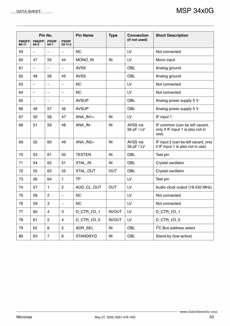
DATA SHEET MSP 34x0Gwww.DataSheet4U.com
59 − − − NC LV Not connected
60 47 55 44 MONO_IN IN LV Mono input
61 − − − AVSS OBL Analog ground
62 48 56 45 AVSS OBL Analog ground
63 − − − NC LV Not connected
64 − − − NC LV Not connected
65 − − − AVSUP OBL Analog power supply 5 V
66 49 57 46 AVSUP OBL Analog power supply 5 V
67 50 58 47 ANA_IN1+ IN LV IF input 1
68 51 59 48 ANA_IN− IN AVSS via 56 pF / LV
IF common (can be left vacant, only if IF input 1 is also not in use)
69 52 60 49 ANA_IN2+ IN AVSS via 56 pF / LV
IF input 2 (can be left vacant, only if IF input 1 is also not in use)
70 53 61 50 TESTEN IN OBL Test pin
71 54 62 51 XTAL_IN IN OBL Crystal oscillator
72 55 63 52 XTAL_OUT OUT OBL Crystal oscillator
73 56 64 1 TP LV Test pin
74 57 1 2 AUD_CL_OUT OUT LV Audio clock output (18.432 MHz)
75 58 2 − NC LV Not connected
76 59 3 − NC LV Not connected
77 60 4 3 D_CTR_I/O_1 IN/OUT LV D_CTR_I/O_1
78 61 5 4 D_CTR_I/O_0 IN/OUT LV D_CTR_I/O_0
79 62 6 5 ADR_SEL IN OBL I2C Bus address select
80 63 7 6 STANDBYQ IN OBL Stand-by (low-active)
Pin No. Pin Name Type Connection(if not used)
Short DescriptionPMQFP80-11
PMQFP64-2
PSDIP64-1
PSDIP52-1/-2
Micronas May 27, 2003; 6251-476-1DS 53

MSP 34x0G DATA SHEETwww.DataSheet4U.com
4.3. Pin Descriptions
Pin numbers refer to the PMQFP80-11 package.
Pin 1, NC – Pin not connected.
Pin 2, I2C_CL – I2C Clock Input/Output (Fig. 4–17)Via this pin, the I2C-bus clock signal has to be sup-plied. The signal can be pulled down by the MSP incase of wait conditions.
Pin 3, I2C_DA – I2C Data Input/Output (Fig. 4–17)Via this pin, the I2C-bus data is written to or read from the MSP.
Pin 4, I2S_CL – I2S Clock Input/Output (Fig. 4–18)Clock line for the I2S bus. In master mode, this line isdriven by the MSP; in slave mode, an external I2Sclock has to be supplied.
Pin 5, I2S_WS – I2S Word Strobe Input/Output (Fig. 4–18)Word strobe line for the I2S bus. In master mode, thisline is driven by the MSP; in slave mode, an externalI2S word strobe has to be supplied.
Pin 6, I2S_DA_OUT – I2S Data Output (Fig. 4–22)Output of digital serial sound data of the MSP on theI2S bus.
Pin 7, I2S_DA_IN1 – I2S Data Input 1 (Fig. 4–14)First input of digital serial sound data to the MSP viathe I2S bus.
Pin 8, ADR_DA – ADR Bus Data Output (Fig. 4–22)Output of digital serial data to the DRP 3510A via theADR bus.
Pin 9, ADR_WS – ADR Bus Word Strobe Output (Fig. 4–22)Word strobe output for the ADR bus.
Pin 10, ADR_CL – ADR Bus Clock Output (Fig. 4–22)Clock line for the ADR bus.
Pins 11, 12, 13, DVSUP* – Digital Supply VoltagePower supply for the digital circuitry of the MSP. Mustbe connected to a +5 V or +3.3 V power supply.
Pins 14, 15, 16, DVSS* – Digital GroundGround connection for the digital circuitry of the MSP.
Pin 17, I2S_DA_IN2 – I2S Data Input 2 (Fig. 4–14)Second input of digital serial sound data to the MSPvia the I2S bus.
Pins 18, 19, 20, NC – Pins not connected.
Pin 21, RESETQ – Reset Input (Fig. 4–10)In the steady state, high level is required. A low levelresets the MSP 34x0G.
Pins 22, 23, NC – Pins not connected.
Pins 24, 25, DACA_R/L – Headphone Outputs (Fig. 4–20)Output of the headphone signal. A 1-nF capacitor toAHVSS must be connected to these pins. The DC off-set on these pins depends on the selected headphonevolume.
Pin 26, VREF2 – Reference Ground 2Reference analog ground. This pin must be connectedseparately to ground (AHVSS). VREF2 serves as aclean ground and should be used as the reference foranalog connections to the loudspeaker and head-phone outputs.
Pins 27, 28, DACM_R/L – Loudspeaker Outputs (Fig. 4–20)Output of the loudspeaker signal. A 1-nF capacitor toAHVSS must be connected to these pins. The DC off-set on these pins depends on the selected loud-speaker volume.
Pin 29, NC – Pin not connected.
Pin 30, DACM_SUB – Subwoofer Output (Fig. 4–20)Output of the subwoofer signal. A 1-nF capacitor toAHVSS must be connected to this pin. Due to the lowfrequency content of the subwoofer output, the valueof the capacitor may be increased for better suppres-sion of high-frequency noise. The DC offset on this pindepends on the selected loudspeaker volume.
Pins 31, 32, NC – Pin not connected.
Pins 33, 34, SC2_OUT_R/L – SCART2 Outputs (Fig. 4–21)Output of the SCART2 signal. Connections to thesepins must use a 100-Ω series resistor and are intendedto be AC-coupled.
Pin 35, VREF1 – Reference Ground 1Reference analog ground. This pin must be connectedseparately to ground (AHVSS). VREF1 serves as aclean ground and should be used as the reference foranalog connections to the SCART outputs.
Pins 36, 37, SC1_OUT_R/L – SCART1 Outputs (Fig. 4–21)Output of the SCART1 signal. Connections to thesepins must use a 100-Ω series resistor and are intendedto be AC-coupled.
54 May 27, 2003; 6251-476-1DS Micronas

DATA SHEET MSP 34x0Gwww.DataSheet4U.com
Pin 38, CAPL_A – Volume Capacitor Headphone (Fig. 4–23)A 10-µF capacitor to AHVSUP must be connected tothis pin. It serves as a smoothing filter for headphonevolume changes in order to suppress audible plops.The value of the capacitor can be lowered to 1-µF iffaster response is required. The area encircled by thetrace lines should be minimized; keep traces as shortas possible. This input is sensitive for magnetic induc-tion.
Pin 39, AHVSUP* – Analog Power Supply High Volt-agePower is supplied via this pin for the analog circuitry ofthe MSP (except IF input). This pin must be connectedto the +8 V supply.
Pin 40, CAPL_M – Volume Capacitor Loudspeaker(Fig. 4–23)A 10-µF capacitor to AHVSUP must be connected tothis pin. It serves as a smoothing filter for loudspeakervolume changes in order to suppress audible plops.The value of the capacitor can be lowered to 1 µF iffaster response is required. The area encircled by thetrace lines should be minimized; keep traces as shortas possible. This input is sensitive for magnetic induc-tion.
Pins 41, 42, NC – Pins not connected.
Pins 43, 44, AHVSS* – Ground for Analog PowerSupply High VoltageGround connection for the analog circuitry of the MSP(except IF input).
Pin 45, AGNDC – Internal Analog Reference VoltageThis pin serves as the internal ground connection forthe analog circuitry (except IF input). It must be con-nected to the VREF pins with a 3.3-µF and a 100-nFcapacitor in parallel. This pins shows a DC level of typ-ically 3.73 V (with AHVSUP = 8 V).
Pin 46, NC – Pin not connected.
Pins 47, 48, SC4_IN_L/R – SCART4 Inputs (Fig. 4–13)The analog input signal for SCART4 is fed to this pin.Analog input connection must be AC-coupled.
Pin 49, ASG – Analog Shield GroundAnalog ground (AHVSS) should be connected to thispin to reduce cross-coupling between SCART inputs.
Pins 50, 51, SC3_IN_L/R – SCART3 Inputs (Fig. 4–13)The analog input signal for SCART3 is fed to this pin.Analog input connection must be AC-coupled.
Pin 52, ASG – Analog Shield GroundAnalog ground (AHVSS) should be connected to thispin to reduce cross-coupling between SCART inputs.
Pins 53, 54, SC2_IN_L/R – SCART2 Inputs (Fig. 4–13)The analog input signal for SCART2 is fed to this pin.Analog input connection must be AC-coupled.
Pin 55, ASG – Analog Shield GroundAnalog ground (AHVSS) should be connected to thispin to reduce cross-coupling between SCART inputs.
Pins 56, 57, SC1_IN_L/R – SCART1 Inputs (Fig. 4–13)The analog input signal for SCART1 is fed to this pin.Analog input connection must be AC-coupled.
Pin 58, VREFTOP – Reference Voltage IF A/D Con-verter (Fig. 4–15)Via this pin, the reference voltage for the IF A/D con-verter is decoupled. It must be connected to AVSSpins with a 10-µF and a 100-nF capacitor in parallel.Traces must be kept short.
Pin 59, NC – Pin not connected.
Pin 60, MONO_IN – Mono Input (Fig. 4–13)The analog mono input signal is fed to this pin. Analoginput connection must be AC-coupled.
Pins 61, 62, AVSS* – Ground for Analog PowerSupply VoltageGround connection for the analog IF input circuitry ofthe MSP.
Pins 63, 64, NC – Pins not connected.
Pins 65, 66, AVSUP* – Analog Power Supply VoltagePower is supplied via this pin for the analog IF inputcircuitry of the MSP. This pin must be connected to the+5 V supply.
Pin 67, ANA_IN1+ – IF Input 1 (Fig. 4–15)The analog sound IF signal is supplied to this pin.Inputs must be AC-coupled. This pin is designed assymmetrical input: ANA_IN1+ is internally connectedto one input of a symmetrical op amp, ANA_IN- to theother.
Pin 68, ANA_IN− – IF Common (Fig. 4–15)This pins serves as a common reference for ANA_IN1/2+ inputs.
Pin 69, ANA_IN2+ – IF Input 2 (Fig. 4–15)The analog sound if signal is supplied to this pin.Inputs must be AC-coupled. This pin is designed assymmetrical input: ANA_IN2+ is internally connectedto one input of a symmetrical op amp, ANA_IN− to theother.
Pin 70, TESTEN – Test Enable Pin (Fig. 4–11)This pin enables factory test modes. For normal opera-tion, it must be connected to ground.
Micronas May 27, 2003; 6251-476-1DS 55

MSP 34x0G DATA SHEETwww.DataSheet4U.com
Pins 71, 72, XTAL_IN, XTAL_OUT – Crystal Input andOutput Pins (Fig. 4–19)These pins are connected to an 18.432 MHz crystaloscillator which is digitally tuned by integrated shuntcapacitances. An external clock can be fed intoXTAL_IN. The audio clock output signalAUD_CL_OUT is derived from the oscillator. Externalcapacitors at each crystal pin to ground (AVSS) arerequired. It should be verified by layout, that no supplycurrent for the digital circuitry is flowing through theground connection point.
Pin 73, TP – This pin enables factory test modes. Fornormal operation, it must be left vacant.
Pin 74, AUD_CL_OUT – Audio Clock Output (Fig. 4–19)This is the 18.432 MHz main clock output.
Pins 75, 76, NC – Pins not connected.
Pins 77, 78, D_CTR_I/O_1/0 – Digital Control Input/Output Pins (Fig. 4–18)General purpose input/output pins. Pin D_CTR_I/O_1can be used as an interrupt request pin to the control-ler.
Pin 79, ADR_SEL – I2C Bus Address Select (Fig. 4–16)By means of this pin, one of three device addressesfor the MSP can be selected. The pin can be con-nected to ground (I2C device addresses 80/81hex), to+5 V supply (84/85hex), or left open (88/89hex).
Pin 80, STANDBYQ – Stand-byIn normal operation, this pin must be high. If theMSP 34x0G is switched off by first pulling STANDBYQlow and then (after >1µs delay) switching off DVSUPand AVSUP, but keeping AHVSUP (‘Standby’-mode),the SCART switches maintain their position and func-tion.
* Application Note:All ground pins should be connected to one low-resis-tive ground plane. All supply pins should be connectedseparately with short and low-resistive lines to thepower supply. Decoupling capacitors from DVSUP toDVSS, AVSUP to AVSS, and AHVSUP to AHVSS arerecommended as closely as possible to these pins.Decoupling of DVSUP and DVSS is most important.We recommend using more than one capacitor. Bychoosing different values, the frequency range ofactive decoupling can be extended. In our applicationboards we use: 220 pF, 470 pF, 1.5 nF, and 10 µF. Thecapacitor with the lowest value should be placed near-est to the DVSUP and DVSS pins.
The ASG pins should be connected as closely as pos-sible to the MSP ground. If they are lead with theSCART-inputs as shielding lines, they should not beconnected to ground at the SCART connector.
56 May 27, 2003; 6251-476-1DS Micronas

DATA SHEET MSP 34x0Gwww.DataSheet4U.com
4.4. Pin Configurations
Fig. 4–6: PSDIP64-1 package
Fig. 4–7: PSDIP52-1/-2 package
1AUD_CL_OUT
2NC
3NC
4D_CTR_I/O_1
5D_CTR_I/O_0
6ADR_SEL
7STANDBYQ
8NC
9I2C_CL
10I2C_DA
11I2S_CL
12I2S_WS
13I2S_DA_OUT
14I2S_DA_IN1
15ADR_DA
16ADR_WS
TP64
XTAL_OUT63
XTAL_IN62
TESTEN61
ANA_IN2+60
ANA_IN−59
ANA_IN+58
AVSUP57
AVSS56
MONO_IN55
VREFTOP54
SC1_IN_R53
SC1_IN_L52
ASG51
SC2_IN_R50
SC2_IN_L49
17ADR_CL
18DVSUP
19DVSS
20I2S_DA_IN2
21NC
22NC
23NC
24RESETQ
25DACA_R
26DACA_L
ASG48
SC3_IN_R47
SC3_IN_L46
ASG45
SC4_IN_R44
SC4_IN_L43
AGNDC42
AHVSS41
CAPL_M40
AHVSUP39
MS
P 3
4x0G
VREF2
DACM_R
DACM_L
NC
DACM_SUB
NC
38
37
36
35
34
33
27
28
29
30
31
32
CAPL_A
SC1_OUT_L
SC1_OUT_R
VREF1
SC2_OUT_L
SC2_OUT_R
1
2
3
4
5
6
7
8
9
10
11
12
13
14
15
16
17
18
19
20
21
22
23
24
25
26
52
51
50
49
48
47
46
45
44
43
42
41
40
39
38
37
36
35
34
33
32
31
30
29
28
27
TP
AUD_CL_OUT
D_CTR_I/O_1
D_CTR_I/O_0
ADR_SEL
STANDBYQ
I2C_CL
I2C_DA
I2S_CL
I2S_WS
I2S_DA_OUT
I2S_DA_IN1
ADR_DA
ADR_WS
ADR_CL
DVSUP
XTAL_OUT
XTAL_IN
TESTEN
ANA_IN2+
ANA_IN−
ANA_IN1+
AVSUP
AVSS
MONO_IN
VREFTOP
SC1_IN_R
SC1_IN_L
SC2_IN_R
SC2_IN_L
SC3_IN_R
SC3_IN_L
DVSS
I2S_DA_IN2
NC
RESETQ
DACA_R
DACA_L
VREF2
DACM_R
DACM_L
DACM_SUB
AGNDC
AHVSS
CAPL_M
AHVSUP
CAPL_A
SC1_OUT_L
SC1_OUT_R
VREF1
SC2_OUT_L
SC2_OUT_R
MS
P 3
4x0G
Micronas May 27, 2003; 6251-476-1DS 57

MSP 34x0G DATA SHEETwww.DataSheet4U.com
Fig. 4–8: PMQFP80-11 package
65
66
67
68
69
70
71
72
73
74
75
76
77
78
79
80
40
39
38
37
36
35
34
33
32
31
30
29
28
27
26
251 2 3 4 5 6 7 8 9 10 11 12 13 14 15 16 17 18 19 20 21 22 23 24
64 63 62 61 60 59 58 57 56 55 54 53 52 51 50 49 48 47 46 45 44 43 42 41AVSUP
AVSUP
ANA_IN1+
ANA_IN−
ANA_IN2+
TESTEN
XTAL_IN
XTAL_OUT
TP
AUD_CL_OUT
NC
NC
D_CTR_I/O_1
D_CTR_I/O_0
ADR_SEL
STANDBYQ
CAPL_M
AHVSUP
CAPL_A
SC1_OUT_L
SC1_OUT_R
VREF1
SC2_OUT_L
SC2_OUT_R
NC
NC
DACM_SUB
NC
DACM_L
DACM_R
VREF2
DACA_L
NC
AVSS
AVSS
MONO_IN
NC
VREFTOP
SC1_IN_R
SC1_IN_L
ASG
NC
SC2_IN_R
SC2_IN_L ASG
SC3_IN_R
SC3_IN_L
ASG
SC4_IN_R
SC4_IN_L
NC
AGNDC
AHVSS
AHVSS
NC
NC
I2C_CL
I2C_DA
I2S_CL
I2S_WS
I2S_DA_OUT
I2S_DA_IN1
ADR_DA
ADR_WS
ADR_CL
NC
DVSUP
DVSUP DVSUP
DVSS
DVSS
DVSS
I2S_DA_IN2
NC
NC
NC
RESETQ
NC
NC
DACA_R
MSP 34x0G
58 May 27, 2003; 6251-476-1DS Micronas
DATA SHEET MSP 34x0Gwww.DataSheet4U.com
Fig. 4–9: PMQFP64-2 package
AVSUP
ANA_IN1+
ANA_IN−
ANA_IN2+
TESTEN
XTAL_IN
XTAL_OUT
TP
AUD_CL_OUT
NC
NC
D_CTR_I/OUT1
D_CTR_I/OUT0
ADR_SEL
STANDBYQ
NC
CAPL_M
AHVSUP
CAPL_A
SC1_OUT_L
SC1_OUT_R
VREF1
SC2_OUT_L
SC2_OUT_R
NC
DACM_SUB
NC
DACM_L
DACM_R
VREF2
DACA_L
DACA_R
MONO_IN
VREFTOP
SC1_IN_R
SC1_IN_L
ASG
SC2_IN_R
SC2_IN_L
AVSS
ASG
SC3_IN_R
SC3_IN_L
ASG
SC4_IN_R
SC4_IN_L
AGNDC
AHVSS
I2C_DA
I2S_CL
I2S_WS
I2S_DA_OUT
I2S_DA_IN1
ADR_DA
ADR_WS
I2C_CL
ADR_CL
DVSUP
DVSS
I2S_DA_IN2
NC
NC
NC
RESETQ
MSP 34x0G
49
50
51
52
53
54
55
56
57
58
59
60
61
62
63
64
32
31
30
29
28
27
26
25
24
23
22
21
20
19
18
171 2 3 4 5 6 7 8 9 10 11 12 13 14 15 16
48 47 46 45 44 43 42 41 40 39 38 37 36 35 34 33
Micronas May 27, 2003; 6251-476-1DS 59

MSP 34x0G DATA SHEETwww.DataSheet4U.com
4.5. Pin Circuits
Fig. 4–10: Input Pin: RESETQ
Fig. 4–11: Input Pin TESTEN
Fig. 4–12: Input Pin: MONO_IN
Fig. 4–13: Input Pins: SC4-1_IN_L/R
Fig. 4–14: Input Pins:I2S_DA_IN1, I2S_DA_IN2, STANDBYQ
Fig. 4–15: Input Pins:VREFTOP, ANA_IN1+, ANA_IN-, ANA_IN2+
Fig. 4–16: Input Pin: ADR_SEL
Fig. 4–17: Input/Output Pins: I2C_CL, I2C_DA
Fig. 4–18: Input/Output Pins:I2S_CL, I2S_WS, D_CTR_I/O_1, D_CTR_I/O_0
Fig. 4–19: Input/Output Pins:XTAL_IN, XTAL_OUT, AUD_CL_OUT
DVSS
>300 k
AVSUP
200 k
≈ 3.75 V24 kΩ
≈ 3.75 V40 kΩ
DA
ANA_IN1+
VREFTOPANA_IN−
ANA_IN2+
ADR_SELGND
DVSUP
23 kΩ
23 kΩ
N
GND
DVSUP
P
N
GND
3−30 pF
2.5 V
500 kΩ
3−30 pF
P
N
60 May 27, 2003; 6251-476-1DS Micronas

DATA SHEET MSP 34x0Gwww.DataSheet4U.com
Fig. 4–20: Output Pins:DACA_R/L, DACM_R/L, DACM_SUB
Fig. 4–21: Output Pins: SC_2_OUT_R/L, SC_1_OUT_R/L
Fig. 4–22: Output Pins:I2S_DA_OUT, ADR_DA, ADR_WS, ADR_CL
Fig. 4–23: Capacitor Pins: CAPL_A, CAPL_M
Fig. 4–24: Pin: AGNDC
AHVSUP
0...1.2 mA
3.3 kΩ
26 pF
120 kΩ
300 Ω
≈ 3.75 V
DVSUP
P
N
GND
0...2 V
≈ 3.75 V125 kΩ
Micronas May 27, 2003; 6251-476-1DS 61

MSP 34x0G DATA SHEETwww.DataSheet4U.com
4.6. Electrical Characteristics
Abbreviations:
tbd = to be definedvacant = not applicablepositive current values mean current flowing into the chip
4.6.1. Absolute Maximum Ratings
Stresses beyond those listed in the "Absolute Maximum Ratings" may cause permanent damage to the device. Thisis a stress rating only. Functional operation of the device at these conditions is not implied. Exposure to absolut max-imum rating conditions for extended periods will affect device reliability.
All voltages listed are referenced to ground (0 V, VSS ), except where noted.
All grounds must be externally connected low ohmic.
This device contains circuitry to protect the inputs and outputs against damage due to high static voltages or electricfields; however, it is advised that normal precautions be taken to avoid application of any voltage higher than absolutmaximum-rated voltages to this high-impedance circuit.
Table 4–1: Absolute Maximum Ratings
Symbol Parameter Pin Name Limit Values Unit
Min. Max.
TA1) Ambient Operating Temperature
PSDIP64-1PSDIP52-1/-2PMQFP80-11PMQFP64-2
− 070707065
°C
TC Case Operating TemperaturePSDIP64-1PSDIP52-1/-2PMQFP80-11PMQFP64-2
− 0859095100
°C
TS Storage Temperature − −40 125 °C
PMAX Maximum Power DissipationPSDIP64-1PSDIP52-1/-2PMQFP80-11PMQFP64-2
130012001000 930
mWmWmWmW
VSUP1 Supply Voltage 1 AHVSUP −0.3 9.0 V
VSUP2 Supply Voltage 2 DVSUP −0.3 6.0 V
VSUP3 Supply Voltage 3 AVSUP −0.3 6.0 V
VIdig Input Voltage, all Digital Inputs −0.3 VSUP2+0.3 V
IIdig Input Current, all Digital Pins − −20 +20 mA
1) Measured on standard board according to JESD 51 Standard with maximum power consumption allowed forthis package.
62 May 27, 2003; 6251-476-1DS Micronas

DATA SHEET MSP 34x0Gwww.DataSheet4U.com
VIana Input Voltage, all Analog Inputs SCn_IN_s,1)
MONO_IN−0.3 VSUP1+0.3 V
IIana Input Current, all Analog Inputs SCn_IN_s,1)
MONO_IN−5 +5 mA
IOana Output Current, all SCART Outputs SCn_OUT_s1) 2) 2)
IOana Output Current, all Analog Outputs except SCART Outputs
DACp_s1) 2) 2)
ICana Output Current, other pins connected to capacitors
CAPL_p,1)
AGNDC
2) 2)
1) “n” means “1”, “2”, “3”, or “4”, “s” means “L” or “R”, “p” means “M” or “A”2) The analog outputs are short-circuit proof with respect to Supply Voltage 1 and ground.
Table 4–1: Absolute Maximum Ratings, continued
Symbol Parameter Pin Name Limit Values Unit
Min. Max.
Micronas May 27, 2003; 6251-476-1DS 63

MSP 34x0G DATA SHEETwww.DataSheet4U.com
4.6.2. Recommended Operating Conditions
Functional operation of the device beyond those indicated in the "Recommended Operating Conditions/Characteris-tics" is not implied and will result in unpredictable behaviour of the device and may result in device destruction.
All voltages listed are referenced to ground (VSS = 0 V) except where noted.
All grounds must be externally connected low ohmic.
Do not insert the device into a live socket. Instead, apply power by switching on the external power supply. Forpower-up/-down sequences, see the instructions in Section 4.6.3.3. of this document.
4.6.2.1. General Recommended Operating Conditions
Symbol Parameter Pin Name Limit Values Unit
Min. Typ. Max.
TA Ambient Operating TemperaturePSDIP64-1PSDIP52-1/-2PMQFP80-11PMQFP64-2
− 1)
70707065
°C
TC Case Operating TemperaturePSDIP64-1PSDIP52-1/-2PMQFP80-11PMQFP64-2
−859095100
°C
VSUP1 Supply Voltage 1(AHVSUP = 8 V)
AHVSUP 7.6 8.0 8.7 V
Supply Voltage 1 (AHVSUP = 5 V)
4.75 5.0 5.25 V
VSUP2 Supply Voltage 2(DVSUP = 5 V)
DVSUP 4.75 5.0 5.25 V
Supply Voltage 2 (DVSUP = 3.3 V)
3.15 3.3 3.45 V
VSUP3 Supply Voltage 3 AVSUP 4.75 5.0 5.25 V
tSTBYQ1 STANDBYQ Setup Time before Turn-off of Second Supply Voltage
STANDBYQ,DVSUP
1 µs
1) A power-optimized board layout is recommended. The Case Operating Temperatures mentioned in the Rec-ommended Operating Conditions must not be exceeded at worst case conditions of the application.
64 May 27, 2003; 6251-476-1DS Micronas

DATA SHEET MSP 34x0Gwww.DataSheet4U.com
4.6.2.2. Analog Input and Output Recommendations
Symbol Parameter Pin Name Limit Values Unit
Min. Typ. Max.
CAGNDC AGNDC-Filter-Capacitor AGNDC −20% 3.3 µF
Ceramic Capacitor in Parallel −20% 100 nF
CinSC DC-Decoupling Capacitor in front of SCART Inputs
SCn_IN_s1) −20% 330 nF
VinSC SCART Input Level 2.0 VRMS
VinMONO Input Level, Mono Input MONO_IN 2.0 VRMS
RLSC SCART Load Resistance SCn_OUT_s1) 10 kΩ
CLSC SCART Load Capacitance 6.0 nF
CVMA Main/AUX Volume Capacitor CAPL_p 10 µF
CFMA Main/AUX Filter Capacitor DACp_s1) −10% 1 +10% nF
1) “n” means “1”, “2”, “3”, or “4”, “s” means “L” or “R”, “p” means “M” or “A”
Micronas May 27, 2003; 6251-476-1DS 65

MSP 34x0G DATA SHEETwww.DataSheet4U.com
4.6.2.3. Recommendations for Analog Sound IF Input Signal
Symbol Parameter Pin Name Limit Values Unit
Min. Typ. Max.
CVREFTOP VREFTOP-Filter-Capacitor VREFTOP −20% 10 µF
Ceramic Capacitor in Parallel −20% 100 nF
FIF_FMTV Analog Input Frequency Range for TV Applications
ANA_IN1+, ANA_IN2+, ANA_IN−
0 9 MHz
FIF_FMRADIO Analog Input Frequency for FM-Radio Applications
10.7 MHz
VIF_FM Analog Input Range FM/NICAM 0.1 0.8 3 Vpp
VIF_AM Analog Input Range AM/NICAM 0.1 0.45 0.8 Vpp
RFMNI Ratio: NICAM Carrier/FM Carrier(unmodulated carriers)BG:I:
−20−23
−7−10
00
dBdB
RAMNI Ratio: NICAM Carrier/AM Carrier(unmodulated carriers)
−25 −11 0 dB
RFM Ratio: FM-Main/FM-Sub Satellite 7 dB
RFM1/FM2 Ratio: FM1/FM2German FM-System
7 dB
RFC Ratio: Main FM Carrier/Color Carrier
15 − − dB
RFV Ratio: Main FM Carrier/Luma Components
15 − − dB
PRIF Passband Ripple − − ±2 dB
SUPHF Suppression of Spectrum above 9.0 MHz (not for FM Radio)
15 − dB
FMMAX Maximum FM-Deviation (approx.)normal modeHDEV2: high deviation modeHDEV3: very high deviation mode
±180±360±540
kHzkHzkHz
66 May 27, 2003; 6251-476-1DS Micronas

DATA SHEET MSP 34x0Gwww.DataSheet4U.com
4.6.2.4. Crystal Recommendations
Symbol Parameter Pin Name Min. Typ. Max. Unit
General Crystal Recommendations
fP Crystal Parallel Resonance Fre-quency at 12 pF Load Capacitance
18.432 MHz
RR Crystal Series Resistance 8 25 Ω
C0 Crystal Shunt (Parallel) Capacitance 6.2 7.0 pF
CL External Load Capacitance1) XTAL_IN,XTAL_OUT
PSDIP approx. 1.5PMQFP approx. 3.3
pFpF
Crystal Recommendations for Master-Slave Applications (MSP-clock must perform synchronization to I2S clock)
fTOL Accuracy of Adjustment −20 +20 ppm
DTEM Frequency Variation versus Temperature
−20 +20 ppm
C1 Motional (Dynamic) Capacitance 19 24 fF
fCL Required Open Loop Clock Frequency (Tamb = 25 °C)
AUD_CL_OUT 18.431 18.433 MHz
Crystal Recommendations for FM / NICAM Applications (No MSP-clock synchronization to I2S clock possible)
fTOL Accuracy of Adjustment −30 +30 ppm
DTEM Frequency Variation versus Temperature
−30 +30 ppm
C1 Motional (Dynamic) Capacitance 15 fF
fCL Required Open Loop Clock Frequency (Tamb = 25 °C)
AUD_CL_OUT 18.4305 18.4335 MHz
Crystal Recommendations for all analog FM/AM Applications (No MSP-clock synchronization to I2S clock possible)
fTOL Accuracy of Adjustment −100 +100 ppm
DTEM Frequency Variation versus Temperature
−50 +50 ppm
fCL Required Open Loop Clock Frequency (Tamb = 25 °C)
AUD_CL_OUT 18.429 18.435 MHz
Amplitude Recommendation for Operation with External Clock Input (Cload after reset typ. 22 pF)
VXCA External Clock Amplitude XTAL_IN 0.7 Vpp
1) External capacitors at each crystal pin to ground are required. They are necessary to tune the open-loop fre-quency of the internal PLL and to stabilize the frequency in closed-loop operation. Due to different layouts, the accurate capacitor value should be determined with the customer PCB. The suggested values (1.5...3.3 pF) are figures based on experience and should serve as “start value”.
To adjust the capacitor value, reset the MSP. After the reset, no I2C telegrams should be transmitted. Measure the frequency at AUD_CL_OUT-pin. Change the capacitor value until the free running frequency matches 18.432 MHz as closely as possible. The higher the capacity, the lower the resulting clock frequency.
Note: To minimize adjustment tolerances for all MSP-generations, it is strongly recommended to use the so-called MSP-XTAL-REF ICs (available in all packages) for the capacitor adjustment.
Micronas May 27, 2003; 6251-476-1DS 67

MSP 34x0G DATA SHEETwww.DataSheet4U.com
4.6.3. Characteristics
For Min./Max. values: at TA = 0 to 70 °C, fCLOCK = 18.432 MHzVSUP1 = 7.6 to 8.7 V (4.75 to 5.25 V if VSUP1 = 5 V)VSUP2 = 4.75 to 5.25 V (3.15 to 3.45 V if VSUP2 = 3.3 V)VSUP3 = 4.75 to 5.2 V
For typical values: at TA = 60 °C, fCLOCK = 18.432 MHzVSUP1 = 8 V (5 V if noted)VSUP2 = 5 V (3.3 V if noted)VSUP3 = 5 V
TJ = Junction Temperature
MAIN (M) = Loudspeaker Channel, AUX (A) = Headphone Channel
4.6.3.1. General Characteristics
Symbol Parameter Pin Name Limit Values Unit Test Conditions
Min. Typ. Max.
Supply
ISUP1A First Supply Current (active)(AHVSUP = 8 V)
AHVSUP 1711
2516
mAmA
Vol. Main and Aux = 0 dBVol. Main and Aux = -30dB
First Supply Current (active)(AHVSUP = 5 V)
118
1711
mAmA
Vol. Main and Aux = 0 dBVol. Main and Aux = -30 dB
ISUP2A Second Supply Current (active)(DVSUP = 5 V)
DVSUP 55 70 mA
Second Supply Current (active)(DVSUP = 3.3 V)
55 70 mA
ISUP3A Third Supply Current (active) AVSUP 30 38 mA
ISUP1S First Supply Current(AHVSUP = 8 V)
AHVSUP 5.6 7.7 mA STANDBYQ = low
First Supply Current(AHVSUP = 5 V)
3.7 5.1 mA
Clock
fCLOCK Clock Input Frequency XTAL_IN 18.432 MHz
DCLOCK Clock High to Low Ratio 45 55 %
tJITTER Clock Jitter (Verification not provided in Production Test)
50 ps
VxtalDC DC-Voltage Oscillator 2.5 V
tStartup Oscillator Startup Time at VDD Slew-rate of 1 V/1 µs
XTAL_IN,XTAL_OUT
0.4 2 ms
VACLKAC Audio Clock Output AC Voltage AUD_CL_OUT 1.2 1.8 Vpp load = 40 pF
VACLKDC Audio Clock Output DC Voltage 0.4 0.6 VSUP3 Imax = 0.2 mA
routHF_ACL HF Output Resistance 140 Ω
68 May 27, 2003; 6251-476-1DS Micronas
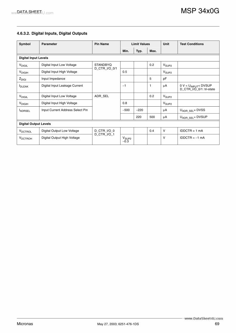
DATA SHEET MSP 34x0Gwww.DataSheet4U.com
4.6.3.2. Digital Inputs, Digital Outputs
Symbol Parameter Pin Name Limit Values Unit Test Conditions
Min. Typ. Max.
Digital Input Levels
VDIGIL Digital Input Low Voltage STANDBYQD_CTR_I/O_0/1
0.2 VSUP2
VDIGIH Digital Input High Voltage 0.5 VSUP2
ZDIGI Input Impedance 5 pF
IDLEAK Digital Input Leakage Current −1 1 µA 0 V < UINPUT< DVSUPD_CTR_I/O_0/1: tri-state
VDIGIL Digital Input Low Voltage ADR_SEL 0.2 VSUP2
VDIGIH Digital Input High Voltage 0.8 VSUP2
IADRSEL Input Current Address Select Pin −500 −220 µA UADR_SEL= DVSS
220 500 µA UADR_SEL= DVSUP
Digital Output Levels
VDCTROL Digital Output Low Voltage D_CTR_I/O_0D_CTR_I/O_1
0.4 V IDDCTR = 1 mA
VDCTROH Digital Output High Voltage VSUP2−0.3
V IDDCTR = −1 mA
Micronas May 27, 2003; 6251-476-1DS 69

MSP 34x0G DATA SHEETwww.DataSheet4U.com
4.6.3.3. Reset Input and Power-Up
Fig. 4–25: Power-up sequence
Symbol Parameter Pin Name Limit Values Unit Test Conditions
Min. Typ. Max.
RESETQ Input Levels
VRHL Reset High-Low Transition Voltage RESETQ 0.3 0.4 VSUP2
VRLH Reset Low-High Transition Voltage 0.45 VSUP2
ZRES Input Capacitance 5 pF
IRES Input High Current 20 µA URESETQ = DVSUP
0.9×DVSUP
InternalReset
t/ms
RESETQ
AVSUPDVSUP
High
Low
t/ms
t/ms
Note: The reset shouldnot reach high levelbefore the oscillator hasstarted. This requires areset delay of >2 ms
0.45 x DVSUP means 2.25 Volt with DVSUP = 5.0 V
0.3...0.4×DVSUP
0.45×DVSUPHigh-to-LowThreshold
Low-to-HighThreshold
Reset Delay>2 ms
70 May 27, 2003; 6251-476-1DS Micronas

DATA SHEET MSP 34x0Gwww.DataSheet4U.com
4.6.3.4. I2C-Bus Characteristics
Fig. 4–26: I2C bus timing diagram
Symbol Parameter Pin Name Limit Values Unit Test Conditions
Min. Typ. Max.
VI2CIL I2C-Bus Input Low Voltage I2C_CL,I2C_DA
0.3 VSUP2
VI2CIH I2C-Bus Input High Voltage 0.6 VSUP2
tI2C1 I2C Start Condition Setup Time 120 ns
tI2C2 I2C Stop Condition Setup Time 120 ns
tI2C5 I2C-Data Setup Time before Rising Edge of Clock
55 ns
tI2C6 I2C-Data Hold Time after Falling Edge of Clock
55 ns
tI2C3 I2C-Clock Low Pulse Time I2C_CL 500 ns
tI2C4 I2C-Clock High Pulse Time 500 ns
fI2C I2C-BUS Frequency 1.0 MHz
VI2COL I2C-Data Output Low Voltage I2C_CL,I2C_DA
0.4 V II2COL = 3 mA
II2COH I2C-Data Output High Leakage Current
1.0 µA VI2COH = 5 V
tI2COL1 I2C-Data Output Hold Time after Falling Edge of Clock
15 ns
tI2COL2 I2C-Data Output Setup Time before Rising Edge of Clock
100 ns fI2C = 1 MHz
I2C_CL
I2C_DA as input
I2C_DA as output
TI2C1 TI2C5 TI2C6 TI2C2
TI2C4 TI2C3
1/FI2C
TI2COL2 TI2COL1
Micronas May 27, 2003; 6251-476-1DS 71

MSP 34x0G DATA SHEETwww.DataSheet4U.com
4.6.3.5. I2S-Bus Characteristics
Symbol Parameter Pin Name Limit Values Unit Test Conditions
Min. Typ. Max.
VI2SIL Input Low Voltage I2S_DA_IN1/2I2S_CLI2S_WS
0.2 VSUP2
VI2SIH Input High Voltage 0.5 VSUP2
ZI2SI Input Impedance 5 pF
ILEAKI2S Input Leakage Current −1 1 µA 0 V < UINPUT< DVSUP
VI2SOL I2S Output Low Voltage I2S_CLI2S_WSI2S_DA_OUT
0.4 V II2SOL = 1 mA
VI2SOH I2S Output High Voltage VSUP2 − 0.3
V II2SOH = −1 mA
fI2SOWS I2S-Word Strobe Output Frequency I2S_WS 32.0 kHz
fI2SOCL I2S-Clock Output Frequency I2S_CL 1.0242.048
MHzMHz
I2S_CONFIG[0] = 0I2S_CONFIG[0] = 1
RI2S10/I2S20 I2S-Clock Output High/Low-Ratio 0.9 1.0 1.1
ts_I2S I2S Input Setup Timebefore Rising Edge of Clock
I2S_CLI2S_DA_IN1/2
12 ns for details see Fig. 4–27 “I2S bus timing diagram”
th_I2S I2S Input Hold Timeafter Rising Edge of Clock
40 ns
td_I2S I2S Output Delay Time after Falling Edge of Clock
I2S_CLI2S_WSI2S_DA_OUT
28 ns CL = 30 pF
fI2SWS I2S-Word Strobe Input Frequency I2S_WS 32.0 kHz
fI2SCL I2S-Clock Input Frequency I2S_CL 1.024 2.048 MHz
RI2SCL I2S-Clock Input High/Low Ratio 0.9 1.1
72 May 27, 2003; 6251-476-1DS Micronas

DATA SHEET MSP 34x0Gwww.DataSheet4U.com
Fig. 4–27: I2S bus timing diagram
Data: MSB first, I2S master
R LSB L LSB
R LSB L LSB
16/32 bit right channel
L LSB
L LSB
R MSB
R MSB
Detail C
I2S_WS
I2S_CL
I2S_DA_IN
Detail A
MODUS[6] = 1MODUS[6] = 0
Detail B
R LSB
R LSB L MSB
L MSBI2S_DA_OUT
16/32 bit right channel16/32 bit left channel
16/32 bit left channel
1/FI2SWS
I2S_CL
Detail C
I2S_WS as INPUT
I2S_WS as OUTPUT
1/FI2SCL
Ts_I2S
Td_I2S
Detail A,B
I2S_CL
I2S_DA_OUT
Td_I2S
Data: MSB first, I2S slave
R LSB L LSB
R LSB L LSB
16, 18...32 bit right channel
L LSB
L LSB
R MSB
R MSB
Detail C
I2S_WS
I2S_CL
I2S_DA_IN
Detail A
MODUS[6] = 1MODUS[6] = 0
Detail B
R LSB
R LSB L MSB
L MSBI2S_DA_OUT
16, 18...32 bit right channel
16, 18...32 bit left channel
16,18...32 bit left channel
1/FI2SWS
Th_I2STs_I2S
I2S_DA_IN1/2
Micronas May 27, 2003; 6251-476-1DS 73

MSP 34x0G DATA SHEETwww.DataSheet4U.com
4.6.3.6. Analog Baseband Inputs and Outputs, AGNDC
Symbol Parameter Pin Name Limit Values Unit Test Conditions
Min. Typ. Max.
Analog Ground
VAGNDC0 AGNDC Open Circuit Voltage(AHVSUP =8 V)
AGNDC 3.77 V Rload ≥10 MΩ
AGNDC Open Circuit Voltage(AHVSUP = 5 V)
2.51 V
RoutAGN AGNDC Output Resistance(AHVSUP = 8 V)
70 125 180 kΩ 3 V ≤ VAGNDC ≤ 4 V
AGNDC Output Resistance(AHVSUP = 5 V)
47 83 120 kΩ
Analog Input Resistance
RinSC SCART Input Resistancefrom TA = 0 to 70 °C
SCn_IN_s1) 25 40 58 kΩ fsignal = 1 kHz, I = 0.05 mA
RinMONO MONO Input Resistancefrom TA = 0 to 70 °C
MONO_IN 15 24 35 kΩ fsignal = 1 kHz, I = 0.1 mA
Audio Analog-to-Digital-Converter
VAICL Analog Input Clipping Level for Analog-to-Digital-Conversion(AHVSUP = 8 V)
SCn_IN_s,1)
MONO_IN2.00 2.25 VRMS fsignal = 1 kHz
Analog Input Clipping Level for Analog-to-Digital-Conversion(AHVSUP = 5 V)
1.13 1.51 VRMS
SCART Outputs
RoutSC SCART Output Resistance SCn_OUT_s1)
200200
330 460500
ΩΩ
fsignal = 1 kHz, I = 0.1 mATj = 27 °CTA = 0 to 70 °C
dVOUTSC Deviation of DC-Level at SCART Output from AGNDC Voltage
−70 +70 mV
ASCtoSC Gain from Analog Inputto SCART Output
SCn_IN_s,1)
MONO_IN →SCn_OUT_s1)
−1.0 +0.5 dB fsignal = 1 kHz
frSCtoSC Frequency Response from Analog Input to SCART Output
−0.5 +0.5 dB with resp. to 1 kHz Bandwidth: 0 to 20000 Hz
VoutSC Signal Level at SCART Output(AHVSUP = 8 V)
SCn_OUT_s1) 1.8 1.9 2.0 VRMS fsignal = 1 kHzVolume 0 dBFull Scale input from I2S
Signal Level at SCART Output(AHVSUP = 5V)
1.17 1.27 1.37 VRMS
1) “n” means “1”, “2”, “3”, or “4”; “s” means “L” or “R”
74 May 27, 2003; 6251-476-1DS Micronas

DATA SHEET MSP 34x0Gwww.DataSheet4U.com
4.6.3.7. Sound IF Inputs
4.6.3.8. Power Supply Rejection
Main and AUX Outputs
RoutMA Main/AUX Output Resistance DACp_s1)
2.12.1
3.3 4.65.0
kΩkΩ
fsignal = 1 kHz, I = 0.1 mATj = 27 °CTA = 0 to 70 °C
VoutDCMA DC-Level at Main/AUX-Output(AHVSUP = 8 V)
1.80 2.0461
2.28 VmV
Volume 0 dBVolume −30 dB
DC-Level at Main/AUX-Output(AHVSUP = 5 V)
1.12 1.3640
1.60 VmV
Volume 0 dBVolume −30 dB
VoutMA Signal Level at Main/AUX-Output (AHVSUP = 8 V)
1.23 1.37 1.51 VRMS fsignal = 1 kHzVolume 0 dBFull scale input from I2S
Signal Level at Main/AUX-Output (AHVSUP = 5 V)
0.76 0.90 1.04 VRMS
1) “s” means “L” or “R”; “p” means “M” or “A”
Symbol Parameter Pin Name Limit Values Unit Test Conditions
Min. Typ. Max.
RIFIN Input Impedance ANA_IN1+, ANA_IN2+, ANA_IN−
1.56.8
29.1
2.511.4
kΩkΩ
Gain AGC = 20 dBGain AGC = 3 dB
DCVREFTOP DC Voltage at VREFTOP VREFTOP 2.45 2.65 2.75 V
DCANA_IN DC Voltage on IF Inputs ANA_IN1+, ANA_IN2+, ANA_IN−
1.3 1.5 1.7 V
XTALKIF Crosstalk Attenuation ANA_IN1+, ANA_IN2+, ANA_IN−
40 dB fsignal = 1 MHzInput Level = −2 dBr
BWIF 3 dB Bandwidth 10 MHz
AGC AGC Step Width 0.85 dB
Symbol Parameter Pin Name Limit Values Unit Test Conditions
Min. Typ. Max.
PSRR: Rejection of Noise on AHVSUP at 1 kHz
PSRR AGNDC AGNDC 80 dB
From Analog Input to I2S Output MONO_IN,SCn_IN_s1)
70 dB
From Analog Input to SCART Output
MONO_IN,SCn_IN_s1)
SCn_OUT_s1)
70 dB
From I2S Input to SCART Output SCn_OUT_s1) 60 dB
From I2S Input to MAIN or AUX Output
DACp_s1) 80 dB
1) “n” means “1”, “2”, “3”, or “4”; “s” means “L” or “R”; “p” means “M” or “A”
Symbol Parameter Pin Name Limit Values Unit Test Conditions
Min. Typ. Max.
Micronas May 27, 2003; 6251-476-1DS 75
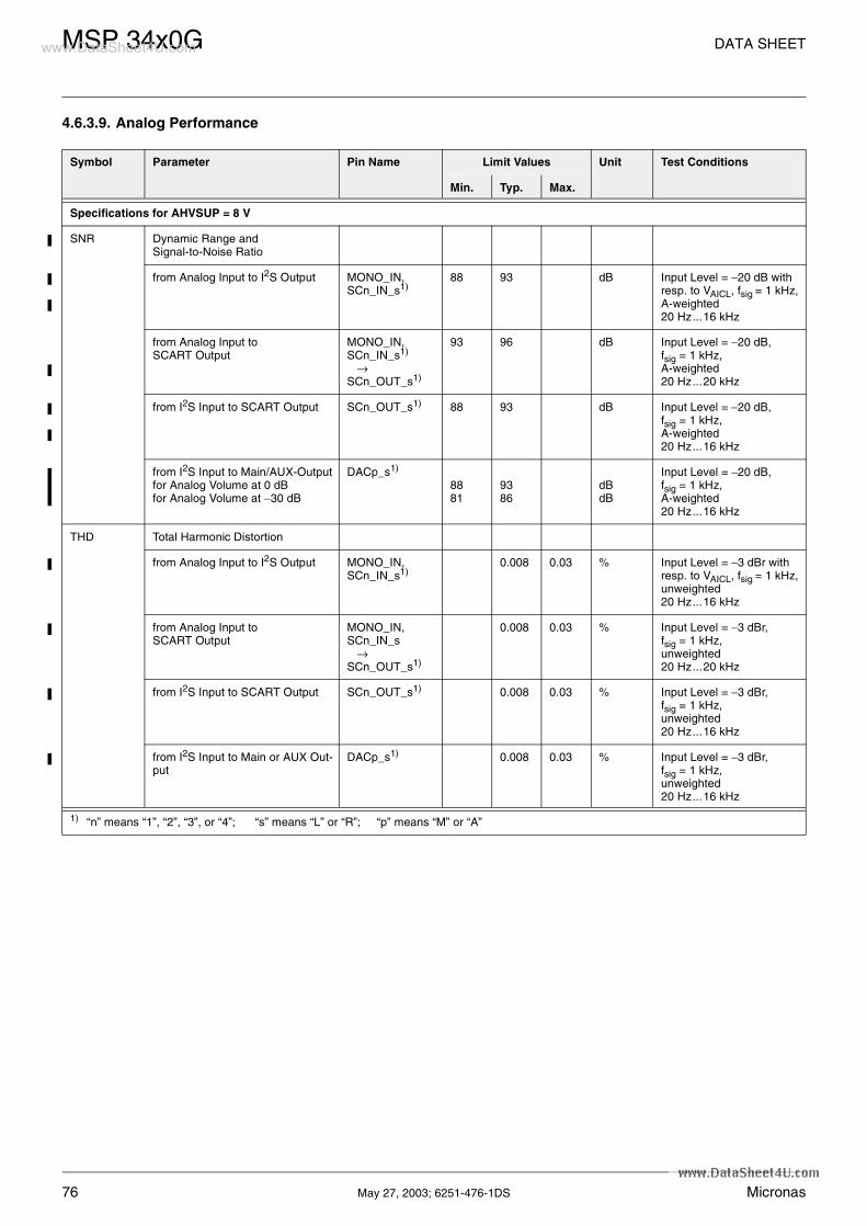
MSP 34x0G DATA SHEETwww.DataSheet4U.com
4.6.3.9. Analog Performance
Symbol Parameter Pin Name Limit Values Unit Test Conditions
Min. Typ. Max.
Specifications for AHVSUP = 8 V
SNR Dynamic Range and Signal-to-Noise Ratio
from Analog Input to I2S Output MONO_IN,SCn_IN_s1)
88 93 dB Input Level = −20 dB with resp. to VAICL, fsig = 1 kHz, A-weighted 20 Hz...16 kHz
from Analog Input to SCART Output
MONO_IN,SCn_IN_s1)
→SCn_OUT_s1)
93 96 dB Input Level = −20 dB, fsig = 1 kHz, A-weighted 20 Hz...20 kHz
from I2S Input to SCART Output SCn_OUT_s1) 88 93 dB Input Level = −20 dB,fsig = 1 kHz, A-weighted 20 Hz...16 kHz
from I2S Input to Main/AUX-Outputfor Analog Volume at 0 dBfor Analog Volume at −30 dB
DACp_s1)
8881
9386
dBdB
Input Level = −20 dB,fsig = 1 kHz, A-weighted 20 Hz...16 kHz
THD Total Harmonic Distortion
from Analog Input to I2S Output MONO_IN,SCn_IN_s1)
0.008 0.03 % Input Level = −3 dBr with resp. to VAICL, fsig = 1 kHz, unweighted20 Hz...16 kHz
from Analog Input to SCART Output
MONO_IN,SCn_IN_s →SCn_OUT_s1)
0.008 0.03 % Input Level = −3 dBr,fsig = 1 kHz, unweighted 20 Hz...20 kHz
from I2S Input to SCART Output SCn_OUT_s1) 0.008 0.03 % Input Level = −3 dBr,fsig = 1 kHz,unweighted 20 Hz...16 kHz
from I2S Input to Main or AUX Out-put
DACp_s1) 0.008 0.03 % Input Level = −3 dBr,fsig = 1 kHz,unweighted 20 Hz...16 kHz
1) “n” means “1”, “2”, “3”, or “4”; “s” means “L” or “R”; “p” means “M” or “A”
76 May 27, 2003; 6251-476-1DS Micronas

DATA SHEET MSP 34x0Gwww.DataSheet4U.com
Specifications for AHVSUP = 5 V
SNR Dynamic Range and Signal-to-Noise Ratio
from Analog Input to I2S Output MONO_IN,SCn_IN_s1)
85 90 dB Input Level = −20 dB with resp. to VAICL, fsig = 1 kHz, A-weighted 20 Hz...16 kHz
from Analog Input to SCART Output
MONO_IN,SCn_IN_s1)
→SCn_OUT_s1)
90 93 dB Input Level = −20 dB, fsig = 1 kHz, A-weighted 20 Hz...20 kHz
from I2S Input to SCART Output SCn_OUT_s1) 85 90 dB Input Level = −20 dB,fsig = 1 kHz, A-weighted 20 Hz...16 kHz
from I2S Input to Main/AUX-Outputfor Analog Volume at 0 dBfor Analog Volume at −30 dB
DACp_s1)
8578
9083
dBdB
Input Level = −20 dB,fsig = 1 kHz, A-weighted 20 Hz...16 kHz
THD Total Harmonic Distortion
from Analog Input to I2S Output MONO_IN,SCn_IN_s1)
0.03 0.1 % Input Level = −3 dBr with resp. to VAICL, fsig = 1 kHz, unweighted20 Hz...16 kHz
from Analog Input to SCART Output
MONO_IN,SCn_IN_s →SCn_OUT_s1)
0.1 % Input Level = −3 dBr,fsig = 1 kHz, unweighted 20 Hz...20 kHz
from I2S Input to SCART Output SCn_OUT_s1) 0.1 % Input Level = −3 dBr,fsig = 1 kHz,unweighted 20 Hz...16 kHz
from I2S Input to Main or AUX Out-put
DACp_s1) 0.1 % Input Level = −3 dBr,fsig = 1 kHz,unweighted 20 Hz...16 kHz
1) “n” means “1”, “2”, “3”, or “4”; “s” means “L” or “R”; “p” means “M” or “A”
Symbol Parameter Pin Name Limit Values Unit Test Conditions
Min. Typ. Max.
Micronas May 27, 2003; 6251-476-1DS 77
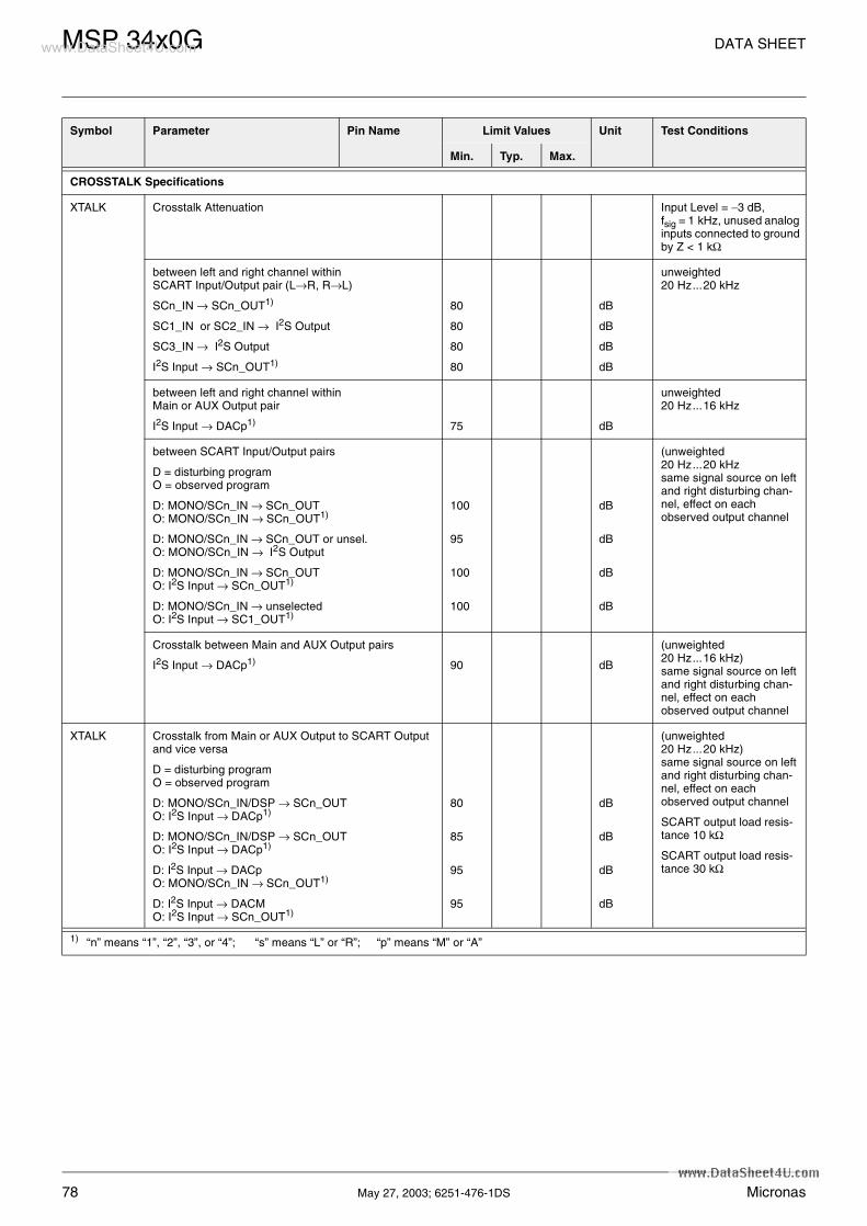
MSP 34x0G DATA SHEETwww.DataSheet4U.com
CROSSTALK Specifications
XTALK Crosstalk Attenuation Input Level = −3 dB, fsig = 1 kHz, unused analog inputs connected to ground by Z < 1 kΩ
between left and right channel within SCART Input/Output pair (L→R, R→L)
SCn_IN → SCn_OUT1)
SC1_IN or SC2_IN → I2S Output
SC3_IN → I2S Output
I2S Input → SCn_OUT1)
80
80
80
80
dB
dB
dB
dB
unweighted 20 Hz...20 kHz
between left and right channel withinMain or AUX Output pair
I2S Input → DACp1) 75 dB
unweighted 20 Hz...16 kHz
between SCART Input/Output pairs
D = disturbing programO = observed program
D: MONO/SCn_IN → SCn_OUT O: MONO/SCn_IN → SCn_OUT1)
D: MONO/SCn_IN → SCn_OUT or unsel.O: MONO/SCn_IN → I2S Output
D: MONO/SCn_IN → SCn_OUTO: I2S Input → SCn_OUT1)
D: MONO/SCn_IN → unselectedO: I2S Input → SC1_OUT1)
100
95
100
100
dB
dB
dB
dB
(unweighted 20 Hz...20 kHzsame signal source on left and right disturbing chan-nel, effect on each observed output channel
Crosstalk between Main and AUX Output pairs
I2S Input → DACp1) 90 dB
(unweighted 20 Hz...16 kHz)same signal source on left and right disturbing chan-nel, effect on each observed output channel
XTALK Crosstalk from Main or AUX Output to SCART Output and vice versa
D = disturbing programO = observed program
D: MONO/SCn_IN/DSP → SCn_OUTO: I2S Input → DACp1)
D: MONO/SCn_IN/DSP → SCn_OUT O: I2S Input → DACp1)
D: I2S Input → DACpO: MONO/SCn_IN → SCn_OUT1)
D: I2S Input → DACMO: I2S Input → SCn_OUT1)
80
85
95
95
dB
dB
dB
dB
(unweighted 20 Hz...20 kHz)same signal source on left and right disturbing chan-nel, effect on each observed output channel
SCART output load resis-tance 10 kΩ
SCART output load resis-tance 30 kΩ
1) “n” means “1”, “2”, “3”, or “4”; “s” means “L” or “R”; “p” means “M” or “A”
Symbol Parameter Pin Name Limit Values Unit Test Conditions
Min. Typ. Max.
78 May 27, 2003; 6251-476-1DS Micronas

DATA SHEET MSP 34x0Gwww.DataSheet4U.com
4.6.3.10. Sound Standard Dependent Characteristics
Symbol Parameter Pin Name Limit Values Unit Test Conditions
Min. Typ. Max.
NICAM Characteristics (MSP Standard Code = 8)
dVNICAMOUT Tolerance of Output Voltage of NICAM Baseband Signal
DACp_sSCn_OUT_s1
−1.5 +1.5 dB 2.12 kHz, Modulator input level = 0 dBref
S/NNICAM S/N of NICAM Baseband Signal 72 dB NICAM: −6 dB, 1 kHz, RMS unweighted0 to 15 kHz, Vol = 9 dB NIC_Presc = 7FhexOutput level 1 VRMS at DACp_s
THDNICAM Total Harmonic Distortion + Noise of NICAM Baseband Signal
0.1 % 2.12 kHz, Modulator input level = 0 dBref
BERNICAM NICAM: Bit Error Rate 1 10−7 FM+NICAM, norm conditions
fRNICAM NICAM Frequency Response , 20...15000 Hz
−1.0 +1.0 dB Modulator input level = −12 dB dBref; RMS
XTALKNICAM NICAM Crosstalk Attenuation (Dual) 80 dB
SEPNICAM NICAM Channel Separation (Stereo) 80 dB
FM Characteristics (MSP Standard Code = 3)
dVFMOUT Tolerance of Output Voltage of FM Demodulated Signal
DACp_s,SCn_OUT_s1
−1.5 +1.5 dB 1 FM-carrier, 50 µs, 1 kHz,40 kHz deviation; RMS
S/NFM S/N of FM Demodulated Signal 73 dB 1 FM-carrier 5.5 MHz, 50 µs, 1 kHz, 40 kHz deviation; RMS, unweighted 0 to 15 kHz (for S/N); full input range, FM-Pres-cale = 46hex, Vol = 0 dB → Output Level 1 VRMS at DACp_s
THDFM Total Harmonic Distortion + Noise of FM Demodulated Signal
0.1 %
fRFM FM Frequency Responses,20...15000 Hz
−1.0 +1.0 dB 1 FM-carrier 5.5 MHz, 50 µs, Modulator input level = −14.6 dBref; RMS
XTALKFM FM Crosstalk Attenuation (Dual) 80 dB 2 FM-carriers 5.5/5.74 MHz, 50 µs, 1 kHz, 40 kHz devia-tion; Bandpass 1 kHz
SEPFM FM Channel Separation (Stereo) 50 dB 2 FM-carriers 5.5/5.74 MHz, 50 µs, 1 kHz, 40 kHz devia-tion; RMS
AM Characteristics (MSP Standard Code = 9)
S/NAM(1) S/N of AM Demodulated Signalmeasurement condition: RMS/Flat
DACp_s,SCn_OUT_s1
55 dB SIF level: 0.1−0.8 VppAM-carrier 54% at 6.5 MHzVol = 0 dB, FM/AM prescaler set for output = 0.5 VRMS at Loudspeaker out;Standard Code = 09hexno video/chroma components
S/NAM(2) S/N of AM Demodulated Signalmeasurement condition: QP/CCIR
45 dB
THDAM Total Harmonic Distortion + Noise of AM Demodulated Signal
0.6 %
fRAM AM Frequency Response50...12000 Hz
−2.5 +1.0 dB
1) “n” means “1” or “2”; “s” means “L” or “R”; “p” means “M” or “A”
Micronas May 27, 2003; 6251-476-1DS 79

MSP 34x0G DATA SHEETwww.DataSheet4U.com
BTSC Characteristics (MSP Standard Code = 20hex, 21hex)
S/NBTSC S/N of BTSC Stereo Signal
S/N of BTSC-SAP Signal
DACp_s,SCn_OUT_s1)
68
57
dB
dB
1 kHz L or R or SAP, 100% modulation, 75 µs deempha-sis, RMS unweighted 0 to 15 kHz
THDBTSC THD+N of BTSC Stereo Signal
THD+N of BTSC SAP Signal
0.1
0.5
%
%
1 kHz L or R or SAP, 100% 75 µs EIM2), DBX NR or MNR, RMS unweighted 0 to 15 kHz
fRDBX Frequency Response of BTSC Ste-reo, 50 Hz...12 kHz
Frequency Response of BTSC-SAP, 50 Hz...9 kHz
−1.0
−1.0
1.0
1.0
dB
dB
L or R or SAP, 1%...66% EIM2), DBX NR
fRMNR Frequency Response of BTSC Ste-reo, 50 Hz...12 kHz
−2.0 2.0 dB L or R 5%...66% EIM2), MNR
Frequency Response of BTSC-SAP, 50 Hz...9 kHz
−2.0 2.0 dB SAP, white noise, 10% Modu-lation, MNR
XTALKBTSC Stereo → SAP
SAP → Stereo
76
80
dB
dB
1 kHz L or R or SAP, 100% modulation, 75 µs deempha-sis, Bandpass 1 kHz
SEPDBX Stereo Separation DBX NR50 Hz...10 kHz50 Hz...12 kHz
3530
dBdB
L or R 1%...66% EIM2), DBX NR
SEPMNR Stereo Separation MNR 30 dB L = 300 Hz, R = 3.1 kHz 14% Modulation, MNR
FMpil Pilot deviation threshold
Stereo off → on
Stereo on → off
ANA_IN1+,ANA_IN2+
3.2
1.2
3.5
1.5
kHz
kHz
4.5 MHz carrier modulated with fh = 15.734 kHzSIF level = 100 mVppindication: STATUS Bit[6]
fPilot Pilot Frequency Range 15.563 15.843 kHz standard BTSC stereo sig-nal, sound carrier only
1) “n” means “1” or “2”; “s” means “L” or “R”; “p” means “M” or “A”2) EIM refers to 75-µs Equivalent Input Modulation. It is defined as the audio-signal level which results in a stated percentage modulation, when the DBX encoding process is replaced by a 75-µs preemphasis network.
Symbol Parameter Pin Name Limit Values Unit Test Conditions
Min. Typ. Max.
80 May 27, 2003; 6251-476-1DS Micronas

DATA SHEET MSP 34x0Gwww.DataSheet4U.com
BTSC Characteristics (MSP Standard Code = 20hex, 21hex) with a minimum IF input signal level of 70 mVpp (measured without any video/chroma signal components)
S/NBTSC S/N of BTSC Stereo Signal
S/N of BTSC-SAP Signal
DACp_s,SCn_OUT_s1
64
55
dB
dB
1 kHz L or R or SAP, 100% modulation, 75 µs deempha-sis, RMS unweighted 0 to 15 kHz
THDBTSC THD+N of BTSC Stereo Signal
THD+N of BTSC SAP Signal
0.15
0.8
%
%
1 kHz L or R or SAP, 100% 75 µs EIM2), DBX NR or MNR, RMS unweighted 0 to 15 kHz
fRDBX Frequency Response of BTSC Ste-reo, 50 Hz...12 kHz
Frequency Response of BTSC-SAP, 50 Hz...9 kHz
−1.0
−1.0
1.0
1.0
dB
dB
L or R or SAP, 1%...66% EIM2), DBX NR
fRMNR Frequency Response of BTSC Ste-reo, 50 Hz...12 kHz
−2.0 2.0 dB L or R 5%...66% EIM2), MNR
Frequency Response of BTSC-SAP, 50 Hz...9 kHz
−2.0 2.0 dB SAP, white noise, 10% Modu-lation, MNR
XTALKBTSC Stereo → SAP
SAP → Stereo
75
75
dB
dB
1 kHz L or R or SAP, 100% modulation, 75 µs deempha-sis, Bandpass 1 kHz
SEPDBX Stereo Separation DBX NR50 Hz...10 kHz50 Hz...12 kHz
3530
dBdB
L or R 1%...66% EIM2), DBX NR
SEPMNR Stereo Separation MNR 30 dB L = 300 Hz, R = 3.1 kHz 14% Modulation, MNR
1) “n” means “1” or “2”; “s” means “L” or “R”; “p” means “M” or “A”2) EIM refers to 75-µs Equivalent Input Modulation. It is defined as the audio-signal level which results in a stated percentage modulation, when the DBX encoding process is replaced by a 75-µs preemphasis network.
Symbol Parameter Pin Name Limit Values Unit Test Conditions
Min. Typ. Max.
Micronas May 27, 2003; 6251-476-1DS 81
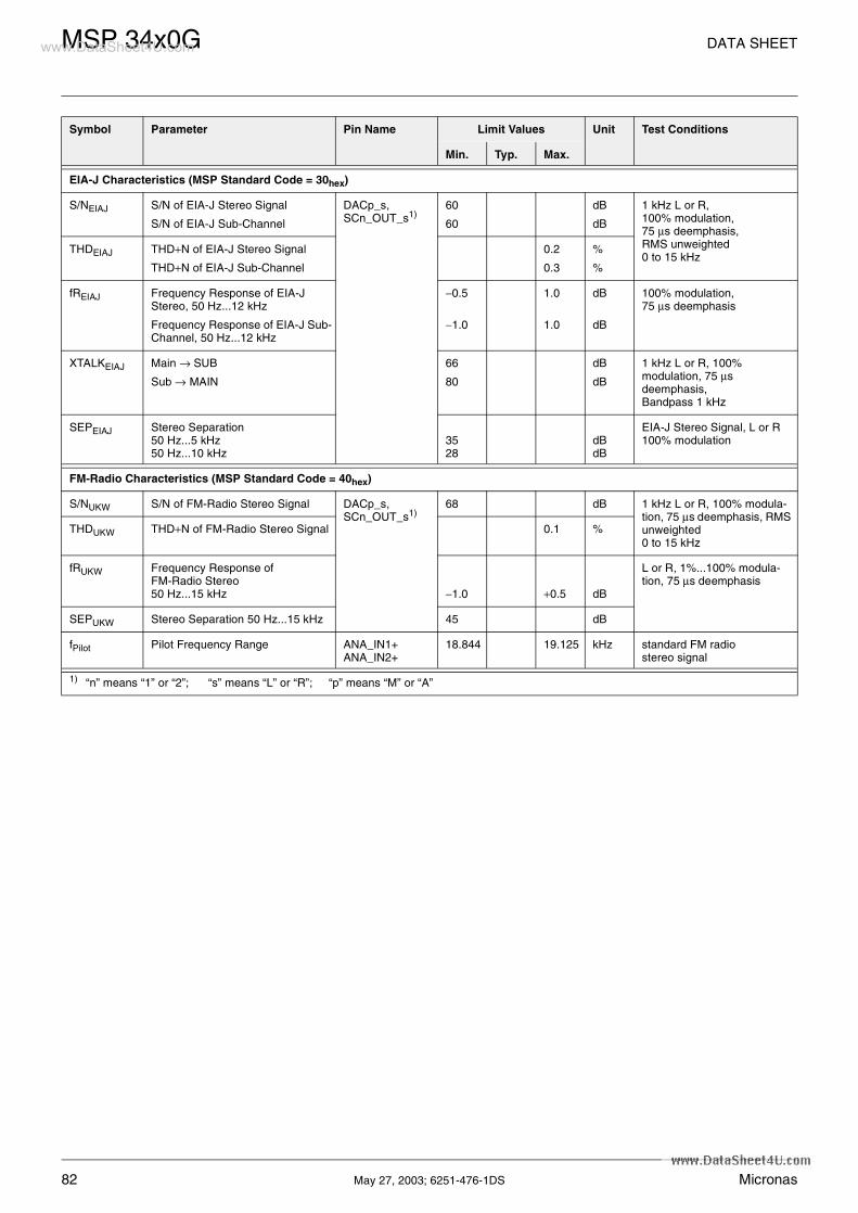
MSP 34x0G DATA SHEETwww.DataSheet4U.com
EIA-J Characteristics (MSP Standard Code = 30hex)
S/NEIAJ S/N of EIA-J Stereo Signal
S/N of EIA-J Sub-Channel
DACp_s,SCn_OUT_s1)
60
60
dB
dB
1 kHz L or R, 100% modulation, 75 µs deemphasis, RMS unweighted 0 to 15 kHz
THDEIAJ THD+N of EIA-J Stereo Signal
THD+N of EIA-J Sub-Channel
0.2
0.3
%
%
fREIAJ Frequency Response of EIA-J Stereo, 50 Hz...12 kHz
Frequency Response of EIA-J Sub-Channel, 50 Hz...12 kHz
−0.5
−1.0
1.0
1.0
dB
dB
100% modulation, 75 µs deemphasis
XTALKEIAJ Main → SUB
Sub → MAIN
66
80
dB
dB
1 kHz L or R, 100% modulation, 75 µs deemphasis, Bandpass 1 kHz
SEPEIAJ Stereo Separation50 Hz...5 kHz50 Hz...10 kHz
3528
dBdB
EIA-J Stereo Signal, L or R 100% modulation
FM-Radio Characteristics (MSP Standard Code = 40hex)
S/NUKW S/N of FM-Radio Stereo Signal DACp_s,SCn_OUT_s1)
68 dB 1 kHz L or R, 100% modula-tion, 75 µs deemphasis, RMS unweighted 0 to 15 kHz
THDUKW THD+N of FM-Radio Stereo Signal 0.1 %
fRUKW Frequency Response of FM-Radio Stereo50 Hz...15 kHz −1.0 +0.5 dB
L or R, 1%...100% modula-tion, 75 µs deemphasis
SEPUKW Stereo Separation 50 Hz...15 kHz 45 dB
fPilot Pilot Frequency Range ANA_IN1+ANA_IN2+
18.844 19.125 kHz standard FM radio stereo signal
1) “n” means “1” or “2”; “s” means “L” or “R”; “p” means “M” or “A”
Symbol Parameter Pin Name Limit Values Unit Test Conditions
Min. Typ. Max.
82 May 27, 2003; 6251-476-1DS Micronas

DATA SHEET MSP 34x0Gwww.DataSheet4U.com
5. Appendix A: Overview of TV-Sound Standards
5.1. NICAM 728
Table 5–1: Summary of NICAM 728 sound modulation parameters
Specification I B/G L D/K
Carrier frequency of digital sound
6.552 MHz 5.85 MHz 5.85 MHz 5.85 MHz
Transmission rate 728 kbit/s
Type of modulation Differentially encoded quadrature phase shift keying (DQPSK)
Spectrum shapingRoll-off factor
by means of Roll-off filters
1.0 0.4 0.4 0.4
Carrier frequency of analog sound component
6.0 MHzFM mono
5.5 MHzFM mono
6.5 MHz AM mono 6.5 MHzFM mono
terrestrial cable
Power ratio between vision carrier and analog sound carrier
10 dB 13 dB 10 dB 16 dB 13 dB
Power ratio between analog and modulated digital sound carrier
10 dB 7 dB 17 dB 11 dB China/Hungary
Poland
12 dB 7 dB
Table 5–2: Summary of NICAM 728 sound coding characteristics
Characteristics Values
Audio sampling frequency 32 kHz
Number of channels 2
Initial resolution 14 bit/sample
Companding characteristics near instantaneous, with compression to 10 bits/sample in 32-samples (1 ms) blocks
Coding for compressed samples 2’s complement
Preemphasis CCITT Recommendation J.17 (6.5 dB attenuation at 800 Hz)
Audio overload level +12 dBm measured at the unity gain frequency of the preemphasis network (2 kHz)
Micronas May 27, 2003; 6251-476-1DS 83

MSP 34x0G DATA SHEETwww.DataSheet4U.com
5.2. A2-Systems
Table 5–3: Key parameters for A2 Systems of Standards B/G, D/K, and M
Characteristics Sound Carrier FM1 Sound Carrier FM2
TV-Sound Standard B/G D/K M B/G D/K M
Carrier frequency in MHz 5.5 6.5 4.5 5.7421875 6.25781256.74218755.7421875
4.724212
Vision/sound power difference 13 dB 20 dB
Sound bandwidth 40 Hz to 15 kHz
Preemphasis 50 µs 75 µs 50 µs 75 µs
Frequency deviation (nom/max) ±27/±50 kHz ±17/±25 kHz ±27/±50 kHz ±15/±25 kHz
Transmission Modes
Mono transmission mono mono
Stereo transmission (L+R)/2 (L+R)/2 R (L−R)/2
Dual sound transmission language A language B
Identification of Transmission Mode
Pilot carrier frequency 54.6875 kHz 55.0699 kHz
Max. deviation portion ±2.5 kHz
Type of modulation / modulation depth AM / 50%
Modulation frequency mono: unmodulatedstereo: 117.5 Hzdual: 274.1 Hz
149.9 Hz276.0 Hz
84 May 27, 2003; 6251-476-1DS Micronas

DATA SHEET MSP 34x0Gwww.DataSheet4U.com
5.3. BTSC-Sound System
5.4. Japanese FM Stereo System (EIA-J)
Table 5–4: Key parameters for BTSC-Sound Systems
Aural Carrier
BTSC-MPX-Components
(L+R) Pilot (L−R) SAP Prof. Ch.
Carrier frequency (fhNTSC = 15.734 kHz)(fhPAL = 15.625 kHz)
4.5 MHz Baseband fh 2 fh 5 fh 6.5 fh
Sound bandwidth in kHz 0.05 - 15 0.05 - 15 0.05 - 10 0.05 - 3.4
Preemphasis 75 µs DBX DBX 150 µs
Max. deviation to Aural Carrier 73 kHz(total)
25 kHz1) 5 kHz 50 kHz1) 15 kHz 3 kHz
Max. Freq. Deviation of SubcarrierModulation Type AM
10 kHzFM
3 kHzFM
1) Sum does not exceed 50 kHz due to interleaving effects
Table 5–5: Key parameters for Japanese FM-Stereo Sound System EIA-J
Aural Carrier FM
EIA-J-MPX-Components
(L+R) (L−R) Identification
Carrier frequency (fh = 15.734 kHz) 4.5 MHz Baseband 2 fh 3.5 fh
Sound bandwidth 0.05 - 15 kHz 0.05 - 15 kHz −
Preemphasis 75 µs 75 µs none
Max. deviation portion to Aural Carrier 47 kHz 25 kHz 20 kHz 2 kHz
Max. Freq. Deviation of SubcarrierModulation Type
10 kHzFM
60%AM
Transmitter-sided delay 20 µs 0 µs 0 µs
Mono transmission L+R − unmodulated
Stereo transmission L+R L−R 982.5 Hz
Bilingual transmission Language A Language B 922.5 Hz
Micronas May 27, 2003; 6251-476-1DS 85

MSP 34x0G DATA SHEETwww.DataSheet4U.com
5.5. FM Satellite Sound
5.6. FM-Stereo Radio
Table 5–6: Key parameters for FM Satellite Sound
Carrier Frequency Maximum FM Deviation
Sound Mode Bandwidth Deemphasis
6.5 MHz 85 kHz Mono 15 kHz 50 µs
7.02/7.20 MHz 50 kHz Mono/Stereo/Bilingual 15 kHz adaptive
7.38/7.56 MHz 50 kHz Mono/Stereo/Bilingual 15 kHz adaptive
7.74/7.92 MHz 50 kHz Mono/Stereo/Bilingual 15 kHz adaptive
Table 5–7: Key parameters for FM-Stereo Radio Systems
Aural Carrier
FM-Radio-MPX-Components
(L+R) Pilot (L−R) RDS/ARI
Carrier frequency (fp = 19 kHz) 10.7 MHz Baseband fp 2 fp 3 fp
Sound bandwidth in kHz 0.05 - 15 0.05 - 15
Preemphasis: − USA− Europe
75 µs50 µs
75 µs50 µs
Max. deviation to Aural Carrier 75 kHz(100%)
90% 10% 90% 5%
86 May 27, 2003; 6251-476-1DS Micronas

DATA SHEET MSP 34x0Gwww.DataSheet4U.com
6. Appendix B: Manual/Compatibility Mode
To adapt the modes of the STANDARD SELECT regis-ter to individual requirements and for reasons of com-patibility to the MSP 34x0D, the MSP 34x0G offersan Manual/Compatibility Mode, which provides sophis-ticated programming of the MSP 34x0G.
Using the STANDARD SELECT register generally pro-vides a more economic way to program theMSP 34x0G and will result in optimal behavior. There-fore, it is not recommend to use the Manual/Com-patibility mode. In those cases, where theMSP 34x0D is to be substituted by the MSP 34x0G,the tips given in Section 6.9. on page 101 have to beobeyed by the controller software.
6.1. Demodulator Write and Read Registers for Manual/Compatibility Mode
Table 6–1: Demodulator Write Registers; Subaddress: 10hex; these registers are not readable!
DemodulatorWrite Registers
Address (hex)
MSP-Version
Description Reset Mode
Page
AUTO_FM/AM 00 21 3410,3450
1. MODUS[0]=1 (Automatic Sound Select): Switching Level threshold ofAutomatic Switching between NICAM and FM/AM in case of bad NICAMreception
2. MODUS[0]=0 (Manual Mode): Activation and configuration of AutomaticSwitching between NICAM and FM/AM in case of bad NICAM reception
00 00 89
A2_Threshold 00 22 all A2 Stereo Identification Threshold 01 90hex 91
CM_Threshold 00 24 all Carrier-Mute Threshold 00 2Ahex 91
AD_CV 00 BB all SIF-input selection, configuration of AGC, and Carrier-Mute Function 00 00 92
MODE_REG 00 83 3410,3450
Controlling of MSP-Demodulator and Interface options. As soon as thisregister is applied, the MSP 34x0G works in the MSP 34x0D compatibilitymode.
Warning: In this mode, BTSC, EIA-J, and FM-Radio are disabled. OnlyMSP 34x0D features are available; the use of MODUS and STATUS registeris not allowed.
The MSP 34x0G is reset to the normal mode by first programming theMODUS register followed by transmitting a valid standard code to theSTANDARD SELECTION register.
00 00 93
FIR1FIR2
00 0100 05
FIR1-filter coefficients channel 1 (6 ⋅ 8 bit)FIR2-filter coefficients channel 2 (6 ⋅ 8 bit), + 3 ⋅ 8 bit offset (total 72 bit)
00 00 95
DCO1_LODCO1_HI
DCO2_LODCO2_HI
00 9300 9B
00 A300 AB
Increment channel 1 Low PartIncrement channel 1 High Part
Increment channel 2 Low PartIncrement channel 2 High Part
00 00 95
PLL_CAPS 00 1F Not of interest for the customerSwitchable PLL capacitors to tune open-loop frequency
00 56 98
Note: All registers except AUTO_FM/AM, A2_Threshold, and CM_Threshold are initialized during STANDARD SELECTION and are automatically updated when Automatic Sound Select (MODUS[0]=1) is on.
Micronas May 27, 2003; 6251-476-1DS 87

MSP 34x0G DATA SHEETwww.DataSheet4U.com
6.2. DSP Write and Read Registers for Manual/Compatibility Mode
Table 6–2: Demodulator Read Registers; Subaddress: 11hex; these registers are not writable!
DemodulatorRead Registers
Address (hex)
MSP-Version
Description Page
C_AD_BITS 00 23 3410,3450
NICAM-Sync bit, NICAM-C-Bits, and three LSBs of additional data bits 97
ADD_BITS 00 38 NICAM: bit [10:3] of additional data bits 97
CIB_BITS 00 3E NICAM: CIB1 and CIB2 control bits 97
ERROR_RATE 00 57 NICAM error rate, updated with 182 ms 98
PLL_CAPS 02 1F Not for customer use 98
AGC_GAIN 02 1E Not for customer use 98
Table 6–3: DSP-Write Registers; Subaddress: 12hex, all registers are readable as well
Write Register Address(hex)
Bits Operational Modes and Adjustable Range Reset Mode
Page
Volume SCART1 channel: Ctrl. mode 00 07 [7:0] [Linear mode / logarithmic mode] 00hex 99
FM Fixed Deemphasis 00 0F [15:8] [50 µs, 75 µs, J17, OFF] 50 µs 99
FM Adaptive Deemphasis [7:0] [OFF, WP1] OFF 99
Identification Mode 00 15 [7:0] [B/G, M] B/G 100
FM DC Notch 00 17 [7:0] [ON, OFF] ON 100
Volume SCART2 channel: Ctrl. mode 00 40 [7:0] [Linear mode / logarithmic mode] 00hex 99
Table 6–4: DSP Read Registers; Subaddress: 13hex, all registers are not writable
Additional Read Registers Address(hex)
Bits Output Range Page
Stereo detection register for A2 Stereo Systems
00 18 [15:8] [80hex ... 7Fhex] 8 bit two’s complement 100
DC level readout FM1/Ch2-L 00 1B [15:0] [8000hex ... 7FFFhex] 16 bit two’s complement 100
DC level readout FM2/Ch1-R 00 1C [15:0] [8000hex ... 7FFFhex] 16 bit two’s complement 100
88 May 27, 2003; 6251-476-1DS Micronas
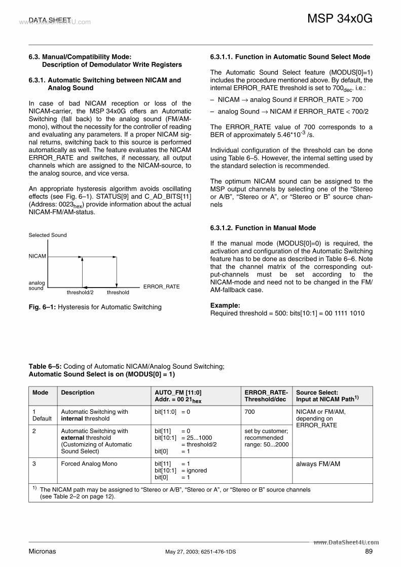
DATA SHEET MSP 34x0Gwww.DataSheet4U.com
6.3. Manual/Compatibility Mode: Description of Demodulator Write Registers
6.3.1. Automatic Switching between NICAM and Analog Sound
In case of bad NICAM reception or loss of theNICAM-carrier, the MSP 34x0G offers an AutomaticSwitching (fall back) to the analog sound (FM/AM-mono), without the necessity for the controller of readingand evaluating any parameters. If a proper NICAM sig-nal returns, switching back to this source is performedautomatically as well. The feature evaluates the NICAMERROR_RATE and switches, if necessary, all outputchannels which are assigned to the NICAM-source, tothe analog source, and vice versa.
An appropriate hysteresis algorithm avoids oscillatingeffects (see Fig. 6–1). STATUS[9] and C_AD_BITS[11](Address: 0023hex) provide information about the actualNICAM-FM/AM-status.
Fig. 6–1: Hysteresis for Automatic Switching
6.3.1.1. Function in Automatic Sound Select Mode
The Automatic Sound Select feature (MODUS[0]=1)includes the procedure mentioned above. By default, theinternal ERROR_RATE threshold is set to 700dec. i.e.:
– NICAM → analog Sound if ERROR_RATE > 700
– analog Sound → NICAM if ERROR_RATE < 700/2
The ERROR_RATE value of 700 corresponds to aBER of approximately 5.46*10-3 /s.
Individual configuration of the threshold can be doneusing Table 6–5. However, the internal setting used bythe standard selection is recommended.
The optimum NICAM sound can be assigned to theMSP output channels by selecting one of the “Stereoor A/B”, “Stereo or A”, or “Stereo or B” source chan-nels
6.3.1.2. Function in Manual Mode
If the manual mode (MODUS[0]=0) is required, theactivation and configuration of the Automatic Switchingfeature has to be done as described in Table 6–6. Notethat the channel matrix of the corresponding out-put-channels must be set according to theNICAM-mode and need not to be changed in the FM/AM-fallback case.
Example: Required threshold = 500: bits[10:1] = 00 1111 1010
ERROR_RATE
Selected Sound
NICAM
analog sound
thresholdthreshold/2
Table 6–5: Coding of Automatic NICAM/Analog Sound Switching; Automatic Sound Select is on (MODUS[0] = 1)
Mode Description AUTO_FM [11:0] Addr. = 00 21hex
ERROR_RATE-Threshold/dec
Source Select: Input at NICAM Path1)
1Default
Automatic Switching with internal threshold
bit[11:0] = 0 700 NICAM or FM/AM, depending on ERROR_RATE
2 Automatic Switching with external threshold(Customizing of Automatic Sound Select)
bit[11] = 0bit[10:1] = 25...1000
= threshold/2bit[0] = 1
set by customer; recommended range: 50...2000
3 Forced Analog Mono bit[11] = 1bit[10:1] = ignoredbit[0] = 1
always FM/AM
1) The NICAM path may be assigned to “Stereo or A/B”, “Stereo or A”, or “Stereo or B” source channels (see Table 2–2 on page 12).
Micronas May 27, 2003; 6251-476-1DS 89

MSP 34x0G DATA SHEETwww.DataSheet4U.com
Table 6–6: Coding of Automatic NICAM/Analog Sound Switching; Automatic Sound Select is off (MODUS[0] = 0)
Mode Description AUTO_FM [11:0] Addr. = 00 21hex
ERROR_RATE-Threshold/dec
Source Select: Input at NICAM Path
0resetstatus
Forced NICAM (Automatic Switching disabled)
bit[11] = 0bit[10:1] = 0bit[0] = 0
none always NICAM; Mute in case of no NICAM available
1 Automatic Switching with internal threshold (Default, if Automatic Sound Select is on)
bit[11] = 0bit[10:1] = 0bit[0] = 1
700 NICAM or FM/AM, depending on ERROR_RATE
2 Automatic Switching with external threshold(Customizing of Automatic Sound Select)
bit[11] = 0bit[10:1] = 25...1000
= threshold/2bit[0] = 1
set by customer; recommended range: 50...2000
3 Forced Analog Mono(Automatic Switching disabled)
bit[11] = 1bit[10:1] = 0bit[0] = 1
none always FM/AM
90 May 27, 2003; 6251-476-1DS Micronas

DATA SHEET MSP 34x0Gwww.DataSheet4U.com
6.3.2. A2 Threshold
The threshold between Stereo/Bilingual and MonoIdentification for the A2 Standard has been made pro-grammable according to the user’s preferences. Aninternal hysteresis ensures robustness and stability
.
6.3.3. Carrier-Mute Threshold
The Carrier-Mute threshold has been made program-mable according to the user’s preferences. An internalhysteresis ensures stable behavior.
Table 6–7: Write Register on I2C Subaddress 10hex : A2 Threshold
RegisterAddress
Function Name
THRESHOLDS
00 22hex (write) A2 THRESHOLD Register
Defines threshold of all A2 and EIA_J standards for Stereo and Bilingual detection
bit[15:0] 07F0hex force Mono Identification...0190hex default setting after reset...00A0hex minimum Threshold for stable detection
recommended range : 00A0hex...03C0hex
A2_THRESH
Table 6–8: Write Register on I2C Subaddress 10hex : Carrier-Mute Threshold
RegisterAddress
Function Name
THRESHOLDS
00 24hex (write) Carrier-Mute THRESHOLD Register
Defines threshold for the carrier mute feature
bit[15:0] 0000hex Carrier-Mute always ON (both channels muted)...002Ahex default setting after reset...07FFhex Carrier-Mute always OFF
(both channels forced on)
recommended range : 0014hex...0050hex
CM_THRESH
Micronas May 27, 2003; 6251-476-1DS 91

MSP 34x0G DATA SHEETwww.DataSheet4U.com
6.3.4. Register AD_CV
The use of this register is no longer recommended.Use it only in cases where compatibility to theMSP 34x0D is required. Using the STANDARDSELECTION register together with the MODUS regis-ter provides a more economic way to program theMSP 34x0G.
Note: This register is initialized during STANDARD SELECTION and is automatically updated when Automatic Sound Select (MODUS[0]=1) is on.
Table 6–9: AD_CV Register; reset status: all bits are “0”
AD_CV(00 BBhex)
Automatic setting bySTANDARD SELECT Register
Bit Function Settings 2-8, 0A-60hex 9
[0] not used must be set to 0 0 0
[1:6] Reference level in case of Automatic Gain Control = on (see Table 6–10). Constant gain factor when Automatic Gain Control = off (see Table 6–11).
101000 100011
[7] Determination of Automatic Gain or Constant Gain
0 = constant gain1 = automatic gain
1 1
[8] Selection of Sound IF source(identical to MODUS[8])
0 = ANA_IN1+1 = ANA_IN2+
X X
[9] MSP-Carrier-Mute Feature 0 = off: no mute1 = on: mute as de-scribed in section 2.2.2.
1 0
[10:15] not used must be set to 0 0 0
X : not affected while choosing the TV sound standard by means of the STANDARD SELECT Register
Table 6–10: Reference Values for Active AGC (AD_CV[7] = 1)
Application Input Signal Contains AD_CV [6:1] Ref. Value
AD_CV [6:1] in integer
Range of Input Signal at pin ANA_IN1+ and ANA_IN2+
Terrestrial TV
− FM Standards
− NICAM/FM
− NICAM/AM
− NICAM only
1 or 2 FM Carriers
1 FM and 1 NICAM Carrier
1 AM and 1 NICAM Carrier
1 NICAM Carrier only
101000
101000
100011
010100
40
40
35
20
0.10 − 3 Vpp1)
0.10 − 3 Vpp1)
0.10 − 1.4 Vpp(recommended: 0.10 − 0.8 Vpp)
0.05 − 1.0 Vpp
SAT 1 or more FM Carriers 100011 35 0.10 − 3 Vpp1)
ADR FM and ADR carriers see DRP 3510A data sheet
1) For signals above 1.4 Vpp, the minimum gain of 3 dB is switched, and overflow of the A/D converter may result. Due to the robustness of the internal processing, the IC works up to and even more than 3 Vpp, if norm conditions of FM/NICAM or FM1/FM2 ratio are supposed. In this overflow case, a loss of FM-S/N ratio of about 10 dB may appear.
92 May 27, 2003; 6251-476-1DS Micronas

DATA SHEET MSP 34x0Gwww.DataSheet4U.com
6.3.5. Register MODE_REG
Note: The use of this register is no longer recom-mended. It should be used only in cases wheresoftware compatibility to the MSP 34x0D isrequired. Using the STANDARD SELECTIONregister together with the MODUS register pro-vides a more economic way to program theMSP 34x0G.
As soon as this register is applied, the MSP 34x0Gworks in the MSP 34x0D Manual/CompatibilityMode. In this mode, BTSC, EIA-J, and FM-Radio aredisabled. Only MSP 34x0D features are available; theuse of MODUS and STATUS register is not allowed.The MSP 34x0G is reset to the normal mode by firstprogramming the MODUS register, followed by trans-mitting a valid standard code to the STANDARDSELECTION register.
The register ‘MODE_REG’ contains the control bitsdetermining the operation mode of the MSP 34x0G inthe MSP 34x0D Manual/Compatibility Mode; Table 6–12 explains all bit positions.
Table 6–11: AD_CV parameters for Constant Input Gain (AD_CV[7]=0)
Step AD_CV [6:1]Constant Gain
Gain Input Level at pin ANA_IN1+ and ANA_IN2+
01234567891011121314151617181920
000000000001000010000011000100000101000110000111001000001001001010001011001100001101001110001111010000010001010010010011010100
3.00 dB 3.85 dB 4.70 dB 5.55 dB 6.40 dB 7.25 dB 8.10 dB 8.95 dB 9.80 dB
10.65 dB11.50 dB12.35 dB13.20 dB14.05 dB14.90 dB15.75 dB16.60 dB17.45 dB18.30 dB19.15 dB20.00 dB
maximum input level: 3 Vpp (FM) or 1 Vpp (NICAM)1)
maximum input level: 0.14 Vpp
1) For signals above 1.4 Vpp, the minimum gain of 3 dB is switched and overflow of the A/D converter may result. Due to the robustness of the internal processing, the IC works up to and even more than 3 Vpp, if norm conditions of FM/NICAM or FM1/FM2 ratio are supposed. In this overflow case, a loss of FM-S/N ratio of about 10 dB may appear.
Micronas May 27, 2003; 6251-476-1DS 93

MSP 34x0G DATA SHEETwww.DataSheet4U.com
Table 6–12: Control word ‘MODE_REG’; reset status: all bits are “0”
MODE_REG 00 83hex Automatic setting bySTANDARD SELECT Register
Bit Function Comment Definition 2 - 5 8, A, B 9
[0] not used 0 : must be used 0 0 0
[1] DCTR_TRI Digital control out 0/1 tri-state
0 : active1 : tri-state
X X X
[2] I2S_TRI I2S outputs tri-state (I2S_CL, I2S_WS, I2S_DA_OUT)
0 : active1 : tri-state
X X X
[3] I2S Mode1) Master/Slave mode of the I2S bus
0 : Master1 : Slave
X X X
[4] I2S_WS Mode WS due to the Sony or Philips-Format
0 : Sony1 : Philips
X X X
[5] Audio_CL_OUT Switch Audio_Clock_Outputto tri-state
0 : on1 : tri-state
X X X
[6] NICAM1) Mode of MSP-Ch1 0 : FM1 : Nicam
0 1 1
[7] not used 0 : must be used 0 0 0
[8] FM AM Mode of MSP-Ch2 0 : FM1 : AM
0 0 1
[9] HDEV High Deviation Mode(channel matrix must be sound A)
0 : normal1 : high deviation mode
0 0 0
[11:10] not used 0 : must be used 0 0 0
[12] MSP-Ch1 Gain see also Table 6–14 0 : Gain = 6 dB 1 : Gain = 0 dB
0 0 0
[13] FIR1-Filter Coeff. Set
see also Table 6–14 0 : use FIR11 : use FIR2
1 0 0
[14] ADR Mode of MSP Ch1/ ADR-Interface
0 : normal mode/tri-state1 : ADR-mode/active
0 0 0
[15] AM-Gain Gain for AM Demodulation
0 : 0 dB (default. of MSPB)1 :12 dB (recommended)
1 1 1
1) NICAM and I2S-Slave mode are not allowed simultaneously X: not affected bySTANDARD SELECT register
94 May 27, 2003; 6251-476-1DS Micronas

DATA SHEET MSP 34x0Gwww.DataSheet4U.com
6.3.6. FIR-Parameter, Registers FIR1 and FIR2
Note: The use of this register is no longer recom-mended. It should be used only in cases wheresoftware compatibility to the MSP 34x0D isrequired. Using the STANDARD SELECTIONregister together with the MODUS register pro-vides a more economic way to program theMSP 34x0G.
Data-shaping and/or FM/AM bandwidth limitation isperformed by a pair of linear phase Finite ImpulseResponse filters (FIR-filter). The filter coefficients areprogrammable and are either configured automaticallyby the STANDARD SELECT register or written manu-ally by the control processor via the control bus. Twonot necessarily different sets of coefficients arerequired: one for MSP-Ch1 (NICAM or FM2) and onefor MSP-Ch2 (FM1 = FM-mono). In Table 6–14 severalcoefficient sets are proposed.
To load the FIR-filters, the following data values are tobe transferred 8 bits at a time embeddedLSB-bound in a 16-bit word.
The loading sequences must be obeyed. To change acoefficient set, the complete block FIR1 or FIR2 mustbe transmitted.
Note: For compatibility with MSP 3410B, IMREG1 andIMREG2 have to be transmitted. The value forIMREG1 and IMREG2 is 004. Due to the parti-tioning to 8-bit units, the values 04hex, 40hex,and 00hex arise.
6.3.7. DCO-Registers
Note: The use of this register is no longer recom-mended. It should be used only in cases wheresoftware-compatibility to the MSP 34x0D isrequired. Using the STANDARD SELECTIONregister together with the MODUS register pro-vides a more economic way to program theMSP 34x0G.
When selecting a TV-sound standard by means of theSTANDARD SELECT register, all frequency tuning isperformed automatically.
If manual setting of the tuning frequency is required, aset of 24-bit registers determining the mixing frequen-cies of the quadrature mixers can be written manuallyinto the IC. In Table 6–15, some examples of DCO reg-isters are listed. It is necessary to divide them up intolow part and high part. The formula for the calculationof the registers for any chosen IF frequency is as fol-lows:
INCRdec = int(f/fs ⋅ 224)
with: int = integer functionf = IF frequency in MHzfS = sampling frequency (18.432 MHz)
Conversion of INCR into hex-format and separation ofthe 12-bit low and high parts lead to the required regis-ter values (DCO1_HI or _LO for MSP-Ch1, DCO2_HIor LO for MSP-Ch2).
Table 6–13: Loading sequence for FIR-coefficients
FIR1 00 01hex (MSP-Ch1: NICAM/FM2)
No. Symbol Name Bits Value
1 NICAM/FM2_Coeff. (5) 8
see Table 6–14
2 NICAM/FM2_Coeff. (4) 8
3 NICAM/FM2_Coeff. (3) 8
4 NICAM/FM2_Coeff. (2) 8
5 NICAM/FM2_Coeff. (1) 8
6 NICAM/FM2_Coeff. (0) 8
FIR2 00 05hex (MSP-Ch2: FM1/AM)
No. Symbol Name Bits Value
1 IMREG1 8 04hex
2 IMREG1/ IMREG2 8 40hex
3 IMREG2 8 00hex
4 FM/AM_Coef (5) 8
see Table 6–14
5 FM/AM_Coef (4) 8
6 FM/AM_Coef (3) 8
7 FM/AM_Coef (2) 8
8 FM/AM_Coef (1) 8
9 FM/AM_Coef (0) 8
Micronas May 27, 2003; 6251-476-1DS 95
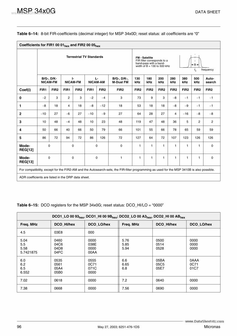
MSP 34x0G DATA SHEETwww.DataSheet4U.com
Table 6–14: 8-bit FIR-coefficients (decimal integer) for MSP 34x0D; reset status: all coefficients are “0”
Coefficients for FIR1 00 01hex and FIR2 00 05hex
Terrestrial TV Standards
B/G-, D/K- NICAM-FM
I-NICAM-FM
L-NICAM-AM
B/G-, D/K-,M-Dual FM
130kHz
180kHz
200kHz
280kHz
380kHz
500kHz
Auto-search
Coef(i) FIR1 FIR2 FIR1 FIR2 FIR1 FIR2 FIR2 FIR2 FIR2 FIR2 FIR2 FIR2 FIR2 FIR2
0 −2 3 2 3 −2 −4 3 73 9 3 −8 −1 −1 −1
1 −8 18 4 18 −8 −12 18 53 18 18 −8 −9 −1 −1
2 −10 27 −6 27 −10 −9 27 64 28 27 4 −16 −8 −8
3 10 48 −4 48 10 23 48 119 47 48 36 5 2 2
4 50 66 40 66 50 79 66 101 55 66 78 65 59 59
5 86 72 94 72 86 126 72 127 64 72 107 123 126 126
Mode-REG[12]
0 0 0 0 1 1 1 1 1 1 0
Mode-REG[13]
0 0 0 1 1 1 1 1 1 1 0
For compatibility, except for the FIR2-AM and the Autosearch-sets, the FIR-filter programming as used for the MSP 3410B is also possible.
ADR coefficients are listed in the DRP data sheet.
Table 6–15: DCO registers for the MSP 34x0G; reset status: DCO_HI/LO = “0000”
DCO1_LO 00 93hex, DCO1_HI 00 9Bhex; DCO2_LO 00 A3hex, DCO2_HI 00 ABhex
Freq. MHz DCO_HI/hex DCO_LO/hex Freq. MHz DCO_HI/hex DCO_LO/hex
4.5 03E8 000
5.045.55.585.7421875
046004C604D804FC
0000038E000000AA
5.765.855.94
050005140528
000000000000
6.06.26.56.552
0535056105A405B0
05550C71071C0000
6.66.656.8
05BA05C505E7
0AAA0C7101C7
7.02 0618 0000 7.2 0640 0000
7.38 0668 0000 7.56 0690 0000
B
FM - SatelliteFIR filter corresponds to aband-pass with a band-width of B = 130 to 500 kHz
fc frequency
96 May 27, 2003; 6251-476-1DS Micronas
DATA SHEET MSP 34x0Gw w w . D a t a S h e e t 4 U . c o m
6.4. Manual/Compatibility Mode: Description of Demodulator Read Registers
Note: The use of these register is no longer recom-mended. It should be used only in cases wheresoftware compatibility to the MSP 34x0D isrequired. Using the STANDARD SELECTIONregister together with the STATUS register pro-vides a more economic way to program theMSP 34x0G and to retrieve information from theIC.
All registers except C_AD_BITs are 8 bits wide. Theycan be read out of the RAM of the MSP 34x0G if theMSP 34x0D Manual/Compatibility Mode is required.
All transmissions take place in 16-bit words. The valid8-bit data are the 8 LSBs of the received data word.
If the Automatic Sound Select feature is not used, theNICAM or FM-identification parameters must be readand evaluated by the controller in order to enableappropriate switching of the channel select matrix ofthe baseband processing part. The FM-identificationregisters are described in section 6.6.1. To handle theNICAM-sound and to observe the NICAM-quality, atleast the registers C_AD_BITS and ERROR_RATEmust be read and evaluated by the controller. Addi-tional data bits and CIB bits, if supplied by the NICAMtransmitter, can be obtained by reading the registersADD_BITS and CIB_BITS.
6.4.1. NICAM Mode Control/Additional Data Bits Register
NICAM operation mode control bits and A[2:0] of theadditional data bits.
Format:
Important: “S” = Bit[0] indicates correct NICAM-syn-chronization (S = 1). If S = 0, the MSP 3410/3450Ghas not yet synchronized correctly to frame andsequence, or has lost synchronization. The remainingread registers are therefore not valid. The MSP mutesthe NICAM output automatically and tries to synchro-nize again as long as MODE_REG[6] is set.
The operation mode is coded by C4-C1 as shown inTable 6–16.
Note: It is no longer necessary to read out and evalu-ate the C_AD_BITS. All evaluation is performed in theMSP and indicated in the STATUS register.
6.4.2. Additional Data Bits Register
Contains the remaining 8 of the 11 additional data bits.The additional data bits are not yet defined by theNICAM 728 system.
Format:
6.4.3. CIB Bits Register
CIB bits 1 and 2 (see NICAM 728 specifications).
Format:
MSB C_AD_BITS 00 23hex LSB
11 ... 7 6 5 4 3 2 1 0
Auto_FM
... A[2] A[1] A[0] C4 C3 C2 C1 S
Table 6–16: NICAM operation modes as defined by the EBU NICAM 728 specification
C4 C3 C2 C1 Operation Mode
0 0 0 0 Stereo sound (NICAMA/B), independent mono sound (FM1)
0 0 0 1 Two independent mono signals (NICAMA, FM1)
0 0 1 0 Three independent mono channels (NICAMA, NICAMB, FM1)
0 0 1 1 Data transmission only; no audio
1 0 0 0 Stereo sound (NICAMA/B), FM1 carries same channel
1 0 0 1 One mono signal (NICAMA). FM1 carries same channel as NICAMA
1 0 1 0 Two independent mono channels (NICAMA, NICAMB). FM1 carries same channel as NICAMA
1 0 1 1 Data transmission only; no audio
x 1 x x Unimplemented sound coding option (not yet defined by EBU NICAM 728 specification)
AUTO_FM: monitor bit for the AUTO_FM Status:0: NICAM source is NICAM1: NICAM source is FM
MSB ADD_BITS 00 38hex LSB
7 6 5 4 3 2 1 0
A[10] A[9] A[8] A[7] A[6] A[5] A[4] A[3]
MSB CIB_BITS 00 3Ehex LSB
7 6 5 4 3 2 1 0
x x x x x x CIB1 CIB2
Micronas May 27, 2003; 6251-476-1DS 97

MSP 34x0G DATA SHEETwww.DataSheet4U.com
6.4.4. NICAM Error Rate Register
Average error rate of the NICAM reception in a timeinterval of 182 ms, which should be close to 0. The ini-tial and maximum value of ERROR_RATE is 2047.This value is also active if the NICAM bit ofMODE_REG is not set. Since the value is achieved byfiltering, a certain transition time (approx. 0.5 sec) isunavoidable. Acceptable audio may have error ratesup to a value of 700 int. Individual evaluation of thisvalue by the controller and an appropriate thresholdmay define the fallback mode from NICAM to FM/AM-Mono in case of poor NICAM reception.
The bit error rate per second (BER) can be calculatedby means of the following formula:
BER = ERROR_RATE * 12.3*10−6 /s
6.4.5. PLL_CAPS Readback Register
It is possible to read out the actual setting of thePLL_CAPS. In standard applications, this register isnot of interest for the customer.
6.4.6. AGC_GAIN Readback Register
It is possible to read out the actual setting ofAGC_GAIN in Automatic Gain Mode. In standardapplications, this register is not of interest for the cus-tomer.
6.4.7. Automatic Search Function for FM-Carrier Detection in Satellite Mode
The AM demodulation ability of the MSP 3410G andMSP 3450G offers the possibility to calculate the “fieldstrength” of the momentarily selected FM carrier,which can be read out by the controller. In SAT receiv-ers, this feature can be used to make automatic FMcarrier search possible.
For this, the MSP has to be switched to AM-mode(MODE_REG[8]), FM-Prescale must be set to7Fhex = +127dec, and the FM DC notch (see section6.5.7.) must be switched off. The sound-IF frequencyrange must now be “scanned” in the MSP-channel 2by means of the programmable quadrature mixer withan appropriate incremental frequency (i.e. 10 kHz).After each incrementation, a field strength value isavailable at the quasi-peak detector output (quasi-peak detector source must be set to FM), which mustbe examined for relative maxima by the controller. Thisresults in either continuing search or switching theMSP back to FM demodulation mode.
During the search process, the FIR2 must be loadedwith the coefficient set “AUTOSEARCH”, whichenables small bandwidth, resulting in appropriate fieldstrength characteristics. The absolute field strengthvalue (can be read out of “quasi-peak detector outputFM1”) also gives information on whether a main FMcarrier or a subcarrier was detected; and as a practicalconsequence, the FM bandwidth (FIR1/2) and thedeemphasis (50 µs or adaptive) can be switchedaccordingly.
Due to the fact that a constant demodulation frequencyoffset of a few kHz leads to a DC level in the demodu-lated signal, further fine tuning of the found carrier canbe achieved by evaluating the “DC Level ReadoutFM1”. Therefore, the FM DC Notch must be switchedon, and the demodulator part must be switched back toFM-demodulation mode.
ERROR_RATE 00 57hex
Error free 0000hex
maximum error rate 07FFhex
PLL_CAPS 02 1Fhex L
minimum frequency 1111 1111 FFhex
nominal frequency 0101 0110 56hexRESET
maximum frequency 0000 0000 00hex
PLL_CAPS 02 1Fhex H
PLL open xxxx xxx0
PLL closed xxxx xxx1
AGC_GAIN 02 1Ehex
max. amplification(20 dB)
0001 0100 14hex
min. amplification(3 dB)
0000 0000 00hex
98 May 27, 2003; 6251-476-1DS Micronas

DATA SHEET MSP 34x0Gwww.DataSheet4U.com
6.5. Manual/Compatibility Mode: Description of DSP Write Registers
6.5.1. Additional Channel Matrix Modes
This table shows additional modes for the channelmatrix registers.
The sum/difference mode can be used together withthe quasi-peak detector to determine the sound mate-rial mode. If the difference signal on channel B (right)is near to zero, and the sum signal on channel A (left)is high, the incoming audio signal is mono. If there is asignificant level on the difference signal, the incomingaudio is stereo.
6.5.2. Volume Modes of SCART1/2 Outputs
Note: SCART Volume linear mode will not be sup-ported in the future (documented for compatibil-ity reasons only).
6.5.3. FM Fixed Deemphasis
Note: This register is initialized during STANDARDSELECTION and is automatically updated whenAuto-matic Sound Select (MODUS[0]=1) is on.
6.5.4. FM Adaptive Deemphasis
Note: This register is initialized during STANDARDSELECTION and is automatically updated whenAuto-matic Sound Select (MODUS[0]=1) is on.
Loudspeaker Matrix 00 08hex L
Headphone Matrix 00 09hex L
SCART1 Matrix 00 0Ahex L
SCART2 Matrix 00 41hex L
I2S Matrix 00 0Bhex L
Quasi-Peak Detector Matrix
00 0Chex L
SUM/DIFF 0100 0000 40hex
AB_XCHANGE 0101 0000 50hex
PHASE_CHANGE_B 0110 0000 60hex
PHASE_CHANGE_A 0111 0000 70hex
A_ONLY 1000 0000 80hex
B_ONLY 1001 0000 90hex
Volume Mode SCART1 00 07hex [3:0]
Volume Mode SCART2 00 40hex [3:0]
linear 0000 0hexRESET
logarithmic 0001 1hex
Linear Mode
Volume SCART1 00 07hex H
Volume SCART2 00 40hex H
OFF 0000 0000 00hexRESET
0 dB gain (digital full scale (FS) to 2 VRMS output)
0100 0000 40hex
+6 dB gain (−6 dBFS to 2 VRMS output)
0111 1111 7Fhex
FM Deemphasis 00 0Fhex H
50 µs 0000 0000 00hexRESET
75 µs 0000 0001 01hex
J17 0000 0100 04hex
OFF 0011 1111 3Fhex
FM Adaptive Deemphasis WP1
00 0Fhex L
OFF 0000 0000 00hexRESET
WP1 0011 1111 3Fhex
Micronas May 27, 2003; 6251-476-1DS 99

MSP 34x0G DATA SHEETwww.DataSheet4U.com
6.5.5. NICAM Deemphasis
A J17 Deemphasis is always applied to the NICAMsignal. It is not switchable.
6.5.6. Identification Mode for A2 Stereo Systems
To shorten the response time of the identification algo-rithm after a program change between two FM-Stereocapable programs, the reset of the ident-filter can beapplied.
Sequence:
1. Program change
2. Reset ident-filter
3. Set identification mode back to standard B/G or M
4. Wait approx. 500 ms
5. Read stereo detection register
Note: This register is initialized during STANDARDSELECTION and is automatically updated whenAuto-matic Sound Select (MODUS[0]=1) is on.
6.5.7. FM DC Notch
The DC compensation filter (FM DC Notch) for FMinput can be switched off. This is used to speed up theautomatic search function (see Section 6.4.7.). In nor-mal FM-mode, the FM DC Notch should be switchedon.
6.6. Manual/Compatibility Mode: Description of DSP Read Registers
All readable registers are 16-bit wide. Transmissionsvia I2C bus have to take place in 16-bit words. Some ofthe defined 16-bit words are divided into low and highbyte, thus holding two different control entities.
These registers are not writable.
6.6.1. Stereo Detection Registerfor A2 Stereo Systems
Note: It is no longer necessary to read out and evalu-ate the A2 identification level. All evaluation isperformed in the MSP and indicated in the STA-TUS register.
6.6.2. DC Level Register
The DC level register measures the DC component ofthe incoming FM signals (FM1 and FM2). This can beused for seek functions in satellite receivers and for IFFM frequencies fine tuning. A too low demodulationfrequency (DCO) results in a positive DC-level andvice versa. For further processing, the DC content ofthe demodulated FM signals is suppressed. The timeconstant τ, defining the transition time of the DC LevelRegister, is approximately 28 ms.
Identification Mode 00 15hex L
Standard B/G (German Stereo)
0000 0000 00hexRESET
Standard M (Korean Stereo)
0000 0001 01hex
Reset of Ident-Filter 0011 1111 3Fhex
FM DC Notch 00 17hex L
ON 0000 0000 00hex Reset
OFF 0011 1111 3Fhex
Stereo Detection Register
00 18hex H
Stereo Mode Reading(two’s complement)
MONO near zero
STEREO positive value (ideal reception: 7Fhex)
BILINGUAL negative value (ideal reception: 80hex)
DC Level Readout FM1 (MSP-Ch2)
00 1Bhex H+L
DC Level Readout FM2 (MSP-Ch1)
00 1Chex H+L
DC Level [8000hex ... 7FFFhex]values are 16 bit two’s complement
100 May 27, 2003; 6251-476-1DS Micronas

DATA SHEET MSP 34x0Gwww.DataSheet4U.com
6.7. Demodulator Source Channels in Manual Mode
6.7.1. Terrestric Sound Standards
Table 6–17 shows the source channel assignment ofthe demodulated signals in case of manual mode forall terrestric sound standards. See Table 2–2 for theassignment in the Automatic Sound Select mode. Inmanual mode for terrestric sound standards, only twodemodulator sources are defined.
6.7.2. SAT Sound Standards
Table 6–18 shows the source channel assignment ofthe demodulated signals for SAT sound standards.
6.8. Exclusions of Audio Baseband Features
In general, all functions can be switched independently.Two exceptions exist:
1. NICAM cannot be processed simultaneously with the FM2 channel.
2. FM adaptive deemphasis cannot be processed simultaneously with FM-identification.
6.9. Compatibility Restrictions to MSP 34x0D
The MSP 34x0G is fully hardware compatible to theMSP 34x0D. However, to substitute a MSP 34x0D bythe corresponding MSP 34x0G, the controller softwarehas to be adapted slightly:
1. The register FM-Matrix (00 0Ehex low part) must be changed from “no matrix (00hex)” to “sound A mono (03hex)” during mono transmission of all TV-sound standards (see also Table 6–17).
2. With the MSP 34x0G, the STANDARD SELECTION initializes the FM-deemphasis, which is not the case for the MSP 34x0D. So, if STANDARD SELECTION is applied, this I2C instruction can be omitted.
Micronas May 27, 2003; 6251-476-1DS 101

MSP 34x0G DATA SHEETwww.DataSheet4U.com
Table 6–17: Manual Sound Select Mode for Terrestric Sound Standards
Source Channels of Sound Select Block
Broadcasted Sound Standard
Selected MSP Standard Code
Broadcasted Sound Mode
FM Matrix FM/AM(use 0 for channel select)
Stereo or A/B(use 1 for channel select)
B/G-FMD/K-FMM-KoreaM-Japan
0304, 050230
MONO Sound A Mono Mono Mono
STEREO German StereoKorean Stereo
Stereo Stereo
BILINGUAL, Languages A and B
No Matrix Left = ARight = B
Left = ARight = B
B/G-NICAML-NICAMI-NICAMD/K-NICAMD/K-NICAM (with high deviation FM)
08090A0B0C, 0D
NICAM not available or NICAM error rate too high
Sound A Mono1) analog Mono no sound
with AUTO_FM: analog Mono
MONO Sound A Mono1) analog Mono NICAM Mono
STEREO Sound A Mono1) analog Mono NICAM Stereo
BILINGUAL, Languages A and B
Sound A Mono1) analog Mono Left = NICAM ARight = NICAM B
BTSC
20
MONO Sound A Mono Mono Mono
STEREO Korean Stereo Stereo Stereo
MONO + SAP Sound A Mono Mono Mono
STEREO + SAP Korean Stereo Stereo Stereo
21
MONO Sound A Mono Mono Mono
STEREO
MONO + SAPNo Matrix Left = Mono
Right = SAPLeft = MonoRight = SAP
STEREO + SAP
FM-Radio 40MONO Sound A Mono Mono Mono
STEREO Korean Stereo Stereo Stereo
1) Automatic refresh to Sound A Mono, do not write any other value to the register FM Matrix!
Table 6–18: Manual Sound Select Modes for SAT-Standards
Source Channels of Sound Select Blockfor SAT-Modes
Broadcasted Sound Standard
Selected MSP Standard Code
Broadcasted Sound Mode
FM Matrix FM/AM(source select: 0)
Stereo or A/B(source select: 1)
Stereo or A(source select: 3)
FM SAT
6, 50hex MONO Sound A Mono Mono Mono Mono
51hex STEREO No Matrix Stereo Stereo Stereo
BILINGUAL No Matrix Left = A (FM1)Right = B (FM2)
Left = A (FM1)Right = B (FM2)
A (FM1)
102 May 27, 2003; 6251-476-1DS Micronas

DATA SHEET MSP 34x0Gwww.DataSheet4U.com
7. Appendix C: Application Information
7.1. Phase Relationship of Analog Outputs
The analog output signals: Loudspeaker, headphone,and SCART2 all have the same phases. The userdoes not need to correct output phases when usingthese analog outputs directly. The SCART1 output hasopposite phase.
Using the I2S-outputs for other DSPs or D/A convert-ers, care must be taken to adjust for the correct phase.If the attached coprocessor is one of the MSP family,the following schematics help to determine the phaserelationship.
Fig. 7–1: Phase diagram of the MSP 34x0G
SCART2-Ch.
SCART1
SCART1
SCART2
SCART4
SCART3
MONO
Loudspeaker
Audio
SCARTDSP Input Select
SCARTOutput Select
BasebandProcessing
Headphone
SCART1-Ch.
SCART2
I2S_OUTI2S_IN1/2
MONO, SCART1...4
Micronas May 27, 2003; 6251-476-1DS 103

MSP 34x0G DATA SHEETwww.DataSheet4U.com
7.2. Application Circuit
SC1_OUT_L
SC1_OUT_R
SC2_OUT_L
SC2_OUT_R
AH
VS
UP
AH
VS
S
AV
SU
P
DV
SU
P
DV
SS
RE
SE
TQ
AV
SS
VR
EF
1
VR
EF
2
5 V 5 V 8 V
AV
SS
5 V
5 V
CA
PL_
M
CA
PL_
A
VR
EF
TO
P
AG
ND
C
AN
A_I
N1+
AN
A_I
N2+
AN
A_I
N-
XT
AL_
IN
XT
AL_
OU
T
MSP 34x0G
D_CTR_I/O_0
D_CTR_I/O_1
AUD_CL_OUT
TESTEN
+
100 Ω
100 Ω
100 Ω
100 Ω
22 µF
22 µF
22 µF
22 µF
+
+
+
DACA_R
1 nF
1 nF
1 nF
1 nF
1 nF
DACA_L
DACM_SUB
DACM_R
DACM_L
1 µF
1 µF
1 µF
1 µF
1 µF
HEADPHONE
LOUD
Tuner 1
Tuner 2SIF 2 IN
Signal GND
SIF 1 IN
56 pF 56 pF 56 pF +
3.3 µF
100 nF
100 nF
10 µF
+
-
if ANA_IN2+ not used
8 V(5 V)
18.432MHz
++
10 µF 10 µF
MONO_IN
SC1_IN_L
SC1_IN_R
ASG
SC2_IN_L
SC2_IN_R
ASG
SC3_IN_L
SC3_IN_R
ASG
SC4_IN_L
SC4_IN_R
STANDBYQ
ADR_SEL
I2C_DA
I2C_CL
ADR_WS
ADR_CL
ADR_DA
I2S_WS
I2S_CL
I2S_DA_IN1
I2S_DA_IN2
I2S_DA_OUT
220 pF
Alternative circuit for SIF-inputs for more attenuation of video
100 pF 56 pF
1 kΩ
ANA_IN1/2+
AHVSS
AHVSS
AHVSS
330 nF
330 nF
330 nF
330 nF
330 nF
330 nF
330 nF
330 nF
330 nF
DVSS
DVSS
AHVSS
components:
C s. section 4.6.2.
SPEAKER
RESETQ
(from Controller, see section 4.6.3.3.) 1.5 nF
470 pF
10 µF
1.5 nF
470 pF
10 µF
1.5 nF
470 pF
10 µF
(5 V) AH
VS
S
AH
VS
S
AH
VS
S
(3.3 V)
104 May 27, 2003; 6251-476-1DS Micronas

DATA SHEET MSP 34x0Gwww.DataSheet4U.com
8. Appendix D: MSP 34x0G Version History
MSP 34x0G-B8
– fine-tuning of A2-identification and carrier mute
– EIA-J identification: faster transition time stereo/bilingual to mono
– J17 FM-deemphasis implemented
– input specification for RESETQ and TESTEN changed
– MB implemented
MSP 34x0G-B8V3
– The Automatic Sound Select (ASS) malfunction has been corrected. In the previous version, under cer-tain circumstances and depending on the baseband features used, e.g.: Micronas BASS, Virtual Sur-round Sound, Equalizer... etc., the Automatic Sound Select Feature (ASS) did not work correctly.
– Pseudo Stereo Effect (PSE) malfunction has been corrected
MSP 34x0G-C12
– FM-Radio available in non-BTSC versions with acti-vation key MSP 3400G/3410G
– implementation of SRS WOW
– implementation of BBE
– implementation of Micronas VOICE
– correction of default Scart-Switch configuration dur-ing power-up
Micronas May 27, 2003; 6251-476-1DS 105

All information and data contained in this data sheet are without anycommitment, are not to be considered as an offer for conclusion of acontract, nor shall they be construed as to create any liability. Any newissue of this data sheet invalidates previous issues. Product availabilityand delivery are exclusively subject to our respective order confirmationform; the same applies to orders based on development samples deliv-ered. By this publication, Micronas GmbH does not assume responsibil-ity for patent infringements or other rights of third parties which mayresult from its use.Further, Micronas GmbH reserves the right to revise this publication andto make changes to its content, at any time, without obligation to notifyany person or entity of such revisions or changes. No part of this publication may be reproduced, photocopied, stored on aretrieval system, or transmitted without the express written consent ofMicronas GmbH.
MSP 34x0G DATA SHEET
106 May 27, 2003; 6251-476-1DS Micronas
Micronas GmbHHans-Bunte-Strasse 19D-79108 Freiburg (Germany)P.O. Box 840D-79008 Freiburg (Germany)Tel. +49-761-517-0Fax +49-761-517-2174E-mail: [email protected]: www.micronas.com
Printed in GermanyOrder No. 6251-476-1DS
9. Data Sheet History
1. Preliminary data sheet: “MSP 34x0G Multistandard Sound Processor Family”, March 5, 2001, 6251-476-4PD. Fourth release of the preliminary data sheet. Major changes:
– specification for version B8 added (see Appendix D: Version History)
– MSP 3460 added, MSP 3430 removed
– description for MDB added
– specification for MNR added
– I2C-bus description changed
– ACB register: documentation for bit allocation D_CTR_I/O changed
2. Data Sheet: “MSP 34x0G Multistandard Sound Pro-cessor Family”, May 27, 2003, 6251-476-1DS. First release of the data sheet.Major changes:
– specification for version C12 added
– implementation of SRS WOW
– implementation of BBE
– implementation of Micronas VOICE
– Section 4.1.: diagrams for all packages changed
– PLQFP64 changed to PMQFP64-2
– Micronas Dynamic Bass (MDB) changed to Micronas BASS (MB)
www.DataSheet4U.com