
TV Thomson Scattering System on JFT-2M
10
Proceedings of the 6th International Symposium on Advanced Nuclear Energy Research -INNOVATIVE LASER TECHNOLOGIES IN NUCLEAR ENERGY - TV Thomson Scattering System on JFT-2M T.Yamauchi, T.Shiina, Y.Ishige and D.Dimock* Department of Fusion Plasma Research, Japan Atomic Energy Research Institute, Tokal-mura, Ibarak1-ken, 319-11, Japan * Princeton University Plasma Physics Laboratory, PO BOX451, Princeton NJ 08543 USA A higher spatial resolution TV Thomson scattering system was constructed on JFT-2M tokamak This system has been providing complete profiles of Te and ne at a single time during a plasma discharge. New detector system was developed composed of two stages of Image Inten- sifler tubes coupled to a CCD. The extinction ratio of image intenslfier was improved to 1.4x10 7 at least. Keywords:Thomson scattering, Ruby laser, CCD, Image Intenslfier, plasma, JFT-2M 1. Introduction Electron temperature(Te) and density(ne) are the essential parameters to inves- tigate the physics of tokamak plasma. There are several ways to measure Te and/or ne in plasma. The representative diagnostic systems on Te are the electron cyclotron emission (ECE)[1], X-ray pulse height spectrometer(SX)[2] and Thomson scattering[3- ]. The systems on ne are the microwave interferometry[4] and Thomson scattering. Each system has some advantages. ECE and SX are passive methods for Te mea- surement, and are simple systems. But ECE system gives the arbitrary temperature from the intensity, and SX system gives the monitor Te because of the impurity lines on the energy spectrum. On the other hand, the microwave interferometry gives the line-integrated electron density, and several chords through plasma is necessary to get the ne profile with the abel-inversion at least. The ne and Te profiles measured with these methods have not enough spatial resolution, especially at edge. It is difficult to determine the slope of Te, ne and pressure(Pe) at edge with a high resolution of below 1cm. However, Thomson scattering system measures the local Te and ne with the e-folding width of doppler-broadened profile of scattered spectrum and total scat- tered intensity, respectively[5]. Thomson scattering has some advantages as follows; Laser beam does not disturb the plasma, and the measured point is definite. But, Thomson scattering cross-section is so small (6.6x10" 25 cm 2 ) that laser power, sensi- tivity of detector and transmittance of optics should be made as high as possible. Initial TV Thomson scattering system(TVTS) was developed to measure Te and ne profiles of plasma diameter in Princeton University Plasma Physics Laboratory (PPPL)[6-8]. This system has the following characteristics^ wide-angle lens was used for collecting the scattered light, and the micro-channel plate intensifier(40mm in diameter was available at maximum) with a gating pulse system and the intensified sil- — 502— Procecdings of Ihe 61h Imemalional Symposium on Advanced Nuclcar EncrgyResεa 陀h -INNOVATIVE lASER TECHNOLOGIES IN NU Cl EAR ENERGY- TV Thomson Scattering System on JFT ・ 2M T.Yamauchi , T.Shiina , V . l shige and D.Dimock* DepartmentofFus10nPlasmaResearch.JapanAtom1cEnergyResearch Inst1tute , TOka1-mura , Ibarak1-ken , 319-11 , Japan ーモ Pr1ncetonUn1vers1ty PlasmaPhys1csLaboratory. POBoX451 , PrlncetonNJ 08543 USA A higher spatial resolutlon TV Thomson scattermg system was constructed onJFT-2 門 tokamakThlS system has been provldmg complete proflles of Te and ne at a smgle tlme durmg a plasma discharge , New detector system was developed composed of two stages of image inten- slfler t Ut es coupled to a CCD , The extmctlon ratlo of lmage mtensifler was lmproved to 1.4x 10 I at leas t . Keywords:T hO mson scattering , Rubylaser , CCD , imageintensifler , plasma , JFT-2 門 1. Introduction Electron temperature(Te}and density(ne} are the essential parameters to inves- tigate the physics of tokamak plasma. There are several ways tomeasure Te and/or nein plasma. The representative diagnostic systems on Te are the electron cyclotron emission (ECE}[1] , X-ray pulse height spectrometer{SX}[2] and Thomson scattering[3 ・ ]. The systems on ne are the microwave inte 付 erometry[4]and Thomson scattering. Each system has some advantages.ECE and SX are passive methods for Te mea- surement , and are simple systems. But ECE system gives the arbitrary temperature from the intensity , and SX system gives the monitor Te because of the impurity lines on the energy spectrum. On the other hand , themicrowave interferometry gives the line-integrated electron density , and several chords through plasma is necessary to get the ne profile with the abel-inversion at leas t. The ne and Te profiles measured with these methods have not enough spatial resolution , especially at edge.It is difficult to determine the slope of Te , ne and pressure(Pe) at edge with ahigh resolution of below 1cm.However , Thomson scattering system measures the local Te and ne with the e-folding width of doppler-broadened profile of scattered spectrum and total scat- tered intensity , respectively[5]. Thomson scattering has some advantages as follows; Laser beam does not disturb the plasma , and the measured point is definite.But , Thomson scattering cross-section is so small(6.6x10 ・ 25cm2)that laser power , sensi- tivity of detector and transmittance of optics should be made as high as possible. Initial TV Thomson scattering system(TVTS) was developed to measure Te and ne profiles of plasma diameter in PrincetonUniversity Plasma Physics Laboratory (PPPL}[6 ・ 8].This system has the following characteristics;a wide-angle lens was used for co J l ecting the scattered light , and the micro-channel plate intensifier( 40mm in diameter was available at maximum) with agating pulse system and the intensified si 卜 -502-
-
Upload
khangminh22 -
Category
Documents
-
view
1 -
download
0
Transcript of TV Thomson Scattering System on JFT-2M

Proceedings of the 6th International Symposium on
Advanced Nuclear Energy Research
-INNOVATIVE LASER TECHNOLOGIES IN NUCLEAR ENERGY -
TV Thomson Scattering System on JFT-2M
T.Yamauchi, T.Shiina, Y.Ishige and D.Dimock* Department of Fusion Plasma Research, Japan Atomic Energy Research
Inst i tute, Tokal-mura, Ibarak1-ken, 319-11, Japan * Princeton University Plasma Physics Laboratory, PO BOX451 ,
Princeton NJ 08543 USA
A higher spatial resolution TV Thomson scattering system was constructed on JFT-2M tokamak This system has been providing complete profiles of Te and ne at a single time during a plasma discharge. New detector system was developed composed of two stages of Image Inten-sifler tubes coupled to a CCD. The extinction ratio of image intenslfier was improved to 1.4x10⁷ at least.
Keywords:Thomson scattering, Ruby laser, CCD, Image Intenslfier, plasma, JFT-2M
1. Introduction Electron temperature(Te) and density(ne) are the essential parameters to inves
tigate the physics of tokamak plasma. There are several ways to measure Te and/or
ne in plasma. The representative diagnostic systems on Te are the electron cyclotron
emission (ECE)[1], X-ray pulse height spectrometer(SX)[2] and Thomson scattering[3-
]. The systems on ne are the microwave interferometry[4] and Thomson scattering.
Each system has some advantages. ECE and SX are passive methods for Te mea
surement, and are simple systems. But ECE system gives the arbitrary temperature
from the intensity, and SX system gives the monitor Te because of the impurity lines
on the energy spectrum. On the other hand, the microwave interferometry gives the
line-integrated electron density, and several chords through plasma is necessary to
get the ne profile with the abel-inversion at least. The ne and Te profiles measured
with these methods have not enough spatial resolution, especially at edge. It is difficult
to determine the slope of Te, ne and pressure(Pe) at edge with a high resolution of
below 1cm. However, Thomson scattering system measures the local Te and ne with
the e-folding width of doppler-broadened profile of scattered spectrum and total scat
tered intensity, respectively[5]. Thomson scattering has some advantages as follows;
Laser beam does not disturb the plasma, and the measured point is definite. But,
Thomson scattering cross-section is so small (6.6x10"25cm2) that laser power, sensi
tivity of detector and transmittance of optics should be made as high as possible.
Initial TV Thomson scattering system(TVTS) was developed to measure Te and ne
profiles of plasma diameter in Princeton University Plasma Physics Laboratory
(PPPL)[6-8]. This system has the following characteristics^ wide-angle lens was
used for collecting the scattered light, and the micro-channel plate intensifier(40mm in
diameter was available at maximum) with a gating pulse system and the intensified sil-
— 502—
Procecdings of Ihe 61h Imemalional Symposium on
Advanced Nuclcar Encrgy Resεa陀h
-INNOVATIVE lASER TECHNOLOGIES IN NUClEAR ENERGY-
TV Thomson Scattering System on JFT・2M
T.Yamauchi, T.Shiina, V.lshige and D.Dimock* Department of Fus10n Plasma Research. Japan Atom1c Energy Research
Inst1tute, TOka1-mura, Ibarak1-ken, 319-11, Japan ーモ Pr1nceton Un1vers1ty Plasma Phys1cs Laboratory. PO BoX451,
Prlnceton NJ 08543 USA
A higher spatial resolutlon TV Thomson scattermg system was constructed onJFT-2門tokamak ThlS system has been provldmg complete proflles of Te and ne at a smgle tlme durmg a plasma discharge, New detector system was developed composed of two stages of image inten-slfler tUtes coupled to a CCD, The extmctlon ratlo of lmage mtensifler was lmproved to 1.4x 1 0 I at least.
Keywords:ThOmson scattering, Ruby laser, CCD, image intensifler, plasma, JFT-2門
1. Introduction Electron temperature(Te} and density(ne} are the essential parameters to inves-
tigate the physics of tokamak plasma. There are several ways to measure Te and/or
ne in plasma. The representative diagnostic systems on Te are the electron cyclotron
emission (ECE}[1], X-ray pulse height spectrometer{SX}[2] and Thomson scattering[3・
]. The systems on ne are the microwave inte付erometry[4]and Thomson scattering.
Each system has some advantages. ECE and SX are passive methods for Te mea-
surement, and are simple systems. But ECE system gives the arbitrary temperature
from the intensity, and SX system gives the monitor Te because of the impurity lines
on the energy spectrum. On the other hand, the microwave interferometry gives the
line-integrated electron density, and several chords through plasma is necessary to
get the ne profile with the abel-inversion at least. The ne and Te profiles measured
with these methods have not enough spatial resolution, especially at edge. It is difficult
to determine the slope of Te, ne and pressure(Pe) at edge with a high resolution of
below 1cm. However, Thomson scattering system measures the local Te and ne with
the e-folding width of doppler-broadened profile of scattered spectrum and total scat-
tered intensity, respectively[5]. Thomson scattering has some advantages as follows;
Laser beam does not disturb the plasma, and the measured point is definite. But,
Thomson scattering cross-section is so small (6.6x10・25cm2)that laser power, sensi-
tivity of detector and transmittance of optics should be made as high as possible.
Initial TV Thomson scattering system(TVTS) was developed to measure Te and ne
profiles of plasma diameter in Princeton University Plasma Physics Laboratory
(PPPL}[6・8].This system has the following characteristics;a wide-angle lens was
used for coJlecting the scattered light, and the micro-channel plate intensifier( 40mm in
diameter was available at maximum) with a gating pulse system and the intensified si卜
-502-
icon diode target vidicon tube were used as a detector. This detector had to be im
proved for a low sensitivity and a serious limitation of input diameter of MCP.
ICCD(lntensified CCD) tube has been developed soon. ICCD has an anode consisted
of CCD and an electron emitted from cathode surface hits on CCD to produce -106
electrons. However, it is impossible to buy ICCD anymore. Then, the new detector for
TVTS was designed and fabricated in collaboration with PPPL[9]. This detector con
sists of two stages of image intensifier tubes with a large input surface(80mm in diam
eter) coupled to a CCD fiber-optically. By the way.TVTS on JFT-2M tokamak is com
posed of six subsystems; optical, electro-optical, control and data acquisition,
laser[10], software and vacuum components 1] subsystems[12].
Not only ruby laser power is high (1.5x10¹⁰W/cm2) in plasma, but also quartz
image fibers and Littrow type spectrometer are applied to produce the high optical
transmittance. The characteristics of this system is as follows; total measuring length
of 70cm, spatial points of 81, spatial resolution of 0.86cm, measured temperature
range of 50eV<Te<7~8keV and measured density range of ~3x10¹²<ne<5x1014cm"3.
The Te and ne profiles give the physical informations on JFT-2M plasma; The in
crease of central temperature and density and the pedestal of Te at edge were ob
served in H-mode. In this paper we describe TVTS, especially about new detector,
and the Te and ne measured in JFT-2M plasma.
2. Overview of TVTS
It is described in ref.[12,13] in detail, then is written here in brief. Figure.1 shows
the overview of TVTS. A ruby laser beam with 20J (or usually 15J) in 20ns and 0.25
milliradian beam divergence is focussed to below 3mm diameter over the 70cm mea
surement region in the horizontal mid-plane of the plasma. The beam is terminated in
a beam dump designated to minimize stray laser light. A 6m long beam tube in vacu
um places the window at a point where the beam size(25mm in diameter) is large
enough to keep laser damage to the window(threshold power of
breakdown:~6x10⁹W/cm2) at a tolerable level. The light scattered from the beam is
collected from an f:6 cone and imaged at f:1.75, using a Bouwers concentric catadiop-
tric mirror system on the top flange, onto an array of 81 fiber optic bundles each of
which measures 0.9x2.25mm. These bundles are then rearranged from the
0.9x191 mm input to 2.25x72.9mm at the input to the spectrometer. A relay lens ex
pands this image onto the input slit of the spectrometer. A simple Littrow spectrometer
is used to minimize the scattering of stray laser light and the formation of secondary
- 503-
icon diode target vidicon tube were used as a detector. This detector had to be irrト
proved for a low sensitivity and a serious Iimitation of input diameter of MCP.
ICCD(lntensified CCD) tube has been developed soon. ICCD has an anode consisted
of CCD and an electron emitted from cathode surface hits on CCD to produce ....106
electrons. However, it is impossible to buy ICCD anymore. Then, the new detector for
TVTS was designed and fabricated in collaboration with PPPL[9]. This detector con-
sists of two stages of image intensifier tubes with a large input surface(80mm in diam-
eter) coupled to a CCD fiber-optically. By the way,TVTS on JFT・2Mtokamak is com-
posed of six subsystems; optical, electro-optical, control and data acquisition,
laser[10], software and vacuum component[11] subsystems[12].
Not only ruby laser power is high (1.5x10¹⁰W/cm2) in plasma, but also qua吋Z
image fibers and Littrow type spectrometer are applied to produce the high optical
transmittance. The characteristics of this system is as follows; total measuring length
of70cm,sp剖ialpoints of 81, spatial resolution of O.86cm, measured temperature
range of 50eV<Te<7....8keV and measured density range of ....3x1012<ne<5x1014cm-3.
The Te and ne profiles give the physical informations on JFT・2Mplasma; The in-
crease of central temperature and density and the pedestal of Te at edge were ob-
served in H-mode. In this paper we describe TVTS, especially about new detector,
and the Te and ne measured in JFT・2Mplasma.
2. Overview 01 TVTS
It is described in ref.[12,13] in detail, then is written here in brief. Figure.1 shows
the overview of TVTS. A ruby laser beam with 20J (or usually 15J) in 20ns and 0.25
milliradian beam divergence is focussed to below 3mm diameter over the 70cm mea-
surement region in the horizontal mid-plane of the plasma. The beam is terminated in
a beam dump designated to minimize stray laser light. A 6m long beam tube in vacu-
um places the window at a point where the beam size(25mm in diameter) is large
enough to keep laser damage to the window(threshold power of
breakdown:向 6x10⁹W/cm2 ) at a tolerable level. The light scattered from the beam is
collected from an f:6 cone and imaged at f:1.75, using a Bouwers concentric catadiop-
tric mirror system on the top flange, onto an array of 81 fiber optic bundles each of
which measures 0.9x2.25mm. These bundles are then rearranged from the
O.9x191 mm input to 2.25x72.9mm at the input to the spectrometer. A relay lens ex-
pands this image onto the input slit of the spectrometer. A simple Littrow spectrometer
is used to minimize the scattering of stray laser light and the formation of secondary
- 503-
images by reflections. A field lens at the image plane focuses the light onto a camera
lens which images the spatially resolved spectra onto the face of an 80mm diameter
gateable image intensifier tube. This tube demagnifies the image from 80mm to
18mm. A second image intensifier tube provides further gain and further demagnifies
the image from 18 to 11 mm. Output image of second image intensifier is fiber-optically
coupled to a cooled CCD. The data from the CCD are digitized and temporarily stored
in the personal computer used to control the camera. The data are then sent to a Vax
station 3500 for calculation of Te and ne.
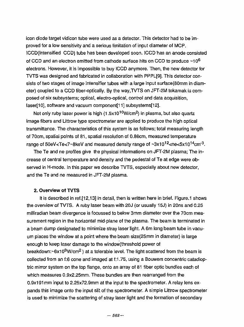
3. Image intensifier coupled to CCD detector system
The detector consists of two stages of image intensifier tubes coupled to a CCD
as shown in Fig.2. Both of the intensifier tubes have fast phosphors. The first tube,
made by DEP in Holland (type:PP0050), has an 80mm diameter fiber optic faceplate
with a red enhanced S25 photocathode, and a P47 blue phosphor with a decay time
of about 80ns with a fiber optic output. It demagnifies from 80 to 18mm and has appre
ciable pincushion distortion. On the other hand, the second tube(type:XX1600) has a
fiber optic input with 18mm diameter, a blue sensitive S20 photocathode and a P46
green phosphor with about 160ns decay time. It demagnifies from 18 to 11 mm and
adds some additional pincushion distortion.
The CCD is made by EEV and is their type CCD02-06-1-014 as shown in Table I.
It is a 385 by 288 pixel, frame transfer type which makes it possible to transfer a frame
in about 2ms. It is also possible to compress frames into the storage register. This is
coupled to the output of the second image intensifier through a long(50mm) fiber optic
coupler. The CCD is housed in a polyethylene foam filled cannister which can be
cooled by a flow of cold nitrogen gas to below -30°C. This results in negligible dark
current during the readout time of about 1s.
The CCD is controlled by a Princeton Scientific Instruments Inc. camera controller.
This controller provides all the clocking signals for CCD, and digitizes and stores the
output. Using the IBM type personal computer which is an integral part of this con
troller, it is also possible to do some preliminary analysis of the data which is very use
ful for alignment problem with the system.
3.1 Extinction ratio
Plasma background lights, such as a bremsstrahlung emission and a spectral
line emission , are always incident on the input surface of image intensifier tube. In the
case of (scattered signal)/(background signal)=10~20 estimated from experiments,
-504 —
images by reflections. A field 19n5 at the image plane focuses the light onto a camera
lens which images the spatially resolved spectra onto the face of an 80mm diameter
gateable image intensifier tube. This tube demagnifies the image from 80mm to
18mm. A second image intensifier tube provides further gain and further demagn而es
the image from 18 to 11 mm. Output image of second image intensifier is fiber-optically
coupled to a cooled CCD. The data from the CCD are digitized and temporarily stored
in the personal computer ¥Jsed to control the camera. The data are then sent to a Vax
station 3500 for calculation of Te and ne.
3. Image intensifier coupled to CCD detector system
The detector consists of two stages of image intensifier tubes coupled to a CCO
as shown in Fig.2. 80th of the intensifier tubes have fast phosphors. The first tube,
made by DEP in Holland (type:PP0050), has an 80mm diameter fiber optic faceplate
with a red enhanced 825 photocathode, and a P47 blue phosphor with a decay time
of about 80ns with a fiber optic output. It demagnifies from 80 to 18mm and has appre-
ciable pincushion distortion. On the other hand, the second tube(type:XX1600) has a
fiber optic input with 18mm diameter, a blue sensitive 820 photocathode and a P46
green phosphor with about 160ns decay time. It demagnifies from 18 to 11 mm and
adds some additional pincushion distortion.
The CCD is made by EEV and is their type CC002・06-1・014as shown in Table 1.
It is a 385 by 288 pixel, frame transfer type which makes it possible to transfer a frame
in about 2ms. It is also possible to compress frames into the storage register. This is
coupled to the output of the second image intensifier through a long(50mm} fiber optic
coupler. The CCO is housed in a polyethylene foam filled cannister which can be
cooled by a flow of cold nitrogen gas to below ・300C.This results in negligible dark
current during the readout time of about 1 s.
The CCO is controlled by a Princeton Scientific Instruments Inc. camera controller.
This controller provides all the clocking signals for CCO, and digitizes and stores the
output. Using the IBM type personal computer which is an integral pa円ofthis con-
troller, it is also possible to do some preliminary analysis of the data which is very use-
ful for alignment problem with the system.
3.1 Extinction ratio
Plasma background lights, such as a bremsstrahlung emission and a spectral
line emission , are always incident on the input surface of image intensifier tube. In the
case of (scattered signal)/(background signal)=1 0-20 estimated from experiments,
-504-

duration of plasma discharged s and gated duration=100ns, a high extinction ratio is
necessary to get the signal-to-noise ratio S/N >10. That is, the S/N is represented as
(scattered signalxextinction ratio)/{(scattered signal/10)x(duration of discharge/gated
duration)}. The extinction ratio should be (5~10)x107.
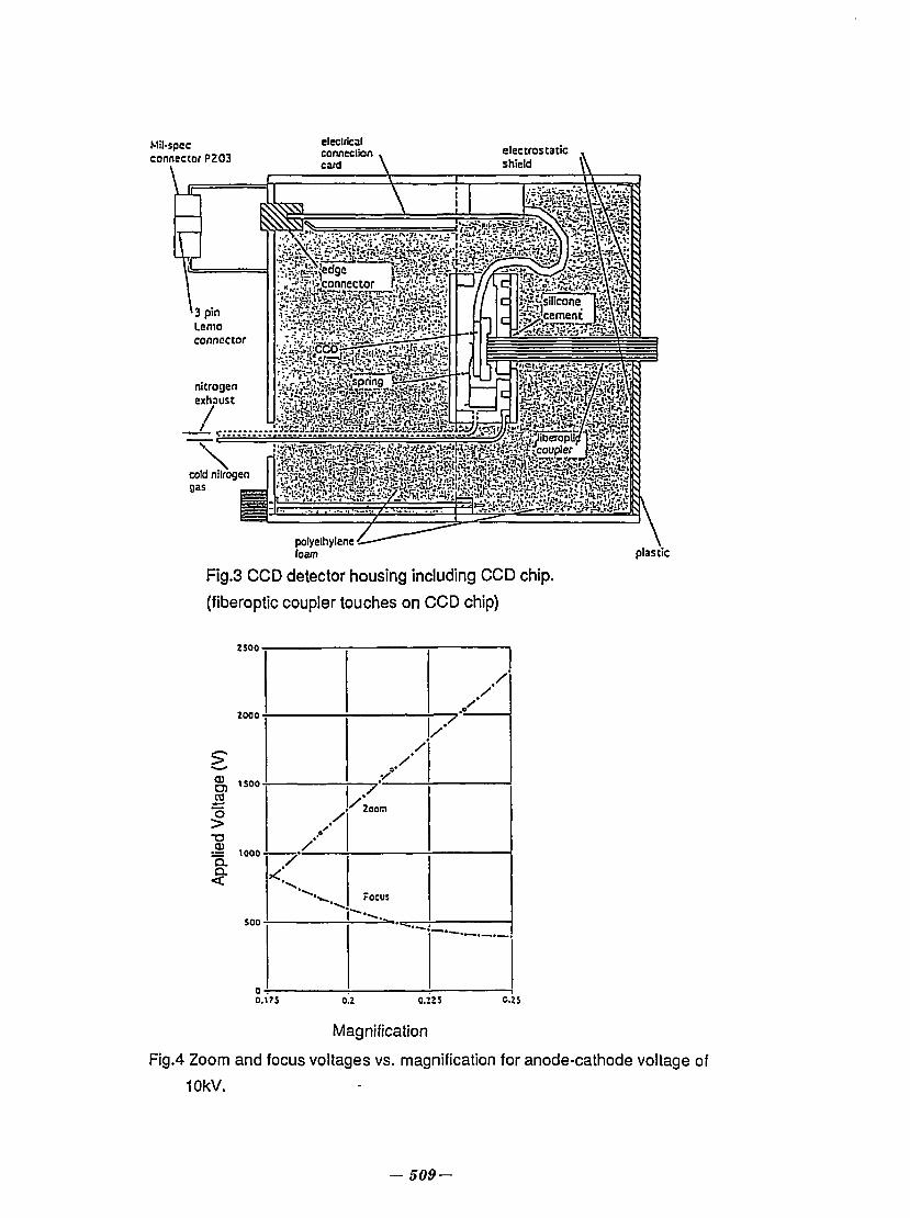
The PP0050 tube has four electrodes. They are the cathode, the focus electrode,
the zoom electrode and the anode shown in Fig.3. The tube is normally gated by bias
ing the focus electrode sufficiently negative. This is expected not to provide an ade
quate extinction ratio. We expected that it would be necessary to gate the zoom elec
trode. The tube was operated at -1 OkV cathode voltage and grounded anode. The
zoom pulse is generated by changing a cable (delay line) to ~20kV. It is discharged by
a spark gap which drives a 50 ohm terminating divider. Measurement of the voltages
for different magnifications are shown in Fig.4. The extinction measurements were
carried out at the nominal voltages for the 0.192 magnification. Biasing the focus elec
trode from 250 to 700 V negative with respect to the cathode gave about the same ex
tinction of -3x10³. It was found that the zoom electrode had to be biased to 480V neg
ative with respect to cathode to give good extinction. The extinction at 480V was
8.5x10⁶. If the signal remained even when the high voltage supply was turned com
pletely off is subtracted from the total signal at extinction, one obtains an extinction
factor of 1.4x10⁷. At its' full operating voltage of 20kV the tube would have higher gain
and the extinction factor including the direct shine through should exceed 107. The ef
fect of voltage on the tube gain was measured and found to be linear and follow the
law g=k(v-4300) above 5000V(k=const, v is the voltage). A gate pulse is flat to about
4% during the laser pulse shown in Fig.5.
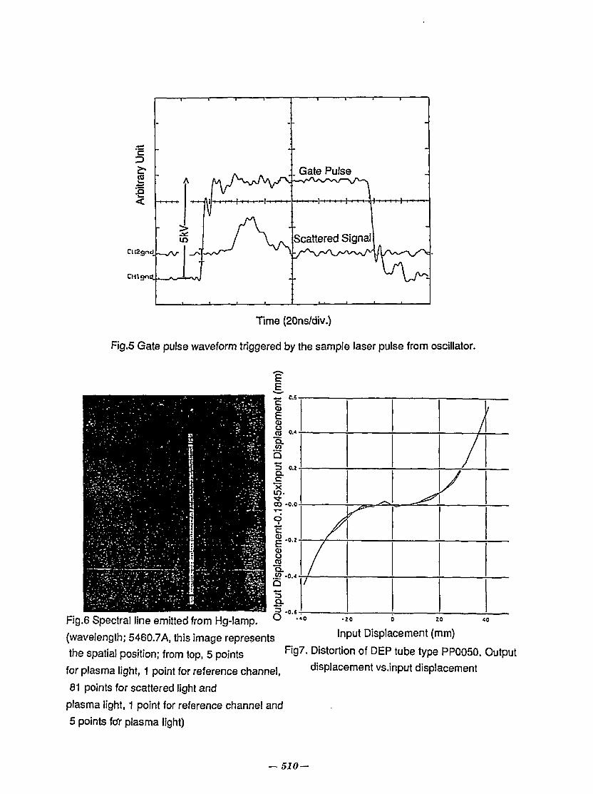
3.2 Distortion and modulation transfer function (MTF)
Spatial resolution depends on the design of collecting optics, Littrow spectrome
ter and CCD camera. We show the good image on the output of spectrometer in Fig.6.
The 81 points clearly seen and it goes to CCD through camera lens and the intensifier
tube. However the distortion of tube was measured and is shown in Fig.7. The optical
design of the camera lens corrects for this distortion and that of the second stage in
tensifier. The distortion for this tube is about 6.8% at 40mm input radius.
The resolution of PP0050 is 86lp/mm on axis and XX1600 is 75lp/mm, which are
sufficient for 81 points. By the way, MTF of XX1600 is 95% at 2.5lp/mm on axis based
on DPE data sheet.
4. Te and ne profiles
-505-
duration of plasma discharge=1 5 and gated duration=1 OOns, a high extinction ratio is
necessary to get the signal-to-noise ratio S/N >10. That is, the S/N is represented as
(scattered signalxextinction ratio)/{(sca抗eredsignal/1 O)x(duration of discharge/gated
duration)}. The extinction ratio should be (5旬 10)x1 07.
The PP0050 tube has four electrodes. They are the cathode, the focus electrode,
the 200m electrode and the anode shown in Fig.3. The tube is normally gated by bias-
ing the focus electrode sufficiently negative. This is expected not to provide an ade-
quate extinction ratio. We expected that it would be necessary to gate the 200m elec-
trode. The tube was operated at ・1OkV cathode voltage and grounded anode. The
200m pulse is generated by changing a cable (delay line) to -20kV. It is discharged by
a spark gap which drives a 50 ohm terminating divider. Measurement of the voltages
for different magnifications are shown in Fig.4. The extinction measurements were
carried out at the nominal voltages for the 0.192 magnification. Biasing the focus elec-
trode from 250 to 700 V negative with respect to the cathode gave about the same ex-
tinction of -3x1 03. It was found that the zoom electrode had to be biased to 480V neg-
ative with respect to cathode to give good extinction. The extinction at 480V was
8.5x1 06. If the signal remained even when the high voltage supply was turned com-
pletely off is subtracted from the total signal at extinction, one obtains an extinction
factor of 1.4x1 07. At its' full operating voltage of 20kV the tube would have higher gain
and the extinction factor including the direct shine through should exceed 107. The ef-
fect of voltage on the tube gain was measured and found to be linear and follow the
law g=k(v・4300)above 5000V(k=const, v is the voltage). A gate pulse is flat to about
4% during the laser pulse shown in Fig.5.
3.2 Distortion and modulation transfer function (MTF)
Spatial resolution depends on the design of collecting optics, Littrow spectrome-
ter and CCD camera. We show the good image on the output of spectrometer in Fig.6.
The 81 points clearly seen and it goes to CCD through camera lens and the intensifier
tube. However the distortion of tube was measured and is shown in Fig.7. The optical
design of the camera lens corrects for this distortion and that of the second stage in-
tensifier. The distortion for this tube is about 6.8% at 40mm input radius.
The resolution of P
4. Te and ne profiles
-505ー
TVTS was installed on JFT-2M tokamak and tested for the detector on the con
dition of -30°C. The temperature fluctuation is below 1°C. As CCD and fiberoptic cou
pler contract with cold, every test was done under the condition of -30°C. The stan
dard lamp was set inside of vacuum vessel to calibrate TVTS totally. The software
was modified based on the PPPL's, and also the Oak Ridge national laboratory's was
combined in JAERI. Te and ne profiles are obtained at a real time. The representative
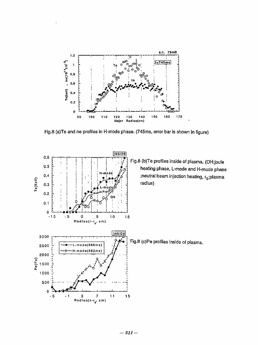
profiles measured with TVTS in H-mode plasma are shown in Fig.8. Te profile shows
the pedestal at edge and ne profile shows the sharp gradient at edge and also flat pro
file. In addition, Pe profile shows the sharper slope at edge compared to L-mode.
5. Summary
TVTS is completed in the collaboration with PPPL. Almost components was fab
ricated in JAERI, and tested. The advanced technique which PPPL has was applied
for JFT-2M TVTS.
1 .International collaboration of TVTS project was terminated successfully.
2.New detector system was fabricated and its characteristics are as follows;
extinction ratio >1.4x10⁷, MTF~95% at 2.5lp/mm on axis,
gate duration ~100ns, uniformity of gate pulse <4%.
3.Characteristics of TVTS are;
compact and high transmittance system, spatial resolution of 0.86cm, spatial
point of 81, measured length of 70cm.
4.Te and ne are measured on JFT-2M, and the representative results are;
Te: pedestal formation on H-mode plasma. ne:sharp gradient at edge on H-mode
plasma and flat profile. Pe:sharp slope at edge on H-mode.
Acknowledgement
The highest spatial resolution TVTS was developed in a collaboration with PPPL
for two years. And it has been measuring Te and ne profiles on JFT-2M. Through
these research, I would like to express my gratitude to Dr.K.Young in PPPL, Dr.Maeda
in JAERI for their continuous support.
REFERENCES
1)K.Hoshino, T.Yamamoto, H.Kawashima, T.Yamauchi, T.Shoji, N.Suzuki, Y.Uesugi-.J. Phys. Soc. Jpn. 58 (1989) 1248.
2)A.J.Bearden, F.L.Ribe, G.A.Sawyer and T.F.Stratton:Phys. Rev. Letters 6
- 506-
TVTS was installed on JFT・2Mtokamak and tested for the detector on the con-
dition of -30oC. The temperature fluctuation is below 10C. As CCD and fiberoptic cou・
pler contract with cold, every test was done under the condition of・300C.The stan-
dard lamp was set inside of vacuum vessel to calibrate TVTS totally. The software
was modified based on the PPPL's, and also the Oak Ridge nationallaboratory's was
combined in JAERI. Te and ne profiles are obtained at a real time. The representative
profiles measured with TVTS in H-mode pJasma are shown in Fig.8. Te profile shows
the pedestal at edge and ne profile shows the sharp gradient at edge and also flat pro-
fiJe. Jn addition, Pe profiJe shows the sharper sJope at edge compared to L -mode.
5. Summary
TVTS is completed in the collaboration with PPPL. Almost components was fab-
ricated in JAERI, and tested. The advanced technique which PPPL has was applied
for JFT・2MTVTS.
1.lnternational collaboration of TVTS pr吋ectwas terminated successfully.
2.New detector system was fabricated and its characteristics are as follows;
extinction ratio > 1.4x1 07, MTF"'95% at 2.5lp/mm on axis,
gate duration ...1 OOns, uniformity of gate pulse <4%.
3.Characteristics of TVTS are;
compact and high transmittance system, spatial resolution of 0.86cm, spatial
point of 81, measured length of 70cm.
4.Te and ne are measured on JFT-2M, and the representative results are;
Te: pedestal formation on H-mode plasma. ne:sharp gradient at edge on H-mode
plasma and fJat profile. Pe:sharp slope at edge on H-mode.
Acknowledgement
The highest spatial resoJution TVTS was developed in a collaboration with PPPL
for two years. And it has been measuring Te and ne profiles on JFT・2M.Through
these research, I would like to express my gratitude to Dr.K.Young in PPPL, Dr.Maeda
in JAERI for their continuous suppo凡
REFERENCES
1 )K.Hoshino, T.Yamamoto, H.Kawashima, T.Yamauchi, T.Shoji, N.Suzuki,
Y.Uesugi:J. Phys. Soc. Jpn. 58 (1989) 1248.
2)A.J.Bearden, F.L.Ribe, G.A.Sawyer and T.F.Stratton:Phys. Rev. Letters 6
- 506-

(1961)257.
3)J.Sheffield:"Plasma Scattering of Electromagnetic Radiation", Academic
press, Inc. New York (1975).
4)LE.Bailey:Rev. Sci. Instr. 31 (1960) 1147.
5)T.Yamauchi and l.YanagisawarAppl. Opt. 24 (1985) 700.
6)N.Bretz, D.Dimock, V.Foote, D.Johnson, D.Long and E.TolnasiAppl. Opt. 17
(1978)192.
7)D.Johnson, B.Grek, D.Dimock, R.Palladino and E.Tolnas: Rev. Sci. Instrum.
57(1986)1810.
8)D.Johnson, D.Dimock, B.Grek, D.Long, D.McNeill, R.Palladino, J.Robinson
and E.Tolnas:Rev. Sci. Instrum. 56 (1985) 1015.
9)D.Dimock and T.Yamauch'r.Jpn. At. Res. Inst. Rep.,JAERI-M 88-137 (1988).
10)T.Shiina, T.Yamauchi, T.Fujisawa, O.Hanawa, D.Dimock, A.Takahashi and
S.lnomataiJpn. At En. Res. Inst. Rep., JAERI-M 91-030 (1991).
11)T.Yamauchi, J.Davis, T.Shiina, D.Dimock, A.Takahashi and S.inomatarJpn.
At. En. Res. Inst. Rep., JAERI-M 91-035(1991)
12)T.Yamauchi and TVTS team:"20th EPS Conference on Controlled Fusion
and Plasma Physics", Vol.lll (1993) 1195.
13)T.Yamauchi, D.Dimock, E.Tolnas, V.Corso, B.LeBlanc, T.Shiina,
A.Takahashi, J.Felt, D.Johnson, J.Bartolick and R.Paladino:Jpn. J. Appl.
Phys.31 (1992) 2255.
Table I Characteristics of frame transfer CCD
CCD model CCD02-06-1-014(EEV)
Spectral response range 350-1 OOOnm
number of pixel 385x576pixels
image area 385x288pixels, 6.3x8.5mm
1 channel 4x9pixels
dynamic range ~4000/pixel
cooling cooled nitrogen gas flow, -30~-40°C
exposure control gated duration of image intensifier, ~100ns
— 507-
(1961) 257.
3)J.Sheffield:"Plasma Scattering of Electromagnetic Radiation", Academic
press, Inc. New York (1975).
4)l.E.Bailey:Rev. Sci.lnstr. 31 (1960) 1147.
5)T.Yamauchi and l.Yanagisawa:Appl. Opt. 24 (1985) 700.
6)N.Bretz, D.Dimock, V.Foote, D.Johnson, D.Long and E.Tolnas:Appl. Opt. 17
(1978) 192.
7)D.Johnson, B.Grek, D.Dimock, R.Palladino and E.Tolnas: Rev. Sci. Instrum.
57 (1986) 1810.
8)D.Johnson, D.Dimock, B.Grek, D.Long, D.McNeill, R.Palladino, J.Robinson
and E.Tolnas:Rev. Sci. Instrum. 56 (1985) 1015.
9)D.Dimock and T.Yamauchi:Jpn. At. Res. Inst. Rep.,JAER卜M88-137 (1988).
10)T.Shiina, T.Yamauchi, T.Fujisawa, O.Hanawa, D.Dimock, A.Takahashi and
S.lnomata:Jpn. At En. Res. Inst. Rep., JAERI-M 91・030(1991).
11)T.Yamauchi, J.Davis, T.Shiina, D.Dimock, A.Takahashi and S.lnomata:Jpn.
At. En. Res. Inst. Rep., JAERI-M 91・035(1991)
12)T.Yamauchi and TVTS team:"20th EPS Conference on Controlled Fusion
and Plasma Physics", Vol.lIl (1993) 1195.
13)T.Yamauchi, D.Dimock, E.Tolnas, V.Corso, B.LeBlanc, T.Shiina,
A.Takahashi, J.Felt, D.Johnson, J.Bartolick and R.Paladino:Jpn. J. Appl.
Phys.31 (1992) 2255.
Table I Characteristics of frame transfer CCD
CCD model CCD02・06・1・014(EEV)
Spectral response range 350・1000nm
number of pixel
Image area
1channeJ
dynamic range
cooling
exposure control
385x576pixels
385x288pixels, 6.3x8.5mm
4x9pixels
....4000/pixel
cooled nitrogen gas flow, -30.....40oC
gated duration of image intensifier, ....100ns
-507-

__ Objective issenbly Qs$<^r-" lit, fiber bundles
SkieU Boi
JH-PM
^Viwi lH
Floor
iunp
fr&fe^-1
^ :
\*\t— Came IDati
kcquisi* t i on
**' u
i Ruby laser in< U s enclosure
CoMrol Roon VAX Sitlion 3500
— 7 * Spit\ gsp electronics
«»ll
Fig.1 Elevation view of TV Thomson scattering system on JFT-2M.
(Spark gap electronics:laser triggered spark gap using a sample from the laser
pulse and spark gap using a pair of electrodes near the gap)
20KV(gating with spark gap)
A image fiber plate {input surface)
E X
(type:PP0050)
V 7&ZZ2
24cm
image Tiber plater'-
20KV
)
JL
S_S
output surface 'g>
(type:XXl600)
I
^
J »
)
Fig.2 Two stage of image intensifier tubes.
(type PP0050 electrodes from left side; cathodes;ground, focus;~1000V, zoom
bias;~-1000V, and zoom pulse voltage;~5kV, anodes;20kV)
-508 —
Bur. dUIIP
且_ObkCIIYe 1SS!lIbly ~ 111. Fibll bundlu
m-p~1
rloor
5p・1¥9ap 'h¥¥ e I ccl rani cs
Fig.1 Elevation view of TV Thomson sc~ttering system on JFT・2M.
(Spark gap electronics:laser triggered spark gap using a sample from the laser
pulse and spark gap using a pair of electrodes near the gap)
20KV(galing wilh spark gap)
5
(type:P P0050)
24cm
Fig.2 Two stage of image intensifier tubes.
(type PP0050 electrodes from left side; cathodes;ground, focus;-1 OOOV, zoom
bias;--1000V, and zoom pulse voltage;....5kV, anodes;20kV)
-508-
Mil-spec connector P203
electrostatic shield
polyethylene foam plastic
Fig.3 CCD detector housing including CCD chip,
(fiberoptic coupler touches on CCD chip)
i i U O -
ed V
olta
g
> <
> c
App
I
ft <
> c
0 -
/ <
y ' Zoom
Focus
• t — . - ^
1 /
/
" — • " - ~
0.I7S 0.2 C.2S 0.225
Magnification
Fig.4 Zoom and focus voltages vs. magnification for anode-cathode voltage of
10kV.
— 509-
conncctor
eleclriclll ∞Meclion card
Fig.3 CCD detector housing including CCD chip.
(fiberoptic coupJer touches on CCD chip)
%500
zooo
:;旬、
壱〉Z伺 W帥
.0 G3
〈CEL L
500
0 0.175
¥・ Fo:us、、.、、、~.、』
C;.~S
Magnification
Fig.4 200m and focus voltages vs. magnification for anode-cathode vo1tage of
10kV.
-509-
Time (20ns/div.)
Rg.5 Gate pulse waveform triggered by the sample laser pulse from oscillator.
/
/ /
r ^
1 1 y
/
5 -0.6-
Fig.6 Spectral line emitted from Hg-lamp. u , 4 ° • " ° 20 *° (wavelength; 5460.7A, this image represents l nPu t Displacement (mm) the spatial position; from top, 5 points F i97- Distortion of DEP tube type PP0050. Output for plasma light, 1 point for reference channel, displacement vs.input displacement
81 points for scattered light and
plasma light, 1 point for reference channel and
5 points for plasma light)
— 510 —
zcコEEZD』〈
C1l29n,!
C1119nd.
Time (20ns/div.)
Fig.5 Gate pulse waveform triggered by the sampJe Jaser pulse from oscillator.
V
A
(EE)言。EOQω一色
ω一QHコ且c-xb寸∞
F.O・芭ωEOOMw-aEQ古島コO
司引州川副引
J
壬ト吉ιAl
に白壬主夜埼(守.必一
一アて.¥.一一4:一一一…コ引J
一一一
J.-.. イ~vλ三
-JeJ(.J
一一一一一一一心一一一一-H-Y14Jザ淀川万一一一四円足
ile--¥J
一
一ー一-
j
j
a
-
-
¥
-
-
・
1
¥
-一
i
B
i
ト
ι
{
ι
l
i
い
i
・jl,・一一一¥よ
J
一¥~--
7.4一
PMinasHEBB-EEUBIE--
一一一一-J¥
一一一¥一一一一一一一…lfirvwhy-jr
一一一一一一一一一トUL--
一一一γ
人一一一一心一…一…人一一Input Displacement (mm)
Fig7. Distortion of DEP tube type PP0050. Output
displacement vs.input displacement
- 510ー
~O D .20 Fig.6 Spectralline emitted from Hg-Iamp.
(waveJength; 5460.7A, this image repre$ents
the spatial position; from top, 5 points
for plasma light, 1 point for reference channel,
81 points for scattered Iight and
plasma Iight, 1 point for reference channel and
5 points flσi' plasma light)
s.n. 734S8 1.2
*E 1
° 0.8
. 0.6
2 0.4
0.2
0
o ' o *b
o — • °-
,t=745ms
o • ne , o ,
, c»
• • l fTr»Tv-^- l
90 100 110 120 130 140 150 160 170 Major Radlus(cm)
Fig.8 (a)Te and ne profiles in H-mode phase. (745ms, error bar is shown in figure)
0.6
0.5
0.4
0.3
0.2
0.1
0 10
3000
2500
2000
1500
1000
500
0
• ; • i •
i : '. f r i
: i ! ' :
- ?_J
'-—•—'-m-ms.-trm-^
|INSIDE|
I l l I -
••1 I'ttJ/i 1 \p t • ! 7 0 •
ode^B >
/ O H ' : 1 i 1 ! • ' -
Fig.8 (b)Te profiles inside of plasma. (OH;joule
heating phase, L-mode and H-mode phase
;neutral beam injection heating, rs;plasma
radius)
10 15 Radlus(r-r , cm)
- L-mode(666ms)
•H-mode(682ms)
IINSIDEI
P*^ J Fig.8 (c)Pe profiles inside of plasma.
Radlus(r - r , cm)
— 511-
5.". 73488
。で仕'0 a
Te 0 oooOJ<f o'M45m::::il ' f e 06 o .... ~ 。t ' e 。 a L
. n..白。,..0唱o ";,.9_ O"OQ) ~ '6'"'0 .... 0
20!o'
E ぜ3、nなY.-が宇-品nee J九iJ,・-。拘r勾a •
唱ザ苦Yat l o
10 ~ ,-~
-・z. F-、3M...
1.2
智司'
'E U 司.
o 0.8 ‘・'回E _ 0.6
ミ 0.4.:<c -由ト・
0.2
o 90 170 160 150 130 140
Radlus(cm) 120 Major
110 100
Fig.8 (a}Te and ne profiles in H-mode phase. (745ms, error bar is shown in figure)
Fig.8 (b)Te profiles inside of plasma. (OH;joule
heating phase, L-mode and H-mode phase
;neutral beam injection heating, r S;plasma
radius)
0.6
ZLo
0.5
0.3
0.4
0.2
{〉也記}曲ド
15 10 o 5 Radlus(r・rs'cm)
E悪
二ココ工;:口:1工:::::: :::::ロ幻訓;::立幻山;2江お山:口引::;リ|li:://///////己r升門什~仇円?白行庁、!..F円向叩附W山…i泊い馴ω川gω州仰川8引附州(作ωc吋)内P向陶町山い山e叩叩巾山pro州州r巾耐叫of州file飴…s';1-,/' , '-:;
戸、 ft', ・'‘ I 司
γ~ "W
.. , ,C!f・ "v・・“日・ ・….. ~.で
3000 ・(;'"'"T
2500 -
2000 '-国-
!::.1500二41 ;' a.
1000 :-
500ヶ陶“
.、《o一、-.雪
・5 15
- 511ー
11 }
m
戸』・
ヲ,.ee ,
• • ,. {
ed' U
3
1
AU
SM
R