Tuneable VCSEL aiming for the application in interconnects and short haul systems
13
Tuneable VCSEL aiming for the application in interconnects and short haul systems Christian Gierl a , Karolina Zogal a , Sandro Jatta a , Hooman A. Davani a , Franko K¨ uppers a , Peter Meissner a , Tobias Gr¨ undl b ,Christian Grasse b , Markus-Christian Amann b , Aidan Daly c , Brian Corbett c , Benjamin K¨ ogel d , ˚ Asa Haglund d , Johan Gustavsson d , Petter Westbergh d , Anders Larsson d , Pierluigi Debernardi e , Markus Ortsiefer f a Technische Universit¨at Darmstadt, Merkstrasse 25, Darmstadt, Germany b Walter Schottky Institut, Am Coulombwall 3, Garching, Germany c Tyndall National Institute, Lee Maltings, Cork, Ireland d Chalmers University of Technology, Gothenburg, Sweden e Istituto di Elettronica e di Ingegneria dell’Informazione e delle Telecomunicazioni, Corso Duca degli Abruzzi 24, Torino, Italy f VERTILAS GmbH, Lichtenbergstrasse 8, Garching, Germany ABSTRACT Widely tunable vertical cavity surface emitting lasers (VCSEL) are of high interest for optical communications, gas spectroscopy and fiber-Bragg-grating measurements. In this paper we present tunable VCSEL operating at wavelengths around 850 nm and 1550 nm with tuning ranges up to 20 nm and 76 nm, respectively. The first versions of VCSEL operating at 1550 nm with 76 nm tuning range and an output power of 1.3 mW were not designed for high speed modulation, but for applications where only stable continuous tuning is essential (e.g. gas sensing). The next step was the design of non-tunable VCSEL showing high speed modulation frequencies of 10 GHz with side mode suppression ratios beyond 50 dB. The latest version of these devices show record output powers of 6.7mW at 20 ◦ C and 3mW at 80 ◦ C. The emphasis of our present and future work lies on the combination of both technologies. The tunable VCSEL operating in the 850 nm-region reaches a modulation bandwidth of 5.5 GHz with an output power of 0.8 mW. Keywords: Tunable VCSEL, High-Speed, High-Power, Wide Tunability, Telecommunication, Optical Intercon- nects, Short Haul Systems 1. INTRODUCTION Today, broadband communication has become a very important resource for our quick growing society. During the information era, communication has become a basic need. Every year, the number of internet users increases rapidly and with it the requirements for todays telecommunication networks. The increasing supply of services, such as real-time high definition video streaming and peer to peer file exchange require low delay and high capacity access networks. Given standards like digital subscriber line (DSL - phone) or hybrid fiber coax (HFC - cable) will not be able to fulfill the future requirements on broadband access networks, for they are already reaching their capacity limits. Even the most recent very high speed digital subscriber line (VDSL2) is limited to 100 MBit/s in up- and downstream direction. 1 Thus the near future is asking for a new infrastructure which fulfills the requirements of future demands. A very promising candidate is the passive optical network (PON) which allows to provide high performance and Further author information: (Send correspondence to Christian Gierl) Christian Gierl: E-mail:[email protected], Telephone: +49 6151 16 4418 Invited Paper Optical Metro Networks and Short-Haul Systems III, edited by Werner Weiershausen, Benjamin Dingel, Achyut Kumar Dutta, Atul K. Srivastava, Proc. of SPIE Vol. 7959, 795908 · © 2011 SPIE · CCC code: 0277-786X/11/$18 · doi: 10.1117/12.881247 Proc. of SPIE Vol. 7959 795908-1 DownloadedFrom:http://proceedings.spiedigitallibrary.org/on01/28/2015TermsofUse:http://spiedl.org/terms
Transcript of Tuneable VCSEL aiming for the application in interconnects and short haul systems

Tuneable VCSEL aiming for the application in interconnectsand short haul systems
Christian Gierla, Karolina Zogala, Sandro Jattaa, Hooman A. Davania, Franko Kuppersa,Peter Meissnera,
Tobias Grundlb,Christian Grasseb, Markus-Christian Amannb,Aidan Dalyc, Brian Corbettc ,
Benjamin Kogeld, Asa Haglundd, Johan Gustavssond, Petter Westberghd, Anders Larssond,Pierluigi Debernardie,
Markus Ortsieferf
aTechnische Universitat Darmstadt, Merkstrasse 25, Darmstadt, GermanybWalter Schottky Institut, Am Coulombwall 3, Garching, Germany
cTyndall National Institute, Lee Maltings, Cork, IrelanddChalmers University of Technology, Gothenburg, Sweden
eIstituto di Elettronica e di Ingegneria dell’Informazione e delle Telecomunicazioni, CorsoDuca degli Abruzzi 24, Torino, Italy
fVERTILAS GmbH, Lichtenbergstrasse 8, Garching, Germany
ABSTRACT
Widely tunable vertical cavity surface emitting lasers (VCSEL) are of high interest for optical communications,gas spectroscopy and fiber-Bragg-grating measurements. In this paper we present tunable VCSEL operatingat wavelengths around 850 nm and 1550 nm with tuning ranges up to 20 nm and 76 nm, respectively. The firstversions of VCSEL operating at 1550 nm with 76 nm tuning range and an output power of 1.3 mW were notdesigned for high speed modulation, but for applications where only stable continuous tuning is essential (e.g.gas sensing). The next step was the design of non-tunable VCSEL showing high speed modulation frequenciesof 10 GHz with side mode suppression ratios beyond 50 dB. The latest version of these devices show recordoutput powers of 6.7 mW at 20 ◦C and 3 mW at 80 ◦C. The emphasis of our present and future work lies onthe combination of both technologies. The tunable VCSEL operating in the 850 nm-region reaches a modulationbandwidth of 5.5 GHz with an output power of 0.8 mW.
Keywords: Tunable VCSEL, High-Speed, High-Power, Wide Tunability, Telecommunication, Optical Intercon-nects, Short Haul Systems
1. INTRODUCTION
Today, broadband communication has become a very important resource for our quick growing society. Duringthe information era, communication has become a basic need. Every year, the number of internet users increasesrapidly and with it the requirements for todays telecommunication networks. The increasing supply of services,such as real-time high definition video streaming and peer to peer file exchange require low delay and highcapacity access networks. Given standards like digital subscriber line (DSL - phone) or hybrid fiber coax (HFC- cable) will not be able to fulfill the future requirements on broadband access networks, for they are alreadyreaching their capacity limits. Even the most recent very high speed digital subscriber line (VDSL2) is limitedto 100 MBit/s in up- and downstream direction.1 Thus the near future is asking for a new infrastructure whichfulfills the requirements of future demands.A very promising candidate is the passive optical network (PON) which allows to provide high performance and
Further author information: (Send correspondence to Christian Gierl)Christian Gierl: E-mail:[email protected], Telephone: +49 6151 16 4418
Invited Paper
Optical Metro Networks and Short-Haul Systems III, edited by Werner Weiershausen, Benjamin Dingel, Achyut Kumar Dutta, Atul K. Srivastava, Proc. of SPIE Vol. 7959,
795908 · © 2011 SPIE · CCC code: 0277-786X/11/$18 · doi: 10.1117/12.881247
Proc. of SPIE Vol. 7959 795908-1
Downloaded From: http://proceedings.spiedigitallibrary.org/ on 01/28/2015 Terms of Use: http://spiedl.org/terms

ONUs
λ1
λ1
λ1
λ1
OLT
CentralOffice
Power-splitter
(a) Power Splitting PON.
ONUs
λ1,λ2,λ3
λ1
λ2
λ3
OLT
CentralOffice
Wavelength-router
(b) WDM-PON.
Figure 1. In a Power splitting PON, the power of the downstream signal is splitted via a power splitter to the differentONUs (a). In a WDM-PON a wavelength router seperates the different wavelength of the downstream to the appropriateusers (b), which is a physical point to point connection.
low delay services. In a PON the connection between optical line terminal (OLT) at the service providers centraloffice and the optical network units (ONU) near the end users is based only on passive optical components. Thusno electrical power is needed within the feeder network. Furthermore PONs have two significant advantagesas compared to the given standards like VDSL2. First, it exploits the very high channel capacity of opticalfibres enabling access to broadband intensive sevices. The lower attenuation per length in optical fibre networkscompared to electrical networks is the second advantage.There mainly exist two different PON architectures. Wavelength division multiplexing (WDM) PONs (e.g.DWDM-PONs, channel spacings of 100 GHz in the range of 1528.77 nm to 1563.86 nm, ITU G.6922) and todaystime-division multiple access (TDMA) PONs like Ethernet PON (EPON, IEEE 802.3ah3) and gigabit PON(GPON, ITU-T G.9844). However, the latter cannot keep up with future requirements regarding bandwidth,attainable reach and allowable power budget. This approach uses a passive power splitting unit to split theoptical power in the feeder fibre equally to the ONUs (Fig. 1a). However, this concept limits the flexibilityfor assigning different bandwidths (wavelength) to different ONUs since every ONU has to communicate at thesame data rate. A WDM-PON5 overcomes these limitations and offers a higher optical bandwidth per ONU,low splitting losses and thus a higher link reach as opposed to EPON and GPON networks.6 WDM-PON ac-cess networks use wavelength selective filters7 instead of power splitters for seperating the information for thedifferent ONUs (Fig. 1b). This technique allows the OLT to address each ONU by selecting the appropriatewavelength thus allowing different data rates and privacy. All of the WDM-PON approaches are trying to solveone of the main challenges which is to provide cost effective light sources at the OLT and the ONUs. We willfocus on the approach using a photonic integrated circuit at the OLT and a tunable vertical cavity emittingdiode laser (VCSEL) at the ONU. Each ONU uses an identical tunable VCSEL which is able to tune to anygiven wavelength of the channel grid. This attempt is called ”colorless” ONU. Whereas the OLT is equippedwith an array of lasers combined in an photonic integrated circuit (PIC).8 Tunable VCSEL are high desirablecomponents for WDM-PON networks for several reasons. In order to supply for example a 100-channel WDMsystem, one would need 100 different distributed feedback lasers with fixed wavelength. This matter leads toseveral disadvantages. The laser manufacturers need to introduce expensive selection processes for supplying theONUs with lasers of the appropriate wavelength. Moreover, the network operators need to stock many differentlasers and keep inventories of spare parts for each laser wavelength in the event transmitters fail in the fieldand need to be replaced. A tunable VCSEL would be able to compensate all of these disadvantages. Only one”colorless” ONU would be needed which reduces the capital as well as operational expenditures.Another application for tunable VCSEL are short distance communication networks. Such networks are used inhigh-end computing, switching and storage systems. They can be used e.g. as optical interconnects in distributedshared memory machines (DSM).9 The CPU performance has increased rapidly following Moore’s law.10 Whereasthe bandwidth of the interconnects between the processors and the memory has not increased this fast. Thisgap in performance becomes a significant problem in massively parallel processing (MPP) systems.11 Electricalinterconnects suffer from attenuation, crosstalk and reflections inside the electrical signal lines which becomes
Proc. of SPIE Vol. 7959 795908-2
Downloaded From: http://proceedings.spiedigitallibrary.org/ on 01/28/2015 Terms of Use: http://spiedl.org/terms

even worse for higher bus speeds. Thus optical interconnects using WDM are very attractive for MPP or DSMsystems. They enable a significant increase in bandwidth as well as more complex interconnect topologies.11
Many different concepts for tunable laser sources have been investigated in the past decades.13–15 Tunabilitydescribes the ability of a single mode laser to change its operating wavelength via an external control parameter.The tuning range of such a laser can be defined by the given requirements of the application. These requirementscould be side mode supression ratio (SMSR), output power, linewidth or relative intensity noise (RIN), whichmust not go below or above a certain limit or keep constant over the tuning range. In telecommunication, thetuning range should cover the entire C-band (1529 nm to 1565 nm) or L-band (1565 nm to 1610 nm) or even both.A SMSR > 30 dB and data rates of about 10 GBit/s are recommended. In short distance data communicationnetworks a tuning range of ≥ 30 nm in the range of 820 nm to 880 nm and a modulation bandwidth ≥ 10 GBit/sare desirable.
2. TUNABILITY OF VCSEL
z
Optical field
n-contact
p-contact/Au-heatsink
Bottom mirror
Gain-region (Quantum wells)
Top movable mirror
Figure 2. Cross-section of a MEMS tunable VCSEL. The bottom and the curved top mirror form an optical resonator.The optical field inside the resonator is amplified in the gain region. The top mirror can be moved along the z-axis whichchanges the cavity length.
The basic physics of a tunable VCSEL can be best explained with the principle of Fabry-Perot lasers. Sucha laser consists of two parallel mirrors with an active gain material for light amplification in between. Thiscan be an electrically pumped semiconductor whose parallel crystal surfaces form a resonator consisting of twoplain mirrors (the semiconductor air interface has a sufficient reflectivity of ≈ 30 %). After each reflection, thelight passes the electrically pumped gain medium and is amplified. A stable laser mode inside the cavity is onlypossible if the circulating wave in between two crystal surfaces superimposes itself in-phase (a standing waveinside the resonator):
L = nL′ = mλm
2(1)
where L′ is the geometrical cavity length, n the effective refraction index, m an integer and λm the emittedwavelength. The main mechanism for tuning a laser is to change the effective optical cavity length L and thusthe wavelength λ. There exist three parameters for changing the emitted wavelength. The first one is thetemperature of the device (thermo optical effect). An increase of the temperature T leads to a change of therafractive index (n(T )) and thus to an increase of the wavelength λ. The wavelength change over temperature istypically 0.09 to 0.12 nm/◦C12 and limited to a continuous tuning range of about 7 nm for standard VCSEL (seemeasurement results in section 5). The second one is the injection current, which changes the carrier density Cinside the cavity and therewith the refractive index (n(C)) index n. As the device heats up for higher currents,this effect is limited to several nm, too. The third one is to change the cavity length mechanically. In this paperwe will focus on micro-electro-mechanical (MEMS) tunable VCSEL (see Fig. 2). This concept enables recordtuning ranges > 70 nm.15
Proc. of SPIE Vol. 7959 795908-3
Downloaded From: http://proceedings.spiedigitallibrary.org/ on 01/28/2015 Terms of Use: http://spiedl.org/terms

3. BASIC PRINCIPLE OF A MEMS TUNABLE VCSEL
Transmission ofthe Resonator
Gain
Losses
Lasermode
Longitudinal modeFSRλ
λm+1 λm λm−1λ
α,g,T
Figure 3. The selectivity of the Fabry-Perot resonator of a short cavity VCSEL allows only one logitudinal mode (λm) tolase. The adjacent logitudinal modes (λm+1,λm−1) underlie too high losses.
A MEMS tunable VCSEL mainly consists of an electrically pumped active region embedded between twodistributed bragg reflectors (DBR). They are based on the principle of interference and enable very high re-flectivities (> 99 %). These reflectivities are needed since the active region is quite short as compared to edgeemitting diode lasers which reduces the gain during one pass through the active medium significantly. One canseperate the tunable VCSEL into two main parts. The first part mainly consists of the bottom mirror and theactive gain region. This part is called half-VCSEL, because the second mirror is missing. Our devices use acurved movable mirror membrane which is suspended on four flexible beams as top mirror.15 An implementedconductive layer allows thermal heating of the membrane and thus an expansion of the suspension beams. Thisleads to an increase of the air gap length (see fig. 7). The curved top mirror and the flat bottom mirror of thehalf-VCSEL are forming a plane-concave Fabry-Perot cavity. This type of cavity is much more insensitive to tiltangles between the two mirrors as compared to cavities consisting of two plane mirrors.16 Furthermore we willsee that this approach can be used to further increase the SMSR and to guarantee stable optical properties overthe whole tuning range, too. The MEMS tunable VCSEL devices presented in this paper can be described asoptical oscillators with resonant wavelengths defined by equation (1). The standing waves are the longitudinaleigenmodes of the optical resonator. The free spectral range (FSR) between two longitudinal modes is given by
FSRλ = λm − λm+1 ≈ λ2
2L. (2)
This equation illustrates one advantage of VCSEL as a tunable laser source. In comparison to edge emittinglasers, the resonator length of typically L = 10 λ is quite short and leads to a FSRλ ≈ λ/20 ≈ 80 nm at awavelength of λ = 1550 nm. Because of the limited amplification bandwidth g of the gain medium, the lossesα of the passive resonator and the large spectral distance of the longitudinal modes (Transmission T of theresonator), only one longitudinal mode has a sufficient amplification for lasing (a schematic view of α,g and Tis given in fig. 3). This intrinsic single mode behaviour allows a continuous tuning of the wavelength. Anotheradvantage is the tuning efficiency. A change in the distance of the two resonator mirrors of ΔL leads to a linearshift of the wavelength Δλ with
Δλ = ΔL · 2m
(3)
whereas m is the order of the longitudinal mode. In our example with a typical resonator length of L = 10 λ onegets m = 20 and therewith Δλ = 0.1ΔL. Whereas a typical edge emitter with L = 450 λ has a tuning efficiencyof only Δλ/ΔL ≈ 0.005 which is twenty times smaller. The consequence is, that a reduction of the resonatorlength effects an increase of the tuning efficiency. Never the less a tuning over the whole FSR requires a changeof the resonator length of ΔL = λ/2 ≈ 780 nm, which is independent of the resonator length.
3.1 Resonator geometry and Gaussian modesIn section 3 we introduced a one dimensional model for Fabry-Perot resonators and calculated its one dimensionallogitudinal modes. To describe their three dimensional field distributions inside a plane-concave resonator, this
Proc. of SPIE Vol. 7959 795908-4
Downloaded From: http://proceedings.spiedigitallibrary.org/ on 01/28/2015 Terms of Use: http://spiedl.org/terms

0.0 0.5 1.0 1.5 2.0 2.5 3.00.0
0.2
0.4
0.6
0.8
1.0
Apperture
TEM00
TEM10
TEM20
Normalised radius r/w0
Nor
mal
ised
inte
nsity
I/I 0
(a) Radial modes
0.0 0.5 1.0 1.5 2.0 2.5 3.00.0
0.2
0.4
0.6
0.8
1.0
Apperture
TEM00
TEM01
TEM02
Normalised radius r/w0
Nor
mal
ised
inte
nsity
I/I 0
(b) Azimutal modes
Figure 4. Cross section view of the intensity distribution for radial (a) and azimutal Gauss-Laguerre-modes TEMpl (b).The implementation of an aperture inside the resonator (shaded area) allows to increase the losses for higher order modeswhich leads to a significant increase of the SMSR.
model needs to be extended. The three dimensional electrical field distribution of the longitudinal modes insidethe resonator can be approximated by the radial symmetric Gaussian beam equation (in zylindric coordinates)
E(r, z) = E0w0
w(z)· exp
(− r2
w(z)2
). (4)
This equation is completely defined with the beam waist w0 = w(z = 0) of the Gaussian beam and the Rayleighlength z0 = πw2
0/λ. The Gaussian beam diverges in z-direction at which w(z) defines the beam radius along thepropagation axis z. The phasefront R(z) of the Gaussian beam transforms from a plane wave at z = 0 into aspherical wave for z → ∞ with
w(z) = w0
√1 +
(z
z0
)2
; R(z) = z
(1 +
(z0
z
)2)
(5)
Thus the Gaussian mode is completely defined by the radius of curvature (RoC) of the top movable mirrormembrane and the cavity length L (in z-direction, see Fig. 2), so that the phasefronts of the Gaussian modecoincide with the mirror geometries. This circumstance causes a plane phasefront at the bottom mirror of theVCSEL with a given beam waist of
w0 =
√λ
π
√L(RoC − L). (6)
In fact, a rotation symmetric resonator is not restricted to the longitudinal Gaussian modes. Transversal higherorder modes fullfill the boundary conditions of the resonator as well. These modes can be described as TEMpl
modes with the radial and azimutal order p and l, respectively. In fact, the intensity distributions insidethe complex VCSEL device can not completely be described with TEMpl-modes but with hybrid modes withlongitudinal field components.18 But the Gaussian beam theory can be used as a good approximation. Theintensity profile for the TEMpl modes can be calculated with the Gauss-Laguerre-polynomes Ll
p(t) (in polarcoordinates (r, φ)) as follows:
Ipl(r, φ) = I0 · tl · (Llp(t))
2 · cos2(lφ) · e−t with t = 2r2/w20. (7)
For higher order modes, the intensity distribution spreads in radial direction. A cross section view of the higherorder radial (a) as well as azimutal modes (b) is shown in Fig. 4 (the intensity distributions are symmetric tothe Intensity-axis). This fact allows us to increase the losses for higher order modes with the implementation ofan apperture inside the VCSEL structure (coloured area in Fig. 4). Thus a significant increase of the SMSR is
Proc. of SPIE Vol. 7959 795908-5
Downloaded From: http://proceedings.spiedigitallibrary.org/ on 01/28/2015 Terms of Use: http://spiedl.org/terms

possible. In a plane concave resonator each TEMpl mode has its characteristic resonance frequency
νplq =c
2L
(q +
2p + l + 1π
arccos(√
1 − L/RoC))
(8)
with longitudinal order q. The measurement of the emission spectrum allows to identify the lateral modes andthus the SMSR as will be shown in section 5.
3.2 Lateral and longitudinal confinement factor
z n-contact
p-contact
Active region
Electrical current
DA
Figure 5. The current flowing from the n- to the p-contact is confined to the diameter DA of the integrated apperture.The active region is electrically pumped only within this area which leads to a spatial confinement of the gain.
The size of the integrated aperture is chosen to be in the range of the beam waist of the fundamental Gauss-mode. As illustrated in fig. 4, the fundamental mode is nearly not effected by the aperture, whereas the higherorder modes have a larger overlap between the intensity distribution and the apperture. The basic principlebehind the aperture is to confine the current flowing through the device to a defined diameter DA (see Fig. 5).Since the gain profile is directly correlated with the current density, the overlap between the lateral gain g(r, φ)and the transversal intensity distribution Ipl(r, φ) ∝ |Epl(r, φ)|2 for a certain mode p, l can be described by thelateral confinement factor
Γxy =∫ |Epl(r, φ)|2g(r, φ) r dr dφ∫ |Epl(r, φ)|2 r dr dφ
. (9)
Considering a constant gain profile limited by the integrated aperture, one can calculate that Γxy(E00) > Γxy(Epl)for p or l > 0. Thus the fundamental Gaussian mode has a higher gain as compared to higher order transversalmodes leading to an increase of the SMSR. With the longitudinal confinement factor Γz which quantizes theoverlap between the longitudinal intensity distribution of a given mode and the active gain region
Γz =
∫dgain
|Epl(z)|2 dz∫L |Epl(z)|2 dz
, (10)
one can calculate the effective gain 〈g〉 = Γg = ΓxyΓzg for each resonator mode. The longitudinal confinementfactor Γz compares the thickness of the active region dgain with the resonator length L. Thus equation 10 canbe written as19
Γz =dgain
L·Γr with Γr = 1 + cos(2kzΔz)
sin(kzdgain)kzdgain
. (11)
The relative confinement factor Γr describes the overlap between the standing wave and the active region insidethe VCSEL cavity, with the wavenumber kz and the relative shift Δz of the nodes and antinodes of the standingwave while changing the cavity length with the movable membrane. If an antinode of |E(z)|2 overlaps with the
Proc. of SPIE Vol. 7959 795908-6
Downloaded From: http://proceedings.spiedigitallibrary.org/ on 01/28/2015 Terms of Use: http://spiedl.org/terms

air
n
top DBR (membrane)|E
(z)|2
,n
|E(z)|2air-gap
Quantum wells
bottom DBR
zFigure 6. Simulation of the longitudinal 1D intensity distribution (|E(z)|2) in a long-wavelength tunable VCSEL. Therefractive index profile n(z) is defined by the layer composition of the VCSEL. The blow-up shows that |E(z)|2 has anantinode inside the gain region (quantum wells)
active region, Γr has a maximum value of two. On the other hand, if a node coincides with the active region, Γr
becomes zero. Thus the tunable VCSEL needs to be designed in a way that an antinode overlaps with the activeregion for a maximum effective gain. The one dimensional longitudinal intensity distribution has been simulatedconsidering every single layer and its refraction index of a given tunable VCSEL-design (via Matrix-Transfer-Method20 implemented with Matlab-software∗). Fig. 6 shows that the intensity distribution has an antinodeinside the gain region for an air-gap length of 11 μm.
4. TECHNOLOGY AND FABRICATION
(a) MEMS-VCSEL consisting of tunable membrane- andhalf-VCSEL chip
Thermal expansion
Current Source
Via-holes(b) Electro thermal tuning of the membrane
Figure 7. Realization of the MEMS-VCSEL concept with a movable top mirror membrane which can be electro-thermallyactuated. Its deflection is directly correlated to the emission wavelength of the VCSEL device and can be controlled viaa heating current flowing through the membrane.
Micro-electro-mechanical-system (MEMS) technology is very promising in respect to the achievement ofstable spectral properties over a large tuning range (> 70 nm).15 By use of a curved mirror (with a definedRoC) the fundamental mode of the VCSEL can be supported. Essential for this approach is the coincidence ofthe phasefront of the optical beam with the curvature of the membrane. The included length of air-gap can bevaried by using electro thermal actuation thus the cavity resonance can be tuned to longer wavelengths. TheMEMS-DBR is realised in two different material systems: semiconductive and dielectric. The semiconductor
∗Trademark of MathWorks
Proc. of SPIE Vol. 7959 795908-7
Downloaded From: http://proceedings.spiedigitallibrary.org/ on 01/28/2015 Terms of Use: http://spiedl.org/terms
(a) Optical emission spectrum for a fixed tuningcurrent and tuning envelope
(b) Output power over tuning range
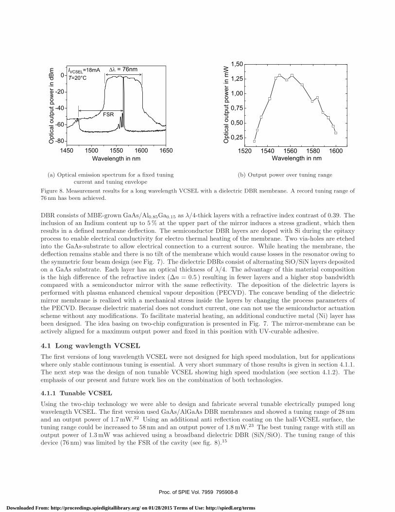
Figure 8. Measurement results for a long wavelength VCSEL with a dielectric DBR membrane. A record tuning range of76 nm has been achieved.
DBR consists of MBE-grown GaAs/Al0.85Ga0.15 as λ/4-thick layers with a refractive index contrast of 0.39. Theinclusion of an Indium content up to 5 % at the upper part of the mirror induces a stress gradient, which thenresults in a defined membrane deflection. The semiconductor DBR layers are doped with Si during the epitaxyprocess to enable electrical conductivity for electro thermal heating of the membrane. Two via-holes are etchedinto the GaAs-substrate to allow electrical connection to a current source. While heating the membrane, thedeflection remains stable and there is no tilt of the membrane which would cause losses in the resonator owing tothe symmetric four beam design (see Fig. 7). The dielectric DBRs consist of alternating SiO/SiN layers depositedon a GaAs substrate. Each layer has an optical thickness of λ/4. The advantage of this material compositionis the high difference of the refractive index (Δn = 0.5 ) resulting in fewer layers and a higher stop bandwidthcompared with a semiconductor mirror with the same reflectivity. The deposition of the dielectric layers isperformed with plasma enhanced chemical vapour deposition (PECVD). The concave bending of the dielectricmirror membrane is realized with a mechanical stress inside the layers by changing the process parameters ofthe PECVD. Because dielectric material does not conduct current, one can not use the semiconductor actuationscheme without any modifications. To facilitate material heating, an additional conductive metal (Ni) layer hasbeen designed. The idea basing on two-chip configuration is presented in Fig. 7. The mirror-membrane can beactively aligned for a maximum output power and fixed in this position with UV-curable adhesive.
4.1 Long wavlength VCSEL
The first versions of long wavelength VCSEL were not designed for high speed modulation, but for applicationswhere only stable continuous tuning is essential. A very short summary of those results is given in section 4.1.1.The next step was the design of non tunable VCSEL showing high speed modulation (see section 4.1.2). Theemphasis of our present and future work lies on the combination of both technologies.
4.1.1 Tunable VCSEL
Using the two-chip technology we were able to design and fabricate several tunable electrically pumped longwavelength VCSEL. The first version used GaAs/AlGaAs DBR membranes and showed a tuning range of 28 nmand an output power of 1.7 mW.22 Using an additional anti reflection coating on the half-VCSEL surface, thetuning range could be increased to 58 nm and an output power of 1.8 mW.23 The best tuning range with still anoutput power of 1.3 mW was achieved using a broadband dielectric DBR (SiN/SiO). The tuning range of thisdevice (76 nm) was limited by the FSR of the cavity (see fig. 8).15
Proc. of SPIE Vol. 7959 795908-8
Downloaded From: http://proceedings.spiedigitallibrary.org/ on 01/28/2015 Terms of Use: http://spiedl.org/terms

Figure 9. Cross-section of a high-speed 1.55 μm InP-based BTJ VCSEL
4.1.2 Non tunable high speed VCSEL
The single-mode high speed VCSEL operating in the 1.55 μm wavelength range is based on InP-semiconductorcavity with a burried tunnel junction (BTJ). Figure 9 shows the cross-section of the half VCSEL. The active regionconsists of seven highly compressively strained AlGaInAs quantum wells (QW) with a thickness of 6 nm whichare separated by 7 nm thick lattice matched AlGaInAs barriers. This compressive strain increases the differentialgain of the active region, which is essential for high speed properties.21 The active region is embedded betweentwo thick InP layers (see ”InP n-cladding” and ”InP regrowth” in fig. 9). By lowering the doping level of then-InP overgrowth, the parasitic capacitance of the space charge region is reduced. This leads to strongly reduceddevice parasitics,24 which is essential to gain access to > 10 GBit/s modulation frequencies. Current confinementand thus a sufficient high current density in the active region is achieved by implementing a BTJ.25, 27 TheBTJ consists of two highly doped layers, namely AlGaInAs (p-doped, 1.5 · 1020 cm−3) and GaInAs (highly n-doped 1.5 · 1020 cm−3). The dielectric bottom DBR consists of evaporated AlF3/ZnS with gold coating andan electroplated substrate (serving as heatsink). The advantage of these materials is the high refractive indexcontrast Δn ≈ 1 , therefore only 3.5 pairs are needed to reach a desired reflectivity beyond 99 %. The nextadvantage is that a reduction of the DBR thickness is possible. This is important due to the better heatmanagement of the whole device. However, the thickness of the DBR is not critical in respect to the electricalresistance, since the given design uses intracavity current injection. That means that the current does not haveto flow through all the DBR layers to reach the active region. The next important technological advancementis a shrinkage of the contact pad area and the inclusion of Benzo-Cyclo-Butene (BCB) with a low dielectricconstant of 2.6, which is intended to reduce the parasitic contact pad capacitances and hence enable high speedoperation.
4.2 Short wavelength VCSEL
Starting from the bottom GaAs-substrate, the half-VCSEL consists of an n-type GaAs contact layer above then-contact (Ni/Ge/Au). The bottom DBR consists of 36.5 pairs of n-doped AlGaAs with a maximum reflectivityof 99.9 %, a gain region consisting of three GaAs QW and a top p-region. An Al-rich layer has been set justabove the QW. This layer can be selectively oxidized and define simultaneously a current and gain aperture.Additionally, the semiconductor-air interface is covered with a λ/4 anti-reflection coating. To be able to supplythe VCSEL with a high-frequency signal a 1.3 mm long microstrip line connects the VCSEL to ground-signal-ground (G-S-G) pads (fig. 10). A 6 μm thick layer of BCB separates the transmission line from the groundplane. Etching small mesa structures and filling the etched regions with BCB significantly reduces the parasiticcapacitance. This enables modulation frequencies > 5 GHz. The top concave mirror membrane of the VCSELconsists of AlGa(In)As layers grown by molecular beam epitaxy on an undoped GaAs substrate. The high-index
Proc. of SPIE Vol. 7959 795908-9
Downloaded From: http://proceedings.spiedigitallibrary.org/ on 01/28/2015 Terms of Use: http://spiedl.org/terms

Optical Output
n-contact
n-contact
p-contact
Quantum Wells
DBR
Currentspreadlayer
OxideApperture
GaAs-Substrate
Membrane
(a) Cross section view of the VCSEL
n-contact (ground)
n-contact (ground)
p-contact (signal)
Mesa
BCB
VCSEL-chip Membrane-chip
(b) Picture of the VCSEL andschematic top view of the
half-VCSEL
Figure 10. Cross-section of a high-speed 850 nm GaAs-based VCSEL with integrated oxide apperture. The area aroundthe mesa structure is filled with BCB which reduces the parasitic capacitance. The top picture in (b) shows a membranechip assembled with the half-VCSEL.
layers have an aluminium-content of 14 % and the low-index layers are composed of Al0.85GaAs. This resultsin a refractive index difference of about 0.4. To achive a reflection of 99.8 %, 22.5 pairs are required. Due todifficulties in the fabrication process, eight of 22.5 pairs have an increased thickness of 3λ/4 to achive a bettermechanical stability of the membrane. The reflection measurements show that the grown DBR has a centerwavelength of 851 nm and a bandwidth of 23 nm (see fig. 12) in which the reflectivities keep higher than 99.7 %.The penalty of making the layers thicker is a reduction of the bandwidth of 40 nm as compared to a mirrorconsisting of λ/4-thick layers only (calculated with matrix transfer method20).
5. CHARACTERISATION
5.1 Long wavelength VCSEL
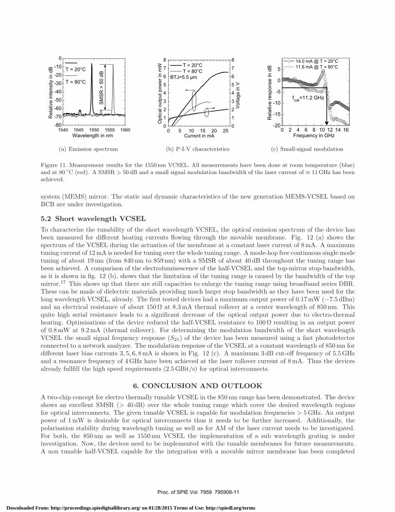
For the preliminary static and dynamic device characteristics, a flat and non-tunable dielectric DBR is evaporatedon the top of the half-VCSEL (same material composition for the bottom mirror consisting of 5 pairs). Themeasurements has been done at room temperature and at 80 ◦C.26 Fig. 11 (b) shows the P-I-V characteristicsof a long-wavelength VCSEL consisting of a 5.5 μm BTJ. The single-mode fiber coupled optical output power atthermal roll-over shows a maximum value of 6.7 mW at room temperature and 3 mW at 80 ◦C. The thresholdcurrent amounts 1.2 mA and 2.1 mA for 20 ◦C and 80 ◦C, respectively. The voltage drop over the fully appliedcurrent range from 0− 27 mA shows a kink voltage of approximately 0.9 V and a maximum value of 2.1 V. Thiscurrent-voltage curve does not vary over the full considered temperature range from 20 ◦C to 80 ◦C. The SMSRexceeds 50 dB. Fig. 11 (a) shows thermal tuning of the wavelength, which is limited to a couple of nanometers.In order to determine the resonance frequency, a small signal modulation has been applied for various laser biascurrents. Fig. 11 (c) presents the measured S21-parameter plotted over the modulation frequency. As can beseen, a maximum 3 dB-cutoff frequency of 11 GHz is reached for bias currents smaller than the respective roll-overcurrents and is stable over the whole temperature range. This means that these devices can be applied for datatransmission in the 12.5 GBit/s range for each desired and specified temperature within 20◦C and 80◦C. To realisea wide tunable laser one has to replace the evaporated top flat DBR by an external micro-electro-mechanical
Proc. of SPIE Vol. 7959 795908-10
Downloaded From: http://proceedings.spiedigitallibrary.org/ on 01/28/2015 Terms of Use: http://spiedl.org/terms
(a) Emission spectrum (b) P-I-V characteristics (c) Small-signal modulation
Figure 11. Measurement results for the 1550 nm VCSEL. All measurements have been done at room temperature (blue)and at 80 ◦C (red). A SMSR > 50 dB and a small signal modulation bandwidth of the laser current of ≈ 11GHz has beenachieved.
system (MEMS) mirror. The static and dynamic characteristics of the new generation MEMS-VCSEL based onBCB are under investigation.
5.2 Short wavelength VCSEL
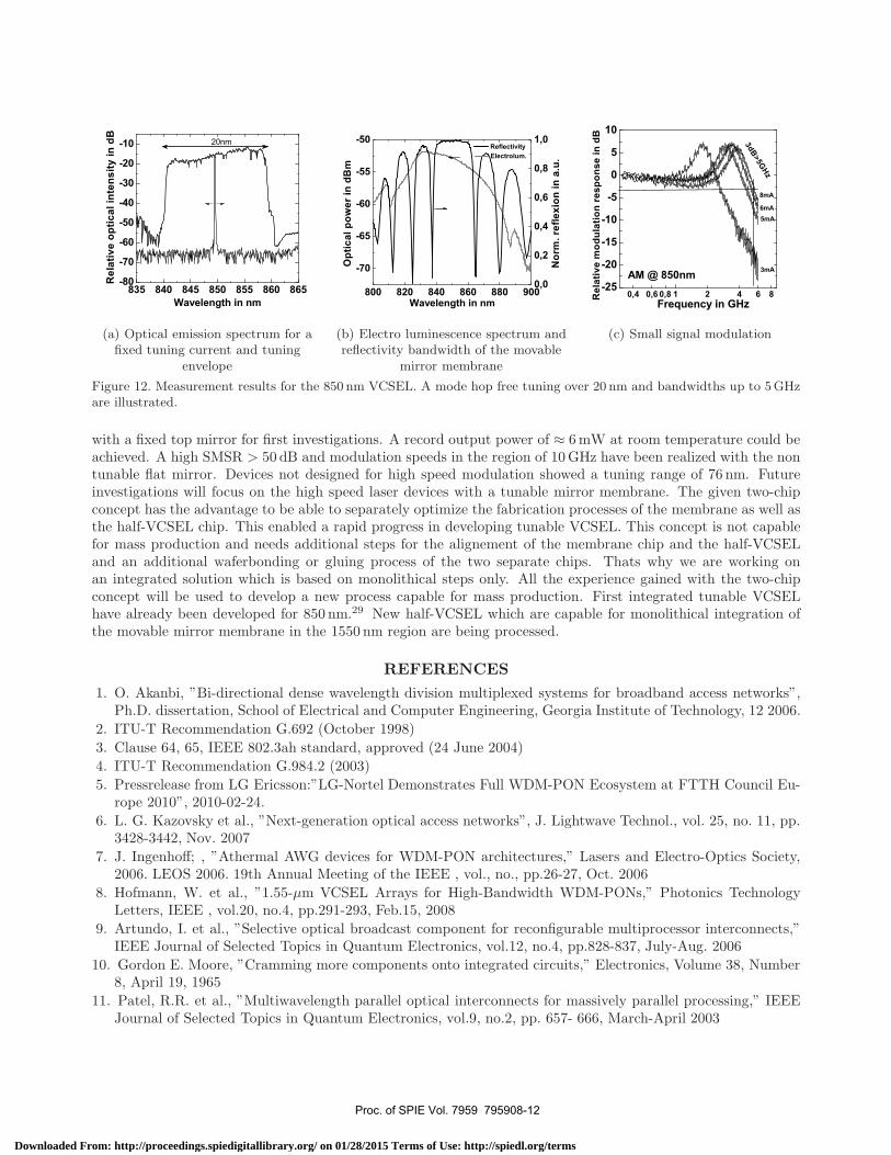
To characterize the tunability of the short wavelength VCSEL, the optical emission spectrum of the device hasbeen measured for different heating currents flowing through the movable membrane. Fig. 12 (a) shows thespectrum of the VCSEL during the actuation of the membrane at a constant laser current of 8 mA. A maximumtuning current of 12 mA is needed for tuning over the whole tuning range. A mode-hop free continuous single modetuning of about 19 nm (from 840 nm to 859 nm) with a SMSR of about 40 dB throughout the tuning range hasbeen achieved. A comparison of the electroluminescence of the half-VCSEL and the top-mirror stop-bandwidth,as it is shown in fig. 12 (b), shows that the limitation of the tuning range is caused by the bandwidth of the topmirror.17 This shows up that there are still capacities to enlarge the tuning range using broadband series DBR.These can be made of dielectric materials providing much larger stop bandwidth as they have been used for thelong wavelength VCSEL, already. The first tested devices had a maximum output power of 0.17mW (−7.5 dBm)and an electrical resistance of about 150 Ω at 8.3 mA thermal rollover at a center wavelength of 850 nm. Thisquite high serial resistance leads to a significant decrease of the optical output power due to electro-thermalheating. Optimisations of the device reduced the half-VCSEL resistance to 100 Ω resulting in an output powerof 0.8 mW at 9.2 mA (thermal rollover). For determining the modulation bandwidth of the short wavelengthVCSEL the small signal frequency response (S21) of the device has been measured using a fast photodetectorconnected to a network analyzer. The modulation response of the VCSEL at a constant wavelength of 850 nm fordifferent laser bias currents 3, 5, 6, 8 mA is shown in Fig. 12 (c). A maximum 3 dB cut-off frequency of 5.5 GHzand a resonance frequency of 4 GHz have been achieved at the laser rollover current of 8 mA. Thus the devicesalready fullfill the high speed requirements (2.5 GBit/s) for optical interconnects.
6. CONCLUSION AND OUTLOOK
A two-chip concept for electro thermally tunable VCSEL in the 850 nm range has been demonstrated. The deviceshows an excellent SMSR (> 40 dB) over the whole tuning range which cover the desired wavelength regionsfor optical interconnects. The given tunable VCSEL is capable for modulation frequencies > 5 GHz. An outputpower of 1 mW is desirable for optical interconnects thus it needs to be further increased. Additionally, thepolarisation stability during wavelength tuning as well as for AM of the laser current needs to be investigated.For both, the 850 nm as well as 1550 nm VCSEL the implementation of a sub wavelength grating is underinvestigation. Now, the devices need to be implemented with the tunable membranes for future measurements.A non tunable half-VCSEL capable for the integration with a movable mirror membrane has been completed
Proc. of SPIE Vol. 7959 795908-11
Downloaded From: http://proceedings.spiedigitallibrary.org/ on 01/28/2015 Terms of Use: http://spiedl.org/terms
(a) Optical emission spectrum for afixed tuning current and tuning
envelope
(b) Electro luminescence spectrum andreflectivity bandwidth of the movable
mirror membrane
(c) Small signal modulation
Figure 12. Measurement results for the 850 nm VCSEL. A mode hop free tuning over 20 nm and bandwidths up to 5GHzare illustrated.
with a fixed top mirror for first investigations. A record output power of ≈ 6 mW at room temperature could beachieved. A high SMSR > 50 dB and modulation speeds in the region of 10 GHz have been realized with the nontunable flat mirror. Devices not designed for high speed modulation showed a tuning range of 76 nm. Futureinvestigations will focus on the high speed laser devices with a tunable mirror membrane. The given two-chipconcept has the advantage to be able to separately optimize the fabrication processes of the membrane as well asthe half-VCSEL chip. This enabled a rapid progress in developing tunable VCSEL. This concept is not capablefor mass production and needs additional steps for the alignement of the membrane chip and the half-VCSELand an additional waferbonding or gluing process of the two separate chips. Thats why we are working onan integrated solution which is based on monolithical steps only. All the experience gained with the two-chipconcept will be used to develop a new process capable for mass production. First integrated tunable VCSELhave already been developed for 850 nm.29 New half-VCSEL which are capable for monolithical integration ofthe movable mirror membrane in the 1550 nm region are being processed.
REFERENCES1. O. Akanbi, ”Bi-directional dense wavelength division multiplexed systems for broadband access networks”,
Ph.D. dissertation, School of Electrical and Computer Engineering, Georgia Institute of Technology, 12 2006.2. ITU-T Recommendation G.692 (October 1998)3. Clause 64, 65, IEEE 802.3ah standard, approved (24 June 2004)4. ITU-T Recommendation G.984.2 (2003)5. Pressrelease from LG Ericsson:”LG-Nortel Demonstrates Full WDM-PON Ecosystem at FTTH Council Eu-
rope 2010”, 2010-02-24.6. L. G. Kazovsky et al., ”Next-generation optical access networks”, J. Lightwave Technol., vol. 25, no. 11, pp.
3428-3442, Nov. 20077. J. Ingenhoff; , ”Athermal AWG devices for WDM-PON architectures,” Lasers and Electro-Optics Society,
2006. LEOS 2006. 19th Annual Meeting of the IEEE , vol., no., pp.26-27, Oct. 20068. Hofmann, W. et al., ”1.55-μm VCSEL Arrays for High-Bandwidth WDM-PONs,” Photonics Technology
Letters, IEEE , vol.20, no.4, pp.291-293, Feb.15, 20089. Artundo, I. et al., ”Selective optical broadcast component for reconfigurable multiprocessor interconnects,”
IEEE Journal of Selected Topics in Quantum Electronics, vol.12, no.4, pp.828-837, July-Aug. 200610. Gordon E. Moore, ”Cramming more components onto integrated circuits,” Electronics, Volume 38, Number
8, April 19, 196511. Patel, R.R. et al., ”Multiwavelength parallel optical interconnects for massively parallel processing,” IEEE
Journal of Selected Topics in Quantum Electronics, vol.9, no.2, pp. 657- 666, March-April 2003
Proc. of SPIE Vol. 7959 795908-12
Downloaded From: http://proceedings.spiedigitallibrary.org/ on 01/28/2015 Terms of Use: http://spiedl.org/terms

12. W. H. Cheng et al., ”Spectral characteristics for a fiber grating external cavity laser,” Optical and QuantumElectronics, vol.32, no.3, pp. 339-348, March 2000.
13. Chang-Hasnain, C.J., ”1.5-1.6 μm VCSEL for metro WDM applications,” 2001. IPRM. IEEE InternationalConference On Indium Phosphide and Related Materials, vol., no., pp.17-18, 2001
14. Tayebati, P. et al., ”Half-symmetric cavity tunable microelectromechanical VCSEL with single spatial mode,”Photonics Technology Letters, IEEE , vol.10, no.12, pp.1679-1681, Dec 1998
15. Jatta, S. et al., ”Bulk-Micromachined VCSEL At 1.55 μ m With 76 nm Single-Mode Continuous TuningRange,” Photonics Technology Letters, IEEE , vol.21, no.24, pp.1822-1824, Dec.15, 2009
16. P. Meißner et al., ”Micromachined two-chip WDM filters with stable half symmetric cavity and their systemintegration,” Electronic Components and Technology Conference, 2002. Proceedings. 52nd
17. H. A. Davani et al., ”Widely tunable high-speed bulk-micromachined short-wavelength MEMS-VCSEL”IEEE Semiconductor Laser Conference 2010,ISLC 2010, page 14-15.
18. P. Debernardi et al., ”Modal Properties of Long-Wavelength Tunable MEMS-VCSELs With Curved Mirrors:Comparison of Experiment and Modeling,” IEEE Journal of Quantum Electronics, vol.44, no.4, pp.391-399,April 2008
19. L. A. Coldren, S.W. Corzine, ”Diode Lasers and Photonic Integrated Circuits”, John Wiley & Sons, Inc.,New York, 1995.
20. J. Chilwell, I. Hodgkinson. ”Thin-film field-transfer matrix method of planar multilayer waveguides andreflection from prism-loaded waveguides”, J. Opt. Soc. Am. A1 (1984) 742-753
21. S. Healy et al., IEEE J. of Quantum Electronics, Vol. 46, No. 4, pp. 506-512, April 2010.22. B. Kogel et al., ”Long-wavelength MEMS tunable vertical-cavity surface-emitting lasers with high sidemode
suppression” 2006 J. Opt. A: Pure Appl. Opt. 8 S37023. B. Kogel et al., ”Tuning Dynamics of Micromachined Surface-Emitting Lasers with Broadband Long-
Wavelength Coverage,” Photonics in Switching, 2007 , vol., no., pp.111-112, 19-22 Aug. 200724. M. Muller et al., IEEE Photonics Technology Letters, 21, pp . 1615-1617, 200925. M. Maute et al., ”MEMS Tunable 1.55 μm VCSEL With Extended Tuning Range Incorporating a Buried
Tunnel Junction”, IEEE Photonics Technology Letters, vol. 18(5), pp. 688-690, 2006.26. Tobias Grundl et al., ”High-Speed and HighPower Vertical-Cavity Surface-Emitting Lasers based on InP
suitable for Telecommunication and Gas Sensing”, SPIE Remote Sensing 2010, Nr: 7828-627. M.-C. Amann and M. Ortsiefer, ”Long-wavelength (1.3 μm) InGaAlAs-InP vertical-cavity surface-emitting
lasers for applications in optical communications and sensing”, phys. stat. sol. (a) 203 (14),pp. 3538-3544,2006
28. Dissertation, Markus Maute, Walter Schottky Institut, Technische Universitat Munchen, ”Mikromechanischabstimmbare Laser-Dioden mit Vertikalresonator”, Vol.81, ISBN 3-932749-81-2
29. B. Kogel. et al., ”Integrated Tunable VCSELs With Simple MEMS Technology” IEEE Semiconductor LaserConference 2010,ISLC 2010.
Proc. of SPIE Vol. 7959 795908-13
Downloaded From: http://proceedings.spiedigitallibrary.org/ on 01/28/2015 Terms of Use: http://spiedl.org/terms