THz spintronic emitters: a review on achievements and future ...
15
Review Evangelos Th. Papaioannou* and René Beigang THz spintronic emitters: a review on achievements and future challenges https://doi.org/10.1515/nanoph-2020-0563 Received October 8, 2020; accepted November 26, 2020; published online December 18, 2020 Abstract: The field of THz spintronics is a novel direction in the research field of nanomagnetism and spintronics that combines magnetism with optical physics and ultrafast photonics. The experimental scheme of the field involves the use of femtosecond laser pulses to trigger ultrafast spin and charge dynamics in thin films composed of ferromagnetic and nonmagnetic thin layers, where the nonmagnetic layer features a strong spin–orbit coupling. The technological and scientific key challenges of THz spintronic emitters are to increase their intensity and to shape the frequency bandwidth. To achieve the control of the source of the radiation, namely the transport of the ultrafast spin current is required. In this review, we address the generation, detection, efficiency and the future per- spectives of THz emitters. We present the state-of-the-art of efficient emission in terms of materials, geometrical stack, interface quality and patterning. The impressive so far results hold the promise for new generation of THz physics based on spintronic emitters. Keywords: optospintronics; spintronics; THz spintronics; ultrafast photonics. PACS: 85.75.d; 75.78.Jp; 75.76.+j. 1 Introduction Terahertz (THz) radiation covers a broad bandwidth of the electromagnetic spectrum from 100 GHz to 30 THz [1] lying between the microwave and the far infrared band. THz radiation is utilized by a number of scientific and research communities, ranging from chemistry and medi- cine to physics and material sciences. Recent technological innovations in optics and photonics enable THz research and technology to address an increasingly wide variety of applications [2, 3]: information and communications technology; spectroscopy and imaging, biology, medical and pharmaceutical sciences; nondestructive evaluation (material and circuitry diagnosis), security (detection of drugs and explosives), global environmental monitoring, THz sensor networks, ultrafast computing and astrophys- ics. Despite all that, the THz region of the electromagnetic spectrum is still an comparatively unexplored region due to the lack of strong and broadband THz emission sources and sensitive detectors. Here, we review the recent developments in nano- magnetism and spintronics that allowed the first usage of ultrafast spin physics for THz emission. The physical mechanism of the THz radiation of spintronic emitters is based on the inverse spin Hall effect [4] and appears in multilayer heterostructures that consist of ferromagnetic (FM) and nonmagnetic (NM), usually heavy metal, layers. When illuminated by ultrafast femtosecond (fs) laser pulses, spin-polarized electrons are excited in the FM layer and subsequently diffuse as a spin current into the NM layer. Due to the inverse spin Hall effect (ISHE), the spin current is converted into a transient transverse charge current in the NM layer resulting in THz emission [4]. This new source of THz radiation is an emerging topic subject to intensive research. The efficiency of such emitters is in some cases comparable with established types of THz sources (for example, with nonlinear crystals) [5]. The engineering of THz emission is the main technological and scientific challenge and is currently the target of many research activities. In this review article, we highlight and examine the different strategies that have been followed in order to explore the properties of the emitted THz signal, like THz amplitude and bandwidth, e.g., different material compositions of FM/NM systems with a variety of thick- nesses, spintronic emitters in different geometrical stack- ing order using different layers and patterned structures, different substrates, interface materials and quality of *Corresponding author: Evangelos Th. Papaioannou, Institute of Physics, Martin-Luther University Halle-Wittenberg, 06120 Halle, Germany, E-mail: [email protected]. https://orcid.org/0000-0002-9822-2343 René Beigang, Department of Physics, Technische Universität Kaiserslautern, 67663 Kaiserslautern, Germany, E-mail: [email protected] Nanophotonics 2021; 10(4): 1243–1257 Open Access. © 2020 Evangelos Th. Papaioannou and René Beigang, published by De Gruyter. This work is licensed under the Creative Commons Attribution 4.0 International License.
-
Upload
khangminh22 -
Category
Documents
-
view
1 -
download
0
Transcript of THz spintronic emitters: a review on achievements and future ...

Review
Evangelos Th. Papaioannou* and René Beigang
THz spintronic emitters: a review on achievementsand future challenges
https://doi.org/10.1515/nanoph-2020-0563Received October 8, 2020; accepted November 26, 2020;published online December 18, 2020
Abstract: The field of THz spintronics is a novel directionin the research field of nanomagnetism and spintronicsthat combines magnetism with optical physics andultrafast photonics. The experimental scheme of the fieldinvolves the use of femtosecond laser pulses to triggerultrafast spin and charge dynamics in thin films composedof ferromagnetic and nonmagnetic thin layers, where thenonmagnetic layer features a strong spin–orbit coupling.The technological and scientific key challenges of THzspintronic emitters are to increase their intensity and toshape the frequency bandwidth. To achieve the control ofthe source of the radiation, namely the transport of theultrafast spin current is required. In this review,we addressthe generation, detection, efficiency and the future per-spectives of THz emitters. We present the state-of-the-art ofefficient emission in terms of materials, geometrical stack,interface quality and patterning. The impressive so farresults hold the promise for new generation of THz physicsbased on spintronic emitters.
Keywords: optospintronics; spintronics; THz spintronics;ultrafast photonics.
PACS: 85.75.d; 75.78.Jp; 75.76.+j.
1 Introduction
Terahertz (THz) radiation covers a broad bandwidth ofthe electromagnetic spectrum from 100 GHz to 30 THz [1]lying between the microwave and the far infrared band.
THz radiation is utilized by a number of scientific andresearch communities, ranging from chemistry and medi-cine to physics andmaterial sciences. Recent technologicalinnovations in optics and photonics enable THz researchand technology to address an increasingly wide varietyof applications [2, 3]: information and communicationstechnology; spectroscopy and imaging, biology, medicaland pharmaceutical sciences; nondestructive evaluation(material and circuitry diagnosis), security (detection ofdrugs and explosives), global environmental monitoring,THz sensor networks, ultrafast computing and astrophys-ics. Despite all that, the THz region of the electromagneticspectrum is still an comparatively unexplored region dueto the lack of strong and broadband THz emission sourcesand sensitive detectors.
Here, we review the recent developments in nano-magnetism and spintronics that allowed the first usage ofultrafast spin physics for THz emission. The physicalmechanism of the THz radiation of spintronic emitters isbased on the inverse spin Hall effect [4] and appears inmultilayer heterostructures that consist of ferromagnetic(FM) and nonmagnetic (NM), usually heavy metal, layers.When illuminated by ultrafast femtosecond (fs) laserpulses, spin-polarized electrons are excited in the FM layerand subsequently diffuse as a spin current into the NMlayer. Due to the inverse spin Hall effect (ISHE), the spincurrent is converted into a transient transverse chargecurrent in the NM layer resulting in THz emission [4]. Thisnew source of THz radiation is an emerging topic subject tointensive research. The efficiency of such emitters is insome cases comparable with established types of THzsources (for example, with nonlinear crystals) [5]. Theengineering of THz emission is the main technological andscientific challenge and is currently the target of manyresearch activities. In this review article, we highlight andexamine the different strategies that have been followed inorder to explore the properties of the emitted THz signal,like THz amplitude and bandwidth, e.g., different materialcompositions of FM/NM systems with a variety of thick-nesses, spintronic emitters in different geometrical stack-ing order using different layers and patterned structures,different substrates, interface materials and quality of
*Corresponding author: Evangelos Th. Papaioannou, Institute ofPhysics, Martin-Luther University Halle-Wittenberg, 06120 Halle,Germany, E-mail: [email protected]://orcid.org/0000-0002-9822-2343René Beigang, Department of Physics, Technische UniversitätKaiserslautern, 67663 Kaiserslautern, Germany,E-mail: [email protected]
Nanophotonics 2021; 10(4): 1243–1257
Open Access. © 2020 Evangelos Th. Papaioannou and René Beigang, published by De Gruyter. This work is licensed under the CreativeCommons Attribution 4.0 International License.
interfaces and dependence on the excitation wavelength.First, we highlight the radiation mechanism and theexperimental way to measure the emitted THz radiation.We explore the current trends to engineer the properties ofthe THz emission and we discuss the future challenges tointegrate spintronic emitters in THz devices. We finallyexplore the potential of the emitter to extend the THz fieldand widen its applications. The reader should notice thatthis work summarizes only experimental results from thelast couple of years and does not review theoretical modelsand calculations of the spin transport in magnetic hetero-structures. In addition, we focus on the mechanism of THzgeneration from the ISHE and we will not deal in depthwith other novel sources of THz radiation originatingfrom other mechanisms like anomalous Hall effect orRashba interfaces, since both are much less effective asTHz sources compared to the ISHE mechanism.
2 Description of the spin-to-chargeconversion mechanismresponsible for the THz radiation
Commonly, optically generated THz radiation is based oneither transient photocurrents in semiconductors inducedby ultrashort optical pulses from femtosecond lasers or byutilizing nonlinear optical responses of bound electronsin nonlinear crystals [1, 6]. The source of the THz radiationis the time-varying photocurrent in semiconductors(photoconductive switches PCA) or time-varying polari-zation in electro-optical crystals (nonlinear opticalmethods). Further, THz radiation can be obtained fromfree electrons in vacuum either from a bunch of relativisticelectrons or from periodically undulated electron beams[1, 6]. Besides the aforementioned physical principles forthe THz radiation, which are known as electric dipoleemission, a time-varying magnetization on the ultrafast,(sub)-picosecond timescale can also act as a THz source,the so-called magnetic dipole emission. Such emissionwas first observed from optically excited magneticmetallic structures during the ultrafast demagnetizationprocess of themagnetic layers [7, 8]. This type of radiationis weak due to its magnetic dipole character.
For all these methods, there are limitations concern-ing the generated intensities and/or the available band-width. The use of PCAs is, in general, limited to low powerexcitation sources and, as a consequence, to low in-tensities of the generated THz pulses. The bandwidth isusually governed bymaterial properties (intrinsic phononabsorption in the materials used) and typically ends
around 8 THz. In addition, fabrication of PCAs requires anadvanced technology to obtain, e.g., the correct struc-turing which significantly determines the desired prop-erties. Nonlinear methods are, in principle, well suited forTHz generation. However, in order to achieve phasematching only very short nonlinear crystals in combina-tion with ultrashort laser pulses can be used to obtain adecent bandwidth. This in turn limits the intensity of thegenerated THz pulses. The use of high power excitationsources is limited by the damage threshold of thenonlinear crystals.
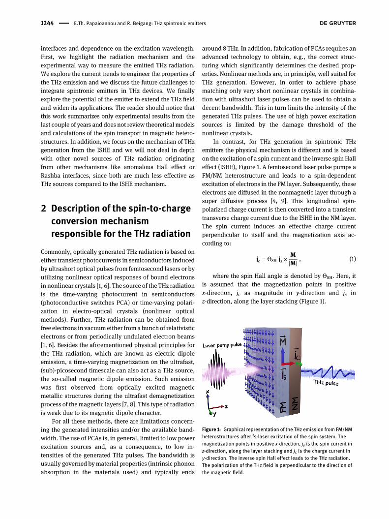
In contrast, for THz generation in spintronic THzemitters the physical mechanism is different and is basedon the excitation of a spin current and the inverse spin Halleffect (ISHE), Figure 1. A femtosecond laser pulse pumps aFM/NM heterostructure and leads to a spin-dependentexcitation of electrons in the FM layer. Subsequently, theseelectrons are diffused in the nonmagnetic layer through asuper diffusive process [4, 9]. This longitudinal spin-polarized charge current is then converted into a transienttransverse charge current due to the ISHE in the NM layer.The spin current induces an effective charge currentperpendicular to itself and the magnetization axis ac-cording to:
jc = ΘSH js ×M|M| , (1)
where the spin Hall angle is denoted by ΘSH. Here, itis assumed that the magnetization points in positivex-direction, jc as magnitude in y-direction and js inz-direction, along the layer stacking (Figure 1).
Figure 1: Graphical representation of the THz emission from FM/NMheterostructures after fs-laser excitation of the spin system. Themagnetization points in positive x-direction, js is the spin current inz-direction, along the layer stacking and jc is the charge current iny-direction. The inverse spin Hall effect leads to the THz radiation.The polarization of the THz field is perpendicular to the direction ofthe magnetic field.
1244 E.Th. Papaioannou and R. Beigang: THz spintronic emitters

The transient charge current generates a short ter-ahertz pulse that propagates perpendicular to the electricalcurrent. The origin of the THz radiation is the evolutionof the hot-carrier distribution after the femtosecond laserexcitation. The emission is dominated by the electric dipoleemission driven by a time varying ISHE-type electric cur-rent [4, 5]. Theoretically, the Boltzmann transport theoryhas been proven to be an adequate tool to simulate excitedcarrier dynamics in metallic structures on the nanoscale[4, 9–12], however, in this review, the theoretical ap-proaches are out of the focus.
The shape of the experimentally obtained pulses andtheir corresponding spectra depend on the experimentalTHz-setup and is a convolution of emitter and detectorresponse. The measured bandwidth, for example, reaches8 THz in the study by Torosyan et al. [13], which is mainlylimited by the detector responsewhich is a low temperature(LT)-GaAs photoconductive antenna in this case. Band-widths with full-width at half-maximum (FWHM) up to30 THz measured with electro-optical sampling and fasterexcitation pulses were reported [5].
It is worth to mention here that the origin of the THzemission after fs-laser excitation is difficult to disentanglebetween ISHE-type and laser-driven transient demagneti-zation in the magnetic layers. Recently, Zhang et al. [14]successfully separated and measured the weak THz emis-sion during the demagnetization process, suggesting toimplement this type of weak THz emission for ultrafastmagnetometry on a pico- and sub-pico timescales. Pres-ently, new spin-to-charge-conversion mechanisms havebeen proposed as sources of THz radiation. One is the THzemission from Rashba-type interfaces [15, 16] where thegeneration of THz waves takes place at interfaces betweentwo nonmagnetic materials due the inverse RashbaEdelstein effect. In a similar experimental procedure, thefs-laser pulse induces a nonequilibrium electron flow inFM/Ag/Bi heterostructures. A femtosecond spin currentpulse is launched in the ferromagnetic Co20Fe60B20 layerand drives terahertz transients at a Rashba interface be-tween two nonmagnetic layers, Ag and Bi. In contrast to theTHz emission in spintronic emitters via the inverse spin Halleffect, the inverse Rashba Edelstein effect transforms anonzero spin density induced by the spin current injectioninto a charge current carried by interfacial states. Anotheralternativemechanism for generating THz emission from anultrathin FM layer via the anomalous Hall effect wasrecently proposed [17]. The process involves a single FMlayer and the generation of backflowsuperdiffusive currentsat the dielectric/FM/dielectric interfaces and subsequentconversion of the charge current to transverse current due tothe anomalous Hall effect. The THz generation is suggested
to be mainly caused by the nonthermal superdiffusive cur-rent near the two FM/dielectric interfaces.
3 Experimental detection of THzemission from spintronicemitters
Detection of the emitted THz pulses from spintronic emit-ters is often accomplished with the established terahertztime-domain spectroscopy (THz-TDS) system [18]. A spe-cific example is presented in Figure 2. The system is drivenby a femtosecond laser delivering sub-100 fs optical pulsesat a repetition rate of usually 50 to 100MHzwith an averageoutput power of typically 600 mW. The laser beam is splitinto a pump and probe beam usually by a 90:10 beam-splitter. The stronger part is led through a mechanicalcomputer-controlled delay line to pump the THz emitter,and the weaker part is used to gate the detector, a photo-conductive switch with a dipole antenna of specificdimensions. In our example here,we refer to a 20 μmdipoleantenna. In a classical (standard) THz setup, both theemitter and the detector operate with photoconductiveantennas (PCA), whereas in the case of spintronic emittersthe PCA emitter is substituted by the spintronic sample,which is placed in a weak magnetic (a few mT) fieldperpendicular to the direction of the pump beam andusually in the direction of the easy axis ofmagnetic layer inorder to achieve saturation. The direction of the magneticfield determines the polarization of the THz field, which isperpendicular to the direction of the magnetic field.Changing the direction of magnetic field into the oppositedirection changes the phase of the detected THzwaveformsby 180° (Figure 2b). In thisway, by changing the orientationof the magnetic field the polarization of the generated THzradiation can be changed easily.
The optical pump beam, that is sharply focusedonto the sample at normal incidence by an asphericalshort-focus lens, excites spin-polarized electrons in themagnetic layer (Fe), which give rise to a spin current, whichin turn excites a transverse transient electric current inthe Pt layer. The latter results in THz pulse generation ofsub-picosecond duration being emitted forward andbackward into free space in the form of a strongly divergentbeam. The central wavelength within the beam is about200 μm and is much longer than the diameter of its source,which is smaller than 10 μm. That is why the emitted THzfield fills the half-space behind the sample. A strategy toincrease the collection efficiency was used by Torosyanet al. [13], comparable to techniques familiar with
E.Th. Papaioannou and R. Beigang: THz spintronic emitters 1245

photoconductive antenna setups: a hyperhemispherical Silens was attached at the back side of the sample, able tocollect the divergent beam in the formof a cone anddirect itfurther. With the lens attached an enhancement factor ofup to 30 in electric field amplitude has been reported [13].After that the beam is collimated with an off-axis parabolicmirror and sent to an identical parabolic mirror in thereversed configuration. The latter focuses the beam tothe second Si lens, which finally focuses the beam throughthe GaAs substrate of the detector PCA onto the dipole gapfor detection. In thisway, the THz optical system consistingof the two Si-lenses and the two parabolic mirrors imagesthe point source of THz wave on the emitter surface ontothe gap of the detector PCA and ensures an efficienttransfer of the emitted THz emission from its source to thedetector. In addition to having two collimated beam paths,this 4-mirror THz-optics also allows for an intermediatefocus of the THz beam aimed at imaging applications(Figure 2a).
In such configuration, the THz beam path is deter-mined by the silicon lens on the emitter, the parabolicmirrors and the silicon lens on the photoconducting an-tenna of the detector. The alignment of these componentsis not changed during an exchange of the spintronicemitter. If in addition the position of the pump beam focusremains constant, the spintronic emitter can easily beexchanged without changing the beam path, as the lateralposition of the focus on the emitter is not critical assuminga homogeneous lateral layer structure. The frequencyresponse of the photoconductive dipole antenna with20 μmdipole length limits the observable bandwidth. Withthis dipole length, amaximumdetector response of around1 THz can be expected with a reduction to 50% at 330 GHzand 2 THz. The 10% values are at 100 GHz and 3 THz [19].
In fact, the detected signal is strongly influenced bythe detector response. The frequency response of thephotoconductive antenna-detector above 3 THz is very flatand at 8 THz a strong phonon resonance in GaAs, whichis used as substrate material for the photoconductiveantenna, causes strong absorption of the THz radiation.Above 8 THz, almost no THz radiation can be detected. Thedelay line provides the synchronous arrival of the weakerpart of the optical pulse and that of the THz pulse at thedetector antenna gap from either side, as well as thescanning in time, the so-called open state of the gap alongthe THz pulse duration. In each position of the delay line,the transient current induced in the detector by the electricfield of the THz sub-picosecond pulse is proportional to itsinstantaneous electrical field value. It is summed upfrom many laser pulses, which reach the detector duringthe single step of the delay line, and it is integrated withinthe “open” state time window. It is measured as one singlepoint of the THz wave-form and is in the order of severalnanoamperes at the maximum of the THz pulse. Hence, alock-in technique has to be used. For that purpose, the pumpbeam is mechanically chopped at usually kHz frequency. Byscanning the “open” state of the detector in time, the THzpulse shape can be sampled. Utilizing the magnetic fielddependence of the THz polarization the THz beam can, inprinciple, also be chopped electrically by means of analternating magnetic field around the emitter.
Alternatively, free-space electro-optical sampling(EOS) is used for the detection of THz radiation fromspintronic emitters [20, 21]. In order to be able to detectfrequencies well above 10 THz very thin ZnTe crystals areused as a detector in combination with extremely shortlaser pulses. The ease of implementation and the possi-bility to detect higher bandwidths [5] render this technique
b)a)B-Field
Figure 2: a) An example of a terahertz time-domain spectroscopy (THz-TDS) experimental setupmodified for spintronic emitters. b) THz pulsesfor two opposite directions of the magnetic field.Reproduced under the terms of a Creative Commons Attribution 4.0 Licence [13] Copyright 2018, The Authors, published by Springer Nature.
1246 E.Th. Papaioannou and R. Beigang: THz spintronic emitters

also popular for the investigation of the efficiency of themagnetic heterostructures.
4 Strategies to engineer intensityand frequency bandwidth of theemitted THz signal
Currently, the main goal of the research on spintronicemitters is the engineering of THz emission and differentstrategies have been followed in order to explore the THzamplitude and bandwidth of the signal. In Figure 3 weconstruct a roadmap with the most important physicalparameters, which can influence the efficiency of thespintronic THz-emitters toward higher signal strengthsand broader bandwidths. Figure 3 summarizes all theimportant factors that can affect the temporal and spatialevolution of the spin current inside the metallic layers, bytaking into account, the generation and optical propaga-tion of the THz wave, and forecasts the THz-pulse shapesand spectra, by taking into consideration the electronscattering lifetime and the interfacial spin current trans-port. Parameters that are included in Figure 3 and play adecisive role in the emission are:ΘSH is the spin Hall angle,λSD is the spin-diffusion-length, T is the interface trans-mission parameter and τel is the inelastic scattering life-time. Moreover, included in the roadmap are effectsoriginating from the excitation wavelength, from geomet-rical stacking order, from the FM and NM layer thicknesstFM, tNM and electrical conductance σFM, σFM, and from theindex of refraction and the absorption coefficient of allinvolved layers (metals and insulators) in the THz-range niand κi. Theoretical calculations and simulation of the spincurrent transport with the Boltzmann equation and of theoptical path with the use of the transfer matrix for the totallayer stack Mtot are also necessary tools for the under-standing and the evaluation of the research progress.
The following sections will analyze the roadmap byreviewing the research efforts on different material compo-sitions, geometrical factors, interfaces and nanopatterning.We will present key works and summarize the uniqueadvantages and the promises for applications of spintronicemitters to the development of THz technology.
4.1 Material dependence
A variety of materials combination of ferromagnetic(FM)/nonmagnetic (NM) layer systems have been so far
explored as spintronic emitters. We initially focus on thechoice of the magnetic layer. Direct comparison between the3d metals like Fe, Co and Ni, in structures like FM (3 nm)/Pt(3 nm) [5] and in FM (2 nm)/Pt (5 nm) [23] have revealed thatNi yields the lowest signal with Fe having a slightlyhigher signal than Co. The comparison of ferromag-netic alloys like Ni89Fe19, Co70Fe30, Co40Fe40B20 andCo20Fe60B20/Pt (3 nm) [5] showed the prominent role of theCoFeB alloy. Sasaki et al. [24] varied the composition ofCo and Fe in the CoFeB alloy. They found that the THzemission in Ta/(CoxFe1−x)80B20 is enhanced at composi-tions of approximately x = 0.1–0.3 which show amaximumsaturation magnetization. Modification of the magneticlayer with ferrimagnetic gadolinium and terbium-iron al-loys was achieved by Schneider et al. [25, 26]. Both systemsGdxFe1−x/Pt and TbxFe1−x/Pt present the highest THzemission for small rare-earth content. However, theGdxFe1−x exhibit up to 17 times higher amplitudes. A strongTHz output was observed from compensated ferrimagneticCo1−xGdx (7 nm)/Pt (6 nm) bilayers. The THz signal de-creases as the Gd fraction increases. At the compensationpoint for x = 26, the almost zero net magnetization was notstrongly correlated to the emitted THz signal [20]. Thereplacement of the ferromagnetic layer with DyCo5,Gd24Fe76, Fe3O4 and FeRh showed that they exhibit lower
Figure 3: Roadmap to efficient spintronic THz-emitters with highsignal strength and broad bandwidth. Here, ΘSH is the spin Hallangle, λSD is the spin-diffusion length, T and τel are the interfacetransmission parameter and the elastic scattering lifetime, respec-tively. tFM, tNM, σFM and σFM are the FM and NM layer thickness andelectrical conductance, respectively. ni and κi are the index ofrefraction and the absorption coefficient of all involved layers(metals and insulators) in the THz range, respectively. λexcitation isthe wavelength of the laser excitation. BTE refers to the Boltzmanntransport equation, Mtot is the transfer matrix used to describe thepropagation of the generated THz wave throughout the total layerstack. THz-detection schemes are defined as THz-TDS for the timedomain spectroscopy and THz-EOS for the free space electro-opticalsampling. Figure modified from the study by Nenno et al. [22].
E.Th. Papaioannou and R. Beigang: THz spintronic emitters 1247

THz emission with respect to CoFeB layer [27]. Further-more, Co-based Heusler alloys and in particular Co2MnSi(CMS) was investigated as spin injector in CMS/Pt bilayers[28]. The achievement of the highly ordered B2 structuralphase after annealing led to up to two times higher THzemission compared to CoFe/Pt bilayers. The effect wasattributed to the small conductivity and the comparable toFeCo spin current injection of the CMS samples.
The efficiency of the conversion of spin-to-chargecurrent is quantified by the spin Hall angle and thespin current relaxation length of the nonmagnetic layer.Different nonmagnetic materials have been studied so farfor THz emission. The THz signal amplitude seems to scalewith the intrinsic spin Hall conductivity of the used NMlayer [5], see Figure 4. The THz emission was even used toestimate the relative spin Hall angle [21, 29]. The prominentchoice at the moment is Pt since it has provided so far thehighest signal compared to W [21], Cu80Ir20 [21], Ta [29], Ru[29, 30], Ir [29], Pd [30], Pt38Mn62 [5]. Interestingly, NMlayers with opposite sign of the spin Hall angle comparedto Pt give rise to THz signals with opposite polarities andsubsequently confirm the ISHE origin of the THz emission.
The spin-to-charge-conversion mechanism driven bythe spin Seebeck effect was additionally probed in insu-lating magnetic/NM interfaces like YIG/Cu1−xIrx [31] andYIG/Pt [32] showing, however, much lower efficiency of theTHz emission compared to the metallic magnetic layers.
4.1.1 Material dependence—summary and outlook
According to experiments performed up to now bilayerscomposed of CoFeB/Pt and Fe/Pt provide the highest THzsignal and they are themost prominent material choices so
far. Other classes ofmagnetic layers have been also studiedlike compensated ferrimagnets, Heusler alloys, insulatingferrimagnets like YIG, however, their efficiency is low.Novel capping materials as spin-to-charge converters likeat ferromagnetic/semiconductor interface [33], and topo-logical insulators with large spin Hall angle like BiSe [34]used in combination with FM layers as in Bi2Se3/Co inter-face [35] can promote large spin injection efficiency, andpave the way for future investigations on materials.
4.2 Thickness dependence
Various thickness dependence studies on the efficiencyof the THz emission have revealed the critical role ofthe thicknesses of the individual layers. Studies on thevariation of the thickness of the NM-layer and by keepingconstant the thickness of the FM layer have shown theexistence of an optimum thickness around 2–3 nm [13].This range of thicknesses holds for different NM-layers likePt [21, 29, 13], W [21, 29] where the maximum signal isobtained, see Figure 5. By fitting the NM-thicknessdependence of the THz amplitude, the spin current diffu-sion length was extracted [21, 13]. Surprisingly, the latterwas found to agree with values extracted from GHz spinpumping experiments although the excitation of the spincurrent is performed in different time- and energy scales.The physical mechanism behind this similarity is currentlyunder on-going research [36].
In the same way, for a constant NM-layer thickness,there is an optimum FM layer thickness in the same rangeof about 2–3 nm [21, 29, 13].When the ferromagnetic layer istoo thin, then either the loss of magnetic order due toheating effects or the reorientation of the magnetizationdue tomonolayer thickness cause a drastic reduction of theTHz signal. The theory of the effect of changing layerthickness was first developed in the study by Seifert et al.[5] for detection of THz-signal fromNM-layer side. A furtherexpansion of the model was achieved in the study Tor-osyan et al. [13], and it is expressed by Eq. (2). The equationholds when the fs-laser illuminates first the NM-layer sideand the detection is performed after the THz-signal hastravelled through the substrate (see also the study byTorosyan et al. [13]):
ETHz∝ΘSHPabs
dFe + dPt⋅ tanh(dFe − d0
2λpol)
⋅1
nair + nSub + Z0 ⋅ (σFedFe + σPtdPt)⋅ tanh( dPt
2λPt) ⋅ e−(dFe+dPt)/sTHz
(2)Figure 4: SpinHall angleandspinHall conductivity for thenonmagnetic(NM) layer. Pt has so far the highest efficiency for THz emission.Reprinted by permission from Springer Nature, Nature Photonics, T.Seifert et al. [5] Copyright 2016.
1248 E.Th. Papaioannou and R. Beigang: THz spintronic emitters

where nair, nSub and Z0 are the index of refraction of air,the index of refraction of the substrate at THz frequenciesand the impedance of vacuum, respectively. Equation (2)takes into account all successive effects that take place,after the laser pulse impinges on the bilayer. In particular,the first term contains the spin Hall angle, the second termaccounts for the absorption of the femtosecond laser pulsein the metal layers. As only spin-polarized electrons withina certain distance from the boundary between FM and NMwill reach the NM layer, only a fraction of the measuredtotal absorbed power contributes to the generated THzsignal. This fraction scales with the inverse of the totalmetal layer thickness 1/(dFe + dPt). The third term describesgeneration and diffusion of the generated spin currentflowing in FM toward the interface with NM. The possibilitythat extra thin FM layers can lose their ferromagneticproperties below a certain thickness can be captured byintroducing the term d0 in Eq. (2). Below this criticalthickness, it is considered that the flow (if any) of spincurrent in FM does not reach the NM layer. Above thiscritical thickness, the generated spin polarization saturateswith a characteristic constant λpol. The fourth and fifthterms, the tangent hyberbolic function divided by the totalimpedance, refer to the spin accumulation in Pt, which isresponsible for the strength of the THz radiation and itdepends on thefinite diffusion length λPt of the spin currentin NM layer. The symbols σFe and σPt correspond to the
electrical conductivities of the layers. This part of theequation also includes the shunting effect of the parallelconnection of the resistances of the individual FM and NMlayers. The last term describes the attenuation of the THzradiation during propagation through the metal layers(with sTHz as an effective inverse attenuation coefficient ofTHz radiation in the two metal layers. The last term isrequired since as aforementioned, the sample is excitedfrom the outer Pt side, whereas the THz radiation iscollected behind the substrate, thus propagating throughboth metal layers [13]. In the case of small losses, theattenuation can be taken into account by this singleexponential factor and the fourth factor, which accountsfor the multiple reflections of the THz pulse at the metal/dielectric interfaces. All terms together describe the layerthickness dependence of the measured THz amplitudes.
Furthermore, additional factors have been proposed toinfluence the thickness dependence like the factor ofinterfacial spin memory loss [37] in Co/Pt bilayers.
4.2.1 Thickness dependence—summary and outlook
The behavior of the thickness dependence of the THz signalfrom spintronic emitters is established. In general, theoptimal thickness of the NM layer depends in particular onthe spin diffusion length. For thicknesses larger than thespin diffusion length, the signal is reduced. For very thin
Figure 5: (Upper panel) Nonmagnetic layer thickness dependence of THz emission for different NM layers like Pt,W, CuIr in CoFeB/NMbilayers[21], and the geometrical arrangement of the experiment. Reproduced under the terms of a Creative Commons Attribution 3.0 Licence [21],2018 IOP Publishing Ltd.(Lower panel) (a) Pt thickness dependence of the THz field amplitude for a constant Fe thickness of 12 nm. (b) Fe thickness dependence of theTHzfield amplitude for a constant Pt thickness of 3 nm [13]. The geometrical arrangement is also depicted to the right of the graph. Reproducedunder a Creative Commons Attribution 4.0 International License [13], The Authors 2018, published by Springer Nature.
E.Th. Papaioannou and R. Beigang: THz spintronic emitters 1249

magnetic layers, the change of the magnetic order alsoreduces the THz emission. Future studies on the thicknessdependencewill aim to study the effect in complexmultilayerstructures. Of large interest are the investigations and thecomparison on spin current diffusion length for ultrafast fs-laser excitation and microwaves (GHz) excitation schemes.
4.3 Wavelength dependence
The majority of the experiments up to now with spintronicTHz emitters are performed at 800 nm excitation wave-length using femtosecond Ti:sapphire lasers. Woulddifferent excitation energies of the incoming fs-laser pulsesinfluence the spin current dynamics and subsequently theTHz-emission? Recent investigations have tried to answerthis question using different excitation wavelengths.Papaioannou et al. [38], used an optimized spintronicbilayer structure of 2 nm Fe and 3 nm Pt grown on 500 μmMgO substrate to show that the emitter is just as effective asa THz radiation sourcewhen excited either at λ = 800 nmorat λ = 1550 nm by ultrafast laser pulses from a fs fiber laser(pulsewidth 100 fs, repetition rate 100MHz). Evenwith lowincident power levels, the Fe/Pt spintronic emitter exhibitsefficient generation of THz radiation at both excitationwavelengths. It should be mentioned that there is a lineardependence of the generated THz amplitude on pumppower in the low-power excitation regime for both pumpwavelengths (see Figure 6). At higher pump powers, therewill be a deviation from the linear behavior, as also shownin the study by Yang et al. [23]. Herapath et al. [39] alsofound that the efficiency of THz generation is essentiallyflat for excitation by 150 fs pulses with center wavelengthsranging from 900 to 1500 nm, using a CoFeB ferromagneticlayer between adjacent nonmagneticWandPt layers. Fromboth experiments, it seems that the crucial factor is the
amount of energy that is deposited by the pump pulse inthe electronic system and not the details of the involvedoptical transitions. By further probing the THz emission ofFe/Pt bilayers at λ = 400 nm [40], the spintronic THzemission efficiency of an optimized spintronic emitter wasequal strong as with probing at 800 and 1550 nm. So it stillremains independent of the optical pump wavelength. Inaddition, the efficiency is highly tunablewith optical pumppower [40]. The reason behind the observed effect is aconsequence of the fact that the out of equilibrium trans-port is done not only by the electrons directly excited bythe laser, but also by all the electrons that are excitedat intermediate energies due to the scattering of thefirst-generation electrons. Considering that the electron–electron scattering lifetimes sharply decrease with theenergy of the excited electron, the direct impact of highenergetic electrons on the transport is expected to beminorat high energy excitation. Instead, the most importantimpact is that, by scattering with another electron, theelectrons will lose energy, they will go down to an inter-mediate energy and transfer that energy to secondaryelectrons. This results in an intermediate energy electronsmultiplication, which is very similar to a direct excitationby a laser at lower frequency. Even with lower energiesnow, they will have longer lifetimes and they willcontribute to the transport more importantly. If the systemis excited with very low-frequency photons, other effectscan become important, changing the qualitative scenariomentioned. In this case, one has to take into account thatthe spin diffusion requires not only asymmetry between thetwo spin channels, but also between electrons and holes.
4.3.1 Wavelength dependence—summary and outlook
The fact that efficient generation of THz radiation fromspintronic structures is possible with lasers over a wide
Figure 6: Excitation wavelength dependence of the THz emission.(Left panel) MaximumTHz-E-field as a function of pump power of the laser recorded at 1550 nm (black squares) and 800 nmpumpwavelength,λexcitation. Figure modified from the study by Papaioannou et al. [38], Copyright 2018, IEEE. (Right panel) THz-E-field, emitted from aW/CoFeB/Pt sample as a function of the pump wavelength while the energy, focus diameter and duration of the pump pulses were kept constant.Reprinted from the study by Herapath et al. [39] with the permission of AIP Publishing, Copyright 2019.
1250 E.Th. Papaioannou and R. Beigang: THz spintronic emitters

wavelength range will have important consequencesfor the use of such emitters in future applications.For example, the efficient excitation at 1550nmwavelengthallows the immediate integration of such spintronic emit-ters in THz systems driven by relatively low cost andcompact fs-fiber lasers, without the need for frequencyconversion. In the future, it will be crucial for the devel-opment of efficient spintronic THz emitters to understandthemechanisms of spin current generation and transport atlower and at higher excitation energies also from a theo-retical point of view.
4.4 Interface dependence
4.4.1 Interface dependence—structural properties
Even though the transfer of a spin current from a FM to aNM layer (that is, the source of THz emission) is a highlyinterface-sensitive effect, only few investigations havetried to correlate the structural quality of the interfacewith the THz signal strength and spectrum. A directcomparison of an epitaxial Fe(3 nm)/Pt(3 nm) bilayer witha signal-optimized polycrystalline CoFeB/Pt structurewith the same layer thicknesses revealed a comparable
THz signal strength [5]. In contrast, a significant increasein signal amplitude between Fe/Pt emitters grownepitaxially on MgO (100) substrates compared to poly-crystalline emitters grown on sapphire substrates wasreported by Torosyan et al. [13]. Similarly, the bettercrystal quality of a CoFeB layer, controlled by theannealing temperature, has significantly enhanced THzemission intensity [41]. Nenno et al. [22] have investigatedin detail the performance of spintronic terahertz emittersby modifying the interface quality and its defect density.In particular, the presence of defect density was corre-lated with the elastic electron-defect scattering lifetime τelin the FM and NM layers and the interface transmission Tfor spin-polarized, nonequilibrium electrons. A decreaseddefect density increases the electron-defect scatteringlifetime and this results in a longer-lasting and strongerspin current pulse. Accordingly, a significant enhance-ment of the THz-signal amplitude and a shift of thespectrum toward lower-THz frequencies [22] wereobserved, see Figure 7. Furthermore, besides the defectdensity, the presence of the parameter of the interfacetransmission T plays an important role. The latter iscorrelated to the ability of the interface to transfer hotcarriers into the NM layer. It was shown [22] that theinterface transmission influences the spectral amplitude
Figure 7: Dependence of the THz emission on the structural quality of the interface.(Upper panel-Left) Numerical simulations of the Boltzmann transport equation for an Fe/Pt spintronic emitter for different elastic scatteringlifetimes τel. The temporal evolution of the laser pulse intensity with a length of 70 fs is also shown on top. (Upper panel-Right) Spectralamplitude of the simulated spin current (and consequently of the charge current) inside Pt layer obtainedby the Fourier transformof the pulseson the left. (Lower panel—Left) Experimental THz-E-field amplitudes for Fe/Pt samples with different τel as detected after traveling the opticalbeam path of a THz-TDS setup. (Lower panel—Right) Experimental spectra amplitudes of Fe/Pt heterostructures with different interfacetransmissions T. Figure modified from the study by Nenno et al. [22].
E.Th. Papaioannou and R. Beigang: THz spintronic emitters 1251

of the emitted THz field but conserves the composition ofthe spectrum, see Figure 7.
Similarly, Li et al. [42] showed the decisive role of themicrostructural properties of a Co–Pt interface in the THzemission. High interfacial roughness between Co–Ptinterface led to a decrease of the THz emission. The intro-duction of an CoxPt1−x alloy as a spacer at the Co–Ptinterface showed that the intermixing amplified the THzemission. Maximum amplification by a factor of 4.2 wasachieved for a Co25Pt75(1 nm thick) interlayer. Possibleexplanation could be the higher flux of spin currents into Ptdue to reduction of spin decoherence at the interfacecaused by the presence of the alloy.
4.4.2 Interface dependence—interlayer
The influence of an interlayer on the THz emission has beenalso studied. One prominent choice as interlayer is Cu, dueto its negligible spin Hall angle and its large spin diffusionlength. The strength of the THz signal amplitudewas foundto decrease with increasing Cu-layer thickness [38], eitherexponentially [21] or linearly [43]. Interestingly, the spincurrent relaxation length obtained from thickness depen-dence studieswas revealed to be larger than formetalswithsizeable spin Hall effect but, on the other hand, smallcompared to DC spin-diffusion lengths, that in Cu are of theorder of 100 nm [21]. The use of a semiconducting materialsuch as ZnO as interlayer has strongly suppressed theTHz signal [43]. The use of insulating interlayers like MgOalso strongly suppresses the THz signal. However, thesuppression of spin current through MgO can be anadvantage in multilayers, as we will see in the next sectionof geometry dependence.
4.4.3 Interface dependence—summary and outlook
The understanding and the structural engineering of THzintensity and spectral bandwidth of spintronic emittersremains an uncharted territory. First efforts have revealedthe defect engineering as a factor that can in future beutilized to shape the THz emission. Nonmagnetic in-terlayers like Cu, ZnO, MgO lead to a reduction of theemitted radiation in FM/interlayer/NM structures.
4.5 Stack geometry dependence
The geometrical arrangement of the layers can play adecisive role for the THz emission (see Figure 8). Seifertet al. [5] used instead of a FM/NM bilayer a trilayer in theform of NM1/FM/NM2 layers. The special feature of the
trilayers is that the NM1 and NM2 layers have opposite spinHall angles, like W and Pt. In such a way, the spin Hallcurrents in W and Pt flow in the same direction and radiatein phase and thus enhance the THz amplitude. Largeimprovement of the signal was achieved in multilayersmade of Fe/Pt/MgO [23]. The MgO layer as an insulatinglayer hinders the flow of the spin current. The spin currentcan flow from each Fe layer to its neighboring Pt layer andgenerate THz radiation. Since the transverse charge cur-rents are almost in phase, the THz signal from each layer isadded constructively and boost the emission. Maximumsignal was observed for 3 repetitions of Fe/Pt/MgO layerswhile above 3 the detected THz signal dropped, due to theabsorption of light. Hibberd et al. [44] followed anotherroute to manipulate the THz radiation. They altered not thelayer stack but the magnetic field pattern that is applied tothe spintronic source. The goal was to manipulate themagnetic state of the ferromagnetic layer and therefore thepolarization profile of the THz radiation. When the spin-tronic sourcewas placed between twomagnets of opposingpolarity, THz radiation with a quadrupole-like polarizationwas generated. When focused, it resulted in longitudinalTHz electric field amplitudes twice as much as that ofthe transverse signals achieved with linearly polarized THzradiation. Ogasawara et al. [45] used synthetic magnetsto manipulate the THz radiation. In particular, they pre-pared NM1(Ta)/CoFeB(FM)/Ir(NM2)/CoFeB(FM)/Ta(NM2)synthetic magnetic multilayers where the Ir spacer haddifferent thicknesses. In such stacking, THz emission isexpected when the magnetizations of the CoFeB layers areantiparallel. The authors observed THz emission under noapplied magnetic field for samples with antiferromagneticcoupling and oscillations of the signal with respect to Irthicknesses. In addition, Li et al. [46] showed as a proof-of-concept, the use a magnetic tunnel junction (MTJ) as a THzsource. They used a MTJ multistack of Ta/Ru/pinned FMstack/MgO/free FM stack/Ta/Ru. The source of the THzradiation due to the ISHEwas the free FM layer/Ta interfacewhile the pinned FM layer controlled the magnetic state ofthe free FM layer and so the THz signal strength andpolarization. A different kind of multilayered structure wasexamined by Fix et al. [47] composed of ferrimagnetic (FIM)rare-earth-3d transition metal alloys. In particular, thestructure had the form of Pt(3 nm)/Gd10Fe90(3 nm)/W(3 nm)/Gd30Fe70 (3 nm)/Pt(3 nm). The combination ofNM-layers with opposite spin Hall angle (Pt, W) withFIM-layers of GdFe with suitable film thickness andcomposition was utilized to control the terahertz high andlow emission state by temperature. Temperature was ableto switch the relative alignment of the Fe moments in thedifferent GdFe layers and thus the strength of the THz
1252 E.Th. Papaioannou and R. Beigang: THz spintronic emitters

emission. Another approach was presented by Feng et al.[48] where the performance of the spintronic THz emitterwas improved by utilizing optics. In particular, the workutilized metal (NM1/FM/NM2)-dielectric photonic crystalstructure where the metal Pt (1.8 nm)/Fe(1.8 nm)/W(1.8 nm) served as the spintronic emitter and the dielectricinterlayers was SiO2, while the maximum number of layerrepeats in the photonic crystal was 3. The goal was tosuppress the reflection and transmission of laser lightsimultaneously aiming to maximize the laser fieldstrength in the metal layers. As a result, the maximizationof the laser energy absorption in the metallic emitterimproved the conversion efficiency of about 1.7 timescompared to a NM1/FM/NM2 single THz emitter. Similarly,one year later, Herapath et al. [39] utilized a dielectric cavitycomposed of TiO2 and SiO2, which was attached on aW/CoFeB/Pt emitter resulting in an enhancement factor of 2in the THz emission. Chen et al. [49] used a cascade of twospintronic emitters to produce circularly polarized terahertzwaves. They used the residual transmitted optical pumppower after the first emitter to excite the second-stageemitter. Equal amplitudes were achieved by adjusting thelosses of the pump laser in the first emitter. The arrangementof the appliedmagnetic field directions on both emitters wassuch that perpendicular electric-field directions were ach-ieved for the terahertz beams generated in the two stages. Byadjusting the refractive index difference of low-pressure airbetween optical and terahertz-frequency ranges, a phasedifference between the terahertz waves was introduced insuch a way that the mixing of the waves could lead to arbi-trary control of the terahertz polarization-shaping, includingalso the chirality.
4.5.1 Stack geometry dependence—summary andoutlook
The trilayer structures NM1/FM/NM2 with the nonmetalliclayers of opposite spin Hall angle are proven to be themostefficient spintronic emitters. However, the structuralquality of very thin NM is not always guaranteed. Thestudies on optical-assisted THz generation using photoniccrystals have just started. The idea of manipulating themagnetization direction of the FM layer, either by creatingexternal magnetic field patterns or manipulating the mag-netic state of themagnetic layers like in syntheticmagnets, isvery effective and interesting fromphysics and technologicalpoint of view. The future investigation of the stack geometrywould definitely include manipulation of magnetic state ofthe FM layer in different giant magnetoresistance (GMR) andtunnel magnetoresistance (TMR) structures. Application offield patterns andmultilayers structure can be very useful forenhancing and shaping of the THz emission. After all, theconcept of modifying the stack geometry by means ofgeometrical andmagneticorderholdsbigpromises for futuredesigns of tunable THz emitters.
5 Future perspectives of THz spintronicemitters
THz spintronic emitters are certainly a new direction inphysics with a huge potential for technological applica-tions. They define the new field of ultrafast terahertzoptospintronics. The emitters have many advantages: theyare of low cost, ultrabroadband, easy to use and robust.
Figure 8: Graphical representation ofgeometrical stacking order that caninfluence the intensity, bandwidth and thepolarization state of the emitted THzsignals. FM denotes the ferromagneticlayer, NM the nonmagnetic layer, IL theisolation layer, STE is the spintronicemitter, D1,2 the dielectric layers and INTthe interlayer in synthetic magneticstructures.
E.Th. Papaioannou and R. Beigang: THz spintronic emitters 1253
The performance of the emitters is comparable to state-of-the-art terahertz sources like the ones routinely used tocover the range from 0.3 to 8 THz, the nonlinear opticalcrystals like ZnTe (110), GaP and high-performancephotoconductive switches [5]. The challenge nowadays isto generate THz broadband radiationwith sufficient power.In this direction, Seifert et al. [50] explored the up-scalingcapabilities ofmetallic spintronic stacks in order to achieveintense THz sources. They used large area W/CoFeB/Ptstack of 5.6 nm thickness.
The emitted THz pulse was found to reach energiesof 5 nJ with peak field values of up to 300 kVcm−1 whenexcited with a laser pulse energy of 5.5 mJ. This corre-sponds to a conversion efficiency of 10−6. Similar conver-sion efficiencies were reported for high repetition ratesystems with repetition rates of 100 MHz and moderateaverage powers (up to 500 mW) using Fe/Pt bilayers [38].The estimated absolute average power of the generatedTHz pulses was almost 50 μW for a pump power of 500mWusing 800 nmexcitationwavelength. Taking into account aTHz pulse length of approximately 1 ps, this corresponds toa comparable conversion efficiency.
Currently, the down-scaling through nanopatterningof the emitters is under investigation. In one of the firstinvestigations on patterned emitters by Yang et al. [23],Fe/Pt heterostructures were patterned in stripes of 5 μmwidth and a spacing of 5 μm and measurements wereperformedwith themagneticfield along and perpendicularto the stripes. Anisotropic emission was observed withhigher intensity for the perpendicular configuration and ablue shift in frequency compared to the parallel configu-ration. Further, modulation of THz radiation in terms ofmagnitude, bandwidth and center frequency was achievedbased onW/CoFeB/Pt stripe patterns [51]. The patterns haddimensions of 5 μm width and 5 μm spacing (see Figure 9,upper panel). By changing the angle between the appliedmagnetic field and the stripe direction, modulation of theTHz emission was measured. Interestingly, Jin et al. [51]attributed this effect to nanoconfinement of the chargecurrent due to nanopatterning. For a specific configurationof stripe andmagnetic field at 90°, the spatial separation ofthe photo-induced positive and negative charges accu-mulate and then create a nonequilibrium electric potentialU(t) at the edge of the stripe. The transient potential createsan opposite built-in electric field. The latter induces a backflowing current, changes the effective length of the chargeflowing and so alters the THz emission. Song et al. [52]fabricated CoFeB/Pt patterned as rectangles and orthog-onal structures of 20 μmwidth and various lengths L, of 20,40, 80, 160 and 320 μm, while the separation between theelements was 10 μm (see Figure 9, lower panel). They
observed a reshaping of the THz wavefront, which in-dicates that the pattern structure influences the temporaldistribution of the transient dynamics of the charge cur-rent. The FWHM decreased by decreasing L pointing to thebackflow effect as mentioned before, while the centerfrequency increases by decreasing L as a result of theantenna effect of the microstructures, where it is expectedthat shorter antennas will lead to higher oscillation fre-quencies. Microfabricated spintronic emitters were alsostudied by Wu et al. [53]. Fe (3 nm)/Pt (3 nm) bilayers werepatterned by optical lithography in the form of stripes ofconstant separation of 510 μm and a variable width of 240,300, 400 and 490 μm. The THz waveform was modulatedby the different stripe widths. As the stripe width isreduced, a second peak in the spectra appears, showingthat the bandwidth can be increased in such microstruc-tures. Wu et al. interpreted the results in terms of asimplified multislit interference model, which can be auseful tool for designing future patterned emitters. Anotherapproach in patterning was followed by Nandi et al. [54]where the spintronic trilayer ofW (2 nm)/CoFeB (1.8 nm)/Pt(2 nm) was inserted in the gap of two antenna types: aslotline (with spacing of 25 μm) and an H-type dipole an-tenna (with length of 200 μm and gap size of 10 μm). Suchantennas are frequently used to improve the radiation ef-ficiency in the state-of-the-art semiconductor-basedphotoconductive THz emitters and receivers. The couplingbetween the spintronic emitter and the antennas led to asignificant increase in the THz signal compared to plaincontinuous film emitters. The incorporation of spintronicemitters with already existing THz technologies can drivethe on-chip application of this new class of THz emittersbased on ultrafast spin and charge currents. In conclusion,the first studies in nanopatterned emitters revealed theability to modify the THz emission, rendering nano-structuring as a key ingredient for future applicationsof THz emitters. Meanwhile the first implementation ofspintronic emitters in real applications has been realized.Arrays of W/Fe/Pt were proposed to form a THz near-fieldmicroscope capable of illuminating an object at an extremenear field [55]. Guo et al. [56] examined the possibility tointegrate W/CoFeB/Pt heterostructures in laser terahertzemission microscopy (LTEM) technique. Müller et al. [57]have demonstrated efficient coupling of THz-pulsesemitted from W/CoFeB/Pt trilayer to the junction of ascanning tunneling microscope, that has the potential toenable spatiotemporal imaging with femtosecond tempo-ral and sub-nm spatial resolution.
Certainly, future investigations will deal with THzemission from giant magnetoresistance (GMR) and tunnelmagnetoresistance (TMR) structures, where the potential
1254 E.Th. Papaioannou and R. Beigang: THz spintronic emitters

for THzmanipulation by defining themagnetic states of thelayers is large. Open challenges for the coming years arethe use of spintronic structures as detectors of THz radia-tion, the exploration of appropriate materials, interfacesand nanopatterns, the electrical detection of the ultrashortcurrent pulses, and the use of emission for microscopy andimaging in the near- and far-field.
6 Conclusion
Spintronic emitters can cover a frequency range from 0.1to well above 30 THz without phonon absorption of theemitter material. The latter renders them superior to allthe current solid-state emitters. The big challenge nowa-days is to generate broadband THz radiationwith sufficientpower by appropriate combination of materials, multilayerstacks, growth quality and nanopatterning. The use of suchsources in THz-imaging has just launched. The physics ofthe optospintronic phenomena can shed light on manylight-induced magnetic interactions. The field is still in itsinfancy and the research on the design and control of THz
waves emitted from spintronic structures has brilliantperspectives.
Acknowledgement: Garik Torosyan and Laura Scheuerare acknowledged for their long standing collaboration.Philipp Trempler, Nikos Kanistras and Georg Schmidt areacknowledged for their support on this work. DeutscheForschungsgemeinschaft (DFG) in the collaborativeresearch center TRR227, project B02 is alsoacknowledged.Author contributions: All the authors have acceptedresponsibility for the entire content of this submittedmanuscript and approved submission.Research funding: This research was funded by DeutscheForschungsgemeinschaft (DFG) in the collaborativeresearch center TRR227.Conflict of interest statement: The authors declare noconflicts of interest regarding this article.
References
[1] B. Ferguson and X.-C. Zhang, “Materials for terahertz scienceand technology,” Nat. Mater., vol. 1, pp. 26–33, 2002.
[2] D. M. Mittleman, “Perspective: terahertz science andtechnology,” J. Appl. Phys., vol. 122, p. 230901, 2017.
[3] M. Tonouchi, “Cutting-edge terahertz technology,” Nat.Photonics, vol. 1, pp. 97–105, 2007.
[4] T. Kampfrath, M. Battiato, P. Maldonado, et al., “Terahertz spincurrent pulses controlled by magnetic heterostructures,” Nat.Nanotechnol., vol. 8, p. 256, 2013.
[5] T. Seifert, S. Jaiswal, U. Martens, et al., “Efficient metallicspintronic emitters of ultrabroadband terahertz radiation,” Nat.Photonics, vol. 10, pp. 483–488, 2016.
[6] R. A. Lewis, “A review of terahertz sources,” J. Phys. Appl. Phys.,vol. 47, p. 374001, 2014.
[7] E. Beaurepaire, G.M. Turner, S.M.Harrel,M. C. Beard, J.-Y. Bigot,and C. A. Schmuttenmaer, “Coherent terahertz emission fromferromagnetic films excited by femtosecond laser pulses,” Appl.Phys. Lett., vol. 84, pp. 3465–3467, 2004.
[8] D. J. Hilton, R. D. Averitt, C. A. Meserole, et al., “Terahertzemission via ultrashort-pulse excitation of magnetic metalfilms,” Opt. Lett., vol. 29, pp. 1805–1807, 2004.
[9] M. Battiato, K. Carva, and P. M. Oppeneer, “Superdiffusive spintransport as a mechanism of ultrafast demagnetization,” Phys.Rev. Lett., vol. 105, p. 027203, 2010.
[10] J. Hurst, P.-A. Hervieux, and G. Manfredi, “Spin currentgeneration by ultrafast laser pulses in ferromagnetic nickelfilms,” Phys. Rev. B, vol. 97, p. 014424, 2018.
[11] G. Manfredi and P. A. Hervieux, “Finite-size and nonlinear effectson the ultrafast electron transport in thinmetal films,” Phys. Rev.B, vol. 72, p. 155421–13, 2005.
[12] D. M. Nenno, R. Binder, and H. C. Schneider, “Simulation of hot-carrier dynamics and terahertz emission in laser-excitedmetallicbilayers,” Phys. Rev. Appl., vol. 11, p. 054083, 2019.
Figure 9: (Upper panel) Illustration of the patterned W/CoFeB/Ptfilm in stripes of 5μmwidth and length. Shift of the central frequencyand changes in the FWHM are observed for different orientationsbetween stripes and external magnetic field. Reproduced from thestudy by Jin et al. [51] with permission of Wiley-VCH, Copyright 2019.(Lower panel) Blocky patterned CoFeB/Pt with lengths ranging from20 to 160 μm. Shaping of the THz spectral amplitude is observed fordifferent patterned dimensions. Reproduced from the study by Songet al. [52] with permission of The Japan Society of Applied Physics,Copyright 2019.
E.Th. Papaioannou and R. Beigang: THz spintronic emitters 1255

[13] G. Torosyan, S. Keller, L. Scheuer, R. Beigang, andE. T. Papaioannou, “Optimized spintronic terahertz emittersbased on epitaxial grown Fe/Pt layer structures,” Sci. Rep.,vol. 8, p. 1311, 2018.
[14] W. Zhang, P. Maldonado, Z. Jin, et al., “Ultrafast terahertzmagnetometry,” Nat. Commun., vol. 11, p. 4247, 2020.
[15] C. Zhou, Y. P. Liu, Z. Wang, et al., “Broadband terahertzgeneration via the interface inverse rashba-edelstein effect,”Phys. Rev. Lett., vol. 121, p. 086801, 2018.
[16] M. B. Jungfleisch, Q. Zhang, W. Zhang, et al., “Control ofterahertz emissionby ultrafast spin-charge current conversion atRashba interfaces,” Phys. Rev. Lett., vol. 120, p. 207207, 2018.
[17] Q. Zhang, Z. Luo, H. Li, Y. Yang, X. Zhang, and Y. Wu, “Terahertzemission from anomalous Hall effect in a single-layerferromagnet,” Phys. Rev. Appl., vol. 12, p. 054027, 2019.
[18] C. Fattinger and D. Grischkowsky, “Terahertz beams,” Appl.Phys. Lett., vol. 54, pp. 490–492, 1989.
[19] P. U. Jepsen, R. H. Jacobsen, and S. R. Keiding, “Generation anddetection of terahertz pulses from biased semiconductorantennas,” J. Opt. Soc. Am. B, vol. 13, pp. 2424–2436, 1996.
[20] M. Chen, R. Mishra, Y. Wu, K. Lee, and H. Yang, “Terahertzemission from compensated magnetic heterostructures,” Adv.Opt. Mater., vol. 6, p. 1800430, 2018.
[21] T. S. Seifert, N. M. Tran, O. Gueckstock, et al., “Terahertzspectroscopy for all-optical spintronic characterization of thespin-Hall-effect metals Pt, W and Cu80Ir20,” J. Phys. Appl. Phys.,vol. 51, p. 364003, 2018.
[22] D. M. Nenno, L. Scheuer, D. Sokoluk, et al., “Modification ofspintronic terahertz emitter performance through defectengineering,” Sci. Rep., vol. 9, p. 13348, 2019.
[23] D. Yang, J. Liang, C. Zhou, et al., “Powerful and tunable THzemitters based on the Fe/Pt magnetic heterostructure,” Adv.Opt. Mater., vol. 4, pp. 1944–1949, 2016.
[24] Y. Sasaki, Y. Kota, S. Iihama, K. Z. Suzuki, A. Sakuma, andS. Mizukami, “Effect of Co and Fe stoichiometry on terahertzemission from Ta/(CoxFe1−x)80B20/MgO thin films,” Phys. Rev. B,vol. 100, p. 140406, 2019.
[25] R. Schneider, M. Fix, R. Heming, S. Michaelis de Vasconcellos,M. Albrecht, and R. Bratschitsch, “Magnetic-field-dependent THzemission of spintronic TbFe/Pt layers,” ACS Photonics, vol. 5,pp. 3936–3942, 2018.
[26] R. Schneider, M. Fix, J. Bensmann, S. Michaelis de Vasconcellos,M. Albrecht, and R. Bratschitsch, “Spintronic GdFe/Pt THzemitters,” Appl. Phys. Lett., vol. 115, p. 152401, 2019.
[27] T. Seifert, U. Martens, S. Günther, et al., “Terahertz spin currentsand inverse spin Hall effect in thin-film heterostructurescontaining complex magnetic compounds,” SPIN, vol. 57,p. 1740010, 2017.
[28] Y. Sasaki, Y. Takahashi, and S. Kasai, “Laser-induced terahertzemission in Co2MnSi/Pt structure,” APEX, vol. 13, p. 093003, 2020.
[29] Y. Wu, M. Elyasi, X. Qiu, et al., “High-performance THz emittersbased on ferromagnetic/nonmagnetic heterostructures,” Adv.Mater., vol. 29, p. 1603031, 2017.
[30] S. Zhang, Z. Jin, Z. Zhu, et al., “Bursts of efficient terahertzradiation with saturation effect from metal-basedferromagnetic heterostructures,” J. Phys. Appl. Phys., vol. 51,p. 034001, 2017.
[31] J. Cramer, T. Seifert, A. Kronenberg, et al., “Complex terahertzand direct current inverse spin Hall effect in YIG/Cu1–xIrxbilayers across a wide concentration range,” Nano Lett., vol. 18,pp. 1064–1069, 2018.
[32] T. S. Seifert, S. Jaiswal, J. Barker, et al., “Femtosecond formationdynamics of the spin Seebeck effect revealed by terahertzspectroscopy,” Nat. Commun., vol. 9, p. 2899, 2018.
[33] L. Cheng, X. Wang, W. Yang, et al., “Far out-of-equilibrium spinpopulations trigger giant spin injection into atomically thinMoS2,” Nat. Phys., vol. 15, pp. 347–351, 2019.
[34] N. H. D. Khang, Y. Ueda, and P. N. Hai, “A conductive topologicalinsulator with large spin Hall effect for ultralow power spin–orbittorque switching,” Nat. Mater., vol. 17, pp. 808–813, 2018.
[35] X. Wang, L. Cheng, D. Zhu, et al., “Ultrafast spin-to-chargeconversion at the surface of topological insulator thin films,”Adv. Mater., vol. 30, p. 1802356, 2018.
[36] T. H. Dang, J. Hawecker, E. Rongione, et al., “Ultrafast spin-currents and charge conversion at 3d-5d interfaces probed bytime-domain terahertz spectroscopy,” Appl. Phys. Rev., vol. 7,no. 4, p. 041409, 2020.
[37] H. S. Qiu, K. Kato, K. Hirota, N. Sarukura, M. Yoshimura, andM. Nakajima, “Layer thickness dependence of the terahertzemission based on spin current in ferromagneticheterostructures,”Opt. Express, vol. 26, pp. 15247–15254, 2018.
[38] E. T. Papaioannou, G. Torosyan, S. Keller, et al., “Efficientterahertz generation using Fe/Pt spintronic emitters pumped atdifferent wavelengths,” IEEE Trans. Magn., vol. 54, pp. 1–5,2018.
[39] R. I. Herapath, S. M. Hornett, T. S. Seifert, et al., “Impact of pumpwavelength on terahertz emission of a cavity-enhancedspintronic trilayer,” Appl. Phys. Lett., vol. 114, p. 041107, 2019.
[40] R. Beigang, E. T. Papaioannou, L. Scheuer, et al., “Efficientterahertz generation using Fe/Pt spintronic emitters pumped atdifferent wavelengths,” in Terahertz, RF, Millimeter, andSubmillimeter-wave Technology and Applications XII, vol. 10917,L. P. Sadwick and T. Yang, Eds., San Francisco, InternationalSociety for Optics and Photonics (SPIE), 2019, pp. 74–80.
[41] Y. Sasaki, K. Z. Suzuki, and S. Mizukami, “Annealing effect onlaser pulse-induced THzwave emission in Ta/CoFeB/MgOfilms,”Appl. Phys. Lett., vol. 111, p. 102401, 2017.
[42] G. Li, R. Medapalli, R. V. Mikhaylovskiy, et al., “THz emissionfrom Co/Pt bilayers with varied roughness, crystal structure, andinterface intermixing,” Phys. Rev.Mater., vol. 3, p. 084415, 2019.
[43] G. Li, R. V. Mikhaylovskiy, K. A. Grishunin, J. D. Costa, T. Rasing,and A. V. Kimel, “Laser induced THz emission from femtosecondphotocurrents in Co/ZnO/Pt and Co/Cu/Pt multilayers,” J. Phys.Appl. Phys., vol. 51, p. 134001, 2018.
[44] M. T. Hibberd, D. S. Lake, N. A. B. Johansson, T. Thomson,S. P. Jamison, and D. M. Graham, “Magnetic-field tailoring of theterahertz polarization emitted from a spintronic source,” Appl.Phys. Lett., vol. 114, p. 031101, 2019.
[45] Y. Ogasawara, Y. Sasaki, S. Iihama, A. Kamimaki, K. Z. Suzuki,and S. Mizukami, “Laser-induced terahertz emission fromlayered synthetic magnets,” APEX, vol. 13, p. 063001, 2020.
[46] J. Li, Z. Jin, B. Song, et al., “Magnetic-field-free terahertzemission fromamagnetic tunneling junction,” Jpn. J. Appl. Phys.,vol. 58, p. 090913, 2019.
1256 E.Th. Papaioannou and R. Beigang: THz spintronic emitters

[47] M. Fix, R. Schneider, J. Bensmann, S. Michaelis de Vasconcellos,R. Bratschitsch, and M. Albrecht, “Thermomagnetic control ofspintronic THz emission enabled by ferrimagnets,” Appl. Phys.Lett., vol. 116, p. 012402, 2020.
[48] Z. Feng, R. Yu, Y. Zhou, et al., “Highly efficient spintronicterahertz emitter enabled by metal–dielectric photonic crystal,”Adv. Opt. Mater., p. 1800965, 2018, https://doi.org/10.1002/adom.201800965.
[49] X. Chen, X. Wu, S. Shan, et al., “Generation and manipulationof chiral broadband terahertz waves from cascade spintronicterahertz emitters,” Appl. Phys. Lett., vol. 115, p. 221104,2019.
[50] T. Seifert, S. Jaiswal, M. Sajadi, et al., “Ultrabroadband single-cycle terahertz pulses with peak fields of 300 kV/cm from ametallic spintronic emitter,” Appl. Phys. Lett., vol. 110,p. 252402, 2017.
[51] Z. Jin, S. Zhang,W. Zhu, et al., “Terahertz radiationmodulated byconfinement of picosecond current based on patternedferromagnetic heterostructures,” Phys. Status Solidi Rapid Res.Lett., vol. 13, p. 1900057, 2019.
[52] B. Song, Y. Song, S. Zhang, et al., “Controlling terahertzradiation with subwavelength blocky patterned CoFeB/Ptheterostructures,” APEX, vol. 12, p. 122003, 2019.
[53] W.Wu, S. Lendinez,M. Taghipour Kaffash, R. D. Schaller, H.Wen,and M. B. Jungfleisch, “Modification of terahertz emissionspectrum using microfabricated spintronic emitters,” J. Appl.Phys., vol. 128, p. 103902, 2020.
[54] U. Nandi, M. S. Abdelaziz, S. Jaiswal, et al., “Antenna-coupledspintronic terahertz emitters driven by a 1550 nm femtosecondlaser oscillator,” Appl. Phys. Lett., vol. 115, p. 022405, 2019.
[55] S.-C. Chen, Z. Feng, J. Li, et al., “Ghost spintronic THz-emitter-array microscope,” Light Sci. Appl., vol. 9, p. 99, 2020.
[56] F. Guo, C. Pandey, C. Wang, et al., “Generation of highly efficientterahertz radiation in ferromagnetic heterostructures and itsapplication in spintronic terahertz emission microscopy(STEM),” OSA Continuum, vol. 3 pp. 893–902, 2020.
[57] M. Müller, N. Martín Sabanes, T. Kampfrath, and M. Wolf,“Phase-resolved detection of ultrabroadband THz pulses insidea scanning tunneling microscope junction,” ACS Photonics,vol. 7, pp. 2046–2055, 2020.
E.Th. Papaioannou and R. Beigang: THz spintronic emitters 1257