
This paper must be cited as - RiuNet
18
Document downloaded from: This paper must be cited as: The final publication is available at Copyright Additional Information http://dx.doi.org/10.1109/TMTT.2015.2495180 http://hdl.handle.net/10251/65617 Institute of Electrical and Electronics Engineers (IEEE) Sans, M.; Selga, J.; Velez, P.; Rodríguez Pérez, AM.; Bonache Albacete, J.; Boria Esbert, VE.; Martin, F. (2015). Automated Design of Common-Mode Suppressed Balanced Wideband Bandpass Filters by Means of Aggressive Space Mapping. IEEE Transactions on Microwave Theory and Techniques. 63(12):3896-3908. doi:10.1109/TMTT.2015.2495180.
-
Upload
khangminh22 -
Category
Documents
-
view
0 -
download
0
Transcript of This paper must be cited as - RiuNet
Document downloaded from:
This paper must be cited as:
The final publication is available at
Copyright
Additional Information
http://dx.doi.org/10.1109/TMTT.2015.2495180
http://hdl.handle.net/10251/65617
Institute of Electrical and Electronics Engineers (IEEE)
Sans, M.; Selga, J.; Velez, P.; Rodríguez Pérez, AM.; Bonache Albacete, J.; Boria Esbert,VE.; Martin, F. (2015). Automated Design of Common-Mode Suppressed BalancedWideband Bandpass Filters by Means of Aggressive Space Mapping. IEEE Transactions onMicrowave Theory and Techniques. 63(12):3896-3908. doi:10.1109/TMTT.2015.2495180.
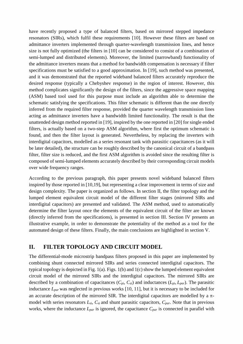
Automated Design of Balanced Wideband Bandpass Filters based on Mirrored Stepped Impedance Resonators (SIRs) and Interdigital Capacitors Marc Sans1, Jordi Selga1, Paris Vélez1, Ana Rodríguez2, Jordi Bonache1, Vicente E. Boria2, Ferran Martín1
1 CIMITEC, Departament d’Enginyeria Electrònica, Universitat Autònoma de Barcelona, 08193 Bellaterra, Spain
2 Departamento de Comunicaciones-iTEAM, Universitat Politècnica de València, 46022 Valencia, Spain.
This paper presents small balanced bandpass filters exhibiting wide differential-mode pass bands and high common-mode suppression. The filters are implemented in microstrip technology and their topology consists of multisection mirrored stepped impedance resonators (SIRs) alternating with mirrored interdigital capacitors. The mirrored SIRs provide the required common-mode transmission zeros to achieve effective rejection of that mode in the region of interest, i.e., the differential-mode pass band. An automated design method for such filters, based on aggressive space mapping (ASM), is reported. The method uses the equivalent circuit model of both the mirrored SIRs and the interdigital capacitors, and filter synthesis is based on a quasi-Newton iterative algorithm where parameter extraction is the key aspect. The automated design approach is illustrated through an order-3 filter, where it is demonstrated that the filter topology is generated from the specifications. As compared to previous balanced filters based on mirrored SIRs coupled through admittance inverters, the proposed filters of this work are smaller and the design method is simplified, since bandwidth compensation due to the narrowband functionality of the inverters is avoided.
Corresponding author: J. Selga; email: [email protected]; phone: +34 93 581 35 24
I. INTRODUCTION The design of differential-mode (or balanced) wideband bandpass filters with common-mode noise suppression is a very active research topic today [1-18]. These filters are fundamental elements in balanced circuits and systems (e.g., high-speed digital circuits), of increasing demand for their inherent high immunity to noise, electromagnetic interference (EMI) and crosstalk. Filter size and performance, i.e., good differential-mode characteristics (including a wide stop band) and significant common-mode suppression in the region of interest (differential filter pass band), are the warhorses of the researchers working on this topic. In this regard, we
have recently proposed a type of balanced filters, based on mirrored stepped impedance resonators (SIRs), which fulfil these requirements [10]. However these filters are based on admittance inverters implemented through quarter-wavelength transmission lines, and hence size is not fully optimized (the filters in [10] can be considered to consist of a combination of semi-lumped and distributed elements). Moreover, the limited (narrowband) functionality of the admittance inverters means that a method for bandwidth compensation is necessary if filter specifications must be satisfied to a good approximation. In [19], such method was presented, and it was demonstrated that the reported wideband balanced filters accurately reproduce the desired response (typically a Chebyshev response) in the region of interest. However, this method complicates significantly the design of the filters, since the aggressive space mapping (ASM) based tool used for this purpose must include an algorithm able to determine the schematic satisfying the specifications. This filter schematic is different than the one directly inferred from the required filter response, provided the quarter wavelength transmission lines acting as admittance inverters have a bandwidth limited functionality. The result is that the unattended design method reported in [19], inspired by the one reported in [20] for single ended filters, is actually based on a two-step ASM algorithm, where first the optimum schematic is found, and then the filter layout is generated. Nevertheless, by replacing the inverters with interdigital capacitors, modelled as a series resonant tank with parasitic capacitances (as it will be later detailed), the structure can be roughly described by the canonical circuit of a bandpass filter, filter size is reduced, and the first ASM algorithm is avoided since the resulting filter is composed of semi-lumped elements accurately described by their corresponding circuit models over wide frequency ranges.
According to the previous paragraph, this paper presents novel wideband balanced filters inspired by those reported in [10,19], but representing a clear improvement in terms of size and design complexity. The paper is organized as follows. In section II, the filter topology and the lumped element equivalent circuit model of the different filter stages (mirrored SIRs and interdigital capacitors) are presented and validated. The ASM method, used to automatically determine the filter layout once the elements of the equivalent circuit of the filter are known (directly inferred from the specifications), is presented in section III. Section IV presents an illustrative example, in order to demonstrate the potentiality of the method as a tool for the automated design of these filters. Finally, the main conclusions are highlighted in section V.
II. FILTER TOPOLOGY AND CIRCUIT MODEL The differential-mode microstrip bandpass filters proposed in this paper are implemented by combining shunt connected mirrored SIRs and series connected interdigital capacitors. The typical topology is depicted in Fig. 1(a). Figs. 1(b) and 1(c) show the lumped element equivalent circuit model of the mirrored SIRs and the interdigital capacitors. The mirrored SIRs are described by a combination of capacitances (Cpi, Czi) and inductances (Lpi, Lpar). The parasitic inductance Lpar was neglected in previous works [10, 11], but it is necessary to be included for an accurate description of the mirrored SIR. The interdigital capacitors are modelled by a π-model with series resonators Lsi, Csi and shunt parasitic capacitors, Cpar. Note that in previous works, where the inductance Lpar is ignored, the capacitance Cpar is connected in parallel with
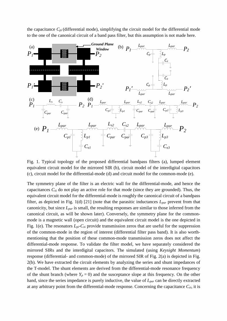
the capacitance Cpi (differential mode), simplifying the circuit model for the differential mode to the one of the canonical circuit of a band pass filter, but this assumption is not made here.
Lp
Cz
Cz
Lp
P1
P1'Cp
CpP2
P2'
Lpar Lpar
Lpar Lpar
Fig. 1. Typical topology of the proposed differential bandpass filters (a), lumped element equivalent circuit model for the mirrored SIR (b), circuit model of the interdigital capacitors (c), circuit model for the differential-mode (d) and circuit model for the common-mode (e).
The symmetry plane of the filter is an electric wall for the differential-mode, and hence the capacitances Czi do not play an active role for that mode (since they are grounded). Thus, the equivalent circuit model for the differential-mode is roughly the canonical circuit of a bandpass filter, as depicted in Fig. 1(d) [21] (note that the parasitic inductances Lpar prevent from that canonicity, but since Lpar is small, the resulting responses are similar to those inferred from the canonical circuit, as will be shown later). Conversely, the symmetry plane for the common-mode is a magnetic wall (open circuit) and the equivalent circuit model is the one depicted in Fig. 1(e). The resonators Lpi-Czi provide transmission zeros that are useful for the suppression of the common-mode in the region of interest (differential filter pass band). It is also worth-mentioning that the position of these common-mode transmission zeros does not affect the differential-mode response. To validate the filter model, we have separately considered the mirrored SIRs and the interdigital capacitors. The simulated (using Keysight Momentum) response (differential- and common-mode) of the mirrored SIR of Fig. 2(a) is depicted in Fig. 2(b). We have extracted the circuit elements by analyzing the series and shunt impedances of the T-model. The shunt elements are derived from the differential-mode resonance frequency of the shunt branch (where Yp = 0) and the susceptance slope at this frequency. On the other hand, since the series impedance is purely inductive, the value of Lpar can be directly extracted at any arbitrary point from the differential-mode response. Concerning the capacitance Czi, it is
P1 P2
P2'P1'
Ls Cs
Cpar Cpar
P1 P2Lp1Cp1
Ls2 Cs2
Lp3Cp3
P1 P2Lpar Lpar Lpar
Cpar Cpar
Lpar
Lp1Cp1 Lp3Cp3
P1 P2
Cz1 Cz3
Lpar Lpar Ls2 Cs2
Cpar Cpar
Lpar Lpar
Ground Plane Window (a) (b)
(c) (d)
(e)
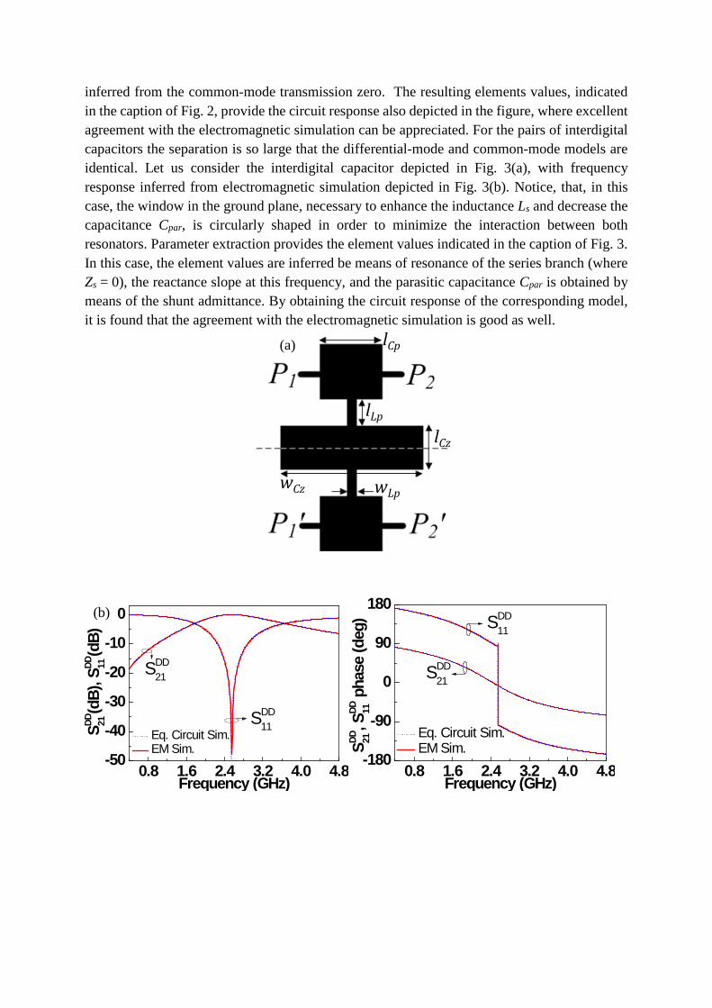
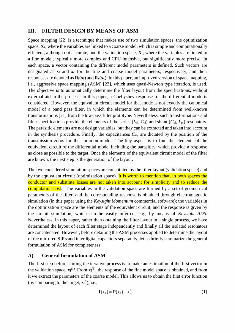
inferred from the common-mode transmission zero. The resulting elements values, indicated in the caption of Fig. 2, provide the circuit response also depicted in the figure, where excellent agreement with the electromagnetic simulation can be appreciated. For the pairs of interdigital capacitors the separation is so large that the differential-mode and common-mode models are identical. Let us consider the interdigital capacitor depicted in Fig. 3(a), with frequency response inferred from electromagnetic simulation depicted in Fig. 3(b). Notice, that, in this case, the window in the ground plane, necessary to enhance the inductance Ls and decrease the capacitance Cpar, is circularly shaped in order to minimize the interaction between both resonators. Parameter extraction provides the element values indicated in the caption of Fig. 3. In this case, the element values are inferred be means of resonance of the series branch (where Zs = 0), the reactance slope at this frequency, and the parasitic capacitance Cpar is obtained by means of the shunt admittance. By obtaining the circuit response of the corresponding model, it is found that the agreement with the electromagnetic simulation is good as well.
lLp
lCp
wLpwCz
lCz
0.8 1.6 2.4 3.2 4.0 4.8-50
-40
-30
-20
-10
0
SDD11
Eq. Circuit Sim. EM Sim.
SDD 21
(dB)
, SDD 11
(dB)
Frequency (GHz)
SDD21
0.8 1.6 2.4 3.2 4.0 4.8-180
-90
0
90
180SDD
11
Eq. Circuit Sim. EM Sim. S
DD 21, S
DD 11 p
hase
(deg
)
Frequency (GHz)
SDD21
(a)
(b)
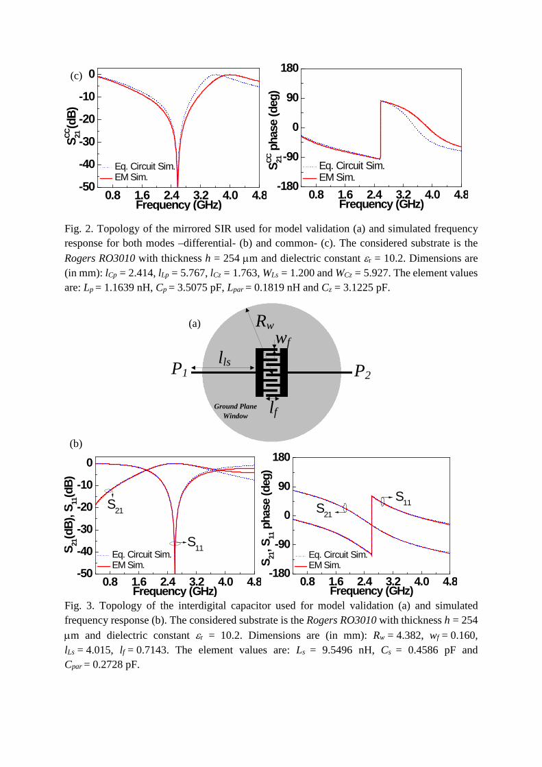
Fig. 2. Topology of the mirrored SIR used for model validation (a) and simulated frequency response for both modes –differential- (b) and common- (c). The considered substrate is the Rogers RO3010 with thickness h = 254 µm and dielectric constant εr = 10.2. Dimensions are (in mm): lCp = 2.414, lLp = 5.767, lCz = 1.763, WLs = 1.200 and WCz = 5.927. The element values are: Lp = 1.1639 nH, Cp = 3.5075 pF, Lpar = 0.1819 nH and Cz = 3.1225 pF.
Fig. 3. Topology of the interdigital capacitor used for model validation (a) and simulated frequency response (b). The considered substrate is the Rogers RO3010 with thickness h = 254 µm and dielectric constant εr = 10.2. Dimensions are (in mm): Rw = 4.382, wf = 0.160, lLs = 4.015, lf = 0.7143. The element values are: Ls = 9.5496 nH, Cs = 0.4586 pF and Cpar = 0.2728 pF.
0.8 1.6 2.4 3.2 4.0 4.8-50
-40
-30
-20
-10
0
Eq. Circuit Sim. EM Sim.
SCC 21
(dB)
Frequency (GHz)0.8 1.6 2.4 3.2 4.0 4.8
-180
-90
0
90
180
Eq. Circuit Sim. EM Sim.
SCC 21
pha
se (d
eg)
Frequency (GHz)
P1 P2
wf
lf
lls
Rw
0.8 1.6 2.4 3.2 4.0 4.8-50
-40
-30
-20
-10
0
S11 Eq. Circuit Sim. EM Sim.
S21
(dB)
, S11
(dB)
Frequency (GHz)
S21
0.8 1.6 2.4 3.2 4.0 4.8-180
-90
0
90
180
S11
Eq. Circuit Sim. EM Sim. S
21, S
11 p
hase
(deg
)
Frequency (GHz)
S21
(a)
(b)
Ground Plane Window
(c)
III. FILTER DESIGN BY MEANS OF ASM Space mapping [22] is a technique that makes use of two simulation spaces: the optimization space, Xc, where the variables are linked to a coarse model, which is simple and computationally efficient, although not accurate; and the validation space, Xf, where the variables are linked to a fine model, typically more complex and CPU intensive, but significantly more precise. In each space, a vector containing the different model parameters is defined. Such vectors are designated as xf and xc for the fine and coarse model parameters, respectively, and their responses are denoted as Rf(xf) and Rc(xc). In this paper, an improved version of space mapping, i.e., aggressive space mapping (ASM) [23], which uses quasi-Newton type iteration, is used. The objective is to automatically determine the filter layout from the specifications, without external aid in the process. In this paper, a Chebyshev response for the differential mode is considered. However, the equivalent circuit model for that mode is not exactly the canonical model of a band pass filter, in which the elements can be determined from well-known transformations [21] from the low-pass filter prototype. Nevertheless, such transformations and filter specifications provide the elements of the series (Lsi, Csi) and shunt (Cpi, Lpi) resonators. The parasitic elements are not design variables, but they can be extracted and taken into account in the synthesis procedure. Finally, the capacitances Czi, are dictated by the position of the transmission zeros for the common-mode. The key aspect is to find the elements of the equivalent circuit of the differential mode, including the parasitics, which provide a response as close as possible to the target. Once the elements of the equivalent circuit model of the filter are known, the next step is the generation of the layout.
The two considered simulation spaces are constituted by the filter layout (validation space) and by the equivalent circuit (optimization space). It is worth to mention that, in both spaces the conductor and substrate losses are not taken into account for simplicity and to reduce the computation cost. The variables in the validation space are formed by a set of geometrical parameters of the filter, and the corresponding response is obtained through electromagnetic simulation (in this paper using the Keysight Momentum commercial software); the variables in the optimization space are the elements of the equivalent circuit, and the response is given by the circuit simulation, which can be easily inferred, e.g., by means of Keysight ADS. Nevertheless, in this paper, rather than obtaining the filter layout in a single process, we have determined the layout of each filter stage independently and finally all the isolated resonators are concatenated. However, before detailing the ASM processes applied to determine the layout of the mirrored SIRs and interdigital capacitors separately, let us briefly summarize the general formulation of ASM for completeness.
A) General formulation of ASM The first step before starting the iterative process is to make an estimation of the first vector in the validation space, xf(1). From xf(1), the response of the fine model space is obtained, and from it we extract the parameters of the coarse model. This allows us to obtain the first error function (by comparing to the target, xc*), i.e.,
*cff xxPxf −= )()( (1)

where P(xf) is the vector corresponding to the coarse model parameters extracted from the response of the fine model. To iterate the process following the standard quasi-Newton type ASM approach, the new fine model vector is obtained according to
( 1) ( ) ( )j j j+ = +f fx x h (2)
where h(j) is given by:
( ) )(1)()( jjj fBh −−= (3)
and B(j) is an approach to the Jacobian matrix, which is updated according to the Broyden formula:
)()(
)()1()()1(
jTj
Tjjjj
hhhfBB
++ += (4)
In (4), f(j+1) is obtained by evaluating (1), and the super-index T stands for transpose. To initiate the Jacobian matrix, the elements of the fine model are slightly perturbed, being the effects on the extracted parameters inferred, and expressed as derivatives in matrix form. This process is iterated until convergence is achieved (once the error function is smaller than a certain predefined value).
B) ASM applied to the interdigital capacitors Once the elements of the series resonator of the interdigital capacitors are known, a specific ASM process for the determination of the layout giving such elements is necessary. In this ASM algorithm, the variables in the optimization space are xc = [Lsi, Csi], whereas the variables in the validation space are the length of the inductive line, lLs, and the length of the fingers, lf, i.e., xf = [lLs, lf]. The other geometrical parameters are set to 0.16 mm. The first vector of the validation space, xf
(1), is estimated from approximate formulas providing the inductance of a narrow inductive strip and the capacitance of an interdigital capacitor [24]. Parameter extraction is carried out as indicated in section II. Finally, the first approach to the Broyden matrix, necessary to iterate the process as indicated above, is given by:
=
f
s
f
s
Ls
s
Ls
s
lC
lC
lL
lL
δδ
δδ
δδ
δδ
B (5)
With this ASM scheme, the layout providing the target elements of the series branch is determined, and from this layout, the parasitic capacitance Cpar is also inferred. The value of Cpar is relevant since it must be subtracted to the capacitance Cpi of the mirrored SIRs, as it will be justified later.
C) ASM applied to the mirrored SIRs The layout of the mirrored SIRs is determined using an ASM algorithm with three variables. The variables in the optimization space are the elements of the shunt resonator from the circuit
schematic for the common mode depicted in Fig. 1(d), i.e., xc = [Lpi, Cpi, Czi]. The validation space is constituted by a set of variables defining the resonator layout. In order to deal with the same number of variables in both spaces, the widths of the central patch, WCzi, as well as the widths of the high- and low-impedance transmission line sections of the SIRs, WLpi and WCpi, respectively, are set to fixed values. Thus, the variables in the validation space are the remaining dimensions of the shunt resonators, that is, the length of the central capacitive patch, lCzi, and the lengths lLpi and lCpi of the high- and low-impedance transmission line sections, respectively, of the SIR (i.e., xf = [lLpi, lCpi, lCzi]). The specific procedure to determine the layout is similar to the one detailed in [20]. The first vector of the validation space, xf(1), is estimated from the well-known (and simple) approximate formulas providing the inductance and capacitance of a narrow and wide, respectively, electrically small transmission line section [24]. Isolating the lengths, we obtain:
h
hpLp Z
vLl = (6a)
lplppCp ZvCl = (6b)
lzlzzCz ZvCl = (6c)
where vh and vlp,z are the phase velocities of the high- and low-impedance transmission lines sections, respectively, and Zh and Zlp,z the corresponding characteristic impedances (note that the sub-indices p, z in the phase velocity and characteristic impedance of the low-impedance transmission line sections are used to differentiate the central, Cz, and external, Cp, patches). Parameter extraction is carried out as specified in Section II. Finally, the first approach to the Broyden matrix, necessary to iterate the process, is given by:
=
Cz
z
Cp
z
Lp
z
Cz
p
Cp
p
Lp
p
Cz
p
Cp
p
Lp
p
lC
lC
lC
lC
lC
lC
lL
lL
lL
δδ
δδ
δδ
δδ
δδ
δδ
δδ
δδ
δδ
B (7)
With this ASM scheme, the layout providing the target elements of the shunt branch is determined, and from this layout, the parasitic capacitance Lpar is also inferred.
D) Strategy to determine the circuit schematic satisfying specifications With the previous ASM algorithms, the layouts of the filter stages corresponding to the interdigital capacitors and mirrored SIRs can be determined. However, the presence of the parasitic elements forces us to recalculate the circuit schematic taking into account such parasitics. The hypothesis in the design process is to assume that once the parasitics are inferred, following the processes indicated above, the values do not significantly depend on the specific geometry. Hence, the next step is to set the elements values of the parasitics to the inferred values, and consider the remaining elements as variables that must be tuned at the circuit level in order to satisfy the filter specifications. However, as long as the inductance Lpar is small, as it has been verified, one expects that by subtracting the parasitic capacitance Cpar to the
capacitance of the mirrored SIR, Cp, the variables in the optimization process do not need to be modified so much. Indeed, it has been verified that it is enough to tune Ls to satisfy the filter specifications. Thus, by tuning this element, the final circuit schematic, including the parasitics, is determined. Therefore, the layout of the interdigital capacitors must be recalculated following the previous ASM algorithms. Then the resulting layouts are cascaded, and filter topology is thus constructed.
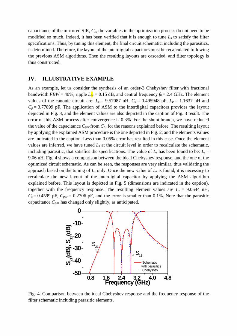
IV. ILLUSTRATIVE EXAMPLE As an example, let us consider the synthesis of an order-3 Chebyshev filter with fractional bandwidth FBW = 40%, ripple LAr = 0.15 dB, and central frequency f0 = 2.4 GHz. The element values of the canonic circuit are: Ls = 9.57087 nH, Cs = 0.495948 pF, Lp = 1.1637 nH and Cp = 3.77899 pF. The application of ASM to the interdigital capacitors provides the layout depicted in Fig. 3, and the element values are also depicted in the caption of Fig. 3 result. The error of this ASM process after convergence is 0.3%. For the shunt branch, we have reduced the value of the capacitance Cpar from Cp, for the reasons explained before. The resulting layout by applying the explained ASM procedure is the one depicted in Fig. 2, and the elements values are indicated in the caption. Less than 0.05% error has resulted in this case. Once the element values are inferred, we have tuned Ls at the circuit level in order to recalculate the schematic, including parasitic, that satisfies the specifications. The value of Ls has been found to be: Ls = 9.06 nH. Fig. 4 shows a comparison between the ideal Chebyshev response, and the one of the optimized circuit schematic. As can be seen, the responses are very similar, thus validating the approach based on the tuning of Ls only. Once the new value of Ls is found, it is necessary to recalculate the new layout of the interdigital capacitor by applying the ASM algorithm explained before. This layout is depicted in Fig. 5 (dimensions are indicated in the caption), together with the frequency response. The resulting element values are Ls = 9.0644 nH, Cs = 0.4599 pF, Cpar = 0.2706 pF, and the error is smaller than 0.1%. Note that the parasitic capacitance Cpar has changed only slightly, as anticipated.
Fig. 4. Comparison between the ideal Chebyshev response and the frequency response of the filter schematic including parasitic elements.
0.8 1.6 2.4 3.2 4.0 4.8-50
-40
-30
-20
-10
0
S11
Schematic with parasitics
Chebyshev
S 21(d
B), S
11(d
B)
Frequency (GHz)
S21
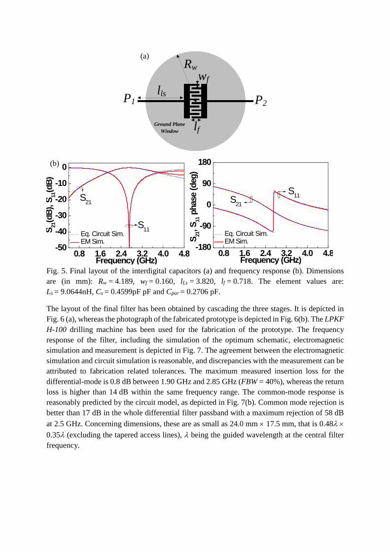
Fig. 5. Final layout of the interdigital capacitors (a) and frequency response (b). Dimensions are (in mm): Rw = 4.189, wf = 0.160, lLs = 3.820, lf = 0.718. The element values are: Ls = 9.0644nH, Cs = 0.4599pF pF and Cpar = 0.2706 pF.
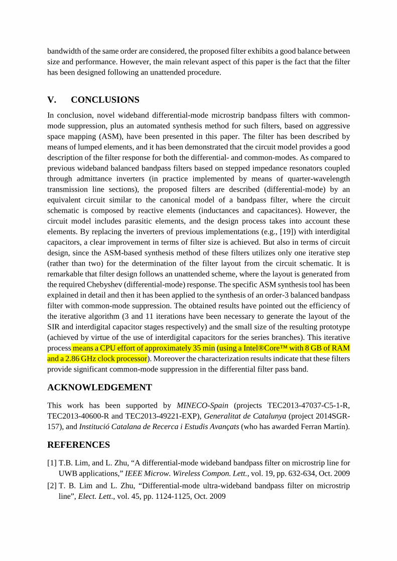
The layout of the final filter has been obtained by cascading the three stages. It is depicted in Fig. 6 (a), whereas the photograph of the fabricated prototype is depicted in Fig. 6(b). The LPKF H-100 drilling machine has been used for the fabrication of the prototype. The frequency response of the filter, including the simulation of the optimum schematic, electromagnetic simulation and measurement is depicted in Fig. 7. The agreement between the electromagnetic simulation and circuit simulation is reasonable, and discrepancies with the measurement can be attributed to fabrication related tolerances. The maximum measured insertion loss for the differential-mode is 0.8 dB between 1.90 GHz and 2.85 GHz (FBW = 40%), whereas the return loss is higher than 14 dB within the same frequency range. The common-mode response is reasonably predicted by the circuit model, as depicted in Fig. 7(b). Common mode rejection is better than 17 dB in the whole differential filter passband with a maximum rejection of 58 dB at 2.5 GHz. Concerning dimensions, these are as small as 24.0 mm × 17.5 mm, that is 0.48λ × 0.35λ (excluding the tapered access lines), λ being the guided wavelength at the central filter frequency.
P1 P2
wf
lf
lls
Rw
0.8 1.6 2.4 3.2 4.0 4.8-50
-40
-30
-20
-10
0
S11 Eq. Circuit Sim. EM Sim.
S21
(dB)
, S11
(dB)
Frequency (GHz)
S21
0.8 1.6 2.4 3.2 4.0 4.8-180
-90
0
90
180
S11
Eq. Circuit Sim. EM Sim. S
21, S
11 p
hase
(deg
)
Frequency (GHz)
S21
(a)
(b)
Ground Plane Window
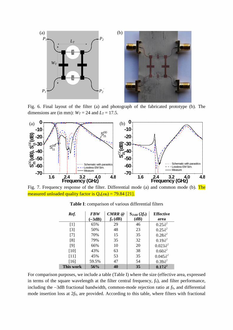
Fig. 6. Final layout of the filter (a) and photograph of the fabricated prototype (b). The dimensions are (in mm): WT = 24 and LT = 17.5.
Fig. 7. Frequency response of the filter. Differential mode (a) and common mode (b). The measured unloaded quality factor is Qu(ω0) = 79.84 [21].
Table I: comparison of various differential filters
Ref. FBW (−3dB)
CMRR @ f0 (dB)
S21dd (2f0) (dB)
Effective area
[1] 65% 29 46 0.25λ2
[3] 50% 48 23 0.25λ2 [7] 70% 15 35 0.28λ2 [8] 79% 35 32 0.19λ2 [9] 66% 10 20 0.023λ2 [10] 43% 63 38 0.60λ2 [11] 45% 53 35 0.045λ2 [16] 59.5% 47 54 0.39λ2
This work 56% 40 35 0.17λ2
For comparison purposes, we include a table (Table I) where the size (effective area, expressed in terms of the square wavelength at the filter central frequency, f0), and filter performance, including the −3dB fractional bandwidth, common-mode rejection ratio at f0, and differential mode insertion loss at 2f0, are provided. According to this table, where filters with fractional
P2P1
P2'P1
'
WT
LT
1.6 2.4 3.2 4.0 4.8-70-60-50-40-30-20-10
0
Schematic with parasitics Lossless EM Sim. Measure
SDD11
SDD 21(d
B), S
DD 11(d
B)
Frequency (GHz)
SDD21
1.6 2.4 3.2 4.0 4.8-70-60-50-40-30-20-10
0
Schematic with parasitics Lossless EM Sim. Measure
SCC 21
(dB)
Frequency (GHz)
(a) (b)
(a) (b)
bandwidth of the same order are considered, the proposed filter exhibits a good balance between size and performance. However, the main relevant aspect of this paper is the fact that the filter has been designed following an unattended procedure.
V. CONCLUSIONS In conclusion, novel wideband differential-mode microstrip bandpass filters with common-mode suppression, plus an automated synthesis method for such filters, based on aggressive space mapping (ASM), have been presented in this paper. The filter has been described by means of lumped elements, and it has been demonstrated that the circuit model provides a good description of the filter response for both the differential- and common-modes. As compared to previous wideband balanced bandpass filters based on stepped impedance resonators coupled through admittance inverters (in practice implemented by means of quarter-wavelength transmission line sections), the proposed filters are described (differential-mode) by an equivalent circuit similar to the canonical model of a bandpass filter, where the circuit schematic is composed by reactive elements (inductances and capacitances). However, the circuit model includes parasitic elements, and the design process takes into account these elements. By replacing the inverters of previous implementations (e.g., [19]) with interdigital capacitors, a clear improvement in terms of filter size is achieved. But also in terms of circuit design, since the ASM-based synthesis method of these filters utilizes only one iterative step (rather than two) for the determination of the filter layout from the circuit schematic. It is remarkable that filter design follows an unattended scheme, where the layout is generated from the required Chebyshev (differential-mode) response. The specific ASM synthesis tool has been explained in detail and then it has been applied to the synthesis of an order-3 balanced bandpass filter with common-mode suppression. The obtained results have pointed out the efficiency of the iterative algorithm (3 and 11 iterations have been necessary to generate the layout of the SIR and interdigital capacitor stages respectively) and the small size of the resulting prototype (achieved by virtue of the use of interdigital capacitors for the series branches). This iterative process means a CPU effort of approximately 35 min (using a Intel®Core™ with 8 GB of RAM and a 2.86 GHz clock processor). Moreover the characterization results indicate that these filters provide significant common-mode suppression in the differential filter pass band.
ACKNOWLEDGEMENT
This work has been supported by MINECO-Spain (projects TEC2013-47037-C5-1-R, TEC2013-40600-R and TEC2013-49221-EXP), Generalitat de Catalunya (project 2014SGR-157), and Institució Catalana de Recerca i Estudis Avançats (who has awarded Ferran Martín).
REFERENCES
[1] T.B. Lim, and L. Zhu, “A differential-mode wideband bandpass filter on microstrip line for UWB applications,” IEEE Microw. Wireless Compon. Lett., vol. 19, pp. 632-634, Oct. 2009
[2] T. B. Lim and L. Zhu, “Differential-mode ultra-wideband bandpass filter on microstrip line”, Elect. Lett., vol. 45, pp. 1124-1125, Oct. 2009
[3] T. B. Lim and L. Zhu, “Highly selective differential-mode wideband bandpass filter for UWB application”, IEEE Microw. Wireless Compon. Lett., vol. 21, pp. 133-135, Mar. 2011.
[4] A.M. Abbosh, “Ultrawideband balanced bandpass filter”, IEEE Microw. Wireless Compon. Lett., vol. 21, pp. 480-482, Sep. 2011
[5] H.T. Zhu, W.J. Feng, W.Q. Che and Q. Xue, “Ultra-wideband differential bandpass filter based on transversal signal-interference concept”, Elect. Lett., vol. 47, pp. 1033-1035, Sep. 2011.
[6] X-H. Wu, Q-X. Chu, “Compact differential ultra-wideband bandpass filter with common-mode suppression”, IEEE Microw. Wireless Compon. Lett., vol. 22, pp. 456-458, Sep. 2012.
[7] W. Feng and W. Che, “Novel wideband differential bandpass filters based on T-shaped structure”, IEEE Trans. Microw. Theory. Techn., vol. 60, pp. 1560-1568, Jun. 2012.
[8] W. Feng, W. Che, Y. Ma and Q. Xue, “Compact wideband differential bandpass filters using half-wavelength ring resonator”, IEEE Microw. Wireless Compon. Lett., vol. 23, pp. 81-83, Feb. 2013.
[9] X.-H. Wu, Q.-X. Chu, and L.-L. Qiu, “Differential wideband bandpass filter with high-selectivity and common-mode suppression”, IEEE Microw. Wireless Compon. Lett., vol. 23, pp. 644-646, Dec. 2013.
[10] P. Vélez, M. Durán-Sindreu, J.Bonache, A. Fernández-Prieto, J. Martel, F. Medina and F. Martín, “Differential bandpass filters with common-mode suppression based on stepped impedance resonators (SIRs)”, IEEE MTT-S Int. Microwave Symp., June 2013, Seattle (USA)
[11] P. Vélez, J. Naqui, A. Fernández-Prieto, M. Durán-Sindreu, J. Bonache, J. Martel, F. Medina, and F. Martín, “Differential bandpass filter with common mode suppression based on open split ring resonators and open complementary split ring resonators”, IEEE Microw. Wirel. Compon. Lett., vol. 23, pp. 22-24, Jan. 2013.
[12] A. K. Horestani, M. Durán-Sindreu, J. Naqui, C. Fumeaux, and F. Martín, “S-Shaped complementary split ring resonators and their application to compact differential bandpass filters with common-mode suppression”, IEEE Microw. Wirel. Compon. Lett., vol. 24, pp. 150-152, Mar. 2014.
[13] X.-H. Wang, H. Zhang, and B.-Z. Wang, “A novel ultra-wideband differential filter based on microstrip line structures”, IEEE Microw. Wirel. Compon. Lett., vol. 23, pp. 128-130, Mar. 2013.
[14] Jin Shi, Chuan Shao, Jian-Xin Chen, Member, IEEE, Qing-Yuan Lu, Yanjun Peng, and Zhi-Hua Bao “Compact low-loss wideband differential bandpass filter with high common-mode suppression”, IEEE Microw. Wirel. Compon. Lett., vol. 23, pp. 480-482, Sep. 2013.
[15] P. Vélez, M. Durán-Sindreu, J. Naqui, J. Bonache and F. Martín, “Common-mode suppressed differential bandpass filter based on open complementary split ring resonators (OCSRRs) fabricated in microstrip technology without ground plane etching”, Microwave and Optical Technology Letters, vol. 56, pp. 910-916, Apr. 2014.
[16] L. Li, J. Bao, J.-J. Du, Y.-M. Wang, “Differential wideband bandpass filters with enhanced common-mode suppression using internal coupling technique”, IEEE Microw. Wirel. Compon. Lett., vol., 24, pp. 300-302, May 2014.
[17] P. Vélez, J. Naqui, A. Fernández-Prieto, J. Bonache, J. Mata-Contreras, J. Martel, F. Medina, and F. Martín “Ultra-compact (80mm2) differential-mode ultra-wideband (UWB) bandpass filters with common-mode noise suppression”, IEEE Trans. Microw. Theory Techn., vol. 63, pp. 1272-1280, Apr. 2015.
[18] X. Guo, L. Zhu, K.-W. Tam, and W. Wu, "Wideband differential bandpass filters on multimode slotline resonator with intrinsic common-mode rejection", IEEE Trans. Microw. Theory Techn., vol. 63, pp. 1587-1594, May. 2015.
[19] M. Sans, J. Selga, P. Vélez, A. Rodríguez, V. E. Boria, F. Martín, “Application of aggressive space mapping (ASM) to the automated design of differential-mode wideband bandpass filters with common-mode suppression”, European Microwave Conference, Paris, France, 6-11 September 2015.
[20] M. Sans, J. Selga, A. Rodríguez, J. Bonache, V.E. Boria, and F. Martín, “Design of planar wideband bandpass filters from specifications using a two-step aggressive space mapping (ASM) optimization algorithm”, IEEE Trans. Microw. Theory Techn., vol. 62, pp. 3341-3350, Dec. 2014
[21] J.S. Hong and M.J. Lancaster, Microstrip Filters for RF/Microwave Applications, John Wiley, 2001
[22] J.W. Bandler, R.M. Biernacki, S.H. Chen, P.A. Grobelny and R.H. Hemmers, “Space mapping technique for electromagnetic optimization”, IEEE Trans. Microw. Theory Techn., vol. 42, pp. 2536–2544, Dec. 1994.
[23] J.W. Bandler, R.M. Biernacki, S.H. Chen, R.H. Hemmers, and K. Madsen, “Electromagnetic optimization exploiting aggressive space mapping”, IEEE Trans. Microw. Theory Techn., vol. 43, pp. 2874–2882, Dec. 1995.
[24] D. M. Pozar, Microwave Engineering. Boston, MA, USA: AddisonWesley, 1990.
Biographies
Marc Sans was born in Terrassa (Barcelona), Spain, in 1982. He received the B.S. Degree in Telecommunications Engineering - Electronic Systems in 2006, the M.S. Degree in Telecommunications Engineering in 2008 and the M.S. Degree in Electronics Engineering in 2013 from the Universitat Autònoma de Barcelona (UAB). In 2008 he started his professional career as
a RF Engineer at Sony-FTVE developing the RF stage of TV receivers. In 2010 he moved to Mier Comunicaciones S.A. to carry out the design of passive and active devices for VHF-UHF broadcasting units. Since 2014 he is working towards the PhD Degree at CIMITEC-UAB in the synthesis of microwave devices based on EM optimization techniques.
Jordi Selga was born in Barcelona, Spain, in 1982. He received the B.S. Degree in Telecommunications Engineering - Electronic Systems in 2006, the M.S. Degree in Electronics Engineering in 2008 and the PhD degree in Electronics Engineering in 2013 from the Universitat Autònoma de Barcelona (UAB), Barcelona, Spain. Since 2008 is member of CIMITEC-UAB, a research centre on Metamaterials supported by TECNIO (Catalan Government). He was holder
of a national research fellowship from the Formación de Profesorado Universitario Program of the Education and Science Ministry (Reference AP2008-4707). He is currently working in subjects related to metamaterials, CAD design of microwave devices, EM optimization methods and automated synthesis of planar microwave components at the UAB.
Paris Vélez was born in Barcelona (Spain) in 1982. He received the degree in Telecommunications Engineering, specializing in Electronics in 2008 and the Electronics Engineering degree in 2010 from the Universitat Autònoma de Barcelona. In 2014 he received his PhD in Electrical Engineering from the UAB with a thesis entitled “Common mode suppression differential microwave circuits based on Metamaterial concepts and semilumped resonators”. During the PhD he
was awarded with a predoctoral teaching and research fellowship by the Spanish Government from 2011 to 2014. Dr. Vélez is a reviewer of the IEEE T-MTT and of other journals. Actually, his scientific activity is focused on the miniaturization of passive circuits RF / microwave based Metamaterials.
Ana Rodriguez was born in Lugo, Spain. She received the Telecommunications Engineering degree from the Universidade de Vigo (UV), Spain, in 2008. As a student, she participated in the Erasmus exchange program, developing the Master Thesis at the University of Oulu, Finland. Since the end of 2008, she has joined the Institute of Telecommunications and Multimedia Applications (iTEAM), which is part of the scientific park at the Universitat Politècnica de
València (UPV), Spain. She obtained “Master en Tecnología, Sistemas y Redes de Comunicaciones" in 2010 from UPV, and the PhD degree in 2014. Her main research interests include CAD design of microwave devices, EM optimization methods and metamaterials.
Jordi Bonache was born in 1976 in Barcelona (Spain). He received the Physics and Electronics Engineering Degrees from the Universitat Autònoma de Barcelona in 1999 and 2001, respectively and the PhD degree in Electronics Engineering from the same university in 2007. In 2000, he joined the "High Energy Physics Institute" of Barcelona (IFAE), where he was involved in the design and implementation of the control and monitoring system of the MAGIC
telescope. In 2001, he joined the Department of Electronics Engineering of the Universitat Autònoma de Barcelona where he is currently Lecturer. From 2006 to 2009 worked as executive manager of CIMITEC. Currently is leading the research in RFID and antennas in CIMITEC. His research interests include active and passive microwave devices, metamaterials, antennas and RFID.
Vicente E. Boria was born in Valencia, Spain, on May 18, 1970. He received his “Ingeniero de Telecomunicación” degree (with first-class honors) and the “Doctor Ingeniero de Telecomunicación” degree from the Universidad Politécnica de Valencia, Valencia, Spain, in 1993 and 1997, respectively. In 1993 he joined the “Departamento de Comunicaciones”, Universidad Politécnica de Valencia, where he has been Full Professor since 2003. In 1995
and 1996, he was holding a Spanish Trainee position with the European Space Research and Technology Centre, European Space Agency (ESTEC-ESA), Noordwijk, The Netherlands, where he was involved in the area of EM analysis and design of passive waveguide devices. He has authored or co-authored 10 chapters in technical textbooks, 135 papers in refereed international technical journals, and over 180 papers in international conference proceedings. His current research interests are focused on the analysis and automated design of passive components, left-handed and periodic structures, as well as on the simulation and measurement of power effects in passive waveguide systems. Dr. Boria has been a member of the IEEE Microwave Theory and Techniques Society (IEEE MTT-S) and the IEEE Antennas and Propagation Society (IEEE AP-S) since 1992. He is reviewer of the IEEE Transactions on Microwave Theory and Techniques, Proceeding of the IET (Microwaves, Antennas and Propagation) and IET Electronics Letters. Since 2013, he serves as Associate Editor of IEEE Microwave and Wireless Components Letters. He is also a member of the Technical Committees of the IEEE-MTT International Microwave Symposium and of the European Microwave Conference.
Ferran Martín received the B.S. Degree in Physics from the Universitat Autònoma de Barcelona (UAB) in 1988 and the PhD degree in 1992. From 1994 up to 2006 he was Associate Professor in Electronics at the Departament d’Enginyeria Electrònica (Universitat Autònoma de Barcelona), and since 2007 he is Full Professor of Electronics. In recent years, he has been involved in different research activities including modelling and simulation of electron
devices for high frequency applications, millimeter wave and THz generation systems, and the application of electromagnetic bandgaps to microwave and millimeter wave circuits. He is now very active in the field of metamaterials and their application to the miniaturization and optimization of microwave circuits and antennas. He is the head of the Microwave Engineering, Metamaterials and Antennas Group (GEMMA Group) at UAB, and director of CIMITEC, a research Center on Metamaterials supported by TECNIO (Generalitat de Catalunya). He has organized several international events related to metamaterials, including Workshops at the IEEE International Microwave Symposium (years 2005 and 2007) and European Microwave Conference (2009), and the Fifth International Congress on Advanced Electromagnetic Materials in Microwaves and Optics (Metamaterials 2011), where he has acted as chair of the Local Organizing Committee. He has acted as Guest Editor for three Special Issues on Metamaterials in three International Journals. He has authored and co-authored over 450 technical conference, letter, journal papers and book chapters, he is co-author of the book on Metamaterials entitled Metamaterials with Negative Parameters: Theory, Design and Microwave Applications (John Wiley & Sons Inc. 2008), author of the book Artificial Transmission Lines for RF and Microwave Applications (John Wiley & Sons Inc. 2015), and

he has generated 15 PhDs. Ferran Martín has filed several patents on metamaterials and has headed several Development Contracts. Prof. Martín is a member of the IEEE Microwave Theory and Techniques Society (IEEE MTT-S). He is reviewer of the IEEE Transactions on Microwave Theory and Techniques and IEEE Microwave and Wireless Components Letters, among many other journals, and he serves as member of the Editorial Board of IET Microwaves, Antennas and Propagation and International Journal of RF and Microwave Computer-Aided Engineering. He is also a member of the Technical Committees of the European Microwave Conference (EuMC) and International Congress on Advanced Electromagnetic Materials in Microwaves and Optics (Metamaterials). Among his distinctions, Ferran Martín has received the 2006 Duran Farell Prize for Technological Research, he holds the Parc de Recerca UAB – Santander Technology Transfer Chair, and he has been the recipient of two ICREA ACADEMIA Awards (calls 2008 and 2013). He is IEEE Fellow since 2012.