Searching the Rhone delta channel in Lake Geneva since François-Alphonse Forel
Upload
khangminh22Category
view
2download
0
THÈSE Pour obtenir le grade de
DOCTEUR DE L’UNIVERSITÉ DE GRENOBLE Spécialité : Nano-Électronique et Nano-Technologies
Arrêté ministériel : 7 août 2006 Présentée par
François BURDIN Thèse dirigée par Philippe FERRARI et codirigée par Florence PODEVIN préparée au sein du Laboratoire IMEP-LAHC dans l'École Doctorale Électronique, Électrotechnique, Automatique et Traitement du Signal Nouvelles topologies de diviseurs de puissance, baluns et déphaseurs en bandes RF et millimétriques, apport des lignes à ondes lentes Thèse soutenue publiquement le 16 Juillet 2013 , devant le jury composé de :
M. Christophe GAQUIERE Professeur des universités, Lille, Président M. Roberto SORRENTINO Professeur des universités, Pérouse (Italie), Rapporteur M. Eric KERHERVE Professeur des universités, Bordeaux, Rapporteur M. Daniel GLORIA Ingénieur STMicroelectronics, Crolles, Membre M. Tibor BERCELI Professeur des universités, Budapest (Hongrie), Invité M. Philippe FERRARI Professeur des universités, Grenoble, Directeur de thèse Mme. Florence PODEVIN Maître de conférences, Grenoble, Co-encadrant de thèse

2

3
Résumé
L’objectif de cette thèse a été premièrement de réaliser des dispositifs passifs
intégrés à base de lignes à onde lentes nommées S-CPW (pour « Slow-wave CoPlanar
Waveguide ») aux fréquences millimétriques. Plusieurs technologies CMOS ou BiCMOS
ont été utilisées: CMOS 65 nm et 28 nm ainsi que BiCMOS 55 nm.
Deux baluns, le premier basé sur une topologie de rat-race et le second basé sur un
diviseur de puissance de Wilkinson modifié, ainsi qu’un inverseur de phase, ont été réalisés
et mesurés dans la technologie CMOS 65 nm. Les résultats expérimentaux obtenus se
situent à l’état de l’art en termes de performances électriques. Un coupler hybride et un
diviseur de puissance avec des sorties en phase sans isolation ont été conçus en technologie
CMOS 28 nm. Les simulations montrent de très bonnes performances pour des dispositifs
compacts. Les circuits sont en cours de fabrication et pourront très bientôt être caractérisés.
Ensuite, une nouvelle topologie de diviseurs de puissance, avec sorties en phase et isolé a
été développée, offrant une grande flexibilité et compacité en comparaison des diviseurs de
puissance traditionnels. Cette topologie est parfaitement adaptée pour les technologies
silicium. Comme preuve de concept, deux diviseurs de puissance avec des caractéristiques
différentes ont été réalisés en technologie PCB microruban à la fréquence de 2.45 GHz. Un
composent a été conçu à 60 GHz en technologie BiCMOS 55 nm utilisant des lignes
S-CPW. Les simulations prouvent que le dispositif est faibles pertes, adapté et isolé. Les
circuits sont également en cours de fabrication. Enfin, deux topologies de « reflection type
phase shifter » ont été développées, la première dans la bande RF et la seconde aux
fréquences millimétrique. Pour la bande RF, le déphasage atteint plus de 360° avec une
figure de mérite très élevée en comparaison avec l’état de l’art. En ce qui concerne le
déphaseur dans la bande millimétrique, la simulation montre un déphasage de 341° avec
également une figure de mérite élevée.
Mots-clés : Ligne à ondes lentes S-CPW, facteur de qualité, technologies CMOS,
balun, rat-race, inverseur de phase, diviseur de puissance, coupleur hybride, déphaseur,
bande millimétrique, bande RF, figure de mérite, miniaturisation.

4

5
Title
New topologies of power dividers, baluns and phase shifters in RF and millimetre-
wave bands, based on microstrip lines and slow-wave coplanar waveguides technologies.
Abstract
The first purpose of this work was the use of slow-wave coplanar waveguides
(S-CPW) to achieve various passive components with the aim to show their great potential
and interest at millimetre-waves. Several CMOS or BiCMOS technologies were used:
CMOS 65 nm and 28 nm, and BiCMOS 55 nm.
Two baluns, one based on a rat-race topology and the other based on a modified
Wilkinson power divider, and a phase inverter, were achieved and measured in a 65 nm
CMOS technology. State-of-the-art results were achieved. A branch-line coupler and an in
phase power divider without isolation were designed in a 28 nm CMOS technology. Really
good performances are expected for these compact devices being yet under fabrication.
Then, a new topology of in phase and isolated power divider was developed, leading to
more flexibility and compactness, well suited to millimetre-wave frequencies. Two power
dividers with different characteristics were realized in a PCB technology at 2.45 GHz by
using microstrip lines, as a proof-of-concept. After that, a power divider was designed at
the working frequency of 60 GHz in the 55 nm BiCMOS technology with S-CPWs. The
simulation results showed a low loss, full-matched and isolated component, which is also
under fabrication and will be characterized as soon as possible. Finally, two new topologies
of reflection type phase shifters were presented, one for the RF band and one for the
millimetre-wave one. For the one in RF band, the phase shift can reach more than 360° with
a great figure-of-merit as compared to the state-of-the-art. Concerning the phase shifter in
the millimetre-wave band, the simulation results show a phase shift of 341° with also a high
figure-of-merit.
Key words : Slow-wave CPW, quality factor, CMOS technologies, balun, rat-race,
phase inverter, power divider, branch-line coupler, reflection type phase shifter, millimetre-
wave band, RF band, figure-of-merit, miniaturization.

6

7
Remerciements
Je souhaite tout d’abord remercier Monsieur Christophe Gaquière, professeur à
l’université de Lille, qui me fait l’honneur de présider le jury, ainsi que Messieurs Eric
Kerhervé, professeur à l’université de Bordeaux et Roberto Sorrentino, professeur à
l’université de Pérouse pour avoir accepté d’être rapporteurs de cette thèse.
Merci à Daniel GLORIA qui a accepté d’être examinateur au cours de la
soutenance ainsi que pour la mise à disposition en toute confiance des technologies de
STMicroelectronics. Sa collaboration a été essentielle pour mon travail de thèse. Un grand
merci au Professeur Tibor BERCELI de l’université de Budapest, qui m’a fait l’honneur
d’assister à cette thèse. Budapest… cette ville qui représente tant de choses pour moi.
Ma rencontre avec Philippe FERRARI à l’IUT en 2006 allait sans le savoir être
déterminante pour ma carrière. Après m’avoir accepté en stage à l’IMEP-LAHC lors de
ma deuxième année à l’ENSERG en 2009, une année après Philippe m’a très gentiment
proposé cette thèse. Ses qualités professionnelles, sa pédagogie et son optimisme ont fait
que l’idée de travailler avec lui a été le facteur dominant pour accepter ce projet. Florence
PODEVIN a parfaitement complété mon encadrement, avec sa gentillesse et sa générosité.
Malgré ses contraintes, Florence a toujours été disponible et m’a toujours aidé pour
avancer au mieux dans mon travail. Philippe et Florence m’ont toujours fait confiance,
j’avais donc une réelle volonté de ne pas les décevoir. Cette confiance était pour moi une
source de motivation aussi importante que la réussite de ma thèse. Je pense avoir eu des
encadrants exceptionnels, ceux que tout thésard rêve d’avoir, et j’en ai conscience. C’est
pour cela que je leurs en suis extrêmement reconnaissant. Merci Philippe. Merci Florence.
Je suis également reconnaissant à Nicolas CORRAO pour les mesures des
dispositifs intégrés et s’être déplacé à Chambéry avec moi, à Benjamin BLAMPEY pour
toute la partie de-embedding, à Alejandro NIEMBRO pour la réalisation et mesure des
antennes et à Alexandre CHAGOYA pour son aide sur les design Kits. Il y a aussi ceux que
j’ai côtoyés ou avec lesquels j’ai travaillé pendant ces trois années, merci à Anne-Laure,
Xiaolan, Jean-Michel, Estelle, Jean-Daniel, Farid, José, Pierre et bien sûr Manu le
chambreur numéro un… Toutes ces personnes m’ont apporté bien plus qu’elles ne le
pensent et je les remercie. Je pense également à Zyad, mon premier et unique stagiaire,
toujours souriant et amical, qui a donc accepté d’être mon cobaye, à son insu… Je pense
que nous avons fait une belle équipe et lui souhaite plein de bonheur pour la suite.
Un grand merci à tous les doctorants qui se sont succédés au bureau A440. J’ai pu
y rencontrer Fabien, Zine, Florent et bien sûr Inès et Alex qui ont apportés une dimension

8
internationale très agréable. Une grande complicité s’était installée entre nous et c’est
avec regret que je les quitte. Merci à notre voisin de bureau, Tan-Phu, qui pensait toujours
à nous pour partager ses friandises.
Il m’est impossible de ne pas citer mes amis de l’ERG avec qui j’ai passé mes trois
plus belles années d’études. Je pense à Armand, Nico, Tyty, Ousmane et Polo, notre groupe
des admis sur titre, mais aussi à Minot, Youyou (dit « Binôme ») et Richard Président.
Merci pour votre aide, pour toutes ces soirées, ces sorties, ces foots… et je m’excuse de
n’avoir pu passer plus de temps avec vous ces trois dernières années. Il y a eu bien sûr
cette coloc Magic, avec les Trois Mousquetaires, période qui restera inoubliable.
Il y a aussi des gens que j’ai rencontrés et qui sont devenus plus que des amis. Je
tiens à remercier Vlad, avec qui j’ai passé tant de temps. C’était toujours un plaisir de faire
du design pour me trouver dans la même salle que lui. Merci aussi à Francesco et Paolo, à
leur année à l’IMEP-LAHC qui est passée beaucoup trop vite. Notre périple en Italie, les
Châteaux de la Loire avec Ana et toutes ces sorties ensemble…que de souvenirs.
Un très grand merci à mes parents qui ont toujours acceptés mes choix, m’ont
soutenus et m’ont fait confiance. Je n’oublie pas mon frère Nico à qui je souhaite la
réussite et tout le bonheur du monde.
Enfin, je remercie la personne qui a partagé avec moi cette aventure et qui a
toujours été à mes côtés depuis trois ans et demi. Merci Elena, pour ta gentillesse et ta
compréhension, je ne te remercierai jamais assez pour les sacrifices que tu as faits en me
suivant en France. Un grand merci à ta famille qui m’accueille toujours comme un Tsar
lors de nos visites à Saint Pétersbourg.

9
TABLE OF CONTENTS
INTRODUCTION........................................................................................................13
CHAPTER I : POWER DIVIDERS/COMBINERS AND REFLECTION TYPE PHASE SHIFTER PRESENTATION .................................. 17
I.1 PLANAR DIVIDERS/COMBINERS ................................................................................. 17
I.1.1 Overview ...................................................................................................................... 18
I.1.2 Wilkinson power divider/combiner ........................................................................... 18
I.1.2.1 Presentation...................................................................................................................... 18
I.1.2.2 Evolution .......................................................................................................................... 19
I.1.2.3 Striking applications ......................................................................................................... 20
I.1.3 Branch-line coupler .................................................................................................... 21
I.1.3.1 Presentation...................................................................................................................... 21
I.1.3.2 Evolution .......................................................................................................................... 22
I.1.3.3 Striking applications ......................................................................................................... 23
I.1.4 Rat race coupler .......................................................................................................... 24
I.1.4.1 Presentation...................................................................................................................... 24
I.1.4.2 Evolution .......................................................................................................................... 25
I.1.4.3 Application ....................................................................................................................... 26
I.2 REFLECTION TYPE PHASE SHIFTER ........................................................................... 27
I.2.1 Principle and theory ................................................................................................... 27
I.2.1.1 Insertion loss .................................................................................................................... 27
I.2.1.2 Relative phase shift ........................................................................................................... 28
I.2.1.3 Practical example with non-ideal varactor ...................................................................... 29
I.2.1.4 Conclusion ........................................................................................................................ 30
I.2.2 Modified reflective load .............................................................................................. 30
I.2.2.1 Serial inductance .............................................................................................................. 30
I.2.2.2 State-of-the-art at RF frequencies .................................................................................... 31
I.2.3 Branch-line coupler substitution ............................................................................... 34
I.2.4 Applications................................................................................................................. 35
I.2.5 State-of-the-art review ............................................................................................... 35
I.3 MINIATURIZATION TECHNIQUES ............................................................................... 36
I.3.1 Shunt-stub-based artificial transmission lines ......................................................... 36
I.3.2 Meander and Fractals ................................................................................................ 37
I.3.3 Phase inverter ............................................................................................................. 37

10
I.3.4 Capacitor loading ....................................................................................................... 38
I.3.5 Stepped-impedance .................................................................................................... 38
I.3.6 Slow-wave transmissions lines ................................................................................... 38
I.4 STATE-OF-THE-ART IN MILLIMETRE-WAVES .......................................................... 41
I.4.1 Power divider with in phase outputs ......................................................................... 41
I.4.2 Power divider with quadrature outputs ................................................................... 42
I.4.3 Power divider with out-of-phase outputs ................................................................. 43
I.4.4 Phase shifter ................................................................................................................ 44
I.5 CONCLUSION .................................................................................................................... 45
CHAPTER II : S-CPW APPLICATIONS ................................................................ 47
II.1 SIMULATION TOOL ........................................................................................................ 47
II.2 CALIBRATION & DE-EMBEDDING.............................................................................. 48
II.2.1 Two port devices ....................................................................................................... 48
II.2.1.1 Transmission Line ............................................................................................................ 48
II.2.1.2 Devices ............................................................................................................................. 49
II.2.2 Four port devices ...................................................................................................... 50
II.3 STACKS ............................................................................................................................. 54
II.4 SIMULATED AND MEASURED TRANSMISSIONS LINES ........................................ 54
II.4.1 Study of the quality factor of the S-CPW in the 65 nm CMOS technology ......... 55
II.4.2 Transmission lines in the 65 nm CMOS technology: measurement versus
simulation results ..................................................................................................... 57
II.4.2.1 Microstrip ........................................................................................................................ 57
II.4.2.2 S-CPW ............................................................................................................................. 58
II.4.2.3 Results synthesis .............................................................................................................. 59
II.4.3 Transmission lines in the 28 nm CMOS technology: simulation results .............. 59
II.4.4 Transmission lines in the 55 nm BiCMOS technology: simulation results .......... 60
II.5 PHASE INVERTER ........................................................................................................... 61
II.6 BALUNS ............................................................................................................................ 62
II.6.1 Rat-race coupler balun ............................................................................................. 62
II.6.1.1 Design and layout ............................................................................................................ 63
II.6.1.2 Simulation versus measurement results ........................................................................... 64
II.6.1.3 Further improvements ...................................................................................................... 66
II.6.2 Power divider balun .................................................................................................. 66

11
II.6.2.1 Simulation versus measurement results ........................................................................... 67
II.6.2.2 Further improvements ..................................................................................................... 68
II.6.3 Comparison with the state-of-the-art ...................................................................... 68
II.7 BRANCH-LINE COUPLER .............................................................................................. 69
II.8 POWER DIVIDER ............................................................................................................. 70
II.9 CONCLUSION .................................................................................................................. 72
CHAPTER III : NEW TYPE OF POWER DIVIDER BASED ON A WILKINSON POWER DIVIDER/COMBINER FOR MILLIMETRE-WAVE FREQUENCIES APPLICATIONS ........ 7 4
III.1 ISSUES FOR WILKINSON POWER DIVIDERS IN SILICON TECHNOLOGY ........ 75
III.1.1 Isolation resistance .................................................................................................. 75
III.1.2 Characteristic impedance flexibility ...................................................................... 75
III.1.3 State-of-the-art of the solutions .............................................................................. 76
III.2 STUDY OF A NEW SOLUTION .................................................................................... 77
III.2.1 Topology presentation ............................................................................................. 77
III.2.2 Theory and design equations .................................................................................. 77
III.2.2.1 Even-mode analysis ....................................................................................................... 78
III.2.2.2 Odd-mode analysis ........................................................................................................ 80
III.2.3 Design procedure ..................................................................................................... 81
III.2.3.1 Demonstration of the good matching and isolation according to the value of ........ 82
III.2.3.2 Procedure for finding solutions ..................................................................................... 85
III.3 CIRCUITS DESIGN AND EXPERIMENTAL RESULTS ............................................. 87
III.3.1 Power Divider with R = 105 Ω ................................................................................ 87
III.3.2 Power Divider with R = 150 Ω ................................................................................ 90
III.4 HARMONICS SUPPRESSION ........................................................................................ 92
III.5 ANTENNAS ARRAY FEEDING NETWORK APPLICATION .................................... 95
III.5.1 2.45 GHz working frequency .................................................................................. 95
III.5.2 5.8 GHz working frequency .................................................................................... 96
III.5.2.1 1:4 feeding network........................................................................................................ 96
III.5.2.2 1:4 feeding circuit with antennas ................................................................................... 97
III.6 MILLIMETRE-WAVE APPLICATION .......................................................................... 98
III.6.1 Design and simulation ............................................................................................. 99

12
III.6.2 Sensitivity to the resistance value ......................................................................... 101
III.7 CONCLUSION ............................................................................................................... 102
CHAPTER IV : NEW TOPOLOGIES OF REFLECTION TYPE PHAS E SHIFTER FOR HIGH FIGURE OF MERIT ............................... 103
IV.1 STUDY OF THE TOPOLOGIES ................................................................................... 104
IV.1.1 Reflection load with one varactor ........................................................................ 104
IV.1.2 Reflection load with two varactors ....................................................................... 108
IV.1.3 Reflection load with three varactors .................................................................... 109
IV.2 DESIGN PROCEDURE ................................................................................................. 111
IV.3 CIRCUITS DESIGN AND EXPERIMENTAL RESULTS IN PCB .............................. 112
IV.3.1 Reflection load with one varactor ........................................................................ 113
IV.3.2 RTPS with reflection load with two varactors cascaded with a Π-type
phase shifter ........................................................................................................... 114
IV.3.2.1 Choice of the RTPS ....................................................................................................... 115
IV.3.2.2 Optimization of the Π-type phase shifter ...................................................................... 116
IV.3.2.3 Simulation of the RTPS with the Π-type phase shifter .................................................. 117
IV.3.2.4 Measurement results ..................................................................................................... 118
IV.3.3 Reflection load with three varactors .................................................................... 119
IV.3.4 Results synthesis .................................................................................................... 121
IV.4 RTPS IN INTEGRATED TECHNOLOGY ................................................................... 122
IV.4.1 Topology of the reflection load based on a distributed loaded line phase
shifter ...................................................................................................................... 122
IV.4.2 Layout and simulation of the RTPS ..................................................................... 124
IV.4.3 RTPS, loaded line phase shifter alone and state-of-the-art comparison ........... 125
IV.5 PERSPECTIVES............................................................................................................. 126
IV.6 CONCLUSION ............................................................................................................... 127
CONCLUSION...........................................................................................................129
APPENDIX-A.............................................................................................................131
APPENDIX-B.............................................................................................................133
REFERENCES...........................................................................................................135
PUBLICATIONS.......................................................................................................143

Introduction
13
Introduction
Nowadays, 21st century, progress and innovation in science and technology are jaw-
dropping. Wave propagation is directly impacted by the technology developments in
several domains and applications. More particularly, millimetre-waves have concentrated
much and much interest since more than ten years. Two main advantages, as compared to
radio frequencies (RF, a few GHz), make millimetre-waves attractive today, (i) the wide
bandwidth and (ii) the antennas small size. In current systems, the bandwidth is more or
less proportional to the working frequency; except for the particular case of Ultra-Wide-
Band dedicated to short range low data-rate communications, the relative bandwidth is
limited to a maximum of 10 to 15 %. Hence, for a given relative bandwidth, increasing the
working frequency increases the bandwidth. The antennas size is also a key issue. It is
obvious that smaller antennas lead to smaller systems, but the main interest stays the
possibility to achieve large antennas arrays allowing focused beams, which is mandatory in
order to address consumption issues for autonomous systems. Antennas arrays also enable
to carry out beam-steering and/or beam-forming systems by using phased antenna arrays. In
a more general point of view, millimetre-waves antenna arrays lead to an improved
efficiency, as compared to RF systems, for the same area of the antenna system.
High-data-rate communications, radars, security, and medical applications are
concerned by the development of millimetre-wave systems. In order to ensure data rates
greater than a few Gbit/s, the most suitable solution has been to operate in the millimetre-
waves. In the vicinity of 60 GHz, in particular, a common 5 GHz band between 59 and 64
GHz was defined for unlicensed use in the countries where the consumer electronic market
was the most developed. This spectrum is an attractive option for very high data rate
wireless local area networks (WLANs) or wireless personal area networks (WPAN).
Moreover, this millimetre-waves radiation is capable of penetrating clothing while being
partially reflected by human skin. As the reflection pattern of metals, but also plastics,
ceramics and liquids are readily detectable for radiation at these frequencies, millimetre-
waves imagers have been considered as a superior alternative as compared to traditional
metal detectors. Hence, the security domain constitutes one of the major areas for
millimetre-waves imaging systems. The frequencies better suited to this use are 35, 94, 140,
and 220 GHz, which correspond to the atmospheric propagation windows, e.g. to the
minima observed in terms of atmospheric attenuation. In the past, 94 GHz systems were
usually adopted, but higher frequencies, leading to even better spatial resolutions, are under
study. Recently, significant technological advances in the automotive industry have taken
place for improving vehicles safety. The radar system can detect and track objects in the
frequency domain triggering a driver warning of an imminent collision and initiate
electronic stability control intervention. For long range radar there is a certain international
consensus regarding the 76-77 GHz band whereas for short range such as anti-collision and

Introduction
14
handheld radars for parking assistance, pre-crash sensing, obstacle avoidance and blind spot
detection the working frequency was fixed to 79 GHz. Here again, high spatial resolution is
required and obviously the smallest antennas as possible.
All these millimetre-waves applications are commonly recognized to belong to and
to lead to a smart society because they will facilitate the communications between people,
inside or outside homes and offices, and from building to building (backhauling), avoiding
heavy civil engineering infrastructure. They will also increase safety in transports, with
improvement of traffic and parking. Nonetheless, they will also be sustainable because they
will not consume much power, will have a small area and high performances level.
CMOS and BiCMOS technologies are addressed to fabricate low cost millimetre-
wave devices. Indeed traditional monolithic microwave integrated circuits (MMICs) with
Gallium Arsenide (GaAs) can provide high-performance millimetre-waves devices due to
the higher electron mobility of GaAs, higher breakdown voltage, and good insulating
properties. However, GaAs technology is expensive even in mass production, which results
in systems with prohibitive costs for consumer applications. This is why CMOS/BiCMOS
technologies are preferred for mass production.
Such applications convey high innovation. They will also permit a large part of the
microelectronic industry in developed countries to pursue its activities.
As discussed above, for some applications beam-steering systems are required either
to achieve specific functions (e.g. radars) or to improve point-to-point transmissions
efficiency. The beam-steering approach gives spatial agility, locating and concentrating the
emitted/received energy in the direction of the receiver/emitter. This allows a longer
communication range and an improvement of the system capability, leading to a more
secure communication, and also to the detection of mobile blind spots. In that case, the
system will quickly establish a new communication path, using for example, beams that
reflect off the walls. It is a significant technological challenge to achieve such goal in a
compact, cost-effective and energy-efficient solution. Mechanical beam-steering has been
used with the advantage of a wide field of view and no signal processing requirement; but
its manufacturing complexity, size, weight and scanning rate are not appropriate for low-
cost consumer applications. Nowadays, few techniques have been developed for beam-
steering. It can be performed by changing the phase of the local oscillator at the millimetre-
wave mixers level but high power consumption is induced because one mixer is necessary
for each antenna element of the antenna array. Other realizations have shown monolithic
millimetre-waves antenna array front-ends, with digitally processed phase shifting for each
antenna. Here again, the main drawback of such approach is linked to its very high power
consumption, which is not compatible with mobile applications where autonomy is
mandatory. The phase shifting in the millimetre-waves path would ensure low power
consumption. The system could be very simple, with simple power splitters feeding phase
shifters controlling each antenna of the antenna array. The key issue is then to improve the

Introduction
15
devices performance while decreasing their surface area in order to decrease the fabrication
costs. A great challenge!
To improve the performances and reduce the area of the passive components needed
in the millimetre-waves range, slow wave transmissions lines have proved to be good
candidates and particularly the slow-wave coplanar waveguides (S-CPWs). It has been
shown in [1] and [2] that the phase constant (β) increases while keeping the same
attenuation constant (α) than a classical microstrip transmission line, leading to a quality
factor (Q) defined as: = 2
about two to three times higher than the classical transmission line. With such transmission
lines not only performances can be improved but also the compactness of the devices.
The performances of the integrated tunable devices are usually related to the tuning
elements used to vary the phase. The utilization of varactors induces high insertion loss
level because of the low quality factor of the varactors, particularly at millimetre-wave
frequencies. Until no varactors with better performances are achieved, all the tunable
topologies developed at RF frequencies have to be studied again in order to reduce the
insertion loss or should be modified in order to substitute the varactors. Ferrites could be
used for this purpose but they suffer from high cost and lead to large size components.
Liquid crystal (LC) appears to be a promising tunable dielectric, since its losses decrease
with frequency. Thus, it is ideally suited for high performance millimetre-waves
applications. At these frequencies, LC features low dielectric losses and continuous
tunability. The main drawback of LC-based devices is the response time (tenths of ms) and
the length of the devices due to a low tunability of the dielectric constant of about 25 %.
BST material is a good candidate at RF frequencies, but suffers from high dielectric losses
at millimetre-waves. Finally, microelectromechanical systems (MEMS) have the potential
to be inexpensive, low loss, with high quality phase-shifting capability. However, all the
above technologies are not compatible with CMOS unless performing a post-process.
Hence, in parallel of the study of these hybrid solutions, it is still important to continue to
study fully integrated solutions and try to develop high-quality factor tunable elements.
The purpose of my thesis work was thus to explore the possibilities to use S-CPWs
in order to achieve high-performance passive devices at millimetre-waves. Power dividers,
baluns and phase shifters were realized in CMOS or BiCMOS technologies. Efforts were
carried out towards the study of new topologies in order to improve both performance and
compactness. Some devices were first realized at RF in a PCB technology as a proof-of-
concept, but also for some of them because their development at RF frequencies was
interesting for RF systems.

Introduction
16
In the first chapter, the principle of planar dividers/combiners with their most
important striking evolutions and applications in the RF range are given. Baluns are
considered as an application of certain power divider type devices. Then, the reflection type
phase shifter topology is explored. The common miniaturization techniques for all the
presented components are also listed. Finally, the state-of-the-art, at millimetre-waves, for
phase shifters and power dividers is developed.
In the second chapter, in order to highlight the great interest of slow-wave coplanar
waveguides at millimetre-waves, baluns achieved by the use of power dividers and a
wideband phase inverter were designed in the 65 nm CMOS technology and measured.
Also, power dividers with in phase (modified Wilkinson power divider) and in quadrature
(branch-line coupler) were designed in the 28 nm CMOS technology.
The third chapter presents a new topology of in phase power divider, which is
compact and flexible, perfectly adapted to millimetre-waves. Two power dividers and two
antennas array feeding circuits were realized in PCB technology, as a proof-of-concept, and
then characterized. Next, the simulation results of such a power divider with slow-wave
coplanar waveguides designed in the 55 nm BiCMOS technology are given.
Finally, the last chapter describes a new topology of reflection type phase shifter
(RTPS) in RF with a high figure-of-merit as compared to the state-of-the-art. This topology
is based on lumped varactors together with transmission lines as a reflexion load and was
achieved after a careful study of the most suitable topologies and a new optimization
procedure. A second solution of reflection type phase shifter was developed for millimetre-
waves in the 55 nm BiCMOS technology. As a reflexion load, a slow-wave coplanar
waveguide loaded with distributed capacitive switches is used. This phase shifter was
achieved thanks to the development of a new switched capacitor showing improved quality
factor as compared to the varactors available in the design kit. Designs carried out showed
that high performance reflection type phase shifters could be realized thanks to this new
topology.

Chapter I
17
Chapter I : Power dividers/combiners and Reflection Type Phase Shifter presentation
With the fast development of multifunctional technologies and the need for
miniaturization in wireless communication systems, compact microwave components and
circuits—especially microwave integrated circuits with system-level performance—have
become increasingly popular. Those considerations stay available whatever the considered
frequency range and topology, i.e. radio frequency (RF) in advanced PCB technologies, or
millimetre-waves (mmW) compatible with CMOS and 3D integration techniques.
Among the large number of microwave integrated passive circuits, power dividers
and phase shifters are fundamental, powerful and necessary, device building blocks. For
wireless communication purpose, they are full part of the front-end transceiver. They can
also be used independently to make analog active circuits more performing: power
amplifiers or local oscillators are common example.
In this chapter, after a brief overview of the already existing solutions in terms of
planar dividers/combiners, we will remind the principle of the commonly used components
with their most important evolution and recent applications in the RF range. In a second
time, solutions for phase shifting will be explored, focusing on the theory of the Reflection
Type Phase Shifting, the most appropriate technique to combine high phase shifting and
port matching in the meantime. Various topologies are compared and explained. Then, we
will list, illustrate and comment miniaturization techniques; most of which are similarly
used to miniaturize both components: power dividers and phase shifters. Finally, we will
draw the state-of-the-art, at millimetre-waves, for phase shifters, power dividers, and baluns
(one application among many of power dividers).
I.1 Planar dividers/combiners
Power dividers are usually considered to be a family of devices. They can be found
in many applications, including power division and combination, modulation and
demodulation, balanced mixing, balun for power amplification, Butler matrices, and
feeding network of antenna arrays, among others. A reciprocal divider can provide an equal
or unequal power split between two or more channels. Thanks to reciprocity, and assuming
that input signals to be combined should be coherent and of equal magnitudes, this circuit
may also be employed to combine a number of oscillators or amplifiers towards a single
port.
The major parameters used to define and compare the dividers/combiners in RF and
microwave integrated circuits are bandwidth, power division, relative phase difference,

Chapter I
18
phase and magnitude imbalance, insertion loss, matching or return loss, isolation, number
of inputs/outputs, integration level and cost. The performances concerning these parameters
have been improved over time, either developing new topologies or with the help of more
advanced techniques and methodologies. Consequently, more than one hundred different
types of dividers/combiners have been developed over the past four decades.
I.1.1 Overview
Dividers/combiners can be classified according to numerous characteristics. The
most common ways are: distributed, lumped-element, or combination of both, number of
ports, equal or unequal power division, fixed or tunable power division, bandwidth and
relative phase difference. Hereby this is the last criterion which is chosen as a parameter so
that the graph in Figure I.1 shows the main planar dividers/combiners classified according
to the relative phase difference. Outputs can be in phase ( = 0°), in quadrature
( = 90°) or out-of-phase ( = 180°).
Figure I.1: Main types of planar dividers/combiners
This study concentrates on the Wilkinson power divider/combiner, the branch-line
coupler and the rat-race. They are the three mostly used dividers/combiners among the ones
of their phase difference category.
I.1.2 Wilkinson power divider/combiner
I.1.2.1 Presentation
The lossless Wilkinson divider/combiner developed in 1960 [3], shown in Figure
I.2, is composed of two quarter wave transmission lines (TLs), of characteristic impedance √2, with being the ports impedance. It is a really efficient component in terms of
matching and isolation. Indeed, it can be matched at all ports simultaneously, while keeping
isolation, thanks to a unique lossy element connected between the two output ports. The
branch between the output ports is named isolation branch. Theoretically, the resistance
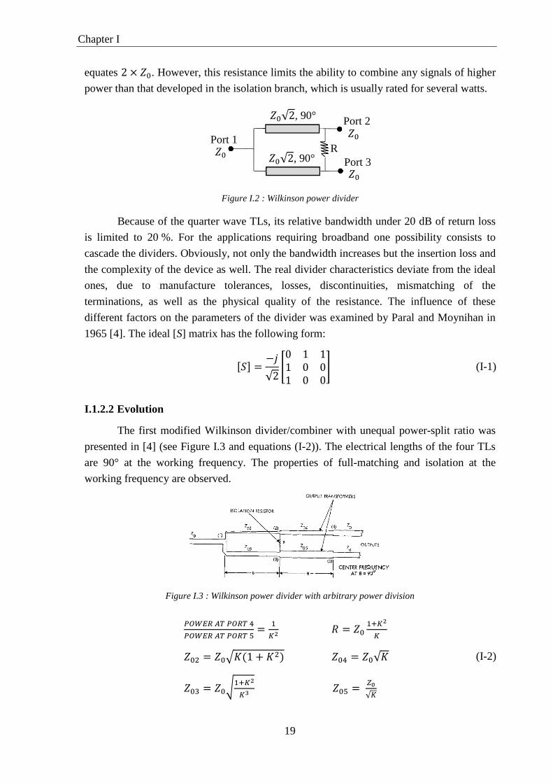
Chapter I
19
equates 2 . However, this resistance limits the ability to combine any signals of higher
power than that developed in the isolation branch, which is usually rated for several watts.
Figure I.2 : Wilkinson power divider
Because of the quarter wave TLs, its relative bandwidth under 20 dB of return loss
is limited to 20 %. For the applications requiring broadband one possibility consists to
cascade the dividers. Obviously, not only the bandwidth increases but the insertion loss and
the complexity of the device as well. The real divider characteristics deviate from the ideal
ones, due to manufacture tolerances, losses, discontinuities, mismatching of the
terminations, as well as the physical quality of the resistance. The influence of these
different factors on the parameters of the divider was examined by Paral and Moynihan in
1965 [4]. The ideal [S] matrix has the following form:
= √2 0 1 11 0 01 0 0 (I-1)
I.1.2.2 Evolution
The first modified Wilkinson divider/combiner with unequal power-split ratio was
presented in [4] (see Figure I.3 and equations (I-2)). The electrical lengths of the four TLs
are 90° at the working frequency. The properties of full-matching and isolation at the
working frequency are observed.
Figure I.3 : Wilkinson power divider with arbitrary power division
= !"# = !$"#"
= %&'1 ( &) = √&
* = +!$"#", = -.√"
(I-2)
Port 1
√2, 90°
Port 2
Port 3
R √2, 90°

Chapter I
20
However, when the power dividing ratio is higher than 3 (& / 3), TLs with very
high characteristic impedances are required. Some popular TLs with potentially very high
characteristic impedances, such as microstrip or CPW, become too narrow to be realized
practically. The high characteristic impedance can be realised by using a meander-shaped
defected ground structure (DGS) [5]. Nevertheless, the increase of impedance in such a
manner is limited. The rectangular-shaped defected ground structure is also effective for the
realisation of high characteristic impedances [6]. In [7] the high characteristic impedances
for a 5:1 unequal power divider were realized by suing offset doubled-sided parallel-strip
lines (DSPSL). DSPSL-to-microstrip transitions have to be employed at the three ports,
which inevitably introduces additional insertion loss and increases the circuit size. The
grooved substrate microstrip method could be used to realize high characteristic impedance
as in [8]. But this grooved substrate microstrip is difficult to be fabricated, compared to
traditional microstrip. In [9] the high characteristic impedance TLs were replaced by T-
shaped structures, in order to decrease the characteristic impedances towards more suitable
values. In the case of the 4:1 unequal divider designed, the highest characteristic impedance
was 97 Ω and the lowest 43 Ω instead of 158 Ω and 35 Ω for the conventional unequal
divider.
I.1.2.3 Striking applications
I.1.2.3.a Feeding network
The Wilkinson power divider is the basic device for many applications. In [10] and
[11], it was used as a feeding circuit for antenna arrays beam forming. In [10] one power
divider feeds two antennas and used stepped-impedance open-circuited radial stubs to
achieve good operation within a ultra-wide band. In [11] two power dividers in parallel
were connected at the outputs of a first one to feed an array of four antennas as shown in
Figure I.4. Phase shifters between the Wilkinson power dividers and the antennas enable
beam-steering. In both cases, the measured input reflection coefficient (!!) is
below -10 dB, in the band 4-14 GHz for [10] and 1.8-2.1 GHz for [11], respectively.
Figure I.4 : Electronic passive vertical beam scanning with Wilkinson dividers and phase shifters.

Chapter I
21
I.1.2.3.b Balun
If a phase inverter is placed in series with one of the two quarter wave TLs of the
Wilkinson power divider, as in Figure I.5, the 180° relative phase difference obtained
between the two output ports makes its use as a balun possible. The output ports of the
modified Wilkinson power divider stay close to each other. We will see soon this is a great
advantage comparing to the rat-race balun. However, the resistance R, mandatory for
isolation and output matching, must be removed. Indeed, the 180° relative phase difference
between the outputs would create a permanent flowing current through the resistance and
would increase considerably the losses. When removing this resistance, isolation and output
ports matching are degraded in such a way that the component cannot be used anymore as a
combiner. Nevertheless, it is still remarkably suitable for differential power amplification.
This device, performed at the IMEP-LAHC, is totally novel. It has been designed and
measured in a 65 nm CMOS technology and will be described in detail in chapter II. It is
not referenced herein since the final version is an optimised case of Figure I.5.
Figure I.5 : Modified Wilkinson divider with phase inverter for balun application.
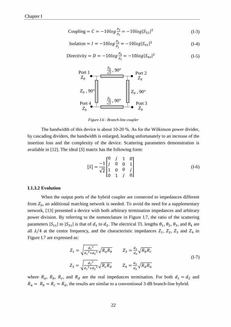
I.1.3 Branch-line coupler
I.1.3.1 Presentation
The branch-line coupler or 90° hybrid coupler is a particular case of a directional
coupler. It is a four ports network where coupling factor is -3 dB and phase relationship
between the output ports is 90°. The ideal coupler is lossless and matched at all ports.
Compared to the Wilkinson power divider, it does not need any resistance for ports
matching, but requires a fourth port. The branch-line coupler is composed by four quarter
wave TLs of characteristic impedances for the vertical TLs and √2⁄ for the horizontal
ones in a system as shown in Figure I.6. Incident power at port 1 separates between port
2 (the through port) and port 3 (the coupled port), but no power flows through port 4 (the
isolated port). Similarly, incident power at port 2 will couple to ports 1 and 4, but not 3.
Thus, ports 1 and 4 are decoupled, as are ports 2 and 3. The fraction of power coupled from
port 1 to port 3, named coupling (C), is given by (I-3). The leakage of power from port 1 to
port 4 is given by (I-4) and is named isolation (I). To conclude, the directivity (D), which is
the ratio of the power delivered to the coupled port and the isolated port is defined as
D = I – C (dB) or by (I-5).
Port 1
√2, 45°
√2, 90°
Port 2
Port 3
phase
inverter
√2, 45°
Chapter I
22
Coupling = 2 = 10345 ,6 = 10345|*!| (I-3)
Isolation = 8 = 10345 96 = 10345|!| (I-4)
Directivity = : = 10345 9, = 10345|*| (I-5)
Figure I.6 : Branch-line coupler
The bandwidth of this device is about 10-20 %. As for the Wilkinson power divider,
by cascading dividers, the bandwidth is enlarged, leading unfortunately to an increase of the
insertion loss and the complexity of the device. Scattering parameters demonstration is
available in [12]. The ideal [S] matrix has the following form:
= 1√2 ;0 0 1 00 11 00 1 0 0< (I-6)
I.1.3.2 Evolution
When the output ports of the hybrid coupler are connected to impedances different
from , an additional matching network is needed. To avoid the need for a supplementary
network, [13] presented a device with both arbitrary termination impedances and arbitrary
power division. By referring to the nomenclature in Figure I.7, the ratio of the scattering
parameters |!!| to |*!| is that of =! to =. The electrical TL lengths >!, >, >*, and > are
all ? 4⁄ at the centre frequency, and the characteristic impedances !, , * and in
Figure I.7 are expressed as:
! = + A6#A6#$A##% B C = A6A#% C D * = + A6#A6#$A##% D A = A6A#% A B
(I-7)
where B, C, D, and A are the real impedances termination. For both =! = = and B = C = D = A, the results are similar to a conventional 3 dB branch-line hybrid.
Port 1 Port 2 -.√ , 90°
-.√ , 90°
, 90° , 90°
Port 4 Port 3

Chapter I
23
Figure I.7 : Branch-line coupler with both arbitrary termination impedances and arbitrary power division
I.1.3.3 Striking applications
I.1.3.3.a Coupling for frequency mixing
Mixers are frequency translation devices. Thanks to a local oscillator (LO), they
allow the signal conversion from a high frequency (RF) to a lower intermediate frequency
(IF or baseband), and inversely. In down-conversions, hybrids as well as rat-races may be
used as functional passives to bring the RF and LO signals towards the non-linear active
component. In [14], a 138 GHz down-conversion mixer with a branch-line coupler was
developed. It was based on a 90 nm CMOS technology. As shown in Figure I.8 the branch-
line coupler converts the separated RF and LO input signals into two RF-LO combined
signals, which were injected into M1 and M2 that basically operate as independent mixers
and generate the IF signals. Although at 138 GHz a quarter wavelength line, equivalent to
one edge of the coupler, becomes shorter than 300 µm on silicon substrates, the size is still
reduced with specific techniques such as capacitive open-stub loading (non-visible here).
This miniaturization technique will be explained with more details further in this chapter.
Figure I.8 : Down-conversion mixer with branch-line coupler
I.1.3.3.b Reflection Type Phase Shifting
When connecting the output ports 2 and 3 of a branch-line coupler by two identical
reflective loads, a reflection type device is obtained between ports 1 and 4. If Γ is the
reflection coefficient at ports 2 or 3, the phase shift between ports 1 and 4 is equal to the
phase of Γ plus 90°; such device is so called Reflection Type Phase Shifter (RTPS). Figure
I.9 shows the block diagram of a typical RTPS with the impedance value of the reflective

Chapter I
24
loads denoted as F. If F is purely reactive, there is no power lost in the reflective loads so
that the whole power is coupled to the output. The main advantage of this configuration is
that input and output impedance matching is preserved, whatever the phase shifting is, as
long as the coupler is terminated with identical reflective loads. Any load which can
provide an impedance mismatch can produce reflections. However, to get better
performance, which means high phase shifting with low loss, different kinds of modified
loads were compared. In chapter IV, devices with optimised loads are achieved and
measured in a PCB technology with state-of-the-art performances. Simulations in a CMOS
technology show excellent performances, to be confirmed soon by measurements.
Figure I.9: Block diagram of a RTPS
I.1.4 Rat race coupler
I.1.4.1 Presentation
The rat-race coupler or hybrid ring directional coupler is a lossless reciprocal four
ports network. The conventional circuit is schematized in Figure I.10. It comprises three
90° branches and one 270° branch. The characteristic impedance of the ring branches
should be √2 times the characteristic impedance of the ports terminations with the purpose
of impedance matching at all ports.
Figure I.10 : Rat-race coupler
Historically, the first hybrid ring was described by Tyrrel in 1947 [15]. As a power
divider, the rat-race coupler can be used for in-phase operation and 180° out-of-phase
operation. However some of the components described herein are much more suitable and
compact for in phase power division. Consequently, the rat race coupler is mainly used for
180° out-of-phase. For this application, a signal injected at port 2 divides evenly between
ports 1 and 4 with 180° phase difference, meanwhile port 3 keeps isolated. As a power
90° BRANCH
LINE COUPLER
GH GH
IN
OUT
Port 1 Port 3 ? 4I
√2 Port 2
Port 4
? 4I ? 4I
3? 4I

Chapter I
25
combiner, signals are simultaneously injected in phase at ports 2 and 3, summing at port 1,
and subtracting at port 4. Consequently, ports 1 and 4 are referred to as Σ and ∆,
respectively. By contrast, if signals injected at ports 2 and 3 have a 180° phase shift, sum
and difference result inversely at ports 1 and 4. The bandwidth of this device is less than
25 %; improvement can be obtained by the addition of a fifth port. Scattering parameters
demonstration is available in [12]. The [S] matrix has the following form:
= √2 ;0 1 1 01 0 0 11 0 0 10 1 1 0 < (I-8)
I.1.4.2 Evolution
In 1961, [16] gave the design equations of a rat-race coupler with any degree of
coupling. These equations are detailed in (I-9) with J! and J the normalized admittances
and ai and bi the incident and reflected waves at port i, respectively, as in Figure I.11.
Figure I.11 : Rat-race with any degree of coupling
J! ( J = 1 K*K = JJ! K!K = JJ!
(I-9)
In 2007, Mandal and Sanyal proved that there is more than one solution in terms of
electrical lengths and characteristic impedances to bring to a lossless, isolated and full-
matched component. Indeed, in [17] it is shown that an infinite number of solutions exist
for coupler design at a given frequency. For all the solutions, characteristic impedances are
less than the conventional √2. Theoretically, the characteristic impedance of the ring can
be chosen between 0 and 70.7 Ω in a 50 Ω system. For each value, two ring electrical
lengths are addressable, one giving a total ring electrical length higher than 1.5 λ and one
lower. The drawback is the bandwidth strengthening further and further with the decrease
of the total electrical length.

Chapter I
26
I.1.4.3 Application
The main application of the rat race coupler is the balun function, used for instance
in balanced mixers as in [18]. The single balanced mixer gets use of a microstrip rat race
hybrid and two GaAs Schottky diodes, in the configuration given in Figure I.12. The LO
and RF signals are mixed in these diodes and are isolated by the rat-race. The IF port is
isolated from both the RF port and the LO port by the low-pass filter. The RF chokes
provide a tuning mechanism and prevent the RF signal from leaking into ground.
Measurement results show that conversion loss is less than 13.5 dB from 90 GHz to
97 GHz. Such mixer can be widely used in communication and radar systems in the mmW
range.
Figure I.12 : Configuration of the rat-race balanced mixer [18].
Another application of the rat race as a balun is the differential measurement as
presented in [19]. The purpose is to measure the gain and noise performances of differential
amplifiers by using single-ended measurements. Ideally, the input balun B1 shown in
Figure I.13, equally splits the signal along two 180° out-of-phase branches. The behaviour
of the output balun B2 is equivalent, although combining the output signals from the
amplifiers A. Baluns to characterize a differential amplifier allow the use of conventional
two ports measurement equipment.
Figure I.13: Measurement procedure of a differential amplifier using baluns.

Chapter I
27
I.2 Reflection Type Phase Shifter
I.2.1 Principle and theory
The first Reflection Type Phase Shifter (RTPS) was proposed in 1960 by Hardin et
al. [20]. The RTPS is composed by the branch-line coupler given in Figure I.7 with equal
power split loaded by two identical varactors as in Figure I.14. The usual input and
isolation ports of the branch-line coupler alone, ports 1 and 2 in Figure I.14, have a port
impedance of , whereas the usual through and coupled ports have a port impedance of . The input signal is divided into two parts. Each part is reflected by a reflective load, to
finally combine at the last port.
Figure I.14 : RTPS loaded by varactors
The calculation of the transmission parameter !with the S matrix of the branch-
line coupler loaded by the variable impedances FLLL easily brings to:
! = ΓL (I-10)
with ML the reflection coefficient between the outputs of the branch-line and the loads
defined as:
ML = FLLL FLLL ( (I-11)
Considering the load FLLL as an ideal varactor 1 2N⁄ , the magnitude of the transmission
parameter ! is 1, which means that all the power is transmitted, while the phase depends
on the reflection coefficient ML and so, on the load FLLL. The principle of the RTPS is
demonstrated. Intentionally, the two following sub-parts which detail the theoretical
equations for loss and phase shift are not referenced. To our best of knowledge, the analysis
throughout the literature was not enabling to enlighten the compromise between minimized
losses and maximized phase shift. The following demonstrations are thus totally novel.
I.2.1.1 Insertion loss
In practice the load is not ideal and leads to losses. To represent losses, a resistance
R representing the loss was connected in series with 1 2N⁄ . FLLL can be written as:
Port 1 +-.-O , 90°
, 90° , 90°
Port 2
FLLL
FLLL +-.-O , 90°

Chapter I
28
FLLL = ( 12N = 1 ( // = '1 ) (I-12)
with Q (I-13) the quality factor of the varactor.
= 1 ∙ 2 ∙ N (I-13)
Under these conditions, the reflection coefficient ΓL is:
ΓL = FLLL FLLL ( = '1 ) '1 ) ( = 1 1 ( = 1 R 1 ( R (I-14)
with R = -O .
The magnitude of !is thus given by:
|!LLLL| = |ΓL| = ST1 U ( T1 ( U ( = V'1 R) ( '1 ( R) ( = S1 ( T1 R U1 ( T1 ( R U (I-15)
According to (I-15), R has to be much greater or much lower than 1 to get |!LLLL| close to 1
and so to reduce the insertion loss. If = (for the conventional branch-line coupler),
since and R are both fixed values, this condition cannot be met for lossy varactors with
the simple configuration given in Figure I.14. Looking at R = -O , it is straightforward that
by increasing , the condition R ≫ 1 is roughly met and therefore the insertion loss is
reduced. In accordance with the formulas given in (I-7), may take any desired value
while the branch-line coupler given in Figure I.14 would keep equal split and matched ports
1 and 2.
I.2.1.2 Relative phase shift
According to (I-10) and (I-14) the phase of the transmission parameter ! of the
RTPS is:
XY#6 = Z2 ( [\5'ΓL) = Z2 ( [\5 ]1 R 1 ( R ^= Z2 ( [\_`abc/'1 R)d ( [\_`abc/'1 ( R)d (I-16)
Among the two possible solutions for minimizing the insertion loss, the only one
leading to a variable phase according to Q and so to C, is a R much greater than 1. Indeed,
with R ≫ 1: XY#6 ≈ Z2 ( 2 ∙ [\_`ab'/R) = Z2 ( 2 ∙ [\_`ab ] 1f ∙ 2 ∙ N^ (I-17)

Chapter I
29
We named 2ghi and 2gBj the minimum and maximum values of the varactor. The
relative phase shift calculated as XY#6'klmn) XY#6'klop) is:
∆X ≈ 2. s[\_`ab ] 1 ∙ 2ghi ∙ N^ [\_`ab ] 1 ∙ 2gBj ∙ N^t (I-18)
Theoretically, if the condition R ≫ 1is checked and if the varactor varies between 0
and +∞, X could reach 180° without insertion loss. However, varactors have a limited
range so that only a maximum relative phase shift may be reached corresponding to a fixed
value of . The equation (I-18) is derived according to and fixed equal with 0 in order
to find the value of leading to the maximal X. The obtained equation is given in (I-19),
and is consequently the condition to respect to get the maximal X, considering that R ≫ 1.
1 = + 12ghi. 2gBj. N . (I-19)
To reduce the insertion loss, has to be as high as possible whilst to get the
highest relative phase shift the equation (I-19) has to be verified. For a given varactor, two
different criteria have to be met by only one variable. In consequence, it is not possible to
benefit simultaneously from the lowest loss with the highest relative phase shift. A
compromise between these two characteristics has to be found. The next part illustrates this
case with a practical example.
I.2.1.3 Practical example with non-ideal varactor
Let’s choose a varactor with a capacitor value C in the range [1-5] pF with a
parasitic resistance R of 2 Ω at 2 GHz. According to (I-19) has to be fixed to 35.6 Ω to
get the maximal relative phase shift. Table I.1 sums up the calculated performances of two
RTPS realized with ideal hybrid couplers, taking into account only the parasitic resistance
R of the load. For one RTPS = 35.6 Ω, chosen to get the maximal relative phase shift,
and for the other one = 100 Ω, chosen as high as possible to respect R ≫ 1while taking
into account standard technology limitation.
ZT
(Ω) κ
Approximate uv
according to (I-18)
(°)
Exact uv
according
to (I-16)
(°)
Max. insertion loss
according to (I-15)
(dB)
FoM
(°/dB)
35.6 17,8 80.57 83.53 0.81 75.3
100 50 58.79 58.94 0.34 92.1
Table I.1 : RTPS performances with simple capacitive reflective load.
The figure-of-merit (FoM) of a phase shifter is defined as the relative phase shift
over the maximum insertion loss. It would not be accurate to calculate the FoM only taking
into account the loss due to R, if we consider that these circuits were fabricated on a

Chapter I
30
dielectric substrate with tan δ = 0.0027, the insertion loss added by the branch-line coupler
is estimated to about 0.3 dB. So the FoMs presented here take also into account the
insertion loss induce by the branch-line coupler.
With = 35.6 Ω, the relative phase shift is about 83° with 0.81 dB of insertion
loss leading to a FoM of 75.3 °/dB. As expected, with = 100 Ω the insertion loss is
lower with 0.34 dB but the relative phase shift as well with 59°. The FoM is higher with
92.1 °/dB. We can notify that the criteria R ≫ 1is respected in both cases, because the error
between the approximate X and the exact one is less than 4 %.
I.2.1.4 Conclusion
The ideal RTPS is lossless and has a phase controlled by the loads connected at the
branch-line output ports. Due to the limited range and the parasitic resistance of the varying
loads, the performances of the phase shifter are getting worse. With the flexible output port
impedance of the branch-line coupler, it is possible to find different values than the
classical 50 Ω in such a way that performances can be improved. It will be a compromise
between the relative phase shift and the loss level. However, in this configuration the
maximum relative phase shift stays modest and not high enough for some applications. In
order to get more degrees of freedom than the only for better performances and
compromise, networks may be placed between the output ports of the branch-line coupler
and the varactors. As we have seen, the purpose is to get a value of different from R, so
the added network can be called a mismatching network. The next part introduces the most
usual modified reflective loads including mismatching network.
I.2.2 Modified reflective load
I.2.2.1 Serial inductance
A modified reflective load can be designed with one, two or even more varactors
depending on the targeted phase shift. As a general rule, the more varactors, higher the
phase shift. The simplest modified reflective load used as a mismatching network is a series
inductance with the varactor, also named series-resonating load. We will first explain the
advantages of this widely used reflective load before presenting mismatching networks
with or without inductance, but of higher complexity.
If the reflective load consists in a fixed inductance L in series with an ideal varactor
C as in Figure I.15, the reflective load becomes:
F = N ( 12N (I-20)

Chapter I
31
Figure I.15 : RTPS with inductive load.
The minimum and maximum values of F are reached for the extreme values of the
variable C. For this study, C and L are ideal, e.g. without loss, and C can reach any value in
the [0;+∞] range.
For 2 = 0: F = N ∞ = ∞ (L has no influence)
For 2 = (∞: F = N ( !$~ = N if = (∞, F = (∞
So X = 2. [\_`ab T~-. U [\_`ab T$~-. U = 2.(90 + 90) = 360°.
When adding a series inductance the maximum relative phase shift increases up to
360° as long as its value tends to be (∞. In practice the value of C and L are limited.
Hence the relative phase shift is much lower, so that a compromise should be found
between phase shift and insertion loss. This is shown in the state-of-the-art.
I.2.2.2 State-of-the-art at RF frequencies
I.2.2.2.a Reflective load with lumped inductance and one varactor
With an lumped inductance in series with a capacitor, a relative phase shift of 97°
with 1.5 dB of maximum insertion loss was measured at 2 GHz in [21]. The varactor range
value is [1.4-8] pF with a parasitic resistance of 2 Ω. The insertion loss variation for the 97°
is 0.4 dB. The relative phase shift is much below the 360° theoretical maximum one
calculated above. This is due to the limited range of values of the varactor and the finite
inductance value. Moreover, there is a compromise to make between the insertion loss and
the insertion loss variation. The outputs ports impedance of the branch line coupler is
50 Ω, leading to an impedance transforming ratio \- = ⁄ = 1. Still in [21], another
RTPS with the same reflective load was measured, but with = 12.5 Ω, e.g. \- = 4. In
that condition the relative phase shift is now 240° with 3.8 dB of maximum insertion loss
and an insertion loss variation of 2.2 dB. In counterpart of the increase of almost 150 % of
the relative phase shift, both the maximum insertion loss and the insertion loss variation
expanded. To reduce the insertion loss variation, a resistance of 82 Ω was connected in
parallel with the load, as shown in Figure I.16.
Port 1 -.√ , 90°
-.√ , 90°
, 90° , 90°
Port 2
F
F
D D

Chapter I
32
Figure I.16 : Reflective load proposed in [21].
This resistance smoothes the loss at its maximum value but does not modify the
relative phase shift. Indeed, concerning the device with , the maximal insertion loss is
still 3.8 dB but the variation of this characteristic dwindles as low as 0.1 dB. The return loss
is better than 20 dB. Figure I.17 shows the measured reflection coefficient of the three
presented RTPSs at 2 GHz.
Figure I.17 : Reflection coefficient of the three types of reflective load at 2 GHz.
These results confirmed that it is not possible yet to get a relative phase shift of 360°
with only one varactor in series with an inductance, due to their limited range. Other
variable reflective loads have been enfaced with several varactors in order to increase ∆X.
Some of them include a series inductance.
I.2.2.2.b Reflective load with lumped inductance and several varactors
In [22], a varactor was added before the reflective load previously presented in
Figure I.15, leading to a Π-shape as described in Figure I.18(a). The simulation Figure
I.18(a) shows that the impedance variation of is not centred anymore on the Smith chart
real axis. Consequently the relative phase shift is really small. Therefore, an impedance
transformation was added. On the Smith chart in Figure I.18(b), it can be seen that the
simulated relative phase shift becomes higher than 360° with the impedance transformation.
F

Chapter I
33
Figure I.18 : Simulated Impedance trajectory on the Smith chart. (a) Π-shape load without impedance transformation. (b) Π-shape load with impedance transformation.
This RTPS was implemented in a 0.18 µm CMOS technology at 2.45 GHz. The two
varactors have a capacitance range of [0.52-1.4] pF and [1.9-5.4] pF, resulting in a
measured relative phase shift of 340° with a maximum insertion loss of 12.6 dB and a loss
variation of 4 dB. With this topology the simulated relative phase shift shown that 360° can
be reached but the measurement result was limited to 341°.
In [23], the reflection loads are composed by two inductances in series with
varactors, interconnected by a quarter-wavelength TL, as shown in Figure I.19.
Figure I.19 : Reflective load proposed in [23].
Here again the resistance was used to smooth the insertion loss, and \- was
modified and fixed to 1.25. The measured maximum relative phase shift is 407° and the
insertion loss is 4.6 dB at 2 GHz with a variation of 0.4 dB. The phase shifter was realized
with silicon varactors of a [1.4-8] pF capacitance range and an average 2 Ω resistance.
I.2.2.2.c Reflective load without lumped inductance
It is also possible to get 360° of relative phase shift with a reflective load without
inductance. The reflective load suggested in Figure I.20 by [24] consists in two shorted
transmission-line stubs connected in series with the varactors. Those two parallel arms are
interconnected with a quarter-wave TL. It increases both the total amount and the linearity
of the phase shift. The phase shifter showed a total phase shift of 380° and a maximum
insertion loss of 5.3 dB with a variation of 1.6 dB at 10 GHz. The high insertion loss is
mainly due to the GaAs beam-lead varactor diodes which exhibit a 5.5 Ω parasitic
resistance.
(a) (b)

Chapter I
34
Figure I.20 : Reflective load proposed in [24].
In [25], 6 varactors were used in each reflective load. F is shown in Figure I.21.
Each one of the seven TL is 50-Ω quarter-wavelength arms with a varactor diode at every
node. All the varactors are similar, with a [0.2-1.1] pF capacitance range. The relative phase
shift is really high with 500°. The maximum insertion loss is 3.5 dB with 2.5 dB of
variation. The main drawbacks of this topology are the big area needed due to the numerous
quarter-wavelength TLs and the cost with the use of 12 varactors for one RTPS.
Figure I.21 : Reflective load proposed in [25].
I.2.3 Branch-line coupler substitution
The above literature review showed that all of the papers that dealt with the RTPS
assumed by default that the coupler, which is the backbone of the phase shifter, is a branch-
line coupler. However, the Lange coupler or quarter-wavelength coupled lines coupler can
be used instead, particularly in order to increase the bandwidth. The RTPS presented in [26]
consists in a CPW Lange coupler with 3-dB coupling and, as a reflective termination, a
combination of two interdigital capacitors in series with an inductor. The relative phase
shift is 95° at 2.5 GHz with a 96 % relative bandwidth determined for an input return loss
better than 10 dB, whereas it is about 10-15 % for a RTPS using a branch-line coupler.
[27] shows that a RTPS can be designed using less than one tenth of a wavelength
coupled structure if the mode impedances of that structure are chosen properly. At 2.2 GHz,
the relative phase shift is 373° with a bandwidth of 36 % under 10 dB of input return loss.
To achieve the maximum possible phase range across the required bandwidth, the odd-
mode impedance of the short coupled structure needs to be around 10 Ω, whereas the even-
mode impedance needs to be around 200 Ω. Thus, the optimized short-section design
requires higher even-mode impedance and lower odd-mode impedance than the values
needed in the traditional design method. To realize such extreme impedances, slotted

Chapter I
35
ground plane was used, which results in a reduction in the even-mode capacitor and, thus,
an increase in the even-mode impedance. Concerning the requirement for a range of low
odd-impedance values, it can be achieved by connecting a chip capacitor between the
middle points of the coupled lines. This capacitor has no effect on the even-mode circuit.
However, it increases the equivalent odd-mode capacitor of the coupled structure and thus
decreases the odd-mode impedance.
I.2.4 Applications
Phase shifters are used to adjust transmission phase in a system; they can be fixed
digital phase shifters or analogue variable types. They are key elements in phased arrays,
especially tunable phase shifters. They can be used to perform adaptive beam-forming or
beam-steering; they enable multi-beam operation and are also used in phase-modulation
communication systems. Recently, the demand for phased array systems operating at
millimetre-wave bands has increased owing to the applications of security, imaging, radars
(automotive), military surveillance and satellite communication. The RTPS is praised as a
low control complexity device (only one control voltage), owing good stability against
temperature changes and low sensitivity to process tolerances. Nevertheless, its main
advantage stays the independency between ports matching and phase tunability thanks to
the recourse of a four-port coupler which leads to design simplicity and high electrical
performance.
I.2.5 State-of-the-art review
Table I.2 : State-of-the-art of the RTPS in PCB technology.
Freq.(GHz)
Phase shift(°)
Average insertion
loss(dB)
Insertion loss
variation(dB)
Varactorrange(pF)
Parasiticresistance
(Ω)
Lumpedinductance
Returnloss (dB)
10 dB return lossbandwidth
(%)
Max. insertion
loss in the BW(dB)
Nb. ofvaractors
Type of RTPS
FoM(°/dB)
2 237 3.75 ±0.05 1.4 - 8 2Yes
(2.7 nH)-21 >10 >4.6 2
Branch-line
62.4
2 407 4.4
±0.1 for 360°
±0.2 for 407°
1.4 - 8 2Yes(-)
-20 >10 >5.8 4Branch-
line88.5
10 380 4.5 ±0.7 0.16 - 2.9 5.5 No -10 - - 4Branch-
line73.1
2.05 500 2.2 ±1.25 0.2 - 1.1 2 No -12 >10 >3.5 12Branch-
line142.9
[26] 2.5 95 1.6 ±0.4 1.35-4.2 <1Yes
(2.2 nH)-15 96 3.8 4
Lange coupler
47.5
[27] 2.2 373 2.5 ±0.75 0.6-4.8 2Yes
(1.7 nH)-13 36 4 2
Lange coupler
116.6
Ref.
[21]
[23]
[25]
[24]

Chapter I
36
Table I.2 summarizes the electrical performances and important characteristics of
the RTPS in PCB technology. The RTPS presented in [25] has the highest FoM with
142.9 °/dB but suffers from serious drawbacks as the big surface, the cost due to the
numerous varactors and a big variation loss. Other phase shifters reached high phase shift
as in [23] with 407° but it is worth to insist that there is no practical need for phase shift
over 360°. Some phase shifters have very small loss variation as in [21] but a high level of
loss and are not optimized to decrease it, leading to low FoMs.
I.3 Miniaturization techniques
Size reduction is an old but very important topic that runs throughout the design
procedure of microwave components from the first to the last stage. To get low cost and
competitive components, the shrinking of the occupied circuit area is essential and pressing
especially when considering integrated technologies like CMOS. Many efforts are carried
out to miniaturize the components. Among them, TLs miniaturization is one of the research
topics of major interest in the microwave range. TLs are the basis of any passive distributed
device and therefore proportional. Nevertheless, attention has to be paid to other
miniaturization techniques in parallel to TLs improvement. Thus in this section, several
techniques dedicated to exploiting miniaturization are described. The use of high-K
dielectrics was not addressed in this section, because it relates to specific substrates, and
cannot be transferred to integrated technologies.
Although other performances improvement such as harmonic suppression,
broadband or multiband techniques does not focus specifically on miniaturization, most of
them involve it, and, thus, should be included also in this discussion. Finally, it is worth
mentioning that striking references that illustrate the numerous solutions for miniaturization
mainly focus on the Wilkinson power divider, the rat-race coupler and the branch-line
coupler, that is to say the components studied during this thesis for power division, power
combining and reflection type phase shifting purposes.
I.3.1 Shunt-stub-based artificial transmission lines
The most promising strategy for miniaturization may be the shunt-stub-based
artificial TL. As an example, it has been developed as the T- and Π-shaped open-stubs in
[28]. The shunt-stub-based artificial TL which consists of series high-impedance microstrip
and bilateral low-impedance shunt stubs, as shown in Figure I.22(a), can be replaced by
shunt stubs with two sets of high-impedance branch-type stubs to become more flexible to
utilise the folding technique, as shown in Figure I.22(b). Thanks to the slow-wave effect
generated by the shunt stubs, this artificial TL can replace the ? 4⁄ TL of any device, with
an equivalent 90° electrical length at centre frequency, which results in a significant
miniaturization.

Chapter I
37
Figure I.22 : (a) A conventional TL and its π- equivalent shunt-stub-based artificial TL, (b) compact structure.
In [29], [30] and [31] this strategy was applied a Wilkinson power divider, a branch-
line coupler and a rat race coupler, respectively. [29] occupies 14.7 % circuit size compared
to the conventional structure, [30] occupies 8 % and [31] only 3.9 %. The drawback of this
feature is the stubs characteristic impedance that can be high with non-reachable values in
an integrated technology. In the previous papers the characteristic impedance may be as
high as 110 Ω. In integrated technologies, values above 70 Ω are unattainable when
considering microstrip TLs.
I.3.2 Meander and Fractals
The space-filling behaviour of the folding technique has proven to be beneficial in
the design of small size devices. It is somewhat similar to the space-filling nature of
meanders [32] and fractals [33], applied to a rat-race and a branch-line coupler. Fractal
geometry is an essential and typical technique with its simple miniaturization mechanism
arising from the high degree of meandering and segment compression introduced during the
space-filling process. The performance of fractal-shaped devices has been demonstrated
without any performance deterioration in various publications. However, it should be
highlighted that the small fractal segments encountered in the second- or even higher-order
iterations deserve consideration [33].
I.3.3 Phase inverter
The 270° TL needed with the conventional rat-race coupler is the main reason for its
big surface. In 1968, in [34], March replaced the three-quarter wavelength section by a pair
of equilateral and broadside-coupled segments of microstrip TL with an electrical length of
90°, having diametrically opposing short-circuited ends, thus creating a phase-reversing
network. Its purpose was to broaden the frequency band meanwhile reducing the rat-race
dimensions. In 1994 two 180° phase shifters were developed, one with coplanar striplines
in [35] and one with a CPW-slotline transition in [36]. In 1999, [37] showed a phase
inverter in a CPW topology with bonding wires. All these phase inverters are efficient in
the framework of the fabrication of uniplanar structures although their need for bonding
°equivalent
High-impedance Branch-type stub
(a) (b)

Chapter I
38
wires, but they are inefficient for non-uniplanar ones. Later, the concept was developed for
non-uniplanar structure as in [38] for a microstrip-CPW transition and even for microstrip
TLs in [39]. In [40], a phase inverter in a CPW topology was integrated in a CMOS back
end of line (BEOL). Figure I.23 shows two possible phase inverters in a CPW topology
compatible with CMOS BEOLs. The symmetrical one is represented in Figure I.23(a) and
the asymmetrical one in Figure I.23(b).
Figure I.23 : (a) Symmetrical and (b) asymmetrical CPW phase inverter.
I.3.4 Capacitor loading
To minimize the physical size of any device, lumped capacitors can load each port
as in [41] or distributed capacitors can be placed along the TL as in [42] for a Wilkinson
power divider, in [43] for a branch line coupler or in [44] for a rat-race coupler. [42] shrinks
the area to 47 % that of the conventional structure, [43] to 38 % and [44] to only 8 %.
Furthermore, the capacitor loading has good harmonic suppression performance due to its
intrinsic low-pass behaviour.
I.3.5 Stepped-impedance
The stepped-impedance is also a really popular method to reduce the size of a TL. In
[45] a periodic stepped-impedance was applied to a rat-race coupler. The reached relative
circuit size was only 21.5 % that of the conventional one. In [28], the concept was adapted
to a Wilkinson power divider. The conventional quarter-wave transformers were replaced
by a constant VSWR-type transmission-line impedance transformer (CVTs). Stubs can be
added at one or two extremities of these CVT in order to get a modified constant-
conductance-type transmission-line impedance transformer (MCCT). According to the
chosen topology, strong miniaturization can be obtained. It is possible to have CVT or
MCCT with electrical lengths smaller than the 90° needed in the classical Wilkinson power
divider. However, in that case, more complex isolation circuit is required to keep perfect
isolation and matching at the outputs. The same author describes several design of isolation
circuit in [47].
I.3.6 Slow-wave transmissions lines
The main drawbacks of the classical TL such as the microstrip TL or the coplanar
TL in integrated technologies are their big surface and poor quality factor. Many different
Vias
(a) (b)

Chapter I
39
approaches have been studied for miniaturization, for instance the use of high relative
permittivity substrates or the use of lumped or semi-lumped components with interesting
results at RF frequencies [48]. However these approaches cannot be transferred to CMOS
technologies, especially in the mmW range. In conventional CMOS processes, classical
coplanar waveguides typically suffer from significant losses (1-2 dB/mm at 10 GHz)
mainly due to dielectric loss effects in the low-resistivity silicon substrate.
Slow-wave coplanar waveguides (S-CPW) are based on conventional CPW with a
patterned floating shield, consisting in floating metallic strips underneath the line as shown
in Figure I.24.
Figure I.24 : S-CPW topology.
Considering a classical S-CPW configuration, geometric parameters can be
classified in two groups: one linked with the main CPW and one with the added floating
strips.
• Parameters regarding the CPW:
W: signal strip
G: signal to ground gap
Wg: ground planes width
• Parameters regarding the floating strips:
SL: floating strips length
SS: floating strips space
h: dielectric thickness between floating strips and CPW
The two parameters SL and SS are chosen as the minimum allowed by the
technology. Concerning SL, this enables to reduce the eddy currents that take place in the
floating strips. Meanwhile the conventional conductive loss along these strips increases. Up
to now, it appears that an optimum between eddy currents and conductive losses is reached
for a SL lower than the minimum authorized by the technology [1]. Concerning SS, it has to
be smaller or equal to h so that the patterned floating shield acts as an electric wall. The
electric and magnetic fields propagation modes are shown in Figure I.25 assuming that any
substrate is replaced with vacuum. The signal strip is centred, with the ground strips on its
sides. The horizontal strip is the floating strip. In a 3D view, the length of the structure is
equal to a period SS+SL which is much smaller than a wavelength. This enabled to perform
SS
SL
W G
Si Substrat
h

Chapter I
40
the simulation with Flux 3DTM, a 3D quasi-static electric and magnetic solution software.
The electric field, given in Figure I.25(a), is concentrated between the CPW and the
floating strips so that the capacitance per unit length 2 is greatly enhanced. Moreover,
there is no field underneath the floating shield, which let us think there would be no electric
field neither if the substrate were the lossy silicon. On the contrary, the magnetic field, as
shown in Figure I.25(b), passes through the patterned ground, so that the inductance per
unit length is quite unchanged and stays similar to that of a conventional CPW.
Figure I.25 : Cross-section of the (a) electric field and (b) magnetic field of a S-CPW.
In this context, the phase velocity given in (I-21) decreases for the S-CPW as
compared to the CPW one. This explains the name: slow-wave. In the same manner,
according to (I-22) a high relative effective permittivity is reached.
= 1 % . 2 (I-21)
= 2. . 2 (I-22)
The quality factor, defined in (I-23) by [49] express the loss per degree of phase.
This definition is used all along this manuscript.
= 2 (I-23)
In practice, the quality factor of slow-wave TLs carried out in CMOS/BiCMOS
technologies is about 2 to 3 times higher than the classical TL one, as we will see further in
chapter II, and the characteristic impedance can reach 100 Ω, that is simply impossible with
other TLs, with a limitation of about 70 Ω. In [50] an efficient electric model was proposed
for S-CPWs. More details about this S-CPW are given in [1] and [2].
A classical dual behaviour resonator (DBR) filter was realized in [51] by associating
two different parallel open-ended stubs built with S-CPW. This topology of TL was also
used to realize matching networks in a power amplifier PA at 60 GHz in [52], fabricated in
the BEOL of a 65 nm CMOS technology. Power dividers were fabricated in [53] at 56 GHz
Electric field
Magnetic field
(a)
(b)

Chapter I
41
and 71 GHz without isolation and in [54] at 67 GHz with isolation. In [54] the authors did
not deal with a floating shield but applied toward the CPWs periodical loading stubs and
elevated signal conductors. The performances of those two power dividers are discussed in
the next section focusing on the state-of-the-art review at mmW.
I.4 State-of-the-art in millimetre-waves
With increased bandwidth and speed requirement for the wireless access and data
transfer, much effort has been carried out to extend the exploration of silicon-based passive
components to mmW applications. Commercially available silicon technology presents a
cost-effective option to realize highly integrated systems for applications such as local
multipoint distribution system (LMDS) at 36 GHz, multi-gigabit short range applications at
60 GHz, but also at 77 GHz for high performance long (76–77 GHz) and short (77–
81 GHz) range automotive radars, and future emerging RF-imaging applications above
100 GHz.
60 GHz radio has proved growing interest because of the worldwide availability of
unlicensed 9 GHz bandwidth. The major drives for commercial applications of 60 GHz
radio are SiGe BiCMOS and CMOS technologies. With further down-scaling and accuracy
of fabrication, it is expected that the CMOS/BiCMOS technologies may become an
alternative solution for circuits and systems implementation at millimetre-wave frequencies
and even towards terahertz.
I.4.1 Power divider with in phase outputs
Distributed passive components such as power dividers/combiners, which are used
extensively to split or combine power at board level are not considered practical at RF
frequencies to be used on a chip because of chip size limitations and cost factors. However,
in the mmW range, the wavelength becomes much smaller. With a relative permittivity of
about 4-4.2, the dimension of a quarter-wave length TL approximates the 650 µm at
60 GHz. As it is the case for any distributed passive component, the miniaturisation at
mmW is a mandatory topic to get low cost devices. Obviously, the size reduction should
maintain high level performance to keep highly competitive dividers/combiners.
Table I.3 summarize the state-of-the-art for power dividers at mmW frequencies. In
[55], a Wilkinson power divider was developed using asymmetrical shunt-stub and
meander-line leading to an ultra-compact device. In [54], the design was based to a slow-
wave elevated coplanar waveguide. The area was smaller than the one in [55] but its
working frequency is higher, with 60 GHz instead of 45 GHz in [55]. The worst value of
the input reflection coefficient !! of the power divider using this technique is -8 dB. Hence
matching is poor. Also in [54] 2.3 dB of extra insertion loss (that is to say excluding the
theoretical 3-dB power dividing ratio) were measured whereas only 0.9 dB were added in

Chapter I
42
[55]. The simple meander technique applied in [56] leads to a bigger surface but with only
0.5 dB of insertion loss at 60 GHz. The meander-line associated with a floating defected
ground structure in [57] induced 1.5 dB of extra loss with a middle area compared to the
other devices.
Table I.3 : State-of-the-art of power divider around 60 GHz.
Isolation is often desired in order to avoid reflected signals to propagate to other
paths in the system. In [55], [56] and [57] the isolation reaches respectively -19, -22
and -21 dB. In [54] isolation is only of -12 dB.
I.4.2 Power divider with quadrature outputs
At mmW frequencies, power-efficient quadrature generation based on a passive
approach has been widely adopted in I/Q direct-conversion transceiver, in the radio front-
ends of wireless systems, amplifiers, balanced mixers, and vector modulators because of
their versatile use. The realization of these couplers requires a large area because of the
utilization of quarter-wavelength TLs. Thus, it is essential to reduce the couplers size,
which significantly lowers the fabrication costs, keeping low insertion loss and good return
loss and isolation.
Table I.4 compares the state-of-the-art in terms of power dividers with quadrature
outputs at 60 GHz. The simple branch-line coupler with meandering in [58] adds the least
insertion loss with 1.5 dB, induces the best return loss and isolation but is much less
compact than the other topologies. Branch-line couplers with modified CPWs are studied in
[59] and [60]. The Lange coupler [40] leads to the most compact device with an area of
0.048 mm2. The difficulty with coupled lines, as in the Lange coupler, is that high even
characteristic impedance is needed. Values are usually unreachable in silicon
technology. In [40] a Thin Film MicroStrip TLs (TFMS) is used. The magnitude imbalance
between the outputs is less than 1 dB for any of these power dividers.
S11
(dB)S22 & S33
(dB)
[54]/90 nm CMOS
60slow-wave
elevated coplanar waveguide
-5.3 -8 -11 -12 -5.3 -6 -10 -11 0.051
[55]/90 nm CMOS
45asymmetrical shunt-
stub andmeander-line
-3.9 -21 -15 -19 -4.2 <-13 -14 -15 0.06
[56]/0.13 um BiCMOS
60 meander-line -3.5 -19 -17 -22 -3.7 <-17 <-17 -18 0.12
[57]/0.18 µm SiGe BiCMOS
60floating defected
grounding structureand meander-line
-4.5 - -16.5 -21 -4.3 - -16.5 -19 0.09
Ref./Tech.Isolation
(dB)
Max. insertion
loss(dB)
Min.isolation
(dB)
Area
(mm2)
In 20 % bandwidthReturn loss
Return loss Freq.(GHz)
TopologyInsertion
loss(dB)
S11
(dB)S22 & S33
(dB)

Chapter I
43
Table I.4 : State-of-the-art of power divider with quadrature outputs at 60 GHz.
I.4.3 Power divider with out-of-phase outputs
In the RF domain, both active and passive baluns are commonly used. For mmW
frequencies, nevertheless, the use of active structures becomes more troublesome as the
delay introduced by the transistors yields to a significant negative effect on the phase
balance of the balun output. Among passive circuits’ solutions, they can be realized with
lumped coupled inductors or transformers, or with distributed TL's based circuits. The key
issue for CMOS RFICs is the chip area. While in RF, say until one tenth of GHz, the use of
transformers is obvious and easy to implement, and on the other hand distributed circuits
are size consuming, the situation becomes different when dealing with frequencies of 60-
100 GHz and above. The design of the transformers becomes more difficult because of the
low efficiency of the coupled inductors, the insertion loss increases and the phase and
magnitude imbalance becomes difficult to control. This lumped approach needs the
development of very accurate electrical models taking into account all the parasitic
elements, in particular the capacitors. On the other hand, the design of TLs is made easier
because of less parasitics, and they are well suited for millimetre-wave devices.
Among the TL based baluns, two main structures are prominent: the Marchand
balun [61], [62], and the rat-race balun [40] and [63]. Marchand baluns combine two pairs
of coupled λ/4 lines, one of which is open-ended and the two others are shorted. Rat-race
baluns, adapted from rat-race couplers, are set by 4 ports in a circular disposition with a
total length of 3λ/2. Table I.5 compares the performances of several baluns realized with
the main structures.
[40]/0.13 µm SiGe BiCMOS
60Lange couper
with TFMS TLs5.5 19 (only S11) 15 1 0.5 0.048
[58]/0.13 µm SiGe BiCMOS
60 meandering 4.5 20 (only S11) 25 0.35 1.3 0.28
[59]/90 nm CMOS
60elevated-center
coplanar waveguide
5.5 15 17 0.7 2 0.10
[60]/90 nm CMOS
60slow-wave coplanar
waveguide6.2 12 25 0.8 0.3 0.083
Ref./Tech.Area
(mm2)
Freq.(GHz)
Topology
Max. insertion
loss(dB)
Worst return loss at any port
(dB)
Isolation(dB)
Magnitude imbalance
(dB)
Phase imbalance
(°)

Chapter I
44
Table I.5 : State-of-the-art of the baluns at 60 GHz.
I.4.4 Phase shifter
Phase shifters can be active or passive in nature. Active ones can be located in the
high or low frequency path of a transceiver. Phase shifters in the low frequency path tend to
be more complicated with larger surface area and higher power consumption. In this
approach, power consumption is a major concern as it can range from 20 mW to almost
1 W. 60 GHz active phase shifters limit the linearity of the front-end and may be prone to
saturation in presence of interferers or jammers and therefore passive designs are
preferable.
The passive phase shifter can be classified among three main types: the reflection
type, the switched-network approach, and the loaded TLs. The varactors allow the RTPS to
have a continuous and accurate variation of the phase. Nevertheless, the low quality factor
of the silicon varactors at mmW makes this kind of RTPS really lossy, as high as 7.5 dB for
180° in [65]. The use of lumped MEMS can improve the insertion loss, however, they still
remain high with 5.5 dB for only 135° of phase shift as reported in [66]. The switched-
network approach consists on switching different delay networks to obtain the required
phase delay. In [67] and [68], these networks were composed of simple TL sections.
Switched-path type phase shifters are inherently digital, and quickly become cumbersome if
a large number of phase states are desired. Devices such as phased arrays often require high
resolution in phase control, which would lead to a large and lossy digital phase shift
system. Another solution for the reflective network consists on periodically loading a high-
impedance TL with MEMS variable (or switched) capacitors [69] or varactors [70]. The
phase shift of the loaded line can be controlled by varying the capacitance of each period
(or a set of periods). Here again the varactors induce high loss, 12.5 dB for 156° in [70]
instead of 3.6 dB for 337° with MEMS. Table I.6 compares more in detail the performances
of the discussed phase shifters.
Through Coupled
[61]/0.18 µm CMOS
16.5-67 Marchand balun <-6 - -7 to -5 -8 to -5 180±5 0.06
[62]/0.18 µm CMOS
25-65 Marchand balun <-7 - -10 to -7 -9 to -6 180±10 0.55
[40]/0.13 µm SiGe BiCMOS
48-80 Rat-race <-10 <-18 -5 to -4 -6 to -5 184±2 0.11
[63]/0.13umBiCMOS
57-71 Rat-race <-14 <-16 -7.5 to -5.5 -6 to -4.5 180±30 0.28
[64]/0.13 µm CMOS
55-65 Transformer - - 180±5 0.05-7.5 to-4.5
Isolation(dB)
Phaseimbalance
(°)
Area
(mm2)
Magnitude imbalance
(dB)Ref./Tech.Freq.(GHz)
ArchitectureReturn
loss(dB)

Chapter I
45
Table I.6 : State-of-the-art of phase shifter around 60 GHz.
The maximum FoM of the phase shifters presented herein is about 90 °/dB for [67]
and [69]. However, the areas of these two devices are respectively 4 and 9.45 mm2 on a
quartz substrate which is unacceptable for a simple phase shifter in integrated circuit, even
in an interposer type technology with 3D integration. Such surface, and so such cost, will
eliminate these solutions for most of the applications. Among the moderate areas, the FoM
dramatically decreases down to around 25 °/dB for a maximal phase shift of 180° for RTPS
and 360° for switched-network approach.
I.5 Conclusion
The Wilkinson power divider/combiner (in phase), the branch-line coupler (in
quadrature) and the rat-race coupler (out-of-phase) has been selected and described because
of their efficiency and their popularity among the designers. They were first defined for
equal power split and 50 Ω ports impedance loading, but later on, their definition was
generalized to arbitrary termination impedances and/or arbitrary power division leading to
more freedom for their applications. The reflection type phase shifter, based on branch-line
coupler, is also explained and different types of reflection loads are compared. The state-of-
the-art is given at RF. The shrinking of these circuits area is an essential topic to get low
cost and competitive components, and it is even more pressing when considering integrated
technologies like CMOS. Shunt-stub-based artificial and S-CPWs, folding technique, phase
inverter, capacitor loading and stepped-impedance are usual ways to reduce the size of the
power dividers but also of any circuits using TLs and can be available to both PCB and
Ref./Tech.Freq.(GHz)
ArchitecturePhase shift(°)
Average insertion
loss(dB)
Insertion loss
variation(dB)
Returnloss (dB)
Return loss over a
10 % BW(dB)
Area
(mm2)FoM(°/dB)
[65]/130nm SiGe
60RT Varactor
MOS180 5.85 ±1.65 - - 0.18 24
[66]/quartz substrate
60 RT MEMS 135 4.25 ±1.25 -14 -13 3.15 24.5
[67]/quartz substrate
60 SL MEMS 269.2 2.5 ±0.5 -13 -12 4 89.7
[68]/90nm CMOS
60SL without small-size capacitor
360 12.5 ±2 <-10 <-10 0.28 24.8
[69]/quartz substrate
65CPW Loaded
MEMs337 2.8 ±0.8 -10 -10 9.45 93.6
[70]/65nm CMOS
60Differential TL loaded
MOS 156 9.25 ±3.25 -13 -11 0.2 12.5

Chapter I
46
silicon technologies. Finally, the state-of-the-art of the presented power dividers and phase
shifters working around 60 GHz is given.
It is really difficult to associate compactness, low insertion loss level and low
phase/magnitude imbalance at millimetre-wave frequencies for power dividers. In chapter
II the S-CPWs are used to design two baluns comprising a phase inverter, a branch-line
coupler and a Wilkinson power divider. Design is performed at 60 GHz in order to
highlight their potential as passive circuits. Among the various power divider applications:
balun, mixing, differential measurement…, feeding circuit for antenna arrays beam-steering
attracted our attention because of its structure. It is usually composed of Wilkinson power
dividers and reflection type phase shifters which are themself based on branch-line coupler.
Both Wilkinson power divider and reflection type phase shifter face limitations in CMOS
technology at millimetre-wave frequencies. The first one needs an isolation resistance in
order to work as a combiner but the latter induces unwanted parasitic and coupling,
moreover it suffers from a lack of characteristic impedance flexibility. A new solution is
proposed in chapter III, first on a PCB technology as a proof of concept and then at 60 GHz
in a CMOS technology. The second one does not offer high FoM which means high
insertion loss level. In chapter IV two solutions are provided, one in RF on a PCB
technology and another one at 60 GHz in a CMOS technology. All the proposed passive
devices at millimetre-wave frequencies were achieved with S-CPWs in order to improve
performances and compactness.

Chapter II
47
Chapter II : S-CPW applications
Performance and compactness are extremely important requirements for
components design, especially in integrated circuits where performance is limited by the
technology and costs are directly linked to the surface area. Many miniaturization
techniques, with their impact on the performance, have already been listed and described in
the chapter I. Here we are interested in the Slow-wave CoPlanar Waveguide (S-CPW). This
topology of transmission line (TL) has been under study for about six years in our
laboratory IMEP-LAHC and already proved its great interest, [50] to [53], and [71], to [73].
Its low insertion loss leads to quality factors between 2 and 3 times higher than the classical
TL one. Many development steps have been overcome: simulation, de-embedding,
parameters extraction, topology optimisation, physical circuit model and realisation of
simple circuits. The continuity of this development is now to enlarge the use of this type of
TL in more complex microwave passive circuits in order to improve their performances and
compactness.
A phase inverter in S-CPW, also presented as a miniaturisation tool in chapter I, was
simulated, fabricated and measured. To prove its broadband and compactness benefits, two
power dividers for balun application making requirement of a phase inverter were designed
and measured. These circuits were realized in the 65 CMOS technology by
STMicroelectronics.
In order to cover all the types of power dividers that had been considered in chapter
I, the slow-wave technique was also applied to two power dividers with in phase and in
quadrature outputs. The circuits are still under fabrication while writing my dissertation, so
only the simulation results are shown. The technology involved for those ones is the 55 nm
BiCMOS by STMicroelectronics.
At the beginning of this chapter, the simulation tool used for designing the TLs and
devices is mentioned and the de-embedding methods applied to the measured TLs, two
ports and four ports devices is explained. The performances and dimensions of the
simulated and/or measured TLs needed for the devices are presented and gathered
according to their back end of line (BOEL).
II.1 Simulation tool
The simulation results of the TLs were obtained thanks to the industry-standard
simulation tool HFSSTM provided by ANSYS. This software is a 3D full wave frequency
domain electromagnetic field solver based on the finite element method (FEM). HFSS
automatically generates mesh and solves Maxwell equations at several nodes of the
meshing. A big amount of random access memory (RAM) and long simulation time are

Chapter II
48
needed, particularly with our structures because of the huge difference between the smallest
and the biggest dimensions.
II.2 Calibration & De-embedding
The whole TLs and devices presented in this report were measured at the IMEP-
LAHC laboratory with a two ports 110 GHz vector network analyzer (VNA) ME7808C by
Anritsu or with a four ports 67 GHz VNA 8510C by Agilent Technologies. The first step of
a RF S-parameters measurement consists in calibrating the VNA, before placing the RF
probes on the circuit pads. In addition to the correction of the errors associated with the test
setup, the calibration step fixes the measurement reference planes. The LRRM (Line
Reflect Reflect Match) calibration method was applied because of its accuracy concerning
S-parameters until 110 GHz [74]. However, the calibration method does not correct the
interconnects parasitics (pads, TLs, tapers…) of the device under test (DUT). Considering
the high working frequency and the size of the device compared to the size of the pads, it is
mandatory to correct these parasitic effects by another step, named de-embedding, in order
to extract rightly the parameters of the DUT, the intrinsic device.
II.2.1 Two port devices
II.2.1.1 Transmission Line
To reduce the influence of the pads and eventually of the interconnects from pads to
TLs, the two lines method proposed by Mangan in [75] was applied in this work. To
compute de-embedding, two identical TLs of different lengths must be measured (3! / 3
for instance). The purpose is then to deduce the ABCD matrix (or transfer matrix) of a
fictive TL of length 3! 3 from the raw results of the two TLs. This matrix can be written
as:
[2:'6#) = ]['6#) '6#)2'6#) :'6#)^= ] cosh'3! 3) D sinh'3! 3)sinh'3! 3) /D cosh'3! 3) ^ (II-1)
From (II-1), it is then easy to extract the characteristic impedance D and the
propagation coefficient with equations (II-2) and (II-3).
D = V'6#)2'6#) (II-2)
= ( = arccosh'['6#))3! 3 (II-3)

Chapter II
49
One advantage of this de-embedding method is that the parasitics from the pads and
interconnects do not need to be known or approximated by a lumped-element network. On
the other hand, as all the TLs that have to be de-embedded have to be fabricated twice with
two different lengths, this method results in a big area.
II.2.1.2 Devices
Concerning the devices, the applied de-embedding principle is explained in Figure
II.1. Contrary to the S-matrix, the ABCD matrix offers the advantage of being chained. So
the purpose consists in calculating the ABCD matrices of the global device with pads and
interconnects (indexed as raw), and the pads and interconnects alone (indexed as pad and
TL, respectively). In our work, the used interconnects are TLs. Then, the raw ABCD matrix
can be written as in equation (II-4):
ABCD = ABCD. ABCDf . ABCD¡¢f. ABCDf . ABCD (II-4)
The determination of the ABCD matrix of the interconnects relies on the
aforementioned two lines method. The TL ABCD matrix is expressed as in (II-5) with the
parameters D and extracted thanks to the Mangan method.
] cosh') D sinh')sinh') /D cosh') ^ (II-5)
The pads are usually modeled by a lumped elements circuit, those elements are
determined thanks to a shorted !!_¤¥¦§ and an open !!_¦i pads measurements. Then the
ABCD matrices of the pads are determined from their lumped elements equivalent circuits.
In our specific case, with the pad dimensions and the considered frequencies below
110 GHz, the open measurement alone is enough to elaborate the model of the pad effect.
As the pad is considered as a one port circuit, with the reflection coefficient M = !! between the probes and the pad, it is easy to deduce the impedance of the pad thanks to the
equation:
S!! = BA– BA ( (II-6)
where is the impedance of the probes, here 50 Ω. The values of BA show a
capacitance effect. Consequently, the matrix of the pad has the form of a parallel
capacitance as:
s 1 01/BA 1t (II-7)
The raw S-parameters are simply converted to ABCD matrices [12]. The final
equation to calculate ABCD¡¢f with pads and TLs as interconnects is:

Chapter II
50
[ 2 :¡¢f = ªcosh') D sinh')sinh')D cosh') «f ! ∙ ª 1 01BA 1«
!
∙ [ BC D ∙ ª 1 01BA 1«!
∙ ªcosh') D sinh')sinh')D cosh') «f !
(II-8)
Then, it is easy to convert the ABCD matrix into a S matrix.
Figure II.1: De-embedding principle for two ports devices.
II.2.2 Four port devices
Concerning the de-embedding of a four ports device, the principle is similar to the 2
ports method except that classical S to ABCD and ABCD to S matrices conversion
formulas cannot be directly used since they are consistent only for two ports devices. These
formulas have thus been modified involving matrices instead of complex numbers. The
¬®¯°±² = ¬®¯³±´. ¬®¯µ¶. ¬®¯¯·µ. ¬®¯µ¶. ¬®¯³±´ (II-4)
Cascade of [ABCD] matrices
Matrices inversion and
calculation
¸¯·µ Conversion [ABCD]
to [S]
Zc (II-2) & γ (II-3) [75]
[ABCD] pad (II-7) [ABCD] TL (II-5) [ABCD] raw
Pad : S11_open
Interconnects : TL l 1 & TL l 2
Global device [S]raw
Measurement of [S]
Conversion [S]
to [ABCD] Z pad (II-6)
¬®¯¯·µ (II-8)

Chapter II
51
measured parameters of a four port S matrix are gathered in such a way that a two ports
matrix is created where the four parameters are not algebraic coefficients but matrices of
coefficients, as expressed in (II-9).
= ;!! ! !* !! * *! * ** *! * < = s!! !! t (II-9)
with
!! = s!! !! t ! = s!* !* t! = s*! *! t = s** ** t (II-10)
The equations between the voltage and current used in the ABCD matrix definition
(¹i, ºi) and the power waves of the S matrix definition (ai, Ki) are rewritten as follows:
• For [S] to [ABCD] conversion:
[1 = ¹1 ( 0812√0
[2 = ¹2 0822√0
1 = ¹1 0812√0
2 = ¹2 ( 0822√0
(II-11)
• For [ABCD] to [S] conversion:
¹1=√0'[1(1)¹2 = √0'[2 ( 2) 81= [1 1√0
82= 2 [2√0
(II-12)
In both cases [1 = a1a2, 1 = K1K2
, ¹1 = 12, 81 = º1º2 and [2 = a3a4, 2 = K3K4, ¹2 = 34, 82 = º3º4. is the common port termination, it is an algebraic value.
Therefore, the conventional development to calculate the conversion equations [S] to
[ABCD] or [ABCD] to [S] can be applied, paying attention to the matrices properties, as
the non-commutability. Thus equations (II-13) and (II-14) are derived:
• For [S] to [ABCD] conversion:
[ = 12 c'8d ( 11)21!'8d ¼22½) ( 12d = 02 c'8d ( 11)21!'8d ( ¼22½) 12d 2 = 120c'8d 11)21!'8d ¼22½) ( 12d
(II-13)

Chapter II
52
: = 12 c'8d 11)21!'8d ( ¼22½) 12d • For [ABCD] to [S] conversion:
12 = ¾¿[ ( 0 À! ( '20( :)!Á!¿[ ( 0 À! ¿[ 0 À '20 ( :)!'20 :)Ã
21 = 2 ][ ( 0 ( 20 ( :^! !! = '20( :) ][ ( 0 ( 20 ( :^! ][ ( 0 20 :^ '20 ( :)! 22 = ][ ( 0 ( 20( :^! ¿[ ( 0 20 ( :À
(II-14)
8d is the identity matrix of the second order. The ABCD matrices of the interconnects
and pads are obtained as previously explained, then cascaded and combined in order to get
only one matrix (pad + interconnect) for each port. After that, these matrices are re-
arranged into two ABCD matrices to be cascaded with the four ports global device
matrix. If the ports of the four ports matrix are named Ä!, Ä, Ä* and Ä, the ports of the two
ports equivalent device are Å! (including Ä! and Ä) and Å (including Ä* and Ä), as
described in Figure II.2.
Figure II.2 : Schematic of a four ports device measurement.
The ABCD matrix of the pad with interconnects at port number n is:
4 ports DUT
Port p1
Port p2
Port p3
Port P1 Port P2
a1
b1
a2
b2
b3
b4
a3
a4
Measurement reference planes with Z0
g matrix
Pads + Inter-
connects
Port p4 Pads + Inter-
connects
Pads + Inter-
connects
Pads + Inter-
connects
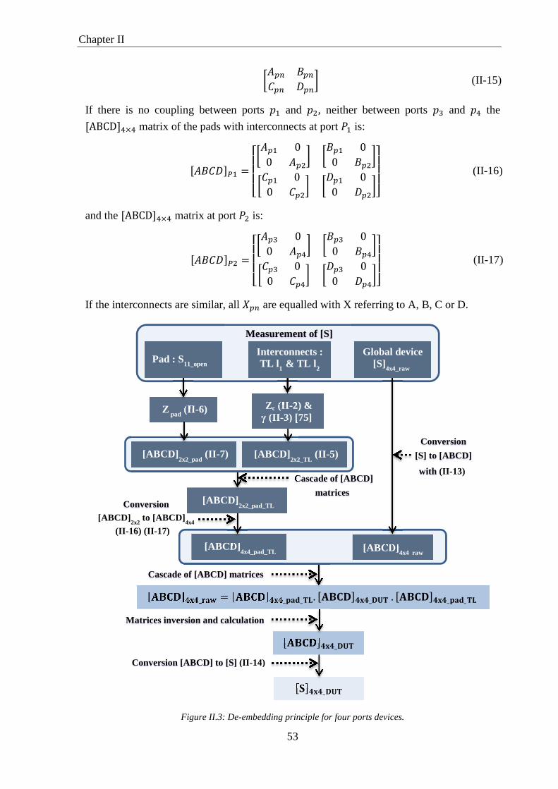
Chapter II
53
s[i i2i :it (II-15)
If there is no coupling between ports Ä! and Ä, neither between ports Ä* and Ä the ABCD matrix of the pads with interconnects at port Å! is:
[2:! = ÆÇÇÇÈs[! 00 [t s! 00 ts2! 00 2t s:! 00 :tÉÊÊÊ
Ë (II-16)
and the ABCD matrix at port Å is:
[2: = ÆÇÇÇÈs[* 00 [t s* 00 ts2* 00 2t s:* 00 :tÉÊÊÊ
Ë (II-17)
If the interconnects are similar, all Ìi are equalled with X referring to A, B, C or D.
Figure II.3: De-embedding principle for four ports devices.
Conversion [ABCD]
2x2 to [ABCD]
4x4
(II-16) (II-17)
¬®¯ÍÎÍ_°±² = ¬®¯ÍÎÍ_³±´_µ¶. ¬®¯ÍÎÍ_¯·µ. ¬®¯ÍÎÍ_³±´_µ¶
Cascade of [ABCD]
matrices
Matrices inversion and calculation
¸ÍÎÍ_¯·µ Conversion [ABCD] to [S] (II -14)
Zc (II-2) & γ (II-3) [75]
[ABCD] 4x4_raw
Pad : S11_open
Interconnects : TL l 1 & TL l2
Global device [S]4x4_raw
Measurement of [S]
Conversion
[S] to [ABCD]
with (II-13)
Z pad (II-6)
¬®¯ÍÎÍ_¯·µ
[ABCD]4x4_pad_TL
[ABCD]2x2_pad_TL
[ABCD]2x2_pad
(II-7) [ABCD]2x2_TL
(II-5)
Cascade of [ABCD] matrices

Chapter II
54
On the basis of the previous theory, it is now possible to follow the process
described in Figure II.3.
II.3 Stacks
The simulated and fabricated components in this report involve three different Back
End Of Lines (BEOL) from STMicroelectronics company: the 65 nm and 28 nm CMOS
technologies and the 55 nm BiCMOS technology. Figure II.4(a) compares the various
stacks and Figure II.4(b) is a SEM (scanning electron microscopy) picture of the 65 nm
CMOS technology BEOL by STMicroelectronics, from [76]. In those BEOLs at least three
thick metal layers (M6, M7 and Alucap) are available at the upper levels, which have for
purpose to decrease the resistive loss. In the 55 nm technology, an eighth level (M8) of very
thick metal is even added before the aluminum cap. In the lower levels (between levels M1
and M5) the dimensions significantly decrease in terms of thickness and authorized small
widths for metallic paths. The decrease of the metal layers thickness also leads to smaller
dielectric thicknesses, and concludes to thin metallic layers closer to the lossy substrate
which decreases the quality factor of the passive components built in these layers.
Figure II.4 : (a) Comparison of the STMicroelectronics BEOL stacks used during this work. (b) SEM picture of the 65 nm CMOS technology BEOL from STMicroelectronics [76].
II.4 Simulated and measured transmissions lines
As it was the first time that S-CPWs were realized in these BEOLs, it was important
to study the influence of the different available stack configurations. This enabled to,
firstly, select TLs with the best quality factors, and, secondly, to measure the TLs further
used in the devices in order to verify their characteristics and compare them with the
simulation. In the 65 nm CMOS technology, devices composed of S-CPW and microstrip
TLs were fabricated and measured. In the 28 nm CMOS and 55 nm BiCMOS technologies,
(a) (b)

Chapter II
55
components with S-CPW were also designed and simulated but the chips containing them
are still in the fabrication chain which compels us to present only the simulated results.
II.4.1 Study of the quality factor of the S-CPW in the 65 nm CMOS technology
The characteristic impedance D = % 2⁄ and the effective relative permittivity of a TL depend on the capacitance per unit length 2, and so depend on their signal
width W. The influence of W is even more significant in the case of S-CPWs because of the
high value of 2. When W increases, 2 increases, leading to the increase of the insertion
loss in the floating strips, whereas the series resistance decreases leading to the decrease of
the insertion loss in the signal strip. Hence both effects act oppositely. Therefore it is not
easy to fix the right W. It is also not easy to determine which stack configuration and
dimensions lead to the best compromise / . In this part, three stack configurations
are compared at 60 GHz for S-CPW in the 65 nm technology, the CPW part is respectively
simulated in M7, M7-Al and Al layer, as shown in Figure II.5. To make the study easier,
the floating strips (FS) level is fixed to M5 layer for all configurations.
Figure II.5: Compared stack configurations for S-CPWs.
The de-embedding method applied here is the one of HFSS with 15 µm of CPW
feeding. First simulations, not reported herein, showed that the quality factor Q increases
with the gap G and so with the total width of the TL. However the total width cannot be too
large otherwise the physical length saved with the high would be wasted by a too
wide TL. This is why the maximal width was fixed to 100 µm. The width of the ground
strip was fixed to 12 µm because of design constraint. When the ground is enlarged, there is
only a small variation in the characteristic impedance. Figure II.6 gives the effective
relative permittivity, the insertion loss and the quality factor versus the characteristic
impedance D for the three different stacks and different dimensions, for a total width equal
to 100 µm. The shape of the symbols indicates the stack configuration and the colour the
dimensions of the TLs. The characteristic impedance range is 38-100 Ω.
65 nm BEOL
CPW M7 FS M5
CPW M7-Al FS M5
CPW Al FS M5
Al
M5
M1
M7
M6

Chapter II
56
Figure II.6 : Parametric study for three stack configurations. (a) Effective relative permittivity, (b) insertion loss and (c) quality factor versus characteristic impedance.
For each couple of W-G, the CPW in Al layer shows a higher D and a lower ,
as shown in Figure II.6(a), and a lower insertion loss, as shown in Figure II.6(b). Indeed,
there is a greater distance between the floating strips and the ground strips and so a lower
capacitance per unit length as shown in Figure II.7(a). D and are slightly shifted for
the stack configurations M7 and M7-Al whereas the capacitances per unit length are
similar, as shown in Figure II.7(a). The inductance per unit length is however reduced when
the Al layer is stacked with M7 as shown in Figure II.7(b) and has for consequence to
decrease D and . With the stack M7-Al the insertion loss is lower than with M7
because the series resistance is decreased. As shown in Figure II.6(c), whatever the stack is,
an optimal value of D concluding to a maximal value of Q can be found. The highest Q is
reached for a CPW in M7-AL level for a D standing between 40 and 50 Ω.
As expected from the theory of electromagnetism, the inductance decreases when
the metal stack increases with a stack composed of M7 and Al layers, as shown in Figure
II.7(b).
W=4 µm G=36 µm W=6 µm G=35 µm W=10 µm G=33 µm W=14 µm G=31 µm W=18 µm G=29 µm W=22 µm G=27 µm W=26 µm G=25 µm W=30 µm G=23 µm
M7 Al M7-Al
30 40 50 60 70 80 90 100 1100,400,420,440,460,480,500,520,540,560,580,60
Zc (Ω)
Inse
rtio
n lo
ss d
B/m
m
30 40 50 60 70 80 90 100 11028
30
32
34
36
38
40
42
44
Zc (Ω)
Qua
lity
fact
or
30 40 50 60 70 80 90 100 110789
10111213141516
Zc (Ω)
Effe
ctiv
e re
lativ
e pe
rmitt
ivity
(a) (b)
(c)
M7 Al M7-Al
M7 Al M7-Al

Chapter II
57
Figure II.7 : (a) Capacitance and (b) inductance per unit length for three stack configurations
II.4.2 Transmission lines in the 65 nm CMOS technology: measurement versus simulation results
II.4.2.1 Microstrip
Figure II.8 : Simulation / measurement results comparison for miscrostrip TLs in the 65 nm technology. (a) Characteristic impedance, (b) effective relative permittivity, (c) insertion loss and (d) quality factor versus
frequency.
Two different microstrip TLs were simulated, fabricated and measured, one with a
characteristic impedance of 45 Ω and W = 6.2 µm in M7-Al (TL1) and one of 70 Ω with
(a) (b)
W4 G36 W6 G35 W10 G33 W14 G31 W18 G29 W22 G27 W26 G25 W30 G23
80
120
160
200
240
280
320
360
M7 Al M7-Al
Cl (
pF/m
)
CPW dimensions (µm)
W4 G36 W6 G35 W10 G33 W14 G31 W18 G29 W22 G27 W26 G25 W30 G23
450
500
550
600
650
700
750
800
850
900
950
M7 Al M7-Al
Ll (
nH/m
)
CPW dimensions (µm)
0 10 20 30 40 50 60 70 80 90 100 11030
40
50
60
70
80
90
Frequency (GHz)
Cha
ract
eris
tic im
peda
nce
(Ω)
simulation TL1 measurement TL1 simulation TL2 measurement TL2
0 10 20 30 40 50 60 70 80 90 100 1100,00,20,40,60,81,01,21,41,61,82,0
Frequency (GHz)
Inse
rtio
n lo
ss (
dB/m
m)
simulation TL1 measurement TL1 simulation TL2 measurement TL2
0 10 20 30 40 50 60 70 80 90 100 11002468
101214161820
Frequency (GHz)
Qua
lity
fact
or
simulation TL1 measurement TL1 simulation TL2 measurement TL2
0 10 20 30 40 50 60 70 80 90 100 1102
3
4
5
6
7
Frequency (GHz)
Effe
ctiv
e re
lativ
e pe
rmitt
ivity
simulation TL1 measurement TL1 simulation TL2 measurement TL2
(a) (b)
(c) (d)

Chapter II
58
W = 3.8 µm in Al (TL2). The comparison between the simulation and measurement results
are shown in Figure II.8. The measured parameters fit very well with the simulation, except
for the insertion loss which is under estimated by the software tool leading to a measured
quality factor lower than expected. The measured effective relative permittivity is about
3.5. The measured quality factor reaches 6 to 9 at 60 GHz
II.4.2.2 S-CPW
Two S-CPWs were also measured, one with W = 20 µm, G = 25 µm, Wg = 12 µm
with floating strips in M5 (TL1) and one with W = 7 µm, G = 31 µm, Wg = 12 µm with
floating strips in M4 (TL2). In both cases the stack configuration of the CPW strips is
M7-Al. For all the S-CPWs designed in this work, the floating strip width (SL) was chosen
close to the smallest feasible value fixed by the technology and the floating strip space (SS)
large enough in order to respect the density rules. Figure II.9 shows the comparison
between the simulated and measured parameters.
Figure II.9 : Simulation / measurement results comparison for S-CPWs in the 65 nm technology. (a) Characteristic impedance, (b) effective relative permittivity, (c) insertion loss and (d) quality factor versus
frequency.
The measured parameters fit well with the simulation, but here again the insertion
loss was under estimated in simulations, leading to a lower quality factor in practice. The
resonances of the characteristic impedance seen in Figure II.9(a) are due to the electrical
length of the TLs which reaches values multiple of ? 2I because of the high value of the
0 10 20 30 40 50 60 70 80 90 100 11030
40
50
60
70
80
90
Frequency (GHz)
Cha
ract
eris
tic im
peda
nce
(Ω)
simulation TL1 measurement TL1 simulation TL2 measurement TL2
0 10 20 30 40 50 60 70 80 90 100 1100,0
0,2
0,4
0,6
0,8
1,0
1,2
1,4
Frequency (GHz)
Inse
rtio
n lo
ss (
dB/m
m)
simulation TL1 measurement TL1 simulation TL2 measurement TL2
0 10 20 30 40 50 60 70 80 90 100 1100
10
20
30
40
50
Frequency (GHz)
Qua
lity
fact
or
simulation TL1 measurement TL1 simulation TL2 measurement TL2
0 10 20 30 40 50 60 70 80 90 100 1107
8
9
10
11
12
13
14
15
Frequency (GHz)
Effe
ctiv
e re
lativ
e pe
rmitt
ivity
simulation TL1 measurement TL1 simulation TL2 measurement TL2
(a) (b)
(c) (d)

Chapter II
59
effective relative permittivity. In the case of the microstrip TLs no resonance appeared
because of effective relative permittivity low value.
The measured effective relative permittivity is about 8.4 and 12.3 for the 45 Ω and
70 Ω characteristic impedance, respectively. The measured quality factor is greater than 20
at 60 GHz.
II.4.2.3 Results synthesis
Table II.1 gathers the physical parameters and performances of the measured TLs in
both topologies, microstrip and S-CPW, at 60 GHz.
Topology Zc (Ω)
Signal stack
Floating strips layer
Dimensions Performances
W (µm)
G (µm)
Wg (µm)
SL (nm)
SS (nm)
Ereff Insertion
loss (dB/mm)
Q
S-CPW 45 M7-AL M5 20 25 12 100 550 12.3 0.78 24
S-CPW 70 M7-AL M4 7 31 12 100 550 8.4 0.76 21
µstrip 47 M7-AL - 6.2 Ground plane in M1
3.5 1.55 6.5
µstrip 70.7 AL - 3.8 3.5 1.05 9.6
Table II.1 : Characteristic and performances of the measured TLs in the 65nm technology at 60 GHz.
The Q factor slightly depends on the characteristic impedance. It reaches 24 and 21
for the 45 Ω and 70 Ω TLs, respectively. In the worst case, measurements show a Q factor
at least 2.2 times higher for the S-CPW, as compared to the microstrip lines.
II.4.3 Transmission lines in the 28 nm CMOS technology: simulation results
Table II.2 summarize the physical parameters and performances of the simulated
TLs in both topologies, microstrip and S-CPW, at 60 GHz in the 28 nm technology.
Because of design constraints, the width of the ground strip was fixed here to
10.8 µm.Three different characteristic impedances were targeted, 35 Ω, 50 Ω and 70 Ω,
with both types S-CPW and microstrip. The maximal characteristic impedance reachable in
microstrip topology is limited to 65 Ω but it is still close to 70 Ω. The effective relative
permittivity of the microstrip TLs is 3.7 whereas it is between 10 and 12 for the S-CPWs.
As for the 65-nm technology, the Q factor of the S-CPW type should also be in the worst
case 2.2 higher as compared to the microstrip one. The highest Q is reached for a 50 Ω
characteristic impedance.

Chapter II
60
Topology Zc (Ω)
Signal stack
Floating strips layer
Dimensions Performances
W (µm)
G (µm)
Wg (µm)
SL (nm)
SS (nm)
Ereff Insertion
loss (dB/mm)
Q
S-CPW 36 M7-Al M5 32 18 10.8 50 450 11.4 0.5 37
S-CPW 50 M7-Al M5 16 31 10.8 50 450 11.9 0.43 44
S-CPW 70 Al M5 7 35.5 10.8 50 450 10.3 0.44 40
µstrip 35 Al - 15
Ground plane in M1
3.7 0.61 17
µstrip 50 Al - 7.6 3.7 0.64 16
µstrip 65 Al - 3.6 3.7 0.7 15
Table II.2 : Characteristic and performances of the simulated TLs in the 28 nm technology at 60 GHz.
II.4.4 Transmission lines in the 55 nm BiCMOS technology: simulation results
The physical parameters and performances of the simulated TLs in both topologies,
microstrip and S-CPW, at 60 GHz in the 55 nm technology are summarized in Table II.3.
The maximal total width of the S-CPW was fixed here to 124 µm, with 12 µm of ground
strip width.
Topology Zc (Ω)
Signal stack
Floating strips layer
Dimensions Performances
W (µm)
G (µm)
Wg (µm)
SL (nm)
SS (nm)
Ereff Insertion
loss (dB/mm)
Q
S-CPW 23 M8-M3 M1 32 34 12 16 64 36.6 1.2 27.5
S-CPW 50 M8-M7 M1 26 37 12 16 64 10.4 0.46 38
S-CPW 83 M8 M5 6 47 12 16 64 8.5 0.5 31
µstrip 26 M8 - 26
Ground plane in M1
3.8 1.01 10.5
µstrip 49 M8 - 8 3.86 1 11.2
µstrip 72 M8 - 2 3.9 1.1 9.1
Table II.3 : Characteristic and performances of the simulated TLs in the 55 nm technology at 60 GHz.
The three targeted characteristic impedances were 23 Ω, 50 Ω and 83 Ω (72 Ω for
microstrip), for both types S-CPW and microstrip. It could be possible to reduce the signal
width of the 72 Ω microstrip TL in order to get higher characteristic impedance but the
insertion loss would increase as well. Indeed W is really thin, equal to 2 µm. Lower values
would lead to very high series resistance and high insertion loss. The effective relative
permittivity of the 23 Ω S-CPW is 36.6. This value is really high thanks to the stack M8-
M3 of the CPW and leads to a strong capacitance per unit length. The drawback is the high
level of insertion loss, 1.2 dB/mm, but in spite of that, the quality factor is still 2.6 times

Chapter II
61
higher as compared to the microstrip TL with the same characteristic impedance. The
highest Q factor is still obtained for the 50 Ω TL.
II.5 Phase inverter
As the phase inverter is an important component which was used in two devices
fabricated in the 65 nm technology, it has been simulated and characterized alone. Figure
II.10(a) shows the symmetric 3D view from HFSS and Figure II.10(b) the layout of the
measured phase inverter. The topology is based on a symmetrical design. The floating
strips are on M1, the top branches on M7 and the bottom ones on M6. The wider the
overlap between signal and ground conductors at the cross point, the bigger its parasitic
capacitor value. Thus, the narrowest width allowed by the technology was used in order to
minimize the parasitic capacitor.
Figure II.10 : (a) 3D symmetrical design and (b) layout picture of the phase inverter.
Figure II.11 : Simulation and measurement results of the phase inverter in the 65 nm technology. Magnitude
of (a) !, (b) !!, and (c) phase of !.
Symmetry
line
50 µm
(a) (b)
0 10 20 30 40 50 60 70 80 90 100-50
-40
-30
-20
-10
0
Frequency (GHz)
|S11
| (dB
)
simulation measurement
0 10 20 30 40 50 60 70 80 90 100-3,0
-2,5
-2,0
-1,5
-1,0
-0,5
0,0
Frequency (GHz)
|S21
| (dB
)
simulation measurement
0 10 20 30 40 50 60 70 80 90 100-220
-210
-200
-190
-180
-170
Frequency (GHz)
phas
e(S
21)
(deg
)
simulation measurement
(a) (b)
(c)

Chapter II
62
Figure II.11 gives the comparison between the simulated and measured
S-parameters. The magnitude of the measured transmission ! and reflection !! parameters are slightly different from the simulated ones. At 60 GHz, measured ! is -1.28 dB and !!, -18 dB. The return loss is better than -11 dB from DC to 100 GHz.
Simulation of such device is a real issue because of its physical length which is really
small, 50 µm, and seems not long enough to enable the propagating mode to be properly
established. However, the measured phase of !, 198° at 60 GHz, fits well with the
simulation. This value is greater than 180°, due to in-out inductive parasitic effects, and the
capacitive loading when ground and signal strips are overlapping. If better accuracy of the
simulation tool could be reached, the phase inverter could be optimized in such a way to
improve the performance of the whole device in which it takes place. Other phase shifters
are currently under fabrication with different widths for the TLs at the overlap in order to
better understand this component in the future. Also special attention has been paid to the
interconnects to be de-embedded.
II.6 Baluns
II.6.1 Rat-race coupler balun
A rat-race coupler working at 60 GHz was designed, fabricated and measured in the
65 nm technology. The design was divided in several blocs simulated individually with
HFSS. Then, the S-parameters were all gathered to be simulated thanks to the circuit
simulator ADS. As already mentioned in chapter I, in [17], it is reported that an infinite
number of electrical lengths exists for the design of a 3-dB hybrid coupler. Whatever the
arms characteristic impedance is, below the conventional value of √2, the ring electrical
length may be less than 1.5 λ. This is very interesting, because the rat-race ring can be
shortened, and the characteristic impedance of the S-CPW can be chosen in order to reach
the highest quality factor. Moreover, in order to reduce even more the ring physical length,
to equate the insertion loss, and to improve the phase imbalance between the two output
ports, a phase-inverter was inserted in the longest arm of the rat-race. Figure II.12 gives the
rat-race topology. The selected TL for the rat-race ring exhibits a characteristic impedance D = 45 Ω with W = 20 µm and G = 25 µm, with the CPW stack in M7-Al and floating
strips in M5. As shown in Figure II.6(c), this stack configuration and characteristic
impedance leads to the highest reachable quality factor in this technology. According to
[17], considering a 45 Ω characteristic impedance, the electrical lengths of the rat-race
paths become 52° and 232° instead of 90° and 270° for the conventional topology,
respectively. Thus, while choosing the TL with the highest quality factor, not only the rat
race will present better loss performances but it will also be miniaturized.
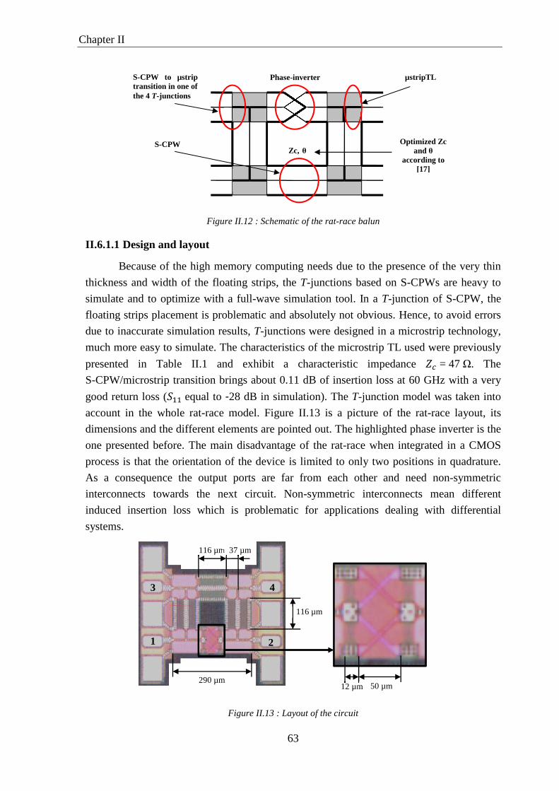
Chapter II
63
Figure II.12 : Schematic of the rat-race balun
II.6.1.1 Design and layout
Because of the high memory computing needs due to the presence of the very thin
thickness and width of the floating strips, the T-junctions based on S-CPWs are heavy to
simulate and to optimize with a full-wave simulation tool. In a T-junction of S-CPW, the
floating strips placement is problematic and absolutely not obvious. Hence, to avoid errors
due to inaccurate simulation results, T-junctions were designed in a microstrip technology,
much more easy to simulate. The characteristics of the microstrip TL used were previously
presented in Table II.1 and exhibit a characteristic impedance D = 47 Ω. The
S-CPW/microstrip transition brings about 0.11 dB of insertion loss at 60 GHz with a very
good return loss (!! equal to -28 dB in simulation). The T-junction model was taken into
account in the whole rat-race model. Figure II.13 is a picture of the rat-race layout, its
dimensions and the different elements are pointed out. The highlighted phase inverter is the
one presented before. The main disadvantage of the rat-race when integrated in a CMOS
process is that the orientation of the device is limited to only two positions in quadrature.
As a consequence the output ports are far from each other and need non-symmetric
interconnects towards the next circuit. Non-symmetric interconnects mean different
induced insertion loss which is problematic for applications dealing with differential
systems.
Figure II.13 : Layout of the circuit
S-CPW to µstrip transition in one of the 4 T-junctions
µstripTL
S-CPW
Phase-inverter
Optimized Zc and θ
according to [17]
Zc, θ
116 µm 37 µm
116 µm
290 µm 50 µm 12 µm
2 1
3 4

Chapter II
64
II.6.1.2 Simulation versus measurement results
Measurements were carried out from 10 GHz to 67 GHz on a four-ports VNA. The
four ports de-embedding method presented above was applied with open pad measurements
including the tapers as explained in the section discussing the de-embedding method.
Figure II.14(a) compares the simulation (solid line) and measurement (dash line) results.
The return loss !! and of the measurements show a shift of the working frequency of
8 GHz; indeed the best matching is reached around 67 GHz with -12.5 dB and -20.5 for !! and , respectively, instead of -22 dB at 59 GHz for the simulation. The transmission
coefficient *!, through the branch without phase inverter, fits well with the simulated one
and reaches 4.6 dB, which means 1.6 dB of added losses beyond the theoretical 3 dB. !, the transmission through the phase inverter is 7.2 dB, that is to say 4.2 dB of added losses.
The transmission parameters are robust with very flat curves. With a bandwidth defined by
considering a return loss better than -10 dB, and a working frequency centred at 67 GHz, a
minimum of 15 % is obtained by symmetry of the measured result at 67 GHz (between
62 GHz and 72 GHz minimum). A measurement till 110 GHz may confirm this
assumption. Isolation * is better than -23 dB over a very large frequency band, at least
from 10 GHz to 67 GHz. Figure II.14(b) shows a phase difference centred around 185°
with a phase imbalance of ±1° between 32 GHz and 67 GHz or 185.5 ±0.5° between
62 GHz and 67 GHz which is excellent in comparison to the state-of-the art. This result is
clearly obtained thanks to the use of the phase inverter, because its phase does not vary with
frequency, leading to an equivalent phase shift for the rat-race branches over the frequency.
There is a shift of 5° compared to the perfect phase imbalance, but it is very flat over the
whole bandwidth. 5° is easy to overcome thanks to TL length readjustment in a second run.
Finally, the chip is compact with an area equal to 0.085 mm2.
• How to explain the discrepancies?
The simulated microstrip and S-CPWs of the rat-race have small electrical lengths,
and we noticed afterwards that the S-parameters of such small lengths obtained with HFSS
were not right, leading to an inaccurate estimation of the TLs effective relative permittivity.
This comes from an un-established propagating mode when considering small-length TLs.
However, this error could be easily corrected. As shown above, simulation and
measurement results of the TLs characteristic parameters fit really well, and hence could be
used for the design of a second set of rat-race baluns.
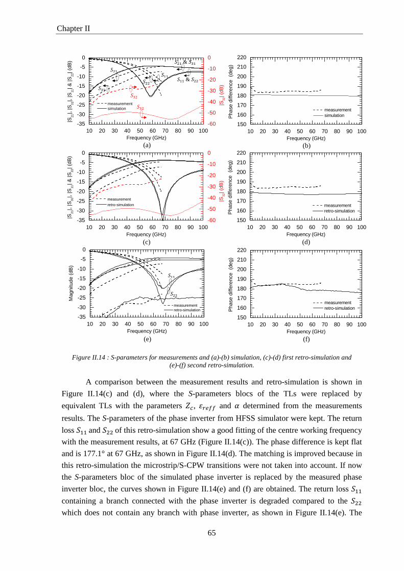
Chapter II
65
Figure II.14 : S-parameters for measurements and (a)-(b) simulation, (c)-(d) first retro-simulation and (e)-(f) second retro-simulation.
A comparison between the measurement results and retro-simulation is shown in
Figure II.14(c) and (d), where the S-parameters blocs of the TLs were replaced by
equivalent TLs with the parameters D, and determined from the measurements
results. The S-parameters of the phase inverter from HFSS simulator were kept. The return
loss !! and of this retro-simulation show a good fitting of the centre working frequency
with the measurement results, at 67 GHz (Figure II.14(c)). The phase difference is kept flat
and is 177.1° at 67 GHz, as shown in Figure II.14(d). The matching is improved because in
this retro-simulation the microstrip/S-CPW transitions were not taken into account. If now
the S-parameters bloc of the simulated phase inverter is replaced by the measured phase
inverter bloc, the curves shown in Figure II.14(e) and (f) are obtained. The return loss !! containing a branch connected with the phase inverter is degraded compared to the which does not contain any branch with phase inverter, as shown in Figure II.14(e). The
10 20 30 40 50 60 70 80 90 100150
160
170
180
190
200
210
220
measurement simulation
Frequency (GHz)
Pha
se d
iffer
ence
(de
g)! *! !!
! & *! !! &
* *
!!
10 20 30 40 50 60 70 80 90 100-35
-30
-25
-20
-15
-10
-5
0
measurement retro-simulation
Frequency (GHz)
Mag
nitu
de (
dB)
10 20 30 40 50 60 70 80 90 100150
160
170
180
190
200
210
220
measurement retro-simulation
Frequency (GHz)
Pha
se d
iffer
ence
(de
g)10 20 30 40 50 60 70 80 90 100
150
160
170
180
190
200
210
220
measurement retro-simulation
Frequency (GHz)
Pha
se d
iffer
ence
(de
g)
10 20 30 40 50 60 70 80 90 100-35
-30
-25
-20
-15
-10
-5
0
measurement simulation
Frequency (GHz)
|S21
|, |S
31|,
|S11
| & |S
22| (
dB)
-60
-50
-40
-30
-20
-10
0
|S32
| (dB
) 10 20 30 40 50 60 70 80 90 100
-35
-30
-25
-20
-15
-10
-5
0
measurement retro-simulation
Frequency (GHz)
|S21
|, |S
31|,
|S11
| & |S
22| (
dB)
-60
-50
-40
-30
-20
-10
0
|S32
| (dB
)
(a) (b)
(c) (d)
(e) (f)

Chapter II
66
effects of the phase inverter are here highlighted. * is also degraded and gets closer to the
measurement result. Finally the simulated insertion loss *! increases up to 5.2 dB.
II.6.1.3 Further improvements
The method consisting in simulating the TLs with their real lengths and taking their
S-parameters in a circuit simulator does not work in our case because of the really small
physical lengths. Equivalent TLs have to be used in the circuit simulator with the
parameters obtained from HFSS simulation with long enough physical lengths.
The phase inverter has a strong effect on the rat-race balun performances. In order
to get better performances, the S-parameters magnitude of the phase inverter has to be
better simulated in order to allow an accurate optimization. With the measurements of the
different phase inverters upcoming soon, we should better understand the influence of the
parasitics induced by the overlap. Special attention has been paid to the future de-
embedding procedure for these phase inverters. Moreover, it could be possible to replace
the CPW phase inverter by a microstrip type to avoid the use of really short S-CPW. In that
case all the TLs between ports 1 and 2 of the rat-race would be of a microstrip type.
II.6.2 Power divider balun
A new topology of balun has been tested out: it is a classical ? 4I power divider in
which a phase inverter was inserted in one branch to get 180° of phase difference between
the two output ports. The isolation resistance R used in the Wilkinson power dividers must
be removed, otherwise the 180° relative phase difference would increase considerably the
losses. Removing this resistance, this topology cannot be used anymore as a combiner
because isolation and output ports matching are degraded. This balun was fabricated and
measured in the 65 nm technology on the same chip as the rat-race balun presented above.
The layout with the dimensions is given in Figure II.15.
Figure II.15 : Layout of the power divider balun
305 µm 35 µm
167 µm
24 µm
104 µm 152 µm
1 2
3

Chapter II
67
As for the conventional Wilkinson power divider, the characteristic impedance of
the TLs is 70 Ω with 90° electrical length. The characteristics of the microstrip and
S-CPWs used in this design were presented in Table II.1. The main advantage of this
topology compared to the rat-race balun is the proximity of the two output ports. The input
port was placed in such a way that the outputs are at the same level with a phase of ! and *! equal to 90° and 270°, respectively. In that case, a good matching at port 1 and 180° of
phase difference should be obtained.
The design method is the same as for the rat-race balun. TLs, S-CPW/microstrip
transitions and phase inverter were simulated with HFSS to get the S-parameters, and then
gathered in ADS to simulate the whole device.
II.6.2.1 Simulation versus measurement results
Measurements were carried out from 10 GHz to 67 GHz. The same four ports de-
embedding method as the rat-race balun was applied. Figure II.16 compares simulation and
measurement results. The return loss !! resonance was shifted towards a lower frequency
with a down step of 7 GHz, as shown in Figure II.16(a). The best matching is -43 dB at
53.3 GHz instead of 60 GHz. However, the matching is still equal to -20 dB at 60 GHz. ! and *! equal -4.3 dB and -3.6 dB, respectively. The phase difference is 173°, as shown in
Figure II.16(b).
Figure II.16 : Simulation and measurement results of the power divider balun in the 65 nm technology.
(a) Magnitude and (b) phase difference.
The simulation of the transmission coefficients shows that !, through the phase
inverter, should have less insertion loss than *! along a long lossy microstrip TL. That is
to say that the simulation of the basic components erroneously indicates lower insertion
loss due to the phase inverter than to the microstrip TLs. The measured results, on the
contrary, clearly show that ! is higher than *!. We already discussed about the high
insertion loss added by the phase inverter and the complexity to simulate it. Despite that, ! and *! were measured at -4.4 dB and -3.6 dB at 53 GHz, which are really good results.
The difference of magnitude between ! and *! is also due to impedance mismatch seen
from the input port. The phase inverter acts as a stepped impedance creating a discontinuity
10 20 30 40 50 60150
160
170
180
190
200
measurement simulation
Frequency (GHz)
Pha
se d
iffer
ence
(de
g)
!!
! ! *!
10 20 30 40 50 60-14
-12
-10
-8
-6
-4
-2
0
measurement simulation
Frequency (GHz)
|S21
| & |S
31| (
dB)
-40
-30
-20
-10
0
|S11
| (dB
)
(a) (b)

Chapter II
68
for the signal between ports 1 and 2. The relative bandwidth centred at 53 GHz satisfying a
-20 dB return loss reaching 25 % (between 46.5 GHz and 60 GHz). In this band the phase
difference is 173.5°, e.g. a discrepancy of 6.5° as compared to the targeted 180°. However
it is really flat since the phase imbalance is only ±0.4°. ! varies from -4.64 dB to -4.31 dB
and *! from -3.72 dB to -3.56 dB. The area equal to 0.1 mm² is bigger as compared to the
rat-race balun (0.085 mm²). This directly stems from the output ports position which was
adjusted to fit with the RF probes (in order to avoid extra connection TLs and to simplify
the de-embedding). The TLs could be designed closer from each other and would decrease
the surface area of at least 25 %. Even though the design method was the same as for the
rat-race balun, here no problem occurred because of an eventual misestimating of the TLs
effective relative permittivity. Indeed, the simulated TLs are longer, and so, long enough
for their propagation mode to be well established and their simulation to be accurate.
II.6.2.2 Further improvements
The mismatch due to the phase inverter slightly shifts the working frequency. With
shorter TLs and better adjustment, the working frequency and the phase difference could be
improved. Moreover, a study of the position of the phase inverter in the branch could lead
to an optimised position.
II.6.3 Comparison with the state-of-the-art
The Table II.4 compares the measument results of the two topologies of baluns with
the state-of-the-art of power divider with out-of-phase presented in Chapter I.
Table II.4 : Comparison of this work with the state-of-the-art.
Through Coupled
[61]/0.18 µm CMOS
16.5-67 Marchand balun <-6 - -7 to -5 -8 to -5 180±5 0.06
[62]/0.18 µm CMOS
25-65 Marchand balun <-7 - -10 to -7 -9 to -6 180±10 0.55
[40]/0.13 µm SiGe BiCMOS
48-80 Rat-race <-10 <-18 -5 to -4 -6 to -5 184±2 0.11
[63]/0.13umBiCMOS
57-71 Rat-race <-14 <-16 -7.5 to -5.5 -6 to -4.5 180±30 0.28
[64]/0.13 µm CMOS
55-65 Transformer - - 180±5 0.05
This work 62- >67 Rat-race <-10 <-23 -7.56 to -7.24 -4.87 to -4.62 185.5±0.5 0.085
This work 46.5-60Power divider
with phase inverter
<-20 -6 -4.64 to -4.31 -3.72 to -3.56 173.5±0.4 0.1
Ref./Tech.Freq.(GHz)
ArchitectureReturn
loss(dB)
-7.5 to-4.5
Isolation(dB)
Phaseimbalance
(°)
Area
(mm2)
Magnitude imbalance
(dB)

Chapter II
69
II.7 Branch-line coupler
A branch-line coupler with -3 dB at each output port for 50-Ω system characteristic
impedance was designed in the 28 nm technology at the working frequency of 60 GHz.
Only the simulated results are presented here. The vertical TLs have a characteristic
impedance of 35 Ω and the horizontal ones of 50 Ω. 50 Ω microstrip feeding lines connect
the pads to the input/output ports of the branch-line, as shown on the layout in Figure II.17.
These feeding lines and pads will be easily de-embedded thanks to the method described
above.
Figure II.17 : Layout of the branch-line coupler with S-CPWs in the 28 nm technology.
The simulated performances of the S-CPW and microstrip TLs used in this device
have been summarized in Table II.2. Here again the T-junctions were designed in a
microstrip technology to simplify simulations and layout design. To simulate the full
device, equivalent TLs on ADS were modelled with the parameters D, and , the
attenuation loss. All the parameters were determined previously thanks to HFSS. The
S-CPW/microstrip transitions were considered as perfect, which means that the equivalent
TLs were directly and ideally connected in the circuit simulator. The simulated results are
shown in Figure II.18. The S-parameters correspond to the ports number according to their
position in the device, which means that pads and 50 Ω feed lines were not taken into
account in the simulations.
303 µm 50 µm
45 µm
309 µm
503 µm
500 µm
1 2
3 4

Chapter II
70
Figure II.18 : Simulation results of a branch-line coupler with S-CPWs in the 28 nm technology.
(a) Magnitude and (b) phase difference.
At 60 GHz, the return loss is -28 dB and the transmission coefficients ! and *! are respectively -3.67 dB and -3.48 dB, as shown in Figure II.18(a). The device has two
symmetry axes, vertical and horizontal, so the return loss parameters are similar at all ports.
The isolation between ports 1 and 4, !, is -30 dB. The bandwidth determined with a
return loss better than -20 dB reaches about 12 %, between 57 GHz and 64 GHz. Over this
bandwidth ! is constant and *! varies between -3.48 and -3.68 dB, so the maximal
magnitude imbalance is 0.19 dB. The variation of *! is less flat than the variation of ! because the electrical length between ports 1 and 3 is 180° and only 90° between ports 1
and 2, so the narrow band effect of the TLs is consequently stronger for *!. The phase
difference is 90.2° at 60 GHz and between 89.6° and 91° in the bandwidth, which means a
phase imbalance of ±0.7°, as shown in Figure II.18(b). The TLs were not placed in a
configuration to optimize the device area, leading to a surface of 0.252 mm2. In order to
reduce the surface area, it could be possible to meander the TLs by using the free space in
the middle of the device.
II.8 Power divider
A power divider was designed in the 28 nm technology to be used at 60 GHz. The
layout is presented in Figure II.19. No resistance was placed between the two output ports,
hence it was not realized a Wilkinson power divider. In CMOS technology the resistance
dimensions are really small and the S-CPW width quite large (around 100 µm) so that long
interconnects were needed between the S-CPW signal strip and the resistance which leads
to a strong inductive effect. As it is really difficult to simulate and estimate this parasitic
effect, the isolation resistance was removed. Obviously this has for consequence to limit the
use of this device as a power divider only. A 40-µm long 50 Ω microstrip feed line was
inserted between the pad at port 1 and the T-junction. Same feed lines were used for output
ports 2 and 3. Then 65 Ω microstrip TLs connect this T-junction to the 70 Ω S-CPWs. The
minimal allowed width and the highest distance h (between the ground and the signal strip)
were fixed for the microstrip topology to get the maximal possible impedance, which is
30 40 50 60 70 80 9050
60
70
80
90
100
110
120
130
Frequency (GHz)
Pha
se d
iffer
ence
(de
g)
!!
*! !
30 40 50 60 70 80 90-10
-9
-8
-7
-6
-5
-4
-3
Frequency (GHz)
|S
21| &
|S31
| (dB
)
-40
-30
-20
-10
0
|S11
| & |S
32| (
dB)
(a) (b)

Chapter II
71
only of 65 Ω. The equivalent TLs modelled with the parameters D, and given in
Table II.2 were ideally connected, without S-CPW/microstrip transition equivalent
electrical model.
Figure II.19 : Layout of the Wilkinson power divider with S-CPWs in the 28 nm technology.
Figure II.20 shows the magnitude of !!, , ! and *. The circuit has horizontal
symmetry axis so that = ** and ! = *!. The return loss is really good with -44 dB at
60 GHz. Using 65 Ω characteristic impedance instead of 70.7 Ω shifted the working
frequency of 3 GHz towards the lower frequencies. This was corrected by adjusting the
electrical length of the S-CPWs in order to reach a 60-GHz working frequency. By this
way, the working frequency is centred with a total electrical length of 84° instead of the
theoretical 90° between the input and output ports. Moreover, as the error is only 8 % on
the characteristic impedance and as the electrical length of the 65 Ω microstrip line is small,
21° among 84°, the device keeps an excellent matching. As expected, with no isolation
resistance, the isolation and matching of the output ports are only -6.4 dB. The bandwidth
determined with a return loss better than -20 dB reaches 40 % (between 48 GHz and
72 GHz). Over this bandwidth, the transmission coefficients ! and *! vary
between -3.35 dB and -3.28 dB. The surface area of the power divider is 0.12 mm2. As for
the power divider balun, the output ports were adjusted to fit with the RF probes. With
closer TLs the surface could be decreased of at least 25 %.
Figure II.20 : Simulation results of a Wilkinson power divider without isolation branch, with S-CPWs in the
28 nm technology.
324 µm 48 µm
100 µm 3
2
1
40 µm
* !! !
30 40 50 60 70 80 90-3,8
-3,7
-3,6
-3,5
-3,4
-3,3
-3,2
-3,1
-3,0
Frequency (GHz)
|S21
| (dB
)
-40
-30
-20
-10
0
|S11
|, |S
22| &
|S32
| (dB
)
Chapter II
72
II.9 Conclusion
In this chapter, S-CPWs were used to realize several devices. The slow-wave TL
combines high effective relative permittivity and high quality factor, and lead to compact
and performing devices having low insertion loss. Even though for high characteristic
impedances the quality factor decreases, S-CPWs can be designed to reach a 100 Ω
characteristic impedance, with a simulated quality factor of 28 in the 65 nm technology.
With microstrip type TLs, the maximal characteristic impedance is limited to about 70 Ω
(the poorer case is 65 Ω only in the 28 nm technology). However, microstrip TLs are still
needed, for the T-junctions for example, as S-CPW junctions are still complicated to design
due to the floating strips.
A phase inverter was fabricated and measured in the 65 nm technology. It is very
wide band and strongly reduces the area of the devices in which it is inserted. Even if the
phase of the transmission coefficient is well determined with HFSS, the magnitude is not
well predicted. With more accurate simulations, it could be optimized in order to reduce the
insertion loss. Based on this phase inverter, two baluns using S-CPWs were achieved in the
65 nm technology at a 60 GHz working frequency. The first one was based on a rat-race. It
exhibited good isolation and matching. The second one was carried out by a novel topology
based on a power divider with close output ports but without isolation. They exhibit a
surface area of 0.085 mm2 and 0.1 mm2, respectively. 25 % of surface area could be saved
for the power divider balun without fitting the feed lines with the RF probes. Optimised
surfaces would reach the state-of-the-art presented in chapter I in terms of miniaturization.
The design method used in this work was not suitable for the rat-race and leaded to a shift
of 8 GHz towards the higher frequencies. Moreover, the phase inverter degraded the
insertion loss in both circuits.
Then, a branch-line coupler and a power divider (without isolation) were simulated
in the 28 nm technology. A design method with equivalent transmission lines characterized
with the parameters D, and , obtained from HFSS and validated by the
measurements, was applied. Really good performances are expected at 60 GHz. Also, de-
embedding methods are given for two ports devices and transmission lines, and for four
ports devices.
The devices designed in this chapter proved that the slow-wave transmission lines
have a strong interest for the design of compact and low-loss passive devices at
millimetre-wave frequencies.
The applications of the power divider designed in the 28 nm technology are limited
because of the lack of good matching at the output ports and the lack of isolation. However,
despite the constraints of the isolation resistance and its access in silicon technology, it is
important to develop fully matched and isolated power dividers for combiner applications.

Chapter II
73
In the next chapter a new topology of power divider is proposed to design and optimise
such power dividers.

Chapter III
74
: New type of power divider based on a Chapter IIIWilkinson power divider/combiner for millimetre-wav e
frequencies applications
This chapter focuses on the design, development, realization and test of a new type
of power divider based on the Wilkinson power divider. This new power divider is intended
to be further implemented in a feeding network system for antenna array beam-steering. At
the beginning, the original Wilkinson power divider was designed for use in shielded
coaxial systems at frequencies low enough not to take into consideration additional
parasitic effects. Design complexity arises when dealing with millimetre-wave bands in
planar technologies. Parasitics typically derived from undesired coupling between the two
quarter-wave arms, or distributed effects introduced by the physical requirements, such as
the stretching of the resistance between the two arms in IC’s, inhibit performances. This is
most of the time not an issue at RF frequencies, but it becomes particularly troublesome at
high frequencies.
The Wilkinson power divider faces another issue in silicon technology which is the
characteristic impedance limitation. Indeed, it is fixed by the BEOL and the design rules of
the considered technology so that it may be not possible for the microstrip type TL to reach
the 70.7 Ω characteristic impedance required in a 50-Ω system.
As already mentioned in this thesis, miniaturization is an unavoidable topic,
particularly for integrated circuits, due to the high cost. Some of the techniques given in the
first chapter are really efficient and could be reused, such as the stub loading technique. By
using a procedure comparable to Mandal’s optimization of the rat-race coupler, described in
[17], we will see that many solutions are available (among which the original Wilkinson
power divider), so that it becomes very easy by the end to compare one solution to another
and to choose the most appropriate for our purpose: lower characteristic impedance or
reduced area, or a compromise of both.
Hence, in this chapter a new topology of power divider/combiner with in phase
outputs is proposed. Our study shows that compactness and high-performance can be met
simultaneously, with high flexibility thanks to several design solutions. The design consists
in a modified Wilkinson power divider with added TLs to connect the isolation resistance
to the output ports, in association with an open stub at the input port junction. While
keeping very good isolation between output ports and matching on all ports, the proposed
new power divider enables an optimal choice of the characteristic impedance of the TLs, of
the output ports position with the best compromise between size and electrical
performances.

Chapter III
75
This chapter focuses first on the design and the fabrication of the proposed power
dividers at RF frequencies, carried out in a classical PCB technology, as proof-of-concept.
1:4 antennas feeding circuit was fabricated and measured, one at 2.45 GHz and another one
at 5.8 GHz. The second one is associated to integrated slot-array antennas on a single
substrate, taking advantages of small size, low profile, and low cost.
Based on the same technology demonstrated at RF frequencies, a 60 GHz power
divider was designed in the 55 nm BiCMOS technology (by STMicroelectronics). S-CPWs
were used in order to reduce the TLs’ length and hence improve both compactness and
performance.
III.1 Issues for Wilkinson power dividers in silicon technology
III.1.1 Isolation resistance
The undesired coupling between the two quarter-wave arms, or the distributed
effects introduced by the physical requirements when stretching the resistance between the
two arms can be devastating for the performances of the circuit at millimetre-wave
frequencies. In order to connect the isolation resistance to the outputs using the smallest
footprint as possible, the typical solution involves the wrapping of the quarter-wave arms
into rounded shapes converging briefly to the resistance placement [77]-[78]. Another way
is the use of interconnects between the isolation resistance and the signal strips [79], but
their physical length is long as compared to the resistance dimensions so that they cannot
be neglected. It is also worth mentioning that in practice it is really difficult to perfectly
model the effects of these interconnects because of the vias, bends and contact resistance
parasitics.
III.1.2 Characteristic impedance flexibility
The 70.7 Ω characteristic impedance of the quarter-wave arms fixed in the
conventional Wilkinson power divider may be not reachable in all CMOS BEOL. We have
seen for instance that in the 65 nm technology a maximum of 65 Ω can be obtained with
microstrip TLs. If such a 65 Ω TL is used to build a power divider, the electrical lengths
have to be adjusted to compensate for the characteristic impedance mismatch, so the design
is more complex, and the return loss will be unavoidably degraded. In the case of S-CPWs,
70.7 Ω is easily reachable, but the corresponding S-CPW exhibits a lower quality factor as
compared to the one with a characteristic impedance around 45 Ω. Hence, flexibility for the
choice of the characteristic impedance could permit to choose the TLs exhibiting the
highest quality factor. Moreover, if different characteristic impedances leading to full
matched, isolated and low loss power divider could be found with electrical lengths shorter
than those of the conventional 90°, solutions would conclude to a more compact device.

Chapter III
76
III.1.3 State-of-the-art of the solutions
In [80], the authors added extra TLs for connecting the isolation resistance to the
output ports as shown in Figure III.1. This avoids parasitic coupling between the two output
ports and in the same time allows the isolation resistance access to be taken into account.
Nevertheless, the proposed power divider suffers from higher surface as compared to the
classical Wilkinson one because of the link between the two electrical lengths,
e.g. >! = > + 90°. More recently, a general model was developed in order to give design
rules for the synthesis of these additional TLs [81]. The characteristic impedances depend
on the power ratio between the two output ports.
Figure III.1: Modified power divider with resistance access proposed in [80].
In [82], the conventional quarter-wave length of the impedance transformer arms
were miniaturized thanks to open stubs and step impedances as shown in Figure III.2. This
also enhanced flexibility in the choice of the TLs characteristic impedance, even though all
the solutions cannot be applied in a CMOS technology. In counterpart, this topology leads
to a complex transformation instead of the classical real one. Since the phase delays of the
modified TLs are arbitrarily greater than -90° the isolation circuit does not only consist in a
resistance but also a series capacitance for compensating the imaginary part. Moreover,
these topologies do not bring any solution concerning the feeding lines.
Figure III.2: Modified asymmetric impedance transformer proposed in [82].

Chapter III
77
III.2 Study of a new solution
III.2.1 Topology presentation
Figure III.3 gives the proposed power divider topology. Compared to the one
presented in [80], an open stub of characteristic impedance and electrical length >was
added at the junction between input port 1 and the arms joining output ports 2 and 3. The
characteristic impedance and electrical length of the latter were named !and >!, while *and >* characterize the arms connecting the output ports to the resistance. The new
solution is thus a combination of [80], Figure III.1 and [82], Figure III.2. As will be seen,
this combination offers a very high flexibility.
Figure III.3: Modified PD with open stub and resistance feeding lines.
III.2.2 Theory and design equations
It is easy to show, by an even-odd modes analysis, that adding the open stub (,>)
alone, without TLs (*,>*), deteriorates the matching of the conventional Wilkinson
topology. However, when both TLs (*,>*) and open stub (,>) are used, good matching
and isolation can be achieved. They are slightly degraded as compared to the classical
Wilkinson topology, but the corollary will be an extended bandwidth as demonstrated by
Fano in [83]. For simplicity, all the characteristic impedances were normalized to the
system characteristic impedance , e.g. Ïh = h/. An even-odd mode analysis was
carried out considering the circuit symmetry, as illustrated in Figure III.4. The open stub
was replaced by two parallel open stubs with a characteristic impedance of 2Ï. Similarly,
port 1 impedance was doubled. The line of symmetry crosses the middle of the resistance r
so that it should be replaced by two series resistances with a value \ 2⁄ . For given ports
conditions and a given r, the two circuits, corresponding to even- or odd-mode analyses,
totalize six unknown parameters corresponding to the three TLs (Ïh ,>h), so that six
independent equations are required to find the solutions.
Z2, θ2
Z3
θ 3
Z3
θ 3
R
Z1, θ1
Z1, θ1
1
1
1
Port 1
Port 3
Port 2
Chapter III
78
Figure III.4: Half of the normalized topology shorted within the odd-mode and open within the even-mode.
III.2.2.1 Even-mode analysis
For even mode excitation, the voltages at ports 2 and 3 have similar magnitude and
phase. No current flows through the resistance \ 2⁄ which is open circuited. The value of
the impedances Ï_ and Ï*_ looking towards the open stubs (Ï,>) and (Ï*,>*), in
Figure III.4, are:
Ï_ = 2Ï_4Ð'>) (III-1)
Ï*_ = Ï*_4Ð'>*) (III-2)
Impedance Ï_ is in parallel with port 1. The equivalent impedance ÏÑ!_ of their
combination is given by equation (III-3):
ÏÑ!_ = 2ÏÏ (Ðab'>) (III-3)
The impedance Ï_ is then derived as follows:
Ï_ = Ï! ÏÑ!_ ( Ï! Ðab'>!)Ï! ( ÏÑ!_Ðab'>!) (III-4)
Impedance Ï_ is in parallel with Ï*_ and should be equal to port 2 impedance in order
to get a matching condition at port 2, leading to equation (III-5):
1Ï*_ ( 1Ï_ = Ðab'>*)Ï* ( Ï! ( ÏÑ!_ Ðab'>!)Ï!ÏÑ!_ ( Ï!Ðab'>!) = 1 (III-5)
From (III-5), the real and imaginary parts of the two members of the equation were split in
two equations. Equation (III-6) was obtained by equating the real parts while equation
(III-7) corresponds to equating the imaginary parts.
z1, θ1
z3
θ3 2z2
θ2 ° ÒI
Port 1 Port 2
2 1 zIN3 zIN2
Symmetry line
zIN1 zIN4

Chapter III
79
Ï!Ï*Ï* 3Ï!ÏÏ*Ðab'>!) Ðab'>)( Ï!Ï*Ðab'>!) Ðab'>)* = Ï!ÏÏ* Ðab'>) 4ÏÏ* Ðab'>!) Ðab'>) 4Ï!Ï Ðab'>) Ðab'>*) Ï!Ï* Ðab'>!) Ðab'>*)( 3Ï!Ï Ðab'>!) Ðab'>) Ðab'>*) (III-6)
Ï!ÏÏ* Ðab'>) ( Ï!Ï*Ï*Ðab'>!) 3Ï!ÏÏ*Ðab'>!) Ðab'>) =Ï!Ï* Ðab'>)*( 2Ï*Ï* Ðab'>!) 2ÏÏ* Ðab'>!) Ðab'>)( 2Ï!Ï* Ðab'>*) 2Ï!Ï Ðab'>) Ðab'>*) 3Ï!Ï Ðab'>!) Ðab'>) Ðab'>*)( Ï! Ðab'>!) Ðab'>)* Ðab'>*) (III-7)
In the same manner, impedance Ï*_ looking towards the TL (Ï*,>*) is in parallel with
port 2 impedance, thus the equivalent impedance named ÏÑ_ becomes:
ÏÑ_ =¿1 ( 1Ï*_À! = Ï*_4Ð'>*)1 Ï*_4Ð'>*) (III-8)
Impedance Ï!_ is the input impedance of TL (Ï!,>!) loaded by ÏÑ_, given by (III-9):
Ï!_ =Ï! ÏÑ_ ( Ï! Ðab'>!)Ï! ( ÏÑ_ Ðab'>!) (III-9)
The combination of Ï!_ in parallel with Ï_ should be equal to port 1 impedance in
order to obtain a matching condition at port 1, leading to equation (III-10):
1Ï!_Ó ( 1Ï_Ó = Ï! ( ÏÑ_ Ðab'>!)Ï!ÏÑ_ ( Ï! Ðab'>!) ( Ðab'>)2Ï = 12 (III-10)
By developing and equating the real and imaginary parts of the two members of equation
(III-10), equations (III-11) and (III-12) were derived:
Ï!Ï* Ðab'>) _4Ð'>*) Ï! Ðab'>!) Ðab'>) ( 2Ï!Ï( 2ÏÏ* Ðab'>!) _4Ð'>*)= Ï! ÏÏ* Ðab'>!) _4Ð'>*) (III-11)
Ï!Ï* Ðab'>!) Ðab'>) _4Ð'>*) ÏÏ* _4Ð'>*) = Ï!Ï Ðab'>!) (III-12)
Finally, the even-mode analysis leads to four different equations, (III-6), (III-7), (III-11)
and (III-12).

Chapter III
80
III.2.2.2 Odd-mode analysis
For the odd-mode analysis, the voltages at ports 2 and 3 have the same magnitude
and are 180° out-of-phase. The voltage is consequently equal to zero along the line of
symmetry of the circuit which can be thus short circuited in its middle part. The impedance
looking towards the circuits from port 2 can be calculated by means of the impedances Ï*_¦ and Ï_¦:
Ï*_¦ = Ï* \ 2I ( Ï* Ðab'>*)Ï* ( \ 2I Ðab'>*) (III-13)
Ï_¦ = Ï! Ðab'>!) (III-14)
The combination of these two impedances in parallel should match port 2 impedance,
which leads to the following equation (III-15):
1Ï*_¦ ( 1Ï_¦ = Ï* ( \2 Ðab'>*)Ï* \2( Ï* Ðab'>*) _4Ð'>!)Ï! = 1 (III-15)
Equations (III-16) and (III-17) are obtained by equating the real and imaginary parts of
equation (III-15), respectively:
Ï* _4Ð'>!) Ðab'>*) = Ï! T\2 1U (III-16)
Ï* _4Ð'>!) _4Ð'>*) = Ï! ]2\ Ï* 1^ (III-17)
Equations (III-16) and (III-17) are the two missing equations over six independent
equations, which is the necessary condition to solve a problem with six unknown
parameters. Next, equation (III-16) is substituted into (III-17) in order to get:
>* = Ðab!ÔÕÖ \2( 12Ï*\ 1×Ø (III-18)
which implies the following condition on the value of the resistance r according to the
value of the characteristic impedance Ï*:
if\ < 2, then Ï* / + or if \ / 2, then Ï* < + (III-19)
Moreover, equation (III-16) can be rewritten as follows:
>! = Ðab!ÂÏ* Ðab'>*)Ï! T\2 1UÃ (III-20)

Chapter III
81
From equation (III-20), it is obvious that the value of r cannot be lower than 2, which
would lead to a negative value of the electrical length >! or an electrical length longer than
a quarter wave length which is not acceptable. Thus, the right condition among the two
suggested in (III-19) is:
\ / 2 with z* < + (III-21)
Meanwhile equation (III-12) can also be rewritten as follows:
> = Ðab! ] ÏÏ* _4Ð'>*) ( ÏÏ! Ðab'>!)^ (III-22)
Finally it is remarkable that equation (III-18) gives >* versus \ and Ï* only, equation
(III-20) gives >! versus \, Ï!, Ï*and >*, and equation (III-22) gives > versus Ï!, Ï, Ï*, >!
and >*.
III.2.3 Design procedure
With an adequate procedure, it seems thus possible to find, in that order, the TLs’
electrical length >*, >! and > which depend on the values of the characteristic impedances Ï!, Ï, Ï* and resistance r. However, the three equations (III-6), (III-7) and (III-11) are too
complex to be solved in an algebraic way with (III-18), (III-20), and (III-22). Consequently,
for equations (III-6), (III-7), and (III-11) delta error functions, respectively named !,, *, were defined as:
ÜÝÞÝKÞ\4bÐℎÞ\º5ℎÐ ÝÞÝKÞ\4bÐℎÞ3ÞàÐÝÞÝKÞ\4bÐℎÞ\º5ℎÐ Ü (III-23)
A solution consists in a set of four values Ï!, Ï, Ï*, and r. The electrical lengths >!, >, and >* uniquely depend on the solution set. A set is solution of the circuit if the three
delta error functions are simultaneously equal to 0. A careful study showed that this
condition cannot be reached, except for the particular solution > = >* = 0, e.g. without
open stub neither resistance feeding lines, leading to the conventional Wilkinson power
divider. As an example, Figure III.5 shows the delta error functions versus !for two sets
of values, set 1 (in black): = 25 Ω, *= 25 Ω, R = 105 Ω and set 2 (in red): = 25 Ω, *= 49 Ω and R = 105 Ω, respectively.

Chapter III
82
Figure III.5: ¦ of (III-18), (III-20) and (III-22) for two sets of values.
For set 1, the delta error reaches 0 for ! = 84 Ω, whereas delta errors ! and *
are not equal to zero for the same characteristic impedance. In the same manner,
considering set 2, !, or * are equal to 0 for three different values of !, e.g 67 Ω,
57 Ω and 65 Ω, respectively. However, it is obvious that the average of the delta errors is
smaller for Set 2 if !is chosen near 60 Ω. Hence, even if a perfect set of characteristic
impedances cannot be found, there exist some sets that enable to be close to the ideal
solution. These “approximate solutions” can be obtained thanks to the use of a simple
algorithm.
However a question remains which is how to rely the delta errors calculated from
equations (III-6), (III-7) and (III-11) to the knowledge of power divider mismatch, isolation
and insertion loss. A solution could be to link, in an algebraic way, the delta errors to some
specific goals on the power divider S-parameters. Such relationship cannot be carried out
easily. Another way could be to calculate directly the aforementioned S-parameters and to
compare them to the power divider specifications, as a condition for the algorithm to end. A
far simpler solution was used. As it is proved below, a single condition solely based on the
scattering parameter as close to zero as possible is sufficient to ensure a good matching
at the three ports as well as a high isolation between the two output ports.
III.2.3.1 Demonstration of the good matching and isolation according to the value of áÒÒ
Statement is valuable for any three ports network as long as (i) the symmetry
condition between ports 2 and 3 is verified (balanced network) and (ii) there is no loss in
the equivalent even-mode circuit (which means no resistive element in the even-mode
circuit). Those conditions are fulfilled by the power divider given in Figure III.3. Due to
condition (i) the latter can be redrawn as the four ports network in Figure III.16(a).
30 40 50 60 70 80 90 1000,0
0,5
1,0
1,5
2,0 ∆
1
∆2
∆3
Z1 (Ω)
∆ erro
r set 1
set 2

Chapter III
83
Figure III.6: a) Normalized representation as a four ports network of the power divider in Figure III.3, b) odd-mode schematic and c) even-mode schematic.
Based on those considerations, the network can be analysed by an even-/odd-mode
approach. If an input power wave a! is considered at port 1, the following equations hold
for the relationship between the power waves defined in Figure III.16, where “e” means
even-mode “o” means odd-mode, respectively:
a = a_ ( a_¦ K = K_ ( K_¦ a = a_ a_¦ K = K_ K_¦ a! = a!_ ( a!_¦ K! = K!_ ( K!_¦
(III-24)
Similarily, if an input power wave a is considered at port 2, the following equations
occur:
a = a_ ( a_¦ K = K_ ( K_¦ a* = a_ a_¦ K* = K_ K_¦
(III-25)
III.2.3.1.a Odd-mode analysis
As port 1 is shunted, see Figure III.6(b), it is obvious that no transmission may
occur between ports 1 and 2. Consequently, the general form of the odd-mode scattering
matrix ¦ is written as:
Z1, θ1
1
Symmetry
2Z2
θ2
Z3
θ3 â ÒI â ÒI
2
Z3
θ3
1 2
2Z2
θ2 Z1, θ1
ãÒ
äÒ ãå
äå ãæ
äæ
Z1, θ
1
1 2Z2
θ2
Z3
θ3 â ÒI
2
ãÒ_ç äÒ_ç
Odd-mode
(b)
Z1, θ
1
1 2Z2
θ2
Z3
θ3
2
ãÒ_è äÒ_è
Even-mode
(c)
+ !
ãÍ äÍ
ãé äé ãÍ_ç äÍ_ç
ãÍ_è äÍ_è
+ !
- ! +
!
Odd-mode Even-mode
+ ! +
!
- ! +
!
(a)

Chapter III
84
s!!_¦ 00 _¦t (III-26)
With no resistive element in the network, |!!_¦| = |_¦| [12]. With the presence
of a resistance in the network, as in the conventional Wilkinson power divider or in Figure
III.6, necessarily ê!!_¦ê ≠ ê_¦ê. Moreover, because of the shunt, power waves a!_¦ and K!_¦ are equal in the odd-mode to zero:
a!_¦ = 0 K!_¦ = 0 (III-27)
III.2.3.1.b Even-mode analysis
The even-mode scattering matrix takes the form below:
s!!_ !_!_ _t (III-28)
The even-mode network being lossless, the two following equations hold:
ê_ê = ê!!_ê
and !!_ ( !_ = 1 (III-29)
Moreover, power waves a!_ and K!_ may be expressed as:
a!_ = √2 ∙ a_ K!_ = √2 ∙ K_ (III-30)
III.2.3.1.c Discussion on the scattering parameters
Using the equations (III-24) to (III-30) linking even, odd and global power waves,
the demonstration given in Appendix-A leads to:
!! = !!_ (III-31)
! = !_√2 = !* = ! = *! (III-32)
= _ _¦ = ** (III-33)
* = _ ( _¦ = * (III-34)
In order to design a three ports device, a parametric study is often necessary. The
convergence of the design process can be ensured by means of conditions on the scattering
parameters. Various possibilities can be enforced.

Chapter III
85
1) Condition |!!| = 0
This condition leads to |!!_| = 0 (III-31), implying |!_| = 1 (III-29), and hence ! = 1 √2⁄ (III-32). This is sufficient as long as output ports matching is not required.
However, such condition is not enough for the use of a power divider as a combiner where
isolation is required.
2) Condition || = 0
Two solutions exist. The first one consists in equating _ to _¦ keeping them
different from 0 (III-33), however this solution is not satisfactory for our power divider.
Indeed, according to (III-34) if _= _¦ ≠ 0, * is not equal to 0 which means a bad
isolation. The second solution is equivalent to having at the same time matching for both
even- and odd-modes at port 2:
_¦ = _ = 0 (III-35)
Consequently:
• Matching at port 1 is realized: Considering (III-29), _ = 0 implies:
!!_ = 0 (III-36)
Considering (III-31), !!_ = 0 implies:
!! = 0 (III-37)
• -3 dB ratio between ports 1 and 2 is reached: Considering (III-29), !!_ = 0 implies:
!_ = 1 (III-38)
Considering (III-32), !_ = 1 implies:
! = 1 √2⁄ (III-39)
• Perfect isolation is realized: Considering (III-33), _¦ = _ = 0 implies:
* = 0 (III-40)
Hence, a matching condition on the scattering parameter alone holds for the four
conditions on , !!, ! and * as long as the power divider stands symmetrical and
lossless (except for the isolation resistance R).
III.2.3.2 Procedure for finding solutions
In practice, the algorithm described in Figure III.7 was used to find close solutions,
based on the port 2 matching condition alone. Matlab software was used.

Chapter III
86
Figure III.7: Algorithm for finding solutions.
First, r must be fixed to the desired value and Ï!, Ï and Ï*to the minimum
achievable characteristic impedance given by the technology. Included in the three
overlapping loops of z!, z, and z* (symbolized with only one block in the algorithm), the
three electrical lengths >*, >!, and > are calculated in this order, according to equations
(III-18), (III-20) and (III-22). Then is compared to the initial goal. Typically, it is a
good choice to start the procedure with _gBj = -35 dB. If after any combinations of Ï!, Ï, and Ï*, stays higher than _gBj, this means that the goal is too ambitious.
Consequently, _gBj should be slightly increased. The poorer the conditions concerning _gBj, the worst the isolation and matching of the power divider. In practice, the choice
of _gBj is deserved to the designer, depending on the specifications related to the
application.
Finally, additional conditions concerning >h and/or Ïh ranges, may lead to conditions
on the device maximum size and/or quality factor for the TLs (in particular if integrated
technologies are targeted). The designer thus can choose a compromise between the power
divider electrical performance and size by electing the appropriate values of the
characteristic impedances and electrical lengths.
Ï! = Ï = Ï* = ÏghiÏ!
fix r value
fix initial _gBj goal
Ï! = ÏgBj Ï = ÏgBj Ï* = %\/2
Calculate>*, >!, > ≤ _gBj?
Save solution
Solutions
exist ?
Increase _gBj
Choose the best solution
Increment Ï!, Ïor Ï*
Yes
No
Yes
No
No
Yes

Chapter III
87
III.3 Circuits design and experimental results
Two power dividers with two different values of R were fabricated as a proof-of-
concept to illustrate and validate the method previously described. As shown in (III-21), r
should be strictly bigger than the normalized value 2, e.g. / 100 Ω when considering a
50-Ω system characteristic impedance. One power divider has a value R = 105 Ω and
another one R = 150 Ω.
III.3.1 Power Divider with R = 105 Ω
The targeted condition for was fixed to -35 dB. The characteristic impedances’
range of variation was fixed to [25-100] Ω, except for * which is limited to 51 Ω from
(III-21). A step of 2 Ω is a good compromise between time simulation and impedance
resolution for the construction of the design graphs.
Figure III.8 shows the solutions in terms of electrical lengths >!, >, and >*,
according to the characteristic impedances !, , and *, respectively. Figure III.8(a)
shows the electrical length >* map versus *. >* varies between 14° and 38°. Figure
III.8(b) gives the electrical length >! according to ! and *. The colour scale indicates that
the smaller the characteristic impedance *, the smaller the electrical length >!.
Consequently, in this example, a strong miniaturization could be reached with the choice of * = 25 Ω and >* = 14.4°. With such a solution, several values for ! and >! are available.
It may be noticed that the bigger !, the smaller >!. ! = 81 Ω appears to be a good
compromise to avoid too high characteristic impedances, which leads to >! = 57.7°. Lastly,
Figure III.8(c) gives the electrical length > versus ! and , for various achievable values
of *. Many possibilities exist for the pair (,>). Based on * = 25 Ω and ! = 81 Ω, a
wide range remains possible but when taking into account design constraints this choice
gets reduced. In particular, > should be chosen short enough to avoid parasitic coupling
between the TLs (*,>*) and (,>). = 39 Ω, leading to > = 35.2° is a good couple.

Chapter III
88
Figure III.8: Design graphs for R = 105 Ω.
Calculi are based on theoretical equations only and do not consider junctions
electrical models neither bends nor parasitic coupling that in practice contribute to degrade
the performances. The electromagnetic simulation of the power divider with the chosen
characteristic impedances and electrical lengths, including junctions, bends and coupling,
showed that the working frequency was slightly shifted and the return loss a little bit
degraded, consequently a tuning on these values was necessary. The final characteristic of
the TLs after tuning are the following (original values are given between brackets): ! = 84 Ω (81 Ω), >! = 56° (57.7°), = 39 Ω (39 Ω), > = 30° (35.2°), * = 30 Ω (25 Ω), >* = 14.9° (14.4°).
The circuits were fabricated on the dielectric substrate Rogers RO4003C, of relative
permittivity 3.38 and thickness 813 µm. All circuits are working at the frequency of
2.45 GHz. A SOLT calibration was carried out on an 8720 Vector Network Analyzer.
Figure III.9 compares the S-parameters obtained from electromagnetic simulations
[Momentum by Agilent Technologies] and measurements, respectively. A very good
agreement was obtained. While keeping the previous sets of (h,>h), the SMD resistance R
placed in the fabricated circuit was measured equal to 100.2 Ω. As expected the power
divider is very low loss with 0.13 dB of insertion loss only at 2.45 GHz, partially due to
SMA RF connectors. The available bandwidth, defined by !! below -20 dB, reaches 14 %,
from 2.26 GHz to 2.6 GHz. Considering this bandwidth, the output port return loss and
(a)
(b)
(c)
ð æ=ÍñΩ
ð æ=ÍóΩ
ð æ=ÍæΩ
ð æ=æóΩ
ð æ=æåΩ
ð æ=ÒéΩ

Chapter III
89
the isolation * are better than -24 dB, and reach -26 dB and -34 dB at 2.45 GHz,
respectively. Remember that was fixed to -35 dB as an input condition for the
convergence of the design algorithm. Even if this value was reached in the optimization
process in theory [Matlab], here again, since calculi do not take into account junctions
models nor parasitic couplings, the return loss is degraded. Moreover, the value of R was
5 % below the right value. However, let’s emphasize that -26 dB as a measured return loss
constitutes excellent conditions for a large majority of applications.
Figure III.9: Simulation [Agilent ADS Momentum™] and measurement results of the proposed topology with measured R = 100.2 Ω (theoretically 105 Ω). (!,>!) = (84 Ω, 56°), (,>) = (39 Ω, 30°), (*,>*) = (30 Ω,
14.9°). (a) Insertion loss and input return loss. (b) Isolation and output return loss.
Figure III.10 is a viewgraph of the fabricated power divider compared to the
modified power divider early proposed in [80]. To design the latter, the value of R was
fixed to 95 Ω in order to get an electrical length of the TLs equal to 12.6° between the
output ports and the resistance, which is close to the 14.9° of the topology presented here.
The TLs’ characteristic impedance was fixed to 69 Ω, with an electrical length between
ports 1 and 2 (or 3) equal to 102.6° (90° + 12.6°). These values lead to a surface of the
proposed circuit that is 24 % smaller as compared to the one proposed in [80].
Figure III.10: Measured circuits. (a) Proposed design. (b) Power divider from [80].
To conclude, these results suggest that the proposed power divider is low loss, with
really good matching and isolation. It is smaller and more flexible than the one proposed in
[80] whilst keeping similar advantages such as the limitation of the parasitic coupling
between the output ports thanks to the TLs connecting the resistance. In terms of simplicity,
1,0 1,5 2,0 2,5 3,0 3,5 4,0-30
-25
-20
-15
-10
-5
0
measured simulated
Frequency (GHz)
Mag
nitu
de (
dB)
1,0 1,5 2,0 2,5 3,0 3,5 4,0-40
-35
-30
-25
-20
-15
-10
-5
0
measured simulated
Frequency (GHz)
Mag
nitu
de (
dB)!
!! *
(b) (a)
1
3.2
mm
9.4 mm 8.9 mm
1
8.3
mm
(a) (b)

Chapter III
90
miniaturization and performance, this design is also clearly well suited to further circuit
integration considerations.
III.3.2 Power Divider with R = 150 Ω
Another power divider was achieved and measured with R fixed to 150 Ω. As for
the previous one the maximum value of was fixed to -35 dB for the initial design, the
characteristic impedances still varied between 25 Ω and 100 Ω, and * was limited to 61 Ω.
Figure III.11 gives the graphs of the electrical lengths >!, >, and >* versus the
characteristic impedances !, , and *. The electrical length >* varies between 44° and
69° with *, Figure III.11(a). Comparing the graphs in Figure III.8(a) and in Figure
III.11(a) when R is fixed to 105 and 150 Ω, respectively, we notice that when R increases
the maximal reachable value of >* increases and * needed to obtain this maximal value of >* increases as well. With R equal to 500 Ω, the maximal value of >* is 77° for * = 100 Ω.
With higher resistance value, higher >* can be obtained but * is beyond our characteristic
impedances’ range. The solution >* = 49°, * = 49 Ω, >! = 60° and ! = 65 Ω enables high
flexibility in terms of power divider shape with a relatively long TL connecting the output
ports to the resistance. In counterpart, particular attention was paid on the electrical length >! that should be longer than >* to avoid meandering of the TL '*, >*). The open circuit
stub (,>) was designed in a T shape in order to fit free space in the power divider loop.
In order to get more flexibility and reduce the length of the stub, the TL, chosen as = 41 Ω and > = 53°, was realized by a stepped-impedance structure, as shown in Figure
III.12, with 6= 125 Ω, >6 = 3.5°, # = 35 Ω, and ># = 41°, respectively. Finally, the
TL with the lower characteristic impedance was divided in two parallel TLs of similar
electrical length but with a characteristic impedance multiplied by 2, so that # becomes
now equal to 70 Ω. Here again a tuning was needed to adjust the performances of the power
divider in order to take into account the junctions parasitics, bends and couplings. The final
characteristics of the TLs after tuning are given herein with the original values between
brackets: ! = 65 Ω (65 Ω), >! = 58° (60°), 6= 130 Ω (125 Ω), >6 = 5.8° (3.5°), # = 88 Ω (70 Ω), and ># = 39° (41°), * = 51 Ω (49 Ω), >* = 47° (49°). 6 can be
considered as a high characteristic impedance, but such value is still achievable in a
classical PCB technology and its shortness should not bring too much loss.

Chapter III
91
Figure III.11: Design graphs for R = 150 Ω.
Figure III.12: Steps to design the open stub (,>) in order to fit the free space in the power divider (before tuning and between brackets after tuning).
Figure III.13 gives a picture of this proposed power divider.
Figure III.13: Proposed design with R = 150 Ω.
(a)
(b)
(c) ð æ=Í
åΩ ð æ=Í
æΩ ð æ=Í
éΩ ð æ=Í
óΩ ð æ=Í
ñΩ ð æ=é
åΩ ð æ=é
æΩ ð æ=é
éΩ ð æ=é
óΩ ð æ=é
ñΩ
OC OC
OC
OC
Z = 41 Ω θ = 53° Z6= 125 Ω θ6= 3.5°
Z#= 35 Ω θ#= 41°
Z6= 125 Ω θ6= 3.5°
Z #= 70 Ω
θ # = 4
1°
Z #= 70 Ω
θ #= 41
°
(Z6= 130 Ω) (θ6= 5.8°)
(Z #= 88
Ω)
(θ #= 39
°) (Z #= 8
8 Ω
) (θ #= 3
9°)

Chapter III
92
Figure III.14 compares the S-parameters obtained from electromagnetic simulations
[Momentum] and measurements. The agreement between simulation and measurement
results is very good. The insertion loss is 0.23 dB at 2.45 GHz and the bandwidth reaches
4.5 %, from 2.37 GHz to 2.48 GHz, see Figure III.14(a). The return loss at the output port is better than -17 dB and the isolation * is better than -21 dB in the defined
bandwidth. They reach -19 dB and -29 dB at 2.45 GHz, respectively, see Figure III.14(b).
This power divider is only slightly smaller (6 %) than the one presented in [80] but its
topology proves a huge shape flexibility which can, by the end, save much space in a global
system. Here, the cost of such flexibility is a reduced bandwidth. The longer >*, the
narrower the bandwidth.
Figure III.14: Simulation [Momentum] and measurement results of the proposed topology with measured R = 150 Ω. (!,>!) = (65 Ω, 58°), (6,>6) = (130 Ω, 5.8°), (#,>#) = (88 Ω, 39°), (*,>*) = (51 Ω, 47°).
(a) Insertion loss and input return loss. (b) Isolation and output return loss.
An application of the fabricated power divider is illustrated in section III.5 where a
4-antenna feeding circuit was realized as a proof-of-concept. But before this, the influence
and the potential in terms of harmonics suppression of the added TLs to our power divider
are compared to the classical one.
III.4 Harmonics suppression
In [84] and [85] modified power dividers contain resistance feed lines and additional
TLs or open stubs in order to suppress harmonics. These structures seem quite similar to
ours, but they are exploited only for harmonics suppression and not for miniaturization or
characteristic impedance flexibility. Their given procedures lead to power dividers with big
area because of the several stubs of low characteristic impedances (equivalent to large
widths) which make the meandering technique complex to apply. It is thus interesting to
study the capability of our topology in spurious suppression.
In [84], the structure looks like the one presented in Figure III.3 but another open
stub was added, named (ö;ξ), see Figure III.15. The electrical lengths δ (equivalent to >
in our design), ψ (equivalent to >*), and ξ create three transmission zeros. The first step of
(b) (a)
1,0 1,5 2,0 2,5 3,0 3,5 4,0-30
-25
-20
-15
-10
-5
0
measured simulated
Frequency (GHz)
Mag
nitu
de (
dB)
! !!
1,0 1,5 2,0 2,5 3,0 3,5 4,0-40
-35
-30
-25
-20
-15
-10
-5
0
measured simulated
Frequency (GHz)
Mag
nitu
de (
dB)
*

Chapter III
93
the design procedure in [84] consists in fixing their values according to the harmonics to
suppress thanks to the formulas (III-41). In a second step, the other characteristic
impedances and electrical lengths were chosen or calculated with extra formulas (given in
[84]).
Figure III.15: Circuit configuration of the power divider proposed in [84] for spurious suppression.
Figure III.16(a) shows the wideband ideal electric simulation of our power dividers
with R = 105 Ω, and Figure III.16(b) with R = 150 Ω, respectively. Circuit simulations were
performed with perfect TLs, perfect junctions and the TLs characteristics deduced from the
optimization process. For the power divider with R = 105 Ω the transmission ! shows two
transmission zeros occurred at 6.26 GHz and 15.3 GHz, respectively. They correspond to
the theoretical values calculated with (III-41), à! = 6.26 GHz (÷ = > = 35.2°) and à = 15.3 GHz (ø = >* = 14.4°). For R = 150 Ω the two transmission zeros occurred at
4.16 GHz and 4.5 GHz which correspond to à! = 4.16 GHz (÷ = > = 53°) and à = 4.5
GHz (ø = >*= 49°). So, as explained in [84] and demonstrated with our design, > and >*
create two predictable transmission zeros. This should be confirmed by electromagnetic
simulations. Figure III.16(c) and (d) show the electromagnetic simulations [Momentum] of
the two power dividers for R = 105 Ω and R = 150 Ω, respectively. For the latters,
junctions, bends and coupling were taken into account. In that case, with R = 105 Ω (see
Figure III.16(c)), the resonances occurred at 6.8 GHz instead of à! = 7.35 GHz (> = 30°
after tuning) and 15.8 GHz instead of à = 14.8 GHz (>* = 14.9° after tuning). For
R = 150 Ω (see Figure III.16(d)), the resonances occurred at 3.4 GHz instead of à! = 4.16 GHz (the open stub in T-shape after tuning is equivalent to > = 53°) and
4.9 GHz instead of à = 4.7 GHz (>* = 47° after tuning).
à! = Z2÷ ∙ à
à = Z2ø ∙ à
à* = Z2ú ∙ à
(III-41)

Chapter III
94
Figure III.16: Electric simulation of the power dividers with (a) R=105 Ω and (b) R=150 Ω and electromagnetic simulation on Momentum with (c) R=105 Ω and (d) R=150 Ω.
The junctions, bends and unwanted coupling obliged us to tune the TLs parameters.
The modifications of > and >* had for consequence to change the resonance frequencies.
Despite the values of the electrical lengths after tuning are used to calculate the theoretical
resonances, a mismatch persists between the calculation and the electromagnetic simulation
due to the parasites.
The electrical lengths > and >* create transmission zeros that can be used for
spurious suppression. In the case of strong miniaturization solution of the power divider as
it has been achieved with R = 105 Ω, these electrical lengths are really small and induce
resonances at much higher frequencies as compared to the working frequency harmonics.
Hence the interest for harmonics suppression is low. However, when R = 150 Ω is
considered, it is possible to take profit of these resonances. The drawback of the proximity
of the first resonance is a smaller bandwidth. With the purpose of harmonic suppression,
first R must be fixed, then > and >* can be calculated with (III-41). After that, the other
parameters can be chosen thanks to the design graphs as presented before. An
electromagnetic simulation is needed at the end to precisely tune the resonance frequencies.
Theoretical resonances:
Ideal circuit
Real circuit after tuning
(b)
1 2 3 4 5 6-70
-60
-50
-40
-30
-20
-10
0
Frequency (GHz)
Mag
nitu
de (
dB)
!! !
1 2 3 4 5 6-50
-40
-30
-20
-10
0
Frequency (GHz)
Mag
nitu
de (
dB) !! !
(d)
(a)
2 4 6 8 10 12 14 16 18-70
-60
-50
-40
-30
-20
-10
0
Frequency (GHz)
Mag
nitu
de (
dB) !! !
(c)
2 4 6 8 10 12 14 16 18-50
-40
-30
-20
-10
0
Frequency (GHz)
Mag
nitu
de (
dB)
!! !

Chapter III
95
III.5 Antennas array feeding network application
III.5.1 2.45 GHz working frequency
The power divider with R = 150 Ω was used as a 1:4 feeding network to be applied
in a 4-antennas array. Two power dividers were connected in parallel at the outputs of a
first one thanks to TLs, called (,>), in such a way that each output stays equidistant from
its neighbours. and > were fixed after a tuning procedure. The choice of a characteristic
impedance different from 50 Ω offers the opportunity to slightly increase the bandwidth,
as compared to the single power divider bandwidth. and > were taken equal to 45 Ω
and 165°, respectively.
Figure III.17: 1:4 feeding circuit.
Figure III.17 shows the fabricated circuit and Figure III.18, the comparison between
simulation and measurement results, respectively. The agreement is very good. The
insertion loss is 0.48 dB above the ideal value of 6 dB at 2.45 GHz. The bandwidth, defined
by !! below -15 dB, reaches 15 %, from 2.26 GHz to 2.63 GHz, as shown in Figure
III.18(a). In the considered bandwidth, the return loss at the output port is better
than -15 dB. The isolation *, which is the one between two outputs of the same power
divider (i.e. between output ports 2 and 3, or 4 and 5, respectively) is better than -15 dB,
while the isolation which is the one between two outputs from different power dividers
is better than -23 dB, as shown in Figure III.18(b). At 2.45 GHz, !!, , * and are
equal to -17 dB, -18 dB, -21 dB and -35 dB, respectively. It would be very easy to improve
the network return loss thanks to the tuning of the TLs (,>). This would lead, in
counterpart, to the reduction of the bandwidth.
Thanks to the particular shape of the proposed circuit, it is possible to save more
surface area compared to what would be obtained with conventional Wilkinson type power
dividers. It is easy to reach both flexibility in the topology and electrical performances. As
in an antenna array the distance between the output ports is a major point to address, with
our topology we can first fix this distance, then miniaturize the PD to match as far as
possible the topology conditions whilst miniaturizing the device and finally play on (,>)
for the best compromise between bandwidth and input matching.
1
2 3 4 5
(Z4, θ4)

Chapter III
96
Figure III.18: Simulation and measurement results of the 1:4 feeding circuit at 2.45 GHz. (a) Magnitude of S21, S11 and S22. (b) Magnitude of S23 and S24.
III.5.2 5.8 GHz working frequency
Another 1:4 feeding network with four-by-eight integrated slot-array antennas [86]
was designed and fabricated at 5.8 GHz on the same dielectric substrate Rogers RO4003C,
as shown Figure III.19. Before showing the measurement results of the full circuit, the
feeding network alone is studied.
Figure III.19: Fabricated slot array antenna with its feeding network.
III.5.2.1 1:4 feeding network
The resistance R of the single power divider was fixed to 150 Ω. The design graphs
in Figure III.11 were used once again. The solution with >* = 52°, * = 51 Ω, >! = 66°, ! = 58 Ω, and the couple > = 53°, = 41 Ω, was chosen. Here again the open circuit
stub (,>) was designed in a T shape with stepped-impedance structure, as in Figure
III.12. After tuning, the final TLs parameters became: >* = 47°, * = 58 Ω, >! = 60°, ! = 56 Ω and 6= 75 Ω, >6 = 14.7°, # = 59 Ω, and ># = 18.4°. was taken equal to
50 Ω. Figure III.20 shows the comparison between electromagnetic simulation and
measurement results of the 1:4 feeding circuit without the antennas. The insertion loss is
1 dB above the ideal value of 6 dB at 5.8 GHz. The bandwidth, defined by !!
(b) (a)
1,0 1,5 2,0 2,5 3,0 3,5 4,0-30
-25
-20
-15
-10
-5
0
measured simulated
Frequency (GHz)
Mag
nitu
de (
dB) !! !
1,0 1,5 2,0 2,5 3,0 3,5 4,0
-50
-40
-30
-20
-10
0
measured simulated
Frequency (GHz)
Mag
nitu
de (
dB)
*
201 mm
30 mm
Chapter III
97
below -15 dB, is 9.3 %, between 5.46 and 6 GHz, as shown in Figure III.20(a), which is
large enough for this application. In the considered bandwidth, the return loss at the output
port is better than -18 dB. The isolation * (between two outputs of the same power
divider) is better than -15.8 dB, while the isolation (between two outputs from different
power dividers) is better than -20.5 dB, as shown in Figure III.20(b). At 5.8 GHz, !!, , * and are equal to -17.2 dB, -20.1 dB, -23.9 dB and -25.8 dB, respectively.
Figure III.20: Simulation and measurement results of the 1:4 feeding circuit at 5.8 GHz. (a) Magnitude of S21, S11 and S22. (b) Magnitude of S23 and S24.
III.5.2.2 1:4 feeding circuit with antennas
In [86], a four-by-eight substrate integrated waveguide (SIW) slot array antenna was
proposed at 10 GHz. Next, a two-by-eight was developed at 5.8 GHz in [87]. They are
composed of longitudinal slots and via holes. The volume in the substrate integrated
waveguide, delimited by the rows of the via holes (w) and the height of the substrate, acts
as an equivalent rectangular waveguide. In our application a four-by-eight SIW slot array
antenna at 5.8 GHz was fabricated and measured. 50 Ω microstrip feeding lines were used
with tapered transitions to match impedances between the output ports of the power divider
and SIW guides [88]. The dimensions of the antennas array given in Figure III.19 and in
Figure III.21 were optimized with the 3D electromagnetic simulation software CST.
Figure III.21: Configuration of the on-substrate integrated slotted-waveguide synthesized using metallized via-hole arrays from [86].
(b) (a)
4,0 4,5 5,0 5,5 6,0 6,5 7,0 7,5 8,0-40
-35
-30
-25
-20
-15
-10
-5
0
measured simulated
Frequency (GHz)
Mag
nitu
de (
dB)
4,0 4,5 5,0 5,5 6,0 6,5 7,0 7,5 8,0-50
-40
-30
-20
-10
0
measured simulated
Frequency (GHz)
Mag
nitu
de (
dB)
!! !
*
Longitudinal slots Via holes
w = 14.8 mm d = 1 mm d1 = 3.5 mm d2 = 20 mm d3 = 30 mm s = 2 mm c = 2 mm lr = 12 mm

Chapter III
98
The return loss of the SIW slot array antenna was measured from 4 to 7 GHz. The
results are shown in Figure III.22. The return loss shows a 5.65 GHz working frequency
instead of 5.8 GHz, which means a shift of 150 MHz. At 5.65 GHz it is -18 dB and less
than -10 dB within a bandwidth of 43 MHz.
Figure III.22: Return loss of the 1:4 antennas array.
The measured E-plane pattern at 5.65 GHz is compared with the simulated pattern
in Figure III.23(a), and the measured and simulated H-plane patterns in Figure III.23(b). At
0° the measured gain reaches 10.1 dB instead of 13.5 dB in simulation, and 10.3 dB instead
of 13.5 dB for H-plane and E-plane, at 5.65 GHz, respectively.
Figure III.23: Simulated and measured (a) E-plane and (b) H-plane radiation pattern at 5.65 GHz.
The measurement of the feeding circuit alone showed good results, with the
expected working frequency and good matching, so the discrepancies of the full circuit are
caused by the antennas array. They are certainly due to the inaccuracy of the fabrication
process: indeed the via holes plating and slots dimensions are critical.
III.6 Millimetre-wave application
The study of the new power divider in PCB technology shows that such a circuit
meets all the requirements needed for a silicon technology and is ready for integration.
Thus it was designed in the 55 nm BiCMOS technology described in chapter II, for a
4,0 4,5 5,0 5,5 6,0 6,5 7,0-20
-15
-10
-5
0
simulated measured
Frequency (GHz)
Ret
urn
loss
(dB
)
-150 -100 -50 0 50 100 150-30-25-20-15-10-505
1015
simulated measured
θ (deg)
Gai
n (d
B)
-150 -100 -50 0 50 100 150-30-25-20-15-10-505
1015
simulated measured
θ (deg)
Gai
n (d
B)
(a) (b)

Chapter III
99
working frequency at 60 GHz. It is still under fabrication meanwhile the writing of this
manuscript, so only the simulation results are presented herein.
III.6.1 Design and simulation
For the TL (!,>!) between the input and output ports, S-CPW were used, whereas
microstrip TLs were chosen for the open stub and the resistance feed lines because they are
narrower. Here again the bends and junctions were realized with microstrips. The value of
the resistance R was fixed to 105 Ω; so the design graphs given in Figure III.8 were used to
choose a solution. The resistance is a polysilicon type. Two ways for selecting a design
were possible:
• Considering that the quality factor is quasi-constant for the microstrip TLs but that
it depends on the characteristic impedance for the S-CPW, the optimal solution can
be achieved by fixing first ! with the characteristic impedance leading to the best
quality factor of the S-CPW. Then, other parameters can be determined with the
design graphs.
• The TLs’ parameters can be simply fixed by the electrical lengths leading to the
smallest component. In that case the characteristic impedances leading to the best
quality factor S-CPW are not used. Moreover the characteristic impedance of
microstrip lines is limited in integrated technologies.
A study comparing these two methods showed that the second one leads to a smaller
power divider area. Indeed, for lower ! (better Q for S-CPWs), >! and >* increase (Figure
III.8), and despite a higher Q, the total loss gets higher than with smaller >h with lower Q.
Consequently, the second method was finally applied. This circuit was fabricated on the
same chip than the branch-line coupler which will be presented in chapter IV. To avoid
having too many different TLs to characterise, the same 26 Ω microstrip TL used in the
branch-line coupler were used as the stub and the resistance feeding lines. Finally the
selected solution was ! = 83 Ω, >! = 59°, = 26 Ω, > = 24°, * = 26 Ω and >* = 15°.
Figure III.24(a) shows the schematic of the power divider and gives its dimensions. The
83 Ω characteristic impedance cannot be achieved with a microstrip TL in the 55 nm
BEOL, so a value of 72 Ω was used. Because of this lower value, the length of the S-CPWs
needed to be shortened by 5 µm (corresponding to 1°) to shift back the working frequency
to 60 GHz while the microstrip stub was shortened by 13 µm (corresponding to 1.8°) in
order to improve the input port matching. The simulation was carried out with equivalent
TLs with the parameters given in chapter II, with perfect S-CPW/microstrip transitions,
R = 100 Ω, and without the 50 Ω feeding lines. The layout with the differential pads is
given in Figure III.24(b) and the results are given in Figure III.25. At 60 GHz, the
transmission coefficient ! shows only 0.55 dB of added insertion loss above the 3 dB.
The return loss at any port is lower than -28 dB. The isolation * is -26.6 dB. For an input
port return loss !! better than 20 dB, the bandwidth is 20 % (between 53 and 65 GHz), the
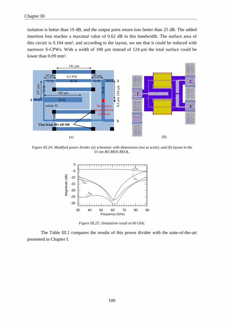
Chapter III
100
isolation is better than 19 dB, and the output ports return loss better than 25 dB. The added
insertion loss reaches a maximal value of 0.62 dB in this bandwidth. The surface area of
this circuit is 0.104 mm², and according to the layout, we see that it could be reduced with
narrower S-CPWs. With a width of 100 µm instead of 124 µm the total surface could be
lower than 0.09 mm².
Figure III.24: Modified power divider (a) schematic with dimensions (not at scale), and (b) layout in the 55 nm BiCMOS BEOL.
Figure III.25: Simulation result at 60 GHz.
The Table III.1 compares the results of this power divider with the state-of-the-art
presented in Chapter I.
10
4 µ
m
160 µm
141 µm
42 µm
10
7 µ
m
50 µm
8.6
µm
83 Ω
26 Ω 2
6 Ω
50 Ω
50 Ω 72 Ω
72
Ω
Resistance in polysilicon
substrate
72 Ω
(a) (b)
1
2
3
S-CPW
µstrip TL
Vias from M1 till M8
1
2
3
! !!
*
30 40 50 60 70 80 90
-30
-25
-20
-15
-10
-5
0
Frequency (GHz)
Mag
nitu
de (
dB)

Chapter III
101
Table III.1 : Comparison of the simulated power divider with the state-of-the-art.
III.6.2 Sensitivity to the resistance value
In CMOS technology, the polysilicon resistances as the one used here exhibit a
variation of ± 20 % around the nominal value. It is thus important to verify the impact of
such variation on the power divider performances. As the resistance determines only the
isolation and the output ports matching, only and * are modified with R. Figure
III.26(a) and Figure III.26(b) shows and * for the lowest and greatest possible values,
80 Ω and 120 Ω, respectively. Still in the bandwidth between 53 GHz and 65 GHz,
determined with a return loss !! better than 20 dB, the isolation is in the worst case better
than 18 dB and is better than 19.8 dB.
Figure III.26: Output port and isolation * simulated at 60 GHz with (a) R = 80 Ω and (b) R = 120 Ω.
The resistance variation degrades the isolation and the output ports matching but
simulated results show still acceptable performances. The polysilicon resistance of 100 Ω
has also been designed alone on the same chip in order to extract its exact value.
S11
(dB)S22 & S33
(dB)
[54]/90 nm CMOS
60slow-wave
elevated coplanar waveguide
-5.3 -8 -11 -12 -5.3 -6 -10 -11 0.051
[55]/90 nm CMOS
45asymmetrical shunt-
stub andmeander-line
-3.9 -21 -15 -19 -4.2 <-13 -14 -15 0.06
[56]/0.13 um BiCMOS
60 meander-line -3.5 -19 -17 -22 -3.7 <-17 <-17 -18 0.12
[57]/0.18 µm SiGe BiCMOS
60floating defected
grounding structureand meander-line
-4.5 - -16.5 -21 -4.3 - -16.5 -19 0.09
This work 60S-CPW, stub and
resistor acces-3.55 -28 -28 -26 -3.62 -25 -25 -19 0.104
Ref./Tech.Isolation
(dB)
Max. insertion
loss(dB)
Min.isolation
(dB)
Area
(mm2)
In 20 % bandwidthReturn loss
Return loss Freq.(GHz)
TopologyInsertion
loss(dB)
S11
(dB)S22 & S33
(dB)
30 40 50 60 70 80 90-45
-40
-35
-30
-25
-20
-15
-10
-5
Frequency (GHz)
Mag
nitu
de (
dB)
30 40 50 60 70 80 90-45
-40
-35
-30
-25
-20
-15
-10
-5
Frequency (GHz)
Mag
nitu
de (
dB)
* *
(a) (b)

Chapter III
102
III.7 Conclusion
A new topology of power divider was studied. It leads to more flexibility and better
compactness as compared to the classical Wilkinson power divider. Hence, it is well suited
for a fabrication in silicon technology at millimetre-wave frequencies. Design rules were
carried out thanks to design graphs, and a simple method of optimization.
Two power dividers were realized at 2.45 GHz in a PCB technology as proofs-of-
concept, with different characteristics. They proved the high level of flexibility offered by
the new developed topology. Measurement and simulation results were in very good
agreement and proved the efficiency of the design method. The two 1:4 antenna arrays
feeding network achieved thanks to the flexible power divider, can minimize the surface
area of these feeding networks.
The simulation results and the surface area of the modified power divider designed
at 60 GHz in the 55 nm BiCMOS technology confirmed that the new proposed topology is
well suited for CMOS millimetre-wave power dividers. It ensures a low loss, full-matched
and isolated component together with a small surface, thanks to the use of S-CPW with
high quality factor. The measurement of this up-coming circuit should confirm the
expectation.
If we keep in mind beam-steering application, efficient feeding circuits for antenna
arrays can now be achieved and only reflection type phase shifters (RTPS) with high FoM
have to be performed yet. In the next chapter two topologies of RTPS are provided, one in
RF in PCB technology and another one at 60 GHz in CMOS.

Chapter IV
103
: New topologies of Reflection Type Phase Chapter IVShifter for high figure of merit
Phase shifters, used to adjust the phase of the wave, are widely used in radar phased
array systems. They have to be compact, low loss, and low cost to enable consumer
applications.
As explained in the first chapter, among the three main types of passive phase
shifters which are the switched-network approach, the loaded transmission lines (TLs), and
the reflection type (RTPS), only the last associates continuous and accurate phase shift with
good matching. Also, it has been shown that reflection type phase shifters reaching 360° of
phase shift and/or with really small insertion loss variation can be realized in printed circuit
board technology (PCB). Concerning integrated technology, the literature barely provide
RTPS with phase shift higher than 200° at 60 GHz, and seems totally void for phase shift of
360°. The referred devices exhibit high insertion loss leading to poor figures of merit
(FoM). As already said in chapter I, the FoM is defined by the ratio of the maximal relative
phase shift over the maximal insertion load.
û4ü = ÝaýºÝa3\Þ3aкÞÄℎaþÞþℎºàÐ'ºb°)ÝaýºÝa3ºbþÞ\к4b34þþ'=) (IV-1)
In this chapter, three RTPSs with design method are proposed in PCB technology in
order to reach high FoM. The reflection loads are easy to design, composed of one
transmission line with varactors, and without extra lumped element. For proof of concept,
one RTPS was realized to achieve a maximal phase shift of 200° with a maximal FoM,
while the others were designed to reach 360° of phase shift, but with a lower FoM. Special
attention is paid to the insertion loss in order to keep it as constant as possible whatever
phase shift. The background principle is explained, the design procedure is given and
circuits design and experimental results are described. A very good agreement between
measurement and simulation results was achieved.
One RTPS in integrated technology was also designed at 60 GHz. Its reflection
loads are based on a slow-wave coplanar waveguides (S-CPW) phase shifter with variable
capacitors. The topology of this new phase shifter which is currently under study in our
laboratory is explained. As the circuit is in-process, only the simulation results are
presented. A phase shift of 341° is expected.
Finally, a new concept of reflection load for RTPS is suggested as a perspective,
mixing digital and analog control to reach 360° of phase shift, high FoM and compactness.
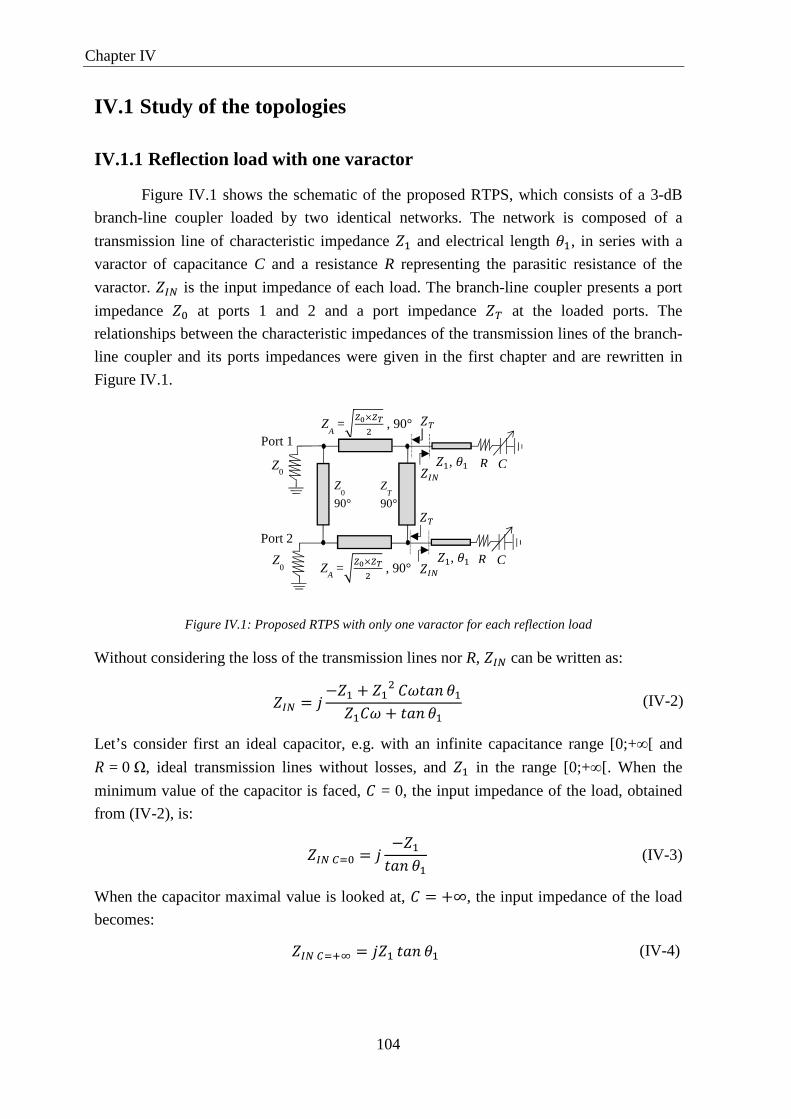
Chapter IV
104
IV.1 Study of the topologies
IV.1.1 Reflection load with one varactor
Figure IV.1 shows the schematic of the proposed RTPS, which consists of a 3-dB
branch-line coupler loaded by two identical networks. The network is composed of a
transmission line of characteristic impedance ! and electrical length >!, in series with a
varactor of capacitance C and a resistance R representing the parasitic resistance of the
varactor. is the input impedance of each load. The branch-line coupler presents a port
impedance at ports 1 and 2 and a port impedance at the loaded ports. The
relationships between the characteristic impedances of the transmission lines of the branch-
line coupler and its ports impedances were given in the first chapter and are rewritten in
Figure IV.1.
Figure IV.1: Proposed RTPS with only one varactor for each reflection load
Without considering the loss of the transmission lines nor R, can be written as:
= ! ( ! 2NÐab >!!2N ( Ðab >! (IV-2)
Let’s consider first an ideal capacitor, e.g. with an infinite capacitance range [0;+∞[ and = 0 Ω, ideal transmission lines without losses, and ! in the range [0;+∞[. When the
minimum value of the capacitor is faced, 2 = 0, the input impedance of the load, obtained
from (IV-2), is:
= !Ðab >! (IV-3)
When the capacitor maximal value is looked at, 2 = (∞, the input impedance of the load
becomes:
$~ = ! Ðab >! (IV-4)
Port 1
Port 2
R!, >!
C
Z0
ZA =+-.-O , 90°
Z0
90°
ZT
90°
Z0
R!, >! C
ZA =+-.-O , 90°

Chapter IV
105
It is easy to demonstrate from:
M = ( ab=! = ΓL (IV-5)
already given in chapter I, that the relative phase-shifting is:
X = 2 sarctan ]gBjZf ^ arctan ]ghiZf ^t. (IV-6)
where ghi = 8Ý'$~) and gBj = 8Ý'). According to (IV-3), (IV-4)
and (IV-6) the relative phase shift can be written as:
X = 2 ;arctan !Ðab >! arctan ]! Ðab >! ^< (IV-7)
In order to get a phase shift X = 360° equations (IV.7) have to be checked:
arctan !Ðab >! = ±90°and arctan ]! Ðab >! ^ = ∓90° (IV-8)
leading to:
!Ðab >! =±∞and ! Ðab >! = ∓∞ (IV-9)
The first solution for (IV-9) is = 0 Ω with ! and Ðab >! having finite values
different from 0, which means >! different from 0°. The second solution is ! = (∞ with and Ðab >! having finite values different from 0. As and ! have a limited value
fixed by the technology, a relative phase shift of 360° cannot be reached. Once and !
are fixed, when plotting ∆X given by (IV-7) as a function of Ðab >!, it can be shown that ∆X varied between minimum and maximum values. By equalling to 0 the derivative of ∆X,
the condition Ðab >! = 1 is obtained. For >! ranging between 0 and 180° the two solutions
of this condition are >! = 45° and 135°. They correspond either to a maximum or a
minimum value of ∆X. A study about the sign of the derivative of ∆X showed that >! = 45°
and 135° correspond to a maximum and a minimum value of relative phase shift in the case ! / , respectively. It is the opposite when ! < . ! / is the most attractive
condition as the maximal relative phase shift is obtained with a shorter >!, 45° instead of
135°.
The varactor capacitance variation is also limited, and a series parasitic resistance
should be taken into account. Hence the practical results may differ from the theoretical
ones previously presented for an ideal circuit. In order to point out the practical limitations,
Figure IV.2 shows the performances of the RTPS versus !, with >! = 45°, C in the range

Chapter IV
106
0.45-2.72 pF with = 1 Ω, corresponding to practically available varactors, and with a
conventional ideal branch-line coupler = 50 Ω, at a working frequency equal to 2 GHz.
The formulas necessary to calculate the insertion loss and the phase shift of the RTPS
presented in Figure IV.1, and taking into account R, are given in (B-3), (B-4), (B-6) and
(B-7) in the Appendix-B.
Figure IV.2: RTPS performances versus ! with one varactor for each reflection load. >! = 45°, C [0.45-2.72] pF, = 1 Ω and = 50 Ω, at 2 GHz.
For the FoM calculation (IV-1), 0.3 dB of added losses were taken into account in
order to consider the coupler insertion loss as estimated with ADS. Hence the FoM values
are very realistic. As expected the phase shift increases with ! (getting closer to the
solution ! = (∞), whilst the maximal insertion loss, and so it is for the insertion loss
variation, decrease after a maximum reached for 60 Ω. For ! = 120 Ω the maximal
insertion loss is quite low, leading to a high FoM of 318 °/dB for a phase shift of 160°.
Figure IV.3 presents the performances of the RTPS versus >!, with ! = 120 Ω, for the
same varactor and than previously, at 2 GHz. For >! between 0 and 360°, two points of
maximum phase shift are obtained, one for >! = 35° and one for >!= 215° (e.g.
35° + 180°), both leading to 168.6° of phase shift. As the capacitance range variation is
limited, equation (IV-7) determined with C in the range [0;+∞[ is not valid anymore. Hence
the condition >! = 45° with ! / leading to the highest phase variation is not strictly
valid anymore. As a consequence, the optimal >! is 35° instead of 45°. Similarly, the two
minimum relative phase shifts are reached for >! = 125° and 305° (i.e. 125° + 180°)
instead of 135° and 315° (i.e. 135° + 180°) as determined previously. Further, the maximal
values of the insertion loss and relative phase shift are not reached for the same >!.
Consequently, >! giving the maximal FoMs are slightly shifted as compared to the ones
giving the maximal phase variation. Finally, the FoM is maximal for >! equal to 45° (same
point which has been found in Figure IV.2) and 225°, and reaches 318 °/dB for 160° of
phase shift.
20 40 60 80 100 1200,00
0,05
0,10
0,15
0,20
0,25
0,30
Z1 (Ω)
M
ax. i
nser
tion
loss
&
inse
rtio
n lo
ss v
aria
tion
(dB
)
Max. loss Loss variation Phase shift FoM
0
50
100
150
200
250
300
Pha
se s
hift
(deg
) &
FoM
(de
g/dB
)
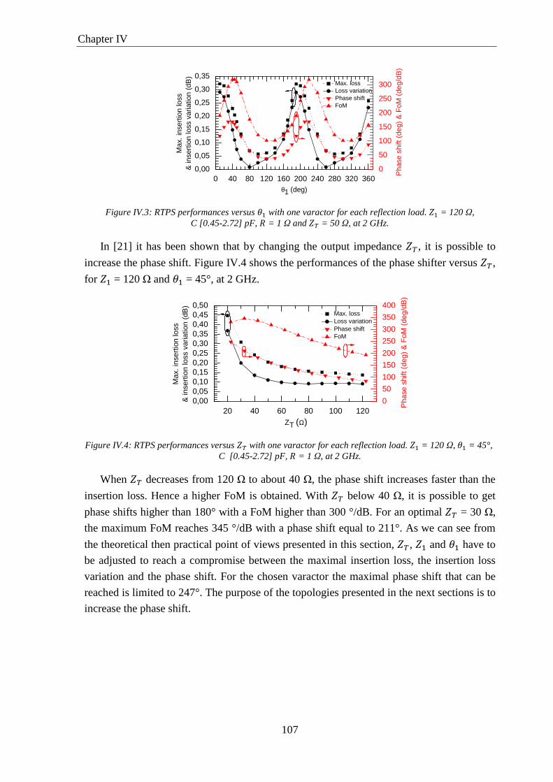
Chapter IV
107
Figure IV.3: RTPS performances versus >! with one varactor for each reflection load. ! = 120 Ω, C [0.45-2.72] pF, = 1 Ω and = 50 Ω, at 2 GHz.
In [21] it has been shown that by changing the output impedance , it is possible to
increase the phase shift. Figure IV.4 shows the performances of the phase shifter versus ,
for ! = 120 Ω and >! = 45°, at 2 GHz.
Figure IV.4: RTPS performances versus with one varactor for each reflection load. ! = 120 Ω,>! = 45°, C [0.45-2.72] pF, = 1 Ω, at 2 GHz.
When decreases from 120 Ω to about 40 Ω, the phase shift increases faster than the
insertion loss. Hence a higher FoM is obtained. With below 40 Ω, it is possible to get
phase shifts higher than 180° with a FoM higher than 300 °/dB. For an optimal = 30 Ω,
the maximum FoM reaches 345 °/dB with a phase shift equal to 211°. As we can see from
the theoretical then practical point of views presented in this section, , ! and >! have to
be adjusted to reach a compromise between the maximal insertion loss, the insertion loss
variation and the phase shift. For the chosen varactor the maximal phase shift that can be
reached is limited to 247°. The purpose of the topologies presented in the next sections is to
increase the phase shift.
0 40 80 120 160 200 240 280 320 3600,00
0,05
0,10
0,15
0,20
0,25
0,30
0,35
θ1 (deg)
Max
. ins
ertio
n lo
ss
& in
sert
ion
loss
var
iatio
n (d
B)
Max. loss Loss variation Phase shift FoM
0
50
100
150
200
250
300
Pha
se s
hift
(deg
) &
FoM
(de
g/dB
)
20 40 60 80 100 1200,000,050,100,150,200,250,300,350,400,450,50
ZT (Ω)
Max
. ins
ertio
n lo
ss
& in
sert
ion
loss
var
iatio
n (d
B)
Max. loss Loss variation Phase shift FoM
0
50
100
150
200
250
300
350
400
Pha
se s
hift
(deg
) &
FoM
(de
g/dB
)

Chapter IV
108
IV.1.2 Reflection load with two varactors
Figure IV.5: Proposed reflection load with two varactors
The previous topology gives really promising performances in terms of insertion loss,
insertion loss variation, and FoM, but does not achieve 360° of phase shift needed in some
applications. In order to get higher phase shift, another varactor was placed at the beginning
of the load network, between the branch-line coupler output and the transmission line
(!,>!), as shown in Figure IV.5. The theoretical input impedance when considering ideal
circuits, and neglecting R, can be written as:
= ! ( ! 2NÐab >!2!2N ( Ðab >! !2NÐab>! (IV-10)
The structures proposed in [23] and [24] seem quite similar to ours. However, as shown
in the first chapter, in [23], inductances and resistances were added and the varactors were
connected in series with the transmission line. In [24], stubs were added between varactors
and ground. Moreover, in both papers the electrical length of the transmission line was
fixed to ? 4⁄ .
Considering an ideal capacitor, e.g. = 0 Ω with a capacitance range [0;+∞[, and an
ideal transmission line, e.g. without losses and with ! in the range [0;+∞[, when the
capacitor has the minimum value, 2 = 0 pF, the input impedance of the load obtained from
(IV-10) is:
D = !Ðab >! (IV-11)
When the capacitor has the maximal value, 2 = (∞, the input impedance of the load is:
D$~ = 0 (IV-12)
With the solutions (IV-11) and (IV-12) it seems that the maximal possible phase shift
according to (IV-6) is 90° with ! =(∞ and >! different from 0°. In practice, the
variation of 8Ý') with C is not monotonous as shown on Figure IV.6 so that the phase
shift is greater than 360°, when considering an infinite variation of the capacitor. With a
realistic variation of the capacitor, e.g. a varactor range of 0.45-2.72 pF as considered
previously, the 360° phase shift cannot be reached, even after an optimization on !, >! and . We will focus on that point more precisely by the following.
R!, >! C R
C

Chapter IV
109
Figure IV.6. 8Ý') versus C for reflection load with two varactors, ! = 120 Ω,>! = 45°, = 0 Ω, at 2 GHz.
IV.1.3 Reflection load with three varactors
In order to get a 360° phase shift without complicating the topology of the load and
with the same varactor without applying another bias voltage, a varactor was added in
parallel of the second one, as shown in Figure IV.7. In that way, the value of the shunt
capacitance is doubled.
Figure IV.7: Proposed reflection load with three varactors
The input impedance of this load without considering R can be written as:
= ! ( ! 2NÐab >!3!2N ( Ðab >! 2!2NÐab>! (IV-13)
Figure IV.8: 8Ý') versus C for reflection load with three varactors, ! = 120 Ω,>! = 45°, = 0 Ω, at 2 GHz.
0,0 0,5 1,0 1,5 2,0 2,5 3,0 3,5 4,0 4,5
-400
-200
0
200
400
C (pF)
Im(Z
IN)
0,6 0,8 1,0 1,2 1,4 1,6 1,8 2,0 2,2 2,4 2,6
-400
-200
0
200
400
C (pF)
Im(Z
IN)
R
!, >! C R
C
R C

Chapter IV
110
As for the load with two varactors, the variation of with C is not monotonous, in
Figure IV.8. Moreover, for the particular values of !, >! and the variation of C chosen
here, the extreme values of C lead to D. ≈ D. ≈ -18. Figure IV.9 shows the
relative phase shift between the two extreme values of C with two and three varactors.
Figure IV.9: Relative phase shift of the RTPS versus with the loads of two or three varactors for each reflection load. ! = 120 Ω,>! = 45°, Cmin = 0.45 pF, Cmax = 2.72 pF, = 0 Ω.
It is clear that the addition of a third varactor leads to a higher phase shift. The phase
shift obtained with the reflection load with three varactors is equal to 360°, whatever the
value of . This is due to gBj = 8Ý'D. ) ≈ ghi = 8Ý'D.), introduced in (IV-6). As we will see further, with other values of !, >! it is possible to get
phase shifts higher than 360°.
Figure IV.10 gives the RTPS return loss versus for the reflection loads with one
and three varactors. The worst return loss in a 10 % bandwidth was considered. The lower leads to the worst return loss. With = 20 Ω, the return loss is 12.2 dB for the two
kinds of reflection loads, whereas with = 120 Ω it is 16.7 dB for the reflection load with
one varactor and 17.4 dB with three varactors, respectively. This plot proves that the three
varactors type reflection load allows the realization of a 360° phase shifter without
scarifying the return loss, e.g. without any trade-off between the FoM and the return loss.
Figure IV.10: Worst return loss versus with loads carried out with one and three varactors for each reflection load. ! = 120 Ω,>! = 45°, C [0.45-2.72] pF, = 1 Ω, at 2 GHz.
20 40 60 80 100 120300
310
320
330
340
350
360
370
ZT (Ω)
Pha
se s
hift
(deg
)
Load with 2 varactors Load with 3 varactors
20 40 60 80 100 12012
13
14
15
16
17
18
Load with 1 varactor Load with 3 varactors
ZT (Ω)
Ret
urn
loss
(dB
)

Chapter IV
111
IV.2 Design procedure
The choice of the set of value >!, ! and results from a compromise between the
maximal insertion loss, the insertion loss variation and the phase shift. An algorithm was
used in order to select >!, ! and for each reflection load proposed here. It has been
considered that the return loss should be always better than 10 dB in a 10 % bandwidth
whatever the values of the parameters are. The algorithm is given in Figure IV.11.
First of all, a varactor has to be chosen which gives 2ghi, 2gBj and R. The limits of
the characteristic impedance !, e.g. !ghi and !gBj, and the hybrid output impedance , e.g. ghi and gBj, are fixed by the technology. The insertion loss cannot be
calculated only at the two extreme values of C because its variation may not be
monotonous, so it has to be calculated for intermediate values. 2¤§ was used as
incremental value between 2ghi and 2gBj. Typically 2¤§ = 0.01 pF is a good choice, with
a good comprise between calculation time and accuracy. At the beginning, the maximal
insertion loss 8gBj, the maximal insertion loss variation 8gBj, the minimum phase shift Xghi and the working frequency freq have to be fixed. The maximal phase shift is
calculated with equations (B-3), (B-4), (B-6) and (B-7) for a load with one varactor and
with equations (B-3), (B-5), (B-6), (B-7) for two or three varactors, respectively, given in
Appendix-B. If the calculated phase shift is lower than the targeted one, one of the three
parameters >!, ! or is incremented, otherwise the insertion loss is calculated for the
intermediate values of C to deduce 8gBj and 8gBj. If they are lower than the fixed
criterions the solution is saved, else >!, ! or is incremented. If after all the
combinations of >!, ! and any solution is found, this means that the goals are too
ambitious and less constraints have to be applied in order to find a solution. At the end, the
designer can select a solution among all the possible ones.

Chapter IV
112
Figure IV.11: Algorithm for finding solutions
IV.3 Circuits design and experimental results in PCB
Three RTPS were fabricated to illustrate and validate the topologies and design
methodology described in the last section, one with the reflection load presented in Figure
IV.1, a second one with the reflection load presented in Figure IV.5 and cascaded with
another phase shifter in order to reach 360° and finally a third one with the reflection load
presented in Figure IV.7. In the three cases, the working frequency is 2 GHz and a SMD
silicon hyperabrupt-junction varactor diode was used with 2ghi = 0.45 pF (20 V), 2gBj = 2.72 pF (0 V) and = 1 Ω. The technology limits the characteristic impedances of
the microstrip transmission lines between 20 and 130 Ω. The circuits were fabricated on
Rogers RO4003 substrate, with relative effective permittivity 3.38 and thickness 813 µm.
All the measurements were carried out with a TRL calibration and the bias voltage was
applied directly from the VNA through SMA connectors soldered on the board.
2ghi , 2gBj , 2¤§, ,!ghi , !gBj , ghi,gBj, >!gBj ,Xghi , 8gBj , 8gBj , à\Þ, ! = !ghi , >! = 0, = ghi CalculateX with
Cmin and Cmax X ≥ Xݺb?
Save solution
Yes
No
No
Yes
Calculate8 forall2valuesbetween 2ghiand2gBj with2¤§ 8 ≤ 8gBj? 8 ≤ 8gBj ?
incrementof !or>!or`
! = !gBj? >! = >!gBj ? = gBj?
Select a solution
No
Yes

Chapter IV
113
IV.3.1 Reflection load with one varactor
The optimisation procedure gives a maximal reachable phase shift of 270° with ! = 130 Ω, >! = 35° and = 20 Ω. R leads to an amount of 0.59 dB of insertion loss and
0.53 dB of insertion loss variation. 0.3 dB of insertion loss were added in order to take into
account the insertion loss of the branch-line coupler, leading to a total insertion loss equal
to 0.89 dB. Hence the FoM of the RTPS was estimated to 303 °/dB. For a minimum 180°
phase shift, a higher FoM with lower insertion loss could be reached. For example, an
RTPS with ! = 116 Ω, >! = 45° and = 30 Ω achieves 211° of phase shift and gives the
highest estimated FoM for a phase shift higher than 180°, with 346 °/dB. R adds 0.31 dB of
insertion loss and only 0.2 dB of insertion loss variation.
Figure IV.12: Simulated performances versus frequency, (a) insertion loss, (b) return loss, and (c) phase shift. Each reflection load is with one varactor, ! = 116 Ω, >! = 45° and = 30 Ω.
Figure IV.12 shows the electrical simulation (with ADS) of this last RTPS, taking
into account the losses due to the branch-line coupler. Simulations were carried out for the
whole range of the varactors bias voltage, with a step of 2 V. The maximal insertion loss is
0.65 dB at 2 GHz, as shown in Figure IV.12(a), which is close to the estimated insertion
loss in the FoM calculus (0.31 dB + 0.3 dB due to the branch-line), and the 0.25 dB of
insertion loss variation also fits with the 0.2 dB theoretically calculated. The maximal
1,90 1,95 2,00 2,05 2,10-1,5
-1,0
-0,5
0,0
Vc = 0V Vc = 6V Vc = 12V Vc = 18V Vc = 2V Vc = 8V Vc = 14V Vc = 20V Vc = 4V Vc = 10V Vc = 16V
Frequency (GHz)
|S21
| (dB
)
1,90 1,95 2,00 2,05 2,10-45
-40
-35
-30
-25
-20
-15
-10
-5
Vc = 0V Vc = 6V Vc = 12V Vc = 18V Vc = 2V Vc = 8V Vc = 14V Vc = 20V Vc = 4V Vc = 10V Vc = 16V
Frequency (GHz)
|S11
| (dB
)
1,90 1,95 2,00 2,05 2,100
100
200
300
Vc = 0V Vc = 6V Vc = 12V Vc = 18V Vc = 2V Vc = 8V Vc = 14V Vc = 20V Vc = 4V Vc = 10V Vc = 16V
Frequency (GHz)
Pha
se s
hift
(deg
)
(a) (b)
(c)
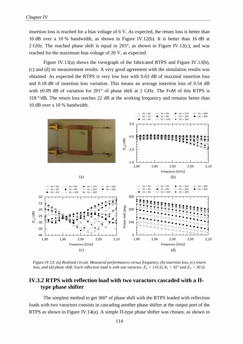
Chapter IV
114
insertion loss is reached for a bias voltage of 6 V. As expected, the return loss is better than
10 dB over a 10 % bandwidth, as shown in Figure IV.12(b). It is better than 16 dB at
2 GHz. The reached phase shift is equal to 203°, as shown in Figure IV.12(c), and was
reached for the maximum bias voltage of 20 V, as expected.
Figure IV.13(a) shows the viewgraph of the fabricated RTPS and Figure IV.13(b),
(c) and (d) its measurement results. A very good agreement with the simulation results was
obtained. As expected the RTPS is very low loss with 0.63 dB of maximal insertion loss
and 0.18 dB of insertion loss variation. This means an average insertion loss of 0.54 dB
with ±0.09 dB of variation for 201° of phase shift at 2 GHz. The FoM of this RTPS is
318 °/dB. The return loss reaches 22 dB at the working frequency and remains better than
10 dB over a 10 % bandwidth.
Figure IV.13: (a) Realized circuit. Measured performances versus frequency, (b) insertion loss, (c) return loss, and (d) phase shift. Each reflection load is with one varactor, ! = 116 Ω, >! = 45° and = 30 Ω.
IV.3.2 RTPS with reflection load with two varactors cascaded with a Π-type phase shifter
The simplest method to get 360° of phase shift with the RTPS loaded with reflection
loads with two varactors consists in cascading another phase shifter at the output port of the
RTPS as shown in Figure IV.14(a). A simple Π-type phase shifter was chosen, as shown in
(a) (b)
(c)
1,90 1,95 2,00 2,05 2,10-1,5
-1,0
-0,5
0,0
Vc = 0V Vc = 6V Vc = 12V Vc = 18V Vc = 2V Vc = 8V Vc = 14V Vc = 20V Vc = 4V Vc = 10V Vc = 16V
Frequency (GHz)
|S21
| (dB
)
1,90 1,95 2,00 2,05 2,10-40
-35
-30
-25
-20
-15
-10
Vc = 0V Vc = 6V Vc = 12V Vc = 18V Vc = 2V Vc = 8V Vc = 14V Vc = 20V Vc = 4V Vc = 10V Vc = 16V
Frequency (GHz)
|S11
| (dB
)
1,90 1,95 2,00 2,05 2,100
100
200
300
Vc = 0V Vc = 6V Vc = 12V Vc = 18V Vc = 2V Vc = 8V Vc = 14V Vc = 20V Vc = 4V Vc = 10V Vc = 16V
Frequency (GHz)
Pha
se s
hift
(deg
)
(d)

Chapter IV
115
Figure IV.14(b). Both phase shifters, RTPS and Π-type, need to be optimized to the lowest
insertion loss because they will be added in the global circuit. The Π-type phase shifter has
to be built with the same varactor as for the RTPS in order not to complicate the bias
voltage circuit and to have only one voltage control.
Figure IV.14: (a) RTPS cascaded with phase shifter. (b) Π-type phase shifter.
IV.3.2.1 Choice of the RTPS
The procedure presented in Figure IV.11 with the loads given in Figure IV.5, with
the capacitor range 0.45-2.72 pF, R = 1 Ω and characteristic impedances ranging between
20 and 130 Ω, proposes a RTPS with 0.66 dB of insertion loss due to R and 0.6 dB of
insertion loss variation, with ! = 130 Ω, >! = 35° and = 20 Ω, at 2 GHz. The phase
variation of such component is 335°. Figure IV.15 shows the electrical simulations (ADS)
of this RTPS. The maximal insertion loss is 1.18 dB with 0.88 dB of insertion loss variation
for 338° of phase shift at 2 GHz, leading to an expected FoM of 286 °/dB. Comparing to
the theoretical calculation with the loss due to R alone, 0.52 dB of insertion loss are added
by taking into account the extra loss due to the TLs and junctions of the branch-line. The
insertion loss variation is increased as well. The simulated (ADS) return loss in a 10 %
bandwidth is better than 10 dB.
90° BRANCH
LINE COUPLER
GH
GH
IN
OUT Phase Shifter
, > C C
(a) (b)

Chapter IV
116
Figure IV.15: Simulated performances versus frequency. (a) Insertion loss, (b) return loss, (c) phase shift. Each reflection load is with two varactors. ! = 130 Ω, >! = 35° and = 20 Ω.
IV.3.2.2 Optimization of the Π-type phase shifter
The characteristic impedance and the electrical length of the TL in the Π-type phase
shifter, named (,>) in Figure IV.14(b), has to be optimized to add minimal insertion
loss, not to degrade the return loss and to complete the missing phase shift in order to reach
360°. Figure IV.16 shows the performances of the Π-type phase shifter optimized with =130 Ω and > =20° at 2 GHz and the same varactors as used previously. The phase
shift is 82°. With the 338° of phase shift simulated with the previous RTPS, the added Π-
type phase shifter will easily allow the designer to get 360°. The maximal insertion loss is
0.73 dB with 0.66 dB of insertion loss variation, a return loss of 17 dB in the worst case at
2 GHz, and 12 dB in the 10 % bandwidth. About 60 % of the phase variation is achieved
between 0 and 2 V (among 20 V) which means a strong non-linearity. For this variation the
level of insertion loss and insertion loss variation is high.
(a) (b)
(c)
1,90 1,95 2,00 2,05 2,10-2,0-1,8-1,6-1,4-1,2-1,0-0,8-0,6-0,4-0,20,0
Vc = 0V Vc = 6V Vc = 12V Vc = 18V Vc = 2V Vc = 8V Vc = 14V Vc = 20V Vc = 4V Vc = 10V Vc = 16V
Frequency (GHz)
|S
21| (
dB)
1,90 1,95 2,00 2,05 2,10-45
-40
-35
-30
-25
-20
-15
-10
-5
Vc = 0V Vc = 6V Vc = 12V Vc = 18V Vc = 2V Vc = 8V Vc = 14V Vc = 20V Vc = 4V Vc = 10V Vc = 16V
Frequency (GHz)
|S11
| (dB
)
1,90 1,95 2,00 2,05 2,100
100
200
300
400
Vc = 0V Vc = 6V Vc = 12V Vc = 18V Vc = 2V Vc = 8V Vc = 14V Vc = 20V Vc = 4V Vc = 10V Vc = 16V
Frequency (GHz)
Pha
se s
hift
(deg
)

Chapter IV
117
Figure IV.16: Simulated Π-type phase shifter performances versus frequency. (a) Insertion loss, (b) return loss, (c) phase shift. = 130 Ω and > = 20°.
IV.3.2.3 Simulation of the RTPS with the Π-type phase shifter
The simulation results of the global phase shifter (RTPS cascaded with the Π-type
phase shifter) are shown in Figure IV.17. The maximal phase shift is 420° for a bias voltage
between 0 and 20 V with a maximal insertion loss of 1.65 dB and 1.25 dB of insertion loss
variation, leading to a FoM of 254 °/dB. As no more than a full cycle is needed, for a bias
ranging between 1 and 20 V, about 360° of phase shift is obtained with 1.3 dB of maximal
insertion loss leading to a better FoM of 277 °/dB. The insertion loss variation is reduced to
0.9 dB. Also, starting the bias voltage from 1 V instead of 0 V improves the worst matching
over the 10 % bandwidth, from 6 dB to 9 dB.
(a) (b)
(c)
1,90 1,95 2,00 2,05 2,10
-1,4
-1,2
-1,0
-0,8
-0,6
-0,4
-0,2
0,0
Vc = 0V Vc = 6V Vc = 12V Vc = 18V Vc = 2V Vc = 8V Vc = 14V Vc = 20V Vc = 4V Vc = 10V Vc = 16V
Frequency (GHz)
|S21
| (dB
)
1,90 1,95 2,00 2,05 2,10-40
-35
-30
-25
-20
-15
-10
-5
Vc = 0V Vc = 6V Vc = 12V Vc = 18V Vc = 2V Vc = 8V Vc = 14V Vc = 20V Vc = 4V Vc = 10V Vc = 16V
Frequency (GHz)
|S11
| (dB
)
1,90 1,95 2,00 2,05 2,100
102030405060708090
100
Vc = 0V Vc = 6V Vc = 12V Vc = 18V Vc = 2V Vc = 8V Vc = 14V Vc = 20V Vc = 4V Vc = 10V Vc = 16V
Frequency (GHz)
Pha
se s
hift
(deg
)
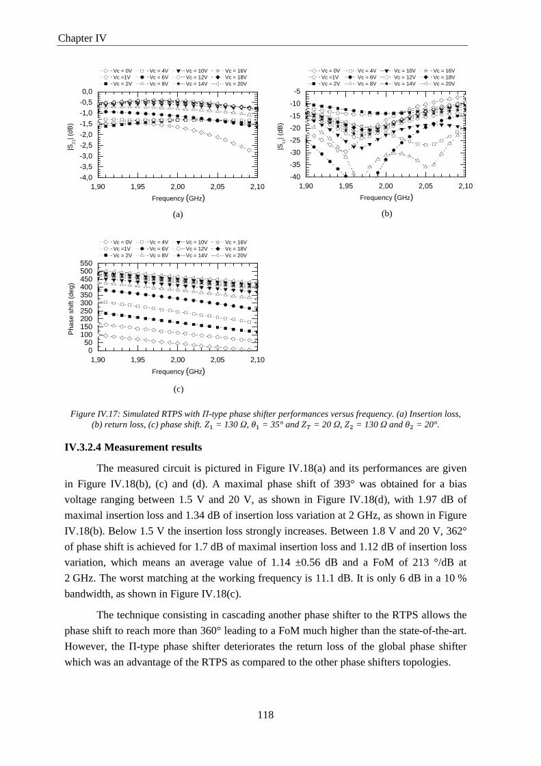
Chapter IV
118
Figure IV.17: Simulated RTPS with Π-type phase shifter performances versus frequency. (a) Insertion loss, (b) return loss, (c) phase shift. ! = 130 Ω, >! = 35° and = 20 Ω, = 130 Ω and > = 20°.
IV.3.2.4 Measurement results
The measured circuit is pictured in Figure IV.18(a) and its performances are given
in Figure IV.18(b), (c) and (d). A maximal phase shift of 393° was obtained for a bias
voltage ranging between 1.5 V and 20 V, as shown in Figure IV.18(d), with 1.97 dB of
maximal insertion loss and 1.34 dB of insertion loss variation at 2 GHz, as shown in Figure
IV.18(b). Below 1.5 V the insertion loss strongly increases. Between 1.8 V and 20 V, 362°
of phase shift is achieved for 1.7 dB of maximal insertion loss and 1.12 dB of insertion loss
variation, which means an average value of 1.14 ±0.56 dB and a FoM of 213 °/dB at
2 GHz. The worst matching at the working frequency is 11.1 dB. It is only 6 dB in a 10 %
bandwidth, as shown in Figure IV.18(c).
The technique consisting in cascading another phase shifter to the RTPS allows the
phase shift to reach more than 360° leading to a FoM much higher than the state-of-the-art.
However, the Π-type phase shifter deteriorates the return loss of the global phase shifter
which was an advantage of the RTPS as compared to the other phase shifters topologies.
(a) (b)
(c)
1,90 1,95 2,00 2,05 2,10-4,0
-3,5
-3,0
-2,5
-2,0
-1,5
-1,0
-0,5
0,0
Vc = 0V Vc = 4V Vc = 10V Vc = 16V Vc =1V Vc = 6V Vc = 12V Vc = 18V Vc = 2V Vc = 8V Vc = 14V Vc = 20V
Frequency (GHz)
|S
21| (
dB)
1,90 1,95 2,00 2,05 2,10-40
-35
-30
-25
-20
-15
-10
-5
Vc = 0V Vc = 4V Vc = 10V Vc = 16V Vc =1V Vc = 6V Vc = 12V Vc = 18V Vc = 2V Vc = 8V Vc = 14V Vc = 20V
Frequency (GHz)
|S11
| (dB
)
1,90 1,95 2,00 2,05 2,100
50100150200250300350400450500550
Vc = 0V Vc = 4V Vc = 10V Vc = 16V Vc =1V Vc = 6V Vc = 12V Vc = 18V Vc = 2V Vc = 8V Vc = 14V Vc = 20V
Frequency (GHz)
Pha
se s
hift
(deg
)

Chapter IV
119
Figure IV.18: (a) Realized circuit. Measured performances versus frequency, (b) insertion loss, (c) return loss, and (d) phase shift. ! = 130 Ω, >! = 35° and = 20 Ω, = 130 Ω and > = 20°.
IV.3.3 Reflection load with three varactors
The purpose was to achieve a phase shift higher than 360° with the topology
described in Figure IV.7. The design procedure leaded to a phase shift of 373° for 0.87 dB
of insertion loss and 0.8 dB of insertion loss variation due to the resistance R, according to
the theoretical formulas given in the Appendix-B, with ! = 120 Ω, >! = 40° and = 30 Ω. Figure IV.19 shows the simulation results. The maximal insertion loss and
insertion loss variation are 1.42 dB and 1.1 dB, respectively, as shown in Figure IV.19(a).
The return loss is better than 11 dB over a 10 % bandwidth, see in Figure IV.19(b). The
phase shift reaches 372°, Figure IV.19(c).
(a) (b)
(c) (d)
1,90 1,95 2,00 2,05 2,10-4,0
-3,5
-3,0
-2,5
-2,0
-1,5
-1,0
-0,5
0,0
Vc = 1,5V Vc = 4V Vc = 10V Vc = 16V Vc =1,8V Vc = 6V Vc = 12V Vc = 18V Vc = 2V Vc = 8V Vc = 14V Vc = 20V
Frequency (GHz)
|S21
| (dB
)
1,90 1,95 2,00 2,05 2,10-40
-35
-30
-25
-20
-15
-10
-5
Vc = 1,5V Vc = 4V Vc = 10V Vc = 16V Vc =1,8V Vc = 6V Vc = 12V Vc = 18V Vc = 2V Vc = 8V Vc = 14V Vc = 20V
Frequency (GHz)
|S11
| (dB
)
1,90 1,95 2,00 2,05 2,100
50100150200250300350400450500550
Vc = 1,5V Vc = 4V Vc = 10V Vc = 16V Vc =1,8V Vc = 6V Vc = 12V Vc = 18V Vc = 2V Vc = 8V Vc = 14V Vc = 20V
Frequency (GHz)
Pha
se s
hift
(deg
)

Chapter IV
120
Figure IV.19: Simulated performances versus frequency, (a) insertion loss, (b) return loss, and (c) phase shift. 6 varactors. ! = 120 Ω, >! = 40° and = 30 Ω.
Figure IV.20(a) shows the viewgraph of the fabricated RTPS and Figure IV.20(b),
(c) and (d) its measurement results. Here again a very good agreement between
measurement and simulation results was obtained. The insertion loss and insertion loss
variation are 1.56 dB and 1.16 dB, respectively, at 2 GHz, as shown in Figure IV.20(b).
This means an average insertion loss of 0.98 dB with ±0.58 dB of variation for 385° of
phase shift, as shown in Figure IV.20(d). The FoM of this device is 246°/dB. The return
loss is 13.4 dB at the working frequency and better than 10.9 dB over a whole 10 %
bandwidth, as shown in Figure IV.20(c). It is worth mentioning that the bias voltage varied
from 0.5 to 20 V. It was not necessary to use a bias voltage lower than 0.5 V because a
phase shift greater than 360° was reached anyway.
(a) (b)
(c)
1,90 1,95 2,00 2,05 2,10-2,0
-1,5
-1,0
-0,5
0,0
Vc = 0V Vc = 6V Vc = 12V Vc = 18V Vc = 2V Vc = 8V Vc = 14V Vc = 20V Vc = 4V Vc = 10V Vc = 16V
Frequency (GHz)
|S
21| (
dB)
1,90 1,95 2,00 2,05 2,10-45
-40
-35
-30
-25
-20
-15
-10
-5
Vc = 0V Vc = 6V Vc = 12V Vc = 18V Vc = 2V Vc = 8V Vc = 14V Vc = 20V Vc = 4V Vc = 10V Vc = 16V
Frequency (GHz)
|S11
| (dB
)
1,90 1,95 2,00 2,05 2,100
100
200
300
400
Vc = 0V Vc = 6V Vc = 12V Vc = 18V Vc = 2V Vc = 8V Vc = 14V Vc = 20V Vc = 4V Vc = 10V Vc = 16V
Frequency (GHz)
Pha
se s
hift
(deg
)

Chapter IV
121
Figure IV.20: (a) Realized circuit. Measured performances versus frequency, (a) insertion loss, (b) return loss, and (c) phase shift. Each reflection load is with three varactors, ! = 120 Ω, >! = 40° and = 30 Ω.
IV.3.4 Results synthesis
Total nb. of
varactors /Topo. of the load
Average insertion loss
(dB)
Insertion loss variation
(dB)
Phase shift (°)
Return loss over a 10 %
BW (dB)
FoM (°/dB)
Simu. (ADS)
Measu- ment
Simu. (ADS)
Measu- ment
Simu. (ADS)
Measu- ment
Simu. (ADS)
Measu- ment
Simu. (ADS)
Measu- ment
2/Figure IV.1
0.525 0.54 ±0.125 ±0.09 203 201 10 10 312 318
6/Figure IV.5+Π-type PS
0.85 1.14 ±0.45 ±0.56 360 # 362 ## 9 6 277 213
6/Figure IV.7
0.87 0.98 ±0.55 ±0.58 372 385 * 11 10.9 262 246
#from 1V to 20V, ##from 1.8V to 20V, *from 0.5V to 20V
Table IV.1: Sum up of the measured performances of the three achieved RTPS
Table IV.1 summarizes the simulated and measured results of the achieved RTPS at
2 GHz. Both fit really well for all the phase shifter. The simulated results are obtained
thanks to circuit analysis on the basis of the topology characteristics determined by the
(a) (b)
(c) (d)
1,90 1,95 2,00 2,05 2,10-2,0
-1,5
-1,0
-0,5
0,0
Vc = 0,5V Vc = 6V Vc = 12V Vc = 18V Vc = 2V Vc = 8V Vc = 14V Vc = 20V Vc = 4V Vc = 10V Vc = 16V
Frequency (GHz)
|S21
| (dB
)
1,90 1,95 2,00 2,05 2,10-35
-30
-25
-20
-15
-10
-5
Vc = 0,5V Vc = 6V Vc = 12V Vc = 18V Vc = 2V Vc = 8V Vc = 14V Vc = 20V Vc = 4V Vc = 10V Vc = 16V
Frequency (GHz)
|S11
| (dB
)
1,90 1,95 2,00 2,05 2,100
100
200
300
400
Vc = 0,5V Vc = 6V Vc = 12V Vc = 18V Vc = 2V Vc = 8V Vc = 14V Vc = 20V Vc = 4V Vc = 10V Vc = 16V
Frequency (GHz)
Pha
se s
hift
(deg
)

Chapter IV
122
theoretical equations given in the Appendix-B and the design procedure explained
previously.
The proposed RTPSs exhibit very high FoM. However, the second solution,
consisting in cascading a RTPS with a Π-type phase shifter, leads to a lower FoM with
higher insertion loss and bad return loss as compared to the third solution which uses 6
varactors too. Consequently, the last solution is better when a 360° phase shift is needed.
For a phase shift lower than 200°, the first solution is more suitable, first because the FoM
is much greater and also because only two varactors are needed which means a lower cost.
IV.4 RTPS in integrated technology
The insertion loss of the RTPS depends on the parasitic resistance of the varactor
and on the loss of the circuit itself (transmission lines, junctions…). In [89], two RTPS
were achieved at 2.45 GHz in a 0.18 µm CMOS technology. For the first one, with a series-
resonating load, it had been shown that 65 % of the 5.6 dB of insertion loss were due to the
varactor load which had a minimal quality factor of 50. For the second RTPS, with a series-
resonating load in Π-shape as shown in the first chapter, 86 % of the 11.9 dB of insertion
loss were due to the varactors. The two varactors used in the load had minimal quality
factors of 33 and 8. No similar analysis has been found at millimetre-wave frequency, but
the high contribution of the varactor for the insertion loss should be even more important
because of lower varactors quality factors at 60 GHz. In [90] varactors were used with a
minimal quality factor of 15 at 60 GHz thanks to the use of differential poly/n-well MOS
varactors having a better quality factor as compared to a single-ended varactor. However,
even with such varactors the insertion loss is very high, 12.5 dB of maximal insertion loss
for a 156° phase shift (as shown in the first chapter).
Here the purpose is to substitute the conventional reflection loads with varactors, by
loaded line phase shifters carried out with S-CPW. In this case, it is possible to associate
the performances of the loaded line phase shifter with the good matching of the RTPS.
IV.4.1 Topology of the reflection load based on a distributed loaded line phase shifter
The loaded line phase shifter was built with a S-CPW in which the capacitances
between the ground and shielding strips can be periodically modified, as shown in Figure
IV.21(a). The total physical length of the S-CPW was divided in eight similar segments
where each segment is composed of ten groups of eight strips as shown in Figure IV.21(b).
There is one variable capacitance per group of strips.

Chapter IV
123
Figure IV.21: (a) Phase shifter based on capacitively switched S-CPW used as a reflection load.(b) Working principle.
All groups of strips in the segments are connected between them according to their
position, e.g. all the groups number one are connected together, all the groups number two
are connected together too and so on… Each capacitance has two states, one with a low
value and one with a high value. This new type of loaded line phase shifter is currently
under study and will lead to a patent demand, so for confidentiality reasons, no more
information about how this two states capacitor is realized in practice can be given. The
groups of finger are driven by a thermometer code, starting from zero to ten, leading to
eleven configurations. Thanks to the variation of these capacitances, it is possible to modify
the global capacitance of the transmission line, and hence to modify its relative effective
permittivity . As its physical length is fixed, when increases, the phase of the
S-CPW increases as well. The average characteristic impedance of this loaded line phase
shifter is 22.5 Ω. This loaded line phase shifter was simulated at 60 GHz in the 55 nm
BiCMOS technology by STMicroelectronics. Its expected performances for the eight
suitable configurations giving the best linearity, among eleven possible configurations, are
shown in Figure IV.22.
Figure IV.22: Simulated performances of the phase shifter for eight configurations at 60 GHz with a 22.5 Ω system characteristic impedance.
0 1 2 3 4 5 6 7-35
-30
-25
-20
-15
-10
-5
0
Configuration
|S21
| & |S
11| (
dB)
S21
S11
Phase shift
0
50
100
150
200
Pha
se s
hift
(deg
)
(a) (b)

Chapter IV
124
By considering a 22.5 Ω system characteristic impedance, the maximal phase shift is 186°
for 2.74 dB of maximal insertion loss and 1.5 dB of insertion loss variation. The return loss
is better than 14.3 dB at 60 GHz.
IV.4.2 Layout and simulation of the RTPS
The loaded line phase shifter based on S-CPW is terminated by a short circuit to
serve as the loading network of the RTPS. The output ports impedance of the branch-
line coupler was tuned to get the best compromise between the insertion loss, the insertion
loss variation and the phase shift. The best choice was = 27 Ω. The ports impedance
was kept equal to 50 Ω. For these values of port impedance, the characteristic impedance of
the two horizontal TLs and the vertical one between the loaded ports is 26 Ω. For the
vertical TL between the ports , the characteristic impedance is 50 Ω. The branch-line
coupler was designed with S-CPW except the T-junctions which were designed with
microstrip lines. The dimensions and simulated performances of these TLs have been given
in the first chapter.
The layout of the RTPS is shown in Figure IV.23. The relative effective permittivity
of the TLs varies according to the characteristic impedance. Consequently, the physical and
electrical lengths of the S-CPW and microstrip TLs have to be adjusted in order to get a
square shape for the branch-line coupler. The DC pads allow the variable capacitors to be
controlled with the digital code.
Figure IV.23: Layout of the RTPS in the BiCMOS 55 nm technology.
The simulation results, always for eight configurations at 60 GHz, are given in
Figure IV.24. The maximal reachable phase shift is 341° with 6.44 dB of maximal insertion
loss, 2.8 dB of insertion loss variation and a return loss better than 17.8 dB. This means an
1050 µm
650
µm
50 Ω
50
Ω
DC pads
Connexions between the groups of finger
and DC pads RF
pad
s
S-CPW
µstrip TL

Chapter IV
125
average insertion loss of 5.04 dB with ±1.4 dB of insertion loss variation. The expected
FoM is 53 °/dB. With one more segment in the S-CPW phase-shifter, the RTPS could reach
360° of phase shift. The circuit covers an area equal to 0.68 mm2 without taking into
account the DC pads.
Figure IV.24: Simulated performances of the RTPS for eight configurations of the S-CPW phase shifter at 60 GHz.
IV.4.3 RTPS, loaded line phase shifter alone and state-of-the-art comparison
Another loaded line phase shifter based on S-CPW was designed and simulated with
a phase shift around 360°, not to be used as a reflection load but to be compared with the
proposed RTPS. The comparison of the simulated results with the state-of-the-art presented
in Chapter I is given in Table IV.2. The loaded line phase shifter alone exhibits lower
average insertion loss and insertion loss variation for a phase shift higher than 360°,
consequently the FoM is higher. However, here again its structure obliges the ports
impedance to be 22.5 Ω, so if 50 Ω ports connexions are required, matching networks have
to be added, and so the area which is currently three times lower, and the insertion loss, will
increase. Moreover, as expected, the return loss achieved by the loaded line phase shifter is
not as good as the one achieved by the RTPS. The FoM of the proposed RTPS is more than
twice higher as compared to the one of the other reflection type topologies.
0 1 2 3 4 5 6 7-35
-30
-25
-20
-15
-10
-5
0
Configuration
|S21
| & |S
11| (
dB)
S21
S11
Phase shift
0
50
100
150
200
250
300
350
Pha
se s
hift
(deg
)

Chapter IV
126
Table IV.2: Comparison of the simulated performance of the RTPS with the S-CPW phase shifter and the state-of-the-art presented in Chapter I.
IV.5 Perspectives
Another type of reflection load is presented here and is currently under study for RF
applications in the 1 GHz-10 GHz frequency range. Its schematic is given in Figure IV.25.
It consists in basic LC cells, where C is a varactor and L a TL short enough to be considered
as a lumped element at the working frequency. In Figure IV.25, two cells are drawn but the
optimum number has to be fixed by an optimisation procedure. The LC cells are connected
with two PIN diodes (PIN1 and PIN2) in parallel. The diodes have complementary voltage
control, when PIN1 is ON, PIN2 is OFF, and vice versa. PIN1 is ended by a short-circuit
and PIN2 by a load Z, which is consider so far as an infinite impedance.
Figure IV.25: New proposed topology of reflection load.
Ref./Tech.Freq.(GHz)
ArchitecturePhase shift(°)
Average insertion
loss(dB)
Insertion loss
variation(dB)
Returnloss (dB)
Return loss over a
10 % BW(dB)
Area
(mm2)FoM(°/dB)
[65]/130nm SiGe
60RT Varactor
MOS180 5.85 ±1.65 - - 0.18 24
[66]/quartz substrate
60 RT MEMS 135 4.25 ±1.25 -14 -13 3.15 24.5
[67]/quartz substrate
60 SL MEMS 269.2 2.5 ±0.5 -13 -12 4 89.7
[68]/90nm CMOS
60SL without small-size capacitor
360 12.5 ±2 <-10 <-10 0.28 24.8
[69]/quartz substrate
65CPW Loaded
MEMs337 2.8 ±0.8 -10 -10 9.45 93.6
[70]/65nm CMOS
60Differential TL loaded
MOS 156 9.25 ±3.25 -13 -11 0.2 12.5
RTPS of this work
60RT with
loaded line phase shifter
341 5.04 ±1.4 17.8 - 0.683 53
S-CPW phase shifter
60Loaded line
with a 22.5 Ω system
370 4.04 ±1.27 10.6 - 0.234 70
C C
PIN2LLLLLLL 8
Z
PIN1LLLLLLL

Chapter IV
127
The purpose of the PIN diodes is to switch the cells from either an open or a short
circuit. This leads to a great difference of phase shift whereas the varactors allow a
continuous and accurate phase shift variation. A first electrical simulation (not presented
here) has shown that the two available relative phase shifts obtained with C, when the short
and open circuits are successively switched, are not continuous: a gap in the phase shift
appears between the two configurations. In the case where PIN1 is ON and PIN2 is OFF,
the reflection load is short-circuited so has the form:
= DÐab'>) (IV-14)
whereas when PIN2 is ON and PIN1 is OFF, has the form:
= DÐab'>) (IV-15)
with D and > the parameters of the equivalent TL of the reflection load, without
considering loss. It is obvious that the value is really different between these two cases.
Hence a gap appears in the phase shift. To get closer values of , Z should have a pure
imaginary finite value. Its value has to be optimized. This load can be achieved by a
lumped or distributed element. With finely optimized LC cells and Z, 360° of phase shift
with high FoM should be achieved.
The mix between digital control for high phase shift variation and analog control for
accuracy makes this reflection load convenient in both PCB and integrated technology. For
the latter, the varactors should be replaced by MEMS and PIN diodes built with transistors.
For PCB technology, microstrip TLs should be used for LC cells instead of coplanar type
usually used for loaded TLs. Indeed, really short TLs are expected, so with microstrip type
TLs the varactors can be alternatively placed around the strip without touching each other.
The varactors would be then connected to the ground through via holes.
IV.6 Conclusion
In all the topologies of RTPS, referenced in chapter I and using transmission lines
with different manners, the authors fixed their electrical length to ? 4⁄ . In this chapter, it
has been shown that this choice was not optimal, and for the devices optimised in a PCB
technology a maximum of 45° of electrical length was used. In that case, a single
transmission line in series with a varactor or between two or three varactors in parallel can
lead to very high performances, as long as all the design parameters are optimized
simultaneously.
A procedure was given in order to optimize the RTPS according to the minimal
targeted phase shift, the maximal insertion loss and the insertion loss variation, depending
on the chosen varactor and fabrication technology limits, and for a given return loss over a
given bandwidth.

Chapter IV
128
Concerning PCB technology, the first RTPS, with only one varactor for each
reflection load, achieved a really high FoM of 318 °/dB for a maximal phase shift of 200° at
2 GHz. The second RTPS, with two varactors for each reflection load was optimized by
simulation in order to get high FoM and phase shift close to 360°. However, it was not
possible to reach 360° with this topology of reflection load with the chosen varactor.
Hence, in order to get 360° of phase shift, a Π-type phase shifter was cascaded at the output
port of the RTPS. The 213 °/dB of measured FoM for 362° of phase shift are really good
but the return loss was sacrificed down to only 6 dB over a 10 % of bandwidth. Not to
deteriorate the return loss and to keep the advantage of the RTPS comparing to other phase
shifters topologies, a third RTPS with three varactors for each reflection load was achieved.
It exhibited a phase shift higher than 360°, and a really high FoM of 246 °/dB was obtained.
For the first and third RTPS the return loss over a 10 % bandwidth was better than 10 dB.
The measured maximal phase shift, insertion loss and insertion loss variation showed very
good agreement with the theoretical calculation prediction and electrical simulations, which
demonstrates the efficiency of the proposed design procedure.
In silicon based integrated technology, a new type of phase shifter, based on S-CPW
with variable capacitances between the grounds and floating strips, was used as a reflection
load of a RTPS. Its purpose was to substitute for the varactors which have really low
quality factor in integrated circuits, leading to a high level of insertion loss. The branch-line
coupler was designed with S-CPWs in the 55 nm BiCMOS technology, with an impedance
of 27 Ω at the loaded ports. The simulated phase shift of the RTPS is 341° for a FoM
achieving 53 °/dB . For the S-CPW loaded line phase shifter alone, the simulated
performances are better, with 370° of phase shift and a FoM of 70 °/dB. However, the
major drawback of the latter is its structure which necessitates a system characteristic
impedance of 22.5 Ω, far from the commonly used 50 Ω.
Finally a new concept of reflection load using digital and analog control was
proposed in order to target a compact and accurate component, with high FoM for 360° of
phase shift. This reflection load should be achievable in PCB technology as well as in
integrated circuit.

Conclusion
129
Conclusion
Slow-wave coplanar waveguides were applied on several passive components to
show their interest at millimetre-waves. Two baluns at the working frequency of 60 GHz,
one with isolation based on a rat-race topology, and one without isolation based on a
modified Wilkinson power divider, and a phase inverter alone, were realized and measured
in a 65 nm CMOS technology. The measurement of the phase inverter proved that it is very
large band. Moreover, it strongly reduces the area of the devices in which it takes place.
However, concerning its simulation, more accuracy is needed for better prediction of the
device performances. The areas of the rat-race and the modified Wilkinson power divider
are 0.085 mm2 and 0.1 mm2, respectively. Without RF probes connexion constraints, the
area of the latter can be at least 25 % smaller. Both components showed a shift of the
working frequency that could be easily adjustable, but in their working bandwidth the phase
imbalance was ±0.5° in the worst case, which is excellent in comparison to the state-of-the
art. Then, a branch-line coupler and an in phase power divider without isolation were
simulated at the working frequency of 60 GHz in a 28 nm CMOS technology. The
simulation results were carried out with equivalent transmission lines characterized with the
parameters D, and of the simulated S-CPWs. Really good performances are
expected for these compact devices.
Next, a new topology of in phase and isolated power divider was presented, leading
to more flexibility and compactness. The input was loaded by a stub, and extra transmission
lines for connecting the isolation resistance to the output ports were added. This component
is perfectly suited to millimetre-wave frequencies. Two power dividers with different
characteristics were realized in a PCB technology at 2.45 GHz as a proof-of-concept. They
demonstrated the high level of flexibility and miniaturization. The simulation and
measurement results are in very good accordance, showing the efficiency of the design
method. Two 1:4 antenna arrays feeding networks were achieved at 2.45 and 5.8 GHz,
respectively, in order to prove that thanks to the flexibility, the area of these feeding
networks could be minimized. To confirm the efficiency of this new kind of power dividers
in silicon technology, a component was designed at the working frequency of 60 GHz in a
55 nm BiCMOS technology with S-CPWs. It is currently being manufactured. The
simulations results showed a low loss, full-matched and isolated component corresponding
to the state-of-the-art.
Finally, two new topologies of reflection type phase shifters (RTPS) were presented,
one for the RF band and one for the millimetre-wave one. As far as the RF band is
concerned, the measurement results of a first version with only one varactor per reflection
load exhibited a figure-of-merit of 318 °/dB for a maximum phase shift of 200°, which is
much higher than the state-of-the-art. The insertion loss variation was only ±0.09 dB. In

Conclusion
130
another version with three varactors per reflection load, the measurement results showed a
phase shift reaching more than 360° with a figure-of-merit of 246 °/dB, still much higher
than the state-of-the-art. The insertion loss variation for this RTPS was ±0.58 dB. For the
two versions of RTPS the return loss was better than 10 dB over a 10 % bandwidth. The
RTPS topology in the millimetre-wave band was based on a slow-wave coplanar
waveguide loaded line phase shifter used as a reflection load. The design of this phase
shifter was achieved thanks to the development of a new switched capacitor showing
improved quality factor as compared with the varactors available in the design kit.
Simulations, carried out in the 55 nm BiCMOS technology, demonstrated that 341° of
phase shift could be reached with higher figure-of-merit than the state-of-the-art. The
expected average insertion loss is 5.04 dB with ±1.4 dB of insertion loss variation. The
component is currently being manufactured.
Several short-term prospects can be drawn. The measurement results of the power
divider and phase shifter up-coming in the 55 nm BiCMOS technology at the working
frequency of 60 GHz should confirm the good expected performances. With a longer phase
shifter in the reflection load of the RTPS, it would be possible to reach 360° of phase shift.
Thanks to the new flexible power divider at 2.45 GHz and the new RTPS topology leading
to a great figure-of-merit in RF, it will be also possible to build a beam-steering system for
Wifi applications, at 2.45 GHz. Topologies are easily transferable to 5.8 GHz. Also, the
substitution of the branch-line coupler by coupled lines in the RTPS is currently under
study in both PCB and silicon technology, in order to increase the bandwidth and to reduce
the area of the devices. Moreover, a novel type of reflection load mixing analog and digital
phase shift control is also under development to further reduce the surface.
Mid-term prospects will concern the development of a complete beam-steering
system by using the proposed devices in the millimetre-wave band. A hybrid integration of
the antenna should be studied in order to get efficient and compact systems. A power
balance approach will tell if power amplifier and low noise amplifiers should be added in
the millimetre-wave front-end, after the transceiver. Differential phase shifters, which could
be connected thanks to the developed baluns, could also be interesting in order to address
the feeding of differential antenna arrays.
Finally, demonstrations should be now carried out at frequencies higher than
60 GHz in order to explore the potentialities of the 55 nm BiCMOS technology to address
millimetre-wave imaging systems above 100 GHz.

Appendix-A
131
Appendix-A
This appendix aims at demonstrating the formulas (III-31) to (III-34) of the
S-parameters. According to the Figure III.6 we can write K as:
K = K_ ( K_¦ = !!_ ∙ a_ ( !_ ∙ a_ ( !!_¦ ∙ a_¦ ( !_¦ ∙ a_¦ (A-1)
From (III-24), it is easy to deduce:
a_ = a ( a 2 , a_ = a ( a*2 , a_¦ = a a 2 anda_¦ = a a*2 (A-2)
Because of the shunt at the port 1:
!_¦ = 0 and !!_¦ = 1 (A-3)
So with (A-2) and (A-3), (A-1) can be rewritten as:
K = !!_ ∙ ]a ( a 2 ^ ( !_ ∙ ]a ( a*2 ^ Ta a 2 U (A-4)
and then as:
K = !!_ 12 ∙ a ( !!_ ( 12 ∙ a ( !_2 ∙ a ( !_2 ∙ a* (A-5)
In the same way, K can be expressed by:
K = K _ ( K _¦ = !!_ ∙ a _ ( !_ ∙ a*_ ( !!_¦ ∙ a _¦ ( !_¦ ∙ a*_¦ (A-6)
It can be deduced from Figure III.6 that:
a*_¦ = a_¦anda _¦ = a_¦ (A-7)
and that:
a_ = a!_√2 = a _ (A-8)
So that we can rewrite (A-6) as
K = !!_ ∙ a_ ( !_ ∙ a_ !!_¦ ∙ a_¦ !_¦ ∙ a_¦= !!_ ∙ ]a ( a 2 ^ ( !_ ∙ ]a ( a*2 ^ ( Ta a 2 U= !!_ ( 12 ∙ a ( !!_ 12 ∙ a ( !_2 ∙ a ( !_2 ∙ a* (A-9)
Then adding K (A-5) and K (A-9) we get:
K ( K = !!_ ∙ a ( !!_ ∙ a ( !_ ∙ a ( !_ ∙ a* (A-10)

Appendix-A
132
With (III-24) and (A-8), and as a _¦ = a_¦(A-7), the addition of a and a can be
simplified to:
a ( a = a_¦ ( a_ ( a _¦ ( a _ = √2 ∙ a!_ = √2 ∙ a! (A-11)
In the same way:
K ( K = √2 ∙ K! (A-12)
We obtain from (A-10), (A-11) and (A-12):
K! = !!_ ∙ a! ( !_√2 ∙ a ( !_√2 ∙ a* (A-13)
Consequently, it is easy to conclude that:
!! = !!Ó ! = !* = !_√2 (A-14)
The three missing S-parameters can be calculated thanks to the equations at port 2 as
the following:
K = K_ ( K_¦ = _ ∙ a_ ( !_ ∙ a_ ( _¦ ∙ a_¦ ( !_¦ ∙ a_¦ (A-15)
With (A-2) and (A-3), (A-15) is written as:
K = _ ∙ ]a ( a*2 ^ ( !_ ∙ ]a ( a 2 ^ _¦ ∙ Ta a*2 U (A-16)
Finally, (A-11) and (A-16) are combined to get:
K = !_√2 ∙ a! ( _ _¦2 ∙ a ( _ ( _¦2 ∙ a* (A-17)
The three others S-parameters can be now obtained:
! = !_√2
= _ _¦2
* = _ ( _¦2
(A-18)

Appendix-B
133
Appendix-B
This appendix aims to give the formulas to calculate the insertion loss and phase
shift of the RTPS as described in Figure IV.1, with the reflective loads of Figure IV.1,
Figure IV.5 or Figure IV.7. Ideal transmission lines and branch-line coupler were
considered, but the varactor series resistance R was taken into account. can be written
as:
= ( û (B-1)
where E, F and G are variables depending on the load topology that are defined below. The
reflection coefficient Γ can be written as:
M = ( = ( û ( ( û (B-2)
The transmission parameter ! of a RTPS is by definition equal to jΓ, so the magnitude of ! can be written as:
|!| = |M| = V' ) ( û' ( ) ( û (B-3)
The phase shift is calculated with (IV-6) and (B-1). The equality of (IV-6) is not true
anymore; it is about equal, exactly as it was the case in chapter I. This is due to the low
value of R, leading to a real part of quite negligible as compared to its imaginary part
and as compared to . The variables E, F and G depend on the reflection load topology.
• For the reflection load in Figure IV.1:
= [2 ( : û = [: 2 =2 (:
(B-4)
• For the reflection loads in Figure IV.5 and Figure IV.7:
= [2 ( : ( [ ( [2 ( : ( û = 2 ( [: [ 2 ( [: = '2 : ( [) ( '2 ( : ( )
(B-5)

Appendix-B
134
In both cases, the parameters A, B, C and D can be written as:
[ = ! ! ! !! ( ! Ðab >! =2! !! 2 = ! ! ( ! ! Ðab >! ( 2! !! Ðab >! : =! !! Ðab >! ( ! !! Ðab >! ! ! Ðab >!( ! !! ( !* Ðab >!
(B-6)
with ! and the parasitic resistances, and ! and the quality factor of the varactors at
the end of the transmission line (!,>!) and at the output port of the branch-line coupler,
respectively. In Figure IV.5, R2 = R1 and C2 = C1 while in Figure IV.7, R2 = ½ R1 and
C2 = 2C1. The quality factor is defined as:
b = 1 b ∙ 2b ∙ N (B-7)

References
135
References
[1] A.-L. Franc, “Lignes de propagation intégrées à fort facteur de qualité en technologie
CMOS–Application à la synthèse de circuits passifs millimétriques,” Thesis, University of
Grenoble, July 2011.
[2] X. Tang, “Apport des lignes à ondes lentes S-CPW aux performances d’un front-end
millimétrique en technologie CMOS avancée,” Thesis, University of Grenoble, Oct. 2012.
[3] E. J. Wilkinson, “An N-way hybrid power divider,” IEEE Trans. Microw. Theory and
Tech., vol. 8, pp. 116-118, Jan. 1960.
[4] L. I. Parad and R. L. Moynihan, “Split-tee power divider,” IEEE Trans. Microw. Theory
and Tech., vol. 13, pp. 91-95, Jan. 1965.
[5] H. Liu, Z. Li, and X. Sun, “Compact defected ground structure in microstrip
technology,” Electron. Lett., vol. 41, no. 3, pp. 132-134, Feb. 2005.
[6] F. Tao, X. Jun, W. M. Yan, “Design of 1:3 unequal Wilkinson power divider with
defected ground structure,” Microwave and Millimeter Wave Technology (ICMMT), 2010
International Conference on, pp. 646-648, May 2010.
[7] J.-X. Chen and Q. Xue, “Novel 5:1 unequal Wilkinson power divider using offset
double-sided parallel-strip lines,” IEEE Microw. Wireless Components Letters, vol. 17, no.
3, pp. 175–177, 2007.
[8] M. Moradian and H. Oaraizi, “Application of grooved substrates for design of unequal
Wilkinson power dividers,” Electron. Lett., vol. 44, no. 1, pp. 32-33, Jan. 2008.
[9] T. Yang, J.-X. Chen, and Q. Xue, “Novel Approach to the Design of Unequal Power
Divider with High-Dividing Ratio,” IEEE Microw. Wireless Components Letters, vol. 51,
no. 5, pp. 1240–1243, May 2009.
[10] M. Strackx, K. Janssen, E. D'Agostino, G.A.E. Vandenbosch, P. Reynaert, P. Leroux,
“Ultra-wideband antipodal Vivaldi antenna array with Wilkinson power divider feeding
network,” Ultra-Wideband (ICUWB), 2011 IEEE International Conference on, pp.1-4, 14-
16 Sept. 2011.
[11] C.-H. Ko, K. M. J.Ho, and G. M. Rebeiz, “An Electronically-Scanned 1.8–2.1 GHz
Base-Station Antenna Using Packaged High-Reliability RF MEMS Phase Shifters,” IEEE
Trans. Microw. Theory Tech., vol. 61, no. 2, pp. 979–985, Feb. 2013.
[12] Pozar D. M., Microwave Engineering, 3rd ed. New York: Wiley, 2005.
[13] H.-R. Ahn and I.Wolff, “Arbitrary power division branch-line hybrid terminated by
arbitrary impedances,” Electron. Lett., vol. 35, no. 7, pp. 572-574, April 1999.

References
136
[14] D.-H. Kim and J.-S. Rieh, “CMOS 138 GHz low-power active mixer with branch-line
coupler,” Electronics Letters, vol. 48, no. 10, pp. 554-555, May 2012.
[15] W. A. Tyrrel, “Hybrid circuits for microwaves,” IEEE Proc. Inst. Radio Eng., vol. 35,
no. 11, pp. 1294-1306, Nov. 1947.
[16] C. Y. Pon, “Hybrid ring directional couplers for arbitrary power division,” IEEE
Trans. Microw. Theory Tech., vol. 9, pp. 529–535, Nov. 1961.
[17] M. K. Mandal and S. Sanyal, “Reduced-Length Rat-Race Couplers,” IEEE Trans.
Microw. Theory Tech., vol. 55, no. 12, pp. 2593-2998, Dec. 2007.
[18] W. Zhao, Y. Zhang, M. Zhan, “Design and performance of a W-band microstrip rat-
race balanced mixer,” Microw. and Millim Wave Technology (ICMMT), 2010 International
Conference on, pp.713-716, 8-11 May 2010.
[19] O. García-Pérez, V. González-Posadas, L. E. García-Muñoz, and D. Segovia-Vargas,
“Noise-Figure Measurement of Differential Amplifiers Using Non ideal Baluns,” IEEE
Trans. Microw. Theory Tech., vol. 58, no. 6, pp. 1658–1664, June 2011.
[20] R. H. Hardin, E. J. Downey, and J. Munushian, “Electronically-variable phase shifters
utilizing variable capacitance diodes,” Proc. Inst. Radio Eng., vol. 48, no. 5, pp. 944-945,
May 1960.
[21] C.-S. Lin, S.-F. Chang, C.-C. Chang, and Y.-H. Shu, “Design of a Reflection-Type
Phase Shifter With Wide Relative Phase Shift and Constant Insertion Loss,” IEEE Trans.
Microw. Theory Tech., vol. 55, no. 9, pp. 1862-1868, Sep. 2007.
[22] J.-C. Wu, T.-Y. Chin, S.-F. Chang, and C.-C. Chang, “2.45-GHz CMOS Reflection-
Type Phase-Shifter MMICs With Minimal Loss Variation Over Quadrants of Phase-Shift
Range,” IEEE Trans. Microw. Theory Tech., vol. 56, no. 10, pp. 2180-2189, Oct. 2008.
[23] C.-S. Lin, S.-F. Chang, and W.-C. Hsiao, “A Full-360 Reflection-Type Phase Shifter
With Constant Insertion Loss,” IEEE Microw. Wireless Comp. Lett., vol. 18, no. 2, pp. 106-
108, Feb. 2008.
[24] T.-W. Yoo, J.-H. Song and M.-S. Park, “360° reflection-type analogue phase shifter
implemented with a single 90° branch-line coupler,” Electron. Lett., vol. 33, no. 3, pp. 224-
226, Jan. 1997.
[25] K.-O. Sun, H.-J. Kim, C.-C. Yen, and D. van der Weide, “A Scalable Reflection Type
Phase Shifter With Large Phase Variation,” IEEE Microw. Wireless Comp. Lett., vol. 15,
no. 10, pp. 647-648, Oct. 2005.
[26] D. Kim, Y. Choi, M. G. Allen, J. S. Kenney, and D. Kiesling, “A Wide-Band
Reflection-Type Phase Shifter at S-Band Using BST Coated Substrate,” IEEE Trans.
Microw. Theory Tech., vol. 50, no. 12, pp. 2903-2909, Dec. 2012.
References
137
[27] A. M. Abbosh, “Compact Tunable Reflection Phase Shifters Using Short Section of
Coupled Lines,” IEEE Trans. Microw. Theory Tech., vol. 60, no. 8, pp. 2465-2472, Aug.
2012.
[28] H.-R. Ahn and T. Itoh, “Compact impedance-transforming 3-dB three-port power
dividers with modified asymmetric impedance transformers (MCCTs),” IEEE MTT-S Int.
Microw. Symp. Dig., pp. 1-4, 2011.
[29] C.-H. Tseng, and C. H. Wu, “Compact planar Wilkinson power divider using π-
equivalent shunt-stub-based artificial transmission lines,” Electron. Lett., vol. 46, no. 19,
pp. 1327-1328, Sep. 2010.
[30] C.-H. Wu, and C.-H. Tseng, “A compact branch-line coupler using π-equivalent shunt-
stub-based artificial transmission lines,” Asia–Pacific Microw. Conf. Dig., pp. 802-805,
2010.
[31] C.-H. Tseng, and H.-J. Chen, “Compact rat-race coupler using shunt-stub-based
artificial transmission lines,” IEEE Microw. Wireless Comp. Lett., vol. 18, no. 11, pp. 734-
736, Nov. 2008.
[32] M. H. Awida, A. M. E. Safwat, and H. El-Hennawy, “Compact rat-race hybrid coupler
using meander space-filling curves,” Microw. Opt. Technol. Lett., vol. 48, no. 3, pp. 606-
609, March 2006.
[33] H. Ghali and T. A. Moselhy, “Miniaturized fractal rat-race, branch-line, and coupled-
line hybrids,” IEEE Trans. Microw. Theory Tech., vol. 52, no. 11, pp. 2513-2520, Nov.
2004.
[34] S. March, “A wideband stripline hybrid ring,” IEEE Trans. Microw. Theory Tech., vol.
16, no. 6, pp. 361, June 1968.
[35] M.-H. Mutgulescu, E. Penard, and I. Zaquine, “Design formulas for generalised 180°
hybrid ring couplers,” Electron. Lett., vol. 30, no. 7, pp. 573-574, March 1994.
[36] C.-H. Ho, L. Fan, and K. Chang, “New uniplanar coplanar waveguide hybrid-ring
couplers and magic-T’s,” IEEE Trans. Microw. Theory Tech., vol. 42, no. 12, pp. 2440-
2448, Dec. 1994.
[37] C.-Y. Chang, and C.-C. Yang, “A Novel Broad-Band Chebyshev-Response Rat-Race
Ring Coupler,” IEEE Trans. Microw. Theory Tech., vol. 47, no. 4, pp. 445-462, April 1999.
[38] T. T. Mo, Q. Xue, and C. H. Chan, “A broadband compact microstrip rat-race hybrid
using a novel CPW inverter,” IEEE Trans. Microw. Theory Tech., vol. 55, no. 1, pp. 161-
167, Jan. 2007.
[39] J.H. Kim, D.W. Woo, G.Y. Jo, and W.S. Park, “Microstrip Phase Inverter using
Slotted Ground,” IEEE Antenna and Propagation Society International
Symposium(APSURS), pp.1-4, 2010.

References
138
[40] M. K. Chirala, and B. A. Floyd, “Millimetre-wave lange and ring-hybrid couplers in a
silicon technology for E-band applications,” IEEE MTT-S Microw. Symp. Dig., pp. 1547-
1550, 2006.
[41] M. C. Scardelletti, G. E. Ponchak, and T. M. Weller, “Miniaturized Wilkinson Power
Dividers Utilizing Capacitive Loading,” IEEE Microw. Wireless Comp. Lett., vol. 12, no. 1,
pp. 6-8, Jan. 2002.
[42] J. Wu, E. Li, and G.-f. Guo, “Microstrip Power Divider with Capacitive Stubs Loading
for Miniaturisation and Harmonic Suppression,” Microwave Technology Computational
Electromagnetics (ICMTCE), 2011 IEEE International Conference on, pp. 237-239, 2011.
[43] S.-C. Jung, R. Negra, and F. M. Ghannouchi, “A Design Methodology for
Miniaturized 3-dB Branch-Line Hybrid Couplers Using Distributed Capacitors Printed in
the Inner Area,” IEEE Trans. Microw. Theory Tech., vol. 56, no. 12, pp. 2950-2953, Dec.
2008.
[44] J. Wang, B.-Z. Wang, Y.-X. Guo, L. C. Ong, and S. Xiao, “Compact slow-wave
microstrip rat-race ring coupler,” Electron. Lett., vol. 43, no. 2, pp. 111-113, Jan. 2007.
[45] J.-T. Kuo, J.-S. Wu, and Y.-C. Chiou, “Miniaturized rat race coupler with suppression
of spurious passband,” IEEE Microw. Wireless Comp. Lett., vol. 17, no. 1, pp. 46–48, Jan.
2007.
[46] H.-R. Ahn, and T. Itoh, “Compact Impedance-Transforming 3-dB Three-Port Power
Dividers with Modified Asymmetric Impedance Transformers (MCCTs),” IEEE MTT-S
Microw. Symp. Dig., pp. 1-4, 2011.
[47] H.-R. Ahn, and T. Itoh, “New Isolation Circuits of Compact Impedance-Transforming
3-dB Baluns for Theoretically Perfect Isolation and Matching,” IEEE Trans. Microw.
Theory Tech., vol. 58, no. 12, pp. 3892–3902, Dec. 2010.
[48] T. Hirota, A. Minakawa, and M. Muraguchi, “Reduced-size branch-line and rat-race
hybrids for uniplanar MMIC’s,” IEEE Trans. Microw. Theory Tech., vol 38, no. 3, pp.270-
275, March 1990.
[49] H. P. Hsu, “On The General Relation Between /α/ and Q (Correspondence),” IEEE
Trans. Microw. Theory Tech., vol. 11, pp. 258-258, 1963.
[50] A.-L. Franc, E. Pistono, G. Meunier, D. Gloria, and P. Ferrari, “A Lossy Circuit Model
Based on Physical Interpretation for Integrated Shielded Slow-Wave CMOS Coplanar
Waveguide Structures,” IEEE Trans. Microw. Theory Tech., vol. 61, no. 2, pp. 754–763,
Feb. 2013.
[51] A. L. Franc, E. Pistono, N. Corrao and P. Ferrari, “Compact high rejection notch and
DBR designed with slow-wave transmission lines,” Proc. Asia-Pacific Microw. Conf., pp.
1146-1149, Dec. 2010.
References
139
[52] X. Tang, E. Pistono, P. Ferrari, and J.-M. Fournier, “Enhanced Performance of 60-
GHz Power Amplifier by using Slow-wave Transmission Lines in 40 nm CMOS
Technology,” International Journal of Microwave & Wireless Technology, vol. 4, pp. 93-
100, Feb. 2012.
[53] A-L. Franc, E. Pistono, N. Corrao, D. Gloria, and P. Ferrari, “Compact high-Q, low-
loss mmW transmission lines and power splitters in RF CMOS technology,” IEEE MTT-S
Microw. Symp. Dig., pp. 1-4, June 2011.
[54] C.-Y. Kuo, A. Y.-K. Chen, C. Li, and C.-H. Luo, “A mm-Wave Stub-Loaded ECPW
Wilkinson Power Divider/Combiner in 90 nm CMOS,” IEEE Microw. Wireless Comp.
Lett., vol. 22, no. 12, pp. 627-629, Nov. 2012.
[55] W.-F. Liang, W. Hong, and J.-X. Chen, “A Q-Band Compact Wilkinson Power
Divider Using Asymmetrical Shunt-Stub in 90nm CMOS Technology,” Proc. Asia-Pacific
Microw. Conf., pp. 974-976, Dec. 2012.
[56] H. Ding, K. Lam, E. Mina, J. Rascoe, D. Jordan, A. Zeeb, and B. Gaucher, “On-Chip
Millimeter-Wave Library Device-Scalable Wilkinson Power Divider/Combiner,” Proc.
Elect. Comp. and Tech. Conf. (ECTC), vol.56, pp. 1246-1251, June 2007.
[57] K. Ma, S. Mou, Y. Lu, L. K. Meng, K. S. Yeo, “A 60GHz defected ground power
divider using SiGe BiCMOS technology,” SoC Design Conference (ISOCC), pp. 1-4, 2011.
[58] H. Ding, G. Wang, K. Lam, D. Jordan, A. Zeeb, A. Bavisi, E. Mina, and B. Gaucher,
“Modeling and Implementation of On-Chip Millimeter-Wave Compact Branch Line
Couplers in a BiCMOS Technology,” 37th European Microwave Conference, pp. 458-461,
Oct. 2007.
[59] I. Haroun, J. Wight, C. Plett, A. Fathy, and D.-C. Chang, “Experimental Analysis of a
60 GHz Compact EC-CPW Branch-Line Coupler for mm-Wave CMOS Radios,” IEEE
Microw. Wireless Comp. Lett., vol. 20, no. 4, pp. 211-213, April 2010.
[60] C.-Y. Kuo, A.Y.-K. Chen, C.-M. Lee and C.-H. Luo, “Miniature 60 GHz slow-wave
CPW branch-line coupler using 90 nm digital CMOS process,” Electronics Letters, vol. 47,
no. 16, pp. 924-925, Aug. 2011.
[61] H.-K. Chiou, and T.-Y. Yang, “Low-Loss and Broadband Asymmetric Broadside-
Coupled Balun for Mixer Design in 0.18-µm CMOS Technology,” IEEE Trans. Microw.
Theory Tech., vol. 56, no. 4, pp. 835-848, April 2008.
[62] C.-H. Liu, C.-Y. Hsu, H.-R. Chuang, and C.-Y. Chen, “A 60-GHz millimetre-wave
CMOS Marchand balun using 0.18-µm CMOS technology,” Microw. Opt. Technol. Lett.,
vol. 51, no. 3, pp. 766-770, Mar. 2009.

References
140
[63] H. Ding, K. Lam, G. Wang, and W. H Woods, “On-chip Millimeter Wave Rat-race
Hybrid and Marchand Balun in IBM 0.13um BiCMOS Technology,” Proc. Asia-Pacific
Microw. Conf., pp. 1-4, 2008.
[64] G. Felic and E. Skafidas, “An Integrated Transformer Balun for 60 GHz Silicon RF IC
Design,” Int. Symp. on Signals, Systems and Electronics, pp. 541-542, July 2007.
[65] M. Tsai and A. Natarajan, “60 GHz passive and active RF-path phase shifters in
silicon,” Proc. IEEE Radio Freq. Integr. Circuits Symp., pp. 223-226, 2009.
[66] H.-T. Kim, J.-H. Park, J. Yim, Y.-K. Kim, and Y. Kwon, “A Compact V-Band 2-Bit
Reflection-Type MEMS Phase Shifter,” IEEE Microw. Wireless Comp. Lett., vol. 12, no. 9,
pp. 324-326, Sep. 2002.
[67] S. Gong, H. Shen, and N. S. Barker, “A 60-GHz 2-bit Switched-Line Phase Shifter
Using SP4T RF-MEMS Switches,” IEEE Trans. Microw. Theory Tech., vol. 59, no. 4, pp.
894-900, April 2011.
[68] Y.-C. Chiang, W.-T. Li, J.-H. Tsai, T.-W. Huang, “A 60GHz Digitally Controlled 4-bit
Phase Shifter with 6-ps Group Delay Deviation,” MTT-S Int. Microw. Symp. Dig., pp. 1-3,
June 2012.
[69] H.-T. Kim, J.-H. Park, S. Lee, S. Kim, J.-M. Kim, Y.-K. Kim, and Y. Kwon, “V -Band
2-b and 4-b Low-Loss and Low-Voltage Distributed MEMS Digital Phase Shifter Using
Metal–Air–Metal Capacitors,” IEEE Trans. Microw. Theory Tech., vol. 50, no. 12, pp.
2918-2923, Dec. 2002.
[70] Y. Yu, P. Baltus, A. van Roermund, D. Jeurissen, A. de Graauw, E. van der Heijden,
R. Pijper, “A 60 GHz digitally controlled phase shifter in CMOS,” Proc. European Solid-
State Circuits Conf. (ESSCIRC), pp. 250-253, 2008.
[71] D. Kaddour, H. Issa, A.-L. Franc, N. Corrao, E. Pistono, F. Podevin, J.-M. Fournier,
J.-M. Duchamp and P. Ferrari, “High-Q slow-wave coplanar transmission lines on 0.35 µm
CMOS process,” IEEE Microw. Wireless Compon. Lett., vol. 19, no. 9, pp.542-544, Sep.
2009.
[72] A. L. Franc, E. Pistono, D. Gloria, and P. Ferrari, “High-Performance Shielded
Coplanar Waveguides for the Design of CMOS 60-GHz Bandpass Filters,” IEEE Trans.
Electron Devices, vol. 59, no. 5, pp. 1219-1226, May 2012.
[73] X.-L. Tang, A.-L. Franc, E. Pistono, A. Siligaris, P. Vincent, P. Ferrari and J.-M.
Fournier, “Performance improvement versus CPW and loss distribution analysis of slow-
wave CPW in 65 nm HR-SOI CMOS technology,” IEEE Trans. Electron Devices, vol.
59, no. 5, pp.1279 -1285, May 2012.

References
141
[74] T. Quémerais, “Conception et étude de la fiabilité des amplificateurs de puissance
fonctionnant aux fréquences millimétriques en technologies CMOS avancées,” Thesis at
Université de Grenoble, Oct. 2010.
[75] M. Mangan, S. P. Voinigescu, Y. Ming-Ta, and M. Tazlauanu, “De-embedding
transmission line measurements for accurate modeling of IC designs,” IEEE Trans.
Electron Devices, vol. 53, no. 2, pp. 235-241, Feb. 2006.
[76] N. Seller, “Contribution à l’étude, au développement et à la réalisation d’oscillateurs à
contrôle numérique en technologie silicium avancée,” Thesis at Université de Bordeaux,
Dec. 2008.
[77] K. J. Herrick and L. P. B. Katehi, “W-band micromachined circuit combining
networks,” IEEE Trans. Microw. Theory Tech., vol. 50, no. 6, pp. 1647–1651, Jun. 2002.
[78] S. Horst, S. Bhattacharya, M. M. Tentzeris, and J. Papapolymerou, “Monolithic low
cost Ka-band Wilkinson power dividers on flexible organic substrates,” Electron. Compon.
Technol. Conf., pp. 1851–1854, Jun. 2007.
[79] C.-Y. Kuo, A. Y.-K. Chen, C. Li, and C.-H. Luo, “A mm-Wave Stub-Loaded ECPW
Wilkinson Power Divider/Combiner in 90 nm CMOS,” IEEE Microw. Wireless
Components Letters, vol. 22, no. 12, pp. 627–629, Dec. 2012.
[80] S. Horst, R. Bairavasubramanian, M. M. Tentzeris and J. Papapolymerou, “Modified
Wilkinson Power Dividers for Millimeter-Wave Integrated Circuits,” IEEE Trans. Microw.
Theory Tech., vol. 55, no. 11, pp. 2439-2446, Nov. 2007.
[81] S. Okamura, X. Wang, K. Takahashi, M. Tahara, and I. Sakagami, “A General Model
of Modified Wilkinson Power Dividers with Additional Transmission Lines,” Proc.2011
IEEE European Microw. Conf. (EuMC), pp. 834-837, Oct. 2011.
[82] H.-R. Ahn, “Modified Asymmetric Impedance Transformers (MCCTs and MCVTs)
and Their Application to Impedance-Transforming Three-Port 3-dB Power Dividers,” IEEE
Trans. Microw. Theory Tech., vol. 59, no. 12, pp. 3312-3321, Dec. 2011.
[83] Fano, R. M., “Theoretical limitations on the broadband matching of arbitrary
impedances,” J. Franklin Institution, vol. 249, pp. 57–83, pp. 139–155, Jan./Feb. 1950.
[84] K.-K. M. Cheng and W.-C. Ip, “A Novel Power Divider Design With Enhanced
Spurious Suppression and Simple Structure,” IEEE Trans. Microw. Theory Tech., vol. 58,
no. 12, pp. 3903-3908, Dec. 2010.
[85] M.G. Kim, J.S. Kim and R. Mittra, “Modified Wilkinson power divider for
suppression of nth harmonics,” Electronics Letters, vol. 48, no. 24, Nov. 2012.
[86] L. Yan, W. Hong, G. Hua, J. Chen, K. Wu, and T. J. Cui, “Simulation and Experiment
on SIW Slot Array Antennas,” IEEE Microw. Wireless Components Letters, vol. 14, no. 9,
pp. 446–448, Sep. 2004.

References
142
[87] A. Niembro, E. Pistono, T.-P. Vuong, “SIW slot array antennas for a TollTag
application at 5.8 GHz,” Antenna Technology and Applied Electromagnetics (ANTEM),
15th International Symposium on, pp. 1-3, June 2012.
[88] D. Deslandes and K. Wu, “Integrated microstrip and rectangular waveguide in planar
form,” IEEE Microw. and Wireless Components Letters, vol.11, no.2, pp.68-70, Feb. 2001.
[89] J.-C. Wu, T.-Y. Chin, S.-F. Chang, and C.-C. Chang, “2.45-GHz CMOS Reflection-
Type Phase-Shifter MMICs With Minimal Loss Variation Over Quadrants of Phase-Shift
Range,” IEEE Trans. Microw. Theory Tech., vol. 56, no. 10, pp. 2180–2189, Oct. 2008.
[90] Y. Yu, P. Baltus, A. van Roermund, D. Jeurissen, A. de Graauw, E. van de Heijden
and R. Pijper, “A 60 GHz digitally controlled phase shifter in CMOS,” Proc. European
Solid-State Circuits Conf. (ESSCIRC), pp.250-253, Sept. 2008.
Publications
143
Publications
During PhD :
François Burdin, Florence Podevin, and Philippe Ferrari “Diviseur de puissance Flexible
et Miniaturisé”, 18èmes Journée Nationales Microondes (18th French national conference
on microwave), Paris, France, May 15-17, 2013. Best student paper award.
François Burdin, Zyad Iskandar, Florence Podevin, and Philippe Ferrari, “Conception
d’un « Reflection Type Phase Shifter » à très fort Facteur de Mérite”, 18èmes Journée
Nationales Microondes (18th French national conference on microwave), Paris, France,
May 15-17, 2013.
Anne-Laure Franc, Florence Podevin, Emmanuel Pistono, Gustavo Rehder, Ariana Serrano,
François Burdin, Xiaolan Tang, Jean-Michel Fournier, and Philippe Ferrari, “Slow-wave
transmission lines for millimeter-wave integrated circuits: State-of-the-art and Prospects”,
Nanofunction ESSDERC/ESSCIRC Workshop on Novel Material Devices and Technologies
for High Performance on-chip applications, invited paper, Bordeaux, France, Sept. 9,
2012.
François Burdin, Florence Podevin, Benjamin Blampey, Nicolas Corrao, Emmanuel
Pistono, and Philippe Ferrari, “Millimeter-wave Rat-race Balun in a CMOS 65nm
Technology with Slow-wave Transmission Lines and Innovative Topology”, PIERS
Proceedings, pp. 808-812, Moscow, Russia, Aug. 19-23, 2012.
François Burdin, Florence Podevin, Anne-Laure Franc, Emmanuel Pistono, Daniel Gloria,
and Philippe Ferrari, “Miniaturized low-loss millimeter-wave rat-race balun in a CMOS 28
nm technology”, Proc. of the IEEE MTT-S International Microwave Workshop Series on
Millimeter Wave Integration Technologies, pp. 73-76, Sitges, Spain, Sept. 15-16, 2011.
François Burdin, Zyad Iskandar, Florence Podevin, and Philippe Ferrari, “A 2.45 GHz
high Figure-of-Merit Reflection Type Phase Shifter”, accepted in PIERS Proceedings,
Stockholm, Sweden, Aug. 12-15, 2013.
François Burdin, Zyad Iskandar, Florence Podevin, and Philippe Ferrari, “Design of
Simple Reflection Type Phase Shifters With High Figure-Of-Merit until 360°”, submitted
to IEEE Transactions Microwave Theory Techniques.
François Burdin, Florence Podevin, and Philippe Ferrari, “Flexible and Miniaturized
Power Divider”, submitted to EuMA International Journal of Microwave and Wireless
Technologies (IJMWT).
François Burdin, Florence Podevin, Nicolas Corrao, and Philippe Ferrari, “Compact Balun
with phase inverter based on S-CPW in a 65 nm technology”, submitted to IEEE Electron
Device letters.

Publications
144
During three months internship at IMEP-LAHC :
Emmanuel Pistono, Hana Maouche, François Burdin, and Philippe Ferrari, “New topology
of short-circuited quarter wavelength resonator filters”, 2009 International Workshop on
Microwave Filters, Toulouse, France, Nov. 16-18, 2009.
François Burdin, Emmanuel Pistono, and Philippe Ferrari, “Tunable compact filters based
on stub-loaded parallel-coupled resonators”, 2010 Mediterranean Microwave Conference,
invited paper, pp. 110-113, Guzelyurt, Cyprus, Aug. 25-27, 2010.
François Burdin, Emmanuel Pistono, and Philippe Ferrari, “Parallel-coupled Stub-loaded
Resonators Compact Size Tunable Filter”, Asia-Pacific Microwave Conference
Proceedings (APMC2010), pp. 147-150, Yokohama, Japan, Dec. 7-10, 2010.
Copyright © 2022 FDOKUMEN