Alesis Performance Pad Reference Manual - Strumenti Musicali
Journal of ELECTRONIC MATERIALS, Vol. 33, No. 4, 2004 Regular Issue Paper
290
Thermosonic Bonding of Gold Wire onto a Copper Pad withTitanium Thin-Film Deposition
JONG-NING AOH1,2 and CHENG-LI CHUANG1
1.—Department of Mechanical Engineering, National Chung Cheng University, Chiayi, 621,Taiwan, Republic of China. 2.—E-mail: [email protected]
A novel thermosonic (TS) bonding process for gold wire bonded onto chips withcopper interconnects was successfully developed by depositing a thin, titaniumpassivation layer on a copper pad. The copper pad oxidizes easily at elevatedtemperature during TS wire bonding. The bondability and bonding strength ofthe Au ball onto copper pads are significantly deteriorated if a copper-oxidefilm exists. To overcome this intrinsic drawback of the copper pad, a titaniumthin film was deposited onto the copper pad to improve the bondability andbonding strength. The thickness of the titanium passivation layer is crucial tobondability and bonding strength. An appropriate, titanium film thickness of3.7 nm is proposed in this work. One hundred percent bondability and highbonding strength was achieved. A thicker titanium film results in poor bond-ability and lower bonding strength, because the thicker titanium film cannotbe removed by an appropriate range of ultrasonic power during TS bonding.The protective mechanism of the titanium passivation layer was interpretedby the results of field-emission Auger electron spectroscopy (FEAES) and elec-tron spectroscopy for chemical analysis (ESCA). Titanium dioxide (TiO2),formed during the die-saw and die-mount processes, plays an important role inpreventing the copper pad from oxidizing. Reliability of the high-temperaturestorage (HTS) test for a gold ball bonded on the copper pad with a 3.7-nm tita-nium passivation layer was verified. The bonding strength did not degradeafter prolonged storage at elevated temperature. This novel process could beapplied to chips with copper interconnect packaging in the TS wire-bondingprocess.
Key words: Thermosonic wire bonding, bondability, chips with copperinterconnect, Ti thin film
(Received August 18, 2003; accepted December 12, 2003)
INTRODUCTION
As semiconductor devices are reduced in scale, thedimension of interconnects shrinks to the submicronlevel. The resistance-capacitance (RC) time constantbecomes a major part of total delay. To reduce theRC time constant, both the resistance of the inter-connect and capacitance of the dielectric materialshould be reduced. A possible way to reduce delaytime is to replace the conventional dielectric-mater-ial SiO2 with materials of lower dielectric constant(low k) or to replace the aluminum interconnectswith metals of lower resistance. Copper has been
proposed as a promising interconnection materialfor ultralarge-scale integration applications becauseit has lower electrical resistivity (1.7 µΩ/mm) andbetter electromigration resistance than those ofaluminum.1 These properties are expected to reducethe signal transmission delay, electrical migrationfailure, and thermal-stress migration failure.
Wire bonding has been widely applied in the pack-aging of integrated circuit (IC) products because ofthe advantages of lower cost, adaptability, and highoutput. Most of the connections between IC chipsand lead frames are made with the gold thermosonic(TS) wire-bonding process that combines ultrasonicand thermocompression welding. The typical stagetemperature applied in the TS wire-bonding process
JEM_1001-R6 3/25/04 8:27 PM Page 290
Thermosonic Bonding of Gold Wire onto a Copper Pad withTitanium Thin-Film Deposition 291
is set between 125°C and 220°C.2 However, the Cupads oxidize easily when exposed to the atmosphericenvironment at elevated temperature during the TSwire-bonding process, and it does not form a stableself-passivation oxide layer to prevent the coppersurface from oxidizing. As a result, the thickness ofthe copper oxide on the copper pads grows rapidly atelevated bonding temperature during the TS wire-bonding process, and the bonding strength betweenthe copper pad and gold ball may be significantly de-teriorated.3 It is essential to prevent the copper padfrom oxidizing during the TS wire-bonding processso that stable bonding quality can be guaranteed.
Some improvements4–6 have been proposed toimprove the bondability and ball-shear force of thegold ball bonded on copper pads. One is to establishan inert shielding environment during the TS wire-bonding process.4 Another is to replace the originalbonding interface with a better bondable materialin the wafer fabrication process. For example, alu-minum5 and gold6 were used as a cap layer. Goldballs are bonded to the cap layer, so the electrical per-formance of chips with copper interconnects could bedeteriorated by the cap layer because of the higherresistance of the cap layer. The formation of inter-metallics between the gold ball and cap layer duringlong-term service at elevated temperature is an issueof concern.7 The development of a new technique forthe wire-bonding process on chips with copper inter-connects should not only focus on bondability andmechanical properties of ball bonds but also on thelong-term reliability and performance of chips.
Titanium thin film is used in microelectronicmanufacturing as a diffusion barrier for retardingthe copper atoms penetrating into dielectric materi-als to cause electrical failure.8 A titanium thin filmis also applied as a passivation layer to prevent thechips with copper interconnects from oxidizing.9 Anadhesive layer made of titanium thin film has beenused for enhancing the adhesion between the metalthin film and silicon wafer.10 In this work, a suitablethickness of titanium thin film was deposited on thesurface of the copper pad as a passivation layer toprevent the copper pad from oxidizing or at leastreducing the oxidation on the copper pad during theTS wire-bonding process. If the ultrasonic power ofthe TS wire bonder is sufficient to break or partiallyremove the titanium thin film on the copper pad, asound ball bond on a fresh copper pad with sufficientbonding strength can be achieved. In this work, thebondability between the gold ball and the copperpad with different thicknesses of the titanium passi-vation layer was investigated. The protective mech-anism of the titanium passivation layer and thereliability of the high-temperature storage (HTS)test for ball bonds were studied.
EXPERIMENTAL METHOD
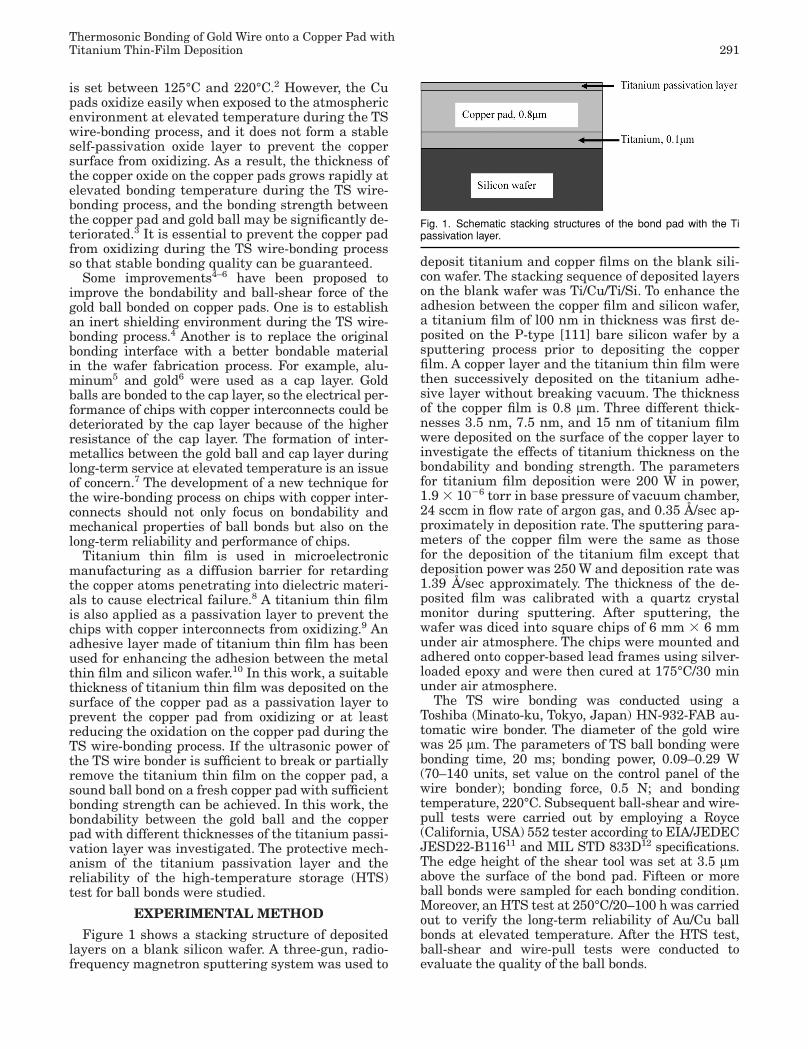
Figure 1 shows a stacking structure of depositedlayers on a blank silicon wafer. A three-gun, radio-frequency magnetron sputtering system was used to
deposit titanium and copper films on the blank sili-con wafer. The stacking sequence of deposited layerson the blank wafer was Ti/Cu/Ti/Si. To enhance theadhesion between the copper film and silicon wafer,a titanium film of l00 nm in thickness was first de-posited on the P-type [111] bare silicon wafer by asputtering process prior to depositing the copperfilm. A copper layer and the titanium thin film werethen successively deposited on the titanium adhe-sive layer without breaking vacuum. The thicknessof the copper film is 0.8 µm. Three different thick-nesses 3.5 nm, 7.5 nm, and 15 nm of titanium filmwere deposited on the surface of the copper layer toinvestigate the effects of titanium thickness on thebondability and bonding strength. The parametersfor titanium film deposition were 200 W in power,1.9 106 torr in base pressure of vacuum chamber,24 sccm in flow rate of argon gas, and 0.35 Å/sec ap-proximately in deposition rate. The sputtering para-meters of the copper film were the same as thosefor the deposition of the titanium film except thatdeposition power was 250 W and deposition rate was1.39 Å/sec approximately. The thickness of the de-posited film was calibrated with a quartz crystalmonitor during sputtering. After sputtering, thewafer was diced into square chips of 6 mm 6 mmunder air atmosphere. The chips were mounted andadhered onto copper-based lead frames using silver-loaded epoxy and were then cured at 175°C/30 minunder air atmosphere.
The TS wire bonding was conducted using aToshiba (Minato-ku, Tokyo, Japan) HN-932-FAB au-tomatic wire bonder. The diameter of the gold wirewas 25 µm. The parameters of TS ball bonding werebonding time, 20 ms; bonding power, 0.09–0.29 W(70–140 units, set value on the control panel of thewire bonder); bonding force, 0.5 N; and bondingtemperature, 220°C. Subsequent ball-shear and wire-pull tests were carried out by employing a Royce(California, USA) 552 tester according to EIA/JEDECJESD22-B11611 and MIL STD 833D12 specifications.The edge height of the shear tool was set at 3.5 µmabove the surface of the bond pad. Fifteen or moreball bonds were sampled for each bonding condition.Moreover, an HTS test at 250°C/20–100 h was carriedout to verify the long-term reliability of Au/Cu ballbonds at elevated temperature. After the HTS test,ball-shear and wire-pull tests were conducted toevaluate the quality of the ball bonds.
Fig. 1. Schematic stacking structures of the bond pad with the Tipassivation layer.
JEM_1001-R6 3/25/04 8:27 PM Page 291
292 Aoh and Chuang
The thickness of the deposited, titanium passiva-tion layer on the copper pad was investigated usingtransmission electron microscopy (TEM). A focusedion-beam technique was applied for TEM specimenpreparation. The depth profiles of the bare copperpad and copper pad with titanium passivation layerwere analyzed using field-emission Auger electronspectroscopy (FEAES), and the depth profiles werecarried out by way of etching the thickness of thecopper pad with the titanium passivation layerusing an argon ion-sputtering device. Electron spec-troscopy for chemical analysis (ESCA) was used toidentify the phase of the titanium passivation layerafter thermal aging at 175°C and 200°C. Monochro-matic Al Kα radiation (1,486.6 eV) was used as anx-ray source with an analyzed area of 20 µm in di-ameter. Scanning electron microscopy (SEM) wasused to investigate the morphology and cross sectionof the ball bonds. The atomic diffusion betweenthe gold ball and copper pad was investigated usingline-scanning analysis of an electron probe x-raymicroanalyzer (EPMA).
RESULTS AND DISCUSSIONInvestigation on Deposited Layers
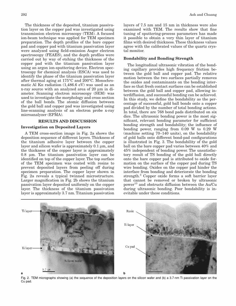
A TEM cross-section image in Fig. 2a shows thedeposition sequence of different layers. Thickness ofthe titanium adhesive layer between the copperlayer and silicon wafer is approximately 0.1 µm, andthe thickness of the copper layer is approximately0.8 µm. The titanium passivation layer can beidentified on top of the copper layer. The top surfaceof the TEM specimen was coated with resins toprevent deposited layers from peeling off duringspecimen preparation. The copper layer shown inFig. 2a reveals a typical twinned microstructure.Larger magnification in Fig. 2b shows the titaniumpassivation layer deposited uniformly on the copperlayer. The thickness of the titanium passivationlayer is approximately 3.7 nm. Titanium passivation
layers of 7.5 nm and 15 nm in thickness were alsoexamined with TEM. The results show that finetuning of sputtering-process parameters has madeit possible to obtain a very thin layer of titaniumfilms with desired thickness. These thickness valuesagree with the calibrated values of the quartz crys-tal monitor.
Bondability and Bonding Strength
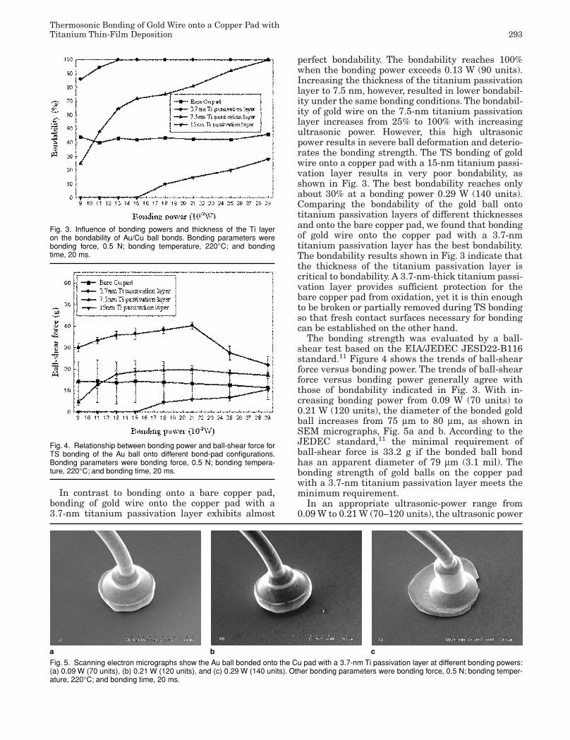
The longitudinal ultrasonic vibration of the bond-ing capillary provides high frequency friction be-tween the gold ball and copper pad. The relativemotion between the two surfaces partially removesthe oxides and contaminants on the bonding inter-face so that fresh contact surfaces can be establishedbetween the gold ball and copper pad, allowing in-terdiffusion, and successful bonding can be achieved.In this study, we define the bondability as the per-centage of successful, gold ball bonds onto a copperpad divided by the number of total bonding actions.In total, there are 768 bond pads distributed on sixdice. The ultrasonic bonding power is the most sig-nificant, relevant bonding parameter for sufficientbonding strength and bondability; the influence ofbonding power, ranging from 0.09 W to 0.29 W(machine setting 70–140 units), on the bondabilityof gold balls onto different bond-pad configurationsis illustrated in Fig. 3. The bondability of the goldball on the bare copper pad varies between 40% and45% independent of bonding power. The unsatisfac-tory result of TS bonding of the gold ball directlyonto the bare copper pad is attributed to oxide for-mation on the surface of the copper pad during TSwire bonding. Oxides on the copper pad hinder theinterface from bonding and deteriorate the bondingstrength.3 Copper oxide forms a soft barrier layerthat cannot be removed or broken by ultrasonicpower13 and obstructs diffusion between the Au/Cuduring ultrasonic bonding. Poor bondability is in-evitable under these conditions.
Fig. 2. TEM micrographs showing (a) the sequence of the deposition layers on the silicon wafer and (b) a 3.7-nm Ti passivation layer on theCu pad.
a b
JEM_1001-R6 3/25/04 8:27 PM Page 292
Thermosonic Bonding of Gold Wire onto a Copper Pad withTitanium Thin-Film Deposition 293
In contrast to bonding onto a bare copper pad,bonding of gold wire onto the copper pad with a3.7-nm titanium passivation layer exhibits almost
perfect bondability. The bondability reaches 100%when the bonding power exceeds 0.13 W (90 units).Increasing the thickness of the titanium passivationlayer to 7.5 nm, however, resulted in lower bondabil-ity under the same bonding conditions. The bondabil-ity of gold wire on the 7.5-nm titanium passivationlayer increases from 25% to 100% with increasingultrasonic power. However, this high ultrasonicpower results in severe ball deformation and deterio-rates the bonding strength. The TS bonding of goldwire onto a copper pad with a 15-nm titanium passi-vation layer results in very poor bondability, asshown in Fig. 3. The best bondability reaches onlyabout 30% at a bonding power 0.29 W (140 units).Comparing the bondability of the gold ball ontotitanium passivation layers of different thicknessesand onto the bare copper pad, we found that bondingof gold wire onto the copper pad with a 3.7-nmtitanium passivation layer has the best bondability.The bondability results shown in Fig. 3 indicate thatthe thickness of the titanium passivation layer iscritical to bondability. A 3.7-nm-thick titanium passi-vation layer provides sufficient protection for thebare copper pad from oxidation, yet it is thin enoughto be broken or partially removed during TS bondingso that fresh contact surfaces necessary for bondingcan be established on the other hand.
The bonding strength was evaluated by a ball-shear test based on the EIA/JEDEC JESD22-B116standard.11 Figure 4 shows the trends of ball-shearforce versus bonding power. The trends of ball-shearforce versus bonding power generally agree withthose of bondability indicated in Fig. 3. With in-creasing bonding power from 0.09 W (70 units) to0.21 W (120 units), the diameter of the bonded goldball increases from 75 µm to 80 µm, as shown inSEM micrographs, Fig. 5a and b. According to theJEDEC standard,11 the minimal requirement ofball-shear force is 33.2 g if the bonded ball bondhas an apparent diameter of 79 µm (3.1 mil). Thebonding strength of gold balls on the copper padwith a 3.7-nm titanium passivation layer meets theminimum requirement.
In an appropriate ultrasonic-power range from0.09 W to 0.21 W (70–120 units), the ultrasonic power
Fig. 3. Influence of bonding powers and thickness of the Ti layeron the bondability of Au/Cu ball bonds. Bonding parameters werebonding force, 0.5 N; bonding temperature, 220°C; and bondingtime, 20 ms.
Fig. 4. Relationship between bonding power and ball-shear force forTS bonding of the Au ball onto different bond-pad configurations.Bonding parameters were bonding force, 0.5 N; bonding tempera-ture, 220°C; and bonding time, 20 ms.
Fig. 5. Scanning electron micrographs show the Au ball bonded onto the Cu pad with a 3.7-nm Ti passivation layer at different bonding powers:(a) 0.09 W (70 units), (b) 0.21 W (120 units), and (c) 0.29 W (140 units). Other bonding parameters were bonding force, 0.5 N; bonding temper-ature, 220°C; and bonding time, 20 ms.
a b c
JEM_1001-R6 3/25/04 8:27 PM Page 293
294 Aoh and Chuang
provides sufficient energy for breaking the titaniumpassivation layer and for atomic diffusion so thata ball bond with sufficient bonding strength isachieved. If ultrasonic power exceeds the appropriaterange, e.g., if it is higher than 0.25 W (130 units), thegold ball is severely deformed, as shown in Fig. 5c.Hence, the ball-shear force decreases significantly.
The ball-shear force curve for the gold wire bondedon the bare copper pad exhibits larger standard devi-ations than those for the copper pad with a titaniumpassivation layer. Our previous work3 also revealedthat minor copper-oxide formation on the copper padresulted in a slight degradation of bonding strength,while prolonged bonding time resulted in rapidoxide formation and thus low bonding strength. Theprevention of the copper pad from oxidation is cru-cial to the improvement of bonding strength andbondability of the gold ball to a copper pad.
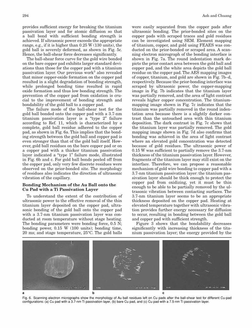
The failure mode of the ball-shear test for thegold ball bonded onto the copper pad with a 3.7-nmtitanium passivation layer is a “type 2” failureaccording to Ref. 11, which is characterized by acomplete, gold ball residue adhered to the copperpad, as shown in Fig. 6a. This implies that the bond-ing strength between the gold ball and copper pad iseven stronger than that of the gold ball itself. How-ever, gold ball residues on the bare copper pad or ona copper pad with a thicker titanium passivationlayer indicated a “type 1” failure mode, illustratedin Fig. 6b and c. For gold ball bonds peeled off fromthe copper pad, only very few discrete residues wereobserved on the prior-bonded site. The morphologyof residues also indicates the direction of ultrasonicvibration of the capillary.
Bonding Mechanism of the Au Ball onto theCu Pad with a Ti Passivation Layer
To understand the extent of the contribution ofultrasonic power to the effective removal of the thintitanium layer deposited on the copper pad, ultra-sonic bonding of the gold ball onto the copper padwith a 3.7-nm titanium passivation layer was con-ducted at room temperature without stage heating.The bonding parameters were bonding force, 0.5 N;bonding power, 0.15 W (100 units); bonding time,20 ms; and stage temperature, 25°C. The gold balls
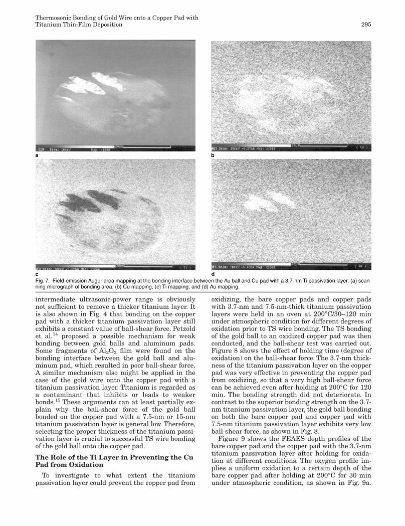
were easily separated from the copper pads afterultrasonic bonding. The prior-bonded sites on thecopper pads with scraped traces and gold residuescan be investigated using SEM. Element mappingof titanium, copper, and gold using FEAES was con-ducted on the prior-bonded or scraped area. A scan-ning electron micrograph of the bonding interface isshown in Fig. 7a. The round indentation mark de-picts the prior contact area between the gold ball andcopper pad, and the white area depicts the gold ballresidue on the copper pad. The AES mapping imagesof copper, titanium, and gold are shown in Fig. 7b–d,respectively. Because the prior-bonding interface wasscraped by ultrasonic power, the copper-mappingimage in Fig. 7b indicates that the titanium layerwas partially removed, and the area of light contrastreveals higher copper concentration. The titanium-mapping image shown in Fig. 7c indicates that thetitanium was partially removed in the round inden-tation area because there is a slightly darker con-trast than the untouched area with thin titaniumdeposition. The dark contrast in Fig. 7c shows thatthe titanium layer was partially removed. The goldmapping image shown in Fig. 7d also confirms thatbonding was achieved in the area of light contrastwhere an elevated gold concentration was detectedbecause of gold residues. The ultrasonic power of0.15 W was sufficient to partially remove the 3.7-nmthickness of the titanium passivation layer. However,fragments of the titanium layer may still exist on theinterface. Therefore, we can propose a reasonablemechanism of gold wire bonding to copper pad with a3.7-nm titanium passivation layer: the titanium pas-sivation layer should be thick enough to protect thecopper pad from oxidizing, yet it must be thinenough to be able to be partially removed by the ul-trasonic vibration between contacting surfaces. The3.7-nm titanium layer seems to be an appropriatethickness deposited on the copper pad. Heating atelevated temperature together with ultrasonic vibra-tion provides further energy necessary for diffusionto occur, resulting in bonding between the gold balland copper pad with sufficient strength.
Figure 3 shows that the bondability decreasessignificantly with increasing thickness of the tita-nium passivation layer; the energy provided by the
a b c
Fig. 6. Scanning electron micrographs show the morphology of Au ball residues left on Cu pads after the ball-shear test for different Cu-padconfigurations: (a) Cu pad with a 3.7-nm Ti passivation layer, (b) bare Cu pad, and (c) Cu pad with a 7.5-nm Ti passivation layer.
JEM_1001-R6 3/25/04 8:27 PM Page 294
Thermosonic Bonding of Gold Wire onto a Copper Pad withTitanium Thin-Film Deposition 295
intermediate ultrasonic-power range is obviouslynot sufficient to remove a thicker titanium layer. Itis also shown in Fig. 4 that bonding on the copperpad with a thicker titanium passivation layer stillexhibits a constant value of ball-shear force. Petzoldet al.14 proposed a possible mechanism for weakbonding between gold balls and aluminum pads.Some fragments of Al2O3 film were found on thebonding interface between the gold ball and alu-minum pad, which resulted in poor ball-shear force.A similar mechanism also might be applied in thecase of the gold wire onto the copper pad with atitanium passivation layer. Titanium is regarded asa contaminant that inhibits or leads to weakerbonds.15 These arguments can at least partially ex-plain why the ball-shear force of the gold ballbonded on the copper pad with a 7.5-nm or 15-nmtitanium passivation layer is general low. Therefore,selecting the proper thickness of the titanium passi-vation layer is crucial to successful TS wire bondingof the gold ball onto the copper pad.
The Role of the Ti Layer in Preventing the CuPad from Oxidation
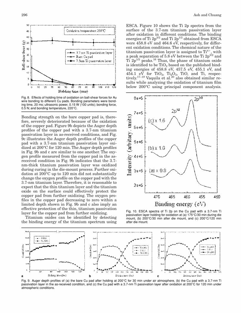
To investigate to what extent the titaniumpassivation layer could prevent the copper pad from
oxidizing, the bare copper pads and copper padswith 3.7-nm and 7.5-nm-thick titanium passivationlayers were held in an oven at 200°C/30–120 minunder atmospheric condition for different degrees ofoxidation prior to TS wire bonding. The TS bondingof the gold ball to an oxidized copper pad was thenconducted, and the ball-shear test was carried out.Figure 8 shows the effect of holding time (degree ofoxidation) on the ball-shear force. The 3.7-nm thick-ness of the titanium passivation layer on the copperpad was very effective in preventing the copper padfrom oxidizing, so that a very high ball-shear forcecan be achieved even after holding at 200°C for 120min. The bonding strength did not deteriorate. Incontrast to the superior bonding strength on the 3.7-nm titanium passivation layer, the gold ball bondingon both the bare copper pad and copper pad with7.5-nm titanium passivation layer exhibits very lowball-shear force, as shown in Fig. 8.
Figure 9 shows the FEAES depth profiles of thebare copper pad and the copper pad with the 3.7-nmtitanium passivation layer after holding for oxida-tion at different conditions. The oxygen profile im-plies a uniform oxidation to a certain depth of thebare copper pad after holding at 200°C for 30 minunder atmospheric condition, as shown in Fig. 9a.
a b
c dFig. 7. Field-emission Auger area mapping at the bonding interface between the Au ball and Cu pad with a 3.7-nm Ti passivation layer: (a) scan-ning micrograph of bonding area, (b) Cu mapping, (c) Ti mapping, and (d) Au mapping.
JEM_1001-R6 3/25/04 8:28 PM Page 295
296 Aoh and Chuang
Bonding strength on the bare copper pad is, there-fore, severely deteriorated because of the oxidationof the copper pad. Figure 9b depicts the Auger depthprofiles of the copper pad with a 3.7-nm titaniumpassivation layer in as-received conditions, and Fig.9c illustrates the Auger depth profiles of the copperpad with a 3.7-nm titanium passivation layer oxi-dized at 200°C for 120 min. The Auger depth profilesin Fig. 9b and c are similar to one another. The oxy-gen profile measured from the copper pad in the as-received condition in Fig. 9b indicates that the 3.7-nm-thick titanium passivation layer was oxidizedduring curing in the die-mount process. Further oxi-dation at 200°C up to 120 min did not substantiallychange the oxygen profile on the copper pad with the3.7-nm titanium layer. Therefore, it is reasonable toexpect that the thin titanium layer and the titaniumoxide on the surface could effectively protect thecopper pad from further oxidizing. The oxygen pro-files in the copper pad decreasing to zero within alimited depth shown in Fig. 9b and c also imply aneffective protection of the thin, titanium passivationlayer for the copper pad from further oxidizing.
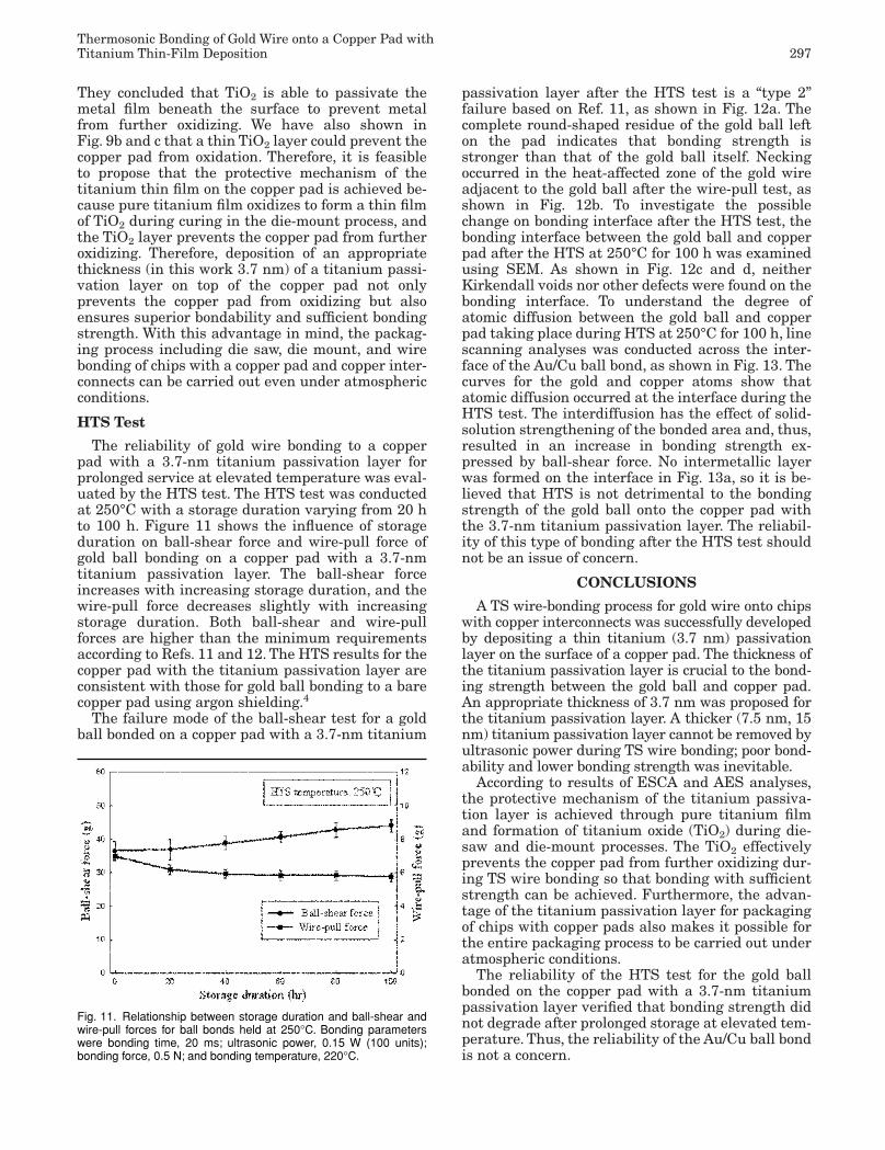
Titanium oxides can be identified by detectingthe binding energy of the titanium spectrum using
ESCA. Figure 10 shows the Ti 2p spectra from thesurface of the 3.7-nm titanium passivation layerafter oxidation in different conditions. The bindingenergies of Ti 2p3/2 and Ti 2p1/2 obtained from ESCAwere 458.8 eV and 464.6 eV, respectively, for differ-ent oxidation conditions. The chemical nature of thetitanium passivation layer is assigned to Ti4, witha peak separation of 5.8 eV between the Ti 2p3/2 andTi 2p1/2 peaks.16 Thus, the phase of titanium oxideis identified to be TiO2 based on the published bind-ing energies of 458.8 eV, 457.5 eV, 455.1 eV, and454.1 eV for TiO2, Ti2O3, TiO, and Ti, respec-tively.17–19 Vaquila et al.20 also obtained similar re-sults while analyzing the oxidation of titanium filmbelow 200°C using principal component analysis.
Fig. 8. Effects of holding time of oxidation on ball-shear forces for Auwire bonding to different Cu pads. Bonding parameters were bond-ing time, 20 ms; ultrasonic power, 0.15 W (100 units); bonding force,0.5 N; and bonding temperature, 220°C.
a b cFig. 9. Auger depth profiles of (a) the bare Cu pad after holding at 200°C for 30 min under air atmosphere, (b) the Cu pad with a 3.7-nm Tipassivation layer in the as-received condition, and (c) the Cu pad with a 3.7-nm Ti passivation layer after oxidation at 200°C for 120 min underatmospheric conditions.
Fig. 10. ESCA spectra of Ti 2p on the Cu pad with a 3.7-nm Tipassivation layer holding for oxidation at (a) 175°C/30 min during diemount, (b) 200°C/30 min after die mount, and (c) 200°C/120 minafter die mount.
JEM_1001-R6 3/25/04 8:28 PM Page 296
Thermosonic Bonding of Gold Wire onto a Copper Pad withTitanium Thin-Film Deposition 297
They concluded that TiO2 is able to passivate themetal film beneath the surface to prevent metalfrom further oxidizing. We have also shown inFig. 9b and c that a thin TiO2 layer could prevent thecopper pad from oxidation. Therefore, it is feasibleto propose that the protective mechanism of thetitanium thin film on the copper pad is achieved be-cause pure titanium film oxidizes to form a thin filmof TiO2 during curing in the die-mount process, andthe TiO2 layer prevents the copper pad from furtheroxidizing. Therefore, deposition of an appropriatethickness (in this work 3.7 nm) of a titanium passi-vation layer on top of the copper pad not onlyprevents the copper pad from oxidizing but alsoensures superior bondability and sufficient bondingstrength. With this advantage in mind, the packag-ing process including die saw, die mount, and wirebonding of chips with a copper pad and copper inter-connects can be carried out even under atmosphericconditions.
HTS Test
The reliability of gold wire bonding to a copperpad with a 3.7-nm titanium passivation layer forprolonged service at elevated temperature was eval-uated by the HTS test. The HTS test was conductedat 250°C with a storage duration varying from 20 hto 100 h. Figure 11 shows the influence of storageduration on ball-shear force and wire-pull force ofgold ball bonding on a copper pad with a 3.7-nmtitanium passivation layer. The ball-shear forceincreases with increasing storage duration, and thewire-pull force decreases slightly with increasingstorage duration. Both ball-shear and wire-pullforces are higher than the minimum requirementsaccording to Refs. 11 and 12. The HTS results for thecopper pad with the titanium passivation layer areconsistent with those for gold ball bonding to a barecopper pad using argon shielding.4
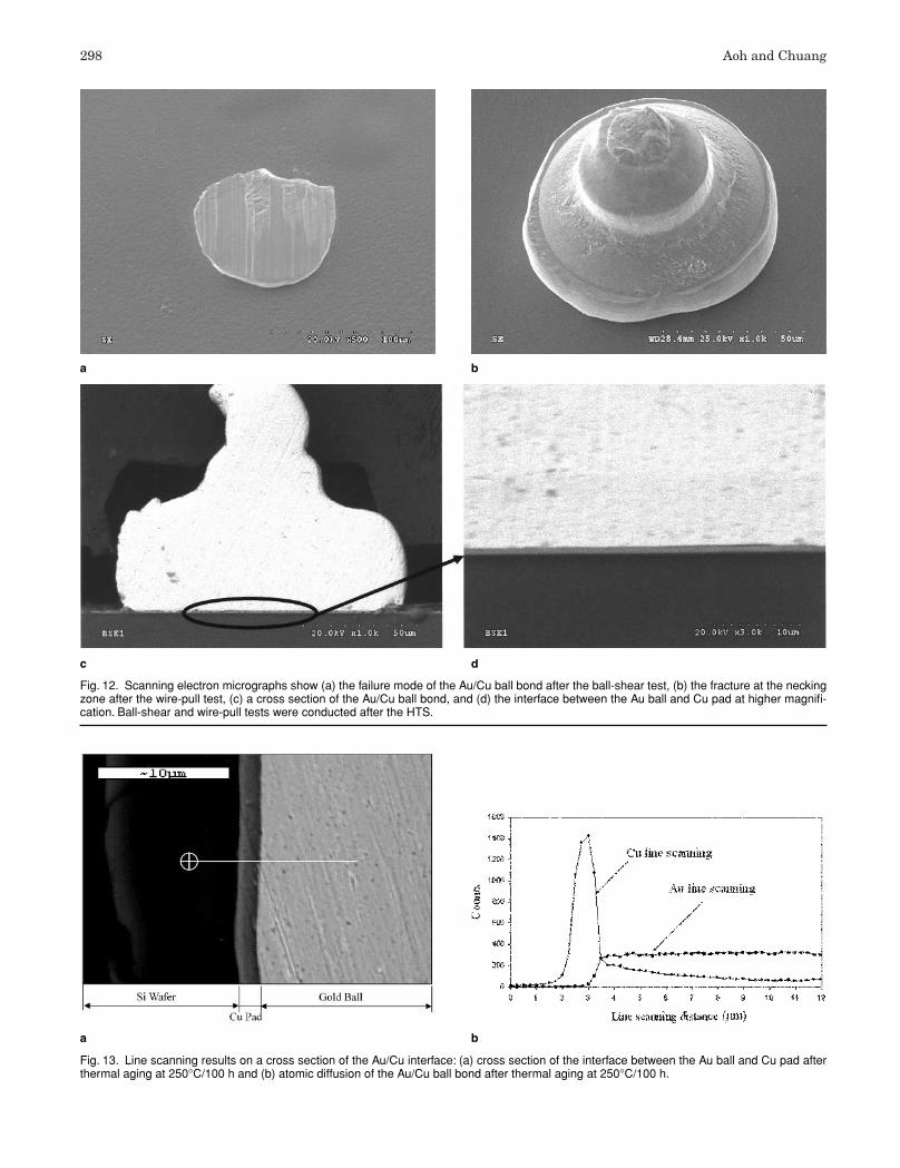
The failure mode of the ball-shear test for a goldball bonded on a copper pad with a 3.7-nm titanium
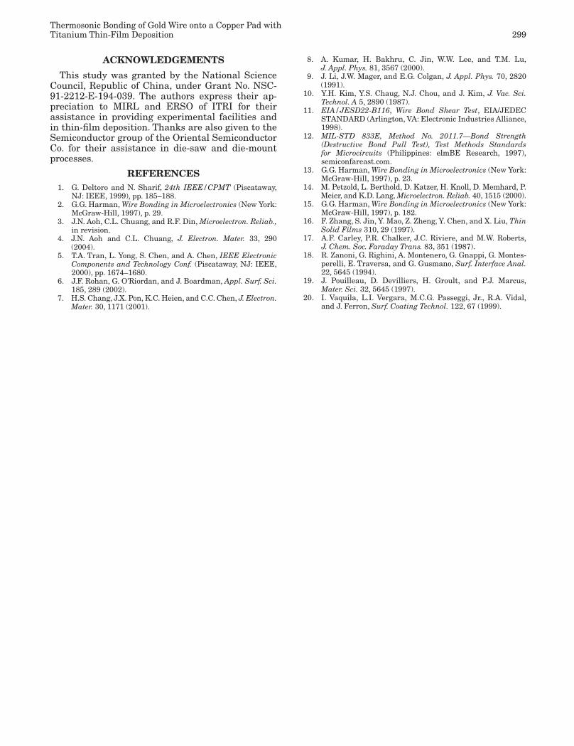
passivation layer after the HTS test is a “type 2”failure based on Ref. 11, as shown in Fig. 12a. Thecomplete round-shaped residue of the gold ball lefton the pad indicates that bonding strength isstronger than that of the gold ball itself. Neckingoccurred in the heat-affected zone of the gold wireadjacent to the gold ball after the wire-pull test, asshown in Fig. 12b. To investigate the possiblechange on bonding interface after the HTS test, thebonding interface between the gold ball and copperpad after the HTS at 250°C for 100 h was examinedusing SEM. As shown in Fig. 12c and d, neitherKirkendall voids nor other defects were found on thebonding interface. To understand the degree ofatomic diffusion between the gold ball and copperpad taking place during HTS at 250°C for 100 h, linescanning analyses was conducted across the inter-face of the Au/Cu ball bond, as shown in Fig. 13. Thecurves for the gold and copper atoms show thatatomic diffusion occurred at the interface during theHTS test. The interdiffusion has the effect of solid-solution strengthening of the bonded area and, thus,resulted in an increase in bonding strength ex-pressed by ball-shear force. No intermetallic layerwas formed on the interface in Fig. 13a, so it is be-lieved that HTS is not detrimental to the bondingstrength of the gold ball onto the copper pad withthe 3.7-nm titanium passivation layer. The reliabil-ity of this type of bonding after the HTS test shouldnot be an issue of concern.
CONCLUSIONS
A TS wire-bonding process for gold wire onto chipswith copper interconnects was successfully developedby depositing a thin titanium (3.7 nm) passivationlayer on the surface of a copper pad. The thickness ofthe titanium passivation layer is crucial to the bond-ing strength between the gold ball and copper pad.An appropriate thickness of 3.7 nm was proposed forthe titanium passivation layer. A thicker (7.5 nm, 15nm) titanium passivation layer cannot be removed byultrasonic power during TS wire bonding; poor bond-ability and lower bonding strength was inevitable.
According to results of ESCA and AES analyses,the protective mechanism of the titanium passiva-tion layer is achieved through pure titanium filmand formation of titanium oxide (TiO2) during die-saw and die-mount processes. The TiO2 effectivelyprevents the copper pad from further oxidizing dur-ing TS wire bonding so that bonding with sufficientstrength can be achieved. Furthermore, the advan-tage of the titanium passivation layer for packagingof chips with copper pads also makes it possible forthe entire packaging process to be carried out underatmospheric conditions.
The reliability of the HTS test for the gold ballbonded on the copper pad with a 3.7-nm titaniumpassivation layer verified that bonding strength didnot degrade after prolonged storage at elevated tem-perature. Thus, the reliability of the Au/Cu ball bondis not a concern.
Fig. 11. Relationship between storage duration and ball-shear andwire-pull forces for ball bonds held at 250°C. Bonding parameterswere bonding time, 20 ms; ultrasonic power, 0.15 W (100 units);bonding force, 0.5 N; and bonding temperature, 220°C.
JEM_1001-R6 3/25/04 8:28 PM Page 297
298 Aoh and Chuang
Fig. 12. Scanning electron micrographs show (a) the failure mode of the Au/Cu ball bond after the ball-shear test, (b) the fracture at the neckingzone after the wire-pull test, (c) a cross section of the Au/Cu ball bond, and (d) the interface between the Au ball and Cu pad at higher magnifi-cation. Ball-shear and wire-pull tests were conducted after the HTS.
a b
c d
Fig. 13. Line scanning results on a cross section of the Au/Cu interface: (a) cross section of the interface between the Au ball and Cu pad afterthermal aging at 250°C/100 h and (b) atomic diffusion of the Au/Cu ball bond after thermal aging at 250°C/100 h.
a b
JEM_1001-R6 3/25/04 8:28 PM Page 298
Thermosonic Bonding of Gold Wire onto a Copper Pad withTitanium Thin-Film Deposition 299
ACKNOWLEDGEMENTS
This study was granted by the National ScienceCouncil, Republic of China, under Grant No. NSC-91-2212-E-194-039. The authors express their ap-preciation to MIRL and ERSO of ITRI for theirassistance in providing experimental facilities andin thin-film deposition. Thanks are also given to theSemiconductor group of the Oriental SemiconductorCo. for their assistance in die-saw and die-mountprocesses.
REFERENCES1. G. Deltoro and N. Sharif, 24th IEEE/CPMT (Piscataway,
NJ: IEEE, 1999), pp. 185–188.2. G.G. Harman, Wire Bonding in Microelectronics (New York:
McGraw-Hill, 1997), p. 29.3. J.N. Aoh, C.L. Chuang, and R.F. Din, Microelectron. Reliab.,
in revision.4. J.N. Aoh and C.L. Chuang, J. Electron. Mater. 33, 290
(2004).5. T.A. Tran, L. Yong, S. Chen, and A. Chen, IEEE Electronic
Components and Technology Conf. (Piscataway, NJ: IEEE,2000), pp. 1674–1680.
6. J.F. Rohan, G. O'Riordan, and J. Boardman, Appl. Surf. Sci.185, 289 (2002).
7. H.S. Chang, J.X. Pon, K.C. Heien, and C.C. Chen, J. Electron.Mater. 30, 1171 (2001).
8. A. Kumar, H. Bakhru, C. Jin, W.W. Lee, and T.M. Lu,J. Appl. Phys. 81, 3567 (2000).
9. J. Li, J.W. Mager, and E.G. Colgan, J. Appl. Phys. 70, 2820(1991).
10. Y.H. Kim, Y.S. Chaug, N.J. Chou, and J. Kim, J. Vac. Sci.Technol. A 5, 2890 (1987).
11. EIA/JESD22-B116, Wire Bond Shear Test, EIA/JEDECSTANDARD (Arlington, VA: Electronic Industries Alliance,1998).
12. MIL-STD 833E, Method No. 2011.7—Bond Strength(Destructive Bond Pull Test), Test Methods Standardsfor Microcircuits (Philippines: elmBE Research, 1997),semiconfareast.com.
13. G.G. Harman, Wire Bonding in Microelectronics (New York:McGraw-Hill, 1997), p. 23.
14. M. Petzold, L. Berthold, D. Katzer, H. Knoll, D. Memhard, P.Meier, and K.D. Lang, Microelectron. Reliab. 40, 1515 (2000).
15. G.G. Harman, Wire Bonding in Microelectronics (New York:McGraw-Hill, 1997), p. 182.
16. F. Zhang, S. Jin, Y. Mao, Z. Zheng, Y. Chen, and X. Liu, ThinSolid Films 310, 29 (1997).
17. A.F. Carley, P.R. Chalker, J.C. Riviere, and M.W. Roberts,J. Chem. Soc. Faraday Trans. 83, 351 (1987).
18. R. Zanoni, G. Righini, A. Montenero, G. Gnappi, G. Montes-perelli, E. Traversa, and G. Gusmano, Surf. Interface Anal.22, 5645 (1994).
19. J. Pouilleau, D. Devilliers, H. Groult, and P.J. Marcus,Mater. Sci. 32, 5645 (1997).
20. I. Vaquila, L.I. Vergara, M.C.G. Passeggi, Jr., R.A. Vidal,and J. Ferron, Surf. Coating Technol. 122, 67 (1999).
JEM_1001-R6 3/25/04 8:28 PM Page 299
Copyright © 2022 FDOKUMEN